parallel gap welding kovar ribbons to copper conductor printed … · nasa technical note parallel...
TRANSCRIPT
N A S A TECHNICAL NOTE
PARALLEL GAP WELDING KOVAR RIBBONS TO COPPER CONDUCTOR PRINTED WIRING BOARDS
by G . E . McDaniel U
George C. Marshall Space Flight Center *
Marshall Space Flight Center, Ala. 35812 0
NATIONAL AERONAUTICS AND SPACE ADMINISTRATION WASHINGTON, D. C. MARC,H' 1971
I
https://ntrs.nasa.gov/search.jsp?R=19710009262 2018-05-30T18:54:10+00:00Z

"
1. Report No. I NASA TN D-6236 1- 4. Title and Subtitle
2. Government Accession No. .. ~
I Parallel Gap Welding Kovar Ribbons to Copper Conductor Printed Wiring Boards
I 7. Author(s1
~.
I 3. Recipient's Catalog No. -.
TECH LIBRARY KAFB, NM
lllllllllllllllllPlllllHli 0133088
8. Performing Organization Report No.
G. E. McDaniel I I . ." - ~~ 10. Work Unit No. I 9. Performing Organization Name and Address M654
I George C. Marshall Space Flight Center Marshall Space Flight Center, Alabama 358 12 i 11. Contract or Grant No.
L 13. Type of Report and Period Covered I 12. Sponsoring Agency Name and Address Technical Note
I National Aeronautics and Space Administration Washington, D. C. 20546 i -~ ~ ,. ~
14. Sponsoring Agency Code
I
Prepared by the Quality and Reliability Assurance Laboratory, Science and Engineering Directorate
. - - .. 16. Abstract
-~
This report describes an investigation to determine the feasibility of, and to subsequently develop the quality assurance criteria for parallel gap welding Kovar ribbons to copper conductor printed wiring boards. The investigation included pre- liminary screening tests considering several copper conductor sizes (thicknesses and widths), platiag combinations (types and thicknesses), and ribbon sizes. Several successful combinations were derived which were explored in greater depth.
17. Key Words (Suggested by Authoris)) . . ~-
Plating Coating Inspection criteria
I 19. Security Classif. (of this report) .. .. " - -
Unclassified ~.
18. Distribution Statement ~.
U n c l a s s i f i e d - Unlimited
I -37 I $3.00 ~
'For sale by the Clearinghouse for Federal Scientific and Technical Information Springfield, Virginia 22151

TABLE OF CONTENTS
Page
SECTION I .
SECTION I1 .
SECTION 111 .
SECTION IV .
SECTION V .
SECTION VI .
SECTION VI1 .
SECTION VI11 .
APPENDIX A .
APPENDIX B .
SUMMARY . . . . . . . . . . . . . . . . . . . . . . . . . . . . . . . . . . . . . . . . 1
INTRODUCTION . . . . . . . . . . . . . . . . . . . . . . . . . . . . . . . . . . 1
PURPOSE AND OBJECTIVE . . . . . . . . . . . . . . . . . . . . . . . . . . 2
LITERATURE SURVEY . . . . . . . . . . . . . . . . . . . . . . . . . . . . . 3
MATERIALS AND EQUIPMENT . . . . . . . . . . . . . . . . . . . . . 3
A . Materials . . . . . . . . . . . . . . . . . . . . . . . . . . . . . . . . . . . . . . 3 B . Equipment . . . . . . . . . . . . . . . . . . . . . . . . . . . . . . . . . . . . . . 5
WELD TEST PROCEDURES . . . . . . . . . . . . . . . . . . . . . . . . . . 6
A . Material Preparation . . . . . . . . . . . . . . . . . . . . . . . . . . . . . . 6 B . Weld Parameters . . . . . . . . . . . . . . . . . . . . . . . . . . . . . . . . . . 7 C . Weld Schedule Development . . . . . . . . . . . . . . . . . . . . . . . . 7
PRELIMINARY SCREENING TESTS . . . . . . . . . . . . . . . . . . 8
A . Kovar Ribbons Welded to 2-Ounce Copper Conductors . . . . 8 B . Kovar Ribbons Welded to 1-Ounce Copper Conductors . . . . 12 C . Summary of Test Results . . . . . . . . . . . . . . . . . . . . . . . . . . 14
FINAL QUALIFICATION TESTS . . . . . . . . . . . . . . . . . . . . . . 14
A . Test Combinations . . . . . . . . . . . . . . . . . . . . . . . . . . . . . . . . 15 B . Test Results . . . . . . . . . . . . . . . . . . . . . . . . . . . . . . . . . . . . 15
CONCLUSIONS AND RECOMMENDATIONS . . . . . . . . . . . . 21
A . Conclusions . . . . . . . . . . . . . . . . . . . . . . . . . . . . . . . . . . . . 21 B . Recommendations . . . . . . . . . . . . . . . . . . . . . . . . . . . . . . . . 22
STATISTICAL ANALYSIS OF TEST RESULTS . . . . . . . . . . 23
QUALITY ASSURANCE AND INSPECTION CRITERIA . . . . 26
REFERENCES . . . . . . . . . . . . . . . . . . . . . . . . . . . . . . . . . . . . 28
BIBLIOGRAPHY . . . . . . . . . . . . . . . . . . . . . . . . . . . . . . . . . . 29
... l l 1
LIST OF ILLUSTRATIONS
Figure
1 .
2 .
3 .
4 .
5
6 .
7 .
8 .
9 .
10 .
11 .
12 .
13 .
14 .
15 .
16 .
Title Page
Kovar ribbon welded to bare copper conductor (135X) . . . . . . . . . . . . 10
Kovar ribbon welded to gold-plated copper conductor (135X) . . . . . . 10
Acceptable weld connection of Kovar ribbon to gold-over- nickel-plated copper conductor (135X) ........................ 11
Discrepant weld connection (copper melting) using same conditions as Figure 3 (1 35X) . . . . . . . . . . . . . . . . . . . . . . . . . . . . . . . . 11
Weld connection of Kovar ribbon to gold-overheavy-nickel- plated copper conductor (135X) . . . . . . . . . . . . . . . . . . . . . . . . . . . . . . 11
Kovar ribbon welded to a tinned copper conductor (135X) . . . . . . . . 13
Higher magnification of the interface in Figure 6 (893X) . . . . . . . . . . 13
Typical copper erosion along the length of a Kovar ribbon (893X) . . . . 13
Settling of the copper conductor under a Kovar ribbon (135X) . . . . . . 14
Gas pocket. produced at the gold-nickel-plating interface (135X) . . . . 17
Pull-tested samples of electrosolder-plated copper conductors ( 15X) . . . 19
Welded connection with nickel ( 1000 microinches) over copper conductor(l35X) . . . . . . . . . . . . . . . . . . . . . . . . . . . . . . . . . . . . . . . . 20
Acceptable welded connection of gold-over-nickel plating. approximately 1500 microinches thick (1 35X) . . . . . . . . . . . . . . . . . . 20
Acceptable welded connection of electrosolder plating (500 microinches) over copper conductor on G-10 laminate (135X) . . . . . . 20
Acceptable welded connection of electrosolder plating (750 microinches) over copper conductor on Micarta laminate (135X) . . . . 20
Acceptable welded connection of electrosolder plating (1 000 microinches) over copper conductor on FR-45 laminate (1 35X) . . . . . . 21
iv
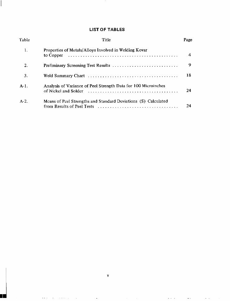
LIST OF TABLES
Table Title Page
1. Properties of Metals/Alloys Involved in Welding Kovar tocopper . . . . . . . . . . . . . . . . . . . . . . . . . . . . . . . . . . . . . . . . . . . . . 4
2. Preliminary Screening Test Results ........................... 9
3. Weld Summary Chart . . . . . . . . . . . . . . . . . . . . . . . . . . . . . . . . . . . . . 18
A-1. Analysis of Variance of Peel Strength Data for 100 Microinches OfNickelandSolder . . . . . . . . . . . . . . . . . . . . . . . . . . . . . . . . . . . . . 24
A-2. Means of Peel Strengths and Standard Deviations ( S ) Calculated from Results of Peel Tests . . . . . . . . . . . . . . . . . . . . . . . . . . . . . . . . . 24
V
....
ACKNOWLEDGMENT
The test and analysis effort described herein was performed by Mr. A. M. Pasciak and Mr. J . A. Burka under Contract NAS8-20081 to SPACO, Inc., Huntsville, Alabama, whose contribution to this report is gratefully acknowledged.
vi
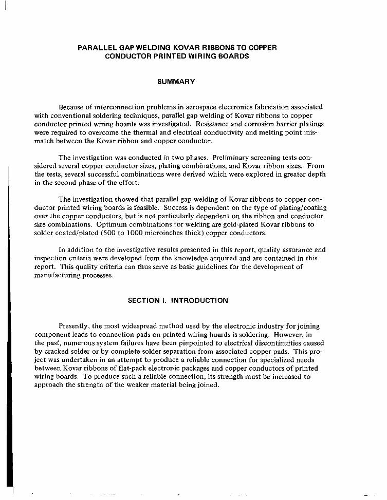
PARALLEL GAP WELDING KOVAR RIBBONS TO COPPER CONDUCTOR PRINTED WIRING BOARDS
SUMMARY
Because of interconnection problems in aerospace electronics fabrication associated with conventional soldering techniques, parallel gap welding of Kovar ribbons to copper conductor printed wiring boards was investigated. Resistance and corrosion barrier platings were required to overcome the thermal and electrical conductivity and melting point mis- match between the Kovar ribbon and copper conductor.
The investigation was conducted in two phases. Preliminary screening tests con- sidered several copper conductor sizes, plating combinations, and Kovar ribbon sizes. From the tests, several successful combinations were derived which were explored in greater depth in the second phase of the effort.
The investigation showed that parallel gap welding of Kovar ribbons to copper con- ductor printed wiring boards is feasible. Success is dependent on the type of plating/coating over the copper conductors, but is not particularly dependent on the ribbon and conductor size combinations. Optimum combinations for welding are gold-plated Kovar ribbons to solder coated/plated (500 to 1000 microinches thick) copper conductors.
In addition to the investigative results presented in this report, quality assurance and inspection criteria were developed from the knowledge acquired and are contained in this report. This quality criteria can thus serve as basic guidelines for the development of manufacturing processes.
SECTION 1. INTRODUCTION
Presently, the most widespread method used by the electronic industry for joining component leads to connection pads on printed wiring boards is soldering. However, in the past, numerous system failures have been pinpointed to electrical discontinuities caused by cracked solder or by complete solder separation from associated copper pads. This pro- ject was undertaken in an attempt to produce a reliable connection for specialized needs between Kovar ribbons of flat-pack electronic packages and copper conductors of printed wiring boards. To produce such a reliable connection, its strength must be increased to approach the strength of the weaker material being joined.
Varying environmental conditions require more reliable connections than the soft soldering technique has provided. Some of these printed wiring board environmental parameters that require higher connection strengths are: Rapid compression and decom- pression, thermal expansion differentials, rapid vacuum reduction, high vibration, and high temperature. All of these conditions place undue stresses upon interconnections, and when the strength of the interconnects is insufficient, electrical discontinuity is induced.
Parallel gap welding is known to provide high interconnection strength when wiring boards of nickel or Kovar cladding is used. This is not always feasible because of the inherent ferromagnetic properties of these materials when used as a conductor [ 11. This would be detrimental in RF circuitry applications in which frequency shift losses and increased signal couplings cannot be tolerated. Nickel or Kovar-clad printed wiring boards are more difficult to fabricate, are less available, and thereby are more costly. The high resistivity also causes them to be unsuitable for some applications.
Because copper-clad printed wiring boards are readily available, reasonably priced, and do not have some of the disadvantages stated above, they were investigated in this project. However, bare copper is highly conductive and susceptible to oxidation and corrosion. Therefore, gold, nickel, and solder platings were selected for use. These platings were designed to serve as a resistance barrier to current flow between Kovar and the highly conductive copper as well as to protect the copper against oxidation and corrosion. The solder acts as a higher resistance to the flow of the direct current than gold or nickel. When molten, the solder then becomes depleted at the Kovar-copper interface by the electrode force during the welding cycle. This causes a brhzing of these materials and results in a highly electrically conductive and reliable connection.
This report discusses materials used with and without plating barriers, equipment, weld parameters, weld schedule development, pull test, and metallographic examination results. Also, quality and inspection requirements are discussed.
SECTION II. PURPOSE AND OBJECTIVE
In an attempt to enhance quality and subsequent reliability by achieving a stronger Kovar ribbon to copper conductor printed wiring board interconnection, parallel gap welding was investigated as the attaching media. This investigation proves the feasibility, establishes some successful combinations of Kovar ribbon and copper conductor sizes and plating conditions, and evolves the general quality assurance and inspection criteria for the technique.
2
SECTION 111. LITERATURE SURVEY
A literature survey of parallel gap welding revealed that numerous evaluation pro- grams were conducted in the United States and in Great Britain. Interest has appeared to be centered toward providing another interconnection technique in addition to soft soldering, one with inherently improved interconnection reliability.
The results of the studies surveyed varied widely and were not in full agreement as t o Kovar-to-copper weldability. W. H. Hill [2] states that satisfactory welds are produced when welding to copper but that the tolerances are narrow. N. Jarosik [3 ] states that copper and Kovar combination welds are unacceptable. The use of barrier platings was investigated by H. G. Carter and W. W. Wilson [4 ] . In their development of a more economical weldable printed wiring board, they state that chemically deposited nickel plating over copper resulted in simple welding, inexpensive board material, and acceptable weld reliability.
Even though test results vary, the studies are in agreement by inference that material process controls and weld system parameter selections and controls are important factors in the achievement of improved weld results by the parallel gap welding technique.
SECTION IV. MATERIALS AND EQUIPMENT
A. Materials
The welding of two materials is ideally achieved when the melting points and thermal and electrical conductivity values are reasonably matched. For a selected energy level, the amount of current flowing through a material is dependent upon its electrical conductivity.
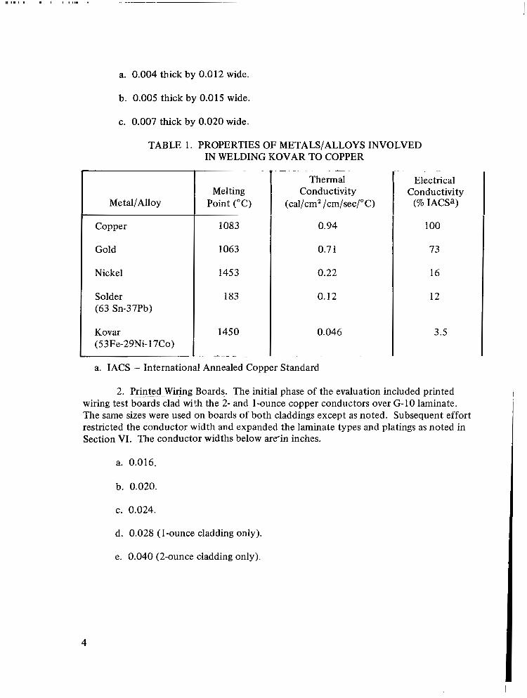
The amount of temperature developed and whether melting occurs are dependent upon the thermal conductivity and melting point of a material. Table 1 lists the important properties of metals and alloys used in this investigation. The barrier platings and coatings discussed below are selected to approximate a match between the properties listed in Table 1.
1. Ribbon Material. Ribbon material used with hard glass hermetic seals is of iron- nickel-cobalt composition and is referred to by trade names of Kovar or Rodar. It will be referred to in this report as Kovar. All ribbon material was gold-plated. The plating thickness was controlled between 95 to 125 microi,nches. The lead dimensions used were confined to the following sizes (in inches):
3
a. 0.004 thick by 0.012 wide.
b. 0.005 thick by 0.015 wide.
c. 0.007 thick by 0.020 wide.
TABLE 1. PROPERTIES OF METALS/ALLQYS INVOLVED IN WELDING KOVAR TO COPPER
Melting Metal/Alloy Point ("C)
Copper
1063 Gold
1083
183 Solder
1453 Nickel
(63 Sn-37Pb)
Kovar 1450 (53Fe-29Ni-17Co)
~~ ~
Thermal Conductivity
(cal/cm* /cm/sec/"C)
0.94
0.7 1
0.22
0.12
0.046
Electrical Conductivity
(% IACSa)
100
73
16
12
3.5
a. IACS - International Annealed Copper Standard
2. Printed Wgng Boards. The initial phase of the evaluation included printed wiring test boards clad with the 2- and 1-ounce copper conductors over G-10 laminate. The same sizes were used on boards of both claddings except as noted. Subsequent effort restricted the conductor width and expanded the laminate types and platings as noted in Section VI. The conductor widths below arcin inches.
a. 0.016.
b. 0.020.
c. 0.024.
d. 0.028 (1-ounce cladding only).
e. 0.040 (2-ounce cladding only).
4
The copper conductor plating corlditions were as follows:
a. Bare.
b. Gold plated.
c. Gold-over-nickel platings.
d. Hot dip-tinned 63/37 tin-lead solder. The hot dip-tinned coating was applied by dipping the test boards into the solder pot containing high purity of 63 percent tin and 37- percent lead solder.
e. Electroplated 63/37 tin-lead, hot oil fused.
B. Equipment
1. Welding System. The welding system used was the Model 1-124-02 Power Supply and Model 2-127-02 Weld Head manufactured by the Weldmatic Division of the Unitek Corporation.
a. Power Supply. The solid-state power supply possessed the capability of pulse control adjustment from 1 to 40 milliseconds in width. A maximum of 2.0 volts amplitude is possible and is dependent upon the pulse-width range selection. This power supply was equipped with manual and/or automatic pulse-width control selection. The manual control mode was used throughout this program to better observe the welding behavior at definite selected parameters.
b. Weld head. The weld head was equipped with electrode holders capable of adjusting the electrode gap tolerance to the nearest 0.001 inch with a micrometer type control. Electrode force variations are readily accomplished from 0.5 to 8.0 pounds. Electrodes RWMA No. 2, size 0.015 by 0.050 inch were used throughout the program.
2. Pull Tester. The pull tester was equipped with a dial-indicating type force gage with readout in pounds and graduated in tenths of a pound. A “hold at maximum’’ feature allows the operator to record pull-test results when convenient. A moveable clamping table holds a specimen and travels at a fixed rate of 3.5 inches per minute away from the stationary recording force gage until the pull test is completed. The pull tester used in this investigation was a Unitek Model 6-092-0 1.
3. Metallogram Equipment. The metallograph used was the Bausch and Lomb Research Model. Complemental equipment included a specimen cutoff machine, specimen polishers, a vibropolisher, zoom microscopes, and other equipment normal to a fully equipped metallographic laboratory.
5
. ”
SECTION V. WELD TEST PROCEDURES
A. Material Preparation
It is of paramount importance in parallel gap welding to use clean materials to achieve good bonding repeatability. Any dirt or contamination of material surfaces change the resistance at the materials' interface in the weld area and produces a weak weld or no weld depending upon the degree of contamination. Therefore, all materials were cleaned with an ethyl alcohol-saturated, lint-free tissue just prior to welding. In addition, the bare copper test boards were first chemically cleaned to remove oxides, then subjected to the alcohol-tissue cleaning process. Plating measurements were metallographically verified of each plating thickness and type on all printed wiring boards used in the program. Initial measurement of the gold-plated Kovar was made from one lot that was subsequently used throughout the program. The approximate thicknesses of the platings were as follows (in microinches):
1. Kovar ribbon gold plating - 100.
2. Copper conductors.
a. Gold ~- 100.
b. Nickel.
(1) 250 (preliminary screening tests only).
(2) 500 (final qualification tests only).
(3) 1000 (final qualification and preliminary tests).
(4) 1500 (final qualification tests only).
c. Hot dip-tinned solder - 750 (preliminary screening tests only).
d. Electroplated, hot-oil fused solder (final qualification test only).
(1) 500.
(2) 750.
(3) 1000.
6
B. Weld Parameters
The proper amount of heat and its distribution required to repeatably produce sound welds are dependent upon the following parameters:
1. Pulse amplitude (voltage) - Selection of pulse amplitude controls the amount of weld current.
2. Pulse duration (time) - Controls the length of time (milliseconds) during which voltage is applied to aid in proper heat distribution.
3. Gap - The air space or dielectric between the electrodes. Varying the gap width controls the resistance between the electrodes.
4. Electrode force - The electrode force holds the ribbon material in place during the weld cycle and also controls somewhat the resistance at the interface of the materials being welded.
C. Weld Schedule Development
The intial weld schedule development investigation revealed that it was necessary to restrict the weld current flow through the highly conductive copper. By decreasing the electrode gap width to the thickness of the Kovar ribbon, more weld current passed through the Kovar and less through the copper, thus providing better heat distribution at the materials’ interface. This resulted in more consistent welding.
An initial electrode force of 1.5 pounds resulted in erratic welding. This erratic welding was attributed to possible surface irregularities and variations in plating densities producing interfacial resistance variations. Increasing the electrode force minimized this undesirable condition whereby more consistent weld quality was obtained. This force was finally optimized at approximately 4.0 pounds and used throughout the program.
By standardizing the electrode gap width to the ribbon thickness and the electrode force to 4.0 pounds, the only variables remaining were pulse amplitude and pulse duration. For welding bare copper, gold-plated copper, and gold-over-nickel plated copper, the 1- through 10-millisecond pulse duration range was used. For welding hot dip-tinned copper and electroplated solder on copper, the 2- through 20-millisecond pulse duration range was selected. The following step-by-step procedure was used to establish pulse amplitude and duration values for each material combination:
1. Initially set the pulse amplitude at minimum and the pulse duration at maximum.
7
2. Incrementally increase the pulse amplitude and perform the welding until a darkened area of the gold plating of the Kovar lead is observed in the gap between the electrodes.
3. Begin pull testing the welded specimens and record the average of five welds at each selected amplitude increment.
4. Continue increasing the amplitude and pull testing the welds until a visually discrepant weld condition is observed.
5. Reduce the pulse duration by selected increments and pull-test welds until the weld separates.
During the preliminary screening tests (Section VI), the pull tests were performed in the lap-shear configuration; however, during the final qualification tests (Section VII), a 180-degree peel-pull test was performed. During the preliminary screening tests, metallographic examinations revealed excessive copper melting on visually-acceptable welds which was not detectable by the lap-shear test; however, the 180-degree peel-pull test revealed the excessive copper melting.
SECTION VI. PRELIMINARY SCREENING TESTS
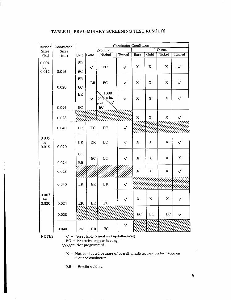
The preliminary screening tests were designed to determine if parallel gap welding of Kovar ribbon to copper conductors was feasible, and to establish some successful com- binations of ribbon and conductor sizes and plating conditions for the purpose of further effort to establish quality requirements for this technique. The preliminary screening tests did not presume to fully consider all possible combinations but did establish a systematic approach to the derivation of successful combinations. An overall evaluation of the test results during this portion of the program is presented in Table 2. This table depicts the various material sizes and copper conductor conditions used in this investigation. Per- formance of the various combinations are discussed in greater detail in the following paragraphs.
A. Kovar Ribbons Welded to 2-Ounce Copper Conductors
I . Bare Copper. Narrow parameter tolerances were encountered when establishing weld schedules for bare copper. Even after a weld schedule was established, discrepant conditions such as blowholes and excessive copper melting occurred during verification of these weld schedules. Average pull strengths of bare copper welds are also lower than the average weld strengths of the other conductor conditions. A transverse cross-section of a welded connection, Kovar ribbon size 0.004 by 0.012 inch welded to 0.040-inch-width
8
Zibbon Sues (in.)
0.004 by
0.012
0.005 by
0.015
0.007 by
0.020
TABLE 11. PRELIMINARY SCREENING TEST RESULTS
Conductor Sues (in.)
0.0 16
0.020
0.024 "
0.028 ~~
0.040
0.020
0.024
0.028
0.040
0.024
0.028
0.040
EC I I I I I ER
I I 1 ""-1 I
NOTES: d = Acceptable (visual and metallurgical). EC = Excessive copper heating.
'/////= Not programmed.
hnce
I
I
x x I
+
X = Not conducted because of overall unsatisfactory performance on 2-ounce conductor.
ER = Erratic welding.
9
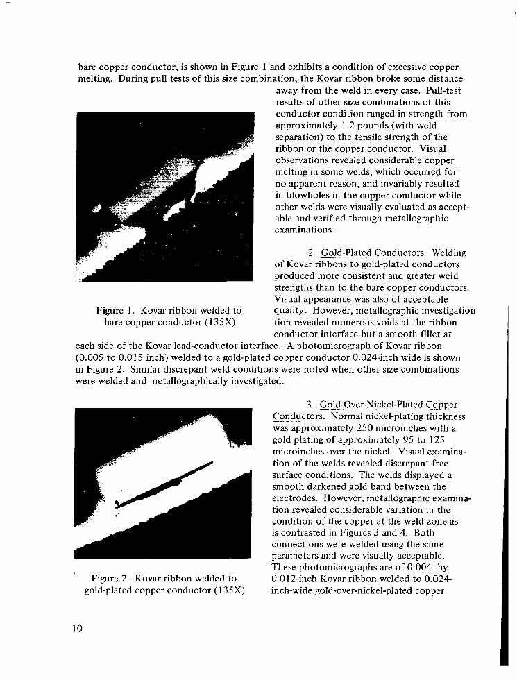
bare copper conductor, is shown in Figure 1 and exhibits a condition of excessive copper melting. During pull tests of this size combination, the Kovar ribbon broke some distance
away from the weld in every case. Pull-test results of other size combinations of this conductor condition ranged in strength from approximately 1.2 pounds (with weld separation) to the tensile strength of the ribbon or the copper conductor. Visual observations revealed considerable copper melting in some welds, which occurred for no apparent reason, and invariably resulted in blowholes in the copper conductor while other welds were visually evaluated as accept- able and verified through metallographic examinations.
2. ~~ Gold-Plated ~ Conductors. Welding of Kovar ribbons to gold-plated conductors produced more consistent and greater weld strengths than to the bare copper conductors. Visual appearance was also of acceptable
Figure 1. Kovar ribbon welded to quality. However, metallographic investigation bare copper conductor (1 35X) tion revealed numerous voids at the ribbon
conductor interface but a smooth fillet at each side of the Kovar lead-conductor interface. A photomicrograph of Kovar ribbon (0.005 to 0.0 15 inch) welded to a gold-plated copper conductor 0.024-inch wide is shown in Figure 2. Similar discrepant weld conditions were noted when other size combinations were welded and metallographically investigated.
Figure 2. Kovar ribbon welded to gold-plated copper conductor (135X)
3. Gold-Over-Nickel-Plated Copper Conductors. Normal nickel-plating thickness was approximately 250 microinches with a gold plating of approximately 95 to 125 microinches over the nickel. Visual examina- tion of the welds revealed discrepant-free surface conditions. The welds displayed a smooth darkened gold band between the electrodes. However, metallographic examina- tion revealed considerable variation in the condition of the copper at the weld zone as is contrasted in Figures 3 and 4. Both connections were welded using the same parameters and were visually acceptable. These photomicrographs are of 0.004- by 0.012-inch Kovar ribbon welded to 0.024- inch-wide gold-over-nickel-plated copper
- " ". -
- - .. "
10
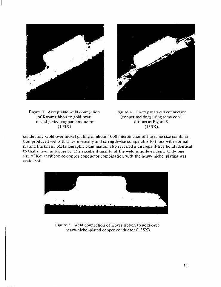
Figure 3. Acceptable weld connection of Kovar ribbon to gold-over-
nickel-plated copper conductor (135X)
Figure 4. Discrepant weld connection (copper melting) using same con-
ditions as Figure 3 ( 1 35X).
conductor. Gold-over-nickel plating of about 1000 microinches of the same size combina- tion produced welds that were visually and strengthwise comparable to those with normal plating thickness. Metallographic examination also revealed a discrepant-free bond identical to that shown in Figure 5 . The excellent quality of the weld is quite evident. Only one size of Kovar ribbon-to-copper conductor combination with the heavy nickel plating was evaluated.
Figure 5 . Weld connection of Kovar ribbon to gold-ovep heavy-nickel-plated copper conduktor (1 35X).
11
4. Hot Dip-Tinned Copper Conductors. This condition exhibited the highest quality of welds. W>d schedules of all size combinations were verified by subsequent metallographic examinations. All cross-sectioned welds revealed discrepant-free acceptable welds. A typical weld of Kovar ribbon (0.005 by 0.01 5 inch) welded to 0.040-inch-wide hot dip-tinned copper conductor is shown in Figure 6. Note the slight copper erosion on each side of the Kovar. A portion of the weld of this connection is depicted at higher magnification in Figure 7 and shows a brazed alloy at the Kovar-copper interface. The eroded portion at the side of the Kovar is also shown at higher magnification in Figure 8. This erosion can be attributed to the hot molten solder being expulsed from under the Kovar ribbon by the force of the electrodes as the weld energy is released during the weld cycle. This erosion was observed in all of the metallographically investigated Kovar ribbon to hot dip-tinned copper conductor weld specimens.
B. Kovar Ribbons Welded to 1-Ounce Copper Conductors
The overall quality of welded connections of a Kovar ribbon and a 1-ounce copper conductor was generally unsatisfactory. Otherwise acceptable connections displayed bending or settling of the copper. Performance of the various combinations are discussed in greater detail in the following paragraphs.
1. Bare Copper Conductor. This conductor condition was not welded with repeat- able satisfactory results on 2-ounce conductors; therefore, only one size combination (0.007 by 0.020 with Kovar ribbon and 0.028-inch-wide copper conductors) was investigated. This also yielded unsatisfactory results.
-~
2. Gold and Gold-Over-Nickel-Plated. Copper Conductors. Again, these platings did not resolve the excessive copper conductor melting problem confronted during welding with the 2-ounce copper conductors; therefore, only one size combination (0.007 by 0.020 Kovar ribbon and an 0.028-inch-wide copper conductor) was investigated. As expected, the results were unsatisfactory.
3. Hot Dip-Tinned Copper Conductors. Tests were completed for all scheduled size combinations. Visual inspection revealed no discrepant weld conditions. Metallographic examinations showed that the bonded interface was of a similar acceptable condition as the 2-ounce conductors. However, there appears to be a'tendency for the 1-ounce copper conductors to settle more under the Kovar ribbon than the 2-ounce copper conductors. A most severe case of this condition is shown in Figure 9 where an 0.004- by 0.0 12-inch Kovar ribbon was welded to 0.028-inch-wide hot dip-tinned copper conductors.
" . .
12
I I I 11.1111 I I
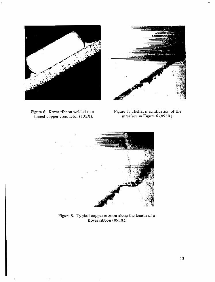
Figure 6. Kovar ribbon welded to a tinned copper conductor (1 35X).
Figure 7. Higher magnification of the interface in Figure 6 (893X).
Figure 8. Typical copper erosion along the length of a Kovar ribbon (893X).
13
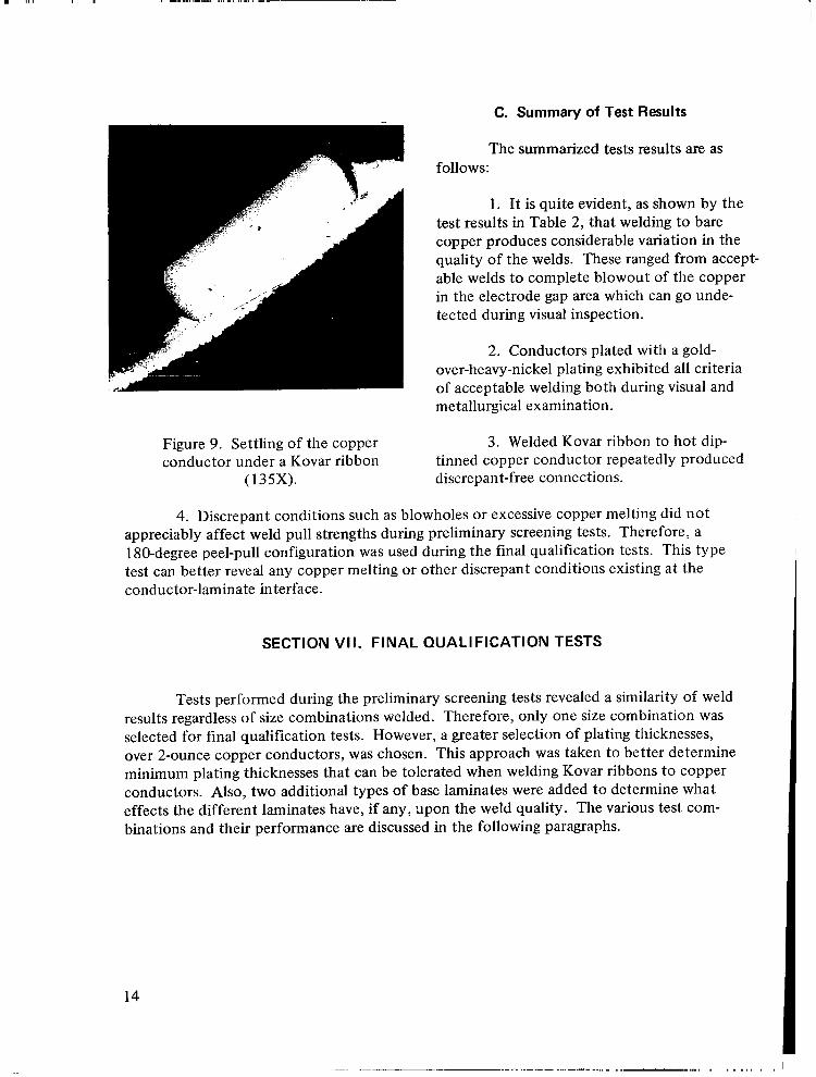
Figure 9. Settling of the copper conductor under a Kovar ribbon
(135X).
C. Summary of Test Results
The summarized tests results are as follows:
1 . It is quite evident, as shown by the test results in Table 2, that welding to bare copper produces considerable variation in the quality of the welds. These ranged from accept- able welds to complete blowout of the copper in the electrode gap area which can go unde- tected during visual inspection.
2. Conductors plated with a gold- over-heavy-nickel plating exhibited all criteria of acceptable welding both during visual and metallurgical examination.
3. Welded Kovar ribbon to hot dip- tinned copper conductor repeatedly produced discrepant-free connections.
4. Discrepant conditions such as blowholes or excessive copper melting did not appreciably affect weld pull strengths during preliminary screening tests. Therefore, a 180-degree peel-pull configuration was used during the final qualification tests. This type test can better reveal any copper melting or other discrepant conditions existing at the conductor-laminate interface.
SECTION VII. FINAL QUALIFICATION TESTS
Tests performed during the preliminary screening tests revealed a similarity of weld results regardless of size combinations welded. Therefore, only one size combination was selected for final qualification tests. However, a greater selection of plating thicknesses, over 2-ounce copper conductors, was chosen. This approach was taken to better determine minimum plating thicknesses that can be tolerated when welding Kovar ribbons to copper conductors. Also, two additional types of base laminates were added to determine what effects the different laminates have, if any, upon the weld quality. The various test com- binations and their performance are discussed in the following paragraphs.
14
A. Test Combinations
1. Kovar Ribbon Material. The Kovar lead material was gold-plated (0.005 by 0.0 15 inch). The gold-plating thickness was approximately 100 microinches thick.
2. Printed Wiring Test Boa* The copper conductors were all 0.024-inch wide on G-10, FR-45, and Micarta laminates. These laminates were used to determine whether the welding heat affects them similarly. The platings and plating thicknesses (in microinches) over the copper conductor of each laminate were as follows:
a. Nickel, Gold Over Plate.
(1) 500.
(2) 1000.
(3) 1500.
A nickel sulfamate bath solution was used for nickel plating. The nickel was overplated with gold, approximately 100 microinches thick to preclude nickel passivation.
b. Electroplated Hot Oil Fused Solder.
(1) 500.
(2) 750.
(3) 1000.
The solder platings were fused in peanut oil at 500°F. This was performed to reveal any contaminated copper surfaces which would cause dewet of the solder and to preclude copper oxidation.
B. Test Results
1. General, Acceptable welds were produced repeatedly when welding to electro- plated, hot-oil fused solder, copper conductors. All three laminates, G-10, FR-45, and Micarta, showed similar surface conditions in the heat-affected zone.
2. Plating Effects. Plated nickel thickness of approximately 500 microinches did not produce consistently discrepant-free welds. During t'he qualification of the weld schedule, visible blowholes were noted in the conductors; therefore, this thickness was established as unqualified for parallel gap welding. Nickel-plated thicknesses of approximately
15
1000 and 1500 microinches produced visually acceptable welds. However, when metallographically examined, the gold plating used to prevent nickel passivation showed signs of buckling when subjected to weld heat. In addition, voids were seen in the weld zone. These two unacceptable conditions may be attributed to the outgassing of the occluded organic materials used in the plating solutions. Representative examples of this condition encountered are pinpointed in photomicrographs A and B of Figure 10. Note the gas pockets under the buckled gold plating. The electroplated, hot-oil fused solder appears to lend itself favorably to parallel gap welding of Kovar ribbons to copper conductors.
3 . Peel-Pull Tests. Peel-pull tests revealed that the copper conductors did not break in a uniform line across the welded connection but followed interfacial bonding. In some instances, the break was uniform across the weld as the ribbon was peeled off. An example of peel-pull-tested specimens is shown in Figure 1 1 . No appreciable difference in the tearing mode was noted between nickel- and electrosolder-plated conductors. The copper con- ductor pinpointed by one arrow shows its rather uniform breaking mode. The copper conductor identified between the two arrows shows an irregular tearing effect. This irregular tearing of the copper conductor resulted in the observed peel-puli strength variations.
For each plating condition and plating thickness over copper conductor of each laminate, a qualification test was conducted. This consisted of welding a total of 50 con- nections of each category and subjecting them to peel-pull tests. In only one case was the peel strength below 1 pound (0.8). Four other welds separated but were comparable in strengths to those in which either the Kovar ribbon or copper conductors broke. All five weld separations were in the 1000-microinch plated-nickel thickness category.
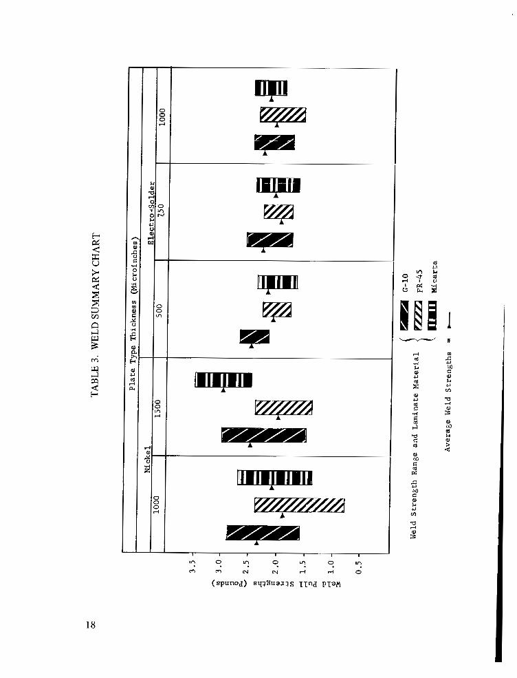
A summary chart of weld test results is given in Table 3. It presents the average strength of each plating condition, plating thickness, and laminate materials. The weld range is also shown for each category by the length of each bar. Even though the maximum values for nickel plating are generally higher than for electrosolder plating, the minimums are lower for nickel in all cases except one. Even the lowest pull strength of 0.8 pound (approximately 13 ounces) is considerably greater than parallel gap soldered connections which showed minimum strengths of approximately 2 to 3 ounces, using similar material size combinations [ 51 . The visual appearance of the welds are similar to the welds of Kovar ribbon to Kovar conductor connections.
4. Metallographic ~~ . . ~ Examinations. . . . Metallographic examinations were performed on welds of allplating conditions and thicknesses. All three laminates were investigated for copper conductor separation from the laminates or any other gross deleterious discrepancy that could be used as criteria for not approving the laminate for parallel gap welding. Since welds of the 500-microinch, nickel-plating thickness did not qualify during the qualification tests, this group was excluded from the metallographic investigation.
16
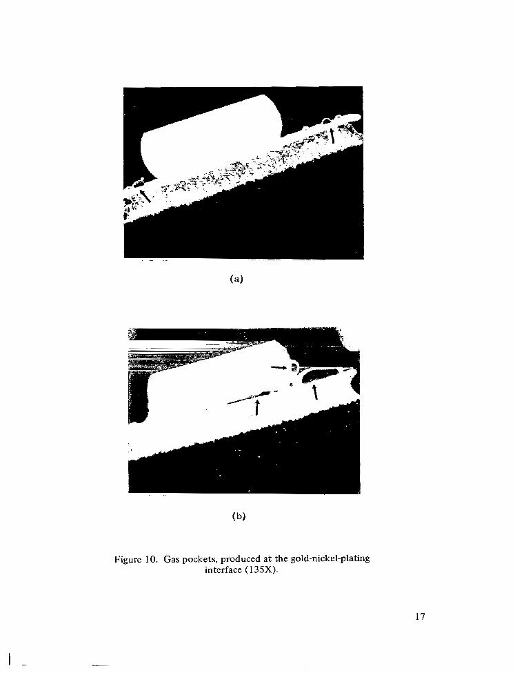
Figure 10. Gas pockets, produced at the gold-nickel-plating interface (135X).
17
1
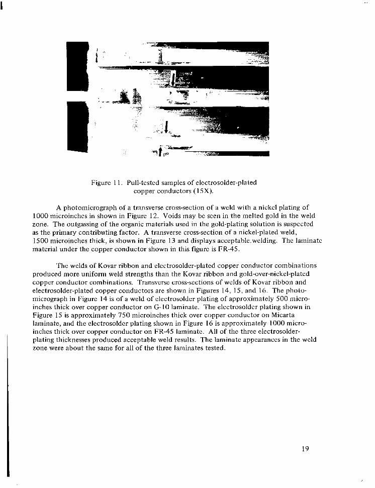
Figure 1 1. Pull-tested samples of electrosolder-plated copper conductors (1 5X).
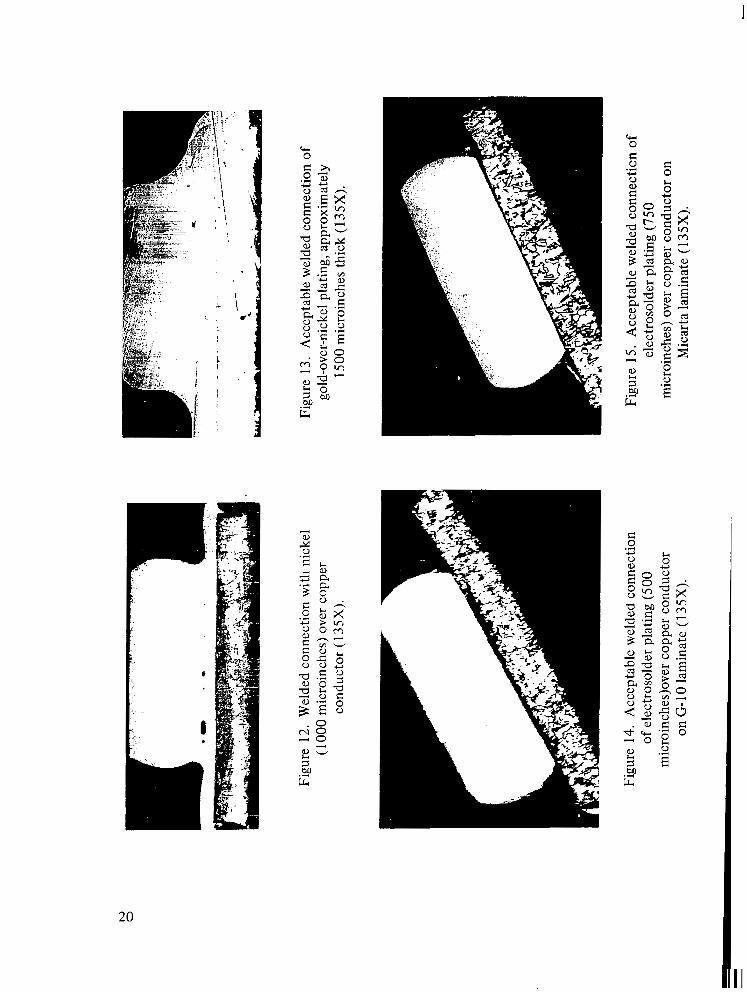
A photomicrograph of a transverse cross-section of a weld with a nickel plating of 1000 microinches in shown in Figure 12. Voids may be seen in the melted gold in the weld zone. The outgassing of the organic materials used in the gold-plating solution is suspected as the primary contributing factor. A transverse cross-section of a nickel-plated weld, 1500 microinches thick, is shown in Figure 13 and displays acceptable.welding. The laminate material under the copper conductor shown in this figure is FR-45.
The welds of Kovar ribbon and electrosolder-plated copper conductor combinations produced more uniform weld strengths than the Kovar ribbon and gold-over-nickel-plated copper conductor combinations. Transverse cross-sections of welds of Kovar ribbon and electrosolder-plated copper conductors are shown in Figures 14, 15, and 16. The photo- micrograph in Figure 14 is of a weld of electrosolder plating of approximately 500 micro- inches thick over copper conductor on G-10 laminate. The electrosolder plating shown in Figure 15 is approximately 750 microinches thick over copper conductor on Micarta laminate, and the electrosolder plating shown in Figure 16 is approximately 1000 micro- inches thick over copper conductor on FR-45 laminate. All of the three electrosolder- plating thicknesses produced acceptable weld results. The laminate appearances in the weld zone were about the same for all of the three laminates tested.
19
20
43 0
Q+ 0
c 0 .I
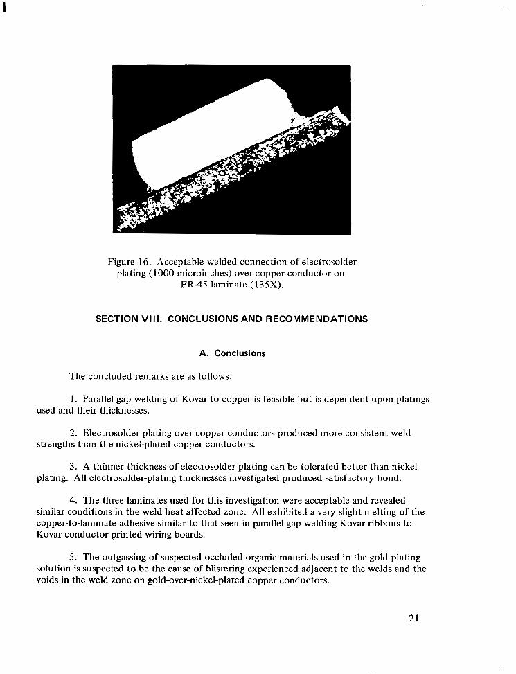
Figure 16. Acceptable welded connection of electrosolder plating (1000 microinches) over copper conductor on
FR-45 laminate (135X).
SECTION VIII. CONCLUSIONS AND RECOMMENDATIONS
A. Conclusions
The concluded remarks are as follows:
1. Parallel gap welding of Kovar to copper is feasible but is dependent upon platings used and their thicknesses.
2. Electrosolder plating over copper conductors produced more consistent weld strengths than the nickei-plated copper conductors.
3. A thinner thickness of electrosolder plating can be tolerated better than nickel plating. All electrosolder-plating thicknesses investigated produced satisfactory bond.
4. The three laminates used for this investigation were acceptable and revealed similar conditions in the weld heat affected zone. All exhibited a very slight melting of the copper-to-laminate adhesive similar to that seen in parallel gap welding Kovar ribbons to Kovar conductor printed wiring boards.
5. The outgassing of suspected occluded organic materials used in the gold-plating solution is suspected to be the cause of blistering experienced adjacent to the welds and the voids in the weld zone on gold-over-nickel-plated copper conductors.
21
6. Kovar ribbon and copper conductor size combinations within the scope of this investigation did not appreciably affect the quality of the welds.
B. Recommendations
The recommendations are as follows:
1. Solder-platings/coatings over copper conductors are recommended.
2. All solder platings/coatings must be uniform in thickness and in density.
3. Solder plating must be 63/37 or 60/40 and fused in suitable hot oil.
4. Parallel gap welding to bare, gold-plated, or gold-over-nickel-plated copper is not recommended.
5. All Kovar ribbons shall be gold plated.
George C. Marshall Space Flight Center National Aeronautics and Space Administration
Marshall Space Flight Center, Alabama 358 12, June 22, 1970 933-50-07-0300
22
APPENDIX A
STATISTICAL ANALYSIS OF TEST RESULTS
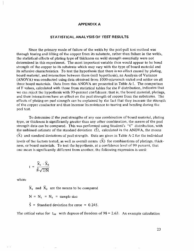
Since the primary mode of failure of the welds by the peel-pull test method was through tearing and lifting of the copper from its substrate, rather than failure in the welds, the statistical effects of plating type of thickness on weld strength essentially were not determined in this experiment. The most important variable then would appear to be bond strength of the copper to its substrate which may vary with the type of board material and its adhesive characteristics. To test the hypothesis that there is no effect caused by plating, board material, and interaction between them (null hypothesis), an Analysis of Variance (ANOVA) was conducted using data obtained from 1000-microinch nickel and solder on all three board materials. Data from this ANOVA are presented in Table A-1 . The comparison of F values, calculated with those from statistical tables for the F distribution, indicates that we can reject the hypothesis with 99-percent confidence; that is, the board material, platings, and their interactions have an effect on the peel strength of copper from the substrates. The effects of plating on peel strength can be explained by the fact that they increase the strength of the copper conductor and thus increase its resistance to tearing and bending during the peel test.
To determine if the peel strengths of any one combination of board material, plating type, or thickness is significantly greater than any other combination, the means of the peel strength data can be compared. This was performzd using Student’s “t” distribution, with the unbiased estimate of the standard deviation ( S ) , calculated in the ANOVA, the means (2) and standard deviations of peel strength. Data are - given in Table A-2 for the individual levels of the factors tested, as well as overall means (X) for combinations of platings, thick- ness, or board materials. To test the hypothesis, at a confidence level of 99 percent, that one mean is significantly different from another, the following expression is used:
x, -x, i m
t =
where
X, and x, are the means to be compared
N = N, = N, = sample size
5 = Standard deviation for error = 0.245.
The critical value for t99 with degrees of freedom of 98 = 2.63. An example calculation
23
TABLE A- 1. ANALYSIS OF VARIANCE OF PEEL STRENGTH DATA FOR 100 MICROINCHES OF NICKEL AND SOLDER
Source of Variation
Board Material
Plating
Interaction - Board Material x Plating
Error
To tal
~"
~~
~.
~.
-~
~ ~~~~
Sum of Squares
5.23
.~
0.5 1 -.
7.28
17.98
3 1 .oo ~
Degrees of Freedom
2
1
.. . .
2
294
299 -
Mean Square
2.62 I 43.66
0.51 I 8.50
3.64
0.06 I 60.66
I TABLE A-2. MEANS OF PEEL STRENGTHS AND STANDARD
DEVIATIONS (S) CALCULATED FROM RESULTS OF PEEL TESTS
(0.25) (0.28) I G-10 I 2.32 1 2.51
(0.42) (0.22) FR-45 2.02 1.90
(0.38) (0.32) Micarta
2.52 2.1 1 X
3.03 2.12 ~
- -
~~
- -
'Ni -
2.4 1
1.96 ~
2.57
2.3 1
Solder (p in
__
(0.12) (0.18) 2.53 2.28
(0.15) (0.13) 2.13 1 2.03
~
2.18 a 2.14
1000
(0.17) 2.35
(0.17) 2.06
(0.19) 2.18
2.20
- - Xsolder
2.39
2.07
2.15
2.20
~~
F99
4.69
6.73
4.69
2 Board Material
-
2.40
2.03
2.32
2.25
24
for comparison of the means for 1000 microinches nickel on FR-45 board material ( 1.90 pounds) and 1000 microinches solder on G-10 (2.39 pounds) is as follows:
t = 2.39 - 1.90 = 0.49 0.245 J2/50 0*49
~ _ _
= 1.00 .
Since the calculated value for t (1 .OO) is less than the critical value for t (2.63), there is no significant difference in these two means at a confidence level of 99 percent. Similar calculations performed on the means for all combinations of board material, plating, and thickness likewise showed no significant differences in their effect on peel strength of the welded joints. However, “t” tests for comparison of the grand means (x) for both the different board materials as well as plating types, using the appropriate “N” for sample size and degrees of freedom, showed a significant difference in all comparisons. Thus, the mean for G-IO material is significantly greater than for the other two and the mean for nickel is greater than for solder.
-
Based on statistical analysis of the data, the greatest peel strength overall was obtained with nickel platings and G-IO board materiaI. However, based on the lower standard devia- tions and ranges for solder and considerations of more universal application, the use of solder plating from 500 to 1000 microinches thickness on G-10 is recommended.
25
I I I 1 I I 1 I I I I.
APPENDIX B
QUALITY ASSURANCE AND INSPECTION CRITERIA
To perform acceptable welding with repeatable results, adherence to definite parameters and process controls is mandatory. The requirements outlined in the following paragraphs will aid in producing and determining acceptable welds.
1. Weld System
The power supply must possess the capability of consistent performance at manually selected pulse amplitude (voltage) and at the selected pulse duration (time). Meters must be provided to detect any variance from these selected parameters.
The weld head shall possess the capability of repeatably applying a preselected force to the work pieces, and permit manual adjustment of the electrodes. A means of automat- ically discharging the weld pulse after applying the selected electrode force must be provided.
2. Materials
a. Kovar ribbons must be gold-plated, performed, and cut to proper lengths prior to usage.
b. All materials must be thoroughly cleaned by accepted methods just prior to welding.
c. Solder shall be Sn60 or Sn63 and fused in suitable oil when electrosolder plating is used.
3. Welding Operation
To assure that quality welding is accomplished, the following guidelines are recommended:
a. Prior to production welding, verification of selected welding parameters shall be conducted on similar Kovar ribbon and printed wiring board materials.
b. Pull test five welds using a 180-degree peel-pull method with a suitable tool. The weld shall be considered acceptable when a portion of the copper conductor material adheres to the Kovar ribbon and the conductor does not exhibit blowholes of excessive melting.
26
c. The electrode tips shall be kept clean and free of contaminants. The tips must be flat and exhibit no mushrooming.
NOTE
Use a slight overpressure of the electrodes rather than underpressure as this will result in a more uniform resistance of materials in the electrode contact areas.
4. Weld Inspection Criteria
All welds shall be visually inspected at 30X. Where positive identification of weld condition is necessary, greater magnification may be used.
Visual acceptance criteria are as follows:
a. Weld shall exhibit a darkened gold band of approximately 70 percent of tlle lead area between the electrodes.
b. Weld shall exhibit a smooth fillet along ribbon conductor interface in the weld zone.
c. A solder fillet shall extend beyond the electrode tip thicknesses along the ribbon length.
d. The Kovar ribbon shall be fully supported by the conductor.
The following weld conditions shall be cause for rejection:
a. Open weld - An open weld is where welding has been attempted but no bonding of the materials has occurred or where a weld is required but overlooked by the operator.
b. Cracked weld - A weld that exhibits a crack or a separation.
c. Blowhole - A weld in which holes or voids are evidenced.
d. Deformed weld, excessive melting - A weld in which either tlle ribbon or the conductor material has been reduced by 15 percent or more.
e. Surface fusion - A weld with surface of the lead at ribbon-electrode interface exhibiting fusion or melting.
f. Weld alignment - A weld with portion of ribbon extending beyond weld pad dimensions.
27
I
REFERENCES
1. Radke, Richard P.: Thin Film Electronic Packaging. TRW Space Technology Laboratories, Redondo Beach, California.
2. Hill, W. H.: Parallel Gap Welding Kovar Leads to Copper Printed Circuit Boards. Welding Engineer, Bulletin No. 106, Hughes Aircraft Company, Vacuum Tube Products Division, Oceanside, California.
3. Jarosik, N.: Printed Circuit Board Requirements for Parallel Gap Welding. Sylvania Electronics Systems Division, Sylvania Electric Products, Inc., Williamsville, New Jersey.
4. Carter, H. G.; and Wilson, W. W.: Westinghouse Aerospace Develops a More Economical Weldable Printed Wiring Board. Westinghouse Defense and Space Center, Aerospace Division, Baltimore, Maryland.
5. Burka, James A.: Establishment of Quality Assurance and Inspection Criteria for the Technique of Parallel Gap Soldering. NASA Technical Memorandum, NASA TM X-53660, Quality and Reliability Assurance Laboratory, George C. Marshall Space Flight Center, Huntsville, Alabama.
28
BIBLIOGRAPHY
Ehrlich, B. J. , Helms, J. D., and Illingworth, W. T.: Dynamically Controlled Energy Applied to Parallel-Gap Resistance Welding. Texas Instruments, Incorporated, Houston, Texas.
Howell, J. R. and Slemmons, J. W.: Interconnection Method for Microcircuits. Materials and Processes Lab, Autonetics Division of North American Aviation, Inc., Anaheim, California.
Keister, F. Z., Engquist, R. D., and Holley, J . H.: Interconnection Techniques for Micro- circuits. Hughes Aircraft Company, Culver City, California. ’
Koudounaris, A.: Vibration and Shock Testing of Multilayer Printed Wiring Boards. Douglas Missile and Space Systems Division, Douglas Aircraft Co., Inc., Santa Monica, California.
Manfield, H. G.: Microbonding Aspects of the Interconnection Problem. Ministry of Aviation, Royal Radar Establishment, Great Melvern, England, Great Britain.
NASA-Langley, 1971 - 15 M654 29


I

Ill 111111111111
NATIONAL AERONAUTICS AND SPACE ADMINISTRAI ION
WASHINGTON, D. C. 20546
OFFICIAL BUSINESS FIRST CLASS MAIL
NATIONAL AERONAUTICS . POSTAGE A N D FEES PA11
SPACE ADMINISTRATIOE
02U 001 40 51 30s 71043 00903 A I R F O R C E WEAPONS L A B O R A T O R Y /WLOL/ K I R T L A N D A f B 9 NEW M E X I C O 87117
A T T E o LOU B O W M A N , C H I E F p T E C H o L I B R A R Y
If Undeliverable ( Section 1 Posnl Manual ) Do Not Re
“The aeronautical and space activities of the United States shall be conducted so as to contribute . , . to the expansion of hu?~zan knowl- edge of phenonlena in the at?)losphere and space. T h e Administration shall provide for the widest practicable and appropriate dissenzinatioz of infor?uation concerning its activities and the resdts thereof.”
-NATIONAL AERONAUTICS AND SPACE ACT OF 1958
NASA SCIENTIFIC AND TECHNICAL PUBLICATIONS
TECHNICAL REPORTS: Scientific and TECHNICAL TRANSLATIONS: Information technical information considered important, published in a foreign language considered complete, and a lasting contribution to existing to merit NASA distribution in English. knowledge.
TECHNIChL NOTES: Information less broad derived from or of value to NASA activities. in scope but nevertheless of importance as a Publications include conference proceedings, contribution to existing knowledge. monographs, data compilations, handbooks,
SPECIAL PUBLICATIONS: Information
TECHNICAL MEMORANDUMS: sourcebooks, and special bibliographies.
Information receiving limited distribution TECHNOLOGY UTILIZATION because of preliminary data, security classifica- PUBLICATIONS: Information on technology tion, or other reasons. used by NASA that may be of particular
CONTRACTOR REPORTS: Scientific and interest in commercial and other non-aerospace applications. Publications include Tech Briefs,
technical information generated under a NASA Technology Utilization Reports and contract or grant and considered an important contribution to existing knowledge.
Technology Surveys.
Details on the availability of these publications may be obtained from:
SCIENTIFIC AND TECHNICAL INFORMATION OFFICE
NATIONAL AERONAUTICS AND SPACE ADMINISTRATION Washington, D.C. PO546