part #: smt 6657 - sundance.technology · smt-6657 issue 1.4 page 5 1 introduction this document is...
TRANSCRIPT

Sundance Multiprocessor Technology Limited
Form : QCF51 Template Date : 10 November 2010
SMT6657 Issue 1.4
Module Description: PC/104 OneBank Dual-DSP + FPGA w. FMC Module
Module Number: SMT6657
Current Issue Number: 1.4
Original Issue Date: 29th November 2015
Original Author: S E Carpenter
PCIe/104TM OneBank
Dual TI TMS320C6657 + Kintex-7 KU35 + VITA57.1 FMC Module
Design Description
Part #: SMT 6657
Sundance Multiprocessor Technology Ltd, Chiltern House, Waterside, Chesham, Bucks. HP5 1PS.
This document is the property of Sundance and may not be copied nor communicated to a third party without prior written
permission. © Sundance Multiprocessor Technology Limited 2016

SMT-6657 Issue 1.4 Page 2
Revision History
Issue Changes Made Date Initials
0.1 First Sundance unofficial draft. 21SEP15 SEC
0.2 Additional edits 22SEP15 FC
0.3 Added 8 x MGT and 8 x FPGA I/O to the down connector, 1 x MGT to FMC connector, SMBUS to I2C BUS Router. Rerouted DSPA SPI port to FMC through DSP FPGA. Change DSP power sequence to tabular state machine.
22SEP15 SEC
0.4 Change to 4 x MGT to the down connector, 8 MGT to the FMC connector
23SEP15 SEC
1.0 First release. 25SEP15 SEC
1.1 Revised FPGA pin allocation, added -40°C to +100°C contact Sundance, replaced pcie/104 reset to fpga with reset from cpld, updated block diagram.
23OCT15 SEC
1.2 Corrected FPGA pin allocation table (FMC)
Watchdog moved from CPLD to FPGA to allow programming. Dedicated watchdog signal from FPGA to CPLD added. GPIO8 changed from watchdog to FPGA_PROGRAM_B configuration control. CPLD STATUS_DATA & STATUS_CLOCK replace DIPSWDAT and DIPSWCLK, and data includes FPGA configuration status. Added I2C bus address map.
21DEC15 SEC
1.3 Moved SMBUS to I2C router inside FPGA to save pcb space. Reduced FPE general I/O from 8 to 4. Added FPE pin allocation.
14MAR16 SEC
1.4 Added PCB build information and fully routed board image.
25th May 2016
GKP

SMT-6657 Issue 1.4 Page 3
Table of Contents
1 Introduction ................................................................................................................... 5
1.1 Main Features ................................................................................................................. 5
1.1.1 Hardware .................................................................................................................... 5
1.1.2 Standards-based external interfaces .................................................................... 5
1.1.3 Interconnection between programmable devices ............................................. 7
1.1.4 TI comport compatibility ........................................................................................ 7
2 Notes ................................................................................................................................ 8
2.1 Abbreviations / Definitions ........................................................................................ 8
2.2 Sundance References .................................................................................................... 8
2.3 Internet References ....................................................................................................... 8
3 System Architecture ................................................................................................... 10
3.1 Block Diagram .............................................................................................................. 11
3.2 FMC Data Acquisition Interface ............................................................................... 12
3.3 PCIe/104 Interface ...................................................................................................... 12
3.4 FPGA Interfaces ............................................................................................................ 13
3.4.1 FPGA POWER ............................................................................................................ 17
3.4.2 FPGA EMIF16 ............................................................................................................ 18
3.4.3 FPGA SRIO ................................................................................................................ 20
3.4.4 FPGA UART .............................................................................................................. 20
3.4.5 FPGA DSP GPIO ........................................................................................................ 21
3.4.6 FPGA PCIe ................................................................................................................. 23
3.4.7 FPGA MGT to Carrier Board ................................................................................. 23
3.4.8 FPGA General I/O to Carrier Board..................................................................... 23
3.4.9 FPGA PWRGOOD & ALERT .................................................................................... 23
3.4.10FPGA I2C ................................................................................................................... 23
3.4.11FPGA SPI .................................................................................................................... 24
3.4.12FPGA I/O LVDS ........................................................................................................ 24
3.4.13FPGA I/O LEDS......................................................................................................... 24
3.4.14FPGA I/O LVTTL ...................................................................................................... 25
3.4.15FPGA I/O & FMC JTAG ........................................................................................... 25
3.4.16FPGA LOCAL LEDS .................................................................................................. 25
3.4.17FPGA FMC LVDS CLOCKS ...................................................................................... 25
3.4.18FPGA FMC DATA I/O LA00-33 ............................................................................. 25
3.4.19FPGA FMC SPI .......................................................................................................... 26
3.4.20FPGA FMC INTERRUPTS ........................................................................................ 27
3.4.21FPGA FMC MGT ....................................................................................................... 28
3.5 DSP Interfaces .............................................................................................................. 29
3.5.1 DSPA Ethernet ......................................................................................................... 30
3.5.2 DSP JTAG .................................................................................................................. 30
3.5.3 DSP EMIF16 .............................................................................................................. 31
3.5.4 DSP UART ................................................................................................................. 31

SMT-6657 Issue 1.4 Page 4
3.5.5 DSP GPIO ................................................................................................................... 32
3.5.6 DSP RESET ................................................................................................................ 33
3.5.7 DSP POWER .............................................................................................................. 33
3.5.8 DSP SRIO ................................................................................................................... 35
3.5.9 DSP HYPERLINK ...................................................................................................... 35
3.5.10DSP PCIe .................................................................................................................... 35
3.5.11DSP EMIF32 & DDR3 memory .............................................................................. 36
3.5.12DSP I2C ...................................................................................................................... 37
3.6 I2C Temperature Sensor ............................................................................................ 38
3.7 I2C Supply Volts ADC ................................................................................................. 39
3.8 CPLD ............................................................................................................................... 40
3.9 DSP Booting ................................................................................................................... 43
3.9.1 DIP Switches ............................................................................................................. 44
3.10 Flash Memories ............................................................................................................ 45
3.10.1256KByte I2C EEPROM ............................................................................................ 45
3.10.2256MByte Parallel NOR Flash ............................................................................... 45
3.11 Clock System ................................................................................................................ 47
3.12 Power Supplies ............................................................................................................. 51
3.13 I/O expansion connector ........................................................................................... 55
3.14 SRIO expansion connector ........................................................................................ 57
4 PCB Layout ................................................................................................................... 59
4.1 Heat Sinks...................................................................................................................... 59
4.2 Component Placement ............................................................................................... 59
4.3 PCB Construction ......................................................................................................... 61
4.4 PCB Layout .................................................................................................................... 64
4.4.1 Main Board ............................................................................................................... 64
4.4.2 Front Panel Interface Board .................................................................................. 65
5 Physical Properties ..................................................................................................... 66
6 Verification, Review & Validation Procedures ..................................................... 67
7 Safety ............................................................................................................................. 67
8 EMC Statement of Compliance ................................................................................. 67
9 Ordering Information ................................................................................................. 67

SMT-6657 Issue 1.4 Page 5
1 Introduction
This document is the design description of a dual DSP+FPGA PCIe/104 module, which describes the hardware design in detail. Where possible specific devices are identified for use in the design, along with how they are connected.
This document provides a set of design requirements, which are used by the PCB designer, and for PCB testing.
The SMT6657 dual-DSP+FPGA module is a reliable and flexible platform for digital signal processing applications requiring high-performance integer and floating-point computation.
It is applicable to both symmetric multiprocessing applications in which the computational load is shared by the two DSPs; and asymmetric applications where one of the DSPs is responsible for hard real-time processing and the other acts as a supervisor, handling all non-deterministic communication and optionally running under control of an operating system.
1.1 Main Features
1.1.1 Hardware
This module consists of the following major hardware features:
1) PCIe/104TM OneBank plug-able module format 2) Two dual-core TI C6657 floating-point DSPs 3) Xilinx Kintex-7 Ultra Scale series FPGA 4) Serial RapidIO and Hyperlink connectivity between DSPs 5) Accepts one FMC-LPCTM Mezzanine Card data acquisition add-on module 6) Additional stack-down SRIO connector to SMT-Carrier-GSI 7) Front panel I/O connector carrying gigabit Ethernet and flexible FPGA I/O
1.1.2 Standards-based external interfaces
The SMT-DSP-GSI module benefits from the incorporation of three key interface standards, each one the leading standard in its area of the embedded systems field:
1) PCIe/104TM provides tightly integrated high-speed connectivity with PC hosts and also defines a compact and rugged module format.
2) FMC provides an FPGA-oriented data acquisition card interface that is particularly well suited to analogue conversion applications. Due to the flexibility of FPGA I/O, the function of its 68 pins (Low pin count FMC; or 160 pins for the High Pin Count version) can optimised to the needs of the FMC add-on module.
3) Serial RapidIO is a standard designed to address the need for inter-module communication in high bandwidth embedded systems such as 4G wireless base stations, and has become a standard peripheral in high-end TI DSPs.

SMT-6657 Issue 1.4 Page 6

SMT-6657 Issue 1.4 Page 7
1.1.3 Interconnection between programmable devices
Carrier to DSPs
One 500MByte/s PCIe Gen2 lane to each DSP, for memory-mapped host communication
One 500MByte/s PCIe Gen2 lane to the FPGA Two 500MByte/s SRIO lanes to each DSP, for telegram-oriented
communication between DSP modules Four 500MByte/s PCIe Gen2 lanes to the FPGA
DSP to DSP
4GByte/s TI Hyperlink for memory-sharing between DSPs
One 500MByte/s SRIO lane between DSPs, for telegram-oriented communication between DSPs
DSP to FPGA
Each DSP has its own 100MByte/s 16-bit memory bus interface to the FPGA (also configurable as a Universal Parallel Port)
Each DSP has one 500MByte/s SRIO lane to the FPGA All DSP GPIO is routed to the FPGA A full duplex 6MByte/s SPI communications channel for control and
diagnostics
FPGA to FMC
34 user-definable I/O pairs, configurable to the interfacing needs of the FMC Data Acquisition card: ADC & DAC data, SPI bus, Interrupt
Eight MGT 5ooMByte/s transceiver data pair Two clock signals
System Management Bus
All I2C-capable devices including both DSPs, are connected to a single I2C bus, which extends to the I2C pins of the FMC connector and the SMbus pins of the PCIe/104TM stack-down connector, through an SMBUS router within the FPGA.
1.1.4 TI comport compatibility
The SMT6657 is supplied with firmware that permits TMS320C40 comports to be implemented on its external I/O and/or FMC daughterboard interfaces. As each DSP has a memory bus connected to the FPGA, this functionality is exposed to the DSP software via a memory-mapped interface that is very similar to the original TI hardware implementation of comports.

SMT-6657 Issue 1.4 Page 8
2 Notes
Several part numbers are described in the text. These are possible part numbers, and alternative devices may be designed in at a later date.
2.1 Abbreviations / Definitions
ADC Analog to Digital Converter.
DAC Digital to Analogue Converter
DDR & DDR3 Dual Data Rate. An interface mechanism where data is transferred on both rising and falling clock edges. DDR3 memory is lower power and higher performance than its predecessor, DDR2.
DRAM Dynamic RAM.
FPGA Field Programmable Gate Array.
GPIO General Purpose Input Output.
I2C Inter-integrated Circuit. A two wire low speed serial interface.
MAC Media Access Control.
Magnetics Commonly used to refer to the inductors and transformers within the Ethernet signalling to the RJ45 connector.
PHY Commonly used to refer to the device that interfaces to the physical layer.
RAM Random Access Memory.
SEIC Sundance External Interface Connector, a module-specific breakout board for external I/O.
SPI Serial Peripheral Interface. A high speed serial interface.
SRIO Serial RapidIO (also known as Serial RocketIO). A multi-gigabit serial interface for peer-to-peer communication. Provides both message-passing and read/write transactions.
EMIF32 High speed synchronous 32 bit bus to the DDR3 SDRAM
EMIF16 Medium speed asynchronous 16 bit bus to the FPGA and flash ROM
SGMII 1G Ethernet interfaces to a dual 1G Ethernet PHY
PCIE Dual lane gen 2
JTAG Test and development connection to external emulation system
CLOCKS Multiple clocks to drive different parts of the DSP & FPGA
UART Standard asynchronous serial communications
POWER Multiple power supplies for the core and the I/O
MGT Multi Gigabit Transceiver
2.2 Sundance References
[1] SMT-DSP-GSI (qcf51) v1_7.pdf
[2] SMT-FMC-GSI (qcf51) v1_5.pdf
[3] SMT-IO-GSI (qcf51) v1_4.pdf
[4] SMT-MBRD-GSI (qcf51) v1_5.pdf
2.3 Internet References
[5] http://www.pc104.org/history.php
[6] http://shop.vita.com/ANSI-VITA-571-2008-R2010-FPGA-Mezzanine-Card-FMC-Standard-AV571.htm
[7] http://www.ti.com/lsds/ti/dsp/keystone/overview.page
[8] http://www.ti.com/lit/ug/sprugw1b/sprugw1b.pdf

SMT-6657 Issue 1.4 Page 9
[9] http://www.xilinx.com/support/documentation/data_sheets/ds095.pdf
[10] http://www.ti.com/product/tms320c6657
[11] http://www.xilinx.com/support/documentation/data_sheets/ds180_7Series_Overview.pdf
[12] http://www.xilinx.com/support/documentation/data_sheets/ds182_Kintex_7_Data_Sheet.pdf
[13] http://www.ti.com/tool/XDS560
[14] http://www.xilinx.com/support/documentation/data_sheets/ds593.pdf
[15] http://www.xilinx.com/support/documentation/data_sheets/ds892-kintex-ultrascale-data-sheet.pdf
[16] http://www.xilinx.com/products/technology/power/xpe.html
[17] http://www.xilinx.com/support/documentation/user_guides/ug570-ultrascale-configuration.pdf
[18] http://www.ti.com/litv/pdf/spru655i
[19] http://en.stackpc.org/specs.html

SMT-6657 Issue 1.4 Page 10
3 System Architecture
The DSP system consists of a PCIe/104 format PCB, with major components:
A pair of 1.25GHz Texas Instruments DSPs part number: TMS320C6657CZH25
A Xilinx Kintex7 UltraScale FPGA part number: XCKU035-1FBVA676C.
These and all other components used are specified for operation in a laboratory environment over the temperature range of 0°C to +85°C, and comply with ROHS requirements.
For operating requirements over the range of -40°C to +100°C, please contact Sundance.
The DSP PCB has thick copper power plane internal layers for high thermal and electrical conductivity. A solid aluminum heat sink provides further conduction cooling and rigidity and EMI shielding.
The system design around each DSP is largely symmetrical, apart from the boot procedure and non-deterministic interfaces.
DSP A is the master and boots first from the EMIF16 NOR FLASH PROM. Code running on DSP A is then responsible for booting DSP B and configuring the Kintex-7 FPGA.
With its large flash memory and gigabit Ethernet connection, DSP A is most suited to run a Real Time Operating System, leaving DSP B free to perform real time signal processing which is both deterministic and very low latency.
Below is a diagram showing the system architecture:

SMT-6657 Issue 1.4 Page 11
3.1 Block Diagram
Figure 1 Block diagram of SMT6657
Reset
4 x LVDS
16 x LVDSEMIF16
EMIF16
GPIO inc UART & SPI
GPIO inc UART & SPI
SGMII
Copper
32 x LVTTL
EMIF32
EMIF32
JTAG
2 x LED
Reset
En
PCIe
PCIe
SRIO 5Gbit/s
SRIO 5Gbit/s
SRIO 5Gbit/s
I2C
16 x LVDS
Alarm
I2C
SPICLK
SPICLK
Interrupt
2 x LVDS Clock
4 x LVDS
FMC LPC68 IO & I2C
& MGT
I/OSamtec
LSHM
68 Signal
28 GND
4 Power
Ethernet Phy1Gbit/s
LEDs
DSP BTMS320C6657
Boot: Hyperlink,
PCIe, SRIO
FPGA
Xilinx
UltraScale
Kintex-7
KU35-A676
Speed
Grade: -2
Commercial
Temperature
Logic Cells:
355000
DSP Slice:
1700
27mm x 27mm
1.0mm balls
104 HR I/O
208 HP I/O
16 GTH/GTY
DSP ATMS320C6657
Boot: Flash,
PCIe, SRIO
DSP
Power
Supply
PCIe/104OneBank
Down
StackPCB1FPE
Down
EEPROM
256KBytes
20 years
DDR3 RAM
1Gbyte Error
Correcting
Clock
System
CDCM6208
DSP JTAG60 way
MIPI
PCIe
Hyp
erlin
k 4
0G
bit/s
Temp
Sensor
CPLD
Xilinx
XC2C384
Power-up
Resets
Watchdog
NOR Flash
256MBbyte
20 years
I2C
SRIO 5Gbit/s
DDR3 RAM
1Gbyte Error
Correcting
Boot
Mode
DIP
Switches
SRIO 5Gbit/s
SRIO 5Gbit/s
SRIO
5Gbit/s
Supply
Volts
ADC x 8
SPI
PERST_N + PWRGOOD + ALERT
MDIO
Fibre
Stat
8x MGT 5Gbit/s
PCIe 4 x MGT 5Gbit/s
12V0
5V0
3V3
4 x General I/O
SMBUS
12V0
1 x MGT 5Gbit/s
Reset
JTAG JTAG
12V0

SMT-6657 Issue 1.4 Page 12
3.2 FMC Data Acquisition Interface
The FMC is the “Low Pin Count” variant, which provides the following signals:
34 flexibly configured I/O pairs, which in the standard firmware are configured as
o 8 high speed LVDS double data rate inputs (for ADC sample data) o 16 high speed LVDS outputs (for DAC sample data) o SPI bus from the DSP FPGA o Interrupt / DMA request to the DSP FPGA
2 LVDS data clocks I2C for peripheral configuration and status monitoring FPGA JTAG permitting debugging of the data acquisition module firmware Eight MGT 500MByte/s serial communications lanes
3.3 PCIe/104 Interface
The PCIe/104 OneBank connector provides power, global Reset, PCI Express connections to the host, and I2C.
The first three PCIe lanes on the connector are routed to the two DSPs and the Kintex-7 FPGA. The SMT6657 board thus provides three separate PCIe x1 ports.
Each DSP has a single PCIe GEN2 port operating at up to 5G Baud per lane, which can be configured at reset as either a “Root Complex” or “End Point” by the CPLD.
A PCI Express block can be instantiated in the FPGA to provide a single PCIe Gen2 port operating as “Root Complex” or “End Point”. Only one lane is routed to the PCIe/104 OneBank connector.
“End Point” would be used to communicate with a standard Host, and “Root Complex” would be used to communicate with a peripheral that only implements an “End Point”. The Root Complex is usually provided by a host PC, and therefore a typical configuration will have both DSPs and the FPGA configured as End Points.
The global I2C bus is connected to the PCIe/104 connector signals SMB_DAT and SMB_CLK through a SMBUS to I2C BUS Router within the FPGA. This allows the DSPs to read the carrier board status, and to allow a service processor on the carrier board to read the temperature of the SMT-DSP-GSI board. The Router is required to implement the SMBUS “Address Resolution Protocol” (ARP). This allows I2C device with the same I2C address located on different boards on the PCIe/104 connector stack to communicate with the host board without address conflicts.
The PCIe/104 connector signal SMB_ALERT is fed to both the FPGA and the CPLD. It is used by the CPLD to assert a DSPA interrupt using a DSPA GPIO signal.
The PCIe/104 connector signal PWRGOOD is fed to both the FPGA and the CPLD. The CPLD uses it to control the power up and down sequencing. In the event of

SMT-6657 Issue 1.4 Page 13
system power failure, the mains power supply negates PWRGOOD and the CPLD powers down the DSPs with the correct sequence before total power failure.
The PCIe/104 connector signal PE_RST_N is fed to the CPLD only. This is the host system reset, and the CPLD uses it to reset the DSPs and other devices without power sequencing.
The PCIe/104 connector signal PSON_N is fed to both the FPGA and the CPLD. This signal is used by the system host to turn on the primary power supply. Use by SMT-6657 is reserved.
There is no PCIe/104 UP connector because the one bank connector does not provide enough power to supply a second DSP board. This also means there are no automatic link shifting switches required.
3.4 FPGA Interfaces
The FPGA is Xilinx Kintex7 UltraScale FPGA part number: XCKU035-1FBVA676C. The package is designated FBVA676 which is a 27 by 27 ball grid array with 1mm pitch. This device has 312 I/O pins and 16 MGT / GTH gigabit serial ports.
This FPGA primarily provides serial data formatting and LVDS I/O through the FMC daughterboard connector, for interfacing to the data acquisition board.
The FPGA has sufficient processing power to perform complex pre- and post-processing of sample streams, allowing the processing of raw data to be offloaded from the DSPs:
1) > 55000 Xilinx 7 logic slices (equivalent to at least 200000 Xilinx 2 slices) 2) 1700 DSP slices 3) > 2MB Block RAM

SMT-6657 Issue 1.4 Page 14
The FPGA implements communication functions appropriate to the installed I/O expansion board. The default use is:
4 (four) Optical inputs 4 (four) Optical outputs 4 (four) TTL inputs 4 (four) TTL outputs 2 (two) TI DSP Links 2 (two) Health LEDs
The board firmware includes two TI comport bridging modules that provide a way for user firmware to send and receive data using TMS320C40 comport signalling conventions. This provides backwards compatibility for users with legacy systems.
The EMIF16 bus timing determines the maximum I/O throughput for each DSP to the FPGA. A DSP running at 1.25GHz clocks the EMIF16 at 208.3MHz, and consecutive reads or writes can be completed in 4 clocks, or 52.085MHz. This makes the EMIF16 peak transfer speed to or from the FPGA, 104.1M Bytes/sec.
For applications that require higher bandwidth between FPGA and DSP, the DSP Universal Parallel Port (UPP) peripheral can be enabled instead of EMIF16. Although UPP has a higher bandwidth (up to 240MB/s) it is DMA driven and has a minimum transfer size of 64 bytes, resulting in a higher latency than EMIF16. UPP is therefore better suited to data-streaming applications than ones which require low latency.
The FPGA has 6 I/O banks each with 52 I/O pins making a total of 312. Each bank can have up to 24 differential pairs. There is also a dedicated configuration bank (0), which can not be used for normal I/O. Each I/O bank can be connected for either 3V3 or 1V8 I/O. It is not possible to mix I/O levels on the same bank. LVDS outputs can only be allocated to banks with 1V8 supply. LVDS inputs can be allocated to 3V3 or 1V8 banks.
The following table lists all FPGA I/O pins including clocks but excluding MGTs. Each pin type is associated with either 3V3 or 1V8 I/O levels. This allocation ensures that all the 3V3 I/O fit exactly with a single bank dedicated to 3V3 I/O and the 5 other banks are all 1V8 I/O. Note that ALL DSP signals are 1V8 only.

SMT-6657 Issue 1.4 Page 15
The following table gives an example bank allocation of the I/O data and clock (non MGT) pins of the FPGA:
Inter face
Signal Standard FP GA I/O
B44 52x 1V8 24
pairs
B45 52x 1V8 24
pairs
B46 52x 3V3 24
pairs
B64 52x 1V8 24
pairs
B65 52x 1V8 24
pairs
B66 52x 1V8 24
pairs
Comment
DSPA_EMIF
16 D0-15
LVCMOS18
I/O 16 Must be B65
for select MAP config
DSPA_EMIF
16 A0-23
LVCMOS18
IN 24
DSPA_EMIF
16 CE0-3
LVCMOS18
IN 4
DSPA_EMIF
16
Controls: R/W, OE,
WE, BE0-1
LVCMOS18
IN
5
DSPA_EMIF
16 WAIT0-1
LVCMOS18
OUT
2
DSPA_EMIF
16
SYSCLKOUT
LVCMOS18
IN 1 1.25GHz/6=
208.3MHz
DSPB_EMIF
16 D0-15
LVCMOS18
I/O 16
DSPB_EMIF
16 A0-23
LVCMOS18
IN 24
DSPB_EMIF
16 CE0-3
LVCMOS18
IN 4
DSPB_EMIF
16
Controls: R/W, OE,
WE, BE0-1
LVCMOS18
IN
5
DSPB_EMIF
16 WAIT0-1
LVCMOS18
OUT
2
DSPB_EMIF
16
SYSCLKOUT
LVCMOS18
IN 1 1.25GHz/6=
208.3MHz
DSPA_GPIO
GPIO00-31 LVCMOS
18 I/O
32 Includes SPI (except SPICLK) and UARTS
DSPA_SPIC
LK SPICLK
LVCMOS18
IN
1
DSPB_GPIO
GPIO00-31 LVCMOS
18 I/O
5 8 19 Includes SPI (except SPICLK) and UARTS

SMT-6657 Issue 1.4 Page 16
DSPB_SPIC
LK SPICLK
LVCMOS18
IN
1
FMC CLK0_M2C LVDS IN 2
Clock FMC module to carrier
FMC CLK0_C2M LVDS OUT
2
Clock FMC carrier to module
FMC LA00_CC LVDS IN 2
Clock Source Sync module to carrier
FMC LA01_CC LVDS OUT
2
Clock Source Sync carrier to module
FMC ADC_M2C LVDS IN 16
ADC 8 bit double data rate
FMC FRAME_M
2C LVDS IN
2
ADC Frame & data valid bit
FMC DAC_C2M LVDS OUT 32
DAC 16 bit data
FMC FRAME_C
2M LVDS
OUT 2
DAC Frame & data valid bit
FMC SPICLK,
SPICS_C2M
LVDS OUT
4
FMC SPID_C2M LVDS OUT
2
External discrete LVDS to LVCMOS18
FMC SPID_M2C LVDS IN
2
External discrete LVCMOS18 TO LVDS
FMC Interrupt_M
2C LVDS IN
2
FMC (reserved) LVDS I/O 2
34 signal pairs on FMC, 1 reserved
FMC Clock:
M2C, C2M LVDS IN
4
Data clocks
FMC PG_C2M LVTTL OUT 1
Power good
I2C SDA LVTTL I/O 1
I2C SCL LVTTL IN 1
CPLD RESET_N LVCMOS
18 IN
1
PCIe/104
PWRGOOD, ALERT
LVTTL IN 2
LED LED0 LVTTL OUT 1
I/O_LSHM
OPTICALIN0-3
LVDS IN 8
I/O_LSHM
OPTICALOUT0-3
LVDS OUT 8
I/O_LSHM
LEDS LVTTL OUT 2

SMT-6657 Issue 1.4 Page 17
I/O_LSHM
LVTTL_OUT0-3
LVTTL OUT 4
I/O_LSHM
LVTTL_IN0-3
LVTTL IN 4
I/O_LSHM
DSPLINK0 LVTTL I/O 12
I/O_LSHM
DSPLINK1 LVTTL I/O 12
I/O_LSHM
IOENABLE LVTTL OUT 1
STACKPC
FGPIO0-7 LVTTL OUT 8
SYNTHESIS
ER
STATUS0-1
LVCMOS18
IN
1
PLL_UNLOCK
CLOCK
CLK200MHZ
LVDS IN 2
CLOCK
CLK25M LVTTL IN 1
TOTALS
52 52 52 52 52 52 312
Notes:
This table is one solution to allocating pins to FPGA banks, and is provided to demonstrate that solutions exist. There are other solutions with equal functionality which may be adopted during detailed design, if required due to other constraints.
This table only shows the allocation of general I/O pins, it does not show any dedicated pins such as the FPGA configuration interface and Bank 0.
Xilinx do not permit allocation of all I/O pins in a bank to differential pairs.
5 Banks are supplied with 1.8V, and 1 Bank is supplied with 3.3V.
The postfix “_N” denotes an active low signal
The following FPGA interface descriptions describe all the FPGA interfaces:
3.4.1 FPGA POWER
The supply voltages and tolerances are specified in ref [15] Table 2: Recommended Operating Conditions. The idle no load currents are given in ref [15] Table 6: Typical quiescent Supply Current. The following table estimates FPGA power consumption under 2 conditions: Typical idle no load and maximum power. The maximum power estimates are made with Xilinx Power Estimator ref [16] set to “quick estimate” and process “maximum”.
Supply Volts Typical Typical Max Max

SMT-6657 Issue 1.4 Page 18
Idle
Amps
Idle
Watts
Amps Watts
Vccint 0.95 0.907 0.862 4.237 4.025
Vccint_io 0.95 0.077 0.073 0.285 0.270
Vcco_3v3 3.30 0.001 0.003 0.302 0.996
Vcco_1V8 1.80 0.001 0.002 0.302 0.543
Vccaux 1.80 0.145 0.261 0.295 0.531
Vccaux_io 1.80 0.066 0.119 0.381 0.686
Vccbram 0.95 0.039 0.037 0.182 0.173
TOTAL na na 1.357 na 7.224
Note: The 3V3 I/O is only supported by High Range (HR) type pins. Both HR and High Performance (HP) type pins support 1V8 I/O.
Not all of the Vcco power will be consumed in the FPGA chip.
The maximum 0.95V current draw is 4.704A.
The maximum 1.8V current draw is 0.978A.
Control of power sequencing is required both during power up and power down, as specified in the section “Power-On/Off Power Supply Sequencing” in DS892 ref[15]. This control is provided by the CPLD which also controls the DSP power sequencing.
3.4.2 FPGA EMIF16
Each DSP is connected to the FPGA with the EMIF16 bus. This bus consists of a 16 bit bidirectional data bus, a 24 bit address bus, 11 control signals, and the clock signal SYSCLKOUT. This clock is a DSP “System Clock Output” and is the DSP core clock divided by 6, which is the same clock used to time all I/O on the EMIF16 bus. So with a core clock of 1.25GHz, this clock is 208.3MHz or 1/4.8nS.
Texas Instruments have fully specified the EMIF16 bus for asynchronous timing, however by connecting the DSP SYSCLKOUT to the FPGA, it is possible to implement synchronous data transfers. For initial development the FPGA design will implement a 4 clock random read or write, giving a peak transfer rate of 104.1Mbytes/s. During development a 3 clock random read or write will be implemented, giving a peak transfer rate of 138.8Mbytes/s.
For data transfer from DSP to FPGA it is possible to double the data rate by using the EMIF address bus to transfer data. Address signals A00-A15 can be used as an additional 16 bit write only data bus, effectively doubling the write data rate. To allow operation in this mode, address signals A16-23 are used to decode the internal FPGA address space.
The EMIF16 bus from DSPA is used during FPGA configuration to load the configuration data into the FPGA using the Xilinx “Select MAP” interface (ref[17]

SMT-6657 Issue 1.4 Page 19
“Select MAP configuration modes”) , under software control. The DSP software can reconfigure the FPGA at any time.
The FPGA select MAP interface can be 8, 16 or 32 bit so the DSP EMIF16 data bus is connected for 16 bit FPGA configuration. For configuration the EMIF16 data bus must be connected with bits D0-3 on FPGA Bank 0, and D4-15 on FPGA bank 65. However Bank 0 does not support normal I/O after configuration as it is dedicated for configuration only. It is then necessary to ALSO connect EMIF16 data bus D3-0 to bank 65, so these 4 DSPA EMIF16 data bus pins are each connected to 2 FPGA pins. This also applies to the read/write signal EMIFR/W_N , the output enable signal EMIFOE_N and the write enable signal EMIFWE_N. The dedicated FPGA configuration clock is used to clock data in and out on the rising edge. To correctly generate this clock from the EMIF16 control signals, a dedicated high speed NAND gate in the CPLD is used to combine EMIFOE_N and EMIFWE_N, so that either generates a rising edge on CCLK at the start of a data transfer.
Here is a table showing connectivity between DSPA EMIF16 and the FPGA to allow configuration read write and I/O read write:
DSPA
EMIF16
Signal
FPGA
Bank
FPGA
Config
Pin
Name
Notes
D0-3 0
65
D[03:00] Configuration data bus
I/O data bus
D4-15 65 D[15:04] Configuration and I/O data bus
A0-23 65 I/O address bus
EMIFR/W_N 0
65
RDWR_B Configuration read write
I/O read write
EMIFCE0_N 65 I/O chip select
EMIFCE1_N 65 I/O chip select
EMIFCE2_N 65 I/O chip select
EMIFCE3_N 65 CSI_B_N Configuration interface chip select
EMIFOE_N 0
65
CCLK Configuration clock: NAND with EMIFWE_N
I/O read output enable
EMIFWE_N 0
65
CCLK Configuration clock: NAND with EMIFOE_N
I/O write enable
EMIFBE0_N 65 I/O Byte 0 select
EMIFBE1_N 65 I/O Byte 1 select
EMIFWAIT0 65 I/O Interrupt 0, or DMA request
EMIFWAIT1 65 I/O Interrupt 1, or DMA request
SYSCLKOUT 65 I/O Clock (Core clock/6)
Note: “_N” denotes an active low signal

SMT-6657 Issue 1.4 Page 20
Note: There are 52 signals in EMIF16 + SYSCLKOUT which completely fills bank 65
There are 3 other FPGA signals used during Configuration, all are on FPGA bank 0:
PROGRAM_B is an FPGA input, which starts a new configuration when driven low. This FPGA input is driven by the CPLD.
INIT_B is a FPGA bidirectional signal which requires an external resistor pull up. This signal is driven low by the FPGA to indicate it is NOT ready to begin receiving configuration data. It can be driven low externally to force the FPGA to delay configuration. After configuration it can be driven low by the FPGA to signal a CRC error. This FPGA output is connected to the CPLD.
DONE is a FPGA bidirectional signal with an external resistor pull up. This pin is driven low by the FPGA until the configuration is complete. A red LED is attached to this signal which is illuminated when DONE is driven low. This FPGA output is connected to the CPLD.
The EMIF16 bus from DSPB completely fills another FPGA bank, which can be chosen for optimum board layout.
The normal operating FPGA data interface consists of a series of memory mapped registers and memory areas which are always available to the DSP software and the DSP DMA engines. There are 2 DSP control inputs EMIFWAIT0 and EMIFWAIT1, and a rising edge from the FPGA on either of these can cause either a DSP software interrupt, or a DSP DMA transfer.
3.4.3 FPGA SRIO
Each DSP has 4 SRIO ports, each operates at 5GBits/s, and a single SRIO port is connected from each DSP to the FPGA. All the PCB design rules relating to SRIO interconnect are followed, and because of the short distance, full speed operation is required.
3.4.4 FPGA UART
Each DSP has a dual UART port with each UART having 2 output signals and 2 input signals, making a total of 8 signals. These signals are all connected directly to the FPGA, for optional routing to external board I/O through the FPGA.

SMT-6657 Issue 1.4 Page 21
3.4.5 FPGA DSP GPIO
Each DSP has 32 GPIO pins, and all have a dual function:
GPIO DUAL FUNCTION
00-15 BOOT CONFIGURATION
16 BOOT CONFIGURATION & TIMER
17-19 TIMER
20-27 UART
28-31 SPI
All 32 of the GPIO pins from each DSP are connected to the FPGA. The boot configuration pins are also connected to the CPLD and are driven by the CPLD during power up and DSP reset. It is essential that the FPGA does not drive any of these signals during this period, as this could interfere with the DSP booting control. During power up the FPGA will not be configured so it can not drive any of these signals. However care is required if the DSP is reset without a power up. To avoid problems the CPLD can force the FPGA PROGRA_B signal low when the DSP is reset, so the FPGA is guaranteed to be in configure mode and can not drive the DSP BOOT CONFIGURATION signals.
Note that all GPIO signals can be used as interrupts to the DSP, and a number (TBD) of these signals are used as dedicated interrupts.
The DSPA SPI signals are connected to the dedicated FPGA SPI interface.
The following table details the allocation of all GPIO signals between FPGA and CPLD after DSP reset is complete, for both DSPs:
GPIO DSP
Normal
Function
CPLD/FPGA Allocated
Normal
Function
Normal
Description
00 IO00 CPLD INT0_TEMP Temperature alarm interrupt
01 IO01 CPLD INT1_ALERT PCIe/104 Alert interrupt
02 IO02 CPLD INT2_PWRGOOD PCIe/104 Powergood interrupt
03 IO03 CPLD INT3_DSP Interrupt from the other DSP
04 IO04 CPLD DIPSWDAT Serial dipswitch data
05 IO05 CPLD DIPSWCLK Dipswitch clock
06 IO06 CPLD RESETDSP Reset the other DSP
07 IO07 CPLD DSP_INTERRUPT Interrupt to the other DSP
08 IO08 CPLD DSP_WATCHDOG Watchdog software clock
09 IO09 FPGA INT4 Interrupt / DMA 4
10 IO10 FPGA INT5 Interrupt / DMA 5

SMT-6657 Issue 1.4 Page 22
11 IO11 FPGA INT6 Interrupt / DMA 6
12 IO12 FPGA INT7 Interrupt / DMA 7
13 IO13 FPGA INT8 Interrupt / DMA 8
14 IO14 FPGA INT9 Interrupt / DMA 9
15 IO15 FPGA INT10 Interrupt / DMA 10
16 Timi0 FPGA Reserved FPGA Reserved for future use
17 Timi1 FPGA Reserved FPGA Reserved for future use
18 Timo0 FPGA Reserved FPGA Reserved for future use
19 Timo1 FPGA Reserved FPGA Reserved for future use
20 Uartrxd FPGA Uartrxd Uart 0 receive data
21 Uarttxd FPGA Uarttxd Uart 0 transmit data
22 Uartcts FPGA Uartcts Uart 0 cts
23 Uartrts FPGA Uartrts Uart 0 rts
24 Uartrxd1 FPGA Uartrxd1 Uart 1 receive data
25 Uarttxd1 FPGA Uarttxd1 Uart 1 transmit data
26 Uartcts1 FPGA Uartcts1 Uart 1 cts
27 Uartrts1 FPGA Uartrts1 Uart 1 rts
28 Spiscs0 FPGA Spiscs0 SPI chip select 0
29 Spiscs1 FPGA Spiscs1 SPI chip select 1
30 Spidin FPGA Spidin SPI data in
31 Spidout FPGA Spidout SPI data out
The UART pins of both DSPs are reserved for use during development.
The SPI pins of DSPA are used for SPI communication to the DSP FPGA only.
The SPI pins of DSPB are used for SPI communication to the DSP FPGA only.

SMT-6657 Issue 1.4 Page 23
3.4.6 FPGA PCIe
A single PCIe channel is connected from the FPGA to the PCIe/104 connector. All PCB design rules are followed and full speed operation is required. The PCIe clock is supplied by the PCIe/104 connector.
3.4.7 FPGA MGT to Carrier Board
Four MGT 500MByte/s lanes are connected from the FPGA directly to the StackPC down connector. This can be used to implement a 4 lane PCIe.
3.4.8 FPGA General I/O to Carrier Board
Eight FPGA 3.3V general I/O pins are connected from the FPGA directly to the StackPC down connector. These can be used for triggers, interrupts clocks etc.
3.4.9 FPGA PWRGOOD & ALERT
These 3V3 are signals are status inputs to the FPGA and CPLD from the PCIe/104 connector.
PWRGOOD is driven by the system power supply unit (psu) to indicate that the psu outputs and inputs are within tolerance. Since the psu input is the mains supply, this signal provides early warning of impending mains failure and allows the system to take appropriate action.
ALERT is driven by the system board as a software interrupt, routed through the FPGA.
3.4.10 FPGA I2C
Each DSP has a single I2C interface which is connected to all other I2C devices and the FPGA. This is a multi master bus which provides system management connectivity on-board and to selected off-board interfaces:
DSP A (as bus master) DSP B (as bus master) Kintex-7 FPGA (as a peripheral and/or bus master) Temperature sensor Parameter EEPROM memory PCIe/104™ motherboard connector SMBUS router (within the FPGA) FMC analog daughterboard connector Clock system generator CDCM6208 Supply voltage monitor 8 channel ADC

SMT-6657 Issue 1.4 Page 24
As the I2C bus is inherently multi master, this allows either DSP to access any I2C peripheral.
The I2C bus has 2 signals, clock and data which can be connected to standard FPGA I/O pins, although there may be an advantage in connecting the clock signal to an FPGA clock input.
3.4.11 FPGA SPI
DSPA SPI bus is connected to the DSP FPGA.
FMC SPI bus is connected to the DSP FPGA.
DSPA has 2 dedicated SPI chip selects:
SPISCS0 = FMC FPGA SPI select
SPISCS1 = DSP FPGA SPI select
When DSP FPGA detects SPISCS0 active it routes the DSPA SPI communication through to the FMC SPI pins. When SPISCS1 is active the SPI communication is routed to the SPI peripheral in the DSP FPGA.
The SPI bus operates a single serial data bit channel at 55.5MBit/s (6.9Mbytes/s) and provides a medium speed communications channel to the FPGA for control and diagnostics. This provides an alternative to using the EMIF16 bus for less time critical communications.
3.4.12 FPGA I/O LVDS
There are 4 LVDS I/O outputs and 4 LVDS I/O inputs connected to the 100 way I/O expansion connector. These provide high speed serial communication with the optical interfaces on the I/O board. These optical interfaces are implemented with Avago AFBR-5972Z “Compact 650nm Transceiver with Compact Versatile-Link connector for Fast Ethernet over POF” operating with a Manchester encoded signal at 80MHz. A dedicated 200MHz clock is supplied to the FPGA to enable encoding and decoding.
3.4.13 FPGA I/O LEDS
Two 3V3 level LED outputs are connected to the I/O expansion connector to provide front panel status indicators. The LEDs are buffered on the I/O expansion board, so no significant current is passed on these FPGA signals.

SMT-6657 Issue 1.4 Page 25
3.4.14 FPGA I/O LVTTL
32 LVTTL 3V3 I/O signals provide 2 separate 12 bit DSP links, and 4 general purpose outputs and 4 general purpose inputs, through the 100 way I/O expansion connector.
3.4.15 FPGA I/O & FMC JTAG
This JTAG interface is defined by Xilinx for serial connection to the DSP FPGA, the DSP CPLD and the FMC FPGA. These 3 devices are chained together so they can all be controlled by this single JTAG interface, which is routed to the 100 way I/O expansion connector. The standard Xilinx Platform Cable USB-II [9] debugging interface connector is located on the I/O expansion board.
To maintain chain integrity when the FMC card is not fitted, a simple analogue switch is used to bypass the FMC connector.
3.4.16 FPGA LOCAL LEDS
One externally buffered LED, colour green, is mounted on the DSP PCB for use in development. This is controlled by a standard FPGA I/O pin, allowing direct software control.
A third LED (colour red) is mounted on the DSP PCB, and is connected to the FPGA “DONE” output, so that it is illuminated when the FPGA is not configured.
Both LEDs are located near to a PCB edge so they can easily be seen.
3.4.17 FPGA FMC LVDS CLOCKS
Two LVDS clocks are output from the FMC module. One clocks data in to the DSP FPGA and the other clocks data out of the DSP FPGA. Frequencies can be up to 250MHz. The net names are CLK0_M2C and CLK0_C2M.
3.4.18 FPGA FMC DATA I/O LA00-33
The FMC LPC interface has 34 signal pairs labelled LA00 to LA33. These are all connected to the FPGA and allocated for use with SMT-FMC311 as follows:
FMC LA FPGA
Bank
DSP FPGA
IN/OUT
Signal Description
CLK0_M2C 45 (GC) IN
CLK0_C2M 44 (GC) OUT
LA00_CC 45 (GC) IN

SMT-6657 Issue 1.4 Page 26
LA01_CC 44 (GC) OUT
LA02-17 44 OUT 16 SDATAOUT Sample data out to DAC
LA18 44 OUT SDOUT_FRAME Framing and valid data out bit
LA19 44 IN SPIDIN SPI data in
LA20 44 OUT SPIDOUT SPI data out
LA21 44 OUT SPICLK SPI clock
LA22 44 OUT SPICS SPI chip select (data framing)
LA23 45 - Reserved Reserved
LA24-31 45 IN 8 SDATAIN Sample data in from ADC (8 bit double data rate)
LA32 45 IN SDIN_FRAME Framing and valid data in bit
LA33 45 IN INTERRUPT Interrupt
Notes:
All 34 pairs are connected to LVDS I/O capable pins on the FPGA, so that usage for all pairs can easily be changed in the FPGA firmware. This is also required for compatibility with other 3rd party FMC boards.
FPGA Bank allocation keeps all bits of each of the following signal groups on a single bank to optimise FPGA internal layout:
DAC data and frame out
ADC data and frame in
SPI bus and controls
To transport sample data, the data is synchronous and clocked using the two LVDS FMC clocks: CLK0_M2C and CLK0_C2M.
The input and out FRAME bits are used both to identify channel 1 data, and flag valid data.
The data is always transferred in pairs, channel 1 and 2. The data is only valid when the FRAME bit is valid for channel 1.
3.4.19 FPGA FMC SPI
When SMT-FMC311 is plugged in to the FMC connector, a SPI bus is available for communication, and to configure the FMC FPGA. The DSP FPGA is the SPI bus master.
The SPI channel has 2 uses:
1. General purpose data transport e.g. diagnostic data such as captured raw sample data
2. To configure the FMC FPGA using the “slave serial” configuration interface

SMT-6657 Issue 1.4 Page 27
To transport SPI data, the data is synchronous and clocked using SPICLK. This SPI communications channel allows DSPA to communicate with the FMC independently of the sample data channel, and at much higher speed than is possible using the I2C interface. With DSPA core clock at 1.25GHz, the maximum SPICLK frequency is:
1/(3 x SYSCLK7) or 1/(3 x 4.8ns) = 69.4MBits/s.
The SPI channel is connected to both the FMC FPGA slave serial configuration interface, and a set of FPGA I/O pins to implement a SPI data slave. Other pins required for the slave serial configuration interface are connected to an I2C I/O port chip. The following table lists all of these connections:
Signal Source FMC FPGA configuration pins
FMC FPGA data slave pins
SPIDIN FMC SPI BUS input DOUT I/O data
SPIDOUT FMC SPI BUS output DIN I/O data
SPICLK FMC SPI BUS output CCLK I/O Clock input
PROGRAM I2C I/O CHIP output PROGRAM_B none
DONE I2C I/O CHIP input DONE with pull up resistor none
INIT I2C I/O CHIP input INIT_B with pull up resistor
none
An I2C input pin is connected to the FPGA DONE pin, which allows software to confirm the configuration was successful.
An I2C input pin is connected to the FPGA INIT_B so that software can confirm the state of the FPGA during configuration, and determine if a CRC error occurred during configuration.
The FMC FPGA is configured using the SPI interface and “slave serial” mode. The FMC FPGA is part number XC7A100T, which requires 30606404 bits to configure without compression. At 69.4MHz this process takes 0.441 seconds. With data compression, this process will be faster.
The FMC FPGA requires a low pulse on pin PROGRAM_B followed by a continuous stream of configuration bits, with bit 0 clocked on the first rising edge of CCLK after PROGRAM_B goes high. These requirements are met by driving PROGRAM_B with an output of an I2C parallel port, which is controlled by software. Software then waits until INIT_B signals the FPGA has finished clearing its previous configuration (if any), then transmits the serial configuration data as a continuous SPI data stream.
3.4.20 FPGA FMC INTERRUPTS
The FMC signal FMC_INTERRUPT is assigned as an FMC board output, and a DSP board input. It can be configured in software as a real time interrupt or DMA request.

SMT-6657 Issue 1.4 Page 28
3.4.21 FPGA FMC MGT
Eight MGT 500MByte/s lanes are routed from the DSP FPGA to the FMC connector.

SMT-6657 Issue 1.4 Page 29
3.5 DSP Interfaces
Digital signal processing power is provided by a pair of Texas Instruments TMS320C6657 [5] Floating Point DSPs. These DSPs have been selected for their low-power (relative to performance) and low-latency characteristics.
The high clock frequency of 1.25GHz and broad internal parallelism of the TI Keystone DSP CorePac result in a floating-point processing power of up to 20GFlops per core.
Where the SMT-GSI-DSP is embedded in a control loop, this high processing rate minimises the contribution of the DSP to control loop delay.
Compared to previous generations of TI floating-point DSPs, the TMS320C6657 has plentiful internal memory: 1MB of static memory (or cache) per CorePac, with an additional 1MB of on-chip shared memory. This allows most real-time applications to run from on-chip memory, freeing the system design from the non-deterministic behaviour of cached SDRAM, and also reducing the overall power consumption.
The combination of these factors results in the real-world performance of the C6657 core being at least 4x faster than predecessors such as the TMS320C6713, and potentially up to 8x faster. The C6657 supports the instruction set of earlier Texas Instruments floating-point DSPs; recompiling existing software for the new processor architecture will realise further performance gains.
The dual-core architecture of the TMS320C6657 makes it possible for one core to be dedicated to real-time processing, with housekeeping tasks being offloaded to the second core; or for two different filters to be computed at the same time.
Due to the close coupling between DSPs offered by the TI Hyperlink, this approach can be extended to the pairing of DSP A and B – with housekeeping offloaded to DSP A and both cores of DSP B fully available for hard real-time processing.
However the DSPs are not so closely coupled that there is a risk of housekeeping and non-deterministic processing on DSP A interfering with the real-time processing of DSP B. This is one of the advantages of using two TMS320C6657s DSPs rather than a single four-core TMS320C6674; the other main benefit is lower thermal dissipation.
The TMS320C6657 has another key advantage over previous generations of TI floating-point DSP: the availability of Serial RapidIO communication ports which allow DSP systems to be expanded by the addition of processing modules.
In the SMTC6657 design, each TMS320C6657 advanced DSP has:
2 DSP core subsystems, each performing up to 40G MACs or 20G FLOPs per second 64K Byte L1 cache memory per core 1024K Byte L2 cache memory per core, also configurable as core-local RAM
1024K Byte internal shared memory 32 bit DDR3-1333 memory interface with 1G Byte of memory

SMT-6657 Issue 1.4 Page 30
40G bit Hyperlink interface to the other DSP
Four lanes of SRIO 2.1, each operating up to 5G bit/sec o One lane connected to the other DSP o One lane connected to the FPGA o Two lanes made available to the carrier card stack-down connector.
A 5G bit/sec PCIe Gen2 x1 interface on the PCIe/104 connector EMIF16 Interface to the Xilinx Kintex-7 FPGA 16 way GPIO to the Kintex-7 FPGA
I2C interface to a local Temperature sensor, shared parameter memory, on-board and data acquisition module FPGAs, and carrier card.
JTAG interface for DSP debugging and tracing
SPI bus interface to the FPGA High speed UART (used for development only, routed to the FPGA for optional
forwarding to the front panel TTL I/O connector)
DSP A additionally has its 1 gigabit Ethernet port routed to the expansion I/O connector, and access to a large flash memory on its EMIF16 interface.
3.5.1 DSPA Ethernet
DSPA has a single Serial Gigabit Media Independent Interface (SGMII), which is connected to a dedicated Gigabit Ethernet Transceiver (PHY). The recommended part is Marvell 88E1112, because it is used by TI in their C66 EVMs, so the existing TI software will run without modification. It also supports both copper and fibre optic external interfaces at the same time, and it has a small 9mm square package. Both of these external interfaces are connected to the I/O expansion connector, so that the I/O board may implement either or both.
The SGMII interface operates at 1.25GBits/s and requires full impedance control. The PHY should be placed as close as possible to the DSP to minimise routing length. No vias are used to route the SGMII transmit and receive differential pairs.
The single ended PHY clock has strict jitter requirements and is routed with ground shields on either side to prevent cross talk from other signals. The fibre optic data pairs FIN and FOUT also operate at 1.25GBits/s and require full impedance control, and are routed without vias to the 100 way I/O expansion connector.
3.5.2 DSP JTAG
The DSP JTAG implements the standard TI XDS560 [8] debugging interface as well as the full system trace back implemented by Texas Instruments in Code Composer Studio 6.x. The 60 way MIPI connector is located on the DSP board adjacent to the DSPs. The TI TMS320C6657 EVM has the TI-60 pin header fitted, however this requires more board space than the MIPI-60. Additionally the Spectrum Digital XDS560V2 emulation pod is supplied with the MIPI-60 connector as standard, and it requires an additional adapter for it to connect to the TI-60 connector.

SMT-6657 Issue 1.4 Page 31
The interface from both DSPs to the MIPI-60 connector has a total routing length constraint of 3 inches (76.2mm) maximum. The routing requirements are specified in TI document “spru655i.pdf” ref [18]. This is a very important layout constraint.
3.5.3 DSP EMIF16
The EMIF16 interface and SYSCLKOUT signal from each DSP is wired directly to the FPGA. The EMIF16 interface from DSPA is also wired to the 256MByte NOR flash. See above section FPGA EMIF16 for more details.
3.5.4 DSP UART
Each DSP has a dual UART port with each UART having 2 output signals and 2 input signals, making a total of 8 signals. These signals are all connected directly to the FPGA, for optional routing to external board I/O through the FPGA.

SMT-6657 Issue 1.4 Page 32
3.5.5 DSP GPIO
Each DSP has 32 GPIO pins, which are all connected to the FPGA, with some connected to the CPLD. During DSP reset they are used to set the DSP boot mode by the CPLD. After reset some have dedicated use and some are general purpose I/O. See sections FPGA GPIO and CPLD for more details of these connections.
The DSP GPIO pins are allocated as follows:
DSP
BALL
Reset
Bootmode
Function
Reset
Bootmode
Description
GPIO Normal
Function
Normal
Description
T25 Lendian Endian config 00 IO00 See CPLD & FPGA sections
R25 Bootmode0 Boot device 0 01 IO01 See CPLD & FPGA sections
R23 Bootmode1 Boot device 1 02 IO02 See CPLD & FPGA sections
U25 Bootmode2 Boot device 2 03 IO03 See CPLD & FPGA sections
T23 Bootmode3 Sub mode 0 04 IO04 See CPLD & FPGA sections
U24 Bootmode4 Sub mode 1 05 IO05 See CPLD & FPGA sections
T22 Bootmode5 Sub mode 2 06 IO06 See CPLD & FPGA sections
R21 Bootmode6 Sub mode 3 07 IO07 See CPLD & FPGA sections
U22 Bootmode7 Sub mode 4 08 IO08 See CPLD & FPGA sections
U23 Bootmode8 Sub mode 5 09 IO09 See CPLD & FPGA sections
V23 Bootmode9 Sub mode 6 10 IO10 See CPLD & FPGA sections
U21 Bootmode10 Sub mode 7 11 IO11 See CPLD & FPGA sections
T21 Bootmode11 Sub mode 8 12 IO12 See CPLD & FPGA sections
V22 Bootmode12 Sub mode 9 13 IO13 See CPLD & FPGA sections
W21 Pciessmode0 PCIe mode 0 14 IO14 See CPLD & FPGA sections
V21 Pciessmode1 PCIe mode 1 15 IO15 See CPLD & FPGA sections
AD20 Pciessen PCIe enable 16 Timi0 Timer in 0
AE21 not used not used 17 Timi1 Timer in 1
AC19 not used not used 18 Timo0 Timer out 0
AE20 not used not used 19 Timo1 Timer out 1
AB15 not used not used 20 Uartrxd Uart 0 receive data
AA15 not used not used 21 Uarttxd Uart 0 transmit data
AC17 not used not used 22 Uartcts Uart 0 cts
AB17 not used not used 23 Uartrts Uart 0 rts
AC14 not used not used 24 Uartrxd1 Uart 1 receive data
AC15 not used not used 25 Uarttxd1 Uart 1 transmit data
AE16 not used not used 26 Uartcts1 Uart 1 cts

SMT-6657 Issue 1.4 Page 33
AD15 not used not used 27 Uartrts1 Uart 1 rts
AA12 not used not used 28 Spiscs0 SPI chip select 0
AA14 not used not used 29 Spiscs1 SPI chip select 1
AB14 not used not used 30 Spidin SPI data in
AB13 not used not used 31 Spidout SPI data out
The CPLD is connected to GPIO00-16 (17 pins) and drives them all during DSP reset to set the DSP bootmode. After reset is complete the CPLD drives some of the GPIO pins to signal interrupts, and to allow software to read the state of the DIP switches. Refer to the TMS320C6657 data sheet for details of the boot mode settings.
3.5.6 DSP RESET
This is driven by the CPLD so that each DSP is held in reset until the following conditions are met:
1. All power supplies have sequenced to a stable state
2. The boot mode has been set on the GPIO signals
3. There is no DSP reset required by the DSP JTAG connector
The CPLD can then release the DSP from reset. In the event of a power supply failure, the CPLD will begin the power down sequence and assert DSP reset.
3.5.7 DSP POWER
Each DSP has a number of power supply requirements and TI provide the following spreadsheet for power estimation: “6657_Power_Spreadsheet_Version_1_8.xlsm”.
The settings in this spreadsheet were increased from those supplied so that all parts are enabled and operating at 50% utilisation.
The DSP requires 5 separate power supplies, and the table below shows worst case peak power consumption estimates from the TI Power Estimator spreadsheet for 1 DSP only with all utilisation factors set to 100%. It includes the DDR3:
Voltage Power Estimate
Watts
Current estimate Amps
Function
0.850V to 1.103V
1.100V at startup
4.591 4.17A @ 1.1V
5.401A @ 0.85V
CVDD core adjustable
1.0V +/-0.05V 0.558 0.558 CVDD1 core fixed
1.8V +/-0.09V 0.023 0.013 DVDD18 general I/O

SMT-6657 Issue 1.4 Page 34
1.5V +/-0.075V 0.533
1.000
0.355
0.666
DVDD15
DDR3
0.75V (50% of 1.5V) 0.417 0.556 DDR3 Termination
Total 7.122 n/a
Texas Instruments parts UCD9222 and UCD7242 are designed to supply a pair of DSP cores by providing a dual independent CVDD supply, controlled by each DSP with its 4 pin VID interface. It also provides digital monitoring of power supply parameters, including 3 auxiliary ADCs which can be used to monitor other supplies. The UCD9222 is connected to the I2C bus.
The sequencing of the DSP power supplies is controlled during both power up and down by the CPLD. The CPLD core is supplied by 1V8AUX which is always on. The I/O is powered by the DSP main 1V8 so that both the DSP and CPLD I/O are powered at the same time. The power supply enable I/O pins are supplied by 3V3 which is always on.
The following state machine list shows the power up sequence used. There is 10mS between each step. The following table lists the sequence in 10ms states:
STATE CONDITION NEXT STATE
OUTPUT
0 PGD3V3 and PGD5V0 and PGD2V3 and PGD1V8AUX and PGD1V2
1 ENA2V5, DSPRESET
1 PGD3V3 and PGD5V0 and PGD2V3 and PGD1V8AUX and PGD1V2 and PGD2V5
2 ENCVDD, DSPRESET
2 PGD3V3 and PGD5V0 and PGD2V3 and PGD1V8AUX and PGD1V2 and PGD2V5 and PGDCVDD
3 EN1V0, DSPRESET
3 PGD3V3 and PGD5V0 and PGD2V3 and PGD1V8AUX and PGD1V2 and PGD2V5 and PGDCVDD and PGD1V0
4 EN1V8, DSPRESET
4 PGD3V3 and PGD5V0 and PGD2V3 and PGD1V8AUX and PGD1V2 and PGD2V5 and PGDCVDD and PGD1V0 and PGD1V8
5 EN1V5, DSPRESET
5 PGD3V3 and PGD5V0 and PGD2V3 and PGD1V8AUX and PGD1V2 and PGD2V5 and PGDCVDD and PGD1V0 and PGD1V8 and PGD1V5
6 EN0V75, DSPRESET
6 PGD3V3 and PGD5V0 and PGD2V3 and PGD1V8AUX and PGD1V2 and PGD2V5 and PGDCVDD and PGD1V0 and PGD1V8 and PGD1V5 and PGD0V75
7 (no change/wait) , DSPRESET
7 PGD3V3 and PGD5V0 and PGD2V3 and PGD1V8AUX and PGD1V2 and PGD2V5 and PGDCVDD and PGD1V0 and PGD1V8 and
8 (no change/wait) , DSPRESET

SMT-6657 Issue 1.4 Page 35
PGD1V5 and PGD0V75
8 PGD3V3 and PGD5V0 and PGD2V3 and PGD1V8AUX and PGD1V2 and PGD2V5 and PGDCVDD and PGD1V0 and PGD1V8 and PGD1V5 and PGD0V75
9 (no change/wait) , DSPRESET
9 PGD3V3 and PGD5V0 and PGD2V3 and PGD1V8AUX and PGD1V2 and PGD2V5 and PGDCVDD and PGD1V0 and PGD1V8 and PGD1V5 and PGD0V75 and RESET_MIPI = '0'
10 Continue, DSPRESET
9 PGD3V3 and PGD5V0 and PGD2V3 and PGD1V8AUX and PGD1V2 and PGD2V5 and PGDCVDD and PGD1V0 and PGD1V8 and PGD1V5 and PGD0V75 and RESET_MIPI = '1'
9 Stop here, DSPRESET
10 PGD3V3 and PGD5V0 and PGD2V3 and PGD1V8AUX and PGD1V2 and PGD2V5 and PGDCVDD and PGD1V0 and PGD1V8 and PGD1V5 and PGD0V75 and RESET_MIPI = '0'
10 Negate DSPRESET so DSP runs
10 PGD3V3 and PGD5V0 and PGD2V3 and PGD1V8AUX and PGD1V2 and PGD2V5 and PGDCVDD and PGD1V0 and PGD1V8 and PGD1V5 and PGD0V75 and RESET_MIPI = '1'
9 Assert DSPRESET
The power down sequence is the reverse of power up.
Note that the DSP JTAG MIPI interface can force the DSP to reset.
3.5.8 DSP SRIO
Each DSP has 4 SRIO interfaces, each operating up to 5G bit/sec, and these are divided with 2 directly connected to the SRIO down connectors, 1 to the other DSP and 1 to the FPGA.
The SRIO stacking connector is the “StackPC” Expansion Connector B1 (FPE bottom), see ref [19]. Pin allocation for the SRIO pairs is defined in the section below titled “SRIO Expansion Connector”.
All SRIO routing is on the first internal signal layer from the top surface. No deeper layers are used because blind via impedance increases with depth.
3.5.9 DSP HYPERLINK
Each DSP has a Hyperlink port which is connected directly to the other DSP, to provide communication between the DSPs at up to 40GBits/s.
3.5.10 DSP PCIe

SMT-6657 Issue 1.4 Page 36
Each DSP has a PCIe interface which is connected directly to the PCIe/104 connector and routed down to the host board.
3.5.11 DSP EMIF32 & DDR3 memory
Each DSP has a bank of 1G Bytes of DDR3 SDRAM, operating at 1333M transfers/second, implemented by a pair of 16 bit wide memories. An additional memory chip provides extra data to implement error correction in real time.
There are a number of DDR3 routing requirements:
1. The DDR3 clock is routed on the surface layer only with no vias.
2. The DDR3 clock and control signals are routed from the DSP to DDR3 chip 1, chip2, chip3 in a single daisy chain with no branches, and no more than 1 via per memory chip. They are routed as a single group with length balancing as specified by the C6657 DDR3 design guide.
3. The DDR3 data signals are routed strictly point to point with no more than 2 vias. The data signals from each DDR3 chip are routed as a group with length balancing as specified by the C6657 DDR3 design guide.
4. NO other traces are routed on layers used by the DDR3 routing, in the vicinity of the DDR3 routing. Other signals can be routed on lower layers through this area, so that they are completely isolated from the DDR3 signals by power planes.
5. Terminating resistors are located as required by the C6657 DDR3 design guide.
6. Differential signals are length balanced to ensure both halves meet the tolerance specified in the C6657 DDR3 design manual.
7. The TI DDR3 timing Excel spread sheet is used during the routing process to ensure that the actual routed trace lengths provide a working solution to the DSP timing requirements.

SMT-6657 Issue 1.4 Page 37
3.5.12 DSP I2C
Each DSP is connected to the global I2C bus. The DSP I/O is all 1V8 maximum, so a level convertor is required to translate this level to the 3V3 level required by all other I2C devices. The recommended device is TI part PCA9306, as used on the TI EVM.
The global I2C bus has the following 7 bit address map:
Address hex
Address range
hex
Part number Description
TBD TBD XCKU035 Kintex-7 FPGA as a peripheral
54 54-5F CDCM6208 Clock system generator
4A 48-4B ADS7830 Supply voltage monitor 8 channel ADC
4C 48-4F TMP75C Temperature sensor
50 50-53 M24M02 DSP Parameter EEPROM
54 54-57 M24M02 FMC daughterboard EEPROM
0C 0c-0E DAC121C081 FMC VADJ 12 bit DAC
48 48-48 DAC121C081 FMC VADJ 12 bit DAC (fixed broadcast address)
4E 01-7F UCD9222 DSP SmartReflex PSU
TBD TBD PCIe/104™ motherboard connector SMBUS router
Notes:
The I2C bus 7 bit address range is hex 00 to 7F.
The FMC specification requires all FMC I2C bus devices to use FMC signals GA0 and GA1 to define the least significant bits of their 7 bit address. The SMT6657 connects GA0 and GA1 to the CPLD, so these signals can be changed by modifying the CPLD.
The CPLD sets GA0=1 and GA1=1, and devices on SMT6657 do not have an address with least significant bits equal to 11. This guarantees no FMC addresses clash with devices on the SMT6657 carrier.
The EEPROM address in the FMC specification is required to have an address with the most significant bits corresponding to 0b1010, which equates to a 7 bit address range of 0x50 to 0x57.
The 2M bit EEPROM only allows external control of address bit A2, since address bits A1 and A0 are used for addressing the memory array. So for the FMC daughterboard the FMC signal GA1 is connected to EEPROM address select A2. The EEPROM on the DSP board has address select input A2 connected to the CPLD,

SMT-6657 Issue 1.4 Page 38
which sets it to 0, and there is no address conflict. This can be changed by modifying the CPLD.
The DSP I2C bus operates at 1V8, and all other devices operate at 3V3. An I2C voltage translator (http://www.ti.com/lit/gpn/pca9306) connects both of these I2C segments when enabled by the CPLD. The CPLD only enables this translator after both DSPs have been released from reset. This allows external communication with the 3V3 bus segment, while the DSPs are not ready. This is essential, since the UCD9222 must be programmed over I2C to supply power to the DSPs.
3.6 I2C Temperature Sensor
A temperature sensor is centrally located between the DSPs and FPGA, attached to the I2C bus and with its alarm output connected to the CPLD, e.g. LM73.
The temperature sensor has a programmable alarm threshold and can signal an alarm condition to the CPLD, which can force a complete shutdown if required, in the event of a prolonged over temperature condition.
Due to its presence on the I2C bus the measured temperature can be monitored by either DSP, as well as a service processor on the carrier card. The extension of the interface to the carrier card enables intelligent control of fans in the enclosure.
SMT-6657 Issue 1.4 Page 39
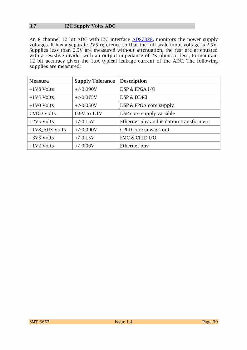
3.7 I2C Supply Volts ADC
An 8 channel 12 bit ADC with I2C interface ADS7828, monitors the power supply voltages. It has a separate 2V5 reference so that the full scale input voltage is 2.5V. Supplies less than 2.5V are measured without attenuation, the rest are attenuated with a resistive divider with an output impedance of 2K ohms or less, to maintain 12 bit accuracy given the 1uA typical leakage current of the ADC. The following supplies are measured:
Measure Supply Tolerance Description
+1V8 Volts +/-0.090V DSP & FPGA I/O
+1V5 Volts +/-0.075V DSP & DDR3
+1V0 Volts +/-0.050V DSP & FPGA core supply
CVDD Volts 0.9V to 1.1V DSP core supply variable
+2V5 Volts +/-0.15V Ethernet phy and isolation transformers
+1V8_AUX Volts +/-0.090V CPLD core (always on)
+3V3 Volts +/-0.15V FMC & CPLD I/O
+1V2 Volts +/-0.06V Ethernet phy

SMT-6657 Issue 1.4 Page 40
3.8 CPLD
The Xilinx XC2C384-10FTG256I CPLD strictly controls the DSP power supply start up and shut down sequence, and has direct control of each DSP reset. This allows it to set each DSP to boot from a location specified by user set DIP switches, by controlling the state of the DSP GPIO signals during reset.
After reset is complete the GPIO signals can be used as interrupts to each DSP to signal temperature alarm, and as inputs to the CPLD for software to drive a watch dog timeout, which can force a DSP reset in the event of a software crash.
It also allows DSP A to control the reset of DSP B, and performs a correctly sequenced power down in the event of an over temperature timeout, or a failure of the PCIe/104 power supply, indicated by the PCIe/104 PWRGOOD signal.
The following table lists the connections to the CPLD:
Source Signals Q
T
Y
CPLD In/
Out
Description
CLOCKS CLK25M 1 I 25MHz clock from master crystal oscillator
DSPA GPIO00-16 17 I/O Sets boot modes / general dspa i/o
DSPB GPIO00-16 17 I/O Sets boot modes / general dspb i/o
DSPA NMI_N 1 O Non maskable interrupt
DSPB NMI_N 1 O Non maskable interrupt
DSPA LRESET_N 1 O Warm reset
DSPB LRESET_N 1 O Warm reset
DSPA LRESETNMIEN_N 1 O Enable for core selects
DSPB LRESETNMIEN_N 1 O Enable for core selects
DSPA CORESEL0-1 2 O Core select for LRESET and NMI
DSPB CORESEL0-1 2 O Core select for LRESET and NMI
DSPA RESETFULL_N 1 O Full reset
DSPB RESETFULL_N 1 O Full reset
DSPA POR_N 1 O Power on reset
DSPB POR_N 1 O Power on reset
DSPA RESETSTAT_N 1 I Reset status
DSPB RESETSTAT_N 1 I Reset status
DSPA BOOTCOMPLETE 1 I Boot progress indication
DSPB BOOTCOMPLETE 1 I Boot progress indication

SMT-6657 Issue 1.4 Page 41
Temp Sensor
TEMPALARM 1 I Temperature alarm
DIP SWITCH
SWITCHES0-7 8 I User set switches
PSU PGD5V0 1 I 5v0 power good
PSU PGD3V3 1 I 3V3 power good
PSU PGD2V5 1 I 2V5 power good
PSU PGD1V8 1 I 1V8 power good
PSU PGD1V5 1 I 1V5 power good
PSU PGD1V2 1 I 1V2 power good
PSU PGD1V0 1 I 1V0 power good
PSU PGDCVDDA 1 I DSPA CVDD power good
PSU PGDCVDDB 1 I DSPB CVDD power good
PSU PGD0V75 1 I 0V75 power good
PSU EN2V5 1 O 2V5 enable
PSU EN1V8 1 O 1V8 enable
PSU EN1V5 1 O 1V5 enable
PSU EN1V2 1 O 1V2 enable
PSU EN1V0 1 O 1V0 enable
PSU ENCVDDA 1 O CVDDA enable
PSU ENCVDDB 1 O CVDDB enable
PSU EN0V75 1 O 0V75 enable
IO IOENABLE 1 O Enable front panel I/O
PCIe/104 PWRGOOD 1 I Host power is good
PCIe/104 ALERT 1 I Host interrupt
PCIe/104 PE_RST_N 1 I Host reset
PCIe/104 PSON_N 1 I/O Host primary PSU on
CLOCKS SYNC_N 1 O Synchronise all clock outputs
CLOCKS PDN_N 1 O Power up/down clock synthesiser
CLOCKS RESET_N 1 O Reset clock synthesiser
CLOCKS STATUS0-1 2 I Clock synthesiser status
LED (RED) RESET_LED 1 O Reset LED (on during DSP reset)
TOTAL 91 Total CPLD I/O pins
Notes:
The postfix “_N” denotes an active low signal.

SMT-6657 Issue 1.4 Page 42
CPLD XC2C384-10FTG256 has 212 I/O pins in 256 ball BGA 17mm x 17mm.
There are 121 CPLD I/O pins not allocated in the table above which are available to implement general logic as required.
The sequencing of the DSP power supplies is controlled during both power up and down by the CPLD. The CPLD core is supplied by 1V8AUX which is always on. The I/O is powered by the DSP main 1V8 so that both the DSP and CPLD I/O are powered at the same time. The power supply enable I/O pins are supplied by 3V3 which is always on. See the DSP power section for more details.
The CPLD is connected to GPIO00-16 (17 pins) of both DSPA and DSPB, and drives them all during DSP reset to set the DSP bootmode. After reset is complete the CPLD drives some of the GPIO pins to signal interrupts, and to allow software to read the state of the DIP switches, and the FPGA configuration. Refer to the TMS320C6657 data sheet for details of the boot mode settings.
After reset the CPLD uses GPIO00-16 in the same way for both DSPA and DSPB:
GPIO Function DSP In/Out Description
00 INT0_TEMP In Temperature alarm interrupt
01 INT1_ALERT In PCIe/104 Alert interrupt
02 INT2_PWRGOOD In PCIe/104 Powergood interrupt
03 INT3_DSP In Interrupt from the other DSP
04 STATUS_DATA In Serial CPLD status data
05 STATUS_CLOCK Out Serial CPLD status clock
06 RESETDSP Out Reset the other DSP
07 DSP_INTERRUPT Out Interrupt to the other DSP
08 FPGA_PROGRAM_B Out DSPA: FPGA configuration control
DSPB: not used
09 Reserved FPGA n/a Reserved for FPGA use
10 Reserved FPGA n/a Reserved for FPGA use
11 Reserved FPGA n/a Reserved for FPGA use
12 Reserved FPGA n/a Reserved for FPGA use
13 Reserved FPGA n/a Reserved for FPGA use
14 Reserved FPGA n/a Reserved for FPGA use
15 Reserved FPGA n/a Reserved for FPGA use
16 Reserved FPGA n/a Reserved for FPGA use
CPLD STATUS data is read serially and has the following bits:
BIT NAME DESCRIPTION

SMT-6657 Issue 1.4 Page 43
0 SWITCHES0 Dip switch 0
1 SWITCHES1 Dip switch 1
2 SWITCHES2 Dip switch 2
3 SWITCHES3 Dip switch 3
4 SWITCHES4 Dip switch 4
5 SWITCHES5 Dip switch 5
6 SWITCHES6 Dip switch 6
7 SWITCHES7 Dip switch 7
8 FPGA_INIT_B Fpga configuration wait, or crc error
9 FPGA_DONE Fpga configuration complete
10 Reserved=(0)
11 Reserved=(0)
12 Reserved=(0)
13 Reserved=(0)
14 Reserved=(0)
15 Reserved=(0)
The DSP can read the STATUS_DATA using a simple serial protocol. The DSP drives the STATUS_CLOCK low for at least 2ms, then pulses STATUS_CLOCK high for less than 10us for each of the 8 data bits, and reads the state of STATUS_DATA to determine the state of each status bit. The CPLD has a 1ms timer which measures the time STATUS_CLOCK is low and resets the output bit counter to 0 if it is low for more than 1ms.
Each DSP can interrupt the other DSP.
Each DSP can force the CPLD to reset the other DSP.
The watchdog programmable timer is implemented in the FPGA, and it has a dedicated connection to the CPLD which will reset both DSPA and DSPB if there is a watchdog timeout.
The CPLD has 3 separate power supplies:
1V8AUX is the core supply and is always on
3V3 is the LVTTL I/O supply for the PSU enable signals
1V8 is the DSP I/O supply
As far as possible, the CPLD design process is restricted to the smaller CPLD XC2C256-7FTG256I, in case the design is small enough to fit into this part for production.
3.9 DSP Booting
The DSPs support a total of 6 boot modes:

SMT-6657 Issue 1.4 Page 44
1) EMIF16 NOR flash or through the FPGA 2) SRIO 3) Ethernet 4) PCIe 5) I2C PROM 6) Hyperlink (from the other DSP)
The currently active boot mode is controlled independently for each DSP by the CPLD. User set DIP switches allow manual control of the boot mode during test and development.
Typically DSP A provides DSP B with its boot image using either the Hyperlink or the shared SRIO, and provides the FPGA with the configuration image using the EMIF16 interface.
3.9.1 DIP Switches
There are 8 dip switches, which set the boot mode for both DSPs. The surface mount switch assembly has right angle keys for easy access in a stacked system, and a pin pitch of 1.27mm for small PCB footprint. All 8 switches are connected to the CPLD. The switch is mounted at the PCB edge near the I/O expansion connector.
The dip switches are divided into 2 banks, 4 switches for each DSP:
SWITCH DSP DESCRIPTION
1 A Boot mode select switch 0
2 A Boot mode select switch 1
3 A Software readable switch 0
4 A Software readable switch 1
5 B Boot mode select switch 0
6 B Boot mode select switch 1
7 B Software readable switch 0
8 B Software readable switch 1
Note: switches are ON to indicate 1 or high.
The boot modes are selected differently for each DSP:
Boot Mode selection DSPA Boot Source DSPB Boot Source
0 EMIF16 FLASH HYPERLINK
1 SRIO SRIO
2 PCIE PCIE
3 NO BOOT NO BOOT
The setting “NO BOOT” is useful during development and production when there is no valid boot image in the EMIF16 FLASH.

SMT-6657 Issue 1.4 Page 45
3.10 Flash Memories
All flash memory parts have a minimum 20 year data retention.
3.10.1 256KByte I2C EEPROM
This is a 2M bit or 256K byte serial EEPROM, and is intended to provide storage for board identification and serialisation, usage data, and other parameters. Connected to the system management I2C bus, this EEPROM is accessible to both DSPs and the on-board FPGA.
Either of the following parts may be used:
Manufacturer Part number Data retention years
Write cycle endurance
STM M24M02 200 4M
ATMEL AT24CM02 100 1M
3.10.2 256MByte Parallel NOR Flash
A 1.8 Volt 2G bit 256M byte 128M by 16-bit parallel NOR flash memory is present on the EMIF16 interface of DSPA, so that DSPA software can read and securely write to this memory at high speed. NOR flash memory is used in preference to NAND flash for increased reliability.
This memory typically holds the boot images for both DSPs, the local Kintex-7 FPGA, and the FPGA on the FMC daughter board.
Sufficient capacity is provided to enable an operating system running on DSP A to implement a file system alongside the boot images.
The following part may be used: Micron PC28F00BP30EFA-ND.
Note that endurance is specified as 100,000 erase cycles per block, so this memory should be used with caution, for applications that require continuous block erase. For further details of data retention, please see this Micron technical note: TN-12-30: NOR Flash Cycling Endurance and Data Retention.

SMT-6657 Issue 1.4 Page 46
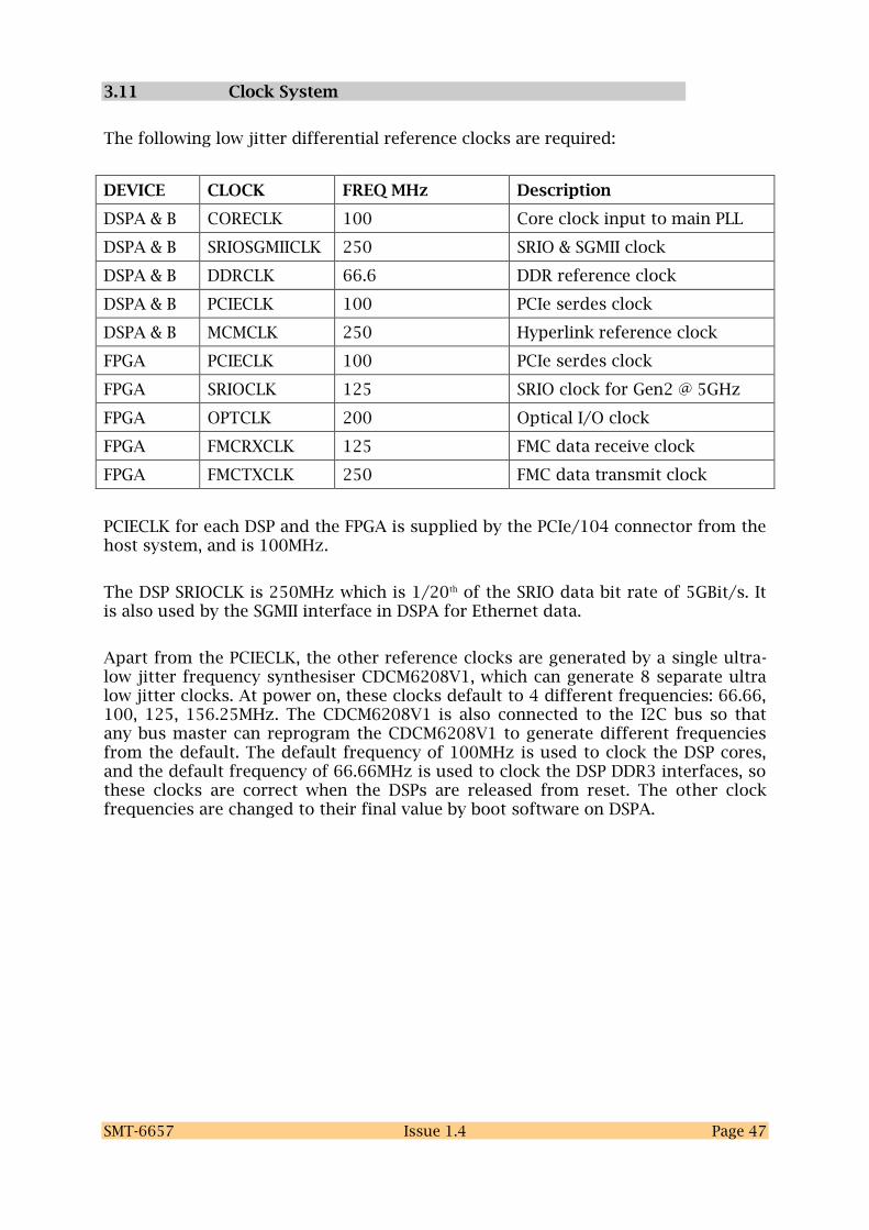
SMT-6657 Issue 1.4 Page 47
3.11 Clock System
The following low jitter differential reference clocks are required:
DEVICE CLOCK FREQ MHz Description
DSPA & B CORECLK 100 Core clock input to main PLL
DSPA & B SRIOSGMIICLK 250 SRIO & SGMII clock
DSPA & B DDRCLK 66.6 DDR reference clock
DSPA & B PCIECLK 100 PCIe serdes clock
DSPA & B MCMCLK 250 Hyperlink reference clock
FPGA PCIECLK 100 PCIe serdes clock
FPGA SRIOCLK 125 SRIO clock for Gen2 @ 5GHz
FPGA OPTCLK 200 Optical I/O clock
FPGA FMCRXCLK 125 FMC data receive clock
FPGA FMCTXCLK 250 FMC data transmit clock
PCIECLK for each DSP and the FPGA is supplied by the PCIe/104 connector from the host system, and is 100MHz.
The DSP SRIOCLK is 250MHz which is 1/20th of the SRIO data bit rate of 5GBit/s. It is also used by the SGMII interface in DSPA for Ethernet data.
Apart from the PCIECLK, the other reference clocks are generated by a single ultra-low jitter frequency synthesiser CDCM6208V1, which can generate 8 separate ultra low jitter clocks. At power on, these clocks default to 4 different frequencies: 66.66, 100, 125, 156.25MHz. The CDCM6208V1 is also connected to the I2C bus so that any bus master can reprogram the CDCM6208V1 to generate different frequencies from the default. The default frequency of 100MHz is used to clock the DSP cores, and the default frequency of 66.66MHz is used to clock the DSP DDR3 interfaces, so these clocks are correct when the DSPs are released from reset. The other clock frequencies are changed to their final value by boot software on DSPA.

SMT-6657 Issue 1.4 Page 48
The CDCM6208V1 outputs are connected as follows:
Output Default
Freq
MHz
Final
Freq
MHz
Destination Software change required
for full speed operation
Y0 156.25 200.0 FPGA OPTCLK Yes
Y1 156.25 250.0 DSPA & DSPB SRIOSGMIICLK Yes
Y2 125.0 250.0 DSPA & DSPB MCMCLK Yes
Y3 125.0 125.0 FPGA SRIOCLK No
Y4 66.6 66.6 DSPA DDRCLK No
Y5 66.6 66.6 DSPB DDRCLK No
Y6 100.0 100.0 DSPA CORECLK No
Y7 100.0 100.0 DSPB CORECLK No
To drive both DSPs with identical MCMCLK clocks and SRIOSGMIICLK clocks, outputs Y1 and Y2 are duplicated using a dual 1:2 LVDS buffer CDCLVD2102.
The CDCM6208V1 and the FPGA require a low jitter 25MHz LVDS crystal clock source. The Ethernet PHY and the CPLD require a 25MHz LVTTL crystal clock source. These clocks are all provided by fully low jitter buffering a single 25MHz low jitter crystal oscillator with CDCLVD1204. This buffers a single LVDS source and drives 4 LVDS outputs. The LVTTL clock for the Ethernet PHY and the CPLD are generated by converting LVDS clocks to LVTTL with SN65LVDS2, as close as possible to the destination. Using LVDS to distribute the LVTTL clocks greatly reduces the effects of noise on the clocks, and the electromagnetic radiation of these clocks.
The FMC LVDS data acquisition interfaces have 2 shared ultra-low jitter clocks generated on the FMC daughterboard, which are fed directly to FPGA clock inputs.
The SYSCLKOUT clocks from each DSP are fed directly to the FPGA, so it can support high-speed operation of the EMIF16 for each DSP. These are at 1/6 of the DSP core frequency, which is 208.3MHz for a 1.25GHz DSP. As both DSPs have the same CORECLK, the SYSCLKOUT from each DSP will have the same frequency, although there may be some difference in the phase. The FPGA internal PLL requires a clock between 70MHz and 800MHz, so SYSCLKOUT from DSPA is used as the reference clock for the FPGA PLL. This has the advantage that processing in the FPGA can be synchronous to the DSP cores, which can reduce latency caused by synchronising data when passing it across clock domains . The SYSCLKOUT signals are 1.8V LVTTL, and are routed with 0V guard traces to ensure added jitter from adjacent signals is minimised.
The DSPs power up with their internal PLL bypassed, so the external CORECLK is used to clock the cores directly. With the CORECLK at 100MHZ, SYSCLKOUT will be 16.6MHz with the PLL bypassed. DSPA will enable its internal PLL during booting so that it generates 1.25GHz before it configures the FPGA, so that the configured

SMT-6657 Issue 1.4 Page 49
FPGA always receives the correct SYSCLKOUT frequency. This places a restriction on the minimum DSP core frequency for correct operation of the FPGA PLL, which is 70MHz x 6 = 420MHz. This restriction is only relevant if it is desired to reduce the DSP internal core clock frequency, for instance to reduce power consumption.
Note that ALL clocks in the system are distributed strictly point to point with no branches, and impedance control.

SMT-6657 Issue 1.4 Page 50
The diagram below shows the high speed continuous clock architecture:
Low Jitter8 Output
SynthesiserCDCM
6208V1
Crystal
Clock
25MHz
4 OutputLVDS
BufferCDCLVD
1204
FPGA
CPLD
ENET PHY
DSPA
DSPB
PCIe/104
FMC
25MHz
25MHz
25MHz
25MHz
25MHz
125MHz
250MHz
LVDS to
LVTTL
SN65LVDS2
LVDS to
LVTTL
SN65LVDS2
25MHz
25MHz
125MHz SRIOCLK
100MHz PCIECLK
100MHz PCIECLK
100MHz PCIECLK
100MHz CORECLK
100MHz CORECLK
66MHz DDRCLK
66MHz DDRCLK
200MHz OPTCLK
250MHz SRIOSGMIICLK
2 Output
LVDS Buffer
CDCLVD2102
250MHz MCMCLK
250MHz MCMCLK
250MHz MCMCLK
208MHz SYSCLKOUT
208MHz SYSCLKOUT
2 Output
LVDS Buffer
CDCLVD2102
250MHz SRIOSGMIICLK
250MHz SRIOSGMIICLK
Notes:
The following clocks are not shown: SPI data clock, I2C data clock, DDR3 clock.

SMT-6657 Issue 1.4 Page 51
3.12 Power Supplies
The table below shows the power supplies available from the PCIe/104 “one bank” connector:
Volts Amps Watts
+3.3 3.6 11.9
+5V 8.4 42.0
+5V_SB 3.6 18.0
TOTAL n/a 71.9
There are no requirements to use 5 Volt power directly, so it is used to supply a number of DC-DC voltage convertors. The 3V3 supply is used directly.
The FMC Low Pin Count (LPC) connector is specified with the following power supplies. The supplies 3P3V and 3P3VAUX are supplied directly from the PCIe/104 3.3V supply. The others are supplied from DC-DC converters.
Supply Volts Amps Watts
VADJ 0 to 3.3 2 0 to 6.6
VREF_A_M2C 0 to VADJ 0.001 0 to 0.0033
3P3VAUX 3.3 0.020 0.066
3P3V 3.3 3 9.9
12P0V 12.0 1 12.0
The FMC supply 12P0V (12.0V) is supplied directly from either the host board through the SRIO connector, or from the I/O expansion board.
The FMC supply VADJ is generated using a DC-DC from the main +5V supply. Allowing for 80% efficiency the maximum +5V power draw is 8.254W (1.65A).
The FMC supply VREF_A_M2C is generated using a linear regulator from VADJ.

SMT-6657 Issue 1.4 Page 52
The table below shows estimated worst case power draw for the board. Allowance has been made for DC-DC convertor efficiency of 80%. The FMC power draw is the maximum permissible:
DEVICE
5V
AMPS
5V
WATTS
3V3
AMPS 3V3 WATTS
TOTAL WATTS
C6657 DSP x 2 2.4 12.0 0.0 0.0 12.0
FPGA 1.49 7.45 0.3 0.99 8.44
DDR3 0.56 2.8 0 0 2.8
FMC 1.65 8.254 3.02 9.966 18.22
Other devices 0.0 0.0 0.3 0.99 0.99
TOTALS 6.1 30.5 3.62 11.94 42.45
This worst case analysis shows that it is possible to use all the available 3.3V power directly from the PCIe/104 connector.
The system requires 8 further power supplies:
Supply
Volts
Tolerance
Volts
Estimated
Max Amps
Estimated
Max
Watts
Description
2.5 +/-0.15 0.43 1.075 Ethernet PHY 88E1112
1.8 +/-0.09 0.41 0.738 2 x DSP I/O
FPGA I/O
1.8_AUX +/-0.10 0.01 0.018 CPLD core
1.5 +/-0.075 2.042 3.063 2 x DSP & DDR3
1.2 +/-0.06 0.32 0.384 Ethernet PHY 88E1112
1.0 +/-0.05 1.116 1.116 2 x DSP Cores
FPGA CORE
0.75 (half 1.5V rail)
1.112 0.834 2 x DDR3 termination
CVDDA
(0.85 to 1.1)
TBD [email protected] 4.59 1 x DSP Core
CVDDB
(0.85 to 1.1)
TBD [email protected] 4.59 1 x DSP Core

SMT-6657 Issue 1.4 Page 53
The following table shows the difference between using a DC-DC and a linear voltage regulator for each supply, where feasible. The source for all DCDC is 5V0 and efficiency is 80%. Each linear regulator is supplied from the next highest voltage supply. The difference is shown as the power lost in each power supply:
Supply
Volts
DCDC
Watts
Lost
Linear
Source
Volts
Linear
Watts
Lost
2.5 0.269 3.3 0.344
1.8 0.185 2.5 0.287
1.5 0.766 1.8 0.613
1.2 0.096 1.5 0.115
1.0 0.279 1.2 0.223
Using DC/DC converters with better than 80% efficiency for all supplies, offers a net saving over using idealised linear regulators. However in some cases the total power lost is small, and a linear regulator may be advantageous for both output noise and PCB space. Where a DC/DC is used the output ripple must be shown to be within the supply voltage tolerance.
All decoupling capacitors are ceramic to provide increased reliability over Tantalum capacitors.

SMT-6657 Issue 1.4 Page 54
The drawing below shows the power supply architecture, with maximum PCIe/104 connector current supplies, and estimated load current draws:
PCIe/104
5V0@8A4MAX
5V0SB@3A6MAX
3V3@3A0
FMC
DSPB
DSPA
FPGA
DDR3A & B
CPLD
SRIO
I/O LSHM
12V0@1A0
12V0@1A0
I2C PROGRAMMABLESWITCHING REG 12A
TPS53915
5V0SB@1A65 0V6 to 3V3@2A0
3V3@3A6MAX
3V3@0A05
1V8@0A4
ENET PHY
SWITCHINGREGS
UCD9222UCD7242
0V8 to 1V1@4A1
0V8 to 1V1@4A1
VIDA
VIDB
1V0@0A5
1V0@0A5
1V5@0A3
1V5@0A3
1V8@0A1
1V8@0A1
1V5@0A7
0V75@0A6
5V0@2A2
2V5@0A23
1V2@0A32
5V0@0A1
2V5@0A11
3V3@0A5
1V8@1A
3V3@0A1
1V0@4A7
ENCVDD1V8AUX@0A4
EN2V5
EN1V8
EN1V5
EN1V0
EN0V75
ENCVDD
5V0SB@0A18
DDR TerminationTPS51200
1V5@0A6
SWITCHING REG6 AMPS OUT
TPS54620
5V0@0A7
SWITCHING REG6 AMPS OUT
TPS54620
5V0@1A42
SWITCHING REG6 AMPS OUT
TPS54620
5V0@0A72
EN1V8
EN1V0
EN1V5
EN0V75
SWITCHING REG2 AMPS OUT
TPS54218
5V0@0A2
EN2V5
2V5@0A34
1V0@5A7
1V8@1A6
1V5@1A9
SWITCHING REG2 AMPS OUT
TPS54218
1V8AUX@0A4
I2C

SMT-6657 Issue 1.4 Page 55
3.13 I/O expansion connector
The Ethernet, FPGA JTAG, and FPGA I/O pins are all routed to a dedicated high density 100-way, right angle I/O connector, Samtec type LSHM. This allows an add-on I/O PCB to be plugged in at the side of the DSP PCB, above the FMC daughterboard.
This I/O PCB provides external front panel connectors for application-specific interfaces. This eliminates the requirement for any cables in a systems design.
The I/O PCB is NOT required for full operation of the DSPs.
The standard I/O board illustrated in the PCB layout provides the following I/O connectors:
1 (one) RJ45 gigabit Ethernet connector (front panel) 4 (four) Optical Inputs (front panel) 4 (four) Optical Outputs (front panel) 4 (four) TTL inputs and 4 TTL outputs via LEMO coax sockets (front panel) 1 Optical duplicate of a TTL ouptut 2 (two) TI/GSI DSP Links, 34 way IDC (front panel) 1 (one) Xilinx FPGA JTAG 14 way IDC (inboard) 1 (one) 500MByte/s MGT lane
See the SMT-IO-GSI specifications for further details of the standard I/O board.

SMT-6657 Issue 1.4 Page 56
The following table lists all the signals on the I/O connector. Differential signals occupy 2 pins:
Source Signals Q
T
Y
DSP
PCB In/
Out
Description
ENET PHY Copper ENET 8 I/O 1GBit/s copper I/O
ENET PHY Fibre ENET 5 I/O 1.25GBit/s fibre I/O
FPGA 4 x LVDS 8 O Optical outputs
FPGA 4 x LVDS 8 I Optical inputs
FPGA 2 x LED 2 O Front panel LEDs
FPGA 24 x LVTTL 24 I/O 2 x DSP links
FPGA 4 x LVTTL 4 O LVTTL outputs
FPGA 4 x LVTTL 4 I LVTTL inputs
FPGA JTAG 4 I/O FPGA Xilinx Jtag
CPLD IOENABLE 1 O Output enable
FMC +12V 2 I Power supply for FMC only
PCIe/104 +5V0 1 O Power for I/O buffers
PCIe/104 +3V3 1 O Power for I/O buffers
PSU +2V5 1 O ENET transformer common
FPGA MGT 6 I/O MGT 500MByte/s
- GND (0V) 21 - System ground
TOTAL 100
Notes:
The postfix “_N” denotes an active low signal
All differential pairs have each half on adjacent pins, with GND pins between each pair. See the Samtec performance characterisation for pin pair assignment.
LSHM current rating is 1.3A per pin at @ 95°C ambient
The ENET copper isolation transformer is located on the I/O PCB.

SMT-6657 Issue 1.4 Page 57
3.14 SRIO expansion connector
The SRIO expansion connector carries 4 separate SRIO connections down to the host board. This connector uses the “Stack-PC” standard expansion connector B1, known as FPE (bottom). The specification for this connector is defined on page 30 of StackPC specification ref [19] published here: The FPE pins used for the SRIO connections are detailed below.
This connector also carries +12.0V from the host board to the FMC board and 4 MGT lanes to the FPGA, capable of supporting additional PCIE connections.
The table below shows the pins actually connected in SMT6657:
FPE R1 R2 R3 R4 R5 R6 R7 R8 R9 R10
C1 DB0 DB1 GIO0 REF
CLK0p
GIO1 GIO2 GIO3
C2 GND DB2 GND REF
CLK0n
GND GND GND
C3 DB3 DB4 GND GND GND GND
C4 DB5 DB6
C5 GND DB7 GND GND GND GND
C6 DB8 GND SRIO
TX0p
GND SRIO
TX1p
GND SRIO_
TX2p
GND SRIO
TX3p
GND
C7 DB9 DB10 SRIO
TX0n
SRIO
RX0p
SRIO
TX1n
SRIO
RX1p
SRIO
TX2n
SRIO
RX2p
SRIO
TX3n
SRIO
RX3p
C8 GND DB11 GND SRIO
RX0n
GND SRIO
RX1n
GND SRIO
RX2n
GND SRIO
RX3n
C9 PCIe
TX0p
GND PCIe
TX2p
GND GND GND
C10 PCIe
TX0n
PCIe
TX1p
PCIe
TX2n
PCIe
TX3p
C11 GND PCIe
TX1n
GND PCIe
TX3n
GND GND GND PE_
RST_n
C12 PCIe
RX0p
GND PCIe
RX2p
GND GND GND PCIe
CLK0p
GND
C13 PCIe
RX0n
PCIe
RX1p
PCIe
RX2n
PCIe
RX3p
PCIe
CLK0n
BUS_
ERR_n
C14 GND PCIe
RX1n
GND PCIe
RX3n
GND GND GND CON
FIG0
C15 GND GND GND GND CON FIG1
C16 CON

SMT-6657 Issue 1.4 Page 58
FIG2
C17 GND GND GND GND GND Res
C18 GND GND GND GND Res +12V
C19 Res +12V
C20 GND GND GND GND Res +12V
NOTES:
1. Transmit is motherboard output. Receive is motherboard input 2. GIO are shared to all 3 sites. SMT6657 provides a weak pull up TO +3V3.
Usage is TBD. They are connected to both the CPLD and the FPGA on SMT6657. Series damping resistors of 22 Ohms are used.
3. At each FPE site, DB0-11 and GIO0-3 and 4xGND are connected to a 2x10 0.1 inch square pin header on the motherboard for development and debugging.
4. REFCLK0 is a single differential 25.000MHz crystal clock, distributed on the motherboard with a CDCLVD1204 2 to 4 LVDS buffer, to all 3 FPE sites. This can optionally be used by the SMT6657 instead of a local crystal. A central clock ensures there is no frequency tolerance error between the sites, and allows all 3 sites to synchronise.
5. DB0-11 are used for development and debug only, and can be disconnected or set to high impedance for production.

SMT-6657 Issue 1.4 Page 59
4 PCB Layout
4.1 Heat Sinks
Individual pin fin heat sinks are attached to both DSPs and the FPGA with clips.
4.2 Component Placement
There are 2 primary constraints on the component placement:
1. The DSP JTAG interface total trace length must not exceed 3 inches (76.2mm), which includes trace length on the I/O expansion board up to the MIPI 60 way connector.
2. The DSP DDR3 interface must have no other components between the DSP and its 3 DDR3 memory chips.
With the MIPI JTAG connector mounted on the top of the PCB near the DSPs, we can place all 6 DDR3 chips on one side, with the DSPs next to them, and the FPGA next to the 100 way I/O connector.
There are 8 switching regulators and associated inductors and capacitors. These are mostly located on the bottom of the PCB.
There are 4 main chips in the clock generator system, and these are also located on the bottom of the PCB.
The maximum component heights are 8.76mm on the top and 4.83mm on the bottom of the PCB. This means there are no restrictions on ceramic capacitor placement. The DSP CVDD regulators supply up to 4.1 Amps each and the 1.0V regulator supplies up to 5.7 Amps.
Both DSPs and the FPGA are fitted with clip on pin fin heatsinks.
The placement drawings below are a guide showing possible placement of the major components only. There are 8 switch mode power controllers, and this means that there are also a large number of big decoupling capacitors required, as well as the usual smaller high frequency decoupling capacitors (not shown). Each bank of DDR3 memories requires a significant number of termination resistors (not shown).

SMT-6657 Issue 1.4 Page 60
Top surface component placement (top view)
Bottom surface component placement (bottom view)
SMT-6657 Issue 1.4 Page 61
4.3 PCB Construction
The following design requirements force the use of blind and buried vias:
1. Component placement on the top and bottom surface of the PCB overlap, so through vias can not be used.
2. Component packing density is sufficiently high that through vias would waste too much PCB surface area on the surface where they are not connected.
3. Many very high speed signals require via stub length to be taken in to account making routing through vias difficult.
4. Many very high speed signals require via impedance discontinuity to be an absolute minimum.
5. The DDR3 memory traces must be completely isolated from all other signals, however component placement forces routing non DDR3 signals under the DDR3 chips. This can be done by using the signal planes nearest the bottom for non DDR3 signals, as long as through vias are not used.

SMT-6657 Issue 1.4 Page 62
The following drawing shows the layer stack used by Texas Instruments for their C66xx EVM pcbs:
This 12 layer stack provides 6 signal layers and 6 power planes, of which 4 are ground and 2 are power. The use of 0.5oz copper unnecessarily restricts heat flow internally across the board, and from SM pad to via. The SMT6657 PCB design uses a heavier copper weight, since heat flow increases almost exponentially with copper weight. Higher copper weight also increases PCB reliability. So it is recommended that this stack up is used, but with copper weight increased from 0.5oz (17.5um) to 1oz (35um). Note that surface layers will have their copper weight increased by plating, so that 1oz bare copper will increase to around 1.5oz on the surface.
If routing this 12 layer stack is difficult due to component density, it may be necessary to increase the number of layers to 16, with 8 signal layers and 8 power planes.

SMT-6657 Issue 1.4 Page 63
The following is the final 16-layer PCB stack-up for the SMT6657:
The layer build is this:
TOP - Top, main component side.
INNER5 - Differential pairs, impedance controlled.
GND - Reference plane for above layer.
INNER1
PWR1 - Split power plane.
INNER2
INNER7
PWR2 - Split power plane.
PWR3 - Split power plane.
INNER8
INNER4
PWR4 - Split power plane.
INNER3
GND - Reference plane for below layer.
INNER6 - Differential pairs, impedance controlled.
BOTTOM - Bottom, mainly passive components.

SMT-6657 Issue 1.4 Page 64
4.4 PCB Layout
4.4.1 Main Board
Below is an image of the top (red) and bottom (blue) layers:

SMT-6657 Issue 1.4 Page 65
4.4.2 Front Panel Interface Board

SMT-6657 Issue 1.4 Page 66
5 Physical Properties
Dimensions 90mm 96mm
Weight <400 grams
Voltage Power (estimate includes FMC)
5V 30.5W
3.3V 11.9W
RH 10-80%
Operating Temperature 0ºC to +50ºC
MTBF > 90,000 hours
PCB number of layers 12-16
PCB finish ENIG

SMT-6657 Issue 1.4 Page 67
6 Verification, Review & Validation Procedures The SMT6657 is a high reliability product, and all design procedures, production and testing maximise product reliability, and are carried out in accordance with the Sundance Quality Procedures (ISO9001).
See: http://www.sundance.com/web/files/static.asp?pagename=quality
7 Safety This module presents no hazard to the user when in normal use.
8 EMC Statement of Compliance This module is designed to operate from within an enclosed host system, which is built to provide EMC shielding. Operation within the EU EMC guidelines is not guaranteed unless it is installed within an adequate enclosure.
This module is protected from damage by fast voltage transients originating from outside the host system which may be introduced through the output cables.
Short circuiting any output to ground does not cause a host system to lock up or reboot.
9 Ordering Information The Xilinx Kintex FPGA KU040 which is slightly larger than the KU035, can be fitted at assembly as packaging is identical.
Order numbers:
SMT6657-KU35 = Xilinx KU035 FPGA
SMT6657-KU40 = Xilinx KU040 FPGA