passband flattened binary-tree structured sion … · passband flattened binary-tree structured...
TRANSCRIPT


PASSBAND FLATTENED BINARY-TREE STRUCTURED ADD-DROP MULTIPLEXERS
USING SION WAVEGUIDE TECHNOLOGY

This work was financially supported by the Dutch Technology Foundation STW, under TIF.4367 Cover: Layout of the 1-from-16 add-drop multiplexer designed and fabricated at IBM Zurich Research Laboratory, and in the background a photo of a mach-zehnder plus ring resonator. Copyright 2002 by Chris Roeloffzen, Enschede, The Netherlands ISBN 90-365-1803-2

PASSBAND FLATTENED BINARY-TREE STRUCTURED ADD-DROP MULTIPLEXERS
USING SION WAVEGUIDE TECHNOLOGY
PROEFSCHRIFT
ter verkrijging van de graad van doctor aan de Universiteit Twente,
op gezag van de rector magnificus, prof. dr. F.A. van Vught,
volgens besluit van het College voor Promoties in het openbaar te verdedigen
op woensdag 25 september 2002 te 15:00 uur.
door
Chris Gerardus Hermanus Roeloffzen
geboren op 31 oktober 1973 te Almelo

Dit proefschrift is goedgekeurd door: De promotor: Prof. Dr. Th.J.A. Popma de assistent-promotor: Dr. Ir. R.M. de Ridder

Contents Chapter 1: Introduction________________________________________________1
1.1 Telecommunication ___________________________________________1 1.2 Flamingo ___________________________________________________2 1.3 The binary tree add-drop multiplexer ______________________________3 1.4 Integrated optics______________________________________________5 1.5 Outline of the thesis ___________________________________________6
Chapter 2: Theory and mathematical design of passband flattened slicers ________________7 2.1 Introduction_________________________________________________7 2.2 Mach-Zehnder Interferometer ___________________________________7 2.3 Theory: Transfer matrix method and z-transform description of MZI _____8 2.4 Lattice filters________________________________________________16 2.5 Cascading of two slicers with identical filter curves ___________________26 2.6 Alternative slicer: MZI + Ring filter ______________________________27 2.7 Comparing Lattice filter and MZI + Ring__________________________36 2.8 Summary & Conclusions ______________________________________36
Chapter 3: Device design ______________________________________________39 3.1 Introduction________________________________________________39 3.2 Waveguide demands and design _________________________________39 3.3 Power coupling element _______________________________________48 3.4 Heater design (tuning element) __________________________________61 3.5 Passband flattened wavelength slicers _____________________________65 3.6 Binary tree Add-drop Multiplexer ________________________________69 3.7 Summary & Conclusions ______________________________________71
Chapter 4: Device fabrication ___________________________________________73 4.1 Introduction________________________________________________73 4.2 Substrate preparation _________________________________________73 4.3 PECVD ___________________________________________________75 4.4 Film characterization _________________________________________76 4.5 Thermal treatment of the SiON layer _____________________________78

4.6 Channel fabrication __________________________________________80 4.7 Upper cladding deposition _____________________________________84 4.8 Thermal tuning elements ______________________________________86 4.9 Conclusions ________________________________________________88
Chapter 5: Device performance __________________________________________89 5.1 Introduction________________________________________________89 5.2 Experimental setup___________________________________________89 5.3 Measurement steps ___________________________________________91 5.4 Characterizing of waveguides ___________________________________93 5.5 Directional coupler performance ________________________________95 5.6 Slicer performance ___________________________________________97 5.7 ADM measurements _________________________________________99 5.8 MZI + ring resonator ________________________________________106 5.9 Discussion and conclusion ____________________________________112
Chapter 6: Summary and future directions _________________________________115 6.1 Summary _________________________________________________115 6.2 Future directions ___________________________________________117
Appendix ______________________________________________________119 References_______________________________________________________131 Samenvatting (Dutch)_______________________________________________137 Dankwoord (Dutch)________________________________________________139 Bibliography _____________________________________________________141

1
Chapter 1: Introduction
1.1 Telecommunication
When writing this introduction I saw the following press release on the Internet: “Nielsen//Netratings reports a record half billion people worldwide now have home internet access”. The number of home users grew worldwide with 5 % over the last quarter of 2001. The growth was nearly doubled compared to Q3 2001. The growth in Europe was 4.9%, almost equal to the world growth. One in three households in Europe/Middle East and Africa have Internet access, compared with over half in the US. The Netherlands has 52 % of the households connected to the Internet and 82 % of the computers is connected to the Internet. Another press release also from Nielsen//Netratings was titled as “Broadband Usage Outpaces Narrowband for the first time.” 1.19 billion of the total 2.3 billion hours was spent by broadband surfers online in January 2002 in the US. The broadband time spent in January 2002 was 64 % higher than in January 2001. Nearly 21.9 million surfers (in the US) at-home accessed the Internet via broadband connection in January 2002 compared to 13.1 million in January 2001, a boost of 67% in one year time. So there is an unstoppable march towards broadband. (See www.nielsen-netratings.com) This demand can be fulfilled with the tremendous bandwidth of the optical fiber of 30 THz (1420-1670 nm). It is not possible to directly address this complete band, since the current maximum speed of the electronics and modulators is 40-100 GHZ. Wavelength division multiplexing (WDM) is used to divide the band in multiple sub bands. The spacing between the sub band channels is defined by the ITU grid. Common spacings between channels are 12.5, 25, 50, 100 and 200 GHz. The device that combines these channels onto one fiber is called a Multiplexer (Mux) and the device that does the opposite, spatial separation of frequency channels onto different fibers, is called a demultiplexer (Demux). When Mux and Demux are combined it is possible to select only one (or more) channel to be dropped or added and leaving the remaining channels undisturbed. Such a device is called an Add-drop multiplexer (ADM). Optical transmission systems 3.28 Tbit/s over a few hundred of kilometers [Nielsen 2000] or 2 Tbit/s over almost ten thousand kilometers [Yamada 2002] have already bee reported.
Introduction
2
1.2 Flamingo
This work has been performed in an STW project called “Flexible Multiwavelength Optical Local Access Network Supporting Multimedia Broadband Services” or “FLAMINGO”. It consists of three tasks major tasks: Task 1: Network issues Protocol issues. This task can be split up into two parts: Physical Systems Network Design, and Multidimensional Access and Control Mechanisms for Multiparty Multimedia Applications in WDM Optical Networks. Two PhD students work on this task. Task 2: Tunable Add-drop wavelength multiplexer. This task is the topic of this thesis Task 3: Wavelength converter: Conversion of the wavelength without affecting the contained data. This conversion will be done in the optical domain. So without transfer of the data stream to the electrical domain. One PhD student works on this task. 1.2.1 Network Architecture
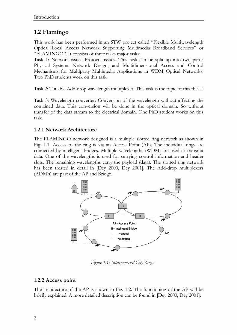
The FLAMINGO network designed is a multiple slotted ring network as shown in Fig. 1.1. Access to the ring is via an Access Point (AP). The individual rings are connected by intelligent bridges. Multiple wavelengths (WDM) are used to transmit data. One of the wavelengths is used for carrying control information and header slots. The remaining wavelengths carry the payload (data). The slotted ring network has been treated in detail in [Dey 2000, Dey 2001]. The Add-drop multiplexers (ADM’s) are part of the AP and Bridge.
B
B
B
AP
AP
AP
AP
AP
AP
AP
APAP
AP= Access Point
B= Intelligent Bridge
=optical
=electrical
B
B
B
AP
AP
AP
AP
AP
AP
AP
APAP
AP= Access Point
B= Intelligent Bridge
=optical
=electrical
Figure 1.1: Interconnected City Rings
1.2.2 Access point
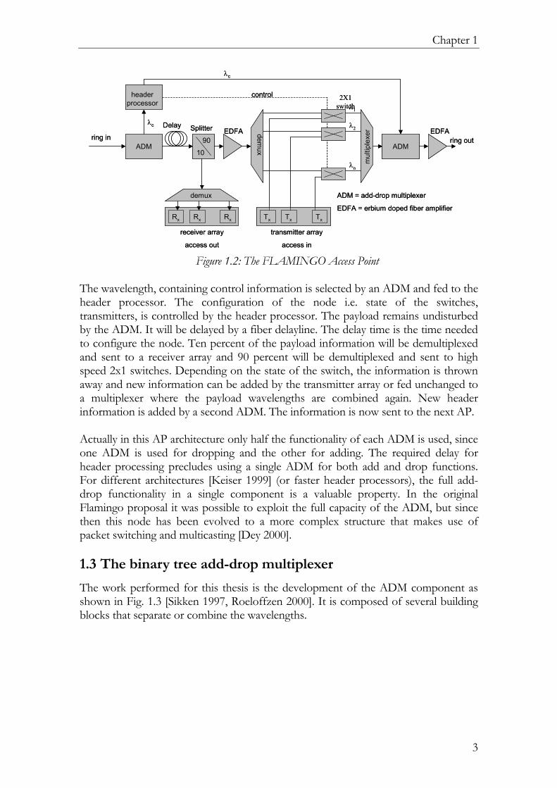
The architecture of the AP is shown in Fig. 1.2. The functioning of the AP will be briefly explained. A more detailed description can be found in [Dey 2000, Dey 2001].
Chapter 1
3
ring out
demuxADM ADM
mul
tiple
xer
2X1 switch
receiver array
access out
EDFA
header processor
transmitter array
access in
λ1
λ2
λn
λc
λc
EDFA
Rx Rx Rx Tx Tx Tx
90
10
SplitterDelay
ring in
ADM = add-drop multiplexer
EDFA = erbium doped fiber amplifier
control
demux
ring out
demuxADM ADM
mul
tiple
xer
2X1 switch
receiver array
access out
EDFA
header processor
transmitter array
access in
λ1
λ2
λn
λc
λc
EDFA
Rx Rx Rx Tx Tx Tx
90
10
SplitterDelay
ring in
ADM = add-drop multiplexer
EDFA = erbium doped fiber amplifier
control
demux
Figure 1.2: The FLAMINGO Access Point
The wavelength, containing control information is selected by an ADM and fed to the header processor. The configuration of the node i.e. state of the switches, transmitters, is controlled by the header processor. The payload remains undisturbed by the ADM. It will be delayed by a fiber delayline. The delay time is the time needed to configure the node. Ten percent of the payload information will be demultiplexed and sent to a receiver array and 90 percent will be demultiplexed and sent to high speed 2x1 switches. Depending on the state of the switch, the information is thrown away and new information can be added by the transmitter array or fed unchanged to a multiplexer where the payload wavelengths are combined again. New header information is added by a second ADM. The information is now sent to the next AP. Actually in this AP architecture only half the functionality of each ADM is used, since one ADM is used for dropping and the other for adding. The required delay for header processing precludes using a single ADM for both add and drop functions. For different architectures [Keiser 1999] (or faster header processors), the full add-drop functionality in a single component is a valuable property. In the original Flamingo proposal it was possible to exploit the full capacity of the ADM, but since then this node has been evolved to a more complex structure that makes use of packet switching and multicasting [Dey 2000]. 1.3 The binary tree add-drop multiplexer
The work performed for this thesis is the development of the ADM component as shown in Fig. 1.3 [Sikken 1997, Roeloffzen 2000]. It is composed of several building blocks that separate or combine the wavelengths.

Introduction
4
1..8
1,3,5,7
2,4,6,8
1,5
3,71
5
Addsplitting combining
OutIn
Drop
1 12 2
33
Figure 1.3: Schematic drawing of an 1-from-8 add/drop multiplexer.
The first block separates the eight wavelengths channels up in odd and even numbered wavelengths. Such a block will be called a ‘slicer’, since the wavelengths are split up in an alternating way. The four odd-numbered channels are sent to the next slicer where the ensemble is once again split up in two times two channels. This continues until only one channel remains at the drop port. The remaining wavelengths are led to the combining part of the device where the wavelengths are recombined in a reverse manner. A new optical signal, at the same wavelength as the dropped channel can be injected at the drop port. The first and last slicers of the ADM, indicated with nr. 1, has to split/combine the neighboring wavelength channels with wavelength spacing ∆λ as shown in Fig. 1.4. Therefore it has as periodicity or free spectral range (FSR) of twice the channel spacing. The next slicer, indicated with nr. 2, has to split only the odd- wavelengths and has a double FSR compared to the first. The last two slicers have a FSR that is four times larger than the first. The channel numbers in Fig. 1.3 are just examples. Each slicer can be tuned over its FSR, which makes it possible, for example, to interchange the even and odd numbered channel groups at the first slicer level. In this way each individual channel can be selected for dropping and adding.
λ1 3 75
FSR 2
λ
FSR 1
2 3 7 864 5
FSR 3
λ1 51
21 3 Figure 1.4: Responses of the slicers as pictured in Figure 1.3.
The number of wavelengths channels can easily be doubled to 16 by adding two new slicers in-between the add and drop. The FSR is again doubled for these two slicers. The following equation gives the relation between the number of wavelength channels and the number of slicers
#
2# 2slicers
channels = (1.1)
This exponential relation is a real advantage of this device compared to the linear relation between the number of channels and number of delay lines in Resonant Coupler based filters [Offrein 1999].

Chapter 1
5
The spectral transfer function of the ADM is mainly determined by the slicers having the smallest bandwidth (so the smallest FSR), which are the ones at level one. A flat passband is very desirable in order to optimize bandwidth utilization and to accommodate small wavelength deviations of the lasers or filters. An other quality of the ADM is that it is an add-after-drop filter. This means that new information is added after dropping the old information so that the new information cannot leak into the drop port even if the slicers are not perfect [Roeloffzen 1999]. Since the splitting and combining parts are equal, every channel is filtered twice. Consider, for example, the case where in the situation of Fig. 1.3 a small part of the power at wavelength 5 is not crossed, but bar-transferred by the input slicer. This fraction thus arrives directly at combiner 1, where again a small fraction will be transferred to the output, where it might interfere with the “add”-signal at wavelength 5. Since this unwanted crosstalk signal is in fact filtered by two equal slicers in cascade, the overall transfer function is effectively squared, thus doubling the crosstalk suppression (in dB) compared to a single slicer. Specifications for an ADM can be found at Telcordia [www.telcordia.com] and see also appendix 1 for the definitions of the specifications. 1.4 Integrated optics
The ADM will be realized using planar waveguide technology for integrated optics [Tamir 1979]. Integrated optics (IO )is similar to integrated electronics (IE) but instead of integration of many electronics building blocks (transistors) optical building blocks are combined on a chip. A major difference between IO and IE is that electrons are fermions and photons are bosons, so direct (without a material) interaction between photons is not possible. The most elemental integrated optical building block is the waveguide channel. Light can propagate through this waveguide in a same manner as through an optical fiber. In an optical fiber a thin rod of glass with certain refractive index is surrounded by glass having a lower refractive index. The light now propagates through the higher index material by means of total internal reflection. In integrated optics thin planar optical transparent layers are deposited on a flat substrate. These layers are then patterned in order to guide and manipulate the light. The technology used at the MESA+ institute of the University of Twente (where the devices were fabricated) is very similar to that used in the IC industry. Most equipment comes from the IC world and the devices are fabricated on silicon substrates. As a consequence, in principle, mass production of these IO devices is possible. Halfway my work as PhD student I was invited by the Photonic Networks group of IBM Research Laboratory in Switzerland (Zurich) to design and fabricate the ADM using their integrated optical building blocks [Offrein 1999] and their technology [Germann 2000]. The used technology is similar and further optimized for specific

Introduction
6
telecom applications than that of MESA+. The basic waveguide can be fabricated reproducibly and the waveguide loss is lower than 0.1 dB/cm. 1.5 Outline of the thesis
This thesis describes the realization of the tunable add-drop multiplexer, described above. The outline is as follows
• This chapter gives an introduction to the subject of this thesis. • The theory and mathematical design of passband-flattened slicers is described
in chapter 2. • The mathematically designed filters are mapped to a planar waveguide
structure in chapter 3. This chapter deals with all optical structures: straight waveguide channel bend waveguides, coupling elements, delay lines, and the designed slicers and ADM’s.
• The designed structures are fabricated using SiON waveguide technology. Chapter 4 describes the fabrication process.
• The fabricated devices are characterized and the results are presented in chapter 5.
• Finally, Chapter 6 gives a summary of the results.

7
Chapter 2: Theory and mathematical design of
passband flattened slicers
2.1 Introduction
In this chapter transfer matrix techniques and the z-transform are used to get a deeper understanding of the design of passband flattened filters. First, the transfer matrix and z-transform is explained on the basis of a simple Mach-Zehnder interferometer. Next, the z-transform is applied for designing passband flattened slicers using lattice filters. The dispersion and design tolerance of the slicers are examined. As an alternative, a different type of slicer, namely MZI+ ring, is investigated and compared to the lattice filter. 2.2 Mach-Zehnder Interferometer
The fundamental building block for making the filter is the Asymmetric Mach-Zehnder interferometer (MZI) as shown in Figure 2.1. The MZI has two inputs and two outputs. It consists of two couplers with power coupling ratios κ1 and κ2, and a differential delay section. Due to this delay the output intensity of the MZI is wavelength dependent. The bar and cross transfer are periodic sine shaped functions as function of the frequency of the light.

Theory and mathematical design of passband flattened slicers
8
(a)
Bar
0
1
Frequency
Cro
ss
0
1
Figure 2.1: An asymmetric Mach-Zehnder interferometer (a) and the bar and cross transfer (b).
The black bars are the frequency channels. In order to obtain a framework for describing this relatively simple device and the more advanced variations to be discussed later, we will first introduce the concepts of the transfer matrix, the normalized frequency and the z-transform [Madsen 1999, Oppenheim 1975]. The overall transfer matrix of the MZI will be calculated in terms of the z-parameter which maps to frequency. From this matrix, the cross (e.g. from input E1 to output E2’, see Figure 2.2) and bar (e.g. E1 to E1’ ) transfer functions are calculated. 2.3 Theory: Transfer matrix method and z-transform
description of MZI
A versatile tool for describing the behavior of optical components is the transfer matrix which relates field quantities in one plane to those in another one. Consider, for example, a device having two input ports (carrying electric fields having complex amplitudes E1 and E2,, respectively) and two output ports (with fields E1’ and E2’ ) as shown in Figure 2.2.

Chapter 2
9
E′2
E′1 E1
E2
H11
H22
H21 H12
Figure 2.2: Schematic drawing of the possible transfers in a 2x2 port. Reflections in the system
are neglected. The relation between the fields in the left plane and the fields in the right plane is then given by
1 1 11 12 1
21 222 2 2
E E H H EH HE E E
′ = = ′ H (2.1)
where the complex matrix H is called the transfer matrix consisting of two bar transfer functions (H11 and H22) and two cross transfer functions (H12 and H21). The transfer matrix Htot of a composite device consisting of several concatenated elementary devices having individual transfer matrices H1, H2, ..., Hn-1, Hn is found as 1 2 1tot n n−= ⋅⋅⋅H H H H H (2.2) Omitting a constant factor (representing the average delay and possible loss), the transfer matrix of a directional coupler is given by
dc
c jsjs c
− = −
H (2.3)
where 1c κ= − and js j κ− = − , and κ is power coupling ratio. The delay section of an MZI is formed by two independent waveguides having different lengths L1 and L2 respectively (we assume L1>L2). We assume almost identical branches (in particular having the same attenuation coefficient α of the -single- guided mode), but we allow for a small deviation from the average effective index Neff , leading to an additional phase delay ϕ in branch 1 with respect to branch 2. The transfer matrix of the delay section is then given by
0 11
0 22
0
0
eff
eff
jk N LL j
delay jk N LL
e e e
e e
α ϕ
α
−− −
−−
=
H (2.4)
where 0 /k cω= is the vacuum wave number, ω the angular frequency of the guided wave, and c the vacuum speed of light. It is useful to introduce the differential delay T as

Theory and mathematical design of passband flattened slicers
10
1 2( ) eff effL L N L NT c c
− ∆ ⋅= = (2.5)
Taking branch 2 as a reference, the transfer matrix is written in terms of T:
00 1
j T jL
delaye eω ϕγγ
− −∆
=
H (2.6)
where 0 22 effjk N LLe eαγ −−= , comprising attenuation 2Le αγ −= (loss in decibels: 1020 logA γ= − × ) and an overall phase delay. The differential loss L
L e αγ − ∆∆ = is the
loss along the differential path length L∆ . Noting that, except for the common factor γ, the delay-section has a periodic angular frequency response with period
2 /Tω π∆ = (or in frequency 1/f T∆ = ), it is useful to normalize the angular frequency with respect to the free spectral range (FSRf = 1/T), so that the transfer function in terms of the normalized angular frequency Tω ω′ = ( f fT′ = ) will be periodic with period 2ω π′∆ = (or 1f ′∆ = ). In digital filter theory the so-called z-transform is widely used in order to simplify mathematics. Then, by making the substitution 1je zω′− −= (2.7) the transfer function becomes a polynomial in z , so that for instance transmission zeroes are given by the zeroes of this polynomial. However, only zeroes which lie exactly on the unit circle in the complex z -plane will be absolute transmission zeroes since Eq. (2.7) constrains z to be on that circle. Applying this z-transform, we arrive at
1 0
0 1
jL
delayz e ϕγγ
− −∆
=
H (2.8)
The transfer matrix for the MZI can be calculated by simple multiplication of the transfer matrices.
12MZI dc delay dc=H H H H (2.9) For simplicity we will neglect the common path length, since it adds only a constant loss and a linear phase to the frequency response. The loss along the differential path length will also be neglected, which is justified only if this differential loss is very low. With these simplifications, the following first order polynomials in z-1 are found:
1 1
11 12 1 2 1 2 1 2 1 21 1
21 22 1 2 1 2 1 2 1 2
( ) ( ) ( ) ( ) ( )( ) ( ) ( ) ( ) ( )
j j R
j j R
H z H z s s c c z e j c s s c z e A z B zH z H z j s c c s z e c c s s z e B z A z
ϕ ϕ
ϕ ϕ
− − − −
− − − −
− + − + = = − + −
(2.10)
Note that the coefficients of the polynomial of 22 ( )H z are in reverse order compared to 11( )H z . The same holds for 12 ( )H z and 21( )H z . This symmetry property allows calculating 22 ( )H z and 21( )H z if 11( )H z and 12 ( )H z are known. The two polynomials

Chapter 2
11
in the left-hand column, called the forward polynomials, are labeled A(z) for the bar transfer and B(z) for the cross transfer respectively. The two polynomials in the second column, called the reverse polynomials, are labeled AR(z) and BR(z) respectively (see appendix 2). These reverse polynomials appear in the z-transform description of many optical filters. The transfer matrix can also be written in terms of the roots of the polynomials as follows:
1 11 2 1 21 2 1 2
1 2 1 2
1 11 2 1 21 2 1 2
1 2 1 2
( ) ( ( ))( )
( ( )) ( ))
j j
MZIj j
c c s cs s z z e jc s z z es s c s
zc s s sjs c z z e c c z z e
s c c c
ϕ ϕ
ϕ ϕ
− − − −
− − − −
− − − − − =
− − − − −
H (2.11)
For example the bar transfer ( )A z has a zero for 1 2
1 2
jc cz es s
ϕ−= and a pole at the origin
( 0z = ). A way to get insight into the polynomials is to plot al the poles and zeroes in the complex z-plane. Their position in the z-plane depends on the coupling ratios and the phase ϕ. The zeroes always lie on the real axis when ϕ=0. The transfer is zero if z is equal to a zero point and infinite if equal to a pole. Since passive devices never have an infinite transfer, possible poles will never occur on the unit circle jz e ω′= . An MZI transfer function, having a single pole at the center, clearly satisfies this condition. The behavior of a filter over its free spectral range can be investigated by evaluating its transfer matrix for all values of z encountered by traveling once around the unit circle. The transfer goes to zero if z crosses zero on the unit circle. However, a zero can also lie inside or outside the circle. The closer z (on the unit circle) gets to a zero the lower the transfer is. Two zeroes at mirrored positions with respect to the unit circle ( mz and *
1mz ) will give the same amplitude transfer but a different phase transfer. The
bar transfer (H11 and H22) has only a zero on the unit circle if 1 21κ κ= − and the cross transfer (H12 and H21) has a zero on the unit circle if 1 2κ κ= . With 1 2 0.5κ κ= = , both the bar and the cross transfer functions have a zero on the unit circle as shown in Figure 2.3. When the two couplers are equal the matrix reduces to
22 1 1
2 2 1 1 2
1 2 2 1 21 2 1
2
( ) ( ( 1))(1 )(1 )
( ( 1)) ( )MZI
cs z z jscz zs c z jsc z sjcs z c s z sjscz z c z z
c
γ γ
− −− −
− −− −
− − − − − − + − + = = − + − − − − − −
H (2.12)
For convenience ϕ has been neglected here. It can always be reintroduced at a later stage by replacing z-1 by 1 jz e ϕ− − . This matrix shows that H12(z) and H21(z) will always have a zero on the unit circle but H11(z) and H22(z) will have a zero on the unit circle, only if κ1=κ2=0.5. This means that it is much easier to have complete isolation at the cross port than at the bar port.

Theory and mathematical design of passband flattened slicers
12
Re(z)
Im(z)
Zero bar transfer
Zero cross transfer
Figure 2.3: Pole-zero diagram showing the zeroes of the bar and cross transfer of the ideal MZI.
The complete frequency response (optical power transfer for low losses) is given by
( )22 2 211 22
1( ) ( ) sin 12 4L LTH H ωω ω γ γ∆ ∆
= = + −
(2.13)
and
( )22 2 212 21
1( ) ( ) cos 12 4L LTH H ωω ω γ γ∆ ∆
= = + −
(2.14)
The ideal (lossless) filter satisfies the simple condition 2 2
11 12( ) ( ) 1H Hω ω+ = , which is obvious from power conservation (See appendix 3). Figure 2.4 shows the frequency response of the MZI filter for several values of the differential loss. Note that the filter curve has a very narrow stopband. The width of the stopband at -25 dB is only 4% of the FSR.

Chapter 2
13
normalized frequency0.0 0.2 0.4 0.6 0.8 1.0
Tran
smis
sion
[dB
]
-40
-30
-20
-10
0
barcross
γ∆L
0 dB
0.5 dB
1 dB
Figure 2.4: Magnitude response for the Mach-Zehnder interferometer filter with differential loss of
0, 0.5 and 1 dB respectively. 2.3.1 Quality parameters
An important quality factor for a filter is the extinction (Ex), which is given by the ratio of maximum to minimum output at a given output port (Yj) with constant power (yet variable frequency) applied to a given input port (Xi). So the extinction is the ratio between the maximum and minimum of a filter function.
max max max
min min min
10 log 20log 20log ij
ij
HP EExP E H
= = = (2.15)
The extinction for the cross transfer of an MZI with two identical couplers (eq. (2.12)) is
( )2 2
max2 2
min
20 log 20log 20log 2 1abcross
ab
H s cExH s c
κ + ≡ = = − − −
(2.16)
Figure 2.5 shows the extinction of the MZI for different power coupling coefficients κ. It is obvious that the extinction is very sensitive to a change in de directional couplers.

Theory and mathematical design of passband flattened slicers
14
power coupling coefficient (κ)0.3 0.4 0.5 0.6 0.7
Extin
ctio
n [d
B]
0
10
20
30
40
50
Figure 2.5: Extinction of the MZI as function of the power coupling coefficient.
2.3.2 The Free Spectral Range
Actually, the relation between the delay T of the MZI and the path length difference is a little bit more complicated than described above. The delay is the product of the length of the path ( 1L or 2L ) and the group index ( gN ) divided by the vacuum speed of the light
0
1 gN LT
FSR c= = (2.17)
where
0 0
0 0 0 0( ) ( )eff effg eff eff
f
dN dNN N f f N
df d λ
λ λλ
= + = − (2.18)
The group index Ng deviates considerably from the effective index Neff for the used waveguides. See table 3.1: 1.462effN = and 0.036effdN
dff = at 0 1550nmλ = ( 193.4f = THz). So Ng=1.501 and that is 2.5 % difference. 2.3.3 Group Delay and Dispersion
The normalized group delay ( gτ ′ ) can be written as the negative derivative of the
phase of the transfer function with respect to the normalized angular frequency (ω'). The absolute group delay gτ is found by multiplying gτ ′ by the actual differential delay T of the MZI. So the absolute group delay is given in seconds and the normalized group delay in number of delay. Note that the group delay, from causality reasons is always larger than zero.

Chapter 2
15
( ) ( )arg ( )gjz e
d d H zd d ω
τ ωω ω ′=
′ ′= − Φ = −′ ′
(2.19)
The normalized dispersion of a filter is defined as
2g gd dD
df dτ τ
πω
′ ′′ ≡ =
′ ′ (2.20)
and its relation with the standard definition of dispersion (D) is
2
0TD c Dλ
′= −
[ps/nm] (2.21)
where 0c is the vacuum speed of the light. A standard single mode fiber has a dispersion of +17 ps/nm/km at λ=1550 nm. The time delay for a filter with a FSR of 100 GHz is 10 ps, which gives 12.5D D′= − [ps/nm]. So for example if D′ is –1, D is equal to that of 0.7 km standard single mode fiber. Note that the dispersion is quadratically dependent on the time delay ( 1
FSR= ). So the filters with the lowest FSR have the highest dispersion. The phase of the bar transfer of the non-ideal MZI with identical directional couplers (equation (2.12)) is
( )( )
( )
2
21
2
2
sintan
1 cos
cscs
ωω
ω
−
′ ′Φ =
′−
(2.22)
and the normalized group delay is
( )( )
( )
2 2
2 2
2 4
2 4
cos
1 2 cosg
c cs s
c cs s
ωτ ω
ω
′− ′ ′ =
′− + (2.23)
Figure 2.6 shows the normalized group delay of the MZI for different coupling constants. Note that the ideal MZI ( 0.5 c sκ = → = ) has a constant group delay and thus no dispersion. The zeroes for 1z > are called maximum phase (since the delay has a maximum), and those with 1z < are called minimum-phase. The group delay at this single zero can easily be extended to multiple zeroes. The total phase is the sum of individual phases for each root. This follows from equation (2.2). ( ) ( ) ( ) ( ) ( ) ( ) ( )1 2 ...
1 2 .... z z Nzjz z NzH H H H e ω ω ωω ω ω ω ′ ′ ′Φ +Φ + +Φ ′ ′ ′ ′= (2.24)

Theory and mathematical design of passband flattened slicers
16
normalized frequency0.6 0.8 1.0 1.2 1.4
norm
aliz
ed g
roup
del
ay
-3
-2
-1
0
1
2
3
κ=0.4 (z1=1.5)
κ=0.6 (z1=0.67)
κ=0.3 (z1=2.33)
κ=0.5 (z1=1)κ=0.7 (z1=0.43)
stopband passbandpassband
Figure 2.6: Group delay of the bar transmission of the MZI for various coupling constants.
Figure 2.7: shows the normalized dispersion of the MZI. Note that the dispersion sweep is in the stopband region and that dispersion is low in the passband region. The group delay and dispersion go to infinite, when κ goes to 0.5. This is possible since this is in the stopband region and the intensity transfer goes to zero.
normalized frequency0.6 0.8 1.0 1.2 1.4
norm
aliz
ed d
ispe
rsio
n
-30
-20
-10
0
10
20
30
κ=0.4
κ=0.3 κ=0.5
stopbandpassband passband
Figure 2.7: Normalized dispersion for the bar transfer of the MZI.
2.4 Lattice filters
The disadvantage of the MZI filter is that its transfer is sine shaped. This results in very narrow stopband. For example, if -25 dB isolation is required, the stopband

Chapter 2
17
width is only 8% of the channel spacing, so that 92% of the available spectrum must remain unused. Although the ideal rectangular-shaped filter transfer function, which would allow 100% spectrum use, cannot be realized for reasons of causality, several approaches are known from literature [Moslehi 1984] for improving on the simple MZI filter. One of them is the resonant couplers (RC, also called Multi-Stage Moving average filters or lattice filters). These filters can be implemented by cascading single MZIs, as shown in Figure 2.8. Here a 2-stage filter is shown, consisting of 2 delaylines and 3 couplers. This concept can be extended to more stages. An N-stage filter has N delaylines and N+1 couplers. The filter has 2 inputs and 2 outputs. For simplicity the filters are assumed to have no loss. This means that the outputs are power complementary (The sum of the output power is 100%). The best way to design such a filter is by using the z-transform description (polynomials) and the accompanying zero diagram as described above. One can find in literature a synthesis algorithm which calculates the power coupling ratios of each DC and the phase of the delay line from these polynomials [Jinguji 1995, Madsen 1999]. This is a very important algorithm since it opens the way for using all the design tools for digital filters in order to design a desired filter that then can be mapped to a real optical filter layout. Due to chip space restrictions and optical losses, it is not possible to make an optical filter with a large number of delay lines. For example, a polynomial filter of order one hundred, which is very common in digital filters, is not (yet) possible. Also, every additional delay line needs an independent tuning element. Therefore it is important to design a filter using as few delay lines as possible.
Figure 2.8: 2 stage resonant coupler filter, consisting of three couplers and two delay lines
2.4.1 Filter Demands and design strategy
Since the filters are to be used in the binary tree ADM, they have to fulfill certain requirements. These filters send the channels alternating to the cross and the bar port. For this reason they are called slicers. 2.4.1.1 Demands
A good slicer has the following properties: • Bar transfer must be equal to the cross transfer shifted by half FSR . The filter
can then be used as slicer. • To use the bandwidth as efficiently as possible, slicers having broad passbands
and stopbands are necessary. • low passband loss. • Good isolation. It is difficult to fabricate filters having better isolation than 25
dB.

Theory and mathematical design of passband flattened slicers
18
2.4.1.2 Design strategy
The following sections describe the design of passband-flattened slicers based on RC’s. The strategy followed in the design process is:
• Define the order of the filter. The number of zeroes is equal to the order. • Generate the desired filter curve by positioning the zeroes in the complex
plane. Zeroes on the unit circle give zero intensity transfer. • Calculation of the bar transfer polynomial ( )A z from these zeroes • Calculation of the cross transfer polynomial ( )B z from ( )A z . • Generation of the power coupling ratios and phases from ( )A z and ( )B z .
First a third order passband flattened slicer having three zeroes is designed followed by a improved fifth order filter having five zeroes. 2.4.2 Third order slicer
The first order polynomial having one zero can be improved by adding a zero. Now two zeroes (z1 and z2) are be placed on the unit circle, which ensures zero transfer at those normalized frequencies. This results in a second order polynomial having stopband broadening. There is a side-lobe in the transfer function in between the two zeroes that rises when the distance between the zeroes is increased. This gives a restriction of the width of the stopband. The disadvantage of this second order filter is that the passband is not flattened. For a passband flattening an extra zero (z3) is needed which lies in between the two zeroes but at the other side of the origin and not on the unit circle as shown in Figure 2.9a. The intensity transfer is shown in Figure 2.9b. Here the distance between the two zeroes 1z and 2z is chosen so that the maximum of the side lobe is -25 dB. Increasing the distance results in a higher side lobe and broader stopband.

Chapter 2
19
normalized frequency0.0 0.2 0.4 0.6 0.8 1.0
Tran
smis
sion
[dB
]
-30
-25
-20
-15
-10
-5
0
Cross
Bar
Figure 2.9: Zero diagram of the bar transfer (A(z)) and the intensity transfer for the third order lattice filter. It has three zeroes, two are on the unit circle ( 1z , 2z ) and give a zero
transfer; the third zero is on the Re axis and can be chosen inside ( 3z ) or outside( *
3
1z
) the unit circle. Both give the same amplitude transfer.
Proper slicer operation requires identical cross and bar amplitude transfer functions, shifted over half FSR. This condition is easily satisfied by rotating the bar transfer zero diagram by π in the complex plane. There is still a degree of freedom left, since the amplitude transfer does not change if z3 is replaced by 1/z3*. Both for the bar and the cross transfer, this zero can then be chosen to lie either inside or outside the unit circle, giving in total four possible solutions for this third order filter. These four different optical filter implementations have equal amplitude transfer but different phase transfer. The parameters for the third order slicer of Figure 2.9 are shown in appendix 4.1, where these same formulation is used as the MZI (see section 2.2). The distance between the zeroes on the unit circle is chosen so that the side-lobe is at -25 dB. One of the couplers turns out to have 0κ = , which means that this coupler is removed and the two neighboring delay lines are combined into one having the double delay. The three-stage filter is reduced to a two stage. Since the number of tuning elements is equal to the number of delay lines this implementation has also one tuning element less. The stopband width at -25 dB is 14% of the FSR or 28 % of the channel spacing, 72 % of the band cannot be used for data transmission. Since the filter is power complementary, -25 dB at the stopband corresponds to 0.014 dB at the passband. When looking at the four possible filter implementations (appendix 4.1), it can be seen that these four solutions can be split up in two parts where one is a mirrored implementation of the other. This again shows that such a filter can be used both as filter and combiner. The last coupler can have a power coupling of 0.923 or 0.077 (=
Re(z)
Im(z)
0.29∠ π 3.47 ∠ π
1 ∠ 0.3
1 ∠ -0.3
1/z3*
z1
z2
z3
(a)

Theory and mathematical design of passband flattened slicers
20
1-0.923). The implementation with power coupling 0.077 will be chosen in the design of the ADM. It is the shortest coupler, which is therefore less sensitive to wavelength change. A schematic picture is shown in figure 2.11a. The dispersion for this third order slicer is in contrast to the ideal MZI not zero anymore as shown in Figure 2.10. The minimum normalized dispersion is –2.6, which is equal to 1.9 km of standard single mode fiber for a 100 GHz FSR filter.
normalized frequency
0.2 0.4 0.6 0.8
Nor
mal
ized
Gro
up D
elay
0.0
0.5
1.0
1.5
2.0
Nor
mal
ized
Dis
pers
ion
-3
-2
-1
0
1
2
3
group delaydispersion
Figure 2.10: Normalized group delay and normalized dispersion for the minimum phase case (z1
inside the unit circle) of the third order 2 stage filter, bar response. The minimum and maximum dispersion is -2.6 and 2.6 respectively.
Further reduction of the size of the couplers can be obtained for all couplers with a κ value larger than 0.5 by the following procedure:
1. κnew=1-κold (c and s are interchanged) 2. flip all delay lines after DC 3. add π phase shift of the first delay line after the DC.
This follows directly from the matrix of the DC (2.3) Figure 2.11 shows this transformation for the two stage resonant coupler and the flipped version.
(a)

Chapter 2
21
(b)
Figure 2.11: A schematic of a two-stage lattice filter. (a) Standard and (b) flipped. In the latter
case the length of κ1 is reduced. 2.4.3 Fifth order slicer
Further improvement of the filter curve can be obtained by adding two more zeroes to the diagram, as shown in Figure 2.12. Three zeroes are on the unit circle ( 3 4 5, ,z z z ) giving a broader stopband width (24 % of the FSR at -25 dB). The distance between these zeros is chosen so that the side lobes in the stopband are –27 dB. The other two zeroes are placed at the opposite side of the imaginary axis and not on the unit circle to obtain passband flattening. Now the filter is also passband flattened and the cross transfer shape is equal to the bar (It is only shifted half FSR). These two zeros can be chosen individually inside or outside the unit circle. There are in total four possible configurations for these two zeroes giving sixteen solutions for the bar and the cross. The sixteen solutions are given in two tables in appendix 4.2. Some of the solutions have one coupler with 0κ = . So this coupler can be removed and the two neighboring delay lines are combined to one having a double delay. The solution in bold has two couplers with a zero length and the rest of the couplers are also the shortest (for a non flipped lattice filter). The size of the coupler with κ=0.79 can be reduced to 0.21 by applying the flip method described above.
z3
Im(z)
1 ∠ 0.6
1 ∠ -0.6
0.4 ∠ -2.6
2.6 ∠ 2.6
1 ∠ 0 z4
z5z2`
z1`
z1
z2
normalized frequency0.0 0.2 0.4 0.6 0.8 1.0
Tran
smis
sion
-30
-25
-20
-15
-10
-5
0
Cross Bar
Figure 2.12: Zero diagram of the bar transfer (A(z)) and intensity transfer for the fifth order
lattice filter. It has five zeroes, three are on the unit circle (z3, z4, z5) and give a zero transfer, two zeroes are on the opposite (z1, z2) and can be chosen
independently inside or outside the unit circle. Both choices give the same amplitude transfer. This graph must be mirrored about the origin to get the bar transfer.

Theory and mathematical design of passband flattened slicers
22
There is a frequency dependent group delay (shown in Figure 2.13) with a minimal delay at the center of the passband resulting in zero dispersion. The dispersion also goes to infinity when reaching the stopband, which is not interesting since the intensity is low. The minimum normalized dispersion is –5.9, which is equivalent to 5.5 km of standard single mode fiber for a 100 GHz FSR filter.
Normalized frequency
0.1 0.2 0.3 0.4 0.5 0.6 0.7 0.8 0.9
Nor
mal
ized
gro
up d
elay
0.0
0.5
1.0
1.5
2.0
Dis
pers
ion
-8
-6
-4
-2
0
2
4
6
8
group delaydispersion
stopband passband stopband
Figure 2.13: Normalized group delay and normalized dispersion for the bar response, minimum
phase case ( 1 2,z z inside the circle) of the fifth order 3 stage slicer, bar response. The minimum and maximum dispersion is –5.9 and 5.9 respectively.
2.4.4 Summarize
Figure 2.14 shows the simultaneous plots of the transfer functions of the three different slicers. It is clearly visible that the 3-stage filter has real passband flattening (and stopband broadening).
normalized frequency0.0 0.5 1.0 1.5 2.0
Tran
smis
sion
[dB
]
-30
-25
-20
-15
-10
-5
0
1 stage2 stage3 stage
Figure 2.14: Magnitude response for the 1, 2 and 3 stage slicer.

Chapter 2
23
These 1, 2 and 3 stage filters will be used as basic building blocks in the add-drop multiplexer. The parameters for the power coupling ratios and phases can be found in appendix 4 and the chosen implementations are shown below (table 2.1).
Table 2.1: Coupling ratios and phases for each stage of the cascaded slicers designs. # Stages
κ0 L0/Lc φ1 κ1 L1/Lc φ2 κ2 L2/Lc φ3 κ3 L3/Lc
1 0.50 0.5 0.5 0.5 - - - - 2 0.50 0.50 0 0.29 0.36 0 0.078 0.18 3 0.50 0.50 0 0.21 0.30 0 0.19 0.29 π 0.020 0.09 2.4.5 Tolerance of the designed slicers
The slicers have been designed for optimal power coupling ratios (κ) of the directional couplers. They were chosen such that the isolation was -25 dB. This is not an arbitrary choice. It is extremely difficult to fabricate lattice filters having better isolation and the designed filters are cascaded in the ADM design, which gives already better isolation. However the designed values will deviate due to fluctuations in the fabrication process. These fluctuations can have different origins: Deviation in core layer thickness, channel width or refractive index of the core or the cladding. All these fluctuations will cause a change in coupling length in a systematic manner, i.e. all the coupling lengths will shift to higher or lower values. Figure 2.15 and Figure 2.16 show the change in intensity response due to a 2 percent change in coupling length, which is a realistic value in a good fabrication process, for the 2-stage and 3 stage filter respectively. A 2 percent lowering of the coupling length will give 5 dB rise of the stopband for the two-stage filter. But for the 3-stage filter this is only 3 dB. So the 3-stage filter is somewhat less sensitive to fluctuations in the coupling length.
Normalized Frequency0.0 0.2 0.4 0.6 0.8 1.0
Tran
smis
sion
[dB
]
-30
-25
-20
-15
-10
-5
0
Figure 2.15: 2 stage resonant coupler magnitude response for a 2 percent fluctuation in coupling
length.

Theory and mathematical design of passband flattened slicers
24
Normalized Frequency0.0 0.2 0.4 0.6 0.8 1.0
Tran
smis
sion
[dB]
-30
-25
-20
-15
-10
-5
0
Figure 2.16: 3 stage resonant coupler magnitude response for a 2 percent fluctuation in coupling
length. It is also important to know the effect of loss on the magnitude response of the slicer. Figure 2.17 shows the bar and cross intensity response of the 2-stage slicer for different values of differential loss. The legend gives the differential loss of the first delay line. The differential loss of the second delay line is twice this loss. Incorporation of loss into a filter means that the filter is evaluated over jz e ωγ ′= , which is a circle smaller than the unit circle. Two things can be observed: first the transmission does not go to zero anymore. This can easily be explained since the two zeroes which were on the unit circle is the no loss case are now outside the smaller circle. The bar and cross transfer have different passband attenuation. This depends on which path the light follows through the filter. It is important to mention that the chosen losses are highly exaggerated, since the length differences of the delay lines are in the order of 1 mm and the differential loss of the waveguides to be used is expected to be less than 0.1 dB.

Chapter 2
25
Normalized Frequency0.0 0.2 0.4 0.6 0.8 1.0
Tran
smis
sion
[dB
]
-30
-20
-10
0
0 dB0.5 dB1 dB0 dB0.5 dB1 dB
Figure 2.17: Magnitude response of the 2 stage resonant coupler for several values of differential
loss. Figure 2.18 shows the bar and cross intensity response of the 3-stage slicer for different values of differential loss. The legend gives the differential loss of the first delay line. The differential loss of the second and third delay line is twice the loss of the first. The transfer of one of the two passbands is highly affected by the differential loss.
Normalized Frequency0.0 0.2 0.4 0.6 0.8 1.0
Tran
smis
sion
[dB
]
-30
-20
-10
0
0 dB0.5 dB1 dB0 dB0.5 dB1 dB
Figure 2.18: Magnitude response of the 3 stage resonant coupler for several values of differential
loss.

Theory and mathematical design of passband flattened slicers
26
2.5 Cascading of two slicers with identical filter curves
The previously discussed filter elements are now cascaded like in Figure 1.3 to build the add-drop multiplexer. Some of the connections that occur in the cascade is shown in Figure 2.19. Here the two filters 1 and 2 have the same power transfer. The transfer function of two cascaded filters is found by multiplying their individual transfer functions. So cascading of two identical filters effectively squares the original transfer function, leading to much better isolation. The phase change, (as well as group delay and dispersion) of the cascade is the sum of the individual ones.
A1R A2
R1 2R RA A
B1R
S1 S2
1 2RB B
B2
B1 B2
R
A1 A2
1 2A A
1 2RB B
Figure 2.19: Possible cascades of two filters.
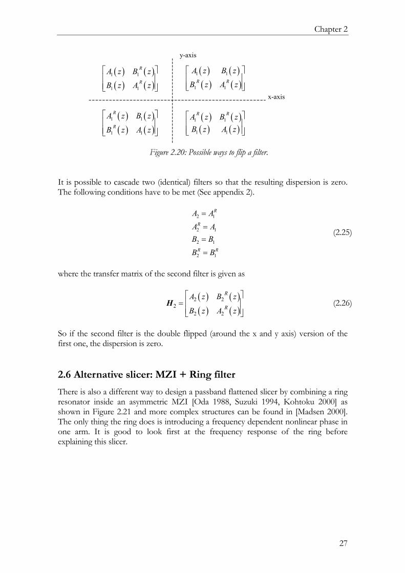
An interesting possibility is to cascade two identical filters so that the total dispersion is zero [Chiba 2001]. We know from appendix 2 that multiplying a filter function and its reverse will give zero dispersion. The filters discussed here are reciprocal, meaning that an output signal will return to the input from which it originated if time is reversed. As a consequence the filter function does not change when inputs and outputs are interchanged. Let us assume we have a filter S1 that can be flipped about the x and y axis. Flipping about the x-axis means interchanging the inputs and outputs separately (i.e. X1 becomes X2 and vice versa and Y1 becomes Y2 and vice versa). All cross terms in the matrix are interchanged. If the filter is flipped about the y-axis the inputs are interchanged with the corresponding outputs and the matrix will be transposed. The different transformations are shown below (Figure 2.20).
Chapter 2
27
x-axis
( ) ( )( ) ( )
1 1
1 1
R
R
A z B z
B z A z
( ) ( )( ) ( )
1 1
1 1
R
R
A z B z
B z A z
( ) ( )( ) ( )
1 1
1 1R R
A z B z
B z A z
y-axis
( ) ( )( ) ( )
1 1
1 1
R RA z B zB z A z
Figure 2.20: Possible ways to flip a filter.
It is possible to cascade two (identical) filters so that the resulting dispersion is zero. The following conditions have to be met (See appendix 2).
2 1
2 1
2 1
2 1
R
R
R R
A A
A AB BB B
=
==
=
(2.25)
where the transfer matrix of the second filter is given as
( ) ( )( ) ( )
2 22
2 2
R
R
A z B z
B z A z
=
H (2.26)
So if the second filter is the double flipped (around the x and y axis) version of the first one, the dispersion is zero. 2.6 Alternative slicer: MZI + Ring filter
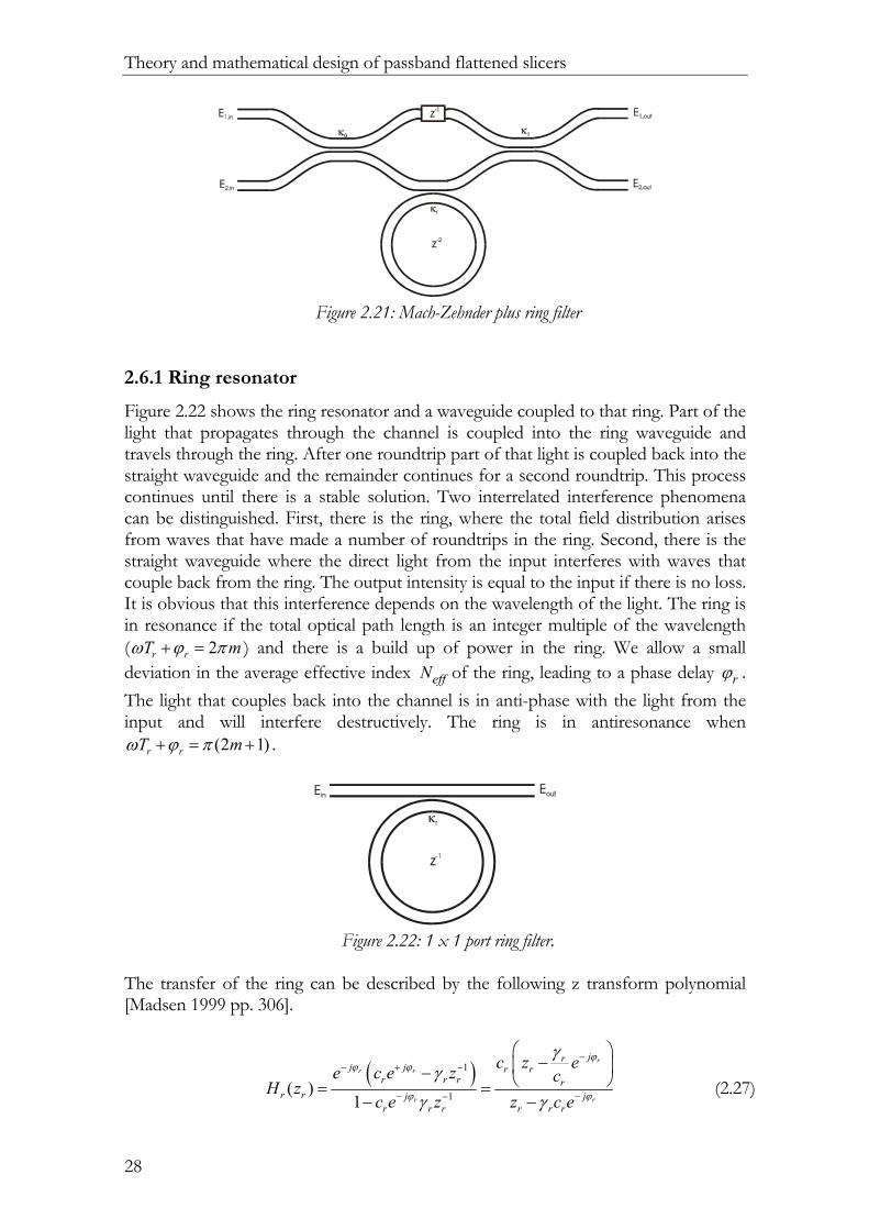
There is also a different way to design a passband flattened slicer by combining a ring resonator inside an asymmetric MZI [Oda 1988, Suzuki 1994, Kohtoku 2000] as shown in Figure 2.21 and more complex structures can be found in [Madsen 2000]. The only thing the ring does is introducing a frequency dependent nonlinear phase in one arm. It is good to look first at the frequency response of the ring before explaining this slicer.
Theory and mathematical design of passband flattened slicers
28
Figure 2.21: Mach-Zehnder plus ring filter
2.6.1 Ring resonator
Figure 2.22 shows the ring resonator and a waveguide coupled to that ring. Part of the light that propagates through the channel is coupled into the ring waveguide and travels through the ring. After one roundtrip part of that light is coupled back into the straight waveguide and the remainder continues for a second roundtrip. This process continues until there is a stable solution. Two interrelated interference phenomena can be distinguished. First, there is the ring, where the total field distribution arises from waves that have made a number of roundtrips in the ring. Second, there is the straight waveguide where the direct light from the input interferes with waves that couple back from the ring. The output intensity is equal to the input if there is no loss. It is obvious that this interference depends on the wavelength of the light. The ring is in resonance if the total optical path length is an integer multiple of the wavelength ( 2r rT mω ϕ π+ = ) and there is a build up of power in the ring. We allow a small deviation in the average effective index effN of the ring, leading to a phase delay rϕ . The light that couples back into the channel is in anti-phase with the light from the input and will interfere destructively. The ring is in antiresonance when
(2 1)r rT mω ϕ π+ = + .
Figure 2.22: 1 x 1 port ring filter.
The transfer of the ring can be described by the following z transform polynomial [Madsen 1999 pp. 306].
( )1
1( )1
rr r
r r
jrj j r r
r r r rr r j j
r r r r r r
c z ee c e z cH z
c e z z c e
ϕϕ ϕ
ϕ ϕ
γγ
γ γ
−− + −
− −−
− − = =
− − (2.27)

Chapter 2
29
where 1r rc κ= − , rϕ is an extra phase of the ring, 2 r rr
r e παγ −= , rα is the ring waveguide attenuation coefficient and rr is the ring radius. Figure 2.23 shows the pole and the zero in the complex diagram. The function has one pole for pz z= and one zero for 0z z= ,
rjp r rz c e ϕγ −= (2.28)
and
0rjr
r
z ec
φγ −= (2.29)
Figure 2.23: Pole zero diagram showing the pole and the zero of a ring resonator coupled to a
waveguide. The intensity transfer for a ring with loss is not equal to one anymore. The output intensity is minimal at the resonance condition, because the light can travel in the lossy ring without destructive interference.
2
2
min 1r r
rr r
cHc
γγ−
=−
(2.30)
Figure 2.24 shows the intensity transfer of a ring for different values of the roundtrip loss. This loss is an important factor in the design of the filer, since it can considerably degrade the filter performance. It must be as low as possible.
Re( z )
Im( z )
*o

Theory and mathematical design of passband flattened slicers
30
normalized frequency0.0 0.2 0.4 0.6 0.8 1.0
Tran
smis
sion
[dB]
-1.4
-1.2
-1.0
-0.8
-0.6
-0.4
-0.2
0.0
0.05dB0.1 dB0.5 dB1 dB
Figure 2.24: Intensity response for the ring resonator with four different roundtrip losses and
κr=0.82. The most important feature of the ring, for making the pass band flattened filter, is the frequency dependent phase shift. The phase response is given by
( )( ) ( )
( ) ( )
2
12
1 sintan
2 1 cosr r r
rr r r r
c T
c c T
ω ϕω
ω ϕ−
− + Φ = − + +
(2.31)
and is shown in Figure 2.25 for different values of the modulus of the pole location,
pz . In the lossless case considered here, p rz c= is found from (2.28). The extreme
case 0p rz c= = corresponds to a power coupling constant 1κ = , meaning that all the light couples from the input into the ring, makes exactly one roundtrip, and then couples back completely to the straight waveguide. This is equivalent to a single waveguide, which is lengthened by an amount equal to the circumference of the ring. As expected, its phase response is linear. For 0.9pz = only a small part of the power is coupled into the ring. Near resonance a high intensity builds up and the phase changes rapidly in a nonlinear fashion.

Chapter 2
31
normalized frequency0.0 0.2 0.4 0.6 0.8 1.0
phas
e(2π
)
0.0
0.2
0.4
0.6
0.8
1.0
|zp|=0|zp|=1/3|zp|=0.9
Figure 2.25: Phase response for a lossless ring resonator with three different pole locations pz ,
assuming that ϕr=0. 2.6.2 MZI + Ring slicers
This non-linear phase shift can now be used inside the MZI (Figure 2.21), where the ring is connected to the short channel. The time delay (or roundtrip length) of the ring should be exactly twice the differential time delay of the MZI ( tT ), since the periodic nonlinear phase change should occur synchronously with the periodic MZI response curve in order for the ring to effect passband flattening and stopband broadening.. The intensity transfer from E1,in to E1,out (bar) and E1,in to E2,out (cross) for the MZI + Ring is given by (2.32) and (2.33), where the DC’s of the MZI have both
0.5κ = .
( ) ( )2 211 sin
2H
ωω
∆Φ=
(2.32)
( ) ( )2 212 cos
2H
ωω
∆Φ=
(2.33)
where ( ) ( )r tTω ω ω∆Φ = Φ − , the difference between the phase of the ring-path
and the phase of the through-path arm of the MZI. The bar transfer ( )11H ω is zero when ( ) 2mω π∆Φ = , where m is an integer; it is one for ( ) (2 1)mω π∆Φ = + . Passband flattening can be obtained by setting the phase of the ring to be in anti-phase ( rϕ π= ) at a maximum transfer of the MZI. The transfer of the MZI+ring can be written in the following matrix notation, where 2r tT T= (or 2
rz z= )

Theory and mathematical design of passband flattened slicers
32
( ) ( )1
00
rc js c jsH zz
js c js cz−
− − = = − −
H
( )
( )( )1
010
Rc js c jsA zjs c js cz A zA z −
− − = − −
(2.34)
where ( ) 21 rA z c z−= + ( ( ) ( )( )
R
r
A zH z
A z= )
The transfer functions for the case that the MZI has perfect coupling ratios (κ=0.5)are
( )1 2 3
11 2
12 1
r r
r
c z z c zH zc z
− − −
−
− + −= +
(2.35)
( )1 2 3
12 22 1r r
r
j c z z c zH zc z
− − −
−
− + + += +
(2.36)
Figure 2.26 shows the result obtained by adding the ring. The intensity transfer is passband flattened and stopband broadened. The second graph shows the frequency dependent phase of the two arms of the MZI with respect to the short arm of the same MZI without ring. The dashed line is the phase of the long arm (the one without ring). It has a phase change of 2π in one FSR. The dotted line is the phase of the short branch with 100% coupling to the connected ring. It has a phase change of 4π in one period ( 2rT T= ). The solid line shows the phase for 0.82rκ = power coupling to the ring. The phase oscillates around the dotted line. There are exactly two periods of oscillations. The intensity transfer of the filter is now determined by the phase difference between the two channels as shown in the last graph. The centers of the passband and stopband occur at a phase difference of mπ . The coupling coefficient has been calculated in such a way that near the center of the pass- and stopbands the phase slope of the short branch + ring is equal to that of the long branch, resulting in a constant zero (or π) phase difference between the branches over a large fraction of these bands. As a result there is almost no change in the transfer. It is important that this stability occurs at a maximal or minimal transfer by careful tuning of the phase of the ring relative to the MZI. The local maxima in the stop band occur at the frequency where the slope of the phase difference is zero. There is a rapid transition in the transfer from pass band to stop band, because the ring is in resonance, which results in a fast phase change.

Chapter 2
33
2D Graph 4
normalized frequency
0.0 0.2 0.4 0.6 0.8 1.0
phas
e di
ffere
nce/
2π
-2.0
-1.5
-1.0
-0.5
0.0
trans
mis
sion
[dB
]
-30
-20
-10
0
Cross Bar
phas
e/2π
-3.0
-2.5
-2.0
-1.5
-1.0
-0.5
0.0
short arm + ring, κ=0.82short arm + ring, κ=1long arm
Figure 2.26: Intensity transfer, phase of each arm (with respect to the short arm without ring),
and the phase difference of a lossless correctly tuned MZI + Ring filter with perfect 3 dB couplers.
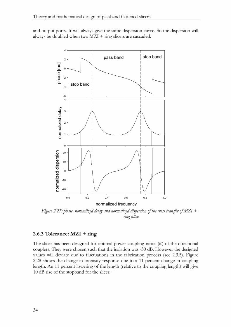
Figure 2.27 shows the overall phase, delay and dispersion of the bar transfer (H11(z)) of the MZI +ring filter. The normalized dispersion is zero at the center of the passband en goes from negative to positive in the passband region. The extremes are -22 and + 22 at a normalized frequency of 0.29 and 0.71 respectively. The transfer is -0.5 dB at these points. The dispersion of the filter does not depend on the chosen in
Theory and mathematical design of passband flattened slicers
34
and output ports. It will always give the same dispersion curve. So the dispersion will always be doubled when two MZI + ring slicers are cascaded.
normalized frequency0.0 0.2 0.4 0.6 0.8 1.0
norm
aliz
ed d
ispe
rsio
n
-20
-10
0
10
20
norm
aliz
ed d
elay
0
1
2
3
4
phas
e [ra
d]
-6
-4
-2
0
2
4
pass band stop band
stop band
Figure 2.27: phase, normalized delay and normalized dispersion of the cross transfer of MZI +
ring filter. 2.6.3 Tolerance: MZI + ring
The slicer has been designed for optimal power coupling ratios (κ) of the directional couplers. They were chosen such that the isolation was -30 dB. However the designed values will deviate due to fluctuations in the fabrication process (see 2.3.5). Figure 2.28 shows the change in intensity response due to a 11 percent change in coupling length. An 11 percent lowering of the length (relative to the coupling length) will give 10 dB rise of the stopband for the slicer.

Chapter 2
35
normalized frequency0.0 0.2 0.4 0.6 0.8 1.0
Tran
sfer
[dB
]
-30
-20
-10
0
0.72Lc (κ=0.82)0.64Lc (κ=0.71)0.80Lc (κ=0.90)
Figure 2.28: Transfer function for three different coupler lengths (or power coupling constants).
Figure 2.29 shows the intensity transfer of the slicer for several differential losses. This loss is incorporated in the MZI and the ring; the loss in the ring is twice as large as in the MZI. Note that the losses given in the picture are highly exaggerated, since the length of the differential delay is ±1 mm and the differential loss of the waveguides to be used is expected to be less than 0.1 dB.
normalized frequency0.0 0.2 0.4 0.6 0.8 1.0
trans
fer [
dB]
-30
-25
-20
-15
-10
-5
0
0 dB0.5 dB1 dB2 dB3 dB
Figure 2.29: Transfer function for five different loss values differential length of the MZI,
including ring losses.

Theory and mathematical design of passband flattened slicers
36
2.7 Comparing Lattice filter and MZI + Ring
The following table compares the 3 stage lattice type filter and the MZI + Ring filter. The main advantage of the MZI + Ring is that its stopband width (at –25 dB transfer) is 6 percent wider and needs one phase tuning element less. The size of the MZI + ring can also be made very small by flipping the MZI around the ring and will be approximately the size of one delay line. The MZI + ring has one main problem and that is the birefringence. Since the devices are based on interference it is important that the birefringence of the waveguide is low in the differential length parts. Al differential length differences can be formed in the straight waveguide for the lattice type. But that is not possible for the ring resonator, since a ring always has bends. Another drawback of MZI + ring is its maximum FSR that is limited by the minimum feasible bend radius.
Table 2.2: Lattice type and MZI + ring compared. Criterion Lattice (3 st.) MZI + Ring resonator Stopband width 24% of FSR @ -25 dB 30 % of FSR @ -25 dB Number of tuning elements
3 2
Size Size of 3 delay lines Size of ring (one delay line)
Birefringence In straight Also in ring Maximum normalized dispersion
5.9 22
Zero dispersion of cascade
Possible Not possible
Isolation (ideal) 27 dB 29 dB 2 % error in coupling (all couplers)
24 dB isolation 22 dB isolation
Differential loss 1 dB 4 dB non uniformity between passbands
30 dB isolation reduced to 27 dB
2.8 Summary & Conclusions
Two different types of passband flattened slicers, lattice type and MZI+ring, have been mathematically designed and compared. z-transform The design strategy using z-transform has been introduced. Filters can now be designed by placing zeroes and poles of the z-polynomial in the complex z-plane, which is a very good way to get insight into the polynomials. A third and fifth-order polynomial have been generated that give passband flattened and stopband broadened filters curves. The width of the stopband width at –25 dB is 14 % of the Free spectral range (FSR) for the third-order polynomial and 24 % of the FSR for the fifth order polynomial. The stopband width is only 4 % of the FSR for the standard

Chapter 2
37
MZI filter (first-order polynomial). Different polynomial solutions that give equal intensity transfer but different phase transfer have been found. The phase transfer is also important since it gives the group delay and dispersion of the filter, which have also been calculated. Recursion relations that translate the polynomial coefficients to the filter coefficients of the Lattice type filters can be found in literature [Jinguji 1995]. So the third-order filter can be mapped to a three-stage filter and the fifth order polynomial can be mapped to a five-stage filter. Some of the solutions gave couplers with zero length. These couplers can be removed from the design resulting in a two and three stage filter. We can conclude that z-transform is a good mathematical design tool for lattice type filters and that the third order polynomial filter could be realized with a two stage lattice type filter and the fifth-order polynomial with a three stage filter. The dispersion of the lattice type filter can be removed by cascading two identical lattice type filters, where the second filter is double flipped. As a result the intensity transfer is squared, leading to much better isolation. This can be used in the design of the binary tree Add-drop multiplexer. The tolerance of the filters due to change in the parameters has been analyzed. To have reasonable function filters it is important that the deviation of the couplers is less than 2 percent. The differential loss must be as low as possible since it gives different transfer losses for the bar and cross output. Filters having a differential loss smaller than 0.1 dB are expected to be fabricated so it will not be a larger problem. A different type of slicer based on a MZI filter with a ring resonator coupled to the short branch of the MZI has also been designed.. The ring introduces a frequency dependent nonlinear phase in one arm and as a result the filter curve becomes passband flattened and stopband broadened. The filter is compared with the three-stage lattice filter. The stopband width at –25 dB of the 3-stage lattice filter is 24% of the FSR and the width of the MZI+Ring filter is 30% of the FSR. The number of tuning elements is three for the three-stage lattice and two for the MZI+Ring respectively, which is one heater less. The size of the MZI + Ring filter is about three times less than the three stage slicer. One disadvantage of the MZI + ring filter is that dispersion is always doubled when two filters are cascaded. So zero dispersion cannot be obtained over the complete passband. The maximal FSR of the filter is limited by the minimal bend radius of the ring. The lattice type filter does not have this restriction.

Theory and mathematical design of passband flattened slicers
38

39
Chapter 3: Device design
3.1 Introduction
In the first part, the design is described of the basic building blocks: the straight waveguide; the adiabatic waveguide bend which minimizes the chip area needed for bends, by gradually changing waveguide width and bending radius; directional couplers; and the thermo-optic tuning element. The second part deals with the combination of the building blocks into a basic filter element, the passband-flattened wavelength slicer based on a Mach-Zehnder Interferometer coupled to a ring resonator. Finally, the design of the complete ADM is described, which has been designed and fabricated during the stay at the Optical Network Group of IBM. 3.2 Waveguide demands and design
3.2.1 Demands
The most elementary building block is the buried waveguide channel designed in our group [Wörhoff 2001]. A schematic drawing is shown in Figure 3.1. It is a waveguide having a refractive index cn , channel width chw and height chh , surrounded by a material width lower refractive index cln . Since the material is birefringent due to stress in the layers, TE polarized light experiences a different index, TEn , than TM polarized light, TMn . The electrical field for TE and TM polarized light is parallel and perpendicular to the layer stack respectively as indicated in Figure 3.1. The typical birefringence for the used PECVD SiON layers is 47 10TM TEn n −− = ⋅ . The parameters ( , ,c ch chn w h ) are chosen in order to optimize the channel. Several requirements should be taken into account:
• Monomodality: It is absolutely necessary that the channel is monomodal, since the delay in the MZI is mode dependent and will result in unwanted intensity fluctuations.
• Low modal birefringence: Different effective indices of the two polarization directions, TEN and TMN , of the channel will result in different optical pathlengths in the MZI and thus in different wavelength positions of the passband of a filter. This is unwanted because the polarization of the incoming light is unknown in a fibre-coupled optical network.

Device design
40
• Small bend radius with acceptable loss: the bend radius of the channel largely determines the size of the devices.
• High fiber to chip coupling efficiency, equal for TE and TM polarized light.
Figure 3.1: Cross section of the buried waveguide channel.
Other important boundary conditions are the technological restrictions:
• The index of the upper cladding should be kept equal to the buffer layer in order to suppress cladding modes. In a first test series PECVD SiO2 (nTE = 1.463 and nTM=1.464) was used both as buffer layer and upper cladding. However, the stress in the PECVD SiO2 buffer layer causes bending of the wafer and hence affects photolithography. For this reason thermally grown SiO2 is used as buffer layer. The refractive index of thermal SiO2 is 1.446. The upper cladding will be PECVD SiO2 that is thermally treated in order to lower its refractive index to the value for thermal oxide, n=1.446. Channels fabricated by the new process are indicated as type II channels. Many optimizations were performed on the old (type I) parameters for the indices. These can be mapped directly to the new type, since the contrast is kept the same.
• Refractive index of the core layer must be between 1.45 and 1.6. Higher indices than 1.6 will give cracks in the layer stack after thermal treatment.
• The maximum core thickness is 1 µm, which is restricted by the etching process.
• Minimum width of the channel is 1.5 µm, given by photolithographic restrictions.
• The thickness of the buffer layer is chosen such that substrate leakage can be neglected.
• The thickness of the upper cladding will be chosen equal to the thickness of the buffer.
The parameters that can be changed in the optimization are the width (wch), height (hch) and refractive index of the core (nc ). A channel has been designed that fulfills these demands [Wörhoff 2001] The parameters are shown in table 3.1 (Type I). Material birefringence has been taken into account. The dimensions of the core are chosen so that the material birefringence was
ncl
nb
wch
hch
upper cladding
buffer layer
tcl
tb
TM TEnc

Chapter 3
41
compensated by the geometric birefringence resulting in zero modal birefringence (∆Neff,TM-TE = 0).
Table 3.1: Material parameters and thickness of the designed channels. Type I is the original channel, where the layers are not annealed and a PECVD SiO2 is used a buffer layer. Type II has been evolved from Type I. The layers are now annealed and thermal SiO2 is used as buffer
layer.
Type Type I Type II buffer layer PECVD SiO2
nTE=1.463 nTM=1.464 tb = 8 µm
Thermal SiO2 nTE=1.445 nTM=1.446 tb = 8 µm
core layer PECVD SiON nTE=1.533 nTM=1.534 hch = 0.82 µm wch = 3.25 µm
Annealed PECVD SiON nTE=1.520 nTM=1.521 hch = 0.82 µm wch = 3.25 µm
upper cladding PECVD SiO2 nTE=1.463 nTM=1.464 tcl = 8 µm
Annealed PECVD SiO2 nTE=1.445 nTM=1.446 tcl = 8 µm
Neff NeffTE = 1.478 NeffTM = 1.478
NeffTE= 1.462 NeffTM= 1.462
Figure 3.2 shows a cross section of the channels and the intensity profile of the mode. The substrate leakage can be neglected.
Figure 3.2: Intensity profile of the buried waveguide channel.

Device design
42
3.2.2 Bend waveguide structure
This section is an adaptation of a contribution written for the IEEE/LEOS Benelux chapter [Roeloffzen 2000]. In order to accommodate the increasing complexity of integrated optical structures, there is a need of bends, which occupy a chip area as small as possible. Good results with respect to loss and size can be obtained by adiabatic bends with gradually decreasing radius and variable waveguide width [Bona 1999]. Detailed simulations using 2D bend (mode) solver [C2V] and adiabatic conformally-mapped 2D-BPM [C2V] have been carried out in order to achieve a minimal size. Comparison is made with other approaches like standard bends with offsets. 3.2.2.1 Introduction
Since the demands on functionality of integrated-optic components for optical communication are growing, compactness of the devices, e.g. add-drop multiplexers, is a major concern. This compactness is determined mostly by the minimum bend radius that can be realized for low-loss optical channel waveguides. The aim is to design a bend, which has low loss and small dimensions. In this paper we concentrate on a rectangular waveguide structure having low polarisation dependence. This waveguide is fabricated using PECVD technology [Wörhof 1999, de Ridder 1998]. Although the specific numerical results reported in this paper relate to this particular structure, the method used is valid for arbitrary waveguides. It is difficult to use an approximation to calculate the bend loss because of the high index contrast and buried channel waveguide structure [Ladouceur 1996]. The Marcatilli and effective index method (EIM) approximation turned out to fail for this structure. Therefore, we calculated the bend loss using a numerical bend mode solver [C2V], while varying two parameters, the channel width and bend radius. From a technological point of view these parameters can easily be varied. 3.2.2.2 Adiabatic bend
When a bent waveguide is connected to a straight waveguide two loss mechanisms occur. The first is the intrinsic radiation loss of the bend mode, which is called Pure Bend Loss (PB-loss). The second is transition loss (T-loss) due to mismatch between the modes of the straight and the bend, the latter being shifted outwards and changed in shape. The modal shift can be compensated by an offset between channel and bend, but a change in mode profile shape cannot. Figure 3.3 shows the 2D bend mode calculation result of the PB-loss of a 180-degree bend for different radii and channel widths. The PB-loss not only depends on the radius but also on the width. The PB-loss increases with both decreasing bend radius and decreasing channel width. The upper left region in Figure 3.3 where the contour lines tend to run vertically is characteristic for the whispering gallery mode (WGM) regime, where a further increase of the width has no effect on the PB-loss.

Chapter 3
43
Radius [µm]
500 550 600 650 700 750 800
Cha
nnel
wid
th [µ
m]
4
5
6
7
8
9
0.01
0.01
0.01
0.1
0.1
0.1
0.1
WGM
standard width3.25 µm
Figure 3.3: Contour graph of the pure bend loss as function of radius and waveguide width. The
values at the contour lines are dB/180 degree values. The taper function (see Figure 3.5) is also shown in the graph.
This calculation result is the starting-point for designing an adiabatic bend. The optimization of the design involves a trade-off between pure bend loss, transition loss and needed chip area. The following strategy will be employed:
1) For the given channel structure, calculate the pure bending loss versus both bend radius R and waveguide widthW .
2) Select an acceptable and realistic loss figure for the total bend; this results in a minimum allowed bend radius minR .
3) Determine a function ( )W R that keeps the loss constant at the selected value (adiabatic exponentional taper function).
4) Select the maximum bend radius startR that gives negligible transition loss to a standard width straight waveguide.
5) Determine a function that changes the radius gradually from startR to minR where the rate of change is given by a single parameter bendA .
6) Determine a value of bendA that results in a good compromise between bend loss and chip area.
The assumption of the bend being adiabatic implies that the modal solution at a certain position in the bend is independent of the solution at any other position, so that the total bend loss can be calculated by simply integrating local losses. The bend

Device design
44
starts with a large radius having a low transition loss. The bend radius decreases slowly during propagation in the bend until a minimum is reached [Bona (feb) 1999]. The simplest way to decrease the radius is linear as a function of the arc length (or angle). A better way is the use of a function, which has a large negative slope at large radii and low slope at small radii. A possible function is given in Eq. 5.1 and a solution is shown in Figure 3.4.
R( l R eRstartR bendA l
) minln
min= ⋅+ ⋅
1
e j (3.1) Here Rstart is the radius of the bend at the beginning of the bend. It will be set to 3 mm, since the transition loss (from straight to 3000 µm bend) is virtually zero. minR is the minimum radius, which will be set to 600 µm (0.11 dB/360deg for a waveguide width of 7.3 µm). Smaller bend radii will give much higher loss. bendA is the rate of decrease of the radius and l is the arc length of the bend. If this rate is too high the bend is not adiabatic anymore and additional loss will occur. If the decrease is too slow the bend size will be too large.
Arc length [µm]0 200 400 600 800 1000
Rad
ius
[µm
]
500
600
700
800
900
1000
Abend=0.01µm-1
Abend=0.04µm-1
Abend=0.1µm-1
Figure 3.4: Radius of the bend as function of the arc length according to Eq.5.1with two fixed
parameters , Rmin =600 µm, Rstart =3000 µm and for three different rates of radius decrease.
Simultaneously with decreasing the radius, the channel width will be enlarged. Figure 3.3 shows that widening the waveguide at constant radius results in lower loss. The function given in eq. (3.2) approximates the contour lines of Figure 3.3, ( ) ( )t tA R R
wgW R W e −= + (3.2) where the position on the x-axis is given by tR ; tA is a constant that gives the rate of widening of the waveguide; wgW is the width of the straight waveguide with which the bend starts. Figure 3.5 shows an example of the width function (3.2). The curve is also added to Figure 3.3, where it almost follows the contour lines. It starts to deviate in the WGM regime.

Chapter 3
45
Radius [µm]
600 800 1000 1200 1400
Wch
0
2
4
6
8
10
3.25 µm
wmax
Figure 3.5: Waveguide width as function of the radius of the bend according to Eq. (3.2), with
parameters, Rt=800 µm and At=0.007. Further analysis is done on a 180-degree bend, which consists of two cascaded adiabatic 90-degree bends. So from 0 to 90 degrees the radius decreases and the waveguide widens, from 90 to 180 the opposite happens. Waveguide loss has not been taken into account because it depends on the quality of the fabrication process and it can be in the order of 0.1 dB/cm for an optimized process [Germann 2000]. As a measure for the size of a bend we take the surface area of a rectangle tightly enclosing the bend.
Abend [µm-1]
0.00 0.02 0.04 0.06 0.08 0.10
Loss
[dB
]
0.00
0.01
0.02
0.03
0.04
Sur
face
are
a [m
m2 ]
0.6
0.8
1.0
1.2
1.4
1.6
1.8
2.0
(a)
(b)
Figure 3.6: (a) Loss of 180-degree bend versus the rate of radius decrease Abend and (b) Surface
area of 180-degree bend versus Abend. Parameter: Rmin = 600 µm, Rstart = 3000 µm, Wwg = 3.25 µm, Ar = 0.007µm-1 and Rt = 800 µm.

Device design
46
Figure 3.6a shows the loss of the adiabatic bend (in dB) as function of the parameter bendA . When bendA is large (fast decay of radius) the loss will be the loss of a bend
having radius min 600R = µm which is 0.06 dB. But then the transition will not be adiabatic anymore and transition loss will occur. When bendA is close to zero, the loss is equal to loss for startR R= (3 mm) that is almost zero. When we now look at the surface area (Figure 3.6b) of the bend as function of Abend we see that for large bendA (fast decay of radius) the surface is very small (equal to surface of bend with radius
minR ). For small bendA the surface is large (equal to surface of bend with radius startR ). So bendA must be small for low loss and large for small size. A good compromise is
bendA is 0.04 µm-1. 3.2.2.3 Comparison
In Table 3.2 the loss and size of different types of bends are compared. Type 1 and 2 are bends with constant radius (600 and 652 µm) connected to the straight channel without a shift, having a total loss (PB-loss + 2*TL-loss) of 0.76 and 0.47 dB respectively. Adding an optimal shift between bend and straight decreases the total loss (type 3, 4). However these two bends still suffer from the high PB-loss. Increasing the waveguide width lowers the bend loss but increases the transition loss due to modal shape mismatch between the straight and bend mode (type 5, 6). Type 7 is the adiabatic bend, which has the lowest total loss (0.022 dB).
Table 3.2: Loss and size of different types of 180-degree bends. Type Offset Radius
(µm) Bend width (µm)
Transition loss (dB)
Pure Bend loss (dB)
Total loss (dB)
Length (mm)
Surface (mm2)
1 No 600 3.25 0.13 0.50 0.76 1.88 0.72 2 No 652 3.25 0.097 0.28 0.47 2.05 0.85 3 Yes 600 3.25 0.06 0.50 0.62 1.88 0.72 4 yes 652 3.25 0.037 0.28 0.35 2.05 0.85 5 yes 600 6 0.19 0.06 0.44 1.88 0.72 6 yes 652 6 0.20 0.026 0.43 2.05 0.85 7 no variable variable - - 0.029 2.06 0.85 3.2.2.4 Validity
Figure 3.7a shows the conformally-mapped index structure [Smit 1993] of the first half of the 180-degree bend and the BPM-simulation results [C2V]. The loss, thus calculated for this first half is 0.04 dB and the total 180-degree bend loss is 0.08 dB, which is higher than expected (0.03 dB). This deviation can have two causes: the bend is not adiabatic, which is not likely since Figure 3.7b does not show abrupt radiation points, or the EIM used to do the 2D-BPM simulation gives the wrong core index, which is more likely since small variation of the effective core index gives a large change in loss.

Chapter 3
47
Figure 3.7: (a) Conformally-mapped waveguide structure (the refractive index is indicated as a
grayscale value); (b) 2D-BPM simulation result The results from the optimization process are considered to be more reliable since they are based on accurate 2D calculations given in Figure 3.3. 3.2.2.5 Conclusion
An adiabatic bend having low loss and small size has been designed, the needed chip area is only 15% larger compared to a non-adiabatic bend with constant radius of 600 µm. The estimated loss for a 180-degree bend is 0.029 dB which is much less than a non-optimized bend 0.47 dB having the same surface area of 0.85 mm2. The 2D-BPM simulation gives a good qualitative and quantitative agreement with designed radiation behavior, but it shows a small deviation of the loss compared to the model. 3.2.3 Fiber to chip coupling
A very important aspect in the design is the coupling of the light from the fiber to the optical chip. Efficient, low cost and reliable coupling is very important for devices in communication systems. Fiber to chip coupling can be obtained by active or passive alignment. The advantages of active alignment are:
1. The optical chip can easily be sawn or cleaved and if necessary be polished. 2. No extra processing steps are needed during fabrication of the optical chip
such as definition of on-chip alignment-grooves. This means that the optical chip can be fabricated independent of the coupling. In research this is an advantage because the fabrication process itself is not standard and can be changed.
3. Simultaneous coupling of multiple fibers is possible by first placing several fibers in a separate V-groove array and then placing this array to the optical chip. Active alignment of the two outer fibers suffices for aligning the entire fiber array.
4. Maximal power transfer is reached with active alignment. The disadvantages are:
1. The fibers must be actively aligned to the chip. This is a time consuming process, which can, however, be done automatically.

Device design
48
2. The fiber is glued to the chip after alignment and it is not known how strong this connection is and if it is stable in time. A current trend in the integrated optics industry is to remove all polymer materials from the light path.
Butt-coupling, which is placing a cleaved fiber directly to the facet of the chip, is a simple and efficient way if the modal field distributions of the fiber and the channel match. An on-chip spot-size converter can be used to match the two profiles. Different converters can be found in [Spühler 1998, de Ridder 1995]. The (type I and type II) waveguides were designed in such a way that horizontal (lateral) tapering to a channel width of 1.5 µm gives sufficiently low loss when coupled with a high numerical aperture (HNA) fiber (mode field diameter (MFD) 4.0 µm) as shown in Figure 3.8. The calculated fiber to chip coupling loss is 0.2 dB. The HNA fiber can be spliced adiabatically to a standard telecom fiber (core diameter of 9 µm and MFD of 10.5 µm.) This splice has a loss of 0.5 dB. So a total fiber to chip coupling loss of 0.7 dB can be obtained [Leinse 2001].
Standard telecom
fiber
Smallcorefiber
Adiabatic spot size converter
caused by splicing the fibers together
Fiber Matched Channel
Tapered waveguide
(spot size converter)
Standard channel
SiO2
SiON
Figure 3.8: Schematic drawing (top view) of the coupling between a standard telecom fiber and
waveguide. 3.3 Power coupling element
3.3.1 coupler choice (history)
Power coupling elements are needed in the design of the Lattice filters [see section 2.3] or MZI + Ring [see section 2.5]. Several types of coupling elements can be found in literature [Soldano 1995] Well-known elements are the directional coupler (DC), two mode interferometer (TMI) and multimode interferometer (MMI). Much effort has been put into the 2x2 MMI in the first year. Aim was low loss and 50/50 splitting. The splitting ratio could be obtained but not a calculated loss less than 0.2 dB, which is still too high for use in the ADM. This loss is due to an imperfect image caused by the relatively low index contrast of the used channel at the end of the MMI and discrete transitions from channel to MMI section. A second difficulty is the design of MMI’s having other splitting ratios than 50/50. Several solutions can be found in literature [Bachmann 1995, Besse 1996, Levy 1997]. We [Lith 2000] tried the butterfly

Chapter 3
49
solution, with loss of 1 dB as result. Furthermore the butterfly MMI has to be redesigned for every different splitting ratio. This is not the case for the TMI and DC, because the splitting is based on interference of only two modes and the ratio directly depends on the length of the coupling section. First choice was the TMI because of better fabrication tolerances [Rajaran 1999]. The designed TMI is shown in Figure 3.9. The gap between two neighboring waveguides was set to 0.81 µm. During fabrication it turned out that it was very difficult to open this gap. Strictly speaking this TMI is not a two mode interferometer but a three mode interferometer, since three modes can propagate in the coupling section.
Gap
L
Xinput
BarInput
Cross
W
Figure 3.9: Schematic top view of the two mode interference coupler.
The positions of the input waveguides were chosen such that the third mode is not excited. The simulated excess loss for the TMI was 0.3 dB. Measured losses were 1 dB, and higher order mode beats were observed [Harbers 2001]. So both MMI and TMI turned out to be less suitable choices for the given waveguide technology. The main reasons that these splitters fail are the discrete transitions from channel waveguides to interference sections. The DC does not have this shortcoming, since a DC can be designed adiabatically and thus can have extremely low loss. The next section describes the design of the DC. It is important that the power-coupling ratio of the DC to be fabricated does not deviate much (2-4 percent) from the ideal values (calculated in section 2.3). For that reason the sensitivity of the coupling length due to deviations from the optimal designed parameters will be calculated. 3.3.2 Directional coupler design
Figure 3.10 shows a schematic drawing of two waveguides placed in close proximity to allow power transfer from one channel to the other. Power coupling occurs due to overlap of the evanescent field of a mode in one waveguide with the other waveguide. The most important parameter is the coupling length ( Lπ ) of a coupler, which is the length needed to transfer all power from one waveguide to the other.

Device design
50
Lstr
gDCdDC
o2
o1i1
i2 Figure 3.10: Schematic top view of the directional coupler.
The operation of a DC is easily understood by considering the two parallel waveguides as a single system, which supports two system modes. The modes of the input and output channels are decomposed into these system modes, and the power exchange between the separate waveguides can be simply described as an interference phenomenon of the system modes (just as in the TMI). It can easily be shown that the field amplitudes at the output channels, ,1oE and ,2oE are related to those at the input channels, ,1iE and ,2iE as:
,1 ,1
,2 ,2
cos sinsin cos
o i
o i
E EjE Ej
ϕ ϕϕ ϕ
− = −
(3.3)
where 0
effDC
NL
πϕ
λ∆
=
The coupling length is the propagation distance giving π phase difference between the system modes:
0
2 effNL Lπ π
πβ ϕ π
λ∆
∆ = = = (3.4)
leading to
( )
0
02 eff
LNπ
λλ
=∆
(3.5)
where ∆Neff is the difference in effective index of the two system modes, ∆β is the difference in propagation constant and λ0 is the wavelength in vacuum. Every power splitting can be obtained by simply choosing a length between 0 and Lπ. The power is split equally over the output channels if the length of the coupler is half the coupling length. The DC has been described in section 2.2 by the following 2 x 2 transfer matrix. It describes the output fields by the input fields.
dc
c jsH
js c−
= − (3.6)

Chapter 3
51
where cos( ) 1c ϕ κ= = − and sin( )js j jϕ κ− = − = − are the through and cross-port transfer. Where ϕ is equal to the coupling strength integrated over the length and κ is the power coupling ratio. Coupling does not only occur in the straight waveguides. It occurs already in the leads and the total phase is the sum of the phase in the straight waveguides and the leads dc str leadsϕ ϕ ϕ= + (3.7) with
2
effstr str str str str
Nk L L L
Lπ
ππϕλ
∆= = = (3.8)
and
0
2 ( )z end
leads str leadsz
k z dz k Lφ=
=
= ≡∫ (3.9)
where ( )k z is the z dependent coupling strength in the leads. The integration is from z=0, the start of the leads where ( )k z is equal to strk , to z=end where the coupling strength is zero. Here we introduced an equivalent length leadsL , which is the additional length of the straight section which would cause the same phase shift of the system modes as the leads do. So the total phase shift can be written as:
,
( )2
str leadsdc str str leads
str
L Lk L LLπ
πϕ += + = (3.10)
which shows that the effect of coupling between the leads can be compensated by reducing the length of the straight section. 3.3.3 Straight coupling section
Figure 3.11 shows the cross-section of the directional coupler including the design parameters. These parameters can be split up in parameters, which can be freely chosen and those that are given by the channel waveguide design ( , ,ch c clh n n ). The two free parameters are the width of the channel ( chw ) and the gap between ( DCg ) the two waveguides. A tapering is needed if the channel width in the coupler is unequal to that of the standard waveguide. All parameters can fluctuate due to errors in fabrication.

Device design
52
Figure 3.11: Cross-section of directional coupler structure.
The 2 dimensional mode solver TempSelene [C2V] is used to calculate Lπ and change of Lπ as function of the parameters. The change of Lπ can be expressed best as the relative change of Lπ due to a change in one parameter. The sensitivity, for parameter
np , can be written as
( ) ( )1 2
1 21 2 ( , ,.., ,.., )
, ,.., ,..,, ,.., ,..,
n N
n n Nn N n p p p p
LS p p p pL p p p p p
π
π
δδ
=⋅
(3.11)
where 1,... Np p are the design parameters. np is the fluctuation parameter. The total change in relative coupling length is in first order approximation the sum of all sensitivities multiplied by the error in the respective parameters.
( ) ( )1 2
1 21 1 2 ( , ,.., ,.., )
, ,.., ,..,, ,.., ,..,
n N
N
n N nn n N n p p p p
L Lp p p p pL L p p p p p
π π
π π
δδ=
∆ = ⋅∆⋅
∑ (3.12)
As seen in section 2.3 for good functioning filters the maximal error in Lπ is 2 %. We study the sensitivity of Lπ to several parameters. Unless otherwise noted, the constant parameters in the following graphs have their design values, 1.445cln = ,
1.520cn = , 3.25chw = µm, 0.82chh = µm, and 1DCg = µm. 3.3.4 Sensitivity to change in channel width
Figure 3.12 shows the coupling length as function of the gap for different channel widths. The logarithmic scale of the coupling length leads to approximately straight lines in the plot, as could be expected from the exponential decay of the evanescent fields which form the physical coupling mechanism between the waveguides. Small deviations can be observed for a gap smaller than 0.2 µm. Such a small gap is not very realistic and a gap of 1 µm is the minimum, which can be obtained with the current technology. The coupling length is also dependent on the channel width, since a
gDC
wch
dch
hch nc
ncl

Chapter 3
53
smaller channel gives larger evanescent fields, which results in greater interaction and thus smaller Lπ .
gDC [µm]0.0 0.2 0.4 0.6 0.8 1.0 1.2 1.4 1.6 1.8 2.0 2.2
L π [µ m
]
100
1000
wch 2.25 µmwch 2.75 µmwch 3.25 µmwch 3.75 µm
Figure 3.12: Coupling length of directional coupler as function of the gap for TE polarized light.
The refractive index of the core is 1.52 and 1.45 for the cladding. It is not fair to look at the sensitivity of Lπ due to a change of the channel width while the gap remains fixed, because this will not happen during fabrication. What will happen is that the channel width deviates from the designed value and that the distance between the centers of the waveguides remains unchanged, resulting in a change in gap. Therefore, a model has been developed that accounts for this simultaneous change in both channel width and gap. The following equation will be fitted to the calculation results (of Figure 3.12). ( , )
0( , ) ( , ) ch c DCb w n gch DC ch cL w g L w n eπ π
⋅= ⋅ (3.13) where ( )0 ,ch cL w nπ is the coupling length at a zero gap and chw is the width of one channel, ( ),ch cb w n is the exponential rate of increase and DCg is the gap. ( )0 ,ch cL w nπ can be seen as the beat length between the zero and first order modes of a waveguide having a width of 2 chw⋅ . Again there is an exponential relation between the beat length and the width of this bi-modal channel as shown in Figure 3.13. The beat length is smaller for a larger core index. Intuitively one could say the opposite because higher index gives better confinement of the modes but it also gives a larger index contrast and so a larger difference between the effective index of the zeroth and first order mode.

Device design
54
wch [µm]2.6 2.8 3.0 3.2 3.4 3.6 3.8 4.0
L π0
100
nc 1.5nc 1.51nc 1.52
Figure 3.13: Exact calculation (solid line) and exponential fit curve (dashed line) of the coupling
length of directional coupler with zero gap as function of the channel width. The y-axis is on a logarithmic scale.
The following formula can be fit 0 ( ) chc W
chL w a eπ⋅= ⋅ (3.14)
The following table gives the fit results
Table 3.3: fit results for 0Lπ . nc a [µm] c [µm-1] 1.5 30.6255 0.3826 1.51 24.378 0.426 1.52 18.806 0.490
The next parameter that is extracted is ( ),ch cb w n [µm-1]. From eq. (3.13) following differential equation is found giving ( ),ch cb w n .
( , ) ( , )
( , )ch c
ch cch c DC
L w n b w nL w n g
π
π
∂=
⋅∂ (3.15)
This shows that ( ),ch cb w n can be seen as the sensitivity of Lπ to a change in the gap for fixed channel width. Figure 3.14 shows ( ),ch cb w n as function of chw for different core indices.
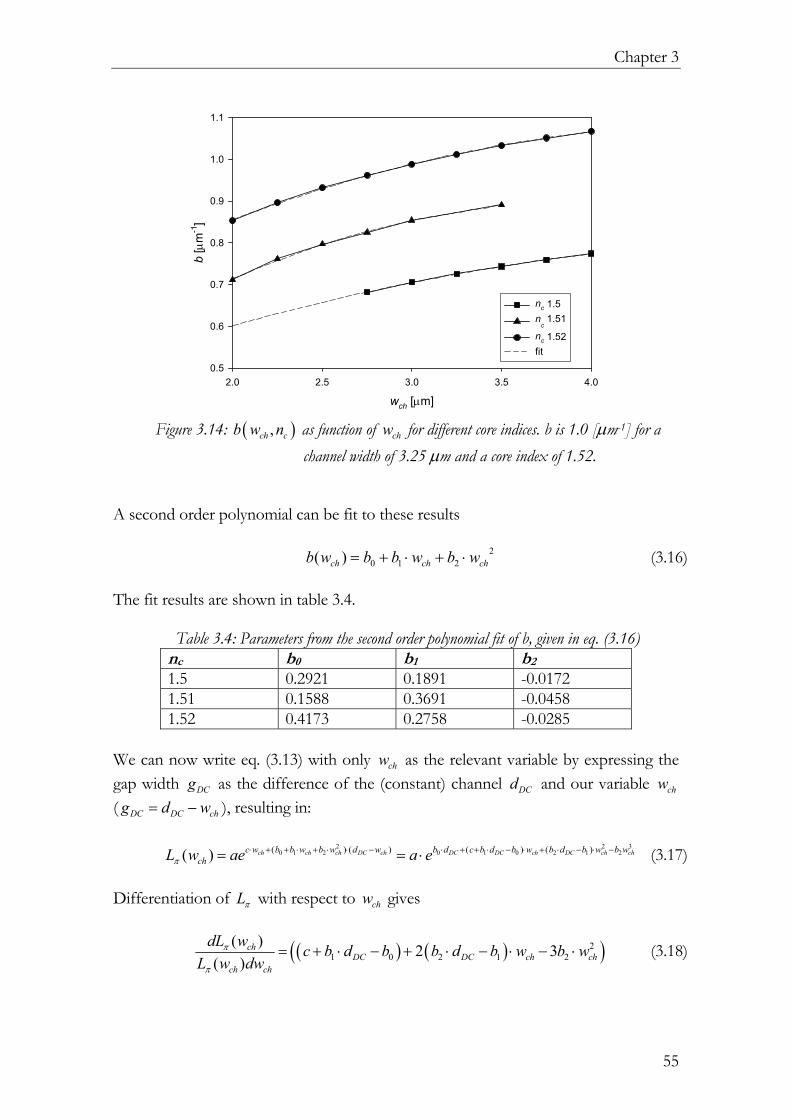
Chapter 3
55
wch [µm]2.0 2.5 3.0 3.5 4.0
b [µ
m-1
]
0.5
0.6
0.7
0.8
0.9
1.0
1.1
nc 1.5 n
c 1.51
nc 1.52fit
Figure 3.14: ( ),ch cb w n as function of chw for different core indices. b is 1.0 [µm-1] for a
channel width of 3.25 µm and a core index of 1.52. A second order polynomial can be fit to these results 2
0 1 2( )ch ch chb w b b w b w= + ⋅ + ⋅ (3.16) The fit results are shown in table 3.4.
Table 3.4: Parameters from the second order polynomial fit of b, given in eq. (3.16) nc b0 b1 b2 1.5 0.2921 0.1891 -0.0172 1.51 0.1588 0.3691 -0.0458 1.52 0.4173 0.2758 -0.0285
We can now write eq. (3.13) with only chw as the relevant variable by expressing the gap width DCg as the difference of the (constant) channel DCd and our variable chw ( DC DC chg d w= − ), resulting in:
2 2 30 1 2 0 1 0 2 1 2( ) ( ) ( ) ( )( ) ch ch ch DC ch DC DC ch DC ch chc w b b w b w d w b d c b d b w b d b w b w
chL w ae a eπ⋅ + + ⋅ + ⋅ ⋅ − ⋅ + + ⋅ − ⋅ + ⋅ − ⋅ −= = ⋅ (3.17)
Differentiation of Lπ with respect to chw gives
( ) ( )( )21 0 2 1 2
( ) 2 3( )
chDC DC ch ch
ch ch
dL w c b d b b d b w b wL w dw
π
π
= + ⋅ − + ⋅ − ⋅ − ⋅ (3.18)

Device design
56
This is the sensitivity of the coupling length to a change in chw where DCd is kept constant. Figure 3.15 shows the sensitivity of cL to chw as function of chw for different values of cn . It has negative values, which means that Lπ increases when chw becomes narrower. This is true for a strongly guided mode where the change of mode field diameter and change in channel width have equal sign.
wch [µm]
2.75 3.00 3.25 3.50 3.75
(dL c/(
dwch
*Lc))
[µm
-1]
-0.6
-0.5
-0.4
-0.3
-0.2
-0.43
ddc=5, nc=1.52
ddc=4.25, nc=1.52
ddc=4.25, nc=1.51
Figure 3.15: Sensitivity of the coupling length to change in channel width.
3.3.5 Sensitivity to change in channel height
Figure 3.16a shows the coupling length as function of channel height chh . An increase in height gives an increase in Lπ . The effective core index increases when chh increases and so does the lateral contrast. This results in further confinement of the mode in the channel and so a decrease in field overlap with the neighboring channel. Figure 3.16b: shows the sensitivity to a change in chh . The influence of chh on the sensitivity is very small but a change in core index changes the sensitivity drastically. The sensitivity is 0.6 [1/µm] for the standard waveguide.

Chapter 3
57
hch [µm]
0.80 0.82 0.84 0.86 0.88 0.90 0.92 0.94 0.96
L π [µ
m]
200
220
240
260
280
300
320
340nc 1.52 nc 1.51 nc 1.50 nc 1.53
257 µm
hch [µm]0.80 0.82 0.84 0.86 0.88 0.90 0.92 0.94 0.96
Sens
itivi
ty [µ
m-1
]
0.1
0.2
0.3
0.4
0.5
0.6
0.7
0.8
nc 1.50 nc 1.51nc 1.52nc 1.53
a) b)
Figure 3.16: : Coupling length of the directional coupler as function of the channel height chh (a) and sensitivity of the coupling length to change in chh (b) for different core indices. The sensitivity is 0.6 µm-1 for a height of 0.82 µm and core index of 1.52. This
means that a change of 2% in coupling length is caused by 30 nm variation of chh .
3.3.6 Sensitivity to change in core index
The last parameter that can change during fabrication is the index of the core layer cn . Figure 3.17 shows Lπ as function of cn . An increasing core index gives an increasing index contrast and the mode withdraws into the core. The sensitivity of Lπ to a change in core index is very high. A change of 0.002 of core index will result in 2 percent change of Lπ .
nc
1.500 1.505 1.510 1.515 1.520 1.525 1.530
L π [µ
m]
220
240
260
280
300
257.6 µm
nc
1.500 1.505 1.510 1.515 1.520 1.525 1.530
Sen
sitiv
ity
4
6
8
10
12
Figure 3.17: Coupling length of directional coupler as function of the core index cn (left) and
sensitivity of the coupling length to a change in cn (right). The sensitivity is 10.3 for a core index of 1.52. This means that a change of 2% in coupling length is
caused by 0.002 variation of the core index. Table 3.5 shows the designed values, the accuracy of the fabrication process and sensitivities for the parameters cn , chh and chw for a 1 µm gap. For these values, the coupling length is calculated to be 257.6 µm. 2 percent is the maximum deviation of

Device design
58
Lπ still having good filter curves (see section 2.5). The fabrication is more relaxed since the length of the couplers is varied on the mask with 10 percent variation. The maximum acceptable fabrication errors for 2 and 10 percent change of Lπ are shown in the last two columns. This is for change in one parameter only, for worst-case scenario the maximum acceptable errors are three times less.
Table 3.5: Sensitivities in fabrication errors in cn , chh and chw and maximum change of one of the parameters for 2 and 10 percent fluctuation in Lπ from a nominal value of
257.6µm.
Parameter Design value
Fabrication accuracy
Sensitivity 2 % Lπ 10 % Lπ
nc 1.520 0.001 10.3 0.002 0.01 hch 0.82 20 [nm] 0.6 [1/µm] 30 [nm] 167 [nm] wch 3.25 0.05 -0.43 [1/µm] 0.05 [µm] 0.23 [µm]
When looking at the worst case scenario when all parameters have cumulative offset within the fabrication accuracy, the maximal offset for Lπ is 5%. So it should be possible to fabricate couplers within a 5 percent accuracy in Lπ . The most critical parameter is the width of the waveguide. 3.3.7 Wavelength dependency
Figure 3.18 shows the wavelength dependency of Lπ of the directional coupler for fixed value of the difference in effective index of the two system modes
( )1.55eff effN N m∆ = ∆ µ and for wavelength dependent ( )effN λ∆ , where equation (3.5) is to calculate Lπ . It shows that the wavelength dependency of ( )effN λ∆ cannot be neglected. The following equation has been fit to the calculated curve. ( ) 883.79 403.55Lπ λ λ= − [µm] (3.19) The usable bandwidth is 26 nm (3.2 THz) for 2 % variation in Lπ .

Chapter 3
59
Wavelength [µm]1.50 1.51 1.52 1.53 1.54 1.55 1.56 1.57 1.58 1.59 1.60
L π [µ m
]
230
240
250
260
270
280
290
∆Νeff(λ)fixed ∆Neff
linear fit
257.6 µm
26 nm (=3.2 THz)
+ 2%
-2 %
Figure 3.18: Wavelength dependence of the coupling length (Lπ). for fixed ∆Neff and calculated
∆Neff(λ). 3.3.8 Coupling in the lead waveguides
In order to obtain the correct power splitting, the coupling in the leads cannot be neglected. A 3D-Beam propagation simulation has been performed to obtain the coupling in the leads. The results are shown in Figure 3.19. For the nominal
parameters, with 1 µm gap, ,
leadLLπ
is found to be 0.348, i.e. 89.64leadL = µm for
257.6Lπ = µm.
gDC [µm]
0.5 1.0 1.5 2.0 2.5
L Lea
d/L π
0.1
1
3D-BPM simulationFit
Figure 3.19: Relative coupling length of the leads (ncore is 1.52).

Device design
60
3.3.9 Polarization dependent coupling
All calculations were performed with TE polarized light. But since the polarization of the light is not known in a network it is important that the power splitting is not polarization dependent. Therefore, additional calculations have been performed for TM polarized light to see if the DC is polarization independent. Results are shown in Figure 3.20. It shows the difference in Lπ for TE and TM light in percent. The difference is 4 % for a standard width channel. This is higher than the allowed 2%. Careful tapering to a 2.1 µm wide channel can eliminate the polarization dependent power coupling. The designed DC’s will not have these tapers, because it needs more research.
Wch [µm]
1.5 2.0 2.5 3.0 3.5 4.0 4.5
(Lπ ,
TM-L
π,TE
) /Lπ,
TE
-0.06
-0.05
-0.04
-0.03
-0.02
-0.01
0.00
0.01
Figure 3.20: Difference between the coupling length for TE and TM polarized light as function
of the channel width. 3.3.10 Tunable coupler
Tunable couplers can also be used instead of the fixed splitting ratio of the DC’s. They are MZI’s with equal arm length as shown in Figure 3.21. A heater is placed on top of one channel to tune the coupler.
3 dB
heater
3 dBi1
i2 o2
o1
Figure 3.21: Layout of the tunable coupler.
Every power splitting can be obtained when the DC’s have 50:50 splitting, as shown in Figure 3.22. It shows the minimum tunable intensity for the bar port and the maximum tunable intensity of the cross port as function of the power coupling ratio

Chapter 3
61
(κ ) of the DC’s. The DC’s are assumed to be identical. The region becomes smaller when the couplers deviate from the 3-dB point. It is impossible to tune the coupler to 3dB splitting, if κ (of the DC’s) is smaller than 0.15 or larger than 0.85.
κ
0.0 0.2 0.4 0.6 0.8 1.0
Nor
mal
ized
inte
nsity
0.0
0.2
0.4
0.6
0.8
1.0
Bar
Cross
Figure 3.22: Maximum intensity of the cross and minimum intensity of the bar port as function
of κ (power coupling ratio) of the DC. 3.4 Heater design (tuning element)
In the filters described in Chapter 2 phase shifters were introduced on every delay line in order to obtain the correct filter curves. In silica base waveguides, this phase shift can be obtained by the thermo-optic effect. A temperature change induces a change in the refractive index of the material and hence in the effective refractive index of the mode, effN . The strength of the thermo-optic effect is expressed by the thermo-optic coefficient α.
dndT
α ≡ (3.20)
The value of 5 11.2 10 Kα − −= ⋅ for SiO2 and SiON materials. [Offrein (Feb.) 1999] 3.4.1 Heating element
The material is heated by a resistive heater placed on top of the waveguide, as shown in Figure 3.23.

Device design
62
Figure 3.23: Cross section of the waveguide structure used in the thermal simulation
A voltage applied across the length of the heater ( hl ) causes the electrical power dissipation and hence heat generation. The heat flows due to thermal conductivity through the layer stack until it reaches the Si substrate. The Si wafer will be kept at a constant temperature and behaves like a heat sink since the thermal conductivity of Si is high. The program Tempselene [C2V] has been used to solve the two-dimensional heat equation and the temperature profile of the cross-section of the waveguide is obtained. This temperature profile is modified the original refractive index profile, for which the two-dimensional guided mode (in particular its effective index) is calculated. The steps are shown in Figure 3.24.
Figure 3.24: Steps followed in the design process of the heater.
3.4.2 Heater: Electrical properties simple 1D model
The phase shift is calculated using a simple 1D model, where we assumed that the heat flux density is constant under the heater as show in Figure 3.25. Thermal radiation is neglected and α and ρ are assumed to be temperature-independent, and also assuming small index changes n∆ .
V ∆Neff ∆ϕ
R heater
∆n(x,y)P ∆T(x,y)
α Eq. (3.20)
2D-mode solver
2D heat equation
wch
hch
upper cladding
buffer layer
tcl = 8 µm
tb = 8 µm
Si substrate
heater
hh
wh
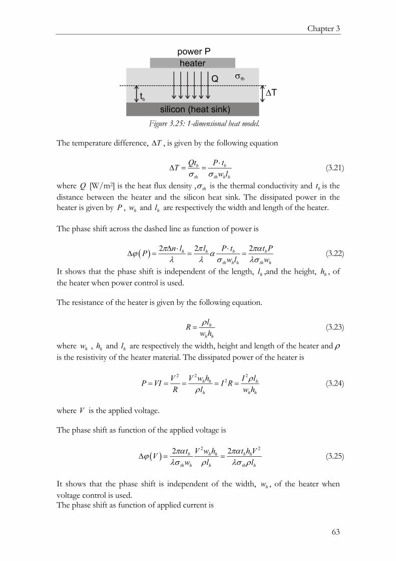
Chapter 3
63
heater
silicon (heat sink)
power P
∆TQ σth
tb
Figure 3.25: 1-dimensional heat model.
The temperature difference, T∆ , is given by the following equation
b b
th th h h
Qt P tTw lσ σ⋅
∆ = = (3.21)
where Q [W/m2] is the heat flux density , thσ is the thermal conductivity and bt is the distance between the heater and the silicon heat sink. The dissipated power in the heater is given by P , hw and hl are respectively the width and length of the heater. The phase shift across the dashed line as function of power is
( ) 2 2 2h h b b
th h h th h
n l l P t t PPw l w
π π παϕ αλ λ σ λσ
∆ ⋅ ⋅∆ = = = (3.22)
It shows that the phase shift is independent of the length, hl ,and the height, hh , of the heater when power control is used. The resistance of the heater is given by the following equation.
h
h h
lRw hρ
= (3.23)
where hw , hh and hl are respectively the width, height and length of the heater and ρ is the resistivity of the heater material. The dissipated power of the heater is
2 22
2h h h
h h h
V w h I lVP VI I RR l w h
ρρ
= = = = = (3.24)
where V is the applied voltage. The phase shift as function of the applied voltage is
( )2 22 2b h h b h
th h h th h
t V w h t h VVw l l
πα παϕλσ ρ λσ ρ
∆ = = (3.25)
It shows that the phase shift is independent of the width, hw , of the heater when voltage control is used. The phase shift as function of applied current is

Device design
64
( )2 2
2
2 2b h b h
th h h h th h h
t I l t l IIw w h w h
πα ρ παρϕλσ λσ
∆ = = (3.26)
Now the phase shift depends on the thickness, width and length of the heater. Equation (3.25) implies that the phase shift does not depend on the width of the heater when constant power is applied. This is not true since the change of effN depends on the position where the power is dissipated. Heating the material far away from the waveguide is a waste of energy. The material properties needed in solving the 2D heat equation are shown in table 3.6.
Table 3.6: Parameters used in the design of the heater structure Material Thermo-optic
coefficient α [1/K]
specific heat [J/(Km3)]
Thermal conductivity [W/(m.K)]
ρ [Ωm]
Si - 1.77·106 80 - 150 SiO2 (thermal) 1.15·10-5 1.75·106 2 SiO2 (PECVD) 1.15·10-5 1.75·106 1.4 SiON 1.15·10-5 1.75·106 1.4 Chromium 5·10-7
3.4.3 Calculation of the change in Effective index
The phase shift is now calculated, using a full 2D simulation. In Figure 3.26, curve A shows the effective refractive index change as function of the heater width for a fixed heater power of 0.1 W. The effN∆ is maximum for zero hw , which is not physical since it is impossible to dissipate power in a zero volume heater. So for optimal power efficiency the heater must be as small as possible. For large hw the curve has 1
hw dependency, as expected from the 1D-model.
The second curve (B) is also interesting; it is ∆Neff as function of wh for constant applied voltage. The curve tends to go to a constant effN∆ for large hw , which is expected by the 1D model. This curve shows the index increasing with heater width, but it also illustrates a remark made before, that further widening of the heater has little effect since it mainly leads to heating the layer stack at positions far away from the channel. A heater width of 20 µm will be chosen for the design in order to have no problems during fabrication. The ∆Neff is 41.9 10−⋅ for 0.1 W heating and lh of 1 mm. A tuning power of 0.82 W is needed for inducing 2π phase shift.
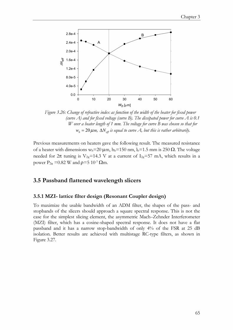
Chapter 3
65
Wh [µm]
0 10 20 30 40 50 60
∆ Nef
f
0.0
4.0e-5
8.0e-5
1.2e-4
1.6e-4
2.0e-4
2.4e-4
2.8e-4
A
B
Figure 3.26: Change of refractive index as function of the width of the heater for fixed power
(curve A) and for fixed voltage (curve B). The dissipated power for curve A is 0.1 W over a heater length of 1 mm. The voltage for curve B was chosen so that for
20hw = µm, effN∆ is equal to curve A, but this is rather arbitrarily. Previous measurements on heaters gave the following result. The measured resistance of a heater with dimensions wh=20 µm, hh=150 nm, lh=1.5 mm is 250 Ω. The voltage needed for 2π tuning is V2π=14.3 V at a current of I2π=57 mA, which results in a power P2π =0.82 W and ρ=5 10-7 Ωm. 3.5 Passband flattened wavelength slicers
3.5.1 MZI- lattice filter design (Resonant Coupler design)
To maximize the usable bandwidth of an ADM filter, the shapes of the pass- and stopbands of the slicers should approach a square spectral response. This is not the case for the simplest slicing element, the asymmetric Mach–Zehnder Interferometer (MZI) filter, which has a cosine-shaped spectral response. It does not have a flat passband and it has a narrow stop-bandwidth of only 4% of the FSR at 25 dB isolation. Better results are achieved with multistage RC-type filters, as shown in Figure 3.27.

Device design
66
Figure 3.27: Bar and cross transfer function of one-, two-, and three-stage resonant-coupler filters
with free spectral ranges of 12.8, 6.4, and 3.2 nm, respectively (top to bottom). A schematic drawing of a three-stage RC filter (the fifth order slicer, designed in section 2.3.3) is shown in Figure 3.28. It consists of four directional couplers with different coupling constants, and three delay lines, the second and third of which have twice the path length difference of the first one. This three-stage filter design features a flattened passband and a stop-bandwidth of 24% of its FSR at 25 dB isolation. The usable bandwidth for a slicer based on this three-stage RC filter will be 48% of the channel spacing. The transfer functions of the one-, two-, and three-stage RC-filters are given in Figure 3.27. The design parameters and the stop-bandwidth at 25 dB isolation of the RC filters are given in Table 3.7.
Table 3.7:Lengths of the couplers relative to one cross coupling length Lπ , for one-, two-, and three-stage flattened passband filters designed for 30 db isolation. The values for the two-stage slicer deviate slightly from the values given in Table 2.1. Within the tolerance band
the isolation is better than 25 db. The last row gives the isolation bandwidth relative to the FSR.
1 stage 2 stage 3 stage L1 0.50 ±0.04 0.50 ±0.02 0.50 ±0.02 L2 0.50 ±0.04 0.34 ±0.02 0.30 ±0.02 L3 - 0.18 ±0.02 0.29 ±0.02 L4 - - 0.09 ±0.02
-25dB BW 0.04 FSR 0.14 FSR 0.24 FSR

Chapter 3
67
As explained in section 2.3.2, the length of couplers that should be longer than half the coupling length can be reduced if all delay lines before the coupler are inverted/flipped. This has been used to reduce the length of the second coupler of the three-stage slicer shown in Figure 3.28.
L2L1L3 L4
∆L2∆L 2∆L
Delay line
Phase shifting elementL2L1
L3 L4∆L
2∆L 2∆LDelay line
Phase shifting element Figure 3.28: Three-stage resonant-coupler layout. ∆L is the length difference of the delay line and
L is the length of directional coupler. 3.5.2 Design MZI + Ring resonator
Figure 3.29 shows the designed filter. It clearly shows the MZI with a ring connected to the short channel. The roundtrip length of the ring is twice as large as the length difference of the MZI, as required by the condition for passband flattening. Heaters have been placed on the ring and on the long branch of the MZI. The MZI heaters have been split into two sections at both sides of the bend since it was not possible to obtain 1.5 mm length in a single section without placing the heaters on bent waveguides. The heaters of the ring are bend, since the ring does not have a straight section of 1.5 mm. The 3 dB couplers of the MZI are tunable couplers (Figure 3.21). So 3 dB splitting can always be obtained even when the fabricated directional couplers have an offset. A heater is placed on one of the two branches. These tunable couplers are not wavelength dependent because the two branches are of equal length. It is impossible to use tunable couplers in the MZI to ring coupler since these tunable couplers are about 2 mm long. Therefore fixed DC’s have been used for coupling the ring to the short MZI branch. Six filters having different ring-DC lengths have been placed on the mask with a total variation of 25 percent in strL , as shown in table 3.8.

Device design
68
Figure 3.29: Device layout
As seen in section 2.5, the power coupling ratio for the ring should be 0.82rκ = , which is equivalent to 0.72 0.72*257.6 µm 185.47 µmdcL Lπ= = = . The length of the straight part can be calculated using equation (3.11) and compensating for the coupling in the leads, giving 95.98 µmstrL = .
Table 3.8: Different lengths of the straight waveguides in the DC. Relative length Lstr [µm] 1 0.85 81.58 2 0.9 86.38 3 0.95 91.18 4 1 95.98 5 1.05 100.77 6 1.1 105.57
The length of the coupling sections of the DC’s in the tunable couplers is fixed to 39.22 µm. The filters are designed for two different FSR’s namely 50 and 100 GHz. Table 3.9 shows the parameters for the designed filter.
Table 3.9: Designed filters FSR [GHz]
FSR [nm]
∆LMZI [mm]
LRing [mm]
Rring, min [mm]
∆Neff, straight-
bend
50 0.4 3.997 7994 1,1 -2·10-3
100 0.8 1.998 3997 0.55 -2·10-3 The effective index of the mode in the bent waveguide of the ring is lower than in the straight waveguide ( 3
, 2 10eff straight bendN −−∆ = ⋅ ) and as a consequence the FSR of the ring
is not exactly half the FSR of the MZI anymore. The FSR of the ring is
waveguide
tunable coupler ring h=heater
h h
hh
h
electricalconnectionlead
bond padlong branch
short branchcommon electrode
Chapter 3
69
ringg ring
cFSRN L
= (3.27)
where Ng is the group index of the mode, Lring is the roundtrip length of the ring and c is the speed of the light. Differentiation with respect to Ng and reordering of the parameters gives
310ring g eff
ring g eff
FSR N NFSR N N
−∆ ∆ ∆= − ≈ − ≈ (3.28)
This error in the FSR is very small and only a small change of the transfer function is expected over many FSR This error is neglected in the design of the filter. Compensation can always be done by calculation of the complete optical roundtrip length over the ring using TempSelene [C2V]. 3.5.2.1 Effect of birefringence on filter curves
Although the channels were designed to have zero birefringence, due to fluctuations in the fabrication process there will always be some birefringence ( ,eff TM TEN −∆ ) in the order of 42 10−⋅ in the straight waveguides. The birefringence in the bend waveguide sections is not known. This birefringence results in a phase difference between TE and TM modes, given by 0 ,TM TE eff TM TEk N Lϕ − −∆ = ∆ ∆ (3.29) where k0 is the propagation constant in vacuum and L∆ is the length difference of the delay line or the roundtrip length of the ring. This phase difference will result in a frequency shift of the filter curves. The following equation gives the shift expressed in frequency.
,
2eff TM TETM TE
TM TEg
f Nf FSR
Nϕ
π−−
−
∆∆∆ = = (3.30)
where f is the frequency of the light. The shift between the TE and TM filter curve does not depend on the FSR of the filter. The shift is 26 GHz (= 0.21 nm) for
4, 2 10eff TM TEN −
−∆ = ⋅ ( 193,415f THz= ). For the lattice type filter this will result in a shift of the filter curve, since the length difference occurs in the straight waveguides. For the MZI + Ring filter we have the length difference of the MZI and the circumference of the ring, where both probably have different birefringence. 3.6 Binary tree Add-drop Multiplexer
The 1-from-16 ADM be presented here consists of one branch of a binary tree of cascaded even-odd channel-splitting optical filter elements (“slicers”) [Verbeek 1988, Oda 1990] as shown in Figure 3.30. In the left half of the device, starting at the “in”

Device design
70
port, the even and odd wavelength channels are separated in the first slicer. One half of the channels is directed to the next slicer having a double free spectral range (FSR), where they are split again. This continues until one channel, the “drop” channel remains. In the right half of the device, the “add” channel with new data and the remaining channels are recombined, and transferred to the “out” port. Note that the in-to-drop and the add-to-out transfer function are equal, because the right half of the device is a mirrored copy of the left half. One advantage of the binary-tree-based device layout is that the number of slicers, and thus the number of RC filter stages, grows only logarithmically with the number of wavelength channels in the communications system. For ADM devices based on a linear RC [Offrein (Nov) 1999, Kuznetsov 1994], the number of filter stages grows linearly with the number of wavelength channels. A second advantage of the device layout results from the add-after-drop configuration of the device. This ensures extremely low add-to-drop crosstalk [Roeloffzen 1999, Offrein (Sept) 1999], and the dropped wavelength is isolated from the output port by the channel-splitting as well as the combining sections of the device, leading to an improved suppression of the dropped wavelength at the output port.
Figure 3.30: Schematic drawing of the 1-from-16 add/drop multiplexer. The boxes represent the individual filter elements (“slicers”). The number in the box indicates the number of delay lines used for that slicer. The free spectral range for slicers A, B, C, and D is 3.2, 6.4, 12.8, and
25.6 nm, respectively. The mask layout for the add–drop multiplexer is shown in Figure 3.31. Because the cascade of couplers and delay lines contains many bend sections, a small radius of curvature is of high interest to keep the ADM device compact. Our (IBM) silicon–oxynitride (SiON)-based structure has a relatively high refractive index contrast of 3.3% and a waveguide size of 2 x 3 µm [Bona 1998]. The strong guiding of the mode allows a minimum bending radius as low as 1.5 mm without introducing noticeable bend or radiation losses and thus enables the cascading and folding of many stages into a compact device. The propagation losses of the waveguide are as low as 0.1 dB/cm at 1550 nm. The length differences of the 14 delay lines in the design were chosen to result in a channel wavelength spacing of 1.6 nm (200 GHz) for the complete device. On one arm of each delay line a chromium heater film is deposited, which is used for tuning the ADM to different wavelengths. The heaters are also used to compensate for phase errors in the delay lines.

Chapter 3
71
Figure 3.31: Device layout of the 1-from-16 device. It consists of eight slicers and 14 delay lines.
The input and output are the two center left waveguides and the add and drop are the two center right waveguides. The total device size is 65 x 14 mm2.
A 1-from-4 and 1-from-8 ADM have also been designed in the same way. The design of these ADMs is not shown here but at the measurements in Chapter 5. The next fabrication chapter does not apply for these ADMs, since these devices have been fabricated at IBM Research in Switserland. 3.7 Summary & Conclusions
A different type of slicer, the MZI + ring, has been designed using a low birefringence (the Type II) buried waveguide channel. Different subcomponents had to be designed first such as bent waveguide, directional coupler and tuning elements, since it was the first time that a device was designed using this waveguide. Fiber to chip coupling can easily be obtained by simple butt-coupling of a high numerical aperture fiber to the lateral tapered waveguide, with as loss of 0.2 dB. An adiabatic bend having low loss and small size has been designed, the surface is only 15% larger compared to a non-adiabatic bend with constant radius of 600 µm. The estimated loss for a 180 degree bend is 0.029 dB which is much less than a non-optimized bend 0.47 dB with equal surface area of 0.85 mm2. We have looked at three different coupling elements namely: the Multimode interferometer (MMI), two mode interferometer (TMI) and directonal coupler (DC). The directional coupler has been chosen as coupling element, since it is the only one which can be designed adiabatically (and thus lossless). Both MMI and TMI have discrete transitions where loss occures. The loss is not high (0.2 per coupling element) but since more than 20 cascaded couplers are quite common in advanced filter structures, it ads up to an unexeptable level. A further disadvantage of the MMI is that it has to be redesigned again for every splitting ratio. The sensitivity of DC to changes in the desing parameters are calculated. The DC is extremely sensitive to a change in channel with. The maximum allowed variation in channel width is 0.05 µm for 2 % change in coupling length. So good control of the fabrication process is necessary. The DC is wavelength dependent and the usable bandwidth is 26 nm (3.2 THz) for 2 % variation in Lπ .
In
Out
Drop
Add

Device design
72
The size of the MZI+ring filter could be kept small by folding the MZI around the ring. Tunable couplers are used instead of fixed 3 dB couplers in the MZI. In this way it is possible to tune to 3-dB splitting even when the fabricated DC’s deviate from the design. These tunable couplers can always be replaced by standard DC’s for a standardized fabrication process. The FSR of the designed filters are 50 and 100 GHz. Probably the 100 GHz type does not work, since the radius of the ring is 0.55 mm, which is smaller than the minimum allowed radius for low loss operation, 0.6 mm. The shift of the filter curve between TE and TM polarized light is independent of the FSR of the filter. Birefringence 4
, 2 10eff TM TEN −−∆ = ⋅ will result in a shift of 26 GHz (=
0.21 nm). This is a problem for the MZI+Ring that has a FSR of 50 GHz. Three binary tree Add-drop multiplexers (ADM’s) have been designed, 1-from-4, 1-from-8 and 1-from-16 during a stay at the Photonic Networks group of IBM. The used slicers are of the lattice type as described in chapter 2. The size of the 1-from-16 ADM is 65 x 14 mm2. All ADM’s are of the add-after-drop type, which ensures extremely low add-to-drop crosstalk. The channel spacing of the ADM’s is 200 GHz (=1.6 nm.) Chromium heaters are used as thermo-optical tuning elements. The tuning speed is in the order of 1 ms.

73
Chapter 4: Device fabrication
4.1 Introduction
This chapter describes the fabrication process at the MESA+ facilities of the integrated optical devices. Deposition and characterization of the layers as well as the used deposition and characterization equipment are explained. This is followed by a description of the etch process and the etching machine for fabricating the channels. The layers are annealed in order to obtain low optical loss. The complete fabrication process can be split up into four different phases. The first phase is the deposition of a low loss planar layer stack. Low loss is obtained by thermal treatment of the layers. The second phase is the patterning of the core layer where the structures on the mask are transferred to the core layer. The third phase is deposition and annealing of the top cladding. This phase completes the fabrication of the buried waveguide structures. The process steps are shown in Figure 4.1. The fourth and last step is the fabrication of the thermo optical tuning elements or heaters. The devices can now be sawn out of the wafer. 4.2 Substrate preparation
In order to be able to use standard lithography procedures and deposition equipment, silicon wafers have been used as substrates. The optical circuits should be isolated from the substrate by a thick (≥ 8 µm) SiO2 lower cladding (the buffer layer). High-quality photolithography requires that the wafers remain flat (within 50 nm). Since the deposition of a thick buffer layer would introduce a strong stress leading to strongly curved wafers if done on a single side, it is essential to deposit the thick oxide at both sides of the wafer. The most convenient way for this is thermal oxidation. However, using the available MESA+ cleanroom process, producing an 8 µm thick thermal oxide layer takes approximately one week. For this reason, commercially available [Vegatec] pre-oxidized Si wafers have been used in many cases as starting material (diameter 100 mm, <100> crystal orientation).

Device fabrication
74
SiSiO2
SiON
SiSiO2
SiONPhotoresistNickelPhotoresist
SiSiO2
SiONPhotoresistNickel
SiSiO2
SiONPhotoresist
SiSiO2
SiON
Photoresist
SiSiO2
SiONPhotoresist
SiSiO2
SiONPhotoresistNickel
SiSiO2
SiONPhotoresist
Photoresist
SiSiO2
SiON
Si
SiO2
SiON
(a)
(d)
(e) (f)
(b)
(h)(g)
(c)
(i) (j) Figure 4.1: Steps in the fabrication process of the planar waveguide device. (a) PECVD SiON
deposition. (b) 3.3 µm resist hard-baked at 180 °C. (c) evaporated nickel. (d) and (e) photolithography. (f) nickel etch (wet chemical). (g) resist etch (O2 plasma). (h) nickel removal.
(i) RIE etching of SiON. (j) PECVD SiO2 deposition.

Chapter 4
75
4.3 PECVD
Plasma-enhanced chemical vapor deposition (PECVD) is a well-known deposition process for SiOxNy layers [Morosanu 1990, de Ridder 1998, Bona 1999, Germann 2000]. These layers are highly transparent both in the visible and in the near infrared wavelength region. The refractive index can be set to any value in the region of 1.45 to 1.7 by selecting the process parameters [Wörhoff 1999]. The layer thickness grows linearly with deposition time. The layers are formed from a plasma of N2, SiH4, N2O at a temperature of 300 °C. The parallel plate Electrotech Plasmafab 310 PECVD reactor will be used to grow the core and upper cladding for the devices that have been designed in chapter 3. A schematic drawing of the PECVD reactor is shown in Figure 4.2.
Shower head & Upper electrode
LF plasma generator(187.5 kHz)
Gas inlet & flow control
- N O- 2% SiH : N- CF / O (cleaning gas)
- N (ventilation)
2
4 2
4 2
2
- NH (not used)3
Lower electrode & heater
Wafer
pump system
Figure 4.2: Schematic diagram of the PECVD reactor used to deposit the dielectric films. In principle four 100 mm wafers can be processed simultaneously. However, the wafers are arranged in a circle about the reactor axis, which leads to non-uniform layer deposition (e.g. layer thickness decreases with distance from the axis). Therefore, the full capacity of the reactor is not used, and only a single wafer (at the center position) is processed at a time. The refractive index of the PECVD SiON layers is tuned by changing the flow ratio N2O : 2% SiH4/N2 as can be seen in Figure 4.3.

Device fabrication
76
Flow rate ratio N2O : 2%SiH4/N2
0.0 0.2 0.4 0.6 0.8 1.0 1.2 1.4 1.6 1.8
Ref
ract
ive
inde
x
1.46
1.48
1.50
1.52
1.54
1.56
1.58
1.60
1.62
1.64
1.66
Dep
ositi
on ra
te [n
m/m
in]
34
36
38
40
42
44
46
48
Figure 4.3: Measured refractive index of TE polarized light (at λ=1550 nm) and deposition
rate of PECVD SiON as function of the flow ratio N2O : 2% SiH4/N2. The measured refractive index of TM polarized light is an about 10-3 higher.
4.4 Film characterization
A very important step in the production process is the characterization of the optical layers. The most important parameters to be characterized are the refractive index and the thickness of the layer since they directly define de waveguide channel. Other important parameters are the wavelength dependent absorption loss of the material, the homogeneity of the refractive index and layer thickness and the surface roughness. Two different characterization setups are used to measure the refractive index and thickness of a layer namely: an ellipsometer (Woollam M44) [Azzam 1977] and a prism coupling setup [Ulrich 1973]. The ellipsometer determines the refractive index and thickness of a layer by probing intensity and polarization of light reflected from interfaces between layers. The incident light is a parallel beam of linear polarized light. The used ellipsometer measures at 44 wavelengths ranging from 601 nm to 1098 nm. The measured refractive index values are fit to the Cauchy dispersion formula (4.1):
( ) 2 4
B Cn Aλλ λ
= + + (4.1)
where A,B and C are fit parameters. The refractive index can now be calculated at 1550 nm wavelength. In the prism coupling setup a prism, P1, is used to couple light into a guiding layer as shown in Figure 4.4. A condition for coupling of light is phase matching i.e. when the component of the propagation vector in the prism parallel to the layer stack is equal to the propagation constant of the mode ( , , )pz e p pk nϕ ϕ β= . In the prism coupling setup the external angle (ϕe) can be changed by rotation of the wafer including prism. The power of the guided mode is measured for a range of angles. For this purpose, a second prism, P2, can be used to couple the light directly onto a detector. The detector can also be placed at the side of the wafer to measure the intensity, since the guided mode is automatically coupled out there. This measurement, without the

Chapter 4
77
second prism turned out to give good results and was used in the setup. The layer parameters (dwg and nwg) can now be found from the measured angles of mode propagation. The layer stack must be at least bimodal to determine the two unknowns. The TE and TM modes can be measured independently by changing the polarization of the incoming light. Thus it is possible to measure the birefringence of the layer. It is also possible to measure the propagation loss of the guided mode by measuring the power of the out coupled light for different distances between the in and out couple prisms. The used prism coupling setup is home made and works with a broad range of wavelengths. Both characterization setups, ellipsometer and prism coupling setup, have been used in this work.
ϕp
β
ϕe
d nwg wg
nsubstr
Air
P1
P2 kp
np
k0
kpz
Figure 4.4: The principle of prism coupling.
Comparing both measurement setups it cannot be said that one of them is preferred. They both have advantages and disadvantages, as indicated in Table 4.1. The ellipsometer is used to set the correct parameters for the PECVD and the prism coupler is used to check the correct index and thickness.
Table 4.1: Properties of the Ellipsometer and Prism coupling setup Ellipsometer Prism coupling setup Speed of measurement
in the order of 1 minute
About 30 minutes per wafer
Type of substrate Si wafer Oxidized wafer (buffer layer needed)
Layer thickness 150 nm >900 nm (two modes at λ=632.8 nm)
Accuracy refractive index
7 10-3 1 10-3
Accuracy thickness 5 nm 10 nm Birefringence No Yes Location Next to PECVD Outside cleanroom

Device fabrication
78
4.5 Thermal treatment of the SiON layer
Although the PECVD SiON layers are highly transparent at the infrared wavelength of 1560 nm, there is small absorption of light at the 1460-1560 wavelength region. This absorption is caused by overtones of the resonance frequencies of Si-H and N-H bonds incorporated in the SiON matrix [Albers 1995, Denisse 1986, Hussein 2001, Worhoff 1999]. Thermal heat treatment will remove these hydrogen bonds and low losses below 0.1 dB/cm at 1550 nm wavelength have been reported [Horst 1998, Germann 2000]. Figure 4.5 shows the relative absorption loss spectrum of a SiON layer for different anneal temperatures measured with the prism coupler setup. The absorption was set to zero at 1570 nm. The absorption peak is 11 dB/cm at 1510 nm for the non-treated layer. Although the absorption falls off rapidly there is still significant loss of 1 dB/cm at 1550 nm. This wafer is now cumulatively annealed starting at a temperature of 400 °C. Each time the wafer was kept for at least 3 hours at the anneal temperature. Extreme drop of the absorption peak was observed at 1150 °C. The absorption peak reduced to 0.6 dB/cm at 1510 nm and less than 0.2 dB/cm at 1550 nm. It turned out that no further loss reduction occurred for annealing times longer than 3 hours.
1480 1500 1520 1540 1560 1580
0
2
4
6
8
10
12
asdeposited
T=400 OC
T=600 OC
T=800 OC
T=1000 OC
T=1150 OC
optic
al lo
ss (d
B/cm
)
wavelength (nm) Figure 4.5: Measured spectral absorption loss of a SiON layer (n1550=1.527), relative to the
loss at λ=1570 nm. For this reason, we used thermal treatment at 1150 °C for 3 hours for the SiON core layer as standard Unfortunately the important parameters refractive index and layer thickness are affected by the thermal treatment as shown in Figure 4.6. The index and thickness were measured using the ellipsometer. For the curve with initial index of 1.530, the index decreases until at 1000 °C the layer starts to densify and the index increases again. A layer having an initial index of 1.53 will have its index changed by –0.005 and a thickness change of –5% after the standard annealing process. These changes have to be taken into account, when depositing the layer.

Chapter 4
79
200 400 600 800 1000 1200-0.016
-0.014
-0.012
-0.010
-0.008
-0.006
-0.004
-0.002
0.000
0.002
0.004
n=1.474 n=1.530 n=1.587 n=1.636re
fract
ive
inde
x ch
ange
, ∆n
anneal temperture (0C)
200 400 600 800 1000 1200
0.93
0.94
0.95
0.96
0.97
0.98
0.99
1.00
1.01
n=1.474 n=1.530 n=1.587 n=1.636
Rel
ativ
e Th
ickn
ess
chan
ge, d
/dO
anneal temperture (0C)
a) b)
Figure 4.6: Measured refractive index change (a) and relative thickness change (b) of 4 SiON
layers having different initial indices (λ=1550 nm), as function of the anneal temperature. The measurements have been performed using the ellipsometer.
The material birefringence can be calculated since the prism coupler measurements were performed for the two different polarizations. The results are shown in Figure 4.7 for two different initial index values. The measured birefringence shows a dip at 800 °C for the 1.527 index layer. At 1150 °C it is almost equal to the non-annealed case.
200 400 600 800 1000 12000.0002
0.0004
0.0006
0.0008
0.0010
0.0012
0.0014
0.0016
0.0018
n1550=1.527 n1550=1.472M
ater
ial b
irefri
ngen
ce, ∆
n TM-T
E
anneal temperature (0C)
Figure 4.7: Measured birefringence of 2 SiON layers having different initial refractive indices.
The measurements are performed using the prism-coupling setup. Annealed SiON core layers having the designed refractive index of 1.520 @ 1550 nm and thickness of 820 nm can now be fabricated and further processed. A pre-annealed index of 1.525 @ 1550 nm and thickness of 855 nm has to be grown to obtain the designed values after annealing. The curve for n=1.530 of Figure 4.6 has been used.

Device fabrication
80
4.6 Channel fabrication
4.6.1 Photolithography
The next step in the fabrication process is the transfer of the structures on the photomask onto the photoresist on the wafer. In order to resolve the smallest details on the mask with sufficient accuracy (better than 0.1 µm) the thickness of the resist should be below 1 µm. Unfortunately, such a thin resist cannot withstand the aggressive SiON etching process. Therefore two new multi-step lithographic processes have been developed. (see Figure 4.1). The difference between the two processes is the mask used in the SiON etch step (section 4.6.4):
a) Etching of SiON using a metal mask. b) Etching of SiON using a thick resist mask
The first step is spinning of photoresist having a thickness of 0.4 µm (process a) or 3.3 µm (process b). The resist is then hard baked on a hot plate at different increasing temperatures starting at 95 °C till 140 °C. The slow process ensures good removal of the solvent. After that the resist is baked at an even higher temperature in an atmospheric oven where it is hardened out. A thin nickel layer is evaporated on top of the hard resist using the Balzers BA600 (Figure 4.1c) and a thin photoresist layer is spun on top (Figure 4.1d). The structures on the mask can now be transferred to this resist layer by aligning the mask and the wafer. Once the mask is aligned, hard contact is made (in vacuum) and the wafer is exposed to ultraviolet light through the photomask. Next, the wafer is post-exposure baked. This bake is needed to get a smooth and well defined border between exposed and unexposed resist. The wafer is subsequently developed. The developer removes all the resist that is exposed to the ultraviolet light and the unexposed resist remains unaffected (Figure 4.1e). Next, the remaining resist is hardened on a hot plate. The resist pattern is now examined under the microscope. A picture of the directional coupler is shown below (Figure 4.8). It is important that the resist between the two channels (gap is 1 µm) has completely disappeared and that the width of the channel and the gap have the right dimensions. The microscope has a line width measurement system for that purpose. It turned out that it is difficult to measure the exact dimensions, since the structures are rather small. The accuracy is about 0.2 µm.
Figure 4.8: Microscope picture of resist pattern of the directional coupler structure on top of the
nickel layer.
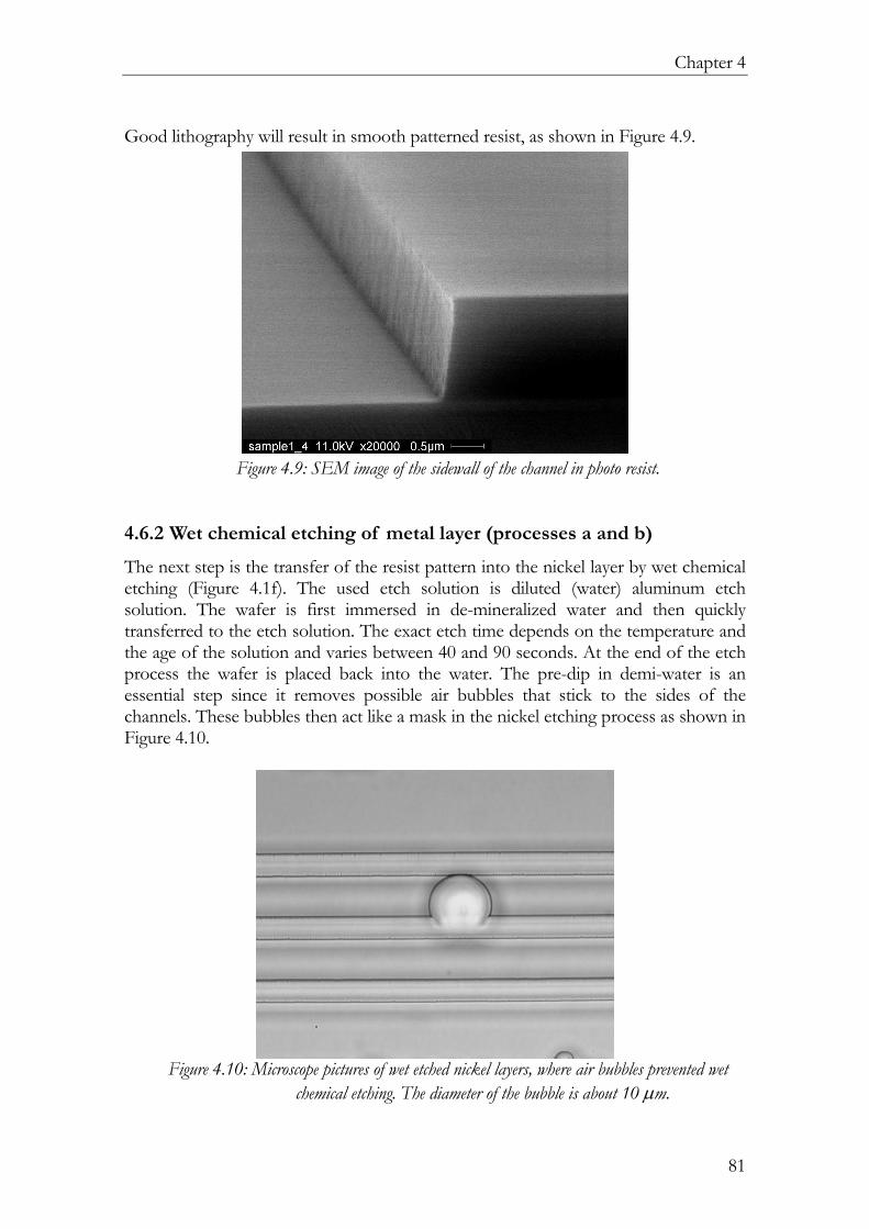
Chapter 4
81
Good lithography will result in smooth patterned resist, as shown in Figure 4.9.
Figure 4.9: SEM image of the sidewall of the channel in photo resist.
4.6.2 Wet chemical etching of metal layer (processes a and b)
The next step is the transfer of the resist pattern into the nickel layer by wet chemical etching (Figure 4.1f). The used etch solution is diluted (water) aluminum etch solution. The wafer is first immersed in de-mineralized water and then quickly transferred to the etch solution. The exact etch time depends on the temperature and the age of the solution and varies between 40 and 90 seconds. At the end of the etch process the wafer is placed back into the water. The pre-dip in demi-water is an essential step since it removes possible air bubbles that stick to the sides of the channels. These bubbles then act like a mask in the nickel etching process as shown in Figure 4.10.
Figure 4.10: Microscope pictures of wet etched nickel layers, where air bubbles prevented wet
chemical etching. The diameter of the bubble is about 10 µm.

Device fabrication
82
4.6.3 Reactive ion etching of the base resist (process b)
Reactive ion etching (RIE) is used transfer the structures to the thick base resist. RIE is a dry etch procedure. The machinery (PlasmaFab Electrotech PF340) is almost equal to the PECVD (Figure 4.2). A plasma containing different gasses is generated between two electrodes in a vacuum chamber. The ions in the plasma are accelerated towards the lower electrode where they bombard the wafer that is placed on the lower electrode. The etching process is a combination of chemical and physical etching. Proper setting of the plasma power and chamber pressure results in high anisotropic etch ratios. Oxygen plasma is used for RIE etching of the thick resist. The following parameters are used for the etch process. The oxygen flow rate is 20 sccm (=cm3/min), chamber pressure 10 mTorr, lower electrode temperature 10 °C and a plasma source power of 50 W. The resulting etch rate of the resist is 220 ± 10 nm/min. The nickel mask is now removed in the same manner as the patterning described above in 4.6.2. This nickel layer is removed for two reasons. First reason is that nickel will re-sputter during the SiON etch process and thus contaminates the complete wafer. The second reason is that the additional cleaning step, described below, removes the nickel in any case and will be contaminated with nickel if it has not been removed beforehand. What remains is the waveguide stack including the channel structure in thick resist (Figure 4.1h). The wafer is now dipped in a cleaning solution where it cleans the surface of unwanted contamination. It turned out be an extremely crucial process step as be explained in section 4.7. Unfortunately this cleaning step is not possible in the metal mask case (process a), since it removes the metal. Figure 4.11 shows the resist profile of a channel before and after the cleaning step.
Figure 4.11: Two different SEM images of the 3.3 µm thick resist profile before (left) and after
(right) the cleaning step. 4.6.4 Reactive ion etching of the SiON layer
The same RIE machine is now used to etch into the SiON layer (and also through the thin protective resist layer of process b). Fluorine based gasses are led into the etch chamber at a background pressure of 10 mTorr. The plasma is activated with a power

Chapter 4
83
of 50 W. The lower electrode is kept at a temperature of 10 °C. Steep vertical walls are obtained with these parameters. A special interferometric tool is used to measure the etch depth in situ. Since this etch process is highly anisotropic, minor contamination (when the cleaning step is not applied) of the wafer surface leads to extreme roughness: a “grassy” pattern has formed, after etching. Figure 4.12 shows a picture of RIE etched SiON layer without the cleaning step.
3.25 µm
Figure 4.12: SEM images of the channel and surface after SiON etch step of process option a
(metal mask, without cleaning step). The sidewall of the channel is smooth but a grass pattern has formed on the surface.
The etch depth including the remainder of the resist mask is measured using the surface profile scanner (Dektak 8). Then the resist is removed by the standard wafer cleaning process and the depth is measured again. The SiON and resist etch speed can now be calculated. The etch rate of photoresist (147 ± 3 nm/min) is almost three times as fast as that of SiON (57 ± 2 nm/min). Microscope pictures of the directional coupler are shown in Figure 4.13 for both options: metal mask (a) and thick resist mask (b). The thick resist did not withstand the etching process of the SiON resulting in rough sidewalls and narrowed channels.

Device fabrication
84
20 µm3.2 µm 4.3 µm
(a)
20 µm 2.3 µm 4.3 µm
(b)
Figure 4.13: Microscope picture of directional coupler in SiON for both process options: metal mask (a) and thick resist mask (b). The sidewall of the channel is rough and the
channel has become narrower for option b (compare with Figure 4.8) At this point it is difficult to choose the best option, since both options have imperfections. The metal mask gives good channels (smooth sidewalls and good dimensions) but extreme roughness of the surrounding area. The thick resist mask (incl. the additional cleaning step) gives a smooth surface but imperfect channels (rough side walls and channel narrowing). Devices will be fabricated using both options, to see which option gives the lowest loss. The metal mask option is seems to be most favorable for its preserving the channel width, since design of the DC showed high sensitivity to error in channel width. 4.7 Upper cladding deposition
The next step is deposition of the 8-9 µm thick PECVD SiO2 uppercladding (Figure 4.1j). Actually this layer still is a SiOxNy material, but since it contains only a small amount of nitrogen, and it has the lowest index that can be obtained using this process it is called SiO2. The same PECVD machine will be used as in the deposition of the core layer, only with different settings. The refractive index is 1.472 @ 632.8 nm wavelength and 1.458 for a wavelength of 1523 nm. It is not necessary to put the wafer at the middle position of the under electrode since the thickness of this layer is not a very critical parameter and maximum four 100 mm wafers can be processed simultaneously. Figure 4.14 shows two microscope pictures of a channel structure and surroundings after the deposition started with a rough and flat surface respectively. The SiO2 layer did not grow homogeneously on the rough surface. This will lead to unacceptable optical losses and emphasizes the need for the cleaning step.

Chapter 4
85
100 µm
20 µm
Figure 4.14: Top view microscope pictures of a channel structure and surrounding after deposition
of the upper cladding, metal mask option (left) and thick resist option including cleaning step (right).
The SEM picture below (Figure 4.15) show the facet, obtained by cleaving, of the layer stack including the waveguide channel. The PECVD SiO2 did not grow smoothly over the channel. It starts growing on top of the channel, at the large surface, but also on the sidewall of the channel. A border can be observed at the point where the surface and the side grown depositions meet, resulting in a small gap. The initial angle of this gap is about 60 degrees. This discontinuity probably causes some optical propagation loss.
gap core
Figure 4.15: SEM images of the side facet of a cleaved wafer.
Although the optical loss is already extremely low for PECVD SiO2 layers, the layer will undergo thermal treatment. The reason for this is lowering of the refractive index of the material so that it becomes equal to the index of the thermal SiO2. Figure 4.16 shows the refractive index and thickness of a 9 µm thick PECVD SiO2 as function of the anneal temperature. The annealing time was 4 hours in all cases. The layer stack next to the waveguide is Si / Thermal SiO2 /PECVD SiO2 layer. The indices of both oxides were assumed to be the same in the design of the channel, but in reality there will always be a small difference. The PECVD SiO2 layer will become a guiding layer when the anneal temperature of the PECVD SiO2 is set so that the index is higher than the thermal oxide and light can propagate as slab light. Guided modes can only exist in the Si substrate when the index of the PECVD SiO2 is lower than the thermal oxide and light not guided by the channel is automatically removed. The standard

Device fabrication
86
anneal process is set to 4 hours at 700 °C. The index is 1.444, which is a bit lower than the 1.446 of thermal SiO2.
anneal temperature [deg C] 400 600 800 1000 1200
refra
ctiv
e in
dex
(@ 1
523
nm)
1.440
1.442
1.444
1.446
1.448
1.450
1.452
1.454
1.456
1.458
1.460
TETM
thermal SiO2
Figure 4.16: Refractive index of PECVD SiO2 as function of anneal temperature.
4.8 Thermal tuning elements
In order to tune the device, electrical heaters (chromium) are placed on top of the upper cladding above the channel waveguides. Heating is done by an electrical current flowing through the resistive chromium heater material when a voltage difference is applied to the heater through aluminum leads connected to bond pads. Fabrication of the heaters is done by the lift-off process as shown in Figure 4.17. On top of the wafer containing the buried waveguide structures, a 1 µm thick photoresist layer is spun and pre-exposure baked at a temperature of 95 °C. Next, the wafer is exposed in the mask aligner through the heater-mask. The heater mask is of the inverted type, meaning that the heater structures are transparent. The resist is removed at the heater positions after developing. Next a 150 nm thick chromium layer is evaporated on top of the wafer using the Balzers BA600. The unwanted chromium is removed by placing the wafer in an ultrasonically agitated acetone bath. The next step is the fabrication of the lead waveguides by deposition of a 1-2 µm thick aluminum layer on top of the chromium except at the heater positions by a similar lift-off process. The dissipation of electrical power in the electronic leads can now be neglected since their resistance is low. Two microscope pictures of the heater and lead are shown in Figure 4.18. The fabrication is now finished and the devices can be sawn out of the wafer.

Chapter 4
87
SiSiO2
SiON
Photoresist
Si
SiO2
SiONChromiumPhotoresist
Si
SiO2
SiONChromiumAluminum
Si
SiO2
SiON
Si
SiO2
SiONPhotoresistChromium
SiSiO2
SiONChromium
Photoresist
Aluminum
SiSiO2
SiONChromium
Photoresist
Photoresist
SiSiO2
SiON
(a) (b)
(c) (d)
(e)
(g) (h)
(f)
Figure 4.17: Steps in the fabrication process of the thermo optical tuning elements. Resist (a) is spun on top of the wafer and exposed with ultraviolet light through the heater mask, and the
resist is developed (b). Chromium (c) is sputtered on top and immersed in acetone to initiate the lift-off process (d). The steps are repeated once again but now with the lead mask (e, f, g and h).
lead
heater
waveguide
lead
heater
Figure 4.18: Microscope picture of the heaters and the leads.

Device fabrication
88
4.9 Conclusions
The MZI+ring has been fabricated using SiON waveguide technology. The fabrication process was described in this chapter. The different ways to realize the channel have been examined:
• Realization of the channel using a thick layer of photoresist. The thick photoresist could not withstand the etching of the channels. As a result, the sidewalls were extremely rough and the channel was much narrower than designed. The surface of the wafer could be cleaned by a additional cleaning step before etching of the SiON channel, since photoresist is not affected by an additional cleaning step. The surface of the wafer is smooth after etching and the upper cladding can also be grown well.
• Realization of the channel using a metal mask resulted in well-defined channels: the sidewalls where smooth and the channel width was as designed. Unfortunately, the etched surface was extremely rough because the cleaning step could not be applied since this cleaning step removes the metal mask. As a consequence the upper cladding could not be grown smoothly.
Further research of the fabrication process is necessary to tackle this problem.
89
Chapter 5: Device performance
5.1 Introduction
This chapter shows the performance of the 1-from-4, 1-from-8 and 1-from16 ADM The performance of the sub-components is also measured. The chapter starts with the description of the measurement setup in section 5.2, followed by the measurement steps needed for characterizing the building blocks in section 5.3. Next the measurement results of the straight and bent waveguide are presented in section 5.4 followed by the measurement of the power splitting of the directional coupler (section 5.5). The performance of the lattice type slicers is shown in section 5.6. Next the measurements on the ADM’s are presented in section 5.7. Properties of the heaters, linearity with wavelength and maximal power are presented in section 5.8. Transmission spectra and group delay measurements on the MZI + Ring configuration are shown in section 5.9. The chapter ends with a discussion about the two types of slicers. 5.2 Experimental setup
The performance of the MZI + ring has been measured using an infrared characterization setup as shown in Figure 5.1. It is a versatile setup for characterizing the device and its building blocks. Infrared and visible light are coupled together using a 50/50 fiber coupler. The visible HeNe laser light (λ=633 nm) is used for alignment and will be turned off during a measurement. Light from one of the two outputs is then linearly polarized and coupled into a polarization maintaining fiber (PMF). The polarized light is then coupled from the cleaved fiber end into the planar waveguide chip by simple butt coupling. It is important that the center of the fiber is aligned to the center of the waveguide. Therefore the fibers are placed on a x-y-z-stage controlled by piezoelectric actuators. The fiber must be placed as close as possible against the chip to obtain optimal coupling. Index matching gel can be used to eliminate possible Fabry-Perot reflections in the air gap. The polarization state of the coupled light can be controlled by rotating the fiber around its axis. If a principal axis of the PMF has been aligned with the waveguide plane, a quick change between TE and TM coupled light is easily obtained just by rotating the polarizer by 90 degrees in order to couple through the second PMF principal axis. The light remains linearly polarized and no drop in intensity was observed. The chip is fixed on an x-axis stage with a vacuum holder. The light from the chip is coupled into a standard single mode

Device performance
90
fiber (SMF) (again using butt-end coupling) where it is split up by a second fiber splitter and transported to a power meter (Newport 2832 C) and an optical spectrum analyzer (OSA, Ando AQ-6310). Two different infrared light sources are available. The first is an erbium doped fiber source (EDFS) emitting a continuous spectrum of infrared light in the 1510-1570 nm wavelength range. The OSA can then be used to do spectral measurements. The maximal resolution is 0.1 nm and a typical scan takes about 10 seconds. The second source is an infrared tunable laser (Hewlett-Packard, HP8168C, λ=1500-1600 nm). The wavelength can be controlled by a computer. The spectral measurement is performed by stepping the wavelength of the laser and simultaneous read out of the power on the detector. The spectral resolution is much higher (0,1 pm) than that of the spectrum analyzer but a wavelength scan lasts for several minutes. A second difficulty of the laser is that the light is already polarized and the polarization state changes in the connection fibers with the wavelength resulting in change in intensity after the polarizer. The use of the EDFS - spectrum analyzer combination is preferred over the laser when 0.1 nm resolution is sufficient. A computer program optimizes the position of the fibers and maximizes the measured intensity. The shape of the mode profile can be examined by exchanging the fiber at the output side by a lens objective that images the output facet on an infrared camera. Non circular mode profile and bimodality can easily be observed. Propagation of light through the channels can be observed by a camera, which is placed above the chip. It shows the scattered light from the channel and thus is only useful for minor quality waveguides For thermo-optic measurements, bond-pads of the chip are connected to individual DC voltage sources. The voltage can be controlled accurately by the computer and can be set from 0 to 40 volt. The maximum current is 100 mA.
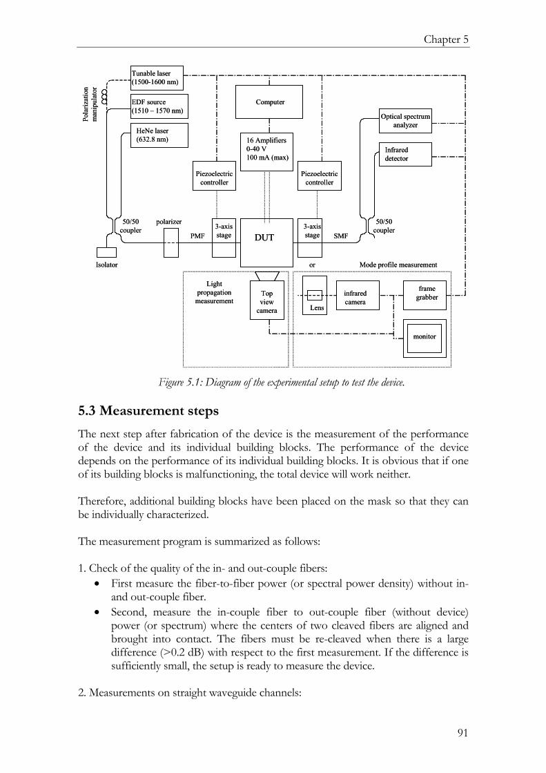
Chapter 5
91
3-axis stage
3-axis stageDUT
polarizer
Tunable laser(1500-1600 nm)
EDF source(1510 – 1570 nm)
HeNe laser(632.8 nm)
Pola
rizat
ion
man
ipul
ator
Infrared detector
Optical spectrum analyzer
PMF SMF
infraredcamera
16 Amplifiers0-40 V100 mA (max)
Computer
Lens
Isolator
monitor
frame grabber
Piezoelectriccontroller
Piezoelectriccontroller
or
50/50coupler
50/50coupler
Mode profile measurement
Top view
camera
Light propagation
measurement
Figure 5.1: Diagram of the experimental setup to test the device.
5.3 Measurement steps
The next step after fabrication of the device is the measurement of the performance of the device and its individual building blocks. The performance of the device depends on the performance of its individual building blocks. It is obvious that if one of its building blocks is malfunctioning, the total device will work neither. Therefore, additional building blocks have been placed on the mask so that they can be individually characterized. The measurement program is summarized as follows: 1. Check of the quality of the in- and out-couple fibers:
• First measure the fiber-to-fiber power (or spectral power density) without in- and out-couple fiber.
• Second, measure the in-couple fiber to out-couple fiber (without device) power (or spectrum) where the centers of two cleaved fibers are aligned and brought into contact. The fibers must be re-cleaved when there is a large difference (>0.2 dB) with respect to the first measurement. If the difference is sufficiently small, the setup is ready to measure the device.
2. Measurements on straight waveguide channels:

Device performance
92
• Channel loss: The easiest way to measure the channel loss and the fiber to chip coupling loss is by measuring the output power of different lengths of channels (cutback method). This must be a straight line in a logarithmic graph where the slope gives the channel loss in dB/cm. The extrapolated value for zero channel length gives the fiber to chip coupling loss, if the graph is normalized with respect to the fiber-to-fiber measurement. If the measurement is performed with the spectrum- analyzer one also gets the spectral losses, which is interesting since the losses near 1510 nm are larger because of absorption. This also provides a check on parasitic Fabry-Perot resonances. The difference between the TE and TM measurement gives information about polarization dependent coupling and polarization-dependent channel loss. The birefringence (difference between Neff,TE and Neff,TM) of a waveguide channel can be determined by measuring the frequency-dependent mode beat between the TE and TM light.
• Another important measurement is looking at the mode profile with the camera at the outcouple facet since it can show bimodality and a non circular mode profile. The size of the mode profile relative to a SMF can also be measured.
3. Measurements on bend waveguide structures:
• Measurement is performed for different bend radii and the bend loss is expressed in dB/90 deg. The channel losses can be filtered out, since the lengths of the designed bend test structures are all equal. The relation between bendloss and bendradius is exponentional.
• Adiabatic bend loss measurement. Same measurement as non-adiabatic bend.
4. Measurements on the directional coupler:
• The two important parameters for the directional coupler are loss and splitting ratio for TE and TM polarized light. By comparing the total output power at the output ports of the DC with that at the output of a channel of equal length one can determine the excess loss of the DC. The difference between the splitting ratios for TE and TM polarized light is an important quality factor of the DC. Measurement is performed for different lengths of the DC.
5. Measurement on the slicers:
• The most important measurement is the power spectrum. It can be measured by making use of the broadband light source and spectrum analyzer or tunable laser and detector.
• Measurement of the group delay of the filter. Using a different setup (to be discussed in 5.9.2.)
6. Measurement on the ADM’s:
• The filter curves of the ADM’s are measured in the same way as the slicers.

Chapter 5
93
5.4 Characterizing of waveguides
5.4.1 Waveguide loss
The loss of the waveguides has been measured by using the cutback method. The output power of two waveguides of different length has been measured. The difference in power divided by the length difference gives the channel loss in dB per unit length. Figure 5.2 shows the measured waveguide loss as function of wavelength for both TE and TM polarized light. The minimum loss is 0.55 and 0.73 dB/cm for TE and TM respectively. The absorption peak is about 1.3 dB/cm at 1516 nm wavelength. The absorption peak is not expected at 1516 nm wavelength but at 1510 nm. Probably the absorption still goes up and the measurement goes wrong. An explanation is that the power below 1520 nm gets too low to be measured well. The loss at 1520 nm is slightly less than 1.3 dB/cm and has been reduced a lot compared to the measured 4-5 dB/cm in [van Lith 2000] because of the annealing process. We have measured (using the broadband light source) the channel loss on a total of 6 wafers and it varied from 0.50 dB/cm to 3.60 dB/cm. The experimental error depends on the variation in the fiber to chip coupling loss and is about 0.2 dB. The major cause for the waveguide loss is the sidewall roughness of the channel. The wafers, which had lower sidewall roughness during fabrication, turned out to have lower loss. Lower losses can only be obtained by careful processing of many wafers and optimization of the etching process. The measured waveguide loss of the wafer containing “good” functioning filters was 1.7 dB/cm. This is important to know since this loss will have effect on the filter curve.
1500 1520 1540 1560 1580 1600
0.4
0.6
0.8
1.0
1.2
1.4
bad
mea
sure
men
t reg
ion
too
little
pow
er
TE TM
Wav
egui
de lo
ss (d
B/cm
)
Wavelength (nm) Figure 5.2: Channel loss as function of the wavelength.
5.4.2 Bend loss measurements
Bent waveguides can be characterized by comparing bends with different radii. These bend structures were designed in such a way that the total optical channel length is always the same. The loss of the bend is given in dB/90°. The result of the

Device performance
94
measurement depends strongly on the alignment of the fibers to the chip. Figure 5.3 shows the measured bend loss of a 90° bend plus two straight-to-bend transitions as function of the bend radius for standard bends. The broadband light source and power meter are used for the measurement. These bends are not adiabatic and no offset was applied between straight and bend. Bend losses were also calculated and shown in Figure 5.3. The calculation was performed by TempSelene [C2V] using the parameters of the Type II waveguide. The bend loss is 0.2 and 0.5 dB/90° at a bend radius of 700 µm for TE and TM polarized light respectively, which is a bit higher than the calculated bend loss (see Figure 5.3). The error in the measurement is 0.2 dB, which can be reduced by cascading more 90-degree bends. For this measurement we used four cascaded 90-degree bends.
Bend radius [µm]
400 600 800 1000
Loss
[dB
/90
deg]
-0.2
0.0
0.2
0.4
0.6measured TMmeasured TETheoretical TETheoretical TM
Figure 5.3: Measured and calculated bend loss (90° bend + 2 transitions) as function of bend
radius of the non-adiabatic bend. Waveguide loss has been subtracted out. Bend loss is reduced with adiabatic bends, as shown in the measurement result of Figure 5.4. Here the 0.2 dB/90° threshold lies at 475 µm radius. This measurement has less noise compared to the previous, because here we used 52 cascaded 90-degree bends.

Chapter 5
95
Bend radius [µm]
450 500 550 600 650
Bend
loss
[dB/
90o ]
0.0
0.1
0.2
0.3
0.4
0.5
TETM
Figure 5.4: Bendloss of the adiabatic bend as function of the minimal bendradius.
5.5 Directional coupler performance
Several DC’s having different lengths of the straight coupling section have been placed on the mask in order to enable measurement of the coupling length. The measured bar and cross power is shown in Figure 5.5. A sine-shaped function has been fit to the measurements. The coupling length Lπ (of the straight coupling section) is 354 µm for TM and 406 µm for TE respectively, which deviates from the designed 257 µm. A main cause for this deviation is probably a too high index contrast between the core and the cladding. For 3 dB couplers, the length of the straight coupling section has been designed to be 39.2µmstrL = . The measured power coupling of these devices was found to be 0.30 for TE and 0.33 for TM respectively. It should be noted, that even though the actual coupling deviates from the designed value, it is still possible to tune the tunable couplers (that are part of the MZI + ring filter) to the 3 dB point. The measured power-coupling ratio of the ring coupler (with a length of the straight coupling section 105.6µmstrL = ) is 0.59 and 0.52 for TM and TE respectively, which is considerably lower than the designed 0.82 (and this one cannot be compensated). As a consequence, the filter curve of the MZI + ring will deviate from the designed transfer function as will be seen in section 2.5. Main cause of the deviation is the fabrication process, which must be improved to get DC’s with correct coupling length. Excess loss compared to a straight waveguide of equal length has not been observed for any of the characterized DC’s.

Device performance
96
Lstr [µm]
0 100 200 300 400 500
Inte
nsity
[a.u
.]
0
1e-4
2e-4
3e-4
4e-4
5e-4Lπ=354 µm
Sum
Bar
Cross
Designed length for 3dB coupling
Designed length for κ=0.82
Figure 5.5: Measurement and fit of the bar and cross output power as function of the length of the
coupler for TM polarized light. The broadband light source and power meter were used for the measurement.
The wavelength dependence of the DC has been measured on the DC having a straight coupling section of 455 µm and is shown in Figure 5.6. This coupler is sensitive to the wavelength because it is quite long (compared to the DC’s used in the filter) and the power transfer is close to the 3-dB point. The power of the cross output is given by the following equation.
( ) ( )2sin
2crossLP
Lπ
πλλ
=
(5.1)
where ( )Lπ λ is the wavelength dependent coupling length calculated in section 3.3.7 and L is the length of the coupler.. A good fit (crossing at the same position) can be obtained with coupler length Lstr=395 µm and is also shows in Figure 5.6. This length is smaller since coupling in the leads in not included in eq. (5.1) and the formula ( )Lπ λ for the designed coupler was used.

Chapter 5
97
Wavelength [nm]1520 1540 1560 1580
Nor
mal
ized
pow
er
0.0
0.2
0.4
0.6
0.8
1.0
LDC=455 µm
Bar
Cross
Figure 5.6: Measurement (solid) and fit (dashed) of the normalized power output of the bar and
cross output of a 455 µm long directional coupler as a function of wavelength 5.6 Slicer performance
In this section, measurements on individual slicers are presented, starting with the two and three stage resonant coupler filters. The measurements of the MZI + Ring slicers are not presented in the section but at the end of the chapter. 5.6.1 2 stage slicer
This slicer was fabricated and measured at the optical networking group of IBM. The used DC’s are also from IBM design and are not to be confused with those of the previous measurement. Figure 5.7 shows the measured filter curve for the 2-stage slicer having an FSR of 800 GHz (6.4 nm). The bar and cross spectra were measured for both TE and TM polarized light separately without retuning the slicer. From comparing the measurement with the design, it can be concluded that the filter almost works as designed. There is a small deviation in the power coupling ratios of the directional couplers of the slicer resulting in a small asymmetry between the bar and cross measurement. The deviation from the design is in the order of 4 percent. The crosstalk is -19.0 dB and -13.5 dB for the bar and cross-port respectively. The width of the passband 1.8 nm (28 % of the FSR) at -0.5 dB. The measured shift between the curves of the TE and TM polarized light is 0.2 nm (25 GHz), indicating a birefringence of 4
, 2 10eff TM TEN −−∆ ≈ ⋅ . Additional loss compared to a straight
waveguide was not observed.

Device performance
98
Figure 5.7: Measured spectra for the 2-stage slicer (FSR is 6.4 nm). The spectra were measured
for TE (2 bar and 2 cross) and TM (also 2 bar and 2 cross) light separately, without retuning.
5.6.2 3-stage slicer
The spectrum of the 3-stage slicer was measured in the same way as the 2-stage slicer and the result is shown in Figure 5.8. The measured FSR is 3.2 nm (400 GHz). The measured crosstalk is -13.2 dB and -11.1 dB for the bar and cross respectively. The width of the passband is 1.2 nm (38 % of the FSR) at –0.5 dB. The TE TM shift is also 0.2 nm.
Figure 5.8: Measured spectra for the 3 stage slicer (FSR is 3.2 nm) . The spectra were measured
for TE and TM light separately, without retuning.

Chapter 5
99
5.7 ADM measurements
Three ADM were designed and fabricated, 1-from-4, 1-from-8 and the 1-from-16. The measurement results are presented here. 5.7.1 ADM layout
Figure 5.9 shows the schematic drawing of the three ADM’s and Figure 5.10 shows the device layout of the 1-from-16 device, which has been folded at the connection between the splitting and combining sections. The channels spacing is 1.6 nm. The add–drop multiplexer can be tuned to any wavelength channel by properly addressing the individual heaters. To find the optimum heater settings for a given wavelength, one can use manual or automatic optimization procedures, like the Levenberg-Marquardt algorithm. We used manual tuning of the devices where the non-used channels are used for tuning. The devices have been pigtailed and packaged by a commercial company Opto Speed [optospeed] and installed into a control box (IBM design). This control box consists of (maximal 16) amplifiers for tuning the heaters and a computer with D/A converter. The voltage across every heater can be regulated between 0 and 40 Volt. The size of the 1-from-16 chip is 65 x 14 mm2. The sizes of the 1-from-8 and 1-from-4 are not much smaller since only the small single-stage sections D and C are removed.
1,2,3,41,3
2,41
3
Add
Out
AAB B
In
Drop
3 322
(a)
1..8
1,3,5,7
2,4,6,8
1,5
3,71
5
Add
OutIn
Drop
3 32 2
11AA
BBCC
(a) (b)
odd
even
1,5,9,13
3,7,11,15
1,9
5,13
1
9
Add Drop
23
23
1 111
ABB
CCDD
A
1..16
OutIn (c)
Figure 5.9: Schematic drawing of the three add/drop multiplexers ((a) 1-from-4, (b) 1-from-8 (c) 1-from-16 ). The boxes represent the individual filter elements (“slicers”). The number in the box indicates the number of delay lines used for that slicer. The free spectral range for slicers A,
B, C, D is 3.2, 6.4, 12.8 and 25.6 nm respectively.
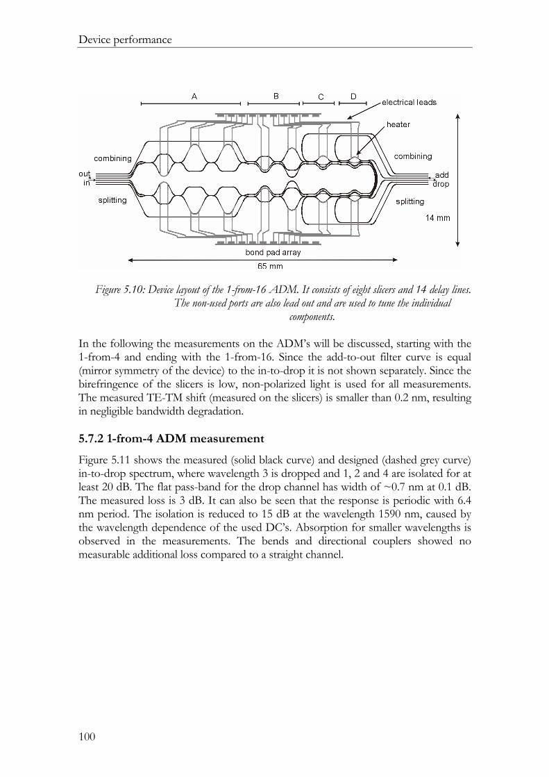
Device performance
100
Figure 5.10: Device layout of the 1-from-16 ADM. It consists of eight slicers and 14 delay lines. The non-used ports are also lead out and are used to tune the individual
components. In the following the measurements on the ADM’s will be discussed, starting with the 1-from-4 and ending with the 1-from-16. Since the add-to-out filter curve is equal (mirror symmetry of the device) to the in-to-drop it is not shown separately. Since the birefringence of the slicers is low, non-polarized light is used for all measurements. The measured TE-TM shift (measured on the slicers) is smaller than 0.2 nm, resulting in negligible bandwidth degradation. 5.7.2 1-from-4 ADM measurement
Figure 5.11 shows the measured (solid black curve) and designed (dashed grey curve) in-to-drop spectrum, where wavelength 3 is dropped and 1, 2 and 4 are isolated for at least 20 dB. The flat pass-band for the drop channel has width of ~0.7 nm at 0.1 dB. The measured loss is 3 dB. It can also be seen that the response is periodic with 6.4 nm period. The isolation is reduced to 15 dB at the wavelength 1590 nm, caused by the wavelength dependence of the used DC’s. Absorption for smaller wavelengths is observed in the measurements. The bends and directional couplers showed no measurable additional loss compared to a straight channel.

Chapter 5
101
Wavelength [nm]1530 1540 1550 1560 1570 1580 1590
Tran
sfer
[dB
]
-40
-30
-20
-10
0
1 2 3 4
Figure 5.11: Measured (solid) and designed (dashed) in-to-drop (or add-to-out) spectrum for a
packaged 1-from-4 add-after-drop multiplexer. Nonpolarized light was used in the measurements.
Figure 5.12 presents the transmission spectrum for the in-to-out connection. The dropped wavelength is isolated by at least 31 dB (channel 3). The notch width of the drop channel is 1.0 nm (is 44% of the channel spacing) at 20 dB isolation. Between the through channels small notches are visible which are due to multipath interference between the two paths leading from the drop to the add section of the device. Because these paths are made equally long, the interference is not wavelength dependent and only leads to additional losses. These become significant only outside the flat passband ranges of the first slicer. Therefore, each of the through channels has, like the drop channel, a usable bandwidth of 0.7 nm. The on-chip loss for the in-to-out connection is about 3 dB. The isolation degrades to 12 dB for larger wavelengths, which is due to the wavelength dependent coupling ratio of the DC’s.

Device performance
102
Wavelength [nm]1530 1540 1550 1560 1570 1580 1590
Tran
sfer
[dB]
-40
-30
-20
-10
0
1 2 3 4
Figure 5.12: Measured (solid) and designed (dashed) in-to-out spectrum for 1-from-4 add-after-
drop multiplexer. Nonpolarized light was used in the measurements 5.7.3 1-from-8 ADM measurement
The black dashed line in Figure 5.13 shows the measured in-to-drop spectrum, where channel 5 is dropped. The isolation between the transit and the drop channels is better than 19 dB. The flat pass-band for the drop channel has width of ~0.7 nm at 0.1 dB. The measured loss is 6 dB, which is higher than the 3 dB loss of the 1-from 1-from-4 ADM. This is probably caused by a misalignment of the pigtailed fibers. The solid curve in Figure 5.13 presents the transmission spectrum for the in-to-out connection. The dropped wavelength is isolated by at least 21 dB (channel 5). The notch width of the drop channel is 1.0 nm at 20 dB isolation. The fiber-to-fiber loss for the in-to-out connection is about 8 dB, which is also high compared to the 1-from 4 ADM. The difference in loss of in-to-out and in-to-drop is 3 dB and is also higher than expected. Probable cause is the different misalignment of the pigtailed fibers.

Chapter 5
103
Wavelength [mm]1.540 1.545 1.550 1.555 1.560
Tran
smis
sion
[dB
]
-40
-30
-20
-10
0
1 2 3 4 5 6 7 8
Figure 5.13: Measured in-to-out (solid) and in-to-drop (dashed) spectrum for 1-from-8 add-after-
drop multiplexer. The designed curves are shown in grey. Nonpolarized light was used in the measurements.
5.7.4 1-from-16 ADM measurement
The dashed curve in Figure 5.14 shows the measured spectrum of the in-to-drop or add-to-out connection. The flat pass-band for the drop channel has a width of ~0.7 nm at 0.1 dB. The isolation between the transit and the drop channels is better than 18 dB. The difference between designed and measured isolation is due to a small deviation of the coupling lengths of the fabricated couplers compared to the design. The on-chip loss for the in-to-drop connection is about 4 dB. The solid curve in Figure 5.14 presents the transmission spectrum for the in-to-out connection. The dropped wavelength is isolated by at least 26 dB. The notch width of the drop channel is 1.0 nm at 20 dB isolation. Because these paths are made equally long, the interference only leads to additional losses. These become significant only out-side the flat passband ranges of the first slicer. Therefore, each of the through channels has, like the drop channel, a usable bandwidth of 0.7 nm. The on-chip loss for the in-to-out connection is about 4 dB. The uniformity of the transit channels at the output ports is 1.6 dB, where channel 1 has the lowest transfer and it also not flattened. This can be explained, since its path goes through al eight slicers and is thus rounded most. Channel 5 and 13 travel through six slicers and have lower transfer than the others.

Device performance
104
Wavelength [nm]1535 1540 1545 1550 1555 1560 1565
Tran
sfer
[dB]
-40
-30
-20
-10
0 1 2 3 4 5 6 7 8 9 10 11 12 13 14 15 16
Figure 5.14: Measured in-to-out (solid) and in-to-drop (dashed) spectrum for 1-from-16 add-
after-drop multiplexer. The designed curves are shown in grey. Nonpolarized light was used in the measurements.
The add-after-drop configuration resulted in a homo-wavelength crosstalk from the add-to-drop port of less than -50 dB as shown in Figure 5.15.
Figure 5.15: Measured add-to-drop spectrum for 1-from-16 add-after-drop multiplexer.
Nonpolarized light was used in the measurement. The filter was set to drop 1550 nm wavelength.

Chapter 5
105
5.7.5 Comparison and discussion
The following table shows different characteristics of the three ADM’s. All three ADM’s function well. Some variations in isolation were observed, especially the isolation at the output port varied from 21 to 31 dB for the 1-from-8 and 1-from-4 respectively. One should expect that the 1-from-16 has the worst isolation, since it has four different paths leading from in to out, but its isolation was 26 dB and thus better than the 1-from-8. The usable bandwidth is 0.7 nm, which is 44% of the channel spacing. The fiber-to-fiber loss varied from 3 to 8 dB, this variation can be mainly contributed to the fiber to chip coupling. The uniformity of the excess channels at the output was best for the 1-from-4 and worst for the 1-from 16.
Table 5.1: Characteristics of the three ADM’s. 1-from-4 1-from-8 1-from-16 Channel spacing 1.6 nm 1.6 nm 1.6 nm Usable bandwidth 0.7 nm 0.7 nm 0.7 nm Period 6.4 nm 12.8 nm 25.6 nm Packaged yes yes yes Location Flamingo Flamingo IBM Fiber to fiber loss in-to-drop 3 dB 6 dB 4 dB Fiber to fiber loss in-to-out 3 dB 8 dB 5 dB Uniformity at out 0.1 dB 1.3 dB 1.6 dB TE-TM shift 0.2 nm 0.2 nm 0.2 nm Isolation at drop 20 dB 19 dB 18 dB Isolation at out 31 dB 21 dB 26 dB Chip surface 49 x 14 mm2 57 x 14 mm2 65 x 14 mm2
5.7.6 Thermal tuning
Figure 5.16 shows the power applied to of three heaters for different drop wavelengths measured on the 1-fron-8 ADM.. It clearly shows that the power goes linearly with the wavelength. The maximal power for tuning across one FSR is 0.59 W per heater.

Device performance
106
Heater power as function of wavelength
Wavelength [nm]1544 1546 1548 1550 1552 1554 1556
Hea
ter p
ower
(W)
0.0
0.1
0.2
0.3
0.4
0.5
0.6
FSR 12.8 nmFSR 6.4 nmFSR 3.2 nm
Figure 5.16: Heater tuning of three (of the in total 12) different heaters of the 1-from-8 ADM.
5.8 MZI + ring resonator
5.8.1 Power transfer
Figure 5.17 shows the measured filter response of the MZI + ring slicer (fabricated at MESA+). The measurement was performed with TM polarized light. Because the resolution of the OSA is only 0.1 nm it was not possible to do the measurement using the OSA and the tunable laser was used instead. The OSA was only used during tuning of the device because the measurement of the spectrum takes less than one second. Both tunable couplers were tuned to the 3 dB splitting point and the ring was tuned to the right relative phase (compared to the MZI). Passband flattened and stopband broadened response is clearly observed. The measured FSR = 0.400nm. The measured crosstalk is –14 dB, which is higher than the designed value of –29 dB. This difference can easily be explained. From of the measurement of the separated DC’s it is already known that the power coupling to the ring is not the designed 0.82 but only 0.59 for TM polarized light. The calculated filter response will be almost equal to the measured one when 0.59 power coupling is used as shown in Figure 5.18. The passband of the filter is a little bit rounded, which can be explained by loss in the ring, which is higher near resonance.

Chapter 5
107
Wavelength [nm]1549.0 1549.5 1550.0 1550.5 1551.
Inte
nsity
[dB
]
-25
-20
-15
-10
-5
0bar cross
14 dB
FSR=0.4 nm
0.16 nm
Figure 5.17: Measured bar (black) and cross (grey) filter response for TM-polarized light.
Wavelength [nm]1549.8 1550.0 1550.2 1550.4
Inte
nsity
[dB
]
-35
-30
-25
-20
-15
-10
-5
0
Measurementidealfit
0.12 nm@ -1dB
0.40 nm
0.16 nm@ -15dB
Figure 5.18: Measured cross for TM polarized light, ideal and fit (κr=0.59, loss = 1.7 dB/cm,
MZI couplers: κ=0.5 and κ=0.51) cross transfer. The filter response is also measured for TE polarized light without retuning the heater settings and is shown in Figure 5.19 (dashed line) and after retuning the ring (solid line). Two problems can be identified:
1) The ring is detuned with respect to the MZI. 2) The MZI shows a 0.03 nm TE-TM shift
Both problems are due to waveguide birefringence, which may be different is the straight and the curved ring. Further research has to be performed to tackle this birefringence problem. It is difficult to make filters with 50 GHz FSR that are free of birefringence, since

Device performance
108
4, 2 10eff TM TEN −
−∆ = ⋅ always results in a frequency shift of 25 GHz independent of the FSR of the filter. It would be nice to have a way to tune the birefringence actively. The crosstalk for TE polarized light is 12 dB, which is higher than for the TM polarized light. This can be explained by the even smaller power coupling ratio of κr=0.52.
Wavelength [nm]1549.0 1549.5 1550.0 1550.5 1551.
Tran
sfer
[dB
]
-25
-20
-15
-10
-5
0 barcross
Figure 5.19: Measured bar (grey) and cross (black) filter response for TE-polarized light. The
dashed curve was found without retuning. The bar measurements for both TE and TM are shown in Figure 5.20. It again shows that the filter is not free of birefringence and that a good transfer curve can be obtained for TE polarized light after retuning of the ring. The shift between the TE and TM curve is then 0.03 nm.

Chapter 5
109
Wavelength [nm]1549.6 1549.8 1550.0 1550.2
Tran
sfer
[dB
]
-25
-20
-15
-10
-5
0
TETE_retunedTM
Figure 5.20: Measured bar response for TM, TE without retuning and TE retuned.
5.8.2 Dispersion measurement of the MZI + Ring filter
5.8.2.1 setup
The setup shown in Figure 5.21 has been used to measure the chromatic dispersion of the MZI+ring filter. The measurement is known as the Phase shift method [Daikoku 1978, Marcuse 1981]. Monochromatic light from a tunable laser (Hewlett-Packard, HP8168C, λ=1500-1600 nm) is modulated with a sinusoidal signal (fixed frequency) by an external modulator (UTP). Since the modulator is polarization sensitive a polarization manipulator (Hewlett-Packard, HP11896A) has been put in front. Next the light is amplified (±20 dB) using a EDFA (Firmstein Technology) and split by a fiber splitter. One part goes to a photo detector (New Focus, model 1011). The other part is coupled into the device under test (DUT) after it has been re-polarized. Since the intensity was too low to be detected a second EDFA was used for amplification. The light was detected by a second detector (Hewlett-Packard, HP83411C). Central in this setup is the Lightwave Component Analyzer (Hewlett-Packard, HP8702B), which drives the modulator and receives the signals from the two detectors. It measures the amplitude and phase of the two signals. The group delay is expressed in terms of the phase as follows:
( ) A Bg
m
ϕ ϕτ λω−
= (5.2)
where Aϕ and Bϕ are the phases of the two signals and mω is the modulation angular frequency. The phase is measured at multiple points over one FSR of the device. It is not possible to measure the absolute group delay, because the total group delay is the sum of the delays of the extra fiber length in the device branch of the measurement

Device performance
110
setup, total length of the channel waveguides and the filter, but we are only interested in the variation of the delay, which comes from the filter.
Tunable laser(1500-1600 nm)
Polarization manipulator
Modulator EDFA
DUTPolarizer EDFA
Detector
Detector
Netw
ork Analyzer
Polarization manipulator 50/50
coupler
RF-out
In A
In B
= optical signal
= electrical signal
Tunable laser(1500-1600 nm)
Polarization manipulator
Modulator EDFA
DUTPolarizer EDFA
Detector
Detector
Netw
ork Analyzer
Polarization manipulator 50/50
coupler
RF-out
In A
In B
= optical signal
= electrical signal
Figure 5.21: Group delay measurement setup. 5.8.2.2 Measurement
The group delay response was measured for the MZI + ring filter with an FSR = 50 GHz (=0.4 nm, TMZI=20 ps). The result is shown in Figure 5.22b. A tunable laser was swept in 5 pm step. The modulation frequency was 1 GHz. A good fit to the data was achieved using the theoretical model of the filter. The fitted parameters for the differential loss of the MZI and power coupling ratios of the tunable couplers were 0.7 dB (= 1.7 dB/cm) and κ=0.52, respectively. The fitted waveguide loss is identical to the measured waveguide loss performed by the cutback method. The power-coupling ratio of the MZI can be retuned to the correct value of 0.5. The power coupling ratio to the ring was κr=0.59, which is identical to the DC measurement. The measured transmission, group delay and dispersion are also shown in Figure 5.22. The maximal group delay difference in the passband is 44 ps. The dispersion (maximal slope) in the passband is 1660 ps/nm, which is roughly equal to 100 km of standard single mode fiber (=17 ps/nm/km).

Chapter 5
111
Gro
up D
elay
[ps]
-100
-50
0
50
100
Tran
smis
sion
[dB
]
-20
-18
-16
-14
-12
-10
-8
-6
-4
-2
0
2
Wavelength [nm]
1550.0 1550.1 1550.2 1550.3 1550.4 1550.5
Dis
pers
ion
[ps/
nm]
-2000
-1000
0
1000
2000
a
b
c
Figure 5.22: Measured (a) intensity spectrum, (b) group delay (and theoretical fit with
parameters κr=0.59, κMZI=0.52 and differential loss: γMZI=0.7 dB) and (c) dispersion of the MZI + Ring filter.

Device performance
112
5.9 Discussion and conclusion
5.9.1 Comparison of Resonant coupler and MZI + Ring filter
Both RC’s and MZI + Ring have advantages and disadvantages, which will be discussed next.
• The MZI + ring resonator gives better passband flattening and stopband broadening than the three stage RC.
• Only two tuning elements are needed for the MZI + Ring to tune the device whereas the 3 stage slicer needs three tuning elements. The heaters on the tunable couplers are not taken into account here, since they can be replaced by standard 3 dB DC’s.
• Both filters have dispersion. Cascading (see section 2.3 and 2.5) two center mirrored RC’s results in zero dispersion, which is not possible for the MZI + Ring, since it has always the same dispersion curves for al transfers.
• Birefringence is a problem for the MZI+ Ring filter, since not only the straight waveguide must have low birefringence but also the bent waveguides of the ring, which results in restrictions in design freedom of the bend waveguide.
• The FSR of the MZI + Ring is restricted by the minimum achievable circumference (restricted by the minimum bend radius) of the Ring. The FSR of the measured filter was 0.4 nm (50 GHZ). Probably 100 GHz is the highest FSR the can be realized using the type II waveguide. The RC does not have this restriction.
5.9.2 Conclusions
Three different ADM’s based on the binary tree configuration have been designed, fabricated, measured and packaged. The overall performance was good and is shown in table 5.1. The measured isolation of the neighboring channels of the in-to-drop measurement was at least –18 dB, which is less than the design value of at least –35 dB. This deviation can be directly ascribed to the measured crosstalk (-11 to -19 dB) of the individual slicers compared to the design (better than -25 dB). Better control of the fabrication process directly results in better crosstalk. Addition of post filters can also improve the crosstalk of the filter curves. An MZI + ring resonator can be used as an alternative for the lattice type filters. This filter has also been designed, fabricated and measured. The measured crosstalk is –14 dB for TM and –12 dB for TE polarized light respectively. The deviations of the measured devices from the theory are mainly due to errors in the fabrication, which gave large offset of the couplers. The measured power-coupling ratio to the ring was 0.59 for TM and 0.52 for TE polarization, which deviates from the designed 0.82. The measured waveguide loss was 1.7 dB/cm for the wafer with functioning filter, which is considerably high. Waveguide loss of 0.4 dB/cm has been measured on a different wafer. These deviations were directly measured using cutback method and could also be found from the model fit to the filter measurements. The passband of

Chapter 5
113
the filter is a little bit rounded, which can be explained by loss in the ring, which is higher near resonance. The cause of the deviation of the DC is a too high index contrast and a new fabrication run will probably give correct index contrast. The measured maximum dispersion is 1660 ps/nm (equal to about 100 km single mode fiber), which deviates from the designed value of 1112 ps/nm. The distance between the maximum and minimum dispersion (in the passband) is 0.18 nm (is 44 % of the FSR), which is almost equal to the distance for the designed filter (42%). Again the model could be fit to the measurement using the same parameters as found in the model fit of the power transfer measurement. The filter does not work for both TE and TM without retuning the ring. The shift between the TE and TM curve after tuning the ring was 0.03 nm (=0.08 * FSR), which is equal to a birefringence of 3 * 10-5. However it is possible that the curves have been translated over a full FSR, since a birefringence of 4 * 10-4 already give that result. Best way to measure the birefringence is the measurement of the shift of the filter curve of a standard MZI filter with larger FSR, so that shift over one FSR is not possible. Active tuning of the birefringence is also a possibility. Laser trimming using amorphous Silicon [Takato 1990] or hydrogen soaking [Chen 2002] are good options.

Device performance
114

115
Chapter 6: Summary and future directions
6.1 Summary
This thesis deals with the realization of a binary tree based Add-drop multiplexer. Summary of the individual chapters is presented below:
• Chapter 1: The network architecture, network node and individual network components are described. One component is the Add-drop-multiplexer (ADM). The ADM dealt in this thesis is a binary tree ADM. The functioning of the binary tree ADM is explained and the wavelength slicer is introduced as a building block.
• Chapter 2: A mathematical basis is needed to design the slicers. Since the
functioning of the slicers is based on interference in a delay line, z-transform description, a well-known concept in digital signal theory, turned out to be a good basis for understanding and design of the slicer. Two types of slicers have been introduced namely: the lattice type filter, which consists of cascaded delay lines, and the Mach-Zehnder + ring filter, which consists of one delay line and a ring resonator. The parameters for the filters have been optimized in order to obtain good functioning slicers.
• Chapter 3: The design of several basic building blocks has been described:
o The waveguide used in the design of the filter is a buried waveguide channel that has low birefringence. Low loss fiber to chip coupling can be obtained by lateral tapering of the waveguide and using high numerical aperture fiber.
o An adiabatic bend waveguide has been designed in order to obtain low bendloss and small bendradius.
o The power-coupling element that will be used in the filters is a directional coupler (DC). A DC has been designed and the sensitivity to changes of fabrication parameters has been examined.
o A tunable coupler has been designed, which enables tuning of the power coupling ratio during the measurement. The heater needed for tuning the device has been designed and the necessary power has been calculated.
o Two different slicers have been designed, where the lattice type have been designed at IBM using their building blocks, and the MZI+ring

Summary and future directions
116
has been designed a LDG using the building blocks described in this chapter.
o Three different full add-drop multiplexers (1-from-4, 1-from-8 and 1-from-16) have been designed (and fabricated) at IBM making use of the lattice type slicers.
• Chapter 4: Much effort and time has been put in the fabrication of the devices.
Plasma enhanced chemical vapor deposition (PECVD) has been used to realize the SiON layer stack. Two different approaches have been taken to realize the channel waveguides. A fabrication process that makes simultaneous use of the strong aspects of both approaches has not been found yet. Although the functional performance of the device has been proven, waveguide loss is still quite high and the yield is low. Additional effort has to be done in improvement of the waveguide and yield.
• Chapter 5: The first component that has been tested is the channel waveguide.
Waveguide loss has been measured using the cutback method. The loss varied form 0.5 dB/cm to 3.6 dB/cm, which again stresses the need for additional research on the fabrication process. Bend loss has been measured on standard (constant bendradius and no offset in the waveguide) and adiabatic bends and the loss is 0.1 dB/90° at a bendradius of 800-850 µm for the standard bend. The minimal bend radius is 500 µm for the adiabatic bend having equal loss (0.1 dB/90°). The coupling length of the DC has been measured and is 354 µm for TM polarized light. This deviates considerably from the calculated 257 µm. Probably the contrast of the waveguide is too high. Although the measured isolation of the 2 and 3-stage slicer is somewhat higher than designed, passband flattening and stopband broadening is clearly observed. The insertion loss was very low (<0.2 dB). Passband flattening and stopband broadening is also clearly observed for the MZI+Ring filter (fabricated at MESA+). The passband of the filter is rounded due to the “relatively high” channel loss of 1.7 dB/cm. The measured isolation is 14 dB, which is also lower than designed. The cause is the deviation of the power coupling to the ring. The wavelength dependent dispersion of the filter has been measured and the model could be fit to the measurement. A 1-from-4, 1-from-8 and 1-from-16 ADM have been realized at IBM. The channel spacing is 200 GHz (1.6 nm wavelength). Polarization dependent shift of the filter curves was less than 0.2 nm. The devices were packaged and installed in a control box. The fiber-to-fiber loss varied from 4 to 8 dB. The isolation was at least 18 dB at the drop port and varied from 21 to 31 dB for the drop channel at the output port. The maximal needed power per heater is 0.6 W.

Chapter 6
117
6.2 Future directions
6.2.1 Technology
Improvement of SiON etch process: The most time consuming part of my work was the realization of the devices at the MESA+ cleanroom. Especially the realization of good waveguide channels was difficult. It was not possible to use standard photoresist as mask during etching of the SiON core because it is not compatible with the used etch gasses SF6 and CHF3, used in the RIE process. The process would have simplified a lot if that was possible. So I can recommend to solve this problem first. Some possible solutions are: Search for a different type of photoresist that can withstand the two etch gasses, or extensively investigate different etching processes (and machinery). Always keep in mind: The fabrication process must be kept simple. In the fabrication chapter we described two processes one with metal mask and one with thick resist mask. The metal mask gave well-defined channels but the surface of the etched wafer was rough. When thick resist was used as mask, the sidewall of the channel was rough after RIE, because the resist was severely attacked. The rough surface of the wafer after RIE can be prevented by dipping the wafer in a cleaning solution prior to the RIE etching. The solution removes contamination (that acts as unwanted mask during RIE) from the surface. Unfortunately this dip is only possible when resist is used as mask and not for a metal mask, because cleaning solution removes the metal mask. Removal of the gap next to the channel in the uppercladding: The gap can be removed by adding phosphorus and/or boron in the uppercladding during PECVD deposition. The layer will now melt and flatten when it is heated. Extension of the lifetime of the heaters: Further research has to be put into extension of the lifetime of the chromium heaters. The maximal power was 0.6 W over a length of 1.5 mm and a width of 20 µm. Possible solutions are: longer heaters, covering of the heaters with a thin layer of SiN or a different heater material. Trimming of the birefringence: Further research has to be put in control of the birefringence. Since it is difficult to obtain low birefringence, especially for small FSR filters, active control of the birefringence seems to be a good option. Laser trimming using amorphous Silicon [Takato 1990] or hydrogen soaking [Chen 2002] are good options. Dilemma During my four year work on this project I worked at two research groups namely at the Lightwave Devices Group (LDG) at the university of Twente and at the Optical Networking Group of IBM in Switzerland. At IBM I was able to make use of a highly optimized and standardized fabrication process. So my major work was the design of the ADM using their standard building blocks. The fabrication was more or less standardized and much effort was put in keeping the fabrication process within its

Summary and future directions
118
specs. Most of the devices worked after the first run. The deposition and etch equipment was dedicated for this process. The fabrication process used at MESA+ was only for my project and a lot of effort has been put in the optimization and standardization but there are still many steps that can be optimized. The equipment is also used by many other users all having their on materials and processes. This counts especially for the RIE machine. We could already improve the stability by using a dedicated (only for SiON) etch chamber but this is still not optimal. So I think that it is very important that the designed waveguide is going to be used by more than one PhD student. This is the only way that the knowledge will be kept in our group. One can try to write everything down but the most important things are the little things that are not written down. 6.2.2 New Devices
My work ended with the realization of the MZI+ring slicer. It would be nice to make a complete ADM using this filter. Addition of even more rings and delay lines to have even better filter curves would be a real challenge. Many different type of devices can be designed that make use of delay lines and ring resonators such as: Add-drop multiplexers, gain equalizers, channel equalizers, dispersion compensators, but also modulators and sensors that exploit of the steep phase change of ring resonators. A disadvantage of the field is that it is already extensively researched. Many papers have already written and it is difficult to find things that are really new. The best opportunity for innovative device design will be in complex composite structures. Here I again stress that the technology must be improved to realize those devices.

119
Appendix
A1 ADM design considerations The following information has been taken from Clarendon Photonics (http://www.clarendonphotonics.com) Channel plan
The channel plan includes the number of wavelengths, their spacing and width, and the channel center wavelengths, which, will be used in a WDM network. The International Telecommunications Union (ITU) defines allowed channel optical frequencies. The wavelength centers of these frequencies are referenced in the ITU Grid. Channel center accuracy
Channel center accuracy is the allowable offset from the ITU channel wavelength. Low cost laser sources with relaxed channel offset specifications drive tighter channel offsets for the ADM. Typical center channel accuracy is +/-0.05 nm.
Passband
The flatness of the peak around each central frequency is critical in determining a component response to an incident wavelength band having a central frequency that does not coincide with that of the component. Telcordia GR-1209 (Bellcore) calls for the following bandwidths as fractions of the channel spacing. Spectral Width at [dB] Factor x channel spacing 100 GHz Bandwidth -1 > 0.35 > 35 GHz -3 > 0.50 > 50 GHz -20 < 1.5 < 150 GHz -30 < 2.2 < 220 GHz Table A1: Telcordia GR-1209 “Flat-top” passband
A wider & flatter ADM filter response is highly desirable in metro networks because it allows the inclusion of lower cost lasers with relaxed channel offset specifications.

Appendix
120
Channel Spacing
-0.5 dBpassband
λ1λ2
Figure A.1: Channel spacing.
For a reconfigurable ADM incorporating all-optical switching, cumulative narrowing drives “flatter top” filter line shape requirements. "Cumulative Narrowing"
Cumulative narrowing is the effect of the filter line shape narrowing as the signal passes through a series of filters. Clear Window
The "clear window" is a defined band of wavelengths around each ITU center frequency. Worst-case values are specified within the "clear window" of all channels and for all polarizations. This approach eliminates the need to calculate the effects of the filter line shape, center channel accuracy and polarization.
λ1
ClearWindow
TE TM
Figure A.2: Clear window
Typically, the clear window is defined as 25% of the channel spacing. For 100 GHz spacing, the clear window is defined as the ITU center wavelength +/-12.5 GHz (+/-0.10 nm). Insertion loss, isolation and return loss specifications reference the clear window.
Appendix
121
Insertion loss
Insertion loss is the maximum difference between input power and output power. It is the maximum loss through the device within any clear window for all polarizations. Insertion loss is specified separately for ADM drop and express ports. Insertion loss is measured fiber-to-fiber and does not include connector loss.
λ1
InsertionLoss
TE
TM
Figure A.3: Insertion Loss
As the insertion losses of discrete network components compile, amplifiers are required to regenerate the signal. Considering that amplification is the most costly function of the network, the minimization of insertion loss is critical. Uniformity
Insertion loss uniformity is the difference in insertion loss between the best case and worst-case channels.
Insertion LossUniformity
λ2 λ3λ1
TE
TM
Figure A.4: Insertion Loss Uniformity
Non-uniformity increases the uncertainty in power at the receiver and thus, increases the required dynamic range of the receiver and reduces its sensitivity.

Appendix
122
Ripple
Ripple is the difference between the minimum and maximum insertion loss within the clear window for all polarizations. For an OADM, ripple is specified for the worst-case port.
λ1
Ripple
TE
TM
Figure A.5: Ripple
Isolation and Crosstalk
Isolation is the amount of unwanted power in a channel clear window from other channels relative to the output power of the device. Crosstalk is the amount of unwanted power in a channel clear window from other channels relative to the input power. The difference between isolation and crosstalk is insertion loss. Telcordia GR-1209 recommends isolation greater than or equal to -25 dB for bit rates up to at least 10 Gb/s. Although systems can operate up to 10 Gb/s with isolation of -15 dB, if one transmitter fails and the receiver sensitivity is high or the transmission distance is short, the receiver can lock on the wrong signal. Adjacent Channel Isolation
Adjacent channel isolation of a channel is the difference between the maximum intensity in the channel's clear window and the maximum intensity within an adjacent clear window. Maximum intensities are determined for any polarization state within the clear window.

Appendix
123
AdjacentChannelIsolation
λ2 λ3λ1 Figure A.6: Adjacent channel isolation
Total Channel Isolation
Total channel isolation is the sum of maximum isolation values from all other channels. Non-adjacent channel isolation of a channel is the difference between the maximum intensity in the channel's clear window and the maximum intensity within a non-adjacent clear window. Maximum intensities are determined for any polarization state within the clear window.
&TotalChannelIsolation Adjacent Non Adjacent= −∑
AdjacentChannelIsolation
λ5 λ6λ3 λ4λ2λ1
Non-AdjacentChannelIsolation
Figure A.7: Total channel isolation
Extinction Ratio
For an ADM, the extinction ratio is the leakage of the express channel signal into the drop port relative to power out when the switch is in the bar state. It is the ratio of the express channel input to the drop channel output. It is specified for the worst-case scenario. Return Loss
Return loss is the fraction of power transmitted from an input port back to the same input port in units of dB. Return loss is the maximum reflection within the clear windows of the selected channels for all polarizations. For an ADM, return loss is specified as the maximum value of any input or add channel ports. Low return loss minimizes noise associated with reflections back to the laser source and noise caused by multiple reflection paths. Both result in a system power penalty. Return loss of less than or equal to -40 dB is typically sufficient for bit-rates to at least 10 Gb/s.

Appendix
124
Polarization
Polarization Dependent Loss (PDL)
PDL is the variation in insertion loss as the state of polarization of the incident signal is varied over all orientations. It is the maximum difference in insertion loss over all orientations of light at any wavelength within the clear window.
λ1
PDL
PDW
TE
TM
Figure A.8: Polarization dependent loss & polarization dependent wavelength
Polarization Dependent Wavelength (PDW)
PDW is the maximum variation in peak wavelength found as the incident light is varied over all states of polarization. Wavelength variation effectively reduces the usable passband of the respective device channel. The usable bandwidth is the passband minus PDW minus the ITU channel offset. Telcordia GR-1209 advises that the deviation from the nominal central ITU wavelength shall not exceed 20% of the channel spacing for all incident states of polarization. For 100 GHz channel spacing, PDW should not exceed 20 GHz. Polarization Mode Dispersion (PMD)
A signal passing through a component will experience some delay. The variation of this delay with polarization state changes is the PMD of the device. In fiber cable, PMD is statistical, varying with time and changes in wavelength, temperature and vibration. With components, PMD is more stable. According to Telcordia GR-1209, the maximum allowable PMD at all operating wavelengths is 0.1(1 + log2N) ps where N is the number of channels. The total system PMD must be less that 10% of the bit period. For example, the total PMD resulting from all components and fiber in the optical path should not exceed 10 ps for a data rate of 10 Gb/s.

Appendix
125
A2 Reverse polynomial Let ( )NH z be N-order (filter) polynomial written as ( ) 1 2
0 1 2 ... NN NH z h h z h z h z− − −= + + + + (1)
This expression can also be written in terms of the roots of a the polynomial as follows:
( )1
( )N
NN n
n
H z z z z−
=
= Γ −∏ (2)
The roots ( nz ) are called zeroes of the polynomial and lie somewhere in the complex z-plane. A related function, the so-called reverse polynomial ( )R
NH z is obtained for
the case that the zeroes are reflected about the unit circle ( *1
nn
z z→ ):
( ) *1
1( )N
R NN
nn
H z z z z−
=
= Γ −∏ (3)
or in polynomial representation ( ) * * 1 * 2 *
1 2 0...R NN N N NH z h h z h z h z− − −
− −= + + + + (4) where *
Nh is the complex conjugate of Nh . The reverse polynomial can be obtained from ( )NH z using the linear operation ( ) ( )* * 1R N
N NH z z H z− −= . When two filters having response ( )NH z and ( )R
NH z are cascaded, the total response is the product ( ) ( )R
N NH z H z . This response can be evaluated over the unit circle by insertion of 1 jz e ω′− −= giving
( ) ( ) ( ) ( ) ( ) 2*R j N j N
N N N N NH H H e H H eω ωω ω ω ω ω− −= = (5) It is the square magnitude response times a linear decaying phase, which means that this cascade has no dispersion.

Appendix
126
A3 Power Conservation As we saw, power conservation gives us a relation between the cross and the bar transfer of the MZI. The sum of the output powers of a lossless filter is always equal to the sum of the input powers,
2 2
, ,1 1
N M
n in n outn n
E E= =
=∑ ∑ (6)
Where M is the number of outputs and N the number of inputs. Let S be the scattering matrix of a filter, which relates the inputs to the outputs. out inE E= ⋅S (7) Here a simplified version of the scatter matrix is used, where possible reflections in the device are neglected. In fact we are considering a transfer matrix here, since inputs and outputs are each in their own plane, and the impedances at all inputs and outputs are the same. This power conservation is equivalent to the requirement that the matrix be unitary. A matrix is unitary when † =S S I , where I is the identity matrix and †S is the Hermitian transposed matrix of S , ( † *
ij jis s= , *jis being the complex conjugate of jis ). The
determinant of a unitary matrix can always be written as ( ) djDet e ϕ=S .The power conservation has the following consequences for a 2x2 port filter. Let the scattering matrix be given by
11 12
21 22
s ss s
=
S (8)
This matrix is unitary when 1 †− =S S
* *
22 12 11 21* *
21 11 12 22
dj s s s se
s s s sφ− −
= − (9)
giving the following relations
11 22
12 21
2 211 12
2 221 22
* *11 12 21 22
1
1
0
s s
s s
s s
s s
s s s s
=
=
+ =
+ =
+ =
(10)
So for a unitary matrix the sum of the square magnitude of the elements of a row is equal to one, which is in reality power conservation. With the relation, the magnitudes of all elements can be calculated if only one of the is given.

Appendix
127
A4 Several lattice filter designs The design steps are.
1. Placement of the zeroes of the bar transfer ( )A z in the complex plane. 2. Calculation of the polynomial ( )A z from the chosen zeros.
3. Calculation of all possible zeroes for the cross transfer ( )B z and ( )RB z .
4. Assigning the zeroes to ( )B z and ( )RB z .
5. Calculation of the polynomials ( )B z and ( )RB z 6. Calculation of κ’s and ϕ’s from ( )A z and ( )B z .
The following matrix gives the transfer of the filter. A4.1 Third order filter Polynomial A has three roots. Two lie on the unit circle ( 1Az =1 ∠ 2.79, 2Az =1 ∠ -2.79) and are fixed; the third 3Az can be chosen inside or outside the unit circle; the 2 possible solutions have been labeled A1 and A2:
3Az
A1 Az = 3.467 ∠ 0 A2 Az = 0.288 ∠ 0
Polynomial B also has three roots. Two lie on the unit circle ( 1Bz = 1 ∠ 0.351, 2Bz =1 ∠ -0.351) and are fixed. For the third one, 3Bz ,there is a choice:
3Bz
B1 Bz = 3.467 ∠ π B2 Bz = 0.288 ∠ π
The four solutions (permutations) for the third order filter are given in the following table:
κ0 κ1 κ2 κ3 ϕ1 ϕ2 ϕ3 A1B1 0.923 0 0.716 0.5 0 0 0 A1B2 0.5 0.716 0 0.923 0 0 0 A2B1 0.5 0.716 0 0.077 π 0 π A2B2 0.077 0 0.716 0.5 π 0 π

Appendix
128
A4.2 Fifth order filter Polynomial A has five roots. Three lie on the unit circle and are fixed ( 3Az = 1 ∠ -0.625, 4Az = 1 ∠ 0, 5Az = 1 ∠ 0.625), and the other two ( 1Az and 2Az ) have been
chosen out from mirror transformations of point Az : Az , *Az , 1
Az and *1
Az.
The following combinations, labeled A1….A4 ,are possible: 1Az 2Az A1 Az = 2.636 ∠ 2.63 *
Az = 2.636 ∠ -2.63 A2 Az = 2.636 ∠ 2.63 1
Az = 0.379 ∠ -2.63
A3 *1
Az = 0.379 ∠ 2.63 *
Az = 2.636 ∠ -2.63
A4 *1
Az = 0.379 ∠ 2.63 1
Az = 0.379 ∠ -2.63
Polynomial B has five roots. Three lie on the unit circle and are fixed ( 3Bz = 1 ∠ -2.517, 4Bz = 1 ∠ π, 5Bz = 1 ∠ 2.517), and the other two have been chosen from
mirror transformations of point Bz : Bz , *Bz , 1
Bz and *1
Bz.
The following combinations are possible: B1 Bz = 2.636 ∠ +0.516 *
Bz = 2.636 ∠ -0.516 B2 Bz = 2.636 ∠ +0.516 1
Bz = 0.379 ∠ -0.516
B3 *1
Bz = 0.379 ∠ +0.516 *
Bz = 2.636 ∠ -0.516
B4 *1
Bz = 0.379 ∠ +0.516 1
Bz = 0.379 ∠ -0.516

Appendix
129
The sixteen solutions (permutations) for the fifth order filter are given in the following table:
κ0 κ1 κ2 κ3 κ4 κ5 ϕ1 ϕ2 ϕ3 ϕ4 ϕ5 A1B1 0.0203 0 0.195 0 0.794 0.50 0 π 0 π 0 A1B2 0.126 0.359 0.491 0.491 0.359 0.126 0.516 1.221 0 -1.221 -0.516A1B3 0.126 0.359 0.491 0.491 0.359 0.126 -0.516 -1.221 0 1.221 0.516 A1B4 0.50 0.794 0 0.195 0 0.0203 0 π 0 π 0 A2B1 0.126 0.359 0.491 0.491 0.359 0.874 2.625 -4.363 π -1.920 0.516 A2B2 0.50 0.554 0 0.895 0 0.50 1.571 -1.669 1.669 -1.647 0.0759A2B3 0.50 0 0.895 0 0.554 0.50 -1.571 0 π -π 1.571 A2B4 0.874 0.359 0.491 0.491 0.359 0.126 -0.516 1.920 π -4.363 2.625 A3B1 0.874 0.359 0.491 0.491 0.359 0.126 -2.625 4.363 -π 1.920 -0.516A3B2 0.50 0 0.895 0 0.554 0.50 1.358 0.213 0.356 -0.356 -1.571A3B3 0.50 0.554 0 0.895 0 0.50 -1.571 2.956 -2.956 0.125 1.445 A3B4 0.126 0.359 0.491 0.491 0.359 0.874 -0.516 1.920 -π 4.363 -2.625A4B1 0.50 0.794 0 0.195 0 0.980 π 0 π 0 0 A4B2 0.874 0.359 0.491 0.491 0.359 0.874 2.625 -1.221 0 1.221 -2.625A4B3 0.874 0.359 0.491 0.491 0.359 0.874 -2.625 1.221 0 -1.221 2.625 A4B4 0.980 0 0.195 0 0.794 0.50 π π 0 π π

Appendix
130

131
References
[Albers 1995] H. Albers, L.T.H. Hilderink, E. Szilàgyi, F. Paszti, P.V. Lambeck, and Th. J. Popma, “Reduction of hydrogen induced loss in PECVD SiON optical waveguides in the near infrared,” in Proc. LEOS’95, vol. 2, pp. 88-89, 1995. [C2V] Selene Pro and Prometheus DV, commercial products of C2V, Colosseum 20, 7521 PT Enschede, The Netherlands. [Azzam 1977] R.M.A. Azzam, and N.M. Bashara, “Ellipsometry and polarized light,” North-Holland, Amsterdam, 1977. [Bachmann 1995] M. Bachmann, P.A. Besse, and H. Melchior, “Overlapping-image multimode interference couplers with a reduced number of self-images for uniform and nonuniform power splitting” Appl. Opt., vol.34, no. 30, pp. 6898-6910, 1995. [Besse 1996] P. A. Besse, E. Gini, M. Bachman, and H. Melchior, “New 2x2 and 1x3 Multimode Interference Couplers with Free Selection of Power Splitting Ratios,” J. Lightwave Technol., vol. 14, no.10 , pp. 2286–2293, 1996. [Bona 1998] G. L. Bona, W. E. Denzel, B. J. Offrein, R. Germann, H. W. M. Salemink, and F. Horst, “Wavelength division multiplexed add/drop ring technology in corporate backbone networks,” Opt. Eng., vol. 37, pp. 3218–3228, Dec. 1998. [Bona (feb) 1999] G.L. Bona, R. Germann, B.J. Offrein and H.W.M. Salemink, “Curved waveguide element for connecting singlemode oplical waveguides,” World Patent 9908141, Feb 18 1999. [Bona 1999] G.L. Bona, W.E. Denzel, B.J. Offrein, R. Germann, H.W.M. Salemink, and F. Horst, “Wavelength division multiplexed add/drop ring technology in corporate backbone networks,” Opt. Eng., vol 37, no. 12, pp. 3218-3228, 1999. [Chen 2002] K.P. Chen, and P.R. Herman, “Trimming Phase and Birefringence Errors in Photosensitivity-Locked Planar Optical Cricuits,” IEEE Photon. Technol. Lett, vol. 14, no. 1, pp. 71-73, 2002. [Chiba 2001] T. Chiba, H. Arai, K. Ohira, H. Nonen, H. Okano, and H. Uetsuka, “Wavelength splitters for DWDM systems,” Advanced Semiconductor Lasers and Applications/Ultraviolet and Blue Lasers and Their Applications/Ultralong Haul DWDM Transmission and Networking/WDM Components, 2001. Digest of the LEOS Summer Topical Meetings , 2001. [Daikoku 1978] K. Daikoku, and A. Sugimura, “Direct measurement of wavelength dispersion in optical fibers – difference method,” Electron. Lett., vol. 14 pp. 367, 1978. [Denisse 1986] C.M.M. Denisse, K.Z. Troost, F.H.P.M. Habraken, W.F. Van der Weg, and M. Hendriks, “Annealing of plasma silicon oxinitride films,” J. Appl. Phys., vol. 60, pp. 2543-2547, 1986.

References
132
[DeRidder 1995] R.M. de Ridder, R.A. Wijbrans, H. Albers, J.S. Aukema, P.V. Lambeck, H.J.W.M. Hoekstra, and A. Driessen, “A spot-size transformer for fiber-to-chip coupling in sensor applications at 633 nm in silicon oxinitride,” in Proc. LEOS’95, vol. 2, pp. 86-87, 1995. [DeRidder 1998] R.M. de Ridder, K. Wörhoff, A. Driessen, P.V. Lambeck, and H. Albers, “Silicon oxinitride planar waveguiding structures for application in optical telecommunication,” Special Issue on Silicon-Based Optoelectronics, IEEE J. Select. Topics Quantum electron., vol. 4, pp. 930-937, 1998 [Dey 2000] D. Dey, A.M.J. Koonen, M.R. Salvador, “Network Architecture of a Packet-switched WDM LAN/MAN”, in Proc. IEEE/LEOS Symp. Benelux Chapter, pp 251-254, Oct. 2000. [Dey 2001] D. Dey, A.M.J. Koonen, D. Geuzebroek, M.R. Salvador, “FLAMINGO: A Packet-switched IP over WDM Metro Optical Network”, in Proc. of Networks and Optical Communications Conference (NOC), , pp 400-406, June 2001. [Feridun 2000] Feridun Ay, Atilla Aydinli, C.G.H. Roeloffzen, A. Driessen, “Structural and loss characterization of SiON layers for optical waveguide applications,” Proceedings LEOS 2000, Vol. 2 , pp. 760 –761. [Germann 2000] R. Germann, H.W.M. Salemink, R. Beyeler, G.L. bona, F. Horst, I. Massarek, and B.J. Offrein, “Silicon Oxinitride layers for optical waveguide application,” J. Electrochem. Soc., 147 (6), pp. 2237-2241, 2000. [Harbers 2001] R. Harbers, “A passband-flattened integrated optical wavelength filter,” M.Sc. Thesis, Lightwave Devices Group, University of Twente, The Netherlands 2001. [Horst 1998] F. Horst, H.W.M. Salemink, R. Germann, B.J. Offrein, and G.L. Bona, “High quality ring resonators in high refractive index contrast SiON waveguides,” Proc. IEEE/LEOS Symp. Benelux Chapter, pp. 33-36, 1998. [Hussein 2001] M.G. Hussein, K. Wörhoff, C.G.H. Roeloffzen, L.T.H. Hilderink, R.M. de Ridder, and A. Driessen, “Characterization of thermally treated PECVD SiON layers,” accepted for poster presentation at the Proc. IEEE/LEOS Symp. Benelux Chapter, pp. 265-268, Nov. 2001. [Hussein 2002] M.G. Hussein, “Thermal treatment of PECVD SiON based waveguiding structures,” M.Sc. Thesis, Lightwave Devices Group, University of Twente, The Netherlands 2002. [Jinguji 1995] K. Jinguji, and M. Kawachi, “Synthesis of Coherent Two-Port Lattice-Form Optical Delay-Line Circuit,” J. Lightwave Technol., vol. 13, no. 1, pp. 73-82, 1995. [Kaneko 2000] S. Kaneko, M. Noda, K. Shibata, T. Aoyagi, H. Watanabe, T. Hatta, and K. Kasahara, “Novel Fiber Alignment Method Using a Partially Metal-Coated Fiber in a Silicon V-Groove,” IEEE Photon. Technol. Lett., vol. 12, no. 6, pp. 645–647, June. 2000. [Keiser 1999] G. E. Keiser, “A review of WDM technology, and applications,” Opt. Fiber Technol., vol. 5, pp. 3–39, 1999.

References
133
[Kohtoku 2000] M. Kohtoku, S. Oku, Y. Kadota, Y. Shibata, and Y. Yoshikuni, “200-GHz FSR Periodic Multi/Demultiplexer with Flattened Transmission and Rejection Band by Using a Mach-Zehnder Interferometer with a Ring Resonator,” IEEE Photon. Technol. Lett, vol. 12, no. 9, pp. 1174-1176, 2000. [Kuznetsov 1994] M. Kuznetsov, “Cascaded coupler Mach–Zehnder channel dropping filter for wavelength-division-multiplexed optical systems,” J. Lightwave Technol., vol. 12, pp. 226–230, Feb. 1994. [Ladouceur 1996] F. Ladouceur and J.D. Love, “Silica-based Buried Channel Waveguides and Devices,” Chapman & Hall, 1996. [Leinse 2001] A. Leinse, C.G.H. Roeloffzen, K. Wörhoff, G. Sengo, R.M. de Ridder, and A. Driessen, “Low loss fiber to chip connection system for telecommunication devices,” Proc. IEEE/LEOS Symp. Benelux Chapter, pp. 185-188, Nov. 2001. [Levy 1997] D.S. Levy, Y.M. Li, R. Scarmozzino, and R.M. Osgood, “A multimode Interference-Based Variable Power Splitter in GaAs-AlGaAs,” IEEE Photon. Technol. Lett., vol. 9, no. 10, pp. 1373–1375, Oct. 1997. [Lith 2000] J. van Lith, “Design and Realization of Multimode Interference Couplers with Free Selection of Splitting Ratio,” M.Sc. Thesis, Lightwave Devices Group, University of Twente, The Netherlands 2000. [Madsen 1999] C.K. Madsen, and J.H. Zhao, “Optical Filter Design and Analysis, a signal processing approach,” New York: John Wiley & Sons, 1999. [Madsen 2000] C.K. Madsen, “General IIR Optical Filter Design for WDM Applications Using All-Pass Filters,” J. Lightwave Technol., vol. 18, no. 6, pp. 860-868, 2000. [Marcuse 1981] D. Marcuse, “Principles of Optical Fiber Measurements,” New York: Academic Press, pp. 279-281, 1981. [Morosanu 1990] C.E. Morosanu, “Thin films by chemical vapour deposition,” New York [etc.], ElsevierBucharest, Romania : Editura Tehnica 1990. [Moslehi 1984] J. Goodman, J. Goodman, M. Tur, and H.Saw, “Fiber-Optic Lattice Signal Processing,” Proc. IEEE, vol. 72, no. 7, pp. 909-930, 1984. [Nielsen 2000] T.N. Nielsen, A.J. Stentz, K. Rottwitt, D.S. Vengsarkar, Z.J. Chen, P.B. Hansen, J.H. Park, K.S. Feder, S. Cabot, S. Stulz, D.W. Peckham, L. Hsu, C.K. Kan, F. Judy, S.Y. Park, L.E. Nelson, and Grüner-Nielsen, “3.28-Tb/s Transmission Over 3x100 km of Nonzero-Dispersion Fiber Using Dual C- and L-band Distributed Raman Amplification,” IEEE Photon. Technol. Lett., vol. 12,, no. 8, pp. 1079–1081, Aug. 2000. [Oda 1988] K. Oda, N. Takato, H. Toba, and K. Nosu, “A wide-Band Guided-Wave Periodic Multi/Demultiplexer with a Ring Resonator for optical FDM Transmission Systems”, J. Lightwave Technol., vol. 6, no. 6, pp. 1016-1022, 1988.

References
134
[Oda 1990] K. Oda, N. Takato, T. Kominato, and H. Toba, “A 16-channel frequency selection switch for optical FDM distribution systems,” IEEE J. Select. Areas Commun., vol. 8, pp. 1132–1140, Aug. 1990. [Offrein (Feb.) 1999] B. J. Offrein, G. L. Bona, F. Horst, H. W. M. Salemink, R. Beyeler, and R. Germann, “Wavelength Tunable Optical Add-After-Drop Filter with Flat Passband for WDM Networks,” IEEE Photon. Technol. Lett., vol. 11,, no. 2, pp. 239–241, Feb. 1999. [Offrein (Sept.) 1999] B. J. Offrein, R. Germann, F. Horst, H. W. M. Salemink, R. Beyeler, and G. L. Bona, “Resonant coupler-based tunable add-after-drop filter in silicon-oxynitride technology for WDM networks,” IEEE J. Sel. Topics Quantum Electron., vol. 5, pp. 1400–1406, Sept./Oct. 1999. [Offrein (Nov.) 1999] B. J. Offrein, F. Horst, G. L. Bona, H. W. M. Salemink, R. Germann, and R. Beyeler, “Wavelength tunable 1-from-16 and flat passband 1-from-8 add-drop filters,” IEEE Photon. Technol. Lett., vol. 11, pp. 1440–1442, Nov. 1999. [Oppenheim 1975] A.V. Oppenheim, and R.W. Schafter, “Digital Signal Processing,” Englewood Cliffs, NJ: Prentice-Hall, 1975. [Optospeed] www.optospeed.ch [Rajaran 1999] M. Rajaran, B.M.A. Rahman, and K.T.V. Grattan, “A Rigorous Comparison of the Performance of Directional Couplers with Multimode Interference Devices,” J. Lightwave Technol., vol. 17, no. 2 , pp. 243–248, 1999. [Roeloffzen 1999] C. G. H. Roeloffzen, R. M. de Ridder, K. Wörhoff, and A. Driessen, “Crosstalk reduction of a Mach–Zehnder based add-drop multiplexer,” in Proc. Symp. IEEE/LEOS Benelux Chapter, Nov. 1999. [Roeloffzen 2000] C.G.H. Roeloffzen, F. Horst, B.J. Offrein, R. Germann, G.L. Bona, H.W.M. Salemink, and R.M. de Ridder, “Tunable passband flattened 1-from-16 binary-tree structured add-after-drop multiplexer using SiON waveguide technology,” IEEE Photon. Technol. Lett., vol. 12, no. 9, pp. 1201–1203, Sept. 2000. [Roeloffzen 2000] C. G. H. Roeloffzen, R. M. de Ridder, and A. Driessen, “Low-loss adiabatic bend using minimized chip area,” in Proc., Proc. IEEE/LEOS Symp. Benelux Chapter Nov. 2000. [Sikken 1997] B.H. Sikken, R. M. de Ridder, K. Wörhoff, G.J.M. Krijnen, R.G. Heideman, and A. Driessen, “Tuneable WDM add-drop multiplexer using cascaded Mach-Zehnder wavelength filters,” in Proc., Proc. IEEE/LEOS Symp. Benelux Chapter, pp. 37 Nov. 1997. [Smit 1993] M.K. Smit, E.C.M. Pennings and H. Blok, “A Normalized Approach to the Design of Low-Loss Optical Waveguide Bends,” J. Lightwave Technol., vol. 11, pp. 1737-1742, 1993. [Soldano 1995] L.B. Soldano, and E.C.M. Pennings, “Optical Multi-Mode Interference Devices Based on Self-Imaging: Principles and Applications,” J. Lightwave Technol., vol. 13, no.4 , pp. 615–627, 1995.

References
135
[Spühler 1998] M.M. Spühler, B.J. Offrein, G.L. Bona, R. Germann, I. Massarek, and D. Erni, “A very Short Planar Silica Spot-Size Converter Using a Nonperiodic Segmented Waveguide,” J. Lightwave Technol., vol. 16, no. 9, pp. 1680-1685, 1998. [Suzuki 1994] S. Suzuki, M. Yanagisawa, Y. Hibino, and K. Oda, “High-Density Integrated Planar Lightwave Circuits Using SiO2-GeO2 Waveguides with a High Refractive Index Difference,” J. Lightwave Technol., vol. 12, no. 5, pp. 790-796, 1994. [Takato 1990] N. Takato, A. Sugita, K. Onose, H. Okazaki, M. Okuno, M. Kawachi, and K. Oda, “128-Channe Polarization-Insensitive Frequency-Selection-Switch Using High-Silica Waveguides on Si,” IEEE Photon. Technol. Lett., vol. 2, no. 6, pp. 441-443, 1990 [Tamir 1979] T. Tamir, “Integrated optics,” Springer Verlag, Berlin, 1979. [Ulrich 1973] R.Ulrich and R. Torge, “Measurement of thin film parameters with a prism coupler,” Appl. Opt., vol.12, no. 12, pp. 2901-2908, 1973. [Verbeek 1988] B. H. Verbeek, C. H. Henry, N. A. Olsson, K. J. Orlowsky, R. F. Kazarinov, and B. H. Johnson, “Integrated four-channel Mach–Zehnder multi/demultiplexer fabricated with posphorous dped SiO waveguides on Si,” J. Lightwave Technol., vol. 6, pp. 1011–1015, 1988. [Wörhoff 1999] K. Wörhoff, P.V. Lambeck, and A. Driessen, “Design, Tolerance, and Fabrication of Silicon Oxinitride Based Planar Optical Waveguides for Communication Devices,” J. Lightwave Technol., vol. 17, no. 8, pp. 1401-1407, 1999. [Wörhoff 1999] K. Wörhoff, A. Driessen, P.V. Lambeck, L.T.H. Hilderink, P.W.C. Linders, and Th. J. A. Popma, “PECVD silicon oxinitride optimized for application in integrated optics,” Sens. Act. A, vol. 74, pp. 9-12, 1999. [Wörhoff 2001 (internal report)] POA2 [Yaffe 1999] H. H. Yaffe, C. H. Henry, M. R. Serbin, and L. G. Cohen, “Resonant cou-plers acting as add-drop filters made with silica-on-silicon waveguide technology,” J. Lightwave Technol., vol. 12, pp. 1010–1014, 1994. [Yamada 2002] Y. Yamada, S.I. Nakagawa, Y. Kurosawa, T. Kawazawa, H. Taga, and K. Goto, “2 Tbit/s (200/spl times/10 Gbit/s) over 9240 km transmission experiment with 0.15 nm channel spacing using VSB format,” Electron. Lett., vol. 38 pp. 328-330, 2002.

References
136

137
Samenvatting (Dutch)
Deze samenvatting is een bewerking van de samenvatting in hoofdstuk 6. Dit proefschrift beschrijft de realisatie van binaire boom gebaseerde Add-drop multiplexers en kan als volgt worden samengevat:
• Hoofdstuk 1 ‘Introduction’: de architectuur van het netwerk, een knooppunt en de individuele componenten in een netwerk worden beschreven. De Add-drop-multiplexer (ADM) is een van deze componenten. Een ADM gebaseerd op een binaire boom structuur wordt behandeld en de golflengte splitser (onderdeel van de ADM) wordt besproken.
• Hoofdstuk 2 ‘Theory and mathematical design of passband flattened
slicers’: in dit hoofdstuk wordt de wiskundige basis gelegd die nodig is voor het ontwerp van de golflengte splitsers. De splitsers, asymmetrische Mach-Zehnder Interferometer (MZI), kunnen goed beschreven en ontworpen worden door gebruik te maken van de zogeheten z-transformatie (bekend uit de digitale signaal theorie.) Twee verschillende type splitsers zijn ontworpen namelijk het lattice-type filter bestaande uit gecascadeerde vertragingslijnen en een type waarbij een ring resonator gekoppeld is aan een enkelvoudige MZI. De filter parameters zijn geoptimaliseerd voor gewenste filter curven.
• Hoofdstuk 3 ‘Device design’: dit hoofdstuk beschrijft het geïntegreerd
optisch ontwerp van verschillende bouwblokken die nodig zijn voor de ADM en eindigt bij het volledig ontwerp van de ADM:
o Als eerste wordt het ontwerp van het kanaal besproken. Deze is van
het zogenaamde buried waveguide type en heeft een kleine dubbelbreking. De optische verliezen tussen fiber en chip kunnen laag gehouden worden door gebruik te maken van een high numerical aperture fiber en geleidelijke versmalling van het kanaal.
o Er wordt een adiabatische bocht ontworpen waarbij de bocht verliezen laag blijven en er toch een redelijk kleine bochtstraal behaald kan worden.
o De ontworpen koppelelementen (nodig in de filters) zijn van het directional coupler (DC) type. Tevens is de gevoeligheid van afwijkingen die tijdens fabricage kunnen ontstaan onderzocht.
o Er wordt een afstembare koppelaar ontworpen, waarmee de vermogens-verdeling tijdens de meting kan worden ingesteld. Het elektrisch vermogen dat nodig is voor deze instelling is berekend.
o Het ontwerp van de twee golflengte splitsers wordt besproken, waarbij de lattice type bij IBM is ontworpen met gebruikmaking van de daar aanwezige componenten en de MZI+ring die ontwordpen is op de

Samenvatting
138
Universiteit Twente met gebruikmaking van hierboven beschreven bouwblokken.
o Als laatste worden de drie verschillende ADM’s besproken die ontworpen en gefabriceerd zijn bij IBM.
• Hoofdstuk 4 ‘Device fabrication’: er is veel tijd gestoken in het verkrijgen
van een goed fabricage proces voor de devices. Plasma enhanced chemical vapor deposition (PECVD) wordt gebruikt voor het maken van het SiON lagenpakket. Twee verschillende methoden zijn toegepast voor het fabriceren van de kanalen. Helaas is er geen methode gevonden die de sterke aspecten van beide methoden combineert.
• Hoofdstuk 5 ‘Device performance’: als eerste zijn de verliesmetingen van de
kanalen uitgevoerd. Deze varieerden van 0.5 tot 3.6 dB/cm. Deze grote fluctuatie benadrukt de noodzaak voor extra onderzoek naar het fabricageproces. De bochtverliezen van de standaard (constante bochtstraal) en adiabatische bochten zijn gemeten. De bochtstraal dat een verlies geeft van 0.1 dB/90° is 500 µm voor de adiabatiche bocht en 800-850 µm voor de standaard bocht respectievelijk. De gemeten koppellengte van de DC is 354 µm voor TM gepolariseerd licht en wijkt af van de ontworpen 257 µm. Waarschijnlijk is het index contrast van de gefabriceerde kanalen nog te hoog. De gemeten isolatie van de lattice filters is kleiner dan ontworpen, maar de verbreding van de stopband en de afvlakking van de doorlaatband is goed te zien. De gemeten verliezen van deze bij IBM gemaakte componenten is laag (<0.2 dB/cm). De gemeten isolatie van het MZI_ring filter is lager dan ontworpen, maar de afvlakking van de doorlaatband en verbreding van de stopband is hier ook goed zichtbaar. De afwijking in de isolatie wordt veroorzaakt door de afwijking van koppeling van licht naar de ring. De dispersie van het filter is gemeten en de meting kwam overeen met het model. De drie ADM’s gefabriceerd bij IBM zijn doorgemeten en de gemeten isolatie aan de drop poort is tenminste 18 dB en de isolatie (van het drop kanaal) aan de out poort varieerde van 21 tot 31 dB. De goed werkende ADM’s zijn gepigtailed en gepackaged en de fiber naar fiber verliezen varieerden van 4 tot 8 dB.

139
Dankwoord (Dutch)
Bijna klaar met schrijven. Een dankwoord schrijf je op het laatst, wat absoluut niet betekent dat de volgende personen voor mij op de laatste plaats komen. Zonder hen had ik de afgelopen vier en een half jaar niet zo’n uitdagende, gezellige, soms dramatische AIO-tijd gehad. Als eerste wil ik Theo Popma, de promotor noemen. Mijn assistent-promotor Rene de Ridder, waarmee ik uren kon brainstormen over devices, die vaak achteraf niet bleken te functioneren. Ik ben Rene dankbaar voor de zorgvuldige behandeling van mijn proefschrift waarbij woorden en formuleringen op een goudschaaltje werden gewogen, totdat hij, volgens mij, er zelf een ons van woog. Alfred Driessen die met zijn overvloed aan standpunten mij regelmatig aan het denken heeft gezet. Niet alleen wat betreft geïntegreerde optica, Ik heb door zijn uitspraken zelfs wel eens gedacht dat ik een “vis in een kom ben” die niet weet wat zich daarbuiten afspeelt. Met mijn roommate Kerstin Wörhoff heb ik waardevolle discussies gehad over fabricage processen en realiseerbaarheid van bedachte devices. Door haar weet ik nu hoe bekladde muren zo snel mogelijk te reinigen en hoe SiON lagen te groeien. Lucie Hilderink, aan wie ik gelukkig het groeien van de lagen mocht overlaten. Met haar geduld en nauwkeurigheid voorzag ze me van een flink aantal wafers met perfecte lagen waarvan er in een korte tijd een flink aantal sneuvelden, waar ik Gabriel Sengo, mijn technoloog, voor wil bedanken. Gelukkig heeft hij er nog een aantal laten overleven, waar ik mijn meetvaardigheid op mocht beproeven. Een persoon die ik zeker niet mag vergeten is Anton Hollink voor alle technische ondersteuning, hulp met computers die het lieten afweten en natuurlijk de onvergetelijke tijd tijdens de workshop en vakantie in Indonesië. Henk van Wolferen met zijn hulp in de ‘bulk’ optica en advies over fotografie. Meindert Dijkstra en Robert Wijn, kunstenaars in zagen zagen wiede wiede wagen. De volgende studenten die het onder mijn begeleiding aandurfden hun eindopdracht te volbrengen wil ik bedanken: Joris van Lith, Arne ‘Mac Gyver’ Leinse, Rik Harbers, Gamar Hussein en Johan Veneman. Eind 1999 heb ik vier maanden stage gelopen bij IBM Zurich Research Laboratory in Zwitserland. De groep van photonic networks alwaar ik ontzettend veel geleerd heb. Bert Jan Offrein, Folkert Horst, Gian-Luca Bona, Roland Germann, Rene Beyeler, Dorothea Wiesmann en Huub Salemink, bedankt voor deze onvergetelijke tijd. Daarnaast wil ik STW bedanken voor de financiële ondersteuning van het FLAMINGO project. Natuurlijk ook een bedankje de AIO’s waarmee ik in dit project het samengewerkt: Diptish Dey, Marcos Salvador en Ronald Broeke. Verder een bedankje aan de volgende personen voor de leuke tijd op de groep: Paul Lambeck, Hugo Hoekstra, Dion Klunder, elkaar bijna tien jaar lastig gevallen, Ton Koster, Remco Stoffer, ik mis de quake tijd, Sami Musa, Freddy Susanto, Geert Alena, Douwe Geuzebroek, Henry Kelderman, Marcel Hoekman, Peter Linders, Remco Sanders en natuurlijk alle technologen van de cleanroom. Tot slot wil ik mijn ouders en Bionda bedanken voor alle niet-technische zaken en steun. Moin Chris

140

141
Bibliography
C.G.H. Roeloffzen, R. M. de Ridder, K. Wörhoff, and A. Driessen, “3D-BPM analysis of a Mach-Zehnder Interferometer wavelength filter: influency of MMI-coupler parameters and coherent crosstalk,” Proc. IEEE/LEOS Symp. Benelux Chapter, pp. 177-180, Nov. 1998. C.G.H. Roeloffzen, R. M. de Ridder, K. Wörhoff, and A. Driessen, “Crosstalk reduction of a Mach–Zehnder based add-drop multiplexer,” Proc. IEEE/LEOS Symp. Benelux Chapter, pp. 195-198, Nov. 1999. C.G.H. Roeloffzen, F. Horst, B.J. Offrein, R. Germann, G.L. Bona, H.W.M. Salemink, and R.M. de Ridder, “Tunable 1-from-16 binary-tree structured add-after-drop multiplexer using SiON waveguide technology,” Proceedings of LEOS’99, postdeadline papers, PD1.4. G. Beelen, P. Linders, C.G.H. Roeloffzen, A. Driessen, M.B.J. Diemeer, X.J.M. Leijtens, A.F. Bakker and A.J.T. de Krijger, "Polymer-based Reconfigurable Integrated Optics Add-drop Multiplexer," in Proc. IEEE/LEOS Symp. Benelux Chapter, Mons, Belgium, 15 Nov. 1999, pp. 53-56. G. Beelen, P. Linders, C.G.H. Roeloffzen, A. Driessen, M.B.J. Diemeer, X.J.M. Leijtens, A.F. Bakker, and A.J.T. de Krijger, “First polymer-based reconfigurable add-drop multiplexer,” Postdeadline paper, ECOC’99, PD 58-59. C.G.H. Roeloffzen, R. M. de Ridder, and A. Driessen, “Low-loss adiabatic bend using minimized chip area,” in Proc., accepted for poster presentation at the Proc. IEEE/LEOS Symp. Benelux Chapter Nov. 2000. C.G.H. Roeloffzen, F. Horst, B.J. Offrein, R. Germann, G.L. Bona, H.W.M. Salemink, and R.M. de Ridder, “Tunable passband flattened 1-from-16 binary-tree structured add-after-drop multiplexer using SiON waveguide technology,” IEEE Photon. Technol. Lett., vol. 12, no. 9, pp. 1201–1203, Sept. 2000. Feridun Ay, Atilla Aydinli, C.G.H. Roeloffzen, A. Driessen, “Structural and loss characterization of SiON layers for optical waveguide applications,” Proceedings LEOS 2000, Vol. 2 , pp. 760 –761. Horst, F.; Beyeler, R.; Bona, G.L.; Germann, R.; Offrein, B.; Roeloffzen, C.G.H.; Salemink, H.W.M.; Wiesmann, D. ,”SiON-based integrated optics devices for WDM networks,” Proceding of. LEOS 2000, Vol. 2 ,pp. 756 –757. A. Leinse, C.G.H. Roeloffzen, K. Wörhoff, G. Sengo, R.M. de Ridder, and A. Driessen, “Low loss fiber to chip connection system for telecommunication devices,” Proc. IEEE/LEOS Symp. Benelux Chapter, pp. 185-188, Nov. 2001. M.G. Hussein, K. Wörhoff, C.G.H. Roeloffzen, L.T.H. Hilderink, R.M. de Ridder, and A. Driessen, “Characterization of thermally treated PECVD SiON layers,” accepted for poster presentation at the Proc. IEEE/LEOS Symp. Benelux Chapter, pp. 265-268, Nov. 2001.

142
C.G.H. Roeloffzen, R.M. de Ridder, G. Sengo, K. Wörhoff, and A. Driessen, “Passband flattening and rejection band broadening of a periodic Mach-Zehnder wavelength filter by adding a tuned ring resonator,” submitted toECOC 2002. Chris Roeloffzen, Rene de Ridder, Gabriel Sengo, Kerstin Wörhoff, and Alfred Driessen, “Passband flattened Periodic Multi/Demultiplexer using a Mach-Zehnder Interferometer with Ring Resonator fabricated in SiON waveguide technology,” submitted to SPIE-photonic fabrication Europe 2002. D.J.W. Klunder, C.G.H. Roeloffzen, and A. Driessen, “ A novel polarization-independent wavelength division multiplexing filter based on cylindrical microresonators,” IEEE J. Sel. Top. Quant. Electron., submitted for publication.

143