passive optical components...from: b.e.a. saleh and m.c. teich, fundamentals of photonics, wiley...
TRANSCRIPT
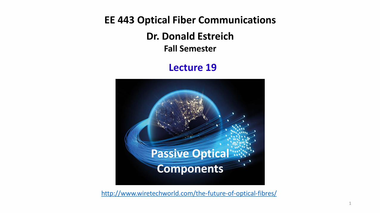
http://www.wiretechworld.com/the-future-of-optical-fibres/
EE 443 Optical Fiber Communications
Dr. Donald EstreichFall Semester
1
Lecture 19
Passive OpticalComponents
2
Summary of Lecture 18
1. Many factors can give rise to splice and connector loss: end gaps, non-concentric alignment, NA mismatch,, core mismatch, non-coaxiality, poor finish or dirt on end of fiber strands.
2. Two types of fiber splicing are used: fusion splicing and mechanical splicing3. Fusion splicing is welding of two fibers together with careful alignment
and use of an electric arc for heating.4. Fusion splicing equipment is available for field and laboratory use.5. Mechanical splicing commonly uses a V-groove for alignment of the fibers
and then a lid is tightly fastened to mechanically grip the fibers.6. Cleaving the ends of the fiber is a critical step in obtaining a good splice.7. Evaluation of splice quality: Use optical time domain reflectometry. This
is a measurement technique analogous to radar where a narrow lightpulse is sent down the fiber and a sensitive detector measures thereflected signals of the fiber under test.

3
Summary of Lecture 18 (continued)
8. In OTDR, connectors show typically show a reflection spike followed by astep down equal to the loss of the connector and splices show only astep down equal to the loss (no reflected pulse).
9. Many OFC connectors are available – connectors are for convenience andquick connect/disconnect and consist of a ferrule, a connector body,and a latching or coupling mechanism to hold the connection overtime without failure.
10. The most common types of connectors are the FC, ST, SC, LC and the MTPconnectors. While many others exist, these have been the most widely used.
11. Some connectors use fibers with an angled physical contact (APC) for mating to its companion connector.
4
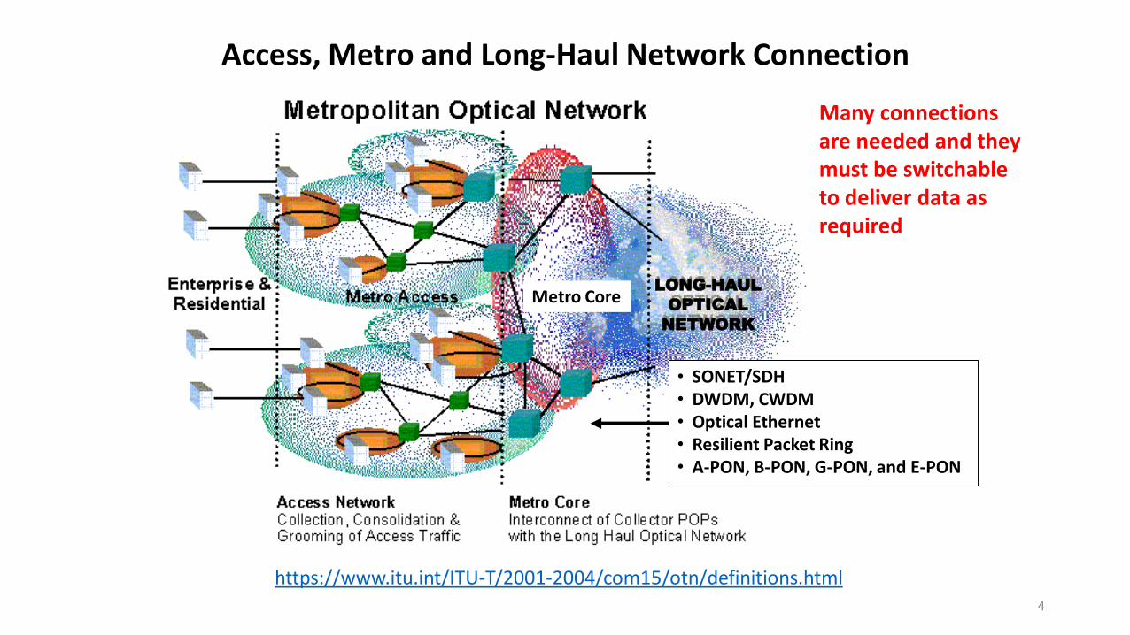
Access, Metro and Long-Haul Network Connection
https://www.itu.int/ITU-T/2001-2004/com15/otn/definitions.html
• SONET/SDH • DWDM, CWDM• Optical Ethernet • Resilient Packet Ring • A-PON, B-PON, G-PON, and E-PON
Metro CoreLONG-HAUL
OPTICAL
NETWORK
Many connectionsare needed and theymust be switchableto deliver data as required
5
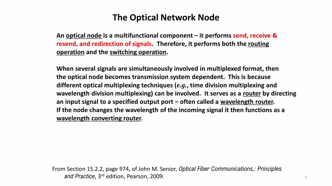
The Optical Network Node
An optical node is a multifunctional component – it performs send, receive &resend, and redirection of signals. Therefore, it performs both the routingoperation and the switching operation.
When several signals are simultaneously involved in multiplexed format, thenthe optical node becomes transmission system dependent. This is because different optical multiplexing techniques (e.g., time division multiplexing and wavelength division multiplexing) can be involved. It serves as a router by directingan input signal to a specified output port – often called a wavelength router. If the node changes the wavelength of the incoming signal it then functions as a wavelength converting router.
From Section 15.2.2, page 974, of John M. Senior, Optical Fiber Communications,: Principles
and Practice, 3rd edition, Pearson, 2009.

6
Four Functions of the Optical Node
Optical WavelengthDemultiplexer
12
1
2
12
1
2
Optical WavelengthMultiplexer
123
1Drop
234
4Add
Optical Add/DropMultiplexer
Optical 22Switch
12
34
13
24
From Figure 15.4, page 975, of John M. Senior, Optical Fiber Communications,: Principles
and Practice, 3rd edition, Pearson, 2009.

7
From Figure 15.4, page 975, of John M. Senior, Optical Fiber Communications,: Principles
and Practice, 3rd edition, Pearson, 2009.
Reconfigurable Optical Add/Drop Multiplexer
Optical Switch
DroppedChannels
AddedChannels
1 2 N 1 2 N
MU
X
DeM
UX
N components
ROADM
Combing an N-to-1 MUX, with a 1-to-N DeMUX and N N Optical Switch makes a ROADM.

8
Concept of the Cross Connect Switch
INP
UTS
1
1
OUTPUTS
2
3
32switches

9
Optical Cross Connect (OXC)
https://commons.wikimedia.org/wiki/File:Optical_Cross_Connect,_OXC.png
The OXC is for complex mesh topologies with large numbers of optical nodes.
10
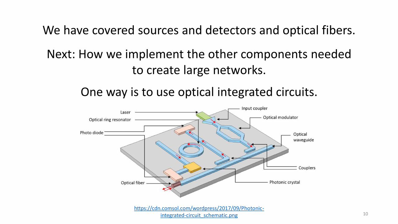
We have covered sources and detectors and optical fibers.
Next: How we implement the other components neededto create large networks.
One way is to use optical integrated circuits.
https://cdn.comsol.com/wordpress/2017/09/Photonic-integrated-circuit_schematic.png

11
Strip Waveguide StructuresPlanar and Strip Waveguide Structures
Titanium doped or proton bombarded
https://slideplayer.com/slide/6245103/
Propagation loss in Ti-doped LNbO3 is less than 0.2 dB/cm

12
https://picmagazine.net/article/105021/Thinking_Beyond_Conventional_Silicon_Photonics/feature
Photonic Integrated Circuit Waveguide Structures

13
Passive Y-Junction Beam Splitter
The fiber optic splitter is one of the most important
passive devices in the optical fiber link.
https://www.researchgate.net/figure/The-two-dimensional-Y-junction-dielectric-waveguide-used-in-the-analysis-The-main_fig12_3240569
W
W/2
W/2
n2
n2
n1
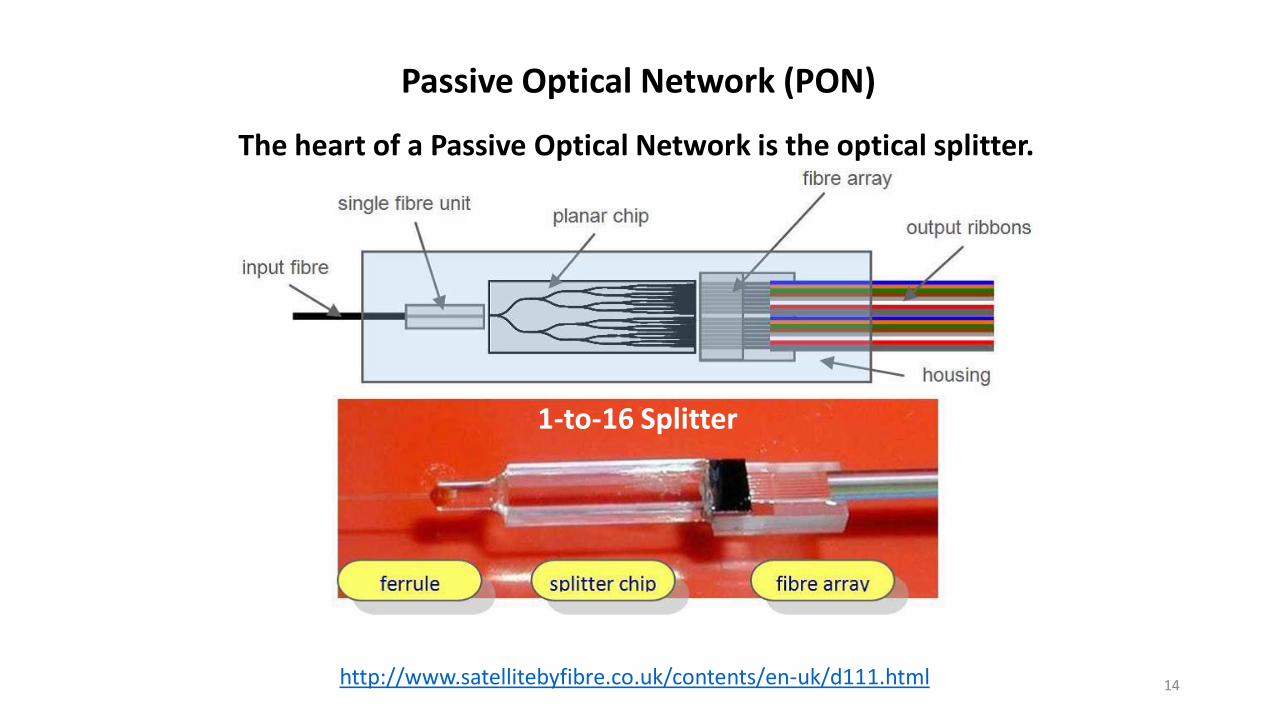
14http://www.satellitebyfibre.co.uk/contents/en-uk/d111.html
The heart of a Passive Optical Network is the optical splitter.
Passive Optical Network (PON)
1-to-16 Splitter

15
For the GPON, the optical splitter is essentially the heart of the network. The splitter allows a single port on the optical line terminal (OLT) to serve many optical network terminals (ONT).
Gigabit Passive Optical Network (GPON)
http://www.fiberlogs.fomsn.com/go4fiber/fiber-optic-news/what-is-gigabit-passive-optical-networks-gpon/
Point-to-Multipoint Network

16
An optical fiber coupler is a device that distributes light from a main fiber toone or more branch fibers.
Two types of optical fiber couplers:
A. Core interaction – core to core interaction either directly or through lenses or gratings
B. Surface interaction – through itssurface normal to its core axis by converting guided core modes to both cladding or refracted modes
From: Senior, Optical Fiber Communications, 3rd ed., 2009; Section 5.6, Fig. 5.26, p. 257
Optical Fiber Couplers

17
Splitter
Combiner
Coupler
Optical Fiber Coupler Types and Functions
From: Senior, Optical Fiber Communications, 3rd ed., 2009; Section 5.6, Fig. 5.27, p. 258

18
Optical Fiber Coupler Types and Functions
From: Senior, Optical Fiber Communications, 3rd ed., 2009; Section 5.6, Fig. 5.27, p. 258
WavelengthMultiplexer
WavelengthDemultiplexer
Star Coupler

19
https://www.brainkart.com/article/Fiber-couplers_13622/
https://www.fiber-mart.com/news/fiber-optic-couplers-and-splitters-tutorial-a-922.html
Optical Fiber Fused Biconical Taper Coupler
Four-port (or 2 2)

20
Reducing the Cladding Thickness of Core-to-Core Spacing

21
Coupling Between Closely Spaced Optical Waveguides
21 0
22 0
coupling coefficient
( ) ( )cos
( ) ( )sin
P z P z Cz
P z P z Cz
C
=
=
=
From: Saleh & Teich, Fundamentals of Photonics, J. Wiley & Sons, Inc.; Section 7.4B
Light scattering isphysical mechanismleading to coupling
Planar waveguides
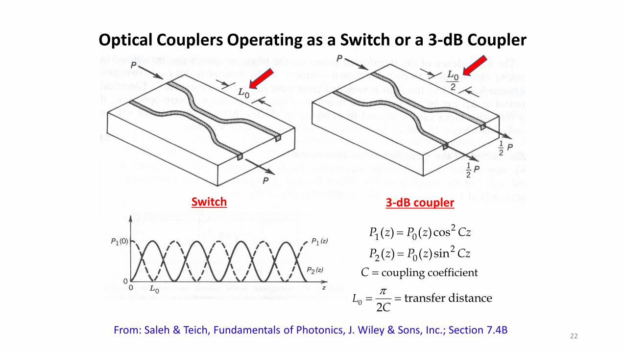
22From: Saleh & Teich, Fundamentals of Photonics, J. Wiley & Sons, Inc.; Section 7.4B
0
21 0
22 0
coupling coefficient
( ) ( )cos
( ) ( )sin
transfer distance2
L
P z P z Cz
P z P z Cz
C
C
=
=
=
= =
3-dB couplerSwitch
Optical Couplers Operating as a Switch or a 3-dB Coupler
23
Optical Fiber Fused Biconical Taper Coupler
1P
3P
4P
From: Senior, Optical Fiber Communications, 3rd ed., 2009; Section 5.6, p. 261-262
10
10
10
1
3 4
1
4
2
1
Excess loss 10 log (dB)
Insertion loss 10 log (dB)
Crosstalk 10 log (dB)
P
P P
P
P
P
P
= +
=
=
3
3 4
Split ratio 100%P
P P
= +
This is actuallya four-port
device
2P

24
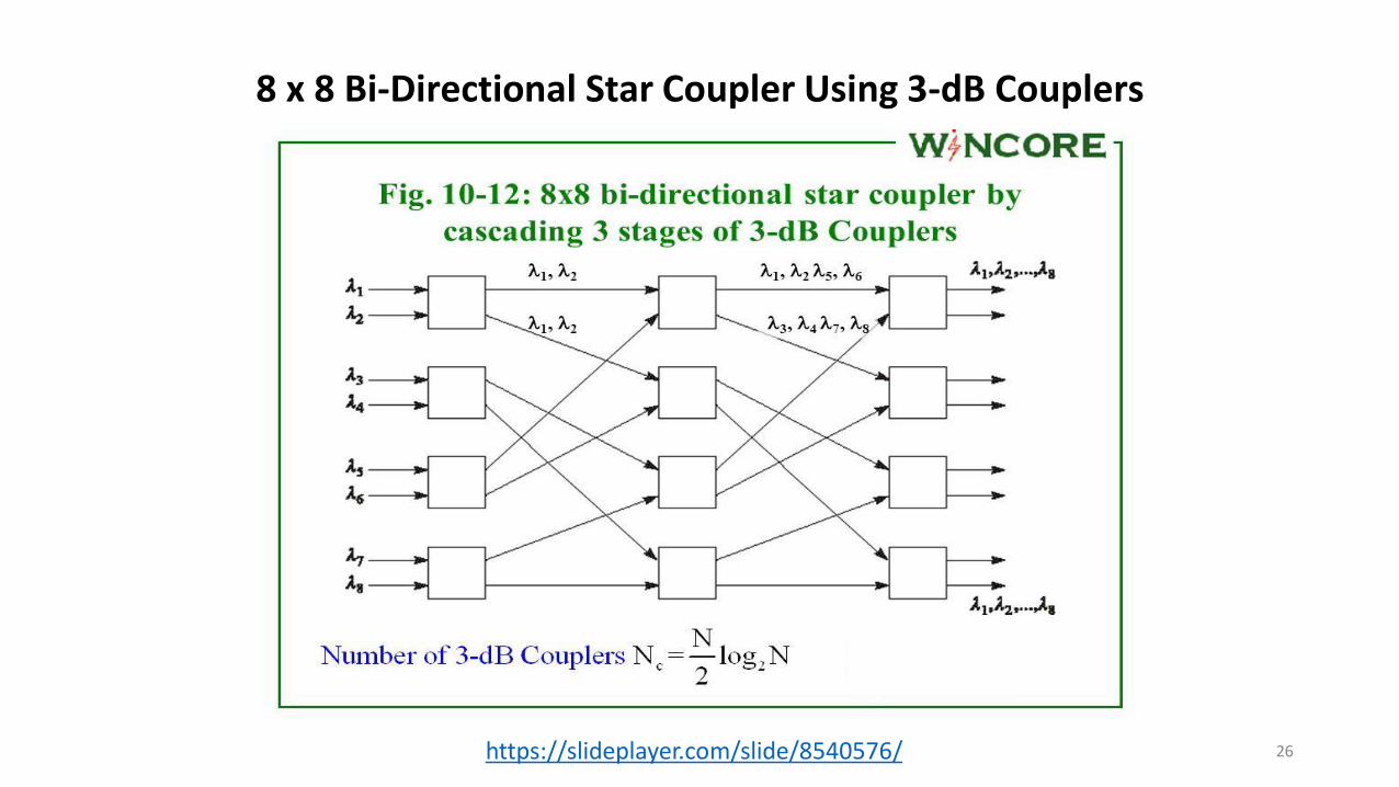
Optical Fiber Fused Biconical Taper 8 x 8 Star Coupler
25
https://www.fs.com/uk/how-do-different-fiber-optic-couplers-work-aid-405.html
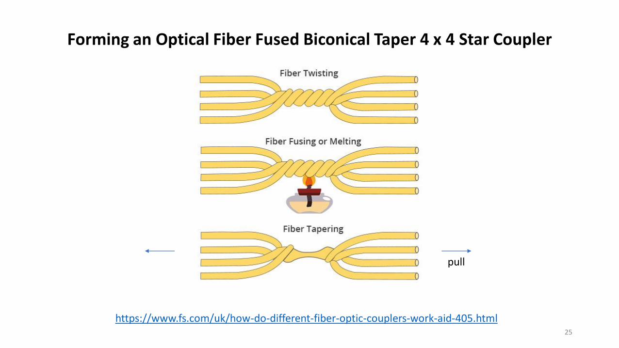
Forming an Optical Fiber Fused Biconical Taper 4 x 4 Star Coupler
pull
26https://slideplayer.com/slide/8540576/
8 x 8 Bi-Directional Star Coupler Using 3-dB Couplers

27
Electro-Optic Effects
https://en.wikipedia.org/wiki/Electro-optic_effect
An electro-optic effect is a change in the optical properties of a material in
response to an electric field that varies slowly compared with the
frequency of light.
a) Change of the absorption
• Electroabsorption: general change of the absorption constants
b) Change of the refractive index and permittivity
• Pockels effect (or linear electro-optic effect): change in the refractive index
linearly proportional to the electric field. Only certain crystalline solids show the
Pockels effect, as it requires lack of inversion symmetry
• Kerr effect (or quadratic electro-optic effect, QEO effect): change in the
refractive index proportional to the square of the electric field. All materials
display the Kerr effect, with varying magnitudes, but it is generally much weaker
than the Pockels effect

28
Certain materials change their optical properties when subjected to an
electric field E. This is caused by forces that distort the positions,
orientations or shapes of the molecular structure of the material.
The electro-optic effect is the change in the refractive index of the
Material from the application of a DC or slowly varying electric field.
An applied electric field to an anisotropic electro-optic material modifies
Its refractive index and thus its effect of polarized light.
E
n(E)
n
Pockels medium
E
n(E)
n
Kerr medium
From: B.E.A. Saleh and M.C. Teich, Fundamentals of Photonics, Wiley & Sons, Inc. 1991.
Electro-Optic Effect (continued)

29
Electro-Optic Effect (continued)
From: B.E.A. Saleh and M.C. Teich, Fundamentals of Photonics, Wiley & Sons, Inc. 1991.
The change in the refractive index is typically very small. However,
its effect on an optical wave propagating a distance much greater
than a wavelength can be very significant. Suppose the refractive
index increases by only 10-5, then an optical wave traveling 105
wavelengths will experience an added phase shift of 2 radians.
Materials which exhibit electro-optic effect can be modified by
deliberately applying a DC or slowly varying electric field by way of
electrodes placed strategically on the material’s surface. The next
slide presents an example.

30
Atomic Origin of Optical Nonlinearity
• Simple harmonic oscillator model (linear)
Electronic charge
Atomic nucleus
Restoring force
Linear polarization: parabolic potential
Lorentz-Drude
2nd order nonlinearity: Pockels media
3rd order nonlinearity: Kerr media
2nd order nonlinearity is absent in crystals
with centro-symmetry!
Induced dipole moment
Charge density Electron charge
Displacement
PED += 0
F = kx F = kx + k2x2 F = kx + k3x3
22
2 b
d r drm m r eE
dt dt + + =
eP n e r=
Damping Restoring Driving
Juejun Hu, MSEG 667 Nanophotonics: Materials and Devices, [email protected]

31
(a) A lens of material whose index of refraction can be varied thus
varying its focal length.
(b) A prism whose bean bending ability is controllable can function
as a scanning device.
(c) Light transmitted through a transparent plate of controllable
refractive index undergoes a controllable phase shift – it can
be used as a phase modulator.
(d) An anisotropic crystal with variable refractive index can be used
as a controllable wave retarder – used to change the polarization
of the light beam – polarizer.
(e) A wave retarder placed between two crossed polarizers gives rise
to transmitted light whose intensity is dependent upon the phase
retardation allows for a device whose transmittance is voltage
controllable – thereby making an optical intensity modulator or
a switch.
Some Applications of EO Devices
From: B.E.A. Saleh and M.C. Teich, Fundamentals of Photonics, Wiley & Sons, Inc. 1991.

32
Electro-Optic Effect (continued)
Taylor’s series expansion:
https://slideplayer.com/slide/6245103/
633 21 1
2 2( )n E n r n sE E= − − −
6331
2( )n E n r n E= −
21
2( )n E n sE= −

33
Pockels Effect
Schematic diagram of the operation of a modulator based
on the electro-optic effect. In this configuration, the voltage is
applied parallel to the direction of light propagation.
https://pe2bz.philpem.me.uk/Lights/-%20Laser/Info-999-LaserCourse/C04-M07-ElectroOptic+AcoustoOpticDevices/mod04_07.htm
6331
2( )n E n r n E= −
34From: B.E.A. Saleh and M.C. Teich, Fundamentals of Photonics, Wiley & Sons, Inc. 1991; p. 701
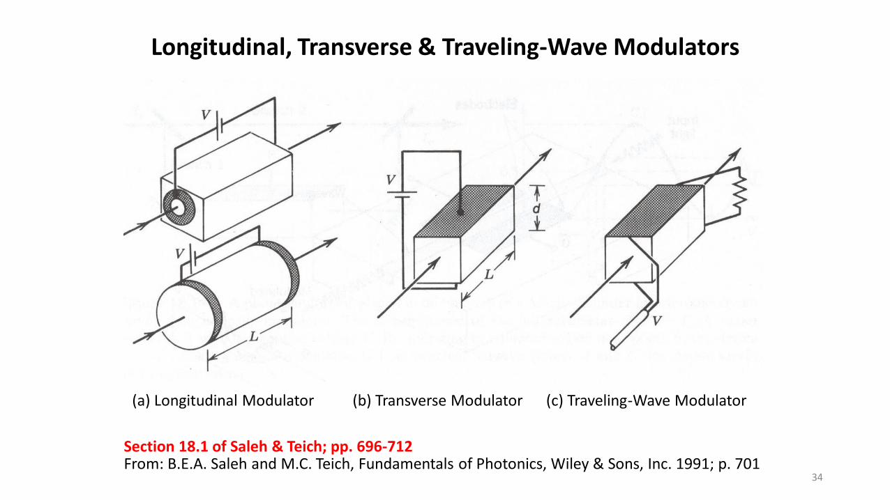
Longitudinal, Transverse & Traveling-Wave Modulators
(a) Longitudinal Modulator (b) Transverse Modulator (c) Traveling-Wave Modulator
Section 18.1 of Saleh & Teich; pp. 696-712

35
Phase Modulators
When a beam of light traverses a Pockels cell of length L with an electric
field E is applied, it exhibits a phase shift (wavelength 0)
We can write the phase as
where
The electric field is applied across the cell with voltage V over distance d.
Hence, E = V /d .
Traveling Wave:
0
0
2 ( )( )
n E Ln E k L
= =
630
0
3r n LV
d
− = =
0
0
2 nL
=
From: B.E.A. Saleh and M.C. Teich, Fundamentals of Photonics, Wiley & Sons, Inc. 1991;. Sect. 18.1B
Section 18.1 of Saleh & Teich; pp. 696-712
0 0( , ) exp ;V
t L A j tV
= − − +
0
633
dV
L r n
=
V
L
d

36
Phase Modulators (continued)
From: B.E.A. Saleh and M.C. Teich, Fundamentals of Photonics, Wiley & Sons, Inc. 1991;. Sect. 18.1B
Section 18.1 of Saleh & Teich; pp. 696-712
V
V
00
633
where
V
V
dV
L r n
= −
=
The parameter V is known as the half-wave voltage, and it is the applied voltage at which the phase shift changes by radians. Note that this is a linear relationship between optical phase shift and applied voltage.
The electric field may be applied either perpendicular (transverse) to the direction of light propagation or parallel (longitudinal) to that direction.

37
Phase Modulators (Traveling Wave Effect)
From: B.E.A. Saleh and M.C. Teich, Fundamentals of Photonics, Wiley & Sons, Inc. 1991;. Sect. 18.1B
Section 18.1 of Saleh & Teich; pp. 696-712
How fast a phase modulator can be operated depends upon the capacitanceof the device and the transit time of the light through the modulator. If the
electric field E(t) varies significantly over the transit time T of the light, thenthe traveling optical wave will be subjected to different electric fields during itstravel through the device. A traveling wave electrode structure which matches the velocity of the light is one solution to this issue.
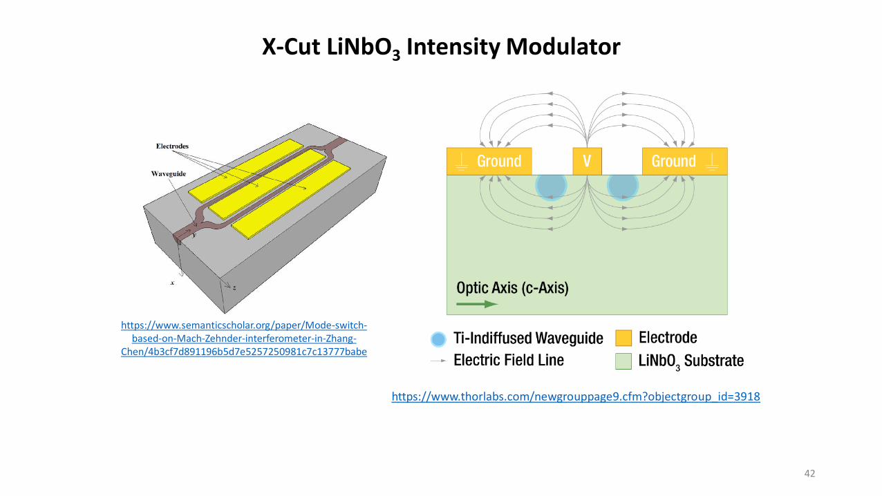
Practical phase modulators operate from hundreds of megahertz to several gigahertz. A commonly used material for such modulators is lithium niobate(LiNbO3). An optical waveguide for defining the path if the light signal is todope the LiNbO3 with titanium (to increase the refractive index). Another wayto form the waveguide is to use proton ion bombardment.
See the next slide for an illustration of this.

38
Integrated-Optical Phase Modulator (Using E-O Effect)
From: B.E.A. Saleh and M.C. Teich, Fundamentals of Photonics, Wiley & Sons, Inc. 1991; p. 702Section 18.1 of Saleh & Teich; pp. 696-712
Such modulators have been operatedat speeds in excess of100 GHz.

39
The Kerr electro-optic effect, or DC Kerr effect, occurs when a slowly
varying external electric field is applied (e.g., a voltage between two
electrodes) across the sample material, the sample becomes
birefringent. Thus, the material exhibits different indices of refraction
for light polarized parallel to or perpendicular to the applied field. The
difference in index of refraction, n, is given by
where is the wavelength of the light, K is the Kerr constant, and E is
the strength of the electric field. This difference in index of refraction
causes the material to act like a waveplate when light is incident on it
in a direction perpendicular to the electric field. If the material is
placed between two "crossed" (perpendicular) linear polarizers, no
light will be transmitted when the electric field is turned off, while
nearly all the light will be transmitted at some optimum value of the
electric field.
2n KE =
https://en.wikipedia.org/wiki/Kerr_effect
Kerr Electro-Optic Effect

40From: B.E.A. Saleh and M.C. Teich, Fundamentals of Photonics, Wiley & Sons, Inc. 1991; p. 703
A Phase Modulator Within a Mach-Zehnder Interferometer
Section 18.1 of Saleh & Teich; pp. 696-712
Transmittance: 02( ) cos2 2
VT V
V
= −
( )T V
V

41From: B.E.A. Saleh and M.C. Teich, Fundamentals of Photonics, Wiley & Sons, Inc. 1991; p. 704Section 18.1 of Saleh & Teich; pp. 696-712
Integrated-Optical Intensity Modulator (IM) For Switching
42
X-Cut LiNbO3 Intensity Modulator
https://www.semanticscholar.org/paper/Mode-switch-based-on-Mach-Zehnder-interferometer-in-Zhang-
Chen/4b3cf7d891196b5d7e5257250981c7c13777babe
https://www.thorlabs.com/newgrouppage9.cfm?objectgroup_id=3918

43https://www.slideshare.net/SureshJat5/external-modulators
Driving an Integrated-Optical Mach-Zehnder Modulator

44From: B.E.A. Saleh and M.C. Teich, Fundamentals of Photonics, Wiley & Sons, Inc. 1991; p. 704Section 18.1 of Saleh & Teich; pp. 696-712
Intensity Modulator Using Pockels Cell Between Two Polarizers
t
Transmittance: 02( ) sin2 2
VT V
V
= −

45
Modulation Characteristic of an External Intensity ModulatorShowing output light-wave signal from input electrical signal
From: Papen & Blahut, Lightwave Communications, Cambridge University Press,2019
V
2cos2
V
V
Figure 7.18 (p. 328)
Input electrical signal
Output light-wavepowerNonlinear
Operation
46From: Papen & Blahut, Lightwave Communications, Cambridge University Press,2019
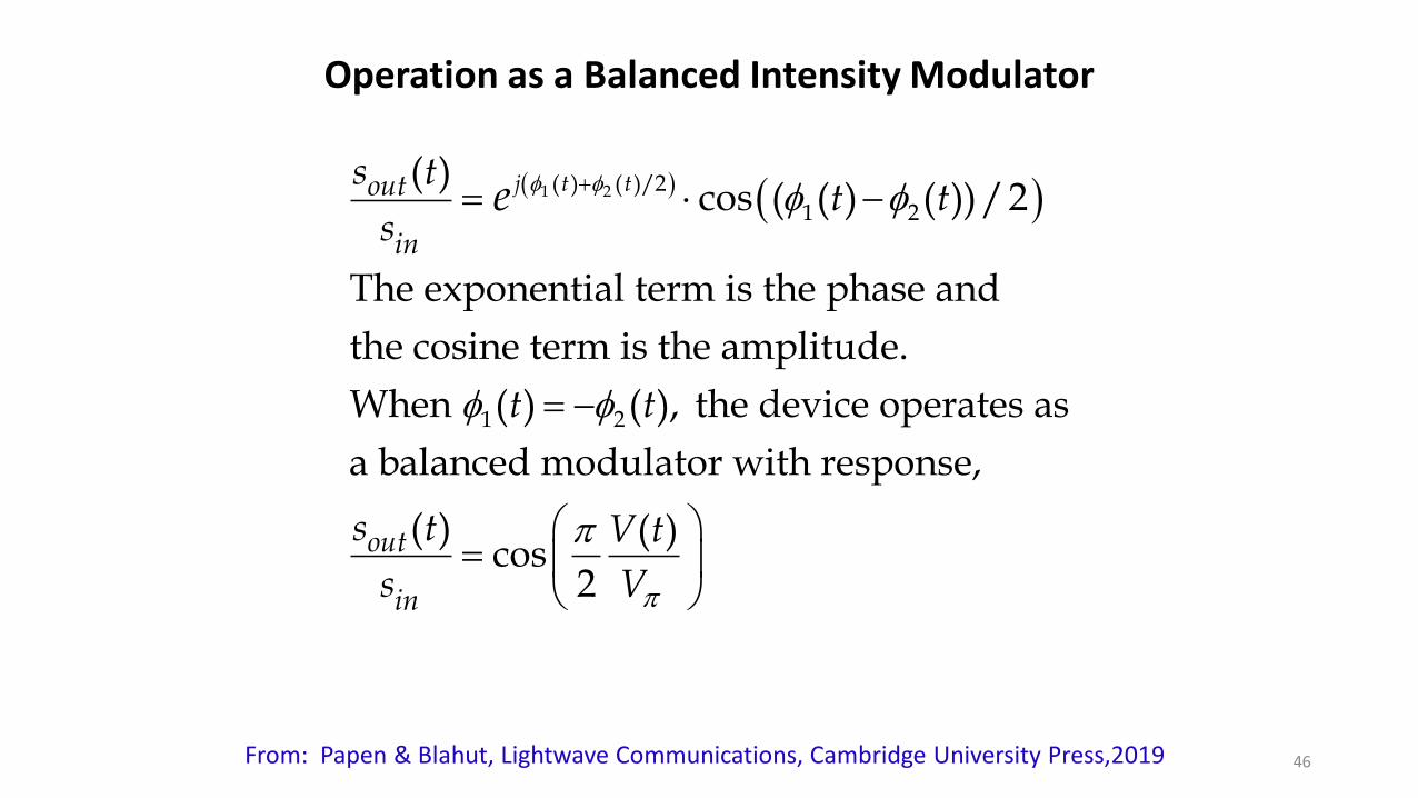
Operation as a Balanced Intensity Modulator
( ) ( )1 2( ) ( )/2
1 2
1 2
( )cos ( ( ) ( ))/2
The exponential term is the phase and
the cosine term is the amplitude.
When ( ) ( ), the device operates as
a balanced modulator with response,
( )
j t tout
in
out
in
s tt t
s
t t
s t
s
e
+= −
= −
( )cos
2
V t
V
=

47From: B.E.A. Saleh and M.C. Teich, Fundamentals of Photonics, Wiley & Sons, Inc. 1991; p. 706Section 18.1 of Saleh & Teich; pp. 696-712
An Electro-Optic Prism & An Electro-Optic Double Prism
3 31 1
2 2
Vn n n
dr rE = = − −=

48
https://medium.com/@stangarfield/100-questions-answers-on-collaboration-communities-5ceed474dca9

49
PONPassive Optical Network: A point-to-multipoint, passive fiber network architecture in which a single fiber utilizes optical splitters to serve multiple premises.----------------------------------APONATM PON: The first type of PON standard, based on ATM (Asynchronous Transfer Mode) which is a protocol in telecom networkingBPONBroadband PON: Coming after APON, BPON supports WDM, higher upstream bandwidth, and a standard management interface that enabled shared vendor networksGPONGigabit PON: Based on the previous PON types, GPON supports higher data rates and increased security, and has been deployed around the world by major telecom operators.EPONEthernet PON: EPON is part of IEEE standard Ethernet for 1/1 Gbit/s, 10/1 Gbit/s, and 10/10 Gbit/s. With over 40 million installed EPON ports, it is the most widely deployed PON technology worldwide. Cable operators are utilizing EPON for business services as part of the DOCSIS initiative.10G-PONXG-PON: Is a new standard from 2010 that enables the delivery of 10Gbit/s speeds using PON network architecture. As the next generation of GPON, devices operate on the same network as GPON devices.
http://www.m2optics.com/blog/bid/52030/Passive-Optical-Networks-PON-Commonly-Used-Terms-Definitions
Passive Optical Networks