pc87303 superi/o(tm) sidewinder lite floppy disk...
TRANSCRIPT

TL/C/12074
PC
87303V
UL
SuperI/
OSid
ew
inderLite
Flo
ppy
Dis
kC
ontro
ller,
Keyboard
Contro
ller,
Real-T
ime
Clo
ck,D
ualU
AR
Ts,IE
EE
1284
Para
llelPort,
and
IDE
Inte
rface
PRELIMINARYFebruary 1995
PC87303VUL SuperI/OTM Sidewinder LiteFloppy Disk Controller, Keyboard Controller,Real-Time Clock, Dual UARTs, IEEE 1284 Parallel Port,and IDE Interface
General DescriptionThe PC87303VUL is a single chip solution incorporating a
Keyboard and PS/2É Mouse Controller (KBC), Real Time
Clock (RTC) and most commonly used I/O peripherals in
ISA, EISA and MicroChannelÉ based computers. In addition
to the KBC and RTC, a Floppy Disk Controller (FDC), two
full featured UARTs, an IEEE 1284 compatible parallel port
and all the necessary control logic for an IDE interface pro-
vides support for most commonly used I/O peripherals.
Standard PC-ATÉ address decoding for all the peripherals,
a set of configuration registers, and two user selectable chip
selects are also implemented in this highly integrated mem-
ber of the SuperI/O family. The advanced features and high
integration of the PC87303 result in several benefits for low
cost, high performance systems. Printed circuit board space
savings, fewer components on the motherboard and com-
patibility with the latest industry standard peripherals are
only a few of the benefits of using a PC87303.
The KBC is fully software compatible with the 8042AH mi-
crocontroller. It contains system timing, control logic, cus-
tom ROM program memory, RAM data memory and 18 pro-
grammable I/O lines necessary to implement dedicated
control functions. It is an efficient controller which uses pre-
dominantly singlebyte instructionswith support for binaryand
BCD arithmetic and extensive bit handling capabilities.
(Continued)
FeaturesY The Floppy Disk Controller:
Ð Software compatible with the DP8477, the 765A and
the N82077
Ð 16-byte FIFO (disabled by default)
Ð Burst and Non-Burst modes
Ð Perpendicular Recording drive support
Ð High performance internal analog data separator
(no external filter components required)
Ð Low power CMOS with power-down mode
Ð Automatic media-sense support with full IBM TDR
(Tape Drive Register) implementation for PC-AT and
PS/2 floppy drive typesY The Keyboard Controller:
Ð 8042AH and PC87911 software compatible
Ð 8-bit Microcomputer with 2 kbytes custom ROM and
256 bytes data RAM
Ð Asynchronous access to two data registers and one
status register during normal operation
Ð Dedicated open drain outputs for keyboard controller
application
Ð Supports both interrupt and polling
Ð Supports DMA handshake
Ð 18 programmable I/O pins
Ð 4 dedicated open-drain outputs
Ð 8-bit Timer/Counter
Ð Binary and BCD arithmetic
Ð Expandable I/O (Continued)
Block Diagram
TL/C/12074–1
TRI-STATEÉ is a registered trademark of National Semiconductor Corporation.
SuperI/OTM is a trademark of National Semiconductor Corporation.
MicroChannelÉ, PC-ATÉ and PS/2É are registered trademarks of International Business Machines Corporation.
C1995 National Semiconductor Corporation RRD-B30M75/Printed in U. S. A.

General Description (Continued)
The RTC is a low-power design that provides a time-of-day
clock, a 100-year calendar, several alarm features and 242
bytes of general purpose RAM. An external battery is used
to maintain the time and contents of the general purpose
RAM, when power is removed from the PC87303. The
PC87303 RTC is compatible with the DS1287 and
MC146818 RTC devices.
The PC87303 FDC uses a high performance analog data
separator eliminating need for any external filter compo-
nents. The FDC is fully compatible with the PC8477 and
incorporates a superset of DP8473, NEC mPD765 and
N82077 floppy disk controller function. All popular 5.25×and 3.5× floppy drives, including 2.88 MB 3.5× floppy drive,
are supported. Full TDR support for PC-AT and PS/2 floppy
drive types is also provided.
The two UARTs are fully NS16450 and NS16550 compati-
ble.
The parallel port is fully IEEE 1284 level 2 compatible. The
SPP (Standard Parallel Port) is fully compatible with ISA,
EISA and MicroChannel parallel ports. In addition to the
SPP, EPP (Enhanced Parallel Port) and ECP (Extended Ca-
pabilities Port) modes are supported by the parallel port.
All IDE control signals with DMA support, including support
for Type F DMA are provided by the PC87303. Only external
signal buffers are required to implement a complete IDE
interface.
A set of fourteen configuration registers are provided to
control various functions of the PC87303. These registers
are accessed using two 8-bit wide index and data registers.
The ISA I/O address of the register pair can be relocated
using a power-up strapping option.
Two general purpose user programmable chip selects are
available. These chip selects can be used to decode game
port addresses.
Features (Continued)Y The Real-Time Clock:
Ð DS1287, MC146818 and PC87911 compatible
Ð 242 bytes battery backed-up CMOS RAM in two
banks
Ð Selective lock mechanism locks any half of the RTC
RAM
Ð Calendar in days, day of the week, months and
years with automatic leap-year adjustment
Ð Time of day in seconds, minutes and hours:
Ð12 or 24 hour format
Ð Optional daylight savings adjustment
Ð BCD or binary format for time keeping
Ð Three individually maskable interrupt event flags:
ÐPeriodic rates from 122 ms to 500 ms
ÐTime-of-day alarm once per second to once per
day
Ð Separate battery pin, 2.4V operation
Ð 2 mA power consumption
Ð Double buffer time registersY The UARTs:
Ð Software compatible with the PC16550A and
NS16450Y Parallel Port:
Ð EPP, ECP compatible with ECP level 2 support
Ð ISA, EISA and MicroChannel compatible architecture
Ð Bi-directional data transfer under software or hard-
ware control
Ð Includes protection circuit to prevent damage to the
parallel port when a connected printer is powered up
or is operated at a higher voltageY IDE:
Ð All IDE control signals, with DMA and support for
Type F DMA. Only external signal buffers are re-
quired to implement the full IDE interfaceY The Programmable Chip Selects:
Ð Separater pins for two user programmable chip se-
lect decoders provide ability to control a game portY The address decoder:
Ð Provides selection of all primary and secondary ISA
addresses including COM1–4Y General:
Ð Low power CMOS technology
Ð Ability to stop clocks to all modules
Ð The PC87303 is a drop-in replacement for the
PC87323VUL
Ð Reduced pin leakage current
Ð Special configuration register for power-down
Ð Disable bit for RTC
Ð 160-pin PQFP package
2

Table of Contents1.0 PIN DESCRIPTIONÀÀÀÀÀÀÀÀÀÀÀÀÀÀÀÀÀÀÀÀÀÀÀÀÀÀÀÀÀÀ10
2.0 CONFIGURATION REGISTERS ÀÀÀÀÀÀÀÀÀÀÀÀÀÀÀÀÀÀ16
2.1 OverviewÀÀÀÀÀÀÀÀÀÀÀÀÀÀÀÀÀÀÀÀÀÀÀÀÀÀÀÀÀÀÀÀÀÀÀÀÀ16
2.2 Software ConfigurationÀÀÀÀÀÀÀÀÀÀÀÀÀÀÀÀÀÀÀÀÀÀÀÀÀ16
2.3 Hardware Configuration ÀÀÀÀÀÀÀÀÀÀÀÀÀÀÀÀÀÀÀÀÀÀÀÀ19
2.4 Index and Data RegistersÀÀÀÀÀÀÀÀÀÀÀÀÀÀÀÀÀÀÀÀÀÀÀ19
2.5 Base Configuration Registers ÀÀÀÀÀÀÀÀÀÀÀÀÀÀÀÀÀÀÀ21
2.5.1 Function Enable RegisterÀÀÀÀÀÀÀÀÀÀÀÀÀÀÀÀÀÀ21
2.5.2 Function Address RegisterÀÀÀÀÀÀÀÀÀÀÀÀÀÀÀÀÀ22
2.5.3 Power and Test Register ÀÀÀÀÀÀÀÀÀÀÀÀÀÀÀÀÀÀ22
2.5.4 Function Control Register ÀÀÀÀÀÀÀÀÀÀÀÀÀÀÀÀÀ23
2.5.5 Printer Control Register ÀÀÀÀÀÀÀÀÀÀÀÀÀÀÀÀÀÀÀ23
2.5.6 KBC and BTC Control Register ÀÀÀÀÀÀÀÀÀÀÀÀÀ24
2.5.7 Power Management Control Register ÀÀÀÀÀÀÀ24
2.5.8 Tape, UARTs and Parallel Port Configuration
RegisterÀÀÀÀÀÀÀÀÀÀÀÀÀÀÀÀÀÀÀÀÀÀÀÀÀÀÀÀÀÀÀÀÀ25
2.5.9 SIO Identification Register ÀÀÀÀÀÀÀÀÀÀÀÀÀÀÀÀÀ25
2.5.10 Advanced SIO Configuration Register ÀÀÀÀÀÀ25
2.5.11 Chip Select 0 Configuration Register 0 ÀÀÀÀÀ25
2.5.12 Chip Select 0 Configuration Register 1 ÀÀÀÀÀ25
2.5.13 Chip Select 1 Configuration Register 0 ÀÀÀÀÀ26
2.5.14 Chip Select 1 Configuration Register 1 ÀÀÀÀÀ26
2.6 Power-Down Options ÀÀÀÀÀÀÀÀÀÀÀÀÀÀÀÀÀÀÀÀÀÀÀÀÀÀ26
2.7 Power-Up Procedure and Considerations ÀÀÀÀÀÀÀÀÀ26
2.7.1 Crystal StabilizationÀÀÀÀÀÀÀÀÀÀÀÀÀÀÀÀÀÀÀÀÀÀÀ26
2.7.2 UART Power-Up ÀÀÀÀÀÀÀÀÀÀÀÀÀÀÀÀÀÀÀÀÀÀÀÀÀ26
2.7.3 FDC Power-UpÀÀÀÀÀÀÀÀÀÀÀÀÀÀÀÀÀÀÀÀÀÀÀÀÀÀÀ26
3.0 FDC REGISTER DESCRIPTION ÀÀÀÀÀÀÀÀÀÀÀÀÀÀÀÀÀÀ27
3.1 FDC Control Registers ÀÀÀÀÀÀÀÀÀÀÀÀÀÀÀÀÀÀÀÀÀÀÀÀÀ28
3.1.1 Status Register A (SRA)ÀÀÀÀÀÀÀÀÀÀÀÀÀÀÀÀÀÀÀ28
3.1.2 Status Register B (SRB)ÀÀÀÀÀÀÀÀÀÀÀÀÀÀÀÀÀÀÀ28
3.1.3 Digital Output Register (DOR) ÀÀÀÀÀÀÀÀÀÀÀÀÀÀ29
3.1.4 Tape Drive Register (TDR)ÀÀÀÀÀÀÀÀÀÀÀÀÀÀÀÀÀ29
3.1.5 Main Status Register (MSR) ÀÀÀÀÀÀÀÀÀÀÀÀÀÀÀ31
3.1.6 Data Rate Select Register (DSR) ÀÀÀÀÀÀÀÀÀÀÀ31
3.1.7 Data Register (FIFO)ÀÀÀÀÀÀÀÀÀÀÀÀÀÀÀÀÀÀÀÀÀÀ32
3.1.8 Digital Input Register (DIR) ÀÀÀÀÀÀÀÀÀÀÀÀÀÀÀÀ32
3.1.9 Configuration Control Register (CCR) ÀÀÀÀÀÀÀ33
3.2 Result Phase Status Registers ÀÀÀÀÀÀÀÀÀÀÀÀÀÀÀÀÀÀ33
3.2.1 Status Register 0 (ST0) ÀÀÀÀÀÀÀÀÀÀÀÀÀÀÀÀÀÀÀ33
3.2.2 Status Register 1 (ST1) ÀÀÀÀÀÀÀÀÀÀÀÀÀÀÀÀÀÀÀ33
3.2.3 Status Register 2 (ST2) ÀÀÀÀÀÀÀÀÀÀÀÀÀÀÀÀÀÀÀ34
3.2.4 Status Register 3 (ST3) ÀÀÀÀÀÀÀÀÀÀÀÀÀÀÀÀÀÀÀ34
4.0 FDC COMMAND SET DESCRIPTION ÀÀÀÀÀÀÀÀÀÀÀÀÀ34
4.1 Command Descriptions ÀÀÀÀÀÀÀÀÀÀÀÀÀÀÀÀÀÀÀÀÀÀÀÀ34
4.1.1 Configure CommandÀÀÀÀÀÀÀÀÀÀÀÀÀÀÀÀÀÀÀÀÀÀ34
4.1.2 Dumpreg Command ÀÀÀÀÀÀÀÀÀÀÀÀÀÀÀÀÀÀÀÀÀÀ35
4.1.3 Format Track CommandÀÀÀÀÀÀÀÀÀÀÀÀÀÀÀÀÀÀÀ35
4.1.4 Invalid CommandÀÀÀÀÀÀÀÀÀÀÀÀÀÀÀÀÀÀÀÀÀÀÀÀÀ38
4.1.5 Lock Command ÀÀÀÀÀÀÀÀÀÀÀÀÀÀÀÀÀÀÀÀÀÀÀÀÀÀ38
4.1.6 Mode Command ÀÀÀÀÀÀÀÀÀÀÀÀÀÀÀÀÀÀÀÀÀÀÀÀÀ38
4.1.7 NSC Command ÀÀÀÀÀÀÀÀÀÀÀÀÀÀÀÀÀÀÀÀÀÀÀÀÀÀ39
4.1.8 Perpendicular Mode CommandÀÀÀÀÀÀÀÀÀÀÀÀÀ40
4.1.9 Read Data Command ÀÀÀÀÀÀÀÀÀÀÀÀÀÀÀÀÀÀÀÀÀ41
4.1.10 Read Deleted Data Command ÀÀÀÀÀÀÀÀÀÀÀÀ43
4.1.11 Read ID Command ÀÀÀÀÀÀÀÀÀÀÀÀÀÀÀÀÀÀÀÀÀÀ43
4.1.12 Read A Track Command ÀÀÀÀÀÀÀÀÀÀÀÀÀÀÀÀÀ43
4.1.13 Recalibrate Command ÀÀÀÀÀÀÀÀÀÀÀÀÀÀÀÀÀÀÀ44
4.1.14 Relative Seek Command ÀÀÀÀÀÀÀÀÀÀÀÀÀÀÀÀÀ44
4.1.15 Scan CommandsÀÀÀÀÀÀÀÀÀÀÀÀÀÀÀÀÀÀÀÀÀÀÀÀ45
4.1.16 Seek CommandÀÀÀÀÀÀÀÀÀÀÀÀÀÀÀÀÀÀÀÀÀÀÀÀÀ46
4.1.17 Sense Drive Status Command ÀÀÀÀÀÀÀÀÀÀÀÀ46
4.1.18 Sense Interrupt CommandÀÀÀÀÀÀÀÀÀÀÀÀÀÀÀÀ46
4.1.19 Set Track CommandÀÀÀÀÀÀÀÀÀÀÀÀÀÀÀÀÀÀÀÀÀ47
4.1.20 Specify CommandÀÀÀÀÀÀÀÀÀÀÀÀÀÀÀÀÀÀÀÀÀÀÀ47
4.1.21 Verify Command ÀÀÀÀÀÀÀÀÀÀÀÀÀÀÀÀÀÀÀÀÀÀÀÀ48
4.1.22 Version CommandÀÀÀÀÀÀÀÀÀÀÀÀÀÀÀÀÀÀÀÀÀÀÀ49
4.1.23 Write Data Command ÀÀÀÀÀÀÀÀÀÀÀÀÀÀÀÀÀÀÀÀ50
4.1.24 Write Deleted Data Command ÀÀÀÀÀÀÀÀÀÀÀÀ50
4.2 Command Set Summary ÀÀÀÀÀÀÀÀÀÀÀÀÀÀÀÀÀÀÀÀÀÀÀ51
4.3 Mnemonic Definitions for FDC CommandsÀÀÀÀÀÀÀÀ56
5.0 FDC FUNCTIONAL DESCRIPTION ÀÀÀÀÀÀÀÀÀÀÀÀÀÀÀ57
5.1 Microprocessor Interface ÀÀÀÀÀÀÀÀÀÀÀÀÀÀÀÀÀÀÀÀÀÀÀ57
5.2 Modes of Operation ÀÀÀÀÀÀÀÀÀÀÀÀÀÀÀÀÀÀÀÀÀÀÀÀÀÀÀ57
5.3 Controller Phases ÀÀÀÀÀÀÀÀÀÀÀÀÀÀÀÀÀÀÀÀÀÀÀÀÀÀÀÀÀ57
5.3.1 Command Phase ÀÀÀÀÀÀÀÀÀÀÀÀÀÀÀÀÀÀÀÀÀÀÀÀÀ57
5.3.2 Execution Phase ÀÀÀÀÀÀÀÀÀÀÀÀÀÀÀÀÀÀÀÀÀÀÀÀÀ57
5.3.2.1 DMA ModeÐFIFO DisabledÀÀÀÀÀÀÀÀÀ58
5.3.2.2 DMA ModeÐFIFO Enabled ÀÀÀÀÀÀÀÀÀ58
5.3.2.3 Interrupt ModeÐFIFO DisabledÀÀÀÀÀÀ59
5.3.2.4 Interrupt ModeÐFIFO Enabled ÀÀÀÀÀÀ59
5.3.2.5 Software Polling ÀÀÀÀÀÀÀÀÀÀÀÀÀÀÀÀÀÀÀ59
5.3.3 Result Phase ÀÀÀÀÀÀÀÀÀÀÀÀÀÀÀÀÀÀÀÀÀÀÀÀÀÀÀÀ59
5.3.4 Idle PhaseÀÀÀÀÀÀÀÀÀÀÀÀÀÀÀÀÀÀÀÀÀÀÀÀÀÀÀÀÀÀÀ59
5.3.5 Drive Polling Phase ÀÀÀÀÀÀÀÀÀÀÀÀÀÀÀÀÀÀÀÀÀÀÀ60
5.4 Data SeparatorÀÀÀÀÀÀÀÀÀÀÀÀÀÀÀÀÀÀÀÀÀÀÀÀÀÀÀÀÀÀÀÀ60
5.5 Crystal Oscillator ÀÀÀÀÀÀÀÀÀÀÀÀÀÀÀÀÀÀÀÀÀÀÀÀÀÀÀÀÀÀ62
5.6 Perpendicular Recording ModeÀÀÀÀÀÀÀÀÀÀÀÀÀÀÀÀÀÀ62
5.7 Data Rate Selection ÀÀÀÀÀÀÀÀÀÀÀÀÀÀÀÀÀÀÀÀÀÀÀÀÀÀÀ64
5.8 Write Precompensation ÀÀÀÀÀÀÀÀÀÀÀÀÀÀÀÀÀÀÀÀÀÀÀÀ64
5.9 FDC Low Power Mode Logic ÀÀÀÀÀÀÀÀÀÀÀÀÀÀÀÀÀÀÀÀ64
5.10 Reset Operation ÀÀÀÀÀÀÀÀÀÀÀÀÀÀÀÀÀÀÀÀÀÀÀÀÀÀÀÀÀ64
3

Table of Contents (Continued)
6.0 SERIAL PORTS ÀÀÀÀÀÀÀÀÀÀÀÀÀÀÀÀÀÀÀÀÀÀÀÀÀÀÀÀÀÀÀÀ65
6.1 Serial Port Registers ÀÀÀÀÀÀÀÀÀÀÀÀÀÀÀÀÀÀÀÀÀÀÀÀÀÀÀ65
6.2 Line Control Register ÀÀÀÀÀÀÀÀÀÀÀÀÀÀÀÀÀÀÀÀÀÀÀÀÀÀ65
6.3 Programmable Baud Rate GeneratorÀÀÀÀÀÀÀÀÀÀÀÀÀ68
6.4 Line Status Register ÀÀÀÀÀÀÀÀÀÀÀÀÀÀÀÀÀÀÀÀÀÀÀÀÀÀÀ69
6.5 FIFO Control RegisterÀÀÀÀÀÀÀÀÀÀÀÀÀÀÀÀÀÀÀÀÀÀÀÀÀÀ70
6.6 Interrupt Identification RegisterÀÀÀÀÀÀÀÀÀÀÀÀÀÀÀÀÀÀ70
6.7 Interrupt Enable Register ÀÀÀÀÀÀÀÀÀÀÀÀÀÀÀÀÀÀÀÀÀÀÀ70
6.8 MODEM Control Register ÀÀÀÀÀÀÀÀÀÀÀÀÀÀÀÀÀÀÀÀÀÀ70
6.9 MODEM Status Register ÀÀÀÀÀÀÀÀÀÀÀÀÀÀÀÀÀÀÀÀÀÀÀ72
6.10 Scratchpad Register ÀÀÀÀÀÀÀÀÀÀÀÀÀÀÀÀÀÀÀÀÀÀÀÀÀÀ72
7.0 PARALLEL PORT ÀÀÀÀÀÀÀÀÀÀÀÀÀÀÀÀÀÀÀÀÀÀÀÀÀÀÀÀÀÀ72
7.1 Introduction ÀÀÀÀÀÀÀÀÀÀÀÀÀÀÀÀÀÀÀÀÀÀÀÀÀÀÀÀÀÀÀÀÀÀ72
7.2 Data Register (DTR) ÀÀÀÀÀÀÀÀÀÀÀÀÀÀÀÀÀÀÀÀÀÀÀÀÀÀÀ73
7.3 Status Register (STR)ÀÀÀÀÀÀÀÀÀÀÀÀÀÀÀÀÀÀÀÀÀÀÀÀÀÀ73
7.4 Control Register (CTR)ÀÀÀÀÀÀÀÀÀÀÀÀÀÀÀÀÀÀÀÀÀÀÀÀÀ74
7.5 Enhanced Parallel Port Operation ÀÀÀÀÀÀÀÀÀÀÀÀÀÀÀ74
7.6 Extended Capabilities Parallel PortÀÀÀÀÀÀÀÀÀÀÀÀÀÀÀ79
7.6.1 IntroductionÀÀÀÀÀÀÀÀÀÀÀÀÀÀÀÀÀÀÀÀÀÀÀÀÀÀÀÀÀÀ79
7.6.2 Software Operation ÀÀÀÀÀÀÀÀÀÀÀÀÀÀÀÀÀÀÀÀÀÀÀ80
7.7 Register DefinitionsÀÀÀÀÀÀÀÀÀÀÀÀÀÀÀÀÀÀÀÀÀÀÀÀÀÀÀÀ80
7.8 Software Controlled Data TransferÀÀÀÀÀÀÀÀÀÀÀÀÀÀÀ82
7.9 Automatic Data Transfer ÀÀÀÀÀÀÀÀÀÀÀÀÀÀÀÀÀÀÀÀÀÀÀ82
7.9.1 Forward Direction ÀÀÀÀÀÀÀÀÀÀÀÀÀÀÀÀÀÀÀÀÀÀÀÀ82
7.9.2 ECP Forward Write CycleÀÀÀÀÀÀÀÀÀÀÀÀÀÀÀÀÀÀ82
7.9.3 Backward Direction ÀÀÀÀÀÀÀÀÀÀÀÀÀÀÀÀÀÀÀÀÀÀÀ82
7.9.4 ECP Backward Read Cycle ÀÀÀÀÀÀÀÀÀÀÀÀÀÀÀÀ82
7.10 FIFO Test Access (Mode 110) ÀÀÀÀÀÀÀÀÀÀÀÀÀÀÀÀÀ83
7.11 Configuration Registers Access ÀÀÀÀÀÀÀÀÀÀÀÀÀÀÀÀ83
7.12 Interrupt Generation ÀÀÀÀÀÀÀÀÀÀÀÀÀÀÀÀÀÀÀÀÀÀÀÀÀÀ83
8.0 INTEGRATED DEVICE ELECTRONICS
INTERFACE (IDE) ÀÀÀÀÀÀÀÀÀÀÀÀÀÀÀÀÀÀÀÀÀÀÀÀÀÀÀÀÀÀ83
8.1 Introduction ÀÀÀÀÀÀÀÀÀÀÀÀÀÀÀÀÀÀÀÀÀÀÀÀÀÀÀÀÀÀÀÀÀÀ83
8.2 IDE Signals ÀÀÀÀÀÀÀÀÀÀÀÀÀÀÀÀÀÀÀÀÀÀÀÀÀÀÀÀÀÀÀÀÀÀÀ83
9.0 KEYBOARD CONTROLLER AND REAL-TIME
CLOCK ÀÀÀÀÀÀÀÀÀÀÀÀÀÀÀÀÀÀÀÀÀÀÀÀÀÀÀÀÀÀÀÀÀÀÀÀÀÀÀÀ85
9.1 PC87303 KBC Function ÀÀÀÀÀÀÀÀÀÀÀÀÀÀÀÀÀÀÀÀÀÀÀÀ85
9.1.1 Host System Interface ÀÀÀÀÀÀÀÀÀÀÀÀÀÀÀÀÀÀÀÀ86
9.1.2 Program Memory ÀÀÀÀÀÀÀÀÀÀÀÀÀÀÀÀÀÀÀÀÀÀÀÀÀ87
9.1.3 Data Memory and Registers ÀÀÀÀÀÀÀÀÀÀÀÀÀÀÀ87
9.1.4 I/O InterfaceÀÀÀÀÀÀÀÀÀÀÀÀÀÀÀÀÀÀÀÀÀÀÀÀÀÀÀÀÀ88
9.1.5 Timer/Counter ÀÀÀÀÀÀÀÀÀÀÀÀÀÀÀÀÀÀÀÀÀÀÀÀÀÀÀ89
9.1.6 InterruptsÀÀÀÀÀÀÀÀÀÀÀÀÀÀÀÀÀÀÀÀÀÀÀÀÀÀÀÀÀÀÀÀ89
9.1.7 Oscillator and Instruction TimingÀÀÀÀÀÀÀÀÀÀÀÀ90
9.2 Real Time Clock Function ÀÀÀÀÀÀÀÀÀÀÀÀÀÀÀÀÀÀÀÀÀÀ91
9.2.1 Memory Map ÀÀÀÀÀÀÀÀÀÀÀÀÀÀÀÀÀÀÀÀÀÀÀÀÀÀÀÀ91
9.2.2 Bus Interface ÀÀÀÀÀÀÀÀÀÀÀÀÀÀÀÀÀÀÀÀÀÀÀÀÀÀÀÀ91
9.2.3 Time Generation ÀÀÀÀÀÀÀÀÀÀÀÀÀÀÀÀÀÀÀÀÀÀÀÀÀ91
9.2.4 Time Keeping ÀÀÀÀÀÀÀÀÀÀÀÀÀÀÀÀÀÀÀÀÀÀÀÀÀÀÀÀ92
9.2.5 RAMÀÀÀÀÀÀÀÀÀÀÀÀÀÀÀÀÀÀÀÀÀÀÀÀÀÀÀÀÀÀÀÀÀÀÀÀ93
9.2.6 Power Management ÀÀÀÀÀÀÀÀÀÀÀÀÀÀÀÀÀÀÀÀÀÀ93
9.2.7 System Bus Lock Out
and Power-Up Detection ÀÀÀÀÀÀÀÀÀÀÀÀÀÀÀÀÀÀ93
9.2.8 OscillatorÀÀÀÀÀÀÀÀÀÀÀÀÀÀÀÀÀÀÀÀÀÀÀÀÀÀÀÀÀÀÀÀ93
9.2.9 Interrupt Handling ÀÀÀÀÀÀÀÀÀÀÀÀÀÀÀÀÀÀÀÀÀÀÀÀ93
9.2.10 Control RegistersÀÀÀÀÀÀÀÀÀÀÀÀÀÀÀÀÀÀÀÀÀÀÀÀ94
10.0 ELECTRICAL CHARACTERISTICSÀÀÀÀÀÀÀÀÀÀÀÀÀÀ96
10.1 DC Electrical CharacteristicsÀÀÀÀÀÀÀÀÀÀÀÀÀÀÀÀÀÀÀ96
10.1.1 Microprocessor, Parallel Port, and IDE
Interface PinsÀÀÀÀÀÀÀÀÀÀÀÀÀÀÀÀÀÀÀÀÀÀÀÀÀÀ97
10.1.2 Disk Interface Pins ÀÀÀÀÀÀÀÀÀÀÀÀÀÀÀÀÀÀÀÀÀ97
10.1.3 Oscillator Pins ÀÀÀÀÀÀÀÀÀÀÀÀÀÀÀÀÀÀÀÀÀÀÀÀÀ97
10.1.4 Parallel Port PinsÀÀÀÀÀÀÀÀÀÀÀÀÀÀÀÀÀÀÀÀÀÀÀ97
10.1.5 Keyboard Controller and Real-Time
Clock PinsÀÀÀÀÀÀÀÀÀÀÀÀÀÀÀÀÀÀÀÀÀÀÀÀÀÀÀÀÀ98
10.2 AC Electrical CharacteristicsÀÀÀÀÀÀÀÀÀÀÀÀÀÀÀÀÀÀÀ98
10.2.1 AC Test ConditionsÀÀÀÀÀÀÀÀÀÀÀÀÀÀÀÀÀÀÀÀÀ98
10.2.2 Clock Timing ÀÀÀÀÀÀÀÀÀÀÀÀÀÀÀÀÀÀÀÀÀÀÀÀÀÀ99
10.2.3 Microprocessor Interface Timing ÀÀÀÀÀÀÀÀ100
10.2.4 Baud Out Timing ÀÀÀÀÀÀÀÀÀÀÀÀÀÀÀÀÀÀÀÀÀÀ102
10.2.5 Transmitter Timing ÀÀÀÀÀÀÀÀÀÀÀÀÀÀÀÀÀÀÀÀ102
10.2.6 Receiver Timing ÀÀÀÀÀÀÀÀÀÀÀÀÀÀÀÀÀÀÀÀÀÀ103
10.2.7 MODEM Control TimingÀÀÀÀÀÀÀÀÀÀÀÀÀÀÀÀ104
10.2.8 DMA Timing ÀÀÀÀÀÀÀÀÀÀÀÀÀÀÀÀÀÀÀÀÀÀÀÀÀÀ105
10.2.9 Reset Timing ÀÀÀÀÀÀÀÀÀÀÀÀÀÀÀÀÀÀÀÀÀÀÀÀÀ107
10.2.10 FDC Write Data Timing ÀÀÀÀÀÀÀÀÀÀÀÀÀÀÀ107
10.2.11 FDC Read Data Timing ÀÀÀÀÀÀÀÀÀÀÀÀÀÀÀ108
10.2.12 Drive Control TimingÀÀÀÀÀÀÀÀÀÀÀÀÀÀÀÀÀÀ108
10.2.13 IDE Timing ÀÀÀÀÀÀÀÀÀÀÀÀÀÀÀÀÀÀÀÀÀÀÀÀÀÀ108
10.2.14 Parallel Port Timing ÀÀÀÀÀÀÀÀÀÀÀÀÀÀÀÀÀÀ109
10.2.15 Enhanced Parallel Port Timing ÀÀÀÀÀÀÀÀÀ110
10.2.16 Extended Capabilities Port TimingÀÀÀÀÀÀ111
10.2.17 RTCÀÀÀÀÀÀÀÀÀÀÀÀÀÀÀÀÀÀÀÀÀÀÀÀÀÀÀÀÀÀÀÀ112
10.2.18 Programmable Chip Select Timing ÀÀÀÀÀ113
4

List of Figures
FIGURE 2-1 PC87303 Configuration Registers ÀÀÀÀÀÀÀÀÀÀÀÀÀÀÀÀÀÀÀÀÀÀÀÀÀÀÀÀÀÀÀÀÀÀÀÀÀÀÀÀÀÀÀÀÀÀÀÀÀÀÀÀÀÀÀÀÀÀÀÀÀÀÀÀÀ17
FIGURE 2-2 PC87303 Four Floppy Drive Circuit ÀÀÀÀÀÀÀÀÀÀÀÀÀÀÀÀÀÀÀÀÀÀÀÀÀÀÀÀÀÀÀÀÀÀÀÀÀÀÀÀÀÀÀÀÀÀÀÀÀÀÀÀÀÀÀÀÀÀÀÀÀÀÀÀ21
FIGURE 3-1 FDC Functional Block Diagram ÀÀÀÀÀÀÀÀÀÀÀÀÀÀÀÀÀÀÀÀÀÀÀÀÀÀÀÀÀÀÀÀÀÀÀÀÀÀÀÀÀÀÀÀÀÀÀÀÀÀÀÀÀÀÀÀÀÀÀÀÀÀÀÀÀÀÀ27
FIGURE 4-1 FDC Command Structure ÀÀÀÀÀÀÀÀÀÀÀÀÀÀÀÀÀÀÀÀÀÀÀÀÀÀÀÀÀÀÀÀÀÀÀÀÀÀÀÀÀÀÀÀÀÀÀÀÀÀÀÀÀÀÀÀÀÀÀÀÀÀÀÀÀÀÀÀÀÀÀÀ34
FIGURE 4-2 IBM, Perpendicular, and ISO Formats Supported by Format Command ÀÀÀÀÀÀÀÀÀÀÀÀÀÀÀÀÀÀÀÀÀÀÀÀÀÀÀÀÀÀÀÀÀ37
FIGURE 5-1 FDC Data Separator Block Diagram ÀÀÀÀÀÀÀÀÀÀÀÀÀÀÀÀÀÀÀÀÀÀÀÀÀÀÀÀÀÀÀÀÀÀÀÀÀÀÀÀÀÀÀÀÀÀÀÀÀÀÀÀÀÀÀÀÀÀÀÀÀÀÀ61
FIGURE 5-2 PC87303 Dynamic Window Margin Performance ÀÀÀÀÀÀÀÀÀÀÀÀÀÀÀÀÀÀÀÀÀÀÀÀÀÀÀÀÀÀÀÀÀÀÀÀÀÀÀÀÀÀÀÀÀÀÀÀÀÀÀÀ62
FIGURE 5-3 Read Data AlgorithmÐState DiagramÀÀÀÀÀÀÀÀÀÀÀÀÀÀÀÀÀÀÀÀÀÀÀÀÀÀÀÀÀÀÀÀÀÀÀÀÀÀÀÀÀÀÀÀÀÀÀÀÀÀÀÀÀÀÀÀÀÀÀÀÀÀ63
FIGURE 5-4 Perpendicular Recording Drive R/W Head and Pre-Erase Head ÀÀÀÀÀÀÀÀÀÀÀÀÀÀÀÀÀÀÀÀÀÀÀÀÀÀÀÀÀÀÀÀÀÀÀÀÀÀÀ63
FIGURE 6-1 PC87303 Composite Serial Data ÀÀÀÀÀÀÀÀÀÀÀÀÀÀÀÀÀÀÀÀÀÀÀÀÀÀÀÀÀÀÀÀÀÀÀÀÀÀÀÀÀÀÀÀÀÀÀÀÀÀÀÀÀÀÀÀÀÀÀÀÀÀÀÀÀÀ65
FIGURE 6-2 Receiver FIFO Trigger LevelÀÀÀÀÀÀÀÀÀÀÀÀÀÀÀÀÀÀÀÀÀÀÀÀÀÀÀÀÀÀÀÀÀÀÀÀÀÀÀÀÀÀÀÀÀÀÀÀÀÀÀÀÀÀÀÀÀÀÀÀÀÀÀÀÀÀÀÀÀÀ70
FIGURE 7-1 EPP 1.7 Address WriteÀÀÀÀÀÀÀÀÀÀÀÀÀÀÀÀÀÀÀÀÀÀÀÀÀÀÀÀÀÀÀÀÀÀÀÀÀÀÀÀÀÀÀÀÀÀÀÀÀÀÀÀÀÀÀÀÀÀÀÀÀÀÀÀÀÀÀÀÀÀÀÀÀÀÀ76
FIGURE 7-2 EPP 1.7 Address ReadÀÀÀÀÀÀÀÀÀÀÀÀÀÀÀÀÀÀÀÀÀÀÀÀÀÀÀÀÀÀÀÀÀÀÀÀÀÀÀÀÀÀÀÀÀÀÀÀÀÀÀÀÀÀÀÀÀÀÀÀÀÀÀÀÀÀÀÀÀÀÀÀÀÀÀ76
FIGURE 7-3 EPP Write with ZWSÀÀÀÀÀÀÀÀÀÀÀÀÀÀÀÀÀÀÀÀÀÀÀÀÀÀÀÀÀÀÀÀÀÀÀÀÀÀÀÀÀÀÀÀÀÀÀÀÀÀÀÀÀÀÀÀÀÀÀÀÀÀÀÀÀÀÀÀÀÀÀÀÀÀÀÀÀ77
FIGURE 7-4 EPP 1.9 Address WriteÀÀÀÀÀÀÀÀÀÀÀÀÀÀÀÀÀÀÀÀÀÀÀÀÀÀÀÀÀÀÀÀÀÀÀÀÀÀÀÀÀÀÀÀÀÀÀÀÀÀÀÀÀÀÀÀÀÀÀÀÀÀÀÀÀÀÀÀÀÀÀÀÀÀÀ77
FIGURE 7-5 EPP 1.9 Address ReadÀÀÀÀÀÀÀÀÀÀÀÀÀÀÀÀÀÀÀÀÀÀÀÀÀÀÀÀÀÀÀÀÀÀÀÀÀÀÀÀÀÀÀÀÀÀÀÀÀÀÀÀÀÀÀÀÀÀÀÀÀÀÀÀÀÀÀÀÀÀÀÀÀÀÀ78
FIGURE 7-6 ECP Forward Write Cycle ÀÀÀÀÀÀÀÀÀÀÀÀÀÀÀÀÀÀÀÀÀÀÀÀÀÀÀÀÀÀÀÀÀÀÀÀÀÀÀÀÀÀÀÀÀÀÀÀÀÀÀÀÀÀÀÀÀÀÀÀÀÀÀÀÀÀÀÀÀÀÀÀ82
FIGURE 7-7 ECP Backward Read CycleÀÀÀÀÀÀÀÀÀÀÀÀÀÀÀÀÀÀÀÀÀÀÀÀÀÀÀÀÀÀÀÀÀÀÀÀÀÀÀÀÀÀÀÀÀÀÀÀÀÀÀÀÀÀÀÀÀÀÀÀÀÀÀÀÀÀÀÀÀÀÀ82
FIGURE 8-1 IDE Interface Signal Equations (Non-DMA) ÀÀÀÀÀÀÀÀÀÀÀÀÀÀÀÀÀÀÀÀÀÀÀÀÀÀÀÀÀÀÀÀÀÀÀÀÀÀÀÀÀÀÀÀÀÀÀÀÀÀÀÀÀÀÀÀÀ84
FIGURE 9-1 Keyboard Controller Functional Block DiagramÀÀÀÀÀÀÀÀÀÀÀÀÀÀÀÀÀÀÀÀÀÀÀÀÀÀÀÀÀÀÀÀÀÀÀÀÀÀÀÀÀÀÀÀÀÀÀÀÀÀÀÀÀÀ84
FIGURE 9-2 Keyboard Controller to Host System Interface ÀÀÀÀÀÀÀÀÀÀÀÀÀÀÀÀÀÀÀÀÀÀÀÀÀÀÀÀÀÀÀÀÀÀÀÀÀÀÀÀÀÀÀÀÀÀÀÀÀÀÀÀÀÀ86
FIGURE 9-3 Status Register ÀÀÀÀÀÀÀÀÀÀÀÀÀÀÀÀÀÀÀÀÀÀÀÀÀÀÀÀÀÀÀÀÀÀÀÀÀÀÀÀÀÀÀÀÀÀÀÀÀÀÀÀÀÀÀÀÀÀÀÀÀÀÀÀÀÀÀÀÀÀÀÀÀÀÀÀÀÀÀÀÀ86
FIGURE 9-4 PSW Register BitsÀÀÀÀÀÀÀÀÀÀÀÀÀÀÀÀÀÀÀÀÀÀÀÀÀÀÀÀÀÀÀÀÀÀÀÀÀÀÀÀÀÀÀÀÀÀÀÀÀÀÀÀÀÀÀÀÀÀÀÀÀÀÀÀÀÀÀÀÀÀÀÀÀÀÀÀÀÀÀ87
FIGURE 9-5 Keyboard Controller Data Memory Map ÀÀÀÀÀÀÀÀÀÀÀÀÀÀÀÀÀÀÀÀÀÀÀÀÀÀÀÀÀÀÀÀÀÀÀÀÀÀÀÀÀÀÀÀÀÀÀÀÀÀÀÀÀÀÀÀÀÀÀÀ87
FIGURE 9-6 Keyboard Controller Stack OrganizationÀÀÀÀÀÀÀÀÀÀÀÀÀÀÀÀÀÀÀÀÀÀÀÀÀÀÀÀÀÀÀÀÀÀÀÀÀÀÀÀÀÀÀÀÀÀÀÀÀÀÀÀÀÀÀÀÀÀÀÀ87
FIGURE 9-7 Active Pull-Up I/O Port Structure ÀÀÀÀÀÀÀÀÀÀÀÀÀÀÀÀÀÀÀÀÀÀÀÀÀÀÀÀÀÀÀÀÀÀÀÀÀÀÀÀÀÀÀÀÀÀÀÀÀÀÀÀÀÀÀÀÀÀÀÀÀÀÀÀÀÀ88
FIGURE 9-8 Using Port Pins as InputsÀÀÀÀÀÀÀÀÀÀÀÀÀÀÀÀÀÀÀÀÀÀÀÀÀÀÀÀÀÀÀÀÀÀÀÀÀÀÀÀÀÀÀÀÀÀÀÀÀÀÀÀÀÀÀÀÀÀÀÀÀÀÀÀÀÀÀÀÀÀÀÀÀ88
FIGURE 9-9 Timing Generation and Timer Circuit ÀÀÀÀÀÀÀÀÀÀÀÀÀÀÀÀÀÀÀÀÀÀÀÀÀÀÀÀÀÀÀÀÀÀÀÀÀÀÀÀÀÀÀÀÀÀÀÀÀÀÀÀÀÀÀÀÀÀÀÀÀÀÀ89
FIGURE 9-10 Internal Clock ConnectionÀÀÀÀÀÀÀÀÀÀÀÀÀÀÀÀÀÀÀÀÀÀÀÀÀÀÀÀÀÀÀÀÀÀÀÀÀÀÀÀÀÀÀÀÀÀÀÀÀÀÀÀÀÀÀÀÀÀÀÀÀÀÀÀÀÀÀÀÀÀÀÀ90
FIGURE 9-11 External Clock Connection ÀÀÀÀÀÀÀÀÀÀÀÀÀÀÀÀÀÀÀÀÀÀÀÀÀÀÀÀÀÀÀÀÀÀÀÀÀÀÀÀÀÀÀÀÀÀÀÀÀÀÀÀÀÀÀÀÀÀÀÀÀÀÀÀÀÀÀÀÀÀÀ90
FIGURE 9-12 Instruction Cycle TimingÀÀÀÀÀÀÀÀÀÀÀÀÀÀÀÀÀÀÀÀÀÀÀÀÀÀÀÀÀÀÀÀÀÀÀÀÀÀÀÀÀÀÀÀÀÀÀÀÀÀÀÀÀÀÀÀÀÀÀÀÀÀÀÀÀÀÀÀÀÀÀÀÀÀ90
FIGURE 9-13 Oscillator Internal and External CircuitryÀÀÀÀÀÀÀÀÀÀÀÀÀÀÀÀÀÀÀÀÀÀÀÀÀÀÀÀÀÀÀÀÀÀÀÀÀÀÀÀÀÀÀÀÀÀÀÀÀÀÀÀÀÀÀÀÀÀÀÀ92
FIGURE 9-14 Interrupt/Status Timing ÀÀÀÀÀÀÀÀÀÀÀÀÀÀÀÀÀÀÀÀÀÀÀÀÀÀÀÀÀÀÀÀÀÀÀÀÀÀÀÀÀÀÀÀÀÀÀÀÀÀÀÀÀÀÀÀÀÀÀÀÀÀÀÀÀÀÀÀÀÀÀÀÀÀ92
FIGURE 9-15 Typical Battery Configuration ÀÀÀÀÀÀÀÀÀÀÀÀÀÀÀÀÀÀÀÀÀÀÀÀÀÀÀÀÀÀÀÀÀÀÀÀÀÀÀÀÀÀÀÀÀÀÀÀÀÀÀÀÀÀÀÀÀÀÀÀÀÀÀÀÀÀÀÀÀ93
FIGURE 9-16 Typical Battery Current During Battery Backed Mode ÀÀÀÀÀÀÀÀÀÀÀÀÀÀÀÀÀÀÀÀÀÀÀÀÀÀÀÀÀÀÀÀÀÀÀÀÀÀÀÀÀÀÀÀÀÀÀÀ93
FIGURE 10-1 Clock Timing ÀÀÀÀÀÀÀÀÀÀÀÀÀÀÀÀÀÀÀÀÀÀÀÀÀÀÀÀÀÀÀÀÀÀÀÀÀÀÀÀÀÀÀÀÀÀÀÀÀÀÀÀÀÀÀÀÀÀÀÀÀÀÀÀÀÀÀÀÀÀÀÀÀÀÀÀÀÀÀÀÀÀÀ99
FIGURE 10-2 Microprocessor Read Timing ÀÀÀÀÀÀÀÀÀÀÀÀÀÀÀÀÀÀÀÀÀÀÀÀÀÀÀÀÀÀÀÀÀÀÀÀÀÀÀÀÀÀÀÀÀÀÀÀÀÀÀÀÀÀÀÀÀÀÀÀÀÀÀÀÀÀÀÀ101
FIGURE 10-3 Microprocessor Write Timing ÀÀÀÀÀÀÀÀÀÀÀÀÀÀÀÀÀÀÀÀÀÀÀÀÀÀÀÀÀÀÀÀÀÀÀÀÀÀÀÀÀÀÀÀÀÀÀÀÀÀÀÀÀÀÀÀÀÀÀÀÀÀÀÀÀÀÀÀ101
FIGURE 10-4 Read after Write Operation to All Registers and RAM TimingÀÀÀÀÀÀÀÀÀÀÀÀÀÀÀÀÀÀÀÀÀÀÀÀÀÀÀÀÀÀÀÀÀÀÀÀÀÀÀÀÀ101
FIGURE 10-5 Baud Out Timing ÀÀÀÀÀÀÀÀÀÀÀÀÀÀÀÀÀÀÀÀÀÀÀÀÀÀÀÀÀÀÀÀÀÀÀÀÀÀÀÀÀÀÀÀÀÀÀÀÀÀÀÀÀÀÀÀÀÀÀÀÀÀÀÀÀÀÀÀÀÀÀÀÀÀÀÀÀÀÀ102
FIGURE 10-6 Transmitter Timing ÀÀÀÀÀÀÀÀÀÀÀÀÀÀÀÀÀÀÀÀÀÀÀÀÀÀÀÀÀÀÀÀÀÀÀÀÀÀÀÀÀÀÀÀÀÀÀÀÀÀÀÀÀÀÀÀÀÀÀÀÀÀÀÀÀÀÀÀÀÀÀÀÀÀÀÀÀ102
FIGURE 10-7 Sample Clock Timing ÀÀÀÀÀÀÀÀÀÀÀÀÀÀÀÀÀÀÀÀÀÀÀÀÀÀÀÀÀÀÀÀÀÀÀÀÀÀÀÀÀÀÀÀÀÀÀÀÀÀÀÀÀÀÀÀÀÀÀÀÀÀÀÀÀÀÀÀÀÀÀÀÀÀÀ103
FIGURE 10-8 Receiver Timing ÀÀÀÀÀÀÀÀÀÀÀÀÀÀÀÀÀÀÀÀÀÀÀÀÀÀÀÀÀÀÀÀÀÀÀÀÀÀÀÀÀÀÀÀÀÀÀÀÀÀÀÀÀÀÀÀÀÀÀÀÀÀÀÀÀÀÀÀÀÀÀÀÀÀÀÀÀÀÀ103
FIGURE 10-9 FIFO Mode Receiver TimingÀÀÀÀÀÀÀÀÀÀÀÀÀÀÀÀÀÀÀÀÀÀÀÀÀÀÀÀÀÀÀÀÀÀÀÀÀÀÀÀÀÀÀÀÀÀÀÀÀÀÀÀÀÀÀÀÀÀÀÀÀÀÀÀÀÀÀÀÀ103
FIGURE 10-10 Timeout Receiver TimingÀÀÀÀÀÀÀÀÀÀÀÀÀÀÀÀÀÀÀÀÀÀÀÀÀÀÀÀÀÀÀÀÀÀÀÀÀÀÀÀÀÀÀÀÀÀÀÀÀÀÀÀÀÀÀÀÀÀÀÀÀÀÀÀÀÀÀÀÀÀÀÀ104
FIGURE 10-11 MODEM Control TimingÀÀÀÀÀÀÀÀÀÀÀÀÀÀÀÀÀÀÀÀÀÀÀÀÀÀÀÀÀÀÀÀÀÀÀÀÀÀÀÀÀÀÀÀÀÀÀÀÀÀÀÀÀÀÀÀÀÀÀÀÀÀÀÀÀÀÀÀÀÀÀÀÀ104
FIGURE 10-12a FDC DMA Timing ÀÀÀÀÀÀÀÀÀÀÀÀÀÀÀÀÀÀÀÀÀÀÀÀÀÀÀÀÀÀÀÀÀÀÀÀÀÀÀÀÀÀÀÀÀÀÀÀÀÀÀÀÀÀÀÀÀÀÀÀÀÀÀÀÀÀÀÀÀÀÀÀÀÀÀÀÀÀ105
FIGURE 10-12b ECP DMA Timing ÀÀÀÀÀÀÀÀÀÀÀÀÀÀÀÀÀÀÀÀÀÀÀÀÀÀÀÀÀÀÀÀÀÀÀÀÀÀÀÀÀÀÀÀÀÀÀÀÀÀÀÀÀÀÀÀÀÀÀÀÀÀÀÀÀÀÀÀÀÀÀÀÀÀÀÀÀÀ106
5

List of Figures (Continued)
FIGURE 10-13 Reset Timing ÀÀÀÀÀÀÀÀÀÀÀÀÀÀÀÀÀÀÀÀÀÀÀÀÀÀÀÀÀÀÀÀÀÀÀÀÀÀÀÀÀÀÀÀÀÀÀÀÀÀÀÀÀÀÀÀÀÀÀÀÀÀÀÀÀÀÀÀÀÀÀÀÀÀÀÀÀÀÀÀÀÀÀ107
FIGURE 10-14 Write Data Timing ÀÀÀÀÀÀÀÀÀÀÀÀÀÀÀÀÀÀÀÀÀÀÀÀÀÀÀÀÀÀÀÀÀÀÀÀÀÀÀÀÀÀÀÀÀÀÀÀÀÀÀÀÀÀÀÀÀÀÀÀÀÀÀÀÀÀÀÀÀÀÀÀÀÀÀÀÀÀÀ107
FIGURE 10-15 Read Data Timing ÀÀÀÀÀÀÀÀÀÀÀÀÀÀÀÀÀÀÀÀÀÀÀÀÀÀÀÀÀÀÀÀÀÀÀÀÀÀÀÀÀÀÀÀÀÀÀÀÀÀÀÀÀÀÀÀÀÀÀÀÀÀÀÀÀÀÀÀÀÀÀÀÀÀÀÀÀÀÀ108
FIGURE 10-16 Drive Control TimingÀÀÀÀÀÀÀÀÀÀÀÀÀÀÀÀÀÀÀÀÀÀÀÀÀÀÀÀÀÀÀÀÀÀÀÀÀÀÀÀÀÀÀÀÀÀÀÀÀÀÀÀÀÀÀÀÀÀÀÀÀÀÀÀÀÀÀÀÀÀÀÀÀÀÀÀÀ108
FIGURE 10-17 IDE Timing ÀÀÀÀÀÀÀÀÀÀÀÀÀÀÀÀÀÀÀÀÀÀÀÀÀÀÀÀÀÀÀÀÀÀÀÀÀÀÀÀÀÀÀÀÀÀÀÀÀÀÀÀÀÀÀÀÀÀÀÀÀÀÀÀÀÀÀÀÀÀÀÀÀÀÀÀÀÀÀÀÀÀÀÀÀ108
FIGURE 10-18 Compatible Mode Parallel Port Interrupt Timing ÀÀÀÀÀÀÀÀÀÀÀÀÀÀÀÀÀÀÀÀÀÀÀÀÀÀÀÀÀÀÀÀÀÀÀÀÀÀÀÀÀÀÀÀÀÀÀÀÀÀÀÀÀ109
FIGURE 10-19 Extended Mode Parallel Port Interrupt Timing ÀÀÀÀÀÀÀÀÀÀÀÀÀÀÀÀÀÀÀÀÀÀÀÀÀÀÀÀÀÀÀÀÀÀÀÀÀÀÀÀÀÀÀÀÀÀÀÀÀÀÀÀÀÀÀ109
FIGURE 10-20 Typical Parallel Port Data Exchange ÀÀÀÀÀÀÀÀÀÀÀÀÀÀÀÀÀÀÀÀÀÀÀÀÀÀÀÀÀÀÀÀÀÀÀÀÀÀÀÀÀÀÀÀÀÀÀÀÀÀÀÀÀÀÀÀÀÀÀÀÀÀÀ109
FIGURE 10-21 Enhanced Parallel Port Timing ÀÀÀÀÀÀÀÀÀÀÀÀÀÀÀÀÀÀÀÀÀÀÀÀÀÀÀÀÀÀÀÀÀÀÀÀÀÀÀÀÀÀÀÀÀÀÀÀÀÀÀÀÀÀÀÀÀÀÀÀÀÀÀÀÀÀÀÀ110
FIGURE 10-22 ECP Parallel Port Forward Timing Diagram ÀÀÀÀÀÀÀÀÀÀÀÀÀÀÀÀÀÀÀÀÀÀÀÀÀÀÀÀÀÀÀÀÀÀÀÀÀÀÀÀÀÀÀÀÀÀÀÀÀÀÀÀÀÀÀÀÀ111
FIGURE 10-23 ECP Parallel Port Backward Timing DiagramÀÀÀÀÀÀÀÀÀÀÀÀÀÀÀÀÀÀÀÀÀÀÀÀÀÀÀÀÀÀÀÀÀÀÀÀÀÀÀÀÀÀÀÀÀÀÀÀÀÀÀÀÀÀÀÀ111
FIGURE 10-24 IRQ Release Delay ÀÀÀÀÀÀÀÀÀÀÀÀÀÀÀÀÀÀÀÀÀÀÀÀÀÀÀÀÀÀÀÀÀÀÀÀÀÀÀÀÀÀÀÀÀÀÀÀÀÀÀÀÀÀÀÀÀÀÀÀÀÀÀÀÀÀÀÀÀÀÀÀÀÀÀÀÀÀ112
FIGURE 10-25 PWRGOOD VCC TimingÀÀÀÀÀÀÀÀÀÀÀÀÀÀÀÀÀÀÀÀÀÀÀÀÀÀÀÀÀÀÀÀÀÀÀÀÀÀÀÀÀÀÀÀÀÀÀÀÀÀÀÀÀÀÀÀÀÀÀÀÀÀÀÀÀÀÀÀÀÀÀÀÀÀ112
FIGURE 10-26 PWRGOOD MR Timing ÀÀÀÀÀÀÀÀÀÀÀÀÀÀÀÀÀÀÀÀÀÀÀÀÀÀÀÀÀÀÀÀÀÀÀÀÀÀÀÀÀÀÀÀÀÀÀÀÀÀÀÀÀÀÀÀÀÀÀÀÀÀÀÀÀÀÀÀÀÀÀÀÀÀ112
FIGURE 10-27 Chip Select Timing ÀÀÀÀÀÀÀÀÀÀÀÀÀÀÀÀÀÀÀÀÀÀÀÀÀÀÀÀÀÀÀÀÀÀÀÀÀÀÀÀÀÀÀÀÀÀÀÀÀÀÀÀÀÀÀÀÀÀÀÀÀÀÀÀÀÀÀÀÀÀÀÀÀÀÀÀÀÀ113
List of Tables
TABLE 1-1 Pin Descriptions (Alphabetical) ÀÀÀÀÀÀÀÀÀÀÀÀÀÀÀÀÀÀÀÀÀÀÀÀÀÀÀÀÀÀÀÀÀÀÀÀÀÀÀÀÀÀÀÀÀÀÀÀÀÀÀÀÀÀÀÀÀÀÀÀÀÀÀÀÀÀÀÀÀÀ10
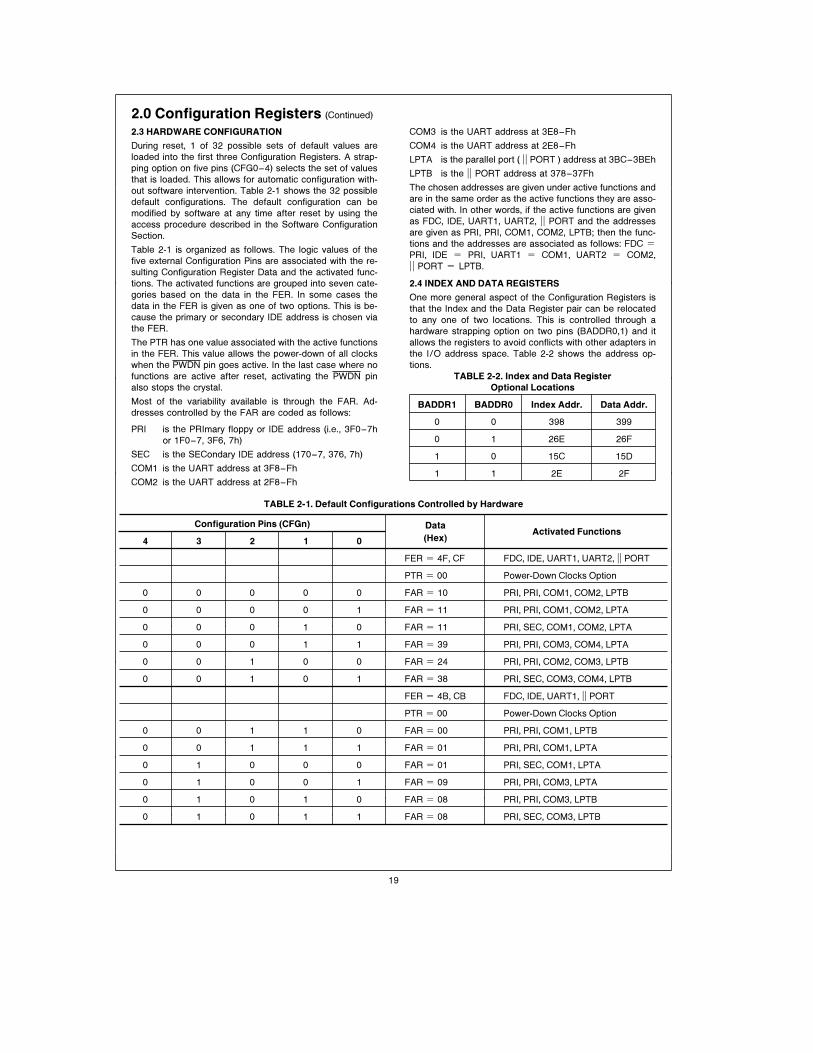
TABLE 2-1 Default Configurations Controlled by Hardware ÀÀÀÀÀÀÀÀÀÀÀÀÀÀÀÀÀÀÀÀÀÀÀÀÀÀÀÀÀÀÀÀÀÀÀÀÀÀÀÀÀÀÀÀÀÀÀÀÀÀÀÀÀÀÀÀ19
TABLE 2-2 Index and Data Register Optional LocationsÀÀÀÀÀÀÀÀÀÀÀÀÀÀÀÀÀÀÀÀÀÀÀÀÀÀÀÀÀÀÀÀÀÀÀÀÀÀÀÀÀÀÀÀÀÀÀÀÀÀÀÀÀÀÀÀÀÀÀ19
TABLE 2-3 Encoded Drive and Motor Pin Information ÀÀÀÀÀÀÀÀÀÀÀÀÀÀÀÀÀÀÀÀÀÀÀÀÀÀÀÀÀÀÀÀÀÀÀÀÀÀÀÀÀÀÀÀÀÀÀÀÀÀÀÀÀÀÀÀÀÀÀÀÀ21
TABLE 2-4 Primary and Secondary Drive Address Selection ÀÀÀÀÀÀÀÀÀÀÀÀÀÀÀÀÀÀÀÀÀÀÀÀÀÀÀÀÀÀÀÀÀÀÀÀÀÀÀÀÀÀÀÀÀÀÀÀÀÀÀÀÀÀÀ22
TABLE 2-5 Parallel Port AddressesÀÀÀÀÀÀÀÀÀÀÀÀÀÀÀÀÀÀÀÀÀÀÀÀÀÀÀÀÀÀÀÀÀÀÀÀÀÀÀÀÀÀÀÀÀÀÀÀÀÀÀÀÀÀÀÀÀÀÀÀÀÀÀÀÀÀÀÀÀÀÀÀÀÀÀÀÀ22
TABLE 2-6 COM Port Selection for UART1 ÀÀÀÀÀÀÀÀÀÀÀÀÀÀÀÀÀÀÀÀÀÀÀÀÀÀÀÀÀÀÀÀÀÀÀÀÀÀÀÀÀÀÀÀÀÀÀÀÀÀÀÀÀÀÀÀÀÀÀÀÀÀÀÀÀÀÀÀÀÀ22
TABLE 2-7 COM Port Selection for UART2 ÀÀÀÀÀÀÀÀÀÀÀÀÀÀÀÀÀÀÀÀÀÀÀÀÀÀÀÀÀÀÀÀÀÀÀÀÀÀÀÀÀÀÀÀÀÀÀÀÀÀÀÀÀÀÀÀÀÀÀÀÀÀÀÀÀÀÀÀÀÀ22
TABLE 2-8 Address Selection for COM3 and COM4 ÀÀÀÀÀÀÀÀÀÀÀÀÀÀÀÀÀÀÀÀÀÀÀÀÀÀÀÀÀÀÀÀÀÀÀÀÀÀÀÀÀÀÀÀÀÀÀÀÀÀÀÀÀÀÀÀÀÀÀÀÀÀ22
TABLE 2-9 Logical Drive Exchange ÀÀÀÀÀÀÀÀÀÀÀÀÀÀÀÀÀÀÀÀÀÀÀÀÀÀÀÀÀÀÀÀÀÀÀÀÀÀÀÀÀÀÀÀÀÀÀÀÀÀÀÀÀÀÀÀÀÀÀÀÀÀÀÀÀÀÀÀÀÀÀÀÀÀÀÀ23
TABLE 2-10 Parallel Port Mode ÀÀÀÀÀÀÀÀÀÀÀÀÀÀÀÀÀÀÀÀÀÀÀÀÀÀÀÀÀÀÀÀÀÀÀÀÀÀÀÀÀÀÀÀÀÀÀÀÀÀÀÀÀÀÀÀÀÀÀÀÀÀÀÀÀÀÀÀÀÀÀÀÀÀÀÀÀÀÀÀÀ23
TABLE 3-1 Register Description and AddressesÀÀÀÀÀÀÀÀÀÀÀÀÀÀÀÀÀÀÀÀÀÀÀÀÀÀÀÀÀÀÀÀÀÀÀÀÀÀÀÀÀÀÀÀÀÀÀÀÀÀÀÀÀÀÀÀÀÀÀÀÀÀÀÀÀÀ28
TABLE 3-2 Drive Enable Values ÀÀÀÀÀÀÀÀÀÀÀÀÀÀÀÀÀÀÀÀÀÀÀÀÀÀÀÀÀÀÀÀÀÀÀÀÀÀÀÀÀÀÀÀÀÀÀÀÀÀÀÀÀÀÀÀÀÀÀÀÀÀÀÀÀÀÀÀÀÀÀÀÀÀÀÀÀÀÀ29
TABLE 3-3 TDR Operation Modes ÀÀÀÀÀÀÀÀÀÀÀÀÀÀÀÀÀÀÀÀÀÀÀÀÀÀÀÀÀÀÀÀÀÀÀÀÀÀÀÀÀÀÀÀÀÀÀÀÀÀÀÀÀÀÀÀÀÀÀÀÀÀÀÀÀÀÀÀÀÀÀÀÀÀÀÀÀ30
TABLE 3-4 Media ID Bit Functions ÀÀÀÀÀÀÀÀÀÀÀÀÀÀÀÀÀÀÀÀÀÀÀÀÀÀÀÀÀÀÀÀÀÀÀÀÀÀÀÀÀÀÀÀÀÀÀÀÀÀÀÀÀÀÀÀÀÀÀÀÀÀÀÀÀÀÀÀÀÀÀÀÀÀÀÀÀ30
TABLE 3-5 Tape Drive Assignment Values ÀÀÀÀÀÀÀÀÀÀÀÀÀÀÀÀÀÀÀÀÀÀÀÀÀÀÀÀÀÀÀÀÀÀÀÀÀÀÀÀÀÀÀÀÀÀÀÀÀÀÀÀÀÀÀÀÀÀÀÀÀÀÀÀÀÀÀÀÀÀ30
TABLE 3-6 Write Precompensation Delays ÀÀÀÀÀÀÀÀÀÀÀÀÀÀÀÀÀÀÀÀÀÀÀÀÀÀÀÀÀÀÀÀÀÀÀÀÀÀÀÀÀÀÀÀÀÀÀÀÀÀÀÀÀÀÀÀÀÀÀÀÀÀÀÀÀÀÀÀÀÀ31
TABLE 3-7 Default Precompensation Delays ÀÀÀÀÀÀÀÀÀÀÀÀÀÀÀÀÀÀÀÀÀÀÀÀÀÀÀÀÀÀÀÀÀÀÀÀÀÀÀÀÀÀÀÀÀÀÀÀÀÀÀÀÀÀÀÀÀÀÀÀÀÀÀÀÀÀÀÀ32
TABLE 3-8 Data Rate Select Encoding ÀÀÀÀÀÀÀÀÀÀÀÀÀÀÀÀÀÀÀÀÀÀÀÀÀÀÀÀÀÀÀÀÀÀÀÀÀÀÀÀÀÀÀÀÀÀÀÀÀÀÀÀÀÀÀÀÀÀÀÀÀÀÀÀÀÀÀÀÀÀÀÀÀ32
TABLE 4-1 Typical Format GAP3 Length Values Based on Drive Data RateÀÀÀÀÀÀÀÀÀÀÀÀÀÀÀÀÀÀÀÀÀÀÀÀÀÀÀÀÀÀÀÀÀÀÀÀÀÀÀÀÀÀ36
TABLE 4-2 Typical Format GAP3 Length Values Based on PC Compatible Diskette MediaÀÀÀÀÀÀÀÀÀÀÀÀÀÀÀÀÀÀÀÀÀÀÀÀÀÀÀÀÀ36
TABLE 4-3 DENSEL Default EncodingÀÀÀÀÀÀÀÀÀÀÀÀÀÀÀÀÀÀÀÀÀÀÀÀÀÀÀÀÀÀÀÀÀÀÀÀÀÀÀÀÀÀÀÀÀÀÀÀÀÀÀÀÀÀÀÀÀÀÀÀÀÀÀÀÀÀÀÀÀÀÀÀÀÀ39
TABLE 4-4 DENSEL EncodingÀÀÀÀÀÀÀÀÀÀÀÀÀÀÀÀÀÀÀÀÀÀÀÀÀÀÀÀÀÀÀÀÀÀÀÀÀÀÀÀÀÀÀÀÀÀÀÀÀÀÀÀÀÀÀÀÀÀÀÀÀÀÀÀÀÀÀÀÀÀÀÀÀÀÀÀÀÀÀÀÀ39
TABLE 4-5 Head Settle Time CalculationÀÀÀÀÀÀÀÀÀÀÀÀÀÀÀÀÀÀÀÀÀÀÀÀÀÀÀÀÀÀÀÀÀÀÀÀÀÀÀÀÀÀÀÀÀÀÀÀÀÀÀÀÀÀÀÀÀÀÀÀÀÀÀÀÀÀÀÀÀÀÀÀ39
TABLE 4-6 Effect of Drive Mode and Data Rate on Format and Write CommandsÀÀÀÀÀÀÀÀÀÀÀÀÀÀÀÀÀÀÀÀÀÀÀÀÀÀÀÀÀÀÀÀÀÀÀÀÀ40
TABLE 4-7 Effect of GAP and WG on Format and Write Commands ÀÀÀÀÀÀÀÀÀÀÀÀÀÀÀÀÀÀÀÀÀÀÀÀÀÀÀÀÀÀÀÀÀÀÀÀÀÀÀÀÀÀÀÀÀÀÀÀ40
TABLE 4-8 Sector Size Selection ÀÀÀÀÀÀÀÀÀÀÀÀÀÀÀÀÀÀÀÀÀÀÀÀÀÀÀÀÀÀÀÀÀÀÀÀÀÀÀÀÀÀÀÀÀÀÀÀÀÀÀÀÀÀÀÀÀÀÀÀÀÀÀÀÀÀÀÀÀÀÀÀÀÀÀÀÀÀ41
TABLE 4-9 SK Effect on the Read Data Command ÀÀÀÀÀÀÀÀÀÀÀÀÀÀÀÀÀÀÀÀÀÀÀÀÀÀÀÀÀÀÀÀÀÀÀÀÀÀÀÀÀÀÀÀÀÀÀÀÀÀÀÀÀÀÀÀÀÀÀÀÀÀÀ42
TABLE 4-10 Result Phase Termination Values with No Error ÀÀÀÀÀÀÀÀÀÀÀÀÀÀÀÀÀÀÀÀÀÀÀÀÀÀÀÀÀÀÀÀÀÀÀÀÀÀÀÀÀÀÀÀÀÀÀÀÀÀÀÀÀÀÀÀ42
TABLE 4-11 SK Effect on Read Deleted Data Command ÀÀÀÀÀÀÀÀÀÀÀÀÀÀÀÀÀÀÀÀÀÀÀÀÀÀÀÀÀÀÀÀÀÀÀÀÀÀÀÀÀÀÀÀÀÀÀÀÀÀÀÀÀÀÀÀÀÀÀ43
TABLE 4-12 Maximum Recalibrate Step Pulses Based on R255 and ETRÀÀÀÀÀÀÀÀÀÀÀÀÀÀÀÀÀÀÀÀÀÀÀÀÀÀÀÀÀÀÀÀÀÀÀÀÀÀÀÀÀÀÀÀÀ44
TABLE 4-13 Scan Command Termination Values ÀÀÀÀÀÀÀÀÀÀÀÀÀÀÀÀÀÀÀÀÀÀÀÀÀÀÀÀÀÀÀÀÀÀÀÀÀÀÀÀÀÀÀÀÀÀÀÀÀÀÀÀÀÀÀÀÀÀÀÀÀÀÀÀÀ45
TABLE 4-14 Status Register 0 Termination CodesÀÀÀÀÀÀÀÀÀÀÀÀÀÀÀÀÀÀÀÀÀÀÀÀÀÀÀÀÀÀÀÀÀÀÀÀÀÀÀÀÀÀÀÀÀÀÀÀÀÀÀÀÀÀÀÀÀÀÀÀÀÀÀÀÀ47
TABLE 4-15 Set Track Register Address ÀÀÀÀÀÀÀÀÀÀÀÀÀÀÀÀÀÀÀÀÀÀÀÀÀÀÀÀÀÀÀÀÀÀÀÀÀÀÀÀÀÀÀÀÀÀÀÀÀÀÀÀÀÀÀÀÀÀÀÀÀÀÀÀÀÀÀÀÀÀÀÀÀ47
TABLE 4-16 Step Rate Time (SRT) Values ÀÀÀÀÀÀÀÀÀÀÀÀÀÀÀÀÀÀÀÀÀÀÀÀÀÀÀÀÀÀÀÀÀÀÀÀÀÀÀÀÀÀÀÀÀÀÀÀÀÀÀÀÀÀÀÀÀÀÀÀÀÀÀÀÀÀÀÀÀÀÀ47
6

List of Tables (Continued)
TABLE 4-17 Motor Off Time (MFT) ValuesÀÀÀÀÀÀÀÀÀÀÀÀÀÀÀÀÀÀÀÀÀÀÀÀÀÀÀÀÀÀÀÀÀÀÀÀÀÀÀÀÀÀÀÀÀÀÀÀÀÀÀÀÀÀÀÀÀÀÀÀÀÀÀÀÀÀÀÀÀÀÀÀ48
TABLE 4-18 Motor On Time (MNT) Values ÀÀÀÀÀÀÀÀÀÀÀÀÀÀÀÀÀÀÀÀÀÀÀÀÀÀÀÀÀÀÀÀÀÀÀÀÀÀÀÀÀÀÀÀÀÀÀÀÀÀÀÀÀÀÀÀÀÀÀÀÀÀÀÀÀÀÀÀÀÀÀ48
TABLE 4-19 Verify Command Result Phase ÀÀÀÀÀÀÀÀÀÀÀÀÀÀÀÀÀÀÀÀÀÀÀÀÀÀÀÀÀÀÀÀÀÀÀÀÀÀÀÀÀÀÀÀÀÀÀÀÀÀÀÀÀÀÀÀÀÀÀÀÀÀÀÀÀÀÀÀÀÀ49
TABLE 6-1 PC87303 UART Register Addresses (AEN e 0) ÀÀÀÀÀÀÀÀÀÀÀÀÀÀÀÀÀÀÀÀÀÀÀÀÀÀÀÀÀÀÀÀÀÀÀÀÀÀÀÀÀÀÀÀÀÀÀÀÀÀÀÀÀÀÀ65
TABLE 6-2 PC87303 Register Summary for an Individual UART Channel ÀÀÀÀÀÀÀÀÀÀÀÀÀÀÀÀÀÀÀÀÀÀÀÀÀÀÀÀÀÀÀÀÀÀÀÀÀÀÀÀÀÀÀÀ67
TABLE 6-3 PC87303 UART Reset Configuration ÀÀÀÀÀÀÀÀÀÀÀÀÀÀÀÀÀÀÀÀÀÀÀÀÀÀÀÀÀÀÀÀÀÀÀÀÀÀÀÀÀÀÀÀÀÀÀÀÀÀÀÀÀÀÀÀÀÀÀÀÀÀÀÀÀ68
TABLE 6-4 PC87303 UART Divisors, Baud Rates, and Clock Frequencies ÀÀÀÀÀÀÀÀÀÀÀÀÀÀÀÀÀÀÀÀÀÀÀÀÀÀÀÀÀÀÀÀÀÀÀÀÀÀÀÀÀÀÀ68
TABLE 6-5 PC87303 Interrupt Control Functions ÀÀÀÀÀÀÀÀÀÀÀÀÀÀÀÀÀÀÀÀÀÀÀÀÀÀÀÀÀÀÀÀÀÀÀÀÀÀÀÀÀÀÀÀÀÀÀÀÀÀÀÀÀÀÀÀÀÀÀÀÀÀÀÀÀ71
TABLE 7-1 Parallel Interface Register Addresses ÀÀÀÀÀÀÀÀÀÀÀÀÀÀÀÀÀÀÀÀÀÀÀÀÀÀÀÀÀÀÀÀÀÀÀÀÀÀÀÀÀÀÀÀÀÀÀÀÀÀÀÀÀÀÀÀÀÀÀÀÀÀÀÀ72
TABLE 7-2 Standard Parallel Port Modes SelectionÀÀÀÀÀÀÀÀÀÀÀÀÀÀÀÀÀÀÀÀÀÀÀÀÀÀÀÀÀÀÀÀÀÀÀÀÀÀÀÀÀÀÀÀÀÀÀÀÀÀÀÀÀÀÀÀÀÀÀÀÀÀÀ72
TABLE 7-3 SPP Data Register Read and Write Modes ÀÀÀÀÀÀÀÀÀÀÀÀÀÀÀÀÀÀÀÀÀÀÀÀÀÀÀÀÀÀÀÀÀÀÀÀÀÀÀÀÀÀÀÀÀÀÀÀÀÀÀÀÀÀÀÀÀÀÀÀ72
TABLE 7-4 Parallel Port Reset StatesÀÀÀÀÀÀÀÀÀÀÀÀÀÀÀÀÀÀÀÀÀÀÀÀÀÀÀÀÀÀÀÀÀÀÀÀÀÀÀÀÀÀÀÀÀÀÀÀÀÀÀÀÀÀÀÀÀÀÀÀÀÀÀÀÀÀÀÀÀÀÀÀÀÀÀ74
TABLE 7-5 EPP RegistersÀÀÀÀÀÀÀÀÀÀÀÀÀÀÀÀÀÀÀÀÀÀÀÀÀÀÀÀÀÀÀÀÀÀÀÀÀÀÀÀÀÀÀÀÀÀÀÀÀÀÀÀÀÀÀÀÀÀÀÀÀÀÀÀÀÀÀÀÀÀÀÀÀÀÀÀÀÀÀÀÀÀÀÀÀ75
TABLE 7-6 Parallel Port Pin OutÀÀÀÀÀÀÀÀÀÀÀÀÀÀÀÀÀÀÀÀÀÀÀÀÀÀÀÀÀÀÀÀÀÀÀÀÀÀÀÀÀÀÀÀÀÀÀÀÀÀÀÀÀÀÀÀÀÀÀÀÀÀÀÀÀÀÀÀÀÀÀÀÀÀÀÀÀÀÀÀ78
TABLE 7-7 ECP Registers ÀÀÀÀÀÀÀÀÀÀÀÀÀÀÀÀÀÀÀÀÀÀÀÀÀÀÀÀÀÀÀÀÀÀÀÀÀÀÀÀÀÀÀÀÀÀÀÀÀÀÀÀÀÀÀÀÀÀÀÀÀÀÀÀÀÀÀÀÀÀÀÀÀÀÀÀÀÀÀÀÀÀÀÀ79
TABLE 8-1 IDE Registers and Their ISA AddressesÀÀÀÀÀÀÀÀÀÀÀÀÀÀÀÀÀÀÀÀÀÀÀÀÀÀÀÀÀÀÀÀÀÀÀÀÀÀÀÀÀÀÀÀÀÀÀÀÀÀÀÀÀÀÀÀÀÀÀÀÀÀÀ83
TABLE 9-1 Summary of System Interface Operations ÀÀÀÀÀÀÀÀÀÀÀÀÀÀÀÀÀÀÀÀÀÀÀÀÀÀÀÀÀÀÀÀÀÀÀÀÀÀÀÀÀÀÀÀÀÀÀÀÀÀÀÀÀÀÀÀÀÀÀÀÀ86
TABLE 9-2 RTC Memory Map ÀÀÀÀÀÀÀÀÀÀÀÀÀÀÀÀÀÀÀÀÀÀÀÀÀÀÀÀÀÀÀÀÀÀÀÀÀÀÀÀÀÀÀÀÀÀÀÀÀÀÀÀÀÀÀÀÀÀÀÀÀÀÀÀÀÀÀÀÀÀÀÀÀÀÀÀÀÀÀÀÀ91
TABLE 10-1 Nominal tICP, tDRP Values ÀÀÀÀÀÀÀÀÀÀÀÀÀÀÀÀÀÀÀÀÀÀÀÀÀÀÀÀÀÀÀÀÀÀÀÀÀÀÀÀÀÀÀÀÀÀÀÀÀÀÀÀÀÀÀÀÀÀÀÀÀÀÀÀÀÀÀÀÀÀÀÀÀÀ99
TABLE 10-2 Minimum tWDW Values ÀÀÀÀÀÀÀÀÀÀÀÀÀÀÀÀÀÀÀÀÀÀÀÀÀÀÀÀÀÀÀÀÀÀÀÀÀÀÀÀÀÀÀÀÀÀÀÀÀÀÀÀÀÀÀÀÀÀÀÀÀÀÀÀÀÀÀÀÀÀÀÀÀÀÀÀ107
7

Basic Configuration
TL/C/12074–2
8

Connection Diagram
Plastic Quad Flatpak
TL/C/12074–3
Note: Do not connect pins marked Reserved.
Order Number PC87303VUL
See NS Package Number VUL160A
9

1.0 Pin Description
TABLE 1-1. Pin Descriptions (Alphabetical)
Symbol Pin I/O Function
A10–A0 46–56 I Address. These address lines from the microprocessor determine which internal register is
accessed. A0–A10 are don’t cares during an DMA transfer. A10 is used only during ECP
operations.
ACK 125 I Acknowledge. This input is pulsed low by a connected printer to indicate that it has received
data from the parallel port. This pin has a nominal 25 kX pull-up resistor attached to it. (See
DR1 and Table 7-5 for further information.)
ADRATE0 16 O Additional Data Rate 0. When selected this output is identical to DRATE0. It is provided in
addition to DRATE0. It reflects the currently selected FDC data rate (bit 0 in the Configuration
Control Register (CCR) or the Data Rate Select Register (DSR), whichever was written to
last). ADRATE0 is configured when bit 0 of Advanced SuperI/O Configuration Register (ASC)
is 1. (See IRQ5 for further information.)
AFD 116 I/O Automatic Feed XT. When this signal is low the printer should automatically line feed after
each line is printed. This pin is in a TRI-STATEÉ condition 10 ns after a 0 is loaded into the
corresponding Control Register bit. The system should pull this pin high using a 4.7 kXresistor. (See DSTRB and Table 7-5 for further information.)
AEN 45 I Address Enable. This input disables function selection via A10–A0 when it is high. Access
during DMA transfer is NOT affected by this pin.
ASTRB 119 O Address Strobe. This signal is used in Enhanced Parallel Port (EPP) mode as an address
strobe. It is active low. (See SLIN and Table 7-5 for further information.)
BADDR0,1 86, 89 I Base Address. These CMOS inputs are sensed during reset to determine one of four base
addresses from which the Index and Data Registers are offset (see Table 2-2). An internal
pull-down resistor of 30 kX is present on this pin. Use a 10 kX resistor to pull this pin to VDD.
(See IDELO, HCS0 for further information.)
BOUT1,2 110,100 O BAUD Output. This multi-function pin provides the associated serial channel Baud Rate
generator output signal when test mode is selected in the Power and Test Configuration
Register and the DLAB bit (LCR7) is set. After a Master Reset, this pin provides the Serial
Output (SOUT) function. (See SOUT and CFG0–4 for further information.)
BUSY 124 I Busy. This pin is set high by a connected printer when it cannot accept another character. It
has a nominal 25 kX pull-down resistor attached to it. (See WAIT and Table 7-5 for further
information.)
CFG0–4 100, 103, I Configuration on Power-Up. These CMOS inputs select 1 of 32 default configurations in
which the PC87303 powers-up (see Table 2-1). They are provided with CMOS input buffers.108, 110,An internal pull-down resistor of 30 kX is present on each pin. Use a 10 kX resistor to pull111these pins to VDD.
CS 2 I Chip Select. Enables the host to access the keyboard controller through D0–D7, when bit 7
of Chip Select 0 Configuration Register 1 (CS0CF1) is 0. (See CS0 for further information.)
CSOUT 21 O Chip Select Read Output. This is the data buffer output enable pin. It indicates any read from
the PC87303, except for IDE accesses. This signal is valid when bit 2 of PTR is 1. CSOUT is
not active during read in PC-AT mode from registers 3F7 and 377. CSOUT is not active when
the read is from a disabled module. (See PWDN for further information.)
CTS1,2 109, 99 I Clear to Send. When low, this indicates that the MODEM or data set is ready to exchange
data. The CTS signal is a MODEM status input whose condition the CPU can test by reading
bit 4 (CTS) of the MODEM Status Register (MSR) for the appropriate serial channel. Bit 4 is
the complement of the CTS signal. Bit 0 (DCTS) of the MSR indicates whether the CTS input
has changed state since the previous reading of the MSR. CTS has no effect on the
transmitter.
Note: Whenever the DCTS bit of the MSR is set an interrupt is generated if MODEM Status interrupts are enabled.
CS0,1 2, 23 O Programmable Chip Select. CS0,1 are programmable chip select and/or enable and/or
output enable signals that can be used for a game port, I/O port expander or other add-on
peripheral. The decoded address and the assertion conditions are configured via the
PC87303 configuration registers, 0Ah–0Dh. When either of these two pins is acting as CS0,1
output enable, the PC87303 assumes the relevant input is 1. (See SYSCLK and CS for further
information.)
D7–D0 33, 34, 35, 36, I/O Data. Bi-directional data lines to the microprocessor. D0 is the LSB and D7 is the MSB. These
signals all have 24 mA (sink) buffered outputs.37, 38, 39, 42
10

1.0 Pin Description (Continued)
TABLE 1-1. Pin Descriptions (Alphabetical) (Continued)
Symbol Pin I/O Function
DCD1,2 114, 106 I Data Carrier Detect. When low, this signal indicates that the MODEM or data set has detected the
data carrier. The DCD signal is a MODEM status input whose condition the CPU can test by reading
bit 7 (DCD) of the MODEM Status Register (MSR) for the appropriate serial channel. Bit 7 is the
complement of the DCD signal. Bit 3 (DDCD) of the MSR indicates whether the DCD input has
changed state since the previous reading of the MSR.
Note: Whenever the DDCD bit of the MSR is set, an interrupt is generated if MODEM Status interrupts are enabled.
DENSEL 77 O Density Select. Indicates that a high FDC density data rate (500 kbps or 1 Mbps) or a low density
data rate (250 kbps or 300 kbps) is selected. DENSEL is active high for high density (5.25× drives)
when IDENT is high, and active low for high density (3.5× drives) when IDENT is low. DENSEL is
also programmable via the Mode command (see Section 4.2.6).
DIR 69 O Direction. This output determines the direction of the floppy disk drive (FDD) head movement
(active e step in, inactive e step out) during a seek operation. During reads or writes, DIR is
inactive.
DR0,1 73, 74 O Drive Select 0,1. These are the decoded Drive Select outputs that are controlled by the Digital
Output Register bits D0,D1. The Drive Select outputs are gated with DOR bits 4–7. These are
active low outputs. They are encoded with information to control four FDDs when bit 4 of the
Function Enable Register (FER) is set. (See MTR0,1 for more information.)
DR23 78 O Drive 2 or 3. DR23 is asserted when either Drive 2 or Drive 3 is accessed (except during logical
drive exchange, see bit 3 of TDR). This pin is configured when bit 1 of ASC is 1. (See DRV2 for
further information.)
DRATE0,1 83, 82 O Data Rate 0,1. These outputs reflect the currently selected FDC data rate (bits 0 and 1 in the
Configuration Control Register (CCR) or the Data Rate Select Register (DSR), whichever was
written to last). These pins are totem-pole buffered outputs (6 mA sink, 6 mA source). (See
MSEN0,1 for further information.)
DRID0,1 90, 87 I Drive ID. These pins accept input from the floppy disk drive which indicates the type of drive in use.
These pins should be tied low if they are not used. DRID0,1 is configured when bit 2 of ASC is 1.
(See IOCS16, IDEHI, and VLD0 for further information.)
DRV2 78 I Drive2. This input indicates whether a second floppy disk drive has been installed. The state of this
pin is available from Status Register A in PS/2 mode. This pin is confgured when bit 1 of ASC is 0.
(See DR23 for further information.)
DSKCHG 60 I Disk Change. This input indicates if the drive door has been opened. The state of this pin is
available from the Digital Input register. This pin can also be configured as the Read Gate (RGATE)
data separator diagnostic input via the Mode command (see Section 4.2.6).
DSR1,2 113, 105 I Data Set Ready. When low, this signal indicates that the data set or MODEM is ready to establish a
communications link. The DSR signal is a MODEM status input whose condition the CPU can test
by reading bit 5 (DSR) of the MODEM Status Register (MSR) for the appropriate channel. Bit 5 is
the complement of the DSR signal. Bit 1 (DDSR) of the MSR indicates whether the DSR input has
changed state since the previous reading of the MSR.
Note: Whenever the DDSR bit of the MSR is set, an interrupt is generated if MODEM Status interrupts are enabled.
DSTRB 116 O Data Strobe. This signal is used in EPP mode as a data strobe. It is active low. (See AFD and
Table 7-5 for further information.)
DTR1,2 108, 98 O Data Terminal Ready. When low, this output indicates to the MODEM or data set that the UART is
ready to establish a communications link. The DTR signal can be set to an active low by
programming bit 0 (DTR) of the MODEM Control Register to a high level. A Master Reset operation
sets this signal to its inactive (high) state. Loop mode operation holds this signal to its inactive state.
(See CFG0–4 for further information.)
ERR 117 I Error. A connected printer sets this input low when it has detected an error. This pin has a nominal
25 kX pull-up resistor attached to it.
FDACK 28 I DMA Acknowledge. Active low input to acknowledge the FDC DMA request and enable the RD
and WR inputs during a DMA transfer. When in PC-AT or Model 30 mode, this signal is enabled by
bit D3 of the Digital Output Register (DOR). When in PS/2 mode, FDACK is always enabled, and bit
D3 of the DOR is reserved. FDACK should be held high during I/O accesses.
11

1.0 Pin Description (Continued)
TABLE 1-1. Pin Descriptions (Alphabetical) (Continued)
Symbol Pin I/O Function
FDRQ 27 O DMA Request. Active high output to signal the DMA controller that a FDC data transfer is needed.
When in PC-AT or Model 30 mode, this signal is enabled by bit D3 of the DOR. When in PS/2 mode,
FDRQ is always enabled, and bit D3 of the DOR is reserved.
HCS0 89 O Hard Drive Chip Select 0. This output is active in the PC-AT mode when 1) the hard drive registers
from 1F0–1F7h are selected and the primary address is used or 2) when the hard drive registers from
170–177h are selected and the secondary address is used. This output is inactive if the IDE interface
is disabled via the Configuration Register. (See BADDR1 for further information.)
HCS1 88 O Hard Drive Chip Select 1. This output is active in the PC-AT mode when 1) the hard drive registers
from 3F6–7 are selected and the primary address is used or 2) the hard drive registers from 376–377
are selected and the secondary address is used. This output is also inactive, if the IDE interface is
disabled via the Configuration Register.
HDSEL 62 O Head Select. This output determines which side of the FDD is accessed. When Active, the head
selects side 1. When inactive, the head selects side 0.
IDEACK 85 I IDE DMA Acknowledge. This is the IDE DMA acknowledge input pin when bit 1 of FCR is 1. In this
case the DENSEL polarity is active high (IDENT assumed 1). This pin is the IDENT input pin when bit 1
of FCR is 0. (See IDENT pin for further information.)
IDED7 91 I/O IDE Bit 7. This pin provides the data bus bit 7 signal to the IDE hard drive during accesses in the
address range 1F0–1F7h, 170–177h, 3F6h and 376h. This pin is TRI-STATE during read or write
accesses to 3F7h and 377h.
IDEHI 87 O IDE High Byte. This output enables the high byte data latch during a read or write to the hard drive if
the hard drive returns IOCS16. This output is inactive if the IDE interface is disabled via the
Configuration Register. (See VLD0 and DRID1 for further information.)
IDELO 86 O IDE Low Byte. This output enables the low byte data latch during a read or write to the hard drive. This
output is inactive if the IDE interface is disabled via the Configuration Register. (See BADDR0 for
further information.)
IDENT 85 I Identity. After chip reset, the state of IDENT determines the polarity of the DENSEL output. When
IDENT is a logic ‘‘1’’, DENSEL is active high for the 500 kbps and 1 Mbps data rates. When IDENT is a
logic ‘‘0’’, DENSEL is active low for the 500 kbps and 1 Mbps data rates. (See Mode command for
explanation of DENSEL.) (See IDEACK for further information.)
INDEX 76 I Index. This input signals the beginning of a FDD track.
INIT 118 I/O Initialize. When this signal is low it causes a connected printer to be initialized. This pin is in a TRI-
STATE condition 10 ns after a 1 is loaded into the corresponding Control Register bit. The system
should pull this pin high using a 4.7 kX resistor.
IOCHRDY 22 O I/O Channel Ready. This is the I/O Channel Ready open drain output. When IOCHRDY is driven low,
the EPP extends the host cycle.
IOCS16 90 I I/O Chip Select 16-Bit. This input is driven by a connected peripheral device which can accommodate
a 16-bit access. This pin is configured when bit 2 of ASC is 0. (See DRID0 for further information.)
IRQ3,4 19, 18 O Interrupt 3 and 4. These are active high interrupts associated with the serial ports. IRQ3 presents the
signal if the serial channel has been designated as COM2 or COM4. IRQ4 presents the signal if the
serial port is designated as COM1 or COM3. The appropriate interrupt goes active whenever it is
enabled via the Interrupt Enable Register (IER), the associated Interrupt Enable bit (Modem Control
Register bit 3, MCR3), and any of the following conditions are active: Receiver Error, Receive Data
available, Transmitter Holding Register Empty, or a Modem Status Flag is set. The interrupt signal is
reset low (inactive) after the appropriate interrupt service routine is executed, after being disabled via
the IER, or after a Master Reset. Either interrupt can be disabled, putting them into TRI-STATE, by
setting the MCR3 bit low.
12

1.0 Pin Description (Continued)
TABLE 1-1. Pin Descriptions (Alphabetical) (Continued)
Symbol Pin I/O Function
IRQ5 16 I/O Interrupt 5. Active high output that indicates a parallel port interrupt. When enabled this bit follows
the ACK signal input. When bit 4 in the parallel port Control Register is set and the parallel port
address is designated as shown in Table 2-5, this interrupt is enabled. When it is not enabled this
signal is TRI-STATE.
This pin is I/O only when ECP is enabled, IRQ5 is configured, and bit 6 of PCR is 1. (See ADRATE0
for further information.)
IRQ6 15 O Interrupt 6. Active high output to signal the completion of the execution phase for certain FDC
commands. Also used to signal when a data transfer is ready during a Non-DMA operation. When in
PC-AT or Model 30 mode, this signal is enabled by bit D3 of the DOR. When in PS/2 mode, IRQ6 is
always enabled, and bit D3 of the DOR is reserved.
IRQ7 14 I/O Interrupt 7. Active high output that indicates a parallel port interrupt. When enabled this bit follows
the ACK signal input. When bit 4 in the parallel port Control Register is set and the parallel port
address is designated as shown in Table 2-5, this interrupt is enabled. When it is not enabled this
signal is TRI-STATE.
This pin is I/O only when ECP is enabled, IRQ7 is configured, and bit 6 of PCR is 1. For ECP
operation, refer to the interrupt ECP Section 7.11.1
IRQ8 13 O Interrupt 8. Real-Time Clock interrupt request output. This is an open-drain output.
KBCLK 96 O Keyboard Clock output.
KBDAT 95 O Keyboard Data output.
MCLK 93 O Mouse Clock output.
MDAT 94 O Mouse Data output.
MR 20 I Master Reset. Active high input that resets the controller to the idle state, and resets all disk
interface outputs to their inactive states. The DOR, DSR, CCR, Mode command, Configure
command, and Lock command parameters are cleared to their default values. The Specify
command parameters are not affected. The Configuration Registers are set to their selected default
values.
MTR0,1 75, 72 O Motor Select 0,1. These are the motor enable lines for drives 0 and 1, and are controlled by bits
D7–D4 of the Digital Output register. They are active low outputs. They are encoded with
information to control four FDDs when bit 4 of the Function Enable Register (FER) is set. MTR0
exchanges logical motor values with MTR1 when bit 4 of FCR is set. (See DR0,1.)
MSEN0,1 83, 82 I Media Sense. These pins are Media Sense input pins when bit 0 of FCR is 0. Each pin has a 40 kXinternal pull-up resistor. When bit 0 of FCR is 1, these pins are Data Rate output pins, and the pull-
up resistors are disabled. (See DRATE0,1 for further information.)
P10–P17 141–148 I/O I/O Port. Quasi-bidirectional port for general purpose input and output.
P20–P27 151–158 I/O I/O Port. Quasi-bidirectional port for general purpose input and output.
PD0–7 134–131, I/O Parallel Port Data. These bidirectional pins transfer data to and from the peripheral data bus and
the parallel port Data Register. These pins have high current drive capability. (See DC Electrical129–126Characteristics.)
PDACK 26 I Printer DMA Acknowledge. Active low input to acknowledge a connected printer’s DMA request,
and enable the RD and WR inputs during a DMA transfer. This input is valid only in Enhanced
Capabilities Port (ECP) mode.
PDRQ 25 O Printer DMA Request. Active high output which signals the DMA controller that a printer data
transfer is required. This pin is in TRI-STATE when ECP is disabled (PCR2 e 0) or when it is
configured without DMA (PMC3 e 0). This output is valid only in ECP mode.
13

1.0 Pin Description (Continued)
TABLE 1-1. Pin Descriptions (Alphabetical) (Continued)
Symbol Pin I/O Function
PDWN 21 I Power-Down. This multi-function pin stops the clocks and/or the external crystal based on the
selections made in the Power and Test Register (PTR) bits 1 and 2. (See CSOUT for additional
information.)
PE 123 I Paper End. This input is set high by a connected printer which is out of paper. This pin has a
nominal 25 kX pull-down resistor attached to it.
PWRGOOD 12 I Power Supply Good. An input to the PC87303 indicating that the power supply is good. This input
should be held low until the power supply is stable.
RD 44 I Read. Active low input to signal a data read by the microprocessor.
RDATA 63 I Read Data. This input is the raw serial data read from the floppy disk drive.
RI1,2 107, 97 I Ring Indicator. When low this indicates that a telephone ring signal has been received by the
MODEM. The RI signal is a MODEM status input whose condition the CPU can test by reading bit
6 (RI) of the MODEM Status Register (MSR) for the appropriate serial channel. Bit 6 is the
complement of the RI signal. Bit 2 (TERI) of the MSR indicates whether the RI input has changed
from low to high since the previous reading of the MSR.
Note: When the TERI bit of the MSR is set, an interrupt is generated if MODEM Status interrupts are enabled.
RTS1,2 111, 103 O Request to Send. When low, this output indicates to the MODEM or data set that the UART is
ready to exchange data. The RTS signal can be set to an active low by programming bit 1 (RTS) of
the MODEM Control Register to a high level. A Master Reset operation sets this signal to its
inactive (high) state. Loop mode operation holds this signal to its inactive state. (See CFG0–4 for
further information.)
SIN1,2 112, 104 I Serial Input. This input receives composite serial data from the communications link (e.g.
peripheral device, MODEM, or data set).
SLCT 122 I Select. When a printer is connected, it sets this input high. This pin has a nominal 25 kX pull-down
resistor attached to it.
SLIN 119 O Select Input. When this signal is low it selects the printer. This pin is a TRI-STATE condition 10 ns
after a 0 is loaded into the corresponding Control Register bit. The system should pull this pin high
using a 4.7 kX resistor.
SOUT1,2 110, 100 O Serial Output. This output sends composite serial data to the communications link (peripheral
device, MODEM, or data set). The SOUT signal is set to a marking state (logic 1) after a Master
Reset operation. (See BOUT and CFG0–4 for further information.)
STB 135 I/O Data Strobe. This output indicates to the printer that valid data is available at the printer port. This
pin is in a TRI-STATE condition 10 ns after a zero is loaded into the corresponding Control
Register bit. The system should pull this pin high using a 4.7 kX resistor. (See WRITE for further
information.)
STEP 68 O Step. This output signal issues pulses to the disk drive at a software programmable rate to move
the head during a seek operation.
SYNC 5 I/O Synch. 32 kHz Real-Time Clock output signal when bit 4 of KRR is 1. SYNC is an input when MR
is high and is sampled by the falling edge of MR. It is a TTL strap input buffer. It is sampled to bit 2
of PTR. A 40 kX internal pullup resistor is present on this pin.
SYSCLK 23 I System Clock. This input is the system clock when bit 7 of CS1CF0 is 0. (See CS1 for further
information.)
T0 4 I Test 0. This input can be directly tested by the conditional jump instructions JT0 and JNT0 of the
Keyboard Controller.
T1 3 I Test 1. This input can be directly tested by the conditional jump instructions JT1 and JNT1 of the
Keyboard Controller. T1 can also be used as the external input to the 8-bit counter/timer of the
Keyboard Controller.
TC 29 I Terminal Count. Control signal from the DMA controller to indicate the termination of a DMA
transfer. TC is accepted only when FDACK or PDACK is active. TC is active high in PC-AT and
Model 30 modes, and active low in PS/2 mode.
14

1.0 Pin Description (Continued)
TABLE 1-1. Pin Descriptions (Alphabetical) (Continued)
Symbol Pin I/O Function
TRK0 65 I Track 0. This input indicates to the controller that the head of the selected floppy disk drive is at
track zero.
VBAT 8 Battery. Real-Time Clock battery pin.
VDD 1, 17, Digital Supply. This is the 5V supply voltage for the digital circuitry.
41, 57,
79, 101,
121, 140,
150
VDDA 61 Analog Supply. This pin is the 5V supply for the analog data separator.
VLD0,1 87, 98 I Valid Data. These inputs are sensed during reset, and determine the state of bit 5 in the FDC Tape
Drive Register (3F3h). Thus, they determine whether bits 6 and 7 of this register contain valid media
id information for floppy drives 0 and 1. If VLD0 is sensed low at reset, then whenever drive 0 is
accessed, bit 5 of the Tape Drive Register is a 0 indicating that bits 6 and 7 contain valid media id
information. If VLD0 is sensed high at reset, then whenever drive 0 is accessed, bit 5 of the Tape
Drive Register is a 1 indicating that bits 6 and 7 do not contain valid media id information. The same
is true of VLD1 relative to the media id information for drive 1.
If bit 0 of FCR is 1, the VLD bits have no meaning. VLD0 value during reset is loaded into bit 0 of FCR
(to select between media sense or DRATE). A 30 kX internal pulldown resistor is present on each
pin. Use a 10 kX resistor to pull these pins high during reset. These strap option pins are CMOS input
buffers. (See IDEHI, DRID1 and DTR2 for further information.)
VSSA 59 Analog Ground. This is the analog ground for the data separator.
VSS 7, 11, Digital Ground. This is the ground for the digital circuitry.
32, 40,
58, 70,
71, 80,
81, 92,
102, 115,
120, 130,
136, 139,
149, 160
WAIT 124 I Wait. This signal is used, in EPP mode, by the parallel port device to extend its access cycle. It is
active low. (See BUSY and Table 7-5 for further information.)
WR 43 I Write. Active low input to signal to indicate a write from the microprocessor to the controller.
WDATA 67 O Write Data. This output is the write precompensated serial data that is written to the selected floppy
disk drive. Precompensation is software selectable.
WGATE 66 O Write Gate. This output signal enables the write circuitry of the selected disk drive. WGATE has been
designed to prevent glitches during power up and power-down. This prevents writing to the disk when
power is cycled.
WP 64 I Write Protect. This input indicates that the floppy disk in the selected drive is write protected.
WRITE 135 O Write Strobe. This signal is used in EPP mode as a write strobe. It is active low. (See STB and Table
7-5 for further information.)
X1/OSC 30 I Crystal1/Clock. One side of an external 24 MHz crystal is attached here. The other side is
connected to X2. If a crystal is not used, a TTL or CMOS compatible clock is connected to this pin.
X1C 9 I Crystal1 Slow. Input for the internal Real-Time Clock crystal oscillator amplifier.
X2C 10 O Crystal2 Slow. Output for the internal Real-Time Clock crystal oscillator amplifier.
X2 31 O Crystal2. One side of an external 24 MHz crystal is attached here. The other side is connected to
X1/OSC. This pin is left unconnected if an external clock is used.
ZWS 24 O Zero Wait State. This pin is the Zero Wait State open drain output pin. ZWS is driven low when the
EPP, or the ECP, is written, and the access can be shortened.
15

2.0 Configuration Registers2.1 OVERVIEW
Fourteen registers constitute the Base Configuration Regis-
ter set, and control the PC87303 setup. In general, these
registers control the enabling of major functions (FDC,
UARTs, parallel port, pin functionalty etc.), the I/O address-
es of these functions, and whether they power-down via
hardware control or not. These registers are the Function
Enable Register (FER), the Function Address Register
(FAR), the Power and Test Register (PTR), the Function
Control Register (FCR), the Printer Control Register (PCR),
the Keyboard and Real-Time Clock Control Register (KRR),
the Power Management Control Register (PMC), the Tape,
UARTs and Parallel Port Register (TUP), the SuperI/O Iden-
tification Register (SID), the Advanced SIO Configuration
Register (ASC), the Chip Select 0 Configuraton Register 0
(CS0CF0), the Chip Select 0 Configuration Register 1
(CS0CF1), the Chip Select 1 Configuration Register 0
(CS1CF0) and the Chip Select 1 Configuration Register 1
(CS1CF1).
The FER, FAR, and PTR can be accessed via hardware or
software. During reset, the PC87303 loads a set of default
values, selected by a hardware strapping option, into these
three Configuration Registers. FCR, PCR and KRR can only
be accessed by software.
An index and data register pair are used to read and write
these registers. Each Configuration Register is pointed to by
the value loaded into the Index Register. The data to be
written into the Configuration Register is transferred via the
Data register. A Configuration Register is read in a similar
way (i.e., by pointing to it via the Index Register and then
reading its contents via the Data Register).
Accessing the Configuration Registers in this way requires
only two system I/O addresses. Since that I/O space is
shared by other devices the Index and Data Registers can
still be inadvertantly accessed. To reduce the chances of an
inadvertant access, a simple procedure (see Section 2.2)
has been developed.
2.2 SOFTWARE CONFIGURATION
If the system requires access to the Configuration Registers
after reset, the following procedure must be used to change
data in the registers.
1. Determine the PC87303 Index Register’s default location.
Check the four possible locations (see Table 2-1) by
reading them twice. The first byte is the ID byte 88h. The
second byte read is always 00h, but read after write al-
ways brings the value of the written byte. Compare the
data read with the ID byte and then 00h. A match occurs
at the correct location. Note that the ID byte is only is-
sued from the Index Register during the first read after a
reset. Subsequent reads return the value loaded into the
Index Register. Bits 5–6 are reserved and always read 0.
2. Load the Configuration Registers.
A. Disable CPU interrupts.
B. Write the index of the Configuration Register (00h–
0Dh) to the Index Register one time.
C. Write the correct data for the Configuration Register in
two consecutive write accesses to the Data Register.
D. Enable CPU interrupts.
3. Load the Configuration Registers (read-modify-write).
A. Disable CPU interrupts.
B. Write the index of the Configuration Register (00h–
0Dh) to the Index Register one time.
C. Read the configuration data in that register via the
Data Register.
D. Modify the configuration data.
E. Write the changed data for the Configuration Register
in two consecutive writes to the Data Register. The
register updates on the second consecutive write.
F. Enable CPU interrupts.
A single read access to the Index and Data Registers can
be done at any time without disabling CPU interrupts. When
the Index Register is read, the last value loaded into the
Index Register is returned. When the Data Register is read,
the Configuration Register data pointed to by the Index Reg-
ister is returned.
16

2.0 Configuration Registers (Continued)
TL/C/12074–4
TL/C/12074–6
TL/C/12074–8
TL/C/12074–10
TL/C/12074–12
TL/C/12074–5
TL/C/12074–7
TL/C/12074–9
TL/C/12074–11
TL/C/12074–13
FIGURE 2-1. PC87303 Configuration Registers
17

2.0 Configuration Registers (Continued)
TL/C/12074–14
TL/C/12074–15
TL/C/12074–16
TL/C/12074–17
FIGURE 2-1. PC87303 Configuration Registers (Continued)
18
2.0 Configuration Registers (Continued)
2.3 HARDWARE CONFIGURATION
During reset, 1 of 32 possible sets of default values are
loaded into the first three Configuration Registers. A strap-
ping option on five pins (CFG0–4) selects the set of values
that is loaded. This allows for automatic configuration with-
out software intervention. Table 2-1 shows the 32 possible
default configurations. The default configuration can be
modified by software at any time after reset by using the
access procedure described in the Software Configuration
Section.
Table 2-1 is organized as follows. The logic values of the
five external Configuration Pins are associated with the re-
sulting Configuration Register Data and the activated func-
tions. The activated functions are grouped into seven cate-
gories based on the data in the FER. In some cases the
data in the FER is given as one of two options. This is be-
cause the primary or secondary IDE address is chosen via
the FER.
The PTR has one value associated with the active functions
in the FER. This value allows the power-down of all clocks
when the PWDN pin goes active. In the last case where no
functions are active after reset, activating the PWDN pin
also stops the crystal.
Most of the variability available is through the FAR. Ad-
dresses controlled by the FAR are coded as follows:
PRI is the PRImary floppy or IDE address (i.e., 3F0–7h
or 1F0–7, 3F6, 7h)
SEC is the SECondary IDE address (170–7, 376, 7h)
COM1 is the UART address at 3F8–Fh
COM2 is the UART address at 2F8–Fh
COM3 is the UART address at 3E8–Fh
COM4 is the UART address at 2E8–Fh
LPTA is the parallel port ( ll PORT ) address at 3BC–3BEh
LPTB is the ll PORT address at 378–37Fh
The chosen addresses are given under active functions and
are in the same order as the active functions they are asso-
ciated with. In other words, if the active functions are given
as FDC, IDE, UART1, UART2, ll PORT and the addresses
are given as PRI, PRI, COM1, COM2, LPTB; then the func-
tions and the addresses are associated as follows: FDC e
PRI, IDE e PRI, UART1 e COM1, UART2 e COM2,
ll PORT e LPTB.
2.4 INDEX AND DATA REGISTERS
One more general aspect of the Configuration Registers is
that the Index and the Data Register pair can be relocated
to any one of two locations. This is controlled through a
hardware strapping option on two pins (BADDR0,1) and it
allows the registers to avoid conflicts with other adapters in
the I/O address space. Table 2-2 shows the address op-
tions.
TABLE 2-2. Index and Data Register
Optional Locations
BADDR1 BADDR0 Index Addr. Data Addr.
0 0 398 399
0 1 26E 26F
1 0 15C 15D
1 1 2E 2F
TABLE 2-1. Default Configurations Controlled by Hardware
Configuration Pins (CFGn)
(Hex)
DataActivated Functions
4 3 2 1 0
FER e 4F, CF FDC, IDE, UART1, UART2, ll PORT
PTR e 00 Power-Down Clocks Option
0 0 0 0 0 FAR e 10 PRI, PRI, COM1, COM2, LPTB
0 0 0 0 1 FAR e 11 PRI, PRI, COM1, COM2, LPTA
0 0 0 1 0 FAR e 11 PRI, SEC, COM1, COM2, LPTA
0 0 0 1 1 FAR e 39 PRI, PRI, COM3, COM4, LPTA
0 0 1 0 0 FAR e 24 PRI, PRI, COM2, COM3, LPTB
0 0 1 0 1 FAR e 38 PRI, SEC, COM3, COM4, LPTB
FER e 4B, CB FDC, IDE, UART1, ll PORT
PTR e 00 Power-Down Clocks Option
0 0 1 1 0 FAR e 00 PRI, PRI, COM1, LPTB
0 0 1 1 1 FAR e 01 PRI, PRI, COM1, LPTA
0 1 0 0 0 FAR e 01 PRI, SEC, COM1, LPTA
0 1 0 0 1 FAR e 09 PRI, PRI, COM3, LPTA
0 1 0 1 0 FAR e 08 PRI, PRI, COM3, LPTB
0 1 0 1 1 FAR e 08 PRI, SEC, COM3, LPTB
19

2.0 Configuration Registers (Continued)
TABLE 2-1. Default Configurations Controlled by Hardware (Continued)
Configuration Pins (CFGn)
(Hex)
DataActivated Functions
4 3 2 1 0
FER e 0F FDC, UART1, UART2, ll PORT
PTR e 00 Power Clocks Option
0 1 1 0 0 FAR e 10 PRI, COM1, COM2, LPTB
0 1 1 0 1 FAR e 11 PRI, COM1, COM2, LPTA
0 1 1 1 0 FAR e 39 PRI, COM3, COM4, LPTA
0 1 1 1 1 FAR e 24 PRI, COM2, COM3, LPTB
FER e 49, C9 FDC, IDE, ll PORT
PTR e 00 Power-Down Clocks Option
1 0 0 0 0 FAR e 00 PRI, PRI, LPTB
1 0 0 0 1 FAR e 01 PRI, PRI, LPTA
1 0 0 1 0 FAR e 01 PRI, SEC, LPTA
1 0 0 1 1 FAR e 00 PRI, SEC, LPTB
FER e 07 UART1, UART2, ll PORT
PTR e 00 Power-Down Clocks Option
1 0 1 0 0 FAR e 10 COM1, COM2, LPTB
1 0 1 0 1 FAR e 11 COM1, COM2, LPTA
1 0 1 1 0 FAR e 39 COM3, COM4, LPTA
1 0 1 1 1 FAR e 24 COM2, COM3, LPTB
FER e 47, C7 IDE, UART1, UART2, ll PORT
PTR e 00 Power-Down Clocks Option
1 1 0 0 0 FAR e 10 PRI, COM1, COM2, LPTB
1 1 0 0 1 FAR e 11 PRI, COM1, COM2, LPTA
1 1 0 1 0 FAR e 11 SEC, COM1, COM2, LPTA
1 1 0 1 1 FAR e 39 PRI, COM3, COM4, LPTA
1 1 1 0 0 FAR e 24 PRI, COM2, COM3, LPTB
1 1 1 0 1 FAR e 38 SEC, COM3, COM4, LPTB
FER e 08 FDC
PTR e 00 Power-Down Clocks Option
1 1 1 1 0 FAR e 10 PRI
FER e 00 None
PTR e 02, 02 Power-Down XTAL and Clocks
1 1 1 1 1 FAR e 10 NA
Note: Bit 2 of PTR is sampled during reset according to the value of the SYNC pin.
20

2.0 Configuration Registers (Continued)
2.5 BASE CONFIGURATION REGISTERS
2.5.1 Function Enable Register (FER, Index 00h)
This register enables and disables major chip functions. Dis-
abled functions have their clocks automatically powered
down, but the data in their registers remains intact. It also
selects whether the FDC and the IDE controller is located at
their primary or secondary address.
Bit 0 When this bit is one the parallel port can be accessed
at the address specified in the FAR.
Bit 1 When this bit is one, UART1 can be accessed at the
address specified in the FAR. When this bit is zero,
access to UART1 is blocked and it is in power-down
mode. The UART1 registers retain all data in power
down mode.
Caution: Any UART1 interrupt that is enabled and
active or becomes active after UART1 is disabled as-
serts the associated IRQ pin when UART1 is dis-
abled. If disabling UART1 via software, clear the IRQ
Enable bit (MCR3) to zero before clearing FER 1.
This is not an issue after reset because MCR3 is zero
until it is written.
Bit 2 When this bit is one, UART2 can be accessed at the
address specified in the FAR. When this bit is zero,
access to UART2 is blocked and it is in power-down
mode. The UART2 registers retain all data in power
down mode.
Caution: Any UART2 interrupt that is enabled and
active or becomes active after UART2 is disabled as-
serts the associated IRQ pin when UART1 is disabled
If disabling UART2 via software, clear the IRQ En-
able bit (MCR3) to zero before clearing FER1. This is
not an issue after reset because MCR3 is zero until it
is written.
Bit 3 When this bit is one, the FDC can be accessed at the
address specified in the FER bits. When this bit is
zero access to the FDC is blocked and it is in power-
down mode. The FDC registers retain all data in pow-
er down mode.
Bit 4 When this bit is zero the PC87303 can control two
floppy disk drives directly without an external decod-
er. When this bit is one the two drive select signals
and two motor enable signals from the FDC are en-
coded so that four floppy disk drives can be con-
trolled (see Table 2-3 and Figure 2-2). Controlling
four FDDs requires an external decoder. The pin
states shown in Table 2-3 are a direct result of the bit
patterns shown. All other bit patterns produce pin
states that should not be decoded to enable any
drive or motor.
Bit 5 This bit selects the primary or secondary FDC ad-
dress. (See Table 2-4.)
Bit 6 When this bit is a one the IDE drive interface can be
accessed at the address specified by FER bit 7.
When it is zero, bit 0 of PMC determines whether the
HCS0,1 pins are inactive, or in TRI-STATE. IDEHI
and IDEHLO are inactive and IDED7 is in TRI-
STATE.
Bit 7 This bit selects the primary or secondary IDE ad-
dress. (See Table 2-4).
TABLE 2-3. Encoded Drive and Motor Pin Information (FER 4 e 1)
Digital Output Register Drive Control PinsDecoded Functions
7 6 5 4 3 2 1 0 MTR1 MTR0 DR1 DR0
X X X 1 X X 0 0 (Note) 0 0 0 Activate Drive 0 and Motor 0
X X 1 X X X 0 1 (Note) 0 0 1 Activate Drive 1 and Motor 1
X 1 X X X X 1 0 (Note) 0 1 0 Activate Drive 2 and Motor 2
1 X X X X X 1 1 (Note) 0 1 1 Activate Drive 3 and Motor 3
X X X 0 X X 0 0 (Note) 1 0 0 Activate Drive 0 and Deactivate Motor 0
X X 0 X X X 0 1 (Note) 1 0 1 Activate Drive 1 and Deactivate Motor 1
X 0 X X X X 1 0 (Note) 1 1 0 Activate Drive 2 and Deactivate Motor 2
0 X X X X X 1 1 (Note) 1 1 1 Activate Drive 3 and Deactivate Motor 3
Note: When FER4 e 1, MTR1 presents a pulse that is the inverted image of the IOW strobe. This inverted pulse is active whenever an I/O write to address 3F2h or
372h takes place. This pulse is delayed by 25 ns–80 ns after the leading edge of IOW and its leading edge can be used to clock data into an external latch (e.g.,
74LS175). Address 3F2h is used if the FDC is located at the primary address (FER5 e 0) and address 372h is used if the FDC is located at the secondary address
(FER5 e 1).
TL/C/12074–85Hex Buffers
ICC e 40 mA
open collector
FIGURE 2-2. PC87303 Four Floppy Drive Circuit
21

2.0 Configuration Registers (Continued)
TABLE 2-4. Primary and Secondary
Drive Address Selection
Bit 5 Bit 7 Drive PC-AT Mode
0 X FDC Primary,
3F0–7h
1 X FDC Secondary,
3F0–7h
X 0 IDE Primary,
1F0–7, 3F6, 3F7h
X 1 IDE Secondary
170–7, 376, 7h
2.5.2 Function Address Register (FAR, Index e 01h)
This register selects the ISA I/O address range to which
each peripheral function responds.
Bits 0,1 These bits select the parallel port address as
shown in Table 2-5:
TABLE 2-5. Parallel Port Addresses
ASC FAR FARParallel
PC-AT
Bit 0 Bit 1 Bit 0Port
InterruptAddress
0 0 0 LPTB (378–37F) IRQ5 (Note)
X 0 1 LPTA (3BC–3BE) IRQ7
0 1 0 LPTC (278–27F) IRQ5
X 1 1 Reserved TRI-STATE
(CTR4 e 0)
1 0 0 LPTB (378–37F) IRQ7
1 1 0 LPTC (278–27F) IRQ7
Note: The interrupt assigned to this address can be changed to IRQ7 by
setting Bit 3 of the power and test register.
Bits 2–5 These bits determine which ISA I/O address range
is associated with each UART (see Tables 2-6,
2-7).
TABLE 2-6. COM Port Selection for UART1
FAR UART1
Bit 3 Bit 2 COMÝ
0 0 1 (3F8-F)
0 1 2 (2F8-F)
1 0 3 (Table 2-8)*
1 1 4 (Table 2-8)*
*Note: COM3 and COM4 addresses are determined by Bits 6 and 7.
TABLE 2-7. COM Port Selection for UART2
FAR UART2
Bit 5 Bit 4 COMÝ
0 0 1 (3F8-F)
0 1 2 (2F8-F)
1 0 3 (Table 2-8)*
1 1 4 (Table 2-8)*
*Note: COM3 and COM4 addresses are determined by Bits 6 and 7.
Bits 6, 7 These bits select the addresses that are used for
COM3 and COM4 (see Table 2-8).
TABLE 2-8. Address Selection for COM3 and COM4
Bit 7 Bit 6 COM3 IRQ4 COM4 IRQ3
0 0 3E8–Fh 2E8–Fh
0 1 338–Fh 238–Fh
1 0 2E8–Fh 2E0–7h
1 1 220–7h 228–Fh
2.5.3 Power and Test Register (PTR, Index e 02h)
This register determines several power-down features: the
power-down method used when the power-down pin
(PWDN) is asserted (crystal and clocks vs clocks only),
whether hardware power-down is enabled, and provides a
bit for software power-down of all enabled functions. It se-
lects whether IRQ7 or IRQ5 is associated with LPTB. It puts
the enabled UARTs into their test mode.
Independent of this register the floppy disk controller can
enter low power mode via the Mode Command or the Data
Rate Select Register.
Bit 0 Setting this bit causes all enabled functions to be
powered down. If the crystal power-down option is se-
lected (see Bit 1) the crystal is also powered down. All
register data is retained when the crystal or clocks are
stopped.
Bit 1 When the power-down pin or Bit 0 is asserted this bit
determines whether the enabled functions have their
internal clocks stopped (Bit 1 e 0) or the external
crystal (Bit 1 e 1) is stopped. Stopping the crystal is
the lowest power consumption state of the part. How-
ever, if the crystal is stopped, a finite amount of time
(E8 ms) is required for crystal stabilization once the
power-down pin (PWDN) or Bit 0 is deasserted. If all
internal clocks are stopped, but the crystal continues
to oscillate, no stabilization period is required after the
power-down pin or Bit 0 is deasserted.
Bit 2 Setting this bit enables the chip select function of the
PWDN/CSOUT pin. Resetting this bit enables the
power-down function of this pin. Sync pin is sampled
during reset to this bit.
22

2.0 Configuration Registers (Continued)
Bit 3 Setting this bit associates the parallel port with IRQ7
when the address for the parallel port is 378–37Fh
(LPTB). This bit is a ‘‘don’t care’’ when the parallel
port address is 3BC–3BEh (LPTA) or 278–27Fh
(LPTC).
Bit 4 Setting this bit puts UART1 into a test mode, which
causes its Baud Out clock to be present on its SOUT1
pin if the Line Control Register bit 7 is set to 1.
Bit 5 Setting this bit puts UART2 into a test mode, which
causes its Baud Out clock to be present on its SOUT2
pin if the Line Control Register bit 7 is set to 1.
Bit 6 Setting this bit to a 1 prevents all further write access-
es to the Configuration Registers. Once it is set by
software it can only be cleared by a hardware reset.
After the initial hardware reset it is 0.
Bit 7 When not in EPP or ECP modes, this bit controls
Compatible/Extended mode, thus controlling Pulse/
Level interrupt.
Set this bit to 0 for Compatible mode, Pulse Interrupt.
Set this bit to 1 for Extended mode, Level Interrupt.
Note: Parallel port interrupt (Pulse/Level) in EPP and ECP modes is
always pulse.
In EPP mode this bit selects Regular/Automatic bi-di-
rectional mode, thus selecting the direction control
method:
Set this bit to 0 for Automatic mode, Host RD and WR
signals control the direction.
Set this bit to 1 for Regular mode, bit 5 of CTR con-
trols the direction.
After hardware reset, this bit is 0.
2.5.4 Function Control Register (FCR, Index e 03h)
This register determines several pin options:
It selects between Data Rate output and automatic media
sense inputs, and between IDENT or IDEACK inputs for
DMA control of IDE.
For Enhanced Parallel Port it enables the ZWS option.
On reset the FCR 2–7 bits are cleared to 0.
Bit 0 Media Sense/Data Rate select bit. When this bit is
0, the MSEN0–1 pins are Media Sense inputs.
When this bit is 1, the DRATE0-1 pins are Data
Rate outputs. VLD0 pin is sampled during reset to
this bit. When ths bit is 0, bits 5–7 of TDR are valid.
When this bit is 1, bits 2–7 of TDR are TRI-STATE
during read. When bit 2 of ASC Register is 1, TDR is
not controlled by this bit.
Bit 1 IDENT/IDEACK select bit. When this bit is 0, the
IDENT pin is used, and the IDE DMA is disabled.
When this bit is 1, the IDE DMA is enabled, and the
IDENT input is assumed to be 1.
Bit 2 Reserved.
Bit 3 Parallel Port Floating Control bit.
When this bit is 0, there is no software uncondition-
al float control. This bit does not affect the parallel
port pins.
When this bit is 1, the parallel port outputs are in
TRI-STATE, and their pull-ups are disconnected.
Bit 4 Logical Drive Exchange bit. This bit allows software
to exchange the physical floppy-disk control sig-
nals, assigned to drives 0 and 1, thus exchanging
the logical drives A and B.
This is accomplished by exchanging control of the
DR0 and MTR0 pins with the DR1 and MTR1 pins.
The result is undefined if this bit is set while bit 4 of
FER is 1. Table 2-9 shows the associations be-
tween the Configuration Register bit, the Digital
Output Register bits (DRVSEL0,1 and MTR0,1) and
the drive and motor control pins (DR0,1 and
MTR0,1). When bit 2 of ASC Register is 1, the logi-
cal drive exchange function is controlled by bits 2
and 3 of TDR.
TABLE 2-9. Logical Drive Exchange
FCR Digital Output Register (FDC) Asserted
Bit 4 MTR1 MTR0 DRVSEL1 DRVSEL0FDC Pins
0 0 1 0 0DR0,
MTR0
0 1 0 0 1DR1,
MTR1
1 0 1 0 0DR1,
MTR1
1 1 0 0 1DR0,
MTR0
Bit 5 Zero Wait State enable bit. If this bit is 1, ZWS is
driven low when the Enhanced Parallel Port
(EPP), or the ECP, can accept a short host read/
write-cycle, otherwise the ZWS open drain output
is not driven. EPP ZWS operation should be con-
figured when the system’s device is fast enough
to support it.
Bits 6, 7 Reserved. Use Read Modified Write to change the
FCR register.
2.5.5 Printer Control Register (PCR, Index e 04h)
This register enables the EPP and ECP version modes, and
interrupt options. It also enables the RTC RAM write mask
bit. On reset the PCR bits are cleared to 0.
The parallel port mode is software configurable as follows:
TABLE 2-10. Parallel Port Mode
Operation FER PTR PCR PCR
Mode Bit 0 Bit 7 Bit 0 Bit 2
None 0 X X X
Compatible 1 0 0 0
Extended 1 1 0 0
EPP 1 X 1 0
ECP 1 X 0 1
Bit 0 EPP enable bit. When this bit is 0, the EPP is dis-
abled, and the EPP registers are not accessible
(access ignored).
When this bit is 1, and bit 2 of PCR is 0, the EPP is
enabled. Note that the EPP should not be config-
ured with base address 3BCh.
For further information refer to bit 5 of FCR.
23

2.0 Configuration Registers (Continued)
Bit 1 EPP version select bit. When this bit is 0, Version
1.7 is supported, and STB, AFD, INIT, and SLIN
are open drain outputs.
When this bit is 1, Version 1.9 is supported (IEEE
1284), and STB, AFD, INIT, and SLIN are push-pull
outputs. This bit has the same affect on the output
buffers in ECP modes 0 and 2.
Bit 2 ECP enabIe bit. When this bit is 0 the ECP is dis-
abled and in power-down mode. The ECP registers
are not accessible (access ignored) and the ECP
interrupt and DMA are inactive. When this bit is 1
the ECP is enabled. The software should change
this bit to 1 only when bits 0, 1, and 2 of the exist-
ing CTR are 1, 0 and 0 respectively.
Bit 3 ECP clock freeze control bit. In power-down
modes 2 and 3: When this bit is 0, the clock provid-
ed to the ECP is stopped; and
When this bit is 1, the clock provided to the ECP is
not stopped.
Bit 4 Reserved. This bit must be set to 0.
Bit 5 Parallel port interrupt (IRQ5 or IRQ7) polarity con-
trol bit. When this bit is 0 the interrupt polarity is
level high or negative pulse. When this bit is 1 the
interrupt polarity is inverted.
Bit 6 Parallel port interrupt (IRQ5 or IRQ7) open drain
control bit. When this bit is 0 the configured inter-
rupt line (IRQ5 or IRQ7) has a totem-pole output.
When this bit is 1 the configured interrupt line has
an open drain output (drive low, no drive high, no
internal pullup).
Bit 7 RTC RAM write mask bit. When this bit is 0, the
RTC RAM is writeable. When this bit is 1, the RTC
RAM is not writeable, and writes are ignored.
2.5.6 KBC and RTC Control Register
(KRR, Index e 05h)
This register enables and disables the keyboard controller
(KBC) and the Real-Time Clock (RTC). It selects the clock
source and operating mode of the KBC, selects different
banks of CMOS RAM in the RTC, and selects the RTC test
mode. When PWRGOOD is low, KRR is initialized to
00000001.
Bit 0 KBC Enable bit. When this bit is zero the KBC
clock is frozen and the state of its dedicated pins
cannot be altered. When this bit is one the KBC is
functional.
Bit 1 KBC Speed control bit. Controls the KBC speed
when X1/OSC clock source is selected (KRR7 is
0). This bit is ignored when SYSCLK clock source
is selected (KRR7 is 1).
When this bit is 0 the KBC clock is the X1/OSC
frequency divided by three (typically 8 MHz). When
this bit is 1 the KBC clock is the X1/OSC frequen-
cy divided by two (typically 12 MHz).
Bit 2 PAE. Program Access Enable of the keyboard
controller. This bit should be set to 1.
Bit 3 RTC Enable bit. When this bit is 0 the RTC is dis-
abled and IRQ8 is in TRI-STATE. When this bit is 1
the RTC is enabled.
Bit 4 CLKTEST. RTC clock test mode select. When this
bit is 1 the SYNC pin outputs the 32 kHz RTC
clock. When this bit is 0 the SYNC pin is not driv-
en. When PWRGOOD is low, this bit is initialized to
0.
Bit 5 RAMSREL. RTC CMOS RAM bank select. When
this bit is 1 it selects the upper 128 bytes of CMOS
RAM. When this bit is 0 it selects the lower
128 bytes of CMOS RAM.
Bit 6 On-chip KBC Address Decoder Enable bit. When
this bit is 0 (and KRR0 is 1) the KBC is accessed
when CS is low, and the address pin A2 selects
the KBC registers. When this bit is 1 (and KRR0 is
1) the CS input is ignored, and the address pins
A0–9 select the KBC registers (60h or 64h).
Bit 7 KBC clock source select bit. When this bit is 0 the
KBC uses the X1/OSC clock source. When this bit
is 1 the KBC uses the SYSCLK clock source. This
bit enables the KBC to operate in power-down
mode, even when the X1 clock is frozen. It may be
modified only when the KBC is disabled via bit 0 of
KRR.
2.5.7 Power Management Control Register
(PMC, Index e 06h)
This register controls the TRI-STATE and input pins. The
PMC register is accessed through Index 06h. The PMC Reg-
ister is cleared to 0 on reset.
Bit 0 IDE TRI-STATE Control bit
0: When this bit is 0, it does not affect the IDE
pins.
1: IDE7 and HCS0,1 are in TRI-STATE, IDEHI and
IDELO are inactive when either the IDE is dis-
abled or the chip is in power-down mode.
Bit 1 FDC TRI-STATE Control bit.
0: When this bit is 0, it does not affect the FDC
pins.
1: The FDC outputs, except IRQ6, are in
TRI-STATE when either the FDC is disabled or
the chip is in power down mode.
Bit 2 UART TRI-STATE Control bit.
0: When this bit is 0, it does not affect the UART’s
pins.
1: The outputs of any UART, except IRQ4 and
IRQ3, are in TRI-STATE when that UART is dis-
abled or the chip is in power-down.
24

2.0 Configuration Registers (Continued)
Bits 3, 4 Reserved.
Bit 5 Selective Lock bit. Unlike bit 6 of PTR, which
locks all configuration bits, this bit only enables
locking of the following:
Bit 5 of PMC, bit 4 of FER, bits 0–7 of FAR, bits
2, 3 of PTR, bit 1 of FCR, and bit 5 of KRR. Once
this bit has been set by software, it can only be
cleared by a hardware reset. It should be used
instead of bit 6 of PTR if a configration bit should
be dynamically modified by software (e.g., PMC
bits).
0: No lock, except via bit 6 of PTR.
1: Any write to the above configuration bits is ig-
nored (until a hardware reset, which clears this
bit).
Bit 6 Parallel Port TRI-STATE Control bit.
0: When this bit is 0, it does not affect the parallel
port pins.
1: The parallel port outputs, except the config-
ured IRQ line (IRQ5 or IRQ7), are in TRI-
STATE when either the parallel port is dis-
abled or the chip is in power-down mode.
Bit 7 Reserved.
2.5.8 Tape, UARTs and Parallel Port Configuration Reg-
ister (TUP, Index e 07h)
The TUP Register is cleared to XXXXX0XX on reset.
Bit 1 Reserved.
Bit 2 EPP Timeout Interrupt Enable bit.
When this bit is 0, the EPP timeout interrupt is
masked.
When this bit is 1, the EPP timeout interrupt is
generated on the selected IRQ line (IRQ5 or
IRQ7), according to bits [4:6] of PCR.
Bits 3–7 Reserved.
2.5.9 SuperI/O Identification Register
(SID, Index e 08h)
The SID Register is accessed, like the other configuration
registers, through the Index Register. This read-only register
is used to identify the PC87303 chip.
TL/C/12074–86
2.5.10 Advanced SuperI/O Configuration Register
(ASC, Index 09h)
During reset bits 0–2 and bit 5 are initialzed to 0, and bits 6–
7 are initialized to 1.
Bit 0 IRQ5/DRATE0 select.
0: Pin 16 is IRQ5.
1: Pin 16 is ADRATE0 open drain output.
Selection of parallel port interrupt pin (IRQ5 or
IRQ7) via bits 1 and 0 of FAR, and via bit 3 of
PTR, is ignored and IRQ7 is used as parallel port
interrupt. Unlike IRQ5, ADRATE0 is not con-
trolled by bits 6 and 5 of PCR, it has the same
value as DRATE0.
Bit 1 DRVE/DR23 select.
0: Pin 78 is DRV2.
1: Pin 78 is DR23.
DR23 is asserted when either drive 2 or drive 3 is
accessed (except during logical drive ex-
changeÐsee bit 3 of TDR).
The value of DR23 is undefined when working
with four drives encoding (bit 4 of FER is 1). The
PC87303 assumes DRV2 is 1 when bit 1 of ASC
is 1.
Bit 2 Enhanced TDR support.
0: TDR read is a function of bit 0 of FCR configu-
ration register.
Pin 90 is IOCS16.
Pin 87 is IDEHI/VLD0.
1: Pin 90 is DRID0 input.
The PC87303 assumes IOCS16 is active when
bit 2 of ASC is 1.
Pin 87 is DRID1/VLD0 input.
Bit 2 of ASC should be set to one before the FDD
is accessed, thus preventing contention between
IDEHI and DRID1.
The PC87303 provides full TDR support.
Bit 3 Reserved bit. On ASC writes, this bit must be
written with a 0. On ASC reads, the value is un-
defined.
Bit 4 Reserved.
Bit 5 The value of this pin is reflected on bit 3 of
CNFGA ECP register.
Bits 6, 7 System Operation Mode. The PC87303 can be
configured to either PC-AT, PS/2 or Model 30
modes.
00: Model 30 mode
01: PS/2 mode
10: Reserved and illegal
11: PC-AT mode
2.5.11 Chip Select 0 Configuration Register 0 (CS0CF0,
Index e 0Ah)
This register holds the low address bits of the monitored I/O
address. See CS0CF1 register for complementary descrip-
tion. Bit 0 holds A0.
2.5.12 Chip Select 0 Configuration Register 1 (CS0CF1,
Index e 0Bh)
This register controls the behavior of the CS0 pin. CS0 is
asserted on non-DMA PIO cycles, when RD or WR is as-
serted. CS0 can be asserted three ways: 1) only on reads
2) only on writes or 3) on all PIO cycles. The register is
initialized to 0 during reset.
Bits 0–2 High address bits of the monitored I/O address.
Bit 2 holds A10, bit 1 holds A9 and bit 0 holds A8.
Bit 3 Reserved.
Bit 4 Enable CS0 assertion on write cycles.
Bit 5 Enable CS0 assertion on read cycles.
Bit 6 Enable full address-decoding.
0: Decode only address bits A9–A0. Ignore ad-
dress bit A10.
1: Decode address bits A10–A0
25

2.0 Configuration Registers (Continued)
Bit 7 CS0 Select Bit.
0: Pin 2 is CS input.
1: Pin 2 is CS0 output. The PC87303 assumes
that CS input is 1, thus bit 6 of KRR must be 1
to access the KBC.
2.5.13 Chip Select 1 Configuration Register 0 (CS1CF0,
Index e 0Ch)
This register holds the low address bits of the monitored I/O
address. See CS1CF1 register for complementary descrip-
tion. Bit 0 holds A0.
2.5.14 Chip Select 1 Configuration Register 1 (CS1CF1,
Index e 0Dh)
This register controls the behaviour of the CS1 pin. CS1 is
asserted on non-DMA PIO cycles, when RD or WR is as-
serted. CS1 can be asserted in three ways: 1) only on reads
2) only on writes or 3) on all PIO cycles. The register is
initialized to 0 during reset.
Bits 0–2 High address bits of the monitored I/O address.
Bit 2 holds A10, bit 1 holds A9 and bit 0 holds A8.
Bit 3 Reserved.
Bit 4 Enable CS1 assertion on write cycles.
Bit 5 Enable CS1 assertion on read cycles.
Bit 6 Enable full address-decoding.
0: Decode only address bits A9–A0. Ignore ad-
dress bit A10.
1: Decode address bits A10–A0
Bit 7 CS1 Select Bit.
0: Pin 23 is SYSCLK.
1: Pin 23 is CS1 output. The PC87303 assumes
that SYSCLK input is 1, thus bit 7 of KRR must
be 0 to operate the KBC.
2.6 POWER-DOWN OPTIONS
There are various methods for entering the power-down
mode. All methods result in one of three possible modes.
This section associates the methods of entering power-
down with the resulting mode.
Mode 1: The internal clock stops for a specific function (i.e.,
UART1 and/or UART2 and/or FDC).
This mode is entered by any of the following actions:
1. Clear the FER bit for the specific function that is powered
down. See Section 2.5.1 FER bits 1–3.
2. During reset, set certain CFG 0–4 pins. See Table 2-1.
3. Execute the FDC Mode Command with PTR bit 1 e 0
(XTAL/CLK). See Section 4.2.6 LOW PWR.
4. Set Data Rate Select Register bit 6, in the FDC, high, with
PTR bit 1 e 0. See Section 3.6 bit 6.
Mode 2: The internal clocks are stopped for all enabled
functions.
Note: Clocks to disabled functions are always inactive.
This mode is entered by any of the following actions:
1. Clear all FER bits for any enabled function. See Section
2.5.1 FER bits 1–3.
2. Clear PTR bits 1 (XTAL/CLK) and 2 (CSOUT/PWDN se-
lect). Then assert the PWDN signal low. See Section
2.5.3 PTR bits 1,2 and Section 1.0 PWDN pin.
3. Clear PTR bit 1 and then set PTR bit 0 (power-down)
high. See Section 2.5.3 PTR bits 0 and 1.
Mode 3: The external crystal is stopped and internal clocks
are stopped for all enabled functions.
This mode is entered by any of the following actions:
1. Clear all FER bits that enable the FDC, UART1, and
UART2 functions. See Section 2.5.1 FER bits 1–3.
2. Set PTR bit 1 (XTAL/CLK), clear PTR bit 2 (CSOUT/
PWDN select). Then assert the PWDN signal low. See
Section 2.5.3 PTR bits 1,2 and Section 1.0 PWDN pin.
3. Set PTR bit 1 and then set PTR bit 0 high. See Section
2.5.3 PTR bits 0 and 1.
4. During reset, pull CFG0–4 pins high.
5. Execute the FDC Mode Command with PTR bit 1 e 1.
See Section 4.2.6 LOW PWR.
6. Set Data Rate Select Register bit 6, in the FDC, high with
PTR bit 1 e 1. See Section 3.6 bit 6.
2.7 POWER-UP PROCEDURE AND CONSIDERATIONS
2.7.1 Crystal Stabilization
If the crystal is stopped by putting either the FDC or the
UARTs into low power mode, then a finite amount of time
(E8 ms) must be allowed for crystal stabilization during
subsequent power-up. The stabilization period can be
sensed by reading the Main Status Register in the FDC, if
the FDC is being powered up. (The Request for Master bit is
not set for E8 ms.) If either one of the UARTs are being
powered up, but the FDC is not, then the software must
determine the E8 ms crystal stabilization period. Stabiliza-
tion of the crystal can also be sensed by putting the UART
into local loopback mode and sending bytes until they are
received correctly.
2.7.2 UART Power-Up
The clock signal to the UARTs is controlled through the
Configuration Registers (FER, PTR). In order to restore the
clock signal to one or both UARTs the following conditions
must exist:
1. The appropriate enable bit (FER 1,2) for the UART(s)
must be set
2. and the power-down bit (PTR 0) must not be set
3. and if the PWDN pin option (PTR 2) is used the
CSOUT/PDWN pin must be inactive.
If the crystal has been stopped follow the guidelines in Sec-
tion 2.7.1 before sending data or signalling that the receiver
channel is ready.
2.7.3 FDC Power-Up
The clock signal to the FDC is controlled through the Con-
figuration Registers, the FDC Mode Command and the Data
Rate Select Register. In order to restore the clock signal to
the FDC the following conditions must exist:
1. The appropriate enable bit (FER 3) must be set
2. and the power-down bit (PTR 0) must not be set
3. and if the PWDN pin option (PTR 2) is used the
CSOUT/PDWN pin must be inactive.
In addition to these conditions, one of the following must be
done to initiate the recovery from power-down mode:
1. Read the Main Status Register until the RQM bit (MSR7)
is set or
26

2.0 Configuration Registers (Continued)
2. Write to the Data Rate Select Register and set the Soft-
ware Reset bit (DSR7) or
3. Write to the Digital Output Register, set and then clear
the Reset bit (DOR2) or
4. Read the Data Register and the Main Status Register
until the RQM bit is set.
If the crystal has been stopped, read the RQM bit in the
Main Status Register until it is set. The RQM bit is not set
until the crystal has stabilized.
3.0 FDC Register DescriptionThe floppy disk controller is suitable for all PC-AT, EISA,
PS/2, and general purpose applications. The operational
mode (PC-AT, PS/2, and Model 30) of the FDC is deter-
mined by bits 7, 6 of ASC register. AT mode is the default.
DP8473 and N82077 software compatibility is provided. Key
features include a 16-byte FIFO, PS/2 diagnostic register
support, perpendicular recording mode, CMOS disk inter-
face, and a high performance analog data separator. See
Figure 3-1 .
The FDC supports the standard PC data rate drives of 250/
500 kbps, 300/500 kbps, and 1 Mbps in MFM-encoded data
mode, but is no longer guaranteed through functional test-
ing to support the older FM encoded data mode. Refer-
ences to the older FM mode remain in this document to
clarify the true functional operation of the device.
The 1 Mbps data rate is used by the high performance tape
and floppy drives. The FDC supports these floppy drives
which utilize high density media, and require the perpendic-
ular recording mode format. When used with the 1 Mbps
data rate, this new format allows the use of 4 MB floppy
drives which format Extra Density (ED) media to 2.88 MB
capacity.
The high performance internal analog data separator needs
no external components. It improves on the window margin
performance standards of the DP8473, and is compatible
with the strict data separator requirements of floppy disk
and floppy-tape drives.
The FDC contains write precompensation circuitry that de-
faults to 125 ns for 250 kbps, 300 kbps, and 500 kbps and
to 41.67 ns for 1 Mbps. These values can be overridden in
software to disable write precompensatoin or to provide lev-
els of precompensation up to 250 ns.
TL/C/12074–18
FIGURE 3-1. FDC Functional Block Diagram
27

3.0 FDC Register Description (Continued)
The FDC has internal 24 mA data bus buffers which allow
direct connection to the system bus. The internal 40 mA
totem-pole disk interface buffers are compatible with both
CMOS drive inputs and 150X resistor terminated disk drive
inputs.
3.1 FDC CONTROL REGISTERS
The following FDC registers are mapped into the addresses
shown in Table 3-1 and described in the following sections.
The base address range is provided by the on-chip address
decoder pin. For PC-AT or PS/2 applications, the diskette
controller primary address range is 3F0 to 3F7h, and the
secondary address range is 370 to 377h. The FDC supports
three different register modes: the PC-AT mode, PS/2
mode (Micro Channel systems), and the Model 30 mode
(Model 30). See Section 5.2 for more details on how each
register mode is enabled. When applicable, the register defi-
nition for each mode of operation is given. If no special
notes are made, then the register is valid for all three regis-
ter modes.
TABLE 3-1. Register Description and Addresses
A2 A1 A0 IDENT R/W Register
0 0 0 0 R Status Register A* SRA
0 0 1 0 R Status Register B* SRB
0 1 0 X R/W Digital Output Register DOR
0 1 1 X R/W Tape Drive Register TDR
1 0 0 X R Main Status Register MSR
1 0 0 X W Data Rate Select Register DSR
1 0 1 X R/W Data Register (FIFO) FIFO
1 1 0 X X None (Bus TRI-STATE)
1 1 1 X R Digital Input Register DIR
1 1 1 X W Configuration Control Register CCR
*Note: SRA and SRB are enabled by IDENT e 0 during a chip reset only.
3.1.1 Status Register A (SRA) Read Only
This is a read-only diagnostic register that is part of the
PS/2 floppy controller register set, and is enabled when in
the PS/2 or Model 30 mode. This register monitors the state
of the IRQ6 pin and some of the disk interface signals. The
SRA can be read at any time when in PS/2 mode. In the
PC-AT mode, D7–D0 are TRI-STATE during a mP read.
SRAÐPS/2 Mode
D7 D6 D5 D4 D3 D2 D1 D0
DESC IRQ6DRV2 STEP TRK0 HDSEL INDX WP DIR
PEND
RESET0 N/A 0 N/A 0 N/A N/A 0
COND
D7 Interrupt Pending: This active high bit reflects the
state of the IRQ6 pin.
D6 2nd Drive Installed: Active low status of the
DRV2 disk interface input, indicating if a second
drive has been installed.
D5 Step: Active high status of the STEP disk interface
output.
D4 Track 0: Active low status of the TRK0 disk inter-
face input.
D3 Head Select: Active high status of the HDSEL disk
interface output.
D2 Index: Active low status of the INDEX disk interface
input.
D1 Write Protect: Active low status of the WP disk in-
terface input.
D0 Direction: Active high status of the DIR disk inter-
face output.
SRAÐModel 30 Mode
D7 D6 D5 D4 D3 D2 D1 D0
DESC IRQ6FDRQ STEP TRK0 HDSEL INDX WP DIR
PEND
RESET0 0 0 N/A 1 N/A N/A 1
COND
D7 Interrupt Pending: This active high bit reflects that
state of the IRQ6 pin.
D6 DMA Request: Active high status of the FDRQ sig-
nal.
D5 Step: Active high status of the latched STEP disk
interface output. This bit is latched with the STEP
output goes active, and is cleared with a read from
the DIR, or with a hardware or software reset.
D4 Track 0: Active high status of TRK0 disk interface
input.
D3 Head Select: Active low status of the HDSEL disk
interface output.
D2 Index: Active high status of the INDEX disk inter-
face input.
D1 Write Protect: Active high status of the WP disk
interface input.
D0 Direction: Active low status of the DIR disk inter-
face output.
3.1.2 Status Register B (SRB) Read Only
This read-only diagnostic register is part of the PS/2 floppy
controller register set, and is enabled when in the PS/2 or
Model 30 mode. The SRB can be read at any time when in
PS/2 mode. In the PC-AT mode, D7–D0 are TRI-STATE
during a mP read.
SRBÐPS/2 Mode
D7 D6 D5 D4 D3 D2 D1 D0
DESC 1 1 DR0 WDATA RDATA WGATE MTR1 MTR0
RESETN/A N/A 0 0 0 0 0 0
COND
D7 Reserved: Always 1.
D6 Reserved: Always 1.
D5 Drive Select 0: Reflects the status of the Drive Se-
lect 0 bit in the DOR (address 2, bit 0). It is cleared
after a hardware reset, not a software reset.
D4 Write Data: Every inactive edge transition of the
WDATA disk interface output causes this bit to
change states.
D3 Read Data: Every inactive edge transition of the
RDATA disk interface output causes this bit to
change states.
D2 Write Gate: Active high status of the WGATE disk
interface output.
D1 Motor Enable 1: Active high status of the MTR1
disk interface output. Low after a hardware reset,
unaffected by a software reset.
28

3.0 FDC Register Description (Continued)
D0 Motor Enable 0: Active high status of the MTR0
disk interface output. Low after a hardware reset,
unaffected by a software reset.
SRBÐModel 30 Mode
D7 D6 D5 D4 D3 D2 D1 D0
DESC DRV2 DR1 DR0 WDATA RDATA WGATE DR3 DR2
RESETN/A 1 1 0 0 0 1 1
COND
D7 2nd Drive Installed: Active low status of the
DRV2 disk interface input.
D6 Drive Select 1: Active low status of the DR1 disk
interface output.
D5 Drive Select 0: Active low status of the DR0 disk
interface output.
D4 Write Data: Active high status of latched WDATA
signal. This bit is latched by the inactive going edge
of WDATA and is cleared by a read from the DIR.
This bit is not gated by WGATE.
D3 Read Data: Active high status of latched RDATA
signal. It is latched by the active going edge of
RDATA and is cleared by a read from the DIR.
D2 Write Gate: Active high status of latched WGATE
signal. This bit is latched by the active going edge of
WGATE and is cleared by a read from the DIR.
D1 Drive Select 3: Active low status of the DR3 disk
interface output.
Note: The MTR3, MTR2, DRV3, DRV2 pins are only available in
four-drive mode (bit 4 of FER is 1) and require external
logic.
D0 Drive Select 2: Active low status of the DR2 disk
interface output.
Note: The MTR3, MTR2, DRV3, DRV2 pins are only available in
four-drive mode (bit 4 of FER is 1) and require external
logic.
3.1.3 Digital Output Register (DOR) Read/Write
The DOR controls the drive select and motor enable disk
interface outputs, enables the DMA logic, and contains a
software reset bit. The contents of the DOR is set to 00
(hex) after a hardware reset, and is unaffected by a software
reset. The DOR can be written to at any time.
DOR
D7 D6 D5 D4 D3 D2 D1 D0
DESC MTR3 MTR2 MTR1 MTR0 DMAEN RESETDRIVE DRIVE
SEL 1 SEL 0
RESET0 0 0 0 0 0 0 0
COND
D7 Motor Enable 3: This bit controls the MTR3 disk
interface output. A 1 in this bit causes the MTR3 pin
to go active.
D6 Motor Enable 2: Same function as D7 except for
MTR2.
D5 Motor Enable 1: Same function as D7 except for
MTR1. (See bit 4 of FCR for further information.)
D4 Motor Enable 0: Same function as D7 except for
MTR0. (See bit 4 of FCR for further information.)
D3 DMA Enable: This bit has two modes of operation.
PC-AT mode or Model 30 mode: Writing a 1 to this
bit enables the FDRQ, FDACK, TC, and IRQ6 pins.
Writing a 0 to this bit disables the FDACK and TC
pins and TRI-STATE the FDRQ and the IRQ6 pins.
This bit is a 0 after a reset when in these modes.
PS/2 mode: This bit is reserved, and the FDRQ,
FDACK, TC, and IRQ6 pins are always enabled. Dur-
ing a reset, the FDRQ, FDACK, TC, and IRQ6 lines
remain enabled, and D3 is 0.
D2 Reset Controller: Writing a 0 to this bit resets the
controller. It remains in the reset condition until a 1
is written to this bit. A software reset does not affect
the DSR, CCR, and other bits of the DOR. A soft-
ware reset affects the Configure and Mode com-
mand bits (see Section 4.0 FDC Command Set De-
scription). The minimum time that this bit must be
low is 100 ns. Thus, toggling the Reset Controller bit
during consecutive writes to the DOR is an accept-
able method of issuing a software reset.
D1, D0 Drive Select: These two bits are binary encoded for
the four drive selects DR0–DR3, so that only one
drive select output is active at a time. (See bit 4 of
FCR for further information.)
It is common programming practice to enable both the mo-
tor enable and drive select outputs for a particular drive.
Table 3-2 below shows the DOR values to enable each of
the four drives.
TABLE 3-2. Drive Enable Values
Drive DOR Value
0 1Ch
1 2D
2 4E
3 8F
Note: The MTR3, MTR2, DRV3, DRV2 pins are only available in four-drive
mode (bit 4 of FER is 1) and require external logic.
3.1.4 Tape Drive Register (TDR) Read/Write
The TDR register is the Tape Drive Register and the floppy
disk controller media and drive type register. The register
has three modes of operation (see Table 3-3):
Compatible PC-AT TDR mode. The register is used to as-
sign a particular drive number to the tape drive support
mode of the data separator. All other logical drives can be
assigned as floppy drive support. Bits 2–7 are TRI-STATE
during read.
Automatic Media Sense mode. Bits 5–7 are implemented,
in addition to the bits of the Compatible PC-AT TDR mode.
Bits 2–4 are reserved.
Enhanced mode. This is the PS/2 TDR mode. It uses all
the register’s bits for operation with PS/2 floppy drives.
The use of the TDR bits, for each of these modes, is shown
in Table 3-3.
29

3.0 FDC Register Description (Continued)
TABLE 3-3. TDR Operation Modes
ModeFCR ASC
Bit D7 D6 D5 D4 D3 D2 D1 D0Bit 0 Bit 2
Compatible PC-AT TDR 1 0
DESC X X X X X XTAPE TAPE
SEL 1 SEL 0
RESETN/A N/A N/A N/A N/A N/A 0 0
COND
Automatic Media Sense 0 0
DESC ED HDVALID
X X XTAPE TAPE
DATA SEL 1 SEL 0
RESETN/A N/A N/A N/A N/A N/A 0 0
COND
Enhanced or
1
0
1
DESC ED HD DRID1 DRID0 SWP1 SWP0TAPE TAPE
SEL 1 SEL 0
RESETN/A N/A N/A N/A 0 0 0 0
COND
D7 Extra Density: When bit 5 is 0, this media id bit is
used with bit 6 to indicate the type of media current-
ly in the active floppy drive. If bit 5 is 1, it is invalid.
This bit holds MSEN1 pin value. See Table 3-4 for
details regarding bits 5–7.
D6 High Density: When bit 5 is 0, this media id bit is
used with bit 7 to indicate the type of media current-
ly in the active floppy drive. If bit 5 is 1, it is invalid.
This bit holds MSEN0/DRATE0 pin value. See Ta-
ble 3-4 for details regarding bits 5–7.
Note: Bits 6 and 7 of TDR are undefined when DRID0,1 pins are
configured as DRATE0,1.
D5 Valid Data: (For Automatic Media Sense mode)
The state of bit 5 is determined by the state of the
VLD0,1 pins during reset. If this bit is 0, there is valid
media id sense data in bits 7 and 6 of this register.
Bit 5 holds VLD0 when drive 0 is accessed, and
media sense is configurfed. It holds VLD1 when
drive 1 is accessed, and media sense is configured.
Otherwise, it is set to 1 to indicate that media infor-
mation is not available. See Table 3-4 for details
regarding bits 5–7.
D4, 5 Drive ID0,1: (For Enhanced mode)
Bits 4 and 5 are read only bits which hold DRID0,1
pins values.
TABLE 3-4. Media ID Bits Functions
Bit 7 Bit 6 Bit 5 Media Type
X X 1 Invalid Data
0 0 0 5.25×0 1 0 2.88M
1 0 0 1.44M
1 1 0 720k
D3, 2 Bits 3 and 2 are read/write bits that control bits con-
trol logical drive exchange.
When working with four drives encoding (bit 4 of
FER is 1) the logical drive exchange is not per-
formed.
00: No logical drive exchange.
01: logical drive exchange between drives 0 and 1
as done by bit 4 of FCR.
10: Logical drive exchange between drives 0 and 2.
This bit allows software to exchange the physi-
cal floppy-disk control signals, assigned to drive
0 and 2. The DR0, DR23 and MTR0 pins func-
tion is exchanged as follows:
DR2 internal signal to DR0 pin.
MTR2 internal signal to MTR0 pin.
DR0 internal signal to DR23 pin.
Note: Drive 3 is not exchanged together wth drive 2.
11: Reserved. Unpredictable results when 11 is
configured.
D1, 0 Tape Select 1, 0: These bits assign a logical drive
number to a tape drive. Drive 0 is not available as a
tape drive and is reserved as the floppy disk boot
drive. See Table 3-5 for the tape drive assignment
values.
TABLE 3-5. Tape Drive Assignment Values
TAPESEL1 TAPESEL0Drive
Selected
0 0 None
0 1 1
1 0 2
1 1 3
30

3.0 FDC Register Description (Continued)
3.1.5 Main Status Register (MSR) Read Only
The read-only Main Status Register indicates the current
status of the disk controller. The Main Status Register is
always available to be read. One of its functions is to control
the flow of data to and from the Data Register (FIFO). The
Main Status Register indicates when the disk controller is
ready to send or receive data through the Data Register. It
should be read before each byte is transferred to or from
the Data Register except during a DMA transfer. No delay is
required when reading this register after a data transfer.
After a hardware or software reset, or recovery from a pow-
er-down state, the Main Status Register is immediately
available to be read by the mP. It contains a value of 00h
until the oscillator circuit has stabilized, and the internal reg-
isters have been initialized. When the FDC is ready to re-
ceive a new command, it reports an 80h to the mP. The
system software can poll the MSR until it is ready. The worst
case time allowed for the MSR to report an 80h value (RQM
set) is 2.5 ms after reset or power up.
MSR
D7 D6 D5 D4 D3 D2 D1 D0
DESC RQM DIO NON CMD DRV3 DRV2 DRV1 DRV0
DMA PROG BUSY BUSY BUSY BUSY
RESET0 0 0 0 0 0 0 0
COND
D7 Request for Master: Indicates that the controller is
ready to send or receive data from the mP through
the FIFO. This bit is cleared immediately after a byte
transfer and is set again as soon as the disk con-
troller is ready for the next byte. During a Non-DMA
Execution phase, the RQM indicates the status of
the interrupt pin.
D6 Data I/O (Direction): Indicates whether the con-
troller is expecting a byte to be written to (0) or read
from (1) the Data Register.
D5 Non-DMA Execution: Indicates that the controller
is in the Execution Phase of a byte transfer opera-
tion in the Non-DMA mode. This mode can be used
for multiple byte transfers by the mP in the Execu-
tion Phase via interrupts or software polling.
D4 Command in Progress: This bit is set after the first
byte of the Command Phase is written. This bit is
cleared after the last byte of the Result Phase is
read. If there is no Result Phase in a command, the
bit is cleared after the last byte of the Command
Phase is written.
D3 Drive 3 Busy: Set after the last byte of the Com-
mand Phase of a Seek or Recalibrate command is
issued for drive 3. Cleared after reading the first
byte in the Result Phase of the Sense Interrupt
Command for this drive.
D2 Drive 2 Busy: Same as above, but for drive 2.
D1 Drive 1 Busy: Same as above, but for drive 1.
D0 Drive 0 Busy: Same as above, but for drive 0.
3.1.6 Data Rate Select Register (DSR) Write Only
This write-only register is used to program the data rate,
amount of write precompensation, power-down mode, and
software reset. The data rate is programmed via the CCR,
not the DSR, for PC-AT and PS/2 Model 30 and MicroChan-
nel applications. Other applications can set the data rate in
the DSR. The data rate of the floppy controller is deter-
mined by the most recent write to either the DSR or CCR.
The DSR is unaffected by a software reset. A hardware re-
set sets the DSR to 02h, which corresponds to the default
precompensation setting and 250 kbps.
DSR
D7 D6 D5 D4 D3 D2 D1 D0
DESC S/W LOW0
PRE- PRE- PRE-DRATE1 DRATE0
RESET POWER COMP2 COMP1 COMP0
RESET0 0 0 0 0 0 1 0
COND
D7 Software Reset: This bit has the same function as
the DOR RESET (D2) except that this software re-
set is self-clearing.
D6 Low Power: A 1 to this bit puts the controller into
the Manual Low Power mode. The oscillator and
data separator circuits are turned off. Manual Low
Power can also be accessed via the Mode com-
mand. The chip comes out of low power after a soft-
ware reset, or access to the Data Register or Main
Status Register.
D5 Undefined. Should be set to 0.
D4, 2 Precompensation Select: These three bits select
the amount of write precompensation the floppy
controller uses on the WDATA disk interface output.
Table 3-6 shows the amount of precompensation
used for each bit pattern. In most cases, the default
values (Table 3-7) can be used; however, alternate
values can be chosen for specific types of drives
and media. Track 0 is the default starting track num-
ber for precompensation. The starting track number
can be changed in the Configure command.
TABLE 3-6. Write Precompensation Delays
Bits 4, 3, 2 Precompensation Delay
111 0.0 ns
001 41.7 ns
010 83.3 ns
011 125.0 ns
100 166.7 ns
101 208.3 ns
110 250.0 ns
000 DEFAULT
31

3.0 FDC Register Description (Continued)
TABLE 3-7. Default Precompensation Delays
Data Rate Precompensation Delay
1 Mbps 41.7 ns
500 kbps 125.0 ns
300 kbps 125.0 ns
250 kbps 125.0 ns
D1, 0 Data Rate Select 1,0: These bits determine the
data rate for the floppy controller. See Table 3-8 for
the corresponding data rate for each value of D1,
D0. The data rate select bits are unaffected by a
software reset, and are set to 250 kbps after a hard-
ware reset.
TABLE 3-8. Data Rate Select Encoding
Data Rate Select Data Rate
1 0 MFM FM
1 1 1 Mbps Illegal
0 0 500 kbps 250 kbps
0 1 300 kbps 150 kbps
1 0 250 kbps 125 kbps
Note: FM mode is not guaranteed by functional testing.
3.1.7 Data Register (FIFO) Read/Write
The FIFO (read/write) is used to transfer all commands,
data, and status between the mP and the FDC. During the
Command Phase, the mP writes the command bytes into the
FIFO after polling the RQM and DIO bits in the MSR. During
the Result Phase, the mP reads the result bytes from the
FIFO after polling the RQM and DIO bits in the MSR.
Enabling the FIFO, and setting the FIFO threshold, is done
via the Configure command. If the FIFO is enabled, only the
Execution Phase byte transfers use the 16 byte FIFO. The
FIFO is always disabled during the Command and Result
Phases of a controller operation. A software reset will not
disable enabled FIFO if the LOCK bit is set in the Lock
Command. After a hardware reset, the FIFO is disabled to
maintain compatibility with PC-AT systems.
The 16-byte FIFO can be used for DMA, Interrupt, or soft-
ware polling type transfers during the execution of a read,
write, format, or scan command. In addition, the FIFO can
be put into a Burst or Non-Burst mode with the Mode com-
mand. In the Burst mode, FDRQ or IRQ6 remains active
until all of the bytes have been transferred to or from the
FIFO. In the Non-Burst mode, FDRQ or IRQ6 is deasserted
for 350 ns to allow higher priority transfer requests to be
serviced. The Mode command can also disable the FIFO for
either reads or writes separately. The FIFO allows the sys-
tem a larger latency without causing a disk over-
run/underrun error. The FIFO is typically used with multi-
tasking operating systems and/or when running systems at
or above a 1 Mbps data rate. In its default state, the FIFO is
disabled and contains a zero threshold. The default state is
entered after a hardware reset.
Data Register (FIFO)
D7 D6 D5 D4 D3 D2 D1 D0
DESC Data [7:0]
RESETByte Mode
COND
During the Execution Phase of a command involving data
transfer to/from the FIFO, the system must respond to a
data transfer service request based on the following formu-
la:
Maximum Allowable Data Transfer Service Time
(THRESH a 1) c 8 c tDRP b (16 c tICP)
This formula is good for all data rates with the FIFO enabled
or disabled. THRESH is a four bit value programmed in the
Configure command, which sets the FIFO threshold. If the
FIFO is disabled, THRESH is zero in the above formula. The
last term of the formula, (16 c tICP) is an inherent delay due
to the microcode overhead required by the FDC. This delay
is also data rate dependent. See Table 9-1 for the tDRP and
tICP times. See Section 11.2.2 for a description of tDRP and
tICP.
The programmable FIFO threshold (THRESH) is useful in
adjusting the floppy controller to the speed of the system. In
other words, a slow system with a sluggish DMA transfer
capability uses a high value of THRESH, giving the system
more time to respond to a data transfer service request
(FDRQ for DMA mode or IRQ6 for Interrupt mode). Con-
versely, a fast system with quick response to a data transfer
service request would use a low value of THRESH.
3.1.8 Digital Input Register (DIR) Read Only
This diagnostic register is used to detect the state of the
DSKCHG disk interface input and some diagnostic signals.
The function of this register depends on its mode of opera-
tion. When in the PC-AT mode, the D6–D0 are TRI-STATE
to avoid conflict with the fixed disk status register at the
same address. DIR is unaffected by a software reset.
DIRÐPC-AT Mode
D7 D6 D5 D4 D3 D2 D1 D0
DESC DSKCHG X X X X X X X
RESETN/A N/A N/A N/A N/A N/A N/A N/A
COND
D7 Disk Changed: Active high status of DSKCHG disk
interface input. During power-down this bit is invalid,
if it is read by the software.
D6–0 Unused by the FDC (at TRI-STATE). The bits are
used by the Hard Disk Controller Status Register.
DIRÐPS/2 Mode
D7 D6 D5 D4 D3 D2 D1 D0
DESC DSKCHG 1 1 1 1 DRATE1 DRATE0HIGH
DEN
RESETN/A N/A N/A N/A N/A N/A N/A 1
COND
D7 Disk Changed: Active high status of DSKCHG disk
interface input. During power-down this bit is invalid,
if it is read by the software.
32

3.0 FDC Register Description (Continued)
D6–3 Reserved: Always 1.
D2–1 Data Rate Select 1,0: These bits indicate the
status of the DRATE1–0 bits programmed through
the DSR or CCR.
D0 High Density: This bit is low when the 1 Mbps or
500 kbps data rate is chosen, and high when the
300 kbps or 250 kbps data rate is chosen. This bit is
independent of the IDENT value.
DIRÐModel 30 Mode
D7 D6 D5 D4 D3 D2 D1 D0
DESC DSKCHG 0 0 0 DMAEN NOPRE DRATE1 DRATE0
RESETN/A 0 0 0 0 0 1 0
COND
D7 Disk Changed: Active low status of DSKCHG disk
interface input. During power-down this bit is invalid,
if it is read by the software.
D6–4 Reserved: Always 0.
D3 DMA Enable: Active high status of the DMAEN bit
in the DOR.
D2 No Precompensation: Active high status of the
NOPRE bit in the CCR.
D1–0 Data Rate Select 1,0: These bits indicate the
status of the DRATE 1,0 bits programmed through
the DSR/CCR.
3.1.9 Configuration Control Register (CCR) Write Only
This is the write-only data rate register commonly used in
PC-AT applications. This register is not affected by a soft-
ware reset, and is set to 250 kbps after a hardware reset.
The data rate of the floppy controller is determined by the
last write to either the CCR or DSR.
CCRÐPC-AT and PS/2 Modes
D7 D6 D5 D4 D3 D2 D1 D0
DESC 0 0 0 0 0 0 DRATE1 DRATE0
RESETN/A N/A N/A N/A N/A N/A 1 0
COND
D7–2 Reserved: Should be set to 0.
D1–0 Data Rate Select 1,0: These bits determine the
data rate of the floppy controller. See Table 3-8 for
the appropriate values.
CCRÐModel 30 Mode
D7 D6 D5 D4 D3 D2 D1 D0
DESC 0 0 0 0 0 NOPRE DRATE1 DRATE0
RESETN/A N/A N/A N/A N/A N/A 1 0
COND
D7–3 Reserved: Should be set to 0.
D2 No Precompensation: This bit can be set by soft-
ware, but it has no functionality. It can be read by bit
D2 of the DIR when in the Model 30 register mode.
Unaffected by a software reset.
D1–0 Data Rate Select 1,0: These bits determine the
data rate of the floppy controller. See Table 3-8 for
the appropriate values.
3.2 RESULT PHASE STATUS REGISTERS
The Result Phase of a command contains bytes that hold
status information. The format of these bytes is described
below. Do not confuse these status bytes with the Main
Status Register, which is a read only register that is always
valid. The Result Phase status registers are read from the
Data Register (FIFO) only during the Result Phase of certain
commands (see Section 4.1 Command Set Summary). The
status of each register bit is indicated when the bit is a 1.
3.2.1 Status Register 0 (ST0)
D7 D6 D5 D4 D3 D2 D1 D0
DESC IC IC SE EC 0 HDS DS1 DS0
RESET0 0 0 0 0 0 0 0
COND
D7–6 Interrupt Code:
00 e Normal Termination of Command.
01 e Abnormal Termination of Command. Execu-
tion of command was started, but was not
successfully completed.
10 e Invalid Command Issued. Command issued
was not recognized as a valid command.
11 e Internal drive ready status changed state dur-
ing the drive polling mode. Only occurs after a
hardware or software reset.
D5 Seek End: Seek, Relative Seek, or Recalibrate
command completed by the controller. (Used during
a Sense Interrupt command.)
D4 Equipment Check: After a Recalibrate command,
Track 0 signal failed to occur. (Used during Sense
Interrupt command.)
D3 Not Used. Always 0.
D2 Head Select: Indicates the active high status of the
HDSEL pin at the end of the Execution Phase.
D1–0 Drive Select 1,0: These two binary encoded bits
indicate the logical drive selected at the end of the
Execution Phase.
00 e Drive 0 selected.
01 e Drive 1 selected.
10 e Drive 2 selected.
11 e Drive 3 selected.
3.2.2 Status Register 1 (ST1)
D7 D6 D5 D4 D3 D2 D1 D0
DESC ET 0 CE OR 0 ND NW MA
RESET0 0 0 0 0 0 0 0
COND
D7 End of Track: Controller transferred the last byte of
the last sector without the TC pin becoming active.
The last sector is the End of Track sector number
programmed in the Command Phase.
D6 Not Used. Always 0.
33

3.0 FDC Register Description (Continued)
D5 CRC Error: If this bit is set and bit 5 of ST2 is clear,
then there was a CRC error in the Address Field of
the correct sector. If bit 5 of ST2 is also set, then
there was a CRC error in the Data Field.
D4 Overrun: Controller was not serviced by the mP
soon enough during a data transfer in the Execution
Phase. For read operations, indicates a data over-
run. For write operations, indicates a data underrun.
D3 Not Used. Always 0.
D2 No Data: Three possible problems:
1. Controller cannot find the sector specified in the
Command Phase during the execution of a Read,
Write, Scan, or Verify command. An address
mark was found however, so it is not a blank disk.
2. Controller cannot read any Address Fields with-
out a CRC error during a Read ID command.
3. Controller cannot find starting sector during exe-
cution of Read A Track command.
D1 Not Writable: Write Protect pin is active when a
Write or Format command is issued.
D0 Missing Address Mark: If bit 0 of ST2 is clear then
the controller cannot detect any Address Field Ad-
dress Mark after two disk revolutions. If bit 0 of ST2
is set then the controller cannot detect the Data
Field Address Mark after finding the correct Ad-
dress Field.
3.2.3 Status Register 2 (ST2)
D7 D6 D5 D4 D3 D2 D1 D0
DESC 0 CM CD WT SEH SNS BT MD
RESET0 0 0 0 0 0 0 0
COND
D7 Not Used. Always 0.
D6 Control Mark: Controller tried to read a sector
which contained a deleted data address mark dur-
ing execution of Read Data or Scan commands. Or,
if a Read Deleted Data command was executed, a
regular address mark was detected.
D5 CRC Error in Data Field: Controller detected a
CRC error in the Data Field. Bit 5 of ST1 is also set.
D4 Wrong Track: Only set if desired sector is not
found, and the track number recorded on any sector
of the current track is different from the track ad-
dress specified in the Command Phase.
D3 Scan Equal Hit: ‘‘Equal’’ condition satisfied during
any Scan command.
D2 Scan Not Satisfied: Controller cannot find a sector
on the track which meets the desired condition dur-
ing any Scan command.
D1 Bad Track: Only set if the desired sector is not
found, the track number recorded on any sector on
the track is FF (hex) indicating a hard error in IBM
format, and is different from the track address spec-
ified in the Command Phase.
D0 Missing Address Mark in Data Field: Controller
cannot find the Data Field AM during a Read, Scan,
or Verify command. Bit 0 of ST1 is also set.
3.2.4 Status Register 3 (ST3)
D7 D6 D5 D4 D3 D2 D1 D0
DESC 0 WP 1 TK0 1 HDS DS1 DS0
RESET0 0 1 0 1 0 0 0
COND
D7 Not Used. Always 0.
D6 Write Protect: Indicates active high status of the
WP pin.
D5 Not Used. Always 1.
D4 Track 0: Indicates active high status of the TRK0
pin.
D3 Not Used. Always 1.
D2 Head Select: Indicates the active high status of the
HD bit in the Command Phase.
D1–D0 Drive Select 1,0: These two binary encoded bits
indicate the DS1–DS0 bits in the Command Phase.
4.0 FDC Command Set DescriptionThis section presents the FDC command setÐfull descrip-
tion in Section 4.1 and a working summary in Section 4.2.
Each command contains a unique first command byte, the
opcode byte, which tells the controller how many (0 or
more) command bytes to expect. The information for each
command is displayed using the structure shown in Figure4-1 .
If an invalid command byte is issued to the controller, it
immediately enters the Result Phase and the status is 80h
signifying an Invalid Command.
I/O Operation
Opcode
Command Byte 1
Command Byte 2
.
.
.
Command Byte n
FIGURE 4-1. FDC Command Structure
4.1 COMMAND DESCRIPTIONS
4.1.1 Configure Command
The Configure Command controls some operation modes of
the controller. It should be issued during the initialization of
the FDC after power-up. These bits are set to their default
values after a hardware reset. The value of each bit after a
software reset is explained. The default value of each bit is
denoted by a ‘‘bullet’’ to the left of each item.
34

4.0 FDC Command Set Description (Continued)
Command Phase:
0 0 0 1 0 0 1 1
0 0 0 0 0 0 0 0
0 EIS FIFO POLL THRESH
PRETRK
Execution Phase: Internal registers written.
Result Phase: None.
EIS: Enable Implied Seeks. Default after a software reset.
#0 e Implied seeks disabled through Configure com-
mand. Implied seeks can still be enabled through
the Mode command when EIS e 0.
1 e Implied seeks enabled for a read, write, scan, or
verify operation. A seek and sense interrupt oper-
ation is performed prior to the execution of the
read, write, scan, or verify operation. The IPS bit
does not need to be set.
FIFO: Enable FIFO for Execution Phase data transfers. De-
fault after a software reset if the LOCK bit is 0. If the
LOCK bit is 1, then the FIFO bit retains its previous
value after a software reset.
0 e FIFO enabled for both reads and writes.
#1 e FIFO disabled.
POLL: Disable for Drive Polling Mode. Default after a soft-
ware reset.
#0 e Enable drive polling mode. An interrupt is gener-
ated after a reset.
1 e Disable drive polling mode. If the Configure
command is issued within 500 ms of a hardware
or software reset, then an interrupt is not gener-
ated. In addition, the use of the four Sense In-
terrupt commands to clear the ‘‘Ready Changed
State’’ of the four logical drives is not required.
THRESH: The FIFO threshold in the Execution Phase of
read and write data transfers. Programmable
from 00h to 0Fh. Defaults to 00h after a software
reset if the LOCK bit is 0. If the LOCK bit is 1,
THRESH retains its value. A high value of
THRESH is suited for slow response systems,
and a low value of THRESH is better for fast re-
sponse systems.
PRETRK: Starting track number for write precompensation.
Programmable from track 0 (‘‘00’’) to track 255
(‘‘FF’’). Defaults to track 0 (‘‘00’’) after a software
reset if the LOCK bit is 0. If the LOCK bit is 1,
then PRETRK retains its value.
4.1.2 Dumpreg Command
The Dumpreg command is designed to support system run-
time diagnostics, application software development and de-
bug. This command has a one-byte command phase and a
10-byte result phase. The Result Phase returns the values
of parameters set in other commands. That is, the PTR
(Present Track Register) contains the least significant byte
of the track the microcode has stored for each drive. The
Step Rate Time, Motor Off and Motor On Times, and the
DMA bit are all set in the Specify command.
The sixth byte of the result phase varies depending on what
commands have been previously executed. If a format com-
mand has previously been issued, and no reads or writes
have been issued since then, this byte contains the Sectors
per track value. If a read or a write command has been
executed more recently than a format command, this byte
contains the End of Track value. The LOCK bit is set in the
Lock command. The eighth result byte also contains the bits
programmed in the Perpendicular Mode command. The last
two bytes of the Dumpreg Result Phase are set in the Con-
figure command. After a hardware or software reset, the
parameters in the result bytes are set to their appropriate
default values.
Note: Some of these parameters are unaffected by a software reset, de-
pending on the state of the LOCK bit. See the Lock Command for
further information.
Command Phase:
0 0 0 0 1 1 1 0
Execution Phase: Internal registers read.
Result Phase:
PTR Drive 0
PTR Drive 1
PTR Drive 2
PTR Drive 3
Step Rate Time Motor Off Time
Motor On Time DMA
Sector per Track/End of Track (Note)
LOCK 0 DC3 DC2 DC1 DC0 GAP WG
0 EIS FIFO POLL THRESH
PRETRK
Note: Sectors per Track parameter returned if last command issued was
Format. End of Track parameter returned if last command issued was
Read or Write.
4.1.3 Format Track Command
This command formats one track on the disk in IBM, ISO, or
Perpendicular format. After the index hole is detected, data
patterns are written on the disk including all gaps, Address
Marks, Address Fields, and Data Fields. The exact format is
determined by the following parameters:
1. The MFM bit in the Opcode (first command) byte, which
determines the format of the Address Marks and the en-
coding scheme.
2. The IAF bit in the Mode command, which selects be-
tween IBM and ISO format.
3. The WGATE and GAP bits in the Perpendicular Mode
command, which select between the conventional and
Toshiba Perpendicular format.
4. The Bytes per Sector code, which determines the sector
size.
5. The Sector per Track parameter, which determines how
many sectors are formatted on the track.
6. The Data Pattern byte, which is used as the filler byte in
the Data Field of each sector.
35

4.0 FDC Command Set Description (Continued)
Command Phase:
0 MFM 0 0 1 1 0 1
X X X X X HD DR1 DR0
Bytes per Sector
Sectors per Track
Format Gap
Data Pattern
Execution Phase: System transfers four ID bytes (track,
head, sector, bytes/sector) per sector to the floppy control-
ler via DMA or Non-DMA modes. The entire track is format-
ted. The data block in the Data Field of each sector is filled
with the data pattern byte.
Result Phase:
Status Register 0
Status Register 1
Status Register 2
Undefined
Undefined
Undefined
Undefined
To allow for flexible formatting, the mP must supply the four
Address Field bytes (track, head, sector, bytes per sector
code) for each sector formatted during the Execution
Phase. This allows for non-sequential sector interleaving.
This transfer of bytes from the mP to the controller can be
done in the DMA or Non-DMA mode, with the FIFO enabled
or disabled.
The Format Gap byte in the Command Phase is dependent
on the data rate and type of disk drive, and controls the
length of GAP3. Some typical values for the programmable
GAP3 are given in Table 4-1. Figure 4-2 shows the track
format for each of the formats recognized by the format
command. Table 4-2 shows some typical values for the For-
mat GAP3 based on media type. The Format command ter-
minates when the index hole is detected a second time, at
which point an interrupt is generated. Only the first three
status bytes in the Result Phase are significant.
TABLE 4-1. Typical Format GAP3 Length Values Based on Drive Data Rate
Sector SectorEOT
Sector Format
Mode Size Code(Hex)
Gap GAP3
(Decimal) (Hex) (Hex) (Note 1) (Hex) (Note 2)
250 kbps 256 01 12 0A 0C
MFM 256 01 10 20 32
512 02 08 2A 50
512 02 09 2A 50
1024 03 04 80 F0
2048 04 02 C8 FF
4096 05 01 C8 FF
500 kbps 256 01 1A 0E 36
MFM 512 02 0F 1B 54
512 02 12 1B 6C
1024 03 08 35 74
2048 04 04 99 FF
4096 05 02 C8 FF
8192 06 01 C8 FF
TABLE 4-2. Typical Format GAP3 Length Values Based on PC Compatible Diskette Media
MediaSector Sector
EOTSector Format
TypeSize Code
HexGap GAP3
Decimal Hex Hex Hex
360k 512 02 09 2A 50
1.2M 512 02 0F 1B 54
720k 512 02 09 1B 50
1.44M 512 02 12 1B 6C
2.88M (Note 3) 512 02 24 1B 53
Note 1: Sector Gap refers to the Intersector Gap Length parameter specified in the Command Phase of the Read, Write, Scan, and Verify commands. Although
this is the recommended value, the FDC treats this byte as a don’t care in the Read, Write, Scan, and Verify commands.
Note 2: Format Gap is the suggested value to use in the Format Gap parameter of the Format command. This is the programmable GAP3 as shown inFigure 4-1 .
Note 3: The 2.88M diskette media is a Barium Ferrite media intended for use in Perpendicular Recording drives at data rates up to 1 Mbps.
36

4.0 FDC Command Set Description (Continued)
TL/C/12039–7
Notes:
A1* e Data Pattern of A1, Clock Pattern of 0A
C2* e Data Pattern of C2, Clock Pattern of 14
All byte counts in decimal
All byte values in hex
CRC uses standard polynomial x16 a x12 a x5 a 1
Perpendicular Format GAP2 e 41 bytes for 1 Mbps and 2 Mbps.
All other data rates use GAP2 e 22 bytes
FIGURE 4-2. IBM, Perpendicular, and ISO Formats Supported by the Format Command
37

4.0 FDC Command Set Description (Continued)
4.1.4 Invalid Command
If an invalid command (illegal Opcode byte in the Command
Phase) is received by the controller, the controller responds
with ST0 in the Result Phase. The controller does not gen-
erate an interrupt during this condition. Bits 6 and 7 in the
MSR are both set to a 1, indicating to the mP that the con-
troller is in the Result Phase and the contents of ST0 must
be read. The system reads an 80h value from ST0 indicating
an invalid command was received.
Command Phase:
Invalid Op Codes
Execution Phase: None.
Result Phase:
Status Register 0 (80h)
4.1.5 Lock Command
The Lock command allows the user full control of the FIFO
parameters after a software reset. If the LOCK bit is set to 1,
then the FIFO, THRESH, and PRETRK bits in the Configure
command are not affected by a software reset. In addition,
the FWR, FRD, and BST bits in the Mode command are
unaffected by a software reset. If the LOCK is 0 (default
after a hardware reset), then the above bits are set to their
default values after a software reset. This command is use-
ful if the system designer wishes to keep the FIFO enabled
and retain the other FIFO parameter values (such as
THRESH) after a software reset.
After the command byte is written, the result byte must be
read before continuing to the next command. The execution
of the Lock command is not performed until the result byte
is read by the mP. If the part is reset after the command byte
is written but before the result byte is read, then the Lock
command execution is not performed. This is done to pre-
vent accidental execution of the Lock command.
Command Phase:
LOCK 0 0 1 0 1 0 0
Execution Phase: Internal Lock register is written.
Result Phase:
0 0 0 LOCK 0 0 0 0
4.1.6 Mode Command
This command is used to select the special features of the
controller. The bits for the Command Phase bytes are
shown in Section 4.1, Command Set Summary, and their
function is described below. These bits are set to their de-
fault values after a hardware reset. The default value of
each bit is denoted by a ‘‘bullet’’ to the left of each item. The
value of each parameter after a software reset is explained.
Command Phase:
0 0 0 0 0 0 0 1
TMR IAF IPS 0 LOW PWR 1 ETR
FWR FRD BST R255 0 0 0 0
DENSEL BFR WLD Head Settle
0 0 0 0 0 RG 0 PU
Execution Phase: Internal registers are written.
Result Phase: None.
TMR: Motor Timer mode. Default after a software reset.
#0 e Timers for motor on and motor off are defined
for Mode 1. (See Specify command.)
1 e Timers for motor on and motor off are defined
for Mode 2. (See Specify command.)
IAF: Index Address Format. Default after a software reset.
#0 e The controller formats tracks with the Index Ad-
dress Field included. (IBM and Perpendicular for-
mat.)
1 e The controller formats tracks without including
the Index Address Field. (ISO format.)
IPS: Implied Seek. Default after a software reset.
#0 e The implied seek bit in the command byte of a
read, write, scan, or verify is ignored. Implied
seeks could still be enabled by the EIS bit in the
Configure command.
1 e The IPS bit in the command byte of a read, write,
scan, or verify is enabled so that if it is set, the
controller performs seek and sense interrupt op-
erations before executing the command.
LOW
PWR: Low Power mode. Default after a software reset.
#00 e Completely disable the low power mode.
01 e Automatic low power. For 500 kbps operation,
go into low power mode 512 ms after the head
unload timer times out. For 250 kbps operation
the timeout period is doubled to 1s.
10 e Manual low power. Go into low power mode
now.
11 e Not used.
ETR: Extended Track Range. Default after a software re-
set.
#0 e Track number is stored as a standard 8-bit value
compatible with the IBM, ISO, and Perpendicular
formats. This allows access of up to 256 tracks
during a seek operation.
1 e Track number is stored as a 12-bit value. The
upper four bits of the track value are stored in
the upper four bits of the head number in the
sector Address Field. This allows access of up to
4096 tracks during a seek operation. With this bit
set, an extra byte is required in the Seek Com-
mand Phase and Sense Interrupt Result Phase.
FWR: FIFO Write Disable for mP write transfers to control-
ler. Default after a software reset if LOCK is 0. If
LOCK is 1, FWR retains its value after a software
reset.
Note: This bit is only valid if the FIFO is enabled in the Configure
command. If the FIFO is not enabled in the Configure com-
mand, then this bit is a don’t care.
#0 e Enable FIFO. mP write transfers druing the Exe-
cution Phase use the internal FIFO.
1 e Disable FIFO. All write data transfers take place
without the FIFO.
38

4.0 FDC Command Set Description (Continued)
FRD: FIFO Read Disable for mP read transfers from con-
troller. Default after a software reset if LOCK is 0. If
LOCK is 1, FRD retains its value after a software re-
set.
Note: This bit is only valid if the FIFO is enabled in the Configure
command. If the FIFO is not enabled in the Configure com-
mand, then this bit is a don’t care.
#0 e Enable FIFO. mP read transfers during the Exe-
cution Phase use the internal FIFO.
1 e Disable FIFO. All read data transfers take place
without the FIFO.
BST: Burst Mode Disable. Default after a software reset if
LOCK is 0. If LOCK is 1, BST retains its value after a
software reset.
Note: This bit is only valid if the FIFO is enabled in the Configure
command. If the FIFO is not enabled in the Configure com-
mand, then this bit is a don’t care.
#0 e Burst mode enabled for FIFO Execution Phase
data transfers.
1 e Non-Burst mode enabled. The DRQ or IRQ6 pin
is strobed once for each byte to be transferred
while the FIFO is enabled.
R255: Recalibrate Step Pulses. The bit determines the
maximum number of recalibrate step pulses the con-
troller issues before terminating with an error. De-
fault after a software reset.
#0 e Maximum of 85 recalibrate step pulses. If ETRe 1, controller issues 3925 recalibrate step
pulses maximum.
1 e Maximum of 255 recalibrate step pulses. If ETRe 1, controller issues 4095 maximum recali-
brate step pulses.
DENSEL: Density Select Pin Configuration. This 2-bit value
configures the Density Select output to one of
three possible modes. The default mode config-
ures the DENSEL pin according to the state of
the IDENT input pin after a data rate has been
selected. That is, if IDENT is high, the DENSEL
pin is active high for the 500 kbps/1 Mbps data
rates. If IDENT is low, the DENSEL pin is active
low for the 500 kbps/1 Mbps data rates. See Ta-
ble 4-3. In addition to these modes, the DENSEL
output can be set to always low or always high, as
shown in Table 4-4. This allows the user more
flexibility with new drive types.
TABLE 4-3. DENSEL Default Encoding
Data RateDENSEL Pin Definition
IDENT e 1 IDENT e 0
250 kbps Low High
300 kbps Low High
500 kbps High Low
1 Mbps* High Low
*When TUP bit 1 e 0, a Data Rate of 1 Mbps is selected.
TABLE 4-4. DENSEL Encoding
Bit 1 Bit 0DENSEL
Pin Definition
0 0 Pin Low
0 1 Pin High
1 0 Undefined
1 1 DEFAULT
BFR: CMOS Disk Interface Buffer Enable.
#0 e Drive output signals configured as standard 4 mA
push-pull outputs (actually 40 mA sink, 4 mA
source).
1 e Drive output signals configured as 40 mA open-
drain outputs.
WLD: Scan Wild Card.
#0 e An FFh from either the mP or the disk during a
Scan command is interpreted as a wildcard
character that always matches true.
1 e The Scan commands do not recognize FFh as a
wildcard character.
Head
Settle: Time allowed for read/write head to settle after a
seek during an Implied Seek operation. This is con-
trolled as shown in Table 4-5 by loading a 4-bit value
for N. (The default value for N is 8.)
TABLE 4-5. Head Settle Time Calculation
Data Rate Multiplier Head Settle
(kbits/sec) (4 Bit Value) Time (ms)
250 N c 8 0–120
300 N c 6.666 0–100
500 N c 4 0–60
1000 N c 2 0–30
RG: Read Gate Diagnostic.
#0 e Enable DSKCHG disk interface input for normal
operation.
1 e Enable DSKCHG to act as an external Read Gate
input signal to the Data Separator. This is intend-
ed as a test mode to aid in evaluation of the Data
Separator.
PU: PUMP Pulse Output Diagnostic.
#0 e Enable MFM output pin for normal operation.
1 e Enable the MFM output to act as an internal serial
data in signal.
4.1.7 NSC Command
The NSC command can be used to distinguish between the
FDC versions and the 82077. The Result Phase byte
uniquely identifies the floppy controller as a PC87334, which
returns a value of 73h. The 82077 and DP8473 return a
value of 80h, signifying an invalid command. The lower four
bits of this result byte are subject to change by National,
and reflects the particular version of the floppy disk control-
ler part.
Command Phase:
0 0 0 1 1 0 0 0
Execution Phase: None.
Result Phase:
0 1 1 1 0 0 1 1
39

4.0 FDC Command Set Description (Continued)
4.1.8 Perpendicular Mode Command
The Perpendicular Mode command is designed to support
the unique Format and Write Data requirements of Perpen-
dicular (Vertical) Recording disk drives (4 Mbyte unformat-
ted capacity). The Perpendicular Mode command config-
ures each of the four logical drives as a perpendicular or
conventional disk drive. Configuration of the four logical disk
drives is done via the D3–0 bits, or with the GAP and WG
control bits. This command should be issued during the ini-
tialization of the floppy controller.
Command Phase:
0 0 0 1 0 0 1 0
OW 0 DC3 DC2 DC1 DC0 GAP WG
Execution Phase: Internal registers are written.
Result Phase: None.
Perpendicular Recording drives operate in ‘‘Extra High Den-
sity’’ mode at 1 Mbps and are downward compatible with
1.44 Mbyte and 720 kbyte drives at 500 kbps (High Density)
and 250 kbps (Double Density) respectively. If perpendicular
drives are present in the system, this command should be
issued during initialization of the floppy controller, which
configures each drive as perpendicular or conventional.
Then, when a drive is accessed for a Format or Write Data
command, the floppy controller adjusts the Format or Write
Data parameters based on the data rate selected (see Ta-
ble 4-6).
TABLE 4-6. Effect of Drive Mode and Data Rate on Format and Write Commands
DriveGAP2 Length Portion of GAP2
Data RateMode
Written during Re-Written by
Format Write Data Command
250 kbps/300 kbps/500 kbps Conventional 22 Bytes 0 Bytes
Perpendicular 22 Bytes 19 Bytes
1 Mbps Conventional 22 Bytes 0 Bytes
Perpendicular 41 Bytes 38 Bytes
TABLE 4-7. Effect of GAP and WG on Format and Write Commands
ModeGAP2 Length Portion of GAP2
GAP WGDescription
Written during Re-Written by
Format Write Data Command
0 0 Conventional 22 Bytes 0 Bytes
0 1 Perpendicular 22 Bytes 19 Bytes
(500 kbps)
1 0 Reserved 22 Bytes 0 Bytes
(Conventional)
1 1 Perpendicular 41 Bytes 38 Bytes
(1 Mbps)
40

4.0 FDC Command Set Description (Continued)
Looking at the second command byte, DC3–0 corresponds
to the four logical drives.
A 0 written to DCn sets drive n to conventional mode, and a
1 sets drive n to perpendicular mode. The OW (Overwrite)
bit offers additional control. When OW e 1, the values of
DC3–0 (drive configuration bits) are changeable. When OWe 0, the internal values of DC3–0 are unaffected, regard-
less of what is written to DC3–0.
The function of the DCn bits must also be qualified by set-
ting both WG and GAP to 0. If WG and GAP are used (i.e.,
not set to 00), they override whatever is programmed in the
DCn bits. Table 4-7 indicates the operation of the FDC
based on the values of GAP and WG. Note that when GAP
and WG are both 0, the DCn bits are used to configure each
logical drive as conventional or perpendicular. DC3–0 is un-
affected by a software reset, but WG and GAP are both
cleared to 0 after a software reset. A hardware reset resets
all the bits to zero (conventional mode for all drives). The
Perpendicular Mode command bits may be rewritten at any
time.
Note: When in the Perpendicular Mode for any drive at any data rate select-
ed by the DC3–0 bits, write precompensation is set to zero.
Perpendicular Recording type disk drives have a Pre-Erase
Head which leads the Read/Write Head by 200 mm, which
translates to 38 bytes at the 1 Mbps data transfer rate (19
bytes at 500 kbps). The increased spacing between the two
heads requires a larger GAP2 between the Address Field
and Data Field of a sector at 1 Mbps. (See Perpendicular
Format in Table 4-1.) This GAP2 length of 41 bytes (at
1 Mbps) ensures that the Preamble in the Data Field is com-
pletely ‘‘pre-erased’’ by the Pre-Erase Head. Also, during
Write Data operations to a perpendicular drive, a portion of
GAP2 must be rewritten by the controller to guarantee that
the Data Field Preamble has been pre-erased (see Table
4-6).
4.1.9 Read Data Command
The Read Data command reads logical sectors containing a
Normal Data Address Mark (AM) from the selected drive
and makes the data available to the host mP. After the last
Command Phase byte is written, the controller simulates the
Motor On time for the selected drive internally. The user
must turn on the drive motor directly by enabling the appro-
priate drive and motor select disk interface outputs with the
Digital Output Register (DOR).
If Implied Seeks are enabled, the controller performs a Seek
operation to the track number specified in the Command
Phase. The controller also issues a Sense Interrupt for the
seek and waits the Head Settle time specified in the Mode
command.
The correct ID information (track, head, sector, bytes per
sector) for the desired sector must be specified in the com-
mand bytes. See Table 4-8 Sector Size Selection for details
on the bytes per sector code. In addition, the End of Track
Sector Number (EOT) should be specified, allowing the con-
troller to read multiple sectors. The Data Length byte is a
don’t care and should be set to FFh.
TABLE 4-8. Sector Size Selection
Bytes per Number of Bytes
Sector Code in Data Field
0 128
1 256
2 512
3 1024
4 2048
5 4096
6 8192
7 16384
The controller then starts the Data Separator and waits for
the Data Separator to find the next sector Address Field.
The controller compares the Address Field ID information
(track, head, sector, bytes per sector) with the desired ID
specified in the Command Phase. If the sector ID bytes do
not match, then the controller waits for the Data Separator
to find the next sector Address Field. The ID comparison
process repeats until the Data Separator finds a sector Ad-
dress Field ID that matches that in the command bytes, or
until an error occurs. Possible errors are:
1. The mP aborted the command by writing to the FIFO. If
there is no disk in the drive, the controller hangs up. The
mP must then take the controller out of this hung state by
writing a byte to the FIFO. This puts the controller into the
Result Phase.
2. Two index pulses were detected since the search began,
and no valid ID has been found. If the track address ID
differs, the WT bit or BT bit (if the track address is FFh) is
set in ST2. If the head, sector, or bytes per sector code
did not match, the ND bit is set in ST1. If the Address
Field AM was never found, the MA bit is set in ST1.
3. The Address Field was found with a CRC error. The CE
bit is set in ST1.
Once the desired sector Address Field is found, the control-
ler waits for the Data Separator to find the subsequent Data
Field for that sector. If the Data Field (normal or deleted) is
not found within the expected time, the controller terminates
the operation and enters the Result Phase (MD is set in
ST2). If a Deleted Data Mark is found and Skip Flag (SK)
was set in the Opcode command byte, the controller skips
this sector and searches for the next sector Address Field
as described above. The effect of SK on the Read Data
command is summarized in Table 4-9.
41

4.0 FDC Command Set Description (Continued)
Having found the Data Field, the controller then transfers
data bytes from the disk drive to the host (described in
Section 5.3 Controller Phases) until the bytes per sector
count has been reached, or the host terminates the opera-
tion (through TC, end of track, or implicitly through overrun).
The controller then generates the CRC for the sector and
compares this value with the CRC at the end of the Data
Field.
Having finished reading the sector, the controller continues
reading the next logical sector unless one or more of the
following termination conditions occurred:
1. The DMA controller asserted TC. The IC bits in ST0 are
set to Normal Termination.
2. The last sector address (of side 1 if MT was set) was
equal to EOT. The EOT bit in ST1 is set. The IC bits in
ST0 are set to Abnormal Termination. This is the expect-
ed condition during Non-DMA transfers.
3. Overrun error. The OR bit in ST1 is set. The IC bits in ST0
are set to Abnormal Termination. If the mP cannot service
a transfer request in time, the last correctly read byte is
transferred.
4. CRC error. The CE bit in ST1 and the CD bit in ST2 are
set. The IC bits in ST0 are set to Abnormal Termination.
If Multi-Track Selector (MT) was set in the Opcode com-
mand byte, and the last sector of side 0 has been trans-
ferred, the controller then continues with side 1.
Upon terminating the Execution Phase of the Read Data
command, the controller asserts IRQ6, indicating the begin-
ning of the Result Phase. The mP must then read the result
bytes from the FIFO. The values that are read back in the
result bytes are shown in Table 4-10. If an error occurs, the
result bytes indicate the sector read when the error oc-
curred.
Command Phase:
MT MFM SK 0 0 1 1 0
IPS X X X X HD DR1 DR0
Track Number
Drive Head Number
Sector Number
Bytes per Sector
End of Track Sector Number
Intersector Gap Length
Data Length
Execution Phase: Data read from disk drive is transferred
to system via DMA or Non-DMA modes.
Result Phase:
Status Register 0
Status Register 1
Status Register 2
Track Number
Head Number
Sector Number
Bytes per Sector
TABLE 4-9. SK Effect on the Read Data Command
SK Data Type Sector Read ? CM Bit (ST2) Description of Results
0 Normal Y 0 Normal Termination
0 Deleted Y 1 No Further Sectors Read
1 Normal Y 0 Normal Termination
1 Deleted N 1 Sector Skipped
TABLE 4-10. Result Phase Termination Values with No Error
MT HDSector
Last ID Information at Result Phase
Track Head Sector Bytes/Sector
0 0 k EOT NC NC S a 1 NC
0 0 e EOT T a 1 NC 1 NC
0 1 k EOT NC NC S a 1 NC
0 1 e EOT T a 1 NC 1 NC
1 0 k EOT NC NC S a 1 NC
1 0 e EOT NC 1 1 NC
1 1 k EOT NC NC S a 1 NC
1 1 e EOT T a 1 0 1 NC
EOT e End of Track Sector Number from Command Phase S e Sector Number last operated on by controller
NC e No Change in Value T e Track Number programmed in Command Phase
42
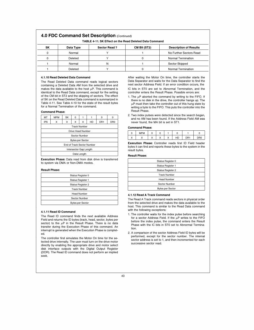
4.0 FDC Command Set Description (Continued)
TABLE 4-11. SK Effect on the Read Deleted Data Command
SK Data Type Sector Read ? CM Bit (ST2) Description of Results
0 Normal Y 1 No Further Sectors Read
0 Deleted Y 0 Normal Termination
1 Normal N 1 Sector Skipped
1 Deleted Y 0 Normal Termination
4.1.10 Read Deleted Data Command
The Read Deleted Data command reads logical sectors
containing a Deleted Data AM from the selected drive and
makes the data available to the host mP. This command is
identical to the Read Data command, except for the setting
of the CM bit in ST2 and the skipping of sectors. The effect
of SK on the Read Deleted Data command is summarized in
Table 4-11. See Table 4-10 for the state of the result bytes
for a Normal Termination of the command.
Command Phase:
MT MFM SK 0 1 1 0 0
IPS X X X X HD DR1 DR0
Track Number
Drive Head Number
Sector Number
Bytes per Sector
End of Track Sector Number
Intersector Gap Length
Data Length
Execution Phase: Data read from disk drive is transferred
to system via DMA or Non-DMA modes.
Result Phase:
Status Register 0
Status Register 1
Status Register 2
Track Number
Head Number
Sector Number
Bytes per Sector
4.1.11 Read ID Command
The Read ID command finds the next available Address
Field and returns the ID bytes (track, head, sector, bytes per
sector) to the mP in the Result Phase. There is no data
transfer during the Execution Phase of this command. An
interrupt is generated when the Execution Phase is complet-
ed.
The controller first simulates the Motor On time for the se-
lected drive internally. The user must turn on the drive motor
directly by enabling the appropriate drive and motor select
disk interface outputs with the Digital Output Register
(DOR). The Read ID command does not perform an implied
seek.
After waiting the Motor On time, the controller starts the
Data Separator and waits for the Data Separator to find the
next sector Address Field. If an error condition occurs, the
IC bits in ST0 are set to Abnormal Termination, and the
controller enters the Result Phase. Possible errors are:
1. The mP aborted the command by writing to the FIFO. If
there is no disk in the drive, the controller hangs up. The
mP must then take the controller out of this hung state by
writing a byte to the FIFO. This puts the controller into the
Result Phase.
2. Two index pulses were detected since the search began,
and no AM has been found. If the Address Field AM was
never found, the MA bit is set in ST1.
Command Phase:
0 MFM 0 0 1 0 1 0
X X X X X HD DR1 DR0
Execution Phase: Controller reads first ID Field header
bytes it can find and reports these bytes to the system in the
result bytes.
Result Phase:
Status Register 0
Status Register 1
Status Register 2
Track Number
Head Number
Sector Number
Bytes per Sector
4.1.12 Read A Track Command
The Read A Track command reads sectors in physical order
from the selected drive and makes the data available to the
host. This command is similar to the Read Data command
with the following exceptions:
1. The controller waits for the index pulse before searching
for a sector Address Field. If the mP writes to the FIFO
before the index pulse, the command enters the Result
Phase with the IC bits in ST0 set to Abnormal Termina-
tion.
2. A comparison of the sector Address Field ID bytes will be
performed, except for the sector number. The internal
sector address is set to 1, and then incremented for each
successive sector read.
43

4.0 FDC Command Set Description (Continued)
3. If the Address Field ID comparison fails, the controller
sets ND in ST1, but continues to read the sector. If there
is a CRC error in the Address Field, the controller sets CE
in ST1, but continues to read the sector.
4. Multi-track and Skip operations are not allowed. SK and
MT should be set to 0.
5. If there is a CRC error in the Data Field, the controller
sets CE in ST1 and CD in ST2, but continues reading
sectors.
6. The controller reads a maximum of EOT physical sectors.
There is no support for multi-track reads.
Command Phase:
0 MFM 0 0 0 0 1 0
IPS X X X X HD DR1 DR0
Track Number
Drive Head Number
Sector Number
Bytes per Sector
End of Track Sector Number
Intersector Gap Length
Data Length
Execution Phase: Data read from disk drive is transferred
to system via DMA or non-DMA modes.
Result Phase:
Status Register 0
Status Register 1
Status Register 2
Track Number
Head Number
Sector Number
Bytes per Sector
4.1.13 Recalibrate Command
The Recalibrate command is very similar to the Seek com-
mand. The controller sets the Present Track Register (PTR)
of the selected drive to zero. It then steps the head of the
selected drive out until the TRK0 disk interface input signal
goes active, or until the maximum number of step pulses
have been issued. See Table 4-12 for the maximum recali-
brate step pulse values based on the R255 and ETR bits in
the Mode command. If the number of tracks on the disk
drive exceeds the maximum number of recalibrate step
pulses, another Recalibrate command may need to be is-
sued.
TABLE 4-12. Maximum Recalibrate
Step Pulses Based on R255 and ETR
R255 ETRMaximum Recalibrate
Step Pulses
0 0 85 (default)
1 0 255
0 1 3925
1 1 4095
After the last command byte is issued, the DRx BUSY bit is
set in the MSR for the selected drive. The controller will
simulate the Motor On time, and then enter the Idle Phase.
The execution of the actual step pulses occur while the con-
troller is in the Drive Polling Phase. An interrupt will be gen-
erated after the TRK0 signal is asserted, or after the maxi-
mum number of recalibrate step pulses are issued. There is
no Result Phase. Recalibrates should not be issued on
more than one drive at a time. This is because the drives are
actually selected via the DOR, which can only select one
drive at a time. No other command except the Sense Inter-
rupt command should be issued while a Recalibrate com-
mand is in progress.
Command Phase:
0 0 0 0 0 1 1 1
0 0 0 0 0 0 DR1 DR0
Execution Phase: Disk drive head is stepped out to Track 0.
Result Phase: None.
4.1.14 Relative Seek Command
The Relative Seek command steps the selected drive in or
out a given number of steps. This command will step the
read/write head an incremental number of tracks, as op-
posed to comparing against the internal present track regis-
ter for that drive.
Command Phase:
1 DIR 0 0 1 1 1 1
X X X X X HD DR1 DR0
Execution Phase: Disk drive head stepped in or out a pro-
grammable number of tracks.
Result Phase: None.
The Relative Seek parameters are defined as follows:
DIR: Read/Write Head Step Direction Control
0 e Step Head Out
1 e Step Head In
RTN: Relative Track Number. This value will determine how
many incremental tracks to step the head in or out
from the current track number.
The controller will issue RTN number of step pulses and
update the Present Track Register for the selected drive.
The one exception to this is if the TRK0 disk input goes
active, which indicates that the drive read/write head is at
the outermost track. In this case, the step pulses for the
Relative Seek are terminated, and the PTR value is set ac-
cording to the actual number of step pulses issued. The
arithmetic is done modulo 255. The DRx BUSY bit in the
MSR is set for the selected drive. The controller will simu-
late the Motor On time before issuing the step pulses. After
the Motor On time, the controller will enter the Idle Phase.
The execution of the actual step pulses occurs in the Idle
Phase of the controller.
After the step operation is complete, the controller will gen-
erate an interrupt. There is no Result Phase. Relative Seeks
should not be issued on more than one drive at a time. This
is because the drives are actually selected via the DOR,
which can only select one drive at a time. No other com-
mand except the Sense Interrupt command should be is-
sued while a Relative Seek command is in progress.
44

4.0 FDC Command Set Description (Continued)
4.1.15 Scan Commands
The Scan commands allow data read from the disk to be
compared against data sent from the mP, using ones com-
plement arithmetic, sector by sector.
There are three Scan commands to choose from:
1. Scan Equal: checks to see if the scanned value of the
disk data is equal to that of the mP data. The scan con-
dition is therefore: disk data e mP data?
2. Scan Low or Equal: checks to see if the scanned val-
ue of the disk data is equal to or less than that of the mP
data. The scan condition is therefore: disk data s data?
3. Scan High or Equal: checks to see if the scanned val-
ue of the disk data is equal to or greater than that of the
mP data. The scan condition is therefore: disk data t
mP data?
The results of these comparisons are indicated in the Status
Register bits 3 and 2, see Table 4-13, and the structure of
the three commands follows.
Each sector is compared starting with the most significant
bytes first, and where the next sector is defined as the cur-
rent Sector Number plus the Sector Step Size. Reading of
sectors continues until either the scan condition is met, the
End of Track (EOT) has been reached, or the Terminal
Count (TC) is asserted.
If the Wildcard mode is enabled in the Mode command, an
FFh from either the disk or the mP is used as a don’t care
byte that will always match equal. Read errors on the disk
will have the same error conditions as the Read Data com-
mand.
Additionally, if the Skip Flag (SK) bit is set, sectors with
deleted data marks will be ignored. If all sectors read are
skipped, the command will terminate with bit 3 of the Status
Register set (mimicking a Scan Equal Hit).
TABLE 4-13. Scan Command Termination Values
CommandComparison
Condition
Status Condition
Met?
Indicated
ResultD2 D3
Scan Equal Disk Data e 1 0 Yes Disk Data e
mP Data? mP Data
0 1 No Disk Data i
mP Data
Scan Low Disk Data s 1 0 Yes Disk Data e
or Equal mP Data? mP Data
0 0 Yes Disk Data k
mP Data
0 1 No Disk Data l
mP Data
Scan High Disk Data t 1 0 Yes Disk Data e
or Equal mP Data? mP Data
0 0 Yes Disk Data l
mP Data
0 1 No Disk Data k
mP Data
SCAN EQUAL
Command Phase:
MT MFM SK 1 0 0 0 1
IPS X X X X HD DR1 DR0
Track Number
Drive Head Number
Sector Number
Bytes per Sector
End of Track Sector Number
Intersector Gap Length
Sector Step Size
Execution Phase: Data transferred from system to control-
ler is compared to data read from disk.
Result Phase:
MT MFM SK 1 1 1 0 1
IPS X X X X HD DR1 DR0
Status Register 0
Status Register 1
Status Register 2
Track Number
Head Number
Sector Number
Bytes per Sector
SCAN HIGH OR EQUAL
Command Phase:
MT MFM SK 1 1 1 0 1
IPS X X X X HD DR1 DR0
Track Number
Drive Head Number
Sector Number
Bytes per Sector
End of Track Sector Number
Intersector Gap Length
Sector Step Size
Execution Phase: Data transferred from system to control-
ler is compared to data read from disk.
Result Phase:
Status Register 0
Status Register 1
Status Register 2
Track Number
Head Number
Sector Number
Bytes per Sector
45

4.0 FDC Command Set Description (Continued)
SCAN LOW OR EQUAL
Command Phase:
MT MFM SK 1 1 0 0 1
IPS X X X X HD DR1 DR0
Track Number
Drive Head Number
Sector Number
Bytes per Sector
End of Track Sector Number
Intersector Gap Length
Sector Step Size
Execution Phase: Data transferred from system to control-
ler is compared to data read from disk.
Result Phase:
Status Register 0
Status Register 1
Status Register 2
Track Number
Head Number
Sector Number
Bytes per Sector
4.1.16 Seek Command
The Seek command steps the selected drive in or out until
the desired track number is reached. During the Execution
Phase of the Seek command, the track number to seek to is
compared with the present track number. The controller will
determine how many step pulses to issue, and the DIR disk
interface output will indicate which direction the R/W head
should move. The DRx BUSY bit is set in the MSR for the
appropriate drive. The controller will wait the Motor On time
before issuing the first step pulse.
After the Motor On time, the controller will enter the Idle
Phase. The execution of the actual step pulses occurs in the
Drive Polling phase of the controller. The step pulse rate is
determined by the value programmed in the Specify com-
mand. An interrupt will be generated one step pulse period
after the last step pulse is issued. A Sense Interrupt com-
mand should be issued to determine the cause of the inter-
rupt. There is no Result Phase.
While the internal microengine is capable of performing
seek commands on 2 or more drives at the same time, soft-
ware should ensure that only one drive is seeking at a time.
This is because the drives are actually selected via the
DOR, which can only select one drive at a time. No other
command except a Sense Interrupt command should be is-
sued while a Seek command is in progress.
If the extended track range mode is enabled with the ETR
bit in the Mode command, a fourth command byte should be
written in the Command Phase to indicate the four most
significant bits of the desired track number. Otherwise, only
three command bytes should be written.
Command Phase:
0 0 0 0 1 1 1 1
X X X X X HD DR1 DR0
New Track Number
MSN of Track Number 0 0 0 0
Note: The last Command Phase byte is required only if ETR is set in Mode
Command.
Execution Phase: Disk drive head is stepped in or out to a
programmed track.
Result Phase: None.
4.1.17 Sense Drive Status Command
The Sense Drive Status command returns the status of the
selected disk drive in ST3. This command does not gener-
ate an interrupt.
Command Phase:
0 0 0 0 0 1 0 0
X X X X X HD DR1 DR0
Execution Phase: Disk drive status information is detected
and reported.
Result Phase:
Status Register 3
4.1.18 Sense Interrupt Command
The Sense Interrupt command is used to determine the
cause of an interrupt when the interrupt is a result of the
change in status of any disk drive.
Command Phase:
0 0 0 0 1 0 0 0
Execution Phase: Status of interrupt is reported.
Result Phase:
Status Register 0
Present Track Number (PTR)
MSN of PTR 0 0 0 0
Note: The third Result Phase byte can only be read if ETR is set in the Mode
Command.
Four possible causes for the interrupt are:
1. Entry into the Result Phase of any of the following com-
mands:
a. Read Data
b. Read Deleted Data
c. Read a Track
d. Read ID
e. Write Data
f. Write Deleted Data
g. Format
h. Scan
i. Verify
2. Occurrence of a data transfer in the Execution Phase
while in the Non-DMA mode.
46

4.0 FDC Command Set Description (Continued)
3. The Ready Signal changed state during the polling mode
for an internally selected drive. (Occurs only after a hard-
ware or software reset.)
4. A Seek, Relative Seek, or Recalibrate command termi-
nates.
An interrupt due to reasons 1 or 2 does not require the
Sense Interrupt command and is cleared automatically. This
type of interrupt occurs during normal command operations
and is easily discernible by the mP via the MSR. It is cleared
when reading or writing information from or to the Data Reg-
ister (FIFO).
An interrupt caused by reasons 3 or 4 is identified with the
aid of the Sense Interrupt command. This type of interrupt is
cleared after the first result byte has been read. Use bits 5,
6, and 7 of ST0 to identify the cause of the interrupt as
shown in Table 4-14.
Issuing a Sense Interrupt command without an interrupt
pending is treated as an Invalid command. If the extended
track range mode is enabled, a third byte should be read in
the Result Phase, which will indicate the four most signifi-
cant bits of the present track number. Otherwise, only two
result bytes should be read.
TABLE 4-14. Status Register 0 Termination Codes
Status Register 0
CauseInterrupt Seek
Code End
D7 D6 D5
1 1 0 Internal Ready Went True
0 0 1 Normal Seek Termination
0 1 1 Abnormal Seek Termination
4.1.19 Set Track Command
This command is used to inspect or change the value of the
internal Present Track Register. This can be useful for re-
covery from disk mistracking errors, where the real current
track can be read through the Read ID command, and then
the Set Track command can be used to set the internal
Present Track Register to the correct value.
If the WNR bit is a 0, a track register is to be read. In this
case, the Result Phase byte contains the value in the inter-
nal register specified, and the third byte in the Command
Phase is a dummy byte.
If the WNR bit is a 1, data is written to a track register. In this
case the third byte of the Command Phase is written to the
specified internal track register, and the Result Phase byte
contains this new value.
The DS1 and DS0 bits select the Present Track Register for
the particular drive. The internal register address depends
on MSB, DS1, and DS0 as shown in Table 4-15. This com-
mand does not generate an interrupt.
TABLE 4-15. Set Track Register Address
DS1 DS0 MSB Register Addressed
0 0 0 PTR0 (LSB)
0 0 1 PTR0 (MSB)
0 1 0 PTR1 (LSB)
0 1 1 PTR1 (MSB)
1 0 0 PTR2 (LSB)
1 0 1 PTR2 (MSB)
1 1 0 PTR3 (LSB)
1 1 1 PTR3 (MSB)
Command Phase:
0 WNR 1 0 0 0 0 1
0 0 1 1 0 MSB DR1 DR0
Present Track Number (PTR)
Execution Phase: Internal register selected by MSB of DR1
or DR0 is read or written.
Result Phase:
Value
4.1.20 Specify Command
The Specify command sets the initial values for three inter-
nal timers. The parameters of this command are undefined
after power-up, and are unaffected by any reset. Thus, soft-
ware should always issue a Specify command as part of an
initialization routine. This command does not generate an
interrupt.
Command Phase:
0 0 0 0 0 0 1 1
Step Rate Time Motor Off Time
Motor On Time DMA
Execution Phase: Internal registers are written.
Result Phase: None.
Step Rate Time: These four bits define the time interval
between successive step pulses during a seek, implied
seek, recalibrate, or relative seek. The programming of this
step rate is shown in Table 4-16.
TABLE 4-16. Step Rate Time (SRT) Values
Data Rate Value Range Units
1 Mbps (16 b SRT)/2 0.5–8 ms
500 kbps (16 b SRT) 1–16 ms
300 kbps (16 b SRT) c 1.67 1.67–26.7 ms
250 kbps (16 b SRT) c 2 2–32 ms
Motor Off Time: These four bits determine the simulated
Motor Off time as shown in Table 4-17.
Motor On Time: These seven bits determine the simulated
Motor On time as shown in Table 4-18.
DMA: This bit selects the data transfer mode in the Execu-
tion Phase of a read, write, or scan operation.
0 e DMA mode is selected
1 e Non-DMA mode is selected
47

4.0 FDC Command Set Description (Continued)
TABLE 4-17. Motor Off Time (MFT) Values
Data RateMode 1 (TMR e 0) Mode 2 (TMR e 1)
UnitsValue Range Value Range
1 Mbps MFT c 8 8–128 MFT c 512 512–8192 ms
500 kbps MFT c 16 16–256 MFT c 512 512–8192 ms
300 kbps MFT c 80/3 26.7–427 MFT c 2560/3 853–13653 ms
250 kbps MFT c 32 32–512 MFT c 1024 1024–16384 ms
Note: Motor Off Time e 0 is treated as MFT e 16.
TABLE 4-18. Motor On Time (MNT) Values
Data RateMode 1 (TMR e 0) Mode 2 (TMR e 1)
UnitsValue Range Value Range
1 Mbps MNT 1–128 MNT c 32 32–4096 ms
500 kbps MNT 1–128 MNT c 32 32–4096 ms
300 kbps MNT c 10/3 3.3–427 MNT c 160/3 53–6827 ms
250 kbps MNT c 4 4–512 MNT c 64 64–8192 ms
Note: Motor On Time e 0 is treated as MNT e 128.
The Motor Off and Motor On timers are artifacts of the NEC
mPD765. These timers determine both the delay from se-
lecting a drive motor until a read or write operation is start-
ed, and the delay of deselecting the drive motor after the
command is completed. Since the FDC enables the drive
and motor select line directly through the DOR, these timers
only provide some delay from the initiation of a command
until it is actually started.
4.1.21 Verify Command
The Verify command reads logical sectors containing a Nor-
mal Data AM from the selected drive without transferring
the data to the host. This command is identical to the Read
Data command, except that no data is transferred during
the Execution Phase.
The Verify command is designed for post-format or post-
write verification. Data is read from the disk, as the control-
ler checks for valid Address Marks in the Address and Data
Fields. The CRC is computed and checked against the pre-
viously stored value on the disk. The EOT value should be
set to the final sector to be checked on each side. If EOT is
greater than the number of sectors per side, the command
will terminate with an error and no useful Address Mark or
CRC data will be given.
The TC pin cannot be used to terminate this command
since no data is transferred. The verify command can simu-
late a TC by setting the EC bit to a 1. In this case, the
command will terminate when SC (Sector Count) sectors
have been read. (If SC e 0 then 256 sectors will be veri-
fied.) If EC e 0, then the command will terminate when
EOT is equal to the last sector to be checked. In this case,
the Data Length parameter should be set to FFh. Refer to
Table 4-10 for the Result Phase values for a successful
completion of the command. Also see Table 4-19 for further
explanation of the result bytes with respect to the MT and
EC bits.
Command Phase:
MT MFM SK 1 0 1 1 0
EC X X X X HD DR1 DR0
Track Number
Drive Head Number
Sector Number
Bytes per Sector
End of Track Sector Number
Intersector Gap Length
Data Length/Sector Count
Execution Phase: Data is read from disk but not transferred
to the system.
Result Phase:
Status Register 0
Status Register 1
Status Register 2
Track Number
Head Number
Sector Number
Bytes per Sector
48

4.0 FDC Command Set Description (Continued)
TABLE 4-19. Verify Command Result Phase
MT EC SC/EOT Value (Notes 1, 2) Termination Result
0 0 DTL used (should be FFh) No Errors
EOT s Ý Sectors per Side
0 0 DTL used (should be FFh) Abnormal Termination
EOT l Ý Sectors per Side
0 1 SC s Ý Sectors per Side No Errors
AND
SC s EOT
0 1 SC l Ý Sectors Remaining Abnormal Termination
OR
SC l EOT
1 0 DTL used (should be FFh) No Errors
EOT s Ý Sectors per Side
1 0 DTL used (should be FFh) Abnormal Termination
EOT l Ý Sectors per Side
1 1 SC s Ý Sectors per Side No Errors
AND
SC s EOT
1 1 SC s (EOT c 2) No Errors
AND
EOT s Ý Sectors per Side
1 1 SC l (EOT c 2) Abnormal Termination
Note 1: Ý Sectors per Side e number of formatted sectors per each side of the disk.
Note 2: Ý Sectors Remaining e number of formatted sectors remaining which can be read, which includes side 1 of the disk if the MT bit is set to 1.
Note 3: If MT e 1 and the SC value is greater than the number of remaining formatted sectors on side 0, verifying will continue on side 1 of the disk.
4.1.22 Version Command
The Version command can be used to determine the floppy
controller being used. The Result Phase uniquely identifies
the floppy controller version. The FDC returns a value of
90h in order to be compatible with the 82077. The DP8473
and other NEC765 compatible controllers will return a value
of 80h (invalid command).
Command Phase:
0 0 0 1 0 0 0 0
Execution Phase: None.
Result Phase:
1 0 0 1 0 0 0 0
49

4.0 FDC Command Set Description (Continued)
4.1.23 Write Data Command
The Write Data command receives data from the host and
writes logical sectors containing a Normal Data AM to the
selected drive. The operation of this command is similar to
the Read Data command except that the data is transferred
from the mP to the controller instead of the other way
around.
The controller will simulate the Motor On time before start-
ing the operation. If implied seeks are enabled, the seek and
sense interrupt functions are then performed. The controller
then starts the Data Separator and waits for the Data Sepa-
rator to find the next sector Address Field. The controller
compares the Address ID (track, head, sector, bytes per
sector) with the desired ID specified in the Command
Phase. If there is no match, the controller waits to find the
next sector Address Field. This process continues until the
desired sector is found. If an error condition occurs, the IC
bits in ST0 are set to Abnormal Termination, and the con-
troller enters the Result Phase. Possible errors are:
1. The mP aborted the command by writing to the FIFO. If
there is no disk in the drive, the controller will hang up.
The mP must then take the controller out of this hung
state by writing a byte to the FIFO. This will put the con-
troller into the Result Phase.
2. Two index pulses were detected since the search began,
and no valid ID has been found. If the track address ID
differs, the WT bit or BT bit (if the track address is FFh)
will be set in ST2. If the head, sector, or bytes per sector
code did not match, the ND bit is set in ST1. If the Ad-
dress Field AM was never found, the MA bit is set in ST1.
3. The Address Field was found with a CRC error. The CE
bit is set in ST1.
4. If the controller detects the Write Protect disk interface
input is Asserted. Bit 1 of ST1 is set.
If the correct Address Field is found, the controller waits for
all (conventional mode) or part (perpendicular mode) of
GAP2 to pass. The controller will then write the preamble
field, address marks, and data bytes to the Data Field. The
data bytes are transferred to the controller by the mP.
Having finished writing the sector, the controller will contin-
ue reading the next logical sector unless one or more of the
following termination conditions has occurred:
1. The DMA controller asserted TC. The IC bits in ST0 are
set to Normal Termination.
2. The last sector address (of side 1 if MT was set) was
equal to EOT. The EOT bit in ST1 is set. The IC bits in
ST0 are set to Abnormal Termination. This is the expect-
ed condition during Non-DMA transfers.
3. Underrun error. The OR bit in ST1 is set. The IC bits in
ST0 are set to Abnormal Termination. If the mP cannot
service a transfer request in time, the last correctly writ-
ten byte will be written to the disk.
If MT was set in the Opcode command byte, and the last
sector of side 0 has been transferred, the controller will then
continue with side 1.
Command Phase:
MT MFM 0 0 0 1 0 1
IPS X X X X HD DR1 DR0
Track Number
Drive Head Number
Sector Number
Bytes per Sector
End of Track Sector Number
Intersector Gap Length
Data Length
Execution Phase: Data is transferred from the system to
the controller via DMA or Non-DMA modes and written to
the disk.
Result Phase:
Status Register 0
Status Register 1
Status Register 2
Track Number
Head Number
Sector Number
Bytes per Sector
4.1.24 Write Deleted Data
The Write Deleted Data command receives data from the
host and writes logical sectors containing a Deleted Data
AM to the selected drive. This command is identical to the
Write Data command except that a Deleted Data AM is writ-
ten to the Data Field instead of a Normal Data AM.
Command Phase:
MT MFM 0 0 1 0 0 1
IPS X X X X HD DR1 DR0
Track Number
Drive Head Number
Sector Number
Bytes per Sector
End of Track Sector Number
Intersector Gap Length
Data Length
Execution Phase: Data is transferred from the system to
the controller via DMA or Non-DMA modes and written to
the disk.
Result Phase:
Status Register 0
Status Register 1
Status Register 2
Track Number
Head Number
Sector Number
Bytes per Sector
50

4.0 FDC Command Set Description (Continued)
4.2 COMMAND SET SUMMARY
CONFIGURE
Command Phase:
0 0 0 1 0 0 1 1
0 0 0 0 0 0 0 0
0 EIS FIFO POLL THRESH
PRETRK
Execution Phase: Internal registers written.
Result Phase: None.
DUMPREG
Command Phase:
0 0 0 0 1 1 1 0
Execution Phase: Internal registers read.
Result Phase:
PTR Drive 0
PTR Drive 1
PTR Drive 2
PTR Drive 3
Step Rate Time Motor Off Time
Motor On Time DMA
Sector per Track/End of Track (Note)
LOCK 0 DC3 DC2 DC1 DC0 GAP WG
0 EIS FIFO POLL THRESH
PRETRK
Note: Sectors per Track parameter returned if last command issued was
Format. End of Track parameter returned if last command issued was
Read or Write.
FORMAT TRACK
Command Phase:
0 MFM 0 0 1 1 0 1
X X X X X HD DR1 DR0
Bytes per Sector
Sectors per Track
Format Gap
Data Pattern
Execution Phase: System transfers four ID bytes (track,
head, sector, bytes/sector) per sector to the floppy control-
ler via DMA or Non-DMA modes. The entire track is format-
ted. The data block in the Data Field of each sector is filled
with the data pattern byte.
Result Phase:
Status Register 0
Status Register 1
Status Register 2
Undefined
Undefined
Undefined
Undefined
INVALID
Command Phase:
Invalid Op Codes
Execution Phase: None.
Result Phase:
Status Register 0 (80h)
LOCK
Command Phase:
LOCK 0 0 1 0 1 0 0
Execution Phase: Internal Lock register is written.
Result Phase:
0 0 0 LOCK 0 0 0 0
MODE
Command Phase:
0 0 0 0 0 0 0 1
TMR IAF IPS 0 LOW PWR 1 ETR
FWR FRD BST R255 0 0 0 0
DENSEL BFR WLD Head Settle
0 0 0 0 0 RG 0 PU
Execution Phase: Internal registers are written.
Result Phase: None.
NSC
Command Phase:
0 0 0 1 1 0 0 0
Execution Phase: None.
Result Phase:
0 1 1 1 0 0 1 1
PERPENDICULAR MODE
Command Phase:
0 0 0 1 0 0 1 0
OW 0 DC3 DC2 DC1 DC0 GAP WG
51

4.0 FDC Command Set Description (Continued)
Execution Phase: Internal registers are written.
Result Phase: None.
READ DATA
Command Phase:
MT MFM SK 0 0 1 1 0
IPS X X X X HD DR1 DR0
Track Number
Drive Head Number
Sector Number
Bytes per Sector
End of Track Sector Number
Intersector Gap Length
Data Length
Execution Phase: Data read from disk drive is transferred
to system via DMA or Non-DMA modes.
Result Phase:
Status Register 0
Status Register 1
Status Register 2
Track Number
Head Number
Sector Number
Bytes per Sector
READ DELETED DATA
Command Phase:
MT MFM SK 0 1 1 0 0
IPS X X X X HD DR1 DR0
Track Number
Drive Head Number
Sector Number
Bytes per Sector
End of Track Sector Number
Intersector Gap Length
Data Length
Execution Phase: Data read from disk drive is transferred
to system via DMA or Non-DMA modes.
Result Phase:
Status Register 0
Status Register 1
Status Register 2
Track Number
Head Number
Sector Number
Bytes per Sector
READ ID
Command Phase:
0 MFM 0 0 1 0 1 0
X X X X X HD DR1 DR0
Execution Phase: Controller reads first ID Field header
bytes it can find and reports these bytes to the system in the
result bytes.
Result Phase:
Status Register 0
Status Register 1
Status Register 2
Track Number
Head Number
Sector Number
Bytes per Sector
READ A TRACK
Command Phase:
0 MFM 0 0 0 0 1 0
IPS X X X X HD DR1 DR0
Track Number
Drive Head Number
Sector Number
Bytes per Sector
End of Track Sector Number
Intersector Gap Length
Data Length
Execution Phase: Data read from disk drive is transferred
to system via DMA or non-DMA modes.
Result Phase:
Status Register 0
Status Register 1
Status Register 2
Track Number
Head Number
Sector Number
Bytes per Sector
RECALIBRATE
Command Phase:
0 0 0 0 0 1 1 1
0 0 0 0 0 0 DR1 DR0
Execution Phase: Disk drive head is stepped out to Track 0.
Result Phase: None.
52

4.0 FDC Command Set Description (Continued)
RELATIVE SEEK
Command Phase:
1 DIR 0 0 1 1 1 1
X X X X X HD DR1 DR0
Execution Phase: Disk drive head stepped in or out a pro-
grammable number of tracks.
Result Phase: None.
SCAN EQUAL
Command Phase:
MT MFM SK 1 0 0 0 1
IPS X X X X HD DR1 DR0
Track Number
Drive Head Number
Sector Number
Bytes per Sector
End of Track Sector Number
Intersector Gap Length
Sector Step Size
Execution Phase: Data transferred from system to control-
ler is compared to data read from disk.
Result Phase:
MT MFM SK 1 1 1 0 1
IPS X X X X HD DR1 DR0
Status Register 0
Status Register 1
Status Register 2
Track Number
Head Number
Sector Number
Bytes per Sector
SCAN HIGH OR EQUAL
Command Phase:
MT MFM SK 1 1 1 0 1
IPS X X X X HD DR1 DR0
Track Number
Drive Head Number
Sector Number
Bytes per Sector
End of Track Sector Number
Intersector Gap Length
Sector Step Size
Execution Phase: Data transferred from system to control-
ler is compared to data read from disk.
Result Phase:
Status Register 0
Status Register 1
Status Register 2
Track Number
Head Number
Sector Number
Bytes per Sector
SCAN LOW OR EQUAL
Command Phase:
MT MFM SK 1 1 0 0 1
IPS X X X X HD DR1 DR0
Track Number
Drive Head Number
Sector Number
Bytes per Sector
End of Track Sector Number
Intersector Gap Length
Sector Step Size
Execution Phase: Data transferred from system to control-
ler is compared to data read from disk.
Result Phase:
Status Register 0
Status Register 1
Status Register 2
Track Number
Head Number
Sector Number
Bytes per Sector
SEEK
Command Phase:
0 0 0 0 1 1 1 1
X X X X X HD DR1 DR0
New Track Number
MSN of Track Number 0 0 0 0
Note: The last Command Phase byte is required only if ETR is set in Mode
Command.
Execution Phase: Disk drive head is stepped in or out to a
programmed track.
Result Phase: None.
53

4.0 FDC Command Set Description (Continued)
SENSE DRIVE STATUS
Command Phase:
0 0 0 0 0 1 0 0
X X X X X HD DR1 DR0
Execution Phase: Disk drive status information is detected
and reported.
Result Phase:
Status Register 3
SENSE INTERRUPT
Command Phase:
0 0 0 0 1 0 0 0
Execution Phase: Status of interrupt is reported.
Result Phase:
Status Register 0
Present Track Number (PTR)
MSN of PTR 0 0 0 0
Note: The third Result Phase byte can only be read if ETR is set in the Mode
Command.
SET TRACK
Command Phase:
0 WNR 1 0 0 0 0 1
0 0 1 1 0 MSB DR1 DR0
Present Track Number (PTR)
Execution Phase: Internal register selected by MSB of DR1
or DR0 is read or written.
Result Phase:
Value
SPECIFY
Command Phase:
0 0 0 0 0 0 1 1
Step Rate Time Motor Off Time
Motor On Time DMA
Execution Phase: Internal registers are written.
Result Phase: None.
VERIFY
Command Phase:
MT MFM SK 1 0 1 1 0
EC X X X X HD DR1 DR0
Track Number
Drive Head Number
Sector Number
Bytes per Sector
End of Track Sector Number
Intersector Gap Length
Data Length/Sector Count
Execution Phase: Data is read from disk but not transferred
to the system.
Result Phase:
Status Register 0
Status Register 1
Status Register 2
Track Number
Head Number
Sector Number
Bytes per Sector
VERSION
Command Phase:
0 0 0 1 0 0 0 0
Execution Phase: None.
Result Phase:
1 0 0 1 0 0 0 0
54

4.0 FDC Command Set Description (Continued)
WRITE DATA
Command Phase:
MT MFM 0 0 0 1 0 1
IPS X X X X HD DR1 DR0
Track Number
Drive Head Number
Sector Number
Bytes per Sector
End of Track Sector Number
Intersector Gap Length
Data Length
Execution Phase: Data is transferred from the system to
the controller via DMA or Non-DMA modes and written to
the disk.
Result Phase:
Status Register 0
Status Register 1
Status Register 2
Track Number
Head Number
Sector Number
Bytes per Sector
WRITE DELETED DATA
Command Phase:
MT MFM 0 0 1 0 0 1
IPS X X X X HD DR1 DR0
Track Number
Drive Head Number
Sector Number
Bytes per Sector
End of Track Sector Number
Intersector Gap Length
Data Length
Execution Phase: Data is transferred from the system to
the controller via DMA or Non-DMA modes and written to
the disk.
Result Phase:
Status Register 0
Status Register 1
Status Register 2
Track Number
Head Number
Sector Number
Bytes per Sector
55

4.0 FDC Command Set Description (Continued)
4.3 MNEMONIC DEFINITIONS FOR FDC COMMANDS
Symbol Description
BFR Buffer enable bit used in the Mode command.
Enabled open-collector output buffers.
BST Burst Mode disable control bit used in Mode
command. Selects the Non-Burst FIFO mode if
the FIFO is enabled.
DC0 Drive Configuration 0–3. Used to set DC1a
drive to conventional or perpendicular DC2
mode. Used in Perpendicular Mode DC3 com-
mand.
DENSEL Density Select control bits used in the Mode
command.
DIR Direction control bit used in Relative Seek
command to indicate step in or out.
DMA DMA mode enable bit used in the Specify com-
mand.
DR0 Drive Select 0–1 bits used in most commands.
Selects the logical drive.
DTL Data Length parameter used in the Read,
Write, Scan and Verify commands.
EC Enable Count control bit used in the Verify
command. When this bit is 1, the DTL parame-
ter becomes SC (Sector Count).
EIS Enable Implied Seeks. Used in the Configure
command.
EOT End of Track parameter set in the Read, Write,
Scan, and Verify commands.
ETR Extended Track Range used with the Seek
command.
FIFO First-In First-Out buffer. Also a control bit used
in the Configure command to enable or disable
the FIFO.
FRD FIFO Read disable control bit used in the
Mode command.
FWR FIFO Write disable control bit used in the
Mode command.
GAP GAP2 control bit used in the Perpendicular
Mode command.
HD Head Select control bit used in most com-
mands. Selects Head 0 or 1 of the disk.
IAF Index Address Field control bit used in the
Mode command. Enables the ISO Format dur-
ing the Format command.
IPS Implied Seek enable bit used in the Mode,
Read, Write, and Scan commands.
LOCK Lock enable bit in the Lock command. Used to
make certain parameters be unaffected by a
software reset.
LOW PWR Low Power control bits used in the Mode com-
mand.
MFM Modified Frequency Modulation control bit
used in the Read, Write, Format, Scan and
Verify commands. Selects MFM or FM data
encoding.
MFT Motor Off Time programmed in the Specify
command.
MNT Motor On Time programmed in the Specify
command.
MT Multi-Track enable bit used in the Read, Write,
Scan and Verify commands.
OW Overwrite control bit used in the Perpendicular
Mode command.
POLL Enable Drive Polling bit used in the Configure
command.
PRETRK Precompensation Track Number used in the
Configure command.
PTR Present Track Register. Contains the internal
track number for one of the four logical disk
drives.
PU Pump diagnostic enable bit used in the Mode
command.
R255 Recalibrate control bit used in Mode com-
mand. Sets maximum recalibrate step pulses
to 255.
RG Read Gate diagnostic enable bit used in the
Mode command.
RTN Relative Track Number used in the Relative
Seek command.
SC Sector Count control bit used in the Verify
command.
SK Skip control bit used in read and scan opera-
tions.
SRT Step Rate Time programmed in the Specify
command. Determines the time between step
pulses for seek and recalibrates.
ST0 Status Register 0–3. Contains status ST1 in-
formation about the execution of an ST2 com-
mand. Read in the Result Phase of some ST3
commands.
THRESH FIFO threshold parameter used in the Config-
ure command.
TMR Timer control bit used in the Mode command.
Affects the timers set in the Specify command.
WG Write Gate control bit used in the Perpendicu-
lar Mode command.
WLD Wildcard bit in the Mode command used to en-
able or disable the wildcard byte (FF) during
Scan commands.
56

5.0 FDC Functional DescriptionThe PC87303 is software compatible with the DP8473 and
82077 floppy disk controllers. Upon a power on reset, the
16-byte FIFO will be disabled. Also, the disk interface out-
puts will be configured as active push-pull outputs, which
are compatible with both CMOS inputs and open-collector
resistor terminated disk drive inputs. The FIFO can be en-
abled with the Configure command. The FIFO can be very
useful at the higher data rates, with systems that have a
large amount of DMA bus latency, or with multi-tasking sys-
tems such as the EISA or MCA bus structures.
The FDC will support all the DP8473 Mode command fea-
tures as well as some additional features. Additional fea-
tures include control over the enabling of the FIFO for reads
and writes, a Non-Burst mode for the FIFO, a bit that will
configure the disk interface outputs as open-drain outputs,
and programmability of the DENSEL output.
5.1 MICROPROCESSOR INTERFACE
The FDC interface to the microprocessor consists of the
A9–A3, AEN, RD, and WR lines, which access the chip for
reads and writes; the data lines D7–0; the address lines
A2–0, which select the appropriate register (see Table 3-1);
the IRQ6 signal, and the DMA interface signals DRQ,
DACK, and TC. It is through this microprocessor interface
that the floppy controller receives commands, transfers
data, and returns status information.
5.2 MODES OF OPERATION
The FDC has three modes of operation: PC-AT mode, PS/2
mode, and Model 30 mode, which are determined by the
state of the IDENT pin and MFM pin. IDENT can be tied
directly to VDD or GND. The MFM pin must be tied high or
low with a 10 kX resistor (there is an internal 40 kX–50 kXresistor on the MFM pin). The state of these pins is interro-
gated by the controller during a chip reset to determine the
mode of operation. See Section 3.0 Register Description for
more details on the register set used for each mode of oper-
ation. After chip reset, the state of IDENT can be changed
to change the polarity of DENSEL (see Section 1.0 Pin De-
scription).
PC-AT ModeÐBits 7, 6 of ASC register are 11 (default):
The PC-AT register set is enabled. The DMA enable bit in
the Digital Output Register becomes valid (IRQ6 and DRQ
can be TRI-STATE). TC and DENSEL become active high
signals (defaults to a 5.25× floppy drive).
PS/2 ModeÐBits 7, 6 of ASC register are 01: This mode
supports the PS/2 Models 50/60/80 configuration and reg-
ister set. The DMA enable bit in the Digital Output Register
becomes a don’t care (IRQ6 and DRQ signals are always
valid). TC and DENSEL become active low signals (default
to 3.5× floppy drive).
Model 30 ModeÐBits 7, 6 of ASC register are 00: This
mode supports the PS/2 Model 30 configuration and regis-
ter set. The DMA enable bit in the Digital Output Register
becomes valid (IRQ6 and DRQ can be TRI-STATE). TC is
active high and DENSEL becomes active low (default to
3.5× floppy drive).
5.3 CONTROLLER PHASES
The FDC has three separate phases of a command, the
Command Phase, the Execution Phase, and the Result
Phase. Each of these controller phases determine how data
is transferred between the floppy controller and the host
microprocessor. In addition, when no command is in prog-
ress, the controller is in the Idle Phase or Drive Polling
Phase.
5.3.1 Command Phase
During the Command Phase, the mP writes a series of bytes
to the Data Register. The first command byte contains the
opcode for the command, and the controller knows how
many more bytes to expect based on this opcode byte. The
remaining command bytes contain the particular parameters
required for the command. The number of command bytes
varies for each particular command. All the command bytes
must be written in the order specified in the Command De-
scription Table. The Execution Phase starts immediately af-
ter the last byte in the Command Phase is written. Prior to
performing the Command Phase, the Digital Output Register
should be set and the data rate should be set with the Data
Rate Select Register or Configuration Control Register.
The Main Status Register controls the flow of command
bytes, and must be polled by the software before writing
each Command Phase byte to the Data Register. Prior to
writing a command byte, the RQM bit (D7) must be set and
the DIO bit (D6) must be cleared in the MSR. After the first
command byte is written to the Data Register, the CMD
PROG bit (D4) is also set and remains set until the last
Result Phase byte is read. If there is no Result Phase, the
CMD PROG bit will be cleared after the last command byte
is written.
A new command may be initiated after reading all the result
bytes from the previous command. If the next command
requires selecting a different drive or changing the data rate,
the DOR and DSR or CCR should be updated. If the com-
mand is the last command, the software should deselect the
drive.
Note: As a general rule, the operation of the controller core is independent
of how the mP updates the DOR, DSR, and CCR. The software must
ensure that the manipulation of these registers is coordinated with the
controller operation.
5.3.2 Execution Phase
During the Execution Phase, the disk controller performs
the desired command. Commands that involve data trans-
fers, (e.g., read, write, or format operation) require the mP to
write or read data to or from the Data Register at this time.
Some commands such as a Seek or Recalibrate control the
read/write head movement on the disk drive during the Exe-
cution Phase via the disk interface signals. Execution of oth-
er commands does not involve any action by the mP or disk
drive, and consists of an internal operation by the controller.
57

5.0 FDC Functional Description (Continued)
If there is data to be transferred between the mP and the
controller during the Execution, there are three methods
that can be used, DMA mode, interrupt transfer mode, and
software polling mode. The last two modes are called the
Non-DMA modes. The DMA mode is used if the system has
a DMA controller. This allows the mP to do other tasks while
the data transfer takes place during the Execution Phase. If
the Non-DMA mode is used, an interrupt is issued for each
byte transferred during the Execution Phase. Also, instead
of using the interrupt during Non-DMA mode, the Main
Status Register can be polled by software to indicate when
a byte transfer is required. All of these data transfer modes
work with the FIFO enabled or disabled.
5.3.2.1 DMA ModeÐFIFO Disabled
The DMA mode is selected by writing a 0 to the DMA bit in
the Specify command and by setting the DMA enabled bit
(D3) in the DOR. With the FIFO disabled, a DMA request
(DRQ) is generated in the Execution Phase when each byte
is ready to be transferred. The DMA controller should re-
spond to the DRQ with a DMA acknowledge (DACK) and a
read or write strobe. The DRQ is cleared by the leading
edge of the active low DACK input signal. After the last byte
is transferred, an interrupt is generated, indicating the begin-
ning of the Result Phase. During DMA operations the chip
select input (CS) must be held high. The DACK signal acts
as the chip select for the FIFO in this case, and the state of
the address lines A2–A0 is a don’t care. The Terminal
Count (TC) signal can be asserted by the DMA controller to
terminate the data transfer at any time. Due to internal gat-
ing, TC is only recognized when DACK is low.
PC-AT Mode. When in the PC-AT interface mode with the
FIFO disabled, the controller is in single byte transfer mode.
That is, the system has one byte time to service a DMA
request (DRQ) from the controller. DRQ will be deasserted
between each byte.
PS/2 and Model 30 Modes. When in the PS/2 or Model 30
modes, DMA transfers with the FIFO disabled are per-
formed differently. Instead of a single byte transfer mode,
the FIFO is actually enabled with THRESH e 0Fh. Thus,
DRQ is asserted when one byte has entered the FIFO dur-
ing reads, and when one byte can be written to the FIFO
during writes. DRQ is deasserted by the leading edge of the
DACK input, and is reasserted when DACK goes inactive
high. This operation is very similar to Burst mode transfer
with the FIFO enabled except that DRQ is deasserted be-
tween each byte.
5.3.2.2 DMA ModeÐFIFO Enabled
Read Data Transfers
Whenever the number of bytes in the FIFO is greater than
or equal to (16 b THRESH), a DRQ is generated. This is the
trigger condition for the FIFO read data transfers from the
floppy controller to the mP.
Burst Mode. DRQ remains active until enough bytes have
been read from the controller to empty the FIFO.
Non-Burst Mode. DRQ is deasserted after each read trans-
fer. If the FIFO is not completely empty, DRQ is reasserted
after a 350 ns delay. This allows other higher priority DMA
transfers to take place between floppy transfers. In addition,
this mode allows the controller to work correctly in systems
where the DMA controller is put into a read verify mode,
where only DACK signals are sent to the FDC, with no RD
pulses. This read verify mode of the DMA controller is used
in some PC software. The FIFO Non-Burst mode allows the
DACK input from the DMA controller to be strobed, which
correctly clocks data from the FIFO.
For both the Burst and Non-Burst modes, when the last byte
in the FIFO has been read, DRQ goes inactive. DRQ is then
reasserted when the FIFO trigger condition is satisfied. After
the last byte of a sector has been read from the disk, DRQ
is again generated even if the FIFO has not yet reached its
threshold trigger condition. This guarantees that all the cur-
rent sector bytes are read from the FIFO before the next
sector byte transfer begins.
Write Data Transfers
Whenever the number of bytes in the FIFO is less than or
equal to THRESH, a DRQ is generated. This is the trigger
condition for the FIFO write data transfers from the mP to
the floppy controller.
Burst Mode. DRQ remains active until enough bytes have
been written to the controller to completely fill the FIFO.
Non-Burst Mode. DRQ is deasserted after each write
transfer. If the FIFO is not full, DRQ is reasserted after a 350
ns delay. This deassertion of DRQ allows other higher priori-
ty DMA transfers to take place between floppy transfers.
The FIFO has a byte counter which monitors the number of
bytes being transferred to the FIFO during write operations
for both Burst and Non-Burst modes. When the last byte of
a sector is transferred to the FIFO, DRQ is deasserted even
if the FIFO has not been completely filled. Thus, the FIFO is
cleared after each sector is written. Only after the floppy
controller has determined that another sector is to be writ-
ten is DRQ asserted again. Also, since DRQ is deasserted
immediately after the last byte of a sector is written to the
FIFO, the system does not need to tolerate any DRQ deas-
sertion delay and is free to do other work.
Read and Write Data Transfers
The DACK input signal from the DMA controller may be held
active during an entire burst or it may be strobed for each
byte transferred during a read or write operation. When in
the Burst mode, the floppy controller deasserts DRQ as
soon as it recognizes that the last byte of a burst was trans-
ferred. If DACK is strobed for each byte, the leading edge of
this strobe is used to deassert DRQ. If DACK is strobed, RD
or WR are not required. This is the case during the Read-
58
5.0 FDC Functional Description (Continued)
Verify mode of the DMA controller. If DACK is held active
during the entire burst, the trailing edge of the RD or WR
strobe is used to deassert DRQ. DRQ is deasserted within
50 ns of the leading edge of DACK, RD, or WR. This quick
response should prevent the DMA controller from transfer-
ring extra bytes in most applications.
Overrun Errors
An overrun or underrun error terminates the execution of
the command if the system does not transfer data within the
allotted data transfer time (see Section 3.7), which puts the
controller into the Result Phase. During a read overrun, the
mP is required to read the remaining bytes of the sector
before the controller asserts IRQ6, signifying the end of ex-
ecution. During a write operation, an underrun error termi-
nates the Execution Phase after the controller has written
the remaining bytes of the sector with the last correctly writ-
ten byte to the FIFO and generated the CRC bytes. Whether
there is an error or not, an interrupt is generated at the end
of the Execution Phase, and is cleared by reading the first
Result Phase byte.
DACK asserted alone without a RD or WR strobe is also
counted as a transfer. If RD or WR are not being strobed for
each byte, DACK must be strobed for each byte so that the
floppy controller can count the number of bytes correctly. A
new command, the Verify command, has been added to
allow easier verification of data written to the disk without
the need of actually transferring the data on the data bus.
5.3.2.3 Interrupt ModeÐFIFO Disabled
If the Interrupt (Non-DMA) mode is selected, IRQ6 is assert-
ed instead of DRQ when each byte is ready to be trans-
ferred. The Main Status Register should be read to verify
that the interrupt is for a data transfer. The RQM and NON
DMA bits (D7 and D5) in the MSR are set. The interrupt is
cleared when the byte is transferred to or from the Data
Register. CS and RD or CS and WR must be used to trans-
fer the data in or out of the Data Register (A2–A0 must be
valid). CS asserted by itself is not significant. CS must be
asserted with RD or WR for a read or write transfer to be
recognized.
The mP should transfer the byte within the data transfer
service time (see Section 3.7). If the byte is not transferred
within the time allotted, an Overrun Error will be indicated in
the Result Phase when the command terminates at the end
of the current sector.
An interrupt is also be generated after the last byte is trans-
ferred. This indicates the beginning of the Result Phase.
The RQM and DIO bits (D7 and D6) in the MSR is set, and
the non-DMA bit (D5) is cleared. This interrupt is cleared by
reading the first Result Phase byte.
5.3.2.4 Interrupt ModeÐFIFO Enabled
The Interrupt (Non-DMA) mode with the FIFO enabled is
very similar to the Non-DMA mode with the FIFO disabled.
In this case, IRQ6 is asserted instead of DRQ under the
exact same FIFO threshold trigger conditions. The MSR
should be read to verify that the interrupt is for a data trans-
fer. The RQM and NON DMA bits (D7 and D5) in the MSR is
set. CS and RD or CS and WR must be used to transfer the
data in or out of the Data Register (A2–A0 must be valid).
CS asserted by itself is not significant. CS must be asserted
with RD or WR for a read or write transfer to be recognized.
The Burst mode may be used to hold the IRQ6 pin active
during a burst, or the Non-Burst mode may be used to tog-
gle the IRQ6 pin for each byte of a burst. The Main Status
Register is always valid from the mP point of view. For ex-
ample, during a read command, after the last byte of data
has been read from the disk and placed in the FIFO, the
MSR still indicates that the Execution Phase is active, and
that data needs to be read from the Data Register. Only
after the last byte of data has been read by the mP from the
FIFO does the Result Phase begin.
The same overrun and underrun error procedures from the
DMA mode apply to the Non-DMA mode. Also, whether
there is an error or not, an interrupt is generated at the end
of the Execution Phase, and is cleared by reading the first
Result Phase byte.
5.3.2.5 Software Polling
If the Non-DMA mode is selected and interrupts are not
suitable, the mP can poll the MSR during the Execution
Phase to determine when a byte is ready to be transferred.
The RQM bit (D7) in the MSR reflects the state of the IRQ6
signal. Otherwise, the data transfer is similar to the Interrupt
Mode described above. This is true for the FIFO enabled or
disabled.
5.3.3 Result Phase
During the Result Phase, the mP reads a series of bytes
from the data register. These bytes indicate the status of the
command. This status may indicate whether the command
executed properly, or contain some control information (see
the Command Description and Status Register Description).
These Result Phase bytes are read in the order specified for
that particular command. Some commands will not have a
result phase. Also, the number of result bytes varies with
each command. All of the result bytes must be read from
the Data Register before the next command can be issued.
Like the Command Phase, the Main Status Register con-
trols the flow of result bytes, and must be polled by the
software before reading each Result Phase byte from the
Data Register. The RQM bit (D7) and DIO bit (D6) must both
be set before each result byte can be read. After the last
result byte is read, the COM PROG bit (D4) in the MSR is
cleared, and the controller is ready for the next command.
5.3.4 Idle Phase
After a hardware or software reset, or after the chip has
recovered from the power-down mode, the controller enters
the Idle Phase. Also, when there are no commands in prog-
ress the controller is in the Idle Phase. The controller waits
for a command byte to be written to the Data Register. The
RQM bit is set and the DIO bit cleared in the MSR. After
receiving the first command (opcode) byte, the controller
enters the Command Phase. When the command is com-
pleted the controller again enters the Idle Phase. The Data
Separator remains synchronized to the reference frequency
while the controller is idle. While in the Idle Phase, the con-
troller will periodically enters the Drive Polling Phase (see
Section 5.3.5).
59

5.0 FDC Functional Description (Continued)
5.3.5 Drive Polling Phase
The National FDC supports the polling mode of the old gen-
eration 8-inch drives as a means of monitoring any change
in status for each disk drive present in the system. This
mode is supported for the sole purpose of providing back-
ward compatibility with software that expects its presence.
While in the Idle Phase the controller enters a Drive Polling
Phase every 1 ms (based on the 500 kbps data rate). While
in the Drive Polling Phase, the controller interrogates the
Ready Changed status for each of the four logical drives.
The internal Ready line for each drive is toggled only after a
hardware or software reset, and an interrupt is generated for
drive 0. At this point, the software must issue four Sense
Interrupt commands to clear the Ready Changed State
status for each drive. This requirement can be eliminated if
drive polling is disabled via the POLL bit in the Configure
command. The Configure command must be issued within
500 ms (worst case ) of the hardware or software reset for
drive polling to be disabled.
Even if drive polling is disabled, drive stepping and delayed
power-down occurs in the Drive Polling Phase. The control-
ler checks the status of each drive and if necessary it issues
a step pulse on the STEP output with the DIR signal at the
appropriate logic level. Also, the controller uses the Drive
Polling Phase to control the Automatic Low Power mode.
When the Motor Off time has expired, the controller waits
512 ms based on the 500 kbps and 1 Mbps data rate before
powering down if this function is enabled via the Mode com-
mand.
If a new command is issued when the FDC is in the middle
of a polling routine, the MSR will not indicate a ready status
for the next parameter byte until the poling sequence com-
pletes the loop. This can cause a delay between the first
and second bytes of up to 500 ms at 250 kbps.
5.4 DATA SEPARATOR
The internal data separator consists of an analog PLL and
its associated circuitry. The PLL synchronizes the raw data
signal read from the disk drive. The synchronized signal is
used to separate the encoded clock and data pulses. The
data pulses are deserialized into bytes and then sent to the
mP by the controller.
The main PLL consists of five main components, a phase
comparator, a charge pump, a filter, a voltage controlled
oscillator (VCO), and a programmable divider. The phase
comparator detects the difference between the phase of the
divider’s output and the phase of the raw data being read
from the disk. This phase difference is converted to a cur-
rent by the charge pump, which either charges or discharg-
es one of three filters which is selected based on the data
rate. The resulting voltage on the filter changes the frequen-
cy of the VCO and the divider output to reduce the phase
difference between the input data and the divider’s output.
The PLL is ‘‘locked’’ when the frequency of the divider is
exactly the same as the average frequency of the data read
from the disk. A block diagram of the data separator is
shown in Figure 5-1 .
To ensure optimal performance, the data separator incorpo-
rates several additional circuits. The quarter period delay
line is used to determine the center of each bit cell, and to
disable the phase comparator when the raw data signal is
missing a clock or data pulse in the MFM or FM pattern. A
secondary PLL is used to automatically calibrate the quarter
period delay line. The secondary PLL also calibrates the
center frequency of the VCO.
To eliminate the logic associated with controlling multiple
data rates, the FDC supports each of the four data rates
(250, 300, 500 kbps, and 1 Mbps) with a separate, optimized
internal filter. The appropriate filter for each data rate is au-
tomatically switched into the data separator circuit when the
data rate is selected via the Data Rate Select or Configura-
tion Control Register. These filters have been optimized
through lab experimentation, and are designed into the con-
troller to reduce the external component cost associated
with the floppy controller.
The FDC has a dynamic window margin and lock range per-
formance capable of handling a wide range of floppy disk
drives. Also, the data separator works well under a variety of
conditions, including the high motor speed fluctuations of
floppy compatible tape drives.
Figure 5-2 shows the floppy disk controller dynamic window
margin performance at the four different data rates. Dynam-
ic window margin is the primary indicator of the quality and
performance level of the data separator. This measurement
indicates how much motor speed variation (MSV) of the
drive spindle motor and bit jitter (or window margin) can be
tolerated by the data separator.
MSV is shown on the x-axis of the dynamic window margin
graph. MSV is translated directly to the actual data rate of
the data as it is read from the disk by the data separator.
That is, a faster than nominal motor will result in a higher
frequency in the actual data rate.
The dynamic window margin performance curves also indi-
cate how much bit jitter (or window margin) can be tolerated
by the data separator. This parameter is shown on the
y-axis of the graphs. Bit jitter is caused by the magnetic
interaction of adjacent data pulses on the disk, which effec-
tively shifts the bits away from their nominal positions in the
middle of the bit window. Window margin is commonly mea-
sured as a percentage. This percentage indicates how far a
data bit can be shifted early or late with respect to its nomi-
nal bit position, and still be read correctly by the data sepa-
rator. If the data separator cannot correctly decode a shifted
bit, then the data is misread and a CRC results.
60

5.0 FDC Functional Description (Continued)
The dynamic window margin performance curves contain
two pieces of information: 1) the maximum range of MSV
(also called ‘‘lock range’’) that the data separator can han-
dle with no read errors, and 2) the maximum percentage of
window margin (or bit jitter) that the data separator can han-
dle with no read errors. Thus, the area under the dynamic
window margin curves inFigure 5-2 is the range of MSV and
bit jitter that the FDC can handle with no read errors. The
FDC internal analog data separator has a much better per-
formance than comparable digital data separator designs,
and does not require any external components.
Note: The dynamic window margin curves were generated using a FlexStar
FS-540 Floppy Disk Simulator and a proprietary dynamic window mar-
gin test program written by National Semiconductor.
The controller takes best advantage of the internal analog
data separator by implementing a sophisticated read algo-
rithm. This ID search algorithm, shown in Figure 5-3 , en-
hances the PLL’s lock characteristics by forcing the PLL to
relock to the crystal reference frequency any time the data
separator attempts to lock to a non-preamble pattern. This
algorithm ensures that the PLL is not thrown way out of lock
by write splices or bad data fields.
TL/C/12074–20
FIGURE 5-1. FDC Data Separator Block Diagram
61

5.0 FDC Functional Description (Continued)
250 kbps
TL/C/12074–21
300 kbps
TL/C/12074–22
500 kbps
TL/C/12074–23
1 Mbps
TL/C/12074–24
FIGURE 5-2. PC87303 Dynamic Window Margin Performance
(Typical performance at VDD e 5.0V, 25§C)
5.5 CRYSTAL OSCILLATOR
The FDC is clocked by a single 24 MHz signal. An on-chip
oscillator is provided to enable the attachment of a crystal
or a clock signal.
A parallel resonant crystal is preferred if at all possible. In
some cases, a series resonant crystal can be used, but care
must be taken to ensure that the crystal does not oscillate
at a sub-harmonic frequency. The oscillator is able to work
with high profile, low profile, and surface mount type crystal
enclosures. External bypass capacitors (5 pF to 10 pF)
should be connected from XTAL1 and XTAL2 to GND. If an
external oscillator circuit is used, it must have a duty cycle of
at least 40%–60%, and minimum input levels of 2.4V and
0.4V. The controller should be configured so that the exter-
nal oscillator clock is input into the X1/OSC pin, and XTAL2
is left unconnected.
5.6 PERPENDICULAR RECORDING MODE
The FDC is fully compatible with perpendicular recording
mode disk drives at all data rates. These perpendicular
mode drives are also called 4 Mbyte (unformatted) or
2.88 Mbyte (formatted) drives, which refers to their maxi-
mum storage capacity. Perpendicular recording will orient
the magnetic flux changes (which represent bits) vertically
on the disk surface, allowing for a higher recording density
than the conventional longitudinal recording methods. With
this increase in recording density comes an increase in the
data rate of up to 1 Mbps, thus doubling the storage capaci-
ty. In addition, the perpendicular 2.88M drive is read/write
compatible with 1.44M and 720k diskettes (500 kbps and
250 kbps respectively).
62

5.0 FDC Functional Description (Continued)
The 2.88M drive has unique format and write data timing
requirements due to its read/write head and pre-erase head
design (see Figure 5-4 ). Unlike conventional disk drives
which have only a read/write head, the 2.88M drive has
both a pre-erase head and read/write head. With conven-
tional disk drives, the read/write head by itself is able to
rewrite the disk without problems. For 2.88M drives, a pre-
erase head is needed to erase the magnetic flux on the disk
surface before the read/write can write to the disk surface.
The pre-erase head is activated during disk write operations
only, i.e., Format and Write Data commands.
In 2.88M drives, the pre-erase head leads the read/write
head by 200 mm, which translates to 38 bytes at 1 Mbps
(19 bytes at 500 kbps). For both conventional and perpen-
dicular drives, WGATE is asserted with respect to the posi-
tion of the read/write head. With conventional drives, this
means that WGATE is asserted when the read/write head is
located at the beginning of the Data Field preamble. With the
2.88M drives, since the preamble must be pre-erased be-
fore it is rewritten, WGATE should be asserted when the
pre-erase head is located at the beginning of the Data Field
preamble. This means that WGATE should be asserted
when the read/write head is at least 38 bytes (at 1 Mbps)
before the preamble. See Table 4-5 for a description of the
WGATE timing for perpendicular drives at the various data
rates.
Because of the 38 byte spacing between the read/write
head and the pre-erase head at 1 Mbps, the GAP2 length of
22 bytes used in the standard IBM disk format is not long
enough. There is a new format standard for 2.88M drives at
1 Mbps called the Perpendicular Format, which increases
the GAP2 length to 41 bytes (see Figure 4-1 ). The Perpen-
dicular Mode command will put the floppy controller into
perpendicular recording mode, which allows it to read and
write perpendicular media. Once this command is invoked,
the read, write and format commands can be executed in
the normal manner. The perpendicular mode of the floppy
controller will work at all data rates, adjusting the format and
write data parameters accordingly. See Section 4.2.6 for
more details.
TL/C/12074–25
FIGURE 5-3. Read Data AlgorithmÐState Diagram
TL/C/12074–26
FIGURE 5-4. Perpendicular Recording Drive R/W Head and Pre-Erase Head
63

5.0 FDC Functional Description (Continued)
5.7 DATA RATE SELECTION
The data rate can be chosen two different ways with the
FDC. For PC compatible software, the Configuration Control
Register at address 3F7h is used to program the data rate
for the floppy controller. The lower bits D1 and D0 are used
in the CCR to set the data rate. The other bits should be set
to zero. See Table 3-7 for the data rate select encoding.
The data rate can also be set using the Data Rate Select
Register at address 4. Again, the lower two bits of the regis-
ter are used to set the data rate. The encoding of these bits
is exactly the same as those in the CCR. The remainder of
the bits in the DSR are used for other functions. Consult the
Register Description (Section 3.1.6) for more details.
The data rate is determined by the last value that is written
to either the CCR or the DSR. In other words, either the
CCR or the DSR can override the data rate selection of the
other register. When the data rate is selected, the micro-
engine and data separator clocks are scaled appropriately.
Also, the DRATE0 and DRATE1 output pins will reflect the
state of the data select bits that were last written to either
the CCR or the DSR.
5.8 WRITE PRECOMPENSATION
Write precompensation is a way of preconditioning the
WDATA output signal to adjust for the effects of bit shift on
the data as it is written to the disk surface. Bit shift is caused
by the magnetic interaction of data bits as they are written
to the disk surface, and has the effect of shifting these data
bits away from their nominal position in the serial MFM or
FM data pattern. Data that is subject to bit shift is much
harder to read by a data separator, and can cause soft read
errors. Write precompensation predicts where bit shift could
occur within a data pattern. It then shifts the individual data
bits early, late, or not at all such that when they are written
to the disk, the resultant shifted data bits will be back in their
nominal position.
The FDC supports software programmable write precom-
pensation. Upon power up, the default write precomp values
will be used (see Table 3-6). The programmer can choose a
different value of write precomp with the DSR register if
desired (see Table 3-5). Also on power up, the default start-
ing track number for write precomp is track zero. This start-
ing track number for write precomp can be changed with the
Configure command.
5.9 FDC LOW POWER MODE LOGIC
The FDC section of the PC87303 supports two low power
modes described here in detail. Other low power modes of
the PC87303 are described in Section 2.5. Details concern-
ing entering and exiting low power mode via setting Date
Rate Select Register bit 6 or by executing the FDC Mode
Command are covered below and in Section 3.1.6 and Sec-
tion 4.1.6. The microcode is driven from the clock, so it will
be disabled while the clock is off. The FDC clock is always
disabled upon entering this mode, however, the oscillator is
only disabled when PTR1 e 1. Upon entering the power-
down state, the RQM (Request For Master) bit in the MSR
will be cleared.
There are two modes of low power in the floppy controller:
manual low power and automatic low power. Manual low
power is enabled by writing a 1 to bit 6 of the DSR. The chip
will go into low power immediately. This bit will be cleared to
0 after the chip is brought out of low power. Manual low
power can also be accessed via the Mode command. The
function of the manual low power mode is a logical OR func-
tion between the DSR low power bit and the Mode com-
mand manual low power bit setting.
Automatic low power mode will switch the controller into low
power 500 ms (at the 500 kbps MFM data rate) after it has
entered the idle state. Once the auto low power mode is set,
it does not have to be set again, and the controller will auto-
matically go into low power mode after it has entered the
idle state. Automatic low power mode can only be set with
the Mode command.
There are two ways the FDC section can recover from the
power-down state. 1) The part will power up after a software
reset via the DOR or DSR. Since a software reset requires
reinitialization of the controller, this method can be undesir-
able. 2) The part will also power up after a read or write to
either the Data Register or Main Status Register. This is the
preferred method of power up since all internal register val-
ues are retained. It may take a few milliseconds for the os-
cillator to stabilize, and the mP will be prevented from issu-
ing commands during this time through the normal Main
Status Register protocol. That is, the RQM bit in the MSR
will be a 0 until the oscillator has stabilized. When the con-
troller has completely stabilized from power up, the RQM bit
in the MSR is set to 1 and the controller can continue where
it left off.
The Data Rate Select, Digital Output, and Configuration
Control Registers are unaffected by the power-down mode.
They will remain active. It is up to the user to ensure that the
Motor and Drive Select signals are turned off.
Note: If the power to an external oscillator driving the PC87303 is to be
independently removed during the FDC low power mode, it must not
be done until 2 ms after the FDC low power command is issued.
5.10 RESET OPERATION
The floppy controller can be reset by hardware or software.
Hardware reset is enacted by pulsing the Master Reset in-
put pin. A hardware reset will set all of the user addressable
registers and internal registers to their default values. The
Specify command values will be don’t cares, so they must
be reinitialized. The major default conditions are: FIFO dis-
abled, FIFO threshold e 0, Implied Seeks disabled, and
Drive Polling enabled.
A software reset can be performed through the Digital Out-
put Register or Data Rate Select Register. The DSR reset
bit is self-clearing, while the DOR reset bit is not self-clear-
ing. If the LOCK bit in the Lock command was set to a 1
previous to the software reset, the FIFO, THRESH, and
PRETRK parameters in the Configure command will be re-
tained. In addition, the FWR, FRD, and BST parameters in
the Mode command will be retained if LOCK is set to 1. This
function eliminates the need for total reinitialization of the
controller after a software reset.
64

5.0 FDC Functional Description(Continued)
After a hardware (assuming the FDC is enabled in the FER)
or software reset, the Main Status Register is immediately
available for read access by the mP. It will return a 00h value
until all the internal registers have been updated and the
data separator is stabilized. When the controller is ready to
receive a command byte, the MSR will return a value of 80h
(Request for Master bit is set). The MSR is guaranteed to
return the 80h value within 2.5 ms after a hardware or soft-
ware reset. All other user addressable registers other than
the Main Status Register and Data Register (FIFO) can be
accessed at any time, even while the part is in reset.
6.0 Serial PortsEach of these serial ports functions as a serial data input/
output interface in a microcomputer system. The system
software determines the functional configuration of the
UARTs via a 8-bit bidirectional data bus.
The UARTs are completely independent. They perform
serial-to-parallel conversion on data characters received
from a peripheral device or a MODEM, and parallel-to-serial
conversion on data characters received from the CPU. The
CPU can read the complete status of either UART at any
time during the functional operation. Status information re-
ported includes the type and condition of the transfer opera-
tions being performed by the UART, as well as any error
conditions (parity, overrun, framing, or break interrupt).
The UARTs have programmable baud rate generators that
are capable of dividing the internal reference clock by divi-
sors of 1 to (216–1), and producing a 16x clock for driving
the transmitter logic. Provisions are also included to use this
16x clock to drive the receiver logic. The UARTs have com-
plete MODEM-control capability and a prioritized interrupt
system. Interrupts can be programmed to the user’s require-
ments, minimizing the computing required to handle the
communications link.
6.1 SERIAL PORT REGISTERS
Two identical register sets, one for each channel, are in the
PC87303. All register descriptions in this section apply to
the register sets in both channels. See Table 6-1.
TABLE 6-1. PC87303 UART
Register Addresses (AEN e 0)
DLAB1 A2 A1 A0 Selected Register
0 0 0 0 Receiver Buffer (Read),
Transmitter Holding (Write)
0 0 0 1 Interrupt Enable
0 0 1 0 Interrupt Identification (Read)
FIFO Control (Write)
X 0 1 1 Line Control
X 1 0 0 MODEM Control
X 1 0 1 Line Status
X 1 1 0 MODEM Status
X 1 1 1 Scratch
1 0 0 0 Divisor Latch
(Least Significant Byte)
1 0 0 1 Divisor Latch
(Most Significant Byte)
6.2 LINE CONTROL REGISTER (LCR) Read/Write
The system programmer uses the Line Control Register
(LCR) to specify the format of the asynchronous data com-
munications exchange and set the Divisor Latch Access bit.
This is a read and write register. Table 6-2 shows the con-
tents of the LCR. Details on each bit follow.
TL/C/12074–27
FIGURE 6-1. PC87303 Composite Serial Data
Bits 0,1 These two bits specify the number of data bits in
each transmitted or received serial character. The
encoding of bits 0 and 1 is as follows:
Bit 1 Bit 0 Data Length
0 0 5 Bits
0 1 6 Bits
1 0 7 Bits
1 1 8 Bits
65

6.0 Serial Ports (Continued)
Bit 2 This bit specifies the number of Stop bits transmit-
ted with each serial character. If it is 0, one Stop
bit is generated in the transmitted data. If it is 1,
when a 5-bit data length is selected, one and a
half Stop bits are generated. If it is logic 1, when
either a 6-, 7-, or 8-bit word length is selected, two
Stop bits are generated. The receiver checks the
first Stop bit only, regardless of the number of
Stop bits selected.
Bit 3 This bit is the Parity Enable bit. When it is 1, a
Parity bit is generated (transmit data) or checked
(receive data) between the last data bit and Stop
bit of the serial data. (The Parity bit is used to
produce an even or odd number of 1s when the
data bits and the Parity bit are summed.)
Bit 4 This bit is the Even Parity Select bit. When parity is
enabled and bit 4 is 0, an odd number of logic 1s
is transmitted or checked in the data word bits and
Parity bit. When parity is enabled and bit 4 is 1, an
even number of logic 1s is transmitted or checked.
Bit 5 This bit is the Stick Parity bit. When parity is en-
abled it is used in conjunction with bit 4 to select
Mark or Space Parity. When LCR bits 3, 4 and 5
are 1 the Parity bit is transmitted and checked as a
0 (Space Parity). If bits 3 and 5 are 1 and bit 4 is a
0, then the Parity bit is transmitted and checked as
1 (Mark Parity). If bit 5 is 0 Stick Parity is disabled.
Bit 6 This bit is the Break Control bit. It causes a break
condition to be transmitted to the receiving UART.
When it is set to 1, the serial output (SOUT) is
forced to the Spacing state (0). The break is dis-
abled by setting bit 6 to 0. The Break Control bit
acts only on SOUT and has no effect on the trans-
mitter logic.
Note that this feature enables the CPU to alert a
terminal. If the following sequence is used, no er-
roneous characters will be transmitted because of
the break.
1. Wait for the transmitter to be idle, (TEMT e 1).
2. Set break for the appropriate amount of time. If
the transmitter will be used to time the break
duration, then check that TEMT e 1 before
clearing the Break Control bit.
3. Clear break when normal transmission has to
be restored.
During the break, the Transmitter can be used as
a character timer to accurately establish the break
duration by sending characters and monitoring
THRE and TEMT.
Bit 7 This bit is the Divisor Latch Access Bit (DLAB). It
must be set high (logic 1) to access the Divisor
Latches of the Baud rate Generator during a Read
or Write operation or to have the Baud Out
(BOUT) signal appear on the BOUT pin. It must be
set low (logic 0) to access any other register.
66

6.0 Serial Ports (Continued)
TABLE 6-2. PC87303 Register Summary for an Individual UART Channel
Register Address
No.
Bit
A0–2e0 A0–2e0 A0–2e12 2 3 4 5 6 7
A0–2e0 A0–2e1
DLABe0 DLABe0 DLABe0 DLABe1 DLABe1
Receiver Transmitter
Interrupt
Register
Enable
Interrupt FIFO
Register
Control
Line
Register
MODEM
Control
Register
Status
Line
Register
MODEM
Status
Register
Scratch
Pad
Divisor
Latch
(LSB)
Divisor
(MSB)
Latch
Buffer Holding Ident. Control
Register Register Register Register
(Read (Write (Read (Write
Only) Only) Only) Only)
RBR THR IER IIR FCR LCR MCR LSR MSR SCR DLL DLM
0 Data Bit 0 Data Bit 0 Enable ‘‘0’’ if FIFO Word Data Data Delta Bit 0 Bit 0 Bit 8
(Note 1) Received Interrupt Enable Length Terminal Ready Clear
Data Pending Select Ready (DR) to Send
Available Bit 0 (DTR)
Interrupt
1 Data Bit 1 Data Bit 1 Enable Interrupt RCVR Word Request Overrun Delta Bit 1 Bit 1 Bit 9
Transmitter ID FIFO Length to Send Error Data
Holding Bit Reset Select (RTS) (OE) Set
Register Bit 1 Ready
Empty
Interrupt
2 Data Bit 2 Data Bit 2 Enable Interrupt XMIT Number of Out 1 Parity Trailing Bit 2 Bit 2 Bit 10
Receiver ID FIFO Stop Bits Bit Error Edge Ring
Line Status Bit Reset (Note 3) (PE) Indicator
Interrupt
3 Data Bit 3 Data Bit 3 Enable Interrupt Reserved Parity IRQ Framing Delta Bit 3 Bit 3 Bit 11
MODEM ID Enable Enable Error Data
Status Bit (FE) Carrier
Interrupt (Note 2) Detect
4 Data Bit 4 Data Bit 4 0 0 Reserved Even Parity Loop Break Clear to Bit 4 Bit 4 Bit 12
Select Interrupt Send
(BI)
5 Data Bit 5 Data Bit 5 0 0 Reserved Stick 0 Transmitter Data Bit 5 Bit 5 Bit 13
Parity Holding Set
Register Ready
(THRE)
6 Data Bit 6 Data Bit 6 0 FIFOs RCVR Set 0 Transmitter Ring Bit 6 Bit 6 Bit 14
Enabled Trigger Break Empty Indicator
(Note 2) (LSB) (TEMT)
7 Data Bit 7 Data Bit 7 0 FIFOs RCVR Divisor 0 Error in Data Bit 7 Bit 7 Bit 15
Enabled Trigger Latch RCVR Carrier
(Note 2) (MSB) Access Bit FIFO Detect
(DLAB) (Note 2)
Note 1: Bit 0 is the least significant bit. It is the first bit serially transmitted or received.
Note 2: These bits are always 0 in the NS16450 Mode.
Note 3: This bit no longer has a pin associated with it.
67

6.0 Serial Ports (Continued)
TABLE 6-3. PC87303 UART Reset Configuration
Register or Signal Reset Control Reset State
Interrupt Enable Master Reset (MR) 0000 0000 (Note 1)
Interrupt Identification Master Reset 0000 0001
FIFO Control Master Reset 0000 0000
Line Control Master Reset 0000 0000
MODEM Control Master Reset 0000 0000
Line Status Master Reset 0110 0000
MODEM Status Master Reset XXXX 0000 (Note 2)
SOUT Master Reset High
INTR (RCVR Errs) Read LSR/MR Low/TRI-STATE
INTR (RCVR Data Ready) Read RBR/MR Low/TRI-STATE
INTR (THRE) Read IIR/Write THR/MR Low/Low/TRI-STATE
INTR (Modem Status Changes) Read MSR/MR Low/TRI-STATE
Interrupt Enable Bit Master Reset Low
RTS Master Reset High
DTR Master Reset High
RCVR FIFO MR or (FCR1e1 and FCR0e1) or Change in FCR0 All Bits Low
XMIT FIFO MR or (FCR2e1 and FCR0e1) or Change in FCR0 All Bits Low
Note 1: Boldface bits are permanently low.
Note 2: Bits 7–4 are driven by the input signals.
6.3 PROGRAMMABLE BAUD RATE GENERATOR
The PC87303 contains two independently programmable
Baud rate Generators. The 24 MHz crystal oscillator fre-
quency input is divided by 13, resulting in a frequency of
1.8462 MHz. This is sent to each Baud rate Generator and
divided by the divisor of the associated UART. The output
frequency of the Baud rate Generator (BOUT1,2) is 16c the
baud rate.
divisor Ý e (frequency input) (baud rate c 16)
The output of each Baud rate Generator drives the transmit-
ter and receiver sections of the associated serial channel.
Two 8-bit latches per channel store the divisor in a 16-bit
binary format. These Divisor Latches must be loaded during
initialization to ensure proper operation of the Baud rate
Generator. Upon loading either of the Divisor Latches, a
16-bit Baud Counter is loaded. Table 6-4 provides decimal
divisors to use with crystal frequencies of 24 MHz. The os-
cillator input to the chip should always be 24 MHz to ensure
that the Floppy Disk Controller timing is accurate and that
the UART divisors are compatible with existing software.
Using a divisor of zero is not recommended.
TABLE 6-4. PC87303 UART Divisors,
Baud Rates and Clock Frequencies
24 MHz Input Divided to 1.8462 MHz
Baud RateDecimal Divisor Percent
for 16x Clock Error (Note)
50 2304 0.1
75 1536
110 1047
134.5 857 0.4
150 768
300 384
600 192
1200 96
1800 64
2000 58 0.5
2400 48
3600 32
4800 24
7200 16
9600 12
19200 6
38400 3
57600 2
115200 1
Note: The percent error for all baud rates, except where indicated otherwise
is 0.2%.
68

6.0 Serial Ports (Continued)
6.4 LINE STATUS REGISTER (LSR)
This 8-bit register provides status information to the CPU
concerning the data transfer. Table 6-2 shows the contents
of the Line Status Register. Details on each bit follow:
Bit 0 This bit is the receiver Data Ready (DR) indicator. It
is set to 1 whenever a complete incoming character
has been received and transferred into the Receiver
Buffer Register or the FIFO. It is reset to 0 by read-
ing the data in the Receiver Buffer Register or the
FIFO.
Bit 1 This bit is the Overrun Error (OE) indicator. It indi-
cates that data in the Receiver Buffer Register was
not read by the CPU before the next character was
transferred into the Receiver Buffer Register, there-
by destroying the previous character. The OE indica-
tor is set to 1 upon detection of an overrun condition,
and reset whenever the CPU reads the contents of
the Line Status Register. If the FIFO mode data con-
tinues to fill the FIFO beyond the trigger level, an
Overrun error will occur only after the FIFO is com-
pletely full and the next character has been received
in the shift register. OE is indicated to the CPU as
soon as it happens. The character in the shift regis-
ter is overwritten, but is not transferred to the FIFO.
Bit 2 This bit is the Parity Error (PE) indicator. It indicates
that the received data character does not have the
correct parity, as selected by the even-parity select
bit. The PE bit is set to 1 upon detection of a parity
error and is reset to 0 whenever the CPU reads the
contents of the Line Status Register. In the FIFO
mode this error is associated with the particular
character in the FIFO that it applies to. This error is
revealed to the CPU when its associated character is
at the top of the FIFO.
Bit 3 This bit is the Framing Error (FE) indicator. It indi-
cates that the received character did not have a val-
id Stop bit. It is set to 1 whenever the Stop bit follow-
ing the last data bit or parity bit is a 0 (Spacing level).
The FE indicator is reset whenever the CPU reads
the contents of the Line Status Register. In the FIFO
mode this error is associated with the particular
character in the FIFO that it applies to. This error is
revealed to the CPU when its associated character is
at the top of the FIFO. The UART will try to resyn-
chronize after a framing error by assuming that the
error was due to the next start bit. It samples this
‘‘start’’ bit twice and then takes in the bits following it
as the rest of the frame.
Bit 4 This bit is the Break Interrupt (BI) indicator. It is set
to 1 whenever the received data input is held in the
Spacing (0) state for longer than a full word trans-
mission time (i.e., the total time of Start bit a data
bits a Parity a Stop bits). The BI indicator is reset
whenever the CPU reads the contents of the Line
Status Register. In the FIFO mode this error is asso-
ciated with the particular character in the FIFO that it
applies to. This error is revealed to the CPU when its
associated character is at the top of the FIFO. When
break occurs only one character is loaded into the
FIFO. To Restart after a break is received, the SIN
pin must be 1 for at least (/2 bit time.
Note: Bits 1 through 4 are the error conditions that produce a
Receiver Line Status interrupt whenever any of the corre-
sponding conditions are detected and the interrupt is en-
abled.
Bit 5 This bit is the Transmitter Holding Register Empty
(THRE) indicator. It indicates that the UART is ready
to accept a new character for transmission. In addi-
tion, it causes the UART to issue an interrupt to the
CPU when the Transmit Holding Register Empty In-
terrupt enable is set high. The THRE bit is set to 1
when a character is transferred from the Transmitter
Holding Register into the Transmitter Shift Register.
The bit is reset to 0 whenever the CPU loads the
Transmitter Holding Register. In the FIFO mode it is
set when the XMIT FIFO is empty; it is cleared when
at least 1 byte is written to the XMIT FIFO.
Bit 6 This bit is the Transmitter Empty (TEMT) indicator. It
is set to 1 whenever the Transmitter Holding Regis-
ter (THR) and the Transmitter Shift Register (TSR)
are both empty. It is reset to 0 if either the THR or
TSR contains a data character. In the FIFO mode
this bit is set to 1 whenever the transmitter FIFO and
the shift register are both empty.
Bit 7 In the NS16450 Mode this is 0. In the FIFO Mode
this bit is set when there is at least one parity error,
framing error or break indication in the FIFO. It is
cleared when the CPU reads the LSR, if there are no
subsequent errors in the FIFO.
Note: The Line Status Register is intended for read operations
only. Writing to this register is not recommended as this
operation is only used for factory testing. In the FIFO mode
the software must load a data byte in the Rx FIFO via the
Loopback Mode in order to write to LSR2–LSR4. LSR0 and
LSR7 can’t be written to in FIFO Mode.
69

6.0 Serial Ports (Continued)
6.5 FIFO CONTROL REGISTER (FCR)
This is a write-only register at the same location as the IIR
(the IIR is a read-only register). This register is used to en-
able the FIFOs, clear the FIFOs and to set the RCVR FIFO
trigger level.
Bit 0 Writing a 1 to FCR0 enables both the XMIT and
RCVR FIFOs. Resetting FCR0 clears all bytes in
both FIFOs. When changing from FIFO Mode to
NS16450 Mode and vice versa, data is automati-
cally cleared from the FIFOs. This bit must already
be 1 when other FCR bits are written to or they will
not be programmed.
Bit 1 Writing 1 to FCR1 clears all bytes in the RCVR
FIFO and resets its counter logic to 0. The shift
register is not cleared. The 1 that is written to this
bit position is self-clearing.
Bit 2 Writing 1 to FCR2 clears all bytes in the XMIT
FIFO and resets its counter logic to 0. The shift
register is not cleared. The 1 that is written to this
bit position is self-clearing.
Bit 3 Writing to FCR3 does not change UART opera-
tions.
Bits 4, 5 FCR4 to FCR5 are reserved for future use.
Bits 6, 7 The combination of FCR6 and FCR7 are used to
designate the interrupt trigger level. See Figure6-2 . When the number of bytes in the RCVR FIFO
equals the designated interrupt trigger level, a Re-
ceived Data Available Interrupt is activated. This
interrupt must be enabled by setting the Interrupt
Enable Register (IER) bit 0.
FCR Bits RCVR FIFO
7 6Trigger Level (Bytes)
0 0 01
0 1 04
1 0 08
1 1 14
FIGURE 6-2. Receiver FIFO Trigger Level
6.6 INTERRUPT IDENTIFICATION REGISTER (IIR)
In order to provide minimum software overhead during data
character transfers, the UART prioritizes interrupts into four
levels and records these in the Interrupt Identification Reg-
ister. The four levels of interrupt conditions in order of priori-
ty are Receiver Line Status; Received Data Ready; Trans-
mitter Holding Register Empty; and MODEM Status.
When the CPU accesses the IIR, the UART freezes all inter-
rupts and indicates the highest priority pending interrupt to
the CPU. While this CPU access is occurring, the UART
records new interrupts, but does not change its current indi-
cation until the current access is complete. Table 6-2 shows
the contents of the IIR. Details on each bit follow.
Bit 0 This bit can be used in an interrupt environment to
indicate whether an interrupt condition is pending.
When it is 0, an interrupt is pending and the IIR
contents may be used as a pointer to the appropri-
ate interrupt service routine. When it is 1, no inter-
rupt is pending. See Table 6-5.
Bits 1, 2 These two bits of the IIR are used to identify the
highest priority interrupt pending as indicated in
Table 6-5.
Bit 3 In the 16450 mode this bit is 0. In the FIFO mode it
is set along with bit 2 when a time-out interrupt is
pending. See Table 6-5.
Bits 4, 5 These bits of the IIR are always 0.
Bits 6, 7 These two bits are set when FCR0 e 1. (FIFO
Mode enabled.)
6.7 INTERRUPT ENABLE REGISTER (IER)
This register enables the five types of UART interrupts.
Each interrupt can individually activate the appropriate inter-
rupt (IRQ3 or IRQ4) output signal. It is possible to totally
disable the interrupt system by resetting bits 0 through 3 of
the Interrupt Enable Register (IER). Similarly, setting bits of
this register to 1, enables the selected interrupt(s). Disabling
an interrupt prevents it from being indicated as active in the
IIR and from activating the interrupt output signal. All other
system functions operate in their normal manner, including
the setting of the Line Status and MODEM Status Registers.
Table 6-2 shows the contents of the IER. Details on each bit
follow. See MODEM Control Register bit 3 for more informa-
tion on enabling the interrupt pin.
Bit 0 When set to 1 this bit enables the Received Data
Available Interrupt and Timeout Interrupt in the
FIFO Mode.
Bit 1 This bit enables the Transmitter Holding Register
Empty Interrupt when set to 1.
Bit 2 This bit enables the Receiver Line Status Interrupt
when set to logic 1.
Bit 3 This bit enables the MODEM Status Interrupt
when set to logic 1.
Bits 4–7 These four bits are always logic 0.
6.8 MODEM CONTROL REGISTER (MCR)
This register controls the interface with the MODEM or data
set (or a peripheral device emulating a MODEM). The con-
tents of the MODEM Control Register (MCR) are indicated
in Table 6-2 and are described as follows:
Bit 0 This bit controls the Data Terminal Ready (DTR)
output. When it is set to 1, the DTR output is
forced to a logic 0. When it is reset to 0, the DTR
output is forced to 1. In Local Loopback Mode, this
bit controls bit 5 of the MODEM Status Register.
Note: The DTR and RTS output of the UART may be applied to
an EIA inverting line driver (such as the DS1488) to ob-
tain the proper polarity input at the MODEM or data set.
Bit 1 This bit controls the Request to Send (RTS) out-
put. Its effect on the RTS output is identical to that
described above for bit 0. In Local Loopback
Mode, this bit controls bit 4 of the MODEM
Status Register.
Bit 2 This bit is the OUT1 bit. It does not have an output
pin associated with it. It can be written to and read
by the CPU. In Local Loopback Mode, this bit con-
trols bit 6 of the MODEM Status Register.
70

6.0 Serial Ports (Continued)
Bit 3 This bit enables the interrupt when set. No exter-
nal pin is associated with this bit other than IRQ3,
4. In Local Loopback Mode, this bit controls bit 7
of the MODEM Status Register.
Bit 4 This bit provides a Local loopback feature for diag-
nostic testing of the UART. When it is set to 1, the
following changes take place: the transmitter Seri-
al Output (SOUT) is set to the Marking (1) state;
the receiver Serial Input (SIN) is disconnected; the
output of the Transmitter Shift Register is ‘‘looped
back’’ (connected) to the Receiver Shift Register;
the four MODEM Control inputs (DSR, CTS, RI
and DCD) are disconnected; and the DTR, RTS,
OUT1, IRQ ENABLE bits in MCR are internally
connected to DSR, CTS, RI and DCD in MSR, re-
spectively. The MODEM Control output pins are
forced to their high (inactive) states. In the Loop-
back Mode, data that is transmitted is immediately
received. This feature allows the processor to veri-
fy the transmit-and-received-data paths of the seri-
al port.
In the Loopback Mode, the receiver and transmit-
ter interrupts are fully operational. The MODEM
Status Interrupts are also operational, but the in-
terrupts’ sources are the lower four bits of MCR
instead of the four MODEM control inputs. Writing
a 1 to any of these 4 MCR bits will cause an inter-
rupt. In Loopback Mode the interrupts are still con-
trolled by the Interrupt Enable Register. The IRQ3
and IRQ4 pins will be at TRI-STATE in the Loop-
back Mode.
Bits 5–7 These bits are permanently set to 0.
TABLE 6-5. PC87303 Interrupt Control Functions
InterruptInterrupt Set and Reset FunctionsIdentification
Register
Bit 3
Bit 2 Bit 1 Bit 0Priority
LevelInterrupt Type Interrupt Source
Interrupt Reset
Control(FIFO
Mode
Only)
0 0 0 1 Ð None None Ð
0 1 1 0 Highest Receiver Line Overrun Error, Parity Error, Reading the Line
Status Framing Error or Break Interrupt Status Register
0 1 0 0 Second Received Data Receiver Data Available Read Receiver Buffer
Available
1 1 0 0 Second Character No Characters Have Been Reading the Receiver
(FIFO Time-Out Removed from or input to the Buffer Register
Mode Indication RCVR FIFO During the Last 4
Only) Character Times and there is at
least 1 Character in it during this
Time.
0 0 1 0 Third Transmitter Holding Transmitter Holding Reading the IIR Register
Register Empty Register Empty (if Source of Interrupt) or
Writing the Transmitter
Holding Register
0 0 0 0 Fourth MODEM Status Clear to Send or Data Set Reading the MODEM
Ready or Ring Indicator or Status Register
Data Carrier Detect
71

6.0 Serial Ports (Continued)
6.9 MODEM STATUS REGISTER (MSR)
This register provides the current state of the control lines
from the MODEM (or peripheral device) to the CPU. In addi-
tion to this current-state information, four bits of the
MODEM Status Register provide change information. These
bits are set to a logic 1 whenever a control input from the
MODEM changes state. They are reset to logic 0 whenever
the CPU reads the MODEM Status Register. Table 6-2
shows the contents of the MSR. Details on each bit follow.
Bit 0 This bit is the Delta Clear to Send (DCTS) indicator.
Bit 0 indicates that the CTS input to the chip has
changed state since the last time it was read by the
CPU.
Bit 1 This bit is the Delta Data Set Ready (DDSR) indica-
tor. It indicates that the DSR input to the chip has
changed state since the last time it was read by the
CPU.
Bit 2 This bit is the Trailing Edge of Ring Indicator (TERI)
detector. It indicates that the RI input to the chip has
changed from a low to a high state.
Bit 3 This bit is the Delta Data Carrier Detect (DDCD) in-
dicator. It indicates that the DCD input to the chip
has changed state.
Note: Whenever bit 0, 1, 2, or 3 is set to logic 1, a MODEM Status
Interrupt is generated.
Bit 4 This bit is the complement of the Clear to Send
(CTS) input. If bit 4 (loopback) of the MCR is set to a
1, this bit is equivalent to RTS in the MCR.
Bit 5 This bit is the complement of the Data Set Ready
(DSR) input. If bit 4 of the MCR is set to a 1, this bit
is equivalent to DTR in the MCR.
Bit 6 This bit is the complement of the Ring Indicator (RI)
input. If bit 4 of the MCR is set to a 1, this bit is
equivalent to OUT1 in the MCR.
Bit 7 This bit is the complement of the Data Carrier De-
tect (DCD) input. If bit 4 of the MCR is set to a 1, this
bit is equivalent to IRQ ENABLE in the MCR.
6.10 SCRATCHPAD REGISTER (SCR)
This 8-bit Read/Write Register does not control the UART
in any way. It is intended as a scratchpad register to be used
by the programmer to hold data temporarily.
7.0 Parallel Port7.1 INTRODUCTION
This parallel interface is designed to provide all of the sig-
nals and registers needed to communicate through a stan-
dard parallel printer port as found in the IBM PC-XT, PC-AT,
PS/2 and Centronics systems. This parallel port supports
three standard modes of operation: SPP, EPP, ECP. The
Standard Parallel Port (SPP) is a software based protocol
with performance of up to 150 kbps.
The Enhanced Parallel Port (EPP) is a hardware protocol
which offers up to 2 Mbps.
The Extended Capabilities Port (ECP) is also a hardware
protocol with up to 2 Mbps transfer rate. In addition, the
ECP has FIFO’s for receive and transmit, and DMA support,
to reduce the CPU overhead. The ECP mode 0 is in fact
compatible with the SPP mode. The ECP specification de-
fines the AC/DC parameters of the signals to allow fast
communication without termination problems.
All the above standards are incorporated into the 1284 IEEE
specifications.
The address decoding of the registers utilizing A0 and A1 is
shown in Table 7-1. Table 7-3 shows the Reset states of
Parallel port registers and pin signals. These registers are
shown in Section 7.2 to Section 7.4.
TABLE 7-1. Parallel Interface
Register Addresses
A1 A0 Address Register Access
0 0 0 Data Read/Write
0 1 1 Status Read
1 0 2 Control Read/Write
1 1 3 TRI-STATE
Special circuitry provides protection against damage that
might be caused when the printer is powered but the
PC87303 is not.
There are two Standard Parallel Port (SPP) modes of opera-
tion (Compatible and Extended, see Table 7-2), two En-
hanced Parallel Port (EPP) modes of operation and one Ex-
tended Capabilities Port (ECP) mode to complete a full IEEE
1284 parallel port.
TABLE 7-2. Standard Parallel Port
Modes Selection
Port Function PTR7
Compatible 0
Extended 1
In Compatible mode a write operation causes the data to be
presented on pins PD0–PD7. A read operation in this mode
causes the Data Register to present the last data written to
it by the CPU. See Table 7-3.
In the Extended Mode a write operation to the data register
causes the data to be latched. If the Data Port Direction bit
(CTR5) is 0, the latched data is presented to the pins; if it is
1 the data is only latched. When Data Port Direction bit
(CTR5) is 0, a read operation from this register allows the
CPU to read the last data it wrote to the port. In the Extend-
ed Mode with the Data Port Direction bit set to 1 (read), a
read from this register causes the port to present the data
on pins PD0–PD7.
TABLE 7-3. SPP Data Register Read and Write Modes
PTR7 CTR5 RD WR Result
0 X 1 0 Data Written to PD0–7
0 X 0 1 Data Read from the Output
Latch
1 0 1 0 Data Written to PD0–7
1 1 1 0 Data Written is Latched
1 0 0 1 Data Read from the Output
Latch
1 1 0 1 Data Read from PD0–7
To support a high transfer rate, the I/O buffers of the paral-
lel port signals require improved impedance matching. IEEE
P1284 defines two types of I/O buffers, Level 1 (standard
I/O buffersÐopen-drain with weak pull-up), and Level 2
(new I/O buffersÐpush-pull with driver impedance and slew
rate according to new standards).
72

7.0 Parallel Port (Continued)
IEEE P1284, Draft 2.00, September 10, 1993, Microsoft’s
ECP Protocol, and ISA Interface Standard, revision 1.14,
July 7, 1993 provide detailed descriptions of Level 2 I/O
buffers.
When an EPP or ECP mode is configured, with the excep-
tion of ECP mode 000, the following parallel port pins have
Level 2 I/O buffers: PD0–PD7, STB, AFD, INIT, SLIN, ACK,
ERR, SLCT, PE and BUSY.
(See DC Electrical Characterisitics, Section 11.1 for further
information.)
7.2 DATA REGISTER (DTR)
TL/C/12074–28
This is a bidirectional data port that transfers 8-bit date. The
direction is determined by the PTR7 and the CTR5 bits.
When PTR7 is high, the CTR5 bit will determine the data
direction in conjunction with the Read and Write strobes.
When PTR7 bit is low, the parallel port operates in the out-
put mode only. See PTR7 bit and CTR5 bit for further infor-
mation. The reset value of this register is 0. See Table 7-3.
7.3 STATUS REGISTER (STR)
TL/C/12074–29
This register provides status for the signals listed below. It is
a read only register. Writing to it is an invalid operation that
has no effect.
Bit 0 When in EPP mode, this is the timeout status bit.
When this bit is 0, no timeout.
When this bit is 1, timeout occurred on EPP cycle
(minimum 10 ms).
It is cleared to 0 after STR is read, i.e., consecutive
reads (after the first read) always return 0. It is also
cleared to 0 when EPP is enabled (bit 0 of PCR is
changed from 0 to 1).
When not in EPP mode, this bit is 1.
Bit 1 Reserved, this bit is always 1.
Bit 2 In the compatible mode (PTR7 bit is 0), or in ECP and
EPP bit 4 of PCR e 0, this bit is always one.
In the Extended Mode (PTR7 bit is 1), or in ECP and
EPP with bit 4 of PCR e 1, this bit is the IRQ
STATUS bit.
In the Extended mode if CTR4 e 1, then this bit is
latched low when the ACK signal makes a transition
from low to high. Reading this bit sets it to a one.
Bit 3 This bit represents the current state of the printer
error signal (ERROR). The printer sets this bit low
when there is a printer error. This bit follows the state
of the ERR pin.
Bit 4 This bit represents the current state of the printer
select signal (SLCT). The printer sets this bit high
when it is selected. This bit follows the state of the
SLCT pin.
Bit 5 This bit represents the current state of the printer
paper end signal (PE). The printer sets this bit high
when it detects the end of the paper. This bit follows
the state of the PE pin.
Bit 6 This bit represents the current state of the printer
acknowledge signal (ACK). The printer pulses this
signal low after it has received a character and is
ready to receive another one. This bit follows the
state of the ACK pin.
Bit 7 This bit (BUSY) represents the current state of the
printer busy signal. The printer sets this bit low when
it is busy and cannot accept another character. This
bit is the inverse of the (BUSY/WAIT) pin.
73

7.0 Parallel Port (Continued)
7.4 CONTROL REGISTER (CTR)
TL/C/12074–30
This register provides all output signals to control the print-
er. Except for bit 5, it is a read and write register.
Bit 0 This bit (STB) directly controls the data strobe sig-
nal to the printer via the STB pin. This bit is the
inverse of the STB pin.
Bit 1 This bit (AFD) directly controls the automatic feed
XT signal to the printer via the AFD pin. Setting this
bit high causes the printer to automatically feed
after each line is printed. This bit is the inverse of
the AFD pin.
Bit 2 This bit (INIT) directly controls the signal to initial-
ize the printer via the INIT pin. Setting this bit to
low initializes the printer. This bit follows the INIT
pin.
Note: This pin must be set to 1 before enabling the EPP or ECP
modes via bits 0 or 2 of the PCR register.
Bit 3 This bit (SLIN) directly controls the select in signal
to the printer via the SLIN pin. Setting this bit high
selects the printer. It is the inverse of the SLIN pin.
Bit 4 This bit controls the parallel port generated by the
ACK signal. Its function changes slightly depend-
ing on the parallel port mode selected. In ECP
mode this bit should be set to 0. In the following
description, IRQx indicates either IRQ5 or IRQ7
(based upon PTR3).
Compatible mode:
when bit 4 e 0 IRQx is floated
when bit 4 e 1 IRQx follows ACK transitions
Extended mode:
when bit 4 e 0 IRQx is floated
when bit 4 e 1 IRQx becomes active on ACK trail-
ing edge
EPP mode:
when bit 4 e 0 IRQx is floated
when bit 4 e 1 IRQx is pulsed when ACK is acti-
vated, or an EPP timeout occurs.
Bit 5 This bit determines the parallel port direction when
bit 7 of PTR is 1. The default condition results in
the parallel port being in the output mode. This is a
Read/Write bit in EPP mode. In SPP mode it is a
write only bit; a read from it will return 1. See Table
7-3 for further details.
Bits 6, 7 Reserved. These bits are always 1.
Normally when the Control Register is read, the bit values
are provided by the internal output data latch. These bit
values can be superseded by the logic level of the STB,
AFD, INIT, and SLIN pins, if these pins are forced high or
low by an external voltage. In order to force these pins high
or low the corresponding bits should be set to their inactive
state (e.g., AFD e STB e SLIN e 0, INIT e 1). See Table
7-4.
TABLE 7-4. Parallel Port Reset States
Signal Reset Control State after Reset
SLIN MR TRI-STATE
INIT MR Zero
AFD MR TRI-STATE
STB MR TRI-STATE
IRQ5, 7 MR TRI-STATE
7.5 ENHANCED PARALLEL PORT OPERATION
EPP mode provides for greater throughput, and more com-
plexity, than Compatible or Extended modes by supporting
faster transfer times and a mechanism that allows the host
to address peripheral device registers directly. Faster trans-
fers are achieved by automatically generating the address
and data strobes. EPP is compatible with both Compatible
and Extended mode parallel-port devices. It consists of
eight (0–7) single-byte registers (See Table 7-5).
There are two EPP modes:
EPP rev 1.7 is supported when bit 0 of PCR is 1, and bit 1 of
PCR is 0.
EPP rev 1.9 (IEEE 1284) is supported when bit 0 of PCR is
1, and bit 1 of PCR is 1.
EPP is supported for a parallel port whose base address is
278h or 378h, but not for a parallel port whose base ad-
dress is 3BCh (there are no EPP registers at 3BFh). There
are four EPP transfer operations: address write, address
read, data write and data read. An EPP transfer operation is
composed of a host read or write cycle (from or to an EPP
register) and an EPP read or write cycle (from a peripheral
device to an EPP register, or from an EPP register to a
peripheral device).
74

7.0 Parallel Port (Continued)
TABLE 7-5. EPP Registers
Name Offset Mode Type Description
Data 0 SPP/ R/W A write to this register sets the state of the eight data pins on the 25-pin D-shell
(DTR) EPP connector.
Status 1 SPP/ R A read from this register presents the system microprocessor with the real-time status
(STR) EPP of five pins on the 25-pin D-shell connector, and the IRQ.
Control 2 SPP/ R/W A write operation to this port sets the state of four pins on the 25-pin D-shell connector,
(CTR) EPP and controls both the parallel port interrupt enable and direction.
Address 3 EPP R/W A write operation to this port initiates an EPP device/register selection operation.
Data 4 EPP R/W Accesses to this port initiate device read or write operations with bits 0–7.
Port 0
Data 5 EPP R/W This port is only accessed to transfer bits 8 to 15 of a 16-bit read or write to data port 0.
Port 1
Data 6 EPP R/W This port is only accessed to transfer bits 16 to 23 of a 32-bit read or write to data port
Port 2 0.
Data 7 EPP R/W This port is only accessed to transfer bits 24 to 31 of a 32-bit read or write to data port
Port 3 0.
75

7.0 Parallel Port (Continued)
The software must write zero to bits 0, 1 and 3 of the CTR
register, before accessing the EPP registers, since the pins
controlled by these bits are controlled by hardware during
EPP access. Once these bits are written with zero, the soft-
ware may issue multiple EPP access cycles. The software
must set bit 7 of the PTR register to 1, if bit 5 of CTR is to
control direction.
To meet the EPP 1.9 specifications, the software should
change direction (bit 5 of CTR) only when bit 7 of STR is 1
(i.e., change direction at EPP Idle Phase, as defined in the
IEEE 1284 document).
When bit 7 of PTR is 0, EPP cycles to the external device
are generated by invoking read or write cycles to the EPP.
When bit 7 of PTR is 1:
1. Reading an EPP register during forward direction (bit 5 of
CTR is 0) is allowed only in EPP 1.7. It returns the register
latched value (not the PD0–7 pins’ value), and does not
generate an EPP read cycle.
2. Writing to an EPP register during backward direction (bit 5
of CTR is 1) updates the register data, and does not gen-
erate an EPP write cycle.
EPP 1.7 Address Write
The following procedure selects a peripheral device or reg-
ister. See also Figure 7-1 .
1. The host writes a byte to the EPP address register. WR
goes low to latch D0–D7 into the address register. The
latch drives the address register onto PD0–7 and the
EPP pulls WRITE low.
2. The EPP pulls ASTRB low to indicate that data has been
sent.
3. If WAIT is low during the host write cycle, IOCHRDY
goes low.
When WAIT goes high, the EPP pulls IOCHRDY high.
4. When IOCHRDY goes high it causes WR to go high. If
WAIT is high during the host write cycle then the EPP
does not pull IOCHRDY to low.
5. When WR goes high it causes the EPP to pull WRITE
and ASTRB to high.
Only when WRITE and ASTRB are high can the EPP
change PD0–7.
TL/C/12074–31
FIGURE 7-1. EPP 1.7 Address Write
EPP 1.7 Address Read
The following procedure reads from the address register.
See also Figure 7-2 .
1. The host reads a byte from the EPP address register. RD
goes low to gate PD0–7 into D0–7.
2. The EPP pulls ASTRB low to signal the peripheral to
start sending data.
3. If WAIT is low during the host read cycle, then the EPP
pulls IOCHRDY low.
When WAIT goes high, the EPP stops pulling IOCHRDY
to low.
4. When IOCHRDY goes high it causes RD to go high if
WAIT is high during the host read cycle then the EPP
does not pull IOCHRDY to low.
5. When RD goes high, it causes the EPP to pull ASTRB
high.
Only when ASTRB is high can the EPP change PD0–7.
After ASTRB goes high, the EPP puts D0–7 in TRI-
STATE.
TL/C/12074–32
FIGURE 7-2. EPP 1.7 Address Read
EPP 1.7 Data Write and Data Read
This procedure writes to the selected peripheral device or
register. See also Figure 7-3 .
An EPP 1.7 data write operation is similar to the EPP 1.7
address write operation, and an EPP 1.7 data read opera-
tion is similar to the EPP 1.7 address read operation, except
that the data strobe (DSTRB signal), and a data register,
replace the address strobe (ASTRB signal) and the address
register respectively.
EPP Zero Wait State (ZWS) Address Write/Read Opera-
tion (both 1.7 and 1.9)
The following procedure performs a short write to the se-
lected peripheral device or register.
ZWS should be configured as follows: bit 5 of FCR is 1 and
bit 6 of FCR is 0.
1. The host writes a byte to the EPP address register. WR
goes low to latch D0–7 into the data register. The latch
drives the data register onto PD0–7.
76

7.0 Parallel Port (Continued)
2. The EPP first pulls WRITE low, and then pulls ASTRB
low to indicate that data has been sent.
3. If WAIT is high during the host write cycle, ZWS goes low
and IOCHRDY goes high.
4. When the host pulls WR high, the EPP pulls ASTRB,
ZWS and WRITE to high.
Only when WRlTE and ASTRB are high can the EPP
change PD0–7.
5. If the peripheral is fast enough to pull WAIT low before
the host terminates the write cycle, the EPP pulls
IOCHRDY to low, but does not pull ZWS to low, thus
carrying out a normal (non-ZWS EPP 1.7) write opera-
tion.
Note: A read operation is similar, except for the data direction, and the
activation of RD instead of WR.
EPP Zero Wait State (ZWS) Data Write/Read Operation
(both 1.7 and 1.9)
An EPP 1.7 and 1.9 Zero Wait State data write/read opera-
tion is similar to the EPP Zero Wait State address write/read
operation with the exception that the data strobe (DSTRB
signal), and a data register, replace the address strobe
(ASTRB signal) and the address register, respectively. See
Figure 7-3 .
TL/C/12074–33
FIGURE 7-3. EPP Write with ZWS
EPP 1.9 Address Write
The following procedure selects a peripheral or register.
See also Figure 7-4 .
1. The host writes a byte to the EPP address register.
2. The EPP pulls IOCHRDY low, and waits for WAIT to go
low.
3. When WAIT goes low the EPP pulls WRITE to low drives
the latched byte onto PD0–PD7.
If WAIT was already low, steps 2 and 3 occur concurrent-
ly.
4. The EPP pulls ASTRB low and waits for WAIT to go high.
5. When WAIT goes high, the EPP stops pulling IOCHRDY
low, pulls ASTRB high, and waits for WAIT to go low.
6. Only if no EPP write is pending, when WAIT goes low, (or
when bit 7 of PTR is 1, and the direction is changed to
Backwards by setting bit 5 of CTR to 1), the EPP pulls
WRITE to high.
If an EPP write is pending WRITE remains low, and the
EPP may change PD0–PD7.
TL/C/12074–34
FIGURE 7-4. EPP 1.9 Address Write
EPP 1.9 Address Read
The following procedure reads from the address register.
See also Figure 7-5 .
1. The host reads a byte from the EPP address register.
When RD goes low, the EPP pulls IOCHRDY low, and
waits for WAIT to go low.
77

7.0 Parallel Port (Continued)
2. When WAIT goes low, the EPP pulls ASTRB low and
waits for WAIT to go high.
If wait was already low, steps 2 and 3 occur concurrently.
3. When WAIT goes high, the EPP stops pulling IOCHRDY
low, latches PD0–PD7, and pulls ASTRB high.
4. When RD goes high, the EPP puts D0–7 in TRI-STATE.
EPP 1.9 Data Write and (Backward) Data Read
This procedure writes to the selected peripheral drive or
register. See Figure 7-5 .
EPP 1.9 data read and write operations are similar to EPP
1.9 address read and write operations, respectively, except
that the data strobe (DSTRB signal) and a data register re-
place the address strobe (ASTRB signal) and the address
register.
Table 7-6 shows the standard 25-pin, D-type connector defi-
nition for various parallel port operations.TL/C/12074–35
FIGURE 7-5. EPP 1.9 Address Read
TABLE 7-6. Parallel Port Pin Out
Connector Chip SPP, ECP PinEPP Mode
Pin
Pin No. Pin No. Mode Direction Direction
1 135 STB I/O WRITE I/O
2 134 PD0 I/O PD0 I/O
3 133 PD1 I/O PD1 I/O
4 132 PD2 I/O PD2 I/O
5 131 PD3 I/O PD3 I/O
6 129 PD4 I/O PD4 I/O
7 128 PD5 I/O PD5 I/O
8 127 PD6 I/O PD6 I/O
9 126 PD7 I/O PD7 I/O
10 125 ACK I ACK I
11 124 BUSY I WAIT I
12 123 PE I PE I
13 122 SLCT I SLCT I
14 116 AFD I/O DSTRB I/O
15 117 ERR I ERR I
16 118 INIT I/O INIT I/O
17 119 SLIN I/O ASTRB I/O
78

7.0 Parallel Port (Continued)
7.6 EXTENDED CAPABILITIES PARALLEL PORT (ECP)
7.6.1 Introduction
The ECP support includes a 16-byte FIFO that can be con-
figured for either direction, command/data FIFO tags (one
per byte), a FIFO threshold interrupt for both directions,
FIFO empty and full status bits, automatic generation of
strobes (by hardware) to fill or empty the FIFO, transfer of
commands and data, and a Run Length Encoding (RLE)
expanding (decompression) as explained below.
The Extended Capabilities Port (ECP) is enabled when bit 2
of PCR is 1. Once enabled, its mode is controlled via the
mode field of ECRÐbits 5,6,7 of ECR register.
The ECP has ten registers. See Table 7-7.
The AFIFO, CFIFO, DFIFO and TFIFO registers access the
same ECP FIFO. The FlFO is accessed at Base a 000h, or
Base a 400h, depending on the mode field of ECR and the
register.
FIFO can be accessed by host DMA cycles, as well as host
PIO cycles.
When DMA is configured and enabled (bit 3 of ECR is 1 and
bit 2 of ECR is 0) the ECP automatically (by hardware) is-
sues DMA requests to fill the FIFO (in the forward direction
when bit 5 of DCR is 0) or to empty the FIFO (in the back-
ward direction when bit 5 of DCR is 1). All DMA transfers are
to or from these registers. The ECP does not assert DMA
request for more than 32 consecutive DMA cycles. The ECP
stops requesting DMA when TC is detected during an ECP
DMA cycle.
Writing into a full FIFO, and reading from an empty FIFO,
are ignored. The written data is lost, and the read data is
undefined. The FIFO empty and full status bits are not af-
fected by such access.
Some registers are not accessible in all modes of operation,
or may be accessed in one direction only. Accessing a non
accessible register has no effect: Data read is undefined,
data written is ignored, the FIFO does not update. The
PV87323VF Parallel Port registers (DRT, STR and CTR) are
not accessible when ECP is enabled.
To improve noise immunity in ECP cycles, the state ma-
chine does not examine the control handshake response
lines until the data has had time to switch.
IN ECP mode:
DATAR replaces DTR of SPP/EPP modes
DSR replaces SPR of SPP/EPP modes
DCR replaces CTR of SPP/EPP modes
A detailed description of the various modes follows in Sec-
tions 7.8–7.11.
TABLE 7-7. ECP Registers
Name Address I/O SizeMode Ý
FunctionECR (5–7)
DATAR Base a 000h R/W Byte 000,001 Parallel Port Data Register
AFIFO Base a 000h W Byte 011 ECP Address FIFO
DSR Base a 001h R Byte ALL Status Register
DCR Base a 002h R/W Byte ALL Control Register
CFIFO Base a 400h W Byte 010 Parallel Port Data FIFO
DFIFO Base a 400h R/W Byte 011 ECP Data FIFO
TFIFO Base a 400h R/W Byte 110 Test FIFO
CNFGA Base a 400h R Byte 111 Configuration Register A
CNFGB Base a 401h R Byte 111 Configuration Register B
ECR Base a 402h R/W Byte ALL Extended Control Register
Base address is 278h, 378h or 3BCh, as specified in the FAR register.
79

7.0 Parallel Port (Continued)
7.6.2 Software Operation
Software operation is detailed in the document ExtendedCapabilities Port Protocol and ISA Interface Standard. To
highlight the ECP usage some software operations are de-
tailed below:
1. The software should enable ECP (bit 2 of PCR is 1) after
bits 0–3 of the Parallel Port Control Register (CTR) are
0100.
2. When ECP is enabled, and the software wishes to switch
modes, it should switch only through modes 000 or 001.
3. When ECP is enabled, the software should change direc-
tion only in mode 001.
4. The software should switch from mode 010, or 011 to
mode 000, or 001, only when the FIFO is empty.
5. The software should switch to mode 011 when bits 0 and
1 of DCR are 0.
6. The software should switch to mode 010 when bit 0 of
DCR is 0.
7. The software should disable ECP (bit 2 of PCR is 0) only
when in mode 000 or 001.
Software may switch from mode 011 backward direction to
modes 000 or 001 when there is an on-going ECP read
cycle. In this case the read cycle is aborted by deasserting
AFD. The FIFO is reset (empty) and a potential byte expan-
sion (RLE) is automatically terminated since the new mode
is 000 or 001.
The ZWS signal is asserted by the ECP when ECP is en-
abled, and an ECP register is accessed by host PIO instruc-
tions, thus using a host zero wait cycle.
The ECP uses the X1/OSC clock. This clock can be frozen
(a power-down mode). When this power-down mode oc-
curs, the DMA is disabled, all interrupts (except ACK) are
masked, and the FIFO registers are not accessible (access
is ignored). The other ECP registers are always accessible
when the ECP is enabled. During this period the FIFO status
and contents are not lost, although the host reads bit 2 of
ECR as 0, bit 1 of ECR as 1 and bit 0 of ECR as 1, regard-
less of the actual values of these bits. When the clock starts
toggling again these bits resume their original functions (val-
ues).
When the clock is frozen, an on-going ECP cycle may be
corrupted but next ECP cycle will not start. This is true even
if in forward direction the FIFO is not empty, and in back-
ward direction the FIFO is not full. If the ECP clock starts or
stops toggling during a host cycle that accesses the FIFO,
the cycle may yield wrong data.
Note 1: The ECP outputs are inactive when the ECP is disabled.
Note 2: Only the FIFO/DMA/RLE are not functional when the clock is fro-
zen. All other registers are accessible and functional. The FIFO/
DMA/RLE are affected by ECR modifications. i.e., they are reset
even when exits from modes 010/011 are carried out while the
clock is frozen.
7.7 REGISTER DEFINITIONS
DATAR: Same as DTR register, except that read always
returns the values of the PD0–PD7 pins (not the register
latched data).
AFIFO: ECP Address FIFO Register. Write Only. In the for-
ward direction (bit 5 of DCR is 0) a byte written into this
register is pushed into the FIFO and tagged as command.
Reading this register has no effect and the data read is
undefined. Writes to this register during backward direction
(bit 5 of DCR is 1) have no effect and the data is ignored.
DSR: Read only. Same as the current STR register, except
for bit 2, which is reserved.
Writes to this register have no effect and the data is ignored.
Note: The FDC has a register of the same name (DSR).
DCR: Same as the SPP CTR register, with the following
exceptions:
1. When bit 5 of the DCR is 0 the ECP is in forward
direction, and when bit 5 is high (1) the ECP is in
backward direction.
2. The ECP drives the PD0-PD7 pins in the forward
direction but does not drive them in the backward
direction.
3. The direction bit, bit 5, is readable and writable.
4. When the control bit is read, the bit values are
provided by the internal data latch. These bit val-
ues are not superseded by the logic level of the
STB, AFD, INIT and SLIN pins.
5. Bit 4 of the DCR enables the ACK deassertion
interrupt event (1 e enable, 0 e mask). If a level
interrupt is configured (bit 4 of PCR is 1) clearing
this bit clears the ACK pending interrupt request.
This bit does not float the IRQ pin.
In mode 011, when bit 1 of DRC is 0, AFD is controlled by
ECP hardware. When bit 1 of DCR is 1, AFD is driven low.
In mode 011 or 010, when bit 0 of DCR is 0, STB is con-
trolled by the ECP hardware. When bit 0 of DCR is 1, STB is
driven low.
CFIFO: Parallel Port FIFO Register. Write only.
A byte written, or DMAed, to this register is pushed into the
FIFO and tagged as data.
Reading this register has no effect and the data read is
undefined.
DFIFO: ECP Data FIFO Register.
In the forward direction (bit 5 of DCR is 0) a byte written, or
DMAed, to this register is pushed into the FIFO and tagged
as data.
Reading this register has no effect and the data read is
undefined.
In the backward direction (bit 5 of DCR is 1) the ECP auto-
matically issues ECP read cycles to fill the FIFO. Reading
this register pops a byte from the FIFO.
Writing this register has no effect and the data written is
ignored.
TFIFO: Test FlFO Register.
A byte written into this register is pushed into the FIFO. A
byte read from this register is popped from the FIFO. The
ECP does not issue a ECP cycle to transfer the data to or
from the peripheral device.
The TFIFO is readable and writable in both directions. In the
forward direction (bit 5 of DCR is 0) PD0–PD7 are driven,
but the data is undefined.
80

7.0 Parallel Port (Continued)
The FIFO does not stall when overwritten or underrun (ac-
cess is ignored). Bytes are always read from the top of the
FIFO, regardless of the direction bit (bit 5 of DCR). For ex-
ample if 44h, 33h, 22h, 11h is written into the FIFO, reading
the FIFO returns 44h, 33h, 22h, 11h (in the same order it
was written).
CNFGA: Configuration Register A. Read only.
Reading this register always returns 0001x100. Writing this
register has no effect and the data is ignored.
Bit 3 of CNFGA reflects the value of bit 5 of the ASC regis-
ter.
CNFGB: Configuration Register B. Read only.
Reading this register returns the configured parallel port in-
terrupt line, and its state, as follows.
Bit 7 This bit is always 0.
Bit 6 Holds the (non-inverted) value on the config-
ured IRQ pin.
Bits 5, 4 These bits are 1 when IRQ5 is configured, and
0 when IRQ7 is configured.
Bit 3 This bit is always 1.
Bits 2–0 These bits are always 0.
Writing this register has no effect and the data
is ignored.
ECR: Extended Control Register. This register controls the
ECP and parallel port functions. Upon reset this register is
initialized to 00010101.
IOCHRDY is driven low on ECR read when the ECR status
bits are not holding updated data.
Bits 7, 6, 5 (Mode) Bit 7 is the MSB of the three bits value.
000: Standard mode. Write cycles are per-
formed under software control. STB, AFD,
INIT, and SLIN are open-drain outputs.
Bit 5 of DCR is ignored (assumes forward
direction) and PD0–PD7 are driven. The
FIFO is reset (empty).
001: PS/2 mode. Read and write cycles are
performed under software control. The
FIFO is reset (empty). STB, AFD, INIT, and
SLIN are open-drain outputs.
010: Parallel Port FIF0 mode. Write cycles are
performed under hardware control (STB is
controlled by hardware). Bit 5 of DCR is
ignored (assumes forward direction) and
PD0–PD7 are driven. STB, AFD, INIT, and
SLIN are open-drain output buffers when
bit 1 of PCR is 0. When bit 1 of PCR is 1,
the output buffers are push-pull.
011: ECP FIFO mode. The FIFO direction is
controlled by bit 5 of DCR.
Read and write cycles to the device are
performed under hardware control (STB
and AFD are controlled by hardware). STB,
AFD, INIT, and SLIN are push-pull output
buffers.
100: Reserved.
101: Reserved.
110: FIFO test mode. The FIFO is accessible
via the TFIFO register.
The ECP does not issue ECP cycles to fill/
empty the FIFO.
111: Configuration mode. The CNFGA and
CNFGB registers are accessible in this
mode.
Bit 4 ECP Interrupt Mask bit. When this bit is 0 an
interrupt is generated on ERR assertion (the
high-to-low edge of ERR). An interrupt is also
generated when ERR is asserted while this bit is
changed from 1 to 0; this prevents the loss of
an interrupt between ECR read and ECR write.
When this bit is 1, no interrupt is generated.
Bit 3 ECP DMA Enable bit. When this bit is 0, DMA is
disabled and the PDRQ pin is in TRI-STATE.
When this bit is 1, DMA is enabled and DMA
starts when bit 2 of ECR is 0.
Note: PDACK is assumed inactive when this bit is 0.
Bit 2 ECP Service bit. When this bit is 0, and one of
the following three interrupt events occur, an in-
terrupt is generated and this bit is set to 1 by
hardware.
1. Bit 3 of ECR is 1, and terminal count is
reached during DMA.
2. Bit 3 of ECR is 0 and bit 5 of DCR is 0, and
there are eight or more bytes free in the
FIFO.
3. Bit 3 of ECR is 0 and bit 5 of DCR is 1, and
there are eight or more bytes to be read from
the FIFO.
When this bit is 1, DMA and the above three
interrupts are disabled.
Writing 1 to this bit does not cause an interrupt.
When the ECP clock is frozen this bit is read as
0, regardless of its actual value (even though
the bit may be modified by software when the
ECP clock is frozen).
Bit 1 FIFO Full bit. Read only.
This bit is 0 when the FIFO has at least one free
byte.
This bit is 1 when the FIFO is full.
This bit continuously reflects the FIFO state,
and therefore can only be read. Data written to
this bit is ignored.
When the ECP clock is frozen this bit is read as
1, regardless of the actual FIFO state.
Bit 0 FIFO Empty bit. Read only.
This bit is 0 when the FiFO has at least one byte
of data.
This bit is 1 when the FIFO is empty.
This bit continuously reflects the FIFO state,
and therefore can only be read. Data written to
this bit is ignored.
When the ECP clock is frozen this bit is read as
1, regardless of the actual FIFO state.
81

7.0 Parallel Port (Continued)
7.8 SOFTWARE CONTROLLED DATA TRANSFER
(Modes 000 and 001)
Software controlled data transfer is supported in modes 000
and 001. The software generates peripheral-device cycles
by modifying the DATAR and DCR registers and reading the
DSR, DCR and DATAR registers. The negotiation phase
and nibble mode transfer, as defined in the IEEE 1284 stan-
dard, are performed in these modes.
In these modes the FIFO is reset (empty) and is not func-
tional, the DMA and RLE are idle.
Mode 000 is for the forward direction only; the direction bit
is forced to 0 and PD0–7 are driven. Mode 001 is for both
the forward and backward directions. The direction bit con-
trols whether PD0–7 are driven.
7.9 AUTOMATIC DATA TRANSFER (Modes 010 and 011)
Automatic data transfer (ECP cycles generated by hard-
ware) is supported only in modes 010 and 011. Automatic
DMA access to fill or empty the FIFO is supported in modes
010, 011 and 110. Mode 010 is for the forward direction
only. The direction bit is forced to 0 and PD0–7 are driven.
Mode 011 is for both the forward and backward directions.
The direction bit controls whether PD0–7 are driven.
Automatic Run Length Expanding (RLE) is supported in the
backward direction.
Note 1: FIFO-full condition is checked before every expanded byte push.
Note 2: A pending DMA request is removed, and a pending RLE expansion
is aborted, when you switch from modes 010 or 011 to other
modes.
Note 3: The two FIFO ports are neither synchronized nor linked together,
except via the empty and full FIF0 status bits. The FIFO shall not
delay the push and pop operations, even when they are performed
concurrently. Care must be taken not to corrupt PD0–PD7 or D0–7
while the other FIFO port is accessed.
Note 4: In the forward direction, the empty bit is updated when the ECP
cycle is completed, not right after the last byte is popped out of the
FIFO (valid cleared on cycle end).
Note 5: ZWS is not asserted for DMA cycles.
Note 6: The one-bit command/data tag is used only in forward direction.
7.9.1 Forward Direction (bit 5 of DCR e 0)
When the ECP is in forward direction and the FIFO is not full
(bit 1 of ECR is 0) the FIFO can be filled by software writes
to the FlFO registers (AFIFO and DFIFO in mode 011, and
CFIFO in mode 010).
When DMA is enabled (bit 3 of ECR is 1 and bit 2 of ECR is
0) the ECP automatically issues DMA requests to fill the
FIFO with normal data byte.
When the ECP is in forward direction and the FIFO is not
empty (bit 0 of ECR is 0) the ECP pops a byte from the FIFO
and issues write cycle to the peripheral device. The ECP
drives AFD according to the operation mode (ECR bits 5–7)
and according to the tag of the popped byte as follows: In
Parallel Port FIFO mode (mode 010) AFD is controlled by bit
1 of DCR. In ECP mode (mode 011) AFD is controlled by the
popped tag. AFD is driven high for normal data byte and
driven low for command byte.
7.9.2 ECP Forward Write Cycle
An ECP write cycle starts when the ECP drives the popped
tag onto AFD and the popped byte onto PD0–7. When
BUSY is low the ECP asserts STB. In 010 mode the ECP
deasserts STB to terminate the write cycle. In 011 mode the
ECP waits for BUSY to be high before it deasserts STB.
When BUSY is high the ECP deasserts STB and changes
AFD and PD0–7 only after BUSY is low.
TL/C/12074–36
FIGURE 7-6. ECP Forward Write Cycle
7.9.3 Backward Direction (bit 5 of DCR is 1)
When the ECP is in the backward direction, and the FIFO is
not full (bit 1 of ECR is 0), the ECP issues a read cycle from
the peripheral device and monitors the BUSY signal. If
BUSY is high the byte is a data byte and it is pushed into the
FIFO. If BUSY is low the byte is a command byte. The ECP
checks bit 7 of the command byte, if it is high the byte is
ignored, if it is low the byte is tagged as an RLC byte (not
pushed into the FIFO but used as a Run Length Count to
expand the next byte read). Following an RLC read the ECP
issues a read cycle from the peripheral device to read the
data byte to be expanded. This byte is considered a data
byte, regardless of its BUSY state (even if it is low). This
byte is pushed into the FIFO (RLC a 1) times (i.e.,
RLC e 0: push the byte once, RLC e 127: push the byte
128 times).
When the ECP is in the backward direction, and the FIFO is
not empty (bit 0 of ECR is 0), the FIFO can be emptied by
software reads from the FIFO register (only DFIFO in mode
011, no AFIFO and CFIFO read).
When DMA is enabled (bit 3 of ECR is 1 and bit 2 of ECR is
0) the ECP automatically issues DMA requests to empty the
FIFO (only in mode 011).
7.9.4 ECP Backward Read Cycle
An ECP read cycle starts when the ECP drives AFD low.
The peripheral device drives BUSY high for a normal data
read cycle, or drives BUSY low for a command read cycle,
and drives the byte to be read onto PD0–7.
When ACK is asserted the ECP drives AFD high. When AFD
is high the peripheral device deasserts ACK. The ECP reads
the PD0–7 byte, then drives AFD low. When AFD is low the
peripheral device may change BUSY and PD0–7 states in
preparation for the next cycle.
TL/C/12074–37
FIGURE 7-7. ECP Backward Read Cycle
82

7.0 Parallel Port (Continued)
7.10 FIFO TEST ACCESS (Mode 110)
Mode 110 is for testing the FIFO in PIO and DMA cycles.
Both read and write operations (pop and push) are support-
ed, regardless of the direction bit.
In the forward direction PD0–PD7 are driven, but the data is
undefined. This mode can be used to measure the host-
ECP cycle throughput, usually with DMA cycles. This mode
can also be used to check the FIFO depth and its interrupt
threshold, usually with PIO cycles.
7.11 CONFIGURATION REGISTERS ACCESS (Mode 111)
The two configuration registers, CNFGA and CNFGB, are
accessible only in this mode.
7.12 INTERRUPT GENERATION
An interrupt is generated when any of the following events
occurs:
1. When bit 2 of ECR is 0, bit 3 of ECR is 1 and TC is
asserted during ECP DMA cycle.
2. When bit 2 of ECR is 0, bit 3 of ECR is 0, bit 5 of DCR is 0
and there are eight or more bytes free in the FIFO. It
includes the case when bit 2 of ECR is cleared to 0 and
there are already eight or more bytes free in the FIFO
(modes 010, 011 and 110 only).
3. When bit 2 of ECR is 0, bit 3 of ECR is 0, bit 5 of DCR is 1
and there are eight or more bytes to be read from the
FIFO. It includes the case when bit 2 of ECR is cleared to
0 and there are already eight or more bytes to be read
from the FIFO (modes 011 and 110 only).
4. When bit 4 of ECR is 0 and ERR is asserted (high to low
edge) or ERR is asserted when bit 4 of ECR is modified
from 1 to 0.
5. When bit 4 of DCR is 1 and ACK is deasserted (low-to-
high edge).
The interrupt is generated according to bits 4, 5 and 6 of
PCR.
Note: Interrupt events Ý2, Ý3 and Ý4 are level events, thus they are
shaped as interrupt pulses. These interrupts are masked (inactive)
when the ECP clock is frozen. Interrupt event Ý1 is a pulse event.
The last interrupt event behaves as in the normal SPP mode: the IRQ
signal follows the ACK signal transition (when bit 5 of PCR is 0 and bit
6 of PCR is 0). Note that interrupt event Ý4 may be lost when the
ECP clock is frozen.
8.0 Integrated Device ElectronicsInterface (IDE)8.1 INTRODUCTION
Another key interface for PC design is facilitated through the
use of the PC87303 IDE (Integrated Drive Electronics) Hard
Disk interface. Only three buffer chips are required to con-
struct the IDE Hard Disk Interface circuit.
The IDE interface is essentially the PC-AT bus ported to the
hard drive. The hard disk controller resides on the hard drive
itself. So the IDE interface circuit must provide the PC-AT
bus signals, including data bits D15–0, address lines A3–0,
as well as the common control signals.
8.2 IDE SIGNALS
Using ’LS244 devices in the IDE interface provides buffering
of the control and address lines. Four control signals, IDEHI,
IDELO, HCS0, HCS1, one status signal, IOCS16, and one
data signal, IDED7, are required by the IDE interface. The
PC87303 provides all of these signals. They are summa-
rized below.
IDEHI enables an ’LS245 octal bus transceiver for the upper
data lines (D15–8) during 16-bit read and write operations
at addresses 1F0–1F7. IDEHI will activate the ’LS245 only if
the IOCS16 output from the hard drive is active. IDELO en-
ables another ’LS245 octal bus transceiver for the lower
data lines (D7–0) during all (1F0–1F7, 3F6 and 3F7) reads
and writes.
The IDED7 signal insures that the D7 data bus signal line is
disabled for address 3F7 (this bit is used for the Disk
Changed register on the floppy disk controller at that ad-
dress).
The two ’LS245 chips are used to enable or TRI-STATE the
data bus signals. In the PC-AT mode the PC87303 provides
the two hard disk chip selects (HCS0, HCS1) for the IDE
interface.
The HCS0 output is active low when the 1F0–1F7h I/O
address space is chosen and corresponds to the 1FX signal
on the IDE header.
The HCS1 output is active low when the 3F6 or 3F7 I/O
addresses are chosen and corresponds to 3FX on the IDE
header. These are the two address blocks used in the
PC-AT hard disk controller.
Table 8-1 summarizes the addresses used by the PC-AT
hard disk controller.
TABLE 8-1. IDE Registers and Their ISA Addresses
Address Read Function Write Function
1F0 Data Data
1F1 Error Features
(Write Precomp)
1F2 Sector Count Sector Count
1F3 Sector Number Sector Number
1F4 Cylinder Low Cylinder Low
1F5 Cylinder High Cylinder High
1F6 Drive/Head Drive/Head
1F7 Status Command
3F6 Alternate Status Device Control
3F7 Drive Address Not Used.
(Note) Data Bus TRI-STATE
Note: Data bus bit D7 is dedicated to the floppy disk controller at this ad-
dress. When reading this address the floppy disk controller disk
change status will be provided by bit D7. There is no write function at
this address in the IDE associated with this bit.
83

8.0 Integrated Device Electronics Interface (IDE) (Continued)
The IDE Interface Circuit has some additional IDE DMA sup-
port. When bit 1 of FCR is 1, the PC87303 IDE responds to
a DMA acknowledgement on the IDEACK input pin as fol-
lows:
a) IDEL0 is asserted when IDEACK is asserted and either
RD or WR is asserted.
b) IDED7 is functional (i.e., read: IDED7 to D7, write D7 to
IDED7) when IDEACK is asserted and either RD or WR is
asserted.
c) HCS1,0 are not asserted on DMA cycles.
The equations shown in Figure 8-1 define the signals of the
PC87303 IDE pins.
Equations Comments
HCS0 e A9*A8*A7*A6*A5*A4*A3*AEN Active at 1F0–1F7
HCS1 e A9*A8*A7*A6*A5*A4*A3*A2*A1*AEN Active at 3F6, 3F7
IDELO e [HCS0*(RD a WR)] a ÀHCS1 * [(WR*A0) a RD]Ó Write 1F0–1F7, 3F6; Read 1F0–1F7, 3F6, 3F7
IDEHI e IOCS16*HCS0*(RD a WR) Read or Write 1F0–1F7 in AT Mode
IDED7 (read) e (HCS0*RD) a [(HCS1*A0)*RD] Provides D7 during Read 1F0–1F7 and 3F6
IDED7 (write) e WR*[HCS0 a (HCS1*A0)] Provides D7 during Write 1F0–1F7 and 3F6
FIGURE 8-1. IDE Interface Signal Equations (Non-DMA)
84

9.0 Keyboard Controller and Real-Time ClockThe keyboard controller (KBC) is a general purpose 8-bit
microcontroller. It consists of 256 Bytes of data memory and
2 kBytes of Read-Only Memory (ROM), two 8-bit I/O ports, a
three register system interface, an 8-bit timer/counter, and
facilities for both binary and Binary Coded Decimal (BCD)
arithmetic. Figure 9-1 shows the relationships of these func-
tional blocks and Figure 9-2 displays the interface between
the PC87303 and a host system.
The ROM may be custom programmed during manufacture
according to customer requirements. These versions of de-
vices are available by special order. For applications which
require program development capabilities, the RAM-based
PC87323 SuperI/O Sidewinder is recommended.
The I/O ports provide up to 18 programmable lines for dedi-
cated control functions. Four lines may be used to expand
the number of I/O ports.
The KBC is software compatible with the 8042AH industry
standard keyboard controller as well as National’s
PC87911. The PC87303 can execute code previously writ-
ten for an 8042 without further development.
The following sections will describe in detail the operation of
the functional blocks shown in Figure 9-1 .
The RTC supports a 100-year calendar as well as a time-of-
day clock with alarm features and battery backup.
TL/C/12074–39
FIGURE 9-1. Keyboard Controller Functional Block Diagram
85

9.0 Keyboard Controller and Real-Time Clock (Continued)
9.1 PC87303 KBC FUNCTION
9.1.1 Host System Interface
Common Signals
The keyboard controller is interfaced to the host system
through a common system interface. The interface consists
of the address bus A0–A9, Address Enable (AEN) signal,
data bus D0–D7, and control signals I/O Read (IOR), I/O
Write (IOW), and Chip Select (CS) (see Figure 9-2 ).
Address bus A0–A9 connects to the system address
SA0–SA9 of the system. The PC87303 uses the system
address and the AEN signal to decode the access to the
configuration register.
Data bus D0–D7 connects to the peripheral bus XD0–XD7
of the system.
The IOR and IOW inputs connect to the IOR and IOW lines
of the system. All read and write operations to the PC87303
are I/O operations.
The CS pin is the keyboard controller chip-select. It must be
connected to the keyboard controller chip/select signal of
the system when bit 6 of KRR is 0. The PC87303 decodes
the keyboard controller chip-select from A0–A9 (60h or
64h) when bit 6 of KRR is 1.
System Interface Registers
The keyboard controller consists of three 8-bit registers:
Data Byte Buffer Output (DBBOUT), Data Byte Buffer Input
(DBBIN), and STATUS. See Figure 9-2 .
The DBBOUT register is used to transfer data from the key-
board controller to the host system. It is written by the key-
board controller using the OUT DBB,A instruction. A data
read operation by the host system reads its content.
The DBBIN register is used to transfer data from the host
system to the keyboard controller. It is written by the host
system. It is read by the keyboard controller using an IN
A, DBB instruction.
The STATUS register holds status information related to the
system interface. Figure 9-3 shows the bit definition. It is
read-only by the system.
ST7 ST6 ST5 ST4 F1 F0 IBF OBF
bit 7 6 5 4 3 2 1 0FIGURE 9-3. Status Register
Bit 0 OBF. Output Buffer Full. A 1 indicates that data is
written into the DBBOUT register. It is cleared by a
system read operation.
Bit 1 IBF. Input Buffer Full. When a write operation is
performed by the host system, it will be set to 1.
Upon executing an IN A,DBB instruction, it will be
cleared.
Bit 2 F0. A general purpose flag that can be cleared or
toggled by the keyboard controller software.
Bit 3 F1. Command/Data Flag. This flag holds the state
of A2 when the host system performs a write oper-
ation. It is typically used to distinguish between
commands and data coming from the host system.
For example; when A2 e 1, F1 e 1 and indicates
a command was written by the host. When A2 e
0, F1 e 0, indicating data was written by the host.
Bits 4-7 ST4–ST7. General purpose flags. They can be
written by a MOV STS,A instruction.
Table 9-1 shows the register address decoding utilized by
the keyboard control system interface.
TABLE 9-1. Summary of System Interface Operations
RD WR A2 CS* Operation
0 1 0 0 Read DBBOUT
1 0 0 0 Write DBBIN, F1 Clear
0 1 1 0 Read STATUS
1 0 1 0 Write DBBIN, F1 Set
X X X 1 No Operation
*For further information about CS; refer to bit 6 of KRR.
TL/C/12074–38
FIGURE 9-2. Keyboard Controller to Host System Interface
86

9.0 Keyboard Controller and Real-Time Clock (Continued)
P24–P27 can be used to enhance the interface to the host
system. P24 and P25 can be used to reflect the state of the
OBF and IBF flags respectively in the STATUS register us-
ing the ‘‘EN FLAGS’’ instruction. After executing this in-
struction, P24 reflects the value of the OBF pin and P25
reflects the value of the IBF pin. Data written to P24 and
P25 serve as a mask to the output. When a 1 is written, P24
outputs the state of the OBF flag and P25 outputs the com-
plement state of the IBF flag. When 0 is written, the output
is forced to zero. These OBF and IBF pins can be used as
the interrupt requests to the host system for data transfer
handshaking.
The ‘‘EN DMA’’ instruction configures P26 and P27 as DRQ
and DACK pins. After executing this instruction, P26 and
P27 can be utilized for DMA transfers between the host
system and the PC87303. P26 goes active when 1 is written
to it. It can be used as the DRQ to the host system. When
P27 which is connected to the DACK of the system is pulled
active, data can be read or written through D0–D7, hence
completing the DMA cycle. P26 is reset to zero when P27 is
pulled active or the ‘‘EN DMA’’ instruction is executed. The
latter case allows the PC87303 to abort a DMA request.
9.1.2 Program Memory
The keyboard controller of the PC87303 has a 2k x 8 ROM
based program memory. An 10-bit program counter allows
direct access to every location of the program memory. Fig-ure 9-4 shows the memory map. There are three special
locations associated with hardware functions.
1. 000h After the keyboard controller is reset, the program
counter is initialized to 000h.
TL/C/12074–40
FIGURE 9-4. Keyboard Controller Data Memory Map
2. 003h When the input buffer of the host interface (DBBlN)
is full, and the IBF interrupt is enabled, the CPU
makes an interrupt call to this location.
3. 007h When the timer overflows and the timer interrupt is
enabled, the CPU makes an interrupt call to this
location.
9.1.3 Data Memory and Registers
The keyboard controller has 256 Bytes of data memory, in-
cluding 2 banks of registers, 8 registers each, and an 8-level
stack. Figure 9-4 shows the data RAM organization.
RAM locations 0h–7h are used as register bank0. They are
designated as R0–R7 respectively. Register bank1 (R0Ê –R7Ê) are located in 18h–1Fh of the address map. Bank0 is
the default register bank when the chip comes out from re-
set. Bank switching is accomplished by using ‘‘register bank
select’’ instructions (SEL RB0, SEL RB1). Locations 8h–
17h are reserved for the stack. Each stack entry consists of
2 bytes. Figure 9-5 shows the organization of the stack. The
stack pointer in the PSW register points to the top of the
stack. A 0 in the stack pointer corresponds to RAM loca-
tions 8h and 9h.
TL/C/12074–41
FIGURE 9-5. Keyboard Controller Stack Organization
87
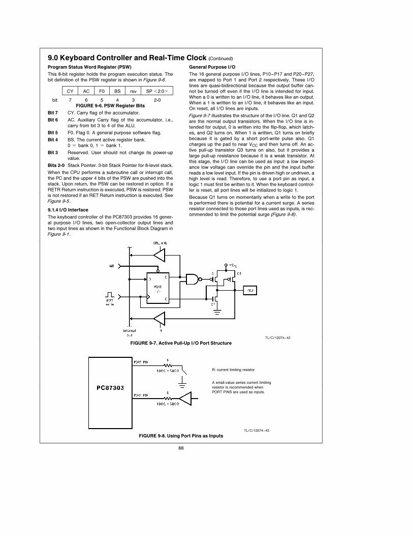
9.0 Keyboard Controller and Real-Time Clock (Continued)
Program Status Word Register (PSW)
This 8-bit register holds the program execution status. The
bit definition of the PSW register is shown in Figure 9-6 .
CY AC F0 BS rsv SP k2:0l
bit 7 6 5 4 3 2-0FIGURE 9-6. PSW Register Bits
Bit 7 CY. Carry flag of the accumulator.
Bit 6 AC. Auxiliary Carry flag of the accumulator, i.e.,
carry from bit 3 to 4 of the ALU.
Bit 5 F0. Flag 0. A general purpose software flag.
Bit 4 BS. The current active register bank.
0 e bank 0, 1 e bank 1.
Bit 3 Reserved. User should not change its power-up
value.
Bits 2-0 Stack Pointer. 3-bit Stack Pointer for 8-level stack.
When the CPU performs a subroutine call or interrupt call,
the PC and the upper 4 bits of the PSW are pushed into the
stack. Upon return, the PSW can be restored in option. If a
RETR Return instruction is executed, PSW is restored. PSW
is not restored if an RET Return instruction is executed. See
Figure 9-5 .
9.1.4 I/O Interface
The keyboard controller of the PC87303 provides 16 gener-
al purpose I/O lines, two open-collector output lines and
two input lines as shown in the Functional Block Diagram in
Figure 9-1 .
General Purpose I/O
The 16 general purpose I/O lines, P10–P17 and P20–P27,
are mapped to Port 1 and Port 2 respectively. These I/O
lines are quasi-bidirectional because the output buffer can-
not be turned off even if the I/O line is intended for input.
When a 0 is written to an I/O line, it behaves like an output.
When a 1 is written to an I/O line, it behaves like an input.
On reset, all I/O lines are inputs.
Figure 9-7 illustrates the structure of the I/O line. Q1 and Q2
are the normal output transistors. When the I/O line is in-
tended for output, 0 is written into the flip-flop, which latch-
es, and Q2 turns on. When 1 is written, Q1 turns on briefly
because it is gated by a short port-write pulse also. Q1
charges up the pad to near VCC and then turns off. An ac-
tive pull-up transistor Q3 turns on also, but it provides a
large pull-up resistance because it is a weak transistor. At
this stage, the I/O line can be used as input: a low imped-
ance low voltage can override the pin and the input buffer
reads a low level input. If the pin is driven high or undriven, a
high level is read. Therefore, to use a port pin as input, a
logic 1 must first be written to it. When the keyboard control-
ler is reset, all port lines will be initialized to logic 1.
Because Q1 turns on momentarily when a write to the port
is performed there is potential for a current surge. A series
resistor connected to those port lines used as inputs, is rec-
ommended to limit the potential surge (Figure 9-8) .
TL/C/12074–42
FIGURE 9-7. Active Pull-Up I/O Port Structure
R: current limiting resistor
A small-value series current limiting
resistor is recommended when
PORT PINS are used as inputs.
TL/C/12074–43
FIGURE 9-8. Using Port Pins as Inputs
88

9.0 Keyboard Controller and Real-Time Clock (Continued)
When the port line is used as an output, an active pull-up
technique is used (instead of a traditional pull-up resistor),
which turns on Q3 only when Q2 is off, hence eliminating a
steady current flow.
Open-Collector Outputs
In order to reduce the glue logic used in a PC-AT compatible
environment, four dedicated open-collector outputs are pro-
vided: KBCLK, KBDAT, MCLK and MDAT. KBCLK is the
complement of P26. KBDAT is the complement of P27.
MCLK is the complement of P23. MDAT is the complement
of P22. These four drivers can drive 16 mA, making them
suitable for driving keyboard and mouse cables. TEST0 and
TEST1 must be externally connected to KBCLK and KBDAT
in the PC-AT compatible applications.
Test Inputs
TEST0 and TEST1 are two dedicated input pins. Conditional
jump instructions directly check the level of these two pins.
TEST1 also serves as the event counter input.
Connection to the I/O Expander
The number of keyboard controller I/O pins can be expand-
ed by adding one or more 8243 I/O Expander chips. Each
I/O expander offers 16 I/O port pins designated as Port 4,
5, 6, and 7. The keyboard controller makes use of the P20–
P24 and the Strobe pin to interface with the 8243.
9.1.5 Timer/Counter
The keyboard controller is equipped with an 8-bit counter
which can be used as a timer or an event counter.
Figure 9-9 shows the two different clock sources for the
counter. The clock source is selected by software.
Timer Operation
The counter can be set to the timer operation mode by con-
necting its clock source to the internal timing generator. The
clock frequency to the timer is equal to the oscillator fre-
quency divided by 480.
The initial value of the timer is programmable. After the tim-
er is started (by STRT T instruction), it counts up continu-
ously until it is stopped or the keyboard controller is reset.
The Timer Overflow Flag is set when the count value over-
flows from FFh back to 00h. The Timer Overflow Flag can
be tested by a conditional jump instruction (JTF). This in-
struction also resets the flag. When the timer interrupt is
enabled, an interrupt occurs when the timer overflows. This
is discussed more detail in the interrupt section.
Event Counter Operation
When the clock input of the counter is switched to the exter-
nal input (TEST1), it essentially becomes an event counter.
The falling edge of the signal on the TEST1 pin causes the
counter to increment. Timer Overflow Flag and Timer inter-
rupt operate in the same way as they do in the timer mode.
9.1.6 Interrupts
The keyboard controller of the PC87303 provides 2 different
internal interrupts. They are the Input Buffer Full (IBF) inter-
rupt and Timer Overflow interrupt. These two interrupts can
be independently enabled or disabled by software. Both of
them are disabled when the chip comes out from reset.
TL/C/12074–44
FIGURE 9-9. Timing Generation and Timer Circuit
89

9.0 Keyboard Controller and Real-Time Clock (Continued)
Timer Interrupt
If the timer interrupt is enabled, upon the timer overflow, an
interrupt occurs. It causes the program to perform a subrou-
tine call to program address 007h. The interrupt is cleared
by this subroutine call. The current Program Counter (PC)
and the upper 4 bits of the PSW is pushed into the stack
before the call occurs. At the end of the timer interrupt serv-
ice routine, an RETR instruction restores the PSW and the
PC. Because the timer interrupt has a lower priority than the
IBF interrupt, simultaneous IBF and timer interrupts cause
the timer interrupt to be pending. It is served as soon as the
program returns from the IBF interrupt service routine.
Input Buffer Full (IBF) Interrupt
If the lBF interrupt is enabled, when there is a host write
operation to the keyboard controller (CS e 0, IOW e 0), an
interrupt occurs. The processor saves the current Program
Counter and the upper 4 bits of the PSW into the stack and
performs a subroutine call to the program address 003h.
Upon entering the interrupt service routine, further interrupts
are held off. The interrupt is re-enabled upon the execution
of the RETR instruction.
9.1.7 Oscillator and Instruction Timing
The oscillator pins of the keyboard controller are X1 and X2,
when bit 7 of KRR is 0. When bit 7 of KRR is 1, the Key-
board Controller clock is SYSCLK. Figures 9-10 and 9-11show the connections for internal and external clock config-
uration via X1 and X2 pins.
The oscillator clock is divided by 3 to generate the state
timing, then is further divided down by 5 to generate the
instruction timing (Figure 9-12) . Hence each instruction cy-
cle consists of 5 states and 15 clock cycles.
Most of the keyboard controller instructions require only one
instruction cycle. The others require two cycles. Refer to the
instruction set for details.
TL/C/12074–45
FIGURE 9-10. Internal Clock Connection
TL/C/12074–46
FIGURE 9-11. External Clock Connection
TL/C/12074–47
FIGURE 9-12. Instruction Cycle Timing
90

9.0 Keyboard Controller and Real-Time Clock (Continued)
9.2 REAL-TIME CLOCK FUNCTION
The RTC in the PC87303 is a low-power clock that provides
a time-of-day clock and 100-year calendar with alarm fea-
tures and battery operation. Other features include three
maskable interrupt sources and 242 bytes of general pur-
pose RAM. Valid RAM and time can be maintained through
the use of an external battery source. It is software compati-
ble with the DS1287 and MC146818.
9.2.1 Memory Map
The RTC contains 14 time and control registers. It also con-
tains 242 bytes of general purpose battery backed static
RAM in two banks. RAMSEL is used to select the active
bank. Refer to Table 9-2.
9.2.2 Bus Interface
The RTC function is mapped to I/O locations 70h (index)
and 71h (data). This decode is done internal to the
PC87303.
9.2.3 Time Generation
The Time Generation function divides the 32.768 kHz from
the external clock pins (X1C, X2C) down to a one Hertz
signal. The divider chain is controlled by bits 6–4 of Control
Register A. Bits 3–0 of Control Register A select one of
fifteen taps from the divider chain to be used as a Periodic
Interrupt. See Control Register A in the Control Register and
Interrupt section for divider configurations and rate selec-
tions.
During divider reset (bits 6–4 of Control Register A e 11x),
the divider chain is reset to 0. An update will occur 500 ms
after the divider chain is activated into normal operational
mode (bits 6–4 of Control Register A e 010). The periodic
flag also becomes active 1/2 of the programmed value
when the divider chain is activated.
Figure 9-13 represents the internal and external circuitry
that comprise the oscillator. The oscillator input may be driv-
en from an external source. If this is desired, the input
should be driven rail to rail and be approximately a 50%
duty cycle. The oscillator output should be open in this case.
The external capacitor values should be chosen to provide
the manufacturer’s specified load capacitance for the crys-
tal when combined with the parasitic capacitance of the
trace, socket, and package, which can vary from 0 pF to
8 pF. The rule of thumb in choosing these capacitors is:
CL e (C1 * C2)/(C1 a C2) a Cparasitic
C2 l C1
C1 can be trimmed to obtain the 32768.0 Hz.
TABLE 9-2. RTC Memory Map
Index Function BCD Format Binary Format Comments
(RAMSEL e 0)
00 Seconds 00–59 00–3b R/W
01 Seconds Alarm 00–59 00–3b R/W
02 Minutes 00–59 00–3b R/W
03 Minutes Alarm 00–59 00–3b R/W
04 Hours 12 hr. e 01–12 (AM) 01–0c (AM) R/W
12 hr. e 81–92 (PM) 81–8c (PM) R/W
24 hr. e 00–23 00–17 R/W
05 Hours Alarm 12 hr. e 01–12 (AM) 01–0c (AM) R/W
12 hr. e 81–92 (PM) 81–8c (PM) R/W
24 hr. e 00–23 00–17 R/W
06 Day of Week 01–07 01–07 (Sunday e 1) R/W
07 Date of Month 01–31 01–1f R/W
08 Month 01–12 01–0c R/W
09 Year 00–99 00–63 R/W
0A Control Register A R/W (Bit 7 is Read Only)
0B Control Register B R/W (Bit 3 is Read Only)
0C Control Register C R
0D Control Register D R
0E–7F Battery-Backed RAM R/W
(114 Bytes)
(RAMSEL e 1)
00–7F Battery-Backed RAM R/W
(128 Bytes)
91

9.0 Keyboard Controller and Real-Time Clock (Continued)
Rext e 5 kX
C1 e 12 x 15 pF
C2 e 15 pF
Cparasitic e 0 x 8 pF
TL/C/12074–49
FIGURE 9-13. Oscillator Internal and External Circuitry
The start-up time of this oscillator may vary from two to
seven seconds and is due to the high ‘‘Q’’ of the crystal.
The parameters below describe the crystal to be used:
Parallel Resonant, tuning fork (N cut) or XY Bar
Q l 35k
Load Capacitance (CL) 9 pF to 13 pF
Accuracy User Choice
Temperature Coefficient User Choice
9.2.4 Time Keeping
The time is kept in BCD or binary format. The format is
determined by bit 2 of Control Register B (DM). Either 12 or
24 hour representation for the hours can be maintained as
determined by bit 1 of Control Register B (24/12). Note that
when changing the format the time registers must be re-ini-
tialized to the corresponding data format.
Daylight savings and leap year exceptions are handled by
the time keeping function. When bit 0 of Control Register A
(DSE) is a ‘‘1’’, time advances from 1:59:59 AM to 3:00:00
on the first Sunday in April. On the last Sunday of October
time changes from 1:59:59 to 1:00:00 when daylight savings
is enabled. On leap year February is extended to 29 days.
The time is updated once per second. If a read of the timing
registers coincides with an update, data read may not be
valid. Also, writes to time registers during an update have
undefined results.
To avoid accessing invalid data, the RTC in the PC87303
provides a user copy of the time registers. Then four meth-
ods are available for reading and writing time to ensure that
the correct time is written or read. They are as follows:
Method 1ÐSet the SET bit. (CRB7)
Set the SET bit to 1. This takes a snapshot of the internal
time registers and loads it into the user copy. Then when
the SET bit is written with 0, the user copy will update the
internal registers.
Method 2ÐAccess after detection of an Update Ended
Interrupt.
This interrupt indicates that an update has just completed
and the next update will occur after 999 ms.
Method 3ÐPoll update-in-progress (bit 7 in Control Reg-
ister A).
The update occurs 244 ms after the update-in-progress
bit goes high. Therefore if a 0 is read, there is a minimum
of 244 ms in which the time is guaranteed to remain sta-
ble.
Method 4ÐUse a Periodic interrupt to determine if an
update cycle is in progress.
The periodic interrupt is first set to a desired period. The
program can then use the periodic interrupt to signify that
there is (Periodic Interrupt/2 a 244 ms) remaining until
another update occurs.
The Alarm condition is also generated by the Time Keeping
function. After each update, the seconds, minutes, and
hours are compared with the seconds alarm, minutes alarm,
and hours alarm. If equal, the Alarm lag is set in Control
TL/C/12074–52
where:
UIP eUpdate In Progress Bit
UF e Update Ended Flag (Update Ended Interrupt if Enabled)
PF e Periodic Flag (Periodic Interrupt if Enabled)
AF e Alarm Flag (Alarm Interrupt if Enabled)
Flags (and IRQ) are reset at the conclusion of Control Register C read or by RESETC low.
A e Update in Progress Bit High before Update Occurs e 244 ms
B e Periodic interrupt to Update e P/2 a 244 ms
C e Update to Alarm Interrupt e 30.5 ms
P e Period is programmed by RS3–0 of control Register A.
FIGURE 9-14. Interrupt/Status Timing
92

9.0 Keyboard Controller and Real-Time Clock (Continued)
Register C. This causes an interrupt condition (IRQZ e 0) if
the Alarm Interrupt Enable bit is set in Control Register B. If
both bit 7 and bit 6 of any alarm byte (seconds alarm, min-
utes alarm, hours alarm) are 1, then that alarm byte is a
‘‘don’t care’’.
9.2.5 RAM
The RAM data is accessed at locations 0E–7F when
RAMSEL (bit 2) of the configuration registers is 0, and loca-
tions 00–7F when RAMSEL is 1. Battery backed power en-
ables the RAM to retain information during system power-
down.
9.2.6 Power Management
The Power Management function provides power to the
RTC in the PC87303. During system operation, power from
the system is used. When system voltage falls below battery
voltage, the Power Management function switches the RTC
cell to battery power. For proper operation, a 500 mV differ-
ential is needed between VCC and VBAT. Figure 9-15 repre-
sents a typical battery configuration and Figure 9-16 repre-
sents typical battery current during battery backed mode.
TL/C/12074–50
FIGURE 9-15. Typical Battery Configuration
TL/C/12074–51
FIGURE 9-16. Typical Battery Current
during Battery Backed Mode
9.2.7 System Bus Lock Out and Power-Up Detection
As the RTC switches to battery power all inputs are locked
out so that the internal registers can not be modified. This
lockout condition continues for 62 ms (min) to 125 ms (max)
after the RTC switches from battery power to system power.
The 62 ms–125 ms lockout during power transition from
battery to system power depends on the following condi-
tions:
1. If the Divider Chain Control (bits 6–4 in Control Register
A) is in any mode but Normal Operation (010), all inputs
are enabled immediately upon detection of system volt-
age above that of battery voltage.
2. When Battery voltage is below 1V and MR is 1, all inputs
are enabled immediately upon detection of system volt-
age above that of battery voltage. This also initializes reg-
isters 00 through 0D to 00.
3. If the VRT bit (bit 7 in Control Register D) is 0, all inputs
are enabled immediately upon detection of system volt-
age above that of battery voltage.
9.2.8 Oscillator
When power is applied to the RTC in the PC87303, the
Oscillator is operational with the following exceptions:
1. The VRT bit (bit 7 in Control Register D) is a 0. The oscil-
lator is disabled after initial power-up. This reduces power
consumption during the time between when the battery is
initially installed and when the RTC is initialized for time-
keeping.
2. The Divider Chain Control (bits 6–4 in Control Register A)
is in Oscillator Disabled modes (000 and 001). This pro-
vides a means for the user to ‘‘shut-down’’ the oscillator
and reduce the power consumption of the RTC cell. The
RAM remains functional when the oscillator is disabled.
9.2.9 Interrupt Handling
The Periodic, Alarm, and Update ended Interrupts are gen-
erated (IRQZ is driven low) when the respective enable bits
in Control Register B are set and an interrupt condition oc-
curs. A read from Register C clears the active interrupt. If a
second interrupt condition occurs (other than that which
caused the interrupt) during a read from Register C, IRQZ
remains active (low). Thus, it is recommended that when
multiple interrupts are enabled, the interrupt service routine
continues to read (and service interrupts) until bit 7 of Con-
trol Register C (IRQ Flag) returns to a 1. Note that if an
interrupt is not serviced before a second condition of the
same interrupt occurs, the second interrupt event is lost.
93

9.0 Keyboard Controller and Real-Time Clock (Continued)
9.2.10 Control Registers
The four Control Registers used to configure timing inter-
rupts can be accessed at any time during non-battery
backed operation. These Control Registers are located at
addresses 0Ah, 0Bh, 0Ch and 0Dh. Their descriptions fol-
low.
Control Register A
UIP DV2 DV1 DV0 RS3 RS2 RS1 RS0
bit 7 6 5 4 3 2 1 0
Bits 0–3 RS3–0ÐPeriodic Interrupt Rate Select
(Read/Write)
These bits control the rate of the periodic inter-
rupt. Reset has no effect on these bits.
RS3–0Periodic
Interrupt Rate
0000 None
0001 3.90625 ms
0010 7.8125 ms
0011 122.070 ms
0100 244.141 ms
0101 488.281 ms
0110 976.562 ms
0111 1.953125 ms
1000 3.90625 ms
1001 7.8125 ms
1010 15.625 ms
1011 31.25 ms
1100 62.5 ms
1101 125 ms
1110 250 ms
1111 500 ms
Bits 4–6 DV2–0ÐDivider Chain Control
(Read/Write)
These bits control the configuration of the divider
chain in the Timing Generation function.
Reset has no effect on these bits.
DV2–0Divider Chain
Configuration
000 Oscillator Disabled
001 Oscillator Disabled
010 Normal Operation
011 TEST
100 TEST
101 TEST
110 Divider Chain RESET
111 Divider Chain RESET
Bit 7 UIPÐUpdate in Progress
(Read Only)
1: Signifies that the timing registers will be updat-
ed within 244 ms.
0: Signifies that an update will not occur before
244 ms. This bit reads 0 when bit 7 of Control
Register B (SET) is a 1.
Reset has no effect on this bit.
Control Register B
SET PIE AIE UIE 0 DM 24/12 DSE
bit 7 6 5 4 3 2 1 0
Bit 0 DSEÐDaylight Savings Enable
(Read/Write)
1: Enables daylight savings. Two conditions ap-
ply as follows:
Daylight Savings Spring: Time advances from
1:59:59 to 3:00:00 on the first Sunday in April.
Daylight Savings Fall: Time advances from
1:59:59 to 1:00:00 on the last Sunday in Octo-
ber.
0: Disables the daylight savings feature.
Reset has no effect on this bit.
Bit 1 24/12Ð24 or 12 Hour Mode
(Read/Write)
1: Enables 24 hour format.
0: Enables 12 hour format.
Reset has no effect on this bit.
94

9.0 Keyboard Controller and Real-Time Clock (Continued)
Bit 2 DMÐData Mode
(Read/Write)
1: Enables BINARY format.
0: Enables BCD format.
Reset has no effect on this bit.
Bit 3 This bit is defined as ‘‘Square Wave Enable’’ by
the MC146818 and is not supported by the RTC
Cell. This bit is always read as 0.
Bit 4 UIEÐUpdate Ended Interrupt Enable
(Read/Write)
1: Enables generation of the Update Ended inter-
rupt. This interrupt is generated at the time an
update occurs.
0: Disables generation of the Update Ended in-
terrupt. Reset forces this bit to 0.
Bit 5 AIEÐAlarm Interrupt Enable
(Read/Write)
1: Enables generation of the Alarm interrupt. The
Alarm interrupt is generated immediately after
a time update in which the Seconds, Minutes,
and Hours time matches with their respective
alarm counterparts.
0: Disables generation of the alarm interrupt.
Reset forces this bit to 0.
Bit 6 PIEÐPeriodic Interrupt Enable
(Read/Write)
1: Enables generation of the Periodic interrupt.
Bits 3–0 of Control Register A determine the
rate of the Periodic interrupt.
0: Disables generation of the Periodic interrupt.
Reset forces this bit to 0.
Bit 7 SETÐSet mode
(Read/Write)
1: The user copy of time is ‘‘frozen’’ allowing the
time registers to be accessed without regard
for an occurrence of an update.
0: The timing updates occur normally.
Reset has no effect on this bit.
Control Register C
IRQF PF AF UF 0 0 0 0
bit 7 6 5 4 3 2 1 0
Bits 0–3 Reserved
(Always 0)
Bit 4 UFÐUpdate Ended Interrupt Flag
(Read Only)
1: When the time registers are updated. This bit
is reset to 0 at the conclusion of a read from
this register. Reset forces this bit to 0.
Bit 5 AFÐAlarm Interrupt Flag
(Read Only)
1: When an alarm condition is detected. This bit
is reset to 0 at the conclusion of a read from
this register. Reset forces this bit to 0.
Bit 6 PFÐPeriodic Interrupt Flag
(Read Only)
1: When a transition occurs on the selected tap
of the divider chain. This bit is reset to 0 at the
conclusion of a read from this register. Reset
forces this bit to 0.
Bit 7 IRQFÐInterrupt Request Flag
(Read Only)
1: When bit pairs PIE and PF; AIE and AF, and
UIE and UF all equal 1. The IRQF bit mirrors
the value on the IRQZ output. When lRQZ is
active (low), IRQF is 1. Reset forces this bit to
0.
Control Register D
VRT 0 0 0 0 0 0 0
bit 7 6 5 4 3 2 1 0
Bits 0–6 Reserved
(Always 0)
Bit 7 VRTÐValid RAM and Time
(Read Only)
1: This bit indicates that the contents of the RTC
are valid.
0: This bit indicates that the battery source is low
and that the RTC data and RAM data are
questionable. This bit is set to 1 at the conclu-
sion of a read from this register.
95

10.0 Electrical CharacteristicsABSOLUTE MAXIMUM RATINGS (Notes 1 and 2)
If Military/Aerospace specified devices are required,
please contact the National Semiconductor Sales
Office/Distributors for availability and specifications.
Supply Voltage (VDD, VDDA) b0.5V to a7.0V
Supply Differential (lVDD–VDDAl) 0.6V
Input Voltage (VI) b0.5V to VDD a 0.5V
Output Voltage (VO) b0.5V to VDD a 0.5V
Storage Temperature (TSTG) b65§C to a165§CPower Dissipation (PD) 1W
Lead Temperature (TL)
(Soldering, 10 seconds) 260§CNote 1: Absolute Maximum Ratings are those values beyond which damage
to the device may occur.
Note 2: Unless otherwise specified, all voltages are referenced to ground.
RECOMMENDED OPERATING CONDITIONS
Supply Voltage (VDD) 4.5V–5.5V
Operating Temp. Range (TA) 0§C to a70§CESD Tolerance 1500V
CZAP e 100 pF (Note 3)
RZAP e 1.5 kX (Note 3)
Note 3: Value based on test complying with NSC SOP5-028 human body
model ESD testing using the ETS-910 tester.
CAPACITANCE TA e 25§C, f e 1 MHz
Symbol Parameter Min Typ Max Units
CIN Input Pin Capacitance 5 7 pF
CIN1 Clock Input Capacitance 8 10 pF
CIO I/O Pin Capacitance 10 12 pF
CO Output Pin Capacitance 6 8 pF
10.1 DC ELECTRICAL CHARACTERISTICS Under Recommended Operating Conditions
Symbol Parameter Conditions Min Typ Max Units
VIH Input High Voltage 2.0 VDD V
VIL Input Low Voltage b0.5 0.8 mA
ICC VDD Average Supply Current VIL e 0.5V
VIH e 2.4V 25 40 mA
No Load
ICCSB VDD Quiescent Supply VIL e VSS
Current in Low Power Mode VIH e VDD 0.8 1.2 mA
No Load
ICCA VDDA Average Supply Current VI e 0.5V
VIH e 2.4V 7 10 mA
No Load
ICCASB VDDA Quiescent Supply VIL e VSS
Current in Low Power Mode VIH e VDD 5 500 mA
No Load
IIL Input Leakage Current VIN e VDD 10 mA
(Note 4)VIN e VSS b10 mA
Note 4: During reset the MFM pin is rated for 10 mA; b150 mA leakage is due to an internal pull-up resistor. The RTS1, 2; SOUT1, 2; DTR1, 2; HCS0, 1; IDEHI;
VLD0, 1 and IDEHLO are rated for 100 mA; b10 mA leakage is due to internal pull-down resistors. During normal operation the BUSY, PE, and SLCT pins are rated
for 100 mA; b10 mA leakage is due to internal pull down resistors. The ACK and ERR pins are rated for 10 mA; b100 mA leakage is due to internal pull-up resistors.
96

10.0 Electrical Characteristics (Continued)
10.1 DC ELECTRICAL CHARACTERISTICS (Continued)
10.1.1 Microprocessor, Parallel Port, and IDE Interface Pins
Symbol Parameter Conditions Min Max Units
VOH Output High Voltage IOH e b15 mA on:
2.4 V
D0–7, IDED7, IRQ3–7, DRQ
ADRATE0
IOH e b6 mA on:
DTR, RTS, SOUT, MFM,
DRATE, CSOUT, IDEHI,
IDELO, HCS, CS0, CS1
VOL Output Low Voltage IOL e 24 mA on:
0.4 V
D0–7, IDED7, IRQ3–7, IRQ8,
DRQ, ZWS, IOCHRDY,
MFM, ADRATE0
IOL e 12 mA on:
DTR, RTS, SOUT, HCS,
IDEHI, IDELO
IOL e 6 mA on:
DRATE, CSOUT, CS0, CS1
IOZ Output TRI-STATE Leakage VIN e VDD 50 mA
Current (D7–D0, IRQ3–7, DRQ)VIN e VSS b50 mA
Note 1: Pins IOCHRDY and ZWS are open drain pins.
10.1.2 Disk Interface Pins
Symbol Parameter Conditions Min Typ Max Units
VH Input Hysteresis 250 mV
VOH Output High Voltage (Note 1) IOH e b4 mA 2.4 V
VOL Output Low Voltage IOL e 40 mA 0.4 V
ILKG Output High Leakage Current VIN e VDD 10 mA
(Note 1)VIN e VSS b10 mA
Note 1: VOH and ILKG for the disk interface pins are valid for CMOS buffered outputs only.
10.1.3 Oscillator Pins (X1/OSC)
Symbol Parameter Conditions Min Typ Max Units
VIH X1 Input High Voltage 2.0 V
VIL X2 Input Low Voltage 0.4 V
IXLKG X1 Leakage VIN e VDD 400 mA
VIN e VSS b400 mA
10.1.4 Parallel Port Pins
Symbol Parameter Conditions Min Typ Max Units
IOH High Level Output Current (Note 1) VOH e 2.4V 12 mA
IOL Low Level Output Current VOL e 0.4V 12 mA
Note 1: AFD, INIT, SLIN and STB are open drain pins when the PC87303 parallel port is operating in one of the following modes: Compatible, Extended, EPP1.7,
ECP mode 0, or ECP mode 2 if PCR1 if 0. 4.7 kX resistors should be used.
97
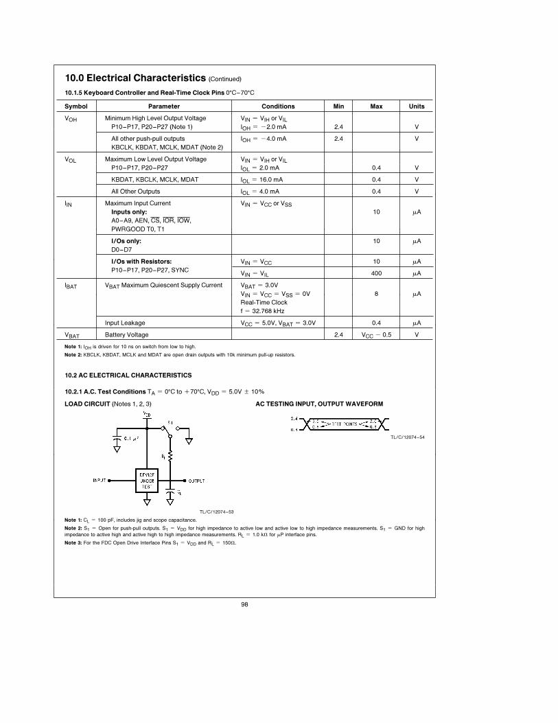
10.0 Electrical Characteristics (Continued)
10.1.5 Keyboard Controller and Real-Time Clock Pins 0§C–70§C
Symbol Parameter Conditions Min Max Units
VOH Minimum High Level Output Voltage VIN e VIH or VIL
P10–P17, P20–P27 (Note 1) IOH e b2.0 mA 2.4 V
All other push-pull outputs IOH e b4.0 mA 2.4 V
KBCLK, KBDAT, MCLK, MDAT (Note 2)
VOL Maximum Low Level Output Voltage VIN e VIH or VIL
P10–P17, P20–P27 IOL e 2.0 mA 0.4 V
KBDAT, KBCLK, MCLK, MDAT IOL e 16.0 mA 0.4 V
All Other Outputs IOL e 4.0 mA 0.4 V
IIN Maximum Input Current VIN e VCC or VSS
Inputs only: 10 mA
A0–A9, AEN, CS, IOR, IOW,
PWRGOOD T0, T1
I/Os only: 10 mA
D0–D7
I/Os with Resistors: VIN e VCC 10 mA
P10–P17, P20–P27, SYNCVIN e VIL 400 mA
IBAT VBAT Maximum Quiescent Supply Current VBAT e 3.0V
VIN e VCC e VSS e 0V 8 mA
Real-Time Clock
f e 32.768 kHz
Input Leakage VCC e 5.0V, VBAT e 3.0V 0.4 mA
VBAT Battery Voltage 2.4 VCC b 0.5 V
Note 1: IOH is driven for 10 ns on switch from low to high.
Note 2: KBCLK, KBDAT, MCLK and MDAT are open drain outputs with 10k minimum pull-up resistors.
10.2 AC ELECTRICAL CHARACTERISTICS
10.2.1 A.C. Test Conditions TA e 0§C to a70§C, VDD e 5.0V g 10%
LOAD CIRCUIT (Notes 1, 2, 3)
TL/C/12074–53
AC TESTING INPUT, OUTPUT WAVEFORM
TL/C/12074–54
Note 1: CL e 100 pF, includes jig and scope capacitance.
Note 2: S1 e Open for push-pull outputs. S1 e VDD for high impedance to active low and active low to high impedance measurements. S1 e GND for high
impedance to active high and active high to high impedance measurements. RL e 1.0 kX for mP interface pins.
Note 3: For the FDC Open Drive Interface Pins S1 e VDD and RL e 150X.
98

10.0 Electrical Characteristics (Continued)
10.2.2 Clock Timing
Symbol Parameter Min Max Units
tCH Clock High Pulse Width 16 ns
tCL Clock Low Pulse Width 16 ns
tCP Clock Period 40 43 ns
tICP Internal Clock Period (Table 10-1) ns
tDRP Data Rate Period (Table 10-1) ns
TABLE 10-1 Nominal tICP, tDRP Values
MFM Data Rate tDRP tICP Value Units
1 Mbps 1000 3 x tCP 125 ns
500 kbps 2000 3 x tCP 125 ns
300 kbps 3333 5 x tCP 208 ns
250 kbps 4000 6 x tCP 250 ns
TL/C/12074–55
FIGURE 10-1. Clock Timing
99

10.0 Electrical Characteristics (Continued)
10.2.3 Microprocessor Interface Timing
Symbol Parameter Min Max Units
tAR Valid Address to Read Active 18 ns
tAW Valid Address to Write Active 18 ns
tDH Data Hold 0 ns
tDS Data Setup 18 ns
tHZ Read to Floating Data Bus 13 25 ns
tPS Port Setup 10 ns
tRA Address Hold from Inactive Read 0 ns
tRCU Read Cycle Update 45 ns
tRD Read Strobe Width 60 ns
tRDH Read Data Hold 10 ns
tRI Read Strobe to Clear IRQ6 55 ns
tRVD Active Read to Valid Data 55 ns
tWA Address Hold from Inactive Write 0 ns
tWCU Write Cycle Update 45 ns
tWI Write Strobe to Clear IRQ6 55 ns
tWO Write Data to Port Update 60 ns
tWR Write Strobe Width 60 ns
RC Read Cycle e tAR a tRD a tRCU 123 ns
WC Write Cycle e tAW a tWR a tWCU 123 ns
tWRR RD Low after WR High 80 ns
100

10.0 Electrical Characteristics (Continued)
TL/C/12074–56
FIGURE 10-2. Microprocessor Read Timing
TL/C/12074–57
FIGURE 10-3. Microprocessor Write Timing
TL/C/12074–60
FIGURE 10-4. Read After Write Operation to All Registers and RAM Timing
101

10.0 Electrical Characteristics (Continued)
10.2.4 Baud Out Timing
Symbol Parameter Conditions Min Max Units
N Baud Divisor 1 65535 ns
tBHD Baud Output Positive Edge Delay CLK e 24 MHz/2, 100 pF Load 56 ns
tBLD Baud Output Negative Edge Delay CLK e 24 MHz/2, 100 pF Load 56 ns
TL/C/12074–62
FIGURE 10-5. Baud Out Timing
10.2.5 Transmitter Timing
Symbol Parameter Min Max Units
tHR Delay from WR (WR THR) to Reset IRQ 40 ns
tIR Delay from RD (RD IIR) to Reset IRQ (THRE) 55 ns
tIRS Delay from Initial IRQ Reset to Transmit Start 8 24 Baud Out Cycles
tSI Delay from Initial Write to IRQ 16 24 Baud Out Cycles
tSTI Delay from Start Bit to IRQ (THRE) 8 Baud Out Cycles
TL/C/12074–63
Note 1: See Microprocessor Write cycle timing, Figure 10-3 .
Note 2: See Microprocessor Read cycle timing, Figure 10-2 .
FIGURE 10-6. Transmitter Timing
102

10.0 Electrical Characteristics (Continued)
10.2.6 Receiver Timing
Symbol Parameter Conditions Min Max Units
tRAI Delay from Active Edge of RD to Reset IRQ 78 ns
tRINT Delay from Inactive Edge of RD (RD LSR) to Reset IRQ 55 ns
tSCD Delay from RCLK to Sample Time (Note 1) 41 ns
tSINT Delay from Stop Bit to Set Interrupt 2 Baud Out
Cycle
Note 1: This is an internal timing specification and is therefore not tested.
TL/C/12074–87
FIGURE 10-7. Sample Clock Timing
TL/C/12074–64
FIGURE 10-8. Receiver Timing
TL/C/12074–65
Note 1: If SCR0 e 1, then tSINT e 3 RCLKs. For a Timeout Interrupt, tSINT e 8 RCLKs.
FIGURE 10-9. FIFO Mode Receiver Timing
103

10.0 Electrical Characteristics (Continued)
TL/C/12074–66
Note 1: If SCR0 e 1, then tSINT e 3 RCLKs. For a Timeout Interrupt, tSINT e 8 RCLKs.
FIGURE 10-10. Timeout Receiver Timing
10.2.7 MODEM Control Timing
Symbol Parameter Conditions Min Max Units
tMDO Delay from WR (WR MCR) to Output 40 ns
tRIM Delay to Reset IRQ from RD (RD MSR) 78 ns
tSIM Delay to Set IRQ from MODEM Input 40 ns
TL/C/12074–67
Note 1: See Microprocessor Write cycle timing, Figure 10-3 .
Note 2: See Microprocessor Read cycle timing, Figure 10-2 .
FIGURE 10-11. MODEM Control Timing
104

10.0 Electrical Characteristics (Continued)
10.2.8 DMA Timing
10.2.8.1 FDC
Symbol Parameter Min Max Units
tKI FDACK Inactive Pulse Width 25 ns
tKK FDACK Active Pulse Width 65 ns
tKQ FDACK Active Edge to FDRQ Inactive 65 ns
tQK FDRQ to FDACK Active Edge 10 ns
tQP FDRQ Period (except Non-Burst DMA) (Note 3) 8 x tDRP ms
tQQ FDRQ Inactive Non-Burst Pulse Width 300 400 ns
tQR FDRQ to RD or WR Active 15 ns
tQW FDRQ to End of RD, WR (Notes 2, 3)(8 x tDRP) b(16 x tICP) ms
(FDRQ Service Time)
tQT FDRQ to TC Active (Notes 2, 3) (8 x tDRP) b(16 x tICP)ms
(FDRQ Service Time)
tRQ RD, WR Active Edge to FDRQ Inactive65 ns
(Note 1)
tTQ TC Active Edge to FDRQ Inactive 75 ns
tTT TC Active Pulse Width 50 ns
Note 1: The active edge of RD or WR and TC is recognized only when FDACK is active.
Note 2: Values shown are with the FIFO disabled, or with FIFO enabled and THRESH e 0. For nonzero values of THRESH, add (THRESH x 8 x tDRP) to the values
shown.
Note 3: tDRP and tICP are defined in Table 10-1.
TL/C/12074–68
FIGURE 10-12a. FDC DMA Timing
105

10.0 Electrical Characteristics (Continued)
10.2.8.2 ECP
Symbol Parameter Min Max Units
tKIP PDACK Inactive Pulse Width 25 ns
tKKP PDACK Active Pulse Width 65 ns
tKQP PDACK Active Edge to PDRQ Inactive (Notes 2, 3) 65 a (6 x 32 x tCP) ns
tQKP PDRQ to PDACK Active Edge 10 ns
tQPP PDRQ Period 330 ms
tQQP PDRQ Inactive Non-Burst Pulse Width 300 400 ns
tQRP PDRQ to RD, WR Active 15 ns
tRQP RD or WR Active Edge to PDRQ Inactive (Note 1) 65 ns
tTQP TC Active Edge to PDRQ Inactive 75 ns
tTT TC Active Pulse Width 50 ns
Note 1: The active edge of RD or WR and TC is recognized only when PDACK is active.
Note 2: One DMA transaction takes six clock cycles.
Note 3: tCP is defined in Section 10.2.2 Clock Timing.
TL/C/12074–69
FIGURE 10-12b. ECP DMA Timing
106

10.0 Electrical Characteristics (Continued)
10.2.9 Reset Timing
Symbol Parameter Min Max Units
tRW Reset Width (Note 1) 22 ms
tSRC Reset to Control Inactive 300 ns
Note 1: The software reset pulse width is 100 ns.
TL/C/12074–70
Note 2: DRQ and IRQ6 will be TRI-STATE after time tSRC when in the PC-AT or Model 30 mode.
FIGURE 10-13. Reset Timing
10.2.10 FDC Write Data Timing
Symbol Parameter Min Max Units
tHDH HDSEL Hold from WGATE Inactive 750 ms
tHDS HDSEL Setup to WGATE Active 100 ms
tWDW Write Data Pulse Width Table 10-2 ns
TABLE 10-2. Minimum tWDW Values
Data Rate tDRP tWDW tWDW Value Units
1 Mbps 1000 2 x tICP 250 ns
500 kbps 2000 2 x tICP 250 ns
300 kbps 3333 2 x tICP 375 ns
250 kbps 4000 2 x tICP 500 ns
TL/C/12074–71
FIGURE 10-14. Write Data Timing
107
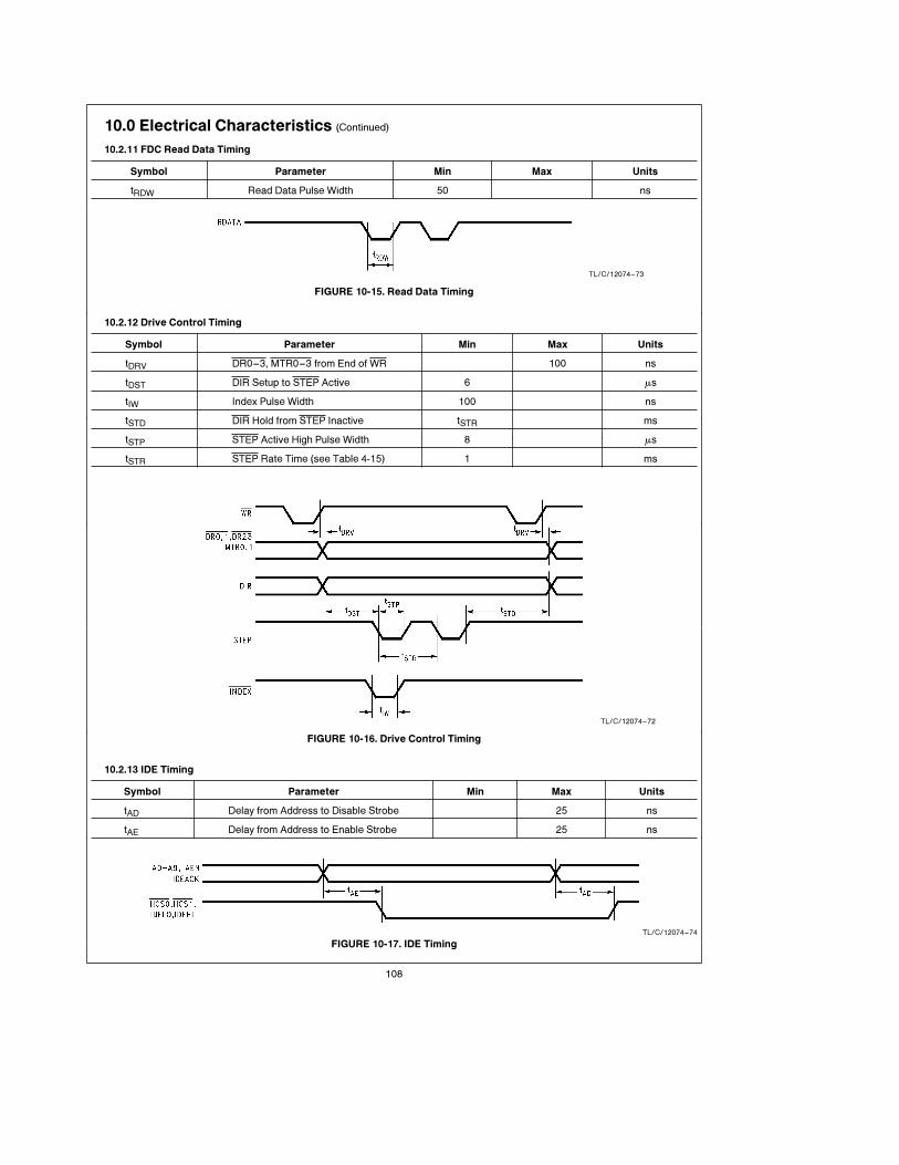
10.0 Electrical Characteristics (Continued)
10.2.11 FDC Read Data Timing
Symbol Parameter Min Max Units
tRDW Read Data Pulse Width 50 ns
TL/C/12074–73
FIGURE 10-15. Read Data Timing
10.2.12 Drive Control Timing
Symbol Parameter Min Max Units
tDRV DR0–3, MTR0–3 from End of WR 100 ns
tDST DIR Setup to STEP Active 6 ms
tIW Index Pulse Width 100 ns
tSTD DIR Hold from STEP Inactive tSTR ms
tSTP STEP Active High Pulse Width 8 ms
tSTR STEP Rate Time (see Table 4-15) 1 ms
TL/C/12074–72
FIGURE 10-16. Drive Control Timing
10.2.13 IDE Timing
Symbol Parameter Min Max Units
tAD Delay from Address to Disable Strobe 25 ns
tAE Delay from Address to Enable Strobe 25 ns
TL/C/12074–74
FIGURE 10-17. IDE Timing
108

10.0 Electrical Characteristics (Continued)
10.2.14 Parallel Port Timing
Symbol Parameter Conditions Type Max Units
tPDH Port Data Hold (Note 1) 500 ns
tPDS Port Data Setup (Note 1) 500 ns
tPI Port Interrupt 33 ns
tSW Strobe Width (Note 1) 500 ns
Note 1: These times are system dependent and are therefore not tested.
TL/C/12074–75
FIGURE 10-18. Compatible Mode Parallel Port Interrupt Timing
TL/C/12074–76
FIGURE 10-19. Extended Mode Parallel Port Interrupt Timing
TL/C/12074–77
FIGURE 10-20. Typical Parallel Port Data Exchange
109

10.0 Electrical Characteristics (Continued)
10.2.15 Enhanced Parallel Port Timing
Symbol Parameter Conditions Min Max Units
tWW WRITE Active from WR Active (Note 1) 45 ns
tWST DSTRB or ASTRB Active from WR Active EEP 1.7 45 ns
(Notes 1, 2)EPP 1.9 65 ns
tWEST DSTRB or ASTRB Active after EPP 1.7 0 ns
WRITE ActiveEPP 1.9 10 ns
tWPDh PD0–PD7 Hold after DSTRB or ASTRB50 ns
Inactive
tHRW IOCHRDY Active after WAIT Active (Note 3) EPP 1.7 40 ns
tWPDS PD0–PD7 Valid after WRITE Active D0–7 is stable 15 ns15 ns
before WR Active
tEPDW 80 ns
tEPDh 0 ns
tZWSa ZWS Valid after WR or RD Active 45 ns
tZWSh ZWS Hold after WR or RD Inactive 0 ns
Note 1: tWST and tWW are valid in EPP 1.9 only if WAIT is low when WR becomes active, else tWST and tWW are measured from WAIT.
Note 2: The PC87303 design guarantees that WRITE will not change from low to high before DSTRB or ASTRB goes from low to high.
Note 3: In EPP 1.9, IOCHRDY is measured from WR or RD.
TL/C/12074–78
FIGURE 10-21. Enhanced Parallel Port Timing
110

10.0 Electrical Characteristics (Continued)
10.2.16 Extended Capabilities Port Timing
10.2.16.1 Forward
Symbol Parameter Conditions Min Max Units
tecdsf Data Setup before STB Active 0 ns
tecdhf Data Hold after BUSY 0 ns
teclhf BUSY Setup after STB Active 75 ns
techhf STB Active after BUSY 0 1 sec
techlf BUSY Setup after STB Inactive 0 35 ms
tecllf STB Active after BUSY 0 ns
TL/C/12074–79
FIGURE 10-22. ECP Parallel Port Forward Timing Diagram
10.2.16.2 Backward
Symbol Parameter Conditions Min Max Units
tecdsb Data Setup before STB Active 0 ns
tecdhb Data Hold after BUSY 0 ns
teclhb BUSY Setup after STB Active 75 ns
techhb STB Active after BUSY 0 1 sec
techlb BUSY Setup after STB Inactive 0 35 ms
tecllb STB Active after BUSY 0 ns
TL/C/12074–80
FIGURE 10-23. ECP Parallel Port Backward Timing Diagram
111

10.0 Electrical Characteristics (Continued)
10.2.17 RTC
Symbol Parameter Conditions Min Max Units
tRDI IOR to IRQ TRI-STATE 36 ns
tRCI MR to IRQ TRI-STATE 25 ns
tRCL MR High Time 100 ms
tVPG VCC (4.5V) to PWRGOOD 0 ns
tPVG PWRGOOD to VCC (4.5V) 0 ns
tVPG VCC (4.5V) to PWRGOOD 10 ms
tVMR VCC (4.5V) to MR 10 ms
tPGM PWRGOOD to MR 0 ns
TL/C/12074–81
FIGURE 10-24. IRQ Release Delay
TL/C/12074–82
FIGURE 10-25. PWRGOOD VCC Timing
TL/C/12074–83
FIGURE 10-26. PWRGOOD MR Timing
112

10.0 Electrical Characteristics (Continued)
10.2.18 Programmable Chip Select Timing
Symbol Parameter Min Max Units
tCE Delay from Command to Enable Chip Select 0 25 ns
tCD Delay from Command to Disable Chip Select 0 25 ns
TL/C/12074–84
FIGURE 10-27. Chip Select Timing
113

PC
87303V
UL
SuperI
/O
Sid
ew
inderLite
Flo
ppy
Dis
kC
ontr
oller,
Keyboard
Contr
oller,
Real-Tim
eC
lock,D
ualU
AR
Ts,IE
EE
1284
Para
llelPort
,and
IDE
Inte
rface
Physical Dimensions inches (millimeters)
Plastic Quad Flatpak
Order Number PC87303VUL
NS Package Number VUL160A
LIFE SUPPORT POLICY
NATIONAL’S PRODUCTS ARE NOT AUTHORIZED FOR USE AS CRITICAL COMPONENTS IN LIFE SUPPORT
DEVICES OR SYSTEMS WITHOUT THE EXPRESS WRITTEN APPROVAL OF THE PRESIDENT OF NATIONAL
SEMICONDUCTOR CORPORATION. As used herein:
1. Life support devices or systems are devices or 2. A critical component is any component of a life
systems which, (a) are intended for surgical implant support device or system whose failure to perform can
into the body, or (b) support or sustain life, and whose be reasonably expected to cause the failure of the life
failure to perform, when properly used in accordance support device or system, or to affect its safety or
with instructions for use provided in the labeling, can effectiveness.
be reasonably expected to result in a significant injury
to the user.
National Semiconductor National Semiconductor National Semiconductor National Semiconductor National Semiconductores National SemiconductorCorporation GmbH Japan Ltd. Hong Kong Ltd. Do Brazil Ltda. (Australia) Pty, Ltd.2900 Semiconductor Drive Livry-Gargan-Str. 10 Sumitomo Chemical 13th Floor, Straight Block, Rue Deputado Lacorda Franco Building 16P.O. Box 58090 D-82256 F 4urstenfeldbruck Engineering Center Ocean Centre, 5 Canton Rd. 120-3A Business Park DriveSanta Clara, CA 95052-8090 Germany Bldg. 7F Tsimshatsui, Kowloon Sao Paulo-SP Monash Business ParkTel: 1(800) 272-9959 Tel: (81-41) 35-0 1-7-1, Nakase, Mihama-Ku Hong Kong Brazil 05418-000 Nottinghill, MelbourneTWX: (910) 339-9240 Telex: 527649 Chiba-City, Tel: (852) 2737-1600 Tel: (55-11) 212-5066 Victoria 3168 Australia
Fax: (81-41) 35-1 Ciba Prefecture 261 Fax: (852) 2736-9960 Telex: 391-1131931 NSBR BR Tel: (3) 558-9999Tel: (043) 299-2300 Fax: (55-11) 212-1181 Fax: (3) 558-9998Fax: (043) 299-2500
National does not assume any responsibility for use of any circuitry described, no circuit patent licenses are implied and National reserves the right at any time without notice to change said circuitry and specifications.