pcb designpcb design - department of electrical ...pcpandey/courses/ee616/pcb...i t b o m b ay p c p...
TRANSCRIPT
IIT Bombay
1PC Pandey: Lecture notes “PCB Design”, EE Dept, IIT Bombay, rev. April’03
♠♠♠♠ ♠♠♠♠ >>>♦♦♦♦♦♦♦♦ <<<• Artwork• Digital Ckts• General • Analog Ckts
PCB DESIGNPCB DESIGN
Dr. P. C. Pandey
EE Dept, IIT Bombay
Revised Aug’07
IIT Bombay
2PC Pandey: Lecture notes “PCB Design”, EE Dept, IIT Bombay, rev. April’03
♠♠♠♠ ♠♠♠♠ >>>♦♦♦♦♦♦♦♦ <<<• Artwork• Digital Ckts• General • Analog Ckts
Topics
1.General Considerations in Layout Design
2.Layout Design for Analog Circuits
3.Layout Design for Digital Circuits
4. Artwork Considerations
References
W.C. Bosshart, Printed Circuit Boards: Design and Technology, TMH,
1992
C.F. Coombs : Printed Circuits Handbook , McGraw-Hill, 2001
R.S. Khandpur : Printed Circuit Boards : Design, Fabrication, and
Assembly, McGraw-Hill, 2005.
IIT Bombay
3PC Pandey: Lecture notes “PCB Design”, EE Dept, IIT Bombay, rev. April’03
♠♠♠♠ ♠♠♠♠ >>>♦♦♦♦♦♦♦♦ <<<• Artwork• Digital Ckts• General • Analog Ckts
• GENERAL CONSIDERATIONS GENERAL CONSIDERATIONS
IN LAYOUT DESIGNIN LAYOUT DESIGN
Main issues
• Component interconnections • Effects of parasitics
• Physical accessibility of components • Power dissipation
Subtopics
1.1 Parasitic effects
1.2 Supply conductors
1.3 Component placement
IIT Bombay
4PC Pandey: Lecture notes “PCB Design”, EE Dept, IIT Bombay, rev. April’03
♠♠♠♠ ♠♠♠♠ >>>♦♦♦♦♦♦♦♦ <<<• Artwork• Digital Ckts• General • Analog Ckts
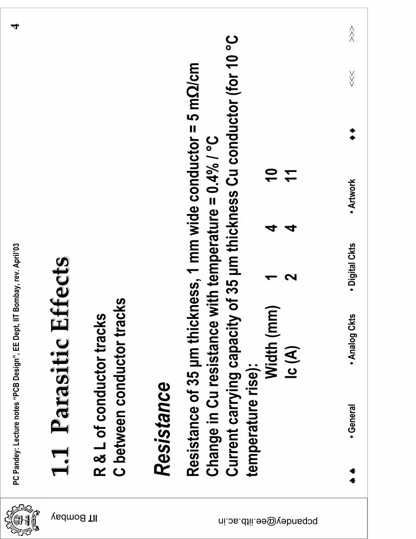
1.1 Parasitic Effects1.1 Parasitic Effects
R & L of conductor tracks
C between conductor tracks
Resistance
Resistance of 35 µm thickness, 1 mm wide conductor = 5 mΩ/cm
Change in Cu resistance with temperature = 0.4% / °C
Current carrying capacity of 35 µm thickness Cu conductor (for 10 °C
temperature rise):
Width (mm) 1 4 10
Ic (A) 2 4 11
IIT Bombay
5PC Pandey: Lecture notes “PCB Design”, EE Dept, IIT Bombay, rev. April’03
♠♠♠♠ ♠♠♠♠ >>>♦♦♦♦♦♦♦♦ <<<• Artwork• Digital Ckts• General • Analog Ckts
Capacitance
• Tracks opposite each other
- Run supply lines above each other
- Don’t let signal line tracks overlap for any significant distance
• Tracks next to each other
- Increase the spacing between critical conductors
- Run ground between signal lines
Inductance
To be considered in
• High frequency analog circuits
• Fast switching logic circuits
IIT Bombay
6PC Pandey: Lecture notes “PCB Design”, EE Dept, IIT Bombay, rev. April’03
♠♠♠♠ ♠♠♠♠ >>>♦♦♦♦♦♦♦♦ <<<• Artwork• Digital Ckts• General • Analog Ckts
1.2 Supply Conductors1.2 Supply Conductors
Unstable supply & ground due to
• Resistive voltage drop
• Voltage drop caused by track L and high freq. current
• Current spikes during logic switching ⇒⇒⇒⇒ local rise in ground potential
& fall in Vcc potential ⇒⇒⇒⇒ possibility of false logic triggering.
Solutions
• Conductor widths : W (ground) > W (supply) > W(signal)
• Ground plane
• Track configuration for distributed C between Vcc & ground
• Analog & digital ground (&supply) connected at the most stable point

IIT Bombay
7PC Pandey: Lecture notes “PCB Design”, EE Dept, IIT Bombay, rev. April’03
♠♠♠♠ ♠♠♠♠ >>>♦♦♦♦♦♦♦♦ <<<• Artwork• Digital Ckts• General • Analog Ckts
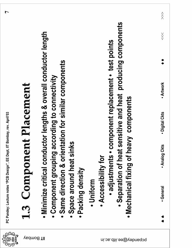
1.3 Component Placement1.3 Component Placement
• Minimize critical conductor lengths & overall conductor length
• Component grouping according to connectivity
• Same direction & orientation for similar components
• Space around heat sinks
• Packing density
• Uniform
• Accessibility for
• adjustments • component replacement • test points
• Separation of heat sensitive and heat producing components
• Mechanical fixing of heavy components
IIT Bombay
8PC Pandey: Lecture notes “PCB Design”, EE Dept, IIT Bombay, rev. April’03
♠♠♠♠ ♠♠♠♠ >>>♦♦♦♦♦♦♦♦ <<<• Artwork• Digital Ckts• General • Analog Ckts
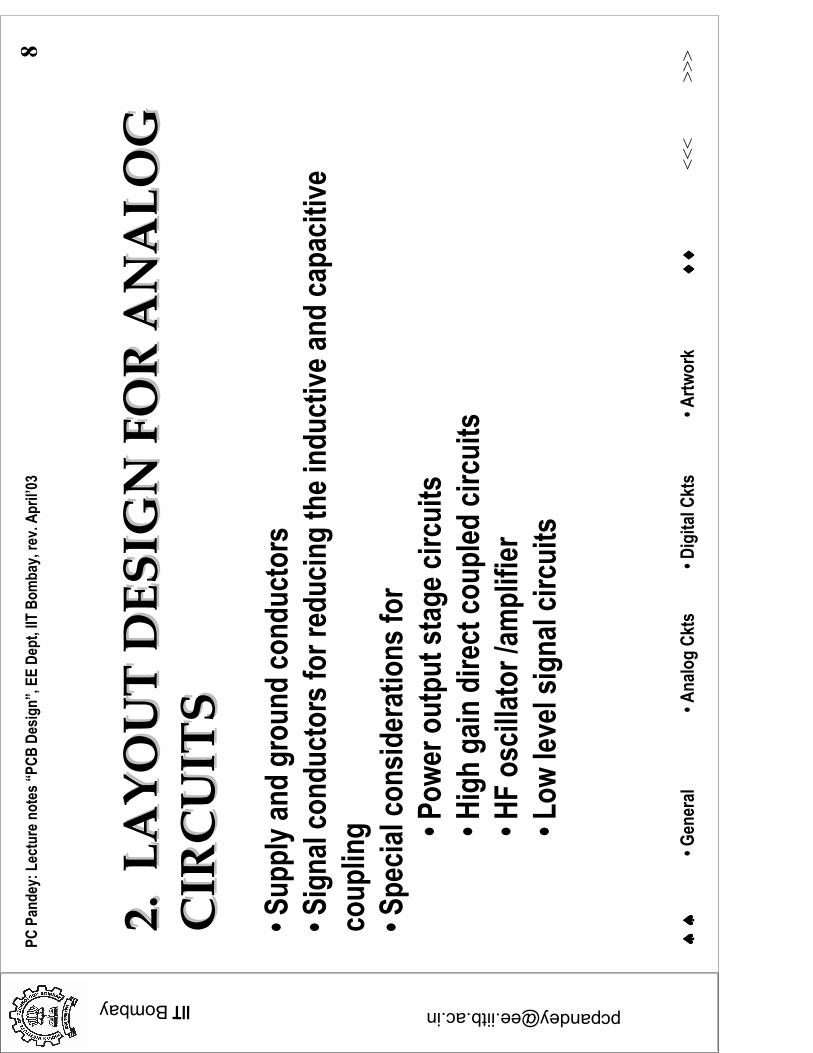
2. LAYOUT DESIGN FOR ANALOG 2. LAYOUT DESIGN FOR ANALOG
CIRCUITSCIRCUITS
• Supply and ground conductors
• Signal conductors for reducing the inductive and capacitive
coupling
• Special considerations for
• Power output stage circuits
• High gain direct coupled circuits
• HF oscillator /amplifier
• Low level signal circuits
IIT Bombay
9PC Pandey: Lecture notes “PCB Design”, EE Dept, IIT Bombay, rev. April’03
♠♠♠♠ ♠♠♠♠ >>>♦♦♦♦♦♦♦♦ <<<• Artwork• Digital Ckts• General • Analog Ckts
2.1 Ground & Supply Lines2.1 Ground & Supply Lines
• Separate GND (& Vcc) lines for analog & digital circuits
• Independent ground for reference voltage circuits
• Connect different ground conductors at most stable
reference point
• Supply lines with sufficient
width and high capacitive
coupling to GND
(use decoupling capacitors)
• Supply line should first
connect to high current drain
ckt blocks
• Supply line independent for voltage references
IIT Bombay
10PC Pandey: Lecture notes “PCB Design”, EE Dept, IIT Bombay, rev. April’03
♠♠♠♠ ♠♠♠♠ >>>♦♦♦♦♦♦♦♦ <<<• Artwork• Digital Ckts• General • Analog Ckts
2.2 HF Oscillator / Amplifier2.2 HF Oscillator / Amplifier
• Decoupling capacitor between Vcc & GND →→→→ Capacitive load on o/p
• Reduce capacitive coupling between output & input lines
• Vcc decoupling for large BW ckts. (even for LF operation)
• Separation between signal & GND to reduce capacitive loading
IIT Bombay
11PC Pandey: Lecture notes “PCB Design”, EE Dept, IIT Bombay, rev. April’03
♠♠♠♠ ♠♠♠♠ >>>♦♦♦♦♦♦♦♦ <<<• Artwork• Digital Ckts• General • Analog Ckts
2.3 Circuits with High Power O/P Stage2.3 Circuits with High Power O/P Stage
Resistance due to track length & solder joints →→→→ modulation
of Vcc & GND and low freq. oscillations
• Large decoupling capacitors
• Separate Vcc & GND for power & pre- amp stages
IIT Bombay
12PC Pandey: Lecture notes “PCB Design”, EE Dept, IIT Bombay, rev. April’03
♠♠♠♠ ♠♠♠♠ >>>♦♦♦♦♦♦♦♦ <<<• Artwork• Digital Ckts• General • Analog Ckts
2.4 High Gain DC Amplifier2.4 High Gain DC Amplifier
Solder joints →→→→ thermocouple jn
Temp gradients →→→→ diff. noisy voltages
• Temp.gradients to be avoided
• Enclosure for stopping free movement of surrounding air
IIT Bombay
13PC Pandey: Lecture notes “PCB Design”, EE Dept, IIT Bombay, rev. April’03
♠♠♠♠ ♠♠♠♠ >>>♦♦♦♦♦♦♦♦ <<<• Artwork• Digital Ckts• General • Analog Ckts
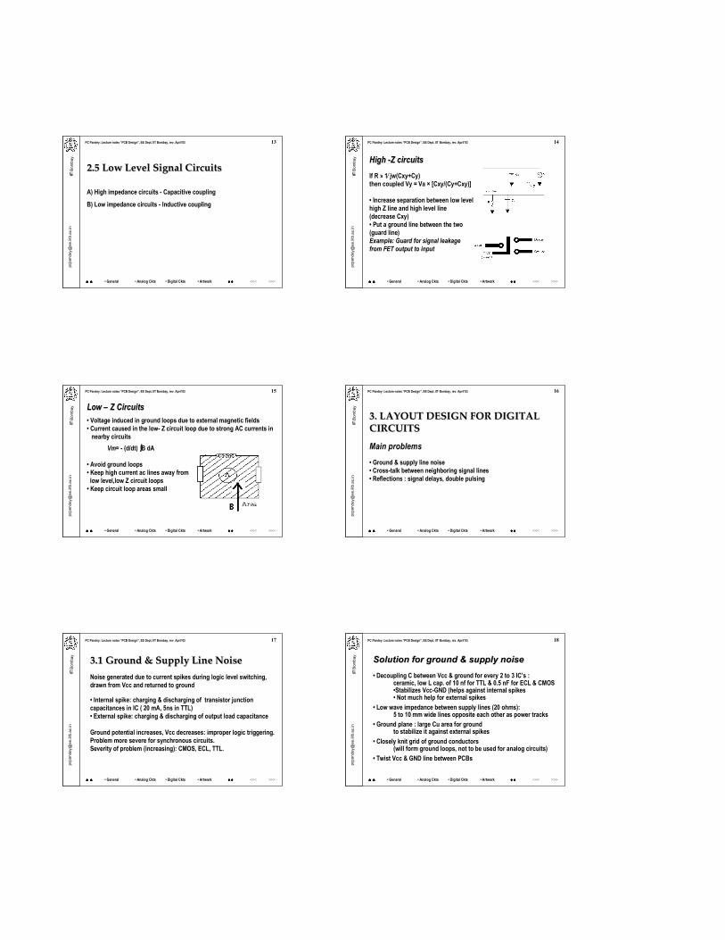
2.5 Low Level Signal Circuits2.5 Low Level Signal Circuits
A) High impedance circuits - Capacitive coupling
B) Low impedance circuits - Inductive coupling
IIT Bombay
14PC Pandey: Lecture notes “PCB Design”, EE Dept, IIT Bombay, rev. April’03
♠♠♠♠ ♠♠♠♠ >>>♦♦♦♦♦♦♦♦ <<<• Artwork• Digital Ckts• General • Analog Ckts
High -Z circuitsHigh -Z circuits
If R » 1⁄ jw(Cxy+Cy)
then coupled Vy = Va × [Cxy/(Cy+Cxy)]
• Increase separation between low level
high Z line and high level line
(decrease Cxy)
• Put a ground line between the two
(guard line)
Example: Guard for signal leakage
from FET output to input
IIT Bombay
15PC Pandey: Lecture notes “PCB Design”, EE Dept, IIT Bombay, rev. April’03
♠♠♠♠ ♠♠♠♠ >>>♦♦♦♦♦♦♦♦ <<<• Artwork• Digital Ckts• General • Analog Ckts
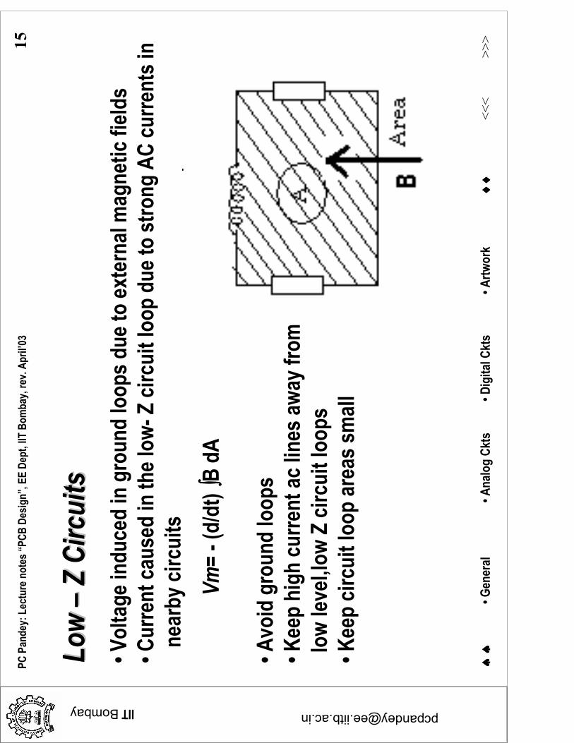
Low – Z CircuitsLow – Z Circuits
• Voltage induced in ground loops due to external magnetic fields
• Current caused in the low- Z circuit loop due to strong AC currents in
nearby circuits
Vm= - (d/dt) ∫∫∫∫B dA
• Avoid ground loops
• Keep high current ac lines away from
low level,low Z circuit loops
• Keep circuit loop areas small
IIT Bombay
16PC Pandey: Lecture notes “PCB Design”, EE Dept, IIT Bombay, rev. April’03
♠♠♠♠ ♠♠♠♠ >>>♦♦♦♦♦♦♦♦ <<<• Artwork• Digital Ckts• General • Analog Ckts
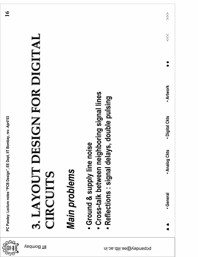
3. LAYOUT DESIGN FOR DIGITAL 3. LAYOUT DESIGN FOR DIGITAL
CIRCUITSCIRCUITS
Main problems
• Ground & supply line noise
• Cross-talk between neighboring signal lines
• Reflections : signal delays, double pulsing
IIT Bombay
17PC Pandey: Lecture notes “PCB Design”, EE Dept, IIT Bombay, rev. April’03
♠♠♠♠ ♠♠♠♠ >>>♦♦♦♦♦♦♦♦ <<<• Artwork• Digital Ckts• General • Analog Ckts
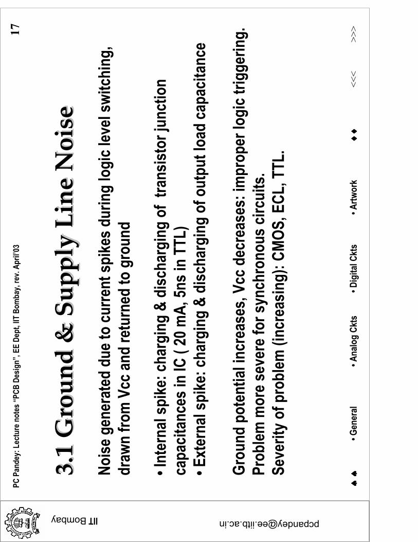
3.1 Ground & Supply Line Noise3.1 Ground & Supply Line Noise
Noise generated due to current spikes during logic level switching,
drawn from Vcc and returned to ground
• Internal spike: charging & discharging of transistor junction
capacitances in IC ( 20 mA, 5ns in TTL)
• External spike: charging & discharging of output load capacitance
Ground potential increases, Vcc decreases: improper logic triggering.
Problem more severe for synchronous circuits.
Severity of problem (increasing): CMOS, ECL, TTL.
IIT Bombay
18PC Pandey: Lecture notes “PCB Design”, EE Dept, IIT Bombay, rev. April’03
♠♠♠♠ ♠♠♠♠ >>>♦♦♦♦♦♦♦♦ <<<• Artwork• Digital Ckts• General • Analog Ckts
Solution for ground & supply noiseSolution for ground & supply noise
• Decoupling C between Vcc & ground for every 2 to 3 IC’s : ceramic, low L cap. of 10 nf for TTL & 0.5 nF for ECL & CMOS•Stabilizes Vcc-GND (helps against internal spikes• Not much help for external spikes
• Low wave impedance between supply lines (20 ohms):5 to 10 mm wide lines opposite each other as power tracks
• Ground plane : large Cu area for ground to stabilize it against external spikes
• Closely knit grid of ground conductors (will form ground loops, not to be used for analog circuits)
• Twist Vcc & GND line between PCBs
IIT Bombay
19PC Pandey: Lecture notes “PCB Design”, EE Dept, IIT Bombay, rev. April’03
♠♠♠♠ ♠♠♠♠ >>>♦♦♦♦♦♦♦♦ <<<• Artwork• Digital Ckts• General • Analog Ckts
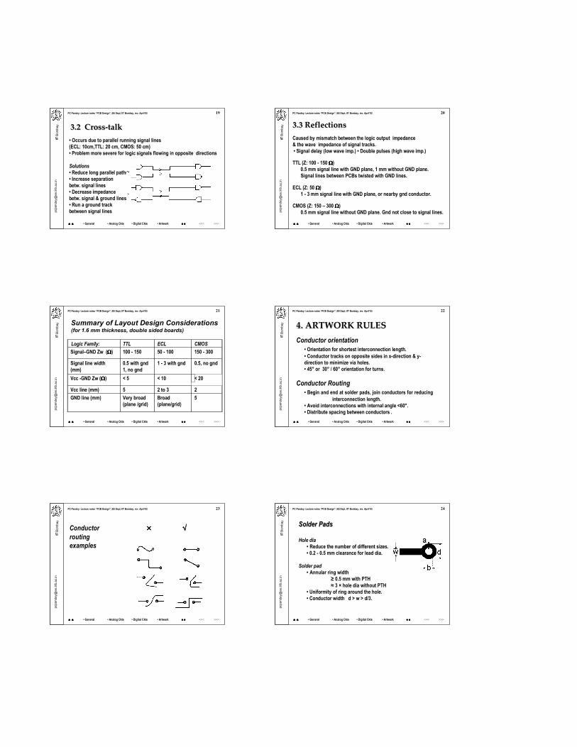
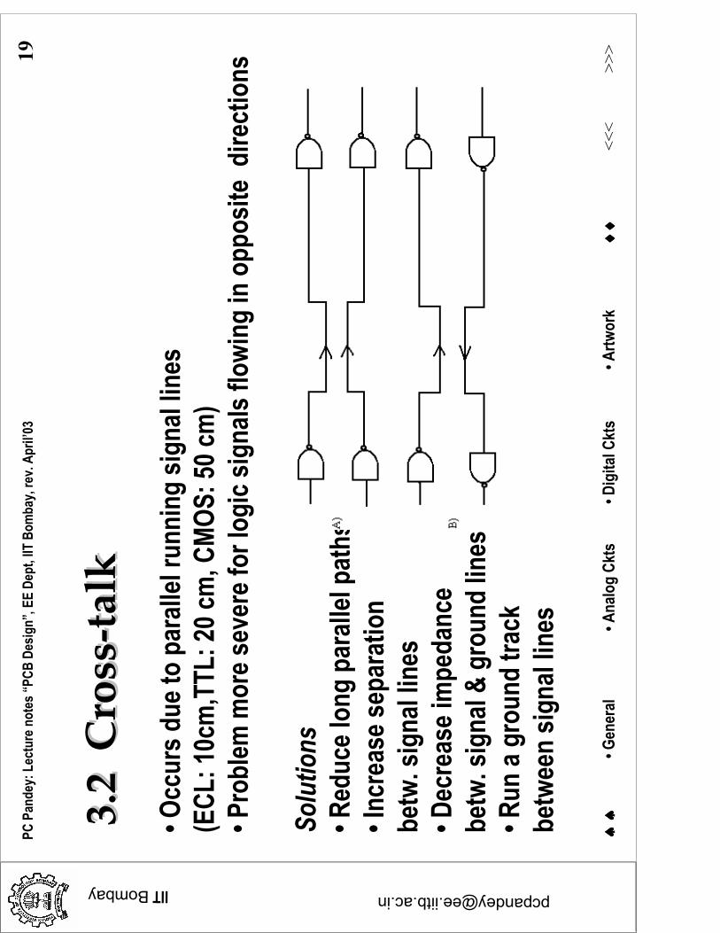
3.2 Cross-talk3.2 Cross-talk
• Occurs due to parallel running signal lines
(ECL: 10cm,TTL: 20 cm, CMOS: 50 cm)
• Problem more severe for logic signals flowing in opposite directions
Solutions
• Reduce long parallel paths
• Increase separation
betw. signal lines
• Decrease impedance
betw. signal & ground lines
• Run a ground track
between signal lines
IIT Bombay
20PC Pandey: Lecture notes “PCB Design”, EE Dept, IIT Bombay, rev. April’03
♠♠♠♠ ♠♠♠♠ >>>♦♦♦♦♦♦♦♦ <<<• Artwork• Digital Ckts• General • Analog Ckts
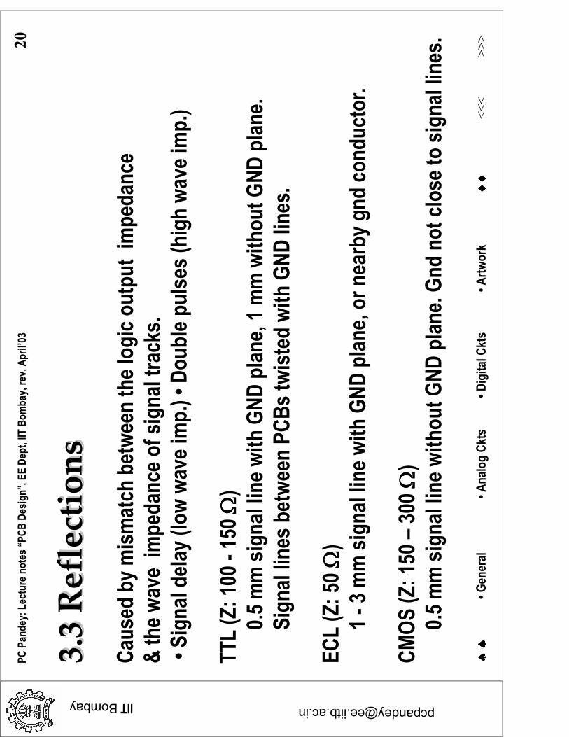
3.3 Reflections3.3 Reflections
Caused by mismatch between the logic output impedance
& the wave impedance of signal tracks.
• Signal delay (low wave imp.) • Double pulses (high wave imp.)
TTL (Z: 100 - 150 ΩΩΩΩ)
0.5 mm signal line with GND plane, 1 mm without GND plane.
Signal lines between PCBs twisted with GND lines.
ECL (Z: 50 ΩΩΩΩ)
1 - 3 mm signal line with GND plane, or nearby gnd conductor.
CMOS (Z: 150 – 300 ΩΩΩΩ)
0.5 mm signal line without GND plane. Gnd not close to signal lines.
IIT Bombay
21PC Pandey: Lecture notes “PCB Design”, EE Dept, IIT Bombay, rev. April’03
♠♠♠♠ ♠♠♠♠ >>>♦♦♦♦♦♦♦♦ <<<• Artwork• Digital Ckts• General • Analog Ckts
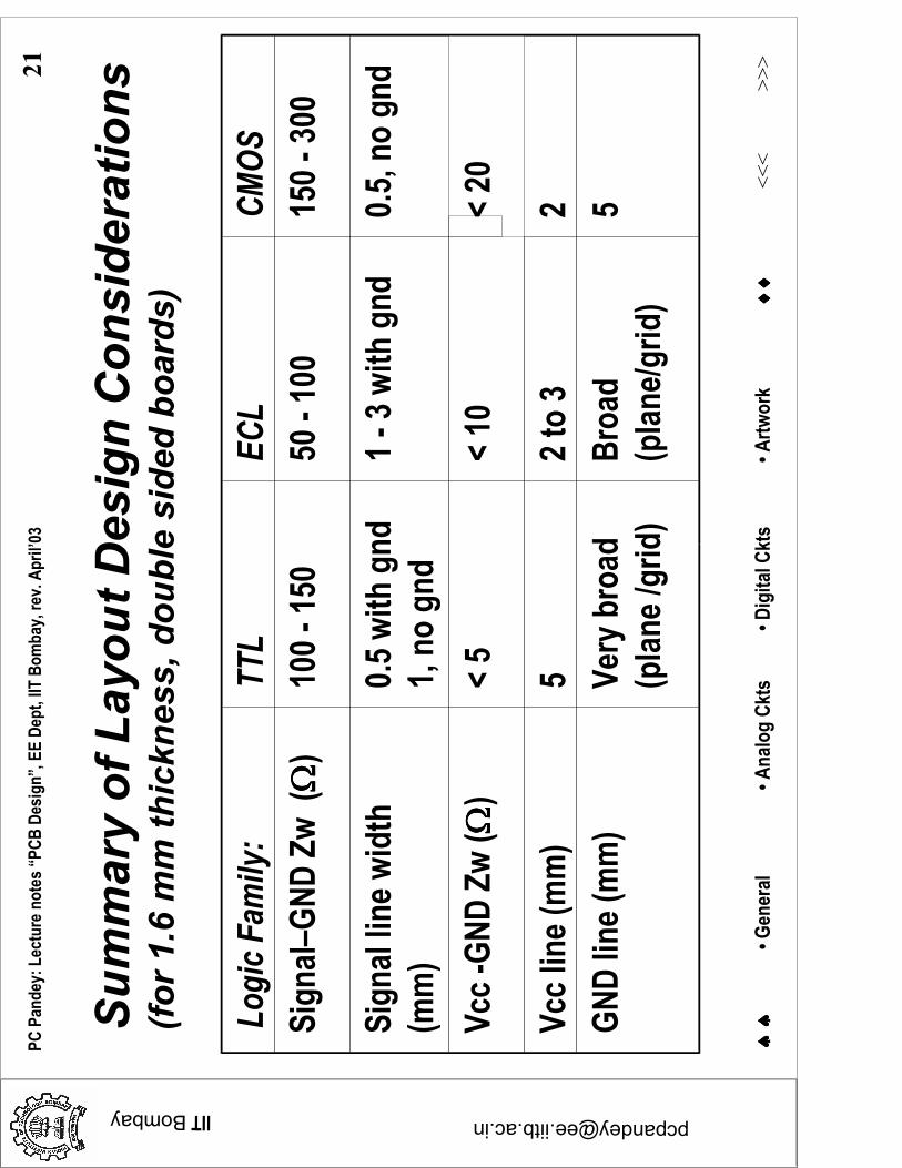
Logic Family: TTL ECL CMOS
Signal–GND Zw (ΩΩΩΩ) 100 - 150 50 - 100 150 - 300
Signal line width
(mm)
0.5 with gnd
1, no gnd
1 - 3 with gnd 0.5, no gnd
Vcc -GND Zw (ΩΩΩΩ) < 5 < 10 < 20
Vcc line (mm) 5 2 to 3 2
GND line (mm) Very broad
(plane /grid)
Broad
(plane/grid)
5
Summary of Layout Design Considerations(for 1.6 mm thickness, double sided boards)
IIT Bombay
22PC Pandey: Lecture notes “PCB Design”, EE Dept, IIT Bombay, rev. April’03
♠♠♠♠ ♠♠♠♠ >>>♦♦♦♦♦♦♦♦ <<<• Artwork• Digital Ckts• General • Analog Ckts
4. ARTWORK RULES4. ARTWORK RULES
Conductor orientation
• Orientation for shortest interconnection length.
• Conductor tracks on opposite sides in x-direction & y-
direction to minimize via holes.
• 45° or 30° / 60° orientation for turns.
Conductor Routing
• Begin and end at solder pads, join conductors for reducing
interconnection length.
• Avoid interconnections with internal angle <60°.
• Distribute spacing between conductors .
IIT Bombay
23PC Pandey: Lecture notes “PCB Design”, EE Dept, IIT Bombay, rev. April’03
♠♠♠♠ ♠♠♠♠ >>>♦♦♦♦♦♦♦♦ <<<• Artwork• Digital Ckts• General • Analog Ckts
Conductor ×××× √√√√routing
examples
IIT Bombay
24PC Pandey: Lecture notes “PCB Design”, EE Dept, IIT Bombay, rev. April’03
♠♠♠♠ ♠♠♠♠ >>>♦♦♦♦♦♦♦♦ <<<• Artwork• Digital Ckts• General • Analog Ckts
Solder PadsSolder Pads
Hole dia
• Reduce the number of different sizes.
• 0.2 - 0.5 mm clearance for lead dia.
Solder pad
• Annular ring width
≥ 0.5 mm with PTH
≈ 3 × hole dia without PTH
• Uniformity of ring around the hole.
• Conductor width d > w > d/3.

IIT Bombay
25PC Pandey: Lecture notes “PCB Design”, EE Dept, IIT Bombay, rev. April’03
♠♠♠♠ ♠♠♠♠ >>>♦♦♦♦♦♦♦♦ <<<• Artwork• Digital Ckts• General • Analog Ckts
IIT Bombay [email protected]
PC
Pan
dey
: L
ectu
re n
ote
s “P
CB
Des
ign
”, E
E D
ept,
IIT
Bo
mb
ay, r
ev. A
pri
l’03
♠ ♠♠♠ ♠ ♠♠♠
>>>
♦ ♦♦♦♦ ♦♦♦
<<<
• A
rtw
ork
• D
igit
al C
kts
• G
ener
al•
An
alo
g C
kts
PC
B D
ES
IGN
PC
B D
ES
IGN
Dr. P. C. Pandey
EE
Dep
t, I
IT B
om
bay
Rev
ised
Au
g’0
7

IIT Bombay [email protected]
PC
Pan
dey
: L
ectu
re n
ote
s “P
CB
Des
ign
”, E
E D
ept,
IIT
Bo
mb
ay, r
ev. A
pri
l’03
♠ ♠♠♠ ♠ ♠♠♠
>>>
♦ ♦♦♦♦ ♦♦♦
<<<
• A
rtw
ork
• D
igit
al C
kts
• G
ener
al•
An
alo
g C
kts
Topics
1.G
ener
al C
on
sid
erat
ion
s in
Lay
ou
t D
esig
n
2.L
ayo
ut
Des
ign
fo
r A
nal
og
Cir
cuit
s
3.L
ayo
ut
Des
ign
fo
r D
igit
al C
ircu
its
4. A
rtw
ork
Co
nsi
der
atio
ns
References
W.C
. Bo
ssh
art,
Printed Circuit Boards: Design and Technology,
TM
H,
1992
C.F
. Co
om
bs
: Printed Circuits Handbook
, McG
raw
-Hill
, 200
1
R.S
. Kh
and
pu
r : Printed Circuit Boards : Design, Fabrication, and
Assem
bly
, McG
raw
-Hill
, 200
5.

IIT Bombay [email protected]
PC
Pan
dey
: L
ectu
re n
ote
s “P
CB
Des
ign
”, E
E D
ept,
IIT
Bo
mb
ay, r
ev. A
pri
l’03
♠ ♠♠♠ ♠ ♠♠♠
>>>
♦ ♦♦♦♦ ♦♦♦
<<<
• A
rtw
ork
• D
igit
al C
kts
• G
ener
al•
An
alo
g C
kts
•G
EN
ER
AL
CO
NS
IDE
RA
TIO
NS
G
EN
ER
AL
CO
NS
IDE
RA
TIO
NS
IN
LA
YO
UT
DE
SIG
NIN
LA
YO
UT
DE
SIG
N
Main issues
• C
om
po
nen
t in
terc
on
nec
tio
ns
• E
ffec
ts o
f p
aras
itic
s
• P
hys
ical
acc
essi
bili
ty o
f co
mp
on
ents
• P
ow
er d
issi
pat
ion
Subtopics
1.1
Par
asit
ic e
ffec
ts
1.2
Su
pp
ly c
on
du
cto
rs
1.3
Co
mp
on
ent
pla
cem
ent
IIT Bombay [email protected]
PC
Pan
dey
: L
ectu
re n
ote
s “P
CB
Des
ign
”, E
E D
ept,
IIT
Bo
mb
ay, r
ev. A
pri
l’03
♠ ♠♠♠ ♠ ♠♠♠
>>>
♦ ♦♦♦♦ ♦♦♦
<<<
• A
rtw
ork
• D
igit
al C
kts
• G
ener
al•
An
alo
g C
kts
1.1
Par
asit
ic E
ffec
ts1.
1 P
aras
itic
Eff
ects
R &
L o
f co
nd
uct
or
trac
ks
C b
etw
een
co
nd
uct
or
trac
ks
Resistance
Res
ista
nce
of
35 µ
m t
hic
knes
s, 1
mm
wid
e co
nd
uct
or
= 5
mΩ
/cm
Ch
ang
e in
Cu
res
ista
nce
wit
h t
emp
erat
ure
= 0
.4%
/ °C
Cu
rren
t ca
rryi
ng
cap
acit
y o
f 35
µm
th
ickn
ess
Cu
co
nd
uct
or
(fo
r 10
°C
tem
per
atu
re r
ise)
:
Wid
th (
mm
)1
410
Ic (
A)
24
11

IIT Bombay [email protected]
PC
Pan
dey
: L
ectu
re n
ote
s “P
CB
Des
ign
”, E
E D
ept,
IIT
Bo
mb
ay, r
ev. A
pri
l’03
♠ ♠♠♠ ♠ ♠♠♠
>>>
♦ ♦♦♦♦ ♦♦♦
<<<
• A
rtw
ork
• D
igit
al C
kts
• G
ener
al•
An
alo
g C
kts
Capacitance
• T
rack
s o
pp
osi
te e
ach
oth
er
- R
un
su
pp
ly li
nes
ab
ove
eac
h o
ther
- D
on
’t le
t si
gn
al li
ne
trac
ks o
verl
ap f
or
any
sig
nif
ican
t d
ista
nce
• T
rack
s n
ext
to e
ach
oth
er
- In
crea
se t
he
spac
ing
bet
wee
n c
riti
cal c
on
du
cto
rs
- R
un
gro
un
d b
etw
een
sig
nal
lin
es
Inductance
To be considered in
• H
igh
fre
qu
ency
an
alo
g c
ircu
its
• F
ast
swit
chin
g lo
gic
cir
cuit
s

IIT Bombay [email protected]
PC
Pan
dey
: L
ectu
re n
ote
s “P
CB
Des
ign
”, E
E D
ept,
IIT
Bo
mb
ay, r
ev. A
pri
l’03
♠ ♠♠♠ ♠ ♠♠♠
>>>
♦ ♦♦♦♦ ♦♦♦
<<<
• A
rtw
ork
• D
igit
al C
kts
• G
ener
al•
An
alo
g C
kts
1.2
Su
pp
ly C
on
du
cto
rs1.
2 S
up
ply
Co
nd
uct
ors
Unstable supply & ground due to
• R
esis
tive
vo
ltag
e d
rop
• V
olt
age
dro
p c
ause
d b
y tr
ack
L a
nd
hig
h f
req
. cu
rren
t
• C
urr
ent
spik
es d
uri
ng
log
ic s
wit
chin
g ⇒ ⇒⇒⇒
loca
l ris
e in
gro
un
d p
ote
nti
al
& f
all i
n V
cc p
ote
nti
al ⇒ ⇒⇒⇒
po
ssib
ility
of
fal
se lo
gic
tri
gg
erin
g.
Solu
tions
• C
on
du
cto
r w
idth
s :
W (
gro
un
d)
> W
(su
pp
ly)
> W
(sig
nal
)
• G
rou
nd
pla
ne
• T
rack
co
nfi
gu
rati
on
fo
r d
istr
ibu
ted
C b
etw
een
Vcc
& g
rou
nd
• A
nal
og
& d
igit
al g
rou
nd
(&
sup
ply
) co
nn
ecte
d a
t th
e m
ost
sta
ble
po
int
IIT Bombay [email protected]
PC
Pan
dey
: L
ectu
re n
ote
s “P
CB
Des
ign
”, E
E D
ept,
IIT
Bo
mb
ay, r
ev. A
pri
l’03
♠ ♠♠♠ ♠ ♠♠♠
>>>
♦ ♦♦♦♦ ♦♦♦
<<<
• A
rtw
ork
• D
igit
al C
kts
• G
ener
al•
An
alo
g C
kts
1.3
Co
mp
on
ent
Pla
cem
ent
1.3
Co
mp
on
ent
Pla
cem
ent
• M
inim
ize
crit
ical
co
nd
uct
or
len
gth
s &
ove
rall
con
du
cto
r le
ng
th
• C
om
po
nen
t g
rou
pin
g a
cco
rdin
g t
o c
on
nec
tivi
ty
• S
ame
dir
ecti
on
& o
rien
tati
on
fo
r si
mila
r co
mp
on
ents
• S
pac
e ar
ou
nd
hea
t si
nks
• P
acki
ng
den
sity
• U
nif
orm
• A
cces
sib
ility
fo
r
• a
dju
stm
ents
• c
om
po
nen
t re
pla
cem
ent
• t
est
po
ints
• S
epar
atio
n o
f h
eat
sen
siti
ve a
nd
hea
t p
rod
uci
ng
co
mp
on
ents
• M
ech
anic
al f
ixin
g o
f h
eavy
co
mp
on
ents
IIT Bombay [email protected]
PC
Pan
dey
: L
ectu
re n
ote
s “P
CB
Des
ign
”, E
E D
ept,
IIT
Bo
mb
ay, r
ev. A
pri
l’03
♠ ♠♠♠ ♠ ♠♠♠
>>>
♦ ♦♦♦♦ ♦♦♦
<<<
• A
rtw
ork
• D
igit
al C
kts
• G
ener
al•
An
alo
g C
kts
2. L
AY
OU
T D
ES
IGN
FO
R A
NA
LO
G
2. L
AY
OU
T D
ES
IGN
FO
R A
NA
LO
G
CIR
CU
ITS
CIR
CU
ITS
• S
up
ply
an
d g
rou
nd
co
nd
uct
ors
• S
ign
al c
on
du
cto
rs f
or
red
uci
ng
th
e in
du
ctiv
e an
d c
apac
itiv
e
cou
plin
g
• S
pec
ial c
on
sid
erat
ion
s fo
r
• P
ow
er o
utp
ut
stag
e ci
rcu
its
• H
igh
gai
n d
irec
t co
up
led
cir
cuit
s
• H
F o
scill
ato
r /a
mp
lifie
r
• L
ow
leve
l sig
nal
cir
cuit
s

IIT Bombay [email protected]
PC
Pan
dey
: L
ectu
re n
ote
s “P
CB
Des
ign
”, E
E D
ept,
IIT
Bo
mb
ay, r
ev. A
pri
l’03
♠ ♠♠♠ ♠ ♠♠♠
>>>
♦ ♦♦♦♦ ♦♦♦
<<<
• A
rtw
ork
• D
igit
al C
kts
• G
ener
al•
An
alo
g C
kts
2.1
Gro
un
d &
Su
pp
ly L
ines
2.1
Gro
un
d &
Su
pp
ly L
ines
• S
epar
ate
GN
D (
& V
cc)
lines
fo
r an
alo
g &
dig
ital
cir
cuit
s
• In
dep
end
ent
gro
un
d f
or
refe
ren
ce v
olt
age
circ
uit
s
• C
on
nec
t d
iffe
ren
t g
rou
nd
co
nd
uct
ors
at
mo
st s
tab
le
refe
ren
ce p
oin
t
• S
up
ply
lin
es w
ith
su
ffic
ien
t
wid
th a
nd
hig
h c
apac
itiv
e
cou
plin
g t
o G
ND
(use
dec
ou
plin
g c
apac
ito
rs)
• S
up
ply
lin
e sh
ou
ld f
irst
con
nec
t to
hig
h c
urr
ent
dra
in
ckt
blo
cks
• S
up
ply
lin
e in
dep
end
ent
for
volt
age
refe
ren
ces

IIT Bombay [email protected]
PC
Pan
dey
: L
ectu
re n
ote
s “P
CB
Des
ign
”, E
E D
ept,
IIT
Bo
mb
ay, r
ev. A
pri
l’03
♠ ♠♠♠ ♠ ♠♠♠
>>>
♦ ♦♦♦♦ ♦♦♦
<<<
• A
rtw
ork
• D
igit
al C
kts
• G
ener
al•
An
alo
g C
kts
2.2
HF
Osc
illa
tor
/ A
mp
lifi
er2.
2 H
F O
scil
lato
r /
Am
pli
fier
• D
eco
up
ling
cap
acit
or
bet
wee
n V
cc &
GN
D → →→→
Cap
acit
ive
load
on
o/p
• R
edu
ce c
apac
itiv
e co
up
ling
bet
wee
n o
utp
ut
& in
pu
t lin
es
• V
cc d
eco
up
ling
fo
r la
rge
BW
ckt
s. (
even
fo
r L
F o
per
atio
n)
• S
epar
atio
n b
etw
een
sig
nal
& G
ND
to
red
uce
cap
acit
ive
load
ing

IIT Bombay [email protected]
PC
Pan
dey
: L
ectu
re n
ote
s “P
CB
Des
ign
”, E
E D
ept,
IIT
Bo
mb
ay, r
ev. A
pri
l’03
♠ ♠♠♠ ♠ ♠♠♠
>>>
♦ ♦♦♦♦ ♦♦♦
<<<
• A
rtw
ork
• D
igit
al C
kts
• G
ener
al•
An
alo
g C
kts
2.3
Cir
cuit
s w
ith
Hig
h P
ow
er O
/P S
tag
e2.
3 C
ircu
its
wit
h H
igh
Po
wer
O/P
Sta
ge
Res
ista
nce
du
e to
tra
ck le
ng
th &
so
lder
jo
ints
→ →→→ m
od
ula
tio
n
of
Vcc
& G
ND
an
d lo
w f
req
. osc
illat
ion
s
• L
arg
e d
eco
up
ling
cap
acit
ors
• S
epar
ate
Vcc
& G
ND
fo
r p
ow
er &
pre
- am
p s
tag
es

IIT Bombay [email protected]
PC
Pan
dey
: L
ectu
re n
ote
s “P
CB
Des
ign
”, E
E D
ept,
IIT
Bo
mb
ay, r
ev. A
pri
l’03
♠ ♠♠♠ ♠ ♠♠♠
>>>
♦ ♦♦♦♦ ♦♦♦
<<<
• A
rtw
ork
• D
igit
al C
kts
• G
ener
al•
An
alo
g C
kts
2.4
Hig
h G
ain
DC
Am
pli
fier
2.4
Hig
h G
ain
DC
Am
pli
fier
So
lder
join
ts → →→→
th
erm
oco
up
le j
n
Tem
p g
rad
ien
ts → →→→
dif
f. n
ois
y vo
ltag
es
• T
emp
.gra
die
nts
to
be
avo
ided
• E
ncl
osu
re f
or
sto
pp
ing
fre
e m
ove
men
t o
f su
rro
un
din
g a
ir

IIT Bombay [email protected]
PC
Pan
dey
: L
ectu
re n
ote
s “P
CB
Des
ign
”, E
E D
ept,
IIT
Bo
mb
ay, r
ev. A
pri
l’03
♠ ♠♠♠ ♠ ♠♠♠
>>>
♦ ♦♦♦♦ ♦♦♦
<<<
• A
rtw
ork
• D
igit
al C
kts
• G
ener
al•
An
alo
g C
kts
2.5
Lo
w L
evel
Sig
nal
Cir
cuit
s2.
5 L
ow
Lev
el S
ign
al C
ircu
its
A)
Hig
h im
ped
ance
cir
cuit
s -
Cap
acit
ive
cou
plin
g
B)
Lo
w im
ped
ance
cir
cuit
s -
Ind
uct
ive
cou
plin
g

IIT Bombay [email protected]
PC
Pan
dey
: L
ectu
re n
ote
s “P
CB
Des
ign
”, E
E D
ept,
IIT
Bo
mb
ay, r
ev. A
pri
l’03
♠ ♠♠♠ ♠ ♠♠♠
>>>
♦ ♦♦♦♦ ♦♦♦
<<<
• A
rtw
ork
• D
igit
al C
kts
• G
ener
al•
An
alo
g C
kts
High -Z circuits
High -Z circuits
If R
» 1
⁄ jw
(Cxy
+C
y)
then
co
up
led
Vy
= V
a ×
[C
xy/(
Cy+
Cxy
)]
• In
crea
se s
epar
atio
n b
etw
een
low
leve
l
hig
h Z
lin
e an
d h
igh
leve
l lin
e
(dec
reas
e C
xy)
• P
ut
a g
rou
nd
lin
e b
etw
een
th
e tw
o
(gu
ard
lin
e)
Example: Guard for signal leakage
from FET output to input
IIT Bombay [email protected]
PC
Pan
dey
: L
ectu
re n
ote
s “P
CB
Des
ign
”, E
E D
ept,
IIT
Bo
mb
ay, r
ev. A
pri
l’03
♠ ♠♠♠ ♠ ♠♠♠
>>>
♦ ♦♦♦♦ ♦♦♦
<<<
• A
rtw
ork
• D
igit
al C
kts
• G
ener
al•
An
alo
g C
kts
Low – Z Circuits
Low – Z Circuits
• V
olt
age
ind
uce
d in
gro
un
d lo
op
s d
ue
to e
xter
nal
mag
net
ic f
ield
s
• C
urr
ent
cau
sed
in t
he
low
- Z
cir
cuit
loo
p d
ue
to s
tro
ng
AC
cu
rren
ts in
n
earb
y ci
rcu
its
Vm
= -
(d
/dt)
∫ ∫∫∫B
dA
• A
void
gro
un
d lo
op
s
• K
eep
hig
h c
urr
ent
ac li
nes
aw
ay f
rom
lo
w le
vel,l
ow
Z c
ircu
it lo
op
s
• K
eep
cir
cuit
loo
p a
reas
sm
all
IIT Bombay [email protected]
PC
Pan
dey
: L
ectu
re n
ote
s “P
CB
Des
ign
”, E
E D
ept,
IIT
Bo
mb
ay, r
ev. A
pri
l’03
♠ ♠♠♠ ♠ ♠♠♠
>>>
♦ ♦♦♦♦ ♦♦♦
<<<
• A
rtw
ork
• D
igit
al C
kts
• G
ener
al•
An
alo
g C
kts
3. L
AY
OU
T D
ES
IGN
FO
R D
IGIT
AL
3.
LA
YO
UT
DE
SIG
N F
OR
DIG
ITA
L
CIR
CU
ITS
CIR
CU
ITS
Main problems
• G
rou
nd
& s
up
ply
lin
e n
ois
e
• C
ross
-tal
k b
etw
een
nei
gh
bo
rin
g s
ign
al li
nes
• R
efle
ctio
ns
: si
gn
al d
elay
s, d
ou
ble
pu
lsin
g
IIT Bombay [email protected]
PC
Pan
dey
: L
ectu
re n
ote
s “P
CB
Des
ign
”, E
E D
ept,
IIT
Bo
mb
ay, r
ev. A
pri
l’03
♠ ♠♠♠ ♠ ♠♠♠
>>>
♦ ♦♦♦♦ ♦♦♦
<<<
• A
rtw
ork
• D
igit
al C
kts
• G
ener
al•
An
alo
g C
kts
3.1
Gro
un
d &
Su
pp
ly L
ine
No
ise
3.1
Gro
un
d &
Su
pp
ly L
ine
No
ise
No
ise
gen
erat
ed d
ue
to c
urr
ent
spik
es d
uri
ng
log
ic le
vel s
wit
chin
g,
dra
wn
fro
m V
cc a
nd
ret
urn
ed t
o g
rou
nd
• In
tern
al s
pik
e: c
har
gin
g &
dis
char
gin
g o
f t
ran
sist
or
jun
ctio
n
cap
acit
ance
s in
IC (
20
mA
, 5n
s in
TT
L)
• E
xter
nal
sp
ike:
ch
arg
ing
& d
isch
arg
ing
of
ou
tpu
t lo
ad c
apac
itan
ce
Gro
un
d p
ote
nti
al in
crea
ses,
Vcc
dec
reas
es:
imp
rop
er lo
gic
tri
gg
erin
g.
Pro
ble
m m
ore
sev
ere
for
syn
chro
no
us
circ
uit
s.
Sev
erit
y o
f p
rob
lem
(in
crea
sin
g):
CM
OS
, EC
L, T
TL
.

IIT Bombay [email protected]
PC
Pan
dey
: L
ectu
re n
ote
s “P
CB
Des
ign
”, E
E D
ept,
IIT
Bo
mb
ay, r
ev. A
pri
l’03
♠ ♠♠♠ ♠ ♠♠♠
>>>
♦ ♦♦♦♦ ♦♦♦
<<<
• A
rtw
ork
• D
igit
al C
kts
• G
ener
al•
An
alo
g C
kts
Solu
tion for gro
und &
supply
nois
eSolu
tion for gro
und &
supply
nois
e
• D
eco
up
ling
C b
etw
een
Vcc
& g
rou
nd
fo
r ev
ery
2 to
3 IC
’s :
ce
ram
ic, l
ow
L c
ap. o
f 10
nf
for
TT
L &
0.5
nF
fo
r E
CL
& C
MO
S•S
tab
ilize
s V
cc-G
ND
(h
elp
s ag
ain
st in
tern
al s
pik
es•
No
t m
uch
hel
p f
or
exte
rnal
sp
ikes
• L
ow
wav
e im
ped
ance
bet
wee
n s
up
ply
lin
es (
20 o
hm
s):
5 to
10
mm
wid
e lin
es o
pp
osi
te e
ach
oth
er a
s p
ow
er t
rack
s
• G
rou
nd
pla
ne
: la
rge
Cu
are
a fo
r g
rou
nd
to
sta
bili
ze it
ag
ain
st e
xter
nal
sp
ikes
• C
lose
ly k
nit
gri
d o
f g
rou
nd
co
nd
uct
ors
(w
ill f
orm
gro
un
d lo
op
s, n
ot
to b
e u
sed
fo
r an
alo
g c
ircu
its)
• T
wis
t V
cc &
GN
D li
ne
bet
wee
n P
CB
s
IIT Bombay [email protected]
PC
Pan
dey
: L
ectu
re n
ote
s “P
CB
Des
ign
”, E
E D
ept,
IIT
Bo
mb
ay, r
ev. A
pri
l’03
♠ ♠♠♠ ♠ ♠♠♠
>>>
♦ ♦♦♦♦ ♦♦♦
<<<
• A
rtw
ork
• D
igit
al C
kts
• G
ener
al•
An
alo
g C
kts
3.
2 C
ross
-tal
k3.
2 C
ross
-tal
k
• O
ccu
rs d
ue
to p
aral
lel r
un
nin
g s
ign
al li
nes
(EC
L:
10cm
,TT
L:
20 c
m, C
MO
S:
50 c
m)
• P
rob
lem
mo
re s
ever
e fo
r lo
gic
sig
nal
s fl
ow
ing
in o
pp
osi
te d
irec
tio
ns
Solutions
• R
edu
ce lo
ng
par
alle
l pat
hs
• In
crea
se s
epar
atio
n
bet
w. s
ign
al li
nes
• D
ecre
ase
imp
edan
ce
bet
w. s
ign
al &
gro
un
d li
nes
• R
un
a g
rou
nd
tra
ck
bet
wee
n s
ign
al li
nes
IIT Bombay [email protected]
PC
Pan
dey
: L
ectu
re n
ote
s “P
CB
Des
ign
”, E
E D
ept,
IIT
Bo
mb
ay, r
ev. A
pri
l’03
♠ ♠♠♠ ♠ ♠♠♠
>>>
♦ ♦♦♦♦ ♦♦♦
<<<
• A
rtw
ork
• D
igit
al C
kts
• G
ener
al•
An
alo
g C
kts
3.3
Ref
lect
ion
s3.
3 R
efle
ctio
ns
Cau
sed
by
mis
mat
ch b
etw
een
th
e lo
gic
ou
tpu
t im
ped
ance
& t
he
wav
e im
ped
ance
of
sig
nal
tra
cks.
• S
ign
al d
elay
(lo
w w
ave
imp
.) •
Do
ub
le p
uls
es (
hig
h w
ave
imp
.)
TT
L (
Z:
100
- 15
0 Ω ΩΩΩ
)
0.5
mm
sig
nal
lin
e w
ith
GN
D p
lan
e, 1
mm
wit
ho
ut
GN
D p
lan
e.
Sig
nal
lin
es b
etw
een
PC
Bs
twis
ted
wit
h G
ND
lin
es.
EC
L (
Z:
50 Ω ΩΩΩ
)
1 -
3 m
m s
ign
al li
ne
wit
h G
ND
pla
ne,
or
nea
rby
gn
d c
on
du
cto
r.
CM
OS
(Z
: 15
0 –
300 Ω ΩΩΩ
)
0.5
mm
sig
nal
lin
e w
ith
ou
t G
ND
pla
ne.
Gn
d n
ot
clo
se t
o s
ign
al li
nes
.
IIT Bombay [email protected]
PC
Pan
dey
: L
ectu
re n
ote
s “P
CB
Des
ign
”, E
E D
ept,
IIT
Bo
mb
ay, r
ev. A
pri
l’03
♠ ♠♠♠ ♠ ♠♠♠
>>>
♦ ♦♦♦♦ ♦♦♦
<<<
• A
rtw
ork
• D
igit
al C
kts
• G
ener
al•
An
alo
g C
kts
Logic Fam
ily:
TTL
ECL
CMOS
Sig
nal
–GN
D Z
w (Ω ΩΩΩ
)10
0 -
150
50 -
100
150
- 30
0
Sig
nal
lin
e w
idth
(mm
)
0.5
wit
h g
nd
1, n
o g
nd
1 -
3 w
ith
gn
d0.
5, n
o g
nd
Vcc
-G
ND
Zw
(Ω ΩΩΩ
)<
5<
10
< 2
0
Vcc
lin
e (m
m)
52
to 3
2
GN
D li
ne
(mm
)V
ery
bro
ad
(pla
ne
/gri
d)
Bro
ad
(pla
ne/
gri
d)
5
Sum
mary
of Layout D
esig
n C
onsid
era
tions
(for
1.6
mm
thic
kness, double
sid
ed b
oard
s)

IIT Bombay [email protected]
PC
Pan
dey
: L
ectu
re n
ote
s “P
CB
Des
ign
”, E
E D
ept,
IIT
Bo
mb
ay, r
ev. A
pri
l’03
♠ ♠♠♠ ♠ ♠♠♠
>>>
♦ ♦♦♦♦ ♦♦♦
<<<
• A
rtw
ork
• D
igit
al C
kts
• G
ener
al•
An
alo
g C
kts
4. A
RT
WO
RK
RU
LE
S4.
AR
TW
OR
K R
UL
ES
Conductor orientation
• O
rien
tati
on
fo
r sh
ort
est
inte
rco
nn
ecti
on
len
gth
.
• C
on
du
cto
r tr
acks
on
op
po
site
sid
es in
x-d
irec
tio
n &
y-
dir
ecti
on
to
min
imiz
e vi
a h
ole
s.
• 45
° o
r 3
0° /
60°
ori
enta
tio
n f
or
turn
s.
Conductor Routing
• B
egin
an
d e
nd
at
sold
er p
ads,
jo
in c
on
du
cto
rs f
or
red
uci
ng
in
terc
on
nec
tio
n le
ng
th.
• A
void
inte
rco
nn
ecti
on
s w
ith
inte
rnal
an
gle
<60
°.
• D
istr
ibu
te s
pac
ing
bet
wee
n c
on
du
cto
rs .

IIT Bombay [email protected]
PC
Pan
dey
: L
ectu
re n
ote
s “P
CB
Des
ign
”, E
E D
ept,
IIT
Bo
mb
ay, r
ev. A
pri
l’03
♠ ♠♠♠ ♠ ♠♠♠
>>>
♦ ♦♦♦♦ ♦♦♦
<<<
• A
rtw
ork
• D
igit
al C
kts
• G
ener
al•
An
alo
g C
kts
Conductor × ×××
√ √√√
routing
exam
ples

IIT Bombay [email protected]
PC
Pan
dey
: L
ectu
re n
ote
s “P
CB
Des
ign
”, E
E D
ept,
IIT
Bo
mb
ay, r
ev. A
pri
l’03
♠ ♠♠♠ ♠ ♠♠♠
>>>
♦ ♦♦♦♦ ♦♦♦
<<<
• A
rtw
ork
• D
igit
al C
kts
• G
ener
al•
An
alo
g C
kts
Solder Pads
Solder Pads
Hole dia
• R
edu
ce t
he
nu
mb
er o
f d
iffe
ren
t si
zes.
• 0.
2 -
0.5
mm
cle
aran
ce f
or
lead
dia
.
Solder pad
• A
nn
ula
r ri
ng
wid
th
≥ 0
.5 m
m w
ith
PT
H
≈ 3
× h
ole
dia
wit
ho
ut
PT
H
• U
nif
orm
ity
of
rin
g a
rou
nd
th
e h
ole
.
• C
on
du
cto
r w
idth
d
> w
> d
/3.
IIT Bombay [email protected]
PC
Pan
dey
: L
ectu
re n
ote
s “P
CB
Des
ign
”, E
E D
ept,
IIT
Bo
mb
ay, r
ev. A
pri
l’03
♠ ♠♠♠ ♠ ♠♠♠
>>>
♦ ♦♦♦♦ ♦♦♦
<<<
• A
rtw
ork
• D
igit
al C
kts
• G
ener
al•
An
alo
g C
kts