pcb revision b hardware guide
TRANSCRIPT

ZLE30250 Evaluation Board PCB Revision B Hardware Guide
June 2014 .

ZLE30250 Hardware Guide
June 2014 2
List of Figures ................................................................................................ 3
List of Tables .................................................................................................. 3
Supported Devices ........................................................................................ 5
Related Documents ....................................................................................... 5
Hardware Overview........................................................................................ 5 Hardware Feature Summary ...................................................................................................... 5
Major Components .............................................................................................................. 5
Hardware Features .............................................................................................................. 5
Power Supply ...................................................................................................................... 6
USB Interface ...................................................................................................................... 7
Hardware Configuration ................................................................................ 7 Top Level Configurations ........................................................................................................... 7
Switch and Jumper Configurations, Detailed Listing ......................................................... 12
Connections and Settings Tables ............................................................................................ 14
Power Supply .................................................................................................................... 14
Reset, SPI Bus and GPIO Settings ................................................................................... 16
Master Clock Oscillator ...................................................................................................... 16
DUT Mode Bits .................................................................................................................. 18
Input Clocks ....................................................................................................................... 19
Output Clocks .................................................................................................................... 21
GPIO Header and Status LEDs ............................................................................................... 21
Connecting Off-Board Devices ................................................................................................ 21
Discrete Component Options for Input and output clocks ....................................................... 22
Oscillator / Crystal Daughter Card ............................................................. 23 Daughter Card Overview ......................................................................................................... 23
Oscillator Daughter Card Assembly ......................................................................................... 24
Crystal Daughter Card Assembly ............................................................................................. 25
Daughter Card Installation ....................................................................................................... 25
Document Revision History ........................................................................ 27
ZLE30250 Hardware Guide
June 2014 3
List of Figures
Figure 1 · Board Floor Plan ............................................................................................................... 6
Figure 2 · Configuration Topology with Annotations .......................................................................... 7
Figure 3 · Board Configuration 1 ....................................................................................................... 8
Figure 4 · Board Configuration 2 ....................................................................................................... 8
Figure 5 · Board Configuration 3 ....................................................................................................... 9
Figure 6 · Board Configuration 4 ..................................................................................................... 10
Figure 7 · Board Configuration 5 ..................................................................................................... 10
Figure 8 · Board Configurations 6 and 7.......................................................................................... 11
Figure 9 · Board Configuration 8 ..................................................................................................... 11
Figure 10 · ZLE30250 Oscillator / Crystal Daughter Card Schematic ............................................. 24
Figure 11 · ZLE30250 Oscillator / Crystal Daughter Assembly Drawing ......................................... 24
Figure 12 · ZLE30250 Oscillator / Crystal Daughter Assembly Drawing ......................................... 24
Figure 13 · ZLE30250 Oscillator / Crystal Daughter Assembly Drawing ......................................... 25
Figure 14 · ZLE30250 Oscillator / Crystal Daughter installed on header JP22 ................................ 26
List of Tables
Table 1 · Serial Bus DIP Switch and Jumper Configurations ........................................................... 12
Table 2 · Power Connections and Settings ..................................................................................... 15
Table 3 · Reset, SPI bus and PC Interface Hardware Configuration ............................................... 16
Table 4 · Master Clock Oscillator Configurable Hardware ............................................................... 16
Table 5 · DUT Master Clock Source Selection Jumper Settings ..................................................... 17
Table 6 · DUT Reset: Mode Bit Settings ......................................................................................... 18
Table 7 · Input Clock Hardware Configuration ................................................................................. 20
Table 8 · Input Clock Differential/Single-Ended Mode Selection Settings ....................................... 20
Table 9 · Output Clock Hardware Configuration .............................................................................. 21
Table 10 · JP4 Serial Header Pin Assignments ............................................................................... 22
Table 11 · JP6 Serial Header Pin Assignments ............................................................................... 22
Table 12 · Discrete Component Options for Clocks ........................................................................ 22

4 June 2014
This page left blank
June 2014 5
ZLE30250 Hardware Guide
Supported Devices The ZLE30250 evaluation board supports the following Microsemi timing and synchronization devices:
ZL30250, ZL30169, ZL30151, ZL30251, ZL30252, ZL30253, ZL30254
Related Documents ZLE30250 Evaluation Board Rev B Schematic
ZLE30250 Evaluation Board Rev B Bill of Materials
Datasheets for the ZL30250 and the other part numbers listed in the Supported Devices section
Hardware Overview The ZLE30250 Evaluation Board is a test and demonstration platform with support for the full feature sets of the family of timing ICs.
Hardware Feature Summary A floor plan of the board is shown in Figure 1.
Throughout this document, the abbreviation “DUT” is used to refer to “Device Under Test”, meaning the Microsemi timing IC on the board.
The ZLE30250Error! Unknown document property name. board includes the following major components and hardware features:
Major Components
Timing IC (DUT)
Low noise linear regulators
USB Interface for optional connection to PC with GUI software
External EEPROM for timing device configuration storage (ZL30250 and ZL30252)
SMA connectors for access to all DUT clocks
Serial bus switch
Hardware Features
Single 5VDC external power interface with connector for AC/DC wall adapter
Fully configurable DUT power options
DUT reset switch
Standalone (DIP switch) operation or GUI Interface
USB interface with USB-B connector for PC GUI connection
Pin headers with direct access to board’s SPI/I2C bus. Off-board DUT, EEPROM, or SPI master device can interface with on-board devices.
Status LEDs
Master clock options: on board or pluggable XOs or XTALs
SMA connectors on all input and output clocks, including master clock
Jumper-configurable input clocks
Additional discrete component configuration options for advanced users

ZLE30250 Hardware Guide
6 June 2014
Figure 1 · Board Floor Plan
Power Supply
The board is normally powered via connector J3 using the provided AC-wall-plug 5V power supply. Red LED D14 illuminates to indicate that the board is powered. Advanced power options for lab experimentation are also provisioned on the board.
ZLE30250 Hardware Guide
June 2014 7
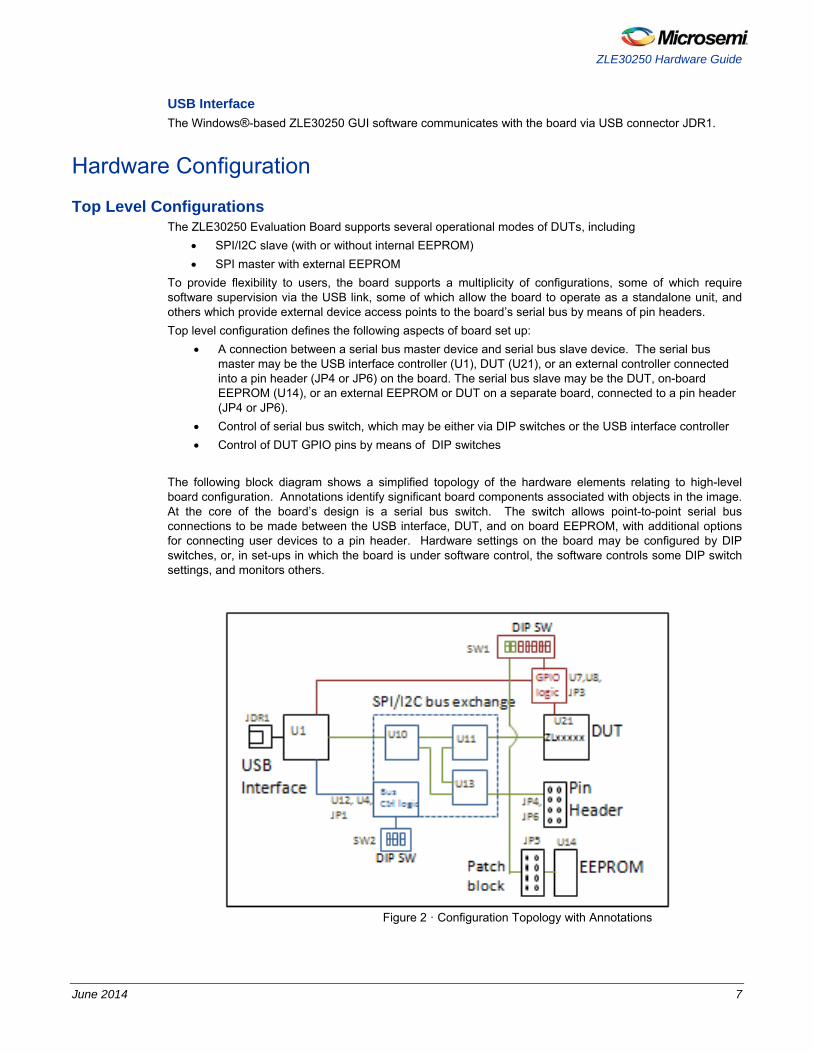
USB Interface
The Windows®-based ZLE30250 GUI software communicates with the board via USB connector JDR1.
Hardware Configuration
Top Level Configurations The ZLE30250 Evaluation Board supports several operational modes of DUTs, including
SPI/I2C slave (with or without internal EEPROM)
SPI master with external EEPROM
To provide flexibility to users, the board supports a multiplicity of configurations, some of which require software supervision via the USB link, some of which allow the board to operate as a standalone unit, and others which provide external device access points to the board’s serial bus by means of pin headers.
Top level configuration defines the following aspects of board set up:
A connection between a serial bus master device and serial bus slave device. The serial bus master may be the USB interface controller (U1), DUT (U21), or an external controller connected into a pin header (JP4 or JP6) on the board. The serial bus slave may be the DUT, on-board EEPROM (U14), or an external EEPROM or DUT on a separate board, connected to a pin header (JP4 or JP6).
Control of serial bus switch, which may be either via DIP switches or the USB interface controller
Control of DUT GPIO pins by means of DIP switches
The following block diagram shows a simplified topology of the hardware elements relating to high-level board configuration. Annotations identify significant board components associated with objects in the image. At the core of the board’s design is a serial bus switch. The switch allows point-to-point serial bus connections to be made between the USB interface, DUT, and on board EEPROM, with additional options for connecting user devices to a pin header. Hardware settings on the board may be configured by DIP switches, or, in set-ups in which the board is under software control, the software controls some DIP switch settings, and monitors others.
Figure 2 · Configuration Topology with Annotations

ZLE30250 Hardware Guide
8 June 2014
Each of the possible configurations is portrayed in the following series of Figures 3 through 9. The active serial bus and hardware control elements of the configuration are depicted by heavy lines. Active blocks are also identified with bold text. Two of the switches on SW1 are shown in green to differentiate them from GPIO controls. These represent settings for signals IF1 and IF0, which act through the SPI bus and are used in DUT configuration on reset.
In Configuration 1, the USB interface is SPI master with the DUT as bus slave.
Figure 3 · Board Configuration 1
In Configurations 2 and 3, the USB device is SPI master. The USB master can interface with an on-board EEPROM as in Configuration 2, or an “external SPI device” as in Configuration 3. The external SPI device could be either an EEPROM or a DUT mounted on another board. The physical form the external device takes would typically be an independently powered board connected by cable interface to JP4 or JP6.
Figure 4 · Board Configuration 2
ZLE30250 Hardware Guide
June 2014 9
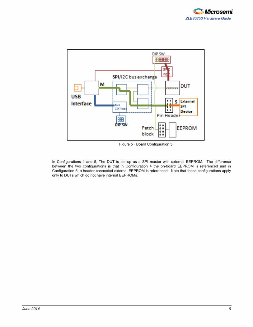
Figure 5 · Board Configuration 3
In Configurations 4 and 5, The DUT is set up as a SPI master with external EEPROM. The difference between the two configurations is that in Configuration 4 the on-board EEPROM is referenced and in Configuration 5, a header-connected external EEPROM is referenced. Note that these configurations apply only to DUTs which do not have internal EEPROMs.

ZLE30250 Hardware Guide
10 June 2014
Figure 6 · Board Configuration 4
Figure 7 · Board Configuration 5
Configurations 6 and 7 depict scenarios in which an external serial bus master device is connected to the DUT. One Figure shows the topology for the two configurations because they are differentiated only by switch settings. Configuration 6 is SPI serial bus mode, whereas Configuration 7 is an I2C serial bus.

ZLE30250 Hardware Guide
June 2014 11
Figure 8 · Board Configurations 6 and 7
Finally, Configuration 8 depicts an external device interfacing with the on-board EEPROM over the serial bus.
Figure 9 · Board Configuration 8

ZLE30250 Hardware Guide
12 June 2014
Switch and Jumper Configurations, Detailed Listing
Each of the possible board configurations illustrated above is implemented as a collection of settings. The settings are comprised of jumper assignments, DIP switch settings, and/or software-controlled bit port logic (1=high, 0=low). This section provides a comprehensive listing of all the board settings for each configuration. It is important to note that for configurations in which the DUT is an active element, settings must be applied prior to and held during the DUT reset cycle so that the DUT starts up in a state which is coordinated with the board.
Table 1 · lists the configurations and their associated settings. References to the configuration topology diagrams in the preceding section are shown in column 1. A summary listing of the Jumpers and switches referenced in Table 1 · can be found in Table 3 · .
The reader is referred to applicable device datasheets for further information about DUT reset and configuration. Some signals, typically GPIOs, may change once DUT has initialized. Note: at this time not all configurations are fully supported by software.
Table 1 · Serial Bus DIP Switch and Jumper Configurations
Board Config. Number
Serial Bus Master
Serial Bus Slave Description Switch and Jumper Settings
USB Controller IO PinSettings
1 USB (SPI)
DUT GUI/PC is master of SPI bus, and controls serial bus configuration settings. DIP switch settings control DUT GPIOs.
JP1 = on
SW1.IF0 = 1 SW1.IF1 = 1 SW1.TEST_GPIO2 = 0 SW1.PUPD_ENB = 0 SW1.AC1_GPIO1, SW1.AC0_GPIO0 = [0,0] for DUT without internal EEPROM
SW1.AC1_GPIO1, SW1.AC0_GPIO0 = [0,0], [0,1], [1,0], or [1,1] for DUT with internal EEPROM
FT_FSW_OEB = 0 FT_HW_SEL = 0 FT_SPI_SEL = 0 FT_DSW_SEL = 0 FT_ESW_SEL = x FT_ESW_OEB = 1 FT_PUPD_ENB = hi-Z
FT_AC0_GPIO0 = hi-Z FT_AC1_GPIO1 = hi-Z FT_TEST_GPIO2 = hi-Z FT_GPIO3 = hi-Z
2 USB (SPI)
EEPROM (U14)
GUI/PC Is master of SPI bus connection with on-board EEPROM, and controls serial bus configuration settings If DUT is running, GPIO DIPs should be left as configured.
JP1=on JP5: shunt pins 1-2, 3-4, 5-6, 7-8
SW1.IF0 = 1 SW1.IF1 = 1 SW1.PUPD_ENB = 0
FT_FSW_OEB = 0 FT_HW_SEL = 0 FT_SPI_SEL = 1
FT_DSW_SEL = x FT_ESW_SEL = 0 FT_ESW_OEB = 0
FT_PUPD_ENB = hi-Z FT_AC0_GPIO0 = hi-Z FT_AC1_GPIO1 = hi-Z FT_TEST_GPIO2 = hi-Z FT_GPIO3 = hi-Z

ZLE30250 Hardware Guide
June 2014 13
Board Config. Number
Serial Bus Master
Serial Bus Slave Description Switch and Jumper Settings
USB Controller IO PinSettings
3 USB (SPI)
JP4 or JP6
GUI/PC controls external EEPROM connected at header, or external DUT via SPI cable, and serial bus configuration If DUT is running, GPIO DIPs should be left as configured.
JP1 = on JP5: all open SW1.IF0 = 1 SW1.IF1 = 1 SW1.PUPD_ENB = 0
FT_FSW_OEB = 0 FT_HW_SEL = 0 FT_SPI_SEL = 1
FT_DSW_SEL = x FT_ESW_SEL = 0 FT_ESW_OEB = 0
FT_PUPD_ENB = hi-Z FT_AC0_GPIO0 = hi-Z FT_AC1_GPIO1 = hi-Z FT_TEST_GPIO2 = hi-Z FT_GPIO3 = hi-Z
4 DUT (SPI)
EEPROM DUT loads from EEPROM (standalone board operation).
DUT variants with internal EEPROM will not load from external EEPROM device.
JP1 = open JP5: shunt pins 1-2, 3-4, 5-6, 7-8
SW1.IF0 = 1 SW1.IF1 = 1 SW1.TEST_GPIO2 = 0 SW1.PUPD_ENB = 0 SW2.DSW_SEL = 1 SW2. ESW_OEB = 0 SW2. ESW_SEL = 1
SW1.AC1_GPIO1, SW1.AC0_GPIO0 = [0,1], [1,0], or [1,1]
N/A
5 DUT JP4 or JP6 Header
DUT as SPI master, external slave EEPROM device connected to header. Applies only to DUT variants without internal EEPROM.
JP1 = open JP5: open
SW1.IF0 = 1 SW1.IF1 = 1 SW1.TEST_GPIO2 = 0 SW1.PUPD_ENB = 0 SW2.DSW_SEL = 1 SW2. ESW_OEB = 0 SW2.ESW_SEL = 1
SW1.AC1_GPIO1, SW1.AC0_GPIO0 = [0,1], [1,0], or [1,1]
N/A

ZLE30250 Hardware Guide
14 June 2014
Board Config. Number
Serial Bus Master
Serial Bus Slave Description Switch and Jumper Settings
USB Controller IO PinSettings
6 JP4 or JP6 Header
DUT Off-board connected device as SPI master, DUT slave
JP1 = open JP5: open
SW1.IF0 = 1 SW1.IF1 = 1 SW1.TEST_GPIO2 = 0 SW1.PUPD_ENB = 0 SW2.DSW_SEL = 1 SW2. ESW_OEB = 0 SW2. ESW_SEL = 1
SW1.AC1_GPIO1, SW1.AC0_GPIO0 = [0,0] for DUT without internal EEPROM
SW1.AC1_GPIO1, SW1.AC0_GPIO0 = [0,0], [0,1], [1,0], or [1,1] for DUT with internal EEPROM
N/A
7 JP4 or JP6 Header
DUT External connected device as I2C master, DUT slave
JP1 = open JP5: open
SW1.IF1, SW1.IF0 = [0,0], [0,1], or [1,0] SW1.TEST_GPIO2 = 0 SW1.PUPD_ENB = 0 SW2.DSW_SEL = 1 SW2. ESW_OEB = 0 SW2. ESW_SEL = 1
SW1.AC1_GPIO1, SW1.AC0_GPIO0 = [x,x], for DUT without internal EEPROM
SW1.AC1_GPIO1, SW1.AC0_GPIO0 = [0,0], [0,1], [1,0], or [1,1] for DUT with internal EEPROM
N/A
8 JP4 or JP6 Header
EEPROM External device SPI master programs and/or reads EEPROM
JP1 = open JP5: shunt pins 1-2, 3-4, 5-6, 7-8
SW1.IF0 = 1 SW1.IF1 = 1 SW1.PUPD_ENB = 0 SW2. ESW_OEB = 1
N/A
Connections and Settings Tables The following sections provide detailed listings of the various evaluation board user interface components.
Power Supply
The board provides several options for evaluating device performance with respect to power supply configuration. DUT power configuration is highly customizable. A thorough understanding of the DUT and board operation should be developed prior to customizing power settings on the board. Table 2 · summarizes the power supply related hardware connectors and their functions.
ZLE30250 Hardware Guide
June 2014 15
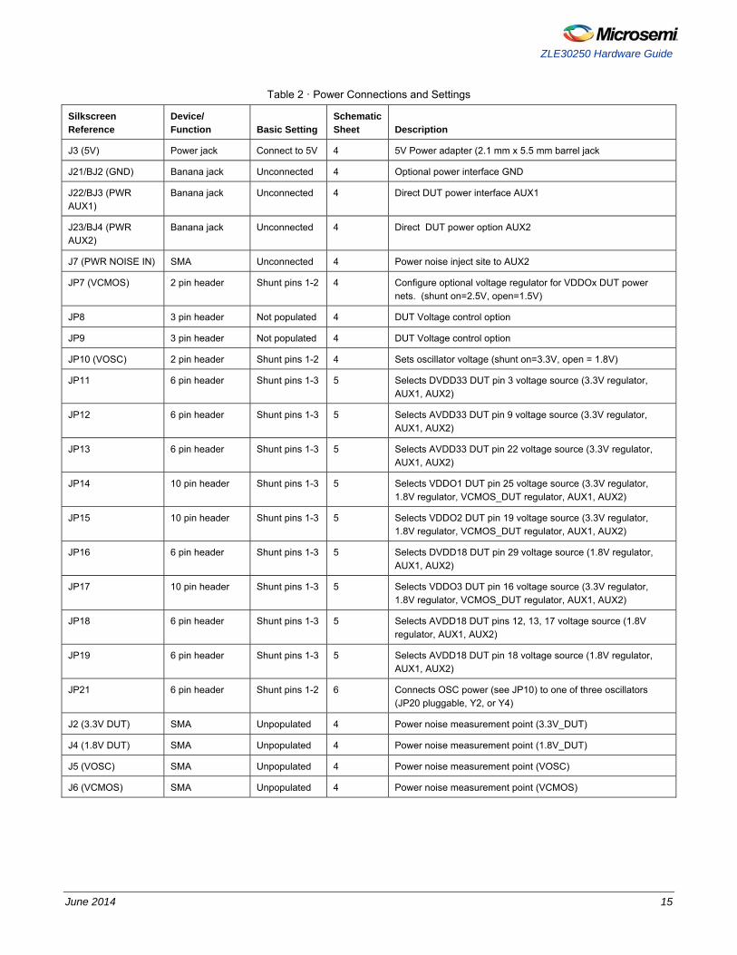
Table 2 · Power Connections and Settings
Silkscreen Reference
Device/ Function Basic Setting
Schematic Sheet Description
J3 (5V) Power jack Connect to 5V 4 5V Power adapter (2.1 mm x 5.5 mm barrel jack
J21/BJ2 (GND) Banana jack Unconnected 4 Optional power interface GND
J22/BJ3 (PWR AUX1)
Banana jack Unconnected 4 Direct DUT power interface AUX1
J23/BJ4 (PWR AUX2)
Banana jack Unconnected 4 Direct DUT power option AUX2
J7 (PWR NOISE IN) SMA Unconnected 4 Power noise inject site to AUX2
JP7 (VCMOS) 2 pin header Shunt pins 1-2 4 Configure optional voltage regulator for VDDOx DUT power nets. (shunt on=2.5V, open=1.5V)
JP8 3 pin header Not populated 4 DUT Voltage control option
JP9 3 pin header Not populated 4 DUT Voltage control option
JP10 (VOSC) 2 pin header Shunt pins 1-2 4 Sets oscillator voltage (shunt on=3.3V, open = 1.8V)
JP11 6 pin header Shunt pins 1-3 5 Selects DVDD33 DUT pin 3 voltage source (3.3V regulator, AUX1, AUX2)
JP12 6 pin header Shunt pins 1-3 5 Selects AVDD33 DUT pin 9 voltage source (3.3V regulator, AUX1, AUX2)
JP13 6 pin header Shunt pins 1-3 5 Selects AVDD33 DUT pin 22 voltage source (3.3V regulator, AUX1, AUX2)
JP14 10 pin header Shunt pins 1-3 5 Selects VDDO1 DUT pin 25 voltage source (3.3V regulator, 1.8V regulator, VCMOS_DUT regulator, AUX1, AUX2)
JP15 10 pin header Shunt pins 1-3 5 Selects VDDO2 DUT pin 19 voltage source (3.3V regulator, 1.8V regulator, VCMOS_DUT regulator, AUX1, AUX2)
JP16 6 pin header Shunt pins 1-3 5 Selects DVDD18 DUT pin 29 voltage source (1.8V regulator, AUX1, AUX2)
JP17 10 pin header Shunt pins 1-3 5 Selects VDDO3 DUT pin 16 voltage source (3.3V regulator, 1.8V regulator, VCMOS_DUT regulator, AUX1, AUX2)
JP18 6 pin header Shunt pins 1-3 5 Selects AVDD18 DUT pins 12, 13, 17 voltage source (1.8V regulator, AUX1, AUX2)
JP19 6 pin header Shunt pins 1-3 5 Selects AVDD18 DUT pin 18 voltage source (1.8V regulator, AUX1, AUX2)
JP21 6 pin header Shunt pins 1-2 6 Connects OSC power (see JP10) to one of three oscillators (JP20 pluggable, Y2, or Y4)
J2 (3.3V DUT) SMA Unpopulated 4 Power noise measurement point (3.3V_DUT)
J4 (1.8V DUT) SMA Unpopulated 4 Power noise measurement point (1.8V_DUT)
J5 (VOSC) SMA Unpopulated 4 Power noise measurement point (VOSC)
J6 (VCMOS) SMA Unpopulated 4 Power noise measurement point (VCMOS)

ZLE30250 Hardware Guide
16 June 2014
Reset, SPI Bus and GPIO Settings
The board has a number of DUT variants and configurations, some of which support GUI/PC software and some of which are standalone operation. Table 3 · lists the hardware interfaces which are related to SPI bus, resets, and DUT configuration. This table provides a physical description and summary of the configurable hardware components referenced in Table 1 · .
Table 3 · Reset, SPI bus and PC Interface Hardware Configuration
Silkscreen Reference Device/ Function Basic Setting
Schematic Sheet Description
JDR1 (USB) USB connector Connected to PC 2 Connects board to host computer
JP1 (PWREN#) 2 pin header Shunt installed 2 Enables USB interface controls on board
JP4 10 pin header Unconnected 3 Can be used to connect an external SPI master to DUT or EEPROM on board
JP5 8 pin header Shunts on pins 1-2, 3-4, 5-6, 7-8
3 Connects EEPROM to switched SPI bus
S2 (DUT RESET)
Reset pushbutton Inactive 2 Sends a reset signal to DUT.
JP6 8 pin header No shunts 3 Probe/test header for EEPROM
JP3 10 pin header No shunts 3 Test/ pull down header for DUT GPIO pins
SW2 4 DIP switch Depends on Configuration
3 SPI bus switch hardware configuration (may be overdriven by USB controller)
SW1 8 DIP switch Depends on Configuration
3 DUT hardware configuration pin and GPIO hardware configuration switches . GPIO switches may be overdriven by USB controller (not currently supported by GUI)
TP8, TP9, TP10, TP11
Testpoints N/A 3 Test points for probing SPI bus at DUT
J1 SMA Connector 3 DUT GPIO0 connection point
JP2 3 pin header Shunt pins 2-3 3 Selector for GPIO0 interface (pin 1-2 is connect J1 SMA, pin 2-3 selects normal GPIO operation)
JP34 3 pin header Shunt pins 1-2 6 1-2 connects DUT IC3_GPIO3 pin to J19 SMA jack
2-3 connects DUT IC3_GPIO3 pin to board GPIO3 network (DIP switches, USB interface IC)
Master Clock Oscillator
The board provides several options for driving the timing device’s master clock input from an on-board oscillator, crystal, or an external source. Table 4 · summarizes the master clock oscillator related hardware jumpers and connectors and functionality. Table 5 · summarizes board jumper settings as required to set up each master clock source.
Table 4 · Master Clock Oscillator Configurable Hardware
Silkscreen Reference Device/ Function Basic Setting
Schematic Sheet Description
JP21 6 pin header Shunt pins 1-2 6 2-pin shunt installed connects OSC power (see JP10) to one of three oscillators (pins 1-2= JP20; pins 3-4 = Y2; pins 5-6= Y4)

ZLE30250 Hardware Guide
June 2014 17
Silkscreen Reference Device/ Function Basic Setting
Schematic Sheet Description
JP20 10-pin receptacle for oscillator daughter board
6 Microsemi custom daughter board installs here.
JP24 2 pin header Open 6 Disable output option for Y2 oscillator
JP26 3 pin header Open 6 Option header for Y4. Usage depends on definition of option pins 1 and 2 of an industry standard 5x7 mm 4 pin or 6 pin package device. Not used in most cases.
JP25 10 pin header Shunt pins 1-3 6
Master clock patch header. Shunt settings are as follows: pins 1-2: JP20 to J8 (monitor JP20) pins 1-3: JP20 to DUT master clock pins 3-5: Y2 to DUT master clock pins 5-7: Y2 to J8 (monitor Y2) pins 4-6: Y4 to DUT master clock pins 6-8: Y4 toJ8 (monitor Y4) pins 2-4: J8 to DUT master clock (external clock master)
J8 SMA connector 6 Access point for monitoring an oscillator on board, or providing DUT master clock from and external clock source
JP23 2 pin header Open 6 Open selects AC coupled clock connection to J8; shunt selects DC coupling to J8
JP22 6 pin header Shunt pins 3-4 6 Header for mounting optional XTAL or oscillator device. Located on bottom side of board. Shunt on pins 3-4 patches oscillator signal from patch header JP25 to DUT master clock
Table 5 · DUT Master Clock Source Selection Jumper Settings
Clock Source Jumper Settings
Y2 on-board 3x5 single-ended oscillator site master clock JP21 = shunt pin 3-4 JP24 = open JP25 = shunt pin 3-5 JP22 = shunt pin 3-4 JP10 = open: 1.8V OSC Power, or shunt:3.3V OSC Power
R100, R107, R104 = remove to disconnect on board XTAL circuit R101, R108 = 0 ohms
Y4 on-board 5x7 single-ended oscillator site master clock JP21 = shunt pin 5-6 JP26 = open JP25 = shunt pin 4-6 JP22 = shunt pin 3-4 JP10 = open: 1.8V OSC Power, or shunt:3.3V OSC Power
R100, R107, R104 = remove to disconnect on board XTAL circuit R101, R108 = 0 ohms
JP20 oscillator daughter card master clock JP20 = 10-pin custom oscillator daughter board JP21 = shunt pin 1-2 JP26 = open JP25 = shunt pin 1-3 JP22 = shunt pin 3-4

ZLE30250 Hardware Guide
18 June 2014
Clock Source Jumper Settings
JP10 = open: 1.8V OSC Power, or shunt:3.3V OSC Power
R100, R107, R104 = remove to disconnect on board XTAL circuit R101, R108 = 0 ohms
J8 external single-ended Input master clock JP21 = open JP25 = shunt pin 2-4 JP22 = shunt pin 3-4 JP23 = shunt for DC coupled; open for AC coupled JP10 = n/a
R100, R107, R104 = remove to disconnect on board XTAL circuit R101, R108 = 0 ohms
JP22 external daughter card xtal/osc site for master clock JP21 = open JP22 = install custom daughter card JP23 = shunt for DC coupled; open for AC coupled JP10 = open: 1.8V OSC Power, or shunt:3.3V OSC Power R100, R107, R104 = remove to disconnect on board XTAL circuit R101, R108 = 0 ohms
Y3 on board XTAL as master clock JP21 = open
Y3 = a recommended XTAL
R101, R108 = remove to disconnect JP23 and stubs
R100, R107, R104, C86, = install with values recommended for XTAL
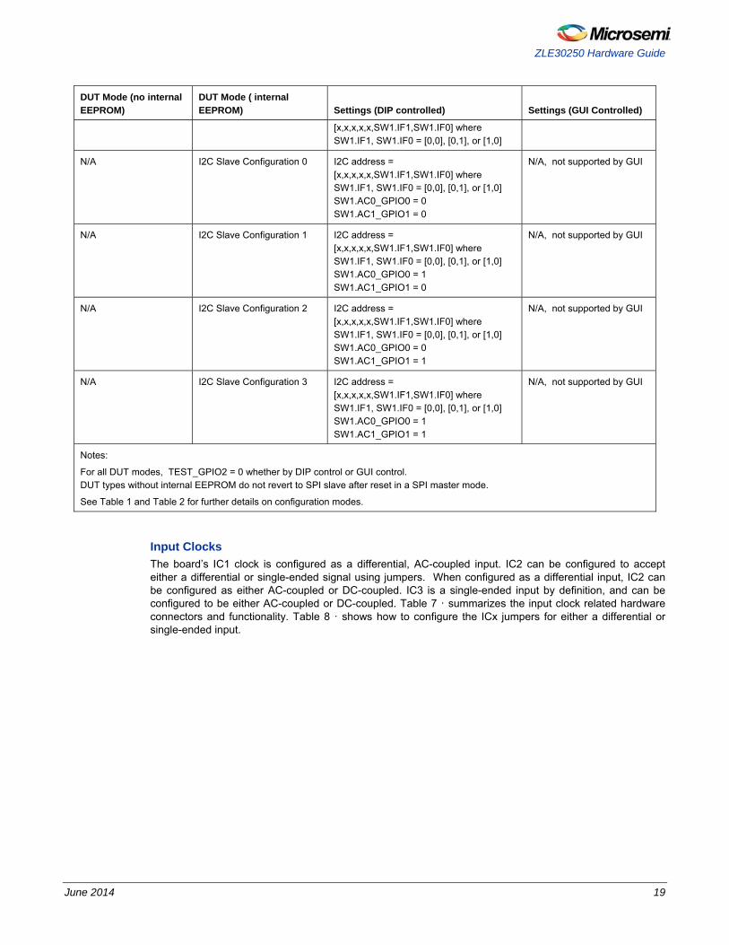
DUT Mode Bits
The various combinations of GPIO[1,0] and IF[1,0] mode bits which apply during DUT reset are summarized in Table 6 · . As described in the timing device datasheets, these four bits determine the operating mode of the DUT with respect to its serial bus interface and configuration data fill selection.
Table 6 · DUT Reset: Mode Bit Settings
DUT Mode (no internal EEPROM)
DUT Mode ( internal EEPROM) Settings (DIP controlled) Settings (GUI Controlled)
SPI Slave SPI slave, Configuration 0 SW1.IF0 = 1 SW1.IF1 = 1 SW1.AC0_GPIO0 = 0 SW1.AC1_GPIO1 = 0
FT_CSN= 1 or HiZ FT_SO = 1 or HiZ SW1.AC0_GPIO0 = HiZ SW1.AC1_GPIO1 = HiZ
SPI Master Configuration 1
SPI Slave Configuration 1 SW1.IF0 = 1 SW1.IF1 = 1 SW1.AC0_GPIO0 = 1 SW1.AC1_GPIO1 = 0
FT_CSN= 1 or HiZ FT_SO = 1 or HiZ FT_AC0_GPIO0 = HiZ FT_AC1_GPIO1 = HiZ
SPI Master Configuration 2
SPI Slave Configuration 2 SW1.IF0 = 1 SW1.IF1 = 1 SW1.AC0_GPIO0 = 0 SW1.AC1_GPIO1 = 1
FT_CSN= 1 or HiZ FT_SO = 1 or HiZ FT_AC0_GPIO0 = HiZ FT_AC1_GPIO1 = HiZ
SPI Master Configuration 3
SPI Slave Configuration 3 SW1.IF0 = 1 SW1.IF1 = 1 SW1.AC0_GPIO0 = 1 SW1.AC1_GPIO1 = 1
FT_CSN= 1 or HiZ FT_SO = 1 or HiZ FT_AC0_GPIO0 = HiZ FT_AC1_GPIO1 = HiZ
I2C Slave N/A I2C address = N/A, not supported by GUI
ZLE30250 Hardware Guide
June 2014 19
DUT Mode (no internal EEPROM)
DUT Mode ( internal EEPROM) Settings (DIP controlled) Settings (GUI Controlled)
[x,x,x,x,x,SW1.IF1,SW1.IF0] where SW1.IF1, SW1.IF0 = [0,0], [0,1], or [1,0]
N/A I2C Slave Configuration 0 I2C address = [x,x,x,x,x,SW1.IF1,SW1.IF0] where SW1.IF1, SW1.IF0 = [0,0], [0,1], or [1,0] SW1.AC0_GPIO0 = 0 SW1.AC1_GPIO1 = 0
N/A, not supported by GUI
N/A I2C Slave Configuration 1 I2C address = [x,x,x,x,x,SW1.IF1,SW1.IF0] where SW1.IF1, SW1.IF0 = [0,0], [0,1], or [1,0] SW1.AC0_GPIO0 = 1 SW1.AC1_GPIO1 = 0
N/A, not supported by GUI
N/A I2C Slave Configuration 2 I2C address = [x,x,x,x,x,SW1.IF1,SW1.IF0] where SW1.IF1, SW1.IF0 = [0,0], [0,1], or [1,0] SW1.AC0_GPIO0 = 0 SW1.AC1_GPIO1 = 1
N/A, not supported by GUI
N/A I2C Slave Configuration 3 I2C address = [x,x,x,x,x,SW1.IF1,SW1.IF0] where SW1.IF1, SW1.IF0 = [0,0], [0,1], or [1,0] SW1.AC0_GPIO0 = 1 SW1.AC1_GPIO1 = 1
N/A, not supported by GUI
Notes:
For all DUT modes, TEST_GPIO2 = 0 whether by DIP control or GUI control. DUT types without internal EEPROM do not revert to SPI slave after reset in a SPI master mode.
See Table 1 and Table 2 for further details on configuration modes.
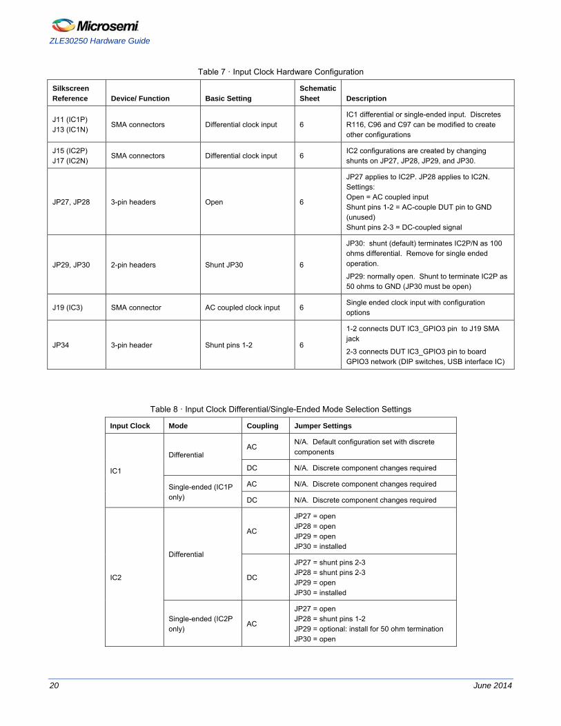
Input Clocks
The board’s IC1 clock is configured as a differential, AC-coupled input. IC2 can be configured to accept either a differential or single-ended signal using jumpers. When configured as a differential input, IC2 can be configured as either AC-coupled or DC-coupled. IC3 is a single-ended input by definition, and can be configured to be either AC-coupled or DC-coupled. Table 7 · summarizes the input clock related hardware connectors and functionality. Table 8 · shows how to configure the ICx jumpers for either a differential or single-ended input.
ZLE30250 Hardware Guide
20 June 2014
Table 7 · Input Clock Hardware Configuration
Silkscreen Reference Device/ Function Basic Setting
Schematic Sheet Description
J11 (IC1P) J13 (IC1N)
SMA connectors Differential clock input 6 IC1 differential or single-ended input. Discretes R116, C96 and C97 can be modified to create other configurations
J15 (IC2P) J17 (IC2N)
SMA connectors Differential clock input 6 IC2 configurations are created by changing shunts on JP27, JP28, JP29, and JP30.
JP27, JP28 3-pin headers Open 6
JP27 applies to IC2P. JP28 applies to IC2N. Settings: Open = AC coupled input Shunt pins 1-2 = AC-couple DUT pin to GND (unused) Shunt pins 2-3 = DC-coupled signal
JP29, JP30 2-pin headers Shunt JP30 6
JP30: shunt (default) terminates IC2P/N as 100 ohms differential. Remove for single ended operation.
JP29: normally open. Shunt to terminate IC2P as 50 ohms to GND (JP30 must be open)
J19 (IC3) SMA connector AC coupled clock input 6 Single ended clock input with configuration options
JP34 3-pin header Shunt pins 1-2 6
1-2 connects DUT IC3_GPIO3 pin to J19 SMA jack
2-3 connects DUT IC3_GPIO3 pin to board GPIO3 network (DIP switches, USB interface IC)
Table 8 · Input Clock Differential/Single-Ended Mode Selection Settings
Input Clock Mode Coupling Jumper Settings
IC1
Differential AC
N/A. Default configuration set with discrete components
DC N/A. Discrete component changes required
Single-ended (IC1P only)
AC N/A. Discrete component changes required
DC N/A. Discrete component changes required
IC2
Differential
AC
JP27 = open JP28 = open JP29 = open JP30 = installed
DC
JP27 = shunt pins 2-3 JP28 = shunt pins 2-3 JP29 = open JP30 = installed
Single-ended (IC2P only)
AC
JP27 = open JP28 = shunt pins 1-2 JP29 = optional: install for 50 ohm termination JP30 = open

ZLE30250 Hardware Guide
June 2014 21
Input Clock Mode Coupling Jumper Settings
DC
JP27 = shunt pins 2-3 JP28 = shunt pins 1-2 JP29 = optional: install for 50 ohm termination JP30 = open
IC3 Single-ended
AC JP33 = open JP34 = shunt pins 1-2
DC JP33 = installed JP34 = shunt pins 1-2
Output Clocks
The board supports evaluation of all device output clocks using SMA connectors. Table 8 · summarizes the output clock hardware connectors. To limit parasitic circuit loads, there are no jumper options on output clocks. Configurations can be modified only by means of discrete component substitutions.
Note that OC3 has on-board balun circuitry. See schematic page 6 for details.
Table 9 · Output Clock Hardware Configuration
Silkscreen Reference Device/ Function Basic Setting
Schematic Sheet Description
J9 (OC1P) J10 (OC1N)
OC1 Output Differential 6 Output clocks, referenced to VDDO1
J12 (OC2P) J14 (OC2N)
OC2 Output Differential 6 Output clocks, referenced to VDDO2
J16 (OC3P) J18 (OC3N)
OC3 Output Differential 6 Output clocks, referenced to VDDO3
GPIO Header and Status LEDs The device’s bi-directional GPIO pins are made available on the 10-pin header JP3. The header pins are labeled for easy identification. The present states of GPIO0 through GPIO3 are indicated by LEDs D3 through D6, respectively. LEDs D7 through D10 are not defined and may be used by the GUI/PC software application as needed.
Connecting Off-Board Devices Two pin headers provide direct access to the ZLE30250 switched serial bus. JP4 and JP6 connect to the same signals on the board. JP4 is a 10-pin shrouded and keyed header which is compatible with the Aardvark brand USB to SPI/I2C adapter interface cable, JP6 is a more generic 8-pin open header.
Possible uses for the headers include the following:
Load DUT from and/or program EEPROMs in a separate socketed board
Connect the GUI to a DUT in a customer’s board via cabled SPI bus connection
Interface a controller in a customer’s board with the ZLE30250 board DUT to assist software development and debugging.
Table 10 · and Table 11 · list all of the pin assignments of JP4 and JP6.

ZLE30250 Hardware Guide
22 June 2014
Table 10 · JP4 Serial Header Pin Assignments
Signal Pin Number Pin Number Signal
SCL 1 2 GND
SDA 3 4 N.C.
MISO 5 6 N.C.
SCLK 7 8 MOSI
CSB 9 10 GND
Notes: SCL and SDA pins require installation of resistors R73 and R74 on board to connect on board.
Table 11 · JP6 Serial Header Pin Assignments
Signal Pin Number Pin Number Signal
CSN 1 2 GND
MISO 3 4 GND
MOSI 5 6 GND
SCLK 7 8 GND
Discrete Component Options for Input and output clocks This section identifies components on clock circuits that an advanced user would be most likely consider modifying. Settings are summarized in Table 12 · below.
Table 12 · Discrete Component Options for Clocks
Clock Net Components Basic Setting Schematic Sheet Description/ Alternate Values
IC3 R129, R130 Not installed 6
Install R130 with a 50 ohm resistor to terminate a clock source with high drive
Install R129 and R130 with values to divide down input clock with high amplitude.
OC1P R112 CML mode, 0 ohms 6
CMOS mode: install a series termination resistor if required
HCSL mode: install a series termination resistor if required.
OC1N R114 CML mode, 0 ohms 6
CMOS mode: install a series termination resistor if required
HCSL mode: install a series termination resistor if required.
OC2P R117 CML mode, 0 ohms 6
CMOS mode: install a series termination resistor if required
HCSL mode: install a series termination resistor if required.

ZLE30250 Hardware Guide
June 2014 23
Clock Net Components Basic Setting Schematic Sheet Description/ Alternate Values
OC2N R119 CML mode, 0 ohms 6
CMOS mode: install a series termination resistor if required
HCSL mode: install a series termination resistor if required.
OC3P R122, C99, C101, R123
CML mode,differential to single ended with on-board balun. R122=0 C99=dni C101=100nF R123=0
6
CML, DC coupled : default + C99= 0 ohms + C101=dni + R123=dni
CMOS: default + C99=0 ohms + R122= 22 ohms + C101=dni + R123=dni
HCSL: default + C99=0 ohms+ change R122 value if required + C101=dni + R123=dni
CML mode, AC coupled: default + R123=dni + C101=dni+ C99=100nF.
OC3N R125, C102, C104
CML mode,differential to single ended with on-board balun. R125=0 C102=100nF C104=dni
6
CML, DC coupled : default + C104= 0 ohms + C102= dni
CMOS: default + C104=0 ohms + R125= 22 ohms + C102=dni
HCSL: default + C104=0 ohms+ change R125 value if required + C102=dni
CML mode, AC coupled: default + C102=dni + C104=100nF
Oscillator / Crystal Daughter Card
Daughter Card Overview The ZLE30250 evaluation board provides an on-board, low-jitter oscillator which can be used as the reference clock for evaluating device features and output clock jitter performance. Applications requiring a more detailed evaluation with a specific reference source can take advantage of the ZLE30250 oscillator / crystal daughter card. This plug-in card provides an easy method to evaluate alternate oscillator and crystal options without the need to re-work the ZLE30250 evaluation board.
The schematic for the ZLE30250 oscillator / crystal daughter card is shown in Figure 10 · . The card contains two circuits, one circuit on each side of connector JP1. The left side circuit is the oscillator circuit. This circuit can be used to evaluate 7mm x 5mm and 3mm x 2.5 mm surface mount oscillators. The oscillator is powered through connector JP1 by a power supply located on the ZLE30250 evaluation board. This supply can be configured to a voltage of 3.3V or 1.8V using evaluation board jumper JP10. The right side circuit is the crystal resonator circuit. This circuit can be used to evaluate 3.2mm x 2.5mm and 2.5mm x 2mm surface mount crystal resonators.

ZLE30250 Hardware Guide
24 June 2014
Figure 10 · ZLE30250 Oscillator / Crystal Daughter Card Schematic
The assembly drawing for the ZLE30250 oscillator / crystal daughter card is shown in Figure 11 · . The physical layout of the card layout is similar to the schematic with connector JP1 located in the center of the board, all oscillator circuit components located on the left side of JP1, and all crystal resonator circuit components located on the right side of JP1. When an XO or crystal daughter card assembly is built, only one of these two circuits is populated.
Figure 11 · ZLE30250 Oscillator / Crystal Daughter Assembly Drawing
Oscillator Daughter Card Assembly The ZLE30250 oscillator / crystal daughter is provided with components JP1, C2, and R2 pre-installed. An oscillator daughter card assembly is built by installing two additional components. The first component is the oscillator to be evaluated which is installed at site Y1 or Y3 based on its package size. The second component is resistor R3 which is the series source termination resistor for the oscillator output clock signal. The value of R3 is chosen such the total impedance of the oscillator output driver and R3 is 50 Ω. An example of an oscillator daughter card assembly is shown in Figure 14 · . The installed components are indicated in red.
Figure 12 · ZLE30250 Oscillator / Crystal Daughter Assembly Drawing

ZLE30250 Hardware Guide
June 2014 25
Crystal Daughter Card Assembly The ZLE30250 oscillator / crystal daughter is provided with components JP1, C2, and R2 pre-installed. The crystal oscillator circuit does not use components C2 and R2. These components have no impact on the circuit performance and can remain installed. A crystal daughter card assembly is built by installing components C1, C3, R1, R4, R5, and Y2. Resistor R5 is a fixed value of 0 Ω. Crystal Y2 is chosen based on the specifications detailed in the ZL30151/ZL30169/ZL3025x data sheet. The remaining components are chosen based on the design guidelines detailed in application note ZLAN-494. Capacitance values of 1.51pf and 1.72pf should be used for ZLAN-494 trace capacitances CXA,PCB and CXB,PCB respectively. An example of a crystal resonator daughter card assembly is shown in Figure 13 · . The installed components are indicated in red.
Figure 13 · ZLE30250 Oscillator / Crystal Daughter Assembly Drawing
Daughter Card Installation The ZLE30250 oscillator / crystal daughter card is installed on the ZLE30250 evaluation board 3x2 pin header JP22 located on the bottom side of the board. Prior to installation, the jumper installed on JP22 pins 3-4 must be removed. The remaining ZLE30250 evaluation board configuration for using the daughter card is:
JP10 = Installed for 3.3V supply oscillator or crystal; Not installed for 1.8V supply oscillator
JP21 = Not installed
JP22 = ZLE30250 oscillator / crystal daughter card
JP25 = Not installed
An example of a ZLE30250 oscillator / crystal daughter card installed on header JP22 is shown in Figure 14 · . When the daughter card is not installed, a jumper must be installed on JP22 pins 3-4.

ZLE30250 Hardware Guide
26 June 2014
Figure 14 · ZLE30250 Oscillator / Crystal Daughter installed on header JP22
Oscillator / Crystal
Daughter Card
ZLE30250 Hardware Guide
June 2014 27
Document Revision History November 2013, First Version
April 2014, Rev B PCB Update
May 2014, Update for change to OC3P/N default
June 2014, Update configuration images and tables, back page corporate template, add xtal board section

June 2014
Microsemi Corporate Headquarters One Enterprise, Aliso Viejo CA 92656 USA Within the USA: +1 (949) 380-6100 Sales: +1 (949) 380-6136 Fax: +1 (949) 215-4996
Microsemi Corporation (Nasdaq: MSCC) offers a comprehensive portfolio of semiconductorand system solutions for communications, defense and security, aerospace, and industrialmarkets. Products include high-performance and radiation-hardened analog mixed-signalintegrated circuits, FPGAs, SoCs and ASICs; power management products; timing andsynchronization devices, and precise time solutions, setting the world's standard for time;voice processing devices; RF solutions; discrete components; security technologies andscalable anti-tamper products; Power-over-Ethernet ICs and midspans; as well as customdesign capabilities and services. Microsemi is headquartered in Aliso Viejo, Calif. and hasapproximately 3,400 employees globally. Learn more at www.microsemi.com.
© 2014 Microsemi Corporation. All rights reserved. Microsemi and the Microsemi logo are trademarks ofMicrosemi Corporation. All other trademarks and service marks are the property of their respective owners.