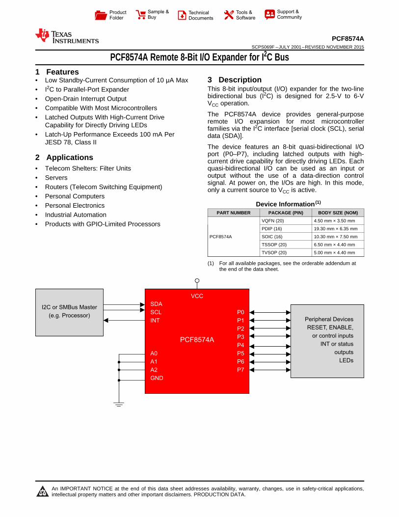
pcf8574a remote 8-bit i/o expander for i2c bus …...pcf8574a i2c or smbus master (e.g. processor)...
TRANSCRIPT
PCF8574A
I2C or SMBus Master
(e.g. Processor)Peripheral Devices
RESET, ENABLE,
or control inputs
INT or status
outputs
LEDs
SDA
SCL
INT
A0
A1
A2
GND
VCC
P0
P1
P2
P3
P4
P5
P6
P7
Product
Folder
Sample &Buy
Technical
Documents
Tools &
Software
Support &Community
PCF8574ASCPS069F –JULY 2001–REVISED NOVEMBER 2015
PCF8574A Remote 8-Bit I/O Expander for I2C Bus1
1 Features• Low Standby-Current Consumption of 10 μA Max 3 Description
This 8-bit input/output (I/O) expander for the two-line• I2C to Parallel-Port Expanderbidirectional bus (I2C) is designed for 2.5-V to 6-V• Open-Drain Interrupt OutputVCC operation.
• Compatible With Most MicrocontrollersThe PCF8574A device provides general-purpose• Latched Outputs With High-Current Drive remote I/O expansion for most microcontrollerCapability for Directly Driving LEDs families via the I2C interface [serial clock (SCL), serial
• Latch-Up Performance Exceeds 100 mA Per data (SDA)].JESD 78, Class II
The device features an 8-bit quasi-bidirectional I/Oport (P0–P7), including latched outputs with high-2 Applications current drive capability for directly driving LEDs. Eachquasi-bidirectional I/O can be used as an input or• Telecom Shelters: Filter Unitsoutput without the use of a data-direction control• Serverssignal. At power on, the I/Os are high. In this mode,• Routers (Telecom Switching Equipment) only a current source to VCC is active.
• Personal ComputersDevice Information (1)• Personal Electronics
PART NUMBER PACKAGE (PIN) BODY SIZE (NOM)• Industrial AutomationVQFN (20) 4.50 mm × 3.50 mm• Products with GPIO-Limited ProcessorsPDIP (16) 19.30 mm × 6.35 mm
PCF8574A SOIC (16) 10.30 mm × 7.50 mm
TSSOP (20) 6.50 mm × 4.40 mm
TVSOP (20) 5.00 mm × 4.40 mm
(1) For all available packages, see the orderable addendum atthe end of the data sheet.
1
An IMPORTANT NOTICE at the end of this data sheet addresses availability, warranty, changes, use in safety-critical applications,intellectual property matters and other important disclaimers. PRODUCTION DATA.
PCF8574ASCPS069F –JULY 2001–REVISED NOVEMBER 2015 www.ti.com
Table of Contents8.2 Functional Block Diagram ....................................... 111 Features .................................................................. 18.3 Feature Description................................................. 122 Applications ........................................................... 18.4 Device Functional Modes........................................ 133 Description ............................................................. 1
9 Application and Implementation ........................ 154 Revision History..................................................... 29.1 Application Information............................................ 155 Pin Configuration and Functions ......................... 39.2 Typical Application ................................................. 156 Specifications......................................................... 4
10 Power Supply Recommendations ..................... 186.1 Absolute Maximum Ratings .................................... 410.1 Power-On Reset Requirements ........................... 186.2 ESD Ratings.............................................................. 4
11 Layout................................................................... 206.3 Recommended Operating Conditions....................... 411.1 Layout Guidelines ................................................. 206.4 Thermal Information .................................................. 411.2 Layout Example .................................................... 206.5 Electrical Characteristics........................................... 5
12 Device and Documentation Support ................. 216.6 I2C Interface Timing Requirements........................... 512.1 Trademarks ........................................................... 216.7 Switching Characteristics .......................................... 512.2 Electrostatic Discharge Caution............................ 216.8 Typical Characteristics .............................................. 612.3 Glossary ................................................................ 217 Parameter Measurement Information .................. 8
13 Mechanical, Packaging, and Orderable8 Detailed Description ............................................ 11Information ........................................................... 218.1 Overview ................................................................. 11
4 Revision History
Changes from Revision E (January 2015) to Revision F Page
• Added Junction temperature to the Absolute Maximum Ratings (2) ....................................................................................... 4• Changed Supply Current (A) To: Supply Current (µA) and fSCL = 400 kHz to fSCL = 100 kHz in Figure 1 ............................ 6• Changed Supply Current (A) To: Supply Current (µA) in Figure 2 ........................................................................................ 6• Changed Supply Current (A) To: Supply Current (µA) and fSCL = 400 kHz to fSCL = 100 kHz in Figure 3 ............................ 6
Changes from Revision D (October 2005) to Revision E Page
• Added Applications, Device Information table, Pin Functions table, ESD Ratings table, Thermal Information table,Typical Characteristics, Feature Description section, Device Functional Modes, Application and Implementationsection, Power Supply Recommendations section, Layout section, Device and Documentation Support section, andMechanical, Packaging, and Orderable Information section. ................................................................................................. 1
• Deleted Ordering Information table. ....................................................................................................................................... 1
2 Submit Documentation Feedback Copyright © 2001–2015, Texas Instruments Incorporated
Product Folder Links: PCF8574A

1
2
3
4
5
6
7
8
16
15
14
13
12
11
10
9
A0
A1
A2
P0
P1
P2
P3
GND
VCC
SDA
SCL
INT
P7
P6
P5
P4
DW OR N PACKAGE
(TOP VIEW)
1
2
3
4
5
6
7
8
9
10
20
19
18
17
16
15
14
13
12
11
INT
SCL
NC
SDA
VCC
A0
A1
NC
A2
P0
P7
P6
NC
P5
P4
GND
P3
NC
P2
P1
DGV OR PW PACKAGE
(TOP VIEW)
RGY PACKAGE
(TOP VIEW)
1 20
10 11
2
3
4
5
6
7
8
9
19
18
17
16
15
14
13
12
P6
NC
P5
P4
GND
P3
NC
P2
SCL
NC
SDA
VCC
A0
A1
NC
A2
INT
P1
P7
P0
PCF8574Awww.ti.com SCPS069F –JULY 2001–REVISED NOVEMBER 2015
5 Pin Configuration and Functions
Pin FunctionsPIN
TYPE DESCRIPTIONNAME RGY DGV or PW DW or N
Address inputs 0 through 2. Connect directly to VCC or ground. PullupA[0..2] 6, 7, 9 6, 7, 9 1, 2, 3 I resistors are not needed.GND 15 15 8 — GroundINT 1 1 13 O Interrupt output. Connect to VCC through a pullup resistor.NC 3, 8, 13, 18 3, 8, 13, 18 - — Do not connect
4, 5, 6, 7,10, 11, 12, 14, 10, 11, 12, 14,P[0..7] 9, 10, 11, I/O P-port input/output. Push-pull design structure.16, 17, 19, 20 16, 17, 19, 20 12SCL 2 2 14 I Serial clock line. Connect to VCC through a pullup resistorSDA 4 4 15 I/O Serial data line. Connect to VCC through a pullup resistor.VCC 5 5 16 — Voltage supply
Copyright © 2001–2015, Texas Instruments Incorporated Submit Documentation Feedback 3
Product Folder Links: PCF8574A

PCF8574ASCPS069F –JULY 2001–REVISED NOVEMBER 2015 www.ti.com
6 Specifications
6.1 Absolute Maximum Ratings (1)
over operating free-air temperature range (unless otherwise noted)MIN MAX UNIT
VCC Supply voltage range –0.5 7 VVI Input voltage range (2) –0.5 VCC + 0.5 VVO Output voltage range (2) –0.5 VCC + 0.5 VIIK Input clamp current VI < 0 –20 mAIOK Output clamp current VO < 0 –20 mAIOK Input/output clamp current VO < 0 or VO > VCC ±400 μAIOL Continuous output low current VO = 0 to VCC 50 mAIOH Continuous output high current VO = 0 to VCC –4 mA
Continuous current through VCC or GND ±100 mATJ Junction temperature 150 °CTstg Storage temperature range –65 150 °C
(1) Stresses beyond those listed under Absolute Maximum Ratings may cause permanent damage to the device. These are stress ratingsonly, and functional operation of the device at these or any other conditions beyond those indicated under Recommended OperatingConditions is not implied. Exposure to absolute-maximum-rated conditions for extended periods may affect device reliability.
(2) The input negative-voltage and output voltage ratings may be exceeded if the input and output current ratings are observed.
6.2 ESD RatingsVALUE UNIT
Human body model (HBM), per ANSI/ESDA/JEDEC JS-001, all 1000pins (1)V(ESD) Electrostatic discharge V
Charged device model (CDM), per JEDEC specification JESD22- 1500C101, all pins (2)
(1) JEDEC document JEP155 states that 500-V HBM allows safe manufacturing with a standard ESD control process.(2) JEDEC document JEP157 states that 250-V CDM allows safe manufacturing with a standard ESD control process.
6.3 Recommended Operating ConditionsMIN MAX UNIT
VCC Supply voltage 2.5 6 VVIH High-level input voltage 0.7 × VCC VCC + 0.5 VVIL Low-level input voltage –0.5 0.3 × VCC VIOH High-level output current –1 mAIOL Low-level output current 25 mATA Operating free-air temperature –40 85 °C
6.4 Thermal InformationPCF8574A
THERMAL METRIC (1) DGV DW N PW RGY UNIT20 PINS 16 PINS 16 PINS 20 PINS 20 PINS
θJA Junction-to-ambient thermal resistance 92 57 67 83 37 °C/W
(1) For more information about traditional and new thermal metrics, see the IC Package Thermal Metrics application report (SPRA953).
4 Submit Documentation Feedback Copyright © 2001–2015, Texas Instruments Incorporated
Product Folder Links: PCF8574A

PCF8574Awww.ti.com SCPS069F –JULY 2001–REVISED NOVEMBER 2015
6.5 Electrical Characteristicsover recommended operating free-air temperature range (unless otherwise noted)
PARAMETER TEST CONDITIONS VCC MIN TYP (1) MAX UNITVIK Input diode clamp voltage II = –18 mA 2.5 V to 6 V –1.2 VVPOR Power-on reset voltage (2) VI = VCC or GND, IO = 0 6 V 1.3 2.4 VIOH P port VO = GND 2.5 V to 6 V 30 300 μAIOHT P-port transient pullup current High during acknowledge, VOH = GND 2.5 V –1 mA
SDA VO = 0.4 V 2.5 V to 6 V 3IOL P port VO = 1 V 5 V 10 25 mA
INT VO = 0.4 V 2.5 V to 6 V 1.6SCL, SDA ±5
II INT VI = VCC or GND 2.5 V to 6 V ±5 μAA0, A1, A2 ±5
IIHL P port VI ≥ VCC or VI ≤ GND 2.5 V to 6 V ±400 μAOperating mode VI = VCC or GND, IO = 0, fSCL = 100 kHz 40 100
ICC 6 V μAStandby mode VI = VCC or GND, IO = 0 2.5 10
Ci SCL VI = VCC or GND 2.5 V to 6 V 1.5 7 pFSDA 3 7
Cio VIO = VCC or GND 2.5 V to 6 V pFP port 4 10
(1) All typical values are at VCC = 5 V, TA = 25°C.(2) The power-on reset circuit resets the I2C-bus logic with VCC < VPOR and sets all I/Os to logic high (with current source to VCC).
6.6 I2C Interface Timing Requirementsover recommended operating free-air temperature range (unless otherwise noted) (see Figure 12)
MIN MAX UNITfscl I2C clock frequency 100 kHztsch I2C clock high time 4 μstscl I2C clock low time 4.7 μstsp I2C spike time 100 nstsds I2C serial-data setup time 250 nstsdh I2C serial-data hold time 0 nsticr I2C input rise time 1 μsticf I2C input fall time 0.3 μstocf I2C output fall time (10-pF to 400-pF bus) 300 nstbuf I2C bus free time between stop and start 4.7 μststs I2C start or repeated start condition setup 4.7 μststh I2C start or repeated start condition hold 4 μstsps I2C stop-condition setup 4 μstvd Valid-data time SCL low to SDA output valid 3.4 μsCb I2C bus capacitive load 400 pF
6.7 Switching Characteristicsover recommended operating free-air temperature range, CL ≤ 100 pF (unless otherwise noted) (see Figure 13)
FROM TOPARAMETER MIN MAX UNIT(INPUT) (OUTPUT)tpv Output data valid SCL P port 4 μstsu Input data setup time P port SCL 0 μsth Input data hold time P port SCL 4 μstiv Interrupt valid time P port INT 4 μstir Interrupt reset delay time SCL INT 4 μs
Copyright © 2001–2015, Texas Instruments Incorporated Submit Documentation Feedback 5
Product Folder Links: PCF8574A
0
5
10
15
20
25
0.0 0.1 0.2 0.3 0.4 0.5 0.6
VCC = 3.3 V
TA = 25°C
TA = 85°C
TA = −40°C
VOL (V)
I SIN
K(m
A)
0
5
10
15
20
25
30
35
0.0 0.1 0.2 0.3 0.4 0.5 0.6
VCC = 5 V
TA = −40ºC
TA = 25ºC
TA = 85ºC
VOL (V)
I SIN
K(m
A)
0
10
20
30
40
50
60
70
80
90
100
2.0 2.5 3.0 3.5 4.0 4.5 5.0 5.5
Su
pp
ly C
urr
en
t (
A)
m
fSCL = 100 kHzAll I/Os unloaded
Supply Voltage (V)
0
2
4
6
8
10
12
14
16
18
20
0.0 0.1 0.2 0.3 0.4 0.5 0.6
VCC = 2.5 V
TA = −40ºC
TA = 25ºC
TA = 85ºC
I SIN
K(m
A)
Vol (V)
0
10
20
30
40
50
60
70
80
90
−50 −25 0 25 50 75 100 125
Temperature (°C)
Su
pp
ly C
urr
en
t (
A)
m
SCL = VCC
All I/Os unloaded
VCC = 5 V
VCC = 3.3 V
VCC = 2.5 V
0
20
40
60
80
100
120
−50 −25 0 25 50 75 100 125
Temperature (°C)
Su
pp
ly C
urr
en
t(
A)
m
fSCL = 100 kHzAll I/Os unloaded
VCC = 5 V
VCC = 3.3 V
VCC = 2.5 V
PCF8574ASCPS069F –JULY 2001–REVISED NOVEMBER 2015 www.ti.com
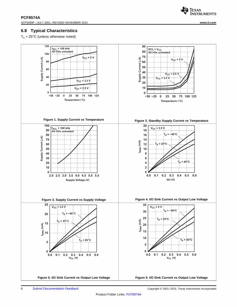
6.8 Typical CharacteristicsTA = 25°C (unless otherwise noted)
Figure 1. Supply Current vs Temperature Figure 2. Standby Supply Current vs Temperature
Figure 4. I/O Sink Current vs Output Low VoltageFigure 3. Supply Current vs Supply Voltage
Figure 5. I/O Sink Current vs Output Low Voltage Figure 6. I/O Sink Current vs Output Low Voltage
6 Submit Documentation Feedback Copyright © 2001–2015, Texas Instruments Incorporated
Product Folder Links: PCF8574A

0
50
100
150
200
250
300
350
−50 −25 0 25 50 75 100 125
Temperature (ºC)
VCC = 5 V
VC
C−
VO
H(V
) VCC = 3.3 V
VCC = 2.5 V
0
5
10
15
20
25
30
35
40
45
0.0 0.1 0.2 0.3 0.4 0.5 0.6 0.7
VCC = 3.3 V
TA = −40ºC
TA = 25ºC
TA = 85ºC
VCC − VOH (V)
I SO
UR
CE
(mA
)
0
5
10
15
20
25
30
35
40
45
0.0 0.1 0.2 0.3 0.4 0.5 0.6 0.7
VCC = 5 VTA = −40ºC
TA = 85ºC
TA = 25ºC
VCC − VOH (V)
I SO
UR
CE
(mA
)
0
100
200
300
400
500
600
−50 −25 0 25 50 75 100 125
Temperature (°C)
VCC = 5 V, ISINK = 10 mA
VCC = 2.5 V, ISINK = 10 mA
VCC = 5 V,
ISINK = 1 mAVCC = 2.5 V,
ISINK = 1mA
VO
L(m
V)
0
5
10
15
20
25
30
35
40
45
0.0 0.1 0.2 0.3 0.4 0.5 0.6 0.7
VCC = 2.5 VTA = −40ºC
TA = 25ºC
TA = 85°C
VCC − VOH (V)
I SO
UR
CE
(mA
)
PCF8574Awww.ti.com SCPS069F –JULY 2001–REVISED NOVEMBER 2015
Typical Characteristics (continued)TA = 25°C (unless otherwise noted)
Figure 8. I/O Source Current vs Output High VoltageFigure 7. I/O Output Low Voltage vs Temperature
Figure 10. I/O Source Current vs Output High VoltageFigure 9. I/O Source Current vs Output High Voltage
Figure 11. I/O High Voltage vs Temperature
Copyright © 2001–2015, Texas Instruments Incorporated Submit Documentation Feedback 7
Product Folder Links: PCF8574A
DUT
RL = 1 kΩ
VCC
CL = 10 pF to 400 pF
tbuf
ticr
tsth tsds
tsdh
ticf
ticr
tscl tsch
tststPHL
tPLH
0.7 × VCC
Stop
Condition
tsps
Repeat
Start
ConditionStart or
Repeat
Start
Condition
SCL
SDA
Start
Condition
(S)
Bit 7
MSBBit 6
Bit 0
LSB
(R/W)
Acknowledge
(A)
Stop
Condition
(P)
2 Bytes for Complete Device
Programming
LOAD CIRCUIT
VOLTAGE WAVEFORMS
ticf
Stop
Condition
(P)
tsp
0.7 × VCC
0.3 × VCC
0.3 × VCC
Pn
PCF8574ASCPS069F –JULY 2001–REVISED NOVEMBER 2015 www.ti.com
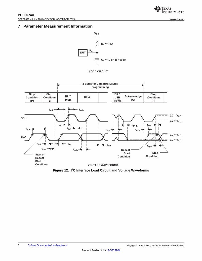
7 Parameter Measurement Information
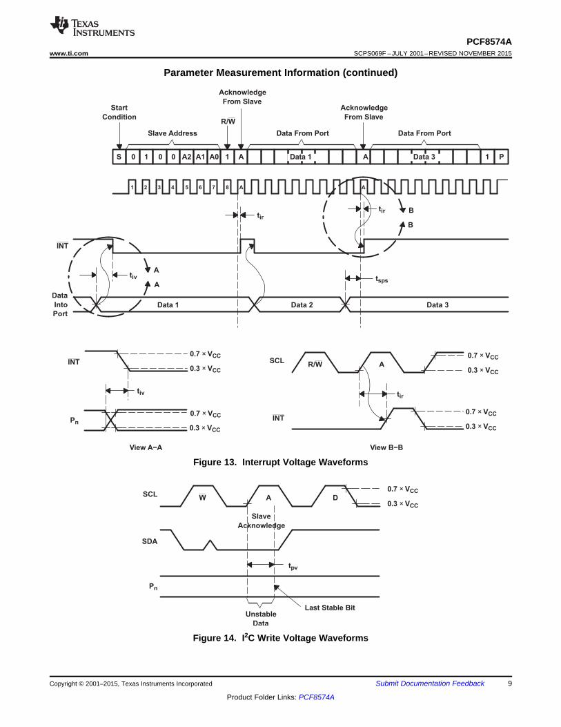
Figure 12. I2C Interface Load Circuit and Voltage Waveforms
8 Submit Documentation Feedback Copyright © 2001–2015, Texas Instruments Incorporated
Product Folder Links: PCF8574A
W A
0.7 × VCC
0.3 × VCC
SCLD
tpv
Slave
Acknowledge
Unstable
Data
Last Stable Bit
SDA
Pn
A
A
A
A
S 0 1 0 0 A1A2 A0 1 Data 1 1 PData 3
Start
Condition
Acknowledge
From SlaveAcknowledge
From Slave
Data From Port Data From PortSlave Address
R/W
87654321
tirtir
tspstiv
Data 1 Data 2 Data 3
INT
Data
Into
Port
B
B
A
A
P INTn
R/W A
tir
0.7 × VCC
0.3 × VCC
0.7 × VCC
0.3 × VCC
0.7 × VCC
0.3 × VCC
0.7 × VCC
0.3 × VCC
INT SCL
View B−BView A−A
tiv
PCF8574Awww.ti.com SCPS069F –JULY 2001–REVISED NOVEMBER 2015
Parameter Measurement Information (continued)
Figure 13. Interrupt Voltage Waveforms
Figure 14. I2C Write Voltage Waveforms
Copyright © 2001–2015, Texas Instruments Incorporated Submit Documentation Feedback 9
Product Folder Links: PCF8574A

DUT
GND
CL = 10 pF to 400 pF
RL = 4.7 kΩ
VCC
SDA LOAD CONFIGURATION INTERRUPT LOAD CONFIGURATION
INTDUT
GND
CL = 10 pF to 400 pF
RL = 1 kΩ
VCC
SDA
PCF8574ASCPS069F –JULY 2001–REVISED NOVEMBER 2015 www.ti.com
Parameter Measurement Information (continued)
Figure 15. Load Circuits
10 Submit Documentation Feedback Copyright © 2001–2015, Texas Instruments Incorporated
Product Folder Links: PCF8574A

14
I/O
Port
4
5
6
7
9
10
11
12
P0
P1
P2
P3
P4
P5
P6
P7
Shift
Register8 Bit
LP FilterInterrupt
Logic
Input
Filter15
Power-On
Reset
Read Pulse
Write Pulse
PCF8574A
3
2
1
13
16
8GND
VCC
SDA
SCL
A2
A1
A0
INT
Pin numbers shown are for the DW and N packages.
I2C Bus
Control
PCF8574Awww.ti.com SCPS069F –JULY 2001–REVISED NOVEMBER 2015
8 Detailed Description
8.1 OverviewThe PCF8574A device provides general-purpose remote I/O expansion for most microcontroller families via theI2C interface [serial clock (SCL), serial data (SDA)].
The device features an 8-bit quasi-bidirectional I/O port (P0–P7), including latched outputs with high-current drivecapability for directly driving LEDs. Each quasi-bidirectional I/O can be used as an input or output without the useof a data-direction control signal. At power on, the I/Os are high. In this mode, only a current source to VCC isactive. An additional strong pullup to VCC allows fast rising edges into heavily loaded outputs. This device turnson when an output is written high and is switched off by the negative edge of SCL. The I/Os should be highbefore being used as inputs.
The PCF8574A device provides an open-drain output (INT) that can be connected to the interrupt input of amicrocontroller. An interrupt is generated by any rising or falling edge of the port inputs in the input mode. Aftertime, tiv, INT is valid. Resetting and reactivating the interrupt circuit is achieved when data on the port is changedto the original setting or data is read from, or written to, the port that generated the interrupt. Resetting occurs inthe read mode at the acknowledge bit after the rising edge of the SCL signal, or in the write mode at theacknowledge bit after the high-to-low transition of the SCL signal. Interrupts that occur during the acknowledgeclock pulse can be lost (or be very short) due to the resetting of the interrupt during this pulse. Each change ofthe I/Os after resetting is detected and, after the next rising clock edge, is transmitted as INT. Reading from, orwriting to, another device does not affect the interrupt circuit.
By sending an interrupt signal on this line, the remote I/O can inform the microcontroller if there is incoming dataon its ports without having to communicate via the I2C bus. Therefore, the PCF8574A device can remain asimple slave device.
8.2 Functional Block Diagram
8.2.1 Simplified Block Diagram of Device
Copyright © 2001–2015, Texas Instruments Incorporated Submit Documentation Feedback 11
Product Folder Links: PCF8574A

To Interrupt
Logic
P0−P7
VCC
GND
C
SI
D Q
FF
C
SI
D Q
FF
Write Pulse
Data From
Shift Register
Power-On
Reset
Read Pulse
Data to
Shift Register
100 µA
PCF8574ASCPS069F –JULY 2001–REVISED NOVEMBER 2015 www.ti.com
Functional Block Diagram (continued)8.2.2 Simplified Schematic Diagram of Each P-Port Input/Output
8.3 Feature Description
8.3.1 I2C InterfaceI2C communication with this device is initiated by a master sending a start condition, a high-to-low transition onthe SDA I/O while the SCL input is high. After the start condition, the device address byte is sent, most-significant bit (MSB) first, including the data direction bit (R/W). This device does not respond to the general calladdress. After receiving the valid address byte, this device responds with an acknowledge, a low on the SDA I/Oduring the high of the acknowledge-related clock pulse. The address inputs (A0–A2) of the slave device must notbe changed between the start and the stop conditions.
The data byte follows the address acknowledge. If the R/W bit is high, the data from this device are the valuesread from the P port. If the R/W bit is low, the data are from the master, to be output to the P port. The data byteis followed by an acknowledge sent from this device. If other data bytes are sent from the master, following theacknowledge, they are ignored by this device. Data are output only if complete bytes are received andacknowledged. The output data will be valid at time, tpv, after the low-to-high transition of SCL and during theclock cycle for the acknowledge.
A stop condition, a low-to-high transition on the SDA I/O while the SCL input is high, is sent by the master.
8.3.2 Interface Definition
BITBYTE
7 (MSB) 6 5 4 3 2 1 0 (LSB)I2C slave address L H H H A2 A1 A0 R/WI/O data bus P7 P6 P5 P4 P3 P2 P1 P0
12 Submit Documentation Feedback Copyright © 2001–2015, Texas Instruments Incorporated
Product Folder Links: PCF8574A
A AS 0 1 1 1 A1A2 A0 0
Start
Condition
ACK
From SlaveACK
From Slave
Data DataSlave Address
R/W
P7 P6 1 P0 P7 P0 A
Integral Multiples of Two Bytes
P5
tpv
IOHT
tir
SCL
SDA
Write to
Port
Data Output
Voltage
P5 Output
Voltage
P5 Pullup
Output
Current
INT
ACK
From Slave
Data A0and B0Valid
1 2 3 4 5 6 7 8 1 2 3 4 5 6 7 8 1 2 3 4 5 6 7 8
IOH
PCF8574Awww.ti.com SCPS069F –JULY 2001–REVISED NOVEMBER 2015
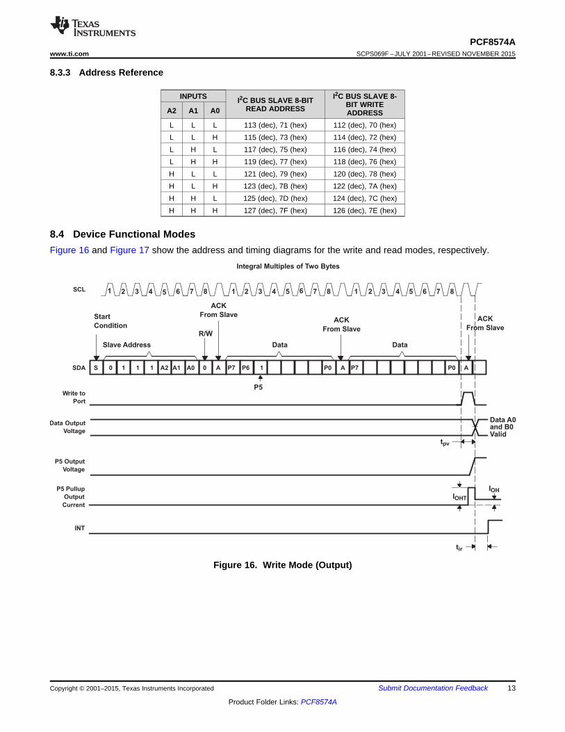
8.3.3 Address Reference
INPUTS I2C BUS SLAVE 8-I2C BUS SLAVE 8-BIT BIT WRITEREAD ADDRESSA2 A1 A0 ADDRESSL L L 113 (dec), 71 (hex) 112 (dec), 70 (hex)L L H 115 (dec), 73 (hex) 114 (dec), 72 (hex)L H L 117 (dec), 75 (hex) 116 (dec), 74 (hex)L H H 119 (dec), 77 (hex) 118 (dec), 76 (hex)H L L 121 (dec), 79 (hex) 120 (dec), 78 (hex)H L H 123 (dec), 7B (hex) 122 (dec), 7A (hex)H H L 125 (dec), 7D (hex) 124 (dec), 7C (hex)H H H 127 (dec), 7F (hex) 126 (dec), 7E (hex)
8.4 Device Functional ModesFigure 16 and Figure 17 show the address and timing diagrams for the write and read modes, respectively.
Figure 16. Write Mode (Output)
Copyright © 2001–2015, Texas Instruments Incorporated Submit Documentation Feedback 13
Product Folder Links: PCF8574A

A AS 0 1 1 1 A1A2 A0 1
ACK
From Slave
ACK
From MasterR/W
P7 P6 P0 P7
ACK
From Master
tsu
tir
SCL
SDA
Read From
Port
Data Into
Port
INT
P5 P4 P3 P2 P1 AP0
tirtiv
P7 to P0
P6 P5 P4 P3 P2 P1
th
P7 P6
1 2 3 4 5 6 7 8 1 2 3 4 5 6 7 8 1 2 3 4 5 6 7 8
P7 to P0
PCF8574ASCPS069F –JULY 2001–REVISED NOVEMBER 2015 www.ti.com
Device Functional Modes (continued)
A. A low-to-high transition of SDA while SCL is high is defined as the stop condition (P). The transfer of data can bestopped at any moment bya stop condition. When this occurs, data present at the latest ACK phase is valid (outputmode). Input data is lost.
Figure 17. Read Mode (Input)
14 Submit Documentation Feedback Copyright © 2001–2015, Texas Instruments Incorporated
Product Folder Links: PCF8574A
A1
A0
SDA
SCL
INT
GND
P6
P0
P1
P2
P3
P4
P5
P7
INT
GND
VCC
VCC
VCC 10 k(1)
Ω 10 k(1)
Ω 10 kΩ2 kΩ
100 kΩ
(x 3)
Master
Controller
PCF8574A
INT
RESET
Subsystem 2
(e.g., counter)
Subsystem 3
(e.g., alarm system)
ALARM
Controlled Device
(e.g., CBT device)ENABLE
A
B
VCC
Subsystem 1
(e.g., temperature sensor)SDA
SCL
15
14
16
13
3
2
1
8
12
11
10
9
7
6
5
4
A2
PCF8574Awww.ti.com SCPS069F –JULY 2001–REVISED NOVEMBER 2015
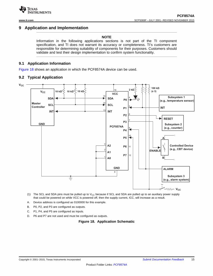
9 Application and Implementation
NOTEInformation in the following applications sections is not part of the TI componentspecification, and TI does not warrant its accuracy or completeness. TI’s customers areresponsible for determining suitability of components for their purposes. Customers shouldvalidate and test their design implementation to confirm system functionality.
9.1 Application InformationFigure 18 shows an application in which the PCF8574A device can be used.
9.2 Typical Application
(1) The SCL and SDA pins must be pulled up to VCC because if SCL and SDA are pulled up to an auxiliary power supplythat could be powered on while VCC is powered off, then the supply current, ICC, will increase as a result.
A. Device address is configured as 0100000 for this example.B. P0, P2, and P3 are configured as outputs.C. P1, P4, and P5 are configured as inputs.D. P6 and P7 are not used and must be configured as outputs.
Figure 18. Application Schematic
Copyright © 2001–2015, Texas Instruments Incorporated Submit Documentation Feedback 15
Product Folder Links: PCF8574A

LED
3.3 V 5 V
LEDx
VCC
LED
LEDx
VCC
100 kΩ
VCC
PCF8574ASCPS069F –JULY 2001–REVISED NOVEMBER 2015 www.ti.com
Typical Application (continued)9.2.1 Design Requirements
9.2.1.1 Minimizing ICC When I/Os Control LEDsWhen the I/Os are used to control LEDs, normally they are connected to VCC through a resistor as shown inFigure 27. For a P-port configured as an input, ICC increases as VI becomes lower than VCC. The LED is a diode,with threshold voltage VT, and when a P-port is configured as an input the LED will be off but VI is a VT dropbelow VCC.
For battery-powered applications, it is essential that the voltage of P-ports controlling LEDs is greater than orequal to VCC when the P-ports are configured as input to minimize current consumption. Figure 19 shows a high-value resistor in parallel with the LED. Figure 20 shows VCC less than the LED supply voltage by at least VT.Both of these methods maintain the I/O VI at or above VCC and prevents additional supply current consumptionwhen the P-port is configured as an input and the LED is off.
Figure 19. High-Value Resistor in Parallel With LED
Figure 20. Device Supplied by a Lower Voltage
16 Submit Documentation Feedback Copyright © 2001–2015, Texas Instruments Incorporated
Product Folder Links: PCF8574A
Cb (pF)
Rp(
max
) (kO
hm)
0 50 100 150 200 250 300 350 400 4500
5
10
15
20
25
D008
Standard-modeFast-mode
VCC (V)
Rp(
min
) (kO
hm)
0 0.5 1 1.5 2 2.5 3 3.5 4 4.5 5 5.50
0.2
0.4
0.6
0.8
1
1.2
1.4
1.6
1.8
D009
VCC > 2VVCC <= 2
rp(max)
b
R0.8473 C
t=
´
CC OL(max)
p(min)
OL
V VR
I
-
=
PCF8574Awww.ti.com SCPS069F –JULY 2001–REVISED NOVEMBER 2015
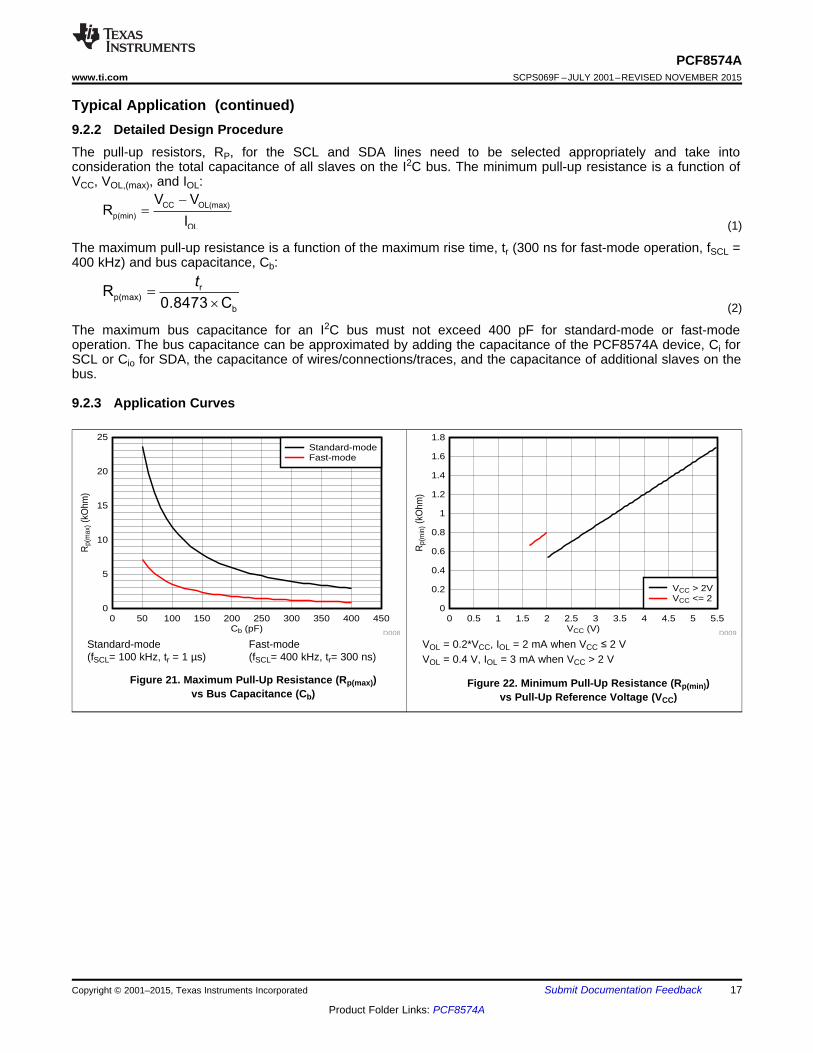
Typical Application (continued)9.2.2 Detailed Design ProcedureThe pull-up resistors, RP, for the SCL and SDA lines need to be selected appropriately and take intoconsideration the total capacitance of all slaves on the I2C bus. The minimum pull-up resistance is a function ofVCC, VOL,(max), and IOL:
(1)
The maximum pull-up resistance is a function of the maximum rise time, tr (300 ns for fast-mode operation, fSCL =400 kHz) and bus capacitance, Cb:
(2)
The maximum bus capacitance for an I2C bus must not exceed 400 pF for standard-mode or fast-modeoperation. The bus capacitance can be approximated by adding the capacitance of the PCF8574A device, Ci forSCL or Cio for SDA, the capacitance of wires/connections/traces, and the capacitance of additional slaves on thebus.
9.2.3 Application Curves
Standard-mode Fast-mode VOL = 0.2*VCC, IOL = 2 mA when VCC ≤ 2 V(fSCL= 100 kHz, tr = 1 µs) (fSCL= 400 kHz, tr= 300 ns) VOL = 0.4 V, IOL = 3 mA when VCC > 2 V
Figure 21. Maximum Pull-Up Resistance (Rp(max)) Figure 22. Minimum Pull-Up Resistance (Rp(min))vs Bus Capacitance (Cb) vs Pull-Up Reference Voltage (VCC)
Copyright © 2001–2015, Texas Instruments Incorporated Submit Documentation Feedback 17
Product Folder Links: PCF8574A
VCC
Ramp-Up
Time to Re-Ramp
Time
Ramp-Down
VIN drops below POR levels
VCC_RTVCC_FT
VCC_TRR_VPOR50
VCC
Ramp-Up Re-Ramp-Up
Time to Re-Ramp
Time
Ramp-Down
VCC_RT VCC_RTVCC_FT
VCC_TRR_GND
PCF8574ASCPS069F –JULY 2001–REVISED NOVEMBER 2015 www.ti.com
10 Power Supply Recommendations
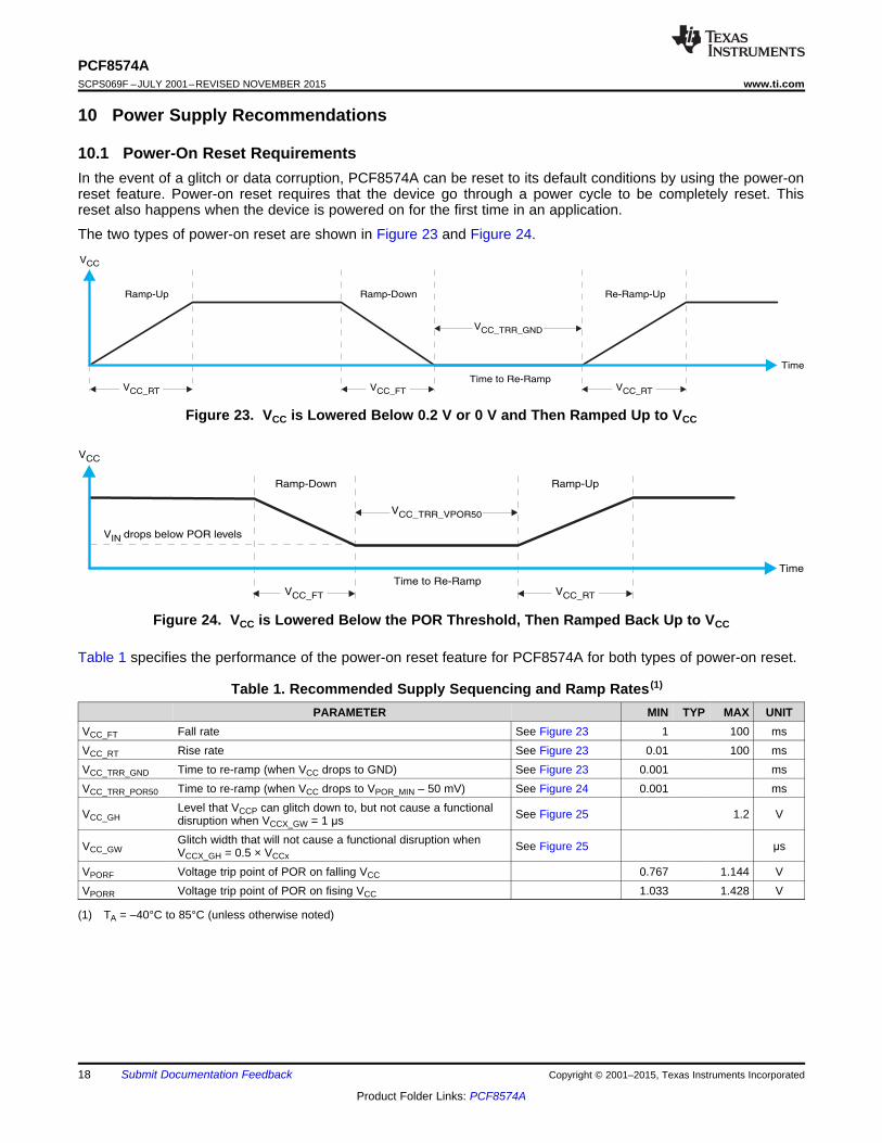
10.1 Power-On Reset RequirementsIn the event of a glitch or data corruption, PCF8574A can be reset to its default conditions by using the power-onreset feature. Power-on reset requires that the device go through a power cycle to be completely reset. Thisreset also happens when the device is powered on for the first time in an application.
The two types of power-on reset are shown in Figure 23 and Figure 24.
Figure 23. VCC is Lowered Below 0.2 V or 0 V and Then Ramped Up to VCC
Figure 24. VCC is Lowered Below the POR Threshold, Then Ramped Back Up to VCC
Table 1 specifies the performance of the power-on reset feature for PCF8574A for both types of power-on reset.
Table 1. Recommended Supply Sequencing and Ramp Rates (1)
PARAMETER MIN TYP MAX UNITVCC_FT Fall rate See Figure 23 1 100 msVCC_RT Rise rate See Figure 23 0.01 100 msVCC_TRR_GND Time to re-ramp (when VCC drops to GND) See Figure 23 0.001 msVCC_TRR_POR50 Time to re-ramp (when VCC drops to VPOR_MIN – 50 mV) See Figure 24 0.001 ms
Level that VCCP can glitch down to, but not cause a functionalVCC_GH See Figure 25 1.2 Vdisruption when VCCX_GW = 1 μsGlitch width that will not cause a functional disruption whenVCC_GW See Figure 25 μsVCCX_GH = 0.5 × VCCx
VPORF Voltage trip point of POR on falling VCC 0.767 1.144 VVPORR Voltage trip point of POR on fising VCC 1.033 1.428 V
(1) TA = –40°C to 85°C (unless otherwise noted)
18 Submit Documentation Feedback Copyright © 2001–2015, Texas Instruments Incorporated
Product Folder Links: PCF8574A

VCC
VPOR
VPORF
Time
POR
Time
VCC
Time
VCC_GH
VCC_GW
PCF8574Awww.ti.com SCPS069F –JULY 2001–REVISED NOVEMBER 2015
Glitches in the power supply can also affect the power-on reset performance of this device. The glitch width(VCC_GW) and height (VCC_GH) are dependent on each other. The bypass capacitance, source impedance, anddevice impedance are factors that affect power-on reset performance. Figure 25 and Table 1 provide moreinformation on how to measure these specifications.
Figure 25. Glitch Width and Glitch Height
VPOR is critical to the power-on reset. VPOR is the voltage level at which the reset condition is released and all theregisters and the I2C/SMBus state machine are initialized to their default states. The value of VPOR differs basedon the VCC being lowered to or from 0. Figure 26 and Table 1 provide more details on this specification.
Figure 26. VPOR
Copyright © 2001–2015, Texas Instruments Incorporated Submit Documentation Feedback 19
Product Folder Links: PCF8574A

xxxxxxxxxxxxxxxxxxxxxxxxxxxxxxxxxxxxxxxx
xxxxxxxxxxxxxxxxxxxxxxxxxxxxxxxx
GND
By-pass/De-coupling capacitors
PC
F85
74A
1 A0
2 A1
3
4 P0
5 P1
6 P2
7 P3
8 GND 9P4
10P5
11P6
12P7
13
14SCL
15SDA
16VCC
A2
INT
VIA to Power Planex Power or GND Plane
VIA to GND Plane
LEGEND
To
I/Os
VCC
To I2C Master
To I/O
s
PCF8574ASCPS069F –JULY 2001–REVISED NOVEMBER 2015 www.ti.com
11 Layout
11.1 Layout GuidelinesFor printed circuit board (PCB) layout of PCF8574A, common PCB layout practices should be followed butadditional concerns related to high-speed data transfer such as matched impedances and differential pairs arenot a concern for I2C signal speeds.
In all PCB layouts, it is a best practice to avoid right angles in signal traces, to fan out signal traces away fromeach other upon leaving the vicinity of an integrated circuit (IC), and to use thicker trace widths to carry higheramounts of current that commonly pass through power and ground traces. By-pass and de-coupling capacitorsare commonly used to control the voltage on the VCC pin, using a larger capacitor to provide additional power inthe event of a short power supply glitch and a smaller capacitor to filter out high-frequency ripple. Thesecapacitors should be placed as close to the PCF8574A device as possible. These best practices are shown inFigure 27.
For the layout example provided in Figure 27, it would be possible to fabricate a PCB with only 2 layers by usingthe top layer for signal routing and the bottom layer as a split plane for power (VCC) and ground (GND). However,a 4 layer board is preferable for boards with higher density signal routing. On a 4 layer PCB, it is common toroute signals on the top and bottom layer, dedicate one internal layer to a ground plane, and dedicate the otherinternal layer to a power plane. In a board layout using planes or split planes for power and ground, vias areplaced directly next to the surface mount component pad which needs to attach to VCC or GND and the via isconnected electrically to the internal layer or the other side of the board. Vias are also used when a signal traceneeds to be routed to the opposite side of the board, but this technique is not demonstrated in Figure 27.
11.2 Layout Example
Figure 27. Layout Example for PCF8574A
20 Submit Documentation Feedback Copyright © 2001–2015, Texas Instruments Incorporated
Product Folder Links: PCF8574A

PCF8574Awww.ti.com SCPS069F –JULY 2001–REVISED NOVEMBER 2015
12 Device and Documentation Support
12.1 TrademarksAll trademarks are the property of their respective owners.
12.2 Electrostatic Discharge CautionThese devices have limited built-in ESD protection. The leads should be shorted together or the device placed in conductive foamduring storage or handling to prevent electrostatic damage to the MOS gates.
12.3 GlossarySLYZ022 — TI Glossary.
This glossary lists and explains terms, acronyms and definitions.
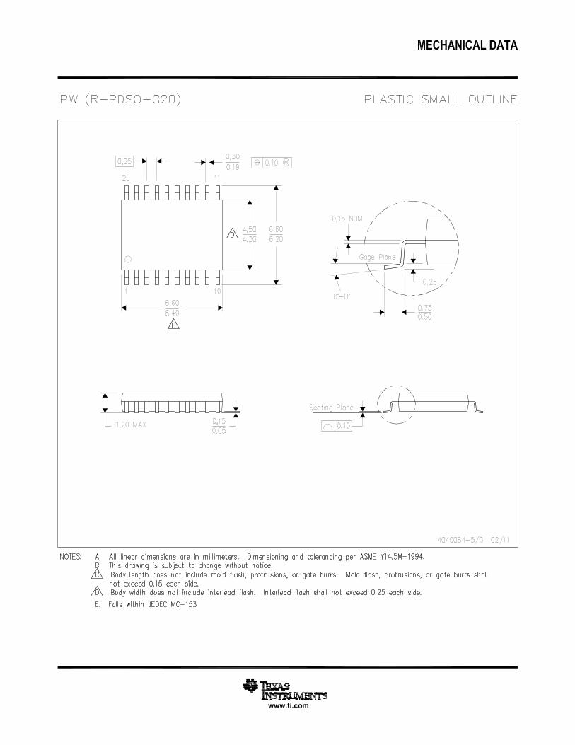
13 Mechanical, Packaging, and Orderable InformationThe following pages include mechanical packaging and orderable information. This information is the mostcurrent data available for the designated devices. This data is subject to change without notice and revision ofthis document. For browser based versions of this data sheet, refer to the left hand navigation.
Copyright © 2001–2015, Texas Instruments Incorporated Submit Documentation Feedback 21
Product Folder Links: PCF8574A

PACKAGE OPTION ADDENDUM
www.ti.com 15-Apr-2017
Addendum-Page 1
PACKAGING INFORMATION
Orderable Device Status(1)
Package Type PackageDrawing
Pins PackageQty
Eco Plan(2)
Lead/Ball Finish(6)
MSL Peak Temp(3)
Op Temp (°C) Device Marking(4/5)
Samples
PCF8574ADGVR ACTIVE TVSOP DGV 20 2000 Green (RoHS& no Sb/Br)
CU NIPDAU Level-1-260C-UNLIM -40 to 85 PF574A
PCF8574ADGVRE4 ACTIVE TVSOP DGV 20 2000 Green (RoHS& no Sb/Br)
CU NIPDAU Level-1-260C-UNLIM -40 to 85 PF574A
PCF8574ADGVRG4 ACTIVE TVSOP DGV 20 2000 Green (RoHS& no Sb/Br)
CU NIPDAU Level-1-260C-UNLIM -40 to 85 PF574A
PCF8574ADW ACTIVE SOIC DW 16 40 Green (RoHS& no Sb/Br)
CU NIPDAU Level-1-260C-UNLIM -40 to 85 PCF8574A
PCF8574ADWE4 ACTIVE SOIC DW 16 40 Green (RoHS& no Sb/Br)
CU NIPDAU Level-1-260C-UNLIM -40 to 85 PCF8574A
PCF8574ADWG4 ACTIVE SOIC DW 16 40 Green (RoHS& no Sb/Br)
CU NIPDAU Level-1-260C-UNLIM -40 to 85 PCF8574A
PCF8574ADWR ACTIVE SOIC DW 16 2000 Green (RoHS& no Sb/Br)
CU NIPDAU Level-1-260C-UNLIM -40 to 85 PCF8574A
PCF8574AN ACTIVE PDIP N 16 25 Pb-Free(RoHS)
CU NIPDAU N / A for Pkg Type -40 to 85 PCF8574AN
PCF8574ANE4 ACTIVE PDIP N 16 25 Pb-Free(RoHS)
CU NIPDAU N / A for Pkg Type -40 to 85 PCF8574AN
PCF8574APW ACTIVE TSSOP PW 20 70 Green (RoHS& no Sb/Br)
CU NIPDAU Level-1-260C-UNLIM -40 to 85 PF574A
PCF8574APWG4 ACTIVE TSSOP PW 20 70 Green (RoHS& no Sb/Br)
CU NIPDAU Level-1-260C-UNLIM -40 to 85 PF574A
PCF8574APWR ACTIVE TSSOP PW 20 2000 Green (RoHS& no Sb/Br)
CU NIPDAU Level-1-260C-UNLIM -40 to 85 PF574A
PCF8574APWRE4 ACTIVE TSSOP PW 20 2000 Green (RoHS& no Sb/Br)
CU NIPDAU Level-1-260C-UNLIM -40 to 85 PF574A
PCF8574APWRG4 ACTIVE TSSOP PW 20 2000 Green (RoHS& no Sb/Br)
CU NIPDAU Level-1-260C-UNLIM -40 to 85 PF574A
PCF8574ARGYR ACTIVE VQFN RGY 20 3000 Green (RoHS& no Sb/Br)
CU NIPDAU Level-2-260C-1 YEAR -40 to 85 PF574A
PCF8574ARGYRG4 ACTIVE VQFN RGY 20 3000 Green (RoHS& no Sb/Br)
CU NIPDAU Level-2-260C-1 YEAR -40 to 85 PF574A
(1) The marketing status values are defined as follows:ACTIVE: Product device recommended for new designs.

PACKAGE OPTION ADDENDUM
www.ti.com 15-Apr-2017
Addendum-Page 2
LIFEBUY: TI has announced that the device will be discontinued, and a lifetime-buy period is in effect.NRND: Not recommended for new designs. Device is in production to support existing customers, but TI does not recommend using this part in a new design.PREVIEW: Device has been announced but is not in production. Samples may or may not be available.OBSOLETE: TI has discontinued the production of the device.
(2) Eco Plan - The planned eco-friendly classification: Pb-Free (RoHS), Pb-Free (RoHS Exempt), or Green (RoHS & no Sb/Br) - please check http://www.ti.com/productcontent for the latest availabilityinformation and additional product content details.TBD: The Pb-Free/Green conversion plan has not been defined.Pb-Free (RoHS): TI's terms "Lead-Free" or "Pb-Free" mean semiconductor products that are compatible with the current RoHS requirements for all 6 substances, including the requirement thatlead not exceed 0.1% by weight in homogeneous materials. Where designed to be soldered at high temperatures, TI Pb-Free products are suitable for use in specified lead-free processes.Pb-Free (RoHS Exempt): This component has a RoHS exemption for either 1) lead-based flip-chip solder bumps used between the die and package, or 2) lead-based die adhesive used betweenthe die and leadframe. The component is otherwise considered Pb-Free (RoHS compatible) as defined above.Green (RoHS & no Sb/Br): TI defines "Green" to mean Pb-Free (RoHS compatible), and free of Bromine (Br) and Antimony (Sb) based flame retardants (Br or Sb do not exceed 0.1% by weightin homogeneous material)
(3) MSL, Peak Temp. - The Moisture Sensitivity Level rating according to the JEDEC industry standard classifications, and peak solder temperature.
(4) There may be additional marking, which relates to the logo, the lot trace code information, or the environmental category on the device.
(5) Multiple Device Markings will be inside parentheses. Only one Device Marking contained in parentheses and separated by a "~" will appear on a device. If a line is indented then it is a continuationof the previous line and the two combined represent the entire Device Marking for that device.
(6) Lead/Ball Finish - Orderable Devices may have multiple material finish options. Finish options are separated by a vertical ruled line. Lead/Ball Finish values may wrap to two lines if the finishvalue exceeds the maximum column width.
Important Information and Disclaimer:The information provided on this page represents TI's knowledge and belief as of the date that it is provided. TI bases its knowledge and belief on informationprovided by third parties, and makes no representation or warranty as to the accuracy of such information. Efforts are underway to better integrate information from third parties. TI has taken andcontinues to take reasonable steps to provide representative and accurate information but may not have conducted destructive testing or chemical analysis on incoming materials and chemicals.TI and TI suppliers consider certain information to be proprietary, and thus CAS numbers and other limited information may not be available for release.
In no event shall TI's liability arising out of such information exceed the total purchase price of the TI part(s) at issue in this document sold by TI to Customer on an annual basis.
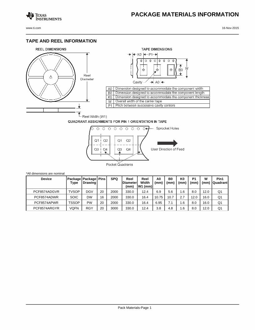
TAPE AND REEL INFORMATION
*All dimensions are nominal
Device PackageType
PackageDrawing
Pins SPQ ReelDiameter
(mm)
ReelWidth
W1 (mm)
A0(mm)
B0(mm)
K0(mm)
P1(mm)
W(mm)
Pin1Quadrant
PCF8574ADGVR TVSOP DGV 20 2000 330.0 12.4 6.9 5.6 1.6 8.0 12.0 Q1
PCF8574ADWR SOIC DW 16 2000 330.0 16.4 10.75 10.7 2.7 12.0 16.0 Q1
PCF8574APWR TSSOP PW 20 2000 330.0 16.4 6.95 7.1 1.6 8.0 16.0 Q1
PCF8574ARGYR VQFN RGY 20 3000 330.0 12.4 3.8 4.8 1.6 8.0 12.0 Q1
PACKAGE MATERIALS INFORMATION
www.ti.com 16-Nov-2015
Pack Materials-Page 1

*All dimensions are nominal
Device Package Type Package Drawing Pins SPQ Length (mm) Width (mm) Height (mm)
PCF8574ADGVR TVSOP DGV 20 2000 367.0 367.0 35.0
PCF8574ADWR SOIC DW 16 2000 367.0 367.0 38.0
PCF8574APWR TSSOP PW 20 2000 367.0 367.0 38.0
PCF8574ARGYR VQFN RGY 20 3000 367.0 367.0 35.0
PACKAGE MATERIALS INFORMATION
www.ti.com 16-Nov-2015
Pack Materials-Page 2


MECHANICAL DATA
MPDS006C – FEBRUARY 1996 – REVISED AUGUST 2000
POST OFFICE BOX 655303 • DALLAS, TEXAS 75265
DGV (R-PDSO-G**) PLASTIC SMALL-OUTLINE 24 PINS SHOWN
14
3,70
3,50 4,90
5,10
20DIM
PINS **
4073251/E 08/00
1,20 MAX
Seating Plane
0,050,15
0,25
0,500,75
0,230,13
1 12
24 13
4,304,50
0,16 NOM
Gage Plane
A
7,90
7,70
382416
4,90
5,103,70
3,50
A MAX
A MIN
6,606,20
11,20
11,40
56
9,60
9,80
48
0,08
M0,070,40
0°–8°
NOTES: A. All linear dimensions are in millimeters.B. This drawing is subject to change without notice.C. Body dimensions do not include mold flash or protrusion, not to exceed 0,15 per side.D. Falls within JEDEC: 24/48 Pins – MO-153
14/16/20/56 Pins – MO-194


GENERIC PACKAGE VIEW
Images above are just a representation of the package family, actual package may vary.Refer to the product data sheet for package details.
DW 16 SOIC - 2.65 mm max heightSMALL OUTLINE INTEGRATED CIRCUIT
4040000-2/H

www.ti.com
PACKAGE OUTLINE
C
TYP10.639.97
2.65 MAX
14X 1.27
16X 0.510.31
2X8.89
TYP0.330.10
0 - 80.30.1
(1.4)
0.25GAGE PLANE
1.270.40
A
NOTE 3
10.510.1
BNOTE 4
7.67.4
4220721/A 07/2016
SOIC - 2.65 mm max heightDW0016ASOIC
NOTES: 1. All linear dimensions are in millimeters. Dimensions in parenthesis are for reference only. Dimensioning and tolerancing per ASME Y14.5M. 2. This drawing is subject to change without notice. 3. This dimension does not include mold flash, protrusions, or gate burrs. Mold flash, protrusions, or gate burrs shall not exceed 0.15 mm, per side. 4. This dimension does not include interlead flash. Interlead flash shall not exceed 0.25 mm, per side.5. Reference JEDEC registration MS-013.
1 16
0.25 C A B
98
PIN 1 IDAREA
SEATING PLANE
0.1 C
SEE DETAIL A
DETAIL ATYPICAL
SCALE 1.500

www.ti.com
EXAMPLE BOARD LAYOUT
0.07 MAXALL AROUND
0.07 MINALL AROUND
(9.3)
14X (1.27)
R0.05 TYP
16X (2)
16X (0.6)
4220721/A 07/2016
SOIC - 2.65 mm max heightDW0016ASOIC
NOTES: (continued) 6. Publication IPC-7351 may have alternate designs. 7. Solder mask tolerances between and around signal pads can vary based on board fabrication site.
METAL SOLDER MASKOPENING
NON SOLDER MASKDEFINED
SOLDER MASK DETAILS
OPENINGSOLDER MASK METAL
SOLDER MASKDEFINED
LAND PATTERN EXAMPLESCALE:7X
SYMM
1
8 9
16
SEEDETAILS
SYMM

www.ti.com
EXAMPLE STENCIL DESIGN
R0.05 TYP
16X (2)
16X (0.6)
14X (1.27)
(9.3)
4220721/A 07/2016
SOIC - 2.65 mm max heightDW0016ASOIC
NOTES: (continued) 8. Laser cutting apertures with trapezoidal walls and rounded corners may offer better paste release. IPC-7525 may have alternate design recommendations. 9. Board assembly site may have different recommendations for stencil design.
SOLDER PASTE EXAMPLEBASED ON 0.125 mm THICK STENCIL
SCALE:7X
SYMM
SYMM
1
8 9
16


IMPORTANT NOTICE
Texas Instruments Incorporated (TI) reserves the right to make corrections, enhancements, improvements and other changes to itssemiconductor products and services per JESD46, latest issue, and to discontinue any product or service per JESD48, latest issue. Buyersshould obtain the latest relevant information before placing orders and should verify that such information is current and complete.TI’s published terms of sale for semiconductor products (http://www.ti.com/sc/docs/stdterms.htm) apply to the sale of packaged integratedcircuit products that TI has qualified and released to market. Additional terms may apply to the use or sale of other types of TI products andservices.Reproduction of significant portions of TI information in TI data sheets is permissible only if reproduction is without alteration and isaccompanied by all associated warranties, conditions, limitations, and notices. TI is not responsible or liable for such reproduceddocumentation. Information of third parties may be subject to additional restrictions. Resale of TI products or services with statementsdifferent from or beyond the parameters stated by TI for that product or service voids all express and any implied warranties for theassociated TI product or service and is an unfair and deceptive business practice. TI is not responsible or liable for any such statements.Buyers and others who are developing systems that incorporate TI products (collectively, “Designers”) understand and agree that Designersremain responsible for using their independent analysis, evaluation and judgment in designing their applications and that Designers havefull and exclusive responsibility to assure the safety of Designers' applications and compliance of their applications (and of all TI productsused in or for Designers’ applications) with all applicable regulations, laws and other applicable requirements. Designer represents that, withrespect to their applications, Designer has all the necessary expertise to create and implement safeguards that (1) anticipate dangerousconsequences of failures, (2) monitor failures and their consequences, and (3) lessen the likelihood of failures that might cause harm andtake appropriate actions. Designer agrees that prior to using or distributing any applications that include TI products, Designer willthoroughly test such applications and the functionality of such TI products as used in such applications.TI’s provision of technical, application or other design advice, quality characterization, reliability data or other services or information,including, but not limited to, reference designs and materials relating to evaluation modules, (collectively, “TI Resources”) are intended toassist designers who are developing applications that incorporate TI products; by downloading, accessing or using TI Resources in anyway, Designer (individually or, if Designer is acting on behalf of a company, Designer’s company) agrees to use any particular TI Resourcesolely for this purpose and subject to the terms of this Notice.TI’s provision of TI Resources does not expand or otherwise alter TI’s applicable published warranties or warranty disclaimers for TIproducts, and no additional obligations or liabilities arise from TI providing such TI Resources. TI reserves the right to make corrections,enhancements, improvements and other changes to its TI Resources. TI has not conducted any testing other than that specificallydescribed in the published documentation for a particular TI Resource.Designer is authorized to use, copy and modify any individual TI Resource only in connection with the development of applications thatinclude the TI product(s) identified in such TI Resource. NO OTHER LICENSE, EXPRESS OR IMPLIED, BY ESTOPPEL OR OTHERWISETO ANY OTHER TI INTELLECTUAL PROPERTY RIGHT, AND NO LICENSE TO ANY TECHNOLOGY OR INTELLECTUAL PROPERTYRIGHT OF TI OR ANY THIRD PARTY IS GRANTED HEREIN, including but not limited to any patent right, copyright, mask work right, orother intellectual property right relating to any combination, machine, or process in which TI products or services are used. Informationregarding or referencing third-party products or services does not constitute a license to use such products or services, or a warranty orendorsement thereof. Use of TI Resources may require a license from a third party under the patents or other intellectual property of thethird party, or a license from TI under the patents or other intellectual property of TI.TI RESOURCES ARE PROVIDED “AS IS” AND WITH ALL FAULTS. TI DISCLAIMS ALL OTHER WARRANTIES ORREPRESENTATIONS, EXPRESS OR IMPLIED, REGARDING RESOURCES OR USE THEREOF, INCLUDING BUT NOT LIMITED TOACCURACY OR COMPLETENESS, TITLE, ANY EPIDEMIC FAILURE WARRANTY AND ANY IMPLIED WARRANTIES OFMERCHANTABILITY, FITNESS FOR A PARTICULAR PURPOSE, AND NON-INFRINGEMENT OF ANY THIRD PARTY INTELLECTUALPROPERTY RIGHTS. TI SHALL NOT BE LIABLE FOR AND SHALL NOT DEFEND OR INDEMNIFY DESIGNER AGAINST ANY CLAIM,INCLUDING BUT NOT LIMITED TO ANY INFRINGEMENT CLAIM THAT RELATES TO OR IS BASED ON ANY COMBINATION OFPRODUCTS EVEN IF DESCRIBED IN TI RESOURCES OR OTHERWISE. IN NO EVENT SHALL TI BE LIABLE FOR ANY ACTUAL,DIRECT, SPECIAL, COLLATERAL, INDIRECT, PUNITIVE, INCIDENTAL, CONSEQUENTIAL OR EXEMPLARY DAMAGES INCONNECTION WITH OR ARISING OUT OF TI RESOURCES OR USE THEREOF, AND REGARDLESS OF WHETHER TI HAS BEENADVISED OF THE POSSIBILITY OF SUCH DAMAGES.Unless TI has explicitly designated an individual product as meeting the requirements of a particular industry standard (e.g., ISO/TS 16949and ISO 26262), TI is not responsible for any failure to meet such industry standard requirements.Where TI specifically promotes products as facilitating functional safety or as compliant with industry functional safety standards, suchproducts are intended to help enable customers to design and create their own applications that meet applicable functional safety standardsand requirements. Using products in an application does not by itself establish any safety features in the application. Designers mustensure compliance with safety-related requirements and standards applicable to their applications. Designer may not use any TI products inlife-critical medical equipment unless authorized officers of the parties have executed a special contract specifically governing such use.Life-critical medical equipment is medical equipment where failure of such equipment would cause serious bodily injury or death (e.g., lifesupport, pacemakers, defibrillators, heart pumps, neurostimulators, and implantables). Such equipment includes, without limitation, allmedical devices identified by the U.S. Food and Drug Administration as Class III devices and equivalent classifications outside the U.S.TI may expressly designate certain products as completing a particular qualification (e.g., Q100, Military Grade, or Enhanced Product).Designers agree that it has the necessary expertise to select the product with the appropriate qualification designation for their applicationsand that proper product selection is at Designers’ own risk. Designers are solely responsible for compliance with all legal and regulatoryrequirements in connection with such selection.Designer will fully indemnify TI and its representatives against any damages, costs, losses, and/or liabilities arising out of Designer’s non-compliance with the terms and provisions of this Notice.
Mailing Address: Texas Instruments, Post Office Box 655303, Dallas, Texas 75265Copyright © 2017, Texas Instruments Incorporated