diodes - information services & technology | …joelsd/electronics/classwork/...• for a real...
TRANSCRIPT
BME 372 Electronics I –J.Schesser
180
Diodes
Lesson #6Chapter 3
BME 372 Electronics I –J.Schesser
181
-5
-4
-3
-2
-1
0
1
2
3
4
5
-7 -5 -3 -1 1 3 5 7
v d
i d
Reverse bias
region
Forward bias regionReverse
breakdown
region
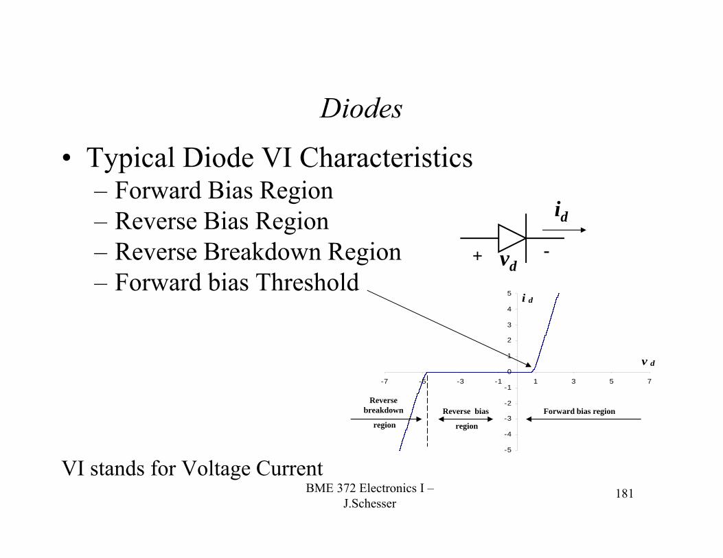
Diodes
• Typical Diode VI Characteristics– Forward Bias Region– Reverse Bias Region– Reverse Breakdown Region– Forward bias Threshold
VI stands for Voltage Current
id
+ -vd
BME 372 Electronics I –J.Schesser
182
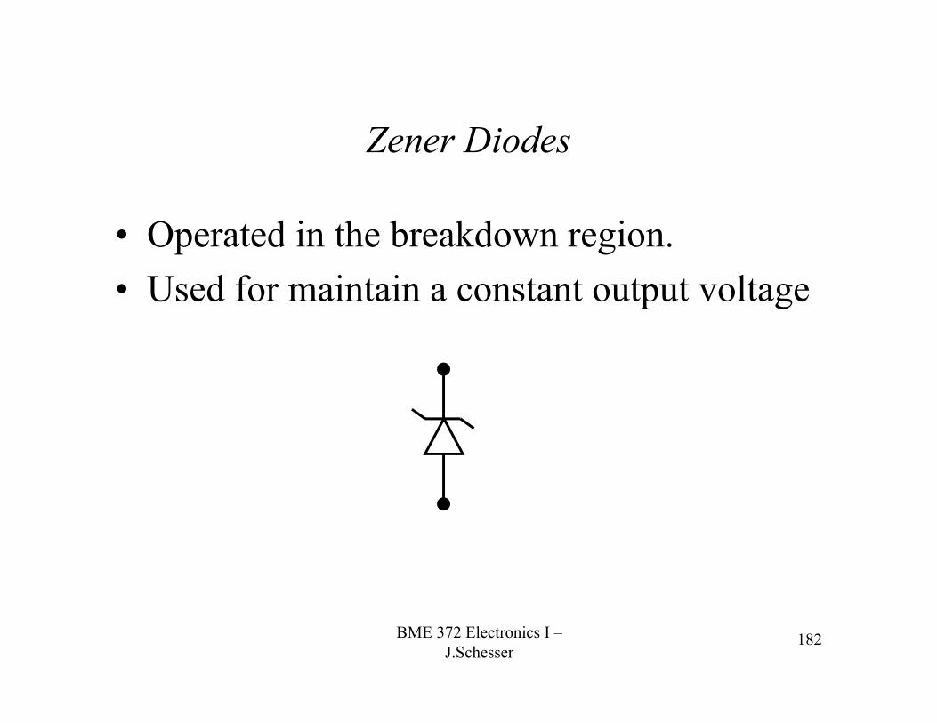
Zener Diodes
• Operated in the breakdown region.• Used for maintain a constant output voltage
BME 372 Electronics I –J.Schesser
183
Load Line
-1
3
7
11
15
19
23
27
31
35
39
-0.3
-0.2
-0.1
0 0.1 0.2 0.3 0.4 0.5 0.6 0.7 0.8 0.9 1 1.1 1.2 1.3 1.4 1.5 1.6 1.7 1.8
v D volts
i D amps
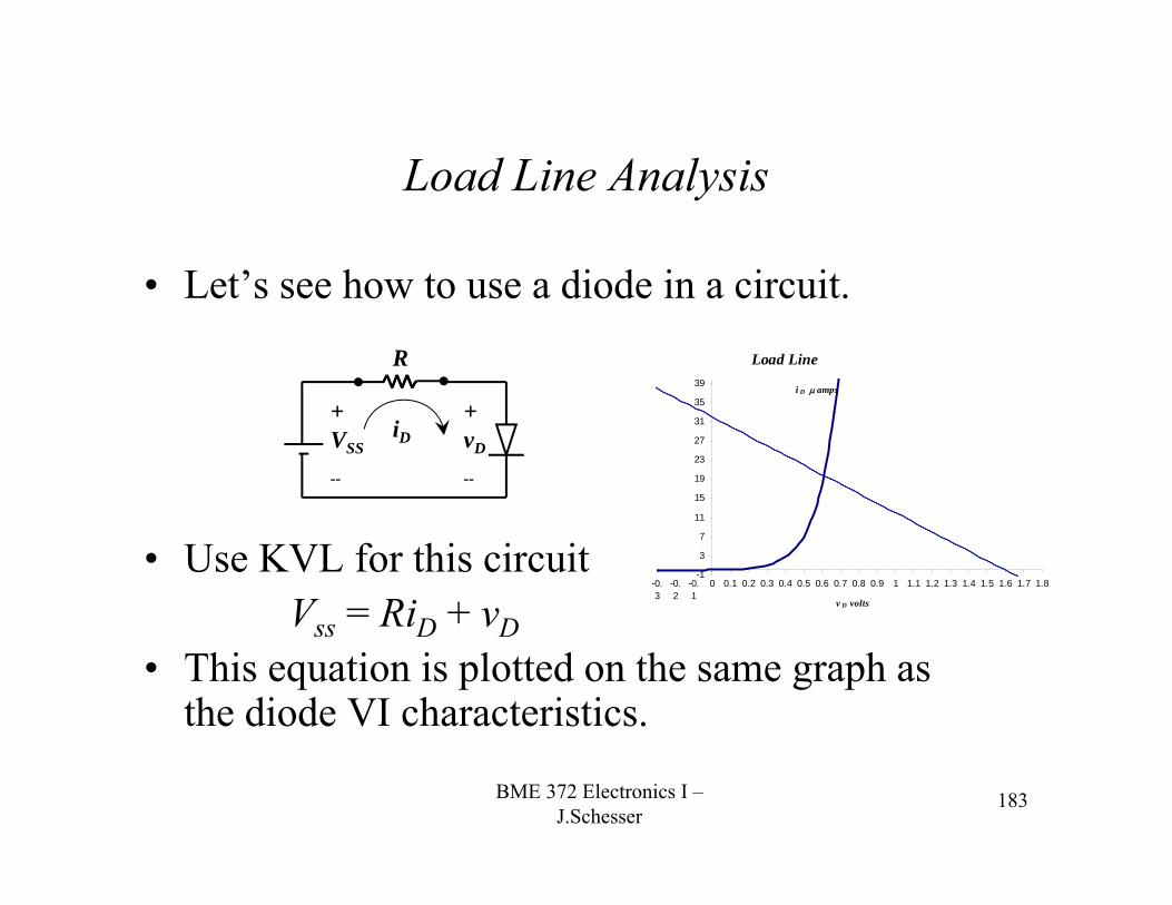
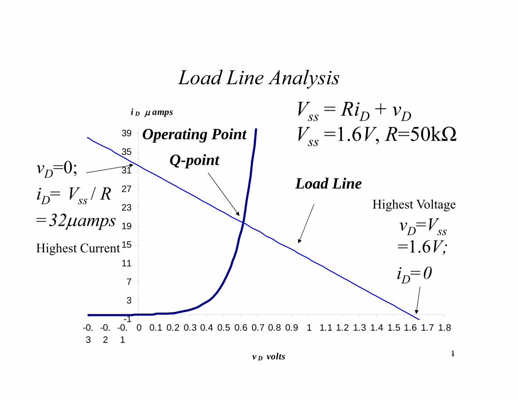
Load Line Analysis
• Let’s see how to use a diode in a circuit.
• Use KVL for this circuitVss = RiD + vD
• This equation is plotted on the same graph as the diode VI characteristics.
R
+vD
--
+ VSS
--
iD
BME 372 Electronics I –J.Schesser
184
-1
3
7
11
15
19
23
27
31
35
39
-0.3
-0.2
-0.1
0 0.1 0.2 0.3 0.4 0.5 0.6 0.7 0.8 0.9 1 1.1 1.2 1.3 1.4 1.5 1.6 1.7 1.8
v D volts
i D amps
Load Line AnalysisVss = RiD + vDVss =1.6V, R=50kΩ
Load LinevD=0;iD= Vss / R=32ampsHighest Current
Highest Voltage
vD=Vss=1.6V;iD=0
Operating Point
Q-point
BME 372 Electronics I –J.Schesser
185
-5
-4
-3
-2
-1
0
1
2
3
4
5
-7 -5 -3 -1 1 3 5 7
v d
i d
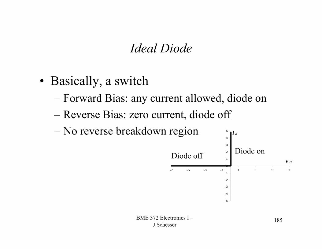
Ideal Diode
• Basically, a switch– Forward Bias: any current allowed, diode on– Reverse Bias: zero current, diode off– No reverse breakdown region
Diode onDiode off
BME 372 Electronics I –J.Schesser
186
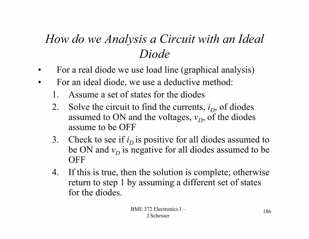
How do we Analysis a Circuit with an Ideal Diode
• For a real diode we use load line (graphical analysis)• For an ideal diode, we use a deductive method:
1. Assume a set of states for the diodes2. Solve the circuit to find the currents, iD, of diodes
assumed to ON and the voltages, vD, of the diodes assume to be OFF
3. Check to see if iD is positive for all diodes assumed to be ON and vD is negative for all diodes assumed to be OFF
4. If this is true, then the solution is complete; otherwise return to step 1 by assuming a different set of states for the diodes.
BME 372 Electronics I –J.Schesser
187
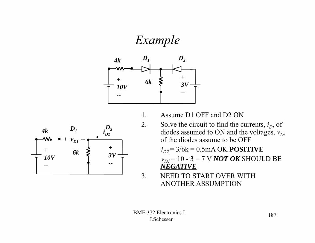
Example
6k
D1
+ 3V --
+ 10V --
4k D2
6k
D1
+ 3V --
+ 10V --
4k D2
1. Assume D1 OFF and D2 ON2. Solve the circuit to find the currents, iD, of
diodes assumed to ON and the voltages, vD, of the diodes assume to be OFFiD2 = 3/6k = 0.5mA OK POSITIVEvD1 = 10 - 3 = 7 V NOT OK SHOULD BE NEGATIVE
3. NEED TO START OVER WITH ANOTHER ASSUMPTION
iD2+ vD1 --
BME 372 Electronics I –J.Schesser
188
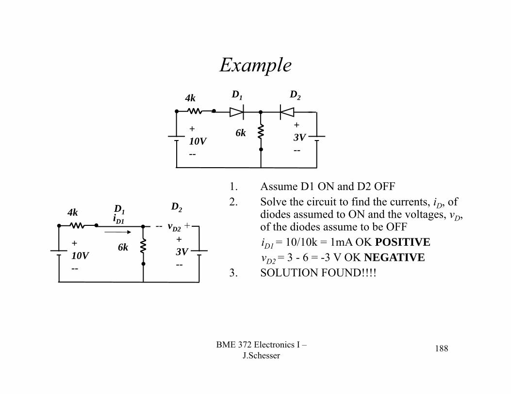
Example
6k
D1
+ 3V --
+ 10V --
4k D2
6k
D1
+ 3V --
+ 10V --
4k D2
1. Assume D1 ON and D2 OFF2. Solve the circuit to find the currents, iD, of
diodes assumed to ON and the voltages, vD, of the diodes assume to be OFFiD1 = 10/10k = 1mA OK POSITIVEvD2 = 3 - 6 = -3 V OK NEGATIVE
3. SOLUTION FOUND!!!!
iD1 -- vD2 +
BME 372 Electronics I –J.Schesser
189
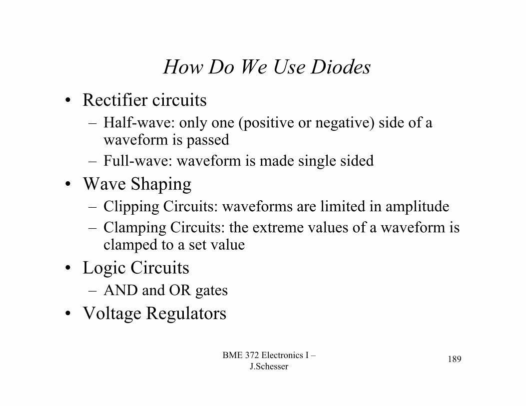
How Do We Use Diodes• Rectifier circuits
– Half-wave: only one (positive or negative) side of a waveform is passed
– Full-wave: waveform is made single sided• Wave Shaping
– Clipping Circuits: waveforms are limited in amplitude– Clamping Circuits: the extreme values of a waveform is
clamped to a set value• Logic Circuits
– AND and OR gates• Voltage Regulators
BME 372 Electronics I –J.Schesser
190
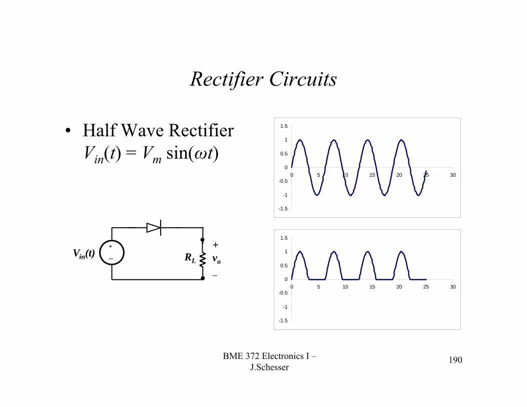
Rectifier Circuits
• Half Wave Rectifier Vin(t) = Vm sin(ωt)
-1.5
-1
-0.5
0
0.5
1
1.5
0 5 10 15 20 25 30
RL
+vo
--
Vin(t)+
--
-1.5
-1
-0.5
0
0.5
1
1.5
0 5 10 15 20 25 30
BME 372 Electronics I –J.Schesser
191
Rectifier Circuits
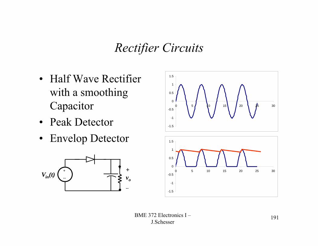
• Half Wave Rectifier with a smoothing Capacitor
• Peak Detector • Envelop Detector
-1.5
-1
-0.5
0
0.5
1
1.5
0 5 10 15 20 25 30
-1.5
-1
-0.5
0
0.5
1
1.5
0 5 10 15 20 25 30+vo
--
Vin(t)+
--
BME 372 Electronics I –J.Schesser
192
Rectifier Circuits
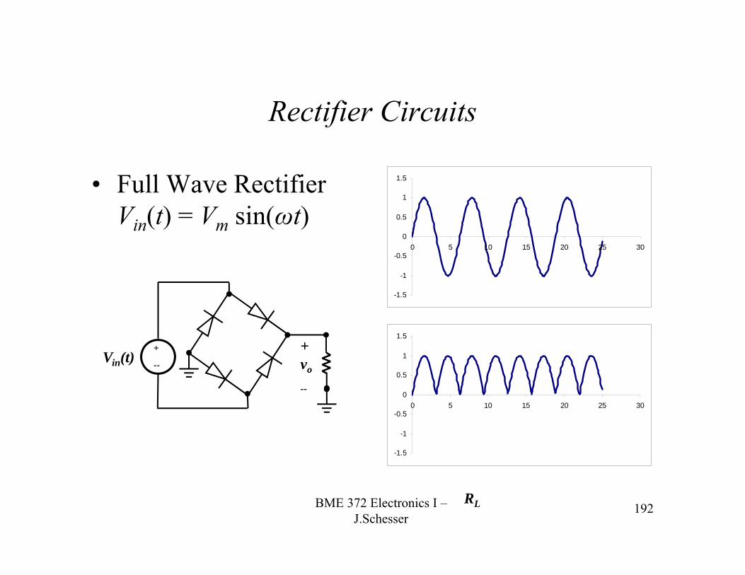
• Full Wave Rectifier Vin(t) = Vm sin(ωt)
-1.5
-1
-0.5
0
0.5
1
1.5
0 5 10 15 20 25 30
RL
+vo
--
Vin(t)+
--
-1.5
-1
-0.5
0
0.5
1
1.5
0 5 10 15 20 25 30
BME 372 Electronics I –J.Schesser
193
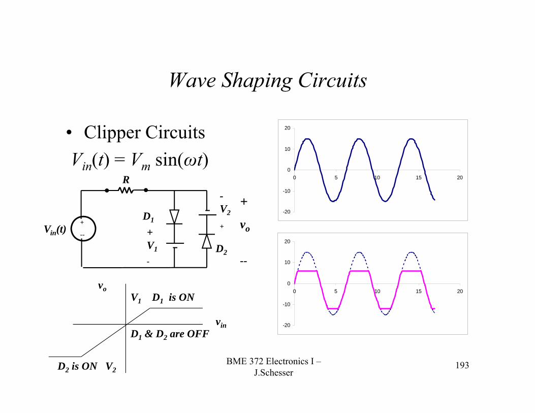
Wave Shaping Circuits
• Clipper CircuitsVin(t) = Vm sin(ωt)
R
+ V1
-
Vin(t)+
--
-V2
+
-20
-10
0
10
20
0 5 10 15 20
-20
-10
0
10
20
0 5 10 15 20
V1 D1 is ON
D1
D2
D2 is ON V2
D1 & D2 are OFFvin
+
vo
--
vo
BME 372 Electronics I –J.Schesser
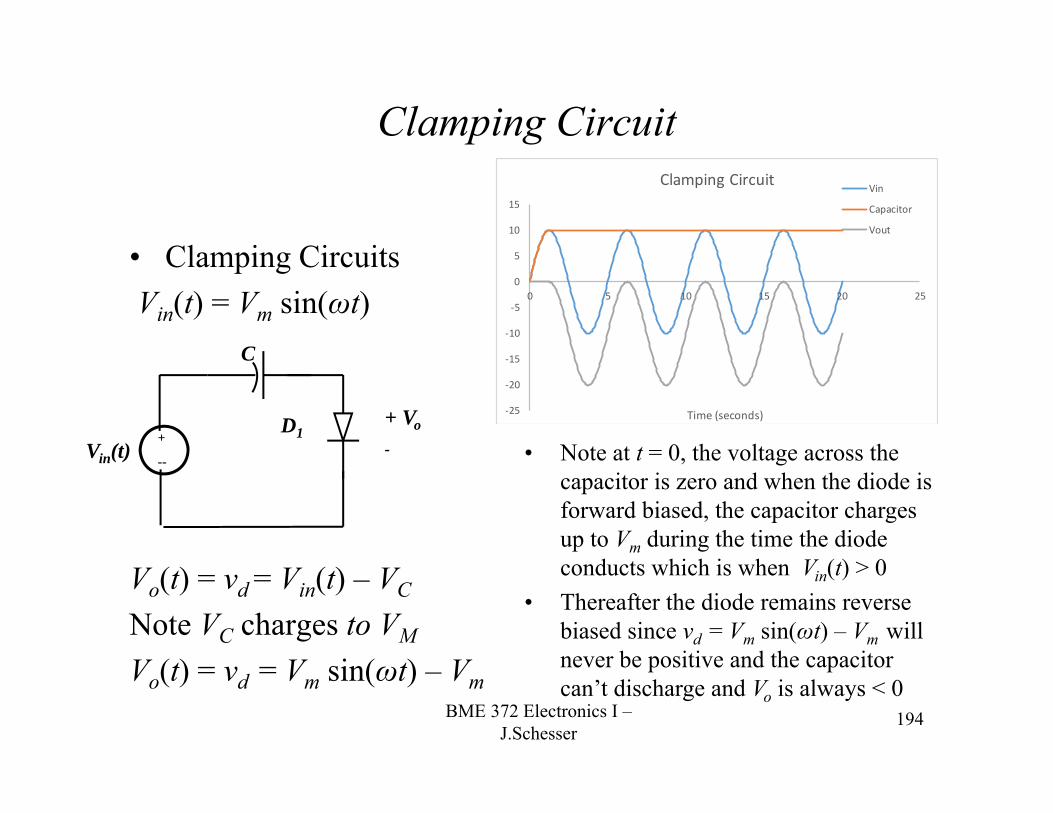
Clamping Circuit
194
‐25
‐20
‐15
‐10
‐5
0
5
10
15
0 5 10 15 20 25
Time (seconds)
Clamping CircuitVin
Capacitor
Vout
C
+ Vo
-Vin(t)+
--
D1• Note at t = 0, the voltage across the
capacitor is zero and when the diode is forward biased, the capacitor charges up to Vm during the time the diode conducts which is when Vin(t) > 0
• Thereafter the diode remains reverse biased since vd = Vm sin(ωt) – Vm will never be positive and the capacitor can’t discharge and Vo is always < 0
• Clamping CircuitsVin(t) = Vm sin(ωt)
Vo(t) = vd = Vin(t) – VC
Note VC charges to VM
Vo(t) = vd = Vm sin(ωt) – Vm
BME 372 Electronics I –J.Schesser
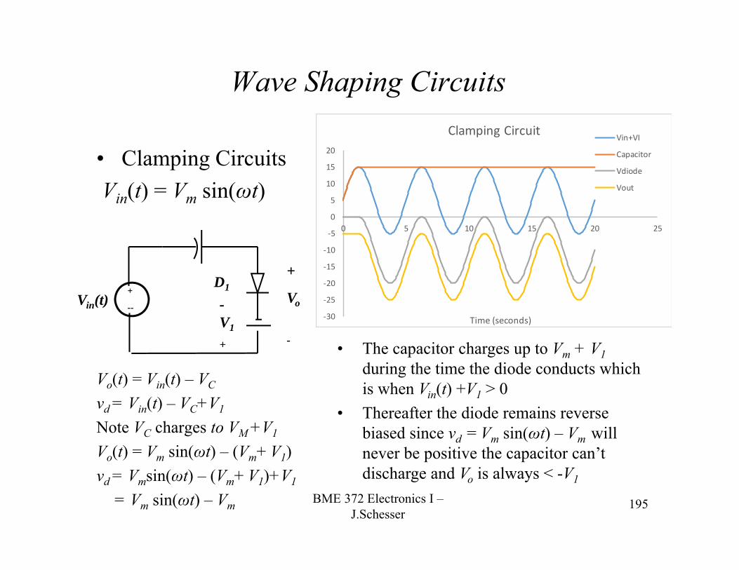
Wave Shaping Circuits
195
‐30
‐25
‐20
‐15
‐10
‐5
0
5
10
15
20
0 5 10 15 20 25
Time (seconds)
Clamping CircuitVin+VI
Capacitor
Vdiode
Vout
+
Vo
-
Vin(t)+
--
D1
-V1
+ • The capacitor charges up to Vm + V1during the time the diode conducts which is when Vin(t) +V1 > 0
• Thereafter the diode remains reverse biased since vd = Vm sin(ωt) – Vm will never be positive the capacitor can’t discharge and Vo is always < -V1
• Clamping CircuitsVin(t) = Vm sin(ωt)
Vo(t) = Vin(t) – VC
vd = Vin(t) – VC+V1
Note VC charges to VM +V1
Vo(t) = Vm sin(ωt) – (Vm+ V1)vd = Vmsin(ωt) – (Vm+ V1)+V1
= Vm sin(ωt) – Vm
BME 372 Electronics I –J.Schesser
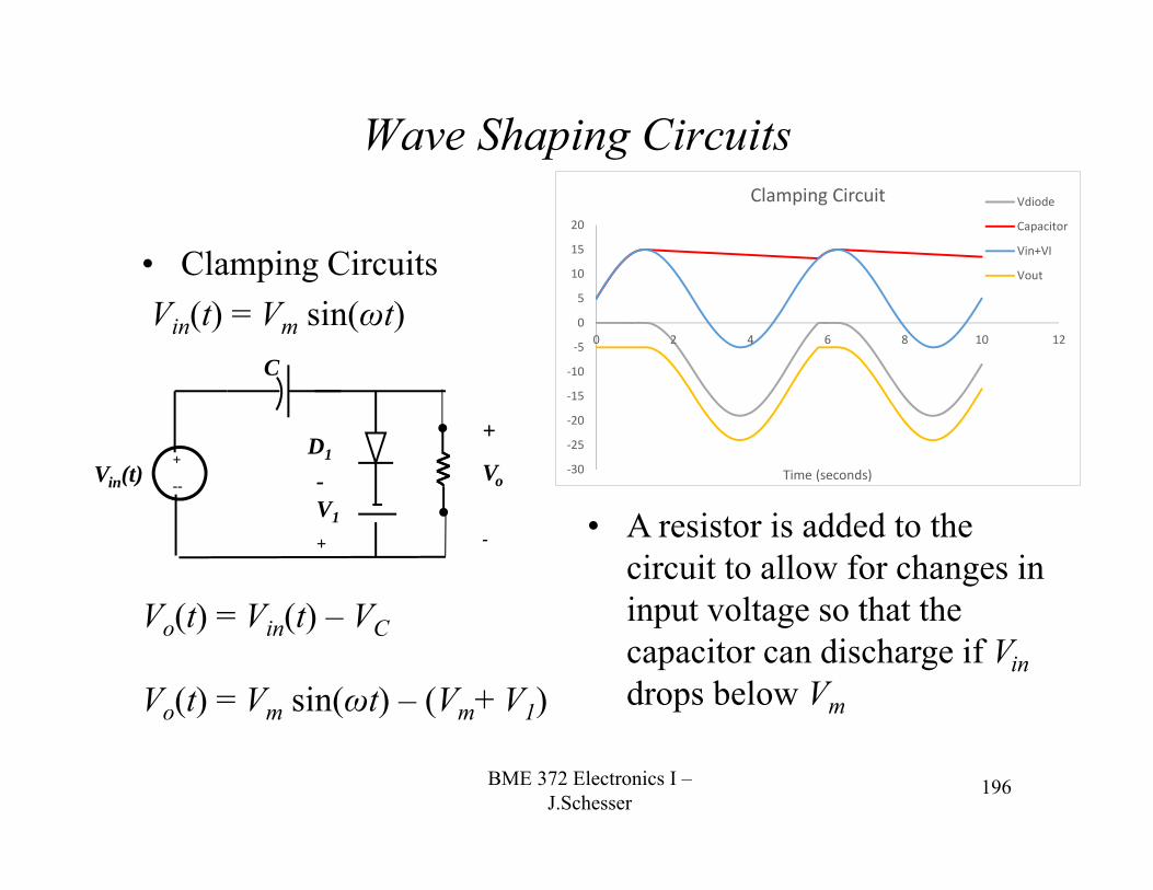
Wave Shaping Circuits
196
C
+
Vo
-
Vin(t)+
--
D1
-V1
+
‐30
‐25
‐20
‐15
‐10
‐5
0
5
10
15
20
0 2 4 6 8 10 12
Time (seconds)
Clamping Circuit Vdiode
Capacitor
Vin+VI
Vout
• A resistor is added to the circuit to allow for changes in input voltage so that the capacitor can discharge if Vindrops below Vm
• Clamping CircuitsVin(t) = Vm sin(ωt)
Vo(t) = Vin(t) – VC
Vo(t) = Vm sin(ωt) – (Vm+ V1)
BME 372 Electronics I –J.Schesser
197
Wave Shaping Circuits
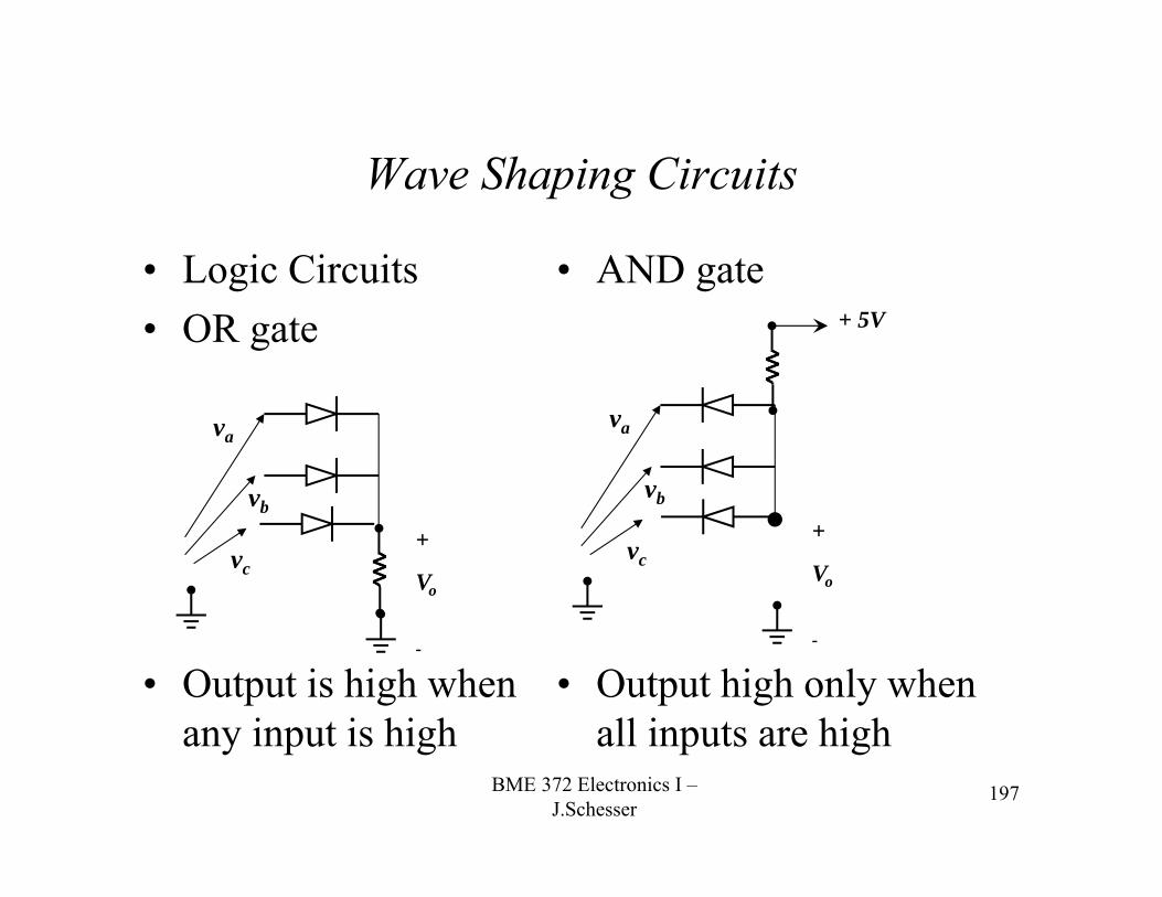
• Logic Circuits • OR gate
• Output is high when any input is high
+
Vo
-
vc
va
vb
• AND gate
• Output high only when all inputs are high
+
Vo
-
vc
va
vb
+ 5V
BME 372 Electronics I –J.Schesser
198
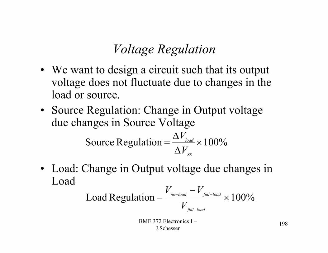
Voltage Regulation• We want to design a circuit such that its output
voltage does not fluctuate due to changes in the load or source.
• Source Regulation: Change in Output voltage due changes in Source Voltage
• Load: Change in Output voltage due changes in Load
%100 Regulation Source
SS
load
VV
%100 Regulation Load
loadfull
loadfullloadno
VVV
BME 372 Electronics I –J.Schesser
199
-20
-15
-10
-5
0
5
-20 -15 -10 -5 0 5
Vd
Id
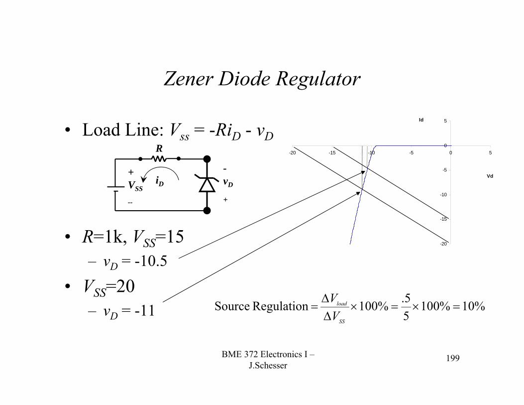
Zener Diode Regulator
• Load Line: Vss = -RiD - vD
• R=1k, VSS=15 – vD = -10.5
• VSS=20– vD = -11
R
-vD
+
+ VSS
--
iD
%10%10055.%100 Regulation Source
SS
load
VV
BME 372 Electronics I –J.Schesser
-20
-15
-10
-5
0
5
-20 -15 -10 -5 0 5
Vd
Id
200
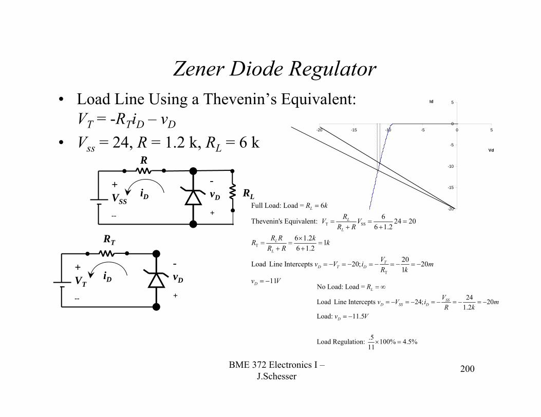
Zener Diode Regulator• Load Line Using a Thevenin’s Equivalent:
VT = -RTiD – vD
• Vss = 24, R = 1.2 k, RL = 6 kR
-vD
+
+ VSS
--
iD RL
RT
-vD
+
+ VT
--
iD
T SS
T
T
Full Load: Load = 66Thevenin's Equivalent: 24 20
6 1.26 1.2 16 1.2
20Load Line Intercepts 20; 201
11
L
L
L
L
L
TD T D
D
R kRV V
R RR R kR k
R RVv V i mR k
v V
No Load: Load =
24Load Line Intercepts 24; 201.2
Load: 11.5
.5Load Regulation: 100% 4.5%11
L
SSD SS D
D
RVv V i mR k
v V
BME 372 Electronics I –J.Schesser
201
Shockley Equation
-10123456789
101112131415
-0.3 -0.2 -0.1 0 0.1 0.2 0.3 0.4 0.5 0.6 0.7 0.8 0.9 1
v D volts
i D amps
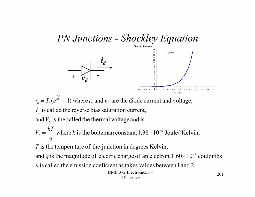
PN Junctions - Shockley Equation
2 and 1between values takesas coeficientemission thecalled is coulombs 011.60 electron,an of charge electric of magnitude theis and
Kelvin, degreesin junction theof re temperatu theis
Kelvin,Joule/ 10 1.38 constant,boltzman theis where
is and voltage thermal thecalled theis and current, saturation bias reverse thecalled is
voltage,andcurrent diode theare and where)1(
19-
23-
nq
T
kq
kTV
VI
vieIi
T
T
S
DDnVv
SDT
D
id
+ -vd
BME 372 Electronics I –J.Schesser
202
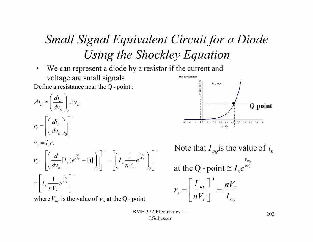
Small Signal Equivalent Circuit for a Diode Using the Shockley Equation
Shockley Equation
-10123456789
101112131415
-0.3 -0.2 -0.1 0 0.1 0.2 0.3 0.4 0.5 0.6 0.7 0.8 0.9 1
v D volts
i D amps
point-Q at the of value theis where
1
1)]1([
:point-Q near the resistance a Define
1
11
1
DDQ
nVV
T
S
Q
nVv
T
S
Q
nVv
S
D
d
ddd
QD
Dd
D
QD
DD
vV
enV
I
enV
IeIdvdr
riv
dvdir
ΔvdvdiΔi
T
DQ
T
DQ
T
D
Q point
DQ
T
T
DQd
nVV
S
DDQ
InV
nVI
r
eI
iI
T
DQ
1
point-Q at the
of value theis that Note
• We can represent a diode by a resistor if the current and voltage are small signals
BME 372 Electronics I –J.Schesser
203
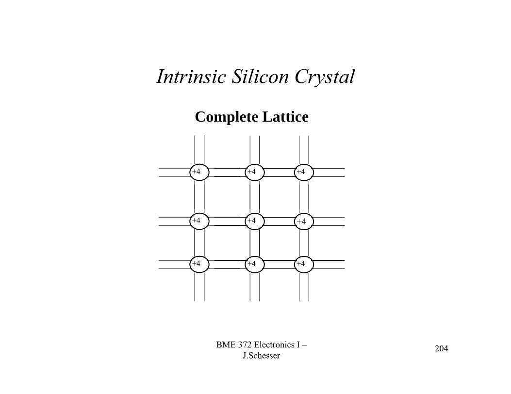
Basic Semiconductor Electronics• Atomic Structure of Valence-4 elements like Carbon, Silicon,
Germanium, etc.– have 4 valence electrons in its outer atomic shell– these atoms form covalent bonds with 4 other atoms in a lattice
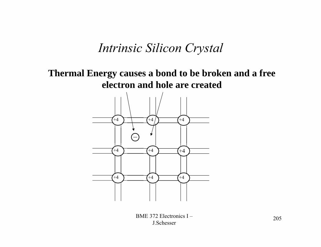
• When the energy levels of these electrons are raised several of these bonds may become randomly broken and a free electron is created– as a result these electrons are free to move about in the material similar to
electron conduction occurs in a metal– in addition to the free electron, a negative particle, a “hole” which is a
positive “particle” is created which also moves freely within the material.• As electrons and holes move through the material, they may encounter
each other and recombine and, thereby, become electrically neutral• This type of material is called an intrinsic semiconductor
BME 372 Electronics I –J.Schesser
204
Intrinsic Silicon Crystal
+4 +4
+4 +4
+4
+4
+4 +4 +4
Complete Lattice
BME 372 Electronics I –J.Schesser
205
Intrinsic Silicon Crystal
+4 +4
+4 +4
+4
+4
+4 +4 +4
Thermal Energy causes a bond to be broken and a free electron and hole are created
BME 372 Electronics I –J.Schesser
206
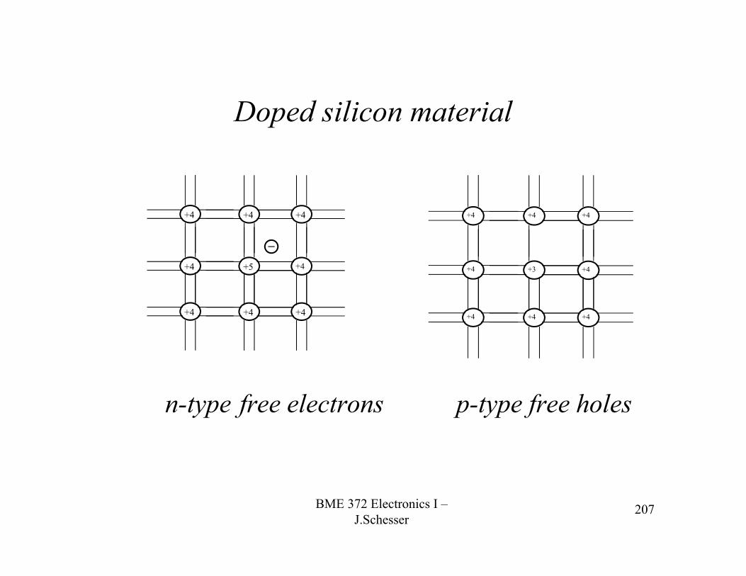
Doped Semiconductor Material• If we incorporate a small impurity of five or three valence band materials into
a 4 valence band lattice, we have created an extrinsic semiconductor which is doped with an impurity
• n-type semiconductor– Doping with five valence material (e.g. Arsenic) to create additional free (donor)
electrons and a static positive charged ion in the core lattice– Majority carriers are electrons; minority carriers are holes– The concentration of electrons in a n-type semiconductor = concentration of the
donor electrons + the concentration of free holes (which is the same as the number of electrons which have randomly broken their valence bonds)
• p-type semiconductor– Doping with three valence material (e.g., Gallium) to create additional free (donor)
holes and a static negative charged ion in the core lattice– Majority carriers are holes; minority carriers are electrons– The concentration of holes in a p-type semiconductor = concentration of the donor
holes + the concentration of free electrons (which is the same as the number of holes which have randomly broken their valence bonds)
BME 372 Electronics I –J.Schesser
207
Doped silicon material
n-type free electrons p-type free holes
+4 +4
+4 +5
+4
+4
+4 +4 +4
+4 +4
+4 +3
+4
+4
+4 +4 +4
BME 372 Electronics I –J.Schesser
208
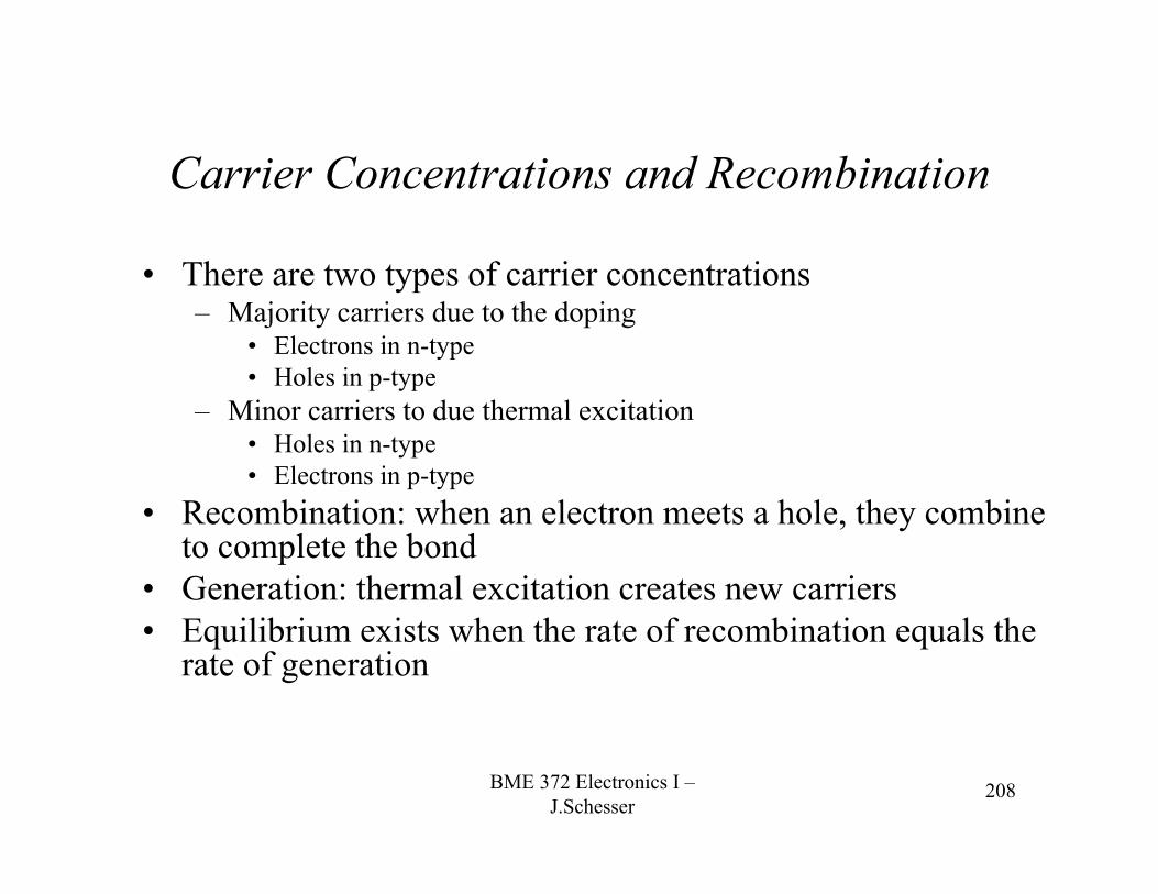
Carrier Concentrations and Recombination
• There are two types of carrier concentrations– Majority carriers due to the doping
• Electrons in n-type• Holes in p-type
– Minor carriers to due thermal excitation• Holes in n-type• Electrons in p-type
• Recombination: when an electron meets a hole, they combine to complete the bond
• Generation: thermal excitation creates new carriers• Equilibrium exists when the rate of recombination equals the
rate of generation
BME 372 Electronics I –J.Schesser
209
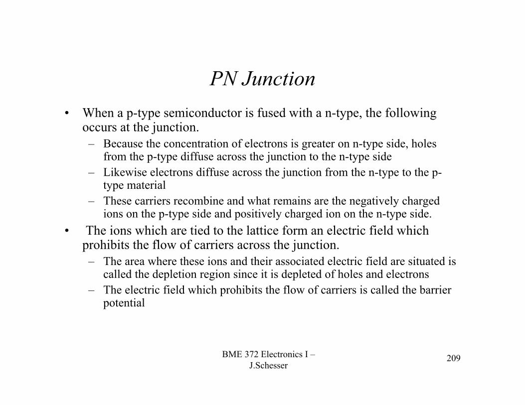
PN Junction• When a p-type semiconductor is fused with a n-type, the following
occurs at the junction.– Because the concentration of electrons is greater on n-type side, holes
from the p-type diffuse across the junction to the n-type side– Likewise electrons diffuse across the junction from the n-type to the p-
type material– These carriers recombine and what remains are the negatively charged
ions on the p-type side and positively charged ion on the n-type side.• The ions which are tied to the lattice form an electric field which
prohibits the flow of carriers across the junction.– The area where these ions and their associated electric field are situated is
called the depletion region since it is depleted of holes and electrons– The electric field which prohibits the flow of carriers is called the barrier
potential
BME 372 Electronics I –J.Schesser
210
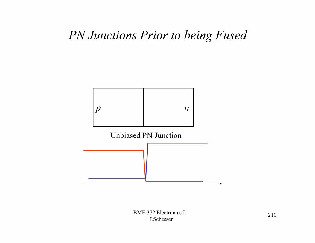
PN Junctions Prior to being Fused
np
Unbiased PN Junction
BME 372 Electronics I –J.Schesser
211
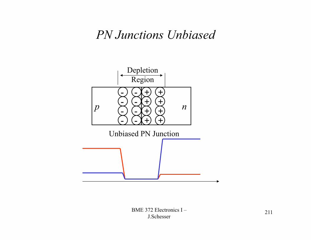
PN Junctions Unbiased
++
++
++
++ n
--
--
--
--p
Unbiased PN Junction
Depletion Region
BME 372 Electronics I –J.Schesser
212
Reverse Bias PN Junction• When an external voltage is a applied to a PN junction such that the n-
type is more positive than the p-type, then we say that the PN junction is reverse-biased and the following happens:– The external voltage creates an electric field which enhances the barrier
potential and the depletion region becomes wider since the majority carriers are pulled away from the junction (e.g., the electrons in the n-type material are attracted away from the junction by the positive voltage).
– However, this applied field supports the flow of minority carriers across the junction (e.g., the holes in the n-type material are attracted across the junction by the enhanced electric field of the widened depletion region) and when they cross the junction they become majority carriers (e.g., the minority carrier n-type holes now become majority carriers once they cross the junction to the p-type) and are attracted away from the junction as described above.
– Since the flow across the junction is due to minority carriers the current flow is small (this is sometimes called the reverse-based leakage current).
BME 372 Electronics I –J.Schesser
213
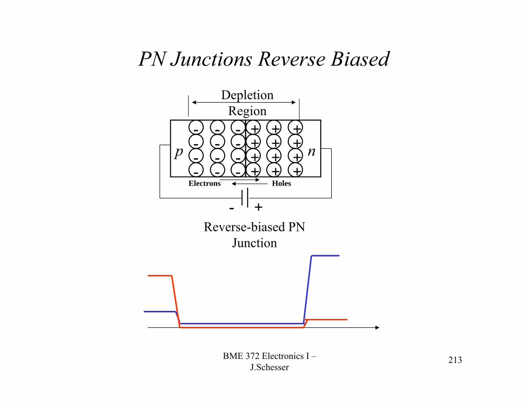
PN Junctions Reverse Biased
++
++
++
++ n
--
--
--
--p
Reverse-biased PN Junction
Depletion Region
++
++
--
--
+-
Electrons Holes
BME 372 Electronics I –J.Schesser
214
Forward Bias PN Junction• When an external voltage is a applied to a PN junction such that the n-
type is more negative than the p-type, then we say that the PN junction is forward-biased and the following happens:– The external voltage creates an electric field which opposes the barrier
potential and the depletion region becomes smaller provided it is larger than the voltage barrier of the depletion region (typically, a few tenths of a volt)
– This allows for the further flow of majority carriers across the junction– As the majority carriers cross the junction, the become minority carriers
and then recombine the majority carriers on the other side – Since the flow across the junction is due to majority carriers the current
flow is large.
BME 372 Electronics I –J.Schesser
215
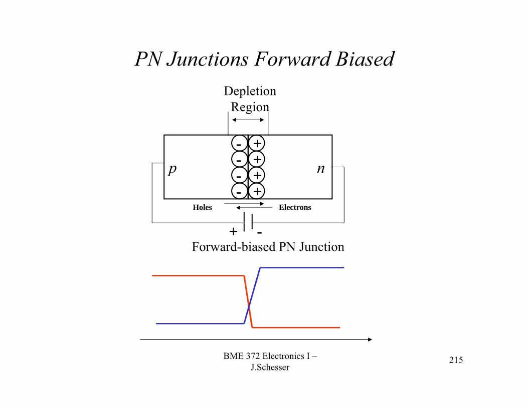
PN Junctions Forward Biased
++
++ n
--
--p
Forward-biased PN Junction
Depletion Region
+ -
Holes Electrons
BME 372 Electronics I –J.Schesser
216
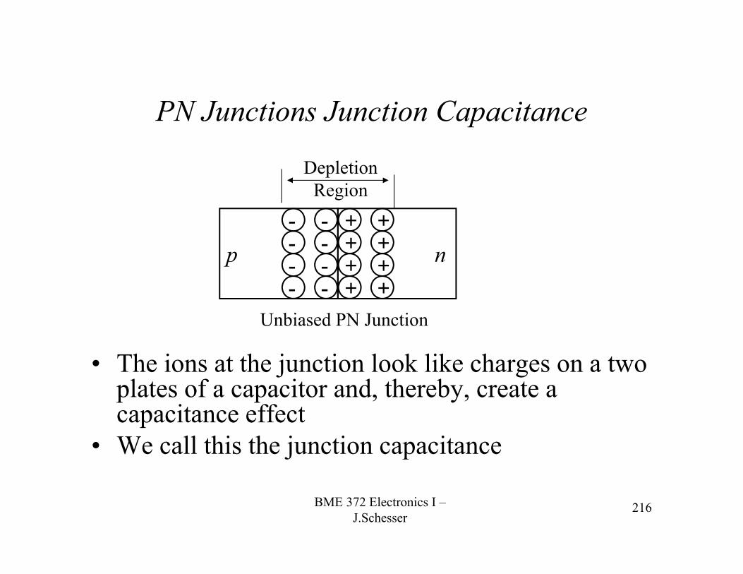
PN Junctions Junction Capacitance
• The ions at the junction look like charges on a two plates of a capacitor and, thereby, create a capacitance effect
• We call this the junction capacitance
++
++
++
++ n
--
--
--
--p
Unbiased PN Junction
Depletion Region
BME 372 Electronics I –J.Schesser
217
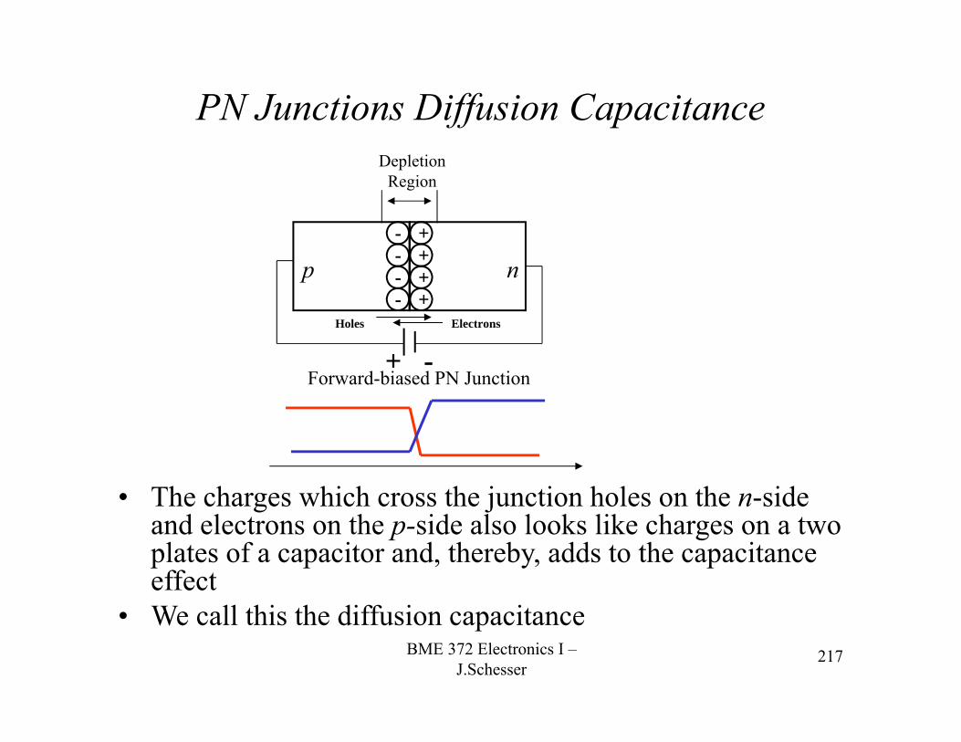
PN Junctions Diffusion Capacitance
++
++ n
--
--p
Forward-biased PN Junction
Depletion Region
+ -Holes Electrons
• The charges which cross the junction holes on the n-side and electrons on the p-side also looks like charges on a two plates of a capacitor and, thereby, adds to the capacitance effect
• We call this the diffusion capacitance
BME 372 Electronics I –J.Schesser
218
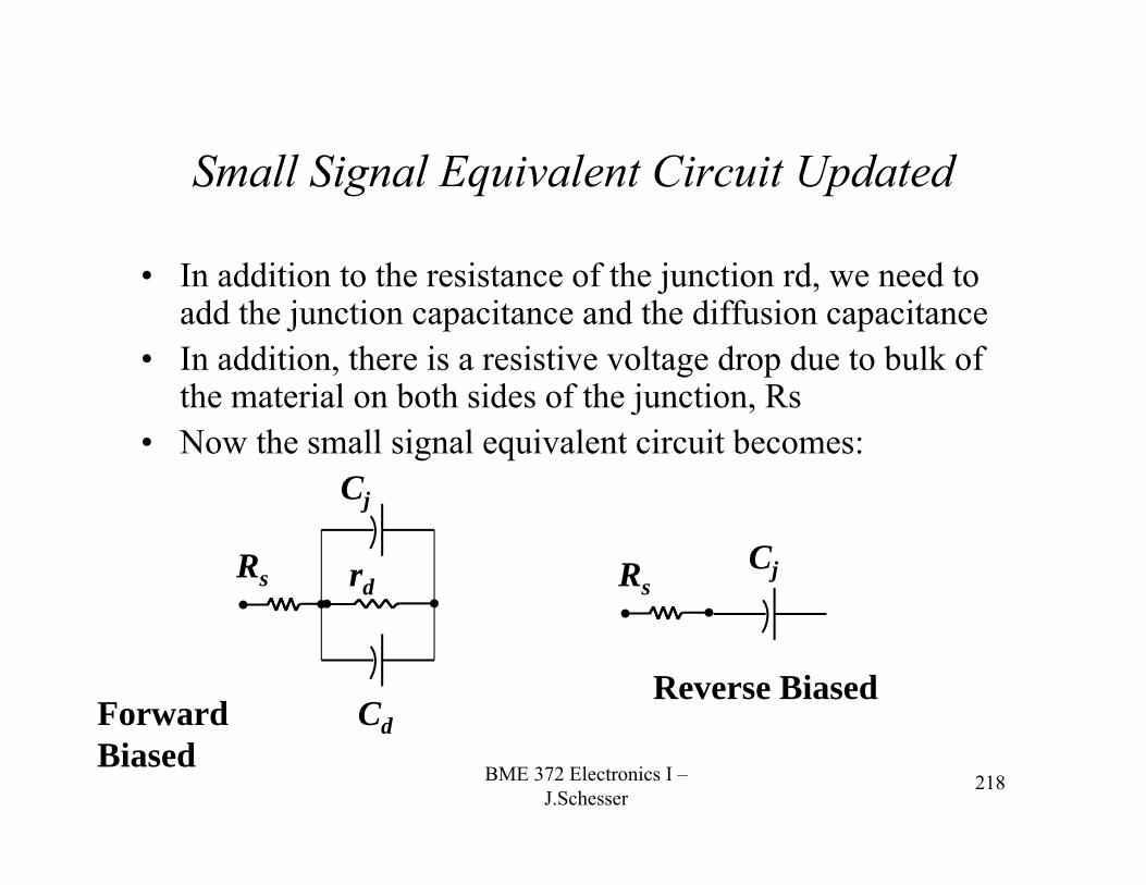
Small Signal Equivalent Circuit Updated
• In addition to the resistance of the junction rd, we need to add the junction capacitance and the diffusion capacitance
• In addition, there is a resistive voltage drop due to bulk of the material on both sides of the junction, Rs
• Now the small signal equivalent circuit becomes:
Rs rd
Cj
Cd
RsCj
Reverse BiasedForward Biased
BME 372 Electronics I –J.Schesser
219
Homework
• Probs. 3.2, 3.3, 3.5, 3.15, 3.16, 3.17, 3.20, 3.22, 3.24, 3.54, 3.61, 3.62, 3.63, 3.65, 3.73, 3.74
• For problem 3.16a repeat with D2 reversed• For problem 3.16c repeat with the +15V
source replaced by -15V