lt5581 - 6ghz rms power detector with 40db …cds.linear.com/docs/en/datasheet/5581fb.pdf6ghz rms...
TRANSCRIPT
LT5581
15581fb
For more information www.linear.com/LT5581
TYPICAL APPLICATION
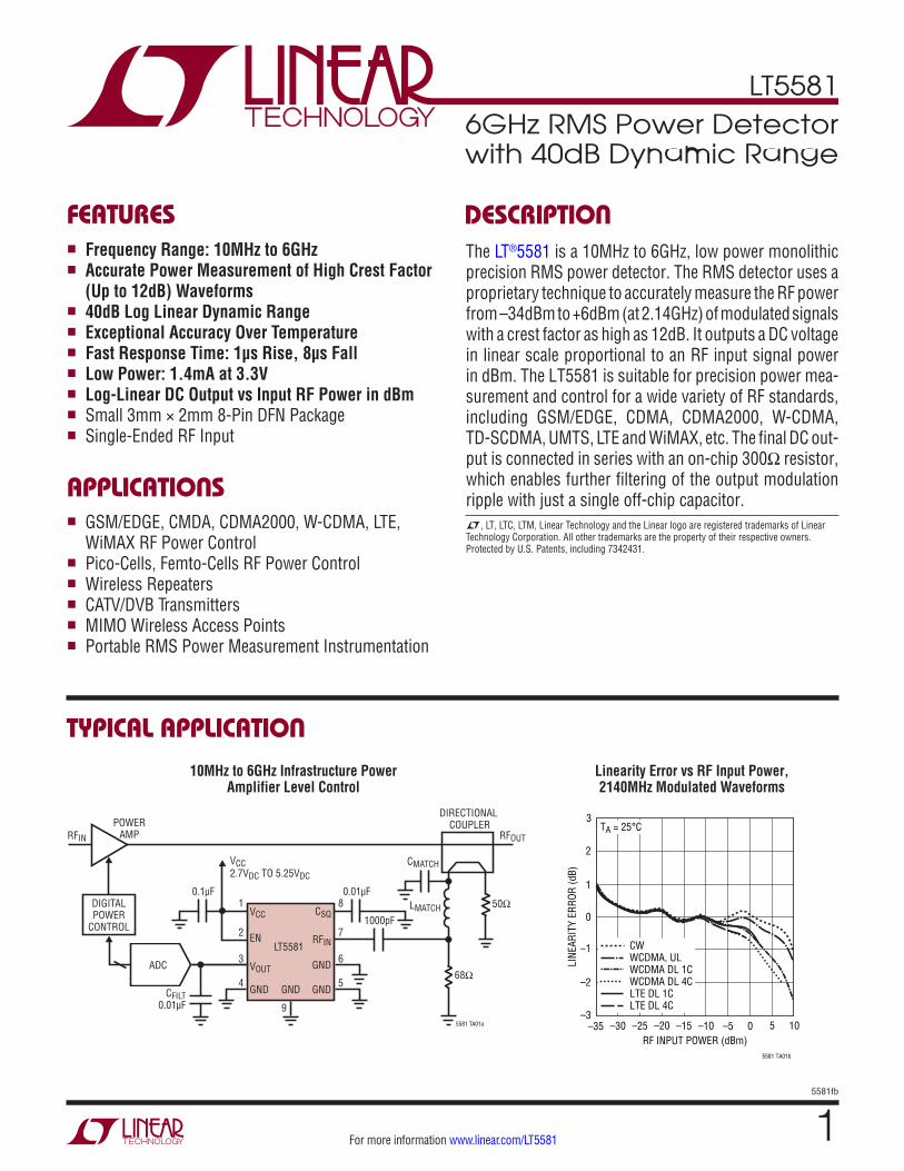
DESCRIPTION
6GHz RMS Power Detector with 40dB Dynamic Range
The LT®5581 is a 10MHz to 6GHz, low power monolithic precision RMS power detector. The RMS detector uses a proprietary technique to accurately measure the RF power from –34dBm to +6dBm (at 2.14GHz) of modulated signals with a crest factor as high as 12dB. It outputs a DC voltage in linear scale proportional to an RF input signal power in dBm. The LT5581 is suitable for precision power mea-surement and control for a wide variety of RF standards, including GSM/EDGE, CDMA, CDMA2000, W-CDMA, TD-SCDMA, UMTS, LTE and WiMAX, etc. The final DC out-put is connected in series with an on-chip 300Ω resistor, which enables further filtering of the output modulation ripple with just a single off-chip capacitor.
10MHz to 6GHz Infrastructure Power Amplifier Level Control
FEATURES
APPLICATIONS
n Frequency Range: 10MHz to 6GHz n Accurate Power Measurement of High Crest Factor
(Up to 12dB) Waveforms n 40dB Log Linear Dynamic Range n Exceptional Accuracy Over Temperature n Fast Response Time: 1μs Rise, 8μs Fall n Low Power: 1.4mA at 3.3V n Log-Linear DC Output vs Input RF Power in dBm n Small 3mm × 2mm 8-Pin DFN Package n Single-Ended RF Input
n GSM/EDGE, CMDA, CDMA2000, W-CDMA, LTE, WiMAX RF Power Control
n Pico-Cells, Femto-Cells RF Power Control n Wireless Repeaters n CATV/DVB Transmitters n MIMO Wireless Access Points n Portable RMS Power Measurement Instrumentation
Linearity Error vs RF Input Power, 2140MHz Modulated Waveforms
9
8
7
6
5
1
2
3
4
VCC
EN
VOUT
GND
CSQ
RFIN
GNDGND
GND
DIGITALPOWER
CONTROL
POWERAMP
DIRECTIONAL COUPLER
0.01µF
1000pF
0.1µF
VCC2.7VDC TO 5.25VDC
RFIN RFOUT
CMATCH
LMATCH
68Ω
50Ω
CFILT0.01µF
5581 TA01a
LT5581
ADC
2
1
0
–2
–1
–3
3
RF INPUT POWER (dBm)
LINE
ARIT
Y ER
ROR
(dB)
–30 –20 –10–35 –25 0 10–15 –5 5
5581 TA01b
TA = 25°C
CWWCDMA, ULWCDMA DL 1CWCDMA DL 4CLTE DL 1CLTE DL 4C
L, LT, LTC, LTM, Linear Technology and the Linear logo are registered trademarks of Linear Technology Corporation. All other trademarks are the property of their respective owners. Protected by U.S. Patents, including 7342431.

LT5581
25581fb
For more information www.linear.com/LT5581
The l denotes the specifications which apply over the full operating temperature range, otherwise specifications are at TA = 25°C, VCC = 3.3V, EN = 3.3V, unless otherwise noted (Note 2). Test circuit is shown in Figure 1.
PIN CONFIGURATIONABSOLUTE MAXIMUM RATINGS
Supply Voltage .........................................................5.5VMaximum Input Signal Power—Average .............15dBmMaximum Input Signal Power—Peak (Note 7) ....25dBmDC Voltage at RFIN ....................................... –0.3V to 2VVOUT Voltage ....................................–0.3V to VCC + 0.3VMaximum Junction Temperature, TJMAX ............... 150°COperating Temperature Range .................–40°C to 85°CStorage Temperature Range .................. –65°C to 150°C
CAUTION: This part is sensitive to electrostatic discharge. It is very important that proper ESD precautions be observed when handling the LT5581.
(Note 1)
TOP VIEW
9
DDB PACKAGE8-LEAD (3mm × 2mm) PLASTIC DFN
5
6
7
8
4
3
2
1VCC
EN
VOUT
GND
CSQ
RFIN
GND
GND
TJMAX = 150°C, θJA = 76°C/W
EXPOSED PAD (PIN 9) IS GND, MUST BE SOLDERED TO PCB
ORDER INFORMATIONLEAD FREE FINISH TAPE AND REEL PART MARKING PACKAGE DESCRIPTION TEMPERATURE RANGE
LT5581IDDB#PBF LT5581IDDB#TRPBF LDKM 8-Lead (3mm × 2mm) Plastic DFN –40°C to 85°C
Consult LTC Marketing for parts specified with wider operating temperature ranges. Consult LTC Marketing for information on non-standard lead based finish parts.For more information on lead free part marking, go to: http://www.linear.com/leadfree/ For more information on tape and reel specifications, go to: http://www.linear.com/tapeandreel/
ELECTRICAL CHARACTERISTICS
PARAMETER CONDITIONS MIN TYP MAX UNITS
AC Input
Input Frequency Range (Note 4) 10-6000 MHz
Input Impedance 205||1.6 Ω||pF
fRF = 450MHz
RF Input Power Range Externally Matched to 50Ω Source –34 to 6 dBm
Linear Dynamic Range, CW (Note 3) ±1dB Linearity Error 40 dB
Linear Dynamic Range, CDMA (Note 3) ±1dB Linearity Error; CDMA 4-Carrier 40 dB
Output Slope 31 mV/dB
Logarithmic Intercept (Note 5) –42 dBm
Output Variation vs Temperature Normalized to Output at 25˚C, –40°C < TA < 85°C; PIN = –34 to +6dBm
±1 dB
Output Variation vs Temperature Normalized to Output at 25°C, –40°C < TA < 85°C; PIN = –27 to –10dBm
±0.5 dB
Deviation from CW Response; PIN = –34dBm to 0dBm
TETRA π/4 DQPSK CDMA 4-Carrier 64-Channel Fwd 1.23Mcps
±0.1 ±0.5
dB dB

LT5581
35581fb
For more information www.linear.com/LT5581
The l denotes the specifications which apply over the full operating temperature range, otherwise specifications are at TA = 25°C, VCC = 3.3V, EN = 3.3V, unless otherwise noted (Note 2). Test circuit is shown in Figure 1.ELECTRICAL CHARACTERISTICS
PARAMETER CONDITIONS MIN TYP MAX UNITS
2nd Order Harmonic Distortion At RF Input; CW Input; PIN = 0dBm –57 dBc
3rd Order Harmonic Distortion At RF Input; CW Input; PIN = 0dBm –52 dBc
fRF = 880MHz
RF Input Power Range Externally Matched to 50Ω Source –34 to 6 dBm
Linear Dynamic Range, CW (Note 3) ±1dB Linearity Error 40 dB
Linear Dynamic Range, EDGE (Note 3) ±1dB Linearity Error; EDGE 3π/8-Shifted 8PSK 40 dB
Output Slope 31 mV/dB
Logarithmic Intercept (Note 5) –42 dBm
Output Variation vs Temperature Normalized to Output at 25°C, –40°C < TA < 85°C; PIN = –34 to +6dBm
±1 dB
Output Variation vs Temperature Normalized to Output at 25°C, –40°C < TA < 85°C; PIN = –27 to –10dBm
±0.5 dB
Deviation from CW Response, Pin = –34 to +6dBm EDGE 3π/8 Shifted 8PSK ±0.1 dB
fRF = 2140MHz
RF Input Power Range Externally Matched to 50Ω Source –34 to 6 dBm
Linear Dynamic Range, CW (Note 3) ±1dB Linearity Error 43 dB
Linear Dynamic Range, WCDMA (Note 3) ±1dB Linearity Error; 4-Carrier WCDMA 37 dB
Output Slope 31 mV/dB
Logarithmic Intercept (Note 5) –42 dBm
Output Variation vs Temperature Normalized to Output at 25°C, –40°C < TA < 85°C; PIN = –34 to 6dBm
±1 dB
Output Variation vs Temperature Normalized to Output at 25°C, –40°C < TA < 85°C; PIN = –27 to –10dBm
±0.5 dB
Maximum Deviation from CW Response PIN = –34 to –4dBm
WCDMA 1-Carrier Uplink WCDMA 64-Channel 4-Carrier Downlink
±0.1 ±0.5
dB dB
fRF = 2600MHz
RF Input Power Range Externally Matched to 50Ω Source –34 to 6 dBm
Linear Dynamic Range, CW (Note 3) ±1dB Linearity Error 40 dB
Output Slope 31 mV/dB
Logarithmic Intercept (Note 5) –42 dBm
Output Variation vs Temperature Normalized to Output at 25°C, –40°C < TA < 85°C; PIN = –34 to +6dBm
±1 dB
Output Variation vs Temperature Normalized to Output at 25°C, –40°C < TA < 85°C; PIN = –27 to –10dBm
±0.5 dB
Maximum Deviation from CW Response PIN = –34 to 2dBm
WiMAX OFDMA Preamble WiMAX OFDM Burst
±0.1 ±0.5
dB dB
fRF = 3500MHz
RF Input Power Range Externally Matched to 50Ω Source –30 to 6 dBm
Linear Dynamic Range, CW (Note 3) ±1dB Linearity Error 36 dB
Output Slope 31 mV/dB
Logarithmic Intercept (Note 5) –41 dBm
Output Variation vs Temperature Normalized to Output at 25°C, –40°C < TA < 85°C; PIN = –30 to +6dBm
±1 dB

LT5581
45581fb
For more information www.linear.com/LT5581
The l denotes the specifications which apply over the full operating temperature range, otherwise specifications are at TA = 25°C, VCC = 3.3V, EN = 3.3V, unless otherwise noted (Note 2). Test circuit is shown in Figure 1.ELECTRICAL CHARACTERISTICS
PARAMETER CONDITIONS MIN TYP MAX UNITS
Output Variation vs Temperature Normalized to Output at 25°C, –40°C < TA < 85°C; PIN = –27 to –10dBm
±0.5 dB
Deviation from CW Response PIN = –34 to –4dBm
WiMAX OFDMA Preamble WiMAX OFDM Burst
±0.1 ±0.5
dB dB
fRF = 5800MHz
RF Input Power Range Externally Matched to 50Ω Source –25 to 6 dBm
Linear Dynamic Range, CW (Note 3) ±1dB Linearity Error 31 dB
Output Slope 31 mV/dB
Logarithmic Intercept (Note 5) –33 dBm
Output Variation vs Temperature Normalized to Output at 25°C, –40°C < TA < 85°C; PIN = –25 to +6dBm
±1 dB
Output Variation vs Temperature Normalized to Output at 25°C, –40°C < TA < 85°C; PIN = –20 to +6dBm
±0.5 dB
Deviation from CW Response WiMAX OFDM Burst; PIN = –25 to 6dBm ±0.2 dB
Output
Output DC Voltage No Signal Applied to RF Input 180 mV
Output Impedance Internal Series Resistor Allows for Off-Chip Filter Cap 300 Ω
Output Current Sourcing/Sinking 5/5 mA
Rise Time 0.2V to 1.6V, 10% to 90%, fRF = 2140MHz 1 µs
Fall Time 1.6V to 0.2V, 10% to 90%, fRF = 2140MHz 8 µs
Power Supply Rejection Ratio (Note 6) For Over Operating Input Power Range 49 dB
Integrated Output Voltage Noise 1kHz to 6.5kHz Integration BW, PIN = 0dBm CW 150 µVRMS
Enable (EN) Low = Off, High = On
EN Input High Voltage (On) l 2 V
EN Input Low Voltage (Off) l 0.3 V
Enable Pin Input Current EN = 3.3V 20 µA
Turn-On Time; CW RF input VOUT Within 10% of Final Value; PIN = 0dBm 1 µs
Settling Time; RF Pulse VOUT Within 10% of Final Value; PIN = 0dBm 1 µs
Power Supply
Supply Voltage l 2.7 3.3 5.25 V
Supply Current No RF Input Signal 1.4 mA
Shutdown Current EN = 0.3V, VCC = 3.3V 0.2 6 µA
Note 1: Stresses beyond those listed under Absolute Maximum Ratings may cause permanent damage to the device. Exposure to any Absolute Maximum Rating condition for extended periods may affect device reliability and lifetime.Note 2: The LT5581 is guaranteed functional over the operating temperature range from –40°C to 85°C.Note 3: The linearity error is calculated by the difference between the incremental slope of the output and the average output slope from –20dBm to 0dBm. The dynamic range is defined as the range over which the linearity error is within ±1dB.
Note 4: An external capacitor at the CSQ pin should be used for input frequencies below 250MHz. Lower frequency operation results in excessive RF ripple in the output voltage.Note 5: Logarithmic intercept is an extrapolated input power level from the best fitted log-linear straight line, where the output voltage is 0V.Note 6: PSRR is determined as the dB value of the change in VOUT voltage over the change in VCC supply voltage.Note 7: Not production tested. Guaranteed by design and correlation to production tested parameters.

LT5581
55581fb
For more information www.linear.com/LT5581
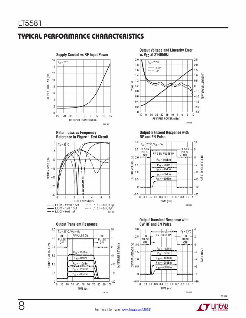
Performance characteristics taken at VCC = 3.3V, EN = 3.3V and TA = 25°C, unless otherwise noted. (Test circuit shown in Figure 1)TYPICAL PERFORMANCE CHARACTERISTICS
Output Voltage and Linearity Error at 450MHz
Linearity Error Temperature Variation from 25°C at 450MHz
Linearity Error vs RF Input Power, 450MHz Modulated Waveforms
Output Voltage and Linearity Error at 880MHz
Linearity Error Temperature Variation from 25°C at 880MHz
Linearity Error vs RF Input Power, 880MHz Modulated Waveforms
Output Voltage vs Frequency Output Voltage vs Frequency Linearity Error vs Frequency
RF INPUT POWER (dBm)–40
V OUT
(V)
0.8
1.8
2.0
–30 –20 –10
0.4
1.4
0.6
1.6
0.2
0
1.2
1.0
–35 –25 0 10–15 –5 5
5581 G01
10MHz450MHz880MHz2.14GHz2.6GHz3.5GHz5.8GHz
TA = 25°C
RF INPUT POWER (dBm)–40
V OUT
(V)
0.8
1.8
2.0
–30 –20 –10
0.4
1.4
0.6
1.6
0.2
0
1.2
1.0
–35 –25 0 10–15 –5 5
5581 G02
880MHz2.14GHz2.6GHz3.5GHz
TA = 25°C
RF INPUT POWER (dBm)–40
LINE
ARIT
Y ER
ROR
(dB)
–30 –20 –10–35 –25 0 10–15 –5 5
5581 G03
10MHz450MHz880MHz2.14GHz2.6GHz3.5GHz5.8GHz
TA = 25°C
2
1
0
–2
–1
–3
3
RF INPUT POWER (dBm)–40
V OUT
(V)
0.8
1.8
2.0
–30 –20 –10
0.4
1.4
0.6
1.6
0.2
0
1.2
1.0
–0.5
2.0
2.5
–1.5
1.0
–1.0
1.5
–2.0
–2.5
0.5
0
–35 –25 0 10–15 –5 5
5581 G04
25°C85°C–40°C
LINEARITY ERROR (dB)
1
2
0
–1
–2
–3
3
RF INPUT POWER (dBm)–40
VARI
ATIO
N (d
B)
–30 –20 –10–35 –25 0 10–15 –5 5
5581 G05
–40°C
85°C
2
1
0
–2
–1
–3
3
RF INPUT POWER (dBm)
LINE
ARIT
Y ER
ROR(
dB)
–30 –20 –10–35 –25 0 10–15 –5 5
5581 G06
TA = 25°C
CWTETRACDMA 4C
RF INPUT POWER (dBm)–40
V OUT
(V)
LINEARITY ERROR (dB)
0.8
1.8
2.0
–30 –20 –10
0.4
1.4
0.6
1.6
0.2
0
1.2
1.0
–0.5
2.0
2.5
–1.5
1.0
–1.0
1.5
–2.0
–2.5
0.5
0
–35 –25 0 10–15 –5 5
5581 G07
25°C85°C–40°C 2
1
0
–2
–1
–3
3
RF INPUT POWER (dBm)–40
VARI
ATIO
N (d
B)
–30 –20 –10–35 –25 0 10–15 –5 5
5581 G08
–40°C
85°C
2
1
0
–2
–1
–3
3
RF INPUT POWER (dBm)
LINE
ARIT
Y ER
ROR(
dB)
–30 –20 –10–35 –25 0 10–15 –5 5
5581 G09
TA = 25°C
CWEDGE

LT5581
65581fb
For more information www.linear.com/LT5581
TYPICAL PERFORMANCE CHARACTERISTICS
Output Voltage and Linearity Error at 2600MHz
Linearity Error Temperature Variation from 25°C at 2600MHz
Linearity Error vs RF Input Power, 2.6GHz Modulated Waveforms
Output Voltage and Linearity Error at 3500MHz
Linearity Error Temperature Variation from 25°C at 3500MHz
Linearity Error vs RF Input Power, 3.5GHz Modulated Waveforms
Output Voltage and Linearity Error at 2140MHz
Linearity Error Temperature Variation from 25°C at 2140MHz
Linearity Error vs RF Input Power, 2140MHz Modulated Waveforms
RF INPUT POWER (dBm)–40
V OUT
(V)
LINEARITY ERROR (dB)
0.8
1.8
2.0
–30 –20 –10
0.4
1.4
0.6
1.6
0.2
0
1.2
1.0
–0.5
2.0
2.5
–1.5
1.0
–1.0
1.5
–2.0
–2.5
0.5
0
–35 –25 0 10–15 –5 5
5581 G10
25°C85°C–40°C 2
1
0
–2
–1
–3
3
RF INPUT POWER (dBm)–40
VARI
ATIO
N (d
B)
–30 –20 –10–35 –25 0 10–15 –5 5
5581 G11
–40°C
85°C
2
1
0
–2
–1
–3
3
RF INPUT POWER (dBm)
LINE
ARIT
Y ER
ROR
(dB)
–30 –20 –10–35 –25 0 10–15 –5 5
5581 G12
TA = 25°C
CWWCDMA, ULWCDMA DL 1CWCDMA DL 4CLTE DL 1CLTE DL 4C
RF INPUT POWER (dBm)–40
V OUT
(V)
LINEARITY ERROR (dB)
0.8
1.8
2.0
–30 –20 –10
0.4
1.4
0.6
1.6
0.2
0
1.2
1.0
–0.5
2.0
2.5
–1.5
1.0
–1.0
1.5
–2.0
–2.5
0.5
0
–35 –25 0–15 –5 5 10
5581 G13
25°C85°C–40°C 2
1
0
–2
–1
–3
3
RF INPUT POWER (dBm)–40
VARI
ATIO
N (d
B)
–30 –20 –10–35 –25 0 10–15 –5 5
5581 G14
–40°C
85°C
2
1
0
–2
–1
–3
3
RF INPUT POWER (dBm)
LINE
ARIT
Y ER
ROR
(dB)
–30 –20 –10–35 –25 0 10–15 –5 5
5581 G15
TA = 25°C
CWWiMax OFDM PREAMBLEWiMax OFDM BURSTWiMax OFDMA PREAMBLE
RF INPUT POWER (dBm)–40
V OUT
(V)
LINEARITY ERROR (dB)
0.8
1.8
2.0
0–30 –20 –10 10
0.4
1.4
0.6
1.6
0.2
1.2
1.0
–0.5
2.0
2.5
–1.5
1.0
–1.0
1.5
–2.0
–2.5
0.5
0
–35 –25 0–15 –5 5
5581 G16
25°C85°C–40°C 2
1
0
–2
–1
–3
3
RF INPUT POWER (dBm)–40
VARI
ATIO
N (d
B)
–30 –20 –10–35 –25 0 10–15 –5 5
5581 G17
–40°C
85°C
2
1
0
–2
–1
–3
3
RF INPUT POWER (dBm)
LINE
ARIT
Y ER
ROR
(dB)
–30 –20 –10–35 –25 0 10–15 –5 5
5581 G18
TA = 25°C
CWWiMax OFDMA PREAMBLEWiMax OFDM BURST

LT5581
75581fb
For more information www.linear.com/LT5581
TYPICAL PERFORMANCE CHARACTERISTICS
Slope vs Frequency Slope Distribution vs Temperature Supply Current vs Supply Voltage
Logarithmic Intercept vs Frequency
Logarithmic Intercept Distribution vs Temperature
Output Voltage and Linearity Error at 5800MHz
Linearity Error Temperature Variation from 25°C at 5800MHz
Linearity Error vs RF Input Power, 5.8GHz Modulated Waveforms
RF INPUT POWER (dBm)–40
V OUT
(V)
LINEARITY ERROR (dB)
0.8
1.8
2.0
0–30 –20 –10 10
0.4
1.4
0.6
1.6
0.2
1.2
1.0
–0.5
2.0
2.5
–1.5
1.0
–1.0
1.5
–2.0
–2.5
0.5
0
–35 –25 0–15 –5 5
5581 G19
25°C85°C–40°C 2
1
0
–2
–1
–3
3
RF INPUT POWER (dBm)–40
VARI
ATIO
N (d
B)
–30 –20 –10–35 –25 0 10–15 –5 5
5581 G20
–40°C
85°C
2
1
0
–2
–1
–3
3
RF INPUT POWER (dBm)
LINE
ARIT
Y ER
ROR
(dB)
–30 –20 –10–35 –25 0 10–15 –5 5
5581 G21
TA = 25°C
CWWiMax OFDM BURST
FREQUENCY (GHz)0
26
SLOP
E (m
V/dB
)
30
1 2 43 5
34
28
32
6
5581 G22
TA = 25°C
SUPPLY VOLTAGE (V)2.6
SUPP
LY C
URRE
NT (m
A)
1.6
1.8
1.4
1.2
3.4 4.23 3.8 4.6 5 5.4
1.0
0.8
2.0
5581 G24
–40°C
85°C
25°C
FREQUENCY (GHz)0
–50
LOGA
RITH
MIC
INTE
RCEP
T (d
Bm)
–40
1 2 43 5
–30
–45
–35
6
5581 G25
TA = 25°C
SLOPE (mV/dB)28
DIST
RIBU
TION
(%)
30
40
50
20
10
029 30 31 32 33 34
5581 G23
TA = 85°CTA = 25°CTA = –40°C
LOGARITHMIC INTERCEPT (dBm)–48
DIST
RIBU
TION
(%)
30
40
50
20
10
0–47 –46 –45 –44 –43 –41–42
5581 G26
TA = 85°CTA = 25°CTA = –40°C
LT5581
85581fb
For more information www.linear.com/LT5581
TYPICAL PERFORMANCE CHARACTERISTICS
Output Transient ResponseOutput Transient Response with CW RF and EN Pulse
Output Voltage and Linearity Error vs VCC at 2140MHz
Return Loss vs Frequency Reference in Figure 1 Test Circuit
Output Transient Response with RF and EN Pulse
RF INPUT POWER (dBm)–40
V OUT
(V)
LINEARITY ERROR (dB)
0.8
1.8
2.0
–30 –20 –10
0.4
1.4
0.6
1.6
0.2
0
1.2
1.0
–0.5
2.0
2.5
–1.5
1.0
–1.0
1.5
–2.0
–2.5
0.5
0
–35 –25 0 10–15 –5 5
5581 G28
3.3V5V
TA = 25°C
FREQUENCY (GHz)0
–30
RETU
RN L
OSS
(dB)
–25
–20
–15
–10
0
1 2 3 4
5581 G29
5 6
–5
L1, C1 = 2.2nH, 1.5pFL1, C1 = 1nH, 1.5pFL1, C1 = 0nH, 1pF
L1, C1 = 0nH, 0.5pF L1, C1 = 0nH, 0pF
TA = 25°C
TIME (ms)0
OUTP
UT V
OLTA
GE (V
) RF PULSE ENABLE (V)
1.5
2.0
2.5
0.7
1.0
0.5
0.2 0.40.1 0.90.3 0.5 0.80.6 1
0
–0.5
3.0
–5
0
5
–10
–15
–20
–25
10
5581 G30
RF & EN PULSE ON
RF & EN PULSE
OFF
RF & EN PULSE
OFF
PIN = 10dBm
PIN = 0dBmPIN = –10dBm
PIN = –20dBm
PIN = –30dBm
TA = 25°C, VCC = 5V
TIME (µs)0
OUTP
UT V
OLTA
GE (V
) RF PULSE ENABLE (V)
1.5
2.0
2.5
70
1.0
0.5
20 4010 9030 50 8060 1000
3.0
–5
0
5
–10
–15
–20
10
5581 G31
RF PULSE ONRFPULSE
OFF
RFPULSE
OFF
PIN = 10dBm
PIN = 0dBm
PIN = –10dBm
PIN = –20dBm
PIN = –30dBm
TA = 25°C, VCC = 5V
TIME (ms)0
OUTP
UT V
OLTA
GE (V
)
ENABLE (V)
1.5
2.0
2.5
0.7
1.0
0.5
0.2 0.40.1 0.90.3 0.5 0.80.6 1
0
–0.5
3.0
–2
0
2
–4
–6
–8
–10
4
5581 G32
EN PULSE ONENPULSE
OFF
ENPULSE
OFF
PIN = 10dBm
PIN = 0dBm
PIN = –10dBm
PIN = –20dBm
PIN = –30dBm
TA = 25°C
Supply Current vs RF Input Power
RF INPUT POWER (dBm)–25
0
SUPP
LY C
URRE
NT (m
A)
4
8
12
–20 –15 –10 –5 50 10
16
2
6
10
14
15
5581 G27
TA = 25°C

LT5581
95581fb
For more information www.linear.com/LT5581
PIN FUNCTIONSVCC (Pin 1): Power Supply, 2.7V to 5.25V. VCC should be bypassed with a 0.1µF ceramic capacitor.
EN (Pin 2): Chip Enable. A logic low or no-connect on the enable pin shuts down the part. A logic high enables the part. An internal 500k pull-down resistor ensures the part is off when the enable driver is in a three-state condition.
VOUT (Pin 3): Detector Output.
GND (Pins 4, 5, 6): Ground.
RFIN (Pin 7): RF Input. Should be DC-blocked with coupling capacitor; 1000pF recommended. This pin has an internal 200Ω termination.
CSQ (Pin 8): Optional Low Frequency Range Extension Capacitor. This pin is for frequencies below 250MHz. Use 0.01µF from pin to ground for 10MHz operation.
Exposed Pad (Pin 9): Ground. The Exposed Pad must be soldered to the PCB. For high frequency operation, the backside ground connection should have a low inductance connection to the PCB ground, using many through-hole vias. See the layout information in the Applications Information section.
BLOCK DIAGRAM
LT5581
7
EXPOSEDPAD
OUTPUTBUFFER
9
VOUTRFIN
5581 BD
EN VCC
3
2
CSQ
8 1 4 5 6
150kHz LPF300Ω
GND
RMSDETECTOR
BIAS
LT5581
105581fb
For more information www.linear.com/LT5581
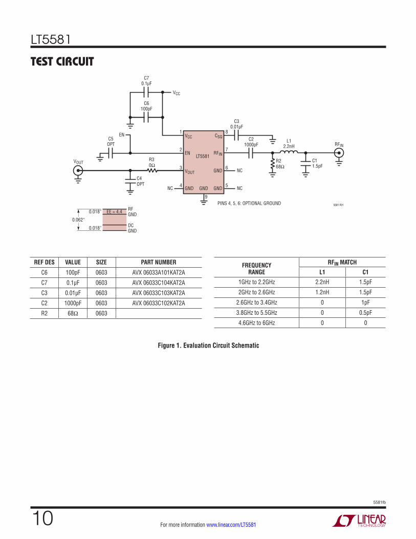
TEST CIRCUIT
Figure 1. Evaluation Circuit Schematic
REF DES VALUE SIZE PART NUMBER
C6 100pF 0603 AVX 06033A101KAT2A
C7 0.1µF 0603 AVX 06033C104KAT2A
C3 0.01µF 0603 AVX 06033C103KAT2A
C2 1000pF 0603 AVX 06033C102KAT2A
R2 68Ω 0603
FREQUENCY RANGE
RFIN MATCH
L1 C1
1GHz to 2.2GHz 2.2nH 1.5pF
2GHz to 2.6GHz 1.2nH 1.5pF
2.6GHz to 3.4GHz 0 1pF
3.8GHz to 5.5GHz 0 0.5pF
4.6GHz to 6GHz 0 0
9
8
7
6
5
1
2
3
4
VCC
EN
EN
NC NC
NCVOUT
GND
CSQ
RFIN
GNDGND
GND
L12.2nH
C30.01µF
PINS 4, 5, 6: OPTIONAL GROUND
C21000pF
VCC
R268Ω
R30Ω
C4OPT
5581 F01
LT5581
C5OPT
RFGND
DCGND
EE = 4.40.018"
0.018"
0.062"
VOUT
RFIN
C70.1µF
C6100pF
C11.5pF

LT5581
115581fb
For more information www.linear.com/LT5581
APPLICATIONS INFORMATIONOPERATION
To achieve an accurate average power measurement of the high crest factor modulated RF signals, the LT5581 combines a proprietary high speed power measurement subsystem with an internal 150kHz low pass averaging filter and an output voltage buffer in a completely integrated solution with minimal off-chip components. The resulting output voltage is directly proportional to the average RF input power in dBm. Figure 1 shows the evaluation circuit schematic, and Figures 2 and 3 show the associated board artwork. For best high frequency performance, it is import-ant to place many ground vias directly under the package.
RF Input Matching
The input resistance is about 205Ω. Input capacitance is 1.6pF. The impedance vs frequency of the RF input is detailed in Table 1.
Figure 2. Top Side of Evaluation Board Figure 3. Bottom Side of Evaluation Board
Table 1. RF Input Impedance
FREQUENCY (MHz)
INPUT IMPEDANCE
(Ω)
S11
MAG ANGLE (°)
10 203.6-j5.5 0.606 –0.8
50 199.5-j22.4 0.603 –3.4
100 191.7-j40.3 0.601 –6.4
200 171.1-j68.5 0.601 –12.3
400 121.8-j95.4 0.608 –24
500 100.2-j97.5 0.613 –29.8
800 56.8-j86.5 0.631 –46.5
900 48-j81.2 0.638 –51.8
1000 41.1-j76 0.645 –56.8
1500 22.2-j55 0.679 –79.5
2000 14.6-j41.4 0.710 –97.9
2100 13.6-j39.2 0.716 –101.2
2500 10.8-j32.1 0.737 –112.9
3000 8.6-j25 0.759 –125.7
3500 7.3-j19.4 0.774 –136.9
4000 6.6-j14.5 0.783 –147.1
5000 8.8-j9.6 0.709 –157.6
6000 6.4-j0 0.774 –179.9
5581 F035581 F02

LT5581
125581fb
For more information www.linear.com/LT5581
A shunt 68Ω resistor can be used to provide a broadband impedance match at low frequencies up to 1.3GHz, and from 4.5GHz to 6GHz. As shown in Figure 4, a nominal broadband input match can be achieved up to 2.2GHz by using an LC matching circuit consisting of a series 2.2nH inductor (L1) and a shunt 1.5pF capacitor (C1). This match will maintain a return loss of about 10dB across the band. For matching at higher frequencies, values for L1 and C1 are listed in the table of Figure 1. The input reflection coefficient referenced to the RF input pin (with no external components) is shown on the Smith Chart in Figure 5. Alternatively, it is possible to match using an impedance transformation network by omitting R1 and transforming the 205Ω load to 50Ω. The resulting match, over a narrow band of frequencies, will improve sensitivity up to about 6dB maximum; the dynamic range remains the same. For example, by omitting R1 and setting L1 = 1.8nH and C1 = 3pF, a 2:1 VSWR match can be obtained from 1.95GHz to 2.36GHz, with a sensitivity improvement of 5dB.
The RFIN input DC blocking capacitor (C2) and the CSQ bias decoupling capacitor (C3), can be adjusted for low
frequency operation. For input frequencies down to 10MHz, 0.01µF is needed at CSQ. For frequencies above 250MHz, the on-chip 20pF decoupling capacitor is sufficient, and CSQ may be eliminated as desired. The DC-blocking capacitor can be as large as 2200pF for 10MHz operation, or 100pF for 2GHz operation. A DC-blocking capacitor larger than 2200pF results in an undesirable RF pulse response on the falling edge. Therefore, for general applications, the recommended value for C2, is conservatively set at 1000pF.
Output Interface
The output buffer of the LT5581 is shown in Figure 6. It includes a push-pull stage with a series 300Ω resistor. The output stage is capable of sourcing and sinking 5mA of current. The output pin can be shorted to GND or VCC without damage, but going beyond VCC + 0.5V or GND – 0.5V may result in damage, as the internal ESD protection diodes will start to conduct excessive current.
The residual ripple, due to RF modulation, can be reduced by adding external components RSS and CLOAD (R3 and C4 on the Evaluation Circuit Schematic in Figure 1) to
APPLICATIONS INFORMATION
Figure 4. Simplified Circuit Schematic of the RF Input Interface Figure 5. Input Reflection Coefficient
CSQ
VCC
5581 F04
205Ω
LT5581
L1
C30.01µF
C21000pF
R168Ω
RFIN(MATCHED)
C1
20pF
RFIN7
8

LT5581
135581fb
For more information www.linear.com/LT5581
APPLICATIONS INFORMATIONthe output pin, to form an RC lowpass filter. The internal 300Ω resistor in series with the output pin enables filter-ing of the output signal with just the addition of CLOAD. Figure 7 shows the effect of the external filter capacitor on the residual ripple level for a 4-carrier WCDMA signal at 2.14GHz with –10dBm. Adding a 10nF capacitor to the output decreases the peak-to-peak output ripple from 135mVP-P to 50mVP-P. The filter –3dB corner frequency can be calculated with the following equation:
fC =
12π CLOAD(300+RSS)
Figure 8 shows the transient response for a 2.6GHz Wi-MAX signal, with preamble and burst ripple reduced by a
factor of 3, using a 0.047µF external filter capacitor. The average power in the preamble section is –10dBm, while the burst section has a 3dB lower average power. With the capacitor, the ripple in the preamble section is about 0.5dB peak-to-peak. The modulation used was OFDM (WiMAX 802.16-2004) MMDS band, 1.5MHz BW, with 256 size FFT and 1 burst at QPSK 3/4.
Figure 9 shows how the peak-to-peak ripple decreases with increasing external filter capacitance value. Also shown is how the RF pulse response will have longer rise and fall times with the addition of this lowpass filter cap.
Figure 6. Simplified Circuit Schematic of the Output Interface
Figure 8. Residual Ripple for 2.6GHz WiMAX OFDM 802.16-2004
Figure 7. Residual Ripple, Output Transient Response for RF Pulse with WCDMA 4-Carrier Modulation
Figure 9. Residual Ripple, Output Transient Times for RF Pulse with WCDMA 4-Carrier Modulation vs External Filter Capacitor C4
300Ω RSSVOUT
INPUT
VCC
40µA
VOUT(FILTERED)
CLOAD
5581
F06
LT5581
3
TIME (µs)
OUTP
UT V
OLTA
GE (V
) OUTPUT VOLTAGE (V)
0.8
1.0
1.2
0.6
0.4
0 7020 4010 9030 50 8060 100
0.2
0
1.4
1.10
1.15
1.20
1.05
1.00
0.95
0.90
1.25
5581 F07
TA = 25°CNO CAP0.01µF
TIME (ms)
OUTP
UT V
OLTA
GE (V
)
0.8
1.0
1.2
0.6
0.4
0 1.40.4 0.80.2 1.80.6 1 1.61.2 2
0.2
0
1.4
5581 F08
TA = 25°C NO CAP0.047µF
EXTERNAL CAPACITOR (µF)0.001
OUTP
UT R
IPPL
E PE
AK-T
O-PE
AK (d
B) RISE TIME AND FALL TIM
E (µs)
3
5
7
2
1
0.01 0.1 10
9
4
6
8
100
10
1
1000
5581 F09
TA = 25°CRIPPLERISEFALL
LT5581
145581fb
For more information www.linear.com/LT5581
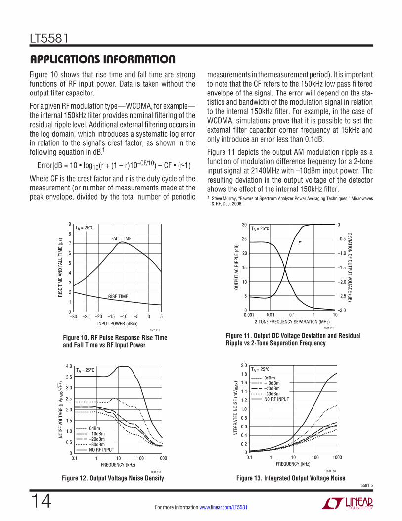
Figure 10. RF Pulse Response Rise Time and Fall Time vs RF Input Power
Figure 10 shows that rise time and fall time are strong functions of RF input power. Data is taken without the output filter capacitor.
For a given RF modulation type—WCDMA, for example—the internal 150kHz filter provides nominal filtering of the residual ripple level. Additional external filtering occurs in the log domain, which introduces a systematic log error in relation to the signal’s crest factor, as shown in the following equation in dB.1
Error|dB = 10 • log10(r + (1 – r)10–CF/10) – CF • (r-1)
Where CF is the crest factor and r is the duty cycle of the measurement (or number of measurements made at the peak envelope, divided by the total number of periodic
measurements in the measurement period). It is important to note that the CF refers to the 150kHz low pass filtered envelope of the signal. The error will depend on the sta-tistics and bandwidth of the modulation signal in relation to the internal 150kHz filter. For example, in the case of WCDMA, simulations prove that it is possible to set the external filter capacitor corner frequency at 15kHz and only introduce an error less than 0.1dB.
Figure 11 depicts the output AM modulation ripple as a function of modulation difference frequency for a 2-tone input signal at 2140MHz with –10dBm input power. The resulting deviation in the output voltage of the detector shows the effect of the internal 150kHz filter.
APPLICATIONS INFORMATION
Figure 11. Output DC Voltage Deviation and Residual Ripple vs 2-Tone Separation Frequency
Figure 12. Output Voltage Noise Density Figure 13. Integrated Output Voltage Noise
1 Steve Murray, “Beware of Spectrum Analyzer Power Averaging Techniques,” Microwaves & RF, Dec. 2006.
INPUT POWER (dBm)–30
RISE
TIM
E AN
D FA
LL T
IME
(µs)
6
7
8
5
4
–20 –10–25 –15 –5 0 5
1
0
3
9
2
5581 F10
FALL TIME
RISE TIME
TA = 25°C
2-TONE FREQUENCY SEPARATION (MHz)0.001
OUTP
UT A
C RI
PPLE
(dB)
DEVIATION OF OUTPUT VOLTAGE (dB)
15
20
25
10
5
0.01 0.1 1 100
30
–1.5
–1.0
–0.5
–2.0
–2.5
–3.0
0
5581 F11
TA = 25°C
FREQUENCY (kHz)0.1
NOIS
E VO
LTAG
E (µ
V RM
S/
Hz)
2.0
4.0
10
1.0
3.5
1.5
0.5
0
3.0
2.5
1 100 1000
5581 F12
0dBm–10dBm–20dBm–30dBmNO RF INPUT
TA = 25°C
FREQUENCY (kHz)0.1
INTE
GRAT
ED N
OISE
(mV R
MS)
0.8
1.8
2.0
10
0.4
1.4
0.6
1.6
0.2
0
1.2
1.0
1 100 1000
5581 F13
0dBm–10dBm–20dBm–30dBmNO RF INPUT
TA = 25°C
LT5581
155581fb
For more information www.linear.com/LT5581
The output voltage noise density and integrated noise are shown in Figures 12 and 13, respectively, for various input power levels. Noise is a strong function of input level. There is roughly a 10dB reduction in the output noise level for an input level of 0dBm versus no input.
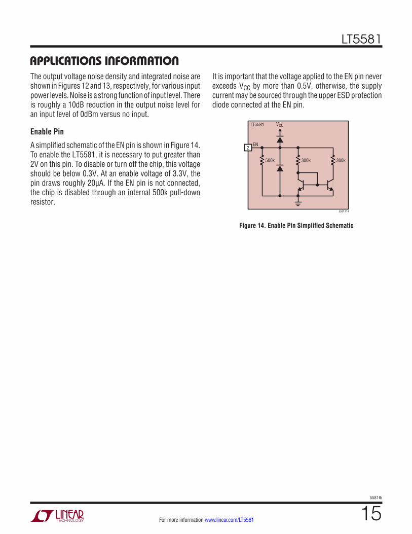
Enable Pin
A simplified schematic of the EN pin is shown in Figure 14. To enable the LT5581, it is necessary to put greater than 2V on this pin. To disable or turn off the chip, this voltage should be below 0.3V. At an enable voltage of 3.3V, the pin draws roughly 20µA. If the EN pin is not connected, the chip is disabled through an internal 500k pull-down resistor.
APPLICATIONS INFORMATION
Figure 14. Enable Pin Simplified Schematic
EN
VCC
5581 F14
300k 300k
LT5581
500k
2
It is important that the voltage applied to the EN pin never exceeds VCC by more than 0.5V, otherwise, the supply current may be sourced through the upper ESD protection diode connected at the EN pin.

LT5581
165581fb
For more information www.linear.com/LT5581
PACKAGE DESCRIPTION
2.00 ±0.10(2 SIDES)
NOTE:1. DRAWING CONFORMS TO VERSION (WECD-1) IN JEDEC PACKAGE OUTLINE M0-229 2. DRAWING NOT TO SCALE 3. ALL DIMENSIONS ARE IN MILLIMETERS4. DIMENSIONS OF EXPOSED PAD ON BOTTOM OF PACKAGE DO NOT INCLUDE MOLD FLASH. MOLD FLASH, IF PRESENT, SHALL NOT EXCEED 0.15mm ON ANY SIDE5. EXPOSED PAD SHALL BE SOLDER PLATED6. SHADED AREA IS ONLY A REFERENCE FOR PIN 1 LOCATION ON THE TOP AND BOTTOM OF PACKAGE
0.40 ±0.10
BOTTOM VIEW—EXPOSED PAD
0.56 ±0.05(2 SIDES)
0.75 ±0.05
R = 0.115TYPR = 0.05
TYP
2.15 ±0.05(2 SIDES)
3.00 ±0.10(2 SIDES)
14
85
PIN 1 BARTOP MARK
(SEE NOTE 6)
0.200 REF
0 – 0.05
(DDB8) DFN 0905 REV B
0.25 ±0.050.50 BSC
PIN 1R = 0.20 OR0.25 × 45°CHAMFER
0.25 ±0.05
2.20 ±0.05(2 SIDES)
RECOMMENDED SOLDER PAD PITCH AND DIMENSIONS
0.61 ±0.05(2 SIDES)
1.15 ±0.05
0.70 ±0.05
2.55 ±0.05
PACKAGEOUTLINE
0.50 BSC
DDB Package8-Lead Plastic DFN (3mm × 2mm)
(Reference LTC DWG # 05-08-1702 Rev B)
Please refer to http://www.linear.com/designtools/packaging/ for the most recent package drawings.

LT5581
175581fb
For more information www.linear.com/LT5581
Information furnished by Linear Technology Corporation is believed to be accurate and reliable. However, no responsibility is assumed for its use. Linear Technology Corporation makes no representation that the interconnection of its circuits as described herein will not infringe on existing patent rights.
REVISION HISTORYREV DATE DESCRIPTION PAGE NUMBER
A 4/10 Updated Note 2 in Electrical Characteristics Section 4
B 8/15 Changed Enable Pin input voltage to 2V 15

LT5581
185581fb
For more information www.linear.com/LT5581 LINEAR TECHNOLOGY CORPORATION 2008
LT 0815 REV B • PRINTED IN USALinear Technology Corporation1630 McCarthy Blvd., Milpitas, CA 95035-7417(408) 432-1900 FAX: (408) 434-0507 www.linear.com/LT5581
RELATED PARTSPART NUMBER DESCRIPTION COMMENTSRF Power DetectorsLTC®5505 RF Power Detectors with >40dB Dynamic Range 300MHz to 3GHz, Temperature Compensated, 2.7V to 6V SupplyLTC5507 100kHz to 1000MHz RF Power Detector 100kHz to 1GHz, Temperature Compensated, 2.7V to 6V SupplyLTC5508 300MHz to 7GHz RF Power Detector 44dB Dynamic Range, Temperature Compensated, SC70 PackageLTC5509 300MHz to 3GHz RF Power Detector 36dB Dynamic Range, Low Power Consumption, SC70 PackageLTC5530 300MHz to 7GHz Precision RF Power Detector Precision VOUT Offset Control, Shutdown, Adjustable GainLTC5531 300MHz to 7GHz Precision RF Power Detector Precision VOUT Offset Control, Shutdown, Adjustable OffsetLTC5532 300MHz to 7GHz Precision RF Power Detector Precision VOUT Offset Control, Adjustable Gain and OffsetLT5534 50MHz to 3GHz Log RF Power Detector with
60dB Dynamic Range±1dB Output Variation over Temperature, 38ns Response Time, Log Linear Response
LTC5536 Precision 600MHz to 7GHz RF Power Detector with Fast Comparator Output
25ns Response Time, Comparator Reference Input, Latch Enable Input, –26dBm to +12dBm Input Range
LT5537 Wide Dynamic Range Log RF/IF Detector Low Frequency to 1GHz, 83dB Log Linear Dynamic RangeLT5538 75dB Dynamic Range 3.8GHz Log RF Power
Detector±0.8dB Accuracy Over Temperature
InfrastructureLT5514 Ultralow Distortion, IF Amplifier/ADC Driver
with Digitally Controlled Gain850MHz Bandwidth, 47dBm OIP3 at 100MHz, 10.5dB to 33dB Gain Control Range
LT5517 40MHz to 900MHz Quadrature Demodulator 21dBm IIP3, Integrated LO Quadrature GeneratorLT5519 0.7GHz to 1.4GHz High Linearity Upconverting
Mixer17.1dBm IIP3 at 1GHz, Integrated RF Output Transformer with 50Ω Matching, Single-Ended LO and RF Ports Operation
LT5520 1.3GHz to 2.3GHz High Linearity Upconverting Mixer
15.9dBm IIP3 at 1.9GHz, Integrated RF Output Transformer with 50Ω Matching, Single-Ended LO and RF Ports Operation
LT5521 10MHz to 3700MHz High Linearity Upconverting Mixer
24.2dBm IIP3 at 1.95GHz, NF = 12.5dB, 3.15V to 5.25V Supply, Single-Ended LO Port Operation
LT5522 600MHz to 2.7GHz High Signal Level Downconverting Mixer
4.5V to 5.25V Supply, 25dBm IIP3 at 900MHz, NF = 12.5dB, 50Ω Single-Ended RF and LO Ports
LT5525 High Linearity, Low Power Downconverting Mixer
Single-Ended 50Ω RF and LO Ports, 17.6dBm IIP3 at 1900MHz, ICC = 28mA
LT5526 High Linearity, Low Power Downconverting Mixer
3V to 5.3V Supply, 16.5dBm IIP3, 100kHz to 2GHz RF, NF = 11dB, ICC = 28mA, –65dBm LO-RF Leakage
LT5527 400MHz to 3.7GHz High Signal Level Downconverting Mixer
IIP3 = 23.5dBm and NF = 12.5dBm at 1900MHz, 4.5V to 5.25V Supply, ICC = 78mA, Conversion Gain = 2dB
LT5557 400MHz to 3.8GHz, 3.3V High Signal Level Downconverting Mixer
IIP3 = 23.7dBm at 2600MHz, 23.5dBm at 3600MHz, ICC = 82mA at 3.3V
LT5560 Ultralow Power Active Mixer 10mA Supply Current, 10dBm IIP3, 10dB NF, Usable as Up- or Down-Converter.LT5568 700MHz to 1050MHz High Linearity Direct
Quadrature Modulator22.9dBm OIP3 at 850MHz, –160.3dBm/Hz Noise Floor, 50Ω, 0.5VDC Baseband Interface, 3-Ch CDMA2000 ACPR = –71.4dBc at 850MHz
LT5572 1.5GHz to 2.5GHz High Linearity Direct Quadrature Modulator
21.6dBm OIP3 at 2GHz, –158.6dBm/Hz Noise Floor, High-Ohmic 0.5VDC Baseband Interface, 4-Ch W-CDMA ACPR = –67.7dBc at 2.14GHz
LT5575 800MHz to 2.7GHz High Linearity Direct Conversion I/Q Demodulator
50Ω, Single-Ended RF and LO Inputs. 28dBm IIP3 at 900MHz, 13.2dBm P1dB, 0.04dB I/Q Gain Mismatch, 0.4° I/Q Phase Mismatch