samsung tft-lcd model no. : lte430wq-f0c lte430wq-f0c rev.no 000 page 1/34 ... samsung tft-lcd model...
TRANSCRIPT
Doc . No LTE430WQ-F0C Rev.No 000 Page 1/34
Approval
TO : 인켈DATE : November. 28. 2007
Customer Approval
Any Modification of Spec is not allowed without SEC's permission.
Approved by : S.C. OH
Mobile Display Business TeamLCD Business
Samsung Electronics Co., LTD.
SAMSUNG TFT-LCD
MODEL NO. : LTE430WQ-F0C
Doc . No LTE430WQ-F0C Rev.No 000 Page 2 /34
Approval
Date Rev. No. Page Summary
Aug. 20. 2007 000 Rev.000 was first issues.
Revision History
Doc . No LTE430WQ-F0C Rev.No 000 Page 3 /34
ApprovalContents
General Description -------------------------- (4)1. Absolute Maximum Ratings -------------------------- (6)
1.1 Absolute Ratings Of Environment1.2 Electrical Absolute Ratings
2. Optical Characteristics ------------------------- (8)3. Electrical Characteristics ------------------------ (12)
3.1 TFT-LCD Module3.2 Back-light Unit
4. Touch Screen Panel Specification ------------------------- (14)4.1 Electrical Characteristics4.2 Mechanical & Reliability Characteristics4.3 Design Guide
5. Block Diagram -------------------------- (17)5.1 TFT-LCD Module(Interface System Structure) with Back Light Unit5.2 Touch Screen Panel5.3 Back-light Unit
6. Input Terminal Pin Assignment -------------------------- (19)6.1 Input Signal & Power6.2 Touch screen panel6.3 Input Signal, Basic Display colors and Gray Scale of Each Colors6.4 Pixel Format
7. Interface Timing ----------------------------- (22)8. Power On/Off Sequence -------------------------- (27)9. Outline Dimension -------------------------- (28)10. Packing -------------------------- (29)11. Marking & Others -------------------------- (30)12. General Precaution -------------------------- (31)
12.1 Handling12.2 Storage12.3 Operation12.4 Others
13. Reliability Test Result -------------------------- (33)
Doc . No LTE430WQ-F0C Rev.No 000 Page 4 /34
ApprovalGeneral Description
* DescriptionLTE430WQ-F0C is a TMR(Transmissive with Micro Reflective) type color active matrixTFT (Thin Film Transistor) liquid crystal display (LCD) that uses amorphous silicon TFTas a switching devices. This model is composed of a TFT-LCD module, a driver circuitand a back-light unit and a Touch Screen Panel(TSP).The resolution of a 4.3" contains 480x272xRGB dots and can display up to 16.7M colors.
* Features- Transmissive with Micro Reflective type and back-light with 10 LEDs are available.- Visible in outdoor & back-light off condition with reflectivity.- Using the Touch Screen Panel (Film to Film-Glass type).- VA(Normally black) mode.- 24bit RGB Interface- DE(Data Enable) & SYNC mode - DE, Vsync, Hsync, DOTCLK
* Applications- Display terminals for PMP(Portable Multimedia Player) , Potable CNS(P-CNS)
application products.- Display terminals for AV application products

Doc . No LTE430WQ-F0C Rev.No 000 Page 5 /34
Approval
* General information
Items Specification Unit Note
Display area 95.04(H) x 53.856(V) (4.3" diagonal) mm -
Driver element a-Si TFT active matrix - -
Display colors 16,777,216 colors -
Number of pixels 480 x 272 x RGB dot -
Pixel arrangement RGB stripe - -
Pixel pitch 0.198(H) x 0.198(V) mm 128ppi
Display mode Normally black - -
* Mechanical information
Item Min. Typ. Max. Unit Note
Module
size
Horizontal(H) 105.3 105.5 105.7 mm -
Vertical(V) 67.0 67.2 67.4 mm (1)
Depth(D) 3.85 4.05 4.25 mm (1)
Weight - 60 - g (2)
Note (1) Not include FPC.Refer to the Outline Dimension in the "9. Outline Dimension" for further information.
(2) Touch Screen Panel and Back-light unit are included.
Doc . No LTE430WQ-F0C Rev.No 000 Page 6 /34
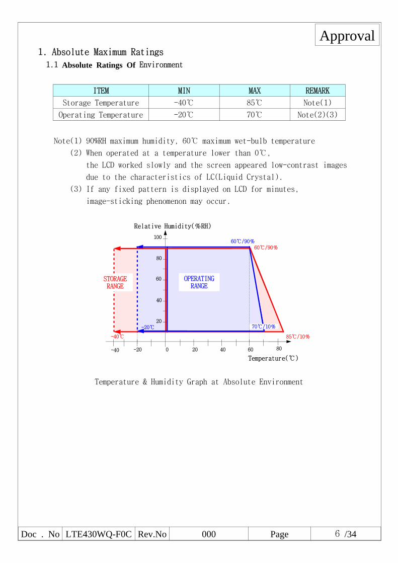
Approval1. Absolute Maximum Ratings
1.1 Absolute Ratings Of Environment
ITEM MIN MAX REMARK
Storage Temperature -40 85 Note(1)
Operating Temperature -20 70 Note(2)(3)
Note(1) 90%RH maximum humidity, 60 maximum wet-bulb temperature
(2) When operated at a temperature lower than 0,
the LCD worked slowly and the screen appeared low-contrast images
due to the characteristics of LC(Liquid Crystal).
(3) If any fixed pattern is displayed on LCD for minutes,
image-sticking phenomenon may occur.
Temperature & Humidity Graph at Absolute Environment
-40
-20
60/90%
85/10%
Temperature()
Relative Humidity(%RH)
0 20 40 60-20
20
40
60
80
100
OPERATINGRANGE
STORAGERANGE
60/90%
70/10%
80-40

Doc . No LTE430WQ-F0C Rev.No 000 Page 7 /34
Approval1.2 Electrical Absolute Ratings(1) TFT-LCD Module
(Ta = 25 ± 2°C, VSS=GND=0)
Item Symbol Min. Max. Unit Note
Digital power supply VDD -0.3 4.6 V -
(2) Back-Light Unit(Ta = 25 ± 2°C)
Item Symbol Min. Max. Unit. Note
Current IB - 25 mA (1)
Note (1) Permanent damage to the device may occur if maximum values are exceeded orreverse voltage is loaded.Functional operation should be restricted to the conditions described under normaloperating conditions.
Doc . No LTE430WQ-F0C Rev.No 000 Page 8 /34
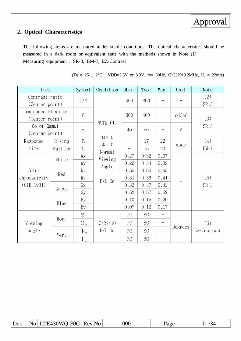
Approval2. Optical Characteristics
The following items are measured under stable conditions. The optical characteristics should bemeasured in a dark room or equivalent state with the methods shown in Note (1).Measuring equipment : SR-3, BM-7, EZ-Contrast
(Ta = 25 ± 2°C, VDD=2.5V or 3.3V, fv= 60Hz, fDCLK=9.2MHz, IL = 22mA)
Item Symbol Condition Min. Typ. Max. Unit Note
Contrast ratio
(Center point)C/R
NOTE (1)
θ= 0
Ф= 0
Normal
Viewing
Angle
B/L On
400 800 - -(2)
SR-3
Luminance of white
(Center point)YL 300 400 - cd/
(3)
SR-3Color Gamut
(Center point)- 40 50 - %
Response
time
Rising TR - 17 22msec
(4)
BM-7Falling TF - 15 20
Color
chromaticity
(CIE 1931)
WhiteWx 0.27 0.32 0.37
-(5)
SR-3
Wy 0.29 0.34 0.39
RedRx 0.55 0.60 0.65
Ry 0.31 0.36 0.41
GreenGx 0.32 0.37 0.42
Gy 0.52 0.57 0.62
BlueBx 0.10 0.15 0.20
By 0.07 0.12 0.17
Viewing
angle
Hor.θL
C/R≥10
B/L On
70 80 -
Degrees(6)
Ez-Contrast
θR 70 80 -
Ver.ФH 70 80 -
ФL 70 80 -

Doc . No LTE430WQ-F0C Rev.No 000 Page 9 /34
ApprovalNote (1) Test Equipment Setup
After stabilizing and leaving the panel alone at a given temperature for 30 min , themeasurement should be executed. Measurement should be executed in a stable, windless,and dark room. 30 min after lighting the back-light. This should be measured in the centerof screen.
Environment condition : Ta = 25 ± 2 °C
Back-Light On condition
The center of the screen
Photodetector
Photodetector Field
BM-5A 1°BM-7 1°PR-650 1°
LCD Panel
TFT - LCD Module
BM-5A : 40BM-7 : 50PR-650: 50
FieldSR-3
SR-3 : 50cm

Doc . No LTE430WQ-F0C Rev.No 000 Page 10/34
Approval
Note (2) Definition of Contrast Ratio (C/R) : Ratio of gray max (Gmax) & gray min (Gmin) atthe center point
C RGG
=m axm in
* Gmax : Luminance with all pixels white
* Gmin : Luminance with all pixels black
Note (3) Definition of Luminance of White (YL) : Luminance of white at the center pointDefinition of Brightness Uniformity (Buni)
100)maxmin( ×=
BBBuni
where, Bmax = Maximum BrightnessBmin = Minimum Brightness
T h e s p o t l o c a t i o n s f o r l u m i n a n c e m e a s u r e m e n t
9 7
5
3 1
H / 6 H / 3 H / 3 H / 6
H
V
V / 6
V / 3
V / 3
V / 62
46
8
Note (4) Definition of Response time : Sum of Tr ,Tf
Doc . No LTE430WQ-F0C Rev.No 000 Page 11/34
Approval
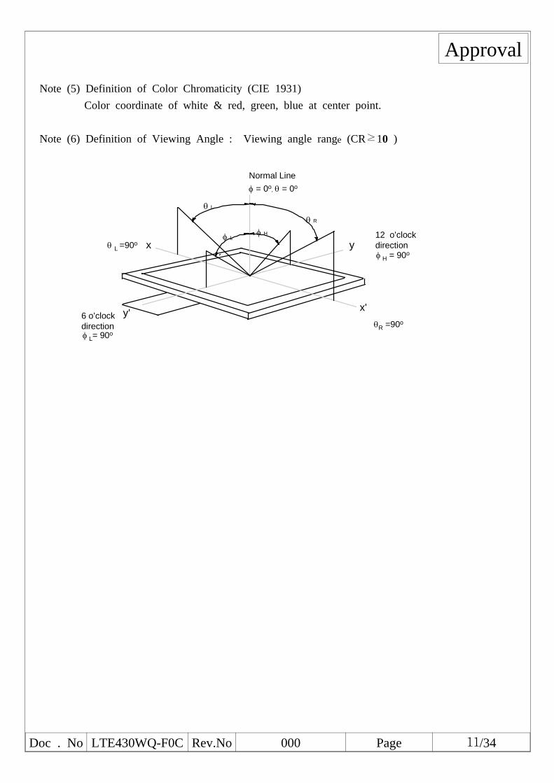
Note (5) Definition of Color Chromaticity (CIE 1931)Color coordinate of white & red, green, blue at center point.
Note (6) Definition of Viewing Angle : Viewing angle range (CR≥10 )
6 o’clockdirection
Normal Line
θ Lθ R
φ Hφ L 12 o’clockdirection
θR =90o
θ L =90o
φ = 0o,
x
x'y'
y
θ = 0o
φ H = 90o
φ L= 90o

Doc . No LTE430WQ-F0C Rev.No 000 Page 12/34
Approval3. Electrical Characteristics
3.1 TFT-LCD ModuleTa = 25 ± 2°C
ITEM Symbol Min. Typ. Max. Unit Note
Digital power supply VDD2.25 2.5 2.9 V (1)
2.9 3.3 3.5 V (2)
Input "High" level voltage VIH 0.7*VDD - VDD V
Input "Low" level voltage VIL 0 - 0.3*VDD V
Vsync Frequency fv - 60 70 Hz
Hsync Frequency fH - 17.28 - kHz
Main Frequency fDCLK - 9.2 15.0 MHZ
Power
Dissipation
White-
- 100 120 mW(3),(4)
Black - 85 105 mW
Note (1). PWRSEL = LowNote (2). PWRSEL = High
※ Refer to the "6. Input Terminal Pin Assignment"
Note (3). fv=60Hz, fDCLK=9.2MHZ, VDD=2.5V or 3.3VNote (4). Power Dissipation check pattern
a) White Pattern b) Black Pattern
Doc . No LTE430WQ-F0C Rev.No 000 Page 13/34
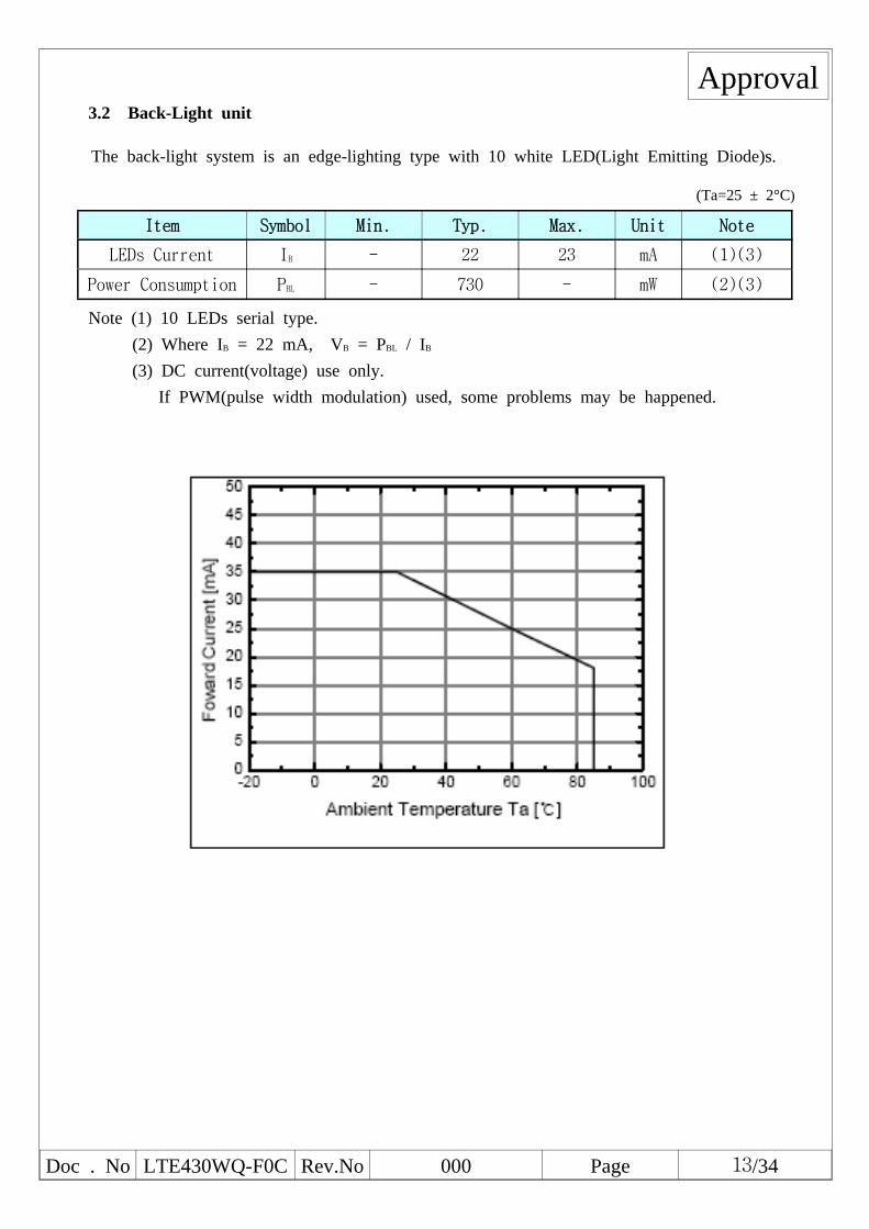
Approval3.2 Back-Light unit
The back-light system is an edge-lighting type with 10 white LED(Light Emitting Diode)s.
(Ta=25 ± 2°C)
Item Symbol Min. Typ. Max. Unit Note
LEDs Current IB - 22 23 mA (1)(3)
Power Consumption PBL - 730 - mW (2)(3)
Note (1) 10 LEDs serial type.(2) Where IB = 22 mA, VB = PBL / IB
(3) DC current(voltage) use only.If PWM(pulse width modulation) used, some problems may be happened.
Doc . No LTE430WQ-F0C Rev.No 000 Page 14/34
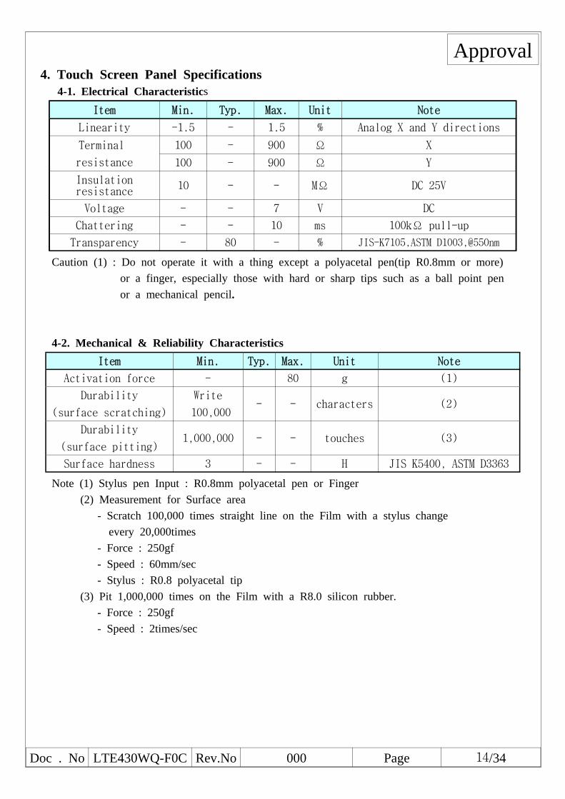
Approval4. Touch Screen Panel Specifications
4-1. Electrical Characteristics
Item Min. Typ. Max. Unit Note
Linearity -1.5 - 1.5 % Analog X and Y directions
Terminal
resistance
100 - 900 Ω X
100 - 900 Ω Y
Insulationresistance 10 - - MΩ DC 25V
Voltage - - 7 V DC
Chattering - - 10 ms 100kΩ pull-up
Transparency - 80 - % JIS-K7105,ASTM D1003,@550nm
Caution (1) : Do not operate it with a thing except a polyacetal pen(tip R0.8mm or more)or a finger, especially those with hard or sharp tips such as a ball point penor a mechanical pencil.
4-2. Mechanical & Reliability CharacteristicsItem Min. Typ. Max. Unit Note
Activation force - 80 g (1)
Durability
(surface scratching)
Write
100,000- - characters (2)
Durability
(surface pitting)1,000,000 - - touches (3)
Surface hardness 3 - - H JIS K5400, ASTM D3363
Note (1) Stylus pen Input : R0.8mm polyacetal pen or Finger(2) Measurement for Surface area
- Scratch 100,000 times straight line on the Film with a stylus changeevery 20,000times
- Force : 250gf- Speed : 60mm/sec- Stylus : R0.8 polyacetal tip
(3) Pit 1,000,000 times on the Film with a R8.0 silicon rubber.- Force : 250gf- Speed : 2times/sec
Doc . No LTE430WQ-F0C Rev.No 000 Page 15/34
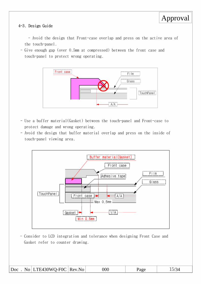
Approval4-3. Design Guide
- Avoid the design that Front-case overlap and press on the active area of
the touch-panel.
- Give enough gap (over 0.5mm at compressed) between the front case and
touch-panel to protect wrong operating.
- Use a buffer material(Gasket) between the touch-panel and Front-case to
protect damage and wrong operating.
- Avoid the design that buffer material overlap and press on the inside of
touch-panel viewing area.
- Consider to LCD integration and tolerance when designing Front Case and
Gasket refer to counter drawing.

TSP Design Guide
Doc . No LTE430WQ-F0C Rev.No 000 Page 17/34
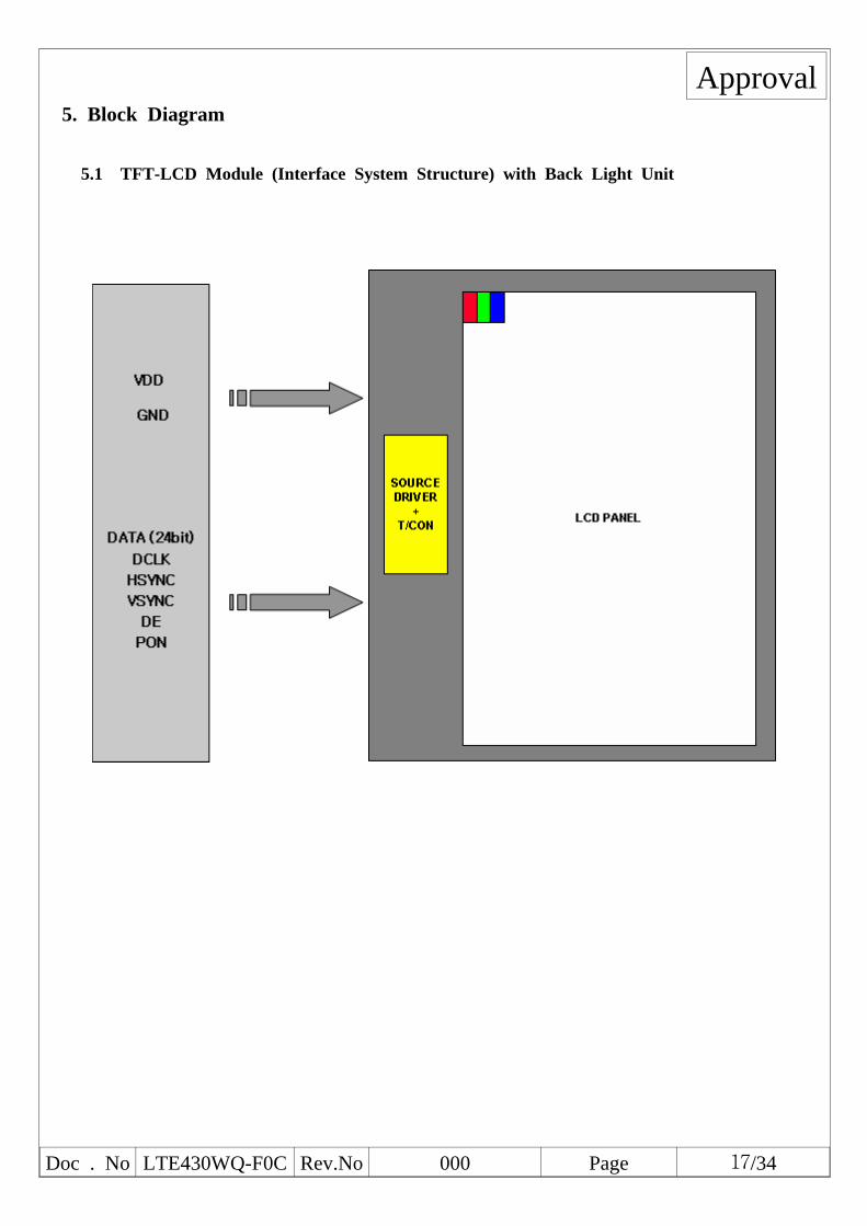
Approval5. Block Diagram
5.1 TFT-LCD Module (Interface System Structure) with Back Light Unit

Doc . No LTE430WQ-F0C Rev.No 000 Page 18/34
Approval5.2 Touch Screen Panel
Y2 X2 Y1 X1
X : Upper electrodeY : Lower electrode
Top View
Y2 X2 Y1 X1
X : Upper electrodeY : Lower electrode
Top View
5.3 Back-light Unit (Connector : 2 pin FPC Solder type)
VLED_Anode
VLED_Cathode

Doc . No LTE430WQ-F0C Rev.No 000 Page 19/34
Approval6. Input Terminal Pin Assignment
6.1 Input Signal & Power (Connector type : 45Pin / 0.5mm pitch / Top contact)- Hirose : FH12 series
Pin# Symbol Function Remark Pin# Symbol Function Remark1 VSS Ground 26 B5 Blue Data
2 VSS Ground 27 B6 Blue Data
3 VDDPower Supply
(2.5or3.3V)28 B7 Blue Data (MSB)
4 VDDPower Supply
(2.5or3.3V)29 VSS Ground
5 R0 Red Data (LSB) 30 PCLK Pixel Clock
6 R1 Red Data 31 PON Display on/off
7 R2 Red Data 32 HSYNC Horizontal Sync Signal
8 R3 Red Data 33 VSYNC Vertical Sync Signal
9 R4 Red Data 34 DE Data Enable
10 R5 Red Data 35 PWRSEL VDD power selectHigh:3.3V
Low:2.5V
11 R6 Red Data 36 VSS Ground
12 R7 Red Data (MSB) 37 Y2 Y_Up
13 G0 Green Data (LSB) 38 X2 X_Left
14 G1 Green Data 39 Y1 Y_Bottom
15 G2 Green Data 40 X1 X_Right
16 G3 Green Data 41 VSS Ground
17 G4 Green Data 42 VLED1- LED 1 Cathode
18 G5 Green Data 43 VLED1+ LED 1 Anode
19 G6 Green Data 44 NC Non Connect
20 G7 Green Data (MSB) 45 NC Non Connect
21 B0 Blue Data (LSB)
22 B1 Blue Data
23 B2 Blue Data
24 B3 Blue Data
25 B4 Blue Data
6.2 Touch Screen Panel (Connector : 4Pin FPC Solder type)
Pin No. Symbol I/O Function
1 X1 Right Right electrode - differential analog
2 Y1 Bottom Bottom electrode - differential analog
3 X2 Left Left electrode - differential analog
4 Y2 Top Top electrode - differential analog
Doc . No LTE430WQ-F0C Rev.No 000 Page 20/34
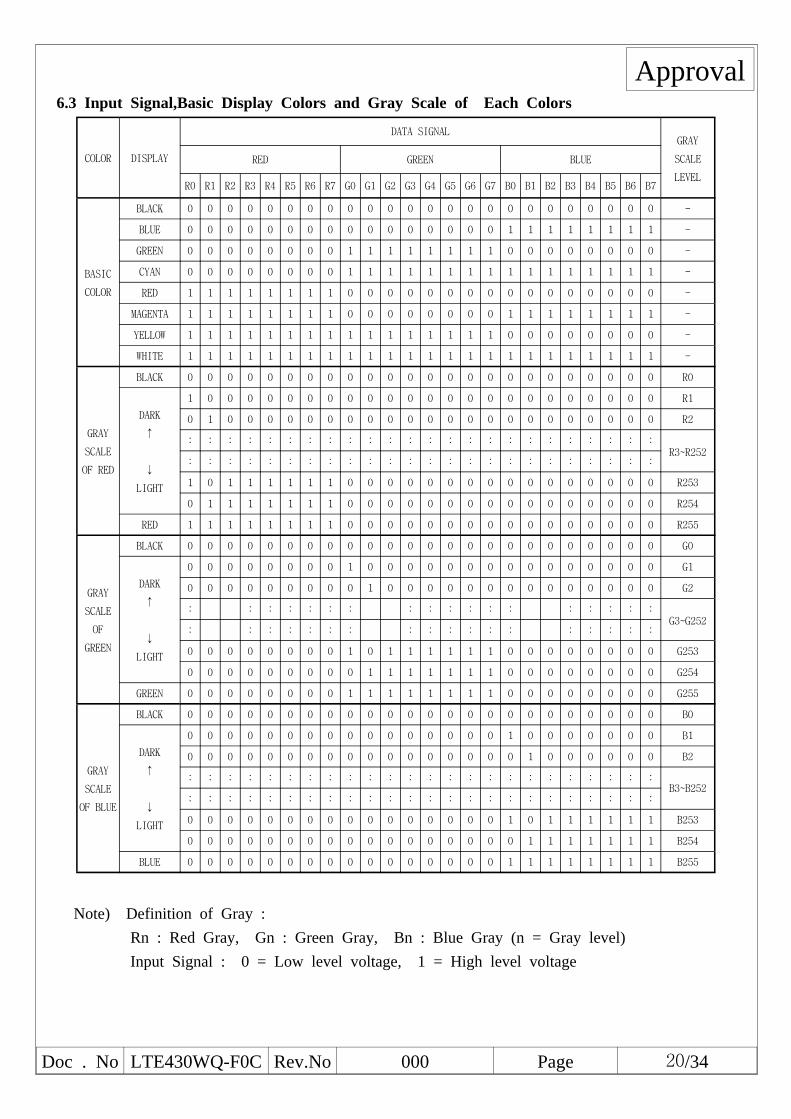
Approval6.3 Input Signal,Basic Display Colors and Gray Scale of Each Colors
COLOR DISPLAY
DATA SIGNALGRAY
SCALE
LEVEL
RED GREEN BLUE
R0 R1 R2 R3 R4 R5 R6 R7 G0 G1 G2 G3 G4 G5 G6 G7 B0 B1 B2 B3 B4 B5 B6 B7
BASIC
COLOR
BLACK 0 0 0 0 0 0 0 0 0 0 0 0 0 0 0 0 0 0 0 0 0 0 0 0 -
BLUE 0 0 0 0 0 0 0 0 0 0 0 0 0 0 0 0 1 1 1 1 1 1 1 1 -
GREEN 0 0 0 0 0 0 0 0 1 1 1 1 1 1 1 1 0 0 0 0 0 0 0 0 -
CYAN 0 0 0 0 0 0 0 0 1 1 1 1 1 1 1 1 1 1 1 1 1 1 1 1 -
RED 1 1 1 1 1 1 1 1 0 0 0 0 0 0 0 0 0 0 0 0 0 0 0 0 -
MAGENTA 1 1 1 1 1 1 1 1 0 0 0 0 0 0 0 0 1 1 1 1 1 1 1 1 -
YELLOW 1 1 1 1 1 1 1 1 1 1 1 1 1 1 1 1 0 0 0 0 0 0 0 0 -
WHITE 1 1 1 1 1 1 1 1 1 1 1 1 1 1 1 1 1 1 1 1 1 1 1 1 -
GRAY
SCALE
OF RED
BLACK 0 0 0 0 0 0 0 0 0 0 0 0 0 0 0 0 0 0 0 0 0 0 0 0 R0
DARK
↑
↓
LIGHT
1 0 0 0 0 0 0 0 0 0 0 0 0 0 0 0 0 0 0 0 0 0 0 0 R1
0 1 0 0 0 0 0 0 0 0 0 0 0 0 0 0 0 0 0 0 0 0 0 0 R2
: : : : : : : : : : : : : : : : : : : : : : : :R3~R252
: : : : : : : : : : : : : : : : : : : : : : : :
1 0 1 1 1 1 1 1 0 0 0 0 0 0 0 0 0 0 0 0 0 0 0 0 R253
0 1 1 1 1 1 1 1 0 0 0 0 0 0 0 0 0 0 0 0 0 0 0 0 R254
RED 1 1 1 1 1 1 1 1 0 0 0 0 0 0 0 0 0 0 0 0 0 0 0 0 R255
GRAY
SCALE
OF
GREEN
BLACK 0 0 0 0 0 0 0 0 0 0 0 0 0 0 0 0 0 0 0 0 0 0 0 0 G0
DARK
↑
↓
LIGHT
0 0 0 0 0 0 0 0 1 0 0 0 0 0 0 0 0 0 0 0 0 0 0 0 G1
0 0 0 0 0 0 0 0 0 1 0 0 0 0 0 0 0 0 0 0 0 0 0 0 G2
: : : : : : : : : : : : : : : : : :G3~G252
: : : : : : : : : : : : : : : : : :
0 0 0 0 0 0 0 0 1 0 1 1 1 1 1 1 0 0 0 0 0 0 0 0 G253
0 0 0 0 0 0 0 0 0 1 1 1 1 1 1 1 0 0 0 0 0 0 0 0 G254
GREEN 0 0 0 0 0 0 0 0 1 1 1 1 1 1 1 1 0 0 0 0 0 0 0 0 G255
GRAY
SCALE
OF BLUE
BLACK 0 0 0 0 0 0 0 0 0 0 0 0 0 0 0 0 0 0 0 0 0 0 0 0 B0
DARK
↑
↓
LIGHT
0 0 0 0 0 0 0 0 0 0 0 0 0 0 0 0 1 0 0 0 0 0 0 0 B1
0 0 0 0 0 0 0 0 0 0 0 0 0 0 0 0 0 1 0 0 0 0 0 0 B2
: : : : : : : : : : : : : : : : : : : : : : : :B3~B252
: : : : : : : : : : : : : : : : : : : : : : : :
0 0 0 0 0 0 0 0 0 0 0 0 0 0 0 0 1 0 1 1 1 1 1 1 B253
0 0 0 0 0 0 0 0 0 0 0 0 0 0 0 0 0 1 1 1 1 1 1 1 B254
BLUE 0 0 0 0 0 0 0 0 0 0 0 0 0 0 0 0 1 1 1 1 1 1 1 1 B255
Note) Definition of Gray :Rn : Red Gray, Gn : Green Gray, Bn : Blue Gray (n = Gray level)Input Signal : 0 = Low level voltage, 1 = High level voltage

Doc . No LTE430WQ-F0C Rev.No 000 Page 21/34
Approval6.4 PIXEL FORMAT
LTE430WQ-F0C PANEL
Doc . No LTE430WQ-F0C Rev.No 000 Page 22/34
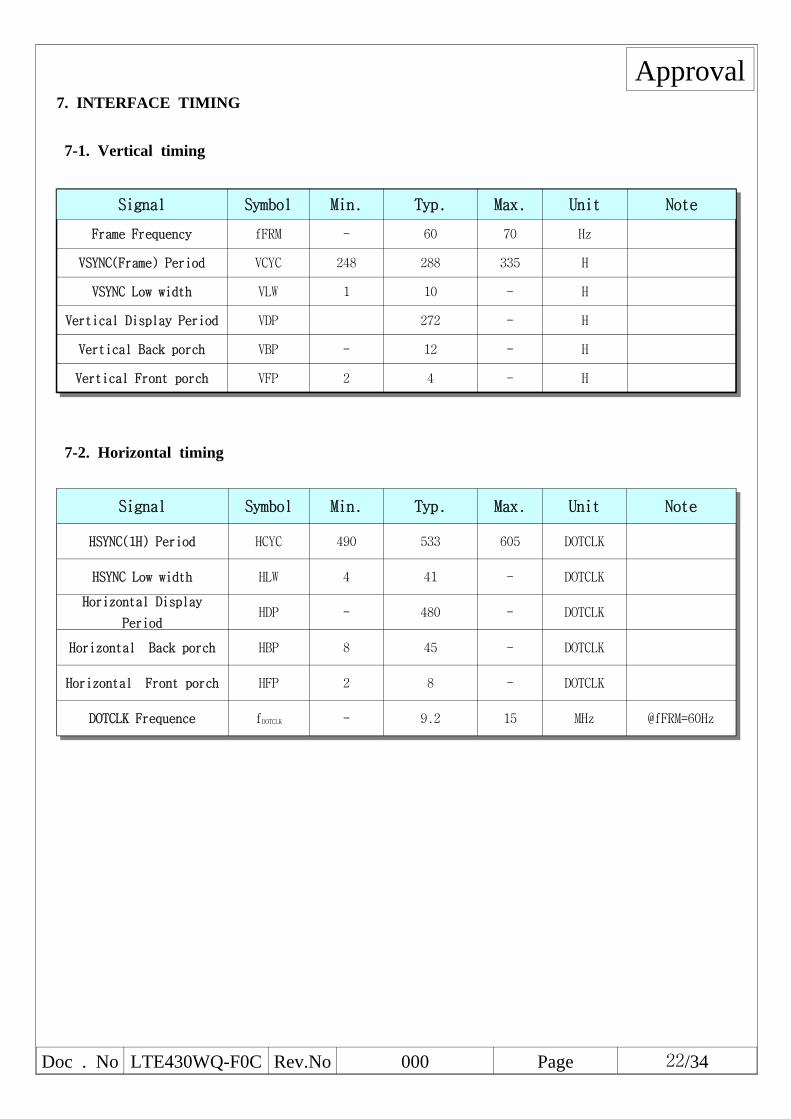
Approval7. INTERFACE TIMING
7-1. Vertical timing
Signal Symbol Min. Typ. Max. Unit Note
Frame Frequency fFRM - 60 70 Hz
VSYNC(Frame) Period VCYC 248 288 335 H
VSYNC Low width VLW 1 10 - H
Vertical Display Period VDP 272 - H
Vertical Back porch VBP - 12 - H
Vertical Front porch VFP 2 4 - H
7-2. Horizontal timing
Signal Symbol Min. Typ. Max. Unit Note
HSYNC(1H) Period HCYC 490 533 605 DOTCLK
HSYNC Low width HLW 4 41 - DOTCLK
Horizontal Display
PeriodHDP - 480 - DOTCLK
Horizontal Back porch HBP 8 45 - DOTCLK
Horizontal Front porch HFP 2 8 - DOTCLK
DOTCLK Frequence fDOTCLK - 9.2 15 MHz @fFRM=60Hz

Doc . No LTE430WQ-F0C Rev.No 000 Page 23/34
Approval

Doc . No LTE430WQ-F0C Rev.No 000 Page 24/34
Approval7-3. AC characteristics
※ Operating at VDD=2.25~2.9V , Ta = -40~+85
Parameter Symbol Min. Typ. Max. Unit
VSYNC,HSYNC setup time tSYNCS 10 - -
ns
ENABLE (DE) setup time tENS 10 - -
ENABLE (DE) hold time tENH 10 - -
DOTCLK "Low" level pulse width PWDL 25 - -
DOTCLK "High" level pulse width PWDH 25 - -
DOTCLK cycle time tCYCD 66.7 - -
Data setup time tPDS 10 - -
Data hold time tPDH 10 - -
DOTCLK,VSYNC,HSYNC
clock rise/fall time
trgbr
trgbf
- - 5
※ Operating at VDD=2.9~3.5V , Ta = -40~+85
Parameter Symbol Min. Typ. Max. Unit
VSYNC,HSYNC setup time tSYNCS 10 - -
ns
ENABLE (DE) setup time tENS 10 - -
ENABLE (DE) hold time tENH 10 - -
DOTCLK "Low" level pulse width PWDL 25 - -
DOTCLK "High" level pulse width PWDH 25 - -
DOTCLK cycle time tCYCD 66.7 - -
Data setup time tPDS 10 - -
Data hold time tPDH 10 - -
DOTCLK,VSYNC,HSYNC
clock rise/fall time
trgbr
trgbf
- - 5

Doc . No LTE430WQ-F0C Rev.No 000 Page 25/34
Approval

Doc . No LTE430WQ-F0C Rev.No 000 Page 26/34
Approval7-4. PON timing characteristics.
※ Operating at VDD=2.25~3.5V , Ta = -40~+85
Item Symbol Min. Typ. Max. unit
PON setup
(SYNC mode)tPONSV 10 - - DOTCLK

Doc . No LTE430WQ-F0C Rev.No 000 Page 27/34
Approval8. Power On/Off Sequence
- To prevent a latch-up or DC operation of the LCD module, the power on/off
sequence should be as the diagram below.
Symbol Specification Note
T1 0 ms < T1 < T2
T2 10 ms < T2 (1)
T3 10 frames < T3
T4 10 ms < T4 < T5
T5 (5 frames + T4) < T5 (1)
T6 10 frames < T6
Note(1) Refer to "7-4. PON timing characteristics."
Power Supplyfor LED unit
Power SupplyVDD
InterfaceSignal
Display On/OffSignal
Doc . No LTE430WQ-F0C Rev.No 000 Page 29/34
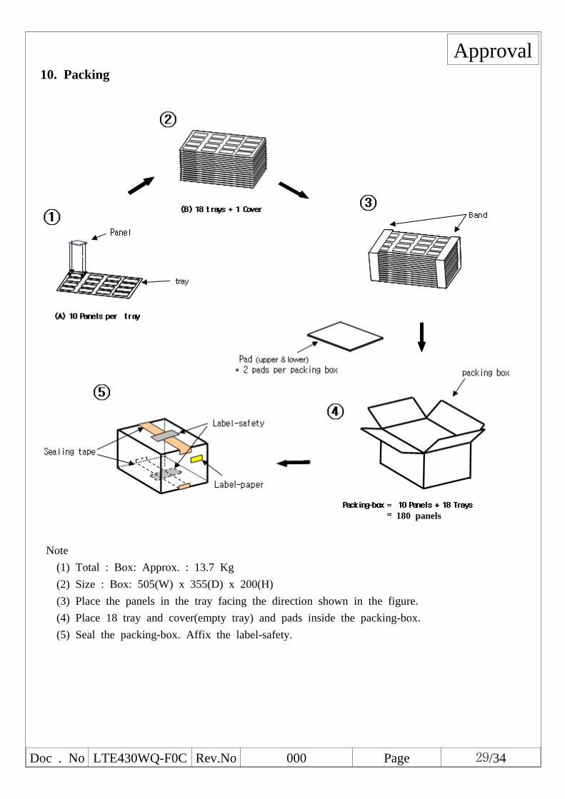
Approval10. Packing
Note(1) Total : Box: Approx. : 13.7 Kg(2) Size : Box: 505(W) x 355(D) x 200(H)(3) Place the panels in the tray facing the direction shown in the figure.(4) Place 18 tray and cover(empty tray) and pads inside the packing-box.(5) Seal the packing-box. Affix the label-safety.
180 panels
Doc . No LTE430WQ-F0C Rev.No 000 Page 30/34
Approval
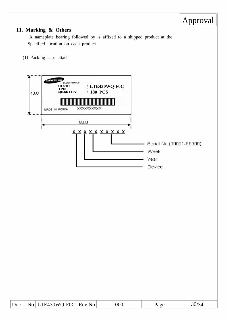
LTE430WQ-F0C
11. Marking & OthersA nameplate bearing followed by is affixed to a shipped product at the
Specified location on each product.
(1) Packing case attach
LTE430WQ-F0C180 PCS
Doc . No LTE430WQ-F0C Rev.No 000 Page 31/34
Approval12. General Precautions
12.1 Handling
(a) When the module is assembled, it should be attached to the system firmly. Be carefulnot to twist and bend the module.
(b) Refrain from strong mechanical shock and / or any force to the module. In addition todamage, this may cause improper operation or damage to the module and back-lightunit.
(c) Note that polarizers are very fragile and could be easily damaged. Do not press orscratch the surface harder than a HB pencil lead.
(d) Wipe off water droplets or oil immediately. If you leave the droplets for a long time,Staining and discoloration may occur.
(e) If the surface of the polarizer is dirty, clean it using some absorbent cotton or softcloth.
(f) The desirable cleaners are water, IPA(Isopropyl Alcohol) or Hexane. Do not useKetone type materials(ex. Acetone), Ethyl alcohol, Toluene, Ethyl acid or Methylchloride. It might permanent damage to the polarizer due to chemical reaction.
(g) If the liquid crystal material leaks from the panel, it should be kept away from theeyes or mouth. In case of contact with hands, legs or clothes, it must be washed awaythoroughly with soap.
(h) Protect the module from static , it may cause damage to the Integrated Gate Circuit.
(i) Use finger-stalls with soft gloves in order to keep display clean during the incominginspection and assembly process.
(j) Do not disassemble the module.
(k) Do not adjust the variable resistor which is located on the back side.
(l) Protection film for polarizer on the module shall be slowly peeled off just before useso that the electrostatic charge can be minimized.
(m) Pins of I/F connector shall not be touched directly with bare hands

Doc . No LTE430WQ-F0C Rev.No 000 Page 32/34
Approval12.2 Storage
(a) Do not leave the panel in high temperature, and high humidity for a long time. It ishighly recommended to store the module with temperature from 0 to 35°C and relativehumidity of less than 70%.
(b) Do not store the TFT-LCD module in direct sunlight.
(c) The module shall be stored in a dark place. It is prohibited to apply sunlight orfluorescent light during the store.
12.3 Operation
(a) Do not connect, disconnect the module in the "Power On" condition.
(b) Power supply should always be turned on/off by the "Power on/off sequence"
(c) Module has high frequency circuits. Sufficient suppression to theelectromagnetic interference shall be done by system manufacturers.Grounding and shielding methods may be important to minimize theinterference.
12.4 Others
(a) The Liquid crystal is deteriorated by ultraviolet, do not leave it in direct sunlight andstrong ultraviolet ray for many hours.
(b) Avoid condensation of water. It may result in improper operation or disconnection ofelectrode.
(c) Do not exceed the absolute maximum rating value. ( the supply voltage variation, inputvoltage variation, variation in part contents and environmental temperature, and so on)Otherwise the panel may be damaged.
(d) If the panel displays the same pattern continuously for a long period of time, it can bethe situation when the image "Sticks" to the screen.
(e) This panel has its circuitry FPC on the bottom side and should be handled carefully inorder not to be stressed.
(f) Avoid shortness between LED soldering pad and TSP soldering pad.
Doc . No LTE430WQ-F0C Rev.No 000 Page 33/34
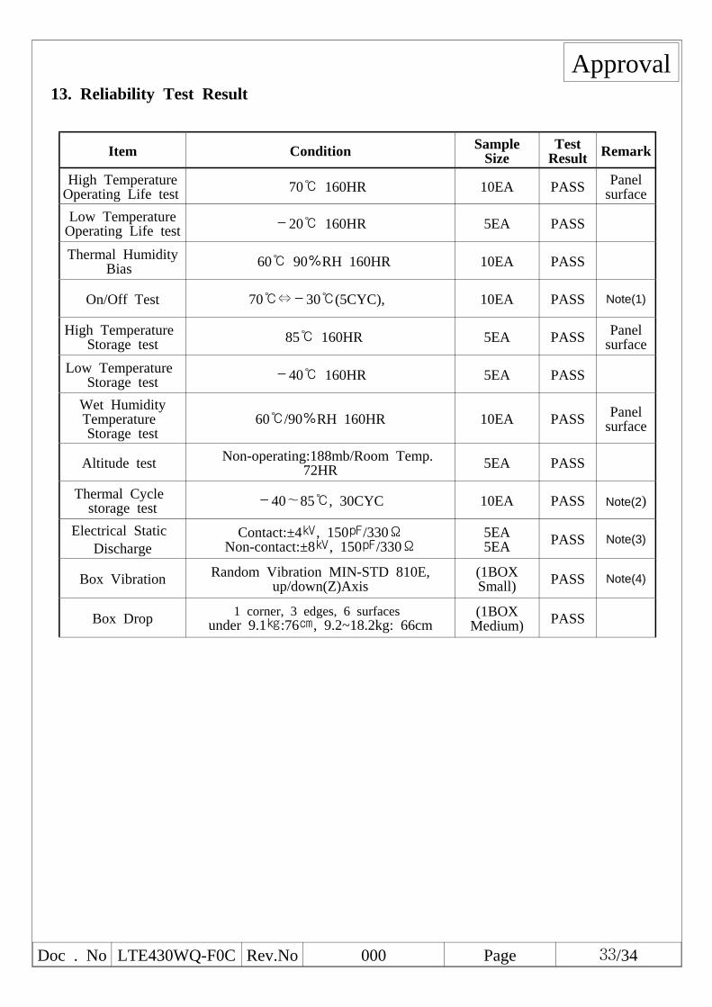
Approval13. Reliability Test Result
Item Condition SampleSize
TestResult Remark
High TemperatureOperating Life test 70 160HR 10EA PASS Panel
surfaceLow Temperature
Operating Life test -20 160HR 5EA PASS
Thermal HumidityBias 60 90%RH 160HR 10EA PASS
On/Off Test 70⇔-30(5CYC), 10EA PASS Note(1)
High TemperatureStorage test 85 160HR 5EA PASS Panel
surfaceLow Temperature
Storage test -40 160HR 5EA PASS
Wet HumidityTemperatureStorage test
60/90%RH 160HR 10EA PASS Panelsurface
Altitude test Non-operating:188mb/Room Temp.72HR 5EA PASS
Thermal Cyclestorage test -40∼85, 30CYC 10EA PASS Note(2)
Electrical StaticDischarge
Contact:±4, 150/330ΩNon-contact:±8, 150/330Ω
5EA5EA PASS Note(3)
Box Vibration Random Vibration MIN-STD 810E,up/down(Z)Axis
(1BOXSmall) PASS Note(4)
Box Drop 1 corner, 3 edges, 6 surfacesunder 9.1:76, 9.2~18.2kg: 66cm
(1BOXMedium) PASS
Doc . No LTE430WQ-F0C Rev.No 000 Page 34/34
Approval
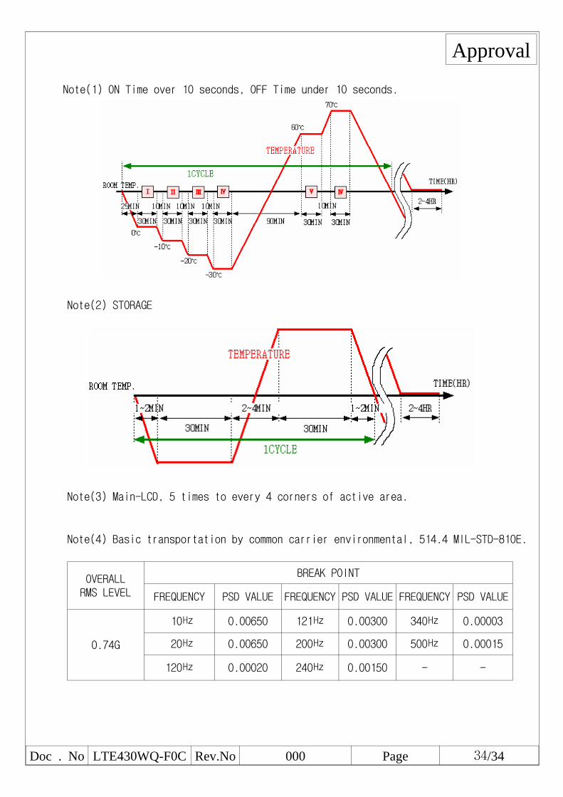
Note(1) ON Time over 10 seconds, OFF Time under 10 seconds.
Note(2) STORAGE
Note(3) Main-LCD, 5 times to every 4 corners of active area.
Note(4) Basic transportation by common carrier environmental, 514.4 MIL-STD-810E.
OVERALLRMS LEVEL
BREAK POINT
FREQUENCY PSD VALUE FREQUENCY PSD VALUE FREQUENCY PSD VALUE
0.74G
10 0.00650 121 0.00300 340 0.00003
20 0.00650 200 0.00300 500 0.00015
120 0.00020 240 0.00150 - -