two-dimensional phosphorus carbide: … phosphorus carbide: competition between sp2 and sp3 bonding...
TRANSCRIPT
Two-Dimensional Phosphorus Carbide: Competition between sp2
and sp3 BondingJie Guan,† Dan Liu,† Zhen Zhu,†,‡ and David Tomanek*,†
†Physics and Astronomy Department, Michigan State University, East Lansing, Michigan 48824, United States‡Materials Department, University of California, Santa Barbara, California 93106, United States
*S Supporting Information
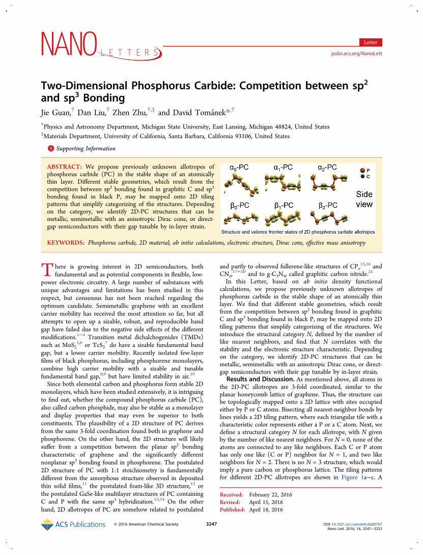
ABSTRACT: We propose previously unknown allotropes ofphosphorus carbide (PC) in the stable shape of an atomicallythin layer. Different stable geometries, which result from thecompetition between sp2 bonding found in graphitic C and sp3
bonding found in black P, may be mapped onto 2D tilingpatterns that simplify categorizing of the structures. Dependingon the category, we identify 2D-PC structures that can bemetallic, semimetallic with an anisotropic Dirac cone, or direct-gap semiconductors with their gap tunable by in-layer strain.
KEYWORDS: Phosphorus carbide, 2D material, ab initio calculations, electronic structure, Dirac cone, effective mass anisotropy
There is growing interest in 2D semiconductors, bothfundamental and as potential components in flexible, low-
power electronic circuitry. A large number of substances withunique advantages and limitations has been studied in thisrespect, but consensus has not been reached regarding theoptimum candidate. Semimetallic graphene with an excellentcarrier mobility has received the most attention so far, but allattempts to open up a sizable, robust, and reproducible bandgap have failed due to the negative side effects of the differentmodifications.1−4 Transition metal dichalchogenides (TMDs)such as MoS2
5,6 or TcS27 do have a sizable fundamental band
gap, but a lower carrier mobility. Recently isolated few-layerfilms of black phosphorus, including phosphorene monolayers,combine high carrier mobility with a sizable and tunablefundamental band gap,8,9 but have limited stability in air.10
Since both elemental carbon and phosphorus form stable 2Dmonolayers, which have been studied extensively, it is intriguingto find out, whether the compound phosphorus carbide (PC),also called carbon phosphide, may also be stable as a monolayerand display properties that may even be superior to bothconstituents. The plausibility of a 2D structure of PC derivesfrom the same 3-fold coordination found both in graphene andphosphorene. On the other hand, the 2D structure will likelysuffer from a competition between the planar sp2 bondingcharacteristic of graphene and the significantly differentnonplanar sp3 bonding found in phosphorene. The postulated2D structure of PC with 1:1 stoichiometry is fundamentallydifferent from the amorphous structure observed in depositedthin solid films,11 the postulated foam-like 3D structure,12 orthe postulated GaSe-like multilayer structures of PC containingC and P with the same sp3 hybridization.13,14 On the otherhand, 2D allotropes of PC are somehow related to postulated
and partly to observed fullerene-like structures of CPx15,16 and
CNx,17−20 and to g-C3N4, called graphitic carbon nitride.21
In this Letter, based on ab initio density functionalcalculations, we propose previously unknown allotropes ofphosphorus carbide in the stable shape of an atomically thinlayer. We find that different stable geometries, which resultfrom the competition between sp2 bonding found in graphiticC and sp3 bonding found in black P, may be mapped onto 2Dtiling patterns that simplify categorizing of the structures. Weintroduce the structural category N, defined by the number oflike nearest neighbors, and find that N correlates with thestability and the electronic structure characteristic. Dependingon the category, we identify 2D-PC structures that can bemetallic, semimetallic with an anisotropic Dirac cone, or direct-gap semiconductors with their gap tunable by in-layer strain.
Results and Discussion. As mentioned above, all atoms inthe 2D-PC allotropes are 3-fold coordinated, similar to theplanar honeycomb lattice of graphene. Thus, the structure canbe topologically mapped onto a 2D lattice with sites occupiedeither by P or C atoms. Bisecting all nearest-neighbor bonds bylines yields a 2D tiling pattern, where each triangular tile with acharacteristic color represents either a P or a C atom. Next, wedefine a structural category N for each allotrope, with N givenby the number of like nearest neighbors. For N = 0, none of theatoms are connected to any like neighbors. Each C or P atomhas only one like (C or P) neighbor for N = 1, and two likeneighbors for N = 2. There is no N = 3 structure, which wouldimply a pure carbon or phosphorus lattice. The tiling patternsfor different 2D-PC allotropes are shown in Figure 1a−c. A
Received: February 22, 2016Revised: April 15, 2016Published: April 18, 2016
Letter
pubs.acs.org/NanoLett
© 2016 American Chemical Society 3247 DOI: 10.1021/acs.nanolett.6b00767Nano Lett. 2016, 16, 3247−3252

similar categorization scheme has been used previously todistinguish between different allotropes of 2D phosphorene,22
where N was the number of “like” neighbors either in the upperor lower position within the lattice.Whereas the tiling pattern is useful for simple categorization,
it does not provide information about the nontrivial optimumstructure shown in Figure 1d−i, which results from acompetition between the favored planar sp2 hybridization ofC and nonplanar sp3 hybridization of P. The side view ofstructures displayed in Figure 1 best illustrates that allotropeswith the same value of N may be structurally different. Inanalogy to the different postulated phosphorene allotropes,23,24
we distinguish αN, which display a black-P-like armchairstructure in side view, from βN phases of PC, which display ablue-P-like (or gray-As-like) zigzag structure in side view, anduse the index N to identify the structural category.We start our discussion with N = 1 allotropes α1-PC and β1-
PC, shown in the middle column in Figure 1. According to thedefinition of N, each atom has one neighbor of the same speciesand two of different species, forming isolated P−P and C−Cdimers, as seen in the tiling pattern and the atomic structures.As seen in Figure 2a, the chemical octet rule25 is satisfied bothon C sites in the graphitic sp2 configuration and on P sites,containing a lone electron pair, in sp3 configuration, indicatingstability. Both allotropes have rectangular unit cells consistingof distorted hexagons. The unit cell of α1-PC with 8 atoms islarger than that of β1-PC with four atoms.In N = 2 allotropes α2-PC and β2-PC, shown in the right
column of Figure 1, each atom has two like neighbors and oneunlike neighbor. In the side view, these allotropes look verysimilar to those of the N = 1 category. The main differencebecomes apparent in the top view. Whereas N = 1 structurescontain ethylene-like C2 units that are interconnected by P2dimers, N = 2 systems contain contiguous trans-polyacetylene-like all-carbon chains that are separated by P-chains. Due to the
difference between the locally planar sp2 bonding of C atomsand locally nonplanar sp3 bonding of P atoms, and due to thedifference between equilibrium C−C and P−P bond lengths,the hexagons found in N = 1 structures change to pentagon−heptagon pairs in the optimum N = 2 structure resemblingpentheptite or haeckelite structures related to graphitic carbon.As seen in Figure 2b, similar to N = 1 structures, the chemicaloctet rule is satisfied on both C and P sites. The lattice of α2-PCand β2-PC allotropes contains rectangular unit cells with 16atoms.In 2D PC compounds of category N = 0, shown in the left
column of Figure 1, each atom is surrounded by three unlikeneighbors. There is no bonding configuration that would satisfythe octet rules on all sites. The bonding configuration depictedin Figure 2c satisfies the octet rule only at the C sites, whereasthe configuration in Figure 2d favors only the P sites. Thebonding configuration depicted in Figure 2e containsalternating P−C chains containing P sites with lone electron
Figure 1. Possible stable structures of an atomically thin PC monolayer, represented by (a−c) tiling patterns and (d−i) by ball-and-stick models inboth top and side view. The number of like nearest neighbors defines the structural category N. There are two stable allotropes, α and β, for each N.The primitive unit cells are highlighted, and the lattice vectors are shown by red arrows. Two inequivalent P sites are distinguished by a subscript in(d).
Figure 2. Bonding configuration in (a) N = 1, (b) N = 2, and (c−e) N= 0 category 2D-PC allotropes. Green-shaded regions indicate sitesthat satisfy the octet rule discussed in the text. Bonding in β0-PC ischaracterized by panel (d) and bonding in α0-PC is described by panel(e).
Nano Letters Letter
DOI: 10.1021/acs.nanolett.6b00767Nano Lett. 2016, 16, 3247−3252
3248

pairs and C atoms in sp2 configuration, which satisfy the octetrule, and P−C chains that do not satisfy it. In whatever bondingarrangement, the bonding configuration in N = 0 structures isfrustrated. As a consequence, the α0-PC structure convertsspontaneously from an initial armchair configuration, similar toα1-PC and α2-PC, to the zigzag structure depicted in Figure 1d,with details about the structural transformation discussed in theSupporting Information. The final α0-PC structure withinequivalent P1 and P2 sites reflects the bonding configurationin Figure 2e containing P1 sites with lone electron pairs and P2sites with lone electrons. The β0-PC structure, depicted inFigure 1g, remains locally stable in the electronic configurationshown in Figure 2d.Structural characteristics and the binding energy of the
different allotropes are summarized in Table 1. Our energy
results are obtained using the DFT-PBE functional (includingspin polarization where required), which is known to overbindto some degree. We define the cohesive energy per atom,⟨Ecoh⟩, by dividing the total atomization energy by the totalnumber of atoms, irrespective of species. The energy values inthe first rows indicate that, for given N, the α and β phases arealmost equally stable, confirming that categorizing structures bythe number of like neighbors at any site makes sense in terms ofstability. Clearly, N = 2 systems are most stable, followed by N= 1 and N = 0 allotropes. In particular, the cohesive energy of N= 2 monolayers exceed the 5.14 eV/atom value of thepostulated GaSe-like PC multilayer structures13,14 by 0.06eV/atom.The lower stability of N = 0 systems has been anticipated
above, since the octet rule can not be satisfied at all sites. Wealso note that the α0 phase is slightly more stable than the β0phase of PC. The stability advantage of α0-PC derives from thelarger variational freedom within the unit cell, which allows todistinguish two different P sites (P1 and P2), as shown in Figure1d and Figure 2e. The α0-PC structure consists of P1(sp
3)−C(sp2) chains, which obey the octet rule and form stable ridges,alternating with P2−C chains, which do not obey the octet ruleand form terraces.Additional support for the plausibility of the bonding
configuration depicted in Figure 2 comes from the equilibriumbond lengths, which are listed in Table 1. With the exception of
N = 0 structures, the bond lengths depend primarily on N andare rather insensitive to the phase (α or β). For N = 1 and N =2 structures, the C−C bond lengths lie close to the 1.42 Å valuein sp2 bonded graphite (or graphene), and the P−P bondlengths are close to the 2.26−2.29 Å range found in layeredblack phosphorus (or phosphorene).As seen in Figure 2a and b, P and C atoms are connected by
a single-bond with dP−C ≈ 1.85 Å in N = 1 and N = 2 categorystructures. As suggested above, the bonding is frustrated at leastin parts of N = 0 structures. In the significantly reconstructedα0-PC system, depicted in Figure 1d, we can distinguish P1 sitesat ridges from P2 sites at terraces. The lengths of the three P−Cbonds are very similar at each of the these P sites but differsignificantly between P1 and P2. At P1 sites that satisfy the octetrule, as seen in Figure 2e, the P1−C bond length of 1.86 Å isvery similar to N = 1 and N = 2 structures. At P2 sites, which donot satisfy the octet rule, the frustrated bonds are much shorterwith dP−C = 1.71 Å. As seen in Figure 1g, there is noreconstruction in the β0-PC structure. As seen in thecorresponding Figure 2c or d, the octet rule is only satisfiedat either the P or the C sites. The P−C bonds are frustrated,and their length of 1.78 Å lies in-between the P1−C and P2−Cbond lengths in α0-PC.Results of our DFT-PBE electronic band structure
calculations for monolayers of the six proposed PC allotropesare presented in Figure 3.The electronic band structure and associated density of states
(DOS) of N = 0 systems is shown in Figure 3a and b. Ourresults in Figure 3a suggest that α0-PC is an indirect-gapsemiconductor with a band gap of ≈0.7 eV. In stark contrast,the structurally similar β0-PC allotrope is metallic according toFigure 3b. As suggested earlier, all bonds and electronicconfigurations are frustrated in β0-PC, with all C sites engagingonly three valence electrons in sp2-like bonds, leaving one loneelectron behind, and the angle at the P ridge being too large fortypical sp3 bonding. This finding, in particular the presence of anonbonding electron in the C2p⊥ orbital, is seen in the frontierstates of β0-PC that are depicted in the right panel of Figure 2b.α0-PC is quite different from β0-PC, as it contains two
inequivalent P and C sites. The P1 site at the ridge displays thefavored sp3 bonding characteristic and its lone pair orbital ispresent in the frontier state displayed in the right-hand panel ofFigure 3a. In contrast, the bonding is very different at the P2site, where the lone pair orbital does not contribute to thefrontier state. The flat bonding geometry near this site isreminiscent of sp2 bonding at the C sites. The added flexibilityprovided by a larger unit cell allows for additional stabilizationof α0-PC due to the opening of a band gap, with vague analogyto the Peierls instability.As seen in Figure 3c and d, both α1-PC and β1-PC have a
direct band gap, which we attribute to the presence of isolatedethylene-like units mentioned above. The two allotropesdisplay a very similar charge distribution in their valencefrontier states, which contain the lone pair orbitals on P sitesand reflects sp2 bonding between C sites. The main differencebetween the two structures is that the 0.4 eV wide gap in α1-PCis at the Γ point, whereas the 0.3 eV gap in β1-PC is at the Xpoint. In both structures, the band dispersion is ratheranisotropic near the top of the valence and bottom of theconduction band, which causes an anisotropy in the effectivemass. We find the effective mass of both electrons and holes tobe much smaller along x-direction than along the y-direction,which is reminiscent of the situation in black phosphorene.8,9
Table 1. Calculated Properties of Different 2D-PCAllotropesa
structure α0-PC β0-PC α1-PC β1-PC α2-PC β2-PC
⟨Ecoh⟩(eV/atom)
4.80 4.75 5.05 5.06 5.20 5.20
⟨ΔE⟩(eV/atom)
−0.40 −0.45 −0.15 −0.14 0.00 0.00
|a1| (Å) 8.41 5.12 8.73 4.76 9.84 10.59|a2| (Å) 2.94 2.95 2.95 2.95 5.11 5.11dP−P (Å) 2.36 2.36 2.29 2.29dP−C (Å) 1.86 (P1) 1.78 1.84 1.84 1.85 1.85
1.71 (P2)dC−C (Å) 1.38 1.38 1.44 1.44a⟨Ecoh⟩ is the cohesive energy per “average” atom with respect toisolated atoms. ⟨ΔE⟩ = ⟨Ecoh⟩ − ⟨Ecoh,max⟩ describes the relativestability of a system with respect to the most stable structure. |a1| and|a 2| are the in-plane lattice constants defined in Figure 1. dP−P, dP−C,and dC−C are the equilibrium bond lengths between the respectivespecies. In α0-PC, the P1−C bonds differ from the P2−C bonds inlength.
Nano Letters Letter
DOI: 10.1021/acs.nanolett.6b00767Nano Lett. 2016, 16, 3247−3252
3249

The effective mass anisotropy offers a significant advantage intransport, since it combines high mobility of carriers with alarge DOS near the band edges.According to Figure 3e and f, also the two N = 2 allotropes,
α2-PC and β2-PC, share a very similar band structure, DOS, andfrontier orbitals due to structural similarities. The electronicstructure of these systems is nevertheless very different fromthe other two categories, chiefly due to the presence of trans-polyacetylene-like chains mentioned above. Both α2-PC and β2-PC display a Dirac cone at the Fermi level, at a crystalmomentum between Γ and Y. As mentioned before, thedistinguishing feature of N = 2 structures is the alternationbetween chains consisting of pure P or pure C atoms. Figure 2bindicates that all P sites have occupied lone pair orbitals, whichare also reflected in the frontier states. The P chains form ridgeswithin the structure, with bond angles characteristic of sp3
bonding found in black phosphorus. The structure of thecarbon chains, also illustrated in Figure 2b, resembles that ofconjugated trans-polyacetylene or graphene with sp2 bonding,and the presence of C2p⊥ orbitals in the frontier states is clearlyseen in the right-side panels of Figure 3e and f. Differencesbetween equilibrium bond length and bond angles of the P andC chains are accommodated by introducing pentagon-heptagonpairs. The conjugation within C chains and their suppresseddimerization caused by their bonding to adjacent P chains liesbehind the formation of the Dirac cone. Due to the stronganisotropy in the system, caused by the direction of the trans-polyacetylene-like chains, the Dirac cone is anisotropic in theplane of the layer. We have found that uniaxial strain may beused to eliminate the anisotropy of the Dirac cone, but will alsochange the location of the Dirac point along the Γ−Y line.
More information about the Dirac cone is provided in theSupporting Information.Even though DFT-PBE calculations notoriously under-
estimate the fundamental band gap between occupied andunoccupied states, the calculated dispersion E(k) of individualbands is believed to closely resemble experimental values. Forthe sake of comparison, we have also performed DFT-HSE0626,27 calculations with a hybrid exchange-correlationfunctional for the same structures. As seen in the SupportingInformation, our DFT-PBE and DFT-HSE06 results are closelyrelated. In particular, DFT-HSE06 opens the band gap insemiconducting α0-PC, α1-PC, and β1-PC structures, but keepsthe metallic character of β0-PC and the semimetallic characterof α2-PC and β2-PC.Similar to other nonplanar 2D systems like phosphorene, PC
is susceptible to even minute in-plane stress, which can causemajor distortions in the geometry, affecting the electronicstructure and bonding. To quantify this effect, we havedetermined the effect of tensile and compressive strain on thestability and the fundamental band gap in the different PCallotropes and present the results in Figure 4. We haveconsidered uniaxial strain along the x- and the y-direction,defined in Figure 1. Since all allotropes discussed here arenonplanar, applying in-layer strain changes the effectivethickness of the layers and vice versa. As expected, layerthickness is reduced under tensile strain and increased undercompressive strain. For strain values below 5%, we haveobserved changes in layer thickness of up to 10%. The distinctstructural anisotropy, best seen in the side views, translates intoa distinct anisotropy of the strain energy with respect to thestrain direction, shown in Figure 4a. Similar to black
Figure 3. Electronic band structure, density of states (DOS), and charge density ρvc associated with valence frontier states of αN and βN allotropes,where N is the structural category defined in the text and used in Figure 1. The energy range associated with ρvc is indicated by the green shadedregion in the band structure and DOS panels and extends from EF − 0.45 eV < E < EF for semiconducting α0-PC in (a), from EF − 0.40 eV < E < EFfor semiconducting α1-PC in (c) and β1-PC in (d), and from EF − 0.10 eV < E < EF for metallic β0-PC in (b), and for semimetallic α2-PC in (e) andβ2-PC in (f). For each system, isosurface plots of ρvc are displayed in the right-side panels and superposed with ball-and-stick models of the structurein top and side view. The isosurface values of ρvc are 1.0 × 10⁻³ e/Å3 in (a), 2.0 × 10⁻³ e/Å3 in (b), 0.5 × 10⁻³ e/Å3 in (c) and (d), and 0.5 × 10⁻⁴ e/Å3 in (e) and (f).
Nano Letters Letter
DOI: 10.1021/acs.nanolett.6b00767Nano Lett. 2016, 16, 3247−3252
3250

phosphorene, the system appears soft when strained along thex-direction normal to the ridges and valleys, whereas it is muchstiffer when distorted along the y-direction. We find the α phaseto be particularly soft in the x-direction, with compressive ortensile strain requiring ΔE ≲ 5 meV/atom in strain energy.The dependence of the fundamental band gap on the in-layer
strain, as obtained by our DFT-PBE calculations, is shown inFigure 4b. We find that compression along the soft x-directiondoes not affect the band gap much, quite unlike what isexpected to occur in black phosphorene.8 This is quite differentfrom our results for strain along the stiffer y-direction. There,we observe the fundamental band gap to disappear atcompressive strain exceeding 4% for α1-PC and 3% for β1-PC. We also find that the metallic character of β0-PC andsemimetallic character of α2-PC and β2-PC are not affected bytensile or compressive strains up to 5% applied along the x- orthe y-direction. Since vertical strain causing a 10% reduction ofthe layer thickness is equivalent to an effective tensile in-layerstrain below 5%, we can judge its effect on the electronicstructure based on the above findings.Even though the cohesive energy of the 2D structures
presented here exceeds that of previously discussed PC systems,the calculated cohesive energy of per formula unit still falls 0.54eV short of the sum of the cohesive energies of pure blackphosphorene, 3.27 eV, and pure graphene, 7.67 eV. Eventhough the PC allotropes discussed here are all stable, as seenin the vibration spectra presented in the SupportingInformation, the slight energetic preference for purecomponents in favor of the PC compound should offerchallenges in the synthesis. We believe that recent advances insupramolecular assembly may solve this problem. Similar to our
requirements, precisely designed structures including graph-diyne,28,29 graphene nanoribbons,30 and carbon nanotubes31
have been assembled using wet chemical processes fromspecific molecular precursors. In the same way, we expect thatthe postulated 2D-PC structures may be formed of propermolecular precursors that contain sp2 bonded carbon and sp3
bonded phosphorus.Conclusions. In conclusion, we have performed ab initio
density functional calculations and identified previouslyunknown allotropes of phosphorus carbide (PC) in the stableshape of an atomically thin layer. We found that differentnonplanar stable geometries, which result from the competitionbetween sp2 bonding found in graphitic C and sp3 bondingfound in black P, may be mapped onto 2D tiling patterns thatsimplify categorizing of the structures. We have introduced thestructural category N, defined by the number of like nearestneighbors ranging from 0 to 2, and found that N correlates withthe stability and the electronic structure characteristic. Wefound structures of the N = 0 category to be either metallic, orto reconstruct spontaneously to a more stable structure with alarger unit cell and a sizable fundamental gap. Systems of the N= 1 category are more stable than N = 0 systems, display asignificant, direct band gap and a significant anisotropy of theeffective mass of carriers. Category N = 2 systems are the moststable of all, are semimetallic, and display an anisotropic Diraccone at the Fermi level. Due to their nonplanar character, allsystems can sustain in-layer strain at little energy cost. Thefundamental band gap is not very sensitive to strain in mostsystems with the exception of N = 1 allotropes, where it closesupon applying compressive strain of ≲5% along the ridges andvalleys.
Methods. We use ab initio density functional theory (DFT)as implemented in the SIESTA32 code to obtain insight into theequilibrium structure, stability, and electronic properties of 2D-PC allotropes reported in the main manuscript. Periodicboundary conditions are used throughout the study, withmonolayers represented by a periodic array of slabs separatedby a 15 Å thick vacuum region. We use the Perdew−Burke−Ernzerhof (PBE)33 exchange-correlation functional, norm-conserving Troullier-Martins pseudopotentials,34 and a dou-ble-ζ basis including polarization orbitals. The reciprocal spaceis sampled by a fine grid35 of 8 × 12 × 1 k-points in theBrillouin zone of the primitive unit cell of 4 atoms or itsequivalent in supercells. SIESTA calculations use a mesh cutoffenergy of 180 Ry to determine the self-consistent chargedensity, which provides us with a precision in total energy of≤2 meV/atom. All geometries have been optimized using theconjugate gradient method,36 until none of the residualHellmann−Feynman forces exceeded 10−2 eV/Å. Since thefundamental band gap is usually underestimated in DFT-PBEcalculations, we have resorted to the HSE0626,27 hybridexchange-correlation functional, as implemented in theVASP37−40 code, to get a different (possibly superior)description of the band structure. We use 500 eV as energycutoff and the default mixing parameter value α = 0.25 in thesestudies. DFT-PBE and DFT-HSE06 band structure results arecompared in the Supporting Information.
■ ASSOCIATED CONTENT*S Supporting InformationThe Supporting Information is available free of charge on theACS Publications website at DOI: 10.1021/acs.nano-lett.6b00767.
Figure 4. Effect of uniaxial in-layer strain on (a) the relative bindingenergy ΔEtot and (b) the fundamental band gap in different PCallotropes. Results for α0-PC, β0-PC, α1-PC, β1-PC, α2-PC, and β2-PCare distinguished by color and symbols. Results for strain in the x-direction, defined in Figure 1, are shown by solid lines and for strain inthe y-direction by dashed lines.
Nano Letters Letter
DOI: 10.1021/acs.nanolett.6b00767Nano Lett. 2016, 16, 3247−3252
3251

Geometry transformation pathway and correspondingchanges in the electronic band structure of α0-PC, detailsof the electronic band structure in all PC allotropes, andthe phonon band structure of β0-PC and β1-PC (PDF)Reconstruction process of α0-PC (AVI)
■ AUTHOR INFORMATION
Corresponding Author*E-mail: [email protected].
NotesThe authors declare no competing financial interest.
■ ACKNOWLEDGMENTS
We thank Teng Yang and Baojuan Dong for their help inperforming the HSE calculations and acknowledge usefuldiscussions with Garrett B. King. This study was supported bythe NSF/AFOSR EFRI 2-DARE grant number EFMA-1433459. Computational resources have been provided bythe Michigan State University High Performance ComputingCenter.
■ REFERENCES(1) Elias, D. C.; Nair, R. R.; Mohiuddin, T. M. G.; Morozov, S. V.;Blake, P.; Halsall, M. P.; Ferrari, A. C.; Boukhvalov, D. W.; Katsnelson,M. I.; Geim, A. K.; Novoselov, K. S. Science 2009, 323, 610−613.(2) Han, M. Y.; Ozyilmaz, B.; Zhang, Y.; Kim, P. Phys. Rev. Lett. 2007,98, 206805.(3) Nakada, K.; Fujita, M.; Dresselhaus, G.; Dresselhaus, M. S. Phys.Rev. B: Condens. Matter Mater. Phys. 1996, 54, 17954−17961.(4) Wimmer, M.; Adagideli, I.; Berber, S.; Tomanek, D.; Richter, K.Phys. Rev. Lett. 2008, 100, 177207.(5) Radisavljevic, B.; Radenovic, A.; Brivio, J.; Giacometti, V.; Kis, A.Nat. Nanotechnol. 2011, 6, 147−150.(6) Fuhrer, M. S.; Hone, J. Nat. Nanotechnol. 2013, 8, 146−147.(7) Weck, P. F.; Kim, E.; Czerwinski, K. R. Dalton Trans. 2013, 42,15288−15295.(8) Liu, H.; Neal, A. T.; Zhu, Z.; Luo, Z.; Xu, X.; Tomanek, D.; Ye, P.D. ACS Nano 2014, 8, 4033−4041.(9) Li, L.; Yu, Y.; Ye, G. J.; Ge, Q.; Ou, X.; Wu, H.; Feng, D.; Chen,X. H.; Zhang, Y. Nat. Nanotechnol. 2014, 9, 372−377.(10) Wood, J. D.; Wells, S. A.; Jariwala, D.; Chen, K.-S.; Cho, E.;Sangwan, V. K.; Liu, X.; Lauhon, L. J.; Marks, T. J.; Hersam, M. C.Nano Lett. 2014, 14, 6964−6970.(11) Furlan, A.; Gueorguiev, G.; Czigany, Z.; Darakchieva, V.; Braun,S.; Correia, M.; Hogberg, H.; Hultman, L. Thin Solid Films 2013, 548,247−254.(12) Hart, J. N.; Allan, N. L.; Claeyssens, F. Phys. Chem. Chem. Phys.2010, 12, 8620−8631.(13) Claeyssens, F.; Fuge, G. M.; Allan, N. L.; May, P. W.; Ashfold,M. N. R. Dalton Trans. 2004, 3085−3092.(14) Zheng, J.-C.; Payne, M. C.; Feng, Y. P.; Lim, A. T.-L. Phys. Rev.B: Condens. Matter Mater. Phys. 2003, 67, 153105.(15) Gueorguiev, G.; Furlan, A.; Hogberg, H.; Stafstrom, S.;Hultman, L. Chem. Phys. Lett. 2006, 426, 374−379.(16) Furlan, A.; Gueorguiev, G.; Hogberg, H.; Stafstrom, S.;Hultman, L. Thin Solid Films 2006, 515, 1028−1032.(17) Gueorguiev, G.; Neidhardt, J.; Stafstrom, S.; Hultman, L. Chem.Phys. Lett. 2005, 401, 288−295.(18) Gueorguiev, G.; Neidhardt, J.; Stafstrom, S.; Hultman, L. Chem.Phys. Lett. 2005, 410, 228−234.(19) Sjostrom, H.; Stafstrom, S.; Boman, M.; Sundgren, J.-E. Phys.Rev. Lett. 1995, 75, 1336−1339.(20) Neidhardt, J.; Hultman, L.; Abendroth, B.; Gago, R.; Moller, W.J. Appl. Phys. 2003, 94, 7059−7066.
(21) Thomas, A.; Fischer, A.; Goettmann, F.; Antonietti, M.; Muller,J.-O.; Schlogl, R.; Carlsson, J. M. J. Mater. Chem. 2008, 18, 4893−4908.(22) Guan, J.; Zhu, Z.; Tomanek, D. ACS Nano 2014, 8, 12763−12768.(23) Zhu, Z.; Tomanek, D. Phys. Rev. Lett. 2014, 112, 176802.(24) Guan, J.; Zhu, Z.; Tomanek, D. Phys. Rev. Lett. 2014, 113,046804.(25) Langmuir, I. J. Am. Chem. Soc. 1919, 41, 868−934.(26) Heyd, J.; Scuseria, G. E.; Ernzerhof, M. J. Chem. Phys. 2003, 118,8207−8215.(27) Krukau, A. V.; Vydrov, O. A.; Izmaylov, A. F.; Scuseria, G. E. J.Chem. Phys. 2006, 125, 224106.(28) Li, G.; Li, Y.; Liu, H.; Guo, Y.; Li, Y.; Zhu, D. Chem. Commun.2010, 46, 3256−3258.(29) Liu, H.; Xu, J.; Li, Y.; Li, Y. Acc. Chem. Res. 2010, 43, 1496−1508.(30) Cai, J.; Ruffieux, P.; Jaafar, R.; Bieri, M.; Braun, T.; Blankenburg,S.; Muoth, M.; Seitsonen, A. P.; Saleh, M.; Feng, X.; Mullen, K.; Fasel,R. Nature 2010, 466, 470−473.(31) Sanchez-Valencia, J. R.; Dienel, T.; Groning, O.; Shorubalko, I.;Mueller, A.; Jansen, M.; Amsharov, K.; Ruffieux, P.; Fasel, R. Nature2014, 512, 61−64.(32) Artacho, E.; Anglada, E.; Dieguez, O.; Gale, J. D.; Garcia, A.;Junquera, J.; Martin, R. M.; Ordejon, P.; Pruneda, J. M.; Sanchez-Portal, D.; Soler, J. M. J. Phys.: Condens. Matter 2008, 20, 064208.(33) Perdew, J. P.; Burke, K.; Ernzerhof, M. Phys. Rev. Lett. 1996, 77,3865−3868.(34) Troullier, N.; Martins, J. L. Phys. Rev. B: Condens. Matter Mater.Phys. 1991, 43, 1993−2006.(35) Monkhorst, H. J.; Pack, J. D. Phys. Rev. B 1976, 13, 5188−5192.(36) Hestenes, M. R.; Stiefel, E. J. Res. Natl. Bur. Stand. 1952, 49,409−436.(37) Kresse, G.; Furthmuller, J. Phys. Rev. B: Condens. Matter Mater.Phys. 1996, 54, 11169−11186.(38) Kresse, G.; Hafner, J. Phys. Rev. B: Condens. Matter Mater. Phys.1993, 47, 558−561.(39) Kresse, G.; Hafner, J. Phys. Rev. B: Condens. Matter Mater. Phys.1994, 49, 14251−14269.(40) Kresse, G.; Joubert, D. Phys. Rev. B: Condens. Matter Mater. Phys.1999, 59, 1758−1775.
Nano Letters Letter
DOI: 10.1021/acs.nanolett.6b00767Nano Lett. 2016, 16, 3247−3252
3252