peak current mode controlled psfb converter reference
TRANSCRIPT

Design Guide: TIDM-02000Peak Current Mode Controlled PSFB Converter Reference Design Using C2000™ Real-time MCU
DescriptionThis design implements a digitally peak current mode controlled (PCMC) phase shifted full bridge (PSFB) DC-DC converter that converts a 400-V DC input to a regulated 12-V DC output. Novel PCMC waveform generation based on type-4 PWM and internal slope compensation, and simple PCMC implementation are the highlights of this design. A TMS320F280049C MCU from the C2000 real-time microcontroller family is used in this design.
ResourcesTIDM-02000 Design FolderTMS320F280049, SN74LVC2G74, TPS730 Product FolderISO7242C, ISO7240C, ISO1050 Product FolderUCC27524, OPA345, DCH010505S Product FolderC2000WARE-DIGITALPOWER-SDK Tool Folder
Ask our TI E2E™ support experts
Features• Peak current mode control (PCMC) with no
external support circuitry for PCMC function• Zero-voltage switching (ZVS) or low-voltage
switching (LVS)• Multiple synchronous rectification (SR) switching
schemes
Applications• Merchant Network and Server PSU• Merchant Telecom Rectifiers • Automotive
L2
L1
T2
Q1
Q4
Q2
Q3
Q6
HV BUS/
BATTERY
J
Cb
T1
Q5Rs
LV BATTERY
ISOLATED GATE DRIVE
LV CURRENT
HV CURRENT
TMS320f28004x
ADC
CM
PS
S
PUSH-PULL/
SYNCHRONOUS
RECTIFIER DRIVE
HV CURRENT
CAN
a
b
Buck Mode Boost Mode
D26
D25
D28
D27
PW
Ms
GND
www.ti.com Description
TIDUEO1B – APRIL 2021 – REVISED JUNE 2021Submit Document Feedback
Peak Current Mode Controlled PSFB Converter Reference Design Using C2000™ Real-time MCU
1
Copyright © 2021 Texas Instruments Incorporated

1 General Texas Instruments High Voltage Evaluation (TI HV EVM) User Safety Guidelines
WARNING
Always follow TI’s setup and application instructions, including use of all interface components within their recommended electrical rated voltage and power limits. Always use electrical safety precautions to help ensure your personal safety and those working around you. Contact TI's Product Information Center http://support/ti./com for further information.
Save all warnings and instructions for future reference.
WARNING
Failure to follow warnings and instructions may result in personal injury, property damage or death due to electrical shock and burn hazards.
The term TI HV EVM refers to an electronic device typically provided as an open framed, unenclosed printed circuit board assembly. It is intended strictly for use in development laboratory environments, solely for qualified professional users having training, expertise and knowledge of electrical safety risks in development and application of high voltage electrical circuits. Any other use and/or application are strictly prohibited by Texas Instruments. If you are not suitable qualified, you should immediately stop from further use of the HV EVM.
1. Work Area Safetya. Keep work area clean and orderly.b. Qualified observer(s) must be present anytime circuits are energized.c. Effective barriers and signage must be present in the area where the TI HV EVM and its interface
electronics are energized, indicating operation of accessible high voltages may be present, for the purpose of protecting inadvertent access.
d. All interface circuits, power supplies, evaluation modules, instruments, meters, scopes and other related apparatus used in a development environment exceeding 50Vrms/75VDC must be electrically located within a protected Emergency Power Off EPO protected power strip.
e. Use stable and nonconductive work surface.f. Use adequately insulated clamps and wires to attach measurement probes and instruments. No
freehand testing whenever possible.2. Electrical Safety
As a precautionary measure, it is always a good engineering practice to assume that the entire EVM may have fully accessible and active high voltages.a. De-energize the TI HV EVM and all its inputs, outputs and electrical loads before performing any
electrical or other diagnostic measurements. Revalidate that TI HV EVM power has been safely de-energized.
b. With the EVM confirmed de-energized, proceed with required electrical circuit configurations, wiring, measurement equipment connection, and other application needs, while still assuming the EVM circuit and measuring instruments are electrically live.
c. After EVM readiness is complete, energize the EVM as intended.
WARNING
While the EVM is energized, never touch the EVM or its electrical circuits, as they could be at high voltages capable of causing electrical shock hazard.
3. Personal Safetya. Wear personal protective equipment (for example, latex gloves or safety glasses with side shields) or
protect EVM in an adequate lucent plastic box with interlocks to protect from accidental touch.
Limitation for safe use:
EVMs are not to be used as all or part of a production unit.
General Texas Instruments High Voltage Evaluation (TI HV EVM) User Safety Guidelines www.ti.com
2 Peak Current Mode Controlled PSFB Converter Reference Design Using C2000™ Real-time MCU
TIDUEO1B – APRIL 2021 – REVISED JUNE 2021Submit Document Feedback
Copyright © 2021 Texas Instruments Incorporated

2 System DescriptionPhase-shifted full bridge (PSFB) DC-DC converters are used frequently to step down high DC bus voltages and provide isolation in medium- to high-power applications like server power supplies, telecom rectifiers, battery charging systems, and renewable energy systems. Traditionally, microcontrollers have been restricted to only performing supervisory or communications tasks in these systems. With the availability of high-performing microcontroller devices, it is now possible to use microcontrollers for closing control loops in these systems, in addition to handling the traditional microcontroller functions. The transition to digital power control means that functions that were previously implemented in hardware are now implemented in software. In addition to the flexibility this adds to the system, this simplifies the system considerably. These systems can implement advanced control strategies to optimally control the power stage under different conditions and also provide system-level intelligence.
A PSFB converter consists of four power electronic switches (like MOSFETs or IGBTs) that form a full-bridge on the primary side of the isolation transformer and diode rectifiers, or MOSFET switches for synchronous rectification (SR) on the secondary side. This topology allows all the switching devices to switch with zero voltage switching (ZVS), resulting in lower switching losses and an efficient converter. In this reference design, ZVS for switches in the one leg of the full bridge, and zero or low-voltage switching for switches in the other leg, is achieved.
For such an isolated topology, signal rectification is required on the secondary side. For systems with low output voltage or high output current ratings, implementing synchronous rectification instead of diode rectification achieves the best possible performance by avoiding diode rectification losses. In this design, current doubler synchronous rectification is implemented on the secondary side with different switching schemes to achieve optimum performance under varying load conditions.
A DC-DC converter system can be controlled in various modes, like voltage mode control (VMC), average current mode control (ACMC), or peak current mode control (PCMC). PCMC is a highly desired control scheme for power converters because of its inherent voltage feed forward, automatic cycle-by-cycle current limiting, flux balancing, and other advantages.
Implementing PCMC for a PSFB system requires complex PWM waveform generation with precise timing control. A new approach to this waveform generation is presented using TMS320F28004x (Texas Instruments Piccolo™ series) microcontrollers without requiring any additional support circuitry. Unique programmable on-chip slope compensation hardware is used to provide appropriate slope compensation that ensures open-loop stability and eliminates/limits subharmonic oscillations at the output. The delayed trip function in type-4 PWM helps implement the dead band with PCMC easily without occupying much CPU resources. This is explained in detail in this reference design guide. This design uses the same hardware ( TIDM-BIDIR-400-12) with some modification as described in the next chapters.
www.ti.com System Description
TIDUEO1B – APRIL 2021 – REVISED JUNE 2021Submit Document Feedback
Peak Current Mode Controlled PSFB Converter Reference Design Using C2000™ Real-time MCU
3
Copyright © 2021 Texas Instruments Incorporated
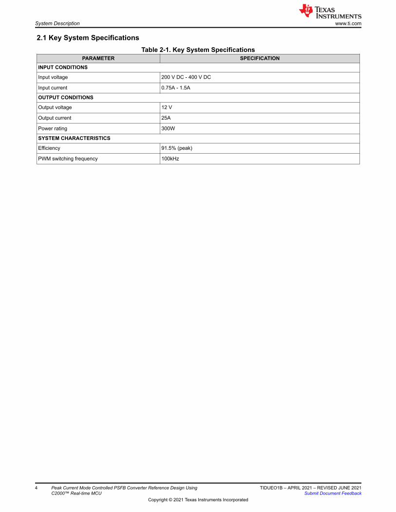
2.1 Key System SpecificationsTable 2-1. Key System Specifications
PARAMETER SPECIFICATIONINPUT CONDITIONS
Input voltage 200 V DC - 400 V DC
Input current 0.75A - 1.5A
OUTPUT CONDITIONS
Output voltage 12 V
Output current 25A
Power rating 300W
SYSTEM CHARACTERISTICS
Efficiency 91.5% (peak)
PWM switching frequency 100kHz
System Description www.ti.com
4 Peak Current Mode Controlled PSFB Converter Reference Design Using C2000™ Real-time MCU
TIDUEO1B – APRIL 2021 – REVISED JUNE 2021Submit Document Feedback
Copyright © 2021 Texas Instruments Incorporated

3 System Overview3.1 Block Diagram
L2
L1
T2
Q1
Q4
Q2
Q3
Q6
HV BUS/
BATTERY
J
Cb
T1
Q5Rs
LV BATTERY
ISOLATED GATE DRIVE
LV CURRENT
HV CURRENT
TMS320f28004x
ADC
CM
PS
S
PUSH-PULL/
SYNCHRONOUS
RECTIFIER DRIVE
HV CURRENT
CAN
a
b
Buck Mode Boost Mode
D26
D25
D28
D27
PW
Ms
GND
Figure 3-1. TIDM-02000 Block Diagram
3.2 Design Considerations3.2.1 Basic Operation
A PSFB converter consists of four-power electronic switches (like MOSFETs or IGBTs) that form a full-bridge on the primary side of the isolation transformer and diode rectifiers or MOSFET switches for synchronous rectification (SR) on the secondary side. This topology allows the switching devices to switch with zero voltage switching (ZVS) resulting in lower switching losses and an efficient converter.
For such an isolated topology, signal rectification is required on the secondary side. For systems with low output voltage and/or high output current ratings, implementing synchronous rectification instead of diode rectification achieves the best possible performance by avoiding diode rectification losses. In this work, synchronous rectification is implemented on the secondary side.
www.ti.com System Overview
TIDUEO1B – APRIL 2021 – REVISED JUNE 2021Submit Document Feedback
Peak Current Mode Controlled PSFB Converter Reference Design Using C2000™ Real-time MCU
5
Copyright © 2021 Texas Instruments Incorporated

LR
LO
T1
Q1
Q4
Q2
Q3
G2
D5 D6
VOUT
VIN
CO
G1
Figure 3-2. A Phase-Shifted Full Bridge Circuit
Figure 3-2 shows a simplified circuit of a phase shifted full-bridge. MOSFET switches Q1, Q4, Q2 and Q3 form the full-bridge on the primary side of the transformer T1. Q1 and Q4 are switched at 50 % duty and 180 degree out of phase with each other. Similarly, Q2 and Q3 are switched at 50 % duty and 180 degree out of phase with each other. The PWM switching signals for leg Q2 – Q3 of the full-bridge are phase shifted with respect to those for leg Q1 - Q4. Amount of this phase shift decides the amount of overlap between diagonal switches, which in turn decides the amount of energy transferred. D5, D6 provide diode rectification on the secondary(MOSFETs used in our design for SR), while Lo and Co form the output filter. Shim inductor LR provides assistance to the transformer leakage inductance for resonance operation with MOSFET capacitance and facilitates Zero Voltage Switching (ZVS). The switching waveforms for the system are shown in Figure 3-3.
Figure 3-3. PSFB PWM Waveforms
3.2.2 PCMC PSFB using C2000
In the system, there are four MOSFET switches (Q1-Q4) that form a full-bridge on the HV side of the isolation transformer and two MOSFET switches (Q5-Q6) on the center-tapped LV side that work as synchronous rectifiers.
Phase shift between PWM signals driving the two legs of the full bridge determines the amount of energy transferred to the load. Controlling such a system in PCMC mode requires generating complex PWM drive waveforms along with fast and efficient control loop calculations. This is made possible on C2000 microcontrollers by advanced on-chip control peripherals like PWM modules, analog comparators with DAC and slope compensation hardware and 12-bit high speed ADCs coupled with an efficient 32-bit CPU. A detailed description of the software algorithm is provided in the following chapters.
System Overview www.ti.com
6 Peak Current Mode Controlled PSFB Converter Reference Design Using C2000™ Real-time MCU
TIDUEO1B – APRIL 2021 – REVISED JUNE 2021Submit Document Feedback
Copyright © 2021 Texas Instruments Incorporated

3.3 System Design Theory3.3.1 Peak Current Mode Control (PCMC) Implementation
Implementing PCMC for a PSFB system requires complex PWM waveform generation with precise timing control. The Piccolo family of devices from Texas Instruments feature advanced on-chip control peripherals that make this implementation possible without any external support circuitry for this purpose. These peripherals include on-chip analog comparators, digital-to-analog converters (DAC), advanced PWM resources and unique programmable on-chip slope compensation hardware. Figure 3-4 shows the PCMC implementation. Transformer primary current is compared with the peak current reference calculated by the voltage loop using the on-chip comparator.
In every half of the switching cycle when the transformer primary current reaches the commanded peak reference value, one of the PWM waveforms driving the switches (Q2/Q3) is Reset immediately ending the power transfer phase. The PWM waveform driving the other switch in the same leg is Set after a programmable dead-time (dead-band) window. Appropriate slope compensation is also applied that adds a ramp with a programmable negative slope to the peak reference current signal.
The Resetting and Setting action of the PWMs in one leg results in a phase shift between PWM signals driving the two legs. The amount of this phase shift, and thereby the overlap between diagonal switches, is dependent on the amount of peak reference current. Higher the peak reference current, longer the overlap between diagonal switches, and thereby, more the energy transferred to the secondary. The controller regulates the output by controlling this energy transfer by way of controlling the peak reference current value. Thus this peak reference current is the controlled parameter.
An important feature of this implementation is that the same peak reference current command is used for both halves of the switching cycle under all operating conditions. This provides optimal flux balance for the transformer primary reducing any chances of saturation.
www.ti.com System Overview
TIDUEO1B – APRIL 2021 – REVISED JUNE 2021Submit Document Feedback
Peak Current Mode Controlled PSFB Converter Reference Design Using C2000™ Real-time MCU
7
Copyright © 2021 Texas Instruments Incorporated

ePWM1 time base
ePWM2 time base
ePWM1A out
ePWM1B out
ePWM2A AQ
ePWM2A out
ePWM2B out
TZBU
T1U
RED
inserted in
DBM
T1D
TZAD
PRD
ZRO
FED + invert DBM
FED +
invert DBM RED DBM
Blanking
window
Offset Window length
ePWM2B AQ
T1U T1DPRD
ZRO
ePWM4 time base
ePWM4A/3B AQ
T1U PRD
ZRO
Blanking
windowPSFB_SR_mode == 2
ZRO
PRD T1D
ePWM4B/3A AQ
ePWM4A out
RED
inserted in
DBM
ePWM4B out
FED
inserted in
DBM
Figure 3-4. PCMC PSFB Implementation
The EPWM1A and EPWM1B outputs are complimentary and 50% duty cycle are maintained based on the action qualifier and deadband settings. The EPWM2A/B_AQ (action qualifier output) is set to 1 when T1U(T1 with counter counting up) event occurs and when counter reaches PRD. The EPWM2A_AQ is set to 0 when T1D (T1 with counter counting down) event occurs and when counter reaches ZERO. The T1D and T1U events are triggered by DCAEVT2.
System Overview www.ti.com
8 Peak Current Mode Controlled PSFB Converter Reference Design Using C2000™ Real-time MCU
TIDUEO1B – APRIL 2021 – REVISED JUNE 2021Submit Document Feedback
Copyright © 2021 Texas Instruments Incorporated

With type-4 PWM, the deadband can be directly added to T1U and T1D events without adding extra code configurations. The rising edge delay is inserted for EPWM2A. And falling edge delay is inserted for EPWM2B together with inversion accordingly.
To achieve the quickest response, the trip zone modules are utilized to setup the falling edge for EPWM2A (with TZAD event) and EPWM2B (with TZBU event) output. The cycle by cycle trip is implemented and is required to be cleared on ZERO and PRD event.
3.3.2 Zero Voltage Switching (ZVS) or Low Voltage Switching (LVS)
PSFB DC-DC converters make use of parasitic elements in the circuit to ensure zero voltage across the MOSFET switches before turning them ON, providing soft switching. This considerably reduces the amount of switching losses associated with hard switching.
For the system discussed here, switching transitions for switches in the Q2- Q3 leg end the power transfer interval. Therefore this leg is called the Active to Passive leg. When transitions occur for switches in this leg, current in the primary winding is close to its maximum magnitude for that half PWM switching cycle. The reflected load current aids the circulating energy in the primary circuit during this time, which makes it possible for voltage across switches in this leg to approach zero volts. It is possible to achieve ZVS for switches in this Q2-Q3 leg across the complete load range. It should be noted that as the load decreases the amount of dead-time needs to be increased to achieve/approach ZVS.
Switching transitions for switches in the Q1- Q4 leg start the power transfer interval. Therefore this leg is called the Passive to Active leg. During these switching transitions, primary current decreases. It crosses zero current value and changes direction. This results in lower available energy for ZVS. In fact for operations under low load conditions, voltage across these switches may not go to zero before turning them on. Switching losses can be kept to a minimum by turning these switches ON at a time when the voltage across them is at a minimum. This is called Low Voltage Switching or low voltage switching (LVS). As the load changes the time at which the switch should be turned on to achieve LVS changes, requiring dead-time adjustment similar to the Q2-Q3 leg switches.
3.3.3 Synchronous Rectification
Figure 3-5. Synchronous Rectification mode
Synchronous rectifiers can work in one of the following three modes at any given time:
1. Mode 0: This is the classical diode current doubler mode achieved by keeping synchronous rectifiers turned OFF. It is useful for very low load operations where synchronous rectifier switching losses are greater than the power savings obtained by synchronous rectification.
www.ti.com System Overview
TIDUEO1B – APRIL 2021 – REVISED JUNE 2021Submit Document Feedback
Peak Current Mode Controlled PSFB Converter Reference Design Using C2000™ Real-time MCU
9
Copyright © 2021 Texas Instruments Incorporated

2. Mode 1: In this mode the synchronous rectifier switches behave like ideal diodes. This mode is useful when operating at very low to low loads, typically when burst mode is being used. In this mode, synchronous rectifier MOSFETs are ON only when the corresponding diagonal bridge drive signals overlap.
3. Mode 2: Useful for all other load conditions. In this mode, synchronous rectifier MOSFETs are OFF only when the corresponding opposite diagonal bridge drive signals overlap.
Figure 3-5 depict waveforms generated for driving the synchronous rectifier switches in these modes. It is important to implement mode transitions seamlessly without any glitches or anomalies on the PWM outputs even during large load transients or sudden phase shift change commands to ensure safe operation of the system.
3.3.4 Slope Compensation
The peak current reference command is written to the RAMPMAXREFS which is the starting value of the RAMP used for slope compensation. The slope is decided by RAMPDACVALS. The ramp generator produces a falling-ramp input for the high reference 12-bit DAC when selected. Note that in this mode, the reference 12-bit DAC uses the most significant 12 bits of the RAMPSTS countdown register as its input. The low 4 bits of the RAMPSTS countdown register effectively act as a prescale for the falling-ramp rate configurable with RAMPDECVALA.
In this reference design, The slope is chosen based on two factors: stability and transient response. The empirical value used in the design should make the system stable and also does not sacrifice the transient response. If the slope is too large, it will limit the duty cycle available and will decreases the transient response. If the slope is too small, it will trigger the sub-harmonics oscillation which creates unstable conditions.
System Overview www.ti.com
10 Peak Current Mode Controlled PSFB Converter Reference Design Using C2000™ Real-time MCU
TIDUEO1B – APRIL 2021 – REVISED JUNE 2021Submit Document Feedback
Copyright © 2021 Texas Instruments Incorporated

3.4 Highlighted Products3.4.1 C2000™ MCU F28004x
C2000 MCUs are part of an optimized MCU family for real-time control application. Fast and high-quality analog-to-digital controller enables accurate measurement of the current and voltage signals, and an integrated comparator subsystem (CMPSS) provides protection for overcurrent and overvoltage without use of any external devices. The optimized CPU core enables fast execution of control loop. Trigonometric operations are accelerated using the on-chip trigonometric math unit (TMU). The solution also provides an option to use the control law accelerator (CLA) on the F28004x. The CLA is a co-processor that can be used to alleviate CPU burden and enable faster-running loops or more functions on the C2000 MCU.
www.ti.com System Overview
TIDUEO1B – APRIL 2021 – REVISED JUNE 2021Submit Document Feedback
Peak Current Mode Controlled PSFB Converter Reference Design Using C2000™ Real-time MCU
11
Copyright © 2021 Texas Instruments Incorporated

4 Hardware, Software, Testing Requirements, and Test Results4.1 Required Hardware and Software4.1.1 Hardware
Figure 4-1 shows key hardware components. This hardware uses the kit of Bidirectional 400-V/12-V DC/DC Converter Reference Design as the base board and with some modification for peak current mode control.
Bias ISO-CANISO USB JTAG
and UART
TMS320F28035
Controller card
400- to 12-V
Bias
Low voltage side High voltage side
LV Bus
connections
Figure 4-1. TIDM-02000 hardware
The key signal connections between the controlCARD and the base board are listed in the Table 4-1
Table 4-1. Key Signal ConnectionsSIGNAL NAME DESCRIPTOIN CONNECTION TO
CONTROLCARD
ePWM-1A PWM drive for full-bridge switch Q2 GPIO-00
ePWM-1B PWM drive for full-bridge switch Q3 GPIO-01
ePWM-2A PWM drive for full-bridge switch Q1 GPIO-02
ePWM-2B PWM drive for full-bridge switch Q4 GPIO-03
ePWM-4A PWM drive for sync rectifier/push-pull switch Q6 GPIO-07
ePWM-4B PWM drive for sync-rectifier/push-pull switch Q5 GPIO-06
VLV-FB Low voltage bus – voltage feedback ADC-A0
ILV-FB Low voltage current feedback (Jumper J2 populated) ADC-B3/COMP2A
ILV-FILT Heavily filtered low voltage current feedback ADC-B2
VHV-FB High voltage bus – voltage feedback ADC-B1
IHV-FB Transformer high voltage winding current ADC-A2/COMP1A
IHV-FILT Heavily filtered transformer high voltage winding current ADC-A1
This board provides a lot of jumper options for experimentation but there are some jumpers that must be populated for proper operation of the board. These jumpers that must be populated are listed below:
Hardware, Software, Testing Requirements, and Test Results www.ti.com
12 Peak Current Mode Controlled PSFB Converter Reference Design Using C2000™ Real-time MCU
TIDUEO1B – APRIL 2021 – REVISED JUNE 2021Submit Document Feedback
Copyright © 2021 Texas Instruments Incorporated

C:JPG1, E:JPG1, J2, J5, J6, J7, J8, J10, J11, J12, J13, J15, J16, and J19.
Some hardware modifications are required by the customer before running the reference code in this board.
C23
330pF
R24
DNP
R32 1K
C33
3.3nF
R49
DNP
R50 1K
CS_HV IHV-FB
IHV-FILT
GND_LV
GND_LV
Figure 4-2. Peak Current Sensing Circuit
1. Remove resistor R50 in Figure 4-2. The heavily filtered winding current of the CT on the secondary side is used for average current mode control. For peak current mode control, a relatively low cutoff frequency filter is needed. Existence of R50 can introduce distortion to the current waveform.
Notes: Some magnetic components in the original board are replaced for peak current mode control as shown in Table 4-2.
Table 4-2. Current and Original magnetic ComponentsCURRENT ORIGINAL
Main transformer MPS P6524_A VITEC AF5551R
Secondary side inductor VITEC 6193R VITEC AF5666BR
Shim inductor VITEC 6194R VITEC AF5667BR
ControlCARD settings:
Certain settings on the device control card are required to communicate over JTAG and use the isolated UART port. The user must also provide a correct ADC reference voltage. The following settings are required for revision A of the TMS320F280049C control card (refer to the info sheet located at \c2000ware\boards\controlCARDs\TMDSCNCD280049C.
1. Set both ends of S1:A on the control card to ON (up) position to enable JTAG connection to the device and UART connection for SFRA GUI. If this switch is OFF (down), the user cannot use the isolated JTAG built in on the control card, nor can the SFRA GUI communicate with the device.
2. Connect the USB cable to J1:A to communicate with the device from a host PC on which CCS runs.3. For the control loop, use the internal reference of the TMS320F28004x and move the S8 switch to the left
(that is, pointing to VREFHI).4. For best performance of this reference design, remove the capacitor connected between the isolated
grounds on the control card, C26:A.
www.ti.com Hardware, Software, Testing Requirements, and Test Results
TIDUEO1B – APRIL 2021 – REVISED JUNE 2021Submit Document Feedback
Peak Current Mode Controlled PSFB Converter Reference Design Using C2000™ Real-time MCU
13
Copyright © 2021 Texas Instruments Incorporated

4.1.2 Software4.1.2.1 Software Control Flow
C2000 Library Modules
DCLSFRA Power Meas Power Meas
EMAVGEMAVG
system solution (solution.c/.h)
System SolutionBoard Drivers
(solution_hal.c/h)
C28x MCU
Driverlib
powerSUITE (solution-settings.h)
C2000 Library Modules
RAMPGENEMAVG
MATH_EMAVG:n:
In Out
EMAVG_Multiplier
main.c / clatasks.cla
powerSUITE (solution-settings.h)
system solution (solution.c/.h)
System SolutionBoard Drivers
(solution_hal.c/h)
C28x MCU
Driverlib
powerSUITE (solution-settings.h)
C2000 Library Modules
RAMPGENEMAVG
MATH_EMAVG:n:
In Out
EMAVG_Multiplier
main.c / clatasks.cla
system solution (solution.c/.h)
System SolutionBoard Drivers
(solution_hal.c/h)
C28x MCU
Driverlib
powerSUITE (solution-settings.h)
C2000 Library Modules
RAMPGENEMAVG
MATH_EMAVG:n:
In Out
EMAVG_Multiplier
main.c / clatasks.clasystem solution (solution.c/.h)
System SolutionBoard Drivers
(solution_hal.c/h)
C28x MCU
Driverlib
powerSUITE (solution-settings.h)
C2000 Library Modules
RAMPGENEMAVG
MATH_EMAVG:n:
In Out
EMAVG_Multiplier
main.c / clatasks.cla
system solution (solution.c/.h)
System SolutionBoard Drivers
(solution_hal.c/h)
C28x MCU
Driverlib
powerSUITE (solution-settings.h)
C2000 Library Modules
RAMPGENEMAVG
MATH_EMAVG:n:
In Out
EMAVG_Multiplier
main.c / clatasks.cla
system solution (solution.c/.h)
System Solution
Board Drivers
(solution_hal.c/h)
C28x MCU
Driverlib
powerSUITE (solution-settings.h)
C2000 Library Modules
RAMPGENEMAVG
MATH_EMAVG:n:
In Out
EMAVG_Multiplier
main.c / clatasks.cla
system solution (solution.c/.h)
System SolutionBoard Drivers
(solution_hal.c/h)
C28x MCU
Driverlib
powerSUITE (solution-settings.h)
C2000 Library Modules
RAMPGENEMAVG
MATH_EMAVG:n:
In Out
EMAVG_Multiplier
main.c / clatasks.cla
system solution (solution.c/.h)
System SolutionBoard Drivers
(solution_hal.c/h)
C28x MCU
Driverlib
powerSUITE (solution-settings.h)
C2000 Library Modules
RAMPGENEMAVG
MATH_EMAVG:n:
In Out
EMAVG_Multiplier
main.c / clatasks.cla
system solution (solution.c/.h)
System Solution
Board Drivers
(solution_hal.c/h)
C28x MCU
Driverlib
powerSUITE (solution-settings.h)
C2000 Library Modules
RAMPGENEMAVG
MATH_EMAVG:n:
In Out
EMAVG_Multiplier
main.c / clatasks.cla
main.c / clatasks.cla
system solution (solution.c/.h)
System Solution
Board Drivers
(solution_hal.c/h)
Driverlib
DCL
C28x MCU
Figure 4-3. Project Structure Overview
Solution specific and device independent files are <solution>.c/h. Board-specific and device-specific files are <solution>_hal.c/h. The main.c file of the project consists of the main function of the C project as well as ISR framework and calls routines in other files. <solution>_settings.h and <solution>_user_settings.h consist of all the settings required for the solution.
<solution>_user_settings.h For this design, <solution> is psfbpcmc.
<solution>_clatask.cla file include the CLA Task definitions.
The powerSUITE page can be opened by clicking the main.syscfg file, listed below the project explorer.
The powerSUITE page generates the <solution>_settings.h file. This file is the only file used in the compile of the project that is generated by the powerSUITE page. The user must not modify this file manually, as the changes will be overwritten by powerSUITE each time the project is rebuilt. The changes will only happen after rebuilding the entire project TheKit.json and solution.js files are used internally by the powerSUITE and must also not be modified by the user. Any changes to these files will result in the project not functioning properly.
Hardware, Software, Testing Requirements, and Test Results www.ti.com
14 Peak Current Mode Controlled PSFB Converter Reference Design Using C2000™ Real-time MCU
TIDUEO1B – APRIL 2021 – REVISED JUNE 2021Submit Document Feedback
Copyright © 2021 Texas Instruments Incorporated

Main
System Level Management
28x Device level
Peripheral level
System level
ISR, ADC
Initialization
Background
Loop
Background
Loop
Timer 0 Tasks
x� SFRA_Backgrou
nd
x� Serial comms
x� Fault
management
x� Start up control
Timer 1 Tasks
x� OVP
x� Ramp update
Control ISR
ISR (100kHz)
SFRA_INJECT()
ADC_VBUS()
Vloop
SR control
SFRA_COLLECT()
EXIT
Figure 4-4. PCMC Software Flow
In Figure 4-4, the project consists of an interrupt service routine, which is called every PWM cycle, called ISR1(), where the control algorithm is executed. In addition to this, there are background tasks, which are called in a polling fashion and can be used to run slow tasks for which absolute timing accuracy is not required.
The system is controlled by two feedback loops; an outer voltage loop, implemented using software control block, and an inner peak current loop, implemented using the on-chip analog comparator, DAC and PWM hardware resources. The voltage loop controller is executed at a rate of 100 kHz (same as the PWM frequency).
www.ti.com Hardware, Software, Testing Requirements, and Test Results
TIDUEO1B – APRIL 2021 – REVISED JUNE 2021Submit Document Feedback
Peak Current Mode Controlled PSFB Converter Reference Design Using C2000™ Real-time MCU
15
Copyright © 2021 Texas Instruments Incorporated

4.1.2.2 Incremental Builds
This project is divided into two incremental builds. This makes it easier to learn and get familiar with the board and the software. This approach is also good for debugging/testing boards.
The build options are shown in Table 4-3. To select a particular build option, open the main.syscfg and select the INCR_BUILD to the corresponding build selection as shown below. Once the build option is selected in powerSUITE page and save button is clicked, compile the complete project by selecting rebuild-all compiler option. Next chapter provides more details to run each of the build options.
Table 4-3. Incremental Build OptionsIncremental Build Options
INCR_BUILD = 1 Peak current loop check with constant I command and open voltage loop (Check PWM drive circuit and sensing circuit)
INCR_BUILD = 2 Closed current and voltage loop (Full PSFB)
4.1.2.3 Procedure for running the incremental builds - PCMC
CAUTION
There are high voltages present on the board. It should only be handled by experienced power supply professionals in a lab environment. To safely evaluate this board an appropriate isolated high voltage DC source should be used. Before DC power is applied to the board a voltmeter and an appropriate resistive or electronic load must be attached to the output. The unit should never be handled when the power is applied to it.
4.1.2.3.1 Build 1: Peak Current Loop Check with Open Voltage Loop4.1.2.3.1.1 Objective
The objective of this build is to evaluate the peak current mode operation of the system, verify the DAC and ADC driver modules, verify the MOSFET driver circuit and sensing circuit on the board and become familiar with the operation of Code Composer Studio (CCS). Since this system is running open-loop, the ADC measured values are only used for instrumentation purposes in this build. Steps required to build and run a project will be explored.
4.1.2.3.1.2 Overview
The software in Build1 has been configured so that the user can quickly evaluate the DAC driver module by viewing various waveforms on an oscilloscope and observing the effect of change in peak current reference command on the output voltage by interactively adjusting this command from CCS. Additionally, the user can evaluate the ADC driver module by viewing the ADC sampled data in the watch view.
The on-chip analog comparator compares the transformer primary current with the slope compensated peak current reference. Comparator output is connected to the trip zone logic of the PWM modules. ePWM1 module acts as the master time-base for the system. It operates in up-down count mode. ePWM1A and ePWM1B drive Q1 and Q4 full-bridge switches, while ePWM2A and ePWM2B drive Q2 and Q3 full-bridge switches. ePWM4A and ePWM4B drive Q5 and Q6 synchronous rectifier switches. Whenever the comparator output goes high in a PWM half cycle, the ePWM2 module output (ePWM2A or ePWM2B) which was high at that instant is immediately pulled low while the other PWM2 module output is pulled high after an appropriate dead-band window (dbAtoP). ePWM4A and ePWM4B outputs are driven in a similar way.
It should be noted that this slope compensation ramp generation, comparator action and PWM waveform generation are all hardware generated without any software involvement as shown in Figure 4-5. Some register reconfigurations for SR are done inside the ISR.
Hardware, Software, Testing Requirements, and Test Results www.ti.com
16 Peak Current Mode Controlled PSFB Converter Reference Design Using C2000™ Real-time MCU
TIDUEO1B – APRIL 2021 – REVISED JUNE 2021Submit Document Feedback
Copyright © 2021 Texas Instruments Incorporated

P
W
M H
W
ePWM1A
ePWM1B
ePWM2A
ePWM2B
dbAtoP
dbPtoA
ePWM4A
ePWM4B
Trip
Ihv_fb
A
CMPSS_H
ADC
H/W
ADC Reading
ADC_PU_SCALING Vlv_fbvLVBus_sensed
Ihv_fb
Vhv_fb
Blanking
Slope100Khz
100 Khz
100 Khz
100 Khz
COMP_OUT
icommand_Set
CMPSS + Slope Comp
RAMPMAXREF
DACVAL
Set_CmpssMaxRamp
iHV_sensed ADC
H/W
ADC Reading
ADC_PU_SCALING
ADC
H/W
ADC Reading
ADC_PU_SCALINGvHVBus_sensed
DAC
12-bit +
Slope
Comp
+
Figure 4-5. Build 1 Software Blocks
The output voltage sensing circuit is made up of simple voltage dividers. A current transformer, and a sense resistor are used to sense the full-bridge transformer primary current.
www.ti.com Hardware, Software, Testing Requirements, and Test Results
TIDUEO1B – APRIL 2021 – REVISED JUNE 2021Submit Document Feedback
Peak Current Mode Controlled PSFB Converter Reference Design Using C2000™ Real-time MCU
17
Copyright © 2021 Texas Instruments Incorporated

4.1.2.3.1.3 Procedure4.1.2.3.1.3.1 Start CCS and Open a Project
To quickly execute this build, follow the following steps:
1. Make sure that all jumpers on the board are correctly installed or removed as listed in the Hardware section.2. Hardware Set-up: Insert the F28004x controlCARD in the 100-pin DIMM connector. Connect a 12 V DC
bench power supply between TP10 and TP11 with correct polarity. Connect an isolated 400V programmable DC power source to the 400 V input connector and 12 V electronic load to the 12 V connector (make sure that this load does not exceed the board ratings). Connect a USB cable between the PC and controlCARD. Do not turn ON any of the power supplies at this time.
3. Open Code Composer Studio. Maximize Code Composer Studio to fill your screen. Close the welcome screen if it opens up.
4. locate the solution package downloaded and import the project in CCS5. In the project window on the left, click the plus sign (+) to the left of Project. Your project window will look like
the following:
Figure 4-6. Project Window
Hardware, Software, Testing Requirements, and Test Results www.ti.com
18 Peak Current Mode Controlled PSFB Converter Reference Design Using C2000™ Real-time MCU
TIDUEO1B – APRIL 2021 – REVISED JUNE 2021Submit Document Feedback
Copyright © 2021 Texas Instruments Incorporated

4.1.2.3.1.3.2 Build and Load the Project
1. Open the main.syscfg and select Open Loop in INCR_BUILD. Click Save.2. Right click the project name PCMC_PSFB_F28004x and click rebuild project. Open the psfbpcmc_settings.h
as shown in Figure 4-7. You should see the setting is #define INCR_BUILD 1. This enables the build 1 solution.
3. Also set #define PSFB_PCMC 1 in the psfbpcmc_user_settings.h. For build 1, this will disable the phase shift debug mode.
NoteTo enable the phase shift debug mode under build 1, set #define PSFB_PCMC 0. phase shift debug mode is an optional and suggested debug mode to test whether the power stage is working normally before build 1. It can directly set up the phase shift between EPWM1 and EPWM2 through PSFB_PhaseShift in the expression window. After PSFB_enable is set to 1 and the project is running, user can change the PSFB_PhaseShift to set up different phase shift (for example: 100). Gradually increase the DC input to 400 V. If all PWMs, voltage across the transformer and output voltage are as expected, it means the power stage is fine.
4. Turn ON the 12 V DC bench power supply. Click on the Debug button. The build 1 code should compile and load.
5. Notice the CCS Debug icon in the upper right corner indicating that we are now in the Debug Perspective view. The program should be stopped at the start of main()
Figure 4-7. Project Window
4.1.2.3.1.3.3 Debug Environment Windows
Populate the expressions window entries by clicking scripting console on the menu bar and then opening the setupdebugenv_allbuilds.js file from the project workspace directory (PCMC_PSFB_F28004x\setupdebugenv_allbuilds.js) using the scripting console Open File ( ) command. Please note that some of the variables have not been initialized at this point in the main code and may contain some garbage values.
www.ti.com Hardware, Software, Testing Requirements, and Test Results
TIDUEO1B – APRIL 2021 – REVISED JUNE 2021Submit Document Feedback
Peak Current Mode Controlled PSFB Converter Reference Design Using C2000™ Real-time MCU
19
Copyright © 2021 Texas Instruments Incorporated

4.1.2.3.1.3.4 Using Real-Time Emulation
Real-time emulation is a special emulation feature that allows the windows within Code Composer Studio to be updated at up to a 10 Hz rate while the MCU is running. This not only allows graphs and watch views to update, but also allows the user to change values in watch or memory windows, and have those changes affect the MCU behavior. This is very useful when tuning control law parameters on-the-fly, for example.
1. Enable real-time mode by hovering your mouse on the buttons on the horizontal toolbar and clicking
button2. A message box may appear. If so, select YES to enable debug events. This will set bit 1 (DGBM bit) of
status register 1 (ST1) to a “0”. The DGBM is the debug enable mask bit. When the DGBM bit is set to “0”, memory and register values can be passed to the host processor for updating the debugger windows.
3. Now click button on the same horizontal toolbar.4. When a large number of windows are open, as bandwidth over the emulation link is limited, updating too
many windows and variables in continuous refresh can cause the refresh frequency to bog down. Right click on the button in the watch view and select “Customize Continuous Refresh Interval..”. You can slow down the refresh rate for the watch view variables by changing the Continuous refresh interval (milliseconds) value. A rate of 4000 ms is usually enough for these exercises.
5. Click on Continuous Refresh button for the watch view.
4.1.2.3.1.3.5 Run the Code
Figure 4-8. Build 1 Expression Window
1. Run the code by using the <F8> key, or using the Run button on the toolbar.2. Apply an appropriate resistive load to the PSFB system at the DC output. A load that draws around 3A – 6A
current at 12 V output is a good starting point.3. Set PSFB_gui_icommand_Set_Amps to be 0.5.4. Set PSFB_enable to be 1. This enables PWM output. The expression window is similar to Figure 4-8.5. Power the input at J1, J2 with 390 V DC. The output will be around 1.6 V (5A constant current load).6. Slowly increase PSFB_gui_icommand_Set_Amps to be 2.35 in increments of 0.05. Carefully observe the
output voltage(PSFB_guiLVbus_Volts), the voltage should gradually increase to 12 V. This should not be allowed to exceed the capabilities of the board. Different waveforms, like the PWM gate drive signals, input voltage and current and output voltage may also be probed using an oscilloscope. Appropriate safety precautions should be taken and appropriate grounding requirements should be considered while probing these high voltages and high currents for this isolated DC-DC converter.
7. The PSFB_slope is set to be 30. User can gradually increase or decrease it for testing.
Hardware, Software, Testing Requirements, and Test Results www.ti.com
20 Peak Current Mode Controlled PSFB Converter Reference Design Using C2000™ Real-time MCU
TIDUEO1B – APRIL 2021 – REVISED JUNE 2021Submit Document Feedback
Copyright © 2021 Texas Instruments Incorporated

8. Fully halting the MCU when in real-time mode is a two-step process. With the 400 V DC input turned off wait a few seconds. First, halt the processor by using the Halt button on the toolbar, or by using Target > Halt.
Then click the button again to take the MCU out of real-time mode and then reset the MCU.
www.ti.com Hardware, Software, Testing Requirements, and Test Results
TIDUEO1B – APRIL 2021 – REVISED JUNE 2021Submit Document Feedback
Peak Current Mode Controlled PSFB Converter Reference Design Using C2000™ Real-time MCU
21
Copyright © 2021 Texas Instruments Incorporated
4.1.2.3.2 Build 2: Closed current and voltage loop (Full PSFB)4.1.2.3.2.1 Objective
The objective of this build is to verify the operation of the complete PCMC based HVPSFB project from the CCS environment.
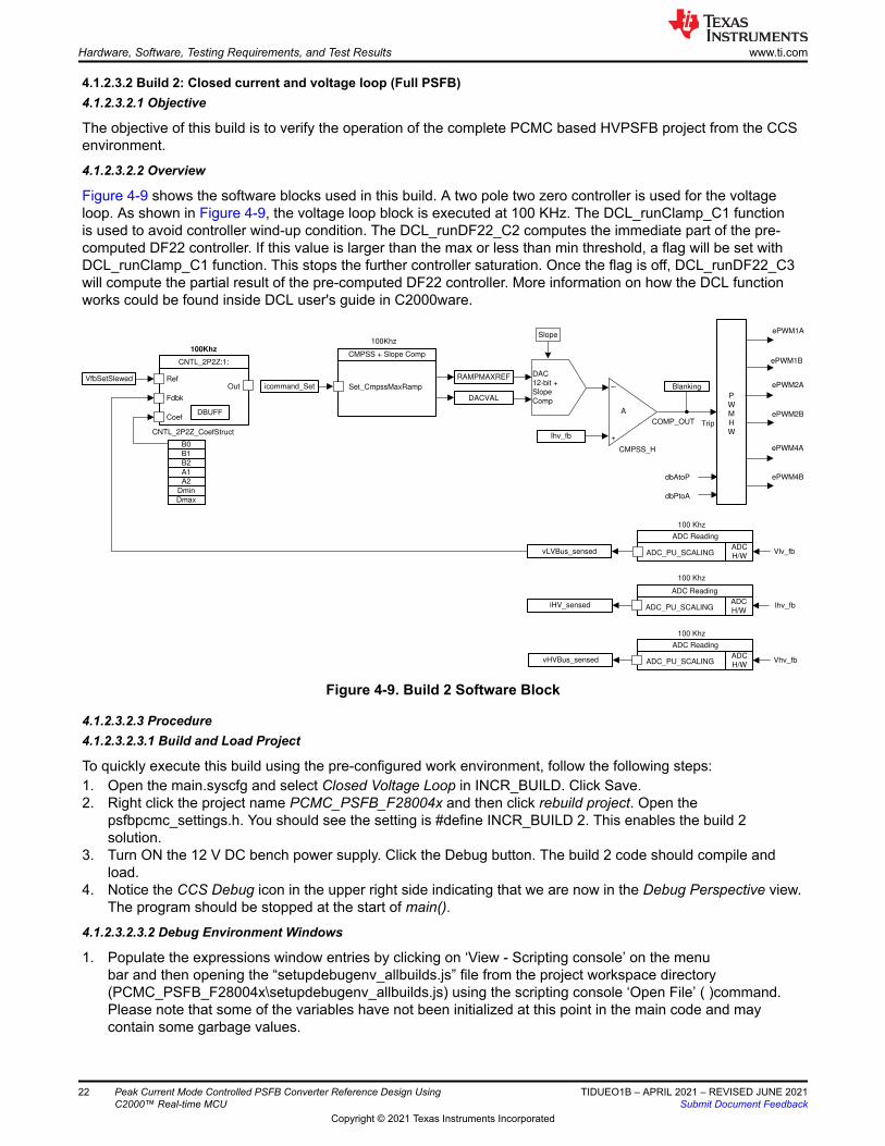
4.1.2.3.2.2 Overview
Figure 4-9 shows the software blocks used in this build. A two pole two zero controller is used for the voltage loop. As shown in Figure 4-9, the voltage loop block is executed at 100 KHz. The DCL_runClamp_C1 function is used to avoid controller wind-up condition. The DCL_runDF22_C2 computes the immediate part of the pre-computed DF22 controller. If this value is larger than the max or less than min threshold, a flag will be set with DCL_runClamp_C1 function. This stops the further controller saturation. Once the flag is off, DCL_runDF22_C3 will compute the partial result of the pre-computed DF22 controller. More information on how the DCL function works could be found inside DCL user's guide in C2000ware.
P
W
M H
W
ePWM1A
ePWM1B
ePWM2A
ePWM2B
dbAtoP
dbPtoA
ePWM4A
ePWM4B
Trip
Ihv_fb
A
CMPSS_H
ADC
H/W
ADC Reading
ADC_PU_SCALING Vlv_fbvLVBus_sensed
Ihv_fb
Vhv_fb
Blanking
Slope100Khz
100 Khz
100 Khz
100 Khz
COMP_OUT
icommand_Set
CMPSS + Slope Comp
RAMPMAXREF
DACVAL
Set_CmpssMaxRamp
iHV_sensed ADC
H/W
ADC Reading
ADC_PU_SCALING
ADC
H/W
ADC Reading
ADC_PU_SCALINGvHVBus_sensed
DAC
12-bit +
Slope
Comp
+
OutRef
Fdbk
CNTL_2P2Z:1:
Coef
B0
B1
B2
A1
A2
Dmin
Dmax
CNTL_2P2Z_CoefStruct
DBUFF
VfbSetSlewed
100Khz
Figure 4-9. Build 2 Software Block
4.1.2.3.2.3 Procedure4.1.2.3.2.3.1 Build and Load Project
To quickly execute this build using the pre-configured work environment, follow the following steps:1. Open the main.syscfg and select Closed Voltage Loop in INCR_BUILD. Click Save.2. Right click the project name PCMC_PSFB_F28004x and then click rebuild project. Open the
psfbpcmc_settings.h. You should see the setting is #define INCR_BUILD 2. This enables the build 2 solution.
3. Turn ON the 12 V DC bench power supply. Click the Debug button. The build 2 code should compile and load.
4. Notice the CCS Debug icon in the upper right side indicating that we are now in the Debug Perspective view. The program should be stopped at the start of main().
4.1.2.3.2.3.2 Debug Environment Windows
1. Populate the expressions window entries by clicking on ‘View - Scripting console’ on the menu bar and then opening the “setupdebugenv_allbuilds.js” file from the project workspace directory (PCMC_PSFB_F28004x\setupdebugenv_allbuilds.js) using the scripting console ‘Open File’ ( )command. Please note that some of the variables have not been initialized at this point in the main code and may contain some garbage values.
Hardware, Software, Testing Requirements, and Test Results www.ti.com
22 Peak Current Mode Controlled PSFB Converter Reference Design Using C2000™ Real-time MCU
TIDUEO1B – APRIL 2021 – REVISED JUNE 2021Submit Document Feedback
Copyright © 2021 Texas Instruments Incorporated

4.1.2.3.2.3.3 Run the Code
1. Follow Steps 1 to 4 of the build 1 procedure to enable real-time mode and continuous refresh for the watch views and also for changing the continuous refresh interval for the watch view if needed.
2. Run the code by using the <F8> key, or using the Run button on the toolbar.3. Apply an appropriate resistive load to the PSFB system at the DC output. A load that draws around 3A – 6A
current at 12 V output is a good starting point.4. Check PSFB_guivLVBus_Set_Volts. PSFB_guivLVBus_Set_Volts should be 2 at the beginning.5. Set PSFB_enable to be 1. This enables PWM output.6. Power the input at J1, J2 with 400V DC (200V and 300V are optional). The output voltage should rise up to
2V.
Note
For user safety, it is recommended to use an isolated DC source to supply 400V DC input to the board.
7. Set PSFB_start_flag to 1. The output voltage should now start ramping up to 12 V. Here is the watch view that corresponds to the operation of the system with 12 V at the output with an input voltage of around 400 V and a load of around ~5A (constant current load).
8. Gradually increase the load (constant current load) to 25A. The output power will be around 300W.The transformer voltage(CH1), PWM signal(CH2, CH3) and primary current (CH4, primary side of CT) should be similar as Figure 4-12.
9. By default, the synchronous rectifiers are operated in mode 2. You can change their mode of operation by changing PSFB_SR_mode variable to 0, 1 or 2 from the watch view. Observe the change in amount of input current being drawn and change in output voltage with different SR modes. You can also probe the PWM waveforms driving the synchronous rectifier switches. Do not change between different SR modes when operating at very low loads or when the output voltage is very low (less than 6V). In these cases use the default SR mode 2. The SR PWM waveforms(CH2 Ch3) are shown in Figure 4-11
10. Now the load transient can be tested. Set the current slew rate to be 0.5A/us (can be tested up to 2.5A). Then set load current to be 12.5A. Now the output power is 150W. More tests can be done between 10% ~ 100% load condition.
11. Probe the MOSFETS Vds and Vgs of active to passive leg and passive to active leg. The low voltage switching is achieved for passive to active leg as Figure 4-10.
12. SFRA is to verify the designed compensator provides enough gain and phase margin by measuring on hardware. To run the SFRA keep the project running, open sfra\gui\SFRA_GUI.exe, SFRA GUI will pop out.
13. Select the options for the device on the SFRA GUI. For example, for F28004x select floating point. Click on Setup Connection. On the pop-up window uncheck the boot on connect option, and select an appropriate COM port. Click OK. Return to the SFRA GUI, and click Connect.
14. The SFRA GUI will connect to the device. A SFRA sweep can now be started by clicking Start Sweep. Activity can be monitored by seeing the progress bar on the SFRA GUI and also checking the flashing of blue LED on the back on the controlcard that indicates UART activity. When complete, a graph with the open loop plot will appear, as in Figure 4-13. This verifies that the designed compensator is indeed stable.
15. Fully halting the MCU when in real-time mode is a two-step process. With the 400 V DC input turned off wait a few seconds. First, halt the processor by using the Halt button on the toolbar, or by using Target > Halt. Then, click the button again to take the MCU out of real-time mode and then reset the MCU.
16. Close CCS.
End of Exercise
www.ti.com Hardware, Software, Testing Requirements, and Test Results
TIDUEO1B – APRIL 2021 – REVISED JUNE 2021Submit Document Feedback
Peak Current Mode Controlled PSFB Converter Reference Design Using C2000™ Real-time MCU
23
Copyright © 2021 Texas Instruments Incorporated

Figure 4-10. Low Voltage Switching
Figure 4-11. SR PWM Waveforms
Hardware, Software, Testing Requirements, and Test Results www.ti.com
24 Peak Current Mode Controlled PSFB Converter Reference Design Using C2000™ Real-time MCU
TIDUEO1B – APRIL 2021 – REVISED JUNE 2021Submit Document Feedback
Copyright © 2021 Texas Instruments Incorporated

Figure 4-12. Transformer voltage, PWM and primary current (primary side of CT) waveforms
Figure 4-13. Voltage loop SFRA Result
www.ti.com Hardware, Software, Testing Requirements, and Test Results
TIDUEO1B – APRIL 2021 – REVISED JUNE 2021Submit Document Feedback
Peak Current Mode Controlled PSFB Converter Reference Design Using C2000™ Real-time MCU
25
Copyright © 2021 Texas Instruments Incorporated

4.1.3 Test results
The efficiency is measured under 400 V input and 12 V output condition. The SR_mode is set to 2 under different load conditions in this test. The peak efficiency is around 91.5%.
POUT (W)
Eff
icie
ncy (
%)
0 50 100 150 200 250 300 35060
65
70
75
80
85
90
95
100
D001
Buck Mode - 400 VIN 12 VOUT
Figure 4-14. Efficiency vs. Power
5 Design and Documentation Support5.1 Design Files5.1.1 Schematics
To download the schematics, see the design files at TIDM-02000.
5.1.2 BOM
To download the bill of materials (BOM), see the design files at TIDM-02000.
5.2 SoftwareTo download the software files, see the design files at TIDM-02000.5.3 Documentation SupportRelated Documentation:
• Texas Instruments, Bidirectional DC-DC Converter Design Guide.• Texas Instruments, Phase-Shifted Full Bridge DC/DC Power Converter Reference Design Guide.
6 TerminologyACRONYM DEFINITIONDAC Digital-to-Analog ConverterHVPSFB High-Voltage Phase-Shifted Full BridgeLVS Low-Voltage SwitchingMCU microcontrollerPCMC Peak Current Mode ControlPSFB Phase-Shifted Full BridgePWM pulse width modulationSR Synchronous RectificationVMC Voltage Mode ControlZVS Zero-Voltage Switching
7 About the AuthorCHEN JIANG is a Systems Application Engineer with the C2000 Microcontrollers System Solutions Group at Texas Instruments, where he is responsible for developing reference design solutions for digital power
Hardware, Software, Testing Requirements, and Test Results www.ti.com
26 Peak Current Mode Controlled PSFB Converter Reference Design Using C2000™ Real-time MCU
TIDUEO1B – APRIL 2021 – REVISED JUNE 2021Submit Document Feedback
Copyright © 2021 Texas Instruments Incorporated

applications. Before joining TI in 2017, Chen received his PhD in Electrical and Computer Engineering from Georgia Institute of Technology, Atlanta in 2017, and his Bachelor of Engineering from Zhejiang University, China in 2012.
8 Revision HistoryNOTE: Page numbers for previous revisions may differ from page numbers in the current version.
Changes from Revision A (April 2021) to Revision B (June 2021) Page• Updated PCMC PSFB Implementation image....................................................................................................7• Added step 3.....................................................................................................................................................19• Deleted step 3...................................................................................................................................................22
Changes from Revision * (October 2020) to Revision A (March 2021) Page• Added step 3.....................................................................................................................................................22
www.ti.com Revision History
TIDUEO1B – APRIL 2021 – REVISED JUNE 2021Submit Document Feedback
Peak Current Mode Controlled PSFB Converter Reference Design Using C2000™ Real-time MCU
27
Copyright © 2021 Texas Instruments Incorporated

IMPORTANT NOTICE AND DISCLAIMERTI PROVIDES TECHNICAL AND RELIABILITY DATA (INCLUDING DATASHEETS), DESIGN RESOURCES (INCLUDING REFERENCEDESIGNS), APPLICATION OR OTHER DESIGN ADVICE, WEB TOOLS, SAFETY INFORMATION, AND OTHER RESOURCES “AS IS”AND WITH ALL FAULTS, AND DISCLAIMS ALL WARRANTIES, EXPRESS AND IMPLIED, INCLUDING WITHOUT LIMITATION ANYIMPLIED WARRANTIES OF MERCHANTABILITY, FITNESS FOR A PARTICULAR PURPOSE OR NON-INFRINGEMENT OF THIRDPARTY INTELLECTUAL PROPERTY RIGHTS.These resources are intended for skilled developers designing with TI products. You are solely responsible for (1) selecting the appropriateTI products for your application, (2) designing, validating and testing your application, and (3) ensuring your application meets applicablestandards, and any other safety, security, or other requirements. These resources are subject to change without notice. TI grants youpermission to use these resources only for development of an application that uses the TI products described in the resource. Otherreproduction and display of these resources is prohibited. No license is granted to any other TI intellectual property right or to any third partyintellectual property right. TI disclaims responsibility for, and you will fully indemnify TI and its representatives against, any claims, damages,costs, losses, and liabilities arising out of your use of these resources.TI’s products are provided subject to TI’s Terms of Sale (https:www.ti.com/legal/termsofsale.html) or other applicable terms available eitheron ti.com or provided in conjunction with such TI products. TI’s provision of these resources does not expand or otherwise alter TI’sapplicable warranties or warranty disclaimers for TI products.IMPORTANT NOTICE
Mailing Address: Texas Instruments, Post Office Box 655303, Dallas, Texas 75265Copyright © 2021, Texas Instruments Incorporated