pentium processors - phat code
TRANSCRIPT

D
Pentium® Processor FamilyDeveloper’s Manual
Volume 1:Pentium® Processors
NOTE: The Pentium® Processor Family Developer’s Manual consistsof three books: Pentium® Processors, Order Number 241428; the
82496/82497/82498 Cache Controller and 82491/82492/82493 CacheSRAM, Order Number 241429; and the Architecture and
Programming Manual, Order Number 241430. Please refer to all three volumes when evaluating your design needs.
1995

PATENT NOTICE
Through its investment in computer technology, Intel Corporation (Intel) has acquired numerous proprietary rights, includingpatents issued by the U.S. Patent and Trademark Office. Intel has patents covering the use or implementation of processorsin combination with other products, e.g., certain computer systems. System and method patents or pending patents, of Inteland others, may apply to these systems. A separate license may be required for their use (see Intel Terms and Conditionsfor details). Specific Intel patents include U.S. patent 4,972,338.
Information in this document is provided solely to enable use of Intel products. Intel assumes no liability whatsoever,including infringement of any patent or copyright, for sale and use of Intel products except as provided in Intel’s Terms andConditions of Sale for such products.
Intel Corporation makes no warranty for the use of its products and assumes no responsibility for any errors which mayappear in this document nor does it make a commitment to update the information contained herein.
Intel retains the right to make changes to these specifications at any time, without notice.
Contact your local Intel sales office or your distributor to obtain the latest specifications before placing your product order.
MDS is an ordering code only and is not used as a product name or trademark of Intel Corporation.
Intel Corporation and Intel's FASTPATH are not affiliated with Kinetics, a division of Excelan, Inc. or its FASTPATH trade-mark or products.
*Other brands and names are the property of their respective owners.
† Since publication of documents referenced in this document, registration of the Pentium, OverDrive and iCOMPtrademarks has been issued to Intel Corporation.
Additional copies of this document or other Intel literature may be obtained from:
Intel CorporationLiterature SalesP.O. Box 7641Mt. Prospect, IL 60056-7641
or call 1-800-879-4683
© INTEL CORPORATION 1995

EE
vii
TABLE OF CONTENTS
PART I — Pentium ® Processor (510\60, 567\66)
CHAPTER 1PINOUT Page1.1. PINOUT AND PIN DESCRIPTIONS......................................................................... 1-11.1.1. Pentium® Processor (510\60, 567\66) Pinout ....................................................... 1-11.2. DESIGN NOTES ..................................................................................................... 1-61.3. QUICK PIN REFERENCE........................................................................................ 1-61.4. PIN REFERENCE TABLES ................................................................................... .1-141.5. PIN GROUPING ACCORDING TO FUNCTION ..................................................... .1-171.6. OUTPUT PIN GROUPING ACCORDING TO WHEN DRIVEN ............................... .1-18
CHAPTER 2MICROPROCESSOR ARCHITECTURE OVERVIEW
CHAPTER 3COMPONENT OPERATION3.1. PIPELINE AND INSTRUCTION FLOW.................................................................... 3-13.1.1. Pentium® Processor Pipeline Description and Improvements ............................... 3-23.1.1.1. INSTRUCTION PREFETCH............................................................................. 3-33.1.2. Instruction Pairing Rules ...................................................................................... 3-43.2. BRANCH PREDICTION........................................................................................... 3-53.3. WRITE BUFFERS AND MEMORY ORDERING....................................................... 3-73.3.1. External Event Synchronization............................................................................ 3-83.3.2. Serializing Operations.......................................................................................... 3-83.3.3. Linefill and Writeback Buffers............................................................................... 3-93.4. EXTERNAL INTERRUPT CONSIDERATIONS....................................................... .3-103.5. MODEL SPECIFIC REGISTERS ........................................................................... .3-103.6. FLOATING-POINT UNIT ....................................................................................... .3-113.6.1. Floating-Point Pipeline Stages ........................................................................... .3-113.6.2. Instruction Issue ................................................................................................. 3-123.6.3. Safe Instruction Recognition .............................................................................. .3-123.6.4. Bypasses........................................................................................................... .3-133.6.5. Branching Upon Numeric Condition Codes......................................................... .3-143.7. ON-CHIP CACHES................................................................................................. 3-153.7.1. Cache Organization ........................................................................................... .3-153.7.2. Cache Structure ................................................................................................. 3-163.7.3. Cache Operating Modes .................................................................................... .3-173.7.4. Page Cacheability.............................................................................................. .3-193.7.4.1. PCD AND PWT GENERATION...................................................................... .3-19

CONTENTS EE
viii
Page3.7.5. Inquire Cycles.....................................................................................................3-223.7.6. Cache Flushing...................................................................................................3-223.7.7. Data Cache Consistency Protocol (MESI Protocol) .............................................3-223.7.7.1. STATE TRANSITION TABLES........................................................................3-233.7.7.2. PENTIUM® PROCESSOR CODE CACHE CONSISTENCY PROTOCOL.........3-27
CHAPTER 4MICROPROCESSOR INITIALIZATION AND CONFIGURATION4.1. POWER UP SPECIFICATIONS............................................................................... 4-14.2. TEST AND CONFIGURATION FEATURES (BIST, FRC, TRISTATE TEST MODE).. 4-14.2.1. Built In Self Test .................................................................................................. 4-24.2.2. Tristate Test Mode............................................................................................... 4-24.2.3. Functional Redundancy Checking........................................................................ 4-24.3. INITIALIZATION WITH RESET, INIT AND BIST ...................................................... 4-34.3.1. Recognition of Interrupts After RESET................................................................. 4-54.3.2. Pin State During/After RESET.............................................................................. 4-5
CHAPTER 5HARDWARE INTERFACE5.1. DETAILED PIN DESCRIPTIONS............................................................................. 5-25.1.1. A20M#................................................................................................................. 5-35.1.2. A31-A3 ................................................................................................................ 5-45.1.3. ADS#................................................................................................................... 5-65.1.4. AHOLD................................................................................................................ 5-85.1.5. AP......................................................................................................................5-105.1.6. APCHK#.............................................................................................................5-125.1.7. BE7#-BE0#.........................................................................................................5-135.1.8. BOFF# ...............................................................................................................5-155.1.9. BP[3:2], PM/BP[1:0]............................................................................................5-175.1.10. BRDY# ...............................................................................................................5-185.1.11. BREQ.................................................................................................................5-205.1.12. BT3-BT0.............................................................................................................5-215.1.13. BUSCHK# ..........................................................................................................5-225.1.14. CACHE#.............................................................................................................5-245.1.15. CLK....................................................................................................................5-255.1.16. D/C#...................................................................................................................5-265.1.17. D63-D0...............................................................................................................5-275.1.18. DP7-DP0............................................................................................................5-285.1.19. EADS# ...............................................................................................................5-305.1.20. EWBE# ..............................................................................................................5-315.1.21. FERR# ...............................................................................................................5-325.1.22. FLUSH# .............................................................................................................5-345.1.23. FRCMC# ............................................................................................................5-355.1.24. HIT# ...................................................................................................................5-365.1.25. HITM# ................................................................................................................5-375.1.26. HLDA .................................................................................................................5-385.1.27. HOLD.................................................................................................................5-405.1.28. IBT .................................................................................................................... .5-415.1.29. IERR# ................................................................................................................5-425.1.30. IGNNE#..............................................................................................................5-44

EE CONTENTS
ix
Page5.1.31. INIT....................................................................................................................5-455.1.32. INTR ..................................................................................................................5-465.1.33. INV.....................................................................................................................5-475.1.34. IU ...................................................................................................................... .5-485.1.35. IV .......................................................................................................................5-495.1.36. KEN#..................................................................................................................5-505.1.37. LOCK# ...............................................................................................................5-515.1.38. M/IO#.................................................................................................................5-525.1.39. NA#....................................................................................................................5-535.1.40. NMI ....................................................................................................................5-545.1.41. PCD ...................................................................................................................5-555.1.42. PCHK# ...............................................................................................................5-565.1.43. PEN#..................................................................................................................5-575.1.44. PM/BP[1:0] .........................................................................................................5-585.1.45. PRDY.................................................................................................................5-595.1.46. PWT...................................................................................................................5-605.1.47. R/S#...................................................................................................................5-615.1.48. RESET ...............................................................................................................5-635.1.49. SCYC.................................................................................................................5-645.1.50. SMI# ..................................................................................................................5-655.1.51. SMIACT#............................................................................................................5-675.1.52. TCK....................................................................................................................5-685.1.53. TDI.................................................................................................................... .5-695.1.54. TDO ...................................................................................................................5-705.1.55. TMS ...................................................................................................................5-715.1.56. TRST#................................................................................................................5-725.1.57. W/R#..................................................................................................................5-735.1.58. WB/WT#.............................................................................................................5-74
CHAPTER 6BUS FUNCTIONAL DESCRIPTION6.1. PHYSICAL MEMORY AND I/O INTERFACE............................................................ 6-16.2. DATA TRANSFER MECHANISM............................................................................. 6-26.2.1. Interfacing With 8-, 16-, 32-, and 64-Bit Memories ............................................... 6-56.3. BUS CYCLES.........................................................................................................6-106.3.1. Single-Transfer Cycle .........................................................................................6-126.3.2. Burst Cycles .......................................................................................................6-146.3.2.1. BURST READ CYCLES..................................................................................6-156.3.2.2. BURST WRITE CYCLES ................................................................................6-176.3.3. Locked Operations .............................................................................................6-196.3.3.1. PROGRAMMER GENERATED LOCKS AND
SEGMENT DESCRIPTOR UPDATES.............................................................6-196.3.3.2. PAGE TABLE/DIRECTORY LOCKED CYCLES ..............................................6-206.3.3.2.1. Cached Lines in the Modified (M) State .......................................................6-206.3.3.2.2. Non-Cached (I-State), S-State and E-State Lines ........................................6-206.3.3.3. LOCK# OPERATION DURING AHOLD/HOLD/BOFF#....................................6-206.3.3.4. INQUIRE CYCLES DURING LOCK#...............................................................6-216.3.3.5. LOCK# TIMING AND LATENCY .....................................................................6-216.3.4. BOFF# ...............................................................................................................6-246.3.5. Bus Hold.............................................................................................................6-266.3.6. Interrupt Acknowledge ........................................................................................6-286.3.7. Flush Operations ................................................................................................6-29

CONTENTS EE
x
Page6.3.8. Special Bus Cycles .............................................................................................6-296.3.9. Bus Error Support...............................................................................................6-316.3.10. Pipelined Cycles .................................................................................................6-316.3.10.1. KEN# AND WB/WT# SAMPLING FOR PIPELINED CYCLES..........................6-336.4. CACHE CONSISTENCY CYCLES (INQUIRE CYCLES)..........................................6-356.4.1. Restrictions on Deassertion of AHOLD................................................................6-406.4.2. Rate of Inquire Cycles ........................................................................................6-436.4.3. Internal Snooping ...............................................................................................6-436.4.4. Snooping Responsibility......................................................................................6-436.5. BUS DIFFERENCES BETWEEN THE Intel486™ MICROPROCESSOR
AND THE PENTIUM® PROCESSOR......................................................................6-466.6. BUS STATE DEFINITION.......................................................................................6-486.6.1. State Transitions.................................................................................................6-516.6.2. Dead Clock Timing Diagrams..............................................................................6-52
CHAPTER 7ELECTRICAL SPECIFICATIONS7.1. POWER AND GROUND.......................................................................................... 7-17.2. DECOUPLING RECOMMENDATIONS.................................................................... 7-17.3. CONNECTION SPECIFICATIONS........................................................................... 7-17.4. MAXIMUM RATINGS .............................................................................................. 7-17.5. DC SPECIFICATIONS............................................................................................. 7-27.6. AC SPECIFICATIONS............................................................................................. 7-47.7. OVERSHOOT/UNDERSHOOT GUIDELINES.........................................................7-16
CHAPTER 8I/O BUFFER MODELS8.1. INPUT DIODE MODELS.......................................................................................... 8-6
CHAPTER 9MECHANICAL SPECIFICATIONS
CHAPTER 10THERMAL SPECIFICATIONS
CHAPTER 11TESTABILITY11.1. BUILT IN SELF TEST (BIST)..................................................................................11-111.2. TRISTATE TEST MODE.........................................................................................11-211.3. IEEE 1149.1 TEST ACCESS PORT AND BOUNDARY SCAN MECHANISM...........11-211.3.1. Pentium® Processor Test Access Port (TAP) ......................................................11-211.3.1.1. TAP PINS .......................................................................................................11-411.3.1.2. TAP REGISTERS ...........................................................................................11-411.3.1.3. TAP CONTROLLER STATE DIAGRAM...........................................................11-711.3.2. Boundary Scan.................................................................................................11-1111.3.2.1. PENTIUM® PROCESSOR BOUNDARY SCAN TAP INSTRUCTION SET......11-12
CHAPTER 12ERROR DETECTION12.1. INTERNAL ERROR DETECTION...........................................................................12-1

EE CONTENTS
xi
Page12.2. ERROR DETECTION AT PENTIUM® PROCESSOR INTERFACE..........................12-212.2.1. Address Parity ....................................................................................................12-212.2.2. Data Parity .........................................................................................................12-312.2.2.1. MACHINE CHECK EXCEPTION AS A RESULT OF A DATA PARITY ERROR12-412.2.3. Machine Check Exception...................................................................................12-512.2.4. Bus Error............................................................................................................12-612.2.5. Functional Redundancy Checking.......................................................................12-712.2.5.1. FRC TIMINGS ................................................................................................12-9
CHAPTER 13EXECUTION TRACING13.1. TEST REGISTER 12 ..............................................................................................13-2
CHAPTER 14PENTIUM® PROCESSOR (510\60, 567\66) POWER MANAGEMENT14.1. SYSTEM MANAGEMENT INTERRUPT PROCESSING..........................................14-114.1.1. System Management Interrupt (SMI#) ............................................................... .14-214.1.2. SMI Active (SMIACT#)........................................................................................14-314.2. SMM — SYSTEM DESIGN CONSIDERATIONS.....................................................14-514.2.1. SMRAM Interface ...............................................................................................14-514.2.2. Cache Flushes....................................................................................................14-614.2.3. A20M# Pin..........................................................................................................14-914.2.4. SMM And Second Level Write Buffers ................................................................14-9
CHAPTER 15DEBUGGING15.1. DESIGNING IN A DEBUG PORT ...........................................................................15-115.1.1. Debug Connector Description .............................................................................15-115.1.2. Signal Descriptions .............................................................................................15-215.1.3. Signal Quality Notes ...........................................................................................15-315.1.4. Implementation Examples...................................................................................15-3
CHAPTER 16FUTURE PENTIUM® OverDrive ® PROCESSOR FOR PENTIUM® PROCESSOR(510\60, 567\66)-BASED SYSTEMS SOCKET SPECIFICATION16.1. INTRODUCTION....................................................................................................16-116.1.1. Upgrade Objectives ............................................................................................16-116.1.2. Intel Verification Program....................................................................................16-216.1.3. Functional Differences to the Pentium® Processor (510\60, 567\66)....................16-216.1.3.1. DEBUG FEATURE DIFFERENCES.................................................................16-216.1.3.2. FEATURE ENHANCEMENTS .........................................................................16-316.2. Future Pentium® OverDrive® Processor Socket ......................................................16-316.3. SOCKET 4 PINOUT ...............................................................................................16-516.4. ELECTRICAL SPECIFICATIONS............................................................................16-716.4.1. Absolute Maximum Ratings For Upgrade ............................................................16-716.4.2. DC Specifications ...............................................................................................16-816.4.3. AC Specifications................................................................................................16-8

CONTENTS EE
xii
Page16.5. MECHANICAL SPECIFICATIONS..........................................................................16-816.6. THERMAL SPECIFICATIONS ..............................................................................16-1116.7. TESTABILITY.......................................................................................................16-1316.7.1. Boundary Scan.................................................................................................16-1316.8. INTEL PLATFORM SUPPORT LABS CRITERIA...................................................16-1416.8.1. Introduction ......................................................................................................16-1416.8.1.1. RELATED DOCUMENTS...........................................................................16-1416.8.2. Intel Platform Support Labs Verification Criteria ................................................16-1516.8.2.1. END-USER TEST CRITERIA.....................................................................16-1516.8.2.2. MECHANICAL SPECIFICATIONS............................................................16-1716.8.2.3. THERMAL TESTING..................................................................................16-2016.8.2.4. ELECTRICAL TESTING.............................................................................16-2016.8.2.5. FUNCTIONAL TESTING............................................................................16-2416.8.3. Submitting a System to Intel Platform Support Labs.........................................16-24
PART II — Pentium ® Processor(610\75, 735\90, 815\100, 1000\120, 1110\133)
CHAPTER 17PINOUT17.1. PINOUT AND CROSS REFERENCE TABLES........................................................17-117.1.1. Pinout.................................................................................................................17-217.1.2. Pin Cross Reference Table .................................................................................17-417.2. DESIGN NOTES ....................................................................................................17-617.3. QUICK PIN REFERENCE.......................................................................................17-717.4. PIN REFERENCE TABLES ..................................................................................17-17
CHAPTER 18FEATURES OF PENTIUM® PROCESSOR (610\75, 735\90, 815\100, 1000\120,1110\133)18.1. PROCESSOR OBJECTIVES..................................................................................18-318.2. PENTIUM® PROCESSOR (610\75, 735\90, 815\100, 1000\120, 1110\133)
DIFFERENCES FROM PENTIUM PROCESSOR (510\60, 567\66) .........................18-318.2.1. Pinout and Package............................................................................................18-418.2.2. CPUTYP Pin.......................................................................................................18-418.2.3. Up To 133-MHz Internal Core Frequency............................................................18-518.2.4. Fractional Speed Bus..........................................................................................18-518.2.5. 3.3V And 5V Power Supply.................................................................................18-518.2.6. Lower Power Dissipation.....................................................................................18-618.2.7. Dual Processor Support......................................................................................18-618.2.8. Local APIC Interrupt Controller ...........................................................................18-618.2.9. Power Management Features.............................................................................18-718.2.10. Breakpoint Pins ..................................................................................................18-718.2.11. Hi-Z TAP Instruction ...........................................................................................18-718.2.12. Bus Cycles .........................................................................................................18-718.2.13. HOLD Latency....................................................................................................18-818.2.14. Interrupt Priorities ...............................................................................................18-818.3. SUMMARY OF DUAL PROCESSING DIFFERENCES FROM UNI-PROCESSING..18-818.3.1. Locked Cycle Sequences....................................................................................18-9

EE CONTENTS
xiii
Page18.3.2. Cycle Pipelining ..................................................................................................18-918.3.3. Cycle Ordering Due to BOFF# ............................................................................18-918.3.4. Cache Line State ................................................................................................18-918.3.5. Back-to-Back Cycles.........................................................................................18-1018.3.6. Address Parity Checking...................................................................................18-1018.3.7. Synchronous Flush# and Reset ........................................................................18-1018.3.8. PCHK# Assertion..............................................................................................18-1118.3.9. Flush Cycles.....................................................................................................18-1118.3.10. Floating Point Error Handling ............................................................................18-1118.4. INTRODUCTION TO DUAL PROCESSOR MODE................................................18-1218.4.1. Dual Processing Terminology............................................................................18-1318.4.2. New Pins / Pin Modifications.............................................................................18-1318.4.3. Dual Processing Overview ................................................................................18-1518.4.3.1. CONCEPTUAL OVERVIEW..........................................................................18-1518.4.3.2. ARBITRATION OVERVIEW ..........................................................................18-1618.4.3.3. CACHE COHERENCY OVERVIEW ..............................................................18-17
CHAPTER 19COMPONENT OPERATION19.1. FEATURES AND DIFFERENCES...........................................................................19-119.1.1. Fractional Speed Bus..........................................................................................19-119.1.2. Selectable Buffer Sizes.......................................................................................19-419.1.3. Power Management: I/O Instruction Restart........................................................19-519.1.4. Power Management: Stop Clock and AutoHalt Powerdown .................................19-519.1.5. APIC Interrupt Controller.....................................................................................19-519.1.6. Interrupt Priorities ...............................................................................................19-619.1.7. CPUID Instruction...............................................................................................19-719.1.8. Bus Cycle and Latency Differences.....................................................................19-819.1.9. Breakpoint Signals..............................................................................................19-819.1.10. New Tap Instruction: Hi-Z ..................................................................................19-819.2. APIC INTERRUPT CONTROLLER .........................................................................19-919.2.1. APIC Configuration Modes................................................................................19-1119.2.1.1. NORMAL MODE...........................................................................................19-1119.2.1.2. BYPASS MODE............................................................................................19-1219.2.1.3. THROUGH LOCAL MODE............................................................................19-1219.2.1.4. MASKED MODE...........................................................................................19-1219.2.1.5. DUAL PROCESSING WITH THE LOCAL APIC.............................................19-1219.2.2. Loading the APIC ID.........................................................................................19-1319.2.3. Response to HOLD...........................................................................................19-14
CHAPTER 20MICROPROCESSOR INITIALIZATION AND CONFIGURATION20.1. MANAGING AND DESIGNING WITH THE SYMMETRICAL
DUAL PROCESSING CONFIGURATION ...............................................................20-120.1.1. Dual Processor Bootup Protocol .........................................................................20-120.1.1.1. BOOTUP OVERVIEW.....................................................................................20-120.1.1.2. BIOS / OPERATING SYSTEM REQUIREMENTS ...........................................20-120.1.1.3. SYSTEM REQUIREMENTS............................................................................20-220.1.1.4. STARTUP BEHAVIOR....................................................................................20-220.1.1.5. DUAL PROCESSOR OR UPGRADE PRESENCE INDICATION......................20-320.1.2. Dual Processor Arbitration ..................................................................................20-3

CONTENTS EE
xiv
Page20.1.2.1. BASIC DP ARBITRATION MECHANISM........................................................20-420.1.2.2. DP ARBITRATION INTERFACE......................................................................20-420.1.2.3. DP ARBITRATION FROM A PARKED BUS ....................................................20-720.1.3. Dual Processor Cache Consistency ....................................................................20-820.1.3.1. BASIC CACHE CONSISTENCY MECHANISM................................................20-820.1.3.2. CACHE CONSISTENCY INTERFACE.............................................................20-920.1.3.3. PIN MODIFICATIONS DUE TO THE DUAL PROCESSOR............................20-1020.1.3.4. LOCKED CYCLES........................................................................................20-1020.1.3.5. EXTERNAL SNOOP EXAMPLES..................................................................20-1120.1.3.6. STATE TRANSITIONS DUE TO DP CACHE CONSISTENCY.......................20-1520.2. DESIGNING WITH SYMMETRICAL DUAL PROCESSORS..................................20-1820.2.1. Dual Processor Bus Interface ...........................................................................20-1920.2.1.1. INTRA- AND INTER-PROCESSOR PIPE-LINING.........................................20-1920.2.1.2. FLUSH# CYCLES.........................................................................................20-2020.2.1.3. ARBITRATION EXCHANGE — WITH BUS PARKING...................................20-2120.2.1.4. BOFF#..........................................................................................................20-2220.2.1.5. BUS HOLD ...................................................................................................20-2220.2.2. Dual Processing Power Management................................................................20-2320.2.2.1. STPCLK#......................................................................................................20-2320.2.2.2. SYSTEM MANAGEMENT MODE..................................................................20-2320.2.3. Other Dual Processor Considerations ...............................................................20-2320.2.3.1. STRONG WRITE ORDERING ......................................................................20-2320.2.3.2. BUS SNARFING...........................................................................................20-2420.2.3.3. INTERRUPTS...............................................................................................20-2420.2.3.4. INIT SEQUENCES........................................................................................20-2420.2.3.5. BOUNDARY SCAN.......................................................................................20-2420.2.3.6. PRESENCE OF A PROCESSOR IN SOCKET 5............................................20-2520.2.3.7. MRM PROCESSOR INDICATION.................................................................20-2520.2.4. Dual Processor Pin Functions...........................................................................20-26
CHAPTER 21HARDWARE INTERFACE21.1. DETAILED PIN DESCRIPTIONS............................................................................21-121.1.1. A20M#................................................................................................................21-221.1.2. ADS#..................................................................................................................21-321.1.3. ADSC# ...............................................................................................................21-421.1.4. APCHK#.............................................................................................................21-521.1.5. APICEN..............................................................................................................21-621.1.6. BE4#-BE0#.........................................................................................................21-721.1.7. BF1-0 .................................................................................................................21-921.1.8. BP3-BP0 ..........................................................................................................21-1021.1.9. BRDYC#...........................................................................................................21-1121.1.10. CACHE#...........................................................................................................21-1221.1.11. CPUTYP...........................................................................................................21-1321.1.12. D/C#.................................................................................................................21-1521.1.13. D/P#.................................................................................................................21-1621.1.14. DPEN# .............................................................................................................21-1721.1.15. FERR# .............................................................................................................21-1821.1.16. FLUSH# ...........................................................................................................21-1921.1.17. HIT# .................................................................................................................21-2021.1.18. HITM# ..............................................................................................................21-2121.1.19. HLDA ...............................................................................................................21-22

EE CONTENTS
xv
Page21.1.20. IGNNE#............................................................................................................21-2321.1.21. INTR ................................................................................................................21-2421.1.22. LINT1-LINT0.....................................................................................................21-2521.1.23. LOCK# .............................................................................................................21-2621.1.24. M/IO#...............................................................................................................21-2721.1.25. NMI ..................................................................................................................21-2821.1.26. PBGNT#...........................................................................................................21-2921.1.27. PBREQ#...........................................................................................................21-3021.1.28. PCHK# .............................................................................................................21-3121.1.29. PHIT#...............................................................................................................21-3221.1.30. PHITM#............................................................................................................21-3421.1.31. PICCLK ............................................................................................................21-3521.1.32. PICD1-PICD0 ...................................................................................................21-3621.1.33. RESET .............................................................................................................21-3721.1.34. SCYC...............................................................................................................21-3821.1.35. SMIACT#..........................................................................................................21-3921.1.36. STPCLK# .........................................................................................................21-4021.1.37. VCC .................................................................................................................21-4221.1.38. W/R#................................................................................................................21-43
CHAPTER 22BUS FUNCTIONAL DESCRIPTION
CHAPTER 23ELECTRICAL SPECIFICATIONS23.1. ELECTRICAL DIFFERENCES OF PENTIUM® PROCESSOR (610\75, 735\90,
815\100, 1000\120, 1110\133) FROM PENTIUM PROCESSOR (510\60, 567\66)...23-123.1.1. 3.3V Power Supply .............................................................................................23-123.1.2. 3.3V Inputs And Outputs.................................................................................... .23-223.1.3. 3.3V Buffer Models .............................................................................................23-223.2. ABSOLUTE MAXIMUM RATINGS..........................................................................23-323.3. DC SPECIFICATIONS............................................................................................23-323.4. AC SPECIFICATIONS............................................................................................23-623.4.1. Private Bus.........................................................................................................23-723.4.2. Power And Ground .............................................................................................23-723.4.3. Decoupling Recommendations............................................................................23-723.4.4. Connection Specifications...................................................................................23-823.4.5. AC Timing Tables ...............................................................................................23-823.4.5.1. AC TIMING TABLE FOR A 50-MHZ BUS........................................................23-823.4.5.2. AC TIMING TABLES FOR A 60-MHZ BUS....................................................23-1323.4.5.3. AC TIMING TABLES FOR A 66-MHZ BUS....................................................23-18
CHAPTER 24I/O BUFFER MODELS24.1. BUFFER MODEL PARAMETERS...........................................................................24-524.2. SIGNAL QUALITY SPECIFICATIONS ....................................................................24-824.2.1. Ringback ............................................................................................................24-824.2.2. Settling Time ......................................................................................................24-9
CHAPTER 25MECHANICAL SPECIFICATIONS

CONTENTS EE
xvi
CHAPTER 26THERMAL SPECIFICATIONS Page26.1. MEASURING THERMAL VALUES..........................................................................26-126.1.1. Thermal Equations and Data...............................................................................26-2
CHAPTER 27TESTABILITY27.1. BOUNDARY SCAN 3.3V CONSIDERATIONS ........................................................27-127.2. BOUNDARY SCAN CHAIN.....................................................................................27-127.3. PRIVATE INTERFACE PINS ..................................................................................27-2
CHAPTER 28ERROR DETECTION
CHAPTER 29EXECUTION TRACING29.1. EXECUTION TRACING CHANGES........................................................................29-1
CHAPTER 30POWER MANAGEMENT30.1. PENTIUM® PROCESSOR (610\75, 735\90, 815\100, 1000\120, 1110\133) POWER
MANAGEMENT DIFFERENCES VS.PENTIUM PROCESSOR (510\60, 567\66).....30-130.2. SYSTEM MANAGEMENT INTERRUPT VIA APIC ..................................................30-130.3. I/O INSTRUCTION RESTART ................................................................................30-230.3.1. SMI# Synchronization For I/O Instruction Restart................................................30-230.4. SMM - DUAL PROCESSING CONSIDERATIONS..................................................30-230.4.1. SMI# Delivery .....................................................................................................30-230.4.2. SMIACT#............................................................................................................30-430.4.3. Cache Flushes....................................................................................................30-430.5. CLOCK CONTROL.................................................................................................30-430.5.1. Clock Generation................................................................................................30-430.5.2. Stop Clock..........................................................................................................30-530.5.2.1. DUAL PROCESSING CONSIDERATIONS......................................................30-530.5.2.2. STPCLK# PIN.................................................................................................30-630.5.3. Stop Grant Bus Cycle .........................................................................................30-730.5.4. Pin State During Stop Grant................................................................................30-830.5.4.1. CLOCK CONTROL STATE DIAGRAM............................................................30-930.5.4.2. NORMAL STATE - STATE 1.........................................................................30-1030.5.4.3. STOP GRANT STATE - STATE 2 .................................................................30-1130.5.4.4. AUTO HALT POWERDOWN STATE - STATE 3 ...........................................30-1130.5.4.5. STOP CLOCK SNOOP STATE (CACHE INVALIDATIONS) - STATE 4..........30-1230.5.4.6. STOP CLOCK STATE - STATE 5 .................................................................30-12
CHAPTER 31PENTIUM® PROCESSOR (610\75, 735\90, 815\100, 1000\120, 1110\133)DEBUGGING31.1. INTRODUCTION....................................................................................................31-131.2. TWO LEVELS OF SUPPORT.................................................................................31-131.2.1. Level 1 Debug Port (L1)......................................................................................31-131.2.2. Level 2 Debug Port (L2)......................................................................................31-131.3. DEBUG PORT CONNECTOR DESCRIPTIONS......................................................31-2
EE CONTENTS
xvii
Page31.4. SIGNAL DESCRIPTIONS.......................................................................................31-331.5. SIGNAL QUALITY NOTES.....................................................................................31-531.6. IMPLEMENTATION EXAMPLES ............................................................................31-631.6.1. Example 1: Single CPU, Boundary Scan Not Used by System ...........................31-631.6.2. Example 2: Single CPU, Boundary Scan Used by System..................................31-731.6.3. Example 3: Dual CPUs, Boundary Scan Not Used by System ............................31-831.6.4. Example 4: Dual CPUs, Boundary Scan Used by System...................................31-931.7. IMPLEMENTATION DETAILS ..............................................................................31-1031.7.1. Signal Routing Note..........................................................................................31-1031.7.2. Special Adapter Descriptions ............................................................................31-1131.7.2.1. UNI-PROCESSOR DEBUG...........................................................................31-1131.7.2.2. DUAL PROCESSOR DEBUG........................................................................31-13
CHAPTER 32FUTURE OverDrive ® PROCESSOR FOR PENTIUM® PROCESSOR(625\75, 735\90, 815\100, 1000\120, 1110\133)-BASED SYSTEMS SOCKETSPECIFICATION32.1. INTRODUCTION....................................................................................................32-132.1.1. Upgrade Objectives ............................................................................................32-132.1.2. Intel Platform Support Labs ................................................................................32-232.2. FUTURE OverDrive® PROCESSOR (SOCKET 5) PINOUTS ..................................32-232.2.1. Pin Diagrams......................................................................................................32-232.2.1.1. SOCKET 5 PINOUT........................................................................................32-232.2.2. Socket 5 Pin Cross Reference Table...................................................................32-532.3. SYSTEM DESIGN CONSIDERATIONS..................................................................32-832.3.1. CPU Type Pin Definition .....................................................................................32-832.3.2. Single Socket System Considerations.................................................................32-932.3.2.1. SINGLE SOCKET PIN CONNECTIONS..........................................................32-932.4. DUAL SOCKET SYSTEM CONSIDERATIONS.......................................................32-932.4.1. Dual Socket Power Considerations .....................................................................32-932.4.1.1. DUAL SOCKET PIN CONNECTIONS ...........................................................32-1032.5. ELECTRICAL SPECIFICATIONS..........................................................................32-1232.5.1. VCC5 Pin Definition ...........................................................................................32-1232.5.2. Absolute Maximum Ratings of Upgrade ............................................................32-1232.5.3. DC Specifications .............................................................................................32-1332.5.3.1. AC SPECIFICATIONS ..................................................................................32-1332.6. MECHANICAL SPECIFICATIONS........................................................................32-1432.6.1. Socket 5 Mechanical Specifications ..................................................................32-1532.7. THERMAL SPECIFICATIONS ..............................................................................32-1532.7.1. Thermal Information .........................................................................................32-1632.7.1.1. THERMAL SPECIFICATIONS.......................................................................32-1632.7.1.2. THERMAL EQUATIONS AND DATA.............................................................32-1632.7.2. Upgrade Processor Cooling Requirements........................................................32-1632.7.2.1. THERMAL AND PHYSICAL SPACE REQUIREMENTS.................................32-1632.7.2.2. FAN/HEATSINK COOLING SOLUTION ........................................................32-1732.7.3. Thermal Failure Protection................................................................................32-2032.7.3.1. FAN FAILURE ..............................................................................................32-2032.7.3.2. THERMAL ERROR RECOGNITION BY THE PROCESSOR .........................32-2032.7.3.3 DETECTION OF A THERMAL ERROR VIA SOFTWARE..............................32-2132.8. TESTABILITY.......................................................................................................32-2132.8.1. Boundary Scan.................................................................................................32-21

CONTENTS EE
xviii
CHAPTER 33MODEL SPECIFIC REGISTERS AND FUNCTIONS Page33.1. MODEL SPECIFIC REGISTERS ............................................................................33-133.1.1. Model Specific Register Usage Restrictions ........................................................33-133.1.2. Model Specific Registers.....................................................................................33-133.2. TESTABILITY AND TEST REGISTERS..................................................................33-333.2.1. Cache, TLB and BTB Test Registers...................................................................33-333.2.1.1. CACHE TEST REGISTERS ............................................................................33-333.2.1.2. TLB TEST REGISTERS..................................................................................33-833.2.1.3. BTB TEST REGISTERS................................................................................33-1133.2.1.4. TEST PARITY CHECK (TR1)........................................................................33-1333.3. NEW FEATURE CONTROL (TR12)......................................................................33-1533.4. PERFORMANCE MONITORING..........................................................................33-1633.4.1. Performance Monitoring Feature Overview .......................................................33-1733.4.2. Time Stamp Counter - TSC...............................................................................33-1733.4.3. Programmable Event Counters - CTR0, CTR1 ..................................................33-1833.4.4. Control and Event Select Register - CESR........................................................33-1833.4.4.1. EVENT SELECT - ES0, ES1.........................................................................33-1833.4.4.2. COUNTER CONTROL - CC0, CC1 ...............................................................33-1933.4.4.3. PIN CONTROL - PC0, PC1...........................................................................33-1933.4.5. Events..............................................................................................................33-20
CHAPTER 34PENTIUM® PROCESSOR (610\75) FOR MOBILE SYSTEMS34.1. INTRODUCTIONS..................................................................................................34-134.1.1. Pentium® Processor (610\75) SPGA Specifications and Differences from the
TCP Package .....................................................................................................34-134.2. TCP PINOUT .........................................................................................................34-334.2.1. TCP Pinout and Pin Descriptions ........................................................................34-334.2.1.1. PENTIUM® PROCESSOR (610\75) TCP PINOUT...........................................34-334.2.1.2. PIN CROSS REFERENCE TABLE FOR PENTIUM® PROCESSOR
(610\75) TCP..................................................................................................34-4
APPENDIX ASUPPLEMENTAL INFORMATION
Figures
Figure Title Page1-1. Pentium® Processor (510\60, 567\66) Pinout (Top View)...................................... 1-11-2. Pentium® Processor (510\60, 567\66) Pinout (Bottom View) ................................ 1-22-1. Pentium® Processor Block Diagram..................................................................... 2-33-1. Intel486® CPU Pipe-line Execution....................................................................... 3-13-2. Pentium® Processor Pipe-line Execution.............................................................. 3-23-3. Conceptual Organization of Code and Data Caches............................................3-163-4. PCD and PWT Generation..................................................................................3-214-1. Pin States During RESET .................................................................................... 4-66-1. Memory Organization .......................................................................................... 6-16-2. I/O Space Organization ....................................................................................... 6-26-3. Pentium® Processor With 64-Bit Memory............................................................. 6-5
EE CONTENTS
xix
Figure Title Page6-4. Addressing 32-, 16- and 8-Bit Memories .............................................................. 6-76-5. Data Bus Interface to 32-, 16- and 8-Bit Memories............................................... 6-86-6. Non-Pipelined Read and Write............................................................................6-136-7. Non-Pipelined Read and Write With Wait States .................................................6-146-8. Basic Burst Read Cycle ......................................................................................6-166-9. Slow Burst Read Cycle .......................................................................................6-176-10. Basic Burst Write Cycle ......................................................................................6-186-11. LOCK# Timing....................................................................................................6-226-12. Two Consecutive Locked Operations ..................................................................6-236-13. Misaligned Locked Cycles...................................................................................6-246-14. Back Off Timing..................................................................................................6-256-15. HOLD/HLDA Cycles............................................................................................6-276-16. Interrupt Acknowledge Cycles.............................................................................6-296-17. Two Pipelined Cache Line Fills............................................................................6-326-18. Pipelined Back-to-Back Read/Write Cycles .........................................................6-336-19. KEN# and WB/WT# Sampling with NA#..............................................................6-346-20. KEN# and WB/WT# Sampling with BRDY# .........................................................6-356-21. Inquire Cycle that Misses Pentium® Processor Cache.........................................6-376-22. Inquire Cycle that Invalidates Non-M-State Line ..................................................6-386-23. Inquire Cycle that Invalidates M-State Line .........................................................6-396-24. AHOLD Restriction during Write Cycles ..............................................................6-416-25. AHOLD Restriction during TD .............................................................................6-426-26. Snoop Responsibility Pickup — Non-Pipelined Cycles.........................................6-446-27. Snoop Responsibility Pickup — Pipelined Cycle..................................................6-456-28. Latest Snooping of Writeback Buffer ...................................................................6-466-29. Pentium® Processor Bus Control State Machine .................................................6-506-30. Bus Cycles Without Dead Clock..........................................................................6-526-31. Bus Cycles with TD Dead Clock..........................................................................6-537-1. Clock Waveform .................................................................................................7-127-2. Valid Delay Timings ............................................................................................7-127-3. Float Delay Timings ............................................................................................7-137-4. Setup and Hold Timings......................................................................................7-137-5. Reset and Configuration Timings ........................................................................7-147-6. Test Timings.......................................................................................................7-157-7. Test Reset Timings.............................................................................................7-157-8. Overshoot/Undershoot and Ringback Guidelines ................................................7-178-1. First Order Input Buffer........................................................................................ 8-18-2. First Order Output Buffer ..................................................................................... 8-28-3. Input Diode Model ............................................................................................... 8-68-4. Complete Input Model Including Diode................................................................. 8-79-1. Pentium® Processor (510\60, 567\66) Package Dimensions................................. 9-29-2. Pentium® Processor (510\60, 567\66) Package Dimensions (Top View) ............... 9-310-1. Technique for Measuring Tcase..........................................................................10-111-1. Test Access Port Block Diagram.........................................................................11-311-2. Boundary Scan Register .....................................................................................11-511-3. Format of the Device ID Register ........................................................................11-611-4. TAP Controller State Diagram.............................................................................11-712-1. Inquire Cycle Address Parity Checking................................................................12-312-2. Data Parity during a Read and Write Cycle .........................................................12-412-3. Machine Check Type Register ............................................................................12-612-4 Conceptual IERR# Implementaiton for FRC ........................................................12-813-1. Test Register TR12.............................................................................................13-3
CONTENTS EE
xx
Figure Title Page14-1. Basic SMI# Interrupt Service...............................................................................14-214-2. Basic SMI# Hardware Interface...........................................................................14-214-3. SMI# Timing .......................................................................................................14-314-4. SMIACT# Timing ................................................................................................14-414-5. SMRAM Location................................................................................................14-614-6. FLUSH# Mechanism during SMM With Overlay ..................................................14-814-7. Flush with Non-Cached SMM with Overlay..........................................................14-815-1. Debug Port Connector ........................................................................................15-115-2. Minimal Debug Port Implementation....................................................................15-415-3. Maximal Debug Port Implementation...................................................................15-516-1. Socket 4 Footprint Dimensions
(See socket manufacturer for the most current information.) ...............................16-416-2. Socket 4 Chip Orientation ...................................................................................16-416-3. Socket 4 Pinout (Top View).................................................................................16-516-4. OverDrive® Processor Pinout (Bottom View) .......................................................16-616-5. Processor Package Dimensions........................................................................16-1016-6. Fan/Heatsink Top Space Requirements ............................................................16-1116-7. Required Free Space from Sides of PGA Package............................................16-1116-8. Fan/Heatsink Example......................................................................................16-1216-9. Airflow Design Examples ..................................................................................16-1316-10 IVP Criteria — Space Requirements .................................................................16-1817-1. Pentium® Processor (610\75, 735\90, 815\100, 1000\120, 1110\133) —
Pinout Top Side View..........................................................................................17-217-2. Pentium® Processor (610\75, 735\90, 815\100, 1000\120, 1110\133) —
Pinout Pin Side View...........................................................................................17-318-1. Dual Processors ...............................................................................................18-1518-2. Dual Processor Arbitration Mechanism..............................................................18-1718-3. Dual Processor L1 Cache Consistency .............................................................18-1819-1. Pentium® Processor (510\60, 567\66)
Synchronous Internal/External Data Movement...................................................19-319-2. Pentium® Processor (610\75, 735\90, 815\100, 1000\120, 1110\133)
1/2 Bus Internal/External Data Movement ...........................................................19-319-3. Pentium® Processor (610\75, 735\90, 815\100, 1000\120, 1110\133)
2/3 Bus Internal/External Data Movement ...........................................................19-419-4. EAX Bit Assignments for CPUID .........................................................................19-719-5. APIC System Configuration ..............................................................................19-1019-6. Local APIC Interface.........................................................................................19-1120-1. EAX Bit Assignments for CPUID .........................................................................20-220-2. Dual Processor Arbitration Interface....................................................................20-520-3. Typical Dual Processor Arbitration Example........................................................20-620-4. Arbitration From LRM to MRM When Bus is Parked ............................................20-720-5. Cache Consistency Interface ..............................................................................20-920-6. DP Cache Consistency for Locked Accesses ....................................................20-1120-7. DP Cache Consistency for External Snoops......................................................20-1220-8. DP Cache Consistency for External Snoops......................................................20-1420-9. Dual Processor Configuration ...........................................................................20-1820-10. Dual Processor Boundary Scan Connections ....................................................20-2523-1. Clock Waveform ...............................................................................................23-2523-2. Valid Delay Timings ..........................................................................................23-2523-3. Float Delay Timings ..........................................................................................23-2623-4. Setup and Hold Timings....................................................................................23-2623-5. Reset and Configuration Timings ......................................................................23-27

EE CONTENTS
xxi
Figure Title Page23-6. Test Timings.....................................................................................................23-2823-7. Test Reset Timings...........................................................................................23-2823-8. VCC Measurement of Flight Time ......................................................................23-2924-1. Input Buffer Model, Except Special Group...........................................................24-224-2. Input Buffer Model for Special Group ..................................................................24-324-3. First Order Output Buffer Model......................................................................... .24-424-4. Overshoot/Undershoot and Ringback Guidelines ................................................24-924-5. Settling Time ....................................................................................................24-1025-1. Package (with the heat spreader) Dimensions.....................................................25-325-2. Package (without the heat spreader) Dimensions................................................25-426-1. Technique for Measuring TC...............................................................................26-126-2. Thermal Resistance vs. Heat Sink Height............................................................26-326-3. Thermal Resistance vs. Heat Sink Height (Non-Spreader Package) ....................26-430-1. SMI# Timing for Servicing an I/O Trap ................................................................30-230-2. Entering Stop Grant State...................................................................................30-830-3. Stop Clock State Machine.................................................................................30-1031-1. Debug Port Connector ........................................................................................31-331-2. Single CPU — Boundary Scan Not Used ............................................................31-631-3. Single CPU — Boundary Scan Used...................................................................31-731-4. Dual CPUs — Boundary Scan Not Used .............................................................31-831-5. Dual CPUs — Boundary Scan Used....................................................................31-931-6. Example of CPU Only in Scan Chain.................................................................31-1031-7. Example of Multiple Components in Scan Chain ...............................................31-1131-8. Uni-Processor Debug........................................................................................31-1331-9. Dual Processor Debug Port Adapter .................................................................31-1431-10. Shared Pins for Dual Processor Adapter ...........................................................31-1532-1. Socket 5 Pinout — Top Side View.......................................................................32-332-2. Socket 5 Pinout — Pin Side View........................................................................32-432-3. Future OverDrive® Processor Package Dimensions ..........................................32-1532-4. Thermal and Physical Space Requirements ......................................................32-1632-5. Examples of Air Exchange Through PC Chassis ...............................................32-1832-6. Fan/Heatsink Unacceptable Airflow Blockage....................................................32-1932-7. Required Free Space From Sides of Chip Package...........................................32-1933-1. Cache Test Registers .........................................................................................33-433-2. TLB Test Registers.............................................................................................33-833-3. BTB Test Registers...........................................................................................33-1233-4. Test Register TR12...........................................................................................33-1333-5. Parity Reversal Register (TR1) .........................................................................33-1633-6. Control and Event Select Register ....................................................................33-1834-1. Pentium Processor (610\75) TCP Pinout.............................................................34-334-2. Cross-Sectional View of the Mounted TCP Package .........................................34-1034-3. One TCP Site in Carrier (Bottom View of Die) ...................................................34-1134-4. One TCP Site in Carrier (Top View of Die) ........................................................34-1234-5. One TCP Site (Cross-Sectional Detail)..............................................................34-1334-6. Outer Lead Bond (OLB) Window Detail .............................................................34-1334-7. Technique for Measuring Case Temperature (TC) .............................................34-15

CONTENTS EE
xxii
Tables
Table Title Page1-1. Pentium® Processor (510\60, 567\66) Pin Cross Reference Table by Pin Nmae... 1-31-2. Quick Pin Reference............................................................................................ 1-71-3. Output Pins ........................................................................................................1-141-4. Input Pins ...........................................................................................................1-151-5. Input/Output Pins................................................................................................1-161-6. Pin Functional Grouping......................................................................................1-173-1. Cache Operating Modes .....................................................................................3-183-2. 32-Bits/4-Kbyte Pages ........................................................................................3-203-3. 32-Bits/4-Mbyte Pages .......................................................................................3-203-4. Data Cache State Transitions for UNLOCKED Pentium® Processor Initiated
Read Cycles*......................................................................................................3-243-5. Data Cache State Transitions for Pentium® Processor Initiated Write Cycles.......3-263-6. Cache State Transitions During Inquire Cycles....................................................3-274-1. Pentium® Processor Reset Modes ....................................................................... 4-34-2. Register State after RESET, INIT and BIST(Register States are Given in
Hexadecimal Format) .......................................................................................... 4-46-1. Pentium® Processor Byte Enables and Associated Data Bytes............................. 6-36-2. Generating A2-A0 from BE7-0# ........................................................................... 6-46-3. When BLE# is Active ........................................................................................... 6-46-4. When BHE# is Active........................................................................................... 6-46-5. When BE3'# is Active........................................................................................... 6-46-6. When BE2'# is Active........................................................................................... 6-56-7. When BE1'# is Active........................................................................................... 6-56-8. When BE0'# is Active........................................................................................... 6-56-9. Transfer Bus Cycles for Bytes, Words, Dwords and Quadwords........................... 6-96-10. Pentium® Processor Initiated Bus Cycles ............................................................6-116-11. Special Bus Cycles Encoding..............................................................................6-126-12. Pentium® Processor Burst Order ........................................................................6-156-13. Special Bus Cycles Encoding..............................................................................6-306-14. Pentium® Processor Bus Activity.........................................................................6-497-1. Absolute Maximum Ratings ................................................................................. 7-27-2. Pentium® Processor (510\60, 567\66) DC Specifications...................................... 7-37-3. 66-MHz Pentium® Processor 567\66 AC Specifications........................................ 7-47-4. 60-MHz Pentium® Processor 510\60 AC Specifications........................................ 7-87-5. External Interface Signal Buffer Assignment........................................................7-168-1. Parameters Used in the Specification of the First Order Input Buffer Model.......... 8-18-2. Parameters Used in the Specification of the First Order Output Buffer Model ....... 8-28-3. Specification of Input External Buffer Model Parameters ...................................... 8-38-4. Specification of Output External Interface Buffer Model Parameters..................... 8-48-5. Diode Parameter List ........................................................................................... 8-78-6. Data for Diode I-V Curves.................................................................................... 8-89-1. Pentium® Processor Package Information Summary............................................ 9-19-2. Pentium® Processor (510\60, 567\66) Mechanical Specifications ......................... 9-410-1. Junction-to-Case and Case-to-Ambient Thermal Resistances for the Pentium®
Processor (510\60, 567\66) (with and without a Heat Sink)..................................10-211-1. Device ID Register Values ..................................................................................11-611-2. TAP Instruction Set and Instruction Register Encoding......................................11-13

EE CONTENTS
xxiii
Table Title Page13-1. Interpretation of IU, IV and IBT Pins....................................................................13-114-1. Scenarios for Cache Flushes with WB Caches....................................................14-715-1. Debug Port Signals.............................................................................................15-216-1. Absolute Maximum Ratings ................................................................................16-716-2. OverDrive® Processor ICC Specifications (2) ......................................................16-816-3. OverDrive® Processor Package Information Summary........................................16-916-4. OverDrive® Processor Mechanical Specifications................................................16-916-5. Minimum Number of Slots Available after OverDrive® Processor Installation .....16-2016-6. Minimum and Maximum VCC Specifications Across Loading Conditions.............16-2116-7. EAX Bit Values Definition for CPUID.................................................................16-2316-8. EAX Bit Values Definition for Processor Type....................................................16-2317-1. Pin Cross Reference by Pin Name......................................................................17-417-2. Quick Pin Reference...........................................................................................17-817-3. Output Pins ......................................................................................................17-1817-4. Input Pins .........................................................................................................17-1917-5. Input/Output Pins..............................................................................................17-2017-6. Interprocessor I/O Pins.....................................................................................17-2017-7. Pin Functional Grouping....................................................................................17-2118-1. Pentium® Processor (610\75, 735\90, 815\100, 1000\120, 1110\133)
Pin Directions vs. Pentium Processor (510\60, 567\66) .....................................18-1419-1. Bus Frequency Selections ..................................................................................19-219-2. Pentium® Processor (610\75, 735\90, 815\100, 1000\120, 1110\133)
Interrupt Priority Scheme ....................................................................................19-619-3. EAX Type Field Values .......................................................................................19-719-4. APIC ID ............................................................................................................19-1320-1. Read Cycle State Transitions Due to DP...........................................................20-1620-2. Write Cycle State Transitions Due to DP ...........................................................20-1720-3. Inquire Cycle State Transitions Due to External Snoop......................................20-1720-4. State Transitions in the LRM Due to DP "Private" Snooping ..............................20-1820-5. Primary and Dual Processor Pipe-lining ............................................................20-2020-6. Cycle Reordering Due to BOFF#.......................................................................20-2220-7. Using D/P# to Determine MRM .........................................................................20-2520-8. DP Pin Functions vs. Pentium® Processor (510\60, 567\66)..............................20-2623-1. Absolute Maximum Ratings ................................................................................23-323-2. 3.3V DC Specifications .......................................................................................23-423-3. 3.3V (5V Safe) DC Specifications........................................................................23-423-4. Input and Output Characteristics.........................................................................23-523-5. Power Dissipation Requirements for Thermal Design ..........................................23-623-6. Pentium® Processor (610\75, 815\100) AC Specifications for 50-MHz
Bus Operation ....................................................................................................23-923-7. Pentium® Processor (610\75, 815\100) Dual Processor Mode
AC Specifications for 50-MHz Bus Operation ....................................................23-1323-8. Pentium® Processor (735\90, 1000\120) AC Specifications for 60-MHz
Bus Operation ..................................................................................................23-1423-9. Pentium® Processor (735\90, 1000\120) Dual Processor Mode
AC Specifications for 60-MHz Bus Operation ....................................................23-1823-10. Pentium® Processor (815\100, 1110\133) AC Specifications for 66-MHz
Bus Operation ..................................................................................................23-1923-11. Pentium® Processor (815\100, 1110\133) Dual Processor Mode
AC Specifications for 66-MHz Bus Operation ....................................................23-2324-1. Parameters Used in the Specification of the First Order Input Buffer Model.........24-424-2. Parameters Used in the Specification of the First Order Output Buffer Model ......24-4

CONTENTS EE
xxiv
Table Title Page24-3. Buffer Selection Chart.........................................................................................24-524-4. Signal to Buffer Type ..........................................................................................24-624-5. Input, Output and Bidirectional Buffer Model Parameters ....................................24-724-6. Input Buffer Model Parameters: D (Diodes).........................................................24-725-1. Package Information Summary...........................................................................25-125-2. Package (with the heat spreader) Dimensions.....................................................25-225-3. Package (without the heat spreader) Dimensions................................................25-526-1. Thermal Resistances for Packages with Heat Spreader ......................................26-226-1. Thermal Resistances for Packages without Heat Spreader..................................26-330-1. Pin State During Stop Grant Bus State................................................................30-931-1. Debug Port Signals.............................................................................................31-431-2. Debug Port Connector Pinout ...........................................................................31-1632-1. Socket 5 Pin Cross Reference by Pin Name .......................................................32-532-2. Pentium® Processor (610\75, 735\90, 815\100, 1000\120) vs. Socket 5 Pins.......32-832-3. CPUTYP Definition .............................................................................................32-932-4. Dual Processing Signal Connections in a Single Socket System..........................32-932-5. Signal Connections in a Dual Socket System ....................................................32-1032-6. Signal Connections in a Dual Socket System ....................................................32-1132-7. Signal Connections in a Dual Socket System ....................................................32-1132-8. Absolute Maximum Ratings ..............................................................................32-1232-9. ICC Specification ...............................................................................................32-1332-10. Future Pentium® OverDrive® Processor Package Summary..............................32-1432-11. Future Pentium® OverDrive® Processor Package Dimensions...........................32-1433-1. Model Specific Registers.....................................................................................33-233-2. Encoding for Valid Bits in TR4.............................................................................33-533-3. Encoding of the LRU Bit in TR4...........................................................................33-533-4. Encoding of the WB Bit in TR5............................................................................33-633-5. Encoding of the Code/Data Bit in TR5.................................................................33-633-6. Encoding of the Entry Bit in TR5 .........................................................................33-633-7. Encoding of the Control Bits in TR5.....................................................................33-633-8. Definition of the WB Bit in TR5............................................................................33-833-9. Definition for the Valid Bit in TR6.........................................................................33-933-10. Definition for the Dirty Bit in TR6 .........................................................................33-933-11. Definition for the User Bit in TR6.........................................................................33-933-12. Definition for the Writeable Bit in TR6..................................................................33-933-13. Definition for the Page Size Bit in TR6...............................................................33-1033-14. Definition for the Operation Bit TR6...................................................................33-1033-15. Definition for the Code/Data TLB Bit in TR6 ......................................................33-1033-16. Format for TR11 Control Field...........................................................................33-1233-17. Parity Reversal Register Bit Definition...............................................................33-1433-18. New Feature Controls.......................................................................................33-1533-19. Architectural Performance Monitoring Features.................................................33-1733-20. Model Specific Performance Monitoring Features..............................................33-1733-21. Performance Monitoring Events ........................................................................33-2134-1. SPGA Signals Removed in TCP..........................................................................34-234-1. SPGA Signals Removed in TCP..........................................................................34-234-2. TCP Pin Cross Reference by Pin Name..............................................................34-434-3. AC Timing Changes for TCP Package ................................................................34-734-4. Input, Output and Bidirectional Buffer Model Parameters ....................................34-834-5. Input Buffer Model Parameters: D (Diodes).........................................................34-834-6. TCP Key Dimensions........................................................................................34-1434-7. Mounted TCP Package Dimensions..................................................................34-14

EE CONTENTS
xxv
Table Title Page34-8. Thermal Resistance vs. Copper Plane Thickness with and without Enhancements34-1634-9. Thermal Resistance vs. Thermal Vias Underneath the Die ................................34-1634-10. Pentium® Processor (610\75) TCP Package Thermal Resistance without
Enhancements .................................................................................................34-1734-11. Pentium® Processor (610\75) TCP Package Thermal Resistance with
Enhancements (Without Airflow) .......................................................................34-1734-12. Pentium® Processor (610\75) TCP Package Thermal Resistance with
Enhancements (with Airflow).............................................................................34-17

Part I
Pentium® Processor(510\60, 567\66)

E1
Pinout


EE
1-1
CHAPTER 1PINOUT
1.1. PINOUT AND PIN DESCRIPTIONS
1.1.1. Pentium ® Processor (510\60, 567\66) Pinout
PDB82
212019181716151413121110 9 8 7 6 5 4 3 2
D45D43DP5VccVccVccVcc
D48D47D41VssVssVssVss
D52D50D34D36D33D21D19
D44D42D38DP4D35D37D39
DP7D54DP6D46
VccD57D49D51
VccVssD55D53
D56VssD59D63
VccVssD62D58
VccVssD61CLK
VccVssD60RESET
VccVssFRCMC#PEN#
VccVssNMIINTR
VccVssTMSSMI#
VccVssNCVcc
VccVssNCR/S#
TDOIGNNE#NCTRST#
TDIINITIBTNC
A21A23A25A5
A27A29A31Vss
BT1BT3A4Vcc
A3A7A9A11
A6A8A10A12
VssVssVssVss
VccVccVccVcc
A13A15A17A19
A14A16A18A20
VssVssVssVss
VccVccVccVcc
A26
A22
Vss
Vcc
BT0BT2BE4#SMIACT#
A24BE6#BE2#A20M#
VssVssA28HOLD
VccVccVccA30
VccVccVccVcc
VssVssVssVss
D12D10D9D26
D40D14D30D28
D23DP2VccVcc
D24D17VssVss
D31D29D25D22
D32D27DP3D20
Vcc
Vss
D18
D16
VccVccEWBE#M/IO#
VssD6BP3BP2
DP1D4PM1/BP1IERR#
D15D13D0PM0/BP0
1
INV
IV
Vcc
Vcc
D11D2D1VssVcc
D8D3Vss
D7D5Vss
Vcc
Vcc
DP0FERR#VssVcc
CACHE#KEN#IUVss
BOFF#NA#Vss
BRDY#NCAHOLD
Vss
Vss
HITM#EADS#WB/WT#Vss
NCW/R#VssVcc
ADS#APVss
BE1#HLDAVss
Vcc
Vcc
SCYCPCHK#VssVcc
BE5#PWTVssVcc
TCKBUSCHK#Vss
BE0#PRDYFLUSH#
Vcc
Vcc
D/C#LOCK#BREQBE3#
PCDAPCHK#HIT#BE7#
A
B
C
D
E
F
G
H
J
K
L
M
N
P
Q
R
S
T
U
V
W
A
B
C
D
E
F
G
H
J
K
L
M
N
P
Q
R
S
T
U
V
W
212019181716151413121110 9 8 7 6 5 4 3 2 1
Top View
Figure 1-1. Pentium ® Processor (510\60, 567\66) Pinout (Top View)

PINOUT EE
1-2
PDB83
21 20 19 18 17 16 15 14 13 12 11 10 9 8 7 6 5 4 3 2
D45 D43 DP5 Vcc Vcc Vcc Vcc
D48 D47 D41 Vss Vss Vss Vss
D52 D50 D34 D36 D33 D21 D19
D44 D42 D38 DP4 D35 D37 D39
DP7 D54 DP6 D46
Vcc D57 D49 D51
Vcc Vss D55 D53
D56 Vss D59 D63
Vcc Vss D62 D58
Vcc Vss D61 CLK
Vcc Vss D60 RESET
Vcc Vss FRCMC# PEN#
Vcc Vss NMI INTR
Vcc Vss TMS SMI#
Vcc Vss NC Vcc
Vcc Vss NC R/S#
TDO IGNNE# NC TRST#
TDI INIT IBT NC
A21 A23 A25 A5
A27 A29 A31 Vss
BT1 BT3 A4 Vcc
A3 A7 A9 A11
A6 A8 A10 A12
Vss Vss Vss Vss
Vcc Vcc Vcc Vcc
A13 A15 A17 A19
A14 A16 A18 A20
Vss Vss Vss Vss
Vcc Vcc Vcc Vcc
A26
A22
Vss
Vcc
BT0 BT2 BE4# SMIACT#
A24 BE6# BE2# A20M#
Vss Vss A28 HOLD
Vcc Vcc Vcc A30
Vcc Vcc Vcc Vcc
Vss Vss Vss Vss
D12 D10 D9 D26
D40 D14 D30 D28
D23 DP2 Vcc Vcc
D24 D17 Vss Vss
D31 D29 D25 D22
D32 D27 DP3 D20
Vcc
Vss
D18
D16
Vcc Vcc EWBE# M/IO#
Vss D6 BP3 BP2
DP1 D4 PM1/BP1 IERR#
D15 D13 D0 PM0/BP0
1
INV
IV
Vcc
Vcc
D11 D2 D1 Vss Vcc
D8 D3 Vss
D7 D5 Vss
Vcc
Vcc
DP0 FERR# Vss Vcc
CACHE# KEN# IU Vss
BOFF# NA# Vss
BRDY# NC AHOLD
Vss
Vss
HITM# EADS# WB/WT# Vss
NC W/R# Vss Vcc
ADS# AP Vss
BE1# HLDA Vss
Vcc
Vcc
SCYC PCHK# Vss Vcc
BE5# PWT Vss Vcc
TCK BUSCHK# Vss
BE0# PRDY FLUSH#
Vcc
Vcc
D/C# LOCK# BREQ BE3#
PCD APCHK# HIT# BE7#
A
B
C
D
E
F
G
H
J
K
L
M
N
P
Q
R
S
T
U
V
W
A
B
C
D
E
F
G
H
J
K
L
M
N
P
Q
R
S
T
U
V
W
21 20 19 18 17 16 15 14 13 12 11 10 9 8 7 6 5 4 3 2 1
Bottom View
PDB.62
Figure 1-2. Pentium ® Processor (510\60, 567\66) Pinout (Bottom View)
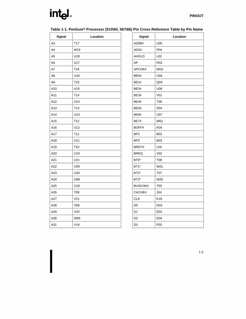
EE PINOUT
1-3
Table 1-1. Pentium ® Processor (510\60, 567\66) Pin Cross Reference Table by Pin Name
Signal Location
A3 T17
A4 W19
A5 U18
A6 U17
A7 T16
A8 U16
A9 T15
A10 U15
A11 T14
A12 U14
A13 T13
A14 U13
A15 T12
A16 U12
A17 T11
A18 U11
A19 T10
A20 U10
A21 U21
A22 U09
A23 U20
A24 U08
A25 U19
A26 T09
A27 V21
A28 V06
A29 V20
A30 W05
A31 V19
Signal Location
A20M# U05
ADS# P04
AHOLD L02
AP P03
APCHK# W03
BE0# U04
BE1# Q04
BE2# U06
BE3# V01
BE4# T06
BE5# S04
BE6# U07
BE7# W01
BOFF# K04
BP2 B02
BP3 B03
BRDY# L04
BREQ V02
BT0* T08
BT1* W21
BT2* T07
BT3* W20
BUSCHK# T03
CACHE# J04
CLK K18
D0 D03
D1 E03
D2 E04
D3 F03

PINOUT EE
1-4
Table 1-1. Pentium ® Processor (510\60, 567\66) Pin Cross Reference Table by Pin Name(Contd.)
Signal Location
D4 C04
D5 G03
D6 B04
D7 G04
D8 F04
D9 C12
D10 C13
D11 E05
D12 C14
D13 D04
D14 D13
D15 D05
D16 D06
D17 B09
D18 C06
D19 C15
D20 D07
D21 C16
D22 C07
D23 A10
D24 B10
D25 C08
D26 C11
D27 D09
D28 D11
D29 C09
D30 D12
D31 C10
D32 D10
Signal Location
D33 C17
D34 C19
D35 D17
D36 C18
D37 D16
D38 D19
D39 D15
D40 D14
D41 B19
D42 D20
D43 A20
D44 D21
D45 A21
D46 E18
D47 B20
D48 B21
D49 F19
D50 C20
D51 F18
D52 C21
D53 G18
D54 E20
D55 G19
D56 H21
D57 F20
D58 J18
D59 H19
D60 L19
D61 K19

EE PINOUT
1-5
Table 1-1. Pentium ® Processor (510\60, 567\66) Pin Cross Reference Table by Pin Name(Contd.)
Signal Location
D62 J19
D63 H18
D/C# V04
DP0 H04
DP1 C05
DP2 A9
DP3 D08
DP4 D18
DP5 A19
DP6 E19
DP7 E21
EADS# M03
EWBE# A03
FERR# H03
FLUSH# U02
FRCMC# M19
HIT# W02
HITM# M04
HLDA Q03
HOLD V05
IBT* T19
IERR# C02
IGNNE# S20
INIT T20
INTR N18
INV A01
IU* J02
Signal Location
IV* B01
KEN# J03
LOCK# V03
M/IO# A02
NA# K03
NMI N19
PCD W04
PCHK# R03
PEN# M18
PM0/BP0 D02
PM1/BP1 C03
PRDY U03
PWT S03
RESET L18
R/S# R18
SCYC R04
SMI# P18
SMIACT# T05
TCK T04
TDI T21
TDO S21
TMS P19
TRST# S18
WB/WT# M02
W/R# N03
NC L03, N04, Q19, R19, S19, T18

PINOUT EE
1-6
Table 1-1. Pentium ® Processor (510\60, 567\66) Pin Cross Reference Table by Pin Name(Contd.)
Signal Location
VCC A04, A05, A06, A07, A08, A11, A12, A13, A14, A15, A16, A17, A18, C01, D01, E01, F01,F21, G01, G21, H01, J21, K21, L21, M21, N01, N21, P01, P21, Q01, Q18, Q21, R01, R21,S01, T01,U01, W06, W07, W08, W09, W10, W11, W12, W13, W14, W15, W16, W17, W18
VSS B05, B06, B07, B08, B11, B12, B13, B14, B15, B16, B17, B18, E02, F02, G02, G20, H02,H20, J01, J20, K01, K02, K20, L01, L20, M01, M20, N02, N20, P02, P20, Q02, Q20, R02,R20, S02, T02, V07, V08, V09, V10, V11, V12, V13, V14, V15, V16, V17, V18
NOTE:
*Not supported on the future Pentium® OverDrive® processor.
1.2. DESIGN NOTESFor reliable operation, always connect unused inputs to an appropriate signal level. Unusedactive low inputs should be connected to VCC. Unused active HIGH inputs should beconnected to GND.
No Connect (NC) pins must remain unconnected. Connection of NC pins may result incomponent failure or incompatibility with processor steppings.
Note: The No Connect pin located at L03 (BRDYC#) along with BUSCHK# are sampled bythe Pentium processor at RESET to configure the I/O buffers of the processor for use with the82496 Cache Controller/82491 Cache SRAM secondary cache as a chip set (refer to the82496 Cache Controller/82491 Cache SRAM Data Book for Use with the Pentium™†Processor, Order Number 241814, for further information).
1.3. QUICK PIN REFERENCEThis section gives a brief functional description of each of the pins. For a detaileddescription, see the Hardware Interface chapter in this manual. Note that all input pinsmust meet their AC/DC specifications to guarantee proper functional behavior. In thissection, the pins are arranged in alphabetical order. The functional grouping of each pin islisted at the end of this chapter.
The # symbol at the end of a signal name indicates that the active, or asserted state occurswhen the signal is at a low voltage. When a # symbol is not present after the signal name,the signal is active, or asserted at the high voltage level.

EE PINOUT
1-7
Table 1-2. Quick Pin Reference
Symbol Type* Name and Function
A20M# I When the address bit 20 mask pin is asserted, the Pentium® processor emulatesthe address wraparound at one Mbyte which occurs on the 8086. When A20M#is asserted, the Pentium processor masks physical address bit 20 (A20) beforeperforming a lookup to the internal caches or driving a memory cycle on the bus.The effect of A20M# is undefined in protected mode. A20M# must be assertedonly when the processor is in real mode.
A31-A3 I/O As outputs, the address lines of the processor along with the byte enables definethe physical area of memory or I/O accessed. The external system drives theinquire address to the processor on A31-A5.
ADS# O The address status indicates that a new valid bus cycle is currently being drivenby the Pentium processor (510\60, 567\66).
AHOLD I In response to the assertion of address hold, the Pentium processor will stopdriving the address lines (A31-A3), BT3-BT0 and AP in the next clock. The restof the bus will remain active so data can be returned or driven for previouslyissued bus cycles.
AP I/O Address parity is driven by the Pentium processor with even parity information onall Pentium processor generated cycles in the same clock that the address isdriven. Even parity must be driven back to the Pentium processor during inquirecycles on this pin in the same clock as EADS# to ensure that the correct paritycheck status is indicated by the Pentium processor.
APCHK# O The address parity check status pin is asserted two clocks after EADS# issampled active if the Pentium processor has detected a parity error on theaddress bus during inquire cycles. APCHK# will remain active for one clock eachtime a parity error is detected.
BE7#-BE0# O The byte enable pins are used to determine which bytes must be written toexternal memory, or which bytes were requested by the CPU for the currentcycle. The byte enables are driven in the same clock as the address lines(A31-3).
BOFF# I The backoff input is used to abort all outstanding bus cycles that have not yetcompleted. In response to BOFF#, the Pentium processor will float all pinsnormally floated during bus hold in the next clock. The processor remains in bushold until BOFF# is negated at which time the Pentium processor restarts theaborted bus cycle(s) in their entirety.
BP[3:2]
PM/BP[1:0]
O The breakpoint pins (BP3-0) correspond to the debug registers, DR3-DR0.These pins externally indicate a breakpoint match when the debug registers areprogrammed to test for breakpoint matches.
BP1 and BP0 are multiplexed with the Performance Monitoring pins (PM1 andPM0). The PB1 and PB0 bits in the Debug Mode Control Register determine ifthe pins are configured as breakpoint or performance monitoring pins. The pinscome out of reset configured for performance monitoring (for more informationsee Appendix A). Because of the fractional speed bus implemented in the futurePentium OverDrive® processor, the breakpoint pins, BP[3:0], may indicate thatone or more BP matches occurred.

PINOUT EE
1-8
Table 1-2. Quick Pin Reference (Contd.)
Symbol Type* Name and Function
BRDY# I The burst ready input indicates that the external system has presented valid dataon the data pins in response to a read or that the external system has acceptedthe Pentium processor data in response to a write request. This signal is sampledin the T2, T12 and T2P bus states.
BREQ O The bus request output indicates to the external system that the Pentiumprocessor has internally generated a bus request. This signal is always drivenwhether or not the Pentium processor is driving its bus.
If the internal request for the bus is removed, the BREQ pin will be deasserted.Note that this means that every assertion of BREQ is NOT guaranteed to have acorresponding assertion of ADS#. For example, assume that the processor hasinternally requested a code prefetch which is a miss in the processor's codecache. BREQ is asserted to indicate that the processor has a bus requestpending internally. If the request can not be serviced immediately (due to busHOLD or AHOLD, or because the bus is busy), and a branch or serializinginstruction is executed, the Pentium processor may recall the request for the codeprefetch and deassert BREQ without ever having driven the code prefetch cycleto the bus.
BT3-BT0 O The branch trace outputs provide bits 2-0 of the branch target linear address(BT2-BT0) and the default operand size (BT3) during a branch trace messagespecial cycle. These signals are not supported on the future Pentium OverDriveprocessor.
BUSCHK# I The bus check input allows the system to signal an unsuccessful completion of abus cycle. If this pin is sampled active, the Pentium processor will latch theaddress and control signals in the machine check registers. If in addition, theMCE bit in CR4 is set, the Pentium processor will vector to the machine checkexception.
CACHE# O For Pentium processor-initiated cycles the cache pin indicates internalcacheability of the cycle (if a read), and indicates a burst writeback cycle (if awrite). If this pin is driven inactive during a read cycle, Pentium processor will notcache the returned data, regardless of the state of the KEN# pin. This pin is alsoused to determine the cycle length (number of transfers in the cycle).
CLK I The clock input provides the fundamental timing for the Pentium processor. Itsfrequency is the internal operating frequency of the Pentium processor andrequires TTL levels. All external timing parameters except TDI, TDO, TMS andTRST# are specified with respect to the rising edge of CLK. It is recommendedthat CLK begin toggling within 150 ms after V CC reaches its properoperating level. This recommendation is only to ensure long-term reliabilityof the device.
D/C# O The Data/Code output is one of the primary bus cycle definition pins. It is drivenvalid in the same clock as the ADS# signal is asserted. D/C# distinguishesbetween data and code or special cycles.
D63-D0 I/O These are the 64 data lines for the processor. Lines D7-D0 define the leastsignificant byte of the data bus; lines D63-D56 define the most significant byte ofthe data bus. The Pentium processor’s data bus (D63-D0) is floated during T1,TD, or Ti bus states. During write cycles, the data bus is driven during the T2,T12, or T2P states. During read cycles, the processor samples the data buswhen BRDY# is returned.

EE PINOUT
1-9
Table 1-2. Quick Pin Reference (Contd.)
Symbol Type* Name and Function
DP7-DP0 I/O These are the data parity pins for the processor. There is one for each byte of thedata bus. They are driven by the Pentium processor with even parity informationon writes in the same clock as write data. Even parity information must be drivenback to the Pentium processor on these pins in the same clock as the data toensure that the correct parity check status is indicated by the Pentium processor.DP7 applies to D63-D56, DP0 applies to D7-D0.
EADS# I This signal indicates that a valid external address has been driven onto thePentium processor address pins to be used for an inquire cycle.
EWBE# I The external write buffer empty input, when inactive (high), indicates that a writecycle is pending in the external system. When the Pentium processor generates awrite, and EWBE# is sampled inactive, the Pentium processor will hold off allsubsequent writes to all E or M-state lines in the data cache until all write cycleshave completed, as indicated by EWBE# being active.
FERR# O The floating-point error pin is driven active when an unmasked floating-point erroroccurs. FERR# is similar to the ERROR# pin on the Intel387™ mathcoprocessor. FERR# is included for compatibility with systems using DOS typefloating-point error reporting.
FLUSH# I When asserted, the cache flush input forces the Pentium processor to writebackall modified lines in the data cache and invalidate its internal caches. A FlushAcknowledge special cycle will be generated by the Pentium processor indicatingcompletion of the writeback and invalidation.
If FLUSH# is sampled low when RESET transitions from high to low, tristate testmode is entered.
FRCMC# I The Functional Redundancy Checking Master/Checker mode input is used todetermine whether the Pentium processor is configured in master mode orchecker mode. When configured as a master, the Pentium processor drives itsoutput pins as required by the bus protocol. When configured as a checker, thePentium processor tristates all outputs (except IERR# and TDO) and samples theoutput pins.
The configuration as a master/checker is set after RESET and may not bechanged other than by a subsequent RESET.
HIT# O The hit indication is driven to reflect the outcome of an inquire cycle. If an inquirecycle hits a valid line in either the Pentium processor data or instruction cache,this pin is asserted two clocks after EADS# is sampled asserted. If the inquirecycle misses Pentium processor cache, this pin is negated two clocks afterEADS#. This pin changes its value only as a result of an inquire cycle andretains its value between the cycles.
HITM# O The hit to a modified line output is driven to reflect the outcome of an inquirecycle. It is asserted after inquire cycles which resulted in a hit to a modified line inthe data cache. It is used to inhibit another bus master from accessing the datauntil the line is completely written back.

PINOUT EE
1-10
Table 1-2. Quick Pin Reference (Contd.)
Symbol Type* Name and Function
HLDA O The bus hold acknowledge pin goes active in response to a hold request driven tothe processor on the HOLD pin. It indicates that the Pentium processor hasfloated most of the output pins and relinquished the bus to another local busmaster. When leaving bus hold, HLDA will be driven inactive and the Pentiumprocessor will resume driving the bus. If the Pentium processor has bus cyclepending, it will be driven in the same clock that HLDA is deasserted.
HOLD I In response to the bus hold request, the Pentium processor will float most of itsoutput and input/output pins and assert HLDA after completing all outstanding buscycles. The Pentium processor will maintain its bus in this state until HOLD isdeasserted. HOLD is not recognized during LOCK cycles. The Pentiumprocessor will recognize HOLD during reset.
IBT O The instruction branch taken pin is driven active (high) for one clock to indicatethat a branch was taken. This output is always driven by the Pentium processor(510\60, 567\66). This signal is not supported on the future Pentium OverDriveprocessor.
IERR# O The internal error pin is used to indicate two types of errors, internal parity errorsand functional redundancy errors. If a parity error occurs on a read from aninternal array, the Pentium processor will assert the IERR# pin for one clock andthen shutdown. If the Pentium processor is configured as a checker and amismatch occurs between the value sampled on the pins and the correspondingvalue computed internally, the Pentium processor will assert IERR# two clocksafter the mismatched value is returned.
IGNNE# I This is the ignore numeric error input. This pin has no effect when the NE bit inCR0 is set to 1. When the CR0.NE bit is 0, and the IGNNE# pin is asserted, thePentium processor will ignore any pending unmasked numeric exception andcontinue executing floating-point instructions for the entire duration that this pin isasserted. When the CR0.NE bit is 0, IGNNE# is not asserted, a pendingunmasked numeric exception exists (SW.ES = 1), and the floating-pointinstruction is one of FINIT, FCLEX, FSTENV, FSAVE, FSTSW, FSTCW, FENI,FDISI, or FSETPM, the Pentium processor will execute the instruction in spite ofthe pending exception. When the CR0.NE bit is 0, IGNNE# is not asserted, apending unmasked numeric exception exists (SW.ES = 1), and the floating-pointinstruction is one other than FINIT, FCLEX, FSTENV, FSAVE, FSTSW, FSTCW,FENI, FDISI, or FSETPM, the Pentium processor will stop execution and wait foran external interrupt.
INIT I The Pentium processor initialization input pin forces the Pentium processor tobegin execution in a known state. The processor state after INIT is the same asthe state after RESET except that the internal caches, write buffers, and floating-point registers retain the values they had prior to INIT. INIT may NOT be used inlieu of RESET after power-up.
If INIT is sampled high when RESET transitions from high to low the Pentiumprocessor will perform built-in self test prior to the start of program execution.

EE PINOUT
1-11
Table 1-2. Quick Pin Reference (Contd.)
Symbol Type* Name and Function
INTR I An active maskable interrupt input indicates that an external interrupt has beengenerated. If the IF bit in the EFLAGS register is set, the Pentium processor willgenerate two locked interrupt acknowledge bus cycles and vector to an interrupthandler after the current instruction execution is completed. INTR must remainactive until the first interrupt acknowledge cycle is generated to assure that theinterrupt is recognized.
INV I The invalidation input determines the final cache line state (S or I) in case of aninquire cycle hit. It is sampled together with the address for the inquire cycle inthe clock EADS# is sampled active.
IU O The u-pipe instruction complete output is driven active (high) for 1 clock toindicate that an instruction in the u-pipeline has completed execution. This pin isalways driven by the Pentium processor (510\60, 567\66). This signal is notsupported on the future Pentium OverDrive processor.
IV O The v-pipe instruction complete output is driven active (high) for one clock toindicate that an instruction in the v-pipeline has completed execution. This pin isalways driven by the Pentium processor (510\60, 567\66). This signal is notsupported on the future Pentium OverDrive processor.
KEN# I The cache enable pin is used to determine whether the current cycle is cacheableor not and is consequently used to determine cycle length. When the Pentiumprocessor generates a cycle that can be cached (CACHE# asserted) and KEN#is active, the cycle will be transformed into a burst line fill cycle.
LOCK# O The bus lock pin indicates that the current bus cycle is locked. The Pentiumprocessor will not allow a bus hold when LOCK# is asserted (but AHOLD andBOFF# are allowed). LOCK# goes active in the first clock of the first locked buscycle and goes inactive after the BRDY# is returned for the last locked bus cycle.LOCK# is guaranteed to be deasserted for at least one clock between back toback locked cycles.
M/IO# O The Memory/Input-Output is one of the primary bus cycle definition pins. It isdriven valid in the same clock as the ADS# signal is asserted. M/IO#distinguishes between memory and I/O cycles.
NA# I An active next address input indicates that the external memory system is readyto accept a new bus cycle although all data transfers for the current cycle havenot yet completed. The Pentium processor will drive out a pending cycle twoclocks after NA# is asserted. The Pentium processor supports up to twooutstanding bus cycles.
NMI I The non-maskable interrupt request signal indicates that an external non-maskable interrupt has been generated.
PCD O The page cache disable pin reflects the state of the PCD bit in CR3, the PageDirectory Entry, or the Page Table Entry. The purpose of PCD is to provide anexternal cacheability indication on a page by page basis.

PINOUT EE
1-12
Table 1-2. Quick Pin Reference (Contd.)
Symbol Type* Name and Function
PCHK# O The parity check output indicates the result of a parity check on a data read. It isdriven with parity status two clocks after BRDY# is returned. PCHK# remains lowone clock for each clock in which a parity error was detected. Parity is checkedonly for the bytes on which valid data is returned.
PEN# I The parity enable input (along with CR4.MCE) determines whether a machinecheck exception will be taken as a result of a data parity error on a read cycle. Ifthis pin is sampled active in the clock a data parity error is detected, the Pentiumprocessor will latch the address and control signals of the cycle with the parityerror in the machine check registers. If in addition the machine check enable bitin CR4 is set to "1," the Pentium processor will vector to the machine checkexception before the beginning of the next instruction.
PM/BP[1:0]BP[3:2]
O For more information on the performance monitoring pins, see Appendix A.
The breakpoint pins BP[1:0] are multiplexed with the Performance Monitoring pinsPM[1:0]. The PB1 and PB0 bits in the Debug Mode Control Register determine ifthe pins are configured as breakpoint or performance monitoring pins. The pinscome out of reset configured for performance monitoring (for more informationsee Appendix A).
PRDY O The PRDY output pin indicates that the processor has stopped normal executionin response to the R/S# pin going active, or Probe Mode being entered (seeAppendix A for more information). This pin is provided for use with the Intel debugport described in the "Debugging" chapter.
PWT O The page writethrough pin reflects the state of the PWT bit in CR3, the PageDirectory Entry, or the Page Table Entry. The PWT pin is used to provide anexternal writeback indication on a page by page basis.
R/S# I The R/S# input is an asynchronous, edge sensitive interrupt used to stop thenormal execution of the processor and place it into an idle state. A high to lowtransition on the R/S# pin will interrupt the processor and cause it to stopexecution at the next instruction boundary. This pin is provided for use with theIntel debug port described in the "Debugging" chapter.
RESET I Reset forces the Pentium processor to begin execution at a known state. All thePentium processor internal caches will be invalidated upon the RESET. Modifiedlines in the data cache are not written back.
FLUSH#, FRCMC# and INIT are sampled when RESET transitions from high tolow to determine if tristate test mode or checker mode will be entered, or if BISTwill be run.
SCYC O The split cycle output is asserted during misaligned LOCKed transfers to indicatethat more than two cycles will be locked together. This signal is defined forlocked cycles only. It is undefined for cycles which are not locked.
SMI# I The system Management Interrupt causes a system management interruptrequest to be latched internally. When the latched SMI# is recognized on aninstruction boundary, the processor enters System Management Mode.
SMIACT# O An active system management interrupt active output indicates that the processoris operating in System Management Mode (SMM).

EE PINOUT
1-13
Table 1-2. Quick Pin Reference (Contd.)
Symbol Type* Name and Function
TCK I The testability clock input provides the clocking function for the Pentiumprocessor boundary scan in accordance with the IEEE Boundary Scan interface(Standard 1149.1). It is used to clock state information and data into and out ofthe Pentium processor (510\60, 567\66) during boundary scan.
TDI I The test data input is a serial input for the test logic. TAP instructions and dataare shifted into the Pentium processor on the TDI pin on the rising edge of TCKwhen the TAP controller is in an appropriate state.
TDO O The test data output is a serial output of the test logic. TAP instructions and dataare shifted out of the Pentium processor on the TDO pin on the falling edge ofTCK when the TAP controller is in an appropriate state.
TMS I The value of the test mode select input signal sampled at the rising edge of TCKcontrols the sequence of TAP controller state changes.
TRST# I When asserted, the test reset input allows the TAP controller to beasynchronously initialized.
W/R# O Write/Read is one of the primary bus cycle definition pins. It is driven valid in thesame clock as the ADS# signal is asserted. W/R# distinguishes between writeand read cycles.
WB/WT# I The writeback/writethrough input allows a data cache line to be defined aswriteback or writethrough on a line by line basis. As a result, it determineswhether a cache line is initially in the S or E state in the data cache.
NOTES:
*The pins are classified as Input or Output based on their function in Master Mode. See the FunctionalRedundancy Checking section in the 'Error Detection' chapter for further information.

PINOUT EE
1-14
1.4. PIN REFERENCE TABLES
Table 1-3. Output Pins
Name Active Level When Floated
ADS# Low Bus Hold, BOFF#
APCHK# Low
BE7#-BE0# Low Bus Hold, BOFF#
BREQ High
BT3-BT0 n/a
CACHE# Low Bus Hold, BOFF#
FERR# Low
HIT# Low
HITM# Low
HLDA High
IBT* High
IERR# Low
IU* High
IV* High
LOCK# Low Bus Hold, BOFF#
M/IO#, D/C#, W/R# n/a Bus Hold, BOFF#
PCHK# Low
BP3-2, PM1/BP1, PM0/BP0 High
PRDY High
PWT, PCD High Bus Hold, BOFF#
SCYC High Bus Hold, BOFF#
SMIACT# Low
TDO n/a All states except Shift-DR and Shift-IR
NOTE:
All output and input/output pins are floated during tristate test mode and checker mode (except IERR#).
*These signals will be internally tied inactive (low) on the future Pentium® OverDrive® processor.

EE PINOUT
1-15
Table 1-4. Input Pins
Name Active LevelSynchronous/Asynchronous Internal Resistor Qualified
A20M# LOW Asynchronous
AHOLD HIGH Synchronous
BOFF# LOW Synchronous
BRDY# LOW Synchronous Bus State T2,T12,T2P
BUSCHK# LOW Synchronous Pullup BRDY#
CLK n/a
EADS# LOW Synchronous
EWBE# LOW Synchronous BRDY#
FLUSH# LOW Asynchronous
FRCMC# LOW Asynchronous
HOLD HIGH Synchronous
IGNNE# LOW Asynchronous
INIT HIGH Asynchronous
INTR HIGH Asynchronous
INV HIGH Synchronous EADS#
KEN# LOW Synchronous First BRDY#/NA#
NA# LOW Synchronous Bus State T2,TD,T2P
NMI HIGH Asynchronous
PEN# LOW Synchronous BRDY#
R/S# n/a Asynchronous Pullup
RESET HIGH Asynchronous
SMI# LOW Asynchronous Pullup
TCK n/a Pullup
TDI n/a Synchronous/TCK Pullup TCK
TMS n/a Synchronous/TCK Pullup TCK
TRST# LOW Asynchronous Pullup
WB/WT# n/a Synchronous First BRDY#/NA#
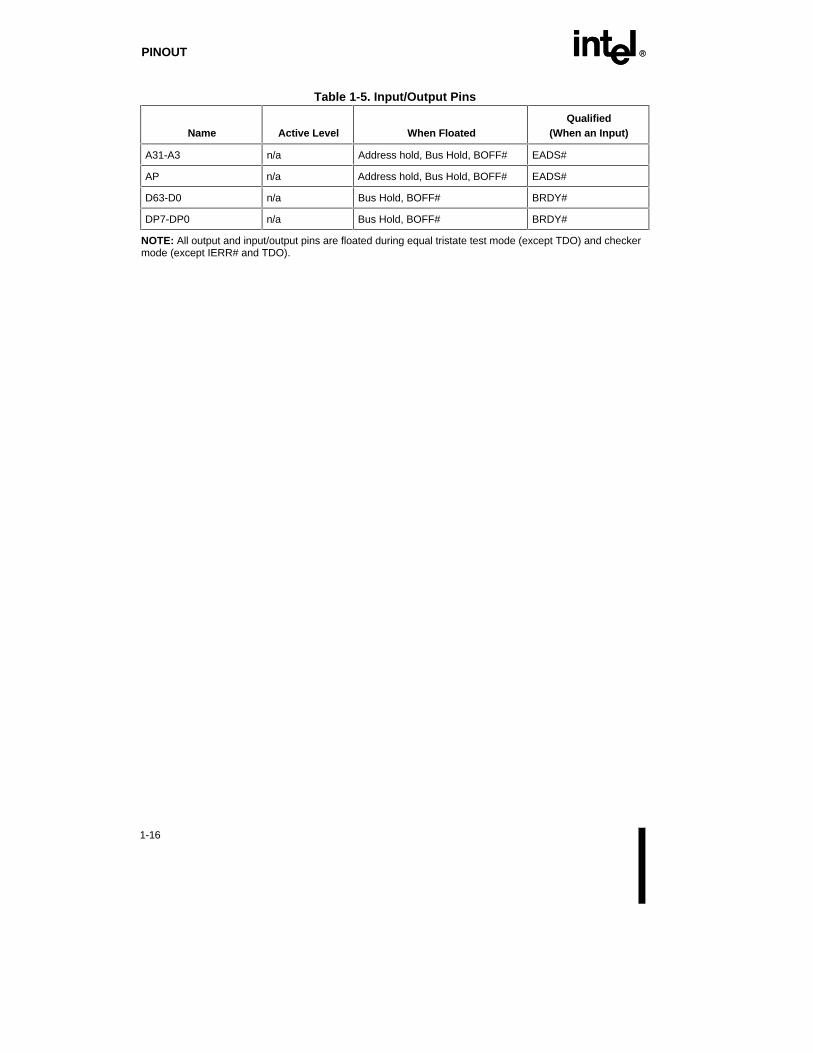
PINOUT EE
1-16
Table 1-5. Input/Output Pins
Name Active Level When FloatedQualified
(When an Input)
A31-A3 n/a Address hold, Bus Hold, BOFF# EADS#
AP n/a Address hold, Bus Hold, BOFF# EADS#
D63-D0 n/a Bus Hold, BOFF# BRDY#
DP7-DP0 n/a Bus Hold, BOFF# BRDY#
NOTE: All output and input/output pins are floated during equal tristate test mode (except TDO) and checkermode (except IERR# and TDO).

EE PINOUT
1-17
1.5. PIN GROUPING ACCORDING TO FUNCTIONTable 1-6 organizes the pins with respect to their function.
Table 1-6. Pin Functional Grouping
Function Pins
Clock CLK
Initialization RESET, INIT
Address Bus A31-A3, BE7# - BE0#
Address Mask A20M#
Data Bus D63-D0
Address Parity AP, APCHK#
Data Parity DP7-DP0, PCHK#, PEN#
Internal Parity Error IERR#
System Error BUSCHK#
Bus Cycle Definition M/IO#, D/C#, W/R#, CACHE#, SCYC, LOCK#
Bus Control ADS#, BRDY#, NA#
Page Cacheability PCD, PWT
Cache Control KEN#, WB/WT#
Cache Snooping/Consistency AHOLD, EADS#, HIT#, HITM#, INV
Cache Flush FLUSH#
Write Ordering EWBE#
Bus Arbitration BOFF#, BREQ, HOLD, HLDA
Interrupts INTR, NMI
Floating-Point Error Reporting FERR#, IGNNE#
System Management Mode SMI#, SMIACT#
Functional Redundancy Checking FRCMC# (IERR#)
TAP Port TCK, TMS, TDI, TDO, TRST#
Breakpoint/Performance Monitoring PM0/BP0, PM1/BP1, BP3-2
Execution Tracing BT3-BT0, IU, IV, IBT
Probe Mode R/S#, PRDY

PINOUT EE
1-18
1.6. OUTPUT PIN GROUPING ACCORDING TO WHEN DRIVENThis section groups the output pins according to when they are driven.
Group 1
The following output pins are driven active at the beginning of a bus cycle with ADS#. A31-A3 and AP are guaranteed to remain valid until AHOLD is asserted or until the earlier of theclock after NA# or the last BRDY#. The remaining pins are guaranteed to remain valid untilthe earlier of the clock after NA# or the last BRDY#:
A31-A3, AP, BE7#-0#, CACHE#, M/IO#, W/R#, D/C#, SCYC, PWT, PCD.
Group 2
As outputs, the following pins are driven in T2, T12, and T2P. As inputs, these pins aresampled with BRDY#:
D63-0, DP7-0.
Group 3
These are the status output pins. They are always driven:
BREQ, HIT#, HITM#, IU, IV, IBT, BT3-BT0, PM0/BP0, PM1/BP1, BP3, BP2, PRDY,SMIACT#.
Group 4
These are the glitch free status output pins.
APCHK#, FERR#, HLDA, IERR#, LOCK#, PCHK#.

E2
MicroprocessorArchitectureOverview

EE
2-1
CHAPTER 2MICROPROCESSOR ARCHITECTURE OVERVIEW
The Pentium processor is the next generation member of the Intel386™ and Intel486microprocessor family. It is 100% binary compatible with the 8086/88, 80286, Intel386 DXCPU, Intel386 SX CPU, Intel486 DX CPU, Intel486 SX and the Intel486 DX2 CPUs.
The Pentium processor (510\60, 567\66) contains all of the features of the Intel486 CPU, andprovides significant enhancements and additions including the following:
• Superscalar Architecture
• Dynamic Branch Prediction
• Pipe-lined Floating-Point Unit
• Improved Instruction Execution Time
• Separate 8K Code and Data Caches
• Writeback MESI Protocol in the Data Cache
• 64-Bit Data Bus
• Bus Cycle Pipe-lining
• Address Parity
• Internal Parity Checking
• Function Redundancy Checking
• Execution Tracing
• Performance Monitoring
• IEEE 1149.1 Boundary Scan
• System Management Mode
• Virtual Mode Extensions
• Upgradable with a future Pentium OverDrive® processor
The application instruction set of the Pentium processor family includes the completeIntel486 CPU instruction set with extensions to accommodate some of the additionalfunctionality of the Pentium processor. All application software written for the Intel386 andIntel486 microprocessors will run on the Pentium processor without modification. The on-chip memory management unit (MMU) is completely compatible with the Intel386 andIntel486 CPUs.
The Pentium processor family implements several enhancements to increase performance.The two instruction pipe-lines and floating-point unit on the Pentium processor are capableof independent operation. Each pipe-line issues frequently used instructions in a single clock.

MICROPROCESSOR ARCHITECTURE OVERVIEW EE
2-2
Together, the dual pipes can issue two integer instructions in one clock, or one floating-pointinstruction (under certain circumstances, 2 floating-point instructions) in one clock.
Branch prediction is implemented in the Pentium processor. To support this, the Pentiumprocessor implements two prefetch buffers, one to prefetch code in a linear fashion, and onethat prefetches code according to the BTB so the needed code is almost always prefetchedbefore it is needed for execution.
The floating-point unit has been completely redesigned over the Intel486 CPU. Fasteralgorithms provide up to a 10X speed-up for common operations including ADD,MULTIPLY, and LOAD. Many applications can achieve five times the performance or morewith instruction scheduling and overlapped (pipe-lined) execution.
The Pentium processor includes separate code and data caches integrated on chip to meet itsperformance goals. Each cache is 8 Kbytes in size, with a 32-byte line size and is 2-way setassociative. Each cache has a dedicated Translation Lookaside Buffer (TLB) to translatelinear addresses to physical addresses. The data cache is configurable to be writeback orwritethrough on a line by line basis and follows the MESI protocol. The data cache tags aretriple ported to support two data transfers and an inquire cycle in the same clock. The codecache is an inherently write protected cache. The code cache tags are also triple ported tosupport snooping and split line accesses. Individual pages can be configured as cacheable ornon-cacheable by software or hardware. The caches can be enabled or disabled by softwareor hardware.
The Pentium processor has increased the data bus to 64-bits to improve the data transfer rate.Burst read and burst writeback cycles are supported by the Pentium processor. In addition,bus cycle pipe-lining has been added to allow two bus cycles to be in progresssimultaneously. The Pentium processor Memory Management Unit contains optionalextensions to the architecture which allow 4 Mbyte page sizes.
The Pentium processor has added significant data integrity and error detection capability.Data parity checking is still supported on a byte-by-byte basis. Address parity checking, andinternal parity checking features have been added along with a new exception, the machinecheck exception. In addition, the Pentium processor has implemented functional redundancychecking to provide maximum error detection of the processor and the interface to theprocessor. When functional redundancy checking is used, a second processor, the "checker"is used to execute in lock step with the "master" processor. The checker samples the master'soutputs and compares those values with the values it computes internally, and asserts an errorsignal if a mismatch occurs.
As more and more functions are integrated on chip, the complexity of board level testing isincreased. To address this, the Pentium processor has increased test and debug capability.Like many of the Intel486 CPUs, the Pentium processor implements IEEE Boundary Scan(Standard 1149.1). In addition, the Pentium processor has specified 4 breakpoint pins thatcorrespond to each of the debug registers and externally indicate a breakpoint match.Execution tracing provides external indications when an instruction has completed executionin either of the two internal pipe-lines, or when a branch has been taken.
System management mode has been implemented along with some extensions to the SMMarchitecture. Enhancements to the Virtual 8086 mode have been made to increase

EE MICROPROCESSOR ARCHITECTURE OVERVIEW
2-3
performance by reducing the number of times it is necessary to trap to a virtual 8086monitor.
Figure 2-1 shows a block diagram of the Pentium processor.
BranchTargetBuffer
Code Cache8 KBytes
ROM
Control Unit
GenerateAddress
Generate
Data Cache8 KBytes
256
TLB
TLB
Prefetch
Address
Prefetch Buffers
Instruction Decode
InstructionPointer
Integer Register FileALU
Barrel Shifter
3232
32
32 32
32
PageUnit
BusUnit
32-BitAddress
Bus
Control
64-BitDataBus
32-BitAddr.Bus
64
ControlRegister File
Add
Multiply
Divide
FloatingPointUnit
Pentium ® Microprocessor
Control
80
80
Address
(U Pipeline) (V Pipeline)
(U Pipeline) (V Pipeline)ALU
PDB24
Branch Verif.& Target Addr
32
64-BitDataBus
Figure 2-1. Pentium ® Processor Block Diagram
The block diagram shows the two instruction pipe-lines, the "u" pipe and the "v" pipe. Theu-pipe can execute all integer and floating-point instructions. The v-pipe can execute simpleinteger instructions and the FXCH floating-point instructions.
The separate caches are shown, the code cache and data cache. The data cache has two ports,one for each of the two pipes (the tags are triple ported to allow simultaneous inquire cycles).The data cache has a dedicated Translation Lookaside Buffer (TLB) to translate linearaddresses to the physical addresses used by the data cache.

MICROPROCESSOR ARCHITECTURE OVERVIEW EE
2-4
The code cache, branch target buffer and prefetch buffers are responsible for getting rawinstructions into the execution units of the Pentium processor. Instructions are fetched fromthe code cache or from the external bus. Branch addresses are remembered by the branchtarget buffer. The code cache TLB translates linear addresses to physical addresses used bythe code cache.
The decode unit decodes the prefetched instructions so the Pentium processor can execute theinstruction. The control ROM contains the microcode which controls the sequence ofoperations that must be performed to implement the Pentium processor architecture. Thecontrol ROM unit has direct control over both pipe-lines.
The Pentium processor contains a pipe-lined floating-point unit that provides a significantfloating-point performance advantage over previous generations of Intel Architecture-basedCPUs.
Supporting an upgrade socket (Socket 4) in the system will provide end user upgradability bythe addition of a future Pentium OverDrive processor. Typical applications will realize a40% to 70% performance increase by the addition of a future Pentium OverDrive processor.Refer to Chapter 16 for details on the future Pentium OverDrive processor for Pentiumprocessor (510\60, 567\66)-based systems.
The architectural features introduced in this chapter are more fully described in the"Component Operation" chapter of this document.

E3
ComponentOperation


EE
3-1
CHAPTER 3COMPONENT OPERATION
The Pentium processor has an optimized superscalar micro-architecture capable of executingtwo instructions in a single clock. A 64-bit external bus, separate 8-Kbyte data and instruc-tion caches, write buffers, branch prediction, and a pipe-lined floating-point unit combine tosustain the high execution rate. These architectural features and their operation are discussedin this chapter.
3.1. PIPE-LINE AND INSTRUCTION FLOWLike the Intel486 CPU, integer instructions traverse a 5 stage pipe-line. The pipe-line stagesare as follows:
PF Prefetch
D1 Instruction Decode
D2 Address Generate
EX Execute - ALU and Cache Access
WB Writeback
Figure 3-1 shows how instructions move through the Intel486 CPU pipe-line.
PDB60
D1
D2
EX
WB
PF l1 l2 l3 l4
l1 l2 l3 l4
l1 l2 l3 l4
l1 l2 l3 l4
l1 l2 l3 l4
Figure 3-1. Intel486 CPU Pipe-line Execution

COMPONENT OPERATION EE
3-2
Unlike the Intel486 microprocessor, the Pentium processor is a superscalar machine capableof executing two instructions in parallel. Two five stage pipe-lines operate in parallelallowing integer instructions to execute in a single clock in each pipe-line. Figure 3-2 depictsinstruction flow in the Pentium processor.
PDB61
I1
I4
I5I3
I2 I6
I7
I8
I1
I4
I5I3
I2 I6
I7
I8
I1
I4
I5I3
I2 I6
I7
I8
I1
I4
I5I3
I2 I6
I7
I8
I1
I4
I5I3
I2 I6
I7
I8
PF
D1
D2
EX
WB
Figure 3-2. Pentium ® Processor Pipe-line Execution
The pipe-lines in the Pentium processor are called the "u" and "v" pipes and the process ofissuing two instructions in parallel is termed "pairing." The u-pipe can execute anyinstruction in the Intel architecture while the v-pipe can execute "simple" instructions asdefined in the "Instruction Pairing Rules" Section of this chapter. When instructions arepaired, the instruction issued to the v-pipe is always the next sequential instruction after theone issued to the u-pipe.
3.1.1. Pentium ® Processor Pipe-line Description andImprovements
While the basic pipe-line structure is the same as the Intel486 CPU, the Pentium processorpipe-line has been optimized to achieve higher throughput.
The first stage of the pipe-line is Prefetch (PF) stage in which instructions are prefetchedfrom the on chip instruction cache or memory. Because the Pentium processor has separatecaches for instructions and data, prefetches no longer conflict with data references for accessto the cache. If the requested line is not in the code cache, a memory reference is made. Inthe PF stage, two independent pairs of line-size (32-byte) prefetch buffers operate in

EE COMPONENT OPERATION
3-3
conjunction with the branch target buffer. This allows one prefetch buffer to prefetchinstructions sequentially, while the other prefetches according to the branch target bufferpredictions. The prefetch buffers alternate their prefetch paths. See the section titled"Instruction Prefetch" in this chapter for further details on the Pentium processor prefetchbuffers.
The next pipe-line stage is Decode1 (D1) in which two parallel decoders attempt to decodeand issue the next two sequential instructions. The decoders determine whether one or twoinstructions can be issued contingent upon the instruction pairing rules described in thesection titled "Instruction Pairing Rules." The Pentium processor, similar to the Intel486CPU, requires an extra D1 clock to decode instruction prefixes. Prefixes are issued to the u-pipe at the rate of one per clock without pairing. After all prefixes have been issued, the baseinstruction will then be issued and paired according to the pairing rules. The one exception tothis is that the Pentium processor will decode near conditional jumps (long displacement) inthe second opcode map (0Fh prefix) in a single clock in either pipe-line.
The D1 stage is followed by Decode2 (D2) in which the address of memory residentoperands are calculated similar to the Intel486 CPU. In the Intel486 CPU, instructionscontaining both a displacement and an immediate, or instructions containing a base and indexaddressing mode require an additional D2 clock to decode. The Pentium processor removesboth of these restrictions and is able to issue instructions in these categories in a single clock.
Similar to the Intel486 CPU, the Pentium processor uses the Execute (EX) stage of the pipe-line for both ALU operations and for data cache access; therefore those instructionsspecifying both an ALU operation and a data cache access will require more than one clockin this stage. In EX all u-pipe instructions and all v-pipe instructions except conditionalbranches are verified for correct branch prediction. Microcode is designed to utilize bothpipe-lines and thus those instructions requiring microcode execute faster than on the Intel486CPU.
The final stage is Writeback (WB) where instructions are enabled to modify processor stateand complete execution. In this stage v-pipe conditional branches are verified for correctbranch prediction.
During their progression through the pipe-line instructions may be stalled due to certainconditions. Both the u-pipe and v-pipe instructions enter and leave the D1 and D2 stages inunison. When an instruction in one pipe is stalled then the instruction in the other pipe is alsostalled at the same pipe-line stage. Thus both the u-pipe and the v-pipe instructions enter theEX stage in unison. Once in EX if the u-pipe instruction is stalled, then the v-pipe instruction(if any) is also stalled. If the v-pipe instruction is stalled then the instruction paired with it inthe u-pipe is allowed to advance. No successive instructions are allowed to enter the EXstage of either pipe-line until the instructions in both pipe-lines have advanced to WB.
3.1.1.1. INSTRUCTION PREFETCH
In the PF stage, two independent pairs of line-size (32-byte) prefetch buffers operate inconjunction with the branch target buffer. Only one prefetch buffer actively requestsprefetches at any given time. Prefetches are requested sequentially until a branch instructionis fetched. When a branch instruction is fetched, the branch target buffer (BTB) predicts

COMPONENT OPERATION EE
3-4
whether the branch will be taken or not. If the branch is predicted not taken, prefetch requestscontinue linearly. On a predicted taken branch the other prefetch buffer is enabled and beginsto prefetch as though the branch was taken. If a branch is discovered mis-predicted, theinstruction pipelines are flushed and prefetching activity starts over.
For more information on branch prediction, see section 3.2.
3.1.2. Instruction Pairing RulesThe Pentium processor can issue one or two instructions every clock. In order to issue twoinstructions simultaneously they must satisfy the following conditions:
• Both instructions in the pair must be "simple" as defined below
• There must be no read-after-write or write-after-write register dependencies betweenthem
• Neither instruction may contain both a displacement and an immediate
• Instructions with prefixes (other than 0F of JCC instructions) can only occur in the u-pipe
Simple instructions are entirely hardwired; they do not require any microcode control and, ingeneral, execute in one clock. The exceptions are the ALU mem,reg and ALU reg,meminstructions which are three and two clock operations respectively. Sequencing hardware isused to allow them to function as simple instructions. The following integer instructions areconsidered simple and may be paired:
1. mov reg, reg/mem/imm
2. mov mem, reg/imm
3. alu reg, reg/mem/imm
4. alu mem, reg/imm
5. inc reg/mem
6. dec reg/mem
7. push reg/mem
8. pop reg
9. lea reg,mem
10. jmp/call/jcc near
11. nop
In addition, conditional and unconditional branches may be paired only if they occur as thesecond instruction in the pair. They may not be paired with the next sequential instruction.Also, SHIFT/ROT by 1 and SHIFT by imm may pair as the first instruction in a pair.
The register dependencies that prohibit instruction pairing include implicit dependencies viaregisters or flags not explicitly encoded in the instruction. For example, an ALU instructionin the u-pipe (which sets the flags) may not be paired with an ADC or an SBB instruction in
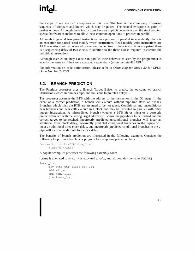
EE COMPONENT OPERATION
3-5
the v-pipe. There are two exceptions to this rule. The first is the commonly occurringsequence of compare and branch which may be paired. The second exception is pairs ofpushes or pops. Although these instructions have an implicit dependency on the stack pointer,special hardware is included to allow these common operations to proceed in parallel.
Although in general two paired instructions may proceed in parallel independently, there isan exception for paired "read-modify-write" instructions. Read-modify-write instructions areALU operations with an operand in memory. When two of these instructions are paired thereis a sequencing delay of two clocks in addition to the three clocks required to execute theindividual instructions.
Although instructions may execute in parallel their behavior as seen by the programmer isexactly the same as if they were executed sequentially (as on the Intel486 CPU).
For information on code optimization, please refer to Optimizing for Intel's 32-Bit CPUs,Order Number 241799.
3.2. BRANCH PREDICTIONThe Pentium processor uses a Branch Target Buffer to predict the outcome of branchinstructions which minimizes pipe-line stalls due to prefetch delays.
The processor accesses the BTB with the address of the instruction in the D1 stage. In theevent of a correct prediction, a branch will execute without pipe-line stalls or flushes.Branches which miss the BTB are assumed to be not taken. Conditional and unconditionalnear branches and near calls execute in 1 clock and may be executed in parallel with otherinteger instructions. A mispredicted branch (whether a BTB hit or miss) or a correctlypredicted branch with the wrong target address will cause the pipe-lines to be flushed and thecorrect target to be fetched. Incorrectly predicted unconditional branches will incur anadditional three clock delay, incorrectly predicted conditional branches in the u-pipe willincur an additional three clock delay, and incorrectly predicted conditional branches in the v-pipe will incur an additional four clock delay.
The benefits of branch prediction are illustrated in the following example. Consider thefollowing loop from a benchmark program for computing prime numbers:
for(k=i+prime;k<=SIZE;k+=prime)flags[k]=FALSE;
A popular compiler generates the following assembly code:
(prime is allocated to ecx, k is allocated to edx , and al contains the value FALSE)
inner_loop:mov byte ptr flags[edx],aladd edx,ecxcmp edx, SIZEjle inner_loop

COMPONENT OPERATION EE
3-6
Each iteration of this loop will execute in 6 clocks on the Intel486 CPU. On the Pentiumprocessor, the mov is paired with the add ; the cmp with the jle . With branch prediction,each loop iteration executes in 2 clocks.
NOTE
The dynamic branch prediction algorithm speculatively runs code fetchcycles to addresses corresponding to instructions executed some time in thepast. Such code fetch cycles are run based on past execution history,regardless of whether the instructions retrieved are relevant to the currentlyexecuting instruction sequence.
One effect of the branch prediction mechanism is that the Pentiumprocessor may run code fetch bus cycles to retrieve instructions which arenever executed. Although the opcodes retrieved are discarded, the systemmust complete the code fetch bus cycle by returning BRDY#. It isparticularly important that the system return BRDY# for all code fetchcycles, regardless of the address.
Furthermore, it is possible that the Pentium processor may run speculativecode fetch cycles to addresses beyond the end of the current code segment(approximately 100 bytes past end of last executed instruction). Althoughthe Pentium processor may prefetch beyond the CS limit, it will not attemptto execute beyond the CS limit. Instead, it will raise a GP fault. Thus,segmentation cannot be used to prevent speculative code fetches toinaccessible areas of memory. On the other hand, the Pentium processornever runs code fetch cycles to inaccessible pages (i.e., not present pages orpages with incorrect access rights), so the paging mechanism guards againstboth the fetch and execution of instructions in inaccessible pages.
For memory reads and writes, both segmentation and paging prevent thegeneration of bus cycles to inaccessible regions of memory. If paging is notused, branch prediction can be disabled by setting TR12.NBP (bit 0)* andflushing the BTB by loading CR3 before disabling any areas of memory.Branch prediction can be re-enabled after re-enabling memory.
The following is an example of a situation that may occur:
1. Code passes control to segment at address c000h.
2. Code transfers control to code at different address (6000h) by usingFAR CALL instruction.
3. This portion of the code does an I/O write to a port that disablesmemory at address c000h.
4. At the end of this segment, an I/O write is performed to re-enablememory at address c000h.
5. Following the OUT instruction, there is a RETF instruction to c000hsegment.

EE COMPONENT OPERATION
3-7
OUT ; disable c000h
OUT ; enable c000hRETF
--
--
FAR CALL
6000h
c000h
The branch prediction mechanism of the Pentium processor, however,predicts that the RETF instruction is going to transfer control to thesegment at address c000h and performs a prefetch from that address prior tothe OUT instruction that re-enables that memory address. The result is thatno BRDY is returned for that prefetch cycle and the system hangs.
In this case, branch prediction should be disabled (by setting TR12.NBP*and flushing the BTB by loading CR3) prior to disabling memory at addressc000h and re-enabled after the RETF instruction by clearing TR12.NBP* asindicated above.
* Please refer to Chapter 33 of this volume.
3.3. WRITE BUFFERS AND MEMORY ORDERINGThe Pentium processor has two write buffers, one corresponding to each of the pipe-lines, toenhance the performance of consecutive writes to memory. These write buffers are one quad-word wide (64-bits) and can be filled simultaneously in one clock e.g., by two simultaneouswrite misses in the two instruction pipe-lines. Writes in these buffers are driven out on theexternal bus in the order they were generated by the processor core. No reads (as a result ofcache miss) are reordered around previously generated writes sitting in the write buffers. Theimplication of this is that the write buffers will be flushed or emptied before a subsequent buscycle is run on the external bus (unless BOFF# is asserted and a writeback cycle becomespending, see section 3.3.3.).
The Pentium processor supports strong write ordering only. That is, writes generated by thePentium processor will be driven to the bus or updated in the cache in the order that theyoccur. The Pentium processor will not write to E or M-state lines in the data cache if there isa write in either write buffer, if a write cycle is running on the bus, or if EWBE# is inactive.
Note that only memory writes are buffered and I/O writes are not. There is no guarantee ofsynchronization between completion of memory writes on the bus and instruction execution

COMPONENT OPERATION EE
3-8
after the write. The OUT instruction or a serializing instruction needs to be executed tosynchronize writes with the next instruction. Please refer to the "Serializing Operations"section for more information.
No re-ordering of read cycles occurs on the Pentium processor. Specifically, the write buffersare flushed before the IN instruction is executed.
3.3.1. External Event SynchronizationWhen the system changes the value of NMI, INTR, FLUSH#, SMI# or INIT as the result ofexecuting an OUT instruction, these inputs must be at a valid state three clocks beforeBRDY# is returned to ensure that the new value will be recognized before the nextinstruction is executed.
Note that if an OUT instruction is used to modify A20M#, this will not affect previouslyprefetched instructions. A serializing instruction must be executed to guarantee recognitionof A20M# before a specific instruction.
3.3.2. Serializing OperationsAfter executing certain instructions the Pentium processor serializes instruction execution.This means that any modifications to flags, registers, and memory for previous instructionsare completed before the next instruction is fetched and executed. The prefetch queue isflushed as a result of serializing operations.
The Pentium processor serializes instruction execution after executing one of the followinginstructions: MOV to Debug Register, MOV to Control Register, INVD, INVLPG, IRET,IRETD, LGDT, LLDT, LIDT, LTR, WBINVD, CPUID, RSM and WRMSR.
Notes
1. The CPUID instruction can be executed at any privilege level to serialize instructionexecution.
2. When the Pentium processor serializes instruction execution, it ensures that it hascompleted any modifications to memory, including flushing any internally bufferedstores; it then waits for the EWBE# pin to go active before fetching and executing thenext instruction. Pentium processor systems may use the EWBE# pin to indicate that astore is pending externally. In this manner, a system designer may ensure that allexternally pending stores will complete before the Pentium processor begins to fetch andexecute the next instruction.
3. The Pentium processor does not generally writeback the contents of modified data in itsdata cache to external memory when it serializes instruction execution. Software canforce modified data to be written back by executing the WBINVD instruction.

EE COMPONENT OPERATION
3-9
4. Whenever an instruction is executed to enable/disable paging (that is, change the PG bitof CR0), this instruction must be followed with a jump. The instruction at the target ofthe branch is fetched with the new value of PG (i.e., paging enabled/disabled), however,the jump instruction itself is fetched with the previous value of PG. Intel386, Intel486and Pentium processors have slightly different requirements to enable and disablepaging. In all other respects, an MOV to CR0 that changes PG is serializing. Any MOVto CR0 that does not change PG is completely serializing.
5. Whenever an instruction is executed to change the contents of CR3 while paging isenabled, the next instruction is fetched using the translation tables that correspond to thenew value of CR3. Therefore the next instruction and the sequentially followinginstructions should have a mapping based upon the new value of CR3.
6. The Pentium processor implements branch-prediction techniques to improveperformance by prefetching the destination of a branch instruction before the branchinstruction is executed. Consequently, instruction execution is not generally serializedwhen a branch instruction is executed.
7. Although the I/O instructions are not "serializing" because the processor does not waitfor these instructions to complete before it prefetches the next instruction, they do havethe following properties that cause them to function in a manner that is identical toprevious generations. I/O reads are not re-ordered within the processor; they wait for allinternally pending stores to complete. Note that the Pentium processor does not samplethe EWBE# pin during reads. If necessary, external hardware must ensure thatexternally pending stores are complete before returning BRDY#. This is the samerequirement that exists on Intel386 and Intel486 systems. The OUT and OUTSinstructions are also not "serializing," as they do not stop the prefetcher. They do,however, ensure that all internally buffered stores have completed, that EWBE# has beensampled active indicating that all externally pending stores have completed and that theI/O write has completed before they begin to execute the next instruction. Note thatunlike the Intel486 CPU, it is not necessary for external hardware to ensure thatexternally pending stores are complete before returning BRDY#.
3.3.3. Linefill and Writeback BuffersIn addition to the write buffers corresponding to each of the internal pipe-lines, the Pentiumprocessor has 3 writeback buffers. Each of the writeback buffers are 1 deep and 32-bytes(1 line) wide.
There is a dedicated replacement writeback buffer which stores writebacks caused by alinefill that replaces a modified line in the data cache. There is one external snoop writebackbuffer that stores writebacks caused by an inquire cycle that hits a modified line in the datacache. Finally, there is an internal snoop writeback buffer that stores writebacks caused byan internal snoop cycle that hits a modified line in the data cache (Internal and externalsnoops are discussed in detail in the Inquire Cycle section of the Bus Functional Descriptionchapter of this document). Write cycles are driven to the bus with the following priority:

COMPONENT OPERATION EE
3-10
• Contents of external snoop writeback buffer
• Contents of internal snoop writeback buffer
• Contents of replacement writeback buffer
• Contents of write buffers.
Note that the contents of whichever write buffer was written into first is driven to the busfirst. If both write buffers were written to in the same clock, the contents of the u-pipe bufferis written out first.
The Pentium processor also implements two line fill buffers, one for the data cache and onefor the code cache. As information (data or code) is returned to the Pentium processor for acache line fill, it is written into the line fill buffer. After the entire line has been returned tothe processor it is transferred to the cache. Note that the processor requests the neededinformation first and uses that information as soon as it is returned. The Pentium processordoes not wait for the line fill to complete before using the requested information.
If a linefill causes a modified line in the data cache to be replaced, the replaced line willremain in the cache until the line fill is complete. After the line fill is complete, the linebeing replaced is moved into the replacement writeback buffer and the new line fill is movedinto the cache.
3.4. EXTERNAL INTERRUPT CONSIDERATIONSThe Pentium processor recognizes the following external interrupts: BUSCHK#, R/S#,FLUSH#, SMI#, INIT, NMI, and INTR. These interrupts are recognized at instructionboundaries. On the Pentium processor, the instruction boundary is the first clock in theexecution stage of the instruction pipe-line. This means that before an instruction is executed,the Pentium processor checks to see if any interrupts are pending. If an interrupt is pending,the processor flushes the instruction pipe-line and then services the interrupt. The priorityorder of external interrupts is as shown below:
• BUSCHK#
• R/S#
• FLUSH#
• SMI#
• INIT
• NMI
• INTR
3.5. MODEL SPECIFIC REGISTERSThe Pentium processor (510\60, 567\66) defines certain Model Specific Registers that areused in execution tracing, performance monitoring, testing, and machine check errors. They
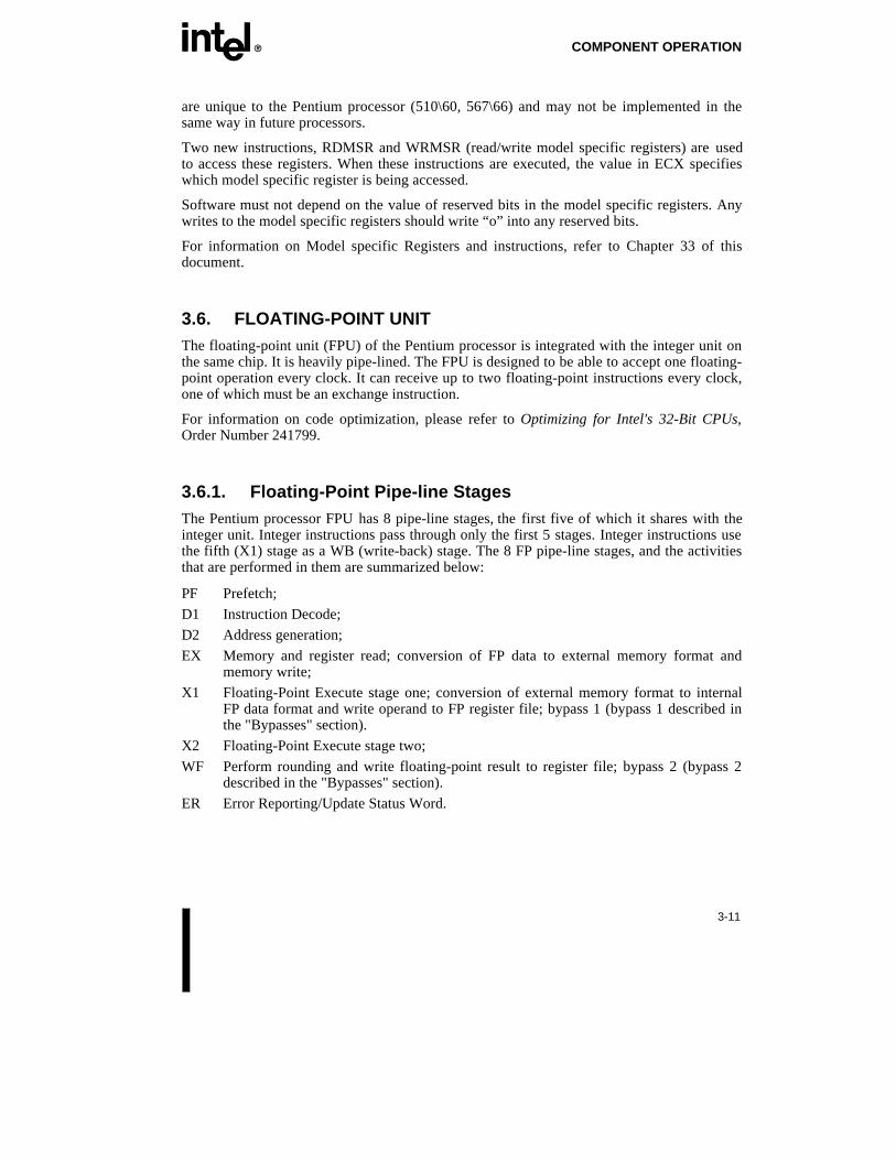
EE COMPONENT OPERATION
3-11
are unique to the Pentium processor (510\60, 567\66) and may not be implemented in thesame way in future processors.
Two new instructions, RDMSR and WRMSR (read/write model specific registers) are usedto access these registers. When these instructions are executed, the value in ECX specifieswhich model specific register is being accessed.
Software must not depend on the value of reserved bits in the model specific registers. Anywrites to the model specific registers should write “o” into any reserved bits.
For information on Model specific Registers and instructions, refer to Chapter 33 of thisdocument.
3.6. FLOATING-POINT UNITThe floating-point unit (FPU) of the Pentium processor is integrated with the integer unit onthe same chip. It is heavily pipe-lined. The FPU is designed to be able to accept one floating-point operation every clock. It can receive up to two floating-point instructions every clock,one of which must be an exchange instruction.
For information on code optimization, please refer to Optimizing for Intel's 32-Bit CPUs,Order Number 241799.
3.6.1. Floating-Point Pipe-line StagesThe Pentium processor FPU has 8 pipe-line stages, the first five of which it shares with theinteger unit. Integer instructions pass through only the first 5 stages. Integer instructions usethe fifth (X1) stage as a WB (write-back) stage. The 8 FP pipe-line stages, and the activitiesthat are performed in them are summarized below:
PF Prefetch;
D1 Instruction Decode;
D2 Address generation;
EX Memory and register read; conversion of FP data to external memory format andmemory write;
X1 Floating-Point Execute stage one; conversion of external memory format to internalFP data format and write operand to FP register file; bypass 1 (bypass 1 described inthe "Bypasses" section).
X2 Floating-Point Execute stage two;
WF Perform rounding and write floating-point result to register file; bypass 2 (bypass 2described in the "Bypasses" section).
ER Error Reporting/Update Status Word.

COMPONENT OPERATION EE
3-12
3.6.2. Instruction IssueDescribed below are the rules of how floating-point (FP) instructions get issued on thePentium processor:
1. FP instructions do not get paired with integer instructions. However, a limited pairing oftwo FP instructions can be performed.
2. When a pair of FP instructions is issued to the FPU, only the FXCH instruction can bethe second instruction of the pair. The first instruction of the pair must be one of a set Fwhere F = [ FLD single/double, FLD ST(i), all forms of FADD, FSUB, FMUL, FDIV,FCOM, FUCOM, FTST, FABS, FCHS].
3. FP instructions other than the FXCH instruction and other than instructions belonging toset F (defined in rule 2) always get issued singly to the FPU.
4. FP instructions that are not directly followed by an FP exchange instruction are issuedsingly to the FPU.
The Pentium processor stack architecture instruction set requires that all instructions haveone source operand on the top of the stack. Since most instructions also have their destinationas the top of the stack, most instructions see a "top of stack bottleneck." New source op-erands must be brought to the top of the stack before we can issue an arithmetic instructionon them. This calls for extra usage of the exchange instruction, which allows the programmerto bring an available operand to the top of the stack. The Pentium processor FPU usespointers to access its registers to allow fast execution of exchanges and the execution ofexchanges in parallel with other floating-point instructions. An FP exchange that is pairedwith other FP instructions takes 0 clocks for its execution. Since such exchanges can beexecuted in parallel on the Pentium processor, it is recommended that one use them whennecessary to overcome the stack bottleneck.
Note that when exchanges are paired with other floating-point instructions, they should notbe followed immediately by integer instructions. The Pentium processor stalls such integerinstructions for a clock if the FP pair is declared safe, or for 4 clocks if the FP pair is unsafe.
Also note that the FP exchange must always follow another FP instruction to get paired. Thepairing mechanism does not allow the FP exchange to be the first instruction of a pair that isissued in parallel. If an FP exchange is not paired, it takes 1 clock for its execution.
3.6.3. Safe Instruction RecognitionThe Pentium processor FPU performs Safe Instruction Recognition or SIR in the X1 stage ofthe pipe-line. SIR is an early inspection of operands and opcodes to determine whether theinstruction is guaranteed not to generate an arithmetic overflow, underflow, or unmaskedinexact exception. An instruction is declared safe if it cannot raise any other floating-pointexception, and if it does not need microcode assist for delivery of special results. If aninstruction is declared safe, the next FP instruction is allowed to complete its E stageoperation. If an instruction is declared unsafe, the next FP instruction stalls in the E stageuntil the current one completes (ER stage) with no exception. This means a 4 clock stall,

EE COMPONENT OPERATION
3-13
which is incurred even if the numeric instruction that was declared unsafe does noteventually raise a floating-point exception.
For normal data, the rules used on the Pentium processor for declaring an instruction safe areas follows.
If FOP= FADD/FSUB/FMUL/FDIV, the instruction is safe from arithmetic overflow,underflow, and unmasked inexact exceptions if:
1. Both operands have unbiased exponent =< 1FFEh AND
2. Both operands have unbiased exponent >= -1FFEh AND
3. The inexact exception is masked
Note that arithmetic overflow of the double precision format occurs when the unbiasedexponent of the result is >= 400h, and underflow occurs when the exponent is <=-3FFh.Hence, the SIR algorithm on the Pentium processor allows improved throughput on a muchgreater range of numbers than that spanned by the double precision format.
3.6.4. BypassesThe following section describes the floating-point register file bypasses that exist on thePentium processor. The register file has two write ports and two read ports. The read portsare used to read data out of the register file in the E stage. One write port is used to write datainto the register file in the X1 stage, and the other in the WF stage. A bypass allows data thatis about to be written into the register file to be available as an operand that is to be readfrom the register file by any succeeding floating-point instruction. A bypass is specified by apair of ports (a write port and a read port) that get circumvented. Using the bypass, data ismade available even before actually writing it to the register file.
The following procedures are implemented:
1. Bypass the X1 stage register file write port and the E stage register file read port.
2. Bypass the WF stage register file write port and the E stage register file read port.
With bypass 1, the result of a floating-point load (that writes to the register file in the X1stage) can bypass the X1 stage write and be sent directly to the operand fetch stage or E stageof the next instruction.
With bypass 2, the result of any arithmetic operation can bypass the WF stage write to theregister file, and be sent directly to the desired execution unit as an operand for the nextinstruction.
Note that the FST instruction reads the register file with a different timing requirement, sothat for the FST instruction, which attempts to read an operand in the E stage:

COMPONENT OPERATION EE
3-14
1. There is no bypassing the X1 stage write port and the E stage read port, i.e. no addedbypass for FLD followed by FST. Thus FLD (double) followed by FST (double) takes4 clocks (2 for FLD, and 2 for FST).
2. There is no bypassing the WF stage write port and the E stage read port. The E stageread for the FST happens only in the clock following the WF write for any precedingarithmetic operation.
Furthermore, there is no memory bypass for an FST followed by an FLD from the samememory location.
3.6.5. Branching Upon Numeric Condition CodesBranching upon numeric condition codes is accomplished by transferring the floating-pointSW to the integer FLAGS register and branching on it. The "test numeric condition codesand branch" construct looks like:
FP instruction1; instruction whose effects on the status word are to be examined;
"numeric_test_and_branch_construct":
FSTSW AX; move the status word to the ax register.
SAHF; transfer the value in ah to the lower half of the eflags register.
JC xyz ; jump upon the condition codes in the eflags register.
Note that all FP instructions update the status word only in the ER stage. Hence there is abuilt-in status word interlock between FP instruction1 and the FSTSW AX instruction. Theabove piece of code takes 9 clocks before execution of code begins at the target of the jump.These 9 clocks are counted as:
FP instruction1 : X1, X2, WF, ER (4 E stage stalls for the FSTSWAX );
FSTSW AX : 2 E clocks;
SAHF : 2 E clocks;
JC xyz : 1 clock if no mispredict on branch.
Note that if there is a branch mispredict, there will be a minimum of 3 clocks added to theclock count of 9.
It is recommended that such attempts to branch upon numeric condition codes be precededby integer instructions, i.e. one should insert integer instructions in between FP instruction1and the FSTSW AX instruction which is the first instruction of the "numeric test and branch"construct. This allows the elimination of up to 4 clocks (the 4 E-stage stalls on FSTSW AX)from the cost attributed to this construct, so that numeric branching can be accomplished in5 clocks.

EE COMPONENT OPERATION
3-15
3.7. ON-CHIP CACHESThe Pentium processor implements two internal caches for a total integrated cache size of16 Kbytes: an 8 Kbyte data cache and a separate 8 Kbyte code cache. These caches aretransparent to application software to maintain compatibility with previous generations of theIntel386 and Intel486 architectures.
The data cache fully supports the MESI (modified/exclusive/shared/invalid) writeback cacheconsistency protocol. The code cache is inherently write protected to prevent code frombeing inadvertently corrupted, and as a consequence supports a subset of the MESI protocol,the S (shared) and I (invalid) states.
The caches have been designed for maximum flexibility and performance. The data cache isconfigurable as writeback or writethrough on a line by line basis. Memory areas can bedefined as non-cacheable by software and external hardware. Cache writeback andinvalidations can be initiated by hardware or software. Protocols for cache consistency andline replacement are implemented in hardware, easing system design.
3.7.1. Cache OrganizationEach of the caches are 8 Kbytes in size and each is organized as a 2-way set associativecache. There are 128 sets in each cache, each set containing 2 lines (each line has its own tagaddress). Each cache line is 32 bytes wide.
Replacement in both the data and instruction caches is handled by the LRU mechanismwhich requires one bit per set in each of the caches. A conceptual diagram of theorganization of the data and code caches is shown below in Figure 3-3. Note that the datacache supports the MESI writeback cache consistency protocol which requires 2 state bits,while the code cache supports the S and I state only and therefore requires only one state bit.

COMPONENT OPERATION EE
3-16
PDB38
TAG Address
MESI
State
LRU
Set TAG Address
Data Cache
TAG Address
StateBit
(S or I)
LRU
TAG Address
Code Cache
Set
WAY 0
WAY 0
MESI
State
WAY 1
StateBit
(S or I)
WAY 1
Figure 3-3. Conceptual Organization of Code and Data Caches
3.7.2. Cache StructureThe instruction and data caches can be accessed simultaneously. The instruction cache canprovide up to 32 bytes of raw opcodes and the data cache can provide data for two datareferences all in the same clock. This capability is implemented partially through the tagstructure. The tags in the data cache are triple ported. One of the ports is dedicated tosnooping while the other two are used to lookup two independent addresses corresponding todata references from each of the pipe-lines. The instruction cache tags are also triple ported.Again, one port is dedicated to support snooping and other two ports facilitate split lineaccesses (simultaneously accessing upper half of one line and lower half of the next line).
The storage array in the data cache is single ported but interleaved on 4 byte boundaries to beable to provide data for two simultaneous accesses to the same cache line.
Each of the caches are parity protected. In the instruction cache, there are parity bits on aquarter line basis and there is one parity bit for each tag. The data cache contains one paritybit for each tag and a parity bit per byte of data.

EE COMPONENT OPERATION
3-17
Each of the caches are accessed with physical addresses and each cache has its own TLB(translation lookaside buffer) to translate linear addresses to physical addresses. The datacache has a 4-way set associative, 64-entry TLB for 4 Kbyte pages and a separate 4-way setassociative, 8-entry TLB to support 4 Mbyte pages. The code cache has one 4-way setassociative, 32-entry TLB for 4 Kbyte pages and 4 Mbyte pages which are cached in 4 Kbyteincrements. The TLBs associated with the instruction cache are single ported whereas thedata cache TLBs are fully dual ported to be able to translate two independent linear addressesfor two data references simultaneously. Replacement in the TLBs is handled by a pseudoLRU mechanism (similar to the Intel486 CPU) that requires 3 bits per set. The tag and dataarrays of the TLBs are parity protected with a parity bit associated with each of the tag anddata entries in the TLBs.
3.7.3. Cache Operating ModesThe operating modes of the caches are controlled by the CD (cache disable) and NW (notwritethrough) bits in CR0. See Table 3-1 for a description of the modes. For normaloperation and highest performance, these bits should both be reset to "0." The bits come outof RESET as CD = NW = 1.

COMPONENT OPERATION EE
3-18
Table 3-1. Cache Operating Modes
CD NW Description
1 1 Read hits access the cache.
Read misses do not cause linefills.
Write hits update the cache, but do not access memory.
Write hits will cause Exclusive State lines to change to Modified State.
Shared lines will remain in the Shared state after write hits.
Write misses access memory.
Inquire and invalidation cycles do not affect the cache state or contents.
This is the state after reset.
1 0 Read hits access the cache.
Read misses do not cause linefills.
Write hits update the cache.
Writes to Shared lines and write misses update external memory.
Writes to Shared lines can be changed to the Exclusive State under the con-trol of the WB/WT# pin.
Inquire cycles (and invalidations) are allowed.
0 1 GP(0)
0 0 Read hits access the cache.
Read misses may cause linefills.
These lines will enter the Exclusive or Shared state under the control of theWB/WT# pin.
Write hits update the cache.
Only writes to shared lines and write misses appear externally.
Writes to Shared lines can be changed to the Exclusive State under the con-trol of the WB/WT# pin.
Inquire cycles (and invalidations) are allowed.
To completely disable the cache, the following two steps must be performed.
1. CD and NW must be set to 1.
2. The caches must be flushed.
If the cache is not flushed, cache hits on reads will still occur and data will be read from thecache. In addition, the cache must be flushed after being disabled to prevent anyinconsistencies with memory.

EE COMPONENT OPERATION
3-19
3.7.4. Page CacheabilityTwo bits for cache control, PWT and PCD are defined in the page table and page directoryentries. The state of these bits are driven out on the PWT and PCD pins during memoryaccess cycles. The PWT bit controls write policy for the second level caches used with thePentium processor. Setting PWT to 1 defines a writethrough policy for the current page,while clearing PWT to 0 defines a writeback policy for the current page.
The PCD bit controls cacheability on a page by page basis. The PCD bit is internally ANDedwith the KEN# signal to control cacheability on a cycle by cycle basis. PCD = 0 enablescacheing, while PCD = 1 disables it. Cache line fills are enabled when PCD = 0 andKEN# = 0.
3.7.4.1. PCD AND PWT GENERATION
The value driven on PCD is a function of the PWT bits in CR3, the page directory pointer,the page directory entry and the page table entry, and the CD and PG bits in CR0.
The value driven on PWT is a function of the PCD bits in CR3, the page directory pointer,the page directory entry and the page table entry, and the PG bit in CR0 (CR0.CD does notaffect PWT).
CR0.CD = 1
If cacheing is disabled, the PCD pin is always driven high. CR0.CD does not affect the PWTpin.
CR0.PG = 0
If paging is disabled, the PWT pin is forced low and the PCD pin reflects the CR0.CD. ThePCD and PWT bits in CR3 are assumed 0 during the cacheing process.
CR0.CD = 0, PG = 1, normal operation
The PCD and PWT bits from the last entry (can be either PDE or PTE, depends on 4 Mbyteor 4 Kbyte mode) are cached in the TLB and are driven anytime the page mapped by theTLB entry is referenced.
CR0.CD = 0, PG = 1, during TLB Refresh
During TLB refresh cycles when the PDE and PTE entries are read, the PWT and PCD bitsare obtained as shown in Tables 3-2 and 3-3.

COMPONENT OPERATION EE
3-20
Table 3-2. 32-Bits/4-Kbyte Pages
PCD/PWT Taken From During Accesses To
CR3 PDE
PDE PTE
PTE All other paged mem references
Table 3-3. 32-Bits/4-Mbyte Pages
PCD/PWT Taken From During Accesses To
CR3 PDE
PDE All other paged mem references

EE COMPONENT OPERATION
3-21
Figure 3-4 shows how PCD and PWT are generated.
PDB102
+
DIR PTRS DIRECTORY TABLE(Optional)
OFFSET
LINEAR ADDRESS
PCD,PWT
PCD,PWT
PCD,PWT
PCD,PWT
CR3
CR0
PAGE DIRECTORY
PAGE TABLE
PAGE FRAME
PWT
PCD
PWT
PCD
KEN#
PG (Paging Enable)
CD (Cache Disable)
Unlocked Memory Reads
Writeback Cycle
CI
Cache Inhibit
TR12.3
Cache transition toE-state enable
Cache line fill enable
CACHE#
WB/WT#
PCD
+
+
1
Figure 3-4. PCD and PWT Generation

COMPONENT OPERATION EE
3-22
3.7.5. Inquire CyclesInquire cycles are initiated by the system to determine if a line is present in the code or datacache, and what its state is. (This document refers to inquire cycles and snoop cyclesinterchangeably.)
Inquire cycles are driven to the Pentium processor when a bus master other than the Pentiumprocessor initiates a read or write bus cycle. Inquire cycles are driven to the Pentiumprocessor when the bus master initiates a read to determine if the Pentium processor datacache contains the latest information. If the snooped line is in the Pentium processor datacache in the modified state, the Pentium processor has the most recent information and mustschedule a writeback of the data. Inquire cycles are driven to the Pentium processor whenthe other bus master initiates a write to determine if the Pentium processor code or datacache contains the snooped line and to invalidate the line if it is present. Inquire cycles aredescribed in detail in the "Bus Functional Description" chapter.
3.7.6. Cache FlushingThe on-chip cache can be flushed by external hardware or by software instructions.
Flushing the cache through hardware is accomplished by driving the FLUSH# pin low. Thiscauses the cache to writeback all modified lines in the data cache and mark the state bits forboth caches invalid. The Flush Acknowledge special cycle is driven by the Pentiumprocessor when all writebacks and invalidations are complete.
The INVD and WBINVD instructions cause the on-chip caches to be invalidated also.WBINVD causes the modified lines in the internal data cache to be written back, and alllines in both caches to be marked invalid. After execution of the WBINVD instruction, theWriteback and Flush special cycles are driven to indicate to any external cache that it shouldwriteback and invalidate its contents.
INVD causes all lines in both caches to be invalidated. Modified lines in the data cache arenot written back. The Flush special cycle is driven after the INVD instruction is executed toindicate to any external cache that it should invalidate its contents. Care should be takenwhen using the INVD instruction that cache consistency problems are not created.
Note that the implementation of the INVD and WBINVD instructions are processordependent. Future processor generations may implement these instructions differently.
3.7.7. Data Cache Consistency Protocol (MESI Protocol)The Pentium processor Cache Consistency Protocol is a set of rules by which states areassigned to cached entries (lines). The rules apply for memory read/write cycles only. I/Oand special cycles are not run through the data cache.
Every line in the Pentium processor data cache is assigned a state dependent on both Pentiumprocessor generated activities and activities generated by other bus masters (snooping). ThePentium processor Data Cache Protocol consists of 4 states that define whether a line is valid

EE COMPONENT OPERATION
3-23
(HIT/MISS), if it is available in other caches, and if it has been MODIFIED. The four statesare the M (Modified), E (Exclusive), S (Shared) and the I (Invalid) states and the protocol isreferred to as the MESI protocol. A definition of the states is given below:
M - Modified: An M-state line is available in ONLY one cache and it is also MODIFIED(different from main memory). An M-state line can be accessed(read/written to) without sending a cycle out on the bus.
E - Exclusive: An E-state line is also available in ONLY one cache in the system, but theline is not MODIFIED (i.e., it is the same as main memory). An E-state linecan be accessed (read/written to) without generating a bus cycle. A write toan E-state line will cause the line to become MODIFIED.
S - Shared: This state indicates that the line is potentially shared with other caches (i.e.the same line may exist in more than one cache). A read to an S-state linewill not generate bus activity, but a write to a SHARED line will generate awrite-through cycle on the bus. The write-through cycle may invalidate thisline in other caches. A write to an S-state line will update the cache.
I - Invalid: This state indicates that the line is not available in the cache. A read to thisline will be a MISS and may cause the Pentium processor to execute aLINE FILL (fetch the whole line into the cache from main memory). Awrite to an INVALID line will cause the Pentium processor to execute awrite-through cycle on the bus.
3.7.7.1. STATE TRANSITION TABLES
Lines cached in the Pentium processor can change state because of processor generatedactivity or as a result of activity on the Pentium processor bus generated by other bus masters(snooping). State transitions happen because of processor generated transactions (memoryreads/writes) and by a set of external input signals and internally generated variables. ThePentium processor also drives certain pins as a consequence of the Cache ConsistencyProtocol.
3.7.7.1.1. Read Cycle
Table 3-4 shows the state transitions for lines in the data cache during unlocked read cycles.

COMPONENT OPERATION EE
3-24
Table 3-4. Data Cache State Transitions for UNLOCKEDPentium ® Processor Initiated Read Cycles*
Present State Pin Activity Next State Description
M n/a M Read hit; data is provided to processor core bycache. No bus cycle is generated.
E n/a E Read hit; data is provided to processor core bycache. No bus cycle is generated.
S n/a S Read hit; data is provided to the processor bythe cache. No bus cycle is generated.
I CACHE# low
AND
KEN# low
AND
WB/WT# high
AND
PWT low
E Data item does not exist in cache (MISS). A buscycle (read) will be generated by the Pentium®
processor. This state transition will happen ifWB/WT# is sampled high with first BRDY# orNA#.
I CACHE# low
AND
KEN# low
AND
(WB/WT# low
OR PWT high)
S Same as previous read miss case except thatWB/WT# is sampled low with first BRDY# orNA#.
I CACHE# high
OR
KEN# high
I KEN# pin inactive; the line is not intended to becached in the Pentium processor (510\60,567\66).
*Locked accesses to the data cache will cause the accessed line to transition to the Invalid state
Note the transition from I to E or S states (based on WB/WT#) happens only if KEN# issampled low with the first of BRDY# or NA#, and the cycle is transformed into a LINE FILLcycle. If KEN# is sampled high, the line is not cached and remains in the I state.
3.7.7.1.2. Write Cycle
The state transitions of data cache lines during Pentium processor generated write cycles areillustrated in the next table. Writes to SHARED lines in the data cache are always sent out onthe bus along with updating the cache with the write item. The status of the PWT andWB/WT# pins during these write cycles on the bus determines the state transitions in the datacache during writes to S-state lines.
EE COMPONENT OPERATION
3-25
A write to a SHARED line in the data cache will generate a write cycle on the Pentiumprocessor bus to update memory and/or invalidate the contents of other caches. If the PWTpin is driven high when the write cycle is run on the bus, the line will be updated, and willstay in the S-state regardless of the status of the WB/WT# pin that is sampled with the firstBRDY# or NA#. If PWT is driven low, the status of the WB/WT# pin sampled along withthe first BRDY# or NA# for the write cycle determines what state (E:S) the line transitionsto.
The state transition from S to E is the only transition in which the data and the status bits arenot updated at the same time. The data will be updated when the write is written to thePentium processor write buffers. The state transition does not occur until the write hascompleted on the bus (BRDY# has been returned). Writes to the line after the transition tothe E-state will not generate bus cycles. However, it is possible that writes to the same linethat were buffered or in the pipe-line before the transition to the E-state will generate buscycles after the transition to E-state.
An inactive EWBE# input will stall subsequent writes to an E- or an M-state line. Allsubsequent writes to E- or M-state lines are held off until EWBE# is returned active.

COMPONENT OPERATION EE
3-26
Table 3-5. Data Cache State Transitions for Pentium ® Processor Initiated Write Cycles
PresentState Pin Activity
NextState Description
M n/a M Write hit; update data cache. No bus cycle generated toupdate memory.
E n/a M Write hit; update cache only. No bus cycle generated; line isnow MODIFIED.
S PWT low
AND
WB/WT# high
E Write hit; data cache updated with write data item. A write-through cycle is generated on bus to update memory and/orinvalidate contents of other caches. The state transition oc-curs after the writethrough cycle completes on the bus (withthe last BRDY#).
S PWT low
AND
WB/WT# low
S Same as above case of write to S-state line except thatWB/WT# is sampled low.
S PWT high S Same as above cases of writes to S state lines except thatthis is a write hit to a line in a writethrough page; status ofWB/WT# pin is ignored.
I n/a I Write MISS; a writethrough cycle is generated on the bus toupdate external memory. No allocation done.
NOTE: Memory writes are buffered while I/O writes are not. There is no guarantee of synchronization betweencompletion of memory writes on the bus and instruction execution after the write. A serializing instructionneeds to be executed to synchronize writes with the next instruction if necessary.
3.7.7.1.3. Inquire Cycles (Snooping)
The purpose of inquire cycles is to check whether the address being presented is containedwithin the caches in the Pentium processor. Inquire cycles may be initiated with or withoutan INVALIDATION request (INV = 1 or 0). An inquire cycle is run through the data andcode caches through a dedicated snoop port to determine if the address is in one of thePentium processor caches. If the address is in a Pentium processor cache, the HIT# pin isasserted. If the address hits a modified line in the data cache, the HITM# pin is also assertedand the modified line is then written back onto the bus.

EE COMPONENT OPERATION
3-27
The state transition tables for inquire cycles are given below:
Table 3-6. Cache State Transitions During Inquire Cycles
PresentState
NextState
INV=1
NextStateINV=0 Description
M I S Snoop hit to a MODIFIED line indicated by HIT# and HITM# pins low.Pentium® processor schedules the writing back of the modified line tomemory.
E I S Snoop hit indicated by HIT# pin low; no bus cycle generated.
S I S Snoop hit indicated by HIT# pin low; no bus cycle generated.
I I I Address not in cache; HIT# pin high.
3.7.7.2. PENTIUM® PROCESSOR CODE CACHE CONSISTENCY PROTOCOL
The Pentium processor code cache follows a subset of the MESI protocol. Accesses to thecode cache are either a Hit (Shared) or a Miss (Invalid).
In the case of a read hit, the cycle is serviced internally to the Pentium processor and no busactivity is generated. In the case of a read miss, the read is sent to the external bus and maybe converted to a line fill.
Lines are never overwritten in the code cache. Writes generated by the Pentium processor aresnooped by the code cache. If the snoop is a hit in the code cache, the line is invalidated. Ifthere is a miss, the code cache is not affected.
E4
MicroprocessorInitialization andConfiguration


EE
4-1
CHAPTER 4MICROPROCESSOR INITIALIZATION AND
CONFIGURATION
Before normal operation of the Pentium processor can begin, the Pentium processor must beinitialized by driving the RESET pin active. The RESET pin forces the Pentium processor tobegin execution in a known state. Several features are optionally invoked at the falling edgeof RESET: Built in Self Test (BIST), Functional Redundancy Checking and Tristate TestMode.
In addition to the standard RESET pin, the Pentium processor has implemented aninitialization pin (INIT) that allows the processor to begin execution in a known state withoutdisrupting the contents of the internal caches or the floating-point state.
This chapter describes the Pentium processor power up and initialization procedures as wellas the test and configuration features enabled at the falling edge of RESET.
4.1. POWER UP SPECIFICATIONSDuring power up, RESET must be asserted while VCC is approaching nominal operatingvoltage to prevent internal bus contention which could negatively affect the reliability of theprocessor.
It is recommended that CLK begin toggling within 150ms after VCC reaches its properoperating level. This recommendation is only to ensure long term reliability of the device.
In order for RESET to be recognized, the CLK input needs to be toggling. RESET mustremain asserted for 1 millisecond after VCC and CLK have reached their AC/DCspecifications.
4.2. TEST AND CONFIGURATION FEATURES (BIST, FRC,TRISTATE TEST MODE)
The INIT, FLUSH#, and FRCMC# inputs are sampled when RESET transitions from high tolow to determine if BIST will be run, or if tristate test mode or checker mode will be entered(respectively).
If RESET is driven synchronously, these signals must be at their valid level and meet setupand hold times on the clock before the falling edge of RESET. If RESET is assertedasynchronously, these signals must be at their valid level two clocks before and after RESETtransitions from high to low.

MICROPROCESSOR INITIALIZATION AND CONFIGURATION EE
4-2
4.2.1. Built In Self TestSelf test is initiated by driving the INIT pin high when RESET transitions from high to low.
No bus cycles are run by the Pentium processor during self test. The duration of self test isapproximately 219 clocks. Approximately 70% of the devices in the Pentium processor aretested by BIST.
The Pentium processor BIST consists of two parts: hardware self test and microcode self test.
During the hardware portion of BIST, the microcode ROM and all large PLAs are tested. Allpossible input combinations of the microcode ROM and PLAs are tested.
The constant ROMs, BTB, TLBs, and all caches are tested by the microcode portion ofBIST. The array tests (caches, TLBs and BTB) have two passes. On the first pass, datapatterns are written to arrays, read back and checked for mismatches. The second pass writesthe complement of the initial data pattern, reads it back, and checks for mismatches. Theconstant ROMs are tested by using the microcode to add various constants and check theresult against a stored value.
Upon successful completion of BIST, the cumulative result of all tests are stored in the EAXregister. If EAX contains 0h, then all checks passed; any non-zero result indicates a faultyunit. Note that if an internal parity error is detected during BIST, the processor will assert theIERR# pin and attempt to shutdown.
4.2.2. Tristate Test ModeWhen the FLUSH# pin is sampled low when RESET transitions from high to low, thePentium processor enters tristate test mode. The Pentium processor floats all of its outputpins and bi-directional pins including pins which are never floated during normal operation(except TDO). Tristate test mode can be initiated in order to facilitate testing boardinterconnects. The Pentium processor remains in tristate test mode until the RESET pin isasserted again.
4.2.3. Functional Redundancy CheckingThe functional redundancy checking master/checker configuration input is sampled whenRESET is high to determine whether the Pentium processor is configured in master mode(FRCMC# high) or checker mode (FRCMC# low). The final master/checker configuration ofthe Pentium processor is determined the clock before the falling edge of RESET. When con-figured as a master, the Pentium processor drives its output pins as required by the busprotocol. When configured as a checker, the Pentium processor tristates all outputs (exceptIERR# and TDO) and samples the output pins (that would normally be driven in mastermode). If the sampled value differs from the value computed internally, the Pentiumprocessor asserts IERR# to indicate an error. Note that IERR# will not be asserted due to anFRC mismatch until two clocks after the ADS# of the first bus cycle (or in the third clock ofthe bus cycle).

EE MICROPROCESSOR INITIALIZATION AND CONFIGURATION
4-3
4.3. INITIALIZATION WITH RESET, INIT AND BISTTwo pins, RESET and INIT, are used to reset the Pentium processor in different manners. A"cold" or "power on" RESET refers to the assertion of RESET while power is initially beingapplied to the Pentium processor. A "warm" RESET refers to the assertion of RESET or INITwhile VCC and CLK remain within specified operating limits.
Table 4-1 shows the effect of asserting RESET and/or INIT.
Table 4-1. Pentium ® Processor Reset Modes
RESET INIT BIST Run?Effect on Code and
Data CachesEffect on FP
RegistersEffect on BTB
and TLBs
0 0 No n/a n/a n/a
0 1 No None None Invalidated
1 0 No Invalidated Initailized Invalidated
1 1 Yes Invalidated Initialized Invalidated
Toggling either the RESET pin or the INIT pin individually forces the Pentium processor tobegin execution at address FFFFFFF0h. The internal instruction cache and data cache areinvalidated when RESET is asserted (modified lines in the data cache are NOT written back).The instruction cache and data cache are not altered when the INIT pin is asserted withoutRESET. In both cases, the branch target buffer (BTB) and translation lookaside buffers(TLBs) are invalidated.
After RESET (with or without BIST) or INIT, the Pentium processor will start executinginstructions at location FFFFFFF0H. When the first Intersegment Jump or Call instruction isexecuted, address lines A20-A31 will be driven low for CS-relative memory cycles and thePentium processor will only execute instructions in the lower one Mbyte of physicalmemory. This allows the system designer to use a ROM at the top of physical memory toinitialize the system.
RESET is internally hardwired and forces the Pentium processor to terminate all executionand bus cycle activity within 2 clocks. No instruction or bus activity will occur as long asRESET is active. INIT is implemented as an edge triggered interrupt and will be recognizedwhen an instruction boundary is reached. As soon as the Pentium processor completes theINIT sequence, instruction execution and bus cycle activity will continue at addressFFFFFFF0h even if the INIT pin is not deasserted.
At the conclusion of RESET (with or without self test) or INIT, the DX register will containa component identifier. The upper byte will contain 05h and the lower byte will contain astepping identifier.
Table 4-2 defines the processor state after RESET, INIT and RESET with BIST (built in selftest).

MICROPROCESSOR INITIALIZATION AND CONFIGURATION EE
4-4
Table 4-2. Register State after RESET, INIT and BIST(Register States are Given in Hexadecimal Format)
Storage Element RESET (No BIST) RESET (BIST) INIT
EAX 0 0 if pass 0
EDX 0500+stepping 0500+stepping 0500+stepping
ECX, EBX, ESP, EBP, ESI, EDI 0 0 0
EFLAGS 2 2 2
EIP 0FFF0 0FFF0 0FFF0
CS selector = F000 selector = F000 selector = F000
AR = P, R/W, A AR = P, R/W, A AR = P, R/W, A
base = FFFF0000 base = FFFF0000 base = FFFF0000
limit = FFFF limit = FFFF limit = FFFF
DS,ES,FE,GS,SS selector = 0 selector = 0 selector = 0
AR = P, R/W, A AR = P, R/W, A AR = P, R/W, A
base = 0 base = 0 base = 0
limit = FFFF limit = FFFF limit = FFFF
(I/G/L)DTR, TSS selector = 0 selector = 0 selector = 0
base = 0 base = 0 base = 0
AR = P, R/W AR = P, R/W AR = P, R/W
limit = FFFF limit = FFFF limit = FFFF
CR0 60000010 60000010 Note 1
CR2,3,4 0 0 0
DR3-0 0 0 0
DR6 FFFF0FF0 FFFF0FF0 FFFF0FF0
DR7 00000400 00000400 00000400
Time Stamp Counter 0 0 Unchanged
Control and Event Select 0 0 Unchanged
TR12 0 0 Unchanged
All other MSR's Undefined Undefined Unchanged
CW 0040 0040 Unchanged
SW 0 0 Unchanged
TW 5555 5555 Unchanged
FIP,FEA,FCS,FDS,FOP 0 0 Unchanged
FSTACK 0 0 Unchanged
Data and Code Cache Invalid Invalid Unchanged
Code Cache TLB, Data CacheTLB, BTB, SDC
Invalid Invalid Invalid
NOTE: CD and NW are unchanged, bit 4 is set to 1, all other bits are cleared.

EE MICROPROCESSOR INITIALIZATION AND CONFIGURATION
4-5
4.3.1. Recognition of Interrupts after RESETIn order to guarantee recognition of the edge sensitive interrupts (FLUSH#, NMI, R/S#,SMI#) after RESET or after RESET with BIST, the interrupt input must not be asserted untilfour clocks after RESET is deasserted, regardless of whether BIST is run or not.
4.3.2. Pin State during/after RESETThe Pentium processor recognizes and will respond to HOLD, AHOLD and BOFF# duringRESET. Figure 4-1 shows the processor state during and after a power on RESET if HOLD,AHOLD, and BOFF# are inactive. Note that the address bus (A31-A3, BE7#-BE0#) andcycle definition pins (M/IO#, D/C#, W/R#, CACHE#, SCYC, PM0/BP0, PM1/BP1 andLOCK#) are undefined from the time RESET is asserted until the start of the first bus cycle.
The following lists the state of the output pins after RESET assuming HOLD, AHOLD andBOFF# are inactive, boundary scan is not invoked, and no internal parity error is detected.
High: LOCK#, ADS#, APCHK#, PCHK#, IERR#, HIT#, HITM#, FERR#,SMIACT#
Low: HLDA, BREQ, BP3, BP2, PRDY, IBT, IU, IV, BT3-BT0
High Impedance: D63-D0, DP7-DP0
Undefined: A31-A3, AP, BE7#-BE0#, W/R#, M/IO#, D/C#, PCD, PWT, CACHE#,TDO, SCYC

MICROPROCESSOR INITIALIZATION AND CONFIGURATION EE
4-6
4
3
1
5
Undef ined
Undef ined
Undef ined
Undef ined
2 Clocks i f BIST1 9
150-200 C locks if no B IST
PDB26
An assertion of RESET takes at least 2 clocks to affect the pins.5
Tx Tx Tx Tx Tx T i T i T i T 1
1 RESET must meet setup and hold times to guarantee rec ognition on a specific clock edge.If RESET does not need to be recognized on a specific clock edge it may be asserted asynchronously.
2 At power up, RESET needs to be asserted for 1 ms after Vcc and CLK have reachedtheir AC/DC specifications. For warm reset, RESET needs to be asserted for at least 15 clocks while Vcc and CLK remain within specified operating limits.
3 If RESET is driven synchr onously, FLUSH#, FRCMC#, and INIT must be at their valid leveland meet setup and hold times the clock before the falling edge of RESET.
4 If RESET is driven asynchronously, FLUSH#, FRCMC#, and INIT must be at their valid l evel2 clocks before and after the falling edge of RESET.
Valid
Valid
Valid
CLK
RESET
ADS#
INIT, FLUSH#FRCMC# (SYNC)
INIT, FLUSH#FRCMC# (ASYNC)
BREQ, HLDA,BP3, BP2,
BT3-0, PRDY, IBT, IU, IV
A31-A3, M/IO#, D/C#,W/R#, SCYC, CACHE#,
BE7#-BE0#, AP, PCD,PM0/BP0, PM1/BP1, TDO, PWT
LOCK#, APCHK#,PCHK#, IERR#,
HIT#, HITM#, FERR#,SMIACT#
D63-D0DP7-DP0
Figure 4-1. Pin States during RESET

E5
Hardware Interface

EE
5-1
CHAPTER 5HARDWARE INTERFACE
The Pentium processor bus is similar to the Intel486 microprocessor bus, but it has distinctdifferences and improvements. Several new features have been added to increaseperformance, to support writeback cacheing, and add functionality.
The data bus on the Pentium processor has been increased to 64 bits, allowing the largercache line to be filled with the standard four data transfers. Burst read cycles were carriedforward from the Intel486 microprocessor and writeback cycles are bursted on the Pentiumprocessor. The Pentium processor implements bus cycle pipe-lining which allows two buscycles to be outstanding on the bus simultaneously.
An initialization pin, INIT was added (in addition to the RESET pin) to provide a method toswitch from protected to real mode while maintaining the contents of the caches and floating-point state.
The data parity feature implemented by the Intel486 microprocessor has been extended tosupport the entire 64-bit data bus, and address parity and internal parity features have beenadded to the Pentium processor. In addition, support for functional redundancy checking andthe machine check exception were also added to the Pentium processor.
The test access port (TAP) for IEEE Standard 1149.1 Boundary Scan is implemented on thePentium processor, along with a new mode that also uses the TAP, probe mode.
System management mode, similar to that on the Intel386 SL microprocessor, is im-plemented on the Pentium processor. A method to track instruction execution through each ofthe pipe-lines has also been implemented.
This chapter describes the pins that interface to the system that allow these features to beimplemented at the system level. The pin descriptions are arranged alphabetically for ease ofreference. The pins are grouped functionally as defined in Table 1-6.

HARDWARE INTERFACE EE
5-2
5.1. DETAILED PIN DESCRIPTIONSEach pin name has a brief descriptive heading organized as follows:
Pin Symbol Pin Name
Function
Input/Output
Each heading is followed by three sections that describe the signal function, when the signalis driven or sampled, and the relation that signal has to other signals.
The # symbol at the end of a signal name indicates that the active, or asserted state occurswhen the signal is at a low voltage. When a # symbol is not present after the signal name, thesignal is active, or asserted at the high voltage level.

EE HARDWARE INTERFACE
5-3
5.1.1. A20M#A20M# Address 20 Mask
Used to emulate the 1 Mbyte address wraparound on the 8086.
Asynchronous Input
Signal Description
When the address 20 mask input is asserted, the Pentium processor masks physical addressbit 20 (A20) before performing a lookup to the internal caches or driving a memory cycle onthe bus. A20M# is provided to emulate the address wraparound at one Mbyte which occurson the 8086.
A20M# must only be asserted when the processor is in real mode. The effect of assertingA20M# in protected mode is undefined and may be implemented differently in futureprocessors.
Inquire cycles and writebacks caused by inquire cycles are not affected by this input. Addressbit A20 is not masked when an external address is driven into the Pentium processor for aninquire cycle. Note that if an OUT instruction is used to modify A20M# this will not affectpreviously prefetched instructions. A serializing instruction must be executed to guaranteerecognition of A20M# before a specific instruction.
When Sampled
A20M# is sampled on every rising clock edge. A20M# is level sensitive and active low. Thispin is asynchronous, but must meet setup and hold times for recognition in any specificclock. To guarantee that A20M# will be recognized before the first ADS# after RESET,A20M# must be asserted within two clocks after the falling edge of RESET.
Relation to Other Signals
Pin Symbol Relation to Other Signals
A20 When asserted, A20M# will mask the value of address pin A20.

HARDWARE INTERFACE EE
5-4
5.1.2. A31-A3A31-A3 Address Lines
Defines the physical area of memory or I/O accessed.
Input/Output
Signal Description
As outputs, the address lines (A31-A3) along with the byte enable signals (BE7#-BE0#) formthe address bus and define the physical area of memory or I/O accessed.
The Pentium processor is capable of addressing 4-gigabytes of physical memory space and64K bytes of I/O address space.
As inputs, the address bus lines A31-A5 are used to drive addresses back into the processor toperform inquire cycles. Since inquire cycles affect an entire 32-byte line, the logic values ofA4 and A3 are not used for the hit/miss decision, however A4 and A3 must be at valid logiclevel and meet setup and hold times during inquire cycles.
When Sampled/Driven
When an output, the address is driven in the same clock as ADS#. The address remains validfrom the clock in which ADS# is asserted until AHOLD is asserted or the clock after theearlier of NA# or the last BRDY#.
When an input, the address must be returned to the processor to meet setup and hold times inthe clock EADS# is sampled asserted.

EE HARDWARE INTERFACE
5-5
Relation to Other Signals
Pin Symbol Relation to Other Signals
A20M# Causes address pin A20 to be masked.
ADS# A31-A3 are driven with ADS# (except when a external inquire cycle causes awriteback before AHOLD is deasserted, see the Bus Functional Descriptionchapter).
AHOLD A31-A3 are floated one clock after AHOLD is asserted.
AP Even address parity is driven/sampled with the address bus on AP.
APCHK# The status of the address parity check is driven on the APCHK# pin.
BE7#-BE0# Completes the definition of the physical area of memory or I/O accessed.
BOFF# A31-A3 are floated one clock after BOFF# is asserted.
EADS# A31-A5 are sampled with EADS# during inquire cycles.
HIT# HIT# is driven to indicate whether the inquire address driven on A31-A5 is valid inan internal cache.
HITM# HITM# is driven to indicate whether the inquire address driven on A31-A5 is in themodified state in the data cache.
HLDA A31-A3 are floated when HLDA is asserted.
INV INV determines if the inquire address driven to the processor on A31-A5 should beinvalidated or marked as shared if it is valid in an internal cache.

HARDWARE INTERFACE EE
5-6
5.1.3. ADS#ADS# Address Strobe
Indicates that a new valid bus cycle is currently being driven by the Pentium®
processor.
Output
Signal Description
The address status output indicates that a new valid bus cycle is currently being driven by thePentium processor. The following pins are driven to their valid level in the clock ADS# isasserted: A31-A3, AP, BE7#-0#, CACHE#, LOCK#, M/IO#, W/R#, D/C#, SCYC, PWT,PCD.
ADS# is used by external bus circuitry as the indication that the processor has started a buscycle. The external system may sample the bus cycle definition pins on the next rising edgeof the clock after ADS# is driven active.
ADS# floats during bus HOLD and BOFF#. ADS# is not driven low to begin a bus cyclewhile AHOLD is asserted unless the cycle is a writeback due to an external invalidation. Anactive (floating low) ADS# in the clock after BOFF# is asserted should be ignored by thesystem.
When Driven
ADS# is driven active in the first clock of a bus cycle and is driven inactive in the secondand subsequent clocks of the cycle. ADS# is driven inactive when the bus is idle.

EE HARDWARE INTERFACE
5-7
Relation to Other Signals
Pin Symbol Relation to Other Symbols
A31-A3APBE7#-BE3#CACHE#D/C#LOCK#M/IO#PCDPWTSCYCW/R#
These signals are driven valid in the clock in which ADS# is asserted.
AHOLD ADS# will not be driven if AHOLD is asserted (except when a external inquirecycle causes a writeback before AHOLD is deasserted, see the Bus FunctionalDescription chapter).
BOFF# ADS# is floated one clock after BOFF# is asserted.
BREQ BREQ is always asserted in the clock that ADS# is driven.
BT3-BT0 BT3-BT0 are driven to their valid level with the ADS# of a branch trace messagespecial cycle.
FLUSH# The flush special cycle is driven as a result of the assertion of FLUSH#.
HLDA ADS# is floated when HLDA is asserted.
IBT The branch trace message special cycle is driven after an assertion of IBT ifTR12.TR is set to 1.
INTR The interrupt acknowledge cycle is driven as a result of the assertion of INTR.
NA# If NA# is sampled asserted and an internal bus request is pending, the Pentium®
processor drives out the next bus cycle and asserts ADS#.

HARDWARE INTERFACE EE
5-8
5.1.4. AHOLDAHOLD Address Hold
Floats the address bus so an inquire cycle can be driven to the Pentium®
processor.
Synchronous Input
Signal Description
In response to the address hold request input the Pentium processor will stop driving A31-A3,BT3-BT0, and AP in the next clock. This pin is intended to be used for running inquirecycles to the Pentium processor. AHOLD allows another bus master to drive the Pentiumprocessor address bus with the address for an inquire cycle. Since inquire cycles affect theentire cache line, although A31-A3 are floated during AHOLD, only A31-A5 are used by thePentium processor for inquire cycles (and parity checking). Address pins 3 and 4 arelogically ignored during inquire cycles but must be at a valid logic level when sampled.
While AHOLD is active, the address bus will be floated, but the remainder of the bus canremain active. For example, data can be returned for a previously driven bus cycle whenAHOLD is active. In general, the Pentium processor will not issue a bus cycle (ADS#) whileAHOLD is active, the only exception to this is writeback cycles due to an external snoop willbe driven while AHOLD is asserted.
Since the Pentium processor floats its bus immediately (in the next clock) in response toAHOLD, an address hold acknowledge is not required.
When AHOLD is deasserted, the Pentium processor will drive the address bus in the nextclock. It is the responsibility of the system designer to prevent address bus contention. Thiscan be accomplished by ensuring that other bus masters have stopped driving the address busbefore AHOLD is deasserted. Note the restrictions to the deassertion of AHOLD discussed inthe inquire cycle section of the Bus Functional Description chapter.
AHOLD is recognized during RESET and INIT. Note that the internal caches are flushed as aresult of RESET, so invalidation cycles run during RESET are unnecessary.
When Sampled
AHOLD is sampled on every rising clock edge, including during RESET and INIT.

EE HARDWARE INTERFACE
5-9
Relation to Other Signals
Pin Symbol Relation to Other Signals
A31-A3 A31-A3 are floated as a result of the assertion of AHOLD.
ADS# ADS# will not be driven if AHOLD is asserted (except when a external inquirecycle causes a writeback before AHOLD is deasserted, see the Bus FunctionalDescription chapter).
AP AP is floated as a result of the assertion of AHOLD.
BT3-BT0 The branch trace outputs are floated as a result of the assertion of AHOLD.
EADS# EADS# is recognized while AHOLD is asserted.

HARDWARE INTERFACE EE
5-10
5.1.5. APAP Address Parity
Bi-directional address parity pin for the address lines of processor.
Input/Output
Signal Description
This is the bi-directional address parity pin for the address lines of processor. There is oneaddress parity pin for the address lines A31-A5. Note A4 and A3 are not included in theparity determination.
When an output, AP is driven by the Pentium processor with even parity information on allPentium processor generated cycles in the same clock as the address driven. (Even addressparity means that there are an even number of HIGH outputs on A31-A5 and the AP pins.)
When an input, even parity information must be returned to the Pentium processor on this pinduring inquire cycles in the same clock that EADS# is sampled asserted to insure that thecorrect parity check status is driven on the APCHK# output.
The value read on the AP pin does not affect program execution. The value returned on theAP pin is used only to determine even parity and drive the APCHK# output with the propervalue. It is the responsibility of the system to take appropriate actions if a parity error occurs.If parity checks are not implemented in the system, AP may be connected to VCC through apullup resistor and the APCHK# pin may be ignored.
When Sampled/Driven
When an output, AP is driven by the Pentium processor with even parity information on allPentium processor generated cycles in the same clock as the address driven. The AP outputremains valid from the clock in which ADS# is asserted until AHOLD is asserted or the clockafter the earlier of NA# or the last BRDY#.
When an input, even parity information must be returned to the Pentium processor on this pinduring inquire cycles in the same clock that EADS# is sampled asserted to guarantee that theproper value is driven on APCHK#. The AP input must be at a valid level and meet setup andhold times when sampled.

EE HARDWARE INTERFACE
5-11
Relation to Other Signals
Pin Symbol Relation to Other Signals
A31-A5 The AP pin is used to create even parity with the A31-A5 pins.
ADS# AP is driven with ADS# (except when a external inquire cycle causes a writebackbefore AHOLD is deasserted, see the Bus Functional Description chapter).
AHOLD AP is floated one clock after AHOLD is asserted.
APCHK# The status of the address parity check is driven on the APCHK# output.
BOFF# AP is floated one clock after BOFF# is asserted.
EADS# AP is sampled with EADS# during inquire cycles.
HLDA AP is floated when HLDA is asserted.

HARDWARE INTERFACE EE
5-12
5.1.6. APCHK#APCHK# Address Parity Check
The status of the address parity check is driven on the APCHK# output.
Output
Signal Description
APCHK# is asserted two clocks after EADS# is sampled active if the Pentium processor hasdetected a parity error on the A31-A5 during inquire cycles.
Driving APCHK# is the only effect that bad address parity has on the Pentium processor. It isthe responsibility of the system to take appropriate action if a parity error occurs. If paritychecks are not implemented in the system, the APCHK# pin may be ignored.
When Driven
APCHK# is valid for one clock two clocks after EADS# is sampled asserted. APCHK# willremain active for one clock each time a parity error is detected. At all other times it isinactive (HIGH). APCHK# is not floated with AHOLD, HOLD, or BOFF#. The APCHK#signal is glitch free.
Relation to Other Signals
Pin Symbol Relation to Other Signals
AP Even address parity with the A31-A5 should be returned to the Pentium®
processor on the AP pin. If even parity is not driven, the APCHK# pin is asserted.
A31-A5 The AP pin is used to create even parity with A31-A5. If even parity is not driven tothe Pentium processor, the APCHK# pin is asserted.
EADS# APCHK# is driven to its valid level two clocks after EADS# is sampled asserted.

EE HARDWARE INTERFACE
5-13
5.1.7. BE7#-BE0#BE7#-BE0# Byte Enables
Helps define the physical area of memory or I/O accessed.
Output
Signal Description
The byte enable outputs are used in conjunction with the address lines to provide physicalmemory and I/O port addresses. The byte enables are used to determine which bytes of datamust be written to external memory, or which bytes were requested by the CPU for thecurrent cycle.
• BE7# applies to D63-D56
• BE6# applies to D55-D48
• BE5# applies to D47-D40
• BE4# applies to D39-D32
• BE3# applies to D31-D24
• BE2# applies to D23-D16
• BE1# applies to D15-D8
• BE0# applies to D7-D0
In the case of cacheable reads (line fill cycles), all 8 bytes of data must be driven to thePentium processor regardless of the state of the byte enables. If the requested read cycle is asingle transfer cycle, valid data must be returned on the data lines corresponding to the activebyte enables. Data lines corresponding to inactive byte enables need not be driven with validlogic levels. Even data parity is checked and driven only on the data bytes that are enabledby the byte enables.
When Driven
The byte enables are driven in the same clock as ADS#. The byte enables are driven with thesame timing as the address (A31-3). The byte enables remain valid from the clock in whichADS# is asserted until the clock after the earlier of NA# or the last BRDY#. The byte enablesdo not float with AHOLD.

HARDWARE INTERFACE EE
5-14
Relation to Other Signals
Pin Symbol Relation to Other Signals
A31-A3 A31-3 and BE7#-BE0# together define the physical area of memory or I/Oaccessed.
ADS# BE7#-BE0# are driven with ADS#.
BOFF# BE7#-BE0# are floated one clock after BOFF# is asserted.
D63-D0 BE7#-BE0# indicate which data bytes are being requested or driven by thePentium® processor.
DP7-DP0 Even data parity is checked/driven only on the data bytes enabled by BE7#-BE0#.
HLDA BE7#-BE0# are floated when HLDA is asserted.

EE HARDWARE INTERFACE
5-15
5.1.8. BOFF#BOFF# Backoff
The back off input is used to force the Pentium® processor off the bus in the nextclock.
Synchronous Input
Signal Description
In response to BOFF#, the Pentium processor will abort all outstanding bus cycles that havenot yet completed and float the Pentium processor bus in the next clock. The processor floatsall pins normally floated during bus hold. Note that since the bus is floated in the clock afterBOFF# is asserted, an acknowledge is not necessary (HLDA is not asserted in response toBOFF#).
The processor remains in bus hold until BOFF# is negated, at which time the Pentiumprocessor restarts any aborted bus cycle(s) in their entirety by driving out the address andstatus and asserting ADS#.
This pin can be used to resolve a deadlock situation between two bus masters.
Any data with BRDY# returned to the processor while BOFF# is asserted is ignored.
BOFF# has higher priority than BRDY#. If both BOFF# and BRDY# occur in the sameclock, BOFF# takes effect.
BOFF# also has precedence over BUSCHK#. If BOFF# and BUSCHK# are both assertedduring a bus cycle, BOFF# causes the BUSCHK# to be forgotten.
When Sampled
BOFF# is sampled on every rising clock edge, including when RESET and INIT are asserted.
NOTE
If a read cycle is running on the bus, and an internal snoop of that readcycle hits a modified line in the data cache, and the system asserts BOFF#,then the sequence of bus cycles is as follows. Upon negation of BOFF#, thePentium processor will drive out a writeback resutling from the internalsnoop hit. After completion of the writeback, the processor will then restartthe original read cycle. Thus, like external snoop writebacks, internal snoopwritebacks may also be reordered in front of cycles that encounter aBOFF#. Also note that, although the original read encountered both anexternal BOFF# and an internal snoop hit to an M-state line, it is restartedonly once.
This circumstance can occur during accesses to the page tables/directoriesand during prefetch cycles (these accesses cause a bus cycle to be generatedbefore the internal snoop to the data cache is performed).

HARDWARE INTERFACE EE
5-16
Relation to Other Signals
Pin Symbol Relation to Other Signals
A3-A31 These signals float in response to BOFF#.
ADS#
AP
BE7#-BE3#
CACHE#
D/C#
D63-D0
DP7-DP0
LOCK#
M/IO#
PCD
PWT
SCYC
W/R#
BRDY# If BRDY# and BOFF# are asserted simultaneously, BOFF# takes priority andBRDY# is ignored.
EADS# EADS# is recognized when BOFF# is asserted.
HLDA The same pins are floated when HLDA or BOFF# is asserted.
BUSCHK# If BUSCHK# and BOFF# are both asserted during a bus cycle, BOFF# takespriority and BUSCHK# is forgotten.
NA# If NA# and BOFF# are asserted simultaneously, BOFF# takes priority and NA# isignored.

EE HARDWARE INTERFACE
5-17
5.1.9. BP[3:2], PM/BP[1:0]BP3-0 Breakpoint and Performance Monitoring
PM1-0 BP3-BP0 externally indicate a breakpoint match.
Output
Signal Description
The breakpoint pins (BP3-BP0) correspond to the debug registers DR3-DR0. These pinsexternally indicate a breakpoint match of the corresponding debug register when the debugregisters are programmed to test for breakpoint matches.
BP1 and BP0 are multiplexed with the Performance Monitoring pins (PM1 and PM0). ThePB1 and PB0 bits in the Debug Mode Control Register determine if the pins are configuredas breakpoint or performance monitoring pins. The pins come out of reset configured forperformance monitoring (for more information see Appendix A).
Because of the fractional-speed bus implemented in the Future Pentium OverDrive processor,the breakpoint pins, BP3-0, may indicate that one or more BP matches occurred.
When Driven
The BP[3:2], PM/BP[1:0] pins are driven in every clock and are not floated during busHOLD, or BOFF#.
Relation to Other Signals
Pin Symbol Relation to Other Signals
PM1-PM0 BP1 and BP0 share pins with PM1 and PM0.

HARDWARE INTERFACE EE
5-18
5.1.10. BRDY#BRDY# Burst Ready
Transfer complete indication.
Synchronous Input
Signal Description
The burst ready input indicates that the external system has presented valid data on the datapins in response to a read, or that the external system has accepted the Pentium processordata in response to a write request.
Each cycle generated by the Pentium processor will either be a single transfer read or write,or a burst cache line fill or writeback. For single data transfer cycles, one BRDY# is expectedto be returned to the Pentium processor. Once this BRDY# is returned, the cycle is complete.For burst transfers, four data transfers are expected by the Pentium processor. The cycle isended when the fourth BRDY# is returned.
When Sampled
This signal is sampled in the T2, T12 and T2P bus states.

EE HARDWARE INTERFACE
5-19
Relation to Other Signals
Pin Symbol Relation to Other Signals
BOFF# If BOFF# and BRDY# are asserted simultaneously, BOFF# takes priority andBRDY# is ignored.
BUSCHK# BUSCHK# is sampled with BRDY#.
CACHE# In conjunction with the KEN# input, CACHE# determines whether the bus cyclewill consist of 1 or 4 transfers.
D63-D0 During reads, the D63-D0 pins are sampled by the Pentium® processor withBRDY#.
During writes, BRDY# indicates that the system has accepted D63-D0.
DP7-0 During reads, the DP7-0 pins are sampled by the Pentium processor with BRDY#.
During writes, BRDY# indicates that the system has accepted DP7-0.
EWBE# EWBE# is sampled with each BRDY# of a write cycle.
KEN# KEN# is sampled & latched by the Pentium processor with the earlier of the firstBRDY# or NA#. Also, in conjunction with the CACHE# input, KEN# determineswhether the bus cycle will consist of 1 or 4 transfers (assertions of BRDY#).
LOCK# LOCK# is deasserted after the last BRDY# of the locked sequence.
PCHK# PCHK# indicates the results of the parity check two clocks after BRDY# isreturned for reads.
PEN# PEN# is sampled with BRDY# for read cycles.
WB/WT# WB/WT# is sampled & latched by the Pentium processor with the earlier of the firstBRDY# or NA#.

HARDWARE INTERFACE EE
5-20
5.1.11. BREQBREQ Bus Request
Indicates externally when a bus cycle is pending internally.
Output
Signal Description
The Pentium processor asserts the BREQ output whenever a bus cycle is pending internally.BREQ is always asserted in the first clock of a bus cycle with ADS#. Furthermore, if thePentium processor is not currently driving the bus (due to AHOLD, HOLD, or BOFF#),BREQ is asserted in the same clock that ADS# would have been asserted if the Pentiumprocessor were driving the bus. After the first clock of the bus cycle, BREQ may changestate. Every assertion of BREQ is not guaranteed to have a corresponding assertion of ADS#.
External logic can use the BREQ signal to arbitrate between multiple processors. This signalis always driven regardless of the state of AHOLD, HOLD or BOFF#.
When Driven
BREQ is always driven by the Pentium processor, and is not floated during bus HOLD orBOFF#.
Relation to Other Signals
Pin Symbol Relation to Other Signals
ADS# BREQ is always asserted in the clock that ADS# is asserted.

EE HARDWARE INTERFACE
5-21
5.1.12. BT3-BT0BT3-BT0 Branch Trace
Provide bits 0-2 of the branch target linear address and the default operand sizeduring a Branch Trace Message Special Cycle.
Output
Signal Description
The Branch Trace pins provide bits 2-0 of the branch target linear address and the defaultoperand size during a Branch Trace Message Special Cycle.
BT0: Address bit A0 of the branch target linear address
BT1: Address bit A1 of the branch target linear address
BT2: Address bit A2 of the branch target linear address
BT3: Driven high if the default operand size of the current instruction is 32-bits
Driven low if the default operand size of the current instruction is 16-bits
The Branch Trace Message Special Cycle is part of the Pentium processor (510\60, 567\66)execution tracing protocol. If the execution tracing enable bit (bit 1) in TR12 is set to 1, abranch trace message special cycle will be driven each time IBT is asserted, i.e. whenever abranch is taken.
These signals are not supported on the Future Pentium OverDrive processor.
When Driven
The BT3-BT0 outputs are driven to their valid level with the ADS# of a branch tracemessage special cycle. These outputs remain valid until AHOLD is asserted or the clock afterthe earlier of NA# or the last BRDY#. At all other times these outputs are undefined.
These outputs are always undefined on the Future Pentium OverDrive processor.
Relation to Other Signals
Pin Symbol Relation to Other Signals
ADS# BT3-BT0 are driven to their valid level with the ADS# of a branch trace messagespecial cycle.
AHOLD BT3-BT0 are floated one clock after AHOLD is asserted.
IBT If TR12.TR is set to 1, BT3-BT0 are driven along with the branch trace messagespecial cycle for each assertion of IBT.

HARDWARE INTERFACE EE
5-22
5.1.13. BUSCHK#BUSCHK# Bus Check
Allows the system to signal an unsuccessful completion of a bus cycle.
Synchronous Input
Internal Pullup Resistor
Signal Description
The bus check input pin allows the system to signal an unsuccessful completion of a buscycle. If this pin is sampled active, the Pentium processor will latch the address and controlsignals of the failing cycle in the machine check registers. If in addition, the MCE bit in CR4is set, the Pentium processor will vector to the machine check exception upon completion ofthe current instruction.
If BUSCHK# is asserted in the middle of a cycle, the system must return all expectedBRDY#s to the Pentium processor. BUSCHK# is remembered by the processor if assertedduring a bus cycle. The processor decides after the last BRDY# whether to take the machinecheck exception or not.
BOFF# has precedence over BUSCHK#. If BOFF# and BUSCHK# are both asserted during abus cycle, the BOFF# causes the BUSCHK# to be forgotten.
When Sampled
BUSCHK# is sampled when BRDY# is returned to the Pentium processor.
NOTE
The Pentium processor can remember only one machine check exception ata time. This exception is recognized on an instruction boundary. IfBUSCHK# is sampled active while servicing the machine check exceptionfor a previous BUSCHK#, it will be remembered by the processor until theoriginal machine check exception is completed. It is then that the processorwill service the machine check exception for the second BUSCHK#. Notethat only one BUSCHK# will be remembered by the processor while themachine exception for the previous one is being serviced.
When the BUSCHK# is sampled active by the processor, the cycle addressand cycle type information for the failing bus cycle is latched uponassertion of the last BRDY# of the bus cycle. The information is latchedinto the Machine Check Address (MCA) and Machine Check Type (MCT)registers respectively. However, if the BUSCHK# input is not deassertedbefore the first BRDY# of the next bus cycle, and the machine checkexception for the first bus cycle has not occurred, then new information willbe latched into the MCA and MCT registers, over-writing the previousinformation at the completion of this new bus cycle. Therefore, in order for

EE HARDWARE INTERFACE
5-23
the MCA and MCT registers to report the correct information for the failingbus cycle when the machine check exception for this cycle is taken at thenext instruction boundary, the system must deassert the BUSCHK# inputimmediately after the completion of the failing bus cycle (i.e., before thefirst BRDY# of the next bus cycle is returned).
Relation to Other Signals
Pin Symbol Relation to Other Signals
BOFF# If BOFF# and BUSCHK# are both asserted during a bus cycle, the BOFF# signalcauses the BUSCHK# to be forgotten.
BRDY# BUSCHK# is sampled with BRDY#.

HARDWARE INTERFACE EE
5-24
5.1.14. CACHE#CACHE# Cacheability
External indication of internal cacheability.
Output
Signal Description
The cacheability output is a cycle definition pin. For Pentium processor initiated cycles thispin indicates internal cacheability of the cycle (if a read), and indicates a burst writeback (if awrite). CACHE# is asserted for cycles coming from the cache (writebacks) and for cyclesthat will go into the cache if KEN# is asserted (linefills). More specifically, CACHE# isasserted for cacheable reads, cacheable code fetches, and writebacks. It is driven inactive fornon-cacheable reads, TLB replacements, locked cycles (except writeback cycles from anexternal snoop that interrupt a locked read/modify/write sequence), I/O cycles, special cyclesand writethroughs.
For read cycles, the CACHE# pin indicates whether the Pentium processor will allow thecycle to be cached. If CACHE# is asserted for a read cycle, the cycle will be turned into acache line fill if KEN# is returned active to the Pentium processor. If this pin is driveninactive during a read cycle, Pentium processor will not cache the returned data, regardless ofthe state of the KEN#.
If this pin is asserted for a write cycle, it indicates that the cycle is a burst writeback cycle.Writethroughs cause a non-burst write cycle to be driven to the bus. The Pentium processordoes not support write allocations (cache line fills as a result of a write miss).
When Driven
CACHE# is driven to its valid level in the same clock as the assertion of ADS# and remainsvalid until the clock after the earlier of NA# or the last BRDY#.
Relation to Other Signals
Pin Symbol Relation to Other Signals
ADS# CACHE# is driven to its valid level with ADS#.
BOFF# CACHE# floats one clock after BOFF# is asserted.
BRDY# In conjunction with the KEN# input, CACHE# determines whether the bus cyclewill consist of 1 or 4 transfers (assertions of BRDY#).
HLDA CACHE# floats when HLDA is asserted.
KEN# KEN# and CACHE# are used together to determine if a read will be turned into alinefill.

EE HARDWARE INTERFACE
5-25
5.1.15. CLKCLK Clock
Fundamental timing for the Pentium processor.
Input
Signal Description
The clock input provides the fundamental timing for the Pentium processor. Its frequency isthe internal operating frequency of the Pentium processor and requires TTL levels. Allexternal timing parameters except TDI, TDO, TMS, and TRST# are specified with respect tothe rising edge of CLK.
When Sampled
CLK is a clock signal and is used as a reference for sampling other signals. It isrecommended that CLK begin toggling within 150ms after VCC reaches its proper operatinglevel. This recommendation is only to ensure long term reliability of the device. VCCspecifications and clock duty cycle, stability and frequency specifications must be met for 1millisecond before the negation of RESET. If at any time during normal operation one ofthese specifications is violated, the power on RESET sequence must be repeated. Thisrequirement is to insure proper operation of the phase locked loop circuitry on the clockinput.
Relation to Other Signals
Pin Symbol Relation to Other Signals
All except TCK,TDI,TDO,TMS,TRST#
External timing parameters are measured from the rising edge of CLK for allsignals except TDI, TDO, TMS, TCK, and TRST#.

HARDWARE INTERFACE EE
5-26
5.1.16. D/C#D/C# Data/Code
Distinguishes a data access from a code access.
Output
Signal Description
The Data/Code signal is one of the primary bus cycle definition pins. D/C# distinguishesbetween data (D/C# = 1) and code/special cycles (D/C# = 0).
When Driven
The D/C# pin is driven valid in the same clock as ADS# and the cycle address. It remainsvalid from the clock in which ADS# is asserted until the clock after the earlier of NA# or thelast BRDY#.
Relation to Other Signals
Pin Symbol Relation to Other Signals
ADS# D/C# is driven to valid state with ADS#.
BOFF# D/C# floats one clock after BOFF# is asserted.
HLDA D/C# floats when HLDA is asserted.

EE HARDWARE INTERFACE
5-27
5.1.17. D63-D0D63-D0 Data Lines
Forms the 64-bit data bus.
Input/Output
Signal Description
The bi-directional lines, D63-D0 form the 64 data bus lines for the Pentium processor. LinesD7-D0 define the least significant byte of the data bus; lines D63-D56 define the mostsignificant byte of the data bus.
When Sampled/Driven
When the CPU is driving the data lines (during writes), they are driven during the T2, T12,or T2P clocks for that cycle.
During reads, the CPU samples the data bus when BRDY# is returned.
D63-D0 are floated during T1, TD, and Ti states.
Relation to Other Signals
Pin Symbol Relation to Other Signals
BE7#-BE0# BE7#-BE0# indicate which data bytes are being requested or driven by thePentium® processor.
BOFF# D63-D0 float one clock after BOFF# is asserted.
BRDY# BRDY# indicates that the data bus transfer is complete.
DP7-DP0 Even data parity is driven/sampled with the data bus on DP7-DP0.
HLDA D63-D0 float when HLDA is asserted.
PCHK# The status of the data bus parity check is driven on PCHK#.
PEN# Even data parity with D63-D0 should be returned on to the Pentium processor onthe DP pin. If a data parity error occurs, and PEN# is enabled, the cycle will belatched and a machine check exception will be taken if CR4.MCE = 1.
HARDWARE INTERFACE EE
5-28
5.1.18. DP7-DP0DP7-DP0 Data Parity
Bi-directional data parity pins for the data bus.
Input/Output
Signal Description
These are the bi-directional data parity pins for the processor. There is one parity pin for eachbyte of the data bus. DP7 applies to D63-D56, DP0 applies to D7-D0.
As outputs, the data parity pins are driven by the Pentium processor with even parityinformation for writes in the same clock as write data. Even parity means that there are aneven number of HIGH logic values on the eight corresponding data bus pins and the paritypin.
As inputs, even parity information must be driven back to the Pentium processor on thesepins in the same clock as the data to ensure that the correct parity check status is indicated bythe Pentium processor.
The value read on the data parity pins does not affect program execution unless PEN# is alsoasserted. If PEN# is not asserted, the value returned on the DP pins is used only to determineeven parity and drive the PCHK# output with the proper value. If PEN# is asserted when aparity error occurs the cycle address and type will be latched in the MCA and MCT registers.If in addition, the MCE bit in CR4 is set, a machine check exception will be taken.
It is the responsibility of the system to take appropriate actions if a parity error occurs. Ifparity checks are not implemented in the system, the DP/PEN# pins should be tied to VCCthrough a pullup resistor and the PCHK# pin may be ignored.
When Sampled/Driven
As outputs, the data parity pins are driven by the Pentium processor with even parityinformation in the same clock as write data. The parity remains valid until sampled by theassertion of BRDY# by the system.
As inputs, even parity information must be driven back to the Pentium processor on thesepins in the same clock as the data to ensure that the correct parity check status is indicated bythe Pentium processor. The data parity pins must be at a valid logic level and meet setup andhold times when sampled.

EE HARDWARE INTERFACE
5-29
Relation to Other Signals
Pin Symbol Relation to Other Signals
BE7#-BE0# Even data parity is checked/driven only on the data bytes enabled by BE7#-BE0#.
BOFF# DP7-DP0 are floated one clock after BOFF# is asserted.
BRDY# DP7-DP0 are sampled with BRDY# for reads.
D63-D0 The DP7-0 pins are used to create even parity with D63-D0 on a byte by bytebasis.
DP7-DP0 are driven with D63-D0 for writes.
HLDA DP7-DP0 are floated when HLDA is asserted.
PCHK# The status of the data parity check is driven on the PCHK# output.
PEN# The DP7-DP0 pins are used to create even parity with D63-D0. If even parity isnot detected, and PEN# is enabled, the cycle address and type will be latched. Ifin addition CR4.MCE = 1, the machine check exception will be taken.

HARDWARE INTERFACE EE
5-30
5.1.19. EADS#EADS# External Address Strobe
Signals the Pentium® processor to run an inquire cycle with the address on thebus.
Synchronous Input
Signal Description
The EADS# input indicates that a valid external address has been driven onto the Pentiumprocessor address pins to be used for an inquire cycle. The address driven to the Pentiumprocessor when EADS# is sampled asserted will be checked with the current cache contents.The HIT# and HITM# signals will be driven to indicate the result of the comparison. If theINV pin is returned active (high) to the Pentium processor in the same clock as EADS# issampled asserted, an inquire hit will result in that line being invalidated. If the INV pin is re-turned inactive (low), an inquire hit will result in that line being marked Shared (S).
When Sampled
EADS# is recognized two clocks after an assertion of AHOLD or BOFF#, or one clock afteran assertion of HLDA. In addition, the Pentium processor will ignore an assertion of EADS#if the processor is driving the address bus, or if HITM# is active, or in the clock after ADS#or EADS# is asserted.
Relation to Other Signals
Pin Symbol Relation to Other Signals
A31-A5 The inquire cycle address must be valid on A31-A5 when EADS# is sampledasserted.
A4-A3 These signals must be at a valid logic level when EADS# is sampled asserted.
AHOLD EADS# is recognized while AHOLD is asserted.
AP AP is sampled when EADS# is sampled asserted.
APCHK# APCHK# is driven to its valid level two clocks after EADS# is sampled asserted.
BOFF# EADS# is recognized while BOFF# is asserted.
HIT# HIT# is driven to its valid level two clocks after EADS# is sampled asserted.
HITM# HITM# is driven to its valid level two clocks after EADS# is sampled asserted.
HLDA EADS# is recognized while HLDA is asserted.
INV INV is sampled with EADS# to determine the final state of the cache line in thecase of an inquire hit.

EE HARDWARE INTERFACE
5-31
5.1.20. EWBE#EWBE# External Write Buffer Empty
Provides the option of strong write ordering to the memory system.
Synchronous Input
Signal Description
The external write buffer empty input, when inactive (high), indicates that a writethroughcycle is pending in the external system. When the Pentium processor generates a write(memory or I/O), and EWBE# is sampled inactive, the Pentium processor will hold off allsubsequent writes to all E or M-state lines until all writethrough cycles have completed, asindicated by EWBE# being active. In addition, if the Pentium processor has a write pendingin a write buffer, the Pentium processor will also hold off all subsequent writes to E or M-state lines. This insures that writes are visible from outside the Pentium processor in the sameorder as they were generated by software.
When the Pentium processor serializes instruction execution through the use of a serializinginstruction, it waits for the EWBE# pin to go active before fetching and executing the nextinstruction.
After the OUT or OUTS instructions are executed, the Pentium processor ensures thatEWBE# has been sampled active before beginning to execute the next instruction. Note thatthe instruction may be prefetched if EWBE# is not active, but it will not execute untilEWBE# is sampled active.
When Sampled
EWBE# is sampled with each BRDY# of a write cycle. If sampled deasserted, the Pentiumprocessor repeatedly samples EWBE# in each clock until it is asserted. Once sampledasserted, the Pentium processor ignores EWBE# until the next BRDY# of a write cycle.
Relation to Other Signals
Pin Symbol Relation to Other Signals
BRDY# EWBE# is sampled with each BRDY# of a write cycle.
SMIACT# SMIACT# is not asserted until EWBE# is asserted.

HARDWARE INTERFACE EE
5-32
5.1.21. FERR#FERR# Floating-Point Error
The floating-point error output is driven active when an unmasked floating-pointerror occurs.
Output
Signal Description
The floating-point error output is driven active when an unmasked floating-point erroroccurs. FERR# is similar to the ERROR# pin on the Intel387 math coprocessor. FERR# isincluded for compatibility with systems using DOS type floating-point error reporting.
In some cases, FERR# is asserted when the next floating-point instruction is encountered andin other cases it is asserted before the next floating-point instruction is encountereddepending upon the execution state of the instruction causing the exception.
The following class of floating-point exceptions drive FERR# at the time the exceptionoccurs (i.e., before encountering the next floating-point instruction):
1. Stack fault, all invalid operation exceptions and and denormal exceptions on: all-transcendental instructions, FSCALE, FXTRACT, FPREM, FPREM(1), FBLD,FLD_extended, FRNDINT, and stack fault and invalid operation exceptions on Floating-Point arithmetic instructions with an integer operand (FIADD/FIMUL/FISUB/FIDIV,etc.).
2. All real stores (FST/FSTP), Floating-Point integer stores (FIST/FISTP) and BCD store(FBSTP) (true for all exception on stores except Precision Exception).
The following class of floating-point exceptions drive FERR# only after encountering thenext floating-point instruction.
1. Numeric underflow, overflow and precision exception on: Transcendental instructions,FSCALE, FXTRACT, FPREM, FPREM(1), FRNDINT, and Precision Exception on alltypes of stores to memory.
2. All exception on basic arithmetic instructions (FADD/FSUB/FMUL/FDIV/FSQRT/FCOM/FUCOM...)
FERR# is deasserted when the FCLEX, FINIT, FSTENV, or FSAVE instructions areexecuted. In the event of a pending unmasked floating-point exception the FNINIT,FNCLEX, FNSTENV, FNSAVE, FNSTSW, FNSTCW, FNENI, FNDISI, and FNSETPMinstructions assert the FERR# pin. Shortly after the assertion of the pin, an interrupt windowis opened during which the processor samples and services interrupts, if any. If no interruptsare sampled within this window, the processor will then execute these instructions with thepending unmasked exception. However, for the FNCLEX, FNINIT, FNSTENV, andFNSAVE instructions, the FERR# pin is deasserted to enable the execution of theseinstructions. For details please refer to Section 23.3.7 in the Volume 3: Architecture andProgramming Manual of the Pentium® Processor Family Developer’s Manual.

EE HARDWARE INTERFACE
5-33
When Driven
FERR# is driven in every clock and is not floated during bus HOLD or BOFF#. The FERR#signal is glitch free.
Relation to Other Signals
None

HARDWARE INTERFACE EE
5-34
5.1.22. FLUSH#FLUSH# Cache Flush
Writes all modified lines in the data cache back and flushes the code and datacaches.
Asynchronous Input
Signal Description
When asserted, the cache flush input forces the Pentium processor to writeback all modifiedlines in the data cache and invalidate both internal caches. A Flush Acknowledge special cy-cle will be generated by the Pentium processor indicating completion of the invalidation andwriteback.
FLUSH# is implemented in the Pentium processor as an interrupt, so it is recognized oninstruction boundaries. External interrupts are ignored while FLUSH# is being serviced.Once FLUSH# is sampled active it is ignored until the flush acknowledge special cycle isdriven.
If FLUSH# is sampled low when RESET transitions from high to low, tristate test mode isentered.
When Sampled
FLUSH# is sampled on every rising clock edge. FLUSH# is falling edge sensitive andrecognized on instruction boundaries. Recognition of FLUSH# is guaranteed in a specificclock if it is asserted synchronously and meets the setup and hold times. If it meets setup andhold times, FLUSH# need only be asserted for one clock. To guarantee recognition ifFLUSH# is asserted asynchronously, it must have been deasserted for a minimum of 2 clocksbefore being returned active to the Pentium processor and remain asserted for a minimumpulse width of two clocks.
If the processor is in the HALT or Shutdown state, FLUSH# is still recognized. Theprocessor will return to the HALT or Shutdown state after servicing the FLUSH#.
If FLUSH# is sampled low when RESET transitions from high to low, tristate test mode isentered. If RESET is negated synchronously, FLUSH# must be at its valid level and meetsetup and hold times on the clock before the falling edge of RESET. If RESET is negatedasynchronously, FLUSH# must be at its valid level two clocks before and after RESETtransitions from high to low.
Relation to Other Signals
Pin Symbol Relation to Other Signals
ADS# and cycledefinition pins.
Writeback cycles are driven as a result of FLUSH# assertion.
The Flush Special Cycle is driven as a result of FLUSH# assertion.
RESET If FLUSH# is sampled low when RESET transitions from high to low, tristate testmode is entered.

EE HARDWARE INTERFACE
5-35
5.1.23. FRCMC#FRCMC# Functional Redundancy Checking Master/Checker Configuration
Determines whether the Pentium® processor is configured as a Master or Checker.
Asynchronous Input
Signal Description
The functional redundancy checking master/checker configuration input is sampled in everyclock that RESET is asserted to determine whether the Pentium processor is configured inmaster mode (FRCMC# high) or checker mode (FRCMC# low). When configured as amaster, the Pentium processor drives its output pins as required by the bus protocol. Whenconfigured as a checker, the Pentium processor tristates all outputs (except IERR# and TDO)and samples the output pins that would normally be driven in master mode. If the sampledvalue differs from the value computed internally, the Checker Pentium processor assertsIERR# to indicate an error.
Note that the final configuration as a master or checker is set after RESET and may not bechanged other than by a subsequent RESET. FRCMC# is sampled in every clock that RESETis asserted to prevent bus contention before the final mode of the processor is determined.
When Sampled
This pin is sampled in any clock in which RESET is asserted. FRCMC# is sampled in theclock before RESET transitions from high to low to determine the final mode of theprocessor. If RESET is negated synchronously, FRCMC# must be at its valid level and meetsetup and hold times on the clock before the falling edge of RESET. If RESET is negatedasynchronously, FRCMC# must be at its valid level two clocks before and after RESETtransitions from high to low.
Relation to Other Signals
Pin Symbol Relation to Other Signals
IERR# IERR# is asserted by the Checker Pentium® processor in the event of an FRCerror.
RESET FRCMC# is sampled when RESET is asserted to determine if the Pentiumprocessor is in Master or Checker mode.

HARDWARE INTERFACE EE
5-36
5.1.24. HIT#HIT# Inquire Cycle Hit/Miss Indication
Externally indicates whether an inquire cycle resulted in a hit or miss.
Output
Signal Description
The HIT# output is driven to reflect the outcome of an inquire cycle. If an inquire cycle hitsa valid line (M, E, or S) in either the Pentium processor data or instruction cache, HIT# isasserted two clocks after EADS# has been sampled asserted by the processor. If the inquirecycle misses Pentium processor cache, HIT# is negated two clocks after EADS# is sampledasserted. This pin changes its value only as a result of an inquire cycle and retains its valuebetween cycles.
When Driven
HIT# reflects the hit or miss outcome of the inquire cycle 2 clocks after EADS# is sampledasserted. After RESET, this pin is driven high. It changes it value only as a result of aninquire cycle. This pin is always driven. It is not floated during bus HOLD or BOFF#.
Relation to Other Signals
Pin Symbol Relative to Other Signals
A31-A5 HIT# is driven to indicate whether the inquire address driven onA31-A5 is valid in an internal cache.
EADS# HIT# is driven two clocks after EADS# is sampled asserted to indicate the out-come of the inquire cycle.
HITM# HITM# is never asserted without HIT# also being asserted.

EE HARDWARE INTERFACE
5-37
5.1.25. HITM#HITM# Hit/Miss to a Modified Line
Externally indicates whether an inquire cycle hit a modified line in the data cache.
Output
Signal Description
The HITM# output is driven to reflect the outcome of an inquire cycle. If an inquire cyclehits a modified line in the Pentium processor data cache, HITM# is asserted two clocks afterEADS# has been sampled asserted by the processor and a writeback cycle is scheduled to bedriven to the bus. If the inquire cycle misses Pentium processor cache, HITM# is negated twoclocks after EADS# is sampled asserted.
HITM# can be used to inhibit another bus master from accessing the data until the line iscompletely written back.
HITM# is asserted two clocks after an inquire cycle hits a modified line in the Pentiumprocessor cache. ADS# for the writeback cycle will be asserted no earlier than two clocksafter the assertion of HITM#. ADS# for the writeback cycle will be driven even if AHOLDfor the inquire cycle is not yet deasserted. ADS# for a writeback of an external snoop cycle isthe only ADS# that will be driven while AHOLD is asserted.
When Driven
HITM# is driven two clocks after EADS# is sampled asserted to reflect the outcome of theinquire cycle. HITM# remains asserted until two clocks after the last BRDY# of writeback isreturned. This pin is always driven. It is not floated during bus HOLD or BOFF#.
Relation to Other Signals
Pin Symbol Relation to Other Signals
A31-A5 HITM# is driven to indicate whether the inquire address driven on A31-A5 is in themodified state in the data cache.
EADS# HITM# is driven two clocks after EADS# is sampled asserted.
HIT# HITM# is never asserted without HIT# also being asserted.
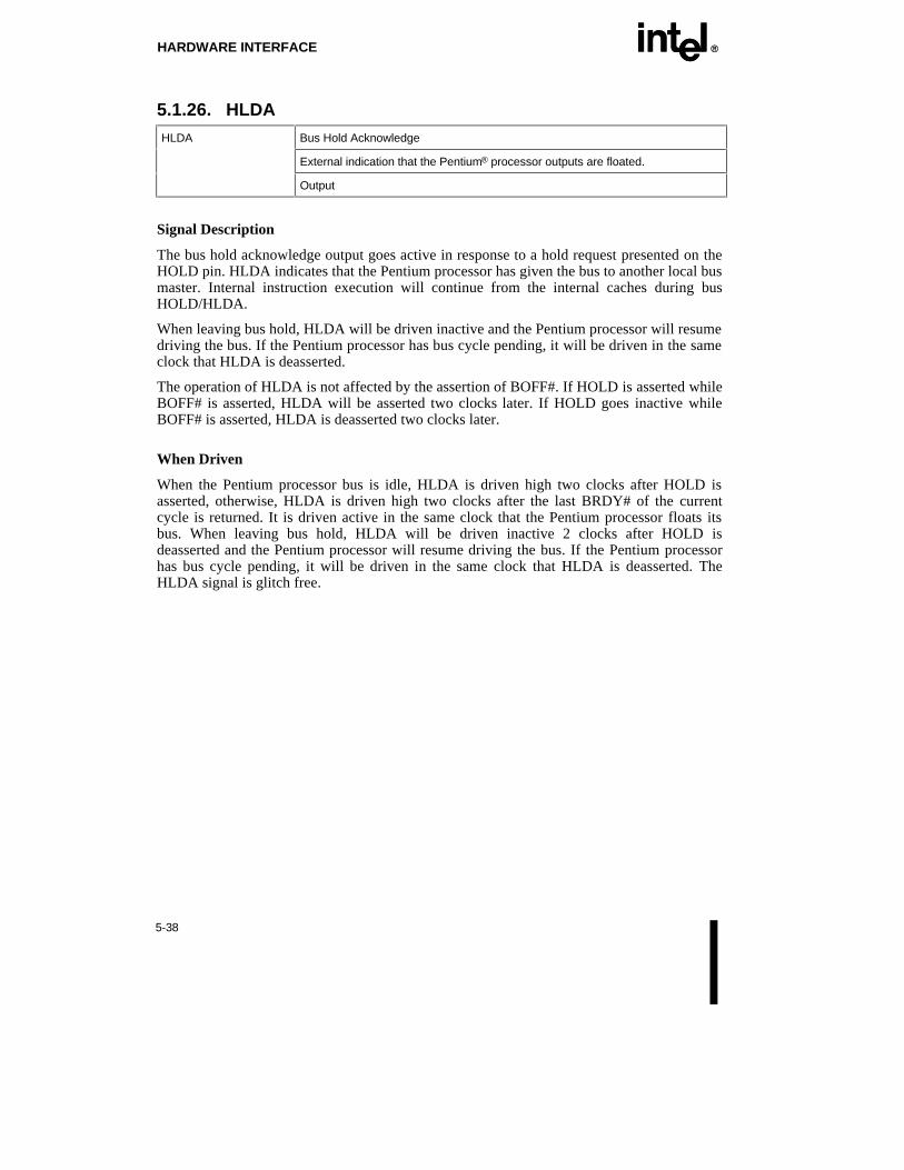
HARDWARE INTERFACE EE
5-38
5.1.26. HLDAHLDA Bus Hold Acknowledge
External indication that the Pentium® processor outputs are floated.
Output
Signal Description
The bus hold acknowledge output goes active in response to a hold request presented on theHOLD pin. HLDA indicates that the Pentium processor has given the bus to another local busmaster. Internal instruction execution will continue from the internal caches during busHOLD/HLDA.
When leaving bus hold, HLDA will be driven inactive and the Pentium processor will resumedriving the bus. If the Pentium processor has bus cycle pending, it will be driven in the sameclock that HLDA is deasserted.
The operation of HLDA is not affected by the assertion of BOFF#. If HOLD is asserted whileBOFF# is asserted, HLDA will be asserted two clocks later. If HOLD goes inactive whileBOFF# is asserted, HLDA is deasserted two clocks later.
When Driven
When the Pentium processor bus is idle, HLDA is driven high two clocks after HOLD isasserted, otherwise, HLDA is driven high two clocks after the last BRDY# of the currentcycle is returned. It is driven active in the same clock that the Pentium processor floats itsbus. When leaving bus hold, HLDA will be driven inactive 2 clocks after HOLD isdeasserted and the Pentium processor will resume driving the bus. If the Pentium processorhas bus cycle pending, it will be driven in the same clock that HLDA is deasserted. TheHLDA signal is glitch free.

EE HARDWARE INTERFACE
5-39
Relation to Other Signals
Pin Symbol Relation to Other Signals
A3-A31 These signals float in response to HLDA.
ADS#
AP
BE7#-BE3#
CACHE#
D/C#
D63-D0
DP7-DP0
LOCK#
M/IO#
PCD
PWT
SCYC
W/R#
BOFF# The same pins are floated when HLDA or BOFF# is asserted.
EADS# EADS# is recognized while HLDA is asserted.
HOLD The assertion of HOLD causes HLDA to be asserted when all outstanding cyclesare complete.

HARDWARE INTERFACE EE
5-40
5.1.27. HOLDHOLD Bus Hold
The bus hold request input allows another bus master complete control of thePentium® processor bus.
Synchronous Input
Signal Description
The bus hold request input allows another bus master complete control of the Pentiumprocessor bus. In response to HOLD, after completing all outstanding bus cycles the Pentiumprocessor will float most of its output and input/output pins and assert HLDA. The Pentiumprocessor will maintain its bus in this state until HOLD is deasserted. Cycles that are lockedtogether will not be interrupted by bus HOLD. HOLD is recognized during RESET.
When Sampled
HOLD is sampled on every rising clock edge including during RESET and INIT.
Relation to Other Signals
Pin Symbol Relation to Other Signals
A3-A31 These are the signals floated in response to HOLD.
ADS#
AP
BE7#-BE3#
CACHE#
D/C#
D63-D0
DP7-DP0
LOCK#
M/IO#
PCD
PWT
SCYC
W/R#
HLDA HLDA is asserted when the Pentium® processor relinquishes the bus in responseto the HOLD request.
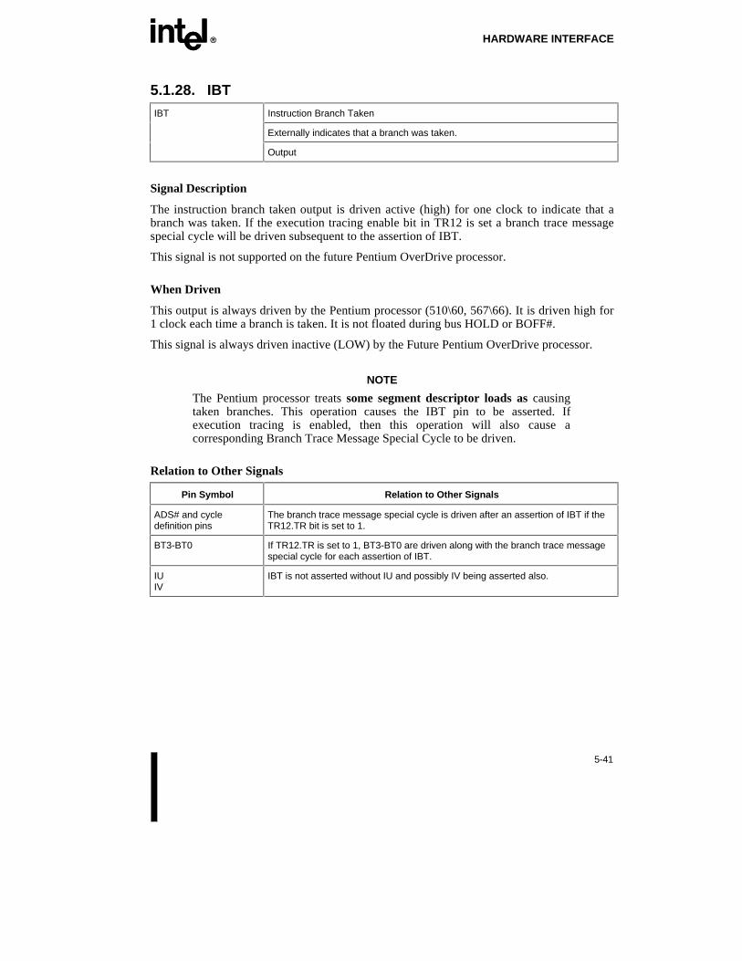
EE HARDWARE INTERFACE
5-41
5.1.28. IBTIBT Instruction Branch Taken
Externally indicates that a branch was taken.
Output
Signal Description
The instruction branch taken output is driven active (high) for one clock to indicate that abranch was taken. If the execution tracing enable bit in TR12 is set a branch trace messagespecial cycle will be driven subsequent to the assertion of IBT.
This signal is not supported on the future Pentium OverDrive processor.
When Driven
This output is always driven by the Pentium processor (510\60, 567\66). It is driven high for1 clock each time a branch is taken. It is not floated during bus HOLD or BOFF#.
This signal is always driven inactive (LOW) by the Future Pentium OverDrive processor.
NOTE
The Pentium processor treats some segment descriptor loads as causingtaken branches. This operation causes the IBT pin to be asserted. Ifexecution tracing is enabled, then this operation will also cause acorresponding Branch Trace Message Special Cycle to be driven.
Relation to Other Signals
Pin Symbol Relation to Other Signals
ADS# and cycledefinition pins
The branch trace message special cycle is driven after an assertion of IBT if theTR12.TR bit is set to 1.
BT3-BT0 If TR12.TR is set to 1, BT3-BT0 are driven along with the branch trace messagespecial cycle for each assertion of IBT.
IUIV
IBT is not asserted without IU and possibly IV being asserted also.

HARDWARE INTERFACE EE
5-42
5.1.29. IERR#IERR# Internal or Functional Redundancy Check Error
Alerts the system of internal parity errors and functional redundancy errors.
Output
Signal Description
The internal error output is used to alert the system of two types of errors, internal parityerrors and functional redundancy errors.
If a parity error occurs on a read from an internal array (reads during normal instructionexecution, reads during a flush operation, reads during BIST and testability cycles, and readsduring inquire cycles), the Pentium processor will assert the IERR# pin for one clock andthen shutdown. Shutdown will occur provided the processor is not prevented from doing soby the error.
If the Pentium processor is configured as a checker (by FRCMC# being sampled low whileRESET is asserted) and a mismatch occurs between the value sampled on the pins and thevalue computed internally, the Pentium processor will assert IERR# two clocks after themismatched value is returned. Shutdown is not entered as a result of a function redundancyerror.
It is the responsibility of the system to take appropriate action if an internal parity or FRCerror occurs.
When Driven
IERR# is driven in every clock. While RESET is active IERR# is driven high. After RESETis deasserted, IERR# will not be asserted due to an FRC mismatch until after the first clockof the first bus cycle. Note however that IERR# may be asserted due to an internal parityerror before the first bus cycle. IERR# is asserted for 1 clock for each detected FRC orinternal parity error two clocks after the error is detected. IERR# is asserted for each detectedmismatch, so IERR# may be asserted for more than one consecutive clock.
IERR# is not floated with HOLD or BOFF#. IERR# is a glitch free signal.
NOTE
When paging is turned on, an additional parity check occurs to page 0 forall TLB misses. If this access is a valid entry in the cache and this entry alsohas a parity error, then IERR# will be asserted and shutdown will occureven though the pipe-line is frozen to service the TLB miss.
During a TLB miss, a cache lookup occurs (to the data cache for a dataTLB miss, or the code cache for a code TLB miss) to a default page 0physical address until the correct page translation becomes available. Atthis time, if a valid cache entry is found at the page 0 address, then paritywill be checked on the data read out of the cache. However, the data is not

EE HARDWARE INTERFACE
5-43
used until after the correct page address becomes available. If this valid linecontains a true parity error, then the error will be reported. This will notcause an unexpected parity error. It can cause a parity error and shutdown ata time when the data is not being used because the pipe-line is frozen toservice the TLB miss. However, it still remains that a true parity error mustexist within the cache in order for IERR# assertion and shutdown to occur.For more details on TLB, refer to Chapter 11 of the Pentium ProcessorFamily Developer’s Manual, Volume 3.
Relation to Other Signals
Pin Symbol Relative to Other Signals
FRCMC# If the Pentium® processor is configured as a Checker, IERR# will be asserted inthe event of an FRC error.

HARDWARE INTERFACE EE
5-44
5.1.30. IGNNE#IGNNE# Ignore Numeric Exception
Determines whether or not numeric exceptions should be ignored.
Asynchronous Input
Signal Description
This is the ignore numerics exception input. This pin has no effect when the NE bit in CR0 isset to 1. When the CR0. NE bit is 0, this pin is functional as follows:
When the IGNNE# pin is asserted, the Pentium processor will ignore any pending unmaskednumeric exception and continue executing floating-point instructions for the entire durationthat this pin is asserted.
When IGNNE# is not asserted and a pending unmasked numeric exception exists, (SW.ES =1), the Pentium processor will behave as follows:
On encountering a floating-point instruction that is one of FNINIT, FNCLEX,FNSTENV, FNSAVE, FNSTSW, FNSTCW, FNENI, FNDISI, or FNSETPM, thePentium processor will assert the FERR# pin. Subsequently, the processor opens aninterrupt sampling window. The interrupts are checked and serviced during this window.If no interrupts are sampled within this window the processor will then execute theseinstructions in spite of the pending unmasked exception. For further details please referto Section 23.3.7 in the Volume 3: Architecture and Programming Manual of thePentium® Processor Family Developer’s Manual.
On encountering any floating-point instruction other than FINIT, FCLEX, FSTENV,FSAVE, FSTSW, FSTCW, FENI, FDISI, or FSETPM, the Pentium processor will stopexecution and wait for an external interrupt.
When Sampled
IGNNE# is sampled on every rising clock edge. Recognition of IGNNE# is guaranteed in aspecific clock if it is asserted synchronously and meets the setup and hold times. Toguarantee recognition if IGNNE# is asserted asynchronously, it must have been deassertedfor a minimum of 2 clocks before being returned active to the Pentium processor and remainasserted for a minimum pulse width of two clocks.
Relation to Other Signals
None

EE HARDWARE INTERFACE
5-45
5.1.31. INITINIT Initialization
Forces the Pentium® processor to begin execution in a known state withoutflushing the caches or affecting floating-point state.
Asynchronous Input
Signal Description
The initialization input forces the Pentium processor to begin execution in a known state.The processor state after INIT is the same as the state after RESET except that the internalcaches, write buffers, model specific registers, and floating-point registers retain the valuesthey had prior to INIT. The Pentium processor starts execution at physical addressFFFFFFF0H.
INIT can be used to help performance for DOS extenders written for the 80286. INITprovides a method to switch from protected to real mode while maintaining the contents ofthe internal caches and floating-point state. INIT may not be used instead of RESET afterpower-up.
Once INIT is sampled active, the INIT sequence will begin on the next instruction boundary(unless a higher priority interrupt is requested before the next instruction boundary). TheINIT sequence will continue to completion and then normal processor execution will resume,independent of the deassertion of INIT. ADS# will be asserted to drive bus cycles even ifINIT is not deasserted.
If INIT is sampled high when RESET transitions from high to low the Pentium processor willperform built-in self test prior to the start of program execution.
When Sampled
INIT is sampled on every rising clock edge. INIT is an edge sensitive interrupt. Recognitionof INIT is guaranteed in a specific clock if it is asserted synchronously and meets the setupand hold times. To guarantee recognition if INIT is asserted asynchronously, it must havebeen deasserted for a minimum of 2 clocks before being returned active to the Pentiumprocessor and remain asserted for a minimum pulse width of two clocks. INIT must remainactive for three clocks prior to the BRDY# of an I/O write cycle to guarantee that thePentium processor recognizes and processes INIT right after an I/O write instruction.
If INIT is sampled high when RESET transitions from high to low the Pentium processor willperform built-in self test. If RESET is driven synchronously, INIT must be at its valid levelthe clock before the falling edge of RESET. If RESET is driven asynchronously, INIT mustbe at its valid level two clocks before and after RESET transitions from high to low.
Relation to Other Signals
Pin Symbol Relation to Other Signals
RESET If INIT is sampled high when RESET transitions from high to low, BIST will beperformed.
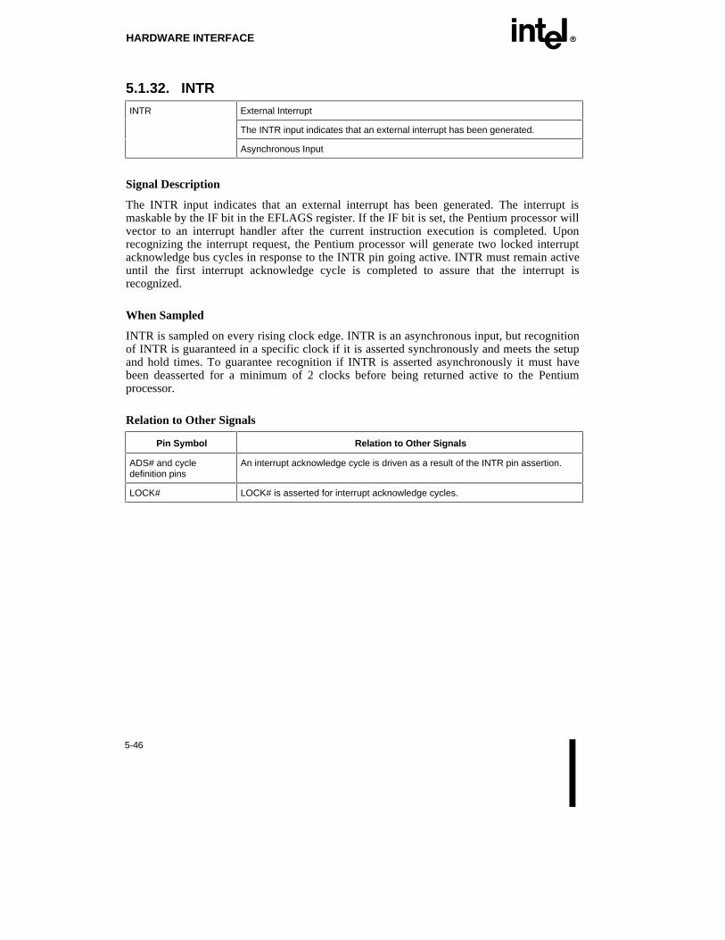
HARDWARE INTERFACE EE
5-46
5.1.32. INTRINTR External Interrupt
The INTR input indicates that an external interrupt has been generated.
Asynchronous Input
Signal Description
The INTR input indicates that an external interrupt has been generated. The interrupt ismaskable by the IF bit in the EFLAGS register. If the IF bit is set, the Pentium processor willvector to an interrupt handler after the current instruction execution is completed. Uponrecognizing the interrupt request, the Pentium processor will generate two locked interruptacknowledge bus cycles in response to the INTR pin going active. INTR must remain activeuntil the first interrupt acknowledge cycle is completed to assure that the interrupt isrecognized.
When Sampled
INTR is sampled on every rising clock edge. INTR is an asynchronous input, but recognitionof INTR is guaranteed in a specific clock if it is asserted synchronously and meets the setupand hold times. To guarantee recognition if INTR is asserted asynchronously it must havebeen deasserted for a minimum of 2 clocks before being returned active to the Pentiumprocessor.
Relation to Other Signals
Pin Symbol Relation to Other Signals
ADS# and cycledefinition pins
An interrupt acknowledge cycle is driven as a result of the INTR pin assertion.
LOCK# LOCK# is asserted for interrupt acknowledge cycles.

EE HARDWARE INTERFACE
5-47
5.1.33. INVINV Invalidation Request
Determines final state of a cache line as a result of an inquire hit.
Synchronous Input
Signal Description
The INV input is driven to the Pentium processor during an inquire cycle to determine thefinal cache line state (S or I) in case of an inquire cycle hit. If INV is returned active (high)to the Pentium processor in the same clock as EADS# is sampled asserted, an inquire hit willresult in that line being invalidated. If the INV pin is returned inactive (low), an inquire hitwill result in that line being marked Shared (S). If the inquire cycle is a miss in the cache, theINV input has no effect.
If an inquire cycle hits a modified line in the data cache, the line will be written backregardless of the state of INV.
When Sampled
The INV input is sampled with the EADS# of the inquire cycle.
Relation to Other Signals
Pin Symbol Relative to Other Signals
A31-A5 INV determines if the inquire address driven to the processor on A31-A5 should beinvalidated or marked as shared if it is valid in an internal cache.
EADS# INV is sampled with EADS#.

HARDWARE INTERFACE EE
5-48
5.1.34. IUIU U-Pipe Instruction Complete
Externally indicates that an instruction in the u-pipeline has completed execution.
Output
Signal Description
The IU output is driven active (high) for one clock to indicate that an instruction in theu-pipeline has completed execution.
This signal is not supported on the Future Pentium OverDrive processor.
When Driven
This pin is always driven by the Pentium processor (510\60, 567\66). It is not floated duringbus HOLD or BOFF#.
This signal is always driven inactive (LOW) by the Future Pentium OverDrive processor.
Relation to Other Signals
Pin Symbol Relative to Other Signals
IBT IBT is not asserted without IU being asserted also.
IV IV is not asserted without IU being asserted also.

EE HARDWARE INTERFACE
5-49
5.1.35. IVIV V-Pipe Instruction Complete
Externally indicates that an instruction in the v-pipeline has completed execution.
Output
Signal Description
The IV output is driven active (high) for one clock to indicate that an instruction in thev-pipeline has completed execution.
This signal is not supported on the Future Pentium OverDrive processor.
When Driven
This pin is always driven by the Pentium processor (510\60, 567\66). It is not floated duringbus HOLD or BOFF#.
This signal is always driven inactive (LOW) by the Future Pentium OverDrive processor.
Relation to Other Signals
Pin Symbol Relative to Other Signals
IBT IBT is not asserted without IU being asserted also.
IU IV is not asserted without IU being asserted also.

HARDWARE INTERFACE EE
5-50
5.1.36. KEN#KEN# Cache Enable
Indicates to the Pentium® processor whether or not the system can support acache line fill for the current cycle.
Synchronous Input
Signal Description
KEN# is the cache enable input. It is used to determine whether the current cycle iscacheable or not and consequently is used to determine cycle length.
When the Pentium processor generates a read cycle that can be cached (CACHE# asserted)and KEN# is active, the cycle will be transformed into a burst cache line fill. During a cacheline fill the byte enable outputs should be ignored and valid data must be returned on all 64data lines. The Pentium processor will expect 32-bytes of valid data to be returned in fourBRDY# transfers.
If KEN# is not sampled active, a line fill will not be performed (regardless of the state ofCACHE#) and the cycle will be a single transfer read.
Once KEN# is sampled active for a cycle, the cacheability cannot be changed. If a cycle isbacked off (BOFF#) after the cacheability of the cycle has been determined, the samecacheability attribute on KEN# must be returned to the processor when the cycle is redriven.
When Sampled
KEN# is sampled once in a cycle to determine cacheability. It is sampled and latched withthe first BRDY# or NA# of a cycle, however it must meet setup and hold times on everyclock edge.
Relation to Other Signals
Pin Symbol Relative to Other Signals
BRDY# KEN# is sampled with the first of the first BRDY# or NA# for that cycle. Also, inconjunction with the CACHE# input, KEN# determines whether the bus cycle willconsist of 1 or 4 transfers (assertions of BRDY#).
CACHE# KEN# determines cacheability only if the CACHE# pin is asserted.
NA# KEN# is sampled with the first of the first BRDY# or NA# for that cycle.
W/R# KEN# determines cacheability only if W/R# indicates a read.

EE HARDWARE INTERFACE
5-51
5.1.37. LOCK#LOCK# Bus Lock
Indicates to the system that the current sequence of bus cycles should not beinterrupted.
Output
Signal Description
The bus lock output indicates that the Pentium processor is running a read-modify-writecycle where the external bus must not be relinquished between the read and write cycles.Read-modify-write cycles of this type are used to implement memory based semaphores.Interrupt Acknowledge cycles are also locked.
If a cycle is split due to a misaligned memory operand, two reads followed by two writesmay be locked together. When LOCK# is asserted, the current bus master should be allowedexclusive access to the system bus.
The Pentium processor will not allow a bus hold when LOCK# is asserted, but address holds(AHOLD) and BOFF# are allowed. LOCK# is floated during bus hold.
All locked cycles will be driven to the external bus. If a locked address hits a valid locationin one of the internal caches, the cache location is invalidated (if the line is in the modifiedstate, it is written back before it is invalidated). Locked read cycles will not be transformedinto cache line fill cycles regardless of the state of KEN#.
LOCK# is guaranteed to be deasserted for at least one clock between back to back lockedcycles.
When Driven
LOCK# goes active with the ADS# of the first locked bus cycle and goes inactive after theBRDY# is returned for the last locked bus cycle. The LOCK# signal is glitch free.
Relation to Other Signals
Pin Symbol Relation to Other Signals
ADS# LOCK# is driven with the ADS# of the first locked cycle.
BOFF# LOCK# floats one clock after BOFF# is asserted.
BRDY# LOCK# is deasserted after the last BRDY# of the locked sequence.
HLDA LOCK# floats when HLDA is asserted.
NA# ADS# is not asserted to pipe-line an additional cycle if LOCK# is asserted,regardless of the state of NA#.
INTR LOCK# is asserted for interrupt acknowledge cycles.
SCYC SCYC is driven active if the locked cycle is misaligned.

HARDWARE INTERFACE EE
5-52
5.1.38. M/IO#M/IO# Memory/Input-Output
Distinguishes a memory access from an I/O access.
Output
Signal Description
The Memory/Input-Output signal is one of the primary bus cycle definition pins. M/IO#distinguishes between memory (M/IO# =1) and I/O (M/IO# =0) cycles.
When Driven
M/IO# is driven valid in the same clock as ADS# and the cycle address. It remains valid fromthe clock in which ADS# is asserted until the clock after the earlier of NA# or the lastBRDY#.
Relation to Other Signals
Pin Symbol Relation to Other Signals
ADS# M/IO# is driven to its valid state with ADS#.
BOFF# M/IO# floats one clock after BOFF# is asserted.
HLDA M/IO# floats when HLDA is asserted.

EE HARDWARE INTERFACE
5-53
5.1.39. NA#NA# Next Address
Indicates that external memory is prepared for a pipe-lined cycle.
Synchronous Input
Signal Description
The Next Address input, when active, indicates that external memory is ready to accept anew bus cycle although all data transfers for the current cycle have not yet completed. This isreferred to as bus cycle pipe-lining.
The Pentium processor will drive out a pending cycle in response to NA# no sooner than twoclocks after NA# is asserted. The Pentium processor supports up to 2 outstanding bus cycles.ADS# is not asserted to pipe-line an additional cycle if LOCK# is asserted, or during awriteback cycle. In addition, ADS# will not be asserted to pipe-line a locked cycle or awriteback cycle into the current cycle.
NA# is latched internally, so once it is sampled active during a cycle, it need not be heldactive to be recognized. The KEN#, and WB/WT# inputs for the current cycle are sampledwith the first NA#, if NA# is asserted before the first BRDY# of the current cycle.
When Sampled
NA# is sampled in all T2, TD and T2P clocks.
Relation to Other Signals
Pin Symbol Relation to Other Signals
ADS# If NA# is sampled asserted and an internal bus request is pending, the Pentium®
processor drives out the next bus cycle and asserts ADS#.
KEN# KEN# is sampled with the first of the first BRDY# or NA# for that cycle.
WB/WT# WB/WT# is sampled with the first of the first BRDY# or NA# for that cycle.
LOCK# ADS# is not asserted to pipe-line an additional cycle if LOCK# is asserted,regardless of the state of NA#.
BOFF# If NA# and BOFF# are asserted simultaneously, BOFF# takes priority and NA# isignored.

HARDWARE INTERFACE EE
5-54
5.1.40. NMINMI Non Maskable Interrupt
Indicates that an external non-maskable interrupt has been generated.
Asynchronous Input
Signal Description
The non-maskable interrupt request input indicates that an external non-maskable interrupthas been generated. Asserting NMI causes an interrupt with an internally supplied vectorvalue of 2. External interrupt acknowledge cycles are not generated.
If NMI is asserted during the execution of the NMI service routine it will remain pending andwill be recognized after the IRET is executed by the NMI service routine. At most, oneassertion of NMI will be held pending.
When Sampled
NMI is sampled on every rising clock edge. NMI is rising edge sensitive. Recognition ofNMI is guaranteed in a specific clock if it is asserted synchronously and meets the setup andhold times. To guarantee recognition if NMI is asserted asynchronously, it must have beendeasserted for a minimum of 2 clocks before being returned active to the Pentium processorand remain asserted for a minimum pulse width of two clocks.
Relation to Other Signals
None
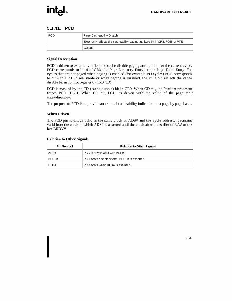
EE HARDWARE INTERFACE
5-55
5.1.41. PCDPCD Page Cacheability Disable
Externally reflects the cacheability paging attribute bit in CR3, PDE, or PTE.
Output
Signal Description
PCD is driven to externally reflect the cache disable paging attribute bit for the current cycle.PCD corresponds to bit 4 of CR3, the Page Directory Entry, or the Page Table Entry. Forcycles that are not paged when paging is enabled (for example I/O cycles) PCD correspondsto bit 4 in CR3. In real mode or when paging is disabled, the PCD pin reflects the cachedisable bit in control register 0 (CR0.CD).
PCD is masked by the CD (cache disable) bit in CR0. When CD =1, the Pentium processorforces PCD HIGH. When CD =0, PCD is driven with the value of the page tableentry/directory.
The purpose of PCD is to provide an external cacheability indication on a page by page basis.
When Driven
The PCD pin is driven valid in the same clock as ADS# and the cycle address. It remainsvalid from the clock in which ADS# is asserted until the clock after the earlier of NA# or thelast BRDY#.
Relation to Other Signals
Pin Symbol Relation to Other Signals
ADS# PCD is driven valid with ADS#.
BOFF# PCD floats one clock after BOFF# is asserted.
HLDA PCD floats when HLDA is asserted.

HARDWARE INTERFACE EE
5-56
5.1.42. PCHK#PCHK# Data Parity Check
Indicates the result of a parity check on a data read.
Output
Signal Description
The data parity check pin indicates the result of a parity check on a data read. Data parity ischecked during code reads, memory reads, and I/O reads. Data parity is not checked duringthe first Interrupt Acknowledge cycle. PCHK# indicates the parity status only for the byteson which valid data is expected. Parity is checked for all data bytes for which a byte enable isasserted. In addition, during a cache line fill, parity is checked on the entire data busregardless of the state of the byte enables.
PCHK# is driven low two clocks after BRDY# is returned if incorrect parity was returned.
Driving PCHK# is the only effect that bad data parity has on the Pentium processor unlessPEN# is also asserted. The data returned to the processor is not discarded.
If PEN# is asserted when a parity error occurs, the cycle address and type will be latched inthe MCA and MCT registers. If in addition, the MCE bit in CR4 is set, a machine checkexception will be taken.
It is the responsibility of the system to take appropriate actions if a parity error occurs. Ifparity checks are not implemented in the system, the PCHK# pin may be ignored, and PEN#pulled high (or CR4.MCE cleared).
When Driven
PCHK# is driven low two clocks after BRDY# is returned if incorrect parity was returned.PCHK# remains low one clock for each clock in which a parity error was detected. At allother times PCHK# is inactive (HIGH). PCHK# is not floated during bus HOLD or BOFF#.PCHK# is a glitch free signal.
Relation to Other Signals
Pin Symbol Relation to Other Signals
BRDY# PCHK# is driven to its valid level two clocks after the assertion of BRDY#.
D63-D0 The DP7-DP0 pins are used to create even parity with D63-D0. If even parity isnot returned, the PCHK# pin is asserted.
DP7-DP0 Even data parity with D63-D0 should be returned on to the Pentium® processor onthe DP pin. If even parity is not returned, the PCHK# pin is asserted.

EE HARDWARE INTERFACE
5-57
5.1.43. PEN#PEN# Parity Enable
Indicates to the Pentium® processor that the correct data parity is being returnedby the system. Determines if a Machine Check Exception should be taken if a dataparity error is detected.
Synchronous Input
Signal Description
The PEN# input (along with CR4.MCE) determines whether a machine check exception willbe taken as a result of a data parity error on a read cycle. If this pin is sampled active in theclock a data parity error is detected, the Pentium processor will latch the address and controlsignals of the cycle with the parity error in the machine check registers. If in addition themachine check enable bit in CR4 is set to "1," the Pentium processor will vector to themachine check exception before the beginning of the next instruction. If this pin is sampledinactive, it does not prevent PCHK# from being asserted in response to a bus parity error. Ifsystems are using PCHK#, they should be aware of this usage of PEN#.
This pin may be tied to VSS.
When Sampled
This signal is sampled when BRDY# is asserted for memory and I/O read cycles and thesecond interrupt acknowledge cycle.
Relation to Other Signals
Pin Symbol Relation to Other Signals
BRDY# PEN# is sampled with BRDY# for read cycles.
D63-D0 The DP7-DP0 pins are used to create even parity with D63-D0. If even parity isnot returned, and PEN# is enabled, the cycle will be latched and an MCE will betaken if CR4.MCE = 1.
DP7-DP0 Even data parity with D63-D0 should be returned to the Pentium® processor onthe DP pins. If even parity is not returned, and PEN# is enabled, the cycle will belatched and a MCE will be taken if CR4.MCE = 1.

HARDWARE INTERFACE EE
5-58
5.1.44. PM/BP[1:0]PM/BP1-0 Pin Name: Performance Monitoring and Breakpoint
Function: PM1-0 externally indicate the status of the performance monitor counter.
Input/Output: Output pins
Signal Description
The performance monitoring pins can be individually configured to externally indicate eitherthat the associated performance monitoring counter has incremented or that it hasoverflowed. PM1 indicates the status of CTR1, PM0 indicates the status of CTR0.
BP1 and BP0 are multiplexed with the Performance Monitoring pins (PM1 and PM0). ThePB1 and PB0 bits in the Debug Mode Control Register determine if the pins are configuredas breakpoint or performance monitoring pins. The pins come out of reset configured forperformance monitoring .
When Driven
The BP[3:2], PM/BP[1:0] pins are driven in every clock and are not floated during busHOLD, or BOFF#.
NOTE
The PM1/PM0 pins externally indicate the status of the performancemonitoring counters on the Pentium processor. These counters areundefined after RESET, and must be cleared or pre-set (using the WRMSRinstruction) before they are assigned to specific events. The Pentiumprocessor databook in section 4.3.2. lists the state of these two output pins(PM0/PM1) as undefined until at least 2 clocks after RESET is asserted. Itis however possible for these pins to toggle even during RESET. This mayoccur ONLY if the RESET pin was asserted while the Pentium processorwas in the process of counting a particular performance monitoring event.Since the even counters continue functioning until the CESR (Control andEvent Select Register) is cleared by RESET, it is possible for the eventcounters to increment even during RESET. Externally the state of the eventcounters would also be reflected on the PM1/PM0 pins. Any assertion of thePM1/PM0 pins during RESET should be ignored until after the start of thefirst bus cycle.
Relation to Other Signals
Pin Symbol Relation to Other Signals
BP1-BP0 PM1 and PM0 are share pins with BP1 and BP0.

EE HARDWARE INTERFACE
5-59
5.1.45. PRDYPRDY PRDY
For use with the Intel debug port.
Output
Signal Description
The PRDY output pin indicates that the processor has stopped normal execution in responseto the R/S# pin going active, or Probe Mode being entered. See Appendix A for moreinformation.
The PRDY pin is provided for use with the Intel debug port described in the "Debugging"chapter.
When Driven
This output is always driven by the Pentium processor. It is not floated during bus HOLD orBOFF#.
Relation to Other Signals
Pin Symbol Relation to Other Signals
R/S# R/S# is also used with the Intel debug port. Deassertion of R/S# to resume normaloperation should only occur while PRDY is asserted.

HARDWARE INTERFACE EE
5-60
5.1.46. PWTPWT Page Writethrough
Externally reflects the writethrough paging attribute bit in CR3, PDE, or PTE.
Output
Signal Description
PWT is driven to externally reflect the cache writethrough paging attribute bit for the currentcycle. PWT corresponds to bit 3 of CR3, the Page Directory Entry, or the Page Table Entry.For cycles that are not paged when paging is enabled (for example I/O cycles), PWTcorrespond to bit 3 in CR3. In real mode or when paging is disabled, the Pentium processordrives PWT low.
PWT can override the effect of the WB/WT# pin. If PWT is asserted for either reads orwrites, the line is saved in, or remains in, the Shared (S) state.
When Driven
The PWT pin is driven valid in the same clock as ADS# and the cycle address. It remainsvalid from the clock in which ADS# is asserted until the clock after the earlier of NA# or thelast BRDY#.
Relation to Other Signals
Pin Symbol Relation to Other Signals
ADS# PWT is driven valid with ADS#.
BOFF# PWT floats one clock after BOFF# is asserted.
HLDA PWT floats when HLDA is asserted.
WB/WT# PWT is used in conjunction with the WB/WT# pin to determine the MESI state ofcache lines.

EE HARDWARE INTERFACE
5-61
5.1.47. R/S#R/S# R/S#
For use with the Intel debug port.
Asynchronous Input
Internal Pullup Resistor
Signal Description
The R/S# pin is provided for use with the Intel debug port described in the "Debugging"chapter.
The R/S# input is an asynchronous, edge sensitive interrupt used to stop the normal executionof the processor and place it into an idle state where it is optionally capable of executingprobe mode instructions. The R/S# pin is implemented as an interrupt. A high to lowtransition on the R/S# pin will interrupt the processor and cause it to stop execution at thenext instruction boundary. While in this mode, the processor does not recognize any externalinterrupts. External interrupts that are latched are held pending and are serviced when theprocessor resumes normal operation. Those interrupts that are not latched must be heldpending until they are recognized by the processor after R/S# is deasserted.
The R/S# pin works in conjunction with the PRDY output from the processor. Waiting forthe PRDY output to go active ensures that the processor has stopped all execution. A low tohigh transition on the R/S# pin to resume normal operation must not occur until the PRDYoutput from the processor is sampled asserted.
Since the R/S# pin functions as an interrupt, the frequency at which it may toggle and itsrecognition by the processor can affect normal instruction execution. In order to guaranteeexecution of at least one instruction between back to back assertion of the R/S# pin, thesystem can qualify every subsequent assertion of R/S# with two assertions of the IU outputfrom the Pentium processor (510\60, 567\66). After R/S# is deasserted, the processoractivates the IU pin for one clock to indicate that it has successfully returned from theinterrupt (resumed normal operation). This is the first assertion of the IU pin. The Pentiumprocessor (510\60, 567\66) then generates a prefetch cycle to re-fill the instruction pipe-lineand continue code execution. As soon as one instruction has completed execution, theprocessor activates the IU pin again for one clock. This second assertion of IU confirms thatat least one instruction has completed execution before R/S# is asserted again.
When Sampled
This pin should not be driven except in conjunction with the Intel debug port.
NOTE
Deasserting R/S# while PRDY is asserted will cause the processor to exitprobe mode and return to normal executing. The behavior of the processoris unpredictable if R/S# is deasserted to exit probe mode while PRDY isdeasserted.

HARDWARE INTERFACE EE
5-62
Relation to Other Signals
Pin Symbol Relation to Other Signals
PRDY PRDY is also used with the Intel debug port. A low to high transition on the R/S#pin to resume normal operation must not occur until the PRDY output is asserted.

EE HARDWARE INTERFACE
5-63
5.1.48. RESETRESET Reset
Forces the Pentium® processor to begin execution at a known state.
Asynchronous Input
Signal Description
The RESET input forces the Pentium processor to begin execution at a known state. All thePentium processor internal caches (code and data caches, the translation lookaside buffers,branch target buffer and segment descriptor cache) will be invalidated upon the RESET.Modified lines in the data cache are not written back. When RESET is asserted, the Pentiumprocessor will immediately abort all bus activity and perform the RESET sequence. ThePentium processor starts execution at FFFFFFF0H.
When RESET transitions from high to low, FLUSH# is sampled to determine if tristate testmode will be entered, FRCMC# is sampled to determine if the Pentium processor will beconfigured as a master or a checker, and INIT is sampled to determine if BIST will be run.
When Sampled
RESET is sampled on every rising clock edge. RESET must remain asserted for a minimumof 1 millisecond after VCC and CLK have reached their AC/DC specifications for the "cold"or "power on" reset. During power up, RESET should be asserted while VCC is approachingnominal operating voltage (the simplest way to insure this is to place a pullup resistor onRESET). RESET must remain active for at least 15 clocks while VCC and CLK are withintheir operating limits for a "warm reset." Recognition of RESET is guaranteed in a specificclock if it is asserted synchronously and meets the setup and hold times. To guaranteerecognition if RESET is asserted asynchronously, it must have been deasserted for aminimum of 2 clocks before being returned active to the Pentium processor.
FLUSH#, FRCMC# and INIT are sampled when RESET transitions from high to low todetermine if tristate test mode or checker mode will be entered, or if BIST will be run. IfRESET is driven synchronously, these signals must be at their valid level and meet setup andhold times on the clock before the falling edge of RESET. If RESET is drivenasynchronously, these signals must be at their valid level two clocks before and after RESETtransitions from high to low.
Relation to Other Signals
Pin Symbol Relation to Other Signals
FLUSH# If FLUSH# is sampled low when RESET transitions from high to low, tristate testmode will be entered.
FRCMC# FRCMC# is sampled when RESET transitions from high to low to determine if thePentium processor is in Master or Checker mode.
INIT If INIT is sampled high when RESET transitions from high to low, BIST will beperformed.

HARDWARE INTERFACE EE
5-64
5.1.49. SCYCSCYC Split Cycle Indication
Indicates that a misaligned locked transfer is on the bus.
Output
Signal Description
The split cycle output is activated during misaligned locked transfers. It is asserted toindicate that more than two cycles will be locked together. This signal is defined for lockedcycles only. It is undefined for cycles which are not locked.
The Pentium processor defines misaligned transfers as a 16-bit or 32-bit transfer whichcrosses a 4-byte boundary, or a 64-bit transfer which crosses an 8-byte boundary.
When Driven
SCYC is only driven during the length of the locked cycle that is split. SCYC is asserted withthe first ADS# of a misaligned split cycle and remains valid until the clock after the earlier ofNA# or the last BRDY# of the last split cycle.
Relation to Other Signals
Pin Symbol Relation to Other Signals
ADS# SCYC is driven valid in the same clock as ADS#.
BOFF# SCYC is floated one clock after BOFF# is asserted.
HLDA SCYC is floated when HLDA is asserted.
LOCK# SCYC is defined for locked cycles only.
EE HARDWARE INTERFACE
5-65
5.1.50. SMI#SMI# System Management Interrupt
Latches a System Management Interrupt request.
Asynchronous Input
Internal Pullup Resistor
Signal Description
The system management interrupt input latches a System Management Interrupt request.After SMI# is recognized on an instruction boundary, the Pentium processor waits for allwrites to complete and EWBE# to be asserted, then asserts the SMIACT# output. Theprocessor will then save its register state to SMRAM space and begin to execute the SMMhandler. The RSM instruction restores the registers and returns to the user program.
Subsequent SMI# requests are not acknowledged while the processor is in systemmanagement mode (SMM) and are held pending until the processor completes an RSMinstruction.
When Sampled
SMI# is sampled on every rising clock edge. SMI# is a falling edge sensitive input.Recognition of SMI# is guaranteed in a specific clock if it is asserted synchronously andmeets the setup and hold times. To guarantee recognition if SMI# is asserted asynchronously,it must have been deasserted for a minimum of 2 clocks before being returned active to thePentium processor and remain asserted for a minimum pulse width of two clocks.
NOTE
The current Pentium processor specification allows SMI# to be recognizedwhile in shutdown state. However, if SMM is entered from shutdown state,the following must be considered:
1. if FLUSH# is asserted after the processor has entered SMM from ashutdown state, the processor will service the FLUSH# and then re-enter the shutdown state rather than returning to SMM. The systemsshould either assert SMI# and FLUSH# simultaneously or preventFLUSH# from being asserted while SMIACT# is active.
2. Servicing an SMI# request during the shutdown state could potentiallyfurther corrupt the system if the shutdown state occurred as a result ofan error encountered during the RSM instruction (misalignedSMBASE, reserved bit of CR4 is set to '1', etc.)
Once the system has detected that the processor has entered shutdown state(through the special bus cycle), it should generate an NMI interrupt or

HARDWARE INTERFACE EE
5-66
invoke reset initialization to get the processor out of the shutdown statebefore allowing an SMI# to be asserted to the processor.
Relation to Other Signals
Pin Symbol Relation to Other Signals
SMIACT# When the SMI# input is recognized, the Pentium® processor asserts SMIACT#.

EE HARDWARE INTERFACE
5-67
5.1.51. SMIACT#SMIACT# System Management Interrupt Active
Indicates that the processor is operating in SMM.
Output
Signal Description
The system management interrupt active output is asserted in response to the assertion ofSMI#. It indicates that the processor is operating in System Management Mode (SMM). Itwill remain active (low) until the processor executes the RSM instruction to leave SMM.
When Driven
SMIACT# is driven active in response to the assertion of SMI# after all internally pendingwrites are complete and the EWBE# pin is active (low). It will remain active (low) until theprocessor executes the RSM instruction to leave SMM. This signal is always driven. It doesnot float during bus HOLD or BOFF#.
Relation to Other Signals
Pin Symbol Relation to Other Signals
EWBE# SMIACT# is not asserted until EWBE# is active.
SMI# SMIACT# is asserted when the SMI# is recognized.

HARDWARE INTERFACE EE
5-68
5.1.52. TCKTCK Test Clock Input
Provides Boundary Scan clocking function.
Input
Internal Pullup Resistor
Signal Description
This is the testability clock input that provides the clocking function for the Pentiumprocessor boundary scan in accordance with the boundary scan interface (IEEE Std 1149.1).It is used to clock state information and data into and out of the Pentium processor duringboundary scan or probe mode operation. State select information and data are clocked intothe Pentium processor on the rising edge of TCK on TMS and TDI inputs respectively. Datais clocked out of the Pentium processor on the falling edge of TCK on TDO.
When TCK is stopped in a low state the boundary scan latches retain their state indefinitely.When boundary scan is not used, TCK should be tied high or left as a no-connect.
When Sampled
TCK is a clock signal and is used as a reference for sampling other boundary scan signals.
Relation to Other Signals
Pin Symbol Relation to Other Signals
TDI Serial data is clocked into the Pentium® processor on the rising edge of TCK.
TDO Serial data is clocked out of the Pentium processor on the falling edge of TCK.
TMS TAP controller state transitions occur on the rising edge of TCK.

EE HARDWARE INTERFACE
5-69
5.1.53. TDITDI Test Data Input
Input to receive serial test data and instructions.
Synchronous Input to TCK
Internal Pullup Resistor
Signal Description
This is the serial input for the Boundary Scan and Probe Mode test logic. TAP instructionsand data are shifted into the Pentium processor on the TDI pin on the rising edge of TCKwhen the TAP controller is in the SHIFT-IR and SHIFT-DR states. During all other states,TDI is a "don't care."
An internal pull-up resistor is provided on TDI to ensure a known logic state if an opencircuit occurs on the TDI path. Note that when "1" is continuously shifted into the instructionregister, the BYPASS instruction is selected.
When Sampled
TDI is sampled on the rising edge of TCK during the SHIFT-IR and SHIFT-DR states.During all other states, TDI is a "don't care."
Relation to Other Signals
Pin Symbol Relation to Other Signals
TCK TDI is sampled on the rising edge of TCK.
TDO In the SHIFT-IR and SHIFT-DR TAP controller states, TDO contains the outputdata of the register being shifted and TDI provides the input.
TMS TDI is sampled only in the SHIFT-IR and SHIFT DR states (controlled by TMS).

HARDWARE INTERFACE EE
5-70
5.1.54. TDOTDO Test Data Output
Outputs serial test data and instructions.
Output
Signal Description
This is the serial output of the Boundary Scan and Probe Mode test logic. TAP and ProbeMode instructions and data are shifted out of the Pentium processor on the TDO pin on thefalling edge of TCK when the TAP controller is in the SHIFT-IR and SHIFT-DR states.During all other states, the TDO pin is driven to the high impedance state to allowconnecting TDO of different devices in parallel.
When Driven
TDO is driven on the falling edge of TCK during the SHIFT-IR and SHIFT-DR TAPcontroller states. At all other times, TDO is driven to the high impedance state. TDO doesnot float during bus HOLD or BOFF#.
Relation to Other Signals
Pin Symbol Relation to Other Signals
TCK TDO is driven on the falling edge of TCK.
TDI In the SHIFT-IR and SHIFT-DR TAP controller states, TDI provides the input datato the register being shifted and TDO provides the output.
TMS TDO is driven only in the SHIFT-IR and SHIFT DR states (controlled by TMS).

EE HARDWARE INTERFACE
5-71
5.1.55. TMSTMS Test Mode Select
Controls TAP controller state transitions.
Synchronous Input to TCK
Internal Pullup Resistor
Signal Description
This a Boundary Scan test logic control input. The value of this input signal sampled at therising edge of TCK controls the sequence of TAP controller state changes.
To ensure deterministic behavior of the TAP controller, TMS is provided with an internalpullup resistor. If boundary scan is not used, TMS may be tied to VCC or left unconnected.
When Sampled
TMS is sampled on every rising edge of TCK.
Relation to Other Signals
Pin Symbol Relation to Other Signals
TCK TMS is sampled on every rising edge of TCK.
TDI TDI is sampled only in the SHIFT-IR and SHIFT DR states (controlled by TMS).
TDO TDO is driven only in the SHIFT-IR and SHIFT DR states (controlled by TMS).

HARDWARE INTERFACE EE
5-72
5.1.56. TRST#TRST# Test Reset
Allows the TAP controller to be asynchronously initialized.
Asynchronous Input
Internal Pullup Resistor
Signal Description
This is a Boundary Scan test logic reset or initialization pin. When asserted, it allows theTAP controller to be asynchronously initialized. When asserted TRST# will force the TAPcontroller into the Test Logic Reset State. When in this state, the test logic is disabled so thatnormal operation of the device can continue unhindered. During initialization the Pentiumprocessor initializes the instruction register with the IDCODE instruction.
An alternate method of initializing the TAP controller is to Drive TMS high for at least 5TCK cycles. In addition, the Pentium processor implements a power on TAP controller resetfunction. When the Pentium processor is put through its normal power on/RESET function,the TAP controller is automatically reset by the processor. The user does not have to assertthe TRST# pin or drive TMS high after the falling edge of RESET.
When Sampled
TRST# is an asynchronous input.
Relation to Other Signals
None

EE HARDWARE INTERFACE
5-73
5.1.57. W/R#W/R# Write/Read
Distinguishes a read cycle from a write cycle.
Output
Signal Description
The Write/Read signal is one of the primary bus cycle definition pins. W/R# distinguishesbetween write (W/R# = 1) and read cycles (W/R# = 0).
When Driven
W/R# is driven valid in the same clock as ADS# and the cycle address. It remains valid fromthe clock in which ADS# is asserted until the clock after the earlier of NA# or the lastBRDY#.
Relation to Other Signals
Pin Symbol Relation to Other Signals
ADS# W/R# is driven to its valid state with ADS#.
BOFF# W/R# floats one clock after BOFF# is asserted.
HLDA W/R# floats when HLDA is asserted.
KEN# KEN# determines cacheability only if W/R# indicates a read.

HARDWARE INTERFACE EE
5-74
5.1.58. WB/WT#WB/WT# Writeback/Writethrough
This pin allows a cache line to be defined as writeback or writethrough on a line byline basis.
Synchronous Input
Signal Description
This pin allows a cache line to be defined as writeback or writethrough on a line by linebasis. As a result, in conjunction with the PWT pin, it controls the MESI state that the line issaved in.
If WB/WT# is sampled high during a memory read cycle and the PWT pin is low, the line issaved in the Exclusive (E) state in the cache. If WB/WT# is sampled low during a memoryread cycle the line is saved in the Shared (S) state in the cache.
If WB/WT# is sampled high during a write to a shared line in the cache and the PWT pin islow, the line transitions to the E state. If WB/WT# is sampled low during a write to a sharedline in the cache, the line remains in the S state.
If for either reads or writes the PWT pin is high the line is saved in, or remains in, the Shared(S) state.
When Sampled
This pin is sampled with KEN# on the clock in which the first BRDY# or NA# is returned,however it must meet setup and hold times on every clock edge.
Relation to Other Signals
Pin Symbol Relation to Other Signals
BRDY#NA#
WB/WT# is sampled with the first of the first BRDY# or NA# for that cycle.
PWT If PWT is high, WB/WT# is a "don't care."

E6
Bus FunctionalDescription


EE
6-1
CHAPTER 6BUS FUNCTIONAL DESCRIPTION
The Pentium processor bus is designed to support a 528-Mbyte/sec data transfer rate at66 MHz. All data transfers occur as a result of one or more bus cycles. This chapter describesthe Pentium processor bus cycles and the Pentium processor data transfer mechanism.
6.1. PHYSICAL MEMORY AND I/O INTERFACEPentium processor memory is accessible in 8-, 16-, 32-, and 64-bit quantities. Pentiumprocessor I/O is accessible in 8-, 16-, and 32-bit quantities. The Pentium processor candirectly address up to 4 Gbytes of physical memory, and up to 64 Kbytes of I/O.
In hardware, memory space is organized as a sequence of 64-bit quantities. Each 64-bitlocation has eight individually addressable bytes at consecutive memory addresses (seeFigure 6-1).
PDB1 0 1
00000007H 00000000H
00000007H 00000000H
BE7# BE6# BE5# BE4# BE3# BE2# BE1#BE0#
PHYSICALMEMORY4 GBYTES
PHYSICAL MEMORYSPACE
64-BIT WIDE MEMORY ORGANIZATION
FFFFFFFFH FFFFFFF8H
FFFFFFFFH FFFFFFF8H
Figure 6-1. Memory Organization
I/O space is organized as a sequence of 32-bit quantities. Each 32-bit quantity has fourindividually addressable bytes at consecutive memory addresses. See Figure 6-2 for aconceptual diagram of the I/O space.

BUS FUNCTIONAL DESCRIPTION EE
6-2
PDB34
64 KBYTE00000003H 00000000H
00000003H 00000000H
BE3# BE2# BE1# BE0#
NOTACCESSIBLE
I/O SPACE 32-BIT WIDE MEMORY ORGANIZATION
0000FFFFH 0000FFFCH
0000FFFFH 0000FFFCH
Figure 6-2. I/O Space Organization
64-bit memories are organized as arrays of physical quadwords (8-byte words). Physicalquadwords begin at addresses evenly divisible by 8. The quadwords are addressable byphysical address lines A31-A3.
32-bit memories are organized as arrays of physical dwords (4-byte words). Physical dwordsbegin at addresses evenly divisible by 4. The dwords are addressable by physical addresslines A31-A3 and A2. A2 can be decoded from the byte enables according to Table 6-2.
16-bit memories are organized as arrays of physical words (2-byte words). Physical wordsbegin at addresses evenly divisible by 2. The words are addressable by physical address linesA31-A3, A2-A1, BHE#, and BLE#. A2 and A1 can be decoded from the byte enablesaccording to Table 6-2, BHE# and BLE# can be decoded from the byte enables according toTable 6-3 and Table 6-4.
To address 8-bit memories, the lower 3 address lines (A2-A0) must be decoded from the byteenables as indicated in Table 6-2.
6.2. DATA TRANSFER MECHANISMAll data transfers occur as a result of one or more bus cycles. Logical data operands of byte,word, dword, and quadword lengths may be transferred. Data may be accessed at any byteboundary, but two cycles may be required for misaligned data transfers. The Pentiumprocessor considers a 2-byte or 4-byte operand that crosses a 4-byte boundary to bemisaligned. In addition, an 8-byte operand that crosses an 8-byte boundary is misaligned.

EE BUS FUNCTIONAL DESCRIPTION
6-3
Like the Intel486 CPU, the Pentium processor address signals are split into two components.High-order address bits are provided by the address lines A31-A3. The byte enables BE7#-BE0# form the low-order address and select the appropriate byte of the 8-byte data bus.
The byte enable outputs are asserted when their associated data bus bytes are involved withthe present bus cycle as shown in Table 6-1. For both memory and I/O accesses, the byteenable outputs indicate which of the associated data bus bytes are driven valid for writecycles and on which bytes data is expected back for read cycles. Non-contiguous byte enablepatterns will never occur.
Table 6-1. Pentium ® Processor Byte Enables and Associated Data Bytes
Byte Enable Signal Associated Data Bus Signals
BE0# D0-D7 (byte 0 — least significant)
BE1# D8-D15 (byte 1)
BE2# D16-D23 (byte 2)
BE3# D24-D31 (byte 3)
BE4# D32-D39 (byte 4)
BE5# D40-D47 (byte 5)
BE6# D48-D55 (byte 6)
BE7# D56-D63 (byte 7 — most significant)
Address bits A2-A0 of the physical address can be decoded from the byte enables accordingto Table 6-2. The byte enables can also be decoded to generate BLE# (byte low enable) andBHE# (byte high enable) to address 16-bit memory systems (see Table 6-3 and Table 6-4).

BUS FUNCTIONAL DESCRIPTION EE
6-4
Table 6-2. Generating A2-A0 from BE7-0#
A2 A1 A0 BE7# BE6# BE5# BE4# BE3# BE2# BE1# BE0#
0 0 0 X X X X X X X Low
0 0 1 X X X X X X Low High
0 1 0 X X X X X Low High High
0 1 1 X X X X Low High High High
1 0 0 X X X Low High High High High
1 0 1 X X Low High High High High High
1 1 0 X Low High High High High High High
1 1 1 Low High High High High High High High
Table 6-3. When BLE# is Active
BE7# BE6# BE5# BE4# BE3# BE2# BE1# BE0# BLE#
X X X X X X X Low Low
X X X X X Low High High Low
X X X Low High High High High Low
X Low High High High High High High Low
Table 6-4. When BHE# is Active
BE7# BE6# BE5# BE4# BE3# BE2# BE1# BE0# BHE#
X X X X X X Low X Low
X X X X Low X High High Low
X X Low X High High High High Low
Low X High High High High High High Low
Because the data bus is 64 bits, special considerations need to be made for interfacing to 32-bit memory systems. Address bit 2 along with the appropriate byte enable signals need to begenerated by external hardware. Address bit 2 is generated as shown in Table 6-2. New byteenable signals BE3'#-BE0'# are generated as shown in Tables 6-5 through 6-8.
Table 6-5. When BE3'# is Active
BE7# BE6# BE5# BE4# BE3# BE2# BE1# BE0# BE3'#
Low X X X Low X X X Low

EE BUS FUNCTIONAL DESCRIPTION
6-5
Table 6-6. When BE2'# is Active
BE7# BE6# BE5# BE4# BE3# BE2# BE1# BE0# BE2'#
X Low X X X Low X X Low
Table 6-7. When BE1'# is Active
BE7# BE6# BE5# BE4# BE3# BE2# BE1# BE0# BE1'#
X X Low X X X Low X Low
Table 6-8. When BE0'# is Active
BE7# BE6# BE5# BE4# BE3# BE2# BE1# BE0# BE0'#
X X X Low X X X Low Low
6.2.1. Interfacing With 8-, 16-, 32-, and 64-Bit MemoriesIn 64-bit physical memories such as Figure 6-3, each 8-byte qword begins at a byte addressthat is a multiple of eight. A31-A3 are used as an 8-byte qword select and BE7#-BE0# selectindividual bytes within the word.
PDB27
PENTIUM® PROCESSOR
D63-D0
A31-A3, BE7#-BE0#
64-BIT MEMORY
Figure 6-3. Pentium ® Processor with 64-Bit Memory
Memories that are 32 bits wide require external logic for generating A2 and BE3'#-BE0'#.Memories that are 16 bits wide require external logic for generating A2, A1, BHE# andBLE#. Memories that are 8 bits wide require external logic for generating A2, A1, and A0.All memory systems that are less than 64 bits wide require external byte swapping logic forrouting data to the appropriate data lines.
The Pentium processor expects all the data requested by the byte enables to be returned asone transfer (with one BRDY#), so byte assembly logic is required to return all requested

BUS FUNCTIONAL DESCRIPTION EE
6-6
bytes to the Pentium processor at one time. Note that the Pentium processor does not supportBS8# or BS16# (or BS32#), so this logic must be implemented externally if necessary.
Figure 6-4 shows the Pentium processor address bus interface to 64, 32, 16 and 8-bitmemories. Address bits A2, A1, and A0 and BHE#, BLE#, and BE3'#-BE0'# are decoded asshown in Table 6-2 through Table 6-8.

EE BUS FUNCTIONAL DESCRIPTION
6-7
PDB28
PENTIUM®
PROCESSORBE7#-BE0#
BYTE SELECTLOGIC
A31-A3
64-BITMEMORY
32-BITMEMORY
A2, BE3'# - BE0'#
16-BITMEMORY
8-BITMEMORY
BHE#, BLE#,A2, A1
A2,A1,A0
Figure 6-4. Addressing 32-, 16- and 8-Bit Memories
Figure 6-5 shows the Pentium processor data bus interface to 32-, 16- and 8-bit widememories. External byte swapping logic is needed on the data lines so that data is supplied toand received from the Pentium processor on the correct data pins (see Table 6-1). Formemory widths smaller than 64 bits, byte assembly logic is needed to return all bytes of datarequested by the Pentium processor in one cycle.

BUS FUNCTIONAL DESCRIPTION EE
6-8
PDB30
PENTIUM®
PROCESSOR
D7-D0D15-D8D23-D16D31-D24D39-D32D47-D40D55-D48D63-D56
A31-A
3 BE
7#-BE
0#
64-BITMEMORY
BYTESWAPLOGIC
3232-BIT
MEMORY
BYTESWAPLOGIC
16-BITMEMORY
BYTESWAPLOGIC
8-BITMEMORY
16
8
64-BIT DATA ASSEMBLY
LOGIC
D7-D0D15-D8D23-D16D31-D24D39-D32D47-D40D55-D48D63-D56
Figure 6-5. Data Bus Interface to 32-, 16- and 8-Bit Memories
Operand alignment and size dictate when two cycles are required for a data transfer. Table6-9 shows the transfer cycles generated by the Pentium processor for all combinations oflogical operand lengths and alignment. Table 6-9 applies to both locked and unlockedtransfers. When multiple cycles are required to transfer a multi-byte logical operand, thehighest order bytes are transferred first.

EE BUS FUNCTIONAL DESCRIPTION
6-9
Table 6-9. Transfer Bus Cycles for Bytes, Words, Dwords and Quadwords
Length of Transfer 1 Byte 2 Bytes
Low Order Address xxx 000 001 010 011 100 101 110 111
1st transfer b w w w hb w w w hb
Byte enables driven 0 BE0-1# BE1-2# BE2-3# BE4# BE4-5# BE5-6# BE6-7# BE0#
Value driven on A3 0 0 0 0 0 0 0 1
2nd transfer (ifneeded)
lb lb
Byte enables driven BE3# BE7#
Value driven on A3 0 0
Length of Transfer 4 Bytes
Low Order Address 000 001 010 011 100 101 110 111
1st transfer d hb hw h3 d hb hw h3
Byte enables driven BE0-3# BE4# BE4-5# BE4-6# BE4-7# BE0# BE0-1# BE0-2#
Low order address 0 0 0 0 0 1 1 1
2nd transfer (ifneeded)
l3 lw lb l3 lw lb
Byte enables driven BE1-3# BE2-3# BE3# BE5-7# BE6-7# BE7#
Value driven on A3 0 0 0 0 0 0
Length of Transfer 8 Bytes
Low Order Address 000 001 010 011 100 101 110 111
1st transfer q hb hw h3 hd h5 h6 h7
Byte enables driven BE0-7# BE0# BE0-1# BE0-2# BE0-3# BE0-4# BE0-5# BE0-6#
Value driven on A3 0 1 1 1 1 1 1 1
2nd transfer (ifneeded)
l7 l6 l5 ld l3 lw lb
Byte enables driven BE1-7# BE2-7# BE3-7# BE4-7# BE5-7# BE6-7# BE7#
Value driven on A3 0 0 0 0 0 0 0
Key:
b = byte transfer w = 2-byte transfer 3 = 3-byte transfer d = 4-byte transfer
5 = 5-byte transfer 6 = 6-byte transfer 7 = 7-byte transfer q = 8-byte transfer
h = high order l = low order

BUS FUNCTIONAL DESCRIPTION EE
6-10
8-byte operand:
high orderbyte
byte 7 byte 6 byte 5 byte 4 byte 3 byte 2 low orderbyte
↑ ↑byte with highest address byte with lowest address
6.3. BUS CYCLESThe following terminology is used in this document to describe the Pentium processor busfunctions. The Pentium processor requests data transfer cycles, bus cycles, and busoperations. A data transfer cycle is one data item, up to 8 bytes in width, being returned tothe Pentium processor or accepted from the Pentium processor with BRDY# asserted. A buscycle begins with the Pentium processor driving an address and status and asserting ADS#,and ends when the last BRDY# is returned. A bus cycle may have 1 or 4 data transfers. Aburst cycle is a bus cycle with 4 data transfers. A bus operation is a sequence of bus cycles tocarry out a specific function, such as a locked read-modify-write or an interruptacknowledge.
The section titled "Bus State Definition" describes each of the bus states, and shows the busstate diagram.
Table 6-10 and Table 6-11 list all of the bus cycles that will be generated by the Pentiumprocessor. Note that inquire cycles (initiated by EADS#) may be generated from the systemto the Pentium processor.
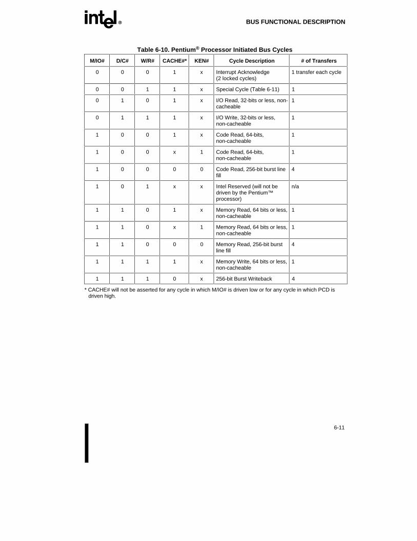
EE BUS FUNCTIONAL DESCRIPTION
6-11
Table 6-10. Pentium ® Processor Initiated Bus Cycles
M/IO# D/C# W/R# CACHE#* KEN# Cycle Description # of Transfers
0 0 0 1 x Interrupt Acknowledge(2 locked cycles)
1 transfer each cycle
0 0 1 1 x Special Cycle (Table 6-11) 1
0 1 0 1 x I/O Read, 32-bits or less, non-cacheable
1
0 1 1 1 x I/O Write, 32-bits or less,non-cacheable
1
1 0 0 1 x Code Read, 64-bits,non-cacheable
1
1 0 0 x 1 Code Read, 64-bits,non-cacheable
1
1 0 0 0 0 Code Read, 256-bit burst linefill
4
1 0 1 x x Intel Reserved (will not bedriven by the Pentium™processor)
n/a
1 1 0 1 x Memory Read, 64 bits or less,non-cacheable
1
1 1 0 x 1 Memory Read, 64 bits or less,non-cacheable
1
1 1 0 0 0 Memory Read, 256-bit burstline fill
4
1 1 1 1 x Memory Write, 64 bits or less,non-cacheable
1
1 1 1 0 x 256-bit Burst Writeback 4
* CACHE# will not be asserted for any cycle in which M/IO# is driven low or for any cycle in which PCD isdriven high.

BUS FUNCTIONAL DESCRIPTION EE
6-12
Table 6-11. Special Bus Cycles Encoding
BE7# BE6# BE5# BE4# BE3# BE2# BE1# BE0# Special Bus Cycle
1 1 1 1 1 1 1 0 Shutdown
1 1 1 1 1 1 0 1 Flush(INVD,WBINVD instr)
1 1 1 1 1 0 1 1 Halt
1 1 1 1 0 1 1 1 Writeback(WBINVD instruction)
1 1 1 0 1 1 1 1 Flush Acknowledge(FLUSH# assertion)
1 1 0 1 1 1 1 1 Branch Trace Message
Note that all burst reads are cacheable, and all cacheable read cycles are bursted. There areno non-cacheable burst reads or non-burst cacheable reads.
The remainder of this chapter describes all of the above bus cycles in detail. In addition,locked operations and bus cycle pipelining will be discussed.
6.3.1. Single-Transfer CycleThe Pentium processor supports a number of different types of bus cycles. The simplest typeof bus cycle is a single-transfer non-cacheable 64-bit cycle, either with or without wait states.Non-pipelined read and write cycles with 0 wait states are shown in Figure 6-6.
The Pentium processor initiates a cycle by asserting the address status signal (ADS#) in thefirst clock. The clock in which ADS# is asserted is by definition the first clock in the buscycle. The ADS# output indicates that a valid bus cycle definition and address is available onthe cycle definition pins and the address bus. The CACHE# output is deasserted (high) toindicate that the cycle will be a single transfer cycle.
For a zero wait state transfer, BRDY# is returned by the external system in the second clockof the bus cycle. BRDY# indicates that the external system has presented valid data on thedata pins in response to a read or the external system has accepted data in response to a write.The Pentium processor samples the BRDY# input in the second and subsequent clocks of abus cycle (the T2, T12 and T2P bus states, see the Bus State Definition section of this chapterfor more information).
The timing of the data parity input, DP, and the parity check output, PCHK#, is also shownin Figure 6-6. DP is driven by the Pentium processor and returned to the Pentium processorin the same clock as the data. PCHK# is driven two clocks after BRDY# is returned for readswith the results of the parity check.

EE BUS FUNCTIONAL DESCRIPTION
6-13
PDB1
CLK
ADDR
ADS#
CACHE#
W/R#
BRDY#
DATA
PCHK#
T1 T2 Ti T1 T2 Ti T1
DP
NA#
VALID VALIDINVALID INVALID
TO CPU
TO CPU
FROM CPU
FROM CPU
Figure 6-6. Non-Pipelined Read and Write
If the system is not ready to drive or accept data, wait states can be added to these cycles bynot returning BRDY# to the processor at the end of the second clock. Cycles of this type,with one and two wait states added are shown in Figure 6-7. Note that BRDY# must bedriven inactive at the end of the second clock. Any number of wait states can be added toPentium processor bus cycles by maintaining BRDY# inactive.

BUS FUNCTIONAL DESCRIPTION EE
6-14
PDB2
T2 T2CLK
ADDR
ADS#
CACHE#
W/R#
BRDY#
DATA/DP
PCHK#
T1 T2 T1 T2 T2Ti
NA#
VALID VALID
FROM CPUTO CPU
Figure 6-7. Non-Pipelined Read and Write with Wait States
6.3.2. Burst CyclesFor bus cycles that require more than a single data transfer (cacheable cycles and writebackcycles), the Pentium processor uses the burst data transfer. In burst transfers, a new data itemcan be sampled or driven by the Pentium processor in consecutive clocks. In addition theaddresses of the data items in burst cycles all fall within the same 32-byte aligned area(corresponding to an internal Pentium processor cache line).
The implementation of burst cycles is via the BRDY# pin. While running a bus cycle of morethan one data transfer, the Pentium processor requires that the memory system perform aburst transfer and follow the burst order (see Table 6-12). Given the first address in the burstsequence, the address of subsequent transfers must be calculated by external hardware. This

EE BUS FUNCTIONAL DESCRIPTION
6-15
requirement exists because the Pentium processor address and byte-enables are asserted forthe first transfer and are not re-driven for each transfer. The burst sequence is optimized fortwo bank memory subsystems and is shown in Table 6-12. The addresses are in hexadecimalform.
Table 6-12. Pentium ® Processor Burst Order
1st Address 2nd Address 3rd Address 4th Address
0 8 10 18
8 0 18 10
10 18 0 8
18 10 8 0
The cycle length is driven by the Pentium processor together with cycle specification (seeTable 6-10), and the system should latch this information and terminate the cycle on timewith the appropriate number of transfers. The fastest burst cycle possible requires 2 clocksfor the first data item to be returned/driven with subsequent data items returned/driven everyclock.
6.3.2.1. BURST READ CYCLES
When initiating any read, the Pentium processor will present the address and byte enables forthe data item requested. When the cycle is converted into a cache line fill, the first data itemreturned should correspond to the address sent out by the Pentium processor; however, thebyte enables should be ignored, and valid data must be returned on all 64 data lines. Inaddition, the address of the subsequent transfers in the burst sequence must be calculated byexternal hardware since the address and byte enables are not re-driven for each transfer.
Figure 6-8 shows a cacheable burst read cycle. Note that in this case the initial cyclegenerated by the Pentium processor might have been satisfied by a single data transfer, butwas transformed into a multiple-transfer cache fill by KEN# being returned active on theclock that the first BRDY# is returned. In this case KEN# has such an effect because thecycle is internally cacheable in the Pentium processor (CACHE# pin is driven active). KEN#is only sampled once during a cycle to determine cacheability.
PCHK# is driven with the parity check status two clocks after each BRDY#.

BUS FUNCTIONAL DESCRIPTION EE
6-16
PDB3
T2CLK
ADDR
ADS#
CACHE#
W/R#
BRDY#
DATA/DP
PCHK#
T1 T2 T2 T2
KEN#
Ti
VALID
TO CPU TO CPU TO CPU TO CPU
Figure 6-8. Basic Burst Read Cycle

EE BUS FUNCTIONAL DESCRIPTION
6-17
Data will be sampled only in the clock that BRDY# is returned, which means that data neednot be sent to Pentium processor every clock in the burst cycle. An example burst cyclewhere two clocks are required for every burst item is shown in Figure 6-9.
PDB5
CLK
ADDR
ADS#
CACHE#
W/R#
BRDY#
DATA/DP
PCHK#
T1 T2 T2 T2 T2
KEN#
T2 T2 T2
TO CPU TO CPU TO CPUTO CPU
Figure 6-9. Slow Burst Read Cycle
6.3.2.2. BURST WRITE CYCLES
Figure 6-10 shows the timing diagram of basic burst write cycle. KEN# is ignored in burstwrite cycle. If the CACHE# pin is active (low) during a write cycle, it indicates that the cyclewill be a burst writeback cycle. Burst write cycles are always writebacks of modified lines inthe data cache. Writeback cycles have several causes:
1. Writeback due to replacement of a modified line in the data cache.
2. Writeback due to an inquire cycle that hits a modified line in the data cache.

BUS FUNCTIONAL DESCRIPTION EE
6-18
3. Writeback due to an internal snoop that hits a modified line in the data cache.
4. Writebacks caused by asserting the FLUSH# pin.
5. Writebacks caused by executing the WBINVD instruction.
Writeback cycles are described in more detail in the Inquire Cycle section of this chapter.
The only write cycles that are burstable by the Pentium processor are writeback cycles. Allother write cycles will be 64 bits or less, single transfer bus cycles.
PDB4
CLK
ADDR
ADS#
CACHE#
W/R#
BRDY#
DATA/DP
PCHK#
T1 T2 T2T2 T2 Ti
VALID
FROM CPU FROM CPU FROM CPU FROM CPU
Figure 6-10. Basic Burst Write Cycle
For writeback cycles, the lower 5 bits of the first burst address always starts at 0; therefore,the burst order becomes 0, 8h, 10h, and 18h. Again, note that the address of the subsequenttransfers in the burst sequence must be calculated by external hardware since the Pentiumprocessor does not drive the address and byte enables for each transfer.

EE BUS FUNCTIONAL DESCRIPTION
6-19
6.3.3. Locked OperationsThe Pentium processor architecture provides a facility to perform atomic accesses ofmemory. For example, a programmer can change the contents of a memory-based variableand be assured that the variable was not accessed by another bus master between the read ofthe variable and the update of that variable. This functionality is provided for selectinstructions using a LOCK prefix, and also for instructions which implicitly perform lockedread modify write cycles such as the XCHG (exchange) instruction when one of its operandsis memory based. Locked cycles are also generated when a segment descriptor or page tableentry is updated and during interrupt acknowledge cycles.
In hardware, the LOCK functionality is implemented through the LOCK# pin, whichindicates to the outside world that the Pentium processor is performing a read-modify-writesequence of cycles, and that the Pentium processor should be allowed atomic access for thelocation that was accessed with the first locked cycle. Locked operations begin with a readcycle and end with a write cycle. Note that the data width read is not necessarily the datawidth written. For example, for descriptor access bit updates the Pentium processor fetches 8bytes and writes one byte.
A locked operation is a combination of one or multiple read cycles followed by one ormultiple write cycles. Programmer generated locked cycles and locked page table/directoryaccesses are treated differently and are described in the following sections.
6.3.3.1. PROGRAMMER GENERATED LOCKS AND SEGMENTDESCRIPTOR UPDATES
For programmer generated locked operations and for segment descriptor updates, thesequence of events is determined by whether or not the accessed line is in the internal cacheand what state that line is in.
6.3.3.1.1. Cached Lines in the Modified (M) State
Before a programmer initiated locked cycle or a segment descriptor update is generated, thePentium processor first checks if the line is in the Modified (M) state. If it is, the Pentiumprocessor drives an unlocked writeback first (leaving the line in the Invalid, I, state) and thenruns the locked read on the external bus. Since the operand may be misaligned, it is possiblethat the Pentium processor may do two writeback cycles before starting the first locked read.In the misaligned scenario the sequence of bus cycles is: writeback, writeback, locked read,locked read, locked write, then the last locked write. Note that although a total of six cyclesare generated, the LOCK# pin is active only during the last four cycles. In addition, theSCYC pin is asserted during the last four cycles to indicate that a misaligned lock cycle isoccurring. In the aligned scenario the sequence of cycles is writeback, locked read, lockedwrite. The LOCK# pin is asserted for the last two cycles (SCYC is not asserted and indicatesthat the locked cycle is aligned). The cache line is left in the Invalid state after the lockedoperation.

BUS FUNCTIONAL DESCRIPTION EE
6-20
6.3.3.1.2. Non-Cached (I-State), S-State and E-State Lines
A programmer initiated locked cycle or a segment descriptor update to an S, E or I-state lineis always forced out to the bus and the line is transitioned to the Invalid state. Since the lineis not in the M-State, no writeback is necessary. Because the line is transitioned to the Invalidstate, the locked write is forced out to the bus also. The cache line is left in the Invalid stateafter the locked operation.
6.3.3.2. PAGE TABLE/DIRECTORY LOCKED CYCLES
In addition to programmer generated locked operations, the Pentium processor performslocked operations to set the dirty and accessed bits in page tables/page directories. ThePentium processor runs the following sequence of bus cycles to set the dirty/accessed bit.
6.3.3.2.1. Cached Lines in the Modified (M) State
If there is a TLB miss, the Pentium processor issues an (unlocked) read cycle to determine ifthe dirty or accessed bits need to be set. If the line is modified in the internal data cache, theline is written back to memory (lock not asserted). If the dirty or accessed bits need to be set,the Pentium processor then issues a locked read modify write operation. The sequence of buscycles to set the dirty or accessed bits in a page table/directory when the line is in the M-stateis: unlocked read, unlocked writeback, locked read, then locked write. The line is left in theInvalid state after the locked operation. Note that accesses to the page tables/directories willnot be misaligned.
6.3.3.2.2. Non-Cached (I-State), S-State and E-State Lines
If the line is in the E, S or I state, the locked cycle is always forced out to the bus and the lineis transitioned to the Invalid state. The sequence of bus cycles for an internally generatedlocked operation is locked read, locked write. The line is left in the Invalid state. Note thataccesses to the page tables/directories will not be misaligned.
6.3.3.3. LOCK# OPERATION DURING AHOLD/HOLD/BOFF#
LOCK# is not deasserted if AHOLD is asserted in the middle of a locked cycle.
LOCK# is floated during bus HOLD, but if HOLD is asserted during a sequence of lockedcycles, HLDA will not be asserted until the locked sequence is complete.
LOCK# will float if BOFF# is asserted in the middle of a locked cycle, and is driven lowagain when the cycle is restarted. If BOFF# is asserted during the read cycle of a lockedread-modify write, the locked cycle is redriven from the read when BOFF# is deasserted. IfBOFF# is asserted during the write cycle of a locked read-modify write, only the write cycleis redriven when BOFF# is deasserted. The system is responsible for ensuring that other busmasters do not access the operand being locked if BOFF# is asserted during a LOCKed cycle.

EE BUS FUNCTIONAL DESCRIPTION
6-21
6.3.3.4. INQUIRE CYCLES DURING LOCK#
This section describes the Pentium processor bus cycles that will occur if an inquire cycle isdriven while LOCK# is asserted. Note that inquire cycles are only recognized if AHOLD,BOFF# or HLDA is asserted and the external system returns an external snoop address to thePentium processor. If AHOLD, BOFF# or HLDA is not asserted when EADS# is driven,EADS# is ignored. Note also that an inquire cycle can not hit the "locked line" because theLOCK cycle invalidated it.
Because HOLD is not acknowledged when LOCK# is asserted, inquire cycles run inconjunction with the assertion of HOLD can not be driven until LOCK# is deasserted andHLDA is asserted.
BOFF# takes priority over LOCK#. Inquire cycles are permitted while BOFF# is asserted. Ifan inquire cycle hits a modified line in the data cache, the writeback due to the snoop hit willbe driven before the locked cycle is re-driven. LOCK# will be asserted for the writeback.
An inquire cycle with AHOLD may be run concurrently with a locked cycle. If the inquirecycle hits a modified line in the data cache, the writeback may be driven between the lockedread and the locked write. If the writeback is driven between the locked read and write,LOCK# will be asserted for the writeback.
NOTE
Only writebacks due to an external snoop hit to a modified line may bedriven between the locked read and the locked write of a LOCKedsequence. No other writebacks (due to an internal snoop hit or data cachereplacement) are allowed to invade a LOCKed sequence.
6.3.3.5. LOCK# TIMING AND LATENCY
The timing of LOCK# is shown in Figure 6-11. Note that LOCK# is asserted with the ADS#of the read cycle and remains active until the BRDY# of the write cycle is returned. Figure6-12 shows an example of two consecutive locked operations. Note that the Pentiumprocessor automatically inserts at least one idle clock between two consecutive lockedoperations to allow the LOCK# pin to be sampled inactive by external hardware. Figure 6-13shows an example of a misaligned locked operation with SCYC asserted.
The maximum number of Pentium processor initiated cycles that will be locked together isfour. Four cycles are locked together when data is misaligned for programmer generatedlocks (read, read, write, write). SCYC will be asserted for misaligned locked cycles. Notethat accesses to the page tables/directories will not be misaligned.

BUS FUNCTIONAL DESCRIPTION EE
6-22
PDB6
CLK
ADDR
ADS#
W/R#
BRDY#
DATA
T1 T2 T1 T2
LOCK#
Ti Ti
VALID VALIDINVALID
TO CPU FROM CPU
Figure 6-11. LOCK# Timing

EE BUS FUNCTIONAL DESCRIPTION
6-23
PDB7
CLK
ADDR
ADS#
CACHE#
W/R#
BRDY#
DATA
T1 T2 T1 T2 T2T1
Rd Wr Rd
T i
LOCK#
T i
min. 1 clock
VALID VALID VALIDINVALID INVALID
TO CPU FROM CPU TO CPU
Figure 6-12. Two Consecutive Locked Operations

BUS FUNCTIONAL DESCRIPTION EE
6-24
PDB29
CLK
ADS#
W/R#
DATA
CACHE#
BRDY#
LOCK#
SCYC
T1 T2 T i T1 T2 T i T1 T2 T i T1 T2 T i
TO CPU TO CPU FROM CPU FROM CPU
Figure 6-13. Misaligned Locked Cycles
6.3.4. BOFF#In a multi-master system, another bus master may require the use of the bus to enable thePentium processor to complete its current cycle. The BOFF# pin is provided to prevent thisdeadlock situation. If BOFF# is asserted, the Pentium processor will immediately (in the nextclock) float the bus (see Figure 6-14). Any bus cycles in progress are aborted and any data re-turned to the processor in the clock BOFF# is asserted is ignored. In response to BOFF#, thePentium processor floats the same pins as HOLD, but HLDA is not asserted. BOFF# over-rides BRDY#, so if both are sampled active in the same clock, BRDY# is ignored. ThePentium processor samples the BOFF# pin every clock.

EE BUS FUNCTIONAL DESCRIPTION
6-25
PDB8
CLK
CACHE#
BOFF#
ADS#
BRDY#
T1 T2 T2 T2T1T2 T2 T i
Figure 6-14. Back Off Timing
The device that asserts BOFF# to the Pentium processor is free to run any bus cycle while thePentium processor is in the high impedance state. If BOFF# is asserted after the Pentiumprocessor has started a cycle, the new master should wait for memory to return BRDY#before driving a cycle. Waiting for BRDY# provides a handshake to insure that the memorysystem is ready to accept a new cycle. If the bus is idle when BOFF# is asserted, the newmaster can start its cycle two clocks after issuing BOFF#. The system must wait two clocksafter the assertion of BOFF# to begin its cycle to prevent address bus contention.
The bus remains in the high impedance state until BOFF# is negated. At that time, thePentium processor restarts all aborted bus cycles from the beginning by driving out theaddress and status and asserting ADS#. Any data returned before BOFF# was asserted is usedto continue internal execution, however that data is not placed in an internal cache. Anyaborted bus cycles will be restarted from the beginning.
External hardware should assure that if the cycle attribute KEN# was returned to theprocessor (with first BRDY# or NA#) before the cycle was aborted, it must be returned withthe same value after the cycle is restarted. In other words, backoff cannot be used to changethe cacheability property of the cycle. The WB/WT# attribute may be changed when thecycle is restarted.
If more than one cycle is outstanding when BOFF# is asserted, the Pentium processor willrestart both outstanding cycles in their original order. The cycles will not be pipelined unlessNA# is asserted appropriately.

BUS FUNCTIONAL DESCRIPTION EE
6-26
A pending writeback cycle due to an external snoop hit will be reordered in front of anycycles aborted due to BOFF#. For example, if a snoop cycle is run concurrently with a linefill, and the snoop hits an M state line and then BOFF# is asserted, the writeback cycle due tothe snoop will be driven from the Pentium processor before the cache line fill cycle isrestarted.
The system must not rely on the original cycle, that was aborted due to BOFF#, fromrestarting immediately after BOFF# is deasserted. In addition to reordering writebacks due toexternal snoop hit in front of cycles that encounter a BOFF#, the processor may also reorderbus cycles in the following situations:
1. A pending writeback cycle due to an internal snoop hit will be reordered in front of anycycles aborted due to BOFF#. If a read cycle is running on the bus, and an internal snoopof that read cycle hits a modified line in the data cache, and the system asserts BOFF#,the Pentium processor will drive out a writeback cycle resulting from the internal snoophit. After completion of the writeback cycle, the processor will then restart the originalread cycle. This circumstance can occur during accesses to the page tables/directories,and during prefetch cycles, since these accesses cause a bus cycle to be generated beforethe internal snoop to the data cache is performed.
2. If BOFF# is asserted during a data cache replacement writeback cycle, the writebackcycle will be aborted and then restarted once BOFF# is deasserted. However, during theBOFF#, if the processor encounters a request to access the page table/directory inmemory, this request will be reordered in front of the replacement writeback cycle thatwas aborted due to BOFF#. The Pentium processor will first run the sequence of buscycles to service the page table/directory access and then restart the original replacementwriteback cycle.
Asserting BOFF# in the same clock as ADS# may cause the Pentium processor to leave theADS# signal floating low. Since ADS# is floating low, a peripheral device may think that anew bus cycle has begun even though the cycle was aborted. There are several ways toapproach this situation:
1. Design the system's state machines/logic such that ADS# is not recognized the clockafter ADS# is sampled active.
2. Recognize a cycle as ADS# asserted and BOFF# negated in the previous clock.
3. Assert AHOLD one clock before asserting BOFF#.
6.3.5. Bus HoldThe Pentium processor provides a bus hold, hold acknowledge protocol using the HOLD andHLDA pins. HOLD is used to indicate to the Pentium processor that another bus masterwants control of the bus. When the Pentium processor completes all outstanding bus cycles,it will release the bus by floating its external bus, and drive HLDA active. An exampleHOLD/HLDA transaction is shown in Figure 6-15.

EE BUS FUNCTIONAL DESCRIPTION
6-27
PDB9
CLK
ADDR
ADS#
CACHE#
W/R#
BRDY#
DATA
HOLD
T1 T2 T2 T1
HLDA
Ti TiTiTi
VALID
TO CPU
VALID
Figure 6-15. HOLD/HLDA Cycles
The Pentium processor recognizes HOLD while RESET is asserted, when BOFF# is asserted,during Probe Mode, and during BIST (built in self test). HOLD is not recognized whenLOCK# is asserted. Once HOLD is recognized, HLDA will be asserted two clocks after thelater of the last BRDY# or HOLD assertion. Because of this, it is possible that a cycle maybegin after HOLD is asserted, but before HLDA is driven. The maximum number of cyclesthat will be driven after HOLD is asserted is one. BOFF# may be used if it is necessary toforce the Pentium processor to float its bus in the next clock. Figure 6-15 shows the latestHOLD may be asserted relative to ADS# to guarantee that HLDA will be asserted beforeanother cycle is begun.
The operation of HLDA is not affected by the assertion of BOFF#. If HOLD is asserted whileBOFF# is asserted, HLDA will be asserted two clocks later. If HOLD goes inactive whileBOFF# is asserted, HLDA is deasserted two clocks later.
Note that HOLD may be acknowledged between two bus cycles in a misaligned access.

BUS FUNCTIONAL DESCRIPTION EE
6-28
All outputs are floated when HLDA is asserted except: APCHK#, BREQ, FERR#, HIT#,HITM#, HLDA, IERR#, PCHK#, PRDY, BP3-2, PM1/BP1, PM0/BP0, SMIACT#, IU, IV,IBT and TDO.
6.3.6. Interrupt AcknowledgeThe Pentium processor generates interrupt acknowledge cycles in response to maskableinterrupt requests generated on the interrupt request input (INTR) pin (if interrupts are en-abled). Interrupt acknowledge cycles have a unique cycle type generated on the cycle typepins.
An example interrupt acknowledge transaction is shown in Figure 6-16. Interruptacknowledge cycles are generated in locked pairs. Data returned during the first cycle isignored, however the specified data setup and hold times must be met. The interrupt vector isreturned during the second cycle on the lower 8 bits of the data bus. The Pentium processorhas 256 possible interrupt vectors.
The state of address bit 2 (as decoded from the byte enables) distinguishes the first andsecond interrupt acknowledge cycles. The byte address driven during the first interruptacknowledge cycle is 4: (A31-A3) low, BE4# low, BE7# - BE5# high, and BE3# - BE0#high. The address driven during the second interrupt acknowledge cycle is 0 (A31-A3 low,BE0# low, and BE7# - BE1# high).
Interrupt acknowledge cycles are terminated when the external system returns BRDY#. Waitstates can be added by withholding BRDY#. The Pentium processor automatically generatesat least one idle clock between the first and second cycles, however the external system isresponsible for interrupt controller (8259A) recovery.

EE BUS FUNCTIONAL DESCRIPTION
6-29
PDB10
CLK
ADDR
ADS#
BRDY#
DATA
LOCK#
T1 T2 T1 T2Ti Ti TiTi
TO CPU TO CPU
VALID VALID
Figure 6-16. Interrupt Acknowledge Cycles
6.3.7. Flush OperationsThe FLUSH# input is implemented in the Pentium processor as an asynchronous interrupt,similar to NMI. Therefore, unlike the Intel486 microprocessor, FLUSH# is recognized oninstruction boundaries only. FLUSH# is latched internally, so once setup, hold and pulsewidth times have been met, FLUSH# may be deasserted, even if a bus cycle is in progress.
To execute a flush operation, the Pentium processor first writes back all modified lines toexternal memory. The lines in the internal caches are invalidated as they are written back.After the write-back and invalidation operations are complete, a special cycle, flushacknowledge, is generated by the Pentium processor to inform the external system.
6.3.8. Special Bus CyclesThe Pentium processor provides six special bus cycles to indicate that certain instructionshave been executed, or certain conditions have occurred internally. The special bus cycles inTable 6-13 are defined when the bus cycle definition pins are in the following state:M/IO# = 0, D/C# = 0 and W/R# = 1. During the special cycles the data bus is undefined and

BUS FUNCTIONAL DESCRIPTION EE
6-30
the address lines A31-A3 are driven to "0." The external hardware must acknowledge allspecial bus cycles by returning BRDY#.
Table 6-13. Special Bus Cycles Encoding
BE7# BE6# BE5# BE4# BE3# BE2# BE1# BE0# Special Bus Cycle
1 1 1 1 1 1 1 0 Shutdown
1 1 1 1 1 1 0 1 Flush(INVD,WBINVD instr)
1 1 1 1 1 0 1 1 Halt
1 1 1 1 0 1 1 1 Writeback(WBINVD instruction)
1 1 1 0 1 1 1 1 Flush Acknowledge(FLUSH# assertion)
1 1 0 1 1 1 1 1 Branch Trace Message
Shutdown can be generated due to the following reasons:
1. If any other exception occurs while the Pentium processor is attempting to invoke thedouble-fault handler.
2. An internal parity error is detected.
Prior to going into shutdown, the Pentium processor will not writeback the M-state lines.During shutdown, the internal caches remain in the same state unless an inquire cycle is runor the cache is flushed. The FLUSH#, SMI#, and R/S# pins are recognized while the Pentiumprocessor is in a shutdown state. The Pentium processor will remain in shutdown until NMI,INIT, or RESET is asserted.
The Flush Special Cycle is driven after the INVD (invalidate cache) or WBINVD (writebackinvalidate cache) instructions are executed. The Flush Special Cycle is driven to indicate tothe external system that the internal caches were invalidated and that external caches shouldalso be invalidated.
NOTE
INVD should be used with care. This instruction does not write backmodified cache lines. See Instruction set Volume 3 for details.
The Halt Special Cycle is driven when a HLT instruction is executed. Externally, halt differsfrom shutdown in only two ways:
1. In the resulting byte enables that are asserted.
2. The Pentium processor will exit the HLT state if INTR is asserted and maskableinterrupts are enabled in addition to the assertion of NMI, INIT or RESET.
The Writeback Special Cycle is driven after the WBINVD instruction is executed. Itindicates that modified lines in the Pentium processor data cache were written back tomemory or a second level cache. The Writeback Special Cycle also indicates that modified

EE BUS FUNCTIONAL DESCRIPTION
6-31
lines in external caches should be written back. After the WBINVD instruction is executed,writeback special cycle is generated, followed by the flush special cycle. Note that INTR isnot recognized while the WBINVD instruction is being executed.
When the FLUSH# pin is asserted to the Pentium processor, all modified lines in the datacache are written back and all lines in the code and data caches are invalidated. The FlushAcknowledge Special Cycle is driven after the writeback and invalidations are complete. TheFlush Acknowledge special cycle is driven only in response to the FLUSH# pin beingactivated. Note that the Flush Acknowledge special cycle indicates that all modified lineswere written back and all cache lines were invalidated while the Flush special cycle onlyindicates that all cache lines were invalidated.
The Branch Trace Message Special Cycle is part of the Pentium processor (510\60, 567\66)execution tracing protocol. If the execution tracing enable bit (bit 1) in TR12 is set to 1, aBranch Trace message special cycle will be driven each time IBT is asserted, i.e., whenevera branch is taken. The Branch Trace message special cycle is the only special cycle that doesnot drive "0's" on the address bus, however like the other special cycles, the data bus is unde-fined. When the branch trace message is driven, the following is driven on the address bus:
A31-A3: Bits 31-3 of the branch target linear address
BT2-BT0: Bits 2-0 of the branch target linear address(the byte enables should not be decoded for A2-A0)
BT3: High if the default operand size is 32-bits,Low if the default operand size is 16-bits
6.3.9. Bus Error SupportPentium processor provides basic support for bus error handling through data and addressparity check. Even data parity will be generated by the processor for every enabled byte inwrite cycles and will be checked for all valid bytes in read cycles. The PCHK# output signalsif a data parity error is encountered for reads.
Even address parity will be generated for A31-A5 during write and read cycles, and checkedduring inquire cycles. The APCHK# output signals if an address parity error is encounteredduring inquire cycles.
External hardware is free to take whatever actions are appropriate after a parity error. Forexample, external hardware may signal an interrupt if PCHK# or APCHK# is asserted. Pleaserefer to the Error Detection chapter for the details.
6.3.10. Pipelined CyclesThe NA# input indicates to the Pentium processor that it may drive another cycle before thecurrent one is completed. Cacheability (KEN#) and cache policy (WB/WT#) indicators forthe current cycle are sampled in the same clock NA# is sampled active (or the first BRDY#for that cycle, whichever comes first). Note that the WB/WT# and KEN# inputs are sampled

BUS FUNCTIONAL DESCRIPTION EE
6-32
with the first of BRDY# or NA# even if NA# does not cause a pipelined cycle to be drivenbecause there was no pending cycle internally or two cycles are already outstanding.
The NA# input is latched internally, so even if a cycle is not pending internally in the clockthat NA# is sampled active, but becomes pending before the current cycle is complete, thepending cycle will be driven to the bus even if NA# was subsequently deasserted.
LOCK# and writeback cycles are not pipelined into other cycles and other cycles are notpipelined into them (regardless of the state of NA#). Special cycles and I/O cycles may bepipelined.
An example of burst pipelined back to back reads is shown in Figure 6-17. The assertion ofNA# causes a pending cycle to be driven 2 clocks later. Note KEN# timing.
PDB11
CLK
ADDR
ADS#
W/R#
KEN#
CACHE#
T2 T2T2
NA#
BRDY#
DATA
T2 T2 T2P
a b
ba
a a a a b b
T12T1 T2
VALID VALID
b
Figure 6-17. Two Pipelined Cache Line Fills
Write cycles can be pipelined into read cycles and read cycles can be pipelined into writecycles, but one dead clock will be inserted between read and write cycles to allow busturnover (see the bus state diagram in the Bus State Definition section of this chapter).Pipelined back to back read/write cycles are shown in Figure 6-18.

EE BUS FUNCTIONAL DESCRIPTION
6-33
PDB12
CLK
ADDR
ADS#
W/R#
KEN#
CACHE#
T2
NA#
BRDY#
DATA
T2 T2 T2P
b
rd wr
TDT1 T2 T12 Ti
VALIDa VALID
TO CPU TO CPU TO CPU TO CPUFROM CPU
Figure 6-18. Pipelined Back-to-Back Read/Write Cycles
6.3.10.1. KEN# AND WB/WT# SAMPLING FOR PIPELINED CYCLES
KEN# and WB/WT# are sampled with NA# or BRDY# for that cycle, whichever comes first.Figure 6-19 and Figure 6-20 clarify this specification.

BUS FUNCTIONAL DESCRIPTION EE
6-34
PDB31
CYCLE 1
T1 T2 T2 T12 T2P T2P T2P T2P T2P T2 T12CLK
ADS#
NA#
KEN#
WB/WT#
BRDY#
W/R#
CYCLE 1 CYCLE 2
Figure 6-19. KEN# and WB/WT# Sampling with NA#
Figure 6-19 shows that even though 2 cycles have been driven, the NA# for the second cyclestill causes KEN# and WB/WT# to be sampled for the second cycle. A third ADS# will notbe driven until all the BRDY#s for cycle 1 have been returned to the Pentium processor.

EE BUS FUNCTIONAL DESCRIPTION
6-35
PDB32
CYCLE 1 CYCLE 2
T1 T2 T2 T12 T2P T2P T2P T2P T2 T2 T2CLK
ADS#
NA#
KEN#
WB/WT#
BRDY#
W/R#
CYCLE 1 CYCLE 2
Figure 6-20. KEN# and WB/WT# Sampling with BRDY#
Figure 6-20 shows that two cycles are outstanding on the Pentium processor bus. Theassertion of NA# caused the sampling of KEN# and WB/WT# for the first cycle. Theassertion of the four BRDY#s for the first cycle DO NOT cause the KEN# and WB/WT# forthe second cycle to be sampled. KEN# and WB/WT# for the second cycle are sampled withthe first BRDY# for the second cycle (in this example).
6.4. CACHE CONSISTENCY CYCLES (INQUIRE CYCLES)The purpose of an inquire cycle is to check whether a particular address is cached in aPentium processor internal cache and optionally invalidate it. After an inquire cycle iscomplete, the system has information on whether or not a particular address location iscached and what state it is in.
An inquire cycle is typically performed by first asserting AHOLD to force the Pentiumprocessor to float its address bus, waiting two clocks, and then driving the inquire addressand INV and asserting EADS#. Inquire cycles may also be executed while the Pentiumprocessor is forced off the bus due to HLDA, or BOFF#. Because the entire cache line isaffected by an inquire cycle, only A31-A5 need to be driven with the valid inquire address.Although the value of A4-A3 is ignored, these inputs should be driven to a valid logic levelduring inquire cycles for circuit reasons. The INV pin is driven along with the inquireaddress to indicate whether the line should be invalidated (INV high) or marked as shared(INV low) in the event of an inquire hit.

BUS FUNCTIONAL DESCRIPTION EE
6-36
After the Pentium processor determines if the inquire cycle hit a line in either internal cache,it drives the HIT# pin. HIT# is asserted (low) two clocks after EADS# is sampled asserted1 ifthe inquire cycle hit a line in the code or data cache. HIT# is deasserted (high) two clocksafter EADS# is sampled asserted if the inquire cycle missed in both internal caches. TheHIT# output changes its value only as a result of an inquire cycle. It retains its value betweeninquire cycles. In addition, the HITM# pin is asserted two clocks after EADS# if the inquirecycle hit a modified line in the data cache. HITM# is asserted to indicate to the externalsystem that the Pentium processor contains the most current copy of the data and any deviceneeding to read that data should wait for the Pentium processor to write it back. The HITM#output remains asserted until two clocks after the last BRDY# of the writeback cycle isasserted.
The external system must inhibit inquire cycles during BIST (initiated by INIT beingsampled high on the falling edge of RESET), and during the Boundary Scan InstructionRUNBIST. When the model specific registers (test registers) are used to read or write linesdirectly to or from the cache it is important that external snoops (inquire cycles) are inhibitedto guarantee predictable results when testing. This can be accomplished by inhibiting thesnoops externally or by putting the processor in SRAM mode (CR0.CD=CR0.NW=1).
The EADS# input is ignored during external snoop writeback cycles (HITM# asserted), orduring the clock after ADS# or EADS# is active. EADS# is also ignored when the processoris in SRAM mode, or when the processor is driving the address bus.
Note that the Pentium processor may drive the address bus in the clock after AHOLD isdeasserted. It is the responsibility of the system designer to ensure that address buscontention does not occur. This can be accomplished by not deasserting AHOLD to thePentium processor until all other bus masters have stopped driving the address bus.
Figure 6-21 shows an inquire cycle that misses both internal caches. Note that both the HIT#and HITM# signals are deasserted two clocks after EADS# is sampled asserted.
Figure 6-22 shows an inquire cycle that invalidates a non-modified line. Note that INV isasserted (high) in the clock that EADS# is returned. Note that two clocks after EADS# issampled asserted, HIT# is asserted and HITM# is deasserted.
Figure 6-21 and Figure 6-22 both show that the AP pin is sampled/driven along with theaddress bus, and that the APCHK# pin is driven with the address parity status two clocksafter EADS# is sampled asserted.
An inquire cycle that hits a M-state line is shown in Figure 6-23. Both the HIT# and HITM#outputs are asserted two clocks after EADS# is sampled asserted. ADS# for the writebackcycle will occur no earlier than two clocks after the assertion of HITM#.
1Since the EADS# input is ignored by the processor in certain clocks, the two clocks reference is from the clock in
which EADS# is asserted and actually sampled by the processor at the end of this clock (i.e. rising edge of nextclock) as shown in Figure 6-22.
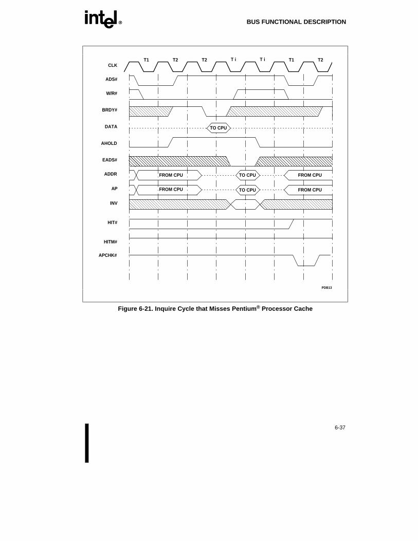
EE BUS FUNCTIONAL DESCRIPTION
6-37
PDB13
CLK
ADS#
W/R#
T2
BRDY#
DATA
T2T2 T1T iT iT1
AHOLD
EADS#
ADDR
INV
HIT#
HITM#
FROM CPU
APCHK#
AP FROM CPU
FROM CPU
FROM CPU
TO CPU
TO CPU
TO CPU
Figure 6-21. Inquire Cycle that Misses Pentium ® Processor Cache

BUS FUNCTIONAL DESCRIPTION EE
6-38
PDB14
CLK
ADS#
W/R#
T2
BRDY#
DATA
T2T2 T1T iT iT1
AHOLD
ADDR/AP
INV
HIT#
HITM#
FROM CPU FROM CPU
APCHK#
EADS#
TO CPU
TO CPU
Figure 6-22. Inquire Cycle that Invalidates Non-M-State Line

EE BUS FUNCTIONAL DESCRIPTION
6-39
PDB15
CLK
ADS#
CACHE#
W/R#
T2 T2T2
DATA
T2 T2
BRDY#
AHOLD
EADS#
ADDR
INV
HIT#
HITM#
T i T2T1 T i T i
1 2 3 4 5 6 7 8 9 10 11
T i
TO CPU FROM CPU FROM CPU FROM CPU FROM CPU
TO CPU
Figure 6-23. Inquire Cycle that Invalidates M-State Line
HITM# is asserted only if an inquire cycle (external snoop) hits a modified line in thePentium processor data cache. HITM# is not asserted for internal snoop writeback cycles orcache relacement writeback cycles. HITM# informs the external system that the inquire cyclehit a modified line in the data cache and that line will be written back. Any ADS# driven bythe Pentium processor while HITM# is asserted will be the ADS# of the writeback cycle. TheHITM# signal will stay active until last BRDY# is returned for the corresponding inquirecycle. Writeback cycles start at burst address 0.
Note that ADS# is asserted despite the AHOLD signal being active. This ADS# initiates awriteback cycle corresponding to the inquire hit. Such a cycle can be initiated while addresslines are floating to support multiple inquires within a single AHOLD session. Thisfunctionality can be used during secondary cache replacement processing if its line is largerthan the Pentium processor cache line (32 bytes). Although the cycle specification is driven

BUS FUNCTIONAL DESCRIPTION EE
6-40
properly by the processor, address pins are not driven because AHOLD forces the Pentiumprocessor off the address bus. If AHOLD is cleared before Pentium processor drives out theinquire writeback cycle, the Pentium processor will drive the correct address for inquirewriteback in the next clock. The ADS# to initiate a writeback cycle as a result of an inquirehit is the only time ADS# will be asserted while AHOLD is also asserted.
Note that in the event of an address parity error during inquire cycles, the snoop cycle willnot be inhibited. If the inquire hits a modified line in this situation and an active AHOLDprevents the Pentium processor from driving the addrss bus, the Pentium processor willpotentially writeback a line at an address other than the one intended. If the Pentiumprocessor is not driving the address bus during the writeback cycle, it is possible that memorywill be corrupted.
If BOFF# or HLDA were asserted to perform the inquire cycle, the writeback cycle wouldwait until BOFF# or HLDA were deasserted.
State machines should not depend on a writeback cycle to follow an assertion of HITM#.HITM# may be negated without a corresponding writeback cycle being run. This may occuras a result of the internal caches being invalidated due to the INVD instruction or bytestability accesses. Note as indicated earlier in this section that inquire cycles occurringduring testability accesses will generate unpredictable results. In addition, a second writebackcycle will not be generated for an inquire cycle which hits a line that is already being writtenback, see Figure 6-28. This can happen if an inquire cycle hits a line in one of the Pentiumprocessor writeback buffers.
6.4.1. Restrictions on Deassertion of AHOLDTo prevent the address and data buses from switching simultaneously, the followingrestrictions are placed on the negation of AHOLD: (i) AHOLD must not be negated in thesame clock as the assertion of BRDY# during a write cycle; (ii) AHOLD must not be negatedin the dead clock between write cycles pipelined into read cycles; and (iii) AHOLD must notbe negated in the same clock as the assertion of ADS# while HITM# is asserted. Note thatthere are two clocks between EADS# being sampled asserted and HITM# being asserted, anda further minimum of two clocks between an assertion of HITM# and ADS#.
These restrictions on the deassertion of AHOLD are the only considerations the systemdesigner needs to make to prevent the simultaneous switching of the address and data buses.All other considerations are handled internally.
Figure 6-23 can be used to illustrate restrictions (i) and (iii). AHOLD may be deasserted inclock 2, 3, or 4, but not in clock 5, 6, 7, 8 or 9.
Figure 6-24 and Figure 6-25 depict restrictions (i) and (ii) respectively. Note that there are norestrictions on the assertion of AHOLD.

EE BUS FUNCTIONAL DESCRIPTION
6-41
PDB16
1 2 3 4 5 6 7 8 9
T1 T2 T2 T2 T2 T2 T2 T2 T i
ADS#
W/R#
BRDY#
AHOLD
CACHE#
HITM#
Figure 6-24. AHOLD Restriction during Write Cycles
Figure 6-24 shows a writeback (due to a previous snoop that is not shown). ADS# for thewriteback is asserted even though AHOLD is asserted. Note that AHOLD can be deassertedin clock 2, 4, 7, or 9. AHOLD can not be deasserted in clock 1, 3, 5, 6, or 8.

BUS FUNCTIONAL DESCRIPTION EE
6-42
PDB17
1 2 3 4 5 6 7 8 9 10
T1 T2 T2 T12 T2P T2P T2P TD T2 T12
ADS#
W/R#
NA#
BRDY#
CACHE#
AHOLD
CYCLE 1
CYCLE 1 CYCLE 2
CYCLE 2
-
Figure 6-25. AHOLD Restriction during TD
Figure 6-25 shows a write cycle being pipelined into a read cycle. Note that if AHOLD isasserted in clock 5, it can be deasserted in clock 7 before the TD, or in clock 10 after the TD,but it can not be deasserted in clock 8 (the TD clock). AHOLD can not be deasserted in clock9 because BRDY# for the write cycle is being returned.

EE BUS FUNCTIONAL DESCRIPTION
6-43
6.4.2. Rate of Inquire CyclesPentium processor can accept inquire cycles at a maximum rate of one every other clock.However, if an inquire cycle hits an M-state line of the Pentium processor, subsequentinquire cycles will be ignored until the line is written back and HITM# is deasserted. EADS#is also ignored the clock after ADS# is asserted.
6.4.3. Internal Snooping"Internal snoop" is the term used to describe the snooping of the internal code or data cachesthat is not initiated by the assertion of EADS# by the external system. Internal snoopingoccurs in the three cases described below. Note that neither HIT# nor HITM# are asserted asa result of an internal snoop.
1. An internal snoop occurs if an access is made to the code cache, and that access is amiss. In this case, if the accessed line is in the S or E-state in the data cache, the line isinvalidated. If the accessed line is in the M-state in the data cache, the line is writtenback then invalidated.
2. An internal snoop occurs if an access is made to the data cache, and that access is a missor a writethrough. In this case, if the accessed line is valid in the code cache, the line isinvalidated.
3. An internal snoop occurs if there is a write to the accessed and/or dirty bits in the pagetable/directory entries. In this case, if the accessed line is valid in either the code or datacache, the line is invalidated. If the accessed line is in the M-state in the data cache, theline is written back then invalidated.
6.4.4. Snooping ResponsibilityIn systems with external second level caches allowing concurrent activity of the memory busand Pentium processor bus, it is desirable to run invalidate cycles concurrently with otherPentium processor bus activity. Writes on the memory bus can cause invalidations in the sec-ondary cache at the same time that the Pentium processor fetches data from the secondarycache. Such cases can occur at any time relative to each other, and therefore the order inwhich the invalidation is requested, and data is returned to the Pentium processor becomesimportant.
The Pentium processor always snoops the instruction and data caches when it accepts aninquire cycle. If a snoop comes in during a line fill, the Pentium processor also snoops theline currently being filled. If more than one cacheable cycle is outstanding (throughpipelining), the addresses of both outstanding cycles are snooped.
For example, during line fills, the Pentium processor starts snooping the address(es)associated with the line(s) being filled after KEN# has been sampled active for the line(s).Each line is snooped until it is put in the cache. If a snoop hits a line being currently filled,the Pentium processor will assert HIT# and the line will end up in the cache in the S or I state

BUS FUNCTIONAL DESCRIPTION EE
6-44
depending on the value of the INV pin sampled during the inquire cycle. The Pentiumprocessor will however use the data returned for that line as a memory operand for theinstruction that caused the data cache miss/line fill or execute an instruction contained in acode cache miss/line fill.
Figure 6-26 and Figure 6-27 illustrate the snoop responsibility pickup. Figure 6-26 shows anon-pipelined cycle, while Figure 6-27 illustrates a pipelined cycle. The figures show theearliest EADS# assertion that will cause snooping of the line being cached relative to firstBRDY# or NA#.
PDB18
CLKT2 T2T2 T2 T2 T2 T2 T iT1
TO CPU TO CPU TO CPU TO CPU
ADDR
ADS#
AHOLD
EADS#
HIT#
CACHE#
W/R#
KEN#
BRDY#
DATA
FROM CPU TO CPU
Figure 6-26. Snoop Responsibility Pickup — Non-Pipelined Cycles

EE BUS FUNCTIONAL DESCRIPTION
6-45
PDB19
CLK
ADDR
ADS#
AHOLD
EADS#
HIT#
T2 T2T2 T2
CACHE#
W/R#
KEN#
BRDY#
DATA
TiT2 T2 T2
NA#
T1
TO CPU
FROM CPU
TO CPU TO CPU TO CPU
TO CPU
Figure 6-27. Snoop Responsibility Pickup — Pipelined Cycle
The Pentium processor also snoops M state lines in the writeback buffers until the writebackof the M state lines are complete. If a snoop hits an M state line in a writeback buffer, bothHIT# and HITM# are asserted. Figure 6-28 illustrates snooping (snoop responsibility drop) ofan M state line that is being written back because it has been replaced with a "new" line inthe data cache. It shows the latest EADS# assertion, relative to the last BRDY# of thewriteback cycle that will result in a snoop hit to the line being written back. HITM# staysasserted until the writeback is complete. Note that no additional ADS# is asserted during thewriteback cycle.
The HIT# signal is a super set of the HITM# signal; it is always asserted with HITM#.

BUS FUNCTIONAL DESCRIPTION EE
6-46
PDB20
CLK
ADS#
W/R#
BRDY#
DATA
AHOLD
T2 T2T2 T2
EADS#
ADDR
HIT#
HITM#
T2 T2 T2 Ti TiT1
FROM CPU FROM CPU FROM CPUFROM CPU
FROM CPU TO CPU From CPU
Figure 6-28. Latest Snooping of Writeback Buffer
6.5. BUS DIFFERENCES BETWEEN THE Intel486™MICROPROCESSOR AND THE PENTIUM® PROCESSOR
The Pentium processor bus is designed to be similar to the Intel486 CPU bus for ease of use.In addition, enhancements have been made to achieve higher performance and provide bettersupport for multi-processing systems.
This section is provided as a quick reference for those designers familiar with the Intel486microprocessor.
The following are differences between the Pentium processor and Intel486 CPU buses:
• The Pentium processor has 64-bit data bus, while the Intel486 CPU supports 32-bit databus. The Pentium processor has more byte enables (BE7#-BE0#) and more data paritypins (DP7-0) than the Intel486 CPU to support this larger data bus size.

EE BUS FUNCTIONAL DESCRIPTION
6-47
• The Pentium processor supports address pipelining through the NA# input to provide thecapability of driving up to two cycles to the bus concurrently.
• The Pentium processor samples the cacheability input KEN# with the earlier of NA# orthe first BRDY#. KEN# is sampled only once. The Intel486 CPU samples KEN# twice,the clock before the first and last RDY#/BRDY# of the cache line fill cycle.
• Burst length information is driven by the Pentium processor via the CACHE# pintogether with the address. The Intel486 CPU controls burst length with the BLAST# pin.
• The Pentium processor generates 8-byte writes as one bus cycle, and therefore does nothave PLOCK# pin.
• The Pentium processor does not change lower-order bits of address and byte enablesduring the burst.
• The Pentium processor requires write-backs and line fills to be run as burst cycles, andthe burst cannot be terminated in the middle (no RDY# or BLAST# pins).
• Non-cacheable burst cycles are not supported by the Pentium processor. Non-burstcacheable cycles are not supported by the Pentium processor. On the Pentium processor,cacheable implies burst-able.
• The Pentium processor supports a writeback cache protocol with the following new pins:CACHE#, HIT#, HITM#, INV and WB/WT#.
• The Pentium processor does not support the dynamic bus sizing implemented with BS8#and BS16#.
• The Pentium processor does not allow invalidations every clock, or invalidations whilethe Pentium processor is driving the address bus.
• The Pentium processor guarantees an idle clock between consecutive LOCKed cycles.
• The Pentium processor provides the SCYC pin which indicates a split cycle duringlocked operations.
• Non-cacheable code prefetches are 8 bytes for the Pentium processor, not 16 bytes.
• The Pentium processor has an INIT pin to perform the reset function while maintainingthe state of the internal caches and the floating point machine state.
• The Pentium processor supports strong store ordering between the Pentium processor andthe external system through the EWBE# pin.
• The Pentium processor supports internal parity error checking, enhanced data paritychecking, and address parity error checking. The following new pins were added toimplement these new features: APCHK#, BUSCHK#, PEN#, IERR# and AP.
• The Pentium processor includes boundary scan with the following pins: TDI, TDO,TMS, TRST#, and TCK.
• The Pentium processor has (510\60, 567\66) IU, IV, and IBT pins and a branch tracemessage special cycle to support execution tracing.
• The Pentium processor supports Functional Redundancy Checking (FRC) with theFRCMC# and IERR# pins.

BUS FUNCTIONAL DESCRIPTION EE
6-48
• The Pentium processor supports performance monitoring and external breakpointindications with the following pins: BP3, BP2, PM1/BP1, and PM0/BP0.
• The Pentium processor implements system management mode using the SMI# input andthe SMIACT# output.
• On the Pentium processor, after a bus cycle is aborted with BOFF#, the bus cycle isrestarted from the beginning. Data returned previous to BOFF# is not saved. TheIntel486 CPU stores the data that was returned previous to the BOFF# assertion andrestarts the cycle at the point it was aborted.
• FLUSH# is an edge triggered input. It is recognized once for every falling edge. It isimplemented as an interrupt, and therefore recognized only at instruction boundaries.
6.6. BUS STATE DEFINITIONThis section describes the Pentium processor bus states in detail. See Figure 6-29 for the busstate diagram.
Ti: This is the bus idle state. In this state, no bus cycles are being run. The Pentium processormay or may not be driving the address and status pins, depending on the state of the HLDA,AHOLD, and BOFF# inputs. An asserted BOFF# or RESET will always force the statemachine back to this state. HLDA will only be driven in this state.
T1: This is the first clock of a bus cycle. Valid address and status are driven out and ADS# isasserted. There is one outstanding bus cycle.
T2: This is the second and subsequent clock of the first outstanding bus cycle. In state T2,data is driven out (if the cycle is a write), or data is expected (if the cycle is a read), and theBRDY# pin is sampled. There is one outstanding bus cycle.
T12: This state indicates there are two outstanding bus cycles, and that the Pentium processoris starting the second bus cycle at the same time that data is being transferred for the first. InT12, the Pentium processor drives the address and status and asserts ADS# for the secondoutstanding bus cycle, while data is transferred and BRDY# is sampled for the first outstand-ing cycle.
T2P: This state indicates there are two outstanding bus cycles, and that both are in theirsecond and subsequent clocks. In T2P, data is being transferred and BRDY# is sampled forthe first outstanding cycle. The address, status and ADS# for the second outstanding cyclewere driven sometime in the past (in state T12).
TD: This state indicates there is one outstanding bus cycle, that its address, status and ADS#have already been driven sometime in the past (in state T12), and that the data and BRDY#pins are not being sampled because the data bus requires one dead clock to turn aroundbetween consecutive reads and writes, or writes and reads. The Pentium processor enters TDif in the previous clock there were two outstanding cycles, the last BRDY# was returned, anda dead clock is needed. The timing diagrams in the next section give examples when a deadclock is needed.
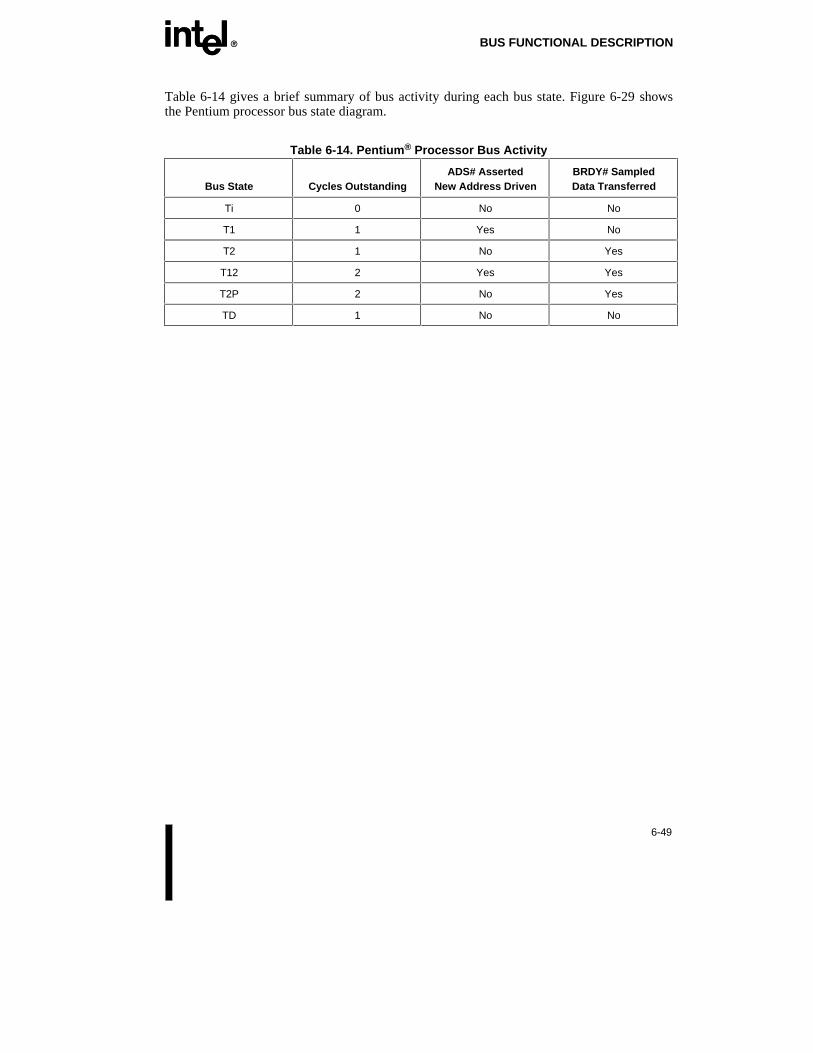
EE BUS FUNCTIONAL DESCRIPTION
6-49
Table 6-14 gives a brief summary of bus activity during each bus state. Figure 6-29 showsthe Pentium processor bus state diagram.
Table 6-14. Pentium ® Processor Bus Activity
Bus State Cycles OutstandingADS# Asserted
New Address DrivenBRDY# SampledData Transferred
Ti 0 No No
T1 1 Yes No
T2 1 No Yes
T12 2 Yes Yes
T2P 2 No Yes
TD 1 No No

BUS FUNCTIONAL DESCRIPTION EE
6-50
PDB21
T1*(5)
(2)(4)
(3)T2
(6)(7)
(8)
TD
T12*
(9)
(11)
T2P
(10)
(13)
(14)
(12)
*ADS# asserted
Ti
(1)
(0)
** If BOFF# is asserted during any state, a state transition to Ti occurs in the next clock (not shown)
*** If RESET is sampled asserted in any state, a state transition to Ti will occur (not shown)
Figure 6-29. Pentium ® Processor Bus Control State Machine

EE BUS FUNCTIONAL DESCRIPTION
6-51
6.6.1. State TransitionsThe state transition equations with descriptions are listed below. In the equations, "&" meanslogical AND, "+" means logical OR, and "#" placed after label means active low. The NA#used here is actually a delayed version of the external NA# pin (delayed by one clock). Thedefinition of request pending is:
The Pentium processor has generated a new bus cycle internally & HOLD (delayed by oneclock) negated & BOFF# negated & (AHOLD negated + HITM# asserted);
Note that once NA# is sampled asserted the Pentium processor latches NA# and will pipelinea cycle when one becomes pending even if NA# is subsequently deasserted.
(0) No Request Pending
(1) Request Pending;
The Pentium processor starts a new bus cycle & ADS# is asserted in the T1 state.
(2) Always;
With BOFF# negated, and a cycle outstanding the Pentium processor always moves to T2 toprocess the data transfer.
(3) Not Last BRDY# & (No Request Pending + NA# Negated);
The Pentium processor stays in T2 until the transfer is over if no new request becomespending or if NA# is not asserted.
(4) Last BRDY# & Request Pending & NA# Sampled Asserted;
If there is a new request pending when the current cycle is complete, and if NA# wassampled asserted, the Pentium processor begins from T1.
(5) Last BRDY# & (No Request Pending + NA# Negated);
If no cycle is pending when the Pentium processor finishes the current cycle or NA# is notasserted, the Pentium processor goes back to the idle state.
(6) Not Last BRDY# & Request Pending & NA# Sampled Asserted;
While the Pentium processor is processing the current cycle (one outstanding cycle), ifanother cycle becomes pending and NA# is asserted, the Pentium processor moves to T12indicating that the Pentium processor now has two outstanding cycles. ADS# is asserted forthe second cycle.
(7) Last BRDY# & No dead clock;
When the Pentium processor finishes the current cycle, and no dead clock is needed, it goesto the T2 state.
(8) Last BRDY# & Need a dead clock;
When the Pentium processor finishes the current cycle, and a dead clock is needed, it goes tothe TD state.

BUS FUNCTIONAL DESCRIPTION EE
6-52
(9) Not Last BRDY#;
With BOFF# negated, and the current cycle not complete, the Pentium processor alwaysmoves to T2P to process the data transfer.
(10) Not Last BRDY#;
The Pentium processor stays in T2P until the first cycle transfer is over.
(11) Last BRDY# & No dead clock;
When the Pentium processor finishes the first cycle, and no dead clock is needed, it goes toT2 state.
(12) Last BRDY# & Need a dead clock;
When the first cycle is complete, and a dead clock is needed, it goes to TD state.
(13) Request Pending & NA# sampled asserted;
If NA# was sampled asserted and there is a new request pending , it goes to T12 state.
(14) No Request Pending + NA# Negated;
If there is no new request pending, or NA# was not asserted, it goes to T2 state.
6.6.2. Dead Clock Timing DiagramsThe timing diagrams in Figure 6-30 and Figure 6-31 show bus cycles with and without a deadclock.
PDB22
T1 T2
ADS#
NA#
BRDY#
1 2 3
1 2 3
T2 T iT2 T1 T2 T2 T12 T2 T i
wr rd rd
Figure 6-30. Bus Cycles Without Dead Clock
In Figure 6-30, cycles 1 and 2 can be either read or write cycles and no dead clock would beneeded because only one cycle is outstanding when those cycles are driven. To prevent adead clock from being necessary after cycle 3 is driven, it must be of the "same type" as

EE BUS FUNCTIONAL DESCRIPTION
6-53
cycle 2. That is if cycle 2 is a read cycle, cycle 3 must also be a read cycle in order toprevent a dead clock. If cycle 2 is a write cycle, cycle 3 must also be a write cycle to preventa dead clock.
PDB23
ADS#
NA#
BRDY#
rd wr
rd wr
deadclk
rd wr
deadclk
T1 T2 T2 T12 TD T2 T12 T2P TD T12 T2P
W/R#
Figure 6-31. Bus Cycles with TD Dead Clock

E7
ElectricalSpecifications

EE
7-1
CHAPTER 7ELECTRICAL SPECIFICATIONS
7.1. POWER AND GROUNDFor clean on-chip power distribution, the Pentium Processor (510\60, 567\66) has 50 VCC(power) and 49 VSS (ground) inputs. Power and ground connections must be made to allexternal VCC and VSS pins of the Pentium Processor (510\60, 567\66). On the circuit board,all VCC pins must be connected to a VCC plane. All VSS pins must be connected to a VSSplane.
7.2. DECOUPLING RECOMMENDATIONSLiberal decoupling capacitance should be placed near the Pentium processor. The Pentiumprocessor driving its large address and data buses at high frequencies can cause transientpower surges, particularly when driving large capacitive loads.
Low inductance capacitors (i.e., surface mount capacitors) and interconnects arerecommended for best high frequency electrical performance. Inductance can be reduced byconnecting capacitors directly to the VCC and VSS planes, with minimal trace length betweenthe component pads and vias to the plane. Capacitors specifically for PGA packages are alsocommercially available.
These capacitors should be evenly distributed among each component. Capacitor valuesshould be chosen to ensure they eliminate both low and high frequency noise components.
7.3. CONNECTION SPECIFICATIONSAll NC pins must remain unconnected.
For reliable operation, always connect unused inputs to an appropriate signal level. Unusedactive low inputs should be connected to VCC. Unused active high inputs should beconnected to ground.
7.4. MAXIMUM RATINGSTable 7-1 is a stress rating only. Functional operation at the maximums is not guaranteed.Functional operating conditions are given in the AC and DC specification tables.

ELECTRICAL SPECIFICATIONS EE
7-2
Extended exposure to the maximum ratings may affect device reliability. Furthermore,although the Pentium processor contains protective circuitry to resist damage from staticelectric discharge, always take precautions to avoid high static voltages or electric fields.
Table 7-1. Absolute Maximum Ratings
Case temperature under bias -65°C to 110°C
Storage temperature -65°C to 150°C
Voltage on any pin with respect to ground -0.5 VCC to VCC + 0.5 (V)
Supply voltage with respect to VSS -0.5V to +6.5V
7.5. DC SPECIFICATIONSTable 7-2 lists the DC specifications associated with the Pentium processor.

EE ELECTRICAL SPECIFICATIONS
7-3
Table 7-2. Pentium ® Processor (510\60, 567\66) DC Specifications
VCC = See Notes 10, 11; T CASE = See Notes 12, 13
Symbol Parameter Min Max Unit Notes
VIL Input Low Voltage -0.3 +0.8 V TTL Level
VIH Input High Voltage 2.0 Vcc+0.3 V TTL Level
VOL Output Low Voltage 0.45 V TTL Level (1)
VOH Output High Voltage 2.4 V TTL Level (2)
ICC Power Supply Current 32002910
mAmA
66 MHz, (7), (8)60 MHz, (7), (9)
ILI Input Leakage Current +15 uA 0 < VIN < VCC , (4)
ILO Output Leakage Current +15 uA 0 < VOUT < VCCTristate , (4)
IIL Input Leakage Current -400 uA VIN = 0.45V, (5)
IIH Input Leakage Current 200 uA VIN = 2.4V, (6)
CIN Input Capacitance 15 pF
CO Output Capacitance 20 pF
CI/O I/O Capacitance 25 pF
CCLK CLK Input Capacitance 8 pF
CTIN Test Input Capacitance 15 pf
CTOUT Test Output Capacitance 20 pf
CTCK Test Clock Capacitance 8 pf
NOTES:
(1) Parameter measured at 4 mA load.
(2) Parameter measured at 1 mA load.
(4) This parameter is for input without pullup or pulldown.
(5) This parameter is for input with pullup.
(6) This parameter is for input with pulldown.
(7) Worst case average Icc for a mix of test patterns.
(8) (16 W max.) Typical Pentium® processor supply current is 2600 mA (13 W) at 66 MHz.
(9) (14.6 W max.) Typical Pentium processor supply current is 2370 mA (11.9 W) at 60 MHz.
(10) VCC = 5V ± 5% at 60 MHz.
(11) VCC = 4.90V to 5.40V at 66 MHz
(12) TCASE = 0°C to +80°C at 60 MHz
(13) TCASE = 0°C to +70°C at 66 MHz

ELECTRICAL SPECIFICATIONS EE
7-4
7.6. AC SPECIFICATIONSThe 66-MHz and 60-MHz AC specifications given in Tables 7-3 and 7-4 consist of outputdelays, input setup requirements and input hold requirements. All AC specifications (with theexception of those for the TAP signals) are relative to the rising edge of the CLK input.
All timings are referenced to 1.5 volts for both "0" and "1" logic levels unless otherwisespecified. Within the sampling window, a synchronous input must be stable for correctPentium processor operation.
Care should be taken to read all notes associated with a particular timing parameter. Inaddition, the following list of notes apply to the timing specification tables in general and arenot associated with any one timing. They are 2, 5, 6, and 14.
Table 7-3. 66-MHz Pentium ® Processor 567\66 AC Specifications
Vcc = 4.90V to 5.40V; T CASE = 0°°C to 70 °°C; CL = 0 pF
Symbol Parameter Min Max Unit Figure Notes
Frequency 33.33 66.66 MHz 1x CLK
t1 CLK Period 15 nS 7.1
t1a CLK Period Stability +/-250 pS (18), (19), (20),(21)
t2 CLK High Time 4 nS 7.1 @2V, (1)
t3 CLK Low Time 4 nS 7.1 @0.8V, (1)
t4 CLK Fall Time 0.15 1.5 nS 7.1 (2.0V-0.8V), (1)
t5 CLK Rise Time 0.15 1.5 nS 7.1 (0.8V-2.0V), (1)
t6 ADS#, A3-A31, BT0-3, PWT,PCD,BE0-7#, M/IO#, D/C#, W/R#,CACHE#, SCYC, LOCK# Valid Delay
1.5 8.0 nS 7.2
t6a AP Valid Delay 1.5 9.5 nS 7.2
t7 ADS#, AP, A3-A31, BT0-3, PWT,PCD, BE0-7#, M/IO#, D/C#, W/R#,CACHE#, SCYC, LOCK# Float Delay
10 nS 7.3 (1)
t8 PCHK#, APCHK#, IERR#, FERR#Valid Delay
1.5 8.3 nS 7.2 (4)
t9 BREQ,HLDA, SMIACT# Valid Delay 1.5 8.0 nS 7.2 (4)
t10 HIT#,HITM# Valid Delay 1.5 8.0 nS 7.2
t11 PM0-1, BP0-3, IU, IV, IBT Valid Delay 1.5 10 nS 7.2
t11a PRDY Valid Delay 1.5 8.0 nS 7.2
t12 D0-D63,DP0-7 Write Data Valid Delay 1.5 9 nS 7.2
t13 D0-D63,DP0-7 Write Data Float Delay 10 nS 7.3 (1)

EE ELECTRICAL SPECIFICATIONS
7-5
Table 7-3. 66-MHz Pentium ® Processor 567\66 AC Specifications (Contd.)
Vcc = 4.90V to 5.40V; T CASE = 0°°C to 70 °°C; CL = 0 pF
Symbol Parameter Min Max Unit Figure Notes
t14 A5-A31 Setup Time 6.5 nS 7.4
t15 A5-A31 Hold Time 1.5 nS 7.4
t16 EADS#, INV, AP Setup Time 5 nS 7.4
t17 EADS#, INV, AP Hold Time 1.5 nS 7.4
t18 KEN#, WB/WT# Setup Time 5 nS 7.4
t18a NA# Setup Time 4.5 nS 7.4
t19 KEN#, WB/WT#, NA# Hold Time 1.5 nS 7.4
t20 BRDY# Setup Time 5 nS 7.4
t21 BRDY# Hold Time 1.5 nS 7.4
t22 AHOLD, BOFF# Setup Time 5.5 nS 7.4
t23 AHOLD, BOFF# Hold Time 1.5 nS 7.4
t24 BUSCHK#, EWBE#, HOLD, PEN#Setup Time
5 nS 7.4
t25 BUSCHK#, EWBE#, HOLD, PEN#Hold Time
1.5 nS 7.4
t26 A20M#, INTR, Setup Time 5 nS 7.4 (12), (16)
t27 A20M#, INTR, Hold Time 1.5 nS 7.4 (13)
t28 INIT, FLUSH#, NMI, SMI#, IGNNE#Setup Time
5 nS 7.4 (16), (17)
t29 INIT, FLUSH#, NMI, SMI#, IGNNE#Hold Time
1.5 nS 7.4
t30 INIT, FLUSH#, NMI, SMI#, IGNNE#Pulse Width, Async
2 CLKs (15), (17)
t31 R/S# Setup Time 5 nS 7.4 (12), (16), (17)
t32 R/S# Hold Time 1.5 nS 7.4 (13)
t33 R/S# Pulse Width, Async. 2 CLKs (15), (17)
t34 D0-D63 Read Data Setup Time 3.8 nS 7.4
t34a DP0-7 Read Data Setup Time 3.8 nS 7.4
t35 D0-D63,DP0-7 Read Data Hold Time 2 nS 7.4
t36 RESET Setup Time 5 nS 7.5 (11), (12), (16)
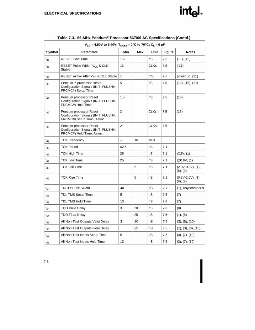
ELECTRICAL SPECIFICATIONS EE
7-6
Table 7-3. 66-MHz Pentium ® Processor 567\66 AC Specifications (Contd.)
Vcc = 4.90V to 5.40V; T CASE = 0°°C to 70 °°C; CL = 0 pF
Symbol Parameter Min Max Unit Figure Notes
t37 RESET Hold Time 1.5 nS 7.5 (11), (13)
t38 RESET Pulse Width, VCC & CLKStable
15 CLKs 7.5 ( 11)
t39 RESET Active After VCC & CLK Stable 1 mS 7.5 power up, (11)
t40 Pentium™ processor ResetConfiguration Signals (INIT, FLUSH#,FRCMC#) Setup Time
5 nS 7.5 (12), (16), (17)
t41 Pentium processor ResetConfiguration Signals (INIT, FLUSH#,FRCMC#) Hold Time
1.5 nS 7.5 (13)
t42 Pentium processor ResetConfiguration Signals (INIT, FLUSH#,FRCMC#) Setup Time, Async.
2 CLKs 7.5 (16)
t43 Pentium processor ResetConfiguration Signals (INIT, FLUSH#,FRCMC#) Hold Time, Async.
2 CLKs 7.5
t44 TCK Frequency -- 16 MHz
t45 TCK Period 62.5 nS 7.1
t46 TCK High Time 25 nS 7.1 @2V, (1)
t47 TCK Low Time 25 nS 7.1 @0.8V, (1)
t48 TCK Fall Time 5 nS 7.1 (2.0V-0.8V), (1),(8), (9)
t49 TCK Rise Time 5 nS 7.1 (0.8V-2.0V), (1),(8), (9)
t50 TRST# Pulse Width 40 nS 7.7 (1), Asynchronous
t51 TDI, TMS Setup Time 5 nS 7.6 (7)
t52 TDI, TMS Hold Time 13 nS 7.6 (7)
t53 TDO Valid Delay 3 20 nS 7.6 (8)
t54 TDO Float Delay 25 nS 7.6 (1), (8)
t55 All Non-Test Outputs Valid Delay 3 20 nS 7.6 (3), (8), (10)
t56 All Non-Test Outputs Float Delay 25 nS 7.6 (1), (3), (8), (10)
t57 All Non-Test Inputs Setup Time 5 nS 7.6 (3), (7), (10)
t58 All Non-Test Inputs Hold Time 13 nS 7.6 (3), (7), (10)

EE ELECTRICAL SPECIFICATIONS
7-7
NOTES:
1. Not 100% tested. Guaranteed by design/characterization.
2. TTL input test waveforms are assumed to be 0 to 3 Volt transitions with 1Volt/ns rise and fall times.
3. Non-Test Outputs and Inputs are the normal output or input signals (besides TCK, TRST#, TDI, TDO, andTMS). These timings correspond to the response of these signals due to boundary scan operations.
4. APCHK#, FERR#, HLDA, IERR#, LOCK#, and PCHK# are glitch free outputs. Glitch free signalsmonotonically transition without false transitions (i.e., glitches).
5. 0.8 V/ns <= CLK input rise/fall time <= 8 V/ns.
6. 0.3 V/ns <= Input rise/fall time <= 5 V/ns.
7. Referenced to TCK rising edge.
8. Referenced to TCK falling edge.
9. 1 ns can be added to the maximum TCK rise and fall times for every 10 MHz of frequency below 16 MHz.
10. During probe mode operation, use the normal specified timings. Do not use the boundary scan timings(t55-58).
11. FRCMC# should be tied to VCC (high) to ensure proper operation of the Pentium® processor as a masterPentium processor.
12. Setup time is required to guarantee recognition on a specific clock.
13. Hold time is required to guarantee recognition on a specific clock.
14. All TTL timings are referenced from 1.5 V.
15. To guarantee proper asynchronous recognition, the signal must have been deasserted (inactive) for aminimum of 2 clocks before being returned active and must meet the minimum pulse width.
16. This input may be driven asynchronously.
17. When driven asynchronously, NMI, FLUSH#, R/S#, INIT, and SMI# must be deasserted (inactive) for aminimum of 2 clocks before being returned active.
18. Functionality is guaranteed by design/characterization.
19. Measured on rising edge of adjacent CLKs at 1.5V.
20. To ensure a 1:1 relationship between the magnitude of the input jitter and the internal and external clocks,the jitter frequency spectrum should not have any power spectrum peaking between 500 KHz and 1/3 ofthe CLK operating frequency. If this occurs, I/O timings are degraded by twice the jitter component withinthis frequency range. For example, if 15% of the jitter energy is within this range degrade I/O timings by2 × 0.15 × magnitude of jitter.
21. The amount of jitter present must be accounted for as a component of CLK skew between devices.

ELECTRICAL SPECIFICATIONS EE
7-8
Table 7-4. 60-MHz Pentium ® Processor 510\60 AC Specifications
Vcc = 5V ± 5%; TCASE = 0°°C to 80 °°C; CL = 0 pF
Symbol Parameter Min Max Unit Figure Notes
Frequency 33.33 60 MHz 1x CLK
t1 CLK Period 16.67 nS 7.1
t1a CLK Period Stability +/-250 pS (18), (19), (20),(21)
t2 CLK High Time 4 nS 7.1 @2V, (1)
t3 CLK Low Time 4 nS 7.1 @0.8V, (1)
t4 CLK Fall Time 0.15 1.5 nS 7.1 (2.0V-0.8V), (1)
t5 CLK Rise Time 0.15 1.5 nS 7.1 (0.8V-2.0V), (1)
t6 ADS#, A3-A31, BT0-3, PWT, PCD,BE0-7#, M/IO#, D/C#, W/R#,CACHE#, SCYC, LOCK# Valid Delay
1.5 9.0 nS 7.2
t6a AP Valid Delay 1.5 10.5 nS 7.2
t7 ADS#, AP, A3-A31, BT0-3, PWT,PCD, BE0-7#, M/IO#, D/C#, W/R#,CACHE#, SCYC, LOCK# Float Delay
11 nS 7.3 (1)
t8 PCHK#, APCHK#, IERR#, FERR#Valid Delay
1.5 9.3 nS 7.2 (4)
t9 BREQ,HLDA, SMIACT# Valid Delay 1.5 9.0 nS 7.2 (4)
t10 HIT#,HITM# Valid Delay 1.5 9.0 nS 7.2
t11 PM0-1, BP0-3, IU, IV, IBT Valid Delay 1.5 11 nS 7.2
t11a PRDY Valid Delay 1.5 9.0 nS 7.2
t12 D0-D63,DP0-7 Write Data Valid Delay 1.5 10 nS 7.2
t13 D0-D63,DP0-7 Write Data Float Delay 11 nS 7.3 (1)
t14 A5-A31 Setup Time 7 nS 7.4
t15 A5-A31 Hold Time 1.5 nS 7.4
t16 EADS#, INV, AP Setup Time 5.5 nS 7.4
t17 EADS#, INV, AP Hold Time 1.5 nS 7.4
t18 KEN#, WB/WT# Setup Time 5.5 nS 7.4
t18a NA# Setup Time 5.0 nS 7.4
t19 KEN#, WB/WT#, NA# Hold Time 1.5 nS 7.4
t20 BRDY# Setup Time 5.5 nS 7.4
t21 BRDY# Hold Time 1.5 nS 7.4

EE ELECTRICAL SPECIFICATIONS
7-9
Table 7-4. 60-MHz Pentium ® Processor 510\60 AC Specifications (Contd.)
Vcc = 5V ± 5%; TCASE = 0°°C to 80 °°C; CL = 0 pF
Symbol Parameter Min Max Unit Figure Notes
t22 AHOLD, BOFF# Setup Time 6 nS 7.4
t23 AHOLD, BOFF# Hold Time 1.5 nS 7.4
t24 BUSCHK#, EWBE#, HOLD, PEN#Setup Time
5.5 nS 7.4
t25 BUSCHK#, EWBE#, HOLD, PEN#Hold Time
1.5 nS 7.4
t26 A20M#, INTR, Setup Time 5.5 nS 7.4 (12), (16)
t27 A20M#, INTR, Hold Time 1.5 nS 7.4 (13)
t28 INIT, FLUSH#, NMI, SMI#, IGNNE#Setup Time
5.5 nS 7.4 (16), (17)
t29 INIT, FLUSH#, NMI, SMI#, IGNNE#Hold Time
1.5 nS 7.4
t30 INIT, FLUSH#, NMI, SMI#, IGNNE#Pulse Width, Async
2 CLKs (15), (17)
t31 R/S# Setup Time 5.5 nS 7.4 (12), (16), (17)
t32 R/S# Hold Time 1.5 nS 7.4 (13)
t33 R/S# Pulse Width, Async. 2 CLKs (15), (17)
t34 D0-D63 Read Data Setup Time 4.3 nS 7.4
t34a DP0-7 Read Data Setup Time 4.3 nS 7.4
t35 D0-D63, DP0-7 Read Data Hold Time 2 nS 7.4
t36 RESET Setup Time 5.5 nS 7.5 (11), (12), (16)
t37 RESET Hold Time 1.5 nS 7.5 (11), (13)
t38 RESET Pulse Width, VCC & CLKStable
15 CLKs 7.5 (11)
t39 RESET Active After VCC & CLK Stable 1 mS 7.5 Power up, (11)
t40 Pentium® processor ResetConfiguration Signals (INIT, FLUSH#,FRCMC#) Setup Time
5.5 nS 7.5 (12), (16), (17)
t41 Pentium processor ResetConfiguration Signals (INIT, FLUSH#,FRCMC#) Hold Time
1.5 nS 7.5 (13)

ELECTRICAL SPECIFICATIONS EE
7-10
Table 7-4. 60-MHz Pentium ® Processor 510\60 AC Specifications (Contd.)
Vcc = 5V ± 5%; TCASE = 0°°C to 80 °°C; CL = 0 pF
Symbol Parameter Min Max Unit Figure Notes
t42 Pentium processor ResetConfiguration Signals (INIT, FLUSH#,FRCMC#) Setup Time, Async.
2 CLKs 7.5 (16)
t43 Pentium processor ResetConfiguration Signals (INIT, FLUSH#,FRCMC#) Hold Time, Async.
2 CLKs 7.5
t44 TCK Frequency -- 16 MHz
t45 TCK Period 62.5 nS 7.1
t46 TCK High Time 25 nS 7.1 @2V, (1)
t47 TCK Low Time 25 nS 7.1 @0.8V, (1)
t48 TCK Fall Time 5 nS 7.1 (2.0V-0.8V), (1),(8), (9)
t49 TCK Rise Time 5 nS 7.1 (0.8V-2.0V), (1),(8), (9)
t50 TRST# Pulse Width 40 nS 7.7 (1), Async
t51 TDI, TMS Setup Time 5 nS 7.6 (7)
t52 TDI, TMS Hold Time 13 nS 7.6 (7)
t53 TDO Valid Delay 3 20 nS 7.6 (8)
t54 TDO Float Delay 25 nS 7.6 (1), (8)
t55 All Non-Test Outputs Valid Delay 3 20 nS 7.6 (3), (8), (10)
t56 All Non-Test Outputs Float Delay 25 nS 7.6 (1), (3), (8), (10)
t57 All Non-Test Inputs Setup Time 5 nS 7.6 (3), (7), (10)
t58 All Non-Test Inputs Hold Time 13 nS 7.6 (3), (7), (10)

EE ELECTRICAL SPECIFICATIONS
7-11
NOTES:
1. Not 100% tested. Guaranteed by design/characterization.
2. TTL input test waveforms are assumed to be 0 to 3 Volt transitions with 1Volt/ns rise and fall times.
3. Non-Test Outputs and Inputs are the normal output or input signals (besides TCK, TRST#, TDI, TDO, andTMS). These timings correspond to the response of these signals due to boundary scan operations.
4. APCHK#, FERR#, HLDA, IERR#, LOCK#, and PCHK# are glitch free outputs. Glitch free signalsmonotonically transition without false transitions (i.e. glitches).
5. 0.8 V/ns <= CLK input rise/fall time <= 8 V/ns.
6. 0.3 V/ns <= Input rise/fall time <= 5 V/ns.
7. Referenced to TCK rising edge.
8. Referenced to TCK falling edge.
9. 1 ns can be added to the maximum TCK rise and fall times for every 10 MHz of frequency below 16 MHz.
10. During probe mode operation, use the normal specified timings. Do not use the boundary scan timings(t55-58).
11. FRCMC# should be tied to VCC (high) to ensure proper operation of the Pentium processor as a masterPentium processor.
12. Setup time is required to guarantee recognition on a specific clock.
13. Hold time is required to guarantee recognition on a specific clock.
14. All TTL timings are referenced from 1.5 V.
15. To guarantee proper asynchronous recognition, the signal must have been deasserted (inactive) for aminimum of 2 clocks before being returned active and must meet the minimum pulse width.
16. This input may be driven asynchronously.
17. When driven asynchronously, NMI, FLUSH#, R/S#, INIT, and SMI# must be deasserted (inactive) for aminimum of 2 clocks before being returned active.
18. Functionality is guaranteed by design/characterization.
19. Measured on rising edge of adjacent CLKs at 1.5V.
20. To ensure a 1:1 relationship between the magnitude of the input jitter and the internal and external clocks,the jitter frequency spectrum should not have any power spectrum peaking between 500 KHz and 1/3 ofthe CLK operating frequency. If this occurs, I/O timings are degraded by twice the jitter component withinthis frequency range. For example, if 15% of the jitter energy is within this range degrade I/O timings by2 × 0.15 × magnitude of jitter.
21. The amount of jitter present must be accounted for as a component of CLK skew between devices.

ELECTRICAL SPECIFICATIONS EE
7-12
Each valid delay is specified for a 0 pF load. The system designer should use I/O buffermodeling to account for signal flight time delays.
1.5V
2.0V
0.8V
Tx
PP0064
Tw
Ty
Tz
Tv
Tv
Tw
Tx
Ty
Tz
=
=
=
=
=
t5, t49
t4, t48
t3, t47
t1, t45
t2, t46
1 .5 V
Figure 7-1. Clock Waveform
PDB65
Signal VALID
Tx min.
1.5 V
1.5 V
Tx max.
Tx = t6, t6a, t8, t9, t10, t11, t11a, t12
Figure 7-2. Valid Delay Timings

EE ELECTRICAL SPECIFICATIONS
7-13
Signal
Tx
1.5 V
PDB66
Ty
1.5 V
Ty
Tz
Tx = t7, t13
Ty = t6min, t12min
Figure 7-3. Float Delay Timings
PDB67
CLK
Signal VALID
Tx Ty
1.5 V
Tx = t14, t16, t18, t18a, t20, t22, t24, t26, t28, t31, t34, t34a
Ty = t15, t17, t19, t21, t23, t25, t27, t29, t32, t35
Figure 7-4. Setup and Hold Timings

ELECTRICAL SPECIFICATIONS EE
7-14
PDB68
VALID
Tw Tx
Ty
TvTz
CLK
RESET
Config
1.5 V
Tt Tu
1.5 V
1.5 V
Tt = t40
Tu = t41
Tv = t37
Tw =t42
Tx = t43
Ty = t38, t39
Tz = t36
Figure 7-5. Reset and Configuration Timings
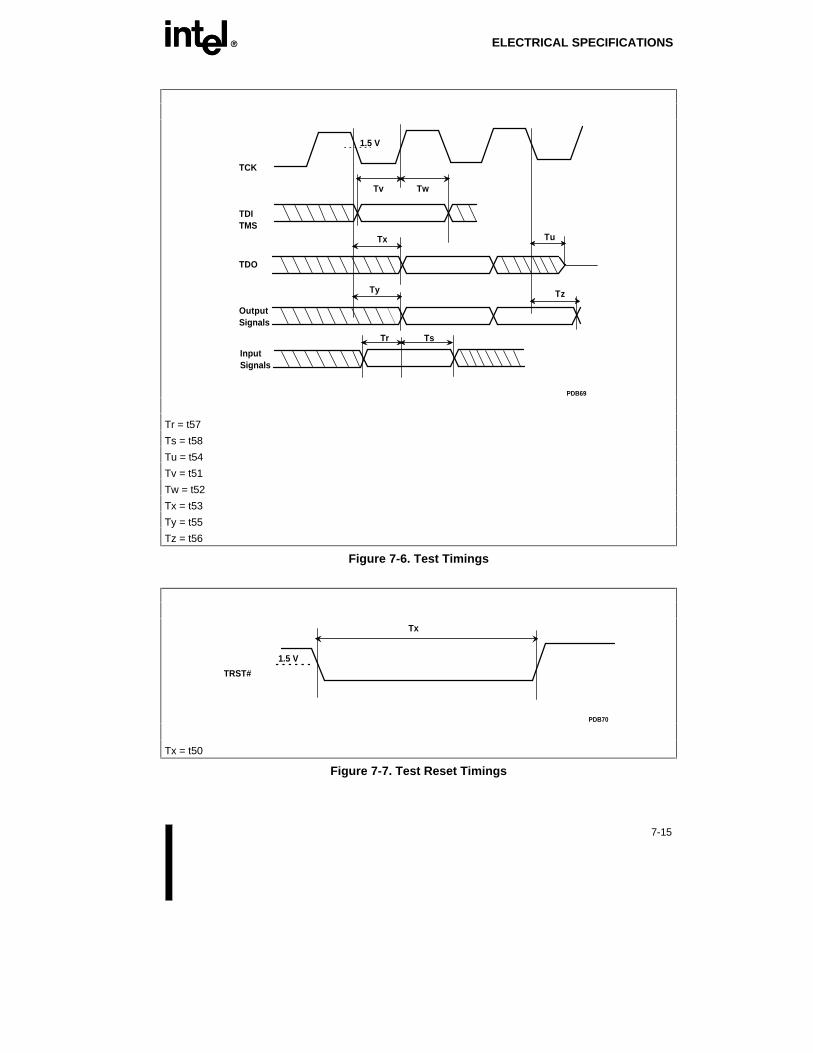
EE ELECTRICAL SPECIFICATIONS
7-15
PDB69
1.5 V
Tv Tw
Tx
Ty Tz
TCK
TDITMS
TDO
OutputSignals
Tu
Tr Ts
InputSignals
Tr = t57
Ts = t58
Tu = t54
Tv = t51
Tw = t52
Tx = t53
Ty = t55
Tz = t56
Figure 7-6. Test Timings
PDB70
1.5 V
TRST#
Tx
Tx = t50
Figure 7-7. Test Reset Timings

ELECTRICAL SPECIFICATIONS EE
7-16
Each valid delay is specified for a 0 pF load. The system designer should use I/O buffermodeling to account for signal delays due to loading. Table 7-5 lists the buffer type to beused for each signal in the external interface.
Table 7-5. External Interface Signal Buffer Assignment
Device Signals TypeDriver Buffer
TypeReceiver
Buffer Type
Pentium®
processorA20M#, FLUSH#, FRCMC#, HOLD, IGNNE#, INIT,INTR, NMI, PEN#, R/S#, RESET, SMI#, TDI, TMS,
I N/A ER1
AHOLD, BOFF#, EADS#, EWBE#, KEN#, NA#,WB/WT#
I N/A ER3
INV I N/A ER3a
BRDY#, BUSCHK#, TRST# I N/A ER2
CLK I N/A ER8
TCK I N/A ER9
A3-20 I/O ED7 ER7
A21-31, BT0-3 I/O ED4 ER6
D0-63, DP0-7 I/O ED3 ER5
AP I/O ED5 ER4
ADS#, HITM#, W/R# O ED6 N/A
BE0-7#, CACHE#, SCYC, LOCK#, PWT, PCD, M/IO#,D/C#, BREQ, HIT#
O ED2 N/A
APCHK#, BP3-0#, PM1, PM0, FERR#, HLDA, IBT,IERR#, IU, IV, PCHK#, PRDY, SMIACT#, TDO
O ED1 N/A
7.7. OVERSHOOT/UNDERSHOOT GUIDELINESThe overshoot/undershoot guideline is provided to limit signals transitioning beyond VCC orVSS due to the fast signal switching at these frequencies. Excessive ringback is the dominantharmful effect resulting from overshoot/undershoot.
Overshoot (Undershoot) is the absolute value of the maximum voltage above VCC (belowVSS). The guideline assumes the absence of diodes on the input. This guideline should beused in simulations, without the diodes present, to ensure overshoot (undershoot) is withinthe acceptable range.
Maximum Overshoot/Undershoot on Inputs = 1.6 Volts(without diodes)

EE ELECTRICAL SPECIFICATIONS
7-17
Ringback is the absolute value of the maximum voltage at the receiving pin below VCC (orabove VSS) relative to VCC (or VSS) level after the signal has reached its maximum voltagelevel. The input diodes are assumed present. This guideline is provided to allow systemdesigners to verify, in an actual system, the decisions made based on simulation using theovershoot (undershoot) guideline. Ringback only applies if the signal crossed above VCC(below VSS).
Maximum Ringback on Inputs = 0.8 Volts(with diodes)
PDB71
Vcc
MaximumOvershoot
MaximumRingback
Vcc
MaximumUndershoot
MaximumRingback
Figure 7-8. Overshoot/Undershoot and Ringback Guidelines

E8
I/O Buffer Models


EE
8-1
CHAPTER 8I/O BUFFER MODELS
The first order I/O buffer model is a simplified representation of the complex input andoutput buffers used in the Pentium Processor (510\60, 567\66). Figure 8-1 shows the structureof the input buffer model and Figure 8-2 shows the output buffer model. Table 8-1 andTable 8-2 show the parameters used to specify these models.
PDB73
LP
CP CIN
Figure 8-1. First Order Input Buffer
Table 8-1. Parameters Used in the Specification of the First Order Input Buffer Model
Parameter Description
Cin Minimum and maximum value of the capacitance of the input buffer model.
Lp Minimum and maximum value of the package inductance.
Cp Minimum and maximum value of the package capacitance.

I/O BUFFER MODELS EE
8-2
PDB72
dV/dt
RO
CO
LP
CP
Figure 8-2. First Order Output Buffer
Table 8-2. Parameters Used in the Specification of the First Order Output Buffer Model
Parameter Description
dV/dt Minimum and maximum value of the rate of change of the open circuit voltage sourceused in the output buffer model.
Ro Minimum and maximum value of the output impedance of the output buffer model.
Co Minimum and maximum value of the capacitance of the output buffer model.
Lp Minimum and maximum value of the package inductance.
Cp Minimum and maximum value of the package capacitance.
Table 8-5 and Table 8-Error! Bookmark not defined. list the minimum and maximumparameters for each buffer type within the Pentium Processor (510\60, 567\66). Theseparameters supply the information to use in the circuits shown in Figure 8-1 and Figure 8-2to model the processors behavior in a given environment.

EE I/O BUFFER MODELS
8-3
Table 8-3. Specification of Input External Buffer Model Parameters
Cp(pF)
Lp(nH)
Cin(pF)
Buffer Type min max min max min max
ER1 0.8 10.2 5.2 20.6 1.1 1.5
ER2 1.4 6.8 6.7 16.5 1.7 2.3
ER3 1.1 1.8 6.2 11.3 2.6 3.5
ER3a 7.3 9.9 14.9 20.1 2.6 3.5
ER4 0.5 6.6 5.3 15.2 3.6 4.8
ER5 0.7 7.8 5.4 17.0 3.7 4.9
ER6 0.5 6.6 5.3 15.2 4.2 5.6
ER7 1.3 5.6 6.5 13.5 12.7 17.1
ER8 1.6 2.2 6.2 8.4 1.7 2.3
ER9 2.2 2.9 7.2 9.7 1.9 2.5

I/O BUFFER MODELS EE
8-4
Table 8-4. Specification of Output External Interface Buffer Model Parameters
BufferType Transition Component
dV/dt(V/nsec)
Ro(Ohms)
Co(pF)
Lp(nH)
Cp(pF)
min max min max min max min max min max
ED1 Rising Pentium®
Processor(510\60,567\66)
4.5/3.6 5.5/1.1 21 59 3.6 4.8 5.6 19.9 0.7 9.7
Falling PentiumProcessor(510\60,567\66)
4.5/2.6 5.5/1.1 18 54 3.6 4.8 5.6 19.9 0.7 9.7
ED2 Rising PentiumProcessor(510\60,567\66)
4.5/3.6 5.5/1.1 21 59 3.6 4.8 6.8 18.9 1.4 9.1
Falling PentiumProcessor(510\60,567\66)
4.5/2.6 5.5/1.1 18 54 3.6 4.8 6.8 18.9 1.4 9.1
ED3 Rising PentiumProcessor(510\60,567\66)
4.5/3.6 5.5/1.1 21 59 3.7 4.9 5.4 17.0 0.7 7.8
Falling PentiumProcessor(510\60,567\66)
4.5/2.6 5.5/1.1 18 54 3.7 4.9 5.4 17.0 0.7 7.8
ED4 Rising PentiumProcessor(510\60,567\66)
4.5/3.6 5.5/1.1 21 59 4.2 5.6 5.3 15.2 0.5 6.6
Falling PentiumProcessor(510\60,567\66)
4.5/2.6 5.5/1.1 18 54 4.2 5.6 5.3 15.2 0.5 6.6

EE I/O BUFFER MODELS
8-5
Table 8-5. Specification of Output External Interface Buffer Model Parameters (Contd.)
BufferType Transition Component
dV/dt(V/nsec)
Ro(Ohms)
Co(pF)
Lp(nH)
Cp(pF)
min max min max min max min max min max
ED5 Rising PentiumProcessor(510\60,567\66)
4.5/3.6 5.5/1.1 21 59 3.6 4.8 5.3 15.2 0.5 6.6
Falling PentiumProcessor(510\60,567\66)
4.5/2.6 5.5/1.1 18 54 3.6 4.8 5.3 15.2 0.5 6.6
ED6 Rising PentiumProcessor(510\60,567\66)
4.5/3.6 5.5/1.1 21 59 12.1 16.3 6.3 10.2 1.4 2.6
Falling PentiumProcessor(510\60,567\66)
4.5/2.6 5.5/1.1 18 54 12.1 16.3 6.3 10.2 1.4 2.6
ED7 Rising PentiumProcessor(510\60,567\66)
4.5/3.6 5.5/1.1 21 59 12.7 17.1 6.5 13.5 1.3 5.6
Falling PentiumProcessor(510\60,567\66)
4.5/2.6 5.5/1.1 18 54 12.7 17.1 6.5 13.5 1.3 5.6

I/O BUFFER MODELS EE
8-6
8.1. INPUT DIODE MODELSIn addition to the input and output buffer parameters, input protection diode models areprovided for the external interface I/O buffer models. These diodes have been optimized toprovide ESD protection and provide some level of clamping. Note however, the signalquality specifications for both the optimized and external interfaces are defined assuming thediodes are not present in the simulation. It is important that these specifications are metbecause there is a limit to the amount of clamping the diode can attain. The diode model isprovided because it may be useful in modeling the behavior of other devices drivingtransmission lines with the Pentium processor as the receiving device.
Figure 8-3 shows the components of the diode model. It consists of two diodes, oneconnected to VCC, D2, and one to VSS, D1. Each diode is modeled by the combination of anideal diode in series with a resistance.
CSJ24
VCC
VSS
RS
D1
D2
RS
Figure 8-3. Input Diode Model
The diode model should be added to the input model for both inputs and I/O signals whendesired. Figure 8-4 shows the complete input model with the diodes added.

EE I/O BUFFER MODELS
8-7
CSJ25
VCC
VSS
RS
D1
D2
RS
LP
CP CIN
Figure 8-4. Complete Input Model Including Diode
The specific parameters associated with each diode are listed below. Table 8-Error!Bookmark not defined. lists the buffer types with their corresponding diode I-V curve andseries resistance. Table 8-Error! Bookmark not defined. provides the diode I-V curve datafor both D1 and D2 for each buffer type.
Table 8-5. Diode Parameter List
Input Model Type Buffer Type Driver Mode DiodeDiode I-V
Curve Type Rs (Ohms)
ER4, ER5, ER6 I/O std D1 IV1 6.5
D2 IV2 6.5
ER7 I/O xlg D1 IV3 6.5
D2 IV4 6.5
ER1, ER2, ER3, ER3a,ER8, ER9
I N/A D1 IV5 6.5
D2 IV6 6.5

I/O BUFFER MODELS EE
8-8
Table 8-6. Data for Diode I-V Curves
Curve Type Curve Type
IV1 IV2 IV1 IV2
Vd Id Vd Id Vd Id Vd Id
0v 0a 0v 0a 0.699v 24.81ua 0.698v 46.58ua
25mv 0.0053pa 25mv 0.0037pa 0.722v 58.06ua 0.719v 0.12ma
50mv 0.0062pa 50mv 0.0038pa 0.744v 0.13ma 0.737v 0.26ma
75mv 0.0083pa 75mv 0.0039pa 0.762v 0.25ma 0.751v 0.47ma
100mv 0.0134pa 100mv 0.0041pa 0.778v 0.44ma 0.762v 0.76ma
0.125v 0.0260pa 0.125v 0.0046pa 0.79v 0.69ma 0.772v 0.76ma
0.15v 0.0572pa 0.15v 0.0062pa 0.8v 1ma 0.779v 1.07ma
0.15v 0.0572pa 0.15v 0.0062pa 0.809v 0.99ma 0.784v 1.49ma
0.175v 0.13pa 0.175v 0.0107pa 0.817v 1.32ma 0.788v 1.91ma
0.2v 0.33pa 0.2v 0.0237pa 0.822v 1.73ma 0.792v 2.3ma
0.225v 0.8pa 0.225v 0.0621pa 0.826v 2.13ma 0.795v 2.7ma
0.25v 1.98pa 0.25v 0.18pa 0.83v 2.52ma 0.798v 3.13ma
0.275v 4.91pa 0.275v 0.51pa 0.834v 2.93ma 0.801v 3.57ma
0.3v 12.18pa 0.3v 1.49pa 0.837v 3.35ma 0.803v 4.01ma
0.325v 30.22pa 0.325v 4.4pa 0.84v 3.79ma 0.806v 4.46ma
0.35v 74.98pa 0.35v 12.96pa 0.843v 4.22ma 0.808v 4.91ma
0.375v 0.19na 0.375v 38.22pa 0.845v 4.67ma 0.809v 5.37ma
0.4v 0.46na 0.4v 0.11na 0.848v 5.11ma 0.811v 5.83ma
0.425v 1.15na 0.425v 0.33na 0.85v 5.57ma 0.813v 6.3ma
0.45v 2.84na 0.45v 0.98na 0.852v 6.02ma 0.814v 6.76ma
0.475v 7.26na 0.475v 2.89na 0.854v 6.48ma 0.816v 7.23ma
0.5v 18.02na 0.5v 8.95na 0.856v 6.94ma 0.817v 7.7ma
0.525v 44.72na 0.525v 26.4na 0.857v 7.4ma 0.819v 8.17ma
0.55v 0.11ua 0.55v 77.85na 0.859v 7.87ma 0.82v 8.64ma
0.575v 0.28ua 0.575v 0.23ua 0.86v 8.34ma 0.821v 9.12ma
0.6v 0.68ua 0.6v 0.68ua 0.862v 8.81ma 0.822v 9.59ma
0.625v 1.69ua 0.625v 1.99ua 0.863v 9.28ma 0.823v 10.07ma
0.65v 4.18ua 0.65v 5.82ua 0.864v 9.75ma 0.824v 10.55ma
0.674v 10.26ua 0.674v 16.79ua

EE I/O BUFFER MODELS
8-9
Table 8-7. Data for Diode I-V Curves (Contd.)
Curve Type Curve Type
IV1 IV2 IV1 IV2
Vd Id Vd Id Vd Id Vd Id
0.866v 10.22ma 0.825v 11.03ma 0.888v 23.26ma 0.843v 24.16ma
0.867v 10.7ma 0.826v 11.51ma 0.888v 23.75ma 0.843v 24.65ma
0.868v 11.17ma 0.827v 11.99ma 0.889v 24.24ma 0.844v 25.14ma
0.869v 11.65ma 0.828v 12.47ma 0.889v 24.73ma 0.844v 25.63ma
0.87v 12.13ma 0.829v 12.95ma 0.89v 25.22ma 0.845v 26.12ma
0.871v 12.61ma 0.83v 13.43ma 0.89v 25.71ma 0.845v 26.61ma
0.872v 13.09ma 0.83v 13.92ma 0.891v 26.2ma 0.845v 27.11ma
0.873v 13.56ma 0.831v 14.4ma 0.891v 26.69ma 0.846v 27.6ma
0.874v 14.05ma 0.832v 14.89ma 0.892v 27.18ma 0.846v 28.09ma
0.875v 14.53ma 0.833v 15.37ma 0.892v 27.67ma 0.847v 28.58ma
0.876v 15.01ma 0.833v 15.86ma 0.893v 28.16ma 0.847v 29.07ma
0.877v 15.49ma 0.834v 16.34ma 0.893v 28.65ma 0.847v 29.57ma
0.878v 15.97ma 0.835v 16.83ma 0.894v 29.14ma 0.848v 30.06ma
0.878v 16.46ma 0.835v 17.32ma 0.894v 29.63ma 0.848v 30.55ma
0.879v 16.94ma 0.836v 17.8ma 0.895v 30.12ma 0.848v 31.04ma
0.88v 17.43ma 0.836v 18.29ma 0.895v 30.61ma 0.849v 31.53ma
0.881v 17.91ma 0.837v 18.78ma 0.895v 31.1ma 0.849v 32.03ma
0.881v 18.39ma 0.838v 19.27ma 0.896v 31.59ma 0.849v 32.52ma
0.882v 18.88ma 0.838v 19.75ma 0.896v 32.09ma 0.85v 33.01ma
0.883v 19.37ma 0.839v 20.24ma 0.897v 32.58ma 0.85v 33.51ma
0.883v 19.85ma 0.839v 20.73ma 0.897v 33.07ma 0.85v 34ma
0.884v 20.34ma 0.84v 21.22ma 0.898v 33.56ma 0.851v 34.49ma
0.885v 20.83ma 0.84v 21.71ma 0.898v 34.05ma 0.851v 34.99ma
0.885v 21.31ma 0.841v 22.2ma 0.898v 34.54ma 0.851v 35.48ma
0.886v 21.8ma 0.841v 22.69ma 0.899v 35.04ma 0.852v 35.97ma
0.886v 22.29ma 0.842v 23.18ma 0.899v 35.53ma 0.852v 36.47ma
0.887v 22.78ma 0.842v 23.67ma 0.899v 36.02ma 0.852v 36.96ma

I/O BUFFER MODELS EE
8-10
Table 8-8. Data for Diode I-V Curves (Contd.)
Curve Type Curve Type
IV1 IV2 IV1 IV2
Vd Id Vd Id Vd Id Vd Id
0.9v 36.51ma 0.853v 37.45ma 0.908v 49.84ma 0.86v 50.81ma
0.9v 37.01ma 0.853v 37.95ma 0.909v 50.34ma 0.86v 51.31ma
0.901v 37.5ma 0.853v 38.44ma 0.909v 50.83ma 0.86v 51.8ma
0.901v 37.99ma 0.854v 38.94ma 0.909v 51.33ma 0.86v 52.3ma
0.901v 38.49ma 0.854v 39.43ma 0.909v 51.82ma 0.861v 52.79ma
0.902v 38.98ma 0.854v 39.92ma 0.91v 52.32ma 0.861v 53.29ma
0.902v 39.47ma 0.854v 40.42ma 0.91v 52.81ma 0.861v 53.79ma
0.902v 39.96ma 0.855v 40.91ma 0.91v 53.3ma 0.861v 54.28ma
0.903v 40.46ma 0.855v 41.41ma 0.91v 53.8ma 0.861v 54.78ma
0.903v 40.95ma 0.855v 41.9ma 0.911v 54.29ma 0.862v 55.27ma
0.903v 41.44ma 0.856v 42.4ma 0.911v 54.79ma 0.862v 55.77ma
0.904v 41.94ma 0.856v 42.89ma 0.911v 55.28ma 0.862v 56.27ma
0.904v 42.43ma 0.856v 43.39ma 0.911v 55.78ma 0.862v 56.76ma
0.904v 42.92ma 0.856v 43.88ma 0.912v 56.27ma 0.862v 57.26ma
0.904v 43.42ma 0.857v 44.38ma 0.912v 56.77ma 0.863v 57.75ma
0.905v 43.91ma 0.857v 44.87ma 0.912v 57.27ma 0.863v 58.25ma
0.905v 44.41ma 0.857v 45.37ma 0.912v 57.76ma 0.863v 58.74ma
0.905v 44.9ma 0.857v 45.86ma 0.913v 58.26ma 0.863v 59.24ma
0.906v 45.39ma 0.858v 46.36ma 0.913v 58.75ma 0.863v 59.74ma
0.906v 45.89ma 0.858v 46.85ma 0.913v 59.25ma 0.864v 60.23ma
0.906v 46.38ma 0.858v 47.35ma 0.913v 59.74ma 0.864v 60.73ma
0.907v 46.88ma 0.858v 47.84ma 0.913v 60.24ma 0.864v 61.23ma
0.907v 47.37ma 0.859v 48.34ma 0.914v 60.73ma 0.864v 61.72ma
0.907v 47.86ma 0.859v 48.83ma 0.914v 61.23ma 0.864v 62.22ma
0.907v 48.36ma 0.859v 49.33ma 0.914v 61.72ma 0.864v 62.71ma
0.908v 48.85ma 0.859v 49.82ma 0.914v 62.22ma 0.865v 63.21ma
0.908v 49.35ma 0.859v 50.32ma 0.915v 62.71ma 0.865v 63.71ma

EE I/O BUFFER MODELS
8-11
Table 8-9. Data for Diode I-V Curves (Contd.)
Curve Type Curve Type
IV1 IV2 IV1 IV2
Vd Id Vd Id Vd Id Vd Id
0.915v 63.21ma 0.865v 64.2ma 0.919v 72.63ma 0.868v 73.64ma
0.915v 63.71ma 0.865v 64.7ma 0.919v 73.13ma 0.868v 74.14ma
0.915v 64.2ma 0.865v 65.2ma 0.919v 73.63ma 0.868v 74.63ma
0.915v 64.7ma 0.866v 65.69ma 0.919v 74.12ma 0.869v 75.13ma
0.916v 65.19ma 0.866v 66.19ma 0.919v 74.62ma 0.869v 75.63ma
0.916v 65.69ma 0.866v 66.69ma 0.919v 75.11ma 0.869v 76.12ma
0.916v 66.18ma 0.866v 67.18ma 0.92v 75.61ma 0.869v 76.62ma
0.916v 66.68ma 0.866v 67.68ma 0.92v 76.11ma 0.869v 77.12ma
0.916v 67.18ma 0.866v 68.18ma 0.92v 76.6ma 0.869v 77.62ma
0.917v 67.67ma 0.867v 68.67ma 0.92v 77.1ma 0.87v 78.11ma
0.917v 68.17ma 0.867v 69.17ma 0.92v 77.6ma 0.87v 78.61ma
0.917v 68.66ma 0.867v 69.67ma 0.921v 78.09ma 0.87v 79.11ma
0.917v 69.16ma 0.867v 70.16ma 0.921v 78.59ma 0.87v 79.6ma
0.917v 69.66ma 0.867v 70.66ma 0.921v 79.09ma 0.87v 80.1ma
0.918v 70.15ma 0.867v 71.16ma 0.921v 79.58ma 0.87v 80.6ma
0.918v 70.65ma 0.868v 71.65ma 0.921v 80.08ma 0.87v 81.09ma
0.918v 71.14ma 0.868v 72.15ma 0.921v 80.58ma 0.871v 81.59ma
0.918v 71.64ma 0.868v 72.65ma 0.922v 81.07ma 0.871v 82.09ma
0.918v 72.14ma 0.868v 73.14ma

I/O BUFFER MODELS EE
8-12
Table 8-10. Data for Diode I-V Curves (Contd.)
Curve Type Curve Type
IV3 IV4 IV3 IV4
Vd Id Vd Id Vd Id Vd Id
0v 0a 0v 0a 0.696v 83ua 0.693v 0.14ma
25mv 0.021pa 25mv 0.013pa 0.716v 0.17ma 0.711v 0.29ma
50mv 0.024pa 50mv 0.013pa 0.734v 0.33ma 0.724v 0.52ma
75mv 0.032pa 75mv 0.014pa 0.748v 0.55ma 0.735v 0.81ma
100mv 0.051pa 100mv 0.014pa 0.759v 0.82ma 0.744v 0.81ma
0.125v 0.098pa 0.125v 0.016pa 0.768v 1.14ma 0.751v 1.13ma
0.15v 0.21pa 0.15v 0.021pa 0.776v 1.14ma 0.756v 1.55ma
0.175v 0.5pa 0.175v 0.037pa 0.783v 1.48ma 0.76v 1.97ma
0.2v 1.21pa 0.2v 0.083pa 0.788v 1.9ma 0.763v 2.36ma
0.225v 2.98pa 0.225v 0.22pa 0.792v 2.31ma 0.767v 2.77ma
0.25v 7.35pa 0.25v 0.62pa 0.796v 2.7ma 0.77v 3.2ma
0.275v 18.22pa 0.275v 1.79pa 0.799v 3.12ma 0.772v 3.64ma
0.3v 45.17pa 0.3v 5.26pa 0.803v 3.54ma 0.775v 4.09ma
0.325v 0.11na 0.325v 15.47pa 0.805v 3.98ma 0.777v 4.54ma
0.35v 0.28na 0.35v 45.6pa 0.808v 4.42ma 0.779v 4.99ma
0.375v 0.69na 0.375v 0.13na 0.81v 4.86ma 0.781v 5.45ma
0.4v 1.71na 0.4v 0.4na 0.813v 5.31ma 0.782v 5.91ma
0.425v 4.25na 0.425v 1.17na 0.815v 5.77ma 0.784v 6.37ma
0.45v 10.85na 0.45v 3.45na 0.817v 6.22ma 0.786v 6.84ma
0.475v 26.93na 0.475v 10.68na 0.819v 6.68ma 0.787v 7.31ma
0.5v 66.83na 0.5v 31.49na 0.82v 7.15ma 0.788v 7.78ma
0.525v 0.17ua 0.525v 92.86na 0.822v 7.61ma 0.79v 8.25ma
0.55v 0.41ua 0.55v 0.27ua 0.823v 8.08ma 0.791v 8.72ma
0.575v 1.02ua 0.575v 0.81ua 0.825v 8.55ma 0.792v 9.2ma
0.6v 2.52ua 0.6v 2.37ua 0.826v 9.01ma 0.793v 9.67ma
0.625v 6.22ua 0.625v 6.93ua 0.828v 9.49ma 0.794v 10.15ma
0.649v 15.2ua 0.649v 19.9ua 0.829v 9.96ma 0.795v 10.63ma
0.673v 36.33ua 0.672v 54.64ua 0.83v 10.43ma 0.796v 11.11ma

EE I/O BUFFER MODELS
8-13
Table 8-11. Data for Diode I-V Curves (Contd.)
Curve Type Curve Type
IV3 IV4 IV3 IV4
Vd Id Vd Id Vd Id Vd Id
0.831v 10.91ma 0.797v 11.59ma 0.853v 24.46ma 0.815v 25.22ma
0.832v 11.38ma 0.798v 12.07ma 0.853v 24.95ma 0.815v 25.71ma
0.834v 11.86ma 0.799v 12.55ma 0.854v 25.44ma 0.815v 26.2ma
0.835v 12.34ma 0.8v 13.03ma 0.854v 25.93ma 0.816v 26.69ma
0.836v 12.82ma 0.801v 13.51ma 0.855v 26.41ma 0.816v 27.19ma
0.837v 13.3ma 0.801v 14ma 0.855v 26.9ma 0.817v 27.68ma
0.838v 13.78ma 0.802v 14.48ma 0.856v 27.39ma 0.817v 28.17ma
0.838v 14.26ma 0.803v 14.97ma 0.856v 27.88ma 0.818v 28.66ma
0.839v 14.74ma 0.804v 15.45ma 0.857v 28.38ma 0.818v 29.15ma
0.84v 15.22ma 0.804v 15.94ma 0.857v 28.87ma 0.818v 29.65ma
0.841v 15.7ma 0.805v 16.42ma 0.858v 29.36ma 0.819v 30.14ma
0.842v 16.19ma 0.806v 16.91ma 0.858v 29.85ma 0.819v 30.63ma
0.843v 16.67ma 0.806v 17.39ma 0.859v 30.34ma 0.819v 31.12ma
0.843v 17.15ma 0.807v 17.88ma 0.859v 30.83ma 0.82v 31.62ma
0.844v 17.64ma 0.807v 18.37ma 0.86v 31.32ma 0.82v 32.11ma
0.845v 18.12ma 0.808v 18.86ma 0.86v 31.81ma 0.82v 32.6ma
0.846v 18.61ma 0.809v 19.34ma 0.86v 32.3ma 0.821v 33.09ma
0.846v 19.1ma 0.809v 19.83ma 0.861v 32.79ma 0.821v 33.59ma
0.847v 19.58ma 0.81v 20.32ma 0.861v 33.29ma 0.821v 34.08ma
0.848v 20.07ma 0.81v 20.81ma 0.862v 33.78ma 0.822v 34.57ma
0.848v 20.55ma 0.811v 21.3ma 0.862v 34.27ma 0.822v 35.07ma
0.849v 21.04ma 0.811v 21.79ma 0.862v 34.76ma 0.822v 35.56ma
0.849v 21.53ma 0.812v 22.28ma 0.863v 35.25ma 0.823v 36.05ma
0.85v 22.02ma 0.812v 22.77ma 0.863v 35.75ma 0.823v 36.55ma
0.851v 22.5ma 0.813v 23.26ma 0.864v 36.24ma 0.823v 37.04ma
0.851v 22.99ma 0.813v 23.75ma 0.864v 36.73ma 0.824v 37.54ma
0.852v 23.48ma 0.814v 24.24ma 0.864v 37.22ma 0.824v 38.03ma
0.852v 23.97ma 0.814v 24.73ma 0.865v 37.72ma 0.824v 38.52ma

I/O BUFFER MODELS EE
8-14
Table 8-12. Data for Diode I-V Curves (Contd.)
Curve Type Curve Type
IV3 IV4 IV3 IV4
Vd Id Vd Id Vd Id Vd Id
0.865v 38.21ma 0.825v 39.02ma 0.873v 51.54ma 0.831v 52.38ma
0.865v 38.7ma 0.825v 39.51ma 0.873v 52.04ma 0.832v 52.88ma
0.866v 39.2ma 0.825v 40.01ma 0.874v 52.53ma 0.832v 53.37ma
0.866v 39.69ma 0.825v 40.5ma 0.874v 53.03ma 0.832v 53.87ma
0.866v 40.18ma 0.826v 40.99ma 0.874v 53.52ma 0.832v 54.36ma
0.867v 40.68ma 0.826v 41.49ma 0.874v 54.02ma 0.832v 54.86ma
0.867v 41.17ma 0.826v 41.98ma 0.875v 54.51ma 0.833v 55.35ma
0.867v 41.66ma 0.826v 42.48ma 0.875v 55.01ma 0.833v 55.85ma
0.868v 42.16ma 0.827v 42.97ma 0.875v 55.5ma 0.833v 56.35ma
0.868v 42.65ma 0.827v 43.47ma 0.875v 56ma 0.833v 56.84ma
0.868v 43.14ma 0.827v 43.96ma 0.876v 56.49ma 0.833v 57.34ma
0.869v 43.64ma 0.828v 44.46ma 0.876v 56.99ma 0.834v 57.83ma
0.869v 44.13ma 0.828v 44.95ma 0.876v 57.48ma 0.834v 58.33ma
0.869v 44.62ma 0.828v 45.45ma 0.876v 57.98ma 0.834v 58.83ma
0.869v 45.12ma 0.828v 45.94ma 0.877v 58.47ma 0.834v 59.32ma
0.87v 45.61ma 0.829v 46.44ma 0.877v 58.97ma 0.834v 59.82ma
0.87v 46.11ma 0.829v 46.93ma 0.877v 59.47ma 0.835v 60.31ma
0.87v 46.6ma 0.829v 47.43ma 0.877v 59.96ma 0.835v 60.81ma
0.871v 47.09ma 0.829v 47.92ma 0.877v 60.46ma 0.835v 61.31ma
0.871v 47.59ma 0.829v 48.42ma 0.878v 60.95ma 0.835v 61.8ma
0.871v 48.08ma 0.83v 48.91ma 0.878v 61.45ma 0.835v 62.3ma
0.872v 48.58ma 0.83v 49.41ma 0.878v 61.94ma 0.835v 62.8ma
0.872v 49.07ma 0.83v 49.9ma 0.878v 62.44ma 0.836v 63.29ma
0.872v 49.57ma 0.83v 50.4ma 0.879v 62.93ma 0.836v 63.79ma
0.872v 50.06ma 0.831v 50.89ma 0.879v 63.43ma 0.836v 64.28ma
0.873v 50.55ma 0.831v 51.39ma 0.879v 63.93ma 0.836v 64.78ma
0.873v 51.05ma 0.831v 51.88ma 0.879v 64.42ma 0.836v 65.28ma
0.879v 64.92ma 0.837v 65.77ma

EE I/O BUFFER MODELS
8-15
Table 8-13. Data for Diode I-V Curves (Contd.)
Curve Type Curve Type
IV3 IV4 IV3 IV4
Vd Id Vd Id Vd Id Vd Id
0.88v 65.41ma 0.837v 66.27ma 0.883v 73.85ma 0.839v 74.71ma
0.88v 65.91ma 0.837v 66.77ma 0.883v 74.34ma 0.84v 75.21ma
0.88v 66.4ma 0.837v 67.26ma 0.883v 74.84ma 0.84v 75.71ma
0.88v 66.9ma 0.837v 67.76ma 0.883v 75.33ma 0.84v 76.21ma
0.88v 67.4ma 0.837v 68.26ma 0.884v 75.83ma 0.84v 76.7ma
0.881v 67.89ma 0.838v 68.75ma 0.884v 76.33ma 0.84v 77.2ma
0.881v 68.39ma 0.838v 69.25ma 0.884v 76.82ma 0.84v 77.7ma
0.881v 68.88ma 0.838v 69.75ma 0.884v 77.32ma 0.84v 78.19ma
0.881v 69.38ma 0.838v 70.24ma 0.884v 77.82ma 0.841v 78.69ma
0.881v 69.88ma 0.838v 70.74ma 0.885v 78.31ma 0.841v 79.19ma
0.882v 70.37ma 0.838v 71.24ma 0.885v 78.81ma 0.841v 79.68ma
0.882v 70.87ma 0.839v 71.73ma 0.885v 79.31ma 0.841v 80.18ma
0.882v 71.36ma 0.839v 72.23ma 0.885v 79.8ma 0.841v 80.68ma
0.882v 71.86ma 0.839v 72.73ma 0.885v 80.3ma 0.841v 81.18ma
0.882v 72.36ma 0.839v 73.22ma 0.885v 80.8ma 0.841v 81.67ma
0.883v 72.85ma 0.839v 73.72ma 0.886v 81.29ma 0.842v 82.17ma
0.883v 73.35ma 0.839v 74.22ma 0.886v 81.79ma 0.842v 82.67ma
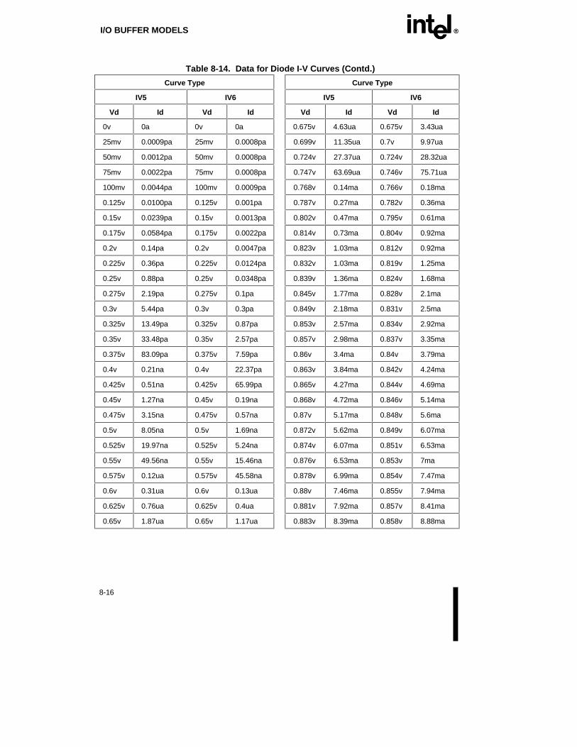
I/O BUFFER MODELS EE
8-16
Table 8-14. Data for Diode I-V Curves (Contd.)
Curve Type Curve Type
IV5 IV6 IV5 IV6
Vd Id Vd Id Vd Id Vd Id
0v 0a 0v 0a 0.675v 4.63ua 0.675v 3.43ua
25mv 0.0009pa 25mv 0.0008pa 0.699v 11.35ua 0.7v 9.97ua
50mv 0.0012pa 50mv 0.0008pa 0.724v 27.37ua 0.724v 28.32ua
75mv 0.0022pa 75mv 0.0008pa 0.747v 63.69ua 0.746v 75.71ua
100mv 0.0044pa 100mv 0.0009pa 0.768v 0.14ma 0.766v 0.18ma
0.125v 0.0100pa 0.125v 0.001pa 0.787v 0.27ma 0.782v 0.36ma
0.15v 0.0239pa 0.15v 0.0013pa 0.802v 0.47ma 0.795v 0.61ma
0.175v 0.0584pa 0.175v 0.0022pa 0.814v 0.73ma 0.804v 0.92ma
0.2v 0.14pa 0.2v 0.0047pa 0.823v 1.03ma 0.812v 0.92ma
0.225v 0.36pa 0.225v 0.0124pa 0.832v 1.03ma 0.819v 1.25ma
0.25v 0.88pa 0.25v 0.0348pa 0.839v 1.36ma 0.824v 1.68ma
0.275v 2.19pa 0.275v 0.1pa 0.845v 1.77ma 0.828v 2.1ma
0.3v 5.44pa 0.3v 0.3pa 0.849v 2.18ma 0.831v 2.5ma
0.325v 13.49pa 0.325v 0.87pa 0.853v 2.57ma 0.834v 2.92ma
0.35v 33.48pa 0.35v 2.57pa 0.857v 2.98ma 0.837v 3.35ma
0.375v 83.09pa 0.375v 7.59pa 0.86v 3.4ma 0.84v 3.79ma
0.4v 0.21na 0.4v 22.37pa 0.863v 3.84ma 0.842v 4.24ma
0.425v 0.51na 0.425v 65.99pa 0.865v 4.27ma 0.844v 4.69ma
0.45v 1.27na 0.45v 0.19na 0.868v 4.72ma 0.846v 5.14ma
0.475v 3.15na 0.475v 0.57na 0.87v 5.17ma 0.848v 5.6ma
0.5v 8.05na 0.5v 1.69na 0.872v 5.62ma 0.849v 6.07ma
0.525v 19.97na 0.525v 5.24na 0.874v 6.07ma 0.851v 6.53ma
0.55v 49.56na 0.55v 15.46na 0.876v 6.53ma 0.853v 7ma
0.575v 0.12ua 0.575v 45.58na 0.878v 6.99ma 0.854v 7.47ma
0.6v 0.31ua 0.6v 0.13ua 0.88v 7.46ma 0.855v 7.94ma
0.625v 0.76ua 0.625v 0.4ua 0.881v 7.92ma 0.857v 8.41ma
0.65v 1.87ua 0.65v 1.17ua 0.883v 8.39ma 0.858v 8.88ma

EE I/O BUFFER MODELS
8-17
Table 8-15. Data for Diode I-V Curves (Contd.)
Curve Type Curve Type
IV5 IV6 IV5 IV6
Vd Id Vd Id Vd Id Vd Id
0.884v 8.86ma 0.859v 9.36ma 0.908v 21.86ma 0.878v 22.45ma
0.885v 9.33ma 0.86v 9.83ma 0.909v 22.34ma 0.879v 22.94ma
0.887v 9.8ma 0.861v 10.31ma 0.909v 22.83ma 0.879v 23.43ma
0.888v 10.28ma 0.862v 10.79ma 0.91v 23.32ma 0.88v 23.92ma
0.889v 10.75ma 0.863v 11.27ma 0.91v 23.81ma 0.88v 24.41ma
0.89v 11.23ma 0.864v 11.75ma 0.911v 24.3ma 0.881v 24.9ma
0.891v 11.7ma 0.865v 12.23ma 0.911v 24.79ma 0.881v 25.39ma
0.892v 12.18ma 0.866v 12.71ma 0.912v 25.27ma 0.882v 25.88ma
0.894v 12.66ma 0.867v 13.2ma 0.913v 25.76ma 0.882v 26.37ma
0.894v 13.14ma 0.867v 13.68ma 0.913v 26.25ma 0.883v 26.86ma
0.895v 13.62ma 0.868v 14.16ma 0.914v 26.74ma 0.883v 27.35ma
0.896v 14.1ma 0.869v 14.65ma 0.914v 27.23ma 0.883v 27.85ma
0.897v 14.58ma 0.87v 15.13ma 0.915v 27.72ma 0.884v 28.34ma
0.898v 15.06ma 0.87v 15.62ma 0.915v 28.21ma 0.884v 28.83ma
0.899v 15.55ma 0.871v 16.1ma 0.915v 28.7ma 0.885v 29.32ma
0.9v 16.03ma 0.872v 16.59ma 0.916v 29.19ma 0.885v 29.81ma
0.901v 16.51ma 0.872v 17.07ma 0.916v 29.69ma 0.885v 30.31ma
0.901v 17ma 0.873v 17.56ma 0.917v 30.18ma 0.886v 30.8ma
0.902v 17.48ma 0.874v 18.05ma 0.917v 30.67ma 0.886v 31.29ma
0.903v 17.96ma 0.874v 18.54ma 0.918v 31.16ma 0.886v 31.78ma
0.904v 18.45ma 0.875v 19.02ma 0.918v 31.65ma 0.887v 32.28ma
0.904v 18.94ma 0.875v 19.51ma 0.919v 32.14ma 0.887v 32.77ma
0.905v 19.42ma 0.876v 20ma 0.919v 32.63ma 0.887v 33.26ma
0.906v 19.91ma 0.876v 20.49ma 0.919v 33.12ma 0.888v 33.76ma
0.906v 20.39ma 0.877v 20.98ma 0.92v 33.62ma 0.888v 34.25ma
0.907v 20.88ma 0.877v 21.47ma 0.92v 34.11ma 0.888v 34.74ma
0.907v 21.37ma 0.878v 21.96ma 0.921v 34.6ma 0.889v 35.24ma

I/O BUFFER MODELS EE
8-18
Table 8-16. Data for Diode I-V Curves (Contd.)
Curve Type Curve Type
IV5 IV6 IV5 IV6
Vd Id Vd Id Vd Id Vd Id
0.921v 35.09ma 0.889v 35.73ma 0.93v 48.41ma 0.896v 49.08ma
0.921v 35.58ma 0.889v 36.22ma 0.93v 48.91ma 0.896v 49.58ma
0.922v 36.08ma 0.89v 36.72ma 0.93v 49.4ma 0.897v 50.07ma
0.922v 36.57ma 0.89v 37.21ma 0.93v 49.9ma 0.897v 50.57ma
0.922v 37.06ma 0.89v 37.7ma 0.931v 50.39ma 0.897v 51.06ma
0.923v 37.56ma 0.891v 38.2ma 0.931v 50.89ma 0.897v 51.56ma
0.923v 38.05ma 0.891v 38.69ma 0.931v 51.38ma 0.898v 52.05ma
0.923v 38.54ma 0.891v 39.19ma 0.932v 51.88ma 0.898v 52.55ma
0.924v 39.03ma 0.891v 39.68ma 0.932v 52.37ma 0.898v 53.04ma
0.924v 39.53ma 0.892v 40.17ma 0.932v 52.87ma 0.898v 53.54ma
0.924v 40.02ma 0.892v 40.67ma 0.932v 53.36ma 0.898v 54.04ma
0.925v 40.51ma 0.892v 41.16ma 0.933v 53.86ma 0.899v 54.53ma
0.925v 41.01ma 0.893v 41.66ma 0.933v 54.35ma 0.899v 55.03ma
0.925v 41.5ma 0.893v 42.15ma 0.933v 54.85ma 0.899v 55.52ma
0.926v 41.99ma 0.893v 42.65ma 0.933v 55.34ma 0.899v 56.02ma
0.926v 42.49ma 0.893v 43.14ma 0.934v 55.84ma 0.899v 56.52ma
0.926v 42.98ma 0.894v 43.64ma 0.934v 56.33ma 0.9v 57.01ma
0.927v 43.47ma 0.894v 44.13ma 0.934v 56.83ma 0.9v 57.51ma
0.927v 43.97ma 0.894v 44.63ma 0.934v 57.32ma 0.9v 58ma
0.927v 44.46ma 0.894v 45.12ma 0.934v 57.82ma 0.9v 58.5ma
0.928v 44.96ma 0.895v 45.62ma 0.935v 58.31ma 0.9v 59ma
0.928v 45.45ma 0.895v 46.11ma 0.935v 58.81ma 0.901v 59.49ma
0.928v 45.94ma 0.895v 46.61ma 0.935v 59.3ma 0.901v 59.99ma
0.929v 46.44ma 0.895v 47.1ma 0.935v 59.8ma 0.901v 60.48ma
0.929v 46.93ma 0.896v 47.6ma 0.936v 60.29ma 0.901v 60.98ma
0.929v 47.43ma 0.896v 48.09ma 0.936v 60.79ma 0.901v 61.48ma
0.929v 47.92ma 0.896v 48.59ma 0.936v 61.28ma 0.902v 61.97ma

EE I/O BUFFER MODELS
8-19
Table 8-17. Data for Diode I-V Curves (Contd.)
Curve Type Curve Type
IV5 IV6 IV5 IV6
Vd Id Vd Id Vd Id Vd Id
0.936v 61.78ma 0.902v 62.47ma 0.94v 71.7ma 0.905v 72.4ma
0.937v 62.28ma 0.902v 62.97ma 0.941v 72.19ma 0.905v 72.9ma
0.937v 62.77ma 0.902v 63.46ma 0.941v 72.69ma 0.905v 73.39ma
0.937v 63.27ma 0.902v 63.96ma 0.941v 73.19ma 0.906v 73.89ma
0.937v 63.76ma 0.902v 64.45ma 0.941v 73.68ma 0.906v 74.39ma
0.937v 64.26ma 0.903v 64.95ma 0.941v 74.18ma 0.906v 74.88ma
0.938v 64.75ma 0.903v 65.45ma 0.941v 74.67ma 0.906v 75.38ma
0.938v 65.25ma 0.903v 65.94ma 0.942v 75.17ma 0.906v 75.88ma
0.938v 65.75ma 0.903v 66.44ma 0.942v 75.67ma 0.906v 76.38ma
0.938v 66.24ma 0.903v 66.94ma 0.942v 76.16ma 0.907v 76.87ma
0.938v 66.74ma 0.904v 67.43ma 0.942v 76.66ma 0.907v 77.37ma
0.939v 67.23ma 0.904v 67.93ma 0.942v 77.16ma 0.907v 77.87ma
0.939v 67.73ma 0.904v 68.43ma 0.943v 77.65ma 0.907v 78.36ma
0.939v 68.22ma 0.904v 68.92ma 0.943v 78.15ma 0.907v 78.86ma
0.939v 68.72ma 0.904v 69.42ma 0.943v 78.65ma 0.907v 79.36ma
0.939v 69.22ma 0.904v 69.92ma 0.943v 79.14ma 0.907v 79.85ma
0.94v 69.71ma 0.905v 70.41ma 0.943v 79.64ma 0.908v 80.35ma
0.94v 70.21ma 0.905v 70.91ma 0.943v 80.14ma 0.908v 80.85ma
0.94v 70.7ma 0.905v 71.41ma 0.944v 80.63ma 0.908v 81.35ma
0.94v 71.2ma 0.905v 71.9ma
For information on IBIS models, please contact Intel Corporation.

E9
MechanicalSpecifications


EE
9-1
CHAPTER 9MECHANICAL SPECIFICATIONS
The Pentium Processor (510\60, 567\66) is packaged in a 273-pin ceramic pin grid array(PGA). The pins are arranged in a 21 by 21 matrix and the package dimensions are 2.16" X2.16" (Table 9-1).
Table 9-1. Pentium ® Processor Package Information Summary
Package Type Total Pins Pin Array Package SizeEstimatedWattage
Pentium®
ProcessorPGA 273 21 x 21 2.16" X 2.16"
5.49 cm X 5.49 cm
16
NOTE: See DC Specifications for more detailed power specifications.
Figure 9-1 and Figure 9-2 shows the package dimensions for the Pentium Processor (510\60,567\66). The mechanical specifications are provided in Table 9-2.

MECHANICAL SPECIFICATIONS EE
9-2
BasePlane
01.65REF.
S1
DD 1
E1
A
A 1A2
REF.
PIN D4(signal D13)
2.291.5245˚ CHAMFER(INDEX CORNER)
B
L
D
D2
SEATING PLANE
A 4
PDB7 4
Figure 9-1. Pentium ® Processor (510\60, 567\66) Package Dimensions
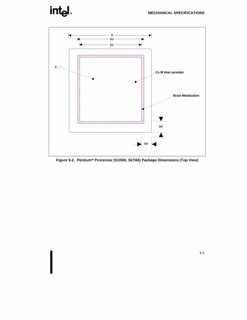
EE MECHANICAL SPECIFICATIONS
9-3
D2
D3D
Cu W Heat spreader
Braze Metalization
F
D4
D4
Figure 9-2. Pentium ® Processor (510\60, 567\66) Package Dimensions (Top View)

MECHANICAL SPECIFICATIONS EE
9-4
Table 9-2. Pentium ® Processor (510\60, 567\66) Mechanical Specifications
Family: Ceramic Pin Grid Array Package
Millimeters Inches
Symbol Min Max Notes Min Max Notes
A 3.91 4.70 Solid Lid 0.154 0.185 Solid Lid
A1 0.38 0.43 Solid Lid 0.015 0.017 Solid Lid
A2 2.62 2.97 0.103 0.117
A4 0.97 1.22 0.038 0.048
B 0.43 0.51 0.017 0.020
D 54.66 55.07 2.152 2.168
D1 50.67 50.93 1.995 2.005
D2 37.85 38.35 Spreader Size 1.490 1.510 Spreader Size
D3 40.335 40.945 Braze 1.588 1.612 Braze
D4 8.382 0.330
E1 2.29 2.79 0.090 0.110
F 0.127 Flatness ofspreadermeasureddiagonally
0.005 Flatness ofspreadermeasureddiagonally
L 3.05 3.30 0.120 0.130
N 273 Total Pins 273 Total Pins
S1 1.651 2.16 0.065 0.085
The weight of the heat spreader package increases to approximately twice the weight of thestandard PGA package (70.7 grams vs. 33.2 grams).

E10
ThermalSpecifications


EE
10-1
CHAPTER 10THERMAL SPECIFICATIONS
10.1. THERMAL MEASUREMENTSThe Pentium Processor (510\60, 567\66) is specified for proper operation when TC (casetemperature) is within the specified range (TC = 0°C to + 80°C at 60 MHz; TC = 0°C to +70°C at 66 MHz). To verify that the proper TC is maintained, it should be measured at thecenter of the top surface (opposite of the pins) of the device in question. To minimize themeasurement errors, it is recommended to use the following approach:
• Use 36 gauge or finer diameter K, T, or J type thermocouples. The laboratory testing wasdone using a thermocouple made by Omega (part number: 5TC-TTK-36-36).
• Attach the thermocouple bead or junction to the center of the package top surface usinghigh thermal conductivity cements. The laboratory testing was done by using OmegaBond (part number: OB-100).
• The thermocouple should be attached at a 90° angle as shown in Figure 10-1. When aheat sink is attached, a hole (no larger than 0.15 × 0.15) should be drilled through theheat sink to allow probing the center of the package as shown in Figure 10-1.
• If the case temperature is measured with a heat sink attached to the package, drill a holethrough the heat sink to route the thermocouple wire out.
CSJ23A
Figure 10-1. Technique for Measuring Tcase*
* Though the figure shows the package with a heat spreader, the same technique applies to measuring TC of thepackage without a heat spreader.

THERMAL SPECIFICATIONS EE
10-2
An ambient temperature TA is not specified directly. The only restriction is that TC is met.To determine the allowable TA values, the following equations may be used:
TJ = TC + (P * ΘJC)
TA = TJ - (P * ΘJA)
ΘCA = ΘJA - ΘJC
TA = TC - (P * ΘCA)
where, TJ, TA, and TC = Junction, Ambient and Case Temperature, respectively.
ΘJC, ΘJA, and ΘCA = Junction-to-Case, Junction-to-Ambient, and Case-to-Ambient Thermal Resistance, respectively.
P = Maximum Power Consumption
Table 10-1 lists the ΘJC and ΘCA values for the Pentium Processor (510\60, 567\66).
Table 10-1. Junction-to-Case and Case-to-Ambient Thermal Resistances for the Pentium ® Processor (510\60, 567\66) (with and without a Heat Sink)
ΘΘCA vs Airflow (ft/min)
ΘΘJC 0 200 400 600 800 1000
With 0.25" Heat Sink 0.6 8.3 5.4 3.5 2.6 2.1 1.8
With 0.35" Heat Sink 0.6 7.4 4.5 3.0 2.2 1.8 1.6
With 0.65" Heat Sink 0.6 5.9 3.0 1.9 1.5 1.2 1.1
Without Heat Sink 1.2 10.5 7.9 5.5 3.8 2.8 2.4
NOTES:
1. Heat Sink: 2.1 sq. in. base, omni-directional pin AI heat sink with 0.050 in. pin width, 0.143 in pin-to-pincenter spacing and 0.150 in. base thickness. Heat sinks are attached to the package with a 2 to 4 mil thicklayer of typical thermal grease. The thermal conductivity of this grease is about 1.2 w/m °C.
2. Θca values shown in Table 10-1 are typical values. The actual Θca values depend on the air flow in thesystem (which is typically unsteady, non uniform and turbulent) and thermal interactions betweenPentium® processor and surrounding components through PCB and the ambient.
10.2. PACKAGE THERMAL PERFORMANCE WITH THE HEATSPREADER
The following is a description of how the heat spreader improves the package thermalperformance:
Since the Pentium processor requires an external heat sink in order to maintain the junctionand case temperatures below the acceptable levels, the main contributors to the total junction

EE THERMAL SPECIFICATIONS
10-3
to ambient thermal resistance are junction to case (ΘJC), case to heat sink (ΘCS), and heatsink to ambient (ΘSA) thermal resistances.
ΘJC is mainly a function of internal construction of the package and packaging material,thermal properties such as the die size and die attach, and ceramic thermal conductivity. ΘCSis a function of the thickness and thermal properties of the interface material between thepackage and heat sink, package and heat sink flatness, and surface finish and effective heattranser are between the package and the heat sink. ΘSA is a function of both the heat sinkdesign and the airflow type and rate.
Using a heat spreader in the package lowers the overall thermal resistance in two ways:
1. It increases the effective heat transfer area between the package and the heat sink and asa result lowers ΘCS. The actual reduction in ΘCS depends on the magnitude of ΘCSwithout a heat spreader. The larger the value of ΘCS without using a heat spreader, thelarger will be the reduction in the value of ΘJA if a heat spreader is used.
2. A heat spreader may also improve the heat sink thermal performance by increasing theeffective heat transfer area in the heat sink and making the fins away from the die moreeffective.
Using a heat spreader with a thermal grease interface will result in about .4 c/w lower ΘCAthan that for the package without the heat spreader. Thermal grease is considered one of themore thermally efficient materials for use as an interface between heat sink and package.Thermally conductive adhesives and conductive tapes or films typically have poorer thermalperformance when compared to a thin layer of thermal grease, because grease facilitates alarger reduction in thermal resistance.
10.2.1. Case Temperature SpecificationsFollowing are the case temperature specifications for the Pentium processor with and withoutthe heat spreader on the package:
10.2.1.1. PENTIUM® PROCESSOR PACKAGE WITHOUT HEAT SPREADER
The case temperature specifications for the Pentium processor package without heat spreaderat 60 and 66 MHz are as follows (Note: This applies to B1" and previous steppings):
1. Tc (case temperature) 0°C to 85°C @ 60 MHz.
2. Tc (case temperature) 0°C to 75°C @ 66 MHz.
10.2.1.2. PENTIUM® PROCESSOR WITH HEAT SPREADER PACKAGE
The case temperature specifications for the Pentium processor heat spreader package at 60and 66 MHz are as follows (Note: This applies to C1 and later steppings):
1. Tc (case temperature) 0°C to 80°C @ 60 MHz.
2. Tc (case temperature) 0°C to 70°C @ 66 MHz.

THERMAL SPECIFICATIONS EE
10-4
In the case of the Pentium processor with heat spreader package, the case temperature ismeasured at the center of the package top surface on the heat spreader. The procedure tomeasure the case temperature, is outlined in Chapter 10 of the Pentium® Processor FamilyDeveloper’s Manual, Volume 1 (Order Number 241428).
The thermal specification of the heat spreader package calls for 5 degrees Celsius lower casetemperature than the non-spreader package for both 60- and 66-MHz versions. The lowercase temperature requirement of the heat spreader package is due to its lower junction toambient thermal resistance compared to a non-heat spreader package with the same heat sink.For example, at 66-MHz, the heat spreader package will have 0.4 × 16 = 6.4 degree Celsiuslower case temperature than a non-heat spreader package with the same heat sink design andgrease interface. This implies that in a system designed for a non-spreader package, if thenon-spreader package is replaced with a heat spreader package, the measured casetemperature will be lower by 6.4 degrees Celsius for the 66-MHz and 5.8 degrees Celsius forthe 60-MHz versions. The actual reduction in the case temperature will be slightly higher orlower depending on the efficiency of the thermal interface. Therefore, a more conservativevalue of 5 degrees Celsius is used as the difference between the case temperaturespecifications of the two package types for both frequency versions. The expectation is thatthe ambient temperature in the system will be maintained while gaining the benefits of lowerjunction and case temperatures when the heat spreader package is added to an existingsystem with the same airflow and unmodified heat sink.

E11
Testability


EE
11-1
CHAPTER 11TESTABILITY
This chapter describes the features which are included in the Pentium Processor (510\60,567\66) or the purpose of enhancing the testability of the Pentium Processor (510\60,567\66). The capability of the Intel486 CPU test hooks are included in the Pentium Processor(510\60, 567\66), however some are implemented differently. In addition, new test featureswere added to assure timely testing and production of the system product.
Internal component testing through the Built In Self Test (BIST) feature of the PentiumProcessor (510\60, 567\66) provides 100% single stuck at fault coverage of the microcodeROM and large PLAs. Some testing of the instruction cache, data cache, TranslationLookaside Buffers (TLBs), and Branch Target Buffer (BTB) is also performed. In addition,the constant ROMs are checked.
Tristate test mode and the IEEE 1149.1 "Test Access Port and Boundary Scan" mechanismare included to facilitate testing of board connections.
See Appendix A for more information regarding the testing of the on-chip caches, translationlookaside buffers, branch target buffer, second level caches, the superscalar architecture, andinternal parity checking through the test registers.
Built in self test, tristate test mode, Boundary Scan, and TR12 are discussed in this chapter.
11.1. BUILT IN SELF TEST (BIST)Self test is initiated by driving the INIT pin high when RESET transitions from high to low.
No bus cycles are run by the Pentium processor during self test. The duration of self test isapproximately 219 clocks. Approximately 70% of the devices in the Pentium processor aretested by BIST.
The Pentium processor BIST consists of two parts: hardware self test and microcode self test.
During the hardware portion of BIST, the microcode and all large PLAs are tested. Allpossible input combinations of the microcode ROM and PLAs are tested.
The constant ROMs, BTB, TLBs and all caches are tested by the microcode portion of BIST.The array tests (caches, TLBs and BTB) have two passes. On the first pass, data patterns arewritten to arrays, read back and checked for mismatches. The second pass writes thecomplement of the initial data pattern, reads it back and checks for mismatches. The constantROMs are tested by using the microcode to add various constants and check the result againsta stored value.
Upon completion of BIST, the cumulative result of all tests are stored in the EAX register. IfEAX contains 0h, then all checks passed; any non-zero result indicates a faulty unit. Note

TESTABILITY EE
11-2
that if an internal parity error is detected during BIST, the processor will assert the IERR#pin and attempt to shutdown.
11.2. TRISTATE TEST MODEWhen the FLUSH# pin is sampled low in the clock prior to the RESET pin going from highto low, the Pentium processor enters tristate test mode. The Pentium processor floats all of itsoutput pins and bi-directional pins including pins which are never floated during normaloperation (except TDO). Tristate test mode can be initiated in order to facilitate testing ofboard connections. The Pentium processor remains in tristate test mode until the RESET pinis toggled again.
11.3. IEEE 1149.1 TEST ACCESS PORT AND BOUNDARY SCANMECHANISM
The IEEE Standard Test Access Port and Boundary Scan Architecture (Standard 1149.1) isimplemented in the Pentium processor. This feature allows board manufacturers to test boardinterconnects by using "boundary scan," and to test the Pentium processor itself throughBIST. All output pins are tristateable through the IEEE 1149.1 mechanism. The test accessport mechanism is also used in the new debug mode implemented in the Pentium processor,Probe Mode. See the Probe Mode chapter for details.
11.3.1. Pentium ® Processor Test Access Port (TAP)The Pentium processor Test Access Port (TAP) contains a TAP controller, a Boundary ScanRegister, a Probe Data Register, a Probe Instruction Register, 4 input pins (TDI, TCK, TMS,and TRST#) and one output pin (TDO). The TAP controller consists of an InstructionRegister, a Device ID Register, a Bypass Register, a Runbist Register and control logic. SeeFigure 11-1 for the TAP Block Diagram.

EE TESTABILITY
11-3
PDB39
TMS
TRST#
TDI
TCK
TDO
TDO-EN
Instruction Register
TAP Controller
RUNBIST Register
BYPASS Register
Device Identification
Probe Instruction Register
Probe Data Register
Pentium ® Processor
External Pins and Control Cells
Control Signals
Boundary Scan Test Register
Instruction Decode/Control Logic
Figure 11-1. Test Access Port Block Diagram
TESTABILITY EE
11-4
11.3.1.1. TAP PINS
As mentioned in the previous section, the TAP includes 4 input pins and one output pin. TDI(test data in) is used to shift data or instructions into the TAP in a serial manner. TDO (testdata out) shifts out the response data. TMS (test mode select) is used to control the state ofthe TAP controller. TCK is the test clock. The TDI and TMS inputs are sampled on the risingedge of this TCK. Asserting TRST# will force the TAP controller into the Test Logic ResetState (see the TAP controller state diagram, Figure 11-4). The input pins (TDI, TMS, TCK,and TRST#) have pullup resistors.
11.3.1.2. TAP REGISTERS
Boundary Scan Register
The IEEE standard requires that an extra single bit shift register be inserted at each pin on thedevice (Pentium processor). These single bit shift registers are connected into a long shiftregister, the Boundary Scan Register. Therefore, the Boundary Scan Register is a single shiftregister path containing the boundary scan cells that are connected to all input and outputpins of the Pentium processor. Figure 11-2 shows the logical structure of the Boundary ScanRegister. While output cells determine the value of the signal driven on the correspondingpin, input cells only capture data; they do not affect the normal operation of the device (theINTEST instruction is not supported by the Pentium processor). Data is transferred withoutinversion from TDI to TDO through the Boundary Scan Register during scanning. TheBoundary Scan Register can be operated by the EXTEST and SAMPLE/PRELOADinstructions. The Boundary Scan Register order is defined later in this chapter.
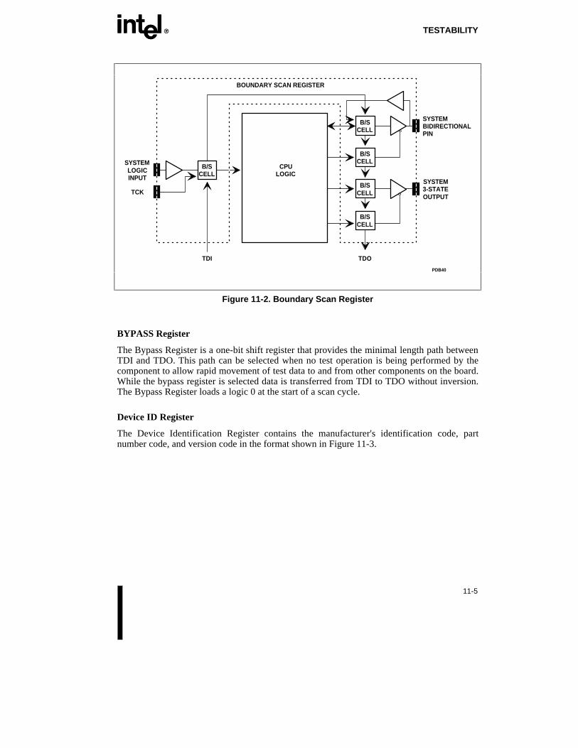
EE TESTABILITY
11-5
PDB40
SYSTEMLOGICINPUT
TCK
B/SCELL
CPULOGIC
B/SCELL
B/SCELL
B/SCELL
B/SCELL
BOUNDARY SCAN REGISTER
SYSTEMBIDIRECTIONALPIN
SYSTEM3-STATEOUTPUT
TDOTDI
Figure 11-2. Boundary Scan Register
BYPASS Register
The Bypass Register is a one-bit shift register that provides the minimal length path betweenTDI and TDO. This path can be selected when no test operation is being performed by thecomponent to allow rapid movement of test data to and from other components on the board.While the bypass register is selected data is transferred from TDI to TDO without inversion.The Bypass Register loads a logic 0 at the start of a scan cycle.
Device ID Register
The Device Identification Register contains the manufacturer's identification code, partnumber code, and version code in the format shown in Figure 11-3.

TESTABILITY EE
11-6
PDB41
1MANUFACTURER
IDENTITYPART NUMBERVERSION
Figure 11-3. Format of the Device ID Register
The Pentium processor has divided up the 16-bit part number into 3 fields. The upper 7 bitsare used to define the product type (examples: Cache, CPU architecture). The middle 4-bitsare used to represent the generation or family (examples: Intel486 CPU, Pentium processor).The lower 5 bits are used to represent the model (examples: SX, DX). Using this definition,the Pentium Processor (510\60, 567\66) ID code is shown in Table 11-1.
The version field is used to indicate the stepping ID.
Table 11-1. Device ID Register Values
Part Number
Stepping Version ProductType Generation Model
Manufacturing ID "1" Entire Code
x xh 01h 05h 01h 09h 1 x02A1013h
Runbist Register
The Runbist Register is a one bit register used to report the results of the Pentium processorBIST when it is initiated by the RUNBIST instruction. This register is loaded with "0" uponsuccessful completion of BIST.
Instruction Register
This register is 13 bits wide. The command field (the lower 4 bits of instruction) is used toindicate one of the following instructions: EXTEST, IDCODE, RUNBIST,SAMPLE/PRELOAD and BYPASS. The upper 9 bits are reserved by Intel.
The most significant bit of the Instruction Register is connected to TDI, the least significantto TDO.

EE TESTABILITY
11-7
11.3.1.3. TAP CONTROLLER STATE DIAGRAM
Figure 11-4 shows the 16-state TAP controller state diagram. A description of each statefollows. Note that the state machine contains two main branches to access either data orinstruction registers.
PDB42
0
1 1
0
0
0
1
0
0
1
1
0101
1
1
0
0
1
0
0
0
1 1
0
Select-DR-Scan
Capture-IR
1
1
1
0
.
1
Run-Test-Idle
Test-Logic-Reset
Pause-DR
Shift-IR
Pause-IR
Capture-DR
Exit1-DR
Exit2-DR
Update-DR Update-IR
Exit2-IR
Exit1-IR
Select-IR-Scan
Shift-DR 0
Figure 11-4. TAP Controller State Diagram
Test-Logic-Reset State
In this state, the test logic is disabled so that normal operation of the device can continueunhindered. During initialization, the Pentium processor initializes the instruction registersuch that the IDCODE instruction is loaded.
No matter what the original state of the controller, the controller enters Test-Logic-Resetstate when the TMS input is held high (logic 1) for at least five rising edges of TCK. Thecontroller remains in this state while TMS is high. The TAP controller is forced to enter thisstate when the TRST# pin is asserted (with TCK toggling or TCK at a high logic value). ThePentium processor automatically enters this state at power-up.

TESTABILITY EE
11-8
Run-Test/Idle State
This is a controller state between scan operations. Once in this state, the controller remains inthis state as long as TMS is held low. In devices supporting the RUNBIST instruction, theBIST is performed during this state and the result is reported in the Runbist Register. Forinstructions not causing functions to execute during this state, no activity occurs in the testlogic. The instruction register and all test data registers retain their previous state. WhenTMS is high and a rising edge is applied to TCK, the controller moves to the Select-DR state.
Select-DR-Scan State
This is a temporary controller state. The test data register selected by the current instructionretains its previous state. If TMS is held low and a rising edge is applied to TCK when in thisstate, the controller moves into the Capture-DR state, and a scan sequence for the selectedtest data register is initiated. If TMS is held high and a rising edge is applied to TCK, thecontroller moves to the Select-IR-Scan state.
The instruction does not change in this state.
Capture-DR State
In this state, the Boundary Scan Register captures input pin data if the current instruction isEXTEST or SAMPLE/PRELOAD. The other test data registers, which do not have parallelinput, are not changed.
The instruction does not change in this state.
When the TAP controller is in this state and a rising edge is applied to TCK, the controllerenters the Exit1-DR state if TMS is high or the Shift-DR state if TMS is low.
Shift-DR State
In this controller state, the test data register connected between TDI and TDO as a result ofthe current instruction shifts data one stage toward its serial output on each rising edge ofTCK.
The instruction does not change in this state.
When the TAP controller is in this state and a rising edge is applied to TCK, the controllerenters the Exit1-DR state if TMS is high or remains in the Shift-DR state if TMS is low.
Exit1-DR State
This is a temporary state. While in this state, if TMS is held high, a rising edge applied toTCK causes the controller to enter the Update-DR state, which terminates the scanningprocess. If TMS is held low and a rising edge is applied to TCK, the controller enters thePause-DR state.
The test data register selected by the current instruction retains its previous value during thisstate. The instruction does not change in this state.
EE TESTABILITY
11-9
Pause-DR State
The pause state allows the test controller to temporarily halt the shifting of data through thetest data register in the serial path between TDI and TDO. An example use of this state couldbe to allow a tester to reload its pin memory from disk during application of a long testsequence.
The test data register selected by the current instruction retains its previous value during thisstate. The instruction does not change in this state.
The controller remains in this state as long as TMS is low. When TMS goes high and a risingedge is applied to TCK, the controller moves to the Exit2-DR state.
Exit2-DR State
This is a temporary state. While in this state, if TMS is held high, a rising edge applied toTCK causes the controller to enter the Update-DR state, which terminates the scanningprocess. If TMS is held low and a rising edge is applied to TCK, the controller enters theShift-DR state.
The test data register selected by the current instruction retains its previous value during thisstate. The instruction does not change in this state.
Update-DR State
The Boundary Scan Register is provided with a latched parallel output to prevent changes atthe parallel output while data is shifted in response to the EXTEST and SAMPLE/PRELOADinstructions. When the TAP controller is in this state and the Boundary Scan Register isselected, data is latched onto the parallel output of this register from the shift-register path onthe falling edge of TCK. The data held at the latched parallel output does not change otherthan in this state.
All shift-register stages in the test data register selected by the current instruction retains theirprevious value during this state. The instruction does not change in this state.
Select-IR-Scan State
This is a temporary controller state. The test data register selected by the current instructionretains its previous state. If TMS is held low and a rising edge is applied to TCK when in thisstate, the controller moves into the Capture-IR state, and a scan sequence for the instructionregister is initiated. If TMS is held high and a rising edge is applied to TCK, the controllermoves to the Test-Logic-Reset state. The instruction does not change in this state.
Capture-IR State
In this controller state the shift register contained in the instruction register loads a fixedvalue on the rising edge of TCK.
The test data register selected by the current instruction retains its previous value during thisstate. The instruction does not change in this state.

TESTABILITY EE
11-10
When the controller is in this state and a rising edge is applied to TCK, the controller entersthe Exit1-IR state if TMS is held high, or the Shift-IR state if TMS is held low.
Shift-IR State
In this state the shift register contained in the instruction register is connected between TDIand TDO and shifts data one stage towards its serial output on each rising edge of TCK.
The test data register selected by the current instruction retains its previous value during thisstate. The instruction does not change in this state.
When the controller is in this state and a rising edge is applied to TCK, the controller entersthe Exit1-IR state if TMS is held high, or remains in the Shift-IR state if TMS is held low.
Exit1-IR State
This is a temporary state. While in this state, if TMS is held high, a rising edge applied toTCK causes the controller to enter the Update-IR state, which terminates the scanningprocess. If TMS is held low and a rising edge is applied to TCK, the controller enters thePause-IR state.
The test data register selected by the current instruction retains its previous value during thisstate. The instruction does not change in this state.
Pause-IR State
The pause state allows the test controller to temporarily halt the shifting of data through theinstruction register.
The test data register selected by the current instruction retains its previous value during thisstate. The instruction does not change in this state.
The controller remains in this state as long as TMS is low. When TMS goes high and a risingedge is applied to TCK, the controller moves to the Exit2-IR state.
Exit2-IR State
This is a temporary state. While in this state, if TMS is held high, a rising edge applied toTCK causes the controller to enter the Update-IR state, which terminates the scanningprocess. If TMS is held low and a rising edge is applied to TCK, the controller enters theShift-IR state.
The test data register selected by the current instruction retains its previous value during thisstate. The instruction does not change in this state.
Update-IR State
The instruction shifted into the instruction register is latched onto the parallel output from theshift-register path on the falling edge of TCK. Once the new instruction has been latched, itbecomes the current instruction.

EE TESTABILITY
11-11
Test data registers selected by the current instruction retain their previous value.
11.3.2. Boundary ScanThe IEEE Standard 1149.1 Boundary Scan is implemented using the Test Access Port andTAP Controller as described above. The Pentium Processor (510\60, 567\66) implements allof the required boundary scan features as well as some additional features. The required pinsare: TDI, TDO, TCK and TMS. The required registers are: Boundary Scan, Bypass, and theInstruction Register. Required instructions include: BYPASS, SAMPLE/PRELOAD andEXTEST. The additional pin, registers, and instructions are implemented to add additionaltest features and to support Probe Mode.
On the board level, the TAP provides a simple serial interface that makes it possible to testall signal traces with only a few probes. The testing is controlled through the TAP ControllerState machine that can be implemented with automatic test equipment or a PLD.
On power up the TAP controller is automatically initialized to the test logic reset state (testlogic disabled), so normal Pentium processor behavior is the default. The Test Logic ResetState is also entered when TRST# is asserted, or when TMS is high for 5 or more consecutiveTCK clocks.
To implement boundary scan, the TDO of one device is connected to TDI of the next in adaisy chain fashion. This allows all of the I/O of the devices on this chain to be accessedthrough a long shift register. TMS and TCK are common to all devices.
The Boundary Scan Register for the Pentium Processor (510\60, 567\66) contains a cell foreach pin. The following is the bit order of the Pentium Processor (510\60, 567\66) BoundaryScan Register (left to right, top to bottom):
TDI -> Reserved, Reserved, Reserved, RESET, FRCMC#, PEN#, R/S#, NMI, INTR,IGNNE#, SMI#, INIT, Reserved, CLK, Reserved, A3, A4, A5, A6, A7, A8, A9, A10, A11,A12, A13, A14, A15, A16, A17, A18, A19, A20, A21, A22, A23, A24, A25, A26, A27, A28,A29, A30, A31, BT0, Disabus*, BT1, BT2, BT3, BE7#, BE6#, BE5#, BE4#, BE3#, BE2#,BE1#, BE0#, SCYC, D/C#, PWT, PCD, W/R#, ADS#, ADSC#, PRDY, AP, LOCK#, HLDA,APCHK#, PCHK#, HIT#, HITM#, Disbus*, BREQ, SMIACT#, A20M#, FLUSH#, HOLD,WB/WT#, EWBE#, EADS#, BUSCHK#, AHOLD, BRDYC#, BRDY#, KEN#, NA#, INV,BOFF#, IU, IV, CACHE#, M/IO#, BP3, BP2, PM1/BP1, PM0/BP0, Dismisc*, FERR#,IERR#, Disfrc*, DP0, D0, D1, D2, D3, D4, D5, D6, D7, DP1, D8, D9, D10, D11, D12, D13,D14, D15, DP2, D16, D17, D18, D19, D20, D21, D22, D23, DP3, D24, D25, D26, D27, D28,D29, D30, D31, DP4, D32, D33, D34, D35, D36, Diswr*, D37, D38, D39, DP5, D40, D41,D42, D43, D44, D45, D46, D47, DP6, D48, D49, D50, D51, D52, D53, D54, D55, DP7, D56,D57, D58, D59, D60, D61, D62, D63, IBT -> TDO
"Reserved" includes the no connect "NC" signals on the Pentium processor.
The ADSC# and BRDYC# pins are part of the optimized interface between the Pentiumprocessor and the 82496 Cache Controller/82491 Cache SRAM (refer to the 82496 CacheController/82491 Cache SRAM Data Book for Use with the Pentium™ Processor, OrderNumber 241814, for further information).

TESTABILITY EE
11-12
The cells marked with * are control cells that are used to select the direction of bi-directionalpins or tristate the output pins. If "1" is loaded into the control cell, the associated pin(s) aretristated or selected as input. The following lists the control cells and their correspondingpins:
Disabus: A31-A3, AP, BT3-BT0
Disbus: ADS#, BE7-0#, CACHE#, SCYC, M/IO#, D/C#, W/R#, PWT, PCD, LOCK#
Dismisc: BREQ, APCHK#, SMIACT#, PRDY, IU, IV, IBT, BP3, BP2, PM1/BP1,PM0/BP0, FERR#, HITM#, HIT#, PCHK#, HLDA
Disfrc: IERR#
Diswr: D63-D0, DP7-0
11.3.2.1. PENTIUM® PROCESSOR BOUNDARY SCAN TAP INSTRUCTIONSET
Table 11-2 shows the Pentium processor Boundary Scan TAP instructions and theirinstruction register encoding. A description of each instruction follows. The IDCODE andBYPASS instructions may also be executed concurrent with processor execution. Thefollowing instructions are not affected by the assertion of RESET: EXTEST, SAMPLEPRELOAD, BYPASS, and ID CODE.
The instructions should be scanned in to the TAP port least significant bit first (bit 0 of theTAP Command field is the first bit to be scanned in).

EE TESTABILITY
11-13
Table 11-2. TAP Instruction Set and Instruction Register Encoding
Instruction Name Instruction Register Bits 12:4TAP CommandField [Bits 3:0]
EXTEST XXXXXXXXX 0000
Sample/Preload XXXXXXXXX 0001
IDCODE XXXXXXXXX 0010
Private Instruction XXXXXXXXX 0011
Private Instruction XXXXXXXXX 0100
Private Instruction XXXXXXXXX 0101
Private Instruction XXXXXXXXX 0110
RUNBIST XXXXXXXXX 0111
Private Instruction XXXXXXXXX 1000
Private Instruction XXXXXXXXX 1001
Private Instruction XXXXXXXXX 1010
Private Instruction XXXXXXXXX 1011
Private Instruction XXXXXXXXX 1100
BYPASS XXXXXXXXX 1111
The TAP Command field encodings not listed in Table 11-2 (1101, 1110) are unimplementedand will be interpreted as Bypass instructions.
EXTEST The EXTEST instruction allows testing of circuitry external tothe component package, typically board interconnects. It does soby driving the values loaded into the Pentium processor'sBoundary Scan Register out on the output pins corresponding toeach boundary scan cell and capturing the values on the Pentiumprocessor input pins to be loaded into their correspondingBoundary Scan Register locations. I/O pins are selected as inputor output, depending on the value loaded into their control settinglocations in the Boundary Scan Register. Values shifted intoinput latches in the Boundary Scan Register are never used by theinternal logic of the Pentium processor. Note: after using theEXTEST instruction, the Pentium processor must be reset beforenormal (non-boundary scan) use.
SAMPLE/PRELOAD The SAMPLE/PRELOAD performs two functions. When theTAP controller is in the Capture-DR state, theSAMPLE/PRELOAD instruction allows a "snap-shot" of thenormal operation of the component without interfering with thatnormal operation. The instruction causes Boundary Scan Registercells associated with outputs to sample the value being driven by

TESTABILITY EE
11-14
the Pentium processor. It causes the cells associated with inputsto sample the value being driven into the Pentium processor. Onboth outputs and inputs the sampling occurs on the rising edge ofTCK. When the TAP controller is in the Update-DR state, theSAMPLE/PRELOAD instruction preloads data to the device pinsto be driven to the board by executing the EXTEST instruction.Data is preloaded to the pins from the Boundary Scan Register onthe falling edge of TCK.
IDCODE The IDCODE instruction selects the device identification registerto be connected to TDI and TDO. This allows the deviceidentification code to be shifted out of the device on TDO.
BYPASS The BYPASS instruction selects the Bypass Register to beconnected to TDI and TDO. This effectively bypasses the testlogic on the Pentium processor by reducing the shift length of thedevice to one bit. Note that an open circuit fault in the boardlevel test data path will cause the Bypass Register to be selectedfollowing an instruction scan cycle due to a pull-up resistor onthe TDI input. This was implemented to prevent any unwantedinterference with the proper operation of the system logic.
RUNBIST The RUNBIST instruction selects the one (1) bit RunbistRegister, loads a value of "1" into the Runbist Register, andconnects it to TDO. It also initiates the built-in self test (BIST)feature of the Pentium processor. After loading the RUNBIST in-struction code in the instruction register, the TAP controller mustbe placed in the Run-Test/Idle state. BIST begins on the firstrising edge of TCK after entering the Run-Test/Idle state. TheTAP controller must remain in the Run-Test/Idle state until BISTis completed. It requires 219 (CLK) cycles to complete BIST andreport the result to the Runbist Register. After completing BIST,the value in the Runbist Register should be shifted out on TDOduring the Shift-DR state. A value of "0" being shifted out onTDO indicates BIST successfully completed. A value of "1" indi-cates a failure occurred. The CLK clock must be running in orderto execute RUNBIST. After executing the RUNBIST instruction,the Pentium processor must be reset prior to normal (non-boundary scan) operation.

E12
Error Detection


EE
12-1
CHAPTER 12ERROR DETECTION
The Pentium processor incorporates a number of data integrity features that are focused onthe detection and limited recovery of errors. The data integrity features in the Pentiumprocessor provide capabilities for error detection of the internal devices and the externalinterface. The Pentium processor also provides the capability to obtain maximum levels oferror detection by incorporating Functional Redundancy Checking (FRC) support. Errordetecting circuits in the Pentium processor do not limit the operating frequency of the chip.
The data integrity features in the Pentium processor can be categorized as (1) internal errordetection, (2) error detection at the bus interface, and (3) FRC support.
12.1. INTERNAL ERROR DETECTIONDetection of errors of a majority of the devices in the Pentium processor is accomplished byemploying parity checking in the large memory arrays of the chip. The data and instructioncaches (both storage and tag arrays), translation lookaside buffers, and microcode ROM areall parity protected. The following describes the parity checking employed in the majormemory arrays in the Pentium processor (MESI status bits are not parity protected):
• Parity bit per byte in the data cache storage array.
• Parity bit per entry in the data cache tag array.
• Parity bit per quarter line in the instruction cache storage array.
• Parity bit per entry in the instruction cache tag array.
• Parity bit per entry in both the data and instruction TLBs storage arrays.
• Parity bit per entry in both the data and instruction TLBs tag arrays.
• Parity bit per entry in the microcode ROM.
Parity checking as described above provides error detection coverage of 53% of the on-chipdevices. This error detection coverage number also includes the devices in the branch targetbuffer since branch predictions are always verified.
If a parity error has occurred internally, then the Pentium processor operation can no longerbe trusted. Therefore, a parity error on a read from an internal array will cause the Pentiumprocessor to assert the IERR# pin and then shutdown. (Shutdown will be entered assuming itis not prevented from doing so by the error.) Parity errors on reads during normal instructionexecution, reads during a flush operation, reads during BIST and testability cycles, and reads

ERROR DETECTION EE
12-2
during inquire cycles will cause IERR# to be asserted. The IERR# pin will be asserted forone clock for each clock a parity error is detected and may be latched by the system. TheIERR# pin is a glitch free signal, so no spurious assertions of IERR# will occur.
In general, internal timing constraints of the Pentium processor do not allow the inhibition ofwriteback cycles caused by inquire cycles, FLUSH# assertion or the WBINVD instructionwhen a parity error is encountered. In those cases where an internal parity error occurredduring the generation of a writeback cycle, and that cycle was not able to be inhibited, theIERR# pin can be used to recognize that the writeback should be ignored. If an internalparity error occurs during a flush operation, the Pentium processor will assert the IERR# pinas stated above, and the internal caches will be left in a partially flushed state. No specialcycles (flush, flush acknowledge, or writeback) will be run.
12.2. ERROR DETECTION AT PENTIUM® PROCESSORINTERFACE
The Pentium processor provides parity checking on the external address and data buses.There is one parity bit for each byte of the data bus and one parity bit for bits A31-A5 of theaddress bus.
12.2.1. Address ParityA separate and independent mechanism is used for parity checking on the address bus duringinquire cycles. Even address parity is driven along with the address bus during all Pentiumprocessor initiated bus cycles and checked during inquire cycles. When the Pentiumprocessor is driving the address bus, even parity is driven on the AP pin. When the addressbus is being driven into the Pentium processor during an inquire cycle, this pin is sampled inany clock in which EADS# is sampled asserted. APCHK# is driven with the parity status twoclocks after EADS# is sampled active. The APCHK# output (when active) indicates that aparity error has occurred on the address bus during an inquire. Figure 12-1 depicts an addressparity error during an inquire cycle. For additional timing diagrams which show addressparity, see the Bus Functional Description chapter. The APCHK# pin will be asserted for oneclock for each clock a parity error is detected and may be latched by the system. TheAPCHK# pin is a glitch free signal, so no spurious assertions of APCHK# will occur.
In the event of an address parity error during inquire cycles, the internal snoop will not beinhibited. If the inquire hits a modified line in this situation and an active AHOLD preventsthe Pentium processor from driving the address bus, the Pentium processor will potentiallywriteback a line at an address other than the one intended. If the Pentium processor is notdriving the address bus during the writeback cycle, it is possible that memory will becorrupted.

EE ERROR DETECTION
12-3
PDB35
1 2 3 4
CLK
AHOLD
EADS#
APCHK#
HIT#
ADDR/AP FROM CPUTO CPU
Figure 12-1. Inquire Cycle Address Parity Checking
Driving APCHK# is the only effect that bad address parity has on the Pentium processor. It isthe responsibility of the system to take appropriate action if a parity error occurs. If paritychecks are not implemented in the system, the APCHK# pin may be ignored.
12.2.2. Data ParityEven data parity is driven on the DP7-DP0 pins in the same clock as the data bus during allPentium processor initiated data write cycles. During reads, even parity information may bedriven back to the Pentium processor on the data parity pins along with the data beingreturned. Parity status for data sampled is driven on the PCHK# pin two clocks after the datais returned. PCHK# is driven low if a data parity error was detected, otherwise it is drivenhigh. The PCHK# pin will be asserted for one clock for each clock a parity error is detectedand may be latched by the system. The PCHK# pin is a glitch free signal, so no spuriousassertions of PCHK# will occur. Figure 12-2 shows when the data parity (DP) pins aredriven/sampled and when the PCHK# pin is driven. For additional timing diagrams that showdata parity, see the Bus Functional Description chapter.

ERROR DETECTION EE
12-4
PDB1
CLK
ADDR
ADS#
CACHE#
W/R#
BRDY#
DATA
PCHK#
T1 T2 Ti T1 T2 Ti T1
DP
NA#
VALID VALIDINVALID INVALID
TO CPU
TO CPU
FROM CPU
FROM CPU
Figure 12-2. Data Parity during a Read and Write Cycle
Driving PCHK# is the only effect that bad data parity has on the Pentium processor. It is theresponsibility of the system to take appropriate action if a parity error occurs. If parity checksare not implemented in the system, the PCHK# pin may be ignored.

EE ERROR DETECTION
12-5
12.2.2.1. MACHINE CHECK EXCEPTION AS A RESULT OF A DATA PARITYERROR
The PEN# input determines whether a machine check interrupt will be taken as a result of adata parity error. If a data parity error occurs on a read for which PEN# was asserted, thephysical address and cycle information of the cycle causing the parity error will be saved inthe Machine Check Address Register and the Machine Check Type Register. If in addition,the CR4.MCE is set to 1, the machine check exception is taken. The "Machine CheckException" section provides more information on the machine check exception.
The parity check pin, PCHK#, is driven as a result of read cycles regardless of the state of thePEN# input.
12.2.3. Machine Check ExceptionAs mentioned in the earlier section, a new exception has been added to the Pentiumprocessor. This is the machine check exception which resides at interrupt vector 18(decimal). In processors previous to the Pentium processor, interrupt vector 18 was reservedand, therefore, there should be no interrupt routine located at vector 18. For reasons ofcompatibility, the MCE bit of the CR4 register will act as the machine check enable bit.When set to "1," this bit will enable the generation of the machine check exception. Whenreset to "0," the processor will inhibit generation of the machine check exception. CR4.MCEwill be cleared on processor reset. In the event that a system is using the machine checkinterrupt vector for another purpose and the Machine Check Exception is enabled, theinterrupt routine at vector 18 must examine the state of the CHK bit in the Machine CheckType register to determine the cause of its activation (see Figure 6-2). Note that at the timethe system software sets CR4.MCE to 1, it must read the Machine Check Type register inorder to clear the CHK bit.
The Machine Check Exception is an abort, that is, it is not possible to reliably restart theinstruction stream or identify the instruction causing the exception. In addition, the exceptiondoes not allow the restart of the program that caused the exception. The Pentium processordoes not generate an error code for this exception. Since the machine check exception issynchronous to a bus cycle and not an instruction, the IP pushed on to the stack may not bepointing to the instruction which caused the failing bus cycle.
The Machine Check Exception can be caused by one of two events: 1) Detection of dataparity error during a read when the PEN# input is active, or 2) The BUSHCK# input beingsampled active. When either of these events occur, the cycle address and type will be latchedinto the Machine Check Address (MCA) and Machine Check Type (MCT) registers(independent of the state of the CR4.MCE bit). If in addition, the CR4.MCE is "1," amachine check exception will occur. When the MCA and MCT registers are latched, theMCT.CHK bit is set to "1" indicating that their contents are valid (Figure 12-3).

ERROR DETECTION EE
12-6
The Machine Check Address register, and the Machine Check Type register are modelspecific, read only registers. The Machine Check Address register is a 64-bit registercontaining the physical address for the cycle causing the error. The Machine Check Typeregister is a 64-bit register containing the cycle specification information, as defined inFigure 12-3. These registers are accessed using the RDMSR instruction. When theMCT.CHK is zero, the contents of the MCT and MCA registers are undefined. When theMCT register is read (using the RDMSR instruction), the CHK bit is reset to zero. Therefore,software must read the MCA register before reading the MCT register.
PDB37
M/IO
D/C
W/R
0 0 0 0 0 05 4 3 2 1 0
63
LOCK
CHKRESERVED
Figure 12-3. Machine Check Type Register
The bits in the Machine Check Type Register are defined as follows:
CHK: This bit is set to 1 when the Machine Check Type register islatched and is reset to 0 after the Machine Check Type register isread via the RDMSR instruction. In the event that the MachineCheck Type register is latched in the same clock in which it isread, the CHK bit will be set. The CHK bit is reset to 0 onassertion of RESET. When the CHK bit is "0," the contents of theMCT and MCA registers are undefined.
M/IO#, D/C#, WR#: These cycle definition pins can be decoded to determine if thecycle in error was a memory or I/O cycle, a data or code fetch,and a read or a write cycle.
LOCK: Set to "1" if LOCK# is asserted for the cycle
12.2.4. Bus Error

EE ERROR DETECTION
12-7
The BUSCHK# input provides the system a means to signal an unsuccessful completion of abus cycle. This signal is sampled on any edge in which BRDY# is sampled, for reads andwrites. If this signal is sampled active, then the cycle address and type will be latched intothe Machine Check Address and Machine Check Type registers. If in addition, the CR4.MCEbit is set to 1, the processor will be vectored to the machine check exception.
Even if BUSCHK# is asserted in the middle of a cycle, BRDY# must be asserted theappropriate number of clocks required to complete the bus cycle. The purpose of BUSCHK#is to act as an indication of an error that is synchronous to bus cycles. If the machine checkinterrupt is not enabled, i.e. the MCE bit in the CR4 register is zero, then an assertion ofBUSCHK# will not cause the processor to vector to the machine check exception.
The Pentium processor can remember only one machine check exception at a time. Thisexception is recognized on an instruction boundary. If BUSCHK# is sampled active whileservicing the machine check exception for a previous BUSCHK#, it will be remembered bythe processor until the original machine check exception is completed. It is then that theprocessor will service the machine check exception for the second BUSCHK#. Note that onlyone BUSCHK# will be remembered by the processor while the machine exception for theprevious one is being serviced.
For use of BUSCHK# with STPCLK#, please see Table 17-2.
When the BUSCHK# is sampled active by the processor, the cycle address and cycle typeinformation for the failing bus cycle is latched upon assertion of the last BRDY# of the buscycle. The information is latched into the Machine Check Address and Machine Check Typeregisters respectively. However, if the BUSCHK# input is not deasserted before the firstBRDY# of the next bus cycle, and the machine check exception for the first bus cycle has notoccurred, then new information will be latched into the MCA and MCT registers, over-writing the previous information at the completion of this new bus cycle. Therefore, in orderfor the MCA and MCT registers to report the correct information for the failing bus cyclewhen the machine check exception for this cycle is taken at the next instruction boundary,the system must deassert the BUSCHK# input immediately after the completion of the failingbus cycle and before the first BRDY# of the next bus cycle is returned.
12.2.5. Functional Redundancy CheckingFunctional Redundancy Checking (FRC) in the Pentium processor will provide maximumerror detection (>99%) of on-chip devices and the processor's interface. A "checker" Pentiumprocessor that executes in lock step with the "master" Pentium processor is used to compareoutput signals every clock.
Two Pentium processors are required to support FRC. Both the master and checker must beof the same stepping. The Pentium processor configured as a master operates according tobus protocol described in this document. The outputs of the checker Pentium processor are

ERROR DETECTION EE
12-8
tristated (except IERR# and TDO) so the outputs of the master can be sampled. If thesampled value differs from the value computed internally by the checker, the checker assertsthe IERR# output to indicate an error. A master-checker pair should have all pins exceptFRCMC#, IERR# and TDO tied together.
The Pentium processors are configured either as a master or a checker by driving theFRCMC# input to the appropriate level while RESET is asserted. If sampled low duringreset, the Pentium processor enters checker mode and tristates all outputs except IERR# andTDO (IERR# is driven inactive during reset). This feature is provided to prevent buscontention before reset is completed. The final master/checker configuration is determinedwhen RESET transitions from high to low. The final master/checker configuration may notbe changed other than by a subsequent RESET.
The IERR# pin reflects the result of the master-checker comparison. It is asserted for oneclock, two clocks after the mismatch. It is asserted for each detected mismatch, so IERR#may be low for more than one consecutive clock. During the assertion of RESET, IERR#will be driven inactive. After RESET is deasserted, IERR# will not be asserted due to amismatch until two clocks after the ADS# of the first bus cycle (i.e., in the third clock of thefirst bus cycle). IERR# will reflect pin comparisons thereafter. Note that IERR# may beasserted due to an internal parity error prior to the first bus cycle. It is possible for FRCmismatches to occur in the event that undefined processor state is driven off-chip, thereforeno processor state should be stored without having been previously initialized.
In order for the master-checker pair to operate correctly, the system must be designed suchthat the master and the checker sample identical input states in the same clock. Allasynchronous inputs should change state in such a manner that both the master and checkersample them in the same state in the same clock. The simplest way to do this is to design allasynchronous inputs to be synchronously controlled.
The TDO pin is not tested by FRC since it operates on a separate clock. Note that it ispossible to use boundary scan to verify the connection between the master and checker byscanning into one, latching the outputs of the other and then scanning out.
Figure 12-4 illustrates the configuration of output pins with respect to FRC. The comparatorsat each output compare the value of the package pin with the value being driven from thecore to that pin, not the value driven by boundary scan to that pin. Therefore, during the useof boundary scan, FRC mismatches (IERR# assertion) can be expected to occur.

EE ERROR DETECTION
12-9
Core
Boundary Scan Chain
OutputEnable
InputBuffer
IERR#
Output Pin
pdb36
Figure 12-4. Conceptual IERR# Implementation for FRC
12.2.5.1. FRC TIMINGS
Please refer to Pentium processor specifications update for the AC specifications for FRC.Note that the Pentium processor configured as a master operates with the output delays andinput setup time requirements as specified in Chapter 7 of the Pentium® ProcessorDeveloper’s Manual, Volume 1.
E13
Execution Tracing


EE
13-1
CHAPTER 13EXECUTION TRACING
The Pentium processor (510\60, 567\66) includes dedicated pins and a special bus cycle tosupport execution tracing. This feature allows external hardware to track the flow ofinstructions as they execute in the processor.
Specifically, the Pentium processor (510\60, 567\66) dedicates three pins, IU, IV and IBTand the Branch Trace Message Special Cycle to track the flow of instructions within theprocessor. The IU and IV pins track the sequential flow of instructions. The IU pin is assertedto indicate that an instruction completed execution in the u-pipe. The IV pin is asserted toindicate that an instruction completed execution in the v-pipe. IBT is asserted when a takenbranch instruction has completed execution. If enabled through Test Register 12 (see section13.1), the Branch Trace Message special cycle is driven subsequent to each assertion of IBT.
NOTE
The Future Pentium® OverDrive® processor does not support executiontracing.
Table 13-1 indicates the proper interpretation of the IU, IV, and IBT pins.
Table 13-1. Interpretation of IU, IV and IBT Pins
IU IV IBT Meaning
0 0 0 No Instruction Completed
0 0 1 Does Not Occur
0 1 0 Does Not Occur
0 1 1 Does Not Occur
1 0 0 An instruction other than a taken branch has completed inthe u pipe.
1 0 1 A branch was taken by an instruction in the u pipe.
1 1 0 Instructions completed in the u pipe and the v pipe. Neitherwas a taken branch.
1 1 1 Instructions completed in both pipes. The instruction in the vpipe was a taken branch.
The IU, IV and IBT pins are always driven, however the Branch Trace Message SpecialCycle is optionally driven. If the execution tracing enable bit (bit 1) in TR12 is set to 1, abranch trace message special cycle will be driven every time IBT is asserted, i.e. every timea branch is taken. The branch trace message special cycle may be delayed by 0 or more

EXECUTION TRACING EE
13-2
clocks after the one in which the IBT is asserted, depending on bus activity. These cycles arebuffered and do not normally stall the processor. At most two additional IBTs may besignaled before the first branch trace message is driven to the bus. If the bus is busy, theprocessor will stall.
When the branch trace message cycle is driven, the address bus is driven with the followinginformation:
A31-A3: Bits 31-3 of the branch target linear address
BT2-BT0: Bits 2-0 of the branch target linear address (the byte enables should not bedecoded for A2-A0)
BT3: High if the default operand size is 32 bits, Low if the default operand size is16 bits
In addition to taken conditional branches, jumps, calls, returns, software interrupts, andinterrupt returns, the Pentium processor (510\60, 567\66) treats the following operations ascausing taken branches: serializing instructions, some segment descriptor loads, hardwareinterrupts (including FLUSH#), and programmatic exceptions that invoke a trap or faulthandler. Note that the conditions which cause the VERR, VERW, LAR and LSL instructionsto clear the ZF bit in EFLAGS will also cause these instructions to be treated as takenbranches. These operations will cause the IBT, IU and possibly the IV pins to be asserted. Ifexecution tracing is enabled, then these operations will also cause a corresponding BranchTrace Message Cycle to be driven. Note that if an instruction faults, it does not completeexecution but instead is flushed from the pipeline and an exception handler is invoked. ThePentium processor (510\60, 567\66) treats this operation as an instruction that takes a branch,thus causing the IU and IBT pins to be asserted.
13.1. TEST REGISTER 12Test Register 12 (Figure 13-1) allows the branch trace message special cycle to be enabled ordisabled.

EE EXECUTION TRACING
13-3
PDB46
2
Bit Reserved
Test Register 12
63 1 034
CI NBPTRSE
Figure 13-1. Test Register TR12
The TR12.TR bit (Tracing) controls the Branch Trace Message Special Cycle. When theTR12.TR bit is set to 1, a branch trace message special cycle is generated whenever a takenbranch is executed (whenever IBT is asserted). If the TR12.TR bit is not set, IBT will still beasserted, however the branch trace message special cycle is not driven by the Pentiumprocessor (510\60, 567\66).
TR12.TR is initialized to zero on RESET. This register is write only and the reserved bitsshould be written with zeroes. The test registers should be written to for testability accessesonly. Writing to the test registers during normal operation causes unpredictable behavior.
For information related to the TR12.NBP, TR12.SE and TR12.CI bits, see Appendix A.

E14
Pentium® Processor(510\60, 567\66)Power Management


EE
14-1
CHAPTER 14PENTIUM® PROCESSOR (510\60, 567\66) POWER
MANAGEMENT
The Pentium® processor (510\60, 567\66) implements Intel's System Management Mode(SMM) architecture. This chapter describes the hardware interface to SMM. For a detailedarchitectural description, refer to the Power Management chapter in the Pentium ProcessorFamily Developer’s Manual, Volume 3.
14.1. SYSTEM MANAGEMENT INTERRUPT PROCESSINGThe system interrupts the normal program execution and invokes SMM by generating aSystem Management Interrupt (SMI#) to the CPU. The CPU will service the SMI# byexecuting the following sequence.
1. Wait for all pending bus cycles to complete and EWBE# to go active.
2. The CPU asserts the SMIACT# signal while in SMM indicating to the system that itshould enable the SMRAM.
3. The CPU saves its state (context) to SMRAM, starting at address location SMBASE +0FFFFH, proceeding downward in a stack-like fashion.
4. The CPU switches to the System Management Mode processor environment (a pseudo-real mode).
5. The CPU will then jump to the absolute address of SMBASE + 8000H in SMRAM toexecute the SMI handler. This SMI handler performs the system management activities.
6. The SMI handler will then execute the RSM instruction which restores the CPU's contextfrom SMRAM, de-asserts the SMIACT# signal, and then returns control to thepreviously interrupted program execution.
NOTE
The default SMBASE value following RESET is 30000H.

PENTIUM® PROCESSOR (510\60, 567\66) POWER MANAGEMENT EE
14-2
SMI#
SMIACT#
RSM
Instr Instr Instr
State Save SMI Handler State Restore
#1 #2 #3 #4 #5
SMI#
Active during bus cycles in SMM
PP0001
Instr Instr
Figure 14-1. Basic SMI# Interrupt Service
The System Management Interrupt hardware interface consists of the SMI# interrupt requestinput and the SMIACT# output used by the system to decode the SMRAM.
C PU
SMI#
SMIACT#
} SMI Interface
PP0002
Figure 14-2. Basic SMI# Hardware Interface
EE PENTIUM® PROCESSOR (510\60, 567\66) POWER MANAGEMENT
14-3
14.1.1. System Management Interrupt (SMI#)SMI# is a falling-edge triggered, non-maskable interrupt request signal. SMI# is anasynchronous signal, but setup and hold times, t28 and t29, must be met in order to guaranteerecognition on a specific clock. The SMI# input need not remain active until the interrupt isactually serviced. The SMI# input only needs to remain active for a single clock if therequired setup and hold times are met. SMI# will also work correctly if it is held active foran arbitrary number of clocks.
The SMI# input must be held inactive for at least four clocks after it is asserted to reset theedge triggered logic. A subsequent SMI# might not be recognized if the SMI# input is notheld inactive for at least four clocks after being asserted.
SMI#, like NMI, is not affected by the IF bit in the EFLAGS register and is recognized on aninstruction boundary. An SMI# will not break locked bus cycles. The SMI# has a higherpriority than NMI and is not masked during an NMI. In the Pentium® processor (510\60,567\66), the interrupt priorities are as follow: FLUSH#, SMI#, INIT, NMI, INTR.
After the SMI# interrupt is recognized, the SMI# signal will be masked internally until theRSM instruction is executed and the interrupt service routine is complete. Masking the SMI#prevents recursive SMI# calls. If another SMI# occurs while the SMI# is masked, thepending SMI# will be recognized and executed on the next instruction boundary after thecurrent SMI# completes. This instruction boundary occurs before execution of the nextinstruction in the interrupted application code, resulting in back to back SMM handlers.Only one SMI# can be pending while SMI# is masked.
The SMI# signal is synchronized internally and must be asserted at least three (3) CLKperiods prior to asserting the BRDY# signal in order to guarantee recognition on a specificinstruction boundary.

PENTIUM® PROCESSOR (510\60, 567\66) POWER MANAGEMENT EE
14-4
SMI#
BRDY#
tsu thd
SMI#Sampled
CLK
A
PP0003
A: Setup time for recognition on instruction boundary
Figure 14-3. SMI# Timing
14.1.2. SMI Active (SMIACT#)SMIACT# indicates that the CPU is operating in System Management Mode. The CPUasserts SMIACT# in response to an SMI interrupt request on the SMI# pin or through theAPIC message. SMIACT# is driven active for accesses only after the CPU has completed allpending write cycles (including emptying the write buffers - EWBE# returned active by thesystem). SMIACT# will be asserted for all accesses in SMM beginning with the first accessto SMRAM when the CPU saves (writes) its state (or context) to SMRAM. SMIACT# isdriven active for every access until the last access to SMRAM when the CPU restores (reads)its state from SMRAM. The SMIACT# signal is used by the system logic to decodeSMRAM.

EE PENTIUM® PROCESSOR (510\60, 567\66) POWER MANAGEMENT
14-5
Normal State
T1 T2
A FC ED
System Management Mode
G
BSMI#
ADS#
BRDY#
SMIACT#
CLK
Pentium® ProcessorA: Last BRDY# from non-SMM transfer to SMIACT# assertionB: SMIACT# assertion to first ADS# for SMM state saveC: SMM state save (dependent on memory performance)D: SMM handlerE: SMM state restore (dependent on memory performance)F: Last RDY# from SMM transfer to de-assertion of SMIACT#G: SMIACT# de-assertion to first non-SMM ADS#
StateSave SMMHandler StateRestore NormalState
Normal State
PP0004
2 CLKs minimum2 CLKs minimumApproximately 180 CLKsUser determinedApproximately 200 CLKs2 CLKs minimum5 CLKs minimum
Figure 14-4. SMIACT# Timing
NOTE
The number of CLKs required to complete the SMM state save and restoreis very dependent on system memory performance and the CPU busfrequency.
As shown in Figure 14-41.4, the approximate time required to enter an SMI handler routinefor the Pentium® processor (510\60, 567\66) (from the completion of the interruptedinstruction) is given by:
Latency to beginning of SMI handler = A + B + C = ~184 CLKs

PENTIUM® PROCESSOR (510\60, 567\66) POWER MANAGEMENT EE
14-6
The approximate time required to return to the interrupted application (following the finalSMM instruction before RSM) is given by:
Latency to continue interrupted application = E + F + G = ~207 CLKs
14.2. SMM — SYSTEM DESIGN CONSIDERATIONS
14.2.1. SMRAM InterfaceThe hardware designed to control the SMRAM space must follow these guidelines:
1. A provision should be made to allow for initialization of SMRAM space during systemboot up. This initialization of SMRAM space must happen before the first occurrence ofan SMI# interrupt. Initializing the SMRAM space must include installation of an SMMhandler, and may include installation of related data structures necessary for particularSMM applications. The memory controller providing the interface to the SMRAMshould provide a means for the initialization code to manually open the SMRAM space.
2. A minimum initial SMRAM address space of SMBASE + 8000H to SMBASE + 0FFFFHshould be decoded by the memory controller.
3. Alternate bus masters (such as DMA controllers) should not be allowed to accessSMRAM space. Only the CPU, either through SMI or during initialization, should beallowed access to SMRAM.
4. In order to implement a zero-volt suspend function, the system must have access to all ofnormal system memory from within an SMM handler routine. If the SMRAM is going tooverlay normal system memory, there must be a method of accessing any systemmemory that is located underneath SMRAM.

EE PENTIUM® PROCESSOR (510\60, 567\66) POWER MANAGEMENT
14-7
Shadowed RegionNormalMemory
NormalMemory
Non-overlaid(no need to
flush caches)
Non-overlaid(caches mustbe flushed)
NormalMemory
PP0005
SMRAM
SMRAM
Figure 14-5. SMRAM Location
14.2.2. Cache FlushesThe Pentium® processor (510\60, 567\66) does not unconditionally write back and invalidateits cache before entering SMM (this option is left to the system designer). If the SMRAM isin an area that is cacheable and overlaid on top of normal memory that is visible to theapplication or operating system (default), then it is necessary for the system to flush both theCPU cache and any second level cache upon entering SMM. This may be accomplished byasserting flush the same time as the request to enter SMM (i.e. Cache flushing during SMMentry is accomplished by asserting the FLUSH# pin at the same time as the request to enterSMM through SMI#). The priorities of FLUSH# and SMI# are such that the FLUSH# will beserviced first. To guarantee this behavior, the constraints on setup and hold timings on theinteraction of FLUSH# and SMI# as specified for a processor should be obeyed. When thedefault SMRAM location is used, SMRAM is overlaid on top of system main memory (atSMBASE + 8000H to SMBASE + 0FFFFH).
In a system where FLUSH# and SMI# pins are synchronous and setup/hold times are met,then the FLUSH# and SMI# pins may be asserted in the same clock. In asynchronous

PENTIUM® PROCESSOR (510\60, 567\66) POWER MANAGEMENT EE
14-8
systems, the FLUSH# pin must be asserted at least one clock before the SMI# pin toguarantee that the FLUSH# pin is serviced first. Note that in systems that use the FLUSH#pin to write back and invalidate the cache contents before entering SMM, the Pentium®
processor (510\60, 567\66) will prefetch at least one cache line in between the time the FlushAcknowledge special cycle is run and the recognition of SMI# and the driving of SMIACT#for SMRAM accesses. It is the obligation of the system to ensure that these lines are notcached by returning KEN# inactive.
If SMRAM is located in its own distinct memory space, which can be completely decodedwith only the CPU address signals, it is said to be non-overlaid. In this case, there is one newrequirement for maintaining cache coherency, refer to Table 14-1 below.
Table 14-1. Scenarios for Cache Flushes with WB Caches
Is SMRAMoverlapped withnormal memory?
Is NormalMemory
cacheable ?Is SMRAMcacheable?
Flush requiredduring SMM
entry?
Flush requiredduring SMM
exit? Comments
No No No No No
No WT No No
WT No No No
WB No No* No *Snoop WB's mustalways go tonormal memoryspace
WT WT No No
WB WT No* No *Snoop andReplacementWB's must go tonormal memoryspace.
Yes No No No No
No WT No Yes
WT No Yes No
WB No Yes No
WT WT Yes Yes
WB WT Yes Yes
NOTE:
Write-back cacheable SMRAM is not recommended. When flushing upon SMM exit, SMIACT# will bedeasserted and may cause regular memory to be overwritten.

EE PENTIUM® PROCESSOR (510\60, 567\66) POWER MANAGEMENT
14-9
The Pentium® processor (510\60, 567\66) implements write back caches. Hence theperformance hit due to flushing the cache for SMM execution can be more significant. Dueto the write back nature of the cache, flushing the cache has the following penalties:
1. Before entry into SMM (when SMRAM is cacheable), the cache has to be flushed.Hence, all dirty lines need to be written back. This may cause a large number of buscycles and increase SMM entry latency.
2. If the cache had to be flushed upon SMM exit, execution starts with cache miss 100%.The cache fill cycles reduce performance.
SMI#
SMIACT# RSM
Instr Instr Instr Instr Instr
State Save SMM Handler State Resume
#1 #2 #3 #4 #5
SMI#
Flush Cache
Cache mustbe empty
Cache mustbe empty
PP0006
Figure 14-6. FLUSH# Mechanism during SMM with Overlay
The method suggested is shown in Figure 14-7.

PENTIUM® PROCESSOR (510\60, 567\66) POWER MANAGEMENT EE
14-10
StateSave
SMIACT#
KEN#
FLUSH#
RSM
SMI#
SMMHandler
StateResume
NormalCycle
PP0007
Figure 14-7. Flush with Non-Cached SMM with Overlay
14.2.3. A20M# PinSystems based on the MS-DOS operating system contain a feature that enables the CPUaddress bit A20 to be forced to 0. This limits physical memory to a maximum of 1 Mbyte,and is provided to ensure compatibility with those programs that relied on the physicaladdress wrap around functionality of the original IBM PC. The A20M# pin on Pentium®
processor (510\60, 567\66) provides this function. When A20M# is active, all external buscycles will drive A20 low, and all internal cache accesses will be performed with A20 low.
The A20M# pin is recognized while the CPU is in SMM. The functionality of the A20M#input must be recognized in two instances:
1. If the SMM handler needs to access system memory space above 1 Mbyte (for example,when saving memory to disk for a zero-volt suspend), the A20M# pin must be de-asserted before the memory above 1 Mbyte is addressed.
2. If SMRAM has been relocated to address space above 1 Mbyte, and A20M# is activeupon entering SMM, the CPU will attempt to access SMRAM at the relocated address,but with A20 low. This could cause the system to crash, since there would be no validSMM interrupt handler at the accessed location.
In order to account for the above two situations, the system designer must ensure that A20M#is de-asserted on entry to SMM. A20M# must be driven inactive before the first cycle of theSMM state save, and must be returned to its original level after the last cycle of the SMM

EE PENTIUM® PROCESSOR (510\60, 567\66) POWER MANAGEMENT
14-11
state restore. This can be done by blocking the assertion of A20M# whenever SMIACT# isactive.
14.2.4. SMM and Second Level Write BuffersBefore the Pentium® processor (510\60, 567\66) enters SMM, it empties its internal writebuffers. This is necessary so that the data in the write buffers is written to normal memoryspace, not SMM space. Once the CPU is ready to begin writing an SMM state save toSMRAM, it asserts the SMIACT# signal for SMRAM references. SMIACT# may be drivenactive by the CPU before the system memory controller has had an opportunity to empty thesecond level write buffers.
To prevent the data from these second level write buffers from being written to the wronglocation, the system memory controller needs to direct the memory write cycles to eitherSMM space or normal memory space. This can be accomplished by saving the status ofSMIACT# along with the address for each word in the write buffers.
EWBE# can also be used to prevent the CPU from asserting SMIACT# before write buffersare empty. The processor will wait for an active EWBE# before asserting SMIACT#.

E15
Debugging


EE
15-1
CHAPTER 15DEBUGGING
15.1. DESIGNING IN A DEBUG PORTA Debug Port, when designed into a Pentium processor-based system, allows a debugger tointerface to the processor's debug hooks. An example pinout for Debug Port signals isprovided in Table 15-1. Please contact your debugging tool vendor before designing in adebug port to ensure compatibility.
15.1.1. Debug Connector DescriptionFollowing are two recommended connectors to mate with the cable from the debugger.Install either of the connectors on the Pentium processor-based system board:
• AMP 104068-1 20 pos shrouded vertical header
• AMP 104069-1 20 pos shrouded right-angle header
Figure 15-1 shows the pinout of the connector footprint as viewed from the connector side ofthe circuit board:
PDB105
19 17 15 13 11 9 7 5 3 1
20 18 16 14 12 10 8 6 4 2
KEY
Figure 15-1. Debug Port Connector

DEBUGGING EE
15-2
15.1.2. Signal DescriptionsFollowing are the debug port signals. Direction is given as follows:
• O = output from the Pentium processor board to the debugger
• I = input to the Pentium processor board from the debugger.
Please contact your debugging tool vendor before designing in a debug port to ensurecompatibility. For more information on the signal descriptions, see Appendix A.
Table 15-1. Debug Port Signals
Signal Name Dir Pin
TDO O 13
TDI I 12
TMS I 14
TCLK I 16
TRST# I 18
BSEN# I 20
R/S# I 7
PRDY O 11
INIT O 1
RESET O 3
DBRESET I 2
SYSR/S# O 9
DBINST# I 19
VCC 6
GND 4,8,10,15,17
SMIACT# O 5

EE DEBUGGING
15-3
15.1.3. Signal Quality NotesSince the debugger connects to the Pentium processor system via a cable of significantlength, care must be taken in the Pentium processor system design with regard to the signalsgoing to the Debug Port. System outputs to the Debug Port (TDO, PRDY, INIT, RESET,SMIACT# and SYSR/S#) should have dedicated drivers to the Debug Port if the signals areused elsewhere in the system (to isolate them from the reflections from the end of the de-bugger cable). Series termination is recommended at the driver output. If the Pentiumprocessor boundary scan signals are used elsewhere in the system, then the TDI, TMS,TCLK, and TRST# signals from the Debug Port should be isolated from the system signalswith multiplexers.
15.1.4. Implementation ExamplesFigure 15-2 shows a schematic of a minimal Debug Port implementation in which the R/S#and boundary scan pins of the Pentium processor are not used in the system.
Figure 15-3 shows a schematic of a maximal Debug Port implementation in which the R/S#and boundary scan pins of the Pentium processor are used in the system. Note that theDBINST# signal is used to multiplex the R/S# signal and that the BSEN# signal is used tomultiplex the boundary scan signals.

DEBUGGING EE
15-4
PDB56
17
4
81015
SMIACT#
GND
GNDGNDGNDGND
Vcc
1.0K
Debug Port
6 Vcc
2 DBRESET
3 RESET
1 INIT7 R/S#
9 SYSR/S#
19 DBINST#11 PRDY
12 TDI
14 TMS
16 TCLK
18 TRST#
13 TDO
20 BSEN#
PENTIUM®
PROCESSOR
RESET
INIT
R/S#
PRDY
TDI
TMS
TCK
TRST#
TDO
33
33
To/From SystemReset Circuit
533
SMIACT#
SMIACT# ToSystem
33
33
Figure 15-2. Minimal Debug Port Implementation
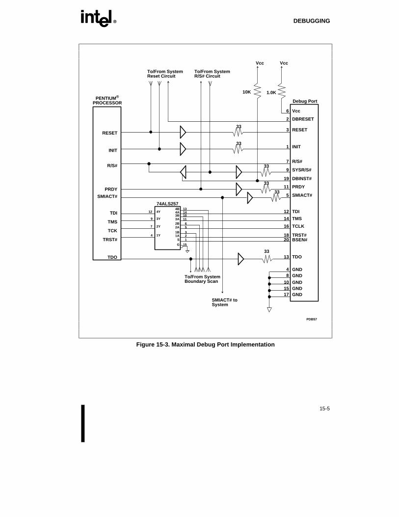
EE DEBUGGING
15-5
PDB57
17
48
1015
GNDGNDGNDGNDGND
Vcc
1.0K
Debug Port
6 Vcc
2 DBRESET
3 RESET
1 INIT
7 R/S#
9 SYSR/S#
19 DBINST#
11 PRDY
PENTIUM®
PROCESSOR
RESET
INIT
R/S#
PRDY
TDI
TMS
TCK
TRST#
TDO
To/From SystemReset Circuit
33
Vcc
10K
To/From SystemR/S# Circuit
33
TDI
TMS
TCLK
TRST#BSEN#
TDO
74ALS257
12
9
7
4
13141011
65
321
15
To/From SystemBoundary Scan
12
14
16
1820
13
SMIACT#533
SMIACT#
SMIACT# toSystem
33
33
33
4B4Y
3Y
2Y
1Y
4A3B3A2B2A
1B1A
S
G
Figure 15-3. Maximal Debug Port Implementation

E16
Future Pentium®
OverDrive®
Processor forPentium Processor(510\60, 567\66)-Based SystemsSocket Specification


EE
16-1
CHAPTER 16FUTURE PENTIUM® OverDrive ® PROCESSORFOR PENTIUM PROCESSOR (510\60, 567\66)-BASED SYSTEMS SOCKET SPECIFICATION
16.1. INTRODUCTIONThe Future Pentium OverDrive processor is an end user single-chip CPU upgrade product forPentium processor (510\60, 567\66)-based systems. The Future Pentium OverDrive processorwill speed up most software applications by 40% to 70%. It is binary compatible with thePentium processor (510\60, 567\66).
An upgrade socket (Socket 4) has been defined along with the Pentium processor (510\60,567\66) as part of the processor architecture. The Future Pentium OverDrive processor will besocket compatible with the Pentium processor (510\60, 567\66). The Future PentiumOverDrive processor is packaged in a 273-pin ceramic pin grid array package with anattached fan/heatsink present on the turbo upgrade processor component.
Execution tracing is not supported in the Future Pentium OverDrive processor, andperformance monitoring is implemented differently than in the Pentium processor (510\60,567\66). Refer to section 16.1.3 .
16.1.1. Upgrade ObjectivesSystems using the Pentium processor (510\60, 567\66) must use Socket 4 to also accept theFuture Pentium OverDrive processor. Inclusion of upgrade Socket 4 in Pentium processor(510\60, 567\66) systems provides the end user with an easy and cost effective way to increasesystem performance. The process of simply installing an upgrade component into an easy touse Zero Insertion Force (ZIF) socket to achieve enhanced system performance is familiar tothe millions of end users and dealers who have purchased Intel Math CoProcessor upgrades toboost system floating-point performance.
Inclusion of Socket 4 in Pentium processor (510\60, 567\66) systems provides the end-userwith an easy and cost-effective way to increase system performance. The paradigm of simplyinstalling an additional component into an easy to use Zero Insertion Force (ZIF) Socket toachieve enhanced system performance is familiar to the millions of end-users and dealers whohave purchased Intel math coprocessor upgrades to boost system floating point performance.
The majority of upgrade installations which take advantage of Socket 4 will be performed byend users and resellers. Therefore, it is important that the design be "end user easy," and thatthe amount of training and technical expertise required to install the upgrade processors beminimized. Upgrade installation instructions should be clearly described in the system user’s

OverDrive ® PROCESSOR SOCKET SPECIFICATION EE
16-2
manual. In addition, by making installation simple and foolproof, PC manufacturers canreduce the risk of system damage, warranty claims and service calls.
Feedback from Intel's Math CoProcessor upgrade customers highlights three maincharacteristics of end user easy designs:
• accessible socket location
• clear indication of upgrade component orientation
• minimization of insertion force
The Future Pentium OverDrive processor will support the Intel 82430 PCIset. Unlike thePentium processor (510\60, 567\66), the Future Pentium OverDrive processor will not supportthe 82496 Cache Controller and 82491 Cache SRAM chip set.
16.1.2. Intel Verification ProgramThe Intel Platform Support Labs ensures that a Pentium processor (510\60, 567\66)-basedpersonal computer meets a minimum set of design criteria for reliable and straightforwardCPU upgradability with the Future Pentium OverDrive processor. Evaluation performed at theIntel Platforms Support Labs confirms that future Pentium OverDrive processor specificationsfor mechanical, thermal, electrical, functional, and end-user installation attributes have beenmet. While system designs may exceed these minimum design criteria, the intent is to provideend-users with confidence that computer systems based on verified designs can be upgradedwith Future Pentium OverDrive processors.
The OEM submits production-ready designs to one of Intel's worldwide Platform SupportLabs for evaluation. The OEM benefits from advance testing of the design prior to availabilityof the Future Pentium OverDrive processor. Section 16.8.2 briefly describes the areas whichwill be evaluated at Intel Platform Support Labs.
Contact your local Intel representative for more information on the Intel Platform SupportLabs for Pentium processor (510\60, 567\66)-based systems.
16.1.3. Functional Differences to the Pentium ® Processor(510\60, 567\66)
16.1.3.1. DEBUG FEATURE DIFFERENCES
The following Pentium processor (510\60, 567\66) features are either not supported orfunctionality has been modified in the Future Pentium OverDrive processor:
• The Pentium processor (510\60, 567\66) IU, IV and IBT functions have been removed.
• The branch trace (BT[3:0]) functions have been removed.
• The breakpoint pins (BP[3:0]) have been redefined such that each assertion of one ofthese pins indicates that 1 to N BP matches occurred, where N = core/bus frequency ratio.

EE OverDrive ® PROCESSOR SOCKET SPECIFICATION
16-3
16.1.3.2. FEATURE ENHANCEMENTS
• The CPUID instruction is used to deliver processor-specific information. The FuturePentium OverDrive processor CPUID status has been extended to supply the pocessortype information which includes "Turbo-Upgrade" classification ("type" field: bits13-12 = 0-1).
31 14 13 12 11 8 7 3
SteppingModelFamily
EAX Bit Assignments for CPUID
Type0 (reserved)
4 0
• STI/CLI latencies are each 2 clocks shorter.
• BIOS should not depend on the internal Future Pentium OverDrive processor cachesbeing identical to those of the Pentium processor (510\60, 567\66) (except for the linesize).
16.2. Future Pentium ® OverDrive ® Processor SocketThe following drawings in Figure 16-1 show the preliminary worst case socket footprintsfrom two qualified Socket 4 vendors, AMP and Yamaichi. OEMs should work directly withsocket vendors for the most current socket information.
To order Socket 4 from AMP and Yamaichi, the phone numbers and part numbers are:
AMP: 1-800-522-6752 Part #: 916510-1Yamaichi: 1-800-769-0797 Part #: NP11J-273K13221
Figure 16-2 shows the Future Pentium OverDrive processor chip's orientation in the Socket 4.
For a complete list of qualified sockets and vendor order numbers, call the Intel Faxbacknumber for your geographical area and have document number 7209 automatically faxed toyou.

OverDrive ® PROCESSOR SOCKET SPECIFICATION EE
16-4
PP0114
Socket 4
Socket 4
Figure 16-1. Socket 4 Footprint Dimensions(See socket manufacturer for the most current information.)
PP0116
AMP Yamaichi
Socket 4
Socket 4
Figure 16-2. Socket 4 Chip Orientation

EE OverDrive ® PROCESSOR SOCKET SPECIFICATION
16-5
16.3. SOCKET 4 PINOUTThe Future Pentium OverDrive processor pinout is identical to that of the Pentium processor(510\60, 567\66). Note that all input pins must meet their A.C./D.C. specifications toguarantee proper functional behavior. Figure 16-3 and Figure 16-4 show the Socket 4 pinout.
Socket 4
Figure 16-3. Socket 4 Pinout (Top View)

OverDrive ® PROCESSOR SOCKET SPECIFICATION EE
16-6
Socket 4
Figure 16-4. OverDrive ® Processor Pinout (Bottom View)
Locations E17, S17 and S5 should be plugged on the Socket 4 in order to ensure that thePentium processor (510\60, 567\66) or OverDrive processor chip is installed in the socketwith the correct orientation.

EE OverDrive ® PROCESSOR SOCKET SPECIFICATION
16-7
16.4. ELECTRICAL SPECIFICATIONSThe Future Pentium OverDrive processor will have the same power and groundspecifications, decoupling recommendations, connection specifications and maximum ratingsas the Pentium processor (510\60, 567\66).
16.4.1. Absolute Maximum Ratings for UpgradeThe on-chip voltage regulation and fan/heatsink devices included on the Future PentiumOverDrive processor require different stress ratings than the Pentium processor (510\60,567\66). The voltage regulator is surface mounted on the Future Pentium OverDrive processorand is, therefore, an integral part of the assembly. The Future Pentium OverDrive processorstorage temperature ratings area tightened as a result. The fan is a detachable unit, and thestorage temperature is stated separately in the table below. Functional operation of the FuturePentium OverDrive processor remains 0°C to 70°C.
Table 16-1. Absolute Maximum Ratings
Future Pentium ® OverDrive ® Processor and Voltage Regulator Assembly:
Parameter Min Max Unit Notes
Storage Temperature -30 100 °C
Case Temperature Under Bias -30 100 °C
Fan:
Parameter Min Max Unit Notes
Storage Temperature -30 75 °C
Case Temperature Under Bias -30 75 °C
WARNING
Stressing the devices beyond the "Absolute Maximum Ratings" may causepermanent damage. These are stress ratings only. Operation beyond the"Operating Conditions" is not recommended and extended exposure beyondthe "Operating Conditions" may affect device reliability.
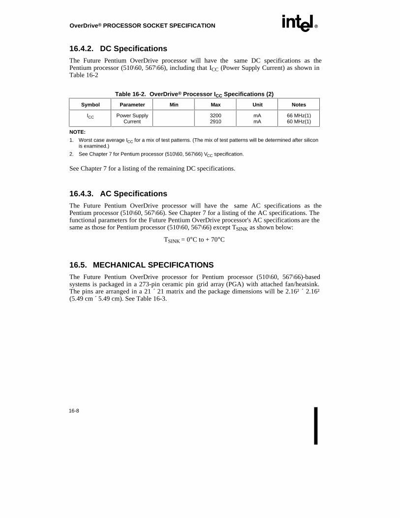
OverDrive ® PROCESSOR SOCKET SPECIFICATION EE
16-8
16.4.2. DC SpecificationsThe Future Pentium OverDrive processor will have the same DC specifications as thePentium processor (510\60, 567\66), including that ICC (Power Supply Current) as shown inTable 16-2
Table 16-2. OverDrive ® Processor I CC Specifications (2)
Symbol Parameter Min Max Unit Notes
ICC Power SupplyCurrent
32002910
mAmA
66 MHz(1)60 MHz(1)
NOTE:
1. Worst case average ICC for a mix of test patterns. (The mix of test patterns will be determined after siliconis examined.)
2. See Chapter 7 for Pentium processor (510\60, 567\66) VCC specification.
See Chapter 7 for a listing of the remaining DC specifications.
16.4.3. AC SpecificationsThe Future Pentium OverDrive processor will have the same AC specifications as thePentium processor (510\60, 567\66). See Chapter 7 for a listing of the AC specifications. Thefunctional parameters for the Future Pentium OverDrive processor's AC specifications are thesame as those for Pentium processor (510\60, 567\66) except TSINK as shown below:
TSINK = 0°C to + 70°C
16.5. MECHANICAL SPECIFICATIONSThe Future Pentium OverDrive processor for Pentium processor (510\60, 567\66)-basedsystems is packaged in a 273-pin ceramic pin grid array (PGA) with attached fan/heatsink.The pins are arranged in a 21 ´ 21 matrix and the package dimensions will be 2.16² ´ 2.16²(5.49 cm ´ 5.49 cm). See Table 16-3.

EE OverDrive ® PROCESSOR SOCKET SPECIFICATION
16-9
Table 16-3. OverDrive ® Processor Package Information Summary
Package Type Total Pins Pin Array Package Size
PGA 273 21 x 21 2.16² x 2.16²(5.49 cm x 5.49 cm)
NOTE: See DC Specifications for more detailed power specifications.
Table 16-4. OverDrive ® Processor Mechanical Specifications
Family: Ceramic Pin Grid Array Package
Symbol Millimeters Inches
Min Max Notes Min Max Notes
A 33.98 Solid Lid 1.338 Solid Lid
A1 2.84 3.50 Solid Lid 0.112 0.138 Solid Lid
A2 0.33 0.43 Solid Lid 0.013 0.017 Solid Lid
A3 2.51 3.07 0.099 0.121
A4 20.32 0.800
A5 10.16 0.400
B 0.43 0.51 0.017 0.020
D 54.61 55.11 2.150 2.170
D1 50.67 50.93 1.995 2.005
E1 2.29 2.79 0.090 0.110
L 3.05 3.30 0.120 0.130
N 273 273
S1 1.65 2.16 0.065 0.085

OverDrive ® PROCESSOR SOCKET SPECIFICATION EE
16-10
Figure 16-5. Processor Package Dimensions
As can be seen in the mechanical dimensions in Table 16-4 and Figure 16-5, the actual heightrequired by the heatsink and fan is less than the total space allotted. Since the Future PentiumOverDrive processor for Pentium processor (510\60, 567\66)-based systems employs afan/heatsink, a certain amount of space is required above the fan/heatsink unit to ensure thatthe airflow is not blocked. Figure 16-6 shows unacceptable blocking of the airflow for theFuture Pentium OverDrive processor fan/heatsink. Figure 16-7 details the minimum spaceneeded around the PGA package to ensure proper heatsink airflow.
As shown in Figure 16-7, it is acceptable to allow any device (i.e., add-in cards, surfacemount device, chassis, etc.) to enter within the free space distance of 0.2² from the PGApackage if it is not taller than the level of the heatsink base. In other words, if a component istaller than height "B," it cannot be closer to the PGA package than distance "A." This appliesto three of the four sides of the PGA package, although the back and handle sides of a ZIFsocket will generally automatically meet this specification since they have widths larger thandistance "A."

EE OverDrive ® PROCESSOR SOCKET SPECIFICATION
16-11
NOT ACCEPTABLE
0.4"Obstruction
Minimum Air Space from Fan/Heatsink
PP0080
Figure 16-6. Fan/Heatsink Top Space Requirements
A
Motherboard
ZIF Socket
Fan/Heatsink Unit
B
Surface MountComponent
A = Space from package (0.2")B = Height from motherboard (Socket Dependent)
PP0081
Figure 16-7. Required Free Space from Sides of PGA Package
16.6. THERMAL SPECIFICATIONSThe fan/heatsink cooling solution will properly cool the Future Pentium OverDrive processoras long as the maximum air temperature entering the fan/heatsink cooling solution (TA(In))does not exceed 45°C. It is left up to the OEM to ensure that TA(In) meets this specificationby providing sufficient airflow around the Future Pentium OverDrive processor heatsink unit.

OverDrive ® PROCESSOR SOCKET SPECIFICATION EE
16-12
Intel's fan/heatsink will dissipate approximately 1W and is powered by the chip such that noexternal wires or connections are required. The extra power needed for the fan/heatsink istaken into account in the ICC numbers of the processor. Additionally, Intel is evaluating thefeasibility of having the Future Pentium OverDrive processor monitor its temperature. NoBIOS or hardware changes will be needed for this thermal protection mechanism. Theshutdown temperature will be greater than the maximum temperature specification of theprocessor. The fan/heatsink unit will be designed to be removable so that if fan failure shouldoccur, the unit may be easily replaced. Figure 16-8 gives a functional representation of theprocessor and fan/heatsink unit. The actual fan/heatsink unit may be different from the oneshown in the figure.
AAAAAAAAAAAAAAAAAAAAAAAAAAAAAAAA
AAAAAAAAAAAAAAAA
AAAAAAAAAAAA
AAAAAAAAAAAA
AAAAAAAAAAAA
AAAAAAAAAAAA
AAAAAAAAAAAA
AAAAAAAAAAAA
AAAAAAAAAAAA
AAAAAAAAAAAA
AAAAAAAAAAAA
AAAAAAAAAAAA
AAAAAAAAAAAA
AAA
AAAAAAAAAAAAAAAAAAAAAAAA
AAAAAAAAAAAAAAAAAAAAAAAA
AAAAAAAAAAAAAAAAAAAAAAAA
AAAAAAAAAAAAAAAAAAAAAAAA
AAAAAAAAAAAAAAAAAAAAAAAA
AAAAAAAAAAAAAAAAAAAAAAAA
AAAAAAAAAAAAAAAAAAAAAAAA
AAAAAAAAAAAAAAAAAAAAAAAA
AAAAAA
AAAAAAAAAAAAAAAAAAAAAAAA
AAAAAAAAAAAAAAAAAAAAAAAA
AAAAAAAAAAAAAAAAAAAAAAAA
AAAAAA
AirflowAirflow
Fan
Heat Sink
Ceramic PGA
Free Space
Figure 16-8. Fan/Heatsink Example
Since the Future Pentium OverDrive processor for Pentium processor (510\60, 567\66)-basedsystems employs a fan/heatsink, it is not as important that the processor heatsink receivedirect airflow, rather that the system has sufficient capability to remove the warm air that theFuture Pentium OverDrive processor will generate. This implies that enough airflow exists atthe Socket 4 to keep localized heating from occurring. This can be accomplished by astandard power supply fan with a clear path to the processor. Figure 16-9 shows how systemdesign can cause localized heating to occur by limiting the airflow in the area of theprocessor. The airflow supplied in the system should also be enough to ensure that the OEMprocessor shipped with the system will meet the OEM processor thermal specifications beforethe system is upgraded with the Future Pentium OverDrive processor.

EE OverDrive ® PROCESSOR SOCKET SPECIFICATION
16-13
Drive Bays Drive Bays
Vents
Vents
Vents
CPU
PowerSupply
PowerSupply
Fan Fan
Good CPU Airflow Poor CPU Airflow
RiserCard
RiserCard
CPU
Adequate venting = good air exchange
Poor venting = poor air exchange
CPU CPU
PP0079
Figure 16-9. Airflow Design Examples
16.7. TESTABILITY
16.7.1. Boundary ScanThe Future Pentium OverDrive processor supports the IEEE Standard 1149.1 boundary scanusing the Test Access Port (TAP) and TAP Controller as described in Chapter 11. Theboundary scan register for the Future Pentium OverDrive processor contains a cell for eachpin. The turbo upgrade component will have a different bit order than the Pentium processor(510\60, 567\66). If the TAP port on your system will be used by an end user followinginstallation of the Future Pentium OverDrive processor, please contact Intel for the bit orderof the OverDrive processor boundary scan register.

OverDrive ® PROCESSOR SOCKET SPECIFICATION EE
16-14
16.8. INTEL PLATFORM SUPPORT LABS CRITERIA
16.8.1. IntroductionThe purpose of this section is to provide the OEM engineers with information regarding theIntel Platform Support Labs and the OverDrive processor upgradability that can beincorporated during the system design and manufacturing phase. The evaluatation criteria ofthe Intel Platform Support Labs for the Future Pentium OverDrive processor for the PentiumProcessor (510\60, 567\66)-based systems are specified in this section. A thorough review ofthe Criteria section is recommended for all engineering groups.
Important Note
The Future Pentium® OverDrive® processor for Pentium processor (510\60,567\66)-based systems does not support subsystems which require 5VCMOS drive levels, such as the 82496 cache controller.
16.8.1.1. RELATED DOCUMENTS
Several other documents are available that will help the engineer understand the IntelPlatform Support Labs and design systems that meet the Intel Platform Support Labsevaluation criteria. These references will provide detailed information required for the systemdesign to support the Future Pentium OverDrive processor. To obtain information regardingthese documents, contact your local Intel field sales representative.
You can also call the Intel Faxback number for your geographical area to obtain any of thesebelow documents that have a Faxback document number next to them. You will be asked toenter the Faxback number for the desired document on a digital touch tone telephone key pad.The Intel Faxback telephone numbers are as follows: 1-916-356-3105 (worldwide), 1-800-628-2283 (U.S. and Canada), or 44(0)793-496646 (Europe).
To obtain documents from Intel Corporation Literature Sales call 1-800-628-8686 and orderthe desired document using the associated Intel literature order number.
Processor Specifications:
• Pentium® Processor Family Developer’s Manual, Volume 3: Architecture andProgramming Manual (Intel Literature Order # 241430)
Intel Platform Support Labs Documentation:
• Intel Platform Support Labs Guide (Faxback document # 7300)
• System Design Checklist (Faxback document # 7307)
• Motherboard Design checklist (Faxback document # 7312)
• List of Qualified Sockets and Vendor Order Numbers (Faxback document # 7209)

EE OverDrive ® PROCESSOR SOCKET SPECIFICATION
16-15
16.8.2. Intel Platform Support Labs Verification CriteriaThe Intel Platform Support Labs helps assure OEMs and PC buyers that their systems meetminimum design criteria for reliable and straightforward CPU upgradability with the FuturePentium OverDrive processor for Pentium processor (510\60, 567\66)-based systems. Thissection specifies the criteria used to evaluate whether systems meet the criteria for the FuturePentium OverDrive processor socket specification.
The Intel Platform Support Labs establishes the minimum system design criteria for FuturePentium OverDrive processor upgradability. The details of the test criteria are described inthe following sections and are divided into five key areas:
End User Installation
Mechanical Specifications
Thermal Specifications
Electrical Specifications
Functional Operation
16.8.2.1. END-USER TEST CRITERIA
One of the key aspects of that upgradability is that it be straightforward and well documentedfor the end user. The end user should be able to open the system, readily locate theCPU\OverDrive processor socket, install the OverDrive processor, close and boot the system,all within a matter of minutes. The criteria that follows provide guidelines to evaluatewhether this has been accomplished.
16.8.2.1.1. Qualified Future Pentium ® OverDrive ® Processor Socket
A system design verified as part of the Intel Platform Support Labs must employ an Intel-qualified OverDrive processor socket:
• Socket 4, 273-hole ZIF (5V only).
16.8.2.1.2. Primary CPU
A system design verified as part of the Intel Platform Support Labs must be shipped with agenuine Intel Pentium processor (510\60, 567\66) as the original CPU.
16.8.2.1.3. Socket Visibility
If Socket 4 is not visible upon opening the system case, simple diagrams or other indicatorsshould be visible upon removal of the system case or clear instructions in the users manualshould guide the user to the CPU/OverDrive processor socket.

OverDrive ® PROCESSOR SOCKET SPECIFICATION EE
16-16
16.8.2.1.4. Socket Accessibility
It is required that the area around the ZIF socket lever be clear for unobstructed operation, toensure proper component removal and insertion, and to reduce possible damage to nearbycomponents during the process. Heatsink clips, when used, must be accessible and must berestrained to prevent the clip from ejecting out of the system if and when tension is released.Substantial force (greater than 10 lbs, 4.5 kg) must not be required to remove (or reinstall) aheatsink clip.
It is required that the upgrade installation not necessitate the end user to remove any cables(disk drive, power, etc.) that are shipped with the system. Removal of I/O cards fromexpansion slots is acceptable.
It is required that no special tools be needed to access the OverDrive processor socket orremove heatsink clips, if used and their removal is necessary for the upgrade installationprocess. Standard screwdrivers (Phillips, slotted) are not considered special tools. If ascrewdriver is required, its use must not jeopardize other components in the system should thetool slip during the process. Torx and Allen wrenches or tools from the OEM only availableafter purchasing the system are considered special tools. If a special tool is necessary, it mustbe shipped with the system and contained inside the chassis.
16.8.2.1.5. Jumper Configuration
End-user configured jumpers are not recommended. Installation of Future Pentium OverDriveprocessor should not require jumper configuration. If jumper changes are required to installthe Future Pentium OverDrive processor, they must be documented in the system End-Usermanual.
16.8.2.1.6. BIOS Changes
The system should not require a BIOS change or additional software (other than a standardsystem configuration utility shipped with the system) are needed to complete the upgrade.Any reconfiguration of the system must be able to be performed with the Future PentiumOverDrive processor installed.
16.8.2.1.7. Documentation
The Intel Platform Support Labs requires that system documentation contains clear andconcise end-user installation instructions for the Future Pentium OverDrive processor. Thesystem must contain the following minimum documentation:
• Installation instructions including illustrations of the system and socket location, whichcontain a clear description of the procedures for safe removal (and re-installation) of theOEM CPU, and operation of heatsink clips, if used. If heatsink clips are used theirremoval is necessary for the upgrade process (a diagram is strongly recommended).
• Pin 1 alignment information. If a heatsink clip is used and its orientation is important forproper operation of the clip, or for meeting verification requirements, this orientationmust be indicated in the event that re-installation of the OEM CPU is required.

EE OverDrive ® PROCESSOR SOCKET SPECIFICATION
16-17
• Jumper locations and settings.
• Warnings which address:
– Required clearance (sections 16.8.2.2.1 and 16.8.2.2.2).
– ESD precautions.
– Powering down the system to allow the chip to cool prior to starting the installationprocess.
• Loss of bus slot information due to processor upgrade (section 16.8.2.2.4) if slots are lost.
• Standard system configuration utility usage if applicable (e.g. EISA systems or systemswith separate configuration utility necessary to configure system).
16.8.2.1.8. Warranty
The Future Pentium OverDrive processor installation must not affect the OEM systemwarranty and should be so stated in the system documentation. Labels on the CPU stating thatthe warranty is void if removed are not permitted.
16.8.2.1.9. Upgrade Removal
The upgrade installation process must be reversible in case of device failure or hardware andsoftware incompatibilities discovered after verification. The end user must be able to installthe original processor with no more than the complexity of the original upgrade process.Reinstallation of the original processor must return the system to its original functionality.The original CPU cooling solution must also return to its original effectiveness.
16.8.2.1.10. Full Configuration
Verification testing requires submission of all motherboard designs configured to a level thatis representative of its ultimate use. As a result, all system designs must be submitted in afully configured state, where fully configured means that all optional proprietary slots,adapters, sockets, or footprints on the motherboard are populated with the options that areintended to be sold with the system or made available after purchase of the system.
16.8.2.2. MECHANICAL SPECIFICATIONS
Mechanical specifications ensure that the Future Pentium OverDrive processor will fitproperly in a system and be afforded the proper clearance for component removal/insertionand proper thermal management.
16.8.2.2.1. Vertical Clearance
The active fan/heatsink on the Future Pentium OverDrive processor requires 0.4" (1.02cm) ofspace above the device for proper airflow. For physical measurements, the clearance areaextends from the socket surface to 1.4" (3.56cm) perpendicular to the socket surface. Therecan be no obstructions in this area. The system must be able to meet this specification in a
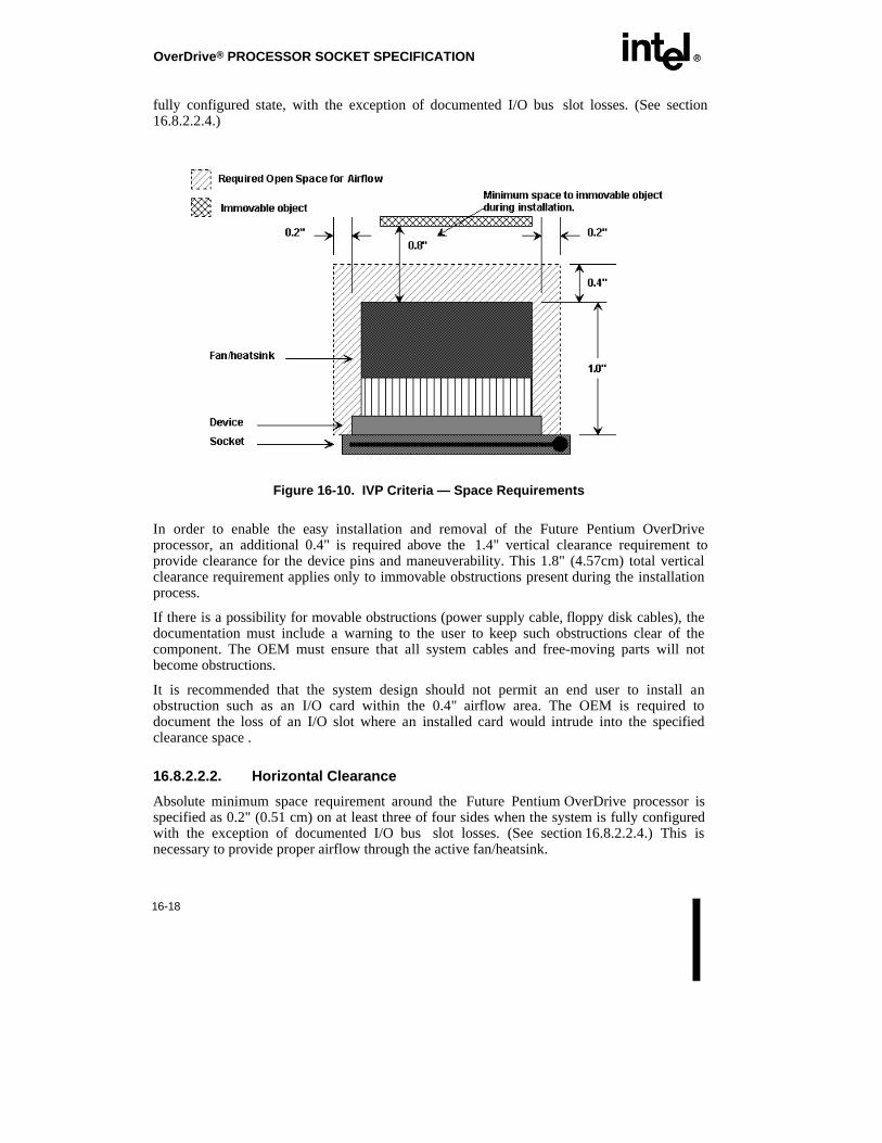
OverDrive ® PROCESSOR SOCKET SPECIFICATION EE
16-18
fully configured state, with the exception of documented I/O bus slot losses. (See section16.8.2.2.4.)
Figure 16-10. IVP Criteria — Space Requirements
In order to enable the easy installation and removal of the Future Pentium OverDriveprocessor, an additional 0.4" is required above the 1.4" vertical clearance requirement toprovide clearance for the device pins and maneuverability. This 1.8" (4.57cm) total verticalclearance requirement applies only to immovable obstructions present during the installationprocess.
If there is a possibility for movable obstructions (power supply cable, floppy disk cables), thedocumentation must include a warning to the user to keep such obstructions clear of thecomponent. The OEM must ensure that all system cables and free-moving parts will notbecome obstructions.
It is recommended that the system design should not permit an end user to install anobstruction such as an I/O card within the 0.4" airflow area. The OEM is required todocument the loss of an I/O slot where an installed card would intrude into the specifiedclearance space .
16.8.2.2.2. Horizontal Clearance
Absolute minimum space requirement around the Future Pentium OverDrive processor isspecified as 0.2" (0.51 cm) on at least three of four sides when the system is fully configuredwith the exception of documented I/O bus slot losses. (See section 16.8.2.2.4.) This isnecessary to provide proper airflow through the active fan/heatsink.

EE OverDrive ® PROCESSOR SOCKET SPECIFICATION
16-19
If there is an obstruction within the 0.2" airflow area on one side of the Future PentiumOverDrive processor, the system design must not permit installation of an obstruction, such asan I/O card, within the 0.2" airflow area on any other side of the Future Pentium OverDriveprocessor.
If there is a possibility for movable obstructions (power supply cables, floppy disk cables,etc.), the documentation must include a warning to the user to keep such obstructions clear ofthe component. The OEM must ensure that all system cables and free-moving parts will notbecome obstructions.
16.8.2.2.3. ZIF Socket Lever Clearance
The ZIF socket lever must operate from a closed position to the fully open position withoutinterference. If the lever action is obstructed or prevented from extending to the full openposition, damage may occur to the OEM CPU or OverDrive processor duringremoval/installation.
16.8.2.2.4. Loss of Local Bus Slot and Expansion Slot
The Future Pentium OverDrive processor is designed to increase the performance of a system;however, installation of the OverDrive processor before installation of other devices (such aslocal bus graphics cards) may prevent the installation of these performance enhancingdevices, thereby decreasing the overall performance of the system. To prevent this fromoccurring, the Intel Platform Support Labs has established the following slot loss criteria forsystem upgrade designs:
All Slots:
• Microchannel, EISA, and ISA slots are defined as I/O slots. VESA Local (VL) and PCIslots are defined as local bus slots.
• Installation of the Future Pentium OverDrive processor must not result in the loss of morethan 50% of the available local bus or expansion slots; see Table 16-5.
• Any slots that are lost as a result of the Future Pentium OverDrive processor installationmust be clearly specified in the OEM documentation. These are counted as lost slots onlyif the slots were usable before the upgrade.
I/O Slots:
• After installation of the Future Pentium OverDrive processor in a system with 1 or moreusable full length expansion slots, a minimum of 1 usable full length I/O slots mustremain.
Local Bus Slots:
• After installation of the Future Pentium OverDrive processor in a system with 1 or moreusable full length local bus slots, a minimum of 1 usable full length local bus slot mustremain.

OverDrive ® PROCESSOR SOCKET SPECIFICATION EE
16-20
Table 16-5. Minimum Number of Slots Available afterOverDrive ® Processor Installation
Total I/O SlotsI/O Slots Available
After Upgrade Total Local Bus SlotsLocal Bus Slots
Available After Upgrade
1 1 1 1
2 1 2 1
3 2 3 2
4 2 4 2
5 3 5 3
6 3 6 3
7 4 7 4
8 4 8 4
16.8.2.3. THERMAL TESTING
Thermal testing is performed to verify that the system has proper thermal management todissipate the heat from the Future Pentium OverDrive processor. Thermal measurementsshould be performed with worst case thermal loading and the maximum system ambienttemperature as specified by the OEM. Worst case thermal loading requires every expansionslot to be populated by the longest add-in card that will fit in each slot without violating therequired clearance for airflow around the OverDrive processor specifies (see sections16.8.2.2.1 and 16.8.2.2.2). Furthermore, the Intel Platform Support Labs requires that eachadd-in card should dissipate the average power for its form factor. For PCI and Microchanneladd-in cards the average power dissipation is 10 Watts. For Full length and 3/4 length ISAcards the average power dissipation is also 10 Watts. For 1/2 length ISA cards the averagepower dissipation is 5 Watts, and the average power dissipation for 1/4 length ISA cards is3.3 Watts. The OEM specified maximum system ambient temperature must be no less than32°C.
The requirement for the Future Pentium OverDrive processor is that the temperature of the airentering the fan/heatsink not exceed 45°C.
16.8.2.4. ELECTRICAL TESTING
The tests performed determine whether the system design meets the specifications andcharacteristics of the OverDrive processor. For active measurements the system should betested after the processor has completed the reset sequence. The system design must meet thespecification under the worst case load and thermal conditions.

EE OverDrive ® PROCESSOR SOCKET SPECIFICATION
16-21
16.8.2.4.1. Vcc Continuity
All V CC pins must be connected to the proper supply. Failure to connect all VCC pins maycause functionality and reliability problems. All pins are checked for a resistance of less than0.5 Ohm to the supply plane.
16.8.2.4.2. Vss Continuity
All V SS pins must be connected to ground. Failure to connect all VSS pins to ground maycause functionality and reliability problems. All pins are checked for a resistance of less than0.5 Ohm to the ground plane.
16.8.2.4.3. Vcc Specification
VCC must meet the Future Pentium OverDrive processor VCC specifications under anyoperating condition.
Table 16-6. Minimum and Maximum V CC Specifications Across Loading Conditions
Loading Conditions Minimum V CC Maximum V CC
Steady State Conditions for 60mhz System Bus
Maximum (2.91A) and Minimum (0A) Icc Load
4.75V 5.25V
Steady State Conditions for 66mhz System Bus
Maximum (3.2A) and Minimum (0A) Icc Load
4.9V 5.4V
Worst Case Load Switch for 60mhz System Bus200mA to 2.91A within 200nS2.91A to 200mA within 200ns
4.75V 5.67V (VCC max + 5%)
Worst Case Load Switch for 66mhz System Bus200mA to 3.2A within 200nS3.2A to 200mA within 200ns
4.75V 5.67V (VCC max + 5%)
16.8.2.4.4. No Connect (NC) and Reserve Pins
There must be no connections to the NC and Reserve pins. Failure to comply may causeproblems due to reserved test features of the Future Pentium OverDrive Processor. All NC andReserve pins are checked for conformity to specification.
16.8.2.4.5. Signal Usage
There are differences in pin usage between the 5V Pentium processor (510\60, 567\66) andthe Future Pentium OverDrive Processor, specifically, the IU, IV and IBT pins. Systemdesigns must not depend on identical behavior (on these pins) to the 5V Pentium processor(510\60, 567\66).

OverDrive ® PROCESSOR SOCKET SPECIFICATION EE
16-22
16.8.2.4.6. Cold RESET Pulse Width
During cold system boot, the RESET signal must be active for a minimum of 1mS to properlysynchronize the internal phase-locked loop. RESET is measured after VCC and CLK reachvalid levels. Failure to meet specification may cause the Future Pentium OverDrive processorto malfunction.
16.8.2.4.7. Warm RESET Pulse Width
If RESET is pulsed for warm reset (instead of INIT), the RESET signal must be active for aminimum of 15 clocks. Failure to meet specification may cause the Future Pentium OverDriveprocessor to malfunction. If INIT is used, it must meet setup and hold times to the CLKsignal.
16.8.2.4.8. CLK Waveform
The input clock waveforms must meet the specifications for the Future Pentium OverDriveprocessor to work properly. Refer to Chapter 7 for the CLK specifications.
16.8.2.4.9. Input Signal Quality
Input signals to the processor must meet the electrical specifications of the Pentium processor(510\60, 567\66). Furthermore, input signals to the processor on input or bi-directional pinsmust meet the ringback specifications for the Pentium processor (510\60, 567\66). Theringback of the input signal as defined in Chapter 7 must not exceed 0.8V.

EE OverDrive ® PROCESSOR SOCKET SPECIFICATION
16-23
16.8.2.4.10. CPUID Instruction
The CPUID instruction allows software like the PC BIOS, to determine the type and featuresof the microprocessor on which it is executing.
When executing CPUID, the Future Pentium OverDrive Processor behaves like the PentiumProcessor:
If the value in EAX is '0' then the 12-byte ASCII string "GenuineIntel" (little endian) isreturned in EBX, EDX, and ECX. Also, a '1' is returned to EAX.
If the value in EAX is '1' then the processor version is returned in EAX and the processorcapabilities are returned in EDX. The values of EAX and EDX for the Future PentiumOverDrive Processor are given below.
If the value in EAX is neither '0' nor '1', the Future Pentium OverDrive Processor writes'0' to all registers.
The following EAX and EDX values are defined for the CPUID instruction executed withEAX = '1'.
The stepping fields has the same format as the Pentium processor’s and will be the same forthe Future Pentium OverDrive Processor. The Pentium Processor (510\60, 567\66) is CPUID= 051xH and the Future Pentium OverDrive Processor is CPUID = 152xH. The type field isdefined as follows:
Table 16-7. EAX Bit Values Definition for CPUID
CPU 31.....14 13.12 11...8 7...4 3...0
Field Definition (reserved) type family model stepping
Pentium® Processor(567\66, 510\60)
(reserved) table 5H 1H (varies)
Future Pentium OverDrive®
Processor(reserved) table 5H 2H (varies)
Table 16-8. EAX Bit Values Definition for Processor Type
Bit 13 Bit 12 Processor Type
0 0 Primary Pentium® Processor
0 1 Future Pentium OverDrive® Processor
1 0 Dual Pentium Processor *
1 1 Reserved
Note: * The Future Pentium® OverDrive® Processor does not support Dual mode.
After masking the reserve bits, the Future Pentium OverDrive Processor will have a value of0x000001BF in the EDX (when APIC is disabled, using APICEN boot pin).

OverDrive ® PROCESSOR SOCKET SPECIFICATION EE
16-24
16.8.2.5. FUNCTIONAL TESTING
Functional testing verifies whether the hardware and firmware are likely to operate properlywith the Future Pentium OverDrive processor. The purpose of the functional testing is touncover hardware or BIOS problems that may exist when the Future Pentium OverDriveprocessor is installed. Areas of testing include checking for BIOS timing loops that may notbehave properly when executed at a significantly higher speed, CPU ID recognition, testregister usage, etc.
16.8.2.5.1. AC Timing Specifications
The system must meet all AC timing specifications as documented in Chapter 7.
16.8.2.5.2. Error-Free Boot
The system must boot properly without error messages when the Future Pentium OverDriveprocessor is installed. There should be no new error messages, beeps or other indications ofanomalous behavior. An exception to this is a message declaring the presence of an“OverDrive processor.” If the system displays the CPU type, then it must display it correctly;otherwise, the CPU type should not be displayed at all.
16.8.2.5.3. Software Compatibility
The system hardware and configuration must not cause any software that operates properlywith the host CPU to not function properly with the OverDrive processor.
16.8.2.5.4. No 5V CMOS Drive Levels
Since the OverDrive processor, unlike the Pentium processor (510\60, 567\66), does notsupport 5V CMOS drive levels, subsystems which require 5V CMOS drive level inputs (suchas the 82496 cache controller) can not be connected to the processor.
16.8.3. Submitting a System to Intel Platform Support LabsTo submit a system design to Intel Platform Support Labs, first obtain a SystemDesignChecklist from your local Intel field sales representative or Intel Faxback (see Section16.8.1.1 for Faxback document information). Next, throughly complete the System DesignChecklist. Send the completed System Design Checklist along with the fully configuredsystem design to Intel Platform Support Lab nearest to your geographical location.

Part II
Pentium® Processor (610\75,735\90, 815\100, 1000\120,
1110\133)

E17
Pinout

EE
17-1
CHAPTER 17PINOUT
The physical pinouts of the Pentium processor (610\75, 735\90, 815\100, 1000\120,1110\133), and the Pentium processor (510\60, 567\66) are different. The Pentium processor(610\75, 735\90, 815\100, 1000\120, 1110\133) uses a 296-pin Staggered PGA package,while the Pentium processor (510\60, 567\66) uses a 273-pin PGA.
17.1. PINOUT AND CROSS REFERENCE TABLESThe text orientation on the top side view drawings in this section represents the orientation ofthe ink mark on the actual packages (Note that the text shown in this section is not the actualtext which will be marked on the packages).

PINOUT EE
17-2
17.1.1. Pinout
12345678910111213141516171819202122232425262728293031323334353637
12345678910111213141516171819202122232425262728293031323334353637
VCC VCC VCC VCC VCC VCC VCC VCC
INCINCINCFLUSH#VCCVCCVCCVCCVCCVCCVCCVCCVCCVCCVCCA10A6NC
ADSC#EADS#W/R#VSSVSSVSSVSSVSSVSSVSSVSSVSSVSSVSSVSSA8A4A30
INCPWTHITM#BUSCHK#BE0#BE2#BE4#BE6#SCYCA20A18A16A14A12A11A7A3
APD/C#HIT#A20M#BE1#BE3#BE5#BE7#CLKRESETA19A17A15A13A9A5A29A28
A25 A31
A26A22
VCC A24 A27
A21VSS
VCC D/P# A23
INTRVSS
VCC R/S# NMI
SMI#VSS
INITIGNNE#VCC
PEN#VSS
FRCMC#VCC
VSS
VCC
STPCLK#VSS
VCC
VSS
NC
VSS
TRST#VCC
TMSVSS
TDOTDI
TCKVSS
PICD1VCC
D0VSS
PICD0D2VCC
PICCLKVSS
D3D1VCC
D5D4
D7D6
DP0 D8 D12 DP1
D9 D10 D14 D17 D21
D11 D13 D16 D20
NC D15 D18 D22 VCC
BREQHLDAADS#
VSSLOCK#
VCCSMIACT#PCD
VSSPCHK#
VCCPBREQ#APCHK#
VSSPBGNT#
VCCPHITM#PRDY
VSSHOLD
VCCPHIT#WB/WT#
VSSBOFF#
VCCBRDYC#NA#
VSSBRDY#
VCCEWBE#KEN#
VSSAHOLD
VCCCACHE#INV
VSSMI/O#
VCCBP2BP3
VSSPM1BP1
VCCPM0BP0FERR#
VSSIERR#
VCCD63DP7
VSSD62
VCCD61D60
VSSD59
VCCD57D58
VSSD56
VCCD55D53
DP6D51DP5
D54D52D49D46D42
D50D48D44D40D39
INCD47D45DP4D38D36
INCD43VSSVSSVSSVSSVSSVSSVSSVSSVSSVSSVSSVSS
D37D35D33DP3D30
D34D32D31D29D27
INCD41VCCVCCVCC
D28
D25
D26
DP2
D23
D24
D19
PE
NT
IUM
® P
RO
CE
SS
OR
(610
\75,
735
\90,
815
\100
, 100
0\12
0, 1
110\
133)
PIN
OU
T T
OP
SID
E V
IEW
VCC
VCC
VCC
VCC
VCC
NC
NC
VCCVSS
NCNC
BF1
BF0
VSS
VSS
VSS
NC
CPUTYP
AN
AM
AL
AK
AJ
AH
AG
AF
AE
AD
AC
AB
AA
Z
Y
X
W
V
U
T
S
R
Q
P
N
M
L
K
J
H
G
F
E
D
C
B
A
AN
AM
AL
AK
AJ
AH
AG
AF
AE
AD
AC
AB
AA
Z
Y
X
W
V
U
T
S
R
Q
P
N
M
L
K
J
H
G
F
E
D
C
B
A
PP0008
Figure 17-1. Pentium ® Processor (610\75, 735\90, 815\100, 1000\120, 1110\133) Pinout —Top Side View

EE PINOUT
17-3
VCCVCCVCCVCCVCCVCCVCCVCC
INC INC INC FLUSH# VCC VCC VCC VCC VCC VCC VCC VCC VCC VCC VCC A10 A6 NC
ADSC# EADS# W/R# VSS VSS VSS VSS VSS VSS VSS VSS VSS VSS VSS VSS A8 A4 A30
INC PWT HITM#BUSCHK#BE0# BE2# BE4# BE6# SCYC A20 A18 A16 A14 A12 A11 A7 A3
AP D/C# HIT# A20M# BE1# BE3# BE5# BE7# CLK RESET A19 A17 A15 A13 A9 A5 A29 A28
A25A31
A26 A22
VCCA24A27
A21 VSS
VCCD/P#A23
INTR VSS
VCCR/S#NMI
SMI# VSS
INIT IGNNE# VCC
PEN# VSS
FRCMC# VCC
VSS
VCC
STPCLK# VSS
VCC
VSS
NC
VSS
TRST# CPUTYP VCC
TMS VSS
TDO TDI
TCK VSS
PICD1 VCC
D0 VSS
PICD0 D2 VCC
PICCLK VSS
D3 D1 VCC
D5 D4
D7 D6
DP0D8D12DP1
D9D10D14D17D21
D11D13D16D20
NCD15D18D22VCC
BREQ HLDA ADS#
VSS LOCK#
VCC SMIACT# PCD
VSS PCHK#
VCC PBREQ#APCHK#
VSS PBGNT#
VCC PHITM# PRDY
VSS HOLD
VCC PHIT# WB/WT#
VSS BOFF#
VCC BRDYC# NA#
VSS BRDY#
VCC EWBE# KEN#
VSS AHOLD
VCC CACHE# INV
VSS MI/O#
VCC BP2 BP3
VSS PM1BP1
VCC PM0BP0FERR#
VSS IERR#
VCC D63 DP7
VSS D62
VCC D61 D60
VSS D59
VCC D57 D58
VSS D56
VCC D55 D53
DP6 D51 DP5
D54 D52 D49 D46 D42
D50 D48 D44 D40 D39
INC D47 D45 DP4 D38 D36
INC D43 VSS VSS VSS VSS VSS VSS VSS VSS VSS VSS VSS VSS
D37 D35 D33 DP3 D30
D34 D32 D31 D29 D27
INC D41 VCC VCC VCC
D28
D25
D26
DP2
D23
D24
D19
VCC
VCC
VCC
VCC
VCC
NC
NC
VCC VSS
BF1 NC
NC
BF0
VSS
VSS
VSS
NC
AN
AM
AL
AK
AJ
AH
AG
AF
AE
AD
AC
AB
AA
Z
Y
X
W
V
U
T
S
R
Q
P
N
M
L
K
J
H
G
F
E
D
C
B
A
1 2 3 4 5 6 7 8 9 10 11 12 13 14 15 16 17 18 19 20 21 22 23 24 25 26 27 28 29 30 31 32 33 34 35 36 37
AN
AM
AL
AK
AJ
AH
AG
AF
AE
AD
AC
AB
AA
Z
Y
X
W
V
U
T
S
R
Q
P
N
M
L
K
J
H
G
F
E
D
C
B
A
1 2 3 4 5 6 7 8 9 10 11 12 13 14 15 16 17 18 19 20 21 22 23 24 25 26 27 28 29 30 31 32 33 34 35 36 37
PP0009
PENTIUM® PROCESSOR(610\75, 735\90, 815\100, 1000\120, 1110\133)
PINOUT PIN SIDE VIEW
Figure 17-2. Pentium ® Processor (610\75, 735\90, 815\100, 1000\120, 1110\133) Pinout —Pin Side View

PINOUT EE
17-4
17.1.2. Pin Cross Reference Table
Table 17-1. Pin Cross Reference by Pin Name
Address
A3 AL35 A9 AK30 A15 AK26 A21 AF34 A27 AG33
A4 AM34 A10 AN31 A16 AL25 A22 AH36 A28 AK36
A5 AK32 A11 AL31 A17 AK24 A23 AE33 A29 AK34
A6 AN33 A12 AL29 A18 AL23 A24 AG35 A30 AM36
A7 AL33 A13 AK28 A19 AK22 A25 AJ35 A31 AJ33
A8 AM32 A14 AL27 A20 AL21 A26 AH34
Data
D0 K34 D13 B34 D26 D24 D39 D10 D52 E03
D1 G35 D14 C33 D27 C21 D40 D08 D53 G05
D2 J35 D15 A35 D28 D22 D41 A05 D54 E01
D3 G33 D16 B32 D29 C19 D42 E09 D55 G03
D4 F36 D17 C31 D30 D20 D43 B04 D56 H04
D5 F34 D18 A33 D31 C17 D44 D06 D57 J03
D6 E35 D19 D28 D32 C15 D45 C05 D58 J05
D7 E33 D20 B30 D33 D16 D46 E07 D59 K04
D8 D34 D21 C29 D34 C13 D47 C03 D60 L05
D9 C37 D22 A31 D35 D14 D48 D04 D61 L03
D10 C35 D23 D26 D36 C11 D49 E05 D62 M04
D11 B36 D24 C27 D37 D12 D50 D02 D63 N03
D12 D32 D25 C23 D38 C09 D51 F04

EE PINOUT
17-5
Table 17-1. Pin Cross Reference by Pin Name (Contd.)
Address
A20M# AK08 BRDYC# Y03 FLUSH# AN07 PEN# Z34
ADS# AJ05 BREQ AJ01 FRCMC# Y35 PM0/BP0 Q03
ADSC# AM02 BUSCHK# AL07 HIT# AK06 PM1/BP1 R04
AHOLD V04 CACHE# U03 HITM# AL05 PRDY AC05
AP AK02 CPUTYP Q35 HLDA AJ03 PWT AL03
APCHK# AE05 D/C# AK04 HOLD AB04 R/S# AC35
BE0# AL09 D/P# AE35 IERR# P04 RESET AK20
BE1# AK10 DP0 D36 IGNNE# AA35 SCYC AL17
BE2# AL11 DP1 D30 INIT AA33 SMI# AB34
BE3# AK12 DP2 C25 INTR/LINT0 AD34 SMIACT# AG03
BE4# AL13 DP3 D18 INV U05 TCK M34
BE5# AK14 DP4 C07 KEN# W05 TDI N35
BE6# AL15 DP5 F06 LOCK# AH04 TDO N33
BE7# AK16 DP6 F02 M/IO# T04 TMS P34
BOFF# Z04 DP7 N05 NA# Y05 TRST# Q33
BP2 S03 EADS# AM04 NMI/LINT1 AC33 W/R# AM06
BP3 S05 EWBE# W03 PCD AG05 WB/WT# AA05
BRDY# X04 FERR# Q05 PCHK# AF04
APIC Clock Control Dual Processor Private Interface
PICCLK H34 CLK AK1 8 PBGNT# AD04
PICD0 J33 BF0 Y33 PBREQ# AE03
[DPEN#] BF1 Y34
STPCLK# V34 PHIT# AA03
PICD1 L35 PHITM# AC03
[APICEN]

PINOUT EE
17-6
Table 17-1. Pin Cross Reference by Pin Name (Contd.)
VCC
A07 A21 G37 N37 U33 AA37 AN09 AN23
A09 A23 J01 Q01 U37 AC01 AN11 AN25
A11 A25 J37 Q37 W01 AC37 AN13 AN27
A13 A27 L01 S01 W37 AE01 AN15 AN29
A15 A29 L33 S37 Y01 AE37 AN17
A17 E37 L37 T34 Y37 AG01 AN19
A19 G01 N01 U01 AA01 AG37 AN21
VSS
B06 B20 K02 R36 X36 AF02 AM12 AM26
B08 B22 K36 T02 Z02 AF36 AM14 AM28
B10 B24 M02 T36 Z36 AH02 AM16 AM30
B12 B26 M36 U35 AB02 AJ37 AM18 AN37
B14 B28 P02 V02 AB36 AL37 AM20
B16 H02 P36 V36 AD02 AM08 AM22
B18 H36 R02 X02 AD36 AM10 AM24
NC/INC
A03 AL01 AN01 AN05 B02 R34 S35 W35
A37 AL19 AN03 AN35 C01 S33 W33
17.2. DESIGN NOTESFor reliable operation, always connect unused inputs to an appropriate signal level. Unusedactive low inputs should be connected to VCC. Unused active HIGH inputs should beconnected to GND (VSS).
No Connect (NC) pins must remain unconnected. Connection of NC pins may result incomponent failure or incompatibility with processor steppings.

EE PINOUT
17-7
17.3. QUICK PIN REFERENCEThis section gives a brief functional description of each of the pins. Note that all input pinsmust meet their AC/DC specifications to guarantee proper functional behavior.
The # symbol at the end of a signal name indicates that the active, or asserted, state occurswhen the signal is at a low voltage. When a # symbol is not present after the signal name, thesignal is active, or asserted, at the high voltage level. Square brackets around a signal nameindicate that the signal is defined only at RESET. See Chapter 23 for the timingrequirements of these signals.
The following pins exist on the Pentium processor (510\60, 567\66) but have been removedfrom the Pentium processor (610\75, 735\90, 815\100, 1000\120, 1110\133):
• IBT, IU, IV, BT0-3
The following pins become I/O pins when two Pentium processor (610\75, 735\90, 815\100,1000\120, 1110\133) are operating in a dual processing environment:
• ADS#, CACHE#, HIT#, HITM#, HLDA#, LOCK#, M/IO, D/C#, W/R#, SCYC
Please refer to Chapter 32 for information how to connect the Pentium processor (610\75,735\90, 815\100, 1000\120, 1110\133) pins if an upgrade socket is designed in the system.

PINOUT EE
17-8
Table 17-2. Quick Pin Reference
Symbol Type* Name and Function
A20M# I When the address bit 20 mask pin is asserted, the Pentium processor (610\75,735\90, 815\100, 1000\120, 1110\133) emulates the address wraparound at 1Mbyte which occurs on the 8086. When A20M# is asserted, the Pentiumprocessor (610\75, 735\90, 815\100, 1000\120, 1110\133) masks physicaladdress bit 20 (A20) before performing a lookup to the internal caches or driving amemory cycle on the bus. The effect of A20M# is undefined in protected mode.A20M# must be asserted only when the processor is in real mode.
A20M# is internally masked by the Pentium processor (610\75, 735\90, 815\100,1000\120, 1110\133) when configured as a Dual processor.
A31-A3 I/O As outputs, the address lines of the processor along with the byte enables definethe physical area of memory or I/O accessed. The external system drives theinquire address to the processor on A31-A5.
ADS# O The address status indicates that a new valid bus cycle is currently being drivenby the Pentium processor (610\75, 735\90, 815\100, 1000\120, 1110\133) .
ADSC# O ADSC# is functionally identical to ADS#.
AHOLD I In response to the assertion of address hold , the Pentium processor (610\75,735\90, 815\100, 1000\120, 1110\133) will stop driving the address lines (A31-A3), and AP in the next clock. The rest of the bus will remain active so data canbe returned or driven for previously issued bus cycles.
AP I/O Address parity is driven by the Pentium processor (610\75, 735\90, 815\100,1000\120, 1110\133) with even parity information on all Pentium processor(610\75, 735\90, 815\100, 1000\120, 1110\133) generated cycles in the sameclock that the address is driven. Even parity must be driven back to the Pentiumprocessor (610\75, 735\90, 815\100, 1000\120, 1110\133) during inquire cycleson this pin in the same clock as EADS# to ensure that correct parity check statusis indicated by the Pentium processor (610\75, 735\90, 815\100, 1000\120,1110\133).
APCHK# O The address parity check status pin is asserted two clocks after EADS# issampled active if the Pentium processor (610\75, 735\90, 815\100, 1000\120,1110\133) has detected a parity error on the address bus during inquire cycles.APCHK# will remain active for one clock each time a parity error is detected(including during dual processing private snooping).
[APICEN]PICD1
I Advanced Programmable Interrupt Controller enable is a new pin thatenables or disables the on-chip APIC interrupt controller. If sampled high at thefalling edge of RESET, the APIC is enabled. APICEN shares a pin with theProgrammable Interrupt Controller Data 1 signal.

EE PINOUT
17-9
Table 17-2. Quick Pin Reference (Contd.)
Symbol Type* Name and Function
BE7#-BE5#BE4#-BE0#
OI/O
The byte enable pins are used to determine which bytes must be written toexternal memory, or which bytes were requested by the CPU for the currentcycle. The byte enables are driven in the same clock as the address lines(A31-3).
Unlike the Pentium processor (510\60, 567\66), the lower four byte enables(BE3#-BE0#) are used on the Pentium processor (610\75, 735\90, 815\100,1000\120, 1110\133) as APIC ID inputs and are sampled at RESET. AfterRESET, these behave exactly like the Pentium processor (510\60, 567\66) byteenables.
In dual processing mode, BE4# is used as an input during flush cycles.
BF[1:0] I Bus Frequency determines the bus-to-core frequency ratio. BF[1:0] is sampledat RESET, and cannot be changed until another non-warm (1 ms) assertion ofRESET. Additionally, BF[1:0] must not change values while RESET is active.For proper operation of the Pentium processor (610\75, 735\90, 815\100,1000\120, 1110\133) these pins should be strapped high or low. When BF0 isstrapped to VCC, the processor will operate at a 2/3 bus/core frequency ratio.When BF0 is strapped to VSS, the processor will operate at a 1/2 bus/corefrequency ratio. If BF0 is left floating, the Pentium processor (610\75, 735\90,815\100, 1000\120, 1110\133) defaults to a 2/3 bus ratio. Note the Pentiumprocessor (610\75, 735\90) will not operate at a 1/2 bus/core frequency ratio. Fordescriptions on BF1 and more detailed information, please refer to section 21.2.7of this document.
BOFF# I The backoff input is used to abort all outstanding bus cycles that have not yetcompleted. In response to BOFF#, the Pentium processor (610\75, 735\90,815\100, 1000\120, 1110\133) will float all pins normally floated during bus hold inthe next clock. The processor remains in bus hold until BOFF# is negated, atwhich time the Pentium processor (610\75, 735\90, 815\100, 1000\120, 1110\133)restarts the aborted bus cycle(s) in their entirety.
BP[3:2]
PM/BP[1:0]
O The breakpoint pins (BP3-0) correspond to the debug registers, DR3-DR0.These pins externally indicate a breakpoint match when the debug registers areprogrammed to test for breakpoint matches.
BP1 and BP0 are multiplexed with the performance monitoring pins (PM1 andPM0). The PB1 and PB0 bits in the Debug Mode Control Register determine ifthe pins are configured as breakpoint or performance monitoring pins. The pinscome out of RESET configured for performance monitoring.
BRDY# I The burst ready input indicates that the external system has presented valid dataon the data pins in response to a read or that the external system has acceptedthe Pentium processor (610\75, 735\90, 815\100, 1000\120, 1110\133) data inresponse to a write request. This signal is sampled in the T2, T12 and T2P busstates.
BRDYC# I This signal has the same functionality as BRDY#.

PINOUT EE
17-10
Table 17-2. Quick Pin Reference (Contd.)
Symbol Type* Name and Function
BREQ O The bus request output indicates to the external system that the Pentiumprocessor (610\75, 735\90, 815\100, 1000\120, 1110\133) has internallygenerated a bus request. This signal is always driven whether or not the Pentiumprocessor (610\75, 735\90, 815\100, 1000\120, 1110\133) is driving its bus.
BUSCHK# I The bus check input allows the system to signal an unsuccessful completion of abus cycle. If this pin is sampled active, the Pentium processor (610\75, 735\90,815\100, 1000\120, 1110\133) will latch the address and control signals in themachine check registers. If, in addition, the MCE bit in CR4 is set, the Pentiumprocessor (610\75, 735\90, 815\100, 1000\120, 1110\133) will vector to themachine check exception.
NOTE: To assure that the BUSCHK# will always be recognized, STPCLK# mustbe deasserted any time BUSCHK# is asserted by the system, before the systemallows another external bus cycle.
If BUSCHK# is asserted by the system for a snoop cycle while STPCLK#remains asserted, usually (if MCE = 1) the processor will vector to the exceptionafter STPCLK# is deasserted. But if another snoop to the same line occurs duringSTPCLK# assertion, the processor can lose the BUSCHK# request.
CACHE# O For Pentium processor (610\75, 735\90, 815\100, 1000\120, 1110\133)-initiatedcycles the cache pin indicates internal cacheability of the cycle (if a read), andindicates a burst writeback cycle (if a write). If this pin is driven inactive during aread cycle, the Pentium processor (610\75, 735\90, 815\100, 1000\120,1110\133) will not cache the returned data, regardless of the state of the KEN#pin. This pin is also used to determine the cycle length (number of transfers in thecycle).
CLK I The clock input provides the fundamental timing for the Pentium processor(610\75, 735\90, 815\100, 1000\120, 1110\133). Its frequency is the operatingfrequency of the Pentium processor (610\75, 735\90, 815\100, 1000\120,1110\133) external bus and requires TTL levels. All external timing parametersexcept TDI, TDO, TMS, TRST#, and PICD0-1 are specified with respect to therising edge of CLK. Note: It is recommended that CLK begin toggling within150ms after V CC reaches its proper operating level. This recommendation isonly to ensure long-term reliability of the device.
CPUTYP I CPU type distinguishes the Primary processor from the Dual processor. In asingle processor environment, or when the Pentium processor (610\75, 735\90,815\100, 1000\120, 1110\133) is acting as the Primary processor in a dualprocessing system, CPUTYP should be strapped to VSS. The Dual processorshould have CPUTYP strapped to VCC. For the future Pentium OverDriveprocessor, CPUTYP will be used to determine whether the bootup handshakeprotocol will be used (in a dual socket system) or not (in a single socket system).
D/C# O The data/code output is one of the primary bus cycle definition pins. It is drivenvalid in the same clock as the ADS# signal is asserted. D/C# distinguishesbetween data and code or special cycles.

EE PINOUT
17-11
Table 17-2. Quick Pin Reference (Contd.)
Symbol Type* Name and Function
D/P# O The dual / primary processor indication. The Primary processor drives this pinlow when it is driving the bus, otherwise it drives this pin high. D/P# is alwaysdriven. D/P# can be sampled for the current cycle with ADS# (like a status pin).This pin is defined only on the Primary processor. Dual processing issupported in a system only if both processors are operating at identicalcore and bus frequencies. Within these restrictions, two processors ofdifferent steppings may operate together in a system.
D63-D0 I/O These are the 64 data lines for the processor. Lines D7-D0 define the leastsignificant byte of the data bus; lines D63-D56 define the most significant byte ofthe data bus. When the CPU is driving the data lines, they are driven during theT2, T12, or T2P clocks for that cycle. During reads, the CPU samples the databus when BRDY# is returned.
DP7-DP0 I/O These are the data parity pins for the processor. There is one for each byte ofthe data bus. They are driven by the Pentium processor (610\75, 735\90,815\100, 1000\120, 1110\133) with even parity information on writes in the sameclock as write data. Even parity information must be driven back to the Pentiumprocessor (610\75, 735\90, 815\100, 1000\120, 1110\133) on these pins in thesame clock as the data to ensure that the correct parity check status is indicatedby the Pentium processor (610\75, 735\90, 815\100, 1000\120, 1110\133). DP7applies to D63-56, DP0 applies to D7-0.
[DPEN#]
PICD0
I/O Dual processing enable is an output of the Dual processor and an input of thePrimary processor. The Dual processor drives DPEN# low to the Primaryprocessor at RESET to indicate that the Primary processor should enable dualprocessor mode. DPEN# may be sampled by the system at the falling edge ofRESET to determine if Socket 5 is occupied. DPEN# shares a pin with PICD0.
EADS# I This signal indicates that a valid external address has been driven onto thePentium processor (610\75, 735\90, 815\100, 1000\120, 1110\133) address pinsto be used for an inquire cycle.
EWBE# I The external write buffer empty input, when inactive (high), indicates that awrite cycle is pending in the external system. When the Pentium processor(610\75, 735\90, 815\100, 1000\120, 1110\133) generates a write, and EWBE# issampled inactive, the Pentium processor (610\75, 735\90, 815\100, 1000\120,1110\133) will hold off all subsequent writes to all E- or M-state lines in the datacache until all write cycles have completed, as indicated by EWBE# being active.
FERR# O The floating point error pin is driven active when an unmasked floating pointerror occurs. FERR# is similar to the ERROR# pin on the Intel387™ mathcoprocessor. FERR# is included for compatibility with systems using DOS-typefloating point error reporting. FERR# is never driven active by the Dualprocessor.

PINOUT EE
17-12
Table 17-2. Quick Pin Reference (Contd.)
Symbol Type* Name and Function
FLUSH# I When asserted, the cache flush input forces the Pentium processor (610\75,735\90, 815\100, 1000\120, 1110\133) to writeback all modified lines in the datacache and invalidate its internal caches. A Flush Acknowledge special cycle willbe generated by the Pentium processor (610\75, 735\90, 815\100, 1000\120,1110\133) indicating completion of the writeback and invalidation.
If FLUSH# is sampled low when RESET transitions from high to low, tristate testmode is entered.
If two Pentium processor (610\75, 735\90, 815\100, 1000\120, 1110\133) areoperating in dual processing mode in a system and FLUSH# is asserted, the Dualprocessor will perform a flush first (without a flush acknowledge cycle), then thePrimary processor will perform a flush followed by a flush acknowledge cycle.
FRCMC# I The functional redundancy checking master/checker mode input is used todetermine whether the Pentium processor (610\75, 735\90, 815\100, 1000\120,1110\133) is configured in master mode or checker mode. When configured as amaster, the Pentium processor (610\75, 735\90, 815\100, 1000\120, 1110\133)drives its output pins as required by the bus protocol. When configured as achecker, the Pentium processor (610\75, 735\90, 815\100, 1000\120, 1110\133)tristates all outputs (except IERR# and TDO) and samples the output pins.
The configuration as a master/checker is set after RESET and may not bechanged other than by a subsequent RESET.
HIT# O The hit indication is driven to reflect the outcome of an inquire cycle. If an inquirecycle hits a valid line in either the Pentium processor (610\75, 735\90, 815\100,1000\120, 1110\133) data or instruction cache, this pin is asserted two clocksafter EADS# is sampled asserted. If the inquire cycle misses the Pentiumprocessor (610\75, 735\90, 815\100, 1000\120, 1110\133) cache, this pin isnegated two clocks after EADS#. This pin changes its value only as a result of aninquire cycle and retains its value between the cycles.
HITM# O The hit to a modified line output is driven to reflect the outcome of an inquirecycle. It is asserted after inquire cycles which resulted in a hit to a modified line inthe data cache. It is used to inhibit another bus master from accessing the datauntil the line is completely written back.
HLDA O The bus hold acknowledge pin goes active in response to a hold request drivento the processor on the HOLD pin. It indicates that the Pentium processor(610\75, 735\90, 815\100, 1000\120, 1110\133) has floated most of the outputpins and relinquished the bus to another local bus master. When leaving bushold, HLDA will be driven inactive and the Pentium processor (610\75, 735\90,815\100, 1000\120, 1110\133) will resume driving the bus. If the Pentiumprocessor (610\75, 735\90, 815\100, 1000\120, 1110\133) has a bus cyclepending, it will be driven in the same clock that HLDA is de-asserted.

EE PINOUT
17-13
Table 17-2. Quick Pin Reference (Contd.)
Symbol Type* Name and Function
HOLD I In response to the bus hold request , the Pentium processor (610\75, 735\90,815\100, 1000\120, 1110\133) will float most of its output and input/output pinsand assert HLDA after completing all outstanding bus cycles. The Pentiumprocessor (610\75, 735\90, 815\100, 1000\120, 1110\133) will maintain its bus inthis state until HOLD is de-asserted. HOLD is not recognized during LOCKcycles. The Pentium processor (610\75, 735\90, 815\100, 1000\120, 1110\133)will recognize HOLD during reset.
IERR# O The internal error pin is used to indicate two types of errors, internal parity errorsand functional redundancy errors. If a parity error occurs on a read from aninternal array, the Pentium processor (610\75, 735\90, 815\100, 1000\120,1110\133) will assert the IERR# pin for one clock and then shutdown. If thePentium processor (610\75, 735\90, 815\100, 1000\120, 1110\133) is configuredas a checker and a mismatch occurs between the value sampled on the pins andthe corresponding value computed internally, the Pentium processor (610\75,735\90, 815\100, 1000\120, 1110\133) will assert IERR# two clocks after themismatched value is returned.
IGNNE# I This is the ignore numeric error input. This pin has no effect when the NE bit inCR0 is set to 1. When the CR0.NE bit is 0, and the IGNNE# pin is asserted, thePentium processor (610\75, 735\90, 815\100, 1000\120, 1110\133) will ignore anypending unmasked numeric exception and continue executing floating pointinstructions for the entire duration that this pin is asserted. When the CR0.NE bitis 0, IGNNE# is not asserted, a pending unmasked numeric exception exists(SW.ES = 1), and the floating-point instruction is one of FINIT, FCLEX, FSTENV,FSAVE, FSTSW, FSTCW, FENI, FDISI, or FSETPM, the Pentium processor(610\75, 735\90, 815\100, 1000\120) will execute the instruction in spite of thepending exception. When the CR0.NE bit is 0, IGNNE# is not asserted, apending unmasked numeric exception exists (SW.ES = 1), and the floating-pointinstruction is one other than FINIT, FCLEX, FSTENV, FSAVE, FSTSW, FSTCW,FENI, FDISI, or FSETPM, the Pentium processor (610\75, 735\90, 815\100,1000\120, 1110\133) will stop execution and wait for an external interrupt.
IGNNE# is internally masked when the Pentium processor (610\75, 735\90,815\100, 1000\120, 1110\133) is configured as a Dual processor.
INIT I The Pentium processor (610\75, 735\90, 815\100, 1000\120, 1110\133)initialization input pin forces the Pentium processor (610\75, 735\90, 815\100,1000\120, 1110\133) to begin execution in a known state. The processor stateafter INIT is the same as the state after RESET except that the internal caches,write buffers, and floating point registers retain the values they had prior to INIT.INIT may NOT be used in lieu of RESET after power up.
If INIT is sampled high when RESET transitions from high to low, the Pentiumprocessor (610\75, 735\90, 815\100, 1000\120, 1110\133) will perform built-in selftest prior to the start of program execution.

PINOUT EE
17-14
Table 17-2. Quick Pin Reference (Contd.)
Symbol Type* Name and Function
INTR / LINT0 I An active maskable interrupt input indicates that an external interrupt has beengenerated. If the IF bit in the EFLAGS register is set, the Pentium processor(610\75, 735\90, 815\100, 1000\120, 1110\133) will generate two locked interruptacknowledge bus cycles and vector to an interrupt handler after the currentinstruction execution is completed. INTR must remain active until the firstinterrupt acknowledge cycle is generated to assure that the interrupt isrecognized.
If the local APIC is enabled, this pin becomes local interrupt 0 .
INV I The invalidation input determines the final cache line state (S or I) in case of aninquire cycle hit. It is sampled together with the address for the inquire cycle inthe clock EADS# is sampled active.
KEN# I The cache enable pin is used to determine whether the current cycle iscacheable or not and is consequently used to determine cycle length. When thePentium processor (610\75, 735\90, 815\100, 1000\120, 1110\133) generates acycle that can be cached (CACHE# asserted) and KEN# is active, the cycle willbe transformed into a burst line fill cycle.
LINT0/INTR I If the APIC is enabled, this pin is local interrupt 0 . If the APIC is disabled, thispin is interrupt .
LINT1/NMI I If the APIC is enabled, this pin is local interrupt 1 . If the APIC is disabled, thispin is non-maskable interrupt .
LOCK# O The bus lock pin indicates that the current bus cycle is locked. The Pentiumprocessor (610\75, 735\90, 815\100, 1000\120, 1110\133) will not allow a bushold when LOCK# is asserted (but AHOLD and BOFF# are allowed). LOCK#goes active in the first clock of the first locked bus cycle and goes inactive afterthe BRDY# is returned for the last locked bus cycle. LOCK# is guaranteed to bedeasserted for at least one clock between back to back locked cycles.
M/IO# O The memory/input-output is one of the primary bus cycle definition pins. It isdriven valid in the same clock as the ADS# signal is asserted. M/IO#distinguishes between memory and I/O cycles.
NA# I An active next address input indicates that the external memory system is readyto accept a new bus cycle although all data transfers for the current cycle havenot yet completed. The Pentium processor (610\75, 735\90, 815\100, 1000\120,1110\133) will issue ADS# for a pending cycle two clocks after NA# is asserted.The Pentium processor (610\75, 735\90, 815\100, 1000\120, 1110\133) supportsup to 2 outstanding bus cycles.
NMI/LINT1 I The non-maskable interrupt request signal indicates that an external non-maskable interrupt has been generated.
If the local APIC is enabled, this pin becomes local interrupt 1 .
PBGNT# I/O Private bus grant is the grant line that is used when two Pentium processor(610\75, 735\90, 815\100, 1000\120, 1110\133) are configured in dual processingmode, in order to perform private bus arbitration. PBGNT# should be leftunconnected if only one Pentium processor (610\75, 735\90, 815\100, 1000\120,1110\133) exists in a system.

EE PINOUT
17-15
Table 17-2. Quick Pin Reference (Contd.)
Symbol Type* Name and Function
PBREQ# I/O Private bus request is the request line that is used when two Pentium processor(610\75, 735\90, 815\100, 1000\120, 1110\133) are configured in dual processingmode, in order to perform private bus arbitration. PBREQ# should be leftunconnected if only one Pentium processor (610\75, 735\90, 815\100, 1000\120,1110\133) exists in a system.
PCD O The page cache disable pin reflects the state of the PCD bit in CR3, the PageDirectory Entry, or the Page Table Entry. The purpose of PCD is to provide anexternal cacheability indication on a page by page basis.
PCHK# O The parity check output indicates the result of a parity check on a data read. It isdriven with parity status two clocks after BRDY# is returned. PCHK# remains lowone clock for each clock in which a parity error was detected. Parity is checkedonly for the bytes on which valid data is returned.
When two Pentium processor (610\75, 735\90, 815\100, 1000\120, 1110\133) areoperating in dual processing mode, PCHK# may be driven two or three clocksafter BRDY# is returned.
PEN# I The parity enable input (along with CR4.MCE) determines whether a machinecheck exception will be taken as a result of a data parity error on a read cycle. Ifthis pin is sampled active in the clock a data parity error is detected, the Pentiumprocessor (610\75, 735\90, 815\100, 1000\120, 1110\133) will latch the addressand control signals of the cycle with the parity error in the machine checkregisters. If, in addition, the machine check enable bit in CR4 is set to "1", thePentium processor (610\75, 735\90, 815\100, 1000\120, 1110\133) will vector tothe machine check exception before the beginning of the next instruction.
PHIT# I/O Private hit is a hit indication used when two Pentium processor (610\75, 735\90,815\100, 1000\120, 1110\133) are configured in dual processing mode, in order tomaintain local cache coherency. PHIT# should be left unconnected if only onePentium processor (610\75, 735\90, 815\100, 1000\120, 1110\133) exists in asystem.
PHITM# I/O Private modified hit is a hit indication used when two Pentium processor(610\75, 735\90, 815\100, 1000\120, 1110\133) are configured in dual processingmode, in order to maintain local cache coherency. PHITM# should be leftunconnected if only one Pentium processor (610\75, 735\90, 815\100, 1000\120,1110\133) exists in a system.
PICCLK I The APIC interrupt controller serial data bus clock is driven into theprogrammable interrupt controller clock input of the Pentium processor(610\75, 735\90, 815\100, 1000\120, 1110\133).
PICD0-1[DPEN#][APICEN]
I/O Programmable interrupt controller data lines 0-1 of the Pentium processor(610\75, 735\90, 815\100, 1000\120, 1110\133) comprise the data portion of theAPIC 3-wire bus. They are open-drain outputs that require external pull-upresistors. These signals share pins with DPEN# and APICEN.

PINOUT EE
17-16
Table 17-2. Quick Pin Reference (Contd.)
Symbol Type* Name and Function
PM/BP[1:0] O These pins function as part of the performance monitoring feature.
The breakpoint 1-0 pins are multiplexed with the performance monitoring 1-0pins. The PB1 and PB0 bits in the Debug Mode Control Register determine if thepins are configured as breakpoint or performance monitoring pins. The pins comeout of RESET configured for performance monitoring.
PRDY O The probe ready output pin indicates that the processor has stopped normalexecution in response to the R/S# pin going active, or Probe Mode being entered.
PWT O The page write through pin reflects the state of the PWT bit in CR3, the PageDirectory Entry, or the Page Table Entry. The PWT pin is used to provide anexternal writeback indication on a page by page basis.
R/S# I The run / stop input is an asynchronous, edge sensitive interrupt used to stop thenormal execution of the processor and place it into an idle state. A high to lowtransition on the R/S# pin will interrupt the processor and cause it to stopexecution at the next instruction boundary.
RESET I RESET forces the Pentium processor (610\75, 735\90, 815\100, 1000\120,1110\133) to begin execution at a known state. All the Pentium processor(610\75, 735\90, 815\100, 1000\120, 1110\133) internal caches will be invalidatedupon the RESET. Modified lines in the data cache are not written back. FLUSH#,FRCMC# and INIT are sampled when RESET transitions from high to low todetermine if tristate test mode or checker mode will be entered, or if BIST will berun.
SCYC O The split cycle output is asserted during misaligned LOCKed transfers to indicatethat more than two cycles will be locked together. This signal is defined for lockedcycles only. It is undefined for cycles which are not locked.
SMI# I The system management interrupt causes a system management interruptrequest to be latched internally. When the latched SMI# is recognized on aninstruction boundary, the processor enters System Management Mode.
SMIACT# O An active system management interrupt active output indicates that theprocessor is operating in System Management Mode (SMM).
STPCLK# I Assertion of the stop clock input signifies a request to stop the internal clock ofthe Pentium processor (610\75, 735\90,815\100, 1000\120) thereby causing thecore to consume less power. When the CPU recognizes STPCLK#, theprocessor will stop execution on the next instruction boundary, unlesssuperseded by a higher priority interrupt, and generate a stop grant acknowledgecycle. When STPCLK# is asserted, the Pentium processor (610\75,735\90,815\100, 1000\120) will still respond to interprocessor and external snooprequests.
TCK I The testability clock input provides the clocking function for the Pentiumprocessor (610\75, 735\90, 815\100, 1000\120, 1110\133) boundary scan inaccordance with the IEEE Boundary Scan interface (Standard 1149.1). It is usedto clock state information and data into and out of the Pentium processor (610\75,735\90, 815\100, 1000\120, 1110\133) during boundary scan.

EE PINOUT
17-17
Table 17-2. Quick Pin Reference (Contd.)
Symbol Type* Name and Function
TDI I The test data input is a serial input for the test logic. TAP instructions and dataare shifted into the Pentium processor (610\75, 735\90, 815\100, 1000\120,1110\133) on the TDI pin on the rising edge of TCK when the TAP controller is inan appropriate state.
TDO O The test data output is a serial output of the test logic. TAP instructions anddata are shifted out of the Pentium processor (610\75, 735\90, 815\100,1000\120, 1110\133) on the TDO pin on TCK's falling edge when the TAPcontroller is in an appropriate state.
TMS I The value of the test mode select input signal sampled at the rising edge of TCKcontrols the sequence of TAP controller state changes.
TRST# I When asserted, the test reset input allows the TAP controller to beasynchronously initialized.
VCC I The Pentium processor (610\75, 735\90, 815\100, 1000\120, 1110\133) has 533.3V power inputs.
VSS I The Pentium processor (610\75, 735\90, 815\100, 1000\120, 1110\133) has 53ground inputs.
W/R# O Write/read is one of the primary bus cycle definition pins. It is driven valid in thesame clock as the ADS# signal is asserted. W/R# distinguishes between writeand read cycles.
WB/WT# I The writeback/writethrough input allows a data cache line to be defined as writeback or write through on a line by line basis. As a result, it determines whether acache line is initially in the S or E state in the data cache.
NOTE:
The pins are classified as Input or Output based on their function in Master Mode. Refer to Chapter 21 forfurther information.

PINOUT EE
17-18
17.4. PIN REFERENCE TABLES
Table 17-3. Output Pins
Name Active Level When Floated
ADS#* Low Bus Hold, BOFF#
ADSC# Low Bus Hold, BOFF#
APCHK# Low
BE7#-BE5# Low Bus Hold, BOFF#
BREQ High
CACHE#* Low Bus Hold, BOFF#
D/P#** n/a
FERR#** Low
HIT#* Low
HITM#* Low
HLDA* High
IERR# Low
LOCK#* Low Bus Hold, BOFF#
M/IO#*, D/C#*, W/R#* n/a Bus Hold, BOFF#
PCHK# Low
BP3-2, PM1/BP1, PM0/BP0 High
PRDY High
PWT, PCD High Bus Hold, BOFF#
SCYC* High Bus Hold, BOFF#
SMIACT# Low
TDO n/a All states except Shift-DR and Shift-IR
NOTES:
All output pins are floated during tristate test mode (except TDO) and checker mode(except IERR# and TDO). There are two pins that have pullups attached during dual processor mode,HIT# and HITM#. These pins are pulled high during tri-state test mode. The pull-up on HITM# has a valueof about 30K ohms, HIT# is about 2K ohms.
* These signals are Input/Output when two Pentium processor (610\75, 735\90, 815\100, 1000\120,1110\133) are operating together in Dual Processing Mode.
** These signals are undefined when the Pentium processor (610\75, 735\90, 815\100, 1000\120, 1110\133)is configured as a Dual processor.

EE PINOUT
17-19
Table 17-4. Input Pins
Name Active LevelSynchronous/Asynchronous Internal Resistor Qualified
A20M#* Low Asynchronous
AHOLD High Synchronous
BF1-0 High Synchronous/RESET Pullup
BOFF# Low Synchronous
BRDY# Low Synchronous Pullup Bus State T2,T12,T2P
BRDYC# Low Synchronous Pullup Bus State T2,T12,T2P
BUSCHK# Low Synchronous Pullup BRDY#
CLK n/a
CPUTYP High Synchronous/RESET
EADS# Low Synchronous
EWBE# Low Synchronous BRDY#
FLUSH# Low Asynchronous
FRCMC# Low Asynchronous Pullup
HOLD High Synchronous
IGNNE#* Low Asynchronous
INIT High Asynchronous
INTR High Asynchronous
INV High Synchronous EADS#
KEN# Low Synchronous First BRDY#/NA#
NA# Low Synchronous Bus State T2,TD,T2P
NMI High Asynchronous
PICCLK High Asynchronous Pullup
PEN# Low Synchronous BRDY#
R/S# n/a Asynchronous Pullup
RESET High Asynchronous
SMI# Low Asynchronous Pullup
STPCLK# Low Asynchronous Pullup

PINOUT EE
17-20
Table 17-4. Input Pins (Contd.)
Name Active LevelSynchronous/Asynchronous Internal Resistor Qualified
TCK n/a Pullup
TDI n/a Synchronous/TCK Pullup TCK
TMS n/a Synchronous/TCK Pullup TCK
TRST# Low Asynchronous Pullup
WB/WT# n/a Synchronous First BRDY#/NA#
NOTE:
*Undefined when the Pentium processor (610\75, 735\90, 815\100, 1000\120, 1110\133) is configured as aDual processor.
Table 17-5. Input/Output Pins
Name Active Level When FloatedQualified
(When an Input)InternalResistor
A31-A3 n/a Address hold, Bus Hold, BOFF# EADS#
AP n/a Address hold, Bus Hold, BOFF# EADS#
BE4#-BE0# Low Bus Hold, BOFF# RESET Pulldown*
D63-D0 n/a Bus Hold, BOFF# BRDY#
DP7-DP0 n/a Bus Hold, BOFF# BRDY#
PICD0[DPEN#] Pullup
PICD1[APICEN] Pulldown
NOTES:
* BE4#-BE0# have Pulldowns during RESET only.
All output and input/output pins are floated during tristate test mode (except TDO) and checker mode (exceptIERR# and TDO). Two pins, PICD0 and PICD1 have a pullup and a pulldown respectively in dual processormode. These pins are pulled high and low respectively during tri-state test mode.
Table 17-6. Interprocessor I/O Pins
Name Active Level Internal Resistor
PHIT# Low Pullup
PHITM# Low Pullup
PBGNT# Low Pullup
PBREQ# Low Pullup
NOTES: For proper inter-processor operation, the system cannot load these signals
PHIT#, PHITM#, PBGNT# and PBREQ# have pullups in dual processor mode. These pins are pulled highduring tri-state test mode. The pullups on these pins have a value of about 30K ohms.

EE PINOUT
17-21
Table 17-7 organizes the pins with respect to their function.
Table 17-7. Pin Functional Grouping
Function Pins
Clock CLK
Initialization RESET, INIT, BF1-0
Address Bus A31-A3, BE7# - BE0#
Address Mask A20M#
Data Bus D63-D0
Address Parity AP, APCHK#
APIC Support PICCLK, PICD0-1
Data Parity DP7-DP0, PCHK#, PEN#
Internal Parity Error IERR#
System Error BUSCHK#
Bus Cycle Definition M/IO#, D/C#, W/R#, CACHE#, SCYC, LOCK#
Bus Control ADS#, ADSC#, BRDY#, BRDYC#, NA#
Page Cacheability PCD, PWT
Cache Control KEN#, WB/WT#
Cache Snooping/Consistency AHOLD, EADS#, HIT#, HITM#, INV
Cache Flush FLUSH#
Write Ordering EWBE#
Bus Arbitration BOFF#, BREQ, HOLD, HLDA
Dual Processing Private Bus Control PBGNT#, PBREQ#, PHIT#, PHITM#
Interrupts INTR, NMI
Floating-Point Error Reporting FERR#, IGNNE#
System Management Mode SMI#, SMIACT#
Functional Redundancy Checking FRCMC# (IERR#)
TAP Port TCK, TMS, TDI, TDO, TRST#
Breakpoint/Performance Monitoring PM0/BP0, PM1/BP1, BP3-2
Clock Control STPCLK#
Miscellaneous Dual Processing CPUTYP, D/P#
Probe Mode R/S#, PRDY

E18
Features of Pentium®
Processor (610\75,735\90, 815\100,1000\120, 1110\133)


EE
18-1
CHAPTER 18Features of Pentium ® processor (610\75, 735\90,
815\100, 1000\120, 1110\133)
The Pentium processor family consists of the new Pentium processor at iCOMP® index610\75 MHz, iCOMP index 735\90 MHz, iCOMP index 815\100 MHz and iCOMP index1000\120 MHz, and iCOMP index 1110\133 MHz (product order code 80502), described inthis document, and the original Pentium processor (510\60, 567\66) (order code 80501). Thename Pentium processor (610\75, 735\90, 815\100, 1000\120, 1110\133) will be used in thisdocument to refer to the Pentium processor at iCOMP index 610\75 MHz, iCOMP index735\90 MHz, iCOMP index 815\100 MHz, iCOMP index 1000\120, and iCOMP index1110\133 MHz. Also, the name "Pentium processor (510\60, 567\66)" will be used to referto the original 60- and 66-MHz version product.
In addition to the architecture described in Chapter 2 for the Pentium processor family, thePentium processor (610\75, 735\90, 815\100, 1000\120, 1110\133) offers the followingenhancements over the Pentium processor (510\60, 567\66):
• iCOMP performance rating of 1110 at 133 MHz in single processor configuration
• iCOMP performance rating of 1000 at 120 MHz in single processor configuration
• iCOMP performance rating of 815 at 100 MHz in single processor configuration
• iCOMP performance rating of 735 at 90 MHz in single processor configuration
• iCOMP performance rating of 610 at 75 MHz in single processor configuration
• Dual processing support
• SL power management features
• Fractional bus operation
• On-chip local APIC device
The Pentium processor (610\75, 735\90, 815\100, 1000\120, 1110\133) offers higherperformance and higher operating frequencies than the Pentium processor (510\60, 567\66).
Pentium ® Processor CoreFrequency External Bus Interface iCOMP ® Index
133 MHz 66 MHz 1110
120 MHz 60 MHz 1000
100 MHz 66/50 MHz 815
90 MHz 60 MHz 735
75 MHz 50 MHz 610

Features of Pentium ® Processors EE
18-2
The Pentium processor (610\75, 735\90, 815\100, 1000\120, 1110\133) includes new featuresto support multi-processor systems, namely an on-chip Advanced Programmable InterruptController (APIC). This APIC implementation supports multiprocessor interruptmanagement (with symmetric interrupt distribution across all processors), multiple I/Osubsystem support, 8259A compatibility, and inter-processor interrupt support.
The dual processor configuration allows two Pentium processor (610\75, 735\90, 815\100,1000\120, 1110\133) to share a single L2 cache for a low-cost symmetric multi-processorsystem. The two processors appear to the system as a single Pentium processor (610\75,735\90, 815\100, 1000\120, 1110\133). Multiprocessor operating systems properly schedulecomputing tasks between the two processors. This scheduling of tasks is transparent tosoftware applications and the end-user. Logic built into the processors support a "glueless"interface for easy system design. Through a private bus, the two Pentium processors (610\75,735\90, 815\100, 1000\120, 1110\133) arbitrate for the external bus and maintain cachecoherency. The Pentium processor (610\75, 735\90, 815\100, 1000\120, 1110\133) can alsobe used in a conventional multi-processor system in which one L2 cache is dedicated to eachprocessor.
In this document, in order to distinguish between two Pentium processors (610\75, 735\90,815\100, 1000\120, 1110\133) in dual processing mode, one CPU will be designated as thePrimary processor with the other being the Dual processor. Note that this is a differentconcept than that of "master" and "checker" processors described in the discussion onfunctional redundancy.
Dual processing is supported in a system only if both processors are operating atidentical core and bus frequencies. Within these restrictions, two processors of differentsteppings may operate together in a system.
The Pentium processor (610\75, 735\90, 815\100, 1000\120, 1110\133) is produced on a 3.3VBiCMOS process. 3.3V operation results in much lower power dissipation in the Pentiumprocessor (610\75, 735\90, 815\100, 1000\120, 1110\133) as compared to the Pentiumprocessor (510\60, 567\66). The Pentium processor (610\75, 735\90, 815\100, 1000\120,1110\133) also includes SL enhanced power management features. When the clock to thePentium processor (610\75, 735\90, 815\100, 1000\120, 1110\133) is stopped, powerdissipation is virtually eliminated. The combination of 3.3V operation and SL enhancedpower management features makes the Pentium processor (610\75, 735\90, 815\100,1000\120, 1110\133) a good choice for energy-efficient desktop designs.
Supporting an upgrade socket (Socket 5/Socket 7) in the system will provide end-userupgradability by the addition of a future Pentium OverDrive processor. Typical applicationswill realize a 40% to 70% performance increase by addition of a Future Pentium OverDriveprocessor.
The Pentium processor (610\75, 735\90, 815\100, 1000\120, 1110\133) supports fractionalbus operation. This allows the internal processor core to operate at high frequencies, whilecommunicating with the external bus at lower frequencies. The Pentium processor 1110\133and 1000\120 support a 1/2 bus/core frequency ratio (a 66-MHz bus frequency for a 133-MHz core, and a 60-MHz bus frequency for a 120-MHz core frequency), the Pentiumprocessor 735\90 supports a 2/3 bus/core frequency ratio (a 60-MHz bus frequency for a 90-MHz core frequency), the Pentium processor 610\75 supports a 2/3 bus/core frequency ratio

EE Features of Pentium ® Processors
18-3
(a 50-MHz bus frequency for a 75-MHz core frequency) while the Pentium processor815\100 supports a selectable bus/core frequency ratio of 2/3 (66-MHz bus, 100-MHz core)or 1/2 (50-MHz bus, 100-MHz core).
18.1. PROCESSOR OBJECTIVESThe Pentium processor (610\75, 735\90, 815\100, 1000\120, 1110\133) is the highestperformance member of the Pentium Processor family. Intel has designed the Pentiumprocessor (610\75, 735\90, 815\100, 1000\120, 1110\133) to allow new systems to bedesigned from Pentium processor (510\60, 567\66) systems with few changes needed to thememory bus. The Pentium processor (610\75, 735\90, 815\100, 1000\120, 1110\133) usesthe Pentium processor (510\60, 567\66) as a core, so both parts behave similarly internallyand on the bus.
A new package allows sufficient pins to support new features, and to allow furtherproliferations in the future.
Intel has designed the Pentium processor (610\75, 735\90, 815\100, 1000\120, 1110\133) ona 3.3V process for higher performance and lower power consumption. The power pins andI/O of the Pentium processor (610\75, 735\90, 815\100, 1000\120, 1110\133) are 3.3V.Pentium processor (510\60, 567\66) systems must accommodate this change to use a Pentiumprocessor (610\75, 735\90, 815\100, 1000\120, 1110\133).
The Primary and Dual processors are designed to operate together "gluelessly" and behavelike a single processor. Although both processors are operating simultaneously and aresharing the same bus, they behave like a single Pentium processor (610\75, 735\90, 815\100,1000\120, 1110\133).
18.2. PENTIUM® PROCESSOR (610\75, 735\90, 815\100, 1000\120,1110\133) DIFFERENCES FROM PENTIUM PROCESSOR(510\60, 567\66)
This section describes the major hardware and software differences between the Pentiumprocessor (510\60, 567\66) and Pentium processor (610\75, 735\90, 815\100, 1000\120,1110\133) to help modify a Pentium processor (510\60, 567\66) system to accommodate aPentium processor (610\75, 735\90, 815\100, 1000\120, 1110\133). This is not a list offeatures. Each difference has a Description and Implications section. The differences aresummarized below:
• Pinout and Package
• CPUTYP Pin
• Up to 133 MHz internal core frequency
• Selectable frequency CPU bus (Pentium processor 815\100)
• 3.3V power supply and I/O

Features of Pentium ® Processors EE
18-4
• Lower power dissipation
• Dual-processor and Socket 5 support
• APIC interrupt controller
• Power management features
• Breakpoint pins
• Hi-Z TAP instruction
• Bus cycles
• HOLD latency
• Interrupt priorities
18.2.1. Pinout and PackageThe signals on the Pentium processor (610\75, 735\90, 815\100, 1000\120, 1110\133) andPentium processor (510\60, 567\66) are almost identical. The VCC pins of the Pentiumprocessor (510\60, 567\66) are now 3.3V supply inputs. A small subset of other pins on thePentium processor (510\60, 567\66) have been defined differently for the Pentium processor(610\75, 735\90, 815\100, 1000\120, 1110\133) to enable new features. The physicalpinouts of the package are different, the Pentium processor (610\75, 735\90, 815\100,1000\120, 1110\133) uses a 296-pin SPGA package, while the Pentium processor (510\60,567\66) uses a 273-lead PGA. See Chapter 17 for details.
Implications
The different pinout results in a different layout from a Pentium processor (510\60, 567\66)-based system. There are several added features that would require the same redesign effortto make those features accessible.
18.2.2. CPUTYP PinThe CPUTYP pin is a new configuration signal which, when sampled by the Pentiumprocessor (610\75, 735\90, 815\100, 1000\120, 1110\133) at the falling edge of RESET,indicates the type of OEM processor which will be placed in each socket site.
For the future Pentium OverDrive processor, CPUTYP will be used to determine whether thebootup handshake protocol will be used (in a dual socket system) or not (in a single socketsystem).
Implications
CPUTYP must be strapped to either VCC or VSS, depending upon one or two sockets andwhich socket site.

EE Features of Pentium ® Processors
18-5
18.2.3. Up To 133-MHz Internal Core FrequencyThe multiplied Internal Core frequency allows the Pentium processor (610\75, 735\90,815\100, 1000\120, 1110\133) to execute instructions faster than the Pentium processor(510\60, 567\66). The Pentium processor (610\75, 735\90, 815\100, 1000\120, 1110\133)multiplies the input clock by a factor of 1.5 or 2 depending on the component, and uses thisas the internal clock. This internal clock can operate up to 133 MHz.
Implications
This increased frequency requires no hardware or software modifications, but will causememory bus utilization to be increased.
18.2.4. Fractional Speed BusThe Pentium processor 815\100 uses the BF pin to select the ratio of the CPU bus/corespeeds. The CLK pin inputs either a 50-MHz or a 66-MHz CPU bus speed. The BF pin isused to select a bus to core ratio of either 1/2 or 2/3. This is explained further in Chapter 19.
Implications
No hardware modifications are necessary. If the BF pin is left floating, like in a systemdesigned around the Pentium processor (510\60, 567\66) pinout, the Pentium processor(610\75, 735\90, 815\100) assumes a 2/3 bus/core ratio. If system software expects a certainCPU frequency or relationship between internal and external frequencies, that software maynot function properly. The Pentium processor (1000\120, 1110\133) only support a 1/2bus/core ratio. Hence the BF pin should be pulled low in this case.
18.2.5. 3.3V and 5V Power SupplyThe Pentium processor (610\75, 735\90, 815\100, 1000\120, 1110\133) requires a voltagerange of 3.135 to 3.6 on all of its VCC inputs. This causes the Pentium processor (610\75,735\90, 815\100, 1000\120, 1110\133) to have input and output levels of 3.3V. However,two clock inputs are 5V safe, CLK and PICCLK. See Chapter 23 for more information.
Implications
The power plane or traces that supply power to the CPU must supply 3.3V. In addition, alldevices that drive signals into the Pentium processor (610\75, 735\90, 815\100, 1000\120,1110\133) must not drive more than 3.3V. Outputs of the Pentium processor (610\75,735\90, 815\100, 1000\120, 1110\133), although only driving to 3.3V levels, meet 5V TTLhigh and low specifications. Since the Pentium processor (610\75, 735\90, 815\100,1000\120, 1110\133) CLK is 5V safe, the CPU may be clocked with a 5V or 3.3V clockdriver.

Features of Pentium ® Processors EE
18-6
18.2.6. Lower Power DissipationThe Pentium processor (610\75, 735\90, 815\100, 1000\120, 1110\133) consumes less powerthan the Pentium processor (510\60, 567\66). Please see Chapter 23 for further information.
Implications
Pentium processor (610\75, 735\90, 815\100, 1000\120, 1110\133) and Pentium processor(510\60, 567\66) thermal solutions are different (refer to Chapter 26 for details).
18.2.7. Dual Processor SupportThe Pentium processor (610\75, 735\90, 815\100, 1000\120, 1110\133) contains logic tointerface to the Dual processor. In a dual-processor system, both the Primary and Dualprocessors connect to the same system signals. There are dedicated pins on each device thatare used for dual-processing communication. See Chapters 18 and 20 for furtherinformation.
Implications
The Dual processor socket (socket 5/socket 7) connects to most signals of the Primaryprocessor. Therefore, timing analysis must be done with processors in both sockets, eachcapable of being a bus master. The dual-processing interface is performed gluelessly;however, the system must use the on-chip APIC in the Primary and Dual processors atbootup time.
18.2.8. Local APIC Interrupt ControllerThe APIC interrupt controller has been included in both the Primary and Dual processor. Itis capable of supporting a multiprocessing interrupt scheme with an external APIC-compatible controller. Refer to Chapter 19.
Implications
If used, the APIC requires that the system supply an I/O APIC-compatible interrupt controller(see the APIC section). Also, system software must be able to support the APIC. If notenabled, the APIC is invisible and interrupts behave like in the Pentium processor (510\60,567\66).

EE Features of Pentium ® Processors
18-7
18.2.9. Power Management FeaturesThe Pentium processor (610\75, 735\90, 815\100, 1000\120, 1110\133) supports SMM andother features similar to the SL Enhanced Intel486 Microprocessor Family. Refer toChapter 30.
Implications
These features are inactive or invisible to the system unless they are specifically used.
18.2.10. Breakpoint PinsBecause of the fractional-speed bus, the Pentium processor (610\75, 735\90, 815\100,1000\120, 1110\133) breakpoint pins BP0-3 are defined differently from the Pentiumprocessor (510\60, 567\66). Each assertion of a Pentium processor (610\75, 735\90, 815\100,1000\120, 1110\133) BP pin indicates that one or more BP matches occurred.
Implications
External breakpoint logic handling of the breakpoint function will have to take this intoaccount. Each assertion of BP may have to be treated differently than in the Pentiumprocessor (510\60, 567\66).
18.2.11. Hi-Z TAP InstructionThe Pentium processor (610\75, 735\90, 815\100, 1000\120, 1110\133) have all of the TAPinstructions of the Pentium processor (510\60, 567\66) plus one additional instruction: Hi-Z.Refer to Chapter 19.
Implications
None.
18.2.12. Bus CyclesThe Pentium processor (610\75, 735\90, 815\100, 1000\120, 1110\133) may initiate buscycles differently than the Pentium processor (510\60, 567\66). This is due mainly to thefractional-speed bus and the dual-processor. Refer to Chapter 19.
Implications
None.

Features of Pentium ® Processors EE
18-8
18.2.13. HOLD LatencyWhen the Pentium processor (610\75, 735\90, 815\100, 1000\120, 1110\133) on-chip APIC isbeing accessed, the CPU will not respond to a HOLD request. Thus HLDA may be delayedby up to 6 clocks.
Implications
HOLD latency is increased (just as if APIC was an external device) which may affect otherbus masters.
18.2.14. Interrupt PrioritiesFour interrupts have different priorities in order to support the I/O Instruction Restart featureof SMM. Refer to section 19.1.6 for details.
Implications
System designers must be aware of the changes to interrupt priorities.
18.3. SUMMARY OF DUAL PROCESSING DIFFERENCES FROMUNI-PROCESSING
The following is a list of bus cycles or bus cycle sequences which would not occur inPentium processor (510\60, 567\66) or Pentium processor (610\75, 735\90, 815\100,1000\120, 1110\133) uni-processor systems, but may be seen in Dual processor systems.Refer to Section 18.2 for a list of Pentium processor (610\75, 735\90, 815\100, 1000\120,1110\133) uni-processor differences to Pentium processor (510\60, 567\66) bus cycles.These two sections form a complete list of dual processing bus differences versus thePentium processor (510\60, 567\66).
• Locked cycle sequences
• Cycle pipe-lining
• Cycle ordering due to BOFF#
• Cache line state
• Back-to-back cycles
• Address parity checking
• Flush cycles
• PCHK# assertion
• Synchronous FLUSH# and RESET
• Floating point error handling
EE Features of Pentium ® Processors
18-9
18.3.1. Locked Cycle Sequences1. Locked read to address X
2. Locked write back to address X
3. Locked read to address X
4. Locked write to address X
May occur due to the inter-processor cache consistency mechanism. Refer to Chapter 20.
Implications
Processor bus hardware needs to handle this locked sequence. The only other time thesystem will see a locked write back is when an external snoop hits a modified line while alocked cycle is in progress (this will occur in a uni-processor or a dual-processor system).
18.3.2. Cycle Pipe-liningInter-processor (Primary/Dual processor) back-to-back write cycles will not be pipe-linedeven if NA# has been asserted. The purpose of this rule is to prevent data bus contentionduring bus arbitration from one processor to the other. In dual processor mode, the Primaryprocessor may pipe-line I/O cycles into I/O cycles from the Dual processor (and vice versa)for any I/O instruction combination (i.e., except I/O writes into writes).
Implications
System hardware designers should be aware of these bus changes.
18.3.3. Cycle Ordering Due to BOFF#Cycle ordering following an assertion of BOFF# may be different between uni-processor anddual processor modes. This occurs when there are pipe-lined cycles from both processors, aBOFF# stalls both cycles, and an external snoop hits a modified line in the LRMs cache.
Implications
System hardware designers should be aware of these bus changes.
18.3.4. Cache Line StateIn Pentium processor (610\75, 735\90, 815\100, 1000\120, 1110\133) uni-processor andPentium processor (510\60, 567\66) systems, if a line is put into the E state by the systemhardware using the WB/WT# signal during the line fill, then all subsequent writes to that linewill be handled internally via the on-chip cache. In dual-processor systems, under certain

Features of Pentium ® Processors EE
18-10
circumstances, even if the system puts a line into the E state using WB/WT#, the dual-processor protocol may force the line to be stored in the S state. Private snooping in dualprocessor systems can also cause a line to be placed into the S or I state.
Implications
There are no system implications. The system may be required to handle writes to a linewhich would not otherwise have been seen.
NOTE
In a dual processing system where NW=1 and CD=1 are set, (i.e., SRAMmode), an inquire cycle will invalidate a cache line with INV on a HIT#.
18.3.5. Back-to-Back CyclesDue to the dual-processor cache consistency protocol, the Primary and Dual processors mayfollow a write to address X with a write back to a 32-byte area which contains X. This willnot occur in uni-processor systems. Also a read to address X may be followed by a writeback to a 32-byte area which contains X.
Implications
There are no system implications.
18.3.6. Address Parity CheckingAddress parity is checked during every private snoop between the Primary and Dualprocessors. Therefore, APCHK# may be asserted due to an address parity error during thisprivate snoop. If an error is detected, APCHK# will be asserted 2 clocks after ADS# for oneprocessor clock period. The system can choose to acknowledge this parity error indication atthis time or do nothing.
Implications
There are no system implications. The system designers get extra address parity checkingwith dual processors due to the automatic private snooping.
18.3.7. Synchronous FLUSH# and RESETWhen the Dual processor is present in Socket 5, the FLUSH# and RESET signals must berecognized by both processors at the same time.

EE Features of Pentium ® Processors
18-11
Implications
FLUSH# and RESET must be asserted on the same clock to both the Primary and Dualprocessors.
18.3.8. PCHK# AssertionIn a dual-processor configuration, there is the possibility that the PCHK# signal can beasserted either 2 OR 3 CLKs following incorrect parity being detected on the data bus. Thisis due to the 2/3 bus to internal clock ratio.
Implications
Chip sets must account for this difference from the Pentium processor (610\75, 735\90,815\100, 1000\120, 1110\133) in their logic or state machines.
18.3.9. Flush CyclesThe Primary and Dual processors incorporate a mechanism to present a unified view of thecache flush operation to the system when in dual processing mode. The Dual processorperforms the cache flush operation first, then grants the bus to the Primary processor. ThePrimary processor flushes its internal caches, and then runs the cache flush special cycle.
Implications
The system hardware must not assert a subsequent FLUSH# to the processors until the flushacknowledge special cycle has completed on the processor bus. The assertion of FLUSH# tothe processors prior to this point would result in a corruption of the dual processing busarbitration state machines.
18.3.10. Floating Point Error HandlingThe Pentium processor (610\75, 735\90, 815\100, 1000\120, 1110\133), when configured as aDual processor, ignores the IGNNE# input. The FERR# output is also undefined in the Dualprocessor.
Implications
None.

Features of Pentium ® Processors EE
18-12
18.4. INTRODUCTION TO DUAL PROCESSOR MODESymmetric dual processing in a system is supported with two Pentium processors (610\75,735\90, 815\100, 1000\120, 1110\133) sharing a single second-level cache. The twoprocessors appear to the system as a single Pentium processor (610\75, 735\90, 815\100,1000\120, 1110\133). Multiprocessor operating systems properly schedule computing tasksbetween the two processors. This scheduling of tasks is transparent to software applicationsand the end-user. Logic built into the processors support a "glueless" interface for easysystem design. Through a private bus, the two Pentium processors (610\75, 735\90, 815\100,1000\120, 1110\133) arbitrate for the external bus and maintain cache coherency.
In this document, in order to distinguish between two Pentium processors (610\75, 735\90,815\100, 1000\120, 1110\133) in dual processing mode, one CPU will be designated as thePrimary processor with the other being the Dual processor. Note that this is a differentconcept than that of "master" and "checker" processors.
The Dual processor is a configuration option of the Pentium processor (610\75, 735\90,815\100, 1000\120, 1110\133). The Dual processor is targeted to operate with up to a 133MHz internal core clock and supports two core/bus ratios: 1/2 and 2/3. The bus frequenciessupported are: 50 MHz, 60 MHz, and 66 MHz.
The Dual processor enables a two-socket system to operate without requiring logic changesto a Pentium processor (510\60, 567\66) memory bus controller. Bus cycles issued by thedual processor pair are compatible with the Pentium processor (510\60, 567\66). Differencesbetween Pentium processor (510\60, 567\66) and dual processor cycles are listed in Sections18.2 and section 18.3.
The Primary and Dual processors include logic to maintain cache consistency between theprocessors and to arbitrate for the common bus. The cache consistency and bus arbitrationactivity will cause the dual processor pair to issue extra bus cycles that will not appear in aPentium processor (610\75, 735\90, 815\100, 1000\120, 1110\133) uniprocessor system.These extra bus cycles are compatible with the equivalent Pentium processor (510\60,567\66) cycles.
Chapter 20 describes in detail how the DP bootup, cache consistency, and bus arbitrationmechanisms operate. The dual processor pair should require little or no logic changes to aPentium processor (510\60, 567\66) memory bus controller. In order to operate properly indual processing mode, the Primary and Dual processors require private APIC, cacheconsistency, and bus arbitration interfaces, as well as a multiprocessing-ready operatingsystem.
The dual processor interface allows the Dual processor to be inserted into Socket 5 for asubstantial increase in system performance. The interface allows the Primary and Dualprocessor to operate in a coherent manner that is transparent to the system.
The memory subsystem transparency was the primary goal of the cache coherency and busarbitration mechanisms. Another goal of the Primary and Dual processors, whether runningindividually or in conjunction, is to behave as similarly to a Pentium processor (510\60,567\66) as possible.

EE Features of Pentium ® Processors
18-13
18.4.1. Dual Processing TerminologyThis section defines some terms used in the following discussions. They are here to ensureyour understanding of the explanations and examples in remainder of this document.
Symmetric Multi-Processing: Two or more processors operating with equal priorities ina system. No individual processor is a master, and none isa slave.
DP or Dual Processing: The Primary and Dual processor operating symmetricallyin a system sharing a second-level cache.
MRM or Most Recent Master: The processor (either the Primary or Dual) which currentlyowns the processor address bus. When interprocessorpipe-lining, this is the processor which last issued anADS#.
LRM or Least Recent Master: The processor (either the Primary or Dual) which does notown the address bus. The LRM automatically snoopsevery ADS# from the MRM processor in order to maintainlevel one cache coherency.
Primary Processor: The Pentium processor (610\75, 735\90, 815\100,1000\120, 1110\133) when CPUTYP = VSS.
Upgrade Processor: The Future Pentium OverDrive processor.
Dual Processor: The Pentium processor (610\75, 735\90, 815\100,1000\120, 1110\133) when CPUTYP = VCC.
OverDrive Processor: The Future Pentium OverDrive processor.
18.4.2. New Pins / Pin ModificationsThe following table outlines pin changes that have been made to the Pentium processor(610\75, 735\90, 815\100, 1000\120, 1110\133) from the Pentium processor (510\60, 567\66)in normal operation:

Features of Pentium ® Processors EE
18-14
Table 18-1. Pentium ® Processor (610\75, 735\90, 815\100, 1000\120, 1110\133) PinDirections vs. Pentium Processor (510\60, 567\66)
Pin Name
Pentium ® Processor(510\60, 567\66)Pin Direction
Pentium Processor(610\75, 735\90, 815\100, 1000\120, 1110\133)
Pin Direction
ADS# Output Input/Output
BE[4:0]# Output Input/Output *
BF n/a Input
BT[3:0] Output n/a
CACHE# Output Input/Output
CPUTYP n/a Input
D/C# Output Input/Output
D/P# n/a Output **
HIT# Output Input/Output
HITM# Output Input/Output
HLDA Output Input/Output
IBT Output n/a
IU Output n/a
IV Output n/a
LOCK# Output Input/Output
M/IO# Output Input/Output
PBGNT# n/a Input/Output
PBREQ# n/a Input/Output
PHIT# n/a Input/Output
PHITM# n/a Input/Output
PICCLK n/a Input
PICD[1:0] n/a Input/Output
SCYC Output Input/Output
STPCLK# n/a Input
W/R# Output Input/Output
NOTE:* BE4#-BE0# are I/O during RESET only.** D/P# is only an Output from the Primary processor

EE Features of Pentium ® Processors
18-15
18.4.3. Dual Processing OverviewThe Primary and Dual processor both have logic built-in to support "glueless" dual-processing behind a shared L2 cache. Through a set of private handshake signals, thePrimary and Dual processors arbitrate for the external bus and maintain cache coherencybetween themselves. The bus arbitration and cache coherency mechanisms allow thePrimary and Dual processors to look like a single Pentium processor (610\75, 735\90,815\100, 1000\120, 1110\133) to the external bus.
The Primary and Dual processors implement a fair arbitration scheme. If the Least RecentMaster (LRM) requests the bus from the Most Recent Master (MRM), the bus is granted.The Pentium processor (610\75, 735\90, 815\100, 1000\120, 1110\133) arbitration schemeprovides no penalty to switch from one master to the next. If pipe-lining is used, the twoprocessors will pipe-line into and out of each other's cycles according to the Pentiumprocessor (510\60, 567\66) specification.
Cache coherency is maintained between the two processors by snooping on every bus access.The LRM must snoop with every ADS# assertion of the MRM. Internal cache states aremaintained accordingly. If an access hits a modified line, a write back is scheduled as thenext cycle in accordance with the Pentium processor (510\60, 567\66) specification.
Using the Dual processor may require special design considerations. Please refer toChapter 20 for more details.
18.4.3.1. CONCEPTUAL OVERVIEW
Dual processing can be viewed in Figure 18-1:
Prim aryProcessor
Processor Bus Interface
PrivateInterface
DualProcessor
PP0010
Figure 18-1. Dual Processors

Features of Pentium ® Processors EE
18-16
The dual processor pair will appear to the system bus as a single, unified processor. Theoperation will be identical to a uni-processor Pentium processor (610\75, 735\90, 815\100,1000\120, 1110\133), except as noted in Section 18.3. The interface shields the systemdesigner from the cache consistency and arbitration mechanisms that are necessary for dualprocessor operation.
Both the Primary and Dual processors contain local APIC modules. The system designer isrecommended to supply an I/O APIC or other multiprocessing interrupt controller in the chipset that interfaces to the local APIC blocks over a three wire bus. The APIC allows directedinterrupts as well as inter-processor interrupts.
The Primary and Dual processors, when operating in dual processing mode, require the localAPIC modules to be hardware enabled in order to complete the bootup handshake protocol.This method is used to "wake up" the Dual processor at an address other than the normalIntel Architecture high memory execution address. On bootup, if the Primary processordetects that a Dual processor is present in Socket 5, the dual processor cache consistency andarbitration mechanisms are automatically enabled. The bootup handshake process issupported in a protocol that is included in the Pentium processor (610\75, 735\90, 815\100,1000\120, 1110\133). See Chapter 19 for more details on the APIC.
18.4.3.2. ARBITRATION OVERVIEW
In the dual processor configuration, there is a single-system bus which provides theprocessors access to the external system. This bus is a single, shared resource.
The dual processor pair will need to arbitrate for use of the system bus as requests aregenerated. The processors implement a fair arbitration mechanism.
If the LRM processor needs to run a cycle on the bus it will submit a request for busownership to the MRM. The MRM processor will grant the LRM processor bus ownership assoon as all outstanding bus requests have finished on the processor bus. The LRM processorwill assume the MRM state, and the processor which was just the MRM, will become theLRM. Figure 18-2 further illustrates this point:

EE Features of Pentium ® Processors
18-17
PP0011
Prim aryProcessor
Bus Cycle Act ive
Bus Re quest DualProcessor
M R M L R M
Prim aryProcessor
Cycle CompletionIndication
Bu s Requ es t DualProcessor
M R M L R M
Prim aryProcessor
New Cycle Starts
Bus Grant D ua lP roce ssor
L R M M R M
(a) (b)
(c)
Figure 18-2. Dual Processor Arbitration Mechanism
Diagram (a) of Figure 18-2 shows a configuration where the Primary processor is in theMRM state and the Dual processor is in the LRM state. The Primary processor is running acycle on the system bus when it receives a bus request from the Dual processor. In diagram(b) of Figure 18-2 the MRM (still the Primary processor) has received an indication that thebus request has finished. The bus ownership has transferred in diagram (c) of Figure 18-2,where the Dual processor is now the MRM. At this point, the Dual processor will start a bustransaction and continue to own the bus until the LRM requests the bus.
18.4.3.3. CACHE COHERENCY OVERVIEW
The Primary and Dual processors both contain an 8 Kbyte instruction cache and an 8 Kbytedata cache. The data cache uses the MESI protocol to enforce cache consistency. A line inthe data cache can be in the Modified, Exclusive, Shared or Invalid state whereas a line inthe instruction cache can be either in the valid or invalid state.
A situation can arise where the Primary and Dual processors are operating in dual processormode with shared code or data. The first level caches will attempt to cache this code anddata whenever possible (as indicated by the page cacheability bits and the cacheability pins).The private cache coherency mechanism guarantees data consistency across the processors.If any data is cached in one of the processors, and the other processor attempts to access thedata, the processor containing the data will notify the requesting processor that it has cached

Features of Pentium ® Processors EE
18-18
the data. The state of the cache line in the processor containing the data will changedepending on the current state and the type of request that the other processor has made.
In some cases the data returned by the system will be ignored. This constraint is placed onthe dual processor cache consistency mechanism so that the dual processor pair will look likea single processor to the system bus. However, in general, bus accesses are minimized toefficiently use the available bus bandwidth.
The basic coherency mechanism requires the processor that is in the LRM state to snoop allMRM bus activity. The MRM processor running a bus cycle will watch the LRM processorfor an indication that the data is contained in the LRM cache. The following diagramsillustrate the basic coherency mechanism.
PP0014
PrimaryProcessor
Modified DataWritten Back
Bus GrantDual
Processor
PA PBBus Request
Processor Bus
PrimaryProcessor
New CycleStarts
DualProcessor
MRM LRM
AutomaticSnoop
PA PB
Processor Bus
PrimaryProcessor
CycleRestarted
DualProcessor
MRM LRM
PA PB
Bus Grant
Processor Bus
PrimaryProcessor
CycleCompletes
Snoop HitIndication
DualProcessor
MRM LRM
PA PBBus Request
Processor Bus
LRM MRM
(a) (b)
(c) (d)
Figure 18-3. Dual Processor L1 Cache Consistency
The series of figures above show an example where the Primary processor (the MRM) isperforming a cache line fill of data. In this example, the data requested by the Primaryprocessor is cached by the Dual processor (the LRM), and is in the modified state.
In diagram (a) of Figure 18-3, the Primary processor has already negotiated with the Dualprocessor for use of the system bus and started a cycle. As the Primary processor startsrunning the cycle on the system bus, the Dual processor processor snoops the transaction.

EE Features of Pentium ® Processors
18-19
The key for the start of the snoop sequence for the LRM processor is an assertion of ADS#by the MRM processor.
Diagram (b) of Figure 18-3 shows the Dual processor indicating to the Primary processorthat the requested data is cached and modified in the Dual processor cache. The snoopnotification mechanism uses a dedicated, two-signal interface that is private to the dualprocessor pair. At the same time that the Dual processor indicates that the transaction iscontained as Modified in the its cache, the Dual processor will request the bus from thePrimary processor (still the MRM). The MRM processor continues with the transaction thatis outstanding on the bus, but will ignore the data returned by the system bus.
After the Dual processor notifies the Primary processor that the requested data is modified inthe Dual processor cache, the Dual processor will wait for the bus transaction to complete.At this point, the LRM/MRM state will toggle, with the Primary processor becoming theLRM processor and the Dual processor becoming the MRM processor. This sequence ofevents is shown in diagram (c) of Figure 18-3.
Diagram (c) of Figure 18-3 also shows the Dual processor writing the data back on thesystem bus. The write back cycle will look like a normal cache line replacement to thesystem bus. The final state of the line in the Dual processor is determined by the value ofthe W/R# pin as sampled during the ADS# assertion by the Primary processor.
Finally, diagram (d) of Figure 18-3 shows the Primary processor re-running the bustransaction that started the entire sequence. The requested data will be returned by thesystem as a normal line fill request without intervention from the LRM processor.

E19
ComponentOperation

EE
19-1
CHAPTER 19COMPONENT OPERATION
19.1. FEATURES AND DIFFERENCESIn addition to the component operation described in Chapter 3 for the Pentium processorfamily, the Pentium processor (610\75, 735\90, 815\100, 1000\120, 1110\133) offersextensions to the Pentium processor (510\60, 567\66) architecture and bus:
• Fractional speed bus
• Selectable buffer sizes
• Power management: I/O instruction restart
• Power management: stop clock and autohalt powerdown
• APIC interrupt controller
• Interrupt priorities
• CPUID instruction operation
• Bus cycle and latency differences
• Breakpoint signals
• New TAP instruction: Hi-Z
19.1.1. Fractional Speed BusThe Pentium processor (610\75, 735\90, 815\100, 1000\120, 1110\133) will be offered inbus/core speed ratios of 66\133 MHz, 60\120 MHz, 66/100 MHz, 50/100 MHz, 60/90 MHz,and 50\75 MHz. The BF configuration pin is provided to support a 2/3 bus/core ratio and a1/2 bus/core ratio. The allowable frequencies of the external bus and the CLK pin are 50MHz, 60 MHz, and 66 MHz. The component will multiply the input CLK to achieve thehigher internal core frequencies.
The external bus frequency is set on power-up RESET through the CLK pin. The Pentiumprocessor (610\75, 735\90, 815\100, 1000\120, 1110\133) will sample the BF pin on thefalling edge of RESET to determine which bus/core ratio to use. If the BF pin is leftunconnected, the Pentium processor (610\75, 735\90, 815\100) assumes the 2/3 ratio. ThePentium processor (1110\133, 1000\120) only supports a 1/2 bus/core ratio. Therefore, theBF pin should be pulled low in this case. BF must not change its value while RESET isactive. Once a frequency is selected, it may not be changed with a warm-reset (15 clocks).Changing this speed or ratio requires a "power-on" RESET pulse initialization.

COMPONENT OPERATION EE
19-2
The BF pin must meet a 1 ms setup time to the falling edge of RESET. Table 19.1summarizes the operation of BF.
Table 19-1. Bus Frequency Selections
BF Clock and Bus Frequency Bus/Core Ratio Core Frequency
0 66 MHz 1/2 133 MHz
0 60 MHz 1/2 120 MHz
0 50 MHz 1/2 100 MHz
1 60 MHz 2/3 90 MHz
1 66 MHz 2/3 100 MHz
Despite a fractional-speed CPU bus, the Pentium processor (610\75, 735\90, 815\100,1000\120, 1110\133) will execute bus cycles according to the Pentium processor (510\60,567\66) bus definition. However, due to the higher core frequency of the Pentium processor(610\75, 735\90, 815\100, 1000\120, 1110\133), some cycles in the CPU may be initiated bythe Pentium processor (610\75, 735\90, 815\100, 1000\120, 1110\133) in an order whichdiffers from a Pentium processor (510\60, 567\66) or from another Pentium processor(610\75, 735\90, 815\100, 1000\120, 1110\133) with a different bus speed selection. Thesecycles are prefetch cycles and write back cycles due to a replacement. These are never snoopwrite back cycles or cycles that could cause read or write reordering. Although the Pentiumprocessor (610\75, 735\90, 815\100, 1000\120, 1110\133) may initiate some cycles in adifferent order, the order of execution of instructions remains the same. The Pentiumprocessor (610\75, 735\90, 815\100, 1000\120, 1110\133) synchronizes the internal buses andCPU buses without synchronization waitstate penalties. This means that if a cycle is pendinginternally, it is driven on the next possible CPU clock (CLK) edge out to the bus. Likewise,if data is available at the pins on the Pentium processor (610\75, 735\90, 815\100, 1000\120,1110\133), it is read on the next possible internal clock edge. This is exactly how thePentium processor (510\60, 567\66), with a synchronous core and bus, operates.
The following examples illustrate the Pentium processor (610\75, 735\90, 815\100, 1000\120,1110\133) synchronization mechanism. The Pentium processor (510\60, 567\66) case isgiven to indicate exactly how a 1/1 bus operates.

EE COMPONENT OPERATION
19-3
Int CLK
Ext CLK
Int Data
Ext Data A
A B
B
Output Input
PP0018
Figure 19-1. Pentium ® Processor (510\60, 567\66) SynchronousInternal/External Data Movement
Int CLK
Ext CLK
A A
A
B
B
Int Data
Ext Data
Int Data
Ext Data
Output
Input
PP0019
A
Figure 19-2. Pentium ® Processor (610\75, 735\90, 815\100, 1000\120, 1110\133)1/2 Bus Internal/External Data Movement
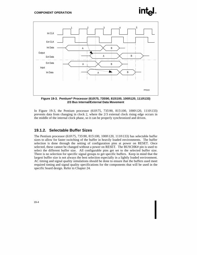
COMPONENT OPERATION EE
19-4
Int CLK
Ext CLK
Int Data
Ext Data
A B
A B
A B
BAInt Data
Ext Data
Output
Input
1 2 3 4 5
PP0020
Figure 19-3. Pentium ® Processor (610\75, 735\90, 815\100, 1000\120, 1110\133)2/3 Bus Internal/External Data Movement
In Figure 19-3, the Pentium processor (610\75, 735\90, 815\100, 1000\120, 1110\133)prevents data from changing in clock 2, where the 2/3 external clock rising edge occurs inthe middle of the internal clock phase, so it can be properly synchronized and driven.
19.1.2. Selectable Buffer SizesThe Pentium processor (610\75, 735\90, 815\100, 1000\120, 1110\133) has selectable buffersizes to allow for faster switching of the buffer in heavily loaded environments. The bufferselection is done through the setting of configuration pins at power on RESET. Onceselected, these cannot be changed without a power on RESET. The BUSCHK# pin is used toselect the different buffer size. All configurable pins get set to the selected buffer size.There is no selection for specific signal groups to get specific buffers. Keep in mind that thelargest buffer size is not always the best selection especially in a lightly loaded environment.AC timing and signal quality simulations should be done to ensure that the buffers used meetrequired timing and signal quality specifications for the components that will be used in thespecific board design. Refer to Chapter 24.

EE COMPONENT OPERATION
19-5
19.1.3. Power Management: I/O Instruction RestartI/O Instruction restart is a power management feature of the Pentium processor (610\75,735\90, 815\100, 1000\120, 1110\133) that allows the Pentium processor (610\75, 735\90,815\100, 1000\120, 1110\133) to re-execute an I/O instruction. In this way, an I/Oinstruction can alert a sleeping device in a system and SMI# can be recognized before the I/Oinstruction is re-executed. SMI# assertion will cause a wake-up routine to be executed, sothe restarted I/O instruction can be executed by the system.
Please reference Chapter 20 of the Pentium® Processor Family Developer’s Manual, Volume3.
19.1.4. Power Management: Stop Clock and AutoHalt PowerdownThe Pentium processor (610\75, 735\90, 815\100, 1000\120, 1110\133) uses stop clock andAutoHalt Powerdown to immediately reduce the power of each device. These features causethe clock to be stopped to most of the CPU's internal units and thus significantly reducepower consumption by the CPU as a whole.
Stop clock is enabled by asserting the STPCLK# pin of the Pentium processor (610\75,735\90, 815\100, 1000\120, 1110\133). While asserted, the Pentium processor (610\75,735\90, 815\100, 1000\120, 1110\133) will stop execution and not service interrupts, but willallow external and interprocessor (Primary and Dual processor) snooping.
AutoHalt Powerdown is entered once the Pentium processor (610\75, 735\90, 815\100,1000\120, 1110\133) executes a HLT instruction. In this state the Pentium processor(610\75, 735\90, 815\100, 1000\120, 1110\133) behaves like it executed a HLT instruction,but most internal units are powered-down. In AutoHalt Powerdown, the Pentium processor(610\75, 735\90, 815\100, 1000\120, 1110\133) will recognize all interrupts and snoops.
Pentium processor (610\75, 735\90, 815\100, 1000\120, 1110\133) pin functions (D/P#, etc.)are not affected by STPCLK# or AutoHalt.
For an extensive explanation of this feature, please reference the Power ManagementSection, Chapter 30, of this document.
19.1.5. APIC Interrupt ControllerThe Advanced Programmable Interrupt Controller (APIC) is an on-chip interrupt controllerthat supports multiprocessing. In a uniprocessor system, APIC may be used as the solesystem interrupt controller, or may be disabled and bypassed completely.
In a multiprocessor system, the APIC operates with an additional and external I/O APICsystem interrupt controller. The dual processor configuration requires that the APIC behardware enabled. The APIC of the Primary and Dual processors are used in the bootupprocedure to communicate startup information. Note: the APIC is not hardware compatiblewith the 82489DX.

COMPONENT OPERATION EE
19-6
On the Pentium processor (610\75, 735\90, 815\100, 1000\120, 1110\133), the APIC uses 3pins: PICCLK, PICD0, and PICD1. PICCLK is the APIC bus clock while PICD0-1 form thetwo-wire communication bus.
To use the 8259A interrupt controller, or to completely bypass, the APIC may be disabledusing the APICEN pin. You must use the local APICs when using the Dual processorcomponent.
19.1.6. Interrupt PrioritiesThe Pentium processor (610\75, 735\90, 815\100, 1000\120, 1110\133) interrupt priorityscheme is different than the Pentium processor (510\60, 567\66) scheme to support newfeatures. The handling of interrupts on the Pentium processor (610\75, 735\90, 815\100,1000\120, 1110\133) can be different than the handling on the Pentium processor (510\60,567\66) because of the priority change. The priority is as follows:
Table 19-2. Pentium ® Processor (610\75, 735\90, 815\100, 1000\120, 1110\133)Interrupt Priority Scheme
ITR = 0 (default) ITR = 1
1. Breakpoint (INT 3) Breakpoint (INT 3)
2. BUSCHK# BUSCHK#
3. Debug Traps (INT 1) FLUSH#
4. R/S# SMI#
5. FLUSH# Debug Traps (INT 1)
6. SMI# R/S#
7. INIT INIT
8. NMI NMI
9. INTR INTR
10. Floating-Point Error Floating-Point Error
11. STPCLK# STPCLK#
12. Faults on Next Instruction Faults on Next Instruction
Note: ITR is bit 9 of the TR12 register

EE COMPONENT OPERATION
19-7
19.1.7. CPUID InstructionThe CPUID instruction allows software to determine the type and features of themicroprocessor on which it is executing.
When executing CPUID, the Pentium processor (610\75, 735\90, 815\100, 1000\120,1110\133) behaves like the Pentium processor (510\60, 567\66) :
• If the value in EAX is "0" then the 12-byte ASCII string "GenuineIntel" (little endian) isreturned in EBX, EDX, and ECX. Also, EAX contains a value of "1" to indicate thelargest value of EAX which should be used when executing CPUID.
• If the value in EAX is "1" then the processor version is returned in EAX and theprocessor capabilities are returned in EDX. The value of EAX for the Pentium processor(610\75, 735\90, 815\100, 1000\120, 1110\133) is given below.
• If the value in EAX is neither "0" nor "1", the Pentium processor (610\75, 735\90,815\100, 1000\120, 1110\133) writes "0" to EAX, EBX, ECX, and EDX.
For more information on values in the EDX register, see Appendix A.
The following EAX value is defined for the CPUID instruction executed with EAX = 1.
The processor version EAX bit assignments are given in figure Figure 19-4.
03478111213
steppingmodelfamilytype
31
0 (reserved)
14
Figure 19-4. EAX Bit Assignments for CPUID
The family field is the same as the Pentium processor (510\60, 567\66) (e.g., family = 5H).The model value is 2H. The stepping field has the same format as the Pentium processor(510\60, 567\66) (see Pentium processor (610\75, 735\90, 815\100, 1000\120, 1110\133)Specification Update). The Future Pentium OverDrive processor will not have the samevalues in EAX as the Pentium processor (610\75, 735\90, 815\100, 1000\120, 1110\133). Thetype field is defined as follows:
Table 19-3. EAX Type Field Values
Bit 13 Bit 12 Processor Type
0 0 Primary Pentium® processor (610\75, 735\90,815\100, 1000\120, 1110\133)
0 1 Future Pentium OverDrive® processor
1 0 Dual Pentium processor (610\75, 735\90, 815\100,1000\120, 1110\133)
1 1 Reserved

COMPONENT OPERATION EE
19-8
19.1.8. Bus Cycle and Latency DifferencesThe Pentium processor (610\75, 735\90, 815\100, 1000\120, 1110\133) may initiate cycles tothe bus in a different order than the Pentium processor (510\60, 567\66), or produce differenttypes of cycles. This is due to two architectural differences: 1), the fractional-speed bus, and2), a dual processor configuration. All of the dual processor configuration differences arelisted in Chapter 20.
Because of the fractional-speed bus, the Pentium processor (610\75, 735\90, 815\100,1000\120, 1110\133) bus scheduler can schedule cycles in an order and number which differfrom the Pentium processor (510\60, 567\66) operation.
While the Pentium processor (610\75, 735\90, 815\100, 1000\120, 1110\133) is accessing thelocal APIC, the processor will delay a HOLD request by up to 6 CLKs. To external agentswhich are not aware of the APIC bus, this looks like the Pentium processor (610\75, 735\90,815\100, 1000\120, 1110\133) is not responding to HOLD even though ADS# has not beendriven and the processor seems idle.
While accessing the APIC, the address and control pins of the Pentium processor (610\75,735\90, 815\100, 1000\120, 1110\133) may toggle without ADS#.
Because of the difference in interrupt priority schemes between the Pentium processor(610\75, 735\90, 815\100, 1000\120, 1110\133) and the Pentium processor (510\60, 567\66),the Pentium processor (610\75, 735\90, 815\100, 1000\120, 1110\133) may respond tomultiple interrupts in a different order than the Pentium processor (510\60, 567\66) .
19.1.9. Breakpoint SignalsBecause of the fractional-speed bus, the Pentium processor (610\75, 735\90, 815\100,1000\120, 1110\133) breakpoint pins BP0-3 are defined differently from the Pentiumprocessor (510\60, 567\66). Each assertion of a Pentium processor (610\75, 735\90, 815\100,1000\120, 1110\133) BP pin indicates that one or more BP matches occurred. The maximumnumber of matches per assertion is 2 when using the 1/2 bus/core fraction. This is differentfrom the Pentium processor (510\60, 567\66) which will only get a single match per clock.
19.1.10. New Tap Instruction: Hi-ZThe Pentium processor (610\75, 735\90, 815\100, 1000\120, 1110\133) has the same TAPinstructions as the Pentium processor (510\60, 567\66) plus one additional instruction: Hi-Z.
Instruction TAP Encoding
Hi-Z XXXXXXXX1011
The TAP Hi-Z instruction causes all outputs and I/Os of the Pentium processor (610\75,735\90, 815\100, 1000\120, 1110\133) to go to a high-impedance state (float) immediately.

EE COMPONENT OPERATION
19-9
The Hi-Z state is terminated by either resetting the TAP with the TRST# pin, by issuinganother TAP instruction, or by entering the Test_Logic_Reset state.
The Hi-Z state is enabled or disabled on the first TCK clock after the TAP instruction hasentered the UPDATE-IR state of the TAP control state machine.
This instruction overrides all other bus cycles. Resetting the Pentium processor (610\75,735\90, 815\100, 1000\120, 1110\133) will not disable this instruction since CPU RESETdoes not reset the TAP.
19.2. APIC INTERRUPT CONTROLLERThe Pentium processor (610\75, 735\90, 815\100, 1000\120, 1110\133) containsimplementations of the Advanced Programmable Interrupt Controller architecture. Theseimplementations are capable of supporting a multiprocessing interrupt scheme with anexternal APIC-compatible controller. The main features of the APIC architecture include:
• Multiprocessor interrupt management (static and dynamic symmetric interruptdistribution across all processors)
• Dynamic interrupt distribution that includes routing interrupts to the lowest-priorityprocessor
• Inter-processor interrupt support
• Edge or level triggered interrupt programmability
• Various naming/addressing schemes
• System-wide processor control functions related to NMI, INIT, and SMI (see Chapter 30for APIC handling of SMI)
• 8259A compatibility by becoming virtually transparent with regard to an externallyconnected 8259A style controller, making the 8259A visible to software
• A 32-bit wide counter used as a timer to generate time slice interrupts local to thatprocessor.
The AC timings of the Pentium processor (610\75, 735\90, 815\100, 1000\120, 1110\133)APIC are described in Chapter 23 of this document. Note that while there are minor softwaredifferences from the 82489DX, programming to the integrated APIC model ensurescompatibility with the external 82489DX. For additional APIC programming information,please refer to the MultiProcessor Specification, Order Number 242016.
In a dual-processor configuration, the local APIC may be used with an additional devicesimilar to the I/O APIC. The I/O APIC is a device which captures all system interrupts anddirects them to the appropriate processors via various programmable distribution schemes.An external device provides the APIC system clock. Interrupts which are local to each CPUgo through the APIC on each chip. A system example is shown in Figure 19-5.

COMPONENT OPERATION EE
19-10
Local
APIC
LocalInterrupts
Pentium® Processor(610\75, 735\90,
815\100, 1000\120,1110\133)
Local
APIC
I/O APIC
PICD1PICD0PICCLK
System I/OInterrupts
16
8259A
3.3VLINT0
LINT1
LINT0
LINT1
CLKGenerator
DualProcessor
LocalInterrupts
PP0022
Figure 19-5. APIC System Configuration
The APIC devices in the Primary and Dual processors may receive interrupts from the I/OAPIC via the three-wire APIC bus, locally via the local interrupt pins (LINT0, LINT1), orfrom the other processor via the APIC bus. The local interrupt pins, LINT0 and LINT1, areshared with the INTR and NMI pins, respectively. When the APIC is bypassed (hardwaredisabled) or programmed in "through local" mode, the 8259A interrupt (INTR) and NMI areconnected to the INTR/LINT0 and NMI/LINT1 pins of the processor. Figure 19-6 shows theAPIC implementation in the Pentium processor (610\75, 735\90, 815\100, 1000\120,1110\133). Note that the PICCLK has a maximum frequency of 16.67 MHz.
When the local APIC is hardware enabled, data memory accesses to its 4 KByte addressspace are executed internally and do not generate an ADS# on the processor bus. However, acode memory access in the 4 KByte APIC address space will not be recognized by the APICand will generate a cycle on the processor bus.
NOTE
Internally executed data memory accesses may cause the address bus totoggle even though no ADS# is issued on the processor bus.

EE COMPONENT OPERATION
19-11
Local APIC
Module
APIC Enable
PICCLKPICD0PICD1
LINT0/INTR
INIT
LINT1/NMI
SMI#
Pentium® Processor (610\75, 735\90, 815\100, 1000\120, 1110\133)
PP0023
Pentium Processor
(610\75, 735\90, 815\100, 1000\120, 1110\133)
Interrupt Logic
Figure 19-6. Local APIC Interface
19.2.1. APIC Configuration ModesThere are four possible APIC Modes:
1. Normal mode
2. Bypass mode (hardware disable).
3. Through local mode.
4. Masked mode (software disable).
19.2.1.1. NORMAL MODE
This is the normal operating mode of the local APIC. When in this mode, the local APIC isboth hardware and software enabled.

COMPONENT OPERATION EE
19-12
19.2.1.2. BYPASS MODE
Bypass mode effectively removes (bypasses) the APIC from the Pentium processor (610\75,735\90, 815\100, 1000\120, 1110\133) causing it to operate as if there were no APIC present(i.e., like a Pentium processor (510\60, 567\66)). Any accesses to the APIC address spacewill go to memory. APICEN is sampled at the falling edge of RESET, and later becomes thePICD1 (part of the APIC 3-wire bus) signal. Bypass mode is entered by driving APICEN lowat the falling edge of RESET. Since the APIC must be used to enable the Dual processorafter RESET, PICD1 must be driven high at reset to ensure APIC is hardware enabled if asecond processor is present.
For hardware disabling operations, the following implications must be considered:
1. The INTR and NMI pins become functionally equivalent to the corresponding interruptpins in the Pentium processor, and the APIC is bypassed.
2. The APIC PICCLK must be tied high.
3. The system will not operate with the Dual Processor if the local APIC is hardwaredisabled.
19.2.1.3. THROUGH LOCAL MODE
Configuring in through local mode allows the APICs to be used for the dual-processor bootuphandshake protocol and then pass interrupts through the local APIC to the core to support anexternal interrupt controller.
To use the through local mode of the local APIC, the APIC must be enabled in both hardwareand software. This is done by programming two local vector table entries, LVT1 and LVT2at addresses 0FEE00350H and 0FEE00360H, as external interrupts (ExtInt) and NMI,respectively. The 8259A responds to the INTA cycles and returns the interrupt vector to theprocessor.
The local APIC should not be sent any interrupts prior to it's being programmed. Once theAPIC is programmed it can receive interrupts.
Note that although external interrupts and NMI are passed through the local APIC to thecore, the APIC can still receive messages on the APIC bus.
19.2.1.4. MASKED MODE
The local APIC is initialized to masked mode once hardware enabled via the APICEN pin.In order to be programmed in normal or through local modes, the APIC must be "softwareenabled." Once operating in normal mode or through local mode, the APIC may be disabledby software through clearing bit 8 of the APIC's spurious vector interrupt register (Note:this register is normally cleared at RESET and INIT). This register is at address0FEE000F0H. Disabling APIC in software will return it to Masked mode. With theexception of NMI, SMI, INIT, remote reads and the startup IPI, all interrupts are masked onthe APIC bus. The local APIC does not accept any interrupts on LINT0 or LINT1. See thefollowing section for software disabling implications.

EE COMPONENT OPERATION
19-13
19.2.1.4.1. Software Disabling Implications
For the software disabling operations, the following implications must be considered:
1. The 4 KByte address space for the APIC is always blocked for data accesses (i.e.,external memory in this region must not be accessed).
2. The interrupt control register (ICR) can be read and written (e.g. interprocessor interruptsare sent by writing to this register).
3. The APIC can continue to receive SMI, NMI, INIT, "startup," and remote read messages.
4. Local interrupts are masked.
5. Software can enable/disable the APIC at any time. After software disabling the localAPICs, pending interrupts must be handled or masked by software.
6. The APIC PICCLK must be driven at all times.
19.2.1.5. DUAL PROCESSING WITH THE LOCAL APIC
The Dual processor bootup protocol may be used in the normal, through local, or maskedmodes.
19.2.2. Loading the APIC IDThe local APIC module on the Pentium processor (610\75, 735\90, 815\100, 1000\120,1110\133) loads its 4-bit APIC ID value from four pins at the falling edge of RESET. Thefollowing table shows the four pins that comprise the APIC ID:
Table 19-4. APIC ID
APIC IDRegister Bit
Pin Latchedat RESET
bit 24 BE0#
bit 25 BE1#
bit 26 BE2#
bit 27 BE3#
Loading the APIC ID may be done with external logic that would drive the proper address atreset. If the BE[3:0]# signals are not driven and do not have external resistors to VCC or VSS,the APIC ID value will default to 0000 for the Primary processor and 0001 for the Dualprocessor.

COMPONENT OPERATION EE
19-14
WARNING
An APIC ID of all 1s is an APIC special case (i.e., a broadcast) and mustnot be used. Since the Dual processor inverts the lowest order bit of theAPIC ID placed on the BE pins, the value "1110" should also be avoidedwhen operating in Dual Processing mode.
In a dual processor configuration, the OEM and Socket 5 should have the four BE pairs tiedtogether. The OEM processor will load the value seen on these four pins at RESET. Thedual processor will load the value seen on these pins and automatically invert bit 24 of theAPIC ID Register. Thus the two processors will have unique APIC ID values.
In a general multi-processing system consisting of multiple Pentium processor (610\75,735\90, 815\100, 1000\120, 1110\133), these pins must not be tied together so each localAPIC can have unique ID values.
These four pins must be valid and stable two clocks before and after the falling edge ofRESET.
19.2.3. Response to HOLDWhile the Pentium processor (610\75, 735\90, 815\100, 1000\120, 1110\133) is accessing theAPIC, the processor will respond to a HOLD request with a maximum delay of six clocks.To external agents which are not aware of the APIC bus, this looks like the Pentiumprocessor (610\75, 735\90, 815\100, 1000\120, 1110\133) is not responding to HOLD eventhough ADS# has not been driven and the processor bus seems idle.

E20
MicroprocessorInitialization andConfiguration


EE
20-1
CHAPTER 20MICROPROCESSOR INITIALIZATION AND
CONFIGURATION
In addition to the processor initialization and configurations described in Chapter 4 for thePentium processor family, the Pentium processor (610\75, 735\90, 815\100, 1000\120,1110\133) supports a symmetric dual processing configuration. This section describes thisnew mode in detail.
20.1. MANAGING AND DESIGNING WITH THE SYMMETRICALDUAL PROCESSING CONFIGURATION
20.1.1. Dual Processor Bootup Protocol
20.1.1.1. BOOTUP OVERVIEW
Systems using the Pentium processor (610\75, 735\90, 815\100, 1000\120, 1110\133) may beequipped with a second processor socket. For correct system operation, the Pentiumprocessor (610\75, 735\90, 815\100, 1000\120, 1110\133) must be able to identify thepresence and type of the second processor (a Dual processor or a Future Pentium OverDriveprocessor). Furthermore, since upgrade processors will typically be installed in the field byend users, system configuration may change between any two consecutive power-down/upsequences. The system must therefore have a mechanism to ascertain the systemconfiguration during boot time. The boot up handshake protocol provides this mechanism.
20.1.1.2. BIOS / OPERATING SYSTEM REQUIREMENTS
The BIOS or HAL (hardware abstraction layer) of the operating system software should begeneric, independent of the kind of OEM or upgrade processor present in the system.BIOS/HAL are specific to the system hardware, and should not need any change when anupgrade processor is installed. For dual processors, if the BIOS is not DP-ready, it will be upto the operating system to initialize and configure the dual processor appropriately.
The CPUID instruction is used to deliver processor-specific information. The Pentiumprocessor (610\75, 735\90, 815\100, 1000\120, 1110\133) CPUID status has been extended tosupply the processor type information which includes "turbo-upgrade" classification ("type"field: bits 13-12 = 0-1). For upgradability with a Future Pentium OverDrive processor,system software must allow the type field of the EAX register following the CPUIDinstruction to contain the values for both the Pentium processor (610\75, 735\90, 815\100,

MICROPROCESSOR INITIALIZATION AND CONFIGURATION EE
20-2
1000\120, 1110\133) and the fFuture Pentium OverDrive processor. Refer to Section 19.1.7for details. Note also that the model field of the CPUID will change for the Future PentiumOverDrive processor, and the new value should not break the system software or BIOS.
03478111213
steppingmodelfamilytype
31
0 (reserved)
14
Figure 20-1. EAX Bit Assignments for CPUID
20.1.1.3. SYSTEM REQUIREMENTS
The number of Dual processors per Primary processor is limited to 1.
This bootup handshake protocol requires enabling the local APIC module using the APICENpin. The startup IPI must be sent via the local APICs. Once the Dual processor has beeninitialized, software can later disable the local APIC module using several methods. Thesemethods and their considerations are discussed in Chapter 19.
The protocol does not preclude more generic multiprocessing systems where multiple pairsof Pentium processor (610\75, 735\90, 815\100, 1000\120, 1110\133) Primary and Dualprocessors may exist on the system bus.
20.1.1.4. STARTUP BEHAVIOR
On RESET and INIT (message or pin), the Pentium processor (610\75, 735\90, 815\100,1000\120, 1110\133) begins execution at the reset vector (0FFFFFFF0H). The Dualprocessor waits for a startup IPI from the BIOS or operating system via the local APIC of thePentium processor (610\75, 735\90, 815\100, 1000\120, 1110\133). The INIT IPI can beused to put the Pentium processor (610\75, 735\90, 815\100, 1000\120, 1110\133) or Dualprocessor to sleep (since, once the INIT IPI is received, the CPU must wait for the startupIPI).
The startup IPI is specifically provided to start the Dual processor's execution from a locationother than the reset vector, although it can be used for the Pentium processor (610\75,735\90, 815\100, 1000\120, 1110\133) as well. The startup IPI is sent by the system softwarevia the local APIC by using a delivery mode of 110B. The startup IPI must include an 8-bitvector which is used to define the starting address. The starting address = 000 VV 000 h,where VV indicates the vector field (in hex) passed through the IPI.
The 8-bit vector defines the address of a 4 K-Byte page in the Intel Architecture Real ModeSpace (1 Meg space). For example, a vector of 0cdH specifies a startup memory address of000cd000H. This value is used by the processor to initialize the segment descriptor for theupgrade's CS register as follows:

EE MICROPROCESSOR INITIALIZATION AND CONFIGURATION
20-3
• The CS selector is set to the startup memory address/16 (real mode addressing)
• The CS base is set to the startup memory address
• The CS limit is set to 64 K-bytes
• The current privilege level (CPL) and instruction pointer (IP) are set to 0
NOTE
Vectors of 0A0H to 0BFH are Reserved by Intel.
The benefit of the startup IPI is that it does not require the APIC to be software enabled (theAPIC must be hardware enabled via the APICEN pin) and does not require the interrupt tableto be programmed. Startup IPIs are non-maskable and can be issued at any time to thePentium processor (610\75, 735\90, 815\100, 1000\120, 1110\133) or Dual processor. If thestartup IPI message is not preceded by a RESET or INIT (message or pin), it will be ignored.
It is the responsibility of the system software to resend the startup IPI message if there is anerror in the IPI message delivery. Although the APIC need not be enabled in order to sendthe startup IPI, the advantage to enabling the APIC prior to sending the startup IPI is to allowAPIC error handling to occur via the APIC error handling entry of the local vector table(ERROR INT or LVT3 at APIC address 0FEE00370). Otherwise, the system software wouldhave to poll the delivery status bit of the interrupt command register to determine if the IPI ispending (Bit 12 of the ICR=1) and resend the startup IPI if the IPI remains pending after anappropriate amount of time.
20.1.1.5. DUAL PROCESSOR OR UPGRADE PRESENCE INDICATION
The bootup handshake protocol becomes aware that an additional processor is presentthrough the DPEN# pin. The second processor is guaranteed to drive this signal low duringRESETs falling edge. If the system needs to remember the presence of a second processorfor future use, it must latch the state of the DPEN# pin during the falling edge of RESET.
20.1.2. Dual Processor ArbitrationThe Pentium processor (610\75, 735\90, 815\100, 1000\120, 1110\133) incorporates a privatearbitration mechanism that allows the Primary and Dual processors to arbitrate for the sharedprocessor bus without assistance from a bus controller. The arbitration scheme is architectedin such a way that the dual processor pair will appear as a single processor to the system.
The arbitration logic uses a fair arbitration scheme. The arbitration state machine wasdesigned to efficiently use the processor bus bandwidth. In this spirit, the dual processor pairsupports inter-CPU pipe-lining of most bus transactions. Furthermore, the arbitrationmechanism does not introduce any dead clocks on bus transactions.

MICROPROCESSOR INITIALIZATION AND CONFIGURATION EE
20-4
20.1.2.1. BASIC DP ARBITRATION MECHANISM
The basic set of arbitration premises requires that the Pentium processor (610\75, 735\90,815\100, 1000\120, 1110\133) check the second socket (Socket 5/Socket 7) for a processorevery time the processor enters reset. To perform the checking of the Socket 5 and toperform the actual boot sequence, the Pentium processor (610\75, 735\90, 815\100,1000\120, 1110\133) in the 296-pin socket will always come out of reset as the MRM. Thiswill require the part in the Socket 5 to always come out of reset as the LRM.
The LRM processor will request ownership of the processor bus by asserting the privatearbitration request pin, PBREQ#. The processor that is currently the MRM and owns the bus,will grant the bus to the LRM as soon as any pending bus transactions have completed. TheMRM will grant the bus to the LRM immediately if that CPU has a pipe-lined cycle to issue.The MRM will notify that the LRM can assume ownership by asserting the privatearbitration grant pin, PBGNT#. The PBREQ# pin is always the output of the LRM and thePBGNT# is always an input to the LRM.
A processor can park on the processor bus if there are no requests from the LRM. A parkedprocessor can be running cycles or just sitting idle on the bus. If a processor just ran a cycleon the bus and has another cycle pending without an LRM request, the processor will run thesecond cycle on the bus.
Locked cycles present an exception to the simple arbitration rules. All locked cycles will beperformed as atomic operations without interrupt from the LRM. The case where a lockedaccess causes an assertion of PHITM# by the LRM provides an exception to this rule. In thiscase, the MRM will grant the bus to the LRM and allow the write back to complete.
The normal system arbitration pins (HOLD, HLDA, BOFF#) will function the same as inuni-processor mode. Thus, the dual processor pair will always factor the state of theprocessor bus as well as the state of the local arbitration before actually running a cycle onthe processor bus.
20.1.2.2. DP ARBITRATION INTERFACE
The following diagram details the hardware arbitration interface.
NOTE
For proper operation, PBREQ# and PBGNT# must not be loaded by thesystem.

EE MICROPROCESSOR INITIALIZATION AND CONFIGURATION
20-5
Pr imaryProcessor
A[31:3] D[63:0]
DualProcessor
PBREQ#
PBGNT#
BOFF#
AHOLD
LOCK#
BREQ
HOLD
HLDA
Processor Control
Processor Data Bus
Processor Address Bus
D[63:0] A[31:3]
PBREQ#
PBGNT#
BOFF#
AHOLD
LOCK#
BREQ
HOLD
HLDA
PP0024
Figure 20-2. Dual Processor Arbitration Interface

MICROPROCESSOR INITIALIZATION AND CONFIGURATION EE
20-6
Figure 20-3 shows a typical arbitration exchange.
PrimaryProcessor
BusTransaction
DualProcessor
MRM LRM
AutomaticSnoop
PA PB
Processor Bus
Cyc lePe ndin g
Cyc lePending
PBREQ# PrimaryProcessor
CycleCompletes
DualProcessor
MRM LRM
PA PB
Processor Bus
Cyc lePe nding
Cyc lePe ndin g
PBREQ#
PBGNT#
PrimaryProcessor
AutomaticSnoop
DualProcessor
LRM MRM
BusTransaction
PA PB
Processor Bus
Cyc lePending
PBGNT#
PBREQ# PrimaryProcessor
BusTransaction
DualProcessor
MRM LRM
PA PB
Processor Bus
PP0025
(a) (b)
(c) (d)
Figure 20-3. Typical Dual Processor Arbitration Example
Diagram (a) of Figure 20-3 shows PA running a cycle on the processor bus with a transactionpending. At the same time, PB has a cycle pending and has asserted the PBREQ# pin tonotify PA that PB needs the bus.
Diagram (b) of Figure 20-3 shows PA's cycle completing with an NA# or the last BRDY#.Note here that PA does not run the pending cycle, instead, PA grants the bus to PB to allowPB to run its pending cycle.
In Diagram (c) of Figure 20-3, PB is running the pending transaction on the processor bus,and PA asserts a request for the bus to PB. The bus is granted to PA, and Diagram (d) ofFigure 20-3 shows PA running the last pending cycle on the bus.

EE MICROPROCESSOR INITIALIZATION AND CONFIGURATION
20-7
20.1.2.3. DP ARBITRATION FROM A PARKED BUS
When both processors are idle on the CPU bus, and the LRM wants to issue an ADS#, thereis an arbitration delay in order that it may become the MRM. The following figure showshow the Pentium processor (610\75, 735\90, 815\100, 1000\120, 1110\133) DP arbitrationmechanism handles this case.
PrimaryProcessor
Parked Bus
DualProcessor
M R M L R M
P A P B
Processor Bus
PBREQ# Pr imaryProcessor
Parked Bus
DualProcessor
M R M L R M
P A P B
Processor Bus
PBG N T #
PrimaryProcessor
Bus Cycle
DualProcessor
L R M M R M
P A P B
Processor Bus
(a) (b)
(c)
PP0029
Figure 20-4. Arbitration from LRM to MRM When Bus is Parked
This example shows the arbitration necessary for the LRM to gain control of the idle CPUbus in order to drive a cycle. In this example, PA is the Primary processor, and PB is theDual processor.
Diagram (a) of Figure 20-4 shows PB requesting the bus from the MRM (PA). Diagram (b)of Figure 20-4 shows PA granting control of the bus to PB. Diagram (c) of Figure 20-4shows PB, now the MRM, issuing a cycle.

MICROPROCESSOR INITIALIZATION AND CONFIGURATION EE
20-8
20.1.3. Dual Processor Cache ConsistencyThe Pentium processor (610\75, 735\90, 815\100, 1000\120, 1110\133) incorporates amechanism to maintain cache coherency with the Dual processor. The mechanism allows adual processor to be inserted into the upgrade socket without special consideration to thesystem hardware or software. The presence or absence of the dual processor is totallytransparent to the system.
20.1.3.1. BASIC CACHE CONSISTENCY MECHANISM
A private snoop interface has been added to the Pentium processor (610\75, 735\90, 815\100,1000\120, 1110\133). The interface consists of two pins (PHIT#, PHITM#) that only connectbetween the two sockets. The dual processors will arbitrate for the system bus via twoprivate arbitration pins (PBREQ#, PBGNT#).
The LRM processor will initiate a snoop sequence for all ADS# cycles to memory that areinitiated by the MRM. The LRM processor will assert the private hit indication (PHIT#) ifthe data accessed (read or written) by the MRM matches a valid cache line in the LRM. Inaddition, if the data requested by the MRM matches a valid cache line in the LRM that is inthe modified state, the LRM will assert the PHITM# signal. The system snooping indicationsignals (HIT#, HITM#) will not change state as a result of a private snoop.
The Pentium processor (610\75, 735\90, 815\100, 1000\120, 1110\133) will support systemsnooping via the EADS# pin in the same manner that the Pentium processor (510\60, 567\66)supports system snooping.
The private snoop interface is bi-directional. The processor that is currently the MRM willsample the private snoop interface, while the processor that is the LRM will drive the privatesnoop signals.
The MRM will initiate a self backoff sequence if the MRM detects an assertion of thePHITM# signal while running a bus cycle. The self backoff sequence will involve thefollowing steps:
1. The MRM will allow the cycle that was requested on the bus to finish. However, theMRM will ignore the data returned by the system.
2. The MRM-LRM will exchange ownership of the bus (as well as MRM-LRM state) toallow the LRM to write the modified data back to the system.
3. The bus ownership will exchange one more time to allow the original bus masterownership of the bus. At this point the MRM will retry the cycle, receiving the freshdata from the system or writing the data once again.
The MRM will use an assertion of the PHIT# signal as an indication that the requested data isbeing shared with the LRM. Independent of the WB/WT# pin, a cache line will be placed inthe cache in the shared state if PHIT# is asserted. This will make all subsequent writes tothat line externally visible until the state of the line becomes exclusive (E or M states). In auniprocessor system, the line may have been placed in the cache in the E state. In thissituation, all subsequent writes to that line will not be visible on the bus until the state ischanged to I.

EE MICROPROCESSOR INITIALIZATION AND CONFIGURATION
20-9
20.1.3.2. CACHE CONSISTENCY INTERFACE
The following diagram details the hardware cache consistency interface.
NOTE
For proper operation, PHIT# and PHITM# must not be loaded by thesystem.
Pentium®
Processor(610\75, 735\90,
815\100,1000\120,1110\133)
A[31:3] D[63:0]
DualProcessor
Processor Control
Processor Address Bus
D[63:0] A[31:3]
PP0032
PHIT#
PHITM#
HITM#
HIT#
W/R#
M/IO#
D/C#
CACHE#
KEN#
BRDY#ADS#
AHOLDEADS#
EWBE#WB/WT#
PHIT#
PHITM#
HITM#
HIT#
W/R#
M/IO#
D/C#CACHE#
KEN#BRDY#
ADS#
AHOLD
EADS#
EWBE#WB/WT#
Processor Data Bus
Figure 20-5. Cache Consistency Interface
MICROPROCESSOR INITIALIZATION AND CONFIGURATION EE
20-10
20.1.3.3. PIN MODIFICATIONS DUE TO THE DUAL PROCESSOR
20.1.3.4. LOCKED CYCLES
The Pentium processor (610\75, 735\90, 815\100, 1000\120, 1110\133) implements atomicbus transactions by asserting the LOCK# pin. Atomic transactions can be initiated explicitlyin software by using a LOCK prefix on specific instructions. In addition, atomic cycles maybe initiated implicitly for instructions or transactions that perform locked read-modify-writecycles. By asserting the LOCK# pin, the Pentium processor (610\75, 735\90, 815\100,1000\120, 1110\133) indicates to the system that the bus transaction in progress can not beinterrupted.
20.1.3.4.1. Locked Cycle Cache Consistency
Lock cycles adhere to the following sequence:
1. Like the Pentium processor (510\60, 567\66), an unlocked write back will occur if acache line is in the modified state in the MRM processor. Two unlocked write backcycles may be required if the locked item spans two cache lines that are both in themodified state.
2. A locked read to a cache line that is in the shared, exclusive or invalid state is always runon the system bus. The cache line will always be moved to the invalid state at thecompletion of the cycle. A locked read cycle that is run by the MRM could hit a linethat is in the modified state in the LRM. In this case, the LRM will assert the PHITM#signal indicating that the requested data is modified in the LRM data cache. The MRMwill complete the locked read, but will ignore the data returned by the system. Thecomponents will exchange ownership of the bus, allowing the Modified cache line to bewritten back with LOCK# still active. The sequence will complete with the original busowner re-running the locked read followed by a locked write. The sequence would be asshown in Figure 20-6 below.

EE MICROPROCESSOR INITIALIZATION AND CONFIGURATION
20-11
Pr imary
Processor
Automatic
Snoop
Dual
Processor
M R M L R M
P A P B
Processor Bus
L o c k e d
R E A D
P rimary
Proces sor
Dual
Proces sor
M R M LR M
P A P B
Processor Bus
Cyc le
Completes
PB RE Q#
PHITM#
P BGNT #
Pr imary
Processor
Dual
Processor
L R M M R M
P A P B
Processor Bus
Locked
Write Back
PBGNT #
PBREQ#
Pr imary
Processor
Dual
Processor
M R M L R M
P A P B
Proc es sor Bus
Locked ReadLocked Write
PP0033
MI MI
MI I I
(a) (b)
(c) (d)
Figure 20-6. DP Cache Consistency for Locked Accesses
In Figure 20-6, the small box inside each CPU indicates the state of an individual cache linein the sequence shown above. Diagram (c) of Figure 20-6 shows the locked write backoccurring as a result of the inter-processor snoop hit to the M state line.
20.1.3.5. EXTERNAL SNOOP EXAMPLES
20.1.3.5.1. Example 1: During a Write to an M State Line
The following set of diagrams illustrates the actions performed when one processor attemptsa write to a line that is contained in the cache of the other processor. In this situation, thecached line is in the M state in the LRM processor. The external snoop and the write are tothe same address in this example.

MICROPROCESSOR INITIALIZATION AND CONFIGURATION EE
20-12
PrimaryProcessor
AutomaticSnoop
DualProcessor
M R M L R M
P A P B
Processor Bus
Wr i teCyc le
PrimaryProcessor
D ua lProcessor
M R M L R M
P A P B
Processor Bus
Cyc leCompletes
PBR EQ#
PH IT M#
PBG N T #
SystemSnoop HITM#
PrimaryProcessor
D ua lProcessor
L R M M R M
P A P B
Processor Bus
WriteBack
PBG N T #
PBR EQ #
HITM#
PrimaryProcessor
DualProcessor
M R M L R M
P A P B
Processor Bus
Wr iteCyc le
MI MI
I I I I
(a)
P P0 03 7
(b)
(c) (d)
Figure 20-7. DP Cache Consistency for External Snoops
In this example, PA is the Primary processor, and PB is the Dual processor.
In diagram (a) of Figure 20-7, processor PA starts a write cycle on the bus to a line that is inthe M state in processor PB. Processor PB notifies PA that the write transaction has hit an Mstate line in diagram (B) of Figure 20-7 by asserting the PHITM# signal. The MRM (PA)completes the write cycle on the bus as if the LRM processor did not exist.
In this example, an external snoop happens just as the write cycle completes on the bus, butbefore PB has a chance to write the modified data back to the system memory. Diagram (b)of Figure 20-7 shows PB asserting the HITM# signal, informing the system that the snoopaddress is cached in the dual processing pair and is in the modified state. The external snoopin this example is hitting the same line that caused the PHITM# signal to be asserted.
Diagram (c) of Figure 20-7 shows that an arbitration exchange has occurred on the bus, andPB is now the MRM. Processor PB writes back the M state line, and it will appear to thesystem as if a single processor was completing a snoop transaction.
EE MICROPROCESSOR INITIALIZATION AND CONFIGURATION
20-13
Finally, diagram (d) of Figure 20-7 shows processor PA re-running the original write cycleafter PB has granted the bus back to PA.
20.1.3.5.2. Example 2: During an MRM Self-Backoff
The following diagrams show an example where an external snoop hits an M state line duringa self backoff sequence.

MICROPROCESSOR INITIALIZATION AND CONFIGURATION EE
20-14
M 2
M 1I1
PrimaryProcessor
P A
D ua lProcessor
P B
Processor Bus
(a)
Wr ite Cycle(l ine 1)
AutomaticSnoop
M 2
M 1I1
PrimaryProcessor
P A
DualProcessor
P B
PH IT M#
PB R E Q #
Processor Bus
(b)
Wr ite Cycle(l ine 1)
M 2
M 1I1
PrimaryProcessor
P A
D ua lProcessor
P B
PBR EQ #
PBG N T #
Processor Bus
(c)
Cyc leCompletes
M 2
M 1I 1
PrimaryProcessor
P A
DualProcessor
P B
Processor Bus
(d)
Write Back(line 1)
M 1I1
PrimaryProcessor
P A
D ua lProcessor
P B
PBR EQ #
Processor Bus
(e)
Write BackCompletes
(line 2)
PrimaryProcessor
P A
DualProcessor
P B
PBR EQ #
Processor Bus
(f)
I1
PrimaryProcessor
P A
D ua lProcessor
P B
PBG N T #
Processor Bus
(g)
I 1
PrimaryProcessor
P A
DualProcessor
P B
Processor Bus
(h)
Wr ite Cycle(Line 1)
M R M L R M M R M L R M
M R M L R M M R M L R M
M R M L R M M R M L R M
M R M L R M M R M L R M
HITM# HITM#SystemSnoop(hits line 2)
I2
I1 I1
I2
Write Back(line 1)
I1
I2
I1
I2
PP 0041
Figure 20-8. DP Cache Consistency for External Snoops
EE MICROPROCESSOR INITIALIZATION AND CONFIGURATION
20-15
In this example, PA is the Primary processor, and PB is the Dual processor.
In diagram (a) of Figure 20-8 processor PA initiates a write cycle that hits a line that ismodified in processor PB. In diagram of (b) of Figure 20-8, processor PB notifies PA thatthe line is modified in its cache by asserting the PHITM# signal.
Diagram (c) of Figure 20-8 shows an external snoop occurring just as the bus arbitration hasexchanged ownership of the bus. Processor PB asserts the HITM# signal to notify the systemthat the external snoop has hit a line in the cache. In this example, the external snoop hits adifferent line that was just hit on the private snoop.
In diagram (d) of Figure 20-8, processor PB takes ownership of the processor bus from PA.Processor PB initiates a writeback of the data just hit on the external snoop even though awriteback due to the private snoop is pending. The external snoop causes processor PB todelay the write back that was initiated by the private snoop (to line 1).
Diagram (f) of Figure 20-8 shows the write back of the modified data hit during the initialprivate snoop. Processor PA then restarts the write cycle for the second time, and completesthe write cycle in Diagram (h) of Figure 20-8.
20.1.3.6. STATE TRANSITIONS DUE TO DP CACHE CONSISTENCY
The following tables outline the state transitions that a cache line can encounter duringvarious conditions.

MICROPROCESSOR INITIALIZATION AND CONFIGURATION EE
20-16
Table 20-1. Read Cycle State Transitions Due to DP
Present State Pin Activity Next State Description
M n/a M Read hit. Data is provided to theprocessor core by the cache. No busactivity.
E n/a E Read hit. Data is provided to theprocessor core by the cache. No busactivity.
S n/a S Read hit. Data is provided to theprocessor core by the cache. No busactivity.
I CACHE#(L) &KEN#(L) &WB/WT#(H) &PHIT#(H) &PWT(L)
E Cache miss. The cacheabilityinformation indicates that the data iscacheable. A bus cycle is requested tofill the cache line. PHIT#(H) indicatesthat the data is not shared by the LRMprocessor.
I CACHE#(L) &KEN#(L) &[WB/WT#(L) +PHIT#(L) +PWT(H)]
S Cache miss. The line is cacheable and abus cycle is requested to fill the cacheline. In this case, either the system or theLRM is sharing the requested data.
I CACHE#(H) +KEN#(h)
I Cache miss. The system or theprocessor indicates that the line is notcacheable.
NOTE:
The assertion of PHITM# would cause the requested cycle to complete as normal, with the requestingprocessor ignoring the data returned by the system. The LRM processor would write the data back and theMRM would retry the cycle. This is called a self backoff cycle.

EE MICROPROCESSOR INITIALIZATION AND CONFIGURATION
20-17
Table 20-2. Write Cycle State Transitions Due to DP
Present State Pin Activity Next State Description
M n/a M Write hit. Data is written directly to thecache. No bus activity.
E n/a M Write hit. Data is written directly to thecache. No bus activity.
S PWT(L) &WB/WT#(H)
E Write hit. Data is written directly to thecache. A write-through cycle will begenerated on the bus to update memoryand invalidate the contents of othercaches. The LRM will invalidate the lineif it is sharing the data. The statetransition from S to E occurs AFTER thewrite completes on the processor bus.
S PWT(H) +WB/WT#(L)
S Write hit. Data is written directly to thecache. A write-through cycle will begenerated on the bus to update memoryand invalidate the contents of othercaches. The LRM will invalidate the lineif it is sharing the data.
I n/a I Write miss (the Pentium® processor(610\75, 735\90, 815\100, 1000\120,1110\133) does not support writeallocate). The LRM will invalidate the lineif it is sharing the data.
Table 20-3. Inquire Cycle State Transitions Due to External Snoop
Present StateNext State
(INV=1)Next State
(INV=0) Description
M I S Snoop hit to an M state line. HIT# andHITM# will be asserted, followed by awrite-back of the line.
E I S Snoop hit. HIT# will be asserted.
S I S Snoop hit. HIT# will be asserted.
I I I Snoop miss.

MICROPROCESSOR INITIALIZATION AND CONFIGURATION EE
20-18
Table 20-4. State Transitions in the LRM Due to DP "Private" Snooping
Present StateNext State
(MRM Write)Next State
(MRM Read) Description
M I S Snoop hit to an M state line. PHIT# andPHITM# will be asserted, followed by awrite-back of the line. Note that HIT# andHITM# will NOT be asserted.
E I S Snoop hit. PHIT# will be asserted.
S I S Snoop hit. PHIT# will be asserted.
I I I Snoop miss.
20.2. DESIGNING WITH SYMMETRICAL DUAL PROCESSORSFigure 20-9 shows how a typical system might be configured to support the Dual processor.
PrimaryProcessor
(610\75, 735/90,815/100, 1000\120,
1110\133)
A[31:3] D[63:0]
TDI TDOPrivate Interface
System Control
DualProcessor
Processor Control
Processor Data Bus
Processor Address Bus
D[63:0] A[31:3]
PP0049
STPCLK#SMI#TDI
TCK
CACHE#
KEN#
BRDY#ADS#FLUSH#
STPCLK#SMI#TDO
TCK
CACHE#KEN#
BRDY#ADS#
FLUSH#
Private Interface
Figure 20-9. Dual Processor Configuration
Refer to Table 20-8 for a complete list of dual processor signal connection requirements.

EE MICROPROCESSOR INITIALIZATION AND CONFIGURATION
20-19
20.2.1. Dual Processor Bus InterfaceThe Pentium processor (610\75, 735\90, 815\100, 1000\120, 1110\133) in the dual processorconfiguration is designed to have an identical bus interface to a standard Pentium processor(510\60, 567\66). In addition, it supports core clock frequency to bus clock frequency ratiosof 1/2 and 2/3. The Pentium processor (610\75, 735\90, 815\100, 1000\120, 1110\133) indual processor mode has the capability to run the following types bus of cycles:
• Single reads and writes from one processor.
• Burst reads and writes from one processor.
• Address pipe-lining with up to two outstanding bus cycles from one processor.
• Inter-processor address pipe-lining with up to two outstanding bus cycles, one from eachprocessor.
All cycles run by the two processors are clock accurate to corresponding Pentium processor(510\60, 567\66) bus cycles.
20.2.1.1. INTRA- AND INTER-PROCESSOR PIPE-LINING
In uni-processor mode, the Pentium processor (610\75, 735\90, 815\100, 1000\120,1110\133) supports bus pipe-lining with the use of the NA# pin. The bus pipe-lining concepthas been extended to the dual processor pair by allowing inter-CPU pipe-lining. Thismechanism allows an exchange between LRM and MRM on assertions of NA#.
When NA# is sampled low, the current MRM processor may drive one more cycle onto thebus or it may grant the address bus and the control bus to the LRM. The MRM will give thebus to the LRM only if its current cycle can have another cycle pipe-lined into it.
The cacheability (KEN#) and cache policy (WB/WT#) indicators for the current cycle aresampled either in the same clock that NA# is sampled or with the first BRDY# of the currentcycle, whichever comes first.
There are no restrictions on NA# due to dual processing mode.
Inter-CPU pipe-lining will not be supported in some situations as shown in Table 20-5.

MICROPROCESSOR INITIALIZATION AND CONFIGURATION EE
20-20
Table 20-5. Primary and Dual Processor Pipe-lining
Primary and Dual Processor Pipe-lining
Cycle Types Inter-CPU Intra-CPU
First Cycle Pipe-lined Cycle Primary<>Dual Primary<>Primary Dual<>Dual
Write Back X No No No
LOCK# X No No No
X Write Back No No No
X LOCK# No No No
Write Write No Yes Yes
Write Read Yes Yes Yes
Read Write Yes Yes Yes
Read Read Yes Yes Yes
I/O I/O* Yes No No
NOTE:
*I/O write cycles may not be inter-processor pipe-lined into I/O write cycles.
The table indicates that, unlike the Pentium processor (510\60, 567\66) or a uni-processorPentium processor (610\75, 735\90, 815\100, 1000\120, 1110\133) system, back-to-backwrite cycles will never be pipe-lined between the two processors.
The Pentium processor (610\75, 735\90, 815\100, 1000\120, 1110\133) alone may pipe-lineI/O cycles into non-I/O cycles, non-I/O cycles into I/O cycles, and I/O cycles into I/O cyclesonly for OUTS or INS (e.g. string instructions). I/O cycles may be pipe-lined in anycombination (barring writes into writes) between the Primary and Dual processors.
20.2.1.2. FLUSH# CYCLES
The on-chip caches can be flushed by asserting the FLUSH# pin. The FLUSH# pin must beconnected together to both the Primary and Dual processor parts. All cache lines in theinstruction cache as well as all lines in the data cache that are not in the modified state willbe invalidated when the FLUSH# pin is asserted. All modified lines in the data cache will bewritten back to system memory and then marked as invalid in the data cache. The Pentiumprocessor (610\75, 735\90, 815\100, 1000\120, 1110\133) will run a special bus cycleindicating that the flush process has completed.
The Pentium processor (610\75, 735\90, 815\100, 1000\120, 1110\133) incorporates thefollowing mechanism to present a unified view of the cache flush operation to the systemwhen used with a Dual processor part:
1. FLUSH# is asserted by the system.
2. The Dual processor requests the bus (if it is not already MRM when FLUSH# isrecognized). The Dual processor will always perform the cache flush operation first, butwill not run a flush special cycle on the system bus.
EE MICROPROCESSOR INITIALIZATION AND CONFIGURATION
20-21
3. The Dual processor completes write backs of modified cache lines, and invalidates allothers.
4. Once the Dual processor caches are completely invalid, the processor grants the bus tothe Primary processor.
5. The Primary processor completes any pending cycles. The Primary processor may haveoutstanding cycles if the Dual processor initiated its flush operation prior to the Primaryprocessor completing pending operations.
6. Primary processor flushes both of its internal caches and runs the cache flush specialcycle. The Primary processor maintains its status of MRM. The Dual processor halts allcode execution while the Primary processor is flushing its caches, and does not beginexecuting code until it recognizes the flush acknowledge special cycle.
The atomic flush operation assumes that the system can tolerate potentially longer interruptlatency during flush operations. The interrupt latency in a dual processor system can bedouble the interrupt latency in a single processor system during flush operations.
The Pentium processor (610\75, 735\90, 815\100, 1000\120, 1110\133) primary cache can beflushed using the WBINVD instruction. In a dual processor system, the WBINVD instructiononly flushes the cache in the processor that executed the instruction. The other processor'scache will be intact.
If the FLUSH# signal is de-asserted before the corresponding FLUSH ACK cycle, theFLUSH# signal must not be asserted again until the FLUSH ACK cycle is generated. Thisrequirement does not apply to a uniprocessor system. In a dual processor system, a singleFLUSH ACK cycle is generated after the caches in both processors have been flushed.
WARNING
If FLUSH# is recognized active a second time by the Primary and Dualprocessors prior to the flush acknowledge special cycle, the private busarbitration state machines will be corrupted.
If the FLUSH# signal is asserted in dual processing mode, it must be deasserted at least oneclock prior to BRDY# of the FLUSH Acknowledge cycle to avoid DP arbitration problems.
20.2.1.3. ARBITRATION EXCHANGE — WITH BUS PARKING
The dual processor pair supports a number of different types of bus cycles. Each processorcan run single-transfer cycles or burst-transfer cycles similar to the Pentium processor(510\60, 567\66). A processor can only initiate bus cycles if it is the MRM. To gainownership of the bus, the LRM processor will request the bus from the MRM processor byasserting PBREQ#.
In response to PBREQ# the MRM will grant the address and the control buses to the LRM byasserting PBGNT#. If NA# is not asserted or if the current cycle on the bus is not capable ofbeing pipe-lined, the MRM will wait until the end of the active cycle before granting the busto the LRM. Once PBGNT# is asserted, since the bus is idling, the LRM will immediately

MICROPROCESSOR INITIALIZATION AND CONFIGURATION EE
20-22
become the MRM. While the MRM, the processor owns the address and the control busesand can therefore start a new cycle.
20.2.1.4. BOFF#
If BOFF# is asserted, the dual processor pair will immediately (in the next clock) float theaddress, control, and data buses. Any bus cycles in progress are aborted and any datareturned to the processor in the clock BOFF# is asserted is ignored. In response to BOFF#,Primary and Dual processors will float the same pins as it does when HOLD is active.
The Primary and Dual processors may reorder cycles after a BOFF#. The reordering willoccur if there is inter-CPU pipe-lining at the time of the BOFF#, but the system cannotchange the cacheability of the cycles after the BOFF#. Note that there could be a change ofbus ownership transparent to the system while the processors are in the backed-off state.Table 20-6 illustrates the flow of events which would result in cycle re-ordering due toBOFF#:
Table 20-6. Cycle Reordering Due to BOFF#
Time* Processor A System Processor B
0 ADS# driven -- --
1 -- NA# active --
2 -- -- ADS# driven
3 Bus float BOFF# active Bus float
4 -- EADS# active --
5 -- -- HITM# driven
6 -- BOFF# inactive --
7 -- -- Write back 'M' data
8 -- BRDY#s --
9 -- -- Restart ADS#
10 Restart ADS# -- --
NOTE:
*Time is merely sequential, NOT measured in CLKs.
20.2.1.5. BUS HOLD
The Pentium processor (610\75, 735\90, 815\100, 1000\120, 1110\133) supports a bushold/hold acknowledge protocol using the HOLD and HLDA signals. When the Pentiumprocessor (610\75, 735\90, 815\100, 1000\120, 1110\133) completes all outstanding buscycles, it will release the bus by floating the external bus, and driving HLDA active. HLDAwill normally be driven two clocks after the later of the last BRDY# or HOLD beingasserted, but may be up to six clocks due to active internal APIC cycles. Because of this, it

EE MICROPROCESSOR INITIALIZATION AND CONFIGURATION
20-23
is possible that an additional cycle may begin after HOLD is asserted but before HLDA isdriven. Therefore, asserting HOLD does not prevent a DP arbitration from occurring beforeHLDA is driven out. Even if an arbitration switch occurs, no new cycles will be started afterHOLD has been active for two clocks.
20.2.2. Dual Processing Power Management
20.2.2.1. STPCLK#
The Primary and Dual processor STPCLK# signals may be tied together or left separate.Refer to Chapter 30 for more information on stop clock and Autohalt.
20.2.2.2. SYSTEM MANAGEMENT MODE
The Pentium processor (610\75, 735\90, 815\100, 1000\120, 1110\133) supports systemmanagement mode (SMM) with a processor inserted in the upgrade socket. SMM provides ameans to implement power management functions as well as operating system independentfunctions. SMM in the Pentium processor (610\75, 735\90, 815\100, 1000\120, 1110\133)consists of an interrupt (SMI), an alternate address space and an instruction (RSM). SMM isentered by asserting the SMI# pin or delivering the SMI interrupt via the local APIC.
Although SMM functions the same when a Dual processor is inserted in Socket 5, the dualprocessor operation of the system must be carefully considered. The SMI# pins may be tiedtogether or not, depending upon the power management features supported.
In order to ensure proper SMM operation when a Future Pentium OverDrive processorupgrade is installed in the system, it is recommended that the SMI# and SMIACT# signals beconnected together. Refer to Chapter 30 for more details.
20.2.3. Other Dual Processor Considerations
20.2.3.1. STRONG WRITE ORDERING
The ordering of write cycles in the processor can be controlled with the EWBE# pin. Duringuniprocessor operation, the EWBE# pin is sampled by the Pentium processor (610\75,735\90, 815\100, 1000\120, 1110\133) with each BRDY# assertion during a write cycle. Theprocessor will stall all subsequent write operations to E or M state lines if EWBE# is sampledinactive. If the EWBE# pin is sampled inactive, it will continue to be sampled on everyclock until it is found to be active.
In dual processing mode, each processor will track EWBE# independently of bus ownership.EWBE# is sampled and handled independently between the two processors. Only theprocessor which owns the bus (MRM) samples EWBE#. Once sampled inactive, the CPUwill stall subsequent write operations.

MICROPROCESSOR INITIALIZATION AND CONFIGURATION EE
20-24
20.2.3.2. BUS SNARFING
The dual processor pair does not support cache-to-cache transfers (bus snarfing). If aprocessor PB requires data that is modified in processor PA, processor PA will write the databack to memory. After PA has completed the data transfer, PB will run a read cycle tomemory. Where PA is either the Primary or the Dual processor, and PB is the otherprocessor.
20.2.3.3. INTERRUPTS
A processor may need to arbitrate for the use of the bus as a result of an interrupt. However,from the simple arbitration model used by the Pentium processor (610\75, 735\90, 815\100,1000\120, 1110\133), an interrupt is not a special case. There is no interaction between dualprocessor support and the interrupt model in the Pentium processor (610\75, 735\90, 815\100,1000\120, 1110\133).
20.2.3.4. INIT SEQUENCES
The INIT operation in dual-processor mode is exactly the same as in uni-processor mode.The two INIT pins must be tied together. However, in dual processor mode, the Primaryprocessor must send an IPI and a starting vector to the Dual processor via the local APICmodules.
20.2.3.5. BOUNDARY SCAN
The Pentium processor (610\75, 735\90, 815\100, 1000\120, 1110\133) supports the fullIEEE JTAG specification. The system designer is responsible to configure an upgrade readysystem in such a way that the addition of a Dual processor in Socket 5 allows the boundaryscan chain to functional as normal. This could be implemented with a jumper in Socket 5that connects the TDI and TDO pins. The jumper would then be removed when the dualprocessor is inserted.
Alternatively, Socket 5 could be placed near the end of the boundary scan chain in thesystem. A multiplexer in the system boundary scan logic could switch between the TDO ofthe Primary and the dual processors as a Dual processor part is inserted. An illustration ofthis approach is shown in Figure 20-10.
EE MICROPROCESSOR INITIALIZATION AND CONFIGURATION
20-25
PrimaryProcessor
MUX
TDI TDO TDI TDO
Processor in Socket 5 Present
LevelTranslator
Socket 5
PP0050
OtherSystem Logic
TDI
TDO TDI
TDO
Figure 20-10. Dual Processor Boundary Scan Connections
20.2.3.6. PRESENCE OF A PROCESSOR IN SOCKET 5
The Dual processor or future Pentium OverDrive processor drives the DPEN# signal lowduring RESET to indicate to the Primary processor that a processor is present in Socket 5.The Pentium processor (610\75, 735\90, 815\100, 1000\120, 1110\133) samples this lineduring RESETs falling edge.
DPEN# shares a pin with the APIC PICD0 signal.
20.2.3.7. MRM PROCESSOR INDICATION
In a DP system, the D/P# (Dual processor/Primary processor Indication) signal indicateswhich processor is running a cycle on the bus. Table 20-7 shows how the external hardwarecan determine which CPU is the MRM.
Table 20-7. Using D/P# to Determine MRM
D/P# Bus Owner
0 Primary processor is MRM
1 Dual processor is MRM
D/P# can be sampled by the system with ADS# to determine which processor is driving thecycle on the bus.
D/P# is driven only by the Pentium processor (610\75, 735\90, 815\100, 1000\120, 1110\133)when operating as the Primary processor. Because of this, this signal is never driven by the

MICROPROCESSOR INITIALIZATION AND CONFIGURATION EE
20-26
Dual processor and does not exist on the fFuture Pentium OverDrive processor. When thefuture Pentium OverDrive processor is installed, the Pentium processor (610\75, 735\90,815\100, 1000\120, 1110\133) continues to drive the D/P# signal high despite being "shutdown."
20.2.4. Dual Processor Pin FunctionsRefer to Chapter 17 for brief descriptions of the Pentium processor (610\75, 735\90, 815\100,1000\120, 1110\133) signals added to support new features.
All the inputs pins described in section Chapter 17 are sampled with bus clock or test clock,and therefore, must meet setup and hold times with respect to the rising edge of theappropriate clock. In the DP configuration, the RESET and FLUSH# pins have beenchanged to be synchronous (i.e. meet setup and hold times). There have been no changes tothe other existing input pins.
If the FLUSH# signal is deasserted before the corresponding FLUSH ACK cycle, theFLUSH# signal must not be asserted again until the FLUSH ACK cycle is generated. Thisrequirement does not apply to a uni-processor system. In a dual processor system, a singleFLUSH ACK cycle is generated after the caches in both processors have been flushed.
All system output pins will be driven from the rising edge of the bus clock and will meetmaximum and minimum valid delays with respect to the bus clock. TDO is driven withrespect to the rising edge of TCK and PICD0-1 are driven with respect to the rising edge ofPICCLK.
The following table summarizes the functional changes of all the pins in DP mode.
Table 20-8. DP Pin Functions vs. Pentium ® Processor (510\60, 567\66)
Pin Name I/OLoad
(Note 1)Same?(Note 2)
TiedTogether?
(Note 3) Comments
A[31:3] I/O Y N Yes When the MRM becomes the LRM(and issues PBGNT#), it tristatesthese signals for one CLK.
A20M# I Y Y Yes Used in virtual mode and possibly inreal mode by DOS and DOSextenders. Internally masked by theDual processor. It is necessary toconnect this signal to Socket 5 inorder for proper Future Pentium®
OverDrive® processor operation.

EE MICROPROCESSOR INITIALIZATION AND CONFIGURATION
20-27
Table 20-8. DP Pin Functions vs. Pentium ® Processor (510\60, 567\66) (Contd.)
Pin Name I/OLoad
(Note 1)Same?(Note 2)
TiedTogether?
(Note 3) Comments
ADS#,ADSC#
I/O
O
Y N Yes ADS# and ADSC# are tristated bythe LRM processor in order to allowthe MRM processor to begin drivingthem. There are no systemimplications.
AHOLD I Y Y Yes
AP I/O Y N Yes When the MRM becomes the LRM(and issues PBGNT#), it tristates thissignal for one CLK.
APCHK# O N Y No Requires a system OR function.
BE[7:5]#BE[4:0]#
OI/O
YY
NN
YesYes
When the MRM becomes the LRM(and issues PBGNT#), it tristatesthese signals for one CLK. BE[3:0]#are used by the local APIC modulesto load the APIC_ID at RESET.BE[3:0]# will be tristated by thePrimary and Dual processors duringRESET.
BF I Y n/a Yes
BOFF# I Y Y Yes
BP[3:0] O N N No BP[3:0] will now only indicatebreakpoint match in the I/O clock.Each processor must have differentbreakpoints. Note that BP[1:0] aremux'd with PM[1:0].
BRDY#,BRDYC#
I Y Y Yes
BREQ O Y N Yes The MRM drives this signal as acombined bus cycle request for itselfand the LRM.
BUSCHK# I Y Y Yes
CACHE# I/O Y N Yes When the MRM becomes the LRM(and issues PBGNT#), it tristates thissignal for one CLK.

MICROPROCESSOR INITIALIZATION AND CONFIGURATION EE
20-28
Table 20-8. DP Pin Functions vs. Pentium ® Processor (510\60, 567\66) (Contd.)
Pin Name I/OLoad
(Note 1)Same?(Note 2)
TiedTogether?
(Note 3) Comments
CLK I Y Y Yes Both processors must use the samesystem clock.
CPUTYP I Y n/a No
D/C# I/O Y N Yes When the MRM becomes the LRM(and issues PBGNT#), it tristates thissignal for one CLK.
D/P# O n/a n/a No The Primary processor always drivesthis signal. This output is not definedon the Dual processor or FuturePentium OverDrive processor.
D[63:0] I/O Y Y Yes
DP[7:0] I/O Y Y Yes
EADS# I Y Y Yes
EWBE# I Y Y Yes This signal is sampled active withBRDY#, but inactive asynchronously.For optimized performance (minimumnumber of write E/M stalls) the chipset/platform should allow a deadclock between buffer going empty tobuffer going full. This will allow thissignal to be completely independentbetween the two processors and nothave one stall internal cache writesdue to the other filling the externalbuffer.
FERR# O Y Y Yes Used for DOS floating pointcompatibility. The Primaryprocessor will drive this signal. TheDual processor will never drive thissignal.
FLUSH# I Y Y Yes In a DP system, the flush operationwill be atomic with a single flushacknowledge bus cycle. Therefore,FLUSH# must not be re-asserteduntil the corresponding FLUSH ACKcycle is generated.
FRCMC# I N Y Yes Both processors must be in Mastermode. A processor in the Socket 5cannot be used as a Checker.

EE MICROPROCESSOR INITIALIZATION AND CONFIGURATION
20-29
Table 20-8. DP Pin Functions vs. Pentium ® Processor (510\60, 567\66) (Contd.)
Pin Name I/OLoad
(Note 1)Same?(Note 2)
TiedTogether?
(Note 3) Comments
HIT# I/O Y N Yes This signal is asserted by the MRMbased on the combined outcome ofthe inquire cycle between the twoprocessors.
HITM# I/O Y N Yes See HIT#.
HLDA I/O Y N Yes Driven by the MRM.
HOLD I Y Y Yes
IERR# O N Y No
IGNNE# I Y Y Yes The Dual processor will ignore thissignal.
INIT I N N Yes In DP mode, the Dual processorrequires an IPI during initialization.
INTR/LINT0 I N N May Be If the APIC is enabled, then this pin isa local interrupt. If the APIC ishardware disabled, this pin functionis not changed.
INV I Y Y Yes
KEN# I Y Y Yes
LOCK# I/O Y N Yes The LRM samples the value ofLOCK#, and drives the sampledvalue in the clock it gets theownership of the DP bus. If sampledactive, then the LRM will keep drivingthe LOCK# signal until ownershipchanges again.
M/IO# I/O Y N Yes When the MRM becomes the LRM(and issues PBGNT#), it tristates thissignal for one CLK.
NA# I Y Y Yes
NC n/a N Y No
NMI/LINT1 I N Y May Be If the APIC is enabled, then this pin isa local interrupt. If the APIC ishardware disabled, this pin functionis not changed.
PBGNT# I/O n/a n/a Yes This signal is always driven by one ofthe processors.

MICROPROCESSOR INITIALIZATION AND CONFIGURATION EE
20-30
Table 20-8. DP Pin Functions vs. Pentium ® Processor (510\60, 567\66) (Contd.)
Pin Name I/OLoad
(Note 1)Same?(Note 2)
TiedTogether?
(Note 3) Comments
PBREQ# I/O n/a n/a Yes This signal is always driven by one ofthe processors.
PCD O Y N Yes When the MRM becomes the LRM(and issues PBGNT#), it tristates thissignal for one CLK.
PCHK# O N Y May Be May be wire-AND'd together in thesystem, tied together, or the chip setmay have two PCHK# inputs for DPdata parity.
PEN# I Y Y Yes
PHIT# I/O n/a n/a Yes This signal is always driven by one ofthe processors.
PHITM# I/O n/a n/a Yes This signal is always driven by one ofthe processors.
PICCLK I Y n/a Yes
PICD[1:0] I/O Y n/a Yes
PM[1:0] O N N No Each processor may track differentperformance monitoring events.Note that PM[1:0] are mux'd withBP[1:0].
PRDY O N Y No
PWT O Y N Yes When the MRM becomes the LRM(and issues PBGNT#), it tristates thissignal for one CLK.
R/S# I N Y No
RESET I Y Y Yes In DP mode, RESET must besynchronous to the CPU CLK whichgoes to the Primary and Dualprocessors.
SCYC I/O Y N Yes When the MRM becomes the LRM(and issues PBGNT#), it tristates thissignal for one CLK.
SMI# I N Y May Be Refer to Chapter 30.
SMIACT# O N Y Yes Refer to Chapter 30.
STPCLK# I n/a n/a May Be Refer to Chapter 30.
TCK I n/a n/a May Be System dependent

EE MICROPROCESSOR INITIALIZATION AND CONFIGURATION
20-31
Table 20-8. DP Pin Functions vs. Pentium ® Processor (510\60, 567\66) (Contd.)
Pin Name I/OLoad
(Note 1)Same?(Note 2)
TiedTogether?
(Note 3) Comments
TDI I n/a n/a No System dependent
TDO O n/a n/a No System dependent
TMS I n/a n/a May Be System dependent
TRST# I n/a n/a May Be System dependent
VCC I N N Yes VCC on the Pentium processor(610\75, 735\90, 815\100, 1000\120,1110\133) must be connected to3.3V.
VCC5 I N Y no Two VCC5 pins remain on the FuturePentium OverDrive processor inorder to support a 5V fan/heatsink inthe future.
VSS I N Y Yes
W/R# I/O Y N Yes When the MRM becomes the LRM(and issues PBGNT#), it tristates thissignal for one CLK.
WB/WT# I Y Y Yes
NOTES:
1. "Load" indicates whether the pin would introduce a capacitive load to the system board due to the dualprocessor being present.
2. "N" indicates that there is a minor functional change to the pin(s) either as an enhancement to the Pentiumprocessor (510\60, 567\66) or due to dual processor operation.
3. "Yes" means that both processors must see the same value on the pin(s) for proper DP operation. "No"means that the system must provide the signal to each processor independently. "May Be" means thatthe system designer can choose to provide the signal to both processors or provide independent signalsto each processor.

E21
Hardware Interface


EE
21-1
CHAPTER 21HARDWARE INTERFACE
21.1. DETAILED PIN DESCRIPTIONSIn addition to the detailed pin descriptions found in Chapter 5 for the Pentium processorfamily, the Pentium processor (610\75, 735\90, 815\100, 1000\120, 1110\133) supportsadditional signals and extensions to Pentium processor (510\60, 567\66) signals.
This Chapter describes the new signals added to the Pentium processor (610\75, 735\90,815\100, 1000\120, 1110\133) over the Pentium processor (510\60, 567\66). This chapteralso describes the functionality changes to the Pentium processor (510\60, 567\66) signalsdue to dual processing, the local APIC, and 3.3V operation.
The Pentium processor (610\75, 735\90, 815\100, 1000\120, 1110\133) adds the followingnew signals:
• ADSC#, APICEN, BF, BRDYC#, CPUTYP, D/P#, DPEN#, PBGNT#, PBREQ#, PHIT#,PHITM#, PICCLK, PICD1, PICD0, STPCLK#
The Pentium processor (610\75, 735\90, 815\100, 1000\120, 1110\133) modifies thefunctionality of the following signals:
• BP, INTR/LINT0, NMI/LINT1, VCC
The Pentium processor (610\75, 735\90, 815\100, 1000\120, 1110\133), when operating indual processing mode, modifies the functionality of the following signals:
• A20M#, ADS#, BE4#-BE0#, CACHE#, D/C#, FERR#, FLUSH#, HIT#, HITM#, HLDA,IGNNE#, LOCK#, M/IO#, PCHK#, RESET, SCYC, SMIACT#, W/R#

HARDWARE INTERFACE EE
21-2
21.1.1. A20M#A20M# Address 20 Mask
Used to emulate the 1 Mbyte address wraparound on the 8086
Asynchronous Input
Signal Description
The Pentium processor (610\75, 735\90, 815\100, 1000\120, 1110\133), when configured as aDual processor, will ignore the A20M# input.
When Sampled/Driven
No new features.
Relation to Other Signals
Pin Symbol Relation to Other Signals
CPUTYP When strapped to VCC, the processor will ignore the A20M# input.
EE HARDWARE INTERFACE
21-3
21.1.2. ADS#ADS# Address Strobe
Indication that a new valid bus cycle is currently being driven by theprocessor.
Synchronous Input/Output
Signal Description
Refer to the ADS# pin description in Chapter 5.
This signal is normally identical to the ADSC# output. When operating in dual processingmode, the Pentium processor (610\75, 735\90, 815\100, 1000\120, 1110\133) uses this signalfor private snooping.
When Sampled/Driven
This signal becomes an Input/Output when two Pentium processors (610\75, 735\90,815\100, 1000\120) are operating together in Dual Processing Mode.
Relation to Other Signals
Pin Symbol Relation to Other Signals
ADSC# ADS# is identical to the ADSC# output.
APCHK# When operating in dual processing mode, APCHK# is driven in response toADS# for a private snoop.
D/P# When operating in dual processing mode, D/P# should be sampled with anactive ADS#.
SMIACT# When operating in dual processing mode, SMIACT# should be sampledwith an active ADS# and qualified by D/P#.

HARDWARE INTERFACE EE
21-4
21.1.3. ADSC#ADSC# Additional Address Strobe
Indicates that a new valid bus cycle is currently being driven by theprocessor.
Synchronous Output
Signal Description
This signal is identical to the ADS# output. This signal can be used to relieve tight boardtimings by easing the load on the address strobe signal.
When Sampled/Driven
Refer to the ADS# signal description.
Relation to Other Signals
Pin Symbol Relation to Other Signals
ADS# ADSC# is identical to the ADS# output.
EE HARDWARE INTERFACE
21-5
21.1.4. APCHK#APCHK# Address Parity Check
The status of the address parity check is driven on this output.
Asynchronous Output
Signal Description
Refer to the APCHK# pin description in Chapter 5.
Address parity is checked during every private snoop between the Primary and Dualprocessors. Therefore, APCHK# may be asserted due to an address parity error during thisprivate snoop. If an error is detected, APCHK# will be asserted 2 clocks after ADS# for oneprocessor clock period. The system can choose to acknowledge this parity error indication atthis time or do nothing.
When Sampled/Driven
APCHK# is valid for one clock and should be sampled two clocks following ADS# andEADS# assertion.
Relation to Other Signals
Pin Symbol Relation to Other Signals
ADS# When operating in dual processing mode, APCHK# isdriven in response to a private snoop.
EADS# APCHK# is driven in response to an external snoop.

HARDWARE INTERFACE EE
21-6
21.1.5. APICENAPICEN APIC Enable
This pin enables the APIC on the processor.
Synchronous Configuration Input
Needs external pull-up resistors.
Signal Description
APICEN, if sampled high at the falling edge of RESET, enables the on-chip APIC. If it issampled low, then the on-chip APIC is not enabled and the processor uses the interrupts as ifthe APIC was not present (Bypass mode).
APICEN must be driven by the system.
When Sampled/Driven
APICEN should be valid and stable two clocks before and after the falling edge of RESET.
Relation to Other Signals
Pin Symbol Relation to Other Signals
BE3#-BE0# When APICEN is sampled active, BE3#-BE0# are used to sample the APICID.
INTR/LINT0 When APICEN is sampled active, this input becomes the APIC localinterrupt 0.
NMI/LINT1 When APICEN is sampled active, this input becomes the APIC localinterrupt 1.
PICCLK PICCLK must be tied or driven high when APICEN is sampled low at thefalling edge of RESET.
PICD1 APICEN shares a pin with PICD1.
RESET APICEN is sampled at the falling edge of RESET.

EE HARDWARE INTERFACE
21-7
21.1.6. BE4#-BE0#BE4#-BE0# Byte Enable Outputs / APIC ID Inputs
When operating in dual processing mode, BE4# is used to transferinformation between the Dual and Primary processors during the atomicFlush operation.
At RESET, the BE3#-BE0# pins read the APIC ID bits for the Pentium®
processor (610\75, 735\90, 815\100, 1000\120, 1110\133).
After RESET, these pins are byte enables and help define the physical areaof memory to I/O accessed.
BE4#: Synchronous Input/Output, Dual Processing Mode.
BE3#-BE0#: Synchronous Configuration Inputs, During RESET.
BE3#-BE0#: Synchronous Outputs, Following RESET.
Signal Description
The local APIC module on the Pentium processor (610\75, 735\90, 815\100, 1000\120,1110\133) loads its 4-bit APIC ID value from the four least significant byte-enable pins at thefalling edge of RESET. The following table shows the four pins that comprise the APIC ID.
APIC ID
APIC IDRegister Bit
Pin Latchedat RESET
bit 24 BE0#
bit 25 BE1#
bit 26 BE2#
bit 27 BE3#
Loading the APIC ID should be done with external logic that drives the proper address atreset. If the BE3#-BE0# signals are not driven, the APIC ID value will default to 0000 forthe Pentium processor (610\75, 735\90, 815\100, 1000\120, 1110\133) and 0001 for the Dualprocessor.
WARNING
An APIC ID of all 1s is an APIC special case (i.e., a broadcast) and mustnot be used. Since the Dual processor inverts the lowest order bit of theAPIC ID placed on the lowest four BE pins, the value "1110" must not beused when operating in Dual Processing mode.

HARDWARE INTERFACE EE
21-8
In a dual-processor configuration, the OEM and Socket 5/Socket 7 should have the four BEpairs tied together. The OEM processor will load the value seen on these four pins atRESET. The dual processor will load the value seen on these pins and automatically invertbit 24 of the APIC ID Register. Thus the two processors will have unique APIC ID values.
The Primary and Dual processors incorporate a mechanism to present an atomic view of thecache flush operation to the system when in dual processing mode. The Dual processorperforms the cache flush operation and grants the bus to the Primary processor byPBREQ#/PBGNT# arbitration exchange. The Primary processor then flushes both of itsinternal caches and runs cache flush acknowledge special cycle by asserting BE4#, toindicate to the external system that the cache line entries have been invalidated. The Dualprocessor halts all code execution while the Pentium processor is flushing its caches, anddoes not begin executing code until it recognizes the flush acknowledge special cycle. Pleaserefer to Table 6-10 and 6-11 of this volume for more detailed operation.
When Sampled/Driven
The four least significant byte-enable bits are sampled for APIC ID at the falling edge ofRESET. These pins should be valid and stable two clocks before and after the falling edge ofRESET. As outputs, refer to the BE7#-BE0# pin description in Chapter 5.
NOTE
Asserting the APIC ID is not specified for the rising edge of RESET. In aFRC system, the BE3#-BE0# pins must not be driven for the 2 clocksfollowing the rising edge of RESET. The system design should drive thesesignals on the third clock or later.
There are strong pull down resistors on the BE pins internally that make itimpractical to use pullup circuits to drive the APIC ID. When not using thedefault APIC ID of the component, the value of the pullup resistors wouldhave to be 50ohms or less. For this reason it is suggested to use activedrivers on these lines that would drive the APIC ID to the componentduring the falling edge of RESET; passive pullups should be avoided.
Relation to Other Signals
Pin Symbol Relation to Other Signals
APICEN When APICEN is sampled active, BE3#-BE0# are used to sample theAPIC ID.
RESET During reset the BE3#-BE0# pins are sampled to determine the APIC ID.Following RESET, they function as byte-enable outputs.

EE HARDWARE INTERFACE
21-9
21.1.7. BF1-0BF1-0 Bus to Core Frequency Ratio
Used to configure processor bus to core frequency ratio as 1/2 or 2/3.
Asynchronous Input
Signal Description
The BF pin determines whether the processor will operate at a 1/2 or 2/3 I/O bus to corefrequency ratio. This pin must be strapped to either VCC or VSS. When strapped to VCC, theprocessor will operate at a 2/3 bus/core frequency ratio. When strapped to VSS, the processorwill operate at a 1/2 bus/core frequency ratio. The available Pentium processor (610\75,735\90, 815\100, 1000\120, 1110\133) bus frequency selections are shown in the table below.
Bus Frequency Selections
BF1* BF0Clock and Bus
Frequency Bus/Core Ratio Core Frequency
1 0 50 MHz 1/2 100 MHz
1 0 60 MHz 1/2 120 MHz
1 0 66 MHz 1/2 133 MHz
1 1 50 MHz 2/3 75 MHz
1 1 60 MHz 2/3 90 MHz
1 1 66 MHz 2/3 100 MHz
* Intel reserves other combinations of BF1 and BF0 for future usage.
If BF0 and BF1 are left unconnected, the bus-to-core ratio defaults to 2/3.
When Sampled/Driven
BF is sampled at RESET and cannot be changed until another non-warm (1 ms) assertion ofRESET. BF must meet a 1 ms setup time to the falling edge of RESET.
Relation to Other Signals
Pin Symbol Relation to Other Signals
RESET BF is sampled at the falling edge of RESET.

HARDWARE INTERFACE EE
21-10
21.1.8. BP3-BP0BP3-BP0 Breakpoint signals
BP3-BP0 externally indicate a breakpoint match.
Synchronous Output
Signal Description
Refer to the BP3-BP0 pin description in Chapter 5.
The breakpoint pins (BP3-0) correspond to the debug registers, DR3-DR0. These pinsexternally indicate a breakpoint match when the debug registers are programmed to test forbreakpoint matches. BP1 and BP0 are multiplexed with the performance monitoring pins(PM1 and PM0). The PB1 and PB0 bits in the debug mode control register determine if thepins are configured as breakpoint or performance monitoring pins. The pins come out ofRESET configured for performance monitoring.
Because of the fractional-speed bus, the Pentium processor (610\75, 735\90, 815\100,1000\120, 1110\133) breakpoint pins BP0-3 are defined differently from the Pentiumprocessor (510\60, 567\66). Each assertion of a Pentium processor (610\75, 735\90, 815\100,1000\120, 1110\133) BP pin indicates that one or more BP matches occurred. The maximumnumber of matches per assertion is 2 when using the 1/2 bus/core fraction. This is differentfrom the Pentium processor (510\60, 567\66) which will only get a single match per clock.
When Sampled/Driven
The BP3-BP0 pins are driven in every clock and are not floated during bus HOLD of BOFF#.
Relation to Other Signals
Pin Symbol Relation to Other Signals
PM1-PM0 BP1 and BP0 share pins with PM1 and PM0, respectively.
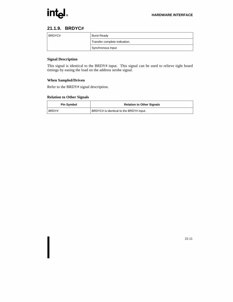
EE HARDWARE INTERFACE
21-11
21.1.9. BRDYC#BRDYC# Burst Ready
Transfer complete indication.
Synchronous Input
Signal Description
This signal is identical to the BRDY# input. This signal can be used to relieve tight boardtimings by easing the load on the address strobe signal.
When Sampled/Driven
Refer to the BRDY# signal description.
Relation to Other Signals
Pin Symbol Relation to Other Signals
BRDY# BRDYC# is identical to the BRDY# input.

HARDWARE INTERFACE EE
21-12
21.1.10. CACHE#CACHE# Cacheability
External indication of internal cacheability.
Synchronous Input/Output
Signal Description
Refer to the CACHE# pin description in Chapter 5.
When operating in dual processing mode, the Pentium processor (610\75, 735\90, 815\100,1000\120, 1110\133) uses this signal for private snooping.
When Sampled/Driven
This signal becomes an Input/Output when two Pentium processors (610\75, 735\90,815\100, 1000\120, 1110\133) are operating together in dual processing mode.
Relation to Other Signals
No new features.

EE HARDWARE INTERFACE
21-13
21.1.11. CPUTYPCPUTYP CPU Type Definition Pin
Used to configure the Pentium® processor (610\75, 735\90, 815\100,1000\120) as a Dual processor.
Asynchronous Input
Signal Description
The CPUTYP pin is used to determine whether the Pentium processor (610\75, 735\90,815\100, 1000\120, 1110\133) will function as a Primary or Dual processor. CPUTYP mustbe strapped to either VCC or VSS. When CPUTYP is strapped to VCC, the Pentium processor(610\75, 735\90, 815\100, 1000\120, 1110\133) will function as a Dual processor. WhenCPUTYP is strapped to VSS, the Pentium processor (610\75, 735\90, 815\100, 1000\120,1110\133) will function as a Primary processor. In a single socket system design, CPUTYPpin should be strapped to VSS.
When Sampled/Driven
CPUTYP is sampled at RESET and cannot be changed until another non-warm (1 ms)assertion of RESET. CPUTYP must meet a 1 ms setup time to the falling edge of RESET. Itis recommended that CPUTYP be strapped to VCC or VSS.
Relation to Other Signals
Pin Symbol Relation to Other Signals
A20M# When CPUTYP is strapped to VCC, the processor will ignore the A20M#input.
BE4#-BE0# The BE3#-BE0# input values are sampled during RESET to determine theAPIC ID. The Dual processor uses BE4# to indicate to the Primaryprocessor that it has completed it's cache flush operation. Refer to theBE4#-BE0# pin description.
D/P# D/P# is driven by the Pentium processor (610\75, 735\90, 815\100,1000\120, 1110\133) only when the CPUTYP signal is strapped to VSS.
DPEN# When CPUTYP is strapped to VCC, DPEN# is driven active to indicate thatthe second socket is occupied.
FERR# When CPUTYP is strapped to VCC, the FERR# output is undefined.
FLUSH# When operating in dual processing mode, the FLUSH# inputs becomeSynchronous to the CPU clock.
IGNNE# When CPUTYP is strapped to VCC, the processor will ignore the IGNNE#input.
RESET CPUTYP is sampled at the falling edge of RESET. When operating in dualprocessing mode, the RESET inputs become Synchronous to the CPUclock.

HARDWARE INTERFACE EE
21-14
NOTE
It is common practice to put either a pullup or pulldown resistor on a net. Ifa pullup resistor is connected to the CPUTYP pin in order to operate in aDual Processing mode, the value of this resistor must be 100 Ohms or lessto override the internal pulldown that is normally used to put the part into aprimary CPU mode of operation. In the absence of an external pullup, theinternal pulldown will sufficiently pulldown the CPUTYP pin, therefore thepin can be left floating.

EE HARDWARE INTERFACE
21-15
21.1.12. D/C#D/C# Data/Code
Distinguishes a data access from a code access.
Synchronous Input/Output
Signal Description
Refer to the D/C# pin description in Chapter 5.
When operating in dual processing mode, the Pentium processor (610\75, 735\90, 815\100,1000\120, 1110\133) uses this signal for private snooping.
When Sampled/Driven
This signal becomes an Input/Output when two Pentium processors (610\75, 735\90,815\100, 1000\120) are operating together in Dual Processing Mode.
Relation to Other Signals
No new features.

HARDWARE INTERFACE EE
21-16
21.1.13. D/P#D/P# Dual Processor / Primary Processor
Indicates whether the Dual processor or the Primary processor is drivingthe bus.
Synchronous Output
Signal Description
The D/P# pin is driven LOW when the Primary processor is driving the bus. Otherwise, thePrimary processor drives this pin high to indicate that the Dual processor owns the bus. TheD/P# pin can be sampled for the current cycle with ADS#. This pin is defined only on thePrimary processor. In a single socket system design, D/P# pin should be left NC.
When Sampled/Driven
The D/P# pin is always driven by the Primary processor and should be sampled with ADS#of the current cycle.
Relation to Other Signals
Pin Symbol Relation to Other Signals
ADS# D/P# is valid for the current cycle with ADS# (like a status pin).
CPUTYP D/P# is driven by the Pentium® processor (610\75, 735\90, 815\100,1000\120, 1110\133) only when the CPUTYP signal is strapped to VSS.
SMIACT# When operating in dual processing mode, D/P# qualifies the SMIACT#SMM indicator.

EE HARDWARE INTERFACE
21-17
21.1.14. DPEN#DPEN# Second Socket Occupied
Configuration signal which indicates that the second socket in a dual socketsystem is occupied.
Synchronous Input (to the Pentium® processor (610\75, 735\90, 815\100,1000\120, 1110\133) processor)
Synchronous Output (from the Pentium processor (610\75, 735\90,815\100, 1000\120, 1110\133), when configured as a Dual processor)
Signal Description
DPEN# is driven during RESET by the Pentium processor (610\75, 735\90, 815\100,1000\120, 1110\133) when configured as a Dual processor to indicate to the Primaryprocessor in the first socket that there is a Dual processor present in the system. This signalis also driven by the fFuture Pentium OverDrive processor to indicate to the Pentiumprocessor (610\75, 735\90, 815\100, 1000\120, 1110\133) that it must execute the bootupprocedure.
When Sampled/Driven
DPEN# is driven during RESET by the Dual processor, and sampled at the falling edge ofRESET by the Primary processor. This pin becomes PICD0 following the falling edge ofRESET. This pin should be valid and stable two clocks before and after the falling edge ofRESET.
Relation to Other Signals
Pin Symbol Relation to Other Signals
CPUTYP When CPUTYP is strapped to VCC, DPEN# is driven active to indicate thatthe second socket is occupied.
RESET DPEN# is valid during the falling edge of RESET.
PICD0 DPEN# shares a pin with PICD0.

HARDWARE INTERFACE EE
21-18
21.1.15. FERR#FERR# Floating-Point Error
The floating-point error output is driven active when an unmasked floating-point error occurs.
Synchronous Output
Signal Description
Refer to the FERR# pin description in Chapter 5.
This signal is undefined when the Pentium processor (610\75, 735\90, 815\100, 1000\120,1110\133) is configured as a Dual processor.
When Sampled/Driven
The Pentium processor (610\75, 735\90, 815\100, 1000\120, 1110\133), when configured as aDual processor, will not drive this signal to valid levels.
Relation to Other Signals
Pin Symbol Relation to Other Signals
CPUTYP When CPUTYP is strapped to VCC, the FERR# output is undefined.

EE HARDWARE INTERFACE
21-19
21.1.16. FLUSH#FLUSH# Cache Flush
Writes all modified lines in the data cache back and flushes the code anddata caches.
Asynchronous Input (Normal, Uni-processor, mode)
Synchronous Input (Dual Processor mode)
Signal Description
Refer to the FLUSH# pin description in Chapter 5.
The Pentium processor (610\75, 735\90, 815\100, 1000\120, 1110\133), when operating witha second Pentium processor (610\75, 735\90, 815\100, 1000\120, 1110\133) in dualprocessing mode, incorporates a mechanism to present an atomic cache flush operation to thesystem. The Dual processor performs the cache flush operation first, then grants the bus tothe Primary processor. The Primary processor flushes its internal caches, and then runs thecache flush special cycle. This could cause the total flush latency of two Pentium processors(610\75, 735\90, 815\100, 1000\120, 1110\133) in dual processor mode to be up to twice thatof the Pentium processor (610\75, 735\90, 815\100, 1000\120, 1110\133) in uni-processormode.
The flush latency of the Future Pentium OverDrive processor may also be up to twice that ofthe Pentium processor (610\75, 735\90, 815\100, 1000\120, 1110\133) due to theimplementation of larger on-chip caches.
When Sampled/Driven
When operating in a dual processing system, FLUSH# must be sample synchronously to therising CLK edge to ensure both processors recognize an active FLUSH# signal in the sameclock.
Relation to Other Signals
Pin Symbol Relation to Other Signals
CPUTYP When operating in dual processing mode, the FLUSH# inputs becomeSynchronous to the CPU clock.
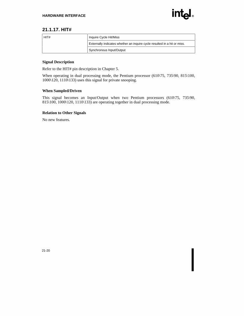
HARDWARE INTERFACE EE
21-20
21.1.17. HIT#HIT# Inquire Cycle Hit/Miss
Externally indicates whether an inquire cycle resulted in a hit or miss.
Synchronous Input/Output
Signal Description
Refer to the HIT# pin description in Chapter 5.
When operating in dual processing mode, the Pentium processor (610\75, 735\90, 815\100,1000\120, 1110\133) uses this signal for private snooping.
When Sampled/Driven
This signal becomes an Input/Output when two Pentium processors (610\75, 735\90,815\100, 1000\120, 1110\133) are operating together in dual processing mode.
Relation to Other Signals
No new features.

EE HARDWARE INTERFACE
21-21
21.1.18. HITM#HITM# Inquire Cycle Hit/Miss to a Modified Line
Externally indicates whether an inquire cycle hit a modified line in the datacache.
Synchronous Input/Output
Signal Description
Refer to the HITM# pin description in Chapter 5.
When operating in dual processing mode, the Pentium processor (610\75, 735\90, 815\100,1000\120, 1110\133) uses this signal for private snooping.
When Sampled/Driven
This signal becomes an input/output when two Pentium processors (610\75, 735\90, 815\100,1000\120, 1110\133) are operating together in dual processing mode.
Relation to Other Signals
No new features.

HARDWARE INTERFACE EE
21-22
21.1.19. HLDAHLDA Bus Hold Acknowledge
External indication that the Pentium processor (610\75, 735\90, 815\100,1000\120, 1110\133) outputs are floated.
Synchronous Input/Output
Signal Description
Refer to the HLDA pin description in Chapter 5.
When operating in dual processing mode, the Pentium processor (610\75, 735\90, 815\100,1000\120, 1110\133) uses this signal for private snooping.
When Sampled/Driven
This signal becomes an input/output when two Pentium processors (610\75, 735\90, 815\100,1000\120, 1110\133) are operating together in dual processing mode.
Relation to Other Signals
No new features.
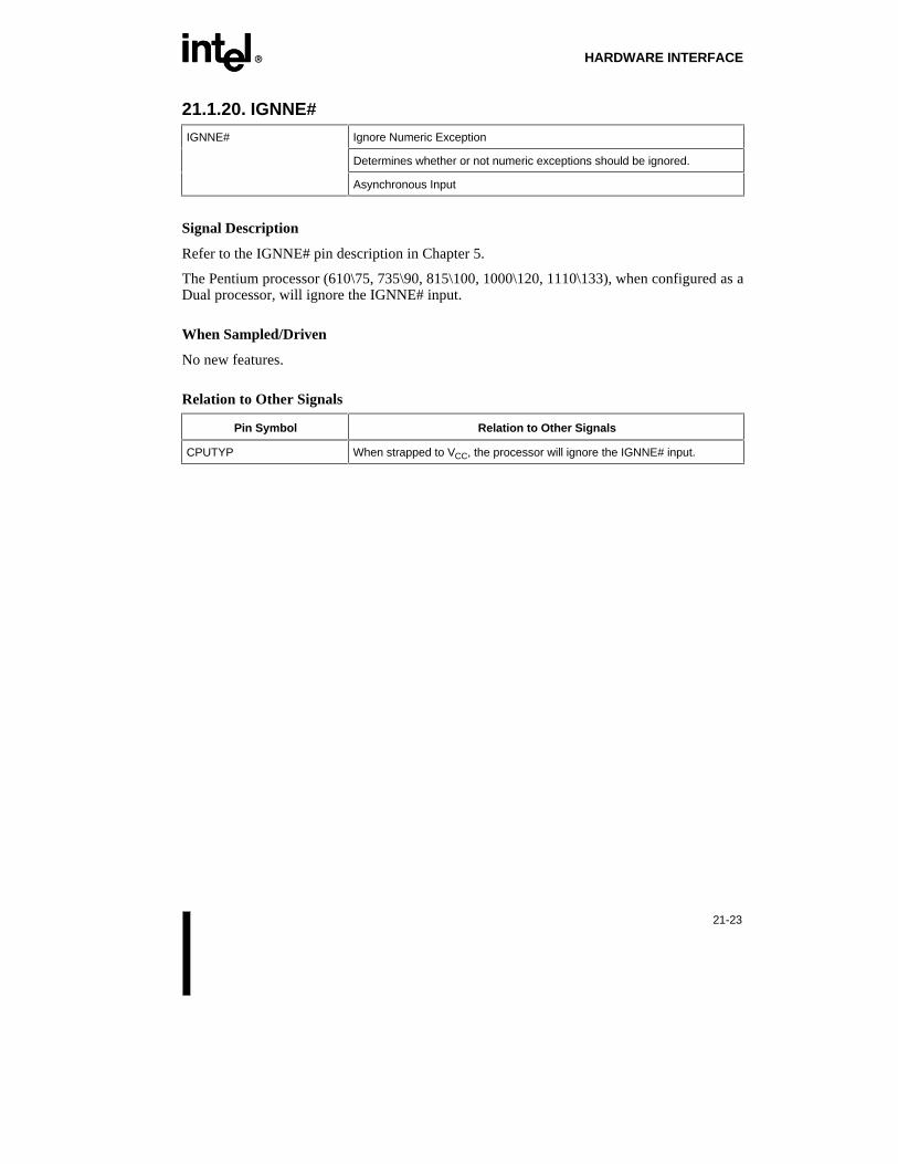
EE HARDWARE INTERFACE
21-23
21.1.20. IGNNE#IGNNE# Ignore Numeric Exception
Determines whether or not numeric exceptions should be ignored.
Asynchronous Input
Signal Description
Refer to the IGNNE# pin description in Chapter 5.
The Pentium processor (610\75, 735\90, 815\100, 1000\120, 1110\133), when configured as aDual processor, will ignore the IGNNE# input.
When Sampled/Driven
No new features.
Relation to Other Signals
Pin Symbol Relation to Other Signals
CPUTYP When strapped to VCC, the processor will ignore the IGNNE# input.

HARDWARE INTERFACE EE
21-24
21.1.21. INTRINTR External Interrupt
Indicates that an external interrupt has been generated.
Asynchronous Input
Signal Description
Refer to the INTR pin description in Chapter 5.
When the local APIC is hardware enabled, this pin becomes the programmable interruptLINT0. It can be programmed in software in any of the interrupt modes. Since this pin isthe INTR input when the APIC is disabled, it is logical to program the vector table entry forthis pin as ExtINT (i.e. through local mode). In this mode, the interrupt signal is passed on tothe processor through the local APIC. The Processor generates the interrupt acknowledge,INTA, cycle in response to this interrupt and receives the vector on the processor data bus.
When the local APIC is hardware disabled, this pin is the INTR input for the processor. Itbypasses the local APIC in that case.
When Sampled/Driven
INTR is sampled on every rising clock edge. INTR is an asynchronous input, but recognitionof INTR is guaranteed in a specific clock if it is asserted synchronously and meets the setupand hold times. To guarantee recognition if INTR is asserted asynchronously it must havebeen deasserted for a minimum of 2 clocks before being returned active to the Pentiumprocessor (610\75, 735\90, 815\100, 1000\120, 1110\133).
NOTE
This applies only when using the APIC in the through local (virtual wire)mode. Once INTR has been asserted (by a rising edge), it must not beasserted again until after the end of the first resulting interrupt acknowledgecycle. Otherwise, the new interrupt may not be recognized. The end of aninterrupt acknowledge cycle is defined by the end of the system's BRDY#response to the CPU cycle. Note that the APIC through local mode wasdesigned to match the protocol of an 8259A PIC, and an 8259A will alwayssatisfy this requirement.
Relation to Other Signals
Pin Symbol Relation to Other Signals
APICEN When the APICEN configuration input is sampled inactive, this inputbecomes the INTR interrupt.
LINT0 INTR shares a pin with LINT0.

EE HARDWARE INTERFACE
21-25
21.1.22. LINT1-LINT0LINT1-LINT0 Local Interrupts 1 and 0
APIC Programmable Interrupts.
Asynchronous Inputs
Signal Description
When the local APIC is hardware enabled, these pins become the programmable interrupts(LINT1-LINT0). They can be programmed in software in any of the interrupt modes. Sincethese pins are the INTR and NMI inputs when the APIC is disabled, it is logical to programthe vector table entry for them as ExtINT (i.e. through local mode) and NMI, respectively.In this mode, the interrupt signals are passed on to the processor through the local APIC.
When the local APIC is hardware disabled, these pins are the INTR and NMI inputs for theprocessor. They bypass the APIC in that case.
When Sampled
LINT1-LINT0 are sampled on every rising clock edge. LINT1-LINT0 are asynchronousinputs, but recognition of LINT1-LINT0 are guaranteed in a specific clock if they areasserted synchronously and meets the setup and hold times. To guarantee recognition ifLINT1-LINT0 are asserted asynchronously they must have been deasserted for a minimum of2 clocks before being returned active to the Pentium processor (610\75, 735\90, 815\100,1000\120, 1110\133).
Relation to Other Signals
Pin Symbol Relation to Other Signals
APICEN When the APICEN configuration input is sampled inactive, these inputsbecome the INTR and NMI interrupts.
INTR INTR shares a pin with LINT0.
NMI NMI shares a pin with LINT1.

HARDWARE INTERFACE EE
21-26
21.1.23. LOCK#LOCK# Bus Lock
Indicates to the system that the current sequence of bus cycles should notbe interrupted.
Synchronous Input/Output
Signal Description
Refer to the LOCK# pin description in Chapter 5.
When operating in dual processing mode, the Pentium processor (610\75, 735\90, 815\100,1000\120, 1110\133) uses this signal for private snooping.
When Sampled/Driven
This signal becomes an input/output when two Pentium processors (610\75, 735\90, 815\100,1000\120, 1110\133) are operating together in dual processing mode.
Relation to Other Signals
No new features.

EE HARDWARE INTERFACE
21-27
21.1.24. M/IO#M/IO# Memory Input/Output
Distinguishes a memory access from an I/O access.
Synchronous Input/Output
Signal Description
Refer to the M/IO# pin description in Chapter 5.
When operating in dual processing mode, the Pentium processor (610\75, 735\90, 815\100,1000\120, 1110\133) uses this signal for private snooping.
When Sampled/Driven
This signal becomes an input/output when two Pentium processors (610\75, 735\90, 815\100,1000\120, 1110\133) are operating together in dual processing mode.
Relation to Other Signals
No new features.

HARDWARE INTERFACE EE
21-28
21.1.25. NMINMI Non Maskable interrupt
Indicates that an external non-maskable interrupt has been generated.
Asynchronous Input
Signal Description
Refer to the NMI pin description in Chapter 5.
When the local APIC is hardware enabled, this pin becomes the programmable interruptLINT1. It can be programmed in software in any of the interrupt modes. Since this pin isthe NMI input when the APIC is disabled, it is logical to program the vector table entry forthis pin as NMI. In this mode, the interrupt signal is passed on to the processor through thelocal APIC.
When the local APIC is hardware disabled, this pin is the NMI input for the processor. Itbypasses the APIC in that case.
When Sampled
NMI is sampled on every rising clock edge. NMI is an asynchronous input, but recognitionof NMI is guaranteed in a specific clock if it is asserted synchronously and meets the setupand hold times. To guarantee recognition if NMI is asserted asynchronously it must havebeen deasserted for an minimum of 2 clocks before being returned active to the Pentiumprocessor (610\75, 735\90, 815\100, 1000\120, 1110\133).
Relation to Other Signals
Pin Symbol Relation to Other Signals
APICEN When the APICEN configuration input is sampled inactive, this inputbecomes the NMI interrupt.
LINT1 NMI shares a pin with LINT1.
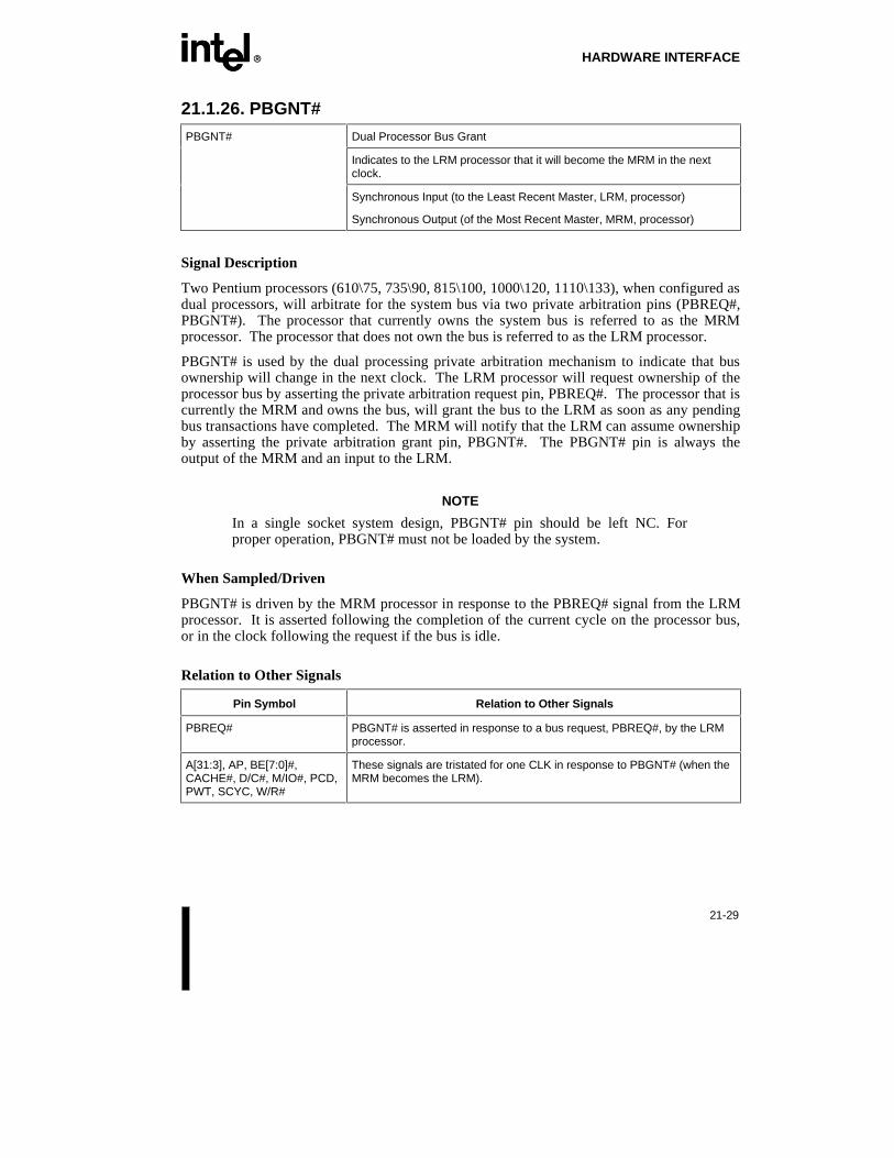
EE HARDWARE INTERFACE
21-29
21.1.26. PBGNT#PBGNT# Dual Processor Bus Grant
Indicates to the LRM processor that it will become the MRM in the nextclock.
Synchronous Input (to the Least Recent Master, LRM, processor)
Synchronous Output (of the Most Recent Master, MRM, processor)
Signal Description
Two Pentium processors (610\75, 735\90, 815\100, 1000\120, 1110\133), when configured asdual processors, will arbitrate for the system bus via two private arbitration pins (PBREQ#,PBGNT#). The processor that currently owns the system bus is referred to as the MRMprocessor. The processor that does not own the bus is referred to as the LRM processor.
PBGNT# is used by the dual processing private arbitration mechanism to indicate that busownership will change in the next clock. The LRM processor will request ownership of theprocessor bus by asserting the private arbitration request pin, PBREQ#. The processor that iscurrently the MRM and owns the bus, will grant the bus to the LRM as soon as any pendingbus transactions have completed. The MRM will notify that the LRM can assume ownershipby asserting the private arbitration grant pin, PBGNT#. The PBGNT# pin is always theoutput of the MRM and an input to the LRM.
NOTE
In a single socket system design, PBGNT# pin should be left NC. Forproper operation, PBGNT# must not be loaded by the system.
When Sampled/Driven
PBGNT# is driven by the MRM processor in response to the PBREQ# signal from the LRMprocessor. It is asserted following the completion of the current cycle on the processor bus,or in the clock following the request if the bus is idle.
Relation to Other Signals
Pin Symbol Relation to Other Signals
PBREQ# PBGNT# is asserted in response to a bus request, PBREQ#, by the LRMprocessor.
A[31:3], AP, BE[7:0]#,CACHE#, D/C#, M/IO#, PCD,PWT, SCYC, W/R#
These signals are tristated for one CLK in response to PBGNT# (when theMRM becomes the LRM).

HARDWARE INTERFACE EE
21-30
21.1.27. PBREQ#PBREQ# Dual Processor Bus Request
Indicates to the MRM processor that the LRM processor requires ownershipof the bus.
Synchronous Input (to the Most Recent Master, MRM, processor)
Synchronous Output (of the Least Recent Master, LRM, processor)
Signal Description
Two Pentium processors (610\75, 735\90, 815\100, 1000\120, 1110\133), when configured asdual processors, will arbitrate for the system bus via two private arbitration pins (PBREQ#,PBGNT#). The processor that currently owns the system bus is referred to as the MRMprocessor. The processor that does not own the bus is referred to as the LRM processor.
PBREQ# is used by the dual processing private arbitration mechanism to indicate that theLRM processor requests bus ownership. The processor that is currently the MRM and ownsthe bus, will grant the bus to the LRM as soon as any pending bus transactions havecompleted. The MRM will notify that the LRM can assume ownership by asserting theprivate arbitration grant pin, PBGNT#. The PBREQ# pin is always the output of the LRMand an input to the MRM.
NOTE
In a single socket system design, PBREQ# pin should be left NC. Forproper operation, PBREQ# must not be loaded by the system.
When Sampled/Driven
PBREQ# is driven by the LRM processor, and sampled by the MRM processor.
Relation to Other Signals
Pin Symbol Relation to Other Signals
PBGNT# PBGNT# is asserted in response to a bus request, PBREQ#, by the LRMprocessor.

EE HARDWARE INTERFACE
21-31
21.1.28. PCHK#PCHK# Data Parity Check
Indicates the result of a parity check on a data read.
Synchronous Output
Signal Description
Refer to the PCHK# pin description in Chapter 5.
When operating in dual processing mode, the PCHK# signal can be asserted either 2 OR 3CLKs following incorrect parity being detected on the data bus. When operating in DualProcessing mode the PCHK# pin circuit is implemented as a weak driving high output thatoperates similar to an open drain output. This implementation allows connection of the twoprocessor PCHK# pins together in a dual processing system with no ill effects. Nominallythis circuit acts like a 360 Ohm resistor tied to VCC.
When Sampled/Driven
No new features.
Relation to Other Signals
No new features.

HARDWARE INTERFACE EE
21-32
21.1.29. PHIT#PHIT# Private Inquire Cycle Hit/Miss Indication
Indicates whether a private, dual processor, inquire cycle resulted in a hit ormiss.
Synchronous Input (to the Most Recent Master, MRM, processor)
Synchronous Output (of the Least Recent Master, LRM, processor)
Signal Description
A private snoop interface has been added to the Pentium processor (610\75, 735\90, 815\100,1000\120, 1110\133) for use in dual processing. The interface consists of two pins (PHIT#,PHITM#) that connect between the OEM socket and Socket 5/Socket 7.
The LRM processor will initiate a snoop sequence for all ADS# cycles that are initiated bythe MRM. The LRM processor will assert the private hit indication (PHIT#) if the datarequested by the MRM matches a valid cache line in the LRM. In addition, if the datarequested by the MRM matches a valid cache line in the LRM that is in the modified state,the LRM will assert the PHITM# signal. The system snooping indication signals (HIT#,HITM#) will not change state as a result of a private snoop.
The MRM will use an assertion of the PHIT# signal as an indication that the requested data isbeing shared with the LRM. Independent of the WB/WT# pin, a cache line will be placed inthe cache in the shared state if PHIT# is asserted. This will make all subsequent writes tothat line externally visible until the state of the line becomes exclusive (E or M states). In auniprocessor system, the line may have been placed in the cache in the E state. In thissituation, all subsequent writes to that line will not be visible on the bus until the state ischanged to I.
PHIT# will also be driven by the LRM during external snoop operations (e.g., followingEADS#) to indicate the private snoop results.
NOTE
In a single socket system, PHIT# pin should be left NC. For properoperation, PHIT# must not be loaded by the system.
When Sampled/Driven
PHIT# is driven by the LRM processor, and sampled by the MRM processor. It is assertedwithin two clocks following an assertion of ADS# or EADS#.
The PHIT# signal operates at the processor core frequency.

EE HARDWARE INTERFACE
21-33
Relation to Other Signals
Pin Symbol Relation to Other Signals
A[31:5] PHIT# is driven to indicate whether the private inquire address driven onA[31:5] is valid in the LRM's on-chip cache.
ADS# PHIT# is driven within 2 clocks after ADS# is sampled asserted to indicatethe outcome of the private inquire cycle.
EADS# PHIT# is driven within 2 clocks after EADS# is sampled asserted to indicatethe outcome of the external inquire cycle.
PHITM# PHITM# is never asserted without PHIT# also being asserted.
WB/WT# The state of the WB/WT# pin will be ignored by the MRM if the PHIT# pin issampled active, and the cache line placed in the shared state.

HARDWARE INTERFACE EE
21-34
21.1.30. PHITM#PHITM# Private Inquire Cycle Hit/Miss to a Modified Line Indication
Indicates whether a private, dual processor, inquire cycle resulted in a hit ormiss to a Modified line.
Synchronous Input (to the Most Recent Master, MRM, processor)
Synchronous Output (of the Least Recent Master, LRM, processor)
Signal Description
A private snoop interface has been added to the Pentium processor (610\75, 735\90, 815\100,1000\120, 1110\133) for use in dual processing. The interface consists of two pins (PHIT#,PHITM#) that connect between the OEM socket and Socket 5/Socket 7.
The LRM processor will initiate a snoop sequence for all ADS# cycles that are initiated bythe MRM. The LRM processor will assert the private hit to a modified line indication(PHITM#) if the data requested by the MRM matches a modified cache line in the LRM. Inaddition, if the data requested by the MRM matches a valid cache line in the LRM, the LRMwill also assert the PHIT# signal. The system snooping indication signals (HIT#, HITM#)will not change state as a result of a private snoop.
PHITM# will also be driven by the LRM during external snoop operations (e.g. followingEADS#) to indicate the private snoop results.
NOTE
In a single socket system, PHITM# pin should be left NC. For properoperation, PHITM# must not be loaded by the system.
When Sampled/Driven
PHITM# is driven by the LRM processor, and sampled by the MRM processor. It is assertedwithin two clocks following an assertion of ADS# or EADS#.
The PHITM# signal operates at the processor core frequency.
Relation to Other Signals
Pin Symbol Relation to Other Signals
A[31:5] PHITM# is driven to indicate whether the private inquire address driven onA[31:5] is modified in the LRM's on-chip cache.
ADS# PHITM# is driven within 2 clocks after ADS# is sampled asserted to indicatethe outcome of the private inquire cycle.
EADS# PHITM# is driven within 2 clocks after EADS# is sampled asserted toindicate the outcome of the external inquire cycle.
PHIT# PHITM# is never asserted without PHIT# also being asserted.

EE HARDWARE INTERFACE
21-35
21.1.31. PICCLKPICCLK Processor Interrupt Controller Clock
This pin drives the clock for the APIC serial data bus operation.
Input
Signal Description
This pin provides the clock timings for the on chip APIC unit of the processor. This clockinput controls the frequency for the APIC operation and data transmission on the 2-wireAPIC serial data bus. All the timings on APIC bus are referenced to this clock.
When hardware disabled, PICCLK must be tied high.
When Sampled
PICCLK is a clock signal and is used as a reference for sampling the APIC data signals.
Relation to Other Signals
Pin Symbol Relation to Other Signals
APICEN PICCLK must be tied or driven high when APICEN is sampled low at thefalling edge of RESET.
PICD0-1 External timing parameters for the PICD0-1 pins are measured with respectto this clock.

HARDWARE INTERFACE EE
21-36
21.1.32. PICD1-PICD0PICD1-PICD0 Processor Interrupt Controller Data
These are the data pins for the 3-wire APIC bus.
Synchronous Input/Output to PICCLK
Needs external pull-up resistors.
Signal Description
The PICD1-PICD0 are bi-directional pins which comprise the data portion of the 3-wireAPIC bus.
When Sampled/Driven
This signal is sampled with the rising edge of PICCLK.
Relation to Other Signals
Pin Symbol Relation to Other Signals
APICEN PICD1 shares a pin with APICEN.
DPEN# PICD0 shares a pin with DPEN#.

EE HARDWARE INTERFACE
21-37
21.1.33. RESETRESET Reset
Forces the Pentium® processor (610\75, 735\90, 815\100, 1000\120,1110\133) to begin execution at a known state.
Asynchronous Input (Normal, Uni-processor, mode)
Synchronous Input (Dual Processor mode)
Signal Description
Refer to the RESET pin description in Chapter 5.
No new features.
When Sampled/Driven
When operating in a dual processing system, RESET must be sample synchronously to therising CLK edge to ensure both processors recognize the falling edge in the same clock.
Relation to Other Signals
Pin Symbol Relation to Other Signals
APICEN APICEN is sampled at the falling edge of RESET.
BE3#-BE0# During reset the BE3#-BE0# pins are sampled to determine the APIC ID.Following RESET, they function as Byte Enable outputs.
BF BF is sampled at the falling edge of RESET.
CPUTYP CPUTYP is sampled at the falling edge of RESET.
DPEN# DPEN# is valid during RESET.

HARDWARE INTERFACE EE
21-38
21.1.34. SCYCSCYC Split Cycle Indication
Indicates that a misaligned locked transfer is on the bus.
Synchronous Input/Output
Signal Description
Refer to the SCYC pin description in Chapter 5.
When operating in dual processing mode, the Pentium processor (610\75, 735\90, 815\100,1000\120, 1110\133) uses this signal for private snooping.
When Sampled/Driven
This signal becomes an input/output when two Pentium processors (610\75, 735\90, 815\100,1000\120, 1110\133) are operating together in dual processing mode.
Relation to Other Signals
No new features.

EE HARDWARE INTERFACE
21-39
21.1.35. SMIACT#SMIACT# System Management Interrupt Active
Indicates that the processor is operating in SMM.
Synchronous Output
Signal Description
Refer to the SMIACT# pin description in Chapter 5.
When the system is operating in dual processing mode, the D/P# signal toggles based uponwhether the Primary or Dual processor owns the bus (MRM). The SMIACT# pins may betied together or be used separately to insure SMRAM access by the correct processor.
CAUTION
If SMIACT# is used separately: the SMIACT# signal is only driven by theCPUs when the processor is the MRM, so this signal must be qualified withthe D/P# signal).
Connecting the SMIACT# signals on the Primary and Dual processors together isstrongly recommended for operation with the Dual processor and upgradability with thefuture Pentium OverDrive processor.
In dual processing systems, SMIACT# may not remain low (e.g., may toggle) if bothprocessors are not in SMM mode. The SMIACT# signal is asserted by either the Primary orDual processor based on two conditions: the processor is in SMM mode and is the busmaster (MRM). If one processor is executing in normal address space, the SMIACT# signalwill go inactive when that processor is MRM. The LRM processor, even if in SMM mode,will not drive the SMIACT# signal low.
When Sampled/Driven
When operating in dual processing mode, the SMIACT# output must be sampled with anactive ADS# and qualified with the D/P# signal to determine which Pentium processor(610\75, 735\90, 815\100, 1000\120, 1110\133) (e.g., the Primary or Dual) is driving theSMM cycle.
Relation to Other Signals
Pin Symbol Relation to Other Signals
ADS# SMIACT# should be sampled with an active ADS# during dual processingoperation.
D/P# When operating in dual processing mode, D/P# qualifies the SMIACT#SMM indicator.

HARDWARE INTERFACE EE
21-40
21.1.36. STPCLK#STPCLK# Stop Clock Pin
Used to stop the internal Pentium® processor (610\75, 735\90, 815\100,1000\120) clock and consume less power.
Asynchronous Input
Signal Description
Assertion of STPCLK# causes the Pentium processor (610\75, 735\90, 815\100, 1000\120,1110\133) to stop its internal clock and consume less power while still responding tointerprocessor and external snoop requests. This low-power state is called the stop grantstate. When the CPU recognizes a STPCLK# interrupt, the CPU will do the following:
1. Wait for all instructions being executed to complete.
2. Flush the instruction pipeline of any instructions waiting to be executed.
3. Wait for all pending bus cycles to complete and EWBE# to go active.
4. Drive a special bus cycle (stop grant bus cycle) to indicate that the clock is beingstopped.
5. Enter low power mode.
The stop grant bus cycle consists of the following signal states: M/IO# = 0, D/C# = 0,W/R# = 1, Address Bus = 0000 0010H (A4 = 1), BE7#-BE0# = 1111 1011, Data bus =undefined.
STPCLK# must be driven high (not floated) to exit the stop grant state. The rising edge ofSTPCLK# will tell the CPU that it can return to program execution at the instructionfollowing the interrupted instruction.
When Sampled/Driven
STPCLK# is treated as a level triggered interrupt to the Pentium processor (610\75, 735\90,815\100, 1000\120, 1110\133) and is prioritized below all of the external interrupts. Whenthe Pentium processor (610\75, 735\90, 815\100, 1000\120, 1110\133) recognizes theSTPCLK# interrupt, the processor will stop execution on the instruction boundary followingthe STPCLK# assertion.

EE HARDWARE INTERFACE
21-41
Relation to Other Signals
Pin Symbol Relation to Other Signals
A4, Cycle Control signals(M/IO#, D/C#, W/R#, BE7#-BE0#, D/P#)
The Stop Grant Special Bus Cycle is driven on these pins in response to anassertion of the STPCLK# signal. M/IO# = 0, D/C# = 0, W/R# = 1. AddressBus = 0000 0010H (A4 = 1), BE7#-BE0# = 1111 1011.
EWBE# After STPCLK# has been recognized, all pending cycles must be completedand EWBE# must go active before the internal clock will be disabled.
External Interrupt signals(FLUSH#, INIT, INTR, NMI,R/S#, SMI#)
While in the Stop Grant state, the CPU will latch transitions on the externalinterrupt signals. All of these interrupts are taken after the de-assertion ofSTPCLK#. The CPU requires that INTR be held active until the CPU issuesan interrupt acknowledge cycle in order to guarantee recognition.
HLDA The CPU will not respond to a STPCLK# request from a HLDA statebecause it cannot generate a Stop Grant cycle.

HARDWARE INTERFACE EE
21-42
21.1.37. VCCVCC Supply Voltage
VCC is used to supply power to the Pentium® processor (610\75, 735\90,815\100, 1000\120, 1110\133) and Socket 5.
Power Input
Signal Description
The Pentium processor (610\75, 735\90, 815\100, 1000\120, 1110\133) and future PentiumOverDrive processor require 3.3V VCC inputs.
When Sampled/Driven
No new features.
Relation to Other Signals
No new features.

EE HARDWARE INTERFACE
21-43
21.1.38. W/R#W/R# Write/Read
Distinguishes a Write cycle from a Read cycle.
Synchronous Input/Output
Signal Description
Refer to the W/R# pin description in Chapter 5.
When operating in dual processing mode, the Pentium processor (610\75, 735\90, 815\100,1000\120, 1110\133) uses this signal for private snooping.
When Sampled/Driven
This signal becomes an input/output when two Pentium processors (610\75, 735\90, 815\100,1000\120, 1110\133) are operating together in dual processing mode.
Relation to Other Signals
No new features.

E22
Bus FunctionalDescription


EE
22-1
CHAPTER 22BUS FUNCTIONAL DESCRIPTION
The Pentium processor (610\75, 735\90, 815\100, 1000\120, 1110\133) supports the same busfunctional features as found in Chapter 6 for the Pentium processor family.
NOTE
According to the Pentium® Processor Family Developer's Manual, Volume1 (Section 6.6.2), there is a dead clock defined for the bus switching from apipelined write to read cycle or a pipelined read to write cycle. Theprocessor ignores BRDY# during this dead clock, but in dual processingmode BRDY# may be falsely recognized in an inter-CPU pipelined cycle.The dual processing system design must not drive BRDY# low during thisdead clock.
ADS#
W/R#
NA#
BRDY#
D/P#
T1 T2 T2 T12 TD T2 T12 T2P TD T12 T2P
Rd Wr Rd Wr
Rd Wr
DeadClk
DeadClk
pdb23a

E23
ElectricalSpecifications


EE
23-1
CHAPTER 23ELECTRICAL SPECIFICATIONS
This section describes the electrical differences between the Pentium processor (510\60,567\66) and the Pentium processor (610\75, 735\90, 815\100, 1000\120, 1110\133), as wellas the DC and AC specifications. Unless otherwise stated, the Pentium processor (610\75,735\90, 815\100, 1000\120, 1110\133) and Dual processor have the same electricalcharacteristics.
23.1. ELECTRICAL DIFFERENCES OF PENTIUM ® PROCESSOR(610\75, 735\90, 815\100, 1000\120, 1110\133) FROMPENTIUM PROCESSOR (510\60, 567\66)
When designing a Pentium processor (610\75, 735\90, 815\100, 1000\120, 1110\133) systemfrom a Pentium processor (510\60, 567\66) system, there are a number of electricaldifferences that require attention. If these differences are understood during Pentiumprocessor (510\60, 567\66) system design, the transition from a Pentium processor (510\60,567\66) to Pentium processor (610\75, 735\90, 815\100, 1000\120, 1110\133) will requirelittle or no redesign.
Pentium ® Processor (510\60, 567\66)Electrical Characteristics
Pentium Processor(610\75, 735\90, 815\100, 1000\120, 1110\133)
Electrical Characteristics
5V Power Supply 3.3V Power Supply*
5V TTL Inputs/Outputs 3.3V Inputs/Outputs
Pentium processor Buffer Models 3.3V Pentium processor (610\75, 735\90, 815\100,1000\120, 1110\133) Buffer Models
NOTE:
* The upgrade socket specifies two 5V supply pins (Chapter 32).
The sections that follow will briefly point out some ways to overcome these electricaldifferences.
23.1.1. 3.3V Power SupplyThe Pentium processor (610\75, 735\90, 815\100, 1000\120, 1110\133) has all VCC 3.3Vinputs. By connecting all Pentium processor (510\60, 567\66) VCC inputs to a common anddedicated power plane, that plane can be converted to 3.3V for the Pentium processor(610\75, 735\90, 815\100, 1000\120, 1110\133).

ELECTRICAL SPECIFICATIONS EE
23-2
The CLK and PICCLK inputs can tolerate a 5V input signal. This allows the Pentiumprocessor (610\75, 735\90, 815\100, 1000\120, 1110\133) to use 5V or 3.3V clock drivers.
23.1.2. 3.3V Inputs and OutputsThe inputs and outputs of the Pentium processor (610\75, 735\90, 815\100, 1000\120,1110\133) are 3.3V JEDEC standard levels. Both inputs and outputs are alsoTTL-compatible, although the inputs cannot tolerate voltage swings above the VIN3 max.
For Pentium processor (610\75, 735\90, 815\100, 1000\120, 1110\133) outputs, if yourPentium processor (510\60, 567\66) system support components use TTL-compatible inputs,they will interface to the Pentium processor (610\75, 735\90, 815\100, 1000\120, 1110\133)without extra logic. This is because the Pentium processor (610\75, 735\90, 815\100,1000\120, 1110\133) drives according to the 5V TTL specification (but not beyond 3.3V).
For Pentium processor (610\75, 735\90, 815\100, 1000\120, 1110\133) inputs, the voltagemust not exceed the 3.3V VIH3 maximum specification. System support components canconsist of 3.3V devices or open-collector devices. 3.3V support components may interface tothe Pentium processor (510\60, 567\66) since they typically meet 5V TTL specifications. Inan open-collector configuration, the external resistor may be biased with the CPU VCC; asthe CPU's VCC changes from 5V to 3.3V, so does this signal's maximum drive.
The CLK and PICCLK inputs of the Pentium processor (610\75, 735\90, 815\100, 1000\120,1110\133) are 5V tolerant, so they are electrically identical to the Pentium processor (510\60,567\66) clock input. This allows a Pentium processor clock driver to drive the Pentiumprocessor (610\75, 735\90, 815\100, 1000\120, 1110\133).
All pins, other than the CLK and PICCLK inputs, are 3.3V only. If an 8259A interruptcontroller is used, for example, the system must provide level converters between the 8259Aand the Pentium processor (610\75, 735\90, 815\100, 1000\120, 1110\133).
23.1.3. 3.3V Buffer ModelsThe structure of the buffer models of the Pentium processor (610\75, 735\90, 815\100,1000\120, 1110\133) are the same as those of the Pentium processor (510\60, 567\66), but thevalues of the components change since the Pentium processor (610\75, 735\90, 815\100,1000\120, 1110\133) buffers are 3.3V buffers on a different process.
Despite this difference, the simulation results of Pentium processor (610\75, 735\90, 815\100,1000\120, 1110\133) buffers and Pentium processor (510\60, 567\66) buffers look nearlyidentical. Since the AC specifications of the Pentium processor (610\75, 735\90, 815\100,1000\120, 1110\133) are derived from the Pentium processor (510\60, 567\66) specifications,the system should see little difference between the AC behavior of the Pentium processor(610\75, 735\90, 815\100, 1000\120, 1110\133) and the Pentium processor (510\60, 567\66).
To meet specifications, simulate the AC timings with Pentium processor (610\75, 735\90,815\100, 1000\120, 1110\133) buffer models. Pay special attention to the new signal qualityrestrictions imposed by 3.3V buffers.

EE ELECTRICAL SPECIFICATIONS
23-3
23.2. ABSOLUTE MAXIMUM RATINGSThe values listed below are stress ratings only. Functional operation at the maximums is notimplied or guaranteed. Functional operating conditions are given in the AC and DCspecification tables.
Extended exposure to the maximum ratings may affect device reliability. Furthermore,although the Pentium processor (610\75, 735\90, 815\100, 1000\120, 1110\133) containsprotective circuitry to resist damage from static electric discharge, always take precautions toavoid high static voltages or electric fields.
Table 23-1. Absolute Maximum Ratings
Symbol Parameter Min Max Unit Notes
Storage Temperature -65 150 ° C
Case Temperature Under Bias -65 110 ° C
VCC3 3V Supply Voltage with respect toVSS
-0.5 4.6 V
VIN3 3V Only Buffer DC Input Voltage -0.5 VCC3+0.5
(not to exceed
VCC3 Max)
V (2)
VINSB 5V Safe Buffer DC Input Voltage -0.5 6.5 V (1) (3)
NOTES:
1. Applies to the CLK and PICCLK.
2. Applies to all Pentium® processor (610\75, 735\90, 815\100, 1000\120, 1110\133) inputs except CLK andPICCLK.
3. See Table 23-3.
WARNING
Stressing the device beyond the "Absolute Maximum Ratings" may causepermanent damage. These are stress ratings only. Operation beyond the"Operating Conditions" is not recommended and extended exposure beyondthe "Operating Conditions" may affect device reliability.
23.3. DC SPECIFICATIONSTables 23-2, and 23-3 list the DC specifications which apply to the Pentium processor(610\75, 735\90, 815\100, 1000\120, 1110\133). The Pentium processor (610\75, 735\90,815\100, 1000\120, 1110\133) is a 3.3V part internally. The CLK and PICCLK inputs maybe 3.3V or 5V. Since the 3.3V (5V safe) input levels defined in Table 23-3 are the same asthe 5V TTL levels, the CLK and PICCLK inputs are compatible with existing 5V clockdrivers. The power dissipation specification in Table 23-5 is provided for design of thermal

ELECTRICAL SPECIFICATIONS EE
23-4
solutions during operation in a sustained maximum level. This is the worst case power thedevice would dissipate in a system for a sustained period of time. This number is used fordesign of a thermal solution for the device.
Table 23-2. 3.3V DC Specifications
TCASE = 0 to 70° C; VCC = 3.135V - 3.6V
Symbol Parameter Min Max Unit Notes
VIL3 Input Low Voltage −0.3 0.8 V TTL Level (3)
VIH3 Input High Voltage 2.0 VCC+0.3 V TTL Level (3)
VOL3 Output Low Voltage 0.4 V TTL Level (1) (3)
VOH3 Output High Voltage 2.4 V TTL Level (2) (3)
ICC3 Power Supply Current 3400
3730
3250
2950
2650
mA
mA
mA
mA
mA
@ 133 MHz (4)
@ 120 MHz (4), (5)
@ 100 MHz (4)
@ 90 MHz (4)
@ 75 MHz (4)
NOTES:
1. Parameter measured at 4 mA.
2. Parameter measured at 3 mA.
3. 3.3V TTL levels apply to all signals except CLK and PICCLK.
4. This value should be used for power supply design. It was determined using a worst case instruction mixand VCC += 3.6V. Power supply transient response and decoupling capacitors must be sufficient tohandle the instantaneous current changes occurring during transitions from stop clock to full activemodes. For more information, refer to section 23.4.3.
5. Please also check the Pentium® processor Specification Update.
Table 23-3. 3.3V (5V Safe) DC Specifications
Symbol Parameter Min Max Unit Notes
VIL5 Input Low Voltage −0.3 0.8 V TTL Level (1)
VIH5 Input High Voltage 2.0 5.55 V TTL Level (1)
NOTES:
1. Applies to CLK and PICCLK only.
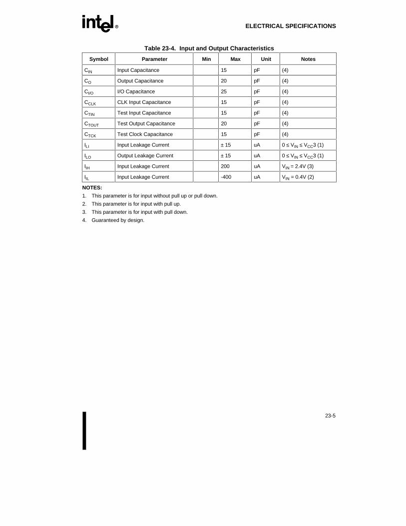
EE ELECTRICAL SPECIFICATIONS
23-5
Table 23-4. Input and Output Characteristics
Symbol Parameter Min Max Unit Notes
CIN Input Capacitance 15 pF (4)
CO Output Capacitance 20 pF (4)
CI/O I/O Capacitance 25 pF (4)
CCLK CLK Input Capacitance 15 pF (4)
CTIN Test Input Capacitance 15 pF (4)
CTOUT Test Output Capacitance 20 pF (4)
CTCK Test Clock Capacitance 15 pF (4)
ILI Input Leakage Current ± 15 uA 0 ≤ VIN ≤ VCC3 (1)
ILO Output Leakage Current ± 15 uA 0 ≤ VIN ≤ VCC3 (1)
IIH Input Leakage Current 200 uA VIN = 2.4V (3)
IIL Input Leakage Current -400 uA VIN = 0.4V (2)
NOTES:
1. This parameter is for input without pull up or pull down.
2. This parameter is for input with pull up.
3. This parameter is for input with pull down.
4. Guaranteed by design.

ELECTRICAL SPECIFICATIONS EE
23-6
Table 23-5. Power Dissipation Requirements for Thermal Design
Parameter Typical (1) Max(2) Unit Notes
Active Power Dissipation 4.3
5.0
3.9
3.5
3.0
11.2
12.81
10.1
9.0
8.0
Watts
Watts
Watts
Watts
Watts
@ 133 MHz
@ 120 MHz (6)
@ 100 MHz
@ 90 MHz
@ 75 MHz SPGA (7)
Stop Grant and AutoHaltPowerdown Power Dissipation
1.7
1.76
1.55
1.40
1.2
Watts
Watts
Watts
Watts
Watts
@ 133 MHz (3)
@ 120 MHz (3), (6)
@ 100 MHz (3)
@ 90 MHz (3)
@ 75 MHz (3)
Stop Clock Power Dissipation .02 < 0.3 Watts (4) (5)
NOTES:1. This is the typical power dissipation in a system. This value was the average value measured in a system
using a typical device at VCC = 3.3V running typical applications. This value is highly dependent upon thespecific system configuration.
2. Systems must be designed to thermally dissipate the maximum active power dissipation. It is determinedusing a worst case instruction mix with VCC = 3.3V. The use of nominal VCC in this measurement takesinto account the thermal time constant of the package.
3. Stop Grant/Auto Halt Powerdown Power Dissipation is determined by asserting the STPCLK# pin orexecuting the HALT instruction.
4. Stop Clock Power Dissipation is determined by asserting the STPCLK# pin and then removing theexternal CLK input.
5. Complete characterization of this specification was still in process at the time of print. Please contact Intelfor the latest information. The final specification will be less than 0.1 W.
6. Please also check the Pentium® Processor Specification Update.7. For power dissipation requirements of Pentium processor (610\75) TCP package, please refer to Chapter
34 of this document.
23.4. AC SPECIFICATIONSThe AC specifications of the Pentium processor (610\75, 735\90, 815\100, 1000\120,1110\133) consist of setup times, hold times and valid delays at 0 pF.
WARNING
Do not exceed the Pentium processor (610\75, 735\90, 815\100, 1000\120,1110\133) internal maximum frequency of 100 MHz by selecting the wrongbus fraction.

EE ELECTRICAL SPECIFICATIONS
23-7
23.4.1. Private BusWhen two Pentium processor (610\75, 735\90, 815\100, 1000\120, 1110\133) are operatingin dual processor mode, a "private bus" exists to arbitrate for the CPU bus and maintain localcache coherency. The private bus consists of two pinout changes:
1. Five pins are added: PBREQ#, PBGNT#, PHIT#, PHITM#, D/P#.
2. Ten output pins become I/O pins: ADS#, D/C#, W/R#, M/IO#, CACHE#, LOCK#,HIT#, HITM#, HLDA, SCYC.
The new pins are given AC specifications of valid delays at 0 pF, setup times and hold times.Simulate with these parameters and their respective I/O buffer models to guarantee thatproper timings are met.
The AC specification gives input setup and hold times for the ten signals that become I/Opins. These setup and hold times must only be met when a Dual processor is present in thesystem.
23.4.2. Power and GroundFor clean on-chip power distribution, the Pentium processor (610\75, 735\90, 815\100,1000\120, 1110\133) has 53 VCC (power) and 53 VSS (ground) inputs. Power and groundconnections must be made to all external VCC and VSS pins of the Pentium processor(610\75, 735\90, 815\100, 1000\120, 1110\133). On the circuit board all VCC pins must beconnected to a 3.3V VCC plane. All VSS pins must be connected to a VSS plane.
23.4.3. Decoupling RecommendationsLiberal decoupling capacitance should be placed near the Pentium processor (610\75, 735\90,815\100, 1000\120, 1110\133). The Pentium processor (610\75, 735\90, 815\100, 1000\120,1110\133) driving its large address and data buses at high frequencies can cause transientpower surges, particularly when driving large capacitive loads.
Low inductance capacitors and interconnects are recommended for best high frequencyelectrical performance. Inductance can be reduced by shortening circuit board tracesbetween the Pentium processor (610\75, 735\90, 815\100, 1000\120, 1110\133) anddecoupling capacitors as much as possible.
These capacitors should be evenly distributed around each component on the 3.3V plane.Capacitor values should be chosen to ensure they eliminate both low and high frequencynoise components.
For the Pentium processor (610\75, 735\90, 815\100, 1000\120, 1110\133), the powerconsumption can transition from a low level of power to a much higher level (or high to lowpower) very rapidly. A typical example would be entering or exiting the Stop Grant state.Another example would be executing a HALT instruction, causing the Pentium processor(610\75, 735\90, 815\100, 1000\120, 1110\133) to enter the Auto HALT Powerdown state, or

ELECTRICAL SPECIFICATIONS EE
23-8
transitioning from HALT to the Normal state. All of these examples may cause abruptchanges in the power being consumed by the Pentium processor (610\75, 735\90, 815\100,1000\120, 1110\133). Note that the Auto HALT Powerdown feature is always enabled evenwhen other power management features are not implemented.
Bulk storage capacitors with a low ESR (Effective Series Resistance) in the 10 to 100 ufrange are required to maintain a regulated supply voltage during the interval between thetime the current load changes and the point that the regulated power supply output can reactto the change in load. In order to reduce the ESR, it may be necessary to place several bulkstorage capacitors in parallel.
These capacitors should be placed near the Pentium processor (610\75, 735\90, 815\100,1000\120, 1110\133) (on the 3.3V plane) to ensure that the supply voltage stays withinspecified limits during changes in the supply current during operation.
23.4.4. Connection SpecificationsAll NC and INC pins must remain unconnected.
For reliable operation, always connect unused inputs to an appropriate signal level. Unusedactive low inputs should be connected to VCC. Unused active high inputs should be connectedto ground.
23.4.5. AC Timing Tables
23.4.5.1. AC TIMING TABLE FOR A 50-MHZ BUS
The AC specifications given in Tables 23-6 and 23-7 consist of output delays, input setuprequirements and input hold requirements for a 50-MHz external bus. All AC specifications(with the exception of those for the TAP signals and APIC signals) are relative to the risingedge of the CLK input.
All timings are referenced to 1.5V for both "0" and "1" logic levels unless otherwisespecified. Within the sampling window, a synchronous input must be stable for correctPentium processor (610\75, 815\100) operation. For (610\75) TCP AC timing specifications,see Chapter 34.

EE ELECTRICAL SPECIFICATIONS
23-9
Table 23-6. Pentium ® Processor (610\75, 815\100) AC Specificationsfor 50-MHz Bus Operation
3.135 ≤ VCC ≤ 3.6V, TCASE = 0 to 70 °C, CL = 0 pF
Symbol Parameter Min Max Unit Figure Notes
Frequency 25.0 50.0 MHz Max Core Freq =100 MHz@1/2
t1a CLK Period 20.0 40.0 nS 23-1
t1b CLK Period Stability ±250 pS (1), (25)
t2 CLK High Time 4.0 nS 23-1 @2V, (1)
t3 CLK Low Time 4.0 nS 23-1 @0.8V, (1)
t4 CLK Fall Time 0.15 1.5 nS 23-1 (2.0V-0.8V), (1),(5)
t5 CLK Rise Time 0.15 1.5 nS 23-1 (0.8V-2.0V), (1),(5)
t6a ADS#, ADSC#, PWT, PCD,BE0-7#, M/IO#, D/C#, CACHE#,SCYC, W/R# Valid Delay
1.0 7.0 nS 23-2
t6b AP Valid Delay 1.0 8.5 nS 23-2
t6c A3-A31, LOCK# Valid Delay 1.1 7.0 nS 23-2
t7 ADS#, ADSC#, AP, A3-A31, PWT,PCD, BE0-7#, M/IO#, D/C#, W/R#,CACHE#, SCYC, LOCK# FloatDelay
10.0 nS 23-3 (1)
t8 APCHK#, IERR#, FERR#, PCHK#Valid Delay
1.0 8.3 nS 23-2 (4)
t9a BREQ, HLDA, SMIACT# ValidDelay
1.0 8.0 nS 23-2 (4)
t10a HIT# Valid Delay 1.0 8.0 nS 23-2
t10b HITM# Valid Delay 1.1 6.0 nS 23-2
t11a PM0-1, BP0-3 Valid Delay 1.0 10.0 nS 23-2
t11b PRDY Valid Delay 1.0 8.0 nS 23-2
t12 D0-D63, DP0-7 Write Data ValidDelay
1.3 8.5 nS 23-2
t13 D0-D63, DP0-3 Write Data FloatDelay
10.0 nS 23-3 (1)
t14 A5-A31 Setup Time 6.5 nS 23-4 (26)
t15 A5-A31 Hold Time 1.0 nS 23-4
t16a INV, AP Setup Time 5.0 nS 23-4

ELECTRICAL SPECIFICATIONS EE
23-10
Table 23-6. Pentium ® Processor (610\75, 815\100) AC Specificationsfor 50-MHz Bus Operation (Contd.)
3.135 ≤ VCC ≤ 3.6V, TCASE = 0 to 70 °C, CL = 0 pF
Symbol Parameter Min Max Unit Figure Notes
t16b EADS# Setup Time 6.0 nS 23-4
t17 EADS#, INV, AP Hold Time 1.0 nS 23-4
t18a KEN# Setup Time 5.0 nS 23-4
t18b NA#, WB/WT# Setup Time 4.5 nS 23-4
t19 KEN#, WB/WT#, NA# Hold Time 1.0 nS 23-4
t20 BRDY#, BRDYC# Setup Time 5.0 nS 23-4
t21 BRDY#, BRDYC# Hold Time 1.0 nS 23-4
t22 BOFF# Setup Time 5.5 nS 23-4
t22a AHOLD Setup Time 6.0 nS 23-4
t23 AHOLD, BOFF# Hold Time 1.0 nS 23-4
t24 BUSCHK#, EWBE#, HOLD, PEN#Setup Time
5.0 nS 23-4
t25 BUSCHK#, EWBE#, PEN# HoldTime
1.0 nS 23-4
t25a HOLD Hold Time 1.5 nS 23-4
t26 A20M#, INTR, STPCLK# SetupTime
5.0 nS 23-4 (12), (16)
t27 A20M#, INTR, STPCLK# HoldTime
1.0 nS 23-4 (13)
t28 INIT, FLUSH#, NMI, SMI#,IGNNE# Setup Time
5.0 nS 23-4 (12), (16), (17)
t29 INIT, FLUSH#, NMI, SMI#,IGNNE# Hold Time
1.0 nS 23-4 (13)
t30 INIT, FLUSH#, NMI, SMI#,IGNNE# Pulse Width, Async
2.0 CLKs (15), (17)
t31 R/S# Setup Time 5.0 nS 23-4 (12), (16), (17)
t32 R/S# Hold Time 1.0 nS 23-4 (13)
t33 R/S# Pulse Width, Async. 2.0 CLKs (15), (17)
t34 D0-D63, DP0-7 Read Data SetupTime
3.8 nS 23-4
t35 D0-D63, DP0-7 Read Data HoldTime
1.5 nS 23-4

EE ELECTRICAL SPECIFICATIONS
23-11
Table 23-6. Pentium ® Processor (610\75, 815\100) AC Specificationsfor 50-MHz Bus Operation (Contd.)
3.135 ≤ VCC ≤ 3.6V, TCASE = 0 to 70 °C, CL = 0 pF
Symbol Parameter Min Max Unit Figure Notes
t36 RESET Setup Time 5.0 nS 23-5 (11), (12), (16)
t37 RESET Hold Time 1.0 nS 23-5 (11), (13)
t38 RESET Pulse Width, VCC & CLKStable
15 CLKs 23-5 (11), (17)
t39 RESET Active After VCC & CLKStable
1.0 mS 23-5 Power up
t40 Reset Configuration Signals (INIT,FLUSH#, FRCMC#) Setup Time
5.0 nS 23-5 (12), (16), (17)
t41 Reset Configuration Signals (INIT,FLUSH#, FRCMC#) Hold Time
1.0 nS 23-5 (13)
t42a Reset Configuration Signals (INIT,FLUSH#, FRCMC#) Setup Time,Async.
2.0 CLKs 23-5 To RESET fallingedge (16)
t42b Reset Configuration Signals (INIT,FLUSH#, FRCMC#, BRDYC#,BUSCHK#) Hold Time, Async.
2.0 CLKs 23-5 To RESET fallingedge (27)
t42c Reset Configuration Signals(BRDYC#, BUSCHK#) SetupTime, Async.
3.0 CLKs 23-5 To RESET fallingedge (27)
t42d Reset Configuration SignalBRDYC# Hold Time, RESETdriven synchronously
1.0 nS To RESET fallingedge (1), (27)
t43a BF, CPUTYP Setup Time 1.0 mS 23-5 (22) to RESETfalling edge
t43b BF, CPUTYP Hold Time 2.0 CLKs 23-5 (22) to RESETfalling edge
t43c APICEN, BE4# Setup Time 2.0 CLKs 23-5 To RESET fallingedge
t43d APICEN, BE4# Hold Time 2.0 CLKs 23-5 To RESET fallingedge
t44 TCK Frequency — 16.0 MHz
t45 TCK Period 62.5 nS 23-1
t46 TCK High Time 25.0 nS 23-1 @2V, (1)

ELECTRICAL SPECIFICATIONS EE
23-12
Table 23-6. Pentium ® Processor (610\75, 815\100) AC Specificationsfor 50-MHz Bus Operation (Contd.)
3.135 ≤ VCC ≤ 3.6V, TCASE = 0 to 70 °C, CL = 0 pF
Symbol Parameter Min Max Unit Figure Notes
t47 TCK Low Time 25.0 nS 23-1 @0.8V, (1)
t48 TCK Fall Time 5.0 nS 23-1 (2.0V–0.8V), (1),(8), (9)
t49 TCK Rise Time 5.0 nS 23-1 (0.8V–2.0V), (1),(8), (9)
t50 TRST# Pulse Width 40.0 nS 23-7 (1),Asynchronous
t51 TDI, TMS Setup Time 5.0 nS 23-6 (7)
t52 TDI, TMS Hold Time 13.0 nS 23-6 (7)
t53 TDO Valid Delay 3.0 20.0 nS 23-6 (8)
t54 TDO Float Delay 25.0 nS 23-6 (1), (8)
t55 All Non-Test Outputs Valid Delay 3.0 20.0 nS 23-6 (3), (8), (10)
t56 All Non-Test Outputs Float Delay 25.0 nS 23-6 (1), (3), (8), (10)
t57 All Non-Test Inputs Setup Time 5.0 nS 23-6 (3), (7), (10)
t58 All Non-Test Inputs Hold Time 13.0 nS 23-6 (3), (7), (10)
APIC AC Specifications
t60a PICCLK Frequency 2.0 16.66 MHz
t60b PICCLK Period 60.0 500.0 nS 23-1
t60c PICCLK High Time 15.0 nS 23-1
t60d PICCLK Low Time 15.0 nS 23-1
t60e PICCLK Rise Time 0.15 2.5 nS 23-1
t60f PICCLK Fall Time 0.15 2.5 nS 23-1
t60g PICD0-1 Setup Time 3.0 nS 23-4 To PICCLK
t60h PICD0-1 Hold Time 2.5 nS 23-4 To PICCLK
t60i PICD0-1 Valid Delay (LtoH) 4.0 38.0 nS 23-2 From PICCLK,(28)
t60j PICD0-1 Valid Delay (HtoL) 4.0 22.0 nS 23-2 From PICCLK,(28)
t61 PICCLK Setup Time 5.0 nS To CLK (31)
t62 PICCLK Hold Time 2.0 nS To CLK (31)
t63 PICCLK Ratio (CLK/PICCLK) 4.0 nS (32)

EE ELECTRICAL SPECIFICATIONS
23-13
Table 23-7. Pentium ® Processor (610\75, 815\100) Dual Processor ModeAC Specifications for 50-MHz Bus Operation
3.135 ≤ VCC ≤ 3.6V, TCASE = 0 to 70°C, CL = 0 pF
Symbol Parameter Min Max Unit Figure Notes
t80 PBREQ#, PBGNT#, PHIT#, PHITM#Flight Time
0 2.0 nS 23-8 (29)
t83a A5-A31 Setup Time 6.5 nS 23-4 (18), (21), (26)
t83b D/C#, W/R#, CACHE#, LOCK#,SCYC Setup Time
6.0 nS 23-4 (18), (21)
t83c ADS#, M/IO# Setup Time 8.0 nS 23-4 (18), (21)
t83d HIT#, HITM# Setup Time 8.0 nS 23-4 (18), (21)
t83e HLDA Setup Time 6.0 nS 23-4 (18), (21)
t84 ADS#, D/C#, W/R#, M/IO#, CACHE#,LOCK#, A5-A31, HLDA, HIT#,HITM#, SCYC Hold Time
1.0 nS 23-4 (18), (21)
t85 DPEN# Valid Time 10.0 CLKs (18), (19), (23)
t86 DPEN# Hold Time 2.0 CLKs (18), (20), (23)
t87 APIC ID (BE0#-BE3#) Setup Time 2.0 CLKs 23-5 (23) to falling Edgeof RESET
t88 APIC ID (BE0#-BE3#) Hold Time 2.0 CLKs 23-5 (23) from FallingEdge of RESET
t89 D/P# Valid Delay 1.0 8.0 nS 23-2 Primary processorOnly
23.4.5.2. AC TIMING TABLES FOR A 60-MHz BUS
The AC specifications given in Tables 23-8 and 23-9 consist of output delays, input setuprequirements and input hold requirements for a 60-MHz external bus. All AC specifications(with the exception of those for the TAP signals and APIC signals) are relative to the risingedge of the CLK input.
All timings are referenced to 1.5V for both "0" and "1" logic levels unless otherwisespecified. Within the sampling window, a synchronous input must be stable for correctPentium processor (735\90, 1000\120) operation.

ELECTRICAL SPECIFICATIONS EE
23-14
Table 23-8. Pentium ® Processor (735\90, 1000\120) AC Specificationsfor 60-MHz Bus Operation
3.135 ≤ VCC ≤ 3.6V, TCASE = 0 to 70 °C, CL = 0 pF
Symbol Parameter Min Max Unit Figure Notes
Frequency 30.0 60.0 MHz
t1a CLK Period 16.67 33.33 nS 23-1
t1b CLK Period Stability ±250 pS (1), (25)
t2 CLK High Time 4.0 nS 23-1 @2V, (1)
t3 CLK Low Time 4.0 nS 23-1 @0.8V, (1)
t4 CLK Fall Time 0.15 1.5 nS 23-1 (2.0V-0.8V), (1),(5)
t5 CLK Rise Time 0.15 1.5 nS 23-1 (0.8V-2.0V), (1),(5)
t6a ADS#, ADSC#, PWT, PCD, BE0-7#,M/IO#, D/C#, CACHE#, SCYC,W/R# Valid Delay
1.0 7.0 nS 23-2
t6b AP Valid Delay 1.0 8.5 nS 23-2
t6c LOCK# Valid Delay 1.1 7.0 nS 23-2
t6e A3-A31 Valid Delay 1.1 6.3 nS 23-2
t7 ADS#, ADSC#, AP, A3-A31, PWT,PCD, BE0-7#, M/IO#, D/C#, W/R#,CACHE#, SCYC, LOCK# Float Delay
10.0 nS 23-3 (1)
t8a APCHK#, IERR#, FERR# Valid Delay 1.0 8.3 nS 23-2 (4)
t8b PCHK# Valid Delay 1.0 7.0 nS 23-2 (4)
t9a BREQ,HLDA Valid Delay 1.0 8.0 nS 23-2 (4)
t9b SMIACT# Valid Delay 1.0 7.6 nS 23-2
t10a HIT# Valid Delay 1.0 8.0 nS 23-2
t10b HITM# Valid Delay 1.1 6.0 nS 23-2
t11a PM0-1, BP0-3 Valid Delay 1.0 10.0 nS 23-2
t11b PRDY Valid Delay 1.0 8.0 nS 23-2
t12 D0-D63, DP0-7 Write Data ValidDelay
1.3 7.5 nS 23-2
t13 D0-D63, DP0-3 Write Data FloatDelay
10.0 nS 23-3 (1)
t14 A5-A31 Setup Time 6.0 nS 23-4 (26)
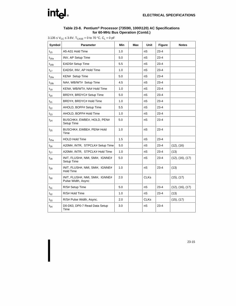
EE ELECTRICAL SPECIFICATIONS
23-15
Table 23-8. Pentium ® Processor (735\90, 1000\120) AC Specificationsfor 60-MHz Bus Operation (Contd.)
3.135 ≤ VCC ≤ 3.6V, TCASE = 0 to 70 °C, CL = 0 pF
Symbol Parameter Min Max Unit Figure Notes
t15 A5-A31 Hold Time 1.0 nS 23-4
t16a INV, AP Setup Time 5.0 nS 23-4
t16b EADS# Setup Time 5.5 nS 23-4
t17 EADS#, INV, AP Hold Time 1.0 nS 23-4
t18a KEN# Setup Time 5.0 nS 23-4
t18b NA#, WB/WT# Setup Time 4.5 nS 23-4
t19 KEN#, WB/WT#, NA# Hold Time 1.0 nS 23-4
t20 BRDY#, BRDYC# Setup Time 5.0 nS 23-4
t21 BRDY#, BRDYC# Hold Time 1.0 nS 23-4
t22 AHOLD, BOFF# Setup Time 5.5 nS 23-4
t23 AHOLD, BOFF# Hold Time 1.0 nS 23-4
t24 BUSCHK#, EWBE#, HOLD, PEN#Setup Time
5.0 nS 23-4
t25 BUSCHK#, EWBE#, PEN# HoldTime
1.0 nS 23-4
t25a HOLD Hold Time 1.5 nS 23-4
t26 A20M#, INTR, STPCLK# Setup Time 5.0 nS 23-4 (12), (16)
t27 A20M#, INTR, STPCLK# Hold Time 1.0 nS 23-4 (13)
t28 INIT, FLUSH#, NMI, SMI#, IGNNE#Setup Time
5.0 nS 23-4 (12), (16), (17)
t29 INIT, FLUSH#, NMI, SMI#, IGNNE#Hold Time
1.0 nS 23-4 (13)
t30 INIT, FLUSH#, NMI, SMI#, IGNNE#Pulse Width, Async
2.0 CLKs (15), (17)
t31 R/S# Setup Time 5.0 nS 23-4 (12), (16), (17)
t32 R/S# Hold Time 1.0 nS 23-4 (13)
t33 R/S# Pulse Width, Async. 2.0 CLKs (15), (17)
t34 D0-D63, DP0-7 Read Data SetupTime
3.0 nS 23-4

ELECTRICAL SPECIFICATIONS EE
23-16
Table 23-8. Pentium ® Processor (735\90, 1000\120) AC Specificationsfor 60-MHz Bus Operation (Contd.)
3.135 ≤ VCC ≤ 3.6V, TCASE = 0 to 70 °C, CL = 0 pF
Symbol Parameter Min Max Unit Figure Notes
t35 D0-D63, DP0-7 Read Data Hold Time 1.5 nS 23-4
t36 RESET Setup Time 5.0 nS 23-5 (11), (12), (16)
t37 RESET Hold Time 1.0 nS 23-5 (11), (13)
t38 RESET Pulse Width, VCC & CLKStable
15 CLKs 23-5 (11), (17)
t39 RESET Active After VCC & CLKStable
1.0 mS 23-5 Power up
t40 Reset Configuration Signals (INIT,FLUSH#, FRCMC#) Setup Time
5.0 nS 23-5 (12), (16), (17)
t41 Reset Configuration Signals (INIT,FLUSH#, FRCMC#) Hold Time
1.0 nS 23-5 (13)
t42a Reset Configuration Signals (INIT,FLUSH#, FRCMC#) Setup Time,Async.
2.0 CLKs 23-5 To RESET fallingedge (16)
t42b Reset Configuration Signals (INIT,FLUSH#, FRCMC#, BRDYC#,BUSCHK#) Hold Time, Async.
2.0 CLKs 23-5 To RESET fallingedge (27)
t42c Reset Configuration Signals(BRDYC#, BUSCHK#) Setup Time,Async.
3.0 CLKs 23-5 To RESET fallingedge (27)
t42d Reset Configuration Signal BRDYC#Hold Time, RESET drivensynchronously
1.0 nS To RESET fallingedge (1), (27)
t43a BF, CPUTYP Setup Time 1.0 mS 23-5 (22) to RESETfalling edge
t43b BF, CPUTYP Hold Time 2.0 CLKs 23-5 (22) to RESETfalling edge
t43c APICEN, BE4# Setup Time, 2.0 CLKs 23-5 To RESET fallingedge
t43d APICEN, BE4# Hold Time, 2.0 CLKs 23-5 To RESET fallingedge
t44 TCK Frequency — 16.0 MHz
t45 TCK Period 62.5 nS 23-1
t46 TCK High Time 25.0 nS 23-1 @2V, (1)
t47 TCK Low Time 25.0 nS 23-1 @0.8V, (1)

EE ELECTRICAL SPECIFICATIONS
23-17
Table 23-8. Pentium ® Processor (735\90, 1000\120) AC Specificationsfor 60-MHz Bus Operation (Contd.)
3.135 ≤ VCC ≤ 3.6V, TCASE = 0 to 70 °C, CL = 0 pF
Symbol Parameter Min Max Unit Figure Notes
t48 TCK Fall Time 5.0 nS 23-1 (2.0V–0.8V), (1),(8), (9)
t49 TCK Rise Time 5.0 nS 23-1 (0.8V–2.0V), (1),(8), (9)
t50 TRST# Pulse Width 40.0 nS 23-6 (1),Asynchronous
t51 TDI, TMS Setup Time 5.0 nS 23-6 (7)
t52 TDI, TMS Hold Time 13.0 nS 23-6 (7)
t53 TDO Valid Delay 3.0 20.0 nS 23-6 (8)
t54 TDO Float Delay 25.0 nS 23-6 (1), (8)
t55 All Non-Test Outputs Valid Delay 3.0 20.0 nS 23-6 (3), (8), (10)
t56 All Non-Test Outputs Float Delay 25.0 nS 23-6 (1), (3), (8), (10)
t57 All Non-Test Inputs Setup Time 5.0 nS 23-6 (3), (7), (10)
t58 All Non-Test Inputs Hold Time 13.0 nS 23-6 (3), (7), (10)
APIC AC Specifications
t60a PICCLK Frequency 2.0 16.66 MHz
t60b PICCLK Period 60.0 500.0 nS 23-1
t60c PICCLK High Time 15.0 nS 23-1
t60d PICCLK Low Time 15.0 nS 23-1
t60e PICCLK Rise Time 0.15 2.5 nS 23-1
t60f PICCLK Fall Time 0.15 2.5 nS 23-1
t60g PICD0-1 Setup Time 3.0 nS 23-4 To PICCLK
t60h PICD0-1 Hold Time 2.5 nS 23-4 To PICCLK
t60i PICD0-1 Valid Delay (LtoH) 4.0 38.0 nS 23-2 From PICCLK,(28)
t60j PICD0-1 Valid Delay (HtoL) 4.0 22.0 nS 23-2 From PICCLK,(28)
t61 PICCLK Setup Time 5.0 nS To CLK (31)
t62 PICCLK Hold Time 2.0 nS To CLK (31)
t63 PICCLK Ratio (CLK/PICCLK) 4.0 nS (32)

ELECTRICAL SPECIFICATIONS EE
23-18
Table 23-9. Pentium ® Processor (735\90, 1000\120) Dual Processor ModeAC Specifications for 60-MHz Bus Operation
3.135 ≤ VCC ≤ 3.6V, TCASE = 0 to 70°C, CL = 0 pF
Symbol Parameter Min Max Unit Figure Notes
t80 PBREQ#, PBGNT#, PHIT#, PHITM#Flight Time
0 2.0 nS 23-8 (29)
t83a A5-A31 Setup Time 3.9 nS 23-4 (18), (21), (26)
t83b D/C#, W/R#, CACHE#, LOCK#,SCYC Setup Time
4.0 nS 23-4 (18), (21)
t83c ADS#, M/IO# Setup Time 6.0 nS 23-4 (18), (21)
t83d HIT#, HITM# Setup Time 6.0 nS 23-4 (18), (21)
t83e HLDA Setup Time 6.0 nS 23-4 (18), (21)
t84 ADS#, D/C#, W/R#, M/IO#, CACHE#,LOCK#, A5-A31, HLDA, HIT#,HITM#, SCYC Hold Time
1.0 nS 23-4 (18), (21)
t85 DPEN# Valid Time 10.0 CLKs (18), (19), (23)
t86 DPEN# Hold Time 2.0 CLKs (18), (20), (23)
t87 APIC ID (BE0#-BE3#) Setup Time 2.0 CLKs 23-5 (23) to fallingEdge of RESET
t88 APIC ID (BE0#-BE3#) Hold Time 2.0 CLKs 23-5 (23) from FallingEdge of RESET
t89 D/P# Valid Delay 1.0 8.0 nS 23-2 Primaryprocessor Only
23.4.5.3. AC TIMING TABLES FOR A 66-MHz BUS
The AC specifications given in Tables 23-10 and 23-11 consist of output delays, input setuprequirements and input hold requirements for a 66-MHz external bus. All AC specifications(with the exception of those for the TAP signals and APIC signals) are relative to the risingedge of the CLK input.
All timings are referenced to 1.5V for both "0" and "1" logic levels unless otherwisespecified. Within the sampling window, a synchronous input must be stable for correctPentium processor 815\100 operation.

EE ELECTRICAL SPECIFICATIONS
23-19
Table 23-10. Pentium ® Processor (815\100, 1110\133) AC Specificationsfor 66-MHz Bus Operation
3.135 ≤ VCC ≤ 3.6V, TCASE = 0 to 70°C, CL = 0 pF
Symbol Parameter Min Max Unit Figure Notes
Frequency 33.33 66.6 MHz
t1a CLK Period 15.0 30.0 nS 23-1
t1b CLK Period Stability ±250 pS (1), (25)
t2 CLK High Time 4.0 nS 23-1 @2V, (1)
t3 CLK Low Time 4.0 nS 23-1 @0.8V, (1)
t4 CLK Fall Time 0.15 1.5 nS 23-1 (2.0V–0.8V), (1)
t5 CLK Rise Time 0.15 1.5 nS 23-1 (0.8V–2.0V), (1)
t6a ADSC#, PWT, PCD, BE0-7#, D/C#,W/R#, CACHE#, SCYC Valid Delay
1.0 7.0 nS 23-2
t6b AP Valid Delay 1.0 8.5 nS 23-2
t6c LOCK# Valid Delay 1.1 7.0 nS 23-2
t6d ADS# Valid Delay 1.0 6.0 nS 23-2
t6e A3-A31 Valid Delay 1.1 6.3 nS 23-2
t6f M/IO# Valid Delay 1.0 5.9 nS 23-2
t7 ADS#, ADSC#, AP, A3-A31, PWT,PCD, BE0-7#, M/IO#, D/C#, W/R#,CACHE#, SCYC, LOCK# Float Delay
10.0 nS 23-3 (1)
t8a APCHK#, IERR#, FERR# Valid Delay 1.0 8.3 nS 23-2 (4)
t8b PCHK# Valid Delay 1.0 7.0 nS 23-2 (4)
t9a BREQ Valid Delay 1.0 8.0 nS 23-2 (4)
t9b SMIACT# Valid Delay 1.0 7.3 nS 23-2 (4)
t9c HLDA Valid Delay 1.0 6.8 nS 23-2 (4)
t10a HIT# Valid Delay 1.0 6.8 nS 23-2
t10b HITM# Valid Delay 1.1 6.0 nS 23-2
t11a PM0-1, BP0-3 Valid Delay 1.0 10.0 nS 23-2
t11b PRDY Valid Delay 1.0 8.0 nS 23-2
t12 D0-D63, DP0-7 Write Data ValidDelay
1.3 7.5 nS 23-2
t13 D0-D63, DP0-3 Write Data FloatDelay
10.0 nS 23-3 (1)

ELECTRICAL SPECIFICATIONS EE
23-20
Table 23-10. Pentium ® Processor (815\100, 1110\133) AC Specificationsfor 66-MHz Bus Operation (Contd.)
3.135 ≤ VCC ≤ 3.6V, TCASE = 0 to 70°C, CL = 0 pF
Symbol Parameter Min Max Unit Figure Notes
t14 A5-A31 Setup Time 6.0 nS 23-4 (26)
t15 A5-A31 Hold Time 1.0 nS 23-4
t16a INV, AP Setup Time 5.0 nS 23-4
t16b EADS# Setup Time 5.0 nS 23-4
t17 EADS#, INV, AP Hold Time 1.0 nS 23-4
t18a KEN# Setup Time 5.0 nS 23-4
t18b NA#, WB/WT# Setup Time 4.5 nS 23-4
t19 KEN#, WB/WT#, NA# Hold Time 1.0 nS 23-4
t20 BRDY#, BRDYC# Setup Time 5.0 nS 23-4
t21 BRDY#, BRDYC# Hold Time 1.0 nS 23-4
t22 AHOLD, BOFF# Setup Time 5.5 nS 23-4
t23 AHOLD, BOFF# Hold Time 1.0 nS 23-4
t24a BUSCHK#, EWBE#, HOLD,SetupTime
5.0 nS 23-4
t24b PEN# Setup Time 4.8 nS 23-4
t25a BUSCHK#, EWBE#, PEN# HoldTime
1.0 nS 23-4
t25b HOLD Hold Time 1.5 nS 23-4
t26 A20M#, INTR, STPCLK# Setup Time 5.0 nS 23-4 (12), (16)
t27 A20M#, INTR, STPCLK# Hold Time 1.0 nS 23-4 (13)
t28 INIT, FLUSH#, NMI, SMI#, IGNNE#Setup Time
5.0 nS 23-4 (12), (16), (17)
t29 INIT, FLUSH#, NMI, SMI#, IGNNE#Hold Time
1.0 nS 23-4 (13)
t30 INIT, FLUSH#, NMI, SMI#, IGNNE#Pulse Width, Async
2.0 CLKs (15), (17)
t31 R/S# Setup Time 5.0 nS 23-4 (12), (16), (17)
t32 R/S# Hold Time 1.0 nS 23-4 (13)
t33 R/S# Pulse Width, Async. 2.0 CLKs (15), (17)
t34 D0-D63, DP0-7 Read Data SetupTime
2.8 nS 23-4

EE ELECTRICAL SPECIFICATIONS
23-21
Table 23-10. Pentium ® Processor (815\100, 1110\133) AC Specificationsfor 66-MHz Bus Operation (Contd.)
3.135 ≤ VCC ≤ 3.6V, TCASE = 0 to 70°C, CL = 0 pF
Symbol Parameter Min Max Unit Figure Notes
t35 D0-D63, DP0-7 Read Data Hold Time 1.5 nS 23-4
t36 RESET Setup Time 5.0 nS 23-5 (11), (12), (16)
t37 RESET Hold Time 1.0 nS 23-5 (11), (13)
t38 RESET Pulse Width, VCC & CLKStable
15.0 CLKs 23-5 (11), (17)
t39 RESET Active After VCC & CLKStable
1.0 mS 23-5 Power up
t40 Reset Configuration Signals (INIT,FLUSH#, FRCMC#) Setup Time
5.0 nS 23-5 (12), (16), (17)
t41 Reset Configuration Signals (INIT,FLUSH#, FRCMC#) Hold Time
1.0 nS 23-5 (13)
t42a Reset Configuration Signals (INIT,FLUSH#, FRCMC#) Setup Time,Async.
2.0 CLKs 23-5 To RESET fallingedge (16)
t42b Reset Configuration Signals (INIT,FLUSH#, FRCMC#, BRDYC#,BUSCHK#) Hold Time, Async.
2.0 CLKs 23-5 To RESET fallingedge (27)
t42c Reset Configuration Signals(BRDYC#, BUSCHK#) Setup Time,Async.
3.0 CLKs 23-5 To RESET fallingedge (27)
t42d Reset Configuration Signal BRDYC#Hold Time, RESET drivensynchronously
1.0 nS To RESET fallingedge (1), (27)
t43a BF, CPUTYP Setup Time 1.0 mS 23-5 (22) to RESETfalling edge
t43b BF, CPUTYP Hold Time 2.0 CLKs 23-5 (22) to RESETfalling edge
t43c APICEN, BE4# Setup Time 2.0 CLKs 23-5 To RESET fallingedge
t43d APICEN, BE4# Hold Time 2.0 CLKs 23-5 To RESET fallingedge
t44 TCK Frequency -- 16.0 MHz
t45 TCK Period 62.5 nS 23-1
t46 TCK High Time 25.0 nS 23-1 @2V, (1)
t47 TCK Low Time 25.0 nS 23-1 @0.8V, (1)
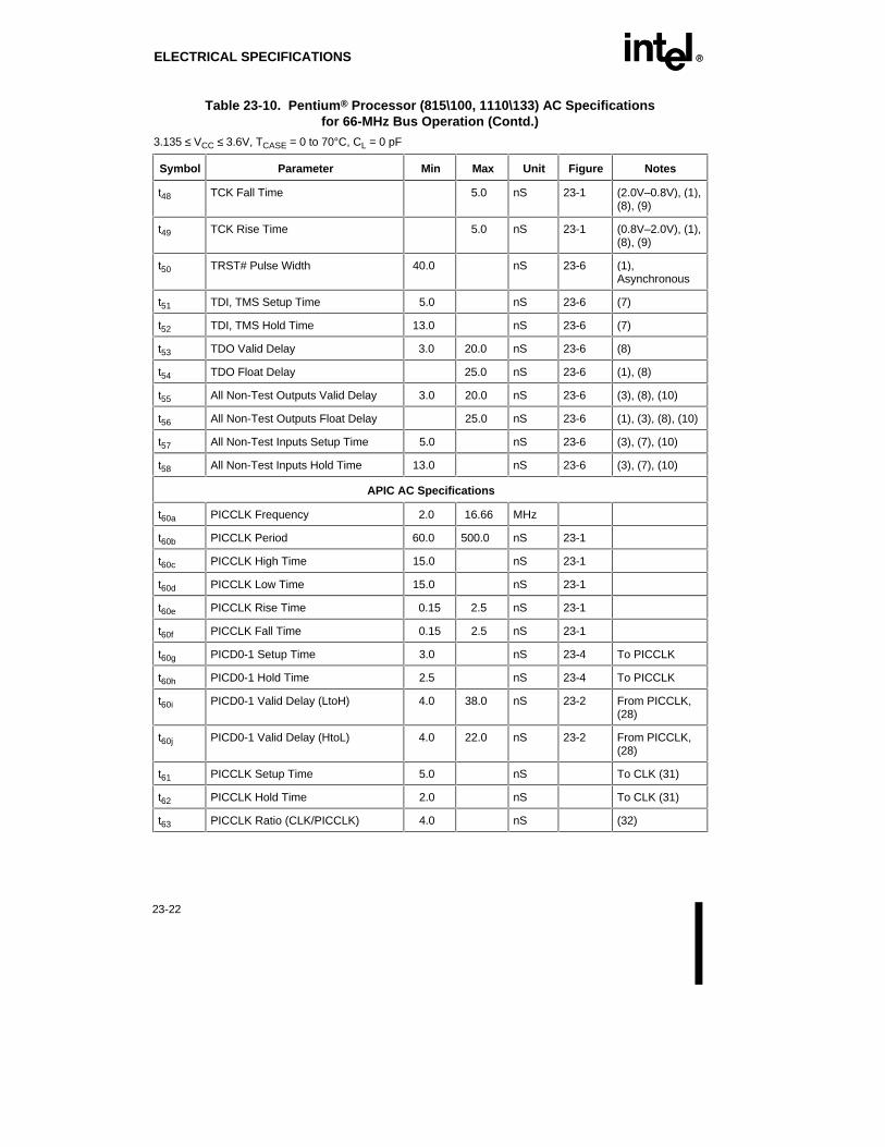
ELECTRICAL SPECIFICATIONS EE
23-22
Table 23-10. Pentium ® Processor (815\100, 1110\133) AC Specificationsfor 66-MHz Bus Operation (Contd.)
3.135 ≤ VCC ≤ 3.6V, TCASE = 0 to 70°C, CL = 0 pF
Symbol Parameter Min Max Unit Figure Notes
t48 TCK Fall Time 5.0 nS 23-1 (2.0V–0.8V), (1),(8), (9)
t49 TCK Rise Time 5.0 nS 23-1 (0.8V–2.0V), (1),(8), (9)
t50 TRST# Pulse Width 40.0 nS 23-6 (1),Asynchronous
t51 TDI, TMS Setup Time 5.0 nS 23-6 (7)
t52 TDI, TMS Hold Time 13.0 nS 23-6 (7)
t53 TDO Valid Delay 3.0 20.0 nS 23-6 (8)
t54 TDO Float Delay 25.0 nS 23-6 (1), (8)
t55 All Non-Test Outputs Valid Delay 3.0 20.0 nS 23-6 (3), (8), (10)
t56 All Non-Test Outputs Float Delay 25.0 nS 23-6 (1), (3), (8), (10)
t57 All Non-Test Inputs Setup Time 5.0 nS 23-6 (3), (7), (10)
t58 All Non-Test Inputs Hold Time 13.0 nS 23-6 (3), (7), (10)
APIC AC Specifications
t60a PICCLK Frequency 2.0 16.66 MHz
t60b PICCLK Period 60.0 500.0 nS 23-1
t60c PICCLK High Time 15.0 nS 23-1
t60d PICCLK Low Time 15.0 nS 23-1
t60e PICCLK Rise Time 0.15 2.5 nS 23-1
t60f PICCLK Fall Time 0.15 2.5 nS 23-1
t60g PICD0-1 Setup Time 3.0 nS 23-4 To PICCLK
t60h PICD0-1 Hold Time 2.5 nS 23-4 To PICCLK
t60i PICD0-1 Valid Delay (LtoH) 4.0 38.0 nS 23-2 From PICCLK,(28)
t60j PICD0-1 Valid Delay (HtoL) 4.0 22.0 nS 23-2 From PICCLK,(28)
t61 PICCLK Setup Time 5.0 nS To CLK (31)
t62 PICCLK Hold Time 2.0 nS To CLK (31)
t63 PICCLK Ratio (CLK/PICCLK) 4.0 nS (32)

EE ELECTRICAL SPECIFICATIONS
23-23
Table 23-11. Pentium ® Processor (815\100, 1110\133) Dual Processor ModeAC Specifications for 66-MHz Bus Operation
3.135 ≤ VCC ≤ 3.6V, TCASE = 0 to 70°C, CL = 0 pF
Symbol Parameter Min Max Unit Figure Notes
t80 PBREQ#, PBGNT#, PHIT#, PHITM#Flight Time
0 2.0 nS 23-8 (29)
t83a A5-A31 Setup Time 3.7 nS 23-4 (18), (21), (26)
t83b D/C#, W/R#, CACHE#, LOCK#,SCYC Setup Time
4.0 nS 23-4 (18), (21)
t83c ADS#, M/IO# Setup Time 5.8 nS 23-4 (18), (21)
t83d HIT#, HITM# Setup Time 6.0 nS 23-4 (18), (21)
t83e HLDA Setup Time 6.0 nS 23-4 (18), (21)
t84 ADS#, D/C#, W/R#, M/IO#, CACHE#,LOCK#, A5-A31, HLDA, HIT#,HITM#, SCYC Hold Time
1.0 nS 23-4 (18), (21)
t85 DPEN# Valid Time 10.0 CLKs (18), (19), (23)
t86 DPEN# Hold Time 2.0 CLKs (18), (20), (23)
t87 APIC ID (BE0#-BE3#) Setup Time 2.0 CLKs 23-5 (23) to fallingEdge of RESET
t88 APIC ID (BE0#-BE3#) Hold Time 2.0 CLKs 23-5 (23) fromFalling Edge ofRESET
t89 D/P# Valid Delay 1.0 8.0 nS 23-2 Primaryprocessor only
NOTES:
Notes 2, 6, and 14 are general and apply to all standard TTL signals used with the Pentium® Processor family.
1. Not 100% tested. Guaranteed by design.
2. TTL input test waveforms are assumed to be 0 to 3V transitions with 1V/nS rise and fall times.
3. Non-test outputs and inputs are the normal output or input signals (besides TCK, TRST#, TDI, TDO, andTMS). These timings correspond to the response of these signals due to boundary scan operations.
4. APCHK#, FERR#, HLDA, IERR#, LOCK#, and PCHK# are glitch-free outputs. Glitch-free signalsmonotonically transition without false transitions (i.e. glitches).
5. 0.8V/ns ≤ CLK input rise/fall time ≤ 8V/ns.
6. 0.3V/ns ≤ Input rise/fall time ≤ 5V/ns.
7. Referenced to TCK rising edge.
8. Referenced to TCK falling edge.
9. 1 ns can be added to the maximum TCK rise and fall times for every 10 MHz of frequency below 33 MHz.
10. During probe mode operation, do not use the boundary scan timings (t55-58).
11. FRCMC# should be tied to VCC (high) to ensure proper operation of the Pentium processor (610\75,735\90, 815\100, 1000\120) as a primary processor.

ELECTRICAL SPECIFICATIONS EE
23-24
12. Setup time is required to guarantee recognition on a specific clock. Pentium processor (610\75, 735\90,815\100, 1000\120) must meet this specification for dual processor operation for the FLUSH# and RESETsignals.
13. Hold time is required to guarantee recognition on a specific clock. Pentium processor (610\75, 735\90,815\100, 1000\120) must meet this specification for dual processor operation for the FLUSH# and RESETsignals.
14. All TTL timings are referenced from 1.5V.
15. To guarantee proper asynchronous recognition, the signal must have been de-asserted (inactive) for aminimum of 2 clocks before being returned active and must meet the minimum pulse width.
16. This input may be driven asynchronously. However, when operating two processors in dual processingmode, FLUSH# and RESET must be asserted synchronously to both processors.
17. When driven asynchronously, RESET, NMI, FLUSH#, R/S#, INIT, and SMI# must be de-asserted(inactive) for a minimum of 2 clocks before being returned active.
18. Timings are valid only when Dual processor is present.
19. Maximum time DPEN# is valid from rising edge of RESET.
20. Minimum time DPEN# is valid after falling edge of RESET.
21. The D/C#, M/IO#, W/R#, CACHE#, and A5-A31 signals are sampled only on the CLK that ADS# is active.
22. BF and CPUTYP should be strapped to VCC or VSS.
23. RESET is synchronous in dual processing mode and functional redundancy checking mode. All signalswhich have a setup or hold time with respect to a falling or rising edge of RESET in UP mode, should bemeasured with respect to the first processor clock edge in which RESET is sampled either active orinactive in dual processing and functional redundancy checking modes.
24. The PHIT# and PHITM# signals operate at the core frequency (75, 90, 100, 120, or 133 MHz).
25. These signals are measured on the rising edge of adjacent CLKs at 1.5V. To ensure a 1:1 relationshipbetween the amplitude of the input jitter and the internal and external clocks, the jitter frequency spectrumshould not have any power spectrum peaking between 500 KHz and 1\3 of the CLK operating frequency.The amount of jitter present must be accounted for as a component of CLK skew between devices.
26. In dual processing mode, timing t14 is replaced by t83a. Timing t14 is required for external snooping (e.g.address setup to the CLK in which EADS# is sampled active) in both uniprocessor and dual processormodes.
27. BRDYC# and BUSCHK# are used as reset configuration signals to select buffer size.
28. This assumes an external pullup resistor to VCC and a lumped capacitive load. The pullup resistor mustbe between 150 ohms and 1K ohms, the capacitance must be between 20 pF and 240 pF, and the RCproduct must be between 3 ns and 36 ns.
29. This is a flight time specification, that includes both flight time and clock skew. The flight time is the timefrom where the unloaded driver crosses 1.5V (50% of min VCC), to where the receiver crosses the 1.5Vlevel (50% of min VCC). See Figure 23.8.
** Each valid delay is specified for a 0 pF load. The system designer should use I/O buffer modeling toaccount for signal flight time delays.
31. This is for the Lock Step operation of the component only. This guarantees that APIC interrupts will berecognized on specific clocks to support 2 processors running in a Lock Step fashion including FRCmode. FRC on the APIC pins is not supported but mismatches on these pins will result in a mismatch onother pins of the CPU.
32. The CLK to PICCLK ratio for lock step operation has to be an integer and the ratio (CLK/PICCLK) cannotbe smaller than 4.

EE ELECTRICAL SPECIFICATIONS
23-25
1.5V
2.0V
0.8V
Tx
PP0051
Tw
Ty
Tz
Tv
Tv
Tw
Tx
Ty
Tz
=
=
=
=
=
t5, t49, t60e
t4, t48, t60f
t3, t47, t60e
t1, t45, t60b
t2, t46, t60c
1.5V
Figure 23-1. Clock Waveform
Signal VALID
1.5V
1.5V
T max.xT min.x
Tx = t6, t8, t9, t10, t11, t12, t60i, t80a, t89
PP0052
Figure 23-2. Valid Delay Timings
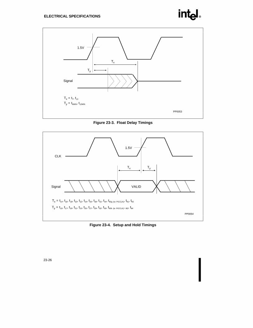
ELECTRICAL SPECIFICATIONS EE
23-26
Signal
1.5V
Ty
Tx
PP0053
Tx = t7, t13
Ty = t6MIN, t12MIN
Figure 23-3. Float Delay Timings
CLK
Signal VALID
1.5V
Tx = t14, t16, t18, t20, t22, t24, t26, t28, t31, t34, t60g (to PICCLK), t81, t83
Ty = t15, t17, t19, t21, t23, t25, t27, t29, t32, t35, t60h (to PICCLK), t82, t84
PP0054
TyTx
Figure 23-4. Setup and Hold Timings

EE ELECTRICAL SPECIFICATIONS
23-27
VALID
CLK
RESET
Config
1.5 V
1.5 V
1.5 V
Tz
Tt = t40
Tv
Tt Tu
Tx
Tw
Ty
PP0055
Tu = t41
Tv = t37
Tw = t42, t43a, t43c, t87
Tx = t43b, t43d, t88
Ty = t38, t39
Tz = t36
Figure 23-5. Reset and Configuration Timings

ELECTRICAL SPECIFICATIONS EE
23-28
1.5 V
Tr = t57
TCK
TDITMS
TDO
OutputSignals
InputSignals
Tv Tw
Tx
Ty
Tr Ts
Tu
Tz
PP0056
Ts = t58
Tu = t54
Tv = t51
Tw = t52
Tx = t53
Ty = t55
Tz = t56
Figure 23-6. Test Timings
1.5VTRST#
Tx = t50
PP0057
Tx
Figure 23-7. Test Reset Timings

EE ELECTRICAL SPECIFICATIONS
23-29
Signal Level
50% DelayFlight Time
At Rece ive r P in
Driver Pin at0 pf Load
T i m e
65% Vc c
50% Vc c
35% Vc c
Vs s
Vc c
PP 0 0 5 8
Figure 23-8. V cc Measurement of Flight Time

E24
I/O Buffer Models


EE
24-1
CHAPTER 24I/O BUFFER MODELS
The 3.3V buffers of the Pentium processor (610\75, 735\90, 815\100, 1000\120, 1110\133)and the 5V buffers of the Pentium processor (510\60, 567\66) are different. This Chapterdescribes the I/O buffer models of the Pentium processor (610\75, 735\90, 815\100,1000\120, 1110\133).
The first order I/O buffer model is a simplified representation of the complex input andoutput buffers used in the Pentium processor (610\75, 735\90, 815\100, 1000\120, 1110\133).Figures 24-1 and 24-2 show the structure of the input buffer model and Figure 24-3 shows theoutput buffer model. Tables 24-1 and 24-2 show the parameters used to specify thesemodels.
Although simplified, these buffer models will accurately model flight time and signal quality.For these parameters, there is very little added accuracy in a complete transistor model.
The following two models represent the input buffer models. The first model, Figure 24-1,represents all of the input buffers of the Pentium processor (610\75, 735\90, 815\100,1000\120, 1110\133) except for a special group of input buffers. The second model, Figure24-2, represents these special buffers. These buffers are the inputs: AHOLD, EADS#,KEN#, WB/WT#, INV, NA#, EWBE#, BOFF#, CLK, and PICCLK.

I/O BUFFER MODELS EE
24-2
L p
C pC i n
D 1
D 2
V
R
PP0059
s
ss
R s
Vcc
Figure 24-1. Input Buffer Model, Except Special Group

EE I/O BUFFER MODELS
24-3
6 x R
D 2
D 2
D 2
D 2
D 2
D 2
D 1C
PP0060
p
L p
R s
C in
s
Figure 24-2. Input Buffer Model for Special Group

I/O BUFFER MODELS EE
24-4
Table 24-1. Parameters Used in the Specification of the First Order Input Buffer Model
Parameter Description
Cin Minimum and Maximum value of the capacitance of the input buffer model.
Lp Minimum and Maximum value of the package inductance.
Cp Minimum and Maximum value of the package capacitance.
Rs Diode Series Resistance
D1, D2 Ideal Diodes
Figure 24-3 below shows the structure of the output buffer model. This model is used for allof the output buffers of the Pentium processor (610\75, 735\90, 815\100, 1000\120,1110\133).
dV/dt
R
P P 00 6 1
o
C o
L p
C p
Figure 24-3. First Order Output Buffer Model
Table 24-2. Parameters Used in the Specification of the First Order Output BufferModel
Parameter Description
dV/dt Minimum and maximum value of the rate of change of the open circuitvoltage source used in the output buffer model.
Ro Minimum and maximum value of the output impedance of the output buffermodel.
Co Minimum and Maximum value of the capacitance of the output buffer model.
Lp Minimum and Maximum value of the package inductance.
Cp Minimum and Maximum value of the package capacitance.
In addition to the input and output buffer parameters, input protection diode models areprovided for added accuracy. These diodes have been optimized to provide ESD protection
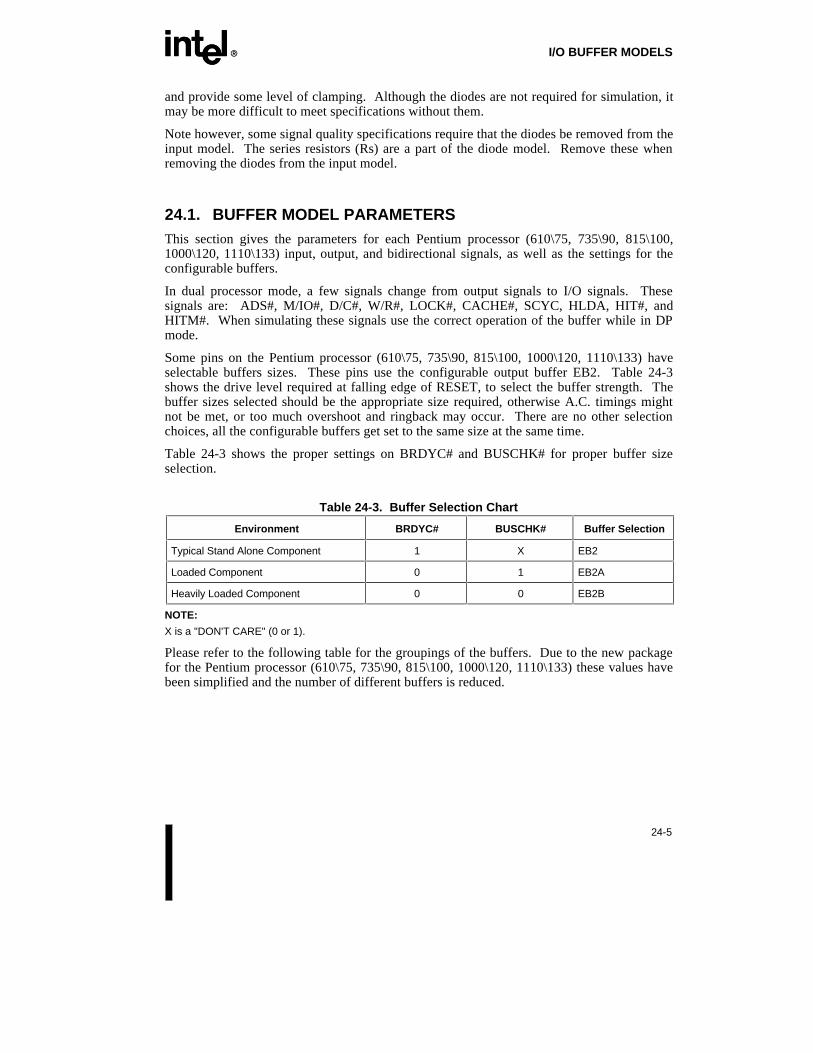
EE I/O BUFFER MODELS
24-5
and provide some level of clamping. Although the diodes are not required for simulation, itmay be more difficult to meet specifications without them.
Note however, some signal quality specifications require that the diodes be removed from theinput model. The series resistors (Rs) are a part of the diode model. Remove these whenremoving the diodes from the input model.
24.1. BUFFER MODEL PARAMETERSThis section gives the parameters for each Pentium processor (610\75, 735\90, 815\100,1000\120, 1110\133) input, output, and bidirectional signals, as well as the settings for theconfigurable buffers.
In dual processor mode, a few signals change from output signals to I/O signals. Thesesignals are: ADS#, M/IO#, D/C#, W/R#, LOCK#, CACHE#, SCYC, HLDA, HIT#, andHITM#. When simulating these signals use the correct operation of the buffer while in DPmode.
Some pins on the Pentium processor (610\75, 735\90, 815\100, 1000\120, 1110\133) haveselectable buffers sizes. These pins use the configurable output buffer EB2. Table 24-3shows the drive level required at falling edge of RESET, to select the buffer strength. Thebuffer sizes selected should be the appropriate size required, otherwise A.C. timings mightnot be met, or too much overshoot and ringback may occur. There are no other selectionchoices, all the configurable buffers get set to the same size at the same time.
Table 24-3 shows the proper settings on BRDYC# and BUSCHK# for proper buffer sizeselection.
Table 24-3. Buffer Selection Chart
Environment BRDYC# BUSCHK# Buffer Selection
Typical Stand Alone Component 1 X EB2
Loaded Component 0 1 EB2A
Heavily Loaded Component 0 0 EB2B
NOTE:
X is a "DON'T CARE" (0 or 1).
Please refer to the following table for the groupings of the buffers. Due to the new packagefor the Pentium processor (610\75, 735\90, 815\100, 1000\120, 1110\133) these values havebeen simplified and the number of different buffers is reduced.

I/O BUFFER MODELS EE
24-6
Table 24-4. Signal to Buffer Type
Signals TypeDriver Buffer
TypeReceiver
Buffer Type
CLK I ER0
A20M#, AHOLD, BF, BOFF#, BRDY#, BRDYC#,BUSCHK#, EADS#, EWBE#, FLUSH#, FRCMC#, HOLD,IGNNE#, INIT, INTR, INV, KEN#, NA#, NMI, PEN#, PICCLK,R/S#, RESET, SMI#, STPCLK#, TCK, TDI, TMS, TRST#,WB/WT#
I ER1
ADSC#, APCHK#, BE[7:5]#, BP[3:2], BREQ, FERR#,IERR#, PCD, PCHK#, PM0/BP0, PM1/BP1, PRDY, PWT,SMIACT#, TDO, U/O#
O ED1
A[31:21], AP, BE[4:0]#, CACHE#, D/C#, D[63:0], DP[8:0],HLDA, LOCK#, M/IO#, PBGNT#, PBREQ#, PHIT#, PHITM#,SCYC
I/O EB1 EB1
A[20:3], ADS#, HITM#, W/R# I/O EB2/A/B EB2
HIT# I/O EB3 EB3
PICD0, PICD1 I/O EB4 EB4
The input, output and bidirectional buffers values are listed below. This table containslistings for all three types, do not get them confused during simulation. When a bidirectionalpin is operating as an input, just use the Cin, Cp and Lp values, if it is operating as a driveruse all the data parameters.

EE I/O BUFFER MODELS
24-7
Table 24-5. Input, Output and Bidirectional Buffer Model Parameters
BufferType Transition
dV/dt(V/nsec)
Ro(Ohms)
Cp(pF)
Lp(nH)
Co/Cin(pF)
min max min max min max min max min max
ER0 Rising 3.0 5.0 4.0 6.0 0.8 1.2
(input) Falling 3.0 5.0 4.0 6.0 0.8 1.2
ER1 Rising 1.1 5.3 7.7 15.3 0.8 1.2
(input) Falling 1.1 5.3 7.7 15.3 0.8 1.2
ED1 Rising 3/3.0 3.7/0.9 21.6 53.1 1.1 5.8 8.1 16.3 2.0 2.6
(output) Falling 3/2.8 3.7/0.8 17.5 50.7 1.1 5.8 8.1 16.3 2.0 2.6
EB1 Rising 3/3.0 3.7/0.9 21.6 53.1 1.3 7.0 8.2 18.4 2.0 2.6
(bidir) Falling 3/2.8 3.7/0.8 17.5 50.7 1.3 7.0 8.2 18.4 2.0 2.6
EB2 Rising 3/3.0 3.7/0.9 21.6 53.1 1.3 5.4 8.5 16.0 9.1 9.7
(bidir) Falling 3/2.8 3.7/0.8 17.5 50.7 1.3 5.4 8.5 16.0 9.1 9.7
EB2A Rising 3/2.4 3.7/0.9 10.1 22.4 1.3 5.4 8.5 16.0 9.1 9.7
(bidir) Falling 3/2.4 3.7/0.9 9.0 21.2 1.3 5.4 8.5 16.0 9.1 9.7
EB2B Rising 3/1.8 3.7/0.7 5.5 12.9 1.3 5.4 8.5 16.0 9.1 9.7
(bidir) Falling 3/1.8 3.7/0.7 4.6 12.3 1.3 5.4 8.5 16.0 9.1 9.7
EB3 Rising 3/3.0 3.7/0.9 21.6 53.1 1.9 4.2 10.5 14.3 3.3 3.9
(bidir) Falling 3/2.8 3.7/0.8 17.5 50.7 1.9 4.2 10.5 14.3 3.3 3.9
EB4 Rising 3/3.0 3.7/0.9 100K* 100K* 2.0 4.3 10.7 14.6 5.0 7.0
(bidir) Falling 3/2.8 3.7/0.8 17.5 50.7 2.0 4.3 10.7 14.6 5.0 7.0
* The buffer is an open drain, and for simmulation purposes should be a very large internal resistance withadditional external pull-up.
Table 24-6. Input Buffer Model Parameters: D (Diodes)
Symbol Parameter D1 D2
IS Saturation Current 1.4e-14A 2.78e-16A
N Emission Coefficient 1.19 1.00
RS Series Resistance 6.5 ohms 6.5 ohms
TT Transit Time 3 ns 6 ns
VJ PN Potential 0.983V 0.967V
CJ0 Zero Bias PN Capacitance 0.281 pF 0.365 pF
M PN Grading Coefficient 0.385 0.376

I/O BUFFER MODELS EE
24-8
24.2. SIGNAL QUALITY SPECIFICATIONSSignals driven by the system into the Pentium processor (610\75, 735\90, 815\100, 1000\120,1110\133) must meet signal quality specifications to guarantee that the components read dataproperly and to ensure that incoming signals do not affect the reliability of the component.There are two signal quality parameters: Ringback and Settling Time.
24.2.1. RingbackExcessive ringback can contribute to long-term reliability degradation of the Pentiumprocessor (610\75, 735\90, 815\100, 1000\120, 1110\133), and can cause false signaldetection. Ringback is simulated at the input pin of a component using the input buffermodel. Ringback can be simulated with or without the diodes that are in the input buffermodel.
Ringback is the absolute value of the maximum voltage at the receiving pin below VCC (orabove VSS) relative to VCC (or VSS) level after the signal has reached its maximum voltagelevel. The input diodes are assumed present.
Maximum Ringback on Inputs = 0.8V
(with diodes)
If simulated without the input diodes, follow the Maximum Overshoot/Undershootspecification. By meeting the overshoot/undershoot specification, the signal is guaranteednot to ringback excessively.
If simulated with the diodes present in the input model, follow the maximum ringbackspecification.
Overshoot (Undershoot) is the absolute value of the maximum voltage above VCC (belowVSS). The guideline assumes the absence of diodes on the input.
• Maximum Overshoot/Undershoot on 5V 82497 Cache Controller, 82492 Cache SRAM,and Pentium processor (610\75, 735\90, 815\100, 1000\120, 1110\133) Inputs (CLK andPICCLK only) = 1.6V above VCC5 (without diodes)
• Maximum Overshoot/Undershoot on 3.3V Pentium processor (610\75, 735\90, 815\100,1000\120, 1110\133) Inputs (not CLK and PICCLK) = 1.4V above VCC3 (withoutdiodes)
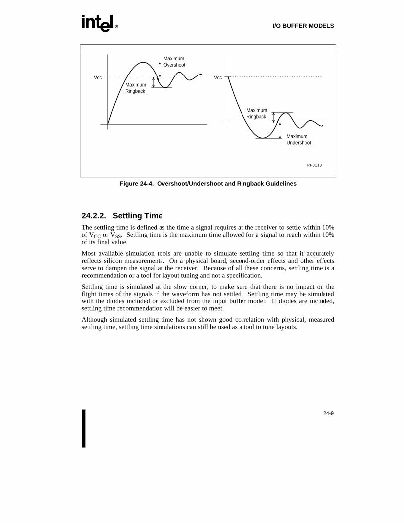
EE I/O BUFFER MODELS
24-9
Vcc
MaximumOvershoot
MaximumRingback
Vcc
MaximumUndershoot
MaximumRingback
PP0110
Figure 24-4. Overshoot/Undershoot and Ringback Guidelines
24.2.2. Settling TimeThe settling time is defined as the time a signal requires at the receiver to settle within 10%of VCC or VSS. Settling time is the maximum time allowed for a signal to reach within 10%of its final value.
Most available simulation tools are unable to simulate settling time so that it accuratelyreflects silicon measurements. On a physical board, second-order effects and other effectsserve to dampen the signal at the receiver. Because of all these concerns, settling time is arecommendation or a tool for layout tuning and not a specification.
Settling time is simulated at the slow corner, to make sure that there is no impact on theflight times of the signals if the waveform has not settled. Settling time may be simulatedwith the diodes included or excluded from the input buffer model. If diodes are included,settling time recommendation will be easier to meet.
Although simulated settling time has not shown good correlation with physical, measuredsettling time, settling time simulations can still be used as a tool to tune layouts.

I/O BUFFER MODELS EE
24-10
Use the following procedure to verify board simulation and tuning with concerns for settlingtime.
1. Simulate settling time at the slow corner for a particular signal.
2. If settling time violations occur, simulate signal trace with D.C. diodes in place at thereceiver pin. The D.C. diode behaves almost identically to the actual (non-linear) diodeon the part as long as excessive overshoot does not occur.
3. If settling time violations still occur, simulate flight times for 5 consecutive cycles forthat particular signal.
4. If flight time values are consistent over the 5 simulations, settling time should not be aconcern. If however, flight times are not consistent over the 5 simulations, tuning of thelayout is required.
5. Note that, for signals that are allocated 2 cycles for flight time, the recommended settlingtime is doubled.
Maximum Settling Time to within 10% of VCC is: 12.5ns @66 MHz
14.2ns @60 MHz
17.5ns @50 MHz
Vcc + 10%
Vcc -10%
Settl ing Time
PP0111
Vcc
Figure 24-5. Settling Time

E25
MechanicalSpecifications


25-1
CHAPTER 25MECHANICAL SPECIFICATIONS
The physical packages of the Pentium processor (610\75, 735\90, 815\100, 1000\120,1110\133) and the Pentium processor (510\60, 567\66) are different. The Pentium processor(610\75, 735\90, 815\100, 1000\120, 1110\133) uses a 296-pin Staggered PGA package,while the Pentium processor (510\60, 567\66) uses a 273-pin PGA.
The pins of the Pentium processor (610\75, 735\90, 815\100, 1000\120, 1110\133) arearranged in a 37 x 37 matrix and the package dimensions are 1.95" x 1.95" (Table 25-1). A1.25" x 1.25" copper tungsten heat spreader may be attached to the top of the ceramic.
Intel provides two kinds of packages for Pentium processor (610\75, 735\90, 815\100,1000\120, 1110\133). One has a 1.25" × 1.25" copper tungsten heat spreader brazed to thetop of the ceramic, and the later package conversion removes the heat spreader from the topof the package, and replaces the metal lid covering the die with a ceramic lid. Table 25-1summarizes the information of both packages.
Table 25-1. Package Information Summary
Package Type Total Pins Pin Array Package Size
Pentium processor(610\75, 735\90,815\100, 1000\120,1110\133)
SPGA 296 37 x 37 1.95" x 1.95"
4.95cm x 4.95cm
Figure 25-1 and Figure 25-2 show the dimensions of the packages with the heat spreader andwithout the heat spreader respectively. Table 25-2 and Table 25-3 provide the mechanicalspecifications of the packages with the heat spreader and without the heat spreaderrespectively.

MECHANICAL SPECIFICATIONS EE
25-2
Table 25-2. Package (with the heat spreader) Dimensions
Family: Ceramic Pin Grid Array Package
Symbol Millimeter Inches
Min Max Notes Min Max Notes
A 3.91 4.70 Solid Lid 0.154 0.185 Solid Lid
A1 0.33 0.43 Solid Lid 0.013 0.017 Solid Lid
A2 2.62 2.97 0.103 0.117
B 0.43 0.51 0.017 0.020
D 49.28 49.91 1.940 1.965
D1 45.47 45.97 1.790 1.810
D2 31.50 32.00 Square 1.240 1.260 Square
D3 33.99 34.59 1.338 1.362
D4 8.00 9.91 0.315 0.390
E1 2.41 2.67 0.095 0.105
E2 1.14 1.40 0.045 0.055
F 0.127 Diagonal 0.005 Diagonal
L 3.05 3.30 0.120 0.130
N 296 296
S1 1.52 2.54 0.060 0.100

EE MECHANICAL SPECIFICATIONS
25-3
01.65REF.
S1
D
L
SEATINPLANE
AA1A2
REF.2.291.52
45° CHAMFER(INDEX CORNER)
B
PP0112
Pin C3
E1E2
D
D1
D
D3
D2
D4
D4
F
CU W Heat Spreader
Braze Metalization
Figure 25-1. Package (with the heat spreader) Dimensions

MECHANICAL SPECIFICATIONS EE
25-4
01.65REF.
L
SEATINGPLANE
AA1A2
REF.2.291.52
45° INDEX CHAMFER(INDEX CORNER)
PP0112a
Pin C3
E1E2
F
S1
D
D1
D3
DD1D3
B
Bottom View (Pin Side Up)
Top View
Intel Pentium ®
pp0112a
Figure 25-2. Package (without the heat spreader) Dimensions

EE MECHANICAL SPECIFICATIONS
25-5
Table 25-3. Package (without the heat spreader) Dimensions
Family: 296 Pin Ceramic Pin Grid Array Package
Millimeters Inches
Symbol Min Max Notes Min Max Notes
A 3.27 3.83 Ceramic Lid 0.129 0.151 Ceramic Lid
A1 0.66 0.86 Ceramic Lid 0.026 0.034 Ceramic Lid
A2 2.62 2.97 0.103 0.117
B .043 0.51 0.017 0.020
D 49.28 49.78 1.940 1.960
D1 45.59 45.85 1.795 1.805
D3 24.00 24.25 Includes Fillet 0.945 0.955 Includes Fillet
e1 2.29 2.79 0.090 0.110
F 0.127 Flatness of the top of thepackage, measureddiagonally
0.005 Flatness of the top of thepackage, measureddiagonally
L 3.05 3.30 0.120 1.130
N 296 Total Pins 296 Total Pins
S1 1.52 2.54 0.060 0.100

E26
ThermalSpecifications


EE
26-1
CHAPTER 26THERMAL SPECIFICATIONS
Due to the advanced 3.3V BiCMOS process that it is produced on, the Pentium processor(610\75, 735\90, 815\100, 1000\120, 1110\133) dissipates less power than the Pentiumprocessor (510\60, 567\66).
The Pentium processor (610\75, 735\90, 815\100, 1000\120, 1110\133) is specified for properoperation when case temperature, TCASE, (TC) is within the specified range of 0°C to 70°C.
26.1. MEASURING THERMAL VALUESTo verify that the proper TC (case temperature) is maintained, it should be measured at thecenter of the package top surface on the heat spreader (opposite of the pins). Themeasurement is made in the same way with or without a heat sink attached. When a heatsink is attached a hole (smaller than .150" diameter) should be drilled through the heat sinkto allow probing the center of the package. See Figure 26-1 for an illustration of how tomeasure TC.
PP0062
Figure 26-1. Technique for Measuring T C*
* Though the figure shows the package with a heat spreader, the same technique applies to measuring TCof the package without a heat spreader.
To minimize the measurement errors, it is recommended to use the following approach:
• Use 36-gauge or finer diameter K, T, or J type thermocouples. The laboratory testingwas done using a thermocouple made by Omega (part number: 5TC-TTK-36-36).
• Attach the thermocouple bead or junction to the center of the package top surface usinghigh thermal conductivity cements. The laboratory testing was done by using OmegaBond (part number: OB-100).
• The thermocouple should be attached at a 90-degrees angle as shown in Figure 26-1.
• The hole size should be smaller than .150" in diameter.

THERMAL SPECIFICATIONS EE
26-2
26.1.1. Thermal Equations and DataFor the Pentium processor (610\75, 735\90, 815\100, 1000\120, 1110\133), an ambienttemperature, TA (air temperature around the processor), is not specified directly. The onlyrestriction is that TC is met. To calculate TA values, the following equations may be used:
TA = TC - (P * ΘCA)
ΘCA = ΘJA - ΘJCwhere, TA and TC = ambient and case temperature. (oC)
ΘCA = case-to-ambient thermal resistance. (oC/Watt)
ΘJA = junction-to-ambient thermal resistance. (oC/Watt)
ΘJC = junction-to-case thermal resistance. (oC/Watt)
P = maximum power consumption (Watt)
(See DC specifications in Chapter 23 for detailed power consumption specifications.)
Table 26-1 lists the ΘCA values for the Pentium processor (610\75, 735\90, 815\100,1000\120, 1110\133) with heat spreader and passive heat sinks. Figure 26-2 shows Table26-1 in graphic format.
Table 26-2 lists the ΘCA values for the Pentium processor (610\75, 735\90, 815\100,1000\120, 1110\133) with passive heat sinks, but without a heat spreader. Figure 26-3 showsTable 26-2 in graphic format.
Table 26-1. Thermal Resistances for Packages with Heat Spreader
ΘΘCA (oC/Watt) vs. Laminar Airflow (linear ft/min)
Heat Sink in inches ΘΘJC (oC/Watt) 0 100 200 400 600 800
1.95x1.95x0.25 0.9 8.7 7.6 6.2 4.0 3.2 2.6
1.95x1.95x0.35 0.9 8.4 7.1 5.6 3.6 2.9 2.4
1.95x1.95x0.45 0.9 8.0 6.6 4.9 3.2 2.5 2.1
1.95x1.95x0.55 0.9 7.7 6.1 4.3 2.8 2.2 1.9
1.95x1.95x0.65 0.9 7.3 5.6 3.9 2.6 2.0 1.7
1.95x1.95x0.80 0.9 6.6 4.9 3.5 2.2 1.8 1.6
1.95x1.95x1.00 0.9 5.9 4.2 3.2 2.2 1.7 1.4
1.95x1.95x1.20 0.9 5.5 3.9 2.9 2.0 1.6 1.4
1.95x1.95x1.40 0.9 5.0 3.5 2.6 1.8 1.5 1.3
Without Heat Sink 1.4 11.4 10.5 8.7 5.7 4.5 3.8

EE THERMAL SPECIFICATIONS
26-3
Table 26-2. Thermal Resistances for Packages without Spreader
ΘΘCA (oC/Watt) vs. Laminar Airflow (linear ft/min)
Heat Sink in Inches ΘΘJC (°C/Watt) 0 100 200 400 600 800
0.25 0.8 9.1 8.0 6.6 4.4 3.6 3.0
0.35 0.8 8.8 7.5 6.0 4.0 3.3 2.8
0.45 0.8 8.4 7.0 5.3 3.6 2.9 2.5
0.55 0.8 8.1 6.5 4.7 3.2 2.6 2.3
0.65 0.8 7.7 6.0 4.3 3.0 2.4 2.1
0.80 0.8 7.0 5.3 3.9 2.8 2.2 2.0
1.00 0.8 6.3 4.6 3.6 2.6 2.1 1.8
1.20 0.8 5.9 4.3 3.3 2.4 2.0 1.8
1.40 0.8 5.4 3.9 3.0 2.2 1.9 1.7
Without Heat Sink 1.3 14.4 13.1 11.7 8.8 7.4 6.5
NOTES:
Heat sinks are omni directional pin aluminum alloy.
Features were based on standard extrusion practices for a given height
Pin size ranged from 50 to 129 mils
Pin spacing ranged from 93 to 175 mils
Based thickness ranged from 79 to 200 mils
Heat sink attach was 0.005" of thermal grease.
Attach thickness of 0.002" will improve performance approximately 0.3oC/Watt
Heat Sink Height (in)
The
ta (
CA
)
0
2
4
6
8
1 0
0 0.2 0.4 0.6 0.8 1 1.2 1.4 1.6
0 LFM100 LFM20 0 L FM
400 LFM60 0 L FM
800 LFM
PP0063
Thermal Resistance vs. Heatsink Height
Figure 26-2. Thermal Resistance vs. Heat Sink Height
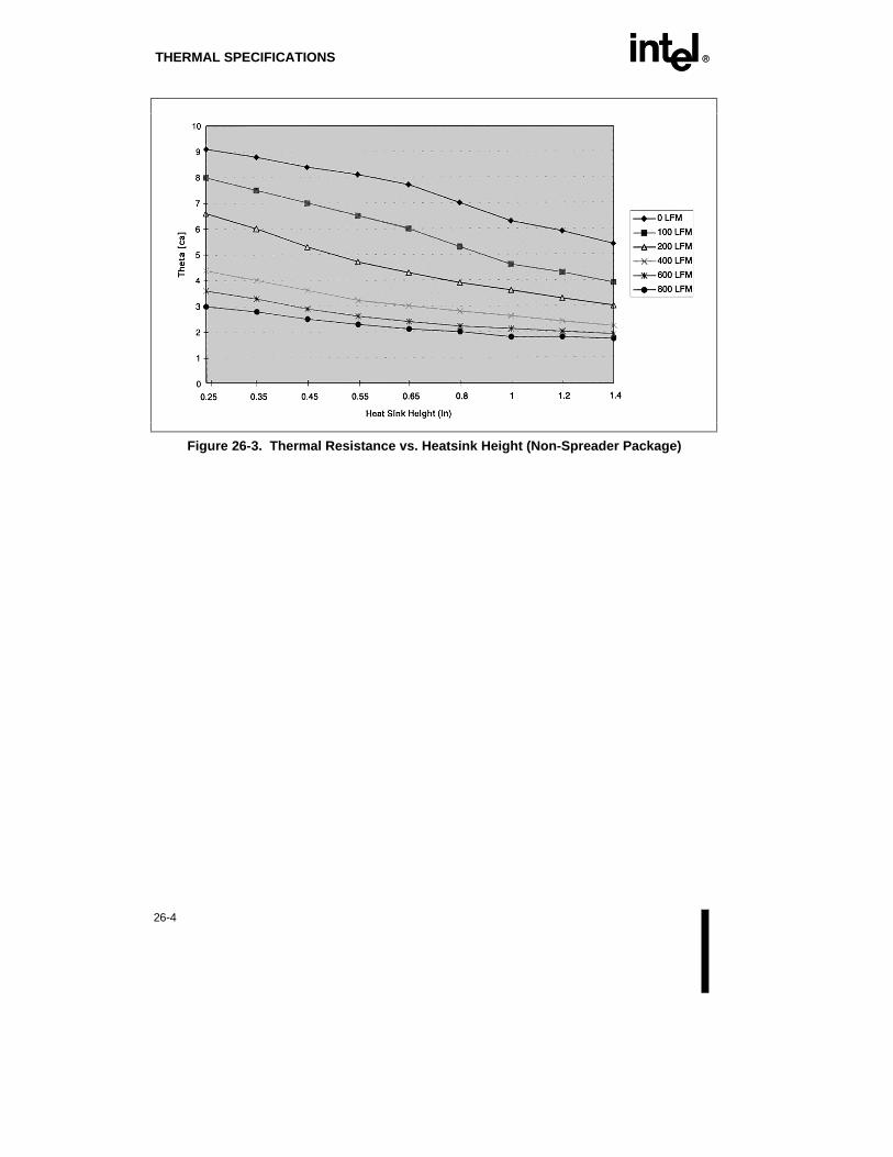
THERMAL SPECIFICATIONS EE
26-4
Figure 26-3. Thermal Resistance vs. Heatsink Height (Non-Spreader Package)

E27
Testability


EE
27-1
CHAPTER 27TESTABILITY
The Pentium processor (610\75, 735\90, 815\100, 1000\120, 1110\133) supports the sametestability features as found in Chapter 11 for the Pentium processor family. Since thePentium processor (610\75, 735\90, 815\100, 1000\120, 1110\133) operates at 3.3V and thePentium processor (510\60, 567\66) operates at 5V, the following section describes theboundary scan considerations to handle this change.
27.1. BOUNDARY SCAN 3.3V CONSIDERATIONSThe boundary scan pins of the Pentium processor (610\75, 735\90, 815\100, 1000\120,1110\133) are all 3.3V signals (including TCK).
Intel recommends that the system design use separate scan chains for its 5V portions and3.3V portions.
Contact your local Intel representative for BSDL files describing the implementation of theboundary scan chain.
If a single scan chain must be used:
1. The system TCK must be a 3.3V-level clock (unlike CLK and PICCLK).
2. TDO from 5V components must have a level translator before connecting to the TDIinput of the Pentium processor (610\75, 735\90, 815\100, 1000\120, 1110\133).
27.2. BOUNDARY SCAN CHAINThe Boundary Scan Register for the Pentium processor (610\75, 735\90, 815\100, 1000\120,1110\133) contains a cell for each pin. The following is the bit order of the Pentiumprocessor (610\75, 735\90, 815\100, 1000\120, 1110\133) boundary scan register (left toright, top to bottom):
TDI -> Disapsba*, PICD1, PICD0, Reserved, PICCLK, D0, D1, D2, D3, D4, D5, D6, D7,DP0, D8, D9, D10, D11, D12, D13, D14, D15, DP1, D16, D17, D18, D19, D20, D21, D22,D23, DP2, D24, D25, D26, D27, D28, D29, D30, D31, DP3, D32, D33, D34, D35, D36, D37,D38, D39, DP4, D40, D41, D42, D43, D44, D45, D46, Diswr*, D47, DP5, D48, D49, D50,D51, D52, D53, D54, D55, DP6, D56, D57, D58, D59, D60, D61, D62, D63, DP7, IERR#,FERR#, PM0/BP0, PM1/BP1, BP2, BP3, M/IO#, CACHE#, EWBE#, INV, AHOLD, KEN#,BRDYC#, BRDY#, BOFF#, NA#, Disbus*, Dismisch*, Disbus1*, Dismisc*, Disua2bus*,Disua1bus*, Dismisca*, Dismiscfa*, WB/WT#, HOLD, PHITM#, PHIT#, PBREQ#,PBGNT#, SMIACT#, PRDY, PCHK#, APCHK#, BREQ, HLDA, AP, LOCK#, ADSC#,PCD, PWT, D/C#, EADS#, ADS#, HITM#, HIT#, W/R#, BUSCHK#, FLUSH#, A20M#,

TESTABILITY EE
27-2
BE0#, BE1#, BE2#, BE3#, BE4#, BE5#, BE6#, BE7#, SCYC, CLK, RESET, Disabus*,A20, A19, A18, A17, A16, A15, A14, A13, A12, A11, A10, A9, A8, A7, A6, A5, A4, A3,A31, A30, A29, A28, A27, A26, A25, A24, A23, A22, A21, D/P#, NMI, R/S#, INTR, SMI#,IGNNE#, INIT, PEN#, FRCMC#, Reserved, Reserved, Reserved, Reserved, BF, STPCLK#,Reserved, Reserved, Reserved, Reserved, Reserved, Reserved -> TDO
"Reserved" includes the "NC" signals on the Pentium processor (610\75, 735\90, 815\100,1000\120, 1110\133).
The cells marked with an "*" are control cells that are used to select the direction of bi-directional pins or tristate the output pins. If "1" is loaded into the control cell, theassociated pin(s) are tristated or selected as input. The following lists the control cells andtheir corresponding pins:
Disabus: A31-A3, AP
Dismiscfa: D/P#, FERR#
Dismisca: IERR#
Disua1bus: PBREQ#, PHIT#, PHITM#
Disua2bus: PBGNT#
Dismisc: APCHK#, PHCK#, PRDY#, BP3, BP2, PM1/BP1, PM0/BP0
Disbus1: ADS#, ADSC#, LOCK#
Dismisch: HIT#, HITM#, HLDA, BREQ#, SMIACT#
Disbus: SCYC, BE7#-BE0#, W/R#, D/C#, PWT, PCD, CACHE#, M/IO#
Diswr: DP7-DP0, D63-D0
Disapsba: PICD0, PICD1
27.3. PRIVATE INTERFACE PINSIn a dual-processor system, the private interface pins are not floated in Tri-state Test mode.These pins are PBREQ#, PBGNT#, PHIT#, and PHITM#.
NOTE
When Tri-state Test mode is entered, by holding FLUSH# low at the fallingedge of RESET, all output pins of the Pentium processor are set into a Tri-state Test mode. There are several pins that have internal pullups orpulldowns attached that show these pins going high or low, respectively,during Tri-state Test mode. There is one pin, PICD1, that has an internalpulldown attached that shows this pin going low during Tri-state Test mode.The five pins that have pullups are PHIT#, PHITM#, PBREQ#, PBGNT#,and PICD0. There are two other pins that have pullups attached during dualprocessor mode, HIT# and HITM#. The pullups on these pins (except HIT#)have a value of about 30K ohms, HIT# is about 2K ohms.

E28
Error Detection


EE
28-1
CHAPTER 28ERROR DETECTION
The Pentium processor (610\75, 735\90, 815\100, 1000\120, 1110\133) supports the sameerror detection features as found in Chapter 12 for the Pentium processor family.

E29
Execution Tracing


EE
29-1
CHAPTER 29EXECUTION TRACING
Due to pin and frequency changes in the Pentium processor (610\75, 735\90, 815\100,1000\120, 1110\133), the execution tracing operation described in Chapter 13 for thePentium processor family has been modified. This section describes these changes in detail.
29.1. EXECUTION TRACING CHANGESThe Pentium processor (610\75, 735\90, 815\100, 1000\120, 1110\133) uses special buscycles to support execution tracing. These bus cycles, which are optional, have a significantimpact on overall performance. Execution tracing allows the external hardware to track theflow of instructions as they execute inside the processor. Unlike the Pentium processor(510\60, 567\66), the Pentium processor (610\75, 735\90, 815\100, 1000\120, 1110\133) onlyuses the special bus cycles, and does not have pins IU, IV, and IBT.
The special bus cycles generated by the Pentium processor (610\75, 735\90, 815\100,1000\120, 1110\133) are Branch Trace Messages. The Pentium processor (610\75, 735\90,815\100, 1000\120, 1110\133) format of these messages is different from the Pentiumprocessor (510\60, 567\66) format. Also, because of physical limitations, the maximumnumber of outstanding taken branches allowed is two. Once the second taken branch reachesthe last stage of the pipeline, execution is stalled until the first branch message is sent on thebus.
Branch trace messages may be enabled by setting the Execution Tracing bit, TR, of TR12(bit 1) to a 1. Once enabled, there are two forms of branch trace messages: normal and fast.Normal messages produce two cycles, one for the linear address of the instruction causing thetaken branch, and one for the branch target linear address. Fast messages only produce thesecond of these two cycles. Fast execution tracing is enabled by setting bit 8 of TR12 to 1.
Normal and fast branch trace messages may be delayed by 0 or more clocks after the cycle inwhich the branch was taken depending on the bus activity. Also, higher priority cycles maybe run between the first and second cycles of a normal branch trace message. In dual-processor mode, branch trace message cycles may be interleaved with cycles from the otherprocessor. Branch trace message cycles are buffered so they do not normally stall theprocessor.
Branch trace messages, normal and fast, may be identified by the following cycle:
M/IO# = 0
D/C# = 0
W/R# = 1
BE [7:0]# = 0DFh
EXECUTION TRACING EE
29-2
The address and data bus fields for the two bus cycles associated with a branch trace messageare defined below:
First Cycle (Normal)A31 - A4 Bits 31 - 4 of the branch target linear address
A3 "1" if the default operand size is 32 bits
"0" if the default operand size is 16 bits
D63 - D60 Bits 3 - 0 of the branch target linear address
D59 "0" - indicating the first of the two cycles
D58-D00 Reserved. Driven to a valid state, but must be ignored
Second Cycle (Normal)A31 - A4 Bits 31 - 4 of the linear address of the instruction causing the taken branch
A3 "1" if the default operand size is 32 bits
"0" if the default operand size is 16 bits
D63 - D60 Bits 3 - 0 of the linear address of the instruction causing the taken branch
D59 "1" - indicating the second of the two cycles
D58-D00 Reserved. Driven to a valid state, but must be ignored
Fast CycleA31 - A4 Bits 31 - 4 of the linear address of the instruction causing the taken branch
A3 "1" if the default operand size is 32 bits
"0" if the default operand size is 16 bits
D63 - D60 Bits 3 - 0 of the linear address of the instruction causing the taken branch
D59 Driven to a "1"
D58-D00 Reserved. Driven to a valid state, but must be ignored
In addition to conditional branches, jumps, calls, returns, software interrupts, and interruptreturns, the Pentium processor (610\75, 735\90, 815\100, 1000\120, 1110\133) treats thefollowing operations as causing taken branches:
• serializing instructions
• segment descriptor loads
• hardware interrupts
• exceptions that invoke a trap or fault handler
With execution tracing enabled, these operations will also cause a corresponding branch tracemessage cycle.
Note that in the Pentium processor (510\60, 567\66), the data bus was undefined for allspecial bus cycles. However, in the Pentium processor (610\75, 735\90, 815\100, 1000\120,1110\133), the data bus is valid during branch trace message special cycles.

E30
Power Management


EE
30-1
CHAPTER 30POWER MANAGEMENT
The Pentium processor (610\75, 735\90, 815\100, 1000\120, 1110\133) implements Intel'sSystem Management Mode (SMM) architecture. This chapter describes the hardwareinterface to SMM and Clock Control. For a detailed architectural description, refer to thePower Management chapter in the Pentium® Processor Family Developer’s Manual,Volume 3.
30.1. PENTIUM® PROCESSOR (610\75, 735\90, 815\100, 1000\120,1110\133) POWER MANAGEMENT DIFFERENCES vs.PENTIUM PROCESSOR (510\60, 567\66)
• System Management Interrupt can be delivered through the SMI# signal or through thelocal APIC using the SMI# message. The Pentium processor (510\60, 567\66) supportedonly the SMI# pin interface. The addition of the APIC SMI# message enhances the SMIinterface, and provides for SMI delivery in APIC-based Pentium processor (610\75,735\90, 815\100, 1000\120, 1110\133) dual processing systems.
• In dual processing systems, SMIACT# from the bus master (MRM) behaves the same asin Pentium processor (510\60, 567\66) systems. If the LRM processor is the CPU inSMM mode, SMIACT# will be inactive and remain so until that processor becomes theMRM.
• The Pentium processor (610\75, 735\90, 815\100, 1000\120, 1110\133) is capable ofsupporting an SMM I/O instruction restart feature (not supported in the Pentiumprocessor (510\60, 567\66)). This feature is automatically disabled following RESET.To enable the I/O instruction restart feature, set bit 9 of the TR12 register to "1".
• The Pentium processor (610\75, 735\90, 815\100, 1000\120, 1110\133) default SMMrevision identifier changes to 2 when the SMM I/O instruction restart feature is enabled.The Pentium processor (510\60, 567\66) revision ID is 0.
• SMI# is NOT recognized by the Pentium processor (610\75, 735\90, 815\100, 1000\120,1110\133) in the shutdown state.
• Clock control was not implemented in the Pentium processor (510\60, 567\66).
30.2. SYSTEM MANAGEMENT INTERRUPT VIA APICWhen SMI# is asserted (SMI# pin asserted low or APIC SMI# message) it causes theprocessor to invoke SMM.

POWER MANAGEMENT EE
30-2
30.3. I/O INSTRUCTION RESTARTFor additonal information, refer to Chapter 20 of the Pentium® Processor FamilyDeveloper’s Manual, Volume 3.
30.3.1. SMI# Synchronization for I/O Instruction RestartThe SMI# signal is synchronized internally and must be asserted at least three (3) CLKperiods prior to asserting the BRDY# signal in order to guarantee recognition on a specificI/O instruction boundary. This is important for servicing an I/O trap with an SMI# handler.Due to the asynchronous nature of SMI# delivery with the APIC, it is impossible tosynchronize the assertion of BRDY#. As a result, the SMM I/O instruction restart featurecannot be used when an SMI is delivered via the local APIC.
Tsu
CLK
SMI#
BRDY#
SMI# Sampled
Th d
A
A: Setup time for recognition on I/O instruction boundary
PP0206
Figure 30-1. SMI# Timing for Servicing an I/O Trap
30.4. SMM — DUAL PROCESSING CONSIDERATIONSAlthough the SMM functions the same when the Dual processor is inserted into Socket 5, thedual processor operation of the system must be carefully considered. The issues have to beaddressed with the following: SMI# delivery, SMRAM and SMIACT#.
30.4.1. SMI# DeliveryFour options are possible depending on the SMM applications (mainly power management)the system has to support. There are implications to system design and the SMM handler.

EE POWER MANAGEMENT
30-3
Note that for operation with the Dual processor and upgradability with the Future PentiumOverDrive processor, Option #3 is strongly recommended.
SMI# Pins Tied Together SMI# Pins NOT Tied Together
SMI# pins
delivering SMI
Option #1
Both CPUs enter SMM.
Option #2
One CPU enters SMM.
APIC
delivering SMI
Option #3
One or Both CPUs enter SMM.
Option #4
One or Both CPUs enter SMM
NOTE:
The I/O Instruction Restart Power Management feature should not be used when delivering the systemmanagement interrupt via the local APIC. Refer to Chapter 20 of the Pentium® Processor Family Developer’sManual, Volume 3 for additional details on I/O instruction restart.
Implications
1. SMI# pin delivery of SMI and SMI# pins are tied together: Any assertion of the SMI#pin will cause both the Primary and Dual processors to interrupt normal processing, enterSMM mode and start executing SMM code in their respective SMRAM spaces. In thiscase, using the I/O Instruction restart feature in DP mode will require additional systemhardware (D/P# pin) and software (detection of which processor was the MRM when theSMI# pin was asserted) considerations. This option will work for the Future PentiumOverDrive processor.
2. SMI# pin delivery of SMI and SMI# pins are NOT tied together: Only the processorwhose SMI# pin is asserted will handle SMM processing. It is possible that both thePrimary and Dual processor will be doing SMM processing at the same time, especiallyif the I/O Instruction restart feature is being used. If I/O instruction restart is notsupported, then it is possible to dedicate only one processor for SMM handling at anytime. This option is not recommended for Future Pentium OverDrive processorcompatibility.
3. APIC SMI# delivery of SMI and SMI# pins are tied together: This option is stronglyrecommended for operation with the Dual processor and upgradability with the FuturePentium OverDrive processor. System Management Interrupts should be delivered viathe APIC for DP systems, and may be delivered either via the APIC or the SMI# pin forturbo-upgraded systems. Either the Primary or Dual processor can be the assigned targetfor SMI# delivery and hence SMM handling. The SMM I/O instruction restart featuremay be used in a uniprocessor system or in a system with a Future Pentium OverDriveprocessor (with SMI# pin delivery of the interrupt), but the system must not use thisfeature when operating in dual processing mode (with APIC delivery of the interrupt).
4. APIC SMI# delivery of SMI and SMI# pins are NOT tied together: I/O InstructionRestart feature is not recommended when delivering SMI via the local APIC. Either thePrimary or Dual processor can be the assigned target for SMI# delivery and hence SMMhandling. This option is not recommended for Future Pentium OverDrive processorcompatibility.

POWER MANAGEMENT EE
30-4
30.4.2. SMIACT#When the Pentium processor (610\75, 735\90, 815\100, 1000\120, 1110\133) is the only CPUpresent, then it always drives the D/P# signal low. SMIACT# is asserted when the Pentiumprocessor (610\75, 735\90, 815\100, 1000\120, 1110\133) enters SMM and is de-assertedonly when the Pentium processor (610\75, 735\90, 815\100, 1000\120, 1110\133) exits SMM.
When the Dual processor is also present, the D/P# signal toggles depending upon whether thePrimary or Dual processor owns the bus (MRM). The SMIACT# pins may be tied togetheror be used separately to insure SMRAM access by the correct processor.
CAUTION
If SMIACT# is used separately: the SMIACT# signal is only driven by thePrimary or Dual processor when it is the MRM, so this signal must bequalified with the D/P# signal.
In a dual socket system, connecting the SMIACT# signals together on the Primary and Dualprocessor sockets is strongly recommended for both dual processing operation andupgradability with the Future Pentium OverDrive processor.
In dual processing systems, SMIACT# may not remain low (e.g., may toggle) if bothprocessors are not in SMM mode. The SMIACT# signal is asserted by either the Primary orDual processor based on two conditions: the processor is in SMM mode and is the busmaster (MRM). If one processor is executing in normal address space, the SMIACT# signalwill go inactive when that processor is MRM. The LRM processor, even if in SMM mode,will not drive the SMIACT# signal low.
30.4.3. Cache FlushesCache flushing during SMM exit is not possible while both the Primary and Dual processorsare present due to the fact that it is not possible to clearly predict when the CPU in SMM hasexited. This is because the SMIACT# is not a static status indicator but only a bus cycleindicator for SMRAM accesses.
30.5. CLOCK CONTROL
30.5.1. Clock GenerationThe Pentium processor (610\75, 735\90, 815\100, 1000\120, 1110\133), although runninginternally at frequencies up to 2/3 the bus speed, allows its interface to the CPU bus to be atmultiple system frequencies. The 1/2 or the 2/3 bus/core frequency clock allows simplersystem design by lowering the clock speeds required in the external system. The 1/2 or 2/3clock relies on an internal Phase Lock Loop (PLL) to generate the two internal clock phases,"phase one" and "phase two". Most external timing parameters are specified with respect to

EE POWER MANAGEMENT
30-5
the rising edge of CLK. The PLL requires a constant frequency CLK input, and therefore theCLK input cannot be changed dynamically.
On the Pentium processor (610\75, 735\90, 815\100, 1000\120, 1110\133), CLK provides thefundamental timing reference for the bus interface unit. The internal clock converterenhances all operations functioning out of the internal cache and/or not blocked by externalbus accesses. This mode uses a Phase Lock Loop (PLL) and therefore the CLK input mustbe maintained at a constant frequency.
30.5.2. Stop ClockThe Pentium processor (610\75, 735\90, 815\100, 1000\120, 1110\133) provides an interruptmechanism, STPCLK#, that allows system hardware to control the power consumption ofthe CPU by stopping the internal clock (output of the PLL) to the CPU core in a controlledmanner. This low-power state is called the Stop Grant state. The target for low-power modesupply current in the Stop Grant state is ~15% of normal Icc.
When the CPU recognizes a STPCLK# interrupt, the processor will stop execution on thenext instruction boundary (unless superseded by a higher priority interrupt), stop the pre-fetch unit, complete all outstanding writes, generate a Stop Grant bus cycle, and then stop theinternal clock. At this point, the CPU is in the Stop Grant state.
NOTE
If STPCLK# is asserted during RESET and continues to be held active afterRESET is deasserted, the processor will execute one instruction before theSTPCLK# interrupt is recognized. Execution of instructions will thereforestop on the second instruction boundary after the falling edge of RESET.
The CPU cannot respond to a STPCLK# request from a HLDA state because it cannotgenerate a Stop Grant cycle.
The rising edge of STPCLK# will tell the CPU that it can return to program execution at theinstruction following the interrupted instruction.
Unlike the normal interrupts, INTR and NMI, the STPCLK# interrupt does not initiateinterrupt table reads. Among external interrupts, STPCLK# is the lowest priority.
30.5.2.1. DUAL PROCESSING CONSIDERATIONS
The Primary and Dual processors may or may not tie their STPCLK# signals together. Thedecision is dependent on system specific CPU power conservation needs. Connecting theSTPCLK# signals on the Primary and Dual processors together is strongly recommended foroperation with the Dual processor and upgradability with the Future Pentium OverDriveprocessor.
Tying the STPCLK# signals together causes both the Primary and Dual processors toeventually enter the Stop Grant state on assertion of STPCLK#. The system ceases
POWER MANAGEMENT EE
30-6
processing until the STPCLK# signal is deasserted. In DP mode with the STPCLK# pins tiedtogether, independent STPCLK# control of each processor is not possible. Both the Primaryprocessor and Dual processor will go into the Stop Grant state independently, and will eachgenerate a Stop Grant special bus cycle.
NOTE
In a dual processing system where STPCLK# is tied to both the primary anddual processors, the system expects to see two Stop Grant Bus Cycles afterSTPCLK# is asserted. FLUSH# should not be asserted between the timeSTPCLK# is asserted and the completion of the second Stop Grant BusCycle. If FLUSH# is asserted during this interval, the system may not seethe second Stop Grant Bus Cycle until after STPCLK# is deasserted.
Not tying the STPCLK# signals together gives the flexibility to control either or both theprocessors' power consumption based on the system performance required. External logicwould be required to control this signal to each processor in a DP system. In order to beupgradable with the Future Pentium OverDrive processor, system-level logic would berequired (and be end-user invisible) to allow the STPCLK# signal to operate properly withboth the Pentium processor (610\75, 735\90, 815\100, 1000\120, 1110\133) (in a non-upgraded system) and with the Future Pentium OverDrive processor (in an upgraded system).
30.5.2.2. STPCLK# PIN
STPCLK# is treated as a level triggered interrupt to the Pentium processor (610\75, 735\90,815\100, 1000\120, 1110\133). This interrupt may be asserted asynchronously and isprioritized below all of the external interrupts. If asserted, the Pentium processor (610\75,735\90, 815\100, 1000\120, 1110\133) will recognize STPCLK# on the next instructionboundary, and then do the following:
1. Flush the instruction pipeline of any instructions waiting to be executed.
2. Wait for all pending bus cycles to complete and EWBE# to go active.
3. Drive a special bus cycle (Stop Grant bus cycle) to indicate that the clock is beingstopped.
4. Enter low power mode.
STPCLK# is active LOW. To ensure STPCLK# recognition, the system must keep thissignal active until the appropriate special cycle has been issued by the Pentium processor(610\75, 735\90, 815\100, 1000\120, 1110\133). If STPCLK# does not remain active untilthe Stop Grant bus cycle has been issued, it may not be recognized. In the event that the firstassertion of STPCLK# is recognized, a subsequent reassertion of STPCLK# before thecompletion of the first Stop Grant bus cycle may not generate a second Stop Grant bus cycle.Though STPCLK# is asynchronous, setup and hold times (Refer to Chapter 23) may be metto ensure recognition on a specific clock.
The STPCLK# input must be driven high (not floated) in order to exit the Stop Grant state.Once STPCLK# is deasserted and the Pentium processor (610\75, 735\90, 815\100,1000\120, 1110\133) resumes execution, the Pentium processor (610\75, 735\90, 815\100,

EE POWER MANAGEMENT
30-7
1000\120, 1110\133) is guaranteed to execute at least one instruction before STPCLK# isrecognized again. To return to normal state, external hardware must deassert STPCLK#.
30.5.3. Stop Grant Bus CycleA special Stop Grant bus cycle will be driven to the bus after the CPU recognizes theSTPCLK# interrupt. The definition of this bus cycle is the same as the HALT cycledefinition for the standard Intel486 microprocessor architecture, with the exception that theStop Grant bus cycle drives the value 0000 0010H on the address pins. In a DP system, withboth STPCLK# signals tied together, two stop grant cycles will occur in a row. The systemhardware must acknowledge the Stop Grant cycle by returning BRDY#. The CPU will notenter the Stop Grant state until BRDY# has been returned.
The Stop Grant Bus cycle consists of the following signal states: M/IO# = 0, D/C# = 0,W/R# = 1, Address Bus = 0000 0010H (A4 = 1), BE7#-BE0# = 1111 1011, Data bus =undefined.
NOTE
When operating in dual processing mode, and the STPCLK# signals are tiedtogether, both the Primary processor and Dual processor will go into theStop Grant state independently, and will each generate a Stop Grant specialbus cycle. The system must return BRDY# for both of the special buscycles.
The latency between a STPCLK# request and the Stop Grant bus cycle is dependent on thecurrent instruction, the amount of data in the CPU write buffers, and the system memoryperformance. Refer to Figure 30-2.

POWER MANAGEMENT EE
30-8
Tsu
CLK
STPCLK#
ADDR
Th d
PP0207
Stop Grant Bus Cycle
BRDY#
Figure 30-2. Entering Stop Grant State
30.5.4. Pin State during Stop GrantDuring the Stop Grant state, most output and input/output signals of the microprocessor willbe held at their previous states (the level they held when entering the Stop Grant state).However, the data bus and data parity pins will be floated. In response to HOLD beingdriven active during the Stop Grant state (when the CLK input is running), the CPU willgenerate HLDA and tri-state all output and input/output signals that are tri-stated during theHOLD/HLDA state. After HOLD is de-asserted, all signals will return to their states prior tothe HOLD/HLDA sequence.

EE POWER MANAGEMENT
30-9
Table 30-1. Pin State During Stop Grant Bus State
Signal Type State
A31-A3 I/O Previous State
D63-D0 I/O Floated
BE7# - BE0# O Previous State
DP7 - DP0 I/O Floated
W/R#, D/C#, M/IO# O Previous State
ADS#, ADSC# O Inactive
LOCK# O Inactive
BREQ O Previous State
HLDA O As per HOLD
FERR# O Previous State
PCHK# O Previous State
PWT, PCD O Previous State
SMIACT# O Previous State
In order to achieve the lowest possible power consumption during the Stop Grant state, thesystem designer must ensure the input signals with pull-up resistors are not driven LOW andthe input signals with pull-down resistors are not driven HIGH. (Refer to Chapter 17, tables17-3 to 17-6 in this document for signals with internal pull-up and pull-down resistors).
All inputs, except data bus pins, must be driven to the power supply rails to ensure the lowestpossible current consumption during Stop Grant or Stop Clock modes. Data pins should bedriven low to achieve the lowest power consumption. Pull down resistors or bus keepers areneeded to minimize the leakage current.
30.5.4.1. CLOCK CONTROL STATE DIAGRAM
The following state descriptions and diagram show the state transitions for the clock controlarchitecture.

POWER MANAGEMENT EE
30-10
Normal Execution
Icc ~ 15% of Active IccPerform cacheinvalidation/writeback
1 Normal State
2 Stop Grant State
3 Auto HALT Power Down State
4 Stop Clock Snoop State
HALT asserted andHalt bus cycle
generated
STPCLK# assertedand stop grant cycle
generated
STPCLK#de-asserted
CLK Running
INTR*, NMI, SMI#,RESET. INIT(* If enabled)
Icc ~ 15% of Active Icc
Start CLK + PLLStartup LatencyStop CLK
5 Stop Clock State
(held low)CLK StoppedInternal Powerdown
EADS#
Last BRDY#
EADS# Last BRDY#
PP0109
CLK Running
Figure 30-3. Stop Clock State Machine
A Flush State can be entered from states 1, 2 and 3 by asserting the FLUSH# input signal.The flush state is exited (e.g., the CPU returns to the state from which it came) when theFlush Acknowlege Special Bus Cycle is issued by the CPU.
A Probe Mode State can be entered from states 1, 2 and 3 by asserting the R/S# input signal.The Probe Mode State is exited (e.g., the CPU returns to the state from which it came) whenthe R/S# signal is deasserted by the system.
30.5.4.2. NORMAL STATE — STATE 1
This is the normal operating state of the CPU.

EE POWER MANAGEMENT
30-11
30.5.4.3. STOP GRANT STATE — STATE 2
The Stop Grant state (~15% of normal state Icc) provides a fast wake-up state that can beentered by simply asserting the external STPCLK# interrupt pin. Once the Stop Grant buscycle has been placed on the bus, and BRDY# is returned, the CPU is in this state. The CPUreturns to the normal execution state in approximately 10 clock periods after STPCLK# hasbeen deasserted.
For minimum CPU power consumption, all other input pins should be driven to their inactivelevel while the CPU is in the Stop Grant state. A RESET will bring the CPU from the StopGrant state to the normal state (note: unless STPCLK# is also deasserted, an active RESETwill only bring the CPU out of the Stop Grant state for a few cycles). The CPU willrecognize the inputs required for maintaining cache coherency (e.g., HOLD, AHOLD,BOFF#, and EADS# for cache invalidations and snoops) as explained later in this section.The CPU will not recognize any other inputs while in the Stop Grant state. Input signals tothe CPU will not be recognized until 1 CLK after STPCLK# is de-asserted.
While in the Stop Grant state, the CPU will latch transitions on the external interrupt signals(SMI#, NMI, INTR, FLUSH#, R/S#, and INIT). All of these interrupts are taken after thedeassertion of STPCLK# (e.g. upon re-entering the normal state). The Pentium processor(610\75, 735\90, 815\100, 1000\120, 1110\133) requires INTR to be held active until theCPU issues an interrupt acknowledge cycle in order to guarantee recognition.
The CPU will generate a Stop Grant bus cycle only when entering that state from the normalstate. When the CPU enters the Stop Grant state from the Stop Clock Snoop state, the CPUwill not generate a Stop Grant bus cycle.
30.5.4.4. AUTO HALT POWERDOWN STATE — STATE 3
The execution of a HALT instruction will also cause the Pentium processor (610\75, 735\90,815\100, 1000\120, 1110\133) to automatically enter the Auto HALT Power Down statewhere Icc will be ~15% of Icc in the Normal state. The CPU will issue a normal HALT buscycle when entering this state. The CPU will transition to the normal state upon theoccurrence of INTR, NMI, SMI#, RESET, or INIT.
A FLUSH# event during the Auto HALT power down state will be latched and acted uponwhile in this state.
STPCLK# is not recognized by the CPU while in the Auto HALT Powerdown state. Thesystem can generate a STPCLK# while the CPU is in the Auto HALT Powerdown state, butthe Pentium processor (610\75, 735\90, 815\100, 1000\120, 1110\133) will only service thisinterrupt if the STPCLK# pin is still asserted when the Pentium processor (610\75, 735\90,815\100, 1000\120, 1110\133) returns to the normal state.
While in Auto HALT Powerdown state, the CPU will only recognize the inputs required formaintaining cache coherency (e.g., HOLD, AHOLD, BOFF#, and EADS# for cacheinvalidations and snoops) as explained later in this section.

POWER MANAGEMENT EE
30-12
30.5.4.5. STOP CLOCK SNOOP STATE (CACHE INVALIDATIONS) —STATE 4
When the CPU is in the Stop Grant state or the Auto HALT Powerdown state, the CPU willrecognize HOLD, AHOLD, BOFF# and EADS# for cache invalidation/writebacks. Whenthe system asserts HOLD, AHOLD, or BOFF#, the CPU will float the bus accordingly.When the system then asserts EADS#, the CPU will transparently enter the Stop Clock Snoopstate and perform the required cache snoop cycle. It will then re-freeze the clock to the CPUcore and return to the previous state. The CPU does not generate the Stop Grant bus cycle orHALT special cycle when it returns to the previous state.
30.5.4.6. STOP CLOCK STATE — STATE 5
Stop Clock state is entered from the Stop Grant state by stopping the CLK input. Note: forthe Pentium processor (610\75, 735\90, 815\100, 1000\120, 1110\133), the CLK must be heldat a logic low while stopped. This is different than the Intel486 family of processors whichallow the CLK to be held at either logic high or logic low while stopped. None of the CPUinput signals should change state while the CLK input is stopped. Any transition on an inputsignal (with the exception of INTR) before the CPU has returned to the Stop Grant state willresult in unpredictable behavior. If INTR is driven active while the CLK input is stopped,and held active until the CPU issues an interrupt acknowledge bus cycle, it will be servicedin the normal manner once the clock has been restarted. The system design must ensure theCPU is in the correct state prior to asserting cache invalidation or interrupt signals to theCPU.
While the processor is in Stop Clock state, all pins with static pullups or pulldowns must bedriven to their appropriate values as specified in Chapter 17, tables 17-3 to 17-6.
If, while in the Stop Grant state, the CPU clock input frequency is changed, the CPU will notreturn to that state until the CLK input has been running at a constant frequency for the timeperiod necessary for the PLL to stabilize. This constant frequency must be within thespecified operating frequency range of the CPU. When the CLK input is stopped, thePentium processor (610\75, 735\90, 815\100, 1000\120, 1110\133) requires the CLK input tobe held at a constant frequency for a minimum of 1 ms before deasserting STPCLK#. This1-ms time period is necessary so that the PLL can stabilize, and it must be met before theCPU will return to the Stop Grant state. The CLK input can be restarted to any frequencybetween the minimum and maximum frequency listed in the A.C. timing specifications.
In order to realize the maximum power reduction while in the Stop Clock state, PICCLK andTCK should also be stopped. These clock inputs have the same restarting restrictions asCLK. The local APIC cannot be used while in the Stop Clock state since it also uses thesystem clock, CLK.
WARNING
The Stop Clock state feature cannot be used in dual processing modebecause there is no way to re-synchronize the internal clocks of the twoprocessors.

E31
Pentium® Processor(610\75, 735\90,815\100, 1000\120,1110\133) Debugging


EE
31-1
CHAPTER 31PENTIUM® PROCESSOR (610\75, 735\90, 815\100,
1000\120, 1110\133) DEBUGGING
31.1. INTRODUCTIONPentium processor (610\75, 735\90, 815\100, 1000\120, 1110\133) system designersintending to use integration tools to debug their prototype systems can interface to the CPUdebug hooks using two methods: (1) insert an emulator probe into the CPU socket, or(2) include some simple logic on their board that implements a debug port connection.Inserting an emulator probe into the CPU socket will allow access to all bus signals, butcapacitive loading issues may affect high speed operations. In contrast, the debug portconnection will allow a debugger access to thePentium processor's (610\75, 735\90, 815\100,1000\120, 1110\133) probe mode interface and a few other signals without affecting any highspeed CPU signals. This will ensure that the system can operate at full speed with thedebugger attached. Intel recommends that all Pentium processor (610\75, 735\90, 815\100,1000\120, 1110\133)-based system designs include a debug port .
31.2. TWO LEVELS OF SUPPORTTwo levels of support are defined for the Pentium processor (610\75, 735\90, 815\100,1000\120, 1110\133) debug port , the second level being a superset of first. The systemdesigner should choose the level of support that is appropriate for the particular systemdesign and implement that level. Samples of each level of implementation are given insection 31.6 of this document.
31.2.1. Level 1 Debug Port (L1)The Level 1 debug port supports systems with a single Pentium processor (610\75, 735\90,815\100, 1000\120, 1110\133) CPU. L1 is equivalent to the debug port described for thePentium processor (510\60, 567\66) and uses a 20-pin connector to allow a debugger toaccess the CPU's boundary scan and probe mode interface.
31.2.2. Level 2 Debug Port (L2)L2 extends the 20-pin debug port connector to 30 pins. The extra ten pins include a secondset of boundary scan signals as well as additional R/S# and PRDY signals. The additionalR/S# and PRDY signals are added to support the Pentium processor (610\75, 735\90,
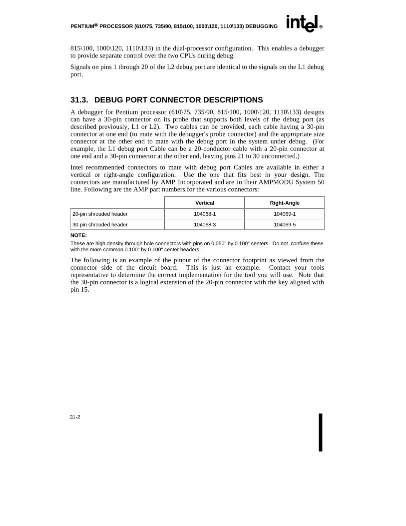
PENTIUM® PROCESSOR (610\75, 735\90, 815\100, 1000\120, 1110\133) DEBUGGING EE
31-2
815\100, 1000\120, 1110\133) in the dual-processor configuration. This enables a debuggerto provide separate control over the two CPUs during debug.
Signals on pins 1 through 20 of the L2 debug port are identical to the signals on the L1 debugport.
31.3. DEBUG PORT CONNECTOR DESCRIPTIONSA debugger for Pentium processor (610\75, 735\90, 815\100, 1000\120, 1110\133) designscan have a 30-pin connector on its probe that supports both levels of the debug port (asdescribed previously, L1 or L2). Two cables can be provided, each cable having a 30-pinconnector at one end (to mate with the debugger's probe connector) and the appropriate sizeconnector at the other end to mate with the debug port in the system under debug. (Forexample, the L1 debug port Cable can be a 20-conductor cable with a 20-pin connector atone end and a 30-pin connector at the other end, leaving pins 21 to 30 unconnected.)
Intel recommended connectors to mate with debug port Cables are available in either avertical or right-angle configuration. Use the one that fits best in your design. Theconnectors are manufactured by AMP Incorporated and are in their AMPMODU System 50line. Following are the AMP part numbers for the various connectors:
Vertical Right-Angle
20-pin shrouded header 104068-1 104069-1
30-pin shrouded header 104068-3 104069-5
NOTE:
These are high density through hole connectors with pins on 0.050" by 0.100" centers. Do not confuse thesewith the more common 0.100" by 0.100" center headers.
The following is an example of the pinout of the connector footprint as viewed from theconnector side of the circuit board. This is just an example. Contact your toolsrepresentative to determine the correct implementation for the tool you will use. Note thatthe 30-pin connector is a logical extension of the 20-pin connector with the key aligned withpin 15.

EE PENTIUM® PROCESSOR (610\75, 735\90, 815\100, 1000\120, 1110\133) DEBUGGING
31-3
PP0065
Figure 31-1. Debug Port Connector
31.4. SIGNAL DESCRIPTIONSFollowing are the debug port signals. Direction is given as follows: O = output from thePentium processor (610\75, 735\90, 815\100, 1000\120, 1110\133) board to a debugger; I =input to the Pentium processor (610\75, 735\90, 815\100, 1000\120, 1110\133) board from adebugger. These are 3.3 V signals, compatible with the Pentium processor (610\75, 735\90,815\100, 1000\120, 1110\133) DC specifications. For the L1 debug port , ignore signals onpins 21 through 30.
NOTE
Target systems should be sure to provide a way for debugging tools likeemulators, in-target probes and logic analyzers to reset the entire system,including uprgrade processor, chip sets, etc. For example, if you follow thedebug port implementation described below, the DBRESET signal providesthis functionality. If you are not implementing the debug port , make surethat your system has a test point connected into the system reset logic towhich a debug tool can connect.

PENTIUM® PROCESSOR (610\75, 735\90, 815\100, 1000\120, 1110\133) DEBUGGING EE
31-4
Table 31-1. Debug Port Signals
Signal Name Dir Pin Description
INIT O 1 (Pentium® processor (610\75, 735\90, 815\100, 1000\120, 1110\133)signal). A debugger may use INIT to support emulating through theCPU INIT sequence while maintaining breakpoints or breaking onINIT.
DBRESET I 2 Debugger Reset output. A debugger may assert DBRESET (high)while performing the "RESET ALL" and "RESET TARGET" debuggercommands. DBRESET should be connected to the system resetcircuitry such that the system and processor(s) are reset whenDBRESET is asserted. This is useful for recovering from conditionslike a "ready hang". This signal is asynchronous.
RESET O 3 (Pentium processor (610\75, 735\90, 815\100, 1000\120, 1110\133)signal). A debugger may use RESET to support emulating throughthe reset while maintaining breaking on RESET.
GND 4 Signal ground.
NC 5 No connect. Leave this pin unconnected.
VCC 6 VCC from the Pentium processor (610\75, 735\90, 815\100, 1000\120,1110\133) system. A debugger uses this signal to sense that systempower is on. Connect this signal to VCC through a 1 K-ohm (orsmaller) resistor.
R/S# I 7 Connect to the R/S# pin of the Pentium processor (610\75, 735\90,815\100, 1000\120, 1110\133).
GND 8 Signal ground.
NC 9 No connect. Leave this pin unconnected.
GND 10 Signal ground.
PRDY O 11 From the PRDY pin of the Pentium processor (610\75, 735\90,815\100, 1000\120, 1110\133).
TDI I 12 Boundary scan data input (Pentium processor (610\75, 735\90,815\100, 1000\120, 1110\133) signal). This signal connects to TDI ofthe Pentium processor (610\75, 735\90, 815\100, 1000\120,1110\133). For dual processor operation, TDI of the Dual Pentiumprocessor (610\75, 735\90, 815\100, 1000\120, 1110\133) wouldconnect to TDO of the Pentium processor (610\75, 735\90, 815\100,1000\120, 1110\133).
TDO O 13 Boundary scan data output (Pentium processor (610\75, 735\90,815\100, 1000\120, 1110\133) signal). This signal connects to TDOfrom the Pentium processor (610\75, 735\90, 815\100, 1000\120,1110\133) for a single processor design, or to TDO from the DualPentium Pentium processor (610\75, 735\90, 815\100, 1000\120,1110\133) for dual processor operation.
TMS I 14 Boundary scan mode select (Pentium processor (610\75, 735\90,815\100, 1000\120, 1110\133) signal).
GND 15 Signal ground.
TCK I 16 Boundary scan clock (Pentium processor (610\75, 735\90, 815\100,1000\120, 1110\133) signal).
GND 17 Signal ground.

EE PENTIUM® PROCESSOR (610\75, 735\90, 815\100, 1000\120, 1110\133) DEBUGGING
31-5
Table 31-1. Debug Port Signals (Contd.)
Signal Name Dir Pin Description
TRST# I 18 Boundary scan reset (Pentium processor (610\75, 735\90, 815\100,1000\120, 1110\133) signal).
DBINST# I 19 DBINST# is asserted (connected to GND) while the debugger isconnected to the debug port . DBINST# can be used to control theisolation of signals while the debugger is installed.
BSEN# I 20 Boundary scan enable. This signal can be used by the Pentiumprocessor (610\75, 735\90, 815\100, 1000\120, 1110\133) system tocontrol multiplexing of the boundary scan input pins (TDI, TMS, TCK,and TRST# signals) between the debugger and other boundary scancircuitry in the Pentium processor (610\75, 735\90, 815\100,1000\120, 1110\133) system. The debugger asserts (low) BSEN#when it is driving the boundary scan input pins. Otherwise, thedebugger drivers are high impedance. If the boundary scan pins areactively driven by the Pentium processor (610\75, 735\90, 815\100,1000\120, 1110\133) system, then BSEN# should control the systemdrivers/multiplexers on the boundary scan input pins. See example 2in section 31.6
PRDY2 O 21 From the PRDY pin of the Dual Pentium processor (610\75, 735\90,815\100, 1000\120, 1110\133) (for dual processor operation).
GND 22 Signal ground.
R/S#2 I 23 Connect to the R/S# pin of the Dual Pentium processor (610\75,735\90, 815\100, 1000\120, 1110\133) (for dual processor operation).
NC 24
NC 25
NC 26
NC 27
NC 28
GND 29 Signal ground.
NC 30
31.5. SIGNAL QUALITY NOTESSince debuggers can connect to the Pentium processor (610\75, 735\90, 815\100, 1000\120,1110\133) system via cables of significant length (e.g., 18 inches), care must be taken inPentium processor (610\75, 735\90, 815\100, 1000\120, 1110\133) system design with regardto the signals going to the debug port . If system outputs to the debug port (i.e. TDO, PRDY,INIT and RESET) are used elsewhere in the system they should have dedicated drivers to thedebug port . This will isolate them from the reflections from the end of the debugger cable.Series termination is recommended at the driver output. If the Pentium processor (610\75,735\90, 815\100, 1000\120, 1110\133) boundary scan signals are used elsewhere in the
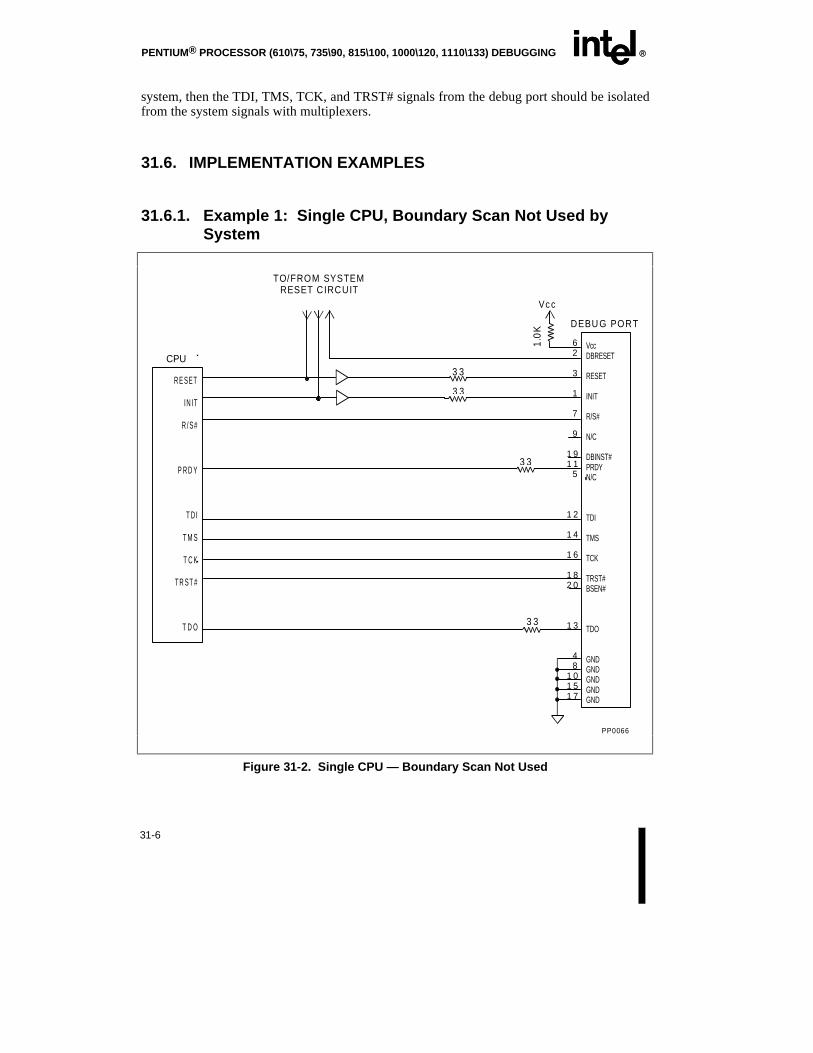
PENTIUM® PROCESSOR (610\75, 735\90, 815\100, 1000\120, 1110\133) DEBUGGING EE
31-6
system, then the TDI, TMS, TCK, and TRST# signals from the debug port should be isolatedfrom the system signals with multiplexers.
31.6. IMPLEMENTATION EXAMPLES
31.6.1. Example 1: Single CPU, Boundary Scan Not Used bySystem
TO/FROM SYSTEMRESET CIRCUIT
CPU
R E SET
IN IT
R / S#
P R D Y
T D I
T M S
T C K
TR ST #
T D O
1.0
K
Vc c
DEBU G PORT
VccDBRESET
RESET
INIT
R/S#
N/C
DBINST#PRDYN/C
TDI
TMS
TCK
TRST#BSEN#
TDO
GNDGNDGNDGNDGND
62
3
1
7
9
1 91 1
5
1 2
1 4
1 6
1 82 0
1 3
48
1 01 51 7
3 3
3 3
3 3
3 3
PP0066
Figure 31-2. Single CPU — Boundary Scan Not Used

EE PENTIUM® PROCESSOR (610\75, 735\90, 815\100, 1000\120, 1110\133) DEBUGGING
31-7
Figure 31-2 shows a schematic of a minimal Level 1 debug port implementation for aPentium processor (610\75, 735\90, 815\100, 1000\120, 1110\133) single processor system inwhich the boundary scan pins of the Pentium processor (610\75, 735\90, 815\100, 1000\120,1110\133) are not used in the system.
31.6.2. Example 2: Single CPU, Boundary Scan Used by System
TO/FROM SYSTEMRESET CIRCUIT
CPU
1.0K
Vcc
33
33
33
33
PP0067
TO/FROM SYSTEMBOUNDARY SCAN
DEBUG PORT
10K
Vcc
RESET
INIT
R/S#
PRDY
TRST#
TCK
TMS
TDI
TDO
62
3
1
7
9
1911
5
18
16
14
12
13
20
48
101517
VccDBRESET
RESET
INIT
R/S#
N/C
DBINST#PRDYN/C
TRST#1
TCK
TMS
TDI
TDO
BSEN#
GNDGNDGNDGNDGND
Figure 31-3. Single CPU — Boundary Scan Used
Figure 31-3 shows a schematic of a Level 1 debug port implementation for a Pentiumprocessor (610\75, 735\90, 815\100, 1000\120, 1110\133) single processor system in which

PENTIUM® PROCESSOR (610\75, 735\90, 815\100, 1000\120, 1110\133) DEBUGGING EE
31-8
the boundary scan pins of the Pentium processor (610\75, 735\90, 815\100, 1000\120,1110\133) are used in the system. Note that the BSEN# signal controls the multiplexing ofthe boundary scan signals. With this implementation, the Pentium processor (610\75,735\90, 815\100, 1000\120, 1110\133) system could use the boundary scan (through thePentium processor (610\75, 735\90, 815\100, 1000\120, 1110\133)) while the debugger is"emulating", but could not while the debugger is "halted" (because the chain is broken).
31.6.3. Example 3: Dual CPUs, Boundary Scan Not Used bySystem
RESETINIT
R/S#PRDY
TRST#TCKTMSTDI
TDO
RESETINIT
R/S#PRDY
TRST#TCKTMSTDI
TDO
Processor
Processor
62317
119
19181614121320
VccDBRESETRESETINITR/S#PRDYN/CDBINST#TRST#TCKTMSTDITDOBSEN#
52321252430282627
48
1015172229
N/CR/S#2PRDY2N/CN/CN/CN/CN/CN/CGNDGNDGNDGNDGNDGNDGND
33
33
33
33
33
1kTo/From SystemReset Circuit
Upgrade Present
Vcc
PP0201
L2 Debug Port
Figure 31-4. Dual CPUs — Boundary Scan Not Used

EE PENTIUM® PROCESSOR (610\75, 735\90, 815\100, 1000\120, 1110\133) DEBUGGING
31-9
Figure 36-4 shows a schematic of a typical Level 2 debug port implementation for a Pentiumprocessor (610\75, 735\90, 815\100, 1000\120, 1110\133) dual processor system in which theboundary scan pins of the Pentium processor (610\75, 735\90, 815\100, 1000\120, 1110\133)are not used in the system. The multiplexer circuit for use with the "upgrade socket" conceptis shown, but could be replaced with a jumper.
31.6.4. Example 4: Dual CPUs, Boundary Scan Used by System
RESETINIT
R/S#PRDY
TRST#TCKTMSTDI
TDO
RESETINIT
R/S#PRDY
TRST#TCKTMSTDI
TDO
Processor
Processor
L2 Debug Port
62317
119
191816141213
VccDBRESETRESETINITR/S#PRDYNCDBINST#TRST#TCKTMSTDITDO
2321
520243028262725
48
1015172229
R/S#2PRDY2N/CBSEN#N/CN/CN/CN/CN/CN/CGNDGNDGNDGNDGNDGNDGND
33
33
33
1k10kTo/From SystemReset Circuit
Upgrade Present
VccVcc
33
33
Boundary ScanTo/From System
PP0202
Figure 31-5. Dual CPUs — Boundary Scan Used
Figure 31-5 shows a schematic of a Level 2 debug port implementation for a Pentiumprocessor (610\75, 735\90, 815\100, 1000\120, 1110\133) dual processor system that usesboundary scan. Note that the BSEN# signal controls the multiplexing of the boundary scansignals. With this implementation, the Pentium processor (610\75, 735\90, 815\100,1000\120, 1110\133) system could use the boundary scan (through the Pentium processor

PENTIUM® PROCESSOR (610\75, 735\90, 815\100, 1000\120, 1110\133) DEBUGGING EE
31-10
(610\75, 735\90, 815\100, 1000\120, 1110\133)) while the debugger is "emulating", but couldnot while the debugger is "halted" (because the chain is broken).
31.7. IMPLEMENTATION DETAILS
31.7.1. Signal Routing NoteThe debugger software communicates with the CPU through the debug port using theboundary scan signals listed above. Typically, the debugger expects the CPU to be the firstand only component in the scan chain (from the perspective of the debug port). That is, itexpects TDI to go directly from the debug port to the TDI pin of the CPU, and the TDO pinto go directly from the CPU to the debug port (see Figure 31-6, below). If you have designedyour system so that this is not the case (for instance, see Figure 31-7, below), you will needto provide the debugger software with the following information: (1) position of the CPU inthe scan chain, (2) the length of the scan chain, (3) instruction register length of each devicein the scan chain. Without this information the debugger will not be able to establishcommunication with the CPU.
Debug Port
Processor
82497
82492
82492
82492
82492
82492
82492 82492
82492TDI
TDO
TDI
TDO
PP0070
Figure 31-6. Example of CPU Only in Scan Chain

EE PENTIUM® PROCESSOR (610\75, 735\90, 815\100, 1000\120, 1110\133) DEBUGGING
31-11
82492
TDI TDO
82492
TDI TDO
82492
TDI TDO
82492
TDI TDO
82492 82492 82492
TDO TDI
82492
TDOTDI
TDI
Debug Port
TDO
TDI
TDOProcessor
82497
TDO TDI TDO TDI TDO TDI
……
……
Figure 31-7. Example of Multiple Components in Scan Chain
31.7.2. Special Adapter DescriptionsFor those designs where board real estate is a concern or where the design is finished and it istoo late to implement the debug port, it may be possible to use a special "debug port adapter"to replace the on-board debug port described in the previous sections. The purpose of theadapter is to provide easy access to the boundary scan signals of the CPU(s). For simplicity,the adapter should make the boundary scan signals accessible to the debug tool while at thesame time preventing the target system from accessing them. Two debug port adapters aredescribed: (1) for uni-processor debug, (2) for dual processor debug.
31.7.2.1. UNI-PROCESSOR DEBUG
A debug port adapter for use in uni-processor systems, or dual processor systems where onlyone processor will be debugged at a time, can be built by reworking two Pentium processor(610\75, 735\90, 815\100, 1000\120, 1110\133) SPGA sockets as follows (see diagrambelow):

PENTIUM® PROCESSOR (610\75, 735\90, 815\100, 1000\120, 1110\133) DEBUGGING EE
31-12
NOTE
This adapter can be used only when the CPU is NOT included in the targetsystem boundary scan string. In addition, when used in dual processorsystems you will only be able to debug the CPU to which the adapter isconnected.
Connect lines of appropriate 20- or 30-wire cable to the following pins on the top socket:
Cable wire # SPGA Pin# Signal
1 AA33 INIT
2 NC DRESET
3 AK20 RESET
4 AD36(VSS) GND
5 NC NC
6 U37 Vcc
7 AC35 R/S#
8 AB36(VSS) GND
9 NC NC
10 Z36(VSS) GND
11 AC05 PRDY
12 N35 TDI
13 N33 TDO
14 P34 TMS
15 X36(VSS) GND
16 M34 TCK
17 R36(VSS) GND
18 Q33 TRST#
19 NC DBINST#
20 NC BSEN#
NOTE
You may connect the GND pins to any pin marked VSS on the SPGA pinoutdiagram. The NC pins are no connects. You may simply cut those wires.

EE PENTIUM® PROCESSOR (610\75, 735\90, 815\100, 1000\120, 1110\133) DEBUGGING
31-13
Debug Port Connector(AMP# 111196-7)
Connect to socketmounted on debugger board
Plug into processorsocket on system board
Mount processor here
PP0072
Figure 31-8. Uni-Processor Debug
Connect a double-row receptacle (AMP# 111196-7) to the debug port connector end of thecable. This is a 30-pin connector, so that it fits into the socket on the debugger buffer board.
Remove the following pins from the bottom socket:
R/S# AC35
PRDY AC05
TDI N35
TDO N33
TMS P34
TCK M34
TRST# Q33
Connect the two sockets together. Make sure not to crush the wires between the pins.
31.7.2.2. DUAL PROCESSOR DEBUG
A debug port adapter for use in dual processor debugging can be built by reworking fourPentium processor (610\75, 735\90, 815\100, 1000\120, 1110\133) SPGA sockets. (Seediagram below).
NOTE
This adapter can be used only when the CPUs are NOT included in thetarget system boundary scan string.

PENTIUM® PROCESSOR (610\75, 735\90, 815\100, 1000\120, 1110\133) DEBUGGING EE
31-14
You will need to use two SPGA sockets per processor location. For this discussion, assumethat the startup processor is called processor 1 and that the upgrade processor is calledprocessor 2. Thus, you will use two SPGA sockets to connect to processor 1 and two SPGAsockets to connect to processor 2. Certain debug port signals must be shared by Processor 1and Processor 2. These signals must be connected from the debug port connector end of thecable (on which you will place a double-row receptacle: AMP# 111196-7) to both doubleSPGA sockets.
Debug Port Connector(AMP# 111196-7)
Connect to socketmounted on debugger board
Plug into processor 2socket on system board
Mount processor 1 here
Plug into processor 1socket on system board
Mount processor 2 here
PP0073
Figure 31-9. Dual Processor Debug Port Adapter
Connect lines of 30-wire cable to the pins on the top SPGA sockets for both processor 1 and2. Following are the signals which should be connected to each processor socket. Make sureto connect the shared lines to both top sockets.

EE PENTIUM® PROCESSOR (610\75, 735\90, 815\100, 1000\120, 1110\133) DEBUGGING
31-15
TDO
TMST C K
TR ST #
RESETINIT
TMST C KTR ST#
RESETINIT
PRDY2#R/S2#
TDO
PRDY1#R/S1#TDI
TDI
30-Pin Debug Port
Processor UpgradeProcessor
PP0068
Figure 31-10. Shared Pins for Dual Processor Adapter

PENTIUM® PROCESSOR (610\75, 735\90, 815\100, 1000\120, 1110\133) DEBUGGING EE
31-16
Table 31-2. Debug Port Connector Pinout
Cable wire # SPGA Pin# Processor Socket Signal
1 AA33 1,2 INIT
2 NC DBRESET
3 AK20 1,2 RESET
4 VSS 1 GND
5 NC NC
6 VCC 1 Vcc
7 AC35 1 R/S1#
8 VSS 1 GND
9 NC NC
10 VSS 1 GND
11 AC05 1 PRDY1
12 N35 1 TDI
13 N33 2 TDO
14 P34 1,2 TMS
15 VSS 1 GND
16 M34 1,2 TCK
17 VSS 1 GND
18 Q33 1,2 TRST#
19 NC DBINST#
20 NC BSEN#
21 AC05 2 PRDY2
22 VSS 2 GND
23 AC35 2 R/S2#
24 NC NC
25 NC NC
26 NC NC
27 NC NC
28 NC NC
29 VSS 2 GND
30 NC NC
NOTE: You may connect the VCC and GND pins to any convenient power or ground pin.

EE PENTIUM® PROCESSOR (610\75, 735\90, 815\100, 1000\120, 1110\133) DEBUGGING
31-17
Connect a double-row receptacle (AMP# 111196-7) to the debug port end of the cable. Thisis a 30-pin connector, so that it fits into the socket on the debugger buffer board.
Remove the following pins from the bottom of both double sockets:
R/S# AC35
PRDY AC05
TDI N35
TDO N33
TMS P34
TCK M34
TRST# Q33
Connect each set of two sockets together. Make sure not to crush the wires between the pins.

E32
Future OverDrive®
Processor forPentium® Processor(610\75, 735\90,815\100, 1000\120)-Based SystemsSocket Specification


EE
32-1
CHAPTER 32FUTURE OverDrive ® PROCESSOR FOR
PENTIUM® PROCESSOR (610\75, 735\90,815\100, 1000\120, 1110\133)-BASEDSYSTEMS SOCKET SPECIFICATION
32.1. INTRODUCTIONThe future OverDrive processors are end-user single-chip CPU upgrade products for Pentiumprocessor-based systems. The future OverDrive processors will speed up most softwareapplications by 40% to 70% and are binary compatible with the Pentium processor.
Two upgrade sockets have been defined for the Pentium processor-based as part of theprocessor architecture. Socket 5 has been defined for the Pentium processor (610\75, 735\90,815\100, 1000\120)-based systems. Upgradability can be supported by implementing either asingle socket or a dual socket strategy. A single socket system will include a 320-pin SPGASocket 5. When this system configuration is upgraded, the Pentium processor is simplyreplaced by the future OverDrive processor. A dual socket system will include a 296-pinSPGA socket for the Pentium processor and a 320-pin SPGA Socket 5 for the secondprocessor. In dual socket systems, Socket 5 can be filled with either the Dual processor or thefuture OverDrive processors. The rest of this chapter describes the Socket 5 specifications.
Socket 7 has been defined as the upgrade socket for the Pentium processor (1110\133) inaddition to the Pentium processor (610\75, 735\90, 815\100, 1000\120). The flexibility of theSocket 7 definition makes it backward compatible with Socket 5 and should be used for allnew Pentium processor-based system designs. The Socket 7 support requires key changesfrom Socket 5 designs; split voltage planes, voltage regulator module header, 3.3 volt clocks,BIOS updates, additional decoupling, etc. This information is not provided in this databook.Contact Intel for further information regarding the Socket 7 specifications.
32.1.1. Upgrade ObjectivesSystems using the Pentium processor (610\75, 735\90, 815\100, 1000\120), and equipped withonly one processor socket, must use Socket 5 to accept the future OverDrive processor.Systems equipped with two processor sockets must use Socket 5 as the second socket tocontain either the Pentium processor Dual processor or the future OverDrive processor.
Inclusion of Socket 5 in Pentium processor systems provides the end-user with an easy andcost-effective way to increase system performance. The majority of upgrade installationswhich take advantage of Socket 5 will be performed by end users and resellers. Therefore, itis important that the design be "end-user easy," and that the amount of training and technical

OverDrive ® PROCESSOR SOCKET SPECIFICATIONS EE
32-2
expertise required to install the upgrade processors be minimized. Upgrade installationinstructions should be clearly described in the system user's manual. In addition, by makinginstallation simple and foolproof, PC manufacturers can reduce the risk of system damage,warranty claims and service calls. Three main characteristics of end user easy designs are:
• Accessible socket location
• Clear indication of upgrade component orientation
• Minimization of insertion force
The future OverDrive processor will support all Intel chip sets that are supported by thePentium processor, including 82430NX PCIset and 82430FX PCIset.
32.1.2. Intel Platform Support LabsThe Intel Platform Support Labs ensures that Pentium processor (610\75, 735\90, 815\100,1000\120) and Pentium processor (1110\133)-based personal computers meet design criteriafor reliable and straightforward CPU upgradability with the future OverDrive processor.Evaluation performed at the Intel Platforms Support Labs confirms that Pentium processorand future OverDrive processor specifications for mechanical, thermal, electrical, functional,and end-user installation attributes have been met.
The OEM submits motherboard and system designs to one of Intel's worldwide PlatformSupport Labs for evaluation. The OEM benefits from engineering feedback on Pentiumprocessor and future OverDrive processor support. Contact your local Intel representative formore information on the Intel Platform Support Labs.
32.2. FUTURE OverDrive ® PROCESSOR (SOCKET 5) PINOUTThis section contains pinouts of the future OverDrive processor socket (Socket 5) when usedas a single-socket turbo upgrade.
32.2.1. Pin Diagrams
32.2.1.1. SOCKET 5 PINOUT
For systems with a single socket for the Pentium processor (610\75, 735\90, 815\100,1000\120) and future OverDrive processor, the following pinout must be followed for thesingle socket location. The socket footprint contains VCC, VCC5, and VSS pins that areinternal no connects on the Pentium processor. These pins must be connected to theappropriate PCB power and ground layers to ensure future OverDrive processor compatibility.
OEMs should contact Intel for the most current list of Intel-qualified socket vendors.
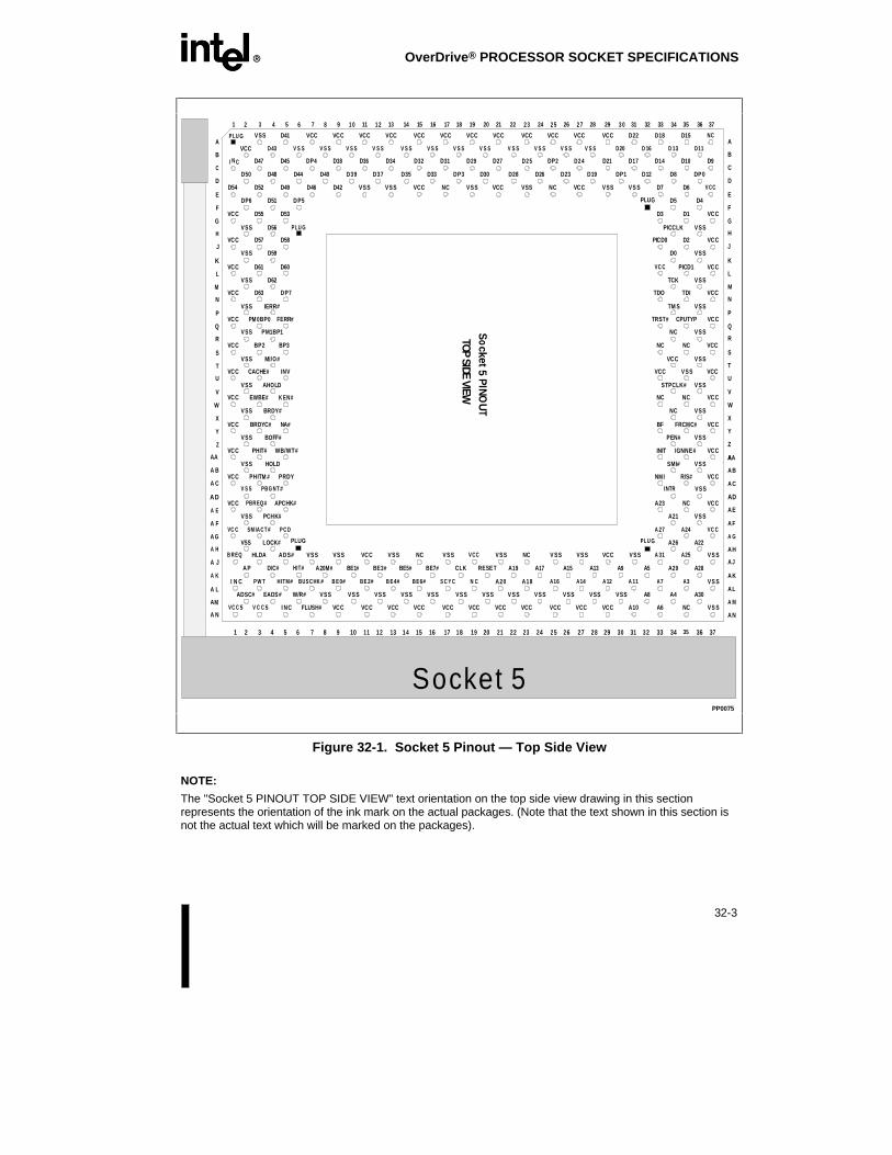
EE OverDrive ® PROCESSOR SOCKET SPECIFICATIONS
32-3
Socket 5
ADSC# EADS# W/R# VSS VSS VSS VSS VSS VSS VSS V SS VSS VSS VSS VSS A8 A4 A30
A26 A22VSS LOCK#
VC CA24A 27VC C SM IACT # P C D
A21 VSSVSS PCHK#
INTR VSSV S S PBG NT #
SMI# VSSVSS HOLD
INIT IGNNE# VCCVCC PHIT# WB/WT#
PEN# VSSVSS BOFF#
STPCLK# VSSVSS AHOLD
TRST# CPUTYP VCCVCC PM 0BP 0 FERR#
TM S VSSVSS IERR#
TCK VSSVSS D62
D0 VSSVSS D59
PICD0 D2 VCCVCC D57 D58
PICCLK VSSVSS D56
D3 D1 VCCVCC D55 D53
DP0D8D12DP1D50 D48 D44 D40 D39 D37 D35 D33 DP3 D30 D28 D26 D23 D19
TDO TDIVCC D63 DP7 VCC
VSSVSS MI/O# VCC
PICD1 VCCVCC D61 D60 VC C
VSSVSS PM1BP1 NC
NCVCC BP2 BP3 VCCNC
VCCVCC CACHE# INV VCC VSS
VCCVCC EWBE# K EN# NC NC
VSSVSS BRDY# NC
FRCMC# VCCVCC BRDYC# NA# BF
D11D 13D 16D20D43 V S S V S S V S S V S S V S S V S S V S S V S S V S S V S S V S S V S SVCC
VCCA23VCC PBREQ# APCHK# NC
1 2 3 4 5 6 7 8 9 1 0 11 1 2 13 14 15 16 17 18 19 20 21 22 2 3 24 2 5 26 2 7 28 29 3 0 31 32 33 34 35 36 37
VCCVCCVCCVCCVCCVCCVCCVCC D15D18D22VCCD41 VCC VCC VCCVSS NC
D7 D6D54 D52 D49 D46 D42 V CCVS SVSSVSS VSS VCC NC VSS VCC VSS NC VCC
P LU G
A25A 31B REQ HLDA ADS# VS SVSS VSS VCC VSS NC VSS VSS NC V SS VSS VCC VSSV CC
D5 D4DP6 D51 D P5
PLU G
PLUG PLU G
PLUG
A
A
A
A
A
A
A
A
A
A
A
A
N
M
L
K
J
H
G
F
E
D
C
B
AA
Z
Y
X
W
V
U
T
S
R
Q
P
N
M
L
K
J
H
G
F
E
D
C
B
A
A N
A M
A L
A K
A J
A H
A G
A F
A E
AD
A C
A B
AAA
Z
Y
X
W
V
U
T
S
R
Q
P
N
M
L
K
J
H
G
F
E
D
C
B
A
1 2 3 4 5 6 7 8 9 10 11 12 13 14 15 16 17 18 19 20 21 22 23 24 25 26 27 28 29 30 31 32 33 34 35 36 37
TOP SID E VI EWS
ock et 5 PIN
OU
T
P W T HITM# BUS CHK # B E 0# BE 2# B E 4# BE 6# S C Y C A20 A18 A16 A14 A 12 A 11 A7 A3 VS SN CI N C
FLUSH# VCC VCC VCC VCC VCC VCC VCC VCC VCC VCC VCC A10 A6 NC VS SV C C 5VC C 5 I NC
I D9D10D14D17D21D47 D45 DP4 D38 D36 D34 D32 D31 D29 D27 D2 5 DP2 D2 4N C
PP0075
VCCNMIVCC PHITM # PRDY R/S#
A P HIT# A 20M# BE1# BE 3# BE5# BE7# CLK RESET A 19 A17 A15 A13 A9 A5 A29 A28D/C#
Figure 32-1. Socket 5 Pinout — Top Side View
NOTE:
The "Socket 5 PINOUT TOP SIDE VIEW" text orientation on the top side view drawing in this sectionrepresents the orientation of the ink mark on the actual packages. (Note that the text shown in this section isnot the actual text which will be marked on the packages).

OverDrive ® PROCESSOR SOCKET SPECIFICATIONS EE
32-4
PP0076
ADSC# EADS # W/R# VSS VSS VSS VSS V SS VSS VSS V SS VSS VSS VSS VSS A8 A4 A30
A26 A22VSS LOCK#
VC CA 24A 27VC C SM IACT # PC D
A21 VSSVSS PCHK#
INTR VSSV S S PB GNT #
SMI# VSSVSS HOLD
INIT IGNN E# VCCVCC PHIT# WB/WT#
PEN# VSSVSS BOFF#
STPCLK # VSSVSS AHOLD
TRST# CPUTYP VCCVCC PM0BP0 FERR#
TM S VSSVSS IERR#
TCK VSSVSS D62
D0 VSSVSS D59
PICD0 D2 VCCVCC D57 D58
PICCLK VSSVSS D56
D3 D1 VCCVCC D55 D53
DP0D8D12DP1D50 D48 D44 D40 D3 9 D3 7 D35 D33 DP3 D30 D28 D26 D23 D19
TDO TDIVCC D63 DP7 VCC
VSSVSS MI/O # VCC
PICD1 VCCVCC D61 D60 VC C
VSSVSS PM1BP1 NC
NCVCC BP2 BP3 VCCNC
VCCVCC CACHE# INV VCC VSS
VCCVCC EWBE# KEN# NC NC
VSSVSS BRDY# NC
FRCMC# VCCVCC BRDYC# NA# BF
D11D 13D16D20D43 V S S V S S V S S V S S V S S V S S V S S V S S V S S V S S V S S V S SVCC
VCCA23VCC PBR EQ # APCHK# NC
1 2 3 4 5 6 7 8 9 10 11 12 13 14 15 16 17 18 19 20 21 22 23 24 25 26 27 28 29 30 31 32 33 34 35 36 37
VCCVCCVCCVCCVCCVCCVCCVCC D15D18D22VCCD41 VCC VCC VCCVSS NC
D7 D6D54 D52 D49 D46 D42 VCCVS SVSSVSS VSS VCC NC VSS VCC VSS NC VCC
P LUG
A 25A 31B RE Q HLDA ADS# VS SVSS VS S VCC VSS NC VSS VSS NC V SS VSS VCC VSSV CC
D5 D4DP6 D51 D P5
PLU G
PLU G PLU G
PLUG
A
A
A
A
A
A
A
A
A
A
A
A
N
M
L
K
J
H
G
F
E
D
C
B
AA
Z
Y
X
W
V
U
T
S
R
Q
P
N
M
L
K
J
H
G
F
E
D
C
B
A
A N
A M
A L
A K
A J
A H
A G
A F
A E
AD
A C
A B
AAA
Z
Y
X
W
V
U
T
S
R
Q
P
N
M
L
K
J
H
G
F
E
D
C
B
A
1 2 3 4 5 6 7 8 9 10 11 12 13 14 15 16 17 18 19 20 21 22 23 24 25 26 27 28 29 30 31 32 33 34 35 36 37
Socket 5 PINOUTPIN SIDE VIEW
P W T HITM# BUSCHK # B E 0# BE 2# BE 4# BE 6# S C Y C A20 A1 8 A 16 A14 A12 A 11 A7 A3 VS SN CI N C
FLUSH# VCC VCC VCC VCC VCC VCC VCC VCC VCC VCC VCC A10 A6 NC VS SV C C 5VC C 5 I NC
I D9D10D14D17D21D47 D45 DP4 D38 D36 D34 D32 D31 D29 D27 D25 DP2 D24N C
VCCNMIVCC PHITM # PRDY R/S#
A P HIT# A20M# BE1# BE3# BE5# BE7# CLK RESET A19 A17 A15 A13 A9 A5 A29 A28D/C#
Figure 32-2. Socket 5 Pinout — Pin Side View

EE OverDrive ® PROCESSOR SOCKET SPECIFICATIONS
32-5
32.2.2. Socket 5 Pin Cross Reference TableNote that the shaded signals in the following tables have different pin definitions for thePentium processor (610\75, 735\90, 815\100, 1000\120) as compared to the future OverDriveprocessor (refer to Table 32-1 for details):
Table 32-1. Socket 5 Pin Cross Reference by Pin Name
Address
A3 AL35 A9 AK30 A15 AK26 A21 AF34 A27 AG33
A4 AM34 A10 AN31 A16 AL25 A22 AH36 A28 AK36
A5 AK32 A11 AL31 A17 AK24 A23 AE33 A29 AK34
A6 AN33 A12 AL29 A18 AL23 A24 AG35 A30 AM36
A7 AL33 A13 AK28 A19 AK22 A25 AJ35 A31 AJ33
A8 AM32 A14 AL27 A20 AL21 A26 AH34
Data
D0 K34 D13 B34 D26 D24 D39 D10 D52 E03
D1 G35 D14 C33 D27 C21 D40 D08 D53 G05
D2 J35 D15 A35 D28 D22 D41 A05 D54 E01
D3 G33 D16 B32 D29 C19 D42 E09 D55 G03
D4 F36 D17 C31 D30 D20 D43 B04 D56 H04
D5 F34 D18 A33 D31 C17 D44 D06 D57 J03
D6 E35 D19 D28 D32 C15 D45 C05 D58 J05
D7 E33 D20 B30 D33 D16 D46 E07 D59 K04
D8 D34 D21 C29 D34 C13 D47 C03 D60 L05
D9 C37 D22 A31 D35 D14 D48 D04 D61 L03
D10 C35 D23 D26 D36 C11 D49 E05 D62 M04
D11 B36 D24 C27 D37 D12 D50 D02 D63 N03
D12 D32 D25 C23 D38 C09 D51 F04

OverDrive ® PROCESSOR SOCKET SPECIFICATIONS EE
32-6
Table 32-1. Socket 5 Pin Cross Reference by Pin Name (Contd.)
Control
A20M# AK08 BRDYC# Y03 FRCMC# Y35 PM0/BP0 Q03
ADS# AJ05 BREQ AJ01 HIT# AK06 PM1/BP1 R04
ADSC# AM02 BUSCHK# AL07 HITM# AL05 PRDY AC05
AHOLD V04 CACHE# U03 HLDA AJ03 PWT AL03
AP AK02 CPUTYP Q35 HOLD AB04 R/S# AC35
APCHK# AE05 D/C# AK04 IERR# P04 RESET AK20
BE0# AL09 DP0 D36 IGNNE# AA35 SCYC AL17
BE1# AK10 DP1 D30 INIT AA33 SMI# AB34
BE2# AL11 DP2 C25 INTR/LINT0 AD34 SMIACT# AG03
BE3# AK12 DP3 D18 INV U05 TCK M34
BE4# AL13 DP4 C07 KEN# W05 TDI N35
BE5# AK14 DP5 F06 LOCK# AH04 TDO N33
BE6# AL15 DP6 F02 M/IO# T04 TMS P34
BE7# AK16 DP7 N05 NA# Y05 TRST# Q33
BOFF# Z04 EADS# AM04 NMI/LINT1 AC33 W/R# AM06
BP2 S03 EWBE# W03 PCD AG05 WB/WT# AA05
BP3 S05 FERR# Q05 PCHK# AF04
BRDY# X04 FLUSH# AN07 PEN# Z34
APIC Clock ControlDual ProcessorPrivate Interface
PICCLK H34 CLK AK18 PBGNT# AD04
PICD0 J33 BF Y33 PBREQ# AE03
[DPEN#] STPCLK# V34 PHIT# AA03
PICD1[APICEN]
L35 PHITM# AC03

EE OverDrive ® PROCESSOR SOCKET SPECIFICATIONS
32-7
Table 32-1. Socket 5 Pin Cross Reference by Pin Name (Contd.)
VCC
A07 A19 B02 G37 N01 T34 Y01 AE01 AJ29 AN19
A09 A21 E15 J01 N37 U01 Y37 AE37 AN09 AN21
A11 A23 E21 J37 Q01 U33 AA01 AG01 AN11 AN23
A13 A25 E27 L01 Q37 U37 AA37 AG37 AN13 AN25
A15 A27 E37 L33 S01 W01 AC01 AJ11 AN15 AN27
A17 A29 G01 L37 S37 W37 AC37 AJ19 AN17 AN29
VSS
A03 B20 E23 M36 V02 AD02 AJ17 AM10 AM26
B06 B22 E29 P02 V36 AD36 AJ21 AM12 AM28
B08 B24 E31 P36 X02 AF02 AJ25 AM14 AM30
B10 B26 H02 R02 X36 AF36 AJ27 AM16 AN37
B12 B28 H36 R36 Z02 AH02 AJ31 AM18
B14 E11 K02 T02 Z36 AJ07 AJ37 AM20
B16 E13 K36 T36 AB02 AJ09 AL37 AM22
B18 E19 M02 U35 AB36 AJ13 AM08 AM24
NC/INC
A37 E25 S33 W33 X34 AJ23 AN35 AN05 C01
E17 R34 S35 W35 AJ15 AL19 AE35* AL01
NOTE:
*This is the D/P# signal in the Pentium® processor (610\75, 735\90, 815\100, 1000\120)
VCC5: AN01 AN03

OverDrive ® PROCESSOR SOCKET SPECIFICATIONS EE
32-8
Table 32-2. Pentium ® Processor (610\75, 735\90, 815\100, 1000\120) vs. Socket 5 Pins
Pentium ® Processor(610\75, 735\90,
815\100, 1000\120)Signal
Socket 5Signal Pin Number
Pentium ® Processor(610\75, 735\90,
815\100, 1000\120)Signal
Socket 5Signal
PinNumber
INC VCC5 AN01 D/P# NC AE35
INC V CC5 AN03 NO PIN VSS AJ07
INC VCC B02 NO PIN VSS AJ09
NO PIN VSS E11 NO PIN VCC AJ11
NO PIN VSS E13 NO PIN VSS AJ13
NO PIN VCC E15 NO PIN NC AJ15
NO PIN NC E17 NO PIN VSS AJ17
NO PIN VSS E19 NO PIN VCC AJ19
NO PIN VCC E21 NO PIN VSS AJ21
NO PIN VSS E23 NO PIN NC AJ23
NO PIN NC E25 NO PIN VSS AJ25
NO PIN VCC E27 NO PIN VSS AJ27
NO PIN VSS E29 NO PIN VCC AJ29
NO PIN VSS E31 NO PIN VSS AJ31
INC VSS A03
NOTES:
See highlighted cells in previous table.
All INCs are internal no connects. These signals are guaranteed to remain internally not connected in thePentium processor processor.
32.3. SYSTEM DESIGN CONSIDERATIONS
32.3.1. CPU Type Pin DefinitionThe CPUTYP pin is a new configuration signal which, when sampled by the Pentiumprocessor at the falling edge of RESET, indicates the type of OEM processor which will beplaced in each socket site. Refer to Table 32-3 for a detailed description of the CPUTYPsignal.

EE OverDrive ® PROCESSOR SOCKET SPECIFICATIONS
32-9
Table 32-3. CPUTYP Definition
Symbol Type Function
CPUTYP Input The Processor Type input signal is used to configure the Pentium processorfor a single or dual processor system. The Pentium processor and the futureOverDrive® processors will be configured as standalone processors whenCPUTYP is connected to VSS. The Pentium processor will be configured as aDual processor when CPUTYP is connected to VCC.
In a two socket system, CPUTYP is connected to VSS in the 296 pin SPGAsite, and to VCC in the 320 pin SPGA site.
In a single socket system, CPUTYP is connected to VSS.
For the future OverDrive processor, CPUTYP will be used to determinewhether the bootup handshake protocol will be used (in a dual socket system)or not (in a single socket system).
32.3.2. Single Socket System Considerations
32.3.2.1. SINGLE SOCKET PIN CONNECTIONS
Use the 320-pin SPGA Socket 5 pinout for single-socket systems. The following table showshow to connect the dual processing signals which remain unused in a single-socket systemdesign.
Table 32-4. Dual Processing Signal Connections in a Single Socket System
Private Interface Signal Connection
CPUTYP VSS
PBGNT# NC
PBREQ# NC
PHIT# NC
PHITM# NC
D/P# NC
32.4. DUAL SOCKET SYSTEM CONSIDERATIONS
32.4.1. Dual Socket Power ConsiderationsIn a dual socket system, the Pentium processor (610\75, 735\90, 815\100, 1000\120) will havea nominal power dissipation when non-operational due to the presence of a future OverDrive

OverDrive ® PROCESSOR SOCKET SPECIFICATIONS EE
32-10
processor in Socket 5. This power should not exceed 1Watt (this value is preliminary and anapproximation only).
There will also be a period of time in which BOTH the Pentium processor (610\75, 735\90,815\100, 1000\120) and the future OverDrive processor may be operating simultaneously.This is during RESET, and for a brief period of time following the falling edge of RESET dueto the bootup handshake protocol between the two processors. The power dissipation duringthis time will not exceed the maximum power of a dual processing system. Therefore, dualsocket Pentium processor (610\75, 735\90, 815\100, 1000\120) systems must be able to handlethe full power of a Primary and Dual processor operating simultaneously.
32.4.1.1. DUAL SOCKET PIN CONNECTIONS
In dual socket systems, the 296 pin SPGA Pentium processor pinout should be used for theprimary OEM processor site. The second processor site should be occupied by the 320-pinSPGA Socket 5 pinout.
Table 32-5 lists all Pentium processor future OverDrive processor signals which should beconnected together in order to operate in either dual processing mode with the Dual processorpresent, or upgraded with the future OverDrive processor.
Table 32-5. Signal Connections in a Dual Socket System
CONNECT TOGETHER
A[31:3] A20M# ADS# ADSC# AHOLD
AP BE[7:0]# BF BOFF# BRDY#
BRDYC# BREQ BUSCHK# CACHE# CLK
D/C# D[63:0] DP[7:0] EADS# EWBE#
FERR# FLUSH# HIT# HITM#
HLDA HOLD IGNNE# INIT INV
KEN# LOCK# M/IO# NA# PBGNT#
PBREQ# PCD PEN# PHIT# PHITM#
PICCLK PICD[1:0] PWT RESET SCYC
VCC VSS W/R# WB/WT#
Table 32-6 lists the signals which must not be connected together in a dual socket Pentiumprocessor system. These functions, if used in the system, must be handled by the systemdesign individually for each socket. If any of these features are used in uni-processing modewith only the OEM processor present, then they MUST be handled for the case of a futureOverDrive processor in the second socket.

EE OverDrive ® PROCESSOR SOCKET SPECIFICATIONS
32-11
NOTES
CPUTYP should be strapped to VSS in the 296 pin SPGA Pentium processor(610\75, 735\90, 815\100, 1000\120) site. CPUTYP should be strapped toVCC in the 320 pin SPGA Socket 5 (future OverDrive processor) site.
D/P# is only a Pentium processor signal, and is defined as a no connect inSocket 5.
If boundary scan is used in the design, TDO of one socket is connected toTDI of the other to make a serial chain with other boundary scancomponents in the system. If boundary scan is not used in the design, TDIand TDO should remain disconnected.
Table 32-6. Signal Connections in a Dual Socket System
DO NOT CONNECT TOGETHER
APCHK# BP[3:0] CPUTYP D/P# IERR#
PM/BP[1:0] PRDY R/S# TDI TDO
Table 32-7 lists the signals which may be connected together or not. It is the systemdesigner's choice as to whether they want to handle these signals individually for each socket,or connect them together. Intel recommends that they be connected together for ease of usingboth the Dual processor and the future OverDrive processor in the same second socket. If anyof these signals are not connected together, and their functions are used in uni-processingmode with only the OEM processor present, then they MUST be handled for the case of afuture OverDrive processor in the second socket. Refer to earlier chapters in this documentfor additional details on the functionality of these signals.
Table 32-7. Signal Connections in a Dual Socket System
MAY BE CONNECTED TOGETHER
FRCMC# INTR/LINT0 NMI/LINT1 PCHK# SMI#
SMIACT# STPCLK# TCK TMS TRST#
NOTE
NC signals should not be connected to anything. Vcc5 signals can beconnected together since pins AN01 and AN03 are Internal No Connects(INC) on the Pentium processor (610\75, 735\90, 815\100, 1000\120).

OverDrive ® PROCESSOR SOCKET SPECIFICATIONS EE
32-12
32.5. ELECTRICAL SPECIFICATIONSThe future OverDrive processor will have the same power and ground specifications,decoupling recommendations, and connection specifications as the Pentium processor.
32.5.1. Vcc5 Pin DefinitionThe future OverDrive processor pinout contains two 5V VCC pins (VCC5) used to providepower to the fan/heatsink. These pins should be connected to +5 volts ±5% regardless of thesystem design. Failure to connect VCC5 to 5V may cause the component to shut down.
32.5.2. Absolute Maximum Ratings of UpgradeThe on-chip Voltage Regulation and fan/heatsink devices included on the future OverDriveprocessor require different stress ratings than the Pentium processor (610\75, 735\90,815\100, 1000\120). The voltage regulator is surface mounted on the future OverDriveprocessor and is, therefore, an integral part of the assembly. The future OverDrive processorstorage temperature ratings are tightened as a result. The fan is a detachable unit, and thestorage temperature is stated separately in the table below. Functional operation of the futureOverDrive processor remains 0°C to 70°C.
Table 32-8. Absolute Maximum Ratings
Future Pentium ® OverDrive ® Processor and Voltage Regulator Assembly:
Parameter Min Max Unit Notes
Storage Temperature -30 100 °C
Case Temperature Under Bias -30 100 °C
Fan:
Parameter Min Max Unit Notes
Storage Temperature -30 75 °C
Case Temperature Under Bias -30 75 °C
WARNING
Stressing the devices beyond the "Absolute Maximum Ratings" may causepermanent damage. These are stress ratings only. Operation beyond the"Operating Conditions" is not recommended and extended exposure beyondthe "Operating Conditions" may affect device reliability.

EE OverDrive ® PROCESSOR SOCKET SPECIFICATIONS
32-13
32.5.3. DC SpecificationsThe future OverDrive processor will have compatible DC specifications to the Pentiumprocessor, except that ICC (Power Supply Current), ICC5 (Fan/Heatsink Current), and VCC arethe following:
Table 32-9. I cc Specification
Symbol Parameter Min Max Unit
ICC Power Supply Current 4330 mA
ICC5 Fan/Heatsink Current 200 mA
NOTE:
VCC = 3.135V to 3.6V, VCC5 = 5V ±5%
Refer to Chapter 23 for a listing of the remaining DC Specifications.
32.5.3.1. AC SPECIFICATIONS
The future OverDrive processor will have the same AC specifications as the Pentiumprocessor. Refer to Chapter 23 for a listing of the remaining AC Specifications.

OverDrive ® PROCESSOR SOCKET SPECIFICATIONS EE
32-14
32.6. MECHANICAL SPECIFICATIONSThe future OverDrive Processor will be packaged in a 320-pin ceramic staggered pin gridarray (SPGA). The pins will be arranged in a 37 x 37 matrix and the package dimensions willbe 1.95″ x 1.95″ (4.95cm x 4.95cm).
Table 32-10. Future Pentium ® OverDrive ® Processor Package Summary
PackageType Total Pins Pin Array Package Size
Future Pentium® OverDrive®
ProcessorSPGA 320 37 x 37 1.95" x 1.95"
4.95cm x 4.95cm
Table 32-11. Future Pentium ® OverDrive ® Processor Package Dimensions
Family: Ceramic Staggered Pin Grid Array Package
Millimeters Inches
Symbol Min Max Notes Min Max Notes
A* 33.88 Solid Lid 1.334 Solid Lid
A1 0.33 0.43 Solid Lid 0.013 0.017 Solid Lid
A2 2.62 2.97 0.103 0.117
A4 20.32 0.800
A5 10.16 Air Space 0.400 Air Space
B 0.43 0.51 0.017 0.020
D 49.28 49.91 1.940 1.965
D1 45.47 45.97 1.790 1.810
E1 2.41 2.67 0.095 0.105
E2 1.14 1.40 0.045 0.055
L 3.05 3.30 0.120 0.130
N 320 SPGA pins 320 SPGA pins
S1 1.52 2.54 0.060 0.100
NOTES:* Assumes the minimum air space above the fan/heatsink
A 0.2″ clearance around three of four sides of the package is also required to allow free airflow through thefan/heatsink.

EE OverDrive ® PROCESSOR SOCKET SPECIFICATIONS
32-15
AAAAAAAAAAAAAAAAAAAAAAAAAAAAAAAAAAAAAAAAAAAAAAAAAAAAAAAAAAAAAAAAAAAAAAAAAAAAAAAAAAAAAAAAAAAAAAAAAAAAAAAAAAAAAAAAAAAAAAAAAAAAAAAAAAAAAAAAAAAAAAAAAAAAAAAAAAAAAAAAAAAAAAAAAAAAAAAAAAAAAAAAAAAA
AAAAAAAAAAAAAAAAAAAAAAAAAAAAAAAAAAAAAAAAAAAAAAAAAAAAAAAAAAAAAAAAAAAAAAAAAAAAAAAAAAAAAAAAAAAAAAAAAAAAAAAAAAAAAAAAAAAAAAAAAAAAAAAAAAAAAAAAAAAAAAAAAAAAAAAAAAAAAAAAAAAAAAAAAAAAAAAAAAAAAAAAAAAA
AAAAAAAAAAAAAAAAAAAAAAAAAAAAAAAAAAAAAAAAAAAAAAAAAAAAAAAAAAAAAAAAAAAAAAAAAAAAAAAAAAAAAAAAAAAAAAAAAAAAAAAAAAAAAAAAAAAAAAAAAAAAAAAAAAAAAAAAAAAAAAAAAAAAAAAAAAAAAAAAAAAAAAAAAAAAAAAAAAAAAAAAAAAA
AAAAAAAAAAAAAAAAAAAAAAAAAAAAAAAAAAAAAAAAAAAAAAAAAAAAAAAAAAAAAAAAAAAAAAAAAAAAAAAAAAAAAAAAAAAAAAAAAAAAAAAAAAAAAAAAAAAAAAAAAAAAAAAAAAAAAAAAAAAAAAAAAAAAAAAAAAAAAAAAAAAAAAAAAAAAAAAAAAAAAAAAAAAA
AAAAAAAAAAAAAAAAAAAAAAAAAAAAAAAAAAAAAAAAAAAAAAAAAAAAAAAAAAAAAAAAAAAAAAAAAAAAAAAAAAAAAAAAAAAAAAAAAAAAAAAAAAAAAAAAAAAAAAAAAAAAAAAAAAAAAAAAAAAAAAAAAAAAAAAAAAAAAAAAAAAAAAAAAAAAAAAAAAAAAAAAAAAA
AAAAAAAAAAAAAAAAAAAAAAAAAAAAAAAAAAAAAAAAAAAAAAAAAAAAAAAAAAAAAAAAAAAAAAAAAAAAAAAAAAAAAAAAAAAAAAAAAAAAAAAAAAAAAAAAAAAAAAAAAAAAAAAAAAAAAAAAAAAAAAAAAAAAAAAAAAAAAAAAAAAAAAAAAAAAAAAAAAAAAAAAAAAA
AAAAAAAAAAAAAAAAAAAAAAAAAAAAAAAAAAAAAAAAAAAAAAAAAAAAAAAAAAAAAAAAAAAAAAAAAAAAAAAAAAAAAAAAAAAAAAAAAAAAAAAAAAAAAAAAAAAAAAAAAAAAAAAAAAAAAAAAAAAAAAAAAAAAAAAAAAAAAAAAAAAAAAAAAAAAAAAAAAAAAAAAAAAA
AAAAAAAAAAAAAAAAAAAAAAAAAAAAAAAAAAAAAAAAAAAAAAAAAAAAAAAAAAAAAAAAAAAAAAAAAAAAAAAAAAAAAAAAAAAAAAAAAAAAAAAAAAAAAAAAAAAAAAAAAAAAAAAAAAAAAAAAAAAAAAAAAAAAAAAAAAAAAAAAAAAAAAAAAAAAAAAAAAAAAAAAAAAA
AAAAAAAAAAAAAAAAAAAAAAAAAAAAAAAAAAAAAAAAAAAAAAAAAAAAAAAAAAAAAAAAAAAAAAAAAAAAAAAAAAAAAAAAAAAAAAAAAAAAAAAAAAAAAAAAAAAAAAAAAAAAAAAAAAAAAAAAAAAAAAAAAAAAAAAAAAAAAAAAAAAAAAAAAAAAAAAAAAAAAAAAAAAA
AAAAAAAAAAAAAAAAAAAAAAAAAAAAAAAAAAAAAAAAAAAAAAAAAAAAAAAAAAAAAAAAAAAAAAAAAAAAAAAAAAAAAAAAAAAAAAAAAAAAAAAAAAAAAAAAAAAAAAAAAAAAAAAAAAAAAAAAAAAAAAAAAAAAAAAAAAAAAAAAAAAAAAAAAAAAAAAAAAAAAAAAAAAA
AAAAAAAAAAAAAAAAAAAAAAAAAAAAAAAAAAAAAAAAAAAAAAAAAAAAAAAAAAAAAAAAAAAAAAAAAAAAAAAAAAAAAAAAAAAAAAAAAAAAAAAAAAAAAAAAAAAAAAAAAAAAAAAAAAAAAAAAAAAAAAAAAAAAAAAAAAAAAAAAAAAAAAAAAAAAAAAAAAAAAAAAAAAA
AAAAAAAAAAAAAAAAAAAAAAAAAAAAAAAAAAAAAAAAAAAAAAAAAAAAAAAAAAAAAAAAAAAAAAAAAAAAAAAAAAAAAAAAAAAAAAAAAAAAAAAAAAAAAAAAAAAAAAAAAAAAAAAAAAAAAAAAAAAAA01.65
REF.
S1
D
LSEATING PLANE
REF.2.291.52
45° CHAMFER(INDEX CORNER)
Pin C3
E2
DD1
A1A2
A4
A
A5
heat sink fan air space
B
E1
PP0077
AAAAAAAAAAAAAAAAAAAAAAAAAAAAAAAAAAAAAAAAAAAAAAAAAAAAAAAAAAAAAAAAAAAAAAAAAAAAAAAAAAAAAAAAAAAAAAAAAAAAAAAAAAAAAAAAAAAAAAAAAAAAAAAAAAAAAAAAAAAAAAAAAAAAAAAAAAAAAAAAAAAAAAAAAAAAAAAAAAAA
AAAAAAAAAAAAAAAAAAAAAAAAAAAAAAAAAAAAAAAAAAAAAAAAAAAAAAAAAAAAAAAAAAAAAAAAAAAAAAAAAAAAAAAAAAAAAAAAAAAAAAAAAAAAAAAAAAAAAAAAAAAAAAAAAAAAAAAAAAAAAAAAAAAAAAAAAAAAAAAAAAAAAAAAAAAAAAAAAAAA
AAAAAAAAAAAAAAAAAAAAAA
AA
AAAA
AAAA
AA
AAAA
AAAAAAAAAAAAAAAAAAAAAAAAAAAAAAAAAAAAAAAA
AAAAAAAAAAAAAAAA
AAAAAAAAAAAAAAAAAAAAAAAAAA
AAAAAA
AAAAAAAAAAAAAAAAAAAAAAA
AAAAAAAAAAAAAAAAAAAA
AAAAAAAAAA
Figure 32-3. Future OverDrive ® Processor Package Dimensions
32.6.1. Socket 5 Mechanical SpecificationsMechanical specifications for Socket 5 may vary among socket vendors. OEMs shouldcontact Intel for the most current list of Intel-qualified socket vendors and should directlycontact the socket vendors for the most current socket information. For a complete list ofqualified sockets and vendor order numbers, contact Intel or call the Intel Faxback number foryour geographical area and have document number 7209 automatically faxed to you.
32.7. THERMAL SPECIFICATIONSSection 32.7.1 outlines the thermal specifications for the future OverDrive processor. Section32.7.2 follows with information specific to the future OverDrive processor cooling solution.Section 32.7.3 contains information regarding thermal failure protection

OverDrive ® PROCESSOR SOCKET SPECIFICATIONS EE
32-16
32.7.1. Thermal Information
32.7.1.1. THERMAL SPECIFICATIONS
The future OverDrive processor will be cooled with a fan/heatsink cooling solution. Thefuture OverDrive processor with a fan/heatsink is specified for proper operation when TA (airtemperature entering the fan/heatsink) is a maximum of 45°C. When the TA(max) ≤ 45°Cspecification is met, the fan/heatsink will keep TCASE within the specified range of 0°C to 70°C provided airflow through the fan/heatsink is unimpeded.
32.7.1.2. THERMAL EQUATIONS AND DATA
The future OverDrive processor fan/heatsink cooling solution requires that the TA does notexceed 45oC. To calculate TA values, the following equations may be used:
TA = TC - (P * ΘCA)
where, TA and TC = ambient and case temperature, respectively (°C)
ΘCA = case-to-ambient thermal resistance (°C/Watt)
P = maximum power consumption (Watt)
32.7.2. Upgrade Processor Cooling Requirements
32.7.2.1. THERMAL AND PHYSICAL SPACE REQUIREMENTS
Figure 32-4 illustrates the thermal and physical space requirements for the future OverDriveprocessor.
AAAAAAAAAAAAAAAAAAAAAAAAAAAAAAAA
AAAAAAAAAAAAAAAA
AAAAAAAAAAAA
AAAAAAAAAAAA
AAAAAAAAAAAA
AAAAAAAAAAAA
AAAAAAAAAAAA
AAAAAAAAAAAA
AAAAAAAAAAAA
AAAAAAAAAAAA
AAAAAAAAAAAA
AAAAAAAAAAAA
AAAAAAAAAAAA
AAAAAA
AAAAAAAAAAAAAAAAAAAAAAAA
AAAAAAAAAAAAAAAAAAAAAAAA
AAAAAAAAAAAAAAAAAAAAAAAA
AAAAAAAAAAAAAAAAAAAAAAAA
AAAAAAAAAAAAAAAAAAAAAAAA
AAAAAAAAAAAAAAAAAAAAAAAA
AAAAAAAAAAAAAAAAAAAAAAAA
AAAAAAAAAAAAAAAAAAAAAAAA
AAAAAA
AAAAAAAAAAAAAAAAAAAAAAAA
AAAAAAAAAAAAAAAAAAAAAAAA
AAAAAAAAAAAAAAAAAAAAAAAA
AAAAAA
AirflowAirflow
Fan
Heat Sink
Ceramic PGA
Free Space
* For the Future Pentium® OverDrive® processor with a fan/heatsink, the specification is T <= 45°C with TAmeasured where the air enters the fan/heatsink unit. The air will enter the fan/heatsink from the top, and exitfrom the sides.
Figure 32-4. Thermal and Physical Space Requirements

EE OverDrive ® PROCESSOR SOCKET SPECIFICATIONS
32-17
• Physical Requirements
1.4" vertical clearance above the surface (opposite pin side) of Socket 5. Note thatthe actual total space is slightly less than this value (1.334"). This requirement isrounded in order to remain consistent over other upgrade processor products.
0.2" clearance around three of four sides of the package. The one side exempt fromthe 0.2" is determined by the OEMs custom layout. This is to add flexibility intoboard layouts.
• Thermal Requirements
For the future OverDrive processor, a maximum air temperature entering thefan/heatsink of 45°C is specified. TA is measured where the air enters thefan/heatsink unit. The air will enter the fan/heatsink from the top, and exit from thesides.
• Other Important Considerations
Adequate airflow for the future OverDrive processor with a fan/heatsink.
Two external 5V power connections via package pins.
32.7.2.2. FAN/HEATSINK COOLING SOLUTION
The future OverDrive processor will utilize a fan/heatsink cooling solution. Intel'sfan/heatsink cooling solution requires that the air temperature entering the fan/heatsink (TA)does not exceed 45°C under worst case conditions. When the air temperature requirement ismet, the fan/heatsink will keep the case temperature, TC, within the specified range, providedairflow through the fan/heatsink is unimpeded. The 45°C maximum air temperature enteringthe fan/heatsink was chosen to provide a reliable and acceptable fan life, and adequately coolthe future OverDrive processor.
Although the thermal performance of fan/heatsink cooling solutions does not significantlyincrease with increased airflow over the processor, adequate airflow through the PC chassis isrequired in order to prevent localized heating around the processor. A clear air path from thePC vents to the power supply fan, as shown in the system on the left in Figure 32-5, willenable the warm air from the future OverDrive processor to be pulled out of the system by thepower supply fan. If no air path exists across the processors, as shown in the system on theright in Figure 32-5, the warm air from the future OverDrive processor will not be removedfrom the system, possibly resulting in localized heating ("hot spots") around the processor.Figure 32-5 shows examples of air exchange through a PC chassis.

OverDrive ® PROCESSOR SOCKET SPECIFICATIONS EE
32-18
Drive Bays Drive Bays
Vents
Vents
Vents
CPU
PowerSupply
PowerSupply
Fan Fan
Good CPU Airflow Poor CPU Airflow
RiserCard
RiserCard
CPU
Adequate venting = good air exchange
Poor venting = poor air exchange
CPU CPU
PP0079
Figure 32-5. Examples of Air Exchange Through PC Chassis
A height of 0.4" airspace is REQUIRED above the fan/heatsink unit to ensure that the airflowthrough the fan/heatsink is not blocked. Blocking the airflow to or from the fan/heatsinkreduces the cooling efficiency and decreases the fan lifetime. Figure 32-6 shows unacceptableblocking of the airflow.

EE OverDrive ® PROCESSOR SOCKET SPECIFICATIONS
32-19
NOT ACCEPTABLE
0.4"Obstruction
Minimum Air Space from Fan/Heatsink
PP0080
Figure 32-6. Fan/Heatsink Unacceptable Airflow Blockage
The fan/heatsink will reside within the boundaries of the surface of the chip (1.95" x 1.95").However, there are also free airspace clearance requirements around the ceramic package toensure that the airflow is not blocked to or from the fan/heatsink. Figure 32-7 details theminimum space needed around the chip package to ensure proper airflow through thefan/heatsink.
A
Motherboard
ZIF Socket
Fan/Heatsink Unit
B
Surface MountComponent
A = Space from package (0.2")B = Height from motherboard (Socket Dependent)
PP0081
Figure 32-7. Required Free Space from Sides of Chip Package
As shown in Figure 32-7, it is acceptable to allow any device (i.e. add-in cards, surface mountdevice, chassis etc.) to enter within the free space distance of 0.2" from the chip package if itis not taller than the level of the heat sink base. In other words, if a component is taller thanheight "B", it cannot be closer to the chip package than distance "A". The 0.2” clearance "A"must be maintained on three of four sides of the chip package.
OverDrive ® PROCESSOR SOCKET SPECIFICATIONS EE
32-20
32.7.3. Thermal Failure ProtectionThe future OverDrive processor includes a fan/heatsink cooling solution. In order to protectthe end-user from thermal failures due to a failure of the fan/heatsink device, Intel hasincorporated a protection mechanism into the upgrade product which will prevent overheatingin the event of a fan failure.
32.7.3.1. FAN FAILURE
The fan/heatsink connection to the future OverDrive processor includes a FANFAIL signal asan input to the processor. This signal is generated by the circuitry of the fan/heatsink deviceto indicate the status of the fan RPM (Rotations Per Minute). The FANFAIL signal goesactive to indicate that the fan RPM has degraded, and will not sufficiently cool the upgradecomponent. While the signal remains inactive, it indicates that the fan RPM (and hence, theheatsink temperature) is acceptable. The FANFAIL signal to the upgrade processor, onceactive, will not return to an inactive state until the fan returns to an acceptable operating RPMrange and the fan has been powered down and then restarted. If the system power is turnedoff and then turned on again, the FANFAIL signal will be reset to its inactive state, and willnot be re-asserted until the fan has had an opportunity to return to the normal operating RPMrange but has failed to do so.
The FANFAIL signal is a direct connection from the fan to the future OverDrive processorcore. This signal is not bonded to a processor pin for system use. The next section describeshow the system can use the fan failure indication via an internal register for thermalprotection.
The future OverDrive processor has an internal pull-up resistor to simulate a fan failure if thefan is not present.
32.7.3.2. THERMAL ERROR RECOGNITION BY THE PROCESSOR
The Machine Check Type Register (MCT) in the future OverDrive processor can be used bythe system to monitor the value of the FANFAIL input. A new bit, THermal ERRor (THERR,bit 5) has been defined in the MCT register to indicate that a thermal failure has occurred.Following RESET, the THERR bit is cleared to a value of 0.
If the FANFAIL signal goes active or fails to clear after reset, the future OverDrive processorwill set the THERR bit (5) in the MCT register to a 1. Note that the Check bit (0) of theMCT register will not be set, nor will an Interrupt 18 be generated from the setting of theTHERR bit if Machine Check Interrupts are enabled. The future OverDrive processor willhave no mechanism to automatically inform the system that a thermal error has occurred. Inorder for the system to detect that a thermal failure has occurred, software must poll theTHERR bit in the MCT register. Once the THERR bit in the MCT register has been set, itwill be cleared only by RESET.

EE OverDrive ® PROCESSOR SOCKET SPECIFICATIONS
32-21
32.7.3.3. DETECTION OF A THERMAL ERROR VIA SOFTWARE
Two instructions, RDMSR (Read from Model Specific Register) and WRMSR (Write toModel Specific Register), may be used by software to poll the value of the THERR bit in theMCT register. Note that RDMSR clears bit 0 of the MCT register; therefore, steps must betaken to preserve the integrity of the contents of the register following a RDMSR instruction.
Intel plans to ship a diagnostic utility diskette with the future OverDrive processor which canbe used by end-users to detect a thermal failure. This utility will include error detectionsoftware as well as instructions to the end-user on how to replace the fan.
32.8. TESTABILITY
32.8.1. Boundary ScanThe future OverDrive processor supports the IEEE Standard 1149.1 boundary scan using theTest Access Port (TAP) and TAP Controller as described in Chapter 11. The boundary scanregister for the future OverDrive processor contains a cell for each pin. The turbo upgradecomponent will have a different bit order than the Pentium processor. If the TAP port onyour system will be used by an end user following installation of the future OverDriveprocessor, please contact Intel for the bit order of the OverDrive processor boundary scanregister.

E33
Model SpecificRegisters andFunctions


EE
33-1
CHAPTER 33MODEL SPECIFIC REGISTERS AND FUNCTIONS
This chapter introduces the model specific registers (MSR’s) as they are implemented on thePentium processor. Model specific registers are used to provide access to features that aregenerally tied to implementation dependent aspects of a particular processor. For example,testability features that provide test access to physical structures such as caches, and branchtarget buffers are inherently model specific. Features to measure the performance of theprocessor or particular components within the processor are also model specific.
The features provided by the model specific registers are expected to change from processorgeneration to processor generation and may even change from model to model within thesame generation. Because these features are implementation dependent, they are notrecommended for use in portable software. Specifically, software developers should notexpect that the features implemented within the MSR’s will be supported in an upwardcompatible manner across generations or even across different models within the samegeneration.
33.1. MODEL SPECIFIC REGISTERSThe Pentium processor implements two new instructions and several model specific registers.The RDMSR and WRMSR instructions are used to read and write the MSR’s respectively. Afeature bit in EDX (bit 5), reported by the CPUID instruction, indicates that the processorsupports the RDMSR and WRMSR instructions.
33.1.1. Model Specific Register Usage RestrictionsProper use of the features described in this chapter requires that the CPUID instructionbe used to validate not only that the FAMILY and MODEL reported in EAX are equalto “5” and “1” or “2” respectively. Note that this requirement is significantly morerestrictive than is required for new architectural features where it is sufficient tovalidate that the FAMILY is equal to or greater than that of the first family toimplement the new feature. For more information regarding the use of the CPUIDinstruction, refer to Chapter 25 of Volume 3 of the Pentium® Processor FamilyDeveloper’s Manual.
33.1.2. Model Specific RegistersAccess to the model specific registers is provided through the RDMSR and WRMSRinstructions. Table 33-1 lists the model specific registers that are implemented on thePentium processor and the values to place in ECX during RDMSR and WRMSR instructions

MODEL SPECIFIC REGISTERS AND FUNCTIONS EE
33-2
in order to access each register. For more information regarding the use of these instructions,refer to Chapter 25 of Volume 3 of the Pentium® Processor Family Developer’s Manual.
Table 33-1. Model Specific Registers
ECX Value (in Hex) Register Name Description
00 Machine Check Address* Stores address of cycle causingthe exception
01 Machine Check Type* Stores cycle type of cycle causingthe exception
02 Test Register 1 Parity Reversal Register
03 RESERVED
04 Test Register 2 Instruction Cache End Bit
05 Test Register 3 Cache Test Data
06 Test Register 4 Cache Test Tag
07 Test Register 5 Cache Test Control
08 Test Register 6 TLB Test Linear Address
09 Test Register 7 TLB Test Control & PhysicalAddress 31–12
0A RESERVED
0B Test Register 9 BTB Test Tag
0C Test Register 10 BTB Test Target
0D Test Register 11 BTB Test Control
0E Test Register 12 New Feature Control
0F RESERVED
10 Time Stamp Counter Performance Monitor
11 Control and Event Select Performance Monitor
12 Counter 0 Performance Monitor
13 Counter 1 Performance Monitor
14+ RESERVED
NOTES:
* CR4.MCE must be 1 in order to utilize the machine check exception feature.

EE MODEL SPECIFIC REGISTERS AND FUNCTIONS
33-3
33.2. TESTABILITY AND TEST REGISTERSThe Pentium processor provides testability access to the on-chip caches, TLB’s, BTB andinternal parity checking features through model specific test registers. On the Intel486processor, access to the test registers was provided through the dedicated MOV to/from TRxinstructions. As the Pentium processor provides an expanded set of test capabilities, thefunctionality of the MOV to/from TRx instructions is superseded by that of theRDMSR/WRMSR instructions.
33.2.1. Cache, TLB and BTB Test RegistersThe Pentium processor contains several test registers. The purpose of the test registers is toprovide direct access to the Pentium processor’s caches, TLBs, and BTB, so test programscan easily exercise these structures. Because the architecture of the caches, TLBs, and BTBis different, a different set of test registers (along with a different test mechanism) is requiredfor each. Most test registers are shared between the code and data caches.
The test registers should be written to for testability purposes only. Writing to the testregisters during normal operation causes unpredictable behavior. Note that when the testregisters are used to read or write lines directly to or from the cache, external inquire cyclesmust be inhibited to guarantee predictable results when testing. This is done by setting bothCR0.CD and CR0.NW to “1”. In addition, the INVD, WBINVD and INVLPG instructionsmay be executed before and after but not during testing.
NOTE
If a memory data access occurs during a code cache testability operationusing the test registers, the data chat is checked before the external memoryoperation in initiated. If the access is a miss in the data cache, then if theaccessed line is valid in the code cache, it is invalidated through the internalsnooping mechanism.
Similarly, if a code access occurs during a data cache testability operationusing the test registers, the code cache is checked before the externalmemory operation is initiated. If the access is a miss in the code cache, thenthe accessed line if valid in the data cache in invalidated (or written backand then invalidated if in the M-state) through the internal snoopingmechanism.
33.2.1.1. CACHE TEST REGISTERS
The registers in Figure 33-1 provide direct access to the Pentium processor’s code and datacaches.

MODEL SPECIFIC REGISTERS AND FUNCTIONS EE
33-4
END BIT TEST REGISTER
3 1
3 0
2 9
2 8
2 7
2 6
2 5
2 4
2 3
2 2
2 1
2 0
1 9
1 8
1 7
1 6
1 5
1 4
1 3
1 2
1 1
1 0 9… 8 7 6 5 4 3 2 1 0
3 2
6 3
DATATR3
CACHE DATA TEST REGISTER
3 1
3 0
2 9
2 8
2 7
2 6
2 5
2 4
2 3
2 2
2 1
2 0
1 9
1 8
1 7
1 6
1 5
1 4
1 3
1 2
1 1
1 0 9… 8 7 6 5 4 3 2 1 0
3 2
6 3
TAG [35:12]TR4
CACHE STATUS TEST REGISTER
3 1
3 0
2 9
2 8
2 7
2 6
2 5
2 4
2 3
2 2
2 1
2 0
1 9
1 8
1 7
1 6
1 5
1 4
1 3
1 2
1 1
1 0 9… 8 7 6 5 4 3 2 1 0
3 2
6 3
RESERVED END BITSTR2
L R U
3 1
3 0
2 9
2 8
2 7
2 6
2 5
2 4
2 3
2 2
2 1
2 0
1 9
1 8
1 7
1 6
1 5
1 4
1 3
1 2
1 1
1 0 9… 8 7 6 5 4 3 2 1 0
3 2
6 3
SET SELECTW B
C DTR5
CACHE CONTROL TEST REGISTER
VALID
ENTRY BUFFER CNTRL
RESERVEDCTESTREG
Figure 33-1. Cache Test Registers
TR2 is the End Bit Test Register for the code cache. It contains 4 end bits. Each end bitcorresponds to one byte of instruction in TR3 during code cache testability access. Since acache line 32 bytes, 8 access are needed to read or write the end bits for the entire cache line.TR2 is used for accesses to the code cache only.
The End Bits are used to indicate instruction boundaries. The end bit mechanism aids thedecode of two variable length instructions per clock by providing information on where theboundary between instruction is. If a given byte is the last byte in an instruction, thecorresponding end bit is set to one. When a line is written into the code cache after a miss, allend bits corresponding to the line are initialized to one. As instructions are decoded, the endbits are checked for correctness and modified if incorrect. In order for two instructions to beissued in a single clock, the end bits of the u-pipe instruction must have the correct values,

EE MODEL SPECIFIC REGISTERS AND FUNCTIONS
33-5
otherwise only one instruction will be issued. This does have the effect that instructions areusually not paired the first time that they are put in the code cache.
TR3 is the Cache Data Test Register. This is where the data is held on its way into or out ofthe cache. Prior to a cache testability write, software must load an entire cache line into the32-byte fill buffer using TR3, 4 bytes at a time. Similarly, during a cache testability read, thePentium processor extracts a specified 4-byte data quantity from a cache line and places thedata in TR3. A 32-byte cache line may be written to or read from TR3 as eight 4-byteaccesses.
TR4 is the Cache Status Test Register. It contains the tag, LRU and valid bits to be written toor read from the cache. Like TR3, TR4 must be loaded with the tag/LRU/valid bits prior to atestability write, and gets updated with the tag/LRU/valid bits as a result of a testability read.Note that TR4[31:28] always return a zero as a result of a testability read. The two validbits are interpreted differently by the code and data caches, depending on the setting ofTR5.CD bit. The encodings for TR4.valid are as shown in Table 33-2. The encodings for theLRU bit are shown in Table 33-3.
Table 33-2. Encoding for Valid Bits in TR4
TR5.CD=1 (Data Cache) valid[1] valid[0] Meaning
0 0 Cache line in 1 state
Cache line in S state
Cache line in E state
Cache line in M state
TR5.CD=0 (Code Cache) valid[1] valid[0] Meaning
X 0 Cache line invalid
X 1 Cache line valid
Table 33-3. Encoding of the LRU Bit in TR4
LRU Points to WAY
0 0
1 1
NOTE
The LRU bits for the instruction cache change state when an entry is readusing the test registers, with CR0.CD=1. The LRU bit for this data cache,however, do not change their state during testability reads with CR0.CD=1.

MODEL SPECIFIC REGISTERS AND FUNCTIONS EE
33-6
TR5 is the Cache Control Test Register. it contains the writeback bit, the CD bit, the cacheentry, the set address, the buffer select, and a two-bit control field, cntl.
The writeback bit determines whether that particular line is configured for writethrough orallows the possibility of writeback. It is used by the data cache only. The CD bitdistinguishes between the code and data cache. The entry field selects one of the two ways inthe cache. The set address field selects one of 128 sets within the cache to be accessed. Thebuffer field selects one of the eight portions of a cache line to be visible through TR3. Thecontrol field selects one of the four possible operation modes. The encodings for the TR5fields are shown in Table 33-4, Table 33-5, Table 33-6 and Table 33-7.
Table 33-4. Encoding of the WB Bit in TR5
WB Writeback or Writethrough
0
1
Writethrough
Writeback
Table 33-5. Encoding of the Code/Data Cache Bit in TR5
CD Cache
0 Code cache
1 Data cache
Table 33-6. Encoding of the Entry Bit in TR5
Entry Way
0 Way 0
1 Way 1
Table 33-7. Encoding of the Control Bits in TR5
Cntl1 Cntl0 Command
0 0 Normal operation
0 1 Testability write
1 0 Testability read
1 1 Flush

EE MODEL SPECIFIC REGISTERS AND FUNCTIONS
33-7
33.2.1.1.1. Direct Cache Access
To access the cache for testing, the programmer specifies a set address and entry and requestsa testability read or write. No tag comparison is done; the programmer can directly read/writea particular entry in a particular set.
To write down an entry into the cache:
• Disable replacements by setting CR0.CD=1.
• For each 4-byte access:
1) Write address into TR5.buffer. Here, TR5.cntl=00.
2) Write data into TR3.
3) Write end bits into TR2 (for instruction cache only).
• Write the desired tag, LRU and valid bits into TR4. Note that the contents of TR4completely overwrites the previous tag, LRU and valid bits in the cache.
• Perform a testability write by loading TR5 with the appropriate CD, entry, set address,and cntl fields. Here, TR5.cntl=01.
To read an entry from the cache:
• For each 4-byte access:
1) Write the appropriate CD, entry, set address, buffer and cntl fields into TR5.Here, TR5.cntl=10.
2) Read data from TR3.
3) Read end bits from TR2[3:0] (for instruction cache only).
4) Read the tag, LRU, and valid bits from TR4. No hit/comparison is performed.Whatever was in that entry in that set is read into TR4, TR3, and TR2.
To invalidate the cache or invalidate an entry:
• When TR5.cntl=11 (flush), and CD=0 (code cache), the entire code cache is invalidated.However, if TR5.cntl=11 and CD=1 (data cache), the user can specify through theTR5.WB bit whether to invalidate the entire data cache, or invalidate and writeback onlythe cache line specified by TR5 (see Table 33-8).
Note that TR2, TR3, and TR4 permit both reads and writes, whereas TR5 is a write-onlyregister. The test registers should be written to for testability accesses only. Writing to thetest registers during normal operation may cause unpredictable behavior. For example,inadvertent cache hits can be created.
During cache testability operations, the internal snooping mechanism functions similarto that described in section 6.4.3 of the Pentium® Processor Data Book. If a memory dataaccess occurs during a code cache testability operation using the test registers, the datecache is checked before the external memory operation is initiated. If the access is amiss in the data cache, then the accessed line if valid in the code cache is invalidatedthrough the internal snooping mechanism.

MODEL SPECIFIC REGISTERS AND FUNCTIONS EE
33-8
Similarly, if a code access occurs during a data cache testability operation using the testregisters, the code cache is checked before the external memory operation is initiated. Ifthe access is a miss in the code cache, then the accessed line if valid in the data cache isinvalidated (or written back and then invalidated if in the M-state) through the internalsnooping mechanism.
Table 33-8. Definition of the WB Bit in TR5
TR5.cntl=11 TR5.WB Meaning
CD=0 X Invalidate the entire code cache.
CD=1 0 Invalidate entire data cache. Modified lines are notwritten back.
CD=1 1 Invalidate line. Writeback if modified.
33.2.1.2. TLB TEST REGISTERS
The registers in Figure 33-2 provide access to the code and data cache translation lookasidebuffers (TLBs). Note that the data cache has two TLBs: a 64-entry TLB for 4K-byte datapages and an 8-entry TLB for 4 MByte data pages. The code cache contains only one32-entry TLB for both 4 KByte code pages and 4 MByte code pages. The 4 MByte codepages are cached in 4 KByte increments (the PS bit in TR6 is ignored).
3 1
3 0
2 9
2 8
2 7
2 6
2 5
2 4
2 3
2 2
2 1
2 0
1 9
1 8
1 7
1 6
1 5
1 4
1 3
1 2
1 1
1 0 9… 8 7 6 5 4 3 2 1 0
3 2
6 3
PHYSICAL ADDRESS [31:12] L 2
L 1
L 0 HTR7
TLB DATA TEST REGISTER
P W T
P C D
ENTRY
3 1
3 0
2 9
2 8
2 7
2 6
2 5
2 4
2 3
2 2
2 1
2 0
1 9
1 8
1 7
1 6
1 5
1 4
1 3
1 2
1 1
1 0 9… 8 7 6 5 4 3 2 1 0
3 2
6 3
LINEAR ADDRESS DV U WTR6
TLB COMMAND TEST REGISTER
C D
P S
O P
RESERVEDTTESTREG
Figure 33-2. TLB Test Registers
TR6 is the TLB Command Test Register. It contains the linear address, code/data TLB select(CD), operation (Op) bits and the following status bits: valid (V), dirty (D), user (U),writeable (W), and page size (PS) bits.

EE MODEL SPECIFIC REGISTERS AND FUNCTIONS
33-9
The status bits are inputs to the TLB entry during testability writes, and outputs from theTLB entry during testability reads. The V bit indicates whether a TLB entry is valid orinvalid during testability writes. The D bit indicates whether or not a write across was madeto the page. The U bit indicates the privilege level that the Pentium processor must be in toaccess the page. The W bit is one of the factors in determining the read/write protection ofthe page. The PS (page size) bit specifies the page size for the TLB entry. The CD bitdetermines if the code or data TLB is being accessed. The Op bit distinguished between aread and write cycle.
The W-bit, D-bit, and PS-bit are defined only for the data TLB.
Table 33-9, Table 33-10, Table 33-11, Table 33-12, Table 33-13, Table 33-14 and Table33-15 list the encodings for the fields in the TR6 register.
Table 33-9. Encoding for the Valid Bit in TR6
Valid Valid/Invalid TLB Entry
0 Invalid
1 Valid
Table 33-10. Encoding for the Dirty Bit in TR6
D-bit Write access made to page?
0 Write access was not made
1 Write access was made
Table 33-11. Encoding for the User Bit in TR6
U-bit Privilege Level Access Allowed
0 PL=0,1,2,3
1 PL=0
Table 33-12. Encoding for the Writeable Bit in TR6
W-bit Writes Allowed?
0 No writes, read only
1 Allows writes

MODEL SPECIFIC REGISTERS AND FUNCTIONS EE
33-10
Table 33-13. Encoding for the Page Size Bit in TR6
PS-bit Page Size
0 4 KByte Page
1 4 MByte
NOTE
Normally the user should not allocate a page entry in both the TLBs; duringtestability however if a match is found in both, then the processor reportsthat it found it for the 4 MByte page size (PS=1).
Table 33-14. Encoding for the Operation Bit TR6
Op Command
0 TLB write
1 TLB read
Table 33-15. Encoding for the Code/Data TLB Bit in TR6
CD Cache
0 Code TLB
1 Data TLB
TR7 is the TLB Data Test Register. It contains bits 31:12 of the physical address, the hitindicator H, a two-bit entry pointer, and the status bits. The status bits include the two pagingattribute bits PCD and PWT, and three LRU bits (L0, L1, and L2). PCD is the page levelcache disable bit. PWT is the page level write through bit. The LRU bits determine whichentry is to be replaced according to the pseudo-LRU algorithm. TLB reads which result inhits and TLB writes can change the LRU bits. The LRU bits reported for a test read are thevalue before the TLB read. The LRU bits are then changed according to the pseudo-LRUreplacement algorithm.
The H is the hit indicator. This bit needs to be set to 1 during testability writes. Duringtestability reads, if the input linear address matches a valid entry in the TLB, the H bit is setto 1. The two entry bits determine in which one of the four ways to write to the TLB duringtestability writes. During testability reads, they indicate the way that resulted in a read bit.
TR6, and TR7 are read/write registers. The test registers should be written to for testabilityaccesses only. Writing to the test registers during normal operation causes unpredictablebehavior.
When reading from the code cache TLB (TR5.cd = 0), the TR6 register zeros out bits [31:12](corresponding to the linear address) at the end of the TLB testability read cycle. This does

EE MODEL SPECIFIC REGISTERS AND FUNCTIONS
33-11
not mean that an incorrect linear address was used. All operations happen normally (withwhatever linear address was written into TR6 before the testability read operation).
33.2.1.2.1. TLB Access
Unlike the caches, the TLB is structured as a CAM cell and, thus, can only be searched(rather than directly read). In other words, the programmer can directly read/write aparticular entry in a particular set of the code or data caches, however the TLB only reports ahit or a miss in the Hit bit in TR7. Dumping the TLB requires the programmer to stepthrough the entire linear address space one page at a time.
To write an entry into the TLB:
• Write the physical address bits [31:12], attribute bits, LRU bits and replacement entryinto TR7, setting TR7.H=1.
• Write the linear address, protection bits, and page size bit into TR6, setting TR6.Op=0.
To read an entry from the TLB:
• Write the linear address, CD, and OP bits into TR6, setting TR6.Op=1.
• If TR7.H is set to 1, the read resulted in a hit. Read the translated physical address,attribute bits, and entry from TR7. Read the V, D, U, and W bits from TR6. If TR7.H iscleared to 0, the read was a miss and the physical address is undefined.
Note that when reading from the TLB, the PS bit in the TR6 register does not have to beset; the PS bit is actually written by the processor at the end of the TLB (testability)lookup. Based on the PS bit the user is supposed to infer whether the linear addressfound in the TLB corresponds to the 4 KByte or 4 MByte page size. Normally the usershould not allocate a page entry in both the TLBs; during testability however if a matchis found in both, then the processor reports that it found it for the 4 MByte page size(PS=1).
Also note that when reading from the code cache TLB (TR5.CD=0), the TR6 registerzeros out bits 12-31 (corresponding to the linear address) at the end of the TLBtestability read cycle. This does not mean that an incorrect linear address was used. Alloperations happen normally (with whatever linear address was written into TR6 beforethe testability read operation).
33.2.1.3. BTB TEST REGISTERS
The test registers in Figure 33-3 provide direct access to the branch target buffer. Note thatthe branch prediction mechanism should be disabled through test register 12 before doing anyBTB testability access.
TR9 is the BTB Tab Test Register. Before writing any entry into the BTB, software mustfirst load TR9 with a valid tag address and history information. After reading any entry in theBTB, the hardware places the retrieved tag and history bits in TR9.

MODEL SPECIFIC REGISTERS AND FUNCTIONS EE
33-12
3 1
3 0
2 9
2 8
2 7
2 6
2 5
2 4
2 3
2 2
2 1
2 0
1 9
1 8
1 7
1 6
1 5
1 4
1 3
1 2
1 1
1 0 9… 8 7 6 5 4 3 2 1 0
3 2
6 3
SET SELECTTR11
BTB COMMAND TEST REGISTER
ENTRY CNTL
3 1
3 0
2 9
2 8
2 7
2 6
2 5
2 4
2 3
2 2
2 1
2 0
1 9
1 8
1 7
1 6
1 5
1 4
1 3
1 2
1 1
1 0 9… 8 7 6 5 4 3 2 1 0
3 2
6 3
TAG ADDRESSTR9
BTB TAG TEST REGISTER
HISTORY
3 1
3 0
2 9
2 8
2 7
2 6
2 5
2 4
2 3
2 2
2 1
2 0
1 9
1 8
1 7
1 6
1 5
1 4
1 3
1 2
1 1
1 0 9… 8 7 6 5 4 3 2 1 0
3 2
6 3
TARGET ADDRESSTR10
BTB TARGET TEST REGISTER
RESERVEDBTESTREG
Figure 33-3. BTB Test Registers
TR10 is the BTB Target Test Register. Like TR9, TR10 must be loaded with the targetaddress before a testability write. After a BTB testability read, the target address is placed inthis register.
TR11 is the BTB Command Test Register. This register is used to issue read and writecommands to the BTB. the set address field selects one of 64 sets to access. The entry fieldselects one of four ways within the set. A BTB testability cycle is initiated by loading TR11with TR11.cntl=01 or TR11.cntl=10. The format for the control field is shown in Table 33-16
Table 33-16. Format for TR11 Control Field
Cntl1 Cntl0 Command
0 0 Normal operation
0 1 Testability write
1 0 Testability read
1 1 Flush

EE MODEL SPECIFIC REGISTERS AND FUNCTIONS
33-13
TR9, TR10 and TR11 are all read/write registers. The test registers should be written to fortestability accesses only. Writing to the test registers during normal operation causesunpredictable behavior.
33.2.1.3.1. Direct BTB Access
The BTB contents are directly accessible, in a manner similar to the code/data caches. Notethat the branch prediction mechanism should be disabled before doing any BTB testabilityaccess.
To write an entry into the BTB:
• Disable BTB entry allocation by setting TR12.NBP=1 (see next section)
• Write the tag address and history information in TR9
• Write the target address in TR10
• Perform a testability write to TR11 with the appropriate set address and entry fields.TR11.cntl is set to 01.
To read an entry from the BTB:
• Perform a testability read by writing to TR11 with the appropriate set address and entryfields. TR11.cntl is set to 10.
• Read the tag address and history information from TR9.
• Read the target address from TR10.
33.2.1.4. TEST PARITY CHECK (TR1)
A model specific register, TR1, the Parity Reversal Register (PRR), allows the parity checkmechanism to be tested. Figure 33-4 shows the format of the PRR.
0
S E
C I
T R
3 1
3 0
2 9
2 8
2 7
2 6
2 5
2 4
2 3
2 2
2 1
2 0
1 9
1 8
1 7
1 6
1 5
1 4
1 3
1 2
1 1
1 0 9… 8 7 6 5 4 3 2 1
3 2
6 3
TR12
TEST REGISTER 12
RESERVED
I T R
N B P
TR12
Figure 33-4. Test Register TR12
Table 33-17 lists each of the bits in the parity reversal register and their function.

MODEL SPECIFIC REGISTERS AND FUNCTIONS EE
33-14
Table 33-17. Parity Reversal Register Bit Definition
Bit Name Description
PES Parity Error Summary, set on any parity error
NS 0 = set PRR.PES, assert IERR#, and shutdown on parity error
1 = set PRR.PES, and assert IERR# on parity error
IT code (instruction) cache tag
ID0 code cache data even bits 126, 124 ... 2,0
ID1 code cache data odd bits 127, 125 ... 3,1
ID2 code cache data even bits 254, 252 ... 130,128
ID3 code cache data odd bits 255, 253 ... 131, 129
ITT code TLB tag
ITD code TLB data
DT data cache tag
DD data cache data, use byte writes for individual access
DTT data TLB tag
DTD data TLB data
MC microcode, reverse parity on read
Writing a one into bits 2-12 reverses the sense of the parity generation for any write into thecorresponding array. This includes both normal cache replacements as well as testabilitywrites and data writes. Parity is checked during both normal reads and testability reads.
To test parity error detection, software should write a one into the appropriate bit of theparity reversal register (PRR), perform a testability write into the array, and then perform atestability read. Upon successful detection of the parity error, the Pentium processor assertsthe IERR# pin and may shutdown. Alternatively, after writing a one into the appropriate bitof the PRR, software may perform a normal write and read of the array by creating a cachemiss and doing a read.
As an option, software may mask the shutdown by setting PRR.NS to 1 if the system isunable to recover from a shutdown. To determine if a parity error has occurred, software mayread the parity error summary bit, PRR.PES. Hardware sets this bit on any parity error, and itremains set until cleared by software.
For the microcode, bad parity may be forced on a read by setting the PRR.MC bit to 1.
Bit 0 of TR1 is read/write. The remaining bits are write only. The test registers should bewritten to for testability accesses only. Writing to the test registers during normal operationcauses unpredictable behavior.

EE MODEL SPECIFIC REGISTERS AND FUNCTIONS
33-15
33.3. NEW FEATURE CONTROL (TR12)The new features of branch prediction, execution tracing, and instruction pairing in thePentium processor can be selectively enabled or disabled through individual bits in testregister TR12 (Figure 33-5). In addition, on chip caching can be disabled without affectingthe PCD output to allow testing of a second level cache.
Table 33-18. New Feature Controls
Name Position Function
NBP 0 No Branch Prediction controls the allocation of new entries in the BTB.When TR12.NBP is clear, the code cache allocates entries in the BTB.When TR12.NBP is set, no new entry is allocated in the BTB, however,entries already in the BTB may continue to cause a BTB hit and result inthe pipeline being reloaded from the predicted branch target. Tocompletely disable branch prediction, first set TR12.NBP to 1 and thenflush the entire BTB by loading CR3.
TR 1 Execution Tracing controls the Branch Trace message Special Cycle.When the TR12.TR bit is set to 1, a branch trace message special cycleis generated whenever a taken branch is executed (whenever IBT isasserted). If the TR12.TR bit is not set, IBT is still asserted, however thebranch trace message special cycle is not driven by the Pentiumprocessor.
SE 2 Single Pipe Execution controls instruction pairing. When TR12.SE iscleared to zero, instructions are issued to both the u and v pipescontingent on pairing restrictions. When TR12.SE is set to one, the v pipeis disabled and instructions are issued only to the u pipe. Microcodedinstructions are designed to utilize both pipes concurrently, independentof the state of TR12.SE. Note that all instructions requiring microcode arenot pairable. The ability to utilize the v pipe in Probe Mode is also notaffected by the state of TR12.SE.
CI 3 Cache Inhibit controls line fill behavior When TR12.CI is reset to 0, theon chip data and instruction caches operate normally. When TR12.CI isset to 1, all cache line fills are inhibited and all bus cycles due to cachemisses are run as single transfer cycles (CACHE# is not asserted).Unlike CR0.CD, TR12.CI does not affect the state of the PCD output pin.This allows the first level cache to be disabled while the second levelcache is still active and can be tested. Note that the contents of theinstruction and data caches are not affected by the state of TR12.CI, e.g.,they are not flushed. The second level cache test sequence should be:set TR12.CI to 1; flush the internal caches, run the second level cachetests.
4-8 Reserved
ITR 9 IO Trap Restart enables proper interrupt pritoritization to supportrestarting IO accesses trapped by System Management Mode. Pleaserefer to the “Component Operation” chapter in the Pentium® ProcessorData Book
10-63 Reserved

MODEL SPECIFIC REGISTERS AND FUNCTIONS EE
33-16
TR12.NBP, TR12.TR, TR12.SE, and TR12.CI are initialized to zero on reset. This register iswrite only and the reserved bits should be written with zeros.
03 1
3 0
2 9
2 8
2 7
2 6
2 5
2 4
2 3
2 2
2 1
2 0
1 9
1 8
1 7
1 6
1 5
1 4
1 3
1 2
1 1
1 0 9… 8 7 6 5 4 3 2 1
3 2
6 3
TR1
PARITY REVERSAL REGISTER
D T D
D T T
I T D
I T T
I D 3
I D 2
I D 1
I D 0
P E S
D D
M CRESERVED D
TI T
N S
TR1
Figure 33-5. Parity Reversal Register (TR1)
33.4. PERFORMANCE MONITORINGThe Pentium processor includes features to measure and monitor various parameters thatcontribute to the performance of the processor. This information can be then used forcompiler and memory system tuning. For memory system tuning, it is possible to measuredata and instruction cache hit rates, and time spent waiting for the external bus. Theperformance monitor allows compiler writers to gauge the effectiveness of instructionscheduling algorithms by measuring address generation interlocks and parallelism.
While the performance monitoring features that are provided by the Pentium processor aregenerally model specific and available only to privileged software, the Pentium processoralso provides an architectural Time Stamp Counter that is available at the user. With thisnotable exception, the performance monitor features and the events they monitor areotherwise implementation dependent, and consequently, they are not considered part of thePentium processor architecture. The performance monitor features are expected to change infuture implementations. It is essential that software abide by the usage restrictions foraccessing model specific registers discussed in section 33.1.1 above.
EE MODEL SPECIFIC REGISTERS AND FUNCTIONS
33-17
33.4.1. Performance Monitoring Feature OverviewPentium processor performance monitoring features include:
Table 33-19. Architectural Performance Monitoring Features
RDTSC Read Time Stamp Counter - a user level instruction to provide read access to a 64-bitfree-running counter
CPUID(EDX.TSC)
Time Stamp Counter Feature Bit - Bit 4 of EDX is set to 1 to indicate that the processorimplements the TSC and RDTSC instruction
CR4.TSD Time Stamp Disable - A method for a supervisor program to disable user access to thetime stamp counter in secure systems. When bit 2 of CR4 is set to 1, an attempt toexecute the RDTSC instruction generates an general protection exception (#GP).
Table 33-20. Model Specific Performance Monitoring Features
CTR0, CTR1 Counter 0, Counter 1 - two programmable counters
CESR Control and Event Select Register - programs CTR0, CTR1
TSC Time Stamp Counter - provides read and write access to the architectural 64-bit counter ina manner that is model specific.
PM0/BP0,PM1/BP1
Event Monitoring Pins - These pins allow external hardware to monitor the activity inCTR0 and CTR1.
33.4.2. Time Stamp Counter - TSCA dedicated, free-running, 64-bit time stamp counter is provided on-chip. Note that on thePentium processor, this counter increments on every clock cycle, although it is notguaranteed that this will be true on future processors. As a time stamp counter, the RDTSCinstruction reports values that are guaranteed to be unique and monotonically increasing.Portable software should not expect that the counter reports absolute time or clock counts.The user level RDTSC (Read Time Stamp Counter) instruction is provided to allow aprogram of any privilege level to sample its value. A bit in CR4, TSD (Time Stamp Disable)is provided to disable this instruction in secure environments. Supervisor mode programsmay sample this counter using the RDMSR instruction or reset/preset this counter with aWRMSR instruction. The counter is cleared after reset.
While the user level RDTSC instruction and a corresponding 64-bit time stamp counter willbe provided in all future Pentium CPU compatible processors, access to this counter via theRDMSR/WRMSR instructions is dependent upon the particular implementation.

MODEL SPECIFIC REGISTERS AND FUNCTIONS EE
33-18
33.4.3. Programmable Event Counters - CTR0, CTR1Two programmable 40-bit counters CTR0 and CTR1 are provided. Each counter may beprogrammed to count any event from a pre-determined list of events. These events, which aredescribed in the Events section of this chapter, are selected by programming the Control andEvent Select Register (CESR). The counters are not affected by writes to CESR and must becleared or pre-set when switching to a new event. The counters are undefined after RESET.
Associated with each counter is an event pin (PM1/BP1, PM0/BP0) which externally signalsthe occurrence of the selected event.
Note that neither the CTR0/CTR1 nor CESR are part of the processor state that isautomatically saved and restored during a context switch. If it is desired to coordinate the useof the programmable counters in a multiprocessing system, it is the software’s responsibilityto share or restrict the use of these counters through a semaphore or other appropriatemechanism.
33.4.4. Control and Event Select Register - CESRA 32-bit Control and Event Select Register (CESR) is used to control operation of theprogrammable counters and their associated pins. Figure 33-6 depicts the CESR. For eachcounter, the CESR contains a 6-bit Event Select field (ES), a Pin Control bit (PC), and athree bit control field (CC). It is not possible to selectively write a subset of the CESR. Ifonly one event needs to be changed, the CESR must first be read, the appropriate bitsmodified, and all bits must be written back. At reset, all bits in the Control and Event SelectRegister are cleared.
03 1
3 0
2 9
2 8
2 7
2 6
2 5
2 4
2 3
2 2
2 1
2 0
1 9
1 8
1 7
1 6
1 5
1 4
1 3
1 2
1 1
1 0 9 8 7 6 5 4 3 2 1
RESERVED
CC1 ES1P C 1
P C 0
ES0CC0
CONEVESR
Figure 33-6. Control and Event Select Register
33.4.4.1. EVENT SELECT - ES0, ES1
Up to two independent events, may be monitored by placing the appropriate event code inthe Event Select field. The events and codes are listed in the Events section of this chapter.
EE MODEL SPECIFIC REGISTERS AND FUNCTIONS
33-19
33.4.4.2. COUNTER CONTROL - CC0, CC1
A three bit field is used to control the operation of the counter. the highest order bit selectsbetween counting events and counting clocks. The middle bit enables counting when theCPL=3. The low order bit enables counting when the CPL=0, 1 or 2.
CC Meaning
000 Count Nothing (Disable Counter)
001 Count the selected Event while the CPL=0, 1 or 2
010 Count the selected Event while the CPL=3
011 Count the selected Event regardless of the CPL
100 Count Nothing (Disable Counter)
101 Count Clocks while the CPL=0, 1 or 2
110 Count Clocks while the CPL=3
111 Count Clocks regardless of the CPL
While a counter need not be stopped to sample its contents, it must be stopped and cleared orpre-set before switching to a new event.
33.4.4.3. PIN CONTROL - PC0, PC1
Associated with CTR0 and CTR1 are two pins, PM0 and PM1 (PM0/BP0, PM1/BP1), andtwo bits which control their operation, PC0 and PC1. These pins may be individuallyprogrammed by the PC0/PC1 bits in the CESR to indicate either that the associated counterhas incremented or that it has overflowed. Note that the external signalling of the event onthe pins will lag the internal event by a “few” clocks as the signals are latched and buffered.
PC PM pin signals when the corresponding counter:
0 has incremented
1 has overflowed
When the pins are configured to signal that a counter has incremented, it should be noted thatalthough the counters may increment by 1 or 2 in a single clock, the pins can only indicatethat the event occurred. Moreover, since the internal clock frequency may be higher than theexternal clock frequency, a single external clock may correspond to multiple internal clocks.
A "count up to" function may be provided when the event pin is programmed to signal anoverflow of the counter. Because the counters are 40 bits, a carry out of bit 39 indicates anoverflow. A counter may be preset to a specific value less than 240 - 1. After the counter hasbeen enabled and the prescribed number of events has transpired, the counter will overflow.
MODEL SPECIFIC REGISTERS AND FUNCTIONS EE
33-20
Approximately 5 clocks later, the overflow is indicated externally and appropriate action,such as signaling an interrupt, may then be taken.
When the performance monitor pins are configured to indicate when the performancemonitor counter has incremented and an "occurrence event" is being counted, the associatedPM pin is asserted (high) each time the event occurs. When a "duration event" is beingcounted the associated PM pin is asserted for the entire duration of the event. When theperformance monitor pins are configured to indicate when the counter has overflowed, theassociated PM pin is not asserted until the counter has overflowed.
The PM0/BP0, PM1/BP1 pins also serve to indicate breakpoint matches during in CircuitEmulation, during which time the counter increment or overflow function of these pins is notavailable. After RESET, the PM0/BP0, PM1/BP1 pins are configured for performancemonitoring, however a hardware debugger may re-configure these pins to indicate breakpointmatches.
33.4.5. EventsEvents may be considered to be of two types: those that count OCCURRENCES, and thosethat count DURATION. Each of the events listed below is classified accordingly.
Occurrences events are counted each time the event takes place. If the PM0 or PM1 pins areconfigured to indicate when a counter increments, they are asserted each clock the counterincrements. Note that if an event can happen twice in one clock the counter increments by 2,however the PM0/1 pins are asserted only once.
For Duration events, the counter counts the total number of clocks that the condition is true.When configured to indicate when a counter increments, the PM0 and PM1 pins are assertedfor the duration of the event.
Table 33-21 lists the events that can be counted, and their encodings for the Control andEvent Select Register.

EE MODEL SPECIFIC REGISTERS AND FUNCTIONS
33-21
Table 33-21. Performance Monitoring Events
Encoding Performance Monitoring EventOccurrence or
Duration?
000000 Data Read OCCURRENCE
000001 Data Write OCCURRENCE
101000 Data Read or Data Write OCCURRENCE
000010 Data TLB Miss OCCURRENCE
000011 Data Read Miss OCCURRENCE
000100 Data Write Miss OCCURRENCE
101001 Data Read Miss or Data Write Miss OCCURRENCE
000101 Write (hit) to M or E state lines OCCURRENCE
000110 Data Cache Lines Written Back OCCURRENCE
000111 External Snoops OCCURRENCE
001000 Data Cache Snoop Hits OCCURRENCE
001001 Memory Accesses in Both Pipes OCCURRENCE
001010 Bank Conflicts OCCURRENCE
001011 Misaligned Data Memory or I/O References OCCURRENCE
001100 Code Read OCCURRENCE
001101 Code TLB Miss OCCURRENCE
001110 Code Cache Miss OCCURRENCE
001111 Any Segment Register Loaded OCCURRENCE
010010 Branches OCCURRENCE
010011 BTB Hits OCCURRENCE
010100 Taken Branch or BTB Hit OCCURRENCE
010101 Pipeline Flushes OCCURRENCE
010110 Instruction Executed OCCURRENCE
010111 Instructions Executed in the v-pipe e.g., parallelism/pairing OCCURRENCE
011000 Clocks while a bus cycle is in progress (bus utilization) DURATION
011001 Number of clocks stalled due to full write buffers DURATION
011010 Pipeline stalled waiting for data memory read DURATION
011011 Stall on write to an E or M state line DURATION

MODEL SPECIFIC REGISTERS AND FUNCTIONS EE
33-22
Table 33-21. Performance Monitoring Events (Contd)
Encoding Performance Monitoring EventOccurrence or
Duration?
011100 Locked Bus Cycle OCCURRENCE
011101 I/O Read or Write Cycle OCCURRENCE
011110 Non-cacheable memory reads OCCURRENCE
011111 Pipeline stalled because of an address generation interlock DURATION
100010 FLOPs OCCURRENCE
100011 Breakpoint match on DR0 Register OCCURRENCE
100100 Breakpoint match on DR1 Register OCCURRENCE
100101 Breakpoint match on DR2 Register OCCURRENCE
100110 Breakpoint match on DR3 Register OCCURRENCE
100111 Hardware interrupts OCCURRENCE
The following descriptions clarify the events. The event codes are provided in parenthesis.
Data Read (000000), Data Write (000001), Data Read or Data Write (101000):
These are memory data reads and/or writes (internal data cache hit and miss combined),I/O is not included. The individual component reads and writes for split cycles arecounted individually. Data Memory Reads that are part of TLB miss processing are notincluded. These events may occur at a maximum of two per click.
Data TLB Miss (000010):
This event counts the number of misses to the data cache translation look-aside buffer.
Data Read Miss (000011), Data Write Miss (000100), Data Read Miss or Data Write Miss(101001):
These are memory read and/or write accesses that miss the internal data cache whether ornot the access is cacheable or non-cacheable. Data accesses that are part of TLB missprocessing are not included. Accesses directed to I/O space are not included.
Write (hit) to M or E state lines (000101):
This measures the number of write hits to exclusive or modified lines in the data cache.(These are the writes which may be held up if EWBE# is inactive.) This event may occurat a maximum of two per clock.
Data Cache Lines Written Back (000110):
This counts ALL Dirty lines that are written back, regardless of the cause. Replacementsand internal and external snoops can all cause writeback and are counted.

EE MODEL SPECIFIC REGISTERS AND FUNCTIONS
33-23
External Snoops (000111), Data Cache Snoop Hits (001000):
The first event counts accepted external snoops whether they hit in the code cache or datacache or neither. Assertions of EADS# outside of the sampling interval are not counted.No internal snoops are counted. The second event applies to the data cache only. Snoophits to a valid line in either the data cache, the data line fill buffer, or one of the writeback buffers are all counted as hits.
Memory Accesses in Both Pipes (001001):
Data memory reads or writes which are paired in the pipeline. Note that these accessesare not necessarily run in parallel due to cache misses, bank conflicts, etc.
Bank Conflicts (001010):
These are the number of actual bank conflicts.
Misaligned Data Memory or I/O References (001011):
Memory or I/O reads or writes that are misaligned. A two or four byte access ismisaligned when it crosses a four byte boundary; an eight byte access is misaligned whenit crosses an eight byte boundary. Ten byte accesses are treated as two separate accessesof eight and two bytes each.
Code Read (001100), Code TLB Miss (001101), Code Cache Miss (001110):
Total instruction reads and reads that miss the code TLB or miss the internal code cachewhether or not the read is cacheable or non-cacheable. Individual eight byte non-cacheable instruction reads are not counted.
Any Segment Register Loaded (001111):
Writes into any segment register in real or protected mode including the LDTR, GDTR,IDTR, and TR. Segment loads are caused by explicit segment register load instructions,far control transfers, and task switches. Far control transfers and task switches causing aprivilege level change will signal this event twice. Note that interrupts and exceptionsmay initiate a far control transfer.
Branches (010010):
In addition to taken conditional branches, jumps, calls, returns, software interrupts, andinterrupt returns, the Pentium processor treats the following operations as causing takenbranches: serializing instructions, some segment descriptor loads, hardware interrupts(including FLUSH#), and programmatic exceptions that invoke a trap or fault handler.Both Taken and Not Taken Branches are counted. The pipe is not necessarily flushed.The number of branches actually executed is measured, not the number of predictedbranches.
BTB Hits (010011):
Hits are counted only for those instructions that are actually executed.

MODEL SPECIFIC REGISTERS AND FUNCTIONS EE
33-24
Taken Branch or BTB Hit (010100):
This is a logical OR of taken branch and BTB hit. It represents an event that may cause ahit in the BTB. Specifically, it is either a candidate for a space in the BTB, or it is alreadyin the BTB.
Pipeline Flushes (010101):
BTB Misses on taken branches, mis-predictions, exceptions, interrupts, and some segmentdescriptor loads all cause pipeline flushes.
Instructions Executed (010110):
Up to two per clock. Invocations of a fault handler are considered instructions.
Instructions Executed in the v-pipe e.g. parallelism/pairing (010111):
This event counts the number of instructions actually executed in the v-pipe. It indicatesthe number of instructions that were paired.
Clocks while a bus is in progress (bus utilization) (011000):
Including HLDA, AHOLD, BOFF# clocks.
Number of clocks stalled due to full write buffers (011001):
This event counts the number of clocks that the internal pipeline is stalled due to fullwrite buffers. Full write buffers stall data memory read misses, data memory writemisses, and data memory write hits to S state lines. Stalls on I/O accesses are notincluded.
Pipeline stalled waiting for data memory read (011010):
Data TLB Miss processing is also included. The pipeline stalls while a data memory readis in progress including attempts to read that are not bypassed while a line is being filled.
Locked Bus Cycle (011100):
LOCK prefix or LOCK instruction, Page Table Updates, and Descriptor Table Updates.Only the Read portion of the Locked Read-Modify-Write is counted. Split Locked cycles(SCYC active) count as two separate accesses. Cycles restarted due to BOFF# are not re-counted.
I/O Read or Write Cycle (011101):
Bus cycles directed to I/O space. Misaligned I/O accesses will generate two bus cycles.Bus cycles restarted due to BOFF# are not re-counted.
Non-cacheable memory reads (011110):
Non-cacheable instruction or data memory read bus cycles. Includes read cycles causedby TLB misses; does not include read cycles to I/O space. Cycles restarted due to BOFF#are not re-counted.

EE MODEL SPECIFIC REGISTERS AND FUNCTIONS
33-25
Pipeline stalled because of an address generation interlock (011111):
Number of address generation interlocks (AGIs). An AGI occurring in both the U and Vpipelines in the same clock signals this event twice. An AGI occurs when the instructionin the execute stage of either of U or V pipelines is writing to either the index or baseaddress register of an instruction in the D2 (address generation) stage of either the U or Vpipelines.
FLOPs (100010);
Number of floating point adds, subtracts, multiplies, divides, remainders, and squareroots. The transcendental instructions consist of multiple adds and multiplies and willsignal this event multiple times. Instructions generating the divide by zero, negativesquare root, special operand, or stack exceptions will not be counted. Instructionsgenerating all other floating point exceptions will be counted. As the integer multiplyinstructions share the floating point multiplier, they will signal this counter.
Breakpoint match on DR0 Register (100011),
Breakpoint match on DR1 Register (100100),
Breakpoint match on DR2 Register (100101),
Breakpoint match on DR3 Register (100110):
If programmed for one of these breakpoint match events, the performance monitorcounters will be incremented in the event of a breakpoint match whether or notbreakpoints are enabled. These events correspond to the signals driven on the BP[3:0]pins. Please refer to the Debugging chapter in Volume 3 of the Pentium® ProcessorFamily Developer’s Manual.
Hardware Interrupts (100111):
Number of taken INTR and NMI only.
E34
Pentium® Processor(610\75) for MobileSystems

EECHAPTER 34
Pentium ® Processor (610\75) for Mobile Systems
34.1. INTRODUCTIONIntel is now manufacturing a version of the Pentium processor family that is designedspecifically for mobile systems, with a core frequency of 75 MHz and a bus frequency of 50MHz. The Pentium processor (610\75) is provided in the TCP (Tape Carrier Package) andSPGA packages, and has all of the advanced features of the Pentium processor (735\90,815\100).
The new Pentium processor (610\75) TCP package has several features which allow high-performance notebooks to be designed with the Pentium processor, including the following:
• TCP package dimensions are ideal for small form-factor designs.
• The TCP package has superior thermal resistance characteristics.
• 3.3V VCC reduces power consumption by half (in both the TCP and SPGA packages).
• The SL Enhanced feature set, which was initially implemented in the Intel486™ CPU.
The Pentium processor family consists of the new Pentium processor at iCOMP rating610\75 MHz, described in this document, the original Pentium processor (510\60, 567\66),and the New Device. The name "Pentium processor (610\75)" will be used in this documentto refer to the Pentium processor at iCOMP rating 610\75 MHz. "Pentium Processor" will beused in this document to refer to the entire Pentium processor family in general.
The architecture and internal features of the Pentium processor (610\75) TCP and SPGApackages are identical to those of the New Device, although several features have beeneliminated for the Pentium processor (610\75) TCP.
34.1.1. Pentium ® Processor (610\75) SPGA Specifications andDifferences from the TCP Package
This section provides references to the Pentium processor (610\75) SPGA specifications anddescribes the major differences between the Pentium processor (610\75) SPGA and TCPpackages.
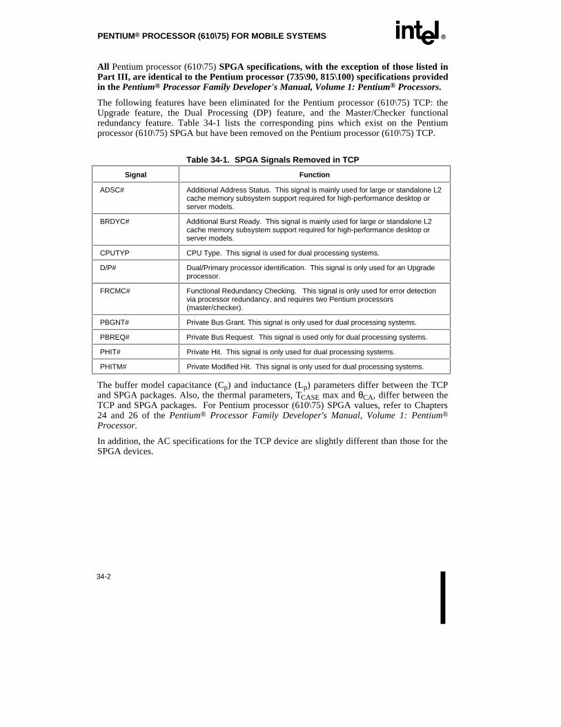
PENTIUM® PROCESSOR (610\75) FOR MOBILE SYSTEMS EE
34-2
All Pentium processor (610\75) SPGA specifications, with the exception of those listed inPart III, are identical to the Pentium processor (735\90, 815\100) specifications providedin the Pentium® Processor Family Developer's Manual, Volume 1: Pentium® Processors.
The following features have been eliminated for the Pentium processor (610\75) TCP: theUpgrade feature, the Dual Processing (DP) feature, and the Master/Checker functionalredundancy feature. Table 34-1 lists the corresponding pins which exist on the Pentiumprocessor (610\75) SPGA but have been removed on the Pentium processor (610\75) TCP.
Table 34-1. SPGA Signals Removed in TCP
Signal Function
ADSC# Additional Address Status. This signal is mainly used for large or standalone L2cache memory subsystem support required for high-performance desktop orserver models.
BRDYC# Additional Burst Ready. This signal is mainly used for large or standalone L2cache memory subsystem support required for high-performance desktop orserver models.
CPUTYP CPU Type. This signal is used for dual processing systems.
D/P# Dual/Primary processor identification. This signal is only used for an Upgradeprocessor.
FRCMC# Functional Redundancy Checking. This signal is only used for error detectionvia processor redundancy, and requires two Pentium processors(master/checker).
PBGNT# Private Bus Grant. This signal is only used for dual processing systems.
PBREQ# Private Bus Request. This signal is used only for dual processing systems.
PHIT# Private Hit. This signal is only used for dual processing systems.
PHITM# Private Modified Hit. This signal is only used for dual processing systems.
The buffer model capacitance (Cp) and inductance (Lp) parameters differ between the TCPand SPGA packages. Also, the thermal parameters, TCASE max and θCA, differ between theTCP and SPGA packages. For Pentium processor (610\75) SPGA values, refer to Chapters24 and 26 of the Pentium® Processor Family Developer's Manual, Volume 1: Pentium®
Processor.
In addition, the AC specifications for the TCP device are slightly different than those for theSPGA devices.

EE PENTIUM® PROCESSOR (610\75) FOR MOBILE SYSTEMS
34-3
34.2. TCP PINOUT
34.2.1. TCP Pinout and Pin Descriptions
34.2.1.1. PENTIUM® PROCESSOR (610\75) TCP PINOUT
VCC240239238237236235234233232231230
VSSA11A10VCCVSSA9VSSVCCA8VCC
219218217216215214213212211210
A3VSSVCCVCCVSSA31A30A29A28VCC
229228227226225224223222221220
VSSA7A6VCCVCCVSSA5A4VCCVSS
209208207206205204203202201200
VSSA27A26A25A24VCCVSSA23A22A21
199198197196195194193192191190
NMI/LINT1R/S#INTR/LNT0SMI#VCCVSSIGNNE#INITPEN#VCC
189188187186185184183182181180
VSSVCCVSSBFNCNCVCCVSSSTPCLK#VCC
179178177176175174173172171170
VSSVCCVCCVSSNCVCCVSSVCCVSSVCC
169168167166165164163162161
VSSVCCTRST#VSSVCCTMSTDITDOTCK
VCC 123456789
1011
VCCVSS
HOLDWB/WT#
VCC
NA#BOFF#BRDY#
VCC
22232425262728293031
M/IO#VCCVSSBP3VSSVCCBP2
PM1/BP1PM0/BP0
FERR#
12131415161718192021
VSSKEN#
AHOLDINV
EWBE#VCCVSSVCCVSS
CACHE#
32333435363738394041
VSSVCC
IERR#VCCVSSDP7D63D62D61VCC
42434445464748495051
VSSVCCVSSD60D59D58D57VCCVSSVCC
52535455565758596061
VSSD56DP6D55D54VCCVSSVCCVSSD53
62636465666768697071
D52D51D50VCCVSSVCCVSSD49D48DP5
727374757677787980
D47VCCVSSD46D45D44D43VCCVSS
VSS
VS
S32
031
931
831
731
631
531
431
331
231
131
0
SM
IAC
T#
PR
DY
VC
CP
CH
K#
AP
CH
K#
VS
SV
CC
BR
EQ
HLD
AV
SS
299
298
297
296
295
294
293
292
291
290
PW
TD
/C#
EA
DS
#A
DS
#V
CC
VS
SH
ITM
#H
IT#
VC
CV
SS
309
308
307
306
305
304
303
302
301
300
VC
CA
PV
SS
VC
CV
SS
VC
CLO
CK
#V
SS
VC
CP
CD
289
288
287
286
285
284
283
282
281
280
W/R
#B
US
CH
K#
FLU
SH
#A
20M
#B
E0#
BE
1#B
E2#
BE
3#V
CC
VS
S27
927
827
727
627
527
427
327
227
127
0
BE
4#B
E5#
BE
6#B
E7#
VC
CV
SS
SC
YC
CLK
NC
RE
SE
T26
926
826
726
626
526
426
326
226
126
0
VS
SV
CC
VS
SV
CC
A20
VC
CV
SS
A19
VS
SV
CC
259
258
257
256
255
254
253
252
251
250
A18
VC
CV
CC
VS
SA
17A
16V
CC
VS
SA
15V
SS
249
248
247
246
245
244
243
424
241
VC
CA
14V
CC
VS
SA
13V
SS
VC
CA
12V
CC
D42
81 82 83 84 85 86 87 88 89 90 91
D41
D40
DP
4V
CC
VS
S
D38
D37
D36
VC
C
102
103
104
105
106
107
108
109
110
111
D29
VC
CV
SS
D28
D27
D26
D25
VC
CV
SS
VC
C
92 93 94 95 96 97 98 99 100
101
VS
SD
35D
34D
33D
32V
CC
VS
SD
P3
D31
D30
112
113
114
115
116
117
118
119
120
121
VS
SD
24D
P2
D23
D22
VC
CV
SS
D21
D20
D19
122
123
124
125
126
127
128
129
130
131
D18
VC
CV
SS
D17
D16
DP
1D
15V
CC
VS
SD
1413
213
313
413
513
613
713
813
914
014
1
D13
D12
D11
VC
CV
SS
D10 D
9D
8D
P0
VC
C14
214
314
414
514
614
714
814
915
015
1
VS
SD
7D
6D
5D
4V
CC
VS
SD
3D
2D
115
215
315
415
515
615
715
815
916
0
D0
VC
CV
SS
NC
NC
VC
CN
CV
SS
VC
C
D39
Pentium ® Processor (610\75)
TCP Pinout
Figure 34-1. Pentium ® Processor (610\75) TCP Pinout

PENTIUM® PROCESSOR (610\75) FOR MOBILE SYSTEMS EE
34-4
34.2.1.2. PIN CROSS REFERENCE TABLE FOR PENTIUM ® PROCESSOR(610\75) TCP
Table 34-2. TCP Pin Cross Reference by Pin Name
Address
A3 219 A9 234 A15 251 A21 200 A27 208
A4 222 A10 237 A16 254 A22 201 A28 211
A5 223 A11 238 A17 255 A23 202 A29 212
A6 227 A12 242 A18 259 A24 205 A30 213
A7 228 A13 245 A19 262 A25 206 A31 214
A8 231 A14 248 A20 265 A26 207
Data
D0 152 D13 132 D26 107 D39 87 D52 62
D1 151 D14 131 D27 106 D40 83 D53 61
D2 150 D15 128 D28 105 D41 82 D54 56
D3 149 D16 126 D29 102 D42 81 D55 55
D4 146 D17 125 D30 101 D43 78 D56 53
D5 145 D18 122 D31 100 D44 77 D57 48
D6 144 D19 121 D32 96 D45 76 D58 47
D7 143 D20 120 D33 95 D46 75 D59 46
D8 139 D21 119 D34 94 D47 72 D60 45
D9 138 D22 116 D35 93 D48 70 D61 40
D10 137 D23 115 D36 90 D49 69 D62 39
D11 134 D24 113 D37 89 D50 64 D63 38
D12 133 D25 108 D38 88 D51 63

EE PENTIUM® PROCESSOR (610\75) FOR MOBILE SYSTEMS
34-5
Table 34-2. TCP Pin Cross Reference by Pin Name (Contd.)
Control
A20M# 286 BREQ 312 HITM# 293 PM1/BP1 29
ADS# 296 BUSCHK# 288 HLDA 311 PRDY 318
AHOLD 14 CACHE# 21 HOLD 4 PWT 299
AP 308 D/C# 298 IERR# 34 R/S# 198
APCHK# 315 DP0 140 IGNNE# 193 RESET 270
BE0# 285 DP1 127 INIT 192 SCYC 273
BE1# 284 DP2 114 INTR/LINT0 197 SMI# 196
BE2# 283 DP3 99 INV 15 SMIACT# 319
BE3# 282 DP4 84 KEN# 13 TCK 161
BE4# 279 DP5 71 LOCK# 303 TDI 163
BE5# 278 DP6 54 M/IO# 22 TDO 162
BE6# 277 DP7 37 NA# 8 TMS 164
BE7# 276 EADS# 297 NMI/LINT1 199 TRST# 167
BOFF# 9 EWBE# 16 PCD 300 W/R# 289
BP2 28 FERR# 31 PCHK# 316 WB/WT# 5
BP3 25 FLUSH# 287 PEN# 191
BRDY# 10 HIT# 292 PM0/BP0 30
APIC Clock Control
PICCLK 155 PICD1 158 BF 186 STPCLK# 181
PICD0 156 [APICEN] CLK 272
[DPEN#]

PENTIUM® PROCESSOR (610\75) FOR MOBILE SYSTEMS EE
34-6
Table 34-2. TCP Pin Cross Reference by Pin Name (Contd.)
Vcc
1*
2
6*
11*
17*
19
23
27*
33*
35
41*
43
49*
51
57*
59
65*
67
73
79
85
91
97
103
109
111*
117
123
129
135
141
147
153*
157*
160
165*
168*
170*
172*
174*
177*
178
180*
183*
188*
190*
195*
204
210
216
217*
221
225*
226
230
232*
236
240*
241
243*
247
249*
253
257*
258
260*
264
266*
268*
275
281
291
295
301
304*
306
309*
313
317*
Vss
3
7
12
18
20
24
26
32
36
42
44
50
52
58
60
66
68
74
80
86
92
98
104
110
112
118
124
130
136
142
148
154
159
166
169
171
173
176
179
182
187
189
194
203
209
215
218
220
224
229
233
235
239
244
246
250
252
256
261
263
267
269
274
280
290
294
302
305
307
310
314
320
NC
175 184 185 271
NOTE:
*These VCC pins are 3.3V supplies for the Pentium processor (610\75) TCP but will be lower voltage pins onfuture offerings of this microprocessor family. All other VCC pins will remain at 3.3V.

EE PENTIUM® PROCESSOR (610\75) FOR MOBILE SYSTEMS
34-7
34.2.1.3. POWER DISSIPATION REQUIREMENTS
Table 34-3. Power Dissipation Requirements for Thermal Solution Design
Parameter Typical(1) Max(2) Unit Notes
Active Power Dissipation 3 7.6 Watts @ 75 Mhz
Stop Grant and Auto HaltPowerdown Power Dissipation
1.2 Watts @ 75 MHz(3)
Stop Clock Power Dissipation 0.02 ≤ .05 Watts (4) (5)
NOTE:1. This is the typical power dissipation in a system. This value was the average value measured in a system using a
typical device at VCC = 3.3V running typical applications. This value is highly dependent upon the specific systemconfiguration.
2. Systems must be designed to thermally dissipate the maximum active power dissipation. It is determined using a worst-case instruction mix with VCC = 3.3V. The use of nominal VCC in this measurement takes into account the thermal timeconstant of the package.
3. Stop Grant/Auto Halt Powerdown Power Dissipation is determined by asserting the STPCLK# pin or executing theHALT instruction.
4. Stop Clock Power Dissipation is determined by asserting the STPCLK# pin and then removing the external CLK input.5. Complete characterization of the specification was still in process at the time of print. Please contact Intel for the latest
information. The final specification may be less than 50mW.
34.2.1.4. AC TIMING CHANGES
Table 34-4 lists the deviations for AC timing parameters with use of the TCP package. Forall unlisted parameters, the AC timing values associated with SPGA packages should beused.
Table 34-4. AC Timing Changes for TCP Package
Symbol Parameter Min Max Unit Figure Notes
t6d C/C#, SCYC, LOCK# Valid Delay 0.9 nS
t6e ADS# Valid Delay 0.8 nS
t6f A3-A31, BE0-7# Valid Delay 0.7 nS
t6g W/R# Valid Delay 0.5 nS
t10b HITM# Valid Delay 0.5 nS
t23 BOFF# Hold Time 1.1 nS
t29 SMI# Hold Time 1.1 nS
t42d Reset Configuration SignalBRDYC# (BRDY# on TCP) HoldTime, RESET driven synchronously
1.0 nS To RESET fallingedge (1), (27)
NOTE:
1. Not 100 percent tested. Guaranteed by design/characterization.
27. BRDYC# and BUSCHK# are used as reset configuration signals to select buffer size.

PENTIUM® PROCESSOR (610\75) FOR MOBILE SYSTEMS EE
34-8
34.3. PENTIUM® PROCESSOR (610\75) TCP BUFFER MODELPARAMETERS
Table 34-5. Input, Output and Bidirectional Buffer Model Parameters
BufferType Transition
dV/dt(V/nsec)
Ro(Ohms)
Cp(pF)
Lp(nH)
Co/Cin(pF)
min max min max min max min max min max
ER0 Rising 0.3 0.4 3.9 5.0 0.8 1.2
(input) Falling 0.3 0.4 3.9 5.0 0.8 1.2
ER1 Rising 0.2 0.5 3.1 6.0 0.8 1.2
(input) Falling 0.2 0.5 3.1 6.0 0.8 1.2
ED1 Rising 3/3.0 3.7/0.9 21.6 53.1 0.3 0.6 3.7 6.6 2.0 2.6
(output) Falling 3/2.8 3.7/0.8 17.5 50.7 0.3 0.6 3.7 6.6 2.0 2.6
EB1 Rising 3/3.0 3.7/0.9 21.6 53.1 0.2 0.5 2.9 6.1 2.0 2.6
(bidir) Falling 3/2.8 3.7/0.8 17.5 50.7 0.2 0.5 2.9 6.1 2.0 2.6
EB2 Rising 3/3.0 3.7/0.9 21.6 53.1 0.2 0.5 3.1 6.4 9.1 9.7
(bidir) Falling 3/2.8 3.7/0.8 17.5 50.7 0.2 0.5 3.1 6.4 9.1 9.7
EB2A Rising 3/2.4 3.7/0.9 10.1 22.4 0.2 0.5 3.1 6.4 9.1 9.7
(bidir) Falling 3/2.4 3.7/0.9 9.0 21.2 0.2 0.5 3.1 6.4 9.1 9.7
EB3 Rising 3/3.0 3.7/0.9 21.6 53.1 0.2 0.4 3.2 4.1 3.3 3.9
(bidir) Falling 3/2.8 3.7/0.8 17.5 50.7 0.2 0.4 3.2 4.1 3.3 3.9
EB4 Rising 3/3.0 3.7/0.9 21.6 53.1 0.3 0.4 4.0 4.1 5.0 7.0
(bidir) Falling 3/2.8 3.7/0.8 17.5 50.7 0.3 0.4 4.0 4.1 5.0 7.0
Table 34-6. Input Buffer Model Parameters: D (Diodes)
Symbol Parameter D1 D2
IS Saturation Current 1.4e-14A 2.78e-16A
N Emission Coefficient 1.19 1.00
RS Series Resistance 6.5 ohms 6.5 ohms
TT Transit Time 3 ns 6 ns
VJ PN Potential 0.983V 0.967V
CJ0 Zero Bias PN Capacitance 0.281 pF 0.365 pF
M PN Grading Coefficient 0.385 0.376

EE PENTIUM® PROCESSOR (610\75) FOR MOBILE SYSTEMS
34-9
34.4. PENTIUM® PROCESSOR (610\75) TCP MECHANICALSPECIFICATIONS
Today's portable computers face the challenge of meeting desktop performance in anenvironment that is constrained by thermal, mechanical, and electrical design considerations.These considerations have driven the development and implementation of Intel’s TapeCarrier Package (TCP). The Intel TCP package has been designed to offer a high pin count,low profile, reduced footprint package with uncompromised thermal and electricalperformance. Intel continues to provide packaging solutions that meet our rigorous criteriafor quality and performance, and this new entry into the Intel package portfolio is noexception.
Key features of the TCP package include: surface mount technology design, lead pitch of0.25 mm, polyimide body size of 24 mm and polyimide up for pick&place handling. TCPcomponents are shipped with the leads flat in slide carriers, and are designed to be excisedand lead formed at the customer manufacturing site. Recommendations for the manufactureof this package are included in the New Device Tape Carrier Package User’s Guide.
Figure 34-2 shows a cross-sectional view of the TCP package as mounted on the PrintedCircuit Board. Figures 34-3 and 34-4 show the TCP as shipped in its slide carrier, and keydimensions of the carrier and package. Figure 34-5 shows a blow up detail of the package incross-section. Figure 34-6 shows an enlarged view of the outer lead bond area of thepackage.
Tables 34-7 and 34-8 provide Pentium processor (610\75) Pentium processor (610\75) TCPpackage dimensions.

PENTIUM® PROCESSOR (610\75) FOR MOBILE SYSTEMS EE
34-10
34.4.1. TCP Package Mechanical Diagrams
AAAAAAAAAAAAAAAA
AAAAAAAAAAAAAAAA
AAAAAAAAAAAAAAAA
AAAAAAAAAAAAAAAA
AAAAAAAA
AAAAAAAAAAAAAAAA
AAAAAAAAAAAAAAAA
AAAAAAAAAAAAAAAA
AAAAAAAAAAAAAAAA
AAAAAAAAAAAAAAAAAAAAAAAAAAAA
AAAAAAAAAAAAAAAAAAAAAAAAAAAA
AAAAAAAAAAAAAAAAAAAAAAAAAAAA
AAAAAAAAAAAAAAAAAAAAAAAAAAAA
AAAAAAAAAAAAAAAAAAAAAAAAAAAA
AAAAAAAAAAAAAAAAAAAAAAAAAAAA
AAAAAAAAAAAAAAAAAAAAAAAAAAAA
AAAAAAAAAAAAAAAAAAAAAAAAAAAA
AAAAAAAAAAAAAAAAAAAAAAAAAAAA
AAAAAAAAAAAAAAAAAAAAAAAAAAAA
AAAAAAAAAAAAAAAAAAAAAAAAAAAA
AAAAAAAAAAAAAAAAAAAAAAAAAAAA
AAAAAAAAAAAAAAAAAAAAAAAAAAAA
AAAAAAAAAAAAAAAAAAAAAAAAAAAA
AAAAAAAAAAAAAAAAAAAAAAAAAAAA
AAAAAAAAAAAAAAAAAAAAAAAAAAAA
AAAAAAAAAAAAAAAAAAAAAAAAAAAA
AAAAAAAAAAAAAAAAAAAAAAAAAAAA
AAAAAAAAAAAAAAAAAAAAAAAAAAAA
AAAAAAAAAAAAAAAAAAAAAAAAAAAA
AAAAAAAAAAAAAAAAAAAAAAAAAAAA
TAB Lead(OFC Copper)
Gold Bump
PolyimideSupport Ring
PolyimideKeeper
Bar
Thermally & Electrically Conductive Adhesive
(Silver Filled Thermoplastic)
AAAAAAAAAAAAAAAAAAAA
AAAAAAAAAAAAAAAAAAAAAAAA
AAAAAAAA
AAAAAAAAAAAA
AAAAAAAAAAAA
AAAAAAAAAAAA
AAAAAAAAAAAA
AAAAAAAAAAAA
AAAAAAAAAAAA
AAAAAAAAAAAA
AAAAAAAAAAAA
AAAAAA
AAAAAAAAAAAAAAAAAAAAAAAAAAAA
AAAAAAAAAAAAAAAAAAAAAAAAAAAA
AAAAAAAAAAAAAAAAAAAAAAAAAAAA
AAAAAAAAAAAAAAAAAAAAAAAAAAAA
AAAAAAAAAAAAAAAAAAAAAAAAAAAA
AAAAAAAAAAAAAAAAAAAAAAAAAAAA
AAAAAAAAAAAAAAAAAAAAAAAAAAAA
AAAAAAAAAAAAAAAAAAAAAAAAAAAA
AAAAAAAAAAAAAAAAAAAAAAAAAAAA
AAAAAAAAAAAAAAAAAAAAAAAAAAAA
AAAAAAAAAAAAAAAAAAAAAAAAAAAA
AAAAAAAAAAAAAAAAAAAAAAAAAAAA
AAAAAAAAAAAAAAAAAAAAAAAAAAAA
AAAAAAAAAAAAAAAAAAAAAAAAAAAA
AAAAAAAAAAAAAAAAAAAAAAAAAAAA
AAAAAAAAAAAAAAAAAAAAAAAAAAAA
AAAAAAAAAAAAAAAAAAAAAAAAAAAA
AAAAAAAAAAAAAAAAAAAAAAAAAAAA
AAAAAAAAAAAAAAAAAAAAAAAAAAAA
AAAAAAAAAAAAAAAAAAAAA
Note:Sketches Not to Scale
Encapsulant
AAAAAAAAAAAAAAAAAAAAAAAA
AAAAAAAAAAAAAAAAAAAAAAAA
AAAAAAAAAAAAAAAAAAAAAAAA
AAAAAAAAAAAAAAAAAA
Die
Full X-Section
1/2 X-Section
Thermal vias
PCB
Ground plane
AAAAAAAAAAAAAAAA
AAAAAAAAAAAAAAAA
AAAAAAAAAAAAAAAA
AAAAAAAAAAAAAAAA
AAAAAAAAAAAAAAAA
AAAAAAAAAAAAAAAA
AAAAAAAAAAAAAAAA
AAAAAAAAAAAAAAAA
AAAAAAAAAAAAAAAA
AAAAAAAAAAAAAAAA
AAAAAAAAAAAAAAAA
AAAAAAAAAAAAAAAA
AAAAAAAAAAAAAAAA
AAAAAAAAAAAAAAAA
AAAAAAAAAAAAAAAA
AAAAAAAAAAAAAAAA
AAAAAAAAAAAAAAAA
AAAAAAAAAAAAAAAA
AAAAAAAAAAAAAAAA
AAAAAAAAAAAAAAAA
AAAAAAAAAAAAAAAA
AAAAAAAAAAAAAAAA
AAAAAAAAAAAAAAAA
AAAAAAAAAAAA
AAAAAAAAAAA
AAAAAAAA
AAAAAAAA
AAAAAAAA
AAAAAAAA
AAAAAAAAAAAAAAAA
AAAAAAAAAAAAAAAA
AAAAAAAAAAAAAAAA
AAAAAAAAAAAAAAAA
AAAAAAAAAAAAAAAA
AAAAAAAAAAAAAAAA
AAAAAAAAAAAAAAAA
AAAAAAAAAAAAAAAA
AAAAAAAA
PCBAAAAAAAA
AAAAAAAA
AA
AAAAAAAAA
AAAAAAAA
AAAAAAAA
AAAAAAAA
AAAAAAAA
AA
AAAAAAAAAAAAAAAA
AAAAAAAAAAAAAAAA
AAAAAAAAAAAAAAAA
AAAAAAAAAAAAAAAA
AAAAAAAAAAAAAAAA
AAAAAAAAAAAAAAAA
AAAAAAAAAAAAAAAA
AAAAAAAAAAAAAAAA
AAAAAAAA
AAAAAAAAAAAAAAAA
AAAAAAAAAAAAAAAA
AAAAAAAAAAAAAAAA
AAAA
Figure 34-2. Cross-Sectional View of the Mounted TCP Package

EE PENTIUM® PROCESSOR (610\75) FOR MOBILE SYSTEMS
34-11
Figure 34-3. One TCP Site in Carrier (Bottom View of Die)

PENTIUM® PROCESSOR (610\75) FOR MOBILE SYSTEMS EE
34-12
Figure 34-4. One TCP Site in Carrier (Top View of Die)

EE PENTIUM® PROCESSOR (610\75) FOR MOBILE SYSTEMS
34-13
Figure 34-5. One TCP Site (Cross-Sectional Detail)
Figure 34-6. Outer Lead Bond (OLB) Window Detail

PENTIUM® PROCESSOR (610\75) FOR MOBILE SYSTEMS EE
34-14
Table 34-7. TCP Key Dimensions
Symbol Description Dimension
N Leadcount 320 leads
W Tape Width 48.18 +/- 0.12
L Site Length (43.94) ref.
e1 Outer Lead Pitch 0.25 nom.
b Outer Lead Width 0.10 +/- 0.01
D1,E1 Package Body Size 24.0 +/- 0.1
A2 Package Height 0.615 +/- 0.030
DL Die Length 12.614 +/- 0.015
DW Die Width 11.603 +/- 0.015
NOTES:
Be sure to refer to Pentium® Processor Specification Update for any changes.
Dimensions are in millimeters unless otherwise noted.
Dimensions in parentheses are for reference only.
Table 34-8. Mounted TCP Package Dimensions
Description Dimension
Package Height 0.75 max.
Terminal Dimension 29.5 nom.
Package Weight 0.5 g max.
NOTE:
Dimensions are in millimeters unless otherwise noted.
Package terminal dimension (lead tip-to-lead tip) assumes the use of a keeper bar.
34.5. PENTIUM® PROCESSOR (610\75) TCP THERMALSPECIFICATIONS
The Pentium processor (610\75) is specified for proper operation when the case temperature,TCASE, (TC) is within the specified range of 0 °C to 95 °C.
34.5.1. Measuring Thermal ValuesTo verify that the proper TC (case temperature) is maintained for the Pentium processor(610\75), it should be measured at the center of the package top surface (encapsulant). Tominimize any measurement errors, the following techniques are recommended:

EE PENTIUM® PROCESSOR (610\75) FOR MOBILE SYSTEMS
34-15
• Use 36 gauge or finer diameter K, T, or J type thermocouples. Intel's laboratory testingwas done using a thermocouple made by Omega (part number: 5TC-TTK-36-36).
• Attach the thermocouple bead or junction to the center of the package top surface usinghighly thermally conductive cements. Intel's laboratory testing was done by using OmegaBond (part number: OB-100).
• The thermocouple should be attached at a 90° angle as shown in Figure 34-7.
Figure 34-7. Technique for Measuring Case Temperature (T C)
34.5.2. Thermal EquationsFor the Pentium processor (610\75), an ambient temperature (TA) is not specified directly.The only requirement is that the case temperature (TC) is met. The ambient temperature canbe calculated from the following equations:
[ ]
T T P
T T P
T T P
T T P
J C JC
A J JA
A C CA
C A JA JC
CA JA JC
= + ×= − ×= − ×
= + × −= −
θθθ
θ θθ θ θ
( )
where,
TA and TC are ambient and case temperatures (°C)
θCA = Case-to-Ambient thermal resistance (°C/W)
θJA = Junction-to-Ambient thermal resistance (°C/W)
θJC = Junction-to-Case thermal resistance (°C/W)
P = maximum power consumption (Watts)
P (maximum power consumption) is specified in section 4.2.

PENTIUM® PROCESSOR (610\75) FOR MOBILE SYSTEMS EE
34-16
34.5.3. TCP Thermal CharacteristicsThe primary heat transfer path from the die of the Tape Carrier Package (TCP) is through theback side of the die and into the PC board. There are two thermal paths traveling from thePC board to the ambient air. One is the spread of heat within the board and the dissipation ofheat by the board to the ambient air. The other is the transfer of heat through the board andto the opposite side where thermal enhancements (e.g., heat sinks, pipes) are attached. Toprevent the possibility of damaging the TCP component, the thermal enhancements should beattached to the opposite side of the TCP site — not directly mounted to the package surface.
34.5.4. PC Board EnhancementsCopper planes, thermal pads, and vias are design options that can be used to improve heattransfer from the PC board to the ambient air. Tables 34-9 and 34-10 present thermalresistance data for copper plane thickness and via effects. It should be noted that althoughthicker copper planes will reduce the θca of a system without any thermal enhancements,they have less effect on the θca of a system with thermal enhancements. However, placingvias under the die will reduce the θca of a system with and without thermal enhancements.
Table 34-9. Thermal Resistance vs. Copper Plane Thicknesswith and without Enhancements
Copper Plane Thickness* θθCA (°C/W) No Enhancements θθCA (°C/W) With Heat Pipe
1 oz. Cu 18 8
3 oz. Cu 14 8
NOTES:
*225 vias underneath the die
(1 oz = 1.3 ml)
Table 34-10. Thermal Resistance vs. Thermal Vias Underneath the Die
No. of Vias Under the Die* θθCA (°C/W) No Enhancements
0 15
144 13
NOTE:
*3 oz. copper planes in test boards
34.5.4.1. STANDARD TEST BOARD CONFIGURATION
All Tape Carrier Package (TCP) thermal measurements provided in the following tables weretaken with the component soldered to a 2" x 2" test board outline. This six-layer boardcontains 225 vias (underneath the die) in the die attach pad which are connected to two 3 oz.copper planes located at layers two and five. For the Pentium processor (610\75) TCP, the

EE PENTIUM® PROCESSOR (610\75) FOR MOBILE SYSTEMS
34-17
vias in the die attach pad should be connected without thermal reliefs to the ground plane(s).The die is attached to the die attach pad using a thermally and electrically conductiveadhesive. This test board was designed to optimize the heat spreading into the board and theheat transfer through to the opposite side of the board.
NOTE
Thermal resistance values should be used as guidelines only, and are highlysystem dependent. Final system verification should always refer to the casetemperature specification.
Table 34-11. Pentium ® Processor (610\75) TCP Package Thermal Resistancewithout Enhancements
θθJC (°C/W) θθCA (°C/W)
Thermal Resistance without Enhancements 0.8 13.9
Table 34-12. Pentium ® Processor (610\75) TCP Package Thermal Resistancewith Enhancements (Without Airflow)
Thermal Enhancements θθCA (°C/W) Notes
Heat sink 11.7 1.2"×1.2"×.35"
Al Plate 8.7 4"×4"×.030"
Al Plate with Heat Pipe 7.8 0.3×1"×4"
Table 34-13. Pentium ® Processor (610\75) TCP Package Thermal Resistancewith Enhancements (with Airflow)
Thermal Enhancements θθCA (°C/W) Notes
Heat sink with Fan @ 1.7 CFM 5.0 1.2"×1.2"×.35" HS
1"×1"×.4" Fan
Heat sink with Airflow @ 400 LFM 5.1 1.2"×1.2"×.35" HS
Heat sink with Airflow @ 600 LFM 4.3 1.2"×1.2"×.35" HS
HS = heat sink
LFM = Linear Feet/Minute
CFM = Cubic Feet/Minute

EA
SupplementalInformation


EE
A-1
APPENDIX ASUPPLEMENTAL INFORMATION
Some non-essential information regarding the Pentium processor are considered Intelconfidential and proprietary and have not been documented in this publication. Thisinformation is provided in the Supplement to the Pentium® Processor Family User's Manualand is available with the appropriate non-disclosure agreements in place. Please contact IntelCorporation for details.
The Supplement to the Pentium® Processor Family User's Manual contains Intel confidentialinformation on architecture extensions to the Pentium processor which are non-essential forstandard applications. This includes low-level registers that provide access to such features aspage size extensions, virtual mode extensions, testing and performance monitoring.
This information is specifically targeted at writers of the following types of software:
• operating system kernels
• virtual memory managers
• BIOS and CPU test software
• performance monitoring tools
If you are writing software that does not fall into one of these categories, this information isnon-essential and all required programming details are contained in the publicly availablePentium® Processor Family Developer's Manual three volume set.

EELITERATURE
For additional information on Intel products in the U.S. and Canada call Intel’s Literature Center at (800) 548-4725.
INTEL LITERATUREP.O. Box 7641Mt. Prospect, IL 60056-7641
To order literature outside of the U.S. and Canada contact your local international sales office.
CURRENT DATABOOKS
Product line databooks contain datasheets, application notes, article reprints, and other design information.Databooks can be ordered in the U.S. and Canada by calling TAB/McGraw-Hill at 1-800-822-8158; outside ofthe U.S. and Canada contact your local international sales office.
TitleIntel
Order Number ISBN
AUTOMOTIVE PRODUCTS 231792 N/A
EMBEDDED APPLICATIONS 270648 1-55512-242-6
EMBEDDED MICROCONTROLLERS 270646 1-55512-230-2
EMBEDDED MICROPROCESSORS 272396 1-55512-231-0
FLASH MEMORY (2 volume set) 210830 1-55512-232-9
Intel486™ MICROPROCESSORS and Related Products 241731 1-55512-1235-3
i960® PROCESSORS AND RELATED PRODUCTS 272084 1-55512-234-5
MILITARY AND SPECIAL PRODUCTS (2 volume set) 210461 N/A
NETWORKING 297360 1-55512-236-1
OEM BOARDS, SYSTEMS & SOFTWARE 280407 1-55512-237-X
PACKAGING 240800 1-55512-238-8
PENTIUM™ PROCESSORS and Related Products 241732 1-55512-239-6
PERIPHERAL COMPONENTS 296467 1-55512-240-X
A complete set of this information is available on CD-ROM through Intel’s Data on Demand program, order number 240897.For information about Intel’s Data on Demand ask for item number 240952.