performance improvement of spectral amplitude coding-optical code division multiple access systems...
TRANSCRIPT

Performance Improvement of Spectral Amplitude Coding-OpticalCode Division Multiple Access Systems Using NAND Detectionwith Enhanced Double Weight CodeNasim AHMED
�, Syed Alwee ALJUNID, R. Badlishah AHMAD, Hilal A. FADHIL, and Mohd Abdur RASHID1
School of Computer and Communication Engineering, University Malaysia Perlis, 02600 Arau Perlis, Malaysia1School of Electrical Systems Engineering, University Malaysia Perlis, 02600 Arau Perlis, Malaysia
(Received June 15, 2011; Accepted October 27, 2011)
The bit-error rate (BER) performance of the spectral amplitude coding-optical code division multiple access (SAC-OCDMA) system has been investigated by using NAND subtraction detection technique with enhanced double weight(EDW) code. The EDW code is the enhanced version of double weight (DW) code family where the code weight is anyodd number and greater than one with ideal cross-correlation. In order to evaluate the performance of the system,we used mathematical analysis extensively along with the simulation experiment. The evaluation results obtained usingthe NAND subtraction detection technique was compared with those obtained using the complementary detectiontechnique for the same number of active users. The comparison results revealed that the BER performance of thesystem using NAND subtraction detection technique has greatly been improved as compared to the complementarytechnique. # 2012 The Japan Society of Applied Physics
Keywords: SAC-OCDMA, enhanced double weight (EDW), double weight (DW), complementary subtractiondetection, fiber-Bragg-grating (FBG)
1. Introduction
Optical code division multiple access (OCDMA) tech-nique is a smart technology over the past one decade due toits unique advantages of high speed all-optical processing,fully asynchronous transmission with low latency access,soft capacity on demand and so on. Besides, the OCDMAtechnology is also considered as a prospective candidate toprovide secure communication in all optical access net-works. Therefore, by time being it has been a renewedinterest in spectral amplitude coding for OCDMA for opticalaccess network.1) Most of the development over the years inOCDMA area is based on the code development2) as well asthe system performance.3) Accordingly, number of codes areproposed by researchers with ideal cross correlation (� ¼ 1)in order to enhance the system performance.4–7)
The spectral-amplitude-coding OCDMA (SAC-OCDMA)is a spread spectrum technique, which increases the physicalbandwidth of the channel by providing the provision ofsharing the spread code and the same channel among largenumber of users for their communication. Due to the morenumber of users in a single channel, the overall OCDMAsystem performance is always degraded, which is calledthe multi access interference (MAI) effect. The MAIeffect always reduces the system performance.8) In order tosuppress the MAI effect sufficiently, many subtractiontechniques with codes fixed in-phase cross correlation havebeen proposed.9–11)
However, all the well known detection techniques are notsuitable for all kinds of codes used in SAC-OCDMAsystems. The enhance double weight (EDW) code wassuccessfully applied in the complementary technique12) but
the performance is not sufficient enough. We proposed thenNAND subtraction detection technique scheme with EDWcode that greatly improved the system performance ascompared to complementary detection technique. This wasmade possible since the NAND subtraction detectiontechnique is capable of suppressing the MAI effect in asignificant amount.9–11,13) We evaluated the performance ofSAC-OCDMA systems using the NAND subtraction detec-tion technique by theoretical analysis as well as simulationexperiment extensively. The results in both theoretical andsimulation experiments show that the performance of systemis greatly improved by NAND subtraction detectiontechnique as compared to the complementary detectiontechnique.
In this paper, the mathematical as well as simulationanalysis has been done extensively. Finally, the paper isorganized as follows. In x2, EDW code construction hasbeen described. Section 3 shows the proposed NANDsubtraction detection technique. Section 4 describes thesystem performance in terms of mathematical development.In x5, network simulation setup is shown. Results anddiscussion are presented in x6, and finally some concludingremarks are drawn in x7.2. EDW Code Construction
The basic matrix for the EDW code consists of K� Nmatrix depending on the value of the code weight. Thegeneral form of the basic matrix of an EDW code withweight W is shown in eq. (1), where all the componentmatrices ½A1�; ½A2�; . . . ; ½AW � depend on W.12) The basicmatrix consists of the minimum number of K and N for thespecific number of code weight. From the basic matrix,a larger number of K can be achieved using the mappingtechnique as�E-mail address: [email protected]
OPTICAL REVIEW Vol. 19, No. 1 (2012) 1–6
1

½H� ¼
..
. ... ..
.
..
. ... ..
.
A1...
A2...
. . . ...
AW
..
. ... ..
.
..
. ... ..
.
26666666666664
37777777777775: ð1Þ
The size of each matrix consist of Ka � Na, where
Ka ¼ W; ð2Þ
Na ¼
XWj¼1
j
W: ð3Þ
The basic matrix for EDW consists of a 3� 6 matrix.The component matrices are ½A1�, ½A2�, and ½A3�. The sizeof matrix ½A� is 3� 2, after using eqs. (2) and (3). Thecombination sequence for each matrix is 2 and 1. The basicEDW code denoted by ð6; 3; 1Þ is shown Fig. 1.
The basic matrix consists of a chip-combination sequenceof 1; 2; 1; 2; . . . (alternating 1’s and 2’s) for the columns. Achip combination is defined as the summation of the spectralchips (1’s and 0’s) for all users (or rows) in the same columnwith each code sequence allowed to overlap at most, oncewith every other sequence in the columns of the matrix.
3. NAND Subtraction Detection Technique
The mobility of the digital electrons in NAND gate isthree times higher than AND gate as well as NOR gate.14)
This statement refers to the digital logic gates (AND, OR,NAND). However, in our proposed system the idea ofNAND is used as an operation, not as a digital gate.Considering this point of view, the authors brought the
concept of the NAND subtraction technique in our study.In the NAND subtraction detection technique, the cross-correlation �eXY
ðKÞ is substituted by �ðeXYÞY , where �ðeXYÞrepresents the NAND operation between X and Y sequences.For example, let X ¼ 1100 and Y ¼ 0110 therefore theNAND is ðfXYÞY ¼ 0010. Figure 2 shows the implementa-tion of NAND subtraction detection technique and Table 1shows the comparisons between complementary and NANDsubtraction detection technique using EDW codes.
Note that �i (where i is 1; 2; . . . ; N) is the column numberof the codes which also represents the spectral position ofthe chips. Therefore, MAI can be cancelled using bothtechniques. However, NAND subtraction detection tech-nique can generate extra weight as shown in Table 1. This isdue to the fact that when the code weight is increased, thesignal power increases as well; hence, increases the signal-to-noise ratio (SNR). Therefore, The SAC-OCDMA perfor-mance is improved significantly using the NAND subtrac-tion detection technique.
Fig. 1. The chip combination sequence of basic EDW matrix.12)
Fig. 2. Implementation of NAND subtraction detection technique.
OPTICAL REVIEW Vol. 19, No. 1 (2012)2 N. AHMED et al.

4. System Performance by Mathematical Analysis
We have considered the bit-error rate (BER) and the SNRas the system performance criterion for comparison. Theeffect of incoherent intensity noise hiPIINi, shot noise hishoti,and thermal noise hithermali are considered in the system.When the incoherent light fields are mixed and incident upona photo-detector, the phase noise of the fields causes anintensity noise term in the photo-detector output.12) Gaussianapproximation has been used for the calculation of BER.8)
The source coherence time �c is expressed as8)
�c ¼
Z 1
0
G2ðvÞ dv�Z 1
0
GðvÞ dv�2 ; ð4Þ
where GðvÞ denotes the single sideband power spectraldensity (PSD) of the thermal source. The Q-factorperformance provides the qualitative description of theoptical receiver performance. The performance of an opticalreceiver depends on the signal-to-noise ratio (SNR). TheQ-factor suggests the minimum SNR requirement to obtaina specific BER for a given signal.10) The SNR of an electricalsignal is defined as the average signal to noise power,SNR ¼ ½I2=�2�, where �2 is the variance of noise source(note: the effect of the receiver’s dark current andamplification noises are neglected in the analysis of theproposed system), given by
�2 ¼ hi2shoti þ hi2PIINi þ hi2thermali¼ 2eBI þ I2B�c þ 4KbTnB
RLð5Þ
where the symbols bear the following meaning: e, electroncharge; I, average photocurrent; I2, the power spectraldensity for I; B, electrical bandwidth; Kb, Boltzmannconstant; Tn, absolute receiver noise temperature; RL,receiver load resistor.
The code cross-correlation properties of EDW codes usingNAND operation of the detection part differs fromcomplementary and AND-subtraction technique. In thistechnique, the system carried out better performance interms of PIIN noise, shot noise, signal to noise ratio and biterror rate. The new detection scheme based on EDW codeproperties has been explained in eqs. (5) and (6). If CKðiÞ
denotes the ith element of the Kth EDW code sequence, thecode properties for NAND can be written as
XNi¼l
gCKð�ÞClð�Þ � ClðiÞ ¼W; for K ¼ l
W � 1; for K 6¼ l
0; else
8<:¼ K and l different basic matrix: ð6Þ
The system transmitter and receiver is analyzed according tothe analysis of ref. 8. All the assumptions considered inrefs. 8 and 12 are important for mathematical simplicity.Therefore, the following assumption is taken into accountfor the analysis of the system:a) Each light source is ideally unpolarized and its
spectrum is flat over the bandwidth [vo ��v=2; vo þ�v=2], where vo is the central optical frequency and�v is the optical source bandwidth expressed in hertz.
b) Each power spectral component has an identicalspectral width.
c) Each user has equal power at the receiver andd) Each bit stream from each user is synchronized.
The power spectral density of the received optical signalscan be written as8,12)
rðvÞ ¼ Psr
�v
XKK¼1
dKXNi¼1
cKðiÞ rectðiÞ; ð7Þ
where Psr is the effective power of a broadband source at thereceiver, K is the active users and N is the MDW codelength, dK is the data bit of the Kth user that is ‘1’ or ‘0’. TherectðiÞ is given by
rectðiÞ ¼ u v� v0 � �v
2Nð�N þ 2i� 2Þ
� �� u v� v0 � �v
2nð�N þ 2iÞ
� �¼ u
�v
N
� �ð8Þ
where uðvÞ is the unit step function and can be expressed as
uðvÞ ¼ 1; v � 0,
0; v < 0.
�The total incident power at the input of PIN 1 and PIN 2 ofFig. 1 is given byZ 1
0
G1ðvÞ dv
¼Z 1
0
Psr
�v
XKK¼1
dkXNi¼l
CKðiÞ �CiðiÞ u�v
N
� �� �" #dv
¼ PsrðW � 1ÞN
XKK¼1 K¼l
dK: ð9Þ
Now, power spectral density for photodetector 2 is given byZ 1
0
G2ðvÞ dv
¼Z 1
0
Psr
�v
XKK¼1
dkXNi¼l
ð gCKð�ÞClðiÞ � CKðiÞÞ u�v
N
� �� �" #dv
¼ Psr
NW þ ðW � 1Þ
XdK
h i: ð10Þ
Table 1. Comparison of complementary and NAND subtractiondetection technique.
ComplementarySubtraction
NAND Subtraction
�1 �2 �3 �4 �1 �2 �3 �4
X 1 1 0 0 1 1 0 0Y 0 1 1 0 0 1 1 0
�XY ¼ 1 �XY ¼ 1
X ¼ 0011 �eXY¼ 1011
�XY ¼ 1 �ðeXYÞY ¼ 1
Z Z ¼ �XY � �XY ¼ 0 Z ¼ �XY � �ðeXYÞY ¼ 0
OPTICAL REVIEW Vol. 19, No. 1 (2012) 3N. AHMED et al.
Now the photodiode current I can be expressed as andcombining eqs. (9) and (10):
I ¼ I2 � I1
¼ <Z 1
0
G2ðvÞ dv�<Z 1
0
G1ðvÞ dv
¼ <PsrW
N: ð11Þ
In the above equations, dK is the data bit of the Kth user thatcarries the value of either ‘1’ or ‘0’. Consequently, where <is the responsivity of the photo-detectors and given by< ¼ ne=hvc. Here, � is the quantum efficiency, e is theelectron charge, h is the Planck’s constant, and vc is thecentral frequency of the original broadband optical pulse.
The noise power of shot noise can be written as
hI2shoti ¼ 2eBðI1 þ I2Þ ¼ 2eB<Z 1
0
G1ðvÞ dvþZ 1
0
G2ðvÞ dv� �
ð12Þ
¼ 2eB< �v
N
� �"PsrðW � 1Þ
N
XKK¼1 K 6¼l
dk þ Psr
NðW þ ðW � 1ÞÞ
XKK¼1 K6¼l
dk
#
¼ 2eB<Psr
N½2W2 �W�: ð13Þ
By using the similar methodology in ref. 1 and approximating the summationPK
K¼1 cK � KW=N andPK
K¼1 cKT � KW=Nthe noise power can be written as hI2PIINi ¼ BI21 oc1 þ BI22 oc2:
hI2PIINi ¼ B<2
Z 1
0
G1ðvÞ dvþZ 1
0
G2ðvÞ dv� �
¼ B<2P2sr
N�v
KW
N
� �XKK¼1
XNi¼l
CKðiÞ �ClðiÞ" #
þ B<2P2sr
N�v
KW
N
� �XKK¼1
XNi¼l
gCKð�ÞClð�Þ � CKðiÞ" #
¼ B<2P2srKW
N2�v½2W2 � 5W þ 4�: ð14Þ
The thermal noise is given as15,16)
hi2thermali ¼4KbTnB
RL: ð15Þ
Noting that the probability of sending bit ‘1’ at any time for each user is 1/28) so that the SNR of the NAND detection systemcan be written as
SNR ¼ I2
o2¼
<2P2srW
2
N2
eB<Psr
N½2W2 �W� þ BR2P2
srKW
N2�v½2W2 � 5W þ 4� þ 4KbTnB
RL
: ð16Þ
Equation (16) is the general equation used to calculate thesignal to noise ratio for the MDW code families. UsingGaussian approximation, the BER can be expressed as8)
BER ¼ Pe ¼ 1
2erfc
ffiffiffiffiffiffiffiffiffiffiSNR
8
r !: ð17Þ
5. Results and Discussion
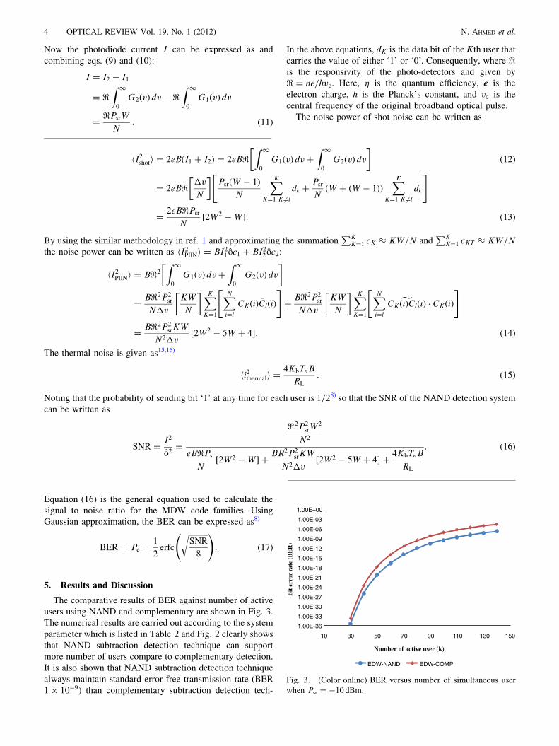
The comparative results of BER against number of activeusers using NAND and complementary are shown in Fig. 3.The numerical results are carried out according to the systemparameter which is listed in Table 2 and Fig. 2 clearly showsthat NAND subtraction detection technique can supportmore number of users compare to complementary detection.It is also shown that NAND subtraction detection techniquealways maintain standard error free transmission rate (BER1� 10�9) than complementary subtraction detection tech-
1.00E-36
1.00E-33
1.00E-30
1.00E-27
1.00E-24
1.00E-21
1.00E-18
1.00E-15
1.00E-12
1.00E-09
1.00E-06
1.00E-03
1.00E+00
10 30 50 70 90 110 130 150
Bit
err
or r
ate
(BE
R)
Number of active user (k)
EDW-NAND EDW-COMP
Fig. 3. (Color online) BER versus number of simultaneous userwhen Psr ¼ �10 dBm.
OPTICAL REVIEW Vol. 19, No. 1 (2012)4 N. AHMED et al.

nique. It can be seen that using NAND subtraction detectionBER is (10�9) and complementary (10�8) when thesimultaneous user is 110. Consequently, the NANDsubtraction detection technique can supports more numberof users (110 users at BER 10�9) compared complementarydetection techniques. The reason of better performance forNAND subtraction detection technique is that the MAI issignificantly suppressed in the receiver side.
The SNR against the number of simultaneous user isshown in Fig. 4. It is seen that the EDW codes give a higherSNR value using NAND subtraction detection techniquecompared to complementary techniques with the effectivepower is (when Psr < �10 dBm).
The system can maintain average transmit power is 0 to�30 dBm. Figure 5 shows the performance of the systemusing NAND and complementary subtraction detectiontechnique at various values of received power Psr with thefixed numbers of active users (40). The performance of thesystem using NAND subtraction detection technique isbetter than complementary techniques. It can be seen inFig. 4 that with less transmit power NAND subtractiondetection technique produce better BER and maintain loweststandard BER (10�36).
In numerical analysis, we do not consider any parameterssuch as optical fiber non-linear effects. However, all thisparameters will not affect the comparative analysis betweenthe three techniques, because all the transmission conditionsare same. Moreover, all these parameters are taken in to theaccount in the simulation. The results are shown bellow inthe x5.6. Network Simulation Setup
As an example Fig. 6 is illustrated a simple schematicblock diagram of NAND subtraction detection techniqueconsisting for two users. The overall simulation was carriedout from 4 to 16 users using simulation software,OptiSystem Version 9.0, at 622Mbps bit rates. The spectralwidth of 0.8 nm was set for each chip. The system insertion
1.00E-25
1.00E-23
1.00E-21
1.00E-19
1.00E-17
1.00E-15
1.00E-13
1.00E-11
1.00E-09
1.00E-07
1.00E-05
1.00E-03
1.00E-01
-30 -25 -20 -15 -10 -5 0
Bit
err
or r
ate
(BE
R)
Various effective power (Psr)
EDW-NAND EDW-COMP
Fig. 5. (Color online) BER versus Psr when number ofsimultaneous users is 40.
50
150
250
350
450
550
650
20 40 60 80 100 120 140
Sign
al t
o no
ise
(SN
R)
Number of active user (k)
EDW-NAND EDW-COMP
Fig. 4. (Color online) SNR versus number of simultaneous userwhen Psr ¼ �10 dBm.
Table 2. The MDW code NAND subtraction detection techniquesystem parameters.
PD quantum efficiency c 0.6Line width of the thermal source �v (THz) 3.75Operation wavelength €e (�m) 1.55Electrical bandwidth B (MHz) 311Receiver noise temperature Tr (K) 300Receiver load resistor RL (�) 1030
Fig. 6. (Color online) Simulation setup for the OCDMA system with NAND subtraction detection technique.
OPTICAL REVIEW Vol. 19, No. 1 (2012) 5N. AHMED et al.

loss 0.25 dBm including multiplexer/demultiplexer losses2 dBm is taken in to an account. The ITU-T G.652 standardsingle-mode optical fiber (SMF) is used to transmit thesignal. The used fiber parameters’ values were taken fromthe data which are based on the G.652 non dispersion shiftedfiber (NDSF) standard. This includes all fiber parameterwhich are all wavelength dependent. All parameters wereactivated during simulation. Where the dark current valuewas 5 nA and the thermal noise co-efficient was 1:8�10�23 W/Hz for each of the photodetectors. All types ofgenerated noises at the receivers were set to be random andtotally uncorrelated.
The fiber transmit power (�10 dBm) was set for the broadband source (BBS). The system performance was carriedout by referring to the bit error rate. The whole simulationis specified according to the typical industrial values tosimulate the real environment as close as possible. Thedata’s are plotted in Fig. 7. It can be seen that as thefiber length is increases the BER decreases. The systemperformance is compared using NAND, and complementarysubtraction detection techniques at various fiber distance.
We found that the NAND subtraction detection techniqueprovides better BER compared to complementary subtrac-tion technique for any length of fiber. This is possible asbecause of less MAI effect in the receiver side when NANDsubtraction detection technique is used. In this proposed
system, NAND subtraction detection technique can supporthigher number of users compared to complimentary becausethe MAI is fully suppressed. It can be pointed out that thevery low BER values are just measure the quality of thesignals, which may not effect in real experiment.
7. Conclusion
The BER performance of the SAC-OCDMA systemusing NAND subtraction detection technique was evaluatedextensively and was compared with the complementarydetection technique. The analysis results ascertained that theNAND subtraction detection technique with EDW code canimprove the system performance by suppressing the MAIeffect significantly. Therefore, the proposed system will besuitable for all optical access networks.
References
1) R. C. Menendez, P. Toliver, and S. Galli et al.: J. LightwaveTechnol. 23 (2005) 3219.
2) S. Mashhadi and J. A. Salehi: IEEE Trans. Commun. 54(2006) 1457.
3) H. Lundqvist and G. Karlsson: J. Lightwave Technol. 23(2005) 2342.
4) E. D. J. Smith, R. J. Blailkie, and D. P. Taylor: IEEE Trans.Commun. 46 (1998) 1176.
5) M. Kavehrad and D. Zaccarin: IEEE J. Lightwave Technol. 13(1995) 534.
6) H. A. Fadil, S. A. Aljunid, and R. B. Ahmad: Opt. FiberTechnol. 15 (2009) 283.
7) M. S. Anuar, S. A. Aljunid, and N. M. Saad et al.: Opt.Commun. 7 (2009) 2659.
8) Z. Wei and H. Ghafouri-Shiraz: IEEE J. Lightwave Technol.50 (2002) 1209.
9) T. Demeechai: IEEE Trans. Commun. 54 (2006) 29.10) E. D. J. Smith, R. J. Blaikie, and D. P. Taylor: IEEE Trans.
Commun. 46 (1998) 1176.11) Y. Hassan, I. F. Ahmed, and M. S. Naufal: Int. J. Comput.
Appl. 202 (2010) 2881.12) K. A. Mohamad, N. Feras, and S. A. Aljunid: Opt. Commun.
281 (2008) 4658.13) T. H. Abd, S. A. AlJunid, and H. A. Fadil et al.: Opt. Fiber
Technol. 17 (2011) 273.14) H. Brain and R. Clive: Digital Logic Design (Elsevier, 2002)
4th ed.15) W. Huang et al.: J. Lightwave Technol. 18 (2000) 765.16) L. Nguyen, B. Aazhang, and J. F. Young: IEEE Electron
Device Lett. 31 (1995) 469.
1.00E-15
1.00E-14
1.00E-13
1.00E-12
1.00E-11
1.00E-10
1.00E-09
-22 -20 -18 -16 -14 -12 -10
Bit
err
or r
ate
(BE
R)
Received power (dBm)
EDW-NAND EDW-COMP
Fig. 7. (Color online) BER against received optical power at622Mbps at 30 km.
OPTICAL REVIEW Vol. 19, No. 1 (2012)6 N. AHMED et al.