personal area networks (pan): near-field intra-body communication · · 2017-05-25near-field...
TRANSCRIPT

Personal Area Networks (PAN):Near-Field Intra-Body Communication
by
Thomas Guthrie Zimmerman
B.S., Humanities and EngineeringMassachusetts Institute of Technology
February 1980
Submitted to the Program in Media Arts and Sciences,School of Architecture and Planning,
in partial fulfillment of the requirements for the degree of
MASTER OF SCIENCE IN MEDIA ARTS AND SCIENCESat the
Massachusetts Institute of TechnologySeptember 1995
(c) Massachusetts Institute of Technology, 1995All Rights Reserved
Signature of Author _______________________________________________________Program in Media Arts and Sciences
June 26, 1995
Certified by _____________________________________________________________Neil Gershenfeld
Assistant Professor of Media Arts and SciencesProgram in Media Arts and Sciences
Thesis Supervisor
Accepted by _____________________________________________________________Stephen A. Benton
ChairpersonDepartmental Committee on Graduate Students
Program in Media Arts and Sciences

2
Personal Area Networks (PAN):Near-Field Intra-Body Communication
by
Thomas Guthrie Zimmerman
Submitted to the Program in Media Arts and Sciences,School of Architecture and Planning,
on June 26, 1995in partial fulfillment of the requirements for the degree of
MASTERS OF SCIENCE IN MEDIA ARTS AND SCIENCES
Abstract
PAN is a wireless communication system that allows electronic devices on and near thehuman body to exchange digital information through near-field electrostatic coupling.Information is transmitted by modulating electric fields and electrostatically (capactively)coupling picoamp currents into the body. The body conducts the tiny current (e.g., 50 pA)to body mounted receivers. The environment (“room ground”) provides a return path forthe transmitted signal. A low frequency carrier (e.g., 330 kHz) is used so no energy ispropagated, minimizing remote eavesdropping and interference by neighboring PANs.Digital information is transferred using on-off keying with quadrature detection to reducestray interference and increase receiver sensitivity. A low cost (<$20) half-duplex modemis implemented using an analog bipolar chopper and integrator as a quadrature detector,and a microcontroller for signal acquisition. The technology used in the PAN can beintegrated into a custom CMOS chip for lowest size and cost.
Thesis Supervisor: Neil Gershenfeld, Assistant Professor of Media Arts and Sciences
This work was supported in part by Hewlett-Packard Corporation and Festo Corporation.

3
Personal Area Networks (PAN):Near-Field Intra-Body Communication
by
Thomas Guthrie Zimmerman
Thesis Readers
Thesis Reader____________________________________________________________Jerome Ysrael Lettvin
Professor of Electrical Engineering and Bioengineeringand Communications Physiology, Emeritus
Thesis Reader____________________________________________________________Louis Dijour Smullin
Professor of Electrophysics, Emeritus

4
Acknowledgments
I am indebted to my advisor, Neil Gershenfeld, for reacquainting me with the all-
encompassing power of physics through his broad command of the discipline. His class
Physics and Media succinctly reviews how important a knowledge of physics is to tackling
any engineering problem. I would like to thank all the members of the Physics and Media
Group; Josh Smith, Joe Paradiso, Rich Flecher, Barrett, Henry Chong, and David Allport
for their camaraderie, team work, stimulating technical discussions, and friendship during
a very busy and exciting eighteen months. I would like to particularly thank Joe Paradiso
for all the advice, design discussions, and great music.
I would like to thank the Media Lab, that big box of very talented people, and those who
build it and keep it running. Of particular merit is the work of Linda Peterson, Santina
Tonelli and Suzanne McDermott. I came to the Media Lab because it has everything I am
interested in under one roof, and my experience here have confirmed my belief. The Media
Lab is truly a unique laboratory at a unique institution.
The visitors who come to the Media Lab for demonstrations have provided me with
instant feedback on the usefulness and value of my research. Without their support and
interest, the Media Lab would not exist. I would like to thank Dr. Hermann Klinger and
the Festo Didactic Corporation for their enthusiastic support of our research and for the
hospitality Dr. Klinger showed my on my visit to Germany. I would like to thank the
Hewlett-Packard Corporation for their generous support of our laboratory, and my
readers Professor Lettvin and Professor Smullin for their comments.
Finally I would like to thank my wife, Patricia Canon Zimmerman, for being the most
wonderful, understanding, helpful, loving, and fun person I know. She sacrificed much to
come here to see me through this process and now we can go back to California, both
Masters, with our wonderful six month old son, Matthew Daniel Zimmerman.

5
Contents
1. INTRODUCTION...............................................................................................................................7
1.1 PREVIOUS WORK ON ELECTRIC FIELD SENSING......................................................................................71.2 CURRENT TRENDS IN WIRELESS NETWORKS ..........................................................................................71.3 MOTIVATION FOR PERSONAL AREA NETWORKS .....................................................................................8
1.3.1 WAN ⇒ MAN ⇒ LAN ⇒ PAN.....................................................................................................81.3.2 Interconnectivity Reduces Redundancy ........................................................................................91.3.3 Ubiquitous Computing vs. Distributed I/O ...................................................................................91.3.4 Connecting to the "Outside" World ............................................................................................10
1.4 COMPARISON OF ELECTROSTATIC TO INFRARED TRANSMISSION ...........................................................101.5 COMPARISON OF ELECTROSTATIC TO RF TRANSMISSION......................................................................10
1.5.1 Antenna Size and Efficiency.......................................................................................................111.5.2 Interference ...............................................................................................................................111.5.3 FCC Field Strength Regulations ................................................................................................121.5.4 Eavesdropping...........................................................................................................................131.5.5 Power ........................................................................................................................................15
1.6 NETWORKING STANDARDS .................................................................................................................151.7 THESIS OVERVIEW..............................................................................................................................16
2. ELECTRICAL MODEL OF PAN SYSTEM ...................................................................................17
2.1 ELECTRICAL IMPEDANCE TOMOGRAPHY (EIT).....................................................................................172.2 RESISTIVITY OF MAMMALIAN TISSUE ..................................................................................................182.3 HUMAN BODY APPROXIMATES A PERFECT CONDUCTOR .......................................................................182.4 BASIC CONCEPT OF PAN COMMUNICATION.........................................................................................182.5 LUMPED MODEL OF COMMUNICATION CHANNEL: SYMMETRY BREAKING .............................................202.6 PAN DEVICE ELECTRICAL FIELDS.......................................................................................................212.7 ELECTRICAL MODEL OF THE COMMUNICATION CHANNEL ....................................................................23
2.7.1 Lumped-Circuit Electrical Model ..............................................................................................232.7.2 Body Capacitance Measurement................................................................................................242.7.3 Electrode Capacitance Measurements .......................................................................................25
3. PAN DESIGN ISSUES ......................................................................................................................26
3.1 SIZE...................................................................................................................................................263.2 POWER CONSUMPTION........................................................................................................................27
3.2.1 Sneaker Power...........................................................................................................................273.2.2 Energy Loss Due to Capacitor Charging ...................................................................................283.2.3 Resonant Transmitter.................................................................................................................28
3.3 COST .................................................................................................................................................283.4 CHANNEL CAPACITY ..........................................................................................................................293.5 LOCATING PAN DEVICES ON THE HUMAN BODY .................................................................................30
4. MODULATION STRATEGIES.......................................................................................................31
4.1 MODULATION AND CODING ................................................................................................................314.2 NARROWBAND VS. BROADBAND TRANSMISSION ..................................................................................324.3 NARROWBAND TRANSMISSION ............................................................................................................324.4 TRANSMITTERS, RECEIVERS, AND TRANSCEIVERS................................................................................334.5 HALF DUPLEX TRANSCEIVERS .............................................................................................................344.6 BROADBAND DIGITAL TRANSMISSION .................................................................................................34
4.6.1 Spread Spectrum........................................................................................................................344.6.2 Pseudo-Noise Sequence .............................................................................................................354.6.3 Synchronization & Manchester Coding......................................................................................35
4.7 RESONANT TRANSMITTER...................................................................................................................36

6
4.7.1 Boosting Transmission Signal Strength ......................................................................................364.7.2 Digitally Controlled Transmitter Gain .......................................................................................374.7.3 Proximity Effect on Resonant Transmitter..................................................................................374.7.4 Contactless Switch .....................................................................................................................38
5. PAN PROTOTYPE DEVELOPMENT ............................................................................................39
5.1 HARDWARE DEVELOPMENT ................................................................................................................395.1.1 Development of a PAN Prototype...............................................................................................395.1.2 System Components ...................................................................................................................405.1.3 Circuit Review ...........................................................................................................................415.1.4 Prototype Construction..............................................................................................................445.1.5 Hardware Development Environment ........................................................................................45
5.2 SOFTWARE DEVELOPMENT..................................................................................................................46
6. EXPERIMENTS WITH CODING STRATEGIES..........................................................................46
6.1 SPREAD SPECTRUM CODING................................................................................................................466.1.1 Generating the PN Sequence .....................................................................................................476.1.2 Acquisition of PN Sequence .......................................................................................................506.1.3 Message Byte Framing ..............................................................................................................506.1.4 Phase Slippage ..........................................................................................................................516.1.5 Random Number Generators......................................................................................................516.1.6 Problems With Spread Spectrum................................................................................................52
6.2 CONTINUOUS WAVE ON-OFF KEYING .................................................................................................546.2.1 Experiments With Resonant Transmitter ....................................................................................546.2.2 Experiments Comparing Spread Spectrum to On-Off Keying .....................................................556.2.3 Selection of On-Off Keying Over Spread Spectrum ...................................................................56
7. DEMONSTRATION PROTOTYPE ................................................................................................56
7.1 THE BUSINESS CARD HANDSHAKE.......................................................................................................567.1.1 Transmitter Dimensions .............................................................................................................587.1.2 Receiver Dimensions .................................................................................................................58
7.2 RECEIVER SIGNAL PROCESSING ...........................................................................................................587.2.1 Approximations To Quadrature Detection..................................................................................587.2.2 Message Timing.........................................................................................................................59
8. RELATED WORK ...........................................................................................................................61
8.1 FISH EVALUATION BOARD ..................................................................................................................618.2 TRANSCEIVER DESIGN ........................................................................................................................618.3 SMART FISH EVALUATION BOARD .......................................................................................................63
8.3.1 Introduction...............................................................................................................................638.3.2 Hardware Review.......................................................................................................................648.3.3 Parts List ...................................................................................................................................708.3.4 Vendor List ................................................................................................................................718.3.5 Smart Fish Programming Manual ..............................................................................................73
8.4 CABLE RESONANCE PHENOMENA AND NON-IDEAL OP AMP PERFORMANCE...........................................768.5 HUMIDITY AND PERMITIVITY ..............................................................................................................77
9. FUTURE RESEARCH......................................................................................................................78
REFERENCES.....................................................................................................................................80

7
1. INTRODUCTION
1.1 Previous Work on Electric Field Sensing
The development of the PAN grew our of research at the Physics and Media Group of the
MIT Media Lab on applying electric field sensing to position measurement. The group
became interested in electric field sensing while trying to solve a measurement and
instrumentation problem. Professor Neil Gershenfeld was trying to measure the position of
Yo-Yo Ma's cello bow in a project with Professor Tod Machover. The concept was to
extend Yo-Yo's playing technique by treating his bow as an elaborate mouse. The
challenge was to measure bow position in two axes without encumbering Yo-Yo's playing
technique. The resulting mechanism applied a low frequency RF signal (~ 50 kHz) to an
antenna mounted on the body of the cello and measured the near-field signal strength at
the ends of a resistive strip (~ 10 megaohm) mounted along the bow [Gershenfeld93]. In
an attempt to make the sensing wireless, it was discovered that placing one’s hand in the
electric field attenuates the received signal dramatically. The sensing mechanism that
emerged from this observation is described in [Zimmerman95].
1.2 Current Trends in Wireless Networks
Historically work on wireless networks has been focused on infrared (IR) light technology
and radio transmission. The former suffers from line-of-sight limitations and the latter
from regulations by the FCC. In 1985 the FCC released several frequency bands called the
ISM bands, for Industrial, Scientific, and Medical applications. The ISM band allows up to
1 watt of peak output power for frequency hopping and direct sequence spread spectrum
transmitters. The ISM frequency bands include 902-928 MHz, 2.2835-2.4, and 5.725-5.85
GHz [FCC93].
The standard criteria for wireless network performance is message bit rate. Kahn
[Kahn92] presents analysis that shows it is possible to achieve data rates as high as 100
Mb/s using non-directional IR. Current IR systems perform up to 4 Mb/s. The system
Kahn proposes uses infrared laser diodes located in the walls and ceilings of office
8
buildings, each consuming about 1 watt of power per 75 cubic feet of room1. Although the
transmitters require a large amount of energy, the receivers can operate at a fraction of the
transmitter power. Typically a mobile user is transmitting keystroke and pointing device
information, which can be accommodated with a 2400 baud modem. This asymmetry
works well in favor of low-power mobile computer modems.
The first generation of radio wireless LANs were designed to interconnect stationary
workstations and marketed as LAN extensions, consuming approximately 20 watts
supplied by the mains. The current generation of wireless LANs use spread spectrum in
the ISM band and achieve data rates as high as 20 Mb/s [Pahlavan95].
1.3 Motivation for Personal Area Networks
As electronic devices become smaller, lower power, and less expensive, we have begun to
adorn ourselves with personal information and communication appliances. These devices
include cellular phones, personal digital assistants (PDA), pocket video games, pen based
computer pads, palm top computers, and pagers. Currently there is no standard method to
interconnect these personal electronic devices. The personal area network is a means to
interconnect these personal device, in a manner appropriate to the power, size, and cost of
these devices.
1.3.1 WAN ⇒⇒ MAN ⇒⇒ LAN ⇒⇒ PAN
Wide area networks (WAN) connect distant computers using microwaves, radio waves,
coaxial cable, and fiber optic. Metropolitan area networks (MAN) connect computers in a
city. Local area networks (LAN) connect computers in an office building. This thesis
introduces the new concept of a personal area network (PAN); a wireless communication
system that allows electronic devices on and near the human body to exchange digital
information through near-field electrostatic coupling, developed by Neil Gershenfeld and
the author [Gershenfeld95a]. The communication system is called a PAN to identify an
evolutionary progression in the development of computer networks and mark a trend
1 Khan's simulation was done using a 1 W source radiating an ideal Lambertian pattern toa room 5m x5m x 3m.

9
towards very personal computing and information appliances that are worn on and near
the body. Devices that use PAN communication techniques for data transmission and
reception are referred to as PAN devices.
1.3.2 Interconnectivity Reduces Redundancy
A person who carries a watch, pager, cellular phone, cassette/fm player/recorder, PDA,
and notebook computer is carrying five displays, three keyboards, two speakers, two
microphones, and three communication devices [Shivers93]. The duplicity of input/output
(I/O) devices is a result of the inability of the devices to exchange data. All of these
devices contain some logical processing unit, typically a microprocessor. With proper
networking structure these devices can share computational resources, either performing
distributed computation or relying on neighbors with more specialized and higher capacity
processing power to perform functions too intensive for the resident processor. The ability
to share resources is tempered by inter-communication channel capacity and system
complexity.
1.3.3 Ubiquitous Computing vs. Distributed I/O
The ability of personal information devices to share data will increase their usefulness,
synergistically providing features not possible with independent isolated devices. Often
these new devices will be the interface between a user's intent and the machine/system that
will satisfy the user's desire. A person in the future might find the time of her first meeting
by calling out “When’s my first meeting”. The microphone in her shirt collar or watch
would transmit her voice through a series of wireless transponders in her environment
(e.g., shoe, desk, table, chair) to a remote voice recognition computer that searches her
calendar and sends a response back through the network of transponders to a speaker on
her collar or a visual display on her watch. The capability of autonomous yet
interconnected devices may transform the notion of ubiquitous computing to distributed
input and output (I/O). The computer does not have to be portable if the device are
portable and continuously networked to stationary databases and computing machines.
This concept of distributed networked computational resources has been referred to as a
"computational cloud" [Pahlavan95].

10
1.3.4 Connecting to the "Outside" World
Allowing body-based devices to inter-communicate relieves each of the burden of
supporting a communication channel to the outside wired world. If one PAN device is
capable of communicating to all of the body-based PAN devices and to an external device
attached to a wired network, then all the body-based PAN devices can communicate to the
outside world. The body-based PAN device that communicates to the outside world can
be a) any PAN device which happens to be at the moment optimally located to reach an
externally networked PAN device, b) a PAN device well situated to communicate to the
environment, for example a shoe-based PAN device, or c) a PAN device equipped with a
traditional radio-based or infrared-based transceiver.
1.4 Comparison of Electrostatic to Infrared Transmission
Infrared communication relies on line-of-sight transmission which is not appropriate for
devices that may be located in wallets, purses, or pockets. Infrared provides a higher
bandwidth than can be achieved with electrostatic means since the optical carrier
frequency is orders of magnitude higher than the PAN device carrier. Infrared transmitters,
however, must produce a wide angle beam of high optical power to be received, on the
orders of hundreds of milliwatts. Electrostatic coupled PAN devices can operate on a few
milliwatts of power.
1.5 Comparison of Electrostatic to RF Transmission
An obvious competitor to electrostatic coupling as a physical communication channel for a
PAN device is radio transmission; the propagation of electromagnetic waves. The main
advantages of radio wave energy propagation, as compared to electrostatic coupling, is
higher bandwidth and longer range. One might consider electrostatic coupling as the low
frequency end of radio since the energy coupling mechanism to any receiver substantially
within a wavelength of a radio transmitter is electrostatic or magnetostatic (the near-field
or inductive field region) [Weston91, Mills93, Ramo94]. Considering the operating
distance of PAN devices is under 2 meters, the carrier frequency of a radio transmitter
would need to be in excess of 150 MHz to operate at far-field.

11
1.5.1 Antenna Size and Efficiency
The fundamental difference between PAN device near-field communication and radio-
frequency far-field (broadcast) communication is clearly demonstrated in antenna design.
To maximize electrostatic coupling, electrode area is maximized. To maximize broadcast
transmitter signal strength, the electrical impedance of the transmitter is matched to that of
free space.
The strength of the transmitted electromagnetic waves is a function of antenna current
flow, which is inversely proportional to the reactance of the antenna. Maximum antenna
current is achieved by operating the antenna at resonance; the frequency at which the
reactance goes to zero. The shortest antenna length to achieve resonance is one half a
wavelength long. Considering that common PAN devices are on the order of 25 to 80 mm
long (see SIZE), a carrier in excess of 3.75 GHz would be required. Inductors can be
used as a matching network to compensate for electrically short antennas2, albeit
decreasing the bandwidth of the antenna and increasing the power dissipation in the
matching network [Orr87].
1.5.2 Interference
The nature of radiation is to propagate to infinity until stopped, with a field strength that
falls off quadratically (in the far-field region). The electromagnetic spectrum is crowded
with many sources, mostly human-made. Part 15 of the FCC specification allows
unlicensed broadcasters of limited power and bandwidth, with the understanding that the
broadcasters must accept interference from other licensed and non-licensed broadcasters.
When a frequency band is opened up to consumer products, such as wireless telephones
using the 900 MHz band, interference is probable.
It is not uncommon to have many people together in a small space, such as in public
transportation, elevators, queuing lines, conferences, and auditoriums. Under these
circumstances it would be unacceptable to have PAN devices fail due to interference from
neighboring PAN systems. The challenge of operating many unregulated broadcasters is

12
faced by designers of wireless LANs. The emerging solution appears to be one of
"spectrum etiquette" which promotes "listen before you transmit" and only transmit the
power necessary to be heard by your listener [Pahlavan95].
The electric field in the near-field region falls off with distance cubed. This makes the non-
radiating electric field inherently limited to short haul communication. Electrostatic
transmitter and receiver electrodes are optimized by having large surface areas, yet they
are extremely small compared to the wavelength of the carrier, making them very
inefficient electromagnetic transmitters and receivers. There is therefore little interference
between distant (e.g., >5 meters) transmitters and negligible transmission and interception
of electromagnetic radiation. Multiple neighboring PAN systems, whose fields do
significantly overlap, may run simultaneously by frequency, time, or code division.
Radiating transmitters are basically pollution to any receiver except the intended one. The
number of wireless consumer products in use, such as pagers, cellular phones, and wireless
phones, are dramatically increasing, yet the electromagnetic spectrum remains a finite
resource. Therefore communication channels that have equal or better transmission media
alternatives should choose them, rather than congesting the electromagnetic spectrum. If
local personal device communication systems become as common as watches and credit
cards, near-field communication can avoid a dramatic increase in local electromagnetic
pollution.
1.5.3 FCC Field Strength Regulations
The FCC classifies electronic devices as intentional or unintentional radiators. A wireless
microphone is an intentional transmitter while a pocket calculator is an unintentional
radiator. PAN devices do not intentionally radiate power; their communication is based on
near-field coupling. All electronic devices must comply with FCC emission regulations.
Part 15 of the FCC specifications details the allowable electric field strength for electronic
devices, summarized in the following table [FCC93]:
2 Short compared to the ideal half wavelength.

13
Freq. (MHz) Field Strength (uV/m) Distance (meter)0.009-0.490 2400/Freq. (kHz) 3000.490-1.705 2400/Freq. (kHz) 30
1.705-30 30 3030-88 100 388-216 150 3
216-960 200 3>960 500 3
To check the compliance of a typical PAN transmitter with the FCC Part 15 specifications,
the electric field strength is found by differentiating the field potential Vfield with respect to
distance r which is defined for a dipole at far-field by:
Vfield=(P/4ππεε)(1/r2)
The dipole moment P (P=Qd) is estimated by approximating the electrodes as a parallel
plate capacitor, distance d apart, and calculating the resulting charge Q on the plates by
the relationship Q=CVosc, where Vosc is the voltage across the plates. A typical PAN
transmitter measuring 80 mm x 50 mm x 8 mm (a thick credit card), transmitting at 330
kHz at 30 volts (typical for a resonant transmitter), has a field strength of 344 pV/m at
300 meters, 86 dB below the FCC allowable field strength. The approximations are
sufficient to show that the PAN transmitter field strength is orders of magnitude lower
than those allowed by the FCC.
The development of radiating networks has been delayed by the licensing requirements of
the FCC. In the late 1970’s Hewlett-Packard began experimenting with direct sequence
spread spectrum transmission for wireless inter-terminal networking and petitioned the
FCC to release some spectra for the commercial use of spread spectrum communication.
After four years of study, the FCC released the ISM bands in 1985 [Pahlavan95]. The use
of electrostatic coupled PAN devices can begin immediately without an FCC license.
Approval for PAN transmitters under Part 15 should be easy due to the small electric field
strengths generated.
1.5.4 Eavesdropping
A radio transmitter propagates energy, this is the nature of broadcasting. The signal
14
strength from an isotropic (omni-directional) radiator decreases with distance squared, a
result of the radiator "illuminating" the surface of a sphere. Some of the data
communicated among PAN devices will be of a sensitive nature, for example credit card
and telephone numbers, client notes, diary entries, business communications, and
computer passwords. Radio systems can be made secure with cryptographic strategies,
requiring additional processing overhead, but the best security is a message that is never
intercepted.
Electrostatic coupling, on the other hand, does not propagate electromagnetic energy. The
electric field strength falls off with distance cubed, a result of the dipole charges canceling
their fields. The greater signal attenuation with electrostatic coupling (the cube verses the
square of distance), make electrostatic coupled signals more difficult to detect at a far
distance. For example, the electrostatic-coupled signal strength at 300 meters, referenced
to 1 meter, is 50 dB smaller than a comparable radiated signal.
If the distance between the transmitter and eavesdropper is large enough, the intercepted
signal strength will be smaller than thermal noise, making reception of the message very
difficult. In the previous section FCC Field Strength Regulations, it was shown that a
typical PAN transmitter has a signal strength less than 400 pV/m at 300 meters. A very
high impedance (e.g., 109 to 1012) is required to measure such a small potential. As will be
shown in Cable Resonance Phenomena and Non-Ideal Op Amp Performance, the
thermal noise (also know as Johnson noise [Horowitz94]) for a 1 M resistor at room
temperature is 41 uV, which is five orders of magnitude larger than the field potential
across a meter at 300 meters. Stated another way, an ideal amplifier (no noise) with an
input impedance of 10 kohm and 10 kHz bandwidth would need to operate below one
degree Kelvin to receive a PAN signal at 300 meters.
In addition to the inherent security of dramatic signal attenuation with distance, the same
security means used with LAN communication can be used in PAN systems.

15
1.5.5 Power
The energy consumed by electronic components increases with frequency due to the
dissipative losses incurred discharging capacitances3, which amount to 1/2CFV2, where C
is capacitance, F is charging/discharging frequency, and V is the capacitance charging
voltage. A radio transmitting PAN device would need to run at frequencies in the MHz to
GHz in order to efficiently transmit. Any increase in the frequency of the carrier beyond
that required to contain the information is essentially wasted.
Electrostatic coupling can operate at very low frequencies (0.1 to 1 MHz), making them
inherently more efficient than higher frequency radio transmission for short distance (<2
meters) low bandwidth (<100 kbits/sec) communication. For example, in the PAN system
prototype which operates at 330 kHz at 30 volts with 10 pf electrode capacitance, 1.5
mW are consumed discharging the electrode capacitance. A majority of this energy can be
conserved (recycled) by creating a resonant tank circuit between the electrode capacitance
and an inductor (see Boosting Transmission Power).
1.6 Networking Standards
There are many choices and trade-offs in defining a networked communication system.
The PAN system is an initial attempt to explore some of the design and engineering issues
of intra-body communication using electrostatic fields. To be practical and useful a
communication standard will need to be developed. The TCP/IP protocol allows over 20
million people to electronically communicate over dozens of different types of machines
distributed across the globe. The MIDI (Musical Instrument Digital Interface) standard
allows hundreds of musical devices from keyboard to drum machines and computers to
communicate, integrating electronic music studios. Similarly a standard for personal
information appliances needs to be developed to increase the usefulness and synergy, and
reduce redundancies among these devices.
To understand how the PAN transmitter and receiver technology presented in the thesis
3 Novel techniques using resonant power supplies are being investiaged to avoid capacitivecharging losses, particularly for use in CMOS integrated circuits [Gershenfeld95b].
16
can be incorporated into existing computer systems, it is important to review network
standards. The International Organization for Standardization (ISO) formed a
subcommittee in 1977 to develop network standards to promote interoperability among
computer communicating equipment. The subcommittee produced a report, ISO 7498,
released in 1984, that specifies a seven layer model for communication functions
[Stalling93]. The ISO network standard provides an explicit means to incorporate PAN
devices into existing computer systems. The model defines the function of each layer to
allow each layer to be developed independent of the others and assure they will operate
together. The first layer is the physical layer; the electrical specification to transfer
unstructured bits across a communication medium. The second layer established a data
link, providing reliable data transmission through synchronization and framing techniques.
The third layer provides networking to upper layers independent of the specific physical
and data link techniques used. The seventh and last layer, the application layer, provides
services to the user, such as file transfers.
The thesis is primarily concerned with the first layer, the physical layer, examining the
electrical properties of the communication channel, and the second layer, establishing a
reliable information link, in order to implement a working prototype of an electrostatically
coupled PAN devices. The ISO network standard allows a system designer to incorporate
PAN device into an application, by developing the third layer to connect the PAN devices
to an application.
Work on the upper levels of intra-body network architecture is currently being conducted
by Professor Michael Hawley and his personal information architecture group at the Media
Lab at MIT [Shivers93]. The thesis is a product of applied research on electric field
sensing conducted at the Physics and Media Group of the Media Lab at MIT described in
[Zimmerman95].
1.7 Thesis Overview
The thesis starts with the physical layer, exploring the electrical nature of the PAN
communication channel, developing a circuit model and empirically quantifying circuit

17
model component values through measurement. Physical design issues, including size,
cost, power and device location, are then considered. Having established the physical
constraints of the system, modulation and coding strategies are examined. Particular
attention is given to spread spectrum, a broadband modulation technique, and narrowband
transmission using a resonant transmitter, for both are well suited for PAN
communication. Attention then turns to the more pragmatic issues of hardware and
software development, particularly circuit design, programming, and development
environments, in order to realize a PAN prototype.
Experiments are conducted exploring spread spectrum and on-off amplitude keying
(OOK) modulating techniques. These experiments lead to the construction of a working
prototype, allowing wearers of PAN devices to exchange business cards by shaking hands.
The experience of developing a PAN device prototype raises many unanswered questions,
some of which are posed in the chapter on future research. The section Related Work
contains some research and development results relevant to electric field (EF) sensing,
particularly the design of evaluation boards and transceivers, and the effect of cable
capacitance and humidity on EF sensing.
2. ELECTRICAL MODEL OF PAN SYSTEM
2.1 Electrical Impedance Tomography (EIT)
PAN transmitters and receivers use the human body as a communication channel. In order
to design and evaluate a PAN system it is necessary to characterize the communication
channel. Extensive literature exists on the electrical properties of the human body.
Electrical Impedance Tomography4 (EIT) attempts to image the internal organs and
structure of the body by measuring tissue resistivity [Webster89]. A typical EIT system
places a multitude of electrodes around the body (e.g., 24 electrodes), applies a constant
current to one of the electrodes (transmitter), and records the potential at the remaining
electrodes (receivers). The potential arises from tissue impedances between the
4 Also known as Applied Potential Tomography (APT).

18
transmitting and receiving electrodes. By sequencing the electrodes, sets of impedance
measurements are collected. These sets are then processed to reconstruct the tissue
impedances and formulate a low resolution image of body organs and tissues.
2.2 Resistivity of Mammalian Tissue
Barber and Brown [Barber84] conducted a survey of published resistivity values for
mammalian tissues. They report the human arm as having a resistivity of 2.4 ohms-meter
longitudinal, 6.75 ohms-meter transverse. Lung tissue range from 1.6 to 51 ohms-meter
calculated under interstitial and intra-cellular conditions, receptively. Blood is reported to
have a resistivity of 1.5 ohms-meter and the resistivity of fat is 12.75 ohms-meter. The
highest resistivity is for wet bovine bone, reported at 166 ohms-meter. Although the
reported resistivity value for any tissue might vary by several factors, it can be said with
confidence that the bulk resistivity of the human body is on the order of ten ohms-meter or
less, since the arm is less then 7 ohms-meter and blood, which pervades the body, has a
resistivity of 1.5 ohm-meters.
2.3 Human Body Approximates a Perfect Conductor
To estimate the internal resistance R of the human body (beneath the skin), the
relationship R=ρρ(L/A) is used, where R is resistance, ρρ is the resistivity, L is the length of
the conductor, and A is the area of the conductor. For an adult male 2 meters tall and an
average diameter of 0.3 meters, with an average resistivity of 10 ohm-meters, a resistance
of 251 ohms is calculated. The low internal body resistance is insulated from the PAN
device electrodes by skin, air, and clothing, which collectively have a large impedance, on
the order of megaohms to gigaohms. When compared to electrodes to body impedances
(megaohms and gigaohms), the body can be considered a perfect conductor (R=0).
2.4 Basic Concept of PAN Communication
In general terms a PAN transmitter perturbs the electrical potential of the environment and
the receiver detects these perturbations. Another way to state the communication
mechanism is to say the transmitter is capacitively coupled to the receiver. In order for a
non-radiating signal to flow from the transmitter to the receiver, a current return path

19
must be provided. The transmitter capacitively couples to the receiver through the human
body. The return path is provided by the air (dielectric) and earth ground (dielectric and
conductor), as shown in Figure 1. The earth ground refers to conductors and dielectrics in
the environment which are in close proximity to PAN devices; close proximity is important
since the electric field falls off with distance cubed (for an ideal dipole field).
The transmitter and receiver electrodes can be modeled as capacitor plates with everything
in the environment in between them. Metals effectively bring the plates together,
increasing the capacitance. Dielectrics allow greater charge Q to accumulate on the plates
for a given voltage V, also increase the capacitance (C=Q/V). Conductors in the
environment includes metallic furniture, wires, plumbing, reinforcement rods, metallic wall
studs, office equipment, ventilation ducts, bodies of water, and the earth. Common
dielectrics in the environment include air (e=1), wood (e=3-4), dry geological materials (4-
8) [Kearey91], glass (e=4-10), plastic (e=2-10), rubber (e=3-7), and water (e=78). The
environmental materials need to be electrically isolated from the body for any coupling
between the body and the return path essentially shorts the current loop, as will become
evident when we investigate an electrical model of the communication channel.
D E C O D E
E N C O D E
I N F O R M A T I O N
I N F O R M A T I O N
R C V A M P
T X A M P
BIO
LO
GIC
AL
CO
ND
UC
TO
R
E A R T H G R O U N D
R E C E IVER
T R A N S M ITTER
Figure 1. Block diagram of a PAN system. Information is encoded by modulating anelectric field which capacitively couples to the body. The body conducts the tiny(picoamp) signal to a receiver which demodulated the signal. The earth ground providesa return path for the signal.
20
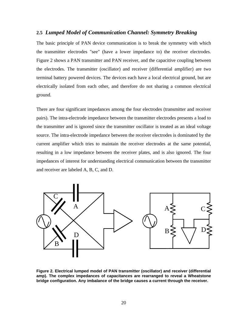
2.5 Lumped Model of Communication Channel: Symmetry Breaking
The basic principle of PAN device communication is to break the symmetry with which
the transmitter electrodes "see" (have a lower impedance to) the receiver electrodes.
Figure 2 shows a PAN transmitter and PAN receiver, and the capacitive coupling between
the electrodes. The transmitter (oscillator) and receiver (differential amplifier) are two
terminal battery powered devices. The devices each have a local electrical ground, but are
electrically isolated from each other, and therefore do not sharing a common electrical
ground.
There are four significant impedances among the four electrodes (transmitter and receiver
pairs). The intra-electrode impedance between the transmitter electrodes presents a load to
the transmitter and is ignored since the transmitter oscillator is treated as an ideal voltage
source. The intra-electrode impedance between the receiver electrodes is dominated by the
current amplifier which tries to maintain the receiver electrodes at the same potential,
resulting in a low impedance between the receiver plates, and is also ignored. The four
impedances of interest for understanding electrical communication between the transmitter
and receiver are labeled A, B, C, and D.
B
C
DB
C
D
AA
Figure 2. Electrical lumped model of PAN transmitter (oscillator) and receiver (differentialamp). The complex impedances of capacitances are rearranged to reveal a Wheatstonebridge configuration. Any imbalance of the bridge causes a current through the receiver.

21
The four impedances are represented as purely reactive (capacitance), though they may
contain a real (resistive) component. The circuit is rearranged to show how PAN device
communication works by breaking the symmetry between the four electrodes. The circuit
is a Wheatstone bridge where any imbalance of the relationship A/B = C/D will cause a
potential, and therefore a current, across the receiver. Since the ratios must be exactly
equal to null the circuit, and body-based PAN devices are constantly in motion, there will
always be an electrical communication path, as long as receiver is sensitive enough to
detect the imbalance.
2.6 PAN Device Electrical Fields
A more detailed electrical model of PAN electrical communication is derived by
identifying all the electric field paths in the system. Electric fields exists between all bodies
with different potentials. Figure 3 illustrates an electric model of a PAN transmitter
communicating with a PAN receiver. The PAN transmitter T creates an oscillating
potential across two electrically isolated electrodes. The oscillation frequency is less than
one MHz (wavelength greater than 300 meters) and the electrode size is on the order of
B
E
E
G
A
D
E
C F H
Figure 3. Electric fields produced by PAN transmitter T. A small portion of the electricfield G reaches the receiver R.

22
centimeters so there is no appreciable energy radiated. All objects around the PAN devices
are either electrically neutral (no static or alternating potential), or at least do not have the
same exact potential (frequency, phase, and amplitude) as the PAN transmitter.
The concept of an environment electrode e and a body electrode b is introduced for
convenience when referring to the electrode closer to the environment and closer to the
body, respectively. There is no inherent difference between them; reversing the body and
environment electrode of the transmitter or receiver results in a 180 degree phase shift in
transmitted and received signal, respectively. The PAN device is designed so that one
electrode is very close to the human body (the body electrode b) and the other electrode
points away from the body (the environment electrode e). An electric field C forms
between PAN transmitter body electrode tb and the human body. The body is modeled as
a perfect conductor electrically isolated from the room potential and acts like a large plate
of a capacitor, being charged and discharged by the transmitter. The charging of the body
gives the body a potential different from its environment, resulting in an electric field E
between the body and the environment. The body potential also forms an electric field B
between the body and the transmitters environment electrode te.
The receiver environment electrode re on the “sees” the environment better (has a smaller
impedance) than it sees the body, and correspondingly the body electrode rb sees the body
better than it sees the environment. This asymmetry allows the receiver to detect the
potential difference between the body and the environment. The potential of the body
produces an electric field F to the receiver body electrode rb. The circuitry in the receiver
R maintain the receiver environment electrode re at the same potential of the receiver
body electrode rb, resulting in a small current measured by the receiver circuit. The
oscillating potential of the body electrode rb is maintained on the environment electrode
re, producing an electric field G to the environment. In practice the receiver cannot keep
the electrodes at exactly the same potential so a small electric field H is created between
the body and the environment electrode re.

23
2.7 Electrical Model of the Communication Channel
2.7.1 Lumped-Circuit Electrical Model
Figure 4 shows an equivalent circuit of the electric fields illustrated in Figure 3. The body
appears as a perfect conducting node (body node). A is the capacitive coupling between
the transmitter environment electrode te and the environmental ground potential. B is the
capacitive coupling between the transmitter environment electrode te and the body. C is
the capacitive coupling between the transmitter body electrode tb and the body. D is the
capacitive coupling between the transmitter environment electrode te and the
environment. E is the capacitive coupling between the body and the environment. F is the
capacitive coupling between the body and the receiver body electrode rb. G is the
capacitive coupling between the receiver environment electrode re and the environment
ground.
A
B
C
E
F
GD
body node10 pf
110 pf1 nf 1 nf
10 ff 10 ff
H R
tb
te
rb
re
10 pf
T
Figure 4. Electrical model of PAN system. Transmitter T capacitively couples to receiver R through

24
the body (modeled as a perfect conductor). The earth ground provides the return signal path.
The electrical model reveals that body capacitance to the environment E is detrimental to
PAN device communication performance, shorting to ground the potential the transmitter
is trying to impose on the body. In one experiment a current is capacitively coupled from a
transmitter on the left wrist of a subject to a receiver on the right wrist of the subject who
is wearing sneakers, under the conditions specified in Electrode Capacitance
Measurement. The measured displacement current is attenuated -12 dB when the subject
is barefoot, and -28 dB when a ground wire is connected to the subject's forehead.5 These
measurements suggest that the performance of PAN devices will suffer when a wearer
grabs a grounded water pipe, for example.
The electrical model suggests that feet are the best location for PAN devices; body and
environment electrodes have the strongest coupling to the body and environment,
respectively. This is particularly true for the environment electrode which is the "weakest
link" (largest impedance) of PAN communication. Placing a large area environment
electrode as close as possible to the physical ground (which is where shoes usually are)
maximizes the magnitude of signal communication. Shoes are also an ideal location to
capture some of the energy dissipated during walking, as discussed in Sneaker Power.
2.7.2 Body Capacitance Measurement
Some typical values of the electric model capacitances are included in Figure 4. The value
for the body capacitance E to the environment is empirically determined by measuring the
resonance frequency of a coil in parallel with the body6. The body-to-environment
capacitance can be viewed as a capacitor formed by two plates separated by an insulator;
the body is a large three dimensional plate and the environment is a gigantic plate, with air
and other insulators as the dielectric. The body-to-environment capacitance depends on
the geometry of the body (i.e.; size and shape), its spatial relationship to the environment,
and the composition of the environment. Touching an electrically grounded conductor
5 The ground electrode is attached to the subject’s forehead using a 1" square of coppertape with conductive adhesive. The subject is the author, male, 6’ 2”, 210 lbs.6 The resonance frequency of a 33.5 uH coil is first measured to account for stray

25
increases body capacitance by effectively decreasing the distance between the plates. Skin
is composed of dead cells and water filled cells enclosed in a fatty membrane, making the
skin an insulator and dielectric. The insulating skin covers low resistance tissue and
conductive blood. When a person touches a grounded piece of metal, the internal
conductors (blood and tissue) are brought closer to the external conductor (grounded
metal). For example a body capacitance of 107 pf is measured for an electrically isolated
person. When the person squeezes an electrically grounded terminal, the measured body
capacitance increases to 845 pf.
Body capacitance can be calculated analytically. A simple approach is to approximate the
body as a sphere, the lowest order moment of a geometric model of the body. An isolated
charged sphere produces a uniform electric field that extends radially. This simplification
produces an equally simple result; the capacitance C of an isolated sphere of radius R is
C=4ππεεR where εε is the permittivity of free space. Approximating a person as a sphere of
one meter radius results in a capacitance of 111 pf. Though the person might be smaller
than a one meter radius sphere, this is compensated by the fact that the body is not
isolated; the location of the zero potential is much closer than infinity, and is composed of
all the conductors that make up the environmental ground potential. An exact solution
would require using Laplace’s equation to calculate the potential around the body and the
application of Gauss’s Law around a surface enclosing the body to calculate the charge on
the body.
2.7.3 Electrode Capacitance Measurements
Electrode capacitance measurements were made using a lock-in amplifier7. Path
impedances Z were determined and capacitances calculate by the relationship C=1/2ππFZ,
where F is the oscillator frequency. All impedances Z are treated as purely reactive
(capacitive), reducing the problem to a network of reactive impedances and application of
Kirchoff's and Ohm's law (Z=V/I). The measurement technique was to apply a 5 volts 100
kHz sinusoidal signal from the lock-in amplifier’s oscillator to a transmitter electrode and
capacitance, then the resonance frequency remeasured with the subject touching the coil.7 Stanford Model SR-850 DSP Lock-in Amplifier

26
measure the displacement current at a receiver electrode.
Circular transmitter and receiver electrodes 25 mm diameter are used to remove any
sensitivity to rotation. A 4 cm x 4 cm x 1 mm sheet of plastic was placed in between the
electrodes and skin to assure that the impedance is completely capacitive (no real resistive
component). A battery powered current amplifier was used at the receiver electrode to
eliminate any cable capacitive effects.
First the body-to-ground impedance ZE8 was measured as described in Body Capacitance
Measurement. Body-to-electrode impedances, ZC and ZF, are assumed to be equal since
they are the same size electrode (2.5 cm diameter). To measure ZC and ZF the transmitter
electrode was attached to one wrist of the subject9 and the receiver electrode was attached
to the subject’s other wrist. The electrodes were attached 30 mm above the wrist joint
with Velcro tape. The lock-in amplifier provided a low resistance ground, so impedances
ZD and ZG are treated as zero ohms. The voltage at the body node was calculated using
Kirchoff's voltage law (ZE is known), and once known, allowed the calculation of the
current through impedances ZF, ZH, and ZR (the latter two are in parallel).
The outer-electrode to ground impedances, ZD and ZG, were determined by measuring the
voltage drop across a 1 megaohm load resistor installed in between the transmitter
oscillator and transmitter electrode. The resulting displacement current was calculated
using Ohm's law. Once the displacement current and voltage were known, the transmitter
electrode to ground impedance was calculated using Ohm's law.
3. PAN DESIGN ISSUES
3.1 Size
The design of the PAN devices is primarily driven by power consumption, size, and cost
constraints. PAN devices take the shape of common objects found about a body, e.g.; a
credit card, watch, belt, and shoe. A credit card has two large surface areas (face and
8 ZE is the impedance across capacitor E. This notation will be used throughout.9 The subject is the author.

27
back), one of which faces towards the body (body electrode), and the other faces away
from the body (environment electrode), independent of location. A watch is a more
challenging object since it has a smaller surface area and volume, with a variable
orientation, though half of the watch band usually points away from the body. The watch
band presents itself as a natural location for electrodes; the length could be sectioned and
electronically multiplexed to optimally bisect the band into a body and environment
electrode. A belt provides a larger surface area but can be electrically shorted by the close
proximity of hands and arms. Some type of segmentation, or limitation of electrodes to
areas away from those portions most likely to be shorted by hands and arms, may be
necessary.
PAN device operation is optimized by having large area electrodes (collects more electric
field) with small intra-electrode capacitance (shunts less displacement current that can be
measured)10. The size, area and intra-electrode capacitance (calculated as ideal flat plate
capacitors) of several electrode configurations are as follows:
Item Electrode Dimensions (mm) Area (m2x10-4) Capacitance (pf)Watch face 25 x 25 x 8 5 0.5Heel patch 30 x 30 x 8 9 0.9Watch bands 70 x 20 x 4 14 3.0
70 x 20 x 8 14 1.5Credit card 80 x 50 x 3 40 11.4
80 x 50 x 8 40 4.3Shoe insert 130 x 40 x 8 52 5.3Belt 900 x 25 x 4 225 48.2
3.2 Power Consumption
3.2.1 Sneaker Power
A typical battery life design criteria for electric watches is three years [Helm95]. A typical
10 The intra-electrode capacitive shunting takes on less significance as the input impedanceof the current amp decreases. The current amp used in the PAN prototype has an inputimpedance of 57 kilohms while the impedance of a 1 pf capacitance at 100 kHz is 1.6megohms, representing a shunting loss of less than four percent.

28
watch battery has a energy capacity of 57 mWH11, or 1.4 uA over three years. A
hermetically sealed credit-card device does not permit batteries to be replaced. An
embedded induction coil would allow a hermetically sealed battery or super capacitor to
be recharged by close proximity to an external charging induction coil. Locating PAN
devices in shoes benefits signal strength. Energy is dissipated in human gait; a 75 kg
person dissipates approximately 400 mW with each step12. A piezo ceramic pile charging a
capacitor at an efficiently as low as 10 % provides enough power for a PAN device.
3.2.2 Energy Loss Due to Capacitor Charging
The PAN transmitter is an electrode driven by an oscillating voltage source referenced to
another electrode. The simplest electrical implementation is to connect a digital square
wave output directly to the transmitting electrode. The transmitter electrode appears as a
capacitive load to the oscillator, discharged each cycle through a dissipative driving
circuit, resulting in an energy consumption of 1/2CFV2; wasting a milliwatt of power in a
typical PAN transmitter.
3.2.3 Resonant Transmitter
A majority of the energy required to charge the load capacitance may be recovered by
storing the energy in the magnetic field of an inductor. An inductor placed in series with
the load capacitor forms a LC tank circuit. Once the 1/2CV2 energy is put into the tank
circuit, the only additional energy required is to replenish the energy dissipated by the real
resistance of the tank components. This is only true when the tank circuit is driven at
resonance; when the impedance of the capacitance XC is equal to the impedance of the coil
XL. The resonance frequency fr is set by the value of the inductance L and capacitance C:
fr LC= 1 2/ π
3.3 Cost
PAN device communication adds value to conventional personal electronic devices;
11 D384 silver-oxide battery, 38 mAH at 1.5v, 7.7 mm diameter by 3.6 mm thick.12 Assuming 1 mm displacement, half of the body weight is applied to each foot, at a rateof one step per second; Power=mgh/t=(37.5 kg)(9.8 m/sec2 )(.001m)/1sec=367.5 mW.
29
watches that display email and pager messages, PDAs that downloading phone numbers to
cellular phones, calling cards that identifying the owner to a public phone, and people
exchanging data by shaking hands. These value-added services can justify the additional
cost of an embedded communication system. As will all commercial products, the lower
the cost, the easier it is to incorporate the technology into a product. The prototype PAN
transmitter and receiver presented in the thesis uses off-the-shelf low-cost components.
Industrial incentives to produce low power, low cost operational amplifiers and
microcontrollers helps reduce the cost of PAN devices.
One implementation of a low cost version of a PAN receiver may be constructed from an
integrated AM receiver, such as the Plessey ZN414Z, which costs under $2 in small
quantities. The PIC16C71 used in the PAN transmitter and receiver prototypes costs
under $5 in large volumes. The inductor used in the PAN transmitter for creating the tank
transmitter costs $0.20 in small quantity. Since the carrier frequency used in PAN device
communication is under 1 MHz, a single integrated circuit can be constructed using
conventional CMOS technology to perform all of the analog and digital functions of a
PAN transceiver. It might therefore be possible to create a single-chip PAN transceiver
(combined transmitter and receiver) for under $1 in high volume.
The Plessey ZN414Z specifications are worth noting for the device provides a good
example of the realistic performance of an integrated PAN receiver. The ZN414Z is a 10
transistor tuned radio frequency circuit packaged in a 3-pin TO-92 plastic package. The
circuit provides 72 dB of amplifier gain (three stages) with a -6dB bandwidth of 600 kHz
centered at 650 kHz, a transistor detector, and a 20 dB automatic gain control (AGC).
The circuit requires a supply current of 0.3 mA at 1.3 volts, consuming 0.4 mW of power.
3.4 Channel Capacity
A communication network is primarily judged by channel capacity, with a theoretical limit
defined by the Hartley-Shannon law [Carlson86]
C=Blog(1+S/N)
where C is channel capacity in bits/second, B is bandwidth, S is signal, and N is noise. To

30
achieve a high channel capacity for a fixed bandwidth, the signal-to-noise ratio must be
maximized. The signal-to-noise ratio depends on transmitter signal strength and receiver
sensitivity and noise performance.
The -3 dB frequency response of the prototype PAN receiver is approximately 400 kHz
(100 kHz- 500 kHz). The minimum measured sensitivity of the spread spectrum receiver
prototype is S/N=0.0625 (a noise-to-signal ratio of 16). These values produce a maximum
channel capacity of 10.5 kbits per second. A more realistic signal-to-noise ratio of 10
provides a maximum channel capacity of 416.6 kbits per second. The PAN transceiver
prototype implements a modest 2400 bit per second modem.
The capacitance values shown in Figure 4 represent two watches, one on each wrist,
communicating with each other. The theoretical channel capacity can be calculated for the
conditions of the PAN transmitter and receiver prototype; bandwidth=400 kHz,
transmission frequency=330 kHz, transmission voltage=30 volts peak-to-peak. The
minimum noise is limited by the thermal noise from the 1 megaohm feedback resistor (41
uV) and the noise of the TLO82 pre-amplifier (18 nV/√Hz [TI95], bandwidth=400 kHz,
therefore 11.4 uV). The resulting noise is the square root of the sum of the square of the
noise sources, which is 42.6 uV. Using Kirchoff's voltage and current laws on the circuit
shown in Figure 4, the received current is 57 pA. The gain of the system is 108 (106 for the
current amplifier and 102 for the programmable gain amplifier). The resulting signal is 5.7
mV, yielding a signal-to-noise ratio of 134 (5.7 mV/42.6 uV), and a theoretical channel
capacity of 852 kbaud.
3.5 Locating PAN Devices on the Human Body
PAN devices reside on the body for intra-body communication and external to the body
for inter-body communication. Figure 5 shows several sites for PAN transceivers, which
can take on the character of commonly worn objects such as watches, credit cards, eye
glasses, identification badges, belts, waist packs and shoe inserts. Head mounted PAN
transceivers include headphones, hearing aids, microphones, and head mounted displays.
Chest located PAN devices can be used for detecting breathing and heart activity. Shirt

31
pocket PAN devices may serve as identification badges. The wrist watch is a natural
location for a display, microphone, camera, and speaker. Waist mounted PAN devices can
carry a PDA, cellular phone, or another devices that need large batteries. PAN devices
incorporating sensors can provide medical monitoring such as EKG, blood pressure, and
breathing rate. Pants pockets are a natural location for wallet based PAN devices to store
information and identify the possessor. PAN devices located in the shoe can be self-
powered and provide a data link to remote PAN devices located in the environment such
as workstations and floor transponders that detect the location and identity of people in a
room.
Figure 5. Locations and applications for PAN devices include head mounted display,headphones, identification badge, cellular phone (in waist pack), credit and phone cards(in wallet), watch with display, microphone, and speaker, and power sneakers (selfpowering computer shoe inserts).
4. MODULATION STRATEGIES
4.1 Modulation and Coding
Modulation refers to the manipulation of the signal being transmitted to benefit the
32
electrical characteristics of transmission and reception. For example AM radio refers to
the amplitude modulation of a continuous carrier. Coding refers to the manipulation of the
symbols containing the message being transmitted, typically for ease of processing,
compactness, integrity, and confidentiality. For example a message may be organized as a
sequence of message bytes assembled in a packet including error correction bits, where the
bits in the message bytes are encrypted by a key known only by the sender and receiver to
increase security.
4.2 Narrowband vs. Broadband Transmission
There are two basic types of carrier wave modulation; linear and non-linear13. Linear
modulation translates the spectrum of the message up to the carrier frequency. The
transmission bandwidth is narrow, never exceeding twice the bandwidth of the message,
and the signal-to-noise performance can only improve by increasing the transmit power
[Carlson86]. Non-linear modulation uses a non-linear process to modulate the carrier
producing a broadband transmission much greater than the message bandwidth. The
signal-to-noise performance of non-linear modulation increases with the bandwidth of the
transmission, trading bandwidth for power.
4.3 Narrowband Transmission
Narrowband transmission is typically simpler to implement than non-linear modulation.
The carrier can be digitally modulated by shifting the amplitude (on-off keying; OOK),
frequency (frequency-shift key; FSK) or phase of the carrier (phase-shift key; PSK). The
bandwidth of the all three techniques is approximately equal to the signaling (baud) rate
[Carlson86]. The power spectrum of OOK and PSK have a second-order rolloff, while the
FSK has a fourth-order rolloff, allowing more channels to occupy a frequency multiplexed
spectrum.
Non-coherent FSK shifts between two frequencies to represent the state of a message bit
to be sent. Typically FSK detection consists of two bandpass filters tuned to the carrier
and the shift key frequency, respectively. Coherent FSK detection uses synchronous

33
detection and has better noise rejection performance but needs to synchronize to the
frequency and phase of the transmitter.
Phase detection can be achieved without phase synchronization if the phase is differentially
encoded before transmission in a technique called differentially coherent phase-shift keying
(DPSK). The transmitter changes the phase of the carrier each time a logic one message
bit is sent. The receiver uses the phase of the last bit as a reference to determine the
current phase. If the phases differ by 180 degrees, a logic one message bit was sent. The
carries must be an integral multiple of the message bit rate to assure phase changes occur
on carrier zero crossings.
The energy efficiency of a modulation technique can be measured as the energy-to-noise
ratio required to achieve a theoretical error probability; the lower the energy-to-noise
ratio, the more efficient the modulation technique. The energy efficiency to achieve a
theoretical error probability of one bit per ten thousand for several narrowband
modulation techniques are [Carlson86]:
Modulation Signal Strength (dB)Phase Reversal Keying (PRK) 8.4Differentially Coherent Phase Shift Keying (DPSK) 9.3On-off Keying (OOK) 12.3Frequency Shift Keying (FSK) 12.3
4.4 Transmitters, Receivers, and Transceivers
While some PAN devices may need only receive or transmit, making each PAN device a
transceiver enables desirable features. A transceiver can tell neighboring transceivers of its
existence, eliminating attempts to communicate with absent transceivers. Loss of data can
be recovered by requesting re-transmission. Transceivers too distant for direct
communication may communicate through neighbors acting as regenerative repeaters.
Most of the component costs are in the receiver. Adding transmit capabilities to a receiver
amounts to including a resistor, to prevent excessive driver loading due to inadvertent
13 Often referred to as exponential modulation in the communication field.

34
electrode shorting, and possibly an inductor and capacitor, to make a resonant transmitter.
4.5 Half Duplex Transceivers
Communication is the process of conveying information from one location to another. The
communication can be one way (simplex), two way with each party taking turns (half-
duplex), or both parties transmitting and receiving simultaneously (full-duplex). PAN
transceivers use the same electrode pair to transmit and receive. The large electrostatic
field necessary for transmission would saturate a sensitive receiver, making it difficult to
simultaneously transmit and receive. Using separate electrodes does not help since they
would be located near each other, decreasing the electrode area and sacrificing
performance. PAN devices should therefore be designed as half-duplex transceivers.
4.6 Broadband Digital Transmission
The bandwidth of a narrowband communication channel is typically equal to the
bandwidth of the information being sent. Broadband communication trades off power
density for spectrum space, spreading the energy to be transmitted over a bandwidth many
times wider than the information being sent. The resulting transmitted signal is less
susceptible to noise and other interference since the contribution of any one frequency
represents a small portion of the total signal. Spreading the energy over frequency rather
than amplitude benefits the receiver’s front end, decreases the likelihood of signal clipping.
Two types of broadband digital transmission techniques considered for PAN devices are
spread spectrum; where the carrier is a pseudo-noise (PN) generator, and frequency
hopping; where the carrier skips among a multitude of frequencies. Both of these
techniques allow several PAN devices to communicate simultaneously over the same
channel.
4.6.1 Spread Spectrum
In a direct-sequence spread spectrum system the digital message to be transmitted is
multiplied by a digital PN sequence, spreading the spectrum of the digital message. The
broadband product is transmitted through the channel. The receiver retrieves the message
by multiplying the incoming signal by the identical PN sequence. The transmitter and
35
receiver PN sequences must be in phase (synchronized) in order for the receiver to extract
the message from the sequence. Synchronizing the transmitter and receiver PN sequences
is the greatest challenge of a spread spectrum communication system.
4.6.2 Pseudo-Noise Sequence
The digital sequence is called pseudo-noise because it is a finite sequence that repeats
(xn=xn+N where N is the period of the sequence). A binary linear-feedback shift-register
(LFSR) can be used to generate a PN sequence. An ideal PN sequence has the following
properties; a) a flat power spectrum (every frequency is present with the same amplitude)
up to the chip frequency (N/sequence repeat time), b) an autocorrelation of N at zero
phase and 1/N for all other phases, and c) an equal number of 1’s and 0’s.
4.6.3 Synchronization & Manchester Coding
A common receiver synchronization strategy is to acquire synchronization when a
transmitter or receiver is first turned on, then continuously track synchronization while the
devices are communicating. Tracking adjusts the phase of the receiver to correct for
differences in chip rate caused by imprecise matching of transmitter and receiver clocks
(no two crystal oscillators have exactly the same frequency) and thermal drifts. A straight-
forward brute force method of acquiring synchronization is to successively shift the phase
of the receiver sequence, in subsample increments, until synchronization is achieved.
Tracking can be accomplished by comparing the synchronization of three slightly different
phases and moving towards the phase with the best synchronization.
In order to acquire synchronization, some means must be provided to measure
synchronization. One synchronization technique requires the transmitter to send a constant
message known by the receiver, the equivalent of a test tone. Synchronization is achieved
when the valid synchronization message is detected. Another technique takes advantage of
the structure in the transitions of a return-to-zero coding strategy. Manchester coding, for
example, introduces a sign change at the beginning of every bit. This pattern provides a
feature the receiver can detect and use to synchronize to the transmitter. Manchester
coding guarantees structure independent of the message by forcing bit changes, at the

36
expense of doubling the message size (each message bit requires two transmitted bits).
4.7 Resonant Transmitter
While designing electric field transmitters for our fish sensors (see Related Work), the
author began using resonant tank circuits to boost transmission voltage to improve
received signal strength. Applying a resonant tank circuit to PAN transmitters has
additional benefits; the tank circuit produce a clean sine wave output from a square wave
input, and allow the transmitter voltage to be digitally programmed. These desirable
features justify the small additional cost of tank components. The resonant tank used in the
PAN prototype is constructed from an inductor L and capacitor C, as shown in the lower
section of Figure 6.
4.7.1 Boosting Transmission Signal Strength
Transmitter signal strength is directly proportional to transmitter voltage, and typically
limited by power supply voltage. If the transmission is narrowband, a resonant tank circuit
can be used to boost transmission voltage. The operation of the tank used in the PAN
transmitter will now be reviewed by referring to Figure 6. The microcontroller
(PIC16C71) generates a 5 volt square wave which is applied by the transmit line to the
inductor L. The capacitor C is connected to the other side of the inductor L and the
transmit electrode. When a square wave is applied at the resonant frequency of the tank
circuit, the voltage on the transmit electrode quickly builds. The first few cycles of the
square wave charges the tank. The energy in the tank circuit is alternately stored as a
magnetic field in the inductor L and electric field in the capacitor C. Once the tank is fully
charged the only energy required from the microcontroller transmit line is to replenish the
energy dissipated by the real resistance of tank components; the inductor L, capacitor C,
and transmit electrode capacitance.
The voltage on the transmit electrode is equal to the transmit line voltage (5 volts) times
the Q (quality factor) of the tank circuit, so the Q directly boosts transmission gain. The
inexpensive inductor and capacitor used in the PAN transmitter prototype has a Q of 5,
creating a 30 volt oscillating potential from the 5 volt square wave.
37
As the carrier is modulated off the resonant frequency, the output voltage, and hence the
transmit power, decreases. Transmission bandwidth is measured as half-power bandwidth;
the frequency range in which the transmitter voltage is within 0.707 volts of the peak
resonant voltage. Bandwidth decreases inversely with the resonator Q:
Bandwidth=fresonance/Q.
A resonant transmitter is therefore ideal for narrowband transmission since the
transmission bandwidth never exceeds twice the bandwidth of the message. The PAN
transmitter prototype, with a Q=5 and fresonance=330 kHz, has a bandwidth of 66 kHz, easily
accommodating the 2.4 kbaud communication channel used in the prototype.
4.7.2 Digitally Controlled Transmitter Gain
A transmitter can conserve power by transmitting only the power necessary to achieve
reliable communication, which is also a tenant of spectrum etiquette. PAN transceivers can
negotiate transmission signal strength to find the minimum power necessary for reliable
communication. Transmission signal strength is proportional to voltage, which may be
controlled by a DAC, programmable gain amplifier, or programmable resistive element
(e.g., FET). Transmitter voltage can be digitally controlled by varying the pulse width of a
digital oscillator applied to a tank resonator. This simple amplitude control technique
requires no additional hardware and is useful for multi-level M-ary signaling [Carlson86],
where information is encoded in multi-value amplitude modulation.
4.7.3 Proximity Effect on Resonant Transmitter
The resonant Q of a tank is:
Q= 2πFL/R
where I is inductance, F frequency, and R is the resistance of tank components. To
maximize the Q for a given transmission frequency F, inductance L is maximized and
capacitance C is minimized, since the product LC must be constant. The minimum
capacitance C is the inherent intra-electrode capacitance, determined by the size,

38
composition, and location of objects around the PAN transmitter electrodes, making the
resonant frequency susceptible to all these variables. For example, if a person has a PAN
device in his back pants pocket (e.g., a wallet), the load capacitance will increase when he
sits down, decreasing the resonance frequency. The load capacitance of a watch mounted
PAN device will change as the wearer's hand brushes past her body, as she crosses her
arms, and places her hands in her lap.
The sensitivity of resonant frequency to orientation and environmental capacitance may be
minimized by placing a large capacitor (relative to the intra-electrode capacitance) in
parallel with the electrode capacitance. The larger the capacitor, the smaller the effect of
intra-electrode capacitance variations, with a corresponding sacrifice in resonant Q.
4.7.4 Contactless Switch
The capacitive sensitivity of tank-based PAN transmitters to their electrostatic
environment does suggest that the carrier, in addition to encoding messages, may convey
proximity information as well. The resonant frequency of the carrier indicates the
capacitance of the transmitter electrodes, directly effected by objects near the transmitter
electrodes. The amplitude of the received signal is a function of the distance and
orientation between the transmitter and receiver, and to a lesser extent the carrier
frequency14. A receiver monitoring carrier amplitudes and frequencies of several PANs
may be able to make coarse estimates of body orientation.
The ringing nature of resonant circuits provides a simple way for a PAN transmitter to
monitor its own resonant frequency. By pulsing the transmitter and integrating the
received displacement current, a PAN transmitter can monitor its resonant Q. The PAN
transmitter could also sweep the transmission frequency to monitor its resonant frequency.
When the wearers hand comes in close proximity to the PAN transmitter’s environment
electrode, the PAN transmitter can determine hand proximity. This may be useful for
making a contactless switch, instructing the PAN device to start a transmission. A PAN
14 As the Q increases excursions of the carrier from the resonant frequency result in largeramplitude attenuations due to the narrow bandwidth of the resonator.
39
device could wake up every few seconds, pulse the transmitter and monitor hand
proximity. If none was detected, it could go back into sleep mode, conserving power.
5. PAN PROTOTYPE DEVELOPMENT
5.1 Hardware Development
5.1.1 Development of a PAN Prototype
The goal of the PAN prototype is to demonstrate the digital exchange of data through a
human body using electric fields by a small battery-powered low-cost electronic circuitry.
The design is a combination of analog and digital circuitry, implementing an analog bipolar
chopper controlled by a digital microcontroller. This approach allows the tiny (e.g., 50
pA) high frequency (330 kHz) displacement current to be integrated into a voltage that
can be measured by a slow (50 kHz) low resolution (8 bit) analog-to-digital converter
(ADC), provided by the microcontroller.
A bipolar chopper operates by selecting an amplified received signal or an inverted
(multiplied by -1) version of the signal. By switching at the transmission rate and phase,
the tiny received signal (microvolts) is synchronously rectified and integrated into a large
signal (several volts). The hardware is used as a detector for several coding strategies,
determined by microcontroller coding (see SOFTWARE DEVELOPMENT). The PAN
transceiver uses five “off-the-shelf” components, costing less than $10 in large volumes
(e.g., 10,000 pieces). The PGA ($11 quantity 1) can be replaced with an automatic gain
circuit (AGC) constructed from an inexpensive operational amplifier (e.g., TLO82, less
than $1 quantity 1). Ultimately the analog components and microcontroller can be
combined into a single CMOS integrated circuit to produce a low-cost integrated PAN
transceiver.
The bipolar chopper and microprocessor implements the basic function of a lock-in
amplifier for less than $10. The digital nature of the switching does make the detector
sensitive to odd harmonics of the switching frequency. This can be compensated for by
providing a low-pass filter, with a cutoff frequency below the first harmonic of the carrier.

40
As will be seen, the limited high frequency response of the amplifiers used in the PAN
device prototype provide low-pass filtering.
5.1.2 System Components
The functional elements of the PAN transceiver is shown in Figure 6. The design uses
analog circuitry to perform synchronous detection under the control of a digital
microcontroller. This combination takes advantage of the ability of analog circuitry to
integrate microvolt signals that are smaller and faster than the voltage and temporal
resolution of the microcontroller's ADC, and capitalize on the crystal referenced digital
microcontroller's temporal accuracy and programmable flexibility.
C U R R E N T A M P
I N V E R T E R
T A N KR E S O N A T O R
I N T E G R A T O R
A N A L O GS W I T C H E S
R E C E I V EE L E C T R O D E
T R A N S M I TE L E C T R O D E
R E C E I V E( A N A L O G )
R E S E TI N T E G R A T O R
T R A N S M I T
S A M P L EN O N - I N V E R T I N G
S A M P L EI N V E R T I N G
-1
PIC16C71 M I C R O -C O N T R O L L E R
D A T A I N D A T A O U T
L
C30 vpp5 vpp
Figure 6. Block diagram of half-duplex PAN transceiver. Microprocessor controls analogswitches to synchronously rectify and integrate amplified signal picked up by receiveelectrode.
The digital output of the microcontroller’s transmit line drives the resonant tank circuit.
The receiver consists of a current amp which converts the nanoamp received displacement
current into a microvolt signal. Following the current amp (not shown) is a programmable
voltage amplifier to provide digitally selectable gain (1, 10, and 100). The amplified
voltage is either applied to an integrator directly, or through an inverter, which changes

41
the sign of the applied voltage. The selection is performed by the microcontroller,
synchronous to the transmitted signal to produce a signal of constant polarity (either
positive or negative), which integrates to a value large enough to be digitized by the
microcontroller's ADC (0-5 volt, 8 bit, 19.5 mV per division). The microcontroller uses
the digitized integrated signal to determine the logical state (0 or 1) of the received
message bit.
The integrator is discharged after every message bit, a technique known as integrate-and-
dump, which minimized inter-symbol interference (ISI), a phenomena where a message bit
affects its temporal neighbor [Carlson86].
Once the message has been successfully received and demodulated, the microcontroller
transmits the message to a host computer over an optical link (not shown). This is used to
electrically isolate the transceiver, so the PAN transceiver can be evaluated independent of
an electrical ground reference. The optical serial connection is extremely useful for
debugging code since attaching electrical probes to the prototype transceiver affects the
electrical performance of the receiver.
5.1.3 Circuit Review
Figure 7 shows a schematic of the PAN transceiver prototype. The electric field gradient
across the receiver and transmitter electrode (RCV and TX ELECTRODE, respectively)
creates a tiny (nanoamp) displacement current I through R14. The feedback arrangement
produces an output voltage V by the relationship V=IR14; one nanoamp applied produces
one millivolt. with R14=1 M. The voltage is buffered by U1B and applied to a 16 kHz
high pass filter constructed from C1 and R1. The high passed signal is amplified by the
programmable gain amplifier (PGA), used by the microcontroller U6A as an AGC, with
digitally selectable gains of 1, 10, or 100. The PGA output is high passed and applied,
through a single-pole-double-throw CMOS switch U5, either directly to an integrator
(U2B, R6, and C14), or indirectly through an inverter (U2A), under the control of the
microcontroller U6A. The integrator implements the analog function V=-∫1/RC.

42
The amplifiers U1, U2, U3, and CMOS switch U5 all operate bipolar from a battery split
supply (+9 and -9), so the integrator can produce a positive or negative result. The ADC
on the microcontroller U6 is unipolar, from 0 to 5 volts. Resistor R7 and R8 scales and
level shifts the 5 to +5 volts output of the integrator, to a 0 to 5 volts range applied to the
ADC.
The microcontroller U6 is a PIC16C71, a high performance, low cost, CMOS fully static
EPROM based 8-bit controller with on-chip ADC. The PIC16C71 has 1k of EPROM for
program memory, 36 general purpose static RAM registers, a four channel 8-bit ADC (20
usec conversion time per channel), multiple interrupt sources, an 8 bit timer with 8 bits of
pre-scaling, and 13 I/O pins capable of sinking 25 mA and sourcing 20 mA. The
PIC16C71 requires a 5 volt supply, consuming 9 mA at 16 MHz, the frequency used in
the PAN prototype. The microcontroller U6 requires four clock cycles per instruction
(except conditional branches which require eight) resulting in 4 million instructions per
second (MIPS). A 16 MHz crystal with TTL output driver U4 provides the system clock
for the microcontroller U6.
Monitoring the operation and performance of PAN hardware and software is
accomplished through an optical bi-directional serial communication to a host computer
(an IBM ThinkPad 700C/PS2). A red LED D5 is driven directly by the microcontroller
U6. A photoreceiver U7 consisting of a photodiode, amplifier, and Schmitt trigger
incorporated on one die, produces a logic level (0 and 5 volts) in response to on-off
keying modulated light. Software in the microcontroller U6 implements asynchronous half
duplex communication at 19.2 kbaud.
The electro-optic components are Motorola devices with pre-assembled plastic screw-on
connectors. The visible LED transmitter is the MFOE76 and the Schmitt trigger logic
receiver is the MFOD75. A small interface board15 drives the LED, buffers and level shifts
the logic voltage (0,+5v) of the photoreceiver into RS-232 signals (+12, -12).
15 Industrial Fiber Optic, P.O. Box 3576, Scottsdale, AZ 85271-3576.

43
Figure 7. Schematic of PAN transceiver. PIC microcontroller controls the analog bipolar
chopper detector which integrates the amplified received signal. Received messages are
sent to a host computer over optical light guides to eliminate any electrical ground.

44
5.1.4 Prototype Construction
5.1.4.1 Electrode Issues and Construction
The PAN transmitter and receiver prototypes, shown in Figure 8, are point-to-point
soldered on a PIC prototype boards16 measuring 3 inches by 3 inches. The prototype
board is a commercial printed circuit board, providing pre-laid out traces for a voltage
regulator, crystal, and an I/O header. The boards are mounted with aluminum standoffs to
aluminum cast cases measuring 94 mm x 120 mm x 37 mm. The aluminum cover of the
transmitter is mounted 1.5 mm above the lip of the case by non-conducting nylon
standoffs. The case serves as one transmitter electrode, and the cover as the other
transmitter electrode. The receiver prototype board is completely enclosed by the
conducting case, which serves as one electrode. The other receiver electrode is aluminum
coated mylar film, the length and width of the case, mounted 1.2 cm below the case on a
slab of insulating foam. By totally enclosing the receiver electronics in the case electrode,
connected to circuit ground, any electric fields generated by control signals are enclosed in
an equipotential electrode, shielded from the other receiver electrode.
Figure 8. PAN receiver (left) and PAN transmitter (right). The case and aluminized mylarmounted below the case are receiver electrodes. The transmitter lid and case are
16 MicroEngineering Labs, Box 7532, Colorado Springs, Colorado 80933

45
transmitter electrodes. A light guide cable connects the receiver to a host computer.
5.1.4.2 Prototype Power Consumption
Minimal power consumption is vital for PAN transceivers for small battery size and long
life. The prototype, however, needs only to operate several hours using 9 volt alkaline
transistor batteries, a convenient and low-cost power supply. Hence the power
specification for the PAN prototype is less than ideal. The greatest power consumption is
by the red LED used for optical communication, a circuit element that would not be on a
PAN transceiver. The prototype power is supplied by two 9 volt transistor batteries,
arranged as a bipolar supply (+ 9 and - 9 volts), which powers all the analog electronics.
The +9 volt supply is regulated down to +5 and powers the microcontroller, crystal
oscillator, and optical transmitter and receiver, accounting for the large +9 volt current
drain. The power consumption for the prototype receiver is presented in the following
table:
Supply Current (mA) Components Condition+9v 33 all except LED receiving message bits
31 all except LED standby35 LED on
-9v 13 all receiving message bits10 all standby
A practical integrated low-power version of a PAN receiver can consume less than 10 mW
of power. This estimate is based on a PIC running at 4 MHz (1.8 mA @ 5 volts = 9 mW)
and a Plessey ZN414Z front-end receiver (0.3 mA @ 1.3 volts = 0.4 mW). The additional
power required for a bipolar chopper detector, to replace the simple AM detector in the
Plessey receiver, can be compensated for by decreasing the clock speed of the PIC.
5.1.5 Hardware Development Environment
The receiver circuit was first tested on a Global Proto-board17, where components and
wires are inserted without soldering. The proto-board system introduces impedances and
electrical noise that would otherwise not be present on a properly designed printed circuit
board. The hostile environment of the proto-board generally leads to robust designs since
17 Model PB-503 Global Specialties, New Haven, Connecticut

46
the final system assembly (point-to-point soldering or printed circuit) will typically be
electrically cleaner (less parasitic coupling and noise) than the proto-board.
The point-to-point soldered board is first debugged using an attenuated signal generator as
an input current. Then a simple program is written to send ADC values out through the
optical serial port to check the operation of the battery powered, electrically isolated
system.
5.2 Software Development
All PIC16C71 microcontroller coding is done in assembly language due to the critical
timing requirements of synchronous detection and the small amount of RAM (36 bytes)
and EPROM (1K) available on the microcontroller. A full speed in-circuit emulator18 is
used when electrical connections are acceptable (e.g., examining bipolar chopper control
line timing). For tests that require PAN transceivers to be electrically isolated (e.g.,
measuring the sensitivity of the receiver circuit), EPROM versions of the microcontroller
are programmed19. A zero insertion force socket is used on the PAN prototype to allow
easy insertion and extraction of the microcontroller. During the testing and development
of the PAN system, the microcontroller was programmed approximately fifty times. Seven
identical EPROM microcontrollers are sequentially programmed and tested, then erased
en-mass for ten minutes under UV light, minimizing interruptions in the code development
process.
6. EXPERIMENTS WITH CODING STRATEGIES
I investigated two modulation techniques for PAN devices; the simple linear method of
on-off keying (OOK), and the non-linear method of direct sequence spread spectrum.
Implementation issues for each modulation technique shall now be discussed.
6.1 Spread Spectrum Coding
The PAN implements direct sequence spread spectrum in the PIC microcontroller. A logic
18 ClearView, Parallax Inc, 3805 Atherton Road, #102, Rocklin, CA 95765.19 PIC16Cxx Programmer from Parallax Inc.

47
one message bit is represented by transmitting entire PN sequence. A logic zero message
bit is represented by transmitting the inverted version of the PN sequence. Received logic
one and logic zero sequences integrate to large positive and negative correlation,
respectively. If no signal is transmitted, the correlation will be near zero, since the
correlation of noise to any zero-mean signal (except itself) is zero.
6.1.1 Generating the PN Sequence
PN sequences can be generated using a binary linear-feedback shift-register (LFSR) which
can be compactly implemented in software by XORing selected taps of a register and
shifting the XORed result into the register. The taps are selected for maximal length and
are available in table form [Gershenfeld94]. As with most implementations of algorithms,
there is a trade-off between speed and size. The most time efficient (fast running) method
is in-line coding of the sequence; directly programming the state of the transmitter and
detector control lines, for the transmitter and receiver, respectively. The first
synchronization test impediments in-line coding of a 100 element PN sequence. Each
element of a PN sequence is called a chip, a rectangular wave produced at the clocking
rate of the PN sequence. A minimum of three instructions are required for each chip. An 8
MHz clock rate results in the desired chip rate of 1.5 usec (666 kHz).
The design goal of the thesis is to implement a 2400 baud modem PAN. Each message bit
has a duration of 416.67 usec, requiring a 278 element PN sequence of 1.5 usec chips.
Two sequences are necessary; a sequence for logic one message bit, and an inverted
sequence for logic zero message bit. The PIC has a program space of 1,024 words (1 K),
yet 1668 instructions are necessary to in-line code both sequences.
6.1.1.1 LFSR Generation
The most compact method of generating the PN sequence is to implement a LFSR. The
278 chips can be reduced to 256, generated from an 8 bit shift register, a convenient
number for an 8 bit microcontroller. A minimum of 11 instructions are necessary to
generate one chip, as presented in the following fragment of PIC code:

48
pos_out mov chip_count,chips ;routine to send out chipsnext_chip mov w,shift_reg ;move shift register value into w register
xor w,#mask ;xor w with the mask containing the tapssetb c ;makes branch same lengthjnz z_is_one ;jump if xor result is oneclrb c ;otherwise shift a zero into the shift registerrr shift_reg ;rotate xor result into the shift registerclrb tx ;transmit a zerodjnz chip_count,next_chip ;repeat this process for until finishedret ;return to whoever called this routine
z_is_one rr fr ;rotate xor result into the shift registersetb tx ;shift a one (previously set) into shift registerdjne chip_count,next_chip ;repeat this process for until finishedret ;return to whoever called this routine
6.1.1.2 ROM Stored PN Sequence
Currently the fastest PIC available is 16 MHz, with the fastest speed planned at 20 MHz.
At 16 MHz an 11 instruction chip is 2.75 usec (363.63 kHz), about half the desired rate.
As with any CMOS part, power consumption is proportional with clock speed. Typical
supply currents are 35 uA @ 32 kHz, 1.8 mA @ 4 MHz, and 9 mA @ 16 MHz. It is
therefore desirable to minimize clock speed.
A more compact method than in-line coding, yet faster than implementing a LFSR, is to
organize all the runs of one’s and all the runs of zero’s as subroutines. The maximum
number of sequentially identical states (all one’s or all zero’s) for a 256 element PN
sequence is seven (by observation), requiring fourteen subroutines. The in-line code is a
sequence of calls to these subroutines, with 5 instructions per chip (1.25 usec, 800 kHz
@16 MHz). For example, the PIC code to generate the sequence 110001011101000 are
calls to the subroutine that produces two 1's, three 0's, one 1, etc., as follows:
call two1call three0call one1call one0call three1call one0call one1call three0
49
The PIC subroutines to produce the sequential runs are as follows:
one1 setb TXret
two1 setb TXnopret
three1 setb TXnopnopret...
one0 clrb TXret
two0 clrb TXnopret
three0 clrb TXnopnopret...
Each subroutine requires N+1 instructions, where N is the number of identical states. The
total number of subroutine instructions is Nmaximum(Nmaximum+3). For Nmaximum =7, 70
subroutine instructions are required. The number of calls to subroutines is equal to the
number of identical sequence runs, typically about half the length of the PN sequence.
6.1.1.3 Receiving the PN Sequence
The receiver contains the same PN sequence as the transmitter and uses the PN sequence
to de-spread the received signal. The receiver synchronously integrates the received
analog signal, summing the received signal when the PN sequence element is 1, and
summing the inverse (sign reversed) signal when the sequence element is 0. If the
receiver's PN sequence is synchronized (in phase) with the transmitter, the received signal
will integrate to a large positive value if the message bit is one, or negative value if the
message bit is zero. If no message bit is sent, or the transmit and receive sequences are out
of phase (not properly synchronized), the received signal will integrate near zero. A
threshold is set to distinguish a valid correlation from noise.

50
6.1.2 Acquisition of PN Sequence
The transmitter and receiver have an identical crystal time base (up to the tolerance of the
parts, typically 100 ppm), so the transmitter and receiver produce a PN sequence at the
same frequency. The task of the acquisition algorithm is to match the phase of the
receiver's PN sequence to the transmitter's PN sequence, by sequentially correlating the
receiver’s PN sequence with every phase, and selecting the phase with the highest
correlation.
The first synchronization experiment is to display the correlation as a function of phase
using PAN transceiver hardware. The transmitter code is simple; a battery powered PIC
continuously transmits the PN sequence. The receiver is more difficult; a battery powered
PIC performs a correlation (integration using the PN sequence to control the bipolar
chopper) and sends the correlation result (amplitude of integration) to the host PC for
display via the serial (19200 baud) optic link. While it is possible to write receiver code
which simultaneously correlates and sends the results to the PC, the current drawn by the
optical link’s LED (34 mA), and the resulting 19.2 kHz square waves, cause unacceptable
interference with the extremely sensitive high gain receiver, which share the same power
supply and are located within 2 centimeters. The tasks of correlation, ADC conversion,
and serial transmission of the results are therefore done sequentially. Since these tasks take
different amounts of time, a technique of message framing is used to allow the receiver to
perform all tasks sequentially and stay in synchrony with the transmitter.
6.1.3 Message Byte Framing
A transmit frame consists of the transmission of the PN sequence followed by a period of
inactivity. This frame is repeated precisely at 1.2 kHz, initiated by a crystal controlled
timer interrupt in the transmitter's PIC. A receiver frame consists the following sequence;
a) integrate the received signal (presumably a PN sequence), b) digitize the integration
result, c) discharge the integration capacitor, d) serially transmit the integration result to
the host PC, e) wait for next frame interrupt. This frame is repeated precisely at 1.2 kHz,
initiated by a crystal controlled timer interrupt in the receiver's PIC.

51
6.1.4 Phase Slippage
Originally the phase of the receiver was shifted by making the period of the receiver frame
slightly shorter than the transmit frame, causing a slip in phase, producing successive
correlations. The slip proved to be too large due to the nature of the PIC timer which is 8
bits with an 8 bit pre-scalar. To produce a 1.2 kHz interrupt, 2400 instructions need to be
counted (the timer in incremented with each instruction or an integer divisor thereof). A
pre-scale of 1:16 is used to bring the count to less than 8 bits. Each “tick” is therefore 16
instructions, producing a full phase scan (1/1.2 kHz) 16 times a second, which is too
coarse and fast to be observed. The original 1.2 kHz period produces an inherent phase
slip every 2.46 seconds due to the slight mismatch in crystal speeds (a mismatch of 339
ppm). This has serious consequences, however, for the receiver will slip one chip (1.5
usec) in 4.43 msec, about the length of a message byte at 2400 baud (4.167 msec).
Tracking, therefore, needs to be performed several times per message byte.
6.1.5 Random Number Generators
A library routine from the Microsoft C library is used as a source of random numbers. The
library routine produces a sixteen bit integer number. The LSB is used to create a random
binary sequence. Figure 9 shows the correlation results of the random number table
sequence. The correlation is the sum of the ANDed sequences i.e.; the number of times a
chip of the phase shifted sequence had the same logical value as the chip in the unshifted
sequence. The sequences is wrapped around (modulo 256). The correlation result centers
around 128 since the probably of two random bits being the same is 50%.

52
0 5 0 1 0 0 1 5 0 2 0 0 2 5 00
5 0
1 0 0
1 5 0
2 0 0
2 5 0
P H A S E
CORRELATION
Figure 9. Correlation of a 256 element pseudo-noise (PN) sequence generated from theMicrosoft C library routine. Phase is the number of samples shifted. Correlation is thesum of the number of samples that are the same. The correlation at 0 phase is 256(perfect correlation). Random correlation is 128 (50% chance a pair will have the samevalue).
6.1.6 Problems With Spread Spectrum
6.1.6.1 Tracking Phase
The original design of the PAN prototype includes spread spectrum modulation strategy.
Receiver synchronization is crucial for a temporal error of one chip will result in lost
signal. This necessitates vigil tracking of the phase of the transmitter PN sequence.
Tracking can be accomplished by comparing the amplitudes of three correlations, each
with a slightly different phase, and seeking the phase with the largest correlation. Some
type of filtering must be applied to dampen the tendency to track amplitudes that are large
due to other mechanism (e.g., noise).
6.1.6.2 Mysterious Negative Correlation
For reasons not understood, the correlation peak at zero phase changes polarity as the
phase moves off zero. Perhaps the effect is due to frequency dependent phase shifts in the
receiver amplifier and high pass filter. This effect makes tracking the phase difficult when
the sampled phase is on the far side of the negative peak, where advancing towards zero
phase would decrease the correlation (make it more negative). Further, the effect will have
a serious impact on message bit decoding if the sign of the correlation is used to determine

53
message bit values.
6.1.6.3 Oscillations in the Current Amplifier
Spread spectrum revealed a design problem in the current amplifier. The broad spectrum
of the received signal excited oscillations in the current amplifier absent when using
narrowband signals. Apparently the receiver had enough phase shift to cause positive
feedback and therefore oscillations. A 10 pf capacitance added to the feedback loop of the
current amplifier is sufficient to decrease the high frequency gain responsible for the
oscillations.
6.1.6.4 Inefficient Energy Use of Channel
The frequency response of the PAN receiver is shown in Figure 10. Two single pole high
pass filters separate the amplification stages, producing the high pass response. The gain-
bandwidth of the amplifiers accounts for the low pass response. Spread spectrum greatly
increases the bandwidth of the transmitted message. The energy is spread from the PN
sequence repetition rate (3 kHz) to half the chip rate (330 kHz)20, with additional odd
harmonics generated by the rectangular chip waveform. Only a fraction of this wideband
energy is received by the PAN due to the bandpass nature of the receiver circuitry. The
rest of the transmitted energy is essentially wasted. The chip harmonics may radiate energy
as the wavelength approaches the scale of the electrodes, and may not meet FCC emission
regulations.
20 The highest frequency is the sequence 1010, generating a square rate of half the chiprate.

54
0 200 400 600 8000
0.2
0.4
0.6
0.8
1
FREQUENCY (kHz)
OUTPUT
Figure 10. Normalized frequency response of PAN receiver. A test signal is applieddirectly to the receiving electrodes. Bandpass quality is a combination of the two polehigh pass filter and the gain-bandwidth product of the amplifiers.
A shorter spreading sequence may be used to match the transmission bandwidth to the
receiver frequency response. If the full spread sequence is used for a message bit, spread
spectrum does have the advantage that once the sequence is acquired and tracked, bit
framing is also capture. However, if the sequence needs to be shorter than the message bit
to limit the bandwidth of the transmission, coding and tracking would be easier if the
sequence is an integer divisor of the message bit length.
6.2 Continuous Wave On-Off Keying
On-off keying (a quantized version of amplitude modulation) is the simplest method of
encoding data in a carrier. A one is represented as the carrier on, a zero as the carrier off.
Due to the synchronization problems of spread spectrum and the advantages of a resonant
transmitter, on-off keying is used in the PAN prototype.
6.2.1 Experiments With Resonant Transmitter
Since on-off keying produces a bandwidth equal to the bandwidth of the data, which is
less than 2.4 kHz, a resonating transmitter can be used. The resonator produces a very

55
clean sine wave from a square wave oscillator, delivering all the energy at the carrier
frequency. The amplitude of the sine wave can be digitally modulated by varying the pulse
width of the digital oscillator. The carrier is either on or off when using on-off keying.
The tank used in the experiments is constructed from a 1.5 mH surface mount, ferrite core
wound inductor, and a 27 pf monolithic capacitor, which resonates at 355 kHz. When the
top plate electrode is placed on, the frequency shifts down to 336 kHz due to the
additional capacitance of the electrode. The Q of this circuit is measured as 7, with a
corresponding -6 dB bandwidth of +/- 10 kHz.
Multiple PANs may transmit simultaneously on different frequency channels. The narrow
spectrum also eliminates higher frequency harmonics that may radiate RF energy and
interfere with RF communication.
6.2.2 Experiments Comparing Spread Spectrum to On-Off Keying
Two types of modulation techniques are compared; direct sequence spread spectrum and
on-off keying. Both modulation techniques use the same PAN prototype hardware, and
are determined by PIC programming. The PAN transceivers are placed on a wooden
platform, spaced 20 cm apart, measured from the closest edges of the transceivers. The
magnitude of the integrated received signal, in ADC units (255 maximum) for all
combination of transmitter and receiver modulation techniques, are as follows:
TX RCV RECEIVED SIGNAL COMPARISON (%)spread spread 149 100OOK OOK 90 60 (with tank resonator)OOK OOK 62 41 (no resonator)OOK spread 27 18spread OOK 2 1
Spread spectrum produces the largest received signal. A tank resonator increases the
performance of on-off keying about 50%, but is only 60% as effective as spread spectrum
modulation.

56
6.2.3 Selection of On-Off Keying Over Spread Spectrum
There is typically little stray electric field in the environment, due to the significant
attenuation of electric field strength with distance and the absence of large (hundreds of
volts) oscillating electric fields in the frequency range (100-1000 kHz) and proximity of
PAN transceivers. The largest source of electrical interference is 60 Hz utility power,
which is strongly attenuated by the two pole 16 kHz high-pass filter in the PAN receiver.
In light of the complexity of tracking the phase of a spread spectrum PN sequence and the
relatively "clean" received signal (large signal-to-noise ratio), the much simpler OOK
modulation is chosen. A message bit of logic one and zero is represented as carrier on and
off, respectively. A quadrature detector in the receiver detects the OOK carrier
independent of phase. The demodulated signal is compared to a fixed threshold.
A fixed threshold is susceptible to false triggering by large input signals accompanied with
a large noise floor. Touching the receiver increases plate area, increasing the magnitude of
both signal and noise, for example. A more sophisticated detection circuit utilizes
automatic gain control (AGC) or adaptive thresholding. Automatic gain control can be
implemented digitally, as in the PAN prototype21, or with analog electronics, commonly
used in radio circuits. A preferred method of adaptive thresholding sets the detection
threshold as a fraction of the average signal strength, determined by an envelope follower-
- a peak detector with a dissipative element.
7. DEMONSTRATION PROTOTYPE
7.1 The Business Card Handshake
The demonstration prototype of the PAN system, shown in Figure 11, consists of an
autonomous battery powered transmitter, a battery powered receiver, and a host computer
running a terminal program. The transmitter contains a PIC microcontroller continuously
transmitting a series of ASCII characters stored in program memory. The lower plate of
the transmitter is in close proximity to the earth ground (environment electrode). The
21 Although the PAN receiver contains a digital AGC (the PGA and microcontroller), the

57
upper plate of the transmitter is in close proximity to the woman's body (body electrode),
coupling a modulating electric field to her body.
The lower plate of the receiver is in close proximity to the earth ground (environment
electrode). The man has his foot on the upper plate of the receiver, as he would if the
receiver were in his shoe22, coupling the upper plate to the man's body (body electrode).
When the woman and man are in close proximity, particularly when they shake hands, an
electric circuit is completed, allowing the nanoamp transmission signal to pass from the
transmitter through her body, to his body, to the receiver, and back through the earth
ground. When completed, the circuit passes the ASCII characters to the receiver, which
are demodulated and sent to the host computer over a serial optic link. The ASCII
characters are displayed by a terminal program running on a laptop computer.
transmitter receiver
fiber opticserial link
laptopcomputer
Figure 11. PAN demonstration system. When they shake hands, she downloads herelectric business card to him. The transmitter near her feet couples a modulated electricfield into her body. The transmitter contains a microcontroller that continuouslytransmits ASCII characters stored in program memory. When she shakes hands with theman, nanoamp current flows into his body and down to the receiver by his foot. Thereceiver decodes the ASCII characters and sends them through the optical cable to alaptop computer which displays the characters.
PGA gain is fixed at 100, indicating a need for greater pre-PGA signal gain.22 Dr. Sholls manufactures a product line of shoe inserts.

58
The transmitter continuously transmits pre-programmed sequence of message bytes
containing the eight names of the current members of the Physics and Media Group. A
button on the transmitter selects a second message contains the name, address, and email
address of the group. These messages represent the group's business card.
The receiver continually demodulates the received signal. Any demodulated signal below a
fixed threshold is interpreted as a logic 0 message bit. The receiver clears the top bit of
every message byte received to prevent erroneous message bytes from being interpreted as
control characters. No error correction is performed, in order to demonstrate the
degradation of the received signal with distance. An operational PAN would use error
correction techniques, well known to practitioners of digital communication.
7.1.1 Transmitter Dimensions
The transmitter uses the tank resonator previously described to produce a potential of
nominally 30 volts across the transmitter electrodes; the aluminum case and the electrically
isolated aluminum cover. The case measuring 94 mm x 120 mm x 37 mm. The case cover
measures 94 mm x 120 mm, and is suspended above the case by insulating nylon stand-
offs, creating a 1.5 mm gap between the case and cover.
7.1.2 Receiver Dimensions
The receiver uses the circuit described in Circuit Review. The electronics are totally
enclosed in an aluminum case, having the same dimensions as the transmitter. The sealed
conducting case electrically shields the electronics, serves as an electrode, and is
connected to circuit ground (zero volt) reference. The second electrode is mounted below
the case, separated 1.2 cm by a slab of foam (see Prototype Construction).
7.2 Receiver Signal Processing
7.2.1 Approximations To Quadrature Detection
Synchronous quadrature detection is the operation
( ) ( )Vout Vin Vin= × + ×sin cosθ θ2 2
59
which produces a signal Vout equal to the magnitude of received signal Vin, independent
of the phase θ of the received signal Vin. Two bipolar choppers, square, and square-root
functions are required to fully implement quadrature detection. The prototype has only
one bipolar chopper (as required for spread spectrum), and the microcontroller has a
reduced instruction set (which makes it fast and inexpensive) that does not include
multiplication, division, or square roots. Three compromises are made to eliminate the
squares, square roots, and to utilize one bipolar chopper.
The single bipolar chopper is time multiplexed to simulate two bipolar choppers. Since a
message bit maintains phase over the duration of the message bit, the single bipolar
chopper is first used to integrate half of the message bit using zero phase (the sine
component). The integrated result is digitized by the microcontroller's ADC, then
discharged. The second half of the message bit is integrated at 90 degrees phase23 (the
cosine component), and the integrated result is digitized. The absolute value of the two
components are added together and used at the demodulated signal, ignoring the square
and square root functions. The operations performed by these approximations are:
Vout Vin Vin= × + ×sin cosθ θ
These approximations add dips to demodulated signal, at 0, 90, 180, and 270 degrees
phase, which must be greater than the bit detection threshold. However, these dips are the
true magnitude of the Vout vector. All other phase values are greater than the vector,
which is acceptable since the demodulated signal Vout need only exceed a detection
threshold.
7.2.2 Message Timing
The receiver integrates 63 cycles for each phase. A cycle is one period of the carrier,
which is 3 usec (333 kHz frequency carrier). This sets the upper limit on the message bit
rate at 5.3 kbaud. However there is only one bipolar chopper so the integration must be
repeated at ninety degree phase. Further, there is a 32 usec delay in between each phase
integration, representing the time required to perform an ADC (20 usec), discharge the
23 The timing of the bipolar chopper control lines are delayed 0.75 usec, one quarter of the

60
integrator capacitor (6 usec), and code overhead (6 usec). The total time to perform
synchronous quadrature decoding on a message bit is 410 usec, resulting in a baud rate of
2439, fast enough to perform 2400 baud communication. However the baud rate is further
sacrificed to simplify debugging, bit synchronization, and experiments in receiver
sensitivity. A complete timing diagram of message bits and bytes is presented in Figure 12.
Message Synchronization
The transmitted bit (TX BIT) is sampled three times by the receiver (RCV BIT
SAMPLES). The receiver detects a start bit when one of the samples exceeds the
detection threshold. When this occurs, the detector uses the second of the three samples as
the valid sample. This synchronization technique guarantees the valid sample is completely
within the frame of the transmitted bit (TX BIT).
T X B I T
R C V I N T E G R A T I O N
762
63 11 63 117
S I N E D I S C H A R G E C O S I N E I D L E
T X B I T
R C V B I T S A M P L E S
762
254 254 254
T X B Y T E
R C V B I T S A M P L E S
762 762
S T A R T D 0 D1 D2 D 3 D 4 D5 D 6 D 7
762 762
Figure 12. Timing diagram of transmit frame containing message byte and bits. Units arecycles, where a cycle=3 usec. The format is similar to the RS-232C protocol forasynchronous communication.
carrier period, to produce the 90 degree phase signal.
61
8. RELATED WORK
Several topics and areas of research and engineering related to electric field sensing and
signaling are included and elaborated upon in this section.
8.1 Fish Evaluation Board
A prototype evaluation board is constructed to allow researchers to explore electric field
sensing. The system is called a fish since a) fish navigate in three-dimensions while mice
(the optomechanical pointing device and mammalian creature) only navigate two
dimension, and b) weakly electric fish navigate and communicate with electric fields
[Bullock82]. The fish evaluation board, based on a Motorola 68HC11 microprocessor,
supports one transmitter, four receiving channels, and communicates using RS-232, RS-
485, and MIDI protocols. Synchronous detection is performed using analog electronics
and the resulting demodulated signal is digitized by an 8 bit analog-to-digital converter
(ADC) contained in the 68HC11. The demodulated signal has a dynamic range and
resolution that exceeds the resolution of the ADC so potentiometers are used to allow
adjustment of the gain and bias of each channel. These adjustments prove to be rather
tedious; every change in electrode geometry requires multiple iterative adjustments.
Approximately fifty fish units have been produced and distributed to researchers; the
design has been superseded by the smart fish (see Smart Fish Evaluation Board).
8.2 Transceiver Design
Multiple electric field receivers allow low-resolution imaging of objects in the electric field
[Smith95]. It is beneficial to electrically move the transmitters through multiplexing to
provide multiple views of the object. An N by N array of transmitter multiplexed sensors
provides N(N-1)/2 unique sensor readings. Switching electrodes between receiver and
transmitter circuits is a challenging design problem since the received signals are so small
(nanoamps) and any capacitance to ground attenuates received signal and effects the
performance of the current amplifier (see Cable Resonance Phenomena and Non-Ideal
Op Amp Performance).
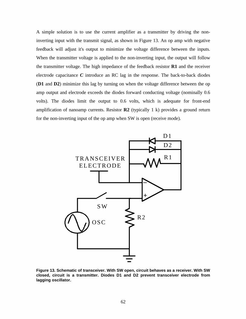
62
A simple solution is to use the current amplifier as a transmitter by driving the non-
inverting input with the transmit signal, as shown in Figure 13. An op amp with negative
feedback will adjust it's output to minimize the voltage difference between the inputs.
When the transmitter voltage is applied to the non-inverting input, the output will follow
the transmitter voltage. The high impedance of the feedback resistor R1 and the receiver
electrode capacitance C introduce an RC lag in the response. The back-to-back diodes
(D1 and D2) minimize this lag by turning on when the voltage difference between the op
amp output and electrode exceeds the diodes forward conducting voltage (nominally 0.6
volts). The diodes limit the output to 0.6 volts, which is adequate for front-end
amplification of nanoamp currents. Resistor R2 (typically 1 k) provides a ground return
for the non-inverting input of the op amp when SW is open (receive mode).
D1
D2
R1
R2
S W
TRANSCEIVER E L E C T R O D E
OSC
_
+
Figure 13. Schematic of transceiver. With SW open, circuit behaves as a receiver. With SWclosed, circuit is a transmitter. Diodes D1 and D2 prevent transceiver electrode fromlagging oscillator.

63
The capacitance of the feedback diodes decreases the gain of the op amp, while decreases
the resonance effect of the circuit, as shown in the frequency response curves in Figure 14.
The flattened frequency response is desired for spread spectrum. The attenuation due to
the diodes (approximately 6 dB) can be compensated by additional amplification, or
preferably by increasing the transmit frequency, resulting in a faster update rate.
8.3 Smart Fish Evaluation Board
8.3.1 Introduction
A second generation electric field evaluation board is designed to a) capture the full
dynamic range of the electric field sensor, b) eliminate the need to manually adjust circuit
parameters, and c) explore other modulation techniques (including spread spectrum). The
new evaluation board is called the smart fish since the system can adjust system
parameters automatically and implement many modulation techniques by software
programming.
0 50 100 150 2000
0.2
0.4
0.6
0.8
1
Frequency (kHz)
OUTPUT
1 M
1 M + diodes
100 K
100 K + diodes
Figure 14. Receiver frequency response of transceiver. R2=1 K, R1=100 K or 1 M, anddiodes D1 and D2 installed or absent (see comments near curves).
64
The received displacement current is converted into a voltage by a current amplifier, as
done in the original fish. The voltage is biased by a programmable voltage from a digital-
to-analog converter (DAC), and amplified by a differential programmable gain amplifier
(DPGA). The programmable voltage effectively nulls (to the resolution of the DAC) the
applied voltage. Any difference is multiplied by the DPGA and digitized by a twelve bit
ADC. The process is controlled by a digital signal processor (Analog Devices AD2101)
running at 20 million instructions per second. The transmitter oscillator is digitally
implemented; the digital signal processor (DSP) controls a 12 bit DAC. The DSP can also
enable a circuit that measures the current loading of the transmitter electrodes. Other
modulation and detection strategies are possible since the transmitter modulation and
detection demodulation is performed in software.
The smart fish evaluation board is designed to be a general purpose data acquisition
system, in addition to the specific application of electric field sensing. Complete
schematics, parts and vendor list, and programming manual for the DSP and 68HC11 are
provided to assist those who might build, use and extend the operation and functionality of
the smart fish.
8.3.2 Hardware Review
Figure 15 presents a functional block diagram of the smart fish. The 68HC11
microprocessor communicates with a host computer through a serial interface (either RS-
232 or MIDI). The AD2101 DSP performs all the low level data acquisition. Figures 16-
19 are the detailed schematics of the smart fish board. Theses schematics represent the
current state of the prototype design; please contact the Physics and Media Group for the
latest update.

65
Figure 15. Smart fish block diagram.

66
Figure 16. Smart fish RECEIVER schematic.

67
Figure 17. Smart fish TRANSMITTER schematic.

68
Figure 18. Smart fish DSP schematic.

69
Figure 19. Smart fish CPU, INTERFACE, POWER schematic.

70
8.3.3 Parts List
The following is a parts list of smart fish components:
Quantity Part Type Designators32 .1 C1 C2 C3 C4 C5 C6 C8 C9 C10 C11 C12 C13
C14 C15 C16 C17 C18 C19 C20 C21 C22 C25 C32 C33 C34 C35 C36 C37 C38 C39 C40 C4126 0 R8 R11 R12 R16 R17 R18 R19 R42 R43
R44 R45 R46 R47 R48 R49 R50 R51 R54 R55 R56 R57 R58 R59 R60 R61 R62
7 1K R6 R7 R9 R10 R13 R14 R152 1K RP RP1 RP2
10 1M R30 R31 R32 R33 R34 R35 R36 R37 R38 R3916 1N914 D3 D4 D5 D6 D7 D8 D9 D10 D11 D12 D13
D14 D15 D16 D17 D182 1N4001 D1 D21 4.7K R201 6N138 U61 8MHZ XTAL11 8SW/DIP16 SW38 10K R1 R2 R3 R4 R5 R52 R53 RP31 10M R214 20K R26 R27 R28 R291 20MHz XTAL21 22uF C282 27pf C23 C241 74HC368 U71 74HC393 U191 74HC574 U201 74HC589 U42 100K R40 R413 100uF C7 C26 C272 220 R24 R252 330 R22 R231 27512 U181 75155 U12 AD684 U26 U271 AD2101 U172 BUTTON SW1 SW21 D25 J41 DB9/F J11 DG406 U142 DIN-5 J2 J3

71
1 HEADER 5 JP11 HEADER 8 J71 IDC10 J51 MAX120 U161 MAX333 U51 MAX532 U91 MC68HC11E2 U21 MC34064 U32 not installed C29 C301 PGA204 U151 POWER J69 RCA J8 J9 J10 J11 J12 J13 J14 J15 J162 TL082 U10 U118 TLO82 U8 U12 U13 U21 U22 U23 U24 U251 GREEN LED11 RED LED21 YELLOW LED3
8.3.4 Vendor List
The smart fish costs approximately $550 in materials, including printed circuit board,
power supply, and case. The following is a vendor list, complete with vendor part numbers
and price estimates:
Vendor: Digi-KeyPhone: 1-800-344-4539FAX: 218-681-3380Address: 701 Brooks Ave. South PO Box 671
Thief River Falls, MN 56701-0677
Part Description PriceA1700-ND FIBER OPTIC CABLE OD=.089 5M 11.20 FB111-ND REPLACEMENT EMITTER/DETECTOR 6.00 MAX120CNG-ND ADC 500KSPS 12BIT 32.59MAX333CPP-ND QUAD SPDT CMOS SWITCH 20PIN DIP 6.39MAX532BCPE-ND DUAL SERIAL V OUT 12BIT DAC 18.00MAX427CPA-NA LOW NOISE OP AMP 8PIN DIP 3.5774ACQ574PC-ND OCTAL FLIP-FLOP W/TRISTATE 2.796N138QT-ND OPTOISOLATOR 1.363P300-ND RED T13/4 DIFFUSED .168P303-ND GREEN T13/4 DIFFUSED .23P306-ND AMBER T13/4 DIFFUSED .249CTX116-ND 16MHZ TTL CRYSTAL 3.25 P6632-ND 47UF 25V ELECT. CAP RADIAL .263

72
P6633-ND 100UF 25V ELECT. CAP RADIAL .30P2105-ND 1UF TANT CAP .198 100XBK-ND 100 RESISTOR 1% 1/4 WATT .04135220XBK-ND 220 RESISTOR 1% 1/4 WATT .04135330XBK-ND 330 RESISTOR 1% 1/4 WATT .041351.00KXBK-ND 1K RESISTOR 1% 1/4 WATT .041354.7KXBK-ND 4.7K RESISTOR 1% 1/4 WATT .0413510.0KXBK-ND 10K RESISTOR 1% 1/4 WATT .0413520.0KXBK-ND 20K RESISTOR 1% 1/4 WATT .041351.00MXBK-ND 1M RESISTOR 1% 1/4 WATT .041350.0QBK-ND ZEROOHM JUMPER WIRE 1/4 WATT .02465 761-3-R1K-ND DIP RESISTOR PACK 16PIN (8 RESES) .65527C512-12/J-ND 512K EPROM 120NS 10.90A2120-ND 28PIN PLCC SOCKET 1.64A2123-ND 52PIN PLCC SOCKET 2.03A2124-ND 68PIN PLCC SOCKET 2.25ED3314-ND 14PIN MACHINE DIP .506ED3316-ND 16PIN MACHINE DIP .578ED3320-ND 20PIN MACHINE DIP .723ED3324-ND 24PIN MACHINE DIP NARROW .867ED3328-ND 28PIN MACHINE DIP NARROW 1.012ED3628-ND 28PIN MACHINE DIP 1.012
Vendor: Allied Electronics Phone: 1-800-433-5700FAX: 617-255-0468Address: Rm 130 1408 Route One Norwood, MA 02062
Part Description Price735-2746 TL084CN Quad Op-Amp 1.25 735-2742 TL082CP Dual Op-Amp .87 735-9994 SN75155P RS-232 TX/RCV Driver 1.25839-2426 RCA pc mount right angle .74 748-2039 capacitor .1uf .1" spacing .48879-0125 Triple power supply 48.00806-5155 Hammond blue box 1.58"h 25.00 870-6058 Switch momentary on .40
Vendor: Analog DevicesPO BOX 9106 Norwood, Mass
Phone: 617-461-3131
Part Description PriceADSP-2101-KP-80 DSP PLCC package 20MHz version $40.00

73
8.3.5 Smart Fish Programming Manual
The following is a preliminary programming manual included to present a glimpse of the
operation of the smart fish. Please contact the Physics and Media Group for the latest
version of this information.
8.3.5.1 SMART FISH FUNCTIONAL OPERATION OVERVIEW
The HC11 communicates to the host through MIDI or RS232 using the asynchronous
port. The HC11 communicates with the DSP and DIP8 switches though the synchronous
port. The HC11 directly selects the transmitter (TX1 and/or TX2) and can enable the
circuitry to measure transmitter load. The DSP selects the following acquisition
parameter; receiver channels, channel gain, transmit frequency and amplitude, sample
phase, and number of samples accumulated per channel. The HC11 sends a request record
to the DSP specifying these acquisition parameters, basically requesting the DSP to get a
bunch of samples. The DSP goes off and does the acquisition and sends back a data
record to the HC11 containing the requested measurements.
8.3.5.2 COMMAND STRUCTURE (HC11 to DSP)
Command Byte followed by any number of optional Data Bytes, as in;
COMMAND_OP_CODE DATA
Command OpCode Data #1 Data #2 CommentRead receiver 0000BBBB Read receiver bankFrequency 0001RRRR D15-P8 D7-D0 Set receiver R to transmitperiod DPhase1 0010RRRR D15-D8 D7-D0 Sample receiver R atphase DPhase2 0011RRRR D15-D8 D7-D0 Sample receiver R atphase DSamples 0100RRRR D7-D0 -------- Number of samples perchannelTransmit Load 01010000 D7-D0 -------- Read transmitter D timesUser channel 01100UUU --------- -------- Read user channel UReceiver RRRR 0000=1, 0001=2, ... , 1111=16

74
Since there are two transmitters and eight receivers, there are effectively 16 receiver
channels, each with their own transmission frequency and phases. The DSP samples the
receiver twice, at two different times (phases). Typically they are set at 90 and 180
degrees to measure the phase shift of the channel. When the transmitter load is measured,
the transmitter power is attenuated so good receiver measurements can’t be made while
measuring transmitter load.
8.3.5.3 DSP & HC11 COMMUNICATION
Synchronous communication requires one device to be the master and generate a
synchronization clock. For the smart fish the device transmitting is the master. The HC11
starts by being the master sends s request record to the DSP. The HC11 then turns into a
slave and the DSP (as master) sends back a data record when the DSP is finished reading
all the requested channels. There are no codes that specify end-of-record so the HC11 and
DSP must know how many bytes to expect in a record. This is determined by an agreed
upon command structure of the form command/data.
To send a request record to the DSP, the HC11 first prepares a record to send to the DSP
in a buffer. The HC11 then configures the SPI as a master and enables SPI interrupts (see
SPCR-SPI Control Register). This starts an interrupt driven routine called by the flag
SPIF- SPI Transfer Complete Flag that sends out a byte from the buffer until the buffer is
empty. The routine sets TSYNC1, puts the data byte in the SPDR-Serial Peripheral Data
Register, then clears TSYNC1. After the last byte of the request record is transmitted, the
HC11 is configured as a slave. When the DSP sends its first byte of the data record to the
HC11, the SPIF will cause an interrupt which should vector into a receive routine that
puts each received byte into a receive buffer. The HC11 should know how long the record
is since the HC11 requested the data record. When all the bytes are received, the HC11
takes the full data record and sends it out the asynchronous port to the host, either in
MIDI or RS232 format.
75
8.3.5.4 DSP READING RECEIVER CHANNELS
The DSP has only one analog-to-digital (ADC) converter so a multiplexer (MUX) is used
to select one of sixteen inputs; eight receiver channels, a transmitter load channel, and
seven user port channels. A differential amp with programmable gain (DPGA) follows the
MUX allowing the DSP to select channel gain from 1-1000 in decade increments. The
DPGA multiplies the difference between the input channel and an output from one of the
two channels of the digital-to-analog (DAC). This allows the DSP to offset the anticipated
value of the channel (e.g., the last reading from the channel), and amplify the difference,
greatly increasing the dynamic range of the system. The DSP selects the receiver channel
and channel gain by writing to any external data memory location. All external data
memory locations are latched by an eight bit latch (data lines D8-D15).
To read a receiver channel pulse the SAMPLE control line high for at least one
microsecond. This holds the analog value of each receiver channel before the MUX.
Select the MUX channel for the receiver channel you want to read, then set the gain of the
DPGA. Wait 8 microseconds for the DPGA to settle, drop ADC CS/ (bit 15 of DSP
Memory Write) . Then read external memory 2 microseconds after dropping ADC CS/.
To read transmitter load or any of the user ADC channels, the sample-and-hold (S/H) is
not connected to these channels and therefore the SAMPLE control line does not need to
be pulsed. The DPGA still needs to settle though after the MUX channel selection address
(MUXD-A) and/or GAIN is changed.
8.3.5.5 DSP WRITING TO THE DACs
The DAC has two channels, each with 12 bits resolution. Channel 0 controls the transmit
voltage. Channel 1 controls the DPGA offset voltage. Both channels are updated together
as one 24 bit serial word, composed as three sequential 8 bit serial transmissions, sent on
SPORT0. DAC0 (DAC channel 0) is the transmit voltage. DAC1 is the offset voltage
applied to the subtracting input of the DPGA.

76
8.4 Cable Resonance Phenomena and Non-Ideal Op Amp Performance
The receiver circuit of the fish prototype exhibits an amplitude sensitivity indicative of a
resonant system. The resonant frequency is observed to be determined by the length and
type of receiver cable used, and is independent of transmitter cable.
In order to understand the resonance phenomena, the deviation of an operation amplifier
from its ideal behavior is examined. The operation amplifier relies on negative feedback
for stable operation. The feedback signal at the inverting input should be -90 degrees24.
The inverting input adds another -90 degrees of phase shift, producing the desired -180
phase signal. An ideal op amp maintains constant phase over its entire bandwidth. In
practice op amps have a number of internal phase shifts and phase compensation circuitry
to produce a single pole phase shift starting at about 10 Hz. The TLO82 used in the fish
has a single pole at 10 Hz and maintains a flat phase shift of -90 degrees from 100 Hz to 1
MHz. Oscillation will result if the phase of the signal at the inverting input is shifted an
additional -90 degrees at a frequency where the gain exceeds unity. Damped oscillations
(i.e., ones that does not blow up) would explain the observed resonance phenomena.
The feedback resistor R and the cable capacitance C form an RC network at the inverting
input to the op amp, which shifts the phase of the feedback signal. A 53 pf cable
capacitance combined with a 1 M feedback resistance shifts the phase of a 30 kHz signal
an additional -90; a necessary condition for oscillation. The cable capacitance has an
additional detrimental impact on the performance of the receiver amplifier. Cable
capacitance shunts a portion of the received current at the noninverting input to ground,
stealing current that would otherwise be converted to voltage. At 30 kHz a 53 pf
capacitance has 100 K impedance, shunting 91% of the received current (assuming a 1 M
feedback resistor).
The cable impedance also decreases the effective gain of the op amp by an order of
magnitude by decreasing the feedback attenuation factor; the ratio of the input resistance
24 Minus sign indicates inverting input lags the output signal.

77
to the sum of the input resistance and feedback resistance25. The open loop gain of a
TLO82 at 30 kHz is 100. The feedback attenuation factor reduces this gain to 9. The small
gain means the non-inverting input (hence the receive electrode) deviates from a virtual
ground, having a signal equal to 9% of the op amp output.
The feedback resistor can be decreased to raise the resonance frequency, moving the pole
to a higher frequency, and increase the feedback attenuation factor, at the sacrifice of
some current to voltage gain. However the loss of gain can be made up in a second stage
of amplification. Noise calculations indicate that thermal noise (4KTRFbw [Horowitz94])
from the 1 M feedback resistor accounts for 98% of the noise in the current-to-voltage
circuit. Reducing the feedback resistor to 100 K decreases the circuit noise 9.3 dB, from
41 uV to 14 uV.
8.5 Humidity and Permitivity
The displacement current from transmitter to receiver electrode is primarily a function of
geometry. As the distance between the transmitter and receiver electrode decrease, the
displacement current increases. The displacement current also depends on the permitivity
of air which has a slight dependence on temperature and humidity. Since these parameters
change on a time scale orders of magnitude slower than the modulation rate (minutes and
hours compared to microseconds) they do not affect the integrity of PAN communication.
However, changes in displacement current measurements may effect the long term
reliability of electric field sensing. The magnitude of the effect of humidity on air
permitivity is calculated using the following equation [Fraden93]:
e=1+(211/T)(P+(48SH/T)*10-6
where T= temperature in KelvinP= pressure of the moist air in mm HgS= pressure of saturated air in mm Hg (temperature dependent)H= relative humidity (in percent, i.e.; 0-100)
25 Attenuation factor=100 K/(100 K + 1 M)=0.09
78
Assuming T=20°C, P=30 mm Hg, S=17.535 mm Hg, permitivity is calculated for twohumidities: H=50% e=1.000125
H=60% e=1.000146
The permitivity changes 0.0021% when humidity changes 10%, a small change indeed.
9. FUTURE RESEARCH
The research of the thesis has uncovered a novel means to perform local communication
using electric fields. The trade-offs among cost, speed, size, power, and operating range
must be further studied and quantified in order to engineer practical PAN devices. Many
of the design and engineering techniques of radio and digital communication can be
applied to PAN devices, for a PAN device is basically a radio with a near-field antenna. A
radio captures far-field electromagnetic radiation using a resonant antenna; a PAN receiver
intercepts near-field electric fields using electrostatically coupled plates. PAN devices
therefore benefit from advances in tiny micro-powered radio circuits.
A communication network is primarily judged by channel capacity. Telephone modems
have pushed modulation and digital signal processing techniques to their limits. The
application of modem telephony techniques to PAN devices may deliver channel capacities
of 100 kbits per second. Data compression also increase the effective capacity of PAN
communication.
The concept of power sneakers is intriguing. A piezo ceramic pile may be used to charge a
capacitor, powering PAN electronics. Piezo elements produce a large charge across a
small capacitance, resulting in a large voltage. Super capacitors on the order of Farads,
typically used to back up RAMs, may be used to increase the capacitance and hence,
decrease the piezo voltage. Surface mount components mounted on a flexible printed
circuit boards can produce a comfortable networked computer shoe insert.
The thesis explored the first two layers of a network. The upper networked layers must be
addressed to make a practical PAN. Applications need to be deeply considered. Privacy
and other cultural issues are raised when personal data can effortlessly be exchanged. As
with other communication and data systems, there is a trade-off between access and

79
security, reminiscent of the Chinese character that simultaneously represents hazard and
opportunity. The thesis is a technical work and does not begin to address these broader
issues, which will continually be explored and resolved as electronic devices such as PANs
permeate the social fabric of our information society.
The next step, from my perspective, is to push the sensitivity and bit rate of the PAN
receiver in order to realize a watch-sized PAN transceiver. Ultimately PAN devices will be
judged a success when they appear as common objects and perform magic; from picture
telephone Dick Tracy watches to self-powered smart sneakers that seamlessly interconnect
us to a world-wide network.

80
10. References[Barber84] Barber, D.C., Brown, B.H., Applied Potential Tomography, J. Phys. Bi
Sci. Instrum. Vol 17, 1984, Printed in Great Britain.
[Bullock82] Bullock, T.H., Electroreception. Ann. Rev. Neuroscience, Vol. 5 (1982), pp. 121-170.
[Carlson86] Carlson, A. B., Communication Systems, Third Edition, McGraw-Hill Book Company, New York, 1986, pp. 230, 401, 514-536, 554.
[FCC93] Federal Communications Commission, Washington, D.C. Part 15 Radio Frequency Devices, 1993.
[Fraden93] Fraden, J., AIP Handbook of Modern Sensors, American Institute of Physics, New York, 1993, pp. 421.
[Gershenfeld93] Gershenfeld, N. Method and Apparatus for Electromagnetic Non-Contact Position Measurement with Respect to One or More Axes, US Patent No. 5,247,261, Sept. 21, 1993.
[Gershenfeld94] Gershenfeld, N., Physics and Media, class notes (unpublished),MIT Media Lab, September 1994.
[Gershenfeld95a] Gershenfeld, N., Zimmerman, T.G., Allport, D., Non-Contact System For Sensing and Signaling by Externally Induced Intra-Body Currents US Patent Application, May 8, 1995.
[Gershenfeld95b] Gershenfeld, N., Personal communication, June 23, 1995.
[Halliday62] Halliday, D., Resnick, R., Physics, Part II, John Wiley & Sons, NewYork, 1962, pp. 721.
[Helm95] Walter Helm, Staff Scientist-Electronics at Timex Corporation, Personal communication, March 17, 1995.
[Horowitz94] Horowitz, P., Hill, W., The Art of Electronics, Second Edition, Cambridge University Press, Cambridge, 1994, pp. 430.
[Kearey91] Kearey, P., Brooks, M., An Introduction to Geophysical Exploration, Second Edition, Blackwell Scientific Publications, Oxford, 1991,pp. 216.
[Mills93] Mills, J.P., Electromagnetic Interference, Prentice Hall, New Jersey, 1993, pp. 143.

81
[Orr87] Orr, W.I., Radio Handbook Twenty-Third Edition, Howard W. Sams & Company, Indiana, 1987., ch. 22 pp. 6.
[Pahlavan95] Pahlavan, K., Probert, T.H., Chase, M.E., Trends in Local Wireless Networks, IEEE Communications Magazine, March 1995, pp. 88-95.
[Ramo94] Ramo, S., Whinnery, J.R., Van Duzer, T., Fields And Waves in Communication Electronics, Third Edition, John Wiley and Sons, New York, 1994, pp. 254-256.
[Shivers93] Shivers, O., BodyTalk and the BodyNet: A Personal Information Infrastructure, Personal Information Architecture Note 1, MIT Laboratory for Computer Science, Dec. 1, 1993.
[Smith95] Smith, J.R., Towards Electric Field Imaging, MS Thesis, MIT Media Lab, 1995.
[Stalling93] Stalling, W., Networking Standards, Addison-Wesley Publishing, Massachusetts, 1993, pp. 23-26.
[TI95] Texas Instruments, Operational Amplifiers and Comparators, Data Book, Volume A, Texas Instruments, Dallas, Texas, 1995, pp. 2-369.
[Webster89] Webster, J.G. (ed.), Electrical Impedance Tomography, Adam Hilger (Publisher), New York, 1989.
[Weston91] Electromagnetic Compatibility, Weston, D.A., Marcel Dekker Publishers, 1991 New York, pp. 36.
[Zimmerman95] Applying Electric Field Sensing to Human-Computer Interfaces, Zimmerman, T.G., Smith, J.R., Paradiso, J.A., Allport, D., Gershenfeld, N., CHI'95 Human Factors in Computing Systems (Denver, May 9-11) ACM Press.