personal computer low-cost alternatives to …
TRANSCRIPT
PERSONAL COMPUTER LOW-COST ALTERNATIVES
TO AUTOMATED TEST EQUIPMENT
by
JOHN C. YOST III, B.S.Comp.E.
A THESIS
IN
ELECTRICAL ENGINEERING
Submitted to the Graduate Faculty of Texas Tech University in
Partial Fulfillment of the Requirements for
the Degree of
MASTER OF SCIENCE
IN
ELECTRICAL ENGINEERING
Approved
August, 2002

TABLE OF CONTENTS
ABSTRACT iv
TABLES V
FIGURES vi
CHAPTER
I. INTRODUCTION 1
PC Test Study 1
II. TESTING AND ALTERNATIVES 3
Integrated Circuit Testing 3
Test Cost 4
ATE Alternatives 6
PC Tester 7
III. ANALYSIS 9
/Design 9
PC Tester Setup 11
Program Operation 13
Control Program 14
Connection Block Program 20
Input Program 22
Output Program 25
Operation 34
IV. RESULTS 37
Hardware Capabilities 37
Versatility 40
DUT Interface 41
Target Device Families 43
V. CONCLUSION 44
Further Development 45
BIBLIOGRAPHY 49

APPENDIX 50
01

ABSTRACT
A thesis exploring the use of PCs as an alternative test vehicle to expensive ATE and
bench testing equipment. An example system is developed for comparing versatility, interface,
and hardware capabilities. Results showed PC is most apphcable to testing SSI, MSI, and LSI
circuit famihes. Future work is also explored for enhancing PC capabilities.
w
TABLES
1: ATE cost example 5
2: Gain and measurement precision 11
3: Specification comparison to ATE 37
4: Specification comparison to bench equipment 38
5: DAQ card comparison 39
6: PC Tester advantages and disadvantages 44
7: Current and future PC tester capabilities 48

FIGURES
1: NI-6024E block diagram 8
2: Lab VIEW program example 12
3: Lab VIEW program interface example 12
4: Control program interface 14
5: Analog input program control 15
6: Sequence one 15
7: Analog I /O initiali2ation 17
8: Analog I / O test control 18
9: Sequence one, analog input refresh and wait 18
10: Coimection board program interface 19
11: Coimection block program control 20
12: Array initialiyarion and selection routines 20
13: Pin indicator controls 21
14: Single indicator control for pin one 21
15: Analog input program interface 22
16: Analog input refiresh and wait routine 23
17: Analog input display window controls sequence 24
18: Window control conversion to control array 24
19: Pan window up routine for window control 25
20: Analog output program interface 26
21: Program interface displaying sawtooth waveform controls 27
22: Control visibihty assignments 28
23: Control visibility assigmnents 29
24: Single tone waveform sequence 29
25: Edit waveform progerties program interface 30
26: Dial initialization and display adjustment routines 31
27: DC waveform generation routine 32
28: Muititone generation routines 32
VI

29: Save waveform sequence 33
30: Supply and meter connections to amplifier example 35
31: Voltage sequence for binary input offset voltage test example 41
32: Switching matrix connection example 42
vu

CHAPTER I
INTRODUCTION
Circuit testing is an integral part of semiconductor product engineering. Testing is
responsible for collecting data, for maintaining good yield in production, for characterizing end
products, and most importantiy, it is responsible for eliminating faulty products. Testing is
done before a design reaches production, after first silicon, during production, after
production, after packaging, and finally after it is installed in the end product Test equipment
is responsible for providing the resources to perform all of these tests, both in production and
outside of production. The cost of this equipment is quickly becoming a paramount
contributor the overall cost of production.
The increasing cost of test equipment in semiconductor product manufacturing is
forcing many integrated circuit (JC) manufacturers to investigate cheaper alternatives. Testing
is quickly becoming a major cost of IC manufacturing due to the high-dollar automated test
equipment (ATE) used in the process. These testers often cost several million dollars with an
average life span of only a few years. At several cents per second, utilizing the tester's time
becomes crucial to maintaining good profit Cleariy a cheaper alternative to ATE is needed.
The capabilities of personal computers (PCs) suggest they have the potential to
provide adequate test diversity at low costs. Other alternatives such as specialized ATE, either
provide littie improvement in cost or are tailored to a specific test or product A PC, even
after being modified for testing, cost less than one tenth of a percent the cost of a typical ATE.
Therefore, a study was performed in order to determine if PCs cotild provide a viable
alternative to commercial ATE.
PC Test Stody
The objective of this research is to determine the capabilities of a PC as a circuit testing
device. The approach is to simulate an ATE on a PC using software in conjunction with
measurement hardware. This combination adapts the PC to perform general ATE type tests.
There are many options available when choosing the software and hardware for the design.
Choices were made that would provide characteristics similar to an ATE.
The software of the design is written in Laboratory Virmal Instrumentation
Engineering Workbench (LabVTEW), a graphical progranmiing language based on data flow
programming. The program is responsible for controlling and managing operations of the
hardware in addition to providing the operator with a robust interface. The hardware
incorporated into the PC is a data acquisition card (DAQ). This card is responsible for making
electrical measurements and generating the electrical stimuli required for administering the
tests.
Chapter II provides a background to IC testing, the type of tests typically performed,
the role of ATE, and an introduction to the PC tester design. Chapter III details the design,
implementation, and assessment of the PC tester. The results of the evaluation are presented
in Chapter IV and conclusions drawn firom these results are offered in Chapter V.

CHAPTER II
TESTING AND ALTERNATIVES
Integrated Circuit Testing
Circuit testing is an integral part of semiconductor product engineering. In an industry
where yield is contingent upon optimization, in-process and post-process testing is critical
Tests are performed during the fabrication process, after fabrication, and after packaging.
These tests are typically referred to as parametric probe, multiprobe, and final test, respectively.
At each step the objective is to "find the bad chips quickly, get them off the tester, and save
expensive tester time" [7]. The test must not only catch the faulty chip but also provide
information for vmcovering the fault mechanisms responsible for the defect However, this is
difficult since test coverage is compensated in order to reduce test time and increase
throughput When a chip fails a test, it is immediately discarded or inked. Inking marks the
chip to indicate that it should be ignored or removed later. The data that is collected is fed
back to the manu&cturing process control in an attempt to reduce abrupt process deviations
and eliminate defect sources.
Parametric probe test involves testing the wafer during processing before it leaves the
production line. Typically this test is performed after the first layer of metal is deposited and
etched thus providing coimections to the circuit devices. Some typical tests performed by the
parametric probe are gate oxide integrity, resistance, and interconnect continuity. These are
referred to as direct current (DC) tests.
Multiprobe, otherwise called wafer test or wafer probe, is typically performed after the
wafer has been processed and before it is separated into individvial die. The first test may be a
simple and fast functionality test Functional tests are performed by stimulating the device
rmder test (DUT) and comparing the output against an expected response. Functional tests
are sometimes referred to as alternating current (AC) tests. The stimulus used in an AC test is
often referred to as a vector. Other tests which may be performed are DC, stmcturaf, or
additional parametric tests. Stmctural tests are aimed at identifying stmctural failures such as
short-circuits or open-circuits.

Final test is performed after the die has been packaged. This test is critical for finding
faults which may have been introduced in the packaging process or faults which might not
have been caught by parametric probe or multiprobe. These tests may be performed at
elevated temperatures to catch circuits that would normally fail under thermal fatigue. The
tests are similar to the functionality tests performed dirring multiprobe. Often, final test is the
first test performed at the circuit's intended clock rate. This is primarily due to the previous
tester's lack of capacity to perform tests at such high ftequencies. In some cases an additional
test, called bum-in, is performed after final test. The objective of bum-in is to catch packaged
circuits that have a high probability of failing due to infant mortality.
Test Cost
Vendors such as Teradyne, Schlumberger, and Advantest produce automated test
equipment (ATE) to perform both functional and parametric tests. These testers are typically
very expensive and make up a significant percentage of production cost. There are several
factors that fiiel the growing cost of these machines. For every new generation of devices,
new testers must be developed. New process technologies become available approximately
every 18 months, therefore new testers must also be available within the same time ftame.
This is due primarily to the growing speed and comiplexity of new designs implemented with
the new technology vehicles. Decreasing feature sizes resxilts in greater fvmctionality. More
functionality results in more complicated circuits requiring more external pins to support the
internal system. Testers must be able to accommodate the new pins and package layout. Steve
Carlson in an EE Times article states "for complex, high-speed SoC devices, testers cost
between $2,000 and $9,000 per pin" [8].
In addition to growing sizes, circuits are also growing in complexity. Application
Specific Integrated Circuit (ASIC) design has grown in popularity due to its ability to provide
the customer with a customized integrated circuit in a very short time-to-market The testers
used in the production of ASIC products must be capable of fiJly exercising the circuit despite
the diversity of ASIC capabihties. Systems On a Chip (SoC) are also gaining popularity due to
their ability to implement many diverse operations on a single chip. One example could be cell
phones. Currentiy a cell phone may contain several ICs. However, an entire cell phone could
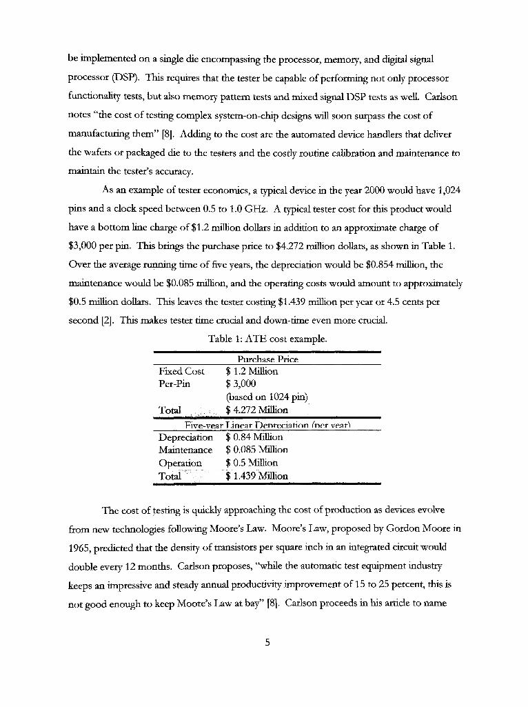
be implemented on a single die encompassing the processor, memory, and digital signal
processor (DSP). This requires that the tester be capable of performing not only processor
functionality tests, but also memory pattern tests and mixed signal DSP tests as well. Carlson
notes "the cost of testing complex system-on-chip designs will soon surpass the cost of
manufacturing them" [8]. Adding to the cost are the automated device handlers that deliver
the wafers or packaged die to the testers and the costiy routine calibration and maintenance to
maintain the tester's accuracy.
As an example of tester economics, a typical device in the year 2000 would have 1,024
pins and a clock speed between 0.5 to 1.0 GHz. A typical tester cost for this product would
have a bottom line charge of $1.2 million dollars in addition to an approximate charge of
$3,000 per pin. This brings the purchase price to $4,272 million dollars, as shown in Table 1.
Over the average running time of five years, the depreciation would be $0,854 million, the
maintenance would be $0,085 million, and the operating costs would amount to approximately
$0.5 million dollars. This leaves the tester costing $1.439 ttiiUion per year or 4.5 cents per
second [2]. This makes tester time crucial and down-time even more crucial.
Table 1: ATE cost example.
Purchase Price Fixed Cost $ 1.2 Million Per-Pin $ 3,000
(based on 1024 pin) Total .;; • $ 4.272 Million
Five-vear Linear Denreciarion Tner ve.ar) Depreciation $ 0.84 Million Maintenance $ 0.085 Million Operation $ 0.5 Million Total $ 1.439 MilHon
The cost of testing is quickly approaching the cost of production as devices evolve
ftom new technologies following Moore's Law. Moore's Law, proposed by Gordon Moore in
1965, predicted that the density of transistors per square inch in an integrated circuit would
double every 12 months. Carison proposes, "whUe the automatic test equipment industry
keeps an impressive and steady aimual productivity improvement of 15 to 25 percent, this is
not good enough to keep Moore's Law at bay" [8]. Carison proceeds in his article to name

four methods of reducing the cost of testing: test less, test more effidentiy, explore different
test strategies, and lower the cost of testers by investigating alternatives. The first three focus
on reducing testing costs by performing more efficient tests and optimizing tester time. The
last option has the potential of significantiy reducing testing cost without compensating test
time.
ATE Alternatives
There are many alternatives to ATE. However, there are usually drawbacks to each.
Most alternatives lack key characteristics of an ATE. ATE must be capable of performing
those tests mentioned previously, yet in order for it to do so, it must have great test versatility.
Some alternatives only perform DC tests and others only AC tests as a means of reducing the
complexity and hence the cost of the tester. This leads to specialized testers that are targeted
to a specific product or test Other alternatives do not even resemble an ATE in functionaEty.
Test benches are not used in production but in characterizing and testing the packaged circuits
outside of the production line. The test bench is usually comprised of several pieces of
precision sources and measiirement equipment used to perform similar tests as an ATE. The
drawback to the test bench is the lack of automation and a lack of repeatability. In addition, a
complete test bench with test diversity comparable to an ATE would require several pieces of
equipment possibly costing several hundreds of thousands of dollars.
Another alternative is virtual testing. Virtual testing involves modeling a circuit design
intended for silicon and stimulating the model with virtual test vectors. Virtual testing allows
test designers to simulate the tests to be performed on the product before the product is even
put into production. Nat Reeves of Level One Communications states "test engineers can
fiiUy debug test vectors before first silicon, minimizing the need for ATE during debug and
substantially improving an ICs time-to-market" [7]. The obvious drawback to virtual testing is
the lack of real test results exhibiting chaotic process flaws. Chad Fasca and Dylan McGrath
comment, "while test simulation software is expected to reduce test time, it will not eliminate
the need for real test" [4].
Virtual testing is performed on a PC using specialized software for simulating large
integrated circuits. If, however, a PC could be used to implement the fimctions of a
commercial A'FE, virtual testing and actual testing could be performed seamlessly on the same
machine. ITie new test system would be capable of performing the test simulation then
actually performing the test. Further, tiie cost of tiie PC tester would be only a fraction of its
commercial counterpart, thereby significantiy reducing the cost of production testing.
PC Tester
In order for a PC to perform ftmctions similar to that of ATE it must be able to
generate and measvure sources and responses of an integrated circuit This requires the PC to
be able to dehver and measure patterns of voltages and currents. In some cases the
measurements must be extremely accurate. Testing ^ t e oxide leakage reqiiires the tester to be
capable of measuring currents in pico-amps. For other tests, such as memory testing, the
tester must be capable of sending and reading thousands of digital memory patterns. Testing
clock jitter could require a tester to be capable of sampling a signal in nano-seconds. Cleariy,
the test system must meet many criteria. It must be fast, programmable, highly accurate, easy
to use, and adaptable.
Adapting a PC to perform ATE tests requires it to be adapted with software and
hardware for regulating and measuring voltages. LabVIEW was chosen as the programming
language for the software, as mentioned in Chapter I. LabVIEW is a graphical programming
language that is primarily used for PC controlled automation. LabVLEW's most robust
programming features are the built in subroutines for controlling external devices such as
DAQ. The program must conomunicate with the DAQ to generate voltage signals and to
make voltage measurements. Because the bottieneck in measurement speed should occur at
the DAQ, the programming language must provide maximum data throughput to the DAQ.
LabVIEW provides this with varying levels of abstraction in DAQ control At the top level
the programmer can easily manipulate the DAQ at the expense of speed At the next level of
complexity, the programmer can control timing and buffer contents of the DAQ. At the
highest level, the programmer can control neariy every aspect of communication with the
DAQ including timing, buffer contents, sampling time, triggering, and output multiplexing.
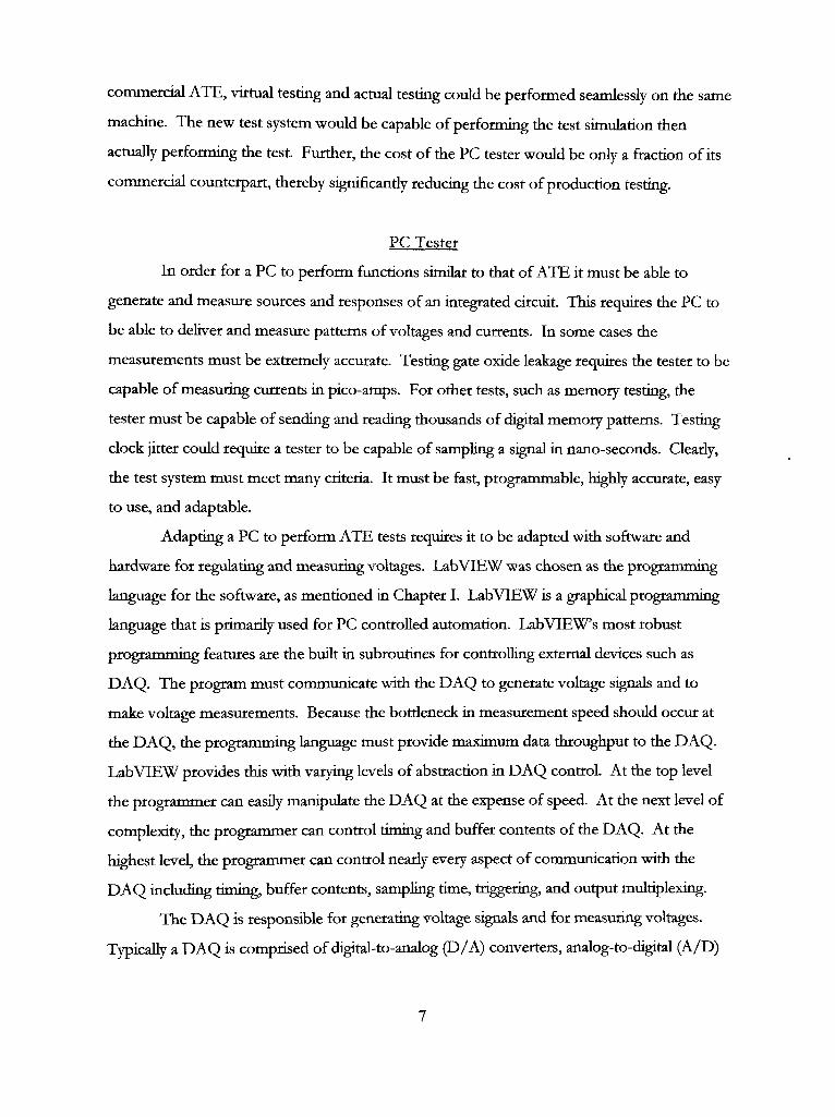
The DAQ is responsible for generating voltage signals and for measuring voltages.
Typically a DAQ is comprised of digital-to-analog (D/A) converters, analog-to-digital (A/D)
converters, multiplexes, amplifiers, a simple processor, and memory. Figure 1 shows a block
diagram of die National Instruments (NI) DAQ 6024E tiiat was chosen for the PC tester.
. irquw Anaiog Input , T . J inlerlace | Tlmlng/c^ttol ! L"'*'^"P
; ) L
Counte>f/ Timing I O DAQ-STC euv
I Analog Output i RT& I BUS [ TlmliiLjContfOl ] Interlace
nrni c - ^ DACO I
Analog Oirtpul (Noton6023E,.
DAQ-STC BUG
Arrak-g Ourpul
P*KJ and PUiy
I 92C:^
TvTv C
C.\]lbraOO(-| DACs JL RTSI Conn^ctoi
C (602;.EOntyi
Figure 1: NI-6024E block diagram.
The 6024E was chosen after making a compromise between cost, speed, and diversity.
The 6024E has 16 analog input channels for sampling voltage signals, two analog output
channels for generating voltage signals, and eight bi-directional digital channels. The 16 analog
input channels can be configured as 16 single-ended inputs or eight differential inputs. Both
analog inputs and analog outputs have 12 bits of resolution with variable voltage ranges. The
DAQ, as mentioned, is typically the bottieneck in sampling speed. Few commercially available
DAQs are capable of sampling faster than one gigahertz. The 6024E has a maximum
sampling rate of 10 kilohertz across two analog output channels and 10 kilohertz across all
analog input and digital charmels.

CHAPTER III
ANALYSIS
It is proposed that a PC could provide an alternative to some portion of commercial
ATE. To illustrate and test the proposal, an instance of the PC tester was designed and
assembled. Characteristics of the example tester can tiien be compared to characteristics of
other testing methods. The results of die demonstration would not be data coEected from
running example tests, but the abilities of the tester to perform tests similar to those run on its
commercial counterparts.
Design
The first step in designing the PC tester was to identify the desirable characteristics.
Since the PC tester is intended as possibly an alternative to ATE, identifying those fimctions
performed by the ATE would define the requirements of the new tester. Commercial ATE
perform either DC tests, AC tests, or both. Both tests requite different capabilities of the
tester. Bums and Roberts state that DC or parametric tests "are those that return a value that
must be compared against one or more test limits to determine pass/fail results." [7] Most DC
tests only require high precision voltage and current sources and high precision voltage and
current meas^u:ements. In some cases the soiirces must be capable of regulating a voltage
while maintaining a high current output For example, these may be required for power
supplies to an IC. AC tests have more stringent requirements. AC or fimctional tests result in
only a pass/fail result without any numerical readings. In order to perform AC tests, the tester
must be equipped with digital input and output (I/O) and analog I /O. In order to perform
some tests, the AC sources must also be capable of generating high frequency waveforms.
Testing filter bandwidth or settling time of a D/A converter, for example, would require a
relatively high frequency source.
Most ATE tests are programs written in a programming language recognized by the
tester. The programs control the operations of the tester to perform the tests. Peari and C++
are two popular languages utilized by commercial ATE for programming automated tests.
The test programs direct the tester to measure or dehver signals to the ICs I /O pins. The

programs provide automation of die test sequence and data interpretation while also
generating dynamic waveforms required by the tests. These waveforms may be digital patterns,
analog signals, or just DC voltages or DC currents.
The smdy is aimed at determining if similar tests can be performed, not automated.
However, in order to provide the flexibility requited for DC and AC tests, the PC tester had to
be designed to provide the same diversity in waveform measurement and generation. This
diversity is also present in bench testing. Bench testing involves utilizing several pieces of
equipment to perform die same DC tests that an ATE might perform. Typically bench testing
does not involve AC testing due to the complexity of the stimulus required. Digital testing is
similar; the size and number of test vectors required to perform digital tests are to
cumbersome for bench test equipment In addition, both digital and AC tests may reqvdre
hundreds or thousands of DUT connections. On a bench, making this many connections and
making them reliable is possible but not practical. Examples of the equipment used in a bench
test are oscilloscopes, function generators, DC regulators, spectrum analyzers, logic analyzers,
etc. If the PC tester could be designed to mimic bench testing, it would be able to perform the
same tests that are possible at the bench level Therefore the interface to the PC tester was
chosen to imitate test bench equipment
The PC tester design is comprised of several pieces of bench test equipment A virtual
oscilloscope provides analysis of a DUT's transient response. A spectrum analyzer, by
graphing the Fourier transform of the response waveform, provides a representation of the
DUT's frequency response. A fimction generator supplies waveform creation with standard
controls for shape, frequency, and phase. A logic analyzer provides graphical access to buffers
where digital patterns are loaded and delivered to the digital I /O of the DAQ. Interpreting a
digital pattern response can be done through a similar interface; an input buffer is designated
separate of the output buffer and again graphical access to the buffer provides the ICs
response to the user. The next section will fturther describe the details, operation, and interface
to the virtual instruments of the PC tester.
10
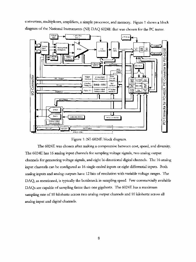
PC Tester Semp
The PC tester is comprised of two parts, tiie NI-6024E DAQ and a program in
LabVIEW for controUing tiie DAQ. The 6024E is a plug-and-play device, and once installed
it is immediately recognized by tiie operating system. Software available for die DAQ assists
in the configuration the device given certain user specifications. The most important option
available in configuration is the chanJiel range. For measurements tiiat do not require large
voltage ranges, the input channel range of the DAQ can be reduced in order to increase the
measurement accuracy. Table 2 lists the ranges available and their corresponding accuracy. As
can be seen in Figure 1 the DAQ contains a programmable gain instrumentation amplifier
(PGIA). The PGIA feeds directiy into the A / D converter. The A / D converter provides a
measurement with 12 bits of resolution. Therefore, if the PGA is programmed to a gain of
0.5, the maximum accuracy obtainable is
tl»3+llovi=w=4.88mV
or for a gain of 100 the maximum accuracy would be
| -50mV|-h|50mV| _ IQOmV __ C)A A-, , , T ; 2^ 4096 — ^'i-^J-pV'
However, it should be mentioned that the NI-6024E has an absolute accuracy of 119[iV at fiiU
scale for a —50 to +50mV range which is more than the resolution of its measurements at that
range.
Table 2: Gain and measurement precision.
Gain
0.5
1.0
10.0
100.0
Input Range
-10 to+10 V
-5 to +5 V
-500 to +500 niV
-50 to +50 niV
Precision'
4.88 inV
2.44 mV
244.14 pV
24.41 pV
' The value of I LSB of the 12-hii ADC; ihal is, (he voltage incieiiient eorrespomljng (o ; eh:i(i"e of one cotiiil in the ADC I2-Iiil coiiiil.
The software for the PC tester requkes that LabVIEW be installed on the computer
that the program is running. Installing LabVIEW is easily done through an installation wizard
11
available witii die programming language. Once installed, the PC test program must also be
installed on tiie same computer. The program consists of 27 files that must be copied to tiie
same directory on die computer. Once copied, tiie program can be initiated by opening if s
root virtoal instrument (VI), Main.vi, and nm from the LabVIEW file menu.
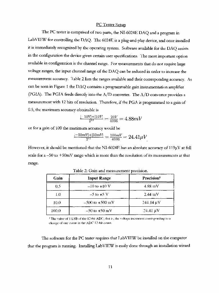
LabVIEW, as mentioned before, is a graphical programming language. Writing a
program in LabVIEW involves selecting subroutines, indicated as icons, and cormecting data
paths between the subroutines, indicated as wires. Figure 2 shows a simple example of a
LabVIEW program that generates waveforms.
hflfsBtt
l-eset signaijl TF ||
signal typelL-iU
frequency iLBgyl
impl i tudelEl^
tahaselE
Sampling infolL-g°=J
duty cycle (%)VIKH-
I ^ IjiA/aveform
MkH^hase out
Instructions
Figure 2: LabVIEW program example.
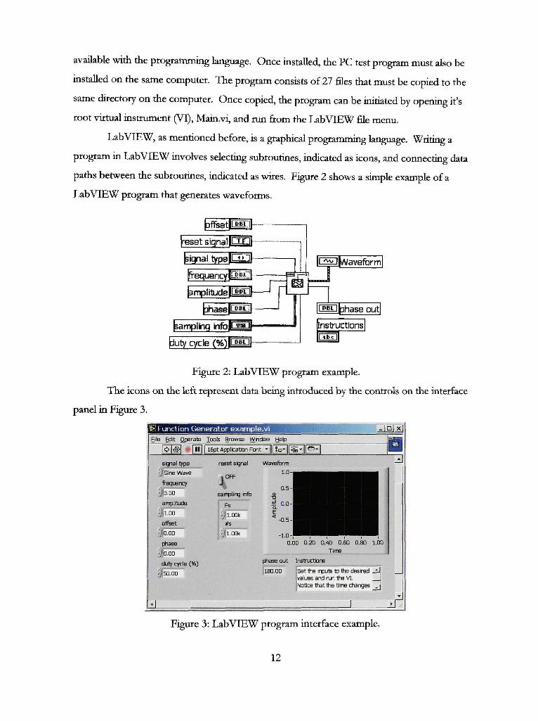
The icons on the left represent data being introduced by the controls on the interface
panel in Figure 3.
I l^ i Fvjnrt ion Generr^tor examnlR.v i v ^ ^ ^ ^ ^ ^ ^ ^ ^ H l a l H l l
Eile Edit OperalE
I O l # l | l l |
signal type
^/Sine Wave
frequency
' te.so
amplitude
' / I . DO
offeet
',):0.oo
phase
'jiO.OO
duty cycle (%)
^teD.OD
1
Xools Browse Window \^\p
1 15pt Application Font - | | ± o - | | ^ ' ' | | ^ - l
reset signal Wavelbrm
|OFF
-*• 0 5 -sampling hnfo m
FS :_ 0.0
i) l.OOk <
•#s - ° ' = -
:,'i.00k _j^()_
0.
phase out
,180.00
i 1
DO 0.2D 0.40 0.60 0.80 l.C Time
a
Instructions
Set the inputs to the desired _ i values and run tha VI, iNotice that the time changes ,
1 1
M • l i
1
1 1'
A
Figure 3: LabVIEW program interface example.
12
The data collected from the controls is supplied to the fimction generator VI located
in the middle of Figure 2. The routine generates a waveform specified by the data supplied to
it. The result of the subroutine is fed out to the indicators on the right side of the subroutine
icon. The data suppUed to the indicators is then presented on the user panel as a waveform
graph and phase out indicator. As a rule of thumb, the input to a VI is typically on die left of
the icon and the output to the right. The colors of the data path wires indicate the type of data
being transferred and it's precision. In the programming window, controls are represented
with bold outlined icons and indicators have thin outlines as can be seen in Figure 2.
Program Operation
The program is divided into four primary blocks: the control program, input, output,
and a connection block diagram. The tester performs two general fimctions, it generates
analog or digital output and measures analog or digital input. Therefore, two separate
programs were written, one for generating output and one for measuring input. A control
program (Figure 4) was created in order to call the separate input and output programs. The
last program provides a depiction of the connection board for locating channel connections.
13

•i!^: TestSvstem.vl idi<J
Analog Output
° J J l Analog Input
J '
J =
J '
J «
J " J 13
Jl5
error out DAQ Device Number SIR 1
AO Buffer Size
AQ Samp n-eq Actual Update Rate
ijllOOO I ^.DD I
AI Buffer Size
IDOO
AI Samp n-eq Actual Update Rate
1000 |D.QO
I Vievif Cormectlonsl
StB»-t error out 2
•
Loop
0 dw
1 Figure 4: Control program interface.
Control Program
Since the tester has multiple input and output channels, writing a separate program for
the input and output fimctions allows the main program to instantiate instances of these
programs rather than opening separate copies for every channel. For example, the tester has
two analog input channels for measuring analog voltage waveforms. When analog chaimel
one is switched on, an instance of the analog input program is created and run. If chaimel two
is then switched on, a separate instance of the same program is opened and run. The program
sequence is shown in Figure 5.
14

r]g>,[A)
oEiirfni
^ [ Z >
ir llAnalog Input ChanneF
m (^^-p -M±I^J
tBt —)«>=%>•
Figure 5: Analog input program control.
Constants on the left have replaced the channel switch controls for simplicity. Prior to
the channel being turned on, the program generates the string "Analog Input Channel 0" to be
used for the subroutine's ftitute tide. When the chaimel is switched on, the routines located
within the True case of the True/False case statements are performed. For the case of the
channel being turned on, the program opens the analog input VI, Al.vi, as step zero of the
sequence loop and assigns an operating system handle to i t Step one, shown in Figure 6,
assigns the tide to the subroutine.
Figure 6: Sequence one.
Step two, three, and four supplies to the newly opened routine, the parameters
required by the routine to execute such as the process identifier associated with analog output.
Step five executes the subroutine and six closes the handle created in step zero.
When the channel is switched off, a new handle is created similar to the previous
sequence. The handle is then used to close the subroutine and clear it from memory. This is
15

the primary advantage of dynamically opening and closing the input and output programs.
When the programs are loaded and executed, they consume system resources such as memory.
Rurming 18 programs simultaneously would dramatically slow the computer and possibly
compromise the performance of the DAQ. Therefore, unless the programs are being used,
they are removed from memory, releasing the system resources. In addition, this approach
reduces the program's complexity.
In addition to calling the input and output programs, the main program also performs
the configuration routine for the I /O charmels. Every time a request is made for the DAQ to
generate a signal several things occur that must be initialized ahead of time. The same is true
for the DAQ to make voltage measurements. It is possible to have multiple DAQ in one PC.
Therefore the program must first know what device the operation is being requested on.
When the DAQ is installed it is assigned a device number. This device number is like an
address to the device. This is important if the computer is installed with multiple DAQ. In
order to distinguish which DAQ the program is controlling, a valid device number must be
provided to i t This control can be seen in the main program interface of Figure 4. The
program will return an error in the error window if the user supplies an invahd device number
that is not recognized by the operating system.
The DAQ generates waveforms using D/A converters. These converters generate
voltages from data samples deHvered from output buffers that are declared in the computer's
random access memory (RAM). The samples are generated at a rate specified in die hardware
setap. Therefore, in order for the board to generate a waveform, the buffer size must be
defined, tiie memory allocated, and tiie sampling rate given by tiie main program. All of tiiese
operations are shown in Figure 7.
16

"HTrue y-r
^jAnalogOutputO
^AnalogOulputl
iSAnaloglnputg
^Analoqlnputl
liAnaiagInput2
ISAnaloglnput3
>SAnaloqlnput4
IjAnaioglnputS
isAnaloqInputS
ISAnaloglpput?
i^Analoglfputa
IjAnaloglnpuig
1
teAnalaglnpuUO
i jAnatoglnmtl l
^AnaloQInpuaz
(jAnajoqlnpjtia
iiAnaloqIiTputl4
^AnaioglnpuaS
Allocate host compulgr memory"^
^ A g Devce (Mumfaerl
TO Buffer Sizel
IftI Buffer Size]
Figure 7: Analog I /O initialization.
On the right of the Figure, in blue, are the controls for the DAQ device number,
analog output buffer size, and analog input buffer size. The digital counterpart is similar and
not shown in the figure for simplicity. In the middle is a Tme/False case statement The
routine within the true case is performed when any of the three input controls gains the
program's key focus. The key focus is assigned to a control when its value is being changed.
The routine inside the true case, initializes the analog input and output channels, combines
theit parameters into two arrays. These arrays are supplied to the analog input and output
group configuration subroutines along with the DAQ device number, and buffer sizes.
The DAQ is only capable of generating an analog output sample every tenth of a
millisecond. If both analog output channels are being used, the board must switch between
channels limiting tiie maximum output sampling frequency to 5 kilohertz (assuming both
channels are requesting the same rate). It is possible however to achieve a higher sampling rate
on one channel by compensating the rate of the other channel. In either case, if the user
requests tiiat a signal be generated, which exceeds the DAQ's capabilities, die program returns
the actual samphng rate that was achieved when the signal was generated. Both the sampling
rate control and the actual sampHr^ rate display can be seen on the main program in Figure 4.
The code sequence for this fimction is shown below in Figure 8.
17
^O Sarrp Freql
M Samp Frig] B
. B a a a a & O B B d i ^ f i n f l a d i h n h H i i i b ' a d l J ,
Figure 8: Analog I /O test control.
The tme case is executed when the user pushes the start button, accessible in the
control program window. Inside die case stmcture is a sequence. The first of the sequence
supplies the analog task identifiers and the buffer sizes to the analog start Vis. These Vis
instmct the DAQ to generate die data samples stored in tiie analog buffers referenced by die
task identifier. The program then waits for the DAQ to complete the signal generation and
measurement samples. Next in die sequence, the program sets a global variable that is
accessible to all subroutines and programs currentiy running in LabVIEW. This is shown in
Figure 9.
1 liool- 0
n n n n n n a a p D n n n • • • n b a d d ri t ran
Figure 9: Sequence one, analog input refresh and wait.
The variable acts as an indicator, indicating that there are new contents in the analog
input buffers. AH analog input programs running monitor this global variable. When the
variable indicates there is new data, the input programs refresh their displays to reflect the new
data in their display. A timer keeps the variable's value for 100 milliseconds.
18
ITie last step of the sequence resets the global variable, and resets the start button's
position tiiat was initially turned on by the user. This indicates die signal generation and input
measurement routine has completed.
A connection block diagram (Figure 10) is also accessible from the main program's
interface. Physical coimections between the DAQ and the DUT are made through the actual
connection block. The block provides access to all of the DAQ I /O channels. The channel
connections are laid out in rows and are numbered from 1 to 68. The purpose of the
connection block program is to make it easier for the user to locate specific channels on the
board to reduce human error. When the program opens, it displays a layout similar to the
actual connection block. The user selects a specific channel from a channel list to locate on
the block. Once selected, the channel is highlighted and a short description of the channel's
fimction is provided in the adjacent window.
"""""^•3113 1 Connection Board [ConnBoard.vi] Elte Edit OperatB Icrols browse WftTctaw tlslp
I I6pt Appticaton Font ' l | t o ' l | i i B ' | [ ' ^ ' j
Connection
Select Connection
>J7.
Figure 10: Connection board program interface.
The program for opening the connection block program is shown in Figure 11 and is
present in the main control program. When tiie user selects to view tiie connection block
19

diagram, tiie control program loads and executes die connection block program. This is done
m die same fashion tiiat die analog input subroutines were called previously in tiiis chapter.
Again, when tiie user is not usmg tiie program, it is closed and its resources returned to tiie
operating system.
•^m\ "HI True k r
E > r x ) | IC°nnBoardv i | [ i l l | jConnBoardl
0-S IConnBoard.vil I H D |connBoard|
L 0? I n i l
J, g-evi ° •FP.Open L
.^......r^.,...,,.,.,^
Figure 11: Connection block program control.
Connection Block Program
When the connection block program is executed, the program initializes an array of
strings that contain the descriptions for each channel. This is shown in violet on the right of
Figure 12.
t f c E b E E E M R a N M I ThSwiTdowdiqalaysinfbnmatfan about the
jonnsction channsi bskig highlighled.
Figure 12: Array initialization and selection routines.
To the left, two other arrays are initialized with pin numbers. For each channel on the
DAQ there are multiple grovmd terminals and in some cases multiple source terminals. For
instance, the grounding pins for analog channel 0 and 1 are internally connected within the
DAQ. Therefore either may be used as ground for either channel Therefore, for each
20

channel tiiere is a corresponding list of possible ground pin numbers and a Est of source pin
numbers. When die user selects a channel, die two strings of pin numbers are pulled from die
array and sent to the indicators shown in Figure 13.
'Blnkfig
Figure 13: Pin indicator controls.
There are 68 indicators for the 68 output pins of the DAQ connection board. The
code for a single indicator is shown for clarity in Figure 14.
LED cont,
P I T F J . P !? H i ^ ^ V
' Visible 'Blinking
W' F^ure 14: Single indicator control for pin one.
As mentioned, the arrays supplied to the "LED cont" VI contain a list of source and
ground pins. The "LED cont" VI searches botii arrays for die pin number indicated in blue.
If tiie number exists in the source array, die "LED cont" VI makes die indicator visible and
illuminates i t If, however, the 'TED cont." VI detects tiie pin number in tiie ground array, it
makes the indicator visible, higUights the indicator, and flashes the indicator on and off. The
21

result appears as flashing ground pins and illuminated source pins when any channel i
selected. is
Input Program
As mentioned before, die main program spawns instances of tiie input and output
programs. The input program can be seen in Figure 15.
injxj
Figure 15: Analog input program interface.
The main function of the input program is to graphically display the contents of the
input buffer after a measurement has been made. How the system generates signals and
makes measurements will be covered later in this chapter. However, when the DAQ is
instructed to sample the input channels, it stores the sampled data points in the first-in-first-
out (FIFO) memory located on the board if the requested buffer size is the same size or
smaller than the amoimt of memory on the board. If the requested buffer size exceeds that
available on the card, the computer's memory is allocated as the input buffer instead. The
maximum sampling rate of the input channels is much higher, 200 samples per second. The
data points are being stored directiy on the DAQ, which is much faster than first being
transferred through the PC's PCI bus and into memory. After the DAQ has completed die
22
number of requested samples, tiie input program retrieves die data points and plots tiiem on
die graph visible on die mterface. The interface provides controls for die user to pan across
the data points or zoom in on select data pomts.
When die control program opens die input program, die input program first waits for
die "AIRNotification" variable to be assigned a tme Boolean value. This is die last fimction
die control program performs when it loads and executes die input program. After tiiis, tiie
program automatically reads die input buffer. If die buffer is empty it waits until die control
program changes die value of die global refresh variable. This variable was discussed eariier in
die context of die control program. The wait is done tiirough an infinite loop tiiat
continuously checks tiie value of die global variable. The wait loop is visible in Figure 16 as a
gray line encompassing the Tme/False case stmcture and corresponding control logic below.
Figure 16: Analog input refresh and wait routine.
The logic below the case statement allows the user to manually refresh the contents of
the input window or close the input program.
After the input program detects a change in the global variable, it reads the new
contents of the input buffer and stores it in a local variable called "Element" which is shown in
brown in the previous Figure.
When "Element" contains data, it is transferred outside the infinite loop to the display
window where it is graphically presented to the user in the window shown in Figure 15. This
sequence is shown in Figure 17, where the local variable is on the left and the display window
is on the far right
23

I 11:1. L^vdt
t2. m m I
h/Vaveform Graph]
ma
' 1
"H-i, laBtaultR"
XbrjlQ.bdit-ahie YScals I'ditahle
d Figure 17: Analog input display window controls sequence.
Changing the limits of the window is accomplished by the user pushing one of the 12
control buttons below and to the left of the display window. The data from these controls is
compressed into an array as shown in Figure 18.
Figure 18: Window control conversion to control
array.
24
This array is passed back to up the case statement in Figure 17. This case statement
determines which button was pressed. For each case, tiie current window settings are fed into
tiie case statement, altered depending on the operation, then reassigned to the display
window's properties. As an example. Figure 19 shows case four where the user has pressed
the pan up button.
^'-•l III • Minimum
!4,D0|- Ltf
« 2 ^ ^ ^
S S
Figure 19: Pan window up routine for window control.
First, the window's current dimensions are sent into the case structure. Inside the
structure, the height of the window is calculated as YScale.Maximimi — YScale.Minimum. The
result is divided by four in order to pan the window up by one fourth. The result is added to
the window's current YScale.Minimum and YScalcMaximum to obtain the new display
parameters. Then the new parameters are sent outside the case stmcture and reassigned to the
window's current setting.
Output Program
The output program is primarily responsible for directing the user when defining the
output and for loading the output buffers. As mentioned before, a buffer is designated in
memory for the output waveform data. When the DAQ is instmcted to generate an output, it
pulls the data points from the buffer and generates them with die D/A converters at tiie
sampling rate defined in the main program. The output program provides the user with
several signal options. First the user can choose one of the following waveforms: single tone,
muititone, square, sawtootii, triangle, or a constant for DC. For each signal type, die program
25

provides different controls. For example, in Figure 20, die signal currentiy selected is die
muititone waveform.
EllB Edit QparatB
«[^jmii i lEKltj
lools arowsB Jftllndo™ help
S l^a l Type
Multttone -J Noise View Wavefbrm
l ""® __JlJ IVIBWJ
• i ' l • 1 lslivTd>er of Tones
Frequency 1
9 0.00
# 0.00
9 0.00
9 0.00
• 0,00
• 0.00
• 0.00
• 'O.OD
9 0.00
• 0.00
ti
Amplitude 1 Phase 1
0.00
'o.oo
0.00
iO.QO
0.00
•0.00
,0.00
,0,00
0.00
:0.oo
n.Do
io.oo
0.00
0,00
|o.'oo"" '
,0.00
0,00
io.oo
jo.oo
0.00
lEdrtl
[ iS l [m} [HSI
[PO [ i * ] [ES I
rsri [ M ] f id^
W - inlxl
AO
«
Save WavBftirm
1 Save Waveform 1
t
1
mi
1 '''6 Figure 20: Analog output program interface.
The parameters of a muititone waveform are: the number of tones, frequencies of the
tones, ampHmdes, and phases of the tones. If the user were to select a square waveform the
muititone controls would disappear and controls for duty cycle, frequency, and amplimde
would appear as shown in Figure 21.
26

EIIB Edit Operate lools Browse j/Vindow Help
•[¥1|#[S1
.zMjii
"3 signal Type
Sawtooth T^
Noise None v l
View Wavefbrm Save Waveform
I View i |save Waveformj
FrequencySwrT AmplltudeSwIPhasBSwT
0.00 0.00 0.00 fidin
LLJ_
Figure 21: Program interface displaying sawtooth waveform controls.
Once the waveform parameters have been selected the user must save the waveform
in order to load the output buffer. The "Save Waveform" control generates the waveform
data points and writes them to the output buffer.
In addition to providing various waveforms, the output program also allows the user
to add noise to the output signal. Three types of noise are available: Gaussian, periodic
random, and uniform. After parameters of the waveform have been selected, the-waveform
can be viewed with a separate program. The program provides a waveform window similar to
the one used in the input program.
The first operation performed by the program is to determine what waveform the user
has selected. For each type of waveform, there is a local variable that is used to display and
hide the waveform controls. The waveform selection control and their corresponding variable
are shown in Figure 22.
27
t=>
nm ShgleToneVl
Visible
viutatoneVl
SavKtoothV
m l •Visibtt
mnj
SquareVl
MoneV anl 1 ! ^ n •Visible
3aussianV|
an l •Visibb
^enodicRVl I3E1I
•Visible
UniformVl J D I
•Visible
fnanglej
Figure 22: Control visibihty assignments.
When a waveform is selected, the variable corresponding to that waveform type is set
to a Boolean true value. When the local variable changes state, the controls corresponding to
that variable either appear or disappear depending whether they are being used. Figure 23
shows the local variables and their assignment to the visible properties of the waveform
controls.
28

^ 3 tesi^^S^^^^^^p—3^^^ Jlitude 1 ^ i ^ y e 2 l a,iTgitude3l ftirAjdi
Figure 23: Control visibihty assignments.
At the top are the frequency, amplimde, and phase controls for the muititone
waveform. The muititone allows up to ten tone contributions, therefore there are ten sets of
these controls. Below this block are the on/off indicators for each of the ten multitones.
Under this are the controls for the square, triangle, single tone, sawtooth, and DC waveforms
that work in the same manner.
Once the user selects what type of waveform to generate, the program takes that
selection and uses it to select a case in a case structure. Within the case structure are the
routines for generating each of the different waveforms. Figure 24 shows the contents of the
first case when the user has selected the single tone waveform.
TequencySTl
^ditST| | ^ m |ftmpltijdeST| valued
;eST
||FrequencyST|—i
)Seltings|| I ' M 1
Figure 24: Single tone waveform sequence.
On the left, when the user selects to edit the parameters of the single tone, the
program enters a True/False case stmcture for the tme case. Within the tme case, the
program first reads the current values of die frequency, amplimde, and phase tiien sends these
29

values to the "F & A" VI. When this VI is called it brings up the control window shown in
Figure 25.
eilB gdlt Operate loots frowse )titndow t l B ^
J a n •Bri i^ri^^i^n>an.-l[;^|s^[?*r:^
4a 5.0 g,s
4,0 . ' ' ' " ' ' • ' « , ^ 6.0
3 5 , ' '
ABiJil
3
M
f T 3.50
3.00 ,v-
2 . 5 n /
2,Q0C
i.5o:. ^
1,00'
0.3) ' ' .
11.00
1.00
N
4.50 5.00 5.50 6.00
• ' • , 6.50 " ^
1
i A w
• ' , 7,00 %
1 '•,'•511 i
I ' " • , .S0
'•"i s'^l-^J
affO^^F
Cancel
Frequsncy
160.0
140.0 . , . - ' ^ ' "
130.0 _.v '
120 0 . , ' '
i m o ,*'•
100,0 , ' ' ^ _
9 0 0 / ^ g
ai-o- *
^°' «.0-f sa.0--
•f f i .D '
3 0 , 0 ' ,
1B0.0 200.0
V AfTfllHuds
•D.QQD
, 220.0 ' ' • » , 230X1
' ' / , 240,0
\
' ^ H
t-^IH^I
' ' , 260.0
'-Z7D.D
V280,D
1 : m,a
1 ^300.0
• 5310.0
' hss^s^
/330.D
20.0 '-_
ID.o'' ' .
/aiao
350.0
360.0
Figure 25: Edit waveform properties program
interface.
The values sent to tiie "F & H" VI are initialized on die controls so tiiey reflect die
current values. The user can tiien make adjustments to all diree parameters by eidier rotating
tiie course dials or tiie fine dials. The programming behind die "F & H" VI is shown in
Figure 26.
30

Jkfreql
Figure 26: Dial initialization and display adjustment routines.
First, the program initializes the dials by calculating their position relative to the
current ranges selected for the dials. This is all seen on the left half of the previous figure. On
the right, the program continuously monitors the values of the dials and updates the digital
displays below the dials to provide a numerical readout of the current value. The readout
displays the sum of the values obtained from the course and the fine dials. When the user
pushes "ok" the program returns the values displayed in the digital displays to the previous
program. If the user selects to "cancel" instead, the program exits and returns the previous
values without change.
When the program returns from the "F & H" routine, the values returned are assigned
to the displays. The program then sends these values in addition to the analog output settings
to the sawtooth VI shown in the right half of Figure 24. This VI, available in LabVIEW, uses
the parameters to generate the appropriate data for a sawtooth waveform.
AH other waveform types are similar with the exception of the DC and muititone
waveforms. The programming behind the DC waveform is shown in Figure 27.
31

^ ^ gs]-
Figure 27: DC waveform generation routbe.
The DC waveform is generated by creating the waveform data from a constant value.
The analog output settings define the size of the waveform array that is initiaUzed with die
constant obtained from the DC dial control. The array and the analog output settings are
lumped into a waveform data type and sent out of the waveform case structure.
The muititone waveform is similar to the single tone waveform, however there are ten
tone settings that must be combined into an array and supplied to the muititone VI supplied
by LabVIEW. Figure 28 shows the contents of the case structure for the muititone selection.
giiCO—
Figure 28: Muititone generation routines.
Each block in the program is similar to that shown for the single tone. The output of
the blocks are pooled into three arrays of frequency, amphtode, and phase as seen on the right
32

TTiese arrays are tiien supphed to tiie muititone waveform as mentioned. The output, as in aU
otiier cases, is tiie waveform data tiiat is sent out of tiie case stmcmre.
Once tiie waveform data has been generated witiiin die case stmcUire, tiie program
loads tills data into die output memory buffer as seen in Figure 29.
Figure 29:Save waveform sequence.
The waveform data, entering on the left is brought into the true case of the Tme/False
case structure when the user chooses to save the waveform. Once in the case structure, the
data is sent to the analog output buffer write VI along with several other parameters such as
the analog output settings, task identifier, and buffer address. The "Write" VI then loads the
waveform data into the output buffer and returns control back to the output program.
The user also has the option to view the resulting waveform through a control in the
output program window. The waveform viewer is the same one used in the analog input
program, with the exception of the "refresh" control. The waveform can only be viewed after
33

die parameters have been defined, radier than while tiiey are being defined. Therefore there is
no need for a refresh control.
Operation
In order to administer a test, the system must carry out several tasks. The system must
generate a stimulus defined by the user and simultaneously measure die DUT's response. First
the system must initialize the waveform data to be generated. The user is responsible for
defining the waveform and its characteristics. Then he/she must save the waveform. The
program clears the buffer then loads the new data into the buffer. Once the data is in memory
the user can run the test sequence from the main program. The input channels do not require
any configuration; they are programmed to sample at the maximum rate possible. When the
user selects to run the sequence the program first initializes the output channels currentiy
configured. This involves setting the sampling rate and test duration for each of the active
channels. The program then checks that valid data is stored in the output buffer. If so, the
program instructs the DAQ to generate the data in the output buffer and begia sampling the
input channels. Once the sequence is completed the program, by means of a global variable,
instructs all open input programs to retrieve new input data. The input programs then refresh
die waveform display with the new DUT response.
To ftirdier illustrate how the PC tester would be used to perform actual tests, take as
an example testing to find input offset voltage of a simple amplifier. Input offset voltage is the
voltage that must be supplied to the amplifier in order to bring the output voltage to a desired
reference voltage. For an ATE to perform this task would be trivial. The following is a
pseudocode example for measuring the input offset voltage of an amplifier,
ampout ~ amp_input_offset_voltage()
{
connect meter: amp_output /*connect voltmeter to amphfier's output*/
set ViO - OV; /*set die amplifier's input 0 to 0 volts*/
for i = 0 to 100
{
set Vil = 5V - i * 50mV; /*decrement tiie amphfier's input 1
34
from 5 volts to 0 volts*/
ampout = read_meter(); /*read voltage level at amphfier's
output*/
if ampout == OV exit for; /*if amphfier's output is OV exit for
loop*/
}
return ampout;
}
In order to perform the same test with bench equipment, the test setap would require
a precise voltage source and meter. First, the voltage source would be connected to the input
to the amplifier as shown in Figure 30.
Voltage Regulator
+
Vi1 -OVtoSV +
ViO -
OV
DUT
+^\.^^
OPAMP I >
Volt Meter
?r K. b
Figure 30: Supply and meter connections to amphfier example.
Next, the voltmeter would be connected to the output of the amphfier and grounds of
both die source and amphfier connected. Next, die DC output voltage of the amphfier would
be read. The voltage of the source would tiien be adjusted until the meter read zero volts.
This is assuming zero volts is being used as tiie reference voltage. Finally, voltage supphed by
the source would be measured with the same or separate meter.
The procedure for performing the same test on die PC tester is very similar. Fkst tiie
PC tester wordd be connected to the device in the same manner as the equipment One of the
tput channels of tiie DAQ card would be connected to the input of tiie ampUfier. The oui
35
output of the amphfier would be connected to die analog input of the same DAQ. Once the
connections have been made, the main testing program would be opened. In the program, the
channels that are externally connected to the DUT are selected. Then, the stimulus is
configured by opening the analog output window of the analog output channel being used.
DC would be selected for the waveform to supply. Two dials appear immediately, the course
voltage control and the fine voltage control. An initial voltage would be selected and die test
run from the main program window. The PC tester would supply the DC voltage for a default
length of time and the output voltage of the amphfier would be available in the analog input
window. The result would be evaluated and the appropriate adjustment to the input voltage
made in order to bring the output to the desired reference voltage.
A faster and more effective method that is possible with the PC tester would be to
supply to the DUT a ramp voltage waveform of low frequency. The settings for this
waveform would be made in the same place as the settings for the DC voltage. However, the
test would only have to be run once. From the response of the DUT, the point in time the
output of the DUT achieved the desired reference voltage could be determined. The output
voltage could be read from the output waveform window. The same point in time could be
determined from the stimulus waveform, giving the required input voltage.
36

CHAPTER IV
RESULTS
In order to perform AC and DC tests, ATE and bench test equipment have specific
capabiHties tiiat are required for die tests. To determine if a PC could be used to perform
production testing or bench-level testing on ICs, die capabiHties of die tester can be compared
against tiiose of tiie testers currentiy in use. The comparison breaks down into tiiree topics:
hardware capabiHties, adaptabihty, and DUT interface. TTie comparison indicates tiiat die PC
test system can more easily perform characterization tests tiian ATE. It also indicates tiiat tiie
PC has tiie advantage of automation and tiie abHity to easily coUect measurement data unHke
bench equipment However, ATE suffer from many shortcomings also. The PC tester cannot
produce measurements as accurately as ATE or bench equipment Also, die PC tester is
incapable of measuring currents and lacks vector memory.
Hardware CapabiHties
Hardware capabiHties refer to the tester's flexibiHty in producing and measuring
voltages and currents. Most ATE are customized for the types of tests they are targeted at
performing. However, there are stiU similar characteristics that can be used as a benchmark
for evaluation. Some of these characteristics are tabulated in Table 3. Table 3 includes specific
values from a few select commercial ATE for comparison purposes.
Table 3: Specification comparison ATE.
Characteristic
Maximum Sampling Digital I / O Channels Analog I /O Channels
Voltage Source Measurement Ranges (V) Measurement Ranges (T)
Bit Resolution Switching Matrix Output
PC Tester
200 kHz 8
16/2 -lOV to +10V
±50mVto±10V N / A
12 N / A
Teradyne J973
41 MHz 1024 N/A
40V to +20V ±64mV to ±2.048V
N/A 12 32
Agilent 4072A Parametric
Tester
IMHz N/A
8 -40V to +40V ±2uV to 200V
lOfA to lA 16 48
37
The values in tiie table indicate tiiat witii die current DAQ card, NI-6024E, tiie PC
tester is comparable to ATE m some respects and not in odiers. Most importantiy, die DAQ
aUows die PC to meet tiie most essential criteria of being able to generate signals and make
measurements. This capabiHty is paramount to any Umitations or otiier capabiHties since tiiis is
requked for every test Beyond tiiis essential criteria, tiie most noticeable deficiency is die PC
testers sampHng rate. The PC tester's sampHng rate hardly compares to tiiose achievable by
tiie commercial ATE or a bench osciUoscope. This is a critical aspect of botii DC and AC
testing. Smidi states "a test program often generates hundreds of thousands of different test
vectors appHed at a frequency of several megahertz over several hundred miHiseconds." [7]
Smith is referring primarily to AC tests, however even DC tests require measurement settHng
times close to the same frequency in order to perform a typical regimen of DC tests. Cleariy,
the PC tester configurations in Table 3 would not be capable of performing the same volume
of tests achievable by an ATE, whether AC or DC, in the same amount of time. However, the
sampHng rate of the PC tester are defined by the type and model of DAQ used. Other DAQ
currentiy available are capable of achieving much higher sampling rates, even rates comparable
to ATE. The tradeoff is the increased cost of the DAQ. In addition, when comparing the PC
tester to bench hardware, there are some tradeoffs. Table 4 shows some benchmark
characteristics of test bench equipment compared to the PC tester setup for this study.
Table 4: Specification comparison bench equipment
Channels Max. Input Voltage
Max. Output Voltage Max. Output Frequency Max. Input Frequency
Max. Resolution
PC Tester
16 10 V 10 V
5 kHz 100 kHz 24 [iV
Fluke PM 3380B Combiscope
2 50 V N / A N / A
500 MHz 20tiV
Wavetek 1281 Multimeter
1 1000 V N / A N/A
IMHz 1\).V
Huke 5138A Function Generator
1 N/A 24 V
20 MHz N/A 2|iV
It is clear from the table that test bench equipment can produce more accurate results
than the PC test system. GeneraHy, bench equipment, Hke DAQ, are available that can
produce the degree of accuracy required. The only discrepancies, which cannot be realized
38
witii a DAQ, are die maximum voltage ranges of die output This is due to the DAQ residing
witiiin a PC in a PCI bus where die card reHes on the PC for power to generate signals.
While bench equipment may provide more accurate measurements for each test
performed, it is not reconfigurable widiout physicaUy altering the test setap. This is an
attribute not Hsted in Table 4. The PC tester can be reconfigured and adapted to any test
simply by altering the program much Hke an ATE.
Another downfaH is that some DAQ cards are incapable of measurir^ currents. This
capabiHty is critical for some DC tests such as current leakage or power consumption. Again,
however, DAQ are available that are capable of measuring currents. Table 5 Hsts some DAQ
that are currentiy on the market which have advanced capabiHties exceeding their less
expensive cotmterparts.
Table 5: DAQ card comparison.
Analog Inputs Digital I /O Channels
Analog Outputs Input Resolution
Input Gains
Maximum Input Ranges Bit Resolution
NIPCI-16 8 2 12
0.5,1,10,100
±10 12
NIPCI-6031E 64 8 2 16
1, 2, 5,10, 20, 50, 100
±10 12
NI PCI-6071E 64 8 2 16
0.5,1, 2, 5,10,20, 50,100
±20 16
Although it may be possible to find a DAQ capable of high-speed test appHcation and
current measurements, there are few, if any, DAQ available which provide a comparable
number of I / O pins that a typical ATE does. Most ATE are capable of supporting tiiousands
of pins. Most DAQ available only support at most 100 pins. This is a critical difference since
most ICs produced have more than 100 pins. Bench testing suffers from tiie same set back
For neariy every pin there must be a separate piece of bench equipment This is unreaHstic due
to the price and size of bench equipment
The only solution to this drawback is to outfit tiie PC witii more tiian one DAQ.
However, m reahty, this is not a reaHstic solution. Most PCs have a Hmited number of PCI
slots or I / O ports for connecting additional DAQ. Expansion cards could be added to die
computer, expanding die number of PCI slots to accommodate die volume of DAQ tiiat
39

would be requked. However die speed of die computer would be severely degraded m
addition to die availabihty of system resources.
Versatility
Anotiier critical aspect of ATE is tiiek abiHty to perform a regimen of mixed tests on
every ckcuit in production. Tlie test programs for an ATE control tiie test equipment and
define tiie stimulus to perform tiie tests. Figure 33 shows a portion of a flow chart:
example test program. as an
Start 3 Turn DUT off
in, Hoad values
I rSelect Vin to even pins
UpS I load to odd pins
I Execute pattern
for odds
Execute pattern for odds
Figure 31: Example test block diagram.
The program is for testing functional shorts. The portion of the program visible is
responsible for detecting shorts between adjacent pins. In order to traverse the flow chart, the
tester must be capable of generating a dynamic stimulus, measuring the result, and making
decisions based on the results. ATE perform this through theit test programs. However, it is
conceivable that a program written in LabVIEW could foUow similar test automata.
40
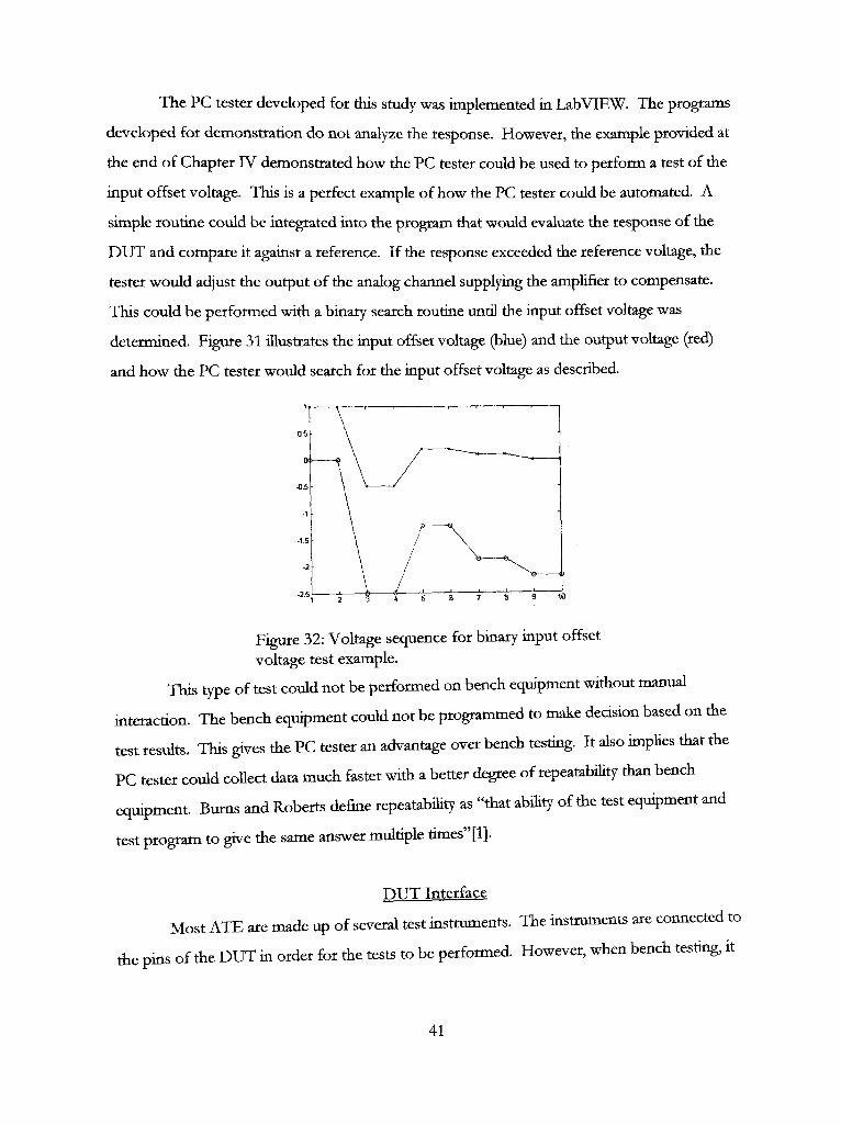
The PC tester developed for this stady was implemented in LabVIEW. The programs
developed for demonstration do not analyze the response. However, the example provided at
the end of Chapter IV demonstrated how the PC tester could be used to perform a test of the
input offset voltage. This is a perfect example of how the PC tester could be automated. A
simple routine could be integrated into the program that would evaluate the response of the
DUT and compare it against a reference. If the response exceeded the reference voltage, the
tester would adjust the output of the analog channel supplying the amplifier to compensate.
This could be performed with a binary search routine until the input offset voltage was
determined. Figure 31 ihustcates the input offset voltage (blue) and the output voltage (red)
and how the PC tester would search for the input offset voltage as described.
Figure 32: Voltage sequence for binary input offset
voltage test example.
This type of test could not be performed on bench equipment widiout manual
interaction. The bench equipment could not be programmed to make decision based on die
test results. This gives tiie PC tester an advantage over bench testing. It also impHes tiiat tiie
PC tester could coUect data much fester witii a better degree of repeatabiHty dian bench
equipment Bums and Roberts define repeatabiHty as "tiiat abiHty of die test equipment and
test program to give the same answer multiple times"[l].
DUT Interface
Most ATE are made up of several test instruments. Tlie instruments are connected to
die pins of die DUT in order for tiie tests to be performed. However, when bench testing, it
41

is tiie responsibOity of tiie user to make tiie physical comiections. The same is true of die PC
tester developed for dus stady. The connection board tiiat accompamed die DAQ suppHes
die leads for connecting to the DUTs.
It is conceivable, however, tiiat die PC tester could be outfitted witii die proper
equipment to automate die physical connections. Smce outfitting an ATE witii a test
instrument for every pin of die DUT is inconceivable, most ATE employ switching matrices.
A switching matrix is a matrix of switches to connect any test instrument in an ATE to any pin
on die DUT. Figure 32 shows how a switching matrix makes die connections.
RO
R1
R2
R3
UUT.'M
/ .^ .^ .^ \.& ^ d* O" vO' -S' s«> O J' / / /i rrrrrrrr
cO cl c2 c3 c4 c5 c6 c7 c9 c9 clO ell m H vuTfn
A- .^ J^ £l^ ^^ • ' ' ' • ' ^ / .* ,<• <y c" jJJ" <- < ^ t^
cO c1 c2 c3 c4 eS c6 e7 c8 cQ ;fO c(1
ft3s=
Figure 33: Switching matrix connection example.
There are many manufacturers of switching matrices since they are common in ATE.
Most of these commercial models are intended to accommodate 32 Hnes. Most ATE have
several of these matrices. If a switching matrix was incorporated into the PC tester, the tester
could make the interconnections between the DUT and the DAQ in the same manner an
ATE does.
42

Target Device Famihes
There are certain IC famihes that the PC test system is more suitably adapted to due to
die Hmitations Hnposed by LabVIEW, die DAQ, and the physical interface. Because of die
limited number of available channels the PC test system provides, famihes of chips with low
pin counts would be more appropriate. In addition, due to the inabihty of the PC tester to
provide large numbers of digital vectors without intermption, processor famihes should be
avoided. Most smaU-scale integration (SSI), medium-scale integration (MSI), and large-scale
integration (LSI) ICs are perfect for testing with the PC test system. However, very large-scale
integration (VLSI) and ultra large-scale integration (ULSI) IC are too complex and have too
many pins to easily be tested with the PC tester. However, within the SSI, MSI, and LSI
famihes, the PC tester would be perfect for performing simple tests such as characterization,
parametric, or even some functionaHty tests.
43

CHAPTER V
CONCLUSION
The PC test system developed for die stady proved a PC could provide die essential
capabiHties requked for performing IC testing relative to bench test equipment and ATE. The
final contribution can best be described as a consoHdation of test bench equipment into a
reconfigurable and programmable test system. The PC test system provided an example in
order to examine the advantages and disadvantages of using a PC rather than bench test
equipment or ATE. These tradeoffs are summarized in Table 6. However, the fiJI potential
of a PC for IC testing was not realized in the demonstration.
Table 6: PC Tester advantages and disadvantages.
PC Tester as Alternative to ATE Advantages Disadvantages
PC tester is fraction of the cost of commercial Loss of measurement accuracy. ATE.
PC tester can easily perform simple tests such PC tester cannot measure currents, suffers as characterization without extensive from a lower sampling rate, and generaHy has programming. a lower voltage ranges.
PC tester can be appHed to any type of PC tester incapable of reading test programs, process test such as characterization, parametric, or fimctional tests.
Loss of pattern depth and vector memory.
PC tester cannot support designs with large pin counts.
PC tester does not support data retention and data interpretation.
PC Tester as Alternative to Bench Equipment Advantages Disadvantages
PC tester is fraction of the cost of commercial Loss of measurement accuracy. ATE. Reconfigurable widiout physical PC tester cannot measure currents, suffers manipulation. &om a lower sampHng rate, and generaHy has
PC tester can easily coHect measurement data.
PC tester is an all-in-one system.
PC tester is programmable and therefore can be automated.
44

Furtiier Developrnf^nt;
The potential of tiie PC tester fat exceeds tiie capabiHties demonstrated in die test
system described m diis stady. Tliere are many capabiHties tiiat can easily be employed in
order to add ftmctionahty and diversity to die PC test system. Fkst, die system developed
lacks a mediod of data retention. The system is incapable of storing measurement results or
test settings. This could easily be implemented in die LabVIEW envkonment witii the file
manipulation routines akeady available. The results could be appended to a common test file,
or multiple results saved as separate files. Also, test settings could be saved for performing die
same test witii rekktiaHzkig die tester's settings. Widi tiiese capabiHties, die system could be
capable of data kiterpretation. This is anotiier feature die system lacks that is common in most
ATE. With the abiHty to puU cataloged data from test result files, many data interpretation
routines could be added to die system. LabVIEW makes statistical analysis sknple by
providing analysis routines such as histograms, distribution calculations, and process control.
Also, the PC test system currentiy does not provide means for test automation.
However, this could be incorporated several different ways. A script interpreter could be
programmed into the system. With a script editor, the test system could read a test script,
much like a test program for commercial ATE, and perform the tasks outlined in the script
Another method would be to tailor the test system program to perform only one test This is
a brute force method of automation, however it would be easy to implement with the bulk of
the program akeady written. For example, the system could be programmed to only perform
a continuity test This would mean adding a simple routine to read the test settings from a file,
initializing those settings, and then running the test sequence of forcing a current and
measuring the voltage produced.
Another feature that could easily be included in the PC test system that is not common
in ATE is virtaal testing. LabVIEW simulations of integrated ckcuits could be used in
conjunction with the current PC test system to perform virtual testing of ckcuit designs. As an
example. Figure 34 shows a LabVIEW simulation interface of a 555 timer ckcuit
45

lE-5 lE-4 1£.7 lE-4
lE-3^
lE-2-
l E - 1 '
lEtO
C J -lE-lD
IE-12
0.00 VCC
O.DO t lbrC
' /10.00
VI
•J!Q.CO
'10,0
D.DOO 0,200 D.f'oO 0,6CD 0.800 0,999 Time
V7, V6 Wavefiorm (Charge on C> 10.0-1
Q.Om 0.200 0.400 D.60D 0.800 0,999 Time
-10.0-• , 0.0)0 0.200 0.400 0.500 O.STO 0.999
Time
Figure 34: LabVIEW 555 IC sknulation kiterface.
Figure 35 shows the program behind the sknulation.
^!0D
(Output)!
^ :_?—#-
Mf"pfrx] nformatMnl k
ugu uuu u UUU'uannUaUUHU nap an f^ i fo..2] li-&flJl aHrtnnnnuuuHnnndmiomm
g;g[j>i|g E L ' ^ ^ S ^ ^ S
^O-JCtii @ EH
- - - = ^ 1
\----^ ©
j : i > z :
|>'a]l==va, VtD2-=Vl: Vffo' vBl -=B> JD~
k o l = = V l , Vm2==V8: Vffij'^ll
^rtol=^^^, VcQ2==VB: Vffa'=vffo|] ; - ^ ^ ^
k o i = = v i . Vca2=^V. Vflfa'=Vl|- r '• I [=>-.[«>-
^fca Vllb'=V1fel
-^:;i=>j
' r t H n f t i a H H h r l H h n n H n h r i t i r t h r l H r t f t h r t h n n a a D h h n r t r i n r i h n Q b H r t h f i a Q r t h r l r t f l
t=0=&>-S
Figure 35: LabVIEW 555 IC simulation program.
Only the basic operation of the ckcikt has been modeled. However, this model could
easily be incorporated into the PC test system. The PC test system is responsible for
generating voltages and currents and measuring voltages and currents. The inputs to the 555
46

sknulation are voltages appHed to die ICs pkis. This can be seen on die left side of Figure 35.
The response of die 555 simulation are die voltages which appear on die output pkis of tiie
IC. These are displayed ki die wmdows of Figure 34. The PC test system could be modified
to provide die stimulus to tiie simulation and tiien display the response. The results of die
sknulation could be compared to actual results obtained by performkig real tests on the actual
ckcuit using the same test system. This would aUow virtual and actual testing to be done on
the same platform.
Also, as mentioned before, if the PC test setap were adapted with a switching matrix,
the computer could control the physical connections to the DUT. Another possibiHty would
be to adapt the PC tester to a test head. This would allow the tester the abiHty to test die
before packaging or even wafers not ftdly processed.
With these additions, the PC test system would more resemble its multi-million doHar
counterpart, the ATE while maintaining the accuracy, diversity, and reconfigurable nature of
bench equipment. Table 7 summarizes the basic capabiHties and future capabiHties of the PC
test system.
47
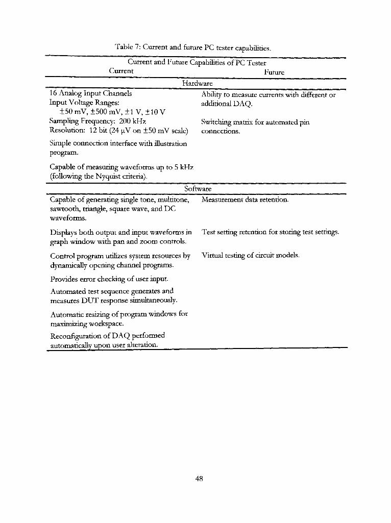
Table 7: Current and future PC tester capabiHties.
Current and Future CapabiHties of PC Tester Current Future
Hardware 16 Analog Input Channels Input Voltage Ranges:
±50 mV, ±500 mV, ±1 V, ±10 V Sampling Frequency: 200 kHz Resolution: 12 bit (24 ]xV on ±50 mV scale)
Simple coimection kiterface with iUustration program.
Capable of measuring waveforms up to 5 kHz (foUowing the Nyquist criteria).
Ability to measure currents with different or additional DAQ.
Switching matrix for automated pin connections.
Software
Capable of generating single tone, muititone, sawtooth, triangle, square wave, and DC waveforms.
Displays both output and input waveforms in graph window with pan and zoom controls.
Control program utilizes system resources by dynamicaUy opening channel programs.
Provides error checking of user input
Automated test sequence generates and measures DUT response simultaneously.
Automatic resizing of program windows for maximizing workspace.
Reconfiguration of DAQ performed automaticaHy upon user alteration.
Measurement data retention.
Test setting retention for storing test settings.
Virtual testing of ckcuit models.
48

BIBLIOGRAPHY
1 Bums, Mark, and Gordon W. Roberts. An Introduction to Mixed-Signal IC Test and Measurement. New York, NY: Oxford University Press, 2001.
2 BushneU, M. L., and V. D. Agrawal. Essentials of Electronic Testing For Digital. Memory, and Mbced-Signal VLSI Ckcuits. Boston, MA: Kluwer Academic PubHshers, 2000.
3 Cema, Michael, Mahesh L. Chugani, and Abhay R. Samant LabVIEW Signal Processing. Englewood CHffs, NJ: Prentice HaU PTR, 1998.
4 Chad Fasca and Dylan McGrath, "Virtual Test Comes of Age," Evaluating Engineenng, July 1998 [on-Hne press archive]; available from http: / /www.virtualtestcom: Internet; accessed June 2001.
5 Feugate, Jr., Robert J., and Steven M. Mclntyre. Introduction to VLSI Testing. Englewood CHffs, NJ: Prentice HaU, 1988.
6 Nat Reeves, "Using Virtual Testers for Test-Vector Verification," Evaluating Engineering, July 1998 [on-Hne magazine]; available from http://www.virtualtestcom: Internet; accessed June 2001.
7 Smith, Michael John Sebastian. AppHcation-Specific Integrated Ckcuits. Reading, MA: Addison Wesley Longman, Inc., 1997.
8 Steve Carison, "ATE Struggles To Keep Pace Witii VLSI," EE Times, 13 December 2001 [on-line magazine]; available from http://www.eetimes.com: Internet; accessed June 2001.
49

APPENDIX
INSTALLATION INSTRUCTIONS
AU programs are available on WebCT at http://www.ctee.ttaedu:8900. The files
should reside on the WebCT server as a compressed Windows .zip file caUed TestSystem.zip.
The .zip file can be downloaded and the contents extracted to a separate folder. Also, a self-
extracting executable file should be present incase the target computer lacks Windows .zip
tools. The self-executable should be caUed TestSystem.exe. The following files must be
downloaded and installed in the same program folder of a computer instaUed with LabVIEW
6i.
• TestSystem.vi
• Al.vi
• AI Refresh.vi
. AO.vi
• ConnBoard.vi
• ConnLedContvi
• EditMTone.vi
. LEDBank.vi
. ViewWaveform.vi
Once die files have been copied to die same folder, open tiie TestSystem.vi file tiirough eitiier
Wkidows Explorer or LabVIEW 6i from tiie file menu. Once opened, tiie program can be
run from tiie LabVIEW "Operate" menu.
50

CI-RMIS.SIONrO C(WY
In presenting this thesis in partial tiilfillmcnt of the requirements for a master's
degree at Texas Tech University or Texas Tech University Health Sciences Center, 1
agree that the Library and my major department shall make it freely avadable for
research purposes. Permission to copy this thesis for scholarly purposes may be
granted by the Director of the Library or my major professor. It is understood that
any copymg or publication of this thesis for financial gam shall not be allowed
without my further wntten permission and that any user may be liable for copyright
mfringement.
Agree (Permission is granted.)
Disagree (Pennission is not granted.)
Student Signature Date