phase change memory: an architecture and systems...
TRANSCRIPT
Phase Change MemoryAn Architecture and Systems Perspective
Benjamin C. LeeStanford University
Fall 2010, Assistant Professor @ Duke University
Benjamin C. Lee 1

Memory Scaling◦ ⇑ density, capacity; ⇓ cost-capability ratio
◦ Emerging challenges for prevalent technologies
“Process integration, devices, and structures,” ITRS 2009.
Benjamin C. Lee 2

Memory in Transition
• Charge Memory◦ Write data by capturing charge Q◦ Read data by detecting voltage V◦ Examples: Flash, DRAM
• Resistive Memory◦ Write data by pulsing current dQ/dt◦ Read data by detecting resistance R◦ Examples: PCM, STT-MRAM, memristor
Benjamin C. Lee 3

Limits of Charge Memory
◦ Difficult charge placement and control
◦ Flash: floating gate charge
◦ DRAM: capacitor charge, transistor leakage
Benjamin C. Lee 4

Towards Resistive Memory
• PCM◦ Inject current to change material phase◦ Resistance determined by phase
• STT-MRAM◦ Inject current to change magnet polarity◦ Resistance determined by polarity
• Memristors◦ Inject current to change atomic structure◦ Resistance determined by atom distn
Benjamin C. Lee 5

Benefits of Resistive Memory
• Scalable◦ Program cell with scalable current◦ Map resistance to logical state
• Non-Volatile◦ Alter structure of storage element◦ Incur activation cost to alter properties
• Competitive◦ Achieve viable latency, power, endurance◦ Scale to improve performance metrics
Benjamin C. Lee 6

TechnologyBenjamin Lee, Engin Ipek, Onur Mutlu, Doug Burger. “Architecting phase change
memory as a scalable DRAM alternative.” ISCA 2009.
Benjamin C. Lee 7
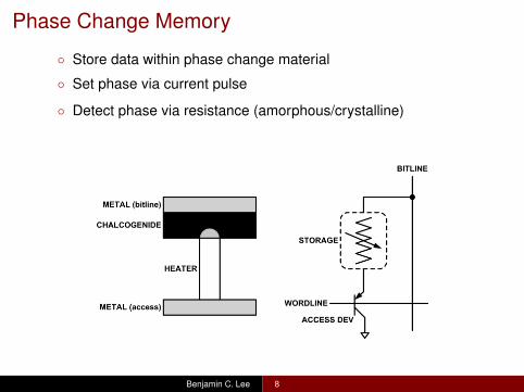
Phase Change Memory
◦ Store data within phase change material
◦ Set phase via current pulse
◦ Detect phase via resistance (amorphous/crystalline)
Benjamin C. Lee 8
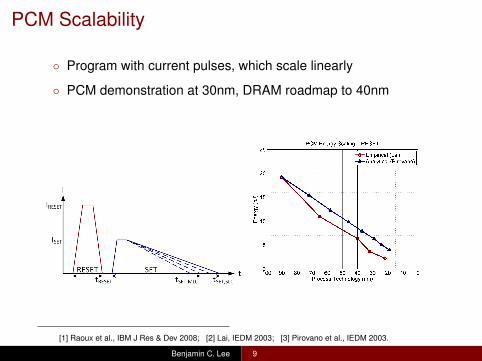
PCM Scalability
◦ Program with current pulses, which scale linearly
◦ PCM demonstration at 30nm, DRAM roadmap to 40nm
[1] Raoux et al., IBM J Res & Dev 2008; [2] Lai, IEDM 2003; [3] Pirovano et al., IEDM 2003.
Benjamin C. Lee 9

PCM Non-Volatility
• Joule Effect◦ Program with current pulses◦ Melt material by heating material (e.g., 650 ◦C)◦ Cool material to desired phase
• Activation Cost◦ Isolate thermal effects to target cell◦ Retain data for >10 years at 85 ◦C
Benjamin C. Lee 10

Technology Parameters
◦ Survey prototypes from 2003-2008 (ITRS, IEDM, VLSI, ISSCC)
◦ Derive PCM parameters for F=90nm
• Cell Size◦ 9-12F2 using BJT◦ 1.5× DRAM, 2-3× NAND
• Endurance◦ 108 writes per cell◦ 10−8× DRAM, 103× NAND
[1] Lee et al., ISCA 2009; [2] Russo, Workshop Emerging Memory Technologies 2010
Benjamin C. Lee 11

Technology Parameters
◦ Survey prototypes from 2003-2008 (ITRS, IEDM, VLSI, ISSCC)
◦ Derive PCM parameters for F=90nm
• Read Latency◦ 50 ns Rd◦ 4× DRAM, 10−3× NAND
• Write Bandwidth◦ 5-10 MB/s◦ 0.1× DRAM, 1.0× NAND
• Dynamic Energy◦ 40µA Rd, 150µA Wr◦ 2-43× DRAM, 1.0× NAND
[1] Lee et al. ISCA 2009; [2] Russo, Workshop Emerging Memory Technologies 2010
Benjamin C. Lee 12

PCM Comparison
• vs. Flash◦ Advantage in endurance, performance◦ Comparable in energy◦ Scalable Flash alternative
• vs. DRAM◦ Disadvantage in endurance, performance, energy◦ Within competitive range of DRAM◦ Scalable DRAM alternative
Benjamin C. Lee 13

PCM as DRAM Alternative
◦ Deploy PCM on memory bus
◦ Begin by co-locating PCM, DRAM
Benjamin C. Lee 14
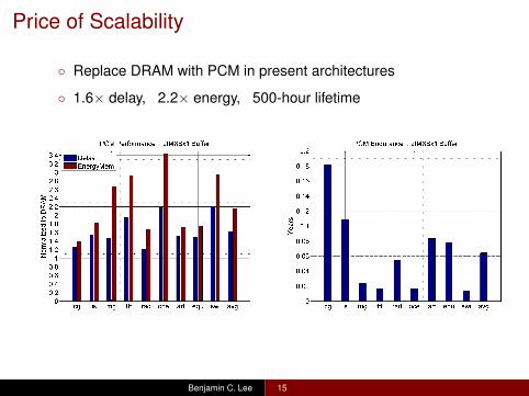
Price of Scalability
◦ Replace DRAM with PCM in present architectures
◦ 1.6× delay, 2.2× energy, 500-hour lifetime
Benjamin C. Lee 15

Architecture and ScalabilityBenjamin Lee, Engin Ipek, Onur Mutlu, Doug Burger. “Architecting phase change
memory as a scalable DRAM alternative.” ISCA 2009.
Benjamin C. Lee 16

Architecture Objectives
• DRAM-Competitive◦ Reorganize row buffer to mitigate delay, energy◦ Implement partial writes to mitigate wear mechanism
• Area-Efficient◦ Minimize disruption to density trends◦ Impacts row buffer organization
• Complexity-Effective◦ Encourage adoption with modest mechanisms◦ Impacts partial writes
Benjamin C. Lee 17

Buffer Organization
• On-Chip Buffers◦ Use DRAM-like buffer and interface◦ Evict modified rows into array
• Narrow Rows◦ Reduce write energy ∝ buffer width◦ Reduce peripheral circuitry, associated area
• Multiple Rows◦ Reduce eviction frequency◦ Improve locality, write coalescing
Benjamin C. Lee 18

Buffer Area Strategy
◦ Narrow rows :: fewer expensive S/A’s (44T)
◦ Multiple rows :: additional inexpensive latches (8T)
Benjamin C. Lee 19

Buffering and Locality
◦ Read locality: number of array reads
◦ Write coalescing: number of array writes per buffer write
Benjamin C. Lee 20

Buffer Design Space◦ Derive DRAM, PCM area model
◦ Explore space of area-neutral buffer designs
Benjamin C. Lee 21
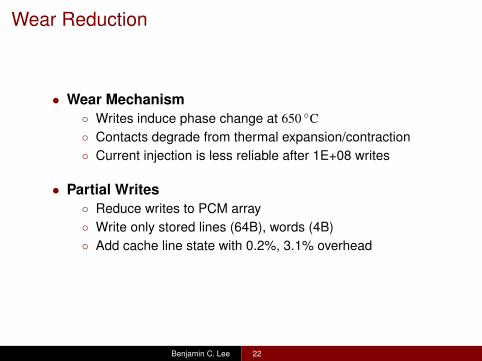
Wear Reduction
• Wear Mechanism◦ Writes induce phase change at 650 ◦C◦ Contacts degrade from thermal expansion/contraction◦ Current injection is less reliable after 1E+08 writes
• Partial Writes◦ Reduce writes to PCM array◦ Write only stored lines (64B), words (4B)◦ Add cache line state with 0.2%, 3.1% overhead
Benjamin C. Lee 22

Partial Writes◦ Derive PCM lifetime model
◦ Quantify eliminated writes during buffer eviction
Benjamin C. Lee 23

Scalable Performance
◦ 1.2× delay, 1.0× energy, 5.6-year lifetime
◦ Scaling improves energy, endurance
Benjamin C. Lee 24

Systems and Non-VolatilityJeremy Condit, Edmund Nightingale, Christopher Frost, Engin Ipek, Benjamin Lee,
Doug Burger, Derrick Coetzee. “Better I/O through byte-addressable, persistent
memory.” SOSP 2009.
Benjamin C. Lee 25

Storage Systems
◦ Persistent data in slow, non-volatile memory
◦ Buffered data in fast, volatile memory
Benjamin C. Lee 26

Storage System Trade-offs
• Design Objectives◦ Safety :: security against crashes◦ Consistency :: accurate description of file state◦ Performance :: buffering in volatile memory
• Byte-addressable Persistence (BPRAM)◦ Narrows gap between volatile/non-volatile memory◦ Byte-addressable like DRAM◦ Persistent like disk, Flash
Benjamin C. Lee 27

Byte-addressable Persistent File System (BPFS)
• Safety◦ Use PCM as DRAM alternative◦ Reflect writes to PCM in O(ms), not O(s)
• Consistency◦ Enforce atomicity, ordering in hardware◦ Support shadow paging, copy-on-write
• Performance◦ Exploit byte-addressability for small, in-place writes◦ Propose short-circuit shadow paging
Benjamin C. Lee 28

Tree-Based File System
Benjamin C. Lee 29

File System (FS) Consistency
• Computer Crash◦ Update to FS may require multiple writes◦ Crash between writes leaves FS invalid◦ State of files not as described by FS
• Consistency Checker◦ Traverse FS◦ Compares directory structure, data blocks◦ Depends on allocator, free-space manager
Benjamin C. Lee 30
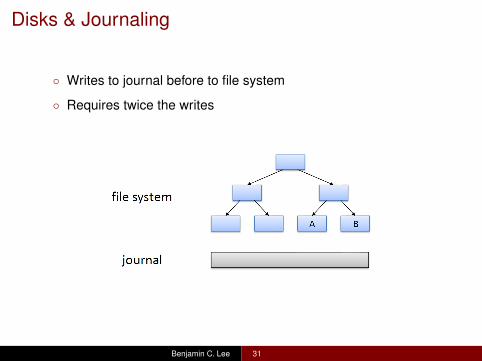
Disks & Journaling
◦ Writes to journal before to file system
◦ Requires twice the writes
Benjamin C. Lee 31

Disks & Journaling
◦ Writes to journal before to file system
◦ Requires twice the writes
Benjamin C. Lee 31

Disks & Journaling
◦ Writes to journal before to file system
◦ Requires twice the writes
Benjamin C. Lee 31

Disks & Shadow Paging
◦ Copy-on-writes up to file system root
◦ Incurs copying overhead
Benjamin C. Lee 32

Disks & Shadow Paging
◦ Copy-on-writes up to file system root
◦ Incurs copying overhead
Benjamin C. Lee 32

Disks & Shadow Paging
◦ Copy-on-writes up to file system root
◦ Incurs copying overhead
Benjamin C. Lee 32

PCM & Short-Circuit Shadow Paging (1)
◦ Exploit PCM byte-addressability
◦ Write in-place when possible (e.g., 64b updates)
◦ Ex: In-place write
Benjamin C. Lee 33

PCM & Short-Circuit Shadow Paging (2)
◦ Exploit PCM byte-addressability
◦ Write in-place when possible (e.g., 64b updates)
◦ Ex: In-place append
Benjamin C. Lee 34

PCM & Short-Circuit Shadow Paging (3)
◦ Exploit PCM byte-addressability
◦ Write in-place when possible (e.g., 64b updates)
◦ Ex: Partial copy-on-write
Benjamin C. Lee 35

Hardware Support for Atomicity
• Volatile Buffers◦ PCM row buffers are volatile 8T latches◦ BPFS updates 64b pointer to buffer◦ BPFS requires atomic 64b eviction to array
• Atomicity◦ PCM writes atomically into memory array◦ PCM writes complete in O(100ns)◦ Capacitors guard against power failures
Benjamin C. Lee 36

Hardware Support for Ordering
• Modern Performance Optimizations◦ Controller for write-back caches re-order stores◦ Controller for memory bus re-orders transactions
• Ordering◦ Epochs define barrier-delimited BPFS writes◦ Copy-on-write updates may be re-ordered◦ Pointer update must follow barrier
Benjamin C. Lee 37
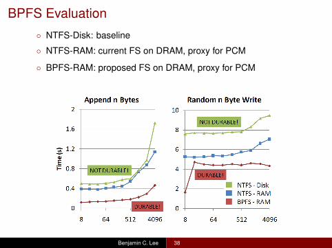
BPFS Evaluation
◦ NTFS-Disk: baseline
◦ NTFS-RAM: current FS on DRAM, proxy for PCM
◦ BPFS-RAM: proposed FS on DRAM, proxy for PCM
Benjamin C. Lee 38

BPFS Evaluation
◦ Safety: no DRAM buffer
◦ Consistency: shadow paging
◦ Performance: short-circuit shadow paging
Benjamin C. Lee 39

For more information...
• Workshop on Emerging Memory Technologies 2010◦ Survey of emerging memories◦ www.stanford.edu/∼bcclee/emt.html
• Phase Change Memory◦ Lee et al., “Architecting phase change memory as a
scalable DRAM alternative.” ISCA 2009.◦ Condit et al., “Better I/O through byte-addressable,
persistent memory.” SOSP 2009.
Benjamin C. Lee 40

Conclusions
• Scaling Challenges◦ Fundamental limits in charge memory◦ Transition towards resistive memory
• Architecture and Scalability◦ PCM position as Flash replacement◦ PCM viable as DRAM alternative◦ Architect buffers, partial writes
• Systems and Non-Volatility◦ Apply non-volatility for new capabilities◦ Change storage system trade-offs◦ Improve durability, performance
Benjamin C. Lee 41

Phase Change MemoryAn Architecture and Systems Perspective
Benjamin C. LeeStanford University
Fall 2010, Assistant Professor @ Duke University
Benjamin C. Lee 42