phase shift overlay iii (pso iii) - assets.new.siemens.comf7c524f8-ee2a-4... · siemens industry,...
TRANSCRIPT
$50.00
PRINTED IN U.S.A.
INSTALLATION & INSTRUCTION PHASE SHIFT OVERLAY III (PSO III) September 2002, Revised September 2014
DOCUMENT NO. SIG-00-00-19 VERSION A
Siemens Industry, Inc., Rail Automation 9568 Archibald Ave., Suite 100, Rancho Cucamonga, California 91730
1-800-793-7233 Copyright © 2014 Siemens Industry, Inc., Rail Automation All rights reserved

ii Document No.: SIG-00-00-19 September 2002, Revised September 2014 Version: A.1
PROPRIETARY INFORMATION Siemens Industry, Inc., Rail Automation (Siemens) has a proprietary interest in the information contained herein and, in some instances, has patent rights in the systems and components described. It is requested that you distribute this information only to those responsible people within your organization who have an official interest. This document, or the information disclosed herein, shall not be reproduced or transferred to other documents or used or disclosed for manufacturing or for any other purpose except as specifically authorized in writing by Siemens.
TRANSLATIONS
The manuals and product information of Siemens are intended to be produced and read in English. Any translation of the manuals and product information are unofficial and can be imprecise and inaccurate in whole or in part. Siemens does not warrant the accuracy, reliability, or timeliness of any information contained in any translation of manual or product information from its original official released version in English and shall not be liable for any losses caused by such reliance on the accuracy, reliability, or timeliness of such information. Any person or entity who relies on translated information does so at his or her own risk.
WARRANTY INFORMATION
Siemens Industry, Inc., Rail Automation warranty policy is as stated in the current Terms and Conditions of Sale document. Warranty adjustments will not be allowed for products or components which have been subjected to abuse, alteration, improper handling or installation, or which have not been operated in accordance with Seller's instructions. Alteration or removal of any serial number or identification mark voids the warranty.
SALES AND SERVICE LOCATIONS
Technical assistance and sales information on Siemens Industry, Inc., Rail Automation products may be obtained at the following locations:
Siemens Industry, Inc., Rail Automation Siemens Industry, Inc., Rail Automation 2400 NELSON MILLER PARKWAY 939 S. MAIN STREET LOUISVILLE, KENTUCKY 40223 MARION, KENTUCKY 42064 TELEPHONE: (502) 618-8800 TELEPHONE: (270) 918-7800 FAX: (502) 618-8810 CUSTOMER SERVICE: (800) 626-2710 SALES & SERVICE: (800) 626-2710 TECHNICAL SUPPORT: (800) 793-7233 WEB SITE: http://www.rail-automation.com/ FAX: (270) 918-7830
FCC RULES COMPLIANCE The equipment covered in this manual has been tested and found to comply with the limits for a Class A digital device, pursuant to part 15 of the FCC Rules. These limits are designed to provide reasonable protection against harmful interference when the equipment is operated in a commercial environment. This equipment generates, uses, and can radiate radio frequency energy and, if not installed and used in accordance with the instruction manual, may cause harmful interference to radio communications. Operation of this equipment in a residential area is likely to cause harmful interference in which case the user will be required to correct the interference at his/her own expense.

iii Document No.: SIG-00-00-19 September 2002, Revised September 2014 Version: A.1
DOCUMENT HISTORY Version Release
Date Sections Changed
Details of Change
A 1-23-01 Initial release (recalled because product not released. All manuals shipped following recall marked PRELIMINARY)
A 9-12-02 Re-release as version A with new date of September 2002 added WARNING to step 10 of para. 7.1 added CAUTION to para. 6.3 voltage changes in para. 7.1 added 90 Hz information for 7A417
A.1 9-4-14 Front matter only
Rebrand for Siemens

TABLE OF CONTENTS Section Title Page PROPRIETARY INFORMATION ....................................................................................... ii WARRANTY INFORMATION ........................................................................................... ii SALES AND SERVICE LOCATIONS ................................................................................. ii TABLE OF CONTENTS ...................................................................................................... iii LIST OF ILLUSTRATIONS ................................................................................................... vi LIST OF TABLES .................................................................................................................. vii NOTE, CAUTIONS AND WARNINGS ............................................................................ viii ELECTROSTATIC DISCHARGE (ESD) PRECAUTIONS ................................................ ix I INTRODUCTION ............................................................................................................... 1-1 1.0 SYSTEM OVERVIEW .................................................................................................. 1-1 1.0.1 Address Formats .......................................................................................... 1-1 1.0.2 PSO III Frequencies ..................................................................................... 1-4 1.0.3 PSO III Transmitter And Receiver Front Panel Connectors And Indicators ............................................................................................... 1-4 1.0.4 PSO III Accessories ...................................................................................... 1-5 1.1 USE OF PSO III WITH PSO II EQUIPMENT .......................................................... 1-6 1.2 PSO III TRANSMITTER AND RECEIVER SPECIFICATIONS .............................. 1-6 1.3 ORDERING INFORMATION ................................................................................... 1-7 II THEORY OF OPERATION ................................................................................................ 2-1 2.0 GENERAL .................................................................................................................... 2-1 2.1 TRANSMITTER ASSEMBLY (7A439, 7A451) ...................................................... 2-1 2.1.1 Circuit Description ...................................................................................... 2-1 2.1.2 Transmitter Harmonics .............................................................................. 2-3 2.1.3 Transmitter Strapping Options ................................................................. 2-3 2.2 RECEIVER ASSEMBLY (7A438, 7A453, part of 7A448) .................................... 2-3 2.2.1 Circuit Description ...................................................................................... 2-3 2.2.2 Frequency Response ................................................................................... 2-7 III APPLICATION GUIDELINES ............................................................................................ 3-1 3.0 GENERAL .................................................................................................................... 3-1 3.1 OPERATING DISTANCE ............................................................................................ 3-1 3.1.1 0.06-Ohm Shunting Sensitivity And No Impedance Bonds .............. 3-1 3.1.2 0.2-Ohm Shunting Sensitivity And No Impedance Bonds ................. 3-1 3.1.3 0.06-Ohm Shunting Sensitivity With Impedance Bonds .................... 3-1 3.1.4 0.2-Ohm Shunting Sensitivity With Impedance Bonds ...................... 3-2 3.2 RECOMMENDED USE OF FREQUENCIES ............................................................ 3-2 3.2.1 Non-Electrified Track ................................................................................... 3-2 3.2.2 Electrified Track ............................................................................................. 3-2
iii Document No.: SIG-00-00-19 Version: A
TABLE OF CONTENTS (continued) Section Title Page 3.3 FREQUENCY COMPATIBILITY GUIDELINES ........................................................ 3-3 3.4 PSO CAB SIGNAL FILTER, 7A417-X ...................................................................... 3-5 3.5 MULTIPLE-RECEIVER APPLICATIONS (0.06-Ω shunting sensitivity only) ... 3-6 3.6 TRANSMITTER LINE APPLICATIONS ................................................................... 3-6 3.7 RECEIVER LINE APPLICATIONS .............................................................................. 3-6 3.8 INSULATED JOINT BYPASS COUPLERS (non-electrified rail only) .............. 3-6 3.9 BATTERY CHOKE ...................................................................................................... 3-7 3.10 SURGE PROTECTION ............................................................................................ 3-7 3.11 USE OF PSO III WITH PSO II EQUIPMENT ........................................................ 3-7 3.12 PSO III MODULE FREQUENCY AND ADDRESS IDENTIFICATION .............. 3-7 IV PSO III CROSSING PACKAGE ......................................................................................... 4-1 4.0 PSO III CROSSING PACKAGE OVERVIEW .......................................................... 4-1 4.0.1 Crossing Package Address Formats ........................................................ 4-2 4.0.2 PSO III Crossing Package Front Panel Connectors And Indicators . 4-2 4.1 ISLAND CIRCUIT (INTELLIGENT PROCESSOR ISLAND (IPI), 62609) .......... 4-3 4.1.1 Island Circuit Operating Modes ................................................................ 4-3 4.1.2 IPI Module Controls & Indicators ............................................................. 4-4 4.1.2.1 STATUS (Relay Drive) Indicator .................................................... 4-4 4.1.2.2 ACTIVITY Indicator ........................................................................... 4-4 4.1.2.3 Alphanumeric Display ....................................................................... 4-4 4.1.2.4 Calibration Select Push Button ..................................................... 4-8 4.1.2.5 RS-232 Serial Port Connector ........................................................ 4-8 4.1.2.6 16-Position Header – Frequency Selection ............................... 4-8 4.1.2.7 16-Position Header – Pickup Delay Time Selection .................. 4-10 4.1.3 IPI Firmware Updates ................................................................................. 4-10 4.2 USING PSO III CROSSING PACKAGE EQUIPMENT WITH PSO II CROSSING SYSTEM ..................................................................................... 4-11 4.3 CROSSING PACKAGE SPECIFICATIONS ............................................................. 4-11 4.4 ORDERING INFORMATION ................................................................................... 4-12 V AUXILIARY EQUIPMENT ................................................................................................. 5-1 5.0 GENERAL .................................................................................................................... 5-1 5.1 BATTERY CHOKES 62648, 7A360 AND 8A065A ............................................. 5-1 5.2 TUNED RECEIVER COUPLERS, 7A355A-F AND 7A366-F ............................... 5-3 5.3 LINE-TO-RAIL/RAIL-TO-LINE COUPLERS, 7A377-1-F, 7A388, & 7A399-F . 5-4 5.4 LINE OVERLAY COUPLER, 7A403 .......................................................................... 5-6 5.5 BATTERY LINE FILTER, 7A418 ................................................................................ 5-7 5.6 TUNED INSULATED JOINT BYPASS COUPLER, 7A422-F ................................ 5-8 5.7 PSO CAB SIGNAL FILTER, 7A417-X ...................................................................... 5-9
iv Document No.: SIG-00-00-19 Version: A

TABLE OF CONTENTS (continued) Section Title Page VI INSTALLATION PROCEDURES ........................................................................................ 6-1 6.0 GENERAL REQUIREMENTS ..................................................................................... 6-1 6.1 WIRING .................................................................................................................... 6-1 6.1.1 AC Power ......................................................................................................... 6-1 6.1.2 Battery Wiring ................................................................................................ 6-1 6.1.3 Case Wiring ..................................................................................................... 6-1 6.1.4 Track Wiring ................................................................................................... 6-1 6.2 TRANSMITTER INSTALLATION .............................................................................. 6-3 6.3 RECEIVER INSTALLATION ....................................................................................... 6-5 6.4 CROSSING PACKAGE INSTALLATION ................................................................. 6-6 VII CHECKOUT AND ADJUSTMENT .................................................................................... 7-1 7.0 GENERAL .................................................................................................................... 7-1 7.1 PSO III RECEIVER ADJUSTMENT ............................................................................ 7-1 7.1.1 Receiver Adjustment For Line-To-Line Applications .......................... 7-4 7.2 IPI MODULE ISLAND CIRCUIT ADJUSTMENT .................................................... 7-4
♦ IPI FREQUENCY SELECTION ............................................................................ 7-5 ♦ IPI PICKUP DELAY TIME SELECTION .............................................................. 7-5 ♦ IPI TRACK CIRCUIT CALIBRATION ................................................................ 7-6
7.2.1 IPI Module Troubleshooting ...................................................................... 7-8 VIII DIAGRAMS .................................................................................................................... 8-1 INDEX ................................................................................................................. Index-1
v Document No.: SIG-00-00-19 Version: A

LIST OF ILLUSTRATIONS Figure No. Title Page 1-1 Phase Shift Overlay III Transmitter and Receiver ..................................................... 1-2 1-2 Phase Shift Overlay III Crossing Package, 7A448 .................................................... 1-3 2-1 Transmitter Assembly, 7A439, Block Diagram ........................................................ 2-2 2-2 Typical Transmitter Frequency-Modulated Output Waveform (4,000 Hz) ...... 2-4 2-3 Receiver Assembly, 7A438, Block Diagram .............................................................. 2-5 2-4 Typical Receiver Frequency Response Curves .......................................................... 2-7 3-1 PSO III And 3000 MS/GCP Frequency Compatibility .............................................. 3-5 3-2 Address Code and Bar Code (Frequency) Label Locations, 7A436 and 7A437 Modules ......................................................................................... 3-8 4-1 Phase Shift Overlay III Crossing Package, 7A488 ..................................................... 4-1 4-2 IPI Module Control And Indicator Locations ............................................................ 4-5 4-3 Jumper Positions On 16-Position Header ................................................................. 4-9 5-1 7A360 PSO Battery Choke With Mounting Dimensions ........................................ 5-2 5-2 62648/8A065A Battery Choke With Mounting Dimensions ................................. 5-3 5-3 Tuned Receiver Couplers, 7A355A-f and 7A366-f ................................................. 5-4 5-4 Receiver Line-To-Rail Coupler, 7A377-1-f ................................................................. 5-5 5-5 Typical of Line-To-Receiver Coupler, 7A388, and Transmitter Line-To-Rail Coupler, 7A399-f ............................................................. 5-5 5-6 PSO Line Overlay Coupler, 7A403 ................................................................................ 5-6 5-7 Battery Line Filter, 7A418, With Mounting Dimensions ........................................ 5-8 5-8 Tuned Insulated Joint Bypass Coupler, 7A422-f ....................................................... 5-9 5-9 PSO Cab Signal Filter, 7A417-X, With Mounting Dimensions .............................. 5-11 6-1 Typical PSO III Installation .............................................................................................. 6-2 6-2 Location of Transmitter Module Address and Frequency Labels ....................... 6-4 6-3 PSO III Transmitter Connections To Remote Keying Relay ................................... 6-4 6-4 Location of Receiver Module Address and Frequency Labels ............................. 6-5 7-1 AD Test Jack and Relay Drive Indicator Locations .................................................. 7-2 7-2 Gain Potentiometer Location On 7A436 Receiver Module .................................. 7-3 7-3 IPI Module Troubleshooting Chart .............................................................................. 7-8 8-1 PSO III Installation With Tuned Receiver Coupler, 7A355A-f ............................... 8-2 8-2 PSO III Installation With Tuned Receiver Coupler, 7A366-f ................................. 8-3 8-3 PSO III Installation With Receiver Line-to-Rail Coupler, 7A377-1-f, And Line-To-Receiver Coupler, 7A388 ............................................................... 8-4 8-4 PSO III Installation With Transmitter Line-to-Rail Coupler, 7A399-f .................. 8-5 8-5 Typical Installation of PSO III Crossing System With Island Circuit .................... 8-6 8-6 Insulated Joint Bypass Device, 7A422-f ....................................................................... 8-7 8-7 PSO Battery Choke, 7A360, 8A065A or 62648 ......................................................... 8-8 8-8 Typical PSO III Line Overlay Application .................................................................... 8-9
8-9 Typical Battery Charger Surge Protection ................................................................ 8-11 8-10 Typical Track Wire Surge Protection For Use In Electrified Territory ............... 8-12
vi Document No.: SIG-00-00-19 Version: A
LIST OF TABLES Table No. Title Page
1-1 PSO III Transmitter and Receiver Assembly Part Numbers ................................. 1-4 1-2 PSO III Transmitter Case Front Panel Connector Functions ................................. 1-5 1-3 PSO III Receiver Case Front Panel Connector And Indicator Functions ........... 1-5 1-4 PSO II and PSO III Transmitter and Receiver Module/Case Interchangeability 1-6 3-1 Maximum Operating Distances at Specific Ballast Resistances
(0.06-Ω shunting sensitivity) – No Impedance Bonds In Circuit ................. 3-2 3-2 PSO II And PSO III Module/Case Interchangeability ............................................... 3-8 4-1 PSO III Assembly Part Numbers .................................................................................... 4-2 4-2 PSO III Crossing Package Case Front Panel Connectors And Indicator Functions ........................................................................................................... 4-2 4-3 IPI Module Operating Modes ........................................................................................ 4-4 4-4 IPI Display Messages ....................................................................................................... 4-6 4-5 IPI Internal Failure Error Codes ................................................................................... 4-7 4-6 PSO II Crossing System and PSO III Crossing Package Module/Case Interchangeability ......................................................................................................... 4-11 7-1 Hardwire Shunt Placement Distances For Various Shunting Sensitivities And IPI Island Frequencies ............................................................................................. 7-6
vii Document No.: SIG-00-00-19 Version: A

NOTES, CAUTIONS, AND WARNINGS
Throughout this manual, notes, cautions, and warnings are frequently used to direct the reader’s attention to specific information. Use of the three terms is defined as follows:
NOTE
Generally used to highlight certain information relating to the topic under discussion.
CAUTION
REFERS TO PROPER PROCEDURES OR PRACTICES WHICH IF NOT STRICTLY OBSERVED, COULD RESULT IN A POTENTIALLY HAZARDOUS SITUATION AND/OR POSSIBLE DAMAGE TO EQUIPMENT. CAUTIONS TAKE PRECEDENCE OVER NOTES AND ALL OTHER INFORMATION, EXCEPT WARNINGS.
WARNING
INDICATES A POTENTIALLY HAZARDOUS SITUATION WHICH, IF NOT AVOIDED, COULD RESULT IN DEATH OR SERIOUS INJURY. WARN-INGS ALWAYS TAKE PRECEDENCE OVER NOTES, CAUTIONS, AND ALL OTHER INFORMATION.
If there are any questions, contact Safetran Application Engineering.
viii Document No.: SIG-00-00-19 Version: A

ELECTROSTATIC DISCHARGE (ESD) PRECAUTIONS Static electricity can damage electronic circuitry, particularly low voltage components such as the integrated circuits commonly used throughout the electronics industry. Therefore, procedures have been adopted industry-wide which make it possible to avoid the sometimes invisible damage caused by electrostatic discharge (ESD) during the handling, shipping, and storage of electronic modules and components. Safetran has instituted these practices at its manufacturing facility and encourages its customers to adopt them as well to lessen the likelihood of equipment damage in the field due to ESD. Some of the basic protective practices include the following: • Ground yourself before touching card cages, assemblies, modules, or components. • Remove power from card cages and assemblies before removing or installing modules. • Remove circuit boards (modules) from card cages by the ejector lever only. If an ejector lever
is not provided, grasp the edge of the circuit board but avoid touching circuit traces or components.
• Handle circuit boards by the edges only. • Never physically touch circuit board or connector contact fingers or allow these fingers to
come in contact with an insulator (e.g., plastic, rubber, etc.). • When not in use, place circuit boards in approved static-shielding bags, contact fingers first.
Remove circuit boards from static-shielding bags by grasping the ejector lever or the edge of the board only. Each bag should include a caution label on the outside indicating static-sensitive contents.
• Cover workbench surfaces used for repair of electronic equipment with static dissipative
workbench matting. • Use integrated circuit extractor/inserter tools designed to remove and install electrostatic-
sensitive integrated circuit devices such as PROM’s (OK Industries, Inc., Model EX-2 Extractor and Model MOS-40 Inserter (or equivalent) are highly recommended).
• Utilize only anti-static cushioning material in equipment shipping and storage containers. For information concerning ESD material applications, please contact the Safetran California Division Technical Support Staff in Rancho Cucamonga, California. ESD Awareness Classes and additional ESD product information are also available through the Technical Support Staff.
ix Document No.: SIG-00-00-19 Version: A

INTRODUCTION
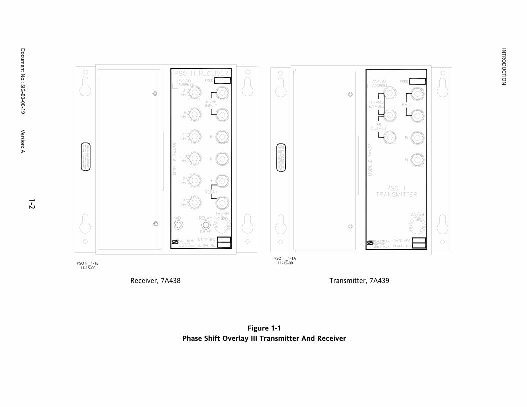
SECTION I INTRODUCTION 1.0 SYSTEM OVERVIEW The Phase Shift Overlay III (PSO III) track circuit manufactured by Safetran Systems Corporation™, Cucamonga, California, is used to supply track occupancy information for crossing warning devices, as well as other train or vehicle detection systems. The PSO III is a reliable and secure solid-state vital system that is sufficiently versatile to permit use in a wide variety of complex installations. The PSO III is available in two configurations; ‘standard’ and Crossing Package. The 'standard' configuration (figure 1-1) consists of separate transmitter and receiver assemblies. Each of these assemblies contains a single printed circuit module. The transmitter assembly sends a coded, 8-bit address through the rails using an audio frequency signal as a carrier. The modulated signal is detected by the receiver assembly where it is decoded and processed. The receiver responds only to signals of the proper frequency, modulation rate, address, and amplitude. The ability of PSO III to differentiate between its operating signal and all other signals present on the track is due to the non-symmetrical coded modulation and receiver decoding techniques which ensure that the system is immune to random or foreign AM, FM, and beat signals. The Crossing Package (figure 1-2) includes two receiver modules and a combination transmitter/ receiver island circuit module (62609) in a single case. The Crossing Package receiver modules are identical to those used in the 'standard' receiver assemblies. The island module used in the Crossing Package is Safetran’s Intelligent Processor Island (IPI) module. See Section IV for further information on the Crossing Package. 1.0.1 Address Formats The PSO III is available in either of two address formats (“A” or “C”). The “A” address format is standard and is intended for most PSO III applications. Unless specified otherwise at the time an order is placed for the PSO III, the “A” address is provided. The “C” address format is intended for use in applications involving a high-density mix of frequencies and multiple tracks. PSO III transmitter and receiver cases and modules are assigned specific part numbers according to the address format used. Refer to table 1-1 for part number assignments. Both cases and modules are also marked with decals that identify the address format used (e.g., “A ADDR” or “C ADDR”). The decals are located adjacent to the assembly part number on the cases and adjacent to the module part number on the component side of the transmitter and receiver printed circuit modules.
1-1 Document No.: SIG-00-00-19 Version: A
INTRO
DU
CTION
Receiver, 7A438 Transmitter, 7A439
Figure 1-1 Phase Shift Overlay III Transmitter And Receiver
PSO III_1-1A
11-15-00
PSO III_1-1B11-15-00
1-2 D
ocument N
o.: SIG-00-00-19 Version: A

INTRO
DU
CTION
Figure 1-2 Phase Shift Overlay III Crossing Package, 7A448
PSOIII_XING1-9-01
1-3 D
ocument N
o.: SIG-00-00-19 Version: A

INTRODUCTION
The PSO III transmitter and receiver modules designed for “C” address operation only are electrically keyed to permit operation only in the “C” address cases. The same is true for the “A” address modules and cases. In addition, “C” address transmitter and receiver modules are further identified by blue ejector levers which are stamped with the assembly part number.
Table 1-1 PSO III Transmitter and Receiver Assembly Part Numbers
Assembly Assembly
(Case) Part Number
Module Installed
Module Installed
A Address C Address Transmitter (“A” address) 7A439 7A437 Transmitter (“C” address) 7A451 7A437-2 Receiver (“A” address) 7A438 7A436 Receiver (“C” address) 7A453 7A436-2
Except for minor differences to provide specific address operation, the “C” address transmitter assembly is identical to the “A” address transmitter and the “C” address receiver assembly is identical to the “A” address receiver. 1.0.2 PSO III Frequencies A wide variety of carrier frequencies are available for the PSO III. For use in non-electrified territory, 16 PSO III carrier frequencies, ranging from 156 Hz to 4,000 Hz, are available with the 'standard' PSO III and the Crossing Package. For electrified territory, 10 frequencies are available ranging from 645 Hz to 4000 Hz. Ten island frequencies are available for the Crossing Package and range from 4.9 kHz to 20.2 kHz. For installations where multiple circuits are required on the same track, the PSO III has two sets of eight frequencies (two sets of five for electrified territory) each that can be connected as required with negligible interference.
NOTE The 62609 island module provides jumper positions for selecting the island frequencies 4.00, 3.24, 2.63 and 2.14 kHz. However, these frequencies are not used in PSO III applications
1.0.3 PSO III Transmitter And Receiver Front Panel Connectors And Indicators Tables 1-2 and 1-3 describe the functions of each of the front panel mounted connectors and indicators on the PSO III Transmitter and Receiver cases. Refer to figure 1-1 for connector and indicator locations.
1-4 Document No.: SIG-00-00-19 Version: A

INTRODUCTION
Table 1-2 PSO III Transmitter Case Front Panel Connector Functions
Front Panel Nomenclature Description Function
B AREMA binding post Positive battery connection N AREMA binding post Negative battery connection
RAIL AREMA binding posts Track wire connections TRANS ENABLE AREMA binding posts Strap these terminals to enable continuous transmitter
operation HI OUTPUT AREMA binding posts Strap these terminals to enable high power operation
2A/SB Fuse holder 2-ampere slow blow fuse for positive battery input
Table 1-3 PSO III Receiver Case Front Panel Connector And Indicator Functions
Front Panel Nomenclature Description Function
B AREMA binding post Positive battery connection N AREMA binding post Negative battery connection
RCVR INPUT AREMA binding posts Receiver input connections from track via an external coupling device such as a 7A355A Tuned Receiver Coupler
RELAY +/- AREMA binding posts Output to polar track relay 0dB, -6dB, -12dB, -18dB, -24dB, -30dB
AREMA binding posts Receiver sensitivity strapping terminals --- one end of strap always connected to –30dB terminal.
AD Test Jack Amplitude detector test jack used during receiver adjustment procedure
RELAY DRIVE LED Relay drive indicator that lights when PSO Receiver RELAY output is energized
1A/SB Fuse holder 1-ampere slow blow fuse for positive battery input 1.0.4 PSO III Accessories A variety of accessory equipment is available for use with the PSO III. Where it is desirable to have the transmitter and receiver at the same location, rail-to-line and line-to-rail couplers are available to enable signals to be transmitted or received over lines. Accessory equipment is also available for specialized applications such as preventing the loading effects of track batteries and bypassing PSO III signals around insulated joints at selected locations.
WARNING
THE BYPASSING OF INSULATED JOINTS IN ELECTRIFIED TERRITORY IS NOT RECOMMENDED.
The PSO III is compatible with other Safetran equipment including motion sensors, grade crossing predictors, pulse-modulated track circuits, etc.
1-5 Document No.: SIG-00-00-19 Version: A

INTRODUCTION
1.1 USE OF PSO III WITH PSO II EQUIPMENT The PSO III receiver and transmitter units are compatible with the signal format and track levels of Safetran’s PSO II receiver and transmitter units using the same address format. This means that a PSO III transmitter is capable of driving a track circuit containing a PSO II receiver, and that a PSO III receiver is capable of receiving and decoding a signal emanating from a PSO II transmitter. PSO III transmitter and receiver modules may also be used in the earlier PSO II cases with the same address format. However, the PSO III cases are electrically keyed to prevent the use of the PSO II modules in the newer PSO III cases. Table 1-4 indicates PSO III and PSO II interchangeability; that is, which modules will operate in each transmitter and receiver case. For example, the 7A400 PSO II transmitter case accepts either a PSO II (7A411) or PSO III (7A437) transmitter module.
Table 1-4 PSO II And PSO III Transmitter and Receiver Module/Case Interchangeability
System Address Format
Module Type
Module Part
Number
Assemblies (Cases) PSO II PSO III
A Address C Address A Address C Address 7A400 7A405 7A420 7A425 7A438 7A439 7A451 7A453
PSO II A Address
Receiver 7A416 X Transmitter 7A411 X
C Address Receiver 7A416-2 X Transmitter 7A411-2 X
PSO III A Address
Receiver 7A436 X X Transmitter 7A437 X X
C Address Receiver 7A436-2 X X Transmitter 7A437-2 X X
1.2 PSO III TRANSMITTER AND RECEIVER SPECIFICATIONS PSO III Frequencies Available: 156 Hz 645 Hz 2,140 Hz
NOTE
Frequencies enclosed by dotted line are recommended for use in electrified territory
211 Hz 790 Hz 2,630 Hz 285 Hz 970 Hz 3,240 Hz 348 Hz 1,180 Hz 4,000 Hz 430 Hz 1,450 Hz 525 Hz 1,770 Hz
Frequency Stability: 0.1% (Hz) Modulation: Phase Modulation with 8-bit serial address Transmitter Output Impedance: 2 Ω (nominal) Receiver Sensitivity: 10 mV rms (minimum) at receiver input terminals Receiver Selectivity: 60 dB down on adjacent channels
1-6 Document No.: SIG-00-00-19 Version: A

INTRODUCTION
Specifications (Continued)
Receiver Input Impedance: With 7A355 Coupler – With 7A366 Coupler -
Low impedance High impedance
Surge Protection: Secondary protection built-in, Primary protection
required on all external lines Relay Coil Resistance: 400 to 1,000 Ω Environmental Range (Temperature): -40 °F to +160 °F (-40 °C to +71 °C) Input Voltage: 9.0 to 16.5 VDC (all units) Input Current:
Transmitter, 7A439/7A451 (low power) Transmitter, 7A439/7A451 (high power)
Receiver, 7A438/7A453
350 mA nominal 600 mA nominal 400 mA nominal
Dimensions:
Transmitter and Receiver
8.75 inches high (22.23 centimeters) 8.25 inches wide (20.96 centimeters) 9.50 inches deep (24.13 centimeters)
Shipping Weight:
Transmitter and Receiver
5 pounds (each) (2.27 kilograms) 1.3 ORDERING INFORMATION
Unit Description Address Format Part Number PSO III Transmitter “A” address 7A439-f PSO III Receiver “A” address 7A438-f PSO III Crossing Package with island “A” address 7A448-f1-f2-IPI PSO III Transmitter “C” address 7A451-f PSO III Receiver “C” address 7A453-f PSO III Crossing Package with island “C” address 7A455-f1-f2-IPI
f = Selected from list of available frequencies f1 = Frequency of receiver number 1 f2 = Frequency of receiver number 2 IPI = IPI Island Module included
1-7 Document No.: SIG-00-00-19 Version: A

INTRODUCTION
1-8 Document No.: SIG-00-00-19 Version: A
This page intentionally left blank

THEORY OF OPERATION
2-1 Document No.: SIG-00-00-19 Version: A
SECTION II
THEORY OF OPERATION 2.0 GENERAL The PSO III System consists of a transmitter connected to the track at one location, and a receiver (which is coupled to the track through a tuned receiver coupling unit) at a remote location. The receiver operates the track relay which supplies track occupancy information. A separate island circuit is provided by the 62509 module in the Crossing Package which is described in Section IV. 2.1 TRANSMITTER ASSEMBLY (7A439, 7A451) All major circuits of the transmitter assembly are contained on Transmitter Module, 7A437 (A address) or 7A437-2 (C address). External connections are accomplished via standard AREMA binding posts mounted on the transmitter case. 2.1.1 Circuit Description Figure 2-1 is a simplified block diagram illustrating signal flow through the transmitter circuits. A high-frequency signal (between 1 and 2 MHz) is generated by a crystal-controlled oscillator. The signal is fed to circuits that comprise a divider and a digital frequency modulator. These circuits process the signal as follows: a counter stage produces an output that is 128 times that of the basic lower PSO III transmitted frequency. The signal is routed to a second counter stage which supplies an input to separate divide-by-62 and divide-by-64 counters. When the enable input from the code generator is applied to the modulator circuit, the divide-by-62 counter produces a corresponding output that is applied to one input of a two-input NAND gate. The other input to the NAND gate is the slightly lower frequency produced by the divide-by-64 counter. The resulting output from the NAND gate corresponds to the divide-by-64 counter output, unless the enable signal is present from the code generator. A second counter stage continues to count the divided basic frequency until a reset pulse is received from the NAND gate, at which time the counter is reset and a count from zero is initiated. A toggle flip-flop changes state each time a reset pulse is applied to the second counter, resulting in an output signal which is one-half the reset frequency. Therefore, the output produced by the flip-flop is at the frequency produced by the first counter stage divided by 124 or 128, depending upon the state of the enable signal from the code generator. The code generator produces a single bit of the address signal for every 32 cycles of the input signal. The enable signal is an 8-bit code which controls the divide-by-62 counter. Therefore, the enable signal modulates the transmitted output frequency with the proper address sequence.

THEORY OF OPERATION
2-2 Document No.: SIG-00-00-19 Version: A
Figu
re 2
-1
Tran
smitt
er A
ssem
bly,
7A4
39, B
lock
Dia
gram
Cry
stal
Osc
illato
rD
ivid
erf xt
al /1
28D
igita
l Fre
quen
cyM
odul
ator
Nar
row
band
Filte
rf ou
t
+5
+12
RA
IL
HI O
UTP
UT
+5 V
olt R
egul
ator
B N
+5
PS
O II
I2-1
11-1
7-00
Pow
er A
mpl
ifier
Cod
e G
ener
ator
+5
A C
Buf
fer
Sur
geP
rote
ctio
n
+12
+5+5
+5
+5
TRA
NS
EN
AB
LE

THEORY OF OPERATION
2-3 Document No.: SIG-00-00-19 Version: A
The output from the digital frequency modulator passes through a narrow-band filter on its way to the power amplifier. The narrow-band filter is a parallel resonant circuit with a Q of about 25 in the collector circuit of a gain-limited transistor amplifier. The inductive element is a pot core that is tuned with two parallel capacitors. The filtered signal is then applied through an opto-coupler to a flip-flop that provides square-wave drive to the power amplifier. The power amplifier stage conditions and shapes the signal received from the narrow-band filter. The amplifier output is coupled through an impedance-matching transformer and output filters to the track. The filters remove the higher harmonics from the power amplifier output signal ensuring that a clean spectrum is applied to the track (see figure 2-2). The high filter impedance at frequencies other than the signal frequency serve to minimize loading of other circuits on the track. 2.1.2 Transmitter Harmonics The harmonic content of the PSO III output waveform is minimized by the tuned output circuits used in the transmitter. The values shown below indicate the harmonic levels in a typical PSO III output waveform as it appears on the track. Any harmonics not listed are more than -60 dB below the fundamental PSO III transmitter signal.
Harmonic Level Second -60 dB Third -30 dB
Fourth -46 dB Fifth -60 dB
2.1.3 Transmitter Strapping Options AREMA binding posts on the transmitter case front panel provide two strapping options. By strapping the TRANS ENABLE terminals, continuous low-power operation is enabled. Higher output power can be obtained by strapping both the HI OUTPUT and the TRANS ENABLE terminals. With either strapping option installed, the transmitter can be controlled remotely by switching the power off and on at the front panel B and N terminals via an external relay. 2.2 RECEIVER ASSEMBLY (7A438, 7A453, part of 7A448) All major circuits of the receiver assembly are contained on Receiver Module, 7A436 (A address) or 7A436-2 (C address). External connections are accomplished via standard AREMA binding posts mounted on the receiver case. 2.2.1 Circuit Description The block diagram for the receiver assembly is shown in figure 2-3. The following discription generally follows the signal flow from receiver input (RCVR INPUT) to relay output (RELAY).

THEORY OF OPERATION
Figure 2-2
Typical Transmitter Frequency-Modulated Output Waveform (4,000 Hz)
2-4 Document No.: SIG-00-00-19 Version: A

THEORY O
F OPERATIO
N
Figure 2-3 Receiver Assembly, 7A438, Block Diagram
Input Attenuator(on backplane
PCB)
Bandpass Filter
Unity VoltageGain Amplifier
Unity VoltageGain Amplifier
RCVRINPUT
FixedThreshold
Comparator
DigitalDiscriminator Local Oscillator
True Decoder
ComplementDecoder
ChargePump
ChargePump
Vcc
V5A
V5BDiscrete
Set/ResetFlip-flop
S
R
Q
~Q
Unity VoltageGain Amplifier
-8 Vdc
Vital Level Detector(Zener controlled
oscillator)
0 to 10 Vdc referenced to +12
PowerAmplifier
+8
RELAY
+8
+8
SurgeProtection
B
N
+8 voltregulator
+5 voltregulator
+5 voltregulator
+5 voltregulator
Vcc
V5A
V5B
+8
PSO III2-312-05-00
GainAdjust
+
-
VoltageGain Amplifier
+8
VccVcc
+8
+8
+8
+12
2-5 D
ocument N
o.: SIG-00-00-19 Version: A

THEORY OF OPERATION
An input attenuator on the backplane circuit board provides up to 30 dB of attenuation for the input signal in 6-dB steps. These steps provide a coarse adjustment for setting the track circuit shunting performance. The input signal is then applied to a four-pole bandpass filter that provides at least 60 dB of attenuation at the nearest adjacent channel. The filter also provides a passive voltage gain by transforming its relatively low input impedance to a higher output impedance. The filter output is applied to a unity voltage gain amplifier. Voltage gain is provided passively by a coupling transformer to the following unity gain amplifier. A 6 dB variable gain control is provided to allow fine adjustment of the track circuit. A discrete operational audio amplifier provides additional voltage gain. The amplified signal is then applied to two different signal-processing channels. One channel verifies that the received signal amplitude is sufficient to allow the relay output to be energized. The second channel decodes the signal to vitally verify that it contains the correct code pattern. The outputs of these two channels are then vitally 'ANDed' to produce a DC relay-drive output. In the first channel, a charge pump (voltage doubler) rectifies the audio frequency signal to obtain a DC voltage proportional to the signal amplitude. This DC voltage is referenced to the +12 volt DC power rail; therefore, when present, it must be higher than the highest DC power supply voltage. A vital level detector (also referenced to the +12 volt DC rail) checks the amplitude of the proportional DC voltage. It produces a 5 kHz sine wave output when the charge pump output exceeds about 5 volts. The 5 kHz sine wave is then buffered with a unity gain amplifier before being applied to the relay output power amplifier. In the second channel, a fixed threshold comparator squares up the sine wave audio signal. The threshold of this comparator is at about the same level as that required to trigger the vital level detector in the first channel. Hence, both channels require about the same signal level to produce an output. The squared-up signal is applied to a digital discriminator that recovers the code pattern imposed on the signal by frequency modulation. A crystal clock at 16 times the nominal signal frequency is necessary for the discriminator to demodulate the signal. However, the comparator and discriminator are not vital. They merely produce a string of pulses that is applied to a vital decoding circuit. The decoding circuit checks whether the string of pulses has the correct timing and pattern. The decoder is dual channel. One channel operates on a true representation of the pulse string while the second channel operates on an inverted or complemented representation. The code is an eight-bit word with a specific value. Both outputs must operate correctly in order to toggle the set/reset flip-flop that combines the decoder outputs. The flip-flop toggles at the frame rate of the modulated signal and produces a square wave output at half the frame rate. Another charge pump rectifies the square wave and produces a DC voltage that is negative with respect to the power supply common rail. This is the only negative polarity DC voltage on the
2-6 Document No.: SIG-00-00-19 Version: A

THEORY OF OPERATION
circuit board. It supplies DC power to the relay output power amplifier. Recall that the input to the power amplifier is a 5 kHz sine wave generated by the vital level detector. Hence, the power amplifier cannot produce an output unless it has both a sine-wave input signal (from the channel that vitally verifies input signal amplitude) and a negative DC voltage (from the channel that vitally decodes the bit pattern imposed on the signal by frequency modulation). If either condition is not true, then no relay drive voltage is produced. The power amplifier output is transformer-coupled (for DC isolation) to a half-wave rectifier and capacitive filter. The filtered DC output is then available to drive a vital relay. The +12 volt power input is surge protected and filtered. It is regulated to +8 volts DC to provide power for most of the receiver analog circuits. Separate +5 volt DC regulators are provided for the dual channel decoders. 2.2.2 Frequency Response Typical PSO III receiver frequency response curves are shown in figure 2-4. The PSO III transmitter frequency varies less than 0.1 percent with temperature changes.
Figure 2-4
Typical Receiver Frequency Response Curves
2-7 Document No.: SIG-00-00-19 Version: A

THEORY OF OPERATION
2-8 Document No.: SIG-00-00-19 Version: A
This page intentionally left blank

APPLICATION GUIDELINES
SECTION III
APPLICATION GUIDELINES 3.0 GENERAL Application of PSO III track circuits should conform to the guidelines found in this section to ensure proper operation and trouble-free performance. Guidelines are provided for electrified and/or light rail operations as well as heavy rail applications. For special applications requiring additional information, contact Safetran™ Applications Engineering. 3.1 OPERATING DISTANCE The operating distance at any PSO III operating frequency depends on the shunting sensitivity used, the ballast resistance encountered at the installation site and whether impedance bonds for electrified track are installed. Various combinations of these factors are addressed in the following paragraphs. 3.1.1 0.06-Ohm Shunting Sensitivity And No Impedance Bonds Table 3-1 indicates the recommended maximum PSO III operating distances at each operating frequency under the following conditions:
• Ballast resistance values of 2 ohms per 1,000 feet and 4 ohms per 1,000 feet • Shunting sensitivity of 0.06 ohm • No impedance bonds in the circuit
Distances specified are between the transmitter and receiver for end-fed track circuits. Maximum eceiver-to-receiver distances for center-fed track circuits are found by doubling listed distances. r
.1.2 0.2-Ohm Shunting Sensitivity And No Impedance Bonds 3
Maximum PSO III operating distance with 0.2-ohm shunting sensitivity and no impedance bonds in the circuit is 75% of the operating distance in table 3-1 for each frequency based on 2 ohms per 1000 feet of ballast resistance.
.1.3 0.06-Ohm Shunting Sensitivity With Impedance Bonds 3
The maximum PSO III operating distance with 0.06-ohm shunting sensitivity and with impedance bonds in the circuit is 3000 feet based on ballast resistance of 2 ohms per 1000 feet. Useable PSO III frequencies are 645 through 4000 Hz.
3-1 Document No.: SIG-00-00-19 Version: A

APPLICATION GUIDELINES
Table 3-1 Maximum Operating Distances at Specific Ballast
Resistances (0.06-ohm shunting sensitivity) – No Impedance Bonds In Circuit Frequency Bal Ft.
(HZ) last Resistance 2 Ω/1,000 Bal Ft. last Resistance 4 Ω/1,000 Operating Distance (Ft.) Operating Distance (Ft.)
156 211 285 348 430 525 645 790 970
1,180 1,450 1,770 2,140 2,630 3,240 4,000 2,000 2,800
9,000 7,900 6,900 6,300 5,800 5,300 4,700 4,300 3,900 3,700 3,300 3,000 2,600 2,400 2,100
12,500 11,100 9,800 9,000 8,000 7,400 6,600 6,100 5,500 5,200 4,600 4,200 3,800 3,300 3,000
3.1.4 0.2-Ohm Shunting Sensitivity With Impedance Bonds
ohms per 1000 feet. Usable PSO III equencies under these conditions are 645 through 4000 Hz.
.2 RECOMMENDED USE OF FREQUENCIES
.2.1 Non-Electrified Track
III operating frequencies (156 through 4000 Hz) are available for use on non-electrified ack.
.2.2 Electrified Track
SO III operating frequencies 645 through 4000 Hz should be used on electrified track.
.3 FREQUENCY COMPATIBILITY GUIDELINES
The maximum PSO III operating distance with 0.2-ohm shunting sensitivity, with impedance bonds in the circuit, is 2000 feet based on ballast resistance of 2 fr 3 3 All PSOtr 3 P 3
3-2 Document No.: SIG-00-00-19 Version: A

APPLICATION GUIDELINES
1. Frequency Groups:
es to two groups with one channel separation between frequencies in each group as follows:
) Non-Electrified Track Frequency Groups
dividing the 16 PSO III frequencies into two groups of eight frequencies each as follows:
Group 1 (Hz) Group 2 (Hz)
As a general rule, avoid using adjacent channel frequencies on the same track except as described in the NOTE below. This is generally accomplished by separating the frequenciin a
One channel separation between frequencies is provided by
156 211 285 348 430 525 645 790 970 1,180
1,450 1,770 2,140 2,630 3,240 4,000
b) Electrified Track Frequency Groups
SO III frequencies for electrified track into two groups of five frequencies each as follows:
Group 1 (Hz) Group 2 (Hz)
One channel separation between frequencies is provided by dividing the 10 P
645 790 970 1,180
1,450 1,770 2,140 2,630 3,240 4,000
NOTE
III circuits are separated by a minimum of 1000 feet.
All frequencies within a group are compatible and may be intermixed without restriction on the same rails without insulated joint separation. Also, when all available frequencies have been used, adjacent frequencies can be intermixed provided the PSO
3-3 Document No.: SIG-00-00-19 Version: A

APPLICATION GUIDELINES
2. For PSO’s with like addresses ("A" or "C"), frequencies can be repeated on the same track when separated by at least 10,000 feet and one set of non-bypassed insulated joints (no type of insulated joint couplers used around the insulated joints).
3. Identical frequencies may be used on either side of non-bypassed insulated joints (end-to-end
track circuits) provided different address codes are used. 4. For PSO’s with like addresses ("A" or "C"), frequencies can be repeated without restriction on
the same track when separated by two sets of non-bypassed insulated joints providing each set of insulated joints is separated by a minimum of 3,000 feet.
5. Multiple track territory frequency assignments must follow a pattern that avoids using the
same frequency on adjacent tracks. Since it is not possible to meet this requirement in three- and four-track territory with available PSO III frequencies, the address coding scheme described in number 3 above (end-to-end track circuits) can be employed here as well. Each track uses a separate frequency with alternating track circuits assigned different address codes and separated by a set of non-bypassed insulated joints. The transmitter and receiver modules are stamped A ADD or C ADD (see paragraph 3.12).
NOTE
Unless otherwise specified, only “A” address transmitters and receivers are supplied.
6. Multiple track highway crossing approaches can use group 1 frequencies on one track (track
number 1) and group 2 frequencies on the other track (track number 2). Since two fre-quencies from each group are required at each crossing, when all frequencies have been used, the same frequencies may be repeated but this time using the group 2 frequencies on track number 1 and the group 1 frequencies on track number 2. Continue to alternate this pattern as required. For further details contact Safetran™ Application Engineering.
7. The IPI track circuit frequencies used in the Crossing Package and the PSO III frequencies are
compatible with the exception of the four lowest IPI frequencies (4.00, 3.24, 2.63 and 2.14 kHz). These four IPI frequencies are generally not used in PSO III applications since they are duplicates of PSO III operating frequencies.
8. Impedance bonds used in electric propulsion territory should provide a minimum of 2 ohms of
impedance at all PSO III frequencies in operation.
WARNING
USE OF INSULATED JOINT BYPASS COUPLERS ON ELECTRIFIED TRACK IS NOT RECOMMENDED
3-4 Document No.: SIG-00-00-19 Version: A

APPLICATION GUIDELINES
9. PSO III and 3000 MS/GCP frequency compatibility (see figure 3-1).
Figure 3-1
PSO III And 3000 MS/GCP Frequency Compatibility 3.4 PSO CAB SIGNAL FILTER, 7A417-X PSO Cab Signal Filter, 7A417-X, is designed for use in territory where 60, 90, 100, or 200-Hz cab signal is used. The filter should be installed on the primary side of the track transformer as shown below. See Section V for further information.
3-5 Document No.: SIG-00-00-19 Version: A

APPLICATION GUIDELINES
3.5 MULTIPLE-RECEIVER APPLICATIONS (0.06-OHM SHUNTING SENSITIVITY ONLY) A maximum of three receivers may be used on either side of a transmitter. When multiple receivers are used with a single transmitter, High Impedance Tuned Receiver Couplers, 7A366-f, must be used with the receiver(s) located nearest the transmitter. The receivers which are located farthest from the transmitter should use Tuned Receiver Couplers, 7A355A-f. When center-fed receivers are used, the receiver nearest the transmitter that is equipped with a 7A355A-f coupler must be no closer than 500 feet from the transmitter. See figure 8-2 for a typical application. 3.6 TRANSMITTER LINE APPLICATIONS When it is desirable to transmit signals over dedicated line wire or buried cable to the track, a PSO Line Coupler, 7A388, must be used to couple the transmitter to the line and a Transmitter Line-to-Rail Coupler, 7A399-f, must be used to couple the line to the rail (see figure 8-4). 3.7 RECEIVER LINE APPLICATIONS When open line or cable carries the signal from the rail to a distant receiver, Receiver Line-to-Rail Coupler, 7A377-f, is required to couple the track to the line and a PSO line coupler (7A388) is used to couple the line to the receiver. Total resistance of the line or cable pair must not exceed 100 ohms (see figure 8-3). 3.8 INSULATED JOINT BYPASS COUPLERS (NON-ELECTRIFIED RAIL ONLY) Two types of insulated joint bypass couplers are used with PSO III:
1) Tuned Insulated Joint Bypass Coupler, 7A422-f, is used with PSO circuits (see figure 8-6). 2) Wideband Shunt, 8A076A, is acceptable for PSO operation when GCP’s are being bypassed
around insulated joints with wideband shunts.
WARNING WHEN GRADE CROSSING PREDICTOR (GCP) OR MOTION SENSOR FREQUENCIES ARE ALSO BYPASSED AROUND INSULATED JOINTS, ALONG WITH PSO III FREQUENCIES, ALWAYS FOLLOW THE INSTRUCTIONS GOVERNING THE GCP OR MOTION SENSOR INSTALLATION.
When using the 7A422-f coupler, insulated joint coupler connections should be made with number 9 AWG or larger copper wire and each wire should not exceed 100 feet in length. However, the shorter the wire length and the larger the wire size, the less PSO signal loss will occur at each insulated joint. For applications requiring coupler connections exceeding 100 feet in length, use number 6 AWG copper wire.
3-6 Document No.: SIG-00-00-19 Version: A

APPLICATION GUIDELINES
3.9 BATTERY CHOKE When the PSO III track circuit includes a track battery, or a track battery is located within 500 feet of a PSO III track circuit that is not isolated by insulated joints, PSO Battery Choke, 7A360, is con-nected in series with the track battery. When GCP's or motion sensors are installed within PSO III circuits, Battery Choke, 8A065A, or Battery Choke, 62648, must be used in place of the 7A360 battery choke (see figure 8-7).
WARNING
IF A BATTERY CHOKE IS INSTALLED WITHIN A MODEL 300 OR 400 GCP APPROACH, THE 8A065A CHOKE MUST BE USED.
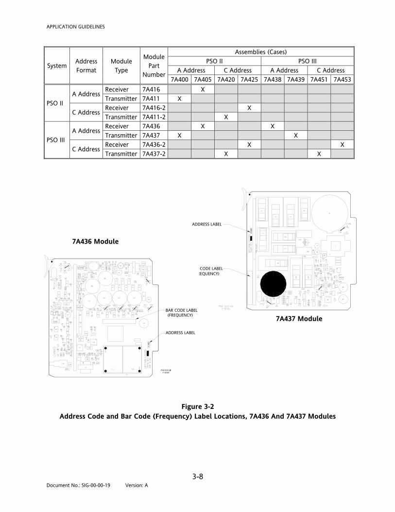
3.10 SURGE PROTECTION The PSO III incorporates built-in surge protection. However, primary surge protection must be installed on all AC power, battery, line, and track leads (see figure 8-9). In electrified territory, protection must be installed on track leads as shown in figure 8-10. 3.11 USE OF PSO III WITH PSO II EQUIPMENT The PSO III receiver and transmitter units are compatible with the signal format and track levels of Safetran’s PSO II receiver and transmitter units using the same address format. This means that a PSO III transmitter is capable of driving a track circuit containing a PSO II receiver, and that a PSO III receiver is capable of receiving and decoding a signal emanating from a PSO II transmitter. PSO III transmitter and receiver modules may also be used in the earlier PSO II cases with the same address format. However, the PSO III cases are electrically keyed to prevent the use of the PSO II modules in the newer PSO III cases. Table 3-2 indicates PSO III and PSO II interchangeability; that is, which modules will operate in each transmitter and receiver case. For example, the 7A400 PSO II transmitter case accepts either a PSO II (7A411) or PSO III (7A437) transmitter module. 3.12 PSO III MODULE FREQUENCY AND ADDRESS IDENTIFICATION PSO III module operating frequencies are indicated on the bar code label affixed to the component side of each module. The frequency is identified by the last four digits of the 13-digit module EDP part number (e.g., 7000-7A436-0790 is a 790 Hz receiver module). The module address format is indicated on a label located adjacent to the module part number. See figure 3-2 for bar code (frequency) and address label locations.
Table 3-2 PSO II And PSO III Module/Case Interchangeability
3-7 Document No.: SIG-00-00-19 Version: A
APPLICATION GUIDELINES
3-8 Document No.: SIG-00-00-19 Version: A
System Address Format
Module Type
Module Part
Number
Assemblies (Cases) PSO II PSO III
A Address C Address A Address C Address 7A400 7A405 7A420 7A425 7A438 7A439 7A451 7A453
PSO II A Address
Receiver 7A416 X Transmitter 7A411 X
C Address Receiver 7A416-2 X Transmitter 7A411-2 X
PSO III A Address
Receiver 7A436 X X Transmitter 7A437 X X
C Address Receiver 7A436-2 X X Transmitter 7A437-2 X X
Figure 3-2 Address Code and Bar Code (Frequency) Label Locations, 7A436 And 7A437 Modules
7A437 Module
ADDRESS LABEL
A AD
D
BAR CODE LABEL(FREQUENCY)
7A436 Module
BAR CODE LABEL
ADDRESS LABEL
A AD
D
(FREQUENCY)
PSO III3-2B1-10-01

PSO III CROSSING PACKAGE
SECTION IV
PSO III CROSSING PACKAGE 4.0 PSO III CROSSING PACKAGE OVERVIEW The PSO III Crossing Package (figure 4-1) includes two receiver modules and a combination transmitter/ receiver island circuit module (62609) in a single case. The Crossing Package receiver modules are identical to those used in the ‘standard’ PSO III receiver assemblies and are described in Sections I and II. The island module used in the Crossing Package is Safetran’s Intelligent Processor Island (IPI) module. The IPI module enables the system to supply a limited distance, frequency-shift-modulated, audio frequency track circuit with an effective range of up to 500 feet. While designated primarily for use as the island track circuit at highway crossings, the Crossing Package satisfies any application requiring a short, high-definition, audio frequency track circuit. See figure 8-5 for a typical PSO III Crossing Package installation.
Figure 4-1 Phase Shift Overlay III Crossing Package, 7A448
PSOIII_XING1-9-01
4-1 Document No.: SIG-00-00-19 Version: A

PSO III CROSSING PACKAGE
4.0.1 Crossing Package Address Formats The Crossing Package is available in either of two address formats (“A” or “C”). The “A” address format (part number 7A448) is standard and is intended for most PSO III Crossing Package applications. Unless specified otherwise at the time an order is placed for the Crossing Package, the “A” address is provided. The “C” address format (part number 7A455) is intended for use in applications involving a high-density mix of frequencies and multiple tracks. Except for minor differences to provide specific address operation, the “C” address units are identical to the “A” address units. The Crossing Package cases and receiver modules are assigned specific part numbers according to the address format used. Refer to table 4-1 for part number assignments. Both cases and modules are also marked with decals that identify the address format used (e.g., “A ADDR” or “C ADDR”). The decals are located adjacent to the assembly part number on the cases and adjacent to the module part number on the component side of the receiver printed circuit modules.
Table 4-1 PSO III Assembly Part Numbers
Assembly Assembly
(Case) Part Number
“A” Address “C” Address Island
Module Receiver Modules Installed
Receiver Modules Installed
Crossing Package (“A” address) 7A448 7A436 62609 Crossing Package (“C” address) 7A455 7A436-2 62609
4.0.2 PSO III Crossing Package Front Panel Connectors And Indicators Table 4-2 describes the functions of each of the front panel mounted connectors and indicators on the PSO III Crossing Package case. Refer to figure 4-1 for connector and indicator locations.
Table 4-2 PSO III Crossing Package Case Front Panel Connector And Indicator Functions
Front Panel Nomenclature Description Function
B AREMA binding post Positive battery connection N AREMA binding post Negative battery connection
ISL XMT AREMA binding posts Island module transmitter output terminals WEST PSO RLY
+/- AREMA binding posts West receiver (receiver #1) output to West polar track
relay WEST PSO RCV AREMA binding posts West receiver (receiver #1) input connections from
track via an external coupling device such as a 7A355A Tuned Receiver Coupler
Continued on next page
4-2 Document No.: SIG-00-00-19 Version: A

PSO III CROSSING PACKAGE
Table 4-2 (concluded) TB1 (0dB, -6dB, -12dB, -18dB, -24dB, -30Db)
Terminal strip West receiver (receiver #1) sensitivity strapping terminals -- one end of strap always connected to –30dB terminal
AD1 Test Jack Amplitude detector test jack used during West receiver (receiver #1) adjustment procedure
DS1 LED Relay drive indicator that lights when West receiver (receiver #1) PSO RLY output is energized
ISL RCV AREMA binding posts Island module receiver input terminals ISL RLY +/- AREMA binding posts Output to polar island (crossing) relay
EAST PSO RLY +/-
AREMA binding posts East receiver (receiver #2) output to East polar track relay
EAST PSO RCV AREMA binding posts East receiver (receiver #2) input connections from track via an external coupling device such as a 7A355A Tuned Receiver Coupler
TB2 (0dB, -6dB, -12dB, -18dB, -24dB, -30Db)
Terminal strip East receiver (receiver #2) sensitivity strapping terminals -- one end of strap always connected to –30dB terminal
AD2 Test Jack Amplitude detector test jack used during East receiver (receiver #2) adjustment procedure
DS2 LED Relay drive indicator that lights when East receiver (receiver #2) PSO RLY output is energized
2A/SB Fuse holder 2-ampere slow blow fuse for positive battery input 4.1 ISLAND CIRCUIT (INTELLIGENT PROCESSOR ISLAND (IPI), 62609) The Intelligent Processor Island (IPI) is a single-board, microprocessor-based, multi-frequency, modulated, short-range track occupancy detector. It is frequency programmable via an on-board jumper and provides a simple automated process for calibration of the track circuit. An on-board four-character alphanumeric display indicates the selected operating frequency plus calibration process status and diagnostic troubleshooting codes. The IPI is designed to detect poor shunting conditions in the IPI track circuit. If poor shunting is detected, the IPI initiates an internal loss-of-shunt timer that prevents relay drive from energizing during the poor-shunting episode. 4.1.1 Island Circuit Operating Modes The IPI module operating modes are identified in table 4-3.
4-3 Document No.: SIG-00-00-19 Version: A
PSO III CROSSING PACKAGE
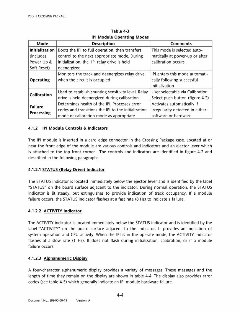
Table 4-3 IPI Module Operating Modes
Mode Description Comments Initialization (includes Power Up & Soft Reset)
Boots the IPI to full operation, then transfers control to the next appropriate mode. During initialization, the IPI relay drive is held deenergized
This mode is selected auto-matically at power-up or after calibration occurs
Operating Monitors the track and deenergizes relay drive when the circuit is occupied
IPI enters this mode automati-cally following successful initialization
Calibration Used to establish shunting sensitivity level. Relay drive is held deenergized during calibration
User selectable via Calibration Select push button (figure 4-2)
Failure Processing
Determines health of the IPI. Processes error codes and transitions the IPI to the initialization mode or calibration mode as appropriate
Activates automatically if irregularity detected in either software or hardware
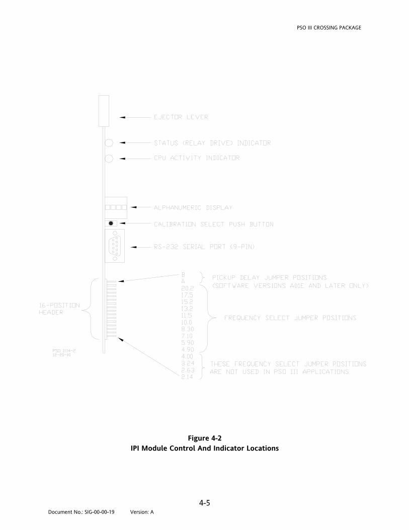
4.1.2 IPI Module Controls & Indicators The IPI module is inserted in a card edge connector in the Crossing Package case. Located at or near the front edge of the module are various controls and indicators and an ejector lever which is attached to the top front corner. The controls and indicators are identified in figure 4-2 and described in the following paragraphs. 4.1.2.1 STATUS (Relay Drive) Indicator The STATUS indicator is located immediately below the ejector lever and is identified by the label “STATUS” on the board surface adjacent to the indicator. During normal operation, the STATUS indicator is lit steady, but extinguishes to provide indication of track occupancy. If a module failure occurs, the STATUS indicator flashes at a fast rate (8 Hz) to indicate a failure. 4.1.2.2 ACTIVITY Indicator The ACTIVITY indicator is located immediately below the STATUS indicator and is identified by the label “ACTIVITY” on the board surface adjacent to the indicator. It provides an indication of system operation and CPU activity. When the IPI is in the operate mode, the ACTIVITY indicator flashes at a slow rate (1 Hz). It does not flash during initialization, calibration, or if a module failure occurs. 4.1.2.3 Alphanumeric Display A four-character alphanumeric display provides a variety of messages. These messages and the length of time they remain on the display are shown in table 4-4. The display also provides error codes (see table 4-5) which generally indicate an IPI module hardware failure.
4-4 Document No.: SIG-00-00-19 Version: A
PSO III CROSSING PACKAGE
Figure 4-2 IPI Module Control And Indicator Locations
4-5 Document No.: SIG-00-00-19 Version: A

PSO III CROSSING PACKAGE
Table 4-4 IPI Display Messages
Message(s) Displayed Length Of Time Message(s) Displayed
Comments
BOOT ………………………………
9 seconds Appears when IPI is powered up, at the end of the automated calibration process, and after any IPI errors are corrected
Software version display … Example: A01E
5 seconds Appears once the BOOT process is complete
REL (release) ……………………
2 seconds
Appears after calibration select push button is pressed and held for 2 seconds to initiate automated calibration
CAL* …………………………………
4 seconds
Appears during automated calibration NOTE
The asterisk symbol (*) in the CAL*
message is actually a rotating bar that indicates calibration in progress.
DONE ………………………………. Momentary Appears momentarily at the end of the calibration process indicating that calibration is complete. The IPI then starts the BOOT process
ARMD (armed) ……………….
2 seconds Appears while the IPI is initiating the calibration process. It appears following REL on the display once the calibration select push button is released, and indicates that the automated calibration process is armed or ready to be started
Actual operating frequency ………………………… example: 10.0 Pickup Delay Time Setting . example: PU+4 (example indicates pickup delay of 4 seconds)
For software level A01D and earlier: Frequency only displayed indefinitely For software level A01E and later: Frequency alternates with pickup delay time. Frequency displayed for 8 seconds, then pickup delay setting for 2 seconds
Appears and remains on the display following successful completion of the IPI calibration, and indicates that the IPI is operational (no internal problems) and ready for in-service operation
WARNING
THE IPI MUST ALWAYS BE RECALIBRATED FOR THE CROSSING IT CONTROLS PRIOR TO PLACING IT IN
SERVICE.
Continued on next page
4-6 Document No.: SIG-00-00-19 Version: A

PSO III CROSSING PACKAGE
Table 4-4 (concluded)
Message(s) Displayed Length Of Time
Message(s) Displayed Comments
FAIL ………………………………….
Remains until calibration select push button is pressed and cali-bration tried again
Appears if automated calibration process does not run to completion. Calibration should be retried if FAIL appears.
CALR ……………………………..…
Flashes intermittently
Appears if frequency jumper has been moved to a new frequency selection on 16-position header, but the IPI has not been recalibrated for the new frequency.
FRQ? ………………………………..
Flashes intermittently This indicates that the frequency selection jumper has come off or that there is more than one frequency selected on the 16-position header.
SIG (signature) …………………
Momentary A status message that appears whenever on-frequency interference is sufficiently high to prevent the IPI modulation signature signal from being decoded on the IPI module.
LOS ………………………………….. Approximately 10 seconds
Appears whenever the IPI detects a loss of train shunting in the island.
Table 4-5
IPI Internal Failure Error Codes Error Code Error Description Action Indicated BATT Battery voltage out of range Check battery condition CALC Calibration parameters are
corrupted. Try recalibration. If the problem persists, replace the IPI module.
CRIT Critical check failure If the problem persists, replace the IPI module. GB Guard Band failure If the problem persists, replace the IPI module. HWSW Hardware/Software
incompatibility. If the problem persists, replace the IPI module.
IRO Island Relay Output failure If the problem persists, replace the IPI module. ISRX Interrupt Service Routine
failure If the problem persists, replace the IPI module.
PHLT Programmed Halt If the problem persists, replace the IPI module. PIRO Primary Island Relay Output
waveform failure If the problem persists, replace the IPI module.
Continued on next page
4-7 Document No.: SIG-00-00-19 Version: A

PSO III CROSSING PACKAGE
Table 4-5 (concluded) Error Code Error Description Action Indicated PS_I Intermediate power supply
output incorrect If the problem persists, replace the IPI module.
PS5A 5-volt analog supply output incorrect
If the problem persists, replace the IPI module.
PS5D 5-volt digital supply output incorrect
If the problem persists, replace the IPI module.
PS25 Internal reference supply voltage incorrect
If the problem persists, replace the IPI module.
RAM RAM failure If the problem persists, replace the IPI module. ROM ROM failure If the problem persists, replace the IPI module. SIRO Secondary Island Relay Output
waveform failure If the problem persists, replace the IPI module.
STKG Guardband error If the problem persists, replace the IPI module. STKP Stack Pointer has exceeded its
limits If the problem persists, replace the IPI module.
TIME Time comparisons failure If the problem persists, replace the IPI module. XCPT Exception failure
If the problem persists, replace the IPI module.
PASS All internal errors have been corrected
none
4.1.2.4 Calibration Select Push Button The push-button switch located immediately below the alphanumeric display is used in conjunction with the display to initiate IPI calibration. 4.1.2.5 RS-232 Serial Port Connector The 9-pin, female, D-type connector, located immediately below the calibration select push button, provides the RS-232 serial interface for downloading a new software revision from a PC to the IPI. 4.1.2.6 16-Position Header - Frequency Selection The 16-position header located below the RS-232 serial port permits selection of the IPI frequency (see figure 4-3). Each of the lower 14 header positions corresponds to a different IPI operating frequency and consists of a pair of pins. Frequency selection is made by placing a jumper (shorting block) across the appropriate pair of pins. If the shorting block is moved to a new frequency select position, the operating frequency of the IPI does not change until the IPI is recalibrated (CALR appears on the display to indicate that calibration is required).
4-8 Document No.: SIG-00-00-19 Version: A

PSO III CROSSING PACKAGE
Each IPI module is furnished with one shorting block for frequency selection. Placement of the frequency select shorting block is generally done at the time of calibration. Header positions for frequency selection are labeled on the board surface adjacent to the header and are identified on figure 4-3. All indicated frequencies are in kilohertz (kHz).
NOTE The lower four IPI frequencies (2.14, 2.63, 3.24 and 4.00 kHz) are not used for PSO III applications.
Figure 4-3
Jumper Positions On 16-Position Header
4-9 Document No.: SIG-00-00-19 Version: A

PSO III CROSSING PACKAGE
4.1.2.7 16-Position Header - Pickup Delay Time Selection (software level A01E and later only) On IPI modules running software version A01E or later, positions A and B of the 16-position header permit selection of additional pickup delay time if required (see Section VII). Each IPI module is furnished with two shorting blocks for pickup delay selection (figure 4-3). Following any change of the pickup delay jumper(s), the IPI must be recalibrated in order to store the new pickup delay time value and make it active. The pickup delay time setting appears on the IPI display alternating with the frequency display. The frequency is displayed for 8 seconds followed by the pickup delay time for 2 seconds. The format of the pickup delay time display is as follows:
Pickup Delay Time IPI Display No delay PU+0 2-seconds PU+2 4-seconds PU+4 6-seconds PU+6
The pickup delay feature is not available on IPI modules running software version A01D or earlier (software version identified on IPI display for approximately 5 seconds at power up). Therefore, positions A and B are not used with the earlier software.
NOTE Only one frequency selection jumper is allowed. A missing frequency jumper, or two or more frequency jumpers, render an invalid selection.
NOTE Modules running IPI software version A01E and later are supplied with two pickup delay time selection jumpers.
4.1.3 IPI Firmware Updates The operating program for the IPI module is contained in a flash memory device located on the module. When revisions to the operating program are issued by Safetran Systems Corporation™, the flash device firmware is updated by simply downloading the new program from a PC to the IPI via the RS-232 serial port (see paragraph 4.1.2.5). Instructions for installing new software will be provided by Safetran™ when a new software revision level is issued.
4-10 Document No.: SIG-00-00-19 Version: A

PSO III CROSSING PACKAGE
4.2 USING PSO III CROSSING PACKAGE EQUIPMENT WITH PSO II CROSSING SYSTEM The PSO III Crossing Package is compatible with the signal format and track levels of Safetran’s PSO II crossing system using the same address format. This means that a PSO III transmitter is capable of driving a crossing system containing a PSO II receiver, and that a PSO III receiver in the Crossing Package is capable of receiving and decoding a signal emanating from a PSO II transmitter. PSO III receiver modules may also be used in the earlier PSO II crossing system cases with the same address format. However, the PSO III Crossing Package cases are electrically keyed to prevent the use of the PSO II modules in the newer PSO III cases. Island modules used in the PSO II and PSO III units are interchangeable. However, the 62509 island module used in the PSO II crossing system is frequency specific. Table 4-6 indicates PSO III Crossing Package and PSO II crossing system interchangeability.
Table 4-6 PSO II Crossing System And PSO III Crossing Package Module/Case Interchangeability
System Address Format
Module Type
Module Part
Number
Assemblies (Cases) PSO II
Crossing System PSO III
Crossing Package A Address C Address A Address C Address
7A408 7A428 7A448 7A455
PSO II A Address Receiver 7A416 X C Address Receiver 7A416-2 X
Island 62509 X X X X
PSO III A Address Receiver 7A436 X X C Address Receiver 7A436-2 X X
Island 62609 X X X X 4.3 CROSSING PACKAGE SPECIFICATIONS Input Power: Voltage Current
9-16.5 VDC 1.3 A (nominal)
Transmitter Output Current: 0.2 ampere (maximum) Microprocessor: Motorola 68332 Relay Drive Output: 400 to 1000-ohm load
4-11 Document No.: SIG-00-00-19 Version: A

PSO III CROSSING PACKAGE
4-12 Document No.: SIG-00-00-19 Version: A
Specifications continued Island Frequencies: 4.9 kHz 10.0 kHz 17.5 kHz 5.9 kHz 11.5 kHz 20.2 kHz 7.1 kHz 13.2 kHz 8.3 kHz 15.2 kHz NOTE
The 62609 island module provides jumper positions for selecting the island frequencies 4.00, 3.24, 2.63 and 2.14 kHz. However, these frequencies are not used in PSO III applications.
Track Circuit Length: Determined by track wire connections (50 – 500 ft.) Surge Protection: Secondary protection built-in, Primary protection
required on all external lines Environmental (Temperature): -40 °F to +160 °F (-40 °C to +71 °C) Island Pickup Delay Time: Field programmable - 0, 2, 4, 6 seconds (IPI software
version A01E and later only) Dimensions:
11 inches high (27.94 centimeters) 14.38 inches wide (36.52 centimeters) 9.50 inches deep (24.13 centimeters)
Shipping Weight: 16 pounds (7.26 kilograms)
4.4 ORDERING INFORMATION
Unit Description Address Format Part Number PSO III Crossing Package with island “A” address 7A448-f1-f2-IPI PSO III Crossing Package with island “C” address 7A455-f1-f2-IPI
f1 = Frequency of receiver number 1 f2 = Frequency of receiver number 2 IPI = IPI Island Module included

AUXILIARY EQUIPMENT
5-1 Document No.: SIG-00-00-19 Version: A
SECTION V
AUXILIARY EQUIPMENT 5.0 GENERAL The equipment described in the following paragraphs may be used with the PSO III. Refer to Section VIII for application diagrams illustrating use of these items.
CAUTION THE DEVICES DESCRIBED HERE MUST BE MOUNTED IN WEATHERPROOF ENCLOSURES UNLESS STATED OTHERWISE.
Paragraph Equipment Covered Paragraph Equipment Covered
5.1 62648, Battery Choke 5.3 7A399-f, PSO Transmitter Line-to-Rail Coupler (1)
5.2 7A355A-f, Tuned Receiver Coupler (1) 5.4 7A403, Line Overlay Coupler 5.1 7A360, PSO Battery Choke 5.8 7A417-X, PSO Cab Signal Filter (2) 5.2 7A366-f, High Impedance Tuned
Receiver Coupler (1) 5.5 7A418, Battery Line Filter
5.3 7A377-1-f, PSO Receiver Line-to-Rail Coupler (1)
5.6 7A422-f, Tuned Insulated Joint Bypass Coupler (1)
5.3 7A388, PSO Line Coupler 5.1 8A065A, Battery Choke (1) -f following part number indicates unit is frequency specific - use appropriate PSO III frequency (2) -X following part number indicates dash number options are available 5.1 BATTERY CHOKES 62648, 7A360 AND 8A065A PSO Battery Choke, 7A360, is used in series with connections to the rail of any track battery within the track circuit. Suitable substitutions for the 7A360 choke are the 8A065A and 62648 battery chokes (figure 8-7).
WARNING WHERE GCP'S OR MOTION SENSORS ARE INSTALLED WITH THE PSO III, THE 7A360 CHOKE MUST NOT BE USED. INSTEAD, USE THE 8A065A OR 62648 CHOKES (8A065A MUST BE USED WITHIN MODEL 300 OR 400 GCP APPROACHES).

AUXILIARY EQUIPMENT
5-2 Document No.: SIG-00-00-19 Version: A
Each of the battery chokes consists of a large inductor and a set of AREMA binding posts on a mounting base (see figures 5-1 and 5-2 for mounting dimensions). Specifications for the 7A360 PSO Battery Choke are as follows:
Dimensions 5.0 inches (12.70 centimeters) wide 5.5 inches (13.97 centimeters) deep 3.4 inches (8.64 centimeters) high Weight 6 pounds, 8 ounces (2.95 kilograms) (approximate)
Figure 5-1 7A360 PSO Battery Choke With Mounting Dimensions
Specifications for the 62648 and 8A065A Battery Chokes are as follows:
Dimensions 4.5 inches (11.43 centimeters) wide 5.0 inches (12.70 centimeters) deep 8.5 inches (21.59 centimeters) high (to top of terminal studs)
Weight 17 pounds (7.72 kilograms) (approximate)

AUXILIARY EQUIPMENT
5-3 Document No.: SIG-00-00-19 Version: A
Figure 5-2
62648/8A065A Battery Choke With Mounting Dimensions 5.2 TUNED RECEIVER COUPLERS, 7A355A-F AND 7A366-F Tuned Receiver Couplers, 7A355A-f and 7A366-f, couple the PSO III signal from the track to the receiver. The 7A355A-f coupler provides a low (0.6 ohm) impedance to the receiver from the track. However, the coupler does not shunt other signals from the track since a low impedance is produced only at the specified frequency. The 7A366-f coupler provides an input impedance of 5 ohms, enabling other receivers on the track to be operated from the same transmitter. Either coupler must always be of the same frequency as the receiver (see figure 8-2). Each coupler assembly consists of a tubular ABS plastic enclosure with mounting brackets at the base. Protruding from the top of each assembly are four AREMA binding posts that provide connections to the circuits housed within the sealed unit (see figure 5-3). Specifications for the 7A355A-f and 7A366-f Tuned Receiver Couplers are as follows:
Diameter 3.5 inches (8.89 centimeters) O.D. Height 7.75 inches (17.15 centimeters) (to top of AREMA binding posts) Weight 3.5 pounds (1.59 kilograms) (approximate)

AUXILIARY EQUIPMENT
5-4 Document No.: SIG-00-00-19 Version: A
Figure 5-3
Tuned Receiver Couplers, 7A355A-f And 7A366-f 5.3 LINE-TO-RAIL/RAIL-TO-LINE COUPLERS, 7A377-1-F, 7A388, AND 7A399-F Receiver Line-To-Rail Coupler, 7A377-1-f, provides line-to-rail coupling when the receiver is remotely located from the rail connections. The 7A388 Line-To-Receiver Coupler provides trans-mitter-to-line coupling or line-to-receiver impedance matching. The 7A399-f Transmitter Line-To-Rail Coupler is used to couple a transmitter line to the track (see figures 8-3 and 8-4). The 7A377-1-f coupler assembly consists of a tubular ABS plastic enclosure with mounting plates extending from each end. Protruding from the top of the assembly are two #6 AWG wires marked "Rail" and two #10 AWG wires marked "Line" (see figure 5-4). Specifications for the 7A377-1-f Receiver Line-To-Rail Coupler are as follows: Diameter 3.5 inches (8.89 centimeters) O.D. Height 9.5 inches (24.13 centimeters) Weight 8 pounds (3.63 kilograms) (approximate) Leads 10 feet (304.8 centimeters); two #6 AWG and two #10 AWG, stranded,
black PVC

AUXILIARY EQUIPMENT
5-5 Document No.: SIG-00-00-19 Version: A
Figure 5-4 Receiver Line-To-Rail Coupler, 7A377-1-f
The 7A388 and 7A399-f coupler assemblies each consist of a tubular ABS plastic enclosure with mounting brackets at the base. Protruding from the top of each assembly are four AREMA binding posts that provide connections to the circuits housed within the sealed units (see figure 5-5). Specifications for the 7A388 Line-To-Receiver Coupler and the 7A399-f Transmitter Line-To-Rail Coupler are as follows:
7A388 7A399-f Diameter: 3.5 inches (8.89 centimeters) O.D. Diameter: 3.5 inches (8.89 centimeters) O.D.
Height: 10.75 inches (27.30 centimeters) (to top of AREMA binding posts)
Height: 8.75 inches (22.23 centimeters) (to top of AREMA binding posts)
Weight: 6 pounds (2.72 kilograms) (approximate)
Weight: 4 pounds, 12 ounces (2.16 kilograms) (approximate)
Figure 5-5
Typical of Line-To-Receiver Coupler, 7A388, and Transmitter Line-To-Rail Coupler, 7A399-f
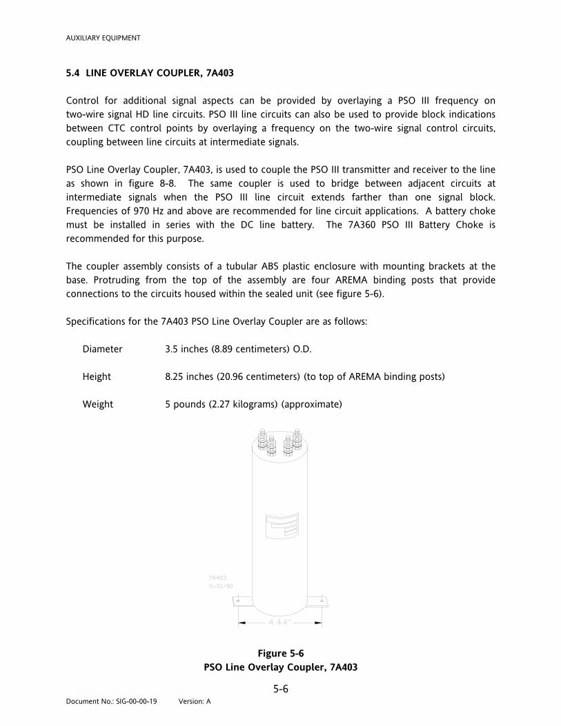
AUXILIARY EQUIPMENT
5-6 Document No.: SIG-00-00-19 Version: A
5.4 LINE OVERLAY COUPLER, 7A403 Control for additional signal aspects can be provided by overlaying a PSO III frequency on two-wire signal HD line circuits. PSO III line circuits can also be used to provide block indications between CTC control points by overlaying a frequency on the two-wire signal control circuits, coupling between line circuits at intermediate signals. PSO Line Overlay Coupler, 7A403, is used to couple the PSO III transmitter and receiver to the line as shown in figure 8-8. The same coupler is used to bridge between adjacent circuits at intermediate signals when the PSO III line circuit extends farther than one signal block. Frequencies of 970 Hz and above are recommended for line circuit applications. A battery choke must be installed in series with the DC line battery. The 7A360 PSO III Battery Choke is recommended for this purpose. The coupler assembly consists of a tubular ABS plastic enclosure with mounting brackets at the base. Protruding from the top of the assembly are four AREMA binding posts that provide connections to the circuits housed within the sealed unit (see figure 5-6). Specifications for the 7A403 PSO Line Overlay Coupler are as follows: Diameter 3.5 inches (8.89 centimeters) O.D. Height 8.25 inches (20.96 centimeters) (to top of AREMA binding posts) Weight 5 pounds (2.27 kilograms) (approximate)
Figure 5-6
PSO Line Overlay Coupler, 7A403

AUXILIARY EQUIPMENT
5-7 Document No.: SIG-00-00-19 Version: A
5.5 BATTERY LINE FILTER, 7A418 Battery Line Filter, 7A418, provides decoupling between the battery and PSO III transmitter and receiver and is recommended in high noise/ripple environments. In track circuits where the transmitter and receiver are powered from the same battery, install the filter between the battery and each transmitter and the battery and each receiver of the same frequency (see examples below).
The 7A418 filter assembly consists of a large choke coil, a capacitor, and a set of AREMA binding posts on a mounting base. See figure 5-7 for mounting dimensions. Specifications for the 7A418 Battery Line Filter assembly are as follows: Dimensions 5.0 inches (12.70 centimeters) wide 9.0 inches (22.86 centimeters) deep 3.75 inches (9.53 centimeters) high Weight 7 pounds, 2 ounces (3.23 kilograms) (approximate)

AUXILIARY EQUIPMENT
5-8 Document No.: SIG-00-00-19 Version: A
Figure 5-7
Battery Line Filter, 7A418, With Mounting Dimensions 5.6 TUNED INSULATED JOINT BYPASS COUPLER, 7A422-F Tuned Insulated Joint Bypass Coupler, 7A422-f, is tuned to pass a specific PSO III frequency around an insulated joint in non-electrified territory.
WARNING THE 7A422-F MUST NOT BE USED TO PASS GCP OR MOTION SENSOR FREQUENCIES.
The coupler assembly consists of a tubular ABS plastic enclosure with mounting brackets at the base. Protruding from the top of the assembly are four AREMA binding posts that provide connections to the circuits housed within the sealed unit (see figure 5-8). Specifications for the 7A422-f Tuned Insulated Joint Bypass Coupler are as follows: Diameter 3.5 inches (8.89 centimeters) O.D. Height 9.75 inches (24.77 centimeters) (to top of AREMA binding posts) Weight 7 pounds (3.18 kilograms) (approximate)

AUXILIARY EQUIPMENT
5-9 Document No.: SIG-00-00-19 Version: A
Figure 5-8
Tuned Insulated Joint Bypass Coupler, 7A422-f 5.7 PSO CAB SIGNAL FILTER, 7A417-X PSO Cab Signal Filter, 7A417-X, is designed for use in territory where 60, 90, 100, or 200-Hz cab signal is used. The filter should be installed on the primary side of the track transformer as shown below.

AUXILIARY EQUIPMENT
5-10 Document No.: SIG-00-00-19 Version: A
The 7A417-X filter assembly can be configured according to signal frequency and relay mounting base type as indicated in the tab chart below. See figure 5-9 for mounting dimensions.
7A417-X DASH NUMBER TAB CHART
Relay Base Configuration
Frequency
100 Hz 60 Hz 200 Hz 90 Hz
Transcontrol -01 -11 -21 -31
U. S. & S. -02 -12 -22 -32
Safetran™ -03 -13 -23 -33
Specifications for the 7A417-X PSO Cab Signal Filter assembly are as follows: Dimensions:
Dash Number Dimensions -01, -02, -03, -11, -12, -13, -31, -32, -33
7.75 inches (19.69 centimeters) high
-21, -22, -23 5.0 inches (12.70 centimeters) high
-01, -11, -21, -31 6.75 inches (17.15 centimeters) wide 9.0 inches (22.86 centimeters) deep
-02, -12, -22, -32 4.94 inches (12.55 centimeters) wide 8.00 inches (20.32 centimeters) deep
-03, -13, -23, -33 4.94 inches (12.55 centimeters) wide 9.4375 inches (23.97 centimeters) deep
Weight: 4 pounds, 8 ounces (2.04 kilograms) (average)

AUXILIARY EQUIPMENT
5-11 Document No.: SIG-00-00-19 Version: A
Figure 5-9
PSO Cab Signal Filter, 7A417-X, With Mounting Dimensions

AUXILIARY EQUIPMENT
5-12 Document No.: SIG-00-00-19 Version: A
This page intentionally left blank
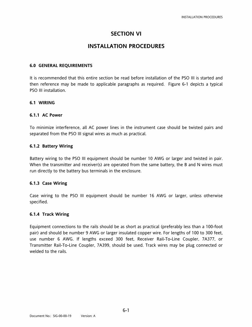
INSTALLATION PROCEDURES
SECTION VI
INSTALLATION PROCEDURES 6.0 GENERAL REQUIREMENTS It is recommended that this entire section be read before installation of the PSO III is started and then reference may be made to applicable paragraphs as required. Figure 6-1 depicts a typical PSO III installation. 6.1 WIRING 6.1.1 AC Power To minimize interference, all AC power lines in the instrument case should be twisted pairs and separated from the PSO III signal wires as much as practical. 6.1.2 Battery Wiring Battery wiring to the PSO III equipment should be number 10 AWG or larger and twisted in pair. When the transmitter and receiver(s) are operated from the same battery, the B and N wires must run directly to the battery bus terminals in the enclosure. 6.1.3 Case Wiring Case wiring to the PSO III equipment should be number 16 AWG or larger, unless otherwise specified. 6.1.4 Track Wiring Equipment connections to the rails should be as short as practical (preferably less than a 100-foot pair) and should be number 9 AWG or larger insulated copper wire. For lengths of 100 to 300 feet, use number 6 AWG. If lengths exceed 300 feet, Receiver Rail-To-Line Coupler, 7A377, or Transmitter Rail-To-Line Coupler, 7A399, should be used. Track wires may be plug connected or welded to the rails.
6-1 Document No.: SIG-00-00-19 Version: A
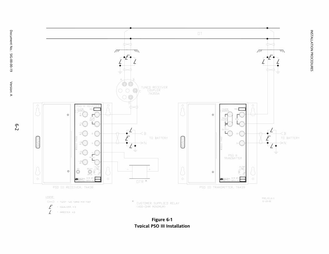
INSTALLATIO
N PRO
CEDU
RES
Figure 6-1 Typical PSO III Installation
6-2 D
ocument N
o.: SIG-00-00-19 Version: A

INSTALLATION PROCEDURES
6.2 TRANSMITTER INSTALLATION
WARNING VERIFY THAT PSO III TRANSMITTER FREQUENCY AND ADDRESS FORMAT ARE AS SPECIFIED BY THE RAILROAD’S APPROVED WIRING OR INSTALLATION DIAGRAM. FAILURE TO DO SO MAY LEAD TO INCORRECT OR UNSAFE OPERATION OF THE TRACK CIRCUIT. REFER TO FIGURE 6-2 FOR LOCATION OF TRANSMITTER MODULE ADDRESS AND FREQUENCY LABELS.
Perform the following steps to install the transmitter: (1) Remove the fuse from the transmitter.
(2) Connect the two track wires to the transmitter RAIL terminals.
(3) Connect the battery wires to the B and N terminals on the transmitter. Ensure correct
polarity. (4) Continuous low-power transmitter operation:
For continuous low-power operation, connect a terminal strap between the TRANS ENABLE terminals.
Continuous hi-power transmitter operation:
For continuous hi-power operation, connect a terminal strap between the TRANS ENABLE terminals and also a terminal strap between the HI OUTPUT terminals.
(5) If the transmitter is to be keyed through relay contacts, strap the transmitter terminals for
either continuous low or hi power operation (step 4 above), and then route the leads to the B and N terminals through the contacts of an external keying relay as shown in figure 6-3.
(6) Apply power to the transmitter by inserting the fuse.
6-3 Document No.: SIG-00-00-19 Version: A

INSTALLATION PROCEDURES
Figure 6-2
Location of Transmitter Module Address and Frequency Labels
Figure 6-3
PSO III Transmitter Connections To Remote Keying Relay (Transmitter Shown Strapped For Continuous Low-Power Operation)
6-4 Document No.: SIG-00-00-19 Version: A
ADDRESS LABEL
BAR CODE LABEL(FREQUENCY)
A AD
D
PSO III_6-312-20-00
TRANSMITTERKEYING RELAY

INSTALLATION PROCEDURES
6.3 RECEIVER INSTALLATION
CAUTION BEFORE INSTALLING PSO III EQUIPMENT, ENSURE THAT NO OTHER EQUIPMENT IS CONNECTED TO THE TRACK THAT, EITHER BY ITSELF OR IN CONJUNCTION WITH THE PSO III TRANSMITTER, CAN CREATE AN ERRONEOUS SIGNAL TO WHICH THE PSO III RECEIVER MAY RESPOND.
WARNING
VERIFY THAT PSO III RECEIVER FREQUENCY, RECEIVER COUPLER FREQUENCY AND ADDRESS FORMAT ARE AS SPECIFIED BY THE RAILROAD’S APPROVED WIRING OR INSTALLATION DIAGRAM. FAILURE TO DO SO MAY LEAD TO INCORRECT OR UNSAFE OPERATION OF THE TRACK CIRCUIT. REFER TO FIGURE 6-4 FOR LOCATION OF RECEIVER MODULE ADDRESS AND FREQUENCY LABELS.
Perform the following steps to install the receiver: (1) Remove the fuse from the receiver.
(2) Connect the track wires to terminals A and B on the receiver coupler.
(3) Connect wires from coupler terminals C and D to RCVR INPUT terminals of the receiver.
(4) Connect the battery wires to the B and N terminals on the receiver. Ensure correct polarity.
(5) Connect the relay coil to the RELAY + and - terminals on the receiver. Ensure correct
polarity as required. The relay coil resistance must be between 400 and 1,000 ohms. (6) Apply power to the receiver by inserting the fuse.
6-5 Document No.: SIG-00-00-19 Version: A
INSTALLATION PROCEDURES
Figure 6-4
Location of Receiver Module Address and Frequency Labels
ADDRESS LABEL
BAR CODE LABEL
A AD
D
PSO III3-1B12-15-00
(FREQUENCY)
6.4 CROSSING PACKAGE INSTALLATION
WARNING VERIFY THAT THE FREQUENCY AND ADDRESS FORMAT OF EACH PSO III RECEIVER IS AS SPECIFIED BY THE RAILROAD’S APPROVED WIRING OR INSTALLATION DIAGRAM. ALSO VERIFY THAT THE RECEIVER AND CORRE-SPONDING RECEIVER COUPLER FREQUENCIES ARE IDENTICAL. FAILURE TO DO SO MAY LEAD TO INCORRECT OR UNSAFE OPERATION OF THE TRACK CIRCUIT. REFER TO FIGURE 6-4 FOR LOCATION OF RECEIVER MODULE ADDRESS AND FREQUENCY LABELS.
Perform the following steps to install the Crossing Package: (1) Remove the fuse from the Crossing Package.
(2) Connect track wires of the WEST receiver to terminals A and B on the tuned receiver
coupler. (3) Connect wires from coupler terminals C and D to WEST PSO RCV terminals on the Crossing
Package.
6-6 Document No.: SIG-00-00-19 Version: A
INSTALLATION PROCEDURES
(4) Connect WEST receiver relay coil wires to WEST PSO RLY + and - terminals on the Crossing Package. Ensure correct polarity.
(5) Repeat steps 2 through 4 for the EAST receiver.
(6) Connect battery wires to B (+) and N (-) terminals on the Crossing Package. Ensure correct
polarity. (7) Connect island circuit transmit track wires to ISL XMT terminals on the Crossing Package.
(8) Connect island circuit receive track wires to ISL RCV terminals on the Crossing Package.
(9) Connect island circuit relay coil to ISL RLY + and - terminals on the Crossing Package.
Ensure correct polarity. The relay should be a standard railroad-type with a coil resistance of 400 ohms or higher.
(10) Apply power to the Crossing Package by inserting the fuse. Proceed to Section VII for
applicable checkout and adjustment procedures.
6-7 Document No.: SIG-00-00-19 Version: A

INSTALLATION PROCEDURES
6-8 Document No.: SIG-00-00-19 Version: A
This page intentionally left blank
CHECKOUT AND ADJUSTMENT
SECTION VII
CHECKOUT AND ADJUSTMENT 7.0 GENERAL This section contains checkout and adjustment procedures for the PSO III receiver module (7A436 used in 7A438 and 7A448 configurations or 7A436-2 used in 7A453 and 7A455 configurations), and the IPI island module (62609) which is used in the Crossing Package (7A448 and 7A455).
WARNING THE CHECKOUT AND ADJUSTMENT PROCEDURES PROVIDED HERE APPLY TO THE PSO III EQUIPMENT ONLY. DO NOT USE CHECKOUT AND ADJUSTMENT PROCEDURES INTENDED FOR THE PSO II EQUIPMENT.
7.1 PSO III RECEIVER ADJUSTMENT Follow the steps listed below to adjust the PSO III receiver(s). When adjusting the Crossing Package, perform the procedures for receiver number 1 first, then repeat all applicable steps for receiver number 2. A VOM (Simpson, Model 260, Series 3 or equivalent) is required to set the amplitude detector (AD) level to +11 volts. Since the AD voltage may fluctuate slightly at certain PSO III operating frequencies, the AD level is adjusted so that peak deflection is no greater than +11 volts. 1. Verify that the PSO III Receiver module and receiver coupler (7A355A-f or 7A366-f), when
used, are the same frequency. 2. With the meter set to read +DC on the 10 VDC scale, connect the common (black) lead to
terminal B on the receiver and the positive (red) lead to the AD test jack (figure 7-1). 3. Connect a temporary jumper between the -30 dB and 0 dB terminals (maximum receiver
sensitivity). Note that the RELAY DRIVE indicator (DS1 and DS2 on Crossing Package) lights when the receiver relay is energized and the meter indicates 6.5 volts or higher.
4. Remove the module cover and adjust the receiver module gain adjust potentiometer (figure 7-
2) to the fully CW position.
7-1 Document No.: SIG-00-00-19 Version: A

CHECKOUT AND ADJUSTMENT
5. When the track ballast is dry, connect a shunt (0.06-ohm or 0.2-ohm) across the track at the receiver track connections. When the ballast is damp, connect the shunt across the track at a point 10 feet beyond the receiver track connections. Ensure that the shunt has solid connections to each rail. If the AD level is above 5 volts, disconnect the jumper from the 0 dB terminal and connect it to the -6 dB terminal. If necessary, continue to move this end of the jumper to the next lower numbered terminal until the 5-volt reading is produced (-6 dB to -12 dB, -12 dB to -18 dB, etc.).
NOTE
Except in erratic shunting or light rail applications, the 0.06-ohm shunt is normally used. PSO III receivers installed in light rail traction territories or rusty rail areas are normally adjusted using a 0.2-ohm shunt.
Figure 7-1
AD Test Jack and Relay Drive Indicator Locations
7-2 Document No.: SIG-00-00-19 Version: A
PSO_III_7-11-10-01
7A438 RECEIVER ASSEMBLY
AD TEST JACKRELAY DRIVEINDICATOR
7A448 CROSSING PACKAGE
AD TEST JACK
RELAY DRIVEINDICATOR
RELAY DRIVEINDICATOR
AD TEST JACK

CHECKOUT AND ADJUSTMENT
Figure 7-2
Gain Potentiometer Location On 7A436 Receiver Module
A AD
D
PSO_III7-212-20-00
GAINPOTENTIOMETER
6. Adjust the receiver module gain adjust potentiometer CCW until the AD voltage is +4.0 volts.
Verify that the receiver relay is de-energized and that the relay voltage is 0 VDC. 7. Remove the temporary jumper (step 4) and install a permanent jumper on the same terminals.
Remove the meter test leads and the track shunt. The receiver relay should energize. 8. Remove the transmitter fuse. The receiver relay should de-energize. Return the fuse to the
original position. When adjusting a Crossing Package (7A448 or 7A455), repeat steps 1 through 8 for the other receiver.
9. For the Crossing Package only (7A448 or 7A455), adjust the island receiver as described in
paragraph 7.2. 10. The system is now ready for operation. Verify proper operation of the track circuit equipment
before placing in service in accordance with railroad procedures and applicable FRA rules.
WARNING VERIFY THAT THE TRACK RELAY DE-ENERGIZES WHEN THE TRACK CIRCUIT IS SHUNTED WITH THE APPROPRIATE RESISTANCE (EITHER 0.06 OR 0.2 OHMS). FAILURE TO DO SO MAY LEAD TO INCORRECT OR UNSAFE OPERATION OF THE TRACK CIRCUIT.
7-3 Document No.: SIG-00-00-19 Version: A

CHECKOUT AND ADJUSTMENT
7.1.1 Receiver Adjustment For Line-To-Line Applications 1. With the meter set to read +DC on the 10 VDC scale, connect the common (black) lead to
terminal B on the receiver and the positive (red) lead to the AD test jack (figure 7-1). 2. Connect a temporary jumper between the front panel -30 dB and 0 dB terminals (maximum
receiver sensitivity). 3. With the gain potentiometer adjusted fully clockwise, move the 0-dB end of the front panel
gain jumper to the –6 dB position. If necessary, continue to move this end of the jumper to the next lower numbered terminal until the meter reads just above +7 volts (-6 dB to -12 dB, -12 dB to -18 dB, etc.).
4. Adjust the gain potentiometer to drop the meter reading to 6.5 volts. 5. Now move the moveable end of the jumper up two terminals so that the gain is 12 dB higher.
NOTE
If the receiver does not drop out with no gain jumper installed, then install a jumper in the –24 dB position.
6. Remove the temporary jumper and install a permanent jumper in its place.
7. Verify that the receiver AD voltage is higher (more positive) than 6.5 volts DC. 8. Remove the transmitter fuse and verify that the AD voltage is between zero and +1.0 VDC. 9. Return the fuse to the original position. The system is now ready for operation. 7.2 IPI MODULE ISLAND CIRCUIT ADJUSTMENT There are three simple procedures that must be performed before placing the IPI in service. The first is to select the operating frequency by installing a jumper on the IPI module. The second is to configure jumper(s) for pickup delay time if required (IPI modules running software version A01E and later only). And the third is to perform the automated calibration of the island circuit.
WARNING
AFTER INSTALLATION OR AFTER ANY ISLAND CHANGES HAVE BEEN MADE, RECALIBRATE THE IPI AND TEST FOR PROPER OPERATION.
7-4 Document No.: SIG-00-00-19 Version: A

CHECKOUT AND ADJUSTMENT
• IPI FREQUENCY SELECTION NOTE
If the IPI module is already installed in the case, remove power from the case and then remove the IPI module.
1. Select the desired IPI operating frequency by installing the provided shorting block across the appropriate pair of frequency selection pins on the 16-position header (see figure 2-5 or the following figure). Only one frequency jumper is allowed.
• IPI PICKUP DELAY TIME SELECTION (SOFTWARE VERSION A01E AND LATER ONLY)
NOTE
The A and B positions on the 16-position header are not used on IPI modules running software version A01D or earlier. However, the A and B positions are used for pickup delay time selection on modules running software version A01E or later.
2. Additional pickup delay time may be added to the IPI module when needed using the A and B header positions. Refer to the chart below for proper jumper placement.
Install Jumper In these
Header Positions Pickup Delay Time Added
(seconds) A & B 0
A 2 B 4
no jumper on A or B 6
7-5 Document No.: SIG-00-00-19 Version: A
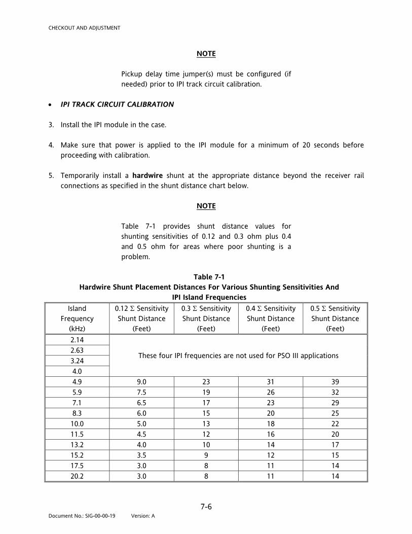
CHECKOUT AND ADJUSTMENT
NOTE Pickup delay time jumper(s) must be configured (if needed) prior to IPI track circuit calibration.
• IPI TRACK CIRCUIT CALIBRATION 3. Install the IPI module in the case. 4. Make sure that power is applied to the IPI module for a minimum of 20 seconds before
proceeding with calibration. 5. Temporarily install a hardwire shunt at the appropriate distance beyond the receiver rail
connections as specified in the shunt distance chart below.
NOTE Table 7-1 provides shunt distance values for shunting sensitivities of 0.12 and 0.3 ohm plus 0.4 and 0.5 ohm for areas where poor shunting is a problem.
Table 7-1
Hardwire Shunt Placement Distances For Various Shunting Sensitivities And IPI Island Frequencies
Island Frequency
(kHz)
0.12 Σ Sensitivity Shunt Distance
(Feet)
0.3 Σ Sensitivity Shunt Distance
(Feet)
0.4 Σ Sensitivity Shunt Distance
(Feet)
0.5 Σ Sensitivity Shunt Distance
(Feet) 2.14
These four IPI frequencies are not used for PSO III applications 2.63 3.24 4.0 4.9 9.0 23 31 39 5.9 7.5 19 26 32 7.1 6.5 17 23 29 8.3 6.0 15 20 25 10.0 5.0 13 18 22 11.5 4.5 12 16 20 13.2 4.0 10 14 17 15.2 3.5 9 12 15 17.5 3.0 8 11 14 20.2 3.0 8 11 14
7-6 Document No.: SIG-00-00-19 Version: A

CHECKOUT AND ADJUSTMENT
NOTE
For all installations where poor shunting has been experienced or is anticipated, a 4-second pickup delay jumper setting and 0.3 ohm shunting sensitivity calibration are recommended.
6. To calibrate the IPI, press and hold the IPI calibration select push button (figure 2-5) for 2 seconds until REL (release) appears on the display. Immediately release the push button and then momentarily press it again within 2 seconds. This starts the automated calibration process (CAL* appears on the display).
NOTE
The IPI module remains in the automatic Calibration mode for approximately 20 seconds. During this time, the display indicates CAL* for 6 seconds, DONE momentarily, BOOT for 9 seconds, and then the software revision level is displayed for 5 seconds. When the calibration process is complete, the IPI operating frequency is displayed (alternates with pickup delay setting when running A01E and later software versions).
NOTE If FAIL appears on the display, the calibration process did not complete. Should this happen, cycle the IPI power and then repeat step 6. If FAIL appears again, replace the IPI module.
7. Once the calibration cycle is complete and the IPI operating frequency (and pickup delay setting if applicable) appears on the display, verify the following:
• That the frequency is correct • That the pickup delay setting is correct (if applicable) • That the IPI STATUS indicator is off • That the IPI relay drive voltage is 0 VDC 8. Remove the hardwire shunt installed in step 5 and then verify the following: • That the IPI STATUS indicator is lit • That the IPI relay drive voltage is more than 10 VDC
9. Verify proper IPI operation by observing train moves.
7-7 Document No.: SIG-00-00-19 Version: A

CHECKOUT AND ADJUSTMENT
7-8 Document No.: SIG-00-00-19 Version: A
7.2.1 IPI Module Troubleshooting
Figure 7-3 IPI Module Troubleshooting Chart
Internal error codes (for reference only)
CALC CRIT
GB HWSW IRO ISRX PHLT PIRO PS_I PS5A PS5D PS25 RAM ROM SIRO STKG STKP TIME XCPT
NOTE If any of the internal error codes listed to the left appear on the IPI display, typically the IPI module should be replaced if the problem persists. See Section II, table 2-2, for a description of these codes.
NOTE If a loss-of-shunt is detected, the LOS indication flashes intermittently on the display for approximately 10 seconds.

DIAGRAMS
SECTION VIII
DIAGRAMS
This section contains the following typical PSO III installation diagrams. Connections are also shown for PSO-related components.
Figure No.
Title
8-1 PSO III Installation With Tuned Receiver Coupler, 7A355A-f 8-2 PSO III Installation With Tuned Receiver Coupler, 7A366-f 8-3 PSO III Installation With Receiver Line-to-Rail Coupler, 7A377-1-f, And
Line-To-Receiver Coupler, 7A388 8-4 PSO III Installation With Transmitter Line-to-Rail Coupler, 7A399-f 8-5 Typical Installation of PSO III Crossing Package With Island Circuit 8-6 Insulated Joint Bypass Device, 7A422-f 8-7 PSO Battery Choke, 7A360, 8A065A or 62648 8-8 Typical PSO III Line Overlay Application (includes 7A403 PSO Line Coupler) 8-9 Typical Battery Charger Surge Protection 8-10 Typical Track Wire Surge Protection For Use In Electrified Territory
NOTE The application drawings provided here apply to both “A” and “C” address format PSO III transmitters, receivers and Crossing Packages.
8-1 Document No.: SIG-00-00-19 Version: A
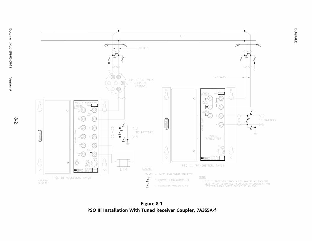
DIAGRAM
S
Figure 8-1 PSO III Installation With Tuned Receiver Coupler, 7A355A-f
8-2 D
ocument N
o.: SIG-00-00-19 Version: A

DIAGRAM
S
Figure 8-2 PSO III Installation With Tuned Receiver Coupler, 7A366-f
8-3 D
ocument N
o.: SIG-00-00-19 Version: A

DIAGRAM
S
Figure 8-3 PSO III Installation With Receiver Line-To-Rail Coupler, 7A377-1-f,
And Line-To-Receiver Coupler, 7A388
8-4 D
ocument N
o.: SIG-00-00-19 Version: A
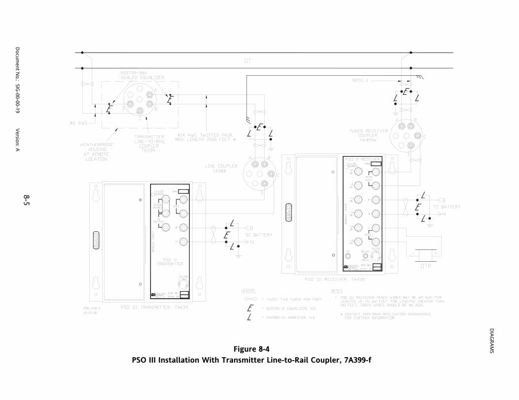
DIAGRAM
S
Figure 8-4 PSO III Installation With Transmitter Line-to-Rail Coupler, 7A399-f
8-5 D
ocument N
o.: SIG-00-00-19 Version: A

DIAGRAM
S
Figure 8-5 Typical Installation of PSO III Crossing Package With Island Circuit
8-6 D
ocument N
o.: SIG-00-00-19 Version: A

DIAGRAMS
Figure 8-6 Insulated Joint Bypass Device, 7A422-f
8-7 Document No.: SIG-00-00-19 Version: A

DIAGRAM
S
8-8 D
ocument N
o.: SIG-00-00-19 Version: A
Figure 8-7 PSO Battery Choke, 7A360, 8A065A or 62648
WARNING
WHERE GCP'S OR MOTION SENSORSARE INSTALLED WITH THE PSO III,
THE 7A360 CHOKE MUST NOT BE USED.INSTEAD, USE THE 8A065A OR 62648
CHOKES. (8A065A MUST BE USED WITHINMODEL 300 OR 400 GCP APPROACHES).
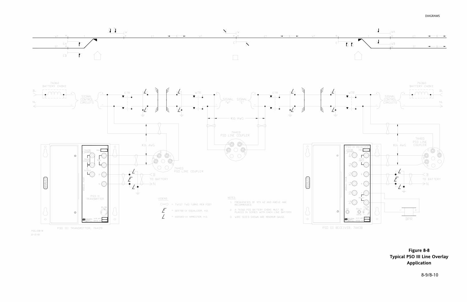
DIAGRAMS
Figure 8-8 Typical PSO III Line Overlay
Application 8-9/8-10

DIAGRAMS
Figure 8-9 Typical Battery Charger Surge Protection
8-11 Document No.: SIG-00-00-19 Version: A
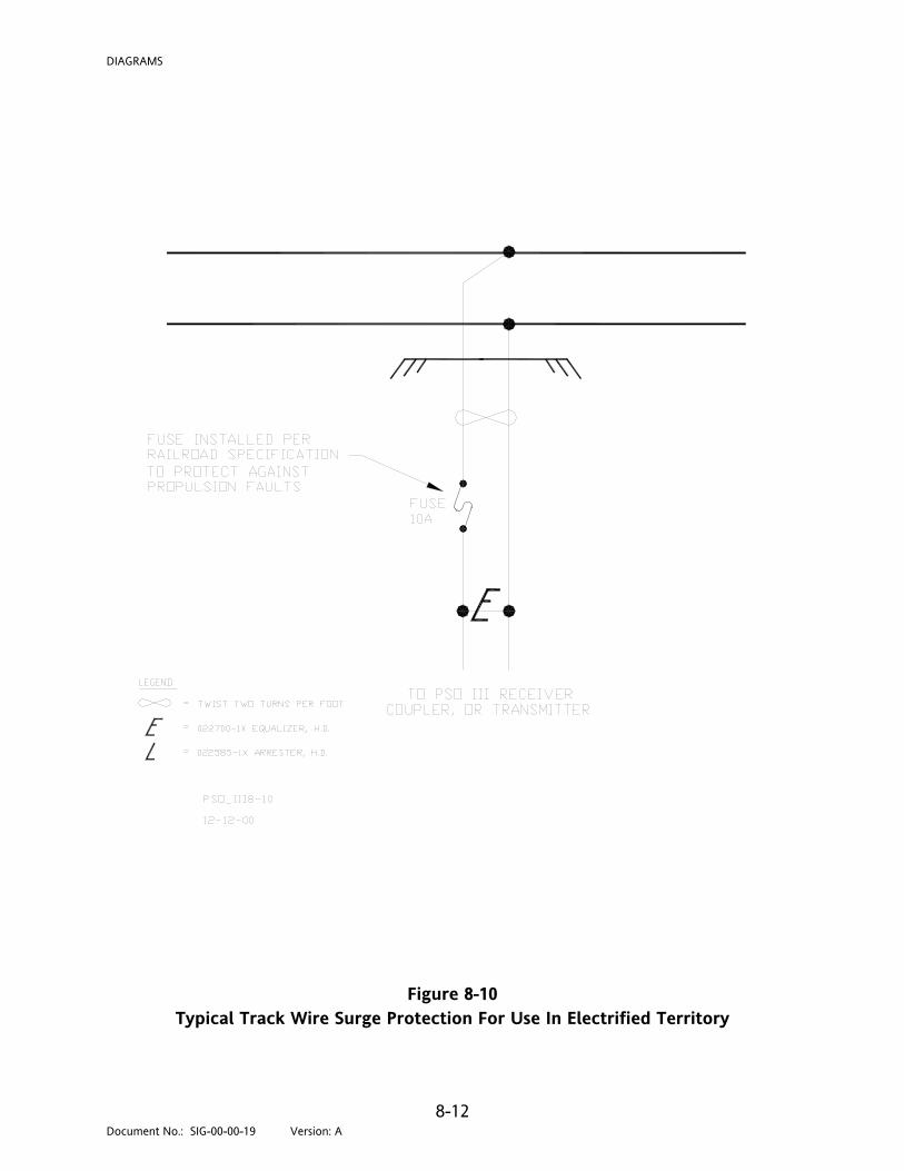
DIAGRAMS
8-12 Document No.: SIG-00-00-19 Version: A
Figure 8-10 Typical Track Wire Surge Protection For Use In Electrified Territory

INDEX
6 62648 Battery Choke, 5-1
7 7A355A-f Tuned Receiver Coupler, 5-3 7A360 PSO Battery Choke, 3-7, 5-1, 5-6 7A366-f Tuned Receiver Coupler, 5-3 7A377-1-f Receiver Line-To-Rail Coupler, 5-4, 6-1 7A388 Line-To-Receiver Coupler, 5-4 7A399-f Transmitter Line-To-Rail Coupler, 5-4, 6-1 7A403 PSO Line Overlay Coupler, 5-6 7A417-X Cab Signal Filter, 3-5, 5-9 7A418 Battery Line Filter, 5-7 7A422-f Tuned Insulated Joint Bypass Coupler, 5-8
8 8A065A Battery Choke, 5-1
A accessory equipment, 1-5 ACTIVITY indicator, 4-4 AD test jack, 7-4 AD1 test jack, 4-3 AD2 test jack, 4-3 address format, Crossing Package, 4-2 address formats, 1-1 adjacent channel frequencies, 3-3 Alphanumeric Display, 4-4 ARMD, 4-6 automated calibration, 7-4
B B (+) and N (-) terminals, 1-5, 4-2, 6-3, 6-7, 6-5 ballast resistance, 3-1 bar code label (frequency), 3-7 Battery Choke, 62648, 5-1 Battery Choke, 7A360, 3-7, 5-6 Battery Choke, 8A065A, 5-1 Battery Line Filter, 7A418, 5-7 Battery wiring, 6-1 BOOT, 4-6, 7-7
C CAL*, 4-6, 7-7 CALC, 4-7 calibrate the IPI, 7-7 Calibration Select Push Button, 4-8 CALR, 4-7
Index-1 Document No.: SIG-00-00-19 Version: A

INDEX
Case wiring, 6-1 Connector and Indicator functions, PSO III Crossing Package, 4-2 Connector and indicator functions, PSO III Receiver, 1-5 Connector functions, PSO III Transmitter, 1-5 Continuous hi-power transmitter operation, 6-3 Continuous low-power transmitter operation, 6-3 CRIT, 4-7 Crossing Package, 1-1, 1-4, 1-7, 4-1, 7-3
D display messages, 4-6 DONE, 4-6 DS1 and DS2 on Crossing Package, 4-3, 7-1
E EAST PSO PCV terminals. 4-3 EAST PSO RLY +/- terminals, 4-3 electrified territory, 1-4, 1-6
F FAIL, 4-7, 7-7 Frequency Select header, 4-8, 7-5 frequency selection, 7-5 Frequency Stability, 1-6 FRQ?, 4-7 Fuse, 1-5, 4-3
G gain potentiometer, 7-4 GB, 4-7
H hardwire shunt, 7-6 harmonic content of the PSO III output waveform, 2-3 HI OUTPUT terminals, 1-5, 6-3 HWSW, 4-7
I Input Current, 1-7 Input Voltage, 1-7 installing new software, 4-10 insulated joint bypass couplers, 3-6 insulated joint separation, 3-3 Intelligent Processor Island (IPI) module, 1-1, 4-3 island circuit module (62609), 1-1 island frequencies, 1-4 island receiver adjustment, 7-3, 7-4 IPI frequencies not used for PSO III applications, 4-9 IPI Internal Failure Error Codes, 4-7 IPI track circuit frequencies, 3-4
Index-2 Document No.: SIG-00-00-19 Version: A

INDEX
IRO, 4-7 ISL RCV terminals, 4-3, 6-7 ISL RLY + and - terminals, 4-3, 6-7 ISL XMT terminals, 4-2, 6-7 island circuit module (62609), 4-1 ISRX, 4-7
L line wire or buried cable, 3-6
M Modulation, 1-6 multiple circuits on the same track, 1-4 multiple receivers, 3-6 Multiple track territory, 3-4
N non-bypassed insulated joints, 3-4
O One channel separation, 3-3 operating distance, 3-1 operating frequency selection (IPI module), 7-5
P PASS, 4-8 PHLT, 4-7 pickup delay selection, 4-10 pickup delay time, 7-4, 7-5 PIRO, 4-7 PS_I, 4-8 PS25, 4-8 PS5A, 4-8 PS5D, 4-8 PSO Battery Choke, 7A360, 3-7 PSO Cab Signal Filter, 7A417-X, 3-5, 5-9 PSO Line Overlay Coupler, 7A403, 5-6 PSO III and 3000 MS/GCP frequency compatibility, 3-4 PSO II And PSO III Transmitter and Receiver Module/Case Interchangeability, 1-6 PSO III Frequencies, 1-4, 1-6 PSO III operating frequencies for use on non-electrified track, 3-2 PSO III operating frequencies used on electrified track, 3-2 PSO III receiver(s) adjustment, 7-1
R RAIL terminals, 1-5 RAM, 4-8 RCVR INPUT, 2-3 RCVR INPUT terminals, 1-5, 6-5 receiver frequency response, 2-7
Index-3 Document No.: SIG-00-00-19 Version: A

INDEX
Index-4 Document No.: SIG-00-00-19 Version: A
Receiver Input Impedance, 1-7 Receiver Line-To-Rail Coupler, 7A377-1-f, 5-4, 6-1 Receiver Module, 7A436, 2-3 receiver module gain adjust potentiometer, 7-1, 7-3 receiver relay, 7-3 Receiver Selectivity, 1-6 Receiver Sensitivity, 1-6 REL, 4-6, 7-7 RELAY, 2-3 RELAY + and - terminals, 1-5, 6-5 Relay Coil Resistance, 1-7 RELAY DRIVE indicator, 1-5, 7-1 relay drive voltage, 7-7 Remote Keying Relay, 6-3, 6-4 ROM, 4-8 RS-232 Serial Port, 4-8
S shunting sensitivity, 3-1 SIG, 4-7 SIRO, 4-8 standard configuration, 1-1 STATUS indicator, 4-4, 7-7 STKP, 4-8 Surge Protection, 1-7, 3-7
T TB1 (0dB, -6dB, -12dB, -18dB, -24dB, -30dB) terminal strip, 4-3 TB2 (0dB, -6dB, -12dB, -18dB, -24dB, -30dB) terminal strip, 4-3 TIME, 4-8 TRANS ENABLE terminals, 1-5, 6-3 Transmitter Line-To-Rail Coupler, 7A399, 5-4, 6-1 Transmitter Module, 7A437, 2-1 Transmitter Output Impedance, 1-6 transmitter strapping options, 2-3 Tuned Insulated Joint Bypass Coupler, 7A422-f, 5-8 Tuned Receiver Couplers, 7A355A-f and 7A366-f, 5-3
W WEST PSO RCV terminals, 4-2, 6-7 WEST PSO RLY + and - terminals, 4-2, 6-6
X XCPT, 4-8