philips technical note - poc-net
TRANSCRIPT

PHILIPS
PHILIPS Electronic components and materials
Technical note 085
Cyclic redundancy check by software
The Cyclic Redundancy Check (CRC) provides a reliable method of detecting errors in serial data streams.* The probability of error detection depends on the length of error sequences received and the code polynominal used. There are four sixteen-degree polynominals in common use:
Xr6 +Xts
Xt6 +Xta
Xr6 +Xr2
Xl6 + XI1
CRC 16
CRC 16
CCITT
CCITT
Forward
Reverse
Forward
Reverse
The routine described in this Technical Note performs CRC encoding and decoding according to any one of these code polynominals. It can be adapted to use other code polynominals with little difficulty.
* Information on the theory of the CRC can be found in Technical Information 030: 8X01 encoder and decoder for serial data error detection.
feedback
Routine operation
The routine simulates a 16-bit syndrome generator with variable feedback as shown in Fig. 1. Since the 2650 uses 8-bit words, the syndrome is stored in two registers, R1 and R2. Data is input via port D and returned unaltered (and followed by the CRC bytes) via port D. An error indication, for use when decoding, is available on port C.
The line numbers given in the following text refer to the listing in Fig. 2. The ORG instruction is placed at address 44A; however, the user may change this location to another more suitable to his system without affecting the working of the routine.
SYNDROME REGISTER
- f
ui~iex
R2
! 1 1 PORT D
DATA STORE
RO
I I I I I I I I PORT D
1 i 1 1R 1 1 1 1 PORT D
COUNTER
Fig. 1 Circuit simulated by the CRC software.
R3
C signifies carry bit
s~n~taes
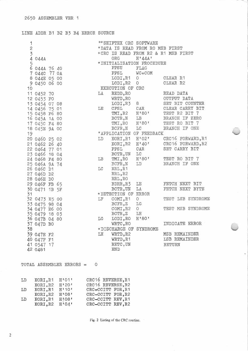
2650 ASSEMBLER VER 1
LINE ADDR B1 B2 B3 B4 ERROR SOURCE
1 **SHIFTEX CRC SOFTWARE 2 DATA IS READ FROM RO MSB FIRST 3 *CRC IS READ FROM R2 & R1 MSB FIRST
4 o44A oRG x'44A` 5 *INITIALISATION PROCEDURE 6 o44A 76 40 PPSU FLAG 7 0440 77 OA PPSL WC+COM 8 044E 05 00 LODI,R1 0 CLEAR R1
9 0450 06 00 LODI,R2 0 CLEAR R2 10 EXECUTION OF CRC 11 0452 70 LA REDD,RO READ DATA 12 0453 FO WRTD,RO OUTPUT DATA 13 0454 07 08 LODI,R3 8 SET BIT COUNTER 14 0456 75 01 LE CPSL CAR CLEAR CARRY BIT 15 0458 F6 80 TMI,R2 H'80' TEST R2 BIT 7 16 045A 1A 00 BCTR,N LB BRANCH IF ZERO 17 045C F4 80 TMI,RO H'80' TEST RO BIT 7 18 045E gA OC BCFR,N LC BRANCH IF ONE 1g *APPLICATION OF FEEDBACK 20 0460 25 02 LD EORI,R1 H'02' CRC16 FORWARD,R1 21 0462 26 40 EORI,R2 H'40' CRC16 FORWARD,R2 22 0464 77 01 PPSL CAR SET CARRY BIT 23 0466 18 04 BGTR,UN LC 24 o46s F4 80 LB TMI,RO H'80' TEST RO BIT 7 25 046A gA 74 BCFR,N LD BRANCH IF ONE 26 o46c D1 LC RRL,R1 27 046D D2 RRL,R2 28 046E DO RRL,RO 2g 046E FB 65 BDRR,R3 LE FETCH NEXT BIT 30 0471 1B 5F BCTR,UN LA FETCH NEXT BYTE 31 DETECTION OF ERROR 32 0473 E5 00 LF COMI,R1 0 TEST LSB SYNDROME
33 0475 98 04 BCFR,Z LG
34 0477 E6 00 COMI,R2 0 TEST MSB SYNDROME
35 0479 18 03 BCTR,Z LH
36 o47B 04 80 LG LODI,RO H'80'
37 047D BO WRTC,RO INDICATE ERROR 38 DISCHARGE OF SYNDROME
39 047E F2 LH WRTD,R2 MSB REMAINDER 40 047E F1 WRTD,R1 LSB REMAINDER
41 0547 17 RETC,UN RETURN 42 0481 END
TOTAL ASSEMBLER ERRORS = 0
LD EORI,R1 H'01' EORI,R2 H'20'
LD EORI,R1 H'10' EORI,R2 H'08'
LD EORI,R1 H'.08' EORI,R2 H'04'
CRC16 REVERSE,R1 CRC16 REVERSE,R2 CRCaCCITT FOR,R1 CRC—CCITT FOR,R2 CRC—CCITT REV,R1 CRC—CCITT REV,R2
Fig. 2 Listing of the CRC routine.
2

At the start of the operation (from line 6) the program status words are set and the syndrome register is cleared.** The first byte of the data is then entered via port D into R0.
Data is accepted in 8-bit bytes, the most significant byte being loaded first. If the message is received serially, then either an 8-bit serial to parallel converter will be required in hardware or the program can be altered to accept data via the sense input.
At line 13, the counter R3 is set to eight bits per byte. This is used to control the number of shifts of the syndrome generator. The carry bit is also cleared.
Lines 15 and 171ook at the most significant bit of the syndrome and of the data respectively. The associated branch statements cause the instructions at label LD (line 20) to be executed if only one or the other of the most significant bits is a one. This section of the routine simulates the exclusive-OR gate shown in Fig. 1.
Lines 20 to 22 contain the feedback information and thus determine the polynominal in use. To alter the code it is merely necessary to change program lines 20 and 21. Polynomials of degree less than 16 can be accommodated by replacing the instruction at line 22 with two No Operation (CO) bytes.
At label LC, R0, R1 and R2 are rotated left and the counter R3 is decremented. The combined registers R1 and R2 now contain the syndrome for the first data bit. The above procedure, from line 14 to line 29, is executed eight times, once for each bit of a data byte. The syndrome is continuously updated as each data bit is read. At the end of each data byte, the routine returns to line 11 to read the next byte. When processing has been completed, the most and least significant bytes of the remainder will be present in R2 and R1 respectively. The contents of R2, followed by those of R1, are made available at port D and an error indication (when the remainder is not zero —for use in decoding mode) at port C.
A set of feedback statements is provided at the foot of the listing in Fig. 2 to cover the three remaining code polynomials. These should replace the instructions at lines 20 and 21 as appropriate. Figure 3 shows the data format and Fig. 4 is a flow chart of the routine.
** For High level Data Link Control (HDLG) or Synchronous Data Link Control (SDLC) operation using the CCITT Forward polynomial, the syndrome register should be set to all ones. To achieve this, replace each of the `00' bytes on lines 8 and 9 with `FF'. The remainder should be checked for `FOB8' instead of zero by replacing each `00' byte at lines 32 and 34 with `OF' and `8B' respectively.
i MSB
vEs
START
ISET FLAG
ISELECT WC
AND LOG. COMP.
I CLEAR
SYNDROME
INPUT DATA AT PORT D
IOUTPUT DATA
AT PORT D
SET COUNTER
CLEAR CARRY BIT
Is MSB OF R2=0?
IS
MSB OF RO#0?
APPLY FEEDBACK TO R7 AND R2
is MSB OF RO#0?
SHIFT SYNDROME LEFT ONCE
SHIFT DATA LEFT ONCE
I DECREMENT COUNTER
Is COUNTER
= o?
/ / END\ \ ~/ OF DATA \~ YES
\BLOCK? / /
DATA
♦♦ LSB MSB
OUTPUT R2 AT PORT D
OUTPUT R1 AT PORT D
~ RETURN ~
Fig. 4 Flow chazt of the CRC routine.
CHECK BITS A
LSB
MSB RO LSB MSB RO LSB MSB RO LSB MSB R2 LSB MSB R1 LSB
read from left to right
Fig. 3 Data as received or transmitted.
12 )SIB]
t~,.>e<
3

Performance The CRC routine is not fast compared to hardware approaches. However, it will be of particular benefit to systems using a microprocessor which remains idle until the data has been checked. The speed of operation is dependent on the data pattern. The worst-case of this software approach is calculated to be 12k baud,* while the average speed is 14k baud.* This should be compared
* Assuming a 1,25 MHz clock.
Related 2650 publications
with. the 3M baud for the GZF1202 and l OM baud for the 8X01, irrespective of the data pattern.
The routine can be used equally well as either an encoder or decoder. However, no provision has been made to generate Register-clear or Decoding-complete signals.
The user will also have to provide the appropriate
control to start and stop the routine for each data block.
no, title summary
AS50 Serial Input/Output
AS51 Bit &Byte Testing Procedures
AS52 General Delay Routines
AS52 Binary Arithmetic Routines
AS54 Conversion Routines
AS55 Fixed Point Decimal Arithmetic
SP50 2650 Evaluation Printed Circuit Board (PC 1001)
SP51 2650 Demo System
SP52 Support Software for use with the NCSS Timesharing System
SP53 Simulator, Version 1.2
SP54 Support Software for use with the General Electric Mazk III Timesharing System
SP55 The ABC 1500 Adaptable Board Computer
SS50 PIPBUG
SS51 Absolute Object Format
MP51 Initialization
MP52 Low-Cost Clock Generator Circuits
MP53 Address and Data Bus Interfacing Techniques
MP54 2650 Input/Output Structures and Interfaces
TN 064 Digital cassette interface fora 2650 microprocessor system
TN 069 2650 Microprocessor keyboard interfaces
TN 072 Introducing the Signetics 2651 PCI Terminology and operation modes
TN 083 Using the Signetics 2651 PCI with popular microprocessors
TN 084 Using seven-segment LED displays with the 2650 microprocessor
Using the Sense/Flag capability of the 2650 for serial I/O interfaces.
Several methods of testing the contents of the internal registers in the 2650.
Several time delay routines for the 2650, including formulas for calculating the
delay time.
Examples for processing binary arithmetic addition, subtraction, multiplication, and division with the 2650.
• Eight-bit unsigned binary to BCD • Sixteen-bit signed binary to BCD • Signed BCD to binary • Signed BCD to ASCH • ASCII to BCD • Hexadecimal to ASCII
• ASCII to Hexadecimal
Methods of performing addition, subtraction, multiplication and division of BCD
numbers with the 2650.
Detailed description of the PC1001, an evaltaation and design tool for the 2650.
Detailed description of the Demo System, a hardware base for use with the 2650 CPU prototyping board (PC1001 or PC1500},
Step-by-step procedures for generating, editing, assembling, punching, and simulating Signetics 2650 programs using the NCSS timesharing service,
Features and characteristics of version 1.2 of the 2650 simulator.
Step-by-step procedures for generating, editing, assembling, simulating, and punching
Signetics 2650 programs using General Electric's Mark III timesharing system.
Describes the components and applications of the ABC 2500 system development card.
Detailed description of PIPBUG, a monitor program designed for use with the 2650.
Describes the absolute object code format for the 2650.
Procedures for initializing the 2650 microprocessor, memory, and I/O devices to their required initial states.
Several clock generator circuits, based on 7400 series TTL, that may be used with the
2650. They include RC, LC and crystal oscillator types.
Examples of interfacing the 2650 address and data busses with ROMs and RAMS, such as the 2608, 2606 and 2602.
Examines the use of the 2650's versatile set of I/O instructions and the interface between the 2650 and I/O ports. A number of application examples for both serial
and parallel I/O aze given.
Interface hardware and software for the Philips DCR digital cassette drive.
Simple interfaces for low-cost keyboard systems.
Description of the 2651 Programmable Communications Interface IC.
Simple hardware interfaces to use the 2651 Programmable Communications Interface with various microprocessors.
Interfaces for single and multi~iigit LED displays.
©1978 N.V, Philips" Gloeilampenfabrieken
This information is furnished for guidance, and with no guarantees as to its accuracy or completeness; its publication conveys no licence under any patent or other right, nor does the publisher assume liability for any consequence of its use; specifications and availability of goods mentioned in it are subject to change without notice; it is not to be reproduced in any way, in whole or in part, without the written consent of the publisher.
"~.~
Printed in The Netherlands Date of release: 3 May 1978 T.D. 9399 500 08501