photo-oxidative tuning of individual and coupled gaas
TRANSCRIPT
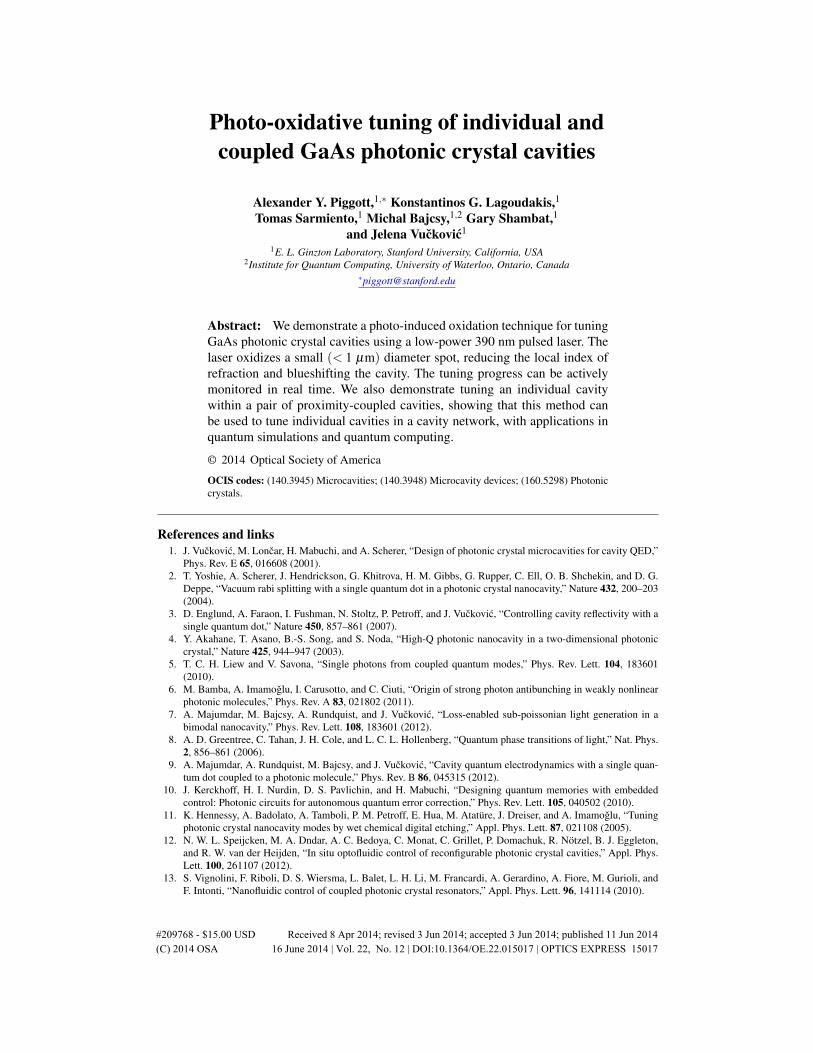
Photo-oxidative tuning of individual andcoupled GaAs photonic crystal cavities
Alexander Y. Piggott,1,∗ Konstantinos G. Lagoudakis,1Tomas Sarmiento,1 Michal Bajcsy,1,2 Gary Shambat,1
and Jelena Vuckovic1
1E. L. Ginzton Laboratory, Stanford University, California, USA2Institute for Quantum Computing, University of Waterloo, Ontario, Canada
Abstract: We demonstrate a photo-induced oxidation technique for tuningGaAs photonic crystal cavities using a low-power 390 nm pulsed laser. Thelaser oxidizes a small (< 1 µm) diameter spot, reducing the local index ofrefraction and blueshifting the cavity. The tuning progress can be activelymonitored in real time. We also demonstrate tuning an individual cavitywithin a pair of proximity-coupled cavities, showing that this method canbe used to tune individual cavities in a cavity network, with applications inquantum simulations and quantum computing.
© 2014 Optical Society of America
OCIS codes: (140.3945) Microcavities; (140.3948) Microcavity devices; (160.5298) Photoniccrystals.
References and links1. J. Vuckovic, M. Loncar, H. Mabuchi, and A. Scherer, “Design of photonic crystal microcavities for cavity QED,”
Phys. Rev. E 65, 016608 (2001).2. T. Yoshie, A. Scherer, J. Hendrickson, G. Khitrova, H. M. Gibbs, G. Rupper, C. Ell, O. B. Shchekin, and D. G.
Deppe, “Vacuum rabi splitting with a single quantum dot in a photonic crystal nanocavity,” Nature 432, 200–203(2004).
3. D. Englund, A. Faraon, I. Fushman, N. Stoltz, P. Petroff, and J. Vuckovic, “Controlling cavity reflectivity with asingle quantum dot,” Nature 450, 857–861 (2007).
4. Y. Akahane, T. Asano, B.-S. Song, and S. Noda, “High-Q photonic nanocavity in a two-dimensional photoniccrystal,” Nature 425, 944–947 (2003).
5. T. C. H. Liew and V. Savona, “Single photons from coupled quantum modes,” Phys. Rev. Lett. 104, 183601(2010).
6. M. Bamba, A. Imamoglu, I. Carusotto, and C. Ciuti, “Origin of strong photon antibunching in weakly nonlinearphotonic molecules,” Phys. Rev. A 83, 021802 (2011).
7. A. Majumdar, M. Bajcsy, A. Rundquist, and J. Vuckovic, “Loss-enabled sub-poissonian light generation in abimodal nanocavity,” Phys. Rev. Lett. 108, 183601 (2012).
8. A. D. Greentree, C. Tahan, J. H. Cole, and L. C. L. Hollenberg, “Quantum phase transitions of light,” Nat. Phys.2, 856–861 (2006).
9. A. Majumdar, A. Rundquist, M. Bajcsy, and J. Vuckovic, “Cavity quantum electrodynamics with a single quan-tum dot coupled to a photonic molecule,” Phys. Rev. B 86, 045315 (2012).
10. J. Kerckhoff, H. I. Nurdin, D. S. Pavlichin, and H. Mabuchi, “Designing quantum memories with embeddedcontrol: Photonic circuits for autonomous quantum error correction,” Phys. Rev. Lett. 105, 040502 (2010).
11. K. Hennessy, A. Badolato, A. Tamboli, P. M. Petroff, E. Hua, M. Atature, J. Dreiser, and A. Imamoglu, “Tuningphotonic crystal nanocavity modes by wet chemical digital etching,” Appl. Phys. Lett. 87, 021108 (2005).
12. N. W. L. Speijcken, M. A. Dndar, A. C. Bedoya, C. Monat, C. Grillet, P. Domachuk, R. Notzel, B. J. Eggleton,and R. W. van der Heijden, “In situ optofluidic control of reconfigurable photonic crystal cavities,” Appl. Phys.Lett. 100, 261107 (2012).
13. S. Vignolini, F. Riboli, D. S. Wiersma, L. Balet, L. H. Li, M. Francardi, A. Gerardino, A. Fiore, M. Gurioli, andF. Intonti, “Nanofluidic control of coupled photonic crystal resonators,” Appl. Phys. Lett. 96, 141114 (2010).
#209768 - $15.00 USD Received 8 Apr 2014; revised 3 Jun 2014; accepted 3 Jun 2014; published 11 Jun 2014(C) 2014 OSA 16 June 2014 | Vol. 22, No. 12 | DOI:10.1364/OE.22.015017 | OPTICS EXPRESS 15017

14. T. Cai, R. Bose, G. S. Solomon, and E. Waks, “Controlled coupling of photonic crystal cavities using pho-tochromic tuning,” Appl. Phys. Lett. 102, 141118 (2013).
15. A. Faraon, D. Englund, D. Bulla, B. Luther-Davies, Benjamin, J. Eggleton, N. Stoltz, P. Petroff, and J. Vuckovic,“Local tuning of photonic crystal cavities using chalcogenide glasses,” Appl. Phys. Lett. 92, 043123 (2008).
16. H. S. Lee, S. Kiravittaya, S. Kumar, J. D. Plumhof, L. Balet, L. H. Li, M. Francardi, A. Gerardino, A. Fiore,A. Rastelli, and O. G. Schmidt, “Local tuning of photonic crystal nanocavity modes by laser-assisted oxidation,”Appl. Phys. Lett. 95, 191109 (2009).
17. K. Hennessy, C. Hogerle, E. Hu, A. Badolato, and A. Imamolu, “Tuning photonic nanocavities by atomic forcemicroscope nano-oxidation,” Appl. Phys. Lett. 89, 041118 (2006).
18. F. Intonti, N. Caselli, S. Vignolini, F. Riboli, S. Kumar, A. Rastelli, O. G. Schmidt, M. Francardi, A. Gerardino,L. Balet, L. H. Li, A. Fiore, and M. Gurioli, “Mode tuning of photonic crystal nanocavities by photoinducednon-thermal oxidation,” Appl. Phys. Lett. 100, 033116 (2012).
19. I. J. Luxmoore, E. D. Ahmadi, B. J. Luxmoore, N. A. Wasley, A. I. Tartakovskii, M. Hugues, M. S. Skolnick, andA. M. Fox, “Restoring mode degeneracy in H1 photonic crystal cavities by uniaxial strain tuning,” Appl. Phys.Lett. 100, 121116 (2012).
20. Y. Gong, B. Ellis, G. Shambat, T. Sarmiento, J. S. Harris, and J. Vuckovic, “Nanobeam photonic crystal cavityquantum dot laser,” Opt. Express 18, 8781–8789 (2010).
21. B. Ellis, M. A. Mayer, G. Shambat, T. Sarmiento, J. Harris, E. E. Haller, and J. Vuckovic, “Ultralow-thresholdelectrically pumped quantum-dot photonic-crystal nanocavity laser,” Nat. Photon. 5, 297–300 (2011).
22. E. M. Purcell, “Spontaneous emission probabilities at radio frequencies,” Phys. Rev. 69, 681 (1946).23. H. A. Haus and W. Huang, “Coupled-mode theory,” Proc. IEEE 79, 1505–1518 (1991).24. C. Yu, D. Podlesnik, M. Schmidt, H. Gilgen, and R. M. Osgood Jr., “Ultraviolet-light-enhanced oxidation of
gallium arsenide surfaces studied by x-ray photoelectron and auger electron spectroscopy,” Chem. Phys. Lett.130, 301–306 (1986).
25. C. F. Yu, M. T. Schmidt, D. V. Podlesnik, , and R. M. Osgood, “Wavelength dependence of optically inducedoxidation of GaAs(100),” J. Vac. Sci. Technol. B 5, 1087–1091 (1987).
26. Z. Lu, M. T. Schmidt, D. V. Podlesnik, C. F. Yu, and R. M. Osgood, “Ultraviolet-light-induced oxide formationon GaAs surfaces,” J. Chem. Phys. 93, 7951–7961 (1990).
27. J. Petykiewicz, G. Shambat, B. Ellis, and J. Vuckovic, “Electrical properties of GaAs photonic crystal cavitylateral p-i-n diodes,” Appl. Phys. Lett. 101, 011104 (2012).
28. E. D. Palik, Handbook of Optical Constants of Solids (Elsevier, 1997).29. S. M. Sze, Semiconductor Sensors (John Wiley, 1994).
1. Introduction
Photonic crystal cavities have been extensively used in studies of cavity quantum-electrodynamics (cQED) [1–3] owing to their ability to strongly confine light with high qualityfactors [4]. Extending this work, a wide range of quantum computing and quantum simulationproposals using coupled cavity networks have been put forward. These include sub-Poissonianlight generation [5–7], the quantum simulation of exotic many-body systems [8, 9], and quan-tum error correction [10]. GaAs is an excellent material for fabricating these coupled-cavitynetworks since thin membranes with embedded quantum dots can be grown epitaxially.
Managing cavity frequency variations caused by fabrication imperfections is a major chal-lenge that must be overcome in order to implement systems based on coupled-cavity networks.Coupled cavity devices require the cavity resonances to be spectrally aligned with each other,but the resonant wavelength of identically designed photonic crystal cavities typically variesby several nanometers, even for devices only a few microns apart [7]. Thus, there has beenconsiderable interest in the post-fabrication tuning of photonic crystal cavities.
A number of techniques for post-fabrication tuning of GaAs photonic crystal cavities havebeen demonstrated. These include wet etching [11], infiltration of water [12, 13], depositionof photosensitive materials [14, 15], thermal oxidation [16], atomic-force microscope (AFM)oxidation [17], green laser photo-oxidation [18], and application of strain to the entire chip [19].However, many of these techniques are not well localized and hence cannot be used to tuneindividual cavities in coupled cavity configurations, while others require the application offluids or polymers, or the use of an AFM.
We describe a more convenient technique for tuning GaAs photonic crystal cavities using
#209768 - $15.00 USD Received 8 Apr 2014; revised 3 Jun 2014; accepted 3 Jun 2014; published 11 Jun 2014(C) 2014 OSA 16 June 2014 | Vol. 22, No. 12 | DOI:10.1364/OE.22.015017 | OPTICS EXPRESS 15018
(a) (c)
(b) (d)
Fig. 1. (a,b) The transverse electric field (Ey) distribution for the fundamental modes ofa (a) single L3 cavity and (b) two coupled L3 cavities, calculated in a finite-differencetime domain (FDTD) simulation. The coupled cavity supports both anti-symmetric andsymmetric modes; here we have plotted the latter. The black circles indicate the locationsof the holes in the photonic crystal membrane. (c,d) Scanning electron microscopy (SEM)images of a single (c) and coupled (d) GaAs L3 cavities, taken before performing anytuning.
390 nm pulsed laser light to introduce photo-induced oxidation. The laser oxidizes a small(< 1 µm) diameter spot, lowering the local index of refraction and blueshifting the cavity. Ourapproach exploits the same physical mechanism used by Intonti et al. [18], which utilized a532 nm laser at a relatively high power (700 µW). By using a shorter-wavelength laser, wewere able to reduce the tuning power by nearly two orders of magnitude while maintainingsimilar tuning rates, potentially enabling tuning of fragile structures such as nanobeam cavities[20]. Finally, to demonstrate the resolution and utility of our approach, we demonstrate tuningindividual cavities in proximity-coupled pairs of cavities.
2. Experimental technique
The photonic crystal cavities used in this experiment were L3 cavities in a triangular photoniccrystal lattice [4], with lattice constant a = 336 nm and design hole radius r = 0.212a. Thefundamental mode for the L3 cavity calculated using finite-difference time-domain (FDTD)simulations is plotted in Fig. 1(a), and has a simulated quality factor of ∼ 4×10⁴. We tested theproposed tuning mechanism on both individual cavities and pairs of proximity-coupled cavities.The coupled L3 defects were placed 5 lattice periods apart, with a spectral splitting of 1.2 nmcalculated using FDTD. Scanning electron microscopy (SEM) images of these structures areshown in Figs. 1(c) and 1(d).
The photonic crystal cavities were fabricated from GaAs wafers grown using molecular beam
#209768 - $15.00 USD Received 8 Apr 2014; revised 3 Jun 2014; accepted 3 Jun 2014; published 11 Jun 2014(C) 2014 OSA 16 June 2014 | Vol. 22, No. 12 | DOI:10.1364/OE.22.015017 | OPTICS EXPRESS 15019
epitaxy, as described in detail in previous work [21]. The structure was grown on a GaAs sub-strate by molecular beam epitaxy and consisted of a 1500 nm Al0.8Ga0.2As sacrificial layer anda 220 nm GaAs membrane. The GaAs membrane contained 3 layers of high-density InAs quan-tum dots
(300 dots/µm2
)emitting at ∼ 1300 nm. The photonic crystal cavities were fabricated
using electron-beam lithography, inductively-coupled plasma reactive-ion etching (ICP-RIE),and a final HF acid undercutting step, as described previously [3].
The tuning was performed in a custom confocal microscopy setup coupled to a grat-ing spectrometer with an InGaAs linear photodiode array. A Carl Zeiss LD-Plan-Neofluar63x/0.75 Korr was used as the microscope objective. A charge-coupled device (CCD) wasused to image the sample and determine where the lasers were focused. The experiments wereall performed at room temperature in air, with the exception of a control test conducted invacuum.
The photonic crystal cavities were tuned by simultaneously irradiating the sample with twolasers through the objective: the 390 nm ultraviolet (UV) tuning laser, and an 830 nm near-infrared pump laser to produce photoluminescence (PL) from the embedded quantum dots.
For the tuning laser, we used a frequency-doubled pulsed Ti:Sapphire laser, producing anoutput wavelength of 390 nm, pulse repetition frequency of 80 MHz, and an average powerof 10 µW before the microscope objective. The pulse length was approximately 10 ps afterpassing through a single-mode fiber (SMF) to clean up the beam profile. The UV laser wasfocused either directly on or immediately adjacent to the cavity to be tuned. The spot size ofthe tuning laser was roughly 500−700 nm as estimated from atomic-force microscopy (AFM)scans of photo-oxidized spots.
An 830 nm, 350 µW SMF-coupled continuous-wave multimode diode laser was used as thePL excitation laser. The PL laser was defocused in order to tightly focus the UV tuning laser, soobtaining a bright PL signal required using a high excitation power. Due to the Purcell effect,the spontaneous emission rate from a photonic crystal cavity is strongly enhanced at its resonantfrequencies [22]. The photoluminescence spectrum was thus used to continuously monitor thecavity resonance during the tuning process. In principle, cross-polarized reflectivity could alsobe used to monitor the cavity resonance when tuning non-photoluminescent devices [3].
3. Experimental results
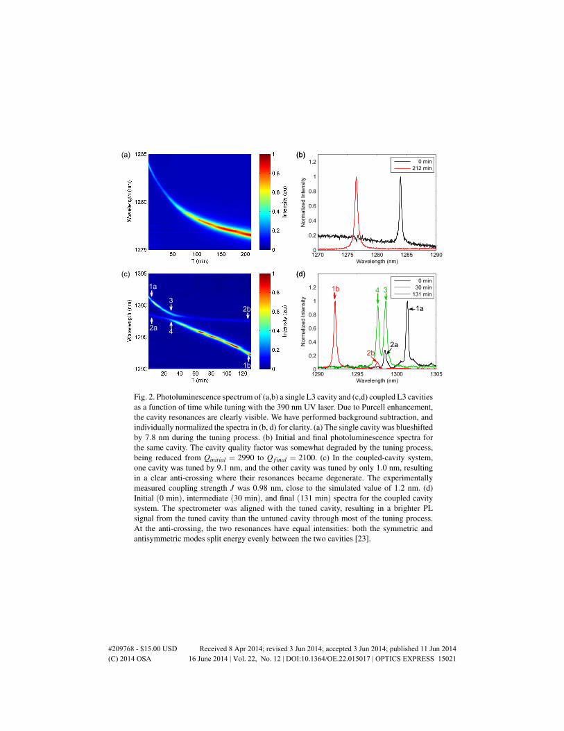
In Fig. 2(a), we present the tuning profile of a single L3 cavity. The tuning rate decreases asa function of time, suggesting a self-limiting mechanism. The tuning rate can be increased byincreasing the UV laser power, but using excessively high power risks causing thermal damage.The initial and final spectra are plotted in Fig. 2(b). During the tuning process, the cavity qual-ity factor was degraded from Qinitial = 2990 to Q f inal = 2100 and the brightness significantlyincreased, most likely due to scattering from the photo-oxidized spot.
Next, in Figs. 2(c) and 2(d) we present the tuning of a single cavity in a proximity-coupledpair of L3 cavities. The behaviour of such a system can be accurately described using coupled-mode theory [23]. Due to the coupling between the cavities, such a system will present tworesonant peaks with frequencies Ω1,Ω2 given by
Ω1,2 =12(ω1 +ω2)±
12
√(ω1 −ω2)
2 + J2 (1)
where ω1,ω2 are the individual cavity frequencies, and J is the coupling between the cavities.We have assumed the cavities are in the strong coupling limit J ωi/Qi, where the Qi is thequality factor of cavity i.
The UV laser was focused on one edge of a cavity, as can be seen in an SEM of the tunedstructure in Fig. 3(c). As the UV laser was applied, the resonant peak at 1298.5 nm remained
#209768 - $15.00 USD Received 8 Apr 2014; revised 3 Jun 2014; accepted 3 Jun 2014; published 11 Jun 2014(C) 2014 OSA 16 June 2014 | Vol. 22, No. 12 | DOI:10.1364/OE.22.015017 | OPTICS EXPRESS 15020
1270 1275 1280 1285 12900
0.2
0.4
0.6
0.8
1
1.2
Wavelengthz(nm)
No
rma
lize
dzIn
ten
sity
0zmin
212zmin
(b)
1290 1295 1300 13050
0.2
0.4
0.6
0.8
1
1.2
Wavelengthz(nm)
No
rma
lize
dzIn
ten
sity
0zmin
30zmin
131zmin
(d)(c)
1a
1b
2a
2b
1b
1a
2a2b
3
4
34
(a) (b)
(d)
Fig. 2. Photoluminescence spectrum of (a,b) a single L3 cavity and (c,d) coupled L3 cavitiesas a function of time while tuning with the 390 nm UV laser. Due to Purcell enhancement,the cavity resonances are clearly visible. We have performed background subtraction, andindividually normalized the spectra in (b, d) for clarity. (a) The single cavity was blueshiftedby 7.8 nm during the tuning process. (b) Initial and final photoluminescence spectra forthe same cavity. The cavity quality factor was somewhat degraded by the tuning process,being reduced from Qinitial = 2990 to Q f inal = 2100. (c) In the coupled-cavity system,one cavity was tuned by 9.1 nm, and the other cavity was tuned by only 1.0 nm, resultingin a clear anti-crossing where their resonances became degenerate. The experimentallymeasured coupling strength J was 0.98 nm, close to the simulated value of 1.2 nm. (d)Initial (0 min), intermediate (30 min), and final (131 min) spectra for the coupled cavitysystem. The spectrometer was aligned with the tuned cavity, resulting in a brighter PLsignal from the tuned cavity than the untuned cavity through most of the tuning process.At the anti-crossing, the two resonances have equal intensities: both the symmetric andantisymmetric modes split energy evenly between the two cavities [23].
#209768 - $15.00 USD Received 8 Apr 2014; revised 3 Jun 2014; accepted 3 Jun 2014; published 11 Jun 2014(C) 2014 OSA 16 June 2014 | Vol. 22, No. 12 | DOI:10.1364/OE.22.015017 | OPTICS EXPRESS 15021
(a) (b) (c)
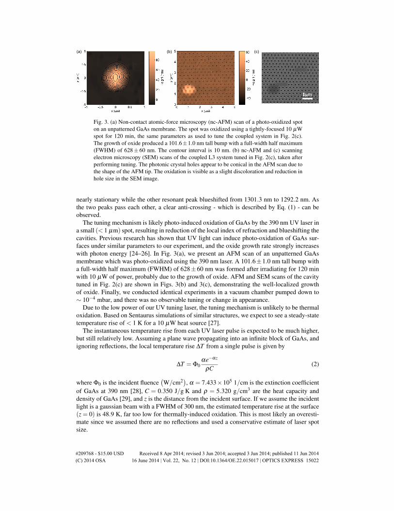
Fig. 3. (a) Non-contact atomic-force microscopy (nc-AFM) scan of a photo-oxidized spoton an unpatterned GaAs membrane. The spot was oxidized using a tightly-focused 10 µWspot for 120 min, the same parameters as used to tune the coupled system in Fig. 2(c).The growth of oxide produced a 101.6±1.0 nm tall bump with a full-width half maximum(FWHM) of 628± 60 nm. The contour interval is 10 nm. (b) nc-AFM and (c) scanningelectron microscopy (SEM) scans of the coupled L3 system tuned in Fig. 2(c), taken afterperforming tuning. The photonic crystal holes appear to be conical in the AFM scan due tothe shape of the AFM tip. The oxidation is visible as a slight discoloration and reduction inhole size in the SEM image.
nearly stationary while the other resonant peak blueshifted from 1301.3 nm to 1292.2 nm. Asthe two peaks pass each other, a clear anti-crossing - which is described by Eq. (1) - can beobserved.
The tuning mechanism is likely photo-induced oxidation of GaAs by the 390 nm UV laser ina small (< 1 µm) spot, resulting in reduction of the local index of refraction and blueshifting thecavities. Previous research has shown that UV light can induce photo-oxidation of GaAs sur-faces under similar parameters to our experiment, and the oxide growth rate strongly increaseswith photon energy [24–26]. In Fig. 3(a), we present an AFM scan of an unpatterned GaAsmembrane which was photo-oxidized using the 390 nm laser. A 101.6±1.0 nm tall bump witha full-width half maximum (FWHM) of 628±60 nm was formed after irradiating for 120 minwith 10 µW of power, probably due to the growth of oxide. AFM and SEM scans of the cavitytuned in Fig. 2(c) are shown in Figs. 3(b) and 3(c), demonstrating the well-localized growthof oxide. Finally, we conducted identical experiments in a vacuum chamber pumped down to∼ 10−4 mbar, and there was no observable tuning or change in appearance.
Due to the low power of our UV tuning laser, the tuning mechanism is unlikely to be thermaloxidation. Based on Sentaurus simulations of similar structures, we expect to see a steady-statetemperature rise of < 1 K for a 10 µW heat source [27].
The instantaneous temperature rise from each UV laser pulse is expected to be much higher,but still relatively low. Assuming a plane wave propagating into an infinite block of GaAs, andignoring reflections, the local temperature rise ∆T from a single pulse is given by
∆T = Φ0αe−αz
ρC(2)
where Φ0 is the incident fluence(W/cm2
), α = 7.433×10⁵ 1/cm is the extinction coefficient
of GaAs at 390 nm [28], C = 0.350 J/g K and ρ = 5.320 g/cm3 are the heat capacity anddensity of GaAs [29], and z is the distance from the incident surface. If we assume the incidentlight is a gaussian beam with a FWHM of 300 nm, the estimated temperature rise at the surface(z = 0) is 48.9 K, far too low for thermally-induced oxidation. This is most likely an overesti-mate since we assumed there are no reflections and used a conservative estimate of laser spotsize.
#209768 - $15.00 USD Received 8 Apr 2014; revised 3 Jun 2014; accepted 3 Jun 2014; published 11 Jun 2014(C) 2014 OSA 16 June 2014 | Vol. 22, No. 12 | DOI:10.1364/OE.22.015017 | OPTICS EXPRESS 15022
4. Conclusion
In conclusion, we have demonstrated a technique for tuning GaAs nanophotonic resonatorswhich requires only a low-power UV laser at room temperature in ambient atmosphere. Inparticular, this technique can be used to independently tune individual cavities in coupled-cavity configurations, enabling a wide variety of quantum computing and quantum simulationdevices based on cavity networks.
Acknowledgments
The authors acknowledge support provided by the Air Force Office of Scientific Research(AFOSR) MURI Center for Multi-Functional Light-Matter Interfaces based on Atoms andSolids (FA9550-09-1-0704), and the AFOSR MURI for Complex and Robust On-chipNanophotonics (FA9550-12-1-0025). AYP acknowledges support from the Stanford GraduateFellowship. KGL acknowledges support from the Swiss National Science Foundation.
#209768 - $15.00 USD Received 8 Apr 2014; revised 3 Jun 2014; accepted 3 Jun 2014; published 11 Jun 2014(C) 2014 OSA 16 June 2014 | Vol. 22, No. 12 | DOI:10.1364/OE.22.015017 | OPTICS EXPRESS 15023