photochemical charge separation at particle...
TRANSCRIPT

Photochemical Charge Separation at Particle Interfaces: Then‑BiVO4−p-Silicon SystemYuxin Yang,†,‡ Jiarui Wang,‡ Jing Zhao,‡ Benjamin A. Nail,‡ Xing Yuan,† Yihang Guo,†
and Frank E. Osterloh*,‡
†School of Environment, Northeast Normal University, Changchun 130117, P.R. China‡Department of Chemistry, University of California, Davis, California 95616, United States
*S Supporting Information
ABSTRACT: The charge transfer properties of interfaces are central to thefunction of photovoltaic and photoelectrochemical cells and photocatalysts.Here we employ surface photovoltage spectroscopy (SPS) to studyphotochemical charge transfer at a p-silicon/n-BiVO4 particle interface.Particle films of BiVO4 on an aluminum-doped p-silicon wafer were obtainedby drop-coating particle suspensions followed by thermal annealing at 353 K.Photochemical charge separation of the films was probed as a function oflayer thickness and illumination intensity, and in the presence of methanol asa sacrificial electron donor. Electron injection from the BiVO4 into the p-silicon is clearly observed to occur and to result in a maximum photovoltageof 150 mV for a 1650 nm thick film under 0.3 mW cm−2 illumination at 3.5eV. This establishes the BiVO4−p-Si interface as a tandem-like junction.Charge separation in the BiVO4 film is limited by light absorption and byslow electron transport to the Si interface, based on time-dependent SPSmeasurements. These problems need to be overcome in functional tandem devices for photoelectrochemical water oxidation.
KEYWORDS: tandem, z-scheme, water splitting, surface photovoltage spectroscopy, photoelectrochemistry, photocatalyst
■ INTRODUCTION
Tandem junctions between two semiconductors are of interestfor the conversion of solar into electrical and chemicalenergy.1−5 Connecting two light absorbers in series increasesthe open circuit voltage of the photovoltaic cell and itsperformance, especially when the semiconductors absorb lightin different ranges of the solar spectrum. This is important forwater splitting cells, which require open circuit voltages inexcess of 1.23 V.6−10 Most of the tandem junctions studied todate consist of well-defined interfaces fabricated by vapordeposition techniques.11−13 For example, Shaner et al. reporteda n-p(+)-Si/n-WO3 microwire junction obtained by successivevacuum deposition of BCl3 to achieve Si p-doping, DC sputtercoating of an ITO ohmic contact, and electrodeposition of n-WO3, followed by annealing at 400 °C for 2 h. The devicesupported overall water splitting with 0.0019% solar tohydrogen (STH) efficiency.12 Recently, there is also increasinginterest in tandem junctions formed between suspendedsemiconductor particles. Such tandem or “z-scheme photo-catalysts” usually employ soluble redox couples for chargetransfer.4,14−17 This is necessary because the rough surfaces ofthe particles preclude controlled charge transfer between thesubsystems. In rare cases the redox couple can be eliminated.18
For example, mixing of Rh:SrTiO3 and BiVO4 particlesuspensions at pH 3.5 produces a junction that supportsoverall water splitting with quantum yields of up to 4.2% at 420
nm and STH efficiency of 0.1%.18,19 However, the details of theelectrical contact and the effects of water and electrolytes on itsfunction are not well understood. In general, junctions betweenparticles are difficult to probe with electrochemical techniques,due to screening effect from electrolytes and due to the slowcharge transport in particulate films. Photocurrents forparticulate electrodes generally do not exceed a few micro-amperes per square centimeter because of the large filmresistance and because of poor redox kinetics at the solid−liquid interface.20−22 The resulting potential drops obscure thephotovoltage at the particle junctions and complicate the datainterpretation. Here we employ surface photovoltage spectros-copy (SPS) to overcome this problem and to shed light onphotochemical charge transfer between particulate lightabsorbers. SPS is a highly sensitive technique23 for theobservation of photochemical charge transfer at nanoscalejunctions.24−26 Because the method relies on potential changes,not currents, it can probe individual junctions without the needfor a coupled redox system.27,28 As initial target system wechoose the combination of bismuth vanadate (BiVO4) and p-silicon. Bismuth vanadate has recently emerged as a promisingphotocatalyst for the water oxidation reaction.11,29 The material
Received: January 9, 2015Accepted: February 20, 2015Published: February 20, 2015
Research Article
www.acsami.org
© 2015 American Chemical Society 5959 DOI: 10.1021/acsami.5b00257ACS Appl. Mater. Interfaces 2015, 7, 5959−5964
has a bandgap of 2.4 eV, but its conduction band edge islocated just short of the thermodynamic proton reductionpotential, making it unsuitable for overall water splitting.30−34
This disadvantage can be overcome by connecting n-BiVO4 inseries with a p-Si as a photocathode. Silicon photocathodeshave been shown to support proton reduction at up to 10 mAcm−2 at 0.20 V underpotential, after addition of Pt or MoS2cocatalysts,35,36 and single crystalline silicon absorbers cangenerate up to 0.71 V photovoltage.37 As we show here, thinfilms of n-BiVO4 on an aluminum-doped silicon wafer can beobtained by simple drop-coating of the BiVO4 particlesuspensions, followed by thermal annealing at 80 °C. Surfacephotovoltage spectra (SPS) of the films prove electron injectionfrom the illuminated BiVO4 layer into Si and photovoltages ofup to 0.15 V generated at the junction, even under low intensityillumination (<10 mW cm−2). This voltage is close to thetheoretical limit for this material combination. The voltageincrease by 44 mV in the presence of absorbed methanol isconsistent with hole injection from BiVO4 into this sacrificialelectron donor. This confirms the functionality of the system asa photoelectrochemical tandem junction. Overall, these resultsshed new light on photochemical charge transfer between metaloxide and main group element absorbers. They are relevant tothe design of future low cost particle-based tandem and z-scheme solar energy conversion devices.
■ RESULTS AND DISCUSSIONThe BiVO4 particles for this study were prepared from Bi2O3and VO2, as described previously,26,38 and their structure andoptical properties were confirmed by XRD and diffusereflectance spectroscopy (Supporting Information Figure S1).According to TEM, the particles are irregularly shaped and havean average size of 81 nm ± 34 nm. Tauc plots (Figure S1d,Supporting Information) yield indirect and direct band gaps of2.45 and 2.57 eV, respectively, similar to previous reports.30
Thin films of n-BiVO4 on aluminum-doped p-type Si wafers orFTO substrates (Figure 1) were obtained by drop-coating
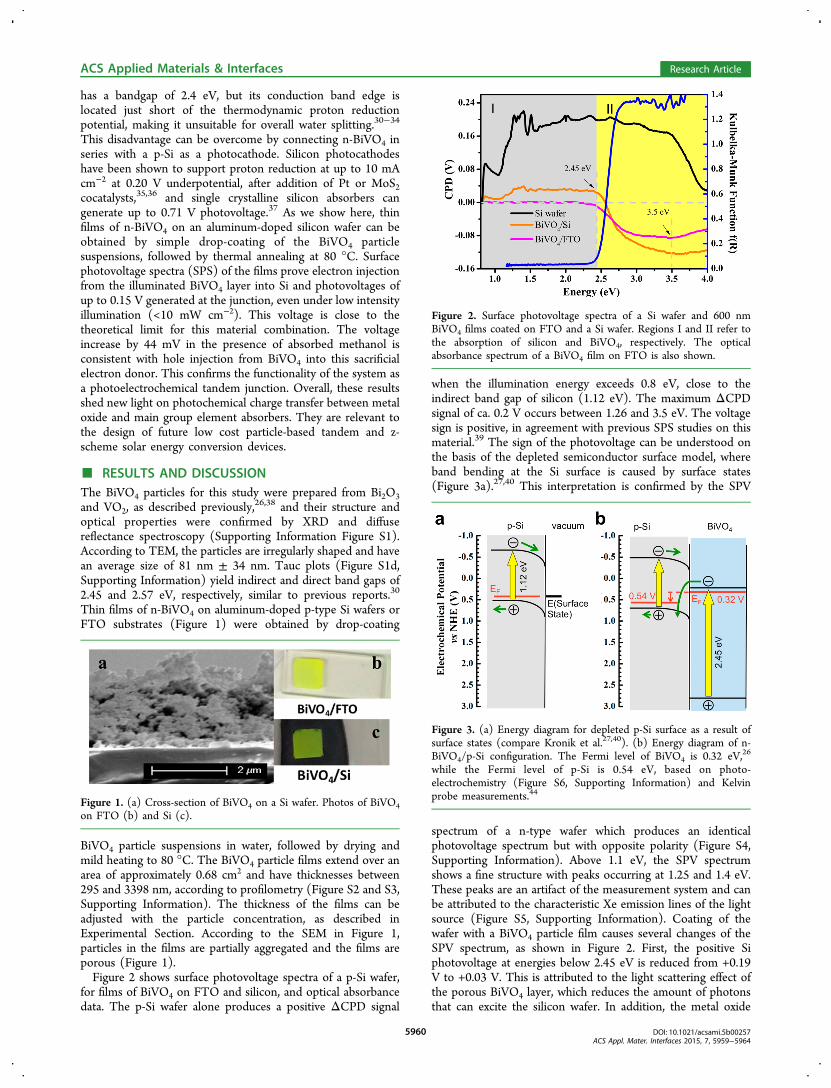
BiVO4 particle suspensions in water, followed by drying andmild heating to 80 °C. The BiVO4 particle films extend over anarea of approximately 0.68 cm2 and have thicknesses between295 and 3398 nm, according to profilometry (Figure S2 and S3,Supporting Information). The thickness of the films can beadjusted with the particle concentration, as described inExperimental Section. According to the SEM in Figure 1,particles in the films are partially aggregated and the films areporous (Figure 1).Figure 2 shows surface photovoltage spectra of a p-Si wafer,
for films of BiVO4 on FTO and silicon, and optical absorbancedata. The p-Si wafer alone produces a positive ΔCPD signal
when the illumination energy exceeds 0.8 eV, close to theindirect band gap of silicon (1.12 eV). The maximum ΔCPDsignal of ca. 0.2 V occurs between 1.26 and 3.5 eV. The voltagesign is positive, in agreement with previous SPS studies on thismaterial.39 The sign of the photovoltage can be understood onthe basis of the depleted semiconductor surface model, whereband bending at the Si surface is caused by surface states(Figure 3a).27,40 This interpretation is confirmed by the SPV
spectrum of a n-type wafer which produces an identicalphotovoltage spectrum but with opposite polarity (Figure S4,Supporting Information). Above 1.1 eV, the SPV spectrumshows a fine structure with peaks occurring at 1.25 and 1.4 eV.These peaks are an artifact of the measurement system and canbe attributed to the characteristic Xe emission lines of the lightsource (Figure S5, Supporting Information). Coating of thewafer with a BiVO4 particle film causes several changes of theSPV spectrum, as shown in Figure 2. First, the positive Siphotovoltage at energies below 2.45 eV is reduced from +0.19V to +0.03 V. This is attributed to the light scattering effect ofthe porous BiVO4 layer, which reduces the amount of photonsthat can excite the silicon wafer. In addition, the metal oxide
Figure 1. (a) Cross-section of BiVO4 on a Si wafer. Photos of BiVO4on FTO (b) and Si (c).
Figure 2. Surface photovoltage spectra of a Si wafer and 600 nmBiVO4 films coated on FTO and a Si wafer. Regions I and II refer tothe absorption of silicon and BiVO4, respectively. The opticalabsorbance spectrum of a BiVO4 film on FTO is also shown.
Figure 3. (a) Energy diagram for depleted p-Si surface as a result ofsurface states (compare Kronik et al.27,40). (b) Energy diagram of n-BiVO4/p-Si configuration. The Fermi level of BiVO4 is 0.32 eV,26
while the Fermi level of p-Si is 0.54 eV, based on photo-electrochemistry (Figure S6, Supporting Information) and Kelvinprobe measurements.44
ACS Applied Materials & Interfaces Research Article
DOI: 10.1021/acsami.5b00257ACS Appl. Mater. Interfaces 2015, 7, 5959−5964
5960

reduces the band bending at the Si surface by about 60%(Figure 3b and discussion below). Second, the p-Si/n-BiVO4system contains a new negative photovoltage feature at >2.45eV (region II), which is due to band gap excitation of n-BiVO4and electron transfer to silicon. This assignment can be verifiedby comparison with the optical spectrum of BiVO4 and its SPVspectrum on FTO (Figure 2). While on FTO the maximumphotovoltage is −0.083 V at 3.5 eV, on silicon it reaches −0.15V. This shows that electron injection from BiVO4 into Si ismore favorable than electron injection into FTO.Charge transfer at the p-Si−BiVO4 contact can be under-
stood with the energy scheme in Figure 3b. Based on thedifference of Fermi levels, Ef(p-Si) − Ef(BiVO4) = 0.54 − 0.32= 0.22 eV, the driving force for electron transfer from n-BiVO4to p-Si is 0.22 eV per electron. The experimental photovoltageof −0.15 V comes close to this value. The negative sign of thephotovoltage also rules out the possibility of a p-/n-junction atthe silicon−BiVO4 interface. The expected band bending forsuch a junction would repel electrons in BiVO4 from theinterface and produce a positive photovoltage. The absence of an-/p-junction is a consequence of the low carrier concentrationin BiVO4 which does not allow an electrochemical equilibriumwith p-Si in the dark. This is analogous to the HCa2Nb3O10/Aucontact described previously.24 The BiVO4/FTO contact is alsoohmic. Here the driving force for electron injection is Ef(FTO)− Ef(BiVO4) = 0.56 (±0.1)41 − 0.32 = 0.24 (±0.1) eV. Theobserved photovoltage of −0.083 V is much lower. This isattributed decreased physical contact resulting from the highsurface roughness of FTO,42 or due to specific ion absorption.43
To obtain additional insight into the factors that governphotochemical charge separation in the p-Si−BiVO4 system,SPV spectra were recorded for BiVO4 films of variable thickness(Figure 4). It can be seen that the Si photovoltage (region I)diminishes with increasing BiVO4 thickness, likely as a result oflight scattering by the porous BiVO4 film. Based on opticaltransmission spectra in Figure S7, Supporting Information, theoptical scattering coefficient τ of the porous BiVO4 film can beestimated as 0.072 μm−1 at 2 eV. This means that the thinnestBiVO4 film (295 nm) only blocks about 2% of the incoming 2.0eV photons which cannot explain the significant photovoltagedecrease from +0.19 V (at 2.0 eV from Figure 2) for theuncoated silicon wafer to +0.07 V (at 2.0 eV) for the 295 nmBiVO4 film). Instead, the observed 0.12 V (63%) photovoltagereduction is attributed to a decrease of the band bending at theSi surface, as shown in Figure 3b. Such a reduction would beexpected from modification or elimination of Si surface statesduring coating with BiVO4. The dependence of the photo-voltage in region II on the thickness of the BiVO4 particle layeris shown in Figure 4b. The photovoltage first rises with BiVO4thickness to reach a maximum of −0.15 V for the 1650 nm filmand then decreases to nearly zero for the thickest film. Thistrend can be understood in terms of the finite light absorptiondepth and electron diffusion length of BiVO4. The lightabsorption depth of BiVO4 can be estimated as 250 nm usingthe reported absorption coefficient of 40 000 cm−1 at 420 nm.45
That means a 750 nm thick BiVO4 film absorbs >95% of theincident super band gap photons. Experimentally, this situationis approached for the 1652 nm thick film in Figure 4a, whichgives the greatest photovoltage. This thickness exceeds 750 nmbecause of the high porosity of the BiVO4 film. Thicker filmsabsorb slightly more photons, but electron hole pairs aregenerated further away from the Si/BiVO4 interface, whichmakes injection into the Si wafer more difficult. Experimental
values for the electron diffusion length Le of BiVO4 films rangebetween 10 and 70 nm depending on technique andpreparation.46,47 This confirms that electron transport becomesthe main limitation for the photovoltage, and it explains theobserved photovoltage decrease with increasing film thicknessas seen in Figure 4b. As expected, the operation of the junctionalso depends on light intensity. Voltage measurements underillumination with variable light intensity at 420 nm (2.95 eV)are shown in Figure 5a. At this excitation energy, thephotovoltage is negative, in agreement with the electrontransfer scheme in Figure 3b. For a single junction, the voltageis expected to have a logarithmic dependence on intensity.24 Inthe experiments we observe a slightly parabolic dependence(Figure 5b), which indicates that additional factors, such aslight absorption, play a role. From Figure 5a, it can be seen thatit takes up to 10 min for the voltage to reach a steady state. Thissuggests that electron transport in the BiVO4 film is slow andlimited by diffusion. Indeed, a plot of the photovoltage changerate d(CPD)/dt versus the light power P (Figure S8,Supporting Information) is linear, as expected for a diffusioncontrolled process.Lastly, we probe the ability of the junction to promote
electrochemical oxidation of a sacrificial electron donor. Forthis purpose, p-Si−BiVO4 films are exposed briefly to methanolvapor before the SPS scan is performed under vacuum (Figure6), using the same procedure as previously reported for a
Figure 4. (a) Surface photovoltage spectra of BiVO4−Si junction withvariable BiVO4 thickness (thermal annealing at 80 °C). (b) Peakphotovoltage (ΔCPDmax) at 3.5 eV versus thickness.
ACS Applied Materials & Interfaces Research Article
DOI: 10.1021/acsami.5b00257ACS Appl. Mater. Interfaces 2015, 7, 5959−5964
5961

HCa2Nb3O10 nanocrystal film.24 We find that methanolexposure does increase the photovoltage at 3.5 eV by 0.044V. This confirms that photogenerated holes in BiVO4 cantransfer to methanol. Interestingly, methanol vapor treatmentalso increases the positive photovoltage in region I. Thisindicates that the adsorbed methanol molecules either reducethe optical scattering characteristics of the porous BiVO4 filmor cause a further change of the surface band bending in silicon.
■ CONCLUSION
We present the first study of photochemical charge transport ata p-Si−BiVO4 particle junction made by physical assembly. Thedata confirms that that the components form a functionaltandem or “z-scheme” type junction. Surface photovoltagespectroscopy confirms the ability of the junction to separatecharge, oxidize methanol, and generate a photovoltage close tothe theoretical limit, as defined by the work functions of thecomponents. However, the function of the tandem junction islimited by slow electron transport through the BiVO4 layer andby the need for thick films to absorb all super bandgap photons.Also we find that the p-Si−BiVO4 particle films are toomechanically unstable to be used as a photoelectrode in anelectrochemical cell. These problems need to be overcome intandem junctions for the conversion of photochemical intoelectrical or chemical energy.
■ EXPERIMENTAL SECTIONChemicals. Bismuth(III) oxide (99.9999% Acros Organics) and
vanadium(IV) oxide (99+% Strem Chemicals) were used as received.Acetic acid (glacial, Macron) and nitric acid (68−70%, EMD) wereused after dilution. Water was purified to 18 MΩ·cm resistivity by aNanopure II system. Al-doped (∼1015 cm−3) silicon wafers with aresistivity of 10−100 Ω·cm were purchased from WRS Materials.
BiVO4 Synthesis. BiVO4 was synthesized via a revised solid−solution method.26 At room temperature, 1.15 g (2.5 mmol) of Bi2O3
and 0.42 g (5 mmol) of VO2 were stirred in 25 mL of 1.0 M aqueousacetic acid solution for 11 days. The obtained powder was washed firstwith water and then with 0.5 M nitric acid and again with water. Thewashed powder was vacuum-dried and calcined at 673 K for 5 h in air.
Film Preparation. Fluorine-doped tin oxide (FTO) substrateswere sonicated sequentially in acetone, methanol and 2-propanol,rinsed with water, and dried in air before use. Silicon wafers weresonicated in acetone, ethanol, and water and then washed with 10%HF solution. After a rinse with pure water, they were dried in air. Filmsof BiVO4 were prepared by applying various concentrations of BiVO4
dispersions onto 0.8 × 0.8 cm2 FTO or Si wafers, followed by drying atroom temperature for 12 h and annealing at 353 K for 1 h. Theresulting films have a thickness ranging between 295 and 3398 nm(Figures S2 and S3, Supporting Information). In the photoxidationexperiment, a BiVO4−Si film was exposed to saturated methanol vaporfor 5 min and then dried at 353 K for 1 h.
Characterization. Scanning electron microscopy (SEM) images ofBiVO4−Si films were obtained on a FEI XL30 high-resolutionscanning electron microscope with an operating voltage at 5 kV. UV−vis diffuse reflectance spectra were recorded on a Thermo ScientificEvolution 220 UV−vis spectrometer equipped with an integratingsphere. The reflectance data were converted to the Kubelka−Munkfunction by f(R) = (1 − R)2/(2R) and plotted versus energy. Filmthickness was measured by a Veeco Dektak profilometer.
Surface Photovoltage Spectroscopy (SPS). SPS measurementswere conducted using a vibrating gold Kelvin probe (3 mm diameter,Delta PHI Besocke) mounted inside a home-built vacuum chamber(<1 × 10⁻⁴ mbar). The distance between sample and gold probe is 1mm. Samples were illuminated with monochromatic light (1−10 mW·cm−2) generated by a Cornerstone 130 monochromator behind a 150W Xe arc lamp. A typical photovoltage spectrum was recorded bymonitoring the contact potential difference (CPD) during amonochromatic scan from 0.8 to 4 eV (1550 to 310 nm). Time-dependent photovoltage measurements were performed with 2.95 eV(420 nm) light of variable power. All surface photovoltage spectrawere corrected for drift effects by subtracting dark scan background.
Figure 5. (a) Photovoltage responses of BiVO4 on a Si wafer(thickness ca. 1652 nm) under monochromatic illumination withvariable intensity (0.180−0.282 mW/cm2 at 420 nm, 2.95 eV. (b) Plotof ΔCPD versus the intensity from a.
Figure 6. Photovoltage spectra of BiVO4 on a p-Si wafer in vacuumbefore and after treatment with methanol vapor.
ACS Applied Materials & Interfaces Research Article
DOI: 10.1021/acsami.5b00257ACS Appl. Mater. Interfaces 2015, 7, 5959−5964
5962
■ ASSOCIATED CONTENT*S Supporting InformationAdditional characterization, optical, and photoelectrochemicaldata. This material is available free of charge via the Internet athttp://pubs.acs.org.
■ AUTHOR INFORMATIONCorresponding Author*E-mail: [email protected]. Tel: +1 530-754-6242. Fax:+1-530-752-8995.NotesThe authors declare no competing financial interest.
■ ACKNOWLEDGMENTSWe thank Adam Moule for access to his profilometer andJoshua Greenfield and Kirill Kovnir for XRD data. We aregrateful for financial support from Research Corporation forScience Advancement (Scialog Award) and from the NationalScience Foundation (NSF, grants 1152250 and 1133099). Y.Y.thanks the Natural Science Fund Council of China (51478097,51178092, 51278092, 21173036) for support.
■ REFERENCES(1) Osterloh, F. E. Inorganic Nanostructures for Photoelectrochem-ical and Photocatalytic Water Splitting. Chem. Soc. Rev. 2013, 42,2294−2320.(2) Nozik, A. J. Photochemical Diodes. Appl. Phys. Lett. 1977, 30,567−569.(3) Khaselev, O.; Turner, J. A. A Monolithic Photovoltaic-Photoelectrochemical Device for Hydrogen Production via WaterSplitting. Science 1998, 280, 425−427.(4) Kudo, A. Z-Scheme Photocatalyst Systems for Water Splittingunder Visible Light Irradiation. MRS Bull. 2011, 36, 32−38.(5) Chang, L.; Holmes, M. A.; Waller, M.; Osterloh, F. E.; Moule, A.J. Calcium Niobate Nanosheets as Novel Electron Transport Materialfor Solution-processed Multi-junction Polymer Solar Cell. J. Mater.Chem. 2012, 22, 20443−20450.(6) Hu, S.; Xiang, C. X.; Haussener, S.; Berger, A. D.; Lewis, N. S. AnAnalysis of the Optimal Band Gaps of Light Absorbers in IntegratedTandem Photoelectrochemical Water-Splitting Systems. EnergyEnviron. Sci. 2013, 6, 2984−2993.(7) Ronge, J.; Bosserez, T.; Martel, D.; Nervi, C.; Boarino, L.;Taulelle, F.; Decher, G.; Bordiga, S.; Martens, J. A. Monolithic Cellsfor Solar Fuels. Chem. Soc. Rev. 2014, 43, 7963−7981.(8) Gratzel, M. Mesoscopic Solar Cells for Electricity and HydrogenProduction from Sunlight. Chem. Lett. 2005, 34, 8−13.(9) Walter, M. G.; Warren, E. L.; McKone, J. R.; Boettcher, S. W.; Mi,Q. X.; Santori, E. A.; Lewis, N. S. Solar Water Splitting Cells. Chem.Rev. 2010, 110, 6446−6473.(10) Krol, R., Principles of Photoelectrochemical Cells. In Photo-electrochemical Hydrogen Production, van de Krol, R.; Gratzel, M., Eds.;Springer: New York, 2012; Chapter 2, pp 13−67.(11) Abdi, F. F.; Han, L. H.; Smets, A. H. M.; Zeman, M.; Dam, B.;van de Krol, R., Efficient Solar Water Splitting by Enhanced ChargeSeparation in a Bismuth Vanadate-Silicon Tandem Photoelectrode.Nat. Commun. 2013, 4.(12) Shaner, M. R.; Fountaine, K. T.; Ardo, S.; Coridan, R. H.;Atwater, H. A.; Lewis, N. S. Photoelectrochemistry of Core-ShellTandem Junction n-p(+)-Si/n-WO3 Microwire Array Photoelectrodes.Energy Environ. Sci. 2014, 7, 779−790.(13) Coridan, R. H.; Arpin, K. A.; Brunschwig, B. S.; Braun, P. V.;Lewis, N. S. Photoelectrochemical Behavior of HierarchicallyStructured Si/WO3 Core−Shell Tandem Photoanodes. Nano Lett.2014, 14, 2310−2317.(14) Osterloh, F. E. Inorganic Materials as Catalysts for Photo-chemical Splitting of Water. Chem. Mater. 2008, 20, 35−54.
(15) Abe, R. Recent Progress on Photocatalytic and Photo-electrochemical Water Splitting under Visible Light Irradiation. J.Photochem. Photobiol. C 2010, 11, 179−209.(16) Sayama, K.; Yoshida, R.; Kusama, H.; Okabe, K.; Abe, Y.;Arakawa, H. Photocatalytic Decomposition of Water into H-2 and O-2by a Two-Step Photoexcitation Reaction Using a WO3 SuspensionCatalyst and an Fe3+/Fe2+ Redox System. Chem. Phys. Lett. 1997, 277,387−391.(17) Maeda, K. Z-Scheme Water Splitting Using Two DifferentSemiconductor Photocatalysts. ACS Catal. 2013, 3, 1486−1503.(18) Sasaki, Y.; Nemoto, H.; Saito, K.; Kudo, A. Solar Water SplittingUsing Powdered Photocatalysts Driven by Z-Schematic InterparticleElectron Transfer without an Electron Mediator. J. Phys. Chem. C2009, 113, 17536−17542.(19) Kato, H.; Sasaki, Y.; Shirakura, N.; Kudo, A. Synthesis of HighlyActive Rhodium-Doped SrTiO3 Powders in Z-Scheme Systems forVisible-Light-Driven Photocatalytic Overall Water Splitting. J. Mater.Chem. A 2013, 1, 12327−12333.(20) Maeda, K. Rhodium-Doped Barium Titanate Perovskite as aStable p-Type Semiconductor Photocatalyst for Hydrogen Evolutionunder Visible Light. ACS Appl. Mater. Interfaces 2014, 6, 2167−2173.(21) Liu, J.; Hisatomi, T.; Ma, G.; Iwanaga, A.; Minegishi, T.; Moriya,Y.; Katayama, M.; Kubota, J.; Domen, K. Improving the Photo-electrochemical Activity of La5Ti2CuS5O7 for Hydrogen Evolution byParticle Transfer and Doping. Energy Environ. Sci. 2014, 7, 2239−2242.(22) Joshi, U. A.; Palasyuk, A. M.; Maggard, P. A. Photo-electrochemical Investigation and Electronic Structure of a p-TypeCuNbO3 Photocathode. J. Phys. Chem. C 2011, 115, 13534−13539.(23) Lagowski, J.; Edelman, P.; Kontkiewicz, A. M.; Milic, O.;Henley, W.; Dexter, M.; Jastrzebski, L.; Hoff, A. M. Iron Detection inthe Part Per Quadrillion Range in Silicon Using Surface Photovoltageand Photodissociation of Iron - Boron Pairs. Appl. Phys. Lett. 1993, 63,3043−3045.(24) Zhao, J.; Osterloh, F. E. Photochemical Charge Separation inNanocrystal Photocatalyst Films − Insights from Surface PhotovoltageSpectroscopy. J. Phys. Chem. Lett. 2014, 5, 782−786.(25) Osterloh, F. E.; Holmes, M. A.; Zhao, J.; Chang, L.; Kawula, S.;Roehling, J. D.; Moule, A. J. P3HT:PCBM Bulk-Heterojunctions:Observing Interfacial and Charge Transfer States with SurfacePhotovoltage Spectroscopy. J. Phys. Chem. C 2014, 118, 14723−14731.(26) Wang, J.; Osterloh, F. E. Limiting Factors for PhotochemicalCharge Separation in BiVO4/Co3O4, a Highly Active Photocatalyst forWater Oxidation in Sunlight. J. Mater. Chem. A 2014, 2, 9405−9411.(27) Kronik, L.; Shapira, Y. Surface Photovoltage Spectroscopy ofSemiconductor Structures: At the Crossroads of Physics, Chemistryand Electrical Engineering. Surf. Interface Anal. 2001, 31, 954−965.(28) Lagowski, J. Semiconductor Surface Spectroscopies - The EarlyYears. Surf. Sci. 1994, 299, 92−101.(29) Kudo, A.; Ueda, K.; Kato, H.; Mikami, I. Photocatalytic O-2Evolution under Visible Light Irradiation on BiVO4 in AqueousAgNO3 Solution. Catal. Lett. 1998, 53, 229−230.(30) Park, Y.; McDonald, K. J.; Choi, K. S. Progress in BismuthVanadate Photoanodes for Use in Solar Water Oxidation. Chem. Soc.Rev. 2013, 42, 2321−2337.(31) He, H.; Berglund, S. P.; Rettie, A. J. E.; Chemelewski, W. D.;Xiao, P.; Zhang, Y.; Mullins, C. B. Synthesis of BiVO4 Nanoflake ArrayFilms for Photoelectrochemical Water Oxidation. J. Mater. Chem. A2014, 2, 9371−9379.(32) Hong, S. J.; Lee, S.; Jang, J. S.; Lee, J. S. Heterojunction BiVO4/WO3 Electrodes for Enhanced Photoactivity of Water Oxidation.Energy Environ. Sci. 2011, 4, 1781−1787.(33) Pilli, S. K.; Furtak, T. E.; Brown, L. D.; Deutsch, T. G.; Turner,J. A.; Herring, A. M. Cobalt-Phosphate (Co-Pi) Catalyst Modified Mo-Doped BiVO4 Photoelectrodes for Solar Water Oxidation. EnergyEnviron. Sci. 2011, 4, 5028−5034.(34) Prevot, M. S.; Sivula, K. Photoelectrochemical Tandem Cells forSolar Water Splitting. J. Phys. Chem. C 2013, 117, 17879−17893.(35) Hou, Y.; Abrams, B. L.; Vesborg, P. C. K.; Bjorketun, M. E.;Herbst, K.; Bech, L.; Setti, A. M.; Damsgaard, C. D.; Pedersen, T.;
ACS Applied Materials & Interfaces Research Article
DOI: 10.1021/acsami.5b00257ACS Appl. Mater. Interfaces 2015, 7, 5959−5964
5963

Hansen, O.; Rossmeisl, J.; Dahl, S.; Nørskov, J. K.; Chorkendorff, I.Bioinspired Molecular Co-Catalysts Bonded to a Silicon Photocathodefor Solar Hydrogen Evolution. Nat. Mater. 2011, 10, 434−438.(36) Boettcher, S. W.; Warren, E. L.; Putnam, M. C.; Santori, E. A.;Turner-Evans, D.; Kelzenberg, M. D.; Walter, M. G.; McKone, J. R.;Brunschwig, B. S.; Atwater, H. A.; Lewis, N. S. PhotoelectrochemicalHydrogen Evolution Using Si Microwire Arrays. J. Am. Chem. Soc.2011, 133, 1216−1219.(37) Osterloh, F. E. Maximum Theoretical Efficiency Limit ofPhotovoltaic Devices: Effect of Band Structure on Excited StateEntropy. J. Phys. Chem. Lett. 2014, 3354−3359.(38) Iwase, A.; Kudo, A. Photoelectrochemical Water Splitting UsingVisible-Light-Responsive BiVO4 Fine Particles Prepared in an AqueousAcetic Acid Solution. J. Mater. Chem. 2010, 20, 7536−7542.(39) Burstein, L.; Shapira, Y.; Partee, J.; Shinar, J.; Lubianiker, Y.;Balberg, I. Surface Photovoltage Spectroscopy of Porous Silicon. Phys.Rev. B 1997, 55, R1930−R1933.(40) Kronik, L.; Shapira, Y. Surface Photovoltage Phenomena:Theory, Experiment, and Applications. Surf. Sci. Rep. 1999, 37, 1−206.(41) Helander, M. G.; Greiner, M. T.; Wang, Z. B.; Tang, W. M.; Lu,Z. H. Work function of fluorine doped tin oxide. J. Vac. Sci. Technol. A2011, 29, 011019.(42) Le Formal, F.; Gratzel, M.; Sivula, K. Controlling Photoactivityin Ultrathin Hematite Films for Solar Water-Splitting. Adv. Funct.Mater. 2010, 20, 1099−1107.(43) Chamousis, R. L.; Osterloh, F. E. Use of Potential DeterminingIons to Control Energetics and Photochemical Charge Transfer of aNanoscale Water Splitting Photocatalyst. Energy Environ. Sci. 2014, 7,736−743.(44) Novikov, A. Experimental measurement of work function indoped silicon surfaces. Solid-State Electron. 2010, 54, 8−13.(45) Zhong, D. K.; Choi, S.; Gamelin, D. R. Near-CompleteSuppression of Surface Recombination in Solar Photoelectrolysis by“Co-Pi” Catalyst-Modified W:BiVO4. J. Am. Chem. Soc. 2011, 133,18370−18377.(46) Abdi, F. F.; Savenije, T. J.; May, M. M.; Dam, B.; van de Krol, R.The Origin of Slow Carrier Transport in BiVO4 Thin FilmPhotoanodes: A Time-Resolved Microwave Conductivity Study. J.Phys. Chem. Lett. 2013, 4, 2752−2757.(47) Seabold, J. A.; Zhu, K.; Neale, N. R. Efficient SolarPhotoelectrolysis by Nanoporous Mo:BiVO4 Through ControlledElectron Transport. Phys. Chem. Chem. Phys. 2014, 16, 1121−1131.
ACS Applied Materials & Interfaces Research Article
DOI: 10.1021/acsami.5b00257ACS Appl. Mater. Interfaces 2015, 7, 5959−5964
5964