photoconductivity in high-quality graphene
TRANSCRIPT
Diana Davydovskaya
Supervisor: Prof. Frank Koppens (ICFO - The Institute of Photonic Sciences)
Co-supervisor: Prof. Uli Lemmer (Karlsruhe Institute of Technology, KIT)
Presented on 8th of September 2015
Registered at
Photoconductivity in High-Quality Graphene

i
I herewith declare, that the present thesis is original work written by me alone and
that I have indicated completely and precisely all aids used as well as all citations,
whether changed or unchanged, of other theses and publications.
Diana Davydovskaya
ii
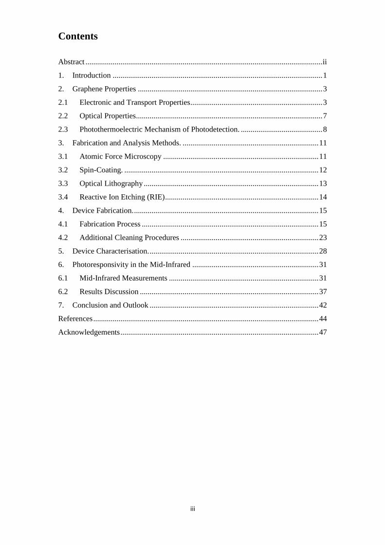
Abstract
Graphene is a relatively new material with unique properties that found application in
the field of electronics and optoelectronics. A broadband absorption makes it
especially interesting for photodetection applications. Middle-infrared domain of
electromagnetic spectrum still lacks active media for photodetection that are cheap, do
not contain toxic elements and do not require additional cooling. This work is focused
on the fabrication of a graphene-based photodetector for middle-infrared domain and
on the photoresponsivity mechanisms in this region where direct absorption by
graphene does not play the dominant role. Several steps to improve the device quality
are considered and the photocurrent measurements in the middle-infrared are
performed and analysed. The substrate properties such as dielectric permittivity
dispersion of the silicon oxide and the hyperbolic nature of hexagonal Boron Nitride
are found to introduce essential contribution to the photocurrent enhancement
mechanism.
iii
Contents
Abstract .......................................................................................................................... ii
1. Introduction ............................................................................................................ 1
2. Graphene Properties ............................................................................................... 3
2.1 Electronic and Transport Properties .................................................................... 3
2.2 Optical Properties ................................................................................................ 7
2.3 Photothermoelectric Mechanism of Photodetection. .......................................... 8
3. Fabrication and Analysis Methods. ...................................................................... 11
3.1 Atomic Force Microscopy ................................................................................ 11
3.2 Spin-Coating. .................................................................................................... 12
3.3 Optical Lithography .......................................................................................... 13
3.4 Reactive Ion Etching (RIE) ............................................................................... 14
4. Device Fabrication. ............................................................................................... 15
4.1 Fabrication Process ........................................................................................... 15
4.2 Additional Cleaning Procedures ....................................................................... 23
5. Device Characterisation. ....................................................................................... 28
6. Photoresponsivity in the Mid-Infrared ................................................................. 31
6.1 Mid-Infrared Measurements ............................................................................. 31
6.2 Results Discussion ............................................................................................ 37
7. Conclusion and Outlook ....................................................................................... 42
References .................................................................................................................... 44
Acknowledgements ...................................................................................................... 47
1
1. Introduction
Graphene, an one-atom thin carbon film, attracts much attention of scientific
community starting from 2004, when it was firstly separated from a bulk graphite by
K.Novoselov and A. Geim. [1] Since then graphene field was developing rapidly both
in fundamental science and application directions. Graphene unique electronic and
optical properties in combination with cheap and simple fabrication process and
silicon electronics compatibility made it a very promising material for optoelectronics
application. [2] High carrier mobility [3], electrostatically tuneable doping and
conductivity type, high transparency, impermeability to gases and mechanical
strength [4] just to name a few of them.
Photodetection is one of the optoelectronics areas where graphene is actively
employed both as part of the readout electronics and as the active media. Broadband
constant absorption from ultra-violet to near infrared and absorption peak in terahertz
region [5] make graphene a promising cheap alternative to materials currently used in
photodetection. The near-infrared (NIR) and middle-infrared regions of the
electromagnetic spectrum specifically lack low-price and environment friendly
materials that could operate at room temperature. To introduce a new active
photodetection material with broadband detection is an interesting task and graphene
appears to be an appropriate choice. Nevertheless, a drop in absorption spectrum in
the middle-Infrared spectral domain introduce a challenge for graphene-based
photodetectors in this region.
This work is focused on the fabrication of graphene devices with p-n junction that
enable photodetection in middle-infrared spectral region. In contrast to direct
absorption process in the visible (VIS) and NIR regions, we exploit here absorption
enhancement mechanism as surface plasmons [5] or device substrate phonons
contribution. [6]
This thesis consist of 8 sections. The second section gives the necessary theoretical
background and discusses graphene electronic and optical properties, photodetection
mechanism and substrate contribution to the graphene devices performance. The third
section describes the methods that were employed for device fabrication and analysis.

2
The fourth section describes the device fabrication process with focusing on the
possible measures to improve the device quality. In the fifths section the device
characterization by transport measurements is presented. The sixth sections focuses on
the photocurrent generation mechanism in middle-infrared region, the spatially- and
spectrally-resolved measurements are presented and the experimental results are
analysed and discussed. The conclusion part gives a short summery of the work and
the outlook to the further steps in the device fabrication improvement and hypothesis
proof.
3
2. Graphene Properties
2.1 Electronic and Transport Properties
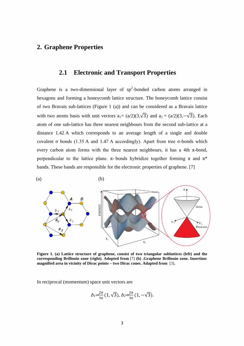
Graphene is a two-dimensional layer of sp2-bonded carbon atoms arranged in
hexagons and forming a honeycomb lattice structure. The honeycomb lattice consist
of two Bravais sub-lattices (Figure 1 (a)) and can be considered as a Bravais lattice
with two atoms basis with unit vectors a1= (a/2)(3,√3) and a2 = (a/2)(3,−√3). Each
atom of one sub-lattice has three nearest neighbours from the second sub-lattice at a
distance 1.42 A which corresponds to an average length of a single and double
covalent σ bonds (1.35 A and 1.47 A accordingly). Apart from tree σ-bonds which
every carbon atom forms with the three nearest neighbours, it has a 4th π-bond,
perpendicular to the lattice plane. π- bonds hybridize together forming π and π*
bands. These bands are responsible for the electronic properties of graphene. [7]
(a) (b)
Figure 1. (a) Lattice structure of graphene, consist of two triangular sublattices (left) and the
corresponding Brillouin zone (right). Adopted from [7] (b) .Graphene Brillouin zone. Insertion:
magnified area in vicinity of Dirac points – two Dirac cones. Adapted from [3].
In reciprocal (momentum) space unit vectors are
b1=2𝜋
3𝑎(1, √3), b2=
2𝜋
3𝑎(1, −√3).
4
Special points of the Brillouin zone are the so-called Dirac points where the π*-band
(or conduction band) touches the π (valence) band forming a zero-bandgap structure.
They are located in the corners of Brillouin zone. Valence and conductance band are
degenerate at Dirac points. [8]
Dirac points play a similar role in graphene band structure as Γ-point in
semiconductor physics. All the electronic properties of graphene are defined in the
vicinity of Dirac points.
The energy dispersion in the close to the Dirac points has linear character for both
charge carriers, electrons and holes. Linear dispersion close to the Dirac points can be
described by a Dirac equation of massless fermions.
Assuming that every atom in the lattice interacts only with the three closest neighbour
atoms (nearest-neighbour approximation) the tight-binding Hamiltonian in the vicinity
of the Dirac points can be written as
𝐻 = (∆ ℏ𝑣𝐹(𝑘𝑥 − 𝑖𝑘𝑦)
ℏ𝑣𝐹(𝑘𝑥 + 𝑖𝑘𝑦) ∆),
where 𝑣𝐹 ≈ 106m/s is the Fermi velocity, 2∆ is the bandgap. It can take a non-zero
value in the case of some perturbations introduced to the graphene lattice. [9]
This results in energy dispersion relation for both bands:
𝐸±(𝑘) = ±√∆2 + (ℏ𝑉𝐹𝑘)2,
Because of the described linear energy dispersion near Dirac points, charge carriers in
graphene can be considered as massless fermions moving with effective speed 1/300
of speed of light in vacuum. This results in a very high carrier mobility which for
suspended graphene reaches 200 000 cm2/(Vs). [8] High mobility makes graphene a
very promising material for high speed electronics.
Nevertheless in real graphene devices the carrier mobility is limited by scattering on
the substrate phonons and charge impurities. For that reason the substrate choice is a
critical question for graphene devices performance.
Another interesting property of graphene is its electrostatically tuneable doping. [1]
A typical device where an electrostatic field is used to provide doping in graphene is
the following: a slab of dielectric material (Silicon Oxide (SiO2) in the case of first
5
graphene devices) separates the sheet of graphene from the conducting backgate. This
configuration can be considered as a parallel-plate capacitor with graphene sheet
being one of the conducting plates. A change in the backgate voltage induces
accumulation of surface charges in the graphene sheet with sign opposite to the gate
voltage as shown on Figure 2 (a). The density of the induced carriers can be
calculated using the following Eq.1
𝑛 =
𝜀𝜀0𝑉𝑔
𝑒𝑑, Eq.1
where 𝜀0 and 𝜀 are the free space and the dielectric permittivity respectively, 𝑑 is the
thickness of the dielectric, 𝑉𝑔 is the gate voltage and 𝑒 is the elementary charge.
(a) (b)
Figure 2. (a) Scheme of a capacitor-like configuration of a graphene device. Sheet of graphene is
separated from gold plane electrode by a slab of dielectric. Voltage applied to the gold electrode
results in accumulation of surface charges in graphene via capacitor-coupling. (b) Gate
dependence of graphene device resistance. It exhibits a sharp peak at Dirac voltage where charge
concentration is minimal and decreased with carrier density increase governed by gate voltage.
Taken from [10].
Electrostatic doping changes the Fermi energy of graphene according to the Eq.2
𝐸𝐹 = ℏ𝑉𝐹√𝜋|𝑛|, Eq.2
where ℏ is the Planck constant and 𝑉𝐹 is the Fermi velocity. Change in the Fermi
energy level changes carrier density and conductivity type. Because graphene has a
zero-bandgap, the conductivity type can be tuned from electron-based to hole-based.
6
The graphene conductivity depends on the induced doping and can be calculated
according to the Drude conductivity equation (Eq.3)
𝜎 =
1
𝜌= 𝑛𝑒𝜇, Eq.3
where 𝜇 is the carrier mobility, 𝜌 is the graphene resistivity. The schematic model
with Dirac cones and typical dependence of graphene resistivity on the gate voltage is
shown on Figure 2 (b). Graphene resistivity exhibits a sharp peak at the Dirac point
where graphene doping theoretically is zero. In real graphene devices the situation of
zero doping can not be observed due to impurities and disorder. Residual doping also
called “electron-hole puddles” is always present in graphene sheet even at the Dirac
voltage.
Although having potentially very high charge carrier mobility, in real devices
graphene does not exhibit the theoretically expected high value. Different scattering
mechanisms decrease the main free path of the graphene charge carriers and therefore
decrease its conductivity and mobility. There are three main scattering mechanisms in
graphene devices: scattering at the phonons, Coulomb scattering at the charged
impurities and scattering at the defects (short-range scattering).
Scattering at the phonons can include both scattering at the graphene phonons and
scattering at the substrate phonons.
Coulomb scattering occurs due to electrostatic potential inhomogeneity caused by
charged impurities (trapped ions as an example) in the device substrate. The graphene
conductivity is inversely proportional to the charged impurities density 𝜎~𝑛
𝑛𝑖 where ni
is the density of impurities, randomly distributed in the substrate and n is the graphene
doping. Short-range scattering occurs mostly due to graphene imperfections – flake
cracks and vacancy defects. The conductivity dependence on the defects density
exhibits the same inversely proportional character as in the case of charged
impurities. [8]
The graphene flake quality and the substrate choice are the critical points for graphene
device transport characteristics.
7
The mainly used substrate for first graphene devices SiO2 did not allow to achieve
graphene carrier mobility above 10 000-15 000 cm2/(Vs). [11] SiO2 surface
roughness, scattering on the phonons and charge impurities – all these mechanisms
are limiting low-temperature mobility. [12] The Coulomb scattering mechanism
associated to the SiO2 substrate or the SiO2-graphene interface is thought to be the
main degradation channel. [13]
Hexagonal Boron Nitride (hBN) was proposed to be a better substrate for high
mobility graphene devices. [12], [14] hBN is a dielectric material (permittivity
constant ≈3-4) with a large bandgap of 5.97 eV. It has a hexagonal graphene-like
lattice with Boron and Nitrogen atoms occupying A and B sublattices and a small
lattice constant mismatch of 1.7% with graphene. Strong ionic bonds in the hexagonal
lattice plane should make the material considerably inert and free from the surface
dandling bonds and charged impurities. Moreover, the larger energy of hBN phonon
resonance compared to SiO2 surface phonon is expected to improve the
hBN-graphene devices high-temperature characteristics.
2.2 Optical Properties
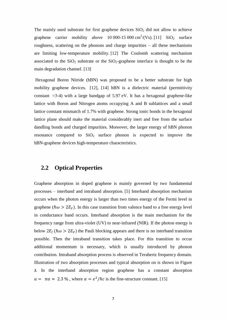
Graphene absorption in doped graphene is mainly governed by two fundamental
processes – interband and intraband absorption. [5] Interband absorption mechanism
occurs when the photon energy is larger than two times energy of the Fermi level in
graphene (ℏ𝜔 > 2𝐸𝐹). In this case transition from valence band to a free energy level
in conductance band occurs. Interband absorption is the main mechanism for the
frequency range from ultra-violet (UV) to near-infrared (NIR). If the photon energy is
below 2Ef (ℏ𝜔 > 2𝐸𝐹) the Pauli blocking appears and there is no interband transition
possible. Then the intraband transition takes place. For this transition to occur
additional momentum is necessary, which is usually introduced by phonon
contribution. Intraband absorption process is observed in Terahertz frequency domain.
Illustration of two absorption processes and typical absorption on is shown in Figure
3. In the interband absorption region graphene has a constant absorption
𝑎 = 𝜋𝛼 ≈ 2.3 % , where 𝛼 = 𝑒2/ℏ𝑐 is the fine-structure constant. [15]
8
(a) (b)
Figure 3. (a) Illustration of an absorption spectrum of doped graphene. Terahertz region has a
peak due intraband absorption, absorption in Mid-IR region exhibits an absorption drop because
in this region a transfer from interband to intraband absorption process takes place, absorption
in NIR-UV region has a constant value of 2.3%. Adapted from [5] (b) Illustration of absorption
mechanisms in doped graphene. If Photon energy is bigger than 2Ef, interband transition occurs
(Left Dirac cone). If Photon energy is lower than 2Ef, interband transition is forbidden due to
Pauli blocking and intraband transition occurs.
2.3 Photothermoelectric Mechanism of Photodetection.
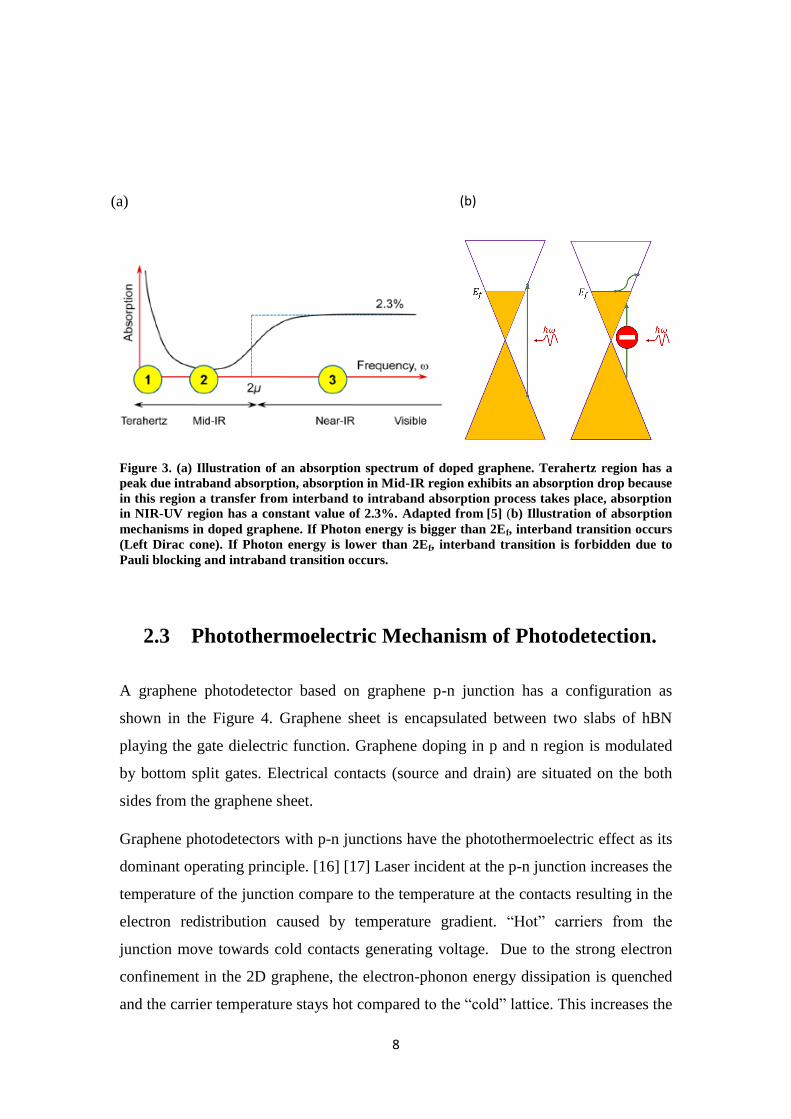
A graphene photodetector based on graphene p-n junction has a configuration as
shown in the Figure 4. Graphene sheet is encapsulated between two slabs of hBN
playing the gate dielectric function. Graphene doping in p and n region is modulated
by bottom split gates. Electrical contacts (source and drain) are situated on the both
sides from the graphene sheet.
Graphene photodetectors with p-n junctions have the photothermoelectric effect as its
dominant operating principle. [16] [17] Laser incident at the p-n junction increases the
temperature of the junction compare to the temperature at the contacts resulting in the
electron redistribution caused by temperature gradient. “Hot” carriers from the
junction move towards cold contacts generating voltage. Due to the strong electron
confinement in the 2D graphene, the electron-phonon energy dissipation is quenched
and the carrier temperature stays hot compared to the “cold” lattice. This increases the
9
cooling pathway of the carriers and allows them to reach the contacts before scattering
at the acoustic phonons.
Figure 4. Sketch of a photodetector based on encapsulated graphene sheet on split backgates
which introduce a p-n junction in graphene sheet. Laser beam incident at the junction (red
arrow) introduce a temperature gradient which results in the change of the initial electron
distribution and creates photoinduced voltage at the drain and source electrodes.
The generated photocurrent can be described by the Eq.4
𝐼 =
(𝑆2 − 𝑆1)∆𝑇
𝑅, Eq.4
where ΔT is the laser induced temperature gradient, R is graphene sheet resistance and
S (V/K) is the Seebeck coefficient (also called the thermoelectric power).
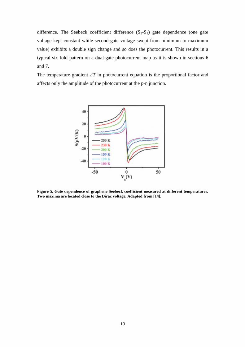
Graphene has a large Seebeck coefficient which is doping dependent and experience a
sign change at charge neutrality point. The two maxima are situated very close to the
Dirac point from both sides of it. Large Seebeck coefficient and controllability by gate
voltage make graphene p-n junction a good choice for the device. Seebeck coefficient
can be calculated using Mott formula
𝑆 = −
𝜋2𝑘2𝑇
3𝑒
1
𝑅
𝑑𝑅
𝑑𝑉𝑔
𝑑𝑉𝑔
𝑑𝐸|𝐸 = 𝐸𝑓 , Eq.5
where k is the Bolzman constant, R is the graphene resistance T is the temperature, Ef
is the Fermi energy.
The typical gate voltage dependence of the graphene Seebeck coefficient measured
for different temperatures is shown in Figure 5. As it can be seen from Eq.4,
photocurrent behaviour at the p-n junction is defined by Seebeck coefficient
10
difference. The Seebeck coefficient difference (S2-S1) gate dependence (one gate
voltage kept constant while second gate voltage swept from minimum to maximum
value) exhibits a double sign change and so does the photocurrent. This results in a
typical six-fold pattern on a dual gate photocurrent map as it is shown in sections 6
and 7.
The temperature gradient ΔT in photocurrent equation is the proportional factor and
affects only the amplitude of the photocurrent at the p-n junction.
Figure 5. Gate dependence of graphene Seebeck coefficient measured at different temperatures.
Two maxima are located close to the Dirac voltage. Adapted from [14].
11
3. Fabrication and Analysis Methods.
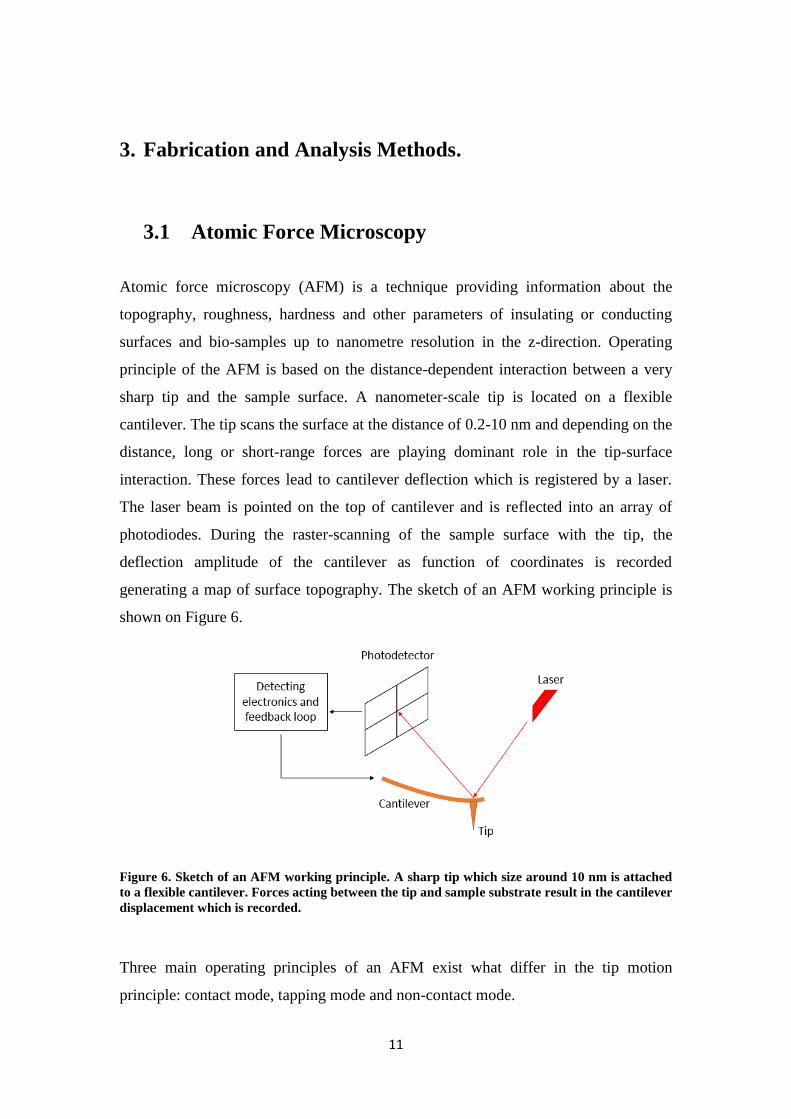
3.1 Atomic Force Microscopy
Atomic force microscopy (AFM) is a technique providing information about the
topography, roughness, hardness and other parameters of insulating or conducting
surfaces and bio-samples up to nanometre resolution in the z-direction. Operating
principle of the AFM is based on the distance-dependent interaction between a very
sharp tip and the sample surface. A nanometer-scale tip is located on a flexible
cantilever. The tip scans the surface at the distance of 0.2-10 nm and depending on the
distance, long or short-range forces are playing dominant role in the tip-surface
interaction. These forces lead to cantilever deflection which is registered by a laser.
The laser beam is pointed on the top of cantilever and is reflected into an array of
photodiodes. During the raster-scanning of the sample surface with the tip, the
deflection amplitude of the cantilever as function of coordinates is recorded
generating a map of surface topography. The sketch of an AFM working principle is
shown on Figure 6.
Figure 6. Sketch of an AFM working principle. A sharp tip which size around 10 nm is attached
to a flexible cantilever. Forces acting between the tip and sample substrate result in the cantilever
displacement which is recorded.
Three main operating principles of an AFM exist what differ in the tip motion
principle: contact mode, tapping mode and non-contact mode.
12
Contact mode
In the contact mode, the repulsive van der Waals force play dominant role in the tip-
surface interaction. The deflection of the cantilever due to the changes in the sample
topography occurs according to the Hooke’s law:
𝐹 = −𝑘 ∗ 𝑥
where k is the cantilever spring constant, x is the cantilever displacement. The surface
topography map is recorded either by registering cantilever deflection or by
maintaining it constant by a feedback loop.
Tapping mode
In tapping mode the cantilever is oscillating at its resonance frequency or slightly
below, driven by a piezoelectric element. The tip does not stay in contact with the
sample surface all the time but lightly touches it for small time intervals. “Tapping”
between the surface and the tip reduces the amplitude of cantilever oscillation, giving
information about the surface topology.
Non-contact mode
In the non-contact mode attractive van der Waals force plays the main role. The tip is
not brought into contact with the sample surface and the cantilever oscillates at
frequency above its resonance. Large-range forces between the tip and the imaged
surface reduces the cantilever resonance and the oscillation amplitude. [18],[19]
In this work, the AFM Veeco Dimension 3100 scanning probe microscope was used
for surface analysis. All images were obtained in tapping mode.
3.2 Spin-Coating.
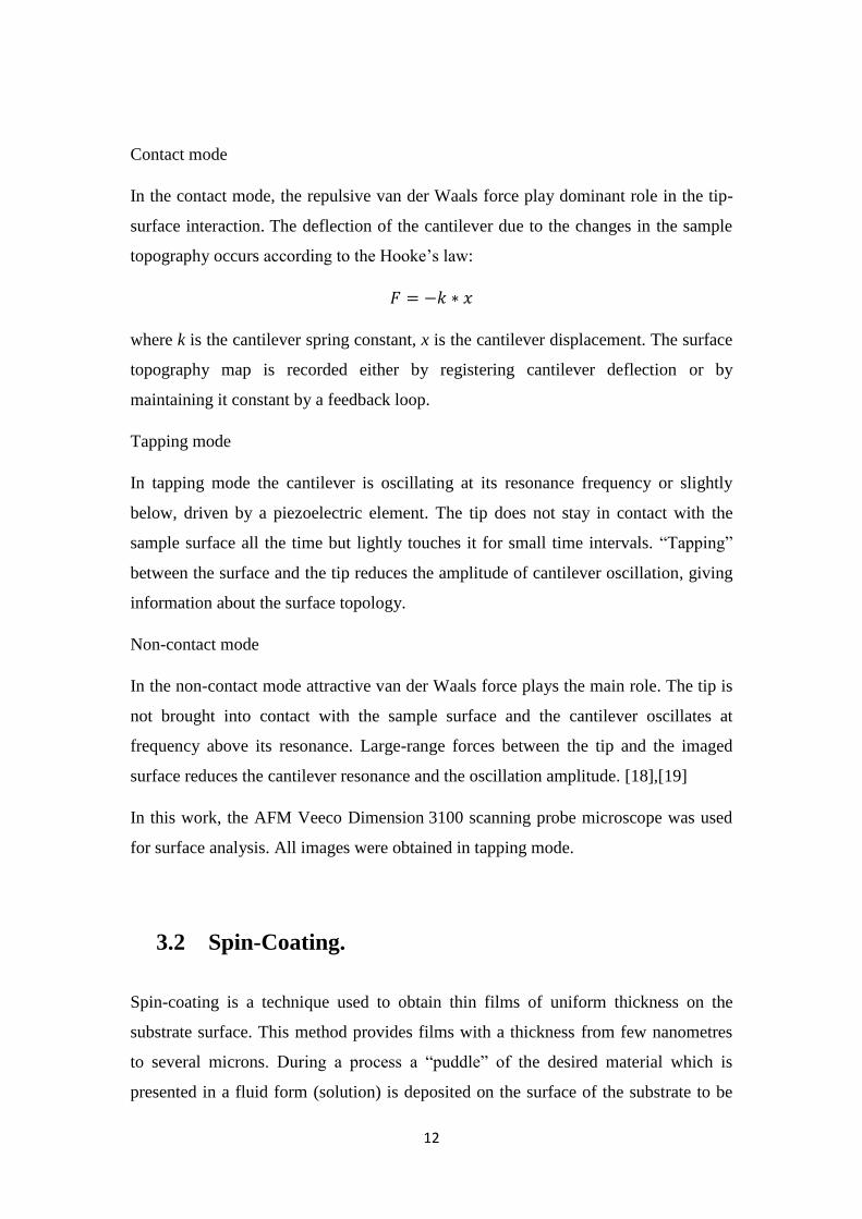
Spin-coating is a technique used to obtain thin films of uniform thickness on the
substrate surface. This method provides films with a thickness from few nanometres
to several microns. During a process a “puddle” of the desired material which is
presented in a fluid form (solution) is deposited on the surface of the substrate to be
13
coated. After the deposition, the substrate is rotated at a high speed, which makes the
solution to spread out across the surface providing a thin film of liquid of even
thickness. The speed and time of the spinning are the main parameters to consider to
obtain a film of desired thickness. Such material properties as viscosity, surface
tension etc. should be also taken into account for the proper parameters choice. After
the film is obtained by spinning the substrate, the sample is dried by air flow or by
baking it on a hot plate. A sketch of a spin coater is shown on the Figure 7. [20][21]
Figure 7. Schematic of a spin-coater. A flat waver is placed on a rotating holder, vacuum is
applied to hold the wafer attached to the holder.
3.3 Optical Lithography
Optical lithography is a technique where light is used to create patterns with
sub-micrometer size on a thin film or a substrate. A special photo-sensitive polymer
(photoresist) is deposited on the substrate using the spin-coating method described in
section 3.2. In the most usual case (shadow mask lithography) an optical mask with a
geometrical layout is used to create the required pattern on the substrate. The
geometrical pattern from a mask is transferred into the resist with an optical system.
Another possibility to create a desired design is the direct writing of the pattern in the
resist with a focused laser beam (direct laser writing). By doing so the laser beam
changes the chemical properties of the photoresist, resulting in the different solubility
of the exposed and non-exposed regions. There are two types of photoresist –
a negative and a positive photoresist. In the “positive” photoresist the light-exposed
regions are easily dissolved during the developing process. In the case of “negative”
resist the non-exposed regions are dissolved while exposed areas stay on the substrate.
14
After the pattern is transferred from the mask into the photoresist, the substrate can be
modified according to the requirements with a help of such fabrication processes as
doping, dry and wet etching, electroplating etc. [22][23]
In this work a direct laser writing with UV laser (Microtech LW405B laserwriter) was
used to fabricate electric contacts in the devices.
3.4 Reactive Ion Etching (RIE)
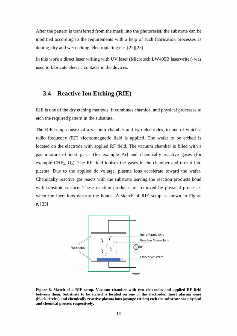
RIE is one of the dry etching methods. It combines chemical and physical processes to
etch the required pattern in the substrate.
The RIE setup consist of a vacuum chamber and two electrodes, to one of which a
radio frequency (RF) electromagnetic field is applied. The wafer to be etched is
located on the electrode with applied RF field. The vacuum chamber is filled with a
gas mixture of inert gases (for example Ar) and chemically reactive gases (for
example CHF3, O2). The RF field ionises the gases in the chamber and turn it into
plasma. Due to the applied dc voltage, plasma ions accelerate toward the wafer.
Chemically reactive gas reacts with the substrate leaving the reaction products bond
with substrate surface. These reaction products are removed by physical processes
when the inert ions destroy the bonds. A sketch of RIE setup is shown in Figure
8. [23]
Figure 8. Sketch of a RIE setup. Vacuum chamber with two electrodes and applied RF field
between them. Substrate to be etched is located on one of the electrodes. Inert plasma iones
(black circles) and chemically reactive plasma ions (orange circles) etch the substrate via physical
and chemical process respectively.
15
4. Device Fabrication.
The goal of this work was to fabricate a photodetector based on graphene p-n
junction. A large and high quality graphene flake should be encapsulated between two
slabs of hBN. The stack then should be allocated on the gold back splitgates to allow
electrostatic doping of a p-n junction in the graphene sheet. The size of the graphene
flake plays an important role for the project because of device assignment for
measurements in mid-infrared region where the laser focal spot has a large size due to
large wavelength. Device with high quality was desired for the study. For that reason
mechanically exfoliated graphene, which is considered to have a better quality than
CVD-grown graphene was used in fabrication and several measures to improve the
device cleanness were tested.
The process of the desired device fabrication is described in the following sections.
4.1 Fabrication Process
Silicon wafer with a layer of SiO2 with 285 nm thickness was cut into square
substrates of approximately 1.5*1.5 cm2. The substrates were cleaned using a standard
cleaning procedure: 5 minutes of ultrasonic bath in Acetone and 5 minutes in IPA.
Then the substrates were dried by the nitrogen gun.
1. Exfoliation
Graphene flakes were mechanically exfoliated on the prepared SiO2 substrates using
the standard “scotch tape” technic where films of graphene are pulled off a bulk piece
of graphite (Graphenium flakes from NGS Naturgraphit GmbH) using an adhesive
tape (R1011 tape from Ultron Systems). Then the films are peeled several more time
with the tape to obtain thinner layer of material. The exfoliated flakes were released
on the substrate by sticking the tape on it. Flakes of different size and thickness stayed
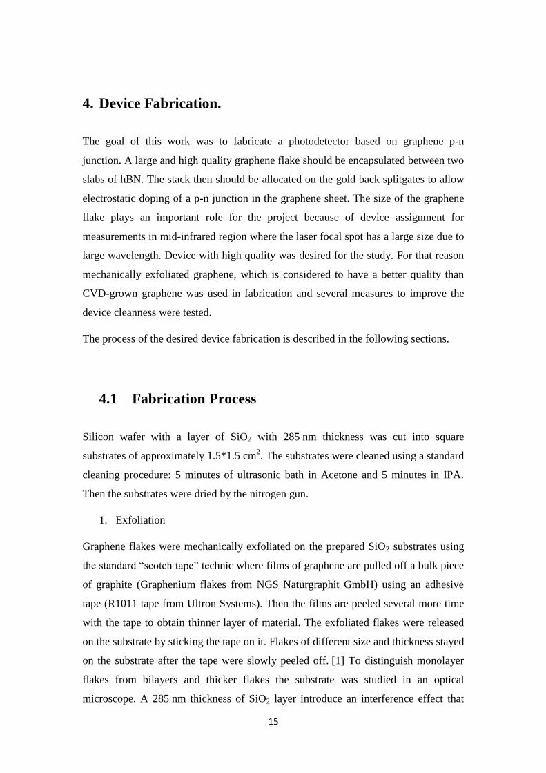
on the substrate after the tape were slowly peeled off. [1] To distinguish monolayer
flakes from bilayers and thicker flakes the substrate was studied in an optical
microscope. A 285 nm thickness of SiO2 layer introduce an interference effect that
16
makes the colour contrast between different layers flakes easy to see and simplifies
choice of the monolayer within multi-layer flakes. [15] An optical image of a
monolayer graphene flake after exfoliation on the SiO2 substrate is presented in
Figure 9.
Figure 9. Optical Image of a monolayer graphene (light purple flake in the middle) obtained with
an optical microscope Zeiss. In the middle of the monolayer flake a small insertion a multiple
layers area can be observed. Interference effects appearing due to SiO2 thickness on the Si wafer
results in optical contrast which allows to distinguish graphene films with different number of
layers.
The mechanical exfoliation is the method providing graphene of the best quality
within other fabrication methods. The disadvantage of this technique is its
uncontrollability and time consumption. After testing different approaches to
exfoliation process as different pressure of attaching the tape with exfoliated graphene
to the substrate, different speed of removing the tape, different number of peeling off
before releasing on the substrate, it is possible to conclude that there is no repeatable
way to obtain large amounts of large monolayer graphene flakes on the substrate.
2. Encapsulation
To encapsulate the graphene flake between two hBN flakes, hBN (provided by Kenji
Watanabe and Takashi Taniguchi) is exfoliated on the Si/SiO2 substrates with the
standard exfoliation method but using the thin PDMS sheets instead of the scotch
tape. Then two hBN flakes of appropriate size (larger than the graphene to be
encapsulated) and good quality (flat, no cracks and noticeable contamination on the
surface) are chosen with an optical microscope.
17
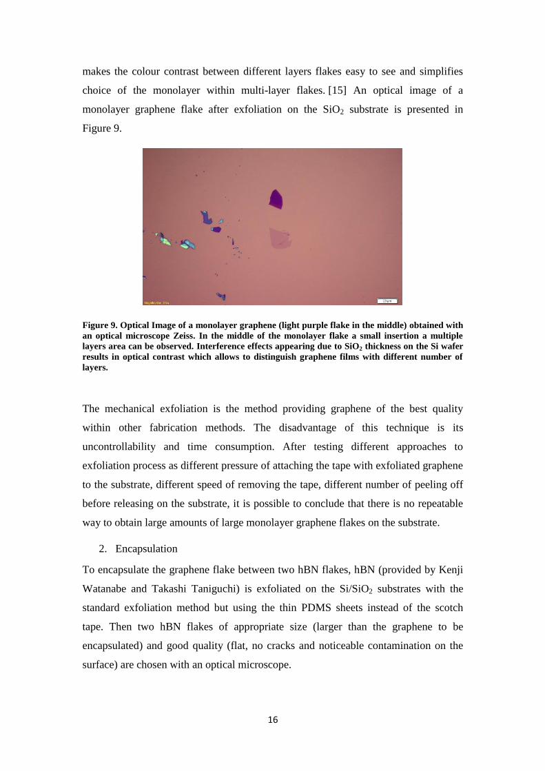
3. Transfer
A clean square of PDMS is cut and put on a glass slide. A PPC film is spin-coated on
a flat substrate (piece of a microscope slide for example) at 1500 rpm for 50 s and
then the substrate baked at 70°C for 2 minutes. Using a usual office scotch-tape the
PPC film is peeled of the glass substrate. Square hole of size larger than the prepared
PDMS piece is cut in the scotch tape to leave part of the PPC area untouched and
clean. The untouched area of PPC is released on the PDMS surface and then the glass
slide is heated up on the hot plate at 70°C for 2-3 minutes to ensure the PPC sticking
to the PDMS and to flatten the air bubbles and wrinkles.
The glass slide was adjusted upside down into a micromanipulator under a
microscope. The SiO2 substrate with one of the exfoliated hBN flakes (which will be
the top hBN of the fabricated device) was placed under the PDMS-PPC stack. The
cleanest area of PPC was aligned above the BN flake and then brought into contact
with it. Then the glass slide was slowly lifted up and the chosen hBN flake stayed
attached to the PPC film. After that the substrate with the chosen graphene flake was
aligned in the same way under the first hBN flake attached to the PPC. The procedure
was repeated and the graphene flake was picked up by hBN due to the van der Waals
interaction force. Then the second hBN flake was picked up from the substrate
following the same procedure and the graphene encapsulation was completed. The
transfer process sketch is shown in Figure 10.
Figure 10. A schematics of the transfer process principle.
After the encapsulation process is finished it is possible to release the obtained stack
on the substrate prepared for the future device. In the project the encapsulated
graphene was released on the gold split gates with a gap of 60-100 nm provided by
Dr. Romain Parret. Two methods of splitgates fabrication were realised and compared
18
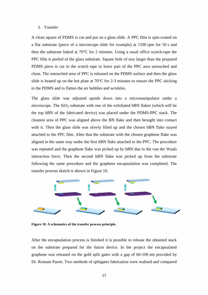
– lift-off and Focused Ion Beam Lithography (FIB). The split gated obtained in lift-off
exhibited a high roughness at the gap edge of about 30 nm and more. Releasing a
stack at these gates would cause its inevitable stack cleavage. FIB, however, was
shown to provide the gap with much more smooth edges with the roughness of few
nm. The AFM image of the splitgates fabricated with two different technics and the
extracted profiles representing its edges height are shown in Figure 11. Although the
gates fabricated with FIB have much lower edge height and better smoothness, the
present roughness can still introduce some damage to the stack if it is released on the
gates not in one step. Figure 12 (e) shows the stack that was released on the split gates
with broken contacts and then removed using the same transfer setup and moved to
another splitgates. The break in the middle of the stack we attribute to the gap edges
roughness.
(a) (b)
(c) (d)
Figure 11. (a) AFM image of the splitgates fabricated using the lift-off method. (b) AFM image of
the splitgates fabricated using the FIB method. (c) Extracted topology profile for the sample
shown in (a). (d) Extracted topology profile for the sample shown in (b).
100.00 nm
0.00 nm
120nm
40
0n
m
100.00 nm
0.00 nm
200nm
19
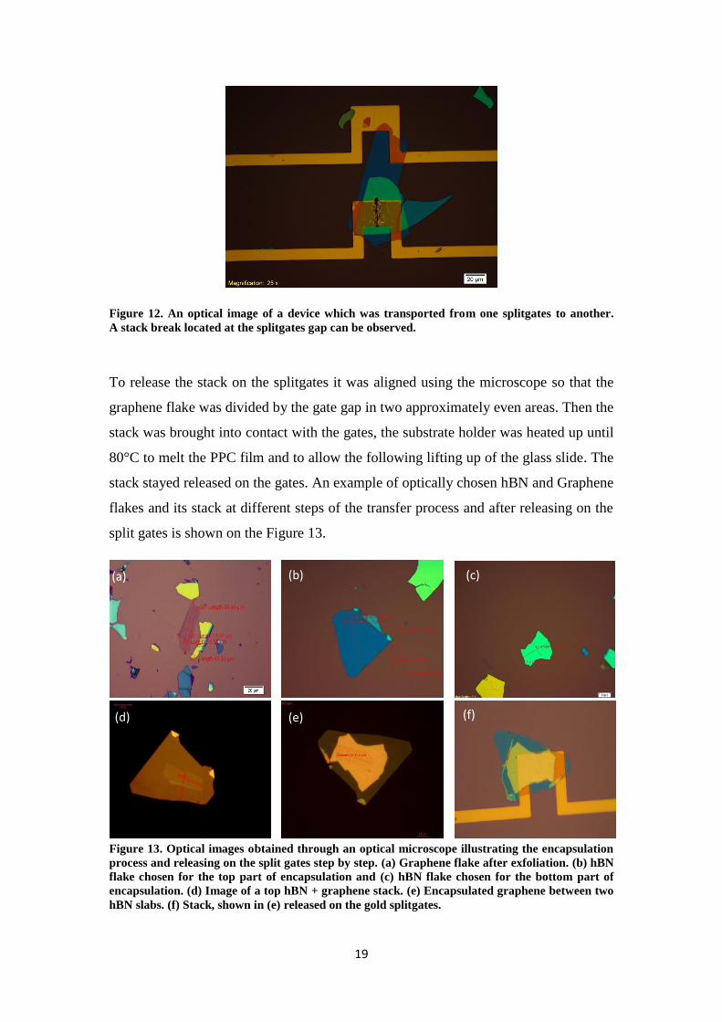
Figure 12. An optical image of a device which was transported from one splitgates to another.
A stack break located at the splitgates gap can be observed.
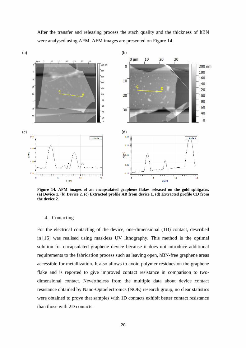
To release the stack on the splitgates it was aligned using the microscope so that the
graphene flake was divided by the gate gap in two approximately even areas. Then the
stack was brought into contact with the gates, the substrate holder was heated up until
80°C to melt the PPC film and to allow the following lifting up of the glass slide. The
stack stayed released on the gates. An example of optically chosen hBN and Graphene
flakes and its stack at different steps of the transfer process and after releasing on the
split gates is shown on the Figure 13.
Figure 13. Optical images obtained through an optical microscope illustrating the encapsulation
process and releasing on the split gates step by step. (a) Graphene flake after exfoliation. (b) hBN
flake chosen for the top part of encapsulation and (c) hBN flake chosen for the bottom part of
encapsulation. (d) Image of a top hBN + graphene stack. (e) Encapsulated graphene between two
hBN slabs. (f) Stack, shown in (e) released on the gold splitgates.
(a) (b) (c)
(d) (e) (f)
20
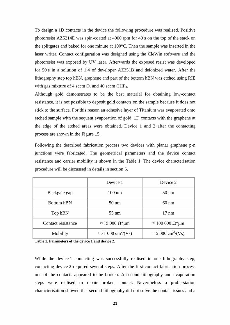
After the transfer and releasing process the stach quality and the thickness of hBN
were analysed using AFM. AFM images are presented on Figure 14.
(a) (b)
(c) (d)
Figure 14. AFM images of an encapsulated graphene flakes released on the gold splitgates.
(a) Device 1. (b) Device 2. (c) Extracted profile AB from device 1. (d) Extracted profile CD from
the device 2.
4. Contacting
For the electrical contacting of the device, one-dimensional (1D) contact, described
in [16] was realised using maskless UV lithography. This method is the optimal
solution for encapsulated graphene device because it does not introduce additional
requirements to the fabrication process such as leaving open, hBN-free graphene areas
accessible for metallization. It also allows to avoid polymer residues on the graphene
flake and is reported to give improved contact resistance in comparison to two-
dimensional contact. Nevertheless from the multiple data about device contact
resistance obtained by Nano-Optoelectronics (NOE) research group, no clear statistics
were obtained to prove that samples with 1D contacts exhibit better contact resistance
than those with 2D contacts.
21
To design a 1D contacts in the device the following procedure was realised. Positive
photoresist AZ5214E was spin-coated at 4000 rpm for 40 s on the top of the stack on
the splitgates and baked for one minute at 100°C. Then the sample was inserted in the
laser writer. Contact configuration was designed using the CleWin software and the
photoresist was exposed by UV laser. Afterwards the exposed resist was developed
for 50 s in a solution of 1:4 of developer AZ351B and deionized water. After the
lithography step top hBN, graphene and part of the bottom hBN was etched using RIE
with gas mixture of 4 sccm O2 and 40 sccm CHF3.
Although gold demonstrates to be the best material for obtaining low-contact
resistance, it is not possible to deposit gold contacts on the sample because it does not
stick to the surface. For this reason an adhesive layer of Titanium was evaporated onto
etched sample with the sequent evaporation of gold. 1D contacts with the graphene at
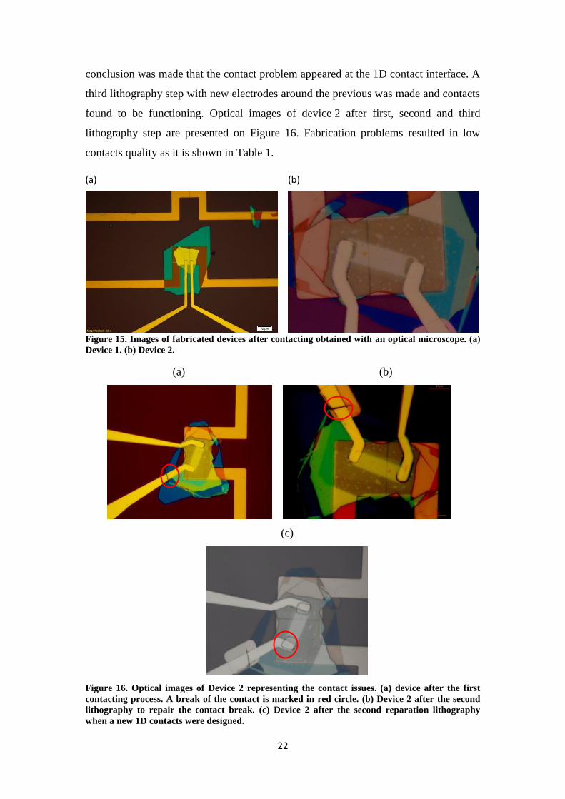
the edge of the etched areas were obtained. Device 1 and 2 after the contacting
process are shown in the Figure 15.
Following the described fabrication process two devices with planar graphene p-n
junctions were fabricated. The geometrical parameters and the device contact
resistance and carrier mobility is shown in the Table 1. The device characterisation
procedure will be discussed in details in section 5.
Device 1 Device 2
Backgate gap 100 nm 50 nm
Bottom hBN 50 nm 60 nm
Top hBN 55 nm 17 nm
Contact resistance ≈ 15 000 Ω*μm ≈ 100 000 Ω*μm
Mobility ≈ 31 000 cm2/(Vs) ≈ 5 000 cm
2/(Vs)
Table 1. Parameters of the device 1 and device 2.
While the device 1 contacting was successfully realised in one lithography step,
contacting device 2 required several steps. After the first contact fabrication process
one of the contacts appeared to be broken. A second lithography and evaporation
steps were realised to repair broken contact. Nevertheless a probe-station
characterisation showed that second lithography did not solve the contact issues and a
22
conclusion was made that the contact problem appeared at the 1D contact interface. A
third lithography step with new electrodes around the previous was made and contacts
found to be functioning. Optical images of device 2 after first, second and third
lithography step are presented on Figure 16. Fabrication problems resulted in low
contacts quality as it is shown in Table 1.
(a) (b)
Figure 15. Images of fabricated devices after contacting obtained with an optical microscope. (a)
Device 1. (b) Device 2.
(a) (b)
(c)
Figure 16. Optical images of Device 2 representing the contact issues. (a) device after the first
contacting process. A break of the contact is marked in red circle. (b) Device 2 after the second
lithography to repair the contact break. (c) Device 2 after the second reparation lithography
when a new 1D contacts were designed.
23
As it can be seen from the device images obtained with AFM, the fabricated devices
do not show a homogeneous, contamination-free interface between hBN and graphene
layers. The presence of “bubble”-like features with variety in size and height
(10-40 nm) are observed. Similar problem was studied by S. J. Haigh et al [24]
According to them the main origin of the “bubbles” is the hydrocarbons trapped
between graphene and hBN layers. To benefit from the hBN properties, which make it
an excellent substrate for graphene devices, the high quality graphene/hBN interface
is required, and thus, the contamination is expected to diminish the electronic
properties of the device. The adsorbates have the tendency to merge together and form
“islands” of contamination, leaving a clean from impurities areas around.
To improve the device cleanness, annealing of the hBN/Gr/hBN stack at 300 °C for
3 hours in Ar/hydrogen (H2) atmosphere was realised. This treatment makes the
contamination islands to combine together into a bigger sized bubbles.
Still a cleaner graphene/hBN interface is required for high quality device fabrication.
4.2 Additional Cleaning Procedures
To find the best approach to the fabrication process, some process parameters that
influence the surface quality of the graphene and hBN flakes were studied as well as
annealing effects before combining them into a 2D materials stack.
First, two substrates, one cleaned in acetone and IPA the described above way and
second, additionally cleaned with O2 plasma were used for graphene exfoliation.
The monolayer flakes were studied with the AFM after exfoliation. There was no
clear improvement in quality after plasma cleaning the substrate notices. Both flakes
had wrinkles or folded edges and bubble-like features on the surface. The AFM
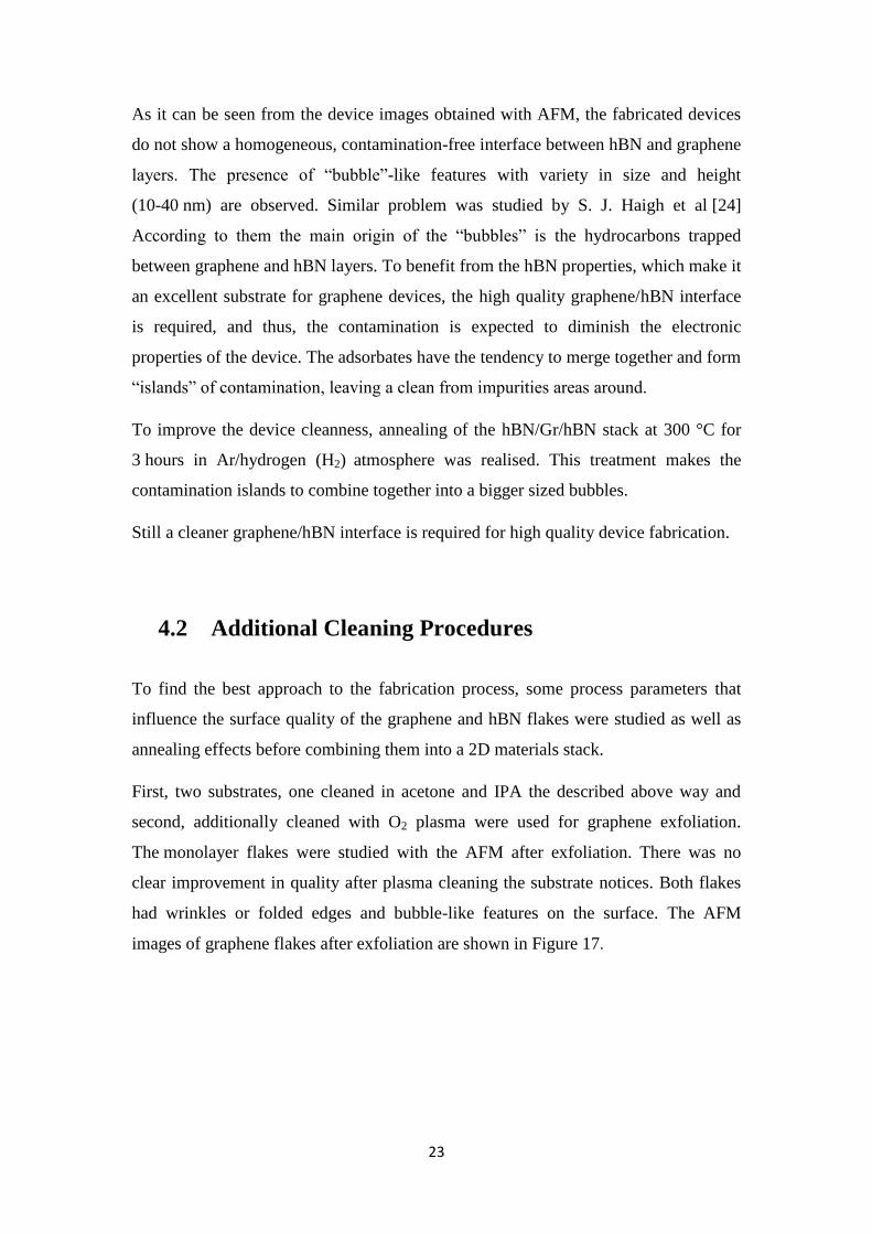
images of graphene flakes after exfoliation are shown in Figure 17.
24
(a) (b)
(c) (d)
Figure 17. AFM image of graphene monolayer flake after exfoliation. (a) Exfoliated graphene
mololayer flake on the substrate cleaned in acetone and IPA. (b) Exfoliated graphene mololayer
flake on the substrate cleaned with O2 plasma. Contamination forming “bubble”-like pockets can
be seen on the both samples. (c) Profile AB extracted from the image (a) displaying
contamination bubbles size. (d) Profile CD extracted from image (b).
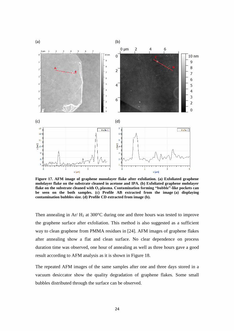
Then annealing in Ar/ H2 at 300°C during one and three hours was tested to improve
the graphene surface after exfoliation. This method is also suggested as a sufficient
way to clean graphene from PMMA residues in [24]. AFM images of graphene flakes
after annealing show a flat and clean surface. No clear dependence on process
duration time was observed, one hour of annealing as well as three hours gave a good
result according to AFM analysis as it is shown in Figure 18.
The repeated AFM images of the same samples after one and three days stored in a
vacuum desiccator show the quality degradation of graphene flakes. Some small
bubbles distributed through the surface can be observed.
25
(a) (b)
(c) (d)
Figure 18. AFM image of graphene flakes after annealing in Ar/H2 atmosphere at 300°C (a)
Sample 1 -annealing for 1 hour. (b) Sample 2 – annealing for 3 hours. (c) Sample 1 after 3 days in
vacuum desiccator after annealing. (d) Sample 2 after one day in the vacuum desiccator after
annealing.
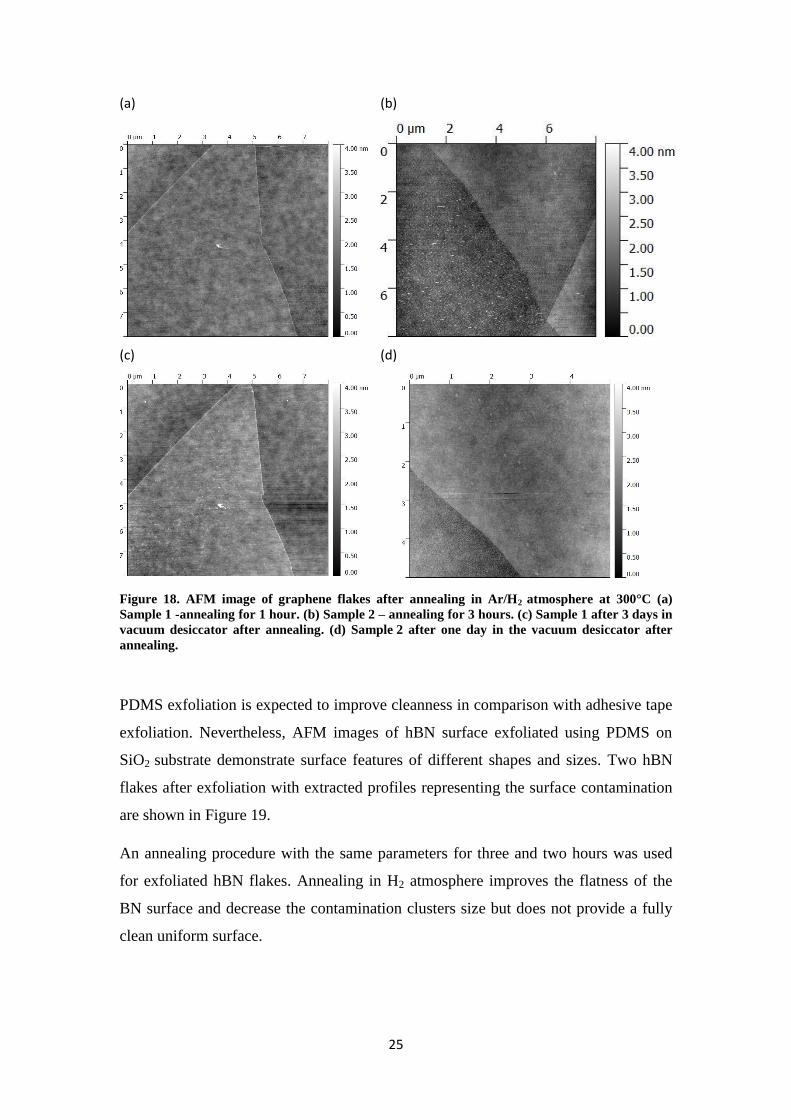
PDMS exfoliation is expected to improve cleanness in comparison with adhesive tape
exfoliation. Nevertheless, AFM images of hBN surface exfoliated using PDMS on
SiO2 substrate demonstrate surface features of different shapes and sizes. Two hBN
flakes after exfoliation with extracted profiles representing the surface contamination
are shown in Figure 19.
An annealing procedure with the same parameters for three and two hours was used
for exfoliated hBN flakes. Annealing in H2 atmosphere improves the flatness of the
BN surface and decrease the contamination clusters size but does not provide a fully
clean uniform surface.
26
(a) (b)
(c) (d)
Figure 19. (a) and (b) AFM image of two hBN flakes after PDMS exfoliation on the SiO2
substrate. Surface contamination of different height and shapes can be observed. (c) and (d)
extracted profiles (1 and 2 from (a) and profile AB from (b) demonstrated the impurities lateral
size and height.
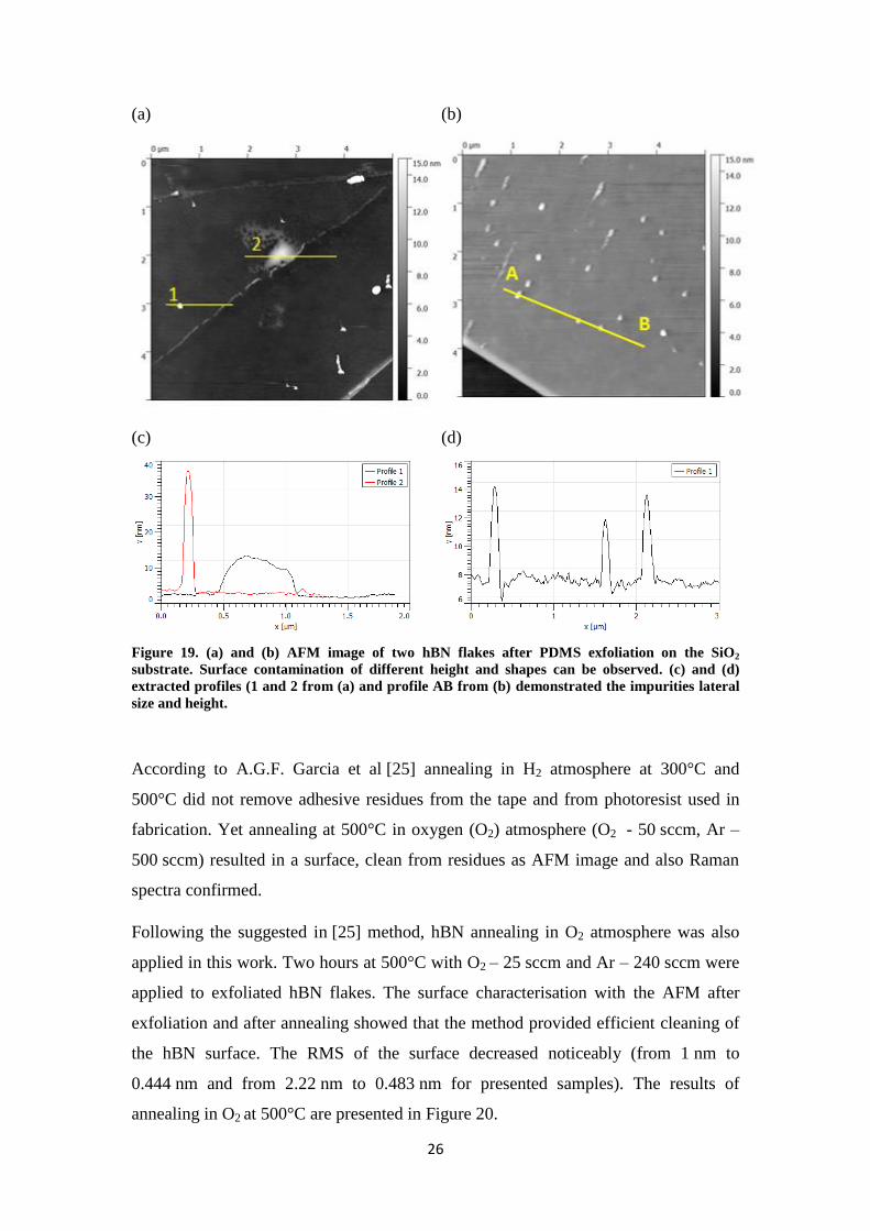
According to A.G.F. Garcia et al [25] annealing in H2 atmosphere at 300°C and
500°C did not remove adhesive residues from the tape and from photoresist used in
fabrication. Yet annealing at 500°C in oxygen (O2) atmosphere (O2 - 50 sccm, Ar –
500 sccm) resulted in a surface, clean from residues as AFM image and also Raman
spectra confirmed.
Following the suggested in [25] method, hBN annealing in O2 atmosphere was also
applied in this work. Two hours at 500°C with O2 – 25 sccm and Ar – 240 sccm were
applied to exfoliated hBN flakes. The surface characterisation with the AFM after
exfoliation and after annealing showed that the method provided efficient cleaning of
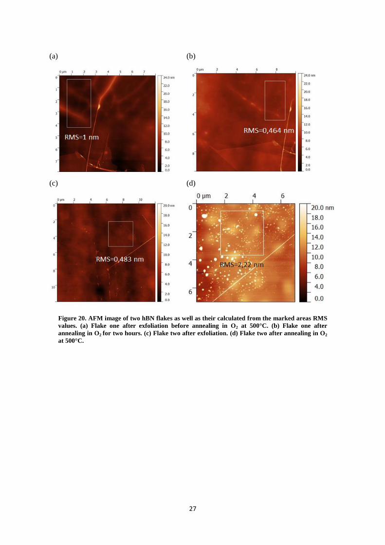
the hBN surface. The RMS of the surface decreased noticeably (from 1 nm to
0.444 nm and from 2.22 nm to 0.483 nm for presented samples). The results of
annealing in O2 at 500°C are presented in Figure 20.
27
(a) (b)
(c) (d)
Figure 20. AFM image of two hBN flakes as well as their calculated from the marked areas RMS
values. (a) Flake one after exfoliation before annealing in O2 at 500°C. (b) Flake one after
annealing in O2 for two hours. (c) Flake two after exfoliation. (d) Flake two after annealing in O2
at 500°C.
28
5. Device Characterisation.
Transport measurements
To evaluate quality of the fabricated device, the contact resistance and the carrier
mobility were measured. To obtain these characteristic of the device 1 the two-probe
measurements were realised. The commonly used sequence of four-probe
measurement, which provides information about graphene sheet resistance, and
two-probe measurement to evaluate the contact resistance was not possible to
implement in this work due to the device size and configuration limitation. It was
difficult to add two more contacts on the small graphene flake and there was a high
risk of a shortcut with the gold splitgates, because only a small area at the gates edges
was covered with the dielectric hBN. Two-probe measurement was performed and
characteristics of our interest were obtained using the fitting method.
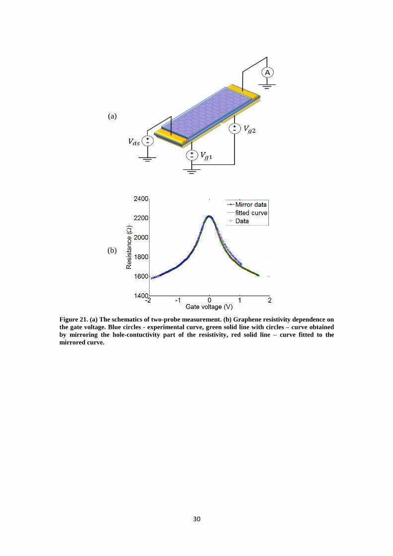
The sketch of the measurements is presented in Figure 21 (b)
. The two-probe measurements give information about the device total resistance
which can be shown as a sum of four resistances in series.
𝑅𝑡𝑜𝑡 = 𝑅𝑐1 + 𝑅𝑐2 + 𝑅𝑔1 + 𝑅𝑔2, Eq.6
where 𝑅𝑐1 and 𝑅𝑐2 are the contact resistances of two electrodes, 𝑅𝑔1 and 𝑅𝑔2 are the
resistances of graphene from two sides of the p-n junction, of p and n-doped regions
separately. To reduce the amount of terms in the equation, two bottom split gates were
simultaneously swiped from -2 V to 2 V, providing the uniform doping across the
entire graphene sheet. The induced carriers density was calculated according to the
Eq.1. Source-drain voltage of 5 mV was applied and drain current was recorded.
To obtain the total device resistance curve source-drain voltage was divided by the
measured drain current. The obtained device resistance curve is shown in Figure 21 (b)
(blue circles).
29
Dirac voltage of 0.4 V is subtracted from the experimental data to obtain the
resistivity peak at Vg=0 V.
The experimental curve is fitted in a MATLAB script (written by Mathieu Massicotte)
with Eq.7
𝑅𝑡𝑜𝑡 = 𝑅𝑐 +1
𝑒𝜇√𝑛02+(
𝜀𝜀0𝑈𝑔
𝑒)2
, Eq.7
where 𝑅𝑐 is the sum of both contacts resistances, e is the elementary charge, 𝜇 is the
carrier mobility and 𝑛0 is the residual doping at the Dirac voltage. 𝑅𝑐, 𝜇, 𝑛0 are the
fitting parameters for the curve. The experimental gate dependence of the resistance is
not symmetric. The non-symmetry appears due to slightly different mobilities for
electrons and holes. Then, to use the symmetric Eq.7 for fitting, only the part with
hole conduction regime is kept and mirrored to obtain the green circle curve. The
applied fitting procedure also assumes the contact resistance to be doping
independent. That allows to extract the contacts resistance value from the total device
resistance curve offset from zero. The red line in Figure 21 (b) represents the fitted
curve obtained.
Once the graphene sheet resistance is extracted, graphene resistivity is given by Eq.8
𝜌𝑔 = 𝑅𝑔𝑊
𝐿, Eq.8
where W and L are the width and length of the channel between two contacts
respectively. From this measurements mobility of the device 1 was obtained to be
30 963 cm2/(Vs), which is significantly better than the mobility obtained in graphene
devices with SiO2 as a substrate ( usually does not show mobility larger than 10 000 -
15 000 cm2/(Vs)).
30
(a)
(b)
Figure 21. (a) The schematics of two-probe measurement. (b) Graphene resistivity dependence on
the gate voltage. Blue circles - experimental curve, green solid line with circles – curve obtained
by mirroring the hole-contuctivity part of the resistivity, red solid line – curve fitted to the
mirrored curve.
31
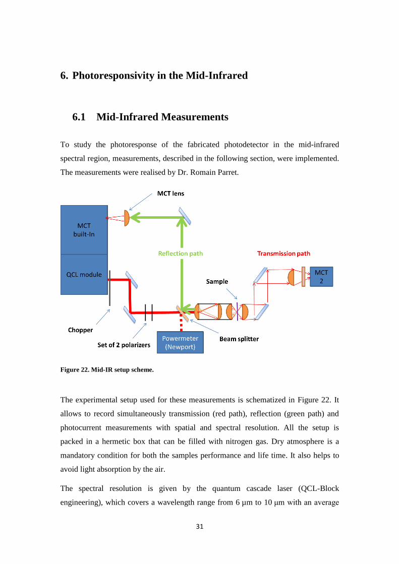
6. Photoresponsivity in the Mid-Infrared
6.1 Mid-Infrared Measurements
To study the photoresponse of the fabricated photodetector in the mid-infrared
spectral region, measurements, described in the following section, were implemented.
The measurements were realised by Dr. Romain Parret.
Figure 22. Mid-IR setup scheme.
The experimental setup used for these measurements is schematized in Figure 22. It
allows to record simultaneously transmission (red path), reflection (green path) and
photocurrent measurements with spatial and spectral resolution. All the setup is
packed in a hermetic box that can be filled with nitrogen gas. Dry atmosphere is a
mandatory condition for both the samples performance and life time. It also helps to
avoid light absorption by the air.
The spectral resolution is given by the quantum cascade laser (QCL-Block
engineering), which covers a wavelength range from 6 µm to 10 μm with an average
32
power of about 2 mW. Before reaching the sample, the beam passes through a beam
expander made of an afocal lens doublet. The beam diameter after passing this optical
element matches the diameter of the focalisation lens. The spot size on the sample is
then close to the diffraction limit which is about 25 μm in this wavelength range.
The sample is mounted in the x-y-z stage and then can be moved with a resolution of
100 nm to achieve spatial mapping. In addition, the setup is composed by a set of two
linear polarizers that allow to measure polarization and power dependences. Finally,
optical signals (reflection and transmission) are recorded using Mercury Cadmium
Telluride (MCT) detectors.
After the sample is inserted in the setup, it is important to obtain information about its
localization on the x-y stage. Because the investigated samples are not transparent due
to the presence of the gold splitgates, the only way to locate the sample is to use the
reflection. For that purpose a beamsplitter is inserted in the laser path before the
sample. A laser beam propagating through the beamsplitter is reflected from the
sample with 90 ͦ to the surface and then directed by the beamsplitter to a
photodetector. The sample holder is moved in x and y direction so that the whole
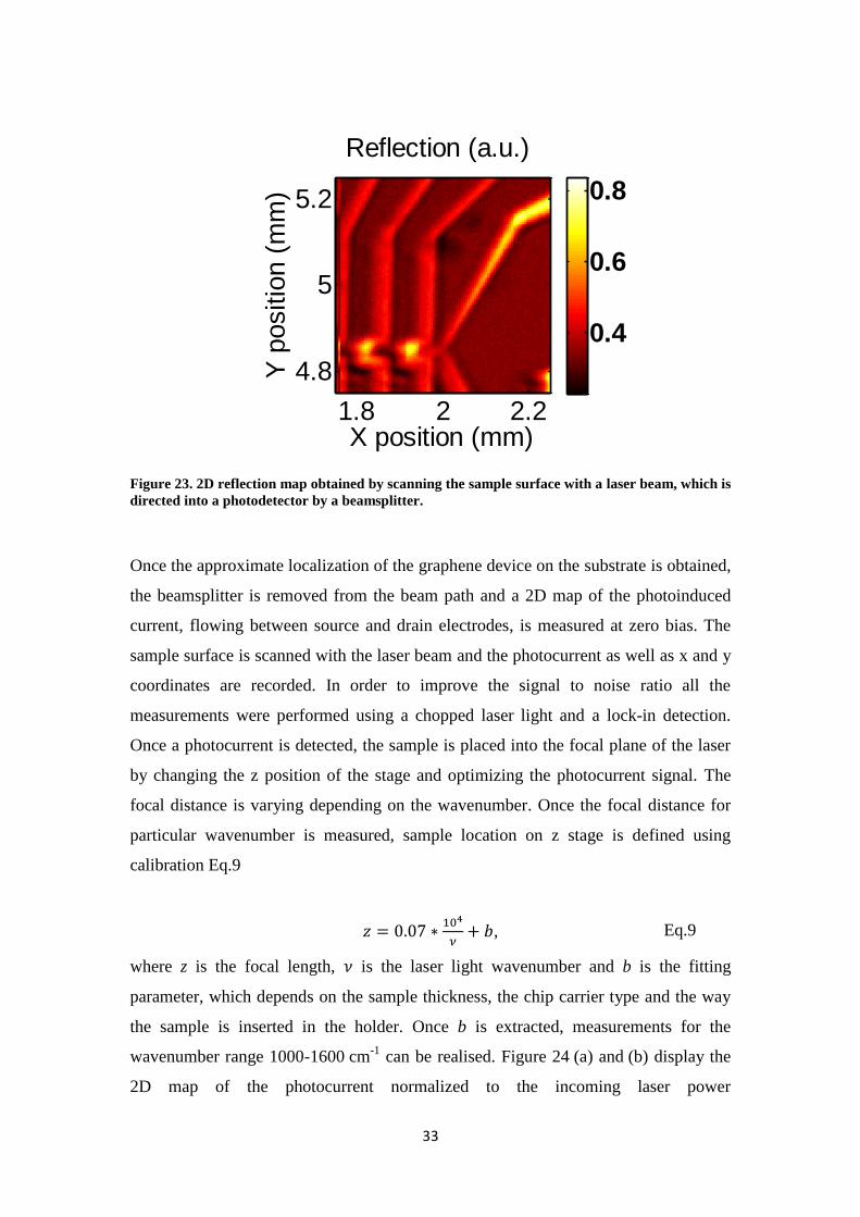
sample is scanned. The reflection signal is recorded for each (x,y) positions and then a
reflection 2D map can be built as shown on Figure 23. Insertion of the beamsplitter
with thickness 5 mm introduces a lateral shift in the laser beam path and decreases the
incident laser power. For this reason, the photocurrent measurements were
implemented without the beamsplitter in the setup. Because of this the reflection map
gives only approximate information about sample topology and device position on the
substrate.
33
Figure 23. 2D reflection map obtained by scanning the sample surface with a laser beam, which is
directed into a photodetector by a beamsplitter.
Once the approximate localization of the graphene device on the substrate is obtained,
the beamsplitter is removed from the beam path and a 2D map of the photoinduced
current, flowing between source and drain electrodes, is measured at zero bias. The
sample surface is scanned with the laser beam and the photocurrent as well as x and y
coordinates are recorded. In order to improve the signal to noise ratio all the
measurements were performed using a chopped laser light and a lock-in detection.
Once a photocurrent is detected, the sample is placed into the focal plane of the laser
by changing the z position of the stage and optimizing the photocurrent signal. The
focal distance is varying depending on the wavenumber. Once the focal distance for
particular wavenumber is measured, sample location on z stage is defined using
calibration Eq.9
𝑧 = 0.07 ∗104
𝜈+ 𝑏, Eq.9
where z is the focal length, 𝜈 is the laser light wavenumber and b is the fitting
parameter, which depends on the sample thickness, the chip carrier type and the way
the sample is inserted in the holder. Once b is extracted, measurements for the
wavenumber range 1000-1600 cm-1
can be realised. Figure 24 (a) and (b) display the
2D map of the photocurrent normalized to the incoming laser power
X position (mm)
Y p
ositio
n (
mm
)
Reflection (a.u.)
1.8 2 2.2
4.8
5
5.2
0.4
0.6
0.8

34
(photoresponsivity = Ipc/Plas) recorded for the parallel and perpendicular polarisations
to the p-n junction at laser wavenumber 𝜈=1501 cm-1
.
(a)
(b)
Figure 24. 2D map of photoresponsivity at v=1501 cm-1
for (a) polarization perpendicular to the
p-n junction, (b) polarization parallel to the p-n junction.
From Figure 24 (a) one can observe a photoresponsivity peak (red spot) of a
magnitude of 60 μA/W, which corresponds to the current generation at the p-n
junction. The map also exhibits two weaker features of opposite sign respectively
located at (x,y) position (2.02 mm,4.81 mm) and (2.03 mm,4.824 mm). They
correspond to the photocurrent generated at the device contacts. Because the laser
focal spot size is about 20-25 nm, which is comparable to the device size, it is
complicated to exclude the contacts contribution to the photocurrent from the junction
contribution. Nevertheless, for this particular polarization, the junction response was
measured to be one order of magnitude higher than the contacts response. For parallel
polarization (Figure 24 (b)) the photoresponse at the junction and both contacts have
almost the same magnitude but the contacts response has the opposite sign to the
X position (mm)
Y p
ositio
n (
mm
)
Responsivity (A/W)
1.98 2 2.02 2.044.8
4.81
4.82
4.83
-5
0
5
x 10-5
X position (mm)
Y p
ositio
n (
mm
)
Responsivity (A/W)
1.98 2 2.02 2.044.8
4.81
4.82
4.83
-1
0
1
x 10-6
35
junction response. This measurements show an enhancement of the photoresponse for
perpendicular polarization of about 50 times.
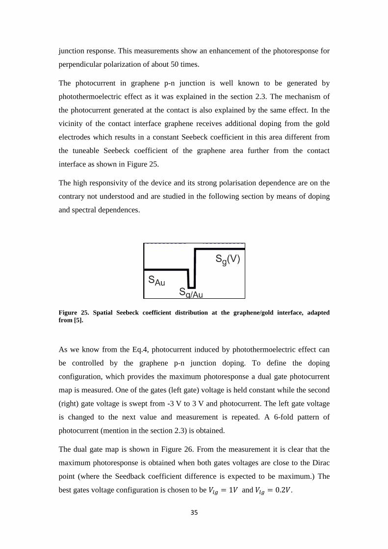
The photocurrent in graphene p-n junction is well known to be generated by
photothermoelectric effect as it was explained in the section 2.3. The mechanism of
the photocurrent generated at the contact is also explained by the same effect. In the
vicinity of the contact interface graphene receives additional doping from the gold
electrodes which results in a constant Seebeck coefficient in this area different from
the tuneable Seebeck coefficient of the graphene area further from the contact
interface as shown in Figure 25.
The high responsivity of the device and its strong polarisation dependence are on the
contrary not understood and are studied in the following section by means of doping
and spectral dependences.
Figure 25. Spatial Seebeck coefficient distribution at the graphene/gold interface, adapted
from [5].
As we know from the Eq.4, photocurrent induced by photothermoelectric effect can
be controlled by the graphene p-n junction doping. To define the doping
configuration, which provides the maximum photoresponse a dual gate photocurrent
map is measured. One of the gates (left gate) voltage is held constant while the second
(right) gate voltage is swept from -3 V to 3 V and photocurrent. The left gate voltage
is changed to the next value and measurement is repeated. A 6-fold pattern of
photocurrent (mention in the section 2.3) is obtained.
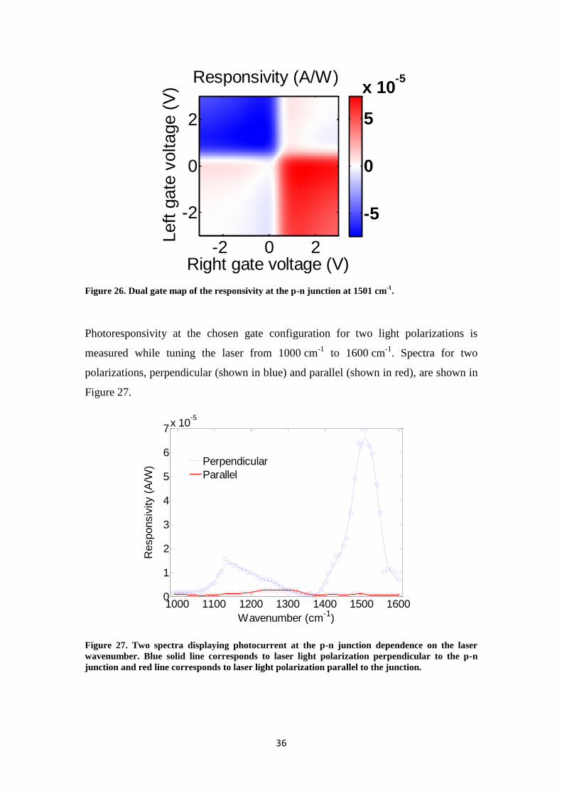
The dual gate map is shown in Figure 26. From the measurement it is clear that the
maximum photoresponse is obtained when both gates voltages are close to the Dirac
point (where the Seedback coefficient difference is expected to be maximum.) The
best gates voltage configuration is chosen to be 𝑉𝑙𝑔 = 1𝑉 and 𝑉𝑙𝑔 = 0.2𝑉.
36
Figure 26. Dual gate map of the responsivity at the p-n junction at 1501 cm-1
.
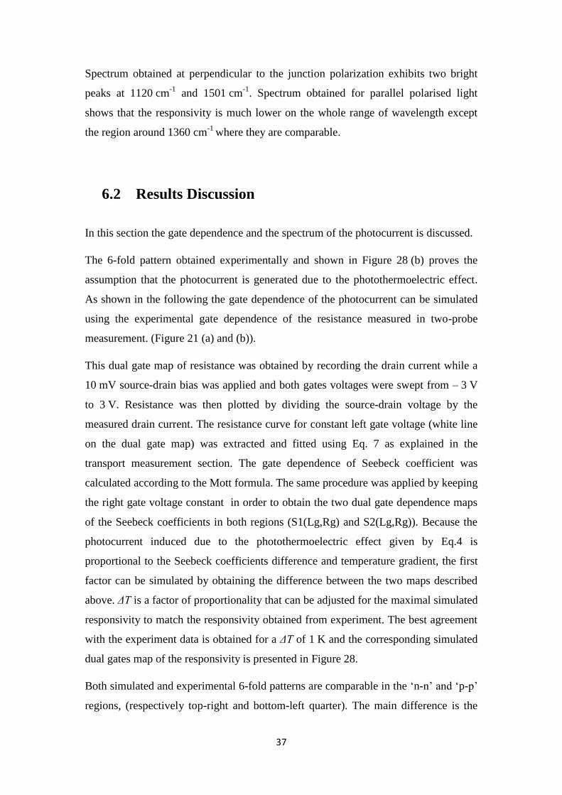
Photoresponsivity at the chosen gate configuration for two light polarizations is
measured while tuning the laser from 1000 cm-1
to 1600 cm-1
. Spectra for two
polarizations, perpendicular (shown in blue) and parallel (shown in red), are shown in
Figure 27.
Figure 27. Two spectra displaying photocurrent at the p-n junction dependence on the laser
wavenumber. Blue solid line corresponds to laser light polarization perpendicular to the p-n
junction and red line corresponds to laser light polarization parallel to the junction.
Right gate voltage (V)
Left
gate
voltage (
V)
Responsivity (A/W)
-2 0 2
-2
0
2
-5
0
5
x 10-5
1000 1100 1200 1300 1400 1500 16000
1
2
3
4
5
6
7x 10
-5
Wavenumber (cm-1
)
Responsiv
ity (
A/W
)
Perpendicular
Parallel
37
Spectrum obtained at perpendicular to the junction polarization exhibits two bright
peaks at 1120 cm-1
and 1501 cm-1
. Spectrum obtained for parallel polarised light
shows that the responsivity is much lower on the whole range of wavelength except
the region around 1360 cm-1
where they are comparable.
6.2 Results Discussion
In this section the gate dependence and the spectrum of the photocurrent is discussed.
The 6-fold pattern obtained experimentally and shown in Figure 28 (b) proves the
assumption that the photocurrent is generated due to the photothermoelectric effect.
As shown in the following the gate dependence of the photocurrent can be simulated
using the experimental gate dependence of the resistance measured in two-probe
measurement. (Figure 21 (a) and (b)).
This dual gate map of resistance was obtained by recording the drain current while a
10 mV source-drain bias was applied and both gates voltages were swept from – 3 V
to 3 V. Resistance was then plotted by dividing the source-drain voltage by the
measured drain current. The resistance curve for constant left gate voltage (white line
on the dual gate map) was extracted and fitted using Eq. 7 as explained in the
transport measurement section. The gate dependence of Seebeck coefficient was
calculated according to the Mott formula. The same procedure was applied by keeping
the right gate voltage constant in order to obtain the two dual gate dependence maps
of the Seebeck coefficients in both regions (S1(Lg,Rg) and S2(Lg,Rg)). Because the
photocurrent induced due to the photothermoelectric effect given by Eq.4 is
proportional to the Seebeck coefficients difference and temperature gradient, the first
factor can be simulated by obtaining the difference between the two maps described
above. ΔT is a factor of proportionality that can be adjusted for the maximal simulated
responsivity to match the responsivity obtained from experiment. The best agreement
with the experiment data is obtained for a ΔT of 1 K and the corresponding simulated
dual gates map of the responsivity is presented in Figure 28.
Both simulated and experimental 6-fold patterns are comparable in the ‘n-n’ and ‘p-p’
regions, (respectively top-right and bottom-left quarter). The main difference is the
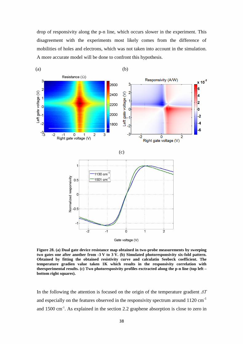
38
drop of responsivity along the p-n line, which occurs slower in the experiment. This
disagreement with the experiments most likely comes from the difference of
mobilities of holes and electrons, which was not taken into account in the simulation.
A more accurate model will be done to confront this hypothesis.
(a) (b)
(c)
Figure 28. (a) Dual gate device resistance map obtained in two-probe measurements by sweeping
two gates one after another from -3 V to 3 V. (b) Simulated photoresponsivity six-fold pattern.
Obtained by fitting the obtained resistivity curve and calculatin Seebeck coefficient. The
temperature gradien value taken 1K which results in the responsivity correlation with
theexperimental results. (c) Two photoresposivity profiles exctracted along the p-n line (top left –
bottom right squares).
In the following the attention is focused on the origin of the temperature gradient ΔT
and especially on the features observed in the responsivity spectrum around 1120 cm-1
and 1500 cm-1. As explained in the section 2.2 graphene absorption is close to zero in
39
the mid-IR range, which differs from one in visible and NIR regions where a constant
broadband absorption of α=2.3% takes place. During the experiments, for the
device 1, the doping is changed from the residual doping 2.7 1011
cm-2
up to
4.89 1011
cm-2
at +3 V. In terms of Fermi energy this frequency range corresponds to
the Fermi energy range from 60 meV to 81 meV. The laser range from 1000 cm-1
to
1600 cm-1
correspond to an energy range from 125 meV to 190 meV, the graphene
interband absorption is allowed at low doping and switches to a Pauli blocking regime
at high doping. Figure 28 (c) shows the normalized photoresponse as a function of
symmetrical doping between both p and n regions for two laser wavenumbers
1130 cm-1
and 1501 cm-1
. These plots correspond to linecuts along the p-n lines from
their respective dual gates maps. For laser excitation at 1130 cm-1
, a transition from
Pauli blocking to interband transition is supposed to be seen whereas for 1501 cm-1
interband transitions are allowed on the whole range of doping. Nevertheless the two
profiles in Figure 28 (c) exhibits almost the same trend. This result which is not fully
understood might show that the photocurrent generation is not due to graphene
absorption.
Graphene photocurrent mechanism in the mid-infrared region differs from one in the
VIS and NIR regions. The mid-infrared domain is associated to Pauli-blocking regime
in graphene absorption which leads to the absorption drop in contrast with the
constant broadband absorption α=2.3% in VIS and NIR. The environment
contribution, one example of which is photon - substrate phonon interaction, plays a
significant role in absorption mechanism.
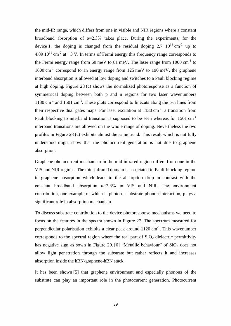
To discuss substrate contribution to the device photoresponse mechanisms we need to
focus on the features in the spectra shown in Figure 27. The spectrum measured for
perpendicular polarisation exhibits a clear peak around 1120 cm-1
. This wavenumber
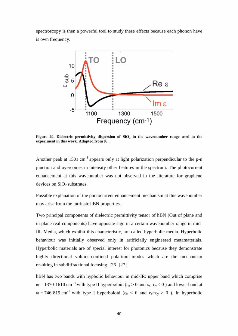
corresponds to the spectral region where the real part of SiO2 dielectric permittivity
has negative sign as sown in Figure 29. [6] “Metallic behaviour” of SiO2 does not
allow light penetration through the substrate but rather reflects it and increases
absorption inside the hBN-graphene-hBN stack.
It has been shown [5] that graphene environment and especially phonons of the
substrate can play an important role in the photocurrent generation. Photocurrent
40
spectroscopy is then a powerful tool to study these effects because each phonon have
is own frequency.
Figure 29. Dielectric permittivity dispersion of SiO2 in the wavenumber range used in the
experiment in this work. Adapted from [6].
Another peak at 1501 cm-1
appears only at light polarization perpendicular to the p-n
junction and overcomes in intensity other features in the spectrum. The photocurrent
enhancement at this wavenumber was not observed in the literature for graphene
devices on SiO2 substrates.
Possible explanation of the photocurrent enhancement mechanism at this wavenumber
may arise from the intrinsic hBN properties.
Two principal components of dielectric permittivity tensor of hBN (Out of plane and
in-plane real components) have opposite sign in a certain wavenumber range in mid-
IR. Media, which exhibit this characteristic, are called hyperbolic media. Hyperbolic
behaviour was initially observed only in artificially engineered metamaterials.
Hyperbolic materials are of special interest for photonics because they demonstrate
highly directional volume-confined polariton modes which are the mechanism
resulting in subdiffractional focusing. [26] [27]
hBN has two bands with hypbolic behaviour in mid-IR: upper band which comprise
ω = 1370-1610 cm -1
with type II hyperboloid (εz > 0 and εx=εy < 0 ) and lower band at
ω = 746-819 cm-1
with type I hyperboloid (εz < 0 and εx=εy > 0 ). In hyperbolic
41
material propagation direction of hyperbolic polariton can be calculated according to
Eq.10
𝑡𝑎𝑛𝜃 =
√𝜀𝑧(𝜔)
𝑖√𝜀𝑡(𝜔), Eq.10
where 𝜃 is the polariton propagation angle, 𝜀𝑧 and 𝜀𝑡 are out of plane and in-plane
dielectric permittivity of hyperbolic material respectively.
In the case of studied device, the propagating through hBN slab external field is
concentrated at the edges of two split gates and polariton modes are launched in hBN
which propagate with angle 𝜃. For particular wavenumber propagation angle
coincides with
𝜃 = arctan𝑎/2
𝑑,
Where a is the width of the splitgates gap and d is the bottom hBN thickness. In this
case a high concentration of the field in at the p-n junction is obtained due to device
geometry as it is shown on Figure 30.
For device 1 arctana/2
d= arctan
100/2
50= 0.785
Which has a close value with the polaritonic rays propagation angle at 1501 cm-1
.
Figure 30. Hyperlensing effect schematic. Under light illumination, represented with green
arrows, the polaritons are launched at the gold backgates gap edge and propagating with angle θ
to the normal.
This hypothesis should be confirmed by fabricating sample with different bottom BN
thickness and splitgates gap sizes, which would result in the different frequency of the
photoresponsivity peak.
42
7. Conclusion and Outlook
During this project, graphene-based photodetectors with a planar p-n junction
configuration were fabricated to study the photoresponse in the mid-infrared spectral
domain. Graphene was mechanically exfoliated and encapsulated between two hBN
slabs. These fabrications details were expected to result in an optoelectronic device of
high quality. To improve the device cleanness several methods were tested including
different substrate cleaning techniques before exfoliation, exfoliation with an adhesive
tape and PDMS films and annealing of the exfoliated flakes with different process
parameters. The substrate cleaning technique was found not to play a significant role
in the quality of exfoliated films. Annealing in H2 atmosphere at 300°C was found to
be a good cleaning and flattering mechanism for exfoliated graphene flakes and
annealing in O2 atmosphere at 500°C appeared to give significant improvement in
hBN surface cleanness.
Fabricated devices were characterised electrically and optical measurements in Mid-
infrared on one of the devices were implemented to study the photocurrent
mechanisms. Electrical characterisation showed good performance characteristics
such as carrier mobility of 31 000 cm2/(Vs) which is about twice as high as the
mobility of 10 000-15 000 cm2/(Vs) reported on the devices with the same
configuration on SiO2 substrate.
Spatially and spectrally-resolved measurements in mid-infrared spectral domain were
realised. The obtained photoresponse exhibits features which were studied in literature
before such as thermoelectric effect at the p-n junction and at the device contacts.
Nevertheless the measured photoresponse in two different absorption regimes –
interband and Pauli blocking didn´t show a significant difference as it was expected
due to the large difference in absorption for these two regimes. This results give an
assumption that direct absorption in graphene is not the major mechanism in
photocurrent generation.
From the spectral-resolved measurements device substrate contribution was found to
play a dominant role in the device photoresponse. SiO2 negative permittivity (real
part) around 1100 cm-2
is considered to be responsible for the photocurrent
43
enhancement at this frequency. hBN, which was recently reported to behave as a
natural hyperbolic media, introduces a hyperlensing effect around 1500 cm-1
which
also depends on the device geometry.
Photoresponsivity of the fabricated photodetector was calculated to be around
0.12 V/W in unbiased regime which is comparable with the lately reported
photodetector responsivity of 0.4 V/W for the biased device. [28]
Further step in this project would be to fabricate a device with larger active area to
exclude the contacts effect contribution in the photocurrent. Also the tested methods
to improve device cleanness should be implemented. Devices with different geometry
which includes variation in bottom hBN thickness and splitgate gap should be
fabricated to introduce more statistics for the hyperlensing effect studies.
44
References
[1] K. S. Novoselov, A. K. Geim, S. V. Morozov, D. Jiang, Y. Zhang, S. V.
Dubonos, I. V. Grigorieva, and A. A. Firsov, “Electric Field Effect in
Atomically Thin Carbon Films,” Science (80-. )., vol. 306, pp. 666–9, 2004.
[2] F. Bonaccorso, Z. Sun, T. Hasan, and a. C. Ferrari, “Graphene Photonics and
Optoelectronics,” Nat. Photonics, vol. 4, no. August, pp. 611–622, 2010.
[3] S. Das Sarma, S. Adam, E. H. Hwang, and E. Rossi, “Electronic transport in
two-dimensional graphene,” Rev. Mod. Phys., vol. 83, no. 2, pp. 407–470, May
2011.
[4] K. S. Novoselov, V. I. Fal′ko, L. Colombo, P. R. Gellert, M. G. Schwab, and K.
Kim, “A roadmap for graphene,” Nature, vol. 490, no. 7419. pp. 192–200,
2012.
[5] T. Low and P. Avouris, “Graphene plasmonics for terahertz to mid-infrared
applications,” ACS Nano, vol. 8, no. 2, pp. 1086–1101, 2014.
[6] M. Badioli, A. Woessner, K. J. Tielrooij, S. Nanot, G. Navickaite, T. Stauber,
F. J. García de Abajo, and F. H. L. Koppens, “Phonon-Mediated Mid-Infrared
Photoresponse of Graphene.,” Nano Lett., vol. 14, pp. 6374–6381, 2014.
[7] A. H. Castro Neto, F. Guinea, N. M. R. Peres, K. S. Novoselov, and A. K.
Geim, “The electronic properties of graphene,” Rev. Mod. Phys., vol. 81, no. 1,
pp. 109–162, 2009.
[8] D. R. Cooper, B. D’Anjou, N. Ghattamaneni, B. Harack, M. Hilke, A. Horth,
N. Majlis, M. Massicotte, L. Vandsburger, E. Whiteway, and V. Yu,
“Experimental Review of Graphene,” ISRN Condensed Matter Physics, vol.
2012. pp. 1–56, 2012.
[9] J. M. Dawlaty, S. Shivaraman, J. Strait, P. George, M. Chandrashekhar, F.
Rana, M. G. Spencer, D. Veksler, and Y. Chen, “Measurement of the optical
absorption spectra of epitaxial graphene from terahertz to visible,” Appl. Phys.
Lett., vol. 93, no. 13, 2008.
[10] A. K. Geim and K. S. Novoselov, “The rise of graphene.,” Nat. Mater., vol. 6,
no. 3, pp. 183–191, 2007.
[11] K. Nagashio, T. Yamashita, T. Nishimura, K. Kita, and A. Toriumi, “Electrical
transport properties of graphene on SiO2 with specific surface structures,” J.
Appl. Phys., vol. 110, no. 2, 2011.
[12] C. R. Dean, A. F. Young, I. Meric, C. Lee, L. Wang, S. Sorgenfrei, K.
Watanabe, T. Taniguchi, P. Kim, K. L. Shepard, and J. Hone, “Boron nitride
substrates for high-quality graphene electronics.,” Nat. Nanotechnol., vol. 5,
no. 10, pp. 722–726, 2010.
45
[13] S. Adam, E. H. Hwang, V. M. Galitski, and S. Das Sarma, “A self-consistent
theory for graphene transport.,” Proc. Natl. Acad. Sci. U. S. A., vol. 104, pp.
18392–18397, 2007.
[14] S. Das Sarma and E. H. Hwang, “Conductivity of graphene on boron nitride
substrates,” Phys. Rev. B - Condens. Matter Mater. Phys., vol. 83, no. 12, pp.
1–4, 2011.
[15] K. F. Mak, M. Y. Sfeir, Y. Wu, C. H. Lui, J. a. Misewich, and T. F. Heinz,
“Measurement of the optical conductivity of graphene,” Phys. Rev. Lett., vol.
101, no. 19, pp. 2–5, 2008.
[16] N. Gabor, J. Song, Q. Ma, and N. Nair, “Hot Carrier – Assisted Intrinsic
Photoresponse in Graphene,” Science (80-. )., vol. 334, pp. 648–652, 2011.
[17] P. K. Herring, A. L. Hsu, N. M. Gabor, Y. C. Shin, J. Kong, T. Palacios, and P.
Jarillo-Herrero, “Photoresponse of an electrically tunable ambipolar graphene
infrared thermocouple,” Nano Lett., vol. 14, no. 2, pp. 901–907, 2014.
[18] “Atomic Force Microscopy (AFM),” Nanotechnology Center for Learning and
Teaching (NCLT). [Online]. Available:
http://community.nsee.us/courses/nano_experiments/AtomicForceMicroscopy/
AFM more info.pdf. [Accessed: 10-Aug-2015].
[19] “Modes of Operation,” University of Cambridge. [Online]. Available:
http://www.doitpoms.ac.uk/tlplib/afm/modes_operation.php. [Accessed: 13-
Aug-2015].
[20] “Spin Coating: A Guide to Theory and Techniques,” Ossila. [Online].
Available: http://www.ossila.com/pages/spin-coating#spin-coating-general-
theory. [Accessed: 15-Aug-2015].
[21] “Spin Coating Theory,” Brewer Science. [Online]. Available:
http://www.brewerscience.com/spin-coating-theory. [Accessed: 15-Aug-2015].
[22] M. Rothschild, M. W. Horn, C. L. Keast, R. R. Kunz, S. C. Palmateer, S. P.
Doran, A. R. Forte, R. B. Goodman, J. H. C. Sedlacek, R. S. Uttaro, D. Corliss,
and A. Grenville, “Photolithography at 193 nm,” LINCOLN Lab. J., vol. 10,
no. 1, pp. 19–34, 1997.
[23] W. Menz, J. Mohr, and O. Paul, Microsystem Technology. Weinheim: WILEY-
VCH Verlag GmhH, 2001.
[24] Y. C. Lin, C. C. Lu, C. H. Yeh, C. Jin, K. Suenaga, and P. W. Chiu, “Graphene
annealing: How clean can it be?,” Nano Lett., vol. 12, no. 1, pp. 414–419,
2012.
[25] A. G. F. Garcia, M. Neumann, F. Amet, J. R. Williams, K. Watanabe, T.
Taniguchi, and D. Goldhaber-Gordon, “Effective cleaning of hexagonal boron
nitride for graphene devices,” Nano Lett., vol. 12, no. 9, pp. 4449–4454, 2012.
46
[26] S. Dai, Q. Ma, T. Andersen, A. S. Mcleod, Z. Fei, M. K. Liu, M. Wagner, K.
Watanabe, T. Taniguchi, M. Thiemens, F. Keilmann, P. Jarillo-Herrero, M. M.
Fogler, and D. N. Basov, “Subdiffractional focusing and guiding of polaritonic
rays in a natural hyperbolic material,” Nat. Commun., vol. 6, p. 6963, 2015.
[27] P. Li, M. Lewin, A. V. Kretinin, J. D. Caldwell, K. S. Novoselov, T. Taniguchi,
K. Watanabe, F. Gaussmann, and T. Taubner, “Hyperbolic phonon-polaritons
in boron nitride for near-field optical imaging and focusing,” Nat. Commun.,
vol. 6, p. 7507, 2015.
[28] Y. Yao, R. Shankar, P. Rauter, Y. Song, J. Kong, M. Loncar, and F. Capasso,
“High-responsivity mid-infrared graphene detectors with antenna-enhanced
photocarrier generation and collection,” Nano Lett., vol. 14, no. 7, pp. 3749–
3754, 2014.

47
Acknowledgements
First of all I would like to express my gratitude to Prof. Frank Koppens for involving
me in this interesting project. And thanks to my project supervisor Romain for the
peculiar combination of his great supervision and friendly support. (And for the
petanque games!). Thanks to Fabien and Peter for revealing all the exfoliation and
transfer secrets and tips, for sharing the material in the lab, for being ready to answer
all the questions regarding fabrication in the Graphene lab. Many thanks to Gabriele
for being always ready to help despite her very busy schedule and for her precise and
comprehensive instructions. And to my office colleagues for being this amazing
combination of fun and work enthusiastic. And in particular to Eric Puma for his last
minute help, which saved me so many times.
Thanks to the whole NOE research group for their friendliness and helpfulness, and
just for being these interesting, broadminded and fun people you feel good to be
around.
And thanks to my sister Polina for her useful recommendations and help in the thesis
writing!