photolithography - chalmersfy.chalmers.se/~yurgens/fka196/lectures/photolithogra… · ·...
TRANSCRIPT
2005-04-07
A. Yurgens 1
Photolithography (PL)
is an optical means for transferring
patterns onto a wafer
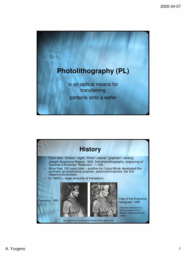
History• From latin: “photos” =light; “lithos” =stone; “graphein” =writing• Joseph Nicephore Niepce, 1826, first photolithography; engraving of
Cardinal d’Amboise. Resolution ~1 mm.• More than 100 years later – another try: Louis Minsk developed the
synthetic photosensitive polymer, polyvinylcinnamate, the first negative photoresist.
• In 1960’s – large amounts of transistors
Engraving, 1650
chemical treatment of a light sensitive form of asphalt, called bitumen of Judea
Copy of the EngravingHeliograph, 1826
http://www.hccs.cc.tx.us/JWoest/Research/photography.html
2005-04-07
A. Yurgens 2
Overview of the PL Process
• Surface Preparation• Spin Coating• Pre-Bake (Soft Bake)• Alignment• Exposure• Development• Post-Bake (Hard Bake)• Processing (thin-film deposition or etching, etc.)• Photoresist Stripping• Post Processing Cleaning (Ashing)
Surface Cleaning• Typical “dirt” that must be removed before applying
photoresist:
• dust, dandruff etc. • abrasive particles from lapping 1-100 micron• fibers from wipers • residues from previous photolithography• bacteria 1-20 micron (wash hands) • also:
– solvent residue– water residue (moisture)– photoresist or developer residue– oil (vacuum pumps)– silicone (vacuum grease)

2005-04-07
A. Yurgens 3
Surface Cleaning• Standard degrease:
– 2-5 min. soak in acetone with ultrasonic agitation– 2-5 min. soak in methanol with ultrasonic agitation– 2-5 min. soak in DI water with ultrasonic agitation– 30 sec. rinse in DI water– spin-rinse dry for wafers; – nitrogen blow-off dry for small substrates
• Organic residues: oxygen plasma (strip 2-3 min 200-300 W)
• Hazards:– acetone is flammable– methanol is toxic by skin adsorption
Photoresist AdhesionResist adhesion factors:
• moisture content on surface• wetting characteristics of resist• delay in exposure after the pre-bake• resist chemistry• surface smoothness• stress from coating process• surface contamination
To improve adhesion photoresist primers are used.

2005-04-07
A. Yurgens 4
Spin Coating• Substrate or wafer is kept on a rotated chuck by
vacuum and resist is applied by spin coating.
• Typically 3000-6000 rpm for 15-60 seconds.
• Resist thickness depends on:– resist viscosity – spinning velocity (~1/��)
• Most resists are 1-2 micron thick (SU-8 up to 200 micron)
Spin Process
excess of photoresistflies off the wafer
chuck
rotation & vacuum
wafer
• Edge Bead Height– up to 20-30 times the thickness of the resist– non-sharp edge reduces it– non-circular wafers increase it
2005-04-07
A. Yurgens 5
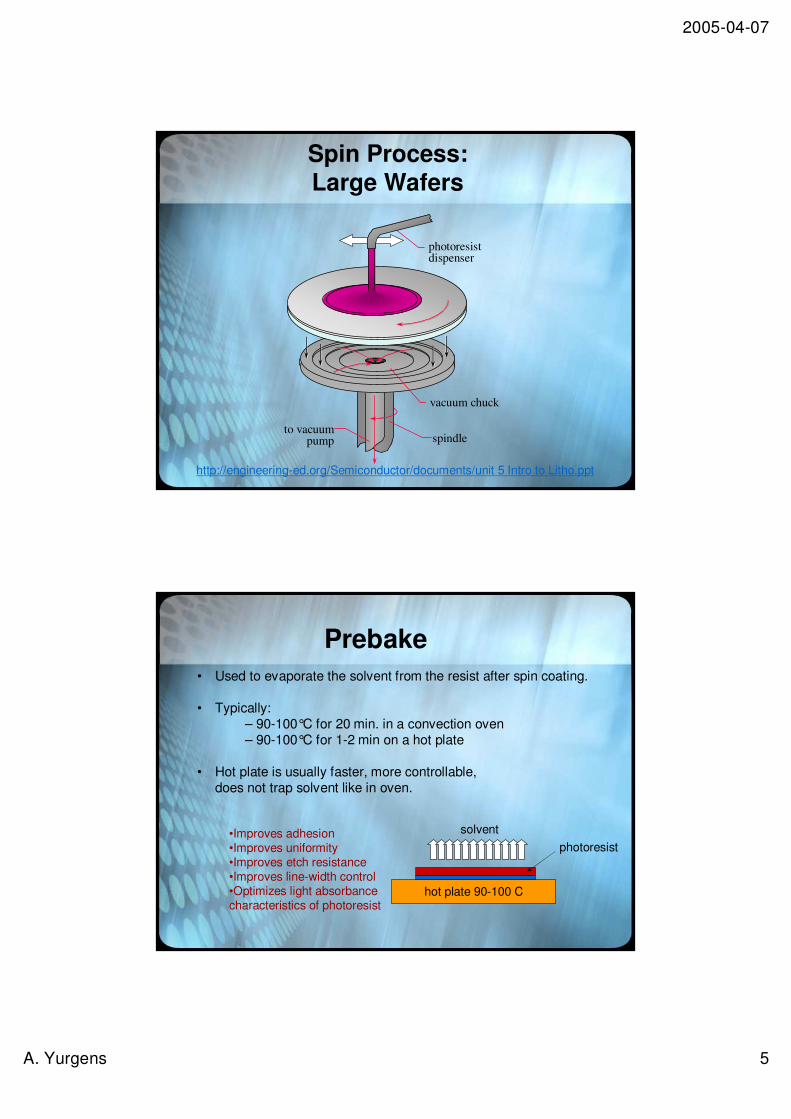
Spin Process: Large Wafers
vacuum chuck
spindleto vacuum
pump
photoresist dispenser
http://engineering-ed.org/Semiconductor/documents/unit 5 Intro to Litho.ppt
Prebake• Used to evaporate the solvent from the resist after spin coating.
• Typically:– 90-100°C for 20 min. in a convection oven– 90-100°C for 1-2 min on a hot plate
• Hot plate is usually faster, more controllable,does not trap solvent like in oven.
hot plate 90-100 C
solventphotoresist
•Improves adhesion•Improves uniformity•Improves etch resistance•Improves line-width control•Optimizes light absorbance characteristics of photoresist

2005-04-07
A. Yurgens 6
Alignment & Exposure
chrome on UV-transparent glassor quartz (expensive, DUV)
UV-lightX - Y - �alignment
mercury lamp
photoresist
substrate
latent image created inphotoresist after exposure
unexposed photoresist
Development
photoresist
substrate
Each commercial photoresist has its recommended developer,a chemical (base-type for S1813) that dissolves exposed / unexposed areas of the photoresist
Exposure destroys a developmentinhibitor and the developerdissolves the exposed areas.
Positive photoresist
exposedareas
Exposed areas become polymerized and insolvable in the developer
Negative photoresist
Some photoresists can be “inversed” by special treatment

2005-04-07
A. Yurgens 7
Alignment and Exposure Hardware
Proximity Contact
Projection
UV-lens UV-lens UV-lens
UV-lens
Resolution 0.1-1 micron;
contact for expose;separate for align.
Research
Resolution 2-4 micron;
poorer image than fromthe contact aligner; themask lifetime longer.
Low-cost processes 0.1-1 micron, mainstream
UV-Light in Photolithography
• High pressure Hg-vapor lamps• Xenon lamps• UV diodes (?!)
http://www.lamptech.co.uk/Spec%20Sheets/Osram%20HBO3500.htm
Xe

2005-04-07
A. Yurgens 8
MC2’s Mask Aligners
- wavelength: 248nm- mask size: 3 inch- intensity: 1.5mW/sqcm
- wavelength: 365nm- mask size: 2 inch- intensity: 5mW/sqcm
Karl-Süss contact DUV aligner Canon projection aligner
Postbake
• Postbake is needed for acid- and Ar-ion etching• Postbake is not needed for processes for liftoff processes.• Photoresist will undergo plastic flow with sufficient time and
temperature:• Glass transition temperature is important parameter.• Postbake removes any residuals of the coating solvent and
developer.• Postbake introduces stress into the photoresist.• Some shrinkage of the photoresist may occur.• Longer and hotter postbake makes subsequent resist removal
more difficult.
Used to stabilize and harden the developed photoresistprior to processing steps
Typically 120-140C for 10-20 min (all depend on photoresist)

2005-04-07
A. Yurgens 9
Processing
thin film
Etch Liftoffundercut
photoresist
after removal of photoresist
1
2
3
4
1
2
3
Processing
Etch Liftoff
•The final thin-film pattern isnegative with respect to photoresist pattern
•Photoresist is in contact with substrate (chemical reactioncan occur)
•The final thin-film pattern isthe same as photoresist pattern
•Photoresist is not in contact with substrate
Pros and cons
2005-04-07
A. Yurgens 10
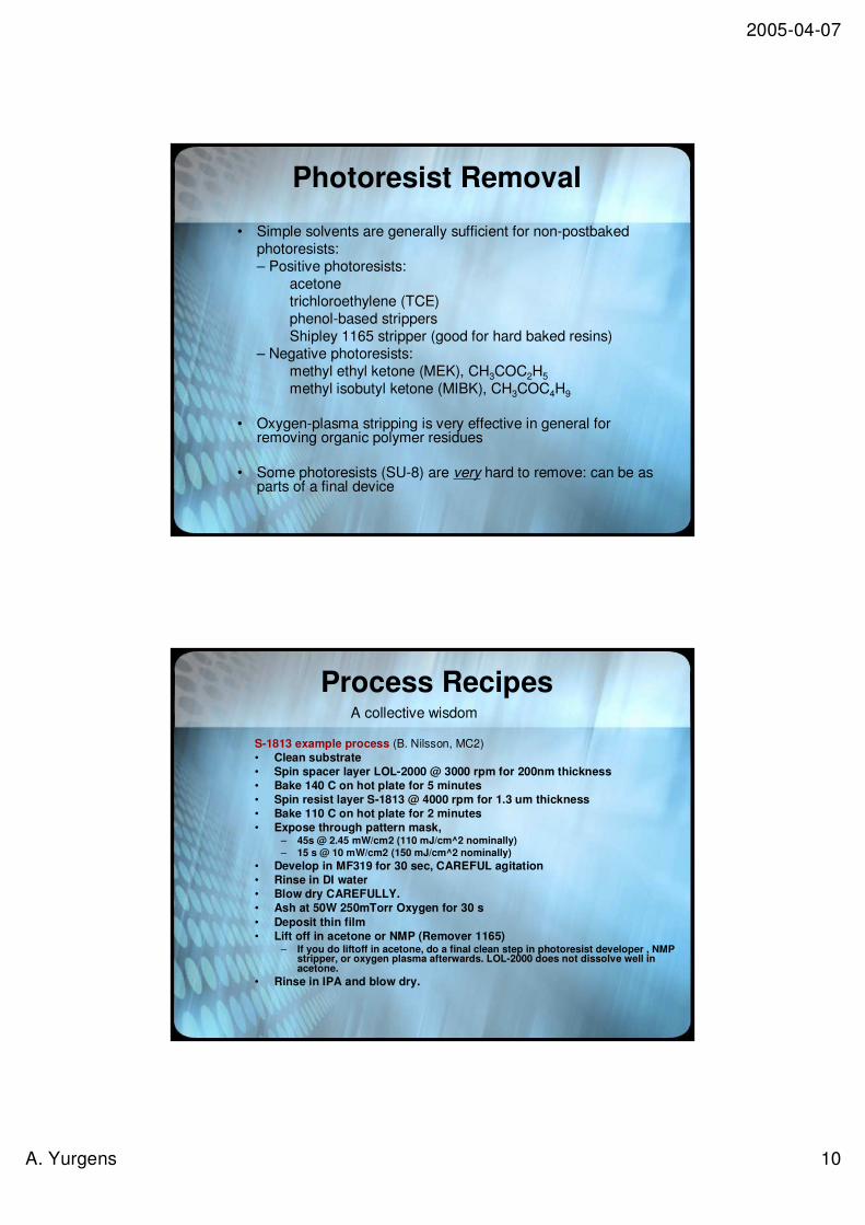
Photoresist Removal
• Simple solvents are generally sufficient for non-postbakedphotoresists:– Positive photoresists:
acetonetrichloroethylene (TCE)phenol-based strippersShipley 1165 stripper (good for hard baked resins)
– Negative photoresists:methyl ethyl ketone (MEK), CH3COC2H5methyl isobutyl ketone (MIBK), CH3COC4H9
• Oxygen-plasma stripping is very effective in general for removing organic polymer residues
• Some photoresists (SU-8) are very hard to remove: can be as parts of a final device
Process Recipes
S-1813 example process (B. Nilsson, MC2)• Clean substrate • Spin spacer layer LOL-2000 @ 3000 rpm for 200nm thickness • Bake 140 C on hot plate for 5 minutes • Spin resist layer S-1813 @ 4000 rpm for 1.3 um thickness • Bake 110 C on hot plate for 2 minutes • Expose through pattern mask,
– 45s @ 2.45 mW/cm2 (110 mJ/cm^2 nominally) – 15 s @ 10 mW/cm2 (150 mJ/cm^2 nominally)
• Develop in MF319 for 30 sec, CAREFUL agitation • Rinse in DI water • Blow dry CAREFULLY. • Ash at 50W 250mTorr Oxygen for 30 s • Deposit thin film • Lift off in acetone or NMP (Remover 1165)
– If you do liftoff in acetone, do a final clean step in photoresist developer , NMP stripper, or oxygen plasma afterwards. LOL-2000 does not dissolve well in acetone.
• Rinse in IPA and blow dry.
A collective wisdom
2005-04-07
A. Yurgens 11
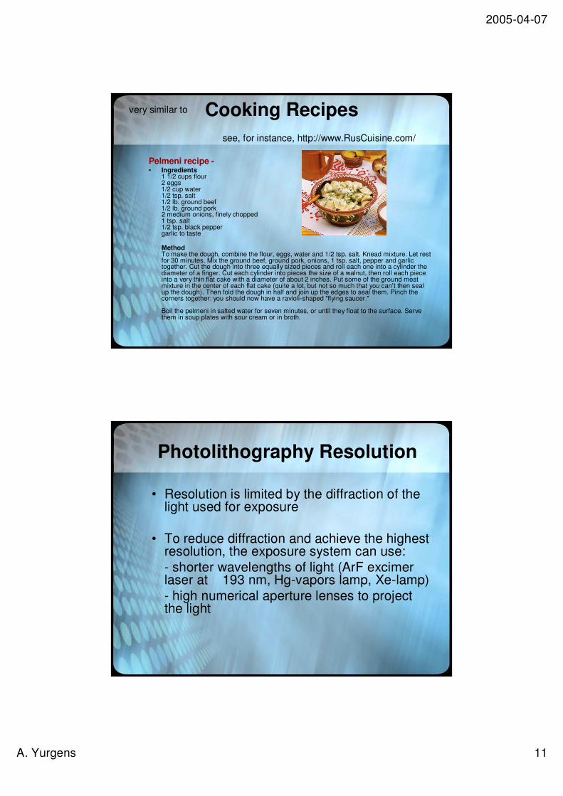
very similar to Cooking Recipes
Pelmeni recipe -• Ingredients
1 1/2 cups flour2 eggs1/2 cup water1/2 tsp. salt1/2 lb. ground beef1/2 lb. ground pork2 medium onions, finely chopped1 tsp. salt1/2 tsp. black peppergarlic to taste
MethodTo make the dough, combine the flour, eggs, water and 1/2 tsp. salt. Knead mixture. Let rest for 30 minutes. Mix the ground beef, ground pork, onions, 1 tsp. salt, pepper and garlic together. Cut the dough into three equally sized pieces and roll each one into a cylinder the diameter of a finger. Cut each cylinder into pieces the size of a walnut, then roll each piece into a very thin flat cake with a diameter of about 2 inches. Put some of the ground meat mixture in the center of each flat cake (quite a lot, but not so much that you can't then seal up the dough). Then fold the dough in half and join up the edges to seal them. Pinch the corners together: you should now have a ravioli-shaped "flying saucer."
Boil the pelmeni in salted water for seven minutes, or until they float to the surface. Serve them in soup plates with sour cream or in broth.
see, for instance, http://www.RusCuisine.com/
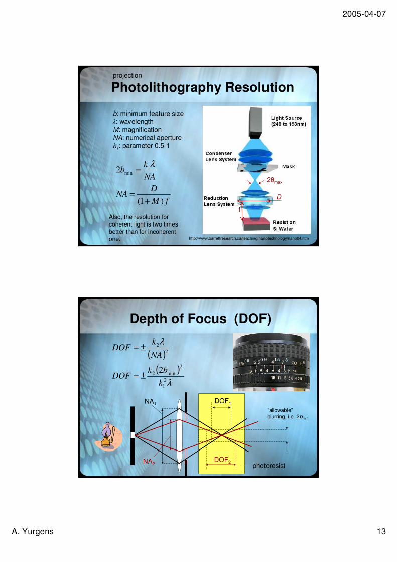
Photolithography Resolution
• Resolution is limited by the diffraction of the light used for exposure
• To reduce diffraction and achieve the highest resolution, the exposure system can use:- shorter wavelengths of light (ArF excimerlaser at 193 nm, Hg-vapors lamp, Xe-lamp)- high numerical aperture lenses to project the light

2005-04-07
A. Yurgens 12
Photolithography Resolution
http://www.barrettresearch.ca/teaching/nanotechnology/nano04.htm
http://www.falstad.com/mathphysics.html
Diffraction limits the resolution
one wants one gets
Photolithography Resolution
adopted from C.G. Willson, Introduction to Microlithography
��
���
� +=2
32 mint
sb λ
b: minimum feature size�: wavelengths: mask-photoresist spacingt: photoresist thickness
proximity- and contact-
2005-04-07
A. Yurgens 13
Photolithography Resolution
b: minimum feature size�: wavelengthM: magnificationNA: numerical aperturek1: parameter 0.5-1
projection
http://www.barrettresearch.ca/teaching/nanotechnology/nano04.htm
fMD
NA
NAk
b
)1(
2 1min
+=
= λ
D
f
2�max
Also, the resolution for coherent light is two times better than for incoherent one.
Depth of Focus (DOF)
( )( )
λ
λ
21
2min2
22
2kbk
DOF
NAk
DOF
±=
±=
“allowable”blurring, i.e. 2bmin
DOF1
DOF2
NA1
NA2 photoresist
2005-04-07
A. Yurgens 14
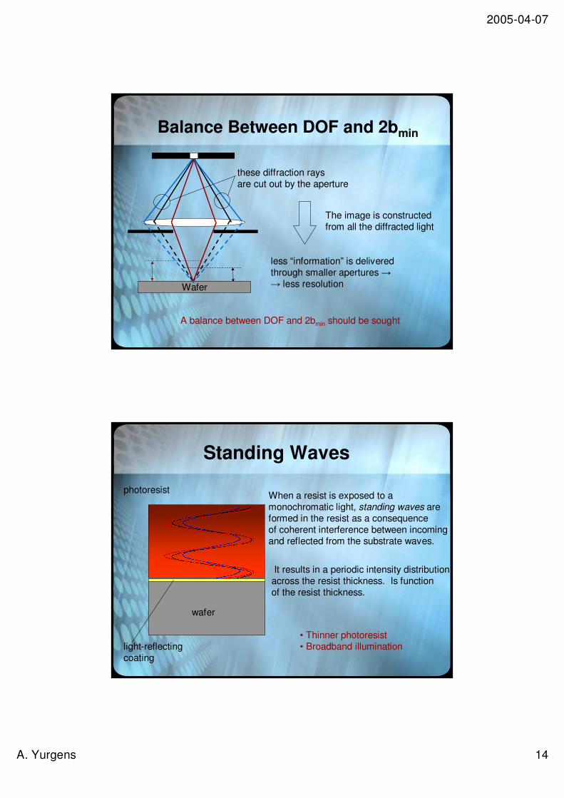
Balance Between DOF and 2bmin
Wafer
these diffraction rays are cut out by the aperture
The image is constructedfrom all the diffracted light
less “information” is deliveredthrough smaller apertures �� less resolution
A balance between DOF and 2bmin should be sought
Standing Waves
light-reflecting coating
photoresist
wafer
When a resist is exposed to a monochromatic light, standing waves areformed in the resist as a consequenceof coherent interference between incomingand reflected from the substrate waves.
It results in a periodic intensity distributionacross the resist thickness. Is functionof the resist thickness.
• Thinner photoresist• Broadband illumination
2005-04-07
A. Yurgens 15
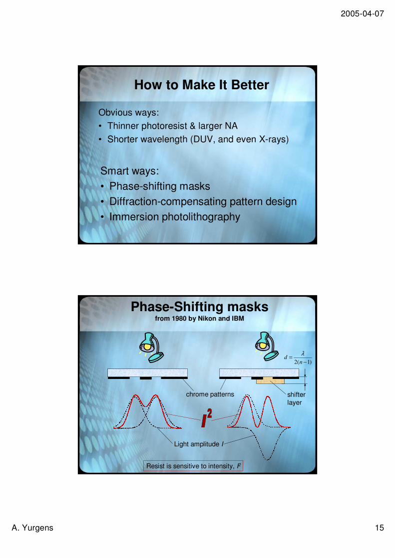
How to Make It Better
Obvious ways:• Thinner photoresist & larger NA• Shorter wavelength (DUV, and even X-rays)
Smart ways:• Phase-shifting masks• Diffraction-compensating pattern design• Immersion photolithography
Phase-Shifting masks from 1980 by Nikon and IBM
shifterlayer
chrome patterns
Light amplitude I
Resist is sensitive to intensity, I2
)1(2 −=
nd
λ
2005-04-07
A. Yurgens 16
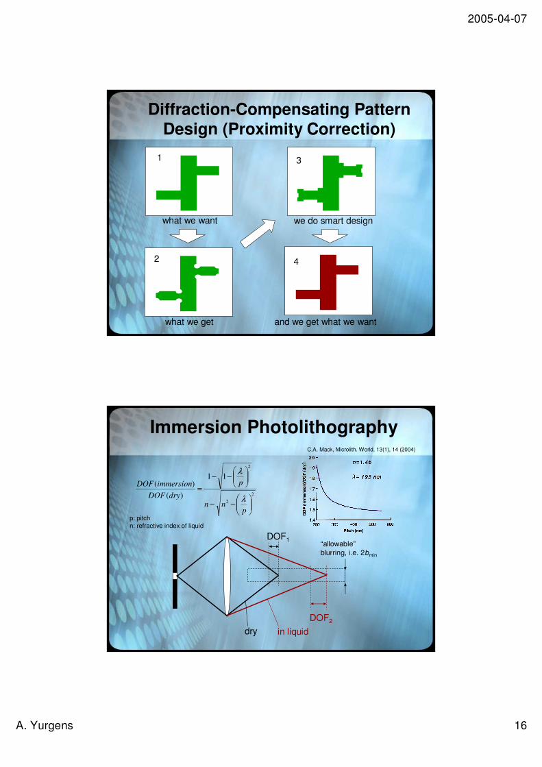
Diffraction-Compensating Pattern Design (Proximity Correction)
what we want
what we get
we do smart design
and we get what we want
1
2
3
4
Immersion Photolithography
“allowable”blurring, i.e. 2bmin
DOF1
DOF2
dry in liquid
22
2
11
)()(
���
����
�−−
���
����
�−−=
pnn
p
dryDOFimmersionDOF
λ
λ
p: pitchn: refractive index of liquid
C.A. Mack, Microlith. World, 13(1), 14 (2004)
2005-04-07
A. Yurgens 17
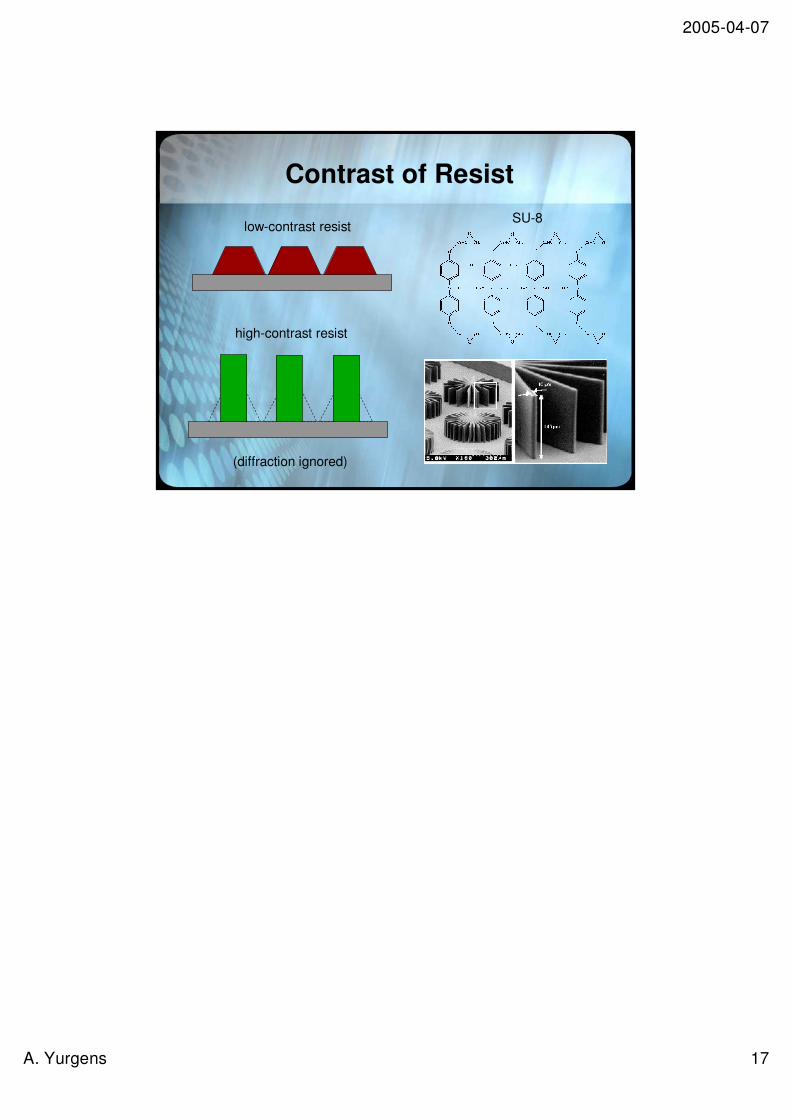
Contrast of ResistSU-8
low-contrast resist
high-contrast resist
(diffraction ignored)