photonic integrated circuits nasa g dd d s fli ht c tnasa ... · photonic integrated circuits nasa...
TRANSCRIPT

Photonic Integrated Circuits
NASA G dd d S Fli ht C tNASA Goddard Space Flight Center

AGENDAAGENDA LCRD modem LCRD modem
Integrated photonics – examples
Direct-Write ideas
NASA EXAMPLES
SUMMARY


LCRDLRD 2019
32 MbpsUplink
LRD 2019
To ISS
1.25 GbpsISS terminal
pDownlinkFrom ISS
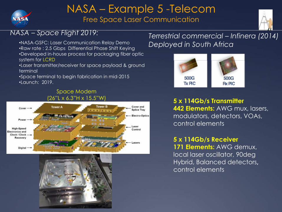
NASA – Example 5 -Telecom Free Space Laser Communication
NASA S Fli ht 2019 •NASA-GSFC: Laser Communication Relay Demo•Raw rate : 2.5 Gbps Differential Phase Shift Keying•Developed in-house process for packaging fiber optic system for LCRD
Terrestrial commercial – Infinera (2014)Deployed in South Africa
NASA – Space Flight 2019:
system for LCRD•Laser transmitter/receiver for space payload & ground terminal•Space terminal to begin fabrication in mid-2015•Launch: 2019.
Space ModemSpace Modem(26”L x 6.3”H x 15.5”W) 5 x 114Gb/s Transmitter
442 Elements: AWG mux, lasers, modulators, detectors, VOAs,
t l l tcontrol elements
5 x 114Gb/s Receiver171 Elements: AWG demux, local laser oscillator, 90deg Hybrid, Balanced detectors, control elements

NASA Space Communication and Navigation (SCaN)Integrated LCRD LEO-User
M d d A lifi (ILLUMA)Modem and Amplifier (ILLUMA)Provides pathway to near-Earth low-cost lasercom terminals
Reduce Size, Weight, Power and Cost of spaceflight modem. Use integrated
l t i / h t i h t ff tielectronics/photonics where cost effective. Establish US industry LEO space-flight modem
supplier that is compatible with LCRD Use vendor up-screened COTS part where Use vendor up screened COTS part where
possible.
6

Transmitter front-endDFB with Integrated MZ modulatorg
(need high extinction ratio ~20 dB)Comparison of integrated InP to LiNbO3

Coherent receiver

Receiver preamplifier PIC
Erbium-doped spiral amplifiers with 20 dB of net gain on silicon
Sergio A. Vázquez-Córdova,1,2,* Meindert Dijkstra,1,2 Edward H. Bernhardi,1 1 3 1 2 1 2Feridun Ay,1,3 Kerstin Wörhoff,1 Jennifer L. Herek,2 Sonia M. García-Blanco,1,2 and
Markus Pollnau1,4 1Integrated Optical MicroSystems Group, MESA + Institute for Nanotechnology, University of Twente, P.O. Box 217,
7500 AE Enschede, The Netherlands 2Optical Sciences Group, MESA + Institute for Nanotechnology, University of Twente, P.O. Box 217, 7500 AE
Enschede, The Netherlands 3Department of Electrical and Electronics Engineering, Anadolu University, 26555 Eskişehir, Turkey
4Department of Materials and Nano Physics, School of Information and Communication Technology, KTHRoyal Institute of Technology, Electrum 229, Isafjordsgatan 2224, 16440 Kista, Sweden
* d 1@ l*[email protected]
• Internal net gain = 20 dB
#221324 - $15.00 USD Received 19 Aug 2014; revised 24 Sep 2014; accepted 3 Oct 2014; published 15 Oct 2014
• Noise figure of 3.75 dB small-signal-gain regime.
(C) 2014 OSA 20 October 2014 | Vol. 22, No. 21 | DOI:10.1364/OE.22.025993 | OPTICS EXPRESS 25993

High sensitivity pre-amplified coherent receivercoherent receiver
406 JOURNAL OF LIGHTWAVE TECHNOLOGY, VOL. 30, NO. 4, FEBRUARY 15, 2012
Demonstration of Record Sensitivities in OpticallyPreamplified Receivers by Combining PDM QPSKPreamplified Receivers by Combining PDM-QPSK
and M-Ary Pulse-Position ModulationXiang Liu, Senior Member, IEEE, Fellow, OSA, Thomas H. Wood, Fellow, IEEE, Fellow, OSA,Robert W. Tkach, Fellow, IEEE, Fellow, OSA, and S. Chandrasekhar, Fellow, IEEE, Fellow, OSA
Fig. 11. Experimental BER performance of the 2.5 Gb/s PQ-16PPM signal ascompared to PDM-QPSK.
Fig. 1. Encoding of a PQ-4PPM signal.

Direct write waveguide fabrication

Goddard Code 554 Femtosecond Direct-Write laser
Di l t i B kd f AiDielectric Breakdown of Airat Laser Focus
Fused Silica Witness SampleEtched by Femtosecond Laser

Direct-write laser system is multi-use
Optical waveguides Precision Machining Patterning graphene
Milling/Bonding/welding glass Glass/copper weldAdditive manufacturingwith laser sintering (3D printer principle)
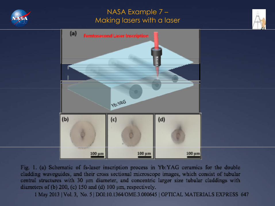
NASA Example 7 –Making lasers with a laser
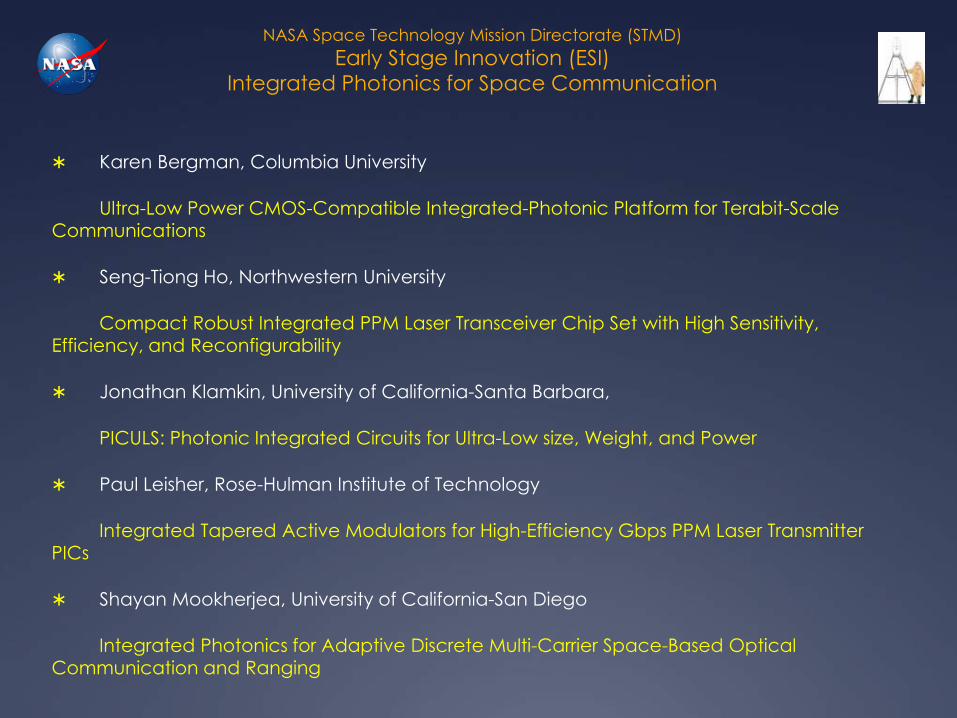
NASA Space Technology Mission Directorate (STMD)Early Stage Innovation (ESI)
Integrated Photonics for Space Communication
Karen Bergman, Columbia University
Ultra Low Power CMOS Compatible Integrated Photonic Platform for Terabit Scale Ultra-Low Power CMOS-Compatible Integrated-Photonic Platform for Terabit-Scale Communications
Seng-Tiong Ho, Northwestern University
Compact Robust Integrated PPM Laser Transceiver Chip Set with High Sensitivity, Efficiency, and Reconfigurability
Jonathan Klamkin, University of California-Santa Barbara,
PICULS: Photonic Integrated Circuits for Ultra-Low size, Weight, and Power
Paul Leisher, Rose-Hulman Institute of Technology
Integrated Tapered Active Modulators for High-Efficiency Gbps PPM Laser Transmitter PICs
Shayan Mookherjea, University of California-San Diego
Integrated Photonics for Adaptive Discrete Multi-Carrier Space-Based Optical Communication and Ranging
NASA Integrated PhotonicsNASA Applications: Sensors – Spectrometers - Chemical/biological sensors:
Lab on a chip systems for landers Lab-on-a-chip systems for landers Astronaut health monitoring Front-end and back-end for remote sensing instruments including
trace gas lidarsg Large telescope spectrometers for exoplanets.
Microwave, Sub-millimeter and Long-Wave Infra-Red Microwave, Sub millimeter and Long Wave Infra Red photonics: Opens new methods due to Size, Weight and Power improvements, radio
astronomy and THz spectroscopy
Telecom: inter and intra satellite communications. Can obtain large leverage from industrial efforts.

Acknowledgments
NASA STMD
NASA SCaN
DoD IP-IMI
AETD colloquium
Th k !Thank you!