phycore -i.mx 6 hardware manual - phytec 2015€¦ · a product of a phytec technology holding...
TRANSCRIPT

A product of a PHYTEC Technology Holding company
phyCORE®-i.MX 6
Hardware Manual
Document No.: L-808e_1
SOM Prod. No.: PCM-058 SOM PCB. No.: 1429.1
Edition: June 2015

phyCORE®-i.MX 6 [PCM-058]
© PHYTEC Messtechnik GmbH 2015 L-808e_1
Copyrighted products are not explicitly indicated in this manual. The absence of the trademark (™, or ®) and copyright (©) symbols does not imply that a product is not protected. Additionally, registered patents and trademarks are similarly not expressly indicated in this manual. The information in this document has been carefully checked and is considered to be entirely reliable. However, PHYTEC Messtechnik GmbH assumes no responsibility for any inaccuracies. PHYTEC Messtechnik GmbH neither gives any guarantee nor accepts any liability whatsoever for consequential damages resulting from the use of this manual or its associated product. PHYTEC Messtechnik GmbH reserves the right to alter the information contained herein without prior notification and accepts no responsibility for any damages that might result. Additionally, PHYTEC Messtechnik GmbH offers no guarantee nor accepts any liability for damages arising from the improper usage or improper installation of the hardware or software. PHYTEC Messtechnik GmbH further reserves the right to alter the layout and/or design of the hardware without prior notification and accepts no liability for doing so. © Copyright 2015 PHYTEC Messtechnik GmbH, D-55129 Mainz. Rights - including those of translation, reprint, broadcast, photomechanical or similar reproduction and storage or processing in computer systems, in whole or in part - are reserved. No reproduction may occur without the express written consent from PHYTEC Messtechnik GmbH. EUROPE NORTH AMERICA FRANCE
Address: PHYTEC Messtechnik GmbH Robert-Koch-Str. 39 D-55129 Mainz GERMANY
PHYTEC America LLC 203 Parfitt Way SW Bainbridge Island, WA 98110 USA
PHYTEC France 17, place Saint-Etienne F-72140 Sillé-le-Guillaume FRANCE
Ordering Information:
+49 6131 9221-32 [email protected]
+1 800 278-9913 [email protected]
+33 2 43 29 22 33 [email protected]
Technical Support:
+49 6131 9221-31 [email protected]
+1 206 780-9047 [email protected]
Fax: +49 6131 9221-33 +1 206 780-9135 +33 2 43 29 22 34
Web Site: http://www.phytec.de http://www.phytec.eu
http://www.phytec.com http://www.phytec.fr
INDIA CHINA
Address: PHYTEC Embedded Pvt. Ltd. #16/9C, 3rd Main, 3rd Floor, 8th Block,Opp. Police Station Koramangala, Bangalore-560095 INDIA
PHYTEC Information Technology (Shenzhen) Co. Ltd. Suite 2611, Floor 26, Anlian Plaza, 4018 Jin Tian Road Futian District, Shenzhen CHINA 518026
Ordering Information:
+91-80-4086 7046/48 [email protected]
+86-755-3395-5875 [email protected]
Technical Support:
+91-80-4086 7047 [email protected]
Fax: +86-755-3395-5999
Web Site: http://www.phytec.in http://www.phytec.cn
1st Edition June 2015

Contents
© PHYTEC Messtechnik GmbH 2015 L-808e_1 i
List of Figures ............................................................................................................ ii List of Tables ............................................................................................................ iii Conventions, Abbreviations and Acronyms .................................................................... iv Preface ................................................................................................................... vii 1 Introduction ...................................................................................................... 1
1.1 Features of the phyCORE-i.MX 6 ....................................................................... 1 1.2 Block Diagram.............................................................................................. 3 1.3 phyCORE-i.MX 6 Component Placement ............................................................. 4 1.4 Minimum Requirements to operate the phyCORE-i.MX 6 ........................................ 6
2 Pin Description ................................................................................................... 7 3 Jumpers .......................................................................................................... 17 4 Power.............................................................................................................. 21
4.1 Primary System Power (VDD_3V3) ...................................................................21 4.2 Power Management IC (PMIC) (U16) ................................................................21
4.2.1 Power Domains.................................................................................22 4.3 Supply Voltage for external Logic ....................................................................24
5 System Configuration and Booting....................................................................... 25 5.1 Boot Mode Selection ....................................................................................25 5.2 Boot Device Selection and Configuration ..........................................................26
6 System Memory................................................................................................. 28 6.1 DDR3-SDRAM (U4-U7) ..................................................................................28 6.2 NAND Flash Memory (U12) .............................................................................29 6.3 eMMC Flash Memory (U14).............................................................................29 6.4 I²C EEPROM (U11) ........................................................................................29
6.4.1 EEPROM Write Protection Control (J4) ...................................................30 6.5 SPI Flash Memory (U9) ) ................................................................................30
7 SD / MM Card Interfaces ..................................................................................... 31 8 Serial Interfaces ............................................................................................... 32
8.1 Universal Asynchronous Interface ...................................................................33 8.2 USB OTG Interface........................................................................................34 8.3 USB Host Interface.......................................................................................34 8.4 Ethernet Interface .......................................................................................35
8.4.1 Ethernet PHY (U2).............................................................................35 8.4.2 Software Reset of the Ethernet Controller ..............................................36 8.4.3 MAC Address ....................................................................................36 8.4.4 RMII Interface..................................................................................37
8.5 SPI Interface...............................................................................................38 8.6 I2C Interface ...............................................................................................39 8.7 I2S Audio Interface (SSI)) ..............................................................................39 8.8 CAN Interface..............................................................................................40 8.9 SATA Interface ............................................................................................40 8.10 PCI Express Interface ....................................................................................41
9 General Purpose I/Os......................................................................................... 42 10 User LED .......................................................................................................... 43 11 Debug Interface................................................................................................ 44

phyCORE®-i.MX 6 [PCM-058]
ii © PHYTEC Messtechnik GmbH 2015 L-808e_1
12 Display Interfaces ............................................................................................. 45 12.1 Parallel Display Interface.............................................................................. 45 12.2 LVDS Display Interface ................................................................................. 46 12.3 Supplementary Signals................................................................................. 46
13 High-Definition Multimedia Interface (HDMI)......................................................... 47 14 Camera Interfaces ............................................................................................. 48
14.1 Parallel 0 Camera Interface (CSI0 of IPU#1)...................................................... 50 14.2 Parallel 1 Camera Interface (CSI1 of IPU#2)...................................................... 51 14.3 MIPI/CSI-2 Camera Interface......................................................................... 52 14.4 Utilizing the Camera Interfaces on a Carrier Board ............................................. 53
15 Technical Specifications ..................................................................................... 54 16 Hints for Integrating and Handling the phyCORE-i.MX 6.......................................... 57
16.1 Integrating the phyCORE-i.MX 6 ..................................................................... 57 16.2 Handling the phyCORE-i.MX 6 ........................................................................ 59
17 Revision History................................................................................................ 60 Index ...................................................................................................................... 61
List of Figures
Figure 1: Block Diagram of the phyCORE-i.MX 6 .............................................................. 3
Figure 2: phyCORE-i.MX 6 Component Placement (top view) ............................................. 4
Figure 3: phyCORE-i.MX 6 Component Placement (bottom view) ........................................ 5
Figure 4: Pinout of the phyCORE-Connector (top view) .................................................... 8
Figure 5: Typical Jumper Pad Numbering Scheme ......................................................... 17
Figure 6: Jumper Locations (top view) ....................................................................... 18
Figure 7: Jumper Locations (bottom view) .................................................................. 19
Figure 8: Powering Scheme of the phyCORE- i.MX 6 ....................................................... 23
Figure 9: Camera Connectivity of the i.MX 6 (Solo/DualLite) ........................................... 48
Figure 10: Camera Connectivity of the i.MX 6 (Dual Core/Quad Core) .................................. 48
Figure 11: Camera Interfaces at the phyCORE-Connector (Parallel 0(CSI0 of IPU#1), Parallel 1(CSI1 of IPU#2), and MIPI/CSI-2)..................................................... 49
Figure 12: Use of Parallel 0 (CSI0 of IPU#1) and Parallel 1 (CSI1 of IPU#2) as phyCAM-P interface................................................................................ 53
Figure 13: Use of Parallel 0 (CSI0 of IPU#1) and Parallel_1 (CSI1 of IPU#2) as phyCAM-S+ interface .............................................................................. 53
Figure 12: Physical Dimensions (top view) .................................................................... 54
Figure 13: Footprint of the phyCORE-i.MX 6................................................................... 58

Contents
© PHYTEC Messtechnik GmbH 2015 L-808e_1 iii
List of Tables
Table 1: Signal Types used in this Manual .....................................................................v
Table 2: Abbreviations and Acronyms used in this Manual...............................................vi
Table 3: Pinout of the phyCORE-Connector X1, Row A..................................................... 9
Table 4: Pinout of the phyCORE-Connector X1, Row B....................................................11
Table 5: Pinout of the phyCORE-Connector X1, Row C ....................................................13
Table 6: Pinout of the phyCORE-Connector X1, Row D....................................................15
Table 7: Jumper Settings ........................................................................................20
Table 8: Boot Modes of the phyCORE-i.MX 6 ................................................................25
Table 9: Boot Configuration Pins at the phyCORE-Connector...........................................27
Table 10: EEPROM write protection states via J4 ............................................................30
Table 11: Location of the SD / MM Card Interface Signals ................................................31
Table 12: Location of the UART Signals ........................................................................33
Table 13: Location of the USB OTG Signals....................................................................34
Table 14: Location of the USB-Host Signals ..................................................................34
Table 15: Location of the Ethernet Signals ...................................................................35
Table 16: Location of the RMII Interface Signals............................................................37
Table 17: I2C Interface Signal Location ........................................................................39
Table 18: SPI Interface Signal Location .......................................................................38
Table 19: I2S Interface Signal Location ........................................................................39
Table 20: CAN Interface Signal Location ......................................................................40
Table 21: SATA Interface Signal Location .....................................................................40
Table 22: PCIe Interface Signal Location ......................................................................41
Table 23: Location of GPIO Pins..................................................................................42
Table 24: Debug Interface Signal Location at phyCORE-Connector X1.................................44
Table 25: Parallel Display Interface Signal Location .......................................................45
Table 26: LVDS Display Interface Signal Location...........................................................46
Table 27: Supplementary Signals to support the Display Connectivity ................................46
Table 28: HDMI Interface Signal Location ....................................................................47
Table 29: Camera Interface Parallel 0 (CSI0) Signal Location............................................50
Table 30: Camera Interface Parallel 1 (CSI1) Signal Location............................................51
Table 31: Camera Interface MIPI/CSI-2 Signal Location ..................................................52

phyCORE®-i.MX 6 [PCM-058]
iv © PHYTEC Messtechnik GmbH 2015 L-808e_1
Conventions, Abbreviations and Acronyms
This hardware manual describes the PCM-058 System on Module in the following referred to as phyCORE®-i.MX 6. The manual specifies the phyCORE®-i.MX 6's design and function. Precise specifications for the Freescale Semiconductor i.MX 6 microcontrollers can be found in the enclosed microcontroller Data Sheet/User's Manual.
Note: We refrain from providing detailed part specific information within this manual, which can be subject to continuous changes, due to part maintenance for our products. Please read the paragraph "Product Change Management and information in this manual on parts populated on the SOM" within the Preface.
Note: The BSP delivered with the phyCORE®-i.MX 6 usually includes drivers and/or software for controlling all components such as interfaces, memory, etc. Therefore programming close to hardware at register level is not necessary in most cases. For this reason, this manual contains no detailed description of the controller's registers, or information relevant for software development. Please refer to the i.MX 6 Reference Manual, if such information is needed to connect customer designed applications. Conventions The conventions used in this manual are as follows: Signals that are preceded by an "n", "/", or “#”character (e.g.: nRD, /RD, or #RD), or
that have a dash on top of the signal name (e.g.: RD) are designated as active low signals. That is, their active state is when they are driven low, or are driving low.
A "0" indicates a logic zero or low-level signal, while a "1" represents a logic one or high-level signal.
The hex-numbers given for addresses of I2C devices always represent the 7 MSB of the address byte. The correct value of the LSB which depends on the desired command (read (1), or write (0)) must be added to get the complete address byte. E.g. given address in this manual 0x41 => complete address byte = 0x83 to read from the device and 0x82 to write to the device
Tables which describe jumper settings show the default position in bold, blue text. Text in blue italic indicates a hyperlink within, or external to the document. Click these
links to quickly jump to the applicable URL, part, chapter, table, or figure. References made to the phyCORE-Connector always refer to the high density Samtec
connector on the undersides of the phyCORE-i.MX 6 System on Module.
Conventions, Abbreviations and Acronyms
© PHYTEC Messtechnik GmbH 2015 L-808e_1 v
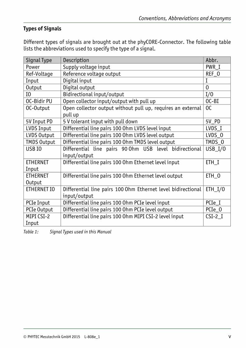
Types of Signals Different types of signals are brought out at the phyCORE-Connector. The following table lists the abbreviations used to specify the type of a signal.
Signal Type Description Abbr. Power Supply voltage input PWR_I Ref-Voltage Reference voltage output REF_O Input Digital input I Output Digital output O IO Bidirectional input/output I/O OC-Bidir PU Open collector input/output with pull up OC-BI OC-Output Open collector output without pull up, requires an external
pull up OC
5V Input PD 5 V tolerant input with pull down 5V_PD LVDS Input Differential line pairs 100 Ohm LVDS level input LVDS_I LVDS Output Differential line pairs 100 Ohm LVDS level output LVDS_O TMDS Output Differential line pairs 100 Ohm TMDS level output TMDS_O USB IO Differential line pairs 90 Ohm USB level bidirectional
input/output USB_I/O
ETHERNET Input
Differential line pairs 100 Ohm Ethernet level input ETH_I
ETHERNET Output
Differential line pairs 100 Ohm Ethernet level output ETH_O
ETHERNET IO Differential line pairs 100 Ohm Ethernet level bidirectional input/output
ETH_I/O
PCIe Input Differential line pairs 100 Ohm PCIe level input PCIe_I PCIe Output Differential line pairs 100 Ohm PCIe level output PCIe_O MIPI CSI-2 Input
Differential line pairs 100 Ohm MIPI CSI-2 level input CSI-2_I
Table 1: Signal Types used in this Manual
phyCORE®-i.MX 6 [PCM-058]
vi © PHYTEC Messtechnik GmbH 2015 L-808e_1
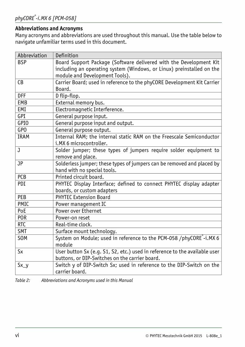
Abbreviations and Acronyms Many acronyms and abbreviations are used throughout this manual. Use the table below to navigate unfamiliar terms used in this document.
Abbreviation Definition BSP Board Support Package (Software delivered with the Development Kit
including an operating system (Windows, or Linux) preinstalled on the module and Development Tools).
CB Carrier Board; used in reference to the phyCORE Development Kit Carrier Board.
DFF D flip-flop. EMB External memory bus. EMI Electromagnetic Interference. GPI General purpose input. GPIO General purpose input and output. GPO General purpose output. IRAM Internal RAM; the internal static RAM on the Freescale Semiconductor
i.MX 6 microcontroller. J Solder jumper; these types of jumpers require solder equipment to
remove and place. JP Solderless jumper; these types of jumpers can be removed and placed by
hand with no special tools. PCB Printed circuit board. PDI PHYTEC Display Interface; defined to connect PHYTEC display adapter
boards, or custom adapters PEB PHYTEC Extension Board PMIC Power management IC PoE Power over Ethernet POR Power-on reset RTC Real-time clock. SMT Surface mount technology. SOM System on Module; used in reference to the PCM-058 /phyCORE®-i.MX 6
module Sx User button Sx (e.g. S1, S2, etc.) used in reference to the available user
buttons, or DIP-Switches on the carrier board. Sx_y Switch y of DIP-Switch Sx; used in reference to the DIP-Switch on the
carrier board.
Table 2: Abbreviations and Acronyms used in this Manual

Preface
© PHYTEC Messtechnik GmbH 2015 L-808e_1 vii
Preface
As a member of PHYTEC's phyCORE® product family the phyCORE-i.MX 6 is one of a series of PHYTEC System on Modules (SOMs) that can be populated with different controllers and, hence, offers various functions and configurations. PHYTEC supports a variety of 8-/16- and 32-bit controllers in two ways:
(1) as the basis for Rapid Development Kits which serve as a reference and evaluation platform
(2) as insert-ready, fully functional phyCORE® OEM modules, which can be embedded directly into the user’s peripheral hardware design.
Implementation of an OEM-able SOM subassembly as the "core" of your embedded design allows you to focus on hardware peripherals and firmware without expending resources to "re-invent" microcontroller circuitry. Furthermore, much of the value of the phyCORE® module lies in its layout and test. Production-ready Board Support Packages (BSPs) and Design Services for our hardware will further reduce your development time and risk and allow you to focus on your product expertise. Take advantage of PHYTEC products to shorten time-to-market, reduce development costs, and avoid substantial design issues and risks. With this new innovative full system solution you will be able to bring your new ideas to market in the most timely and cost-efficient manner. For more information go to: http://www.phytec.de/de/leistungen/entwicklungsunterstuetzung.html or www.phytec.eu/europe/oem-integration/evaluation-start-up.html

phyCORE®-i.MX 6 [PCM-058]
viii © PHYTEC Messtechnik GmbH 2015 L-808e_1
Ordering Information The part numbering of the phyCORE has the following structure:
PCM- 058-xxxxxx.A0
Product number (consecutive) Assembly options (depending on model) Version number
Product Specific Information and Technical Support
In order to receive product specific information on changes and updates in the best way also in the future, we recommend to register at http://www.phytec.de/de/support/registrierung.html or http://www.phytec.eu/europe/support/registration.html For technical support and additional information concerning your product, please visit the support section of our web site which provides product specific information, such as errata sheets, application notes, FAQs, etc. http://www.phytec.de/de/support/faq/faq-phyCORE-i.MX6.html or http://www.phytec.eu/europe/support/faq/faq-phyCORE-i.MX6.html

Preface
© PHYTEC Messtechnik GmbH 2015 L-808e_1 ix
Declaration of Electro Magnetic Conformity of the PHYTEC phyCORE®-i.MX 6 PHYTEC System on Module (henceforth products) are designed for installation in electrical appliances or as dedicated Evaluation Boards (i.e.: for use as a test and prototype platform for hardware/software development) in laboratory environments. Caution! PHYTEC products lacking protective enclosures are subject to damage by ESD and, hence, may only be unpacked, handled or operated in environments in which sufficient precautionary measures have been taken in respect to ESD-dangers. It is also necessary that only appropriately trained personnel (such as electricians, technicians and engineers) handle and/or operate these products. Moreover, PHYTEC products should not be operated without protection circuitry if connections to the product's pin header rows are longer than 3 m. PHYTEC products fulfill the norms of the European Union’s Directive for Electro Magnetic Conformity only in accordance to the descriptions and rules of usage indicated in this hardware manual (particularly in respect to the pin header row connectors, power connector and serial interface to a host-PC). Implementation of PHYTEC products into target devices, as well as user modifications and extensions of PHYTEC products, is subject to renewed establishment of conformity to, and certification of, Electro Magnetic Directives. Users should ensure conformance following any modifications to the products as well as implementation of the products into target systems.

phyCORE®-i.MX 6 [PCM-058]
x © PHYTEC Messtechnik GmbH 2015 L-808e_1
Product Change Management and information in this manual on parts populated on the SOM / SBC
When buying a PHYTEC SOM / SBC, you will, in addition to our HW and SW offerings, receive a free obsolescence maintenance service for the HW we provide.
Our PCM (Product Change Management) Team of developers, is continuously processing, all incoming PCN's (Product Change Notifications) from vendors and distributors concerning parts which are being used in our products.
Possible impacts to the functionality of our products, due to changes of functionality or obsolesce of a certain part, are being evaluated in order to take the right masseurs in purchasing or within our HW/SW design.
Our general philosophy here is: We never discontinue a product as long as there is demand for it.
Therefore we have established a set of methods to fulfill our philosophy:
Avoiding strategies
• Avoid changes by evaluating long-livety of parts during design in phase. • Ensure availability of equivalent second source parts. • Stay in close contact with part vendors to be aware of roadmap strategies. Change management in rare event of an obsolete and non replaceable part
• Ensure long term availability by stocking parts through last time buy management according to product forecasts.
• Offer long term frame contract to customers. Change management in case of functional changes
• Avoid impacts on product functionality by choosing equivalent replacement parts. • Avoid impacts on product functionality by compensating changes through HW redesign
or backward compatible SW maintenance. • Provide early change notifications concerning functional relevant changes of our
products.
Therefore we refrain from providing detailed part specific information within this manual, which can be subject to continuous changes, due to part maintenance for our products.
In order to receive reliable, up to date and detailed information concerning parts used for our product, please contact our support team through the contact information given within this manual.

Introduction
© PHYTEC Messtechnik GmbH 2015 L-808e_1 1
1 Introduction
The phyCORE-i.MX 6 belongs to PHYTEC’s phyCORE System on Module family. The phyCORE SOMs represent the continuous development of PHYTEC System on Module technology. Like its mini-, micro- and nanoMODUL predecessors, the phyCORE boards integrate all core elements of a microcontroller system on a subminiature board and are designed in a manner that ensures their easy expansion and embedding in peripheral hardware developments. As independent research indicates that approximately 70 % of all EMI (Electro Magnetic Interference) problems stem from insufficient supply voltage grounding of electronic components in high frequency environments approximately 20 % of all pin header connectors on the phyCORE bus are dedicated to Ground. This improves EMI and EMC characteristics and makes it easier to design complex applications meeting EMI and EMC guidelines using phyCORE boards even in high noise environments. phyCORE boards achieve their small size through modern SMD technology and multi-layer design. In accordance with the complexity of the module, 0402-packaged SMD components and laser-drilled microvias are used on the boards, providing phyCORE users with access to this cutting edge miniaturization technology for integration into their own design. The phyCORE-i.MX 6 is a subminiature (40 mm x 50 mm) insert-ready System on Module populated with the Freescale Semiconductor i.MX 6 microcontroller. Its universal design enables its insertion in a wide range of embedded applications. Precise specifications for the controller populating the board can be found in the applicable controller reference manual or datasheet. The descriptions in this manual are based on the Freescale Semiconductor i.MX 6. No description of compatible microcontroller derivative functions is included, as such functions are not relevant for the basic functioning of the phyCORE-i.MX 6.
1.1 Features of the phyCORE-i.MX 6
The phyCORE-i.MX 6 offers the following features:
• Subminiature System on Module (40 mm x 50 mm) achieved through modern SMD technology
• Populated with the Freescale Semiconductor i.MX 6 microcontroller (BGA624 packaging)
• 1.0 GHz core clock frequency (optional 1.2 GHz) • Boot from different memory devices (NAND Flash (standard)) • Controller signals and ports extend to two high-density (0.5 mm) Samtec connectors
aligning two sides of the board, enabling the phyCORE-i.MX 6 to be plugged like a "big chip" into target application

phyCORE®-i.MX 6 [PCM-058]
2 © PHYTEC Messtechnik GmbH 2015 L-808e_1
• Single supply voltage of +3.3 V • All controller required supplies are generated on board • Improved interference safety achieved through multi-layer PCB technology and
dedicated ground pins • 1 GB (up to 2 GB1) DDR3 SDRAM • 1 GB (up to 16 GB1) on-board NAND Flash • Alternatively 2 GB (up to 32 GB1) on-board eMMC • 16 MB1 on-board serial Flash (bootable) • 4 kB1 I2C EEPROM • Two serial interfaces (TTL). One with 4 lines allowing simple hardware handshake • High-Speed USB OTG interface • High-Speed USB HOST interface • 10/100/1000 Mbit Ethernet interface. Either with Ethernet transceiver on the
phyCORE-i.MX 6 allowing for direct connection to an existing Ethernet network, or without on-board transceiver and provision of the RMII signals at TTL-level at the phyCORE-Connector instead2
• I2C interface • Two SPI interfaces • PCIe interface • I2S interface • SPDIF interface • PWM output • CAN interface • Two 4 channel LVDS (24 bit) LCD-interfaces • Parallel LCD-interface • HDMI interface • Up to two parallel camera interfaces • MIPI CSI camera interface • Two SD/MMC card interfaces • SATA interface • JTAG interface • One user programmable LEDs • Several dedicated GPIOs3 • Power Management IC (PMIC) • Industrial temperature range (-40 °C to +85 °C) available
1: The maximum memory size listed is as of the printing of this manual. Please contact PHYTEC for more information about additional, or
new module configurations available. 2: Please refer to the order options described in the Preface, or contact PHYTEC for more information about additional module confi-
gurations. 3: Almost every controller port which connects directly to the phyCORE-Connector may be used as GPIO by using the i.MX 6's pin muxing
options.

Introduction
© PHYTEC Messtechnik GmbH 2015 L-808e_1 3
1.2 Block Diagram
Figure 1: Block Diagram of the phyCORE-i.MX 64
4: The specified direction indicated refers to the standard phyCORE use of the pin.

phyCORE®-i.MX 6 [PCM-058]
4 © PHYTEC Messtechnik GmbH 2015 L-808e_1
1.3 phyCORE-i.MX 6 Component Placement
Figure 2: phyCORE-i.MX 6 Component Placement (top view)
123
12
XT1
C91
R136
L9
C106
D1
C320
C291
R37R49
C121
C1
R38
Q1
C246
C323
U1
C10
R17
C220
C241
R18
C290
L4
R108
C296C242
R129
C322
C67
C3
R21L6
C110
C103
C8
C317
C319
C95
C303
Q2
C90
C7
C49
C216
C219
C238
R43
C63
U6C
11
R15
R116
C99
R135
C298
Z5
C89
C40
L7
C35
R133
U11
C313 R122C301
R113
R16
R13
C66
XT2
DMC1
R115
C302
C100
R137
R123
U4
C73
C15
C36
C316
L5
C236
C283
R139
C218
R140
C86
C221
C308
C105
C28
R19
U16
R20
R111
R29
C262
C285
R110
J3
R109
C42
C321
C247
C284
C17
C289
C80
C50
U8
R25
C75
C79
C31
C88
C5
R132
C61
R22
C85
L2
R26
R114
C108
R47
U14
R48R50 TP3
Z4
C20
C293
R28
C245
R112
R125
R45
L8
R138C288
C318
J4
C13
Q3
C81
Z2
R27
R121
U9R
104
C65
C43
R124
C2 R24
U3
C294
U17C297
L3
R14
C237
C292
U12

Introduction
© PHYTEC Messtechnik GmbH 2015 L-808e_1 5
Figure 3: phyCORE-i.MX 6 Component Placement (bottom view)
R90
C266
U7
C179
C138R119
C222
R1
C260R55
C119
R53
C235
U2
C154
C165
TP7
R60
TP6
C54
C26
C279
C307
R74
C311
C183
C164
U5
R94
C126
C231
C32
C240
C257
C60
C140R66
C18
R67
C232
R54C271
C155
TP9R51
C56
C188
J1
C268
C205
C157
C251
C185
C272
C196
R98
C211
C180
R127
C145
C210
C204
Z1
C51 R41
R100R65
R2
C227
C109 C259
C267
C190
C215
R12
C278
R117
C122
C263
C143
R101
X1
C76
C104R102
C177
C141
C209
C123
C213
R79
R89
R56
C111
R76
R42
R31
R83
C118
C16
U10
C178
C189
C199C101
C223
C64
R59
R105
R92
C137
C39
C37
C171
C193
C77
R134
C249
R34
C159
C47
C149
C170
R118
R3
C243C273
C206
C306
R99
C4
C175 C129
C264
C34
C248
R4
R77
C46
R131
C233
C230
R95
C229
C287
XT4
R80
TP5
C116
C208R88
C92
C41
C151
C254
C146
C226
C68C276
C191C74
TP1C94
C72
C163
R93C239
R39
TP4
R71
R107
C19
C93
C195
C275
R130
R69
C133
C203
C198
C280
C78
C212
R52
C6
C107
R68
C102
R36
C150
C97
C228
C29
C261
C71C44
C144
C244
C113
TP2
C96
TP8
C30
C225C300
C184
C314
R9
C162
C253R82
J2C14
C23
C252
C166
C214
C38
C135
Z3
C131C127
R7
C115R44
C120
C114C132
R57
C48
C161
C134
L1
C117
C192
C167
R61
C128
C55
R63
C234
C156
R33
C258
R97
C25
C147
C59
C87
C281
R70
C24
TP10
C69
DMC2
C148
C12
R84R5
C33
R86
C172R58
C270
R120
C158
C200
U15
R23
R30
C186
C194
C282
C98
C207
C168
R10
R103
R128
R72C125
C45
R73 C169
C274
C295
C130
R78
R87
C299
C286C304
C27
C142
C62
C173
C152
C174
C256
R75
C136
R126
R35
C217
C269
C181
C182
R81
C197
R32
C176
C52
C265
C112
C277
R8
C309
C305
R96
C9
R46
R64
XT3
R91 C255
C224
C21
R62
C201
C312
C57
C82
C160
C53
C202
C187
R85
C250
C124
C58
C83
U13
C153
C139
R11
R6
C22
C84
123
123
C70
X1
X1
C1C2C3C4C5C6C7C8C9C10C11C12C13C14C15C16C17C18C19C20C21C22C23C24C25C26C27C28C29C30C31C32C33C34C35C36C37C38C39C40C41C42C43C44C45C46C47C48C49C50C51C52C53C54C55C56C57C58C59C60C61C62C63C64C65C66C67C68C69C70
D1D2D3D4D5D6D7D8D9D10D11D12D13D14D15D16D17D18D19D20D21D22D23D24D25D26D27D28D29D30D31D32D33D34D35D36D37D38D39D40D41D42D43D44D45D46D47D48D49D50D51D52D53D54D55D56D57D58D59D60D61D62D63D64D65D66D67D68D69D70
B1B2B3B4B5B6B7B8B9B10B11B12B13B14B15B16B17B18B19B20B21B22B23B24B25B26B27B28B29B30B31B32B33B34B35B36B37B38B39B40B41B42B43B44B45B46B47B48B49B50B51B52B53B54B55B56B57B58B59B60B61B62B63B64B65B66B67B68B69B70
A1A2A3A4A5A6A7A8A9A10A11A12A13A14A15A16A17A18A19A20A21A22A23A24A25A26A27A28A29A30A31A32A33A34A35A36A37A38A39A40A41A42A43A44A45A46A47A48A49A50A51A52A53A54A55A56A57A58A59A60A61A62A63A64A65A66A67A68A69A70

phyCORE®-i.MX 6 [PCM-058]
6 © PHYTEC Messtechnik GmbH 2015 L-808e_1
1.4 Minimum Requirements to operate the phyCORE-i.MX 6
Basic operation of the phyCORE-i.MX 6 only requires supply of a +3.3 V input voltage with typical 2.5 A load and the corresponding GND connection. These supply pins are located at the phyCORE-Connector X1: VDD_3V3: X1 A1, A2, A3, A4, B1, B2, B3, B4 Connect all +3.3 V VCC input pins to your power supply and at least the matching number of GND pins. Corresponding GND: X1 A6, A11, A16, A21, B6, B12, B17, B22 Please refer to section 2 for information on additional GND Pins located at the phyCORE-Connector X1. Caution! We recommend connecting all available +3.3 V input pins to the power supply system on a custom carrier board housing the phyCORE-i.MX 6 and at least the matching number of GND pins neighboring the +3.3 V pins. In addition, proper implementation of the phyCORE-i.MX 6 module into a target application also requires connecting all GND pins. Please refer to section 4 for more information.

Pin Description
© PHYTEC Messtechnik GmbH 2015 L-808e_1 7
2 Pin Description
Please note that all module connections are not to exceed their expressed maximum voltage or current. Maximum signal input values are indicated in the corresponding controller manuals/data sheets. As damage from improper connections varies according to use and application, it is the user's responsibility to take appropriate safety measures to ensure that the module connections are protected from overloading through connected peripherals. As Figure 4 indicates, all controller signals selected extend to surface mount technology (SMT) connectors (0.5 mm) lining two sides of the module (referred to as phyCORE-Connector). This allows the phyCORE-i.MX 6 to be plugged into any target application like a "big chip". The numbering scheme for the phyCORE-Connector is based on a two dimensional matrix in which column positions are identified by a letter and row position by a number. The pin numbering values increase moving down on the board (refer to Figure 4). The numbered matrix can be aligned with the phyCORE-i.MX 6 (viewed from above; phyCORE-Connector pointing down) or with the socket of the corresponding phyCORE Carrier Board/user target circuitry. The upper left-hand corner of the numbered matrix (pin X1C1) is thus covered with the corner of the phyCORE-i.MX 6. The numbering scheme is always in relation to the PCB as viewed from above, even if all connector contacts extend to the bottom of the module. The numbering scheme is thus consistent for both the module’s phyCORE-Connector as well as the mating connector on the phyCORE Carrier Board or target hardware, thereby considerably reducing the risk of pin identification errors. Since the pins are exactly defined according to the numbered matrix previously described, the phyCORE- Connector is usually assigned a single designator for its position (X1 for example). In this manner the phyCORE-Connector comprises a single, logical unit regardless of the fact that it could consist of more than one physical socketed connector. The following figure illustrates the numbered matrix system. It shows a phyCORE-i.MX 6 with both SMT phyCORE-Connectors on its underside (defined as dotted lines) mounted on a carrier board. In order to facilitate understanding of the pin assignment scheme, the diagram presents a cross-view of the phyCORE-i.MX 6 module showing the phyCORE-Connector mounted on the underside of the module’s PCB. Table 3 to Table 6 provide an overview of the pinout of the phyCORE-Connector X1 with signal names and descriptions specific to the phyCORE-i.MX 6. It also provides the appropriate voltage domain, signal type (ST) and a functional grouping of the signals. The

phyCORE®-i.MX 6 [PCM-058]
8 © PHYTEC Messtechnik GmbH 2015 L-808e_1
signal type includes also information about the signal direction 5. A description of the signal types can be found in Table 1.
Figure 4: Pinout of the phyCORE-Connector (top view) The Freescale Semiconductor i.MX 6 is a multi-voltage operated microcontroller and as such special attention should be paid to the interface voltage levels to avoid unintentional damage to the microcontroller and other on-board components. Please refer to the Freescale Semiconductor i.MX 6 Reference Manual for details on the functions and features of controller signals and port pins.
Note: Most of the controller pins have multiple multiplexed functions. As most of these pins are connected directly to the phyCORE-Connector the alternative functions are available by using the i.MX 6's pin muxing options. Signal names and descriptions in Table 3 to Table 6 however, are in regard to the specification of the phyCORE-i.MX 6 and the functions defined therein. Please refer to the i.MX 6 Reference Manual, or the schematic to get to know about alternative functions. In order to utilize a specific pin's alternative function the corresponding registers must be configured within the appropriate driver of the BSP. If the phyCORE-i.MX 6 is delivered with a carrier board (e.g. the phyBOARD-Mira) the pin muxing might be changed within the appropriate BSP in order to support all features of the carrier board. If so, information on the differences from the pinout given in the following tables can be found in the carrier board's documentation. Caution! As some of the signals which are brought out on the phyCORE-Connector are used to configure the boot mode for specific boot options, please make sure that these signals are not driven by any device on the baseboard during reset. The signals which may affect the boot configuration are shown in Table 9. 5: The specified direction indicated refers to the standard phyCORE use of the pin.

Pin Description
© PHYTEC Messtechnik GmbH 2015 L-808e_1 9
Pin # Signal ST Voltage domain Description A1 VDD_3V3 PWR_I 3.3 V 3.3 V Primary Voltage Supply Input A2 VDD_3V3 PWR_I 3.3 V 3.3 V Primary Voltage Supply Input A3 VDD_3V3 PWR_I 3.3 V 3.3 V Primary Voltage Supply Input A4 VDD_3V3 PWR_I 3.3 V 3.3 V Primary Voltage Supply Input A5 VDD_BAT PWR_I 3.3 V Backup Voltage Supply Input6 A6 GND - - Ground 0 V A7 X_SD3_CMD O VDD_3V3_LOGIC uSDHC3 command A8 X_SD3_DATA0 I/O VDD_3V3_LOGIC uSDHC3 data 0 A9 X_SD3_DATA2 I/O VDD_3V3_LOGIC uSDHC3 data 2 A10 X_SD3_DATA5 I/O VDD_3V3_LOGIC uSDHC3 data 5 A11 GND - - Ground 0 V A12 X_SD3_DATA7 I/O VDD_3V3_LOGIC uSDHC3 data 7 A13 X_SD3_RESET O VDD_3V3_LOGIC uSDHC3 reset A14 X_SD1_DATA0 I/O VDD_3V3_LOGIC uSDHC1 data 0 A15 X_SD1_DATA2 I/O VDD_3V3_LOGIC uSDHC data 2 A16 GND - - Ground 0 V A17 X_UART2_RX_DATA I VDD_3V3_LOGIC UART2 serial data receive A18 X_UART3_RX_DATA I VDD_3V3_LOGIC UART3 serial data receive A19 X_UART3_CTS_B O VDD_3V3_LOGIC UART3 clear to send output
A20 X_UART3_RTS_B I VDD_3V3_LOGIC UART3 request to send input7
A21 GND - - Ground 0 V A22 X_ECSPI1_SCLK I/O VDD_3V3_LOGIC eCSPI1 clock A23 X_ECSPI1_MOSI I/O VDD_3V3_LOGIC eCSPI1 master output/slave input
A24 X_ECSPI1_SS0 I/O VDD_3V3_LOGIC eCSPI1 chip select 07
A25 X_EIM_DA13 I/O VDD_3V3_LOGIC EIM address/data 138, 9
A26 GND - - Ground 0 V
A27 X_CSI1_DATA12 I VDD_3V3_LOGIC CSI1 data 127
A28 X_CSI1_DATA11 I VDD_3V3_LOGIC CSI1 data 117
A29 X_CSI1_DATA10 I VDD_3V3_LOGIC CSI1 data 10
A30 X_CSI1_DATA09 I VDD_3V3_LOGIC CSI1 data 97
A31 GND - - Ground 0 V
A32 X_CSI1_DATA08 I VDD_3V3_LOGIC CSI1 data 87
A33 X_CSI1_DATA03 I VDD_3V3_LOGIC CSI1 data 37
A34 X_CSI1_DATA02 I VDD_3V3_LOGIC CSI1 data 27
A35 X_CSI1_DATA_EN O VDD_3V3_LOGIC CSI1 data enable7
A36 GND - - Ground 0 V
Table 3: Pinout of the phyCORE-Connector X1, Row A
6: connects to PMIC_VBBAT or VDD_MX6_SNVS via J3 (Table 7)

phyCORE®-i.MX 6 [PCM-058]
10 © PHYTEC Messtechnik GmbH 2015 L-808e_1
Pin # Signal ST Voltage Domain Description
A37 X_CSI1_DATA01 I VDD_3V3_LOGIC CSI1 data 17 A38 X_CSI1_DATA00 I VDD_3V3_LOGIC CSI1 data 07
A39 X_CSI1_VSYNC I VDD_3V3_LOGIC CSI1 vertical sync7
A40 X_CSI1_HSYNC I VDD_3V3_LOGIC CSI1 horizontal sync7
A41 GND - - Ground 0 V
A42 X_EIM_BCLK O VDD_3V3_LOGIC EIM burst block9
A43 X_ECSPI2_MISO I/O VDD_3V3_LOGIC eCSPI2 master input/slave output
A44 X_ECSPI2_SS1 I/O VDD_3V3_LOGIC eCSPI2 chip select 17
A45 X_ECSPI2_SS0 I/O VDD_3V3_LOGIC eCSPI2 chip select 07
A46 GND - - Ground 0 V A47 X_LCD_DATA22 O VDD_3V3_LOGIC DISP0 data 22 A48 X_LCD_DATA21 O VDD_3V3_LOGIC DISP0 data 21 A49 X_LCD_DATA19 O VDD_3V3_LOGIC DISP0 data 19 A50 X_LCD_DATA16 O VDD_3V3_LOGIC DISP0 data 16 A51 GND - - Ground 0 V A52 X_LCD_DATA14 O VDD_3V3_LOGIC DISP0 data 14 A53 X_LCD_DATA13 O VDD_3V3_LOGIC DISP0 data 13 A54 X_LCD_DATA11 O VDD_3V3_LOGIC DISP0 data 11 A55 X_LCD_DATA08 O VDD_3V3_LOGIC DISP0 data 8 A56 GND - - Ground 0 V A57 X_LCD_DATA06 O VDD_3V3_LOGIC DISP0 data 6 A58 X_LCD_DATA05 O VDD_3V3_LOGIC DISP0 data 5 A59 X_LCD_DATA03 O VDD_3V3_LOGIC DISP0 data 3 A60 X_LCD_DATA00 O VDD_3V3_LOGIC DISP0 data 0 A61 GND - - Ground 0 V A62 X_LCD_ENABLE O VDD_3V3_LOGIC DISP0 enable A63 X_LCD_HSYNC O VDD_3V3_LOGIC DISP0 horizontal sync A64 X_LCD_RESET O VDD_3V3_LOGIC DISP0 reset A65 X_ENET_REFCLK I VDD_3V3_LOGIC ENET RMII reference clock A66 GND - - Ground 0 V A67 X_ENET_TXER O VDD_3V3_LOGIC ENET RMII transmit error A68 X_ENET_RXD0 I VDD_ENET_IO ENET RMII receive data 0 A69 X_ENET_RXD1 I VDD_ENET_IO ENET RMII receive data 1 A70 X_ENET_RX_ER I VDD_ENET_IO ENET RMII receive error
Table 3: Pinout of the phyCORE-Connector X1, Row A (continued)

Pin Description
© PHYTEC Messtechnik GmbH 2015 L-808e_1 11
Pin # Signal ST Voltage Domain Description B1 VDD_3V3 PWR_I 3.3 V 3.3 V Primary Voltage Supply Input B2 VDD_3V3 PWR_I 3.3 V 3.3 V Primary Voltage Supply Input B3 VDD_3V3 PWR_I 3.3 V 3.3 V Primary Voltage Supply Input B4 VDD_3V3 PWR_I 3.3 V 3.3 V Primary Voltage Supply Input B5 VDD_3V3_LOGIC REF_O VDD_3V3_LOGIC Logic reference voltage output B6 GND - - Ground 0 V B7 X_SD3_CLK O VDD_3V3_LOGIC uSDHC3 clock B8 X_SD3_DATA1 I/O VDD_3V3_LOGIC uSDHC3 data 1 B9 X_SD3_DATA3 I/O VDD_3V3_LOGIC uSDHC3 data 3 B10 X_SD3_DATA4 I/O VDD_3V3_LOGIC uSDHC3 data 4 B11 X_SD3_DATA6 I/O VDD_3V3_LOGIC uSDHC3 data 6 B12 GND - - Ground 0 V B13 X_SD1_CLK O VDD_3V3_LOGIC uSDHC1 clock B14 X_SD1_CMD O VDD_3V3_LOGIC uSDHC1 command B15 X_SD1_DATA1 I/O VDD_3V3_LOGIC uSDHC1 data 1 B16 X_SD1_DATA3 I/O VDD_3V3_LOGIC uSDHC1 data 3 B17 GND - - Ground 0 V B18 X_UART3_TX_DATA O VDD_3V3_LOGIC UART3 serial transmit signal B19 X_ENET_MDIO I/O VDD_ENET_IO ENET management data I/O B20 X_ENET_MDC O VDD_ENET_IO ENET management data clock B21 X_UART2_TX_DATA O VDD_3V3_LOGIC UART2 serial transmit signal B22 GND - - Ground 0 V B23 X_I2C1_SCL OC_BI VDD_3V3_LOGIC I2C1 clock B24 X_I2C1_SDA OC_BI VDD_3V3_LOGIC I2C1 data B25 X_ECSPI1_MISO I/O VDD_3V3_LOGIC eCSPI1 master input/slave output
B26 X_EIM_DA14 I/O VDD_3V3_LOGIC EIM address/data 148, 9
B27 X_EIM_DA15 I/O VDD_3V3_LOGIC EIM address/data 158, 9
B28 GND - - Ground 0 V
B29 X_CSI1_DATA19 I VDD_3V3_LOGIC CSI1 data 197
B30 X_CSI1_DATA18 I VDD_3V3_LOGIC CSI1 data 187
B31 X_CSI1_DATA17 I VDD_3V3_LOGIC CSI1 data 177
B32 X_CSI1_DATA16 I VDD_3V3_LOGIC CSI1 data 167
B33 GND - - Ground 0 V
B34 X_CSI1_DATA15 I VDD_3V3_LOGIC CSI1 data 157
B35 X_CSI1_DATA14 I VDD_3V3_LOGIC CSI1 data 147
B36 X_CSI1_PIXCLK O VDD_3V3_LOGIC CSI1 pixel clock7
Table 4: Pinout of the phyCORE-Connector X1, Row B
phyCORE®-i.MX 6 [PCM-058]
12 © PHYTEC Messtechnik GmbH 2015 L-808e_1
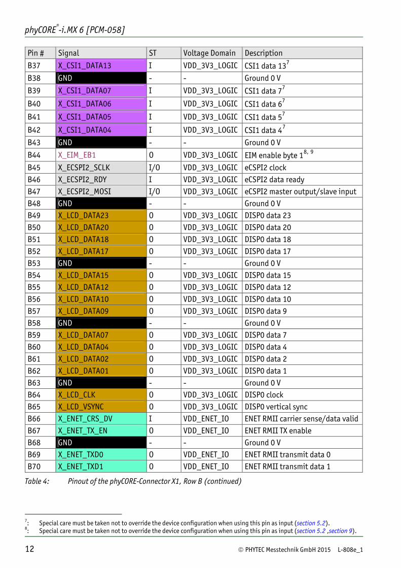
Pin # Signal ST Voltage Domain Description
B37 X_CSI1_DATA13 I VDD_3V3_LOGIC CSI1 data 137
B38 GND - - Ground 0 V
B39 X_CSI1_DATA07 I VDD_3V3_LOGIC CSI1 data 77
B40 X_CSI1_DATA06 I VDD_3V3_LOGIC CSI1 data 67
B41 X_CSI1_DATA05 I VDD_3V3_LOGIC CSI1 data 57
B42 X_CSI1_DATA04 I VDD_3V3_LOGIC CSI1 data 47
B43 GND - - Ground 0 V
B44 X_EIM_EB1 O VDD_3V3_LOGIC EIM enable byte 18, 9
B45 X_ECSPI2_SCLK I/O VDD_3V3_LOGIC eCSPI2 clock B46 X_ECSPI2_RDY I VDD_3V3_LOGIC eCSPI2 data ready B47 X_ECSPI2_MOSI I/O VDD_3V3_LOGIC eCSPI2 master output/slave input B48 GND - - Ground 0 V B49 X_LCD_DATA23 O VDD_3V3_LOGIC DISP0 data 23 B50 X_LCD_DATA20 O VDD_3V3_LOGIC DISP0 data 20 B51 X_LCD_DATA18 O VDD_3V3_LOGIC DISP0 data 18 B52 X_LCD_DATA17 O VDD_3V3_LOGIC DISP0 data 17 B53 GND - - Ground 0 V B54 X_LCD_DATA15 O VDD_3V3_LOGIC DISP0 data 15 B55 X_LCD_DATA12 O VDD_3V3_LOGIC DISP0 data 12 B56 X_LCD_DATA10 O VDD_3V3_LOGIC DISP0 data 10 B57 X_LCD_DATA09 O VDD_3V3_LOGIC DISP0 data 9 B58 GND - - Ground 0 V B59 X_LCD_DATA07 O VDD_3V3_LOGIC DISP0 data 7 B60 X_LCD_DATA04 O VDD_3V3_LOGIC DISP0 data 4 B61 X_LCD_DATA02 O VDD_3V3_LOGIC DISP0 data 2 B62 X_LCD_DATA01 O VDD_3V3_LOGIC DISP0 data 1 B63 GND - - Ground 0 V B64 X_LCD_CLK O VDD_3V3_LOGIC DISP0 clock B65 X_LCD_VSYNC O VDD_3V3_LOGIC DISP0 vertical sync B66 X_ENET_CRS_DV I VDD_ENET_IO ENET RMII carrier sense/data validB67 X_ENET_TX_EN O VDD_ENET_IO ENET RMII TX enable B68 GND - - Ground 0 V B69 X_ENET_TXD0 O VDD_ENET_IO ENET RMII transmit data 0 B70 X_ENET_TXD1 O VDD_ENET_IO ENET RMII transmit data 1
Table 4: Pinout of the phyCORE-Connector X1, Row B (continued)
7: Special care must be taken not to override the device configuration when using this pin as input (section 5.2). 8: Special care must be taken not to override the device configuration when using this pin as input (section 5.2 ,section 9).

Pin Description
© PHYTEC Messtechnik GmbH 2015 L-808e_1 13
Pin # Signal ST Voltage Domain Description C1 X_BOOT_MODE0 I VDD_3V3_LOGIC Boot mode input 0 C2 X_ETH0_A+/TX0+ ETH_O VDD_3V3_LOGIC ETH0 data A+/transmit+ C3 X_ETH0_A-/TX0- ETH_O VDD_3V3_LOGIC ETH0 data A-/transmit- C4 GND - - Ground 0 V C5 X_ETH0_C+ ETH_I/O VDD_3V3_LOGIC ETH0 data C+ (only GbE) C6 X_ETH0_C- ETH_I/O VDD_3V3_LOGIC ETH0 data C- (only GbE) C7 X_ETH0_LED0 OC VDD_3V3_LOGIC ETH0 link LED output C8 X_SATA_TXP LVDS_O i.MX6 internal SATA transmit lane+ C9 X_SATA_TXN LVDS_O i.MX6 internal SATA transmit lane- C10 GND - - Ground 0 V C11 X_PCIe0_CLK+ PCIe_O i.MX 6 internal PCIe clock lane+ C12 X_PCIe0_CLK- PCIe_O i.MX 6 internal PCIe clock lane- C13 X_PCIe_RXP PCIe_I i.MX 6 internal PCIe receive lane+ C14 X_PCIe_RXN PCIe_I i.MX 6 internal PCIe receive lane- C15 GND - - Ground 0 V
C16 X_SPDIF_OUT O VDD_3V3_LOGIC SPDIF output9
C17 X_PWM1_OUT O VDD_3V3_LOGIC PWM1 output9
C18 X_USB_OTG_ID I VDD_3V3_LOGIC USB OTG ID Pin C19 X_USB_OTG_VBUS PWR_I 5 V USB OTG VBUS input C20 X_USB_OTG_PWR O VDD_3V3_LOGIC USB OTG power enable C21 GND - - Ground 0 V C22 X_CCM_CLKO2 O VDD_3V3_LOGIC CCM clock output 2 C23 X_USB_H1_DP USB_I/O i.MX 6 internal USB Host data+ C24 X_USB_H1_DN USB_I/O i.MX 6 internal USB Host data- C25 GND - - Ground 0 V C26 X_PMIC_nSHUTDOWN I VDD_3V3 PMIC shutdown C27 X_PMIC_STBY_REQ O VDD_MX6_SNVS i.MX 6 PMIC standby request C28 X_JTAG_TMS I VDD_3V3_LOGIC JTAG TMS C29 X_JTAG_TDO O VDD_3V3_LOGIC JTAG TDO C30 X_CSI_D0P CSI2_I i.MX 6 internal MIPI/CSI data0+ C31 X_CSI_D0M CSI2_I i.MX 6 internal MIPI/CSI data0- C32 GND - - Ground 0 V C33 X_CSI_D2P CSI2_I i.MX 6 internal MIPI/CSI data2+ C34 X_CSI_D2M CSI2_I i.MX 6 internal MIPI/CSI data2- C35 X_CSI_CLK0P CSI2_I i.MX 6 internal MIPI/CSI clock+ C36 X_CSI_CLK0M CSI2_I i.MX 6 internal MIPI/CSI clock- C37 GND - - Ground 0 V
Table 5: Pinout of the phyCORE-Connector X1, Row C

phyCORE®-i.MX 6 [PCM-058]
14 © PHYTEC Messtechnik GmbH 2015 L-808e_1
Pin # Signal ST Voltage Domain Description C38 X_HDMI_CEC I/O VDD_3V3_LOGIC HDMI CEC C39 X_HDMI_CLKP TDMS_O i.MX 6 internal HDMI clock+ C40 X_HDMI_CLKM TDMS_O i.MX 6 internal HDMI clock- C41 X_HDMI_D1P TDMS_O i.MX 6 internal HDMI data1+ C42 X_HDMI_D1M TDMS_O i.MX 6 internal HDMI data1- C43 GND - - Ground 0 V C44 X_HDMI_DDC_SDA I/O VDD_3V3_LOGIC HDMI DDC data C45 X_CSI0_DAT18 I VDD_3V3_LOGIC CSI0 data 18 C46 X_CSI0_DAT16 I VDD_3V3_LOGIC CSI0 data 16 C47 X_CSI0_DAT14 I VDD_3V3_LOGIC CSI0 data 14 C48 GND - - Ground 0 V C49 X_CSI0_DAT12 I VDD_3V3_LOGIC CSI0 data 12 C50 X_CSI0_DAT10 I VDD_3V3_LOGIC CSI0 data 10 C51 X_CSI0_DAT8 I VDD_3V3_LOGIC CSI0 data 8 C52 X_CSI0_DAT6 I VDD_3V3_LOGIC CSI0 data 6 C53 X_CSI0_DAT5 I VDD_3V3_LOGIC CSI0 data 5 C54 GND - - Ground 0 V C55 X_CSI0_DAT4 I VDD_3V3_LOGIC CSI0 data 4 C56 X_CSI0_PIXCLK O VDD_3V3_LOGIC CSI0 pixel clock C57 X_FLEXCAN1_TX O VDD_3V3_LOGIC FLEXCAN1 transmit C58 GND - - Ground 0 V C59 X_LVDS0_TX1+ LVDS_O i.MX 6 internal LVDS0 data 1+ C60 X_LVDS0_TX1- LVDS_O i.MX 6 internal LVDS0 data 1- C61 X_LVDS0_TX0+ LVDS_O i.MX 6 internal LVDS0 data 0+ C62 X_LVDS0_TX0- LVDS_O i.MX 6 internal LVDS0 data 0- C63 GND - - Ground 0 V C64 X_LVDS0_TX3+ LVDS_O i.MX 6 internal LVDS0 data 3+ C65 X_LVDS0_TX3- LVDS_O i.MX 6 internal LVDS0 data 3- C66 X_LVDS1_CLK+ LVDS_O i.MX 6 internal LVDS1 clock+ C67 X_LVDS1_CLK- LVDS_O i.MX 6 internal LVDS1 clock- C68 GND - - Ground 0 V C69 X_LVDS1_TX0+ LVDS_O i.MX 6 internal LVDS1 data 0+ C70 X_LVDS1_TX0- LVDS_O i.MX 6 internal LVDS1 data 0-
Table 5: Pinout of the phyCORE-Connector X1, Row C (continued)

Pin Description
© PHYTEC Messtechnik GmbH 2015 L-808e_1 15
Pin # Signal ST Voltage Domain Description D1 X_BOOT_MODE1 I VDD_3V3_LOGIC Boot mode input 1 D2 X_ETH0_B+/RX0+ ETH_I VDD_3V3_LOGIC ETH0 data B+/receive+ D3 X_ETH0_B-/RX0- ETH_I VDD_3V3_LOGIC ETH0 data B-/receive- D4 X_ETH0_LED1 OC VDD_3V3_LOGIC ETH0 traffic LED output D5 X_ETH0_D+ ETH_I/O VDD_3V3_LOGIC ETH0 data D+ (only GbE) D6 X_ETH0_D- ETH_I/O VDD_3V3_LOGIC ETH0 data D- (only GbE) D7 GND - - Ground 0 V D8 X_SATA_RXP LVDS_I i.MX 6 internal SATA receive lane+ D9 X_SATA_RXN LVDS_I i.MX 6 internal SATA receive lane- D10 X_PCIe_TXP PCIe_O i.MX 6 internal PCIe transmit lane+ D11 X_PCIe_TXN PCIe_O i.MX 6 internal PCIe transmit lane- D12 GND - - Ground 0 V
D13 X_KEY_COL2 I VDD_3V3_LOGIC Keypad column 29
D14 X_PMIC_nONKEY I VDD_3V3 PMIC onkey input D15 X_ONOFF I VDD_MX6_SNVS i.MX 6 on/off input D16 X_CCM_CLKO1 O VDD_3V3_LOGIC CCM clock output 1 D17 X_USB_OTG_CHD_B O VDD_3V3_LOGIC USB OTG charger detection D18 GND - - Ground 0 V D19 X_USB_OTG_DP USB_I/O i.MX 6 internal USB OTG data+ D20 X_USB_OTG_DN USB_I/O i.MX 6 internal USB OTG data- D21 X_USB_OTG_OC I VDD_3V3_LOGIC USB OTG overcurrent input D22 X_USB_H1_VBUS PWR_I 5 V USB Host VBUS input D23 X_JTAG_TCK I VDD_3V3_LOGIC JTAG clock input D24 GND - - Ground 0 V D25 X_JTAG_TRSTB I VDD_3V3_LOGIC JTAG reset input (low active) D26 X_JTAG_TDI I VDD_3V3_LOGIC JTAG TDI D27 X_CSI_D1P CSI2_I i.MX 6 internal MIPI/CSI data1+ D28 X_CSI_D1M CSI2_I i.MX 6 internal MIPI/CSI data1- D29 X_CSI_D3P CSI2_I i.MX 6 internal MIPI/CSI data3+ D30 X_CSI_D3M CSI2_I i.MX 6 internal MIPI/CSI data3- D31 GND - - Ground 0 V D32 X_nRESET OC_BI VDD_3V3 Reset input/output (low active) D33 X_HDMI_D2P TDMS_O i.MX 6 internal HDMI data2+ D34 X_HDMI_D2M TDMS_O i.MX 6 internal HDMI data2- D35 X_HDMI_HPD I VDD_3V3_LOGIC HDMI hot plug detect D36 GND - - Ground 0 V
Table 6: Pinout of the phyCORE-Connector X1, Row D
9: Signal not used by any other interfaces and can be used as GPIO without harming other features of the phyCORE-i.MX 6
(section 9).

phyCORE®-i.MX 6 [PCM-058]
16 © PHYTEC Messtechnik GmbH 2015 L-808e_1
Pin # Signal ST Voltage Domain Description D37 X_HDMI_D0P TDMS_O i.MX 6 internal HDMI data0+ D38 X_HDMI_D0M TDMS_O i.MX 6 internal HDMI data0- D39 X_HDMI_DDC_SCL I/O VDD_3V3_LOGIC HDMI DDC clock D40 X_CSI0_DAT19 I VDD_3V3_LOGIC CSI0 data 19 D41 X_CSI0_DAT17 I VDD_3V3_LOGIC CSI0 data 17 D42 GND - - Ground 0 V D43 X_CSI0_DAT15 I VDD_3V3_LOGIC CSI0 data 15 D44 X_CSI0_DAT13 I VDD_3V3_LOGIC CSI0 data 13 D45 X_CSI0_DAT11 I VDD_3V3_LOGIC CSI0 data 11 D46 X_CSI0_DAT9 I VDD_3V3_LOGIC CSI0 data 9 D47 X_CSI0_DAT7 I VDD_3V3_LOGIC CSI0 data 7 D48 X_CSI0_VSYNC I VDD_3V3_LOGIC CSI0 vertical sync D49 GND - - Ground 0 V D50 X_CSI0_DATA_EN O VDD_3V3_LOGIC CSI0 data enable D51 X_CSI0_HSYNC I VDD_3V3_LOGIC CSI0 horizontal sync D52 X_AUD5_RXD I/O VDD_3V3_LOGIC AUD5 receive data D53 X_AUD5_TXC I/O VDD_3V3_LOGIC AUD5 transmit clock D54 X_AUD5_TXFS I/O VDD_3V3_LOGIC AUD5 frame sync D55 GND - - Ground 0 V D56 X_AUD5_TXD I/O VDD_3V3_LOGIC AUD5 transmit data D57 X_FLEXCAN1_RX I VDD_3V3_LOGIC FLEXCAN1 receive D58 X_LVDS0_CLK+ LVDS_O i.MX 6 internal LVDS0 clock+ D59 X_LVDS0_CLK- LVDS_O i.MX 6 internal LVDS0 clock- D60 X_LVDS0_TX2+ LVDS_O i.MX 6 internal LVDS0 data 2+ D61 X_LVDS0_TX2- LVDS_O i.MX 6 internal LVDS0 data 2- D62 GND - - Ground 0 V D63 X_LVDS1_TX2+ LVDS_O i.MX 6 internal LVDS1 data 2+ D64 X_LVDS1_TX2- LVDS_O i.MX 6 internal LVDS1 data 2- D65 X_LVDS1_TX1+ LVDS_O i.MX 6 internal LVDS1 data 1+ D66 X_LVDS1_TX1- LVDS_O i.MX 6 internal LVDS1 data 1- D67 GND - - Ground 0 V D68 X_LVDS1_TX3+ LVDS_O i.MX 6 internal LVDS1 data 3+ D69 X_LVDS1_TX3- LVDS_O i.MX 6 internal LVDS1 data 3- D70 X_TAMPER I VDD_3V3_LOGIC Tamper
Table 6: Pinout of the phyCORE-Connector X1, Row D (continued)

Jumpers
© PHYTEC Messtechnik GmbH 2015 L-808e_1 17
3 Jumpers
For configuration purposes, the phyCORE-i.MX 6 has several solder jumpers, some of which have been installed prior to delivery. Figure 5 illustrates the numbering of the solder jumper pads, while Figure 6 and Figure 7 indicate the location of the solder jumpers on the board. Table 7 below provides a functional summary of the solder jumpers which can be changed to adapt the phyCORE-i.MX 6 to your needs. It shows their default positions, and possible alternative positions and functions. A detailed description of each solder jumper can be found in the applicable chapter listed in the table. Note: Jumpers not listed should not be changed as they are installed with regard to the configuration of the phyCORE-i.MX 6.
Figure 5: Typical Jumper Pad Numbering Scheme
If manual jumper modification is required please ensure that the board as well as surrounding components and sockets remain undamaged while de-soldering. Overheating the board can cause the solder pads to loosen, rendering the module inoperable. Carefully heat neighboring connections in pairs. After a few alternations, components can be removed with the solder-iron tip. Alternatively, a hot air gun can be used to heat and loosen the bonds.
e.g.: J1e.g.: J4 e.g.: J4
closed

phyCORE®-i.MX 6 [PCM-058]
18 © PHYTEC Messtechnik GmbH 2015 L-808e_1
Figure 6: Jumper Locations (top view)
D1J4
J3

Jumpers
© PHYTEC Messtechnik GmbH 2015 L-808e_1 19
Figure 7: Jumper Locations (bottom view)
C1C2C3C4C5C6C7C8C9C10C11C12C13C14C15C16C17C18C19C20C21C22C23C24C25C26C27C28C29C30C31C32C33C34C35C36C37C38C39C40C41C42C43C44C45C46C47C48C49C50C51C52C53C54C55C56C57C58C59C60C61C62C63C64C65C66C67C68C69C70
D1D2D3D4D5D6D7D8D9D10D11D12D13D14D15D16D17D18D19D20D21D22D23D24D25D26D27D28D29D30D31D32D33D34D35D36D37D38D39D40D41D42D43D44D45D46D47D48D49D50D51D52D53D54D55D56D57D58D59D60D61D62D63D64D65D66D67D68D69D70
B1B2B3B4B5B6B7B8B9
B10B11B12B13B14B15B16B17B18B19B20B21B22B23B24B25B26B27B28B29B30B31B32B33B34B35B36B37B38B39B40B41B42B43B44B45B46B47B48B49B50B51B52B53B54B55B56B57B58B59B60B61B62B63B64B65B66B67B68B69B70
A1A2A3A4A5A6A7A8A9A10A11A12A13A14A15A16A17A18A19A20A21A22A23A24A25A26A27A28A29A30A31A32A33A34A35A36A37A38A39A40A41A42A43A44A45A46A47A48A49A50A51A52A53A54A55A56A57A58A59A60A61A62A63A64A65A66A67A68A69A70
J1
J2
phyCORE®-i.MX 6 [PCM-058]
20 © PHYTEC Messtechnik GmbH 2015 L-808e_1
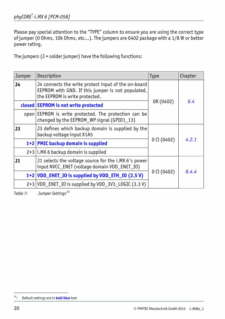
Please pay special attention to the “TYPE” column to ensure you are using the correct type of jumper (0 Ohms, 10k Ohms, etc…). The jumpers are 0402 package with a 1/8 W or better power rating. The jumpers (J = solder jumper) have the following functions: Jumper Description Type Chapter
J4 J4 connects the write protect input of the on-board EEPROM with GND. If this jumper is not populated, the EEPROM is write protected.
closed EEPROM is not write protected
open EEPROM is write protected. The protection can be changed by the EEPROM_WP signal (GPIO1_13)
0R (0402) 6.4
J3 J3 defines which backup domain is supplied by the backup voltage input X1A5
1+2 PMIC backup domain is supplied
2+3 i.MX 6 backup domain is supplied
0 Ω (0402) 4.2.1
J1 J1 selects the voltage source for the i.MX 6's power input NVCC_ENET (voltage domain VDD_ENET_IO)
1+2 VDD_ENET_IO is supplied by VDD_ETH_IO (2.5 V)
2+3 VDD_ENET_IO is supplied by VDD_3V3_LOGIC (3.3 V)
0 Ω (0402) 8.4.4
Table 7: Jumper Settings10
10: Default settings are in bold blue text

Power
© PHYTEC Messtechnik GmbH 2015 L-808e_1 21
4 Power
The phyCORE-i.MX 6 operates off of a single power supply voltage. The following sections of this chapter discuss the primary power pins on the phyCORE-Connector X1 in detail.
4.1 Primary System Power (VDD_3V3)
The phyCORE-i.MX 6 operates off of a primary voltage supply with a nominal value of +3.3 V. On-board switching regulators generate the 2.5 V, 1.375 V, 1.5 V, 0.75 V, 1.2 V and 3 V voltage supplies required by the i.MX 6 MCU and on-board components from the primary 3.3 V supplied to the SOM. For proper operation the phyCORE-i.MX 6 must be supplied with a voltage source of 3.3 V ±5 % with 2.5 A load at the VCC pins on the phyCORE-Connector X1. VDD_3V3: X1 A1, A2, A3, A4, B1, B2, B3, B4 Connect all +3.3 V VCC input pins to your power supply and at least the matching number of GND pins. Corresponding GND: X1 A6, A11, A16, A21, B6, B12, B17, B22 Please refer to section 2 for information on additional GND Pins located at the phyCORE-Connector X1. Caution! As a general design rule we recommend connecting all GND pins neighboring signals which are being used in the application circuitry. For maximum EMI performance all GND pins should be connected to a solid ground plane.
4.2 Power Management IC (PMIC) (U16)
The phyCORE-i.MX 6 provides an on-board Power Management IC (PMIC) at position U16 to generate different voltages required by the microcontroller and the on-board components. Figure 8 presents a graphical depiction of the powering scheme. The PMIC supports many functions like on-chip RTC and different power management functionalities like dynamic voltage control, different low power modes and regulator supervision. It is connected to the i.MX 6 via the on-board I2C bus (I2C3). The I2C address of the PMIC is 0x58 (page 0 and 1) and 0x59 (page 2 and 3).

phyCORE®-i.MX 6 [PCM-058]
22 © PHYTEC Messtechnik GmbH 2015 L-808e_1
4.2.1 Power Domains
External voltages: • VDD_3V3 3.3 V main supply voltage • USB0_VBUS USB0 Bus voltage, must be supplied with 5 V if USB0 is used • USB1_VBUS USB1 Bus voltage, must be supplied with 5 V if USB1 is used • VDD_BAT Backup supply (connected to PMIC_VBBAT or VDD_MX6_SNVS via
J3 (Table 7)) Internally generated voltages: VDD_MX6_ARM (1.375 V), VDD_MX6_SOC (1.375 V), VDD_3V3_LOGIC (3.3 V), VDD_ETH_IO (2.5 V) VDD_MX6_SNVS (3.0 V), VDD_MX6_HIGH (3.0 V), VDD_eMMC_1V8 (1.8 V) VDD_ETH_1V2 (1.2 V), VDD_DDR3_1V5 (1.5 V), DDR3_VREF (0.75 V)
• VDD_MX6_ARM: i.MX 6 core (VDDARM_IN, VDDARM23_IN) (1.375 V)
• VDD_MX6_SOC: i.MX 6 SOC (VDDSOC_IN) (1.375 V)
• VDD_MX6_HIGH: i.MX 6 internal regulator (VDDHIGH_IN) (3.0 V)
• VDD_MX6_SNVS: i.MX 6 backup supply (VDD_SNVS_IN) (3.0 V)
• VDD_ETH_IO: i.MX 6 RGMII supply (NVCC_RGMII, NVCC_ENET11), (2.5 V) Ethernet PHY RGMII IO supply
• VDD_ETH_1V2: Ethernet PHY core voltage (1.2 V)
• VDD_DDR3_1V5: i.MX 6 DDR interface (NVCC_DRAM), RAM devices (1.5 V)
• VDD_eMMC_1V8: 1.8V eMMC supply (1.8 V)
• DDR3_VREF: i.MX 6 DDR3 reference voltage (DRAM_VREF), RAM devices (0.75 V) reference voltage
• VDD_3V3_LOGIC: i.MX 6 pad supply (NVCC_NANDF, NVCC_JTAG, NVCC_LCD, (3.3 V) NVCC_CSI, NVCC_EIM, NVCC_SD, NVCC_GPIO, (NVCC_ENET11)), I2C EEPROM, SPI Flash, NAND Flash, eMMC, Ethernet PHY, User LED, reference output X1B5
11: NVCC_ENET is connected via jumper J1 and can alternatively be supplied by VDD_3V3_LOGIC (section 8.4.4)

Power
© PHYTEC Messtechnik GmbH 2015 L-808e_1 23
Figure 8: Powering Scheme of the phyCORE- i.MX 6
VDD_3V3
DA9062
VDD_MX6_ARM
VDD_MX6_SOC
VDD_DDR3_1V5
Switch
VDD_3V3_LOGIC
VDD_ETH_1V2
Sw
itchi
ng re
gula
tors
LD
Os
VDD_ETH_IO
VDD_eMMC_1V8
VDD_MX6_SNVS
VDD_MX6_HIGH
Voltage divider DDR3_VREF

phyCORE®-i.MX 6 [PCM-058]
24 © PHYTEC Messtechnik GmbH 2015 L-808e_1
4.3 Supply Voltage for external Logic
The voltage level of the phyCORE’s logic circuitry is VDD_3V3_LOGIC (3.3 V) which is derived from the main input voltage VDD_3V3 of the SOM. In order to follow the power-up and power–down sequencing mandatory for the i.MX 6 external devices have to be supplied by the I/O supply voltage VDD_3V3_LOGIC which is brought out at pin X1B5 of the phyCORE-Connector. Use of VDD_3V3_LOGIC ensures that external components are only supplied when the supply voltages of the i.MX 6 are stable. Caution! The current draw for VDD_3V3_LOGIC must not exceed 500 mA. Consequently this voltage should only be used as reference and not for supplying purpose. If devices with a higher power consumption are to be connected to the phyCORE-i.MX 6 they should be switched on and off by use of VDD_3V3_LOGIC. This way the power-up and power–down sequencing will be considered even if the devices are not supplied directly by VDD_3V3_LOGIC. If used to control, or supply bus switches on the phyCORE side VDD_3V3_LOGIC also serves to strictly separate the supply voltages generated on the phyCORE-i.MX 6 and the supply voltages used on the carrier board/custom application. That way, voltages at the IO pins of the phyCORE-i.MX 6 which are sourced from the supply voltage of peripheral devices attached to the SOM are avoided. These voltages can cause a current flow into the controller especially if peripheral devices attached to the interfaces of the i.MX 6 are supposed to be powered while the phyCORE-i.MX 6 is in suspend mode, or turned off. The bus switches can either be supplied by VDD_3V3_LOGIC on the phyCORE side, or the bus switches' output enable to the SOM can be controlled by VDD_3V3_LOGIC to prevent these voltages from occurring. Use of level shifters supplied with VDD_3V3_LOGIC allows converting the signals according to the needs on the custom target hardware. Alternatively signals can be connected to an open drain circuitry with a pull-up resistor attached to VDD_3V3_LOGIC.

System Configuration and Booting
© PHYTEC Messtechnik GmbH 2015 L-808e_1 25
5 System Configuration and Booting
Although most features of the i.MX 6 microcontroller are configured and/or programmed during the initialization routine, other features, which impact program execution, must be configured prior to initialization via pin termination. The system start-up configuration includes: • Boot mode selection • Boot device selection • Boot device configuration The internal ROM code is the first code executed during the initialization process of the i.MX 6 after POR. The ROM code detects the boot mode by using the boot mode pins, while the boot device is selected and configured by determining the state of the eFUSEs and/or the corresponding GPIO input pins.
5.1 Boot Mode Selection
The boot mode of the i.MX 6 microcontroller is determined by the configuration of two boot mode inputs BOOT_MODE[1:0] during the reset cycle of the operational system. These inputs are brought out at the phyCORE-Connector pins X_BOOT_MODE[1:0] (X1D1, X1C1). Table 8 shows the possible settings of pins X_BOOT_MODE0 (X1C1) and X_ BOOT_MODE1 (X1D1) and the resulting boot configuration of the i.MX 6.
Table 8: Boot Modes of the phyCORE-i.MX 6 The BOOT_MODE[1:0] lines have 10 kΩ pull-up and pull-down resistors populated on the module. Hence leaving the two pins unconnected sets the controller to boot mode 2, internal boot.
12: Default boot mode when pins X_BOOT_MODE[1:0] are left unconnected.
Boot Mode X_ BOOT_MODE1 X_ BOOT_MODE0 Boot Source
0 0 0 Bootconfig from eFUSEs
1 0 1 Serial Downloader
2 1 0 Internal Boot12
3 1 1 reserved

phyCORE®-i.MX 6 [PCM-058]
26 © PHYTEC Messtechnik GmbH 2015 L-808e_1
For serial boot (boot mode = 1) the ROM code polls the communication interface selected, initiates the download of the code into the internal RAM and triggers its execution from there. Please refer to the i.MX 6 Reference Manual for more information. In boot mode 0 and 2 the ROM code finds the bootstrap in permanent memories such as NAND-Flash or SD-Cards and executes it. The selection of the boot device and the configuration of the interface required are accomplished with the help of the eFUSEs and/or the corresponding GPIO input pins.
5.2 Boot Device Selection and Configuration
In normal operation (boot mode 0, or 2), the boot ROM uses the state of BOOT_MODE and eFUSEs to determine the boot device. During development it is advisable to set the boot type to “Internal boot” (BOOT_MODE[1:0]=1012 to allow choosing and configuring the boot device by using GPIO pin inputs. The input pins are sampled at boot, and override the values of the corresponding eFUSEs BOOT_CFGx[7:0], if the BT_FUSE_SEL fuse is not blown. Table 9 lists the eFUSEs BOOT_CFGx[7:0] and the corresponding input pins. On the phyCORE-i.MX 6 the GPIOs have 10 kΩ pull-up and pull-down resistors preinstalled to configure eFUSEs BOOT_CFGx[7:0] in accordance with the module features. However, the specific boot configuration settings, which are set by the on-board configuration resistors, can be changed by modifying the resistors on the module or by connecting a configuration resistor (e.g. 10 kΩ) to the configuration signal. Please consider that any change of the default BCFG configuration can also influence other boot modes, which might result in faulty boot behavior. Caution! Please make sure that the signals shown in Table 9 are not driven by any device on the baseboard during reset, to avoid accidental change of the boot configuration. Because of this, we recommend to boot from eFUSE for volume production and use only internal boot mode for development process13. Please refer to the i.MX 6 Reference Manual for further information about the eFUSEs and the impact of the settings at the BCFG pins.
13: For series production Phytec offers to order the phyCORE-i.MX 6 with a costum configuration of the eFUSEs

System Configuration and Booting
© PHYTEC Messtechnik GmbH 2015 L-808e_1 27
Configuration Pin
Pin # Signal ST SL Description
BCFG1[0] X1A30 X_CSI1_DATA09 I 3.3 V CSI1 data 9 BCFG1[1] X1A32 X_CSI1_DATA08 I 3.3 V CSI1 data 8 BCFG1[2] X1B39 X_CSI1_DATA07 I 3.3 V CSI1 data 7 BCFG1[3] X1B40 X_CSI1_DATA06 I 3.3 V CSI1 data 6 BCFG1[4] X1B41 X_CSI1_DATA05 I 3.3 V CSI1 data 5 BCFG1[5] X1B42 X_CSI1_DATA04 I 3.3 V CSI1 data 4 BCFG1[6] X1A33 X_CSI1_DATA03 I 3.3 V CSI1 data 3 BCFG1[7] X1A34 X_CSI1_DATA02 I 3.3 V CSI1 data 2 BCFG2[0] X1A37 X_CSI1_DATA01 I 3.3 V CSI1 data 1 BCFG2[1] X1A38 X_CSI1_DATA00 I 3.3 V CSI1 data 0 BCFG2[2] X1A35 X_CSI1_DATA_EN O 3.3 V CSI1 data enable BCFG2[3] X1A40 X_CSI1_HSYNC I 3.3 V CSI1 horizontal sync BCFG2[4] X1A39 X_CSI1_VSYNC I 3.3 V CSI1 vertical sync BCFG2[5] X1A25 X_EIM_DA13 I/O 3.3 V EIM address/data 13 BCFG2[6] X1B26 X_EIM_DA14 I/O 3.3 V EIM address/data 14 BCFG2[7] X1B27 X_EIM_DA15 I/O 3.3 V EIM address/data 15 BCFG3[0] X1B36 X_CSI1_PIXCLK O 3.3 V CSI1 pixel clock BCFG3[1] X1A27 X_CSI1_DATA12 I 3.3 V CSI1 data 12 BCFG3[2] X1B37 X_CSI1_DATA13 I 3.3 V CSI1 data 13 BCFG3[3] X1B35 X_CSI1_DATA14 I 3.3 V CSI1 data 14 BCFG3[4] X1B34 X_CSI1_DATA15 I 3.3 V CSI1 data 15 BCFG3[5] X1B32 X_CSI1_DATA16 I 3.3 V CSI1 data 16 BCFG3[6] X1B31 X_CSI1_DATA17 I 3.3 V CSI1 data 17 BCFG3[7] X1B30 X_CSI1_DATA18 I 3.3 V CSI1 data 18 BCFG4[0] X1B29 X_CSI1_DATA19 I 3.3 V CSI1 data 19 BCFG4[1] EIM_WAIT not available at phyCORE-Connector14 BCFG4[2] X1A44 X_ECSPI2_SS1 I/O 3.3 V eCSPI2 chip select 1 BCFG4[3] X1A28 X_CSI1_DATA11 I 3.3 V CSI1 data 11 BCFG4[4] X1B44 X_EIM_EB1 O 3.3 V EIM enable byte 1 BCFG4[5] X1A45 X_ECSPI2_SS0 I/O 3.3 V eCSPI2 chip select 0 BCFG4[6] X1A24 X_ECSPI1_SS0 I/O 3.3 V eCSPI1 chip select 0 BCFG4[7] X1A20 X_UART3_RTS_B I 3.3 V UART3 request to send input
Table 9: Boot Configuration Pins at the phyCORE-Connector
14: Connected to GND for the standard module configuration

phyCORE®-i.MX 6 [PCM-058]
28 © PHYTEC Messtechnik GmbH 2015 L-808e_1
6 System Memory
The phyCORE-i.MX 6 provides three types of on-board memory: • 1 Bank DDR3 RAM: 1 GB DDR3 SDRAM (up to 2 GB) 15 • NAND Flash (TSOP) : 1 GB (up to 16 GB) 15,
alternatively eMMC 2 GB (up to 32 GB) 15 • I²C-EEPROM: 4 kB15 • SPI Flash: 16 MB15 The following sections of this chapter detail each memory type used on the phyCORE-i.MX 6.
6.1 DDR3-SDRAM (U4-U7)
The RAM memory of the phyCORE-i.MX 6 is comprised of one 64 bit wide bank with four 16-bit wide DDR3-SDRAM chips (U4-U7). The chips are connected to the special DDR interface called Multi Mode DDR Controller (MMDC) of the i.MX 6 microcontroller. The DDR3 memory is accessible starting at address 0x1000 0000. Typically the DDR3-SDRAM initialization is performed by a boot loader or operating system following a power-on reset and must not be changed at a later point by any application code. When writing custom code independent of an operating system or boot loader, the SDRAM must be initialized by accessing the appropriate SDRAM configuration registers on the i.MX 6 controller. Refer to the i.MX 6 Reference Manual for accessing and configuring these registers.
15: The maximum memory size listed is as of the printing of this manual. Please contact PHYTEC for more information about additional, or
new module configurations available.

System Memory
© PHYTEC Messtechnik GmbH 2015 L-808e_1 29
6.2 NAND Flash Memory (U12)
Use of Flash as non-volatile memory on the phyCORE-i.MX 6 provides an easily reprogrammable means of code storage. The Flash devices are programmable with 3.3 V. No dedicated programming voltage is required. As of the printing of this manual these NAND Flash devices generally have a life expectancy of at least 100,000 erase/program cycles and a data retention rate of 10 years. The NAND Flash memories are connected to the External Interface Module (GPMI). /CS0 (NANDF_CS0) of the EIM interface selects the NAND Flash at U12. Any parts that are footprint (TSOP-48-50-C3) and functionally compatible may be used with the phyCORE-i.MX 6.
6.3 eMMC Flash Memory (U14)
Alternatively to the NAND flash memory at U12, an eMMC can be populated at U14. The eMMC device is programmable with 3.3 V. No dedicated programming voltage is required. The eMMC Flash memory is connected to the SD4 interface of the i.MX 6. Any parts that are footprint (BGA153) and functionally compatible may be used with the phyCORE-i.MX 6.
6.4 I²C EEPROM (U11)
The phyCORE-i.MX 6 is populated with a non-volatile 4 kB I²C16 EEPROM at U11. This memory can be used to store configuration data or other general purpose data. This device is accessed through I²C port 3 on the i.MX 6. The control registers for I²C port 3 are mapped between addresses 0x021A 8000 and 0x021A BFFF. Please see the i.MX 6 Reference Manual for detailed information on the registers. The three lower address bits are fixed to zero which means that the EEPROM can be accessed at I2C address 0x50. Write protection to the device is accomplished via jumper J4. Refer to section 6.4.1 for further details.
16: See the manufacturer’s data sheet for interfacing and operation.

phyCORE®-i.MX 6 [PCM-058]
30 © PHYTEC Messtechnik GmbH 2015 L-808e_1
6.4.1 EEPROM Write Protection Control (J4)
Jumper J4 controls write access to the EEPROM (U11) device. Closing this jumper allows write access to the device, while removing this jumper will cause the EEPROM to enter write protect mode, thereby disabling write access to the device.
The following configurations are possible: EEPROM Write Protection State J4
Write access allowed closed Write protected open
Table 10: EEPROM write protection states via J417
Note: If the jumper is not set, the write protection signal can also be changed by GPIO1_13 of the i.MX 6 controller.
6.5 SPI Flash Memory (U9) )
The SPI Flash Memory of the phyCORE-i.MX 6 at U9 can be used to store configuration data or any other general purpose data. Beside this it can also be used as boot device18 and recovery boot device18. The device is accessed through eCSPI1 SS1 on the i.MX 6. The control registers for eCSPI1 are mapped between addresses 0x0200 8000 and 0x0200 BFFF. Please see the i.MX 6 Reference Manual for detailed information on the registers.
The SPI Flash can be write protected. The active low signal SPI_NOR_WP/GPIO1_12 connects to GPIO1_12 of the i.MX 6 and allows to control the SPI Flash's write-protection.
As of the printing of this manual these SPI Flash devices generally have a life expectancy of at least 100,000+ erase/program cycles and a data retention rate of 20 years. This makes the SPI Flash a reliable and secure solution to store the first and second level bootloaders.
17: Defaults are in bold blue text 18: The standard boot configuration selects the SPI Flash as recovery boot device. To use it as boot device the boot
configuration, or the eFUSEs must be changed.

SD / MMC Card Interfaces
© PHYTEC Messtechnik GmbH 2015 L-808e_1 31
7 SD / MM Card Interfaces
The phyCORE bus features two SD / MM Card interface. On the phyCORE-i.MX 6 the interface signals extend from the controllers third and first Ultra Secured Digital (uSDHC3 / uSDHC1) Host Controller to the phyCORE-Connector. Table 11 shows the location of the different interface signals on the phyCORE-Connector. The MMC/SD/SDIO Host Controller is fully compatible with the SD Memory Card Specification 3.0 and SD I/O Specification, Part E1, v1.10. SDC / MMC interface SD3 (uSDHC3 of the i.MX 6), supports 8 data channels and SD1 (uSDHC1 of the i.MX 6) 4 data channels. Both interfaces have a maximum data rate of up to 104 MB/s (refer to the i.MX 6 Reference Manual for more information). Pin # Signal ST Voltage Domain Description X1A7 X_SD3_CMD O VDD_3V3_LOGIC SD3 command X1A8 X_SD3_DATA0 I/O VDD_3V3_LOGIC SD3 data 0 X1A9 X_SD3_DATA2 I/O VDD_3V3_LOGIC SD3 data 2 X1A10 X_SD3_DATA5 I/O VDD_3V3_LOGIC SD3 data 5 X1A12 X_SD3_DATA7 I/O VDD_3V3_LOGIC SD3 data 7 X1A13 X_SD3_RESET O VDD_3V3_LOGIC SD3 reset X1B7 X_SD3_CLK O VDD_3V3_LOGIC SD3 clock X1B8 X_SD3_DATA1 I/O VDD_3V3_LOGIC SD3 data 1 X1B9 X_SD3_DATA3 I/O VDD_3V3_LOGIC SD3 data 3 X1B10 X_SD3_DATA4 I/O VDD_3V3_LOGIC SD3 data 4 X1B11 X_SD3_DATA6 I/O VDD_3V3_LOGIC SD3 data 6 X1A14 X_SD1_DATA0 I/O VDD_3V3_LOGIC SD1 data 0 X1A15 X_SD1_DATA2 I/O VDD_3V3_LOGIC SD1 data 2 X1B13 X_SD1_CLK O VDD_3V3_LOGIC SD1 clock X1B14 X_SD1_CMD O VDD_3V3_LOGIC SD1 command X1B15 X_SD1_DATA1 I/O VDD_3V3_LOGIC SD1 data 1 X1B16 X_SD1_DATA3 I/O VDD_3V3_LOGIC SD1 data 3
Table 11: Location of the SD / MM Card Interface Signals
The interfaces do not provide dedicated card detect or write protect signals. The card detect and write protect function can be implemented easily by using four GPIOs of the i.MX 6.

phyCORE®-i.MX 6 [PCM-058]
32 © PHYTEC Messtechnik GmbH 2015 L-808e_1
8 Serial Interfaces
The phyCORE-i.MX 6 provides numerous dedicated serial interfaces some of which are equipped with a transceiver to allow direct connection to external devices: 1. Two High speed UARTs (TTL, derived from UART2 and UART3 of the i.MX 6) with up to 4
MHz and one with hardware flow control (RTS and CTS signals) 2. High speed USB OTG interface (extended directly from the i.MX 6’s USB OTG PHY
(USB-PHY)) 3. High speed USB HOST interface (extended directly from the i.MX 6 USB HOST PHY
(USB-PHY)) 4. Auto-MDIX enabled 10/100/1000 Mbit Ethernet interface 5. One I2C interface (derived from I2C port 1 of the i.MX 6) 6. Two Serial Peripheral Interface (SPI) interface (extended from the first and second
SPI module (eCSPI1 and eCSPI2) of the i.MX 6) 7. I2S audio interface (originating from the i.MX 6’s Synchronous Serial Interface (SSI)
and muxed through port 5 of the Digital Audio Multiplexer (AUDMUX5)) 8. CAN 2.0B interface (extended directly from the i.MX 6 FlexCAN1 module) 9. SATA II, 3.0 Gbps (extended directly from the i.MX 6 SATA PHY) 10. PCI Express Gen. 2.0 (extended directly from the i.MX 6 PCIe PHY) The following sections of this chapter detail each of these serial interfaces and any applicable configuration jumpers.

Serial Interfaces
© PHYTEC Messtechnik GmbH 2015 L-808e_1 33
8.1 Universal Asynchronous Interface
The phyCORE-i.MX 6 provides two high speed universal asynchronous interfaces with up to 4 MHz and one with additional hardware flow control (RTS and CTS signals). The following table shows the location of the signals on the phyCORE-Connector. Pin # Signal ST Voltage Domain Description X1A17 X_UART2_RX_DATA I VDD_3V3_LOGIC UART2 serial data receive X1B21 X_UART2_TX_DATA O VDD_3V3_LOGIC UART2 serial transmit signal X1A18 X_UART3_RX_DATA I VDD_3V3_LOGIC UART3 serial data receive X1A19 X_UART3_CTS_B O VDD_3V3_LOGIC UART3 clear to send output X1A20 X_UART3_RTS_B I VDD_3V3_LOGIC UART3 request to send input19 X1B18 X_UART3_TX_DATA O VDD_3V3_LOGIC UART3 serial transmit signal
Table 12: Location of the UART Signals The signals extend from UART2 respectively UART3 of the i.MX 6 directly to the phyCORE-Connector without conversion to RS-232 level. External RS-232 transceivers must be attached by the user if RS-232 levels are required.
19: Special care must be taken not to override the device configuration when using this pin as input (section 5.2).

phyCORE®-i.MX 6 [PCM-058]
34 © PHYTEC Messtechnik GmbH 2015 L-808e_1
8.2 USB OTG Interface
The phyCORE-i.MX 6 provides a high speed USB OTG interface which uses the i.MX 6 embedded HS USB OTG PHY. An external USB Standard-A (for USB host), USB Standard-B (for USB device), or USB mini-AB (for USB OTG) connector is all that is needed to interface the phyCORE-i.MX 6 USB OTG functionality. The applicable interface signals can be found on the phyCORE-Connector X1 as shown in Table 13. Pin # Signal ST Voltage Domain Description X1C18 X_USB_OTG_ID I VDD_3V3_LOGIC USB OTG ID Pin X1C19 X_USB_OTG_VBUS PWR_I 5 V USB OTG VBUS input X1C20 X_USB_OTG_PWR O VDD_3V3_LOGIC USB OTG power enable X1D17 X_USB_OTG_CHD_B O VDD_3V3_LOGIC USB OTG charger detection X1D19 X_USB_OTG_DP USB_I/O i.MX 6 internal USB OTG data+ X1D20 X_USB_OTG_DN USB_I/O i.MX 6 internal USB OTG data- X1D21 X_USB_OTG_OC I VDD_3V3_LOGIC USB OTG overcurrent input
Table 13: Location of the USB OTG Signals
Caution! Either X_USB_OTG_VBUS must be supplied with 5 V for proper USB functionality.
8.3 USB Host Interface
The phyCORE-i.MX 6 provides a high speed USB Host interface which uses the i.MX 6 embedded HS USB Host PHY. An external USB Standard-A (for USB host) connector is all that is needed to interface the phyCORE-i.MX 6 USB Host functionality. The applicable interface signals (D+/D- and VBUS) can be found on the phyCORE-Connector X1. If overcurrent and power enable signals are needed for the USB Host interface, the functionality can be easily implemented with GPIOs.
Pin # Signal ST Voltage Domain Description X1C23 X_USB_H1_DP USB_I/O i.MX 6 internal USB Host data+ X1C24 X_USB_H1_DN USB_I/O i.MX 6 internal USB Host data- X1D22 X_USB_H1_VBUS PWR_I 5V USB Host VBUS input
Table 14: Location of the USB-Host Signals
Caution! X_USB_H1_VBUS must be supplied with 5 V for proper USB functionality.

Serial Interfaces
© PHYTEC Messtechnik GmbH 2015 L-808e_1 35
8.4 Ethernet Interface
Connection of the phyCORE-i.MX 6 to the world wide web or a local area network (LAN) is possible using the on-board GbE PHY at U2. It is connected to the RGMII interface of the i.MX 6. The PHY operates with a data transmission speed of 10 Mbit/s, 100 Mbit/s or 1000 Mbit/s. Alternatively the RMII (ENET) interface which is available on the phyCORE-Connector can be used to connect an external PHY. In this case, the on-board GbE PHY (U2) must not be populated (section 8.4.4).
8.4.1 Ethernet PHY (U2)
With an Ethernet PHY mounted at U2 the phyCORE-i.MX 6 has been designed for use in 10Base-T, 100Base-T and 1000Base-T networks. The 10/100/1000Base-T interface with its LED signals extends to the phyCORE-Connector X1.
Pin # Signal ST Voltage Domain Description X1C2 X_ETH0_A+/TX0+ ETH_O VDD_3V3_LOGIC ETH0 data A+/transmit+ X1C3 X_ETH0_A-/TX0- ETH_O VDD_3V3_LOGIC ETH0 data A-/transmit- X1C5 X_ETH0_C+ ETH_I/O VDD_3V3_LOGIC ETH0 data C+ (only GbE) X1C6 X_ETH0_C- ETH_I/O VDD_3V3_LOGIC ETH0 data C- (only GbE) X1C7 X_ETH0_LED0 OC VDD_3V3_LOGIC ETH0 link LED output X1D2 X_ETH0_B+/RX0+ ETH_I VDD_3V3_LOGIC ETH0 data B+/receive+ X1D3 X_ETH0_B-/RX0- ETH_I VDD_3V3_LOGIC ETH0 data B-/receive- X1D4 X_ETH0_LED1 OC VDD_3V3_LOGIC ETH0 traffic LED output X1D5 X_ETH0_D+ ETH_I/O VDD_3V3_LOGIC ETH0 data D+ (only GbE) X1D6 X_ETH0_D- ETH_I/O VDD_3V3_LOGIC ETH0 data D- (only GbE)
Table 15: Location of the Ethernet Signals
The on-board GbE PHY supports HP Auto-MDIX technology, eliminating the need for the consideration of a direct connect LAN cable, or a cross-over patch cable. It detects the TX and RX pins of the connected device and automatically configures the PHY TX and RX pins accordingly. The Ethernet PHY also features an Auto-negotiation to automatically determine the best speed and duplex mode. The Ethernet controller is connected to the RGMII interface of the i.MX 6. Please refer to the i.MX 6 Reference Manual for more information about this interface.

phyCORE®-i.MX 6 [PCM-058]
36 © PHYTEC Messtechnik GmbH 2015 L-808e_1
In order to connect the module to an existing 10/100/1000Base-T network some external circuitry is required. The required termination resistors on the analog signals (ETH0_A±, ETH0_B±, ETH0_C±, ETH0_D±) are integrated in the chip, so there is no need to connect external termination resistors to these signals. Connection to an external Ethernet magnetics should be done using very short signal traces. The A+/A-, B+/B-, C+/C- and D+/D- signals should be routed as 100 Ohm differential pairs. The same applies for the signal lines after the transformer circuit. The carrier board layout should avoid any other signal lines crossing the Ethernet signals. Caution! Please see the datasheet of the Ethernet PHY when designing the Ethernet transformer circuitry or request the schematic of the applicable carrier board (phyBOARD-Mira i.MX 6) as reference.
8.4.2 Software Reset of the Ethernet Controller
The Ethernet PHY at U2 can be reset by software. The reset input of the Ethernet PHY is permanently connected to pad SD2_DAT1 (GPIO1_14) of the i.MX 6.
8.4.3 MAC Address
In a computer network such as a local area network (LAN), the MAC (Media Access Control) address is a unique computer hardware number. For a connection to the Internet, a table is used to convert the assigned IP number to the hardware’s MAC address. In order to guarantee that the MAC address is unique, all addresses are managed in a central location. PHYTEC has acquired a pool of MAC addresses. The MAC address of the phyCORE-i.MX 6 is located on the bar code sticker attached to the module. This number is a 12-digit HEX value.

Serial Interfaces
© PHYTEC Messtechnik GmbH 2015 L-808e_1 37
8.4.4 RMII Interface
In order to use an external Ethernet PHY instead of the on-board GbE PHY at U2 the RMII interface (ENET) of the i.MX 6 is brought out at the phyCORE-Connector X1. Caution! The GbE PHY (U2) must not be populated on the module if the RMII interface is used. Note: In order to have the same signal level at all pins when using the RMII interface jumper J1 should be closed at 2+3. Closing jumper J1 at 2+3 connects the i.MX 6's power input NVCC_ENET (voltage domain VDD_ENET_IO) to VDD_3V3_LOGIC (3.3 V) instead of VDD_ETH_IO (2.5 V) (Table 7). Pin # Signal ST Voltage Domain Description A65 X_ENET_REFCLK I VDD_3V3_LOGIC ENET RMII reference clock A67 X_ENET_TXER O VDD_3V3_LOGIC ENET MII transmit error A68 X_ENET_RXD0 I VDD_ENET_IO ENET RMII receive data 0 A69 X_ENET_RXD1 I VDD_ENET_IO ENET RMII receive data 1 A70 X_ENET_RX_ER I VDD_ENET_IO ENET RMII receive error B19 X_ENET_MDIO I/O VDD_ENET_IO ENET management data I/O B20 X_ENET_MDC O VDD_ENET_IO ENET management data clock B66 X_ENET_CRS_DV I VDD_ENET_IO ENET RMII carrier sense/data validB67 X_ENET_TX_EN O VDD_ENET_IO ENET RMII TX enable B69 X_ENET_TXD0 O VDD_ENET_IO ENET RMII transmit data 0 B70 X_ENET_TXD1 O VDD_ENET_IO ENET RMII transmit data 1
Table 16: Location of the RMII Interface Signals

phyCORE®-i.MX 6 [PCM-058]
38 © PHYTEC Messtechnik GmbH 2015 L-808e_1
8.5 SPI Interface
The Serial Peripheral Interface (SPI) interface is a four-wire, bidirectional serial bus that provides a simple and efficient method for data exchange among devices. The phyCORE provides two SPI interfaces on the phyCORE-Connector X1. The SPI interfaces provide one respectively two chip select signals. The Enhanced Configurable SPI (eCSPI) of the i.MX 6 has five separate modules (eCSPI1, eCSPI2, eCSPI3, eCSPI4 and eCSPI5) which support data rates of up to 20 Mbit/s. The interface signals of the first and second module (eCSPI1, eCSPI2) are made available on the phyCORE-Connector. These modules are master/slave configurable. The following table lists the SPI signals on the phyCORE-Connector. Pin # Signal ST Voltage Domain Description X1A22 X_ECSPI1_SCLK I/O VDD_3V3_LOGIC eCSPI1 clock
X1A23 X_ECSPI1_MOSI I/O VDD_3V3_LOGIC eCSPI1 master output/slave input
X1A24 X_ECSPI1_SS0 I/O VDD_3V3_LOGIC eCSPI1 chip select 020 X1B25 X_ECSPI1_MISO I/O VDD_3V3_LOGIC eCSPI1 master input/slave output X1A43 X_ECSPI2_MISO I/O VDD_3V3_LOGIC eCSPI2 master input/slave output X1A44 X_ECSPI2_SS1 I/O VDD_3V3_LOGIC eCSPI2 chip select 120 X1A45 X_ECSPI2_SS0 I/O VDD_3V3_LOGIC eCSPI2 chip select 0 X1B45 X_ECSPI2_SCLK I/O VDD_3V3_LOGIC eCSPI2 clock20 X1B46 X_ECSPI2_RDY I VDD_3V3_LOGIC eCSPI2 data ready X1B47 X_ECSPI2_MOSI I/O VDD_3V3_LOGIC eCSPI2 master output/slave input
Table 17: SPI Interface Signal Location
Note: When using the eCSPI1 interface it must be considered that the on-board SPI Flash is connected to this interface, too. The SPI Flash is accessed through SS1 of module eCSPI1 (section 6.5).
20: Special care must be taken not to override the device configuration when using this pin as input (section 5.2).

Serial Interfaces
© PHYTEC Messtechnik GmbH 2015 L-808e_1 39
8.6 I2C Interface
The Inter-Integrated Circuit (I2C) interface is a two-wire, bidirectional serial bus that provides a simple and efficient method for data exchange among devices. The i.MX 6 contains three identical and independent multimaster fast-mode I2C modules. The interface of the first module (I2C1) is available on the phyCORE-Connector. Note: To ensure the proper functioning of the I2C interface external pull resistors matching the load at the interface must be connected. There are no pull up resistors mounted on the module. The following table lists the I2C ports on the phyCORE-Connector.
Pin # Signal ST Voltage Domain Description B23 X_I2C1_SCL OC_BI VDD_3V3_LOGIC I2C1 clock B24 X_I2C1_SDA OC_BI VDD_3V3_LOGIC I2C1 data
Table 18: I2C Interface Signal Location
The third I2C module (I2C3) connects to the on-board EEPROM (section 6.4) and to the PMIC at U16 (section 4.2).
8.7 I2S Audio Interface (SSI))
The Synchronous Serial Interface (SSI) of the phyCORE-i.MX 6 is a full-duplex, serial interface that allows to communicate with a variety of serial devices, such as standard codecs, digital signal processors (DSPs), microprocessors, peripherals, and popular industry audio codecs that implement the inter-IC sound bus standard (I2S) and Intel AC’97 standard. The i.MX 6 provides three instances of the SSI module. On the phyCORE-i.MX 6 SSI is brought out to the phyCORE-Connector through port 5 of the i.MX 6's Digital Audio Multiplexer (AUDMUX5). The main purpose of this interface is to connect to an external codec, such as I2S. Four signals extend from the i.MX 6 SSI module to the phyCORE-Connector (RXD, TXC, TXFS, TXD). Pin # Signal ST Voltage Domain Description X1D52 X_AUD5_RXD I/O VDD_3V3_LOGIC AUD5 receive data X1D53 X_AUD5_TXC I/O VDD_3V3_LOGIC AUD5 transmit clock X1D54 X_AUD5_TXFS I/O VDD_3V3_LOGIC AUD5 frame sync X1D56 X_AUD5_TXD I/O VDD_3V3_LOGIC AUD5 transmit data
Table 19: I2S Interface Signal Location

phyCORE®-i.MX 6 [PCM-058]
40 © PHYTEC Messtechnik GmbH 2015 L-808e_1
8.8 CAN Interface
The CAN interface of the phyCORE-i.MX 6 is connected to the first FlexCAN module (FlexCAN1) of the i.MX 6 which is a full implementation of the CAN protocol specification Version 2.0B. It supports standard and extended message frames and programmable bit rates of up to 1 Mb/s. The signals of the CAN interface are brought out on the phyCORE connector. The following table shows the position of the signals. Pin # Signal ST Voltage Domain Description X1C57 X_FLEXCAN1_TX O VDD_3V3_LOGIC FLEXCAN 1 transmit X1D57 X_FLEXCAN1_RX I VDD_3V3_LOGIC FLEXCAN 1 receive
Table 20: CAN Interface Signal Location
8.9 SATA Interface
The SATA II interface of the phyCORE-i.MX 6 is a high-speed serialized ATA data link interface compliant with SATA Revision 3.0 (physical layer complies with SATA Revision 2.5) which supports data rates of up to 3.0 Gbit/s. The interface includes an internal DMA engine, command layer, transport layer, link layer and the physical layer. The interface itself supports only one SATA device. The phyCORE-i.MX 6 provides an SATA II Interface at the following pins of the phyCORE-Connector: Pin # Signal ST Voltage Domain Description
X1C8 X_SATA_TXP LVDS_O i.MX6 internal SATA transmit lane+
X1C9 X_SATA_TXN LVDS_O i.MX6 internal SATA transmit lane-
X1D8 X_SATA_RXP LVDS_I i.MX 6 internal SATA receive lane+
X1D9 X_SATA_RXN LVDS_I i.MX 6 internal SATA receive lane-
Table 21: SATA Interface Signal Location
As the signals extend directly from the i.MX 6's SATA PHY a standard SATA connector is all that is needed to interface the phyCORE-i.MX 6's SATA functionality.

Serial Interfaces
© PHYTEC Messtechnik GmbH 2015 L-808e_1 41
8.10 PCI Express Interface
The 1-lane PCI Express interface of the phyCORE-i.MX 6 provides PCIe Gen. 2.0 functionality which supports 5 Gbit/s operation. Furthermore the interface is fully backwards compatible to the 2.5 Gbit/s Gen. 1.1 specification. Additional control signals which might be required (e.g. “present” and “wake”) can be implemented with GPIOs. Table 22 shows the position of the PCIe signals on the phyCORE-fix connector X1. Pin # Signal ST Voltage Domain Description X1C11 X_PCIe0_CLK+ PCIe_O i.MX 6 internal PCIe clock lane+ X1C12 X_PCIe0_CLK- PCIe_O i.MX 6 internal PCIe clock lane- X1C13 X_PCIe_RXP PCIe_I i.MX 6 internal PCIe receive lane+ X1C14 X_PCIe_RXN PCIe_I i.MX 6 internal PCIe receive lane- X1D10 X_PCIe_TXP PCIe_O i.MX 6 internal PCIe transmit lane+ X1D11 X_PCIe_TXN PCIe_O i.MX 6 internal PCIe transmit lane-
Table 22: PCIe Interface Signal Location

phyCORE®-i.MX 6 [PCM-058]
42 © PHYTEC Messtechnik GmbH 2015 L-808e_1
9 General Purpose I/Os
Table 23 lists all pins not used by any other of the interfaces described explicitly in this manual and which therefore can be used as GPIO without harming other features of the phyCORE-i.MX 6. Pin # Signal ST Voltage Domain Description X1A25 X_EIM_DA13 I/O VDD_3V3_LOGIC EIM address/data 13; GPIO3_13 X1A42 X_EIM_BCLK O VDD_3V3_LOGIC EIM burst block; GPIO6_31 X1B26 X_EIM_DA14 I/O VDD_3V3_LOGIC EIM address/data 14; GPIO3_14 X1B27 X_EIM_DA15 I/O VDD_3V3_LOGIC EIM address/data 15; GPIO3_15 X1B44 X_EIM_EB1 O VDD_3V3_LOGIC EIM enable byte 1; GPIO2_29 X1C16 X_SPDIF_OUT O VDD_3V3_LOGIC SPDIF output; GPIO7_12 X1C17 X_PWM1_OUT O VDD_3V3_LOGIC PWM1 output; GPIO1_09 X1D13 X_KEY_COL2 I VDD_3V3_LOGIC Keypad column 2; GPIO4_10
Table 23: Location of GPIO Pins Beside these pins, most of the i.MX 6 signals which are connected directly to the module connector can be configured to act as GPIOs, due to the multiplexing functionality of most controller pins. Caution! Depending on the boot mode, signals at pins X1A25 (EIM_DA13), X1B26 (EIM_DA14), X1B27 (EIM_DA15) and X1B44 (EIM_EB1) are latched during boot to determine the device configuration (section 5). Because of that special care must be taken not to override the device configuration when using these pins as input. To avoid this danger, the eFUSEs can be used.
General Purpose I/O
© PHYTEC Messtechnik GmbH 2015 L-808e_1 43
10 User LED
The phyCORE-i.MX 6 provides one green user LED (D1) on board. It can be controlled by setting GPIO1_04 to the desired output level. A high-level turns the LED on, a low-level turns it off.

phyCORE®-i.MX 6 [PCM-058]
44 © PHYTEC Messtechnik GmbH 2015 L-808e_1
11 Debug Interface
The phyCORE-i.MX 6 is equipped with a JTAG interface for downloading program code into the external flash, internal controller RAM or for debugging programs currently executing. Table 24 shows the location of the JTAG pins on the phyCORE-Connector X1. Pin # Signal ST Voltage Domain Description X1C28 X_JTAG_TMS I VDD_3V3_LOGIC JTAG TMS X1C29 X_JTAG_TDO O VDD_3V3_LOGIC JTAG TDO X1D23 X_JTAG_TCK I VDD_3V3_LOGIC JTAG clock input X1D25 X_JTAG_TRSTB I VDD_3V3_LOGIC JTAG reset input (low active) X1D26 X_JTAG_TDI I VDD_3V3_LOGIC JTAG TDI
Table 24: Debug Interface Signal Location at phyCORE-Connector X1

Display Interfaces
© PHYTEC Messtechnik GmbH 2015 L-808e_1 45
12 Display Interfaces
12.1 Parallel Display Interface
The signals from the LCD interface of the i.MX 6 are brought out at the phyCORE-Connector X1. Thus an LCD interface with up to 24-bit bus width can be connected directly to the phyCORE-i.MX 6. The table below shows the location of the applicable interface signals. Pin # Signal ST Voltage Domain Description X1A47 X_LCD_DATA22 O VDD_3V3_LOGIC DISP0 data 22 X1A48 X_LCD_DATA21 O VDD_3V3_LOGIC DISP0 data 21 X1A49 X_LCD_DATA19 O VDD_3V3_LOGIC DISP0 data 19 X1A50 X_LCD_DATA16 O VDD_3V3_LOGIC DISP0 data 16 X1A52 X_LCD_DATA14 O VDD_3V3_LOGIC DISP0 data 14 X1A53 X_LCD_DATA13 O VDD_3V3_LOGIC DISP0 data 13 X1A54 X_LCD_DATA11 O VDD_3V3_LOGIC DISP0 data 11 X1A55 X_LCD_DATA08 O VDD_3V3_LOGIC DISP0 data 8 X1A57 X_LCD_DATA06 O VDD_3V3_LOGIC DISP0 data 6 X1A58 X_LCD_DATA05 O VDD_3V3_LOGIC DISP0 data 5 X1A59 X_LCD_DATA03 O VDD_3V3_LOGIC DISP0 data 3 X1A60 X_LCD_DATA00 O VDD_3V3_LOGIC DISP0 data 0 X1A62 X_LCD_ENABLE O VDD_3V3_LOGIC DISP0 enable X1A63 X_LCD_HSYNC O VDD_3V3_LOGIC DISP0 horizontal sync X1A64 X_LCD_RESET O VDD_3V3_LOGIC DISP0 reset X1B49 X_LCD_DATA23 O VDD_3V3_LOGIC DISP0 data 23 X1B50 X_LCD_DATA20 O VDD_3V3_LOGIC DISP0 data 20 X1B51 X_LCD_DATA18 O VDD_3V3_LOGIC DISP0 data 18 X1B52 X_LCD_DATA17 O VDD_3V3_LOGIC DISP0 data 17 X1B54 X_LCD_DATA15 O VDD_3V3_LOGIC DISP0 data 15 X1B55 X_LCD_DATA12 O VDD_3V3_LOGIC DISP0 data 12 X1B56 X_LCD_DATA10 O VDD_3V3_LOGIC DISP0 data 10 X1B57 X_LCD_DATA09 O VDD_3V3_LOGIC DISP0 data 9 X1B59 X_LCD_DATA07 O VDD_3V3_LOGIC DISP0 data 7 X1B60 X_LCD_DATA04 O VDD_3V3_LOGIC DISP0 data 4 X1B61 X_LCD_DATA02 O VDD_3V3_LOGIC DISP0 data 2 X1B62 X_LCD_DATA01 O VDD_3V3_LOGIC DISP0 data 1 X1B64 X_LCD_CLK O VDD_3V3_LOGIC DISP0 clock X1B65 X_LCD_VSYNC O VDD_3V3_LOGIC DISP0 vertical sync
Table 25: Parallel Display Interface Signal Location

phyCORE®-i.MX 6 [PCM-058]
46 © PHYTEC Messtechnik GmbH 2015 L-808e_1
12.2 LVDS Display Interface
The LVDS-Signals from both channels of the on-chip LVDS Display Bridge (LDB) on the i.MX 6 are brought out at phyCORE-Connector X1. Thus up to two LVDS-Displays can be connected directly to the phyCORE-i.MX 6. The location of the applicable interface signals can be found in the table below.
Pin # Signal ST Voltage Domain Description X1C59 X_LVDS0_TX1+ LVDS_O i.MX 6 internal LVDS0 data 1+ X1C60 X_LVDS0_TX1- LVDS_O i.MX 6 internal LVDS0 data 1- X1C61 X_LVDS0_TX0+ LVDS_O i.MX 6 internal LVDS0 data 0+ X1C62 X_LVDS0_TX0- LVDS_O i.MX 6 internal LVDS0 data 0- X1C64 X_LVDS0_TX3+ LVDS_O i.MX 6 internal LVDS0 data 3+ X1C65 X_LVDS0_TX3- LVDS_O i.MX 6 internal LVDS0 data 3- X1D58 X_LVDS0_CLK+ LVDS_O i.MX 6 internal LVDS0 clock+ X1D59 X_LVDS0_CLK- LVDS_O i.MX 6 internal LVDS0 clock- X1D60 X_LVDS0_TX2+ LVDS_O i.MX 6 internal LVDS0 data 2+ X1D61 X_LVDS0_TX2- LVDS_O i.MX 6 internal LVDS0 data 2- X1C66 X_LVDS1_CLK+ LVDS_O i.MX 6 internal LVDS1 clock+ X1C67 X_LVDS1_CLK- LVDS_O i.MX 6 internal LVDS1 clock- X1C69 X_LVDS1_TX0+ LVDS_O i.MX 6 internal LVDS1 data 0+ X1C70 X_LVDS1_TX0- LVDS_O i.MX 6 internal LVDS1 data 0- X1D63 X_LVDS1_TX2+ LVDS_O i.MX 6 internal LVDS1 data 2+ X1D64 X_LVDS1_TX2- LVDS_O i.MX 6 internal LVDS1 data 2- X1D65 X_LVDS1_TX1+ LVDS_O i.MX 6 internal LVDS1 data 1+ X1D66 X_LVDS1_TX1- LVDS_O i.MX 6 internal LVDS1 data 1- X1D68 X_LVDS1_TX3+ LVDS_O i.MX 6 internal LVDS1 data 3+ X1D69 X_LVDS1_TX3- LVDS_O i.MX 6 internal LVDS1 data 3-
Table 26: LVDS Display Interface Signal Location
12.3 Supplementary Signals
Pin # Signal ST Voltage Domain Description
X1C17 X_PWM1_OUT O VDD_3V3_LOGIC PWM1 output (e.g. to control the brightness)
Table 27: Supplementary Signals to support the Display Connectivity

High-Definition Multimedia Interface (HDMI)
© PHYTEC Messtechnik GmbH 2015 L-808e_1 47
13 High-Definition Multimedia Interface (HDMI)
The High-Definition Multimedia Interface (HDMI) of the phyCORE-i.MX 6 is compliant to HDMI 1.4 and DVI 1.0. It supports a maximum pixel clock of up to 340 MHz for up to 720p at 100 Hz and 720i at 200 Hz, or 1080p at 60 Hz and 1080i/720i at 120 Hz HDTV display resolutions, and a graphic display resolution of up to 2048x1536 (QXGA). Please refer to the i.MX 6 Reference Manual for more information.
The following table shows the location of the HDMI signals on the phyCORE-Connector.
Pin # Signal ST Voltage Domain Description X1C38 X_HDMI_CEC I/O VDD_3V3_LOGIC HDMI CEC X1C39 X_HDMI_CLKP TDMS_O i.MX 6 internal HDMI clock+ X1C40 X_HDMI_CLKM TDMS_O i.MX 6 internal HDMI clock- X1C41 X_HDMI_D1P TDMS_O i.MX 6 internal HDMI data1+ X1C42 X_HDMI_D1M TDMS_O i.MX 6 internal HDMI data1- X1C44 X_HDMI_DDC_SDA I/O VDD_3V3_LOGIC HDMI DDC data X1D33 X_HDMI_D2P TDMS_O i.MX 6 internal HDMI data2+ X1D34 X_HDMI_D2M TDMS_O i.MX 6 internal HDMI data2- X1D35 X_HDMI_HPD I VDD_3V3_LOGIC HDMI hot plug detect X1D37 X_HDMI_D0P TDMS_O i.MX 6 internal HDMI data0+ X1D38 X_HDMI_D0M TDMS_O i.MX 6 internal HDMI data0- X1D39 X_HDMI_DDC_SCL I/O VDD_3V3_LOGIC HDMI DDC clock
Table 28: HDMI Interface Signal Location As the signals extend directly from the i.MX 6's HDMI PHY a standard HDMI connector, a 5 V level shifter for the DDC and the CEC signals and an optional ESD circuit protection device is all that is needed to interface the phyCORE-i.MX 6's HDMI functionality.

phyCORE®-i.MX 6 [PCM-058]
48 © PHYTEC Messtechnik GmbH 2015 L-808e_1
14 Camera Interfaces
The phyCORE-i.MX 6 SOM offers various interfaces to connect digital cameras. Up to two parallel camera interfaces (CSI0 and CSI121) as well as the interface to the MIPI/CSI-2 Host Controller are supported and brought out in different ways. The i.MX 6 (Solo), and i.MX 6 (DualLite) microcontrollers are equipped with one parallel camera port (CSI0) and one image processing units (version 3H) (IPU #1) to process the signals from the parallel, or the MIPI camera interface (Figure 9). The i.MX 6D (dual core), and i.MX 6Q (quad core) provide an additional parallel camera port (CSI1) and a second image processing unit (IPU #221) (Figure 10). The second, independent image processing unit of the i.MX 6D (dual core), and the i.MX 6Q (quad core) allows to operate two cameras at the same time.
Figure 9: Camera Connectivity of the i.MX 6 (Solo/DualLite)
Figure 10: Camera Connectivity of the i.MX 6 (Dual Core/Quad Core)
21 : only i.MX 6 with Dual-. or Quad core. i.MX 6 with Solo-, or DualLite core provide only one parallel camera interface and
one IPU.

LVDS Camera Interface
© PHYTEC Messtechnik GmbH 2015 L-808e_1 49
On the phyCORE-i.MX 6 SOM camera port CSI0 is brought out as parallel interfaces (Parallel 0) with 16 data bits, HSYNC, VSYNC and PIXCLK. Camera port CSI1 is also available as parallel interfaces (Parallel 1) with 20 data bits, HSYNC, VSYNC and PIXCLK. The MIPI/CSI-2 interface connects to the phyCORE-Connector with 5-lanes (Figure 11)
Figure 11: Camera Interfaces at the phyCORE-Connector (Parallel 0(CSI0 of IPU#1), Parallel 1(CSI1 of IPU#2), and MIPI/CSI-2)
The camera interfaces of the phyCORE-i.MX 6 include all signals and are prepared to be used as phyCAM-S(+), phyCAM-P, or MIPI/CSI-2 interface on an appropriate carrier board. Please refer to section 14.4 for more information on how to use the camera interfaces on a carrier board with different interface options.

phyCORE®-i.MX 6 [PCM-058]
50 © PHYTEC Messtechnik GmbH 2015 L-808e_1
14.1 Parallel 0 Camera Interface (CSI0 of IPU#1)
The parallel camera interface CSI0 is available at the pyhCORE-Connector with 16-bit data bus. The following table shows the location of CSI0 camera signals at the phyCORE-Connector.
Pin # Signal ST Voltage Domain Description X1C45 X_CSI0_DAT18 I VDD_3V3_LOGIC CSI0 data 18 X1C46 X_CSI0_DAT16 I VDD_3V3_LOGIC CSI0 data 16 X1C47 X_CSI0_DAT14 I VDD_3V3_LOGIC CSI0 data 14 X1C49 X_CSI0_DAT12 I VDD_3V3_LOGIC CSI0 data 12 X1C50 X_CSI0_DAT10 I VDD_3V3_LOGIC CSI0 data 10 X1C51 X_CSI0_DAT8 I VDD_3V3_LOGIC CSI0 data 8 X1C52 X_CSI0_DAT6 I VDD_3V3_LOGIC CSI0 data 6 X1C53 X_CSI0_DAT5 I VDD_3V3_LOGIC CSI0 data 5 X1C55 X_CSI0_DAT4 I VDD_3V3_LOGIC CSI0 data 4 X1C56 X_CSI0_PIXCLK O VDD_3V3_LOGIC CSI0 pixel clock X1D40 X_CSI0_DAT19 I VDD_3V3_LOGIC CSI0 data 19 X1D41 X_CSI0_DAT17 I VDD_3V3_LOGIC CSI0 data 17 X1D43 X_CSI0_DAT15 I VDD_3V3_LOGIC CSI0 data 15 X1D44 X_CSI0_DAT13 I VDD_3V3_LOGIC CSI0 data 13 X1D45 X_CSI0_DAT11 I VDD_3V3_LOGIC CSI0 data 11 X1D46 X_CSI0_DAT9 I VDD_3V3_LOGIC CSI0 data 9 X1D47 X_CSI0_DAT7 I VDD_3V3_LOGIC CSI0 data 7 X1D48 X_CSI0_VSYNC I VDD_3V3_LOGIC CSI0 vertical sync X1D51 X_CSI0_HSYNC I VDD_3V3_LOGIC CSI0 horizontal sync
X1D16 X_CCM_CLKO1 O VDD_3V3_LOGIC CCM clock output 1 (Camera0 MCLK)
Signals that can be optionally used with the camera ports X1B23 X_I2C1_SCL OC_BI VDD_3V3_LOGIC I2C1 clock X1B24 X_I2C1_SDA OC_BI VDD_3V3_LOGIC I2C1 data X1D50 X_CSI0_DATA_EN O VDD_3V3_LOGIC CSI0 data enable22 X1A38 X_CSI1_DATA00 I VDD_3V3_LOGIC CSI1 data 0 (GPIO3_09) 22, 23
Table 29: Camera Interface Parallel 0 (CSI0) Signal Location
Using the phyCORE's camera interface Parallel 0, together with an I²C bus facilitates easy implementation of a CMOS camera interface, e.g. a phyCAM-P or a phyCAM-S+ interface, on a custom carrier board (section 14.4).
22: Recommended to implement special control features for the camera interface circuitry on the carrier board (e.g.
enabling/disabling of the interface, switching between phyCAM-P and phyCAM-S, etc.). Please refer to L-748 or appropriate Phytec CB designs as reference.

LVDS Camera Interface
© PHYTEC Messtechnik GmbH 2015 L-808e_1 51
14.2 Parallel 1 Camera Interface (CSI1 of IPU#2)
The parallel camera interface CSI1 is available at the pyhCORE-Connector with 20-bit data bus. The following table shows the location of CSI1 camera signals at the phyCORE-Connector.
Pin # Signal ST Voltage Domain Description X1A27 X_CSI1_DATA12 I VDD_3V3_LOGIC CSI1 data 1223 X1A28 X_CSI1_DATA11 I VDD_3V3_LOGIC CSI1 data 1123 X1A29 X_CSI1_DATA10 I VDD_3V3_LOGIC CSI1 data 10 X1A30 X_CSI1_DATA09 I VDD_3V3_LOGIC CSI1 data 923 X1A32 X_CSI1_DATA08 I VDD_3V3_LOGIC CSI1 data 823 X1A33 X_CSI1_DATA03 I VDD_3V3_LOGIC CSI1 data 323 X1A34 X_CSI1_DATA02 I VDD_3V3_LOGIC CSI1 data 223 X1A37 X_CSI1_DATA01 I VDD_3V3_LOGIC CSI1 data 123 X1A38 X_CSI1_DATA00 I VDD_3V3_LOGIC CSI1 data 023 X1A39 X_CSI1_VSYNC I VDD_3V3_LOGIC CSI1 vertical sync23 X1A40 X_CSI1_HSYNC I VDD_3V3_LOGIC CSI1 horizontal sync23 X1B29 X_CSI1_DATA19 I VDD_3V3_LOGIC CSI1 data 1923 X1B30 X_CSI1_DATA18 I VDD_3V3_LOGIC CSI1 data 1823 X1B31 X_CSI1_DATA17 I VDD_3V3_LOGIC CSI1 data 1723 X1B32 X_CSI1_DATA16 I VDD_3V3_LOGIC CSI1 data 1623 X1B34 X_CSI1_DATA15 I VDD_3V3_LOGIC CSI1 data 1523 X1B35 X_CSI1_DATA14 I VDD_3V3_LOGIC CSI1 data 1423 X1B36 X_CSI1_PIXCLK O VDD_3V3_LOGIC CSI1 pixel clock23 X1B37 X_CSI1_DATA13 I VDD_3V3_LOGIC CSI1 data 1323 X1B39 X_CSI1_DATA07 I VDD_3V3_LOGIC CSI1 data 723 X1B40 X_CSI1_DATA06 I VDD_3V3_LOGIC CSI1 data 623 X1B41 X_CSI1_DATA05 I VDD_3V3_LOGIC CSI1 data 523 X1B42 X_CSI1_DATA04 I VDD_3V3_LOGIC CSI1 data 423
X1C22 X_CCM_CLKO2 O VDD_3V3_LOGIC CCM clock output 2 (Camera2 MCLK)
Signals that can be optionally used with the camera ports X1B23 X_I2C1_SCL OC_BI VDD_3V3_LOGIC I2C1 clock X1B24 X_I2C1_SDA OC_BI VDD_3V3_LOGIC I2C1 data X1A35 X_CSI1_DATA_EN O VDD_3V3_LOGIC CSI1 data enable 23, 24 X1A37 X_CSI1_DATA01 I VDD_3V3_LOGIC CSI1 data 1 (GPIO3_08) 23,24
Table 30: Camera Interface Parallel 1 (CSI1) Signal Location
23: Special care must be taken not to override the device configuration when using this pin as input (section 5.2). 24: Recommended to implement special control features for the camera interface circuitry on the carrier board (e.g.
enabling/disabling of the interface, switching between phyCAM-P and phyCAM-S, etc.). Please refer to L-748 or appropriate Phytec CB designs as reference.

phyCORE®-i.MX 6 [PCM-058]
52 © PHYTEC Messtechnik GmbH 2015 L-808e_1
Using the phyCORE's camera interface Parallel 1, together with an I²C bus facilitates easy implementation of a CMOS camera interface, e.g. a phyCAM-P or a phyCAM-S+ interface, on a custom carrier board (section 14.4).
14.3 MIPI/CSI-2 Camera Interface
The MIPI/CSI-2 camera interface of the i.MX 6 extends to the phyCORE-Connector X1 with 4 data lanes and one clock lane. The following table shows the location of the signals. Pin # Signal ST Voltage Domain Description X1C30 X_CSI_D0P CSI2_I i.MX 6 internal MIPI/CSI data0+ X1C31 X_CSI_D0M CSI2_I i.MX 6 internal MIPI/CSI data0- X1C33 X_CSI_D2P CSI2_I i.MX 6 internal MIPI/CSI data2+ X1C34 X_CSI_D2M CSI2_I i.MX 6 internal MIPI/CSI data2- X1C35 X_CSI_CLK0P CSI2_I i.MX 6 internal MIPI/CSI clock+ X1C36 X_CSI_CLK0M CSI2_I i.MX 6 internal MIPI/CSI clock- X1D27 X_CSI_D1P CSI2_I i.MX 6 internal MIPI/CSI data1+ X1D28 X_CSI_D1M CSI2_I i.MX 6 internal MIPI/CSI data1- X1D29 X_CSI_D3P CSI2_I i.MX 6 internal MIPI/CSI data3+ X1D30 X_CSI_D3M CSI2_I i.MX 6 internal MIPI/CSI data3- Signals that can be optionally used with the camera ports X1B23 X_I2C1_SCL OC_BI VDD_3V3_LOGIC I2C1 clock X1B24 X_I2C1_SDA OC_BI VDD_3V3_LOGIC I2C1 data
X1D16 X_CCM_CLKO1 O VDD_3V3_LOGIC CCM clock output 1 (Camera0 MCLK)
Table 31: Camera Interface MIPI/CSI-2 Signal Location
Use of the I²C bus and the camera clock signal allows to directly connect a MIPI/CSI-2 camera module. Note: It is not possible to use the MIPI/CSI-2 interface and the CSI0 or CSI1 interface at the same time.

LVDS Camera Interface
© PHYTEC Messtechnik GmbH 2015 L-808e_1 53
14.4 Utilizing the Camera Interfaces on a Carrier Board
On Phytec carrier boards the interfaces are used directly as parallel interface according to the phyCAM-P standard (Figure 12) and/or by converting the signals with an LVDS deserializer as serial interface following the phyCAM-S+ standard (Figure 13), or as MIPI/CSI-2 interface.
Figure 12: Use of Parallel 0 (CSI0 of IPU#1) and Parallel 1 (CSI1 of IPU#2) as phyCAM-P interface
Figure 13: Use of Parallel 0 (CSI0 of IPU#1) and Parallel 1 (CSI1 of IPU#2) as phyCAM-S+ interface
More information on the Phytec camera interface standards phyCAM-P and phyCAM-S+ and how to implement them on a custom carrier board can be found in the corresponding manual L-748. The schematics of the phyBOARD-Mira i.MX 6 on which camera interface Parallel 0 is brought out as phyCAM-S+ interface (LVDS) can also serve as reference design.
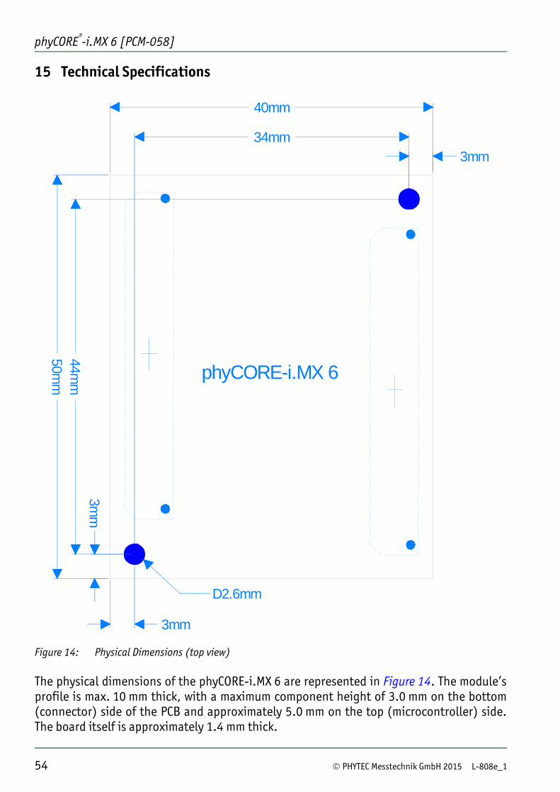
phyCORE®-i.MX 6 [PCM-058]
54 © PHYTEC Messtechnik GmbH 2015 L-808e_1
15 Technical Specifications
Figure 14: Physical Dimensions (top view) The physical dimensions of the phyCORE-i.MX 6 are represented in Figure 14. The module’s profile is max. 10 mm thick, with a maximum component height of 3.0 mm on the bottom (connector) side of the PCB and approximately 5.0 mm on the top (microcontroller) side. The board itself is approximately 1.4 mm thick.
3mm34mm
40mm
3mm
44mm
50mm
3mm
D2.6mm
phyCORE-i.MX 6
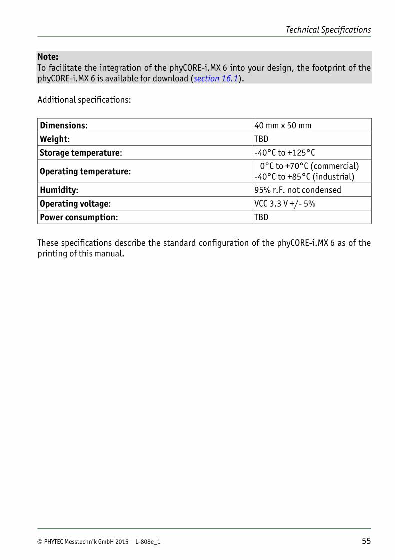
Technical Specifications
© PHYTEC Messtechnik GmbH 2015 L-808e_1 55
Note: To facilitate the integration of the phyCORE-i.MX 6 into your design, the footprint of the phyCORE-i.MX 6 is available for download (section 16.1). Additional specifications:
Dimensions: 40 mm x 50 mm
Weight: TBD
Storage temperature: -40°C to +125°C
Operating temperature: 0°C to +70°C (commercial) -40°C to +85°C (industrial)
Humidity: 95% r.F. not condensed
Operating voltage: VCC 3.3 V +/- 5%
Power consumption: TBD
These specifications describe the standard configuration of the phyCORE-i.MX 6 as of the printing of this manual.

phyCORE®-i.MX 6 [PCM-058]
56 © PHYTEC Messtechnik GmbH 2015 L-808e_1
Connectors on the phyCORE-i.MX 6: Manufacturer Samtec
phyCORE-Connector X1: Number of pins per contact rows 140 pins (2 rows of 70 pins each) Samtec part number (lead free) BSH-070-01-L-D-A-K-TR (old part#)
REF-183456-03 Information on the receptacle sockets that correspond to the connectors populating the underside of the phyCORE—i.MX 6 is provided below. The given connector height indicates the distance between the two connected PCBs when the module is mounted on the corresponding carrier board. In order to get the exact spacing, the maximum component height (3 mm) on the bottom side of the phyCORE must be subtracted. Mating Connector Connector height 5 mm Manufacturer Samtec Number of pins per contact row 140 pins (2 rows of 70 pins each) Samtec part number (lead free) BTH-070-01-L-D-A-K-TR (old part#) REF-183457-03 PHYTEC part number (lead free) VM317 Please refer to the corresponding data sheets and mechanical specifications provided by Samtec (www.samtec.com).

Handling the phyCORE-i.MX 6
© PHYTEC Messtechnik GmbH 2015 L-808e_1 57
16 Hints for Integrating and Handling the phyCORE-i.MX 6
16.1 Integrating the phyCORE-i.MX 6
Besides this hardware manual much information is available to facilitate the integration of the phyCORE-i.MX 6 into customer applications. 1. the design of the phyBOARD-Mira i.MX 6 can be used as a reference for any customer
application 2. many answers to common questions can be found at
http://www.phytec.de/de/support/faq/faq-phyCORE-i.MX 6.html, or http://www.phytec.eu/europe/support/faq/faq-phyCORE-i.MX 6.html
3. the link “Carrier Board” within the category Dimensional Drawing leads to the layout data as shown in Figure 15. It is available in different file formats. Use of this data allows to integrate the phyCORE-i.MX 6 SOM as a single component into your design.
4. different support packages are available to support you in all stages of your embedded development. Please visit http://www.phytec.de/de/support/support-pakete.html, or http://www.phytec.eu/europe/support/support-packages.html, or contact our sales team for more details.

phyCORE®-i.MX 6 [PCM-058]
58 © PHYTEC Messtechnik GmbH 2015 L-808e_1
Figure 15: Footprint of the phyCORE-i.MX 6
Ref Des
D2.6mm
D5mm
19.15mm
32.2
mm
1.8m
m
34m
m37
mm
40m
m
44mm47mm
50mm
3mm 3mm
23.61mm
mounting hole
PAD
A tolerance of +/- 0.1 mm applies to all indicated measures,except for the measures of the outer edges which have a tolerance of +/- 0.2 mm
D1.1mm

Handling the phyCORE-i.MX 6
© PHYTEC Messtechnik GmbH 2015 L-808e_1 59
16.2 Handling the phyCORE-i.MX 6
• Modifications on the phyCORE Module
Removal of various components, such as the microcontroller and the standard quartz, is not advisable given the compact nature of the module. Should this nonetheless be necessary, please ensure that the board as well as surrounding components and sockets remain undamaged while de-soldering. Overheating the board can cause the solder pads to loosen, rendering the module inoperable. Carefully heat neighboring connections in pairs. After a few alternations, components can be removed with the solder-iron tip. Alternatively, a hot air gun can be used to heat and loosen the bonds. Caution! If any modifications to the module are performed, regardless of their nature, the manufacturer guarantee is voided. • Integrating the phyCORE into a Target Application
Successful integration in user target circuitry greatly depends on the adherence to the layout design rules for the GND connections of the phyCORE module. For maximum EMI performance we recommend as a general design rule to connect all GND pins to a solid ground plane. But at least all GND pins neighboring signals which are being used in the application circuitry should be connected to GND.

phyCORE®-i.MX 6 [PCM-058]
60 © PHYTEC Messtechnik GmbH 2015 L-808e_1
17 Revision History
Date Version numbers
Changes in this manual
04.06.2015 Manual L-808e_1
First edition. Describes the phyCORE-i.MX 6 PCB-Version 1429.1

Index
© PHYTEC Messtechnik GmbH 2015 L-808e_1 61
Index
1 1000Base-T ........................................ 35 100Base-T.......................................... 35 10Base-T ........................................... 35
A Audio Interface ................................... 39
B Block Diagram....................................... 3 Boot Configuration .............................. 25 Boot Device ........................................ 26 Boot Mode ......................................... 25 Booting ............................................. 25
C Camera Interfaces................................ 48 CAN .................................................. 40
D DDR3 RAM .......................................... 28 DDR3_VREF ........................................ 22 DDR3-SDRAM ...................................... 28 Debug Interface .................................. 44 Dimensions ........................................ 55 Display Interface ................................. 45
E EEPROM ........................................ 28, 29 EEPROM Write Protection....................... 30 EMC ................................................... ix eMMC Flash ........................................ 29 Ethernet ............................................ 35
F Features .............................................. 1
G General Purpose I/Os............................ 42 GND Connection .................................. 59
H Humidity............................................ 55
I I²C EEPROM......................................... 29 I2C Interface ....................................... 39 I2C Memory......................................... 20 I2S .................................................... 39
J J1 20 J3 20 J4 20, 30 JTAG Interface .................................... 44
L LAN................................................... 36 LED
D1 43 LVDS Display Interface .......................... 46
M MAC .................................................. 36 MAC Address ....................................... 36
N NAND Flash.................................... 28, 29
O Operating Temperature ......................... 55 Operating Voltage................................ 55
P Parallel Display Interface ...................... 45 phyCORE-Connector ............................... 7 Physical Dimensions............................. 54 Pin Description...................................... 7 Pinout
X1-A................................................ 9 X1-B.............................................. 11 X1-C .............................................. 13 X1-D.............................................. 15
PMIC ................................................. 21 Power Consumption ............................. 55 Power Domains ................................... 22 Power Management IC .......................... 21 Power Supply ........................................ 6

phyCORE®-i.MX 6 [PCM-058]
62 © PHYTEC Messtechnik GmbH 2015 L-808e_1
R RMII Interface..................................... 37 RS-232 Level....................................... 33
S SATA Interface .................................... 40 SD / MMC Card Interfaces....................... 31 Serial Interfaces .................................. 32 SMT Connector ......................................7 SPI Flash ....................................... 28, 30 SPI Interface....................................... 38 Storage Temperature ............................ 55 Supply Voltage .................................... 21 System Configuration ........................... 25 System Memory ................................... 28 System Power...................................... 21
T Technical Specifications ........................ 54
U U11................................................... 29 U12................................................... 29
U14................................................... 29 U16................................................... 21 U2 .................................................... 35 U4-U7 ............................................... 28 U9 .................................................... 30 UART ................................................. 33 USB
Host Interface ................................. 34 OTG Interface .................................. 34
USB Device ......................................... 34 USB Host............................................ 34 USB OTG............................................. 34 User LED ............................................ 43
V VDD_3V3............................................ 21 VDD_DDR3_1V5 ................................... 22 VDD_eMMC_1V8 .................................. 22 Voltage Output .................................... 24
W Weight............................................... 55

Suggestions for Improvement
© PHYTEC Messtechnik GmbH 2015 L-808e_1
Document: phyCORE®-i.MX 6 Document number: L-808e_1, June 2015 How would you improve this manual? Did you find any mistakes in this manual? page Submitted by: Customer number: Name: Company: Address: Return to: PHYTEC Messtechnik GmbH Postfach 100403 D-55135 Mainz, Germany Fax : +49 (6131) 9221-33

Published by
© PHYTEC Messtechnik GmbH 2015 Ordering No. L-808e_1 Printed in Germany