physical design automation for high-density 3d ... - e3da lab
TRANSCRIPT
Physical Design Automation for High-Density 3D Power Module
Layout Synthesis and Optimization
Imam Al Razi a, Quang Le b, H. Alan Mantooth b, Yarui Peng a
a Computer Science and Computer Engineering Department,b Electrical Engineering Department
University of Arkansas, Fayetteville, AR, US
[email protected], [email protected]
Abstract—With the on-going trend of electrification of trans-port, ultra-high-density power electronics with advanced 2.5Dand 3D packaging are drawing attention. At present, the powermodule design is still a manual and time-consuming procedure.Floorplanning, placement, routing, and parasitic extraction needto be performed carefully to enhance performance withoutsacrificing reliability. Inspired by design automation tools forVLSI circuits, design automation tools for power electronics candramatically reduce the engineering time and costs. As 3D powermodule fabrication is on the horizon to further improve powerdensity, in this work, we present physical design algorithms toautomate the 3D power module layout synthesis and optimization.Hierarchical corner stitch and constraint graphs are used toguarantee manufacturable layouts. Our algorithms are genericand scalable to integrate heterogeneous components with multipledevices and routing layers into a single power module. Wedemonstrate the improvement in the electro-thermal performanceof a half-bridge 3D power module over a 2D counterpart.Also, the effectiveness and efficiency of our algorithms aredemonstrated using real-world 3D power module designs.
Keywords—PowerSynth, corner stitch, constraint graph, 3DMulti-Chip Power Module, layout optimization
I. INTRODUCTION
To satisfy the increasing demands from automobiles,
telecommunications, aerospace, and consumer electronics in-
dustries, next-generation power conversion systems, i.e., in-
verters and converters, need to be designed with high power
density [1, 2]. As power modules are key components of
all the power converter systems, high-density power module
design methodology is a critical research problem in the power
electronics society. Significant improvement of power module
efficiency has been achieved with the wide bandgap (WBG)
power semiconductor devices. Therefore, power module phys-
ical design is getting increasingly more complex. Multi-
chip power module (MCPM) designers are switching their
focus from conventional 2D (single device and routing layer)
package to 2.5D (single device layer with multiple routing
layers on a planar substrate) and 3D (multiple devices and
routing layers stacked on the same substrate) packaging [3–
7]. The advanced packaging techniques enable heterogeneous
component integration, reduce parasitics, shrink current loops,
and improve efficiency with reduced volume and weight.
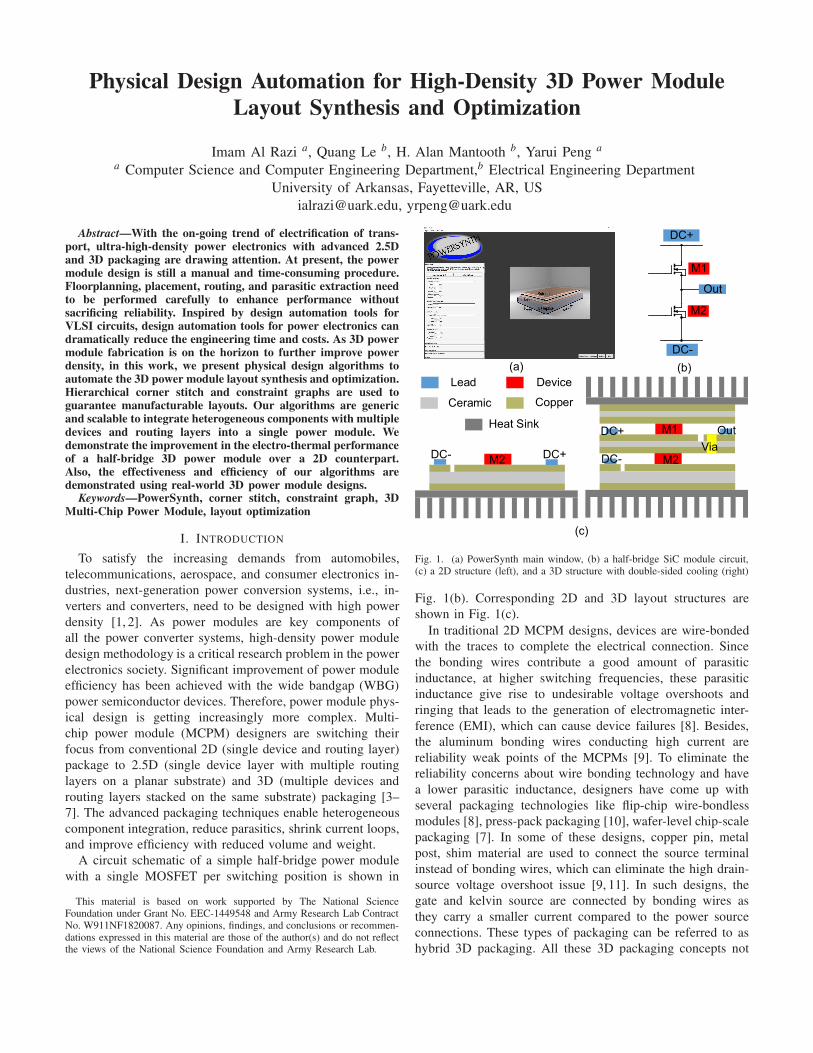
A circuit schematic of a simple half-bridge power module
with a single MOSFET per switching position is shown in
This material is based on work supported by The National ScienceFoundation under Grant No. EEC-1449548 and Army Research Lab ContractNo. W911NF1820087. Any opinions, findings, and conclusions or recommen-dations expressed in this material are those of the author(s) and do not reflectthe views of the National Science Foundation and Army Research Lab.
(b)
(c)
DC+DC- M2
CopperCeramic
DeviceLead
Heat SinkDC+ M1 Out
DC- M2Via
(a)
M1
DC+
DC-
Out
M2
Fig. 1. (a) PowerSynth main window, (b) a half-bridge SiC module circuit,(c) a 2D structure (left), and a 3D structure with double-sided cooling (right)
Fig. 1(b). Corresponding 2D and 3D layout structures are
shown in Fig. 1(c).
In traditional 2D MCPM designs, devices are wire-bonded
with the traces to complete the electrical connection. Since
the bonding wires contribute a good amount of parasitic
inductance, at higher switching frequencies, these parasitic
inductance give rise to undesirable voltage overshoots and
ringing that leads to the generation of electromagnetic inter-
ference (EMI), which can cause device failures [8]. Besides,
the aluminum bonding wires conducting high current are
reliability weak points of the MCPMs [9]. To eliminate the
reliability concerns about wire bonding technology and have
a lower parasitic inductance, designers have come up with
several packaging technologies like flip-chip wire-bondless
modules [8], press-pack packaging [10], wafer-level chip-scale
packaging [7]. In some of these designs, copper pin, metal
post, shim material are used to connect the source terminal
instead of bonding wires, which can eliminate the high drain-
source voltage overshoot issue [9, 11]. In such designs, the
gate and kelvin source are connected by bonding wires as
they carry a smaller current compared to the power source
connections. These types of packaging can be referred to as
hybrid 3D packaging. All these 3D packaging concepts not
only reduce the electrical parasitics by minimizing the loop
area but also improve thermal performance. This is because
the double-sided cooling, as well as higher heat dissipation, is
possible with the 3D technology. With these benefits, the 3D
power module packaging technique becomes more attractive
in the power electronics society.
In the power module manufacturing industry, to accelerate
the current MCPM physical design flow and avoid the manual
and iterative process, physical design automation has been
initiated by many researchers. Several studies leveraging VLSI
placement-and-routing (P&R) concepts are successfully ap-
plied to power module layout synthesis while considering the
fundamental differences between VLSI and power electronics
design [12–14]. Though progress is made on 2D power module
design automation, a generalized 3D MCPM constraint-aware
layout optimization methodology does not exist so far. In [13],
a 2D power module layout is represented using the sequence-
pair method, and a 1D binary string is used to randomize
routing paths within the plane. Simplification is performed
to reduce the problem size, which leads to inefficiency in
handling complex geometry. A genetic algorithm (GA) based
layout optimization method for the motor controller system
is presented in [6]. Here, the 3D layout components are
simplified as cubes and represented as a sequence group (an
extension of sequence pair). GA operators are applied to the
group to generate multiple solutions aiming at volume and
connection length reduction. This method can explore very
few solutions and does not guarantee the alignment of the
layers. Also, the electro-thermal reliability of the solutions is
not considered at all, which makes the approach inappropriate
for 3D MCPM layout optimization.
In [12], a software tool called PowerSynth (GUI shown in
Fig. 1(a)) is introduced that can help engineers to generate
power module layouts from a draft design. It does not even
require expertise in every aspect of the design flow. Further,
with its built-in models for electrical and thermal evaluation,
this tool can quickly analyze the electro-thermal performance
of the layout without the need to run the finite element
method (FEM) tools. A matrix-based methodology is used in
this version to generate layout solutions during optimization.
This methodology has been proven to be inefficient in layout
generation due to iterative DRC-checking, and limited solution
space. Several efforts are performed to overcome the limita-
tions with the baseline tool and make the tool more generic,
scalable, and efficient. As a part of these continuous research
and development efforts, a new layout engine based on the
corner stitching data structure with constraint graphs has been
proposed in [14]. This new layout engine generates DRC-
clean solutions with heterogeneous components and higher
complexity. Since this is a planar version that can handle only
2D layouts and results in higher coordinate correlation, in [15],
a hierarchical corner stitch data structure with hierarchical con-
straint propagation methodology is proposed to demonstrate
the benefits of the hierarchical approach. The methodology
randomizes constraint graph edge weights for generating so-
lutions without considering connectivity or alignment, which
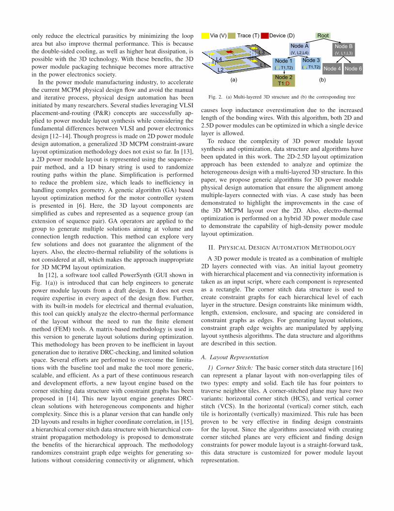
Root
Node B
(V, L1,L3)
Node 4 Node 6
(b)(a)
L1L2
L3
L4
Via (V) Trace (T) Device (D)
Node 1
(V, T1,T2)
Node 3
(V, T1,T2)
Node 2
T1:D
Node A
(V, L2,L4)
Fig. 2. (a) Multi-layered 3D structure and (b) the corresponding tree
causes loop inductance overestimation due to the increased
length of the bonding wires. With this algorithm, both 2D and
2.5D power modules can be optimized in which a single device
layer is allowed.
To reduce the complexity of 3D power module layout
synthesis and optimization, data structure and algorithms have
been updated in this work. The 2D-2.5D layout optimization
approach has been extended to analyze and optimize the
heterogeneous design with a multi-layered 3D structure. In this
paper, we propose generic algorithms for 3D power module
physical design automation that ensure the alignment among
multiple-layers connected with vias. A case study has been
demonstrated to highlight the improvements in the case of
the 3D MCPM layout over the 2D. Also, electro-thermal
optimization is performed on a hybrid 3D power module case
to demonstrate the capability of high-density power module
layout optimization.
II. PHYSICAL DESIGN AUTOMATION METHODOLOGY
A 3D power module is treated as a combination of multiple
2D layers connected with vias. An initial layout geometry
with hierarchical placement and via connectivity information is
taken as an input script, where each component is represented
as a rectangle. The corner stitch data structure is used to
create constraint graphs for each hierarchical level of each
layer in the structure. Design constraints like minimum width,
length, extension, enclosure, and spacing are considered in
constraint graphs as edges. For generating layout solutions,
constraint graph edge weights are manipulated by applying
layout synthesis algorithms. The data structure and algorithms
are described in this section.
A. Layout Representation
1) Corner Stitch: The basic corner stitch data structure [16]
can represent a planar layout with non-overlapping tiles of
two types: empty and solid. Each tile has four pointers to
traverse neighbor tiles. A corner-stitched plane may have two
variants: horizontal corner stitch (HCS), and vertical corner
stitch (VCS). In the horizontal (vertical) corner stitch, each
tile is horizontally (vertically) maximized. This rule has been
proven to be very effective in finding design constraints
for the layout. Since the algorithms associated with creating
corner stitched planes are very efficient and finding design
constraints for power module layout is a straight-forward task,
this data structure is customized for power module layout
representation.
2) Constraint Graph: A constraint graph is a technique
to represent an inequality relationship between two vertices,
where the edge weight is a minimum constraint value. Each
corner-stitched tile can be mapped into two vertices in the
graph connected with an edge weighting minimum constraint
value associated with that tile. Two constraint graphs are
generated: a horizontal constraint graph (HCG), and a ver-
tical constraint graph (VCG). The HCG ensures horizontal
minimum relative location among components, and the VCG
maintains the vertical minimum relative location.
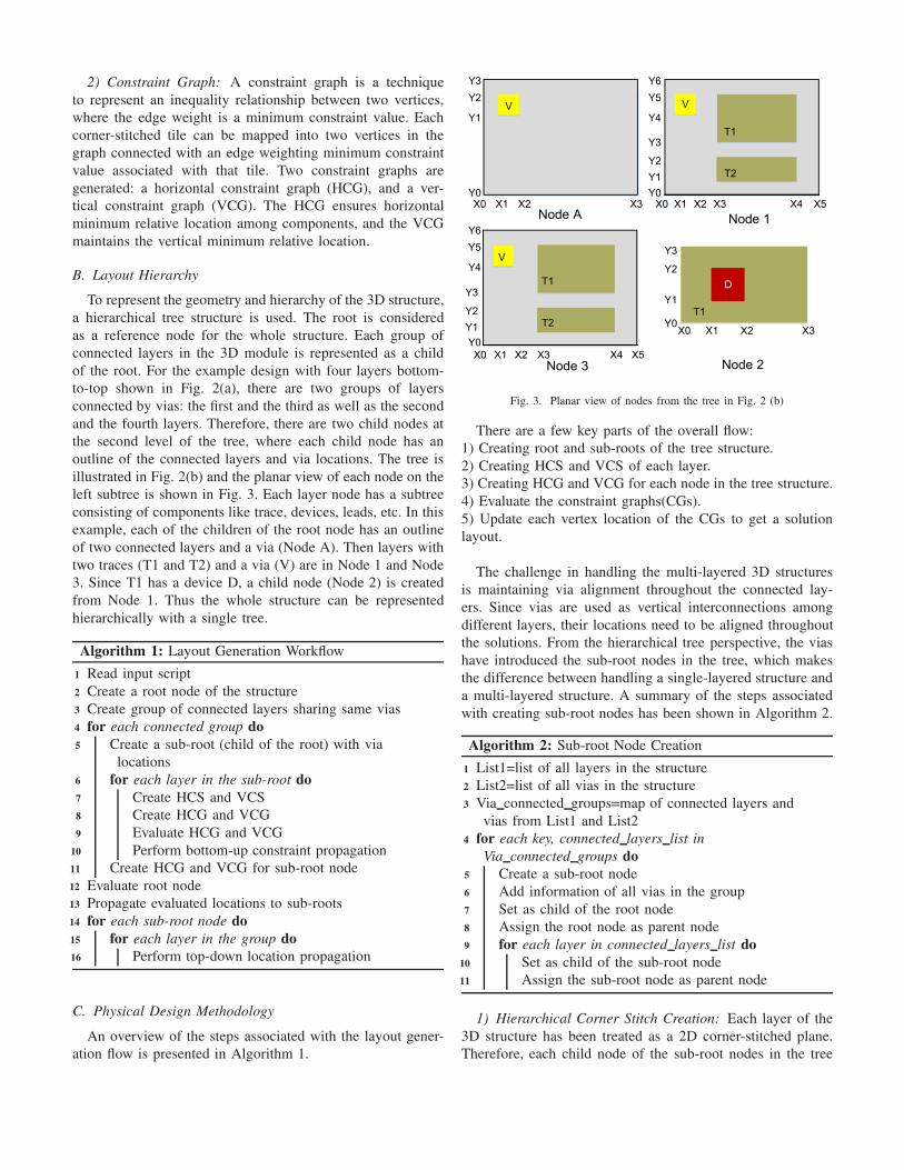
B. Layout Hierarchy
To represent the geometry and hierarchy of the 3D structure,
a hierarchical tree structure is used. The root is considered
as a reference node for the whole structure. Each group of
connected layers in the 3D module is represented as a child
of the root. For the example design with four layers bottom-
to-top shown in Fig. 2(a), there are two groups of layers
connected by vias: the first and the third as well as the second
and the fourth layers. Therefore, there are two child nodes at
the second level of the tree, where each child node has an
outline of the connected layers and via locations. The tree is
illustrated in Fig. 2(b) and the planar view of each node on the
left subtree is shown in Fig. 3. Each layer node has a subtree
consisting of components like trace, devices, leads, etc. In this
example, each of the children of the root node has an outline
of two connected layers and a via (Node A). Then layers with
two traces (T1 and T2) and a via (V) are in Node 1 and Node
3. Since T1 has a device D, a child node (Node 2) is created
from Node 1. Thus the whole structure can be represented
hierarchically with a single tree.
Algorithm 1: Layout Generation Workflow
1 Read input script
2 Create a root node of the structure
3 Create group of connected layers sharing same vias
4 for each connected group do
5 Create a sub-root (child of the root) with via
locations
6 for each layer in the sub-root do
7 Create HCS and VCS
8 Create HCG and VCG
9 Evaluate HCG and VCG
10 Perform bottom-up constraint propagation
11 Create HCG and VCG for sub-root node
12 Evaluate root node
13 Propagate evaluated locations to sub-roots
14 for each sub-root node do
15 for each layer in the group do
16 Perform top-down location propagation
C. Physical Design Methodology
An overview of the steps associated with the layout gener-
ation flow is presented in Algorithm 1.
D
T1
X0 X1 X2 X3Y0
Y1
Y2
Y3
V
T1
T2
X0 X1 X2 X5X3 X4Y0
Y4
Y5
Y6
Y1
Y2
Y3
V
X0 X1 X2 X3Y0
Y1
Y2
Y3
Node A
Node 2
T1
T2
V
X0 X1 X2 X5X3 X4
Y0
Y4
Y5
Y6
Y1
Y2
Y3
Node 1
Node 3
Fig. 3. Planar view of nodes from the tree in Fig. 2 (b)
There are a few key parts of the overall flow:
1) Creating root and sub-roots of the tree structure.
2) Creating HCS and VCS of each layer.
3) Creating HCG and VCG for each node in the tree structure.
4) Evaluate the constraint graphs(CGs).
5) Update each vertex location of the CGs to get a solution
layout.
The challenge in handling the multi-layered 3D structures
is maintaining via alignment throughout the connected lay-
ers. Since vias are used as vertical interconnections among
different layers, their locations need to be aligned throughout
the solutions. From the hierarchical tree perspective, the vias
have introduced the sub-root nodes in the tree, which makes
the difference between handling a single-layered structure and
a multi-layered structure. A summary of the steps associated
with creating sub-root nodes has been shown in Algorithm 2.
Algorithm 2: Sub-root Node Creation
1 List1=list of all layers in the structure
2 List2=list of all vias in the structure
3 Via connected groups=map of connected layers and
vias from List1 and List2
4 for each key, connected layers list in
Via connected groups do
5 Create a sub-root node
6 Add information of all vias in the group
7 Set as child of the root node
8 Assign the root node as parent node
9 for each layer in connected layers list do
10 Set as child of the sub-root node
11 Assign the sub-root node as parent node
1) Hierarchical Corner Stitch Creation: Each layer of the
3D structure has been treated as a 2D corner-stitched plane.
Therefore, each child node of the sub-root nodes in the tree

Node 3
Node 2
X0
1:X0
X1
1:X1X2
1:X2
X3
1:X5
1:WV1:E
1:WV+S
Node A
X0 X1 X2 X5WVE
WV+S
X3 X4WT E
X0 X1 X2 X5WVE
WV+S
X3
2:X0
X4
2:X3
2:P
WT E
Node 1
X0 X1 X2 X3WDE
WD+E
Propagated
Non-Fixed
Fixed
Independent
Sink
Source
Dependent
Edge Type:
Vertex Type:
Fig. 4. Horizontal constraint graph for the left sub-tree in Fig. 2(b) withbottom-up propagation. E and S are minimum enclosure and minimumspacing, respectively, while WT ,WD,WV are minimum widths of trace, device,and via, respectively.
has two corner stitch orientations. While creating hierarchical
corner stitch planes (i.e., HCS, and VCS), two assumptions
are considered:
1) Tile insertion is performed hierarchically. Before inserting
a child component, the parent node components need to
be inserted.
2) All tiles in any rectilinear polygon should be of the same
type and need to be inserted sequentially.
In a hierarchical corner stitch data structure, each node has
both foreground and background tiles. The background tiles
are usually the copies from the parent node in the tree, and
the foreground tiles are the newly inserted tiles and appended
in the child node of the tree. These two varieties of tiles are
required to find appropriate constraints among the components.
Since this step is similar to in 2D layout handling, more details
can be found in [15].
2) Constraint Graph Creation and Evaluation: Constraint
graph creation starts from the leaf node of the tree structure.
Since the parent node needs to have sufficient room for
the child node, the child node constraint graphs are created,
evaluated, and necessary constraint values are propagated to
the parent node. From both corner stitched trees (i.e., HCS,
VCS), the horizontal and vertical constraint graphs are created
for each node in the tree (except the root and sub-root nodes)
by mapping design constraints. The root and sub-root nodes
are different from all other nodes in the tree as these nodes
do not have corresponding corner-stitched planes while the
others have. Therefore, for these nodes, the HCG and VCG are
created using the propagated constraints from each sub-tree of
the corresponding sub-root. A via propagation dictionary (a
data structure to map key and value pair) is maintained for
this purpose. Since via is declared as a component in one of
the hierarchical levels of the tree, the coordinates associated
with vias need to be propagated from that level to the sub-
Algorithm 3: Via Propagation Dictionary Assignment
1 Propagation dict= { }2 for each via do
3 Propagation dict[via name]=[corresponding
sub-root node id (reference node id)]
4 Propagation dict[via name].append(via node id)
5 node id=via node id
6 while node id is not equal to the reference node id
do
7 Propagation dict[via name].append(node id)
8 node id=id of the parent node
9 return Propagation dict
root node. The pseudocode associated with maintaining the
via propagation dictionary is shown in Algorithm 3.
3) Bottom-up Constraint Propagation: The constraint
graphs are evaluated by the longest path algorithm, and a
bottom-up constraint propagation (algorithm shown in [15])
has been performed to respect the necessary design constraints
from a child to the corresponding parent. An illustration of
bottom-up constraint propagation is shown in Fig. 4. Here,
HCG of each node is shown with some basic terminologies
associated with the graph data structure. Each vertex refers to
an x coordinate of the plane (shown in Fig. 3). The red edges
are propagated edges, and corresponding weights are shown as
a map of source node id and propagated value. For each node,
the leftmost vertex is the source, and the rightmost vertex is
the sink vertex. To preserve a fixed size for components, all
dependent vertices and corresponding reference independent
vertices are tracked using a fixed dimension handling algo-
rithm [15]. The algorithm ensures that all incoming edges and
outgoing edges of the dependent vertex are redirected to the
corresponding reference vertex. Thus a dependent vertex is
removed from the longest path. To handle connections between
intra-layer (bond wires) and inter-layer (vias), a propagation
dictionary is used, which provides the necessary propagation
path from a child node to the common reference node. After
propagating up to sub-root nodes, the longest path from the
source and sink is propagated to the root as the root has only
these two shared vertices.
4) Top-Down Location Propagation: Once the bottom-up
constraint propagation is complete, the evaluated constraint
graphs of the root node determine the minimum size of the
structure. This minimum size (width, length) determines the
location of the source and sink vertices of the sub-root nodes.
The rest of the vertices locations are determined using the
fixed floorplan handling algorithm described in [15]. If the
algorithms are used for fixed-sized solution generation, this
root node determines the maximum room for randomization
by subtracting the minimum size from the fixed floorplan
size provided by the user. The shared vertices locations are
propagated from the parent node directly, whereas the rest
of the independent vertices locations are determined from
the constraint graph created for that node. The dependent
vertex location is calculated as soon as the corresponding

reference vertex location is determined. This algorithm gives
a DRC-clean location range for each vertex in each node. All
algorithms associated with the constraint graph evaluation have
a time complexity O(V+E), where E and V are the number
of edges and vertices, respectively. Since the locations of
connected vertices are determined by the common reference
node, bonding wires, and vias are always aligned. Our pro-
posed algorithms handle both 2D and 3D connections in a
generic way. However, there are some fundamental differences
between 2D/2.5D single-layer structure and multi-layer 3D
structure handling. For example, in a multi-layer structure,
the via-connected layers under a sub-root should have the
same floorplan size. 2D/2.5D connection (i.e., bonding wires)
handling algorithms require vertex sharing in either HCG or
VCG, whereas in 3D cases, both HCG and VCG need to be
considered simultaneously to handle via connections.
D. Layout Evaluation and Optimization
The algorithms are implemented to generate an arbitrary
number of solutions. These solutions are evaluated with both
electrical and thermal models. For electrical evaluation, a
partial element equivalent circuit (PEEC)-based hierarchical
RCLM model is used [17] for minimum-sized solutions. In
addition to the built-in model, an electrical modeling interface
has been built to export designs into FastHenry [18]. This
interface has been used for evaluating a large solution space.
To evaluate the static thermal performance, a 3D reduced-
order multi-level RC network model is used by leveraging
the application program interface (API) developed between
PowerSynth and ParaPower [19].
1) Electrical Performance Evaluation: Electrical parasitics,
primarily parasitic inductance, is one of the critical design
parameters for MCPM to achieve high performance at high
switching speed. In this paper, the PEEC model [17] has
been further extended to support the 3D layout evaluation.
For this purpose, an API has been developed to convert the
layout geometrical information into an equivalent netlist of
R and L elements. The layout solution data is arranged into
a table object, where each row of the table contains a set
of trace groups. Depending on the structure of each layout
group, three pre-defined orientations: vertical (V), horizontal
(H), and planar (P). Using these pre-defined orientations, the
meshing algorithm can efficiently generate the mesh for a
single direction or multiple directions of current flows. The
meshing algorithm loops through each trace group and convert
them into equivalent mesh nodes and edges. A mesh node
contains voltage information, while a mesh edge has the
parasitic value R and L as its weight and contains current
information. Once a mesh of all partial parasitic elements is
formed, the modified nodal analysis (MNA) method is used
to evaluate the loop inductance value. This model has shown
good accuracy with FastHenry for the minimum-sized solu-
tion evaluation. However, this model is not matured enough
for handling the optimization case, where the floorplan size
changes dynamically. Therefore, in the case of optimization,
FastHenry has been used for evaluating the loop inductance
values of the generated solution space.
2) Thermal Performance Evaluation: Since the 3D struc-
ture is denser compared to the 2D one, thermal performance
prediction is a critical aspect of optimization. In this work,
static maximum temperature has been used as a thermal
performance metric. ParaPower [19] is a thermal and stress
evaluation tool developed by the Army Research Lab (ARL).
An API has been developed to pass the layout solution
structure to ParaPower and get the maximum temperature
evaluated from it. In this tool, each structure is represented
as a 3D box, and the boundary conditions can be applied to
each arbitrary surface. All empty places in the volume of the
structure are filled with air by default. The meshing precision
is user-defined for each object. The complete structure is stored
as a matrix, and the number of elements of the matrix is
dependent on the meshing size defined by the user. An RC
network is created for each element of the meshing, and each
node of the network is evaluated in the specified time intervals.
After a certain time period, each node temperature is stored
in the result matrix. This temperature evaluation tool results
have been verified against finite element analysis (FEA) tools
like ANSYS Workbench, and significant speedup has been
achieved within acceptable accuracy.
3) Layout Optimization: All generated solutions are eval-
uated using the aforementioned models, and the solution
space is reported to choose the optimum solution. Though the
randomization method has no guidance towards optimization,
it can cover a large solution space if a large number of layout
solutions are generated. Though a genetic algorithm can be
implemented to find an optimal solution set for 2D layouts
in comparatively faster than the randomization approach, the
algorithm needs customization for handling 3D layouts as the
design variables are exponentially increasing with the module
geometry complexity. Therefore, a customized optimization
algorithm study is on-going, and the randomization algorithm
has been used until the best-suited optimization algorithm is
developed. To report the Pareto-front solution space, a non-
dominated sorting algorithm is applied to the complete solu-
tion space generated by the layout engine. From the Pareto-
optimal solution set, the user can choose one point of interest
and export the solution to the standard 3D modeling tools (i.e.,
SolidWorks, Ansys Q3D) through Powersynth export feature.
III. EXPERIMENTAL RESULTS
Since the designers have barely practiced the 3D power
module layout design compared to the 2D cases, a perfor-
mance comparison has been performed between a 2D half-
bridge SiC power module and its 3D counterpart. Among
many aspects, two essential but conflicting performance met-
rics like power loop inductance and maximum junction tem-
perature of the module are considered for evaluation. Follow-
ing the comparison, two hybrid 3D power module design cases
are considered for electro-thermal performance evaluation.

DC+
DC-
OUT
D1D2
D3D4
DC
+
OU
T
D3
D4
V
DC
-
D1
D2
V
L1 L2
V
(a) (b)
Fig. 5. Half-bridge MCPM: (a) 2D structure, (b) 3D structure with planarviews of routing layers: high-side (L1) and low-side (L2).
(c)(a)L1 L2
10
20
30
00 10 20 0 10 0 10
0
10
0
10
20 20
DC+
DC-
OUT
DC+
DC-
OUT
DC+
DC-Via
(b)
Fig. 6. Minimum-sized solution: a) 2D layout (21.5 × 36.5) mm2, (b) 3Dpower loop, (c) high-side (Layer 1) and low-side (Layer 2) layers of 3Dlayout (18×25.5) mm2.
A. 2D vs. 3D Performance Comparison
A 2D and a 3D half-bridge power module with two SiC
MOSFETs per switching position are considered for electro-
thermal performance comparison. Initial layouts for both of the
cases are shown in Fig. 5. For a fair comparison, the 3D layout
has been designed by splitting the 2D module into two layers:
one is for the high-side switching, and the other is for the
low-side switching. Both layers are stacked vertically, and a
metallic post has been considered to have a via type connection
in between them. The 3D structure with layout breakdown is
shown in Fig. 5(b). In each layer floorplan figure, ‘V’ stands
for the via type connection. For both 2D and 3D cases, a
minimum-sized solution has been generated and evaluated by
using PowerSynth. A set of standard design rules (i.e., min
spacing, min enclosure, min width) have been considered for
generating the solutions. The minimum-sized solution refers
to the most compact and maximum achievable power density
for a specific layout. The solution layouts are shown in Fig. 6.
Power loop inductance at 100 kHz is 6.104 nH and 15.793 nH
for 3D and 2D, respectively. From the figure, it is clear that
the 3D power loop area is much smaller than that of 2D as the
former one has a vertical loop, whereas the latter one has a
planar loop. For thermal evaluation, ambient temperature is set
(a)
L4L2
L3L1
DC+
Via
DC-
(b)
Fig. 7. (a) A sample 3D half-bridge power module with four routing layers(L1-L4), (b) the corresponding 3D power loop.
to 300K, heat dissipation for each die is 10W. In the case of 2D
configuration, only the bottom side of the baseplate, whereas
for the 3D case, both top and bottom sides have been equipped
with an effective heat transfer coefficient of 1000 W/m2 −K.
For 3D, and 2D cases, the maximum temperature for the
devices are found 328.377 K, and 332.147 K, respectively.
However, single-sided cooling with 1000 W/m2 − K heat
transfer coefficient makes the 3D case maximum temperature
as high as 370.287 K. Therefore, for the compact 3D layout
with less area for heat dissipation, double-sided cooling is a
must to maintain low junction temperature compared to the 2D
case. The results indicate that adding the third dimension to
the MCPM layout design improves both electrical and thermal
performance.
B. 3D Layout Optimization
Since the 3D power module is an emerging and advanced
technology, there are very few references for the packaging
topology, which are fabricated and tested. Therefore, we chose
two half-bridge power modules to demonstrate our methodol-
ogy performance.
1) Test Case 1 (A SiC Power Module): For the first case,
we have considered two SiC devices per switching position
and split the two switches into two layers. A 3D structure
of the module and the corresponding power loop are shown
in Fig. 7. A layer-wise breakdown layout has been shown in
Fig. 8 (a). Drain, gate, and kelvin source connections for each
device are on the same layer, and the sources are connected to
the neighboring upper layer through metallic post connectors.
Thus the whole half-bridge consists of four routing layers
containing three terminals: DC+, OUT, and DC-. A via (V)
is used to connect two layers (L2 and L3) of a direct bonded
copper (DBC) substrate, which serves as the output. For this
initial layout, a minimum-sized solution has been generated
and evaluated. The solution is shown in Fig. 8 (b). The metallic
post connectors (device source connection) are treated as via
in the layout generation algorithms as they serve a similar
purpose in terms of connectivity. So, all those pads are of the
same color in the figure. The power loop inductance for this
case is 1.406 nH at 1000 kHz, and the maximum temperature
is found 349.282 K. The boundary conditions are the same
as the 3D case used for performance comparison with the 2D
layout.
2) Test Case 2 (An IGBT Power Module): The schematic
of this case and the corresponding 3D structure are shown
in Fig. 9(a), (b), respectively. Four IGBTs and anti-parallel

0
5
10
15
0 5 10 15 0 5 10 15 0 5 10 15 0 5 10 15
DC+ DC-
OUT
V V
L1 L2 L3 L4
S1 S2V
OU
T
S4S3
DC
-DC
+
S1 S2V S3 S4
L1 L2 L3 L4(a) (b)
Fig. 8. (a) Initial layout of routing layers in Fig. 7: high-side device layer (L1), high-side device source layer (L2), low-side device layer (L3), and low-sidedevice source layer (L4), (b) the corresponding minimum-sized solution (19×19) mm2.
(b)
DC+
DC-
S1 S2 S3 S4
S5
S6 S7
S8
Out
(a)
L4
L2L3
L1
3D Structure
Fig. 9. (a) Schematic of a half-bridge power module with IGBT and diode,(b) corresponding 3D structure with four routing layers (L1-L4).
TABLE IPERFORMANCE METRICS FOR THREE LAYOUTS ON SOLUTION SPACE
Layout ID Inductance Temperature Size(nH) ( K) (mm × mm)
A 1.44 334.11 34.5 × 16.5
B 1.22 328.13 37.0 × 24.0
C 2.43 324.62 42.0 × 26.5
diodes are used to make a half-bridge power module. The
initial layout is designed in the same hybrid fashion as the
test case 1. Layer-wise planar images are shown in Fig. 10.
Here, the power loop is similar to the case 1: from DC+
to DC- through the high-side devices (L1), bottom output
trace (L2), via, top output trace (L3) with low-side devices.
The minimum-sized solution is shown in Fig. 11. The loop
inductance and maximum temperature of the solution are 2.73
nH at 1000 kHz, and 341.155 K, respectively.
To optimize the layout, around 2400 solutions are generated
with varying floorplan sizes from 569.25mm2 to 1113mm2. For
each floorplan size, 100 solutions are generated. FastHenry
and ParaPower has been used for electro-thermal performance
evaluation. The resultant 2D plot is shown in Fig. 12. The
solution points are color mapped with the floorplan sizes.
Three corner solutions are chosen to show the tradeoff between
two objectives. These three solutions are marked in Fig. 12,
and the layouts are shown in Fig. 13. The floorplan sizes
and performance values for the three layouts are shown in
Table I. The table shows that Layout A has the smallest
size, which results in the highest temperature rise. On the
other hand, Layout C has the largest footprint with the lowest
temperature and higher inductance. The balanced solution is
shown in Layout B with a better tradeoff. The runtime for
layout generation is about 8 s/100 layouts and evaluation
is about 286 s/100 layouts on an Intel®Silver 4114 CPU
computer. This shows our tool flow is both accurate and
efficient enough for orders-of-magnitude design productivity
improvement.
IV. CONCLUSION AND FUTURE WORK
We propose constraint-aware physical design synthesis and
optimization algorithms for 3D MCPM designs that are
generic and efficient to handle both intra-layer and inter-layer
connections. Our algorithms are scalable and efficient enough
to handle multi-layered 3D layouts with an arbitrary number
of layers. Experimental results of the 3D power module layout
further test our algorithms through optimized layout solutions.
We will further validate our framework by fabricating 3D
power modules designed and optimized with our CAD tools.
This module-level design framework can be extended towards
cabinet-level physical design and optimization. A customized
optimization algorithm will also be implemented to have a
better tradeoff among multiple conflicting objectives.
ACKNOWLEDGMENT
The authors would like to thank Dr. Fang Luo, Dr. Lauren
Boteler, Tristan Evans and Shilpi Mukherjee for their help and
suggestions.
REFERENCES
[1] C. Neeb et al., “Innovative and Reliable Power Modules: A Future Trendand Evolution of Technologies,” IEEE Industrial Electronics Magazine,vol. 8, no. 3, pp. 6–16, Sep. 2014.
[2] S. Tanimoto and K. Matsui, “High Junction Temperature and LowParasitic Inductance Power Module Technology for Compact PowerConversion Systems,” IEEE Transactions on Electron Devices, vol. 62,no. 2, pp. 258–269, Feb. 2015.
[3] A. Dutta and S. S. Ang, “A Module-Level Spring-Interconnected StackPower Module,” IEEE Transactions on Components, Packaging and
Manufacturing Technology, vol. 9, no. 1, pp. 88–95, Jan. 2019.
[4] H. Ishibashi et al., “Direct Power Board Bonding Technology for 3DPower Module Package,” in International Conference on Electronics
Packaging, Apr. 2019, pp. 79–82.
[5] X. Zhao et al., “Performance Optimization of A 1.2kV SiC High DensityHalf Bridge Power Module in 3D Package,” in IEEE Applied Power
Electronics Conference and Exposition, Mar. 2018, pp. 1266–1271.
[6] H. Cao et al., “A Genetic Algorithm Based Motor Controller SystemAutomatic Layout Method,” in International Conference on PowerElectronics and IEEE Energy Conversion Congress and Expo in Asia,May 2019, pp. 1499–1504.
[7] C. Chen, F. Luo, and Y. Kang, “A Review of SiC Power Module Pack-aging: Layout, Material System and Integration,” CPSS Transactions on
Power Electronics and Applications, vol. 2, no. 3, pp. 170–186, Sep.2017.
[8] S. Seal, M. D. Glover, and H. A. Mantooth, “3-D Wire BondlessSwitching Cell Using Flip-Chip-Bonded Silicon Carbide Power De-vices,” vol. 33, no. 10, pp. 8553–8564, 2018.

S1S2S3S4
DC
+
S1S2S3S4V
OU
T
S5 S6 S7 S8
DC
-
L1 L2 L3 L4
V S5S6S7S8
Fig. 10. Planar view of routing layers in Fig. 9: high-side device layer (L1), high-side device source layer (L2), low-side device layer (L3), and low-sidedevice source layer (L4).
4
0
8
16
12
DC+
L1
V V
DC-
0 10 20 300 10 20 300 10 20 300 10 20 30L2 L3 L4
OUT
Fig. 11. Minimum-sized solution (32×16.5) mm2 of Fig. 10.
A
B
C
1 2 3 4 5 6
326
328
330
332
334)K(
erut
are
pm
eT
mu
mix
aM
Inductance (nH)
569623678732787841895950100410591113
Area (mm2)
Fig. 12. Design solution space for the example design in Fig. 9
[9] S. Zhu et al., “Advanced Double Sided Cooling IGBT Module and PowerControl Unit Development,” in International Workshop On Integrated
Power Packaging, 2017, pp. 1–4.
[10] N. Zhu, H. A. Mantooth, D. Xu, M. Chen, and M. D. Glover, “A Solutionto Press-Pack Packaging of SiC MOSFETS,” IEEE Transactions on
Industrial Electronics, vol. 64, no. 10, pp. 8224–8234, 2017.
[11] F. Yang et al., “Design of a Low Parasitic Inductance SiC Power Modulewith Double-Sided Cooling,” in Applied Power Electronics Conference
and Exposition, 2017, pp. 3057–3062.
[12] T. Evans et al., “PowerSynth: A Power Module Layout Generation Tool,”IEEE Transactions on Power Electronics, vol. 34, no. 6, pp. 5063–5078,Jun. 2019.
[13] P. Ning et al., “An Improved Planar Module Automatic Layout Methodfor Large Number of Dies,” CES Transactions on Electrical Machines
and Systems, vol. 1, no. 4, pp. 411–417, Dec. 2017.
[14] I. Al Razi et al., “Constraint-Aware Algorithms for HeterogeneousPower Module Layout Synthesis and Optimization in PowerSynth,” inIEEE Workshop on Wide Bandgap Power Devices and Applications, Oct.2018, pp. 323–330.
[15] ——, “Hierarchical Layout Synthesis and Design Automation for 2.5DHeterogeneous Multi-Chip Power Modules,” in IEEE Energy Conversion
Congress and Expo, Sep. 2019, pp. 2257–2263.
[16] J. K. Ousterhout, “Corner Stitching: A Data-Structuring Technique forVLSI Layout Tools,” IEEE Transactions on Computer-Aided Design of
L4
Layout A Layout B
L3
L2
L1
10mm
Layout C
Fig. 13. Layer-wise planar view of three selected solutions from Fig. 12.
Integrated Circuits and Systems, vol. 3, no. 1, pp. 87–100, Jan. 1984.[17] Q. Le et al., “PEEC Method and Hierarchical Approach Towards
3D Multichip Power Module (MCPM) Layout Optimization,” in IEEEInternational Workshop on Integrated Power Packaging, Apr. 2019, pp.131–136.
[18] M. Kamon, M. J. Tsuk, and J. K. White, “FASTHENRY: A Multipole-Accelerated 3-D Inductance Extraction Program,” IEEE Transactions onMicrowave Theory and Techniques, vol. 42, no. 9, pp. 1750–1758, 1994.
[19] “ARL ParaPower.” [Online]. Available:https://github.com/USArmyResearchLab/ParaPower