physical layer implementation of a class of zigbee baseband
TRANSCRIPT

Physical Layer Implementation of a class of
ZigBee Baseband Transceiver using FPGA
Thesis Submitted to the
National Institute of Technology Rourkela
for award of the degree
of
Master of Technology (Research)
by
Bijaya Kumar Muni
(Roll No: 610EC602)
Under the guidance of
Prof. Sarat Kumar Patra
National Institute of Technology Rourkela
Department of Electronics and Communication Engineering
National Institute of Technology Rourkela
Rourkela, Odisha, 769008, India
January 2013

Dept. of Electronics and Communication EngineeringNational Institute of Technology RourkelaRourkela-769 008, Odisha, India.
January 29, 2013
Certificate
This is to certify that the work in the thesis entitled “Physical Layer Implementation
of a class of ZigBee Baseband Transceiver using FPGA” by Bijaya Kumar
Muni is a record of an original research work carried out under my supervision and guid-
ance in partial fulfillment of the requirements for the award of the degree of Master of
Technolgy (R) in Electronics and Communication Engineering. Neither this thesis nor any
part of it has been submitted for any degree or academic award elsewhere.
Dr. Sarat Kumar PatraProfessor

To my Parents
iii

Acknowledgements
It has been a great experience to work under the esteemed supervision of Prof. Sarat
Kumar Patra. I am very much privileged to have him as my mentor. I would like to
thank him from the bottom of my heart for his involvement, guidance, most importantly
his support and encouragement throughout the project work.
In the same breath, I would also like to thank Prof. D. P. Acharya, Prof. Samit Ari
and Prof B. D. Subudhi, for their suggestions and comments during the project work. I am
indebted to prof. K K Mahapatra for his involvement and helpful discussions throughout
the work. I am thankful to Prof. S. Meher, Head of the Dept., for his suggestion and
cooperation.
I thank all faculty members of Dept. of Electronics & Communication Engineering,
National Institute of Technology Rourkela, Rourkela who have been a great source of
inspiration for my research work.
I would also like to acknowledge ANURAG Lab, Defence Research Development Or-
ganization (DRDO), Hyderbad, for the financial support which lent completeness of my
Master research. I would like to thank Scientist Mr. M.Madhav Kumar of ANURAG Lab
for his support and guidance during research work. I would also like to thank Scientist
Vijay Kumar Agrawal for his cooperation.
My sincere thanks to all "Mobile Communication" group fellow members for their knowl-
edge sharing and filling enthusiasm in me to make my project work enjoyable. It is my
immense pleasure to thank my parents and family members for their constant moral sup-
port and inspiration.
iv

Abstract
ZigBee and IEEE 802.15.4 standard for wireless technology, developed in 2003 were de-
signed for interconnection of data communication using low data rate, low power and low
complexity short range communication in a wireless personal area network (WPAN). Later
in 2006, it was enhanced for market applicability to remove ambiguities in implementation
for low data rate and short range wireless networks with high battery life. This technology
supports cost effective, low power, wireless network monitoring and control products based
on open global standard.
This thesis presents a FPGA implementation of Baseband physical layer for ZigBee. It
presents the designs, implementation, verification and validation.
The ZigBee baseband transceiver proposed in this thesis is based on IEEE 802.15.4
where the transceiver uses OQPSK modulation. DS spread spectrum and half sine pulse
shaping is used for coding and baseband processing respectively. The transceiver is initially
simulated in matlab software using Simulink and next it was simulated in verilog HDL by
the mentor graphics modelsim simulator. Subsequently the baseband transceiver system
was realized on Virtex 5 FPGA using ISE design environment.
Further a new form of baseband transceiver was designed using PN sequence gener-
ated by Residue number system (RNS). The performance of the transceiver using RNS
system was first analyzed through matlab simulation. Following this the transceiver was
implemented on Virtex 5 FPGA in ISE design environment.
v

Contents
Certificate i
Acknowledgements iv
Abstract v
List of Tables x
List of Figures xii
Abbreviations xv
1 Introduction 1
1.1 Motivation . . . . . . . . . . . . . . . . . . . . . . . . . . . . . . . . . . . . 2
1.2 Background of Research . . . . . . . . . . . . . . . . . . . . . . . . . . . . . 3
1.3 Objective of Thesis . . . . . . . . . . . . . . . . . . . . . . . . . . . . . . . . 4
1.4 Thesis Organization . . . . . . . . . . . . . . . . . . . . . . . . . . . . . . . 5
2 ZigBee for IEEE 802.15.4 Review 7
2.1 Introduction . . . . . . . . . . . . . . . . . . . . . . . . . . . . . . . . . . . . 7
2.2 ZigBee Data Communication . . . . . . . . . . . . . . . . . . . . . . . . . . 8
2.2.1 ZigBee Network Device . . . . . . . . . . . . . . . . . . . . . . . . . 8
2.2.2 Topologies in ZigBee . . . . . . . . . . . . . . . . . . . . . . . . . . . 9
2.3 IEEE 802.15.4 Physical Layer Specifications . . . . . . . . . . . . . . . . . . 11
2.3.1 Introduction . . . . . . . . . . . . . . . . . . . . . . . . . . . . . . . 11
2.3.2 Data rate and frequency of operation . . . . . . . . . . . . . . . . . . 14
2.3.3 Channel Assignment . . . . . . . . . . . . . . . . . . . . . . . . . . . 15
vi

2.3.4 ZigBee protocol Architecture . . . . . . . . . . . . . . . . . . . . . . 16
2.3.5 PHY Layer Services . . . . . . . . . . . . . . . . . . . . . . . . . . . 17
2.3.6 MAC Services . . . . . . . . . . . . . . . . . . . . . . . . . . . . . . . 20
2.3.7 Data transfer between devices . . . . . . . . . . . . . . . . . . . . . . 22
2.3.8 Data Transfer Methods . . . . . . . . . . . . . . . . . . . . . . . . . 23
2.4 ZigBee 2.4 GHz PHY Specifications . . . . . . . . . . . . . . . . . . . . . . 26
2.4.1 Modulation and Spreading . . . . . . . . . . . . . . . . . . . . . . . 26
2.4.2 Reference Modulator . . . . . . . . . . . . . . . . . . . . . . . . . . . 26
2.5 Summary and Discussion . . . . . . . . . . . . . . . . . . . . . . . . . . . . 29
3 FPGA Implementation of 2.4 GHz ZigBee Transceiver 30
3.1 ZigBee Transmitter in Simulink . . . . . . . . . . . . . . . . . . . . . . . . . 30
3.1.1 Symbol to Chip Mapping . . . . . . . . . . . . . . . . . . . . . . . . 32
3.1.2 Serial to Parallel Conversion . . . . . . . . . . . . . . . . . . . . . . 34
3.1.3 Half sine pulse shaping . . . . . . . . . . . . . . . . . . . . . . . . . . 34
3.1.4 RF Modulation . . . . . . . . . . . . . . . . . . . . . . . . . . . . . . 35
3.2 ZigBee Receiver in Simulink . . . . . . . . . . . . . . . . . . . . . . . . . . . 36
3.2.1 Receiver Operation . . . . . . . . . . . . . . . . . . . . . . . . . . . . 37
3.2.2 Demodulator . . . . . . . . . . . . . . . . . . . . . . . . . . . . . . . 39
3.2.3 Half sine pulse shape . . . . . . . . . . . . . . . . . . . . . . . . . . . 39
3.2.4 Low Pass Filter . . . . . . . . . . . . . . . . . . . . . . . . . . . . . . 41
3.2.5 Sample and Hold . . . . . . . . . . . . . . . . . . . . . . . . . . . . . 42
3.2.6 Parallel to serial conversion . . . . . . . . . . . . . . . . . . . . . . . 42
3.2.7 Despreading . . . . . . . . . . . . . . . . . . . . . . . . . . . . . . . . 44
3.3 Baseband Transmitter Design for FPGA . . . . . . . . . . . . . . . . . . . . 45
3.3.1 Input data stream . . . . . . . . . . . . . . . . . . . . . . . . . . . . 45
3.3.2 Symbol to chip conversion . . . . . . . . . . . . . . . . . . . . . . . . 47
vii

3.3.3 Serial to Parallel Conversion . . . . . . . . . . . . . . . . . . . . . . 48
3.3.4 ZigBee transmitter Pulse Shaping . . . . . . . . . . . . . . . . . . . 50
3.4 Baseband Receiver Design for FPGA . . . . . . . . . . . . . . . . . . . . . . 52
3.4.1 Pulse shape detection . . . . . . . . . . . . . . . . . . . . . . . . . . 53
3.4.2 Parallel data(even and odd stream) . . . . . . . . . . . . . . . . . . 53
3.4.3 Parallel to serial conversion . . . . . . . . . . . . . . . . . . . . . . . 54
3.4.4 Chip to symbol mapping at receiver . . . . . . . . . . . . . . . . . . 56
3.5 FPGA Implementation . . . . . . . . . . . . . . . . . . . . . . . . . . . . . . 58
3.5.1 VIRTEX 5 FPGA . . . . . . . . . . . . . . . . . . . . . . . . . . . . 60
3.5.2 Digital Clock Manager(DCM) . . . . . . . . . . . . . . . . . . . . . . 61
3.5.3 Implementation on VIRTEX 5 FPGA . . . . . . . . . . . . . . . . . 61
3.5.4 Synthesis Report . . . . . . . . . . . . . . . . . . . . . . . . . . . . . 63
3.6 Summary and Discussion . . . . . . . . . . . . . . . . . . . . . . . . . . . . 67
4 ZigBee Transceiver Design with RNS Based PN sequence 69
4.1 Residue Number System . . . . . . . . . . . . . . . . . . . . . . . . . . . . . 69
4.1.1 Chinese Remainder Theorem . . . . . . . . . . . . . . . . . . . . . . 70
4.1.2 Arithmetic in RNS . . . . . . . . . . . . . . . . . . . . . . . . . . . . 71
4.1.3 Structure of RNS Conversion . . . . . . . . . . . . . . . . . . . . . . 73
4.2 RNS Based PN Sequence for ZigBee Spreading and Despreading . . . . . . 74
4.2.1 RNS Generated PN sequence . . . . . . . . . . . . . . . . . . . . . . 75
4.3 Performance of RNS based PN sequence in ZigBee Transceiver . . . . . . . 75
4.4 RNS Based Baseband Transceiver in FPGA . . . . . . . . . . . . . . . . . . 77
4.4.1 Simulation Result . . . . . . . . . . . . . . . . . . . . . . . . . . . . 79
4.5 Implementation on VIRTEX 5 FPGA . . . . . . . . . . . . . . . . . . . . . 82
4.5.1 Synthesis Report . . . . . . . . . . . . . . . . . . . . . . . . . . . . . 84
4.6 Summary and Discussion . . . . . . . . . . . . . . . . . . . . . . . . . . . . 84
viii

5 Conclusions and Future Scope of Work 88
5.1 ZigBee Transceiver Design using FPGA . . . . . . . . . . . . . . . . . . . . 88
5.1.1 Design Discussion . . . . . . . . . . . . . . . . . . . . . . . . . . . . 89
5.2 Limitation of work . . . . . . . . . . . . . . . . . . . . . . . . . . . . . . . . 89
5.3 Future Scope . . . . . . . . . . . . . . . . . . . . . . . . . . . . . . . . . . . 90
Bibliography 91
Publication 94
Biography 96
ix

List of Tables
2.1 ZigBee Terminology in contrast to IEEE 802.15.4 . . . . . . . . . . . . . . . 8
2.2 Data rate and frequency of operation . . . . . . . . . . . . . . . . . . . . . . 15
2.3 IEEE 802.15.4 Channel assignment . . . . . . . . . . . . . . . . . . . . . . . 15
2.4 Symbol to Chip Mapping for 2.4 GHz Band . . . . . . . . . . . . . . . . . . 28
3.1 I/O Description Datain Module . . . . . . . . . . . . . . . . . . . . . . . . . 46
3.2 I/O Description pnsequence module . . . . . . . . . . . . . . . . . . . . . . 48
3.3 I/O Description of Serial to Parallel . . . . . . . . . . . . . . . . . . . . . . 49
3.4 Samples for Pulse shaping . . . . . . . . . . . . . . . . . . . . . . . . . . . . 50
3.5 I/O Description even pulse shape . . . . . . . . . . . . . . . . . . . . . . . . 51
3.6 I/O Description Odd pulse shape . . . . . . . . . . . . . . . . . . . . . . . . 52
3.7 I/O Description of Evenstream_out . . . . . . . . . . . . . . . . . . . . . . 54
3.8 I/O Description of Oddstream_out . . . . . . . . . . . . . . . . . . . . . . . 55
3.9 I/O Description of IQaddition . . . . . . . . . . . . . . . . . . . . . . . . . . 57
3.10 I/O Description of Decoding . . . . . . . . . . . . . . . . . . . . . . . . . . . 59
3.11 Hardware Resources of VIRTEX 5 LX110T . . . . . . . . . . . . . . . . . . 61
3.12 Clock frequency for VIRTEX 5 LX110T . . . . . . . . . . . . . . . . . . . . 61
3.13 Synthesis options summary . . . . . . . . . . . . . . . . . . . . . . . . . . . 64
3.14 Device Utilization Summary . . . . . . . . . . . . . . . . . . . . . . . . . . . 64
3.15 Advance HDL Synthesis Report . . . . . . . . . . . . . . . . . . . . . . . . . 65
3.16 Hierarchical power analysis . . . . . . . . . . . . . . . . . . . . . . . . . . . 68
x

4.1 Residue Representation in RNS . . . . . . . . . . . . . . . . . . . . . . . . . 72
4.2 Symbol to Chip Mapping using RNS code for 2.4 GHz ZigBee Transceiver . 76
4.3 Synthesis options summary . . . . . . . . . . . . . . . . . . . . . . . . . . . 85
4.4 Device Utilization Summary . . . . . . . . . . . . . . . . . . . . . . . . . . . 85
4.5 Advance HDL Synthesis Report . . . . . . . . . . . . . . . . . . . . . . . . . 86
xi

List of Figures
1.1 Short Range Wireless network Comparison . . . . . . . . . . . . . . . . . . 2
2.1 Star and Peer to peer Topology . . . . . . . . . . . . . . . . . . . . . . . . . 9
2.2 ZigBee Cluster Tree . . . . . . . . . . . . . . . . . . . . . . . . . . . . . . . 12
2.3 ZigBee Protocol Layers . . . . . . . . . . . . . . . . . . . . . . . . . . . . . . 17
2.4 PHY and MAC Reference Model . . . . . . . . . . . . . . . . . . . . . . . . 18
2.5 Data Transfer Between Devices . . . . . . . . . . . . . . . . . . . . . . . . . 22
2.6 Data Transfer From Coordinator to Network Device . . . . . . . . . . . . . 24
2.7 Data Transfer From Network Device to Coordinator . . . . . . . . . . . . . 25
2.8 Modulation and spreading . . . . . . . . . . . . . . . . . . . . . . . . . . . . 27
2.9 Symbol to chip mapping process . . . . . . . . . . . . . . . . . . . . . . . . 27
2.10 O-QPSK chip . . . . . . . . . . . . . . . . . . . . . . . . . . . . . . . . . . . 28
2.11 O-QPSK Pulshaping for I and Q Channel . . . . . . . . . . . . . . . . . . . 29
3.1 Block Diagram of ZigBee transmitter . . . . . . . . . . . . . . . . . . . . . . 31
3.2 Simulink Model of ZigBee Transmitter . . . . . . . . . . . . . . . . . . . . . 31
3.3 Input data and PN sequence . . . . . . . . . . . . . . . . . . . . . . . . . . 33
3.4 DSSS output in Simulink . . . . . . . . . . . . . . . . . . . . . . . . . . . . 33
3.5 Serial to Parallel Conversion . . . . . . . . . . . . . . . . . . . . . . . . . . . 34
3.6 Serial to Parallel conversion in Simulink . . . . . . . . . . . . . . . . . . . . 35
3.7 I-phase and Q-phase pulse shaping in Simulink . . . . . . . . . . . . . . . . 36
3.8 Modulation output waveform . . . . . . . . . . . . . . . . . . . . . . . . . . 37
xii

3.9 Block Diagram of ZigBee Receiver . . . . . . . . . . . . . . . . . . . . . . . 38
3.10 Simulink Model of ZigBee Receiver . . . . . . . . . . . . . . . . . . . . . . . 38
3.11 Demodulation in Simulink . . . . . . . . . . . . . . . . . . . . . . . . . . . . 40
3.12 I-phase and Q-phase pulse shaping in Simulink . . . . . . . . . . . . . . . . 41
3.13 I-phase and Q-phase passed through low pass filter . . . . . . . . . . . . . . 42
3.14 I-phase and Q-phase passed through sampled and hold . . . . . . . . . . . . 43
3.15 I-phase and Q-phase passed through comparator . . . . . . . . . . . . . . . 43
3.16 Despreading at receiver . . . . . . . . . . . . . . . . . . . . . . . . . . . . . 44
3.17 ZigBee baseband Transmitter . . . . . . . . . . . . . . . . . . . . . . . . . . 45
3.18 Bit to Symbol . . . . . . . . . . . . . . . . . . . . . . . . . . . . . . . . . . 46
3.19 Symbol to chip and DSSS . . . . . . . . . . . . . . . . . . . . . . . . . . . . 47
3.20 I-phase Q-phase separation . . . . . . . . . . . . . . . . . . . . . . . . . . . 49
3.21 Q-phase pulse shaping . . . . . . . . . . . . . . . . . . . . . . . . . . . . . . 51
3.22 I-phase pulse shaping . . . . . . . . . . . . . . . . . . . . . . . . . . . . . . . 52
3.23 ZigBee Baseband Receiver . . . . . . . . . . . . . . . . . . . . . . . . . . . . 53
3.24 Q-phase signal at Receiver . . . . . . . . . . . . . . . . . . . . . . . . . . . . 54
3.25 I-phase signal at Receiver . . . . . . . . . . . . . . . . . . . . . . . . . . . . 55
3.26 Parallel to serial conversion at Receiver . . . . . . . . . . . . . . . . . . . . 56
3.27 I-phase and Q-phase Combination at Receiver . . . . . . . . . . . . . . . . . 56
3.28 Decoding at Receiver . . . . . . . . . . . . . . . . . . . . . . . . . . . . . . . 58
3.29 Chip mapping at Receiver . . . . . . . . . . . . . . . . . . . . . . . . . . . . 59
3.30 Received data bit . . . . . . . . . . . . . . . . . . . . . . . . . . . . . . . . . 60
3.31 XILINX VIRTEX 5 FPGA Board with XC5VLX110T . . . . . . . . . . . . 60
3.32 Digital Clock Manager . . . . . . . . . . . . . . . . . . . . . . . . . . . . . . 62
3.33 Digital Clock Manager . . . . . . . . . . . . . . . . . . . . . . . . . . . . . . 62
3.34 ChipScope Pro Internal signals . . . . . . . . . . . . . . . . . . . . . . . . . 65
xiii

3.35 Top level RTL Schematic of ZigBee Baseband Transceiver . . . . . . . . . . 66
4.1 Basic Structure of RNS Processor . . . . . . . . . . . . . . . . . . . . . . . . 73
4.2 Performance in AWGN Channel . . . . . . . . . . . . . . . . . . . . . . . . . 77
4.3 Performance in Rayleigh fadding Channel . . . . . . . . . . . . . . . . . . . 78
4.4 DSSS Operation . . . . . . . . . . . . . . . . . . . . . . . . . . . . . . . . . 79
4.5 Bit to Symbol to Chip Conversion for RNS . . . . . . . . . . . . . . . . . . 80
4.6 Pulse shaping of RNS based Transceiver . . . . . . . . . . . . . . . . . . . . 81
4.7 DSSS signal at Receiver for RNS based Transceiver . . . . . . . . . . . . . . 82
4.8 Decoding of RNS Based Transceiver . . . . . . . . . . . . . . . . . . . . . . 83
4.9 Decoder for RNS based transceiver . . . . . . . . . . . . . . . . . . . . . . . 83
4.10 Chipscope Pro Internal signal for RNS based Baseband Receiver . . . . . . 86
xiv

Abbreviations
AWGN Additive white gaussian noise
BER Bit error rate
CRT Chinese remainder theorem
CMT Clock manager tiles
DCM Digital clock manager
DSCDMA Direct-sequence code division multiple-access
DSSS Direct sequence spread spectrum
DU Data unit
ED Energy detection
FFD Full function device
FPGA Field programmable gate array
GTS Guaranteed time slot
I-phase In Phase
I/O Input/Output
MAC Medium access control layer
MC/DSCDMA Multi carrier Direct-sequence code division dynamic multiple-access
OQPSK Offset quadrature phase shift keying
OSI Open system interconnect
PHY Physical layer
PN Pseudo noise
PPDU Protocol Data Unit
Q-phase Quadrature Phase
xv

RNS Residue number system
RFD Reduced function device
SSP Security service provider
WPAN Wireless personal area network
WLAN Wireless local area network
xvi

1
Introduction
Current millennium has seen explosive growth in wireless communication. The short range
wireless communication has been used for accessing networks and services without cables,
which is a fast-growing technology for providing flexibility and mobility. Major benefits of
the technology includes the dynamic network formation, low cost and easy of deployment
[1, 2]. There are different protocol standards presented in Figure 1.1 used for the short range
wireless communication namely the Bluetooth [3], ZigBee [4] and Wi-Fi [5]. Among these
standards ZigBee over IEEE 802.15.4 protocol can meet a wider variety of real industrial
needs due to its long-term battery operation, wider useful range and reliability of the mesh
networking architecture [6].
ZigBee and Wireless Personal Area Networks (WPANs) are used to transfer short mes-
sages like commands of information over a short distance. Like WPAN, ZgBee needs little
infrastructure for data exchange. This feature allows the ZigBee alliance group for small,
power-efficient and inexpensive solutions to implement in a wide range of wireless devices.
So ZigBee alliance group along with IEEE 802.15.4 standard forms the ZigBee protocol
networking layers for low data rate short range wireless communication. This standard
provides Physical layer(PHY) and medium access control (MAC) specifications for low
data rate wireless connection for fixed, portable and moving devices with limited battery
1

1 CHAPTER 1. INTRODUCTION
Standards Data Rate Typical Range Applications
ZigBee 20 to 250 Kbps 10 to 100 m Wireless sensor
Network
Bluetooth 1 to 3 Mbps 2 to 10 m Wireless
Headset or Wireless Mouse
IEEE 802.11b 1 to 11 Mbps 30 to 100 m Wireless Internet
Connection
ZigBee
Bluetooth
IEEE 802.11b
Power Consumption Complexity
Cost
Data Rate
Figure 1.1: Short Range Wireless network Comparison
power consumption. Low battery power consumption is biggest advantage of the standard
because of the fact that, most of time the network devices are in sleep mode.
1.1 Motivation
ZigBee standard was specifically developed to address the need for very low cost implemen-
tation of low data rate wireless networks with ultra low power consumption. The ZigBee
Standard reduces the implementation cost by simplifying the communication protocols at
reduced data rate. The minimum requirements to meet ZigBee specifications are relatively
relaxed as compared to other standards such as IEEE 802.11 and Bluetooth. This reduces
the complexity and cost of implementing ZigBee compliant transceivers. This feature of
ZigBee enhances the application in wireless sensor network [7] for gathering information
from sensors such as temperature,humidity, pressure and other physical parameters.
One of the general trend in research is new implementation strategies for the present
technology in real time with an aim to reduce the chip size. For this, FPGA is one of
the best hardware tool which is generally used for transceiver implementation [8]. In the
literature, several researchers have provided implementation of different part of the ZigBee
standard using FPGA [9]. Since VIRTEX 5 FPGA board has wide range of capacity and
is popularly used in industry applications for implementation and verification of hardware
design. Hence, in this present work the baseband transceiver was implemented on VIRTEX
2

1 CHAPTER 1. INTRODUCTION
5 FPGA board.
In fact Direct Sequence Spread Spectrum (DSSS) is used in ZigBee transceiver which
uses a PN sequence. In general random PN sequence is used for this purpose. Recently [10]
residue number system (RNS) has been used in DSCDMA. This code provides improved
performance in terms of better bit error rate. and exhibits better cross correlation. This
gives a motivation for implementing RNS based PN sequence for ZigBee transceiver.
1.2 Background of Research
Significant work has been carried out over past few years in the field of FPGA implemen-
tation and ASIC implementation for short range wireless communications. This section
summarizes some of these.
The advantages of ZigBee in short range wireless communication brought in many
researchers trying to implement hardware for real time applications. Oh and Lee [11]
implemented a 2.4 GHz radio transceiver for WPAN in 0.18−µm CMOS technology. In this
Offset Quadrature Phase Shift Keying (OQPSK) pulse shaping has been implemented for
2.4 GHz band of IEEE 802.15.4 standard. A circuit implementation of ZigBee transceiver
for 868/915 MHz was proposed by Wang et. al [12]. The modulator and demodulator
for 868/915 MHz band of IEEE 802.15.4 standard have been implemented in [13, 14] for
ZigBee wearable devices in medical applications.
The ZigBee standard supports DSSS for baseband modulation [1]. In general Pseudo
Noise(PN) random sequence is used in DSSS. However, in ZigBee a standard spreading se-
quence is used. Recently the RNS based PN sequence has attracted attention of researchers
for FIR and IIR filter design [15]. RNS based codes system design can provide implementa-
tion with low computational complexity and can be used for efficient architecture for VLSI
implementation [16]. It has been demonstrated that, the RNS based PN sequence provides
superior performance than PN sequence in DSCDMA [10]. Recently Zhang and Yang [17]
proposed a redundant residue number system(RRNS) assisted multi carrier direct-sequence
code division dynamic multiple-access (MC/DS-CDDMA) for cognitive radios (CRs). Here
3

1 CHAPTER 1. INTRODUCTION
the author have used three types of receiver multiuser diversity aided multistage minimum
mean-square error multiuser detector (RMD/MS-MMSE MUD) for signal detection. A
2.45 GHz WPAN modulator and demodulator compliant to IEEE 802.15.4 physical layer
has been proposed in [18], where a non coherent demodulation scheme is used to overcome
the complexity and power dissipation problem by using phase shift down sampling to de-
tect the maximum phase accumulation, which is the location of correct data. A simulation
based study on transceivers using DSSS and OQPSK modulation was investigated in [19]
. The bit error rate (BER) performance of the transceiver in additive white gaussian noise
(AWGN) and rayleigh flat-fading channels have been analyzed here. A low power baseband
processor for IEEE 802.15.4 standard, which estimate and compensate carrier phase error
at baseband with carrier phase synchronization has been proposed in [20]. Here an existing
packet detection algorithm is used to estimate the large carrier offset. The monitoring of
remote controlled switching devices with power management system using ZigBee is pre-
sented in [21]. A low power 2.4 GHz radio transceiver consuming 14.7 mA current in receive
mode and 15.7 mA in transmitting mode with Packet Error Rate(PER) of 1% has been
designed by Kluge et.al in [22]. A low cost demodulator for ZigBee receiver which extracts
the symbol directly from the baseband signal rather than recovering the PN sequence was
presented [23].
1.3 Objective of Thesis
The work focuses in this thesis is to design and implement of ZigBee baseband transceiver
for IEEE 802.15.4 for short range wireless communication system. The design is preferred
to use in wireless sensor network applications as per the customer requirement, like in
industry automation, medical applications and military applications etc.
The work reported in this thesis was primarily carried out as a part of design for defence
application. It was designed to develop a ZigBee transceiver based on IEEE 802.15.4. The
RF section design of this ZigBee transceiver was completed in [24]. This thesis presents
the baseband processing of ZigBee transceiver. The objectives of this thesis involved in
4

1 CHAPTER 1. INTRODUCTION
design includes.
• Simulation of the ZigBee transceiver system using MATLAB/SIMULINK
• Hardware description language verilog HDL based design and simulation in modelsim
simulator.
• Implementation of the design in VIRTEX 5 FPGA board.
• Design a new form of baseband transceiver using new set of PN sequence based on
residue number system(RNS).
• Analyze the performance of the RNS based baseband transceiver with pseudo noise(PN)
sequence based ZigBee transceiver in AWGN channel and Rayleigh fading single path
channel.
• Verilog HDL simulation of RNS based baseband transceiver using modelsim simula-
tor.
• Implementation of RNS based design on VIRTEX 5 FPGA board.
1.4 Thesis Organization
This section presents the outline of the thesis.
The thesis has been divided into five chapters, remaining four chapters are described
here.
Chapter-2: ZigBee for IEEE 802.15.4 Standard
The basic of IEEE 802.15.4 standard for short range wireless communication is de-
scribed briefly. The ZigBee protocol’s networking layer and the network topologies used
in ZigBee are presented. Various type of data transfer techniques like beacon enabled and
non-beacon enabled along with the physical layer specifications of IEEE 802.15.4 are de-
scribed. The modulation scheme used in ZigBee baseband transceiver is also discused in
this chapter.
5

1 CHAPTER 1. INTRODUCTION
Chapter-3: FPGA Implementation of ZigBee Baseband Transceiver
The FPGA implementation scheme for ZigBee transceiver is explained in this chapter.
ZigBee baseband transmitter and receiver are first designed in hardware programming
language verilog HDL and simulated in modelsim simulator. The transmitter consists
of bit to symbol, symbol to chip, serial to parallel blocks and pulse shaping circuit are
described and each of these blocks are simulated on modelsim. Following this the deign
has been implemented on VIRTEX 5 FPGA Board. In similar manner the receiver consists
of parallel to serial conversion, correlation of received data bit and decoding blocks. All
the blocks are first simulated on modelsim simulator and next implemented on VIRTEX 5
FPGA board. The chapter covers the details of VLSI module of transceiver, clock circuit
generator and input output description of each module. Detail description of digital clock
manager(DCM) is also presented.
Chapter-4: ZigBee Transceiver Design using Residue Number System based PN se-
quence for Spreading
Design of a new ZigBee transceiver using a new set of PN sequence based on Residue
Number System(RNS) is proposed in this chapter. The transceiver uses these codes for
spreading and despreading. The chapter presents brief description of RNS which includes
the basics of RNS , moduli-set selection, Chinese Remainder Theorem (CRT) etc. The
chapter presents the performance of RNS based PN sequence in ZigBee. The bit error
rate performance of the transceiver is compared with standard ZigBee BER performance.
Following this the proposed PN sequence is used for DSSS in the transceiver.
Chapter-5: Presents conclusion and Future scope of work. The chapter provides an
analysis on contribution of the work reported in this thesis. Limitation of work and some
direction for future work is also presented here.
6

2
ZigBee for IEEE 802.15.4 Review
2.1 Introduction
ZigBee standard provides a set of specifications for short range wireless communication with
low battery power consumption, in mesh networking topology. This enables applications to
work in remote areas without intervention. One such application is sensor network, which
can monitor patients health condition by a physician who is away from the patient and
patient can be in remote area. The patient wears a ZigBee device which in turn is interfaced
with a ZigBee sensor [25, 26]. The ZigBee sensor collects information of patients health
parameters like blood pressure, pulse rate, sugar etc and sends this information to personal
computer placed inside patient’s cabin with the help of ZigBee protocol from where the
information transferred to the physicians through broadband internet connection [2, 14].
Wireless ZigBee sensors have been used to detect the structural strength of large build-
ing by placing ZigBee enabled wireless sensors at different part of the building [27]. All the
sensors combining to form a ZigBee wireless network and are able to gather the structural
information of the building on periodic basic. It helps the authority of the building for in-
spection of structural strength of the building before opening to the public after a disaster
like earthquake or tsunami etc[28].
7

2 CHAPTER 2. ZIGBEE FOR IEEE 802.15.4 REVIEW
Table 2.1: ZigBee Terminology in contrast to IEEE 802.15.4ZigBee Terminology IEEE 802.15.4 terminologyZigBee Coordinator IEEE 802.15.4 PAN CoordinatorZigBee Router IEEE 802.15.4 Coordinator(FFD)ZigBee end device Reduced function device(RFD)
There are many standards developed for the collection of information from different
source point. This includes short range wireless networking standards like IEEE 802.11[29]
wireless local area network (WLAN), Bluetooth [30]. Each standard has its own advantage
for particular field of application. For short range, low data rate and very low power
consumption with low implementation cost the ZigBee standard is most suitable.
2.2 ZigBee Data Communication
To enhance data communication, the ZigBee network uses mesh topology, IEEE 802.15.4
network devices like Reduced Function Device (RFD), Full Function Device(FFD) and
various data transfer techniques such as beacon enabled and non-beacon enabled etc. In
ZigBee data communication IEEE 802.15.4 devices plays major role which are termed as
ZigBee devices. The ZigBe standard terminology used in the network is presented at Table
2.1.
2.2.1 ZigBee Network Device
A full function device (FFD) can perform all the tasks and responsibilities mentioned in
IEEE 802.15.4 standard and can play any role in the network topology. A FFD acts as
master to all of the RFDs associated with the network designated as coordinator and can
communicate with any device in the network [31, 32].
A FFD can act as three different types of role such as a coordinator, a PAN coordinator
and a device. A coordinator in a network must be a FFD having the capability of relaying
message from FFD to RFD. The coordinator can be referred as PAN coordinator if it is the
principal coordinator of the network. And the device in the network other than coordinator
is known as device [4].
8

2 CHAPTER 2. ZIGBEE FOR IEEE 802.15.4 REVIEW
The capability of reduced function device (RFD) is limited in the standard. The appli-
cations of RFD are for simple applications like turning on and off switches etc. The RFD
can communicate with a full function device only not with any other RFD. The reduced
function device has normally less power as compared to full function device (FFD).
2.2.2 Topologies in ZigBee
As per the requirement of application IEEE 802.15.4 operates in two types of topology
such as star topology and peer to peer topology. The Figure 2.1a shows star topology and
Figure 2.1b shows peer topology of formation of ZigBee network.
Reduced function device
Full function device
PAN Coordinator
Communication Flow
(a) Star Topology
Reduced function device
Full function device
PAN Coordinator
Communication Flow
(b) Peer TopologyFigure 2.1: Star and Peer to peer Topology
• Star topology
In star topology the communication is established between the full function device
(FFD)and all other reduced function devices. An FFD activated first time will estab-
lish its network with the RFDs and becomes PAN coordinator. The PAN coordinator
9

2 CHAPTER 2. ZIGBEE FOR IEEE 802.15.4 REVIEW
starts a network chooses a PAN identifier which is currently not used by any other
network. This allows independent operation of star network [32].
A PAN coordinator facilitates some associated application to initiate and terminate
the network communication so it is used to initiate, terminate and routing of commu-
nication around the network, for which PAN coordinator is considered as the primary
controller of the PAN. The network devices operating on a network have unique 64-
bit addresses which is used for identification of the device. This address may be used
for direct communication within the PAN, or a short address can also be allocated
by the PAN coordinator when the device associates with the network [1].
Mostly the PAN coordinator gets supply from a main supply but all other RFD are
as usually battery powered. This topology mainly applied for home automation,
personal computer peripherals, different games and toy application.
• Peer to peer topology
Peer to peer topology is different from star topology. In this topology the devices can
communicate with each other as long as they are in the range of the network. The
device which first communicates to the network termed as PAN coordinator, con-
structs the network structure formation and also restricts the topological formation
of network. Peer to peer topology can be help full for creating larger topology or
formation of mesh topology by connecting the star topologies each other along with
peer to peer topology. Application of peer topology lies in industrial control and
monitoring, wireless sensor network, asset tracking and for security purposes.
• Mesh topology
Mesh topology is the combination of many star topology and peer to peer topology. In
ZigBee standard mesh topology of the network is helpful to create a ZigBee cluster as
presented in Figure 2.2 [2]. This topology helpful to create cluster tree network where
most of the devices use FFDs for allowing other devices to associate with the network.
10

2 CHAPTER 2. ZIGBEE FOR IEEE 802.15.4 REVIEW
In a network, RFDs are used as end device as RFD does not allow other device to
associate with network due to its limited resources. Out of all FFDs one FFD acts
as PAN coordinator, which first initiates the network by choosing an unused PAN
identifier and broadcasts beacon messages to neighbor devices. The device receiving
beacon message can request the PAN coordinator to join the network, if the PAN
coordinator permits the device to join it adds a new device as a child device in its
neighbor list. Then the new device adds the PAN coordinator as its parent in its
neighbor list and begins transmitting periodic beacon messages. Other new devices
can join the network with that device. If the original candidate device unable to join
the network at the PAN coordinator then it will search for another PAN coordinator
[4].
2.3 IEEE 802.15.4 Physical Layer Specifications
2.3.1 Introduction
IEEE 802.15.4 specifies the physical layer protocol functions and interactions with MAC
layer which defines the hardware level requirement such as jamming resistance, receiver
sensitivity and transmitter output power etc. Physical layer of ZigBee networking protocol
layer performs following tasks.
• Activation and deactivation of the radio transceiver.
• Energy detection(ED) with in the current channel.
• Link quality indicator for received packets.
• Clear channel assessment (CCA) for carrier sense multiple access with collision avoid-
ance (CSMA-CA).
• Channel frequency selection.
• Data transmission and reception.
11

2 CHAPTER 2. ZIGBEE FOR IEEE 802.15.4 REVIEW
Reduced function device
Full function device (PAN Cordinator )
First PAN Coordinator
Communication Flow
Figure 2.2: ZigBee Cluster Tree
• Energy detection
In ZigBee network if a device need to transmit signal message then it first goes to
receive mode to detect the signal energy in the desired channel. This process is
known as energy detection(ED). For 2.4 GHz the signal energy spread over eight
symbol periods. In this process the receiver estimates the signal energy level not the
type of signal. The Energy detection process unable to detect the weak signal with
lower energy level close to receiver sensitivity level. Hence the receiver sensitivity
energy level is chosen to be lowest signal energy to detect the weak signal of lower
12

2 CHAPTER 2. ZIGBEE FOR IEEE 802.15.4 REVIEW
energy with a packet error rate of less than 1%. After this process the MAC layer
requests the PHY layer to perform energy detection then the PHY layer returns an
8-bit integer representing the energy level of the desired frequency channel of interest.
• Carrier sense(CS)
Carrier sense technique is used to verify the availability of the channel for communi-
cation or method of free channel detection in network. Similar to ED here also the
device wants to transmits data first goes to receive mode to identify whether any
signal is present in the desired frequency channel. In CS the signal is demodulated to
verify whether the signal modulation and spreading are compliant with the charac-
teristics of the PHY that is currently in use by the device. If the signal in the channel
is compliant to the IEEE 802.15.4 PHY than the device considers the channel is busy
even if the energy level is high in the channel.
• Link Quality Indicator(LQI)
Link quality indicator is a parameter which indicates the quality of data packets
received by the receiver. The quality of packets can be found by the measurement
of received signal strength (RSS), which in turn is the measure of total energy of
the received signal. Quality or error in data packets can also be found out by the
measurement of signal to noise ratio (SNR). Higher the SNR value lower the chance
of error in data packet or vice versa as mentioned by (2.1).
SNR = Total Signal power(PS)/Total Noise power(PN ) (2.1)
LQI is performed for every data packet received by the receiver, and the LQI infor-
mation is reported to the MAC sub layer by using a response. The LQI information
is also available to the network and application layer of the architecture which is used
for data path selection. Network layer can use the LQI values of the device in the
network to decide the path to route a message. The path has higher LQI values have
better chance of reception of message by the receiver.
13

2 CHAPTER 2. ZIGBEE FOR IEEE 802.15.4 REVIEW
• Clear channel assessment(CCA)
CCA is a part of PHY layer management service which performs in first step of
CSMA-CA. MAC layer requests PHY layer to perform clear channel assessment which
ensures that the channel is free. In CCA the results of Energy Detection (ED) and
carrier sense (CS) decides whether the channel is assumed to be free or not. CCA is
performed in following three modes.
• Mode 1
In this mode of operation, the Energy detection result considered to detect the usage
of frequency channel. If energy level is above the ED threshold, channel is considered
as busy. Here the ED energy threshold is set by the device manufacturer.
• Mode 2
In this mode the carrier sense (CS) result taken in to account for checking the avail-
ability of free channel. Here the channel is busy only if information in frequency
channel is compliant of PHY layer of the device that is performing CCA.
• Mode 3
This is the hybrid of Mode I and Mode II, where the combination of mode I and
mode II are performed as logically OR and logically AND as given below.
(i) The detected energy level is above the threshold and the carrier in the channel is
sensed. (ii) The detected energy is at above the threshold or carrier in the channel
is sensed.
2.3.2 Data rate and frequency of operation
There are three bands of operating frequency for ZigBee. They are 868 MHz, 915 MHz,
and 2.4 GHz band. Since 2.4 GHz frequency band is available world wide, the 2.4 GHz
band is widely used for short range wireless communication. 868 and 915 MHz band are
14

2 CHAPTER 2. ZIGBEE FOR IEEE 802.15.4 REVIEW
Table 2.2: Data rate and frequency of operationFrequency(MHz) Number of
ChannelsModulation Chip
Rate(Kchips/s)
Bit Rate SymbolRate(Ksym-bol/s)
SpreadingMethod
868-868.6 1 BPSK 300 20 20 BinaryDSSS
902-928 10 BPSK 600 40 40 BinaryDSSS
2400-2483.5 16 O-QPSK 2000 250 62.5 16-arrayOrthogo-nal
Table 2.3: IEEE 802.15.4 Channel assignmentChannel Page Channel Number Description
00 868 MHz band (BPSK)
1-10 915 MHz band (BPSK)11-26 2.4 GHz band (O-QPSK)
10 868 MHz band (ASK)
1-10 915 MHz band (ASK)11-26 Reserved
20 868 MHz band (O- QPSK )
1-10 915 MHz band (O-QPSK )11-26 Reserved
3-31 Reserved Reserved
respectively used in Europe and North America. The specifications for different band of
operation is given in Table 2.2.
2.3.3 Channel Assignment
The initial release of IEEE 802.15.4 2003 version did not include channel pages. In initial
release there were provision of more than 27 channels, so it can exceeds up to 32channels.
To support the growing number of channels channel assignment were defined through
combination of channel number and channel pages in IEEE 802.15.4 2006 version. In
IEEE 802.15.4 standard the channel page 0-2 are used for 868/915 MHz and 2.4 GHz
bands and channel page 3-31 are reserved for future extension of channel number[1]. To
distinguish between the supported PHYs channel pages are introduced in the current release
as presented in Table 2.3.
15

2 CHAPTER 2. ZIGBEE FOR IEEE 802.15.4 REVIEW
By using the above table the center frequency of different bands are calculated
• Center frequency for 868 MHz band
fc = 906 + 2 × (Channel Number − 1) (2.2)
by using (2.2) the center frequency for channel number 4 can be calculated to be 912
MHz.
• Center frequency for 2400 MHz band
fc = 2405 + 5 × (Channel Number − 11) (2.3)
by using (2.3) the center frequency for channel number 12 calculated to be 2410 MHz.
2.3.4 ZigBee protocol Architecture
Figure 2.3 shows ZigBee Networking protocol Layers [2]. Out of seven layers of OSI ar-
chitecture ZigBee implements the layers which are essential for low power, low data rate
applications. In ZigBee architecture the lower two layers ie Physical layer (PHY) and
medium access control (MAC) are defined by IEEE 802.15.4 and all other layers are de-
fined by ZigBee. The security features are defined by both ZigBee and IEEE 802.15.4
standard. The network architecture that implements all layers as shown in Figure 2.3 is
known as ZigBee protocol networking layers. The layer to layer communication takes place
with the help of service access points (SAP), which are the mutual points in the archi-
tecture at which one layer can requests the services of another adjacent layer and after
getting the request the SAP forwards the request to next layer. The role of service access
points(SAPs) in ZigBee protocol architecture are as follows.
• NLDE-SAP(Network Layer Data Entity Service Access Point) Application layer unit
or APS Security Management requests data service to network layer.
• NLME-SAP(Network Layer Management Entity Service Access Point) Application
layer device Management unit can request any management request to network layer
by this SAP.
16

2 CHAPTER 2. ZIGBEE FOR IEEE 802.15.4 REVIEW
Network Management
Routing Management
Network Message Broker
Network Security Management
Medium Access control Layer
Physical Layer
PD-SAP PLME -SAP
PLME -SAP PLME -SAP
Network Layer
ZDO Management Plane APS Security Management
NLDE -SAP NLME -SAP Security Service
Provider ( SSP )
Application Layer
Figure 2.3: ZigBee Protocol Layers
• MLDE-SAP(MAC Layer Data Entity Service Access Point) Network Layer requests
any data service from MAC.
• MLME-SAP(MAC Layer Management Entity Service Access Point) Network man-
agement entity requests to this SAP for any control service from MAC layer.
• PD-SAP(PHY Data Service Access Point) The MAC layer requests any data service
from PHY layer
• PLME-SAP(Physical Layer Management Entity Service Access Point) The MAC
layer requests for any control services from PHY layer.
2.3.5 PHY Layer Services
Physical layer is an intermediate stage between MAC layer and the ZigBee transceiver.
This layer includes two type of services such as PHY data service and PHY management
service. PHY data service is responsible for transmission and reception of PHY protocol
17

2 CHAPTER 2. ZIGBEE FOR IEEE 802.15.4 REVIEW
data unit (PPDU) across the radio channel which is accessed through service access point
PD-SAP. PHY management entity is known as physical layer management entity (PLME)
which provides the layer management services to MAC and is accessed through PLME-
SAP. PHY layer also maintains a database of objects associated with PHY layer which is
called as PHY information data base ((PIB).
MAC PIB
MLME MAC
PD-SAP MLME-SAP
PHY PIB
PLME PHY
Transceiver
(a) PHY Reference Model Interferences MAC
MAC PIB
MLME MAC
PD-SAP
PHY PIB
PLME PHY
NLME NLDE
MLME -SAP
MCPS -SAP MLME -SAP
MAC Common Part sublayer
NWK
Data Management
(b) MAC sub layer reference modelFigure 2.4: PHY and MAC Reference Model
PHY Data Service
The local MAC layer generates a requests for transmission and provides MAC Protocol
Data Unit(MPDU) which is transmitted to PHY layer. After getting request from MAC,
PHY process the request and acknowledges to MAC layer with a report of successful or
unsuccessful transmission containing following information. The PHY reference model for
interfacing MAC is shown in Figure 2.4a. Once the data is received by radio transceiver
then the PHY layer notifies the MAC layer for arrival of MPDU along with the LQI
information.
18

2 CHAPTER 2. ZIGBEE FOR IEEE 802.15.4 REVIEW
The reason of unsuccessful transmission:
• The radio transceiver may be in receiving mode, it should be in transmitting mode
because the radio transceiver unable to transmit and receive simultaneously.
• The radio transmitter may be busy for transmitting. (It is assigned with one task of
transmission)
• The Radio transceiver may not be in enable state, it is in disable state.
PHY Management Services
PHY management services are performed by Physical Layer Management Entity Service
Access point (PLME-SAP). The PLME-SAP is used to transport management commands
between PHY and MAC. PLME-SAP performs following tasks [1].
• Clear channel assessment: When CSMA requires a channel access the MLME requests
PLME for CCA and the results of CCA can be (i) transceiver disabled (ii) channel is
available for communication (iii) channel is busy because it is used by another device
for transmission.
• Signal Energy detection: Energy detection request is created by MLME and issued
to PLME. After detection of energy level it is reported back to MLME. The energy
detection may fail due to unavailability of channel or due to a disabled radio.
• Enabling and disabling the radio transceiver: MLME may request the PLME to
put the transceiver in one of the three states such as (i) transceiver disabled (ii)
transmitter enabled (iii) receiver enabled.
• Obtaining information from PHY-PIB: MLME transmits requests to PLME for read-
ing PHY attributes stored in PHY-PIB. After reading the values PLME provides it
to MLME.
19

2 CHAPTER 2. ZIGBEE FOR IEEE 802.15.4 REVIEW
• Setting the value of PHY layer information base attribute: PHY layer can change
the read-only PHY attributes and also all other attributes can be changed or set to
a given value by receiving a request from MLME.
The work reported in this thesis is design of physical layer only.
2.3.6 MAC Services
The MAC layer acts as a interface between PHY and next higher layer to MAC such as
network layer. The higher layer here is ZigBee networking protocol layer. Similar to PHY
the MAC has also a sub layer reference model for its operation. Figure 2.4b describes this
reference model clearly.
MAC sub layer can access the physical radio transceiver by a process of performing
following tasks.
• Creates network beacon when the ZigBee device is a coordinator.
• Synchronization with network beacons
• Supports PAN association and disassociation
• Supporting the security of device
• Employs channel access mechanism such as CSMA-CA
• Maintains the Guaranteed Time Slot (GTS) mechanism
• Provides reliable link between two peer MAC layers.
MAC layer has two type of services namely Data service and management service. The
MAC layer management entity (MLME) which performs management services accessed
by MLME-SAP. It interacts with the counterpart of ZigBee network layer namely network
layer management entity (NLME).The data service is accessed through MAC common part
sub layer access points (MCPS-SAP). Like PHY, MAC has also its own data base known as
20

2 CHAPTER 2. ZIGBEE FOR IEEE 802.15.4 REVIEW
MAC PAN Information base (MAC-PIB), which includes all primitives and packet formats
[1].
CSMA-CA
Carrier Sense Multiple Access with Collision Avoidance (CSMA-CA) is a channel access
mechanism protocol without centralized control, which operates as follows [1]. Multiple
devices can use the same frequency channel for their communication medium with the help
of CSMA-CA.
The node that wants to transmit a data packet first performs the clear channel assess-
ment procedure, i.e., it listens to the medium, for a prescribed time. If the medium is found
to be free or clear (or idle) during that time, the node can transmit its packet. Otherwise
if the channel is busy for transmitting another stations data or packet than the concerned
station waits for a certain time for channel to be free. Different MAC algorithms used in
different ways to calculate the time they need to listen to the channel during clear channel
assessment procedure and to calculate the time to wait (i.e., the duration of the back off
period) before the next transmission attempt. It is possible that the transmissions from two
or more nodes overlap in time, which results in a collision and loss of all packets involved.
If lossless communication is desired, collisions must be detected so that the lost packets
can be retransmitted. Since a collision can be detected only at the receiver side, some form
of acknowledgment from the receiver may be needed; some MAC protocols provide this
facility, while others leave it to some of the upper layers like transport layer. In terms of
reaction time, the MAC protocol facility is more efficient than the transport layer facility.
In the basic CSMA protocol, carrier sensing is performed only at the sending node.
GTS
GTS stands for guaranteed time slot, which is helpful for network devices to transmit
without using CSMA-CA. The PAN coordinator dedicates a specific time slot to a particular
device. This is called a guaranteed time slot (GTS). Therefore, a device with an allocated
21

2 CHAPTER 2. ZIGBEE FOR IEEE 802.15.4 REVIEW
GTS will start transmitting during that GTS without using the CSMA-CA mechanism.
2.3.7 Data transfer between devices
When data is received by radio transceiver, the PHY layer notifies MAC layer for reception
of MAC PDU (MPDU). PHY layer not only provides the MPDU to the MAC layer, it
also delivers the Link Quality Indicator(LQI) information. Figure 2.5a presents the data
transfer algorithm from application layer of one ZigBee device to another. The data always
does not come from the application layer it may come from or generated by the MAC layer
without involvement of upper layer. Data is provided by the ZigBee device object(ZDO)
or an application object to application support sub layer (APS). During transmission data
packet travels through all the layers and each layer adds its own header (preamble) with
the data unit (DU) and then passes to the adjoining lower layer. Data unit in each layer
is recognized by name of the layer and are defined as follows. [1].
ZDO or Application
object
ZDO or Application
object
Application Data Service
APDU APDU
NPDU NPDU
MPDU MPDU
PPDU PPDU
Network Data Service
MAC Data Service
PHY Data Service
Radio Radio
Source Destination
(a) Data Transfer Between Layers
Request
Confirm
Response
Indication
Layer A Layer B
(b) Two way HandshakingFigure 2.5: Data Transfer Between Devices
22

2 CHAPTER 2. ZIGBEE FOR IEEE 802.15.4 REVIEW
• The data unit in APS layer is called application protocol data unit (APDU) after the
addition of header and footer in APS layer.
• The data unit APDU received from APS is received by Network (NWK) layer and
performs the header addition to produce the network protocol data unit(NPDU)
• Similarly the data unit in MAC layer is known as MAC protocol data unit(MPDU)
• The data unit (MPDU) from MAC layer received by PHY layer and reformed to
PHY protocol data unit (PPDU) by adding the header which is later transmitted by
radio.
on receiver side, the data unit is passed upward from lower layer to higher layer. The
headers added in transmitter side are removed in different layers till data unit reaches the
originated application layer.
2.3.8 Data Transfer Methods
In the network the data packet travels through various nodes like network coordinator, end
device, network router in the mesh networking topology[33][1]. Hence, to facilitate data
communication the standard follows different types of data Transfer methods like.
• Data transfer from a device to a coordinator
• Data transfer from a coordinator to a device
• Data transfer between two peer devices
The data transfer in the network from device to coordinator or coordinator to a device can
be classified as Beacon Enabled and Non-beacon Enabled, which are explained below.
• Beacon Enabled Data Transfer: In beacon enabled data transfer the PAN coordinator
periodically transmits a beacon message. The PAN coordinator transmits beacon
message to the devices associated with the network to ensure that all the devices are
synchronized. The disadvantage of using beacon enabled data transfer is that all the
23

2 CHAPTER 2. ZIGBEE FOR IEEE 802.15.4 REVIEW
devices in the network wake up at regular intervals and listens to the beacon message
for synchronizing their clocks and go back to sleep mode. In this case many devices
in the network do not perform any other than clock synchronization [34]. This results
higher power consumption comparison to non-beacon data transfer there by reducing
battery life.
Coordinator Device
Beacon Message
Data Request
Ack
Data
Ack (Optional)
(a) Beacon Enabled
Data Request
Ack
Coordinator Device
Data
Ack (Optional)
(b) Non-beacon EnabledFigure 2.6: Data Transfer From Coordinator to Network Device
• Non-Beacon Enabled Data Transfer: The ZigBee network where the PAN coordinator
does not transmit beacon message is known as non-beacon network. In this case of
data transfer, the devices in the network do not synchronize to each other which in
turn consumes less power. Therefore the battery life is high in comparison to beacon
enabled data transfer [35].
Data Transfer Primitive
Primitives convey the required information by providing a particular service. These prim-
itives are an abstraction, because they specify only the provided service rather than the
means by which it is provided. A service is specified by describing the service primitives
and parameters that characterize it. A service may have one or more related primitives
24

2 CHAPTER 2. ZIGBEE FOR IEEE 802.15.4 REVIEW
Coordinator Device
Beacon Message
Data
Ack if requested
(a) Beacon Enabled
Data
Ack if requested
Coordinator Device
(b) Non-beacon EnabledFigure 2.7: Data Transfer From Network Device to Coordinator
that constitute the activity which is related to the particular service. Each service primi-
tive may have zero or more parameters used to convey the required information to provide
the service.
The primitives can be of as follows
• Request: The request primitive is passed from layer A to layer B to request, that a
service is initiated.
• Indication: The indication primitive is passed from layer B to layer A to indicate
internal layer B event, that is significant to layer A. This event may be logically
related to a remote service request or it may be caused by layer B internal event.
• Response: The response primitive is passed from layer A to layer B to complete the
procedure invoked by indication primitive.
• Confirm: The confirm primitive is passed from layer B to layer A to convey the
results of previous service requests
PHY layer management entity provides a set of service primitives for request and re-
sponse which are described by 2.4 to 2.7. Communication between layer to layer takes
25

2 CHAPTER 2. ZIGBEE FOR IEEE 802.15.4 REVIEW
place through these service primitives.All primitives, PHY packet format (PPDU format)
are processed as per the two way handshaking method as presented in Figure 2.5b.
< ThePrimitive > .request (2.4)
< ThePrimitive > .indication (2.5)
< ThePrimitive > .response (2.6)
< ThePrimitive > .confirm (2.7)
2.4 ZigBee 2.4 GHz PHY Specifications
The physical layer specification of ZigBee for 2.4 GHz frequency band supports 250 Kbps
data rate with Modulation and spreading functions as described below.
2.4.1 Modulation and Spreading
2.4 GHz physical layer facilitates 16-ary quasi-orthogonal modulation technique. Each sym-
bol transmitted consists of four information data bits which are used to select sixteen nearly
orthogonal pseudo-random noise(PN) sequences. The PN sequences for all successive data
symbols are concatenated during transmission. The aggregated chip sequence developed
from DSSS are modulated on to carrier using offset quadrature phase-shift keying.
2.4.2 Reference Modulator
Figure 2.8 specifies the block diagram for modulation and spreading of physical layer for
2.4 GHz frequency band. The modulator and spreading functions including Bit to symbol
mapping, Symbol to chip mapping and O-QPSK modulator are described as follows.
26

2 CHAPTER 2. ZIGBEE FOR IEEE 802.15.4 REVIEW
Bit to Symbol Mapping
O- QPSK Modulator
Symbol to Chip Mapping
Figure 2.8: Modulation and spreading
C 0 C 1 C 2 • • • • • C 29 C 30 C 31 C 0 C 1 C 2 • • • • • C 29 C 30 C 31
B 0 B 1 B 2 B 3 B 13 B 14 B 15 B 16
• • • • •
• • • • • • •
32 Bit Chip Sequence
4 Bit Symbol
Figure 2.9: Symbol to chip mapping process
Bit to symbol mapping
Digital signal of data bit ‘1’ and ‘0’ inside the PHY Protocol Data Unit(PPDU) is encoded
as per the spreading function. Here binary inputs are mapped to data symbols. For four
bit symbol there are sixteen possible symbol starting from 0000 to 1111 are mapped to
data symbol. Thus there are sixteen symbol to chip mapping as presented in following
section.
Symbol-to-chip mapping
In this block each data symbol of 4 bits are mapped to 32 bit chip sequence as prescribed
in the ZigBee standard. The process of mapping is presented in Figure 2.9 and the DSSS
sequence for mapping is presented at Table 2.4 [36, 1].
27

2 CHAPTER 2. ZIGBEE FOR IEEE 802.15.4 REVIEW
Table 2.4: Symbol to Chip Mapping for 2.4 GHz BandData Symbol(Binary) Chip values (C0 C1 . . . C31)0000 110110011100001101010010001011101000 111011011001110000110101001000100100 001011101101100111000011010100101100 001000101110110110011100001101010010 010100100010111011011001110000111010 001101010010001011101101100111000110 110000110101001000101110110110011110 100111000011010100100010111011010001 100011001001011000000111011110111001 101110001100100101100000011101110101 011110111000110010010110000001111101 011101111011100011001001011000000011 000001110111101110001100100101101011 011000000111011110111000110010010111 100101100000011101111011100011001111 11001001011000000111011110111000
O-QPSK Modulation
Each data symbol is represented by 32 bit chip sequence which increases the chip rate by
32 times of symbol rate, and produces a 2 Mbps DSSS signal. Even bits and odd bits of
DSSS signal is separated into I-phase data stream and Q-phase data stream by assigning
odd bits and even bits as presented in Figure 2.10. To perform offset between I-phase and
Q-phase data stream, the Q-phase chip is delayed by chip period(Tc) 2.10.
C 0 C 2 C 4 ••• C 28 C 30
C 1 C 3 C 5 ••• C 29 C 31
I-Phase
Q -Phase
T c
2T c
Figure 2.10: O-QPSK chip
28

2 CHAPTER 2. ZIGBEE FOR IEEE 802.15.4 REVIEW
Pulse shaping
Half sine pulse shaping of I-phase and Q-phase data stream is achieved by processing the
signal with 2.8. This helps to reduce side lobes keeping inter symbol interference (ISI) low.
The Pulse shaping process presented in Figure 2.11
p(t) ={
sin(Π t2Tc
) 0 ≤ t ≤ 2Tc
0 otherwise(2.8)
Figure 2.11: O-QPSK Pulshaping for I and Q Channel
2.5 Summary and Discussion
The analysis of ZigBee standard along with IEEE 802.15.4 standard for short range wireless
communication explained briefly in this chapter. The analysis includes ZigBee networking
topologies, various data transfer methods, ZigBee networking protocol layers and physical
layer specifications for 2.4 GHz frequency band of IEEE 802.15.4 standard. The process
of data transfer from between ZigBee devices with resource capability are presented in
this chapter. During analysis it was found that ZigBee is one of the better technology
of short range wireless applications like in industry automation, medical applications etc.
Physical layer features such as input data rate, bit to symbol and spread spectrum for
implementation of ZigBee baseband transceiver is analyzed here which is validated and
implemented in next chapter.
29

3
FPGA Implementation of 2.4 GHz ZigBee Transceiver
In previous chapter, short range wireless communication for ZigBee was discussed. In order
to develop the ZigBee transceiver the physical layer properties for 2.4 GHz described in
previous chapter are taken as reference. This chapter presents the implementation process
of ZigBee baseband transceiver. Which is simulated using hardware description language
verilog HDL and finally implementation on VIRTEX 5 FPGA board.
3.1 ZigBee Transmitter in Simulink
With an aim for realization of ZigBee transceiver, the system was validated through MAT-
LAB/Simulink environment in this section. The block diagram of ZigBee transmitter is
presented in Figure 3.1. This transmitter design in Simulink is shown in Figure 3.2 which
is explained in following subsections.
IEEE 802.15.4 standard uses the spreading methods to improve the effect of receiver
sensitivity, jamming resistance, and also to reduce the effect of multi path interference
[37, 38]. The spreading technique used here is DSSS. In this, every four incoming data bit
is combined together to form a four bit symbol and this four bit symbol is mapped onto
an unique 32 chip sequence available in a lookup table. Hence there are sixteen different
32 bit chip sequences. The set of chip sequences is shown in Table 2.4. The chip sequences
30

3 CHAPTER 3. FPGA IMPLEMENTATION OF 2.4 GHZ ZIGBEE TRANSCEIVER
Bit to Symbol Mapping
Symbol to chip Mapping
Half sine pulse shaping
Modulation with inphase carrier
Modulation with quadrature
carrier
Seria
l to
para
llel c
onve
rsio
n
Offset delay
Half sine pulse shaping
Input ,250 Kbps
+
Quadrature data
Inphase data
2 Mbps Transmitter output
Figure 3.1: Block Diagram of ZigBee transmitter
Unipolar to Bipolar
Converter
Unipolar to Bipolar
Converter3
Unipolar to Bipolar
Converter
Unipolar to Bipolar
Converter2
Unipolar to Bipolar
Converter Unipolar to
Bipolar Converter1
Unipolar to Bipolar
Converter
Unipolar to Bipolar
Converter
Sine Wave4
Sine Wave3
Sine Wave2
Sine Wave1 Scope9
Scope7
Scope6
Scope3
Scope2
Scope11
Scope1
Random Integer
Random Integer Generator
Product4
Product3
Product2
Product1
Product
PN Sequence Generator
PN Sequence Generator
J
CLK
K
Q
!Q
J-K Flip-Flop D
CLK
!CLR
Q
!Q
D Flip-Flop1
D
CLK
!CLR
Q
!Q
D Flip-Flop
1
Constant
Clock
Bipolar to Unipolar Converter
Bipolar to Unipolar Converter
Figure 3.2: Simulink Model of ZigBee Transmitter
are also known as Pseudo random noise sequence (PN sequence). The chip sequence is the
collection of zeros and ones. To avoid the similarity between any two chip sequences, the
standard follows a procedure or algorithm of doing the cross-correlation between the chip
sequences. The cross-correlation is calculated by multiplying the sequences together and
then calculating the summation of the result. The 32 bit chip sequence contains a sequence
of zeros and ones in unipolar form. Before calculation of the cross correlation the unipolar
sequence is converted to bipolar sequence ie a ‘0’ is represented by ‘-1’ and ‘1’ is as it is. If
x(n) and y(n) are two sequences then the cross correlation of x(n) and y(n) is calculated
by 3.1.
rxy(0) =n=∞∑
n=−∞x(n)y(n) (3.1)
31

3 CHAPTER 3. FPGA IMPLEMENTATION OF 2.4 GHZ ZIGBEE TRANSCEIVER
The relation 3.1 and 3.2 calculates the cross correlation of x(n) and y(n) where neither
of these sequences shifted. Hence it defines that the two sequences are dissimilar to each
other. In this case the sequences are known as orthogonal to each other and termed as
orthogonal sequences. The sixteen pseudo noise sequences used in the standard IEEE
802.15.4 are not completely orthogonal to each other and are called as quasi orthogonal
or nearly orthogonal [2]. The cross correlation of other Pseudo Noise(PN) sequences are
calculated by shifting one sequence with a margin of time period ‘k’ hence the relationship
is presented as 3.2
rxy(k) =n=∞∑
n=−∞x(n)y(n − k) (3.2)
3.1.1 Symbol to Chip Mapping
ZigBee can transmit data at 250 Kbps.
• A input data stream of 250 Kbps was generated by using random integer generator
block in communication tool box. The parameters like M- ary number, initial seed,
sample time and output data type are configured to get fixed binary stream. In
a real time scenario, this data stream is supplied by application that will generate
information to be transmitted [11].
• Using PN sequence generator block in communication tool box, the 32 bit PN se-
quence is generated from 4 bit symbol. This sequence is of 2 Mbps. The parameters
for generator polynomial, initial states, sample time and output data type were ad-
justed to generate the 32 bit Pseudo Noise code.
• The input data stream and PN code are converted to Non Return to Zero (NRZ)
format and multiplied to each other to generate DSSS signal.
An input data stream, a PN sequence and DSSS output for a ZigBee transmitter
generated using Simulink is presented in Figure 3.3a, 3.3b and 3.4.
32

3 CHAPTER 3. FPGA IMPLEMENTATION OF 2.4 GHZ ZIGBEE TRANSCEIVER
(a) Input data in Simulink
(b) pnsequenceFigure 3.3: Input data and PN sequence
Figure 3.4: DSSS output in Simulink
33

3 CHAPTER 3. FPGA IMPLEMENTATION OF 2.4 GHZ ZIGBEE TRANSCEIVER
I 4 I 3 I 2 I 1
Q 4 Q 3 Q 2 Q 1
Q 4 I 4 Q 3 I 3 Q 2 I 2 Q 1 I 1
In phase signal (1 Mbps )
Serial Data (2 Mbps )
Q -phase signal (1 Mbps )
Figure 3.5: Serial to Parallel Conversion
3.1.2 Serial to Parallel Conversion
ZigBee standard uses OQPSK modulation. In order to achieve this. the input chip sequence
of 2 Mbps serial data stream is converted to even bit stream and odd bit stream by splitting
the sequence to even bit and odd bit of serial data stream separately. This is presented
Figure 3.5. From the figure it is clear that the odd bits are assigned to odd bit stream
and even bits are assigned to even bit stream by naming the signal as I-phase signal and
Q-phase signal respectively.
with the help of Simulink tool box, the I-phase and Q-phase signal extracted from the
DSSS serial data, each of these is 1 Mbps. Splitting the signal into I-phase and Q-phase
requires a clock, a JK flip flop and two D flipflops. Aligning the odd and even streams
in time requires half bit offset which is achieved with D flip flop. The I-phase signal and
Q-phase signal after serial to parallel conversion taken from the simulink scope is given in
Figure 3.6a and 3.6b respectively.
3.1.3 Half sine pulse shaping
The NRZ form of I-phase and Q-phase data of shape sharp edges. Transmission of these
would generate large number of side bands. In order to remove side bands the pulses to be
transmitted and passed through a pulse shaping circuit. This is achieved by multiplying
the signal with 90◦ out of phase sine waves to get the half sine pulse shaping. This is shown
in Figure 3.12a and 3.12b.
34

3 CHAPTER 3. FPGA IMPLEMENTATION OF 2.4 GHZ ZIGBEE TRANSCEIVER
3.1.4 RF Modulation
After pulse shaping the even bit stream be(t) is superimposed on a carrier√
2ps cos ω0t
and the odd bit stream b0(t) is superimposed on a carrier√
2ps sin ω0t with the use of two
multipliers. This generates two signals, these are so(t) and se(t) respectively. These signals
are then added to generate transmitted output signal vm(t) which is given by (3.3).
vm(t) =√
2psso(t) cos ω0t +√
2psse sin ω0t (3.3)
The two terms in (3.3) represents the I-phase stream so(t) and Q-phase stream se(t).
Both se(t) and s0(t) occupy the same spectral range but they are individually identifiable
because of the phase quadrature of the carriers. These four possible output signals have
equal amplitude√
2ps and are in phase quadrature. They have been identified by their
corresponding values of b0 and be.
This modulation is carried out with 2.4 GHz high frequency sinusoidal carrier. By
using sine wave block in Signal Processing tool box, 2.4 GHz high frequency signal is
(a) I-phase data in Simulink
(b) Q-phase data in SimulinkFigure 3.6: Serial to Parallel conversion in Simulink
35

3 CHAPTER 3. FPGA IMPLEMENTATION OF 2.4 GHZ ZIGBEE TRANSCEIVER
generated by adjusting signal processing tool box parameters. Then I-phase half sine pulse
shaping signal is multiplied by a sine wave and Quadrature half sine pulse shaping signal
is multiplied by its orthogonal carrier i.e., cosine signal which is 90◦ phase shift of original
sinusoidal carrier. After modulation the I-phase and Q-phase signal outputs taken from
Simulink scope is presented in Figure 3.8a and 3.8b. Then signals are combined together
to get the transmitter output in ‘sum’ block from commonly used blocks as obtained in
Figure 3.8c
3.2 ZigBee Receiver in Simulink
This section describes ZigBee receiver architecture and its validation in Simulink. The block
diagram of ZigBee receiver and simulink design is presented in Figure 3.9 and 3.10 , here
coherent detection has been used. The receiver implements reverse process of transmitter
blocks and consists of demodulation, halfsine pulse shaping, low pass filter, sample and
hold, comparator and despreading. following sub sections describes each of the blocks.
(a) I-phase pulse shaping in Simulink
(b) Q-phase pulse shaping in SimulinkFigure 3.7: I-phase and Q-phase pulse shaping in Simulink
36

3 CHAPTER 3. FPGA IMPLEMENTATION OF 2.4 GHZ ZIGBEE TRANSCEIVER
3.2.1 Receiver Operation
The incoming received signal is applied to two synchronous demodulators, each of which
consists of amultiplier followed by a low pass filter. The received signal signal from two
modulators are 90◦ out of phase. They can be represented as 3.4 and 3.5.
c1 = cos(ω0t) cos 2Π t
4Tb+ n(t) (3.4)
c2 = sin(ω0t) sin(2Π t
4Tb) + n(t) (3.5)
(a) I-phase modulation signal through Simulink
(b) Q-phase modulation signal through Simulink
(c) transmitter output at SimulinkFigure 3.8: Modulation output waveform
37

3 CHAPTER 3. FPGA IMPLEMENTATION OF 2.4 GHZ ZIGBEE TRANSCEIVER
Received Input
De- Spreading
Para
llel t
o Se
rial C
onve
rter
Delay
Low Pass Filter
Sample and
Hold Circuit Comparator
Baseband output
Low Pass Filter
Sample and
Hold Circuit Comparator
b
c T
t t f
4 2 sin 2 cos π π
b c T
t t f
4 2 cos 2 sin π π
Figure 3.9: Block Diagram of ZigBee Receiver
z
1
Unit Delay
Unipolar to Bipolar
Converter
Unipolar to Bipolar
Converter3
Sum1
B-FFT
Spectrum Scope1
B-FFT
Spectrum Scope
Sine Wave6
Sine Wave5
Sign3
Sign1
Sign
Scope15
Scope14 Scope13 Scope Product8
Product6
Product5
PN Sequence Generator
PN Sequence Generator
Lowpass
Lowpass Filter1
Lowpass
Lowpass Filter Integrate
and Dump
Integrate and Dump1
10
Gain
Bipolar to Unipolar Converter
1
Figure 3.10: Simulink Model of ZigBee Receiver
38

3 CHAPTER 3. FPGA IMPLEMENTATION OF 2.4 GHZ ZIGBEE TRANSCEIVER
Where, c1 and c2 are transmitted signal and n(t) is AWGN. Here it has been assumed
that the channel is single path AWGN channel.
The demodulator at receiver is a coherent receiver its output contains baseband data
and higher frequency harmonics represented as (3.4) and (3.5). Higher frequency harmonics
are removed from the signal by passing through a low pass filter. Generally, a third
order Butterworth filter having a cutoff frequency of 2/Tb Hz is used for the extraction of
baseband data. The resultant signal after low pass filter is passed through a zero order
sample and hold circuit which holds the data for one bit period, later is passed through a
decision device comparator for thresholding. For signal data levels s1 and s2 the threshold
is provided by (3.6), if input to comparator is greater than threshold value, it decodes the
bit as ‘1’ otherwise it decodes as ‘0’.
s∗(t) = s1 + s22
(3.6)
3.2.2 Demodulator
In the process of FPGA design of ZigBee receiver, the performance of ZigBee receiver was
first analyzed in simulink environment. The performance of simulation using Simulink is
presented below.
The performance ZigBee receiver was corrupted with AWGN and the noisy signal is
considered as received signal. This signal was at 2.4 GHz carrier frequency. This noisy
received signal is presented in Figure 3.11a is passed through I-phase and Q-phase demod-
ulator for 2.4 GHz carrier frequency and 90◦ phase shift between them. The demodulated
I-phase Q-phase signal are displayed in Figure 3.11b and 3.11c respectively.
3.2.3 Half sine pulse shape
In OQPSK, abrupt phase changes occurs due to the multiplication of abrupt rectangular
baseband waveform with the Quadrature carrier causing loss of phase continuity, so there
is no phase continuity. These abrupt changes give rise to spectral components at high
39

3 CHAPTER 3. FPGA IMPLEMENTATION OF 2.4 GHZ ZIGBEE TRANSCEIVER
(a) Received signal with noise in Simulink
(b) I-phase demodulation in Simulink
(c) Q-phase demodulation in SimulinkFigure 3.11: Demodulation in Simulink
40

3 CHAPTER 3. FPGA IMPLEMENTATION OF 2.4 GHZ ZIGBEE TRANSCEIVER
frequencies. The baseband spectral range is very large and multiplication by a carrier
translates the spectral pattern without changing its form. It is required to alleviate this
difficulty by passing the baseband signal through a low pass filter to suppress the side
lobes. Such filtering cause inter symbol interference. To overcome this problem half sine
pulse shaping can be implemented. In this design, half sine was used for pulse shaping
to exhibit phase continuity and to smoothen the baseband waveform. This is achieved by
multiplying sine wave with a the bit period of 4Tb in both I and& Q channel.
(a) I-phase pulse shaping in Simulink
(b) Q-phase pulse shaping in SimulinkFigure 3.12: I-phase and Q-phase pulse shaping in Simulink
3.2.4 Low Pass Filter
A low pass filter of cutoff frequency 500 KHz is designed by using analog filter design
block, where the parameters like design method, filter type, filter order and pass band edge
frequency are configured. The output of low pass filter in both I-phase and Q-phase is
presented in Figure 3.13a and 3.13b. The two outputs are next fed to sample and hold
circuit.
41

3 CHAPTER 3. FPGA IMPLEMENTATION OF 2.4 GHZ ZIGBEE TRANSCEIVER
3.2.5 Sample and Hold
The sample and hold circuit samples the signal for every T time period, by using sample
time and time period T in zero order hold circuit. Here a relative time period of 2µs is
used for sampling to get the sample and hold output as shown in Figure 3.14a, 3.14b. The
output taken from this stage forms the even and odd bit stream from receiver.
3.2.6 Parallel to serial conversion
The I-phase signal and Q-phase signal at receiver combined together in a switch block to
form the 2 Mbps serial data, which is the DSSS signal transmitted by the transmitter.
To make accurate alignment between I-phase and Q-phase during combination, a half bit
delay is introduced to I-phase signal at receiver. Here the parameters like threshold value
and criterion for parallel to serial conversion is optimized to generate 2 Mbps serial data
as shown in Figure 3.16a.
(a) I-phase through low pass filter
(b) Q-phase through low pass filterFigure 3.13: I-phase and Q-phase passed through low pass filter
42

3 CHAPTER 3. FPGA IMPLEMENTATION OF 2.4 GHZ ZIGBEE TRANSCEIVER
(a) I-phase after sampling
(b) Q-phase after samplingFigure 3.14: I-phase and Q-phase passed through sampled and hold
(a) I-phase data stream at receiver
(b) Q-phase data stream at receiverFigure 3.15: I-phase and Q-phase passed through comparator
43

3 CHAPTER 3. FPGA IMPLEMENTATION OF 2.4 GHZ ZIGBEE TRANSCEIVER
3.2.7 Despreading
The received 2 Mbps DSSS signal is despreaded by using same PN sequence which is used
for serial to parallel conversion at transmitter. The original data stream is received by
multiplying the PN sequence with DSSS signal which is presented at Figure 3.16a. Here
the PN sequence is the replica of PN sequence used in transmitter.
(a) 2 Mbps serial data stream at receiver
(b) PN sequence at receiver
(c) Baseband output dataFigure 3.16: Despreading at receiver
44

3 CHAPTER 3. FPGA IMPLEMENTATION OF 2.4 GHZ ZIGBEE TRANSCEIVER
PNse
quen
ce
Para
llel
shaping_odd
shaping_even Baseband Transmitter
Dat
ain
input Data
Inphase signal
Q -phase signal
Figure 3.17: ZigBee baseband Transmitter
3.3 Baseband Transmitter Design for FPGA
Following the simulation of ZigBee transceiver in simulink, the transceiver was described in
verilog HDL and simulated on modelsim before downloading the design to FPGA. After the
transmitter was thoroughly simulated in MATLAB/Simulink, the transmitter was designed
using hardware description language verilog HDL and implemented in FPGA as per the
reference modulator diagram mentioned in Chapter 2 [1]. The basic baseband module of
ZigBee transmitter for implementing in FPGA presented in Figure 3.17. The transmitter
consists of following stages.
3.3.1 Input data stream
Input data stream is a sequence of binary bits which is the input signal to transmitter.
The input data is stored in a memory and read from the memory. The input data bit
is transmitted at a rate of 250kbps. So in the design at every 4µs one binary input
bit is transmitted. Clock signal of 4µs time period is generated by the Digital Clock
Manager(DCM). The design of clock circuit is presented in FPGA implementation section,
it provides clock signal for 10 MHz, 1 MHz, 250 KHz.
45

3 CHAPTER 3. FPGA IMPLEMENTATION OF 2.4 GHZ ZIGBEE TRANSCEIVER
Table 3.1: I/O Description Datain ModuleSL No PIN Name Direction Size Description1 Clock(clk) Input 1 Synchronous Clock of 250
KHz2 Reset Input 1 Asynchronous Reset3 Input Input 1 Data input4 Enable Input 1 Valid Signal for input Data5 Symbol Output 4 4 bit output termed as symbol
which is of data rate 62.5 kilosymbol per second
6 Enout output 1 Valid Signal for output Data
Input Output Description of Datain Module
The first block of transmitter is the input data to symbol conversion. In verilog HDl
design the incoming data bits 1 and 0 are stored in a 4 bit register to form a symbol,
which is having 62.5 kilo symbols per second. Input output diagram of input module is
depicted in Figure 3.18a and Table 3.1 presents its description. The signals shown in Figure
3.18b represents clock signal of frequency 250 KHz named as ‘clk’, the incoming data bit
consisting of four bit symbol named as ‘symbol’ and one bit input data of 250 Kbps named
as ‘input data’ for 270000 ns simulation time.
DATAIN
Clock
Reset
Input
Symbol
Enable Enout
(a) I/O Diagram of Datain Module
(b) Bit to symbol Mapping(Modelsim Simulation)Figure 3.18: Bit to Symbol
46
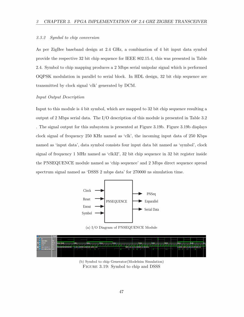
3 CHAPTER 3. FPGA IMPLEMENTATION OF 2.4 GHZ ZIGBEE TRANSCEIVER
3.3.2 Symbol to chip conversion
As per ZigBee baseband design at 2.4 GHz, a combination of 4 bit input data symbol
provide the respective 32 bit chip sequence for IEEE 802.15.4, this was presented in Table
2.4. Symbol to chip mapping produces a 2 Mbps serial unipolar signal which is performed
OQPSK modulation in parallel to serial block. In HDL design, 32 bit chip sequence are
transmitted by clock signal ‘clk’ generated by DCM.
Input Output Description
Input to this module is 4 bit symbol, which are mapped to 32 bit chip sequence resulting a
output of 2 Mbps serial data. The I/O description of this module is presented in Table 3.2
. The signal output for this subsystem is presented at Figure 3.19b. Figure 3.19b displays
clock signal of frequency 250 KHz named as ‘clk’, the incoming input data of 250 Kbps
named as ‘input data’, data symbol consists four input data bit named as ‘symbol’, clock
signal of frequency 1 MHz named as ‘clk32’, 32 bit chip sequence in 32 bit register inside
the PNSEQUENCE module named as ‘chip sequence’ and 2 Mbps direct sequence spread
spectrum signal named as ‘DSSS 2 mbps data’ for 270000 ns simulation time.
PNSEQUENCE
Clock
Reset
Enout
PNSeq
Symbol Serial Data
Enparallel
(a) I/O Diagram of PNSEQUENCE Module
(b) Symbol to chip Generator(Modelsim Simulation)Figure 3.19: Symbol to chip and DSSS
47

3 CHAPTER 3. FPGA IMPLEMENTATION OF 2.4 GHZ ZIGBEE TRANSCEIVER
Table 3.2: I/O Description pnsequence moduleSL No PIN Name Direction Size Description1 Clock(clk32) Input 1 Synchronous Clock of 1 MHz2 Reset Input 1 Asynchronous Reset3 Enout Input 1 Valid Signal for input Data4 Symbol Input 4 4 bit input termed as symbol
which is of data rate 62.5 kilosymbol per second
5 PNSeq Output 1 2 Mbps output after symbol tochip mapping
6 Enparallel Output 1 Valid signal for output data7 Serial Data Output 1 2 Mbps DSSS output after
spread spectrum
3.3.3 Serial to Parallel Conversion
After Symbol to chip mapping serial data constitute a 2 Mbps digital signal which is the
combination of all chip sequences as per the symbol at input. ZigBee standard at 2.4 GHz
uses OQPSK modulation. For this reason the DSSS serial data is converted to a 2 channel
parallel data for I and Q processing channels. Serial to parallel conversion is implemented
with a set of flip flops and flag registers in verilog HDL design.
In verilog HDL design the serial to parallel conversion is performed with the help of
Digital Clock Manager(DCM) clock signal clk32 of 1 MHz. During the active edge of clock
period along with the the flag value 2 Mbps serial data converted to two 1 Mbps parallel
data. during conversion the odd bits of serial data assigned to oddbit stream and even
bits are assigned to even bit stream. since the first bit of the serial data is an odd bit it
is assigned first and even bit assigned next. the process continues as long as input serial
data is available.
Input Output Description
After chip mapping the output is 2 Mbps serial data in pnsequence module, which is
separated in to I-phase signal and Q-phase signal in this module. I-phase signal contains
the odd bits and Q-phase signal contains even bits of serial 2 Mbps signal. I/O description
of this module is presented in Table 3.3. The modelsim result from simulation is presented
48

3 CHAPTER 3. FPGA IMPLEMENTATION OF 2.4 GHZ ZIGBEE TRANSCEIVER
Table 3.3: I/O Description of Serial to ParallelSL No PIN Name Direction Size Description1 Clock(clk32) input 1 Synchronous Clock of 1 MHz2 Reset input 1 Asynchronous Reset3 Enparallel input 1 Valid Signal for input Data4 Serial Data input 1 After DSSS the 2Mbps data
stream5 PNSeq input 1 chip sequence without spread
spectrum6 Enshaping output 1 Valid Signal for pulse shaping7 Oddbit output 1 Every oddbit of serial data
stream assigned to this pin8 Evenbit output 1 Every Evenbit of serial data
stream assigned to this pin
at Figure 3.20b for 270000 ns simulation time. This figure includes the clock signal ‘clk32’
of frequency 1 MHz, 32 bit register named as ‘flag’ consists of 32 bit chip sequence, spread
spectrum signal of 2 Mbps data rate named as ‘DSSS 2 Mbps data’, I-phase signal and
Q-phase signal named as ‘Inphase signal’ and ‘Qphase signal’ respectively. Each of these
signals becomes 1 Mbps data rate after serial to parallel conversion.
SERIAL TO
PARALLEL
Clock
Reset
Serial Data
Oddbit
Evenbit
Enparallel
Enshaping
PNSeq
(a) I/O Diagram of Serial to parallel Converter
(b) Serial to parallel(Modelsim Simulation)Figure 3.20: I-phase Q-phase separation
49

3 CHAPTER 3. FPGA IMPLEMENTATION OF 2.4 GHZ ZIGBEE TRANSCEIVER
Table 3.4: Samples for Pulse shapingSampling time (ns) Sample value for bit 1 Sample value for bit 0
in twos complement100 00000000 00000000200 00010000 11110000300 00100000 11100000400 00110000 11010000500 00111000 11001000600 01000000 11000000700 00111000 11001000800 00110000 11010000900 00100000 111000001000 00010000 11110000
3.3.4 ZigBee transmitter Pulse Shaping
In our design unipolar signal has been used. Here during symbol to chip conversion the
verilog logic replaces ‘-1’ with ‘0’ and ‘1’ is left as it is. During Pulse shaping the bits one
and zero in even stream and odd stream are shaped by half sine wave, hence the name is
half sine pulse shaping. Here pulse shaping has been implemented by taking continuous
values from lookup table in memory. Here stored sample values are multiplied with respect
to bit one and zero of even bitstream and odd bitstream to generate continuous value
signals.
The samples are multiplied with the help of flag value and DCM. The even bitstream
and odd bit stream are of time period 1000 ns. So for every 100 ns one sample is multiplied
as per the flag value to get the pulse shape as shown in simulation result presented in
Figure 3.21b and 3.22b. The lookup table uses 10 continuous values for pulse shaping.
More samples can be multiplied to get the sharpness in the pulse shaping.
Input Output Description
The I-phase signal and Q-phase signals are pulse shaped by continuous values. In this
design the sampling values are fixed integers as mentioned in earlier section. The I/O
diagram and description of this module are as follows and the modelsim result is presented
50

3 CHAPTER 3. FPGA IMPLEMENTATION OF 2.4 GHZ ZIGBEE TRANSCEIVER
Table 3.5: I/O Description even pulse shapeSL No PIN Name Direction Size Description1 Clock(clk50) Input 1 Synchronous Clock 10 MHz2 Reset Input 1 Asynchronous Reset3 Enshaping Input 1 Valid Signal for pulse shape4 Evenbit Input 1 Evenbit PIN output from se-
rial to parallel module is as-signed to this pin
5 Even pulseshape Output 8 8 bit sample value assigned tothis output pin
in 3.21b. This result interprets clock signal of frequency 10 MHz named as ‘clk_sampling’,
Q-phase signal termed as ‘Qphase signal’. This signal produces Q-phase pulse shaping
signal termed as ‘Qphase pulse shaping’ after multiplication of sampling values with Q-
phase signal. This result shown for simulation time of 270000 ns from top to bottom
respectively. Similarly for I-phase signal, pulse shaping description is mentioned in 3.5
with the modelsim results as presented in Figure 3.22b. Figure 3.22b interprets clock
signal of frequency 10 MHz named as ‘clk_sampling’, I-phase signal named as ‘Inphase
signal’ and I-phase pulse shaping signal named as ‘Inphase pulse shaping’ for simulation
time of 270000 ns.
EVEN PULSE SHAPE
Clock
Reset
Evenbit
Even pulseshape
Enshaping
(a) I/O Diagram of Even pulse shaping
(b) Q-phase pulse shaping(Modelsim Simulation)Figure 3.21: Q-phase pulse shaping
51

3 CHAPTER 3. FPGA IMPLEMENTATION OF 2.4 GHZ ZIGBEE TRANSCEIVER
ODD PULSE SHAPE
Clock
Reset
Oddbit Odd pulseshape
Enaddition
Enshaping
(a) I/O Diagram of Odd pulse shaping
(b) I-phase pulse shaping(Modelsim Simulation)Figure 3.22: I-phase pulse shaping
Table 3.6: I/O Description Odd pulse shapeSL No PIN Name Direction Size Description
1 Clock(clk50) Input 1 Synchronous Clock2 Reset Input 1 Asynchronous Reset3 Enshaping Input 1 Valid Signal for pulse shape4 Oddbit Input 1 Oddbit PIN output from se-
rial to parallel module is as-signed to this pin
5 Odd pulseshape Output 8 8 bit sample value assigned tothis output pin
6 Enaddition Output 1 Valid Signal for IQadditionassigned to this output pin
3.4 Baseband Receiver Design for FPGA
This section concentrates on baseband design for synchronous detection of ZigBee trans-
mitter. Input to receiver is the pulse shape signal from the transmitter. The pulse shaping
function performed at the transmitter reduces Inter Symbol Interference (ISI). So it has
been assumed that the pulse shaping signal is the baseband signal after demodulation at
the receiver. The baseband receiver design covers Sample extraction of even bit and odd
bit streams, parallel to serial conversion, chip to symbol conversion. The baseband receiver
is designed in verilog HDL as per the block diagram presented at Figure 3.23.
52

3 CHAPTER 3. FPGA IMPLEMENTATION OF 2.4 GHZ ZIGBEE TRANSCEIVER
Even
stre
am
_out
O
ddst
ream
_o
ut IQ-a
dditi
on
Dec
oder
Baseband Receiver
Received Input
Inphase signal
Q -phase signal
Figure 3.23: ZigBee Baseband Receiver
3.4.1 Pulse shape detection
Here, synchronized communication system is assumed. from the received signal the I and
Q channels are separated and the evenbit stream and oddbit stream are identified. The
pulse output of the transmitter is provided to the input of the baseband receiver for further
processing.
3.4.2 Parallel data(even and odd stream)
In verilog HDL design the DCM clock signal clk50 of frequency 10 MHz is used to detect
the samples in odd pulse shape and in even pulse shape. So according to the samples in the
pulse shape waves the even bit and odd bit streams are detected at receiver. The half bit
delay in even bit stream is provided with clock signal clk50, which is same as transmitter
clock signal clk50 created by DCM.
Input Output Description
Input output description of I-phase signal and Q-phase signals at receiver are presented in
Table 3.7 and 3.8. The I/O diagram and signals are presented at Figure 3.24a to Figure
3.25b. The simulation result shown in Figure 3.24b represents clock signal of frequency
10 MHz named as ‘clk50’ and the signals ‘sampling value’ and ‘register’, which consists of
53
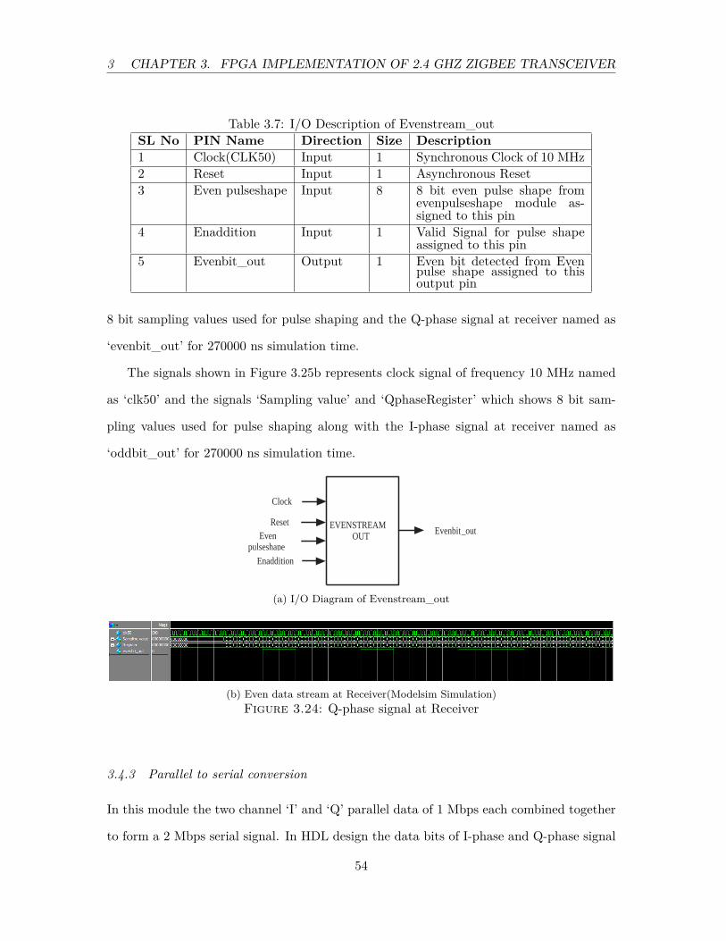
3 CHAPTER 3. FPGA IMPLEMENTATION OF 2.4 GHZ ZIGBEE TRANSCEIVER
Table 3.7: I/O Description of Evenstream_outSL No PIN Name Direction Size Description1 Clock(CLK50) Input 1 Synchronous Clock of 10 MHz2 Reset Input 1 Asynchronous Reset3 Even pulseshape Input 8 8 bit even pulse shape from
evenpulseshape module as-signed to this pin
4 Enaddition Input 1 Valid Signal for pulse shapeassigned to this pin
5 Evenbit_out Output 1 Even bit detected from Evenpulse shape assigned to thisoutput pin
8 bit sampling values used for pulse shaping and the Q-phase signal at receiver named as
‘evenbit_out’ for 270000 ns simulation time.
The signals shown in Figure 3.25b represents clock signal of frequency 10 MHz named
as ‘clk50’ and the signals ‘Sampling value’ and ‘QphaseRegister’ which shows 8 bit sam-
pling values used for pulse shaping along with the I-phase signal at receiver named as
‘oddbit_out’ for 270000 ns simulation time.
EVENSTREAM OUT
Clock
Reset Even
pulseshape
Evenbit _out
Enaddition
(a) I/O Diagram of Evenstream_out
(b) Even data stream at Receiver(Modelsim Simulation)Figure 3.24: Q-phase signal at Receiver
3.4.3 Parallel to serial conversion
In this module the two channel ‘I’ and ‘Q’ parallel data of 1 Mbps each combined together
to form a 2 Mbps serial signal. In HDL design the data bits of I-phase and Q-phase signal
54

3 CHAPTER 3. FPGA IMPLEMENTATION OF 2.4 GHZ ZIGBEE TRANSCEIVER
ODDSTREAM OUT
Clock
Reset Odd
pulseshape
Oddbit _out
Enaddition
(a) I/O Diagram of Oddstream_out
(b) Odd data stream at Receiver(Modelsim Simulation)Figure 3.25: I-phase signal at Receiver
Table 3.8: I/O Description of Oddstream_outSL No PIN Name Direction Size Description1 Clock(CLK50) Input 1 Synchronous Clock of 10 MHz2 Reset Input 1 Asynchronous Reset3 Odd pulseshape Input 8 8 bit odd pulse shape from
oddpulseshape module as-signed to this pin
4 Enaddition Input 1 Valid Signal for pulse shapeassigned to this pin
5 Oddbit_out Output 1 Even bit detected from Evenpulse shape assigned to thisoutput pin
at receiver are assigned to a 4 bit register alternately. The Figure 3.26 represents the
formation of serial data from I-phase and Q-phase signal. The clock signal clk32 is used for
parallel to serial conversion, which is used for serial to parallel conversion at transmitter.
As per the active edge of clk32 and flag value we are assigning the I-phase and Q-phase
data bit to form the 2 Mbps serial data.
Input Output Description
The input and output description of this module with modelsim simulation of serial data
is presented in Table 3.9 and Figure 3.27b respectively. The Figure 3.27b presents the
clock signal ‘clk32’ of frequency 1 MHz, I-phase and Q-phase signal respectively termed as
‘oddbit_out’ and ‘evenbit_out’ and the received DSSS serial signal at receiver named as
55

3 CHAPTER 3. FPGA IMPLEMENTATION OF 2.4 GHZ ZIGBEE TRANSCEIVER
I 4 I 3 I 2 I 1
Q 4 Q 3 Q 2 Q 1
I 1 Q 1 I 2 Q 2
In phase signal
Q -phase signal
IQ combination
Figure 3.26: Parallel to serial conversion at Receiver
‘Received 2 Mbps serial data’ for simulation time of 270000 ns.
IQaddition
Clock
Reset
Oddbit_out
Serialdata_out
ENIQaddition
Evenbit_out
Flag_Enable
(a) I/O Diagram of IQaddition
(b) IQ Combination at Receiver(Modelsim Simulation)Figure 3.27: I-phase and Q-phase Combination at Receiver
3.4.4 Chip to symbol mapping at receiver
In this module the received 2 Mbps serial data is stored in a 32 bit register with the
help of clock signal clk32 generated by DCM, which is used as symbol to chip mapping
in transmitter. Here the lookup table used in transmitter for symbol to chip mapping is
used in reverse order ie chip to symbol mapping for decoding the received symbol. The
received chip sequence is compared with the 16 different chip sequence transmitted by the
transmitter. Figure 3.28 demonstrates this process matching. Here, the XNOR operation
is carried out on received chip sequence with each of 16 different chip sequences used at
transmitter. In XNOR operation, the counter with maximum value provides the symbol
56

3 CHAPTER 3. FPGA IMPLEMENTATION OF 2.4 GHZ ZIGBEE TRANSCEIVER
Table 3.9: I/O Description of IQadditionSL No PIN Name Direction Size Description1 Clock(clk32) Input 1 Synchronous Clock of 1 MHz2 Reset Input 1 Asynchronous Reset3 Evenbit_out Input 1 one bit data from Evenstream
out module assigned to thispin
4 Oddbit_out Input 1 one bit data from Oddstreamout module assigned to thispin
5 ENIQaddition Input 1 Valid input signal for IQad-dition assigned to this outputpin
6 Flag_Enable Output 1 Valid input signal forChipmapping assigned tothis output pin
7 Serialdata_out Output 1 Combined 2 Mbps serial dataafter IQ addition, assigned tothis output pin
transmitted by the help of lookup table of chip to symbol mapping. This 4 bit symbol is
stored in a 4 bit register named as ‘dataout’, then MSB of ‘dataout’ is sent to the output
as received data bit. The Figure 3.30 shows modelsim simulation result of recovered data
bit. This figure displays clock signal of frequency 250 KHz named as ‘clk’, the received
symbol at receiver after chip to symbol mapping is described by a signal of 4 bit register
named as ‘Symbol_received’ and the received signal at receiver is termed as ‘Input databit
received’ which is shown in simulation result over 270000 ns simulation time.
Input Output Description
The 2 Mbps serial data after addition in IQaddition module, is stored in 32 bit flag and the
decoding performs in this module. The I/O description of chip to symbol decoding module
is presented in Table 3.10. The modelsim simulation result in Figure 3.29b displays chip
mapping at receiver. The figure has 16 different chip mapping sequences of 32 bit each,
which indicates the correlation of chip sequences at receiver. Out of all chip sequence, the
chip sequence has highest matching with received chip sequence is considered as transmitted
chip sequence.
The signals in Figure 3.29b represents the clock signal ‘clk32’ of 1 MHz and 32 bit
57

3 CHAPTER 3. FPGA IMPLEMENTATION OF 2.4 GHZ ZIGBEE TRANSCEIVER
Out stream after I & Q Combination
C 0 C 1 C 2 C 3 • • • • • C 15 C 16
Chip Sequence 2
Chip Sequence 16
Chip Sequence 1
Chip Sequence 3
• • •
• • •
•
• • •
• • •
•
Counter1
Counter3
Counter2
Counter16
Figure 3.28: Decoding at Receiver
register named as ‘flag_2Mbps’ are shown for 270000 ns simulation time. The signals
termed as ‘chipmapping1’, ‘chipmaping2’, ‘chipmaping3’, ‘chipmaping4’, ‘chipmaping5’,
‘chipmaping6’, ‘chipmaping7’, ‘chipmaping8’, ‘chipmaping9’, ‘chipmaping10’, ‘chipmap-
ing11’, ‘chipmaping12’, ‘chipmaping13’, ‘chipmaping14’, ‘chipmaping15’, ‘chipmapping16’
represents chip mapping output of ‘flag_2Mbps’ signal with all possible chip sequences of
corresponding transmitted symbol and received serial signal of 2 Mbps data rate named as
‘Received 2 Mbps serial data’ are shown for 270000 ns simulation time.
3.5 FPGA Implementation
After the system level simulation in Simulink, then the module was programmed using
hardware description language verilog HDL for simulation. The baseband transceiver mod-
ule simulated, synthesized and finally implemented on Virtex 5 FPGA. In the process of
implementation on FPGA, clock signal generation is very vital [39]. In order to get the
required clock signal the digital clock manager available in FPGA was used.
58

3 CHAPTER 3. FPGA IMPLEMENTATION OF 2.4 GHZ ZIGBEE TRANSCEIVER
Decoding
Clock
Reset Databit _Received
Flag_Enable
Symbol_out
Serialdata _out
(a) I/O Diagram of Decoding module at Receiver
(b) Chip mapping at Receiver(Modelsim Simulation)Figure 3.29: Chip mapping at Receiver
Table 3.10: I/O Description of DecodingSL No PIN Name Direction Size Description1 Clock(clk) Input 1 Synchronous Clock of 250
KHz2 Reset Input 1 Asynchronous Reset3 Flag_Enable Input 1 Valid input signal for decod-
ing assigned to this pin4 Serialdata_out Input 1 Combined 2 Mbps serial data
from IQaddition module, as-signed to this pin
5 Symbol_out Output 4 4 bit Symbol extracted fromdecoding module assigned tothis output pin
6 Databit_Received Output 1 MSB of the Symbol is as-signed to this output pinwhich is data bit transmitted
59

3 CHAPTER 3. FPGA IMPLEMENTATION OF 2.4 GHZ ZIGBEE TRANSCEIVER
Figure 3.30: Received data bit
Figure 3.31: XILINX VIRTEX 5 FPGA Board with XC5VLX110T
Following verilog simulation of the transceiver, this section presents VIRTEX 5 FPGA
board specification, clock circuit generation, synthesis report of implemented design and
representation of board internal signals for receiver.
3.5.1 VIRTEX 5 FPGA
The general purpose development board from Xilinx which embeds Virtex 5 FPGA is
ML505. This is useful for prototyping on the new architectural features of Virtex-5 FPGA.
ML505 contains Virtex-5 XC5VLX110T device [40]. This device contains block RAM, DSP
blocks, source synchronous interface block, enhanced clock manager etc. Among all devices
of of VIRTEX 5 FPGA family the XC5VLX110T FPGA has higher logic capacity than
others. The Table 3.11 shows available resources for LX110T. 100 MHz clock frequency
chosen from AH15 pin of FPGA board for generation of clock circuitry [41]. Clock pin
description of VIRTEX 5 board is presented in Table 3.12 [41].
60

3 CHAPTER 3. FPGA IMPLEMENTATION OF 2.4 GHZ ZIGBEE TRANSCEIVER
Table 3.11: Hardware Resources of VIRTEX 5 LX110TSlices Flipflops LUTs Multipliers Block RAM(Kb) CMTs17280 69120 69120 64 4608 6
Table 3.12: Clock frequency for VIRTEX 5 LX110TClock Name FPGA PIN Frequency in MHzUSER_CLK AH15 100CLK_33MHz_FPGA AH17 100CLK_27_FPGA AH18 27CLK_FPGA_P L19 200CLK_FPGA_N K19 200
3.5.2 Digital Clock Manager(DCM)
A properly synthesized clock circuit is essential to achieve implementation task so that the
clock signals should be able to reach all the points of the design at the same time. In order
to achieve this, a perfectly synchronized clock circuitry was designed by the help of Digital
Clock Manager(DCM).
The global clock MUX buffer and clock manager tiles(CMT) provides the solution for
designing desired clock network. There are 6 CMTs available on the board, each contains
two DCMs and one phase locked loop(PLL) [42].The DCM can generate 90◦, 180◦ and
270◦ phase-shifted version of external clock. Three different clock frequency signals are
generated by using VIRTEX 5 board clock frequency of 100 MHz. The generation of
internal clocks of 10 MHz, 1 MHz, 250 KHz is done by using Figure 3.32, where the clock
divider factors 10 and 4 are used. This digital clock manager develops clock signal as
presented in Figure3.33.
3.5.3 Implementation on VIRTEX 5 FPGA
Xilinx Synthesis Tool (XST) performs the synthesis and optimization in FPGA. During
this process following steps are carried out for design, synthesis and optimization:
• Mapping and optimization on an entity by entity or module by module basis
• Global optimization on the complete design
61
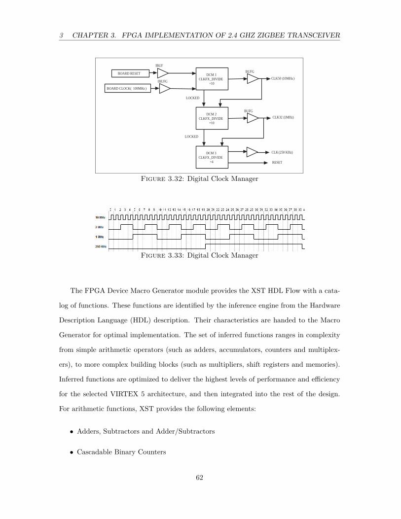
3 CHAPTER 3. FPGA IMPLEMENTATION OF 2.4 GHZ ZIGBEE TRANSCEIVER
BOARD CLOCK( 100MHz )
BOARD RESET
IBUF
IBUFG
BUFG
CLK50 ( 10MHz ) DCM 1
CLKFX _DIVIDE =10
DCM 2 CLKFX _DIVIDE
=10
LOCKED
CLK32 ( 1MHz )
LOCKED
DCM 3 CLKFX _DIVIDE
=4
BUFG
CLK (250 KHz)
RESET
Figure 3.32: Digital Clock Manager
Figure 3.33: Digital Clock Manager
The FPGA Device Macro Generator module provides the XST HDL Flow with a cata-
log of functions. These functions are identified by the inference engine from the Hardware
Description Language (HDL) description. Their characteristics are handed to the Macro
Generator for optimal implementation. The set of inferred functions ranges in complexity
from simple arithmetic operators (such as adders, accumulators, counters and multiplex-
ers), to more complex building blocks (such as multipliers, shift registers and memories).
Inferred functions are optimized to deliver the highest levels of performance and efficiency
for the selected VIRTEX 5 architecture, and then integrated into the rest of the design.
For arithmetic functions, XST provides the following elements:
• Adders, Subtractors and Adder/Subtractors
• Cascadable Binary Counters
62

3 CHAPTER 3. FPGA IMPLEMENTATION OF 2.4 GHZ ZIGBEE TRANSCEIVER
• Accumulators
• Incrementers, Decrementers and Incrementer/Decrementers
• Signed and Unsigned Multipliers
Table 3.13 shows the options to fine-tune FPGA synthesis to meet design constraints.
Table 3.14 shows The Device Utilization Summary. Which is the output of HDL syn-
thesis step to estimate the number of slices and gives the number of flip-flops, IOBs.
Table 3.15 shows the advanced synthesis report, which includes XST additional macro
processing by improving the macros recognized at the HDL synthesis step, or by creating
the new, more complex ones, such as dynamic shift registers. The implemented design
in VIRTEX 5 LX110T FPGA board has maximum clock frequency of 11.792 MHz and
maximum output required time is 3.264 ns. The total logic power consumed by the design
is 0.45 mW.
3.5.4 Synthesis Report
The internal signals along with received baseband data was analyzed through ChipScope
Pro analysis. The received I-phase, Q-phase and baseband data bit received signal are
analyzed as depicted in Figure 3.34. The top level RTL schematic of this transceiver
obtained from the ISE design environment is presented in Figure 3.35.
63

3 CHAPTER 3. FPGA IMPLEMENTATION OF 2.4 GHZ ZIGBEE TRANSCEIVER
Table 3.13: Synthesis options summary
Synthesis options summaryInput File Name "datain_tb.prj"Input format mixedIgnore Synthesis Constraint File NoOutput File name "datain_tb"Automatic FSM Extraction YESFSM Encoding Algorithm NoFSM Style LUTRAM Extraction YesRAM Style AutoRom Extraction YesMux style AutoDecoder Extraction YESPriority Encoder Extraction YesShift Register Extraction YesLogical Shifter Extraction YesMux Extraction YesResource Sharing YESUse DSP Block Auto
Table 3.14: Device Utilization Summary
Slice Logic DistributionNumber of Slice Registers 973 out of 69120 1%Number of Slice LUTs 1179 out of 69120 1%Number used as logic 1178 out of 69120 1%Number used as Memory 1 out of 17920 0%
I/O UtilizationNumber of bonded IOBs 8 out of 640 1%Number of BUFG/BUFGCTRLs 10 out of 32 31%Number of DCM_ADVs 3 out of 12 33%
64

3 CHAPTER 3. FPGA IMPLEMENTATION OF 2.4 GHZ ZIGBEE TRANSCEIVER
Table 3.15: Advance HDL Synthesis Report
Advance HDL Synthesis ReportROMs 1128x1-bit ROM 1Adders/Substracters 326-bit adder 32Counters 62-bit up counter 14-bit up counter 25-bit up counter 27-bit up counter 1Registers 711Flip-Flops 711Latches 545Comparators 48Multiplexers 1
Figure 3.34: ChipScope Pro Internal signals
65

3 CHAPTER 3. FPGA IMPLEMENTATION OF 2.4 GHZ ZIGBEE TRANSCEIVER
Figure 3.35: Top level RTL Schematic of ZigBee Baseband Transceiver
66

3 CHAPTER 3. FPGA IMPLEMENTATION OF 2.4 GHZ ZIGBEE TRANSCEIVER
3.6 Summary and Discussion
ZigBee baseband transceiver for IEEE 802.15.4 was implemented through various stages
which include.
• Initially the transceiver system simulated through MATLAB/Simulink, where Mini-
mum shift keying(MSK) modulation technique is used. The internal signal of different
stages of simulink model are analyzed.
• The baseband module is described in hardware description language verilog HDL
and simulated in mentor graphics modelsim simulator and finally realized in Virtex
5 FPGA using ISE design environment. The system provided desirable performance.
The simulation result presented above are labeled as X-axis in time(ns) and Y-axis
presents the respective signals.
• Following this, in FPGA implementation, the clock signals of 250 KHz, 1 MHz, and
10 MHz were derived by taking 100 MHz clock signal available on Virtex 5 FPGA
board. Further the design synthesis report along with board internal signals were
also analyzed for verification.
• In XILINX power analysis, the total power consumption for the ZigBee baseband
transceiver is reported to be 0.45 mW. The detail power analysis of logic power and
signal power at each stage of the design reported by the ISE synthesizer is as follows.
67

3 CHAPTER 3. FPGA IMPLEMENTATION OF 2.4 GHZ ZIGBEE TRANSCEIVER
Table 3.16: Hierarchical power analysisName Power(w) Logic Power(w) Signal Power(w)Hierarchical Total Power 0.21672 0.21350 0.000322Datain_tb 0.21401/0.21672 0.21317/0.21350 0.00084/0.00322Decoder Module 0.00163 0.00007 0.00156Evenstream_out 0.00009 0.00004 0.00006Parallel1 0.00009 0.00002 0.00007IQADDITION2 0.00011 0.00002 0.00009SHAPINGEV EN 0.00012 0.00004 0.00008ODDSTREAM_OUT 0.00012 0.00003 0.00009PULSHAPING 0.00015 0.00005 0.00010DATAIN 0.00037/0.00039 0.00004/0.00006 0.00033
68

4
ZigBee Transceiver Design with RNS Based PN sequence
In this chapter the design of a new form of ZigBee transceiver is presented. This transceiver
uses residual number system based PN sequence instead of the chip sequence used in 2.4
GHz ZigBee for IEEE 802.15.4. This chapter introduces Residue Number System(RNS) in
brief as presented in following section.
4.1 Residue Number System
Residue Number System (RNS) has become very popular in recent time due to their su-
perior performance in terms of large dynamic range, good cross correlation and auto cor-
relation properties. The chapter discusses advantages of RNS which in turn motivated us
to take up the work.
In Residue number system, a number X is represented by a set of residues like x1, x2, ..xn,
modulo given by co-prime moduli. The moduli set is known as the system base and residues
are known as residue digits. The dynamic range of the system ie the number of possible
number representation is defined by the product of all RNS moduli. In this numbers sys-
tem, addition, multiplication, substraction can be used without carry propagation between
residue digits, which enables arithmetic circuits to perform faster than the circuits for bi-
nary representation. This property permits to build arithmetic units of large numbers as
69

4CHAPTER 4. ZIGBEE TRANSCEIVER DESIGN WITH RNS BASED PN
SEQUENCE
a set of fast and small circuits [43].
The important merit of RNS over conventional number number system is the absence
of carry propagation in addition and multiplication. In other number systems after an
operation if carry is generated than it is forwarded to the next bit of the operand. In RNS,
low precision is required for ranging to individual prime and co-prime number of moduli-
set, subsequently it enables lookup table implementation for different operations. Due to
lookup table the operation speed of RNS is faster with lower computational complexity
and hence low power consumption. These two features are expected to be advantageous
for VLSI implementation.
4.1.1 Chinese Remainder Theorem
Chinese Remainder Theorem(CRT) is a mathematical formulation used to find independent
unique numbers in a given dynamic range. In RNS CRT has an important role to play, so
as to find RNS representation of a number. CRT implies that if moduli of RNS is chosen
accurately then each number can be uniquely represented in the given dynamic range. In
other words CRT states that if all the divisors are co-prime to each other then the residue
representation of each number is different to each other or unique in the dynamic range′R′. Here ′R′ is the multiplication of all the divisors or modulis of the moduli-set. Since
the set of divisors or modulis are not fixed, if the set of divisors increases then the bit
representation in RNS will be increased proportionately.
Assume a1 and a2 are two integers which are relatively prime to each other and b1 and
b2 are any two integers, then there is an integer N can be determined by 4.1 and 4.2.
N ≡ b1(mod a1) (4.1)
N ≡ b2(mod a2) (4.2)
N is an uniquely determined modulo (a1.a2). Equivalently if gcd (a1, a2) = 1, then
the pair of residue classes modulo a1 and a2 corresponds to a simple residue class modulo
70

4CHAPTER 4. ZIGBEE TRANSCEIVER DESIGN WITH RNS BASED PN
SEQUENCE
(a1, a2) which gives a simultaneous congruences b ≡ bi(mod ai), for i = 1, 2, 3....b for which
ai are relatively prime. Then, the solution to set of congruences is given by (4.3).
z = x1 ∗ y1A
a1, x2 ∗ y2
A
a2, .... xp ∗ yb
A
an(4.3)
where A = a1, a2....an and yi is determined from y1Aa1
= 1( mod a1)
4.1.2 Arithmetic in RNS
Residue number system completely depend on the congruence relation of the number.
Two numbers are said to be congruent modulo ‘m’ if the number ‘m’ divides exactly the
difference of a and b ie (a − b), then mathematically congruent modulo of a and b is
represented as a ≡ b(mod m). for example 15 ≡ 12(mod 3), 10 ≡ 6(mod 2), 11 ≡ 2(mod 3)
etc.
The RNS gives separate unique representation for all numbers in the range between 0
and M − 1. If the given integer number is greater than M − 1, then RNS representation of
the integer is the integer itself. Therefore, more than one integer may have the same residue
representation. Before this, it should be confirmed that the moduli have to be relatively
prime to be able to exploit the dynamic range. The example of residue representation
shown in Table 4.1 provides the principle as per Chinese Remainder Theorem (CRT)[44].
Choice of Moduli
By the mathematical perspective the best moduli are the prime numbers. If ‘m’ is prime,
then there must be one generator, p ≤ m − 1. then the set of all non-zero residue with
respect to ‘m’ is given by relation (4.4). There are two approach of moduli selection,
one is consecutive method and the other is arbitrary method [16, 43]. The proposed PN
sequence is generated on the basis of consecutive method of moduli-set selection [15], here
the moduli-set [255 254 253 251] is selected for generation of RNS based PN sequence for
transceiver design.
71

4CHAPTER 4. ZIGBEE TRANSCEIVER DESIGN WITH RNS BASED PN
SEQUENCE
Table 4.1: Residue Representation in RNSN Relative Prime Moduli Relative Non-Prime Moduli
m1 = 2 m2 = 5 m3 = 7 m1 = 2 m2 = 4 m3 = 60 0 0 0 0 0 01 1 1 1 1 1 12 0 2 2 0 2 23 1 3 3 1 3 34 0 4 4 0 0 45 1 0 5 1 1 56 0 1 6 0 2 07 1 2 0 1 3 18 0 3 1 0 0 29 1 4 2 1 1 310 0 0 3 0 2 411 1 1 4 1 3 512 0 2 5 0 0 013 1 3 6 1 1 114 0 4 0 0 2 215 1 0 1 1 3 316 0 1 2 0 0 417 1 2 3 1 1 518 0 3 4 0 2 019 1 4 5 1 3 120 0 0 6 0 0 221 1 1 0 1 1 322 0 2 1 0 2 423 1 3 2 1 3 524 0 4 3 0 0 025 1 0 4 1 1 126 0 1 5 0 2 227 1 2 6 1 3 328 0 3 0 0 0 4
72

4CHAPTER 4. ZIGBEE TRANSCEIVER DESIGN WITH RNS BASED PN
SEQUENCE
Forward Conversion
Reverse Conversion
Modulo m 1
Modulo m 2
Modulo m n
Input Data Analog/Binary
Output Data Analog Binary •
• • •
Figure 4.1: Basic Structure of RNS Processor
Residue = |pi|m : i = 0, 1, 2, ...., m − 2 (4.4)
if m = 7 and p = 5 then residues are calculated as |50|7 = 1, |51|7 = 5, |52|7 = 4, |53|7 = 6
4.1.3 Structure of RNS Conversion
The basic structure of a typical RNS processor is shown in Figure 4.1. The RNS data
processed in parallel according to the concept of residue number system independently
without carry propagation. In RNS processor encoding of input data to RNS is called
forward conversion and decoding of RNS to conventional number representation is known
as reverse conversion.
For full RNS based system the analog input number first converted to binary form then
the residue of the number calculated during forward conversion and residue number to
binary representation during reverse conversion. During processing, conversion to binary
is an intermediate stage which is required in both forward and reverse conversion. This
makes the conversion inefficient due to increased latency and complexity.
73

4CHAPTER 4. ZIGBEE TRANSCEIVER DESIGN WITH RNS BASED PN
SEQUENCE
Arbitrary Moduli-set forward conversion
The special moduli-set such as 2n − 1, 2n, 2n + 1 is help full for making forward conversion
process fast and simple. The special moduli-set forward converters are more efficient con-
verters. Other than this large dynamic range requirement in some applications can not be
provide with efficient special moduli-set, which in turn demands an arbitrary moduli-set
forward conversion.
Arbitrary moduli-set forward conversion can be implemented by using lookup tables or
combinational logic. Implantation of converter with combinational logic makes the process-
ing unit complex, so the lookup table implementation is preferred over combinational logic.
Implementation of large dynamic range increases the ROM size and simultaneously the con-
version process becomes inefficient. Therefore a tradeoff between the two implementations
can be utilized using a combination of lookup table and combinational logic[45, 16].
For ZigBee application standard 16 different PN codes of length 32 bit are required.
The process of generation of the code is discussed in succeeding section. Table4.2.
4.2 RNS Based PN Sequence for ZigBee Spreading and Despreading
In this section the residue number system(RNS)[16] based PN sequence generation is ana-
lyzed. A set of new PN sequence based on RNS is proposed for ZigBee baseband transceiver,
which is used in ZigBee baseband transceiver design for spreading and despreading. The
algorithm to generate PN sequence is as follows and the generated PN sequence is presented
in Table 4.2.
Algorithm 1 RNS Based PN sequence Generation1: Take a dynamic Range for primal generation2: Selection of moduli set3: For each primal generated above calculate the residue for each of the moduli4: Convert the set of residues obtained from step 3 to their equivalent 8 bit binary repre-
sentation5: Concanate all the binary representation of residues called as PN sequence6: After obtaining set of PN sequences check for the cross correlation for a specified
threshold7: The sequences satisfying above condition will be selected as RNS Based PN sequence.
74

4CHAPTER 4. ZIGBEE TRANSCEIVER DESIGN WITH RNS BASED PN
SEQUENCE
4.2.1 RNS Generated PN sequence
Residue Arithmetic based PN sequence generation for multiple scenario are mentioned
here. The inputs to the block of RNS generation consists of spread factor β and the cross
correlation threshold, T. A moduli set is selected according to the requirement of no of bits
in PN sequence. The moduli set is selected either by consecutive method or by exponential
method [15]. Here the consecutive method was adopted.
As mention above the Primal is randomly selected from the range R given by R =∏ni=1 pi, where p is the moduli set and is represented as p = {p1, p2, p3, . . . , pn}. Let A be
a set of primals chosen from range R and is expressed as A = x1, x2, x3, . . . , xn. Defining
J to be set of residues given by J(i,j) = |xj , pj | for i = 1, 2, . . . , n and j = 1, 2, . . . , k. J can
be represented as.
J =
mod(x1, p1) mod(x1, p2) . . . mod(x1, pn). . . . . .
mod(xn, p1) mod(xn, p1) . . . mod(xn, p1)
(4.5)
Each row of J is then represented by 8 bit binary representation. The entire row is
termed as desired length of the PN sequence. Hence the generated sequences are tested for
their cross correlation as following.
• Correlation between ci and cj for i = j will be one.
• Correlation between ci and cj for i ̸= j must be less than a threshold value T .
The value of T can vary depending on the application, here for 32 bit PN sequence
generation threshold T = 1.5 is considered to be desirable. This process is repeated
till the required number of PN codes are generated.
4.3 Performance of RNS based PN sequence in ZigBee Transceiver
The modern transceivers have to meet the various customer requirements like high capacity,
high bandwidth efficiency at variable bit rate. On the other hand wireless environment
75

4CHAPTER 4. ZIGBEE TRANSCEIVER DESIGN WITH RNS BASED PN
SEQUENCE
Table 4.2: Symbol to Chip Mapping using RNS code for 2.4 GHz ZigBee TransceiverData Symbol(Binary) Chip values (C0 C1 . . . C31)0000 111010111110111011110001111101111000 110011011101010011011011111010010100 110101101101110111100100111100101100 101111111100101011010101111010110010 110000001100101111010110111011001010 100111001010101110111010110110000110 101010101011100111001000111001101110 111110110000111100100010010010000001 100110011010110010111111111001011001 101000011011011111001101111110010101 110110011110111100001000001101101101 001010000011111101010110100001000011 011011101000010110011100110010101011 101011111100100111100011000111000111 101110011101001111101101001001101111 11100111000000110001111001010100
signals are usually impaired by fading and multi path delay spread phenomenon, due to
which the mobile communication system do not perform well. In channels with extreme
fading causes Inter Symbol Interference (ISI), results in high probability of errors and
subsequently system’s overall performance becomes very poor.
The next generation short range wireless communication need to be of higher stan-
dard in order to provide the customer different short communication like little message
transfer and some command transfer. In this section the ZigBee baseband transceiver per-
formance is analyzed in Additive White Gaussian Noise (AWGN) channel and Rayleigh
fading channel. Here the performance of the transceiver is tested by replacing the given
PN code in the standard IEEE 802.15.4 with the newly generated RNS based PN code.
Performance evaluation was carried out through BER simulation using MATLAB software.
The BER performance of two types of transceivers using standard code and RNS based
code for AWGN channel and Rayleigh fading channel is presented in Figure 4.2 and 4.3
respectively.
BER simulation suggests that RNS based ZigBee performs better than standard code
76

4CHAPTER 4. ZIGBEE TRANSCEIVER DESIGN WITH RNS BASED PN
SEQUENCE
−10 −5 0 5 1010
−5
10−4
10−3
10−2
10−1
100
SNR in dB
BE
RAWGN Channel
IEEE PN SequenceRNS Based PN Sequence
Figure 4.2: Performance in AWGN Channel
based ZigBee transceiver. Following this the FPGA based implementation is considered
next.
4.4 RNS Based Baseband Transceiver in FPGA
The design principle adopted in 2.4 GHz ZigBee as discussed in chapter 3 is also used here.
Here, RNS based PN sequence is used in transceiver design for spreading. Hence sixteen
different PN sequences are mapped into sixteen different symbols in a lookup table as
presented in Table 4.2. In line with description given in chapter 3, the baseband module is
described in HDL. The HDL structure implemented has been presented in Figure 3.17 and
comprises of blocks input data stream, bit to symbol mapping, PNsequence,serial to parallel
conversion, pulse shaping, parallel to serial conversion etc. Here a minor modification
77

4CHAPTER 4. ZIGBEE TRANSCEIVER DESIGN WITH RNS BASED PN
SEQUENCE
−10 −5 0 5 1010
−5
10−4
10−3
10−2
10−1
100
SNR in dB
BE
RRayleigh Channel
IEEE PN SequenceRNS Based PN Sequence
Figure 4.3: Performance in Rayleigh fadding Channel
is adopted during symbol to chip conversion, where we perform direct sequence spread
spectrum of RNS based PN sequence with respective symbol and rest of all simulation
model is same.
Figure 4.4a shows that the DSSS signal obtained by doing digitally XNOR operation
of symbol with respective PN sequence. The DSSS signal is of 2 Mbps serial data, and is
converted to two 1 Mbps parallel data, In verilog HDL design the PNSEQUENCE module
of chapter 3 consists of output pin ‘Serial Data’ , which is the DSSS output for RNS based
PN sequence. This signal is processed as serial to parallel conversion in this section.
RNS based transceiver is designed in a similar way as done in previous chapter. The
clock signals CLK, CL32 and CLK50 are derived from the crystal by using digital clock
manager. The verilog HDL module of the baseband transceiver is simulated in modelsim
78

4CHAPTER 4. ZIGBEE TRANSCEIVER DESIGN WITH RNS BASED PN
SEQUENCE
Data input XNOR
PN sequence
DSSS output
(a) DSSS Operation
(b) pnsequenceFigure 4.4: DSSS Operation
simulator as per the description and input output diagram described in previous chapter.
4.4.1 Simulation Result
Bit to Chip Conversion
The incoming input data bit is converted to symbol using the datain module and the
pnsequence module performs symbol to chip mapping. thereafter DSS signal of 2 Mbps is
obtained as output for serial to parallel conversion. These signals are presented in Figure
4.5a and 4.5b.
The Figure 4.5a represents the clock signal of frequency 250 KHz named as ‘clk’, the
incoming data bit ‘input’ of 250 Kbps data rate and four bit symbol named as ‘symbol’
for 270000 ns simulation time. The Figure 4.5b displays signals such as clock signal of
frequency 250 KHz named as ‘clk’, data symbol consists four input data bit named as
‘symbol’, clock signal of frequency 1 MHz named as ‘clk32’, 32 bit RNS based PN sequence
in 32 bit register inside the PNSEQUENCE module named as ‘PN sequence’, the incoming
input data of 250 Kbps named as ‘input’ , serial PN sequence signal named as ‘PNSeq’ and
2 Mbps direct sequence spread spectrum signal named as ‘DSSS 2 mbps data’ for 270000
ns simulation time.
79

4CHAPTER 4. ZIGBEE TRANSCEIVER DESIGN WITH RNS BASED PN
SEQUENCE
(a) Bit to symbol in modelsim for RNS
(b) Symbol to Chip for RNSFigure 4.5: Bit to Symbol to Chip Conversion for RNS
Serial to Parallel conversion
The DSSS output of 2 Mbps signal is separated into two 1 Mbps signal of even bit and odd
bits named as I-phase signal and Q-phase signal, which form the input to I-phase pulse
shaping and Q-phase pulse shaping networks.
The Figure 4.6a shows the signals such as clock signal ‘clk32’ of 1 MHz, 4 bit register
internal signal containing four bits of DSSS signal named as ‘FLAG’, the spread spectrum
signal of 2 Mbps data rate named as ‘DSSS 2 Mbps data’, I-phase signal termed as ‘Inphase
signal’ and Q-phase signal termed as ‘Qphase signal’ for 270000 ns simulation time.
The signals shown in Figure 4.6b represents the clock signal of frequency 10 MHz named
as ‘clock sampling’ used for pulse shaping, I-phase signal named as ‘Inphase signal’ and I-
phase pulse shaping signal termed as ‘Inphase pulse shaping’ for simulation time of 270000
ns. Similarly the signals in Figure 4.6c describes 10 MHz clock signal named as ‘clock
sampling’ used for pulse shaping, Q-phase signal named as ‘Qphase signal’ and Q-phase
pulse shaping signal termed as ‘Qphase pulse shaping’ for simulation time of 270000 ns.
Parallel to Serial conversion
From digital clock manager clock signal ‘clk32’ is used for addition of I-phase and Q-phase
signal at the receiver. Combined I-phase and Q-phase signal forms 2 Mbps serial data,
which is the DSSS signal transmitted by transmitter and is presented in Figure 4.7c. This
figure displays 1 MHz clock signal named as ‘clk32’, I-phase signal ‘oddbit_out’, Q-phase
80

4CHAPTER 4. ZIGBEE TRANSCEIVER DESIGN WITH RNS BASED PN
SEQUENCE
(a) Serial to Parallel in modelsim for RNS
(b) I-phase pulse shaping for RNS
(c) Q-phase pulse shaping for RNSFigure 4.6: Pulse shaping of RNS based Transceiver
signal ‘evenbit_out’, two 4 bit register to store I-phase and Q-phase signal at receiver
namely ‘FLAG’ and ‘IQbus’. The out put of this subsystem is received spread spectrum
signal of 2 Mbps named as ‘Received 2 Mbps DSSS signal’. all these signals described for
270000 ns simulation time.
The signals in Figure 4.7a represents 10 MHz clock signal named as ‘clock sampling’
and I-phase signal received at receiver termed as ‘oddbit_out’ with the help of two 8 bit
registers named as ‘samples’ and ‘Register’ used for sample detection at receiver. This
result shown for 270000 ns simulation time. Similarly the signals in Figure 4.7b shows
the clock signal ‘clock sampling’ of 10 MHz and Q-phase signal at receiver termed as
‘evenbit_out’ for 270000 ns simulation time.
Chip to symbol mapping
The received chip sequence is first stored in 32 bit register for decoding. The clock signal
‘clk32’ is used for this purpose. XNOR operation performed between the received sequence
and 16 numbers of 32 bit transmitted sequences. From output of this the sequence with
highest matching with original received chip sequence is selected and is again mapped to
four bit symbol from a lookup table producing desired symbol. The result of chip to symbol
81

4CHAPTER 4. ZIGBEE TRANSCEIVER DESIGN WITH RNS BASED PN
SEQUENCE
(a) Q-phase signal at Receiver in modelsim for RNS
(b) I-phase signal at Receiver for RNS
(c) DSSS serial signal at Receiver for RNSFigure 4.7: DSSS signal at Receiver for RNS based Transceiver
mapping in modelsim is presented in Figure 4.9a.
Figure 4.9a represents the signals such as clock signal ‘clk32’ of 1 MHz and 32 bit
register named as ‘flag_2Mbps’ are shown for 270000 ns simulation time. The signals
termed as ‘chipmapping1’, ‘chipmaping2’, ‘chipmaping3’, ‘chipmaping4’, ‘chipmaping5’,
‘chipmaping6’, ‘chipmaping7’, ‘chipmaping8’, ‘chipmaping9’, ‘chipmaping10’, ‘chipmap-
ing11’, ‘chipmaping12’, ‘chipmaping13’, ‘chipmaping14’, ‘chipmaping15’, ‘chipmapping16’
represents chip mapping output of ‘flag_2Mbps’ signal with all possible chip sequences of
corresponding transmitted symbol and received spread spectrum signal of 2 Mbps data rate
named as ‘Received 2 Mbps DSS signal’ are also shown for 270000 ns simulation time. The
signals in Figure 4.9b displays clock signal of frequency 250 KHz named as ‘clk’, the re-
ceived symbol after chip to symbol mapping is designated by signal of 4 bit register named
as ‘Symbol_RNS’ and the received signal at receiver is termed as ‘Input data received’ for
270000 ns simulation time.
4.5 Implementation on VIRTEX 5 FPGA
The transceiver for RNS based PN sequence was next implemented on VIRTEX 5 FPGA
board. The system used the digital clock manager circuit presented in Figure 3.32 as used
82

4CHAPTER 4. ZIGBEE TRANSCEIVER DESIGN WITH RNS BASED PN
SEQUENCE
C 0 C 1 C 2 C 3 • • • • • C 15 C 16
Symbol 0001
Symbol 1111
Symbol 0000
Symbol 0010
• • •
• • •
•
• • •
• • •
•
Chip Sequence 2
Chip Sequence 16
Chip Sequence 1
Chip Sequence 3
• • •
• • •
•
• • •
• • •
•
Counter1
Counter3
Counter2
Counter16
Out stream after I & Q Combination
Figure 4.8: Decoding of RNS Based Transceiver
(a) Chip Mapping in modelsim for RNS
(b) Data bit received for RNSFigure 4.9: Decoder for RNS based transceiver
83
4CHAPTER 4. ZIGBEE TRANSCEIVER DESIGN WITH RNS BASED PN
SEQUENCE
in chapter 3. In this design a little extra logic is implemented in comparison to chapter
3 because here the PN sequence is used for Direct sequence spread spectrum baseband
modulation for both transmitter and receiver, It is found that most of synthesis report
result is similar to results reported in chapter 3 with little variation. Similar to chapter 3
different parameters of synthesis results for this design on FPGA presented here.
The synthesis options to fine-tune FPGA synthesis to meet design constraints of RNS
based baseband transceiver is listed in Table 4.3. The device utilization summary analyzed
in Table 4.4 which estimates the number of slices, buffers, DCM etc of VIRTEX 5 FPGA
board and the Table 4.5 represents advance synthesis report.
The implemented design in VIRTEX 5 LX110T FPGA board has maximum clock
frequency of 11.792 MHz and maximum output required time is 3.264 ns. The total logic
power consumed by the design is 0.45 mW.
4.5.1 Synthesis Report
The RNS based transceiver design is synthesized in ISE design environment which is re-
ported as follows. It is observed that, in this design there is some differences in slice
logic distribution and advance synthesis report as presented below. After synthesis the
programming bit file is generated which is downloaded to Virtex 5 LX110T FPGA. The
FPGA board internal signals along with received baseband data was analyzed through
ChipScope Pro analyzer software of XILINX synthesizer. The internal I-phase, Q-phase,
2 Mbps serial signal at receiver and baseband data bit received signal are observed as
depicted in Figure 4.10.
4.6 Summary and Discussion
ZigBee baseband transceiver for RNS based PN sequence was implemented through various
stages. The contribution from the chapter can be listed as under.
• The new RNS based PN sequence was used in DSSS transmitter and receiver for the
design, this was further simulated in modelsim simulator.
84

4CHAPTER 4. ZIGBEE TRANSCEIVER DESIGN WITH RNS BASED PN
SEQUENCE
Table 4.3: Synthesis options summary
Synthesis options summaryInput File Name "datain_tb_RNS.prj"Input format mixedIgnore Synthesis Constraint File NoOutput File name "dataintb”Automatic FSM Extraction YESFSM Encoding Algorithm NoFSM Style LUTRAM Extraction YesRAM Style AutoRom Extraction YesMux style AutoDecoder Extraction YESPriority Encoder Extraction YesShift Register Extraction YesLogical Shifter Extraction YesMux Extraction YesResource Sharing YESUse DSP Block Auto
Table 4.4: Device Utilization Summary
Slice Logic DistributionNumber of Slice Registers 988 out of 69120 1%Number of Slice LUTs 1186 out of 69120 1%Number used as logic 1185 out of 69120 1%Number used s Memory 1 out of 17920 0%
I/O UtilizationNumber of bonded IOBs 8 out of 640 1%Number of BUFG/BUFGCTRLs 10 out of 32 31%Number of DCM_ADVs 3 out of 12 33%
85

4CHAPTER 4. ZIGBEE TRANSCEIVER DESIGN WITH RNS BASED PN
SEQUENCE
Table 4.5: Advance HDL Synthesis Report
Advance HDL Synthesis ReportROMs 1128x1-bit ROM 1Adders/Substracters 326-bit adder 32Counters 62-bit up counter 14-bit up counter 25-bit up counter 27-bit up counter 1Registers 717Flip-Flops 717Latches 551Comparators 58Multiplexers 1
Figure 4.10: Chipscope Pro Internal signal for RNS based Baseband Receiver
86

4CHAPTER 4. ZIGBEE TRANSCEIVER DESIGN WITH RNS BASED PN
SEQUENCE
• The baseband module is designed in hardware description language verilog HDL and
simulated in mentor graphics modelsim simulator and the signal at each stage is
analyzed.
• In FPGA implementation, similar to chapter 3 the synchronous clock circuitry is
designed for 250 KHz, 10 MHz, and 1 MHz by taking 100 MHz board frequency from
AH 15 PIN. Further, the implemented designs synthesis report along with some of
internal signals of the design are also analyzed for verification.
• In XILINX power analysis, the total logic power consumption for RNS based base-
band transceiver is found to be same as 0.45mW.
87
5
Conclusions and Future Scope of Work
This thesis presents the design and implementation of ZigBee transceiver for IEEE 802.15.4.
It has been aimed to achieve a complete ZigBeee transceiver for short range wireless com-
munication keeping in mind for military application. Each standard supporting short range
wireless communication has different specifications and different applications. These days
mobile communication has achieved wide applicability, but for application of short range
communication in isolated area mobile communication is very difficult to implement. Zig-
Bee transceiver provides a resilient technology to communicate in shorter range.
5.1 ZigBee Transceiver Design using FPGA
A FPGA design for ZigBee transceiver has been completed in this thesis. The development
was completed through following steps
• Simulation of transceiver performance was carried out using Simulink. The desired
signals of Simulink model of transceiver was analyzed during performance analysis.
• The baseband transceiver is described in hardware description language Verilog HDL
for simulation in mentor graphics modelsim simulator.
88

5 CHAPTER 5. CONCLUSIONS AND FUTURE SCOPE OF WORK
• Following this the simulated design of transceiver was synthesized by using ISE design
environment to implement on Virtex 5 FPGA. Further the board synthesis report
and FPGA internal signals are analyzed. From analysis it is reported that the imple-
mented design consumes 0.45 mW logic power at maximum clock frequency of 11.792
MHz and transportation delay from input to output is 3.264 ns.
In second phase of the design, a new proposed set of PN sequence is generated based on
RNS which is used for baseband transmission and reception. Further the BER performance
analysis of proposed RNS based PN sequence is compared with Pseudo Noise sequence for
different noise conditions. From analysis it is seen that the RNS based receiver performs
very similar to PN based ZigBee, however at low SNR the proposed RNS based coding
provides better performance. The RNS based PN sequence is used as spreading code in
transceiver implemented on Virtex 5 FPGA board in ISE design environment.
5.1.1 Design Discussion
Physical layer in ZigBee inter operates with the other upper layers of networking protocol
such as MAC layer, Network layer and application layer etc. ZigBee devices used in upper
layer are based on IEEE 802.15.4 standard operate in mesh networking topology with line
of sight (LOS) communication. The underlying IEEE 802.15.4 standard provides strong
reliability through different mechanisms at multiple layers. In line of this the design of the
physical layer developed in this thesis is expected to work with other layers.
5.2 Limitation of work
The work reported in this thesis has certain limitations. some of the limitations are listed
below.
• The thesis analyzed a baseband transceiver design suitable for 2.4 GHz RF band. It
does not take care of other frequency bands which include 868 MHz and 915 MHz.
89

5 CHAPTER 5. CONCLUSIONS AND FUTURE SCOPE OF WORK
• The receiver assumes AWGN model for the channel. Multipath effect and fading
have not been considered in this analysis.
• The clock design in this system has been developed on the FPGA hardware. There
may be difficulties associated when the transceiver is interface with other subsystem
having their independent clocks.
5.3 Future Scope
Wireless communication is a fast evolving field. Technology changes have been very rapid.
In view of this and limitations of work in thesis following are some of the directions for
future research.
• Designing a multi band ZigBee transceiver covering 868 MHz, 915 MHz and 2.4 GHz
can be useful from system application point of view.
• The system RF design possess an important challenge in any hardware development.
Integrating the proposed baseband transceiver with a RF stage would provide a
complete hardware design.
• The last step in future work can be consideration of chip fabrication based on a
complete design of a ZigBee system.
90

Bibliography
[1] IEEE Standard for Local and Metropolitan Area Networks-Part 15.4: Low-Rate Wire-less Personal Area Networks (LR-WPANs), IEEE Computer Society Std.
[2] S. Farahani, ZigBee Wireless Network and Transceivers. Newnes, USA, 2008.
[3] S. Bluetooth, “Bluetooth specification,” 2007.
[4] Z. Alliance, “ZigBee Alliance,” WPAN industry group, The industry group responsiblefor the ZigBee standard and certification, 2010.
[5] IEEE Standard for Local Area Networks-Part 11: Wireless Local Area Networks, IEEEComputer Society Std.
[6] J.-S. Lee, Y.-W. Su, and C.-C. Shen, “A Comparative Study of Wireless Protocols:Bluetooth, UWB, ZigBee, and Wi-Fi,” Taipei, Taiwan, 2007, pp. 46 – 51.
[7] S. Chessa, P. Baronti, P. Pillai, V. Chook, A. Gotta, and Y. Hu, “Wireless SensorNetworks: A Survey on the State of the Art and the 802.15.4 and ZigBee Standards,”Computer Communications, vol. 30, no. 7, pp. 1655 – 1695, 2007.
[8] K. Coffman, Real World FPGA Design with Verilog, ser. Prentice Hall Modern Semi-conductor Design Series. Prentice Hall PTR, 2000.
[9] R. Ahmad, O. Sidek, W. Hassin, and S. Mohd, “Implementation of IEEE 802.15.4-Based OQPSK-Pulse-shaping Block on FPGA,” Piscataway, NJ, USA, 2011, pp. 459– 64.
[10] R. Chithra, P. Maji, S. Patra, and G. Rath, “A PN Sequence Generator Based onResidue Arithmetic for Multi-User DS-CDMA Applications,” pp. 26–31, June 2012.
[11] N.-J. Oh and S.-G. Lee, “Building a 2.4-GHz Radio Transceiver using IEEE 802.15.4,”IEEE Circuits and Devices Magazine, vol. 21, no. 6, pp. 43 – 51, Jan.-Feb. 2005.
[12] C.-C. Wang, J.-M. Huang, C.-Y. Chang, K.-T. Cheng, and C.-P. Li, “A 6.57 mWZigBee Transceiver for 868/915 MHz Band,” in Circuits and Systems, 2006. ISCAS2006. Proceedings. 2006 IEEE International Symposium on, may 2006, pp. 4 pp. –5198.
91

BIBLIOGRAPHY
[13] C. Wang, C. Huang, J. Huang, C. Chang, and C. Li, “ZigBee 868/915-MHz Modula-tor/Demodulator for Wireless Personal Area Network,” Very Large Scale Integration(VLSI) Systems, IEEE Transactions on, vol. 16, no. 7, pp. 936–939, 2008.
[14] C. Wang, J. Huang, L. Lee, S. Wang, and C. Li, “A Low-power 2.45 GHz ZigBeeTransceiver for Wearable Personal Medical Devices in WPAN,” in International Con-ference on Consumer Electronics (ICCE). IEEE, 2007, pp. 1–2.
[15] P. Maji and G. Rath, “A Novel Design Approach for Low pass Finite Impulse Re-sponse Filter Based on Residue Number System,” in Electronics Computer Technology(ICECT), 2011 3rd International Conference on, vol. 3. IEEE, 2011, pp. 74–78.
[16] A. Omondi and A. Benjamin Premkumar, Residue Number Systems: Theory andImplementation, ser. Advances in Computer Science and Engineering Texts. ImperialCollege Press, 2007.
[17] S. Zhang, L.-L. Yang, and Y. Zhang, “Redundant Residue Number System AssistedMulticarrier Direct-Sequence Code-Division Dynamic Multiple Access For CognitiveRadios,” IEEE Transactions on Vehicular Technology, vol. 61, no. 3, pp. 1234 –1250,2012.
[18] C. Wang, G. Sung, J. Huang, L. Lee, and C. Li, “A Low-power 2.45 GHz WPANModulator/Demodulator,” Microelectronics Journal, vol. 41, no. 2, pp. 150–154, 2010.
[19] S. Fang, S. Berber, A. Swain, and S. Ur Rehman, “A Study on DSSS Transceiversusing OQPSK Modulation by IEEE 802.15.4 in AWGN and Flat Rayleigh FadingChannels,” Fukuoka, Japan, 2010, pp. 1347 – 1351.
[20] K. Chen and H. Ma, “A Low Power ZigBee Baseband Processor,” in InternationalSoC Design Conference, (ISOCC’08)., vol. 1. IEEE, 2008, pp. I–40–I–43.
[21] A. Raut and L. Malik, “ZigBee Based Industrial Automation Profile for Power Moni-toring Systems,” International Journal on Computer Science and Engineering, vol. 3,no. 5, pp. 2028–2033, 2011.
[22] W. Kluge, F. Poegel, H. Roller, M. Lange, T. Ferchland, L. Dathe, and D. Eggert,“A Fully Integrated 2.4-GHz IEEE 802.15.4-Compliant Transceiver for ZigBee Ap-plications,” IEEE Journal of Solid-State Circuits, vol. 41, no. 12, pp. 2767 – 2775,2006.
[23] Y. Yu, X. Meng, S. Xiao, C. Ma, and T. Ye, “A New Low-cost Demodulator for 2.4GHz ZigBee Receivers,” Journal of Electronics, vol. 26, pp. 252 – 258, 2009.
[24] J. Palepu, “Design of ZigBee Transmitter for IEEE 802.15.4 Standard,” Master’s the-sis, NIT Rourkela, Rourkela, Odisha-769008, INDIA, May 2011.
92

BIBLIOGRAPHY
[25] S. Ahamed, “The Role of ZigBee Technology in Future Data Communication System,”Journal of Applied Information Technology, vol. 5, no. 2, pp. 129 – 135, 2009.
[26] J. Adams, “An Introduction to IEEE STD 802.15. 4,” in Aerospace Conference, 2006IEEE. IEEE, 2006, pp. 8–pp.
[27] C. Suh, Z. Mir, and Y. Ko, “Design and Implementation of Enhanced IEEE 802.15.4for Supporting Multimedia Service in Wireless Sensor Networks,” computer networks,vol. 52, no. 13, pp. 2568–2581, 2008.
[28] D. Zito, D. Pepe, and B. Neri, “Low-power RF Transceiver for IEEE 802.15. 4 (Zig-Bee) Standard Applications,” in 13th IEEE International Conference on Electronics,Circuits and Systems (ICECS’06). IEEE, 2006, pp. 1312–1315.
[29] B. Crow, I. Widjaja, L. Kim, and P. Sakai, “IEEE 802.11 Wireless Local Area Net-works,” Communications Magazine, IEEE, vol. 35, no. 9, pp. 116–126, 1997.
[30] J.-S. Lee, Y.-W. Su, and C.-C. Shen, “A Comparative Study of Wireless Protocols:Bluetooth, UWB, ZigBee, and Wi-Fi,” Piscataway, NJ, USA, 2007, pp. 46 – 51.
[31] S. Ondrej, B. Zdenek, F. Petr, and H. Ondrej, “ZigBee Technology and Device Design,”in Networking, International Conference on Systems and International Conference onMobile Communications and Learning Technologies, 2006. ICN/ICONS/MCL 2006.International Conference on. IEEE, 2006, pp. 129–129.
[32] S. Safaric and K. Malaric, “ZigBee Wireless Standard,” in 48th International Sym-posium ELMAR-2006 focused on Multimedia Signal Processing and Communications.IEEE, 2006, pp. 259–262.
[33] C. Wang, K. Sohraby, R. Jana, L. Ji, and M. Daneshmand, “Voice Communicationsover ZigBee Networks,” Communications Magazine, IEEE, vol. 46, no. 1, pp. 121–127,2008.
[34] W. Guo, W. M. Healy, and M. Zhou, “Battery Discharge Characteristics of WirelessSensors in Building Applications,” Beijing, China, 2012, pp. 133 – 138.
[35] M. Goyal, D. Rohm, W. Xie, S. Hosseini, K. Trivedi, Y. Bashir, and A. Divjak, “AStochastic Model for Beaconless IEEE 802.15. 4 MAC Operation,” Computer Com-munications, vol. 34, no. 12, pp. 1460–1474, 2011.
[36] R. Ahmad, O. Sidek, H. Hassin, S. Korakkottil, K. Mohd, and A. Husain, “Verilog-Based Design and Implementation of Digital Transmitter for ZigBee Applications,”Int. J. Emerg. Sci, vol. 1, no. 4, pp. 723–734, 2011.
[37] D. Torrieri, Principles of Spread-Spectrum Communication Systems. Springer NewYork, 2011.
93

BIBLIOGRAPHY
[38] H. Taub and D. Schilling, Principles of Communication Systems. McGraw-Hill, 1999.
[39] R. Woods, J. Allister, Y. Yi, and G. Lightbody, FPGA-Based Implementation of SignalProcessing Systems. Wiley, 2008.
[40] Virtex-5 FPGA User Guide, XILINX Std.
[41] Virtex-5 FPGA Packaging and Pinout Specification, XILINX Std.
[42] VIRTEX 5 FPGA Board Data Sheet, XILINX Std.
[43] P. Mohan, Residue Number Systems: Algorithms and Architectures. Springer, 2002.
[44] C. Ding, D. Pei, and A. Salomaa, Chinese Remainder Theorem: Applications in Com-puting, Coding, Cryptography. World Scientific, 1996.
[45] M. Lu, Arithmetic and Logic in Computer Systems. Wiley, 2004.
94

Publication
1. Bijaya Kumar Muni, Sarat Kumar Patra, “FPGA Implementation of ZigBee Base-band Transceiver system for IEEE 802.15.4 ," ICAC3-2013, MUMBAI.
2. Bijaya Kumar Muni, Sarat Kumar Patra, “Low Bit Error Rate ZigBee BasebandTransceiver Design for IEEE 802.15.4 ," MECON-2013, Amity university, NOIDA.
95

BIO-DATA
Bijaya Kumar Muni
Date of Birth: 12th July, 1980
Correspondence:M.Tech (Research), Department of Electronics and Communication Engineering,National Institute of Technology Rourkela, India – 769 008.
Ph: +91 96924 37567 (M)
e-mail: [email protected], [email protected]
Qualification
• M.Tech (Continuing)National Institute of Technology Rourkela, Odisha, India
• B.Tech (Electronics and Communication Engineering) [First division]Biju Patnaik University of Technology, Odisha, India
• Diploma [First class]U.G.M.I.T, Rayagada, Odisha, India
• 10th [First division]Board of Secondary Education, Odisha, India
Publications
• 1 Journal Articles• 1 Conference Articles
96