physical review applied 12, 044054 (2019)
TRANSCRIPT

PHYSICAL REVIEW APPLIED 12, 044054 (2019)
Impact of Classical Control Electronics on Qubit Fidelity
J.P.G. van Dijk,1,2,* E. Kawakami,3 R.N. Schouten,1,2 M. Veldhorst,1,2 L.M.K. Vandersypen,1,2,4
M. Babaie,1 E. Charbon,1,2,4,5 and F. Sebastiano1
1QuTech, Delft University of Technology, P.O. Box 5046, 2600 GA Delft, Netherlands
2Kavli Institute of Nanoscience, P.O. Box 5046, 2600 GA Delft, Netherlands3Okinawa Institute of Science and Technology, Okinawa 904-0412, Japan4Intel Corporation, 2501 NW 229th Ave, Hillsboro Oregon 97124, USA
5École Polytechnique Fédérale de Lausanne, Case postale 526, CH-2002 Neuchâtel, Switzerland
(Received 17 March 2018; revised manuscript received 30 May 2019; published 24 October 2019)
Quantum processors rely on classical electronic controllers to manipulate and read out the state ofquantum bits (qubits). As the performance of the quantum processor improves, nonidealities in the classi-cal controller can become the performance bottleneck for the whole quantum computer. To prevent suchlimitation, this paper presents a systematic study of the impact of the classical electrical signals on thequbit fidelity. All operations, i.e., single-qubit rotations, two-qubit gates, and readout, are considered, inthe presence of errors in the control electronics, such as static, dynamic, systematic, and random errors.Although the presented study could be extended to any qubit technology, it currently focuses on single-electron spin qubits, because of several advantages, such as purely electrical control and long coherencetimes, and for their potential for large-scale integration. As a result of this study, detailed electrical speci-fications for the classical control electronics for a given qubit fidelity can be derived. We also discuss howqubit fidelity is affected by the limited performance of the general-purpose room-temperature equipmenttypically employed to control the few qubits available today. Ultimately, we show that tailor-made elec-tronic controllers can achieve significantly lower power, cost, and size, as required to support the scalingup of quantum computers.
DOI: 10.1103/PhysRevApplied.12.044054
I. INTRODUCTION
Quantum computers have the potential to solveproblems that are intractable even for the most powerfulsupercomputers [1]. These problems include the factor-ization of prime numbers using Shor’s algorithm [2], theefficient search in large data sets using Grover’s algorithm[3], and the simulation of quantum systems as initiallyproposed by Feynman [4]. A quantum computer oper-ates by processing the information stored in quantum bits(qubits), which are organized in a quantum processor.Performing operations on the qubits requires a classicalelectronic controller for manipulating the qubits and read-ing out their quantum state [5]. In order not to degradequbit performance, the classical controller must providehigh-accuracy low-noise control signals and the readout
Published by the American Physical Society under the termsof the Creative Commons Attribution 4.0 International license.Further distribution of this work must maintain attribution to theauthor(s) and the published article’s title, journal citation, andDOI.
must be very sensitive and quiet to detect the weak signalsfrom the quantum processor without altering the qubitstates.
Since state-of-the-art quantum processors comprise onlya few qubits (< 20 qubits [6–8]), the classical controlleris currently typically implemented by general-purposeinstruments operating at room temperature or tailor-maderoom-temperature controllers [9,10]. For a recent reviewof state-of-the-art electronic interface for quantum proces-sors, see Ref. [11]. The use of these high-performanceinstruments results in the fidelity of the quantum oper-ations being limited by the quantum processor [12].However, as the performance of the quantum processorimproves, the classical controller can become performancelimiting. Consequently, it is crucial to understand how thecontroller impacts the performance of the whole quantumcomputer in order to properly codesign the controller andthe quantum processor and to identify potential perfor-mance bottlenecks.
Moreover, the simplest nontrivial algorithms, such asquantum-chemistry problems, require more than 100 logi-cal qubits [13]. This translates into the need for thousandsor millions of physical qubits, if the redundancy added by
2331-7019/19/12(4)/044054(20) 044054-1 Published by the American Physical Society

J.P.G. VAN DIJK et al. PHYS. REV. APPLIED 12, 044054 (2019)
quantum-error correction schemes, such as surface codes[14], is taken into account. For such large-scale quan-tum processors, implementation of the classical controllerwith general-purpose instruments would be impracticaland would offer limited scalability due to its size andcost. A more practical and power-efficient approach wouldbe to use tailor-made electronics that can be optimizedfor this specific application in terms of power consump-tion, form factor, and cost [5,11,15–23]. However, definingthe specifications to design such electronics requires acomprehensive analysis of the impact of the electronicsperformance on the quantum computer.
Furthermore, solid-state qubits need to be cooled todeep cryogenic temperatures. When operating the controlelectronics at cryogenic temperatures to relax the wiringrequirements between the cryogenic quantum processorand its controller, as proposed in Refs. [5,15–20], theneed for accurate specifications is even more severe. Thepower dissipation of such a cryogenic controller is lim-ited by the cooling power of the cryogenic refrigerator.For existing fridges, this is only about 1 W at 4 K and< 1 mW below 100 mK [24]. Although this could improvein the future by, e.g., adopting custom-made refrigera-tors [25], the power consumption of the controller is alsoexpected to increase to serve an increasing number ofqubits. To meet these cooling constraints, the power dis-sipated by the electronics must be minimized by optimallyallocating the available power across the various compo-nents of the classical controller. However, carrying outsuch optimization also demands a clear understanding ofthe impact of each component on the quantum-computerperformance.
Analysis of the impact of the controller on the quantumcomputer’s performance has been undertaken previously,but only for specific aspects of the control signals, i.e., theeffect of microwave phase noise [26,27], or for theoreti-cally treating the effects of noise on qubit operations in afilter function framework [28,29], and control sweet spots[30–32] and noise effects in general [33–35]. The workpresented here aims to provide a comprehensive analysisof the effect of nonideal circuit blocks in the classical con-troller on the qubit fidelity for all possible operations, i.e.,single-qubit gates, two-qubit gates, and readout. Initializa-tion is assumed to be performed by relaxation or by readoutand will not be separately discussed. This includes theeffect of signal inaccuracies in the frequency, voltage, andtime domain, and covers static, dynamic, systematic, andrandom errors. Only with a full set of specifications canpotential bottlenecks be identified and tailor-made elec-tronics designed. Besides providing a general method forderiving the electronics specifications, the specificationsresulting from a case study targeting a 99.9% average gatefidelity are mapped onto existing room-temperature inte-grated circuits (IC) to assess the feasibility of a practicalcontroller.
Although the proposed approach can be easily extendedto any quantum technology, such as NMR [36–38], iontraps [8,39], superconducting qubits [7,40,41], or nitrogen-vacancy (N-V) centers in diamond [42], we focus on thespecific case of single-electron spin qubits. This qubit tech-nology offers promising prospects for large-scale quantumcomputing, due to the long coherence times [12,43], thefully electrical control [44,45], and the potential integra-tion of the quantum processor with a classical controlleron a single chip fabricated using standard microelectronictechnologies [46]. In addition, the results obtained for thesingle-qubit gates can be generalized to any qubit systemwhere single-qubit rotations are performed by applying asignal with a frequency matching the energy-level spacingbetween the |0〉 and |1〉 states, e.g., for NMR [36–38], iontraps [8,39], N-V centers in diamond [42], and supercon-ducting qubits [7,40,41]. Similarly, the results obtained forthe two-qubit gates can be generalized to any qubit systemthat exploits the exchange gate.
The paper is organized as follows: Sec. II describesthe generalized spin-qubit quantum computer analyzed inthis paper; Sec. III introduces the method for deriving thefidelity for the various operations; and in Secs. IV, V, andVI the electrical specifications required for single-qubitoperations, two-qubit operations, and qubit readout arederived, respectively. A discussion regarding the feasibil-ity of these specifications follows in Sec. VII. Conclusionsare drawn in Sec. VIII.
II. A SYSTEM-LEVEL VIEW OF A QUANTUMCOMPUTER
A. The quantum processor
A single-electron spin qubit encodes the quantum statein the spin state of a single electron. A generic model ofa quantum processor based on single-electron spin qubitsis shown in Fig. 1(a), which captures all of the propertiesrelevant for the interaction with the controller. Moreover,the figure illustrates a linear array of quantum dots but thiscan be extended to more complex geometries such as a 2Dgrid of quantum dots, as shown in Refs. [46–48].
Quantum dots are formed using a set of gate elec-trodes that locally deplete a two-dimensional electron gas(2DEG) on a semiconductor chip (e.g., a GaAs/(Al,Ga)Asheterojunction, a Si/SiGe heterojunction, or a Si–metal-oxide semiconductor (MOS) structure [49,50]). Due to thesmall size of the quantum dot, the charge states becomediscrete with an energy-level spacing related to the dotcharging energy, thereby setting the required increase ofthe dot potential to add an electron to the dot. The dotpotential, and thereby the number of electrons in the dot, iscontrolled by the plunger gate that capacitively couples tothe quantum dot. Without loss of generality for the analy-sis of the electrical control signals, the following analysisassumes the availability of additional tunnel-barrier gates
044054-2

IMPACT OF CLASSICAL CONTROL ELECTRONICS. . . PHYS. REV. APPLIED 12, 044054 (2019)
B(t) B(t) B(t)
2DEGESR linePlunger gateBarrier gate2DEG contact
Tunnel barrierQuantum dot
QPCB0
ω0,q0 ω0,qNω0,q1
AWG
One-qubit gate
AWG
AWG
AWG
AWG
Two-qubitgate
readoutreadout
dc bias
∫
sensorreadoutcircuit
ESR line
Barrier gate
Plunger gate
dc bias
A
(EDSR)
One-qubitgate
(a)
(b)
FIG. 1. (a) A generic model of a spin-qubit quantum proces-sor comprising qubits encoded in the spin of electrons trappedin quantum dots and a charge sensor (e.g., a quantum point con-tact, QPC). The blue background indicates the two-dimensionalelectron gas (2DEG) where quantum dots, shown in red, areformed locally. Individual control over the dot potential and thetunnel barriers is assumed, using plunger gates (orange) andbarrier gates (green), respectively. Furthermore, each qubit canhave a unique Larmor frequency (ω0,qi). (b) The classical controlelectronics required for each line type (electron-spin-resonance(ESR) line, plunger gate, and barrier gate) of the quantum proces-sor. The electronic components in the figure are placeholders forthe respective functionalities and are grouped by operation, i.e.,single-qubit operation, two-qubit operation, and readout. Thus,they do not necessarily correspond to a physical implementa-tion. Arbitrary-waveform generators (AWG) are shown for theenvelope and pulse generation.
that form tunnel barriers between neighboring dots by con-trolling the width of the depletion layer, thus allowingtunneling of electrons from and to the quantum dot in atunable way. Early integration schemes involved nonover-lapping gates [as shown in Fig. 1(a)] [44,51,52], while, inorder to create better tunability and control, architecturesnow often include overlapping gates [45,53–55].
An external static magnetic field B0 induces an energydifference between electrons with spin up and spin down,with Zeeman energy Ez. Because of the static magneticfield, the electron rotates around the Z axis in the Blochsphere with Larmor frequency ω0 = γe|B0|, where γe isthe gyromagnetic ratio of the electron (γe ≈ 28 GHz/Tin silicon). As indicated in Fig. 1(a), each qubit can
have a different Larmor frequency, which can be usefulfor two-qubit operations or for multiplexing single-qubitoperations [45,55–57].
Single-qubit operations (Sec. IV) require the applica-tion of a varying magnetic field perpendicular to B0 andoscillating at the Larmor frequency. In the case of elec-tron spin resonance (ESR), such a field is generated by avarying current in a nearby ESR line [45,55,58]. Alterna-tively, the same effect can be obtained, e.g., by applyinga varying electric field to the electron in a spatial mag-netic field gradient, as is the case for electric-dipole spinresonance (EDSR) [44,52,59,60]. In that case, the electricfield variations are generated by a voltage on a nearby gate,e.g., through the plunger gate, without requiring an ESRline. Although Fig. 1(a) shows an ESR line, the results ofthe analysis below are applicable to both ESR- or EDSR-based operations, as explained in the following section.Two-qubit operations (Sec. V) and qubit readout (Sec. VI)can be performed by pulsing the barrier and plunger gates.
The effect of cross talk between different gates or theESR line is considered negligible or compensated for inthe classical controller and is not further discussed here,since it can be treated as a purely classical electrical effect.
Qubit readout relies on a spin-to-charge conversion, fol-lowed by the detection of the eventual electron movement[49], using either a gate-dispersive readout [61] or an addi-tional charge sensor. The latter is assumed in this paper,as gate-based readout is still under development [62]. Forsuch a charge sensor, different sensing techniques can beused, e.g., a QPC [63–65] or a single-electron transistor(SET) [66]. As an example, Fig. 1(a) shows a QPC in closeproximity to the quantum dots.
B. The classical electronic controller
The classical controller is responsible for generating therequired electrical signals to bias and control each gateand, in case, the ESR line, and for reading the state of thecharge sensor. The required electronics are schematicallysummarized in Fig. 1(b).
When no operation is performed, each quantum dot mustcontain a single electron at the same dot potential andthe tunnel barriers must be tuned to ensure a negligiblecoupling between neighboring dots (Sec. V B). Such con-ditions are ensured by the use of bias-voltage generators,as shown in Fig. 1(b).
The oscillating magnetic field B(t) required for single-qubit operations can be generated by an oscillating currentI(t), following the relation B(t) = αI I(t) (in the case ofESR), or by an oscillating voltage V(t), resulting in B(t) =αVV(t) (in the case of EDSR). The conversion factorsαI and αV depend on many factors, such as the exactgeometry of the structures, and can be determined exper-imentally. Due to this abstraction, the results shown inSec. IV are valid both in the case of ESR and EDSR.
044054-3

J.P.G. VAN DIJK et al. PHYS. REV. APPLIED 12, 044054 (2019)
The required microwave current or voltage is generated bymodulating a carrier from a local oscillator (LO) with anenvelope produced by an AWG. Although different hard-ware implementations are possible, this allows us, withoutloss of generality, to split the carrier specifications, i.e.,the local oscillator specifications, from the envelope spec-ifications, i.e., the AWG specifications. In the case inwhich each qubit has a unique Larmor frequency, a singlecontrol line can be used to control multiple qubits indepen-dently via frequency-division multiple access (FDMA),i.e., frequency multiplexing, thus simplifying the wiring(Sec. IV B).
The voltage pulses required for the two-qubit gatesand readout are generated by AWGs. Distinct AWGs areassumed for two-qubit gates and readout since the specifi-cations for such operations can be different.
Besides the presented control electronics, additionalhardware is required to process the signal from the chargesensor. The required hardware depends on the readoutmethod employed, e.g., a direct measurement [64] or radio-frequency (rf) reflectometry [61,63]. As an example, adirect readout, requiring a readout amplifier, is shown inFig. 1(b).
III. METHODS
The evolution of the qubit state is evaluated by com-puting the system Hamiltonian (H ), which is a function ofthe electrical signals applied by the classical controller. Forstatic control signals, the Hamiltonian is time independentand the unitary operation describing the evolution after atime T is trivially U = e−iHT (� = 1).
For dynamic signals, such as for complex signalenvelopes, the operation described by the time-varyingHamiltonian H(t) is approximated by the product of time-independent components, leading to
U ≈0∏
n=N
e−iH(n�t)�t, (1)
where �t is the time step, which must be chosen to be smallenough for the required accuracy of the approximation.
As a benchmark to evaluate how close U is to the oper-ation from an ideal controller Uideal, the process fidelity iscomputed as follows [67,68]:
F = 1n2
∣∣Tr[U†
idealU]∣∣2, (2)
for the n-dimensional complex Hilbert space (n = 2 for thesingle-qubit gate and n = 4 for the two-qubit gate).
In case of random dynamic errors, the ensemble aver-age over all realizations is evaluated, following Refs. [28]and [29]. When treating random noise, the noise spectrumis relevant, as the operation can be affected differently by
noise at different frequencies. The method presented inRefs. [28] and [29] is used to evaluate the expected pro-cess fidelity and is outlined in the Supplemental Material[69].
Detailed derivations of the analytical results presented inthis paper are collected in the Supplemental Material [69].The analytical results presented in the main text are oftenthe result of a series expansion of the fidelity truncatedat the second order, as clearly stated in the Supplemen-tal Material [69]. Since this study is focused on high qubitfidelity (> 90%), higher-order processes can be neglected.All presented results are verified by numerical simulationsof the Hamiltonian.
IV. SIGNAL SPECIFICATIONS FORSINGLE-QUBIT OPERATIONS
A. Fidelity of a single-qubit operation
As explained in Sec. II, the qubit rotates around theZ axis due to the applied external magnetic field. Usingan LO tuned to a frequency equal to the qubit’s Larmorfrequency, the qubit phase can be tracked and the qubitappears to be stationary in the reference frame of the LO.In this rotating frame, Z rotations by an angle θZ can easilybe obtained by instantaneously updating the LO’s phasein software by an angle θZ [37,38]. For such a software-defined Z rotation, only the accuracy of the phase updateof the LO matters, which is limited by the finite resolutionin the phase setting. A phase error �φ = �θZ reduces thefidelity of the Z rotation as follows:
FZφ= 1 − 1
4�φ2. (3)
In the remainder of this section, we will focus on rotationsaround the X or Y axis that are obtained by applying a mag-netic field B(t) oscillating at the qubit Larmor frequencyω0 and with a specific phase, which is generated by apply-ing either a microwave current or a microwave voltage,as explained in Sec. II. The Hamiltonian describing a sin-gle electron under microwave excitation in the laboratoryframe is given by the following (� = 1):
Hlab = −ω0σz
2+ γeB(t)
σx
2, (4)
where, here and in the following, σx, σy , and σz arethe Pauli matrices. The microwave magnetic field can bedescribed as B(t) = 2/γeωR(t) cos(ωmwt + φ). A constantamplitude [ωR(t) = ωR], i.e., a rectangular envelope, isconsidered, unless stated otherwise. In the case of a rectan-gular envelope, ωR is the Rabi frequency, i.e., the rotationspeed for the single-qubit gate. Note that for more com-plex envelopes, the resulting specifications for the controlelectronics can differ, as the sensitivity to certain con-trol parameters can be reduced when employing quantumoptimum control, such as GRAPE [70].
044054-4

IMPACT OF CLASSICAL CONTROL ELECTRONICS. . . PHYS. REV. APPLIED 12, 044054 (2019)
For single-qubit rotations, the rotation axis is affectedby the matching of the microwave frequency (ωmw) to theLarmor frequency (ω0) and by the phase of the microwavesignal (φ), i.e., the carrier signal. The rotation angle (θ =ωRT), on the other hand, is determined by the amplitude ofthe signal (ωR) and the duration for which the microwavesignal is applied (T), i.e., the signal envelope.
Table I summarizes the effect of noise and inaccuracyon the fidelity of single-qubit operations. Inaccuracies inthe control signal are generally caused by instrument finiteresolution and drift [71]. In the case of envelope inaccura-cies, the microwave amplitude (∝ ωR) and duration (T) ofthe signal together determine the rotation angle (θ = ωRT).Hence, any error in either one leads to an under or overrotation, thereby reducing the fidelity. In the case of fre-quency inaccuracies, a better fidelity is achieved for largerRabi frequencies, i.e., a larger microwave amplitude and ashorter pulse duration. However, a larger Rabi frequencyultimately requires a sufficiently larger Larmor frequency[72] and it is harder to reach the same phase accuracy �φ
at higher LO frequencies.Next, dynamic changes in the control signal can further
limit the fidelity. In the event that such a change occurs ona time scale larger than the operation time, it can be con-sidered a random static error. For a static but random error� for which F = 1 − c�2, the expected fidelity simplyfollows as F = 1 − cσ 2, if � follows a Gaussian distri-bution with standard deviation σ and zero mean (see theSupplemental Material [69]). Hence the equations for theinaccuracy as given in Table I apply.
In order to treat random noise with spectral content atfrequencies higher than the operation rate, the method pre-sented in Refs. [28] and [29] is adopted to compute theexpected operation fidelity as a function of the noise spec-trum. The results for dephasing noise are reproduced fromRefs. [26,28,29] and are repeated here for completeness,with additional analysis for different rotation angles. Thefidelity due to the various noise sources is summarized inTable I, where generally |H(ω)|2 is the intrinsic qubit-filterfunction, implying that the qubit has a different sensitivityto noise at different frequencies. The amplitude response ofthe intrinsic qubit-filtering functions for frequency noiseand amplitude noise are shown in Fig. 2, with analyti-cal formulas provided in the Supplemental Material [69].These responses have a low-pass filter (LPF) characteris-tic and their properties, the dc gain and the effective noisebandwidth (ENBW), are summarized in Table I and high-lighted in the plots as the brick-wall approximation of thefilter [73].
Note that for frequency noise, the ENBW is proportionalto the Rabi frequency, indicating that for faster opera-tions, noise in a wider band affects the qubit. However,the lower limit of integration (ωmin) is inversely propor-tional to the execution time of the quantum algorithm [74]and is therefore also related to the operation time. In the TA
BL
EI.
The
fidel
ityof
asi
ngle
-qub
itop
erat
ion
fori
nacc
urac
ies
and
nois
ein
the
elec
tric
alco
ntro
lsig
nals
.In
this
tabl
e,θ
isth
ein
tend
edro
tatio
nan
gle,
rang
ing
from
−πto
π;i
nacc
urac
ies
are
deno
ted
by�
;noi
sepo
wer
spec
tral
dens
ities
(PSD
s)by
S(ω
);qu
bit-
filte
rtra
nsfe
rfun
ctio
nsby
H(ω
);an
dω
min
deno
tes
the
low
erlim
itof
inte
grat
ion.
Not
eth
atin
the
case
ofjit
ter,
the
full
tran
sfer
func
tion,
with
T clk
asth
ere
fere
nce
peri
od,i
sgi
ven,
asno
effec
tive
nois
eba
ndw
idth
(EN
BW
[72]
)is
defin
edfo
raH
PF.
Noi
se-fi
lterp
rope
rtie
s
Inac
cura
cyN
oise
Type
dcga
in| H
(0)|2
EN
BW
[72]
Car
rier
Freq
uenc
y1
−1 2
[ 1−
cos(
θ)](
�ω
mw
ωR
) 21
−1 π
∫∞
ωm
in
S mw(ω
)
ω2 R
| Hm
w(ω
)|2dω
LPF
1 2[ 1
−co
s(θ)]
ωR
π| θ|
2[ 1
−co
s(θ)]
Phas
e1
−1 2
[ 1−
cos(
θ)]
�φ
2
Add
itive
nois
e1
−1 π
∫∞
ωm
in
S add
(ω−
ω0)
ω2 R
| Had
d(ω
)|2dω
LPF
1 4θ
2+
1 2[ 1
−co
s(θ)]
ωR
2πθ
θ2+
2[1
−co
s(θ)]
Env
elop
e
Am
plitu
de1
−1 4θ
2(
�ω
R
ωR
) 21
−1 π
∫∞
ωm
in
S R(ω
)
ω2 R
| HR(ω
)|2dω
LPF
1 4θ
2ω
Rπ | θ|
Dur
atio
n1
−1 4θ
2(
�T T
) 21
−1 π
∫∞
ωm
in
S φ(ω
)| H
T(ω
)|2dω
HPF
| HT(ω
)|2=
1 8θ
2
π2
T2 clk
T2si
n2( ω
2T)
044054-5

J.P.G. VAN DIJK et al. PHYS. REV. APPLIED 12, 044054 (2019)
10−1 100 101 102
10−3
10−1
ω−2
ω/ωR
|H(ω
)|2
θ =θ = 2θ = 4
10−1 100 101 102
10−3
add
mw
10−1
ω−2
ω/ωR
|H(ω
)|2
θ =θ = 2θ = 4
10−1 100 101 102
10−3
10−1
ω−2
ω/ωR
|HR(ω
)|2
θ = π
θ = 2θ = 4
(a) (b) (c)
FIG. 2. The amplitude response of the intrinsic qubit filter for (a) frequency noise, (b) wide-band additive noise, and (c) amplitudenoise, for various rotation angles θ . The brick-wall approximations are shown with dashed lines.
case of white noise, a good approximation is obtained withωmin = 0. Due to the factor 1/ω2
R, it is advantageous touse the highest possible Rabi frequency. In the presence offlicker noise, the same conclusion holds, as then a higherωmin is desirable. Finally, the same discussion holds inthe case of amplitude noise. However, a higher tolerancefor amplitude noise at larger Rabi frequencies, i.e., largeramplitudes, simply means that the required signal-to-noiseratio (ω2
R/σ 2ωR
) in the qubit’s band of sensitivity is fixed.The microwave-frequency noise [Sω(�ω)], as discussed
before, is set by the phase noise [Sφ(�ω)] of the LO gen-erator and they can be related by Sω(�ω) = �ω2Sφ(�ω)
at a frequency �ω from the carrier ωmw [26]. While theeffect of phase noise has already been extensively stud-ied in Ref. [26], a more realistic oscillator noise model,including both phase noise and wide-band additive noise,is adopted in this work. Derivation of the intrinsic qubit-filtering function for each noise contribution leads to animproved estimation of the fidelity that deviates from Ref.[26], as elaborated in the following.
Consider, as an example, the typically reported plotfor the phase noise of a phase-locked-loop- (PLL) basedfrequency generator, as shown in Fig. 3 (cf. Ref. [75]).Appended to this figure is a plot of the resulting frequency-noise PSD. At low frequencies, the phase noise is typicallylimited by the flicker noise of the reference clock (which isproportional to the f −3 part). In the plot of the frequency-noise PSD, this has a f −1 roll-off, making it important tomaximize ωmin, which could be resolved by using dynam-ical decoupling schemes, as they introduce an additionalhigh-pass filtering [28,29,76,77]. The part of the phase-noise plot highlighted in red may be a source of concern[26], as it results in a frequency noise increasing as f 2
that exactly cancels the roll-off of the intrinsic qubit fil-ter [Fig. 2(a)], thus resulting in a diverging integral for thefidelity (Table I) in the case in which no additional band-pass filtering is applied. However, the noise highlighted inred, visible in the phase-noise plot, originates from thermalnoise added to the microwave signal by, e.g., the out-put driver of the microwave signal generator [75,78]. Theadditive noise, with generally a wide bandwidth, is moreaccurately modeled in the applied microwave magnetic
field as follows:
B(t) = 2ωR
γecos[ωmwt + φ + φn(t)] + Badd(t), (5)
where Badd(t) represents the additive noise with PSDSadd(ω). The actual phase noise φn(t), indicated by the blueline in Fig. 3, is clearly band limited by the qubit-filterfunction due to the absence of the f 2 factor. The PSD ofthis additive noise has the same frequency dependence asthe PSD of the phase noise [79]. The fidelity of the qubit
101 102 103 104 105 106 107 108 109
−150
−100
−50 ∼ f−3
∼ f−2
∼ 1
∼ f−2
∼ 1
Offset frequency (Hz)
PSD
(dB
c/H
z)
(a)
(b)
101 102 103 104 105 106 107 108 109
10−2
100
102
Offset frequency (Hz)
PSD
(Hz2
/Hz)
FIG. 3. A typical plot of (a) the phase noise and (b) the result-ing frequency-noise PSD of a PLL-based frequency generator.The red line indicates the noise as measured by a phase-noiseanalyzer, whereas the blue line indicates the part of the noisethat is actually phase noise. At high offset frequencies, where thelines diverge, wide-band additive noise shows up in the phase-noise plot, giving rise to a noise floor of around −150 dBc/Hz inthis example.
044054-6

IMPACT OF CLASSICAL CONTROL ELECTRONICS. . . PHYS. REV. APPLIED 12, 044054 (2019)
operation in the presence of this type of noise is given inTable I.
Finally, the signal duration T is also subject to randomvariations, i.e., jitter. However, since the period cannotvary during the operation, the noise in the timing can besimply treated considering the period jitter as a quasistaticerror. This period jitter is determined by the single-side-band phase noise Sφ(ω) of the reference clock (period Tclk)used to set the duration [75,80] (Table I), following a high-pass filter (HPF) characteristic with the corner frequencyset by the duration T.
B. Specifications for the idle operation andqubit-frequency multiplexing
In a typical quantum algorithm, a qubit can be idle fora while, waiting for the operations on other qubits to fin-ish, before being operated on, e.g., due to limitations in thehardware or data dependencies. This section discusses pro-cesses that cause the state of the qubit to degrade duringan idle period lasting Tnop. The loss of the quantum statedue to interactions with other qubits will be discussed inSec. V B.
A qubit will perform an undesired Z rotation (related toT ∗
2 ) in the rotating frame if the microwave frequency isnot matched to the qubit’s Larmor frequency, even whenthe driving tone is not applied to the qubit. Evaluating thefidelity of an identity operation in the case of a frequencyinaccuracy �ωmw,0 leads to FInop,mw = 1 − 1
4�ω2mw,0T2
nop,which can easily be more stringent than the requirementdue to a rotation (Table I).
Besides Z rotations, unintended X and Y rotations of thequbit (related to T1) are possible in the case in which poweris present at the qubit’s Larmor frequency. In general, atone could be present at the qubit frequency, e.g., due tosignal leakage from the microwave source or nonlineari-ties in the system leading to harmonic or intermodulationtones. The presence of a spurious tone that would give aRabi frequency of ωspur will reduce the fidelity as follows:FInop,spur = 1 − 1
4ω2spurT
2nop.
Besides a tone, residual thermal noise could be presenton the drive line. Considering a noise signal withspectral density SRn(ω), the fidelity is FInop,noise = 1 −(1/π)
∫∞0 SRn(ω)|Hn(ω)|2dω, where
|Hn(ω)|2 = 2sin2
[Tnop
2(ω − ω0)
]
(ω − ω0)2 , (6)
which indicates that the noise spectrum is filtered by asinc-shaped band-pass filter centered around ω0, with thefollowing brick-wall approximation:
|Hn(ω)|2 ≈{
T2nop/2, |ω − ω0| ≤ π/Tnop,
0, elsewhere.(7)
Lastly, multiple qubits sharing the same control line, i.e., asingle ESR line or control gates shorted together, canbe controlled independently in the case in which eachqubit has a unique Larmor frequency, as mentioned inSec. II. This technique constitutes FDMA. However, whenrotating a qubit with Larmor frequency ω0 by applyinga microwave signal at frequency ωmw = ω0, any unad-dressed qubit on the same line with Larmor frequencyω0,other = ω0 + ω0,space will be affected. Similarly, even ifnot on the same drive line, another qubit could be uninten-tionally driven due to parasitic coupling such as capacitiveor magnetic cross talk.
An expression for the fidelity of the unaddressed qubitwith respect to the ideal identity operation is reported inthe Supplemental Material [69] for a microwave pulsewith a rectangular envelope [Fig. 4(a)] and it is plottedin Fig. 4(c), where we assume the same Rabi frequencyωR for both qubits. As expected, driving the qubit with alarger amplitude (i.e., larger ωR) results in a shorter pulsefor a given rotation angle, thus leading to a wider pulsebandwidth and, consequently, to a cross talk extending toqubits that are further away in frequency.
Although the expectation may arise that reducing thepulse bandwidth by proper engineering of the pulse enve-lope can lead to lower cross talk, Fig. 4(d) shows thatalso a Gaussian envelope [Fig. 4(b)] does not result in amuch faster roll-off. As the figure shows, the fidelity canbe limited by unintended Z rotations of the unaddressedqubit. However, by applying a simple correction for theZ rotation, the fidelity of the identity operation on theunaddressed qubit improves to the following:
FIFDMA ≈ 1 − β2
α2 sin2(
θ
2α
)≥ 1 − β2
α2 , (8)
where α = ω0,space/ωR and β = ωR,unaddressed/ωR andwhere, in general, the unaddressed qubit can have a differ-ent Rabi frequency (ωR,unaddressed) at the same microwaveamplitude, e.g., due to a lower coupling to the drive signal.As expected, the fidelity given by Eq. (8) is approximatelyproportional to the spectrum of the envelope of the appliedpulse [Fig. 4(c)]. Consequently, reduction of the pulsebandwidth by proper engineering of the pulse envelopeis an effective solution if the unintended Z rotations arecorrected, as shown in, e.g., Figs. 4(b) and 4(d), where aGaussian envelope is employed.
A certain minimum frequency separation is necessary toachieve a target fidelity, as shown in Fig. 4(e) for the rect-angular envelope. The lower bound on the fidelity as givenin Eq. (8) is plotted as well, as the notches in the graphmove depending on θ . Similarly, if the coupling of themicrowave drive is due to parasitic effects and is unwanted,a target fidelity for unaddressed qubits translates into a
044054-7

J.P.G. VAN DIJK et al. PHYS. REV. APPLIED 12, 044054 (2019)
tθ/ωR
ω/ω
R
0 0.1 0.2 0.3 0.4 0.5 0.6 0.7 0.8 0.9 1012
tθ/ωR
ω/ω
R
10−1 100 101 10210−4
10−3
10−2
10−1
100
ω0,space/ωR
1−
F
FDMA with Rectangular envelope ( θ = )
Fidelity|x|2 + |y|2|z|2Fourier transform
10−1 100 101 10210−4
10−3
10−2
10−1
100
ω0, /ωR1
−F
FDMA with Gaussian envelope ( θ = )
Fidelity|x|2 + |y|2|z|2Fourier transform
100 101 10210−6
10−5
10−4
10−3
10−2
10−1
100
ω0, /ωR
1−
F
Rectangular envelope: ω0,space requirement (θ = )
β = 1β = 0.1β = 0.01
100 101 10210−2
10−1
100
ω0, /ωR
β
Rectangular envelope: β requirement (θ = )
F = 99.999%F = 99.99%F = 99.9%
(a) (b)
(c) (d)
(e) (f)
space
spacespace
FIG. 4. Qubit-frequency multiplexing: the envelopes, achievable fidelity, and requirements in the case of a rectangular envelope.(a) The rectangular envelope under consideration. (b) The Gaussian envelope under consideration. (c) The infidelity of an identityoperation (and the amount of X or Y rotation and Z rotation) on a qubit spaced at ω0,space from the carrier for a rectangular envelope,along with the Fourier transform of the rectangular envelope. (d) The infidelity of an identity operation (and the amount of X or Yrotation and Z rotation) on a qubit spaced at ω0,space from the carrier for a Gaussian envelope, obtained by numerical simulation, alongwith the Fourier transform of the Gaussian envelope. (e) The frequency spacing required to achieve a certain fidelity at given relativesignal strength β, for a rectangular envelope. The upper bound (dashed lines) is given in Eq. (8). (f) The driving tone attenuation β
required at a certain frequency spacing to achieve a given fidelity, for a rectangular envelope. The lower bound (dashed lines) is givenin Eq. (9).
requirement in the driving tone attenuation [Fig. 4(f)]:
β =√
1 − Fcorrα∣∣∣∣sin(
θ
2α
)∣∣∣∣≥√
1 − Fcorrω0,space
ωR. (9)
Finally, FDMA has the potential to perform single-qubitgates on several qubits at the same time, using a sin-gle drive line. In that case, it is not sufficient to applya compensating Z rotation afterward, on another qubit,if that qubit is also performing an operation. As the Z
044054-8
IMPACT OF CLASSICAL CONTROL ELECTRONICS. . . PHYS. REV. APPLIED 12, 044054 (2019)
rotation is obtained gradually when an off-resonance toneis applied, the driving tone applied to perform the oper-ation should be altered to compensate for this Z rotationduring the operation. This requires proper engineering ofall the microwave pulses that are applied simultaneously[37,81–84].
C. Case study of the specifications for asingle-qubit operation
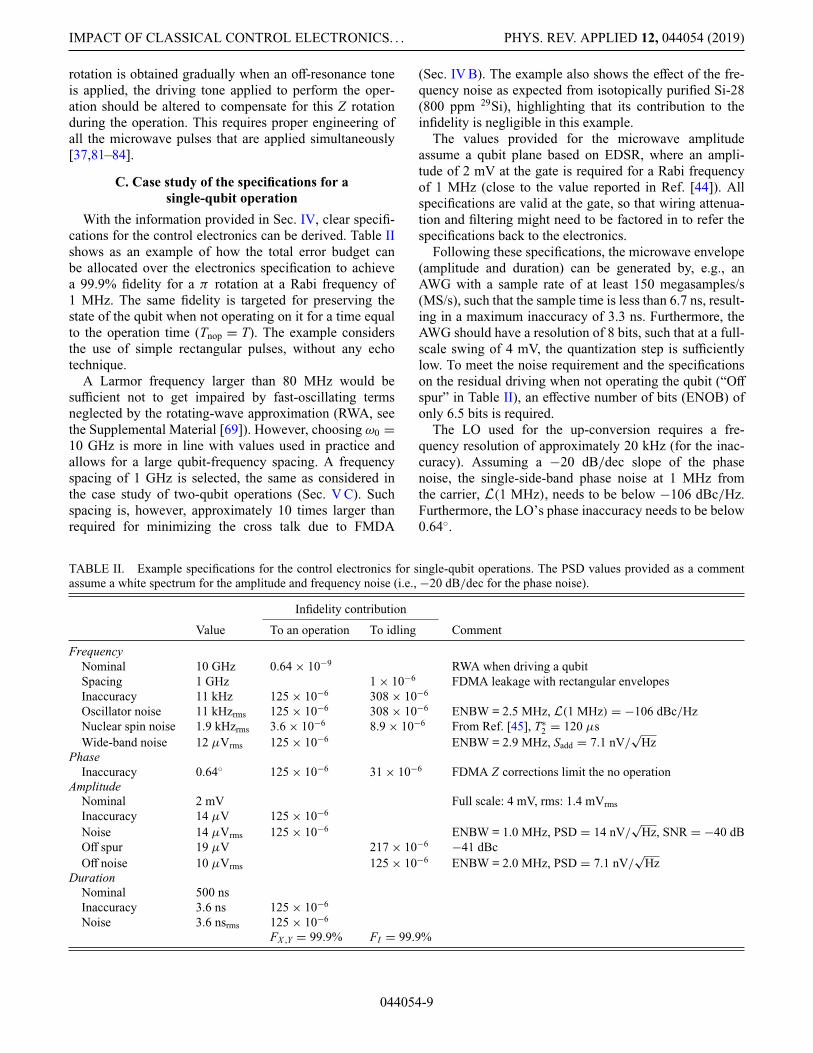
With the information provided in Sec. IV, clear specifi-cations for the control electronics can be derived. Table IIshows as an example of how the total error budget canbe allocated over the electronics specification to achievea 99.9% fidelity for a π rotation at a Rabi frequency of1 MHz. The same fidelity is targeted for preserving thestate of the qubit when not operating on it for a time equalto the operation time (Tnop = T). The example considersthe use of simple rectangular pulses, without any echotechnique.
A Larmor frequency larger than 80 MHz would besufficient not to get impaired by fast-oscillating termsneglected by the rotating-wave approximation (RWA, seethe Supplemental Material [69]). However, choosing ω0 =10 GHz is more in line with values used in practice andallows for a large qubit-frequency spacing. A frequencyspacing of 1 GHz is selected, the same as considered inthe case study of two-qubit operations (Sec. V C). Suchspacing is, however, approximately 10 times larger thanrequired for minimizing the cross talk due to FMDA
(Sec. IV B). The example also shows the effect of the fre-quency noise as expected from isotopically purified Si-28(800 ppm 29Si), highlighting that its contribution to theinfidelity is negligible in this example.
The values provided for the microwave amplitudeassume a qubit plane based on EDSR, where an ampli-tude of 2 mV at the gate is required for a Rabi frequencyof 1 MHz (close to the value reported in Ref. [44]). Allspecifications are valid at the gate, so that wiring attenua-tion and filtering might need to be factored in to refer thespecifications back to the electronics.
Following these specifications, the microwave envelope(amplitude and duration) can be generated by, e.g., anAWG with a sample rate of at least 150 megasamples/s(MS/s), such that the sample time is less than 6.7 ns, result-ing in a maximum inaccuracy of 3.3 ns. Furthermore, theAWG should have a resolution of 8 bits, such that at a full-scale swing of 4 mV, the quantization step is sufficientlylow. To meet the noise requirement and the specificationson the residual driving when not operating the qubit (“Offspur” in Table II), an effective number of bits (ENOB) ofonly 6.5 bits is required.
The LO used for the up-conversion requires a fre-quency resolution of approximately 20 kHz (for the inac-curacy). Assuming a −20 dB/dec slope of the phasenoise, the single-side-band phase noise at 1 MHz fromthe carrier, L(1 MHz), needs to be below −106 dBc/Hz.Furthermore, the LO’s phase inaccuracy needs to be below0.64◦.
TABLE II. Example specifications for the control electronics for single-qubit operations. The PSD values provided as a commentassume a white spectrum for the amplitude and frequency noise (i.e., −20 dB/dec for the phase noise).
Infidelity contribution
Value To an operation To idling Comment
FrequencyNominal 10 GHz 0.64 × 10⁻⁹ RWA when driving a qubitSpacing 1 GHz 1 × 10⁻⁶ FDMA leakage with rectangular envelopesInaccuracy 11 kHz 125 × 10−6 308 × 10−6
Oscillator noise 11 kHzrms 125 × 10−6 308 × 10−6 ENBW = 2.5 MHz, L(1 MHz) = −106 dBc/HzNuclear spin noise 1.9 kHzrms 3.6 × 10⁻⁶ 8.9 × 10⁻⁶ From Ref. [45], T∗
2 = 120 μsWide-band noise 12 μVrms 125 × 10−6 ENBW = 2.9 MHz, Sadd = 7.1 nV/
√Hz
PhaseInaccuracy 0.64◦ 125 × 10−6 31 × 10−6 FDMA Z corrections limit the no operation
AmplitudeNominal 2 mV Full scale: 4 mV, rms: 1.4 mVrmsInaccuracy 14 μV 125 × 10−6
Noise 14 μVrms 125 × 10−6 ENBW = 1.0 MHz, PSD = 14 nV/√
Hz, SNR = −40 dBOff spur 19 μV 217 × 10−6 −41 dBcOff noise 10 μVrms 125 × 10−6 ENBW = 2.0 MHz, PSD = 7.1 nV/
√Hz
DurationNominal 500 nsInaccuracy 3.6 ns 125 × 10−6
Noise 3.6 nsrms 125 × 10−6
FX ,Y = 99.9% FI = 99.9%
044054-9
J.P.G. VAN DIJK et al. PHYS. REV. APPLIED 12, 044054 (2019)
−1 −0.5 0 0.5 1
0
2
4
×1011
ε/U
Ene
rgy
(arb
.un
its)
Energy-Level Diagram
t0 = 0t0 > 0
−999t0n−990t0n
−900t0n
0 900t0n990t0n
999t0n
0.01t0n
0.1t0n
t0n
103
105
107
109
Detuning energyTunnel coupling
ωop
The operation speed ωop (U = 1000 t0n)(a) (b)
FIG. 5. (a) The energy-level diagram of the two-qubit system. An avoided crossing is visible for |ε| = U when there is a finitetunnel coupling between the dots. (b) The two-qubit operation speed ωop [Eq. (11)] versus the interdot tunnel coupling and detuning.A nominal tunnel coupling t0n of 1 GHz is used.
V. SIGNAL SPECIFICATIONS FOR TWO-QUBITOPERATIONS
A. Fidelity of a two-qubit operation
As stated in Sec. II, by default the tunnel couplingbetween the qubits is negligible and the qubits have thesame potential, i.e., they are not detuned. By increasingthe tunnel coupling and/or by detuning the qubits, the qubitinteraction increases and a two-qubit gate can be obtained.In this system, by leveraging this exchange interaction,a two-qubit exchange gate and a C phase gate can beimplemented. With either of these gates and single-qubitoperations, a universal set is obtained.
To describe the physical interactions required for thetwo-qubit gate, higher energy levels need to be mod-eled in the Hamiltonian. The analysis presented hereis limited to the interaction between two neighboringqubits, A and B, and to the single-dot singlet states(|0, 2〉 represents the singlet state in the right dot and|2, 0〉 the singlet state in the left). In the basis � =[|↑, ↑〉 , |↑, ↓〉 , |↓, ↑〉 , |↓, ↓〉 , |0, 2〉 , |2, 0〉], the Hamilto-nian of a double quantum dot is given by the following(� = 1) [55,85,86]:
H =
⎡⎢⎢⎢⎢⎢⎢⎢⎢⎣
−ω0 0 0 0 0 0
0δω0
20 0 t0 t0
0 0 −δω0
20 −t0 −t0
0 0 0 ω0 0 00 t0 −t0 0 U − ε 00 t0 −t0 0 0 U + ε
⎤⎥⎥⎥⎥⎥⎥⎥⎥⎦
,
(10)
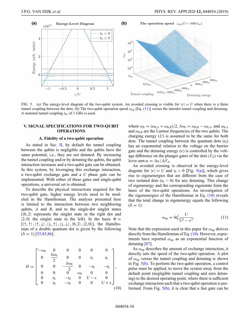
where ω0 = (ω0,A + ω0,B)/2, δω0 = ω0,B − ω0,A, and ω0,Aand ω0,B are the Larmor frequencies of the two qubits. Thecharging energy (U) is assumed to be the same for bothdots. The tunnel coupling between the quantum dots (t0)has an exponential relation to the voltage on the barriergate and the detuning energy (ε) is controlled by the volt-age difference on the plunger gates of the dots (Vd) via thelever arm α = �ε/�Vd.
An avoided crossing is observed in the energy-leveldiagram for |ε| = U and t0 > 0 [Fig. 5(a)], which givesrise to eigenenergies that are different from the case oftwo isolated dots (t0 ∼ 0) for any detuning. This changeof eigenenergy and the corresponding eigenstate form thebasis of the two-qubit operations. An investigation ofthe eigenenergies of the Hamiltonian in Eq. (10) revealsthat the total change in eigenenergy equals the following(� = 1):
ωop = 4t20U
U2 − ε2 . (11)
Note that the expression used in this paper for ωop derivesdirectly from the Hamiltonian of Eq. (10). However, exper-iments have reported ωop as an exponential function ofdetuning [87].
As ωop describes the amount of exchange interaction, itdirectly sets the speed of the two-qubit operation. A plotof ωop versus the tunnel coupling and detuning is shownin Fig. 5(b). To perform the two-qubit operation, a controlpulse must be applied, to move the system away from thedefault point (negligible tunnel coupling and zero detun-ing) to the desired operating point, where there is sufficientexchange interaction such that a two-qubit operation is per-formed. From Fig. 5(b), it is clear that a fast gate can be
044054-10

IMPACT OF CLASSICAL CONTROL ELECTRONICS. . . PHYS. REV. APPLIED 12, 044054 (2019)
obtained at finite detuning, becoming faster closer to theavoided crossing, controlled by the detuning and/or thetunnel coupling. Alteratively, operation at zero detuning(the charge-symmetry point [30]) is possible, controlledby the tunnel coupling alone. Depending on whether thecontrol parameter, the detuning, and/or the tunnel cou-pling is changed adiabatically or diabatically, a C phaseor exchange gate, or a mixture of the two, is obtained.
In the case in which the control parameter changesslowly, i.e., adiabatically, the resulting operation, in therotating frame, can be described by the following diagonalmatrix:
UCZ(t) = diag(1, e−iφZ,A , e−iφZ,B , 1
), (12)
where φZ,A and φZ,B are the acquired phases in the rotat-ing frame. Two additional Z rotations with angles φZ,Aand φZ,B can be applied to the right and left qubit, respec-tively, to obtain the C phase gate with θCZ = −(φZ,A +φZ,B) = ωopt. These Z rotations can easily be obtained byupdating the software reference frame [37,38]. In the casein which θCZ = π , a controlled-Z operation is obtained.Interestingly, the total acquired phase (φZ,A + φZ,B) is inde-pendent of δω0. However, when δω0 = √
2t0, φZ,A = φZ,B[55,85,86], whereas for δω0 = 0, φZ,A = 0.
If, instead, the control parameter is changed rapidly, i.e.,diabatically, and the Larmor-frequency difference is negli-gible (δω0 � ωop), the resulting operation, in the rotatingframe, is as follows:
UJ (t) ≈
⎡⎢⎢⎢⎢⎢⎣
1 0 0 0
01 + eiθJ
21 − eiθJ
20
01 − eiθJ
21 + eiθJ
20
0 0 0 1
⎤⎥⎥⎥⎥⎥⎦
, (13)
where θJ = ωopt. In the case in which θJ = π , a SWAPoperation is obtained. Note that since for an accu-rate exchange operation the Larmor-frequency differenceshould be sufficiently small, the possibility of using FDMAfor single-qubit operations (Sec. IV B) is limited.
From Eq. (10) it follows that the two-qubit operationsare affected by the Larmor frequencies (ω0,A, ω0,B), the tun-nel coupling (t0), the charging energy (U), and the detuning(ε). Furthermore, the operation depends on the total dura-tion (T) for which the two-qubit gate is active. The effectof errors, both static and dynamic, on the fully electricallycontrolled parameters (t0, ε, and T) is analyzed in the sub-sequent section. Detailed derivations of the formulas canbe found in the Supplemental Material [69].
The resulting fidelity in the case of control signal inaccu-racies is summarized in Table III for the exchange gate andthe C phase gate, both at zero detuning and finite detun-ing. For the exchange gate, we assume that no Larmor-frequency difference between the qubits exists, since for
TAB
LE
III.
The
fidel
ityin
the
case
ofco
ntro
lsig
nali
nacc
urac
ies
forv
ario
ustw
o-qu
bito
pera
tions
.
Exc
hang
e:C
phas
e
δω
0=
0δω
0=
0δω
0=
ωop
δω
0=
√ 2t0
Rot
atio
n|φ Z
,B|
θ CZ
θ CZ
√ 2
θ CZ 2
Dur
atio
n1
−3 16
θ2 J
(�
T T
) 21
−3 16
θ2 C
Z
(�
T T
) 21
−7
−4√ 2
16θ
2 CZ
(�
T T
) 21
−1 16
θ2 C
Z
(�
T T
) 2
Tunn
elco
uplin
g1
−3 4θ
2 J
(�
t 0 t 0
) 21
−3 4θ
2 CZ
(�
t 0 t 0
) 21
−1 2θ
2 CZ
(�
t 0 t 0
) 21
−1 4θ
2 CZ
(�
t 0 t 0
) 2
Det
unin
g(|ε
|>0)
1−
3 4θ
2 J
⎛ ⎜ ⎝
ε U
1−(
ε U
) 2
⎞ ⎟ ⎠
2(
�ε U
) 21
−3 4θ
2 CZ
⎛ ⎜ ⎝
ε U
1−(
ε U
) 2
⎞ ⎟ ⎠
2(
�ε U
) 21
−1 2θ
2 CZ
⎛ ⎜ ⎝
ε U
1−(
ε U
) 2
⎞ ⎟ ⎠
2(
�ε U
) 21
−1 4θ
2 CZ
⎛ ⎜ ⎝
ε U
1−(
ε U
) 2
⎞ ⎟ ⎠
2(
�ε U
) 2
Det
unin
g(ε
=0)
1−
3 16θ
2 J
(�
ε U
) 41
−3 16
θ2 C
Z
(�
ε U
) 41
−1 8θ
2 CZ
(�
ε U
) 41
−1 16
θ2 C
Z
(�
ε U
) 4
044054-11

J.P.G. VAN DIJK et al. PHYS. REV. APPLIED 12, 044054 (2019)
such a gate δω0 � ωop is required, while for the C phasegate, various scenarios are analyzed (δω0 = 0, δω0 = ωop,and δω0 = √
2t0). In the table, T denotes the qubit gateoperation time and inaccuracies are shown with the prefix�. The table provides values for different rotation angles(θCZ , θJ ). In the case of the C phase gate, additional Zrotations might be required, which only have a very smalleffect on the fidelity [Eq. (3)].
The error contributions have a quadratic relation withthe infidelity except for detuning errors for ε = 0, wherea fourth-order dependence is found. This implies animproved robustness to detuning errors when operating atthe charge-symmetry point (ε = 0) [30,31].
For low-frequency variations, i.e., those changing overa time scale longer than the operation time, the sameapproach as for single-qubit operations holds and theexpected fidelity follows the same equations as given inTable III when replacing the inaccuracy, such as �ε, withthe standard deviation of the variation (assuming a Gaus-sian distribution). An exception is for detuning errors whenoperating at the charge-symmetry point [30,31], becauseof the fourth-order dependence. For a static but randomerror � for which F = 1 − c�4, the expected fidelity isF = 1 − 3cσ 4, if � follows a Gaussian distribution withstandard deviation σ and zero mean. Consequently, thereis a slightly higher sensitivity to noise than to static errorsfor the detuning.
For timing variations, only the total duration matters andhigh-frequency noise is filtered as described in Table I.Moreover, similar to the single-qubit gate, numerical sim-ulations of the Hamiltonian have shown sensitivity tohigh-frequency noise (> ωop) only in a pass band witha bandwidth that is inversely proportional to the opera-tion duration, for both the electrically controlled detuningenergy and tunnel coupling in the case of the two-qubitgate (see the Supplemental Material [69]). The quantumstate is, however, also affected by noise around the fre-quencies corresponding to the allowed energy transitions,in a pass band with a similar bandwidth. Consequently,it is important that the high-frequency noise componentsin the signals applied to the barrier gates and plungergates are properly filtered. However, since the exchangegate requires a diabatic change in the control parame-ter, only limited filtering can be applied. Closed-formanalytical expressions for these effects have not beenstudied.
B. Specifications for the idle operation
Since, in practice, the tunnel coupling cannot be fullyremoved, the two-qubit operation is never completelyturned off. The interaction strength can, however, beslowed down significantly, thus leading to a fidelity withrespect to the ideal identity operation for the exchange and
C phase gates as follows:
FInop,J =
⎧⎪⎪⎪⎪⎪⎨
⎪⎪⎪⎪⎪⎩
1 − 316
ω2op,offT2
nop, δω0 = 0,
1 − 7 − 4√
216
ω2op,offT2
nop, δω0 = ωop,
1 − 116
ω2op,offT2
nop, δω0 = √2t0,
(14)
where ωop,off is the reduced interaction strength during thetime Tnop when no operation is applied.
Following Eq. (11), the interaction strength can bereduced by lowering the tunnel coupling while not chang-ing the detuning. A two-qubit operation performed at finitedetuning could also be controlled using only the detun-ing. However, assuming that the interaction is consideredto be off at zero detuning, the operation might need to beperformed at far detuning. As mentioned before, operat-ing closer to the avoided crossing reduces the tolerance toinaccuracies and noise in the detuning (Table III).
C. Case study of the specifications for a two-qubitoperation
Specifications for the control electronics responsible forthe two-qubit operation can be derived using the resultspresented in Sec. V. This example develops on the exam-ple given in Sec. IV C and, for instance, assumes that thesame oscillator is used to keep the coherence with thequbits. Two examples will be given here, one at zero detun-ing and one at finite detuning. Both focus on the C phasegate, operating at δω0 = √
2t0. This choice for the Larmor-frequency difference gives the most relaxed specificationsfor the control electronics, while at smaller δω0, the spec-ifications can be up to
√3 times more demanding (see
Table III).The Larmor-frequency difference is chosen as 1 GHz,
to achieve a two-qubit operation speed of ωop = 2 MHz atzero detuning, while maintaining δω0 = √
2t0 [Eq. (11)].Example specifications for this operation are given inTable IV. To further increase the operating speed, aneven higher qubit-frequency spacing would be requiredor δω0 <
√2t0. Alternatively, the operating speed can be
enhanced to, e.g., 20 MHz, by operating the C phase gateat finite detuning [Eq. (11)], as shown in another example(Table IV).
Both examples target a fidelity of 99.9% for a C phasegate with θCZ = π . The examples also indicate the spec-ifications required for idling two qubits at 99.9% fidelityfor a duration of 500 ns, the same as for the example inSec. IV C.
For the charging energy and tunnel coupling, typical val-ues are chosen. As the relation to the gate voltage is devicedependent, no values for the required electrical specifica-tions are given. Note that in either example, the tunnelcoupling only has to change by a factor of approximately
044054-12

IMPACT OF CLASSICAL CONTROL ELECTRONICS. . . PHYS. REV. APPLIED 12, 044054 (2019)
TABLE IV. Example specifications for the control electronics when operating a C phase gate at zero detuning and at finite detuning.The PSD values provided assume a white spectrum with an ENBW of approximately 10 MHz (ωop = 2 MHz) when operating at zerodetuning and an ENBW of approximately 100 MHz (ωop = 20 MHz) at finite detuning. A nominal charging energy of 83 mV (4.1meV, 1.0 THz) is assumed.
Value Infidelity contribution to
An operation An operation Idlingε = 0 ε > 0 ε = 0 ε > 0
FrequencySpacing 1 GHz 1 GHzInaccuracy 11 kHz 11 kHz 77 × 10−6 0.8 × 10⁻⁶ 308 × 10−6
Oscillator noise 11 kHzrms 11 kHzrms 77 × 10−6 0.8 × 10⁻⁶ 308 × 10−6
Nuclear-spin noise 1.9 kHzrms 1.9 kHzrms 2.2 × 10⁻⁶ 0.02 × 10⁻⁶ 8.9 × 10⁻⁶
DurationNominal 250 ns 25 nsError 5.3 ns 0.58 ns 281 × 10−6 333 × 10−6
Detuning energyNominal 0 mV (0 μeV, 0 GHz) 78 mV (3.9 meV, 0.95 THz)Error 12 mV (0.60 meV, 0.15 THz) 0.10 mV (5.1 μeV, 1.2 GHz) 281 × 10−6 333 × 10−6
σ = 9.2 mVrms σ = 0.10 mVrms
PSD = 2.9 μV/√
Hz PSD = 10 nV/√
HzTunnel coupling
Nominal 0.71 GHz (2.9 μeV) 0.71 GHz (2.9 μeV)Error 7.5 MHz (31 neV) 8.2 MHz (34 neV) 281 × 10−6 333 × 10−6
Off value 78 MHz (0.32 μeV) 78 MHz (0.32 μeV) 374 × 10−6
FCZ = 99.9% FCZ = 99.9% FI = 99.9%
9 to turn the operation on or off. In the case of operation atfinite detuning, this assumes that zero detuning is appliedwhen the operation is turned off.
The detuning energy is directly related to the voltage onthe plunger gate via the lever arm, for which a typical valueof α = 0.05 eV/V is assumed [44]. When operating atfinite detuning, the detuning energy is chosen at 95% of thecharging energy. Even though higher operating speeds canbe obtained by moving even closer to the avoided crossing,the electrical specifications become increasingly challeng-ing. When operating at the charge-symmetry point, verylarge detuning errors can be tolerated (at which point theapproximations used to derive the expressions in Table IIIdo not hold any more). When operating at moderate detun-ing, the error specification for the detuning is more than100 times stricter. Moreover, as the operation at finitedetuning is faster with the same tunnel coupling, the signalbandwidth must be larger, with a larger noise bandwidth.As a rough estimate, the ENBW has been chosen as 5 timesthe operating speed in both examples, which seems plau-sible as an adiabatic change is required (for the exchangegate, the situation might be worse). As a result, the maxi-mum allowed noise spectral density, assuming white noise,is much lower. For the given example, this results in adifference of almost 5 orders of magnitude in the noisePSD.
In the example operation at finite detuning, the detun-ing control can be achieved by an AWG running at asample rate of 1 gigasamples/s (GS/s) for a maximum
timing inaccuracy of 0.5 ns. Assuming that the AWG has tocover a voltage range of −U · · · U (where U is the charg-ing energy), it must have a 10-bit resolution to meet theaccuracy specification of the detuning energy.
VI. SIGNAL SPECIFICATIONS FORQUBIT READOUT
A. Fidelity for qubit readout
For the readout of the quantum state, the Pauli spin-blockade readout [88] is analyzed, since it offers severaladvantages with respect to the other possible alternative,i.e., the Elzerman readout [65]: no electron reservoir isrequired next to the quantum dot; and the Zeeman energysplitting does not have to be much higher than the ther-mal energy, thus enabling operation at higher temperaturesand/or lower Larmor frequencies. As a drawback, thePauli spin-blockade readout involves two quantum dots,where the measurement involves discrimination betweenthe singlet and triplet states.
Even though relaxation, which is quantified by the relax-ation time T1, is an important limiting factor in qubit read-out, its effect is not considered in the following analysis,as all gates are assumed to be performed in a time signif-icantly smaller than T1. Furthermore, in our analysis, weassume that the spin-dependent charge state resulting froma Pauli spin-blockade readout is measured using a chargesensor. As a result, the readout fidelity is determined byvarious factors:
044054-13

J.P.G. VAN DIJK et al. PHYS. REV. APPLIED 12, 044054 (2019)
(a) Pcharge: the probability that the spin state is correctlyprojected to the charge state.
(b) Psense: the probability that the charge sensor cor-rectly detects the charge state.
(c) Pdetect: the probability that the readout circuit cor-rectly discriminates the signal of the charge sensor.
The overall readout fidelity is then as follows:
Fread ≈ Pcharge × Psense × Pdetect. (15)
The probability Psense is limited by, e.g., interference onone of the charge-sensor bias gates and charge noise inthe substrate. As this depends highly on the type of sensoremployed and the sensor integration, this error contribu-tion will not be discussed further.
The quantum-dot control electronics limit Pcharge, as dis-cussed in Sec. VI B, while the readout electronics limitPdetect, as discussed in Sec. VI C.
B. Specifications for the electronics controlling thespin to charge conversion
For the analysis of the charge transfer in the Pauli spin-blockade readout, the Hamiltonian of Eq. (10) is extendedwith the lowest-energy triplet states (either due to the val-ley splitting or the orbital energy splitting). Those statesare spaced by a singlet-triplet energy splitting EST from thesinglet energy level (for the Hamiltonian, see the Supple-mental Material [69]). A plot of the energy of the stationarystates versus the detuning near the avoided crossing isshown in Fig. 6(a). For the following discussion, only the|↓, ↓〉 and |↓, ↑〉 states, highlighted in Fig. 6(a), need to beconsidered.
The Pauli spin-blockade readout relies on EST for thediscrimination of the single-dot singlet configuration fromthree possible single-dot triplet configurations. Consider-ing a pair of neighboring qubits, the state of the right qubitcan be measured as follows. The left qubit is initialized inthe |↓〉 state. By detuning adiabatically to a point betweenthe singlet avoided crossing and the triplet avoided cross-ing (with t0 > 0), only the |↓, ↑〉 state (at ε = 0) becomesa singlet and both electrons will move into the same dot.This charge movement can be measured using a chargesensor. Based on the measurement result, it is then clearwhether the qubits are in a singlet or one of the three tripletconfigurations. This scenario is analyzed here.
Starting from the |↓, ↓〉 state, there is a small probabil-ity P(transfer| |↓, ↓〉) that both electrons will end up in thesame dot. Similarly, starting from the |↓, ↑〉 state, thereis a small probability P(no transfer| |↓, ↑〉) that no chargewill transfer. The probability of a correct spin to chargeconversion can be defined as follows:
Pcharge = 1 − P(transfer| |↓, ↓〉) − P(no transfer| |↓, ↑〉).(16)
−0.5 0 0.5 1 1.5−2
−1
0
1
2
↓ , ↓
↑ , ↓↓ , ↑
↑ , ↑
(ε − U)
E/h
(GH
z)
Eigenenergies versus Detuning
0 0.2 0.4 0.6 0.8
ST
ST
detect
dete
ct
10.1×
1×10×
100×
(ε − U)/E
ST/E
Pro
babi
lity
rela
tive
to
opti
mum
1−
P
1− PDegradation versus Detuning
1 − P
Contribution P (no transfer| |↓, ↑〉)Contribution P (transfer| |↓, ↓〉)
10−3 10−110−6
10−3
100
t0/E
1−
P
Charge Transfer Probability
t0: 100 kHz to 1 GHz (EST = 1 GHz)EST : 1 GHz to 10 THz (t0 = 1 GHz)
16 t0E
)2 0 20 40 60 80 10010−8
10−4
100
SNR
1−
P
P versus SNR
∫
Charge sensor Readout circuit Signal processing
0 or ISin,s in,c Tread ½ IS
(a) (b)
(c) (d)
(e)
charge
char
ge
char
ge
Pcharge
ST
FIG. 6. (a) The energy of the stationary states versus the detun-ing near the avoided crossing. The black dashed lines indicatethe states where the left qubit was originally in the |↓〉 state.(b) The error probability 1 − Pcharge, along with the individualerror contributors, at various points of detuning as simulated forvarious tunnel rates, Larmor frequencies, charging energies, andsinglet-triplet energy splittings (each varied over a decade; theresulting plots are overlapping). The obtained probabilities areplotted relative to the optimum, i.e., the lowest error probabil-ity at ε = U + EST/2, thereby showing the degradation whenmoving away from the optimum detuning. (c) The simulatedprobability 1 − Pcharge versus the singlet-triplet splitting, normal-ized to the tunnel coupling at ε = U + EST/2, while sweepingeither the tunnel coupling or the singlet-triplet energy splitting.(d) A plot of 1 − Pdetect versus SNR in the case of Gaussian-distributed noise. (e) A model of a typical readout chain, showingthe sensor, the readout electronics, and the required signal pro-cessing for the measurement discrimination. Additional sourcesmodeling the noise are shown in gray.
The analysis is again simplified by assuming an ideal adia-batic change in the detuning energy. The results presentedin this section are obtained from numerical simulations ofthe Hamiltonian.
Simulations show that the highest Pcharge is obtained bydetuning to ε = U + EST/2, i.e., equidistant between thesinglet and triplet avoided crossings, as shown in Fig. 6(b).The shape of the probability versus (ε − U)/EST plot isindependent of the Larmor frequency, assuming that ω0 �EST. Although the shape remains the same, the obtainable
044054-14

IMPACT OF CLASSICAL CONTROL ELECTRONICS. . . PHYS. REV. APPLIED 12, 044054 (2019)
TABLE V. Example specifications for the control electronics. The PSD values provided assume a white spectrum with an ENBW ofapproximately 1 MHz for the detuning control and a measurement time of Tread = 0.6 μs. A nominal charging energy of 82.7 mV (4.1meV, 1.0 THz) is assumed and a singlet-triplet energy splitting of 1.0 mV (50 μeV, 12 GHz).
Value Infidelity contribution to the readout
Detuning energyNominal 83.2 mV (4.2 meV, 1.0 THz)Error 0.24 mV (12 μeV, 2.8 GHz) 167 × 10−6
σ = 0.24 mVrms, PSD = 0.24 μV/√
HzTunnel coupling
Nominal 39 MHz (0.16 μeV) 167 × 10−6 Pcharge = 99.967%Charge sensor 333 × 10−6 Psense = 99.967%QPC
Signal 400 pANoise 53 pArms, PSD = 57 fA/
√Hz 222 × 10−6
Readout circuitInput-referred noise 26 pArms, PSD = 28 fA/
√Hz 111 × 10−6 Pdetect = 99.967%
F = 99.9%
maximum Pcharge scales with the tunnel coupling and thesinglet-triplet energy splitting, as can be seen in Fig. 6(c).From this figure, an upper bound for the tunnel couplingcan be found, which must be maintained even with errorscaused by limitations in the control electronics.
Even though Pcharge is highly influenced by the achiev-able tunnel couplings and singlet-triplet energy splittingsin the system [Fig. 6(c)], the detuning value has a minorinfluence (provided that there is a sufficient singlet-tripletenergy splitting), since 1 − Pcharge is relatively flat aroundits minimum, as shown in Fig. 6(b). For instance, for atwofold increase in 1 − Pcharge, the detuning must stay inthe range (ε − U)/EST ≈ 0.5 ± 0.235. We can then con-clude that a large singlet-triplet splitting is desired to limitthe influence of the control electronics on the readout.
C. Specifications for the electronics processing thereadout signal
In this section, we will consider a direct readout. Amodel of a typical readout chain is shown in Fig. 6(e). Forsimplicity, the sensor is modeled as a current source witha value of either 0 or Is, depending on the sensed charge.The readout fidelity is limited by the noise introduced bythe sensor and by the readout circuit, indicated in Fig. 6(e)as in,s and in,c, respectively. Assuming the typical matched-filter detection [89], i.e., integrating the signal current for aduration Tread and comparing the result to a threshold, theprobability of a correct measurement under the presence ofGaussian-distributed noise is given by the following:
Pdetect =1 + erf
(√S/N
8
)
2, (17)
with
S/N = I 2s∫ ∞
0Si( f )
[sin(π f Tread)
π f
]2
df
, (18)
where Si( f ) is the PSD of the total noise in = in,s + in,c.When the noise is white, this simplifies to the following:
S/N = I 2s
SiBENBW, (19)
with effective noise bandwidth BENBW = 1/(2Tread).
D. Case study of the specifications for a qubit readout
The example specifications presented in this sectionbuild on those presented in Secs. IV C and V C and henceassume the same charging energy and lever arm for thedetuning control. For the singlet-triplet energy splitting,a typical value of EST = 50 μeV is used. As a result,the optimum detuning is at 83.2 mV. The resulting spec-ifications are summarized in Table V and assume equalcontributions from Pcharge, Psense, and Pdetect [Eq. (15)].
Following Fig. 6(c), to achieve the required Pcharge, thetunnel coupling must be even lower than is required toturn off the two-qubit operation (see Sec. V C), therebyextending the required tunnel-coupling tuning range toapproximately 18×. In the example of Table V, the detun-ing control can be achieved by an AWG with low samplerate, as the detuning must change adiabatically and thereadout generally takes a relatively long time. Assumingthat the AWG has to cover a voltage range from 0 to 2U,it must have a 9-bit resolution to meet the accuracy spec-ification of the detuning energy [Fig. 6(b)]. As a result,the same circuitry as used for the two-qubit operation(Sec. V C) could potentially be used.
044054-15
J.P.G. VAN DIJK et al. PHYS. REV. APPLIED 12, 044054 (2019)
In this example, Pdetect assumes a direct readout of aQPC, following the numbers provided in Ref. [64] (Is =400 pA and in,s = 57 fA/
√Hz). Assuming that the read-
out circuit is designed to contribute about half the noisecompared to the shot-noise limit of the QPC (in,c ≈ in,s/2),an integration time of at least Tread = 0.6 μs is required toachieve an signal-to-noise ratio (SNR) of 46 for a Pdetect of99.967% [for F = 99.9%, Eq. (15)]. For such short read-out times, the assumption of white noise is valid and theeffects of qubit relaxation (T1) could be negligible.
VII. DISCUSSION
Case studies targeting a 99.9% average gate fidelity havebeen presented in Secs. IV C, V C, and VI D. This targetfidelity is particularly relevant since the minimum errorrate to reach fault-tolerant quantum computing is around99% for a complete error correction cycle, thus requir-ing a single-operation fidelity above 99.9% for a typicalcycle of ten operations [14]. Reaching a 99.9% fidelity forall operations is currently an ambitious goal for all qubitplatforms. However, our model can be directly applied toanalyze specifications for any given fidelity.
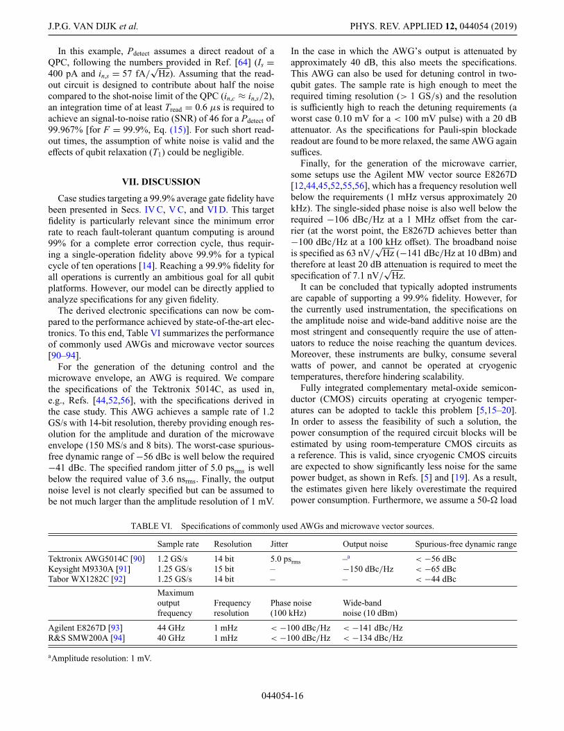
The derived electronic specifications can now be com-pared to the performance achieved by state-of-the-art elec-tronics. To this end, Table VI summarizes the performanceof commonly used AWGs and microwave vector sources[90–94].
For the generation of the detuning control and themicrowave envelope, an AWG is required. We comparethe specifications of the Tektronix 5014C, as used in,e.g., Refs. [44,52,56], with the specifications derived inthe case study. This AWG achieves a sample rate of 1.2GS/s with 14-bit resolution, thereby providing enough res-olution for the amplitude and duration of the microwaveenvelope (150 MS/s and 8 bits). The worst-case spurious-free dynamic range of −56 dBc is well below the required−41 dBc. The specified random jitter of 5.0 psrms is wellbelow the required value of 3.6 nsrms. Finally, the outputnoise level is not clearly specified but can be assumed tobe not much larger than the amplitude resolution of 1 mV.
In the case in which the AWG’s output is attenuated byapproximately 40 dB, this also meets the specifications.This AWG can also be used for detuning control in two-qubit gates. The sample rate is high enough to meet therequired timing resolution (> 1 GS/s) and the resolutionis sufficiently high to reach the detuning requirements (aworst case 0.10 mV for a < 100 mV pulse) with a 20 dBattenuator. As the specifications for Pauli-spin blockadereadout are found to be more relaxed, the same AWG againsuffices.
Finally, for the generation of the microwave carrier,some setups use the Agilent MW vector source E8267D[12,44,45,52,55,56], which has a frequency resolution wellbelow the requirements (1 mHz versus approximately 20kHz). The single-sided phase noise is also well below therequired −106 dBc/Hz at a 1 MHz offset from the car-rier (at the worst point, the E8267D achieves better than−100 dBc/Hz at a 100 kHz offset). The broadband noiseis specified as 63 nV/
√Hz (−141 dBc/Hz at 10 dBm) and
therefore at least 20 dB attenuation is required to meet thespecification of 7.1 nV/
√Hz.
It can be concluded that typically adopted instrumentsare capable of supporting a 99.9% fidelity. However, forthe currently used instrumentation, the specifications onthe amplitude noise and wide-band additive noise are themost stringent and consequently require the use of atten-uators to reduce the noise reaching the quantum devices.Moreover, these instruments are bulky, consume severalwatts of power, and cannot be operated at cryogenictemperatures, therefore hindering scalability.
Fully integrated complementary metal-oxide semicon-ductor (CMOS) circuits operating at cryogenic temper-atures can be adopted to tackle this problem [5,15–20].In order to assess the feasibility of such a solution, thepower consumption of the required circuit blocks will beestimated by using room-temperature CMOS circuits asa reference. This is valid, since cryogenic CMOS circuitsare expected to show significantly less noise for the samepower budget, as shown in Refs. [5] and [19]. As a result,the estimates given here likely overestimate the requiredpower consumption. Furthermore, we assume a 50-� load
TABLE VI. Specifications of commonly used AWGs and microwave vector sources.
Sample rate Resolution Jitter Output noise Spurious-free dynamic range
Tektronix AWG5014C [90] 1.2 GS/s 14 bit 5.0 psrms –a < −56 dBcKeysight M9330A [91] 1.25 GS/s 15 bit – −150 dBc/Hz < −65 dBcTabor WX1282C [92] 1.25 GS/s 14 bit – – < −44 dBc
Maximumoutputfrequency
Frequencyresolution
Phase noise(100 kHz)
Wide-bandnoise (10 dBm)
Agilent E8267D [93] 44 GHz 1 mHz < −100 dBc/Hz < −141 dBc/HzR&S SMW200A [94] 40 GHz 1 mHz < −100 dBc/Hz < −134 dBc/Hz
aAmplitude resolution: 1 mV.
044054-16

IMPACT OF CLASSICAL CONTROL ELECTRONICS. . . PHYS. REV. APPLIED 12, 044054 (2019)
for each circuit, which is not the case for a fully integratedcontroller.
The core component determining the specifications of anAWG is its digital-to-analog converter (DAC). The 10-bit500 MS/s DAC presented in Ref. [95] meets the specifi-cations for the microwave envelope generation at a powerconsumption of 24 mW. For the detuning control, the DACspecifications are stricter, but can be met by the 12-bit1.6 GS/s DAC presented in Ref. [96], with a power con-sumption of 40 mW. Although for the tunnel barrier thespecifications will depend highly on the gate structure, asimilar DAC is assumed to be sufficient.
The core component of a microwave carrier generator,the PLL, is also available as a CMOS circuit operating overthe required frequency range (9.2–12.7 GHz) at a powerconsumption of around 13 mW [97]. Its phase-noise per-formance is slightly worse than required. However, withoperation at cryogenic temperatures, the noise level isexpected to improve.
In a linear qubit array, one DAC is required for the bar-rier gate and one for the plunger gate for each qubit. Thisleads to an estimated power of 80 mW per qubit. For themicrowave signals, the envelope DAC and PLL togetherconsume approximately 40 mW. Without any form ofmultiplexing, this indicates a power consumption of 120mW/qubit. For a state-of-the-art dilution refrigerator witha cooling power of a few watts at 4 K, this suggests a max-imum of a few tens of qubits when operating the classicalcontroller at 4 K.
However, the power consumption of the DACs control-ling the barrier gates and plunger gates could be highlyreduced if it is not being limited to a 50-� system. Toget a sufficient signal swing, in Ref. [96] a 16-mA cur-rent is delivered to a 50-� load, thereby setting a lowerbound to the power consumption. A much lower currentwould be required for a higher impedance, or even for alower swing as acceptable in this application, ultimatelylimited by the speed or noise requirement. Furthermore,the same fast DAC can be used to generate frequency-multiplexed microwave envelopes. With a sample rate of1.6 GS/s, a bandwidth of roughly 640 MHz is available[96]. This can be used to drive 64 qubits with a Rabifreqency of 1 MHz spaced by 10 MHz using, e.g., a Gaus-sian envelope [Fig. 4(d)]. The combined power of the fastDAC and PLL, i.e., 53 mW, is then shared over 64 qubits,thus resulting in a power consumption below 1 mW/qubit.For the readout, on the other hand, cryogenic CMOS cir-cuits have already been proposed that can achieve a powerconsumption < 1 mW/qubit [5,19].
In summary, a cryogenic CMOS controller for a large-scale quantum processor appears to be feasible for a targetfidelity of 99.9%. However, for minimum power con-sumption, the trade-offs in the electronics design mustbe systematically investigated. The analysis proposed inthis paper provides the foundations for such optimization
and will help electronics designers to build a functionalcontroller.
VIII. CONCLUSION
In this paper, the effect of nonidealities in the classi-cal controller for a quantum processor is analyzed. Eventhough this work focuses on single-electron spin-qubits,the presented approach can be used to analyze the perfor-mance of a quantum processor in any qubit technology.A comprehensive approach is proposed, by covering theeffect of both static and dynamic errors on all quantumoperations, i.e., single-qubit gates, two-qubit gates, andreadout.
With the results of this analysis, the impact of the con-troller on the performance of the quantum computer as awhole can be quantified. This is required to ensure thatthe controller does not become the performance bottle-neck as the qubit performance keeps improving. Moreover,with the presented results, a full set of electrical speci-fications can be derived, targeting a given qubit fidelity.The availability of these specifications enables the designof next-generation controllers that are tailor-made for thequantum processor and optimized for performance, power,cost, and size, so as to improve the scalability of thequantum computer.
As future controllers might have to operate physicallyclose to the quantum processor, i.e., at cryogenic tem-peratures where the cooling power is limited, the poweroptimization of the controller will be critical in enablinglarge-scale quantum computing. With the results obtainedin this paper, the trade-offs between qubit fidelity andpower spent in the controller can be analyzed, this repre-senting the foundation for such a power optimization.
ACKNOWLEDGMENTS
The authors would like to thank Intel Corp. for fundingand Dr. Andrea Corna and Richard Versluis for the manyinteresting discussions and their useful insights.
[1] A. Montanaro, Quantum algorithms: An overview, npjQuantum Inf. 2, 15023 EP (2016).
[2] P. W. Shor, in Proceedings of 35th Annual Symposium onFoundations of Computer Science (IEEE, Santa Fe, 1994),p. 124.
[3] L. K. Grover, in Proceedings of the Twenty-Eighth annualACM symposium on Theory of computing (ACM, NewYork, 1996), p. 212.
[4] R. P. Feynman, Simulating physics with computers, Int. J.Theor. Phys. 21, 467 (1982).
[5] B. Patra, R. M. Incandela, J. P. G. van Dijk, H. A. R.Homulle, L. Song, M. Shahmohammadi, R. B. Staszewski,
044054-17

J.P.G. VAN DIJK et al. PHYS. REV. APPLIED 12, 044054 (2019)
A. Vladimirescu, M. Babaie, F. Sebastiano, and E. Char-bon, Cryo-CMOS circuits and systems for quantum com-puting applications, IEEE J. Solid-State Circuits 53, 309(2018).
[6] IBM Research, IBM builds its most powerful universalquantum computing processors (2017).
[7] J. Kelly et al., State preservation by repetitive error detec-tion in a superconducting quantum circuit, Nature 519, 66(2015).
[8] T. Monz, P. Schindler, J. T. Barreiro, M. Chwalla, D. Nigg,W. A. Coish, M. Harlander, W. Hänsel, M. Hennrich, andR. Blatt, 14-Qubit Entanglement: Creation and Coherence,Phys. Rev. Lett. 106, 130506 (2011).
[9] Zurich Instruments, HDAWG Arbitrary Waveform Gener-ator (2018).
[10] Quantum Researchers Toolkit + Labber, Keysight Tech-nologies (2017).
[11] J. P. van Dijk, E. Charbon, and F. Sebastiano, The electronicinterface for quantum processors, Microprocess. Microsyst.66, 90 (2019).
[12] J. Yoneda, K. Takeda, T. Otsuka, T. Nakajima, M. Del-becq, G. Allison, T. Honda, T. Kodera, S. Oda, Y. Hoshi,N. Usami, K. Itoh, and S. Tarucha, A > 99.9%-fidelityquantum-dot spin qubit with coherence limited by chargenoise, arXiv:1708.01454 (2017).
[13] D. Wecker, B. Bauer, B. K. Clark, M. B. Hastings, andM. Troyer, Gate-count estimates for performing quantumchemistry on small quantum computers, Phys. Rev. A 90,022305 (2014).
[14] A. G. Fowler, M. Mariantoni, J. M. Martinis, andA. N. Cleland, Surface codes: Towards practical large-scale quantum computation, Phys. Rev. A 86, 032324(2012).
[15] J. M. Hornibrook, J. I. Colless, I. D. Conway Lamb, S. J.Pauka, H. Lu, A. C. Gossard, J. D. Watson, G. C. Gardner,S. Fallahi, M. J. Manfra, and D. J. Reilly, Cryogenic ControlArchitecture for Large-Scale Quantum Computing, Phys.Rev. Appl. 3, 024010 (2015).
[16] I. Conway Lamb, J. Colless, J. Hornibrook, S. Pauka, S.Waddy, M. Frechtling, and D. Reilly, An FPGA-basedinstrumentation platform for use at deep cryogenic temper-atures, Rev. Sci. Instrum. 87, 014701 (2016).
[17] H. Homulle, S. Visser, B. Patra, G. Ferrari, E. Prati, C.G. Almudéver, K. Bertels, F. Sebastiano, and E. Charbon,in Proceedings of the ACM International Conference onComputing Frontiers, CF ’16 (ACM, New York, NY, USA,2016), p. 282.
[18] E. Charbon, F. Sebastiano, A. Vladimirescu, H. Homulle, S.Visser, L. Song, and R. M. Incandela, in 2016 IEEE Inter-national Electron Devices Meeting (IEDM) (IEEE, SanFrancisco, 2016), p. 13.5.1.
[19] E. Charbon, F. Sebastiano, M. Babaie, A. Vladimirescu,M. Shahmohammadi, R. B. Staszewski, H. A. R. Homulle,B. Patra, J. P. G. van Dijk, R. M. Incandela, L. Song, andB. Valizadehpasha, in 2017 IEEE International Solid-StateCircuits Conference (ISSCC) (IEEE, San Francisco, 2017),p. 264.
[20] F. Sebastiano, H. Homulle, B. Patra, R. Incandela, J. vanDijk, L. Song, M. Babaie, A. Vladimirescu, and E. Char-bon, in Proceedings of the 54th Annual Design Automation
Conference 2017, DAC ’17 (ACM, New York, NY, USA,2017), p. 13:1.
[21] X. Qin, Z. Shi, Y. Xie, L. Wang, X. Rong, W. Jia, W. Zhang,and J. Du, An integrated device with high performancemulti-function generators and time-to-digital convertors,Rev. Sci. Instrum. 88, 014702 (2017).
[22] X. Fu, M. Rol, C. Bultink, J. van Someren, N. Khammassi,I. Ashraf, R. Vermeulen, J. De Sterke, W. Vlothuizen,R. Schouten, C. Almudever, L. DiCarlo, and K. Bertels,in Proceedings of the 50th Annual IEEE/ACM Interna-tional Symposium on Microarchitecture (ACM, Cam-bridge, 2017), p. 813.
[23] C. A. Ryan, B. R. Johnson, D. Ristè, B. Donovan, and T.A. Ohki, Hardware for dynamic quantum computing, Rev.Sci. Instrum. 88, 104703 (2017).
[24] G. Batey, A. J. Matthews, and M. Patton, A new ultralow-temperature cryogen-free experimental platform, J. Phys.Conf. Ser. 568, 032014 (2014). IOP Publishing.
[25] L. Tavian, Latest Developments in Cryogenics at CERN,Tech. Rep. CERN-AT-2005-011-ACR (CERN, Geneva,2005).
[26] H. Ball, W. D. Oliver, and M. J. Biercuk, The role of mas-ter clock stability in quantum information processing, npjQuantum Inf. 2, 16033 EP (2016).
[27] J. Raftery, A. Vrajitoarea, G. Zhang, Z. Leng, S. Srini-vasan, and A. Houck, Direct digital synthesis of microwavewaveforms for quantum computing, arXiv:1703.00942(2017).
[28] T. J. Green, H. Uys, and M. J. Biercuk, High-Order NoiseFiltering in Nontrivial Quantum Logic Gates, Phys. Rev.Lett. 109, 020501 (2012).
[29] T. J. Green, J. Sastrawan, H. Uys, and M. J. Biercuk, Arbi-trary quantum control of qubits in the presence of universalnoise, New J. Phys. 15, 095004 (2013).
[30] M. D. Reed, B. M. Maune, R. W. Andrews, M. G. Borselli,K. Eng, M. P. Jura, A. A. Kiselev, T. D. Ladd, S. T. Merkel,I. Milosavljevic, E. J. Pritchett, M. T. Rakher, R. S. Ross, A.E. Schmitz, A. Smith, J. A. Wright, M. F. Gyure, and A. T.Hunter, Reduced Sensitivity to Charge Noise in Semicon-ductor Spin Qubits via Symmetric Operation, Phys. Rev.Lett. 116, 110402 (2016).
[31] F. Martins, F. K. Malinowski, P. D. Nissen, E. Barnes, S.Fallahi, G. C. Gardner, M. J. Manfra, C. M. Marcus, and F.Kuemmeth, Noise Suppression Using Symmetric ExchangeGates in Spin Qubits, Phys. Rev. Lett. 116, 116801(2016).
[32] N. Didier, E. A. Sete, J. Combes, and M. P. da Silva, ACflux sweet spots in parametrically-modulated superconduct-ing qubits, arXiv:1807.01310 (2018).
[33] S. Anton, C. Müller, J. Birenbaum, S. O’Kelley, A. Fef-ferman, D. S. Golubev, G. Hilton, H.-M. Cho, K. Irwin,F. C. Wellstood, G. Schön, A. Shnirman, and J. Clarke,Pure dephasing in flux qubits due to flux noise with spectraldensity scaling as 1/f α, Phys. Rev. B. 85, 224505 (2012).
[34] P. Rebentrost, I. Serban, T. Schulte-Herbrüggen, and F.Wilhelm, Optimal Control of a Qubit Coupled to a Non-Markovian Environment, Phys. Rev. Lett. 102, 090401(2009).
[35] Y. V. Nazarov, Quantum Noise in Mesoscopic Physics(Springer Science & Business Media, Delft, 2012), Vol. 97.
044054-18

IMPACT OF CLASSICAL CONTROL ELECTRONICS. . . PHYS. REV. APPLIED 12, 044054 (2019)
[36] L. M. K. Vandersypen, M. Steffen, G. Breyta, C. S. Yan-noni, R. Cleve, and I. L. Chuang, Experimental Realizationof an Order-Finding Algorithm with an NMR QuantumComputer, Phys. Rev. Lett. 85, 5452 (2000).
[37] L. M. K. Vandersypen, Experimental quantum computationwith nuclear spins in liquid solution, Ph.D. thesis, StanfordUniversity, 2001.
[38] L. M. K. Vandersypen and I. L. Chuang, NMR techniquesfor quantum control and computation, Rev. Mod. Phys. 76,1037 (2005).
[39] J. I. Cirac and P. Zoller, Quantum Computations with ColdTrapped Ions, Phys. Rev. Lett. 74, 4091 (1995).
[40] Y. Nakamura, Y. A. Pashkin, and J. Tsai, Coherent controlof macroscopic quantum states in a single-Cooper-pair box,Nature 398, 786 (1999).
[41] Y. Makhlin, G. Schön, and A. Shnirman, Quantum-stateengineering with Josephson-junction devices, Rev. Mod.Phys. 73, 357 (2001).
[42] L. Childress, M. G. Dutt, J. Taylor, A. Zibrov, F. Jelezko,J. Wrachtrup, P. Hemmer, and M. Lukin, Coherent dynam-ics of coupled electron and nuclear spin qubits in diamond,Science 314, 281 (2006).
[43] L. R. Schreiber and H. Bluhm, Quantum computation:Silicon comes back, Nat. Nanotechnol. 9, 966 (2014).
[44] E. Kawakami, P. Scarlino, D. R. Ward, F. R. Braakman, D.E. Savage, M. G. Lagally, M. Friesen, S. N. Coppersmith,M. A. Eriksson, and L. M. K. Vandersypen, Electrical con-trol of a long-lived spin qubit in a Si/SiGe quantum dot,Nat. Nanotechnol. 9, 666 EP (2014).
[45] M. Veldhorst, J. C. C. Hwang, C. H. Yang, A. W. Leenstra,B. de Ronde, J. P. Dehollain, J. T. Muhonen, F. E. Hudson,K. M. Itoh, A. Morello, and A. S. Dzurak, An addressablequantum dot qubit with fault-tolerant control-fidelity, Nat.Nanotechnol. 9, 981 EP (2014).
[46] L. M. K. Vandersypen, H. Bluhm, J. S. Clarke, A. S. Dzu-rak, R. Ishihara, A. Morello, D. J. Reilly, L. R. Schreiber,and M. Veldhorst, Interfacing spin qubits in quantum dotsand donors—hot, dense, and coherent, npj Quantum Inf. 3,34 (2017).
[47] M. Veldhorst, H. G. J. Eenink, C. H. Yang, and A. S. Dzu-rak, Silicon CMOS architecture for a spin-based quantumcomputer, Nat. Commun. 8, 1766 (2017).
[48] R. Li, L. Petit, D. P. Franke, J. P. Dehollain, J. Helsen,M. Steudtner, N. K. Thomas, Z. R. Yoscovits, K. J. Singh,S. Wehner, L. Vandersypen, J. Clarke, and M. Veld-horst, A crossbar network for silicon quantum dot qubits,arXiv:1711.03807 (2017).
[49] R. Hanson, L. P. Kouwenhoven, J. R. Petta, S. Tarucha, andL. M. K. Vandersypen, Spins in few-electron quantum dots,Rev. Mod. Phys. 79, 1217 (2007).
[50] F. A. Zwanenburg, A. S. Dzurak, A. Morello, M. Y. Sim-mons, L. C. Hollenberg, G. Klimeck, S. Rogge, S. N. Cop-persmith, and M. A. Eriksson, Silicon quantum electronics,Rev. Mod. Phys. 85, 961 (2013).
[51] J. R. Petta, A. C. Johnson, J. M. Taylor, E. A. Laird, A.Yacoby, M. D. Lukin, C. M. Marcus, M. P. Hanson, andA. C. Gossard, Coherent manipulation of coupled electronspins in semiconductor quantum dots, Science 309, 2180(2005).
[52] E. Kawakami, T. Jullien, P. Scarlino, D. R. Ward, D. E.Savage, M. G. Lagally, V. V. Dobrovitski, M. Friesen, S.
N. Coppersmith, M. A. Eriksson, and L. M. K. Vander-sypen, Gate fidelity and coherence of an electron spin in anSi/SiGe quantum dot with micromagnet, Proc. Natl. Acad.Sci. U.S.A. 113, 11738 (2016).
[53] S. J. Angus, A. J. Ferguson, A. S. Dzurak, and R. G. Clark,Gate-defined quantum dots in intrinsic silicon, Nano Lett.7, 2051 (2007).
[54] D. M. Zajac, T. M. Hazard, X. Mi, E. Nielsen, and J. R.Petta, Scalable Gate Architecture for a One-DimensionalArray of Semiconductor Spin Qubits, Phys. Rev. Appl. 6,054013 (2016).
[55] M. Veldhorst, C. H. Yang, J. C. C. Hwang, W. Huang, J.P. Dehollain, J. T. Muhonen, S. Simmons, A. Laucht, F.E. Hudson, K. M. Itoh, A. Morello, and A. S. Dzurak, Atwo-qubit logic gate in silicon, Nature 526, 410 (2015),letter.
[56] T. F. Watson, S. G. J. Philips, E. Kawakami, D. R. Ward,P. Scarlino, M. Veldhorst, D. E. Savage, M. G. Lagally,M. Friesen, S. N. Coppersmith, M. A. Eriksson, and L.M. K. Vandersypen, A programmable two-qubit quantumprocessor in silicon, Nature 555, 633 (2018).
[57] The Larmor frequency can be controlled by a magneticfield gradient—e.g., by using an on-chip micromagnet[44,52,56,59] [not shown in Fig. 1(a)]—or, alternatively,using the Stark shift, i.e., by an electrical field providedwith an extra confinement gate [45,55] [not shown inFig. 1(a)].
[58] J. P. Dehollain, J. J. Pla, E. Siew, K. Y. Tan, A. S. Dzu-rak, and A. Morello, Nanoscale broadband transmissionlines for spin qubit control, Nanotechnology 24, 015202(2013).
[59] Y. Tokura, W. G. van der Wiel, T. Obata, and S.Tarucha, Coherent Single Electron Spin Control in aSlanting Zeeman Field, Phys. Rev. Lett. 96, 047202(2006).
[60] R. Maurand, X. Jehl, D. Kotekar-Patil, A. Corna, H.Bohuslavskyi, R. Laviéville, L. Hutin, S. Barraud, M.Vinet, M. Sanquer, and S. De Fransceschi, A CMOS siliconspin qubit, Nat. Commun. 7, 13575 (2016).
[61] J. I. Colless, A. C. Mahoney, J. M. Hornibrook, A. C.Doherty, H. Lu, A. C. Gossard, and D. J. Reilly, Dis-persive Readout of a Few-Electron Double Quantum Dotwith Fast RF Gate Sensors, Phys. Rev. Lett. 110, 046805(2013).
[62] A. West, B. Hensen, A. Jouan, T. Tanttu, C. Yang, A. Rossi,M. Gonzalez-Zalba, F. Hudson, A. Morello, D. Reilly,and A. Dzurak, Gate-based single-shot readout of spins insilicon, arXiv:1809.01864 (2018).
[63] D. J. Reilly, C. M. Marcus, M. P. Hanson, and A. C. Gos-sard, Fast single-charge sensing with a RF quantum pointcontact, Appl. Phys. Lett. 91, 162101 (2007).
[64] I. T. Vink, T. Nooitgedagt, R. N. Schouten, L. M. K. Van-dersypen, and W. Wegscheider, Cryogenic amplifier forfast real-time detection of single-electron tunneling, Appl.Phys. Lett. 91, 123512 (2007).
[65] J. M. Elzerman, R. Hanson, L. H. W. Van Beveren, B.Witkamp, L. M. K. Vandersypen, and L. P. Kouwenhoven,Single-shot read-out of an individual electron spin in aquantum dot, Nature 430, 431 (2004).
[66] C. Barthel, M. Kjærgaard, J. Medford, M. Stopa, C. M.Marcus, M. P. Hanson, and A. C. Gossard, Fast sensing of
044054-19

J.P.G. VAN DIJK et al. PHYS. REV. APPLIED 12, 044054 (2019)
double-dot charge arrangement and spin state with a radio-frequency sensor quantum dot, Phys. Rev. B 81, 161308(2010).
[67] M. A. Nielsen, A simple formula for the average gatefidelity of a quantum dynamical operation, Phys. Lett. A303, 249 (2002).
[68] L. H. Pedersen, N. M. Møller, and K. Mølmer, Fidelity ofquantum operations, Phys. Lett. A 367, 47 (2007).
[69] See the Supplemental Material at http://link.aps.org/supplemental/10.1103/PhysRevApplied.12.044054 for detailedderivations along with additional closed-form expressions.
[70] N. Khaneja, T. Reiss, C. Kehlet, T. Schulte-Herbrüggen,and S. J. Glaser, Optimal control of coupled spin dynam-ics: Design of NMR pulse sequences by gradient ascentalgorithms, J. Magn. Reson. 172, 296 (2005).
[71] While it might be possible to calibrate for drift, this signifi-cantly increases the complexity of the system.
[72] Assuming that the rotating-wave approximation (RWA)needs to be accurate. The RWA is discussed in the Sup-plemental Material [69].
[73] The indicated ENBW is defined such that white noise inte-grated over this bandwidth results in the same noise poweras white noise integrated over the actual filter transfer func-tion and can be used to simplify calculations when the noisecan be well approximated as white noise in the band ofinterest [75] (see the Supplemental Material [69]).
[74] Note that some quantum algorithms, such as dynamical-decoupling sequences or error-correction codes, can act asa high-pass filter for the noise, thereby setting ωmin.
[75] D. A. Johns and K. Martin, Analog Integrated CircuitDesign (John Wiley & Sons, 2008).
[76] G. S. Uhrig, Keeping a Quantum Bit Alive by Opti-mized π -Pulse Sequences, Phys. Rev. Lett. 98, 100504(2007).
[77] M. J. Biercuk, H. Uys, A. P. VanDevender, N. Shiga,W. M. Itano, and J. J. Bollinger, Optimized dynamicaldecoupling in a model quantum memory, Nature 458, 996(2009).
[78] Solutions for Reducing Phase Noise at RF and MicrowaveFrequencies, Keysight Technologies (2014).
[79] J. Phillips and K. Kundert, in Proceedings of the IEEE 2000Custom Integrated Circuits Conference (IEEE, Orlando,2000), p. 431.
[80] B. Drakhlis, Calculate oscillator jitter by using phase-noiseanalysis, MICROWAVES & RF 40, 82 (2001).
[81] M. McCoy and L. Mueller, Selective decoupling, J. Magn.Reson., Ser. A 101, 122 (1993).
[82] E. Kupce and R. Freeman, Close encounters between softpulses, J. Magn. Reson., Ser. A 112, 261 (1995).
[83] J. Pauly, P. L. Roux, D. Nishimura, and A. Macovski,Parameter relations for the Shinnar–Le Roux selectiveexcitation pulse design algorithm [NMR imaging], IEEETrans. Med. Imaging 10, 53 (1991).
[84] M. Steffen, L. M. K. Vandersypen, and I. L. Chuang, Simul-taneous soft pulses applied at nearby frequencies, J. Magn.Reson. 146, 369 (2000).
[85] W. A. Coish and D. Loss, Exchange-controlled single-electron-spin rotations in quantum dots, Phys. Rev. B 75,161302 (2007).
[86] T. Meunier, V. E. Calado, and L. M. K. Vandersypen,Efficient controlled-phase gate for single-spin qubits inquantum dots, Phys. Rev. B 83, 121403 (2011).
[87] E. A. Laird, J. R. Petta, A. C. Johnson, C. M. Mar-cus, A. Yacoby, M. P. Hanson, and A. C. Gossard, Effectof Exchange Interaction on Spin Dephasing in a DoubleQuantum Dot, Phys. Rev. Lett. 97, 056801 (2006).
[88] K. Ono, D. Austing, Y. Tokura, and S. Tarucha, Currentrectification by Pauli exclusion in a weakly coupled doublequantum dot system, Science 297, 1313 (2002).
[89] G. Turin, An introduction to matched filters, IRE Trans. Inf.Theory 6, 311 (1960).
[90] Arbitrary Waveform Generators AWG5000 Series DataSheet, Tektronix (2017).
[91] Keysight M9330A Arbitrary Waveform Generator 15-bit,1.25 GS/s, Keysight Technologies (2014).
[92] MODELS WX1281/2C 1.25 GS/s Single/Dual ChannelArbitrary Waveform Generators, Tabor Electronics Inc.(2015).
[93] E8267D PSG Vector Signal Generator, Keysight Technolo-gies (2016).
[94] R&S SMW200A Vector Signal Generator Specifications,Rohde & Schwarz (2018).
[95] W. T. Lin and T. H. Kuo, A compact dynamic-performance-improved current-steering DAC with randomrotation-based binary-weighted selection, IEEE J. Solid-S-tate Circuits 47, 444 (2012).
[96] W. T. Lin, H. Y. Huang, and T. H. Kuo, A 12-bit 40 nm DACachieving SFDR > 70 dB at 1.6 GS/s and IMD < −61 dBat 2.8 GS/s with DEMDRZ technique, IEEE J. Solid-StateCircuits 49, 708 (2014).
[97] K. Raczkowski, N. Markulic, B. Hershberg, and J. Cran-inckx, A 9.2–12.7 GHz wideband fractional-N subsamplingPLL in 28 nm CMOS with 280 fs RMS jitter, IEEE J.Solid-State Circuits 50, 1203 (2015).
044054-20