physical vapour deposition & chemical vaapour deposition
TRANSCRIPT
Modern Manufacturing Processes,
Physical Vapour Deposition
& Chemical vaapour Deposition
[PVD & CVD]
mech14.weebly.com
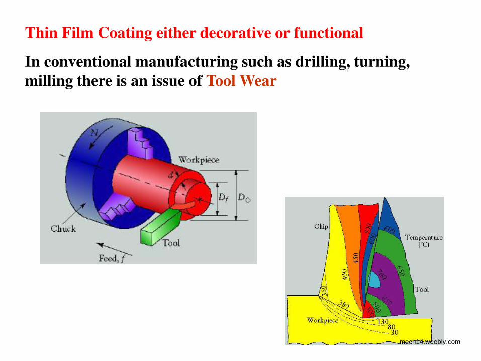
Thin Film Coating either decorative or functional
In conventional manufacturing such as drilling, turning,
milling there is an issue of Tool Wear
mech14.weebly.com
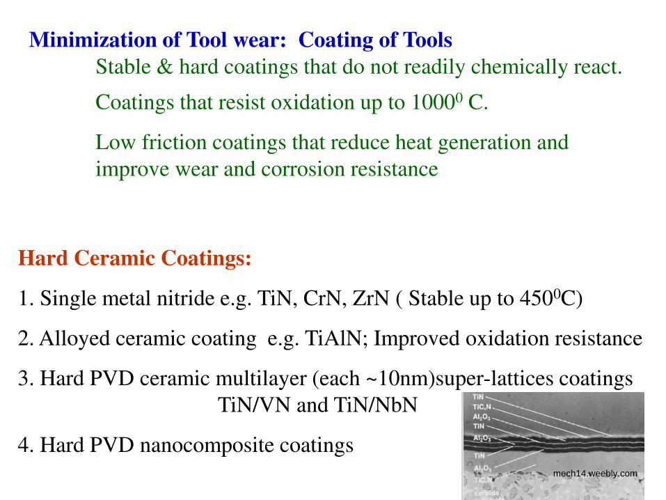
Minimization of Tool wear: Coating of Tools
Stable & hard coatings that do not readily chemically react.
Coatings that resist oxidation up to 10000 C.
Low friction coatings that reduce heat generation and
improve wear and corrosion resistance
Hard Ceramic Coatings:
1. Single metal nitride e.g. TiN, CrN, ZrN ( Stable up to 4500C)
2. Alloyed ceramic coating e.g. TiAlN; Improved oxidation resistance
3. Hard PVD ceramic multilayer (each ~10nm)super-lattices coatings
TiN/VN and TiN/NbN
4. Hard PVD nanocomposite coatings mech14.weebly.com
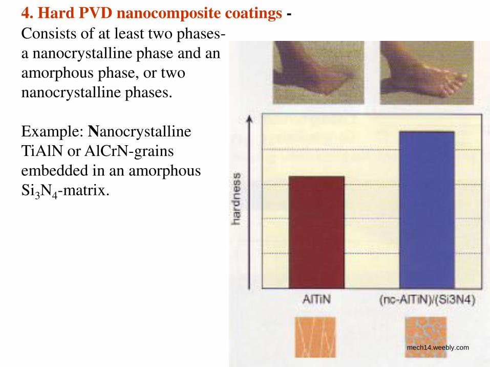
Consists of at least two phases-
a nanocrystalline phase and an
amorphous phase, or two
nanocrystalline phases.
Example: Nanocrystalline
TiAlN or AlCrN-grains
embedded in an amorphous
Si3N4-matrix.
4. Hard PVD nanocomposite coatings -
mech14.weebly.com
mech14.weebly.com
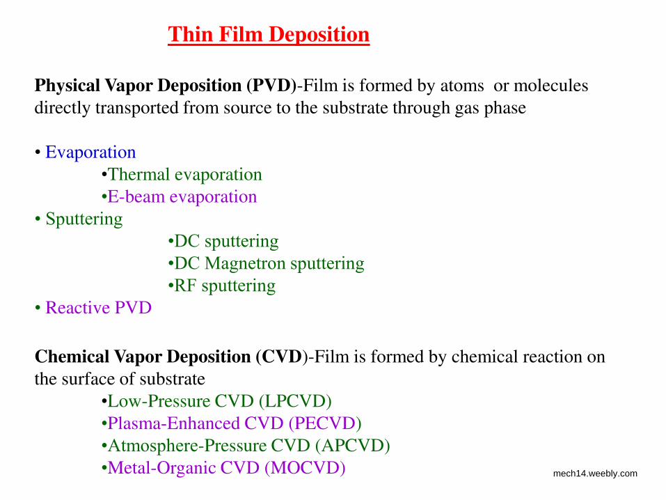
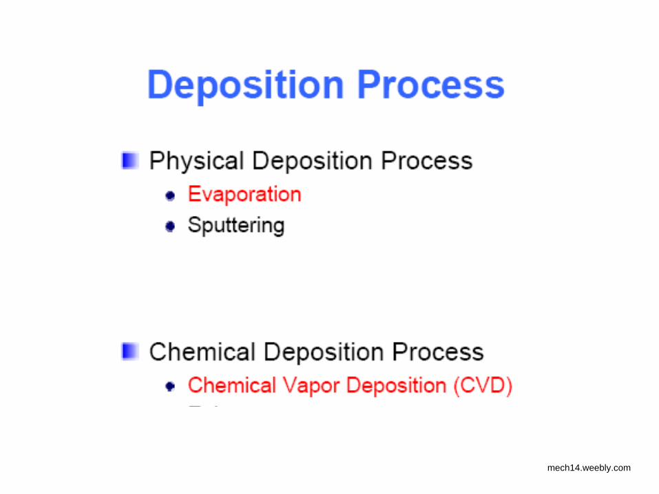
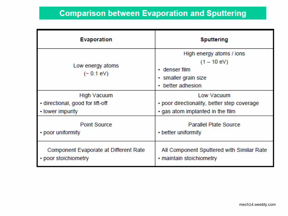
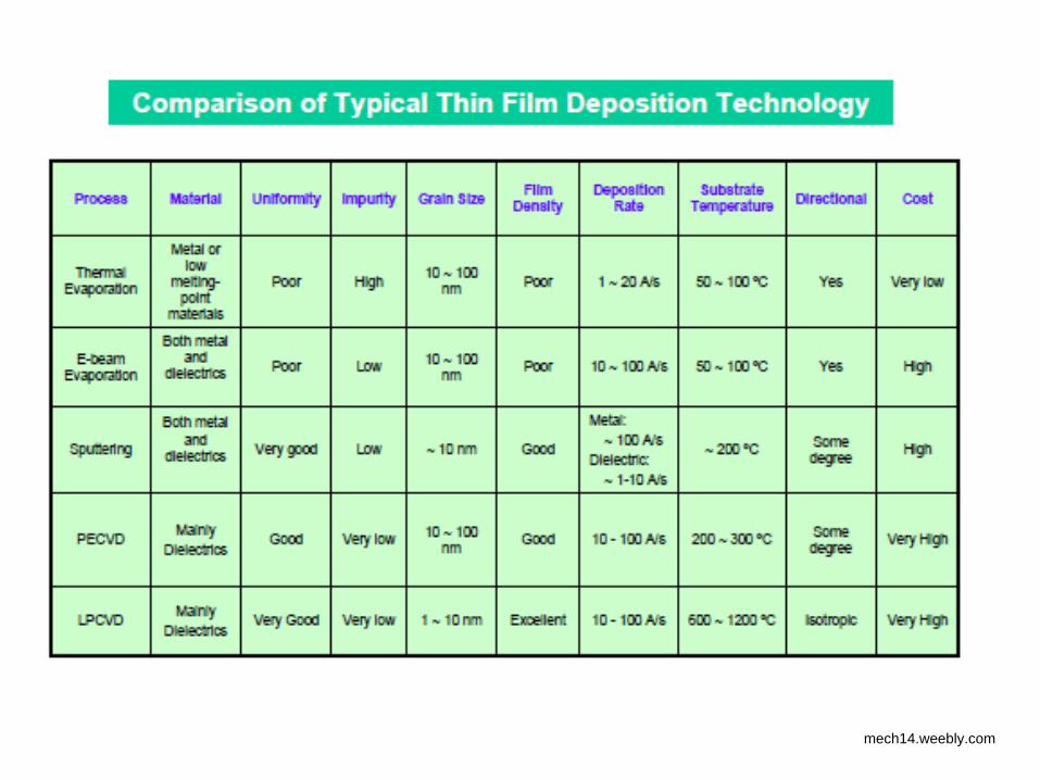
Thin Film Deposition
Physical Vapor Deposition (PVD)-Film is formed by atoms or molecules
directly transported from source to the substrate through gas phase
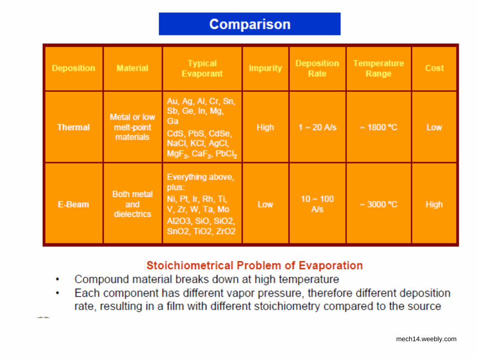
• Evaporation
•Thermal evaporation
•E-beam evaporation
• Sputtering •DC sputtering
•DC Magnetron sputtering
•RF sputtering
• Reactive PVD
Chemical Vapor Deposition (CVD)-Film is formed by chemical reaction on
the surface of substrate
•Low-Pressure CVD (LPCVD)
•Plasma-Enhanced CVD (PECVD)
•Atmosphere-Pressure CVD (APCVD)
•Metal-Organic CVD (MOCVD) mech14.weebly.com
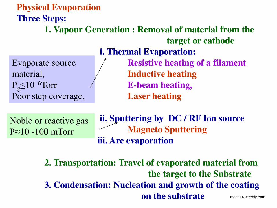
Physical Evaporation
Three Steps:
1. Vapour Generation : Removal of material from the
target or cathode
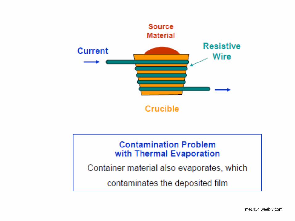
i. Thermal Evaporation:
Resistive heating of a filament
Inductive heating
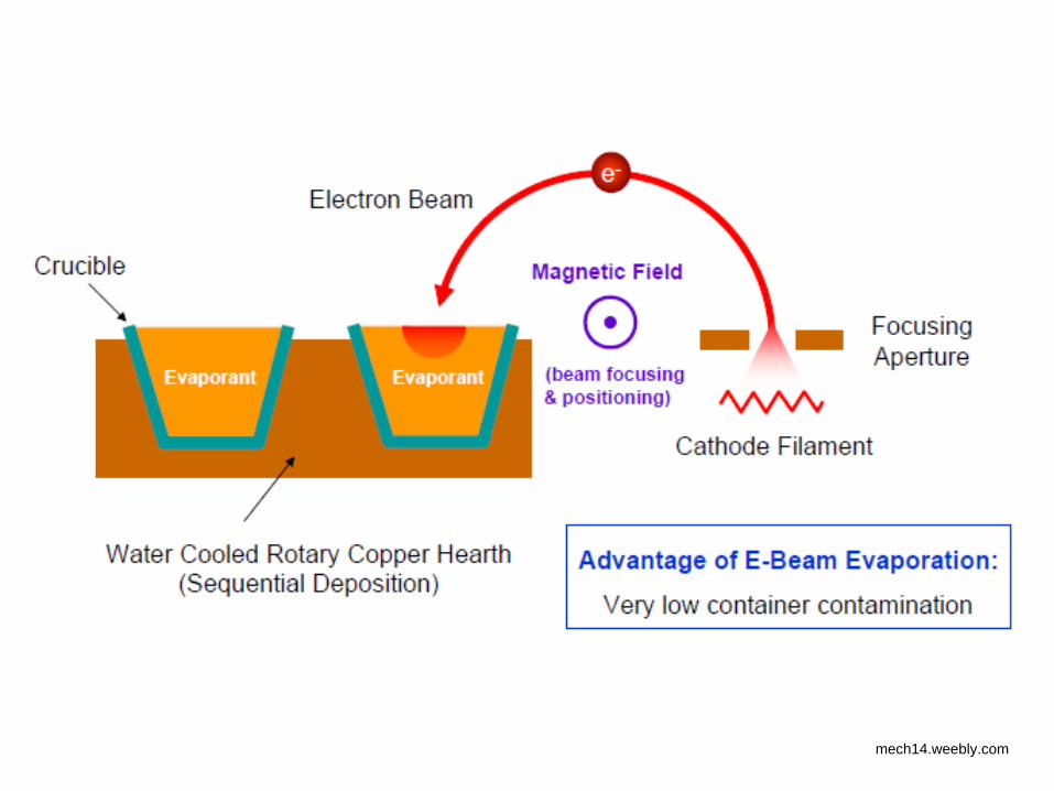
E-beam heating,
Laser heating
ii. Sputtering by DC / RF Ion source
Magneto Sputtering
iii. Arc evaporation
2. Transportation: Travel of evaporated material from
the target to the Substrate
3. Condensation: Nucleation and growth of the coating
on the substrate
Evaporate source
material,
Pg≤10−6Torr
Poor step coverage,
Noble or reactive gas
P≈10 -100 mTorr
mech14.weebly.com
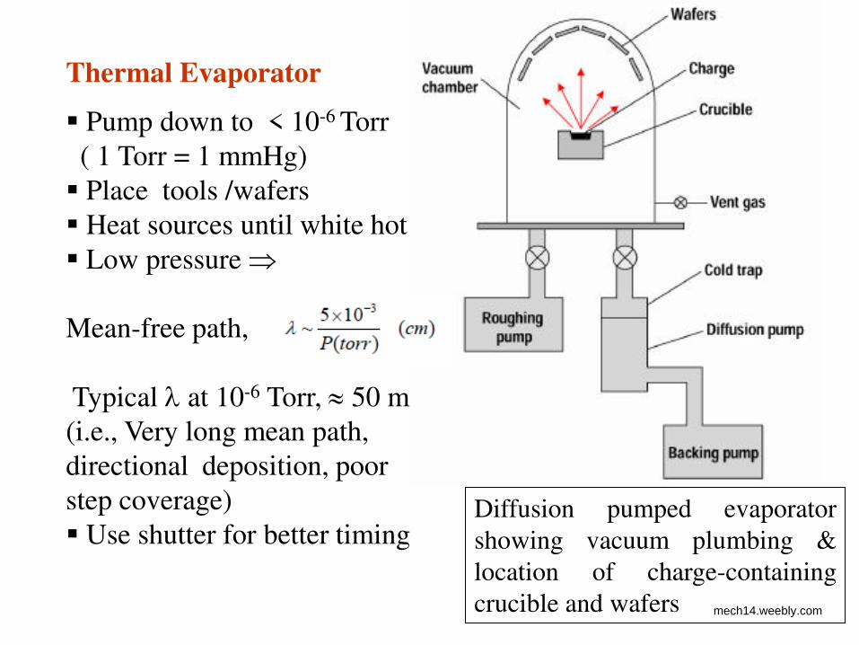
Thermal Evaporator
Pump down to < 10-6 Torr
( 1 Torr = 1 mmHg)
Place tools /wafers
Heat sources until white hot
Low pressure
Mean-free path,
Typical at 10-6 Torr, 50 m
(i.e., Very long mean path,
directional deposition, poor
step coverage)
Use shutter for better timing
Diffusion pumped evaporator
showing vacuum plumbing &
location of charge-containing
crucible and wafers mech14.weebly.com
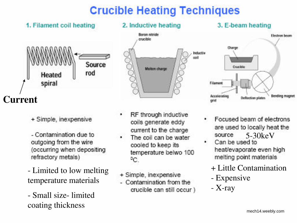
+ Little Contamination
- Expensive
- X-ray
- Limited to low melting
temperature materials
- Small size- limited
coating thickness
5-30keV
Current
mech14.weebly.com
mech14.weebly.com
mech14.weebly.com
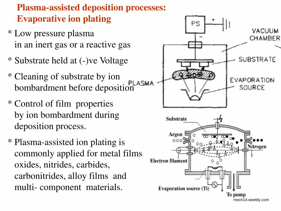
Plasma-assisted deposition processes:
Evaporative ion plating
* Low pressure plasma
in an inert gas or a reactive gas
* Substrate held at (-)ve Voltage
* Cleaning of substrate by ion
bombardment before deposition
* Control of film properties
by ion bombardment during
deposition process.
* Plasma-assisted ion plating is
commonly applied for metal films,
oxides, nitrides, carbides,
carbonitrides, alloy films and
multi- component materials.
mech14.weebly.com
mech14.weebly.com
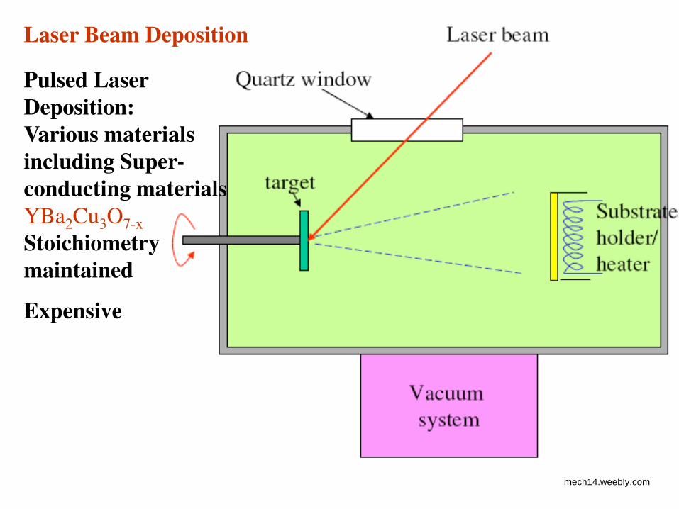
Laser Beam Deposition
Pulsed Laser
Deposition:
Various materials
including Super-
conducting materials
YBa2Cu3O7-x
Stoichiometry
maintained
Expensive
mech14.weebly.com
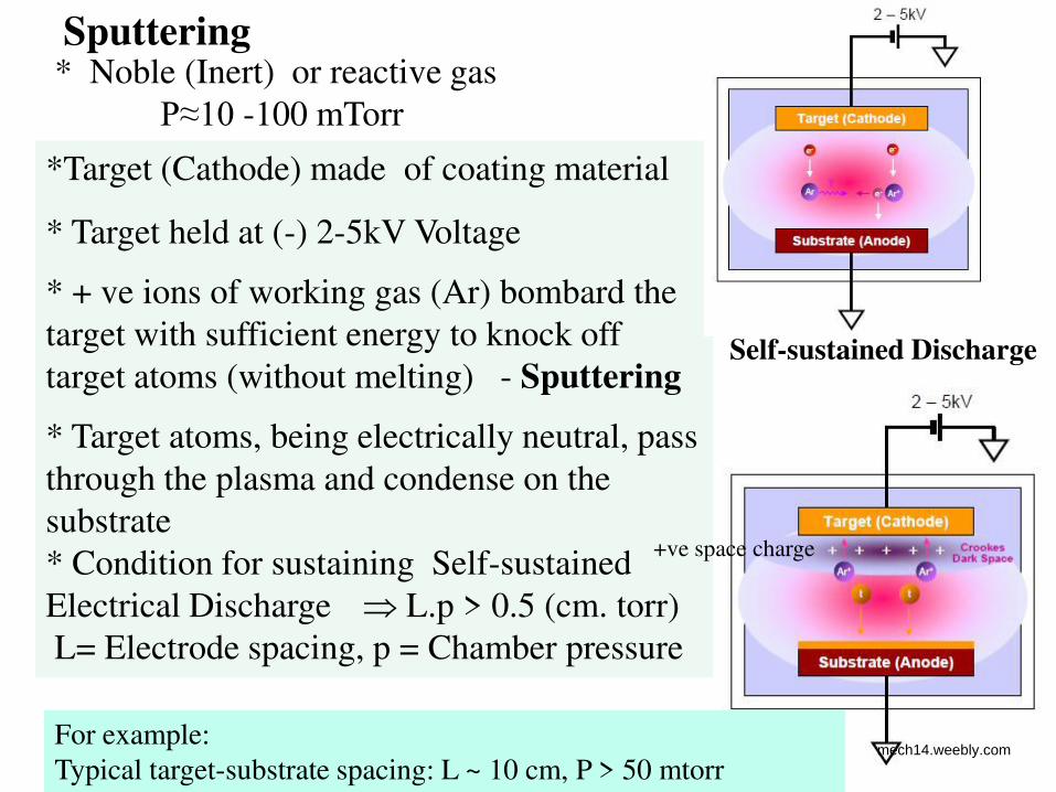
Sputtering
*Target (Cathode) made of coating material
* Target held at (-) 2-5kV Voltage
* + ve ions of working gas (Ar) bombard the
target with sufficient energy to knock off
target atoms (without melting) - Sputtering
* Target atoms, being electrically neutral, pass
through the plasma and condense on the
substrate
* Condition for sustaining Self-sustained
Electrical Discharge L.p > 0.5 (cm. torr)
L= Electrode spacing, p = Chamber pressure
* Noble (Inert) or reactive gas
P≈10 -100 mTorr
Self-sustained Discharge
For example:
Typical target-substrate spacing: L ~ 10 cm, P > 50 mtorr
+ve space charge
mech14.weebly.com
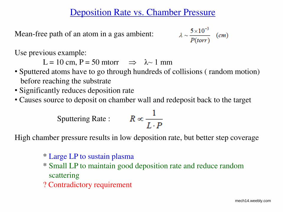
Deposition Rate vs. Chamber Pressure
Mean-free path of an atom in a gas ambient:
Use previous example:
L = 10 cm, P = 50 mtorr λ~ 1 mm
• Sputtered atoms have to go through hundreds of collisions ( random motion)
before reaching the substrate
• Significantly reduces deposition rate
• Causes source to deposit on chamber wall and redeposit back to the target
Sputtering Rate :
High chamber pressure results in low deposition rate, but better step coverage
* Large LP to sustain plasma
* Small LP to maintain good deposition rate and reduce random
scattering
? Contradictory requirement
mech14.weebly.com
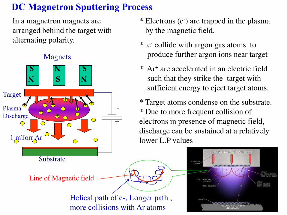
DC Magnetron Sputtering Process
* Electrons (e-) are trapped in the plasma
by the magnetic field.
* e- collide with argon gas atoms to
produce further argon ions near target
* Ar+ are accelerated in an electric field
such that they strike the target with
sufficient energy to eject target atoms.
* Target atoms condense on the substrate.
* Due to more frequent collision of
electrons in presence of magnetic field,
discharge can be sustained at a relatively
lower L.P values
N S S
S N N
+ +
+
+ + + -
+
+ + +
Magnets
Target
Plasma
Discharge
Substrate
1 mTorr Ar
In a magnetron magnets are
arranged behind the target with
alternating polarity.
Line of Magnetic field
Helical path of e-, Longer path ,
more collisions with Ar atoms mech14.weebly.com
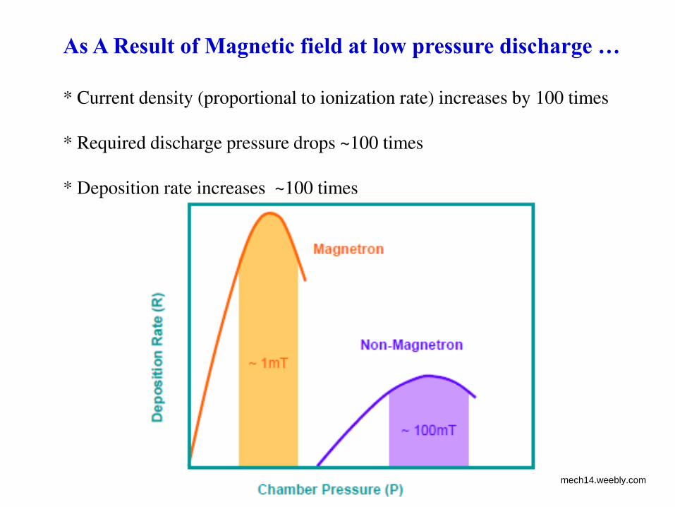
As A Result of Magnetic field at low pressure discharge …
* Current density (proportional to ionization rate) increases by 100 times
* Required discharge pressure drops ~100 times
* Deposition rate increases ~100 times
mech14.weebly.com
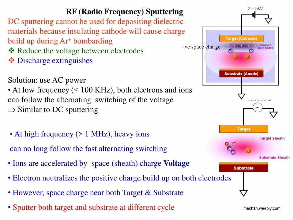
RF (Radio Frequency) Sputtering
DC sputtering cannot be used for depositing dielectric
materials because insulating cathode will cause charge
build up during Ar+ bombarding
Reduce the voltage between electrodes
Discharge extinguishes
Solution: use AC power
• At low frequency (< 100 KHz), both electrons and ions can follow the alternating switching of the voltage
Similar to DC sputtering
• At high frequency (> 1 MHz), heavy ions
can no long follow the fast alternating switching
• Ions are accelerated by space (sheath) charge Voltage
• Electron neutralizes the positive charge build up on both electrodes
• However, space charge near both Target & Substrate
• Sputter both target and substrate at different cycle
+ve space charge
mech14.weebly.com
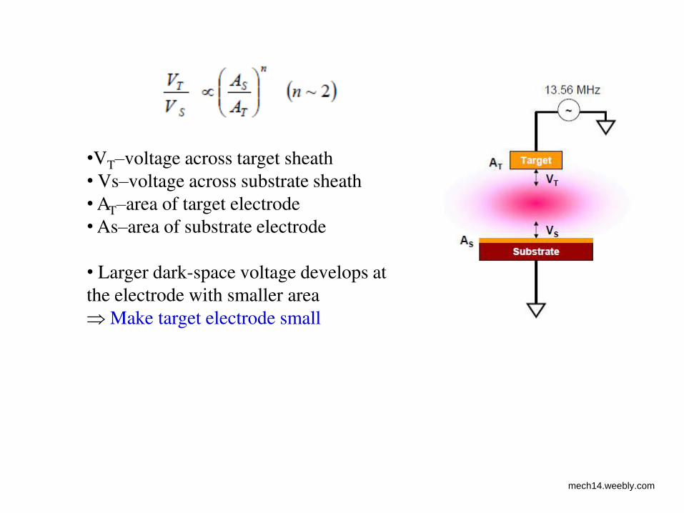
•VT–voltage across target sheath
• Vs–voltage across substrate sheath
• AT–area of target electrode
• As–area of substrate electrode
• Larger dark-space voltage develops at
the electrode with smaller area
Make target electrode small
mech14.weebly.com
mech14.weebly.com
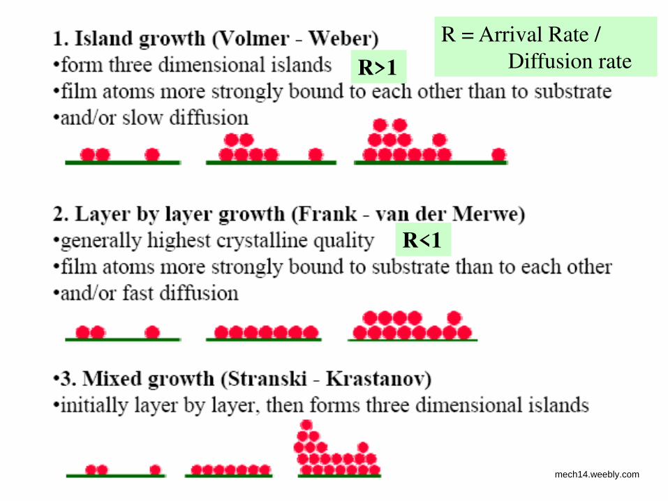
R = Arrival Rate /
Diffusion rate R>1
R<1
mech14.weebly.com
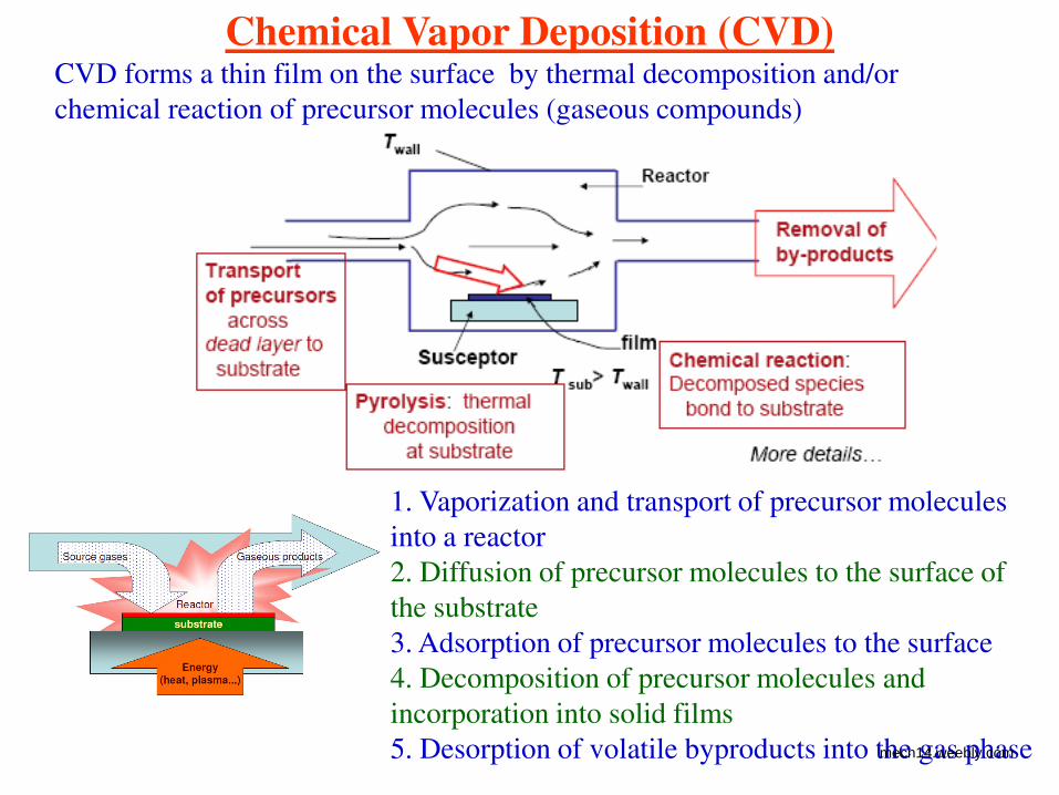
Substrate
1. Vaporization and transport of precursor molecules
into a reactor
2. Diffusion of precursor molecules to the surface of
the substrate
3. Adsorption of precursor molecules to the surface
4. Decomposition of precursor molecules and
incorporation into solid films
5. Desorption of volatile byproducts into the gas phase
Chemical Vapor Deposition (CVD) CVD forms a thin film on the surface by thermal decomposition and/or
chemical reaction of precursor molecules (gaseous compounds)
mech14.weebly.com
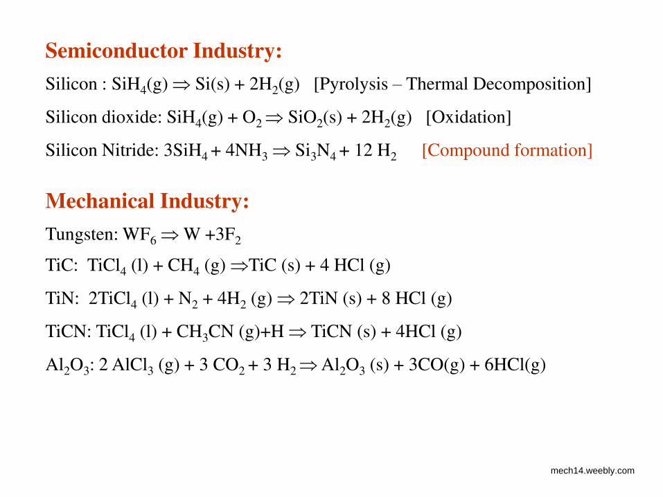
Semiconductor Industry:
Silicon : SiH4(g) Si(s) + 2H2(g) [Pyrolysis – Thermal Decomposition]
Silicon dioxide: SiH4(g) + O2 SiO2(s) + 2H2(g) [Oxidation]
Silicon Nitride: 3SiH4 + 4NH3 Si3N4 + 12 H2 [Compound formation]
Mechanical Industry:
Tungsten: WF6 W +3F2
TiC: TiCl4 (l) + CH4 (g) TiC (s) + 4 HCl (g)
TiN: 2TiCl4 (l) + N2 + 4H2 (g) 2TiN (s) + 8 HCl (g)
TiCN: TiCl4 (l) + CH3CN (g)+H TiCN (s) + 4HCl (g)
Al2O3: 2 AlCl3 (g) + 3 CO2 + 3 H2 Al2O3 (s) + 3CO(g) + 6HCl(g)
mech14.weebly.com
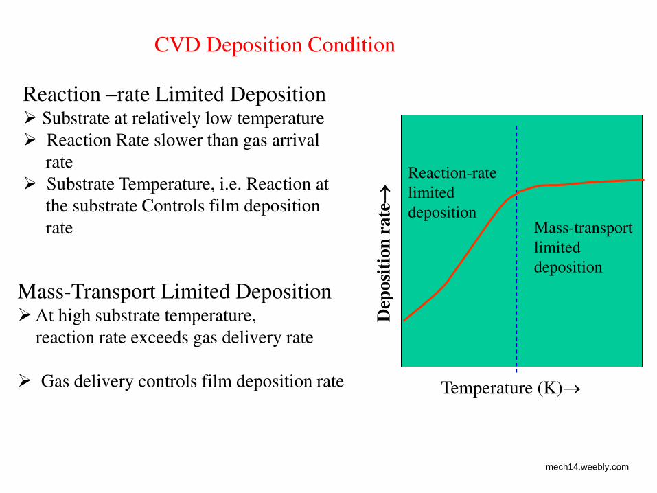
Temperature (K) D
epo
siti
on
rate
CVD Deposition Condition
Reaction-rate
limited
deposition Mass-transport
limited
deposition
Reaction –rate Limited Deposition Substrate at relatively low temperature
Reaction Rate slower than gas arrival
rate
Substrate Temperature, i.e. Reaction at
the substrate Controls film deposition
rate
Mass-Transport Limited Deposition At high substrate temperature,
reaction rate exceeds gas delivery rate
Gas delivery controls film deposition rate
mech14.weebly.com
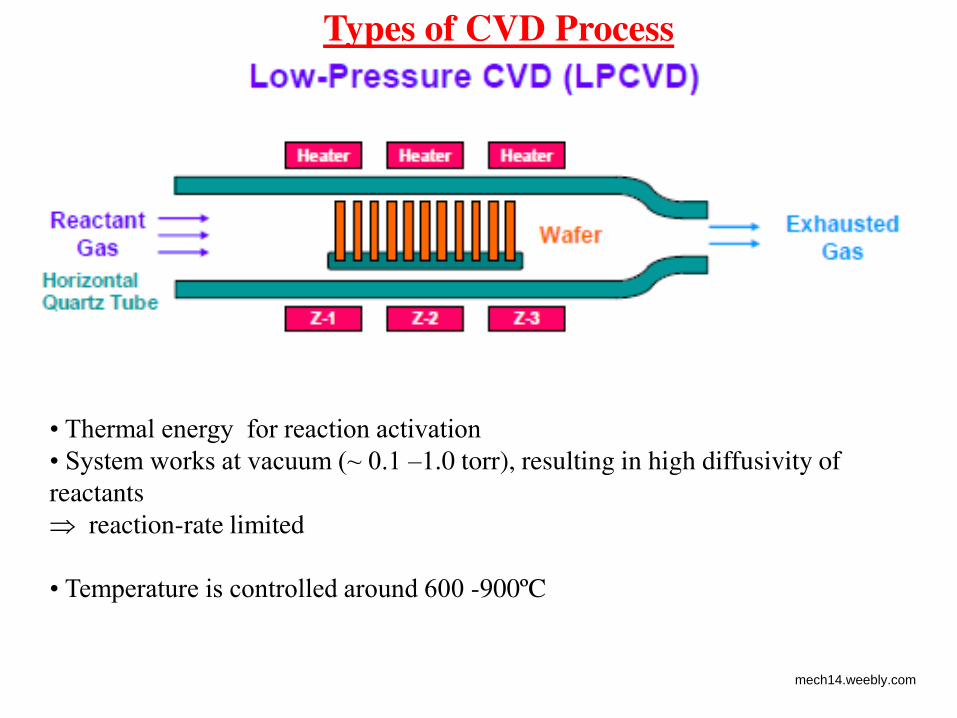
• Thermal energy for reaction activation
• System works at vacuum (~ 0.1 –1.0 torr), resulting in high diffusivity of
reactants
reaction-rate limited
• Temperature is controlled around 600 -900ºC
Types of CVD Process
mech14.weebly.com
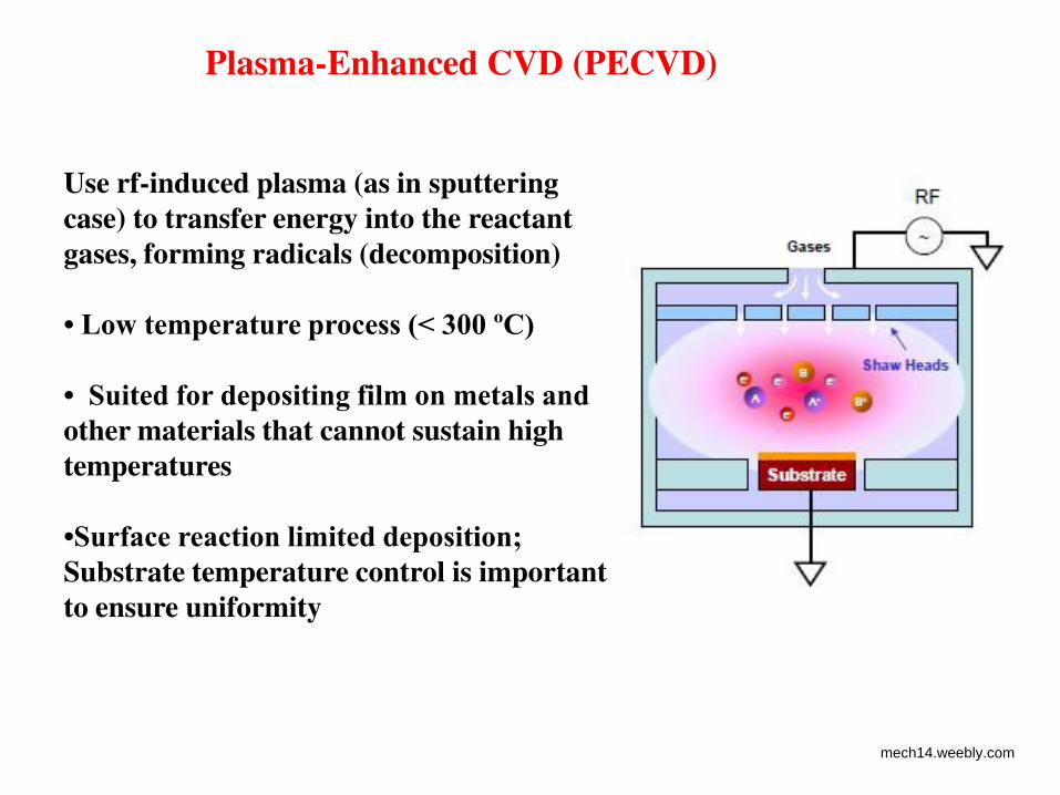
Plasma-Enhanced CVD (PECVD)
Use rf-induced plasma (as in sputtering
case) to transfer energy into the reactant
gases, forming radicals (decomposition)
• Low temperature process (< 300 ºC)
• Suited for depositing film on metals and other materials that cannot sustain high
temperatures
•Surface reaction limited deposition; Substrate temperature control is important
to ensure uniformity
mech14.weebly.com
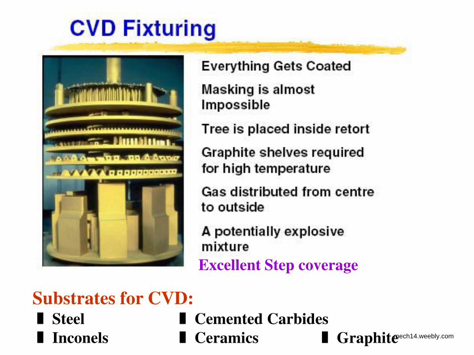
Excellent Step coverage
Substrates for CVD: ❚ Steel ❚ Cemented Carbides
❚ Inconels ❚ Ceramics ❚ Graphite
mech14.weebly.com
mech14.weebly.com