physics 3 problems ii. solid state . · pdf filephysics 3 problems ii. solid state physics. p....
TRANSCRIPT

Physics 3Problems II.
Solid State Physics.
P. Richter, A. SolyomDept. Atomic Physics
Faculty of Natural SciencesBudapest University of Technology and Economics - BME
March 27, 2013

The problems presented here together with their solutions help the deeper under-standing of the lectures. Similar problems may be given in the tests. We tried to give avery detailed solution for every one of them, however in the tests you need not give somuch details. This material will be refreshed from time to time, so please check the dateon the title page!
1
Chapter 2
Solid State Physics
2.1 Formulas used in the solutions
There exists an algebraic formula between the b1, b2, b3 primitive reciprocal latticevectors and the three primitive direct lattice vectors a1, a2, a3
b1 = 2πa2 × a3
a1 · (a2 × a3)
b2 = 2πa3 × a1
a1 · (a2 × a3)
b3 = 2πa1 × a2
a1 · (a2 × a3)
(2.1.1)
The effective masses of electrons and holes in Si and Ge are in Table 2.1. The effectivemass for conductivity of electrons mcc is what we must use for mobility or diffusionconstant calculations. For cubic isotropic semiconductors with anisotropic dispersionrelations minima (again e.g. Si and Ge), one has to sum over the effective masses in thedifferent minima along the equivalent directions. The resulting effective mass for bandswhich have ellipsoidal constant energy surfaces is given by:
mcc =3
1
ml
+1
ml
+1
mt
The general formula from the calculations above can be expressed in the simple form
Nc(T ) = 2.5 1019
(mc
me
) 32(
T
300K
) 32
(2.1.2)
Pv(T ) = 2.5 1019
(mh
me
) 32(
T
300K
) 32
(2.1.3)
2

electronsrel. eff.mass Si Ge
longitudinal ml/me 0.98 1.59transversal mt/me 0.19 0.0815dens.of.states mc/me 0.36 0.22conduct. mcc/me 0.26 0.12
holesrel. eff.mass Si Ge
heavy mh/me 0.49 0.33light mlp/me 0.16 0.043split-off band mso/me 0.24 0.084dens.of.states mv/me 0.81 0.34
Table 2.1: Effective masses in Si and Ge
Figure 2.1: Two different primitive vector sets for the bcc lattice.a) a1 = aex, a2 = aey, a3 = aezb) a1 = a
2 (aey + ez − ex), a2 (aez + ex − ey,
a2 (aex + ey − ez)
As a result of collisions the ordered part of the electron velocities, called the driftvelocity will be constant and proportional with the field strength:
vdrift = µE (2.1.4)
where the constant of proportionality is the mobility µ of the electrons
µ =
(eτ
me
)(2.1.5)
j(= σE) =
(ne2τ
me
)E
3

and
σ =ne2τ
me
(2.1.6)
One way to determine the value of τ is from (2.1.6), where the density n of conductionelectrons is
n = LAZρmA
(2.1.7)
j = e(nc µe + pv µh)E (2.1.8)
j = nie〈v〉 = nie(µe + µh)E and
j = σE
σ = nie(µe + µh) (2.1.9)
Metal| Li Na K Rb Cs Cu Ag Au Mg AlEF (eV )| 4.7 3.1 2.1 1.8 1.5 4.1 5.5 5.5 7.3 11,9
Table 2.2: Fermi energies of some metals
Any of these energy states can be occupied by 2 electrons with opposite spins. Ifeach atom contribute s conduction electrons to the crystal then at T = 0K all possibleenergy states below
EF (= Emax,occupied) =~2π2
2mea2s
2(2.1.10)
will be occupied and all levels above it will be empty. EF is called the Fermi energy ofthe system. We denote the corresponding k value with kF and call it the Fermi wavevector.
The Fermi-Dirac distribution function:
fFD(E) =1
e(E−EF )/kBT + 1(2.1.11)
The number of electrons (Ne = N · s):
Ne = 2k3F6π2
V ⇒ n(≡ Ne
V) =
k3F3π2
(2.1.12)
4

When s = 2 the length of the Fermi wave vector will be 2π/a and the allowed k valueswill satisfy
k ∈[−πa,π
a
]For n-type semiconductors (N+
d > N−a where N+d ≈ Ndand N+
a ≈ Na):
nc ≈ (Nd −Na) pv ≈n2i
Nd −Na
(2.1.13)
while for p-type semiconductors (Na > Nd):
pv ≈ (Na −Nd) nc ≈n2i
Na −Nd
(2.1.14)
nc(T ) = Nce−Ec−EF
kBT (2.1.15a)
pv(T ) = Pve−EF−Ev
kBT (2.1.15b)
where Nc and Pv are the effective density of states in the conduction and valence bandsrespectively:
Nc(T ) = 2 ·(
2πmekBT
h2
)3
2 (2.1.16)
Pv(T ) = 2 ·(
2πmhkBT
h2
)3
2 (2.1.17)
dn =
√Na
Nd(Nd +Na)
ε∆ϕ
2 e
dp =
√Nd
Na(Nd +Na)
ε∆ϕ
2 e
(2.1.18)
In doped semiconductors:
n(d)c (T ) = ni e
−E(d)F−EF
kBT for an n-type semiconductor (2.1.19a)
p(a)v (T ) = ni e−EF−E
(a)F
kBT for a p-type semiconductor (2.1.19b)
5

E (d)F =1
2(Ec + Edonor) +
3
4kBT ln
(mh
mc
)(2.1.20a)
E (a)F =1
2(Ev + Eacceptor) +
3
4kBT ln
(mh
mc
)(2.1.20b)
acceptor in B Al Ga In TeSi 0.046 0.057 0.065 0.16 0.26Ge 0.01 0.01 0.061 0.011 0.01
donor in P As Sb BiSi 0.046 0.057 0.065 0.16 .Ge 0.01 0.01 0.061 0.011 .
Table 2.3: Shallow donor and acceptor levels in Si and Ge in eV.
e∆ϕ = kBT ln
(NdNa
n2i (T )
)(2.1.21)
For intrinsic semiconductors
nc(T ) = pv(T ) (2.1.22)
ni ≡ nc(T ) = pv(T ) =√Nc(T )Pv(T ) e
− Eg2kBT (2.1.23)
6

2.2 Problems
Problem 1.Enumerate the symmetries the following “crystal” has.
Solution:
This “crystal” has the following symmetry elements:
• 1 - 4-fold rotation axis (A4)
• 4 - 2-fold rotation axes (A2), 2 cutting the faces and 2 cutting theedges
• 5 mirror planes (m), 2 cutting across the faces, 2 cutting throughthe edges, and one cutting horizontally through the center.
• There is a center of symmetry (i).
Problem 2.Calculate the surface density of atoms in a bcc crystal if the lattice constant
is a = 0.5nm (= 5 )A and the surface plane cuts the cells diagonally and it isperpendicular to the plane of the a1 and a2 vectorsa.
Solution:
7

The plane in question goes through 4 corner atoms and the middle atom of thecell. Only 1/4th of each of the cross sections of the corner atoms belong to our cell,while the cross section of the middle atom is completely inside it. Therefore thenumber of atoms on this plane is 2. The area of the plane is a · a
√2 , so the density
of atoms is2
a2√
2=
√2
(0.5 10−9)2= 5.66 1018atoms
m2
ai.e. it is a (110) plane - see Miller indices below
Problem 3.With (2.1.1) we can easily prove that the reciprocal lattice of an fcc lattice is a
bcc lattice:Start with the following selection of primitive fcc lattice vectors:
8

Then the 3 primitive vectors are
a1 =a
2(i + k)
a2 =a
2(i + j)
a3 =a
2(j + k)
(2.2.1)
Determine first the denominator in (2.1.1), which is the volume of the primitivecell:
a1 · (a2 × a3) =a
2(i + k) ·
(a2
(i + j)× a
2(j + k)
)=a3
8(i + k) · ((i + j)× (j + k))
=a3
8[i · (i× j) + i · (i× k)
+ i · (j× k) + k · (i× j)
+ k · (i× k) + k · (j× k)]
=a3
8(i · (j× k) + k · (i× j))
here we used that i, j and k are perpendicular to each other. Furthermore
i× j = k, j× k = i and k× i = j
Therefore
a1 · (a2 × a3) =a3
4
Now work with the numerators using the same formulas for i, j and k:
a2 × a3 =a2
4(k− j + i)a3 × a1 =
a2
4(i− k + j)a1 × a2 =
a2
4(j− i + k)
Which gives us the reciprocal base vectors:
b1 =2π
a(a2
4(k− j + i)
b2 =2π
a(i− k + j)
b3 =2π
a(j− i + k)
(2.2.2)
Compare (2.2.2) with vectors in Fig. 2.1 to see that we, in fact got the primitivevectors of a bcc lattice. The only difference is that the length is now. 2π
a. This
means that the volume of the primitive cell in a reciprocal lattice is (2π)3
Vwhere V
is the volume of the primitive cell of the original lattice.
9
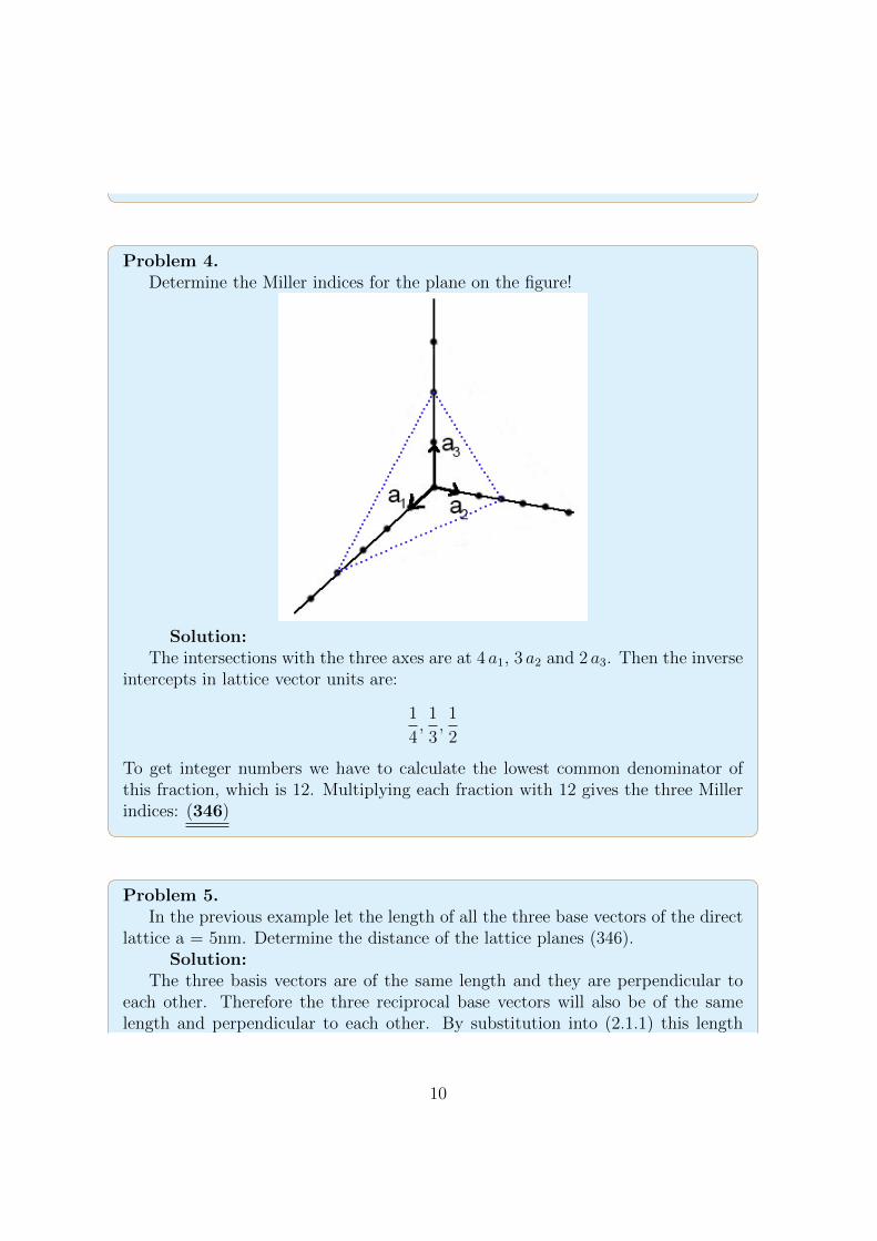
Problem 4.Determine the Miller indices for the plane on the figure!
Solution:The intersections with the three axes are at 4 a1, 3 a2 and 2 a3. Then the inverse
intercepts in lattice vector units are:
1
4,1
3,1
2
To get integer numbers we have to calculate the lowest common denominator ofthis fraction, which is 12. Multiplying each fraction with 12 gives the three Millerindices: (346)
Problem 5.In the previous example let the length of all the three base vectors of the direct
lattice a = 5nm. Determine the distance of the lattice planes (346).Solution:
The three basis vectors are of the same length and they are perpendicular toeach other. Therefore the three reciprocal base vectors will also be of the samelength and perpendicular to each other. By substitution into (2.1.1) this length
10

is b =2π
a= 1.26nm−1. The length of the reciprocal vector perpendicular to the
(346) planes is
|b346| =√
32 + 42 + 62 · 2π
a(=√
61 · 1.26 = 9.81nm−1)
The distance of the planes (346) therefore is
d346 =a√61
= 0.64nm
Problem 6.Draw all 9 lattice planes and determine the Miller indices in a simple cubic
Bravais lattice.Solution:
(Where is the origin of the 3 lattice vectors in the cubes?)
Problem 7.Determine the possible diffraction angles for an X-ray of 10 keV from the (111)
planes of a simple cubic lattice, if the lattice constant is a = 5.3 A.Solution:
11

The wavelength of the X-ray:
E = h ν =h c
λ⇒ λ =
h c
E= 1.24 10−10m
To apply Bragg’s law2 d sinθ = nλ
we need to calculate the distance of the lattice planes of Miller indices (111), whichare planes going through 3 non adjacent corner of the cube. The distance of twosuch planes that intersects a primitive cell (see the figure in the previous example)is 3rd of the body diagonal:
d =1
3
√3 a = 0.305nm
The possible diffraction angles are determined by:
sinθ = nλ
2 d= 0.20325n
Here n = 1, 2, 3, 4, i.e. the angles are
11.72o, 23.99o, 3.57o, and 54.39o
12

Problem 8.Aluminum has three valence electrons per atom, an atomic weight of 0.02698
kg/mol, a density of 2700kg/m3, and a conductivity of 3.54 107 S/m. Calculatethe electron mobility in aluminum. Assume that all three valence electrons of eachatoms are free.
Solution:The number of aluminum atoms per m3 is
na = 6.021023 atoms/mol · 1/0.02698 mol/kg · 2700 kg/m3
= 6.024 1028 atoms/m3
Thus the electron density in aluminum is
n = 3 · 6.024 1028 atoms/m3 = 1.807 1029 electron/m3
From (2.1.5)
µ =σ
ne=
3.54 107
1.807 1029 · 1.6022 10−19= 1.22 10−3m/s
13

Problem 9.What is the value of τ in silver at t = 0 oC if the measured resistivity is 1.51 ·
10−8 Ωm?Solution:
From (2.1.6), (2.1.7) using the definition of ρ
τ =me
ρ(T )n e2=
meA
LA Z ρm e2 ρ
Silver has a single 5s1 electron so Z = 1 and the mass density isρm = 10.49 g/cm3 = 1.049 ·104 kg/m3, A = 107.8682 g/mol = 0.1078682 kg/moland ρ(273K) = 1.51 · 10−8 Ωm. After substitution
τ = 4.013 · 10−14 s
Problem 10.What is the quasi-free electron density in copper? Calculate the Fermi velocity
and momentum tooSolution:
From Table 2.2 and formulas (2.1.12) and (2.1.10)
n =(2me EF )3/2
2 π2 ~3= 5.655 1028 electron
m3
vF = 1.2 106m/s = 0.004 c kF = 1.0 10111/m
Problem 11.The dispersion relation of electrons in the valence and conduction bands near
the band edges are approximated by the following functions:
Ev(k) = −3.024 10−20(k − 2.45108)2 + 13 [eV ]
Ec(k) = 4.65 10−20k2 + 11.9 [eV ]
Express the effective masses of electrons in units of the free electron mass me =9.1 · 10−31kg.
Solution:
14
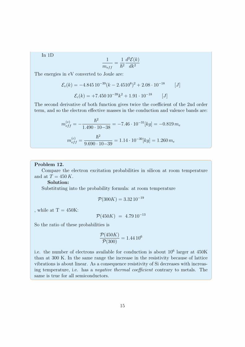
In 1D1
meff
=1
~2d2E(k)
dk2
The energies in eV converted to Joule are:
Ev(k) = −4.845 10−39(k − 2.45108)2 + 2.08 · 10−18 [J ]
Ec(k) = +7.450 10−39k2 + 1.91 · 10−18 [J ]
The second derivative of both function gives twice the coefficient of the 2nd orderterm, and so the electron effective masses in the conduction and valence bands are:
m(v)eff = − ~2
1.490 · 10−38= −7.46 · 10−31[kg] = −0.819me
m(c)eff =
~2
9.690 · 10−39= 1.14 · 10−30[kg] = 1.260me
Problem 12.Compare the electron excitation probabilities in silicon at room temperature
and at T = 450K.Solution:
Substituting into the probability formula: at room temperature
P(300K) = 3.32 10−19
, while at T = 450K:P(450K) = 4.79 10−13
So the ratio of these probabilities is
P(450K)
P(300)= 1.44 106
i.e. the number of electrons available for conduction is about 106 larger at 450Kthan at 300 K. In the same range the increase in the resistivity because of latticevibrations is about linear. As a consequence resistivity of Si decreases with increas-ing temperature, i.e. has a negative thermal coefficient contrary to metals. Thesame is true for all semiconductors.
15

Problem 13.A rod of intrinsic Si is 1 cm long and has a diameter of 1mm. At room temper-
ature, the intrinsic concentration in the silicon is ni = 1.5 1016m−3. The electronand hole mobilities are µe = 0.13m2V −1s−1 and µh = 0.05m2V −1s−1. Calculatethe conductivity σ of the silicon and the resistance R of the rod.
Solution:
σ = nie(µe + µh) = 4.33 10−41/Ωm
R =l
σd2π/4= 29.4MΩ
Problem 14.Calculate the effective carrier densities of states in the conduction and valence
bands of germanium and silicon at 300 K.Solution:
Substitute the effective masses for the density of states from Table 2.1 into(2.1.16) and (2.1.17).
cm−3 Ge SiNc(300K) 1.02 1019 2.81 1019
Pv(300K) 5.64 1018 1.83 1019
Problem 15.A rod of n-type extrinsic Si is 1 cm long and has a diameter of 1mm. At room
temperature, the donor concentration is 5 1014 atom/cm3 and this corresponds to1 impurity for 108 Si atoms. A steady 2µA current is flowing through the bar.Determine the electron and hole concentration, the conductivity and the voltageacross the rod. The intrinsic electron concentration in silicon isa ni = 1.01 1010m−3.The electron mobility is µe = 0.13m2 V −1 s−1.
Solution:n-type: Na ≈ 0. From (2.1.13) n = Nd = 5 10201/m3,
pv =n2i
Nd
= 4.5 10131/m3
From (2.1.8) and using that pv nc
σ = encµe = 0.104S/m
16

The voltage across the rod:
U =I l
σA= 0.12V
aThe previously accepted value before 1991 was 1.45 · 1010
17

Problem 16.Determine the ratio of conduction electrons from P dopants in Si to the intrinsic
electron concentration at the following temperatures: room temperature, 100oC and500oC! Is it possible for the intrinsic electron concentration to become larger thanthe one due to the dopants?
Solution:a)
P is a donor atom, therefore the ratio of the conduction electrons from P andfrom the valence band can be calculated according to (2.1.19), using (2.1.20a) and
neglecting the factor ln
(mc
mh
):
n(d)c (T )
ni(T )= e
−E(d)F−EF
kBT
= e−(Ed−Ev2 kBT
)
= e−(Ed−Ec+Eg
2 kBT
)
The value of Ed − Ec from Table 2.3 is −0.046 eV , Eg = 1.12 eV , and kBT at roomtemperature (300 K) equals to 0.0258 eV so
n(d)c (T )
ni(T )= e−( 1.12−0.046
2·0.0258 ) = 1.09 · 109
Similarly at 100oC (373K) and 500oC (773K)
n(d)c (373K)
ni(373K)= 1.08 · 107
n(d)c (773K)
ni(773K)= 3.17 · 103
The conduction electron concentration in P doped Si at room temperature is ≈ 109
times larger than the electron concentration in intrinsic Si, and about a thousandtimes as large even at the very high temperature of 737 K !
18
b)From this formulas it seems that the intrinsic electron concentration may neverreach n
(d)c and the two concentrations may never even be equal. But this is not so.
We made some assumptions, which become invalid at higher temperatures. First weneglected the logarithmic terms when we calculated the Fermi energies and secondwe neglected the fact that the donor concentration is very small and the numberof conduction electrons from donors has an upper limit, i.e. the electron densitydue to dopants has saturation. Therefore it is possible for the intrinsic electronconcentration to exceed the electron concentration from dopants.
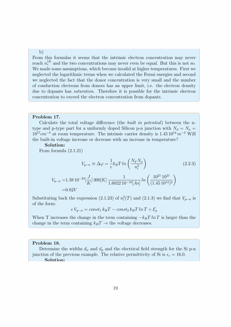
Problem 17.Calculate the total voltage difference (the built in potential) between the n-
type and p-type part for a uniformly doped Silicon p-n junction with Nd = Na =1017cm−3 at room temperature. The intrinsic carrier density is 1.45 1014m−3 Willthe built-in voltage increase or decrease with an increase in temperature?
Solution:From formula (2.1.21)
Vp−n ≡ ∆ϕ =1
ekBT ln
(NdNa
n2i
)(2.2.3)
Vp−n =1.38 10−23[J
K] 300[K]
1
1.6022 10−19[As]ln
(1021 1021
(1.45 1014)2
)=0.82V
Substituting back the expression (2.1.23) of n2i (T ) and (2.1.3) we find that Vp−n is
of the form:e Vp−n = const1 kBT − const2 kBT ln T + Eg
When T increases the change in the term containing −kBT ln T is larger than thechange in the term containing kBT → the voltage decreases.
Problem 18.Determine the widths dn and dp and the electrical field strength for the Si p-n
junction of the previous example. The relative permittivity of Si is εr = 16.0.Solution:
19
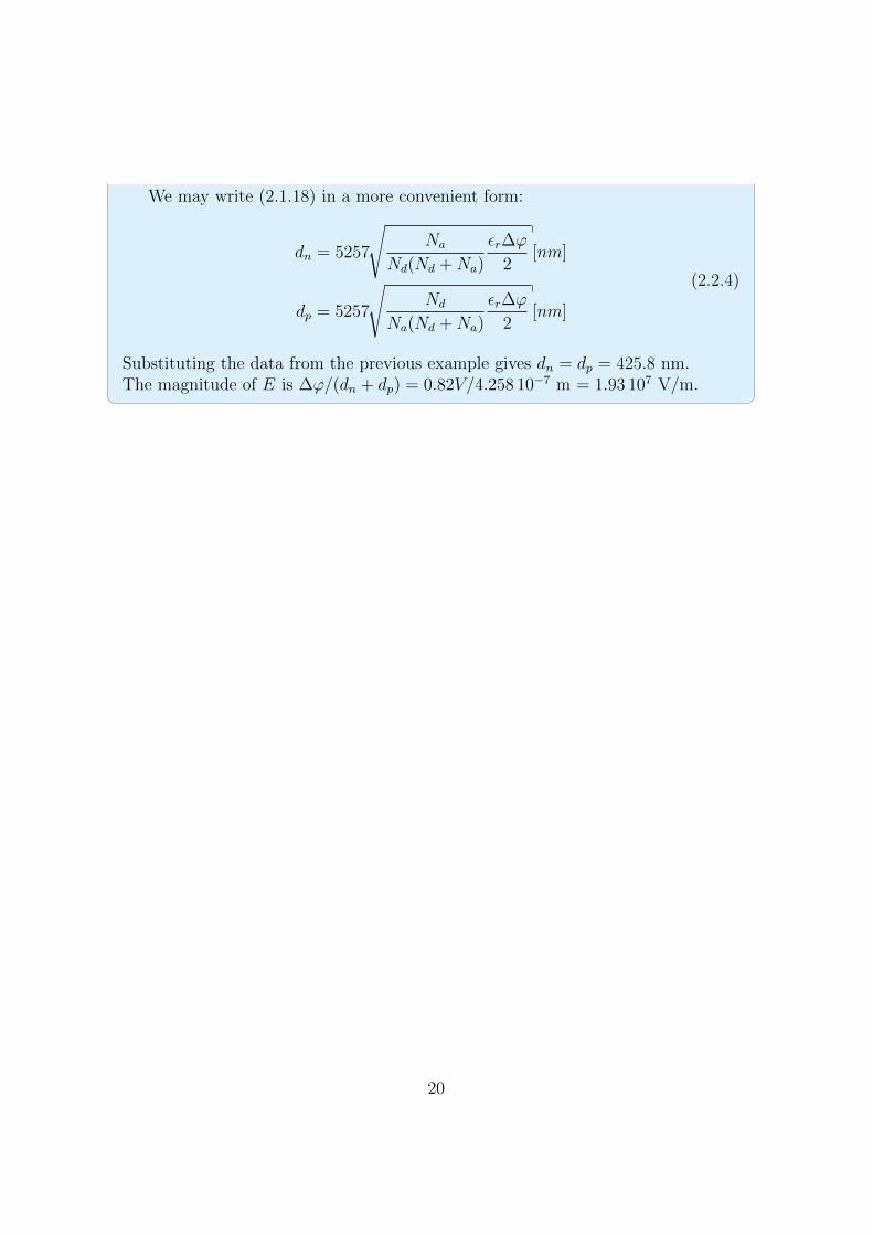
We may write (2.1.18) in a more convenient form:
dn = 5257
√Na
Nd(Nd +Na)
εr∆ϕ
2[nm]
dp = 5257
√Nd
Na(Nd +Na)
εr∆ϕ
2[nm]
(2.2.4)
Substituting the data from the previous example gives dn = dp = 425.8 nm.The magnitude of E is ∆ϕ/(dn + dp) = 0.82V/4.258 10−7 m = 1.93 107 V/m.
20