pic analog voltage to pwm duty cycle - …seniordesignlab.com/sdl_docs/labs/lab5_pic_adc2pwm.pdf ·...
TRANSCRIPT
Name __________________________
Lab Section _____________________
PIC – Analog Voltage to PWM Duty Cycle Lab 5
Introduction: In this lab you will convert an analog voltage into a pulse width modulation (PWM) duty cycle. The source of the analog voltage will be the trim pot voltage divider attached to RA2/ANA2 (pin 11) of your PIC Dev 14 board. The pulse width modulation output will drive the LED connected to RC5 (pin 5) so you can monitor the PWM duty cycle as the brightness of the LED. Lab Requirements:
1. Demonstration of LED Dimmer Control using the analog to digital converter (ADC) and pulse width modulation (PWM).
Demo Check (JK)______
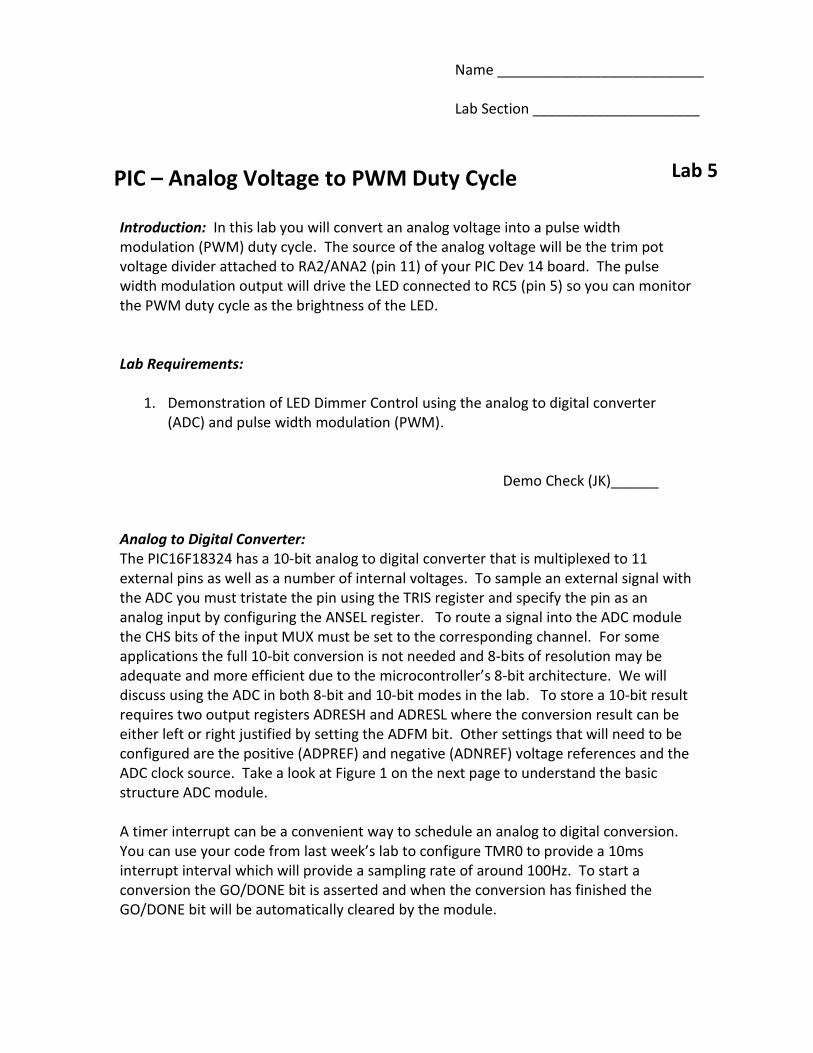
Analog to Digital Converter: The PIC16F18324 has a 10-bit analog to digital converter that is multiplexed to 11 external pins as well as a number of internal voltages. To sample an external signal with the ADC you must tristate the pin using the TRIS register and specify the pin as an analog input by configuring the ANSEL register. To route a signal into the ADC module the CHS bits of the input MUX must be set to the corresponding channel. For some applications the full 10-bit conversion is not needed and 8-bits of resolution may be adequate and more efficient due to the microcontroller’s 8-bit architecture. We will discuss using the ADC in both 8-bit and 10-bit modes in the lab. To store a 10-bit result requires two output registers ADRESH and ADRESL where the conversion result can be either left or right justified by setting the ADFM bit. Other settings that will need to be configured are the positive (ADPREF) and negative (ADNREF) voltage references and the ADC clock source. Take a look at Figure 1 on the next page to understand the basic structure ADC module. A timer interrupt can be a convenient way to schedule an analog to digital conversion. You can use your code from last week’s lab to configure TMR0 to provide a 10ms interrupt interval which will provide a sampling rate of around 100Hz. To start a conversion the GO/DONE bit is asserted and when the conversion has finished the GO/DONE bit will be automatically cleared by the module.
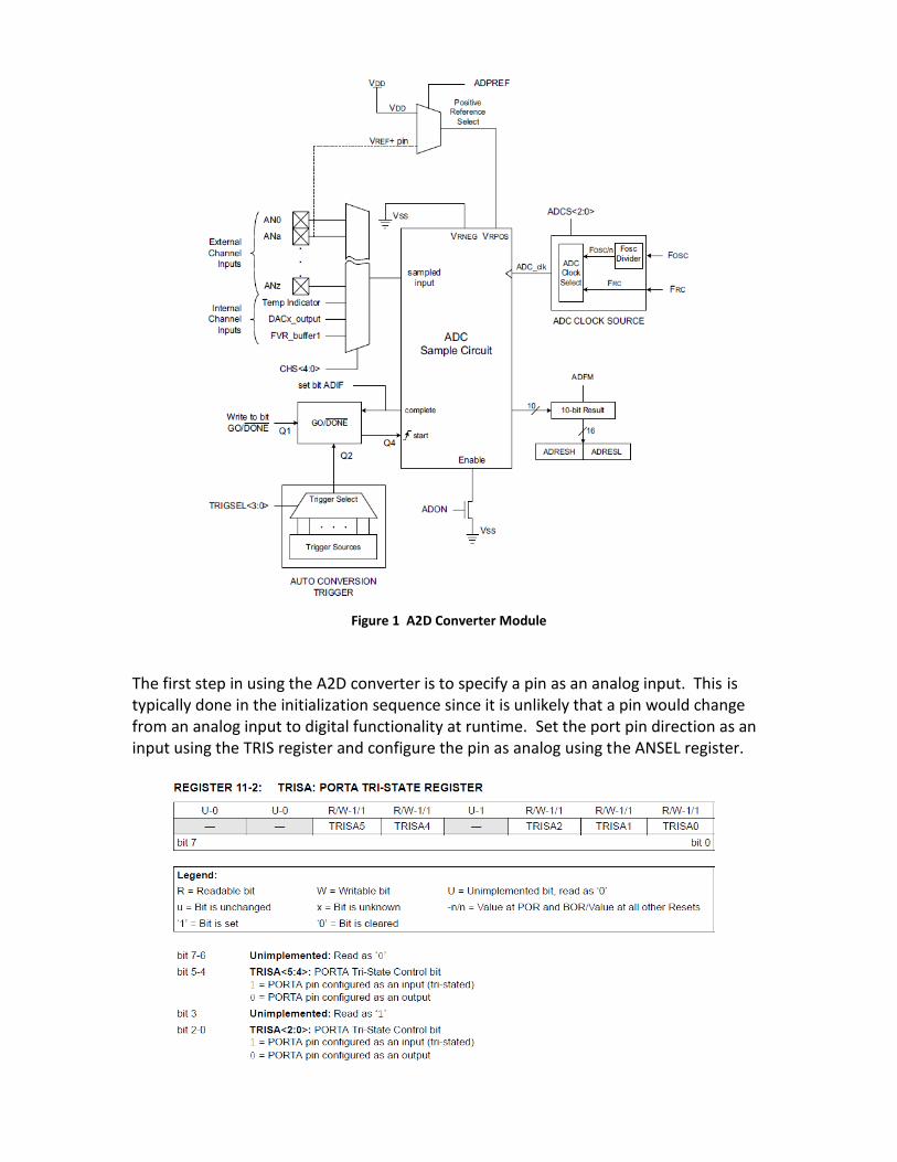
Figure 1 A2D Converter Module
The first step in using the A2D converter is to specify a pin as an analog input. This is typically done in the initialization sequence since it is unlikely that a pin would change from an analog input to digital functionality at runtime. Set the port pin direction as an input using the TRIS register and configure the pin as analog using the ANSEL register.
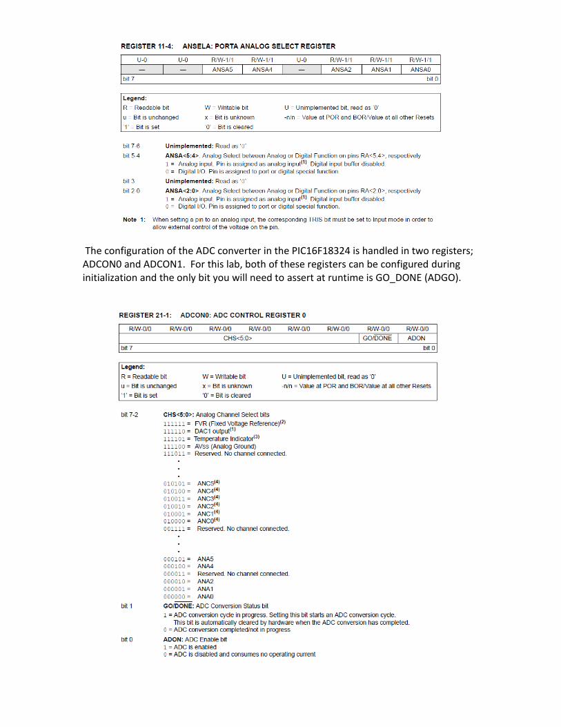
The configuration of the ADC converter in the PIC16F18324 is handled in two registers; ADCON0 and ADCON1. For this lab, both of these registers can be configured during initialization and the only bit you will need to assert at runtime is GO_DONE (ADGO).
The Analog Channel Select bits CHS <5:0> should be set to route the input from the port pin into the analog to digital converter. Since the potentiometer is connected to RA2/ANA2 (pin 11) the value should be “000010”. The ADON bit should be set to turn the ADC on but the Go/nDONE bit should not be set at the same time that the converter is being switched on. The Go/nDONE bit will be asserted later to start a conversion.
ADCON0 = 0b00001001;
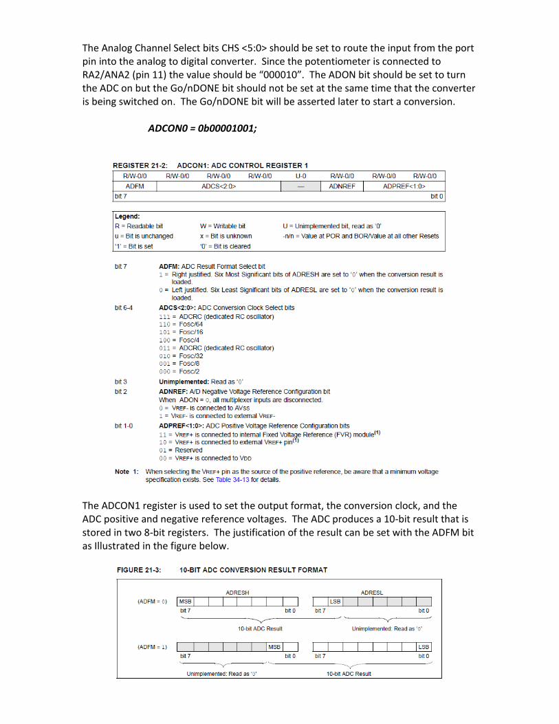
The ADCON1 register is used to set the output format, the conversion clock, and the ADC positive and negative reference voltages. The ADC produces a 10-bit result that is stored in two 8-bit registers. The justification of the result can be set with the ADFM bit as Illustrated in the figure below.
The recommended ADC conversion times are from 1-4us per bit. When operating with a Fosc of 4MHz a suitable conversion clock (ADCS) would be either Fosc/4, Fosc/8 or Fosc/16. For this lab the ADC reference voltages can be VDD and VSS.
ADCON1 = 0b01010000;
To start a conversion set the Go/nDONE bit (ADGO = 1;). The conversion result will be ready when the Go/nDONE bit clears. You can wait for the conversion to finish by testing the status of the Go/nDONE bit like the code below:
bsf ADCON0, GO_DONE ; Start Conversion btfsc ADCON0, GO_DONE ; Conversion Done? goto $-1 ; No, Test Again movf ADRESH, W ; Yes, Put A2D result into W
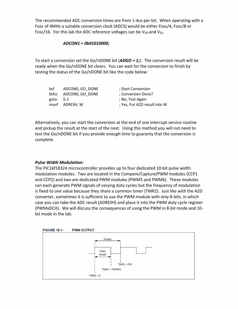
Alternatively, you can start the conversion at the end of one interrupt service routine and pickup the result at the start of the next. Using this method you will not need to test the Go/nDONE bit if you provide enough time to guaranty that the conversion is complete. Pulse Width Modulation: The PIC16f18324 microcontroller provides up to four dedicated 10-bit pulse width modulation modules. Two are located in the Compare/Capture/PWM modules (CCP1 and CCP2) and two are dedicated PWM modules (PWM5 and PWM6). These modules can each generate PWM signals of varying duty cycles but the frequency of modulation is fixed to one value because they share a common timer (TMR2). Just like with the A2D converter, sometimes it is sufficient to use the PWM module with only 8-bits, in which case you can take the ADC result (ADRESH) and place it into the PWM duty cycle register (PWMxDCH). We will discuss the consequences of using the PWM in 8-bit mode and 10-bit mode in the lab.
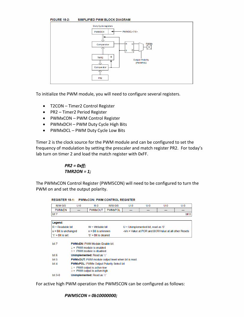
To initialize the PWM module, you will need to configure several registers.
T2CON – Timer2 Control Register
PR2 – Timer2 Period Register
PWMxCON – PWM Control Register
PWMxDCH – PWM Duty Cycle High Bits
PWMxDCL – PWM Duty Cycle Low Bits Timer 2 is the clock source for the PWM module and can be configured to set the frequency of modulation by setting the prescaler and match register PR2. For today’s lab turn on timer 2 and load the match register with 0xFF. PR2 = 0xff; TMR2ON = 1; The PWMxCON Control Register (PWM5CON) will need to be configured to turn the PWM on and set the output polarity.
For active high PWM operation the PWM5CON can be configured as follows:
PWM5CON = 0b10000000;
To set the PWM duty cycle you will write to the PWM5DCH and PWM5DCL registers.
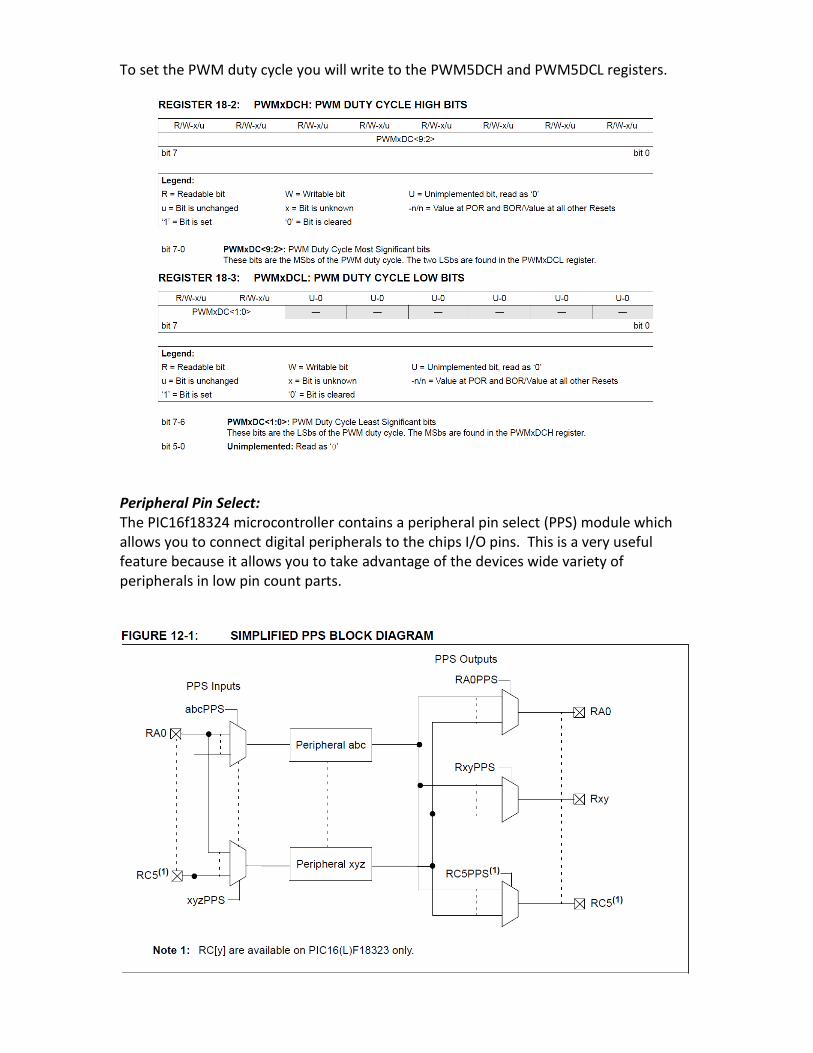
Peripheral Pin Select: The PIC16f18324 microcontroller contains a peripheral pin select (PPS) module which allows you to connect digital peripherals to the chips I/O pins. This is a very useful feature because it allows you to take advantage of the devices wide variety of peripherals in low pin count parts.
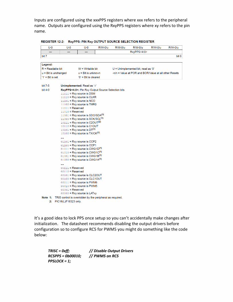
Inputs are configured using the xxxPPS registers where xxx refers to the peripheral name. Outputs are configured using the RxyPPS registers where xy refers to the pin name.
It’s a good idea to lock PPS once setup so you can’t accidentally make changes after initialization. The datasheet recommends disabling the output drivers before configuration so to configure RC5 for PWM5 you might do something like the code below: TRISC = 0xff; // Disable Output Drivers RC5PPS = 0b00010; // PWM5 on RC5 PPSLOCK = 1;