pic16c717/770/771 - microchip technologyww1.microchip.com/downloads/en/devicedoc/41120c.pdf ·...
TRANSCRIPT

PIC16C717/770/77118/20-Pin, 8-Bit CMOS Microcontrollers with 10/12-Bit A/D
Microcontroller Core Features:
• High-performance RISC CPU• Only 35 single word instructions to learn• All single cycle instructions except for program
branches which are two cycle• Operating speed: DC - 20 MHz clock input
DC - 200 ns instruction cycle
• Interrupt capability (up to 10 internal/external interrupt sources)
• Eight level deep hardware stack
• Direct, indirect and relative addressing modes
• Power-on Reset (POR)
• Power-up Timer (PWRT) andOscillator Start-up Timer (OST)
• Watchdog Timer (WDT) with its own on-chip RC oscillator for reliable operation
• Selectable oscillator options:- INTRC - Internal RC, dual speed (4 MHz and
37 kHz nominal) dynamically switchable for power savings
- ER - External resistor, dual speed (user selectable frequency and 37 kHz nominal) dynamically switchable for power savings
- EC - External clock- HS - High speed crystal/resonator- XT - Crystal/resonator- LP - Low power crystal
• Low power, high speed CMOS EPROM technology
• In-Circuit Serial Programming™(ICSP™• Wide operating voltage range: 2.5V to 5.5V
• 15 I/O pins with individual control for:- Direction (15 pins)- Digital/Analog input (6 pins)- PORTB interrupt on change (8 pins)- PORTB weak pull-up (8 pins)- High voltage open drain (1 pin)
• Commercial and Industrial temperature ranges
• Low power consumption: - < 2 mA @ 4V, 4 MHz- 11 A typical @ 2.5V, 37 kHz- < 1 A typical standby current
Pin Diagram
Peripheral Features:
• Timer0: 8-bit timer/counter with 8-bit prescaler
• Timer1: 16-bit timer/counter with prescaler,can be incremented during SLEEP via external crystal/clock
• Timer2: 8-bit timer/counter with 8-bit periodregister, prescaler and postscaler
• Enhanced Capture, Compare, PWM (ECCP)module- Capture is 16-bit, max. resolution is 12.5 ns- Compare is 16-bit, max. resolution is 200 ns- PWM max. resolution is 10-bit- Enhanced PWM:
- Single, Half-Bridge and Full-Bridge Output modes
- Digitally programmable deadband delay
• Analog-to-Digital converter:- PIC16C770/771 12-bit resolution- PIC16C717 10-bit resolution
• On-chip absolute bandgap voltage reference generator
• Programmable Brown-out Reset (PBOR) circuitry
• Programmable Low-Voltage Detection (PLVD) circuitry
• Master Synchronous Serial Port (MSSP) with two modes of operation:- 3-wire SPI™ (supports all 4 SPI modes)- I2C™ compatible including Master mode
support
• Program Memory Read (PMR) capability for look-up table, character string storage and checksum calculation purposes
Device
Memory
PinsA/D
ResolutionA/D
ChannelsProgramx14
Datax8
PIC16C717 2K 256 18, 20 10 bits 6
PIC16C770 2K 256 20 12 bits 6
PIC16C771 4K 256 20 12 bits 6
RB3/CCP1/P1A
RB2/SCK/SCL
RA7/OSC1/CLKIN
RA6/OSC2/CLKOUT
VDD
RB7/T1OSI/P1D
RB6/T1OSO/T1CKI/P1C
RB5/SDO/P1B
RB4/SDI/SDA
RA0/AN0RA1/AN1/LVDIN
RA4/T0CKI
RA5/MCLR/VPP
VSS
RA2/AN2/VREF-/VRL
RA3/AN3/VREF+/VRH
RB0/AN4/INT
RB1/AN5/SS
1
2
3
4
5
6
7
8
9
20
19
18
17
16
15
14
13
12
AVDDAVSS
10 11
PIC
16
C7
70
/77
120-Pin PDIP, SOIC, SSOP
1999-2013 Microchip Technology Inc. DS41120C-page 1

PIC16C717/770/771
Pin Diagrams
18-Pin PDIP, SOIC
RB3/CCP1/P1A
RB2/SCK/SCL
RA7/OSC1/CLKIN
RA6/OSC2/CLKOUT
VDD
RB7/T1OSI/P1D
RB6/T1OSO/T1CKI/P1C
RB5/SDO/P1B
RB4/SDI/SDA
RA0/AN0RA1/AN1/LVDIN
RA4/T0CKI
RA5/MCLR/VPP
VSS
RA2/AN2/VREF-/VRL
RA3/AN3/VREF+/VRH
RB0/AN4/INT
RB1/AN5/SS
1
2
3
4
5
6
7
8
9
18
17
16
15
14
13
12
11
10
PIC
16C
717
RB3/CCP1/P1A
RB2/SCK/SCL
RA7/OSC1/CLKIN
RA6/OSC2/CLKOUT
VDD(2)
RB7/T1OSI/P1D
RB6/T1OSO/T1CKI/P1C
RB5/SDO/P1B
RB4/SDI/SDA
RA0/AN0RA1/AN1/LVDIN
RA4/T0CKIRA5/MCLR/VPP
VSS(1)
RA2/AN2/VREF-/VRL
RA3/AN3/VREF+/VRH
RB0/AN4/INT
RB1/AN5/SS
1
2
3
4
5
6
7
8
9
20
19
18
17
16
15
14
13
12P
IC16
C717
VDD(2)VSS(1)
10 11
20-Pin SSOP
Note 1: VSS pins 5 and 6 must be tied together.
2: VDD pins 15 and 16 must be tied together.
Key FeaturesPICmicroTM Mid-Range MCU Family
Reference Manual, (DS33023)PIC16C717 PIC16C770 PIC16C771
Operating Frequency DC - 20 MHz DC - 20 MHz DC - 20 MHz
RESETS (and Delays) POR, BOR, MCLR, WDT (PWRT, OST)
POR, BOR, MCLR, WDT (PWRT, OST)
POR, BOR, MCLR, WDT (PWRT, OST)
Program Memory (14-bit words) 2K 2K 4K
Data Memory (bytes) 256 256 256
Interrupts 10 10 10
I/O Ports Ports A,B Ports A,B Ports A,B
Timers 3 3 3
Enhanced Capture/Compare/PWM (ECCP) modules
1 1 1
Serial Communications MSSP MSSP MSSP
12-bit Analog-to-Digital Module – 6 input channels 6 input channels
10-bit Analog-to-Digital Module 6 input channels – –
Instruction Set 35 Instructions 35 Instructions 35 Instructions
DS41120C-page 2 1999-2013 Microchip Technology Inc.

PIC16C717/770/771
Table of Contents
1.0 Device Overview ...................................................................................................................................................... 52.0 Memory Organization............................................................................................................................................... 93.0 I/O Ports................................................................................................................................................................. 254.0 Program Memory Read (PMR) .............................................................................................................................. 415.0 Timer0 Module ....................................................................................................................................................... 456.0 Timer1 Module ....................................................................................................................................................... 477.0 Timer2 Module ....................................................................................................................................................... 518.0 Enhanced Capture/Compare/PWM (ECCP) Modules............................................................................................ 539.0 Master Synchronous Serial Port (MSSP) Module.................................................................................................. 6510.0 Voltage Reference Module and Low-voltage Detect.......................................................................................... 10111.0 Analog-to-Digital Converter (A/D) Module.......................................................................................................... 10512.0 Special Features of the CPU ............................................................................................................................. 11713.0 Instruction Set Summary.................................................................................................................................... 13314.0 Development Support ........................................................................................................................................ 14115.0 Electrical Characteristics.................................................................................................................................... 14716.0 DC and AC Characteristics Graphs and Tables................................................................................................. 17917.0 Packaging Information ....................................................................................................................................... 197APPENDIX A: Revision History ............................................................................................................................... 207APPENDIX B: Device Differences ............................................................................................................................ 208Index .......................................................................................................................................................................... 209On-Line Support.......................................................................................................................................................... 215Reader Response ....................................................................................................................................................... 216PIC16C717/770/771 Product Identification System.................................................................................................... 217
TO OUR VALUED CUSTOMERS
It is our intention to provide our valued customers with the best documentation possible to ensure successful use of your Microchipproducts. To this end, we will continue to improve our publications to better suit your needs. Our publications will be refined andenhanced as new volumes and updates are introduced.
If you have any questions or comments regarding this publication, please contact the Marketing Communications Department viaE-mail at [email protected] or fax the Reader Response Form in the back of this data sheet to (480) 792-4150.We welcome your feedback.
Most Current Data Sheet
To obtain the most up-to-date version of this data sheet, please register at our Worldwide Web site at:
http://www.microchip.com
You can determine the version of a data sheet by examining its literature number found on the bottom outside corner of any page.The last character of the literature number is the version number, (e.g., DS30000A is version A of document DS30000).
Errata
An errata sheet, describing minor operational differences from the data sheet and recommended workarounds, may exist for currentdevices. As device/documentation issues become known to us, we will publish an errata sheet. The errata will specify the revisionof silicon and revision of document to which it applies.
To determine if an errata sheet exists for a particular device, please check with one of the following:
• Microchip’s Worldwide Web site; http://www.microchip.com• Your local Microchip sales office (see last page)• The Microchip Corporate Literature Center; U.S. FAX: (480) 792-7277When contacting a sales office or the literature center, please specify which device, revision of silicon and data sheet (include liter-ature number) you are using.
Customer Notification System
Register on our web site at www.microchip.com/cn to receive the most current information on all of our products.
1999-2013 Microchip Technology Inc. DS41120C-page 3

PIC16C717/770/771
NOTES:
DS41120C-page 4 1999-2013 Microchip Technology Inc.

PIC16C717/770/771
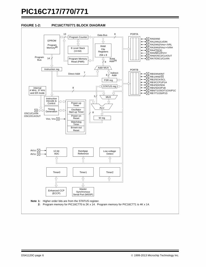
1.0 DEVICE OVERVIEW
This document contains device-specific information.Additional information may be found in the PICmicroTM
Mid-Range MCU Family Reference Manual,(DS33023), which may be obtained from your localMicrochip Sales Representative or downloaded fromthe Microchip website. The Reference Manual shouldbe considered a complementary document to this data
sheet, and is highly recommended reading for a betterunderstanding of the device architecture and operationof the peripheral modules.
There are three devices (PIC16C717, PIC16C770 andPIC16C771) covered by this data sheet. ThePIC16C717 device comes in 18/20-pin packages andthe PIC16C770/771 devices come in 20-pin packages.
The following two figures are device block diagrams ofthe PIC16C717 and the PIC16C770/771.
FIGURE 1-1: PIC16C717 BLOCK DIAGRAM
EPROM
ProgramMemory
2K x 14
13 Data Bus 8
14ProgramBus
Instruction reg
Program Counter
8 Level Stack(13-bit)
RAMFile
Registers
256 x 8
Direct Addr 7
Addr(1)9
Addr MUX
IndirectAddr
FSR reg
STATUS reg
MUX
ALU
W reg
Power-upTimer
OscillatorStart-up Timer
Power-onReset
WatchdogTimer
InstructionDecode &
Control
OSC1/CLKINOSC2/CLKOUT
VDD, VSS
PORTA
PORTB
RA4/T0CKI
RB0/AN4/INT
RB4/SDI/SDA8
8
Brown-outReset
Note 1: Higher order bits are from the STATUS register.
Enhanced CCPMaster
Timer0 Timer1 Timer2
Synchronous
RA3/AN3/VREF+/VRHRA2/AN2/VREF-/VRLRA1/AN1/LVDINRA0/AN0
8
3
TimingGeneration
10-bit ADC
RB1/AN5/SSRB2/SCK/SCLRB3/CCP1/P1A
RA5/MCLR/VPP
RA6/OSC2/CLKOUTRA7/OSC1/CLKIN
RB5/SDO/P1BRB6/T1OSO/T1CKI/P1CRB7/T1OSI/P1D
Internal4 MHz, 37 kHzand ER mode
(ECCP) Serial Port (MSSP)
Bandgap Reference
Low-voltage Detect
RAMProgram MemoryRead (PMR)
1999-2013 Microchip Technology Inc. DS41120C-page 5
PIC16C717/770/771
FIGURE 1-2: PIC16C770/771 BLOCK DIAGRAM
EPROM
ProgramMemory(2)
13 Data Bus 8
14ProgramBus
Instruction reg
Program Counter
8 Level Stack(13-bit)
RAMFile
Registers
256 x 8
Direct Addr 7
Addr(1)9
Addr MUX
IndirectAddr
FSR reg
STATUS reg
MUX
ALU
W reg
Power-upTimer
OscillatorStart-up Timer
Power-onReset
WatchdogTimer
InstructionDecode &
Control
OSC1/CLKINOSC2/CLKOUT
VDD, VSS
PORTA
PORTB
RA4/T0CKI
RB0/AN4/INT
RB4/SDI/SDA8
8
Brown-outReset
Note 1: Higher order bits are from the STATUS register.2: Program memory for PIC16C770 is 2K x 14. Program memory for PIC16C771 is 4K x 14.
Enhanced CCPMaster
Timer0 Timer1 Timer2
Synchronous
RA3/AN3/VREF+/VRHRA2/AN2/VREF-/VRLRA1/AN1/LVDINRA0/AN0
8
3
TimingGeneration
12-bit ADC
RB1/AN5/SSRB2/SCK/SCLRB3/CCP1/P1A
RA5/MCLR/VPP
RA6/OSC2/CLKOUTRA7/OSC1/CLKIN
RB5/SDO/P1BRB6/T1OSO/T1CKI/P1CRB7/T1OSI/P1D
Internal4 MHz, 37 kHzand ER mode
(ECCP) Serial Port (MSSP)
Bandgap Reference
Low-voltage Detect
RAMProgram MemoryRead (PMR)
AVDD
AVSS
DS41120C-page 6 1999-2013 Microchip Technology Inc.
PIC16C717/770/771
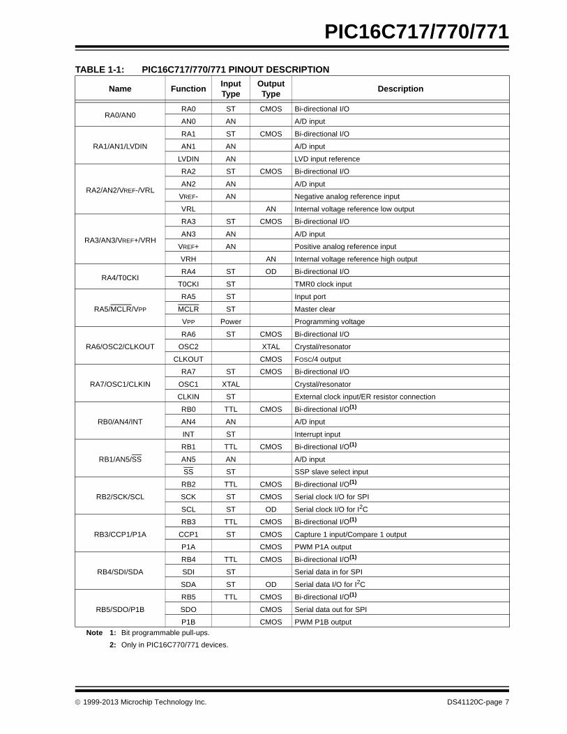
TABLE 1-1: PIC16C717/770/771 PINOUT DESCRIPTION
Name FunctionInputType
OutputType
Description
RA0/AN0RA0 ST CMOS Bi-directional I/O
AN0 AN A/D input
RA1/AN1/LVDIN
RA1 ST CMOS Bi-directional I/O
AN1 AN A/D input
LVDIN AN LVD input reference
RA2/AN2/VREF-/VRL
RA2 ST CMOS Bi-directional I/O
AN2 AN A/D input
VREF- AN Negative analog reference input
VRL AN Internal voltage reference low output
RA3/AN3/VREF+/VRH
RA3 ST CMOS Bi-directional I/O
AN3 AN A/D input
VREF+ AN Positive analog reference input
VRH AN Internal voltage reference high output
RA4/T0CKIRA4 ST OD Bi-directional I/O
T0CKI ST TMR0 clock input
RA5/MCLR/VPP
RA5 ST Input port
MCLR ST Master clear
VPP Power Programming voltage
RA6/OSC2/CLKOUT
RA6 ST CMOS Bi-directional I/O
OSC2 XTAL Crystal/resonator
CLKOUT CMOS FOSC/4 output
RA7/OSC1/CLKIN
RA7 ST CMOS Bi-directional I/O
OSC1 XTAL Crystal/resonator
CLKIN ST External clock input/ER resistor connection
RB0/AN4/INT
RB0 TTL CMOS Bi-directional I/O(1)
AN4 AN A/D input
INT ST Interrupt input
RB1/AN5/SS
RB1 TTL CMOS Bi-directional I/O(1)
AN5 AN A/D input
SS ST SSP slave select input
RB2/SCK/SCL
RB2 TTL CMOS Bi-directional I/O(1)
SCK ST CMOS Serial clock I/O for SPI
SCL ST OD Serial clock I/O for I2C
RB3/CCP1/P1A
RB3 TTL CMOS Bi-directional I/O(1)
CCP1 ST CMOS Capture 1 input/Compare 1 output
P1A CMOS PWM P1A output
RB4/SDI/SDA
RB4 TTL CMOS Bi-directional I/O(1)
SDI ST Serial data in for SPI
SDA ST OD Serial data I/O for I2C
RB5/SDO/P1B
RB5 TTL CMOS Bi-directional I/O(1)
SDO CMOS Serial data out for SPI
P1B CMOS PWM P1B output
Note 1: Bit programmable pull-ups.
2: Only in PIC16C770/771 devices.
1999-2013 Microchip Technology Inc. DS41120C-page 7

PIC16C717/770/771
RB6/T1OSO/T1CKI/P1C
RB6 TTL CMOS Bi-directional I/O(1)
T1OSO XTAL Crystal/Resonator
T1CKI CMOS TMR1 clock input
P1C CMOS PWM P1C output
RB7/T1OSI/P1D
RB7 TTL CMOS Bi-directional I/O(1)
T1OSI XTAL TMR1 crystal/resonator
P1D CMOS PWM P1D output
VSS VSS Power Ground reference for logic and I/O pins
VDD VDD Power Positive supply for logic and I/O pins
AVSS(2) AVSS Power Ground reference for analog
AVDD(2) AVDD Power Positive supply for analog
TABLE 1-1: PIC16C717/770/771 PINOUT DESCRIPTION (CONTINUED)
Name FunctionInputType
OutputType
Description
Note 1: Bit programmable pull-ups.
2: Only in PIC16C770/771 devices.
DS41120C-page 8 1999-2013 Microchip Technology Inc.

PIC16C717/770/771
2.0 MEMORY ORGANIZATIONThere are two memory blocks in each of these PIC®
microcontrollers. Each block (Program Memory andData Memory) has its own bus, so that concurrentaccess can occur.
Additional information on device memory may be foundin the PICmicro Mid-Range MCU Family ReferenceManual, (DS33023).
2.1 Program Memory Organization
The PIC16C717/770/771 devices have a 13-bit pro-gram counter capable of addressing an 8K x 14 pro-gram memory space. The PIC16C717 and thePIC16C770 have 2K x 14 words of program memory.The PIC16C771 has 4K x 14 words of program mem-ory. Accessing a location above the physically imple-mented address will cause a wrap-around.
The RESET vector is at 0000h and the interrupt vectoris at 0004h.
FIGURE 2-1: PROGRAM MEMORY MAP AND STACK OF THE PIC16C717 AND PIC16C770
FIGURE 2-2: PROGRAM MEMORY MAP AND STACK OF THE PIC16C771
2.2 Data Memory Organization
The data memory is partitioned into multiple banks,which contain the General Purpose Registers and theSpecial Function Registers. Bits RP1 and RP0 are thebank select bits.
= 00 Bank0 = 01 Bank1 = 10 Bank2 = 11 Bank3
Each bank extends up to 7Fh (128 bytes). The lowerlocations of each bank are reserved for the SpecialFunction Registers. Above the Special Function Regis-ters are General Purpose Registers, implemented asstatic RAM. All implemented banks contain specialfunction registers. Some frequently used special func-tion registers from one bank are mirrored in anotherbank for code reduction and quicker access.
2.2.1 GENERAL PURPOSE REGISTER FILE
The register file can be accessed either directly, or indi-rectly, through the File Select Register FSR.
PC<12:0>
13
0000h
0004h0005h
Stack Level 1
Stack Level 8
RESET Vector
Interrupt Vector
On-chip
CALL, RETURNRETFIE, RETLW
Stack Level 2
ProgramMemory
Page 007FFh
3FFFh
RP1 RP0 (STATUS<6:5>)
PC<12:0>
13
0000h
0004h0005h
Stack Level 1
Stack Level 8
RESET Vector
Interrupt Vector
On-chip
CALL, RETURNRETFIE, RETLW
Stack Level 2
ProgramMemory
Page 0
Page 1
07FFh0800h
0FFFh1000h
3FFFh
1999-2013 Microchip Technology Inc. DS41120C-page 9

PIC16C717/770/771
FIGURE 2-3: REGISTER FILE MAP
Indirect addr.(*)
TMR0PCL
STATUS
FSRPORTA
PORTB
PCLATH
INTCONPIR1
TMR1L
TMR1HT1CON
TMR2T2CON
SSPBUF
SSPCONCCPR1L
CCPR1HCCP1CON
OPTION_REG
PCLSTATUS
FSRTRISATRISB
PCLATH
INTCONPIE1
PCON
PR2SSPADD
SSPSTAT
00h
01h02h
03h04h
05h06h
07h08h09h
0Ah0Bh
0Ch0Dh
0Eh0Fh10h
11h12h
13h14h
15h16h
17h18h19h
1Ah1Bh
1Ch1Dh
1Eh1Fh
80h81h82h
83h84h
85h86h
87h88h
89h8Ah8Bh
8Ch8Dh
8Eh8Fh
90h91h92h
93h94h
95h96h
97h98h
99h9Ah9Bh
9Ch9Dh
9Eh9Fh
20h A0h
7Fh FFhBank 0 Bank 1
Unimplemented data memory locations, read as '0'. * Not a physical register.
Indirect addr.(*)
ADRESL
PIR2 PIE2
ADRESHADCON0 ADCON1
GeneralPurposeRegister
GeneralPurposeRegister
EFhF0haccesses
70h-7Fh
96 Bytes
80 Bytes
LVDCON
100h
101h102h
103h104h
105h106h
107h108h109h
10Ah10Bh
10Ch10Dh
10Eh10Fh110h
111h112h
113h114h
115h116h
117h118h119h
11Ah11Bh
11Ch11Dh
11Eh11Fh
120h
17FhBank 2
16Fh170h
FileAddress
PCLSTATUS
FSR
PCLATHINTCON
180h181h
182h183h184h
185h186h
187h188h
189h18Ah18Bh
18Ch18Dh
18Eh18Fh
190h191h
192h193h194h
195h196h
197h198h
199h19Ah19Bh
19Ch19Dh
19Eh19Fh
1A0h
1FFhBank 3
Indirect addr.(*)
OPTION_REG
1EFh1F0haccesses
70h - 7Fh
TRISB
PCLSTATUS
FSR
PCLATHINTCON
Indirect addr.(*)
TMR0
GeneralPurposeRegister
accesses70h - 7Fh
PORTB
80 Bytes
FileAddress
FileAddress
FileAddress
REFCON
SSPCON2
WPUBIOCB
ANSEL
P1DEL
PMDATL
PMADRL
PMDATH
PMADRH
PMCON1
DS41120C-page 10 1999-2013 Microchip Technology Inc.

PIC16C717/770/771
2.2.2 SPECIAL FUNCTION REGISTERS
The Special Function Registers are registers used bythe CPU and Peripheral Modules for controlling thedesired operation of the device. These registers areimplemented as static RAM. A list of these registers isgiven in Table 2-1.
The special function registers can be classified into twosets; core (CPU) and peripheral. Those registers asso-ciated with the core functions are described in detail inthis section. Those related to the operation of theperipheral features are described in detail in thatperipheral feature section.
TABLE 2-1: PIC16C717/770/771 SPECIAL FUNCTION REGISTER SUMMARY
Address Name Bit 7 Bit 6 Bit 5 Bit 4 Bit 3 Bit 2 Bit 1 Bit 0Value on:
POR,BOR
Details on
Page:
Bank 0
00h(3) INDF Addressing this location uses contents of FSR to address data memory (not a physical register) 0000 0000 23
01h TMR0 Timer0 module’s register xxxx xxxx 45
02h(3) PCL Program Counter's (PC) Least Significant Byte 0000 0000 22
03h(3) STATUS IRP RP1 RP0 TO PD Z DC C 0001 1xxx 14
04h(3) FSR Indirect data memory address pointer xxxx xxxx 23
05h PORTA RA7 RA6 RA5 RA4 RA3 RA2 RA1 RA0 xxxx 0000 25
06h PORTB RB7 RB6 RB5 RB4 RB3 RB2 RB1 RB0 xxxx xx11 33
07h — Unimplemented — —
08h — Unimplemented — —
09h — Unimplemented — —
0Ah(1,3) PCLATH — — — Write Buffer for the upper 5 bits of the Program Counter ---0 0000 22
0Bh(3) INTCON GIE PEIE T0IE INTE RBIE T0IF INTF RBIF 0000 000x 16
0Ch PIR1 — ADIF — — SSPIF CCP1IF TMR2IF TMR1IF -0---0000 18
0Dh PIR2 LVDIF — — — BCLIF — — — 0--- 0--- 20
0Eh TMR1L Holding register for the Least Significant Byte of the 16-bit TMR1 register xxxx xxxx 47
0Fh TMR1H Holding register for the Most Significant Byte of the 16-bit TMR1 register xxxx xxxx 47
10h T1CON — — T1CKPS1 T1CKPS0 T1OSCEN T1SYNC TMR1CS TMR1ON --00 0000 47
11h TMR2 Timer2 module’s register 0000 0000 51
12h T2CON — TOUTPS3 TOUTPS2 TOUTPS1 TOUTPS0 TMR2ON T2CKPS1 T2CKPS0 -000 0000 51
13h SSPBUF Synchronous Serial Port Receive Buffer/Transmit Register xxxx xxxx 70
14h SSPCON WCOL SSPOV SSPEN CKP SSPM3 SSPM2 SSPM1 SSPM0 0000 0000 67
15h CCPR1L Capture/Compare/PWM Register1 (LSB) xxxx xxxx 54
16h CCPR1H Capture/Compare/PWM Register1 (MSB) xxxx xxxx 54
17h CCP1CON PWM1M1 PWM1M0 DC1B1 DC1B0 CCP1M3 CCP1M2 CCP1M1 CCP1M0 0000 0000 53
18h — Unimplemented — —
19h — Unimplemented — —
1Ah — Unimplemented — —
1Bh — Unimplemented — —
1Ch — Unimplemented — —
1Dh — Unimplemented — —
1Eh ADRESH A/D High Byte Result Register xxxx xxxx 107
1Fh ADCON0 ADCS1 ADCS0 CHS2 CHS1 CHS0 GO/DONE CHS3 ADON 0000 0000 107
Legend: x = unknown, u = unchanged, q = value depends on condition, - = unimplemented read as '0'. Shaded locations are unimplemented, read as ‘0’.
Note 1: The upper byte of the program counter is not directly accessible. PCLATH is a holding register for the PC<12:8> whose contents are transferred to the upper byte of the program counter.
2: Other (non Power-up) Resets include external RESET through MCLR and Watchdog Timer Reset.3: These registers can be addressed from any bank.
1999-2013 Microchip Technology Inc. DS41120C-page 11

PIC16C717/770/771
Bank 1
80h(3) INDF Addressing this location uses contents of FSR to address data memory (not a physical register) 0000 0000 23
81h OPTION_REG RBPU INTEDG T0CS T0SE PSA PS2 PS1 PS0 1111 1111 15
82h(3) PCL Program Counter's (PC) Least Significant Byte 0000 0000 22
83h(3) STATUS IRP RP1 RP0 TO PD Z DC C 0001 1xxx 14
84h(3) FSR Indirect data memory address pointer xxxx xxxx 23
85h TRISA PORTA Data Direction Register 1111 1111 25
86h TRISB PORTB Data Direction Register 1111 1111 33
87h — Unimplemented — —
88h — Unimplemented — —
89h — Unimplemented — —
8Ah(1,3) PCLATH — — — Write Buffer for the upper 5 bits of the Program Counter ---0 0000 22
8Bh(3) INTCON GIE PEIE T0IE INTE RBIE T0IF INTF RBIF 0000 000x 16
8Ch PIE1 — ADIE — — SSPIE CCP1IE TMR2IE TMR1IE -0-- 0000 17
8Dh PIE2 LVDIE — — — BCLIE — — — 0--- 0--- 19
8Eh PCON — — — — OSCF — POR BOR ---- 1-qq 21
8Fh — Unimplemented — —
90h — Unimplemented — —
91h SSPCON2 GCEN ACKSTAT ACKDT ACKEN RCEN PEN RSEN SEN 0000 0000 69
92h PR2 Timer2 Period Register 1111 1111 52
93h SSPADD Synchronous Serial Port (I2C mode) Address Register 0000 0000 76
94h SSPSTAT SMP CKE D/A P S R/W UA BF 0000 0000 66
95h WPUB PORTB Weak Pull-up Control 1111 1111 34
96h IOCB PORTB Interrupt on Change Control 1111 0000 34
97h P1DEL PWM 1 Delay value 0000 0000 62
98h — Unimplemented — —
99h — Unimplemented — —
9Ah — Unimplemented — —
9Bh REFCON VRHEN VRLEN VRHOEN VRLOEN — — — — 0000 ---- 102
9Ch LVDCON — — BGST LVDEN LVV3 LVV2 LVV1 LVV0 --00 0101 101
9Dh ANSEL — — Analog Channel Select --11 1111 25
9Eh ADRESL A/D Low Byte Result Register xxxx xxxx 107
9Fh ADCON1 ADFM VCFG2 VCFG1 VCFG0 — — — — 0000 ---- 107
TABLE 2-1: PIC16C717/770/771 SPECIAL FUNCTION REGISTER SUMMARY (CONTINUED)
Address Name Bit 7 Bit 6 Bit 5 Bit 4 Bit 3 Bit 2 Bit 1 Bit 0Value on:
POR,BOR
Details on
Page:
Legend: x = unknown, u = unchanged, q = value depends on condition, - = unimplemented read as '0'. Shaded locations are unimplemented, read as ‘0’.
Note 1: The upper byte of the program counter is not directly accessible. PCLATH is a holding register for the PC<12:8> whose contents are transferred to the upper byte of the program counter.
2: Other (non Power-up) Resets include external RESET through MCLR and Watchdog Timer Reset.3: These registers can be addressed from any bank.
DS41120C-page 12 1999-2013 Microchip Technology Inc.

PIC16C717/770/771
Bank 2
100h(3) INDF Addressing this location uses contents of FSR to address data memory (not a physical register) 0000 0000 23
101h TMR0 Timer0 module’s register xxxx xxxx 45
102h(3) PCL Program Counter's (PC) Least Significant Byte 0000 0000 22
103h(3) STATUS IRP RP1 RP0 TO PD Z DC C 0001 1xxx 14
104h(3) FSR Indirect data memory address pointer xxxx xxxx 23
105h — Unimplemented — —
106h PORTB PORTB Data Latch when written: PORTB pins when read xxxx xx11 33
107h — Unimplemented — —
108h — Unimplemented — —
109h — Unimplemented — —
10Ah(1,3) PCLATH — — — Write Buffer for the upper 5 bits of the Program Counter ---0 0000 22
10Bh(3) INTCON GIE PEIE T0IE INTE RBIE T0IF INTF RBIF 0000 000x 16
10Ch PMDATL Program memory read data low xxxx xxxx
10Dh PMADRL Program memory read address low xxxx xxxx
10Eh PMDATH — — Program memory read data high --xx xxxx
10Fh PMADRH — — — — Program memory read address high ---- xxxx
110h-11Fh
— Unimplemented — —
Bank 3
180h(3) INDF Addressing this location uses contents of FSR to address data memory (not a physical register) 0000 0000 23
181h OPTION_REG RBPU INTEDG T0CS T0SE PSA PS2 PS1 PS0 1111 1111 15
182h(3) PCL Program Counter's (PC) Least Significant Byte 0000 0000 22
183h(3) STATUS IRP RP1 RP0 TO PD Z DC C 0001 1xxx 14
184h(3) FSR Indirect data memory address pointer xxxx xxxx 23
185h — Unimplemented — —
186h TRISB PORTB Data Direction Register 1111 1111 33
187h — Unimplemented — —
188h — Unimplemented — —
189h — Unimplemented — —
18Ah(1,3) PCLATH — — — Write Buffer for the upper 5 bits of the Program Counter ---0 0000 22
18Bh(3) INTCON GIE PEIE T0IE INTE RBIE T0IF INTF RBIF 0000 000x 16
18Ch PMCON1 Reserved — — — — — — RD 1--- ---0
18Dh-18Fh
— Unimplemented — —
TABLE 2-1: PIC16C717/770/771 SPECIAL FUNCTION REGISTER SUMMARY (CONTINUED)
Address Name Bit 7 Bit 6 Bit 5 Bit 4 Bit 3 Bit 2 Bit 1 Bit 0Value on:
POR,BOR
Details on
Page:
Legend: x = unknown, u = unchanged, q = value depends on condition, - = unimplemented read as '0'. Shaded locations are unimplemented, read as ‘0’.
Note 1: The upper byte of the program counter is not directly accessible. PCLATH is a holding register for the PC<12:8> whose contents are transferred to the upper byte of the program counter.
2: Other (non Power-up) Resets include external RESET through MCLR and Watchdog Timer Reset.3: These registers can be addressed from any bank.
1999-2013 Microchip Technology Inc. DS41120C-page 13

PIC16C717/770/771
2.2.2.1 STATUS REGISTER
The STATUS register, shown in Register 2-1, containsthe arithmetic status of the ALU, the RESET status andthe bank select bits for data memory.
The STATUS register can be the destination for anyinstruction, as with any other register. If the STATUSregister is the destination for an instruction that affectsthe Z, DC or C bits, then the write to these three bits isdisabled. These bits are set or cleared according to thedevice logic. Furthermore, the TO and PD bits are notwritable. Therefore, the result of an instruction with theSTATUS register as destination may be different thanintended.
For example, CLRF STATUS will clear the upper-threebits and set the Z bit. This leaves the STATUS registeras 000u u1uu (where u = unchanged).
It is recommended, therefore, that only BCF, BSF,SWAPF and MOVWF instructions are used to alter theSTATUS register, because these instructions do notaffect the Z, C or DC bits from the STATUS register. Forother instructions not affecting any status bits, see the"Instruction Set Summary."
REGISTER 2-1: STATUS REGISTER (STATUS: 03h, 83h, 103h, 183h)
Note: The C and DC bits operate as a borrowand digit borrow bit, respectively, in sub-traction. See the SUBLW and SUBWFinstructions for examples.
R/W-0 R/W-0 R/W-0 R-1 R-1 R/W-x R/W-x R/W-x
IRP RP1 RP0 TO PD Z DC C
bit 7 bit 0
bit 7 IRP: Register Bank Select bit (used for indirect addressing)
1 = Bank 2, 3 (100h - 1FFh)0 = Bank 0, 1 (00h - FFh)
bit 6-5 RP<1:0>: Register Bank Select bits (used for direct addressing)
11 = Bank 3 (180h - 1FFh) 10 = Bank 2 (100h - 17Fh) 01 = Bank 1 (80h - FFh)00 = Bank 0 (00h - 7Fh)Each bank is 128 bytes
bit 4 TO: Time-out bit
1 = After power-up, CLRWDT instruction, or SLEEP instruction0 = A WDT time-out occurred
bit 3 PD: Power-down bit
1 = After power-up or by the CLRWDT instruction0 = By execution of the SLEEP instruction
bit 2 Z: Zero bit
1 = The result of an arithmetic or logic operation is zero0 = The result of an arithmetic or logic operation is not zero
bit 1 DC: Digit carry/borrow bit (ADDWF, ADDLW,SUBLW,SUBWF instructions) (for borrow the polarityis reversed)
1 = A carry-out from the 4th low order bit of the result occurred0 = No carry-out from the 4th low order bit of the result
bit 0 C: Carry/borrow bit (ADDWF, ADDLW,SUBLW,SUBWF instructions)
1 = A carry-out from the Most Significant bit of the result occurred0 = No carry-out from the Most Significant bit of the result occurred
Note: For borrow, the polarity is reversed. A subtraction is executed by adding the two’scomplement of the second operand. For rotate (RRF, RLF) instructions, this bit isloaded with either the high or low order bit of the source register.
Legend:
R = Readable bit W = Writable bit U = Unimplemented bit, read as ‘0’
- n = Value at POR ’1’ = Bit is set ’0’ = Bit is cleared x = Bit is unknown
DS41120C-page 14 1999-2013 Microchip Technology Inc.

PIC16C717/770/771
2.2.2.2 OPTION_REG REGISTER
The OPTION_REG register is a readable and writableregister, which contains various control bits to configurethe TMR0 prescaler/WDT postscaler (single assign-able register known also as the prescaler), the ExternalINT Interrupt, TMR0 and the weak pull-ups on PORTB.
REGISTER 2-2: OPTION REGISTER (OPTION_REG: 81h, 181h)
Note: To achieve a 1:1 prescaler assignment forthe TMR0 register, assign the prescaler tothe Watchdog Timer.
R/W-1 R/W-1 R/W-1 R/W-1 R/W-1 R/W-1 R/W-1 R/W-1
RBPU INTEDG T0CS T0SE PSA PS2 PS1 PS0
bit 7 bit 0
bit 7 RBPU: PORTB Pull-up Enable bit(1)
1 = PORTB weak pull-ups are disabled0 = PORTB weak pull-ups are enabled by the WPUB register
bit 6 INTEDG: Interrupt Edge Select bit
1 = Interrupt on rising edge of RB0/INT pin0 = Interrupt on falling edge of RB0/INT pin
bit 5 T0CS: TMR0 Clock Source Select bit
1 = Transition on RA4/T0CKI pin0 = Internal instruction cycle clock (CLKOUT)
bit 4 T0SE: TMR0 Source Edge Select bit
1 = Increment on high-to-low transition on RA4/T0CKI pin0 = Increment on low-to-high transition on RA4/T0CKI pin
bit 3 PSA: Prescaler Assignment bit
1 = Prescaler is assigned to the WDT0 = Prescaler is assigned to the Timer0 module
bit 2-0 PS<2:0>: Prescaler Rate Select bits
Note 1: Individual weak pull-up on RB pins can be enabled/disabled from the weak pull-upPORTB Register (WPUB).
Legend:
R = Readable bit W = Writable bit U = Unimplemented bit, read as ‘0’
- n = Value at POR ’1’ = Bit is set ’0’ = Bit is cleared x = Bit is unknown
000001010011100101110111
1 : 21 : 41 : 81 : 161 : 321 : 641 : 1281 : 256
1 : 11 : 21 : 41 : 81 : 161 : 321 : 641 : 128
Bit Value TMR0 Rate WDT Rate
1999-2013 Microchip Technology Inc. DS41120C-page 15

PIC16C717/770/771
2.2.2.3 INTCON REGISTER
The INTCON Register is a readable and writable regis-ter, which contains various enable and flag bits for theTMR0 register overflow, RB Port change and ExternalRB0/INT pin interrupts.
REGISTER 2-3: INTERRUPT CONTROL REGISTER (INTCON: 0Bh, 8Bh, 10Bh, 18Bh)
Note: Interrupt flag bits get set when an interruptcondition occurs, regardless of the state ofits corresponding enable bit or the globalenable bit, GIE (INTCON<7>). User soft-ware should ensure the appropriate inter-rupt flag bits are clear prior to enabling aninterrupt.
R/W-0 R/W-0 R/W-0 R/W-0 R/W-0 R/W-0 R/W-0 R/W-x
GIE PEIE T0IE INTE RBIE T0IF INTF RBIF
bit 7 bit 0
bit 7 GIE: Global Interrupt Enable bit
1 = Enables all un-masked interrupts0 = Disables all interrupts
bit 6 PEIE: Peripheral Interrupt Enable bit
1 = Enables all un-masked peripheral interrupts0 = Disables all peripheral interrupts
bit 5 T0IE: TMR0 Overflow Interrupt Enable bit
1 = Enables the TMR0 interrupt0 = Disables the TMR0 interrupt
bit 4 INTE: RB0/INT External Interrupt Enable bit
1 = Enables the RB0/INT external interrupt0 = Disables the RB0/INT external interrupt
bit 3 RBIE: RB Port Change Interrupt Enable bit(1)
1 = Enables the RB port change interrupt0 = Disables the RB port change interrupt
bit 2 T0IF: TMR0 Overflow Interrupt Flag bit
1 = TMR0 register has overflowed (must be cleared in software)0 = TMR0 register did not overflow
bit 1 INTF: RB0/INT External Interrupt Flag bit
1 = The RB0/INT external interrupt occurred (must be cleared in software)0 = The RB0/INT external interrupt did not occur
bit 0 RBIF: RB Port Change Interrupt Flag bit(1)
1 = At least one of the RB<7:0> pins changed state (must be cleared in software)0 = None of the RB<7:0> pins have changed state
Note 1: Individual RB pin interrupt-on-change can be enabled/disabled from the Interrupt-on-Change PORTB register (IOCB).
Legend:
R = Readable bit W = Writable bit U = Unimplemented bit, read as ‘0’
- n = Value at POR ’1’ = Bit is set ’0’ = Bit is cleared x = Bit is unknown
DS41120C-page 16 1999-2013 Microchip Technology Inc.

PIC16C717/770/771
2.2.2.4 PIE1 REGISTER
This register contains the individual enable bits for theperipheral interrupts.
REGISTER 2-4: PERIPHERAL INTERRUPT ENABLE REGISTER 1 (PIE1: 8Ch)
Note: Bit PEIE (INTCON<6>) must be set toenable any peripheral interrupt.
U-0 R/W-0 U-0 U-0 R/W-0 R/W-0 R/W-0 R/W-0
— ADIE — — SSPIE CCP1IE TMR2IE TMR1IE
bit 7 bit 0
bit 7 Unimplemented: Read as ’0’
bit 6 ADIE: A/D Converter Interrupt Enable bit
1 = Enables the A/D interrupt0 = Disables the A/D interrupt
bit 5-4 Unimplemented: Read as ’0’
bit 3 SSPIE: Synchronous Serial Port Interrupt Enable bit
1 = Enables the SSP interrupt0 = Disables the SSP interrupt
bit 2 CCP1IE: CCP1 Interrupt Enable bit
1 = Enables the CCP1 interrupt0 = Disables the CCP1 interrupt
bit 1 TMR2IE: TMR2 to PR2 Match Interrupt Enable bit
1 = Enables the TMR2 to PR2 match interrupt0 = Disables the TMR2 to PR2 match interrupt
bit 0 TMR1IE: TMR1 Overflow Interrupt Enable bit
1 = Enables the TMR1 overflow interrupt0 = Disables the TMR1 overflow interrupt
Legend:
R = Readable bit W = Writable bit U = Unimplemented bit, read as ‘0’
- n = Value at POR ’1’ = Bit is set ’0’ = Bit is cleared x = Bit is unknown
1999-2013 Microchip Technology Inc. DS41120C-page 17

PIC16C717/770/771
2.2.2.5 PIR1 REGISTER
This register contains the individual flag bits for theperipheral interrupts.
REGISTER 2-5: PERIPHERAL INTERRUPT REGISTER 1 (PIR1: 0Ch)
Note: Interrupt flag bits get set when an interruptcondition occurs, regardless of the state ofits corresponding enable bit or the globalenable bit, GIE (INTCON<7>). User soft-ware should ensure the appropriate inter-rupt flag bits are clear prior to enabling aninterrupt.
U-0 R/W-0 U-0 U-0 R/W-0 R/W-0 R/W-0 R/W-0
— ADIF — — SSPIF CCP1IF TMR2IF TMR1IF
bit 7 bit 0
bit 7 Unimplemented: Read as ‘0’.
bit 6 ADIF: A/D Converter Interrupt Flag bit
1 = An A/D conversion completed0 = The A/D conversion is not complete
bit 5-4 Unimplemented: Read as ’0’
bit 3 SSPIF: Synchronous Serial Port (SSP) Interrupt Flag
1 = The SSP interrupt condition has occurred, and must be cleared in software before returningfrom the Interrupt Service Routine. The conditions that will set this bit are:SPI
A transmission/reception has taken place.I2 C Slave / Master
A transmission/reception has taken place.I2 C Master
The initiated START condition was completed by the SSP module.The initiated STOP condition was completed by the SSP module.The initiated Restart condition was completed by the SSP module.The initiated Acknowledge condition was completed by the SSP module.A START condition occurred while the SSP module was IDLE (Multi-master system).A STOP condition occurred while the SSP module was IDLE (Multi-master system).
0 = No SSP interrupt condition has occurred.
bit 2 CCP1IF: CCP1 Interrupt Flag bit
Capture Mode1 = A TMR1 register capture occurred (must be cleared in software)0 = No TMR1 register capture occurredCompare Mode1 = A TMR1 register compare match occurred (must be cleared in software)0 = No TMR1 register compare match occurredPWM ModeUnused in this mode
bit 1 TMR2IF: TMR2 to PR2 Match Interrupt Flag bit
1 = TMR2 to PR2 match occurred (must be cleared in software)0 = No TMR2 to PR2 match occurred
bit 0 TMR1IF: TMR1 Overflow Interrupt Flag bit
1 = TMR1 register overflowed (must be cleared in software)0 = TMR1 register did not overflow
Legend:
R = Readable bit W = Writable bit U = Unimplemented bit, read as ‘0’
- n = Value at POR ’1’ = Bit is set ’0’ = Bit is cleared x = Bit is unknown
DS41120C-page 18 1999-2013 Microchip Technology Inc.
PIC16C717/770/771
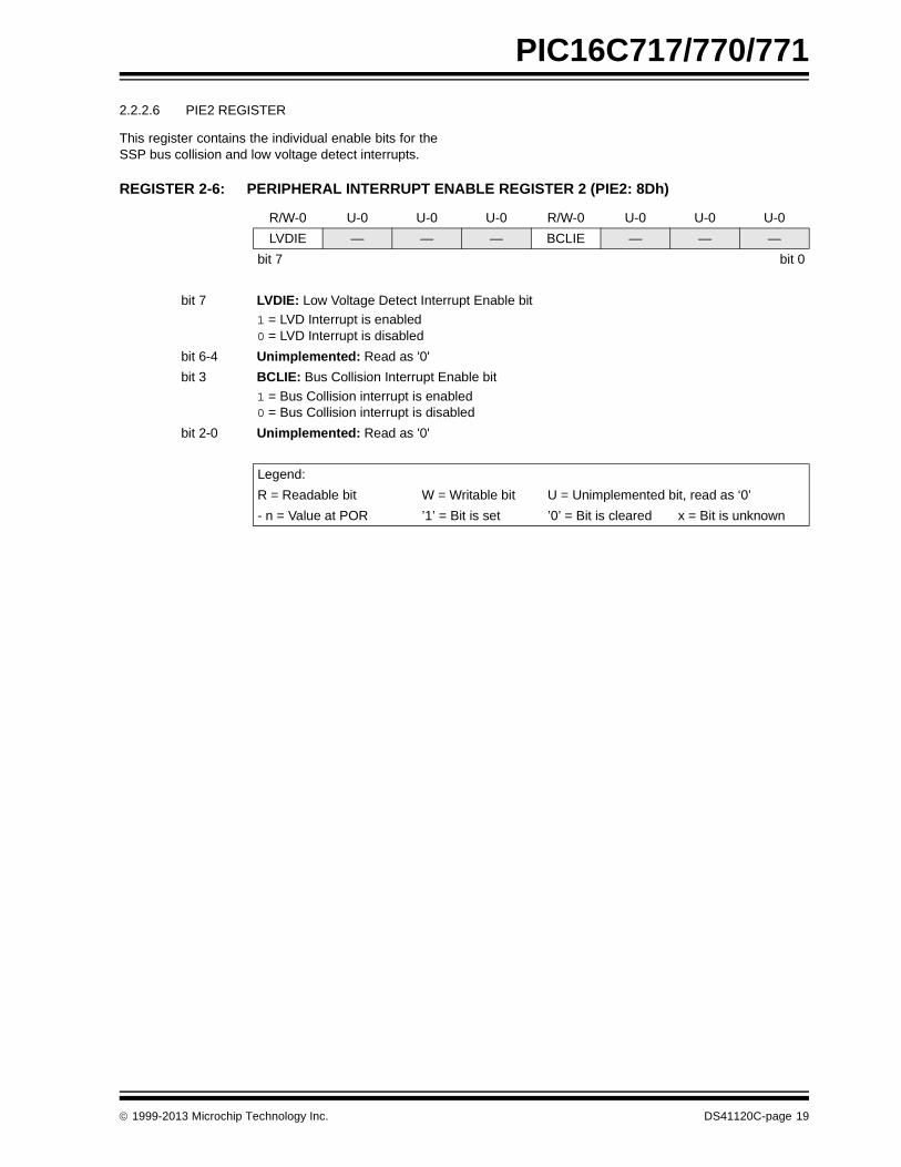
2.2.2.6 PIE2 REGISTER
This register contains the individual enable bits for theSSP bus collision and low voltage detect interrupts.
REGISTER 2-6: PERIPHERAL INTERRUPT ENABLE REGISTER 2 (PIE2: 8Dh)
R/W-0 U-0 U-0 U-0 R/W-0 U-0 U-0 U-0
LVDIE — — — BCLIE — — —
bit 7 bit 0
bit 7 LVDIE: Low Voltage Detect Interrupt Enable bit
1 = LVD Interrupt is enabled0 = LVD Interrupt is disabled
bit 6-4 Unimplemented: Read as '0'
bit 3 BCLIE: Bus Collision Interrupt Enable bit
1 = Bus Collision interrupt is enabled0 = Bus Collision interrupt is disabled
bit 2-0 Unimplemented: Read as '0'
Legend:
R = Readable bit W = Writable bit U = Unimplemented bit, read as ‘0’
- n = Value at POR ’1’ = Bit is set ’0’ = Bit is cleared x = Bit is unknown
1999-2013 Microchip Technology Inc. DS41120C-page 19

PIC16C717/770/771
2.2.2.7 PIR2 REGISTER
This register contains the SSP Bus Collision and low-voltage detect interrupt flag bits.
.
REGISTER 2-7: PERIPHERAL INTERRUPT REGISTER 2 (PIR2: 0Dh)
Note: Interrupt flag bits get set when an interruptcondition occurs, regardless of the state ofits corresponding enable bit or the globalenable bit, GIE (INTCON<7>). User soft-ware should ensure the appropriate inter-rupt flag bits are clear prior to enabling aninterrupt.
R/W-0 U-0 U-0 U-0 R/W-0 U-0 U-0 U-0
LVDIF — — — BCLIF — — —
bit 7 bit 0
bit 7 LVDIF: Low Voltage Detect Interrupt Flag bit
1 = The supply voltage has fallen below the specified LVD voltage (must be cleared in software)0 = The supply voltage is greater than the specified LVD voltage
bit 6-4 Unimplemented: Read as '0'
bit 3 BCLIF: Bus Collision Interrupt Flag bit
1 = A bus collision has occurred while the SSP module configured in I2C Master was transmitting (must be cleared in software)
0 = No bus collision occurred
bit 2-0 Unimplemented: Read as '0'
Legend:
R = Readable bit W = Writable bit U = Unimplemented bit, read as ‘0’
- n = Value at POR ’1’ = Bit is set ’0’ = Bit is cleared x = Bit is unknown
DS41120C-page 20 1999-2013 Microchip Technology Inc.

PIC16C717/770/771
2.2.2.8 PCON REGISTER
The Power Control (PCON) register contains a flag bitto allow differentiation between a Power-on Reset(POR) to an external MCLR Reset or WDT Reset.Those devices with brown-out detection circuitry con-tain an additional bit to differentiate a Brown-out Resetcondition from a Power-on Reset condition.
The PCON register also contains the frequency selectbit of the INTRC or ER oscillator.
REGISTER 2-8: POWER CONTROL REGISTER (PCON: 8Eh)
Note: BOR is unknown on Power-on Reset. Itmust then be set by the user and checkedon subsequent RESETS to see if BOR isclear, indicating a brown-out has occurred.The BOR status bit is a don't care and isnot necessarily predictable if the brown-outcircuit is disabled (by clearing the BODENbit in the Configuration word).
U-0 U-0 U-0 U-0 R/W-1 U-0 R/W-q R/W-q
— — — — OSCF — POR BOR
bit 7 bit 0
bit 7-4 Unimplemented: Read as '0'
bit 3 OSCF: Oscillator Speed bit
INTRC Mode1 = 4 MHz nominal0 = 37 kHz nominalER Mode1 = Oscillator frequency depends on the external resistor value on the OSC1 pin.0 = 37 kHz nominalAll other modesx = Ignored
bit 2 Unimplemented: Read as '0'
bit 1 POR: Power-on Reset Status bit
1 = No Power-on Reset occurred0 = A Power-on Reset occurred (must be set in software after a Power-on Reset occurs)
bit 0 BOR: Brown-out Reset Status bit (See Section 2.2.2.8 Note)
1 = No Brown-out Reset occurred0 = A Brown-out Reset occurred (must be set in software after a Brown-out Reset occurs)
Legend: q = Value depends on conditions
R = Readable bit W = Writable bit U = Unimplemented bit, read as ‘0’
- n = Value at POR ’1’ = Bit is set ’0’ = Bit is cleared x = Bit is unknown
1999-2013 Microchip Technology Inc. DS41120C-page 21

PIC16C717/770/771
2.3 PCL and PCLATH
The program counter (PC) specifies the address of theinstruction to fetch for execution. The PC is 13 bitswide. The low byte is called the PCL register. This reg-ister is readable and writable. The high byte is calledthe PCH register. This register contains the PC<12:8>bits and is not directly readable or writable. All updatesto the PCH register occur through the PCLATH register.
2.3.1 PROGRAM MEMORY PAGING
PIC16C717/770/771 devices are capable of address-ing a continuous 8K word block of program memory.The CALL and GOTO instructions provide only 11 bits ofaddress to allow branching within any 2K programmemory page. When doing a CALL or GOTO instruction,the upper 2 bits of the address are provided byPCLATH<4:3>. When doing a CALL or GOTO instruc-tion, the user must ensure that the page select bits areprogrammed so that the desired program memorypage is addressed. A return instruction pops a PCaddress off the stack onto the PC register. Therefore,manipulation of the PCLATH<4:3> bits are not requiredfor the return instructions (which POPs the addressfrom the stack).
2.4 Stack
The stack allows a combination of up to 8 program callsand interrupts to occur. The stack contains the returnaddress from this branch in program execution.
Mid-range devices have an 8-level deep x 13-bit widehardware stack. The stack space is not part of eitherprogram or data space and the stack pointer is notreadable or writable. The PC is PUSHed onto the stackwhen a CALL instruction is executed or an interruptcauses a branch. The stack is POPed in the event of aRETURN, RETLW or a RETFIE instruction execution.PCLATH is not modified when the stack is PUSHed orPOPed.
After the stack has been PUSHed eight times, the ninthpush overwrites the value that was stored from the firstpush. The tenth push overwrites the second push (andso on).
FIGURE 2-4: LOADING OF PC IN DIFFERENT SITUATIONS
Instruction withPCL asDestination
8ALU
12 0
11Opcode <10:0>
GOTO, CALL
PCLATH<4:3>
PCLATH
PCLATH
8 7
PCLATH<4:0>
12 1110 8 7 0PCH PCL
PCH PCL
5
2
DS41120C-page 22 1999-2013 Microchip Technology Inc.
PIC16C717/770/771
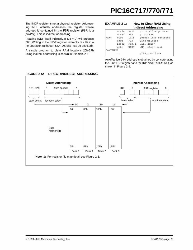
The INDF register is not a physical register. Address-ing INDF actually addresses the register whoseaddress is contained in the FSR register (FSR is apointer). This is indirect addressing.
Reading INDF itself indirectly (FSR = 0) will produce00h. Writing to the INDF register indirectly results in ano-operation (although STATUS bits may be affected).
A simple program to clear RAM locations 20h-2Fhusing indirect addressing is shown in Example 2-1.
EXAMPLE 2-1: How to Clear RAM Using Indirect Addressing
An effective 9-bit address is obtained by concatenatingthe 8-bit FSR register and the IRP bit (STATUS<7>), asshown in Figure 2-5.
FIGURE 2-5: DIRECT/INDIRECT ADDRESSING
movlw 0x20 ;initialize pointer movwf FSR ; to RAMNEXT clrf INDF ;clear INDF register incf FSR ;inc pointer btfss FSR,4 ;all done? goto NEXT ;NO, clear nextCONTINUE : ;YES, continue
Note 1: For register file map detail see Figure 2-3.
DataMemory(1)
Indirect AddressingDirect Addressing
bank select location select
RP1:RP0 6 0from opcode IRP FSR register7 0
bank select location select
00 01 10 11
Bank 0 Bank 1 Bank 2 Bank 3
FFh
80h
7Fh
00h
17Fh
100h
1FFh
180h
1999-2013 Microchip Technology Inc. DS41120C-page 23

PIC16C717/770/771
NOTES:
DS41120C-page 24 1999-2013 Microchip Technology Inc.

PIC16C717/770/771
3.0 I/O PORTSSome pins for these I/O ports are multiplexed with analternate function for the peripheral features on thedevice. In general, when a peripheral is enabled, thatpin may not be used as a general purpose I/O pin.
Additional information on I/O ports may be found in thePIC Mid-Range MCU Family Reference Manual,(DS33023).
3.1 I/O Port Analog/Digital Mode
The PIC16C717/770/771 have two I/O ports: PORTAand PORTB. Some of these port pins are mixed-signal(can be digital or analog). When an analog signal is
present on a pin, the pin must be configured as an ana-log input to prevent unnecessary current draw from thepower supply. The Analog Select Register (ANSEL)allows the user to individually select the Digital/Analogmode on these pins. When the Analog mode is active,the port pin will always read 0.
REGISTER 3-1: ANALOG SELECT REGISTER (ANSEL: 9Dh)
3.2 PORTA and the TRISA Register
PORTA is a 8-bit wide bi-directional port. The corre-sponding data direction register is TRISA. Setting aTRISA bit (=1) will make the corresponding PORTA pinan input (i.e., put the corresponding output driver in aHi-impedance mode). Clearing a TRISA bit (=0) willmake the corresponding PORTA pin an output (i.e., putthe contents of the output latch on the selected pin).
Reading the PORTA register reads the status of thepins, whereas writing to it will write to the port latch. Allwrite operations are read-modify-write operations.Therefore, a write to a port implies that the port pins areread, this value is modified, and then written to the portdata latch.
Pins RA<3:0> are multiplexed with analog functions,such as analog inputs to the A/D converter, analogVREF inputs, and the onboard bandgap reference out-puts. When the analog peripherals are using any of
these pins as analog input/output, the ANSEL registermust have the proper value to individually select theAnalog mode of the corresponding pins.
Pin RA4 is multiplexed with the Timer0 module clockinput to become the RA4/T0CKI pin. The RA4/T0CKIpin is a Schmitt Trigger input and an open drain output.
Pin RA5 is multiplexed with the device RESET (MCLR)and programming input (VPP) functions. The RA5/MCLR/VPP input only pin has a Schmitt Trigger inputbuffer. All other RA port pins have Schmitt Trigger inputbuffers and full CMOS output buffers.
Pins RA6 and RA7 are multiplexed with the oscillatorinput and output functions.
The TRISA register controls the direction of the RApins, even when they are being used as analog inputs.The user must ensure the bits in the TRISA register aremaintained set when using them as analog inputs.
Note 1: On a Power-on Reset, the ANSEL regis-ter configures these mixed-signal pins asAnalog mode.
2: If a pin is configured as Analog mode, theRA pin will always read '0' and RB pin willalways read '1', even if the digital output isactive.
R/W-1 R/W-1 R/W-1 R/W-1 R/W-1 R/W-1 R/W-1 R/W-1
— — ANS5 ANS4 ANS3 ANS2 ANS1 ANS0
bit 7 bit 0
bit 7-6 Reserved: Do not use
bit 5-0 ANS<5:0>: Analog Select between analog or digital function on pins AN<5:0>, respectively.
0 = Digital I/O. Pin is assigned to port or special function.1 = Analog Input. Pin is assigned as analog input.
Note: Setting a pin to an analog input disables the digital input buffer on the pin. The cor-responding TRIS bit should be set to Input mode when using pins as analog inputs.
Legend:
R = Readable bit W = Writable bit U = Unimplemented bit, read as ‘0’
- n = Value at POR ’1’ = Bit is set ’0’ = Bit is cleared x = Bit is unknown
Note: Upon RESET, the ANSEL register config-ures the RA<3:0> pins as analog inputs.All RA<3:0> pins will read as '0'.
1999-2013 Microchip Technology Inc. DS41120C-page 25

PIC16C717/770/771
EXAMPLE 3-1: Initializing PORTA
FIGURE 3-1: BLOCK DIAGRAM OF RA0/AN0, RA1/AN1/LVDIN
BCF STATUS, RP0 ; Select Bank 0CLRF PORTA ; Initialize PORTA by
; clearing output; data latches
BSF STATUS, RP0 ; Select Bank 1MOVLW 0Fh ; Value used to
; initialize data ; direction
MOVWF TRISA ; Set RA<3:0> as inputs; RA<7:4> as outputs. RA<7:6>availability depends on oscillator selection.
MOVLW 03 ; Set RA<1:0> as analog inputs, RA<7:2> are digital I/OMOVWF ANSEL BCF STATUS, RP0 ; Return to Bank 0
DataBus
QD
QCK
QD
QCK
Q D
EN
P
N
WRPORT
WRTRIS
Data Latch
TRIS Mode
VSS
VDD
SchmittTrigger
To A/D Converter input or LVD Module input
RDTRIS
QD
QCK
Analog Select
WRANSEL
RDPORT
VDD
VSS
DS41120C-page 26 1999-2013 Microchip Technology Inc.

PIC16C717/770/771
FIGURE 3-2: BLOCK DIAGRAM OF RA2/AN2/VREF-/VRL AND RA3/AN3/VREF+/VRH
To A/D Converter input
VRH, VRL outputs(From VREF-LVD-BOR Module)
and VREF+, VREF- inputs
Sense input for VRH, VRL amplifier
VRH, VRL output enable
DataBus
QD
QCK
QD
QCK P
N
WRPORT
WRTRIS
Data Latch
TRIS Mode
VSS
VDD
SchmittTrigger
RDTRIS
QD
QCK
Analog Select
WRANSEL
RDPORT
VDD
VSS
Q D
EN
1999-2013 Microchip Technology Inc. DS41120C-page 27

PIC16C717/770/771
FIGURE 3-3: BLOCK DIAGRAM OF RA4/T0CKI
DataBus
QD
QCK
QD
QCK
Q D
EN
N
WRPort
WRTRIS
Data Latch
RD
VSS
Schmitt TriggerInput Buffer
TMR0 clock input
RDTRIS
TRIS Latch
PORT
VSS
DS41120C-page 28 1999-2013 Microchip Technology Inc.

PIC16C717/770/771
FIGURE 3-4: BLOCK DIAGRAM OF RA5/MCLR/VPP
DataBus
Q D
EN
RD PORT
SchmittTrigger
RDTRIS
VSS
To MCLR CircuitMCLR Filter
VSS
HV Detect
Program Mode
1999-2013 Microchip Technology Inc. DS41120C-page 29

PIC16C717/770/771
FIGURE 3-5: BLOCK DIAGRAM OF RA6/OSC2/CLKOUT PIN
DataBus
QD
QCK P
N
WRPORTA
WRTRISA
Data Latch
TRIS Latch
RD TRISA
RD PORTA
VSS
VDD
QD
QCK
Schmitt TriggerInput Buffer
Oscillator Circuit
From OSC1
1
0
CLKOUT (Fosc/4)
(INTRC or ER) and CLKOUT
VDD
VSS
DQ
EN
EC or [(ER or INTRC) and CLKOUT]
DS41120C-page 30 1999-2013 Microchip Technology Inc.

PIC16C717/770/771
FIGURE 3-6: BLOCK DIAGRAM OF RA7/OSC1/CLKIN PIN
DataBus
QD
QCK P
N
WRPORTA
WRTRISA
Data Latch
TRIS Latch
RD TRISA
RD PORTA
Vss
VDD
QD
QCK
Schmitt TriggerInput Buffer
Oscillator Circuit
To OSC2
INTRC
INTRC
Schmitt TriggerInput Buffer
To Chip Clock Drivers
EC Mode
VDD
DQ
EN
1999-2013 Microchip Technology Inc. DS41120C-page 31

PIC16C717/770/771
TABLE 3-1: PORTA FUNCTIONS
TABLE 3-2: SUMMARY OF REGISTERS ASSOCIATED WITH PORTA
Name FunctionInputType
OutputType
Description
RA0/AN0RA0 ST CMOS Bi-directional I/O
AN0 AN A/D input
RA1/AN1/LVDIN
RA1 ST CMOS Bi-directional I/O
AN1 AN A/D input
LVDIN AN LVD input reference
RA2/AN2/VREF-/VRL
RA2 ST CMOS Bi-directional I/O
AN2 AN A/D input
VREF- AN Negative analog reference input
VRL AN Internal voltage reference low output
RA3/AN3/VREF+/VRH
RA3 ST CMOS Bi-directional I/O
AN3 AN A/D input
VREF+ AN Positive analog reference input
VRH AN Internal voltage reference high output
RA4/T0CKIRA4 ST OD Bi-directional I/O
T0CKI ST TMR0 clock input
RA5/MCLR/VPP
RA5 ST Input port
MCLR ST Master clear
VPP Power Programming voltage
RA6/OSC2/CLKOUT
RA6 ST CMOS Bi-directional I/O
OSC2 XTAL Crystal/resonator
CLKOUT CMOS FOSC/4 output
RA7/OSC1/CLKIN
RA7 ST CMOS Bi-directional I/O
OSC1 XTAL Crystal/resonator
CLKIN ST/AN External clock input/ER resistor connection
Address Name Bit 7 Bit 6 Bit 5 Bit 4 Bit 3 Bit 2 Bit 1 Bit 0Value on:
POR,BOR
Value on all other
RESETS
05h PORTA RA7 RA6 RA5 RA4 RA3 RA2 RA1 RA0 xxxx 0000 uuuu 0000
85h TRISA PORTA Data Direction Register 1111 1111 1111 1111
9Dh ANSEL — — ANS5 ANS4 ANS3 ANS2 ANS1 ANS0 --11 1111 --11 1111
Legend: x = unknown, u = unchanged, - = unimplemented locations read as '0'. Shaded cells are not used by PORTA.
DS41120C-page 32 1999-2013 Microchip Technology Inc.
PIC16C717/770/771
3.3 PORTB and the TRISB Register
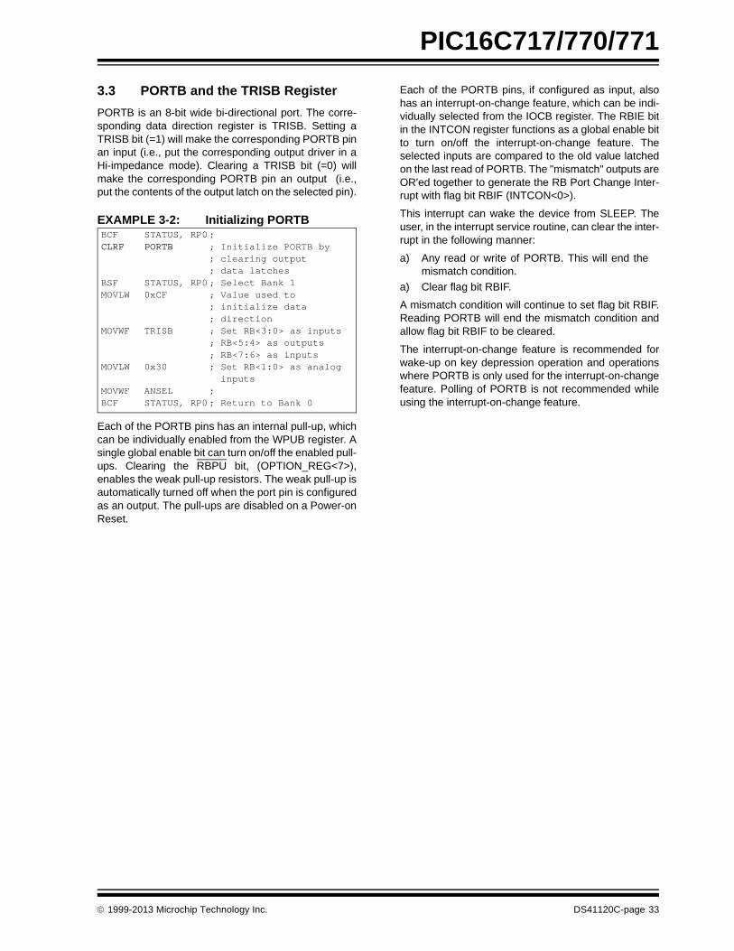
PORTB is an 8-bit wide bi-directional port. The corre-sponding data direction register is TRISB. Setting aTRISB bit (=1) will make the corresponding PORTB pinan input (i.e., put the corresponding output driver in aHi-impedance mode). Clearing a TRISB bit (=0) willmake the corresponding PORTB pin an output (i.e.,put the contents of the output latch on the selected pin).
EXAMPLE 3-2: Initializing PORTB
Each of the PORTB pins has an internal pull-up, whichcan be individually enabled from the WPUB register. Asingle global enable bit can turn on/off the enabled pull-ups. Clearing the RBPU bit, (OPTION_REG<7>),enables the weak pull-up resistors. The weak pull-up isautomatically turned off when the port pin is configuredas an output. The pull-ups are disabled on a Power-onReset.
Each of the PORTB pins, if configured as input, alsohas an interrupt-on-change feature, which can be indi-vidually selected from the IOCB register. The RBIE bitin the INTCON register functions as a global enable bitto turn on/off the interrupt-on-change feature. Theselected inputs are compared to the old value latchedon the last read of PORTB. The "mismatch" outputs areOR'ed together to generate the RB Port Change Inter-rupt with flag bit RBIF (INTCON<0>).
This interrupt can wake the device from SLEEP. Theuser, in the interrupt service routine, can clear the inter-rupt in the following manner:
a) Any read or write of PORTB. This will end themismatch condition.
a) Clear flag bit RBIF.
A mismatch condition will continue to set flag bit RBIF.Reading PORTB will end the mismatch condition andallow flag bit RBIF to be cleared.
The interrupt-on-change feature is recommended forwake-up on key depression operation and operationswhere PORTB is only used for the interrupt-on-changefeature. Polling of PORTB is not recommended whileusing the interrupt-on-change feature.
BCF STATUS, RP0; CLRF PORTB ; Initialize PORTB by
; clearing output; data latches
BSF STATUS, RP0; Select Bank 1MOVLW 0xCF ; Value used to
; initialize data ; direction
MOVWF TRISB ; Set RB<3:0> as inputs; RB<5:4> as outputs; RB<7:6> as inputs
MOVLW 0x30 ; Set RB<1:0> as analog inputs
MOVWF ANSEL ;BCF STATUS, RP0; Return to Bank 0
1999-2013 Microchip Technology Inc. DS41120C-page 33
PIC16C717/770/771
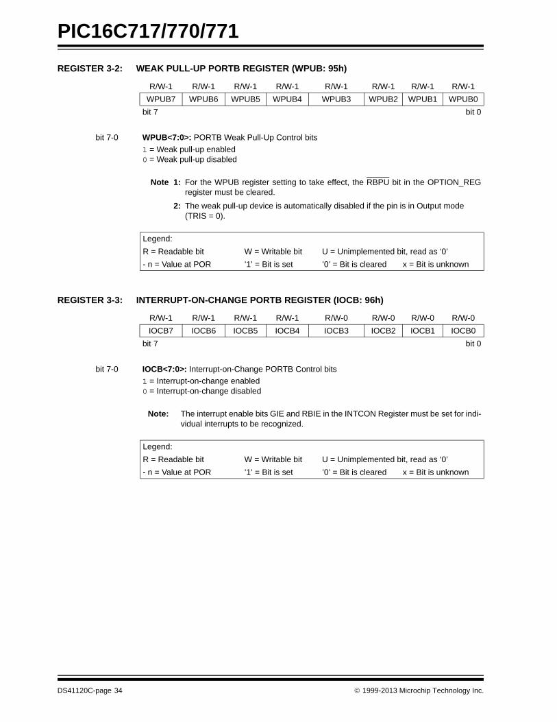
REGISTER 3-2: WEAK PULL-UP PORTB REGISTER (WPUB: 95h)
REGISTER 3-3: INTERRUPT-ON-CHANGE PORTB REGISTER (IOCB: 96h)
R/W-1 R/W-1 R/W-1 R/W-1 R/W-1 R/W-1 R/W-1 R/W-1
WPUB7 WPUB6 WPUB5 WPUB4 WPUB3 WPUB2 WPUB1 WPUB0
bit 7 bit 0
bit 7-0 WPUB<7:0>: PORTB Weak Pull-Up Control bits
1 = Weak pull-up enabled0 = Weak pull-up disabled
Note 1: For the WPUB register setting to take effect, the RBPU bit in the OPTION_REGregister must be cleared.
2: The weak pull-up device is automatically disabled if the pin is in Output mode (TRIS = 0).
Legend:
R = Readable bit W = Writable bit U = Unimplemented bit, read as ‘0’
- n = Value at POR ’1’ = Bit is set ’0’ = Bit is cleared x = Bit is unknown
R/W-1 R/W-1 R/W-1 R/W-1 R/W-0 R/W-0 R/W-0 R/W-0
IOCB7 IOCB6 IOCB5 IOCB4 IOCB3 IOCB2 IOCB1 IOCB0
bit 7 bit 0
bit 7-0 IOCB<7:0>: Interrupt-on-Change PORTB Control bits
1 = Interrupt-on-change enabled0 = Interrupt-on-change disabled
Note: The interrupt enable bits GIE and RBIE in the INTCON Register must be set for indi-vidual interrupts to be recognized.
Legend:
R = Readable bit W = Writable bit U = Unimplemented bit, read as ‘0’
- n = Value at POR ’1’ = Bit is set ’0’ = Bit is cleared x = Bit is unknown
DS41120C-page 34 1999-2013 Microchip Technology Inc.

PIC16C717/770/771
The RB0 pin is multiplexed with the A/D converter ana-log input 4 and the external interrupt input (RB0/AN4/INT). When the pin is used as analog input, the ANSELregister must have the proper value to select the RB0pin as Analog mode.
The RB1 pin is multiplexed with the A/D converter ana-log input 5 and the MSSP module slave select input(RB1/AN5/SS). When the pin is used as analog input,the ANSEL register must have the proper value toselect the RB1 pin as Analog mode.
FIGURE 3-7: BLOCK DIAGRAM OF RB0/AN4/INT, RB1/AN5/SS PIN
Note: Upon RESET, the ANSEL register config-ures the RB1 and RB0 pins as analog inputs.Both RB1 and RB0 pins will read as '1'.
Data Bus
WR
WR
RD
PORTB Reg
TRIS Reg
To INT input or MSSP module
QD
CK
QD
CK
EN
Q D
EN
RD
RBPUweakpull-up
TTL
SchmittTrigger
P
N
VSS
VDD
QD
CK
QD
CK
WPUB Reg
IOCB Reg
PORT
TRIS
PORT
TRIS
WRWPUB
Q
DQ
EN
DQ
EN
Q3
Q1
...
SetRBIF
From RB<7:0> pins
Q
QD
QCK
Analog Select
WRANSEL
WRIOCB
VDD
VSS
Q
P
VDD
Q
To A/D Converter
1999-2013 Microchip Technology Inc. DS41120C-page 35

PIC16C717/770/771
FIGURE 3-8: BLOCK DIAGRAM OF RB2/SCK/SCL, RB3/CCP1/P1A, RB4/SDI/SDA,RB5/SDO/P1B
Data Bus
WR
WR
RD
PORTB Reg
TRIS Reg
SCK, SCL, CC, SDI, SDA inputs
QD
CK
QD
CK
EN
Q D
EN
RD
RBPUweakpull-up
SchmittTrigger
P
N
VSS
VDD
QD
CK
QD
CK
WPUB Reg
IOCB Reg
PORT
TRIS
PORT
TRIS
WRWPUB
Q
DQ
EN
DQ
EN
Q3
Q1
...
SetRBIF
From RB<7:0> pins
Q
WRIOCB
VDD
VSS
Q
P
VDD
Q
1
0
Spec. Func En.
SDA, SDO, SCK, CCP1, P1A, P1B
TTL
DS41120C-page 36 1999-2013 Microchip Technology Inc.

PIC16C717/770/771
FIGURE 3-9: BLOCK DIAGRAM OF RB6/T1OSO/T1CKI/P1C
Data Latch
TRIS Latch
RD TRISB
P
VSS
QD
QCK
QD
QCK N
VDD
RD PORTB
WR PORTB
WR TRISB
T1OSCEN
TMR1 Clock
RBPUVDD
weak pull-upP
From RB7
From
Q D
EN
Set RBIF
RB<7:0> pinsRD Port
Q3
Q1
Serial programming clock
TTLInputBuffer
TMR1 Oscillator
Q D
EN
VDD
Data BusQD
CK
WPUB Reg
WRWPUB
Q
IOCB Reg
WRIOCB
QD
CK Q
Note: The TMR1 oscillator enable (T1OSCEN = 1) overrides the RB6 I/O port and P1C functions.
...
SchmittTrigger
CMOS
1999-2013 Microchip Technology Inc. DS41120C-page 37

PIC16C717/770/771
FIGURE 3-10: BLOCK DIAGRAM OF THE RB7/T1OSI/P1D
Data Latch
TRIS Latch
RD TRISB
P
VSS
QD
QCK
QD
QCK N
VDD
RD PORTB
WR PORTB
WR TRISB
T10SCEN
T1OSCEN
To RB6
RBPUVDD
weak pull-upP
TTLInputBuffer
From Q D
EN
Q D
ENSet RBIF
RB<7:0> pinsRD Port
Q3
Q1
Serial programming input
Schmitt Trigger
TMR1 Oscillator
VDD
Data BusQD
CK
WPUB Reg
WRWPUB
Q
QD
CK
IOCB Reg
WRIOCB
Q
Note: The TMR1 oscillator enable (T1OSCEN = 1) overrides the RB7 I/O port and P1D functions.
...
DS41120C-page 38 1999-2013 Microchip Technology Inc.

PIC16C717/770/771
TABLE 3-3: PORTB FUNCTIONS
TABLE 3-4: SUMMARY OF REGISTERS ASSOCIATED WITH PORTB
Name FunctionInputType
OutputType
Description
RB0/AN4/INT
RB0 TTL CMOS Bi-directional I/O(1)
AN4 AN A/D input
INT ST Interrupt input
RB1/AN5/SS
RB1 TTL CMOS Bi-directional I/O(1)
AN5 AN A/D input
SS ST SSP slave select input
RB2/SCK/SCL
RB2 TTL CMOS Bi-directional I/O(1)
SCK ST CMOS Serial clock I/O for SPI
SCL ST OD Serial clock I/O for I2C
RB3/CCP1/P1A
RB3 TTL CMOS Bi-directional I/O(1)
CCP1 ST CMOS Capture 1 input/Compare 1 output
P1A CMOS PWM P1A output
RB4/SDI/SDA
RB4 TTL CMOS Bi-directional I/O(1)
SDI ST Serial data in for SPI
SDA ST OD Serial data I/O for I2C
RB5/SDO/P1B
RB5 TTL CMOS Bi-directional I/O(1)
SDO CMOS Serial data out for SPI
P1B CMOS PWM P1B output
RB6/T1OSO/T1CKI/P1C
RB6 TTL CMOS Bi-directional I/O(1)
T1OSO XTAL Crystal/Resonator
T1CKI CMOS TMR1 clock input
P1C CMOS PWM P1C output
RB7/T1OSI/P1D
RB7 TTL CMOS Bi-directional I/O(1)
T1OSI XTAL TMR1 crystal/resonator
P1D CMOS PWM P1D output
Note 1: Bit programmable pull-ups.
Address Name Bit 7 Bit 6 Bit 5 Bit 4 Bit 3 Bit 2 Bit 1 Bit 0Value on:
POR,BOR
Value on all other
RESETS
06h, 106h PORTB RB7 RB6 RB5 RB4 RB3 RB2 RB1 RB0 xxxx xx11 uuuu uu11
86h, 186h TRISB PORTB Data Direction Register 1111 1111 1111 1111
81h, 181h OPTION_REG RBPU INTEDG T0CS T0SE PSA PS2 PS1 PS0 1111 1111 1111 1111
95h WPUB PORTB Weak Pull-up Control 1111 1111 1111 1111
96h IOCB PORTB Interrupt on Change Control 1111 0000 1111 0000
9Dh ANSEL — — ANS5 ANS4 ANS3 ANS2 ANS1 ANS0 --11 1111 --11 1111
Legend: x = unknown, u = unchanged. Shaded cells are not used by PORTB.
1999-2013 Microchip Technology Inc. DS41120C-page 39

PIC16C717/770/771
NOTES:
DS41120C-page 40 1999-2013 Microchip Technology Inc.

PIC16C717/770/771
4.0 PROGRAM MEMORY READ(PMR)
Program memory is readable during normal operation(full VDD range). It is indirectly addressed through theSpecial Function Registers:
• PMCON1
• PMDATH
• PMDATL
• PMADRH
• PMADRL
When interfacing the program memory block, thePMDATH & PMDATL registers form a 2-byte word,which holds the 14-bit data. The PMADRH & PMADRLregisters form a 2-byte word, which holds the 12-bitaddress of the program memory location beingaccessed. Mid-range devices have up to 8K words ofprogram EPROM with an address range from 0h to3FFFh. When the device contains less memory thanthe full address range of the PMADRH:PMARDL regis-ters, the Most Significant bits of the PMADRH registerare ignored.
4.1 PMCON1 REGISTER
PMCON1 is the control register for program memoryaccesses.
Control bit RD initiates a read operation. This bit cannotbe cleared, only set, in software. It is cleared in hard-ware at completion of the read operation.
REGISTER 4-1: PROGRAM MEMORY READ CONTROL REGISTER 1 (PMCON1: 18Ch)
4.2 PMDATH AND PMDATL REGISTERS
The PMDATH:PMDATL registers are loaded with thecontents of program memory addressed by thePMADRH and PMADRL registers upon completion of aProgram Memory Read command.
R-1 U-0 U-0 U-0 U-0 U-0 U-0 R/S-0
Reserved — — — — — — RD
bit 7 bit 0
bit 7 Reserved: Read as ‘1’
bit 6-1 Unimplemented: Read as '0'
bit 0 RD: Read Control bit
1 = Initiates a Program memory read (read takes 2 cycles). RD is cleared in hardware.0 = Reserved
Legend: S = Settable (cleared in hardware)
R = Readable bit W = Writable bit U = Unimplemented bit, read as ‘0’
- n = Value at POR ’1’ = Bit is set ’0’ = Bit is cleared x = Bit is unknown
1999-2013 Microchip Technology Inc. DS41120C-page 41

PIC16C717/770/771
REGISTER 4-2: PROGRAM MEMORY DATA HIGH (PMDATH: 10Eh)
REGISTER 4-3: PROGRAM MEMORY DATA LOW (PMDATL: 10Ch)
REGISTER 4-4: PROGRAM MEMORY ADDRESS HIGH (PMADRH: 10Fh)
REGISTER 4-5: PROGRAM MEMORY ADDRESS LOW (PMADRL: 10Dh)
U-0 U-0 R-x R-x R-x R-x R-x R-x
— — PMD13 PMD12 PMD11 PMD10 PMD9 PMD8
bit 7 bit 0
bit 7-6 Unimplemented: Read as '0'
bit 5-0 PMD<13:8>: The value of the program memory word pointed to by PMADRH and PMADRLafter a Program Memory Read command.
Legend:
R = Readable bit W = Writable bit U = Unimplemented bit, read as ‘0’
- n = Value at POR ’1’ = Bit is set ’0’ = Bit is cleared x = Bit is unknown
R-x R-x R-x R-x R-x R-x R-x R-x
PMD7 PMD6 PMD5 PMD4 PMD3 PMD2 PMD1 PMD0
bit 7 bit 0
bit 7-0 PMD<7:0>: The value of the program memory word pointed to by PMADRH and PMADRL aftera Program Memory Read command.
Legend:
R = Readable bit W = Writable bit U = Unimplemented bit, read as ‘0’
- n = Value at POR ’1’ = Bit is set ’0’ = Bit is cleared x = Bit is unknown
U-0 U-0 U-0 U-0 R/W-x R/W-x R/W-x R/W-x
— — — — PMA11 PMA10 PMA9 PMA8
bit 7 bit 0
bit 7-4 Unimplemented: Read as '0'
bit 3-0 PMA<11:8>: PMR Address bits
Legend:
R = Readable bit W = Writable bit U = Unimplemented bit, read as ‘0’
- n = Value at POR ’1’ = Bit is set ’0’ = Bit is cleared x = Bit is unknown
R/W-x R/W-x R/W-x R/W-x R/W-x R/W-x R/W-x R/W-x
PMA7 PMA6 PMA5 PMA4 PMA3 PMA2 PMA1 PMA0
bit 7 bit 0
bit 7-0 PMA<7:0>: PMR Address bits
Legend:
R = Readable bit W = Writable bit U = Unimplemented bit, read as ‘0’
- n = Value at POR ’1’ = Bit is set ’0’ = Bit is cleared x = Bit is unknown
DS41120C-page 42 1999-2013 Microchip Technology Inc.

PIC16C717/770/771
4.3 READING THE EPROM PROGRAM MEMORY
To read a program memory location, the user mustwrite 2 bytes of the address to the PMADRH andPMADRL registers, then set control bit RD(PMCON1<0>). Once the read control bit is set, theProgram Memory Read (PMR) controller will use thesecond instruction cycle after to read the data. Thiscauses the second instruction immediately following
the “BSF PMCON1,RD” instruction to be ignored. The datais available, in the very next cycle, in the PMDATH andPMDATL registers; therefore it can be read as 2 bytesin the following instructions. PMDATH and PMDATLregisters will hold this value until another ProgramMemory Read or until it is written to by the user.
EXAMPLE 4-1: OTP PROGRAM MEMORY Read
4.4 OPERATION DURING CODE PROTECT
When the device is code protected, the CPU can stillperform the Program Memory Read function.
FIGURE 4-1: PROGRAM MEMORY READ CYCLE EXECUTION
Note: The two instructions that follow setting thePMCON1 read bit must be NOPs.
BSF STATUS, RP1 ; BCF STATUS, RP0 ; Bank 2 MOVLW MS_PROG_PM_ADDR ; MOVWF PMADRH ; MS Byte of Program Memory Address to read MOVLW LS_PROG_PM_ADDR ; MOVWF PMADRL ; LS Byte of Program Memory Address to read BSF STATUS, RP0 ; Bank 3 BSF PMCON1, RD ; Program Memory Read NOP ; This instruction must be an NOP NOP ; This instruction must be an NOP next instruction ; PMDATH:PMDATL now has the data
Q1 Q2 Q3 Q4 Q1 Q2 Q3 Q4 Q1 Q2 Q3 Q4 Q1 Q2 Q3 Q4 Q1 Q2 Q3 Q4 Q1 Q2 Q3 Q4
BSF PMCON1,RDExecuted here
INSTR(PC+1)Executed here
Forced NOPExecuted here
PC PC+1 PMADRH,PMADRL PC+3 PC+5
Program
RD bit
PC+3 PC+4
INSTR(PC-1)Executed here
INSTR(PC+3)Executed here
INSTR(PC+4)Executed here
PMDATHPMDATL
register
Memory ADDR
1999-2013 Microchip Technology Inc. DS41120C-page 43

PIC16C717/770/771
TABLE 4-1: PROGRAM MEMORY READ REGISTER SUMMARY
Address Name Bit 7 Bit 6 Bit 5 Bit 4 Bit 3 Bit 2 Bit 1 Bit 0Value on:
POR,BOR
Value on all other
RESETS
18Ch PMCON1 Reserved — — — — — — RD 1--- ---0 1--- ---0
10Eh PMDATH — — PMD13 PMD12 PMD11 PMD10 PMD9 PMD8 --xx xxxx --uu uuuu
10Ch PMDATL PMD7 PMD6 PMD5 PMD4 PMD3 PMD2 PMD1 PMD0 xxxx xxxx uuuu uuuu
10Fh PMADRH — — — — PMA11 PMA10 PMA9 PMA8 ---- xxxx ---- uuuu
10Dh PMADRL PMA7 PMA6 PMA5 PMA4 PMA3 PMA2 PMA1 PMA0 xxxx xxxx uuuu uuuu
Legend: x = unknown, u = unchanged, - = unimplemented locations read as '0'. Shaded cells are not used by Program Memory Read.
DS41120C-page 44 1999-2013 Microchip Technology Inc.

PIC16C717/770/771
5.0 TIMER0 MODULEThe Timer0 module timer/counter has the following fea-tures:
• 8-bit timer/counter
• Readable and writable
• Internal or external clock select
• Edge select for external clock
• 8-bit software programmable prescaler
• Interrupt on overflow from FFh to 00h
Figure 5-1 is a simplified block diagram of the Timer0module.
Additional information on timer modules is available inthe PIC Mid-Range MCU Family Reference Manual,(DS33023).
5.1 Timer0 Operation
Timer0 can operate as a timer or as a counter.
Timer mode is selected by clearing bit T0CS(OPTION_REG<5>). In Timer mode, the Timer0 mod-ule will increment every instruction cycle (without pres-caler). If the TMR0 register is written, the increment isinhibited for the following two instruction cycles. Theuser can work around this by writing an adjusted valueto the TMR0 register.
Counter mode is selected by setting bit T0CS(OPTION_REG<5>). In Counter mode, Timer0 willincrement either on every rising or falling edge of pinRA4/T0CKI. The incrementing edge is determined bythe Timer0 Source Edge Select bit T0SE(OPTION_REG<4>). Clearing bit T0SE selects the ris-ing edge. Restrictions on the external clock input arediscussed in below.
When an external clock input is used for Timer0, it mustmeet certain requirements. The requirements ensurethe external clock can be synchronized with the internalphase clock (TOSC). Also, there is a delay in the actualincrementing of Timer0 after synchronization.
Additional information on external clock requirementsis available in the PIC Mid-Range MCU Family Refer-ence Manual, (DS33023).
5.2 Prescaler
An 8-bit counter is available as a prescaler for theTimer0 module, or as a postscaler for the WatchdogTimer, respectively (Figure 5-2). For simplicity, thiscounter is being referred to as “prescaler” throughoutthis data sheet. Note that there is only one prescaleravailable which is mutually exclusively shared betweenthe Timer0 module and the Watchdog Timer. Thus, aprescaler assignment for the Timer0 module meansthat there is no prescaler for the Watchdog Timer, andvice-versa.
The prescaler is not readable or writable.
The PSA and PS<2:0> bits (OPTION_REG<3:0>)determine the prescaler assignment and prescale ratio.
Clearing bit PSA will assign the prescaler to the Timer0module. When the prescaler is assigned to the Timer0module, prescale values of 1:2, 1:4, ..., 1:256 areselectable.
Setting bit PSA will assign the prescaler to the Watch-dog Timer (WDT). When the prescaler is assigned tothe WDT, prescale values of 1:1, 1:2, ..., 1:128 areselectable.
When assigned to the Timer0 module, all instructionswriting to the TMR0 register (e.g. CLRF 1, MOVWF 1,BSF 1, x....etc.) will clear the prescaler. Whenassigned to WDT, a CLRWDT instruction will clear theprescaler along with the WDT.
FIGURE 5-1: TIMER0 BLOCK DIAGRAM
Note: Writing to TMR0 when the prescaler isassigned to Timer0 will clear the prescalercount, but will not change the prescalerassignment.
Note 1: T0CS, T0SE, PSA, PS<2:0> (OPTION_REG<5:0>).2: The prescaler is shared with Watchdog Timer (refer to Figure 5-2 for detailed block diagram).
RA4/T0CKI
T0SE
0
1
1
0pin
T0CS
Fosc/4
ProgrammablePrescaler
Sync withInternalclocks
TMR0
PSout
(2 Tcy delay)
PSout
Data Bus
8
PSAPS2, PS1, PS0Set interruptflag bit T0IFon overflow
3
1999-2013 Microchip Technology Inc. DS41120C-page 45

PIC16C717/770/771
5.2.1 SWITCHING PRESCALER ASSIGNMENT
The prescaler assignment is fully under software con-trol (i.e., it can be changed “on-the-fly” during programexecution).
5.3 Timer0 Interrupt
The TMR0 interrupt is generated when the TMR0 reg-ister overflows from FFh to 00h. This overflow sets bitT0IF (INTCON<2>). The interrupt can be masked byclearing bit T0IE (INTCON<5>). Bit T0IF must becleared in software by the Timer0 module interrupt ser-vice routine before re-enabling this interrupt. TheTMR0 interrupt cannot awaken the processor fromSLEEP since the timer is shut off during SLEEP.
FIGURE 5-2: BLOCK DIAGRAM OF THE TIMER0/WDT PRESCALER
TABLE 5-1: REGISTERS ASSOCIATED WITH TIMER0
Note: To avoid an unintended device RESET, aspecific instruction sequence (shown in thePIC Mid-Range Reference Manual,DS33023) must be executed when chang-ing the prescaler assignment from Timer0to the WDT. This sequence must be fol-lowed even if the WDT is disabled.
Address Name Bit 7 Bit 6 Bit 5 Bit 4 Bit 3 Bit 2 Bit 1 Bit 0Value on:
POR,BOR
Value on all other
RESETS
01h,101h TMR0 Timer0 register xxxx xxxx uuuu uuuu
0Bh,8Bh,10Bh,18Bh
INTCON GIE PEIE T0IE INTE RBIE T0IF INTF RBIF 0000 000x 0000 000u
81h,181h OPTION_REG RBPU INTEDG T0CS T0SE PSA PS2 PS1 PS0 1111 1111 1111 1111
85h TRISA PORTA Data Direction Register 1111 1111 1111 1111
Legend: x = unknown, u = unchanged, - = unimplemented locations read as '0'. Shaded cells are not used by Timer0.
RA4/T0CKI
T0SE
Pin
MUX
CLKOUT (= Fosc/4)
SYNC2
CyclesTMR0 reg
8-bit Prescaler
8 - to - 1MUX
MUX
M U X
WatchdogTimer
PSA
0 1
0
1
WDTTime-out
PS<2:0>
8
Note: T0CS, T0SE, PSA, PS<2:0> are (OPTION_REG<5:0>).
PSA
WDT Enable Bit
MUX
0
1 0
1
Data Bus
Set flag bit T0IFon Overflow
8
PSAT0CS
DS41120C-page 46 1999-2013 Microchip Technology Inc.

PIC16C717/770/771
6.0 TIMER1 MODULE
The Timer1 module timer/counter has the following fea-tures:
• 16-bit timer/counter(Two 8-bit registers; TMR1H and TMR1L)
• Readable and writable (Both registers)
• Internal or external clock select
• Interrupt on overflow from FFFFh to 0000h
• RESET from ECCP module trigger
Timer1 has a control register, shown in Register 6-1.Timer1 can be enabled/disabled by setting/clearingcontrol bit TMR1ON (T1CON<0>).
Figure 6-2 is a simplified block diagram of the Timer1module.
Additional information on timer modules is available inthe PIC Mid-Range MCU Family Reference Manual,(DS33023).
6.1 Timer1 Operation
Timer1 can operate in one of these modes:
• As a timer
• As a synchronous counter
• As an asynchronous counter
The Operating mode is determined by the clock selectbit, TMR1CS (T1CON<1>).
In Timer mode, Timer1 increments every instructioncycle. In Counter mode, it increments on every risingedge of the external clock input.
REGISTER 6-1: TIMER1 CONTROL REGISTER (T1CON: 10h)
U-0 U-0 R/W-0 R/W-0 R/W-0 R/W-0 R/W-0 R/W-0
— — T1CKPS1 T1CKPS0 T1OSCEN T1SYNC TMR1CS TMR1ON
bit 7 bit 0
bit 7-6 Unimplemented: Read as '0'
bit 5-4 T1CKPS<1:0>: Timer1 Input Clock Prescale Select bits
11 = 1:8 Prescale value10 = 1:4 Prescale value01 = 1:2 Prescale value00 = 1:1 Prescale value
bit 3 T1OSCEN: Timer1 Oscillator Enable Control bit
1 = Oscillator is enabled0 = Oscillator is shut off(1)
bit 2 T1SYNC: Timer1 External Clock Input Synchronization Control bit
TMR1CS = 1:1 = Do not synchronize external clock input0 = Synchronize external clock inputTMR1CS = 0:This bit is ignored. Timer1 uses the internal clock when TMR1CS = 0.
bit 1 TMR1CS: Timer1 Clock Source Select bit
1 = External clock from pin RB6/T1OSO/T1CKI /P1C (on the rising edge)0 = Internal clock (FOSC/4)
bit 0 TMR1ON: Timer1 On bit
1 = Enables Timer10 = Stops Timer1
Note 1: The oscillator inverter and feedback resistor are turned off to eliminate power drain.
Legend:
R = Readable bit W = Writable bit U = Unimplemented bit, read as ‘0’
- n = Value at POR ’1’ = Bit is set ’0’ = Bit is cleared x = Bit is unknown
1999-2013 Microchip Technology Inc. DS41120C-page 47

PIC16C717/770/771
6.1.1 TIMER1 COUNTER OPERATION
In this mode, Timer1 is being incremented via an exter-nal source. Increments occur on a rising edge. AfterTimer1 is enabled in Counter mode, the module mustfirst have a falling edge before the counter begins toincrement.
FIGURE 6-1: TIMER1 INCREMENTING EDGE
FIGURE 6-2: TIMER1 BLOCK DIAGRAM
T1CKI
(Initially high)
T1CKI
(Initially low)
Note: Arrows indicate counter increments.
First falling edge of the T1ON enabled
First falling edge of the T1ON enabled
TMR1H TMR1L
T1OSCT1SYNC
TMR1CST1CKPS<1:0>
SLEEP input
T1OSCENEnableOscillator(1)
Fosc/4InternalClock
TMR1ONon/off
Prescaler1, 2, 4, 8
Synchronize
det
1
0
0
1
Synchronizedclock input
2
RB6/T1OSO/T1CKI/P1C
RB7/T1OSI/P1D
Note 1: When the T1OSCEN bit is cleared, the inverter and feedback resistor are turned off. This eliminates power drain.
Set flag bitTMR1IF onOverflow
TMR1
DS41120C-page 48 1999-2013 Microchip Technology Inc.

PIC16C717/770/771
6.2 Timer1 Oscillator
A crystal oscillator circuit is built in between pins T1OSI(input) and T1OSO (amplifier output). It is enabled bysetting control bit T1OSCEN (T1CON<3>). The oscilla-tor is a low power oscillator rated up to 200 kHz. It willcontinue to run during SLEEP. It is primarily intendedfor a 32 kHz crystal. Table 6-1 shows the capacitorselection for the Timer1 oscillator.
The Timer1 oscillator is identical to the LP oscillator.The user must provide a software time delay to ensureproper oscillator start-up.
TABLE 6-1: CAPACITOR SELECTION FOR THE TIMER1 OSCILLATOR
6.3 Timer1 Interrupt
The TMR1 Register pair (TMR1H:TMR1L) incrementsfrom 0000h to FFFFh and rolls over to 0000h. TheTMR1 Interrupt, if enabled, is generated on overflowwhich is latched in interrupt flag bit TMR1IF (PIR1<0>).This interrupt can be enabled/disabled by setting/clear-ing TMR1 interrupt enable bit TMR1IE (PIE1<0>).
6.4 Resetting Timer1 using a CCP Trigger Output
If the ECCP module is configured in Compare mode togenerate a “special event trigger" (CCP1M<3:0> =1011), this signal will reset Timer1 and start an A/Dconversion (if the A/D module is enabled).
Timer1 must be configured for either timer or Synchro-nized Counter mode to take advantage of this feature.If Timer1 is running in Asynchronous Counter mode,this RESET operation may not work.
In the event that a write to Timer1 coincides with a spe-cial event trigger from ECCP, the write will take prece-dence.
In this mode of operation, the CCPR1H:CCPR1L regis-ters pair effectively becomes the period register forTimer1.
TABLE 6-2: REGISTERS ASSOCIATED WITH TIMER1 AS A TIMER/COUNTER
Osc Type Freq C1 C2
LP 32 kHz 33 pF 33 pF
100 kHz 15 pF 15 pF
200 kHz 15 pF 15 pF
These values are for design guidance only.
Note 1: Higher capacitance increases the stability of oscillator but also increases the start-up time.
2: Since each resonator/crystal has its own characteristics, the user should consult the resonator/crystal manufacturer for appro-priate values of external components.
Note: The special event triggers from the CCP1module will not set interrupt flag bitTMR1IF (PIR1<0>).
Address Name Bit 7 Bit 6 Bit 5 Bit 4 Bit 3 Bit 2 Bit 1 Bit 0Value on:
POR,BOR
Value on all other RESETS
0Bh,8Bh,10Bh,18Bh
INTCON GIE PEIE T0IE INTE RBIE T0IF INTF RBIF 0000 000x 0000 000u
0Ch PIR1 — ADIF — — SSPIF CCP1IF TMR2IF TMR1IF -0-- 0000 -0-- 0000
8Ch PIE1 — ADIE — — SSPIE CCP1IE TMR2IE TMR1IE -0-- 0000 -0-- 0000
0Eh TMR1L Holding register for the Least Significant Byte of the 16-bit TMR1 register xxxx xxxx uuuu uuuu
0Fh TMR1H Holding register for the Most Significant Byte of the 16-bit TMR1 register xxxx xxxx uuuu uuuu
10h T1CON — — T1CKPS1 T1CKPS0 T1OSCEN T1SYNC TMR1CS TMR1ON --00 0000 --uu uuuu
Legend: x = unknown, u = unchanged, - = unimplemented read as '0'. Shaded cells are not used by the Timer1 module.
1999-2013 Microchip Technology Inc. DS41120C-page 49

PIC16C717/770/771
NOTES:
DS41120C-page 50 1999-2013 Microchip Technology Inc.
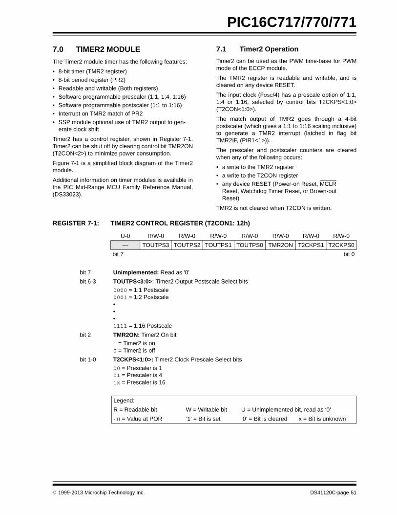
PIC16C717/770/771
7.0 TIMER2 MODULE
The Timer2 module timer has the following features:
• 8-bit timer (TMR2 register)
• 8-bit period register (PR2)
• Readable and writable (Both registers)
• Software programmable prescaler (1:1, 1:4, 1:16)
• Software programmable postscaler (1:1 to 1:16)
• Interrupt on TMR2 match of PR2
• SSP module optional use of TMR2 output to gen-erate clock shift
Timer2 has a control register, shown in Register 7-1.Timer2 can be shut off by clearing control bit TMR2ON(T2CON<2>) to minimize power consumption.
Figure 7-1 is a simplified block diagram of the Timer2module.
Additional information on timer modules is available inthe PIC Mid-Range MCU Family Reference Manual,(DS33023).
7.1 Timer2 Operation
Timer2 can be used as the PWM time-base for PWMmode of the ECCP module.
The TMR2 register is readable and writable, and iscleared on any device RESET.
The input clock (FOSC/4) has a prescale option of 1:1,1:4 or 1:16, selected by control bits T2CKPS<1:0>(T2CON<1:0>).
The match output of TMR2 goes through a 4-bitpostscaler (which gives a 1:1 to 1:16 scaling inclusive)to generate a TMR2 interrupt (latched in flag bitTMR2IF, (PIR1<1>)).
The prescaler and postscaler counters are clearedwhen any of the following occurs:
• a write to the TMR2 register
• a write to the T2CON register
• any device RESET (Power-on Reset, MCLR Reset, Watchdog Timer Reset, or Brown-out Reset)
TMR2 is not cleared when T2CON is written.
REGISTER 7-1: TIMER2 CONTROL REGISTER (T2CON1: 12h)
U-0 R/W-0 R/W-0 R/W-0 R/W-0 R/W-0 R/W-0 R/W-0
— TOUTPS3 TOUTPS2 TOUTPS1 TOUTPS0 TMR2ON T2CKPS1 T2CKPS0
bit 7 bit 0
bit 7 Unimplemented: Read as '0'
bit 6-3 TOUTPS<3:0>: Timer2 Output Postscale Select bits
0000 = 1:1 Postscale0001 = 1:2 Postscale•••1111 = 1:16 Postscale
bit 2 TMR2ON: Timer2 On bit
1 = Timer2 is on0 = Timer2 is off
bit 1-0 T2CKPS<1:0>: Timer2 Clock Prescale Select bits
00 = Prescaler is 101 = Prescaler is 41x = Prescaler is 16
Legend:
R = Readable bit W = Writable bit U = Unimplemented bit, read as ‘0’
- n = Value at POR ’1’ = Bit is set ’0’ = Bit is cleared x = Bit is unknown
1999-2013 Microchip Technology Inc. DS41120C-page 51

PIC16C717/770/771
7.2 Timer2 Interrupt
The Timer2 module has an 8-bit period register PR2.Timer2 increments from 00h until it matches PR2 andthen resets to 00h on the next increment cycle. PR2 isa readable and writable register. The PR2 register isinitialized to FFh upon RESET.
7.3 Output of TMR2
The output of TMR2 (before the postscaler) is fed to theSynchronous Serial Port module which optionally usesit to generate shift clock.
FIGURE 7-1: Timer2 Block Diagram
TABLE 7-1: REGISTERS ASSOCIATED WITH TIMER2 AS A TIMER/COUNTER
Comparator
TMR2Sets flag
TMR2 reg
output (1)
RESET
Postscaler
Prescaler
PR2 reg
2
Fosc/4
1:1 1:16
1:1, 1:4, 1:16
EQ
4
bit TMR2IF
Note: TMR2 register output can be softwareselected by the SSP Module as a baudclock.
to
Address Name Bit 7 Bit 6 Bit 5 Bit 4 Bit 3 Bit 2 Bit 1 Bit 0Value on:
POR,BOR
Value on all other RESETS
0Bh,8Bh,10Bh,18Bh
INTCON GIE PEIE T0IE INTE RBIE T0IF INTF RBIF 0000 000x 0000 000u
0Ch PIR1 — ADIF — — SSPIF CCP1IF TMR2IF TMR1IF -0-- 0000 -0-- 0000
8Ch PIE1 — ADIE — — SSPIE CCP1IE TMR2IE TMR1IE -0-- 0000 -0-- 0000
11h TMR2 Timer2 register 0000 0000 0000 0000
12h T2CON — TOUTPS3 TOUTPS2 TOUTPS1 TOUTPS0 TMR2ON T2CKPS1 T2CKPS0 -000 0000 -000 0000
92h PR2 Timer2 Period Register 1111 1111 1111 1111
Legend: x = unknown, u = unchanged, - = unimplemented read as '0'. Shaded cells are not used by the Timer2 module.
DS41120C-page 52 1999-2013 Microchip Technology Inc.

PIC16C717/770/771
8.0 ENHANCED CAPTURE/COMPARE/PWM (ECCP) MODULES
The ECCP (Enhanced Capture/Compare/PWM)module contains a 16-bit register which can operate asa 16-bit capture register, as a 16-bit compare registeror as a PWM master/slave Duty Cycle register.Table 8-1 shows the timer resources of the ECCP mod-ule modes.
Capture/Compare/PWM Register1 (CCPR1) is com-prised of two 8-bit registers: CCPR1L (low byte) andCCPR1H (high byte). The CCP1CON and P1DEL reg-isters control the operation of ECCP. All are readableand writable.
REGISTER 8-1: CCP1 CONTROL REGISTER (CCP1CON: 17h)
R/W-0 R/W-0 R/W-0 R/W-0 R/W-0 R/W-0 R/W-0 R/W-0
PWM1M1 PWM1M0 DC1B1 DC1B0 CCP1M3 CCP1M2 CCP1M1 CCP1M0
bit 7 bit 0
bit 7-6 PWM1M<1:0>: PWM Output Configuration
CCP1M<3:2> = 00, 01, 10xx = P1A assigned as Capture input, Compare output. P1B, P1C, P1D assigned as Port pins.CCP1M<3:2> = 1100 = Single output. P1A modulated. P1B, P1C, P1D assigned as Port pins.01 = Full-bridge output forward. P1D modulated. P1A active. P1B, P1C inactive.10 = Half-bridge output. P1A, P1B modulated with deadband control. P1C, P1D assigned as
Port pins.11 = Full-bridge output reverse. P1B modulated. P1C active. P1A, P1D inactive.
bit 5-4 DC1B<1:0>: PWM Duty Cycle Least Significant bits
Capture Mode: UnusedCompare Mode: UnusedPWM Mode: These bits are the two LSbs of the PWM duty cycle. The eight MSbs are found in
CCPRnL.
bit 3-0 CCP1M<3:0>: ECCP Mode Select bits
0000 = Capture/Compare/PWM off (resets ECCP module)0001 = Unused (reserved)0010 = Compare mode, toggle output on match (CCP1IF bit is set)0011 = Unused (reserved)0100 = Capture mode, every falling edge0101 = Capture mode, every rising edge0110 = Capture mode, every 4th rising edge0111 = Capture mode, every 16th rising edge1000 = Compare mode, set output on match (CCP1IF bit is set)1001 = Compare mode, clear output on match (CCP1IF bit is set)1010 = Compare mode, generate software interrupt on match (CCP1IF bit is set, CCP1 pin is
unaffected)1011 = Compare mode, trigger special event (CCP1IF bit is set; ECCP resets TMR1, and starts
an A/D conversion, if the A/D module is enabled.)1100 = PWM mode. P1A, P1C active high. P1B, P1D active high.1101 = PWM mode. P1A, P1C active high. P1B, P1D active low.1110 = PWM mode. P1A, P1C active low. P1B, P1D active high.1111 = PWM mode. P1A, P1C active low. P1B, P1D active low.
Legend:
R = Readable bit W = Writable bit U = Unimplemented bit, read as ‘0’
- n = Value at POR ’1’ = Bit is set ’0’ = Bit is cleared x = Bit is unknown
1999-2013 Microchip Technology Inc. DS41120C-page 53

PIC16C717/770/771
TABLE 8-1: ECCP MODE - TIMER RESOURCE
8.1 Capture Mode
In Capture mode, CCPR1H:CCPR1L captures the 16-bit value of the TMR1 register when an event occurs onpin CCP1. An event is defined as:
• every falling edge
• every rising edge
• every 4th rising edge
• every 16th rising edge
An event is selected by control bits CCP1M<3:0>(CCP1CON<3:0>). When a capture is made, the inter-rupt request flag bit CCP1IF (PIR1<2>) is set. It mustbe cleared in software. If another capture occurs beforethe value in register CCPR1 is read, the old capturedvalue will be lost.
8.1.1 CCP1 PIN CONFIGURATION
In Capture mode, the CCP1 pin should be configuredas an input by setting the TRISB<3> bit.
8.1.2 TIMER1 MODE SELECTION
Timer1 must be running in Timer mode or Synchro-nized Counter mode. In Asynchronous Counter mode,the capture operation may not work.
8.1.3 SOFTWARE INTERRUPT
When the Capture mode is changed, a false captureinterrupt may be generated. The user should keep bitCCP1IE (PIE1<2>) clear to avoid false interrupts andshould clear the flag bit CCP1IF following any suchchange in Operating mode.
8.1.4 ECCP PRESCALER
There are three prescaler settings, specified by bitsCCP1M<3:0>. Whenever the ECCP module is turnedoff or the ECCP module is not in Capture mode, theprescaler counter is cleared. This means that anyRESET will clear the prescaler counter.
Switching from one capture prescaler to another maygenerate an interrupt. Also, the prescaler counter willnot be cleared, therefore the first capture may be froma non-zero prescaler. Example 8-1 shows the recom-mended method for switching between capture pres-calers. This example also clears the prescaler counterand will not generate the “false” interrupt.
EXAMPLE 8-1: Changing Between Capture Prescalers
FIGURE 8-1: CAPTURE MODE OPERATION BLOCK DIAGRAM
8.2 Compare Mode
In Compare mode, the 16-bit CCPR1 register value isconstantly compared against the TMR1 register pairvalue. When a match occurs, the CCP1 pin is:
• driven High
• driven Low
• toggle output (High to Low or Low to High)
• remains Unchanged
The action on the pin is based on the value of controlbits CCP1M<3:0>. At the same time, interrupt flag bitCCP1IF is set.
Changing the ECCP mode select bits to the clear out-put on Match mode (CCP1M<3.0> = “1000”) presetsthe CCP1 output latch to the logic 1 level. Changing theECCP mode select bits to the clear output on Matchmode (CCP1M<3:0> = “1001”) presets the CCP1 out-put latch to the logic 0 level.
8.2.1 CCP1 PIN CONFIGURATION
The user must configure the CCP1 pin as an output byclearing the appropriate TRISB bit.
8.2.2 TIMER1 MODE SELECTION
Timer1 must be running in Timer mode or Synchro-nized Counter mode if the ECCP module is using thecompare feature. In Asynchronous Counter mode, thecompare operation may not work.
ECCP Mode Timer Resource
CaptureCompare
PWM
Timer1Timer1Timer2
Note: If the RB3/CCP1/P1A pin is configured asan output, a write to the port can cause acapture condition.
Note: Clearing the CCP1CON register will forcethe CCP1 compare output latch to thedefault low level. This is not the port datalatch.
CLRF CCP1CON ; Turn ECCP module offMOVLW NEW_CAPT_PS ; Load WREG with the
; new prescaler mode; value and ECCP ON
MOVWF CCP1CON ; Load CCP1CON with; this value
CCPR1H CCPR1L
TMR1H TMR1L
Set flag bit CCP1IF(PIR1<2>)
CaptureEnable
Q’sCCP1CON<3:0>
RB3/CCP1/
Prescaler³ 1, 4, 16
andedge detect
P1A Pin
DS41120C-page 54 1999-2013 Microchip Technology Inc.

PIC16C717/770/771
8.2.3 SOFTWARE INTERRUPT MODE
When generate software interrupt is chosen, the CCP1pin is not affected. Only an ECCP interrupt is generated(if enabled).
8.2.4 SPECIAL EVENT TRIGGER
In this mode, an internal hardware trigger is generated,which may be used to initiate an action.
The special event trigger output of ECCP resets theTMR1 register pair. This allows the CCPR1 register toeffectively be a 16-bit programmable period register forTimer1.
The special event trigger output of ECCP module willalso start an A/D conversion if the A/D module isenabled.
FIGURE 8-2: COMPARE MODE OPERATION BLOCK DIAGRAM
TABLE 8-2: REGISTERS ASSOCIATED WITH CAPTURE, COMPARE AND TIMER1
Note: The special event trigger will not set theinterrupt flag bit TMR1IF (PIR1<0>).
CCPR1H CCPR1L
TMR1H TMR1L
ComparatorQ S
R
OutputLogic
Special Event Trigger
Set flag bit CCP1IF(PIR1<2>)
matchRB3/CCP1/
TRISB<3>CCP1CON<3:0>Mode Select
Output Enable
P1A Pin
Special event trigger will:RESET Timer1, but not set interrupt flag bitTMR1IF (PIR1<0>).
Name Bit 7 Bit 6 Bit 5 Bit 4 Bit 3 Bit 2 Bit 1 Bit 0Value on
POR,BOR
Value onall otherRESETS
INTCON GIE PEIE T0IE INTE RBIE T0IF INTF RBIF 0000 000x 0000 000u
PIR1 PSPIF(1) ADIF RCIF TXIF SSPIF CCP1IF TMR2IF TMR1IF 0000 0000 0000 0000
PIE1 PSPIE(1) ADIE RCIE TXIE SSPIE CCP1IE TMR2IE TMR1IE 0000 0000 0000 0000
TRISB PORTB Data Direction Register 1111 1111 1111 1111
TMR1L Holding register for the Least Significant Byte of the 16-bit TMR1 register xxxx xxxx uuuu uuuu
TMR1H Holding register for the Most Significant Byte of the 16-bit TMR1register xxxx xxxx uuuu uuuu
T1CON — — T1CKPS1
T1CKPS0
T1OSCEN T1SYNC TMR1CS TMR1ON
--00 0000 --uu uuuu
CCPR1L Capture/Compare/PWM register1 (LSB) xxxx xxxx uuuu uuuu
CCPR1H Capture/Compare/PWM register1 (MSB) xxxx xxxx uuuu uuuu
CCP1CON PWM1M1 PWM1M0 DC1B1 DC1B0 CCP1M3 CCP1M2 CCP1M1 CCP1M0 0000 0000 0000 0000
Legend: x = unknown, u = unchanged, - = unimplemented read as '0'. Shaded cells are not used by Capture and Timer1.
1999-2013 Microchip Technology Inc. DS41120C-page 55

PIC16C717/770/771
8.3 PWM Mode
In Pulse Width Modulation (PWM) mode, the ECCPmodule produces up to a 10-bit resolution PWM output.Figure 8-3 shows the simplified PWM block diagram.
FIGURE 8-3: SIMPLIFIED PWM BLOCK DIAGRAM
8.3.1 PWM PERIOD
The PWM period is specified by writing to the PR2 reg-ister. The PWM period can be calculated using the fol-lowing formula:
PWM PERIOD = [(PR2) + 1] • 4 • TOSC •(TMR2 PRESCALE VALUE)
PWM frequency is defined as 1 / [PWM period].
When TMR2 is equal to PR2, the following three eventsoccur on the next increment cycle:
• TMR2 is cleared
• The CCP1 pin is set (exception: if PWM duty cycle = 0%, the CCP1 pin will not be set)
• The PWM duty cycle is latched from CCPR1L into CCPR1H
CCPR1L
CCPR1H (Slave)
Comparator
TMR2
Comparator
PR2
(Note 1)
R Q
S
Duty cycle registers CCP1CON<5:4>
Clear Timer,CCP1 pin and latch D.C.
Note: 8-bit timer TMR2 is concatenated with 2-bit internal Q clock or 2 bits of the prescaler to create 10-bit time-base.
TRISB<3>
RB3/CCP1/P1A
TRISB<5>
RB5/SDO/P1B
TRISB<6>
RB6/T1OSO/T1CKI/
TRISB<7>
RB7/T1OSI/P1D
P1C
OUTPUTCONTROLLER
PWM1M1<1:0>2
CCP1M<3:0>4
P1DEL
CCP1/P1A
P1B
P1C
P1D
Note: The Timer2 postscaler (see Section 7.0) isnot used in the determination of the PWMfrequency. The postscaler could be used tohave a servo update rate at a different fre-quency than the PWM output.
DS41120C-page 56 1999-2013 Microchip Technology Inc.

PIC16C717/770/771
8.3.2 PWM DUTY CYCLE
The PWM duty cycle is specified by writing to theCCPR1L register and to the CCP1CON<5:4> bits. Upto 10-bit resolution is available. The CCPR1L containsthe eight MSbs and the CCP1CON<5:4> contains thetwo LSbs. This 10-bit value is represented byCCPR1L:CCP1CON<5:4>. The following equation isused to calculate the PWM duty cycle in time:
PWM duty cycle = (CCPR1L:CCP1CON<5:4>) •TOSC • (TMR2 prescale value)
CCPR1L and CCP1CON<5:4> can be written to at anytime, but the duty cycle value is not latched intoCCPR1H until after a match between PR2 and TMR2occurs (i.e., the period is complete). In PWM mode,CCPR1H is a read-only register.
The CCPR1H register and a 2-bit internal latch areused to double buffer the PWM duty cycle. This doublebuffering is essential for glitchless PWM operation.
When the CCPR1H and 2-bit latch match TMR2 con-catenated with an internal 2-bit Q clock or 2 bits of theTMR2 prescaler, the CCP1 pin is cleared.
Maximum PWM resolution (bits) for a given PWM fre-quency:
8.3.3 PWM OUTPUT CONFIGURATIONS
The PWM1M1 bits in the CCP1CON register allowsone of the following configurations:
• Single output
• Half-Bridge output
• Full-Bridge output, Forward mode
• Full-Bridge output, Reverse mode
In the Single Output mode, the RB3/CCP1/P1A pin isused as the PWM output. Since the CCP1 output ismultiplexed with the PORTB<3> data latch, theTRISB<3> bit must be cleared to make the CCP1 pinan output.
FIGURE 8-4: SINGLE PWM OUTPUT
FIGURE 8-5: EXAMPLE OF SINGLE OUTPUT APPLICATION
In the Half-Bridge Output mode, two pins are used asoutputs. The RB3/CCP1/P1A pin has the PWM outputsignal, while the RB5/SDO/P1B pin has the comple-mentary PWM output signal. This mode can be usedfor half-bridge applications, as shown on Figure 8-7, orfor full-bridge applications, where four power switchesare being modulated with two PWM signal.
Since the P1A and P1B outputs are multiplexed withthe PORTB<3> and PORTB<5> data latches, theTRISB<3> and TRISB<5> bits must be cleared to con-figure P1A and P1B as outputs.
In Half-Bridge Output mode, the programmable dead-band delay can be used to prevent shoot-through cur-rent in bridge power devices. See Section 8.3.5 formore details of the deadband delay operations.
Note: If the PWM duty cycle value is longer thanthe PWM period, the CCP1 pin will not becleared.
FOSCFPWM--------------- log
2 log-----------------------------bits=
Period
Duty Cycle
(1)
(1)
Note 1: At this time, the TMR2 register is equal to the PR2 register.
CCP1(2)
2: Output signal is shown as asserted high.
C
PIC16C717/770/771
CCP1
R
Vout
Using PWM asa D/A Converter
PIC16C717/770/771
CCP1
Using PWM toDrive a Power
V+
LOAD
Load
1999-2013 Microchip Technology Inc. DS41120C-page 57

PIC16C717/770/771
8.3.4 OUTPUT POLARITY CONFIGURATION
The CCP1M<1:0> bits in the CCP1CON register allowuser to choose the logic conventions (asserted high/low) for each of the outputs. See Register 8-1 for fur-ther details.
The PWM output polarities must be selected before thePWM outputs are enabled. Charging the polarity con-figuration while the PWM outputs are active is not rec-ommended, since it may result in unpredictableoperation.
FIGURE 8-6: HALF-BRIDGE PWM OUTPUT
Note 1: At this time, the TMR2 register is equal to the PR2 register.
Period
Duty Cycle
td
td
(1)
P1A(2)
P1B(2)
td = Deadband Delay
Period
(1) (1)
2: Output signals are shown as asserted high.
DS41120C-page 58 1999-2013 Microchip Technology Inc.

PIC16C717/770/771
FIGURE 8-7: EXAMPLE OF HALF-BRIDGE OUTPUT MODE APPLICATIONS
PIC16C717/770/771
P1A
P1B
FETDRIVER
FETDRIVER
V+
V-
LOAD+ -
+V-
+V-
PIC16C717/770/771
P1A
P1B
FETDRIVER
FETDRIVER
V+
V-
LOAD+ -
FETDRIVER
FETDRIVER
1999-2013 Microchip Technology Inc. DS41120C-page 59

PIC16C717/770/771
In Full-Bridge Output mode, four pins are used as out-puts; however, only two outputs are active at a time. Inthe Forward mode, RB3/CCP1/P1A pin is continuouslyactive, and RB7/T1OSI/P1D pin is modulated. In theReverse mode, RB6/T1OSO/T1CKI/P1C pin is contin-uously active, and RB5/SDO/P1B pin is modulated.
P1A, P1B, P1C and P1D outputs are multiplexed withPORTB<3> and PORTB<5:7> data latches. TRISB<3>and TRISB<5:7> bits must be cleared to make the P1A,P1B, P1C, and P1D pins output.
FIGURE 8-8: FULL-BRIDGE PWM OUTPUT
Period
Duty CycleP1A(2)
P1B(2)
P1C(2)
P1D(2)
FORWARD MODE
(1)
Period
Duty Cycle
P1A(2)
P1C(2)
P1D(2)
P1B(2)
REVERSE MODE
10
10
10
10
10
10
10
10
(1)
(1)
(1)
Note 1: At this time, the TMR2 register is equal to the PR2 register. 2: Output signal is shown as asserted high.
DS41120C-page 60 1999-2013 Microchip Technology Inc.
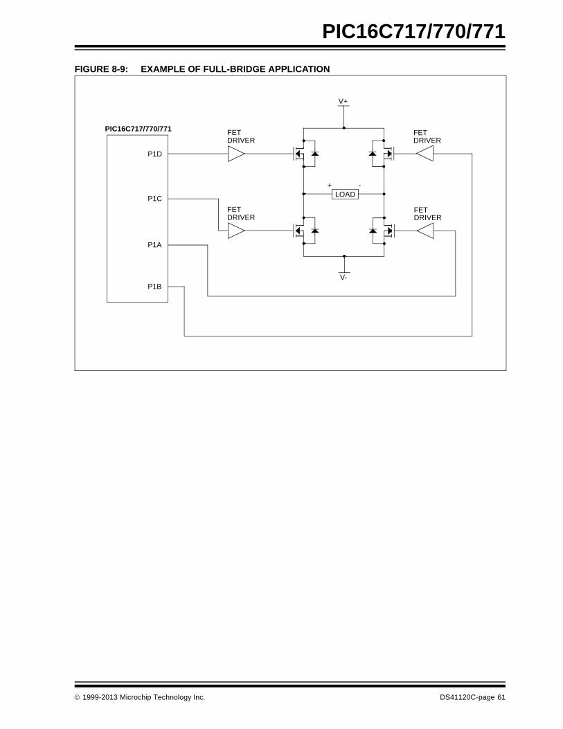
PIC16C717/770/771
FIGURE 8-9: EXAMPLE OF FULL-BRIDGE APPLICATION
PIC16C717/770/771
P1D
P1A
FETDRIVER
FETDRIVER
V+
V-
LOAD+ -
FETDRIVER
FETDRIVER
P1C
P1B
1999-2013 Microchip Technology Inc. DS41120C-page 61

PIC16C717/770/771
8.3.5 PROGRAMMABLE DEADBAND DELAY
In half-bridge or full-bridge applications, driven by half-bridge outputs (see Figure 8-7), the power switchesnormally require longer time to turn off than to turn on.If both the upper and lower power switches areswitched at the same time (one turned on, and theother turned off), both switches will be on for a shortperiod of time, until one switch completely turns off.During this time, a very high current, called shoot-through current, will flow through both power switches,
shorting the bridge supply. To avoid this potentiallydestructive shoot-through current from flowing duringswitching, turning on the power switch is normallydelayed to allow the other switch to completely turn off.
In the Half-Bridge Output mode, a digitally program-mable deadband delay is available to avoid shoot-through current from destroying the bridge powerswitches. The delay occurs at the signal transition fromthe non-active state to the active state. See Figure 8-6for illustration. The P1DEL register sets the amount ofdelay.
REGISTER 8-2: PWM DELAY REGISTER (P1DEL: 97H)
8.3.6 DIRECTION CHANGE IN FULL-BRIDGE OUTPUT MODE
In the Full-Bridge Output mode, the PWM1M1 bit in theCCP1CON register allows user to control the Forward/Reverse direction. When the application firmwarechanges this direction control bit, the ECCP module willassume the new direction on the next PWM cycle. Thecurrent PWM cycle still continues, however, the non-
modulated outputs, P1A and P1C signals, will transitionto the new direction TOSC, 4TOSC or 16TOSC (forTimer2 prescale T2CKRS<1:0> = 00, 01 and 1xrespectively) earlier, before the end of the period. Dur-ing this transition cycle, the modulated outputs, P1Band P1D, will go to the inactive state. See Figure 8-10for illustration.
FIGURE 8-10: PWM DIRECTION CHANGE
R/W-0 R/W-0 R/W-0 R/W-0 R/W-0 R/W-0 R/W-0 R/W-0
P1DEL7 P1DEL6 P1DEL5 P1DEL4 P1DEL3 P1DEL2 P1DEL1 P1DEL0
bit 7 bit 0
bit 7-0 P1DEL<7:0>: PWM Delay Count for Half-Bridge Output Mode: Number of FOSC/4 (Tosc4)cycles between the P1A transition and the P1B transition.
Legend:
R = Readable bit W = Writable bit U = Unimplemented bit, read as ‘0’
- n = Value at POR ’1’ = Bit is set ’0’ = Bit is cleared x = Bit is unknown
DCPERIOD
SIGNAL
P1A (Active High)
Note 1: The Direction bit in the ECCP Control Register (CCP1CON<PWM1M1>) is written anytime during the PWM cycle.2: The P1A and P1C signals switch TOSC, 4*Tosc or 16*TOSC, depending on the Timer2 prescaler value, earlier when
changing direction. The modulated P1B and P1D signals are inactive at this time.
(1)
PERIOD
(2)P1D (Active High)
P1C (Active High)
P1B (Active High)
DS41120C-page 62 1999-2013 Microchip Technology Inc.

PIC16C717/770/771
Note that in the Full-Bridge Output mode, the ECCPmodule does not provide any deadband delay. In gen-eral, since only one output is modulated at a time,deadband delay is not required. However, there is a sit-uation where a deadband delay might be required. Thissituation occurs when all of the following conditions aretrue:
1. The direction of the PWM output changes whenthe duty cycle of the output is at or near 100%.
2. The turn off time of the power switch, includingthe power device and driver circuit, is greaterthan turn on time.
Figure 8-11 shows an example, where the PWM direc-tion changes from forward to reverse at a near 100%duty cycle. At time t1, the output P1A and P1D becomeinactive, while output P1C becomes active. In this
example, since the turn off time of the power devices islonger than the turn on time, a shoot-through currentflows through the power devices, QB and QD, for theduration of t= toff-ton. The same phenomenon will occurto power devices, QC and QB, for PWM directionchange from reverse to forward.
If changing PWM direction at high duty cycle is requiredfor the user’s application, one of the following require-ments must be met:
1. Avoid changing PWM output direction at or near100% duty cycle.
2. Use switch drivers that compensate for the slowturn off of the power devices. The total turn offtime (toff) of the power device and the drivermust be less than the turn on time (ton).
FIGURE 8-11: PWM DIRECTION CHANGE AT NEAR 100% DUTY CYCLE
FORWARD PERIOD REVERSE PERIOD
(PWM)
P1A 10
(PWM)
ton
toff
t = toff - ton
10
10
10
10
10
10
P1B
P1C
P1D
External Switch D
PotentialShoot ThroughCurrent
Note 1: All signals are shown as active high.
2: ton is the turn on delay of power switch and driver.
3: toff is the turn off delay of power switch and driver.
External Switch C
t1
1999-2013 Microchip Technology Inc. DS41120C-page 63

PIC16C717/770/771
8.3.7 SYSTEM IMPLEMENTATION
When the ECCP module is used in the PWM mode, theapplication hardware must use the proper external pull-up and/or pull-down resistors on the PWM output pins.When the microcontroller powers up, all of the I/O pinsare in the high-impedance state. The external pull-upand pull-down resistors must keep the power switchdevices in the off state until the microcontroller drivesthe I/O pins with the proper signal levels, or activatesthe PWM output(s).
8.3.8 START-UP CONSIDERATIONS
Prior to enabling the PWM outputs, the P1A, P1B, P1Cand P1D latches may not be in the proper states.Enabling the TRISB bits for output at the same timewith the CCP module may cause damage to the powerswitch devices. The CCP1 module must be enabled inthe proper Output mode with the TRISB bits enabled asinputs. Once the CCP1 completes a full PWM cycle,the P1A, P1B, P1C and P1D output latches are prop-erly initialized. At this time, the TRISB bits can beenabled for outputs to start driving the power switchdevices. The completion of a full PWM cycle is indi-cated by the TMR2IF bit going from a '0' to a '1'.
8.3.9 SET UP FOR PWM OPERATION
The following steps should be taken when configuringthe ECCP module for PWM operation:
1. Configure the PWM module:
a) Disable the CCP1/P1A, P1B, P1C and/orP1D outputs by setting the respectiveTRISB bits.
b) Set the PWM period by loading the PR2register.
c) Set the PWM duty cycle by loading theCCPR1L register and CCP1CON<5:4>bits.
d) Configure the ECCP module for the desiredPWM operation by loading the CCP1CONregister. With the CCP1M<3:0> bits selectthe active high/low levels for each PWMoutput. With the PWM1M<1:0> bits selectone of the available Output modes: Single,Half-Bridge, Full-Bridge, Forward or Full-Bridge Reverse.
e) For Half-Bridge Output mode, set the dead-band delay by loading the P1DEL register.
2. Configure and start TMR2:
a) Clear the TMR2 interrupt flag bit by clearingthe TMR2IF bit in the PIR1 register.
b) Set the TMR2 prescale value by loading theT2CKPS<1:0> bits in the T2CON register.
c) Enable Timer2 by setting the TMR2ON bitin the T2CON register.
3. Enable PWM outputs after a new cycle hasstarted:
a) Wait until TMR2 overflows (TMR2IF bitbecomes a ’1’). The new PWM cycle beginshere.
b) Enable the CCP1/P1A, P1B, P1C and/orP1D pin outputs by clearing the respectiveTRISB bits.
TABLE 8-3: REGISTERS ASSOCIATED WITH PWM
Address Name Bit 7 Bit 6 Bit 5 Bit 4 Bit 3 Bit 2 Bit 1 Bit 0Value on
POR,BOR
Value onall otherRESETS
0Bh, 8Bh, 10Bh, 18Bh
INTCON GIE PEIE T0IE INTE RBIE T0IF INTF RBIF 0000 000x 0000 000u
0Ch PIR1 — ADIF — — SSPIF CCP1IF TMR2IF TMR1IF -0-- 0000 -0-- 0000
8Ch PIE1 — ADIE — — SSPIE CCP1IE TMR2IE TMR1IE -0-- 0000 -0-- 0000
86h, 186h TRISB PORTB Data Direction Register 1111 1111 1111 1111
11h TMR2 Timer2 register 0000 0000 0000 0000
92h PR2 Timer2 period register 1111 1111 1111 1111
12h T2CON — TOUTPS3 TOUTPS2 TOUTPS1 TOUTPS0 TMR2ON T2CKPS1 T2CKPS0 -000 0000 -000 0000
15h CCPR1L Capture/Compare/PWM register1 (LSB) xxxx xxxx uuuu uuuu
17h CCP1CON PWM1M1 PWM1M0 DC1B1 DC1B0 CCP1M3 CCP1M2 CCP1M1 CCP1M0 0000 0000 0000 0000
97h P1DEL PWM1 Delay value 0000 0000 0000 0000
Legend: x = unknown, u = unchanged, - = unimplemented read as '0'. Shaded cells are not used by ECCP module in PWM mode.
DS41120C-page 64 1999-2013 Microchip Technology Inc.

PIC16C717/770/771
9.0 MASTER SYNCHRONOUSSERIAL PORT (MSSP) MODULE
The Master Synchronous Serial Port (MSSP) module isa serial interface useful for communicating with otherperipheral or microcontroller devices. These peripheraldevices may be serial EEPROMs, shift registers, dis-play drivers, etc. The MSSP module can operate in oneof two modes:
• Serial Peripheral Interface (SPI™)
• Inter-Integrated Circuit (I2C™)
1999-2013 Microchip Technology Inc. Advance Information DS41120C-page 65

PIC16C717/770/771
REGISTER 9-1: SYNC SERIAL PORT STATUS REGISTER (SSPSTAT: 94h)
R/W-0 R/W-0 R-0 R-0 R-0 R-0 R-0 R-0
SMP CKE D/A P S R/W UA BF
bit 7 bit 0
bit 7 SMP: Sample bitSPI Master Mode1 = Input data sampled at end of data output time0 = Input data sampled at middle of data output timeSPI Slave ModeSMP must be cleared when SPI is used in Slave modeIn I2C Master or Slave mode:1= Slew rate control disabled for Standard Speed mode (100 kHz and 1 MHz)0= Slew rate control enabled for High Speed mode (400 kHz)
bit 6 CKE: SPI Clock Edge Select (Figure 9-3, Figure 9-5, and Figure 9-6)CKP = 01 = Data transmitted on rising edge of SCK0 = Data transmitted on falling edge of SCKCKP = 11 = Data transmitted on falling edge of SCK0 = Data transmitted on rising edge of SCK
bit 5 D/A: Data/Address bit (I2C mode only)1 = Indicates that the last byte received or transmitted was data0 = Indicates that the last byte received or transmitted was address
bit 4 P: STOP bit (I2C mode only. This bit is cleared when the MSSP module is disabled, SSPEN is cleared)1 = Indicates that a STOP bit has been detected last (this bit is '0' on RESET)0 = STOP bit was not detected last
bit 3 S: START bit (I2C mode only. This bit is cleared when the MSSP module is disabled, SSPEN is cleared)1 = Indicates that a START bit has been detected last (this bit is '0' on RESET)0 = START bit was not detected last
bit 2 R/W: Read/Write bit information (I2C mode only)This bit holds the R/W bit information following the last address match. This bit is only valid from theaddress match to the next START bit, STOP bit, or NACK bit.In I2 C Slave mode:1 = Read0 = WriteIn I2 C Master mode:1 = Transmit is in progress0 = Transmit is not in progress. ORing this bit with SEN, RSEN, PEN, RCEN, or AKEN will indicate if the MSSP is in IDLE mode
bit 1 UA: Update Address (10-bit I2C mode only)1 = Indicates that the user needs to update the address in the SSPADD register0 = Address does not need to be updated
bit 0 BF: Buffer Full Status bitReceive (SPI and I2 C modes)1 = Receive complete, SSPBUF is full0 = Receive not complete, SSPBUF is emptyTransmit (I2 C mode only)1 = Data Transmit in progress (does not include the ACK and STOP bits), SSPBUF is full0 = Data Transmit complete (does not include the ACK and STOP bits), SSPBUF is empty
Legend:
R = Readable bit W = Writable bit U = Unimplemented bit, read as ‘0’
- n = Value at POR ’1’ = Bit is set ’0’ = Bit is cleared x = Bit is unknown
DS41120C-page 66 Advance Information 1999-2013 Microchip Technology Inc.

PIC16C717/770/771
REGISTER 9-2: SYNC SERIAL PORT CONTROL REGISTER (SSPCON: 14h)
R/W-0 R/W-0 R/W-0 R/W-0 R/W-0 R/W-0 R/W-0 R/W-0
WCOL SSPOV SSPEN CKP SSPM3 SSPM2 SSPM1 SSPM0
bit 7 bit 0
bit 7 WCOL: Write Collision Detect bit
Master Mode: 1 = A write to the SSPBUF register was attempted while the I2C conditions were not valid for a
transmission to be started 0 = No collisionSlave Mode: 1 = The SSPBUF register is written while it is still transmitting the previous word (must be
cleared in software) 0 = No collision
bit 6 SSPOV: Receive Overflow Indicator bit
In SPI mode1 = A new byte is received while the SSPBUF register is still holding the previous data. In case
of overflow, the data in SSPSR is lost. Overflow can only occur in Slave mode. In Slavemode, the user must read the SSPBUF, even if only transmitting data, to avoid setting over-flow. In Master mode, the overflow bit is not set since each new reception (and transmis-sion) is initiated by writing to the SSPBUF register. (Must be cleared in software).
0 = No overflowIn I2 C mode1 = A byte is received while the SSPBUF register is still holding the previous byte. SSPOV is a
"don’t care" in Transmit mode. (Must be cleared in software).0 = No overflow
bit 5 SSPEN: Synchronous Serial Port Enable bit
In both modes, when enabled, the I/O pins must be properly configured as input or output.In SPI mode1 = Enables serial port and configures SCK, SDO, SDI, and SS as the source of the serial port
pins0 = Disables serial port and configures these pins as I/O port pinsIn I2 C mode1 = Enables the serial port and configures the SDA and SCL pins as the source of the serial
port pins0 = Disables serial port and configures these pins as I/O port pins
bit 4 CKP: Clock Polarity Select bit
In SPI mode1 = IDLE state for clock is a high level0 = IDLE state for clock is a low levelIn I2 C Slave mode SCK release control1 = Enable clock 0 = Holds clock low (clock stretch) (used to ensure data setup time)In I2 C Master modeUnused in this mode
Legend:
R = Readable bit W = Writable bit U = Unimplemented bit, read as ‘0’
- n = Value at POR ’1’ = Bit is set ’0’ = Bit is cleared x = Bit is unknown
1999-2013 Microchip Technology Inc. Advance Information DS41120C-page 67

PIC16C717/770/771
REGISTER 9-2: SYNC SERIAL PORT CONTROL REGISTER (SSPCON: 14h) (CONTINUED)
bit 3-0 SSPM<3:0>: Synchronous Serial Port Mode Select bits
0000 = SPI Master mode, clock = FOSC/4
0001 = SPI Master mode, clock = FOSC/16
0010 = SPI Master mode, clock = FOSC/64
0011 = SPI Master mode, clock = TMR2 output/2
0100 = SPI Slave mode, clock = SCK pin. SS pin control enabled.
0101 = SPI Slave mode, clock = SCK pin. SS pin control disabled. SS can be used as I/O pin.
0110 = I2C Slave mode, 7-bit address
0111 = I2C Slave mode, 10-bit address
1000 = I2C Master mode, clock = FOSC / (4 (SSPADD+1) )
1001 = Reserved
1010 = Reserved
1011 = Firmware controlled Master mode (slave idle)
1100 = Reserved
1101 = Reserved
1110 = 7-bit Slave mode with START and STOP condition interrupts
1111 = 10-bit Slave mode with START and STOP condition interrupts
Legend:
R = Readable bit W = Writable bit U = Unimplemented bit, read as ‘0’
- n = Value at POR ’1’ = Bit is set ’0’ = Bit is cleared x = Bit is unknown
DS41120C-page 68 Advance Information 1999-2013 Microchip Technology Inc.

PIC16C717/770/771
REGISTER 9-3: SYNC SERIAL PORT CONTROL REGISTER2 (SSPCON2: 91h)
R/W-0 R/W-0 R/W-0 R/W-0 R/W-0 R/W-0 R/W-0 R/W-0
GCEN ACKSTAT ACKDT ACKEN RCEN PEN RSEN SEN
bit 7 bit 0
bit 7 GCEN: General Call Enable bit (In I2C Slave mode only)
1 = Enable interrupt when a general call address (0000h) is received in the SSPSR.0 = General call address disabled.
bit 6 ACKSTAT: Acknowledge Status bit (In I2C Master mode only)
In Master Transmit mode:1 = Acknowledge was not received from slave0 = Acknowledge was received from slave
bit 5 ACKDT: Acknowledge Data bit (In I2C Master mode only)
In Master Receive mode:Value that will be transmitted when the user initiates an Acknowledge sequence at the end of
a receive.1 = Not Acknowledge (NACK)0 = Acknowledge (ACK)
bit 4 ACKEN: Acknowledge Sequence Enable bit (In I2C Master mode only).
In Master Receive mode:1 = Initiate Acknowledge sequence on SDA and SCL pins, and transmit ACKDT data bit.
Automatically cleared by hardware.0 = Acknowledge sequence IDLE
bit 3 RCEN: Receive Enable bit (In I2C Master mode only).
1 = Enables Receive mode for I2C0 = Receive IDLE
bit 2 PEN: STOP Condition Enable bit (In I2C Master mode only).
SCK Release Control1 = Initiate STOP condition on SDA and SCL pins. Automatically cleared by hardware.0 = STOP condition IDLE
bit 1 RSEN: Repeated START Condition Enabled bit (In I2C Master mode only)
1 = Initiate Repeated START condition on SDA and SCL pins. Automatically cleared by hardware.
0 = Repeated START condition IDLE
bit 0 SEN: START Condition Enabled bit (In I2C Master mode only)
1 = Initiate START condition on SDA and SCL pins. Automatically cleared by hardware.0 = START condition IDLE
Note: For bits ACKEN, RCEN, PEN, RSEN, SEN: If the I2C module is not in the IDLEmode, this bit may not be set (no spooling) and the SSPBUF may not be written (orwrites to the SSPBUF are disabled).
Legend:
R = Readable bit W = Writable bit U = Unimplemented bit, read as ‘0’
- n = Value at POR ’1’ = Bit is set ’0’ = Bit is cleared x = Bit is unknown
1999-2013 Microchip Technology Inc. Advance Information DS41120C-page 69

PIC16C717/770/771
9.1 SPI Mode
The SPI mode allows eight bits of data to be synchro-nously transmitted and received simultaneously. Allfour modes of SPI are supported. To accomplish com-munication, typically three pins are used:
• Serial Data Out (SDO)
• Serial Data In (SDI)
• Serial Clock (SCK)
Additionally, a fourth pin may be used when in a Slavemode of operation:
• Slave Select (SS)
9.1.1 OPERATION
When initializing the SPI, several options need to bespecified. This is done by programming the appropriatecontrol bits (SSPCON<5:0> and SSPSTAT<7:6>).These control bits allow the following to be specified:
• Master Mode (SCK is the clock output)
• Slave Mode (SCK is the clock input)
• Clock Polarity (Idle state of SCK)
• Data input sample phase (middle or end of data output time)
• Clock edge (output data on rising/falling edge of SCK)
• Clock Rate (Master mode only)
• Slave Select Mode (Slave mode only)
Figure 9-1 shows the block diagram of the MSSP mod-ule when in SPI mode.
FIGURE 9-1: MSSP BLOCK DIAGRAM (SPI MODE)
The MSSP consists of a transmit/receive Shift Register(SSPSR) and a Buffer Register (SSPBUF). TheSSPSR shifts the data in and out of the device, MSbfirst. The SSPBUF holds the data that was written to theSSPSR, until the received data is ready. Once the eightbits of data have been received, that byte is moved tothe SSPBUF register. Then the buffer full detect bit, BF(SSPSTAT<0>), and the interrupt flag bit, SSPIF(PIR1<3>), are set. This double buffering of thereceived data (SSPBUF) allows the next byte to startreception before reading the data that was justreceived. Any write to the SSPBUF register duringtransmission/reception of data will be ignored, and thewrite collision detect bit WCOL (SSPCON<7>) will beset. User software must clear the WCOL bit so that itcan be determined if the following write(s) to the SSP-BUF register completed successfully.
Read Write
InternalData Bus
SSPSR reg
SSPBUF reg
SSPM<3:0>
bit0 ShiftClock
SS ControlEnable
EdgeSelect
Clock Select
TMR2 Output
ToscPrescaler4, 16, 64
2EdgeSelect
2
4
Data to TX/RX in SSPSRData direction bit
2SMP:CKE
SDI
SDO
SS
SCK
DS41120C-page 70 Advance Information 1999-2013 Microchip Technology Inc.

PIC16C717/770/771
When the application software is expecting to receivevalid data, the SSPBUF should be read before the nextbyte of data to transfer is written to the SSPBUF. Bufferfull bit, BF (SSPSTAT<0>), indicates when the SSP-BUF has been loaded with the received data (transmis-sion is complete). When the SSPBUF is read, bit BF iscleared. This data may be irrelevant if the SPI is only atransmitter. Generally the MSSP Interrupt is used todetermine when the transmission/reception has com-pleted. The SSPBUF must be read and/or written. If theinterrupt method is not going to be used, then softwarepolling can be done to ensure that a write collision doesnot occur. Example 9-1 shows the loading of the SSP-BUF (SSPSR) for data transmission.
EXAMPLE 9-1: Loading the SSPBUF (SSPSR) Register
The SSPSR is not directly readable or writable, andcan only be accessed by addressing the SSPBUF reg-ister. Additionally, the MSSP STATUS register(SSPSTAT) indicates the various status conditions.
9.1.2 ENABLING SPI I/O
To enable the serial port, MSSP Enable bit, SSPEN(SSPCON<5>) must be set. To reset or reconfigure SPImode, clear bit SSPEN, re-initialize the SSPCON reg-isters, and then set bit SSPEN. This configures theSDI, SDO, SCK and SS pins as serial port pins. For thepins to behave as the serial port function, some musthave their data direction bits (in the TRIS register)appropriately programmed. That is:
• SDI is automatically controlled by the SPI module
• SDO must have TRISB<5> cleared
• SCK (Master mode) must have TRISB<2> cleared
• SCK (Slave mode) must have TRISB<2> set
• SS must have TRISB<1> set, and ANSEL<5> cleared
Any serial port function that is not desired may be over-ridden by programming the corresponding data direc-tion (TRIS) register to the opposite value.
9.1.3 TYPICAL CONNECTION
Figure 9-2 shows a typical connection between twomicrocontrollers. The master controller (Processor 1)initiates the data transfer by sending the SCK signal.Data is shifted out of both shift registers on their pro-grammed clock edge, and latched on the oppositeedge of the clock. Both processors should be pro-grammed to same Clock Polarity (SSPCON<4>), thenboth controllers would send and receive data at thesame time. Whether the data is meaningful (or dummydata) depends on the application software. This leadsto three scenarios for data transmission:
• Master sends data—Slave sends dummy data
• Master sends data—Slave sends data
• Master sends dummy data—Slave sends data
FIGURE 9-2: SPI MASTER/SLAVE CONNECTION
BSF STATUS, RP0 ;Specify Bank 1LOOP BTFSS SSPSTAT, BF ;Has data been
;received;(xmit complete)?
GOTO LOOP ;NoBCF STATUS, RP0 ;Specify Bank 0MOVF SSPBUF, W ;Save SSPBUF...MOVWF RXDATA ;...in user RAMMOVF TXDATA, W ;Get next TXDATAMOVWF SSPBUF ;New data to xmit
Serial Input Buffer(SSPBUF)
Shift Register(SSPSR)
MSb LSb
SDO
SDI
PROCESSOR 1
SCK
SPI Master SSPM<3:0> = 00xxb
Serial Input Buffer(SSPBUF)
Shift Register(SSPSR)
LSbMSb
SDI
SDO
PROCESSOR 2
SCK
SPI Slave SSPM<3:0> = 010xb
Serial Clock
1999-2013 Microchip Technology Inc. Advance Information DS41120C-page 71
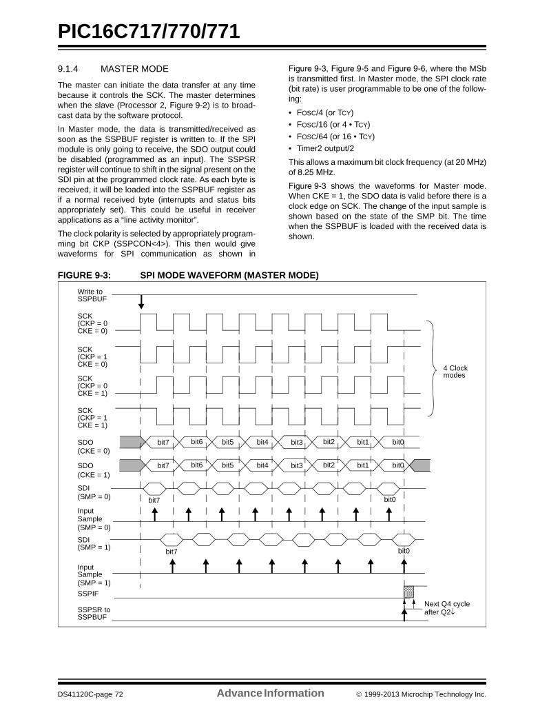
PIC16C717/770/771
9.1.4 MASTER MODE
The master can initiate the data transfer at any timebecause it controls the SCK. The master determineswhen the slave (Processor 2, Figure 9-2) is to broad-cast data by the software protocol.
In Master mode, the data is transmitted/received assoon as the SSPBUF register is written to. If the SPImodule is only going to receive, the SDO output couldbe disabled (programmed as an input). The SSPSRregister will continue to shift in the signal present on theSDI pin at the programmed clock rate. As each byte isreceived, it will be loaded into the SSPBUF register asif a normal received byte (interrupts and status bitsappropriately set). This could be useful in receiverapplications as a “line activity monitor”.
The clock polarity is selected by appropriately program-ming bit CKP (SSPCON<4>). This then would givewaveforms for SPI communication as shown in
Figure 9-3, Figure 9-5 and Figure 9-6, where the MSbis transmitted first. In Master mode, the SPI clock rate(bit rate) is user programmable to be one of the follow-ing:
• FOSC/4 (or TCY)
• FOSC/16 (or 4 • TCY)
• FOSC/64 (or 16 • TCY)
• Timer2 output/2
This allows a maximum bit clock frequency (at 20 MHz)of 8.25 MHz.
Figure 9-3 shows the waveforms for Master mode.When CKE = 1, the SDO data is valid before there is aclock edge on SCK. The change of the input sample isshown based on the state of the SMP bit. The timewhen the SSPBUF is loaded with the received data isshown.
FIGURE 9-3: SPI MODE WAVEFORM (MASTER MODE)
SCK(CKP = 0
SCK(CKP = 1
SCK(CKP = 0
SCK(CKP = 1
4 Clockmodes
InputSample
InputSample
SDI
bit7 bit0
SDO bit7 bit6 bit5 bit4 bit3 bit2 bit1 bit0
bit7 bit0
SDI
SSPIF
(SMP = 1)
(SMP = 0)
(SMP = 1)
CKE = 1)
CKE = 0)
CKE = 1)
CKE = 0)
(SMP = 0)
Write toSSPBUF
SSPSR toSSPBUF
SDO bit7 bit6 bit5 bit4 bit3 bit2 bit1 bit0
(CKE = 0)
(CKE = 1)
Next Q4 cycleafter Q2
DS41120C-page 72 Advance Information 1999-2013 Microchip Technology Inc.
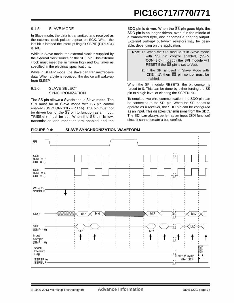
PIC16C717/770/771
9.1.5 SLAVE MODE
In Slave mode, the data is transmitted and received asthe external clock pulses appear on SCK. When thelast bit is latched the interrupt flag bit SSPIF (PIR1<3>)is set.
While in Slave mode, the external clock is supplied bythe external clock source on the SCK pin. This externalclock must meet the minimum high and low times asspecified in the electrical specifications.
While in SLEEP mode, the slave can transmit/receivedata. When a byte is received, the device will wake-upfrom SLEEP.
9.1.6 SLAVE SELECT SYNCHRONIZATION
The SS pin allows a Synchronous Slave mode. TheSPI must be in Slave mode with SS pin controlenabled (SSPCON<3:0> = 0100). The pin must notbe driven low for the SS pin to function as an input.TRISB<1> must be set. When the SS pin is low,transmission and reception are enabled and the
SDO pin is driven. When the SS pin goes high, theSDO pin is no longer driven, even if in the middle ofa transmitted byte, and becomes a floating output.External pull-up/ pull-down resistors may be desir-able, depending on the application.
When the SPI module RESETS, the bit counter isforced to 0. This can be done by either forcing the SSpin to a high level or clearing the SSPEN bit.
To emulate two-wire communication, the SDO pin canbe connected to the SDI pin. When the SPI needs tooperate as a receiver, the SDO pin can be configuredas an input. This disables transmissions from the SDO.The SDI can always be left as an input (SDI function)since it cannot create a bus conflict.
FIGURE 9-4: SLAVE SYNCHRONIZATION WAVEFORM
Note 1: When the SPI module is in Slave modewith SS pin control enabled, (SSP-CON<3:0> = 0100) the SPI module willRESET if the SS pin is set to VDD.
2: If the SPI is used in Slave Mode withCKE = '1', then SS pin control must beenabled.
SCK(CKP = 1
SCK(CKP = 0
InputSample
SDI
bit7
SDO bit7 bit6 bit7
SSPIFInterrupt
(SMP = 0)
CKE = 0)
CKE = 0)
(SMP = 0)
Write toSSPBUF
SSPSR toSSPBUF
SS
Flag
bit0
bit7
bit0
Next Q4 cycleafter Q2
1999-2013 Microchip Technology Inc. Advance Information DS41120C-page 73

PIC16C717/770/771
FIGURE 9-5: SPI SLAVE MODE WAVEFORM (CKE = 0)
FIGURE 9-6: SPI SLAVE MODE WAVEFORM (CKE = 1)
SCK(CKP = 1
SCK(CKP = 0
InputSample
SDI
bit7 bit0
SDO bit7 bit6 bit5 bit4 bit3 bit2 bit1 bit0
SSPIFInterrupt
(SMP = 0)
CKE = 0)
CKE = 0)
(SMP = 0)
Write toSSPBUF
SSPSR toSSPBUF
SS
Flag
optional
Next Q4 cycleafter Q2
SCK(CKP = 1
SCK(CKP = 0
InputSample
SDI
bit7 bit0
SDO bit7 bit6 bit5 bit4 bit3 bit2 bit1 bit0
SSPIFInterrupt
(SMP = 0)
CKE = 1)
CKE = 1)
(SMP = 0)
Write toSSPBUF
SSPSR toSSPBUF
SS
Flag
not optional
Next Q4 cycleafter Q2
DS41120C-page 74 Advance Information 1999-2013 Microchip Technology Inc.

PIC16C717/770/771
9.1.7 SLEEP OPERATION
In Master mode, all module clocks are halted and thetransmission/reception will remain in that state until thedevice wakes from SLEEP. After the device returns toNormal mode, the module will continue to transmit/receive data.
In Slave mode, the SPI transmit/receive shift registeroperates asynchronously to the device. This allows thedevice to be placed in SLEEP mode and data to beshifted into the SPI transmit/receive shift register.When all eight bits have been received, the SSPIFinterrupt flag bit will be set and if enabled will wake thedevice from SLEEP.
9.1.8 EFFECTS OF A RESET
A RESET disables the MSSP module and terminatesthe current transfer.
TABLE 9-1: REGISTERS ASSOCIATED WITH SPI OPERATION
Address Name Bit 7 Bit 6 Bit 5 Bit 4 Bit 3 Bit 2 Bit 1 Bit 0 POR, BOR MCLR, WDT
0Bh, 8Bh, 10Bh,18Bh
INTCON GIE PEIE T0IE INTE RBIE T0IF INTF RBIF 0000 000x 0000 000u
0Ch PIR1 — ADIF — — SSPIF CCP1IF TMR2IF TMR1IF -0-- 0000 -0-- 0000
8Ch PIE1 — ADIE — — SSPIE CCP1IE TMR2IE TMR1IE -0-- 0000 -0-- 0000
13h SSPBUF Synchronous Serial Port Receive Buffer/Transmit Register xxxx xxxx uuuu uuuu
14h SSPCON WCOL SSPOV SSPEN CKP SSPM3 SSPM2 SSPM1 SSPM0 0000 0000 0000 0000
94h SSPSTAT SMP CKE D/A P S R/W UA BF 0000 0000 0000 0000
9Dh ANSEL --11 1111 --11 1111
86h TRISB 1111 1111 1111 1111
Legend: x = unknown, u = unchanged, - = unimplemented read as '0'. Shaded cells are not used by the MSSP in SPI mode.
1999-2013 Microchip Technology Inc. Advance Information DS41120C-page 75

PIC16C717/770/771
9.2 MSSP I2C Operation
The MSSP module in I2C mode fully implements allmaster and slave functions (including general call sup-port) and provides interrupts on START and STOP bitsin hardware to determine when the bus is free (multi-master function). The MSSP module implements theStandard mode specifications, as well as 7-bit and 10-bit addressing.
Two pins are used to transfer data. They are the SCLpin (clock) and the SDA pin (data). The MSSP modulefunctions are enabled by setting SSP Enable bitSSPEN (SSPCON<5>). The SCL and SDA pins are"glitch" filtered when operating as inputs. This filterfunctions in both the 100 kHz and 400 kHz modes.When these pins operate as outputs in the 100 kHzmode, there is a slew rate control of the pin that is inde-pendent of device frequency.
Before selecting any I2C mode, the SCL and SDA pinsmust be programmed as inputs by setting the appropri-ate TRIS bits. This allows the MSSP module to configureand drive the I/O pins as required by the I2C protocol.
The MSSP module has six registers for I2C operation.They are listed below.
• SSP Control Register (SSPCON)
• SSP Control Register2 (SSPCON2)
• SSP STATUS Register (SSPSTAT)
• Serial Receive/Transmit Buffer (SSPBUF)
• SSP Shift Register (SSPSR) - Not directly accessible
• SSP Address Register (SSPADD)
The SSPCON register allows for control of the I2Coperation. Four mode selection bits (SSPCON<3:0>)configure the MSSP as any one of the following I2Cmodes:
• I2C Slave mode (7-bit address)
• I2C Slave mode (10-bit address)
• I2C Master mode SCL Freq = FOSC / [4 (SSPADD + 1)]
• I2C Slave mode with START and STOP interrupts (7-bit address)
• I2C Slave mode with START and STOP interrupts (10-bit address)
• Firmware Controlled Master mode
The SSPSTAT register gives the status of the datatransfer. This information includes detection of aSTART (S) or STOP (P) bit. It specifies whether thereceived byte was data or address, if the next byte isthe completion of 10-bit address, and if this will be aread or write data transfer.
SSPBUF is the register to which the transfer data iswritten, and from which the transfer data is read. TheSSPSR register shifts the data in or out of the device.In receive operations, the SSPBUF and SSPSR createa doubled, buffered receiver. This allows reception ofthe next byte to begin before reading the last byte ofreceived data. When the complete byte is received, it is
transferred from the SSPSR register to the SSPBUFregister and flag bit SSPIF is set. If another completebyte is received before the SSPBUF register is read areceiver overflow occurs, in which case, the SSPOV bit(SSPCON<6>) is set and the byte in the SSPSR is lost.
FIGURE 9-7: I2C SLAVE MODE BLOCK DIAGRAM
9.2.1 UPWARD COMPATIBILITY WITH SSP MODULE
The MSSP module includes three SSP modes of oper-ation to maintain upward compatibility with the SSPmodule. These modes are:
• Firmware controlled Master mode (slave idle)
• 7-bit Slave mode with START and STOP condition interrupts.
• 10-bit Slave mode with START and STOP condition interrupts.
The firmware controlled Master mode enables theSTART and STOP condition interrupts but all other I2Cfunctions are generated through firmware including:
• Generating the START and STOP conditions
• Generating the SCL clock
• Supplying the SDA bits in the proper time and phase relationship to the SCL signal.
In firmware controlled Master mode, the SCL and SDAlines are manipulated by clearing and setting the corre-sponding TRIS bits. The output level is always low irre-spective of the value(s) in the PORT register. A ‘1’ isoutput by setting the TRIS bit and a ‘0’ is output byclearing the TRIS bit
The 7-bit and 10-bit Slave modes with START andSTOP condition interrupts operate identically to theMSSP Slave modes except that START and STOPconditions generate SSPIF interrupts.
Read Write
SSPSR reg
Match detect
SSPADD reg
START and STOP bit detect
SSPBUF reg
InternalData Bus
Addr Match
Set, RESETS, P bits
(SSPSTAT reg)
RB2/SCK/
ShiftClock
MSb LSb
SCL
RB4/SDI/SDA
DS41120C-page 76 Advance Information 1999-2013 Microchip Technology Inc.

PIC16C717/770/771
For more information about these SSP modes see Sec-tion 15 of the PIC Mid-Range MCU Family ReferenceManual (DS33023).
9.2.2 SLAVE MODE
When an address is matched or the data transfer afteran address match is received, the hardware automati-cally will generate the Acknowledge (ACK) pulse.Then, it loads the SSPBUF register with the receivedvalue currently in the SSPSR register.
Any combination of the following conditions will causethe MSSP module to generate a NACK pulse in lieu ofthe ACK pulse:
a) The buffer full bit BF (SSPSTAT<0>) is setbefore the transfer is received.
b) The overflow bit SSPOV (SSPCON<6>) is setbefore the transfer is received.
If the BF bit is set, the SSPSR register value is notloaded into the SSPBUF. However, both the SSPIF andSSPOV bits are set. Table 9-2 shows what happenswhen a data transfer byte is received, given the statusof bits BF and SSPOV. The shaded cells show the con-dition where user software did not properly clear theoverflow condition. The BF flag bit is cleared by readingthe SSPBUF register. The SSPOV flag bit is clearedthrough software.
The SCL clock input must have a minimum high andlow time for proper operation. The high and low timesof the I2C specification as well as the requirements ofthe MSSP module are shown in timing parameters#100 and #101 of the Electrical Specifications.
9.2.2.1 7-BIT ADDRESSING
Once the MSSP module has been enabled(SSPEN=1), the slave module waits for a START con-dition to occur. Following the START condition, eightbits are shifted into the SSPSR register. All incomingbits are sampled on the rising edge of the clock (SCL)line. The received address (register SSPSR<7:1>) iscompared to the stored address (registerSSPADD<7:1>). SSPSR<0> is the R/W bit and is notconsidered in the comparison. Comparison is made onthe falling edge of the eighth clock (SCL) pulse. If theaddresses match, and the BF and SSPOV bits areclear, the following events occur:
a) The SSPSR register value is transferred to theSSPBUF register on the falling edge of theeighth SCL pulse.
b) The buffer full bit; BF is set on the falling edge ofthe eighth SCL pulse.
c) An ACK pulse is generated during the ninthclock cycle.
d) SSP interrupt flag bit; SSPIF (PIR1<3>) is set(interrupt is generated if enabled) - on the fallingedge of the ninth SCL pulse.
9.2.2.2 10-BIT ADDRESSING
In 10-bit mode, the basic receive and transmit opera-tions are the same as in the 7-bit mode. However, thecriteria for address match are more complex.
Two address bytes need to be received by the slave.The five Most Significant bits (MSbs) of the firstaddress byte specify that this is a 10-bit address. TheLSb of the first received address byte is the R/W bit,which must be zero, specifying a write so the slavedevice will receive the second address byte. For a 10-bit address, the first byte equals ‘11110 A9 A8 0’,where A9 and A8 are the two MSbs of the address. Thesequence of events for a 10-bit address is as follows,with steps 7 through 9 applicable only to the slave-transmitter:
1. Receive first (high) byte of Address (bits SSPIF,BF, and bit UA (SSPSTAT<1>) are set).
2. Update the SSPADD register with second (low)byte of Address (clears bit UA and releases theSCL line).
3. Read the SSPBUF register (clears bit BF) andclear flag bit SSPIF.
4. Receive second (low) byte of Address (bitsSSPIF, BF, and UA are set).
5. Update the SSPADD register with the first (high)byte of Address. This will clear bit UA andrelease the SCL line.
6. Read the SSPBUF register (clears bit BF) andclear flag bit SSPIF.
7. Receive Repeated START condition.
8. Receive first (high) byte of Address with R/W bitset to 1 (bits SSPIF and BF are set). This alsoputs the MSSP module in the Slave-transmitmode.
9. Read the SSPBUF register (clears bit BF) andclear flag bit SSPIF.
Note: Following the Repeated START condition(step 7) in 10-bit mode, the user onlyneeds to match the first 7-bit address. Theuser does not update the SSPADD for thesecond half of the address.
1999-2013 Microchip Technology Inc. Advance Information DS41120C-page 77

PIC16C717/770/771
9.2.2.3 SLAVE RECEPTION
When the R/W bit of the address byte is clear(SSPSR<0> = 0) and an address match occurs, the R/W bit of the SSPSTAT register is cleared. The receivedaddress is loaded into the SSPBUF register on the fall-ing edge of the eighth SCL pulse.
When the address byte overflow condition exists, thenno Acknowledge (ACK) pulse is given. An overflowcondition is defined as either bit BF (SSPSTAT<0>) orbit SSPOV (SSPCON<6>) is set.
An MSSP interrupt is generated for each data transferbyte. Flag bit SSPIF (PIR1<3>) must be cleared in soft-ware. The SSPSTAT register is used to determine thestatus of the received byte.
TABLE 9-2: DATA TRANSFER RECEIVED BYTE ACTIONS
FIGURE 9-8: I2C SLAVE MODE WAVEFORMS FOR RECEPTION (7-BIT ADDRESS)
Note: The SSPBUF will be loaded if the SSPOVbit is set and the BF flag is cleared. If aread of the SSPBUF was performed, butthe user did not clear the state of theSSPOV bit before the next receiveoccurred, the ACK is not sent and the SSP-BUF is updated.
Status Bits as DataTransfer is Received
SSPSR SSPBUFGenerate ACK
Pulse
Set bit SSPIF(SSP Interrupt occurs
if enabled)BF SSPOV
0 0 Yes Yes Yes
1 0 No No Yes
1 1 No No Yes
0 1 Yes No Yes
Note 1: Shaded cells show the conditions where the user software did not properly clear the overflow condition.
P98765
D0D1D2D3D4D5D6D7
S
A7 A6 A5 A4 A3 A2 A1SDA
SCL 1 2 3 4 5 6 7 8 9 1 2 3 4 5 6 7 8 9 1 2 3 4
Bus Masterterminatestransfer
Bit SSPOV is set because the SSPBUF register is still full.
Cleared in softwareSSPBUF register is read
ACK Receiving DataReceiving Data
D0D1D2D3D4D5D6D7
ACKR/W=0Receiving Address
SSPIF
BF (SSPSTAT<0>)
SSPOV (SSPCON<6>)
NACK
NACK is sent because of overflow
DS41120C-page 78 Advance Information 1999-2013 Microchip Technology Inc.

PIC16C717/770/771
FIGURE 9-9: I2C SLAVE MODE FOR RECEPTION (10-BIT ADDRESS)
SD
A
SC
L
SS
PIF
BF
(S
SP
STA
T<
0>)
S1
23
45
67
89
12
34
56
78
91
23
45
78
9P
11
11
0A
9A
8A
7A
6A
5A
4A
3A
2A
1A
0D
7D
6D
5D
4D
3D
1D
0
Rec
eiv
e D
ata
Byt
e
AC
K
R/W
= 0 A
CK
Rec
eiv
e F
irst
Byt
e o
f A
ddr
ess
Cle
ared
in s
oftw
are
Bus
Mas
ter
term
inat
es
tran
sfer
D2
6
(PIR
1<
3>)
Rec
eiv
e S
eco
nd B
yte
of
Add
ress
Cle
ared
by
hard
war
e w
hen
SS
PA
DD
is u
pda
ted
with
low
byte
of
addr
ess
.
UA
(S
SP
STA
T<
1>)
Clo
ck is
hel
d lo
w u
ntil
upd
ate
of
SS
PA
DD
ha
s ta
ken
pla
ce
UA
is s
et i
ndic
atin
g th
atth
e S
SP
AD
D n
eed
s to
be
upda
ted
UA
is s
et i
ndi
catin
g th
atS
SP
AD
D n
eeds
to b
eup
date
d
SS
PB
UF
is w
ritte
n w
ithco
nte
nts
of S
SP
SR
Dum
my
read
of
SS
PB
UF
to c
lear
BF
fla
g
AC
K
Cle
are
d in
sof
twar
e
Du
mm
y re
ad o
f SS
PB
UF
to c
lea
r B
F fl
ag
Re
ad o
f SS
PB
UF
cle
ars
BF
fla
g
Cle
are
d b
y ha
rdw
are
whe
nS
SP
AD
D is
up
date
d w
ith h
igh
byt
e of
add
ress
.
1999-2013 Microchip Technology Inc. Advance Information DS41120C-page 79

PIC16C717/770/771
9.2.2.4 SLAVE TRANSMISSION
When the R/W bit of the incoming address byte is setand an address match occurs, the R/W bit of the SSP-STAT register is set. The received address is loadedinto the SSPBUF register on the falling edge of theeighth SCL pulse. The ACK pulse will be sent on theninth bit, and the SCL pin is held low. The slave moduleautomatically stretches the clock by holding the SCLline low so that the master will be unable to assertanother clock pulse until the slave is finished preparingthe transmit data. The transmit data must be loadedinto the SSPBUF register, which also loads the SSPSRregister. The CKP bit (SSPCON<4>) must then be setto release the SCL pin from the forced low condition.The eight data bits are shifted out on the falling edgesof the SCL input. This ensures that the SDA signal isvalid during the SCL high time (Figure 9-10).
The ACK or NACK signal from the master-receiver islatched on the rising edge of the ninth SCL input pulse.The master-receiver terminates slave transmission by
sending a NACK. If the SDA line is high (NACK), thenthe data transfer is complete. When the NACK islatched by the slave, the slave logic is RESET whichalso resets the R/W bit to '0'. The slave module thenmonitors for another occurrence of the START bit. Theslave firmware knows not to load another byte into theSSPBUF register by sensing that the buffer is empty(BF = 0) and the R/W bit has gone low. If the SDA lineis low (ACK), the R/W bit remains high indicating thatthe next transmit data must be loaded into the SSPBUFregister.
An MSSP interrupt (SSPIF flag) is generated for eachdata transfer byte on the falling edge of the ninth clockpulse. The SSPIF flag bit must be cleared in software.The SSPSTAT register is used to determine the statusof the byte transfer.
For more information about the I2C Slave mode, referto Application Note AN734, “Using the PIC® SSP forSlave I2C™ Communication”.
FIGURE 9-10: I2C SLAVE MODE WAVEFORMS FOR TRANSMISSION (7-BIT ADDRESS)
SDA
SCL
SSPIF
BF (SSPSTAT<0>)
CKP (SSPCON<4>)
A7 A6 A5 A4 A3 A2 A1 ACK D7 D6 D5 D4 D3 D2 D1 D0
NACKTransmitting DataR/W = 1Receiving Address
1 2 3 4 5 6 7 8 9 1 2 3 4 5 6 7 8 9P
cleared in softwareSSPBUF is written in software
From SSP interruptservice routine
Set bit after writing to SSPBUF
SData in sampled
SCL held lowuntil SSPBUF
is written
(the SSPBUF must be written-tobefore the CKP bit can be set)
R/W 0
Master terminates transmissionby responding with NACK
DS41120C-page 80 Advance Information 1999-2013 Microchip Technology Inc.

PIC16C717/770/771
FIGURE 9-11: I2C SLAVE MODE WAVEFORMS FOR TRANSMISSION (10-BIT ADDRESS)
SD
A
SC
L
SS
PIF
BF
(S
SP
STA
T<
0>
)
S1
23
45
67
89
12
34
56
78
91
23
45
78
9P
11
11
0A
9A
8A
7A
6A
5A
4A
3A
2A
1A
01
11
10
A8
R/W
=1
AC
KA
CK
AC
K
Rec
eiv
e F
irst
Byt
e o
f Ad
dre
ss
Cle
are
d in
sof
twa
re
Mas
ter
send
s N
AC
K
A9 6
(PIR
1<3>
)
Re
ceiv
e S
eco
nd B
yte
of A
ddr
ess
Cle
are
d b
y ha
rdw
are
whe
nS
SP
AD
D is
upd
ate
d.
UA
(S
SP
STA
T<
1>)
Clo
ck is
hel
d lo
w u
ntil
upd
ate
of S
SP
AD
D h
as
take
n p
lace
UA
is s
et in
dica
ting
that
the
SS
PA
DD
nee
ds
to b
eup
dat
ed
UA
is s
et in
dic
atin
g th
atS
SP
AD
D n
eed
s to
be
upd
ate
d
Cle
ared
by
har
dw
are
wh
enS
SP
AD
D is
up
date
d.
SS
PB
UF
is w
ritte
n w
ithco
nte
nts
of S
SP
SR
Dum
my
rea
d o
f SS
PB
UF
to c
lear
BF
fla
g
Rec
eiv
e F
irst
Byt
e o
f A
ddr
ess
12
34
57
89
D7
D6
D5
D4
D3
D1
NA
CK
D2
6
Tra
nsm
ittin
g D
ata
Byt
e
D0
Dum
my
rea
d of
SS
PB
UF
to c
lear
BF
fla
g
Sr
Cle
are
d in
sof
twar
e
Wri
te o
f SS
PB
UF
initi
ate
s tr
ansm
it
Cle
ared
in s
oftw
areT
ran
smit
is c
om
ple
te
CK
P h
as to
be
set f
or c
lock
to
be
rele
ase
d
Mas
ter
rele
ase
sb
us w
ith S
TO
Pco
nditi
on
R/W
=0
R/W
0
Re
star
t co
nditi
on
1999-2013 Microchip Technology Inc. Advance Information DS41120C-page 81

PIC16C717/770/771
9.2.3 GENERAL CALL ADDRESS SUPPORT
The addressing procedure for the I2C bus is such thatthe first byte after the START condition usually deter-mines which device will be the slave addressed by themaster. The exception is the general call address,which can address all devices. When this address isused, all devices should, in theory, respond with anAcknowledge.
The general call address is one of eight addressesreserved for specific purposes by the I2C protocol. Itconsists of all 0’s with R/W = 0
The general call address is recognized when the Gen-eral Call Enable bit (GCEN) is set (SSPCON2<7> isset). Following a START bit detect, eight bits are shifted
into the SSPSR, and the address is compared againstSSPADD. It is also compared to the general calladdress, fixed in hardware.
If the general call address matches, the SSPSR istransferred to the SSPBUF, the BF flag is set (eighthbit), and on the falling edge of the ninth bit (ACK bit),the SSPIF flag is set.
When the interrupt is serviced, the source for the inter-rupt can be checked by reading the contents of theSSPBUF to determine if the address was device spe-cific or a general call address.
If the general call address is sampled with GCEN setand the slave configured in 10-bit Address mode, thesecond half of the address is not necessary. The UA bitwill not be set and the slave will begin receiving dataafter the Acknowledge (Figure 9-12).
FIGURE 9-12: SLAVE MODE GENERAL CALL ADDRESS SEQUENCE (7- OR 10-BIT MODE)
SDA
SCL
S
SSPIF
BF
SSPOV
Cleared in software
SSPBUF is read
R/W = 0ACKGeneral Call Address
Address is compared to General Call Address
GCEN
Receiving data
ACK
1 2 3 4 5 6 7 8 9 1 2 3 4 5 6 7 8 9
D7 D6 D5 D4 D3 D2 D1 D0
after ACK, set interrupt flag
'0'
'1'
(SSPSTAT<0>)
(SSPCON<6>)
(SSPCON2<7>)
DS41120C-page 82 Advance Information 1999-2013 Microchip Technology Inc.

PIC16C717/770/771
9.2.4 SLEEP OPERATION
While in SLEEP mode, the I2C slave module canreceive addresses or data. When an address match orcomplete byte transfer occurs, it wakes the processorfrom SLEEP (if the SSP interrupt bit is enabled).
9.2.5 EFFECTS OF A RESET
A RESET disables the MSSP module and terminatesthe current transfer.
9.2.6 MASTER MODE
Master mode operation supports interrupt generationon the detection of the START and STOP conditions.The STOP (P) and START (S) bits are cleared from aRESET or when the MSSP module is disabled. Controlof the I2C bus may be taken when the P bit is set or thebus is idle with both the S and P bits clear.
In Master mode, the SCL and SDA lines are manipu-lated by the MSSP hardware.
The following events will cause SSP Interrupt Flag bit(SSPIF) to be set (SSP Interrupt, if enabled):
• START condition
• STOP condition
• Data transfer byte transmitted/received
• Acknowledge transmit
• Repeated START
FIGURE 9-13: MSSP BLOCK DIAGRAM (I2C MASTER MODE)
Read Write
SSPSR
START bit, STOP bit,
START bit detect,
SSPBUF
InternalData Bus
Set/RESET, S, P, WCOL (SSPSTAT)
ShiftClock
MSb LSb
SDA
AcknowledgeGenerate
STOP bit detectWrite collision detect
Clock ArbitrationState counter forend of XMIT/RCV
SCL
SCL in
Bus Collision
SDA in
Re
ceiv
e E
na
ble
cloc
k cn
tl
clo
ck a
rbitr
ate
/WC
OL
de
tect
(ho
ld o
ff cl
ock
so
urc
e)
SSPADD<6:0>
Baud
Set SSPIF, BCLIFRESET ACKSTAT, PEN (SSPCON2)
RateGenerator
SSPM<3:0>,
1999-2013 Microchip Technology Inc. Advance Information DS41120C-page 83

PIC16C717/770/771
9.2.7 MULTI-MASTER OPERATION
In Multi-Master mode, the interrupt generation on thedetection of the START and STOP conditions allowsthe determination of when the bus is free. The STOP(P) and START (S) bits are cleared from a RESET orwhen the MSSP module is disabled. Control of the I2Cbus may be taken when bit P (SSPSTAT<4>) is set, orthe bus is idle with both the S and P bits clear. Whenthe bus is busy, enabling the SSP Interrupt will gener-ate the interrupt when the STOP condition occurs.
In multi-master operation, the SDA line must be moni-tored for arbitration to see if the signal level is theexpected output level. This check is performed in hard-ware, with the result placed in the BCLIF bit.
The states where arbitration can be lost are:
• Address Transfer
• Data Transfer
• A START Condition
• A Repeated START Condition
• An Acknowledge Condition
Refer to Application Note AN578, "Use of the SSPModule in the I2C™ Multi-Master Environment."
9.2.8 I2C MASTER OPERATION
Master mode is enabled by setting and clearing theappropriate SSPM bits in SSPCON and by setting theSSPEN bit. Once Master mode is enabled, the userhas six options.
1. Assert a START condition on SDA and SCL.
2. Assert a Repeated START condition on SDAand SCL.
3. Write to the SSPBUF register initiating transmis-sion of data/address.
4. Generate a STOP condition on SDA and SCL.
5. Configure the I2C port to receive data.
6. Generate an Acknowledge condition at the endof a received byte of data.
The master device generates all serial clock pulses andthe START and STOP conditions. A transfer is endedwith a STOP condition or with a Repeated START con-dition. Since the Repeated START condition is also thebeginning of the next serial transfer, the I2C bus will notbe released.
9.2.9 BAUD RATE GENERATOR
The baud rate generator used for SPI mode operationis used in the I2C Master mode to set the SCL clock fre-quency. Standard SCL clock frequencies are 100 kHz,400 kHz, and 1 MHz. One of these frequencies can beachieved by setting the SSPADD register to the appro-priate number for the selected Fosc frequency. Onehalf of the SCL period is equal to [(SSPADD+1) 2]/Fosc.
The baud rate generator reload value is contained inthe lower seven bits of the SSPADD register (Figure 9-14). When the BRG is loaded with this value, the BRGcounts down to 0 and stops until another reload occurs.The BRG count is decremented twice per instructioncycle (TCY) on the Q2 and Q4 clock.
In I2C Master mode, the BRG is reloaded automaticallyprovided that the SCL line is sampled high. For exam-ple, if Clock Arbitration is taking place, the BRG reloadwill be suppressed until the SCL line is released by theslave allowing the pin to float high (Figure 9-15).
FIGURE 9-14: BAUD RATE GENERATOR BLOCK DIAGRAM
Note: The MSSP Module, when configured in I2CMaster mode, does not allow queueing ofevents. For instance, the user is notallowed to initiate a START condition andimmediately write the SSPBUF register toinitiate transmission before the STARTcondition is complete. In this case, theSSPBUF will not be written to, and theWCOL bit will be set, indicating that a writeto the SSPBUF did not occur.
SSPM<3:0>
BRG Down CounterBRG CLKOUTFosc/2
SSPADD<6:0>
SSPM<3:0>
SCL
Reload
Control
Reload
DS41120C-page 84 Advance Information 1999-2013 Microchip Technology Inc.

PIC16C717/770/771
FIGURE 9-15: BAUD RATE GENERATOR TIMING WITH CLOCK ARBITRATION
9.2.10 I2C MASTER MODE START CONDITION TIMING
To initiate a START condition, the user sets the STARTcondition enable bit, SEN (SSPCON2<0>). If the SDAand SCL pins are sampled high, indicating that the busis available, the baud rate generator is loaded with thecontents of SSPADD<6:0> and starts its count. If SCLand SDA are both sampled high when the baud rategenerator times out (TBRG) indicating the bus is stillavailable, the SDA pin is driven low. The SDA transitionfrom high to low while SCL is high is the START condi-tion. This causes the S bit (SSPSTAT<3>) to be set.When the S bit is set, the baud rate generator isreloaded with the contents of SSPADD<6:0> andresumes its count. When the baud rate generator timesout (TBRG) the START condition is complete, concur-rent with the following events:
• The SEN bit (SSPCON2<0>) is automatically cleared by hardware,
• The baud rate generator is suspended leaving the SDA line held low.
• The SSPIF flag is set.
9.2.10.1 WCOL STATUS FLAG
If the user writes the SSPBUF when a STARTsequence is in progress, the WCOL is set and the con-tents of the buffer are unchanged (the write doesn’toccur).
FIGURE 9-16: FIRST START BIT TIMING
SDA
SCL
SCL de-asserted but slave holds
DX-1DX
BRG
SCL is sampled high, reload takesplace, and BRG starts its count.
03h 02h 01h 00h (hold off) 03h 02h
reload
BRGvalue
SCL low (clock arbitration)SCL allowed to transition high
BRG decrements(on Q2 and Q4 cycles)
Note: If at the beginning of START condition, theSDA and SCL pins are already sampledlow, or if during the START condition, theSCL line is sampled low before the SDAline is driven low, a bus collision occurs.Thus, the Bus Collision Interrupt Flag(BCLIF) is set, the START condition isaborted, and the I2C module is RESET intoits IDLE state.
Note: Because queueing of events is notallowed, writing to the lower five bits ofSSPCON2 is disabled until the STARTcondition is complete.
SDA
SCL
S
TBRG
1st Bit 2nd Bit
TBRG
SDA = 1, At completion of START bit,SCL = 1
Write to SSPBUF occurs hereTBRG
Hardware clears SEN bit
TBRG
Write to SEN bit occurs here.Set S bit (SSPSTAT<3>)
and sets SSPIF bit
1999-2013 Microchip Technology Inc. Advance Information DS41120C-page 85

PIC16C717/770/771
9.2.11 I2C MASTER MODE REPEATED START CONDITION TIMING
A Repeated START condition occurs when the RSENbit (SSPCON2<1>) is set high while the I2C module isin the idle state. When the RSEN bit is set, the SCL pinis asserted low. When the SCL pin is sampled low, thebaud rate generator is loaded with the contents ofSSPADD<6:0> and begins counting. The SDA pin isreleased (brought high) for one baud rate generatorcount (TBRG). When the baud rate generator times out,if SDA is sampled high, the SCL pin will be de-asserted(brought high). When SCL is sampled high, the baudrate generator is reloaded with the contents ofSSPADD<6:0> and begins counting. SDA and SCLmust be sampled high for one TBRG period. This actionis then followed by assertion of the SDA pin (SDA islow) for one TBRG period while SCL is high. As soon asa START condition is detected on the SDA and SCLpins, the S bit (SSPSTAT<3>) will be set. Followingthis, the baud rate generator is reloaded with the con-tents of SSPAD<6:0> and begins counting. When theBRG times out a third time, the RSEN bit in theSSPCON2 register is automatically cleared and SCL ispulled low. The SSPIF flag is set, which indicates theRestart sequence is complete.
Immediately following the SSPIF bit transition to true,the user may write the SSPBUF with the 7-bit addressin 7-bit mode, or the default first address in 10-bitmode. After the first eight bits are transmitted and anACK is received, the user may then perform one of thefollowing:
• Transmit an additional eight bits of address (if the user transmitted the first half of a 10-bit address with R/W = 0),
• Transmit eight bits of data (if the user transmitted a 7-bit address with R/W = 0), or
• Receive eight bits of data (if the user transmitted either the first half of a 10-bit address or a 7-bit address with R/W = 1).
9.2.11.1 WCOL STATUS FLAG
If the user writes the SSPBUF when a RepeatedSTART sequence is in progress, then WCOL is set andthe contents of the buffer are unchanged (the writedoesn’t occur).
FIGURE 9-17: REPEAT START CONDITION WAVEFORM
Note 1: If RSEN is set while another event is inprogress, it will not take effect. Queuing ofevents is not allowed.
2: A bus collision during the RepeatedSTART condition occurs if either of thefollowing is true:
a) SDA is sampled low when SCLgoes from low to high.
b) SCL goes low before SDA isasserted low. This may indicatethat another master is attemptingto transmit a data “1”.
Note: Because queueing of events is notallowed, writing of the lower five bits ofSSPCON2 is disabled until the RepeatedSTART condition is complete.
SDA
SCL
Sr = Repeated START
Write to SSPCON2
Write to SSPBUF occurs here.Falling edge of ninth clockEnd of Xmit
At completion of START bit, hardware clears RSEN bit
1st Bit
Set S (SSPSTAT<3>)
TBRG
TBRG
SDA = 1,
SDA = 1,
SCL (no change)
SCL = 1occurs here.
TBRG TBRG TBRG
and sets SSPIF
DS41120C-page 86 Advance Information 1999-2013 Microchip Technology Inc.

PIC16C717/770/771
9.2.12 I2C MASTER MODE TRANSMISSION
In Master-transmitter mode, serial data is outputthrough SDA, while SCL outputs the serial clock. Thefirst byte transmitted contains seven bits of addressdata and the Read/Write (R/W) bit. In this case, the R/W bit will be logic '0'. Subsequent serial data is trans-mitted eight bits at a time. After each byte is transmit-ted, an Acknowledge bit is received. START and STOPconditions are output to indicate the beginning and theend of a serial transfer.
Transmission of a data byte, a 7-bit address, or eitherhalf of a 10-bit address is accomplished by simply writ-ing a value to the SSPBUF register. This action will setthe buffer full flag (BF) and allow the baud rate genera-tor to begin counting and start the next transmission.Each bit of address/data will be shifted out onto theSDA pin after the falling edge of SCL is asserted (seedata hold time spec). SCL is held low for one baud rategenerator roll over count (TBRG). Data should be validbefore SCL is released high (see data setup timespec). When the SCL pin is released high, it is held thatway for TBRG, the data on the SDA pin must remain sta-ble for that duration and some hold time after the nextfalling edge of SCL. After the eighth bit is shifted out(the falling edge of the eighth clock), the BF flag iscleared and the master releases SDA. This allows theslave device being addressed to respond with an ACKbit during the ninth bit time. The status of ACK is readinto the ACKDT on the rising edge of the ninth clock. Ifthe master receives an Acknowledge, the Acknowl-edge status bit (ACKSTAT) is cleared. Otherwise, thebit is set. The SSPIF is set on the falling edge of theninth clock, and the master clock (baud rate generator)is suspended until the next data byte is loaded into theSSPBUF leaving SCL low and SDA unchanged(Figure 9-18).
A typical transmit sequence would go as follows:
a) The user generates a START Condition by set-ting the START enable bit (SEN) in SSPCON2.
b) SSPIF is set at the completion of the STARTsequence.
c) The user resets the SSPIF bit and loads theSSPBUF with seven bits of address plus R/W bitto transmit.
d) Address and R/W is shifted out the SDA pin untilall eight bits are transmitted.
e) The MSSP Module shifts in the ACK bit from theslave device, and writes its value into theSSPCON2 register (SSPCON2<6>).
f) The module generates an interrupt at the end ofthe ninth clock cycle by setting SSPIF.
g) The user resets the SSPIF bit and loads theSSPBUF with eight bits of data.
h) DATA is shifted out the SDA pin until all eight bitsare transmitted.
i) The MSSP Module shifts in the ACK bit from theslave device and writes its value into theSSPCON2 register (SSPCON2<6>).
j) The MSSP module generates an interrupt at theend of the ninth clock cycle by setting the SSPIFbit.
k) The user resets the SSPIF bit and generates aSTOP condition by setting the STOP enable bitPEN in SSPCON2.
l) SSPIF is set when the STOP condition is complete.
9.2.12.1 BF STATUS FLAG
In Transmit mode, the BF bit (SSPSTAT<0>) is setwhen the CPU writes to SSPBUF and is cleared whenall eight bits are shifted out.
9.2.12.2 WCOL STATUS FLAG
If the user writes the SSPBUF when a transmit isalready in progress (i.e. SSPSR is still shifting out adata byte), then WCOL is set and the contents of thebuffer are unchanged (the write doesn’t occur).
WCOL must be cleared in software.
9.2.12.3 ACKSTAT STATUS FLAG
In Transmit mode, the ACKSTAT bit (SSPCON2<6>) iscleared when the slave has sent an Acknowledge(ACK = 0), and is set when the slave does not Acknowl-edge (ACK = 1). A slave sends an Acknowledge whenit has recognized its address (including a general call),or when the slave has properly received its data.
1999-2013 Microchip Technology Inc. Advance Information DS41120C-page 87

PIC16C717/770/771
FIGURE 9-18: I2C MASTER MODE WAVEFORMS FOR TRANSMISSION (7 OR 10-BIT ADDRESS)
SD
A
SC
L
SS
PIF
BF
(S
SP
STA
T<
0>)
SE
N
A7
A6
A5
A4
A3
A2
A1
AC
KD
7D
6D
5D
4D
3D
2D
1D
0
NA
CK
Tra
nsm
ittin
g D
ata
or
Se
con
d H
alf
R/W
= 0
Tra
nsm
it A
ddre
ss to
Sla
ve
12
34
56
78
91
23
45
67
89
P
clea
red
in s
oftw
are
ser
vice
rou
tine
SS
PB
UF
is w
ritte
n in
sof
twar
e
Fro
m S
SP
inte
rrup
t
Afte
r S
TAR
T c
ond
itio
n S
EN
cle
are
d b
y ha
rdw
are
.
S
SS
PB
UF
wri
tten
with
7-b
it a
ddre
ss a
nd R
/Wst
art
tra
nsm
it
SC
L h
eld
low
SE
N =
0
of 1
0-bi
t Ad
dre
ss
Writ
e S
SP
CO
N2<
0>
SE
N =
1S
TAR
T c
ondi
tion
be
gins
AC
K fr
om
sla
ve c
lear
s A
CK
STA
T b
it (S
SP
CO
N2
<6>
)
cle
are
d in
sof
twar
e
SS
PB
UF
writ
ten
PE
N
Cle
ared
in s
oftw
are
PE
N is
set to
initi
ate
ST
OP
conditi
on
NA
CK
from
sla
ve s
ets
AC
KS
TAT
bit
(SS
PC
ON
2<
6>)
until
SS
PB
UF
isw
ritten
.
DS41120C-page 88 Advance Information 1999-2013 Microchip Technology Inc.

PIC16C717/770/771
9.2.13 I2C MASTER MODE RECEPTION
In Master-receive mode, the first byte transmitted con-tains seven bits of address data and the R/W bit. In thiscase, the R/W bit will be logic '1'. Thus, the first bytetransmitted is a 7-bit slave address followed by a '1' toindicate receive. Serial data is received via SDA, whileSCL outputs the serial clock. Serial data is receivedeight bits at a time. After each byte is received, anAcknowledge bit is transmitted. The START conditionindicates the beginning of a transmission. The master-receiver terminates slave transmission by respondingto the last byte with a NACK Acknowledge and followsthis with a STOP condition to indicate to other mastersthat the bus is free.
Master mode reception is enabled by setting thereceive enable bit, RCEN (SSPCON2<3>), immedi-ately following the Acknowledge sequence.
The baud rate generator begins counting, and on eachrollover, the state of the SCL pin changes (high to low/low to high) and data is shifted into the SSPSR. Afterthe falling edge of the eighth clock, the following eventsoccur:
• The receive enable bit is automatically cleared.
• The contents of the SSPSR are loaded into the SSPBUF.
• The BF flag is set.
• The SSPIF is set.
• The baud rate generator is suspended from counting, holding SCL low.
The SSP is now in IDLE state, awaiting the next com-mand. When the buffer is read by the CPU, the BF flagis automatically cleared. The user can then send anAcknowledge bit at the end of reception by clearing theACKDT bit (SSPCON2<5>) and setting the Acknowl-edge sequence enable bit, ACKEN (SSPCON2<4>).
A typical receive sequence would go as follows:
a) The user generates a START Condition by set-ting the START enable bit (SEN) in SSPCON2.
b) SSPIF is set at the completion of the STARTsequence.
c) The user resets the SSPIF bit and loads theSSPBUF with seven bits of address in the MSbsand the LSb (R/W bit) set to '1' for receive.
d) Address and R/W is shifted out the SDA pin untilall eight bits are transmitted.
e) The MSSP Module shifts in the ACK bit from theslave device, and writes its value into theSSPCON2 register (SSPCON2<6>).
f) The module generates an interrupt at the end ofthe ninth clock cycle by setting SSPIF.
g) The user resets the SSPIF bit and sets theRCEN bit to enable reception.
h) DATA is shifted into the SDA pin until all eightbits are received.
i) The MSSP module sets the SSPIF bit and clearsthe RCEN bit at the falling edge of the eighthclock.
j) The user resets the SSPIF bit and sets theACKDT bit to '0' (ACK), if another byte is antici-pated. Otherwise, the ACKDT bit is set to '1'(NACK) to terminate reception. The user setsADKEN to start the Acknowledge sequence.
k) The MSSP module sets the SSPIF bit at thecompletion of the Acknowledge.
l) If a NACK was sent in step ( j), then the user pro-ceeds with step ( m). Otherwise, reception con-tinues by repeating steps ( g) through ( j).
m) The user generates a STOP condition by settingthe STOP enable bit PEN in SSPCON2.
n) SSPIF is set when the STOP condition is complete.
9.2.13.1 BF STATUS FLAG
In receive operation, BF is set when an address or databyte is loaded into SSPBUF from SSPSR. It is clearedby hardware when SSPBUF is read.
9.2.13.2 SSPOV STATUS FLAG
In receive operation, SSPOV is set when eight bits arereceived into the SSPSR and the BF flag is already setfrom a previous reception.
9.2.13.3 WCOL STATUS FLAG
If the user writes the SSPBUF when a receive isalready in progress (i.e., SSPSR is still shifting in a databyte), then WCOL is set and the contents of the bufferare unchanged (the write doesn’t occur).
Note: The MSSP Module must be in an IDLESTATE before the RCEN bit is set or theRCEN bit will be disregarded.
1999-2013 Microchip Technology Inc. Advance Information DS41120C-page 89

PIC16C717/770/771
FIGURE 9-19: I2C MASTER WAVEFORMS FOR RECEPTION (7-BIT ADDRESS)
P9
87
65
D0
D1
D2
D3
D4
D5
D6
D7
S
A7
A6
A5
A4
A3
A2
A1
SD
A
SC
L1
23
45
67
89
12
34
56
78
91
23
4
Bus
Ma
ster
term
inat
es
tran
sfer
AC
KR
ece
ivin
g D
ata
from
Sla
veR
ece
ivin
g D
ata
from
Sla
ve
D0
D1
D2
D3
D4
D5
D6
D7
AC
KR
/W =
1T
ran
smit
Add
ress
to
Sla
ve
SS
PIF
BF
Ma
ste
r se
nds
NA
CK
to
Writ
e to
SS
PC
ON
2<0>
, (S
EN
= 1
)
Writ
e to
SS
PB
UF
AC
K fr
om
Sla
ve
Mas
ter
conf
igur
ed a
s a
re
ceiv
er
by
prog
ram
min
g S
SP
CO
N2
<3>
, (R
CE
N =
1)
PE
N b
it =
1w
ritte
n he
re
Da
ta s
hifte
d in
on
falli
ng
edg
e o
f C
LK
sta
rts
tra
nsm
it
SE
N =
0
(SS
PS
TAT
<0
>)
NA
CK
Last
bit
is s
hifte
d in
to S
SP
SR
and
con
ten
ts a
re u
nlo
ade
d in
to S
SP
BU
F
SS
PIF
occ
urs
at e
nd o
f re
ceiv
e
SS
PIF
occ
urs
at e
nd
AC
K fr
om M
ast
er
SS
PIF
occ
urs
at
SS
PIF
occ
urs
at e
nd o
f Ack
now
ledg
ese
que
nce
SS
PIF
occ
urs
at e
nd o
f A
ckno
w-
led
ge s
equ
ence
end
of r
ece
ive
RC
EN
cle
ared
aut
om
atic
ally
RC
EN
= 1
to
star
tne
xt r
ece
ive
and
set
AC
KE
N (
SS
PC
ON
2<4
>)
= 1
to s
tart
AC
K A
ckno
wle
dge
sequ
enc
e
Set
AC
KD
T (
SS
PC
ON
2<
5>)
= 0
RC
EN
cle
ared
aut
om
atic
ally
AC
KE
NBeg
in S
TAR
T C
ondi
tion
Cle
are
d in
sof
twar
e
SD
A =
AC
KD
T =
0
Wri
ting
SS
PB
UF
ca
uses
BF
to
go
hig
h
SS
PIF
occ
urs
at e
nd o
f tra
nsm
itS
SP
IF o
ccur
s at
en
d o
f Sta
rt
term
inat
e s
lave
tran
smis
sio
n
and
set A
CK
EN
(S
SP
CO
N2
<4>
) =
1to
sta
rt N
AC
K A
ckno
wle
dge
seq
uenc
e
Set
AC
KD
T (
SS
PC
ON
2<5>
) =
1
of S
TO
P s
equ
ence
SS
PB
UF
is r
ead
cle
arin
g B
F fl
ag
AC
KE
N b
it is
set
to
initi
ate
Ack
now
ledg
e se
quen
ceA
CK
EN
is c
lear
ed b
y h
ardw
are
BF
cle
ars
auto
mat
ica
llyw
hen
the
last
bit
is s
hifte
d o
ut.
DS41120C-page 90 Advance Information 1999-2013 Microchip Technology Inc.
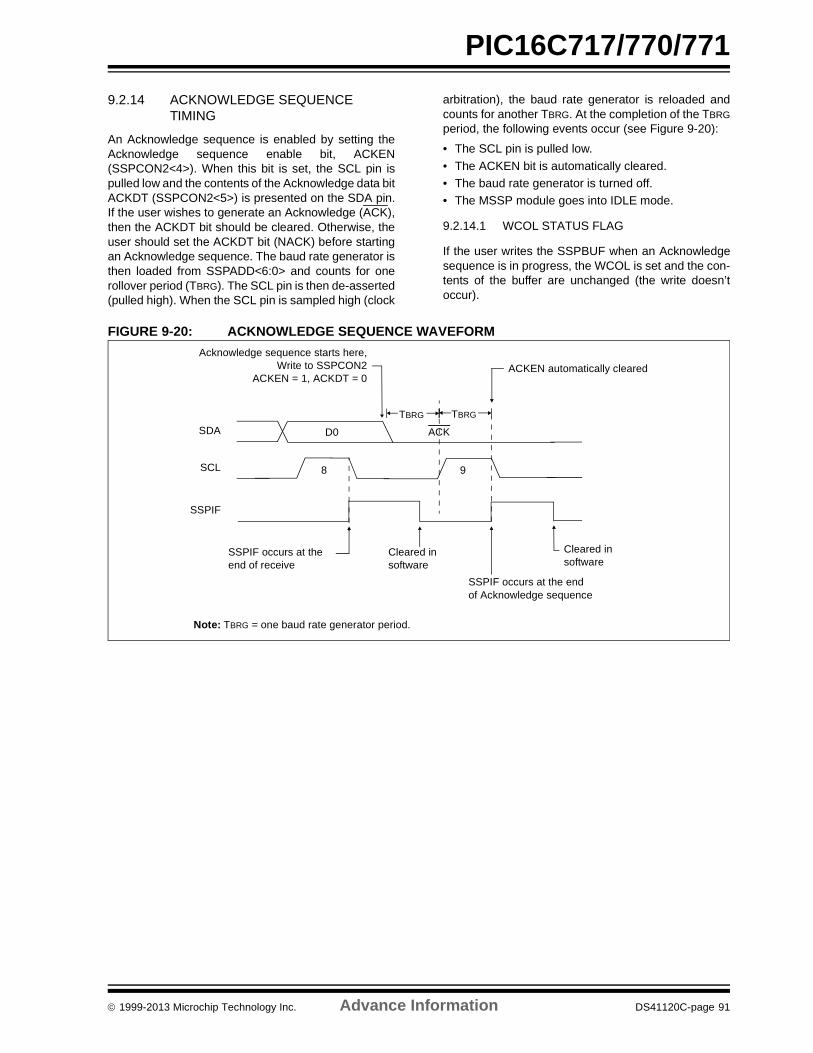
PIC16C717/770/771
9.2.14 ACKNOWLEDGE SEQUENCE TIMING
An Acknowledge sequence is enabled by setting theAcknowledge sequence enable bit, ACKEN(SSPCON2<4>). When this bit is set, the SCL pin ispulled low and the contents of the Acknowledge data bitACKDT (SSPCON2<5>) is presented on the SDA pin.If the user wishes to generate an Acknowledge (ACK),then the ACKDT bit should be cleared. Otherwise, theuser should set the ACKDT bit (NACK) before startingan Acknowledge sequence. The baud rate generator isthen loaded from SSPADD<6:0> and counts for onerollover period (TBRG). The SCL pin is then de-asserted(pulled high). When the SCL pin is sampled high (clock
arbitration), the baud rate generator is reloaded andcounts for another TBRG. At the completion of the TBRG
period, the following events occur (see Figure 9-20):
• The SCL pin is pulled low.
• The ACKEN bit is automatically cleared.
• The baud rate generator is turned off.
• The MSSP module goes into IDLE mode.
9.2.14.1 WCOL STATUS FLAG
If the user writes the SSPBUF when an Acknowledgesequence is in progress, the WCOL is set and the con-tents of the buffer are unchanged (the write doesn’toccur).
FIGURE 9-20: ACKNOWLEDGE SEQUENCE WAVEFORM
Note: TBRG = one baud rate generator period.
SDA
SCL
SSPIF occurs at the
Acknowledge sequence starts here,Write to SSPCON2 ACKEN automatically cleared
Cleared in
TBRG TBRG
end of receive
ACK
8
ACKEN = 1, ACKDT = 0
D0
9
SSPIF
software
SSPIF occurs at the endof Acknowledge sequence
Cleared insoftware
1999-2013 Microchip Technology Inc. Advance Information DS41120C-page 91

PIC16C717/770/771
9.2.15 STOP CONDITION TIMING
The master asserts a STOP condition on the SDA andSCL pins at the end of a receive/transmit by setting theStop Sequence Enable bit PEN (SSPCON2<2>). At theend of a receive/transmit plus Acknowledge, the SCLline is held low immediately following the falling edge ofthe ninth SCL pulse. When the PEN bit is set, the mas-ter will assert the SDA line low. When the SDA line issampled low, the baud rate generator is loaded fromSSPADD<6:0> and counts down to 0. When the baudrate generator times out, the SCL pin is brought high,the BRG is reloaded and one TBRG (baud rate genera-tor rollover count) later, the SDA pin is de-asserted.The SDA pin transition from low to high while SCL ishigh is the STOP condition and causes the P bit (SSP-STAT<4>) to be set. Following this the baud rage gen-erator is reloaded with the contents of SSPADD<6:0>and resumes its count. When the baud rate generator
times out (TBRG) the STOP condition is complete andthe PEN bit is cleared and the SSPIF bit is set(Figure 9-21).
Whenever the firmware decides to take control of thebus, it should first determine if the bus is busy by check-ing the S and P bits in the SSPSTAT register. When theMSSP module detects a START or STOP condition theSSPIF flag is set. If the bus is busy (S bit is set), thenthe CPU can be configured to be interrupted whenwhen the bus is free by enabling the SSPIF interrupt todetect the STOP bit.
9.2.15.1 WCOL STATUS FLAG
If the user writes the SSPBUF when a STOP sequenceis in progress, then WCOL is set and the contents of thebuffer are unchanged (the write doesn’t occur).
FIGURE 9-21: STOP CONDITION RECEIVE OR TRANSMIT MODE
SCL
SDA
SDA asserted low before rising edge of clock
Write to SSPCON2Set PEN
Falling edge of9th clock
SCL brought high after TBRG
Note: TBRG = one baud rate generator period.
TBRG TBRG
P bit (SSPSTAT<4>) is set
TBRG
to setup STOP condition.
NACK
PTBRG
PEN bit (SSPCON2<2>) is cleared by hardware and the SSPIF bit is set
DS41120C-page 92 Advance Information 1999-2013 Microchip Technology Inc.

PIC16C717/770/771
9.2.16 CLOCK ARBITRATION
Clock arbitration occurs when the master, during anyreceive, transmit or repeated START/STOP condition,de-asserts the SCL pin (SCL allowed to float high).When the SCL pin is allowed to float high, the baud rategenerator (BRG) is suspended from counting until the
SCL pin is actually sampled high. When the SCL pin issampled high, the baud rate generator is reloaded withthe contents of SSPADD<6:0> and begins counting.This ensures that the SCL high time will always be atleast one BRG rollover count in the event that the clockis held low by an external device (Figure 9-22).
FIGURE 9-22: CLOCK ARBITRATION TIMING IN MASTER TRANSMIT MODE
SCL
SDA
BRG overflow,Release SCL,If SCL = 1 Load BRG withSSPADD<6:0>, and start count BRG overflow occurs,
Release SCL, Slave device holds SCL low.SCL = 1 BRG starts countingclock high interval.
SCL line sampled once every machine cycle (Tosc 4).Hold off BRG until SCL is sampled high.
TBRG TBRG TBRG
to measure high time interval
1999-2013 Microchip Technology Inc. Advance Information DS41120C-page 93

PIC16C717/770/771
9.2.17 MULTI -MASTER COMMUNICATION, BUS COLLISION, AND BUS ARBITRATION
Multi-master mode support is achieved by bus arbitra-tion. When the master outputs address/data bits ontothe SDA pin, bus arbitration is initiated when one mas-ter outputs a '1' on SDA (by letting SDA float high) andanother master asserts a '0'. If the expected data onSDA is a '1' and the data sampled on the SDA pin = '0',then a bus collision has taken place. The master thatexpected a ‘1’ will set the Bus Collision Interrupt Flag,BCLIF, and reset the I2C port to its IDLE state.(Figure 9-23).
A bus collision during transmit results in the followingevents:
• The transmission is halted.
• The BF flag is cleared
• The SDA and SCL lines are de-asserted
• The restriction on writing to the SSPBUF during transmission is lifted.
When the user services the bus collision interrupt ser-vice routine, and if the I2C bus is free, the user canresume communication by asserting a START condi-tion.
A bus collision during a START, Repeated START,STOP or Acknowledge condition results in the followingevents:
• The condition is aborted.• The SDA and SCL lines are de-asserted.• The respective control bits in the SSPCON2 regis-
ter are cleared.
When the user services the bus collision interrupt ser-vice routine, and if the I2C bus is free, the user canresume communication by asserting a START condi-tion.
The Master will continue to monitor the SDA and SCLpins, and if a STOP condition occurs, the SSPIF bit willbe set.
A write to the SSPBUF will start the transmission ofdata at the first data bit, regardless of where the trans-mitter left off when bus collision occurred.
In Multi-Master mode, the interrupt generation on thedetection of START and STOP conditions allows thedetermination of when the bus is free. Control of the I2Cbus can be taken when the P bit is set in the SSPSTATregister, or the bus is idle and the S and P bits arecleared.
FIGURE 9-23: BUS COLLISION TIMING FOR TRANSMIT AND ACKNOWLEDGE
SDA
SCL
BCLIF
SDA released
SDA line pulled lowby another source
Sample SDA. While SCL is highdata doesn’t match what is driven
Bus collision has occurred.
Set bus collisioninterrupt.
by the master.
by master
Data changeswhile SCL = 0
DS41120C-page 94 Advance Information 1999-2013 Microchip Technology Inc.
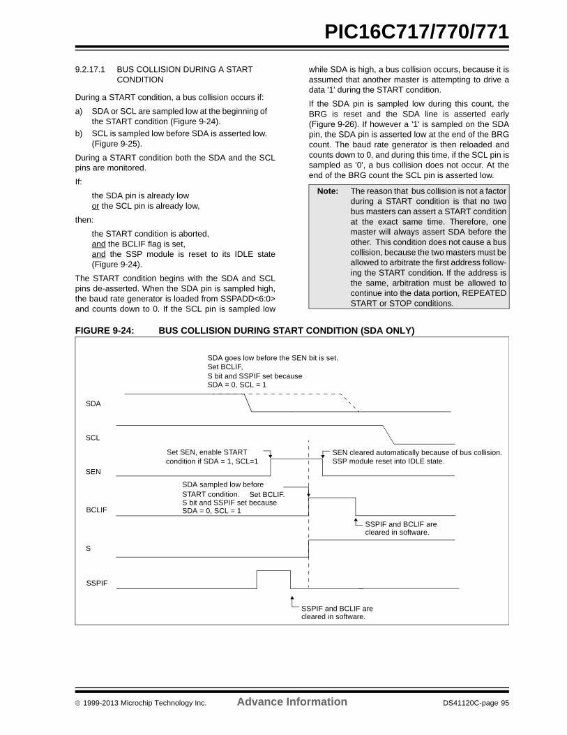
PIC16C717/770/771
9.2.17.1 BUS COLLISION DURING A START CONDITION
During a START condition, a bus collision occurs if:
a) SDA or SCL are sampled low at the beginning ofthe START condition (Figure 9-24).
b) SCL is sampled low before SDA is asserted low.(Figure 9-25).
During a START condition both the SDA and the SCLpins are monitored.
If:
the SDA pin is already lowor the SCL pin is already low,
then:
the START condition is aborted, and the BCLIF flag is set,and the SSP module is reset to its IDLE state(Figure 9-24).
The START condition begins with the SDA and SCLpins de-asserted. When the SDA pin is sampled high,the baud rate generator is loaded from SSPADD<6:0>and counts down to 0. If the SCL pin is sampled low
while SDA is high, a bus collision occurs, because it isassumed that another master is attempting to drive adata '1' during the START condition.
If the SDA pin is sampled low during this count, theBRG is reset and the SDA line is asserted early(Figure 9-26). If however a '1' is sampled on the SDApin, the SDA pin is asserted low at the end of the BRGcount. The baud rate generator is then reloaded andcounts down to 0, and during this time, if the SCL pin issampled as '0', a bus collision does not occur. At theend of the BRG count the SCL pin is asserted low.
FIGURE 9-24: BUS COLLISION DURING START CONDITION (SDA ONLY)
Note: The reason that bus collision is not a factorduring a START condition is that no twobus masters can assert a START conditionat the exact same time. Therefore, onemaster will always assert SDA before theother. This condition does not cause a buscollision, because the two masters must beallowed to arbitrate the first address follow-ing the START condition. If the address isthe same, arbitration must be allowed tocontinue into the data portion, REPEATEDSTART or STOP conditions.
SDA
SCL
SEN
SDA sampled low before
SDA goes low before the SEN bit is set.
S bit and SSPIF set because
SSP module reset into IDLE state.SEN cleared automatically because of bus collision.
S bit and SSPIF set because
Set SEN, enable STARTcondition if SDA = 1, SCL=1
SDA = 0, SCL = 1
BCLIF
S
SSPIF
SDA = 0, SCL = 1
SSPIF and BCLIF arecleared in software.
SSPIF and BCLIF arecleared in software.
Set BCLIF,
Set BCLIF.START condition.
1999-2013 Microchip Technology Inc. Advance Information DS41120C-page 95

PIC16C717/770/771
FIGURE 9-25: BUS COLLISION DURING START CONDITION (SCL = 0)
FIGURE 9-26: BRG RESET DUE TO SDA COLLISION DURING START CONDITION
SDA
SCL
SENBus collision occurs, Set BCLIF.SCL = 0 before SDA = 0,
Set SEN, enable STARTsequence if SDA = 1, SCL = 1
TBRG TBRG
SDA = 0, SCL = 1
BCLIF
S
SSPIF
Interrupts clearedin software.
Bus collision occurs, Set BCLIF.SCL = 0 before BRG time out,
'0'
'0'
'0'
'0'
SDA
SCL
SEN
Set S
Set SEN, enable STARTsequence if SDA = 1, SCL = 1
Less than TBRG TBRG
SDA = 0, SCL = 1
BCLIF
S
SSPIF
s
Interrupts clearedin software.Set SSPIF
SDA = 0, SCL = 1
SDA pulled low by other master.Reset BRG and assert SDA
SCL pulled low after BRGTime-out
Set SSPIF
'0'
DS41120C-page 96 Advance Information 1999-2013 Microchip Technology Inc.

PIC16C717/770/771
9.2.17.2 BUS COLLISION DURING A REPEATED START CONDITION
During a Repeated START condition, a bus collisionoccurs if:
a) A low level is sampled on SDA when SCL goesfrom low level to high level.
b) SCL goes low before SDA is asserted low, indi-cating that another master is attempting to trans-mit a data ’1’.
When the master module de-asserts SDA and the pinis allowed to float high, the BRG is loaded withSSPADD<6:0>, and counts down to ‘0’. The SCL pin isthen de-asserted, and when sampled high, the SDA pinis sampled. If SDA is low, a bus collision has occurred(i.e., another master is attempting to transmit a data
’0’). If however SDA is sampled high, then the BRG isreloaded and begins counting. If SDA goes from high tolow before the BRG times out, no bus collision occurs,because no two masters can assert SDA at exactly thesame time.
If, however, SCL goes from high to low before the BRGtimes out and SDA has not already been asserted, thena bus collision occurs. In this case, another master isattempting to transmit a data ’1’ during the RepeatedSTART condition.
If at the end of the BRG time-out both SCL and SDA arestill high, the SDA pin is driven low, the BRG isreloaded, and begins counting. At the end of the count,regardless of the status of the SCL pin, the SCL pin isdriven low and the Repeated START condition is com-plete (Figure 9-27).
FIGURE 9-27: BUS COLLISION DURING A REPEATED START CONDITION (CASE 1)
FIGURE 9-28: BUS COLLISION DURING REPEATED START CONDITION (CASE 2)
SDA
SCL
RSEN
BCLIF
S
SSPIF
Sample SDA when SCL goes high.If SDA = 0, set BCLIF and release SDA and SCL
Cleared in software'0'
'0'
'0'
'0'
SDA
SCL
BCLIF
RSEN
S
SSPIF
Interrupt clearedin software
SCL goes low before SDA,Set BCLIF. Release SDA and SCL
TBRG TBRG
'0'
'0'
'0'
'0'
1999-2013 Microchip Technology Inc. Advance Information DS41120C-page 97

PIC16C717/770/771
9.2.17.3 BUS COLLISION DURING A STOP CONDITION
Bus collision occurs during a STOP condition if:
a) After the SDA pin has been de-asserted andallowed to float high, SDA is sampled low afterthe BRG has timed out.
b) After the SCL pin is de-asserted, SCL is sam-pled low before SDA goes high.
The STOP condition begins with SDA asserted low.When SDA is sampled low, the SCL pin is allowed tofloat. When the pin is sampled high (clock arbitration),the baud rate generator is loaded with SSPADD<6:0>and counts down to ‘0’. After the BRG times out SDA issampled. If SDA is sampled low, a bus collision hasoccurred. This is due to another master attempting todrive a data '0' (Figure 9-29). If the SCL pin is sampledlow before SDA is allowed to float high, a bus collisionoccurs. This is another case of another master attempt-ing to drive a data '0' (Figure 9-30).
FIGURE 9-29: BUS COLLISION DURING A STOP CONDITION (CASE 1)
FIGURE 9-30: BUS COLLISION DURING A STOP CONDITION (CASE 2)
SDA
SCL
BCLIF
PEN
P
SSPIF
TBRG TBRG TBRG
SDA asserted low
SDA sampledlow after TBRG,Set BCLIF
'0'
'0'
'0'
'0'
SDA
SCL
BCLIF
PEN
P
SSPIF
TBRG TBRG TBRG
Assert SDA SCL goes low before SDA goes highSet BCLIF
'0'
'0'
DS41120C-page 98 Advance Information 1999-2013 Microchip Technology Inc.

PIC16C717/770/771
9.2.18 CONNECTION CONSIDERATIONS FOR I2C BUS
For Standard mode I2C bus devices, the values ofresistors Rp and Rs in Figure 9-31 depends on the fol-lowing parameters
• Supply voltage
• Bus capacitance
• Number of connected devices (input current + leakage current).
The supply voltage limits the minimum value of resistorRp due to the specified minimum sink current of 3 mAat VOL max = 0.4V for the specified output stages. For
example, with a supply voltage of VDD = 5V+10% andVOL max = 0.4V at 3 mA, Rp min = (5.5-0.4)/0.003 =1.7 k VDD as a function of Rp is shown in Figure 9-31.The desired noise margin of 0.1VDD for the low levellimits the maximum value of Rs. Series resistors areoptional and used to improve ESD susceptibility.
The bus capacitance is the total capacitance of wire,connections, and pins. This capacitance limits the max-imum value of Rp due to the specified rise time(Figure 9-31).
The SMP bit is the slew rate control enabled bit. This bitis in the SSPSTAT register, and controls the slew rateof the I/O pins when in I2C mode (master or slave).
FIGURE 9-31: SAMPLE DEVICE CONFIGURATION FOR I2C BUS
TABLE 9-3: REGISTERS ASSOCIATED WITH I2C OPERATION
Address Name Bit 7 Bit 6 Bit 5 Bit 4 Bit 3 Bit 2 Bit 1 Bit 0 POR, BOR MCLR, WDT
0Bh, 8Bh, 10Bh,18Bh
INTCON GIE PEIE T0IE INTE RBIE T0IF INTF RBIF 0000 000x 0000 000u
0Ch PIR1 — ADIF — — SSPIF CCP1IF TMR2IF TMR1IF -0-- 0000 -0-- 0000
8Ch PIE1 — ADIE — — SSPIE CCP1IE TMR2IE TMR1IE -0-- 0000 -0-- 0000
0Dh PIR2 LVDIF — — — BCLIF — — CCP2IF 0--- 0--0 0--- 0--0
8Dh PIE2 LVDIE — — — BCLIE — — CCP2IE 0--- 0--0 0--- 0--0
13h SSPBUF Synchronous Serial Port Receive Buffer/Transmit Register xxxx xxxx uuuu uuuu
14h SSPCON WCOL SSPOV SSPEN CKP SSPM3 SSPM2 SSPM1 SSPM0 0000 0000 0000 0000
91h SSPCON2 GCEN ACKSTAT ACKDT ACKEN RCEN PEN RSEN SEN 0000 0000 0000 0000
94h SSPSTAT SMP CKE D/A P S R/W UA BF 0000 0000 0000 0000
93h SSPADD Synchronous Serial Port (I2C Mode) Address Register 0000 0000 0000 0000
Legend: x = unknown, u = unchanged, - = unimplemented read as '0'. Shaded cells are not used by the MSSP in I2C mode.
RpRp
VDD + 10%
SDA
SCL
Note: I2C devices with input levels related to VDD must have one common supply line to which the pull-up resistor is also
DEVICE
Cb=10 pF to 400 pF
RsRs
connected.
1999-2013 Microchip Technology Inc. Advance Information DS41120C-page 99

PIC16C717/770/771
NOTES:
DS41120C-page 100 Advance Information 1999-2013 Microchip Technology Inc.

PIC16C717/770/771
10.0 VOLTAGE REFERENCEMODULE AND LOW-VOLTAGE DETECT
The Voltage Reference module provides referencevoltages for the Brown-out Reset circuitry, the Low-volt-age Detect circuitry and the A/D converter.
The source for the reference voltages comes from thebandgap reference circuit. The bandgap circuit is ener-gized anytime the reference voltage is required by theother sub-modules, and is powered down when not inuse. The control registers for this module are LVDCONand REFCON, as shown in Register 10-1 andFigure 10-2.
REGISTER 10-1: LOW-VOLTAGE DETECT CONTROL REGISTER (LVDCON: 9Ch)
U-0 U-0 R-0 R/W-0 R/W-0 R/W-1 R/W-0 R/W-1
— — BGST LVDEN LV3 LV2 LV1 LV0
bit 7 bit 0
bit 7-6 Unimplemented: Read as '0'
bit 5 BGST: Bandgap Stable Status Flag bit
1 = Indicates that the bandgap voltage is stable, and LVD interrupt is reliable0 = Indicates that the bandgap voltage is not stable, and LVD interrupt should not be enabled
bit 4 LVDEN: Low-voltage Detect Power Enable bit
1 = Enables LVD, powers up bandgap circuit and reference generator0 = Disables LVD, powers down bandgap circuit if unused by BOR or VRH/VRL
bit 3-0 LV<3:0>: Low Voltage Detection Limit bits(1)
1111 = External analog input is used 1110 = 4.5V1101 = 4.2V1100 = 4.0V1011 = 3.8V1010 = 3.6V1001 = 3.5V1000 = 3.3V0111 = 3.0V0110 = 2.8V0101 = 2.7V0100 = 2.5V0011 = Reserved. Do not use.0010 = Reserved. Do not use.0001 = Reserved. Do not use.0000 = Reserved. Do not use.
Note: These are the minimum trip points for the LVD. See Table 15-8 for the trip point tol-erances. Selection of reserved setting may result in an inadvertent interrupt.
Legend:
R = Readable bit W = Writable bit U = Unimplemented bit, read as ‘0’
- n = Value at POR ’1’ = Bit is set ’0’ = Bit is cleared x = Bit is unknown
1999-2013 Microchip Technology Inc. DS41120C-page 101

PIC16C717/770/771
REGISTER 10-2: VOLTAGE REFERENCE CONTROL REGISTER (REFCON: 9BH)
R/W-0 R/W-0 R/W-0 R/W-0 U-0 U-0 U-0 U-0
VRHEN VRLEN VRHOEN VRLOEN — — — —
bit 7 bit 0
bit 7 VRHEN: Voltage Reference High Enable bit (VRH = 4.096V nominal)
1 = Enabled, powers up reference generator0 = Disabled, powers down reference generator if unused by LVD, BOR, or VRL
bit 6 VRLEN: Voltage Reference Low Enable bit (VRL = 2.048V nominal)
1 = Enabled, powers up reference generator0 = Disabled, powers down reference generator if unused by LVD, BOR, or VRH
bit 5 VRHOEN: High Voltage Reference Output Enable bit(1)
1 = Enabled, VRH analog reference is output on RA3 if enabled (VRHEN = 1)0 = Disabled, analog reference is used internally only(1)
bit 4 VRLOEN: Low Voltage Reference Output Enable bit
1 = Enabled, VRL analog reference is output on RA2 if enabled (VRLEN = 1)0 = Disabled, analog reference is used internally only
bit 3-0 Unimplemented: Read as '0’
Note 1: RA2 and RA3 must be configured as analog inputs when the VREF output functionsare enabled (See ANSEL on page 25).
Legend:
R = Readable bit W = Writable bit U = Unimplemented bit, read as ‘0’
- n = Value at POR ’1’ = Bit is set ’0’ = Bit is cleared x = Bit is unknown
DS41120C-page 102 1999-2013 Microchip Technology Inc.

PIC16C717/770/771
10.1 Bandgap Voltage Reference
The bandgap module generates a stable voltage refer-ence of over a range of temperatures and device sup-ply voltages. This module is enabled anytime any of thefollowing are enabled:
• Brown-out Reset
• Low-voltage Detect
• Either of the internal analog references (VRH, VRL)
Whenever the above are all disabled, the bandgapmodule is disabled and draws no current.
10.2 Internal VREF for A/D Converter
The bandgap output voltage is used to generate twostable references for the A/D converter module. Thesereferences are enabled in software to provide the userwith the means to turn them on and off in order to min-imize current consumption. Each reference can be indi-vidually enabled.
The VRH reference is enabled with control bit VRHEN(REFCON<7>). When this bit is set, the gain amplifieris enabled. After a specified start-up time a stable ref-erence of 4.096V nominal is generated and can beused by the A/D converter as a reference input.
The VRL reference is enabled by setting control bitVRLEN (REFCON<6>). When this bit is set, the gainamplifier is enabled. After a specified start-up time astable reference of 2.048V nominal is generated andcan be used by the A/D converter as a reference input.
Each voltage reference is available for external use viaVRL and VRH pins.
Each reference, if enabled, can be output on an exter-nal pin by setting the VRHOEN (high reference outputenable) or VRLOEN (low reference output enable) con-trol bit. If the reference is not enabled, the VRHOENand VRLOEN bits will have no effect on the corre-sponding pin. The device specific pin can then be usedas general purpose I/O.
FIGURE 10-1: BLOCK DIAGRAM OF LVD AND VOLTAGE REFERENCE CIRCUIT
Note: If VRH or VRL is enabled and the other ref-erence (VRL or VRH), the BOR, and theLVD modules are not enabled, the band-gap will require a start-up time before thebandgap reference is stable. Before usingthe internal VRH or VRL reference, ensurethat the bandgap reference voltage is sta-ble by monitoring the BGST bit in the LVD-CON register. The voltage references willnot be reliable until the bandgap is stableas shown by BGST being set.
VDD
generates
16
to
1 M
UX
BGAP
VRH
VRLLVDEN
LVDCON REFCON
BODEN
LVDENVRHEN + VRLEN
RA1/AN1/LVDIN LVDIF
1999-2013 Microchip Technology Inc. DS41120C-page 103

PIC16C717/770/771
10.3 Low Voltage Detect (LVD)
This module is used to generate an interrupt when thesupply voltage falls below a specified “trip” voltage.This module operates completely under softwarecontrol. This allows a user to power the module onand off to periodically monitor the supply voltage, andthus minimize total current consumption.
The LVD module is enabled by setting the LVDEN bit inthe LVDCON register. The “trip point” voltage is theminimum supply voltage level at which the device canoperate before the LVD module asserts an interrupt.When the supply voltage is equal to or less than the trippoint, the module will generate an interrupt signal set-ting interrupt flag bit LVDIF. If interrupt enable bit LVDIEwas set, then an interrupt is generated. The LVD inter-rupt can wake the device from SLEEP. The "trip point"voltage is software programmable to any one of 16 val-ues, five of which are reserved (See Figure 10-1). Thetrip point is selected by programming the LV<3:0> bits(LVDCON<3:0>).
Once the LV bits have been programmed for the spec-ified trip voltage, the low-voltage detect circuitry is thenenabled by setting the LVDEN (LVDCON<4>) bit.
If the bandgap reference voltage is previously unusedby either the brown-out circuitry or the voltage refer-ence circuitry, then the bandgap circuit requires a timeto start-up and become stable before a low voltage con-dition can be reliably detected. The low-voltage inter-rupt flag is prevented from being set until the bandgaphas reached a stable reference voltage.
When the bandgap is stable the BGST (LVDCON<5>)bit is set indicating that the low-voltage interrupt flag bitis released to be set if VDD is equal to or less than theLVD trip point.
10.3.1 EXTERNAL ANALOG VOLTAGE INPUT
The LVD module has an additional feature that allowsthe user to supply the trip voltage to the module froman external source. This mode is enabled whenLV<3:0> = 1111. When these bits are set the compar-ator input is multiplexed from an external input pin(RA1/AN1/LVDIN).
Note: The LVDIF bit can not be cleared until thesupply voltage rises above the LVD trippoint. If interrupts are enabled, clear theLVDIE bit once the first LVD interruptoccurs to prevent reentering the interruptservice routine immediately after exitingthe ISR.
DS41120C-page 104 1999-2013 Microchip Technology Inc.

PIC16C717/770/771
11.0 ANALOG-TO-DIGITALCONVERTER (A/D) MODULE
The analog-to-digital (A/D) converter module has sixinputs for the PIC16C717/770/771.
The PIC16C717 analog-to-digital converter (A/D)allows conversion of an analog input signal to a corre-sponding 10-bit digital value, while the A/D converterin the PIC16C770/771 allows conversion to a corre-sponding 12-bit digital value. The A/D module has upto 6 analog inputs, which are multiplexed into onesample and hold. The output of the sample and hold isthe input into the converter, which generates the resultvia successive approximation. The analog referencevoltages are software selectable to either the device’sanalog positive and negative supply voltages (AVDD/AVSS), the voltage level on the VREF+ and VREF- pins,or internal voltage references if enabled (VRH, VRL).
The A/D converter can be triggered by setting the GO/DONE bit, or by the special event Compare mode ofthe ECCP module. When conversion is complete, theGO/DONE bit returns to ’0’, the ADIF bit in the PIR1register is set, and an A/D interrupt will occur, ifenabled.
The A/D converter has a unique feature of being ableto operate while the device is in SLEEP mode. To oper-ate in SLEEP, the A/D conversion clock must bederived from the A/D’s internal RC oscillator.
The A/D module has four registers. These registersare:
• A/D Result Register Low ADRESL
• A/D Result Register High ADRESH
• A/D Control Register 0 (ADCON0)
• A/D Control Register 1 (ADCON1)
A device RESET forces all registers to their RESETstate. This forces the A/D module to be turned off andany conversion is aborted.
11.1 Control Registers
The ADCON0 register, shown in Register 11-1, con-trols the operation of the A/D module. The ADCON1register, shown in Register 11-2, configures the func-tions of the port pins, the voltage reference configura-tion and the result format. The ANSEL register, shownin Register 3-1, selects between the Analog or DigitalPort Pin modes. The port pins can be configured asanalog inputs or as digital I/O.
The combination of the ADRESH and ADRESL regis-ters contain the result of the A/D conversion. The reg-ister pair is referred to as the ADRES register. Whenthe A/D conversion is complete, the result is loadedinto ADRES, the GO/DONE bit (ADCON0<2>) iscleared, and the A/D interrupt flag ADIF is set. Theblock diagram of the A/D module is shown inFigure 11-3.
1999-2013 Microchip Technology Inc. DS41120C-page 105

PIC16C717/770/771
REGISTER 11-1: A/D CONTROL REGISTER 0 (ADCON0: 1Fh).
R/W-0 R/W-0 R/W-0 R/W-0 R/W-0 R/W-0 R/W-0 R/W-0
ADCS1 ADCS0 CHS2 CHS1 CHS0 GO/DONE CHS3 ADON
bit 7 bit 0
bit 7-6 ADCS<1:0>: A/D Conversion Clock Select bits
If internal VRL and/or VRH are not used for A/D reference (VCFG<2:0> = 000, 001, 011 or 101):00 = FOSC/201 = FOSC/810 = FOSC/3211 = FRC (clock derived from a dedicated RC oscillator)If internal VRL and/or VRH are used for A/D reference (VCFG<2:0> = 010, 100, 110 or 111):00 = FOSC/1601 = FOSC/6410 = FOSC/25611 = FRC/8
bit 5-3,1 CHS:<3:0>: Analog Channel Select bits
0000 = channel 00 (AN0)0001 = channel 01 (AN1)0010 = channel 02 (AN2)0011 = channel 03 (AN3)0100 = channel 04 (AN4)0101 = channel 05 (AN5)0110 = reserved, do not select0111 = reserved, do not select1000 = reserved, do not select1001 = reserved, do not select1010 = reserved, do not select1011 = reserved, do not select1100 = reserved, do not select1101 = reserved, do not select1110 = reserved, do not select1111 = reserved, do not select
bit 2 GO/DONE: A/D Conversion Status bit
1 = A/D conversion cycle in progress. Setting this bit starts an A/D conversion cycle.This bit is automatically cleared by hardware when the A/D conversion has completed.
0 = A/D conversion completed/not in progress
bit 0 ADON: A/D On bit
1 = A/D converter module is operating0 = A/D converter is shutoff and consumes no operating current
Legend:
R = Readable bit W = Writable bit U = Unimplemented bit, read as ‘0’
- n = Value at POR ’1’ = Bit is set ’0’ = Bit is cleared x = Bit is unknown
DS41120C-page 106 1999-2013 Microchip Technology Inc.

PIC16C717/770/771
REGISTER 11-2: A/D CONTROL REGISTER 1 (ADCON1: 9Fh)
The value that is in the ADRESH and ADRESL regis-ters are not modified for a Power-on Reset. TheADRESH and ADRESL registers will contain unknowndata after a Power-on Reset.
The A/D conversion results can be left justified (ADFMbit cleared), or right justified (ADFM bit set).Figure 11-1 through Figure 11-2 show the A/D resultdata format of the PIC16C717/770/771.
FIGURE 11-1: PIC16C770/771 12-BIT A/D RESULT FORMATS
R/W-0 R/W-0 R/W-0 R/W-0 R/W-0 R/W-0 R/W-0 R/W-0
ADFM VCFG2 VCFG1 VCFG0 Reserved Reserved Reserved Reserved
bit 7 bit 0
bit 7 ADFM: A/D Result Format Select bit
1 = Right justified0 = Left justified
bit 6-4 VCFG<2:0>: Voltage Reference Configuration bits
bit 3-0 Reserved: Do not use.
Note 1: This parameter is VDD for the PIC16C717.
2: This parameter is VSS for the PIC16C717.
Legend:
R = Readable bit W = Writable bit U = Unimplemented bit, read as ‘0’
- n = Value at POR ’1’ = Bit is set ’0’ = Bit is cleared x = Bit is unknown
A/D VREF+ A/D VREF-
000 AVDD(1) AVSS(2)
001 External VREF+ External VREF-
010 Internal VRH Internal VRL
011 External VREF+ AVSS(2)
100 Internal VRH AVSS(2)
101 AVDD(1) External VREF-
110 AVDD(1) Internal VRL
111 Internal VRL AVSS
ADRESH (1Eh) ADRESL (9Eh)
Left Justified(ADFM = 0)
MSB LSB
bit7 bit7
12-bit A/D Result Unused
Right Justified(ADFM = 1)
MSB LSB
bit7 bit7
Unused 12-bit A/D Result
1999-2013 Microchip Technology Inc. DS41120C-page 107

PIC16C717/770/771
FIGURE 11-2: PIC16C717 10-BIT A/D RESULT FORMAT
After the A/D module has been configured as desired,the selected channel must be acquired before the con-version is started. The analog input channels musthave their corresponding TRIS and ANSEL bitsselected as an input. To determine acquisition time, seeSection 11.6. After this acquisition time has elapsed,the A/D conversion can be started. The following stepsshould be followed for doing an A/D conversion:
11.2 Configuring the A/D Module
11.2.1 CONFIGURING ANALOG PORT PINS
The ANSEL and TRIS registers control the operationof the A/D port pins. The port pins that are desired asanalog inputs must have their corresponding TRIS bitset (input). If the TRIS bit is cleared (output), the digitaloutput level (VOH or VOL) will be converted. The properANSEL bits must be set (analog input) to disable thedigital input buffer.
The A/D operation is independent of the state of theTRIS bits and the ANSEL bits.
11.2.2 CONFIGURING THE REFERENCE VOLTAGES
The VCFG bits in the ADCON1 register configure theA/D module reference inputs. The reference high inputcan come from an internal reference (VRH) or (VRL),an external reference (VREF+), or AVDD. The low refer-ence input can come from an internal reference (VRL),an external reference (VREF-), or AVSS. If an externalreference is chosen for the reference high or referencelow inputs, the port pin that multiplexes the incomingexternal references is configured as an analog input,regardless of the values contained in the A/D port con-figuration bits (PCFG<3:0>).
(ADFM = 0) MSB LSB
bit7 bit7
10-bit A/D Result Unused
(ADFM = 1) MSB LSB
bit7 bit7
Unused 10-bit A/D Result Unused
Note 1: When reading the PORTA register, all pinsconfigured as analog input channels willread as ’0’.
2: When reading the PORTB register, allpins configured as analog pins onPORTB will be read as ’1’.
3: Analog levels on any pin that is defined asa digital input, including the ANx pins, maycause the input buffer to consume currentthat is out of the devices specification.
DS41120C-page 108 1999-2013 Microchip Technology Inc.

PIC16C717/770/771
After the A/D module has been configured as desiredand the analog input channels have their correspond-ing TRIS bits selected for port inputs, the selectedchannel must be acquired before conversion isstarted. The A/D conversion cycle can be initiated bysetting the GO/DONE bit. The A/D conversion beginsand lasts for 13TAD. The following steps should be fol-lowed for performing an A/D conversion:
1. Configure port pins:
• Configure Analog Input mode (ANSEL)
• Configure pin as input (TRISA or TRISB)
2. Configure the A/D module
• Configure A/D Result Format / voltage refer-ence (ADCON1)
• Select A/D input channel (ADCON0)
• Select A/D conversion clock (ADCON0)
• Turn on A/D module (ADCON0)
3. Configure A/D interrupt (if required)
• Clear ADIF bit
• Set ADIE bit
• Set PEIE bit
• Set GIE bit
4. Wait the required acquisition time.
5. START conversion
• Set GO/DONE bit (ADCON0)
6. Wait 13TAD until A/D conversion is complete, byeither:
• Polling for the GO/DONE bit to be cleared
OR
• Waiting for the A/D interrupt
7. Read A/D Result registers (ADRESH andADRESL), clear ADIF if required.
8. For next conversion, go to step 1, step 2 or step3 as required.
Clearing the GO/DONE bit during a conversion willabort the current conversion. The ADRESH andADRESL registers will be updated with the partiallycompleted A/D conversion value. That is, theADRESH and ADRESL registers will contain the valueof the current incomplete conversion.
FIGURE 11-3: A/D BLOCK DIAGRAM
Note: Do not set the ADON bit and the GO/DONE bit in the same instruction. Doing sowill cause the GO/DONE bit to be automat-ically cleared.
(INPUT VOLTAGE)
VAIN
VREF+
(REFERENCEVOLTAGE +)
AVDD
VCFG<2:0>
CHS<3:0>
RB1/AN5/SS
RB0/AN4/INT
RA3/AN3/VREF+/VRH
RA2/AN2/VREF-/VRL
RA1/AN1
RA0/AN0
A/DCONVERTER
VREF-
(REFERENCEVOLTAGE -)
AVSS
VCFG<2:0>
VRHVRL
VRL
1999-2013 Microchip Technology Inc. DS41120C-page 109

PIC16C717/770/771
11.3 Selecting the A/D Conversion Clock
The A/D conversion cycle requires 13TAD: 1 TAD for set-tling time, and 12 TAD for conversion. The source of theA/D conversion clock is software selected. If neither theinternal VRH nor VRL are used for the A/D converter,the four possible options for TAD are:
• 2 TOSC
• 8 TOSC
• 32 TOSC
• A/D RC oscillator
If the VRH or VRL are used for the A/D converter refer-ence, then the TAD requirement is automaticallyincreased by a factor of 8.
For correct A/D conversions, the A/D conversion clock(TAD) must be selected to ensure a minimum TAD timeof 1.6 s. Table 11-1 shows the resultant TAD timesderived from the device operating frequencies and theA/D clock source selected.
The ADIF bit is set on the rising edge of the 14th TAD.The GO/DONE bit is cleared on the falling edge of the14th TAD.
TABLE 11-1: TAD vs. DEVICE OPERATING FREQUENCIES
A/D Reference Source
A/D Clock Source (TAD) Device Frequency
External VREF or Analog Supply
Operation ADCS<1:0> 20 MHz 5 MHz 4 MHz 1.25 MHz
2 TOSC 00 100 ns(2) 400 ns(2) 500 ns(2) 1.6 s
8 TOSC 01 400 ns(2) 1.6 s 2.0 s 6.4 s
32 TOSC 10 1.6 s 6.4 s(3) 8.0 s(3) 25.6 s(3)
A/D RC 11 2 - 6 s(1,4) 2 - 6 s(1,4) 2 - 6 s(1,4) 2 - 6 s(1,4)
Internal VRH or VRL
16 TOSC 00 800 ns(2) 3.2 s(2) 4 s(2) 12.8 s
64 TOSC 01 3.2 s(2) 12.8 s 16 s 51.2 s(3)
256 TOSC 10 12.8 s 51.2 s(3) 64 s(3) 204.8 s(3)
A/D RC 11 16 - 48 s(4,5) 16 - 48 s(4,5) 16 - 48 s(4,5) 16 - 48 s(4,5)
Legend: Shaded cells are outside of recommended range.Note 1: The A/D RC source has a typical TAD time of 4 s for VDD > 3.0V.
2: These values violate the minimum required TAD time.3: For faster conversion times, the selection of another clock source is recommended.4: When the device frequency is greater than 1 MHz, the A/D RC clock source is only recommended if the conversion will be
performed during SLEEP.5: A/D RC clock source has a typical TAD time of 32 s for VDD > 3.0V.
DS41120C-page 110 1999-2013 Microchip Technology Inc.

PIC16C717/770/771
11.4 A/D Conversions
Example 11-1 shows an example that performs an A/Dconversion. The port pins are configured as analoginputs. The analog reference VREF+ is the device AVDD
and the analog reference VREF- is the device AVSS.The A/D interrupt is enabled and the A/D conversionclock is TRC. The conversion is performed on the AN0channel.
EXAMPLE 11-1: PERFORMING AN A/D CONVERSIONBSF STATUS, RP0 ;Select Bank 1CLRF ADCON1 ;Configure A/D Voltage ReferenceMOVLW 0x01MOVWF ANSEL ;disable AN0 digital input bufferMOVWF TRISA ;RA0 is input modeBSF PIE1, ADIE ;Enable A/D interruptBCF STATUS, RP0 ;Select Bank 0MOVLW 0xC1 ;RC clock, A/D is on,
;Ch 0 is selectedMOVWF ADCON0 ;BCF PIR1, ADIF ;Clear A/D Int FlagBSF INTCON, PEIE ;Enable Peripheral BSF INTCON, GIE ;Enable All Interrupts
;; Ensure that the required sampling time for the; selected input channel has lapsed. Then the ; conversion may be started.
BSF ADCON0, GO ;Start A/D Conversion: ;The ADIF bit will be
;set and the GO/DONE bit : ;cleared upon completion-
;of the A/D conversion.; Wait for A/D completion and read ADRESH:ADRESL for result.
1999-2013 Microchip Technology Inc. DS41120C-page 111

PIC16C717/770/771
11.5 A/D Converter Module Operation
Figure 11-4 shows the flowchart of the A/D convertermodule.
FIGURE 11-4: FLOW CHART OF A/D OPERATION
Sample
ADON = 0
ADON = 0?
GO = 0?
A/D Clock
GO = 0ADIF = 0
Abort Conversion
SLEEPPower-down A/D
Wake-up
Yes
No
Yes
No
No
Yes
Finish ConversionGO = 0
ADIF = 1
SLEEP
No
Yes
Finish ConversionGO = 0
ADIF = 1
Stay in SLEEP
Selected Channel
= RC?
Instruction?
SLEEP
No
YesInstruction?
Start of A/DConversion Delayed1 Instruction Cycle
From SLEEP?
Power-down A/D
Yes
No
Finish ConversionGO = 0
ADIF = 1
DS41120C-page 112 1999-2013 Microchip Technology Inc.

PIC16C717/770/771
11.6 A/D Sample Requirements
11.6.1 RECOMMENDED SOURCE IMPEDANCE
The maximum recommended impedance for ana-log sources is 2.5 k. This value is calculated basedon the maximum leakage current of the input pin. Theleakage current is 100 nA max., and the analog inputvoltage cannot be varied by more than 1/4 LSb or250 V due to leakage. This places a requirement onthe input impedance of 250 V/100 nA = 2.5 k.
11.6.2 SAMPLING TIME CALCULATION
For the A/D converter to meet its specified accuracy,the charge holding capacitor (CHOLD) must be allowedto fully charge to the input channel voltage level. Theanalog input model is shown in Figure 11-5. Thesource impedance (RS) and the internal samplingswitch (RSS) impedance directly affect the timerequired to charge the capacitor CHOLD. The samplingswitch (RSS) impedance varies over the device voltage(VDD), see Figure 11-5. The maximum recom-mended impedance for analog sources is 2.5 k.After the analog input channel is selected (changed)this sampling must be done before the conversion canbe started.
To calculate the minimum sampling time, Equation 11-2 may be used. This equation assumes that 1/4 LSberror is used (16384 steps for the A/D). The 1/4 LSberror is the maximum error allowed for the A/D to meetits specified resolution.
The CHOLD is assumed to be 25 pF for the 12-bitA/D.
EXAMPLE 11-2: A/D SAMPLING TIME EQUATION
Figure 11-3 shows the calculation of the minimum timerequired to charge CHOLD. This calculation is based onthe following system assumptions:
CHOLD = 25 pF
RS = 2.5 k
1/4 LSb error
VDD = 5V RSS = 10 k(worst case)
Temp (system Max.) = 50C
Note 1:The reference voltage (VREF) has noeffect on the equation, since it cancelsitself out.
2:The charge holding capacitor (CHOLD) isnot discharged after each conversion.
3:The maximum recommended impedancefor analog sources is 2.5 k. This isrequired to meet the pin leakage specifi-cation.
VHOLD VREFVREF
16384----------------–=
VREFVREF
16384----------------– VREF 1 e
TC–CHOLD RIC RSS RS+ + -------------------------------------------------------------------
–
=
VREF 1 116384----------------–
VREF 1 e
TC–CHOLD RIC RSS RS+ + -------------------------------------------------------------------
–
=
TC CHOLD 1k RSS RS+ + 116384---------------- ln–=
Solving for TC:
1999-2013 Microchip Technology Inc. DS41120C-page 113

PIC16C717/770/771
EXAMPLE 11-3: CALCULATING THE MINIMUM REQUIRED SAMPLE TIME
FIGURE 11-5: ANALOG INPUT MODEL
TACQ = Amplifier Settling Time
+ Holding Capacitor Charging Time
+Temperature offset †
TACQ = 5 s
+ TC
+ [(Temp - 25C)(0.05s/C)] †
TC = Holding Capacitor Charging Time
TC = (CHOLD) (RIC + RSS + RS) In (1/16384)
TC = -25 pF (1 k +10 k + 2.5 k) In (1/16384)
TC = -25 pF (13.5 k) In (1/16384)
TC = -0.338 (-9.704)s
TC = 3.3 s
TACQ = 5s
+ 3.3 s
+ [(50C - 25C)(0.05s / C)]
TACQ = 8.3 s + 1.25s
TACQ = 9.55 s
† The temperature coefficient is only required for temperatures > 25C.
CPINVA
RS Port Pin
5 pF
VDD
Vt = 0.6V
VT = 0.6VILEAKAGE
RIC ~ 1k
SamplingSwitch
SS RSS
CHOLD = 25 pF
VSS
6V
Sampling Switch (RSS)
5V4V3V2V
5 6 7 8 9 10 11
( k )
VDD
± 100 nA
Legend CPIN
VT
ILEAKAGE
RIC
SSCHOLD
= input capacitance
= threshold voltage= leakage current at the pin due to
= interconnect resistance= sampling switch= sample/hold capacitance
various junctions
~
DS41120C-page 114 1999-2013 Microchip Technology Inc.

PIC16C717/770/771
11.7 Use of the ECCP Trigger
An A/D conversion can be started by the “specialevent trigger” of the CCP module. This requires thatthe CCP1M<3:0> bits be programmed as 1011b andthat the A/D module is enabled (ADON is set). Whenthe trigger occurs, the GO/DONE bit will be set on Q2to start the A/D conversion and the Timer1 counter willbe reset to zero. Timer1 is RESET to automaticallyrepeat the A/D conversion cycle, with minimal soft-ware overhead (moving the ADRESH and ADRESL tothe desired location). The appropriate analog inputchannel must be selected before the “special eventtrigger” sets the GO/DONE bit (starts a conversioncycle).
If the A/D module is not enabled (ADON is cleared),then the “special event trigger” will be ignored by theA/D module, but will still RESET the Timer1 counter.
11.8 Effects of a RESET
A device RESET forces all registers to their RESETstate. This forces the A/D module to be turned off, andany conversion is aborted. The value that is in theADRESH and ADRESL registers are not modified.The ADRESH and ADRESL registers will containunknown data after a Power-on Reset.
11.9 Faster Conversion - Lower Resolution Trade-off
Not all applications require a result with 12 bits of reso-lution, but may instead require a faster conversiontime. The A/D module allows users to make the trade-off of conversion speed to resolution. Regardless ofthe resolution required, the acquisition time is thesame. To speed up the conversion, the A/D modulemay be halted by clearing the GO/DONE bit after thedesired number of bits in the result have been con-verted. Once the GO/DONE bit has been cleared, allof the remaining A/D result bits are ‘0’. The equationto determine the time before the GO/DONE bit can beswitched is as follows:
Conversion time = (N+1)TAD
Where: N = number of bits of resolution required, and 1TAD is the amplifier settling time.
Since TAD is based from the device oscillator, the usermust use some method (a timer, software loop, etc.) todetermine when the A/D GO/DONE bit may becleared. Table 11-4 shows a comparison of timerequired for a conversion with 4 bits of resolution, ver-sus the normal 12-bit resolution conversion. Theexample is for devices operating at 20 MHz. The A/Dclock is programmed for 32 TOSC.
EXAMPLE 11-4: 4-BIT vs. 12-BIT CONVERSION TIME Example
4-Bit Example:
Conversion Time = (N + 1) TAD
= (4 + 1) TAD
= (5)(1.6 S)
= 8 S
12-Bit Example:
Conversion Time = (N + 1) TAD
= (12 + 1) TAD
= (13)(1.6 S)
= 20.8 S
1999-2013 Microchip Technology Inc. DS41120C-page 115

PIC16C717/770/771
11.10 A/D Operation During SLEEP
The A/D module can operate during SLEEP mode. Thisrequires that the A/D clock source be configured for RC(ADCS<1:0> = 11b). With the RC clock sourceselected, when the GO/DONE bit is set the A/D modulewaits one instruction cycle before starting the conver-sion cycle. This allows the SLEEP instruction to be exe-cuted, which eliminates all digital switching noiseduring the sample and conversion. When the conver-sion cycle is completed the GO/DONE bit is cleared,and the result loaded into the ADRESH and ADRESLregisters. If the A/D interrupt is enabled, the device willwake-up from SLEEP. If the A/D interrupt is notenabled, the A/D module will then be turned off,although the ADON bit will remain set.
When the A/D clock source is another clock option (notRC), a SLEEP instruction causes the present conver-sion to be aborted and the A/D module is turned off,though the ADON bit will remain set.
Turning off the A/D places the A/D module in its lowestcurrent consumption state.
11.11 Connection Considerations
Since the analog inputs employ ESD protection, theyhave diodes to VDD and VSS. This requires that theanalog input must be between VDD and VSS. If the inputvoltage exceeds this range by greater than 0.3V (eitherdirection), one of the diodes becomes forward biasedand it may damage the device if the input current spec-ification is exceeded.
An external RC filter is sometimes added for anti-alias-ing of the input signal. The R component should beselected to ensure that the total source impedance iskept under the 2.5 k recommended specification. It isrecommended that any external components con-nected to an analog input pin (capacitor, zener diode,etc.) have very little leakage current.
TABLE 11-2: SUMMARY OF A/D REGISTERS
Note: For the A/D module to operate in SLEEP,the A/D clock source must be configured toRC (ADCS<1:0> = 11).
Address Name Bit 7 Bit 6 Bit 5 Bit 4 Bit 3 Bit 2 Bit 1 Bit 0Value on:
POR,BOR
Value on all other RESETS
0Bh,8Bh,10Bh,18Bh
INTCON GIE PEIE T0IE INTE RBIE T0IF INTF RBIF 0000 000x 0000 000u
0Ch PIR1 — ADIF — — SSPIF CCP1IF TMR2IF TMR1IF -0-- 0000 -0-- 0000
8Ch PIE1 — ADIE — — SSPIE CCP1IE TMR2IE TMR1IE -0-- 0000 -0-- 0000
1Eh ADRESH A/D High Byte Result Register xxxx xxxx uuuu uuuu
9Eh ADRESL A/D Low Byte Result Register xxxx xxxx uuuu uuuu
9Bh REFCON VRHEN VRLEN VRHOEN VRLOEN — — — — 0000 ---- 0000 ----
1Fh ADCON0 ADCS1 ADCS0 CHS2 CHS1 CHS0 GO/DONE CHS3 ADON 0000 0000 0000 0000
9Fh ADCON1 ADFM VCFG2 VCFG1 VCFG0 — — — — 0000 ---- 0000 ----
05h PORTA PORTA Data Latch when written: PORTA pins when read 000x 0000 000u 0000
06h PORTB PORTB Data Latch when written: PORTB pins when read xxxx xx11 uuuu uu11
85h TRISA PORTA Data Direction Register 1111 1111 1111 1111
86h TRISB PORTB Data Direction Register 1111 1111 1111 1111
9Dh ANSEL — — ANS5 ANS4 ANS3 ANS2 ANS1 ANS0 1111 1111 1111 1111
17h CCP1CON — — — — 0000 0000 0000 0000
Legend: x = unknown, u = unchanged, - = unimplemented read as '0'. Shaded cells are not used for A/D conversion.
DS41120C-page 116 1999-2013 Microchip Technology Inc.

PIC16C717/770/771
12.0 SPECIAL FEATURES OF THECPUThese devices have a host of features intended to max-imize system reliability, minimize cost through elimina-tion of external components, provide power savingoperating modes and offer code protection. These are:
• Oscillator Selection
• RESET
- Power-on Reset (POR)
- Power-up Timer (PWRT)
- Oscillator Start-up Timer (OST)
- Brown-out Reset (BOR)
• Interrupts
• Watchdog Timer (WDT)
• Low-voltage detection
• SLEEP
• Code protection
• ID locations
• In-circuit serial programming (ICSP)
These devices have a Watchdog Timer, which can beshut off only through configuration bits. It runs off itsown RC oscillator for added reliability. There are twotimers that offer necessary delays on power-up. One isthe Oscillator Start-up Timer (OST), intended to keepthe chip in RESET until the crystal oscillator is stable.The other is the Power-up Timer (PWRT), which pro-vides a fixed delay of 72 ms (nominal) on power-uptype RESETS only (POR, BOR), designed to keep thepart in RESET while the power supply stabilizes. Withthese two timers on-chip, most applications need noexternal RESET circuitry.
SLEEP mode is designed to offer a very low currentPower-down mode. The user can wake-up fromSLEEP through external RESET, Watchdog TimerWake-up, or through an interrupt. Several oscillatoroptions are also made available to allow the part to fitthe application. The INTRC and ER oscillator optionssave system cost while the LP crystal option savespower. A set of configuration bits are used to select var-ious options.
Additional information on special features is availablein the PIC Mid-Range MCU Family Reference Manual,(DS33023).
12.1 Configuration Bits
The configuration bits can be programmed (read as '0')or left unprogrammed (read as '1') to select variousdevice configurations. These bits are mapped in pro-gram memory location 2007h.
The user will note that address 2007h is beyond theuser program memory space.
Some of the core features provided may not be neces-sary to each application that a device may be used for.The configuration word bits allow these features to beconfigured/enabled/disabled as necessary. These fea-tures include code protection, Brown-out Reset and itstrip point, the Power-up Timer, the watchdog timer andthe devices Oscillator mode. As can be seen inRegister 12-1, some additional configuration word bitshave been provided for Brown-out Reset trip pointselection.
1999-2013 Microchip Technology Inc. DS41120C-page 117

PIC16C717/770/771
REGISTER 12-1: CONFIGURATION WORD FOR 16C717/770/771 DEVICE
CP CP BORV1 BORV0 CP CP — BODEN MCLRE PWRTE WDTE FOSC2 FOSC1 FOSC0
bit13 bit0
bit 13-12,9-8
CP: Program Memory Code Protection1 = Code protection off0 = All program memory is protected(2)
bit 11-10: BORV<1:0>: Brown-out Reset Voltage bits00 = VBOR set to 4.5V01 = VBOR set to 4.2V10 = VBOR set to 2.7V11 = VBOR set to 2.5V
bit 7: Unimplemented: Read as '1'
bit 6: BODEN: Brown-out Detect Reset Enable bit(1)
1 = Brown-out Detect Reset enabled0 = Brown-out Detect Reset disabled
bit 5: MCLRE: RA5/MCLR pin function select1 = RA5/MCLR pin function is MCLR 0 = RA5/MCLR pin function is digital input, MCLR internally tied to VDD
bit 4: PWRTE: Power-up Timer Enable bit(1)
1 = PWRT disabled0 = PWRT enabled
bit 3: WDTE: Watchdog Timer Enable bit1 = WDT enabled0 = WDT disabled
bit 2-0: FOSC<2:0>: Oscillator Selection bits000 = LP oscillator: Crystal/Resonator on RA6/OSC2/CLKOUT and RA7/OSC1/CLKIN001 = XT oscillator: Crystal/Resonator on RA6/OSC2/CLKOUT and RA7/OSC1/CLKIN010 = HS oscillator: Crystal/Resonator on RA6/OSC2/CLKOUT and RA7/OSC1/CLKIN011 = EC: I/O function on RA6/OSC2/CLKOUT pin, CLKIN function on RA7/OSC1/CLKIN100 = INTRC oscillator: I/O function on RA6/OSC2/CLKOUT pin, I/O function on RA7/OSC1/CLKIN101 = INTRC oscillator: CLKOUT function on RA6/OSC2/CLKOUT pin, I/O function on RA7/OSC1/CLKIN110 = ER oscillator: I/O function on RA6/OSC2/CLKOUT pin, Resistor on RA7/OSC1/CLKIN111 = ER oscillator: CLKOUT function on RA6/OSC2/CLKOUT pin, Resistor on RA7/OSC1/CLKIN
Note 1: Enabling Brown-out Reset automatically enables the Power-up Timer (PWRT), regardless of the value of bit PWRTE. Ensure the Power-up Timer is enabled anytime Brown-out Reset is enabled.
2: All of the CP bits must be given the same value to enable code protection.
Legend
R = Readable bit W = Writable bit U = Unimplemented bit, read as ‘0’
-n = Value at POR 1 = bit is set 0 = bit is cleared x = bit is unknown
DS41120C-page 118 1999-2013 Microchip Technology Inc.

PIC16C717/770/771
12.2 Oscillator Configurations
12.2.1 OSCILLATOR TYPES
The PIC16C717/770/771 can be operated in eight dif-ferent Oscillator modes. The user can program threeconfiguration bits (FOSC<2:0>) to select one of theseeight modes:
• LP Low Power Crystal
• XT Crystal/Resonator
• HS High Speed Crystal/Resonator
• ER External Resistor (with and without CLKOUT)
• INTRC Internal 4 MHz (with and without CLKOUT)
• EC External Clock
12.2.2 LP, XT AND HS MODES
In LP, XT or HS modes, a crystal or ceramic resonatoris connected to the OSC1/CLKIN and OSC2/CLKOUTpins to establish oscillation (Figure 12-1). ThePIC16C717/770/771 oscillator design requires the useof a parallel cut crystal. Use of a series cut crystal maygive a frequency out of the crystal manufacturers spec-ifications.
FIGURE 12-1: CRYSTAL/CERAMIC RESONATOR OPERATION (HS, XT OR LP OSC CONFIGURATION)
TABLE 12-1: CERAMIC RESONATORS
TABLE 12-2: CAPACITOR SELECTION FOR CRYSTAL OSCILLATOR
12.2.3 EC MODE
In applications where the clock source is external, thePIC16C717/770/771 should be programmed to selectthe EC (External Clock) mode. In this mode, the RA6/OSC2/CLKOUT pin is available as an I/O pin. SeeFigure 12-2 for illustration.
FIGURE 12-2: EXTERNAL CLOCK INPUT OPERATION (EC OSC CONFIGURATION)
Note1: See Table 12-1 and Table 12-2 for recom-mended values of C1 and C2.
2: A series resistor (RS) may be required forAT strip cut crystals.
3: RF varies with the Crystal mode chosen.
C1(1)
C2(1)
XTAL
OSC2
OSC1
RF(3)
SLEEP
To
logic
PIC16C717/770/771RS(2)
internal
Ranges Tested:
Mode Freq OSC1 OSC2
XT 455 kHz2.0 MHz4.0 MHz
68 - 100 pF15 - 68 pF15 - 68 pF
68 - 100 pF15 - 68 pF15 - 68 pF
HS 8.0 MHz16.0 MHz
10 - 68 pF10 - 22 pF
10 - 68 pF10 - 22 pF
These values are for design guidance only. See notes at bottom of page.
All resonators used did not have built-in capacitors.
Osc TypeCrystal
FreqCap. Range
C1Cap. Range
C2
LP 32 kHz 33 pF 33 pF
200 kHz 15 pF 15 pF
XT 200 kHz 47-68 pF 47-68 pF
1 MHz 15 pF 15 pF
4 MHz 15 pF 15 pF
HS 4 MHz 15 pF 15 pF
8 MHz 15-33 pF 15-33 pF
20 MHz 15-33 pF 15-33 pF
These values are for design guidance only. See notes at bottom of page.
Note 1: Since each resonator/crystal has its own characteristics, the user should consult the resonator/crystal manufacturer for appropri-ate values of external components.
2: Higher capacitance increases the stability of oscillator but also increases the start-up time.
OSC1
RA6I/O
Clock fromext. system PIC16C717/770/771
1999-2013 Microchip Technology Inc. DS41120C-page 119

PIC16C717/770/771
12.2.4 ER MODE
For timing insensitive applications, the ER (ExternalResistor) Clock mode offers additional cost savings.Only one external component, a resistor connected tothe OSC1 pin and VSS, is needed to set the operatingfrequency of the internal oscillator. The resistor drawsa DC bias current which controls the oscillation fre-quency. In addition to the resistance value, the oscilla-tor frequency will vary from unit to unit, and as afunction of supply voltage and temperature. Since thecontrolling parameter is a DC current and not a capac-itance, the particular package type and lead frame willnot have a significant effect on the resultant frequency.
Figure 12-3 shows how the controlling resistor is con-nected to the PIC16C717/770/771. For REXT valuesbelow 38 k, the oscillator operation may becomeunstable, or stop completely. For very high REXT values(e.g. 1M), the oscillator becomes sensitive to noise,humidity and leakage. Thus, we recommend keepingREXT between 38 k and 1 M.
FIGURE 12-3: EXTERNAL RESISTOR
The Electrical Specification section shows the relation-ship between the REXT resistance value and the oper-ating frequency as well as frequency variations due tooperating temperature for given REXT and VDD values.
The ER Oscillator mode has two options that controlthe OSC2 pin. The first allows it to be used as a generalpurpose I/O port. The other configures the pin as CLK-OUT. The ER oscillator does not run during RESET.
12.2.5 INTRC MODE
The internal RC oscillator provides a fixed 4 MHz (nom-inal) system clock at VDD = 5V and 25C, see “Electri-cal Specifications” section for information on variationover voltage and temperature. The INTRC oscillatordoes not run during RESET.
12.2.6 CLKOUT
In the INTRC and ER modes, the PIC16C717/770/771can be configured to provide a clock out signal by pro-gramming the configuration word. The oscillator fre-quency, divided by 4, can be used for test purposes orto synchronize other logic.
In the INTRC and ER modes, if the CLKOUT output isenabled, CLKOUT is held low during RESET.
12.2.7 DUAL SPEED OPERATION FOR ER AND INTRC MODES
A software programmable dual speed oscillator is avail-able in either ER or INTRC Oscillator modes. This fea-ture allows the applications to dynamically toggle theoscillator speed between normal and slow frequencies.The nominal slow frequency is 37 kHz. In ER mode, theslow speed operation is fixed and does not vary withresistor size. Applications that require low currentpower savings, but cannot tolerate putting the part intoSLEEP, may use this mode.
The OSCF bit in the PCON register is used to controlDual Speed mode. See the PCON Register,Register 2-8, for details.
When changing the INTRC or ER internal oscillatorspeed, there is a period of time when the processor isinactive. When the speed changes from fast to slow,the processor inactive period is in the range of 100 Sto 300 S. For speed change from slow to fast, the pro-cessor is in active for 1.25 S to 3.25 S.
RA7/OSC1/CLKIN
RA6/OSC2/CLKOUT
PIC16C717/770/771
REXT
DS41120C-page 120 1999-2013 Microchip Technology Inc.

PIC16C717/770/771
12.3 RESET
The PIC16C717/770/771 devices have several differ-ent RESETS. These RESETS are grouped into twoclassifications; power-up and non-power-up. Thepower-up type RESETS are the Power-on and Brown-out Resets which assume the device VDD was below itsnormal operating range for the device’s configuration.The non power-up type RESETS assume normal oper-ating limits were maintained before/during and after theRESET.
• Power-on Reset (POR)
• Programmable Brown-out Reset (PBOR)
• MCLR Reset during normal operation
• MCLR Reset during SLEEP
• WDT Reset (during normal operation)
Some registers are not affected in any RESET condi-tion. Their status is unknown on a Power-up Reset andunchanged in any other RESET. Most other registersare placed into an initialized state upon RESET, how-ever they are not affected by a WDT Reset duringSLEEP, because this is considered a WDT Wake-up,which is viewed as the resumption of normal operation.
Several status bits have been provided to indicatewhich RESET occurred (see Table 12-4). SeeTable 12-6 for a full description of RESET states of allregisters.
A simplified block diagram of the On-Chip Reset circuitis shown in Figure 12-4.
These devices have a MCLR noise filter in the MCLRReset path. The filter will detect and ignore smallpulses.
It should be noted that a WDT Reset does not driveMCLR pin low.
FIGURE 12-4: SIMPLIFIED BLOCK DIAGRAM OF ON-CHIP RESET CIRCUIT
S
R Q
ExternalRESET
MCLR
VDD
OSC1
WDTModule
VDD risedetect
OST/PWRT
DedicatedOscillator
Power-on Reset
OST
10-bit Ripple counter
PWRT
Chip_Reset
10-bit Ripple counter
Enable OST
Enable PWRT
SLEEP
Brown-outProgrammable
BODEN
Time-out
1999-2013 Microchip Technology Inc. DS41120C-page 121

PIC16C717/770/771
12.4 Power-On Reset (POR)
A Power-on Reset pulse is generated on-chip when aVDD rise is detected (in the range of 1.5V - 2.1V).Enable the internal MCLR feature to eliminate externalRC components usually needed to create a Power-onReset. A maximum rise time for VDD is specified. SeeElectrical Specifications for details. For a long rise time,enable external MCLR function and use circuit asshown in Figure 12-5.
Two delay timers, (PWRT on OST), have been pro-vided which hold the device in RESET after a POR(dependent upon device configuration) so that all oper-ational parameters have been met prior to releasing thedevice to resume/begin normal operation.
When the device starts normal operation (exits theRESET condition), device operating parameters (volt-age, frequency, temperature,...) must be met to ensureoperation. If these conditions are not met, the devicemust be held in RESET until the operating conditionsare met. Brown-out Reset may be used to meet thestart-up conditions, or if necessary an external POR cir-cuit may be implemented to delay end of RESET for aslong as needed.
FIGURE 12-5: EXTERNAL POWER-ON RESET CIRCUIT (FOR SLOW VDD RAMP)
12.5 Power-up Timer (PWRT)
The Power-up Timer provides a fixed TPWRT time-outon power-up type RESETS only. For a POR, the PWRTis invoked when the POR pulse is generated. For aBOR, the PWRT is invoked when the device exits theRESET condition (VDD rises above BOR trip point).The Power-up Timer operates on an internal RC oscil-lator. The chip is kept in RESET as long as the PWRTis active. The PWRT’s time delay is designed to allowVDD to rise to an acceptable level. A configuration bit isprovided to enable/disable the PWRT for the POR only.For a BOR the PWRT is always available regardless ofthe configuration bit setting.
The power-up time delay will vary from chip-to-chip dueto VDD, temperature and process variation. See DCparameters for details.
12.6 Oscillator Start-up Timer (OST)
The Oscillator Start-up Timer (OST) provides 1024oscillator cycle (from OSC1 input) delay after thePWRT delay is over. This ensures that the crystal oscil-lator or resonator has started and stabilized.
The OST time-out is invoked only for XT, LP and HSmodes and only on a power-up type RESET or a wake-up from SLEEP.
12.7 Programmable Brown-Out Reset (PBOR)
The Programmable Brown-out Reset module is used togenerate a RESET when the supply voltage falls belowa specified trip voltage. The trip voltage is configurableto any one of four voltages provided by the BORV<1:0>configuration word bits.
Configuration bit, BODEN, can disable (if clear/pro-grammed) or enable (if set) the Brown-out Reset cir-cuitry. If VDD falls below the specified trip point forlonger than TBOR, (parameter #35), the brown-out situ-ation will RESET the chip. A RESET may not occur ifVDD falls below the trip point for less than TBOR. Thechip will remain in Brown-out Reset until VDD risesabove VBOR. The Power-up Timer will be invoked atthat point and will keep the chip in RESET an additionalTPWRT. If VDD drops below VBOR while the Power-upTimer is running, the chip will go back into a Brown-outReset and the Power-up Timer will be re-initialized.Once VDD rises above VBOR, the Power-up Timer willagain begin a TPWRT time delay. Even though thePWRT is always enabled when brown-out is enabled,the PWRT configuration word bit should be cleared(enabled) when brown-out is enabled.
Note 1: External Power-on Reset circuit is required only if VDD power-up slope is too slow. The diode D helps discharge the capacitor quickly when VDD powers down.
2: R < 40 k is recommended to make sure that voltage drop across R does not violate the device’s electrical specification.
3: R1 = 100 to 1 k will limit any current flowing into MCLR from external capacitor C in the event of MCLR/VPP pin break-down due to Electrostatic Discharge (ESD) or Electrical Overstress (EOS).
4: External MCLR must be enabled (MCLRE = 1).
C
R1RD
VDD
MCLR
PIC16C717/770/771
VDD
DS41120C-page 122 1999-2013 Microchip Technology Inc.

PIC16C717/770/771
12.8 Time-out Sequence
On power-up, the time-out sequence is as follows:First PWRT time-out is invoked by the POR pulse.When the PWRT delay expires, the Oscillator Start-upTimer is activated. The total time-out will vary based onoscillator configuration and the status of the PWRT.For example, in RC mode with the PWRT disabled,there will be no time-out at all. Figure 12-6, Figure 12-7, Figure 12-8 and Figure 12-9 depict time-outsequences on power-up.
Since the time-outs occur from the POR pulse, if MCLRis kept low long enough, the time-outs will expire. Thenbringing MCLR high will begin execution immediately(Figure 12-8). This is useful for testing purposes or tosynchronize more than one PIC® microcontroller oper-ating in parallel.
Table 12-5 shows the RESET conditions for some spe-cial function registers, while Table 12-6 shows theRESET conditions for all the registers.
12.9 Power Control/STATUS Register (PCON)
The Power Control/STATUS Register, PCON, has twostatus bits that provide indication of which power-uptype RESET occurred.
Bit0 is Brown-out Reset Status bit, BOR. The BOR bitis unknown upon a POR. BOR must be set by the userand checked on subsequent RESETS to see if bit BORcleared, indicating a BOR occurred.
Bit1 is POR (Power-on Reset Status bit). It is cleared ona Power-on Reset and unaffected otherwise. The usermust set this bit following a Power-on Reset.
TABLE 12-3: TIME-OUT IN VARIOUS SITUATIONS
TABLE 12-4: STATUS BITS AND THEIR SIGNIFICANCE
TABLE 12-5: RESET CONDITION FOR SPECIAL REGISTERS
Oscillator ConfigurationPower-up
Brown-outWake-up from
SLEEPPWRTE = 0 PWRTE = 1
XT, HS, LP TPWRT + 1024TOSC 1024TOSC TPWRT + 1024TOSC 1024TOSC
EC, ER, INTRC TPWRT — TPWRT —
POR BOR TO PD
0 x 1 1 Power-on Reset
0 x 0 x Illegal, TO is set on POR
0 x x 0 Illegal, PD is set on POR
1 0 1 1 Brown-out Reset
1 1 0 1 WDT Reset
1 1 0 0 WDT Wake-up
1 1 u u MCLR Reset during normal operation
1 1 1 0 MCLR Reset during SLEEP or interrupt wake-up from SLEEP
Condition ProgramCounter
STATUSRegister
PCONRegister
Power-on Reset 000h 0001 1xxx ---- 1-0x
MCLR Reset during normal operation 000h 000u uuuu ---- 1-uu
MCLR Reset during SLEEP 000h 0001 0uuu ---- 1-uu
WDT Reset 000h 0000 1uuu ---- 1-uu
WDT Wake-up PC + 1 uuu0 0uuu ---- u-uu
Brown-out Reset 000h 0001 1uuu ---- 1-u0
Interrupt wake-up from SLEEP, GIE = 0 PC + 1 uuu1 0uuu ---- u-uu
Interrupt wake-up from SLEEP, GIE = 1 0004h uuu1 0uuu ---- u-uu
Legend: u = unchanged, x = unknown, - = unimplemented bit read as '0'.
1999-2013 Microchip Technology Inc. DS41120C-page 123

PIC16C717/770/771
TABLE 12-6: INITIALIZATION CONDITIONS FOR ALL REGISTERS
Register Power-on Reset orBrown-out Reset
MCLR Reset orWDT Reset
Wake-up via WDT or Interrupt
W xxxx xxxx uuuu uuuu uuuu uuuu
INDF 0000 0000 uuuu uuuu uuuu uuuu
TMR0 xxxx xxxx uuuu uuuu uuuu uuuu
PCL 0000h 0000h PC + 1(1)
STATUS 0001 1xxx 000q quuu(2) uuuq quuu(2)
FSR xxxx xxxx uuuu uuuu uuuu uuuu
PORTA xxxx 0000 uuuu 0000 uuuu uuuu
PORTB xxxx xx11 uuuu uu11 uuuu uuuu
PCLATH ---0 0000 ---0 0000 ---u uuuu
INTCON 0000 000x 0000 000u uuuu uuqq
PIR1 -0-- 0000 -0-- 0000 -0-- uuuu
PIR2 0--- 0--- 0--- 0--- q--- q---
TMR1L xxxx xxxx uuuu uuuu uuuu uuuu
TMR1H xxxx xxxx uuuu uuuu uuuu uuuu
T1CON --00 0000 --uu uuuu --uu uuuu
TMR2 0000 0000 0000 0000 uuuu uuuu
T2CON -000 0000 -000 0000 -uuu uuuu
SSPBUF xxxx xxxx uuuu uuuu uuuu uuuu
SSPCON 0000 0000 0000 0000 uuuu uuuu
CCPR1L xxxx xxxx uuuu uuuu uuuu uuuu
CCPR1H xxxx xxxx uuuu uuuu uuuu uuuu
CCP1CON 0000 0000 0000 0000 uuuu uuuu
ADRESH xxxx xxxx uuuu uuuu uuuu uuuu
ADCON0 0000 0000 0000 0000 uuuu uuuu
OPTION_REG 1111 1111 1111 1111 uuuu uuuu
TRISA 1111 1111 1111 1111 uuuu uuuu
TRISB 1111 1111 1111 1111 uuuu uuuu
PIE1 -0-- 0000 -0-- 0000 -u-- uuuu
PIE2 0--- 0--- 0--- 0--- u--- u---
PCON ---- 1-qq ---- 1-uu ---- u-uu
PR2 1111 1111 1111 1111 1111 1111
SSPADD 0000 0000 0000 0000 uuuu uuuu
SSPSTAT 0000 0000 0000 0000 uuuu uuuu
WPUB 1111 1111 1111 1111 uuuu uuuu
IOCB 1111 0000 1111 0000 uuuu uuuu
Legend: u = unchanged, x = unknown, - = unimplemented bit, read as '0', q = value depends on conditionNote 1: When the wake-up is due to an interrupt and the GIE bit is set, the PC is loaded with the interrupt vector
(0004h).2: See Table 12-5 for RESET value for specific condition.
DS41120C-page 124 1999-2013 Microchip Technology Inc.

PIC16C717/770/771
FIGURE 12-6: TIME-OUT SEQUENCE ON POWER-UP (MCLR TIED TO VDD)
P1DEL 0000 0000 0000 0000 uuuu uuuu
REFCON 0000 ---- 0000 ---- uuuu ----
LVDCON --00 0101 --00 0101 --uu uuuu
ANSEL --11 1111 --11 1111 --uu uuuu
ADRESL xxxx xxxx uuuu uuuu uuuu uuuu
ADCON1 0000 0000 0000 0000 uuuu uuuu
PMDATL xxxx xxxx uuuu uuuu uuuu uuuu
PMADRL xxxx xxxx uuuu uuuu uuuu uuuu
PMDATH --xx xxxx --uu uuuu --uu uuuu
PMADRH ---- xxxx ---- uuuu ---- uuuu
PMCON1 1--- ---0 1--- ---0 1--- ---0
TABLE 12-6: INITIALIZATION CONDITIONS FOR ALL REGISTERS (CONTINUED)
Register Power-on Reset orBrown-out Reset
MCLR Reset orWDT Reset
Wake-up via WDT or Interrupt
Legend: u = unchanged, x = unknown, - = unimplemented bit, read as '0', q = value depends on conditionNote 1: When the wake-up is due to an interrupt and the GIE bit is set, the PC is loaded with the interrupt vector
(0004h).2: See Table 12-5 for RESET value for specific condition.
TPWRT
TOST
VDD
MCLR
INTERNAL POR
PWRT TIME-OUT
OST TIME-OUT
INTERNAL RESET
1999-2013 Microchip Technology Inc. DS41120C-page 125

PIC16C717/770/771
FIGURE 12-7: TIME-OUT SEQUENCE ON POWER-UP (MCLR NOT TIED TO VDD): CASE 1
FIGURE 12-8: TIME-OUT SEQUENCE ON POWER-UP (MCLR NOT TIED TO VDD): CASE 2
FIGURE 12-9: SLOW VDD RISE TIME (MCLR TIED TO VDD)
TPWRT
TOST
VDD
MCLR
INTERNAL POR
PWRT TIME-OUT
OST TIME-OUT
INTERNAL RESET
VDD
MCLR
INTERNAL POR
PWRT TIME-OUT
OST TIME-OUT
INTERNAL RESET
TPWRT
TOST
VDD
MCLR
INTERNAL POR
PWRT TIME-OUT
OST TIME-OUT
INTERNAL RESET
0V
5V
TPWRT
TOST
Note 1: Time dependent on oscillator circuit
(1)
DS41120C-page 126 1999-2013 Microchip Technology Inc.

PIC16C717/770/771
12.10 Interrupts
The devices have up to 11 sources of interrupt. Theinterrupt control register (INTCON) records individualinterrupt requests in flag bits. It also has individual andglobal interrupt enable bits.
A Global Interrupt Enable bit, GIE (INTCON<7>),enables (if set) all un-masked interrupts or disables (ifcleared) all interrupts. When bit GIE is enabled and aninterrupt’s flag bit and mask bit are set, the interrupt willvector immediately. Individual interrupts can be dis-abled through their corresponding enable bits in vari-ous registers. Individual interrupt bits are set,regardless of the status of the GIE bit. The GIE bit iscleared on RESET.
The “return from interrupt” instruction, RETFIE, exitsthe interrupt routine as well as sets the GIE bit, whichre-enables interrupts.
The RB0/INT pin interrupt, the RB port change interruptand the TMR0 overflow interrupt flags are contained inthe INTCON register.
The peripheral interrupt flags are contained in the spe-cial function registers PIR1 and PIR2. The correspond-ing interrupt enable bits are contained in specialfunction registers PIE1 and PIE2, and the peripheralinterrupt enable bit is contained in special function reg-ister INTCON.
When an interrupt is responded to, the GIE bit iscleared to disable any further interrupt, the returnaddress is pushed onto the stack and the PC is loadedwith 0004h. Once in the interrupt service routine thesource(s) of the interrupt can be determined by pollingthe interrupt flag bits. The interrupt flag bit(s) must becleared in software before re-enabling interrupts toavoid recursive interrupts.
For external interrupt events, such as the INT pin orPORTB change interrupt, the interrupt latency will bethree or four instruction cycles. The exact latencydepends when the interrupt event occurs. The latencyis the same for one or two cycle instructions. Individualinterrupt flag bits are set regardless of the status of theircorresponding mask bit or the GIE bit
FIGURE 12-10: INTERRUPT LOGIC
Note: Individual interrupt flag bits are set regard-less of the status of their corresponding mask bit or the GIE bit.
ADIFADIE
SSPIFSSPIE
CCP1IFCCP1IE
TMR2IFTMR2IE
TMR1IFTMR1IE
T0IFT0IE
INTFINTE
RBIFRBIE
GIE
PEIE
Wake-up (If in SLEEP mode)
Interrupt to CPU
LVDIFLVDIE
BCLIEBCLIF
1999-2013 Microchip Technology Inc. DS41120C-page 127

PIC16C717/770/771
12.10.1 INT INTERRUPT
External interrupt on RB0/INT pin is edge triggered:either rising if bit INTEDG (OPTION_REG<6>) is set,or falling, if the INTEDG bit is clear. When a valid edgeappears on the RB0/INT pin, flag bit INTF(INTCON<1>) is set. This interrupt can be disabled byclearing enable bit INTE (INTCON<4>). Flag bit INTFmust be cleared in software in the interrupt service rou-tine before re-enabling this interrupt. The INT interruptcan wake-up the processor from SLEEP, if bit INTE wasset prior to going into SLEEP. The status of global inter-rupt enable bit GIE decides whether or not the proces-sor branches to the interrupt vector following wake-up.See Section 12.13 for details on SLEEP mode.
12.10.2 TMR0 INTERRUPT
An overflow (FFh 00h) in the TMR0 register will setflag bit T0IF (INTCON<2>). The interrupt can beenabled/disabled by setting/clearing enable bit T0IE(INTCON<5>). (Section 2.2.2.3)
12.10.3 PORTB INTCON CHANGE
An input change on PORTB<7:0> sets flag bit RBIF(INTCON<0>). The PORTB pin(s) which can individu-ally generate interrupt is selectable in the IOCB regis-ter. The interrupt can be enabled/disabled by setting/clearing enable bit RBIE (INTCON<4>).(Section 2.2.2.3)
12.11 Context Saving During Interrupts
During an interrupt, only the PC is saved on the stack.At the very least, W and STATUS should be saved topreserve the context for the interrupted program. Allregisters that may be corrupted by the ISR, such asPCLATH or FSR, should be saved.
Example 12-1 stores and restores the STATUS, W andPCLATH registers. The register, W_TEMP, is defined inCommon RAM, the last 16 bytes of each bank that maybe accessed from any bank. The STATUS_TEMP andPCLATH_TEMP are defined in bank 0.
The example:
a) Stores the W register.
b) Stores the STATUS register in bank 0.
c) Stores the PCLATH register in bank 0.
d) Executes the ISR code.
e) Restores the PCLATH register.
f) Restores the STATUS register
g) Restores W.
Note that W_TEMP, STATUS_TEMP andPCLATH_TEMP are defined in the common RAM area(70h - 7Fh) to avoid register bank switching during con-text save and restore.
EXAMPLE 12-1: Saving STATUS, W, and PCLATH Registers in RAM
#define W_TEMP 0x70#define STATUS_TEMP 0x71#define PCLATH_TEMP 0x72
org 0x04 ; start at Interrupt Vector MOVWF W_TEMP ; Save W registerMOVF STATUS,wMOVWF STATUS_TEMP ; save STATUSMOVF PCLATH,wMOVWF PCLATH_TEMP ; save PCLATH:(Interrupt Service Routine):MOVF PCLATH_TEMP,wMOVWF PCLATHMOVF STATUS_TEMP,wMOVWF STATUSSWAPF W_TEMP,f ;SWAPF W_TEMP,w ; swapf loads W without affecting STATUS flagsRETFIE
DS41120C-page 128 1999-2013 Microchip Technology Inc.

PIC16C717/770/771
12.12 Watchdog Timer (WDT)
The Watchdog Timer is a free running on-chip RC oscil-lator, which does not require any external components.This oscillator is independent from the processor clock.If enabled, the WDT will run even if the main clock ofthe device has been stopped, for example, by execu-tion of a SLEEP instruction.
During normal operation, a WDT time-out generates adevice RESET (Watchdog Timer Reset). If the device isin SLEEP mode, a WDT time-out causes the device to
wake-up and continue with normal operation (Watch-dog Timer Wake-up). The TO bit in the STATUS regis-ter will be cleared upon a Watchdog Timer time-out.
The WDT can be permanently disabled by program-ming the configuration bit WDTE to ’0’ (Section 12.1).
WDT time-out period values may be found in Table 15-4. Values for the WDT prescaler may be assigned usingthe OPTION_REG register.
FIGURE 12-11: WATCHDOG TIMER BLOCK DIAGRAM
TABLE 12-7: SUMMARY OF WATCHDOG TIMER REGISTERS
Note: The SLEEP instruction clears the WDT andthe postscaler, if assigned to the WDT,restarting the WDT period.
From TMR0 Clock Source(Figure 5-2)
To TMR0 (Figure 5-2)
Postscaler
WDT Timer
WDT Enable Bit(2)
0
1MUX
PSA
8 - to - 1 MUX PS<2:0>(1)
0 1
MUX PSA(1)
WDTTime-outNote 1: PSA and PS<2:0> are bits in the OPTION_REG register.
8
2: WDTE bit in the configuration word.
Address Name Bit 7 Bit 6 Bit 5 Bit 4 Bit 3 Bit 2 Bit 1 Bit 0
2007h Config. bits(1) — BODEN MCLRE PWRTE WDTE FOSC2 FOSC1 FOSC0
81h,181h OPTION_REG RBPU INTEDG T0CS T0SE PSA PS2 PS1 PS0
Legend: Shaded cells are not used by the Watchdog Timer.Note 1: See Register 12-1 for the full description of the configuration word bits.
1999-2013 Microchip Technology Inc. DS41120C-page 129

PIC16C717/770/771
12.13 Power-down Mode (SLEEP)
Power-down mode is entered by executing a SLEEPinstruction.
If enabled, the Watchdog Timer will be cleared butkeeps running, the PD bit (STATUS<3>) is cleared, theTO (STATUS<4>) bit is set, and the oscillator driver isturned off. The I/O ports maintain the status they had,before the SLEEP instruction was executed (drivinghigh, low, or hi-impedance).
For lowest current consumption in this mode, place allI/O pins at either VDD, or VSS, ensure no external cir-cuitry is drawing current from the I/O pin, power-downthe A/D, disable external clocks. Pull all I/O pins, thatare hi-impedance inputs, high or low externally to avoidswitching currents caused by floating inputs. TheT0CKI input should also be at VDD or VSS for lowestcurrent consumption. The contribution from on-chippull-ups on PORTB should be considered.
12.13.1 WAKE-UP FROM SLEEP
The device can wake-up from SLEEP through one ofthe following events:
1. External RESET input on MCLR pin.
2. Watchdog Timer Wake-up (if WDT wasenabled).
3. Interrupt from INT pin, RB port change, or somePeripheral Interrupts.
External MCLR Reset will cause a device RESET. Allother events are considered a continuation of programexecution and cause a "wake-up". The TO and PD bitsin the STATUS register can be used to determine thecause of device RESET. The PD bit, which is set onpower-up, is cleared when SLEEP is invoked. The TObit is cleared if a WDT time-out occurred (and causedwake-up).
The following peripheral interrupts can wake the devicefrom SLEEP:
1. TMR1 interrupt. Timer1 must be operating asan asynchronous counter.
2. CCP Capture mode interrupt.
3. Special event trigger (Timer1 in Asynchronousmode using an external clock).
4. SSP (START/STOP) bit detect interrupt.
5. SSP transmit or receive in Slave mode (SPI/I2C).
6. A/D conversion (when A/D clock source is RC).
7. Low Voltage detect.
Other peripherals cannot generate interrupts since dur-ing SLEEP, no on-chip clocks are present.
When the SLEEP instruction is being executed, the nextinstruction (PC + 1) is pre-fetched. For the device towake-up through an interrupt event, the correspondinginterrupt enable bit must be set (enabled). Wake-up isregardless of the state of the GIE bit. If the GIE bit is
clear (disabled), the device continues execution at theinstruction after the SLEEP instruction. If the GIE bit isset (enabled), the device executes the instruction afterthe SLEEP instruction and then branches to the inter-rupt address (0004h). In cases where the execution ofthe instruction following SLEEP is not desirable, theuser should have a NOP after the SLEEP instruction.
12.13.2 WAKE-UP USING INTERRUPTS
When global interrupts are disabled (GIE cleared) andany interrupt source has both its interrupt enable bitand interrupt flag bit set, one of the following will occur:
• If the interrupt occurs before the execution of a SLEEP instruction, the SLEEP instruction will com-plete as a NOP. Therefore, the WDT and WDT postscaler will not be cleared, the TO bit will not be set and PD bits will not be cleared.
• If the interrupt occurs during or after the execu-tion of a SLEEP instruction, the device will imme-diately wake-up from SLEEP. The SLEEP instruction will be completely executed before the wake-up. Therefore, the WDT and WDT postscaler will be cleared, the TO bit will be set and the PD bit will be cleared.
Even if the flag bits were checked before executing aSLEEP instruction, it may be possible for flag bits tobecome set before the SLEEP instruction completes. Todetermine whether a SLEEP instruction executed, testthe PD bit. If the PD bit is set, the SLEEP instructionwas executed as a NOP.
If a peripheral can wake the device from SLEEP, thento ensure that the WDT is cleared, a CLRWDT instruc-tion should be executed before a SLEEP instruction.
DS41120C-page 130 1999-2013 Microchip Technology Inc.

PIC16C717/770/771
FIGURE 12-12: WAKE-UP FROM SLEEP THROUGH INTERRUPT
12.14 Program Verification/Code Protection
If the code protection bit(s) have not been pro-grammed, the on-chip program memory can be readout for verification purposes.
12.15 ID Locations
Four memory locations (2000h - 2003h) are designatedas ID locations where the user can store checksum orother code-identification numbers. These locations arenot accessible during normal execution but are read-able and writable during program/verify. It is recom-mended that only the 4 Least Significant bits of the IDlocation are used.
12.16 In-Circuit Serial Programming (ICSP™)
PIC16CXXX microcontrollers can be serially pro-grammed while in the end application circuit. This issimply done with two lines for clock and data, and threeother lines for power, ground, and the programmingvoltage. This allows customers to manufacture boardswith unprogrammed devices, and then program themicrocontroller just before shipping the product. Thisalso allows the most recent firmware or a custom firm-ware to be programmed.
For complete details of serial programming, pleaserefer to the In-Circuit Serial Programming (ICSP™)Guide, (DS30277).
Q1 Q2 Q3 Q4 Q1 Q2 Q3 Q4 Q1 Q1 Q2 Q3 Q4 Q1 Q2 Q3 Q4 Q1 Q2 Q3 Q4 Q1 Q2 Q3 Q4
OSC1
CLKOUT(3)
INT pin
INTF flag(INTCON<1>)
GIE bit(INTCON<7>)
INSTRUCTION FLOW
PC
Instructionfetched
Instructionexecuted
PC PC+1 PC+2
Inst(PC) = SLEEP
Inst(PC - 1)
Inst(PC + 1)
SLEEP
Processor inSLEEP
Interrupt Latency(2)
Inst(PC + 2)
Inst(PC + 1)
Inst(0004h) Inst(0005h)
Inst(0004h)Dummy cycle
PC + 2 0004h 0005h
Dummy cycle
TOST(1)
PC+2
Note 1: TOST = 1024TOSC (drawing not to scale) This delay applies to LP, XT and HS modes only.2: GIE = '1' assumed. In this case after wake- up, the processor jumps to the interrupt routine. If GIE = '0', execution will continue in-line.3: CLKOUT is not available in these osc modes, but shown here for timing reference.
Note: Microchip does not recommend code pro-tecting windowed devices. Code protecteddevices are not reprogrammable.
1999-2013 Microchip Technology Inc. DS41120C-page 131

PIC16C717/770/771
NOTES:
DS41120C-page 132 1999-2013 Microchip Technology Inc.

PIC16C717/770/771
13.0 INSTRUCTION SET SUMMARYEach PIC16CXXX instruction is a 14-bit word dividedinto an OPCODE which specifies the instruction typeand one or more operands which further specify theoperation of the instruction. The PIC16CXX instructionset summary in Table 13-2 lists byte-oriented, bit-ori-ented, and literal and control operations. Table 13-1shows the opcode field descriptions.
For byte-oriented instructions, 'f' represents a file reg-ister designator and 'd' represents a destination desig-nator. The file register designator specifies which fileregister is to be used by the instruction.
The destination designator specifies where the result ofthe operation is to be placed. If 'd' is zero, the result isplaced in the W register. If 'd' is one, the result is placedin the file register specified in the instruction.
For bit-oriented instructions, 'b' represents a bit fielddesignator which selects the number of the bit affectedby the operation, while 'f' represents the number of thefile in which the bit is located.
For literal and control operations, 'k' represents aneight or eleven bit constant or literal value.
TABLE 13-1: OPCODE FIELD DESCRIPTIONS
The instruction set is highly orthogonal and is groupedinto three basic categories:
• Byte-oriented operations
• Bit-oriented operations
• Literal and control operations
All instructions are executed within one single instruc-tion cycle, unless a conditional test is true or the pro-gram counter is changed as a result of an instruction.In this case, the execution takes two instruction cycleswith the second cycle executed as a NOP. One instruc-tion cycle consists of four oscillator periods. Thus, foran oscillator frequency of 4 MHz, the normal instructionexecution time is 1 s. If a conditional test is true or theprogram counter is changed as a result of an instruc-tion, the instruction execution time is 2 s.
Table 13-2 lists the instructions recognized by theMPASM™ assembler.
Figure 13-1 shows the general formats that the instruc-tions can have.
All examples use the following format to represent ahexadecimal number:
0xhh
where h signifies a hexadecimal digit.
FIGURE 13-1: GENERAL FORMAT FOR INSTRUCTIONS
A description of each instruction is available in the PICMid-Range MCU Family Reference Manual,(DS33023).
Field Description
f Register file address (0x00 to 0x7F)
W Working register (accumulator)
b Bit address within an 8-bit file register
k Literal field, constant data or label
x Don't care location (= 0 or 1) The assembler will generate code with x = 0. It is the recommended form of use for compatibility with all
Microchip software tools.
d Destination select; d = 0: store result in W,d = 1: store result in file register f.
Default is d = 1
PC Program Counter
TO Time-out bit
PD Power-down bit
Note: To maintain upward compatibility withfuture PIC16CXXX products, do not usethe OPTION and TRIS instructions.
Byte-oriented file register operations13 8 7 6 0
d = 0 for destination W
OPCODE d f (FILE #)
d = 1 for destination ff = 7-bit file register address
Bit-oriented file register operations13 10 9 7 6 0
OPCODE b (BIT #) f (FILE #)
b = 3-bit bit addressf = 7-bit file register address
Literal and control operations
13 8 7 0
OPCODE k (literal)
k = 8-bit immediate value
13 11 10 0
OPCODE k (literal)
k = 11-bit immediate value
General
CALL and GOTO instructions only
1999-2013 Microchip Technology Inc. DS41120C-page 133

PIC16C717/770/771
TABLE 13-2: PIC16CXXX INSTRUCTION SET
Mnemonic,Operands
Description Cycles 14-Bit Opcode StatusAffected
Notes
MSb LSb
BYTE-ORIENTED FILE REGISTER OPERATIONS
ADDWFANDWFCLRFCLRWCOMFDECFDECFSZINCFINCFSZIORWFMOVFMOVWFNOPRLFRRFSUBWFSWAPFXORWF
f, df, df-f, df, df, df, df, df, df, df-f, df, df, df, df, d
Add W and fAND W with fClear fClear WComplement fDecrement fDecrement f, Skip if 0Increment fIncrement f, Skip if 0Inclusive OR W with fMove fMove W to fNo OperationRotate Left f through CarryRotate Right f through CarrySubtract W from fSwap nybbles in fExclusive OR W with f
111111
1(2)1
1(2)111111111
000000000000000000000000000000000000
011101010001000110010011101110101111010010000000000011011100001011100110
dfffdffflfff0000dfffdfffdfffdfffdfffdfffdffflfff0xx0dfffdfffdfffdfffdfff
ffffffffffff0011ffffffffffffffffffffffffffffffff0000ffffffffffffffffffff
C,DC,ZZZZZZ
Z
ZZ
CCC,DC,Z
Z
1,21,22
1,21,21,2,31,21,2,31,21,2
1,21,21,21,21,2
BIT-ORIENTED FILE REGISTER OPERATIONS
BCFBSFBTFSCBTFSS
f, bf, bf, bf, b
Bit Clear fBit Set fBit Test f, Skip if ClearBit Test f, Skip if Set
11
1 (2)1 (2)
01010101
00bb01bb10bb11bb
bfffbfffbfffbfff
ffffffffffffffff
1,21,233
LITERAL AND CONTROL OPERATIONS
ADDLWANDLWCALLCLRWDTGOTOIORLWMOVLWRETFIERETLWRETURNSLEEPSUBLWXORLW
kkk-kkk-k--kk
Add literal and WAND literal with WCall subroutineClear Watchdog TimerGo to addressInclusive OR literal with WMove literal to WReturn from interruptReturn with literal in W Return from SubroutineGo into Standby modeSubtract W from literalExclusive OR literal with W
1121211222111
11111000101111001100001111
111x10010kkk00001kkk100000xx000001xx00000000110x1010
kkkkkkkkkkkk0110kkkkkkkkkkkk0000kkkk00000110kkkkkkkk
kkkkkkkkkkkk0100kkkkkkkkkkkk1001kkkk10000011kkkkkkkk
C,DC,ZZ
TO,PD
Z
TO,PDC,DC,ZZ
Note 1: When an I/O register is modified as a function of itself ( e.g., MOVF PORTB, 1), the value used will be that value present on the pins themselves. For example, if the data latch is '1' for a pin configured as input and is driven low by an external device, the data will be written back with a '0'.
2: If this instruction is executed on the TMR0 register (and, where applicable, d = 1), the prescaler will be cleared if assigned to the Timer0 Module.
3: If Program Counter (PC) is modified or a conditional test is true, the instruction requires two cycles. The second cycle is executed as a NOP.
DS41120C-page 134 1999-2013 Microchip Technology Inc.

PIC16C717/770/771
13.1 Instruction Descriptions
ADDLW Add Literal and W
Syntax: [label] ADDLW k
Operands: 0 k 255
Operation: (W) + k (W)
Status Affected: C, DC, Z
Description: The contents of the W register are added to the eight bit literal 'k' and the result is placed in the W register.
ADDWF Add W and f
Syntax: [label] ADDWF f,d
Operands: 0 f 127d
Operation: (W) + (f) (destination)
Status Affected: C, DC, Z
Description: Add the contents of the W register with register 'f'. If 'd' is 0, the result is stored in the W register. If 'd' is 1, the result is stored back in reg-ister 'f'.
ANDLW AND Literal with W
Syntax: [label] ANDLW k
Operands: 0 k 255
Operation: (W) .AND. (k) (W)
Status Affected: Z
Description: The contents of W register are AND’ed with the eight bit literal 'k'. The result is placed in the W register.
ANDWF AND W with f
Syntax: [label] ANDWF f,d
Operands: 0 f 127d
Operation: (W) .AND. (f) (destination)
Status Affected: Z
Description: AND the W register with register 'f'. If 'd' is 0, the result is stored in the W register. If 'd' is 1, the result is stored back in register 'f'.
BCF Bit Clear f
Syntax: [label] BCF f,b
Operands: 0 f 1270 b 7
Operation: 0 (f<b>)
Status Affected: None
Description: Bit 'b' in register 'f' is cleared.
BSF Bit Set f
Syntax: [label] BSF f,b
Operands: 0 f 1270 b 7
Operation: 1 (f<b>)
Status Affected: None
Description: Bit 'b' in register 'f' is set.
1999-2013 Microchip Technology Inc. DS41120C-page 135

PIC16C717/770/771
BTFSS Bit Test f, Skip if Set
Syntax: [label] BTFSS f,b
Operands: 0 f 1270 b < 7
Operation: skip if (f<b>) = 1
Status Affected: None
Description: If bit 'b' in register 'f' is '0', the next instruction is executed.If bit 'b' is '1', then the next instruc-tion is discarded and a NOP is exe-cuted instead making this a 2TCY instruction.
BTFSC Bit Test, Skip if Clear
Syntax: [label] BTFSC f,b
Operands: 0 f 1270 b 7
Operation: skip if (f<b>) = 0
Status Affected: None
Description: If bit 'b' in register 'f' is '1', the next instruction is executed.If bit 'b', in register 'f', is '0', the next instruction is discarded, and a NOP is executed instead, making this a 2TCY instruction.
CALL Call Subroutine
Syntax: [ label ] CALL k
Operands: 0 k 2047
Operation: (PC)+ 1 TOS,k PC<10:0>,(PCLATH<4:3>) PC<12:11>
Status Affected: None
Description: Call Subroutine. First, return address (PC+1) is pushed onto the stack. The eleven bit immedi-ate address is loaded into PC bits <10:0>. The upper bits of the PC are loaded from PCLATH. CALL is a two cycle instruction.
CLRF Clear f
Syntax: [label] CLRF f
Operands: 0 f 127
Operation: 00h (f)1 Z
Status Affected: Z
Description: The contents of register 'f' are cleared and the Z bit is set.
CLRW Clear W
Syntax: [ label ] CLRW
Operands: None
Operation: 00h (W)1 Z
Status Affected: Z
Description: W register is cleared. Zero bit (Z) is set.
CLRWDT Clear Watchdog Timer
Syntax: [ label ] CLRWDT
Operands: None
Operation: 00h WDT0 WDT prescaler,1 TO1 PD
Status Affected: TO, PD
Description: CLRWDT instruction resets the Watchdog Timer. It also resets the prescaler of the WDT. Status bits TO and PD are set.
DS41120C-page 136 1999-2013 Microchip Technology Inc.

PIC16C717/770/771
COMF Complement f
Syntax: [ label ] COMF f,d
Operands: 0 f 127d [0,1]
Operation: (f) (destination)
Status Affected: Z
Description: The contents of register 'f' are complemented. If 'd' is 0, the result is stored in W. If 'd' is 1, the result is stored back in register 'f'.
DECF Decrement f
Syntax: [label] DECF f,d
Operands: 0 f 127d [0,1]
Operation: (f) - 1 (destination)
Status Affected: Z
Description: Decrement register 'f'. If 'd' is 0, the result is stored in the W regis-ter. If 'd' is 1, the result is stored back in register 'f'.
DECFSZ Decrement f, Skip if 0
Syntax: [ label ] DECFSZ f,d
Operands: 0 f 127d [0,1]
Operation: (f) - 1 (destination); skip if result = 0
Status Affected: None
Description: The contents of register 'f' are decremented. If 'd' is 0, the result is placed in the W register. If 'd' is 1, the result is placed back in reg-ister 'f'. If the result is 1, the next instruc-tion is executed. If the result is 0, then a NOP is executed instead making it a 2TCY instruction.
GOTO Unconditional Branch
Syntax: [ label ] GOTO k
Operands: 0 k 2047
Operation: k PC<10:0>PCLATH<4:3> PC<12:11>
Status Affected: None
Description: GOTO is an unconditional branch. The eleven bit immediate value is loaded into PC bits <10:0>. The upper bits of PC are loaded from PCLATH<4:3>. GOTO is a two cycle instruction.
INCF Increment f
Syntax: [ label ] INCF f,d
Operands: 0 f 127d [0,1]
Operation: (f) + 1 (destination)
Status Affected: Z
Description: The contents of register 'f' are incremented. If 'd' is 0, the result is placed in the W register. If 'd' is 1, the result is placed back in reg-ister 'f'.
INCFSZ Increment f, Skip if 0
Syntax: [ label ] INCFSZ f,d
Operands: 0 f 127d [0,1]
Operation: (f) + 1 (destination), skip if result = 0
Status Affected: None
Description: The contents of register 'f' are incremented. If 'd' is 0, the result is placed in the W register. If 'd' is 1, the result is placed back in regis-ter 'f'.If the result is 1, the next instruc-tion is executed. If the result is 0, a NOP is executed instead making it a 2TCY instruction.
1999-2013 Microchip Technology Inc. DS41120C-page 137
PIC16C717/770/771
IORLW Inclusive OR Literal with W
Syntax: [ label ] IORLW k
Operands: 0 k 255
Operation: (W) .OR. k (W)
Status Affected: Z
Description: The contents of the W register are OR’ed with the eight bit literal 'k'. The result is placed in the W reg-ister.
IORWF Inclusive OR W with f
Syntax: [ label ] IORWF f,d
Operands: 0 f 127d [0,1]
Operation: (W) .OR. (f) (destination)
Status Affected: Z
Description: Inclusive OR the W register with register 'f'. If 'd' is 0 the result is placed in the W register. If 'd' is 1 the result is placed back in regis-ter 'f'.
MOVF Move f
Syntax: [ label ] MOVF f,d
Operands: 0 f 127d [0,1]
Operation: (f) (destination)
Status Affected: Z
Description: The contents of register f are moved to a destination dependant upon the status of d. If d = 0, des-tination is W register. If d = 1, the destination is file register f itself. d = 1 is useful to test a file register since status flag Z is affected.
MOVLW Move Literal to W
Syntax: [ label ] MOVLW k
Operands: 0 k 255
Operation: k (W)
Status Affected: None
Description: The eight bit literal 'k' is loaded into W register. The don’t cares will assemble as 0’s.
MOVWF Move W to f
Syntax: [ label ] MOVWF f
Operands: 0 f 127
Operation: (W) (f)
Status Affected: None
Description: Move data from W register to reg-ister 'f'.
NOP No Operation
Syntax: [ label ] NOP
Operands: None
Operation: No operation
Status Affected: None
Description: No operation.
DS41120C-page 138 1999-2013 Microchip Technology Inc.

PIC16C717/770/771
RETFIE Return from Interrupt
Syntax: [ label ] RETFIE
Operands: None
Operation: TOS PC,1 GIE
Status Affected: None
RETLW Return with Literal in W
Syntax: [ label ] RETLW k
Operands: 0 k 255
Operation: k (W); TOS PC
Status Affected: None
Description: The W register is loaded with the eight bit literal 'k'. The program counter is loaded from the top of the stack (the return address). This is a two cycle instruction.
RETURN Return from Subroutine
Syntax: [ label ] RETURN
Operands: None
Operation: TOS PC
Status Affected: None
Description: Return from subroutine. The stack is POPed and the top of the stack (TOS) is loaded into the program counter. This is a two cycle instruction.
RLF Rotate Left f through Carry
Syntax: [ label ] RLF f,d
Operands: 0 f 127d [0,1]
Operation: See description below
Status Affected: C
Description: The contents of register 'f' are rotated one bit to the left through the Carry Flag. If 'd' is 0, the result is placed in the W register. If 'd' is 1, the result is stored back in register 'f'.
RRF Rotate Right f through Carry
Syntax: [ label ] RRF f,d
Operands: 0 f 127d [0,1]
Operation: See description below
Status Affected: C
Description: The contents of register 'f' are rotated one bit to the right through the Carry Flag. If 'd' is 0, the result is placed in the W register. If 'd' is 1, the result is placed back in reg-ister 'f'.
SLEEP
Syntax: [ label ]
SLEEP
Operands: None
Operation: 00h WDT,0 WDT prescaler,1 TO,0 PD
Status Affected: TO, PD
Description: The power-down status bit, PD is cleared. Time-out status bit, TO is set. Watchdog Timer and its prescaler are cleared.The processor is put into SLEEP mode with the oscillator stopped. See Section 12.8 for more details.
Register fC
Register fC
1999-2013 Microchip Technology Inc. DS41120C-page 139

PIC16C717/770/771
SUBLW Subtract W from Literal
Syntax: [ label ] SUBLW k
Operands: 0 k 255
Operation: k - (W) W)
Status Affected: C, DC, Z
Description: The W register is subtracted (2’s complement method) from the eight bit literal 'k'. The result is placed in the W register.
SUBWF Subtract W from f
Syntax: [ label ] SUBWF f,d
Operands: 0 f 127d [0,1]
Operation: (f) - (W) destination)
Status Affected: C, DC, Z
Description: Subtract (2’s complement method) W register from register 'f'. If 'd' is 0, the result is stored in the W regis-ter. If 'd' is 1, the result is stored back in register 'f'.
SWAPF Swap Nybbles in f
Syntax: [ label ] SWAPF f,d
Operands: 0 f 127d [0,1]
Operation: (f<3:0>) (destination<7:4>),(f<7:4>) (destination<3:0>)
Status Affected: None
Description: The upper and lower nybbles of register 'f' are exchanged. If 'd' is 0, the result is placed in W regis-ter. If 'd' is 1, the result is placed in register 'f'.
XORLW Exclusive OR Literal with W
Syntax: [label] XORLW k
Operands: 0 k 255
Operation: (W) .XOR. k W)
Status Affected: Z
Description: The contents of the W register are XOR’ed with the eight bit lit-eral 'k'. The result is placed in the W register.
XORWF Exclusive OR W with f
Syntax: [label] XORWF f,d
Operands: 0 f 127d [0,1]
Operation: (W) .XOR. (f) destination)
Status Affected: Z
Description: Exclusive OR the contents of the W register with register 'f'. If 'd' is 0, the result is stored in the W register. If 'd' is 1, the result is stored back in register 'f'.
DS41120C-page 140 1999-2013 Microchip Technology Inc.

PIC16C717/770/771
14.0 DEVELOPMENT SUPPORTThe PIC® microcontrollers are supported with a fullrange of hardware and software development tools:
• Integrated Development Environment
- MPLAB® IDE Software
• Assemblers/Compilers/Linkers
- MPASMTM Assembler
- MPLAB C17 and MPLAB C18 C Compilers
- MPLINKTM Object Linker/MPLIBTM Object Librarian
• Simulators
- MPLAB SIM Software Simulator
• Emulators
- MPLAB ICE 2000 In-Circuit Emulator
- ICEPIC™ In-Circuit Emulator
• In-Circuit Debugger
- MPLAB ICD
• Device Programmers
- PRO MATE® II Universal Device Programmer
- PICSTART® Plus Entry-Level DevelopmentProgrammer
• Low Cost Demonstration Boards
- PICDEMTM 1 Demonstration Board
- PICDEM 2 Demonstration Board
- PICDEM 3 Demonstration Board
- PICDEM 17 Demonstration Board
- KEELOQ® Demonstration Board
14.1 MPLAB Integrated Development Environment Software
The MPLAB IDE software brings an ease of softwaredevelopment previously unseen in the 8-bit microcon-troller market. The MPLAB IDE is a Windows®-basedapplication that contains:
• An interface to debugging tools
- simulator
- programmer (sold separately)
- emulator (sold separately)
- in-circuit debugger (sold separately)
• A full-featured editor
• A project manager
• Customizable toolbar and key mapping
• A status bar
• On-line help
The MPLAB IDE allows you to:
• Edit your source files (either assembly or ‘C’)
• One touch assemble (or compile) and download to PIC MCU emulator and simulator tools (auto-matically updates all project information)
• Debug using:
- source files
- absolute listing file
- machine code
The ability to use MPLAB IDE with multiple debuggingtools allows users to easily switch from the cost-effective simulator to a full-featured emulator withminimal retraining.
14.2 MPASM Assembler
The MPASM assembler is a full-featured universalmacro assembler for all PIC MCUs.
The MPASM assembler has a command line interfaceand a Windows shell. It can be used as a stand-aloneapplication on a Windows 3.x or greater system, or itcan be used through MPLAB IDE. The MPASM assem-bler generates relocatable object files for the MPLINKobject linker, Intel® standard HEX files, MAP files todetail memory usage and symbol reference, an abso-lute LST file that contains source lines and generatedmachine code, and a COD file for debugging.
The MPASM assembler features include:
• Integration into MPLAB IDE projects.
• User-defined macros to streamline assembly code.
• Conditional assembly for multi-purpose source files.
• Directives that allow complete control over the assembly process.
14.3 MPLAB C17 and MPLAB C18 C Compilers
The MPLAB C17 and MPLAB C18 Code DevelopmentSystems are complete ANSI ‘C’ compilers forMicrochip’s PIC17CXXX and PIC18CXXX family ofmicrocontrollers, respectively. These compilers providepowerful integration capabilities and ease of use notfound with other compilers.
For easier source level debugging, the compilers pro-vide symbol information that is compatible with theMPLAB IDE memory display.
1999-2013 Microchip Technology Inc. DS41120C-page 141

PIC16C717/770/771
14.4 MPLINK Object Linker/MPLIB Object Librarian
The MPLINK object linker combines relocatableobjects created by the MPASM assembler and theMPLAB C17 and MPLAB C18 C compilers. It can alsolink relocatable objects from pre-compiled libraries,using directives from a linker script.
The MPLIB object librarian is a librarian for pre-compiled code to be used with the MPLINK objectlinker. When a routine from a library is called fromanother source file, only the modules that contain thatroutine will be linked in with the application. This allowslarge libraries to be used efficiently in many differentapplications. The MPLIB object librarian manages thecreation and modification of library files.
The MPLINK object linker features include:
• Integration with MPASM assembler and MPLAB C17 and MPLAB C18 C compilers.
• Allows all memory areas to be defined as sections to provide link-time flexibility.
The MPLIB object librarian features include:
• Easier linking because single libraries can be included instead of many smaller files.
• Helps keep code maintainable by grouping related modules together.
• Allows libraries to be created and modules to be added, listed, replaced, deleted or extracted.
14.5 MPLAB SIM Software Simulator
The MPLAB SIM software simulator allows code devel-opment in a PC-hosted environment by simulating thePIC series microcontrollers on an instruction level. Onany given instruction, the data areas can be examinedor modified and stimuli can be applied from a file, oruser-defined key press, to any of the pins. The execu-tion can be performed in single step, execute untilbreak, or Trace mode.
The MPLAB SIM simulator fully supports symbolic debug-ging using the MPLAB C17 and the MPLAB C18 C com-pilers and the MPASM assembler. The software simulatoroffers the flexibility to develop and debug code outside ofthe laboratory environment, making it an excellent multi-project software development tool.
14.6 MPLAB ICE High Performance Universal In-Circuit Emulator with MPLAB IDE
The MPLAB ICE universal in-circuit emulator is intendedto provide the product development engineer with acomplete microcontroller design tool set for PIC micro-controllers (MCUs). Software control of the MPLAB ICEin-circuit emulator is provided by the MPLAB IntegratedDevelopment Environment (IDE), which allows editing,building, downloading and source debugging from asingle environment.
The MPLAB ICE 2000 is a full-featured emulator sys-tem with enhanced trace, trigger and data monitoringfeatures. Interchangeable processor modules allow thesystem to be easily reconfigured for emulation of differ-ent processors. The universal architecture of theMPLAB ICE in-circuit emulator allows expansion tosupport new PIC microcontrollers.
The MPLAB ICE in-circuit emulator system has beendesigned as a real-time emulation system, withadvanced features that are generally found on moreexpensive development tools. The PC platform andMicrosoft® Windows environment were chosen to bestmake these features available to you, the end user.
14.7 ICEPIC In-Circuit Emulator
The ICEPIC low cost, in-circuit emulator is a solutionfor the Microchip Technology PIC16C5X, PIC16C6X,PIC16C7X and PIC16CXXX families of 8-bit One-Time-Programmable (OTP) microcontrollers. The mod-ular system can support different subsets of PIC16C5Xor PIC16CXXX products through the use of inter-changeable personality modules, or daughter boards.The emulator is capable of emulating without targetapplication circuitry being present.
DS41120C-page 142 1999-2013 Microchip Technology Inc.

PIC16C717/770/771
14.8 MPLAB ICD In-Circuit Debugger
Microchip's In-Circuit Debugger, MPLAB ICD, is a pow-erful, low cost, run-time development tool. This tool isbased on the FLASH PIC MCUs and can be used todevelop for this and other PIC microcontrollers. TheMPLAB ICD utilizes the in-circuit debugging capabilitybuilt into the FLASH devices. This feature, along withMicrochip's In-Circuit Serial ProgrammingTM protocol,offers cost-effective in-circuit FLASH debugging fromthe graphical user interface of the MPLAB IntegratedDevelopment Environment. This enables a designer todevelop and debug source code by watching variables,single-stepping and setting break points. Running atfull speed enables testing hardware in real-time.
14.9 PRO MATE II Universal Device Programmer
The PRO MATE II universal device programmer is afull-featured programmer, capable of operating inStand-alone mode, as well as PC-hosted mode. ThePRO MATE II device programmer is CE compliant.
The PRO MATE II device programmer has program-mable VDD and VPP supplies, which allow it to verifyprogrammed memory at VDD min and VDD max for max-imum reliability. It has an LCD display for instructionsand error messages, keys to enter commands and amodular detachable socket assembly to support variouspackage types. In Stand-alone mode, the PRO MATE IIdevice programmer can read, verify, or program PICdevices. It can also set code protection in this mode.
14.10 PICSTART Plus Entry Level Development Programmer
The PICSTART Plus development programmer is aneasy-to-use, low cost, prototype programmer. It con-nects to the PC via a COM (RS-232) port. MPLABIntegrated Development Environment software makesusing the programmer simple and efficient.
The PICSTART Plus development programmer sup-ports all PIC devices with up to 40 pins. Larger pincount devices, such as the PIC16C92X andPIC17C76X, may be supported with an adapter socket.The PICSTART Plus development programmer is CEcompliant.
14.11 PICDEM 1 Low Cost PIC MCUDemonstration Board
The PICDEM 1 demonstration board is a simple boardwhich demonstrates the capabilities of several ofMicrochip’s microcontrollers. The microcontrollers sup-ported are: PIC16C5X (PIC16C54 to PIC16C58A),PIC16C61, PIC16C62X, PIC16C71, PIC16C8X,PIC17C42, PIC17C43 and PIC17C44. All necessaryhardware and software is included to run basic demoprograms. The user can program the sample microcon-trollers provided with the PICDEM 1 demonstrationboard on a PRO MATE II device programmer, or aPICSTART Plus development programmer, and easilytest firmware. The user can also connect thePICDEM 1 demonstration board to the MPLAB ICE in-circuit emulator and download the firmware to the emu-lator for testing. A prototype area is available for theuser to build some additional hardware and connect itto the microcontroller socket(s). Some of the featuresinclude an RS-232 interface, a potentiometer for simu-lated analog input, push button switches and eightLEDs connected to PORTB.
14.12 PICDEM 2 Low Cost PIC16CXX Demonstration Board
The PICDEM 2 demonstration board is a simple dem-onstration board that supports the PIC16C62,PIC16C64, PIC16C65, PIC16C73 and PIC16C74microcontrollers. All the necessary hardware and soft-ware is included to run the basic demonstration pro-grams. The user can program the samplemicrocontrollers provided with the PICDEM 2 demon-stration board on a PRO MATE II device programmer,or a PICSTART Plus development programmer, andeasily test firmware. The MPLAB ICE in-circuit emula-tor may also be used with the PICDEM 2 demonstrationboard to test firmware. A prototype area has been pro-vided to the user for adding additional hardware andconnecting it to the microcontroller socket(s). Some ofthe features include a RS-232 interface, push buttonswitches, a potentiometer for simulated analog input, aserial EEPROM to demonstrate usage of the I2CTM busand separate headers for connection to an LCDmodule and a keypad.
1999-2013 Microchip Technology Inc. DS41120C-page 143

PIC16C717/770/771
14.13 PICDEM 3 Low Cost PIC16CXXX Demonstration Board
The PICDEM 3 demonstration board is a simple dem-onstration board that supports the PIC16C923 andPIC16C924 in the PLCC package. It will also supportfuture 44-pin PLCC microcontrollers with an LCD Mod-ule. All the necessary hardware and software isincluded to run the basic demonstration programs. Theuser can program the sample microcontrollers pro-vided with the PICDEM 3 demonstration board on aPRO MATE II device programmer, or a PICSTART Plusdevelopment programmer with an adapter socket, andeasily test firmware. The MPLAB ICE in-circuit emula-tor may also be used with the PICDEM 3 demonstrationboard to test firmware. A prototype area has been pro-vided to the user for adding hardware and connecting itto the microcontroller socket(s). Some of the featuresinclude a RS-232 interface, push button switches, apotentiometer for simulated analog input, a thermistorand separate headers for connection to an externalLCD module and a keypad. Also provided on thePICDEM 3 demonstration board is a LCD panel, with 4commons and 12 segments, that is capable of display-ing time, temperature and day of the week. ThePICDEM 3 demonstration board provides an additionalRS-232 interface and Windows software for showingthe demultiplexed LCD signals on a PC. A simple serialinterface allows the user to construct a hardwaredemultiplexer for the LCD signals.
14.14 PICDEM 17 Demonstration Board
The PICDEM 17 demonstration board is an evaluationboard that demonstrates the capabilities of severalMicrochip microcontrollers, including PIC17C752,PIC17C756A, PIC17C762 and PIC17C766. All neces-sary hardware is included to run basic demo programs,which are supplied on a 3.5-inch disk. A programmedsample is included and the user may erase it andprogram it with the other sample programs using thePRO MATE II device programmer, or the PICSTARTPlus development programmer, and easily debug andtest the sample code. In addition, the PICDEM 17 dem-onstration board supports downloading of programs toand executing out of external FLASH memory on board.The PICDEM 17 demonstration board is also usablewith the MPLAB ICE in-circuit emulator, or thePICMASTER emulator and all of the sample programscan be run and modified using either emulator. Addition-ally, a generous prototype area is available for userhardware.
14.15 KEELOQ Evaluation and Programming Tools
KEELOQ evaluation and programming tools supportMicrochip’s HCS Secure Data Products. The HCS eval-uation kit includes a LCD display to show changingcodes, a decoder to decode transmissions and a pro-gramming interface to program test transmitters.
DS41120C-page 144 1999-2013 Microchip Technology Inc.

PIC16C717/770/771
TABLE 14-1: DEVELOPMENT TOOLS FROM MICROCHIP
PIC12CXXX
PIC14000
PIC16C5X
PIC16C6X
PIC16CXXX
PIC16F62X
PIC16C7X
PIC16C7XX
PIC16C8X
PIC16F8XX
PIC16C9XX
PIC17C4X
PIC17C7XX
PIC18CXX2
PIC18FXXX
24CXX/25CXX/93CXX
HCSXXX
MCRFXXX
MCP2510
Software Tools
MP
LA
B® I
nte
gra
ted
Dev
elo
pm
en
t E
nv
iro
nm
en
t
MP
LA
B® C
17 C
Co
mp
iler
MP
LA
B® C
18 C
Co
mp
iler
MP
AS
MT
M A
ssem
ble
r/M
PL
INK
TM
Ob
ject
Lin
ker
Emulators
MP
LA
B® IC
E In
-Cir
cu
it E
mu
lato
r
**
ICE
PIC
TM In
-Cir
cu
it E
mu
lato
r
Debugger
MP
LA
B® I
CD
In-C
ircu
it
Deb
ug
ger
*
*
Programmers
PIC
ST
AR
T® P
lus
En
try
Lev
el
Dev
elo
pm
en
t P
rog
ram
mer
**
PR
O M
AT
E® II
U
niv
ersa
l De
vic
e P
rog
ram
me
r
**
Demo Boards and Eval Kits
PIC
DE
MT
M 1
Dem
on
str
atio
n
Bo
ard
†
PIC
DE
MT
M 2
Dem
on
str
atio
n
Bo
ard
†
†
PIC
DE
MT
M 3
Dem
on
str
atio
n
Bo
ard
PIC
DE
MT
M 1
4A D
em
on
stra
tio
n
Bo
ard
PIC
DE
MT
M 1
7 D
em
on
stra
tio
n
Bo
ard
KE
EL
OQ
® E
val
uat
ion
Kit
KE
EL
OQ
® T
ran
spo
nd
er K
it
mic
roID
TM P
rog
ram
mer
’s K
it
125
kH
z m
icro
IDT
M
Dev
elo
pe
r’s
Kit
125
kHz
An
tic
oll
isio
n m
icro
IDT
M
Dev
elo
pe
r’s
Kit
13.5
6 M
Hz
An
tico
llisi
on
m
icro
IDT
M D
evel
op
er’s
Kit
MC
P2
510
CA
N D
eve
lop
er’s
Kit
*C
onta
ct th
e M
icro
chip
Tec
hno
logy
Inc.
web
site
at w
ww
.mic
roch
ip.c
om fo
r in
form
atio
n on
ho
w to
use
the
MP
LA
B® IC
D In
-Cir
cuit
Deb
ugg
er (
DV
1640
01)
with
PIC
16C
62,
63,
64,
65,
72,
73,
74
, 76
, 77
.**
Con
tact
Mic
roch
ip T
echn
olo
gy I
nc.
for
ava
ilabi
lity
date
.†
Dev
elo
pmen
t to
ol i
s av
aila
ble
on
se
lect
dev
ice
s.
1999-2013 Microchip Technology Inc. DS41120C-page 145

PIC16C717/770/771
NOTES:
DS41120C-page 146 1999-2013 Microchip Technology Inc.

PIC16C717/770/771
15.0 ELECTRICAL CHARACTERISTICSAbsolute Maximum Ratings †
Ambient temperature under bias................................................................................................................ .-55 to +125°C
Storage temperature .............................................................................................................................. -65°C to +150°C
Voltage on any pin with respect to VSS (except VDD, MCLR and RA4) .......................................... -0.3V to (VDD + 0.3V)
Voltage on VDD with respect to VSS ............................................................................................................ -0.3 to +7.5V
Maximum voltage between AVDD and VDD pins 0.3V
Maximum voltage between AVSS and VSS pins 0.3V
Voltage on MCLR with respect to VSS........................................................................................................ -0.3V to +8.5V
Voltage on RA4 with respect to Vss ......................................................................................................... -0.3V to +10.5V
Total power dissipation (Note 1) ...............................................................................................................................1.0W
Maximum current out of VSS pin ...........................................................................................................................300 mA
Maximum current into VDD pin ..............................................................................................................................250 mA
Input clamp current, IIK (VI < 0 or VI > VDD) 20 mA
Output clamp current, IOK (VO < 0 or VO > VDD) 20 mA
Maximum output current sunk by any I/O pin..........................................................................................................25 mA
Maximum output current sourced by any I/O pin ....................................................................................................25 mA
Maximum current sunk byPORTA and PORTB (combined).................................................................................200 mA
Maximum current sourced by PORTA and PORTB (combined) ...........................................................................200 mA
Note 1: Power dissipation is calculated as follows: Pdis = VDD x {IDD - IOH} + {(VDD - VOH) x IOH} + (VOl x IOL).
† NOTICE: Stresses above those listed under “Absolute Maximum Ratings” may cause permanent damage to the device. This is a stress rating only and functional operation of the device at those or any other conditions above those indicated in the operation listings of this specification is not implied. Exposure to maximum rating conditions for extended periods may affect device reliability.
1999-2013 Microchip Technology Inc. DS41120C-page 147

PIC16C717/770/771
FIGURE 15-1: PIC16C717/770/771 VOLTAGE-FREQUENCY GRAPH, -40C TA +85C
FIGURE 15-2: PIC16LC717/770/771 VOLTAGE-FREQUENCY GRAPH, 0C TA +70C
6.0
2.5
4.0
3.0
0
3.5
4.5
5.0
5.5
4 10
Frequency (MHz)
VDD
20
(Volts)
25
Note 1: The shaded region indicates the permissible combinations of voltage and frequency.
6.0
2.5
4.0
3.0
0
3.5
4.5
5.0
5.5
4 10
Frequency (MHz)
VDD
20
(Volts)
25
Note 1: The shaded region indicates the permissible combinations of voltage and frequency.
DS41120C-page 148 1999-2013 Microchip Technology Inc.

PIC16C717/770/771
FIGURE 15-3: PIC16LC717/770/771 VOLTAGE-FREQUENCY GRAPH, -40C TA 0C, +70C TA +85C
6.0
2.5
4.0
3.0
0
3.5
4.5
5.0
5.5
4 10
Frequency (MHz)
VDD
20
(Volts)
25
Note 1: The shaded region indicates the permissible combinations of voltage and frequency.
1999-2013 Microchip Technology Inc. DS41120C-page 149
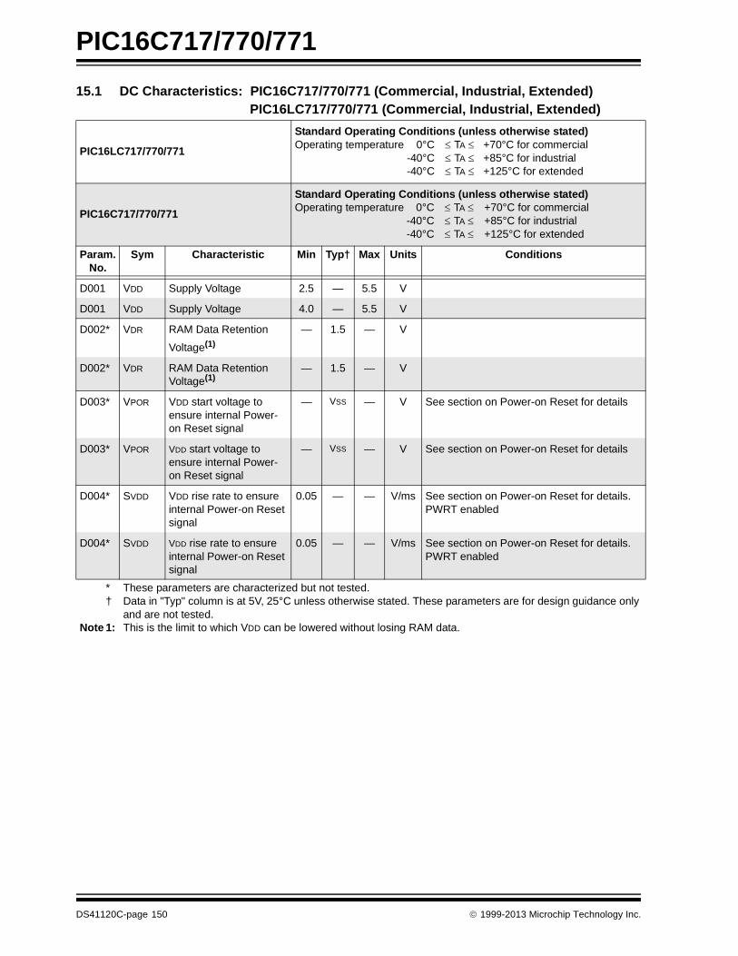
PIC16C717/770/771
15.1 DC Characteristics: PIC16C717/770/771 (Commercial, Industrial, Extended)PIC16LC717/770/771 (Commercial, Industrial, Extended)
PIC16LC717/770/771
Standard Operating Conditions (unless otherwise stated)Operating temperature 0°C TA +70°C for commercial
-40°C TA +85°C for industrial -40°C TA +125°C for extended
PIC16C717/770/771
Standard Operating Conditions (unless otherwise stated)Operating temperature 0°C TA +70°C for commercial
-40°C TA +85°C for industrial -40°C TA +125°C for extended
Param. No.
Sym Characteristic Min Typ† Max Units Conditions
D001 VDD Supply Voltage 2.5 — 5.5 V
D001 VDD Supply Voltage 4.0 — 5.5 V
D002* VDR RAM Data Retention
Voltage(1)
— 1.5 — V
D002* VDR RAM Data Retention Voltage(1)
— 1.5 — V
D003* VPOR VDD start voltage to ensure internal Power-on Reset signal
— VSS — V See section on Power-on Reset for details
D003* VPOR VDD start voltage to ensure internal Power-on Reset signal
— VSS — V See section on Power-on Reset for details
D004* SVDD VDD rise rate to ensure internal Power-on Reset signal
0.05 — — V/ms See section on Power-on Reset for details. PWRT enabled
D004* SVDD VDD rise rate to ensure internal Power-on Reset signal
0.05 — — V/ms See section on Power-on Reset for details. PWRT enabled
* These parameters are characterized but not tested.† Data in "Typ" column is at 5V, 25°C unless otherwise stated. These parameters are for design guidance only
and are not tested.Note 1: This is the limit to which VDD can be lowered without losing RAM data.
DS41120C-page 150 1999-2013 Microchip Technology Inc.

PIC16C717/770/771
15.1 DC Characteristics: PIC16C717/770/771 (Commercial, Industrial, Extended)PIC16LC717/770/771 (Commercial, Industrial, Extended)(Continued)
PIC16LC717/770/771
Standard Operating Conditions (unless otherwise stated)Operating temperature 0°C TA +70°C for commercial
-40°C TA +85°C for industrial -40°C TA +125°C for extended
PIC16C717/770/771
Standard Operating Conditions (unless otherwise stated)Operating temperature 0°C TA +70°C for commercial
-40°C TA +85°C for industrial -40°C TA +125°C for extended
Param. No.
Sym Characteristic Min Typ† Max Units Conditions
IDD Supply Current(2)
D010DD010E
D010G
D010K
PIC16LC7XX 1.0
0.36
11
2.03.0
1.0
45
mA
mA
A
FOSC = 10 MHz, VDD = 3V, -40°C to 85°CFOSC = 10 MHz, VDD = 3V, -40°C to 125°C
FOSC = 4 MHz, VDD = 2.5V, -40°C to 125°C
FOSC = 32 kHz, VDD = 2.5V, -40°C to 125°C
IDD Supply Current(2)
D010D010A
D010BD010C
D010F
D010HD010J
PIC16C7XX 4.0
2.5
0.55
30
7.512.0
5.06.0
1.5
8095
mA
mA
mA
A
FOSC = 20 MHz, VDD = 5.5V, -40°C to 85°CFOSC = 20 MHz, VDD = 5.5V, -40°C to 125°C
FOSC = 20 MHz, VDD = 4V, -40°C to 85°CFOSC = 20 MHz, VDD = 4V, -40°C to 125°C
FOSC = 4 MHz, VDD = 4V, -40°C to 125°C
FOSC = 32 kHz, VDD = 4V, -40°C to 85°CFOSC = 32 kHz, VDD = 4V, -40°C to 125°C
* These parameters are characterized but not tested.† Data in "Typ" column is at 5V, 25°C unless otherwise stated. These parameters are for design guidance only
and are not tested.Note 1: This is the limit to which VDD can be lowered without losing RAM data.
2: The supply current is mainly a function of the operating voltage and frequency. Other factors such as I/O pin loading and switching rate, oscillator type, internal code execution pattern, and temperature also have an impact on the current consumption.The test conditions for all IDD measurements in active Operation mode are: OSC1 = external square wave, from rail to rail; all I/O pins tristated, pulled to VDD MCLR = VDD; WDT enabled/disabled as specified.
1999-2013 Microchip Technology Inc. DS41120C-page 151

PIC16C717/770/771
IPD Power-down Current(3)
D020D
D020E
D020F
D020G
PIC16LC7XX 0.3
0.1
2.0
5.0
1.5
3.0
A
A
VDD = 3V, -40°C to 85°C
VDD = 3V, -40°C to 125°C
VDD = 2.5V, -40°C to 85°C
VDD = 2.5V, -40°C to 125°C
D020
D020A
D020B
D020C
PIC16C7XX 1.4
1.0
4.0
8.0
3.5
6.0
A
A
VDD = 5.5V, -40°C to 85°C
VDD = 5.5V, -40°C to 125°C
VDD = 4V, -40°C to 85°C
VDD = 4V, -40°C to 125°C
* These parameters are characterized but not tested.† Data in "Typ" column is at 5V, 25°C unless otherwise stated. These parameters are for design guidance only
and are not tested.Note 1: This is the limit to which VDD can be lowered without losing RAM data.
2: The supply current is mainly a function of the operating voltage and frequency. Other factors such as I/O pin loading and switching rate, oscillator type, internal code execution pattern, and temperature also have an impact on the current consumption.The test conditions for all IDD measurements in active Operation mode are: OSC1 = external square wave, from rail to rail; all I/O pins tristated, pulled to VDD MCLR = VDD; WDT enabled/disabled as specified.
3: The power-down current in SLEEP mode does not depend on the oscillator type. Power-down current is measured with the part in SLEEP mode, with all I/O pins in hi-impedance state and tied to VDD or VSS.
PIC16LC717/770/771
Standard Operating Conditions (unless otherwise stated)Operating temperature 0°C TA +70°C for commercial
-40°C TA +85°C for industrial -40°C TA +125°C for extended
PIC16C717/770/771
Standard Operating Conditions (unless otherwise stated)Operating temperature 0°C TA +70°C for commercial
-40°C TA +85°C for industrial -40°C TA +125°C for extended
Param. No.
Sym Characteristic Min Typ† Max Units Conditions
DS41120C-page 152 1999-2013 Microchip Technology Inc.

PIC16C717/770/771
15.1 DC Characteristics: PIC16C717/770/771 (Commercial, Industrial, Extended)PIC16LC717/770/771 (Commercial, Industrial, Extended)(Continued)
PIC16LC717/770/771
Standard Operating Conditions (unless otherwise stated)Operating temperature 0°C TA +70°C for commercial
-40°C TA +85°C for industrial -40°C TA +125°C for extended
PIC16C717/770/771
Standard Operating Conditions (unless otherwise stated)Operating temperature 0°C TA +70°C for commercial
-40°C TA +85°C for industrial -40°C TA +125°C for extended
Param. No.
Sym Characteristic Min Typ† Max Units Conditions
Base plus Module current
D021A IWDT Watchdog Timer 2 10 A VDD = 3V, -40°C to 125°C
D021 IWDT Watchdog Timer 5 20 A VDD = 4V, -40°C to 125°C
D021 IWDT Watchdog Timer 5 20 A VDD = 4V, -40°C to 125°C
D025 IT1OSC Timer1 Oscillator 3 9 A VDD = 3V, -40°C to 125°C
D025 IT1OSC Timer1 Oscillator 4 12 A VDD = 4V, -40°C to 125°C
D025 IT1OSC Timer1 Oscillator 4 12 A VDD = 4V, -40°C to 125°C
D026* IAD ADC Converter 300 A VDD = 5.5V, A/D on, not converting
D026* IAD ADC Converter 300 A VDD = 5.5V, A/D on, not converting
D027
D027A
IPLVD Programmable LowVoltage Detect
55 125
150
A VDD = 4V, -40°C to 85°C
VDD = 4V, -40°C to 125°C
D027
D027A
IPLVD Programmable LowVoltage Detect
55 125
150
A VDD = 4V, -40°C to 85°C
VDD = 4V, -40°C to 125°C
D028
D028A
IPBOR Programmable Brown-
out Reset
55 125
150
A VDD = 5V, -40°C to 85°C
VDD = 5V, -40°C to 125°C
D028
D028A
IPBOR Programmable Brown-
out Reset
55 125
150
A VDD = 5V, -40°C to 85°C
VDD = 5V, -40°C to 125°C
D029
D029A
IVRH Voltage reference High 200 750
1.0
A
mA
VDD = 5V, -40°C to 85°C
VDD = 5V, -40°C to 125°C
D029
D029A
IVRH Voltage reference High 200 750
1.0
A
mA
VDD = 5V, -40°C to 85°C
VDD = 5V, -40°C to 125°C
D030
D030A
IVRL Voltage reference Low 200 750
1.0
A
mA
VDD = 4V, -40°C to 85°C
VDD = 4V, -40°C to 125°C
D030
D030A
IVRL Voltage reference Low 200 750
1.0
A
mA
VDD = 4V, -40°C to 85°C
VDD = 4V, -40°C to 125°C
* These parameters are characterized but not tested.† Data in "Typ" column is at 5V, 25°C unless otherwise stated. These parameters are for design guidance only
and are not tested.
1999-2013 Microchip Technology Inc. DS41120C-page 153

PIC16C717/770/771
15.2 DC Characteristics: PIC16C717/770/771 & PIC16LC717/770/771 (Commercial, Industrial, Extended)
DC CHARACTERISTICS
Standard Operating Conditions (unless otherwise stated)Operating temperature 0°C TA +70°C for commercial
-40°C TA +85°C for industrial -40°C TA +125°C for extended
Operating voltage VDD range as described in Section 15.1 and Section 15.2.
Param.No.
Sym Characteristic Min Typ† Max Units Conditions
Input Low VoltageVIL I/O ports
D030 with TTL buffer VSS — 0.15VDD V For entire VDD rangeD030A VSS — 0.8V V 4.5V VDD 5.5VD031 with Schmitt Trigger buffer VSS — 0.2VDD V For entire VDD rangeD032 MCLR VSS — 0.2VDD V
D033 OSC1 (in XT, HS, LP and EC) VSS — 0.3VDD VInput High Voltage
VIH I/O ports —
D040with TTL buffer
2.0 — VDD V 4.5V VDD 5.5VD040A (0.25VDD
+ 0.8V)— VDD V For entire VDD range
D041 with Schmitt Trigger buffer 0.8VDD — VDD V For entire VDD rangeD042 MCLR 0.8VDD — VDD VD042A OSC1 (XT, HS, LP and EC) 0.7VDD — VDD VD070 IPURB PORTB weak pull-up current
per pin50 250 400 A VDD = 5V, VPIN = VSS
Input Leakage Current (1,2)
D060 IIL I/O ports (with digital functions) — — 1 A Vss VPIN VDD, Pin at hi-impedanceD060A IIL I/O ports (with analog func-
tions)— — 100 nA Vss VPIN VDD, Pin at hi-impedance
D061 RA5/MCLR/VPP — — 5 A Vss VPIN VDD
D063 OSC1 — — 5 A Vss VPIN VDD, XT, HS, LP and EC osc configuration
Output Low VoltageD080 VOL I/O ports — — 0.6 V IOL = 8.5 mA, VDD = 4.5V
Output High VoltageD090 VOH I/O ports(2) VDD - 0.7 — — V IOH = -3.0 mA, VDD = 4.5V
D150* VOD Open Drain High Voltage — — 10.5 V RA4 pinCapacitive Loading Specs on Output Pins*
D100 COSC2
OSC2 pin — — 15 pF In XT, HS and LP modes when exter-nal clock is used to drive OSC1.
D101D102
CIO
CB
All I/O pins and OSC2 (in RC
mode) SCL, SDA in I2C mode
——
——
50400
pFpF
CVRH VRH pin — — 200 pF VRH output enabledCVRL VRL pin — — 200 pF VRL output enabled
* These parameters are characterized but not tested.† Data in “Typ” column is at 5V, 25C unless otherwise stated. These parameters are for design guidance only
and are not tested.Note 1: The leakage current on the MCLR pin is strongly dependent on the applied voltage level. The specified levels
represent normal operating conditions. Higher leakage current may be measured at different input voltages.2: Negative current is defined as current sourced by the pin.
DS41120C-page 154 1999-2013 Microchip Technology Inc.

PIC16C717/770/771
15.3 AC Characteristics: PIC16C717/770/771 & PIC16LC717/770/771 (Commercial, Industrial, Extended)
15.3.1 TIMING PARAMETER SYMBOLOGY
The timing parameter symbols have been created using one of the following formats:
1. TppS2ppS 3. TCC:ST (I2C specifications only)
2. TppS 4. Ts (I2C specifications only)
T
F Frequency T Time
Lowercase letters (pp) and their meanings:
pp
cc CCP1 osc OSC1
ck CLKOUT rd RD
cs CS rw RD or WR
di SDI sc SCK
do SDO ss SS
dt Data in t0 T0CKI
io I/O port t1 T1CKI
mc MCLR wr WR
Uppercase letters and their meanings:
S
F Fall P Period
H High R Rise
I Invalid (Hi-impedance) V Valid
L Low Z Hi-impedance
I2C (I2C specifications only)
AA output access
BUF Bus free
High High
Low Low
TCC:ST (I2C specifications only)
CC
HD Hold SU Setup
ST
DAT DATA input hold STO STOP condition
STA START condition
1999-2013 Microchip Technology Inc. DS41120C-page 155

PIC16C717/770/771
FIGURE 15-4: LOAD CONDITIONS
VDD/2
CL
RL
Pin Pin
VSS VSS
CL
RL = 464
CL = 50 pF for all pins except OSC2
15 pF for OSC2 output
Load condition 1 Load condition 2
DS41120C-page 156 1999-2013 Microchip Technology Inc.
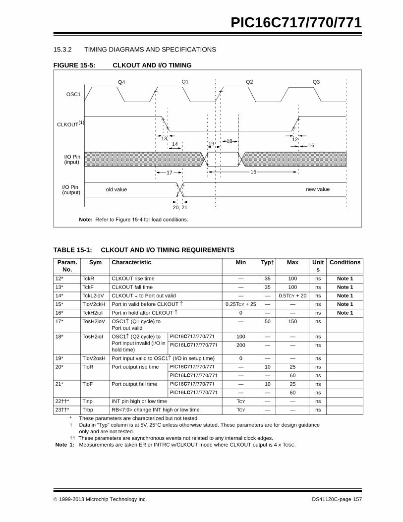
PIC16C717/770/771
15.3.2 TIMING DIAGRAMS AND SPECIFICATIONS
FIGURE 15-5: CLKOUT AND I/O TIMING
TABLE 15-1: CLKOUT AND I/O TIMING REQUIREMENTS
Param.No.
Sym Characteristic Min Typ† Max Units
Conditions
12* TckR CLKOUT rise time — 35 100 ns Note 1
13* TckF CLKOUT fall time — 35 100 ns Note 1
14* TckL2ioV CLKOUT to Port out valid — — 0.5TCY + 20 ns Note 1
15* TioV2ckH Port in valid before CLKOUT 0.25TCY + 25 — — ns Note 1
16* TckH2ioI Port in hold after CLKOUT 0 — — ns Note 1
17* TosH2ioV OSC1 (Q1 cycle) to Port out valid
— 50 150 ns
18* TosH2ioI OSC1 (Q2 cycle) to Port input invalid (I/O in hold time)
PIC16C717/770/771 100 — — ns
PIC16LC717/770/771 200 — — ns
19* TioV2osH Port input valid to OSC1(I/O in setup time) 0 — — ns
20* TioR Port output rise time PIC16C717/770/771 — 10 25 ns
PIC16LC717/770/771 — — 60 ns
21* TioF Port output fall time PIC16C717/770/771 — 10 25 ns
PIC16LC717/770/771 — — 60 ns
22††* Tinp INT pin high or low time TCY — — ns
23††* Trbp RB<7:0> change INT high or low time TCY — — ns
* These parameters are characterized but not tested.† Data in "Typ" column is at 5V, 25°C unless otherwise stated. These parameters are for design guidance
only and are not tested.†† These parameters are asynchronous events not related to any internal clock edges.
Note 1: Measurements are taken ER or INTRC w/CLKOUT mode where CLKOUT output is 4 x TOSC.
Note: Refer to Figure 15-4 for load conditions.
OSC1
CLKOUT(1)
I/O Pin(input)
I/O Pin(output)
Q4 Q1 Q2 Q3
1314
17
20, 21
19 18
15
1216
old value new value
1999-2013 Microchip Technology Inc. DS41120C-page 157

PIC16C717/770/771
FIGURE 15-6: EXTERNAL CLOCK TIMING
OSC1
Q4 Q1 Q2 Q3 Q4 Q1
1
2
3 3 4 4
TABLE 15-2: EXTERNAL CLOCK TIMING REQUIREMENTS
Param No. Sym Characteristic Min Typ† Max Units Conditions
1A FOSC External CLKIN Frequency (Note 1)
DC — 4 MHz XT mode
DC — 20 MHz EC mode
DC — 20 MHz HS mode
DC — 200 kHz LP mode
Oscillator Frequency (Note 1)
0.1* — 4 MHz XT mode
4*5*
——
20200
MHzkHz
HS mode LP mode
1 TOSC External CLKIN Period(Note 1)
250 — — ns XT mode
50 — — ns EC mode
50 — — ns HS mode
5 — — s LP mode
Oscillator Period(Note 1)
250 — 10,000* ns XT mode
50 — 250* ns HS mode
5 — — s LP mode
2 TCY Instruction Cycle Time (Note 1) 200 TCY DC ns TCY = 4/FOSC
3* TosL,TosH
External Clock in (OSC1) High or Low Time
100 — — ns XT mode
2.5 — — s LP mode
15 — — ns HS mode
EC mode
4* TosR,TosF
External Clock in (OSC1) Rise or Fall Time
— — 25 ns XT mode
— — 50 ns LP mode
— — 15 ns HS mode
EC mode
* These parameters are characterized but not tested.† Data in "Typ" column is at 5V, 25°C unless otherwise stated. These parameters are for design guidance only and are not
tested.Note 1: Instruction cycle period (TCY) equals four times the input oscillator time-base period. All specified values are based on
characterization data for that particular oscillator type under standard operating conditions with the device executing code. Exceeding these specified limits may result in an unstable oscillator operation and/or higher than expected current con-sumption. All devices are tested to operate at "Max. Frequency" values with a square wave applied to the OSC1/CLKIN pin.When an external clock input is used, the "Min." frequency (or Max. TCY) limit is "DC" (no clock) for all devices.
DS41120C-page 158 1999-2013 Microchip Technology Inc.

PIC16C717/770/771
TABLE 15-3: CALIBRATED INTERNAL RC FREQUENCIES - PIC16C717/770/771 AND PIC16LC717/770/771
FIGURE 15-7: RESET, WATCHDOG TIMER, OSCILLATOR START-UP TIMER AND POWER-UP TIMER TIMING
FIGURE 15-8: BROWN-OUT RESET TIMING
AC Characteristics Standard Operating Conditions (unless otherwise specified)Operating Temperature 0°C TA +70°C for commercial
-40°C TA +85°C for industrial -40°C TA +125°C for extended
Operating Voltage VDD range is described in Section and Section
Parameter No.
Sym Characteristic Min Typ(1)* Max Units Conditions
FIRCInternal Calibrated RC Frequency 3.65 4.00 4.28 MHz VDD = 5.0V
Internal RC Frequency* 3.55 4.00 4.31 MHz VDD = 2.5V
* These parameters are characterized but not tested.Note 1: Data in the Typical (“Typ”) column is at 5V, 25C unless otherwise stated. These parameters are for design
guidance only and are not tested.
VDD
MCLR
InternalPOR
PWRTTime-out
OSCTime-out
InternalRESET
WatchdogTimer
RESET
33
32
30
3134
I/O Pins
34
Note: Refer to Figure 15-4 for load conditions.
VDD VBOR
35
1999-2013 Microchip Technology Inc. DS41120C-page 159

PIC16C717/770/771
TABLE 15-4: RESET, WATCHDOG TIMER, OSCILLATOR START-UP TIMER, POWER-UP TIMER, AND BROWN-OUT RESET REQUIREMENTS
FIGURE 15-9: BROWN-OUT RESET CHARACTERISTICS
FIGURE 15-10: TIMER0 AND TIMER1 EXTERNAL CLOCK TIMINGS
Parameter No.
Sym Characteristic Min Typ† Max Units Conditions
30* TMCL MCLR Pulse Width (low) 2 — — s VDD = 5V, -40°C to +85°C
31* TWDT Watchdog Timer Time-out Period (No Prescaler)
7 18 33 ms VDD = 5V, -40°C to +85°C
32* TOST Oscillation Start-up Timer Period — 1024 TOSC — — TOSC = OSC1 period
33* TPWRT Power up Timer Period 28 72 132 ms VDD = 5V, -40°C to +85°C
34* TIOZ I/O Hi-impedance from MCLR Low or Watchdog Timer Reset
— — 2.1 s
35* TBOR Brown-out Reset pulse width 100 — — s VDD VBOR (D005)
* These parameters are characterized but not tested.† Data in "Typ" column is at 5V, 25°C unless otherwise stated. These parameters are for design guidance only and are not
tested.
VBOR
RESET (due to BOR)
VDD
(device in Brown-out Reset)
(device not in Brown-out Reset)
72 ms time-out
Note: Refer to Figure 15-4 for load conditions.
46
47
45
48
41
42
40
RA4/T0CKI
RB6/T1OSO/T1CKI/PIC
TMR0 orTMR1
DS41120C-page 160 1999-2013 Microchip Technology Inc.

PIC16C717/770/771
TABLE 15-5: TIMER0 AND TIMER1 EXTERNAL CLOCK REQUIREMENTS
FIGURE 15-11: ENHANCED CAPTURE/COMPARE/PWM TIMINGS (ECCP)
Param. No.
Sym Characteristic Min Typ† Max Units Conditions
40* Tt0H T0CKI High Pulse Width No Prescaler 0.5TCY + 20 — — ns Must also meet parameter 42With Prescaler 10 — — ns
41* Tt0L T0CKI Low Pulse Width No Prescaler 0.5TCY + 20 — — ns Must also meet parameter 42With Prescaler 10 — — ns
42* Tt0P T0CKI Period No Prescaler TCY + 40 — — ns
With Prescaler Greater of:20 or TCY + 40 N
— — ns N = prescale value (2, 4, ..., 256)
45* Tt1H T1CKI High Time Synchronous, Prescaler = 1 0.5TCY + 20 — — ns Must also meet parameter 47 Synchronous,
Prescaler = 2,4,8
PIC16C717/770/771 15 — — ns
PIC16LC717/770/771 25 — — ns
Asynchronous PIC16C717/770/771 30 — — ns
PIC16LC717/770/771 50 — — ns
46* Tt1L T1CKI Low Time Synchronous, Prescaler = 1 0.5TCY + 20 — — ns Must also meet parameter 47 Synchronous,
Prescaler = 2,4,8
PIC16C717/770/771 15 — — ns
PIC16LC717/770/771 25 — — ns
Asynchronous PIC16C717/770/771 30 — — ns
PIC16LC717/770/771 50 — — ns
47* Tt1P T1CKI input period Synchronous PIC16C717/770/771 Greater of:30 OR TCY + 40
N
— — ns N = prescale value (1, 2, 4, 8)
PIC16LC717/770/771 Greater of:50 OR TCY + 40
N
— — ns N = prescale value (1, 2, 4, 8)
Asynchronous PIC16C717/770/771 60 — — ns
PIC16LC717/770/771 100 — — ns
Ft1 Timer1 oscillator input frequency range (oscillator enabled by setting bit T1OSCEN)
DC — 50 kHz
48 Tcke2tmr1 Delay from external clock edge to timer increment 2Tosc — 7Tosc —
* These parameters are characterized but not tested.† Data in "Typ" column is at 5V, 25°C unless otherwise stated. These parameters are for design guidance only and are not
tested.
Note: Refer to Figure 15-4 for load conditions.
RB3/CCP1/P1A(Capture Mode)
50 51
52
53 54
RB3/CCP1/P1A(Compare or PWM Mode)
1999-2013 Microchip Technology Inc. DS41120C-page 161

PIC16C717/770/771
TABLE 15-6: ENHANCED CAPTURE/COMPARE/PWM REQUIREMENTS (ECCP)
Param. No.
Sym Characteristic Min Typ† Max Units Conditions
50* TccL CCP1 input low time
No Prescaler 0.5TCY + 20 — — ns
With Prescaler
PIC16C717/770/771 10 — — ns
PIC16LC717/770/771 20 — — ns
51* TccH CCP1 input high time
No Prescaler 0.5TCY + 20 — — ns
With PrescalerPIC16C717/770/771 10 — — ns
PIC16LC717/770/771 20 — — ns
52* TccP CCP1 input period 3TCY + 40N
— — ns N = prescale value (1, 4 or 16)
53* TccR CCP1 output fall time PIC16C717/770/771 — 10 25 ns
PIC16LC717/770/771 — 25 45 ns
54* TccF CCP1 output fall time PIC16C717/770/771 — 10 25 ns
PIC16LC717/770/771 — 25 45 ns
* These parameters are characterized but not tested.† Data in "Typ" column is at 5V, 25°C unless otherwise stated. These parameters are for design guidance only and are not
tested.
DS41120C-page 162 1999-2013 Microchip Technology Inc.

PIC16C717/770/771
15.4 Analog Peripherals Characteristics: PIC16C717/770/771 & PIC16LC717/770/771 (Commercial, Industrial, Extended)
15.4.1 BANDGAP MODULE
FIGURE 15-12: BANDGAP START-UP TIME
TABLE 15-7: BANDGAP START-UP TIME
Param. No.
Sym Characteristic Min Typ† Max Units Conditions
36* TBGAP Bandgap start-up time — 19 33 S Defined as the time between the instant that the bandgap is enabled and the moment that the bandgap reference voltage is stable.
* These parameters are characterized but not tested.† Data in "Typ" column is at 5V, 25°C unless otherwise stated. These parameters are for design guidance only and are not
tested.
VBGAP = 1.2VVBGAP
Enable Bandgap
Bandgap stableTBGAP
(internal use only)
1999-2013 Microchip Technology Inc. DS41120C-page 163

PIC16C717/770/771
15.4.2 LOW VOLTAGE DETECT MODULE (LVD)
FIGURE 15-13: LOW VOLTAGE DETECT CHARACTERISTICS
TABLE 15-8: ELECTRICAL CHARACTERISTICS: LVD
DC CHARACTERISTICS
Standard Operating Conditions (unless otherwise stated)Operating temperature -40°C TA +85°C for industrial and
0°C TA +70°C for commercialOperating voltage VDD range as described in DC Characteristics Section 15.1.
Param. No.
Characteristic Symbol Min Typ† Max Units Conditions
D420* LVD Voltage LVV = 0100
VLVD
2.5 2.58 2.66 VLVV = 0101 2.7 2.78 2.86 VLVV = 0110 2.8 2.89 2.98 VLVV = 0111 3.0 3.1 3.2 VLVV = 1000 3.3 3.41 3.52 VLVV = 1001 3.5 3.61 3.72 VLVV = 1010 3.6 3.72 3.84 VLVV = 1011 3.8 3.92 4.04 VLVV = 1100 4.0 4.13 4.26 VLVV = 1101 4.2 4.33 4.46 VLVV = 1110 4.5 4.64 4.78 V
* These parameters are characterized but not tested.Note 1: Production tested at Tamb = 25°C. Specifications over temperature limits ensured by characterization.
VLVD
LVDIF
VDD
(LVDIF set by hardware)
(LVDIF can be cleared in software anytime duringthe gray area)
DS41120C-page 164 1999-2013 Microchip Technology Inc.

PIC16C717/770/771
15.4.3 PROGRAMMABLE BROWN-OUT RESET MODULE (PBOR)
TABLE 15-9: DC CHARACTERISTICS: PBOR
15.4.4 VREF MODULE
TABLE 15-10: DC CHARACTERISTICS: VREF
DC CHARACTERISTICS
Standard Operating Conditions (unless otherwise stated)Operating temperature 0°C TA +70°C for commercial
-40°C TA +85°C for industrial -40°C TA +125°C for extended
Operating voltage VDD range as described in DC Characteristics Section 15.1.
Param. No.
Characteristic Symbol Min Typ Max Units Conditions
D005 BOR Voltage BORV<1:0> = 11
VBOR
2.5 2.58 2.66
VBORV<1:0> = 10 2.7 2.78 2.86BORV<1:0> = 01 4.2 4.33 4.46BORV<1:0> = 00 4.5 4.64 4.78
DC CHARACTERISTICS
Standard Operating Conditions (unless otherwise stated)Operating temperature 0°C TA +70°C for commercial
-40°C TA +85°C for industrial -40°C TA +125°C for extended
Operating voltage VDD range as described in DC Characteristics Section 15.1.
Param. No.
SymbolCharacteristic Min Typ† Max Units Conditions
D400 VRL Output Voltage 2.0 2.048 2.1 V VDD 2.7V, -40°C TA +85°C
VRH 4.0 4.096 4.2 V VDD 4.5V, -40°C TA +85°C
D400A VRL Output Voltage 1.9 2.048 2.2 V VDD 2.7V, -40°C TA +125°C
VRH 4.0 4.096 4.3 V VDD 4.5V, -40°C TA +125°C
D404* IVREFSO External Load Source — — 5 mA
D405* IVREFSI External Load Sink — — -5 mA
* CL External Capacitor Load — — 200 pF
D406* Vout/Iout
VRH Load Regulation — 0.6 1 mV/mA VDD 5V ISOURCE = 0 mA to 5 mA
— 1 4 ISINK = 0 mA to 5 mA
VRL Load Regulation — 0.6 1 VDD 3V ISOURCE = 0 mA to 5 mA
— 2 4 ISINK = 0 mA to 5 mA
* These parameters are characterized but not tested.† Data in “Typ” column is at 5V, 25C unless otherwise stated. These parameters are
for design guidance only and are not tested.
1999-2013 Microchip Technology Inc. DS41120C-page 165

PIC16C717/770/771
15.4.5 A/D CONVERTER MODULE
TABLE 15-11: PIC16C770/771 AND PIC16LC770/771 A/D CONVERTER CHARACTERISTICS:
Param. No.
Sym Characteristic Min Typ† Max Units Conditions
A01 NR Resolution — — 12 bits bit Min. resolution for A/D is 1 mV,VREF+ = AVDD = 4.096V, VREF- = AVSS = 0V,VREF- VAIN VREF+
A03 EIL Integral error — — ±2 LSb VREF+ = AVDD = 4.096V, VREF- = AVSS = 0V,VREF- VAIN VREF+
A04 EDL Differential error — — +2
-1
LSb No missing codes to 12 bitsVREF+ = AVDD = 4.096V, VREF- = AVSS = 0V,VREF- VAIN VREF+
A06 EOFF Offset error — — ±2 LSb VREF+ = AVDD = 4.096V, VREF- = AVSS = 0V,VREF- VAIN VREF+
A07 EGN Gain Error — — ±2 LSb VREF+ = AVDD = 4.096V, VREF- = AVSS = 0V,VREF- VAIN VREF+
A10 — Monotonicity — Note 3 — — AVSS VAIN VREF+
A20* VREF Reference voltage (VREF+ - VREF-)
4.096 — VDD +0.3V
V Absolute minimum electrical spec to ensure 12-bit accuracy.
A21* VREF+ Reference V High(AVDD or VREF+)
VREF- — AVDD V Min. resolution for A/D is 1 mV
A22* VREF- Reference V Low(AVSS or VREF-)
AVSS — VREF+ V Min. resolution for A/D is 1 mV
A25* VAIN Analog input volt-age
VREFL — VREFH V
A30* ZAIN Recommended impedance of ana-log voltage source
— — 2.5 k
A50* IREF VREF input current (Note 2)
— — 10 A During VAIN acquisition. Based on differential of VHOLD to VAIN.To charge CHOLD see Section 11.0.During A/D conversion cycle.
* These parameters are characterized but not tested.† Data in “Typ” column is at 5V, 25C unless otherwise stated. These parameters are for design guidance only
and are not tested.
Note 1: When A/D is off, it will not consume any current other than minor leakage current. The power-down currentspec includes any such leakage from the A/D module.
2: VREF input current is from External VREF+, or VREF-, or AVSS, or AVDD pin, whichever is selected as refer-ence input.
3: The A/D conversion result never decreases with an increase in the input voltage and has no missing codes.
DS41120C-page 166 1999-2013 Microchip Technology Inc.

PIC16C717/770/771
FIGURE 15-14: PIC16C770/771 AND PIC16LC770/771 A/D CONVERSION TIMING (NORMAL MODE)
131
130
132
BSF ADCON0, GO
Q4
A/D CLK
A/D DATA
ADRES
ADIF
GO
SAMPLE
OLD_DATA
SAMPLING STOPPED
NEW_DATA
11 10 9 3 2 1 0
Note 1: If the A/D RC clock source is selected, a time of TCY is added before the A/D clock starts. This allows the SLEEP instruction to be executed.
1/2 TCY
8
134
DONE
1999-2013 Microchip Technology Inc. DS41120C-page 167

PIC16C717/770/771
TABLE 15-12: PIC16C770/771 AND PIC16LC770/771 A/D CONVERSION REQUIREMENTS (NORMAL MODE)
Parameter No.
Sym Characteristic Min Typ† Max Units Conditions
130*(3) TAD A/D clock period 1.6 — — s Tosc based, VREF 2.5V
3.0 — — s Tosc based, VREF full range
3.0 6.0 9.0 s
ADCS<1:0> = 11 (A/D RC mode)At VDD = 2.5V
2.0 4.0 6.0 s At VDD = 5.0V
131* TCNV Conversion time (not including acquisition time)(Note 1)
— 13TAD — TAD
132* TACQ Acquisition Time Note 2
5*
11.5
—
—
—
s
s The minimum time is the ampli-fier settling time. This may be used if the “new” input voltage has not changed by more than 1LSb (i.e., 1mV @ 4.096V) from the last sampled voltage (as stated on CHOLD).
134* TGO Q4 to A/D clock start
— TOSC/2 — —
* These parameters are characterized but not tested.† Data in “Typ” column is at 5V, 25C unless otherwise stated. These parameters are for design guidance only
and are not tested.
Note 1: ADRES register may be read on the following TCY cycle.
2: See Section 11.6 for minimum conditions.
3: These numbers multiplied by 8 if VRH or VRL is selected as A/D reference.
DS41120C-page 168 1999-2013 Microchip Technology Inc.

PIC16C717/770/771
FIGURE 15-15: PIC16C770/771 AND PIC16LC770/771 A/D CONVERSION TIMING (SLEEP MODE)
TABLE 15-13: PIC16C770/771 AND PIC16LC770/771 A/D CONVERSION REQUIREMENT (SLEEP MODE)
Parameter No.
Sym Characteristic Min Typ† Max Units Conditions
130*(3) TAD A/D Internal RC oscillator period 3.0 6.0 9.0 s
ADCS<1:0> = 11 (RC mode)At VDD= 3.0V
2.0 4.0 6.0 s At VDD = 5.0V
131* TCNV Conversion time (not including acquisition time) (Note 1)
— 13TAD — —
132* TACQ Acquisition Time (Note 2)
5*
11.5
—
—
—
s
s The minimum time is the amplifier settling time. This may be used if the “new” input voltage has not changed by more than 1LSb (i.e., 1mV @ 4.096V) from the last sam-pled voltage (as stated on CHOLD).
134* TGO Q4 to A/D clock start — TOSC/2 + TCY — — If the A/D clock source is selected as RC, a time of TCY is added before the A/D clock starts. This allows the SLEEP instruction to be executed.
* These parameters are characterized but not tested.† Data in “Typ” column is at 5V, 25C unless otherwise stated. These parameters are for design guidance only and are not
tested.Note 1: ADRES register may be read on the following TCY cycle.
2: See Section 11.6 for minimum conditions.3: These numbers multiplied by 8 if VRH or VRL is selected as A/D reference.
131
130
BSF ADCON0, GO
Q4
A/D CLK
A/D DATA
ADRES
ADIF
GO
SAMPLE
OLD_DATA
SAMPLING STOPPED
NEW_DATA
11 9 3 2 1 0
Note 1: If the A/D RC clock source is selected, a time of TCY is added before the A/D clock starts. This allows the SLEEP instruction to be executed.
134
810
132
DONE
1999-2013 Microchip Technology Inc. DS41120C-page 169

PIC16C717/770/771
TABLE 15-14: PIC16C717 AND PIC16LC717 A/D CONVERTER CHARACTERISTICS:
Param. No.
Sym Characteristic Min Typ† Max Units Conditions
A01 NR Resolution — — 10 bits bit Min. resolution for A/D is 4.1 mV,VREF+ = AVDD = 4.096V, VREF- = AVSS = 0V,VREF- VAIN VREF+
A03 EIL Integral error — — ±1 LSb VREF+ = AVDD = 4.096V, VREF- = AVSS = 0V,VREF- VAIN VREF+
A04 EDL Differential error — — ±1 LSb No missing codes to 10 bitsVREF+ = AVDD = 4.096V, VREF- = AVSS = 0V,VREF- VAIN VREF+
A06 EOFF Offset error — — ±2 LSb VREF+ = AVDD = 4.096V, VREF- = AVSS = 0V,VREF- VAIN VREF+
A07 EGN Gain Error — — ±1 LSb VREF+ = AVDD = 4.096V, VREF- = AVSS = 0V,VREF- VAIN VREF+
A10 — Monotonicity — Note 3 — — AVSS VAIN VREF+
A20* VREF Reference voltage (VREF+ - VREF-)
4.096 — VDD +0.3V V Absolute minimum electrical spec to ensure 10-bit accuracy.
A21* VREF+ Reference V High(AVDD or VREF+)
VREF- — AVDD V Min. resolution for A/D is 4.1 mV
A22* VREF- Reference V Low(AVSS or VREF-)
AVSS — VREF+ V Min. resolution for A/D is 4.1 mV
A25* VAIN Analog input voltage VREFL — VREFH V
A30* ZAIN Recommended impedance of analog voltage source
— — 2.5 k
A50* IREF VREF input current (Note 2)
— — 10 A During VAIN acquisition. Based on differential of VHOLD to VAIN.To charge CHOLD see Section 11.0.During A/D conversion cycle.
* These parameters are characterized but not tested.† Data in “Typ” column is at 5V, 25C unless otherwise stated. These parameters are for design guidance only and are not
tested.Note 1: When A/D is off, it will not consume any current other than leakage current. The power-down current spec includes any such
leakage from the A/D module. 2: VREF current is from External VREF+, or VREF-, or AVSS, or AVDD pin, whichever is selected as reference input. 3: The A/D conversion result never decreases with an increase in the input voltage and has no missing codes.
DS41120C-page 170 1999-2013 Microchip Technology Inc.

PIC16C717/770/771
FIGURE 15-16: PIC16C717 A/D CONVERSION TIMING (NORMAL MODE)
TABLE 15-15: PIC16C717 AND PIC16LC717 A/D CONVERSION REQUIREMENT (NORMAL MODE)
Parameter No.
Sym Characteristic Min Typ† Max Units Conditions
130*(3) TAD A/D clock period 1.6 — — s Tosc based, VREF 2.5V
3.0 — — s Tosc based, VREF full range
3.0 6.0 9.0 sADCS<1:0> = 11 (A/D RC mode)
At VDD = 2.5V
2.0 4.0 6.0 s At VDD = 5.0V
131* TCNV Conversion time (not including acquisition time)(Note 1)
— 11TAD — TAD
132* TACQ Acquisition Time (Note 2)
5*
11.5
—
—
—
s
s The minimum time is the amplifier settling time. This may be used if the “new” input voltage has not changed by more than 1LSb (i.e., 1mV @ 4.096V) from the last sam-pled voltage (as stated on CHOLD).
134* TGO Q4 to A/D clock start — TOSC/2 — —
* These parameters are characterized but not tested.† Data in “Typ” column is at 5V, 25C unless otherwise stated. These parameters are for design guidance only and are not
tested.Note 1: ADRES register may be read on the following TCY cycle.
2: See Section 11.6 for minimum conditions.3:These numbers multiplied by 8 if VRH or VRL is selected as A/D reference.
131
130
132
BSF ADCON0, GO
Q4
A/D CLK
A/D DATA
ADRES
ADIF
GO
SAMPLE
OLD_DATA
SAMPLING STOPPED
NEW_DATA
9 8 7 3 2 1 0
Note 1: If the A/D RC clock source is selected, a time of TCY is added before the A/D clock starts. This allows the SLEEP instruction to be executed.
1/2 TCY
6
134
DONE
1999-2013 Microchip Technology Inc. DS41120C-page 171

PIC16C717/770/771
FIGURE 15-17: PIC16C717 A/D CONVERSION TIMING (SLEEP MODE)
TABLE 15-16: PIC16C717 AND PIC16LC717 A/D CONVERSION REQUIREMENT (SLEEP MODE)
Parameter No.
Sym Characteristic Min Typ† Max Units Conditions
130*(3) TAD A/D clock period 3.0 6.0 9.0 s ADCS<1:0> = 11 (A/D RC mode)At VDD = 3.0V
2.0 4.0 6.0 s At VDD = 5.0V
131* TCNV Conversion time (not including acquisition time) (Note 1)
— 11TAD — —
132* TACQ Acquisition Time (Note 2)
5*
11.5
—
—
—
s
s The minimum time is the amplifier settling time. This may be used if the “new” input voltage has not changed by more than 1LSb (i.e., 1mV @ 4.096V) from the last sam-pled voltage (as stated on CHOLD).
134* TGO Q4 to A/D clock start — TOSC/2 + TCY — — If the A/D RC clock source is selected, a time of TCY is added before the A/D clock starts. This allows the SLEEP instruction to be executed.
* These parameters are characterized but not tested.† Data in “Typ” column is at 5V, 25C unless otherwise stated. These parameters are for design guidance only and are not
tested.Note 1: ADRES register may be read on the following TCY cycle.
2: See Section 11.6 for minimum conditions.3: These numbers multiplied by 8 if VRH or VRL is selected as A/D reference.
131
130
BSF ADCON0, GO
Q4
A/D CLK
A/D DATA
ADRES
ADIF
GO
SAMPLE
OLD_DATA
SAMPLING STOPPED
DONE
NEW_DATA
9 7 3 2 1 0
Note 1: If the A/D RC clock source is selected, a time of TCY is added before the A/D clock starts. This allows the SLEEP instruction to be executed.
134
68
132
DS41120C-page 172 1999-2013 Microchip Technology Inc.

PIC16C717/770/771
15.5 Master SSP SPI Mode Timing Waveforms and Requirements
FIGURE 15-18: SPI MASTER MODE TIMING (CKE = 0)
TABLE 15-17: SPI MODE REQUIREMENTS (MASTER MODE, CKE = 0)
Param. No.
Symbol Characteristic Min Typ† Max Units Conditions
70* TssL2scH, TssL2scL SS to SCK or SCK input TCY — — ns
71* TscH SCK input high time (Slave mode)
Continuous 1.25TCY + 30 — — ns
71A* Single Byte 40 — — ns Note 1
72* TscL SCK input low time (Slave mode)
Continuous 1.25TCY + 30 — — ns
72A* Single Byte 40 — — ns Note 1
73* TdiV2scH, TdiV2scL
Setup time of SDI data input to SCK edge 100 — — ns
73A* TB2B Last clock edge of Byte1 to the 1st clock edge of Byte2
1.5TCY + 40 — — ns Note 1
74* TscH2diL, TscL2diL
Hold time of SDI data input to SCK edge 100 — — ns
75* TdoR SDO data output rise time PIC16CXXX — 10 25 ns
PIC16LCXXX — 20 45 ns
76* TdoF SDO data output fall time — 10 25 ns
78* TscR SCK output rise time (Master mode)
PIC16CXXX — 10 25 ns
PIC16LCXXX — 20 45 ns
79* TscF SCK output fall time (Master mode) — 10 25 ns
80* TscH2doV,TscL2doV
SDO data output valid after SCK edge
PIC16CXXX — — 50 ns
PIC16LCXXX — — 100 ns
* These parameters are characterized but not tested.† Data in “Typ” column is at 5V, 25°C unless otherwise stated. These parameters are for design guidance only
and are not tested.Note 1: Specification 73A is only required if specifications 71A and 72A are used.
SS
SCK(CKP = 0)
SCK(CKP = 1)
SDO
SDI
70
71 72
7374
75, 76
787980
7978
MSb LSbBIT6 - - - - - -1
MSb IN LSb INBIT6 - - - -1
Note: Refer to Figure 15-4 for load conditions.
1999-2013 Microchip Technology Inc. DS41120C-page 173

PIC16C717/770/771
FIGURE 15-19: SPI MASTER MODE TIMING (CKE = 1)
TABLE 15-18: SPI MODE REQUIREMENTS (MASTER MODE, CKE = 1)
Param. No.
Symbol Characteristic Min Typ† Max Units Conditions
71* TscH SCK input high time (Slave mode)
Continuous 1.25TCY + 30 — — ns
71A* Single Byte 40 — — ns Note 1
72* TscL SCK input low time (Slave mode)
Continuous 1.25TCY + 30 — — ns
72A* Single Byte 40 — — ns Note 1
73* TdiV2scH, TdiV2scL
Setup time of SDI data input to SCK edge
100 — — ns
73A* TB2B Last clock edge of Byte1 to the 1st clock edge of Byte2
1.5TCY + 40 — — ns Note 1
74* TscH2diL, TscL2diL
Hold time of SDI data input to SCK edge 100 — — ns
75* TdoR SDO data output rise time
PIC16CXXX — 10 25 ns
PIC16LCXXX 20 45 ns
76* TdoF SDO data output fall time — 10 25 ns
78* TscR SCK output rise time (Master mode)
PIC16CXXX — 10 25 ns
PIC16LCXXX 20 45 ns
79* TscF SCK output fall time (Master mode) — 10 25 ns
80* TscH2doV,TscL2doV
SDO data output valid after SCK edge
PIC16CXXX — — 50 ns
PIC16LCXXX — 100 ns
81* TdoV2scH,TdoV2scL
SDO data output setup to SCK edge TCY — — ns
* These parameters are characterized but not tested.† Data in “Typ” column is at 5V, 25°C unless otherwise stated. These parameters are for design guidance only
and are not tested.Note 1: Specification 73A is only required if specifications 71A and 72A are used.
SS
SCK(CKP = 0)
SCK(CKP = 1)
SDO
SDI
81
71 72
74
75, 76
78
80
MSb
7973
MSb IN
BIT6 - - - - - -1
LSb INBIT6 - - - -1
LSb
Note: Refer to Figure 15-4 for load conditions.
DS41120C-page 174 1999-2013 Microchip Technology Inc.

PIC16C717/770/771
FIGURE 15-20: SPI SLAVE MODE TIMING (CKE = 0)
TABLE 15-19: SPI MODE REQUIREMENTS (SLAVE MODE TIMING (CKE = 0) Param.
No.Symbol Characteristic Min Typ† Max Units Conditions
70* TssL2scH, TssL2scL SS to SCK or SCK input TCY — — ns
71* TscH SCK input high time (Slave mode)
Continuous 1.25TCY + 30 — — ns
71A* Single Byte 40 — — ns Note 1
72* TscL SCK input low time (Slave mode)
Continuous 1.25TCY + 30 — — ns
72A* Single Byte 40 — — ns Note 1
73* TdiV2scH, TdiV2scL
Setup time of SDI data input to SCK edge 100 — — ns
73A* TB2B Last clock edge of Byte1 to the 1st clock edge of Byte2
1.5TCY + 40 — — ns Note 1
74* TscH2diL, TscL2diL
Hold time of SDI data input to SCK edge 100 — — ns
75* TdoR SDO data output rise time PIC16CXXX — 10 25 ns
PIC16LCXXX 20 45 ns
76* TdoF SDO data output fall time — 10 25 ns
77* TssH2doZ SS to SDO output hi-impedance 10 — 50 ns
78* TscR SCK output rise time (Master mode)
PIC16CXXX — 10 25 ns
PIC16LCXXX 20 45 ns
79* TscF SCK output fall time (Master mode) — 10 25 ns
80* TscH2doV,TscL2doV
SDO data output valid after SCK edge
PIC16CXXX — — 50 ns
PIC16LCXXX — 100 ns
83* TscH2ssH,TscL2ssH
SS after SCK edge 1.5TCY + 40 — — ns
* These parameters are characterized but not tested.† Data in “Typ” column is at 5V, 25°C unless otherwise stated. These parameters are for design guidance only and are not tested.
Note 1: Specification 73A is only required if specifications 71A and 72A are used.
SS
SCK(CKP = 0)
SCK(CKP = 1)
SDO
SDI
70
71 72
7374
75, 76 77
787980
7978
SDI
MSb LSbBIT6 - - - - - -1
MSb IN BIT6 - - - -1 LSb IN
83
Note: Refer to Figure 15-4 for load conditions.
1999-2013 Microchip Technology Inc. DS41120C-page 175

PIC16C717/770/771
FIGURE 15-21: SPI SLAVE MODE TIMING (CKE = 1)
TABLE 15-20: SPI SLAVE MODE REQUIREMENTS (CKE = 1)
Param. No.
Symbol Characteristic Min Typ† Max Units Conditions
70* TssL2scH, TssL2scL
SS to SCK or SCK input TCY — — ns
71* TscH SCK input high time (Slave mode)
Continuous 1.25TCY + 30 — — ns
71A* Single Byte 40 — — ns Note 1
72* TscL SCK input low time (Slave mode)
Continuous 1.25TCY + 30 — — ns
72A* Single Byte 40 — — ns Note 1
73A* TB2B Last clock edge of Byte1 to the 1st clock edge of Byte2
1.5TCY + 40 — — ns Note 1
74* TscH2diL, TscL2diL
Hold time of SDI data input to SCK edge 100 — — ns
75* TdoR SDO data output rise time PIC16CXXX — 10 25 ns
PIC16LCXXX 20 45 ns
76* TdoF SDO data output fall time — 10 25 ns
77* TssH2doZ SS to SDO output hi-impedance 10 — 50 ns
78* TscR SCK output rise time (Mas-ter mode)
PIC16CXXX — 10 25 ns
PIC16LCXXX — 20 45 ns
79* TscF SCK output fall time (Master mode) — 10 25 ns
80* TscH2doV,TscL2doV
SDO data output valid after SCK edge
PIC16CXXX — — 50 ns
PIC16LCXXX — — 100 ns
82* TssL2doV SDO data output valid after SS edge
PIC16CXXX — — 50 ns
PIC16LCXXX — — 100 ns
83* TscH2ssH,TscL2ssH
SS after SCK edge 1.5TCY + 40 — — ns
* These parameters are characterized but not tested.† Data in “Typ” column is at 5V, 25°C unless otherwise stated. These parameters are for design guidance only and are not
tested.Note 1: Specification 73A is only required if specifications 71A and 72A are used.
SS
SCK(CKP = 0)
SCK(CKP = 1)
SDO
SDI
70
71 72
82
SDI
74
75, 76
MSb BIT6 - - - - - -1 LSb
77
MSb IN BIT6 - - - -1 LSb IN
80
83
Note: Refer to Figure 15-4 for load conditions.
DS41120C-page 176 1999-2013 Microchip Technology Inc.
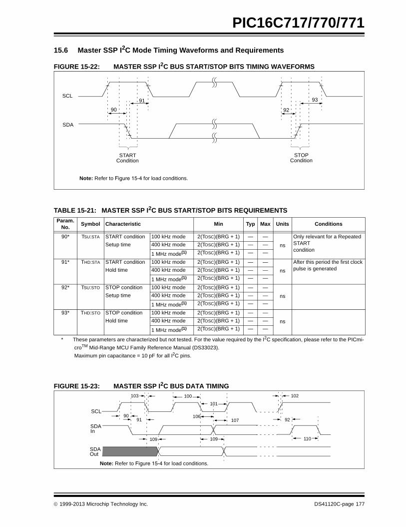
PIC16C717/770/771
15.6 Master SSP I2C Mode Timing Waveforms and Requirements
FIGURE 15-22: MASTER SSP I2C BUS START/STOP BITS TIMING WAVEFORMS
TABLE 15-21: MASTER SSP I2C BUS START/STOP BITS REQUIREMENTS
FIGURE 15-23: MASTER SSP I2C BUS DATA TIMING
Param.No.
Symbol Characteristic Min Typ Max Units Conditions
90* TSU:STA START condition 100 kHz mode 2(TOSC)(BRG + 1) — —
ns
Only relevant for a Repeated START condition
Setup time 400 kHz mode 2(TOSC)(BRG + 1) — —
1 MHz mode(1) 2(TOSC)(BRG + 1) — —
91* THD:STA START condition 100 kHz mode 2(TOSC)(BRG + 1) — —
ns
After this period the first clock pulse is generatedHold time 400 kHz mode 2(TOSC)(BRG + 1) — —
1 MHz mode(1) 2(TOSC)(BRG + 1) — —
92* TSU:STO STOP condition 100 kHz mode 2(TOSC)(BRG + 1) — —
nsSetup time 400 kHz mode 2(TOSC)(BRG + 1) — —
1 MHz mode(1) 2(TOSC)(BRG + 1) — —
93* THD:STO STOP condition 100 kHz mode 2(TOSC)(BRG + 1) — —
nsHold time 400 kHz mode 2(TOSC)(BRG + 1) — —
1 MHz mode(1) 2(TOSC)(BRG + 1) — —
* These parameters are characterized but not tested. For the value required by the I2C specification, please refer to the PICmi-
croTM Mid-Range MCU Family Reference Manual (DS33023).
Maximum pin capacitance = 10 pF for all I2C pins.
Note: Refer to Figure 15-4 for load conditions.
91 93SCL
SDA
STARTCondition
STOPCondition
90 92
Note: Refer to Figure 15-4 for load conditions.
9091 92
100
101
103
106107
109 109 110
102
SCL
SDAIn
SDAOut
1999-2013 Microchip Technology Inc. DS41120C-page 177

PIC16C717/770/771
TABLE 15-22: MASTER SSP I2C BUS DATA REQUIREMENTS Param.
No.Symbol Characteristic Min Max Units Conditions
100* THIGH Clock high time 100 kHz mode 2(TOSC)(BRG + 1) — ms400 kHz mode 2(TOSC)(BRG + 1) — ms
1 MHz mode(1) 2(TOSC)(BRG + 1) — ms
101* TLOW Clock low time 100 kHz mode 2(TOSC)(BRG + 1) — ms400 kHz mode 2(TOSC)(BRG + 1) — ms
1 MHz mode(1) 2(TOSC)(BRG + 1) — ms
102* TR SDA and SCL rise time
100 kHz mode — 1000 ns Cb is specified to be from 10 to 400 pF 400 kHz mode 20 + 0.1Cb 300 ns
1 MHz mode(1) — 300 ns
103* TF SDA and SCL fall time
100 kHz mode — 300 ns Cb is specified to be from 10 to 400 pF 400 kHz mode 20 + 0.1Cb 300 ns
1 MHz mode(1) — 100 ns
90* TSU:STA START condition setup time
100 kHz mode 2(TOSC)(BRG + 1) — ms Only relevant for Repeated START condition
400 kHz mode 2(TOSC)(BRG + 1) — ms
1 MHz mode(1) 2(TOSC)(BRG + 1) — ms
91* THD:STA START condition hold time
100 kHz mode 2(TOSC)(BRG + 1) — ms After this period the first clock pulse is generated400 kHz mode 2(TOSC)(BRG + 1) — ms
1 MHz mode(1) 2(TOSC)(BRG + 1) — ms
106* THD:DAT Data input hold time
100 kHz mode 0 — ns400 kHz mode 0 0.9 ms
1 MHz mode(1) TBD — ns
107* TSU:DAT Data input setup time
100 kHz mode 250 — ns Note 2400 kHz mode 100 — ns
1 MHz mode(1) TBD — ns
92* TSU:STO STOP condition setup time
100 kHz mode 2(TOSC)(BRG + 1) — ms400 kHz mode 2(TOSC)(BRG + 1) — ms
1 MHz mode(1) 2(TOSC)(BRG + 1) — ms
109* TAA Output valid from clock
100 kHz mode — 3500 ns400 kHz mode — 1000 ns
1 MHz mode(1) — — ns
110 TBUF Bus free time 100 kHz mode 4.7 ‡ — ms Time the bus must be free before a new transmission can start
400 kHz mode 1.3 ‡ — ms
1 MHz mode(1) TBD‡ — ms
D102 ‡ Cb Bus capacitive loading — 400 pF
* These parameters are characterized but not tested. For the value required by the I2C specification, please refer to the
PICmicroTM Mid-Range MCU Family Reference Manual (DS33023).‡ These parameters are for design guidance only and are not tested, nor characterized.
Note 1: Maximum pin capacitance = 10 pF for all I2C pins. 2: A Fast mode I2C bus device can be used in a Standard mode I2C bus system, but (TSU:DAT) 250 ns must then be met.
This will automatically be the case if the device does not stretch the LOW period of the SCL signal. If such a device does stretch the LOW period of the SCL signal, it must output the next data bit to the SDA line. [(TR) + (TSU:DAT) = 1000 + 250 = 1250 ns], for 100 kHz mode, before the SCL line is released.
DS41120C-page 178 1999-2013 Microchip Technology Inc.

PIC16C717/770/771
16.0 DC AND AC CHARACTERISTICS GRAPHS AND TABLES
“Typical” represents the mean of the distribution at 25°C. “Maximum” or “minimum” represents (mean + 3 ) or (mean - 3) respectively, where is a standard deviation, over the whole temperature range.
The FOSC IDD was determined using an external sinusoidal clock source with a peak amplitude ranging from VSS to VDD.
FIGURE 16-1: MAXIMUM IDD VS. FOSC OVER VDD (HS MODE)
The graphs and tables provided following this note are a statistical summary based on a limited number of samplesand are provided for informational purposes only. The performance characteristics listed herein are not tested orguaranteed. In some graphs or tables, the data presented may be outside the specified operating range (e.g., outsidespecified power supply range) and therefore outside the warranted range.
0.0
1.0
2.0
3.0
4.0
5.0
6.0
4.00 6.00 8.00 10.00 12.00 14.00 16.00 18.00 20.00
FOSC (MHz)
IDD
(m
A)
5.5V
5.0V
4.5V
4.0V
3.5V
3.0V
2.5V
1999-2013 Microchip Technology Inc. DS41120C-page 179

PIC16C717/770/771
FIGURE 16-2: TYPICAL IDD VS. FOSC OVER VDD (HS MODE)
FIGURE 16-3: MAXIMUM IDD VS. FOSC OVER VDD (XT MODE)
0.0
1.0
2.0
3.0
4.0
5.0
6.0
4.00 6.00 8.00 10.00 12.00 14.00 16.00 18.00 20.00
FOSC (MHz)
IDD
(m
A)
5.5V
4.0V
3.0V
2.5V
4.5V
3.5V
5.0V
0.0
0.2
0.4
0.6
0.8
1.0
1.2
1.4
1.6
0.00 0.50 1.00 1.50 2.00 2.50 3.00 3.50 4.00
FOSC (MHz)
I DD
(m
A)
5.5V
5.0V
4.5V
4.0V
3.5V
3.0V
2.5V
DS41120C-page 180 1999-2013 Microchip Technology Inc.

PIC16C717/770/771
FIGURE 16-4: TYPICAL IDD VS. FOSC OVER VDD (XT MODE)
FIGURE 16-5: MAXIMUM IDD VS. FOSC OVER VDD (LP MODE)
0.0
0.2
0.4
0.6
0.8
1.0
1.2
1.4
0.00 0.50 1.00 1.50 2.00 2.50 3.00 3.50 4.00
FOSC (MHz)
I DD
(m
A)
5.5V
5.0V
4.5V
4.0V
3.5V
3.0V
2.5V
0.000
0.020
0.040
0.060
0.080
0.100
0.120
0.140
0.02 0.03 0.04 0.05 0.06 0.07 0.08 0.09 0.10
FOSC (MHz)
IDD
(m
A)
5.5V
5.0V
4.5V
4.0V
3.5V
3.0V
2.5V
1999-2013 Microchip Technology Inc. DS41120C-page 181

PIC16C717/770/771
FIGURE 16-6: TYPICAL IDD VS. FOSC OVER VDD (LP MODE)
FIGURE 16-7: MAXIMUM IDD VS. FOSC OVER VDD (EC MODE)
0.000
0.020
0.040
0.060
0.080
0.100
0.120
0.02 0.03 0.04 0.05 0.06 0.07 0.08 0.09 0.10
FOSC (MHz)
IDD
(m
A)
5.5V
4.0V
3.0V
2.5V
4.5V
3.5V
5.0V
0.0
0.5
1.0
1.5
2.0
2.5
3.0
3.5
4.0
4.5
5.0
0.00 2.00 4.00 6.00 8.00 10.00 12.00 14.00 16.00 18.00 20.00
FOSC (MHz)
IDD
(m
A)
5.5V
5.0V
4.5V
4.0V
3.5V
3.0V
2.5V
DS41120C-page 182 1999-2013 Microchip Technology Inc.

PIC16C717/770/771
FIGURE 16-8: TYPICAL IDD VS. FOSC OVER VDD (EC MODE)
FIGURE 16-9: MAXIMUM IDD VS. FOSC OVER VDD (ER MODE)
0.0
0.5
1.0
1.5
2.0
2.5
3.0
3.5
4.0
4.5
0.00 2.00 4.00 6.00 8.00 10.00 12.00 14.00 16.00 18.00 20.00
FOSC (MHz)
IDD
(m
A) 5.5V
5.0V
4.5V
4.0V
3.5V
3.0V
2.5V
0.0
0.2
0.4
0.6
0.8
1.0
1.2
1.4
1.6
2.5 3.0 3.5 4.0 4.5 5.0 5.5
VDD (V)
I DD
(m
A)
R = 38.3 K
R = 100 K
R = 200 K
R = 499 KR = 1 M
R = 38.3 k
R = 100 k
R = 200 k
R = 499 k
1999-2013 Microchip Technology Inc. DS41120C-page 183

PIC16C717/770/771
FIGURE 16-10: TYPICAL IDD VS. FOSC OVER VDD (ER MODE)
FIGURE 16-11: TYPICAL FOSC VS. VDD (ER MODE)
0.0
0.2
0.4
0.6
0.8
1.0
1.2
1.4
2.5 3.0 3.5 4.0 4.5 5.0 5.5
VDD (V)
I DD
(m
A)
R = 38.3 K
R = 100 K
R = 200 K
R = 499 K
R = 1 M
R = 38.3 k
R = 100 k
R = 200 k
R = 499 k
0.1
1.0
10.0
2.5 3.0 3.5 4.0 4.5 5.0 5.5
Vdd (V)
Fre
qu
ency
(M
Hz)
R = 38.3 K
R = 100 K
R = 200 K
R = 499 K
R = 1 M
R = 38.3 k
R = 100 k
R = 200 k
R = 499 k
VDD (V)
DS41120C-page 184 1999-2013 Microchip Technology Inc.

PIC16C717/770/771
FIGURE 16-12: MAXIMUM IDD VS. VDD (INTRC 37 kHZ MODE)
FIGURE 16-13: TYPICAL IDD VS. VDD (INTRC 37 kHZ MODE)
0.00
0.10
0.20
0.30
0.40
0.50
0.60
0.70
0.80
0.90
1.00
2.5 3.0 3.5 4.0 4.5 5.0 5.5
VDD (Volts)
I DD
(m
A)
Typ (25 °C)
Max (-40 °C)
0.00
0.02
0.04
0.06
0.08
0.10
0.12
0.14
2.5 3.0 3.5 4.0 4.5 5.0 5.5
VDD (V)
I DD
(m
A)
-40 °C
25 °C
85 °C
125 °C
1999-2013 Microchip Technology Inc. DS41120C-page 185
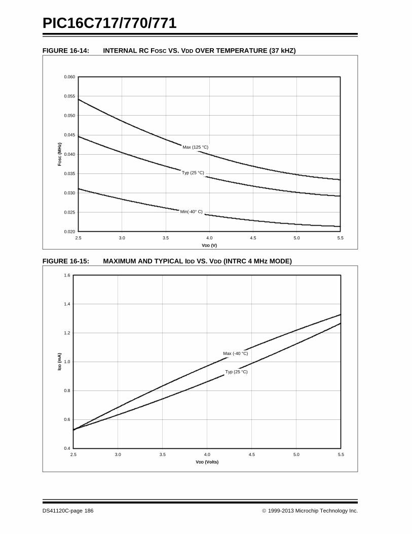
PIC16C717/770/771
FIGURE 16-14: INTERNAL RC FOSC VS. VDD OVER TEMPERATURE (37 kHZ)
FIGURE 16-15: MAXIMUM AND TYPICAL IDD VS. VDD (INTRC 4 MHz MODE)
0.020
0.025
0.030
0.035
0.040
0.045
0.050
0.055
0.060
2.5 3.0 3.5 4.0 4.5 5.0 5.5
VDD (V)
FO
SC
(M
Hz) Max (125 °C)
Typ (25 °C)
Min(-40° C)
0.4
0.6
0.8
1.0
1.2
1.4
1.6
2.5 3.0 3.5 4.0 4.5 5.0 5.5
VDD (Volts)
I DD
(m
A) Max (-40 °C)
Typ (25 °C)
DS41120C-page 186 1999-2013 Microchip Technology Inc.

PIC16C717/770/771
FIGURE 16-16: TYPICAL IDD VS. VDD (INTRC 4 MHz MODE)
FIGURE 16-17: INTERNAL RC FOSC VS. VDD OVER TEMPERATURE (4 MHz)
0.4
0.5
0.6
0.7
0.8
0.9
1.0
1.1
1.2
1.3
1.4
2.5 3.0 3.5 4.0 4.5 5.0 5.5
VDD (Volts)
I DD
(m
A)
-40 °C
25 °C85 °C
125 °C
3.80
3.85
3.90
3.95
4.00
4.05
4.10
4.15
2.5 3.0 3.5 4.0 4.5 5.0 5.5
VDD (V)
FO
SC
(M
Hz)
Max (125 °C)
Typ (25 °C)
Min (-40 °C)
1999-2013 Microchip Technology Inc. DS41120C-page 187

PIC16C717/770/771
FIGURE 16-18: MAXIMUM IPD VS. VDD (-40°C TO +125°C)
0.01
0.1
1
10
2.5 3.0 3.5 4.0 4.5 5.0 5.5
VDD (V)
IPD (A
)
+125°C
+85°C
+25°C -40°C
DS41120C-page 188 1999-2013 Microchip Technology Inc.

PIC16C717/770/771
FIGURE 16-19: TYPICAL AND MAXIMUM IWDT VS. VDD (-40°C TO +125°C)
0.0
2.0
4.0
6.0
8.0
10.0
12.0
14.0
16.0
2.5 3.0 3.5 4.0 4.5 5.0 5.5
VDD (V)
I W
DT
(A
)
Max (-40°C)
Typ (25°C)
1999-2013 Microchip Technology Inc. DS41120C-page 189

PIC16C717/770/771
FIGURE 16-20: TYPICAL AND MAXIMUM ITMR1 VS. VDD (32 KHZ, -40°C TO +125°C)
FIGURE 16-21: TYPICAL AND MAXIMUM IVRL VS. VDD (-40°C TO +125°C)
10.0
30.0
50.0
70.0
90.0
110.0
130.0
150.0
2.5 3.0 3.5 4.0 4.5 5.0 5.5
VDD (V)
I T
MR
1 (A
)
Max (-40°C)
Typ (25°C)
150.0
170.0
190.0
210.0
230.0
250.0
270.0
290.0
310.0
330.0
350.0
2.5 3.0 3.5 4.0 4.5 5.0 5.5
VDD (V)
I V
RL (A
)
Max (125°C)
Max (85°C)
Typ (25°C)
DS41120C-page 190 1999-2013 Microchip Technology Inc.

PIC16C717/770/771
FIGURE 16-22: TYPICAL AND MAXIMUM IVRH VS. VDD (-40°C TO +125°C)
FIGURE 16-23: TYPICAL AND MAXIMUM ILVD VS. VDD (-40°C TO +125°C) (LVD TRIP = 3.0V)
200.0
220.0
240.0
260.0
280.0
300.0
320.0
340.0
360.0
380.0
4.5 5.0 5.5
VDD (V)
I V
RH
(A
)
Max (125°C)
Max (85°C)
Typ (25°C)
30.0
35.0
40.0
45.0
50.0
55.0
60.0
65.0
70.0
75.0
2.5 3.0 3.5 4.0 4.5 5.0 5.5
VDD (V)
I L
VD
(A
)
Max (125°C)
Max (85°C)
Typ (25°C)
1999-2013 Microchip Technology Inc. DS41120C-page 191

PIC16C717/770/771
FIGURE 16-24: TYPICAL AND MAXIMUM ILVD VS. VDD (-40°C TO +125°C) (LVD TRIP = 4.5V)
FIGURE 16-25: TYPICAL AND MAXIMUM IBOR VS. VDD (-40°C TO +125°C) (VBOR = 2.5V)
30.0
35.0
40.0
45.0
50.0
55.0
60.0
65.0
70.0
75.0
2.5 3.0 3.5 4.0 4.5 5.0 5.5
VDD (V)
I L
VD
(A
)
Max (125°C)
Max (85°C)
Typ (25°C)
30.0
40.0
50.0
60.0
70.0
80.0
90.0
2.0 2.5 3.0 3.5 4.0 4.5 5.0 5.5
VDD (V)
I B
OR
(A
)
Max (125°C)
Typ (25°C)
Max (125°C)
Typ (25°C)
Device in SleepDevice in Reset Indeterminate SLEEPRESET
DS41120C-page 192 1999-2013 Microchip Technology Inc.

PIC16C717/770/771
FIGURE 16-26: TYPICAL AND MAXIMUM IBOR VS. VDD (-40°C TO +125°C) (VBOR = 4.5V)
FIGURE 16-27: VOL VS. IOL (-40°C TO +125°C, VDD = 3.0V)
30.0
50.0
70.0
90.0
110.0
130.0
150.0
170.0
2.5 3.0 3.5 4.0 4.5 5.0 5.5
VDD (V)
I B
OR
(A
)
Max (125 °C)
Typ (25 °C)
Max (125 °C)
Typ (25C)
Device in SleepDevice in ResetIndeterminate SLEEPRESET
0.0
0.2
0.4
0.6
0.8
1.0
1.2
1.4
1.6
1.8
0.0 5.0 10.0 15.0 20.0 25.0
IOL (mA)
VO
L (
V)
Min (-40°C)
Max (125°C)
Typ (25°C)
1999-2013 Microchip Technology Inc. DS41120C-page 193

PIC16C717/770/771
FIGURE 16-28: VOL VS. IOL (-40°C TO +125°C, VDD = 5.0V)
FIGURE 16-29: VOH VS. IOH (-40°C TO +125°C, VDD = 3.0V)
0.0
0.1
0.2
0.3
0.4
0.5
0.6
0.7
0.8
0.9
1.0
0.0 5.0 10.0 15.0 20.0 25.0
IOL (mA)
VO
L (
V)
Min (-40°C)
Max (125°C)
Typ (25°C)
0.5
1.0
1.5
2.0
2.5
3.0
-16.0-14.0-12.0-10.0-8.0-6.0-4.0-2.00.0
IOH (mA)
VO
H (
V)
Max (-40°C)Min (125°C) Typ (25°C)
DS41120C-page 194 1999-2013 Microchip Technology Inc.

PIC16C717/770/771
FIGURE 16-30: VOH VS. IOH (-40°C TO +125°C, VDD = 5.0V)
FIGURE 16-31: MINIMUM AND MAXIMUM VIH/VIL VS. VDD (TTL INPUT,-40°C TO +125°C)
2.0
2.5
3.0
3.5
4.0
4.5
5.0
-25.0-20.0-15.0-10.0-5.00.0
IOH (mA)
VO
H (
V)
Max (-40°C)
Min (125°C)
Typ (25°C)
0.8
0.9
1.0
1.1
1.2
1.3
1.4
1.5
1.6
1.7
1.8
2.5 3.0 3.5 4.0 4.5 5.0 5.5
VDD (V)
VIL
/ V
IH (
V)
Min (125°C)
Max (-40°C)
1999-2013 Microchip Technology Inc. DS41120C-page 195

PIC16C717/770/771
FIGURE 16-32: MINIMUM AND MAXIMUM VIH/VIL VS. VDD (ST INPUT,-40°C TO +125°C)
FIGURE 16-33: TYPICAL, MINIMUM AND MAXIMUM WDT PERIOD VS. VDD (-40°C TO +125°C)
0.0
0.5
1.0
1.5
2.0
2.5
3.0
3.5
4.0
2.5 3.0 3.5 4.0 4.5 5.0 5.5
VDD (V)
VIL
/ V
IH (
V)
Max High (125°C)
Min High (-40°C)
Max Low (-40°C)
Min Low (125°C)
10.0
15.0
20.0
25.0
30.0
35.0
2.5 3.0 3.5 4.0 4.5 5.0 5.5
VDD (V)
WD
T P
erio
d (
mS
)
Max (125°C)
Typ (25°C)
Max (85°C)
Min (-40°C)
DS41120C-page 196 1999-2013 Microchip Technology Inc.

PIC16C717/770/771
17.0 PACKAGING INFORMATION
17.1 Package Marking Information
18-Lead SOIC
XXXXXXXXXXXX
YYWWNNN
XXXXXXXXXXXXXXXXXYYWWNNN
18-Lead PDIP Example
PIC16C717/P
9917017
XXXXXXXXXXXXXXXXX
XXXXXXXXXXXX
XXXXXXXXYYWWNNN
18-Lead CERDIP Windowed
PIC16C717/JW
Example
9905017
XXXXXXXX
20-Lead PDIP Example
XXXXXXXXXXXXXXXXXYYWWNNN
PIC16C770/P
9917017
XXXXXXXXXXXXXXXXX
XXXXXXXXXXXX
Example
9910017
PIC16C717/SO
Legend: XX...X Customer-specific informationY Year code (last digit of calendar year)YY Year code (last 2 digits of calendar year)WW Week code (week of January 1 is week ‘01’)NNN Alphanumeric traceability code Pb-free JEDEC designator for Matte Tin (Sn)* This package is Pb-free. The Pb-free JEDEC designator ( )
can be found on the outer packaging for this package.
Note: In the event the full Microchip part number cannot be marked on one line, it willbe carried over to the next line, thus limiting the number of availablecharacters for customer-specific information.
3e
3e
1999-2013 Microchip Technology Inc. DS41120C-page 197

PIC16C717/770/771
17.1 Package Marking Information (Cont’d)
YYWWNNN
XXXXXXXXXXXXXXXXXXXXXX
20-Lead SSOP
9917017
20I/SSPIC16C770
Example
XXXXXXXXYYWWNNN
20-Lead CERDIP Windowed
PIC16C770/JW
Example
9905017
XXXXXXXX
20-Lead SOIC
XXXXXXXXXXXXXXXXXXXXXXXX
YYWWNNN
Example
PIC16C771/SO
9910017
XXXXXXXXXXXXXXXXXXXXXXXX
DS41120C-page 198 1999-2013 Microchip Technology Inc.
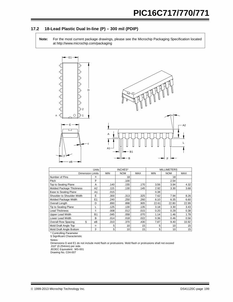
PIC16C717/770/771
17.2 18-Lead Plastic Dual In-line (P) – 300 mil (PDIP)
1510515105Mold Draft Angle Bottom
1510515105Mold Draft Angle Top
10.929.407.87.430.370.310eBOverall Row Spacing §
0.560.460.36.022.018.014BLower Lead Width
1.781.461.14.070.058.045B1Upper Lead Width
0.380.290.20.015.012.008cLead Thickness
3.433.303.18.135.130.125LTip to Seating Plane
22.9922.8022.61.905.898.890DOverall Length
6.606.356.10.260.250.240E1Molded Package Width
8.267.947.62.325.313.300EShoulder to Shoulder Width
0.38.015A1Base to Seating Plane
3.683.302.92.145.130.115A2Molded Package Thickness
4.323.943.56.170.155.140ATop to Seating Plane
2.54.100pPitch
1818nNumber of Pins
MAXNOMMINMAXNOMMINDimension Limits
MILLIMETERSINCHES*Units
1
2
D
n
E1
c
eB
E
p
A2
L
B1
B
A
A1
* Controlling Parameter
Notes:Dimensions D and E1 do not include mold flash or protrusions. Mold flash or protrusions shall not exceed .010” (0.254mm) per side.JEDEC Equivalent: MS-001Drawing No. C04-007
§ Significant Characteristic
Note: For the most current package drawings, please see the Microchip Packaging Specification locatedat http://www.microchip.com/packaging
1999-2013 Microchip Technology Inc. DS41120C-page 199

PIC16C717/770/771
17.3 18-Lead Ceramic Dual In-line with Window (JW) – 300 mil (CERDIP)
3.30 3.56 3.81
5.335.084.83.210.200.190W2Window Length
.150.140.130W1Window Width
10.809.788.76.425.385.345eBOverall Row Spacing
0.530.470.41.021.019.016BLower Lead Width
1.521.401.27.060.055.050B1Upper Lead Width
0.300.250.20.012.010.008cLead Thickness
3.813.493.18.150.138.125LTip to Seating Plane
23.3722.8622.35.920.900.880DOverall Length
7.497.377.24.295.290.285E1Ceramic Pkg. Width
8.267.947.62.325.313.300EShoulder to Shoulder Width
0.760.570.38.030.023.015A1Standoff
4.194.063.94.165.160.155A2Ceramic Package Height
4.954.644.32.195.183.170ATop to Seating Plane
2.54.100pPitch
1818nNumber of Pins
MAXNOMMINMAXNOMMINDimension Limits
MILLIMETERSINCHES*Units
1
2
D
n
W2
E1
W1
c
eB
E
p
L
A2
B
B1
A
A1
*Controlling ParameterJEDEC Equivalent: MO-036Drawing No. C04-010
Note: For the most current package drawings, please see the Microchip Packaging Specification locatedat http://www.microchip.com/packaging
DS41120C-page 200 1999-2013 Microchip Technology Inc.
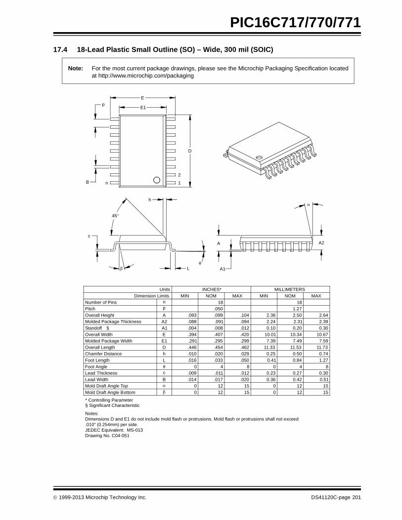
PIC16C717/770/771
17.4 18-Lead Plastic Small Outline (SO) – Wide, 300 mil (SOIC)
Foot Angle 0 4 8 0 4 8
1512015120Mold Draft Angle Bottom
1512015120Mold Draft Angle Top
0.510.420.36.020.017.014BLead Width
0.300.270.23.012.011.009cLead Thickness
1.270.840.41.050.033.016LFoot Length
0.740.500.25.029.020.010hChamfer Distance
11.7311.5311.33.462.454.446DOverall Length
7.597.497.39.299.295.291E1Molded Package Width
10.6710.3410.01.420.407.394EOverall Width
0.300.200.10.012.008.004A1Standoff §
2.392.312.24.094.091.088A2Molded Package Thickness
2.642.502.36.104.099.093AOverall Height
1.27.050pPitch
1818nNumber of Pins
MAXNOMMINMAXNOMMINDimension Limits
MILLIMETERSINCHES*Units
L
c
h
45
1
2
D
p
nB
E1
E
A2
A1
A
* Controlling Parameter
Notes:Dimensions D and E1 do not include mold flash or protrusions. Mold flash or protrusions shall not exceed .010” (0.254mm) per side.JEDEC Equivalent: MS-013Drawing No. C04-051
§ Significant Characteristic
Note: For the most current package drawings, please see the Microchip Packaging Specification locatedat http://www.microchip.com/packaging
1999-2013 Microchip Technology Inc. DS41120C-page 201

PIC16C717/770/771
17.5 20-Lead Plastic Dual In-line (P) – 300 mil (PDIP)
1510515105Mold Draft Angle Bottom
1510515105Mold Draft Angle Top
10.929.407.87.430.370.310eBOverall Row Spacing §
0.560.460.36.022.018.014BLower Lead Width
1.651.521.40.065.060.055B1Upper Lead Width
0.380.290.20.015.012.008cLead Thickness
3.563.303.05.140.130.120LTip to Seating Plane
26.4226.2426.041.0401.0331.025DOverall Length
6.606.356.10.260.250.240E1Molded Package Width
8.267.877.49.325.310.295EShoulder to Shoulder Width
0.38.015A1Base to Seating Plane
3.683.302.92.145.130.115A2Molded Package Thickness
4.323.943.56.170.155.140ATop to Seating Plane
2.54.100pPitch
2020nNumber of Pins
MAXNOMMINMAXNOMMINDimension Limits
MILLIMETERSINCHES*Units
1
2
D
n
E1
c
eB
E
p
A2
L
B1
B
A
A1
* Controlling Parameter
Notes:Dimensions D and E1 do not include mold flash or protrusions. Mold flash or protrusions shall not exceed .010” (0.254mm) per side.JEDEC Equivalent: MS-001Drawing No. C04-019
§ Significant Characteristic
Note: For the most current package drawings, please see the Microchip Packaging Specification locatedat http://www.microchip.com/packaging
DS41120C-page 202 1999-2013 Microchip Technology Inc.

PIC16C717/770/771
17.6 20-Lead Ceramic Dual In-line with Window (JW) – 300 mil (CERDIP)
DRAWING NOT AVAILABLE
1999-2013 Microchip Technology Inc. DS41120C-page 203

PIC16C717/770/771
17.7 20-Lead Plastic Small Outline (SO) – Wide, 300 mi (SOIC)
* Controlling Parameter
Notes:Dimensions D and E1 do not include mold flash or protrusions. Mold flash or protrusions shall not exceed .010” (0.254mm) per side.JEDEC Equivalent: MS-013Drawing No. C04-094
Foot Angle 0 4 8 0 4 8
1512015120Mold Draft Angle Bottom
1512015120Mold Draft Angle Top
0.510.420.36.020.017.014BLead Width
0.330.280.23.013.011.009cLead Thickness
1.270.840.41.050.033.016LFoot Length
0.740.500.25.029.020.010hChamfer Distance
13.0012.8012.60.512.504.496DOverall Length
7.597.497.39.299.295.291E1Molded Package Width
10.6710.3410.01.420.407.394EOverall Width
0.300.200.10.012.008.004A1Standoff §
2.392.312.24.094.091.088A2Molded Package Thickness
2.642.502.36.104.099.093AOverall Height
1.27.050pPitch
2020nNumber of Pins
MAXNOMMINMAXNOMMINDimension Limits
MILLIMETERSINCHES*Units
h
L
c
45
1
2
D
p
nB
E
E1
A2A
A1
§ Significant Characteristic
Note: For the most current package drawings, please see the Microchip Packaging Specification locatedat http://www.microchip.com/packaging
DS41120C-page 204 1999-2013 Microchip Technology Inc.

PIC16C717/770/771
17.8 20-Lead Plastic Shrink Small Outline (SS) – 209 mil, 5.30 mm (SSOP)
10501050Mold Draft Angle Bottom
10501050Mold Draft Angle Top
0.380.320.25.015.013.010BLead Width
203.20101.600.00840Foot Angle
0.250.180.10.010.007.004cLead Thickness
0.940.750.56.037.030.022LFoot Length
7.347.207.06.289.284.278DOverall Length
5.385.255.11.212.207.201E1Molded Package Width
8.187.857.59.322.309.299EOverall Width
0.250.150.05.010.006.002A1Standoff §
1.831.731.63.072.068.064A2Molded Package Thickness
1.981.851.73.078.073.068AOverall Height
0.65.026pPitch
2020nNumber of Pins
MAXNOMMINMAXNOMMINDimension Limits
MILLIMETERSINCHES*Units
2
1
D
p
n
B
E
E1
L
c
A2A
A1
* Controlling Parameter
Notes:Dimensions D and E1 do not include mold flash or protrusions. Mold flash or protrusions shall not exceed .010” (0.254mm) per side.JEDEC Equivalent: MO-150Drawing No. C04-072
§ Significant Characteristic
Note: For the most current package drawings, please see the Microchip Packaging Specification locatedat http://www.microchip.com/packaging
1999-2013 Microchip Technology Inc. DS41120C-page 205

PIC16C717/770/771
NOTES:
DS41120C-page 206 1999-2013 Microchip Technology Inc.

PIC16C717/770/771
APPENDIX A: REVISION HISTORY
Version Date Revision Description
A 09/14/99 This is a new data sheet. However, the devices described in this data sheet are the upgrades to the devices found in the PIC16C7X Data Sheet, DS30390E.
B 1/22/02 Electrical Characteristics tables completed and characteristics graphs added. MSSP I2C (Section 9.2) rewritten. General minor changes and corrections.
C 1/28/13 Added a note to each package outline drawing.
1999-2013 Microchip Technology Inc. DS41120C-page 207

PIC16C717/770/771
APPENDIX B: DEVICE DIFFERENCES
The differences between the devices in this data sheetare listed in Table B-1.
TABLE B-1: DEVICE DIFFERENCES
Difference PIC16C717 PIC16C770 PIC16C771
Program Memory 2K 2K 4K
A/D 6 channels, 10 bits 6 channels, 12 bits 6 channels, 12 bits
Dedicated AVDD and AVSS
Not available Available Available
Packages 18-pin PDIP, 18-pin windowed CERDIP, 18-pin SOIC,
20-pin SSOP
20-pin PDIP, 20-pin windowed CERDIP, 20-pin
SOIC, 20-pin SSOP
20-pin PDIP, 20-pin windowed CERDIP, 20-pin SOIC,
20-pin SSOP
DS41120C-page 208 1999-2013 Microchip Technology Inc.

PIC16C717/770/771
INDEX
AA/D .................................................................................... 105
A/D Converter Enable (ADIE Bit) ................................ 17ADCON0 Register..................................................... 105ADCON1 Register............................................. 105, 107ADRES Register ....................................................... 105Block Diagram........................................................... 109Configuring Analog Port............................................ 108Conversion time ........................................................ 115Conversions .............................................................. 111converter characteristics ................... 164, 165, 166, 170Faster Conversion - Lower Resolution Tradeoff ....... 115Internal Sampling Switch (Rss) Impedence .............. 113Operation During Sleep ............................................ 116Sampling Requirements............................................ 113Sampling Time .......................................................... 113Source Impedance.................................................... 113Special Event Trigger (ECCP) .................................... 55
A/D Conversion Clock ....................................................... 110ACK..................................................................................... 77Acknowledge Data bit, AKD................................................ 69Acknowledge Sequence Enable bit, AKE ........................... 69Acknowledge Status bit, AKS ............................................. 69ACKSTAT ........................................................................... 87ADCON0 Register............................................................. 105ADCON1 Register..................................................... 105, 107ADRES.............................................................................. 105ADRES Register ........................................... 11, 12, 105, 116AKD..................................................................................... 69AKE..................................................................................... 69AKS..................................................................................... 69Analog-to-Digital Converter. See A/DApplication Note AN578, "Use of the SSP Module in the I2C Multi-Master Environment." ............................. 84Architecture
PIC16C717/PIC16C717 Block Diagram ....................... 5PIC16C770/771/PIC16C770/771 Block Diagram ......... 6
AssemblerMPASM Assembler................................................... 141
BBanking, Data Memory ................................................... 9, 14Baud Rate Generator .......................................................... 84BF ..................................................................... 66, 77, 87, 89Block Diagrams
Baud Rate Generator.................................................. 84I2C Master Mode......................................................... 83I2C Module .................................................................. 76RA3:RA0 and RA5 Port Pins .................... 26, 28, 29, 35SSP (I2C Mode) .......................................................... 76SSP (SPI Mode).......................................................... 70
BOR. See Brown-out ResetBRG .................................................................................... 84Brown-out Reset (BOR) .................................... 117, 123, 124Buffer Full bit, BF ................................................................ 77Buffer Full Status bit, BF ..................................................... 66Bus Arbitration .................................................................... 94Bus Collision During a RESTART Condition....................... 97Bus Collision During a Start Condition ................................ 95Bus Collision During a Stop Condition ................................ 98Bus Collision Section .......................................................... 94
CCapture (ECCP Module)..................................................... 54
Block Diagram ............................................................ 54CCPR1H:CCPR1L Registers ..................................... 54Changing Between Capture Prescalers ..................... 54ECCP Pin Configuration ............................................. 54Software Interrupt ....................................................... 54Timer1 Mode Selection............................................... 54
Capture/Compare/PWM (ECCP)Capture Mode. See CaptureCompare Mode. See ComparePWM Mode. See PWM
CCP1CON .......................................................................... 13CCP2CON .......................................................................... 13CCPR1H Register......................................................... 11, 13CCPR1L Register ............................................................... 13CCPR2H Register............................................................... 13CCPR2L Register ............................................................... 13CKE .................................................................................... 66CKP .................................................................................... 67Clock Polarity Select bit, CKP............................................. 67Code Examples
Loading the SSPBUF register .................................... 71Code Protection........................................................ 117, 131Compare (ECCP Module)................................................... 54
Block Diagram ............................................................ 55CCPR1H:CCPR1L Registers ..................................... 54ECCP Pin Configuration ............................................. 54Software Interrupt ....................................................... 55Special Event Trigger ........................................... 49, 55Timer1 Mode Selection............................................... 54
Configuration Bits ............................................................. 117
DD/A...................................................................................... 66Data Memory ........................................................................ 9
Bank Select (RP Bits) ............................................. 9, 14General Purpose Registers .......................................... 9Register File Map ....................................................... 10Special Function Registers......................................... 11
Data/Address bit, D/A ......................................................... 66DC Characteristics
PIC16C717/770/771 ................................. 150, 151, 153Development Support ....................................................... 141Device Differences............................................................ 208Direct Addressing ............................................................... 23
EEnhanced Capture/Compare/PWM (ECCP)
CCP1CCPR1H Register .............................................. 53CCPR1L Register ............................................... 53Enable (CCP1IE Bit)........................................... 17
Timer Resources ........................................................ 54Errata .................................................................................... 3External Power-on Reset Circuit....................................... 122
FFirmware Instructions ....................................................... 133FSR Register .......................................................... 11, 12, 13
GGCE.................................................................................... 69General Call Address Sequence ........................................ 82General Call Address Support ............................................ 82General Call Enable bit, GCE............................................. 69
1999-2013 Microchip Technology Inc. DS41120C-page 209

PIC16C717/770/771
II/O Ports .............................................................................. 25I2C ....................................................................................... 76I2C Master Mode Reception................................................ 89I2C Master Mode Restart Condition .................................... 86I2C Mode Selection ............................................................. 76I2C Module
Acknowledge Sequence timing................................... 91Addressing .................................................................. 77Baud Rate Generator .................................................. 84Block Diagram............................................................. 83BRG Block Diagram.................................................... 84BRG Reset due to SDA Collision ................................ 96BRG Timing ................................................................ 85Bus Arbitration ............................................................ 94Bus Collision ............................................................... 94
Acknowledge....................................................... 94Restart Condition ................................................ 97Restart Condition Timing (Case1)....................... 97Restart Condition Timing (Case2)....................... 97Start Condition .................................................... 95Start Condition Timing .................................. 95, 96Stop Condition .................................................... 98Stop Condition Timing (Case1)........................... 98Stop Condition Timing (Case2)........................... 98Transmit Timing .................................................. 94
Bus Collision timing..................................................... 94Clock Arbitration.......................................................... 93Clock Arbitration Timing (Master Transmit)................. 93Conditions to not give ACK Pulse ............................... 77General Call Address Support .................................... 82Master Mode ............................................................... 83Master Mode 7-bit Reception timing ........................... 90Master Mode Operation .............................................. 84Master Mode Start Condition ...................................... 85Master Mode Transmission......................................... 87Master Mode Transmit Sequence............................... 84Multi-Master Communication ...................................... 94Multi-master Mode ...................................................... 84Operation .................................................................... 76Repeat Start Condition timing ..................................... 86Slave Mode ................................................................. 76Slave Reception.......................................................... 78Slave Transmission..................................................... 80SSPBUF...................................................................... 76Stop Condition Receive or Transmit timing................. 92Stop Condition timing.................................................. 92Waveforms for 7-bit Reception ................................... 78Waveforms for 7-bit Transmission .............................. 80
I2C Slave Mode ................................................................... 76ICEPIC In-Circuit Emulator ............................................... 142ID Locations .............................................................. 117, 131In-Circuit Serial Programming (ICSP) ....................... 117, 131INDF.................................................................................... 13INDF Register ............................................................... 11, 12Indirect Addressing ............................................................. 23
FSR Register ................................................................ 9Instruction Format ............................................................. 133Instruction Set ................................................................... 133
ADDLW ..................................................................... 135ADDWF..................................................................... 135ANDLW ..................................................................... 135ANDWF..................................................................... 135BCF........................................................................... 135BSF ........................................................................... 135BTFSC ...................................................................... 136
BTFSS ...................................................................... 136CALL......................................................................... 136CLRF ........................................................................ 136CLRW ....................................................................... 136CLRWDT .................................................................. 136COMF ....................................................................... 137DECF........................................................................ 137DECFSZ ................................................................... 137GOTO ....................................................................... 137INCF ......................................................................... 137INCFSZ..................................................................... 137IORLW...................................................................... 138IORWF...................................................................... 138MOVF ....................................................................... 138MOVLW .................................................................... 138MOVWF.................................................................... 138NOP.......................................................................... 138RETFIE..................................................................... 139RETLW ..................................................................... 139RETURN................................................................... 139RLF........................................................................... 139RRF .......................................................................... 139SLEEP ...................................................................... 139SUBLW..................................................................... 140SUBWF..................................................................... 140SWAPF..................................................................... 140XORLW .................................................................... 140XORWF .................................................................... 140Summary Table ........................................................ 134
INT Interrupt (RB0/INT). See Interrupt SourcesINTCON .............................................................................. 13INTCON Register................................................................ 16
GIE Bit ........................................................................ 16INTE Bit ...................................................................... 16INTF Bit ...................................................................... 16PEIE Bit ...................................................................... 16RBIE Bit ...................................................................... 16RBIF Bit ................................................................ 16, 33T0IE Bit ....................................................................... 16T0IF Bit ....................................................................... 16
Inter-Integrated Circuit (I2C) ............................................... 65internal sampling switch (Rss) impedence ....................... 113Interrupt Sources ...................................................... 117, 127
Block Diagram .......................................................... 127Capture Complete (ECCP) ......................................... 54Compare Complete (ECCP) ....................................... 55RB0/INT Pin, External............................................... 128TMR0 Overflow................................................... 46, 128TMR1 Overflow..................................................... 47, 49TMR2 to PR2 Match ................................................... 52TMR2 to PR2 Match (PWM)................................. 51, 56
InterruptsSynchronous Serial Port Interrupt............................... 18
Interrupts, Context Saving During..................................... 128Interrupts, Enable Bits
A/D Converter Enable (ADIE Bit)................................ 17CCP1 Enable (CCP1IE Bit) .................................. 17, 54Global Interrupt Enable (GIE Bit) ........................ 16, 127Interrupt-on-Change (RB7:RB4) Enable (RBIE Bit)........................................................ 16, 128Peripheral Interrupt Enable (PEIE Bit) ........................ 16PSP Read/Write Enable (PSPIE Bit) .......................... 17RB0/INT Enable (INTE Bit) ......................................... 16SSP Enable (SSPIE Bit) ............................................. 17TMR0 Overflow Enable (T0IE Bit) .............................. 16TMR1 Overflow Enable (TMR1IE Bit)......................... 17
DS41120C-page 210 1999-2013 Microchip Technology Inc.

PIC16C717/770/771
TMR2 to PR2 Match Enable (TMR2IE Bit) ................. 17USART Receive Enable (RCIE Bit) ...................... 17, 18
Interrupts, Flag BitsCCP1 Flag (CCP1IF Bit) ............................................. 54Interrupt on Change (RB7:RB4) Flag (RBIF Bit) .................................................. 16, 33, 128RB0/INT Flag (INTF Bit).............................................. 16TMR0 Overflow Flag (T0IF Bit) ........................... 16, 128
INTRC Mode ..................................................................... 120
KKEELOQ Evaluation and Programming Tools .................... 144
LLVDCON ........................................................................... 101
MMaster Clear (MCLR)
MCLR Reset, Normal Operation ............... 121, 123, 124MCLR Reset, SLEEP................................ 121, 123, 124
Memory OrganizationData Memory ................................................................ 9Program Memory .......................................................... 9
MPLAB C17 and MPLAB C18 C Compilers...................... 141MPLAB ICD In-Circuit Debugger ...................................... 143MPLAB ICE High Performance Universal In-Circuit Emulator with MPLAB IDE ............................................ 142MPLAB Integrated Development Environment Software .. 141MPLINK Object Linker/MPLIB Object Librarian ................ 142Multi-Master Communication .............................................. 94Multi-Master Mode .............................................................. 84
OOPCODE Field Descriptions ............................................. 133OPTION_REG Register ...................................................... 15
INTEDG Bit ................................................................. 15PS Bits .................................................................. 15, 45PSA Bit.................................................................. 15, 45RBPU Bit..................................................................... 15T0CS Bit................................................................ 15, 45T0SE Bit................................................................ 15, 45
Oscillator Configuration..................................................... 119CLKOUT ................................................................... 120Dual Speed Operation for ER and INTRC Modes ....................................................... 120EC ..................................................................... 119, 123ER ..................................................................... 119, 123ER Mode ................................................................... 120HS..................................................................... 119, 123INTRC ............................................................... 119, 123LP...................................................................... 119, 123XT ..................................................................... 119, 123
Oscillator, Timer1.......................................................... 47, 49Oscillator, WDT................................................................. 129
PP.......................................................................................... 66Packaging ......................................................................... 197Paging, Program Memory ............................................... 9, 22Parallel Slave Port (PSP)
Read/Write Enable (PSPIE Bit)................................... 17PCL Register................................................................. 11, 12PCLATH Register ................................................... 11, 12, 13PCON Register ........................................................... 21, 123PICDEM 1 Low Cost PIC MCU Demonstration Board .................................................... 143PICDEM 17 Demonstration Board .................................... 144PICDEM 2 Low Cost PIC16CXX Demonstration Board .................................................... 143
PICDEM 3 Low Cost PIC16CXXX Demonstration Board.................................................... 144PICSTART Plus Entry Level Development Programmer............................................ 143PIE1 Register ..................................................................... 17
ADIE Bit ...................................................................... 17CCP1IE Bit ................................................................. 17PSPIE Bit.................................................................... 17RCIE Bit................................................................ 17, 18SSPIE Bit.................................................................... 17TMR1IE Bit ................................................................. 17TMR2IE Bit ................................................................. 17
PIE2 Register ..................................................................... 19Pinout Descriptions
PIC16C770 ................................................................... 7PIC16C770/771 ............................................................ 7PIC16C771 ................................................................... 7
PIR1 Register ..................................................................... 18PIR2 Register ..................................................................... 20Pointer, FSR ....................................................................... 23POR. See Power-on ResetPORTA ............................................................................... 13
Initialization................................................................. 26PORTA Register......................................................... 25TRISA Register........................................................... 25
PORTA Register ......................................................... 11, 116PORTB ............................................................................... 13
Initialization................................................................. 33PORTB Register......................................................... 33Pull-up Enable (RBPU Bit).......................................... 15RB0/INT Edge Select (INTEDG Bit) ........................... 15RB0/INT Pin, External .............................................. 128RB7:RB4 Interrupt on Change.................................. 128RB7:RB4 Interrupt on Change Enable (RBIE Bit)........................................................ 16, 128RB7:RB4 Interrupt on Change Flag (RBIF Bit).................................................. 16, 33, 128TRISB Register........................................................... 33
PORTB Register ......................................................... 11, 116Postscaler, Timer2
Select (TOUTPS Bits)................................................. 51Postscaler, WDT................................................................. 45
Assignment (PSA Bit) ........................................... 15, 45Block Diagram ............................................................ 46Rate Select (PS Bits)............................................ 15, 45Switching Between Timer0 and WDT......................... 46
Power-down Mode. See SLEEPPower-on Reset (POR)..................... 117, 121, 122, 123, 124
Oscillator Start-up Timer (OST)........................ 117, 122Power Control (PCON) Register............................... 123Power-down (PD Bit) .................................................. 14Power-on Reset Circuit, External ............................. 122Power-up Timer (PWRT) .................................. 117, 122Time-out (TO Bit)........................................................ 14Time-out Sequence .................................................. 123Time-out Sequence on Power-up..................... 125, 126
PR2 Register ...................................................................... 12Prescaler, Capture.............................................................. 54Prescaler, Timer0 ............................................................... 45
Assignment (PSA Bit) ........................................... 15, 45Block Diagram ............................................................ 46Rate Select (PS Bits)............................................ 15, 45Switching Between Timer0 and WDT......................... 46
Prescaler, Timer1 ............................................................... 48Select (T1CKPS Bits) ................................................. 47
1999-2013 Microchip Technology Inc. DS41120C-page 211

PIC16C717/770/771
Prescaler, Timer2................................................................ 57Select (T2CKPS Bits).................................................. 51
PRO MATE II Universal Device Programmer ................... 143Program Counter
PCL Register............................................................... 22PCLATH Register ............................................... 22, 128Reset Conditions....................................................... 123
Program Memory .................................................................. 9Interrupt Vector ............................................................. 9Paging..................................................................... 9, 22Program Memory Map .................................................. 9READ (PMR)............................................................... 43Reset Vector ................................................................. 9
Program Verification.......................................................... 131Programmable Brown-out Reset (PBOR) ................. 121, 122Programming, Device Instructions .................................... 133PWM (CCP Module)
TMR2 to PR2 Match ................................................... 51TMR2 to PR2 Match Enable (TMR2IE Bit) ................. 17
PWM (ECCP Module) ......................................................... 56Block Diagram............................................................. 56CCPR1H:CCPR1L Registers...................................... 56Duty Cycle................................................................... 57Output Diagram........................................................... 57Period.......................................................................... 56TMR2 to PR2 Match ................................................... 56
QQ Clock ............................................................................... 57
RR/W ..................................................................................... 66R/W bit ................................................................................ 80R/W bit ................................................................................ 78R/W bit ................................................................................ 77RAM. See Data MemoryRCE,Receive Enable bit, RCE............................................ 69RCREG ............................................................................... 13RCSTA Register.................................................................. 13Read/Write bit, R/W ............................................................ 66Receive Overflow Indicator bit, SSPOV .............................. 67REFCON ........................................................................... 102Register File .......................................................................... 9Register File Map ................................................................ 10Registers
FSR Summary ............................................................ 13INDF Summary ........................................................... 13INTCON Summary ...................................................... 13PCL Summary............................................................. 13PCLATH Summary ..................................................... 13PORTB Summary ....................................................... 13SSPSTAT............................................................ 66, 101STATUS Summary ..................................................... 13TMR0 Summary .......................................................... 13TRISB Summary ......................................................... 13
Reset......................................................................... 117, 121Block Diagram........................................................... 121Brown-out Reset (BOR). See Brown-out Reset (BOR)MCLR Reset. See MCLRPower-on Reset (POR). See Power-on Reset (POR)Reset Conditions for All Registers ............................ 124Reset Conditions for PCON Register........................ 123Reset Conditions for Program Counter ..................... 123Reset Conditions for STATUS Register .................... 123WDT Reset. See Watchdog Timer (WDT)
Restart Condition Enabled bit, RSE .................................... 69Revision History ................................................................ 207RSE..................................................................................... 69
SS ......................................................................................... 66SAE..................................................................................... 69SCK .................................................................................... 70SCL..................................................................................... 76SDA .................................................................................... 76SDI...................................................................................... 70SDO .................................................................................... 70Serial Data In, SDI .............................................................. 70Serial Data Out, SDO ......................................................... 70Slave Select Synchronization ............................................. 73Slave Select, SS ................................................................. 70SLEEP .............................................................. 117, 121, 130SMP.................................................................................... 66Software Simulator (MPLAB SIM) .................................... 142SPE..................................................................................... 69Special Event Trigger. See CompareSpecial Features of the CPU ............................................ 117Special Function Registers ................................................. 11
PIC16C717 ................................................................. 11PIC16C717/770/771 ................................................... 11PIC16C770 ................................................................. 11PIC16C771 ................................................................. 11
Speed, Operating.................................................................. 1SPI
Master Mode............................................................... 72Serial Clock................................................................. 70Serial Data In .............................................................. 70Serial Data Out ........................................................... 70Serial Peripheral Interface (SPI) ................................. 65Slave Select................................................................ 70SPI clock..................................................................... 72SPI Mode.................................................................... 70
SPI Clock Edge Select, CKE .............................................. 66SPI Data Input Sample Phase Select, SMP ....................... 66SPI Master/Slave Connection............................................. 71SPI Module
Master/Slave Connection............................................ 71Slave Mode................................................................. 73Slave Select Synchronization ..................................... 73Slave Synch Timnig.................................................... 73
SS ....................................................................................... 70SSP..................................................................................... 65
Block Diagram (SPI Mode) ......................................... 70Enable (SSPIE Bit) ..................................................... 17SPI Mode.................................................................... 70SSPADD..................................................................... 77SSPBUF ............................................................... 72, 76SSPCON .................................................................... 67SSPCON2 ............................................................ 69, 70SSPSR ................................................................. 72, 77SSPSTAT ..................................................... 66, 76, 101TMR2 Output for Clock Shift................................. 51, 52
SSP I2CSSP I2C Operation ..................................................... 76
SSP ModuleSPI Master Mode........................................................ 72SPI Master./Slave Connection.................................... 71SPI Slave Mode.......................................................... 73SSPCON1 Register .................................................... 76
SSP Overflow Detect bit, SSPOV....................................... 77SSPADD Register............................................................... 12SSPBUF ................................................................. 13, 76, 77SSPBUF Register ............................................................... 11SSPCON............................................................................. 67SSPCON Register .............................................................. 11
DS41120C-page 212 1999-2013 Microchip Technology Inc.

PIC16C717/770/771
SSPCON1........................................................................... 76SSPCON2..................................................................... 69, 70SSPEN................................................................................ 67SSPIF............................................................................ 18, 78SSPM.................................................................................. 68SSPOV.................................................................... 67, 77, 89SSPSTAT.............................................................. 66, 76, 101SSPSTAT Register ............................................................. 12Stack ................................................................................... 22Start bit (S) .......................................................................... 66Start Condition Enabled bit, SAE ........................................ 69STATUS Register ................................................. 14, 15, 128
C Bit ............................................................................ 14DC Bit.................................................................... 14, 15IRP Bit......................................................................... 14PD Bit.......................................................................... 14RP Bits ........................................................................ 14TO Bit.......................................................................... 14Z Bit............................................................................. 14
Status Register ................................................................... 14Stop bit (P) .......................................................................... 66Stop Condition Enable bit ................................................... 69Synchronous Serial Port ..................................................... 65Synchronous Serial Port Enable bit, SSPEN ...................... 67Synchronous Serial Port Interrupt ....................................... 18Synchronous Serial Port Mode Select bits, SSPM ............. 68
TT1CON................................................................................ 13T1CON Register ........................................................... 13, 47
T1CKPS Bits ............................................................... 47T1OSCEN Bit.............................................................. 47T1SYNC Bit................................................................. 47TMR1CS Bit ................................................................ 47TMR1ON Bit................................................................ 47
T2CON Register ........................................................... 13, 51T2CKPS Bits ............................................................... 51TMR2ON Bit................................................................ 51TOUTPS Bits .............................................................. 51
Timer0Block Diagram............................................................. 45Clock Source Edge Select (T0SE Bit)................... 15, 45Clock Source Select (T0CS Bit)............................ 15, 45Overflow Enable (T0IE Bit) ......................................... 16Overflow Flag (T0IF Bit)...................................... 16, 128Overflow Interrupt ............................................... 46, 128Prescaler. See Prescaler, Timer0
Timer1................................................................................. 47Block Diagram............................................................. 48Capacitor Selection..................................................... 49Clock Source Select (TMR1CS Bit) ............................ 47External Clock Input Sync (T1SYNC Bit) .................... 47Module On/Off (TMR1ON Bit)..................................... 47Oscillator ............................................................... 47, 49Oscillator Enable (T1OSCEN Bit) ............................... 47Overflow Enable (TMR1IE Bit).................................... 17Overflow Interrupt ................................................. 47, 49Prescaler. See Prescaler, Timer1Special Event Trigger (ECCP) .............................. 49, 55T1CON Register ......................................................... 47TMR1H Register ......................................................... 47TMR1L Register.......................................................... 47
Timer2Block Diagram ............................................................ 52Postscaler. See Postscaler, Timer2PR2 Register ........................................................ 51, 56Prescaler. See Prescaler, Timer2SSP Clock Shift .................................................... 51, 52T2CON Register ......................................................... 51TMR2 Register ........................................................... 51TMR2 to PR2 Match Enable (TMR2IE Bit) ................. 17TMR2 to PR2 Match Interrupt......................... 51, 52, 56
Timing DiagramsAcknowledge Sequence Timing ................................. 91Baud Rate Generator with Clock Arbitration............... 85BRG Reset Due to SDA Collision............................... 96Brown-out Reset....................................................... 159Bus Collision
Start Condition Timing ........................................ 95Bus Collision During a Restart Condition (Case 1).................................................................. 97Bus Collision During a Restart Condition (Case2)................................................................... 97Bus Collision During a Start Condition (SCL = 0) ................................................................ 96Bus Collision During a Stop Condition........................ 98Bus Collision for Transmit and Acknowledge ............. 94Capture/Compare/PWM ........................................... 161CLKOUT and I/O ...................................................... 157External Clock Timing............................................... 157I2C Bus Data............................................................. 177I2C Master Mode First Start bit timing ........................ 85I2C Master Mode Reception timing............................. 90I2C Master Mode Transmission timing ....................... 88Master Mode Transmit Clock Arbitration .................... 93Power-up Timer ........................................................ 159Repeat Start Condition ............................................... 86Reset ........................................................................ 159Slave Synchronization ................................................ 73Start-up Timer........................................................... 159Stop Condition Receive or Transmit ........................... 92Time-out Sequence on Power-up..................... 125, 126Timer0 ...................................................................... 160Timer1 ...................................................................... 160Wake-up from SLEEP via Interrupt .......................... 131Watchdog Timer ....................................................... 159
TMR0.................................................................................. 13TMR0 Register.................................................................... 11TMR1H ............................................................................... 13TMR1H Register ................................................................. 11TMR1L................................................................................ 13TMR1L Register.................................................................. 11TMR2.................................................................................. 13TMR2 Register.................................................................... 11TRISA Register........................................................... 12, 116TRISB Register........................................................... 12, 116TXREG ............................................................................... 13
UUpdate Address, UA........................................................... 66USART
Receive Enable (RCIE Bit) ................................... 17, 18
1999-2013 Microchip Technology Inc. DS41120C-page 213

PIC16C717/770/771
WW Register ........................................................................ 128Wake-up from SLEEP............................................... 117, 130
Interrupts........................................................... 123, 124MCLR Reset ............................................................. 124Timing Diagram......................................................... 131WDT Reset ............................................................... 124
Watchdog Timer (WDT) ............................................ 117, 129Block Diagram........................................................... 129Enable (WDTE Bit).................................................... 129Postscaler. See Postscaler, WDTProgramming Considerations ................................... 129RC Oscillator ............................................................. 129Time-out Period ........................................................ 129WDT Reset, Normal Operation ................. 121, 123, 124WDT Reset, SLEEP.......................................... 123, 124
Waveform for General Call Address Sequence .................. 82WCOL ................................................... 67, 85, 87, 89, 91, 92WCOL Status Flag .............................................................. 85Write Collision Detect bit, WCOL ........................................ 67WWW, On-Line Support........................................................ 3
DS41120C-page 214
1999-2013 Microchip Technology Inc.
THE MICROCHIP WEB SITE
Microchip provides online support via our WWW site atwww.microchip.com. This web site is used as a meansto make files and information easily available tocustomers. Accessible by using your favorite Internetbrowser, the web site contains the followinginformation:
• Product Support – Data sheets and errata, application notes and sample programs, design resources, user’s guides and hardware support documents, latest software releases and archived software
• General Technical Support – Frequently Asked Questions (FAQ), technical support requests, online discussion groups, Microchip consultant program member listing
• Business of Microchip – Product selector and ordering guides, latest Microchip press releases, listing of seminars and events, listings of Microchip sales offices, distributors and factory representatives
CUSTOMER CHANGE NOTIFICATION SERVICE
Microchip’s customer notification service helps keepcustomers current on Microchip products. Subscriberswill receive e-mail notification whenever there arechanges, updates, revisions or errata related to aspecified product family or development tool of interest.
To register, access the Microchip web site atwww.microchip.com. Under “Support”, click on“Customer Change Notification” and follow theregistration instructions.
CUSTOMER SUPPORT
Users of Microchip products can receive assistancethrough several channels:
• Distributor or Representative
• Local Sales Office
• Field Application Engineer (FAE)
• Technical Support
Customers should contact their distributor,representative or field application engineer (FAE) forsupport. Local sales offices are also available to helpcustomers. A listing of sales offices and locations isincluded in the back of this document.
Technical support is available through the web siteat: http://microchip.com/support
1999-2013 Microchip Technology Inc. DS41120C-page 215

READER RESPONSE
It is our intention to provide you with the best documentation possible to ensure successful use of your Microchipproduct. If you wish to provide your comments on organization, clarity, subject matter, and ways in which ourdocumentation can better serve you, please FAX your comments to the Technical Publications Manager at(480) 792-4150.
Please list the following information, and use this outline to provide us with your comments about this document.
TO: Technical Publications Manager
RE: Reader ResponseTotal Pages Sent ________
From: Name
Company
Address
City / State / ZIP / Country
Telephone: (_______) _________ - _________
Application (optional):
Would you like a reply? Y N
Device: Literature Number:
Questions:
FAX: (______) _________ - _________
DS41120C
1. What are the best features of this document?
2. How does this document meet your hardware and software development needs?
3. Do you find the organization of this document easy to follow? If not, why?
4. What additions to the document do you think would enhance the structure and subject?
5. What deletions from the document could be made without affecting the overall usefulness?
6. Is there any incorrect or misleading information (what and where)?
7. How would you improve this document?
DS41120C-page 216 1999-2013 Microchip Technology Inc.

PIC16C717/770/771
PIC16C717/770/771 PRODUCT IDENTIFICATION SYSTEMTo order or obtain information, e.g., on pricing or delivery, refer to the factory or the listed sales office.
* JW Devices are UV erasable and can be programmed to any device configuration. JW Devices meet the electrical requirement ofeach oscillator type.
Sales and Support
PART NO. X /XX XXX
PatternPackageTemperatureRange
Device
Device PIC16C771 : VDD range 4.0V to 5.5VPIC16C771T : VDD range 4.0V to 5.5V (Tape/Reel)PIC16LC771 : VDD range 2.5V to 5.5VPIC16LC771T: VDD range 2.5V to 5.5V (Tape/Reel)
Temperature Range: - = 0C to +70C I = -40C to +85CE = -40C to +125C
Package JW = Windowed CERDIPSO = SOICP = PDIP SS = SSOP
Pattern QTP, SQTP, Code or Special Requirements. Blank for OTP and Windowed devices.
Examples:
a) PIC16C771/P Commercial Temp.,PDIP package, normal VDD limits
Data SheetsProducts supported by a preliminary Data Sheet may have an errata sheet describing minor operational differences and recom-mended workarounds. To determine if an errata sheet exists for a particular device, please contact one of the following:
1. Your local Microchip sales office2. The Microchip Worldwide Site (www.microchip.com)
1999-2013 Microchip Technology Inc. DS41120C-page 217

PIC16C717/770/771
NOTES:
DS41120C-page 218 1999-2013 Microchip Technology Inc.

PIC16C717/770/771
NOTES:
1999-2013 Microchip Technology Inc. DS41120C-page 219

PIC16C717/770/771
NOTES:
DS41120C-page 220 1999-2013 Microchip Technology Inc.

PIC16C717/770/771
NOTES:
1999-2013 Microchip Technology Inc. DS41120C-page 221

PIC16C717/770/771
DS41120C-page 222 1999-2013 Microchip Technology Inc.

Note the following details of the code protection feature on Microchip devices:
• Microchip products meet the specification contained in their particular Microchip Data Sheet.
• Microchip believes that its family of products is one of the most secure families of its kind on the market today, when used in the intended manner and under normal conditions.
• There are dishonest and possibly illegal methods used to breach the code protection feature. All of these methods, to our knowledge, require using the Microchip products in a manner outside the operating specifications contained in Microchip’s Data Sheets. Most likely, the person doing so is engaged in theft of intellectual property.
• Microchip is willing to work with the customer who is concerned about the integrity of their code.
• Neither Microchip nor any other semiconductor manufacturer can guarantee the security of their code. Code protection does not mean that we are guaranteeing the product as “unbreakable.”
Code protection is constantly evolving. We at Microchip are committed to continuously improving the code protection features of ourproducts. Attempts to break Microchip’s code protection feature may be a violation of the Digital Millennium Copyright Act. If such actsallow unauthorized access to your software or other copyrighted work, you may have a right to sue for relief under that Act.
Information contained in this publication regarding deviceapplications and the like is provided only for your convenienceand may be superseded by updates. It is your responsibility toensure that your application meets with your specifications.MICROCHIP MAKES NO REPRESENTATIONS ORWARRANTIES OF ANY KIND WHETHER EXPRESS ORIMPLIED, WRITTEN OR ORAL, STATUTORY OROTHERWISE, RELATED TO THE INFORMATION,INCLUDING BUT NOT LIMITED TO ITS CONDITION,QUALITY, PERFORMANCE, MERCHANTABILITY ORFITNESS FOR PURPOSE. Microchip disclaims all liabilityarising from this information and its use. Use of Microchipdevices in life support and/or safety applications is entirely atthe buyer’s risk, and the buyer agrees to defend, indemnify andhold harmless Microchip from any and all damages, claims,suits, or expenses resulting from such use. No licenses areconveyed, implicitly or otherwise, under any Microchipintellectual property rights.
1999-2013 Microchip Technology Inc.
QUALITY MANAGEMENT SYSTEM CERTIFIED BY DNV
== ISO/TS 16949 ==
Trademarks
The Microchip name and logo, the Microchip logo, dsPIC, FlashFlex, KEELOQ, KEELOQ logo, MPLAB, PIC, PICmicro, PICSTART, PIC32 logo, rfPIC, SST, SST Logo, SuperFlash and UNI/O are registered trademarks of Microchip Technology Incorporated in the U.S.A. and other countries.
FilterLab, Hampshire, HI-TECH C, Linear Active Thermistor, MTP, SEEVAL and The Embedded Control Solutions Company are registered trademarks of Microchip Technology Incorporated in the U.S.A.
Silicon Storage Technology is a registered trademark of Microchip Technology Inc. in other countries.
Analog-for-the-Digital Age, Application Maestro, BodyCom, chipKIT, chipKIT logo, CodeGuard, dsPICDEM, dsPICDEM.net, dsPICworks, dsSPEAK, ECAN, ECONOMONITOR, FanSense, HI-TIDE, In-Circuit Serial Programming, ICSP, Mindi, MiWi, MPASM, MPF, MPLAB Certified logo, MPLIB, MPLINK, mTouch, Omniscient Code Generation, PICC, PICC-18, PICDEM, PICDEM.net, PICkit, PICtail, REAL ICE, rfLAB, Select Mode, SQI, Serial Quad I/O, Total Endurance, TSHARC, UniWinDriver, WiperLock, ZENA and Z-Scale are trademarks of Microchip Technology Incorporated in the U.S.A. and other countries.
SQTP is a service mark of Microchip Technology Incorporated in the U.S.A.
GestIC and ULPP are registered trademarks of Microchip Technology Germany II GmbH & Co. & KG, a subsidiary of Microchip Technology Inc., in other countries.
All other trademarks mentioned herein are property of their respective companies.
© 1999-2013, Microchip Technology Incorporated, Printed in the U.S.A., All Rights Reserved.
Printed on recycled paper.
ISBN: 9781620769713
Microchip received ISO/TS-16949:2009 certification for its worldwide
DS41120C-page 223
headquarters, design and wafer fabrication facilities in Chandler and Tempe, Arizona; Gresham, Oregon and design centers in California and India. The Company’s quality system processes and procedures are for its PIC® MCUs and dsPIC® DSCs, KEELOQ® code hopping devices, Serial EEPROMs, microperipherals, nonvolatile memory and analog products. In addition, Microchip’s quality system for the design and manufacture of development systems is ISO 9001:2000 certified.

DS41120C-page 224 1999-2013 Microchip Technology Inc.
AMERICASCorporate Office2355 West Chandler Blvd.Chandler, AZ 85224-6199Tel: 480-792-7200 Fax: 480-792-7277Technical Support: http://www.microchip.com/supportWeb Address: www.microchip.com
AtlantaDuluth, GA Tel: 678-957-9614 Fax: 678-957-1455
BostonWestborough, MA Tel: 774-760-0087 Fax: 774-760-0088
ChicagoItasca, IL Tel: 630-285-0071 Fax: 630-285-0075
ClevelandIndependence, OH Tel: 216-447-0464 Fax: 216-447-0643
DallasAddison, TX Tel: 972-818-7423 Fax: 972-818-2924
DetroitFarmington Hills, MI Tel: 248-538-2250Fax: 248-538-2260
IndianapolisNoblesville, IN Tel: 317-773-8323Fax: 317-773-5453
Los AngelesMission Viejo, CA Tel: 949-462-9523 Fax: 949-462-9608
Santa ClaraSanta Clara, CA Tel: 408-961-6444Fax: 408-961-6445
TorontoMississauga, Ontario, CanadaTel: 905-673-0699 Fax: 905-673-6509
ASIA/PACIFICAsia Pacific OfficeSuites 3707-14, 37th FloorTower 6, The GatewayHarbour City, KowloonHong KongTel: 852-2401-1200Fax: 852-2401-3431
Australia - SydneyTel: 61-2-9868-6733Fax: 61-2-9868-6755
China - BeijingTel: 86-10-8569-7000 Fax: 86-10-8528-2104
China - ChengduTel: 86-28-8665-5511Fax: 86-28-8665-7889
China - ChongqingTel: 86-23-8980-9588Fax: 86-23-8980-9500
China - HangzhouTel: 86-571-2819-3187 Fax: 86-571-2819-3189
China - Hong Kong SARTel: 852-2943-5100 Fax: 852-2401-3431
China - NanjingTel: 86-25-8473-2460Fax: 86-25-8473-2470
China - QingdaoTel: 86-532-8502-7355Fax: 86-532-8502-7205
China - ShanghaiTel: 86-21-5407-5533 Fax: 86-21-5407-5066
China - ShenyangTel: 86-24-2334-2829Fax: 86-24-2334-2393
China - ShenzhenTel: 86-755-8864-2200 Fax: 86-755-8203-1760
China - WuhanTel: 86-27-5980-5300Fax: 86-27-5980-5118
China - XianTel: 86-29-8833-7252Fax: 86-29-8833-7256
China - XiamenTel: 86-592-2388138 Fax: 86-592-2388130
China - ZhuhaiTel: 86-756-3210040 Fax: 86-756-3210049
ASIA/PACIFICIndia - BangaloreTel: 91-80-3090-4444 Fax: 91-80-3090-4123
India - New DelhiTel: 91-11-4160-8631Fax: 91-11-4160-8632
India - PuneTel: 91-20-2566-1512Fax: 91-20-2566-1513
Japan - OsakaTel: 81-6-6152-7160 Fax: 81-6-6152-9310
Japan - TokyoTel: 81-3-6880- 3770 Fax: 81-3-6880-3771
Korea - DaeguTel: 82-53-744-4301Fax: 82-53-744-4302
Korea - SeoulTel: 82-2-554-7200Fax: 82-2-558-5932 or 82-2-558-5934
Malaysia - Kuala LumpurTel: 60-3-6201-9857Fax: 60-3-6201-9859
Malaysia - PenangTel: 60-4-227-8870Fax: 60-4-227-4068
Philippines - ManilaTel: 63-2-634-9065Fax: 63-2-634-9069
SingaporeTel: 65-6334-8870Fax: 65-6334-8850
Taiwan - Hsin ChuTel: 886-3-5778-366Fax: 886-3-5770-955
Taiwan - KaohsiungTel: 886-7-213-7828Fax: 886-7-330-9305
Taiwan - TaipeiTel: 886-2-2508-8600 Fax: 886-2-2508-0102
Thailand - BangkokTel: 66-2-694-1351Fax: 66-2-694-1350
EUROPEAustria - WelsTel: 43-7242-2244-39Fax: 43-7242-2244-393Denmark - CopenhagenTel: 45-4450-2828 Fax: 45-4485-2829
France - ParisTel: 33-1-69-53-63-20 Fax: 33-1-69-30-90-79
Germany - MunichTel: 49-89-627-144-0 Fax: 49-89-627-144-44
Italy - Milan Tel: 39-0331-742611 Fax: 39-0331-466781
Netherlands - DrunenTel: 31-416-690399 Fax: 31-416-690340
Spain - MadridTel: 34-91-708-08-90Fax: 34-91-708-08-91
UK - WokinghamTel: 44-118-921-5869Fax: 44-118-921-5820
Worldwide Sales and Service
11/29/12