pic16(l)f1508/9 data sheet
TRANSCRIPT

PIC16(L)F1508/920-Pin Flash, 8-Bit Microcontrollers with XLP Technology
High-Performance RISC CPU:• C Compiler Optimized Architecture• Only 49 Instructions• Operating Speed:
- DC – 20 MHz clock input- DC – 200 ns instruction cycle
• Interrupt Capability with Automatic Context Saving
• 16-Level Deep Hardware Stack with Optional Overflow/Underflow Reset
• Direct, Indirect and Relative Addressing modes:- Two full 16-bit File Select Registers (FSRs)- FSRs can read program and data memory
Flexible Oscillator Structure:• 16 MHz Internal Oscillator Block:
- Factory calibrated to ±1%, typical- Software selectable frequency range from
16 MHz to 31 kHz• 31 kHz Low-Power Internal Oscillator • Three External Clock modes up to 20 MHz
Special Microcontroller Features:• Operating Voltage Range:
- 1.8V to 3.6V (PIC16LF1508/9)- 2.3V to 5.5V (PIC16F1508/9)
• Self-Programmable under Software Control• Power-on Reset (POR)• Power-up Timer (PWRT)• Programmable Low-Power Brown-out Reset
(LPBOR)• Extended Watchdog Timer (WDT):
- Programmable period from 1 ms to 256s• Programmable Code Protection• In-Circuit Serial Programming™ (ICSP™) via Two
Pins• Enhanced Low-Voltage Programming (LVP)• In-Circuit Debug (ICD) via Two Pins• Power-Saving Sleep mode:
- Low-Power Sleep mode- Low-Power BOR (LPBOR)
• Integrated Temperature Indicator• 128 Bytes High-Endurance Flash
- 100,000 write Flash endurance (minimum)
Memory:• Up to 8 Kwords Linear Program Memory
Addressing• Up to 512 bytes Linear Data Memory Addressing• High-Endurance Flash Data Memory (HEF)
- 128 bytes if nonvolatile data storage- 100k erase/write cycles
eXtreme Low-Power (XLP) Features(PIC16LF1508/9):
• Sleep Current:- 20 nA @ 1.8V, typical
• Watchdog Timer Current:- 260 nA @ 1.8V, typical
• Operating Current:- 30 A/MHz @ 1.8V, typical
• Secondary Oscillator Current:- 700 nA @ 32 kHz, 1.8V, typical
Peripheral Features:
• Analog-to-Digital Converter (ADC):- 10-bit resolution- 12 external channels- Three internal channels:
- Fixed Voltage Reference- Digital-to-Analog Converter (DAC)- Temperature Indicator channel
- Auto acquisition capability- Conversion available during Sleep
• 5-Bit Digital-to-Analog Converter (DAC):
- Output available externally
- Positive reference selection
- Internal connections to comparators and ADC
• Two Comparators:- Rail-to-rail inputs- Power mode control- Software controllable hysteresis
• Voltage Reference:- 1.024V Fixed Voltage Reference (FVR) with
1x, 2x and 4x Gain output levels• 18 I/O Pins (1 Input-only Pin):
- High current sink/source 25 mA/25 mA- Individually programmable weak pull-ups- Individually programmable
Interrupt-on-Change (IOC) pins• Timer0: 8-Bit Timer/Counter with 8-Bit
Programmable Prescaler• Enhanced Timer1:
- 16-bit timer/counter with prescaler- External Gate Input mode
• Timer2: 8-Bit Timer/Counter with 8-Bit Period Register, Prescaler and Postscaler
• Four 10-bit PWM modules• Master Synchronous Serial Port (MSSP) with SPI
and I2C with:- 7-bit address masking- SMBus/PMBus™ compatibility
2011-2015 Microchip Technology Inc. DS40001609E-page 1

PIC16(L)F1508/9
Peripheral Features (Continued):
• Enhanced Universal Synchronous Asynchronous Receiver Transmitter (EUSART)- RS-232, RS-485 and LIN compatible- Auto-Baud Detect- Auto-wake-up on Start
• Four Configurable Logic Cell (CLC) modules:- 16 selectable input source signals- Four inputs per module- Software control of combinational/sequential
logic/state/clock functions- AND/OR/XOR/D Flop/D Latch/SR/JK- Inputs from external and internal sources- Output available to pins and peripherals- Operation while in Sleep
• Numerically Controlled Oscillator (NCO):- 20-bit accumulator- 16-bit increment- True linear frequency control- High-speed clock input- Selectable Output modes
- Fixed Duty Cycle (FDC) mode- Pulse Frequency (PF) mode
• Complementary Waveform Generator (CWG):- Eight selectable signal sources- Selectable falling and rising edge dead-band
control- Polarity control- Four auto-shutdown sources- Multiple input sources: PWM, CLC, NCO
PIC12(L)F1501/PIC16(L)F150X FAMILY TYPES
Device
Dat
a S
he
et
Ind
ex
Pro
gra
m M
em
ory
Fla
sh
(w
ord
s)
Dat
a S
RA
M(b
ytes
)
I/O’s
(2)
10-b
it A
DC
(ch
)
Co
mp
ara
tors
DA
C
Tim
ers
(8/1
6-b
it)
PW
M
EU
SA
RT
MS
SP
(I2 C
/SP
I)
CW
G
CL
C
NC
O
De
bu
g(1
)
XL
P
PIC12(L)F1501 (1) 1024 64 6 4 1 1 2/1 4 — — 1 2 1 H —
PIC16(L)F1503 (2) 2048 128 12 8 2 1 2/1 4 — 1 1 2 1 H —
PIC16(L)F1507 (3) 2048 128 18 12 — — 2/1 4 — — 1 2 1 H —
PIC16(L)F1508 (4) 4096 256 18 12 2 1 2/1 4 1 1 1 4 1 I/H Y
PIC16(L)F1509 (4) 8192 512 18 12 2 1 2/1 4 1 1 1 4 1 I/H Y
Note 1: Debugging Methods: (I) - Integrated on Chip; (H) - using Debug Header; (E) - using Emulation Header.2: One pin is input-only.
Data Sheet Index: (Unshaded devices are described in this document.)
1: DS40001615 PIC12(L)F1501 Data Sheet, 8-Pin Flash, 8-bit Microcontrollers.
2: DS40001607 PIC16(L)F1503 Data Sheet, 14-Pin Flash, 8-bit Microcontrollers.
3: DS40001586 PIC16(L)F1507 Data Sheet, 20-Pin Flash, 8-bit Microcontrollers.
4: DS40001609 PIC16(L)F1508/9 Data Sheet, 20-Pin Flash, 8-bit Microcontrollers.
Note: For other small form-factor package availability and marking information, please visithttp://www.microchip.com/packaging or contact your local sales office.
DS40001609E-page 2 2011-2015 Microchip Technology Inc.

PIC16(L)F1508/9
PIN DIAGRAMS
PIC
16(L
)F15
08
PIC
16(L
)F15
09
1
2
3
4
14
13
12
11
5
6
7
10
9
8
VDD
RA5
RA4
MCLR/VPP/RA3
RC5
RC4
VSS
RA0/ICSPDAT
RA1/ICSPCLK
RA2
RC0
RC1
RC2RC3
Note: See Table 1 for location of all peripheral functions.
18
17
16
15
20
19
RC6
RC7
RB7
RB4
RB5
RB6
20-pin PDIP, SOIC, SSOP
PIC16(L)F1508PIC16(L)F1509
Note 1: See Table 1 for location of all peripheral functions.
2: It is recommended that the exposed bottom pad be connected to VSS.
15 RA1/ICSPCLK
RA2
RC0
RC1
RC211
12
13
14
6 7
RC
7
RB
7
RB
4
RB
5
RB
6
8 9 10
2
3
1
181920 1617
5
4
VD
D
RA
5
RA
4
MCLR/VPP/RA3
RC5
RC4
RC3
RC6
VS
S
RA
0/IC
SP
DA
T20-pin QFN, UQFN
2011-2015 Microchip Technology Inc. DS40001609E-page 3

PIC16(L)F1508/9
Ba
sic
DATAT
CLKLK
LRP
UTC2
INC1
D
S
PIN ALLOCATION TABLE
TABLE 1: 20-PIN ALLOCATION TABLE (PIC16(L)F1508/9)
I/O
20-
Pin
PD
IP/S
OIC
/SS
OP
20-
Pin
QF
N/U
QF
N
AD
C
Re
fere
nce
Co
mp
arat
or
Tim
ers
EU
SA
RT
MS
SP
CW
G
NC
O
CL
C
PW
M
Inte
rru
pt
Pu
ll-u
p
RA0 19 16 AN0 DAC1OUT1 C1IN+ — ——
— — — — IOC Y ICSPICDD
RA1 18 15 AN1 VREF+ C1IN0-C2IN0-
— — — — — CLC4IN1 — IOC Y ICSPICDC
RA2 17 14 AN2 DAC1OUT2 C1OUT T0CKI — — CWG1FLT — CLC1 PWM3 INT/IOC
Y —
RA3 4 1 — — — T1G(1) — SS(1) — — CLC1IN0 — IOC Y MCVP
RA4 3 20 AN3 — — SOSCOT1G
— — — — — — IOC Y CLKOOS
RA5 2 19 — — — SOSCIT1CKI
— — — NCO1CLK — — IOC Y CLKOS
RB4 13 10 AN10 — — — — SDA/SDI — — CLC3IN0 — IOC Y —
RB5 12 9 AN11 — — — RX/DT — — — CLC4IN0 — IOC Y —
RB6 11 8 — — — — — SCL/SCK — — — — IOC Y —
RB7 10 7 — — — — TX/CK — — — CLC3 — IOC Y —
RC0 16 13 AN4 — C2IN+ — — — — — CLC2 — — — —
RC1 15 12 AN5 — C1IN1-C2IN1-
— — — — NCO1 — PWM4 — — —
RC2 14 11 AN6 — C1IN2-C2IN2-
— — — — — — — — — —
RC3 7 4 AN7 — C1IN3-C2IN3-
— — — — — CLC2IN0 PWM2 — — —
RC4 6 3 — — C2OUT — — — CWG1B — CLC4CLC2IN1
— — — —
RC5 5 2 — — — — — — CWG1A — CLC1(1) PWM1 — — —
RC6 8 5 AN8 — — — — SS — NCO1(1) CLC3IN1 — — — —
RC7 9 6 AN9 — — — — SDO — — CLC1IN1 — — — —
VDD 1 18 — — — — — — — — — — — — VD
VSS 20 17 — — — — — — — — — — — — VS
Note 1: Alternate pin function selected with the APFCON (Register 11-1) register.
DS40001609E-page 4 2011-2015 Microchip Technology Inc.

PIC16(L)F1508/9
TABLE OF CONTENTS
1.0 Device Overview .......................................................................................................................................................................... 82.0 Enhanced Mid-Range CPU ........................................................................................................................................................ 133.0 Memory Organization ................................................................................................................................................................. 154.0 Device Configuration .................................................................................................................................................................. 405.0 Oscillator Module (With Fail-Safe Clock Monitor)....................................................................................................................... 466.0 Resets ........................................................................................................................................................................................ 627.0 Interrupts .................................................................................................................................................................................... 708.0 Power-Down Mode (Sleep) ........................................................................................................................................................ 839.0 Watchdog Timer (WDT) ............................................................................................................................................................. 8610.0 Flash Program Memory Control ................................................................................................................................................. 9011.0 I/O Ports ................................................................................................................................................................................... 10612.0 Interrupt-On-Change ................................................................................................................................................................ 11913.0 Fixed Voltage Reference (FVR) ............................................................................................................................................... 12414.0 Temperature Indicator Module ................................................................................................................................................. 12615.0 Analog-to-Digital Converter (ADC) Module .............................................................................................................................. 12816.0 5-Bit Digital-to-Analog Converter (DAC) Module...................................................................................................................... 14217.0 Comparator Module.................................................................................................................................................................. 14518.0 Timer0 Module ......................................................................................................................................................................... 15219.0 Timer1 Module with Gate Control............................................................................................................................................. 15520.0 Timer2 Module ......................................................................................................................................................................... 16621.0 Master Synchronous Serial Port (MSSP) Module .................................................................................................................... 16922.0 Enhanced Universal Synchronous Asynchronous Receiver Transmitter (EUSART) ............................................................... 22323.0 Pulse-Width Modulation (PWM) Module .................................................................................................................................. 25124.0 Configurable Logic Cell (CLC).................................................................................................................................................. 25725.0 Numerically Controlled Oscillator (NCO) Module ..................................................................................................................... 27326.0 Complementary Waveform Generator (CWG) Module ............................................................................................................ 28027.0 In-Circuit Serial Programming™ (ICSP™) ............................................................................................................................... 29228.0 Instruction Set Summary .......................................................................................................................................................... 29429.0 Electrical Specifications............................................................................................................................................................ 30930.0 DC and AC Characteristics Graphs and Charts ....................................................................................................................... 33931.0 Development Support............................................................................................................................................................... 38032.0 Packaging Information.............................................................................................................................................................. 384Appendix A: Data Sheet Revision History.......................................................................................................................................... 397The Microchip Website ...................................................................................................................................................................... 398Customer Change Notification Service .............................................................................................................................................. 398Customer Support .............................................................................................................................................................................. 398Product Identification System ............................................................................................................................................................ 399
2011-2015 Microchip Technology Inc. DS40001609E-page 5

PIC16(L)F1508/9
TO OUR VALUED CUSTOMERS
It is our intention to provide our valued customers with the best documentation possible to ensure successful use of your Microchipproducts. To this end, we will continue to improve our publications to better suit your needs. Our publications will be refined andenhanced as new volumes and updates are introduced.
If you have any questions or comments regarding this publication, please contact the Marketing Communications Department viaE-mail at [email protected] or fax the Reader Response Form in the back of this data sheet to (480) 792-4150. Wewelcome your feedback.
Most Current Data Sheet
To obtain the most up-to-date version of this data sheet, please register at our Worldwide Website at:
http://www.microchip.com
You can determine the version of a data sheet by examining its literature number found on the bottom outside corner of any page.The last character of the literature number is the version number, (e.g., DS30000A is version A of document DS30000).
Errata
An errata sheet, describing minor operational differences from the data sheet and recommended workarounds, may exist for currentdevices. As device/documentation issues become known to us, we will publish an errata sheet. The errata will specify the revisionof silicon and revision of document to which it applies.
To determine if an errata sheet exists for a particular device, please check with one of the following:
• Microchip’s Worldwide Website; http://www.microchip.com• Your local Microchip sales office (see last page)When contacting a sales office, please specify which device, revision of silicon and data sheet (include literature number) you areusing.
Customer Notification System
Register on our website at www.microchip.com to receive the most current information on all of our products.
DS40001609E-page 6 2011-2015 Microchip Technology Inc.

PIC16(L)F1508/9
1.0 DEVICE OVERVIEW
The block diagram of these devices are shown inFigure 1-1, the available peripherals are shown inTable 1-1, and the pinout descriptions are shown inTable 1-2.
TABLE 1-1: DEVICE PERIPHERAL SUMMARY
Peripheral
PIC
12(L
)F15
01
PIC
16(L
)F15
03
PIC
16(L
)F15
07
PIC
16(L
)F15
08
PIC
16(L
)F15
09
Analog-to-Digital Converter (ADC) ● ● ● ● ●
Complementary Wave Generator (CWG) ● ● ● ● ●
Digital-to-Analog Converter (DAC) ● ● ● ●
Enhanced UniversalSynchronous/Asynchronous Receiver/Transmitter (EUSART)
● ●
Fixed Voltage Reference (FVR) ● ● ● ● ●
Numerically Controlled Oscillator (NCO) ● ● ● ● ●
Temperature Indicator ● ● ● ● ●
Comparators
C1 ● ● ● ●
C2 ● ● ●
Configurable Logic Cell (CLC)
CLC1 ● ● ● ● ●
CLC2 ● ● ● ● ●
CLC3 ● ●
CLC4 ● ●
Master Synchronous Serial Ports
MSSP1 ● ● ●
PWM Modules
PWM1 ● ● ● ● ●
PWM2 ● ● ● ● ●
PWM3 ● ● ● ● ●
PWM4 ● ● ● ● ●
Timers
Timer0 ● ● ● ● ●
Timer1 ● ● ● ● ●
Timer2 ● ● ● ● ●
DS40001609E-page 8 2011-2015 Microchip Technology Inc.

PIC16(L)F1508/9
FIGURE 1-1: PIC16(L)F1508/9 BLOCK DIAGRAM
OSC2/CLKOUT
OSC1/CLKIN
RAM
CPU
(Note 3)
Timing Generation
INTRC Oscillator
MCLR
Program Flash Memory
FVRDACADC10-bit
TempIndicatorC1C2TMR0TMR1TMR2MSSP1
PWM1 EUSARTPWM2PWM3PWM4CLC1CLC2CLC3CLC4NCO1CWG1
PORTA
PORTB
PORTC
Rev. 10-000039A8/1/2013
Note 1: See applicable chapters for more information on peripherals.
2: See Table 1-1 for peripherals on specific devices.
3: See Figure 2-1.
2011-2015 Microchip Technology Inc. DS40001609E-page 9

PIC16(L)F1508/9
TABLE 1-2: PIC16(L)F1508/9 PINOUT DESCRIPTION
Name FunctionInput Type
Output Type
Description
RA0/AN0/C1IN+/DAC1OUT1/ICSPDAT/ICDDAT
RA0 TTL CMOS General purpose I/O.
AN0 AN — ADC Channel input.
C1IN+ AN — Comparator positive input.
DAC1OUT1 — AN Digital-to-Analog Converter output.
ICSPDAT ST CMOS ICSP™ Data I/O.
ICDDAT ST CMOS In-Circuit Debug data.
RA1/AN1/CLC4IN1/VREF+/C1IN0-/C2IN0-/ICSPCLK/ICDCLK
RA1 TTL CMOS General purpose I/O.
AN1 AN — ADC Channel input.
CLC4IN1 ST — Configurable Logic Cell source input.
VREF+ AN — ADC Positive Voltage Reference input.
C1IN0- AN — Comparator negative input.
C2IN0- AN — Comparator negative input.
ICSPCLK ST — ICSP Programming Clock.
ICDCLK ST — In-Circuit Debug Clock.
RA2/AN2/C1OUT/DAC1OUT2/T0CKI/INT/PWM3/CLC1/CWG1FLT
RA2 ST CMOS General purpose I/O.
AN2 AN — ADC Channel input.
C1OUT — CMOS Comparator output.
DAC1OUT2 — AN Digital-to-Analog Converter output.
T0CKI ST — Timer0 clock input.
INT ST — External interrupt.
PWM3 — CMOS PWM output.
CLC1 — CMOS Configurable Logic Cell source output.
CWG1FLT ST — Complementary Waveform Generator Fault input.
RA3/CLC1IN0/VPP/T1G(1)/SS(1)/MCLR
RA3 TTL — General purpose input with IOC and WPU.
CLC1IN0 ST — Configurable Logic Cell source input.
VPP HV — Programming voltage.
T1G ST — Timer1 Gate input.
SS ST — Slave Select input.
MCLR ST — Master Clear with internal pull-up.
RA4/AN3/SOSCO/CLKOUT/T1G
RA4 TTL CMOS General purpose I/O.
AN3 AN — ADC Channel input.
SOSCO XTAL XTAL Secondary Oscillator Connection.
CLKOUT — CMOS FOSC/4 output.
T1G ST — Timer1 Gate input.
RA5/CLKIN/T1CKI/NCO1CLK/SOSCI
RA5 TTL CMOS General purpose I/O.
CLKIN CMOS — External clock input (EC mode).
T1CKI ST — Timer1 clock input.
NCO1CLK ST — Numerically Controlled Oscillator Clock source input.
SOSCI XTAL XTAL Secondary Oscillator Connection.
Legend: AN = Analog input or output CMOS= CMOS compatible input or output OD = Open-DrainTTL = TTL compatible input ST = Schmitt Trigger input with CMOS levels I2C = Schmitt Trigger input with I2C HV = High Voltage XTAL = Crystal levels
Note 1: Alternate pin function selected with the APFCON (Register 11-1) register.
DS40001609E-page 10 2011-2015 Microchip Technology Inc.

PIC16(L)F1508/9
RB4/AN10/CLC3IN0/SDA/SDI RB4 TTL CMOS General purpose I/O.
AN10 AN — ADC Channel input.
CLC3IN0 ST — Configurable Logic Cell source input.
SDA I2C OD I2C data input/output.
SDI CMOS — SPI data input.
RB5/AN11/CLC4IN0/RX/DT RB5 TTL CMOS General purpose I/O.
AN11 AN — ADC Channel input.
CLC4IN0 ST — Configurable Logic Cell source input.
RX ST — USART asynchronous input.
DT ST CMOS USART synchronous data.
RB6/SCL/SCK RB6 TTL CMOS General purpose I/O.
SCL I2C OD I2C clock.
SCK ST CMOS SPI clock.
RB7/CLC3/TX/CK RB7 TTL CMOS General purpose I/O.
CLC3 — CMOS Configurable Logic Cell source output.
TX — CMOS USART asynchronous transmit.
CK ST CMOS USART synchronous clock.
RC0/AN4/CLC2/C2IN+ RC0 TTL CMOS General purpose I/O.
AN4 AN — ADC Channel input.
CLC2 — CMOS Configurable Logic Cell source output.
C2IN+ AN — Comparator positive input.
RC1/AN5/C1IN1-/C2IN1-/PWM4/NCO1
RC1 TTL CMOS General purpose I/O.
AN5 AN — ADC Channel input.
C1IN1- AN — Comparator negative input.
C2IN1- AN — Comparator negative input.
PWM4 — CMOS PWM output.
NCO1 — CMOS Numerically Controlled Oscillator is source output.
RC2/AN6/C1IN2-/C2IN2- RC2 TTL CMOS General purpose I/O.
AN6 AN — ADC Channel input.
C1IN2- AN — Comparator negative input.
C2IN2- AN — Comparator negative input.
RC3/AN7/C1IN3-/C2IN3-/PWM2/CLC2IN0
RC3 TTL CMOS General purpose I/O.
AN7 AN — ADC Channel input.
C1IN3- AN — Comparator negative input.
C2IN3- AN — Comparator negative input.
PWM2 — CMOS PWM output.
CLC2IN0 ST — Configurable Logic Cell source input.
RC4/C2OUT/CLC2IN1/CLC4/CWG1B
RC4 TTL CMOS General purpose I/O.
C2OUT — CMOS Comparator output.
CLC2IN1 ST — Configurable Logic Cell source input.
CLC4 — CMOS Configurable Logic Cell source output.
CWG1B — CMOS CWG complementary output.
TABLE 1-2: PIC16(L)F1508/9 PINOUT DESCRIPTION (CONTINUED)
Name FunctionInput Type
Output Type
Description
Legend: AN = Analog input or output CMOS= CMOS compatible input or output OD = Open-DrainTTL = TTL compatible input ST = Schmitt Trigger input with CMOS levels I2C = Schmitt Trigger input with I2C HV = High Voltage XTAL = Crystal levels
Note 1: Alternate pin function selected with the APFCON (Register 11-1) register.
2011-2015 Microchip Technology Inc. DS40001609E-page 11

PIC16(L)F1508/9
RC5/PWM1/CLC1(1)/CWG1A
RC5 TTL CMOS General purpose I/O.
PWM1 — CMOS PWM output.
CLC1 — CMOS Configurable Logic Cell source output.
CWG1A — CMOS CWG primary output.
RC6/AN8/NCO1(1)/CLC3IN1/SS
RC6 TTL CMOS General purpose I/O.
AN8 AN — ADC Channel input.
NCO1 — CMOS Numerically Controlled Oscillator source output.
CLC3IN1 ST — Configurable Logic Cell source input.
SS ST — Slave Select input.
RC7/AN9/CLC1IN1/SDO RC7 TTL CMOS General purpose I/O.
AN9 AN — ADC Channel input.
CLC1IN1 ST — Configurable Logic Cell source input.
SDO — CMOS SPI data output.
VDD VDD Power — Positive supply.
VSS VSS Power — Ground reference.
TABLE 1-2: PIC16(L)F1508/9 PINOUT DESCRIPTION (CONTINUED)
Name FunctionInput Type
Output Type
Description
Legend: AN = Analog input or output CMOS= CMOS compatible input or output OD = Open-DrainTTL = TTL compatible input ST = Schmitt Trigger input with CMOS levels I2C = Schmitt Trigger input with I2C HV = High Voltage XTAL = Crystal levels
Note 1: Alternate pin function selected with the APFCON (Register 11-1) register.
DS40001609E-page 12 2011-2015 Microchip Technology Inc.

PIC16(L)F1508/9
2.0 ENHANCED MID-RANGE CPU
This family of devices contain an enhanced mid-range8-bit CPU core. The CPU has 49 instructions. Interruptcapability includes automatic context saving. Thehardware stack is 16 levels deep and has Overflow andUnderflow Reset capability. Direct, Indirect, andRelative addressing modes are available. Two FileSelect Registers (FSRs) provide the ability to readprogram and data memory.
• Automatic Interrupt Context Saving
• 16-level Stack with Overflow and Underflow
• File Select Registers
• Instruction Set
FIGURE 2-1: CORE BLOCK DIAGRAM
1515
15
15
8
8
8
1214
75
3
Program Counter
MUX
Addr MUX
16-Level Stack(15-bit)
Program MemoryRead (PMR)
Instruction Reg
Configuration
FSR0 Reg
FSR1 Reg
BSR Reg
STATUS Reg
RAM
W Reg
Power-upTimer
Power-onReset
WatchdogTimer
Brown-outReset
InstructionDecode and
Control
TimingGeneration
InternalOscillator
Block
ALU
FlashProgramMemoryM
UX
Data Bus
ProgramBus
Direct AddrIndirect
Addr
RAM Addr
CLKIN
CLKOUT
VDD VSS
Rev. 10-000055A7/30/2013
1212
2011-2015 Microchip Technology Inc. DS40001609E-page 13

PIC16(L)F1508/9
2.1 Automatic Interrupt Context Saving
During interrupts, certain registers are automaticallysaved in shadow registers and restored when returningfrom the interrupt. This saves stack space and usercode. See Section 7.5 “Automatic Context Saving”,for more information.
2.2 16-Level Stack with Overflow and Underflow
These devices have a hardware stack memory 15 bitswide and 16 words deep. A Stack Overflow or Under-flow will set the appropriate bit (STKOVF or STKUNF)in the PCON register, and if enabled, will cause a soft-ware Reset. See Section 3.5 “Stack” for more details.
2.3 File Select Registers
There are two 16-bit File Select Registers (FSR).FSRs can access all file registers and program mem-ory, which allows one Data Pointer for all memory.When an FSR points to program memory, there is oneadditional instruction cycle in instructions using INDFto allow the data to be fetched. General purpose mem-ory can now also be addressed linearly, providing theability to access contiguous data larger than 80 bytes.There are also new instructions to support the FSRs.See Section 3.6 “Indirect Addressing” for moredetails.
2.4 Instruction Set
There are 49 instructions for the enhanced mid-rangeCPU to support the features of the CPU. See Section28.0 “Instruction Set Summary” for more details.
DS40001609E-page 14 2011-2015 Microchip Technology Inc.

PIC16(L)F1508/9
3.0 MEMORY ORGANIZATION
These devices contain the following types of memory:
• Program Memory
- Configuration Words
- Device ID
- User ID
- Flash Program Memory
• Data Memory
- Core Registers
- Special Function Registers
- General Purpose RAM
- Common RAM
The following features are associated with access andcontrol of program memory and data memory:
• PCL and PCLATH
• Stack
• Indirect Addressing
3.1 Program Memory Organization
The enhanced mid-range core has a 15-bit programcounter capable of addressing a 32K x 14 programmemory space. Table 3-1 shows the memory sizesimplemented. Accessing a location above theseboundaries will cause a wrap-around within theimplemented memory space. The Reset vector is at0000h and the interrupt vector is at 0004h (SeeFigure 3-1).
3.2 High-Endurance Flash
This device has a 128 byte section of high-enduranceprogram Flash memory (PFM) in lieu of data EEPROM.This area is especially well suited for nonvolatile datastorage that is expected to be updated frequently overthe life of the end product. See Section 10.2 “FlashProgram Memory Overview” for more information onwriting data to PFM. See Section 3.2.1.2 “IndirectRead with FSR” for more information about using theFSR registers to read byte data stored in PFM.
TABLE 3-1: DEVICE SIZES AND ADDRESSES
DeviceProgram Memory
Space (Words)Last Program Memory
AddressHigh-Endurance Flash
Memory Address Range (1)
PIC16LF1508PIC16F1508
4,096 0FFFh 0F80h-0FFFh
PIC16LF1509PIC16F1509
8,192 1FFFh 1F80h-1FFFh
Note 1: High-endurance Flash applies to low byte of each address in the range.
2011-2015 Microchip Technology Inc. DS40001609E-page 15

PIC16(L)F1508/9
FIGURE 3-1: PROGRAM MEMORY MAP AND STACK FOR PIC16(L)F1508
Stack Level 0
Stack Level 15
Stack Level 1
Reset Vector
PC<14:0>
Interrupt Vector
Page 1
Page 0
Rollover to Page 0
Rollover to Page 1
0000h
0004h0005h
07FFh0800h
0FFFh1000h
7FFFh
CALL, CALLW RETURN, RETLWInterrupt, RETFIE
On-chipProgramMemory
15
Rev. 10-000040A7/30/2013
PIC16(L)F1508 CALL, CALLW RETURN, RETLWInterrupt, RETFIE
On-chipProgramMemory
Stack Level 0
Stack Level 15
Stack Level 1
Reset Vector
PC<14:0>
Interrupt Vector
Page 1
Page 0
0000h
0004h0005h
07FFh0800h
0FFFh1000h
7FFFh
Rollover to Page 0
Rollover to Page 3
Page 2
Page 3
17FFh1800h
1FFFh2000h
15
Rev. 10-000040B7/30/2013
PIC16(L)F1509
DS40001609E-page 16 2011-2015 Microchip Technology Inc.

PIC16(L)F1508/9
3.2.1 READING PROGRAM MEMORY AS DATA
There are two methods of accessing constants inprogram memory. The first method is to use tables ofRETLW instructions. The second method is to set anFSR to point to the program memory.
3.2.1.1 RETLW Instruction
The RETLW instruction can be used to provide accessto tables of constants. The recommended way to createsuch a table is shown in Example 3-1.
EXAMPLE 3-1: RETLW INSTRUCTION
The BRW instruction makes this type of table verysimple to implement. If your code must remain portablewith previous generations of microcontrollers, then theBRW instruction is not available so the older table readmethod must be used.
3.2.1.2 Indirect Read with FSR
The program memory can be accessed as data by set-ting bit 7 of the FSRxH register and reading the match-ing INDFx register. The MOVIW instruction will place thelower eight bits of the addressed word in the W register.Writes to the program memory cannot be performed viathe INDF registers. Instructions that access the pro-gram memory via the FSR require one extra instructioncycle to complete. Example 3-2 demonstrates access-ing the program memory via an FSR.
The HIGH operator will set bit<7> if a label points to alocation in program memory.
EXAMPLE 3-2: ACCESSING PROGRAM MEMORY VIA FSR
constantsBRW ;Add Index in W to
;program counter to;select data
RETLW DATA0 ;Index0 dataRETLW DATA1 ;Index1 dataRETLW DATA2RETLW DATA3
my_function;… LOTS OF CODE…MOVLW DATA_INDEXcall constants;… THE CONSTANT IS IN W
constantsDW DATA0 ;First constantDW DATA1 ;Second constantDW DATA2DW DATA3
my_function;… LOTS OF CODE…MOVLW DATA_INDEXADDLW LOW constantsMOVWF FSR1LMOVLW HIGH constants;MSb sets
automaticallyMOVWF FSR1HBTFSC STATUS, C ;carry from ADDLW?INCF FSR1h, f ;yesMOVIW 0[FSR1]
;THE PROGRAM MEMORY IS IN W
2011-2015 Microchip Technology Inc. DS40001609E-page 17

PIC16(L)F1508/9
3.3 Data Memory Organization
The data memory is partitioned in 32 memory bankswith 128 bytes in a bank. Each bank consists of(Figure 3-2):
• 12 core registers
• 20 Special Function Registers (SFR)
• Up to 80 bytes of General Purpose RAM (GPR)
• 16 bytes of common RAM
The active bank is selected by writing the bank numberinto the Bank Select Register (BSR). Unimplementedmemory will read as ‘0’. All data memory can beaccessed either directly (via instructions that use thefile registers) or indirectly via the two File SelectRegisters (FSR). See Section 3.6 “IndirectAddressing” for more information.
Data memory uses a 12-bit address. The upper five bitsof the address define the Bank address and the lowerseven bits select the registers/RAM in that bank.
3.3.1 CORE REGISTERS
The core registers contain the registers that directlyaffect the basic operation. The core registers occupythe first 12 addresses of every data memory bank(addresses x00h/x08h through x0Bh/x8Bh). Theseregisters are listed below in Table 3-2. For detailedinformation, see Table 3-8.
TABLE 3-2: CORE REGISTERS
Addresses BANKx
x00h or x80h INDF0x01h or x81h INDF1x02h or x82h PCLx03h or x83h STATUSx04h or x84h FSR0Lx05h or x85h FSR0Hx06h or x86h FSR1Lx07h or x87h FSR1Hx08h or x88h BSRx09h or x89h WREGx0Ah or x8Ah PCLATHx0Bh or x8Bh INTCON
DS40001609E-page 18 2011-2015 Microchip Technology Inc.

PIC16(L)F1508/9
3.3.1.1 STATUS Register
The STATUS register, shown in Register 3-1, contains:
• the arithmetic status of the ALU
• the Reset status
The STATUS register can be the destination for anyinstruction, like any other register. If the STATUSregister is the destination for an instruction that affectsthe Z, DC or C bits, then the write to these three bits isdisabled. These bits are set or cleared according to thedevice logic. Furthermore, the TO and PD bits are notwritable. Therefore, the result of an instruction with theSTATUS register as destination may be different thanintended.
For example, CLRF STATUS will clear the upper threebits and set the Z bit. This leaves the STATUS registeras ‘000u u1uu’ (where u = unchanged).
It is recommended, therefore, that only BCF, BSF,SWAPF and MOVWF instructions are used to alter theSTATUS register, because these instructions do notaffect any Status bits. For other instructions notaffecting any Status bits (Refer to Section28.0 “Instruction Set Summary”).
Note 1: The C and DC bits operate as Borrowand Digit Borrow out bits, respectively, insubtraction.
REGISTER 3-1: STATUS: STATUS REGISTER
U-0 U-0 U-0 R-1/q R-1/q R/W-0/u R/W-0/u R/W-0/u
— — — TO PD Z DC(1) C(1)
bit 7 bit 0
Legend:
R = Readable bit W = Writable bit U = Unimplemented bit, read as ‘0’
u = Bit is unchanged x = Bit is unknown -n/n = Value at POR and BOR/Value at all other Resets
‘1’ = Bit is set ‘0’ = Bit is cleared q = Value depends on condition
bit 7-5 Unimplemented: Read as ‘0’
bit 4 TO: Time-Out bit
1 = After power-up, CLRWDT instruction or SLEEP instruction0 = A WDT time-out occurred
bit 3 PD: Power-Down bit
1 = After power-up or by the CLRWDT instruction0 = By execution of the SLEEP instruction
bit 2 Z: Zero bit
1 = The result of an arithmetic or logic operation is zero0 = The result of an arithmetic or logic operation is not zero
bit 1 DC: Digit Carry/Digit Borrow bit (ADDWF, ADDLW, SUBLW, SUBWF instructions)(1)
1 = A carry-out from the 4th low-order bit of the result occurred0 = No carry-out from the 4th low-order bit of the result
bit 0 C: Carry/Borrow bit(1) (ADDWF, ADDLW, SUBLW, SUBWF instructions)(1)
1 = A carry-out from the Most Significant bit of the result occurred0 = No carry-out from the Most Significant bit of the result occurred
Note 1: For Borrow, the polarity is reversed. A subtraction is executed by adding the two’s complement of the second operand. For rotate (RRF, RLF) instructions, this bit is loaded with either the high-order or low-order bit of the source register.
2011-2015 Microchip Technology Inc. DS40001609E-page 19

PIC16(L)F1508/9
3.3.2 SPECIAL FUNCTION REGISTER
The Special Function Registers are registers used bythe application to control the desired operation ofperipheral functions in the device. The Special FunctionRegisters occupy the 20 bytes after the core registers ofevery data memory bank (addresses x0Ch/x8Chthrough x1Fh/x9Fh). The registers associated with theoperation of the peripherals are described in the appro-priate peripheral chapter of this data sheet.
3.3.3 GENERAL PURPOSE RAM
There are up to 80 bytes of GPR in each data memorybank. The Special Function Registers occupy the 20bytes after the core registers of every data memorybank (addresses x0Ch/x8Ch through x1Fh/x9Fh).
3.3.3.1 Linear Access to GPR
The general purpose RAM can be accessed in anon-banked method via the FSRs. This can simplifyaccess to large memory structures. See Section3.6.2 “Linear Data Memory” for more information.
3.3.4 COMMON RAM
There are 16 bytes of common RAM accessible from allbanks.
FIGURE 3-2: BANKED MEMORY PARTITIONING
Memory Region7-bit Bank Offset
00h
0Bh0Ch
1Fh20h
6Fh
7Fh
70h
Core Registers(12 bytes)
Special Function Registers(20 bytes maximum)
General Purpose RAM(80 bytes maximum)
Common RAM(16 bytes)
Rev. 10-000041A7/30/2013
DS40001609E-page 20 2011-2015 Microchip Technology Inc.

2
01
1-2
01
5 M
icroch
ip T
ech
no
log
y Inc.
Sta
tus
DS
40
00
16
09
E-p
ag
e 2
1
PIC
16(L
)F15
08/9
3.3
Th
TA
BANK 6 BANK 700 0h
Core Registers (Table 3-2)
380hCore Registers
(Table 3-2)
00 Bh 38Bh00 Ch — 38Ch —00 Dh — 38Dh —00 Eh — 38Eh —00 Fh — 38Fh —01 0h — 390h —
01 1h — 391h IOCAP
01 2h — 392h IOCAN
01 3h — 393h IOCAF
01 4h — 394h IOCBP
01 5h — 395h IOCBN
01 6h — 396h IOCBF
01 7h — 397h —
01 8h — 398h —
01 9h — 399h —
01 Ah — 39Ah —
01 Bh — 39Bh —
01 Ch — 39Ch —
01 Dh — 39Dh —
01 Eh — 39Eh —
01 Fh — 39Fh —
02 0h
UnimplementedRead as ‘0’
3A0h
UnimplementedRead as ‘0’
06 Fh 3EFh07 0h
Common RAM(Accesses70h – 7Fh)
3F0hCommon RAM
(Accesses70h – 7Fh)
07 Fh 3FFh
Le
.5 DEVICE MEMORY MAPS
e memory maps for Bank 0 through Bank 31 are shown in the tables in this section.
BLE 3-3: PIC16(L)F1508 MEMORY MAP, BANK 0-7
BANK 0 BANK 1 BANK 2 BANK 3 BANK 4 BANK 50h
Core Registers (Table 3-2)
080hCore Registers
(Table 3-2)
100hCore Registers
(Table 3-2)
180hCore Registers
(Table 3-2)
200hCore Registers
(Table 3-2)
280hCore Registers
(Table 3-2)
30
Bh 08Bh 10Bh 18Bh 20Bh 28Bh 30Ch PORTA 08Ch TRISA 10Ch LATA 18Ch ANSELA 20Ch WPUA 28Ch — 30Dh PORTB 08Dh TRISB 10Dh LATB 18Dh ANSELB 20Dh WPUB 28Dh — 30Eh PORTC 08Eh TRISC 10Eh LATC 18Eh ANSELC 20Eh — 28Eh — 30Fh — 08Fh — 10Fh — 18Fh — 20Fh — 28Fh — 300h — 090h — 110h — 190h — 210h — 290h — 31
1h PIR1 091h PIE1 111h CM1CON0 191h PMADRL 211h SSP1BUF 291h — 31
2h PIR2 092h PIE2 112h CM1CON1 192h PMADRH 212h SSP1ADD 292h — 31
3h PIR3 093h PIE3 113h CM2CON0 193h PMDATL 213h SSP1MSK 293h — 31
4h — 094h — 114h CM2CON1 194h PMDATH 214h SSP1STAT 294h — 31
5h TMR0 095h OPTION_REG 115h CMOUT 195h PMCON1 215h SSP1CON1 295h — 31
6h TMR1L 096h PCON 116h BORCON 196h PMCON2 216h SSP1CON2 296h — 31
7h TMR1H 097h WDTCON 117h FVRCON 197h VREGCON 217h SSP1CON3 297h — 31
8h T1CON 098h — 118h DAC1CON0 198h — 218h — 298h — 31
9h T1GCON 099h OSCCON 119h DAC1CON1 199h RCREG 219h — 299h — 31
Ah TMR2 09Ah OSCSTAT 11Ah — 19Ah TXREG 21Ah — 29Ah — 31
Bh PR2 09Bh ADRESL 11Bh — 19Bh SPBRG 21Bh — 29Bh — 31
Ch T2CON 09Ch ADRESH 11Ch — 19Ch SPBRGH 21Ch — 29Ch — 31
Dh — 09Dh ADCON0 11Dh APFCON 19Dh RCSTA 21Dh — 29Dh — 31
Eh — 09Eh ADCON1 11Eh — 19Eh TXSTA 21Eh — 29Eh — 31
Fh — 09Fh ADCON2 11Fh — 19Fh BAUDCON 21Fh — 29Fh — 310h
GeneralPurposeRegister80 Bytes
0A0h
GeneralPurposeRegister80 Bytes
120h
GeneralPurposeRegister80 Bytes
1A0h
UnimplementedRead as ‘0’
220h
UnimplementedRead as ‘0’
2A0h
UnimplementedRead as ‘0’
32
0EFhFh 16Fh 1EFh 26Fh 2EFh 360h
Common RAM
0F0hCommon RAM
(Accesses70h – 7Fh)
170hCommon RAM
(Accesses70h – 7Fh)
1F0hCommon RAM
(Accesses70h – 7Fh)
270hCommon RAM
(Accesses70h – 7Fh)
2F0hCommon RAM
(Accesses70h – 7Fh)
37
Fh 0FFh 17Fh 1FFh 27Fh 2FFh 37
gend: = Unimplemented data memory locations, read as ‘0’.

PIC
16(L
)F1
508
/9
DS
40
00
16
09
E-p
ag
e 2
2S
tatu
s
20
11
-20
15
Micro
chip
Te
chn
olo
gy In
c.
BANK 6 BANK 7
300h
Core Registers (Table 3-2)
380hCore Registers
(Table 3-2)
30Bh 38Bh30Ch — 38Ch —30Dh — 38Dh —30Eh — 38Eh —30Fh — 38Fh —310h — 390h —
311h — 391h IOCAP
312h — 392h IOCAN
313h — 393h IOCAF
314h — 394h IOCBP
315h — 395h IOCBN316h — 396h IOCBF
317h — 397h —
318h — 398h —
319h — 399h —
31Ah — 39Ah —
31Bh — 39Bh —
31Ch — 39Ch —
31Dh — 39Dh —
31Eh — 39Eh —
31Fh — 39Fh —
320h General Purpose Register 16Bytes 3A0h
UnimplementedRead as ‘0’
UnimplementedRead as ‘0’
36Fh 3EFh370h
Accesses70h – 7Fh
3F0hAccesses70h – 7Fh
37Fh 3FFh
TABLE 3-4: PIC16(L)F1509 MEMORY MAP, BANK 0-7
BANK 0 BANK 1 BANK 2 BANK 3 BANK 4 BANK 5000h
Core Registers (Table 3-2)
080hCore Registers
(Table 3-2)
100hCore Registers
(Table 3-2)
180hCore Registers
(Table 3-2)
200hCore Registers
(Table 3-2)
280hCore Registers
(Table 3-2)
00Bh 08Bh 10Bh 18Bh 20Bh 28Bh00Ch PORTA 08Ch TRISA 10Ch LATA 18Ch ANSELA 20Ch WPUA 28Ch —00Dh PORTB 08Dh TRISB 10Dh LATB 18Dh ANSELB 20Dh WPUB 28Dh —00Eh PORTC 08Eh TRISC 10Eh LATC 18Eh ANSELC 20Eh — 28Eh —00Fh — 08Fh — 10Fh — 18Fh — 20Fh — 28Fh —010h — 090h — 110h — 190h — 210h — 290h —
011h PIR1 091h PIE1 111h CM1CON0 191h PMADRL 211h SSP1BUF 291h —
012h PIR2 092h PIE2 112h CM1CON1 192h PMADRH 212h SSP1ADD 292h —
013h PIR3 093h PIE3 113h CM2CON0 193h PMDATL 213h SSP1MSK 293h —
014h — 094h — 114h CM2CON1 194h PMDATH 214h SSP1STAT 294h —
015h TMR0 095h OPTION_REG 115h CMOUT 195h PMCON1 215h SSP1CON1 295h —
016h TMR1L 096h PCON 116h BORCON 196h PMCON2 216h SSP1CON2 296h —
017h TMR1H 097h WDTCON 117h FVRCON 197h VREGCON 217h SSP1CON3 297h —
018h T1CON 098h — 118h DAC1CON0 198h — 218h — 298h —
019h T1GCON 099h OSCCON 119h DAC1CON1 199h RCREG 219h — 299h —
01Ah TMR2 09Ah OSCSTAT 11Ah — 19Ah TXREG 21Ah — 29Ah —
01Bh PR2 09Bh ADRESL 11Bh — 19Bh SPBRG 21Bh — 29Bh —
01Ch T2CON 09Ch ADRESH 11Ch — 19Ch SPBRGH 21Ch — 29Ch —
01Dh — 09Dh ADCON0 11Dh APFCON 19Dh RCSTA 21Dh — 29Dh —
01Eh — 09Eh ADCON1 11Eh — 19Eh TXSTA 21Eh — 29Eh —
01Fh — 09Fh ADCON2 11Fh — 19Fh BAUDCON 21Fh — 29Fh —
020hGeneralPurposeRegister80 Bytes
0A0h
GeneralPurposeRegister80 Bytes
120hGeneralPurposeRegister80 Bytes
1A0hGeneralPurposeRegister80 Bytes
220hGeneralPurposeRegister80 Bytes
2A0hGeneralPurposeRegister80 Bytes
0EFh06Fh 16Fh 1EFh 26Fh 2EFh070h
Common RAM
0F0hAccesses70h – 7Fh
170hAccesses70h – 7Fh
1F0hAccesses70h – 7Fh
270hAccesses70h – 7Fh
2F0hAccesses70h – 7Fh
07Fh 0FFh 17Fh 1FFh 27Fh 2FFh
Legend: = Unimplemented data memory locations, read as ‘0’.

2
01
1-2
01
5 M
icroch
ip T
ech
no
log
y Inc.
Sta
tus
DS
40
00
16
09
E-p
ag
e 2
3
PIC
16(L
)F15
08/9
TABANK 14 BANK 15
40
40
0h
Bh
Core Registers (Table 3-2)
780h
78Bh
Core Registers (Table 3-2)
40 Ch — 78Ch —40 Dh — 78Dh —40 Eh — 78Eh —40 Fh — 78Fh —41 0h — 790h —41 1h — 791h —41 2h — 792h —41 3h — 793h —41 4h — 794h —41 5h — 795h —41 6h — 796h —41 7h — 797h —41 8h — 798h —41 9h — 799h —41 Ah — 79Ah —41 Bh — 79Bh —41 Ch — 79Ch —41 Dh — 79Dh —41 Eh — 79Eh —41 Fh — 79Fh —42 0h
UnimplementedRead as ‘0’
7A0h
UnimplementedRead as ‘0’
46 Fh 7EFh47 0h
Accesses70h – 7Fh
7F0h
Accesses70h – 7Fh
47 Fh 7FFh
BANK 22 BANK 23
80
80
0h
Bh
Core Registers (Table 3-2)
B80h
B8Bh
Core Registers (Table 3-2)
80 ChUnimplemented
Read as ‘0’
B8ChUnimplemented
Read as ‘0’
86 Fh BEFh
87 0hAccesses70h – 7Fh
BF0hAccesses70h – 7Fh
87 Fh BFFh
Le
BLE 3-5: PIC16(L)F1508/9 MEMORY MAP, BANK 8-23BANK 8 BANK 9 BANK 10 BANK 11 BANK 12 BANK 13
0h
Bh
Core Registers (Table 3-2)
480h
48Bh
Core Registers (Table 3-2)
500h
50Bh
Core Registers (Table 3-2)
580h
58Bh
Core Registers (Table 3-2)
600h
60Bh
Core Registers (Table 3-2)
680h
68Bh
Core Registers (Table 3-2)
70
70Ch — 48Ch — 50Ch — 58Ch — 60Ch — 68Ch — 70Dh — 48Dh — 50Dh — 58Dh — 60Dh — 68Dh — 70Eh — 48Eh — 50Eh — 58Eh — 60Eh — 68Eh — 70Fh — 48Fh — 50Fh — 58Fh — 60Fh — 68Fh — 700h — 490h — 510h — 590h — 610h — 690h — 711h — 491h — 511h — 591h — 611h PWM1DCL 691h CWG1DBR 712h — 492h — 512h — 592h — 612h PWM1DCH 692h CWG1DBF 713h — 493h — 513h — 593h — 613h PWM1CON 693h CWG1CON0 714h — 494h — 514h — 594h — 614h PWM2DCL 694h CWG1CON1 715h — 495h — 515h — 595h — 615h PWM2DCH 695h CWG1CON2 716h — 496h — 516h — 596h — 616h PWM2CON 696h — 717h — 497h — 517h — 597h — 617h PWM3DCL 697h — 718h — 498h NCO1ACCL 518h — 598h — 618h PWM3DCH 698h — 719h — 499h NCO1ACCH 519h — 599h — 619h PWM3CON 699h — 71Ah — 49Ah NCO1ACCU 51Ah — 59Ah — 61Ah PWM4DCL 69Ah — 71Bh — 49Bh NCO1INCL 51Bh — 59Bh — 61Bh PWM4DCH 69Bh — 71Ch — 49Ch NCO1INCH 51Ch — 59Ch — 61Ch PWM4CON 69Ch — 71Dh — 49Dh — 51Dh — 59Dh — 61Dh — 69Dh — 71Eh — 49Eh NCO1CON 51Eh — 59Eh — 61Eh — 69Eh — 71Fh — 49Fh NCO1CLK 51Fh — 59Fh — 61Fh — 69Fh — 710h
UnimplementedRead as ‘0’
4A0h
UnimplementedRead as ‘0’
520h
UnimplementedRead as ‘0’
5A0h
UnimplementedRead as ‘0’
620h
UnimplementedRead as ‘0’
6A0h
UnimplementedRead as ‘0’
72
Fh 4EFh 56Fh 5EFh 66Fh 6EFh 760h
Accesses70h – 7Fh
4F0h
Accesses70h – 7Fh
570h
Accesses70h – 7Fh
5F0h
Accesses70h – 7Fh
670h
Accesses70h – 7Fh
6F0h
Accesses70h – 7Fh
77
Fh 4FFh 57Fh 5FFh 67Fh 6FFh 77
BANK 16 BANK 17 BANK 18 BANK 19 BANK 20 BANK 21
0h
Bh
Core Registers (Table 3-2 )
880h
88Bh
Core Registers (Table 3-2)
900h
90Bh
Core Registers (Table 3-2)
980h
98Bh
Core Registers (Table 3-2)
A00h
A0Bh
Core Registers (Table 3-2)
A80h
A8Bh
Core Registers (Table 3-2)
B0
B0
ChUnimplemented
Read as ‘0’
88ChUnimplemented
Read as ‘0’
90ChUnimplemented
Read as ‘0’
98ChUnimplemented
Read as ‘0’
A0ChUnimplemented
Read as ‘0’
A8ChUnimplemented
Read as ‘0’
B0
Fh 8EFh 96Fh 9EFh A6Fh AEFh B60h
Accesses70h – 7Fh
8F0hAccesses70h – 7Fh
970hAccesses70h – 7Fh
9F0hAccesses70h – 7Fh
A70hAccesses70h – 7Fh
AF0hAccesses70h – 7Fh
B7
Fh 8FFh 97Fh 9FFh A7Fh AFFh B7
gend: = Unimplemented data memory locations, read as ‘0’.

PIC
16(L
)F1
508
/9
DS
40
00
16
09
E-p
ag
e 2
4S
tatu
s
20
11
-20
15
Micro
chip
Te
chn
olo
gy In
c.
BANK 30 BANK 31
s F00h
F0Bh
Core Registers (Table 3-2)
F80h
F8Bh
Core Registers (Table 3-2)
F0Ch
See Table 3-7 for register mapping
details
F8Ch
See Table 3-7 for register mapping
details
F0Dh F8Dh
F0Eh F8Eh
F0Fh F8Fh
F10h F90h
F11h F91h
F12h F92h
F13h F93h
F14h F94h
F15h F95h
F16h F96h
F17h F97h
F18h F98h
F19h F99h
F1Ah F9Ah
F1Bh F9Bh
F1Ch F9Ch
F1Dh F9Dh
F1Eh F9Eh
F1Fh F9Fh
d
F20h FA0h
F6Fh FEFhF70h
Accesses70h – 7Fh
FF0h
Accesses70h – 7Fh
F7Fh FFFh
TABLE 3-6: PIC16(L)F1508/9 MEMORY MAP, BANK 24-31
Legend: = Unimplemented data memory locations, read as ‘0’.
BANK 24 BANK 25 BANK 26 BANK 27 BANK 28 BANK 29C00h
C0Bh
Core Registers (Table 3-2)
C80h
C8Bh
Core Registers (Table 3-2)
D00h
D0Bh
Core Registers (Table 3-2)
D80h
D8Bh
Core Registers (Table 3-2)
E00h
E0Bh
Core Registers (Table 3-2)
E80h
E8Bh
Core Register(Table 3-2)
C0Ch — C8Ch — D0Ch — D8Ch — E0Ch — E8Ch —
C0Dh — C8Dh — D0Dh — D8Dh — E0Dh — E8Dh —
C0Eh — C8Eh — D0Eh — D8Eh — E0Eh — E8Eh —
C0Fh — C8Fh — D0Fh — D8Fh — E0Fh — E8Fh —
C10h — C90h — D10h — D90h — E10h — E90h —
C11h — C91h — D11h — D91h — E11h — E91h —
C12h — C92h — D12h — D92h — E12h — E92h —
C13h — C93h — D13h — D93h — E13h — E93h —
C14h — C94h — D14h — D94h — E14h — E94h —
C15h — C95h — D15h — D95h — E15h — E95h —
C16h — C96h — D16h — D96h — E16h — E96h —
C17h — C97h — D17h — D97h — E17h — E97h —
C18h — C98h — D18h — D98h — E18h — E98h —
C19h — C99h — D19h — D99h — E19h — E99h —
C1Ah — C9Ah — D1Ah — D9Ah — E1Ah — E9Ah —
C1Bh — C9Bh — D1Bh — D9Bh — E1Bh — E9Bh —
C1Ch — C9Ch — D1Ch — D9Ch — E1Ch — E9Ch —
C1Dh — C9Dh — D1Dh — D9Dh — E1Dh — E9Dh —
C1Eh — C9Eh — D1Eh — D9Eh — E1Eh — E9Eh —
C1Fh — C9Fh — D1Fh — D9Fh — E1Fh — E9Fh —C20h
UnimplementedRead as ‘0’
CA0h
UnimplementedRead as ‘0’
D20h
UnimplementedRead as ‘0’
DA0h
UnimplementedRead as ‘0’
E20h
UnimplementedRead as ‘0’
EA0h
UnimplementeRead as ‘0’
C6Fh CEFh D6Fh DEFh E6Fh EEFhC70h
Accesses70h – 7Fh
CF0h
Accesses70h – 7Fh
D70h
Accesses70h – 7Fh
DF0h
Accesses70h – 7Fh
E70h
Accesses70h – 7Fh
EF0h
Accesses70h – 7Fh
CFFh CFFh D7Fh DFFh E7Fh EFFh

PIC16(L)F1508/9
TABLE 3-7: PIC16(L)F1508/9 MEMORY MAP, BANK 30-31
Bank 30F0Ch —
F0Dh —
F0Eh —
F0Fh CLCDATA
F10h CLC1CON
F11h CLC1POL
F12h CLC1SEL0
F13h CLC1SEL1
F14h CLC1GLS0
F15h CLC1GLS1
F16h CLC1GLS2
F17h CLC1GLS3
F18h CLC2CON
F19h CLC2POL
F1Ah CLC2SEL0
F1Bh CLC2SEL1
F1Ch CLC2GLS0
F1Dh CLC2GLS1
F1Eh CLC2GLS2
F1Fh CLC2GLS3
F20h CLC3CON
F21h CLC3POL
F22h CLC3SEL0
F23h CLC3SEL1
F24h CLC3GLS0
F25h CLC3GLS1
F26h CLC3GLS2
F27h CLC3GLS3
F28h CLC4CON
F29h CLC4POL
F2Ah CLC4SEL0
F2Bh CLC4SEL1
F2Ch CLC4GLS0
F2Dh CLC4GLS1
F2Eh CLC4GLS2
F2Fh CLC4GLS3
F30hUnimplemented
Read as ‘0’F6Fh
Bank 31F8Ch
FE3h
UnimplementedRead as ‘0’
FE4h STATUS_SHAD
FE5h WREG_SHAD
FE6h BSR_SHAD
FE7h PCLATH_SHAD
FE8h FSR0L_SHAD
FE9h FSR0H_SHAD
FEAh FSR1L_SHAD
FEBh FSR1H_SHAD
FECh —
FEDh STKPTRFEEh TOSLFEFh TOSH
Legend: = Unimplemented data memory locations, read as ‘0’.
2011-2015 Microchip Technology Inc. DS40001609E-page 25

PIC16(L)F1508/9
3.3.6 CORE FUNCTION REGISTERS SUMMARY
The Core Function registers listed in Table 3-8 can beaddressed from any Bank.
TABLE 3-8: CORE FUNCTION REGISTERS SUMMARY
Addr Name Bit 7 Bit 6 Bit 5 Bit 4 Bit 3 Bit 2 Bit 1 Bit 0Value on
POR, BORValue on all other Resets
Bank 0-31
x00h or x80h
INDF0Addressing this location uses contents of FSR0H/FSR0L to address data memory(not a physical register)
xxxx xxxx uuuu uuuu
x01h or x81h
INDF1Addressing this location uses contents of FSR1H/FSR1L to address data memory(not a physical register)
xxxx xxxx uuuu uuuu
x02h or x82h
PCL Program Counter (PC) Least Significant Byte 0000 0000 0000 0000
x03h or x83h
STATUS — — — TO PD Z DC C ---1 1000 ---q quuu
x04h or x84h
FSR0L Indirect Data Memory Address 0 Low Pointer 0000 0000 uuuu uuuu
x05h or x85h
FSR0H Indirect Data Memory Address 0 High Pointer 0000 0000 0000 0000
x06h or x86h
FSR1L Indirect Data Memory Address 1 Low Pointer 0000 0000 uuuu uuuu
x07h or x87h
FSR1H Indirect Data Memory Address 1 High Pointer 0000 0000 0000 0000
x08h or x88h
BSR — — — BSR<4:0> ---0 0000 ---0 0000
x09h or x89h
WREG Working Register 0000 0000 uuuu uuuu
x0Ah or x8Ah
PCLATH — Write Buffer for the upper 7 bits of the Program Counter -000 0000 -000 0000
x0Bh or x8Bh
INTCON GIE PEIE TMR0IE INTE IOCIE TMR0IF INTF IOCIF 0000 0000 0000 0000
Legend: x = unknown, u = unchanged, q = value depends on condition, - = unimplemented, read as ‘0’, r = reserved. Shaded locations are unimplemented, read as ‘0’.
DS40001609E-page 26 2011-2015 Microchip Technology Inc.

PIC16(L)F1508/9
on all er ets
xxxx
----
xxxx
0-00
-00-
0000
uuuu
uuuu
uuuu
uu-u
uxuu
0000
1111
0000
1111
----
1111
0-00
00--
0000
1111
qquu
0110
1-00
uuuu
uuuu
0000
--00
----
s ‘0’.
TABLE 3-9: SPECIAL FUNCTION REGISTER SUMMARY
Address Name Bit 7 Bit 6 Bit 5 Bit 4 Bit 3 Bit 2 Bit 1 Bit 0Value on
POR, BOR
Valueoth
Res
Bank 0
00Ch PORTA — — RA5 RA4 RA3 RA2 RA1 RA0 --xx xxxx --xx
00Dh PORTB RB7 RB6 RB5 RB4 — — — — xxxx ---- xxxx
00Eh PORTC RC7 RC6 RC5 RC4 RC3 RC2 RC1 RC0 xxxx xxxx xxxx
010h — Unimplemented — —
011h PIR1 TMR1GIF ADIF RCIF TXIF SSP1IF — TMR2IF TMR1IF 0000 0-00 0000
012h PIR2 OSFIF C2IF C1IF — BCL1IF NCO1IF — — 000- -00- 000-
013h PIR3 — — — — CLC4IF CLC3IF CLC2IF CLC1IF ---- 0000 ----
014h — Unimplemented — —
015h TMR0 Holding Register for the 8-bit Timer0 Count xxxx xxxx uuuu
016h TMR1L Holding Register for the Least Significant Byte of the 16-bit TMR1 Count xxxx xxxx uuuu
017h TMR1H Holding Register for the Most Significant Byte of the 16-bit TMR1 Count xxxx xxxx uuuu
018h T1CON TMR1CS<1:0> T1CKPS<1:0> T1OSCEN T1SYNC — TMR1ON 0000 00-0 uuuu
019h T1GCON TMR1GE T1GPOL T1GTM T1GSPM T1GGO/DONE
T1GVAL T1GSS<1:0> 0000 0x00 uuuu
01Ah TMR2 Timer2 Module Register 0000 0000 0000
01Bh PR2 Timer2 Period Register 1111 1111 1111
01Ch T2CON — T2OUTPS<3:0> TMR2ON T2CKPS<1:0> -000 0000 -000
01Dhto
01Fh— Unimplemented — —
Bank 1
08Ch TRISA — — TRISA5 TRISA4 —(2) TRISA2 TRISA1 TRISA0 --11 1111 --11
08Dh TRISB TRISB7 TRISB6 TRISB5 TRISB4 — — — — 1111 ---- 1111
08Eh TRISC TRISC7 TRISC6 TRISC5 TRISC4 TRISC3 TRISC2 TRISC1 TRISC0 1111 1111 1111
08Fh — Unimplemented — —
090h — Unimplemented — —
091h PIE1 TMR1GIE ADIE RCIE TXIE SSP1IE — TMR2IE TMR1IE 0000 0-00 0000
092h PIE2 OSFIE C2IE C1IE — BCL1IE NCO1IE — — 000- 00-- 000-
093h PIE3 — — — — CLC4IE CLC3IE CLC2IE CLC1IE ---- 0000 ----
094h — Unimplemented — —
095h OPTION_REG WPUEN INTEDG TMR0CS TMR0SE PSA PS<2:0> 1111 1111 1111
096h PCON STKOVF STKUNF — RWDT RMCLR RI POR BOR 00-1 11qq qq-q
097h WDTCON — — WDTPS<4:0> SWDTEN --01 0110 --01
098h — Unimplemented — —
099h OSCCON — IRCF<3:0> — SCS<1:0> -011 1-00 -011
09Ah OSCSTAT SOSCR — OSTS HFIOFR — — LFIOFR HFIOFS 0-q0 --00 q-qq
09Bh ADRESL ADC Result Register Low xxxx xxxx uuuu
09Ch ADRESH ADC Result Register High xxxx xxxx uuuu
09Dh ADCON0 — CHS<4:0> GO/DONE ADON -000 0000 -000
09Eh ADCON1 ADFM ADCS<2:0> — — ADPREF<1:0> 0000 --00 0000
09Fh ADCON2 TRIGSEL<3:0> — — — — 0000 ---- 0000
Legend: x = unknown, u = unchanged, q = value depends on condition, - = unimplemented, r = reserved. Shaded locations are unimplemented, read aNote 1: PIC16F1508/9 only.
2: Unimplemented, read as ‘1’.
2011-2015 Microchip Technology Inc. DS40001609E-page 27

PIC16(L)F1508/9
-uuu
----
uuuu
-100
--00
---u
0000
-0--
0000
0-00
-111
----
1111
0000
0000
uuuu
uuuu
q000
0000
--01
0000
0000
0000
0000
000x
0010
0-00
on all er ets
s ‘0’.
Bank 2
10Ch LATA — — LATA5 LATA4 — LATA2 LATA1 LATA0 --xx -xxx --uu
10Dh LATB LATB7 LATB6 LATB5 LATB4 — — — — xxxx ---- uuuu
10Eh LATC LATC7 LATC6 LATC5 LATC4 LATC3 LATC2 LATC1 LATC0 xxxx xxxx uuuu
10Fh — Unimplemented — —
110h — Unimplemented — —
111h CM1CON0 C1ON C1OUT C1OE C1POL — C1SP C1HYS C1SYNC 0000 -100 0000
112hto
114h— Unimplemented — —
115h CMOUT — — — — — — MC2OUT MC1OUT ---- --00 ----
116h BORCON SBOREN BORFS — — — — — BORRDY 10-- ---q uu--
117h FVRCON FVREN FVRRDY TSEN TSRNG CDAFVR<1:0> ADFVR<1:0> 0q00 0000 0q00
118h DAC1CON0 DACEN — DACOE1 DACOE2 — DACPSS — — 0-00 -0-- 0-00
119h DAC1CON1 — — — DACR<4:0> ---0 0000 ---0
11Ahto
11Ch— Unimplemented — —
11Dh APFCON — — — SSSEL T1GSEL — CLC1SEL NCO1SEL ---0 0-00 ---0
11Eh — Unimplemented — —
11Fh — Unimplemented — —
Bank 3
18Ch ANSELA — — — ANSA4 — ANSA2 ANSA1 ANSA0 ---1 -111 ---1
18Dh ANSELB — — ANSB5 ANSB4 — — — — --11 ---- --11
18Eh ANSELC ANSC7 ANSC6 — — ANSC3 ANSC2 ANSC1 ANSC0 11-- 1111 11--
18Fh — Unimplemented — —
190h — Unimplemented — —
191h PMADRL Flash Program Memory Address Register Low Byte 0000 0000 0000
192h PMADRH —(2) Flash Program Memory Address Register High Byte 1000 0000 1000
193h PMDATL Flash Program Memory Read Data Register Low Byte xxxx xxxx uuuu
194h PMDATH — — Flash Program Memory Read Data Register High Byte --xx xxxx --uu
195h PMCON1 —(2) CFGS LWLO FREE WRERR WREN WR RD 1000 x000 1000
196h PMCON2 Flash Program Memory Control Register 2 0000 0000 0000
197h VREGCON(1) — — — — — — VREGPM Reserved ---- --01 ----
198h — Unimplemented — —
199h RCREG USART Receive Data Register 0000 0000 0000
19Ah TXREG USART Transmit Data Register 0000 0000 0000
19Bh SPBRGL Baud Rate Generator Data Register Low 0000 0000 0000
19Ch SPBRGH Baud Rate Generator Data Register High 0000 0000 0000
19Dh RCSTA SPEN RX9 SREN CREN ADDEN FERR OERR RX9D 0000 000x 0000
19Eh TXSTA CSRC TX9 TXEN SYNC SENDB BRGH TRMT TX9D 0000 0010 0000
19Fh BAUDCON ABDOVF RCIDL — SCKP BRG16 — WUE ABDEN 01-0 0-00 01-0
TABLE 3-9: SPECIAL FUNCTION REGISTER SUMMARY (CONTINUED)
Address Name Bit 7 Bit 6 Bit 5 Bit 4 Bit 3 Bit 2 Bit 1 Bit 0Value on
POR, BOR
Valueoth
Res
Legend: x = unknown, u = unchanged, q = value depends on condition, - = unimplemented, r = reserved. Shaded locations are unimplemented, read aNote 1: PIC16F1508/9 only.
2: Unimplemented, read as ‘1’.
DS40001609E-page 28 2011-2015 Microchip Technology Inc.

PIC16(L)F1508/9
1111
----
1111
0000
0000
0000
0000
0000
0000
0000
----
----
----
0000
0000
0000
0001
0000
---0
--00
on all er ets
s ‘0’.
Bank 4
20Ch WPUA — — WPUA5 WPUA4 WPUA3 WPUA2 WPUA1 WPUA0 --11 1111 --11
20Dh WPUB WPUB7 WPUB6 WPUB5 WPUB4 — — — — 1111 ---- 1111
E20Ehto
212h— Unimplemented — —
213h SSP1MSK MSK<7:0> 1111 1111 1111
214h SSP1STAT SMP CKE D/A P S R/W UA BF 0000 0000 0000
215h SSP1CON1 WCOL SSPOV SSPEN CKP SSPM<3:0> 0000 0000 0000
216h SSP1CON2 GCEN ACKSTAT ACKDT ACKEN RCEN PEN RSEN SEN 0000 0000 0000
217h SSP1CON3 ACKTIM PCIE SCIE BOEN SDAHT SBCDE AHEN DHEN 0000 0000 0000
218hto
21Fh— Unimplemented — —
Bank 5
28Chto
29Fh— Unimplemented — —
Bank 6
30Chto
31Fh— Unimplemented — —
Bank 7
38Chto
390h— Unimplemented — —
391h IOCAP — — IOCAP5 IOCAP4 IOCAP3 IOCAP2 IOCAP1 IOCAP0 --00 0000 --00
392h IOCAN — — IOCAN5 IOCAN4 IOCAN3 IOCAN2 IOCAN1 IOCAN0 --00 0000 --00
393h IOCAF — — IOCAF5 IOCAF4 IOCAF3 IOCAF2 IOCAF1 IOCAF0 --00 0000 --00
394h IOCBP IOCBP7 IOCBP6 IOCBP5 IOCBP4 — — — — 0000 ---- 0000
395h IOCBN IOCBN7 IOCBN6 IOCBN5 IOCBN4 — — — — 0000 ---- 0000
396h IOCBF IOCBF7 IOCBF6 IOCBF5 IOCBF4 — — — — 0000 ---- 0000
397hto
39Fh— Unimplemented — —
Bank 8
40Chto
41Fh— Unimplemented — —
Bank 9
48Chto
497h— Unimplemented — —
498h NCO1ACCL NCO1ACC<7:0> 0000 0000 0000
499h NCO1ACCH NCO1ACC<15:8> 0000 0000 0000
49Ah NCO1ACCU NCO1ACC<19:16> 0000 0000 0000
49Bh NCO1INCL NCO1INC<7:0> 0000 0001 0000
49Ch NCO1INCH NCO1INC<15:8> 0000 0000 0000
49Dh — Unimplemented — —
49Eh NCO1CON N1EN N1OE N1OUT N1POL — — — N1PFM 0000 ---0 0000
49Fh NCO1CLK N1PWS<2:0> — — — N1CKS<1:0> 0000 --00 0000
TABLE 3-9: SPECIAL FUNCTION REGISTER SUMMARY (CONTINUED)
Address Name Bit 7 Bit 6 Bit 5 Bit 4 Bit 3 Bit 2 Bit 1 Bit 0Value on
POR, BOR
Valueoth
Res
Legend: x = unknown, u = unchanged, q = value depends on condition, - = unimplemented, r = reserved. Shaded locations are unimplemented, read aNote 1: PIC16F1508/9 only.
2: Unimplemented, read as ‘1’.
2011-2015 Microchip Technology Inc. DS40001609E-page 29
PIC16(L)F1508/9
----
uuuu
----
----
uuuu
----
----
uuuu
----
----
uuuu
----
0000
xxxx
0--0
-000
0000
on all er ets
s ‘0’.
Bank 10
50Chto
51Fh— Unimplemented — —
Bank 11
58Chto
59Fh— Unimplemented — —
Bank 12
60Chto
610h— Unimplemented — —
611h PWM1DCL PWM1DCL<7:6> — — — — — — 00-- ---- 00--
612h PWM1DCH PWM1DCH<7:0> xxxx xxxx uuuu
613h PWM1CON0 PWM1EN PWM1OE PWM1OUT PWM1POL — — — — 0000 ---- 0000
614h PWM2DCL PWM2DCL<7:6> — — — — — — 00-- ---- 00--
615h PWM2DCH PWM2DCH<7:0> xxxx xxxx uuuu
616h PWM2CON0 PWM2EN PWM2OE PWM2OUT PWM2POL — — — — 0000 ---- 0000
617h PWM3DCL PWM3DCL<7:6> — — — — — — 00-- ---- 00--
618h PWM3DCH PWM3DCH<7:0> xxxx xxxx uuuu
619h PWM3CON0 PWM3EN PWM3OE PWM3OUT PWM3POL — — — — 0000 ---- 0000
61Ah PWM4DCL PWM4DCL<7:6> — — — — — — 00-- ---- 00--
61Bh PWM4DCH PWM4DCH<7:0> xxxx xxxx uuuu
61Ch PWM4CON0 PWM4EN PWM4OE PWM4OUT PWM4POL — — — — 0000 ---- 0000
61Dhto
61Fh— Unimplemented — —
Bank 13
68Chto
690h— Unimplemented — —
691h CWG1DBR — — CWG1DBR<5:0> --00 0000 --00
692h CWG1DBF — — CWG1DBF<5:0> --xx xxxx --xx
693h CWG1CON0 G1EN G1OEB G1OEA G1POLB G1POLA — — G1CS0 0000 0--0 0000
694h CWG1CON1 G1ASDLB<1:0> G1ASDLA<1:0> — G1IS<2:0> 0000 -000 0000
695h CWG1CON2 G1ASE G1ARSEN — — G1ASDSC2 G1ASDSC1 G1ASDSFLT G1ASDSCLC2 00-- 0000 00--
696hto
69Fh— Unimplemented — —
TABLE 3-9: SPECIAL FUNCTION REGISTER SUMMARY (CONTINUED)
Address Name Bit 7 Bit 6 Bit 5 Bit 4 Bit 3 Bit 2 Bit 1 Bit 0Value on
POR, BOR
Valueoth
Res
Legend: x = unknown, u = unchanged, q = value depends on condition, - = unimplemented, r = reserved. Shaded locations are unimplemented, read aNote 1: PIC16F1508/9 only.
2: Unimplemented, read as ‘1’.
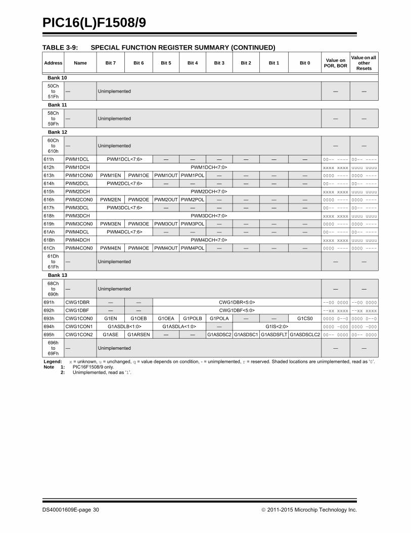
DS40001609E-page 30 2011-2015 Microchip Technology Inc.

PIC16(L)F1508/9
0000
0000
uuuu
-uuu
-uuu
uuuu
uuuu
uuuu
uuuu
0000
uuuu
-uuu
-uuu
uuuu
uuuu
uuuu
uuuu
0000
uuuu
-uuu
-uuu
uuuu
uuuu
uuuu
uuuu
0000
uuuu
-uuu
-uuu
uuuu
uuuu
uuuu
uuuu
0000
uuuu
uuuu
on all er ets
s ‘0’.
Banks 14-29
x0Ch/x8Ch —x1Fh/x9Fh
— Unimplemented — —
Bank 30
F0Chto
F0Eh— Unimplemented — —
F0Fh CLCDATA — — — — MLC4OUT MLC3OUT MLC2OUT MLC1OUT ---- 0000 ----
F10h CLC1CON LC1EN LC1OE LC1OUT LC1INTP LC1INTN LC1MODE<2:0> 0000 0000 0000
F11h CLC1POL LC1POL — — — LC1G4POL LC1G3POL LC1G2POL LC1G1POL 0--- xxxx 0---
F12h CLC1SEL0 — LC1D2S<2:0> — LC1D1S<2:0> -xxx -xxx -uuu
F13h CLC1SEL1 — LC1D4S<2:0> — LC1D3S<2:0> -xxx -xxx -uuu
F14h CLC1GLS0 LC1G1D4T LC1G1D4N LC1G1D3T LC1G1D3N LC1G1D2T LC1G1D2N LC1G1D1T LC1G1D1N xxxx xxxx uuuu
F15h CLC1GLS1 LC1G2D4T LC1G2D4N LC1G2D3T LC1G2D3N LC1G2D2T LC1G2D2N LC1G2D1T LC1G2D1N xxxx xxxx uuuu
F16h CLC1GLS2 LC1G3D4T LC1G3D4N LC1G3D3T LC1G3D3N LC1G3D2T LC1G3D2N LC1G3D1T LC1G3D1N xxxx xxxx uuuu
F17h CLC1GLS3 LC1G4D4T LC1G4D4N LC1G4D3T LC1G4D3N LC1G4D2T LC1G4D2N LC1G4D1T LC1G4D1N xxxx xxxx uuuu
F18h CLC2CON LC2EN LC2OE LC2OUT LC2INTP LC2INTN LC2MODE<2:0> 0000 0000 0000
F19h CLC2POL LC2POL — — — LC2G4POL LC2G3POL LC2G2POL LC2G1POL 0--- xxxx 0---
F1Ah CLC2SEL0 — LC2D2S<2:0> — LC2D1S<2:0> -xxx -xxx -uuu
F1Bh CLC2SEL1 — LC2D4S<2:0> — LC2D3S<2:0> -xxx -xxx -uuu
F1Ch CLC2GLS0 LC2G1D4T LC2G1D4N LC2G1D3T LC2G1D3N LC2G1D2T LC2G1D2N LC2G1D1T LC2G1D1N xxxx xxxx uuuu
F1Dh CLC2GLS1 LC2G2D4T LC2G2D4N LC2G2D3T LC2G2D3N LC2G2D2T LC2G2D2N LC2G2D1T LC2G2D1N xxxx xxxx uuuu
F1Eh CLC2GLS2 LC2G3D4T LC2G3D4N LC2G3D3T LC2G3D3N LC2G3D2T LC2G3D2N LC2G3D1T LC2G3D1N xxxx xxxx uuuu
F1Fh CLC2GLS3 LC2G4D4T LC2G4D4N LC2G4D3T LC2G4D3N LC2G4D2T LC2G4D2N LC2G4D1T LC2G4D1N xxxx xxxx uuuu
F20h CLC3CON LC3EN LC3OE LC3OUT LC3INTP LC3INTN LC3MODE<2:0> 0000 0000 0000
F21h CLC3POL LC3POL — — — LC3G4POL LC3G3POL LC3G2POL LC3G1POL 0--- xxxx 0---
F22h CLC3SEL0 — LC3D2S<2:0> — LC3D1S<2:0> -xxx -xxx -uuu
F23h CLC3SEL1 — LC3D4S<2:0> — LC3D3S<2:0> -xxx -xxx -uuu
F24h CLC3GLS0 LC3G1D4T LC3G1D4N LC3G1D3T LC3G1D3N LC3G1D2T LC3G1D2N LC3G1D1T LC3G1D1N xxxx xxxx uuuu
F25h CLC3GLS1 LC3G2D4T LC3G2D4N LC3G2D3T LC3G2D3N LC3G2D2T LC3G2D2N LC3G2D1T LC3G2D1N xxxx xxxx uuuu
F26h CLC3GLS2 LC3G3D4T LC3G3D4N LC3G3D3T LC3G3D3N LC3G3D2T LC3G3D2N LC3G3D1T LC3G3D1N xxxx xxxx uuuu
F27h CLC3GLS3 LC3G4D4T LC3G4D4N LC3G4D3T LC3G4D3N LC3G4D2T LC3G4D2N LC3G4D1T LC3G4D1N xxxx xxxx uuuu
F28h CLC4CON LC4EN LC4OE LC4OUT LC4INTP LC4INTN LC4MODE<2:0> 0000 0000 0000
F29h CLC4POL LC4POL — — — LC4G4POL LC4G3POL LC4G2POL LC4G1POL 0--- xxxx 0---
F2Ah CLC4SEL0 — LC4D2S<2:0> — LC4D1S<2:0> -xxx -xxx -uuu
F2Bh CLC4SEL1 — LC4D4S<2:0> — LC4D3S<2:0> -xxx -xxx -uuu
F2Ch CLC4GLS0 LC4G1D4T LC4G1D4N LC4G1D3T LC4G1D3N LC4G1D2T LC4G1D2N LC4G1D1T LC4G1D1N xxxx xxxx uuuu
F2Dh CLC4GLS1 LC4G2D4T LC4G2D4N LC4G2D3T LC4G2D3N LC4G2D2T LC4G2D2N LC4G2D1T LC4G2D1N xxxx xxxx uuuu
F2Eh CLC4GLS2 LC4G3D4T LC4G3D4N LC4G3D3T LC4G3D3N LC4G3D2T LC4G3D2N LC4G3D1T LC4G3D1N xxxx xxxx uuuu
F2Fh CLC4GLS3 LC4G4D4T LC4G4D4N LC4G4D3T LC4G4D3N LC4G4D2T LC4G4D2N LC4G4D1T LC4G4D1N xxxx xxxx uuuu
F20h CLC3CON LC3EN LC3OE LC3OUT LC3INTP LC3INTN LC3MODE<2:0> 0000 0000 0000
F21h CLC3POL LC3POL — — — LC3G4POL LC3G3POL LC3G2POL LC3G1POL 0--- xxxx 0---
F2Fh CLC4GLS3 LC4G4D4T LC4G4D4N LC4G4D3T LC4G4D3N LC4G4D2T LC4G4D2N LC4G4D1T LC4G4D1N xxxx xxxx uuuu
F30hto
F6Fh— Unimplemented — —
TABLE 3-9: SPECIAL FUNCTION REGISTER SUMMARY (CONTINUED)
Address Name Bit 7 Bit 6 Bit 5 Bit 4 Bit 3 Bit 2 Bit 1 Bit 0Value on
POR, BOR
Valueoth
Res
Legend: x = unknown, u = unchanged, q = value depends on condition, - = unimplemented, r = reserved. Shaded locations are unimplemented, read aNote 1: PIC16F1508/9 only.
2: Unimplemented, read as ‘1’.
2011-2015 Microchip Technology Inc. DS40001609E-page 31

PIC16(L)F1508/9
-uuu
uuuu
uuuu
uuuu
uuuu
uuuu
uuuu
uuuu
1111
uuuu
uuuu
on all er ets
s ‘0’.
Bank 31
F8Ch —FE3h
— Unimplemented — —
FE4h STATUS_
SHAD
— — — — — Z_SHAD DC_SHAD C_SHAD ---- -xxx ----
FE5h WREG_
SHAD
Working Register Shadow xxxx xxxx uuuu
FE6h BSR_
SHAD
— — — Bank Select Register Shadow ---x xxxx ---u
FE7h PCLATH_
SHAD
— Program Counter Latch High Register Shadow -xxx xxxx uuuu
FE8h FSR0L_
SHAD
Indirect Data Memory Address 0 Low Pointer Shadow xxxx xxxx uuuu
FE9h FSR0H_
SHAD
Indirect Data Memory Address 0 High Pointer Shadow xxxx xxxx uuuu
FEAh FSR1L_
SHAD
Indirect Data Memory Address 1 Low Pointer Shadow xxxx xxxx uuuu
FEBh FSR1H_
SHAD
Indirect Data Memory Address 1 High Pointer Shadow xxxx xxxx uuuu
FECh — Unimplemented — —
FEDh STKPTR — — — Current Stack Pointer ---1 1111 ---1
FEEh TOSL Top-of-Stack Low byte xxxx xxxx uuuu
FEFh TOSH — Top-of-Stack High byte -xxx xxxx -uuu
TABLE 3-9: SPECIAL FUNCTION REGISTER SUMMARY (CONTINUED)
Address Name Bit 7 Bit 6 Bit 5 Bit 4 Bit 3 Bit 2 Bit 1 Bit 0Value on
POR, BOR
Valueoth
Res
Legend: x = unknown, u = unchanged, q = value depends on condition, - = unimplemented, r = reserved. Shaded locations are unimplemented, read aNote 1: PIC16F1508/9 only.
2: Unimplemented, read as ‘1’.
DS40001609E-page 32 2011-2015 Microchip Technology Inc.

PIC16(L)F1508/9
3.4 PCL and PCLATH
The Program Counter (PC) is 15 bits wide. The low bytecomes from the PCL register, which is a readable andwritable register. The high byte (PC<14:8>) is not directlyreadable or writable and comes from PCLATH. On anyReset, the PC is cleared. Figure 3-3 shows the fivesituations for the loading of the PC.
FIGURE 3-3: LOADING OF PC IN DIFFERENT SITUATIONS
3.4.1 MODIFYING PCL
Executing any instruction with the PCL register as thedestination simultaneously causes the ProgramCounter PC<14:8> bits (PCH) to be replaced by thecontents of the PCLATH register. This allows the entirecontents of the program counter to be changed bywriting the desired upper seven bits to the PCLATHregister. When the lower eight bits are written to thePCL register, all 15 bits of the program counter willchange to the values contained in the PCLATH registerand those being written to the PCL register.
3.4.2 COMPUTED GOTO
A computed GOTO is accomplished by adding an offset tothe program counter (ADDWF PCL). When performing atable read using a computed GOTO method, care shouldbe exercised if the table location crosses a PCL memoryboundary (each 256-byte block). Refer to ApplicationNote AN556, “Implementing a Table Read” (DS00556).
3.4.3 COMPUTED FUNCTION CALLS
A computed function CALL allows programs to maintaintables of functions and provide another way to executestate machines or look-up tables. When performing atable read using a computed function CALL, careshould be exercised if the table location crosses a PCLmemory boundary (each 256-byte block).
If using the CALL instruction, the PCH<2:0> and PCLregisters are loaded with the operand of the CALLinstruction. PCH<6:3> is loaded with PCLATH<6:3>.
The CALLW instruction enables computed calls by com-bining PCLATH and W to form the destination address.A computed CALLW is accomplished by loading the Wregister with the desired address and executing CALLW.The PCL register is loaded with the value of W andPCH is loaded with PCLATH.
3.4.4 BRANCHING
The branching instructions add an offset to the PC.This allows relocatable code and code that crossespage boundaries. There are two forms of branching,BRW and BRA. The PC will have incremented to fetchthe next instruction in both cases. When using eitherbranching instruction, a PCL memory boundary may becrossed.
If using BRW, load the W register with the desiredunsigned address and execute BRW. The entire PC willbe loaded with the address PC + 1 + W.
If using BRA, the entire PC will be loaded with PC + 1 +,the signed value of the operand of the BRA instruction.
7 86
14
0
0
4 11
0
6 0
14
7 86 0
014
15
014
15
014
PCL
PCL
PCL
PCL
PCL
PCH
PCH
PCH
PCH
PCH
PC
PC
PC
PC
PC
PCLATH
PCLATH
PCLATH
Instructionwith PCL asDestination
GOTO, CALL
CALLW
BRW
BRA
ALU result
OPCODE <10:0>
W
PC + W
PC + OPCODE <8:0>
Rev. 10-000042A7/30/2013
2011-2015 Microchip Technology Inc. DS40001609E-page 33

PIC16(L)F1508/9
3.5 Stack
All devices have a 16-level x 15-bit wide hardwarestack (refer to Figures 3-4 through 3-7). The stackspace is not part of either program or data space. ThePC is PUSHed onto the stack when CALL or CALLWinstructions are executed or an interrupt causes abranch. The stack is POPed in the event of a RETURN,RETLW or a RETFIE instruction execution. PCLATH isnot affected by a PUSH or POP operation.
The stack operates as a circular buffer if the STVRENbit is programmed to ‘0‘ (Configuration Words). Thismeans that after the stack has been PUSHed sixteentimes, the seventeenth PUSH overwrites the value thatwas stored from the first PUSH. The eighteenth PUSHoverwrites the second PUSH (and so on). TheSTKOVF and STKUNF flag bits will be set on an Over-flow/Underflow, regardless of whether the Reset isenabled.
3.5.1 ACCESSING THE STACK
The stack is available through the TOSH, TOSL andSTKPTR registers. STKPTR is the current value of theStack Pointer. TOSH:TOSL register pair points to theTOP of the stack. Both registers are read/writable. TOSis split into TOSH and TOSL due to the 15-bit size of thePC. To access the stack, adjust the value of STKPTR,which will position TOSH:TOSL, then read/write toTOSH:TOSL. STKPTR is 5 bits to allow detection ofoverflow and underflow.
During normal program operation, CALL, CALLW andInterrupts will increment STKPTR while RETLW,RETURN, and RETFIE will decrement STKPTR. At anytime STKPTR can be inspected to see how much stackis left. The STKPTR always points at the currently usedplace on the stack. Therefore, a CALL or CALLW willincrement the STKPTR and then write the PC, and areturn will unload the PC and then decrement theSTKPTR.
Reference Figure 3-4 through Figure 3-7 for examplesof accessing the stack.
FIGURE 3-4: ACCESSING THE STACK EXAMPLE 1
Note 1: There are no instructions/mnemonicscalled PUSH or POP. These are actionsthat occur from the execution of theCALL, CALLW, RETURN, RETLW andRETFIE instructions or the vectoring toan interrupt address.
Note: Care should be taken when modifying theSTKPTR while interrupts are enabled.
STKPTR = 0x1FStack Reset Disabled(STVREN = 0)
Stack Reset Enabled(STVREN = 1)
Initial Stack Configuration:
After Reset, the stack is empty. Theempty stack is initialized so the StackPointer is pointing at 0x1F. If the StackOverflow/Underflow Reset is enabled, theTOSH/TOSL register will return ‘0’. If theStack Overflow/Underflow Reset isdisabled, the TOSH/TOSL register willreturn the contents of stack address0x0F.
0x0000 STKPTR = 0x1F
TOSH:TOSL 0x0F
0x0E
0x0D
0x0C
0x0B
0x0A
0x09
0x08
0x07
0x06
0x04
0x05
0x03
0x02
0x01
0x00
0x1FTOSH:TOSL
Rev. 10-000043A7/30/2013
DS40001609E-page 34 2011-2015 Microchip Technology Inc.

PIC16(L)F1508/9
FIGURE 3-5: ACCESSING THE STACK EXAMPLE 2
FIGURE 3-6: ACCESSING THE STACK EXAMPLE 3
STKPTR = 0x00Return Address
This figure shows the stack configurationafter the first CALL or a single interrupt.If a RETURN instruction is executed, thereturn address will be placed in theProgram Counter and the Stack Pointerdecremented to the empty state (0x1F).
0x0F
0x0E
0x0D
0x0C
0x0B
0x0A
0x09
0x08
0x07
0x06
0x04
0x05
0x03
0x02
0x01
0x00TOSH:TOSL
Rev. 10-000043B7/30/2013
STKPTR = 0x06
After seven CALLs or six CALLs and aninterrupt, the stack looks like the figure onthe left. A series of RETURN instructions willrepeatedly place the return addresses intothe Program Counter and pop the stack.
Return Address
0x0F
0x0E
0x0D
0x0C
0x0B
0x0A
0x09
0x08
0x07
0x06
0x04
0x05
0x03
0x02
0x01
0x00
Return Address
Return Address
Return Address
Return Address
Return Address
Return Address
TOSH:TOSL
Rev. 10-000043C7/30/2013
2011-2015 Microchip Technology Inc. DS40001609E-page 35

PIC16(L)F1508/9
FIGURE 3-7: ACCESSING THE STACK EXAMPLE 4
3.5.2 OVERFLOW/UNDERFLOW RESET
If the STVREN bit in Configuration Words isprogrammed to ‘1’, the device will be reset if the stackis PUSHed beyond the sixteenth level or POPedbeyond the first level, setting the appropriate bits(STKOVF or STKUNF, respectively) in the PCONregister.
3.6 Indirect Addressing
The INDFn registers are not physical registers. Anyinstruction that accesses an INDFn register actuallyaccesses the register at the address specified by theFile Select Registers (FSR). If the FSRn addressspecifies one of the two INDFn registers, the read willreturn ‘0’ and the write will not occur (though Status bitsmay be affected). The FSRn register value is createdby the pair FSRnH and FSRnL.
The FSR registers form a 16-bit address that allows anaddressing space with 65536 locations. These locationsare divided into three memory regions:
• Traditional Data Memory
• Linear Data Memory
• Program Flash Memory
STKPTR = 0x10
When the stack is full, the next CALL oran interrupt will set the Stack Pointer to0x10. This is identical to address 0x00 sothe stack will wrap and overwrite thereturn address at 0x00. If the StackOverflow/Underflow Reset is enabled, aReset will occur and location 0x00 willnot be overwritten.
Return Address0x0F
0x0E
0x0D
0x0C
0x0B
0x0A
0x09
0x08
0x07
0x06
0x04
0x05
0x03
0x02
0x01
0x00
Return Address
Return Address
Return Address
Return Address
Return Address
Return Address
Return Address
Return Address
Return Address
Return Address
Return Address
Return Address
Return Address
Return Address
Return AddressTOSH:TOSL
Rev. 10-000043D7/30/2013
DS40001609E-page 36 2011-2015 Microchip Technology Inc.

PIC16(L)F1508/9
FIGURE 3-8: INDIRECT ADDRESSING
0x0000
0x0FFF
0x0000
0x7FFF0xFFFF
0x0000
0x0FFF0x1000
0x1FFF0x2000
0x29AF0x29B0
0x7FFF0x8000
Reserved
Reserved
TraditionalData Memory
LinearData Memory
ProgramFlash Memory
FSRAddressRange
Note: Not all memory regions are completely implemented. Consult device memory tables for memory limits.
Rev. 10-000044A7/30/2013
2011-2015 Microchip Technology Inc. DS40001609E-page 37

PIC16(L)F1508/9
3.6.1 TRADITIONAL DATA MEMORY
The traditional data memory is a region from FSRaddress 0x000 to FSR address 0xFFF. The addressescorrespond to the absolute addresses of all SFR, GPRand common registers.
FIGURE 3-9: TRADITIONAL DATA MEMORY MAP
Direct Addressing
4 0BSR 6 0From Opcode
007 FSRxH
0 0 007 FSRxL
Indirect Addressing
00000 00001 00010 11111
Bank Select Location Select
0x00
0x7F
Bank Select Location Select
Bank 0 Bank 1 Bank 2 Bank 31
Rev. 10-000056A7/31/2013
DS40001609E-page 38 2011-2015 Microchip Technology Inc.

PIC16(L)F1508/9
3.6.2 LINEAR DATA MEMORY
The linear data memory is the region from FSRaddress 0x2000 to FSR address 0x29AF. This region isa virtual region that points back to the 80-byte blocks ofGPR memory in all the banks.
Unimplemented memory reads as 0x00. Use of thelinear data memory region allows buffers to be largerthan 80 bytes because incrementing the FSR beyondone bank will go directly to the GPR memory of the nextbank.
The 16 bytes of common memory are not included inthe linear data memory region.
FIGURE 3-10: LINEAR DATA MEMORY MAP
3.6.3 PROGRAM FLASH MEMORY
To make constant data access easier, the entireprogram Flash memory is mapped to the upper half ofthe FSR address space. When the MSb of FSRnH isset, the lower 15 bits are the address in programmemory which will be accessed through INDF. Only thelower eight bits of each memory location is accessiblevia INDF. Writing to the program Flash memory cannotbe accomplished via the FSR/INDF interface. Allinstructions that access program Flash memory via theFSR/INDF interface will require one additionalinstruction cycle to complete.
FIGURE 3-11: PROGRAM FLASH MEMORY MAP
0x020Bank 00x06F
0x0A0Bank 10x0EF
0x120Bank 20x16F
0xF20Bank 300xF6F
0 0 10 07 7FSRnH FSRnL
Location Select 0x2000
0x29AF
Rev. 10-000057A7/31/2013
0x0000
Program Flash
Memory (low 8 bits)
0x7FFF
10 07 7FSRnH FSRnL
Location Select 0x8000
0xFFFF
Rev. 10-000058A7/31/2013
2011-2015 Microchip Technology Inc. DS40001609E-page 39

PIC16(L)F1508/9
4.0 DEVICE CONFIGURATION
Device configuration consists of Configuration Words,Code Protection and Device ID.
4.1 Configuration Words
There are several Configuration Word bits that allowdifferent oscillator and memory protection options.These are implemented as Configuration Word 1 at8007h and Configuration Word 2 at 8008h.
Note: The DEBUG bit in Configuration Words ismanaged automatically by devicedevelopment tools including debuggersand programmers. For normal deviceoperation, this bit should be maintained asa ‘1’.
DS40001609E-page 40 2011-2015 Microchip Technology Inc.

PIC16(L)F1508/9
4.2 Register Definitions: Configuration Words
REGISTER 4-1: CONFIG1: CONFIGURATION WORD 1
R/P-1 R/P-1 R/P-1 R/P-1 R/P-1 U-1
FCMEN(1) IESO(1) CLKOUTEN BOREN<1:0>(2) —
bit 13 bit 8
R/P-1 R/P-1 R/P-1 R/P-1 R/P-1 R/P-1 R/P-1 R/P-1
CP(3) MCLRE PWRTE WDTE<1:0> FOSC<2:0>
bit 7 bit 0
Legend:
R = Readable bit P = Programmable bit U = Unimplemented bit, read as ‘1’
‘0’ = Bit is cleared ‘1’ = Bit is set -n = Value when blank or after Bulk Erase
bit 13 FCMEN: Fail-Safe Clock Monitor Enable bit1 = Fail-Safe Clock Monitor is enabled(1)
0 = Fail-Safe Clock Monitor is disabled
bit 12 IESO: Internal External Switchover bit(1)
1 = Internal/External Switchover (Two-Speed Start-up) mode is enabled0 = Internal/External Switchover mode is disabled
bit 11 CLKOUTEN: Clock Out Enable bit1 = CLKOUT function is disabled. I/O function on the CLKOUT pin0 = CLKOUT function is enabled on the CLKOUT pin
bit 10-9 BOREN<1:0>: Brown-Out Reset Enable bits(2)
11 = BOR enabled10 = BOR enabled during operation and disabled in Sleep01 = BOR controlled by SBOREN bit of the BORCON register00 = BOR disabled
bit 8 Unimplemented: Read as ‘1’
bit 7 CP: Code Protection bit(3)
1 = Program memory code protection is disabled0 = Program memory code protection is enabled
bit 6 MCLRE: MCLR/VPP Pin Function Select bitIf LVP bit = 1:
This bit is ignored.If LVP bit = 0:
1 = MCLR/VPP pin function is MCLR; Weak pull-up enabled.0 = MCLR/VPP pin function is digital input; MCLR internally disabled; Weak pull-up under control of
WPUA3 bit.
bit 5 PWRTE: Power-Up Timer Enable bit1 = PWRT disabled0 = PWRT enabled
bit 4-3 WDTE<1:0>: Watchdog Timer Enable bits11 = WDT enabled10 = WDT enabled while running and disabled in Sleep01 = WDT controlled by the SWDTEN bit in the WDTCON register00 = WDT disabled
2011-2015 Microchip Technology Inc. DS40001609E-page 41

PIC16(L)F1508/9
bit 2-0 FOSC<2:0>: Oscillator Selection bits111 = ECH:External clock, High-Power mode: on CLKIN pin110 = ECM: External clock, Medium Power mode: on CLKIN pin101 = ECL: External clock, Low-Power mode: on CLKIN pin100 = INTOSC oscillator: I/O function on CLKIN pin011 = EXTRC oscillator: External RC circuit connected to CLKIN pin010 = HS oscillator: High-speed crystal/resonator connected between OSC1 and OSC2 pins001 = XT oscillator: Crystal/resonator connected between OSC1 and OSC2 pins000 = LP oscillator: Low-power crystal connected between OSC1 and OSC2 pins
Note 1: When FSCM is enabled, Two-Speed Start-up will be automatically enabled, regardless of the IESO bit value.2: Enabling Brown-out Reset does not automatically enable Power-up Timer.3: Once enabled, code-protect can only be disabled by bulk erasing the device.
REGISTER 4-1: CONFIG1: CONFIGURATION WORD 1 (CONTINUED)
DS40001609E-page 42 2011-2015 Microchip Technology Inc.

PIC16(L)F1508/9
REGISTER 4-2: CONFIG2: CONFIGURATION WORD 2
R/P-1 R/P-1 R/P-1 R/P-1 R/P-1 U-1
LVP(1) DEBUG(3) LPBOR BORV(2) STVREN —
bit 13 bit 8
U-1 U-1 U-1 U-1 U-1 U-1 R/P-1 R/P-1
— — — — — — WRT<1:0>
bit 7 bit 0
Legend:
R = Readable bit P = Programmable bit U = Unimplemented bit, read as ‘1’
‘0’ = Bit is cleared ‘1’ = Bit is set -n = Value when blank or after Bulk Erase
bit 13 LVP: Low-Voltage Programming Enable bit(1)
1 = Low-voltage programming enabled0 = High-voltage on MCLR must be used for programming
bit 12 DEBUG: In-Circuit Debugger Mode bit(3)
1 = In-Circuit Debugger disabled, ICSPCLK and ICSPDAT are general purpose I/O pins0 = In-Circuit Debugger enabled, ICSPCLK and ICSPDAT are dedicated to the debugger
bit 11 LPBOR: Low-Power BOR Enable bit1 = Low-Power Brown-out Reset is disabled0 = Low-Power Brown-out Reset is enabled
bit 10 BORV: Brown-Out Reset Voltage Selection bit(2)
1 = Brown-out Reset voltage (VBOR), low trip point selected0 = Brown-out Reset voltage (VBOR), high trip point selected
bit 9 STVREN: Stack Overflow/Underflow Reset Enable bit1 = Stack Overflow or Underflow will cause a Reset0 = Stack Overflow or Underflow will not cause a Reset
bit 8-2 Unimplemented: Read as ‘1’
bit 1-0 WRT<1:0>: Flash Memory Self-Write Protection bits4 kW Flash memory (PIC16(L)F1508/9 only)
11 = Write protection off10 = 000h to 1FFh write protected, 200h to FFFh may be modified01 = 000h to 7FFh write protected, 800h to FFFh may be modified00 = 000h to FFFh write protected, no addresses may be modified
8 kW Flash memory (PIC16(L)F1509 only)11 = Write protection off10 = 0000h to 01FFh write protected, 0200h to 1FFFh may be modified01 = 0000h to 0FFFh write protected, 1000h to 1FFFh may be modified00 = 0000h to 1FFFh write protected, no addresses may be modified
Note 1: The LVP bit cannot be programmed to ‘0’ when Programming mode is entered via LVP.
2: See VBOR parameter for specific trip point voltages.
3: The DEBUG bit in Configuration Words is managed automatically by device development tools including debuggers and programmers. For normal device operation, this bit should be maintained as a ‘1’.
2011-2015 Microchip Technology Inc. DS40001609E-page 43
PIC16(L)F1508/9
4.3 Code Protection
Code protection allows the device to be protected fromunauthorized access. Internal access to the programmemory is unaffected by any code protection setting.
4.3.1 PROGRAM MEMORY PROTECTION
The entire program memory space is protected fromexternal reads and writes by the CP bit in ConfigurationWords. When CP = 0, external reads and writes ofprogram memory are inhibited and a read will return all‘0’s. The CPU can continue to read program memory,regardless of the protection bit settings. Writing theprogram memory is dependent upon the writeprotection setting. See Section 4.4 “WriteProtection” for more information.
4.4 Write Protection
Write protection allows the device to be protected fromunintended self-writes. Applications, such asbootloader software, can be protected while allowingother regions of the program memory to be modified.
The WRT<1:0> bits in Configuration Words define thesize of the program memory block that is protected.
4.5 User ID
Four memory locations (8000h-8003h) are designated asID locations where the user can store checksum or othercode identification numbers. These locations arereadable and writable during normal execution. SeeSection 10.4 “User ID, Device ID and ConfigurationWord Access” for more information on accessing thesememory locations. For more information on checksumcalculation, see the “PIC12(L)F1501/PIC16(L)F150XMemory Programming Specification” (DS41573).
DS40001609E-page 44 2011-2015 Microchip Technology Inc.
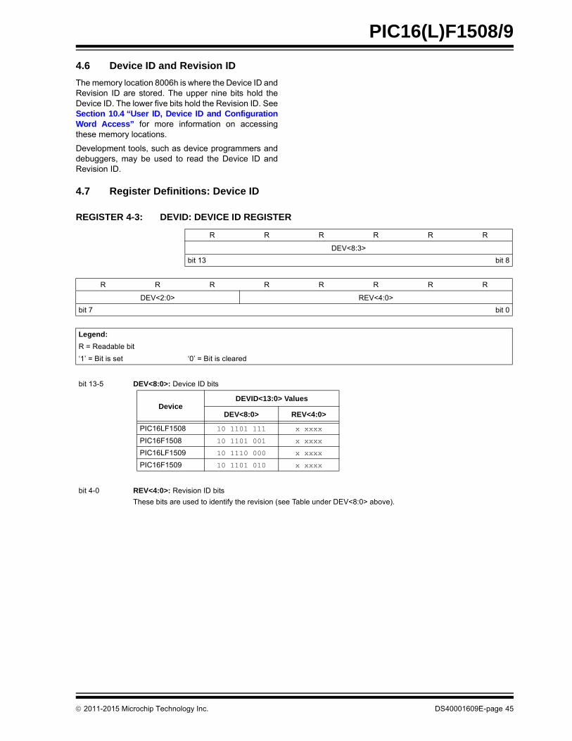
PIC16(L)F1508/9
4.6 Device ID and Revision ID
The memory location 8006h is where the Device ID andRevision ID are stored. The upper nine bits hold theDevice ID. The lower five bits hold the Revision ID. SeeSection 10.4 “User ID, Device ID and ConfigurationWord Access” for more information on accessingthese memory locations.
Development tools, such as device programmers anddebuggers, may be used to read the Device ID andRevision ID.
4.7 Register Definitions: Device ID
REGISTER 4-3: DEVID: DEVICE ID REGISTER
R R R R R R
DEV<8:3>
bit 13 bit 8
R R R R R R R R
DEV<2:0> REV<4:0>
bit 7 bit 0
Legend:
R = Readable bit
‘1’ = Bit is set ‘0’ = Bit is cleared
bit 13-5 DEV<8:0>: Device ID bits
bit 4-0 REV<4:0>: Revision ID bits
These bits are used to identify the revision (see Table under DEV<8:0> above).
DeviceDEVID<13:0> Values
DEV<8:0> REV<4:0>
PIC16LF1508 10 1101 111 x xxxx
PIC16F1508 10 1101 001 x xxxx
PIC16LF1509 10 1110 000 x xxxx
PIC16F1509 10 1101 010 x xxxx
2011-2015 Microchip Technology Inc. DS40001609E-page 45

PIC16(L)F1508/9
5.0 OSCILLATOR MODULE (WITH FAIL-SAFE CLOCK MONITOR)
5.1 Overview
The oscillator module has a wide variety of clocksources and selection features that allow it to be usedin a wide range of applications while maximizing perfor-mance and minimizing power consumption. Figure 5-1illustrates a block diagram of the oscillator module.
Clock sources can be supplied from external oscillators,quartz crystal resonators, ceramic resonators andResistor-Capacitor (RC) circuits. In addition, the systemclock source can be supplied from one of two internaloscillators, with a choice of speeds selectable viasoftware. Additional clock features include:
• Selectable system clock source between external or internal sources via software.
• Two-Speed Start-up mode, which minimizes latency between external oscillator start-up and code execution.
• Fail-Safe Clock Monitor (FSCM) designed to detect a failure of the external clock source (LP, XT, HS, ECH, ECM, ECL or EXTRC modes) and switch automatically to the internal oscillator.
• Oscillator Start-up Timer (OST) ensures stability of crystal oscillator sources
• Fast start-up oscillator allows internal circuits to power-up and stabilize before switching to the 16 MHz HFINTOSC
The oscillator module can be configured in one of thefollowing clock modes.
1. ECL – External Clock Low-Power mode(0 MHz to 0.5 MHz)
2. ECM – External Clock Medium Power mode(0.5 MHz to 4 MHz)
3. ECH – External Clock High-Power mode(4 MHz to 20 MHz)
4. LP – 32 kHz Low-Power Crystal mode.
5. XT – Medium Gain Crystal or Ceramic ResonatorOscillator mode (up to 4 MHz)
6. HS – High Gain Crystal or Ceramic Resonatormode (4 MHz to 20 MHz)
7. EXTRC – External Resistor-Capacitor
8. INTOSC – Internal oscillator (31 kHz to 16 MHz)
Clock Source modes are selected by the FOSC<2:0>bits in the Configuration Words. The FOSC bitsdetermine the type of oscillator that will be used whenthe device is first powered.
The ECH, ECM, and ECL clock modes rely on anexternal logic level signal as the device clock source.The LP, XT, and HS clock modes require an externalcrystal or resonator to be connected to the device.Each mode is optimized for a different frequency range.The EXTRC clock mode requires an external resistorand capacitor to set the oscillator frequency.
The INTOSC internal oscillator block produces a lowand high-frequency clock source, designatedLFINTOSC and HFINTOSC. (See Internal OscillatorBlock, Figure 5-1). A wide selection of device clockfrequencies may be derived from these two clocksources.
DS40001609E-page 46 2011-2015 Microchip Technology Inc.

PIC16(L)F1508/9
FIGURE 5-1: SIMPLIFIED PIC® MCU CLOCK SOURCE BLOCK DIAGRAM
PrimaryOscillator
(OSC)
SecondaryOscillator(SOSC)
CLKIN/ OSC1/SOSCI/ T1CKI
CLKOUT/ OSC2/SOSCO/ T1G
Start-upControl Logic
16 MHzOscillator
Fast Start-upOscillator
31 kHzOscillator
Pre
scal
er
HFINTOSC(1)
16 MHz
8 MHz
4 MHz
2 MHz
1 MHz
*500 kHz
*250 kHz
*125 kHz
62.5 kHz
*31.25 kHz
*31 kHz
IRCF<3:0>
4
INTOSC
Secondary Clock(1)
Primary Clock
HFINTOSC
LFINTOSC
to CPU andPeripherals
Sleep
FOSC(1)
LFINTOSC(1)
to WDT, PWRT, andother Peripherals
* Available with more than one IRCF selection
ClockControl
FOSC<2:0> SCS<1:0>
3 2
600 kHzOscillator
FRCFRC(1)
to ADC andother Peripherals
Rev. 10-000030A7/30/2013
Note 1: See Section 5.2.2.4 “Peripheral Clock Sources”.
2011-2015 Microchip Technology Inc. DS40001609E-page 47

PIC16(L)F1508/9
5.2 Clock Source Types
Clock sources can be classified as external, internal orperipheral.
External clock sources rely on external circuitry for theclock source to function. Examples are: oscillator mod-ules (ECH, ECM, ECL modes), quartz crystal resona-tors or ceramic resonators (LP, XT and HS modes) andResistor-Capacitor (EXTRC) mode circuits.
Internal clock sources are contained within the oscillatormodule. The internal oscillator block has two internaloscillators that are used to generate the internal systemclock sources: the 16 MHz High-Frequency InternalOscillator (HFINTOSC) and the 31 kHz Low-FrequencyInternal Oscillator (LFINTOSC).
The peripheral clock source is a nominal 600 kHzinternal RC oscillator, FRC. The FRC is traditionallyused with the ADC module, but is sometimes availableto other peripherals. See Section 5.2.2.4 “PeripheralClock Sources”.
The system clock can be selected between external orinternal clock sources via the System Clock Select(SCS) bits in the OSCCON register. See Section5.3 “Clock Switching” for additional information.
5.2.1 EXTERNAL CLOCK SOURCES
An external clock source can be used as the devicesystem clock by performing one of the followingactions:
• Program the FOSC<2:0> bits in the Configuration Words to select an external clock source that will be used as the default system clock upon a device Reset.
• Write the SCS<1:0> bits in the OSCCON register to switch the system clock source to:
- Secondary oscillator during run-time, or
- An external clock source determined by the value of the FOSC bits.
See Section 5.3 “Clock Switching” for more informa-tion.
5.2.1.1 EC Mode
The External Clock (EC) mode allows an externallygenerated logic level signal to be the system clocksource. When operating in this mode, an external clocksource is connected to the OSC1 input.OSC2/CLKOUT is available for general purpose I/O orCLKOUT. Figure 5-2 shows the pin connections for ECmode.
EC mode has three power modes to select from throughthe FOSC bits in the Configuration Words:
• ECH – High-power, 4-20 MHz
• ECM – Medium-power, 0.5-4 MHz
• ECL – Low-power, 0-0.5 MHz
The Oscillator Start-up Timer (OST) is disabled whenEC mode is selected. Therefore, there is no delay inoperation after a Power-on Reset (POR) or wake-upfrom Sleep. Because the PIC® MCU design is fullystatic, stopping the external clock input will have theeffect of halting the device while leaving all data intact.Upon restarting the external clock, the device willresume operation as if no time had elapsed.
FIGURE 5-2: EXTERNAL CLOCK (EC) MODE OPERATION
5.2.1.2 LP, XT, HS Modes
The LP, XT and HS modes support the use of quartzcrystal resonators or ceramic resonators connected toOSC1 and OSC2 (Figure 5-3). The three modes selecta low, medium or high gain setting of the internalinverter-amplifier to support various resonator typesand speed.
LP Oscillator mode selects the lowest gain setting of theinternal inverter-amplifier. LP mode current consumptionis the least of the three modes. This mode is designed todrive only 32.768 kHz tuning-fork type crystals (watchcrystals).
XT Oscillator mode selects the intermediate gainsetting of the internal inverter-amplifier. XT modecurrent consumption is the medium of the three modes.This mode is best suited to drive resonators with amedium drive level specification.
HS Oscillator mode selects the highest gain setting of theinternal inverter-amplifier. HS mode current consumptionis the highest of the three modes. This mode is bestsuited for resonators that require a high drive setting.
Figure 5-3 and Figure 5-4 show typical circuits forquartz crystal and ceramic resonators, respectively.
Clock fromExt. system
FOSC/4 or I/O(1)
OSC1/CLKIN
PIC® MCU
OSC2/CLKOUT
Note 1: Output depends upon the CLKOUTEN bitof the Configuration Words.
Rev. 10-000045A7/30/2013
DS40001609E-page 48 2011-2015 Microchip Technology Inc.

PIC16(L)F1508/9
FIGURE 5-3: QUARTZ CRYSTAL OPERATION (LP, XT OR HS MODE)
FIGURE 5-4: CERAMIC RESONATOR OPERATION(XT OR HS MODE)
5.2.1.3 Oscillator Start-up Timer (OST)
If the oscillator module is configured for LP, XT or HSmodes, the Oscillator Start-up Timer (OST) counts1024 oscillations from OSC1. This occurs following aPower-on Reset (POR) and when the Power-up Timer(PWRT) has expired (if configured), or a wake-up fromSleep. During this time, the program counter does notincrement and program execution is suspended,unless either FSCM or Two-Speed Start-Up areenabled. In this case, code will continue to execute atthe selected INTOSC frequency while the OST iscounting. The OST ensures that the oscillator circuit,using a quartz crystal resonator or ceramic resonator,has started and is providing a stable system clock tothe oscillator module.
In order to minimize latency between external oscillatorstart-up and code execution, the Two-Speed ClockStart-up mode can be selected (see Section5.4 “Two-Speed Clock Start-up Mode”).
Note 1: Quartz crystal characteristics varyaccording to type, package andmanufacturer. The user should consult themanufacturer data sheets for specificationsand recommended application.
2: Always verify oscillator performance overthe VDD and temperature range that isexpected for the application.
3: For oscillator design assistance, referencethe following Microchip Applications Notes:
• AN826, “Crystal Oscillator Basics and Crystal Selection for rfPIC® and PIC® Devices” (DS00826)
• AN849, “Basic PIC® Oscillator Design” (DS00849)
• AN943, “Practical PIC® Oscillator Analysis and Design” (DS00943)
• AN949, “Making Your Oscillator Work” (DS00949)
RS(1)
OSC1/CLKIN
PIC® MCU
OSC2/CLKOUT
Note 1: A series resistor (Rs) may be required forquartz crystals with low drive level.
2: The value of RF varies with the Oscillator modeselected (typically between 2 MΩ and 10 MΩ).
RF(2)
C2
C1 To InternalLogic
SleepQuartzCrystal
Rev. 10-000059A7/30/2013
RS(1)
OSC1/CLKIN
PIC® MCU
OSC2/CLKOUT
Note 1: A series resistor (Rs) may be required forceramic resonators with low drive level.
2: The value of RF varies with the Oscillator modeselected (typically between 2 MΩ and 10 MΩ).
3. An additional parallel feedback resistor (RP)may be required for proper ceramic resonatoroperation.
RF(2)
C2
C1 To InternalLogic
SleepRP(3)
CeramicResonator
Rev. 10-000060A7/30/2013
2011-2015 Microchip Technology Inc. DS40001609E-page 49

PIC16(L)F1508/9
5.2.1.4 Secondary Oscillator
The secondary oscillator is a separate crystal oscillatorthat is associated with the Timer1 peripheral. It is opti-mized for timekeeping operations with a 32.768 kHzcrystal connected between the SOSCO and SOSCIdevice pins.
The secondary oscillator can be used as an alternatesystem clock source and can be selected duringrun-time using clock switching. Refer to Section5.3 “Clock Switching” for more information.
FIGURE 5-5: QUARTZ CRYSTAL OPERATION (SECONDARY OSCILLATOR)
5.2.1.5 External RC Mode
The External Resistor-Capacitor (EXTRC) modesupports the use of an external RC circuit. This allows thedesigner maximum flexibility in frequency choice whilekeeping costs to a minimum when clock accuracy is notrequired.
The RC circuit connects to OSC1. OSC2/CLKOUT isavailable for general purpose I/O or CLKOUT. Thefunction of the OSC2/CLKOUT pin is determined by theCLKOUTEN bit in Configuration Words.
Figure 5-6 shows the External RC mode connections.
FIGURE 5-6: EXTERNAL RC MODES
The RC oscillator frequency is a function of the supplyvoltage, the resistor (REXT) and capacitor (CEXT) valuesand the operating temperature. Other factors affectingthe oscillator frequency are:
• threshold voltage variation• component tolerances• packaging variations in capacitance
The user also needs to take into account variation dueto tolerance of the external RC components used.
Note 1: Quartz crystal characteristics varyaccording to type, package andmanufacturer. The user should consult themanufacturer data sheets for specificationsand recommended application.
2: Always verify oscillator performance overthe VDD and temperature range that isexpected for the application.
3: For oscillator design assistance, referencethe following Microchip Applications Notes:
• AN826, “Crystal Oscillator Basics and Crystal Selection for rfPIC® and PIC® Devices” (DS00826)
• AN849, “Basic PIC® Oscillator Design” (DS00849)
• AN943, “Practical PIC® Oscillator Analysis and Design” (DS00943)
• AN949, “Making Your Oscillator Work” (DS00949)
• TB097, “Interfacing a Micro Crystal MS1V-T1K 32.768 kHz Tuning Fork Crystal to a PIC16F690/SS” (DS91097)
• AN1288, “Design Practices for Low-Power External Oscillators” (DS01288)
SOSCI
PIC® MCU
SOSCOC2
C1 To InternalLogic32.768 kHz
QuartzCrystal
Rev. 10-000061A7/30/2013
FOSC/4 or I/O(1)
PIC® MCU
OSC2/CLKOUT
Note 1: Output depends upon the CLKOUTEN bit of the Configuration Words.
OSC1/CLKIN Internal Clock
VSS
CEXT
REXT
Recommended values:10 k REXT 100 k , <3V3 k REXT 100 k , 3-5VCEXT > 20 pF, 2-5V
Rev. 10-000062A7/31/2013
VDD
DS40001609E-page 50 2011-2015 Microchip Technology Inc.

PIC16(L)F1508/9
5.2.2 INTERNAL CLOCK SOURCES
The device may be configured to use the internal oscil-lator block as the system clock by performing one of thefollowing actions:
• Program the FOSC<2:0> bits in Configuration Words to select the INTOSC clock source, which will be used as the default system clock upon a device Reset.
• Write the SCS<1:0> bits in the OSCCON register to switch the system clock source to the internal oscillator during run-time. See Section 5.3 “Clock Switching”for more information.
In INTOSC mode, OSC1/CLKIN is available for generalpurpose I/O. OSC2/CLKOUT is available for generalpurpose I/O or CLKOUT.
The function of the OSC2/CLKOUT pin is determinedby the CLKOUTEN bit in Configuration Words.
The internal oscillator block has two independentoscillators that provides the internal system clocksource.
1. The HFINTOSC (High-Frequency InternalOscillator) is factory calibrated and operates at16 MHz.
2. The LFINTOSC (Low-Frequency InternalOscillator) operates at 31 kHz.
5.2.2.1 HFINTOSC
The High-Frequency Internal Oscillator (HFINTOSC) isa factory calibrated 16 MHz internal clock source.
The output of the HFINTOSC connects to a postscalerand multiplexer (see Figure 5-1). The frequency derivedfrom the HFINTOSC can be selected via software usingthe IRCF<3:0> bits of the OSCCON register. SeeSection 5.2.2.6 “Internal Oscillator Clock SwitchTiming” for more information.
The HFINTOSC is enabled by:
• Configure the IRCF<3:0> bits of the OSCCON register for the desired HF frequency, and
• FOSC<2:0> = 100, or
• Set the System Clock Source (SCS) bits of the OSCCON register to ‘1x’.
A fast start-up oscillator allows internal circuits topower-up and stabilize before switching to HFINTOSC.
The High-Frequency Internal Oscillator Ready bit(HFIOFR) of the OSCSTAT register indicates when theHFINTOSC is running.
The High-Frequency Internal Oscillator Stable bit(HFIOFS) of the OSCSTAT register indicates when theHFINTOSC is running within 0.5% of its final value.
5.2.2.2 LFINTOSC
The Low-Frequency Internal Oscillator (LFINTOSC) isa 31 kHz internal clock source.
The output of the LFINTOSC connects to a multiplexer(see Figure 5-1). Select 31 kHz, via software, using theIRCF<3:0> bits of the OSCCON register. See Section5.2.2.6 “Internal Oscillator Clock Switch Timing” formore information. The LFINTOSC is also the frequencyfor the Power-up Timer (PWRT), Watchdog Timer(WDT) and Fail-Safe Clock Monitor (FSCM).
The LFINTOSC is enabled by selecting 31 kHz(IRCF<3:0> bits of the OSCCON register = 000) as thesystem clock source (SCS bits of the OSCCONregister = 1x), or when any of the following areenabled:
• Configure the IRCF<3:0> bits of the OSCCON register for the desired LF frequency, and
• FOSC<2:0> = 100, or
• Set the System Clock Source (SCS) bits of the OSCCON register to ‘1x’.
Peripherals that use the LFINTOSC are:
• Power-up Timer (PWRT)
• Watchdog Timer (WDT)
• Fail-Safe Clock Monitor (FSCM)
The Low-Frequency Internal Oscillator Ready bit(LFIOFR) of the OSCSTAT register indicates when theLFINTOSC is running.
5.2.2.3 FRC
The FRC clock is an uncalibrated, nominal 600 kHzperipheral clock source.
The FRC is automatically turned on by the peripheralsrequesting the FRC clock.
The FRC clock continues to run during Sleep.
2011-2015 Microchip Technology Inc. DS40001609E-page 51
PIC16(L)F1508/9
5.2.2.4 Peripheral Clock Sources
The clock sources described in this chapter and theTimer’s are available to different peripherals. Table 5-1lists the clocks and timers available for each peripheral.
5.2.2.5 Internal Oscillator Frequency Selection
The system clock speed can be selected via softwareusing the Internal Oscillator Frequency Select bitsIRCF<3:0> of the OSCCON register.
The postscaled output of the 16 MHz HFINTOSC and31 kHz LFINTOSC connect to a multiplexer (seeFigure 5-1). The Internal Oscillator Frequency Selectbits IRCF<3:0> of the OSCCON register (Register 5-1)select the frequency output of the internal oscillators.
The IRCF<3:0> bits of the OSCCON register allowduplicate selections for some frequencies. These dupli-cate choices can offer system design trade-offs. Lowerpower consumption can be obtained when changingoscillator sources for a given frequency. Faster transi-tion times can be obtained between frequency changesthat use the same oscillator source.
5.2.2.6 Internal Oscillator Clock Switch Timing
When switching between the HFINTOSC and theLFINTOSC, the new oscillator may already be shutdown to save power (see Figure 5-7). If this is the case,there is a delay after the IRCF<3:0> bits of theOSCCON register are modified before the frequencyselection takes place. The OSCSTAT register willreflect the current active status of the HFINTOSC andLFINTOSC oscillators. The sequence of a frequencyselection is as follows:
1. IRCF<3:0> bits of the OSCCON register aremodified.
2. If the new clock is shut down, a clock start-updelay is started.
3. Clock switch circuitry waits for a falling edge ofthe current clock.
4. The current clock is held low and the clockswitch circuitry waits for a rising edge in the newclock.
5. The new clock is now active.
6. The OSCSTAT register is updated as required.
7. Clock switch is complete.
See Figure 5-7 for more details.
If the internal oscillator speed is switched between twoclocks of the same source, there is no start-up delaybefore the new frequency is selected. Clock switchingtime delays are shown in Table 5-3.
Start-up delay specifications are located in Table 29-8,“Oscillator Parameters”.
TABLE 5-1: PERIPHERAL CLOCK SOURCES
FO
SC
FR
C
HF
INT
OS
C
LF
INT
OS
C
TM
R0
TM
R1
TM
R2
SO
SC
ADC ● ●
CLC ● ● ● ● ● ● ● ●
COMP ● ●
CWG ● ●
EUSART ● ●
MSSP ● ●
NCO ● ●
PWM ● ●
PWRT ●
TMR0 ●
TMR1 ● ● ●
TMR2 ●
WDT ●
Note: Following any Reset, the IRCF<3:0> bitsof the OSCCON register are set to ‘0111’and the frequency selection is set to500 kHz. The user can modify the IRCFbits to select a different frequency.
DS40001609E-page 52 2011-2015 Microchip Technology Inc.

PIC16(L)F1508/9
FIGURE 5-7: INTERNAL OSCILLATOR SWITCH TIMING
HFINTOSC
LFINTOSC
IRCF <3:0>
System Clock
HFINTOSC
LFINTOSC
IRCF <3:0>
System Clock
0 0
0 0
2-cycle Sync Running
2-cycle Sync Running
HFINTOSC LFINTOSC (FSCM and WDT disabled)
HFINTOSC LFINTOSC (Either FSCM or WDT enabled)
LFINTOSC
HFINTOSC
IRCF <3:0>
System Clock
= 0 0
2-cycle Sync Running
LFINTOSC HFINTOSCLFINTOSC turns off unless WDT or FSCM is enabled(2)
Note 1: See Table 5-3, “Oscillator Switching Delays” for more information.
2: LFINTOSC will continue to run if a peripheral has selected it as the clock source. See Section 5.2.2.4 “Peripheral Clock Sources”.
Oscillator Delay(1)
Oscillator Delay(1)
2011-2015 Microchip Technology Inc. DS40001609E-page 53

PIC16(L)F1508/9
5.3 Clock Switching
The system clock source can be switched betweenexternal and internal clock sources via software usingthe System Clock Select (SCS) bits of the OSCCONregister. The following clock sources can be selectedusing the SCS bits:
• Default system oscillator determined by FOSC bits in Configuration Words
• Secondary oscillator 32 kHz crystal
• Internal Oscillator Block (INTOSC)
5.3.1 SYSTEM CLOCK SELECT (SCS) BITS
The System Clock Select (SCS) bits of the OSCCONregister selects the system clock source that is used forthe CPU and peripherals.
• When the SCS bits of the OSCCON register = 00, the system clock source is determined by value of the FOSC<2:0> bits in the Configuration Words.
• When the SCS bits of the OSCCON register = 01, the system clock source is the secondary oscillator.
• When the SCS bits of the OSCCON register = 1x, the system clock source is chosen by the internal oscillator frequency selected by the IRCF<3:0> bits of the OSCCON register. After a Reset, the SCS bits of the OSCCON register are always cleared.
When switching between clock sources, a delay isrequired to allow the new clock to stabilize. These oscil-lator delays are shown in Table 5-3.
5.3.2 OSCILLATOR START-UP TIMER STATUS (OSTS) BIT
The Oscillator Start-up Timer Status (OSTS) bit in theOSCSTAT register has different definitions that aredependent on the FOSC bit selection in theConfiguration Word. Table 5-2 defines the OSTS bitvalue for the FOSC selections.
The normal function of the OSTS bit is whenFOSC<2:0> selects one of the external oscillatormodes, HS, XT or LP, while the OST is counting pulseson the OSC1 pin from the external oscillator,OSTS = 0. When the OST has counted 1024 pulses,the OSTS bit should be set, OSTS = 1, indicating theoscillator is stable and ready to be used.
When Fail-Safe Clock Monitor and/or Two-SpeedStart-up are enabled, (FCMEN = 1 and/or IESO = 1),the device will operate using the internal oscillator(INTOSC) selected by the IRCF<3:0> bits, wheneverOSTS = 0. When the OST period expires,(OSTS = 1), the system clock will switch to the externaloscillator selected.
When Fail-Safe Clock Monitor and Two-Speed Start-upare disabled, (FCMEN = 0 and IESO = 0), the devicewill be held in Reset while OSTS = 0. When OSTperiod expires, (OSTS = 1), Reset will be released andexecution will begin 10 FOSC cycles later using theexternal oscillator selected.
For definition of the OSTS bit with clock sources otherthan external oscillator modes (HS, XT or LP), seeTable 5-2.
The OSTS bit does not reflect the status of thesecondary oscillator.
5.3.3 SECONDARY OSCILLATOR
The secondary oscillator is a separate crystal oscillatorassociated with the Timer1 peripheral. It is optimizedfor timekeeping operations with a 32.768 kHz crystalconnected between the SOSCO and SOSCI devicepins.
The secondary oscillator is enabled using theT1OSCEN control bit in the T1CON register. SeeSection 19.0 “Timer1 Module with Gate Control” formore information about the Timer1 peripheral.
5.3.4 SECONDARY OSCILLATOR READY (SOSCR) BIT
The user must ensure that the secondary oscillator isready to be used before it is selected as a system clocksource. The Secondary Oscillator Ready (SOSCR) bitof the OSCSTAT register indicates whether thesecondary oscillator is ready to be used. After theSOSCR bit is set, the SCS bits can be configured toselect the secondary oscillator.
Note: Any automatic clock switch, which mayoccur from Two-Speed Start-up orFail-Safe Clock Monitor, does not updatethe SCS bits of the OSCCON register. Theuser can monitor the OSTS bit of theOSCSTAT register to determine the currentsystem clock source. See Table 5-2.
TABLE 5-2: OSTS BIT DEFINITION
FOSC<2:0> selection
SCS<1:0> bits
00 01 1x
OSTS value
INTOSC 0 0 0
ECH, ECM, ECL, EXTRC
1 0 0
HS, XT, LP normal* 0 0
* Normal function for oscillator modes (OSTS = 0), while OST counting (OSTS = 1), after OST count has expired.
DS40001609E-page 54 2011-2015 Microchip Technology Inc.

PIC16(L)F1508/9
5.3.5 CLOCK SWITCHING BEFORE SLEEP
When clock switching from an old clock to a new clockis requested just prior to entering Sleep mode, it isnecessary to confirm that the switch is complete beforethe SLEEP instruction is executed. Failure to do so mayresult in an incomplete switch and consequential lossof the system clock altogether. Clock switching isconfirmed by monitoring the clock status bits in theOSCSTAT register. Switch confirmation can beaccomplished by sensing that the ready bit for the newclock is set or the ready bit for the old clock is cleared.For example, when switching between the internaloscillator with the PLL and the internal oscillator withoutthe PLL, monitor the PLLR bit. When PLLR is set, theswitch to 32 MHz operation is complete. Conversely,when PPLR is cleared, the switch from 32 MHzoperation to the selected internal clock is complete.
5.4 Two-Speed Clock Start-up Mode
Two-Speed Start-up mode provides additional powersavings by minimizing the latency between external oscil-lator start-up and code execution. In applications thatmake heavy use of the Sleep mode, Two-Speed Start-upwill remove the external oscillator start-up time from thetime spent awake and can reduce the overall power con-sumption of the device. This mode allows the applicationto wake-up from Sleep, perform a few instructions usingthe INTOSC internal oscillator block as the clock sourceand go back to Sleep without waiting for the externaloscillator to become stable.
Two-Speed Start-up provides benefits when the oscillatormodule is configured for LP, XT, or HS modes. The Oscil-lator Start-up Timer (OST) is enabled for these modesand must count 1024 oscillations before the oscillatorcan be used as the system clock source.
If the oscillator module is configured for any modeother than LP, XT or HS mode, then Two-SpeedStart-up is disabled. This is because the external clockoscillator does not require any stabilization time afterPOR or an exit from Sleep.
If the OST count reaches 1024 before the device entersSleep mode, the OSTS bit of the OSCSTAT register isset and program execution switches to the external oscil-lator. However, the system may never operate from theexternal oscillator if the time spent awake is very short.
Note: Executing a SLEEP instruction will abortthe oscillator start-up time and will causethe OSTS bit of the OSCSTAT register toremain clear.
2011-2015 Microchip Technology Inc. DS40001609E-page 55

PIC16(L)F1508/9
5.4.1 TWO-SPEED START-UP MODE CONFIGURATION
Two-Speed Start-up mode is configured by the followingsettings:
• IESO (of the Configuration Words) = 1; Internal/External Switchover bit (Two-Speed Start-up mode enabled).
• SCS (of the OSCCON register) = 00.
• FOSC<2:0> bits in the Configuration Words configured for LP, XT or HS mode.
Two-Speed Start-up mode is entered after:
• Power-on Reset (POR) and, if enabled, after Power-up Timer (PWRT) has expired, or
• Wake-up from Sleep.
5.4.2 TWO-SPEED START-UP SEQUENCE
1. Wake-up from Power-on Reset or Sleep.2. Instructions begin execution by the internal
oscillator at the frequency set in the IRCF<3:0>bits of the OSCCON register.
3. OST enabled to count 1024 clock cycles.4. OST timed out, wait for falling edge of the
internal oscillator.5. OSTS is set.6. System clock held low until the next falling edge
of new clock (LP, XT or HS mode).7. System clock is switched to external clock
source.
5.4.3 CHECKING TWO-SPEED CLOCK STATUS
Checking the state of the OSTS bit of the OSCSTATregister will confirm if the CPU is running from theexternal clock source, as defined by the FOSC<2:0>bits in the Configuration Words, or the internal oscilla-tor. See Table 5-2.
TABLE 5-3: OSCILLATOR SWITCHING DELAYS
FIGURE 5-8: TWO-SPEED START-UP
Note: When FSCM is enabled, Two-SpeedStart-up will automatically be enabled.
Switch From Switch To Oscillator Delay
Any clock source
LFINTOSC 1 cycle of each clock source
HFINTOSC 2 s (approx.)
ECH, ECM, ECL, EXTRC 2 cycles
LP, XT, HS 1024 Clock Cycles (OST)
Secondary Oscillator 1024 Secondary Oscillator Cycles
0 1 1022 1023
PC + 1
TOSTT
INTOSC
OSC1
OSC2
Program Counter
System Clock
PC - N PC
DS40001609E-page 56 2011-2015 Microchip Technology Inc.
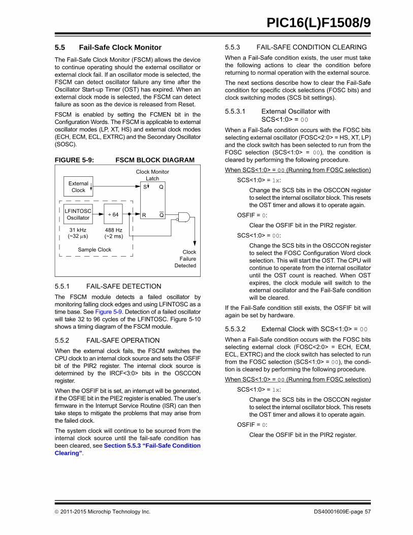
PIC16(L)F1508/9
5.5 Fail-Safe Clock Monitor
The Fail-Safe Clock Monitor (FSCM) allows the deviceto continue operating should the external oscillator orexternal clock fail. If an oscillator mode is selected, theFSCM can detect oscillator failure any time after theOscillator Start-up Timer (OST) has expired. When anexternal clock mode is selected, the FSCM can detectfailure as soon as the device is released from Reset.
FSCM is enabled by setting the FCMEN bit in theConfiguration Words. The FSCM is applicable to externaloscillator modes (LP, XT, HS) and external clock modes(ECH, ECM, ECL, EXTRC) and the Secondary Oscillator(SOSC).
FIGURE 5-9: FSCM BLOCK DIAGRAM
5.5.1 FAIL-SAFE DETECTION
The FSCM module detects a failed oscillator bymonitoring falling clock edges and using LFINTOSC as atime base. See Figure 5-9. Detection of a failed oscillatorwill take 32 to 96 cycles of the LFINTOSC. Figure 5-10shows a timing diagram of the FSCM module.
5.5.2 FAIL-SAFE OPERATION
When the external clock fails, the FSCM switches theCPU clock to an internal clock source and sets the OSFIFbit of the PIR2 register. The internal clock source isdetermined by the IRCF<3:0> bits in the OSCCONregister.
When the OSFIF bit is set, an interrupt will be generated,if the OSFIE bit in the PIE2 register is enabled. The user’sfirmware in the Interrupt Service Routine (ISR) can thentake steps to mitigate the problems that may arise fromthe failed clock.
The system clock will continue to be sourced from theinternal clock source until the fail-safe condition hasbeen cleared, see Section 5.5.3 “Fail-Safe ConditionClearing”.
5.5.3 FAIL-SAFE CONDITION CLEARING
When a Fail-Safe condition exists, the user must takethe following actions to clear the condition beforereturning to normal operation with the external source.
The next sections describe how to clear the Fail-Safecondition for specific clock selections (FOSC bits) andclock switching modes (SCS bit settings).
5.5.3.1 External Oscillator with SCS<1:0> = 00
When a Fail-Safe condition occurs with the FOSC bitsselecting external oscillator (FOSC<2:0> = HS, XT, LP)and the clock switch has been selected to run from theFOSC selection (SCS<1:0> = 00), the condition iscleared by performing the following procedure.
When SCS<1:0> = 00 (Running from FOSC selection)
SCS<1:0> = 1x:
Change the SCS bits in the OSCCON registerto select the internal oscillator block. This resetsthe OST timer and allows it to operate again.
OSFIF = 0:
Clear the OSFIF bit in the PIR2 register.
SCS<1:0> = 00:
Change the SCS bits in the OSCCON registerto select the FOSC Configuration Word clockselection. This will start the OST. The CPU willcontinue to operate from the internal oscillatoruntil the OST count is reached. When OSTexpires, the clock module will switch to theexternal oscillator and the Fail-Safe conditionwill be cleared.
If the Fail-Safe condition still exists, the OSFIF bit willagain be set by hardware.
5.5.3.2 External Clock with SCS<1:0> = 00
When a Fail-Safe condition occurs with the FOSC bitsselecting external clock (FOSC<2:0> = ECH, ECM,ECL, EXTRC) and the clock switch has selected to runfrom the FOSC selection (SCS<1:0> = 00), the condi-tion is cleared by performing the following procedure.
When SCS<1:0> = 00 (Running from FOSC selection)
SCS<1:0> = 1x:
Change the SCS bits in the OSCCON registerto select the internal oscillator block. This resetsthe OST timer and allows it to operate again.
OSFIF = 0:
Clear the OSFIF bit in the PIR2 register.
External
LFINTOSC÷ 64
S
R
Q
31 kHz(~32 s)
488 Hz(~2 ms)
Clock MonitorLatch
ClockFailure
Detected
Oscillator
Clock
Q
Sample Clock
2011-2015 Microchip Technology Inc. DS40001609E-page 57

PIC16(L)F1508/9
SCS<1:0> = 00:
Change the SCS bits in the OSCCON registerto select the FOSC Configuration Word clockselection. Since the OST is not applicable withexternal clocks, the clock module willimmediately switch to the external clock, andthe fail-safe condition will be cleared.
If the Fail-Safe condition still exists, the OSFIF bit willagain be set by hardware.
5.5.3.3 Secondary Oscillator with SCS<1:0> = 01
When a Fail-Safe condition occurs with the clock switchselected to run from the Secondary Oscillator selection(SCS<1:0> = 01), regardless of the FOSC selection,the condition is cleared by performing the following pro-cedure.
SCS<1:0> = 01 (Secondary Oscillator)
SCS<1:0> = 1x:
Change the SCS bits in the OSCCON registerto select the internal oscillator block.
OSFIF = 0:
Clear the OSFIF bit in the PIR2 register.
Read SOSCR:
The OST is not used with the secondaryoscillator, therefore, the user must determine ifthe secondary oscillator is ready by monitoringthe SOSCR bit in the OSCSTAT register.When the SOSCR bit is set, the secondaryoscillator is ready.
SCS<1:0> = 01:
Change the SCS bits in the OSCCON registerto select the secondary oscillator. The clockmodule will immediately switch to thesecondary oscillator and the fail-safe conditionwill be cleared.
If the Fail-Safe condition still exists, the OSFIF bit willagain be set by hardware.
5.5.4 RESET OR WAKE-UP FROM SLEEP
The FSCM is designed to detect external oscillator orexternal clock failures.
When FSCM is used with an external oscillator, theOscillator Start-up Timer (OST) count must expirebefore the FSCM becomes active. The OST is usedafter waking up from Sleep and after any type of Reset.
When the FSCM is used with external clocks, the OSTis not used and the FSCM will be active as soon as theReset or wake-up has completed.
When the FSCM is enabled, the Two-Speed Start-up isalso enabled. Therefore, the device will always be exe-cuting code while the OST is operating.
FIGURE 5-10: FSCM TIMING DIAGRAM
Note: Due to the wide range of oscillator start-uptimes, the Fail-Safe circuit is not activeduring oscillator start-up (i.e., after exitingReset or Sleep).
OSFIF
SystemClock
Output
Sample Clock
FailureDetected
OscillatorFailure
Note: The system clock is normally at a much higher frequency than the sample clock. The relative frequencies inthis example have been chosen for clarity.
(Q)
Test Test Test
Clock Monitor Output
DS40001609E-page 58 2011-2015 Microchip Technology Inc.

PIC16(L)F1508/9
5.6 Register Definitions: Oscillator Control
REGISTER 5-1: OSCCON: OSCILLATOR CONTROL REGISTER
U-0 R/W-0/0 R/W-1/1 R/W-1/1 R/W-1/1 U-0 R/W-0/0 R/W-0/0
— IRCF<3:0> — SCS<1:0>
bit 7 bit 0
Legend:
R = Readable bit W = Writable bit U = Unimplemented bit, read as ‘0’
u = Bit is unchanged x = Bit is unknown -n/n = Value at POR and BOR/Value at all other Resets
‘1’ = Bit is set ‘0’ = Bit is cleared
bit 7 Unimplemented: Read as ‘0’
bit 6-3 IRCF<3:0>: Internal Oscillator Frequency Select bits1111 = 16 MHz1110 = 8 MHz1101 = 4 MHz1100 = 2 MHz1011 = 1 MHz1010 = 500 kHz(1)
1001 = 250 kHz(1)
1000 = 125 kHz(1)
0111 = 500 kHz (default upon Reset)0110 = 250 kHz0101 = 125 kHz0100 = 62.5 kHz001x = 31.25 kHz000x = 31 kHz LF
bit 2 Unimplemented: Read as ‘0’
bit 1-0 SCS<1:0>: System Clock Select bits1x = Internal oscillator block01 = Secondary oscillator00 = Clock determined by FOSC<2:0> in Configuration Words.
Note 1: Duplicate frequency derived from HFINTOSC.
2011-2015 Microchip Technology Inc. DS40001609E-page 59

PIC16(L)F1508/9
REGISTER 5-2: OSCSTAT: OSCILLATOR STATUS REGISTER
R-1/q U-0 R-q/q R-0/q U-0 U-0 R-0/q R-0/q
SOSCR — OSTS HFIOFR — — LFIOFR HFIOFS
bit 7 bit 0
Legend:
R = Readable bit W = Writable bit U = Unimplemented bit, read as ‘0’
u = Bit is unchanged x = Bit is unknown -n/n = Value at POR and BOR/Value at all other Resets
‘1’ = Bit is set ‘0’ = Bit is cleared q = Conditional
bit 7 SOSCR: Secondary Oscillator Ready bitIf T1OSCEN = 1:1 = Secondary oscillator is ready0 = Secondary oscillator is not readyIf T1OSCEN = 0:1 = Timer1 clock source is always ready
bit 6 Unimplemented: Read as ‘0’
bit 5 OSTS: Oscillator Start-up Timer Status bitWhen the FOSC<2:0> bits select HS, XT or LP oscillator:1 = OST has counted 1024 clocks, device is clocked by the FOSC<2:0> bit selection0 = OST is counting, device is clocked from the internal oscillator (INTOSC) selected by the IRCF<3:0>
bits.For all other FOSC<2:0> bit selections:See Table 5-2, “OSTS Bit Definition”.
bit 4 HFIOFR: High-Frequency Internal Oscillator Ready bit 1 = HFINTOSC is ready0 = HFINTOSC is not ready
bit 3-2 Unimplemented: Read as ‘0’
bit 1 LFIOFR: Low-Frequency Internal Oscillator Ready bit 1 = LFINTOSC is ready0 = LFINTOSC is not ready
bit 0 HFIOFS: High-Frequency Internal Oscillator Stable bit1 = HFINTOSC 16 MHz Oscillator is stable and is driving the INTOSC0 = HFINTOSC 16 MHz is not stable, the Start-up Oscillator is driving INTOSC
DS40001609E-page 60 2011-2015 Microchip Technology Inc.

PIC16(L)F1508/9
TABLE 5-4: SUMMARY OF REGISTERS ASSOCIATED WITH CLOCK SOURCES
TABLE 5-5: SUMMARY OF CONFIGURATION WORD WITH CLOCK SOURCES
Name Bit 7 Bit 6 Bit 5 Bit 4 Bit 3 Bit 2 Bit 1 Bit 0Register on Page
OSCCON — IRCF<3:0> — SCS<1:0> 59
OSCSTAT SOSCR — OSTS HFIOFR — — LFIOFR HFIOFS 60
PIE2 OSFIE C2IE C1IE — BCL1IE NCO1IE — — 77
PIR2 OSFIF C2IF C1IF — BCL1IF NCO1IF — — 80
T1CON TMR1CS<1:0> T1CKPS<1:0> T1OSCEN T1SYNC — TMR1ON 163
Legend: — = unimplemented location, read as ‘0’. Shaded cells are not used by clock sources.
Name Bits Bit -/7 Bit -/6 Bit 13/5 Bit 12/4 Bit 11/3 Bit 10/2 Bit 9/1 Bit 8/0Register on Page
CONFIG113:8 — — FCMEN IESO CLKOUTEN BOREN<1:0> —
417:0 CP MCLRE PWRTE WDTE<1:0> FOSC<2:0>
Legend: — = unimplemented location, read as ‘0’. Shaded cells are not used by clock sources.
2011-2015 Microchip Technology Inc. DS40001609E-page 61

PIC16(L)F1508/9
6.0 RESETS
There are multiple ways to reset this device:
• Power-on Reset (POR)
• Brown-out Reset (BOR)
• Low-Power Brown-out Reset (LPBOR)
• MCLR Reset
• WDT Reset
• RESET instruction
• Stack Overflow
• Stack Underflow
• Programming mode exit
To allow VDD to stabilize, an optional power-up timercan be enabled to extend the Reset time after a BORor POR event.
A simplified block diagram of the On-chip Reset Circuitis shown in Figure 6-1.
FIGURE 6-1: SIMPLIFIED BLOCK DIAGRAM OF ON-CHIP RESET CIRCUIT
DeviceReset
Power-on Reset
WDT Time-out
Brown-out Reset
LPBOR Reset
RESET Instruction
MCLRE
Sleep
BOR Active(1)
PWRTELFINTOSC
VDD
ICSP™ Programming Mode Exit
Stack UnderflowStack Overlfow
VPP/MCLR
R Power-up Timer
Rev. 10-000006A8/14/2013
Note 1: See Table 6-1 for BOR active conditions.
DS40001609E-page 62 2011-2015 Microchip Technology Inc.

PIC16(L)F1508/9
6.1 Power-On Reset (POR)
The POR circuit holds the device in Reset until VDD hasreached an acceptable level for minimum operation.Slow rising VDD, fast operating speeds or analogperformance may require greater than minimum VDD.The PWRT, BOR or MCLR features can be used toextend the start-up period until all device operationconditions have been met.
6.1.1 POWER-UP TIMER (PWRT)
The Power-up Timer provides a nominal 64 mstime-out on POR or Brown-out Reset.
The device is held in Reset as long as PWRT is active.The PWRT delay allows additional time for the VDD torise to an acceptable level. The Power-up Timer isenabled by clearing the PWRTE bit in ConfigurationWords.
The Power-up Timer starts after the release of the PORand BOR.
For additional information, refer to Application NoteAN607, “Power-up Trouble Shooting” (DS00607).
6.2 Brown-Out Reset (BOR)
The BOR circuit holds the device in Reset when VDD
reaches a selectable minimum level. Between thePOR and BOR, complete voltage range coverage forexecution protection can be implemented.
The Brown-out Reset module has four operatingmodes controlled by the BOREN<1:0> bits in Configu-ration Words. The four operating modes are:
• BOR is always on
• BOR is off when in Sleep
• BOR is controlled by software
• BOR is always off
Refer to Table 6-1 for more information.
The Brown-out Reset voltage level is selectable byconfiguring the BORV bit in Configuration Words.
A VDD noise rejection filter prevents the BOR fromtriggering on small events. If VDD falls below Vpor for aduration greater than parameter TBORDC, the devicewill reset. See Figure 6-2 for more information.
TABLE 6-1: BOR OPERATING MODES
6.2.1 BOR IS ALWAYS ON
When the BOREN bits of Configuration Words are pro-grammed to ‘11’, the BOR is always on. The devicestart-up will be delayed until the BOR is ready and VDD
is higher than the BOR threshold.
BOR protection is active during Sleep. The BOR doesnot delay wake-up from Sleep.
6.2.2 BOR IS OFF IN SLEEP
When the BOREN bits of Configuration Words are pro-grammed to ‘10’, the BOR is on, except in Sleep. Thedevice start-up will be delayed until the BOR is readyand VDD is higher than the BOR threshold.
BOR protection is not active during Sleep. The devicewake-up will be delayed until the BOR is ready.
6.2.3 BOR CONTROLLED BY SOFTWARE
When the BOREN bits of Configuration Words areprogrammed to ‘01’, the BOR is controlled by theSBOREN bit of the BORCON register. The devicestart-up is not delayed by the BOR ready condition orthe VDD level.
BOR protection begins as soon as the BOR circuit isready. The status of the BOR circuit is reflected in theBORRDY bit of the BORCON register.
BOR protection is unchanged by Sleep.
BOREN<1:0> SBOREN Device Mode BOR ModeInstruction Execution upon:
Release of POR or Wake-up from Sleep
11 X X Active Waits for BOR ready(1)
(BORRDY = 1)
10 XAwake Active Waits for BOR ready
(BORRDY = 1)Sleep Disabled
01
1X
Active Waits for BOR ready(1)
(BORRDY = 1)
0 X Disabled Begins immediately(BORRDY = x)
00 X X Disabled
Note 1: In these specific cases, “release of POR” and “wake-up from Sleep,” there is no delay in start-up. The BORready flag, (BORRDY = 1), will be set before the CPU is ready to execute instructions because the BORcircuit is forced on by the BOREN<1:0> bits.
2011-2015 Microchip Technology Inc. DS40001609E-page 63

PIC16(L)F1508/9
FIGURE 6-2: BROWN-OUT SITUATIONS
6.3 Register Definitions: BOR Control
REGISTER 6-1: BORCON: BROWN-OUT RESET CONTROL REGISTER
R/W-1/u R/W-0/u U-0 U-0 U-0 U-0 U-0 R-q/u
SBOREN BORFS — — — — — BORRDY
bit 7 bit 0
Legend:
R = Readable bit W = Writable bit U = Unimplemented bit, read as ‘0’
u = Bit is unchanged x = Bit is unknown -n/n = Value at POR and BOR/Value at all other Resets
‘1’ = Bit is set ‘0’ = Bit is cleared q = Value depends on condition
bit 7 SBOREN: Software Brown-Out Reset Enable bitIf BOREN <1:0> in Configuration Words = 01:1 = BOR Enabled0 = BOR DisabledIf BOREN <1:0> in Configuration Words 01:SBOREN is read/write, but has no effect on the BOR
bit 6 BORFS: Brown-Out Reset Fast Start bit(1)
If BOREN <1:0> = 10 (Disabled in Sleep) or BOREN<1:0> = 01 (Under software control):1 = Band gap is forced on always (covers sleep/wake-up/operating cases)0 = Band gap operates normally, and may turn offIf BOREN<1:0> = 11 (Always on) or BOREN<1:0> = 00 (Always off)BORFS is Read/Write, but has no effect.
bit 5-1 Unimplemented: Read as ‘0’
bit 0 BORRDY: Brown-Out Reset Circuit Ready Status bit1 = The Brown-out Reset circuit is active0 = The Brown-out Reset circuit is inactive
Note 1: BOREN<1:0> bits are located in Configuration Words.
TPWRT(1)
VBOR VDD
InternalReset
VBOR VDD
InternalReset TPWRT(1)< TPWRT
TPWRT(1)
VBOR VDD
InternalReset
Note 1: TPWRT delay only if PWRTE bit is programmed to ‘0’.
DS40001609E-page 64 2011-2015 Microchip Technology Inc.

PIC16(L)F1508/9
6.4 Low-Power Brown-Out Reset (LPBOR)
The Low-Power Brown-out Reset (LPBOR) operateslike the BOR to detect low voltage conditions on theVDD pin. When too low of a voltage is detected, thedevice is held in Reset. When this occurs, a register bit(BOR) is changed to indicate that a BOR Reset hasoccurred. The BOR bit in PCON is used for both BORand the LPBOR. Refer to Register 6-2.
The LPBOR voltage threshold (Lapboard) has a widertolerance than the BOR (Vpor), but requires much lesscurrent (LPBOR current) to operate. The LPBOR isintended for use when the BOR is configured as dis-abled (BOREN = 00) or disabled in Sleep mode(BOREN = 10).
Refer to Figure 6-1 to see how the LPBOR interactswith other modules.
6.4.1 ENABLING LPBOR
The LPBOR is controlled by the LPBOR bit ofConfiguration Words. When the device is erased, theLPBOR module defaults to disabled.
6.5 MCLR
The MCLR is an optional external input that can resetthe device. The MCLR function is controlled by theMCLRE bit of Configuration Words and the LVP bit ofConfiguration Words (Table 6-2).
6.5.1 MCLR ENABLED
When MCLR is enabled and the pin is held low, thedevice is held in Reset. The MCLR pin is connected toVDD through an internal weak pull-up.
The device has a noise filter in the MCLR Reset path.The filter will detect and ignore small pulses.
6.5.2 MCLR DISABLED
When MCLR is disabled, the pin functions as a generalpurpose input and the internal weak pull-up is undersoftware control. See Section 11.3 “PORTA Regis-ters” for more information.
6.6 Watchdog Timer (WDT) Reset
The Watchdog Timer generates a Reset if the firmwaredoes not issue a CLRWDT instruction within the time-outperiod. The TO and PD bits in the STATUS register arechanged to indicate the WDT Reset. See Section9.0 “Watchdog Timer (WDT)” for more information.
6.7 RESET Instruction
A RESET instruction will cause a device Reset. The RIbit in the PCON register will be set to ‘0’. See Table 6-4for default conditions after a RESET instruction hasoccurred.
6.8 Stack Overflow/Underflow Reset
The device can reset when the Stack Overflows orUnderflows. The STKOVF or STKUNF bits of the PCONregister indicate the Reset condition. These Resets areenabled by setting the STVREN bit in ConfigurationWords. See Section 3.5.2 “Overflow/UnderflowReset” for more information.
6.9 Programming Mode Exit
Upon exit of Programming mode, the device willbehave as if a POR had just occurred.
6.10 Power-Up Timer
The Power-up Timer optionally delays device executionafter a BOR or POR event. This timer is typically used toallow VDD to stabilize before allowing the device to startrunning.
The Power-up Timer is controlled by the PWRTE bit ofConfiguration Words.
6.11 Start-up Sequence
Upon the release of a POR or BOR, the following mustoccur before the device will begin executing:
1. Power-up Timer runs to completion (if enabled).
2. MCLR must be released (if enabled).
The total time-out will vary based on oscillator configu-ration and Power-up Timer configuration. See Section5.0 “Oscillator Module (With Fail-Safe Clock Moni-tor)” for more information.
The Power-up Timer runs independently of MCLRReset. If MCLR is kept low long enough, the Power-upTimer will expire. Upon bringing MCLR high, the devicewill begin execution after 10 FOSS cycles (seeFigure 6-3). This is useful for testing purposes or tosynchronize more than one device operating in parallel.
TABLE 6-2: MCLR CONFIGURATION
MCLRE LVP MCLR
0 0 Disabled
1 0 Enabled
x 1 Enabled
Note: A Reset does not drive the MCLR pin low.
2011-2015 Microchip Technology Inc. DS40001609E-page 65

PIC16(L)F1508/9
FIGURE 6-3: RESET START-UP SEQUENCE
Note 1: Code execution begins 10 FOSC cycles after the FOSC clock is released.
External Oscillators , PWRTEN = 1, IESO = 1
code execution (1)
External Oscillators , PWRTEN = 0, IESO = 1
Ext. OscillatorOsc Start-Up Timer TOST
TPWRT
TOST
VDD
Internal POR
Internal RESET
MCLR
FOSC
Begin Execution
Power-up Timer
Int. Oscillator
code execution (1)
External Oscillators , PWRTEN = 1, IESO = 0
codeexecution (1)
External Oscillators , PWRTEN = 0, IESO = 0
Ext. OscillatorOsc Start-Up Timer
codeexecution (1)
TOST
TPWRT
TOST
VDD
Internal POR
Internal RESET
MCLR
FOSC
Begin Execution
Power-up Timer
VDD
Internal POR
External Clock (EC modes), PWRTEN = 0
Internal RESET
MCLR
FOSC
Begin Execution
Ext. Clock (EC)
Power-up Timer
External Clock (EC modes), PWRTEN = 1
code execution (1)code execution (1)
TPWRT
Int. Oscillator
code execution (1)
Internal Oscillator, PWRTEN = 0 Internal Oscillator, PWRTEN = 1
code execution (1)
TPWRT
VDD
Internal POR
Internal RESET
MCLR
FOSC
Begin Execution
Power-up Timer
Rev. 10-000032A7/30/2013
DS40001609E-page 66 2011-2015 Microchip Technology Inc.

PIC16(L)F1508/9
6.12 Determining the Cause of a Reset
Upon any Reset, multiple bits in the STATUS andPCON registers are updated to indicate the cause ofthe Reset. Table 6-3 and Table 6-4 show the Resetconditions of these registers.
TABLE 6-3: RESET STATUS BITS AND THEIR SIGNIFICANCE
TABLE 6-4: RESET CONDITION FOR SPECIAL REGISTERS
STKOVF STKUNF RWDT RMCLR RI POR BOR TO PD Condition
0 0 1 1 1 0 x 1 1 Power-on Reset
0 0 1 1 1 0 x 0 x Illegal, TO is set on POR
0 0 1 1 1 0 x x 0 Illegal, PD is set on POR
0 0 u 1 1 u 0 1 1 Brown-out Reset
u u 0 u u u u 0 u WDT Reset
u u u u u u u 0 0 WDT Wake-up from Sleep
u u u u u u u 1 0 Interrupt Wake-up from Sleep
u u u 0 u u u u u MCLR Reset during normal operation
u u u 0 u u u 1 0 MCLR Reset during Sleep
u u u u 0 u u u u RESET Instruction Executed
1 u u u u u u u u Stack Overflow Reset (STVREN = 1)
u 1 u u u u u u u Stack Underflow Reset (STVREN = 1)
ConditionProgramCounter
STATUSRegister
PCONRegister
Power-on Reset 0000h ---1 1000 00-- 110x
MCLR Reset during normal operation 0000h ---u muumuu uu-- 0uuu
MCLR Reset during Sleep 0000h ---1 0uuu uu-- 0uuu
WDT Reset 0000h ---0 muumuu uu-- uuuu
WDT Wake-up from Sleep PC + 1 ---0 0uuu uu-- uuuu
Brown-out Reset 0000h ---1 1uuu 00-- 11u0
Interrupt Wake-up from Sleep PC + 1(1) ---1 0uuu uu-- uuuu
RESET Instruction Executed 0000h ---u uuuu uu-- u0uu
Stack Overflow Reset (STVREN = 1) 0000h ---u uuuu 1u-- uuuu
Stack Underflow Reset (STVREN = 1) 0000h ---u uuuu u1-- uuuu
Legend: u = unchanged, x = unknown, - = unimplemented bit, reads as ‘0’.Note 1: When the wake-up is due to an interrupt and the Global Interrupt Enable bit (GIE) is set, the return address
is pushed on the stack and PC is loaded with the interrupt vector (0004h) after execution of PC + 1.
2011-2015 Microchip Technology Inc. DS40001609E-page 67

PIC16(L)F1508/9
6.13 Power Control (PCON) Register
The Power Control (PCON) register contains flag bitsto differentiate between a:
• Power-on Reset (POR)
• Brown-out Reset (BOR)
• Reset Instruction Reset (RI)
• MCLR Reset (RMCLR)
• Watchdog Timer Reset (RWDT)
• Stack Underflow Reset (STKUNF)
• Stack Overflow Reset (STKOVF)
The PCON register bits are shown in Register 6-2.
6.14 Register Definitions: Power Control
REGISTER 6-2: PCON: POWER CONTROL REGISTER
R/W/HS-0/q R/W/HS-0/q U-0 R/W/HC-1/q R/W/HC-1/q R/W/HC-1/q R/W/HC-q/u R/W/HC-q/u
STKOVF STKUNF — RWDT RMCLR RI POR BOR
bit 7 bit 0
Legend:
HC = Bit is cleared by hardware HS = Bit is set by hardware
R = Readable bit W = Writable bit U = Unimplemented bit, read as ‘0’
u = Bit is unchanged x = Bit is unknown -n/n = Value at POR and BOR/Value at all other Resets
‘1’ = Bit is set ‘0’ = Bit is cleared q = Value depends on condition
bit 7 STKOVF: Stack Overflow Flag bit
1 = A Stack Overflow occurred0 = A Stack Overflow has not occurred or cleared by firmware
bit 6 STKUNF: Stack Underflow Flag bit
1 = A Stack Underflow occurred0 = A Stack Underflow has not occurred or cleared by firmware
bit 5 Unimplemented: Read as ‘0’
bit 4 RWDT: Watchdog Timer Reset Flag bit
1 = A Watchdog Timer Reset has not occurred or set by firmware0 = A Watchdog Timer Reset has occurred (cleared by hardware)
bit 3 RMCLR: MCLR Reset Flag bit
1 = A MCLR Reset has not occurred or set by firmware0 = A MCLR Reset has occurred (cleared by hardware)
bit 2 RI: RESET Instruction Flag bit
1 = A RESET instruction has not been executed or set by firmware0 = A RESET instruction has been executed (cleared by hardware)
bit 1 POR: Power-On Reset Status bit
1 = No Power-on Reset occurred0 = A Power-on Reset occurred (must be set in software after a Power-on Reset occurs)
bit 0 BOR: Brown-Out Reset Status bit
1 = No Brown-out Reset occurred0 = A Brown-out Reset occurred (must be set in software after a Power-on Reset or Brown-out Reset
occurs)
DS40001609E-page 68 2011-2015 Microchip Technology Inc.

PIC16(L)F1508/9
TABLE 6-5: SUMMARY OF REGISTERS ASSOCIATED WITH RESETS
TABLE 6-6: SUMMARY OF CONFIGURATION WORD WITH RESETS
Name Bit 7 Bit 6 Bit 5 Bit 4 Bit 3 Bit 2 Bit 1 Bit 0Register on Page
BORCON SBOREN BORFS — — — — — BORRDY 64
PCON STKOVF STKUNF — RWDT RMCLR RI POR BOR 68
STATUS — — — TO PD Z DC C 19
WDTCON — — WDTPS<4:0> SWDTEN 88
Legend: — = unimplemented bit, reads as ‘0’. Shaded cells are not used by Resets.
Name Bits Bit -/7 Bit -/6 Bit 13/5 Bit 12/4 Bit 11/3 Bit 10/2 Bit 9/1 Bit 8/0Register on Page
CONFIG113:8 — — FCMEN IESO CLKOUTEN BOREN<1:0> —
437:0 CP MCLRE PWRTE WDTE<1:0> FOSC<2:0>
CONFIG213:8 — — LVP — LPBOR BORV STVREN —
437:0 — — — — — — WRT<1:0>
Legend: — = unimplemented location, read as ‘0’. Shaded cells are not used by Resets.
2011-2015 Microchip Technology Inc. DS40001609E-page 69

PIC16(L)F1508/9
7.0 INTERRUPTS
The interrupt feature allows certain events to preemptnormal program flow. Firmware is used to determinethe source of the interrupt and act accordingly. Someinterrupts can be configured to wake the MCU fromSleep mode.
This chapter contains the following information forInterrupts:
• Operation
• Interrupt Latency
• Interrupts During Sleep
• INT Pin
• Automatic Context Saving
Many peripherals produce interrupts. Refer to thecorresponding chapters for details.
A block diagram of the interrupt logic is shown inFigure 7-1.
FIGURE 7-1: INTERRUPT LOGIC
TMR0IFTMR0IE
INTFINTE
IOCIFIOCIE
Interruptto CPU
Wake-up(If in Sleep mode)
GIE
(TMR1IF) PIR1<0>
PIRn<7>
PEIE
(TMR1IE) PIE1<0>
Peripheral Interrupts
PIEn<7>
Rev. 10-000010A1/13/2014
DS40001609E-page 70 2011-2015 Microchip Technology Inc.

PIC16(L)F1508/9
7.1 Operation
Interrupts are disabled upon any device Reset. Theyare enabled by setting the following bits:
• GIE bit of the INTCON register
• Interrupt Enable bit(s) for the specific interrupt event(s)
• PEIE bit of the INTCON register (if the Interrupt Enable bit of the interrupt event is contained in the PIE1, PIE2 and PIE3 registers)
The INTCON, PIR1, PIR2 and PIR3 registers recordindividual interrupts via interrupt flag bits. Interrupt flagbits will be set, regardless of the status of the GIE, PEIEand individual interrupt enable bits.
The following events happen when an interrupt eventoccurs while the GIE bit is set:
• Current prefetched instruction is flushed
• GIE bit is cleared
• Current Program Counter (PC) is pushed onto the stack
• Critical registers are automatically saved to the shadow registers (See “Section 7.5 “Automatic Context Saving”.”)
• PC is loaded with the interrupt vector 0004h
The firmware within the Interrupt Service Routine (ISR)should determine the source of the interrupt by pollingthe interrupt flag bits. The interrupt flag bits must becleared before exiting the ISR to avoid repeatedinterrupts. Because the GIE bit is cleared, any interruptthat occurs while executing the ISR will be recordedthrough its interrupt flag, but will not cause theprocessor to redirect to the interrupt vector.
The RETFIE instruction exits the ISR by popping theprevious address from the stack, restoring the savedcontext from the shadow registers and setting the GIEbit.
For additional information on a specific interrupt’soperation, refer to its peripheral chapter.
7.2 Interrupt Latency
Interrupt latency is defined as the time from when theinterrupt event occurs to the time code execution at theinterrupt vector begins. The latency for synchronousinterrupts is three or four instruction cycles. Forasynchronous interrupts, the latency is three to fiveinstruction cycles, depending on when the interruptoccurs. See Figure 7-2 and Figure 7-3 for more details.
Note 1: Individual interrupt flag bits are set,regardless of the state of any otherenable bits.
2: All interrupts will be ignored while the GIEbit is cleared. Any interrupt occurringwhile the GIE bit is clear will be servicedwhen the GIE bit is set again.
2011-2015 Microchip Technology Inc. DS40001609E-page 71
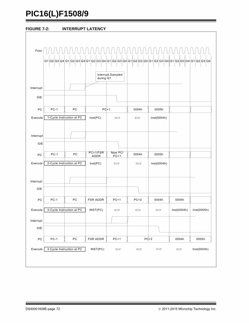
PIC16(L)F1508/9
FIGURE 7-2: INTERRUPT LATENCY
Q1 Q2 Q3 Q4 Q1 Q2 Q3 Q4 Q1 Q2 Q3 Q4 Q1 Q2 Q3 Q4 Q1 Q2 Q3 Q4 Q1 Q2 Q3 Q4
Fosc
PC 0004h 0005hPC
Inst(0004h)NOP
GIE
Q1 Q2 Q3 Q4Q1 Q2 Q3 Q4
1-Cycle Instruction at PC
PC
Inst(0004h)NOP2-Cycle Instruction at PC
FSR ADDR PC+1 PC+2 0004h 0005hPC
Inst(0004h)NOP
GIE
PCPC-1
3-Cycle Instruction at PC
Execute
Interrupt
Inst(PC)
Interrupt Sampled during Q1
Inst(PC)
PC-1 PC+1
NOP
PCNew PC/
PC+10005hPC-1
PC+1/FSR ADDR
0004h
NOP
Interrupt
GIE
Interrupt
INST(PC) NOPNOP
FSR ADDR PC+1 PC+2 0004h 0005hPC
Inst(0004h)NOP
GIE
PCPC-1
3-Cycle Instruction at PC
Interrupt
INST(PC) NOPNOP NOP
Inst(0005h)
Execute
Execute
Execute
DS40001609E-page 72 2011-2015 Microchip Technology Inc.

PIC16(L)F1508/9
FIGURE 7-3: INT PIN INTERRUPT TIMING
Q2Q1 Q3 Q4 Q2Q1 Q3 Q4 Q2Q1 Q3 Q4 Q2Q1 Q3 Q4 Q2Q1 Q3 Q4
FOSC
CLKOUT
INT pin
INTF
GIE
INSTRUCTION FLOW
PC
InstructionFetched
InstructionExecuted
Interrupt Latency
PC PC + 1 PC + 1 0004h 0005h
Inst (0004h) Inst (0005h)
Forced NOP
Inst (PC) Inst (PC + 1)
Inst (PC – 1) Inst (0004h) Forced NOPInst (PC)
—
Note 1: INTF flag is sampled here (every Q1).
2: Asynchronous interrupt latency = 3-5 TCY. Synchronous latency = 3-4 TCY, where TCY = instruction cycle time.Latency is the same whether Inst (PC) is a single cycle or a 2-cycle instruction.
3: For minimum width of INT pulse, refer to AC specifications in Section 29.0 “Electrical Specifications”.
4: INTF is enabled to be set any time during the Q4-Q1 cycles.
(1)
(2)
(3)
(4)(1)
2011-2015 Microchip Technology Inc. DS40001609E-page 73

PIC16(L)F1508/9
7.3 Interrupts During Sleep
Some interrupts can be used to wake from Sleep. Towake from Sleep, the peripheral must be able tooperate without the system clock. The interrupt sourcemust have the appropriate Interrupt Enable bit(s) setprior to entering Sleep.
On waking from Sleep, if the GIE bit is also set, theprocessor will branch to the interrupt vector. Otherwise,the processor will continue executing instructions afterthe SLEEP instruction. The instruction directly after theSLEEP instruction will always be executed beforebranching to the ISR. Refer to Section 8.0 “Power-Down Mode (Sleep)” for more details.
7.4 INT Pin
The INT pin can be used to generate an asynchronousedge-triggered interrupt. This interrupt is enabled bysetting the INTE bit of the INTCON register. TheINTEDG bit of the OPTION_REG register determines onwhich edge the interrupt will occur. When the INTEDGbit is set, the rising edge will cause the interrupt. Whenthe INTEDG bit is clear, the falling edge will cause theinterrupt. The INTF bit of the INTCON register will be setwhen a valid edge appears on the INT pin. If the GIE andINTE bits are also set, the processor will redirectprogram execution to the interrupt vector.
7.5 Automatic Context Saving
Upon entering an interrupt, the return PC address issaved on the stack. Additionally, the following registersare automatically saved in the shadow registers:
• W register
• STATUS register (except for TO and PD)
• BSR register
• FSR registers
• PCLATH register
Upon exiting the Interrupt Service Routine, these regis-ters are automatically restored. Any modifications tothese registers during the ISR will be lost. If modifica-tions to any of these registers are desired, the corre-sponding shadow register should be modified and thevalue will be restored when exiting the ISR. Theshadow registers are available in Bank 31 and arereadable and writable. Depending on the user’s appli-cation, other registers may also need to be saved.
DS40001609E-page 74 2011-2015 Microchip Technology Inc.

PIC16(L)F1508/9
7.6 Register Definitions: Interrupt Control
REGISTER 7-1: INTCON: INTERRUPT CONTROL REGISTER
R/W-0/0 R/W-0/0 R/W-0/0 R/W-0/0 R/W-0/0 R/W-0/0 R/W-0/0 R-0/0
GIE(1) PEIE(2) TMR0IE INTE IOCIE TMR0IF INTF IOCIF(3)
bit 7 bit 0
Legend:
R = Readable bit W = Writable bit U = Unimplemented bit, read as ‘0’
u = Bit is unchanged x = Bit is unknown -n/n = Value at POR and BOR/Value at all other Resets
‘1’ = Bit is set ‘0’ = Bit is cleared
bit 7 GIE: Global Interrupt Enable bit(1)
1 = Enables all active interrupts0 = Disables all interrupts
bit 6 PEIE: Peripheral Interrupt Enable bit(2)
1 = Enables all active peripheral interrupts0 = Disables all peripheral interrupts
bit 5 TMR0IE: Timer0 Overflow Interrupt Enable bit1 = Enables the Timer0 interrupt0 = Disables the Timer0 interrupt
bit 4 INTE: INT External Interrupt Enable bit1 = Enables the INT external interrupt0 = Disables the INT external interrupt
bit 3 IOCIE: Interrupt-on-Change Enable bit1 = Enables the interrupt-on-change0 = Disables the interrupt-on-change
bit 2 TMR0IF: Timer0 Overflow Interrupt Flag bit1 = TMR0 register has overflowed0 = TMR0 register did not overflow
bit 1 INTF: INT External Interrupt Flag bit1 = The INT external interrupt occurred0 = The INT external interrupt did not occur
bit 0 IOCIF: Interrupt-on-Change Interrupt Flag bit(3)
1 = When at least one of the interrupt-on-change pins changed state0 = None of the interrupt-on-change pins have changed state
Note 1: Interrupt flag bits are set when an interrupt condition occurs, regardless of the state of its correspondingenable bit or the Global Interrupt Enable bit, GIE of the INTCON register. User software should ensure theappropriate interrupt flag bits are clear prior to enabling an interrupt.
2: Bit PEIE of the INTCON register must be set to enable any peripheral interrupt.
3: The IOCIF Flag bit is read-only and cleared when all the interrupt-on-change flags in the IOCxF registershave been cleared by software.
2011-2015 Microchip Technology Inc. DS40001609E-page 75

PIC16(L)F1508/9
REGISTER 7-2: PIE1: PERIPHERAL INTERRUPT ENABLE REGISTER 1
R/W-0/0 R/W-0/0 R/W-0/0 R/W-0/0 R/W-0/0 U-0 R/W-0/0 R/W-0/0
TMR1GIE ADIE RCIE TXIE SSP1IE — TMR2IE TMR1IE
bit 7 bit 0
Legend:
R = Readable bit W = Writable bit U = Unimplemented bit, read as ‘0’
u = Bit is unchanged x = Bit is unknown -n/n = Value at POR and BOR/Value at all other Resets
‘1’ = Bit is set ‘0’ = Bit is cleared
bit 7 TMR1GIE: Timer1 Gate Interrupt Enable bit
1 = Enables the Timer1 gate acquisition interrupt0 = Disables the Timer1 gate acquisition interrupt
bit 6 ADIE: Analog-to-Digital Converter (ADC) Interrupt Enable bit
1 = Enables the ADC interrupt0 = Disables the ADC interrupt
bit 5 RCIE: USART Receive Interrupt Enable bit
1 = Enables the USART receive interrupt0 = Disables the USART receive interrupt
bit 4 TXIE: USART Transmit Interrupt Enable bit
1 = Enables the USART transmit interrupt0 = Disables the USART transmit interrupt
bit 3 SSP1IE: Synchronous Serial Port (MSSP) Interrupt Enable bit
1 = Enables the MSSP interrupt0 = Disables the MSSP interrupt
bit 2 Unimplemented: Read as ‘0’
bit 1 TMR2IE: TMR2 to PR2 Match Interrupt Enable bit
1 = Enables the Timer2 to PR2 match interrupt0 = Disables the Timer2 to PR2 match interrupt
bit 0 TMR1IE: Timer1 Overflow Interrupt Enable bit
1 = Enables the Timer1 overflow interrupt0 = Disables the Timer1 overflow interrupt
Note: Bit PEIE of the INTCON register must beset to enable any peripheral interrupt.
DS40001609E-page 76 2011-2015 Microchip Technology Inc.

PIC16(L)F1508/9
REGISTER 7-3: PIE2: PERIPHERAL INTERRUPT ENABLE REGISTER 2
R/W-0/0 R/W-0/0 R/W-0/0 U-0 R/W-0/0 R/W-0/0 U-0 U-0
OSFIE C2IE C1IE — BCL1IE NCO1IE — —
bit 7 bit 0
Legend:
R = Readable bit W = Writable bit U = Unimplemented bit, read as ‘0’
u = Bit is unchanged x = Bit is unknown -n/n = Value at POR and BOR/Value at all other Resets
‘1’ = Bit is set ‘0’ = Bit is cleared
bit 7 OSFIE: Oscillator Fail Interrupt Enable bit
1 = Enables the Oscillator Fail interrupt0 = Disables the Oscillator Fail interrupt
bit 6 C2IE: Comparator C2 Interrupt Enable bit
1 = Enables the Comparator C2 interrupt0 = Disables the Comparator C2 interrupt
bit 5 C1IE: Comparator C1 Interrupt Enable bit
1 = Enables the Comparator C1 interrupt0 = Disables the Comparator C1 interrupt
bit 4 Unimplemented: Read as ‘0’
bit 3 BCL1IE: MSSP Bus Collision Interrupt Enable bit
1 = Enables the MSSP Bus Collision Interrupt0 = Disables the MSSP Bus Collision Interrupt
bit 2 NCO1IE: Numerically Controlled Oscillator Interrupt Enable bit
1 = Enables the NCO interrupt0 = Disables the NCO interrupt
bit 1-0 Unimplemented: Read as ‘0’
Note: Bit PEIE of the INTCON register must beset to enable any peripheral interrupt.
2011-2015 Microchip Technology Inc. DS40001609E-page 77

PIC16(L)F1508/9
REGISTER 7-4: PIE3: PERIPHERAL INTERRUPT ENABLE REGISTER 3
U-0 U-0 U-0 U-0 R/W-0/0 R/W-0/0 R/W-0/0 R/W-0/0
— — — — CLC4IE CLC3IE CLC2IE CLC1IE
bit 7 bit 0
Legend:
R = Readable bit W = Writable bit U = Unimplemented bit, read as ‘0’
u = Bit is unchanged x = Bit is unknown -n/n = Value at POR and BOR/Value at all other Resets
‘1’ = Bit is set ‘0’ = Bit is cleared
bit 7-4 Unimplemented: Read as ‘0’
bit 3 CLC4IE: Configurable Logic Block 4 Interrupt Enable bit
1 = Enables the CLC 4 interrupt0 = Disables the CLC 4 interrupt
bit 2 CLC3IE: Configurable Logic Block 3 Interrupt Enable bit
1 = Enables the CLC 3 interrupt0 = Disables the CLC 3 interrupt
bit 1 CLC2IE: Configurable Logic Block 2 Interrupt Enable bit
1 = Enables the CLC 2 interrupt0 = Disables the CLC 2 interrupt
bit 0 CLC1IE: Configurable Logic Block 1 Interrupt Enable bit
1 = Enables the CLC 1 interrupt0 = Disables the CLC 1 interrupt
Note: Bit PEIE of the INTCON register must beset to enable any peripheral interrupt.
DS40001609E-page 78 2011-2015 Microchip Technology Inc.

PIC16(L)F1508/9
REGISTER 7-5: PIR1: PERIPHERAL INTERRUPT REQUEST REGISTER 1
R/W-0/0 R/W-0/0 R-0/0 R/W-0/0 R/W-0/0 U-0 R/W-0/0 R/W-0/0
TMR1GIF ADIF RCIF TXIF SSP1IF — TMR2IF TMR1IF
bit 7 bit 0
Legend:
R = Readable bit W = Writable bit U = Unimplemented bit, read as ‘0’
u = Bit is unchanged x = Bit is unknown -n/n = Value at POR and BOR/Value at all other Resets
‘1’ = Bit is set ‘0’ = Bit is cleared
bit 7 TMR1GIF: Timer1 Gate Interrupt Flag bit
1 = Interrupt is pending0 = Interrupt is not pending
bit 6 ADIF: ADC Interrupt Flag bit
1 = Interrupt is pending0 = Interrupt is not pending
bit 5 RCIF: USART Receive Interrupt Flag bit
1 = Interrupt is pending0 = Interrupt is not pending
bit 4 TXIF: USART Transmit Interrupt Flag bit
1 = Interrupt is pending0 = Interrupt is not pending
bit 3 SSP1IF: Synchronous Serial Port (MSSP) Interrupt Flag bit
1 = Interrupt is pending0 = Interrupt is not pending
bit 2 Unimplemented: Read as ‘0’
bit 1 TMR2IF: Timer2 to PR2 Interrupt Flag bit
1 = Interrupt is pending0 = Interrupt is not pending
bit 0 TMR1IF: Timer1 Overflow Interrupt Flag bit
1 = Interrupt is pending0 = Interrupt is not pending
Note: Interrupt flag bits are set when an interruptcondition occurs, regardless of the state ofits corresponding enable bit or the GlobalInterrupt Enable bit, GIE of the INTCONregister. User software should ensure theappropriate interrupt flag bits are clear priorto enabling an interrupt.
2011-2015 Microchip Technology Inc. DS40001609E-page 79

PIC16(L)F1508/9
REGISTER 7-6: PIR2: PERIPHERAL INTERRUPT REQUEST REGISTER 2
R/W-0/0 R/W-0/0 R/W-0/0 U-0 R/W-0/0 R/W-0/0 U-0 U-0
OSFIF C2IF C1IF — BCL1IF NCO1IF — —
bit 7 bit 0
Legend:
R = Readable bit W = Writable bit U = Unimplemented bit, read as ‘0’
u = Bit is unchanged x = Bit is unknown -n/n = Value at POR and BOR/Value at all other Resets
‘1’ = Bit is set ‘0’ = Bit is cleared
bit 7 OSFIF: Oscillator Fail Interrupt Flag bit
1 = Interrupt is pending0 = Interrupt is not pending
bit 6 C2IF: Comparator C2 Interrupt Flag bit
1 = Interrupt is pending0 = Interrupt is not pending
bit 5 C1IF: Comparator C1 Interrupt Flag bit
1 = Interrupt is pending0 = Interrupt is not pending
bit 4 Unimplemented: Read as ‘0’
bit 3 BCL1IF: MSSP Bus Collision Interrupt Flag bit
1 = Interrupt is pending0 = Interrupt is not pending
bit 2 NCO1IF: Numerically Controlled Oscillator Flag bit
1 = Interrupt is pending0 = Interrupt is not pending
bit 1-0 Unimplemented: Read as ‘0’
Note: Interrupt flag bits are set when an interruptcondition occurs, regardless of the state ofits corresponding enable bit or the GlobalInterrupt Enable bit, GIE of the INTCONregister. User software should ensure theappropriate interrupt flag bits are clear priorto enabling an interrupt.
DS40001609E-page 80 2011-2015 Microchip Technology Inc.

PIC16(L)F1508/9
REGISTER 7-7: PIR3: PERIPHERAL INTERRUPT REQUEST REGISTER 3
U-0 U-0 U-0 U-0 R/W-0/0 R/W-0/0 R/W-0/0 R/W-0/0
— — — — CLC4IF CLC3IF CLC2IF CLC1IF
bit 7 bit 0
Legend:
R = Readable bit W = Writable bit U = Unimplemented bit, read as ‘0’
u = Bit is unchanged x = Bit is unknown -n/n = Value at POR and BOR/Value at all other Resets
‘1’ = Bit is set ‘0’ = Bit is cleared
bit 7-4 Unimplemented: Read as ‘0’
bit 3 CLC4IF: Configurable Logic Block 4 Interrupt Flag bit
1 = Interrupt is pending0 = Interrupt is not pending
bit 2 CLC3IF: Configurable Logic Block 3 Interrupt Flag bit
1 = Interrupt is pending0 = Interrupt is not pending
bit 1 CLC2IF: Configurable Logic Block 2 Interrupt Flag bit
1 = Interrupt is pending0 = Interrupt is not pending
bit 0 CLC1IF: Configurable Logic Block 1 Interrupt Flag bit
1 = Interrupt is pending0 = Interrupt is not pending
Note: Interrupt flag bits are set when an interruptcondition occurs, regardless of the state ofits corresponding enable bit or the GlobalEnable bit, GIE of the INTCON register.User software should ensure theappropriate interrupt flag bits are clear priorto enabling an interrupt.
2011-2015 Microchip Technology Inc. DS40001609E-page 81

PIC16(L)F1508/9
TABLE 7-1: SUMMARY OF REGISTERS ASSOCIATED WITH INTERRUPTS
Name Bit 7 Bit 6 Bit 5 Bit 4 Bit 3 Bit 2 Bit 1 Bit 0Register on Page
INTCON GIE PEIE TMR0IE INTE IOCIE TMR0IF INTF IOCIF 75
OPTION_REG WPUEN INTEDG TMR0CS TMR0SE PSA PS<2:0> 154
PIE1 TMR1GIE ADIE RCIE TXIE SSP1IE — TMR2IE TMR1IE 76
PIE2 OSFIE C2IE C1IE — BCL1IE NCO1IE — — 77
PIE3 — — — — CLC4IE CLC3IE CLC2IE CLC1IE 78
PIR1 TMR1GIF ADIF RCIF TXIF SSP1IF — TMR2IF TMR1IF 79
PIR2 OSFIF C2IF C1IF — BCL1IF NCO1IF — — 80
PIR3 — — — — CLC4IF CLC3IF CLC2IF CLC1IF 81
Legend: — = unimplemented location, read as ‘0’. Shaded cells are not used by interrupts.
DS40001609E-page 82 2011-2015 Microchip Technology Inc.

PIC16(L)F1508/9
8.0 POWER-DOWN MODE (SLEEP)
The Power-down mode is entered by executing aSLEEP instruction.
Upon entering Sleep mode, the following conditions exist:
1. WDT will be cleared but keeps running, ifenabled for operation during Sleep.
2. PD bit of the STATUS register is cleared.
3. TO bit of the STATUS register is set.
4. CPU clock is disabled.
5. 31 kHz LFINTOSC is unaffected and peripheralsthat operate from it may continue operation inSleep.
6. Timer1 and peripherals that operate fromTimer1 continue operation in Sleep when theTimer1 clock source selected is:
• LFINTOSC
• T1CKI
• Timer1 oscillator
7. ADC is unaffected, if the dedicated FRC oscillatoris selected.
8. I/O ports maintain the status they had beforeSLEEP was executed (driving high, low or high-impedance).
9. Resets other than WDT are not affected bySleep mode.
Refer to individual chapters for more details onperipheral operation during Sleep.
To minimize current consumption, the followingconditions should be considered:
• I/O pins should not be floating• External circuitry sinking current from I/O pins• Internal circuitry sourcing current from I/O pins• Current draw from pins with internal weak pull-ups• Modules using 31 kHz LFINTOSC• CWG, NCO and CLC modules using HFINTOSC
I/O pins that are high-impedance inputs should bepulled to VDD or VSS externally to avoid switchingcurrents caused by floating inputs.
Examples of internal circuitry that might be sourcingcurrent include the FVR module. See Section13.0 “Fixed Voltage Reference (FVR)” for moreinformation on this module.
8.1 Wake-up from Sleep
The device can wake-up from Sleep through one of thefollowing events:
1. External Reset input on MCLR pin, if enabled
2. BOR Reset, if enabled
3. POR Reset
4. Watchdog Timer, if enabled
5. Any external interrupt
6. Interrupts by peripherals capable of runningduring Sleep (see individual peripheral for moreinformation)
The first three events will cause a device Reset. Thelast three events are considered a continuation of pro-gram execution. To determine whether a device Resetor wake-up event occurred, refer to Section6.12 “Determining the Cause of a Reset”.
When the SLEEP instruction is being executed, the nextinstruction (PC + 1) is prefetched. For the device towake-up through an interrupt event, the correspondinginterrupt enable bit must be enabled. Wake-up willoccur regardless of the state of the GIE bit. If the GIEbit is disabled, the device continues execution at theinstruction after the SLEEP instruction. If the GIE bit isenabled, the device executes the instruction after theSLEEP instruction, the device will then call the InterruptService Routine. In cases where the execution of theinstruction following SLEEP is not desirable, the usershould have a NOP after the SLEEP instruction.
The WDT is cleared when the device wakes up fromSleep, regardless of the source of wake-up.
8.1.1 WAKE-UP USING INTERRUPTS
When global interrupts are disabled (GIE cleared) andany interrupt source has both its interrupt enable bitand interrupt flag bit set, one of the following will occur:
• If the interrupt occurs before the execution of a SLEEP instruction
- SLEEP instruction will execute as a NOP.
- WDT and WDT prescaler will not be cleared
- TO bit of the STATUS register will not be set
- PD bit of the STATUS register will not be cleared.
• If the interrupt occurs during or after the execu-tion of a SLEEP instruction
- SLEEP instruction will be completely executed
- Device will immediately wake-up from Sleep
- WDT and WDT prescaler will be cleared
- TO bit of the STATUS register will be set
- PD bit of the STATUS register will be cleared
Even if the flag bits were checked before executing aSLEEP instruction, it may be possible for flag bits tobecome set before the SLEEP instruction completes. Todetermine whether a SLEEP instruction executed, testthe PD bit. If the PD bit is set, the SLEEP instructionwas executed as a NOP.
2011-2015 Microchip Technology Inc. DS40001609E-page 83

PIC16(L)F1508/9
FIGURE 8-1: WAKE-UP FROM SLEEP THROUGH INTERRUPT
8.2 Low-Power Sleep Mode
This device contains an internal Low Dropout (LDO)voltage regulator, which allows the device I/O pins tooperate at voltages up to 5.5V while the internal devicelogic operates at a lower voltage. The LDO and itsassociated reference circuitry must remain active whenthe device is in Sleep mode.
Low-Power Sleep mode allows the user to optimize theoperating current in Sleep. Low-Power Sleep mode canbe selected by setting the VREGPM bit of theVREGCON register, putting the LDO and referencecircuitry in a low-power state whenever the device is inSleep.
8.2.1 SLEEP CURRENT VS. WAKE-UP TIME
In the Default Operating mode, the LDO and referencecircuitry remain in the normal configuration while inSleep. The device is able to exit Sleep mode quicklysince all circuits remain active. In Low-Power Sleepmode, when waking up from Sleep, an extra delay timeis required for these circuits to return to the normal con-figuration and stabilize.
The Low-Power Sleep mode is beneficial for applica-tions that stay in Sleep mode for long periods of time.The Normal mode is beneficial for applications thatneed to wake from Sleep quickly and frequently.
8.2.2 PERIPHERAL USAGE IN SLEEP
Some peripherals that can operate in Sleep mode willnot operate properly with the Low-Power Sleep modeselected. The LDO will remain in the Normal Powermode when those peripherals are enabled. The Low-Power Sleep mode is intended for use with theseperipherals:
• Brown-out Reset (BOR)
• Watchdog Timer (WDT)
• External interrupt pin/Interrupt-on-change pins
• Timer1 (with external clock source)
The Complementary Waveform Generator (CWG), theNumerically Controlled Oscillator (NCO) and the Con-figurable Logic Cell (CLC) modules can utilize theHFINTOSC oscillator as either a clock source or as aninput source. Under certain conditions, when theHFINTOSC is selected for use with the CWG, NCO orCLC modules, the HFINTOSC will remain activeduring Sleep. This will have a direct effect on theSleep mode current.
Please refer to sections Section 24.5 “OperationDuring Sleep”, 25.7 “Operation In Sleep” and 26.10“Operation During Sleep” for more information.
Q1 Q2 Q3 Q4 Q1 Q2 Q3 Q4 Q1 Q1 Q2 Q3 Q4 Q1 Q2 Q3 Q4 Q1 Q2 Q3 Q4 Q1 Q2 Q3 Q4
CLKIN(1)
CLKOUT(2)
Interrupt flag
GIE bit(INTCON reg.)
Instruction FlowPC
InstructionFetched
InstructionExecuted
PC PC + 1 PC + 2
Inst(PC) = Sleep
Inst(PC - 1)
Inst(PC + 1)
Sleep
Processor inSleep
Interrupt Latency(4)
Inst(PC + 2)
Inst(PC + 1)
Inst(0004h) Inst(0005h)
Inst(0004h)Forced NOP
PC + 2 0004h 0005h
Forced NOP
TOST(3)
PC + 2
Note 1: External clock. High, Medium, Low mode assumed.2: CLKOUT is shown here for timing reference.3: TOST = 1024 TOSC. This delay does not apply to EC, RC and INTOSC Oscillator modes.4: GIE = 1 assumed. In this case after wake-up, the processor calls the ISR at 0004h. If GIE = 0, execution will continue in-line.
Note: The PIC16LF1508/9 does not have a con-figurable Low-Power Sleep mode.PIC16LF1508/9 is an unregulated deviceand is always in the lowest power statewhen in Sleep, with no wake-up time pen-alty. This device has a lower maximumVDD and I/O voltage than thePIC16F1508/9. See Section29.0 “Electrical Specifications” formore information.
DS40001609E-page 84 2011-2015 Microchip Technology Inc.

PIC16(L)F1508/9
8.3 Register Definitions: Voltage Regulator Control
TABLE 8-1: SUMMARY OF REGISTERS ASSOCIATED WITH POWER-DOWN MODE
REGISTER 8-1: VREGCON: VOLTAGE REGULATOR CONTROL REGISTER(1)
U-0 U-0 U-0 U-0 U-0 U-0 R/W-0/0 R/W-1/1
— — — — — — VREGPM Reserved
bit 7 bit 0
Legend:
R = Readable bit W = Writable bit U = Unimplemented bit, read as ‘0’
u = Bit is unchanged x = Bit is unknown -n/n = Value at POR and BOR/Value at all other Resets
‘1’ = Bit is set ‘0’ = Bit is cleared
bit 7-2 Unimplemented: Read as ‘0’
bit 1 VREGPM: Voltage Regulator Power Mode Selection bit
1 = Low-Power Sleep mode enabled in Sleep(2)
Draws lowest current in Sleep, slower wake-up
0 = Normal Power mode enabled in Sleep(2)
Draws higher current in Sleep, faster wake-up
bit 0 Reserved: Read as ‘1’. Maintain this bit set.
Note 1: PIC16F1508/9 only.
2: See Section 29.0 “Electrical Specifications”.
Name Bit 7 Bit 6 Bit 5 Bit 4 Bit 3 Bit 2 Bit 1 Bit 0Register on
Page
INTCON GIE PEIE TMR0IE INTE IOCIE TMR0IF INTF IOCIF 75
IOCAF — — IOCAF5 IOCAF4 IOCAF3 IOCAF2 IOCAF1 IOCAF0 121
IOCAN — — IOCAN5 IOCAN4 IOCAN3 IOCAN2 IOCAN1 IOCAN0 121
IOCAP — — IOCAP5 IOCAP4 IOCAP3 IOCAP2 IOCAP1 IOCAP0 121
IOCBF IOCBF7 IOCBF6 IOCBF5 IOCBF4 — — — — 122
IOCBN IOCBN7 IOCBN6 IOCBN5 IOCBN4 — — — — 122
IOCBP IOCBP7 IOCBP6 IOCBP5 IOCBP4 — — — — 122
PIE1 TMR1GIE ADIE RCIE TXIE SSP1IE — TMR2IE TMR1IE 76
PIE2 OSFIE C2IE C1IE — BCL1IE NCO1IE — — 77
PIE3 — — — — CLC4IE CLC3IE CLC2IE CLC1IE 78
PIR1 TMR1GIF ADIF RCIF TXIF SSP1IF — TMR2IF TMR1IF 78
PIR2 OSFIF C2IF C1IF — BCL1IF NCO1IF — — 78
PIR3 — — — — CLC4IF CLC3IF CLC2IF CLC1IF 81
STATUS — — — TO PD Z DC C 19
WDTCON — — WDTPS<4:0> SWDTEN 88
Legend: — = unimplemented, read as ‘0’. Shaded cells are not used in Power-Down mode.
2011-2015 Microchip Technology Inc. DS40001609E-page 85
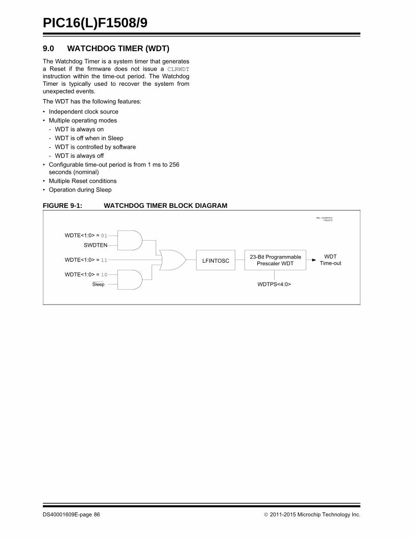
PIC16(L)F1508/9
9.0 WATCHDOG TIMER (WDT)
The Watchdog Timer is a system timer that generatesa Reset if the firmware does not issue a CLRWDTinstruction within the time-out period. The WatchdogTimer is typically used to recover the system fromunexpected events.
The WDT has the following features:
• Independent clock source
• Multiple operating modes
- WDT is always on
- WDT is off when in Sleep
- WDT is controlled by software
- WDT is always off
• Configurable time-out period is from 1 ms to 256 seconds (nominal)
• Multiple Reset conditions
• Operation during Sleep
FIGURE 9-1: WATCHDOG TIMER BLOCK DIAGRAM
WDTE<1:0> = 01
SWDTEN
WDTE<1:0> = 11
WDTE<1:0> = 10
23- it Programmable Prescaler WDTLFINTOSC
WDTPS<4:0>
WDT Time-out
Sleep
Rev. 10-000141A7/30/2013
DS40001609E-page 86 2011-2015 Microchip Technology Inc.
PIC16(L)F1508/9
9.1 Independent Clock Source
The WDT derives its time base from the 31 kHzLFINTOSC internal oscillator. Time intervals in thischapter are based on a nominal interval of 1 ms. SeeSection 29.0 “Electrical Specifications” for theLFINTOSC tolerances.
9.2 WDT Operating Modes
The Watchdog Timer module has four operating modescontrolled by the WDTE<1:0> bits in ConfigurationWords. See Table 9-1.
9.2.1 WDT IS ALWAYS ON
When the WDTE bits of Configuration Words are set to‘11’, the WDT is always on.
WDT protection is active during Sleep.
9.2.2 WDT IS OFF IN SLEEP
When the WDTE bits of Configuration Words are set to‘10’, the WDT is on, except in Sleep.
WDT protection is not active during Sleep.
9.2.3 WDT CONTROLLED BY SOFTWARE
When the WDTE bits of Configuration Words are set to‘01’, the WDT is controlled by the SWDTEN bit of theWDTCON register.
WDT protection is unchanged by Sleep. See Table 9-1for more details.
TABLE 9-1: WDT OPERATING MODES
9.3 Time-Out Period
The WDTPS bits of the WDTCON register set thetime-out period from 1 ms to 256 seconds (nominal).After a Reset, the default time-out period is twoseconds.
9.4 Clearing the WDT
The WDT is cleared when any of the following condi-tions occur:
• Any Reset
• CLRWDT instruction is executed
• Device enters Sleep
• Device wakes up from Sleep
• Oscillator fail
• WDT is disabled
• Oscillator Start-up Timer (OST) is running
See Table 9-2 for more information.
9.5 Operation During Sleep
When the device enters Sleep, the WDT is cleared. Ifthe WDT is enabled during Sleep, the WDT resumescounting. When the device exits Sleep, the WDT iscleared again.
The WDT remains clear until the OST, if enabled, com-pletes. See Section 5.0 “Oscillator Module (WithFail-Safe Clock Monitor)” for more information on theOST.
When a WDT time-out occurs while the device is inSleep, no Reset is generated. Instead, the devicewakes up and resumes operation. The TO and PD bitsin the STATUS register are changed to indicate theevent. The RWDT bit in the PCON register can also beused. See Section 3.0 “Memory Organization” formore information.
WDTE<1:0> SWDTENDevice Mode
WDT Mode
11 X X Active
10 XAwake Active
Sleep Disabled
011 X Active
0 X Disabled
00 X X Disabled
TABLE 9-2: WDT CLEARING CONDITIONS
Conditions WDT
WDTE<1:0> = 00
Cleared
WDTE<1:0> = 01 and SWDTEN = 0
WDTE<1:0> = 10 and enter Sleep
CLRWDT Command
Oscillator Fail Detected
Exit Sleep + System Clock = T1OSC, EXTRC, INTOSC, EXTCLK
Exit Sleep + System Clock = XT, HS, LP Cleared until the end of OST
Change INTOSC divider (IRCF bits) Unaffected
2011-2015 Microchip Technology Inc. DS40001609E-page 87

PIC16(L)F1508/9
9.6 Register Definitions: Watchdog Timer Control
REGISTER 9-1: WDTCON: WATCHDOG TIMER CONTROL REGISTER
U-0 U-0 R/W-0/0 R/W-1/1 R/W-0/0 R/W-1/1 R/W-1/1 R/W-0/0
— — WDTPS<4:0> SWDTEN
bit 7 bit 0
Legend:
R = Readable bit W = Writable bit U = Unimplemented bit, read as ‘0’
u = Bit is unchanged x = Bit is unknown -n/n = Value at POR and BOR/Value at all other Resets
‘1’ = Bit is set ‘0’ = Bit is cleared
bit 7-6 Unimplemented: Read as ‘0’
bit 5-1 WDTPS<4:0>: Watchdog Timer Period Select bits(1)
Bit Value = Prescale Rate
11111 = Reserved. Results in minimum interval (1:32) • • •
10011 = Reserved. Results in minimum interval (1:32)
10010 = 1:8388608 (223) (Interval 256s nominal)10001 = 1:4194304 (222) (Interval 128s nominal)10000 = 1:2097152 (221) (Interval 64s nominal)01111 = 1:1048576 (220) (Interval 32s nominal)01110 = 1:524288 (219) (Interval 16s nominal)01101 = 1:262144 (218) (Interval 8s nominal)01100 = 1:131072 (217) (Interval 4s nominal)01011 = 1:65536 (Interval 2s nominal) (Reset value)01010 = 1:32768 (Interval 1s nominal)01001 = 1:16384 (Interval 512 ms nominal)01000 = 1:8192 (Interval 256 ms nominal)00111 = 1:4096 (Interval 128 ms nominal)00110 = 1:2048 (Interval 64 ms nominal)00101 = 1:1024 (Interval 32 ms nominal)00100 = 1:512 (Interval 16 ms nominal)00011 = 1:256 (Interval 8 ms nominal)00010 = 1:128 (Interval 4 ms nominal)00001 = 1:64 (Interval 2 ms nominal)00000 = 1:32 (Interval 1 ms nominal)
bit 0 SWDTEN: Software Enable/Disable for Watchdog Timer bit
If WDTE<1:0> = 1x:This bit is ignored.If WDTE<1:0> = 01:1 = WDT is turned on0 = WDT is turned offIf WDTE<1:0> = 00:This bit is ignored.
Note 1: Times are approximate. WDT time is based on 31 kHz LFINTOSC.
DS40001609E-page 88 2011-2015 Microchip Technology Inc.

PIC16(L)F1508/9
TABLE 9-3: SUMMARY OF REGISTERS ASSOCIATED WITH WATCHDOG TIMER
TABLE 9-4: SUMMARY OF CONFIGURATION WORD WITH WATCHDOG TIMER
Name Bit 7 Bit 6 Bit 5 Bit 4 Bit 3 Bit 2 Bit 1 Bit 0Register on Page
OSCCON — IRCF<3:0> — SCS<1:0> 59
PCON STKOVF STKUNF — RWDT RMCLR RI POR BOR 68
STATUS — — — TO PD Z DC C 19
WDTCON — — WDTPS<4:0> SWDTEN 88
Legend: x = unknown, u = unchanged, – = unimplemented locations read as ‘0’. Shaded cells are not used by Watchdog Timer.
Name Bits Bit -/7 Bit -/6 Bit 13/5 Bit 12/4 Bit 11/3 Bit 10/2 Bit 9/1 Bit 8/0Register on Page
CONFIG113:8 — — FCMEN IESO CLKOUTEN BOREN<1:0> —
417:0 CP MCLRE PWRTE WDTE<1:0> FOSC<2:0>
Legend: — = unimplemented location, read as ‘0’. Shaded cells are not used by Watchdog Timer.
2011-2015 Microchip Technology Inc. DS40001609E-page 89

PIC16(L)F1508/9
10.0 FLASH PROGRAM MEMORY CONTROL
The Flash program memory is readable and writableduring normal operation over the full VDD range.Program memory is indirectly addressed using SpecialFunction Registers (SFRs). The SFRs used to accessprogram memory are:
• PMCON1
• PMCON2
• PMDATL
• PMDATH
• PMADRL
• PMADRH
When accessing the program memory, thePMDATH:PMDATL register pair forms a 2-byte wordthat holds the 14-bit data for read/write, and thePMADRH:PMADRL register pair forms a 2-byte wordthat holds the 15-bit address of the program memorylocation being read.
The write time is controlled by an on-chip timer. Thewrite/erase voltages are generated by an on-chip chargepump rated to operate over the operating voltage rangeof the device.
The Flash program memory can be protected in twoways; by code protection (CP bit in Configuration Words)and write protection (WRT<1:0> bits in ConfigurationWords).
Code protection (CP = 0)(1), disables access, readingand writing, to the Flash program memory via externaldevice programmers. Code protection does not affectthe self-write and erase functionality. Code protectioncan only be reset by a device programmer performinga Bulk Erase to the device, clearing all Flash programmemory, Configuration bits and User IDs.
Write protection prohibits self-write and erase to aportion or all of the Flash program memory, as definedby the bits WRT<1:0>. Write protection does not affecta device programmers ability to read, write or erase thedevice.
10.1 PMADRL and PMADRH Registers
The PMADRH:PMADRL register pair can address upto a maximum of 32K words of program memory. Whenselecting a program address value, the MSB of theaddress is written to the PMADRH register and the LSBis written to the PMADRL register.
10.1.1 PMCON1 AND PMCON2 REGISTERS
PMCON1 is the control register for Flash programmemory accesses.
Control bits RD and WR initiate read and write,respectively. These bits cannot be cleared, only set, insoftware. They are cleared by hardware at completionof the read or write operation. The inability to clear theWR bit in software prevents the accidental, prematuretermination of a write operation.
The WREN bit, when set, will allow a write operation tooccur. On power-up, the WREN bit is clear. TheWRERR bit is set when a write operation is interruptedby a Reset during normal operation. In these situations,following Reset, the user can check the WRERR bitand execute the appropriate error handling routine.
The PMCON2 register is a write-only register. Attemptingto read the PMCON2 register will return all ‘0’s.
To enable writes to the program memory, a specificpattern (the unlock sequence), must be written to thePMCON2 register. The required unlock sequenceprevents inadvertent writes to the program memorywrite latches and Flash program memory.
10.2 Flash Program Memory Overview
It is important to understand the Flash program memorystructure for erase and programming operations. Flashprogram memory is arranged in rows. A row consists ofa fixed number of 14-bit program memory words. A rowis the minimum size that can be erased by user software.
After a row has been erased, the user can reprogramall or a portion of this row. Data to be written into theprogram memory row is written to 14-bit wide data writelatches. These write latches are not directly accessibleto the user, but may be loaded via sequential writes tothe PMDATH:PMDATL register pair.
See Table 10-1 for Erase Row size and the number ofwrite latches for Flash program memory.
Note 1: Code protection of the entire Flashprogram memory array is enabled byclearing the CP bit of Configuration Words.
Note: If the user wants to modify only a portionof a previously programmed row, then thecontents of the entire row must be readand saved in RAM prior to the erase.Then, new data and retained data can bewritten into the write latches to reprogramthe row of Flash program memory. How-ever, any unprogrammed locations can bewritten without first erasing the row. In thiscase, it is not necessary to save andrewrite the other previously programmedlocations.
TABLE 10-1: FLASH MEMORY ORGANIZATION BY DEVICE
DeviceRow Erase
(words)
Write Latches (words)
PIC16(L)F150832 32
PIC16(L)F1509
DS40001609E-page 90 2011-2015 Microchip Technology Inc.

PIC16(L)F1508/9
10.2.1 READING THE FLASH PROGRAM MEMORY
To read a program memory location, the user must:
1. Write the desired address to thePMADRH:PMADRL register pair.
2. Clear the CFGS bit of the PMCON1 register.
3. Then, set control bit RD of the PMCON1 register.
Once the read control bit is set, the program memoryFlash controller will use the second instruction cycle toread the data. This causes the second instructionimmediately following the “BSF PMCON1,RD” instructionto be ignored. The data is available in the very next cycle,in the PMDATH:PMDATL register pair; therefore, it canbe read as two bytes in the following instructions.
PMDATH:PMDATL register pair will hold this value untilanother read or until it is written to by the user.
FIGURE 10-1: FLASH PROGRAM MEMORY READ FLOWCHART
Note: The two instructions following a programmemory read are required to be NOPs.This prevents the user from executing a2-cycle instruction on the next instructionafter the RD bit is set.
StartRead Operation
SelectProgram or Configuration Memory
(CFGS)
SelectWord Address
(PMADRH:PMADRL)
Initiate Read operation(RD = 1)
Instruction fetched ignoredNOP execution forced
Data read now inPMDATH:PMDATL
Instruction fetched ignoredNOP execution forced
EndRead Operation
Rev. 10-000046A7/30/2013
2011-2015 Microchip Technology Inc. DS40001609E-page 91

PIC16(L)F1508/9
FIGURE 10-2: FLASH PROGRAM MEMORY READ CYCLE EXECUTION
EXAMPLE 10-1: FLASH PROGRAM MEMORY READ
Q1 Q2 Q3 Q4 Q1 Q2 Q3 Q4 Q1 Q2 Q3 Q4 Q1 Q2 Q3 Q4 Q1 Q2 Q3 Q4 Q1 Q2 Q3 Q4
BSF PMCON1,RDexecuted here
INSTR(PC + 1)
executed here
PC PC + 1 PMADRH,PMADRL PC+3 PC + 5Flash ADDR
RD bit
PMDATH,PMDATL
PC + 3 PC + 4
INSTR (PC + 1)
INSTR(PC - 1)executed here
INSTR(PC + 3)executed here
INSTR(PC + 4)executed here
Flash Data
PMDATHPMDATLRegister
INSTR (PC) INSTR (PC + 3) INSTR (PC + 4)
instruction ignoredForced NOP
INSTR(PC + 2)
executed here
instruction ignoredForced NOP
* This code block will read 1 word of program* memory at the memory address:
PROG_ADDR_HI : PROG_ADDR_LO* data will be returned in the variables;* PROG_DATA_HI, PROG_DATA_LO
BANKSEL PMADRL ; Select Bank for PMCON registersMOVLW PROG_ADDR_LO ; MOVWF PMADRL ; Store LSB of addressMOVLW PROG_ADDR_HI ; MOVWF PMADRH ; Store MSB of address
BCF PMCON1,CFGS ; Do not select Configuration SpaceBSF PMCON1,RD ; Initiate readNOP ; Ignored (Figure 10-2)NOP ; Ignored (Figure 10-2)
MOVF PMDATL,W ; Get LSB of wordMOVWF PROG_DATA_LO ; Store in user locationMOVF PMDATH,W ; Get MSB of wordMOVWF PROG_DATA_HI ; Store in user location
DS40001609E-page 92 2011-2015 Microchip Technology Inc.

PIC16(L)F1508/9
10.2.2 FLASH MEMORY UNLOCK SEQUENCE
The unlock sequence is a mechanism that protects theFlash program memory from unintended self-write pro-gramming or erasing. The sequence must be executedand completed without interruption to successfullycomplete any of the following operations:
• Row Erase
• Load program memory write latches
• Write of program memory write latches to program memory
• Write of program memory write latches to User IDs
The unlock sequence consists of the following steps:
1. Write 55h to PMCON2
2. Write AAh to PMCON2
3. Set the WR bit in PMCON1
4. NOP instruction
5. NOP instruction
Once the WR bit is set, the processor will always forcetwo NOP instructions. When an Erase Row or ProgramRow operation is being performed, the processor will stallinternal operations (typical 2 ms), until the operation iscomplete and then resume with the next instruction.When the operation is loading the program memory writelatches, the processor will always force the two NOPinstructions and continue uninterrupted with the nextinstruction.
Since the unlock sequence must not be interrupted,global interrupts should be disabled prior to the unlocksequence and re-enabled after the unlock sequence iscompleted.
FIGURE 10-3: FLASH PROGRAM MEMORY UNLOCK SEQUENCE FLOWCHART
StartUnlock Sequence
EndUnlock Sequence
Write 0x55 toPMCON2
Write 0xAA toPMCON2
InitiateWrite or Erase operation
(WR = 1)
Instruction fetched ignoredNOP execution forced
Instruction fetched ignoredNOP execution forced
Rev. 10-000047A7/30/2013
2011-2015 Microchip Technology Inc. DS40001609E-page 93

PIC16(L)F1508/9
10.2.3 ERASING FLASH PROGRAM MEMORY
While executing code, program memory can only beerased by rows. To erase a row:
1. Load the PMADRH:PMADRL register pair withany address within the row to be erased.
2. Clear the CFGS bit of the PMCON1 register.
3. Set the FREE and WREN bits of the PMCON1register.
4. Write 55h, then AAh, to PMCON2 (Flashprogramming unlock sequence).
5. Set control bit WR of the PMCON1 register tobegin the erase operation.
See Example 10-2.
After the “BSF PMCON1,WR” instruction, the processorrequires two cycles to set up the erase operation. Theuser must place two NOP instructions immediatelyfollowing the WR bit set instruction. The processor willhalt internal operations for the typical 2 ms erase time.This is not Sleep mode as the clocks and peripheralswill continue to run. After the erase cycle, the processorwill resume operation with the third instruction after thePMCON1 write instruction.
FIGURE 10-4: FLASH PROGRAM MEMORY ERASE FLOWCHART
StartErase Operation
EndErase Operation
Disable Interrupts(GIE = 0)
SelectProgram or Configuration Memory
(CFGS)
Select Erase Operation(FREE = 1)
Select Row Address(PMADRH:PMADRL)
Enable Write/Erase Operation(WREN = 1)
Unlock Sequence(See Note 1)
Re-enable Interrupts(GIE = 1)
Disable Write/Erase Operation(WREN = 0)
CPU stalls whileErase operation completes
(2 ms typical)
Rev. 10-000048A7/30/2013
Note 1: See Figure 10-3.
DS40001609E-page 94 2011-2015 Microchip Technology Inc.

PIC16(L)F1508/9
EXAMPLE 10-2: ERASING ONE ROW OF PROGRAM MEMORY
; This row erase routine assumes the following:; 1. A valid address within the erase row is loaded in ADDRH:ADDRL; 2. ADDRH and ADDRL are located in shared data memory 0x70 - 0x7F (common RAM)
BCF INTCON,GIE ; Disable ints so required sequences will execute properlyBANKSEL PMADRLMOVF ADDRL,W ; Load lower 8 bits of erase address boundaryMOVWF PMADRLMOVF ADDRH,W ; Load upper 6 bits of erase address boundaryMOVWF PMADRHBCF PMCON1,CFGS ; Not configuration spaceBSF PMCON1,FREE ; Specify an erase operationBSF PMCON1,WREN ; Enable writes
MOVLW 55h ; Start of required sequence to initiate eraseMOVWF PMCON2 ; Write 55hMOVLW 0AAh ;MOVWF PMCON2 ; Write AAhBSF PMCON1,WR ; Set WR bit to begin eraseNOP ; NOP instructions are forced as processor startsNOP ; row erase of program memory.
;; The processor stalls until the erase process is complete; after erase processor continues with 3rd instruction
BCF PMCON1,WREN ; Disable writesBSF INTCON,GIE ; Enable interrupts
Re
qu
ire
dS
eq
ue
nce
2011-2015 Microchip Technology Inc. DS40001609E-page 95

PIC16(L)F1508/9
10.2.4 WRITING TO FLASH PROGRAM MEMORY
Program memory is programmed using the followingsteps:
1. Load the address in PMADRH:PMADRL of therow to be programmed.
2. Load each write latch with data.
3. Initiate a programming operation.
4. Repeat steps 1 through 3 until all data is written.
Before writing to program memory, the word(s) to bewritten must be erased or previously unwritten. Pro-gram memory can only be erased one row at a time. Noautomatic erase occurs upon the initiation of the write.
Program memory can be written one or more words ata time. The maximum number of words written at onetime is equal to the number of write latches. SeeFigure 10-5 (row writes to program memory with 32write latches) for more details.
The write latches are aligned to the Flash row addressboundary defined by the upper 10-bits ofPMADRH:PMADRL, (PMADRH<6:0>:PMADRL<7:5>)with the lower five bits of PMADRL, (PMADRL<4:0>)determining the write latch being loaded. Write opera-tions do not cross these boundaries. At the completionof a program memory write operation, the data in thewrite latches is reset to contain 0x3FFF.
The following steps should be completed to load thewrite latches and program a row of program memory.These steps are divided into two parts. First, each writelatch is loaded with data from the PMDATH:PMDATLusing the unlock sequence with LWLO = 1. When thelast word to be loaded into the write latch is ready, theLWLO bit is cleared and the unlock sequenceexecuted. This initiates the programming operation,writing all the latches into Flash program memory.
1. Set the WREN bit of the PMCON1 register.
2. Clear the CFGS bit of the PMCON1 register.
3. Set the LWLO bit of the PMCON1 register.When the LWLO bit of the PMCON1 register is‘1’, the write sequence will only load the writelatches and will not initiate the write to Flashprogram memory.
4. Load the PMADRH:PMADRL register pair withthe address of the location to be written.
5. Load the PMDATH:PMDATL register pair withthe program memory data to be written.
6. Execute the unlock sequence (Section10.2.2 “Flash Memory Unlock Sequence”).The write latch is now loaded.
7. Increment the PMADRH:PMADRL register pairto point to the next location.
8. Repeat steps 5 through 7 until all but the lastwrite latch has been loaded.
9. Clear the LWLO bit of the PMCON1 register.When the LWLO bit of the PMCON1 register is‘0’, the write sequence will initiate the write toFlash program memory.
10. Load the PMDATH:PMDATL register pair withthe program memory data to be written.
11. Execute the unlock sequence (Section10.2.2 “Flash Memory Unlock Sequence”).The entire program memory latch content is nowwritten to Flash program memory.
An example of the complete write sequence is shown inExample 10-3. The initial address is loaded into thePMADRH:PMADRL register pair; the data is loadedusing indirect addressing.
Note: The special unlock sequence is requiredto load a write latch with data or initiate aFlash programming operation. If theunlock sequence is interrupted, writing tothe latches or program memory will not beinitiated.
Note: The program memory write latches arereset to the blank state (0x3FFF) at thecompletion of every write or eraseoperation. As a result, it is not necessaryto load all the program memory writelatches. Unloaded latches will remain inthe blank state.
DS40001609E-page 96 2011-2015 Microchip Technology Inc.

2
01
1-2
01
5 M
icroch
ip T
ech
no
log
y Inc.
Sta
tus
DS
40
00
16
09
E-p
ag
e 9
7
PIC
16(L
)F15
08/9
FIG
8
Write Latch #311Fh
1414
14
mory
Write Latch #301Eh
Addr Addr
001Fh001Eh
003Fh003Eh
005Fh005Eh
7FDFh7FDEh
7FFFh7FFEh
14
8009h - 801Fh
gurationords
– 8008h
reserved
emory
MDATL0 Rev. 10-000004A
7/30/2013
URE 10-5: BLOCK WRITES TO FLASH PROGRAM MEMORY WITH 32 WRITE LATCHES
6
14
1414
Program Memory Write Latches
14 14
PMADRH<6:0>:PMADRL<7:5>
Flash Program Me
Row
RowAddressDecode
Addr
Write Latch #101h
Write Latch #000h
Addr
000h 0000h 0001h
001h 0020h 0021h
002h 0040h 0041h
3FEh 7FC0h 7FC1h
3FFh 7FE0h 7FE1h
PMADRL<4:0>
400h 8000h - 8003h
ConfiWUSER ID 0 - 3
8007h8006h
DEVICE IDDev / Revreserved
Configuration M
CFGS = 0
CFGS = 1
PMADRH PMADRL7 6 0 7 5 4 0
c4 c3 c2 c1 c0r9 r8 r7 r6 r5 r4 r3- r1 r0r2
510
PMDATH P7 5 0 7
--
8004h – 8005h

PIC16(L)F1508/9
FIGURE 10-6: FLASH MEMORY WRITE FLOWCHART
StartWrite Operation
EndWrite Operation
CPU stalls while Writeoperation completes
(2 ms typical)
No delay when writing toProgram Memory Latches
Determine number ofwords to be written into
Program or ConfigurationMemory. The number ofwords cannot exceed thenumber of words per row
(word_cnt)
Last word towrite ?
Disable Interrupts(GIE = 0)
SelectProgram or Config.
Memory (CFGS)
Select Row Address(PMADRH:PMADRL)
Select Write Operation(FREE = 0)
Load Write Latches Only(LWLO = 1)
Enable Write/EraseOperation (WREN = 1)
Load the value to write(PMDATH:PMDATL)
Update the word counter(word_cnt--)
Unlock Sequence(See Note 1)
Increment Address(PMADRH:PMADRL++)
Write Latches to Flash(LWLO = 0)
Unlock Sequence(See Note 1)
Disable Write/EraseOperation (WREN = 0)
Re-enable Interrupts(GIE = 1)
Yes
No
Rev. 10-000049A7/30/2013
Note 1: See Figure 10-3.
DS40001609E-page 98 2011-2015 Microchip Technology Inc.

PIC16(L)F1508/9
EXAMPLE 10-3: WRITING TO FLASH PROGRAM MEMORY (32 WRITE LATCHES)
; This write routine assumes the following:; 1. 64 bytes of data are loaded, starting at the address in DATA_ADDR; 2. Each word of data to be written is made up of two adjacent bytes in DATA_ADDR,; stored in little endian format; 3. A valid starting address (the Least Significant bits = 00000) is loaded in ADDRH:ADDRL; 4. ADDRH and ADDRL are located in shared data memory 0x70 - 0x7F (common RAM);
BCF INTCON,GIE ; Disable ints so required sequences will execute properlyBANKSEL PMADRH ; Bank 3MOVF ADDRH,W ; Load initial addressMOVWF PMADRH ;MOVF ADDRL,W ;MOVWF PMADRL ;MOVLW LOW DATA_ADDR ; Load initial data addressMOVWF FSR0L ;MOVLW HIGH DATA_ADDR ; Load initial data addressMOVWF FSR0H ;BCF PMCON1,CFGS ; Not configuration spaceBSF PMCON1,WREN ; Enable writesBSF PMCON1,LWLO ; Only Load Write Latches
LOOPMOVIW FSR0++ ; Load first data byte into lowerMOVWF PMDATL ;MOVIW FSR0++ ; Load second data byte into upperMOVWF PMDATH ;
MOVF PMADRL,W ; Check if lower bits of address are '00000'XORLW 0x1F ; Check if we're on the last of 32 addressesANDLW 0x1F ;BTFSC STATUS,Z ; Exit if last of 32 words,GOTO START_WRITE ;
MOVLW 55h ; Start of required write sequence:MOVWF PMCON2 ; Write 55hMOVLW 0AAh ;MOVWF PMCON2 ; Write AAhBSF PMCON1,WR ; Set WR bit to begin writeNOP ; NOP instructions are forced as processor
; loads program memory write latchesNOP ;
INCF PMADRL,F ; Still loading latches Increment addressGOTO LOOP ; Write next latches
START_WRITEBCF PMCON1,LWLO ; No more loading latches - Actually start Flash program
; memory write
MOVLW 55h ; Start of required write sequence:MOVWF PMCON2 ; Write 55hMOVLW 0AAh ;MOVWF PMCON2 ; Write AAhBSF PMCON1,WR ; Set WR bit to begin writeNOP ; NOP instructions are forced as processor writes
; all the program memory write latches simultaneouslyNOP ; to program memory.
; After NOPs, the processor; stalls until the self-write process in complete; after write processor continues with 3rd instruction
BCF PMCON1,WREN ; Disable writesBSF INTCON,GIE ; Enable interrupts
Re
qu
ire
dS
eq
ue
nce
Re
qu
ire
dS
eq
ue
nce
2011-2015 Microchip Technology Inc. DS40001609E-page 99

PIC16(L)F1508/9
10.3 Modifying Flash Program Memory
When modifying existing data in a program memoryrow, and data within that row must be preserved, it mustfirst be read and saved in a RAM image. Programmemory is modified using the following steps:
1. Load the starting address of the row to bemodified.
2. Read the existing data from the row into a RAMimage.
3. Modify the RAM image to contain the new datato be written into program memory.
4. Load the starting address of the row to berewritten.
5. Erase the program memory row.
6. Load the write latches with data from the RAMimage.
7. Initiate a programming operation.
FIGURE 10-7: FLASH PROGRAM MEMORY MODIFY FLOWCHART
StartModify Operation
EndModify Operation
Read Operation(See Note 1)
An image of the entire rowread must be stored in RAM
Erase Operation(See Note 2)
Modify ImageThe words to be modified arechanged in the RAM image
Write OperationUse RAM image
(See Note 3)
Rev. 10-000050A7/30/2013
Note 1: See Figure 10-2.
2: See Figure 10-4.
3: See Figure 10-5.
DS40001609E-page 100 2011-2015 Microchip Technology Inc.

PIC16(L)F1508/9
10.4 User ID, Device ID and Configuration Word Access
Instead of accessing program memory, the User ID’s,Device ID/Revision ID and Configuration Words can beaccessed when CFGS = 1 in the PMCON1 register.This is the region that would be pointed to byPC<15> = 1, but not all addresses are accessible.Different access may exist for reads and writes. Referto Table 10-2.
When read access is initiated on an address outsidethe parameters listed in Table 10-2, thePMDATH:PMDATL register pair is cleared, readingback ‘0’s.
TABLE 10-2: USER ID, DEVICE ID AND CONFIGURATION WORD ACCESS (CFGS = 1)
EXAMPLE 10-4: CONFIGURATION WORD AND DEVICE ID ACCESS
Address Function Read Access Write Access
8000h-8003h User IDs Yes Yes
8006h Device ID/Revision ID Yes No
8007h-8008h Configuration Words 1 and 2 Yes No
* This code block will read 1 word of program memory at the memory address:* PROG_ADDR_LO (must be 00h-08h) data will be returned in the variables;* PROG_DATA_HI, PROG_DATA_LO
BANKSEL PMADRL ; Select correct BankMOVLW PROG_ADDR_LO ; MOVWF PMADRL ; Store LSB of addressCLRF PMADRH ; Clear MSB of address
BSF PMCON1,CFGS ; Select Configuration Space BCF INTCON,GIE ; Disable interruptsBSF PMCON1,RD ; Initiate readNOP ; Executed (See Figure 10-2)NOP ; Ignored (See Figure 10-2)BSF INTCON,GIE ; Restore interrupts
MOVF PMDATL,W ; Get LSB of wordMOVWF PROG_DATA_LO ; Store in user locationMOVF PMDATH,W ; Get MSB of wordMOVWF PROG_DATA_HI ; Store in user location
2011-2015 Microchip Technology Inc. DS40001609E-page 101

PIC16(L)F1508/9
10.5 Write Verify
It is considered good programming practice to verify thatprogram memory writes agree with the intended value.Since program memory is stored as a full page then thestored program memory contents are compared with theintended data stored in RAM after the last write iscomplete.
FIGURE 10-8: FLASH PROGRAM MEMORY VERIFY FLOWCHART
StartVerify Operation
This routine assumes that the lastrow of data written was from an
image saved on RAM. This imagewill be used to verify the data
currently stored in Flash ProgramMemory
FailVerify Operation
Last word ?
PMDAT =RAM image ?
Read Operation(See Note 1)
EndVerify Operation
No
No
Yes
Yes
Rev. 10-000051A7/30/2013
Note 1: See Figure 10-2.
DS40001609E-page 102 2011-2015 Microchip Technology Inc.

PIC16(L)F1508/9
10.6 Register Definitions: Flash Program Memory Control
REGISTER 10-1: PMDATL: PROGRAM MEMORY DATA LOW BYTE REGISTER
R/W-x/u R/W-x/u R/W-x/u R/W-x/u R/W-x/u R/W-x/u R/W-x/u R/W-x/u
PMDAT<7:0>
bit 7 bit 0
Legend:
R = Readable bit W = Writable bit U = Unimplemented bit, read as ‘0’
u = Bit is unchanged x = Bit is unknown -n/n = Value at POR and BOR/Value at all other Resets
‘1’ = Bit is set ‘0’ = Bit is cleared
bit 7-0 PMDAT<7:0>: Read/write value for Least Significant bits of program memory
REGISTER 10-2: PMDATH: PROGRAM MEMORY DATA HIGH BYTE REGISTER
U-0 U-0 R/W-x/u R/W-x/u R/W-x/u R/W-x/u R/W-x/u R/W-x/u
— — PMDAT<13:8>
bit 7 bit 0
Legend:
R = Readable bit W = Writable bit U = Unimplemented bit, read as ‘0’
u = Bit is unchanged x = Bit is unknown -n/n = Value at POR and BOR/Value at all other Resets
‘1’ = Bit is set ‘0’ = Bit is cleared
bit 7-6 Unimplemented: Read as ‘0’
bit 5-0 PMDAT<13:8>: Read/write value for Most Significant bits of program memory
REGISTER 10-3: PMADRL: PROGRAM MEMORY ADDRESS LOW BYTE REGISTER
R/W-0/0 R/W-0/0 R/W-0/0 R/W-0/0 R/W-0/0 R/W-0/0 R/W-0/0 R/W-0/0
PMADR<7:0>
bit 7 bit 0
Legend:
R = Readable bit W = Writable bit U = Unimplemented bit, read as ‘0’
u = Bit is unchanged x = Bit is unknown -n/n = Value at POR and BOR/Value at all other Resets
‘1’ = Bit is set ‘0’ = Bit is cleared
bit 7-0 PMADR<7:0>: Specifies the Least Significant bits for program memory address
REGISTER 10-4: PMADRH: PROGRAM MEMORY ADDRESS HIGH BYTE REGISTER
U-1 R/W-0/0 R/W-0/0 R/W-0/0 R/W-0/0 R/W-0/0 R/W-0/0 R/W-0/0
—(1) PMADR<14:8>
bit 7 bit 0
Legend:
R = Readable bit W = Writable bit U = Unimplemented bit, read as ‘0’
u = Bit is unchanged x = Bit is unknown -n/n = Value at POR and BOR/Value at all other Resets
‘1’ = Bit is set ‘0’ = Bit is cleared
bit 7 Unimplemented: Read as ‘1’
bit 6-0 PMADR<14:8>: Specifies the Most Significant bits for program memory address
Note 1: Unimplemented, read as ‘1’.
2011-2015 Microchip Technology Inc. DS40001609E-page 103

PIC16(L)F1508/9
REGISTER 10-5: PMCON1: PROGRAM MEMORY CONTROL 1 REGISTER
U-1 R/W-0/0 R/W-0/0 R/W/HC-0/0 R/W/HC-x/q(2) R/W-0/0 R/S/HC-0/0 R/S/HC-0/0
—(1) CFGS LWLO FREE WRERR WREN WR RD
bit 7 bit 0
Legend:
R = Readable bit W = Writable bit U = Unimplemented bit, read as ‘0’
S = Bit can only be set x = Bit is unknown -n/n = Value at POR and BOR/Value at all other Resets
‘1’ = Bit is set ‘0’ = Bit is cleared HC = Bit is cleared by hardware
bit 7 Unimplemented: Read as ‘1’
bit 6 CFGS: Configuration Select bit1 = Access Configuration, User ID and Device ID Registers0 = Access Flash program memory
bit 5 LWLO: Load Write Latches Only bit(3)
1 = Only the addressed program memory write latch is loaded/updated on the next WR command0 = The addressed program memory write latch is loaded/updated and a write of all program memory write latches
will be initiated on the next WR command
bit 4 FREE: Program Flash Erase Enable bit 1 = Performs an erase operation on the next WR command (hardware cleared upon completion)0 = Performs a write operation on the next WR command
bit 3 WRERR: Program/Erase Error Flag bit1 = Condition indicates an improper program or erase sequence attempt or termination (bit is set automatically
on any set attempt (write ‘1’) of the WR bit).0 = The program or erase operation completed normally.
bit 2 WREN: Program/Erase Enable bit1 = Allows program/erase cycles0 = Inhibits programming/erasing of program Flash
bit 1 WR: Write Control bit1 = Initiates a program Flash program/erase operation.
The operation is self-timed and the bit is cleared by hardware once operation is complete. The WR bit can only be set (not cleared) in software.
0 = Program/erase operation to the Flash is complete and inactive.
bit 0 RD: Read Control bit1 = Initiates a program Flash read. Read takes one cycle. RD is cleared in hardware. The RD bit can only be set
(not cleared) in software.0 = Does not initiate a program Flash read.
Note 1: Unimplemented bit, read as ‘1’.2: The WRERR bit is automatically set by hardware when a program memory write or erase operation is started (WR = 1).3: The LWLO bit is ignored during a program memory erase operation (FREE = 1).
DS40001609E-page 104 2011-2015 Microchip Technology Inc.

PIC16(L)F1508/9
TABLE 10-3: SUMMARY OF REGISTERS ASSOCIATED WITH FLASH PROGRAM MEMORY
TABLE 10-4: SUMMARY OF CONFIGURATION WORD WITH RESETS
REGISTER 10-6: PMCON2: PROGRAM MEMORY CONTROL 2 REGISTER
W-0/0 W-0/0 W-0/0 W-0/0 W-0/0 W-0/0 W-0/0 W-0/0
Program Memory Control Register 2
bit 7 bit 0
Legend:
R = Readable bit W = Writable bit U = Unimplemented bit, read as ‘0’
S = Bit can only be set x = Bit is unknown -n/n = Value at POR and BOR/Value at all other Resets
‘1’ = Bit is set ‘0’ = Bit is cleared
bit 7-0 Flash Memory Unlock Pattern bits
To unlock writes, a 55h must be written first, followed by an AAh, before setting the WR bit of thePMCON1 register. The value written to this register is used to unlock the writes. There are specifictiming requirements on these writes.
Name Bit 7 Bit 6 Bit 5 Bit 4 Bit 3 Bit 2 Bit 1 Bit 0Register on
Page
INTCON GIE PEIE TMR0IE INTE IOCIE TMR0IF INTF IOCIF 75
PMCON1 —(1) CFGS LWLO FREE WRERR WREN WR RD 104
PMCON2 Program Memory Control Register 2 105
PMADRL PMADRL<7:0> 103
PMADRH —(1) PMADRH<6:0> 103
PMDATL PMDATL<7:0> 103
PMDATH — — PMDATH<5:0> 103
Legend: — = unimplemented location, read as ‘0’. Shaded cells are not used by Flash program memory.Note 1: Unimplemented, read as ‘1’.
Name Bits Bit -/7 Bit -/6 Bit 13/5 Bit 12/4 Bit 11/3 Bit 10/2 Bit 9/1 Bit 8/0Register on Page
CONFIG113:8 — — FCMEN IESO CLKOUTEN BOREN<1:0> —
417:0 CP MCLRE PWRTE WDTE<1:0> FOSC<2:0>
CONFIG213:8 — — LVP — LPBOR BORV STVREN —
437:0 — — — — — — WRT<1:0>
Legend: — = unimplemented location, read as ‘0’. Shaded cells are not used by Resets.
2011-2015 Microchip Technology Inc. DS40001609E-page 105
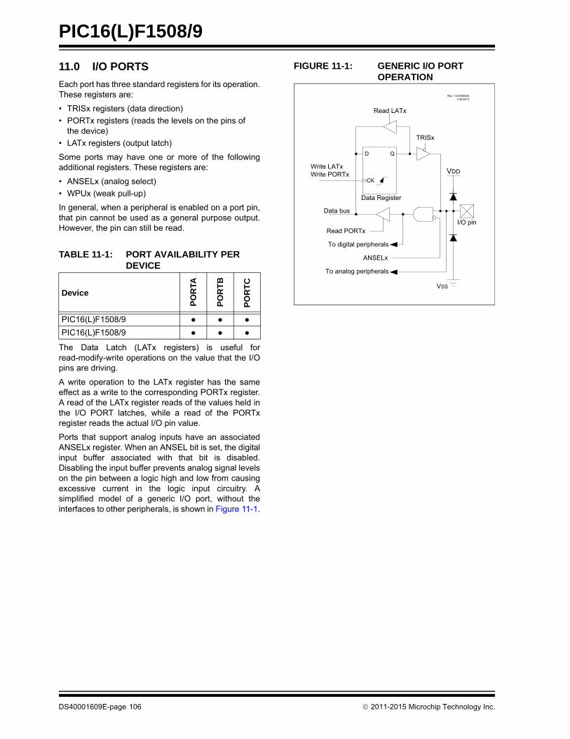
PIC16(L)F1508/9
11.0 I/O PORTS
Each port has three standard registers for its operation.These registers are:
• TRISx registers (data direction)
• PORTx registers (reads the levels on the pins of the device)
• LATx registers (output latch)
Some ports may have one or more of the followingadditional registers. These registers are:
• ANSELx (analog select)
• WPUx (weak pull-up)
In general, when a peripheral is enabled on a port pin,that pin cannot be used as a general purpose output.However, the pin can still be read.
The Data Latch (LATx registers) is useful forread-modify-write operations on the value that the I/Opins are driving.
A write operation to the LATx register has the sameeffect as a write to the corresponding PORTx register.A read of the LATx register reads of the values held inthe I/O PORT latches, while a read of the PORTxregister reads the actual I/O pin value.
Ports that support analog inputs have an associatedANSELx register. When an ANSEL bit is set, the digitalinput buffer associated with that bit is disabled.Disabling the input buffer prevents analog signal levelson the pin between a logic high and low from causingexcessive current in the logic input circuitry. Asimplified model of a generic I/O port, without theinterfaces to other peripherals, is shown in Figure 11-1.
FIGURE 11-1: GENERIC I/O PORT OPERATION
TABLE 11-1: PORT AVAILABILITY PER DEVICE
Device
PO
RTA
PO
RT
B
PO
RT
C
PIC16(L)F1508/9 ● ● ●
PIC16(L)F1508/9 ● ● ●
Write LATxWrite PORTx
Data bus
Read PORTx
To digital peripherals
To analog peripherals
Data Register
TRISx
VSS
I/O pin
ANSELx
D Q
CK
Read LATx
VDD
Rev. 10-000052A7/30/2013
DS40001609E-page 106 2011-2015 Microchip Technology Inc.
PIC16(L)F1508/9
11.1 Alternate Pin Function
The Alternate Pin Function Control (APFCON) registeris used to steer specific peripheral input and outputfunctions between different pins. The APFCON registeris shown in Register 11-1. For this device family, thefollowing functions can be moved between differentpins.
• SS
• T1G
• CLC1
• NCO1
These bits have no effect on the values of any TRISregister. PORT and TRIS overrides will be routed to thecorrect pin. The unselected pin will be unaffected.
11.2 Register Definitions: Alternate Pin Function Control
REGISTER 11-1: APFCON: ALTERNATE PIN FUNCTION CONTROL REGISTER
U-0 U-0 U-0 R/W-0/0 R/W-0/0 U-0 R/W-0/0 R/W-0/0
— — — SSSEL T1GSEL — CLC1SEL NCO1SEL
bit 7 bit 0
Legend:
R = Readable bit W = Writable bit U = Unimplemented bit, read as ‘0’
u = Bit is unchanged x = Bit is unknown -n/n = Value at POR and BOR/Value at all other Resets
‘1’ = Bit is set ‘0’ = Bit is cleared
bit 7-5 Unimplemented: Read as ‘0’
bit 4 SSSEL: Pin Selection bit1 = SS function is on RA30 = SS function is on RC6
bit 3 T1GSEL: Pin Selection bit1 = T1G function is on RA30 = T1G function is on RA4
bit 2 Unimplemented: Read as ‘0’
bit 1 CLC1SEL: Pin Selection bit1 = CLC1 function is on RC50 = CLC1 function is on RA2
bit 0 NCO1SEL: Pin Selection bit1 = NCO1 function is on RC60 = NCO1 function is on RC1
2011-2015 Microchip Technology Inc. DS40001609E-page 107

PIC16(L)F1508/9
11.3 PORTA Registers
11.3.1 DATA REGISTER
PORTA is a 6-bit wide, bidirectional port. Thecorresponding data direction register is TRISA(Register 11-3). Setting a TRISA bit (= 1) will make thecorresponding PORTA pin an input (i.e., disable theoutput driver). Clearing a TRISA bit (= 0) will make thecorresponding PORTA pin an output (i.e., enablesoutput driver and puts the contents of the output latchon the selected pin). The exception is RA3, which isinput-only and its TRIS bit will always read as ‘1’.Example 11-1 shows how to initialize an I/O port.
Reading the PORTA register (Register 11-2) reads thestatus of the pins, whereas writing to it will write to thePORT latch. All write operations are read-modify-writeoperations. Therefore, a write to a port implies that theport pins are read, this value is modified and thenwritten to the PORT data latch (LATA).
11.3.2 DIRECTION CONTROL
The TRISA register (Register 11-3) controls thePORTA pin output drivers, even when they are beingused as analog inputs. The user should ensure the bitsin the TRISA register are maintained set when usingthem as analog inputs. I/O pins configured as analoginput always read ‘0’.
11.3.3 ANALOG CONTROL
The ANSELA register (Register 11-5) is used toconfigure the Input mode of an I/O pin to analog.Setting the appropriate ANSELA bit high will cause alldigital reads on the pin to be read as ‘0’ and allowanalog functions on the pin to operate correctly.
The state of the ANSELA bits has no effect on digitaloutput functions. A pin with TRIS clear and ANSEL setwill still operate as a digital output, but the Input modewill be analog. This can cause unexpected behaviorwhen executing read-modify-write instructions on theaffected port.
EXAMPLE 11-1: INITIALIZING PORTA
11.3.4 PORTA FUNCTIONS AND OUTPUT PRIORITIES
Each PORTA pin is multiplexed with other functions. Thepins, their combined functions and their output prioritiesare shown in Table 11-2.
When multiple outputs are enabled, the actual pincontrol goes to the peripheral with the highest priority.
Analog input functions, such as ADC and comparatorinputs, are not shown in the priority lists. These inputsare active when the I/O pin is set for Analog mode usingthe ANSELx registers. Digital output functions maycontrol the pin when it is in Analog mode with thepriority shown below in Table 11-2.
Note: The ANSELA bits default to the Analogmode after Reset. To use any pins asdigital general purpose or peripheralinputs, the corresponding ANSEL bitsmust be initialized to ‘0’ by user software.
BANKSEL PORTA ;CLRF PORTA ;Init PORTABANKSEL LATA ;Data LatchCLRF LATA ;BANKSEL ANSELA ;CLRF ANSELA ;digital I/OBANKSEL TRISA ;MOVLW B'00111000' ;Set RA<5:3> as inputsMOVWF TRISA ;and set RA<2:0> as
;outputs
TABLE 11-2: PORTA OUTPUT PRIORITY
Pin Name Function Priority(1)
RA0 ICSPDATDAC1OUT1RA0
RA1 RA1
RA2 DAC1OUT2CLC1(2)
C1OUTPWM3RA2
RA3 None
RA4 CLKOUTSOSCORA4
RA5 SOSCIRA5
Note 1: Priority listed from highest to lowest.2: Default pin (see APFCON register).3: Alternate pin (see APFCON register).
DS40001609E-page 108 2011-2015 Microchip Technology Inc.
PIC16(L)F1508/9
11.4 Register Definitions: PORTA
REGISTER 11-2: PORTA: PORTA REGISTER
U-0 U-0 R/W-x/x R/W-x/x R-x/x R/W-x/x R/W-x/x R/W-x/x
— — RA5 RA4 RA3 RA2 RA1 RA0
bit 7 bit 0
Legend:
R = Readable bit W = Writable bit U = Unimplemented bit, read as ‘0’
u = Bit is unchanged x = Bit is unknown -n/n = Value at POR and BOR/Value at all other Resets
‘1’ = Bit is set ‘0’ = Bit is cleared
bit 7-6 Unimplemented: Read as ‘0’
bit 5-0 RA<5:0>: PORTA I/O Value bits(1)
1 = Port pin is > VIH
0 = Port pin is < VIL
Note 1: Writes to PORTA are actually written to corresponding LATA register. Reads from PORTA register is return of actual I/O pin values.
REGISTER 11-3: TRISA: PORTA TRI-STATE REGISTER
U-0 U-0 R/W-1/1 R/W-1/1 U-1 R/W-1/1 R/W-1/1 R/W-1/1
— — TRISA5 TRISA4 —(1) TRISA2 TRISA1 TRISA0
bit 7 bit 0
Legend:
R = Readable bit W = Writable bit U = Unimplemented bit, read as ‘0’
u = Bit is unchanged x = Bit is unknown -n/n = Value at POR and BOR/Value at all other Resets
‘1’ = Bit is set ‘0’ = Bit is cleared
bit 7-6 Unimplemented: Read as ‘0’
bit 5-4 TRISA<5:4>: PORTA Tri-State Control bit1 = PORTA pin configured as an input (tri-stated)0 = PORTA pin configured as an output
bit 3 Unimplemented: Read as ‘1’
bit 2-0 TRISA<2:0>: PORTA Tri-State Control bit1 = PORTA pin configured as an input (tri-stated)0 = PORTA pin configured as an output
Note 1: Unimplemented, read as ‘1’.
2011-2015 Microchip Technology Inc. DS40001609E-page 109

PIC16(L)F1508/9
REGISTER 11-4: LATA: PORTA DATA LATCH REGISTER
U-0 U-0 R/W-x/u R/W-x/u U-0 R/W-x/u R/W-x/u R/W-x/u
— — LATA5 LATA4 — LATA2 LATA1 LATA0
bit 7 bit 0
Legend:
R = Readable bit W = Writable bit U = Unimplemented bit, read as ‘0’
u = Bit is unchanged x = Bit is unknown -n/n = Value at POR and BOR/Value at all other Resets
‘1’ = Bit is set ‘0’ = Bit is cleared
bit 7-6 Unimplemented: Read as ‘0’
bit 5-4 LATA<5:4>: RA<5:4> Output Latch Value bits(1)
bit 3 Unimplemented: Read as ‘0’
bit 2-0 LATA<2:0>: RA<2:0> Output Latch Value bits(1)
Note 1: Writes to PORTA are actually written to corresponding LATA register. Reads from PORTA register is return of actual I/O pin values.
REGISTER 11-5: ANSELA: PORTA ANALOG SELECT REGISTER
U-0 U-0 U-0 R/W-1/1 U-0 R/W-1/1 R/W-1/1 R/W-1/1
— — — ANSA4 — ANSA2 ANSA1 ANSA0
bit 7 bit 0
Legend:
R = Readable bit W = Writable bit U = Unimplemented bit, read as ‘0’
u = Bit is unchanged x = Bit is unknown -n/n = Value at POR and BOR/Value at all other Resets
‘1’ = Bit is set ‘0’ = Bit is cleared
bit 7-5 Unimplemented: Read as ‘0’
bit 4 ANSA4: Analog Select between Analog or Digital Function on pins RA4, respectively1 = Analog input. Pin is assigned as analog input(1). Digital input buffer disabled.0 = Digital I/O. Pin is assigned to port or digital special function.
bit 3 Unimplemented: Read as ‘0’
bit 2-0 ANSA<2:0>: Analog Select between Analog or Digital Function on pins RA<2:0>, respectively1 = Analog input. Pin is assigned as analog input(1). Digital input buffer disabled.0 = Digital I/O. Pin is assigned to port or digital special function.
Note 1: When setting a pin to an analog input, the corresponding TRIS bit must be set to Input mode in order to allow external control of the voltage on the pin.
DS40001609E-page 110 2011-2015 Microchip Technology Inc.

PIC16(L)F1508/9
TABLE 11-3: SUMMARY OF REGISTERS ASSOCIATED WITH PORTA
TABLE 11-4: SUMMARY OF CONFIGURATION WORD WITH PORTA
REGISTER 11-6: WPUA: WEAK PULL-UP PORTA REGISTER
U-0 U-0 R/W-1/1 R/W-1/1 R/W-1/1 R/W-1/1 R/W-1/1 R/W-1/1
— — WPUA5 WPUA4 WPUA3 WPUA2 WPUA1 WPUA0
bit 7 bit 0
Legend:
R = Readable bit W = Writable bit U = Unimplemented bit, read as ‘0’
u = Bit is unchanged x = Bit is unknown -n/n = Value at POR and BOR/Value at all other Resets
‘1’ = Bit is set ‘0’ = Bit is cleared
bit 7-6 Unimplemented: Read as ‘0’
bit 5-0 WPUA<5:0>: Weak Pull-up Register bits(3)
1 = Pull-up enabled0 = Pull-up disabled
Note 1: Global WPUEN bit of the OPTION_REG register must be cleared for individual pull-ups to be enabled.
2: The weak pull-up device is automatically disabled if the pin is configured as an output.
3: For the WPUA3 bit, when MCLRE = 1, weak pull-up is internally enabled, but not reported here.
Name Bit 7 Bit 6 Bit 5 Bit 4 Bit 3 Bit 2 Bit 1 Bit 0Register on Page
ANSELA — — — ANSA4 — ANSA2 ANSA1 ANSA0 110
APFCON — — — SSSEL T1GSEL — CLC1SEL NCO1SEL 107
LATA — — LATA5 LATA4 — LATA2 LATA1 LATA0 110
OPTION_REG WPUEN INTEDG TMR0CS TMR0SE PSA PS<2:0> 154
PORTA — — RA5 RA4 RA3 RA2 RA1 RA0 109
TRISA — — TRISA5 TRISA4 —(1) TRISA2 TRISA1 TRISA0 109
WPUA — — WPUA5 WPUA4 WPUA3 WPUA2 WPUA1 WPUA0 111
Legend: x = unknown, u = unchanged, – = unimplemented locations read as ‘0’. Shaded cells are not used by PORTA.Note 1: Unimplemented, read as ‘1’.
Name Bits Bit -/7 Bit -/6 Bit 13/5 Bit 12/4 Bit 11/3 Bit 10/2 Bit 9/1 Bit 8/0Register on Page
CONFIG113:8 — — FCMEN IESO CLKOUTEN BOREN<1:0> —
417:0 CP MCLRE PWRTE WDTE<1:0> FOSC<2:0>
Legend: — = unimplemented location, read as ‘0’. Shaded cells are not used by PORTA.
2011-2015 Microchip Technology Inc. DS40001609E-page 111

PIC16(L)F1508/9
11.5 PORTB Registers
11.5.1 DATA REGISTER
PORTB is a 4-bit wide, bidirectional port. Thecorresponding data direction register is TRISB(Register 11-8). Setting a TRISB bit (= 1) will make thecorresponding PORTB pin an input (i.e., disable theoutput driver). Clearing a TRISB bit (= 0) will make thecorresponding PORTB pin an output (i.e., enablesoutput driver and puts the contents of the output latchon the selected pin). Example 11-1 shows how toinitialize an I/O port.
Reading the PORTB register (Register 11-7) reads thestatus of the pins, whereas writing to it will write to thePORT latch. All write operations are read-modify-writeoperations. Therefore, a write to a port implies that theport pins are read, this value is modified and thenwritten to the PORT data latch (LATB).
11.5.2 DIRECTION CONTROL
The TRISB register (Register 11-8) controls thePORTB pin output drivers, even when they are beingused as analog inputs. The user should ensure the bitsin the TRISB register are maintained set when usingthem as analog inputs. I/O pins configured as analoginput always read ‘0’.
11.5.3 ANALOG CONTROL
The ANSELB register (Register 11-10) is used toconfigure the Input mode of an I/O pin to analog.Setting the appropriate ANSELB bit high will cause alldigital reads on the pin to be read as ‘0’ and allowanalog functions on the pin to operate correctly.
The state of the ANSELB bits has no effect on digitaloutput functions. A pin with TRIS clear and ANSEL setwill still operate as a digital output, but the Input modewill be analog. This can cause unexpected behaviorwhen executing read-modify-write instructions on theaffected port.
11.5.4 PORTB FUNCTIONS AND OUTPUT PRIORITIES
Each PORTB pin is multiplexed with other functions. Thepins, their combined functions and their output prioritiesare shown in Table 11-5.
When multiple outputs are enabled, the actual pincontrol goes to the peripheral with the highest priority.
Analog input functions, such as ADC and comparatorinputs, are not shown in the priority lists. These inputsare active when the I/O pin is set for Analog mode usingthe ANSELx registers. Digital output functions maycontrol the pin when it is in Analog mode with thepriority shown below in Table 11-5.
Note: The ANSELB bits default to the Analogmode after Reset. To use any pins asdigital general purpose or peripheralinputs, the corresponding ANSEL bitsmust be initialized to ‘0’ by user software.
TABLE 11-5: PORTB OUTPUT PRIORITY
Pin Name Function Priority(1)
RB4 SDARB4
RB5 RB5
RB6 SCLSCKRB6
RB7 CLC3TXRB7
Note 1: Priority listed from highest to lowest.2: Default pin (see APFCON register).3: Alternate pin (see APFCON register).
DS40001609E-page 112 2011-2015 Microchip Technology Inc.

PIC16(L)F1508/9
11.6 Register Definitions: PORTB
REGISTER 11-7: PORTB: PORTB REGISTER
R/W-x/x R/W-x/x R/W-x/x R/W-x/x U-0 U-0 U-0 U-0
RB7 RB6 RB5 RB4 — — — —
bit 7 bit 0
Legend:
R = Readable bit W = Writable bit U = Unimplemented bit, read as ‘0’
u = Bit is unchanged x = Bit is unknown -n/n = Value at POR and BOR/Value at all other Resets
‘1’ = Bit is set ‘0’ = Bit is cleared
bit 7-4 RB<7:4>: PORTB I/O Value bits(1)
1 = Port pin is > VIH
0 = Port pin is < VIL
bit 3-0 Unimplemented: Read as ‘0’
Note 1: Writes to PORTB are actually written to corresponding LATB register. Reads from PORTB register is return of actual I/O pin values.
REGISTER 11-8: TRISB: PORTB TRI-STATE REGISTER
R/W-1/1 R/W-1/1 R/W-1/1 R/W-1/1 U-0 U-0 U-0 U-0
TRISB7 TRISB6 TRISB5 TRISB4 — — — —
bit 7 bit 0
Legend:
R = Readable bit W = Writable bit U = Unimplemented bit, read as ‘0’
u = Bit is unchanged x = Bit is unknown -n/n = Value at POR and BOR/Value at all other Resets
‘1’ = Bit is set ‘0’ = Bit is cleared
bit 7-4 RB<7:4>: PORTB Tri-State Control bits1 = PORTB pin configured as an input (tri-stated)0 = PORTB pin configured as an output
bit 3-0 Unimplemented: Read as ‘0’
2011-2015 Microchip Technology Inc. DS40001609E-page 113

PIC16(L)F1508/9
REGISTER 11-9: LATB: PORTB DATA LATCH REGISTER
R/W-x/u R/W-x/u R/W-x/u R/W-x/u U-0 U-0 U-0 U-0
LATB7 LATB6 LATB5 LATB4 — — — —
bit 7 bit 0
Legend:
R = Readable bit W = Writable bit U = Unimplemented bit, read as ‘0’
u = Bit is unchanged x = Bit is unknown -n/n = Value at POR and BOR/Value at all other Resets
‘1’ = Bit is set ‘0’ = Bit is cleared
bit 7-4 LATB<7:4>: RB<7:4> Output Latch Value bits(1)
bit 3-0 Unimplemented: Read as ‘0’
Note 1: Writes to PORTB are actually written to corresponding LATB register. Reads from PORTB register is return of actual I/O pin values.
REGISTER 11-10: ANSELB: PORTB ANALOG SELECT REGISTER
U-0 U-0 R/W-1/1 R/W-1/1 U-0 U-0 U-0 U-0
— — ANSB5 ANSB4 — — — —
bit 7 bit 0
Legend:
R = Readable bit W = Writable bit U = Unimplemented bit, read as ‘0’
u = Bit is unchanged x = Bit is unknown -n/n = Value at POR and BOR/Value at all other Resets
‘1’ = Bit is set ‘0’ = Bit is cleared
bit 7-6 Unimplemented: Read as ‘0’
bit 5-4 ANSB<5:4>: Analog Select between Analog or Digital Function on pins RB<5:4>, respectively1 = Analog input. Pin is assigned as analog input(1). Digital input buffer disabled.0 = Digital I/O. Pin is assigned to port or digital special function.
bit 3-0 Unimplemented: Read as ‘0’
Note 1: When setting a pin to an analog input, the corresponding TRIS bit must be set to Input mode in order to allow external control of the voltage on the pin.
DS40001609E-page 114 2011-2015 Microchip Technology Inc.

PIC16(L)F1508/9
TABLE 11-6: SUMMARY OF REGISTERS ASSOCIATED WITH PORTB
TABLE 11-7: SUMMARY OF CONFIGURATION WORD WITH PORTB
REGISTER 11-11: WPUB: WEAK PULL-UP PORTB REGISTER(1),(2)
R/W-1/1 R/W-1/1 R/W-1/1 R/W-1/1 U-0 U-0 U-0 U-0
WPUB7 WPUB6 WPUB5 WPUB4 — — — —
bit 7 bit 0
Legend:
R = Readable bit W = Writable bit U = Unimplemented bit, read as ‘0’
u = Bit is unchanged x = Bit is unknown -n/n = Value at POR and BOR/Value at all other Resets
‘1’ = Bit is set ‘0’ = Bit is cleared
bit 7-4 WPUB<7:4>: Weak Pull-up Register bits1 = Pull-up enabled0 = Pull-up disabled
bit 3-0 Unimplemented: Read as ‘0’
Note 1: Global WPUEN bit of the OPTION_REG register must be cleared for individual pull-ups to be enabled.
2: The weak pull-up device is automatically disabled if the pin is configured as an output.
Name Bit 7 Bit 6 Bit 5 Bit 4 Bit 3 Bit 2 Bit 1 Bit 0Register on Page
ANSELB — — ANSB5 ANSB4 — — — — 114
APFCON — — — SSSEL T1GSEL — CLC1SEL NCO1SEL 107
LATB LATB7 LATB6 LATB5 LATB4 — — — — 114
OPTION_REG WPUEN INTEDG TMR0CS TMR0SE PSA PS<2:0> 154
PORTB RB7 RB6 RB5 RB4 — — — — 113
TRISB TRISB7 TRISB6 TRISB5 TRISB4 — — — — 113
WPUB WPUB7 WPUB6 WPUB5 WPUB4 — — — — 115
Legend: x = unknown, u = unchanged, – = unimplemented locations read as ‘0’. Shaded cells are not used by PORTB.Note 1: Unimplemented, read as ‘1’.
Name Bits Bit -/7 Bit -/6 Bit 13/5 Bit 12/4 Bit 11/3 Bit 10/2 Bit 9/1 Bit 8/0Register on Page
CONFIG113:8 — — FCMEN IESO CLKOUTEN BOREN<1:0> —
417:0 CP MCLRE PWRTE WDTE<1:0> FOSC<2:0>
Legend: — = unimplemented location, read as ‘0’. Shaded cells are not used by PORTB.
2011-2015 Microchip Technology Inc. DS40001609E-page 115

PIC16(L)F1508/9
11.7 PORTC Registers
11.7.1 DATA REGISTER
PORTC is a 8-bit wide, bidirectional port. Thecorresponding data direction register is TRISC(Register 11-13). Setting a TRISC bit (= 1) will makethe corresponding PORTC pin an input (i.e., disablethe output driver). Clearing a TRISC bit (= 0) will makethe corresponding PORTC pin an output (i.e., enablethe output driver and put the contents of the outputlatch on the selected pin). Example 11-1 shows how toinitialize an I/O port.
Reading the PORTC register (Register 11-12) reads thestatus of the pins, whereas writing to it will write to thePORT latch. All write operations are read-modify-writeoperations. Therefore, a write to a port implies that theport pins are read, this value is modified and then writtento the PORT data latch (LATC).
11.7.2 DIRECTION CONTROL
The TRISC register (Register 11-13) controls thePORTC pin output drivers, even when they are beingused as analog inputs. The user should ensure the bits inthe TRISC register are maintained set when using themas analog inputs. I/O pins configured as analog inputalways read ‘0’.
11.7.3 ANALOG CONTROL
The ANSELC register (Register 11-15) is used toconfigure the Input mode of an I/O pin to analog.Setting the appropriate ANSELC bit high will cause alldigital reads on the pin to be read as ‘0’ and allowanalog functions on the pin to operate correctly.
The state of the ANSELC bits has no effect on digital out-put functions. A pin with TRIS clear and ANSELC set willstill operate as a digital output, but the Input mode will beanalog. This can cause unexpected behavior when exe-cuting read-modify-write instructions on the affectedport.
11.7.4 PORTC FUNCTIONS AND OUTPUT PRIORITIES
Each PORTC pin is multiplexed with other functions. Thepins, their combined functions and their output prioritiesare shown in Table 11-8.
When multiple outputs are enabled, the actual pincontrol goes to the peripheral with the highest priority.
Analog input and some digital input functions are notincluded in the output priority list. These input functionscan remain active when the pin is configured as anoutput. Certain digital input functions override otherport functions and are included in the output priority list.
Note: The ANSELC bits default to the Analogmode after Reset. To use any pins asdigital general purpose or peripheralinputs, the corresponding ANSEL bitsmust be initialized to ‘0’ by user software.
TABLE 11-8: PORTC OUTPUT PRIORITY
Pin Name Function Priority(1)
RC0 CLC2RC0
RC1 NCO1(2)
PWM4RC1
RC2 RC2
RC3 PWM2RC3
RC4 CWG1BCLC4C2OUTRC4
RC5 CWG1ACLC1(3)
PWM1RC5
RC6 NCO1(3)
RC6
RC7 SDORC7
Note 1: Priority listed from highest to lowest.2: Default pin (see APFCON register).3: Alternate pin (see APFCON register).
DS40001609E-page 116 2011-2015 Microchip Technology Inc.

PIC16(L)F1508/9
11.8 Register Definitions: PORTC
REGISTER 11-12: PORTC: PORTC REGISTER
R/W-x/u R/W-x/u R/W-x/u R/W-x/u R/W-x/u R/W-x/u R/W-x/u R/W-x/u
RC7 RC6 RC5 RC4 RC3 RC2 RC1 RC0
bit 7 bit 0
Legend:
R = Readable bit W = Writable bit U = Unimplemented bit, read as ‘0’
u = Bit is unchanged x = Bit is unknown -n/n = Value at POR and BOR/Value at all other Resets
‘1’ = Bit is set ‘0’ = Bit is cleared
bit 7-0 RC<7:0>: PORTC General Purpose I/O Pin bits1 = Port pin is > VIH
0 = Port pin is < VIL
REGISTER 11-13: TRISC: PORTC TRI-STATE REGISTER
R/W-1/1 R/W-1/1 R/W-1/1 R/W-1/1 R/W-1/1 R/W-1/1 R/W-1/1 R/W-1/1
TRISC7 TRISC6 TRISC5 TRISC4 TRISC3 TRISC2 TRISC1 TRISC0
bit 7 bit 0
Legend:
R = Readable bit W = Writable bit U = Unimplemented bit, read as ‘0’
u = Bit is unchanged x = Bit is unknown -n/n = Value at POR and BOR/Value at all other Resets
‘1’ = Bit is set ‘0’ = Bit is cleared
bit 7-0 TRISC<7:0>: PORTC Tri-State Control bits1 = PORTC pin configured as an input (tri-stated)0 = PORTC pin configured as an output
REGISTER 11-14: LATC: PORTC DATA LATCH REGISTER
R/W-x/u R/W-x/u R/W-x/u R/W-x/u R/W-x/u R/W-x/u R/W-x/u R/W-x/u
LATC7 LATC6 LATC5 LATC4 LATC3 LATC2 LATC1 LATC0
bit 7 bit 0
Legend:
R = Readable bit W = Writable bit U = Unimplemented bit, read as ‘0’
u = Bit is unchanged x = Bit is unknown -n/n = Value at POR and BOR/Value at all other Resets
‘1’ = Bit is set ‘0’ = Bit is cleared
bit 7-0 LATC<7:0>: PORTC Output Latch Value bits(1)
Note 1: Writes to PORTC are actually written to corresponding LATC register. Reads from PORTC register is return of actual I/O pin values.
2011-2015 Microchip Technology Inc. DS40001609E-page 117

PIC16(L)F1508/9
TABLE 11-9: SUMMARY OF REGISTERS ASSOCIATED WITH PORTC
REGISTER 11-15: ANSELC: PORTC ANALOG SELECT REGISTER
R/W-1/1 R/W-1/1 U-0 U-0 R/W-1/1 R/W-1/1 R/W-1/1 R/W-1/1
ANSC7 ANSC6 — — ANSC3 ANSC2 ANSC1 ANSC0
bit 7 bit 0
Legend:
R = Readable bit W = Writable bit U = Unimplemented bit, read as ‘0’
u = Bit is unchanged x = Bit is unknown -n/n = Value at POR and BOR/Value at all other Resets
‘1’ = Bit is set ‘0’ = Bit is cleared
bit 7-6 ANSC<7:6>: Analog Select between Analog or Digital Function on pins RC<7:6>, respectively1 = Analog input. Pin is assigned as analog input(1). Digital input buffer disabled.0 = Digital I/O. Pin is assigned to port or digital special function.
bit 5-4 Unimplemented: Read as ‘0’
bit 3-0 ANSC<3:0>: Analog Select between Analog or Digital Function on pins RC<3:0>, respectively1 = Analog input. Pin is assigned as analog input(1). Digital input buffer disabled.0 = Digital I/O. Pin is assigned to port or digital special function.
Note 1: When setting a pin to an analog input, the corresponding TRIS bit must be set to Input mode in order to allow external control of the voltage on the pin.
Name Bit 7 Bit 6 Bit 5 Bit 4 Bit 3 Bit 2 Bit 1 Bit 0Register on Page
ANSELC ANSC7 ANSC6 — — ANSC3 ANSC2 ANSC1 ANSC0 118
LATC LATC7 LATC6 LATC5 LATC4 LATC3 LATC2 LATC1 LATC0 117
PORTC RC7 RC6 RC5 RC4 RC3 RC2 RC1 RC0 117
TRISC TRISC7 TRISC6 TRISC5 TRISC4 TRISC3 TRISC2 TRISC1 TRISC0 117
Legend: x = unknown, u = unchanged, - = unimplemented locations read as ‘0’. Shaded cells are not used by PORTC.
DS40001609E-page 118 2011-2015 Microchip Technology Inc.

PIC16(L)F1508/9
12.0 INTERRUPT-ON-CHANGE
The PORTA and PORTB pins can be configured tooperate as Interrupt-on-Change (IOC) pins. An interruptcan be generated by detecting a signal that has either arising edge or a falling edge. Any individual port pin, orcombination of port pins, can be configured to generatean interrupt. The interrupt-on-change module has thefollowing features:
• Interrupt-on-Change enable (Master Switch)
• Individual pin configuration
• Rising and falling edge detection
• Individual pin interrupt flags
Figure 12-1 is a block diagram of the IOC module.
12.1 Enabling the Module
To allow individual port pins to generate an interrupt, theIOCIE bit of the INTCON register must be set. If theIOCIE bit is disabled, the edge detection on the pin willstill occur, but an interrupt will not be generated.
12.2 Individual Pin Configuration
For each port pin, a rising edge detector and a fallingedge detector are present. To enable a pin to detect arising edge, the associated bit of the IOCxP register isset. To enable a pin to detect a falling edge, theassociated bit of the IOCxN register is set.
A pin can be configured to detect rising and fallingedges simultaneously by setting both associated bits ofthe IOCxP and IOCxN registers, respectively.
12.3 Interrupt Flags
The IOCAFx and IOCBFx bits located in the IOCAF andIOCBF registers, respectively, are status flags thatcorrespond to the interrupt-on-change pins of theassociated port. If an expected edge is detected on anappropriately enabled pin, then the status flag for that pinwill be set, and an interrupt will be generated if the IOCIEbit is set. The IOCIF bit of the INTCON register reflectsthe status of all IOCAFx and IOCBFx bits.
12.4 Clearing Interrupt Flags
The individual status flags, (IOCAFx and IOCBFx bits),can be cleared by resetting them to zero. If another edgeis detected during this clearing operation, the associatedstatus flag will be set at the end of the sequence,regardless of the value actually being written.
In order to ensure that no detected edge is lost whileclearing flags, only AND operations masking out knownchanged bits should be performed. The followingsequence is an example of what should be performed.
EXAMPLE 12-1: CLEARING INTERRUPT FLAGS(PORTA EXAMPLE)
12.5 Operation in Sleep
The interrupt-on-change interrupt sequence will wakethe device from Sleep mode, if the IOCIE bit is set.
If an edge is detected while in Sleep mode, the IOCxFregister will be updated prior to the first instructionexecuted out of Sleep.
MOVLW 0xffXORWF IOCAF, WANDWF IOCAF, F
2011-2015 Microchip Technology Inc. DS40001609E-page 119

PIC16(L)F1508/9
FIGURE 12-1: INTERRUPT-ON-CHANGE BLOCK DIAGRAM (PORTA EXAMPLE)
IOCANx
IOCAPx
Q2
Q4Q1
data bus =0 or 1
write IOCAFxIOCIE
to data busIOCAFx
edgedetect
IOC interruptto CPU core
from all other IOCnFx individual
pin detectors
D QS
D Q
R
D Q
R
RAx
Q1
Q2
Q3
Q4
Q4Q1
Q1
Q2
Q3
Q4
Q1
Q2
Q3
Q4
Q4Q1 Q4Q1Q4Q1
FOSC
Rev. 10-000 037A6/2/201 4
DS40001609E-page 120 2011-2015 Microchip Technology Inc.

PIC16(L)F1508/9
12.6 Register Definitions: Interrupt-on-Change Control
REGISTER 12-1: IOCAP: INTERRUPT-ON-CHANGE PORTA POSITIVE EDGE REGISTER
U-0 U-0 R/W-0/0 R/W-0/0 R/W-0/0 R/W-0/0 R/W-0/0 R/W-0/0
— — IOCAP5 IOCAP4 IOCAP3 IOCAP2 IOCAP1 IOCAP0
bit 7 bit 0
Legend:
R = Readable bit W = Writable bit U = Unimplemented bit, read as ‘0’
u = Bit is unchanged x = Bit is unknown -n/n = Value at POR and BOR/Value at all other Resets
‘1’ = Bit is set ‘0’ = Bit is cleared
bit 7-6 Unimplemented: Read as ‘0’
bit 5-0 IOCAP<5:0>: Interrupt-on-Change PORTA Positive Edge Enable bits1 = Interrupt-on-Change enabled on the pin for a positive going edge. IOCAFx bit and IOCIF flag will be set
upon detecting an edge.0 = Interrupt-on-Change disabled for the associated pin.
REGISTER 12-2: IOCAN: INTERRUPT-ON-CHANGE PORTA NEGATIVE EDGE REGISTER
U-0 U-0 R/W-0/0 R/W-0/0 R/W-0/0 R/W-0/0 R/W-0/0 R/W-0/0
— — IOCAN5 IOCAN4 IOCAN3 IOCAN2 IOCAN1 IOCAN0
bit 7 bit 0
Legend:
R = Readable bit W = Writable bit U = Unimplemented bit, read as ‘0’
u = Bit is unchanged x = Bit is unknown -n/n = Value at POR and BOR/Value at all other Resets
‘1’ = Bit is set ‘0’ = Bit is cleared
bit 7-6 Unimplemented: Read as ‘0’
bit 5-0 IOCAN<5:0>: Interrupt-on-Change PORTA Negative Edge Enable bits1 = Interrupt-on-Change enabled on the pin for a negative going edge. IOCAFx bit and IOCIF flag will be set
upon detecting an edge.0 = Interrupt-on-Change disabled for the associated pin.
REGISTER 12-3: IOCAF: INTERRUPT-ON-CHANGE PORTA FLAG REGISTER
U-0 U-0 R/W/HS-0/0 R/W/HS-0/0 R/W/HS-0/0 R/W/HS-0/0 R/W/HS-0/0 R/W/HS-0/0
— — IOCAF5 IOCAF4 IOCAF3 IOCAF2 IOCAF1 IOCAF0
bit 7 bit 0
Legend:
R = Readable bit W = Writable bit U = Unimplemented bit, read as ‘0’
u = Bit is unchanged x = Bit is unknown -n/n = Value at POR and BOR/Value at all other Resets
‘1’ = Bit is set ‘0’ = Bit is cleared HS - Bit is set in hardware
bit 7-6 Unimplemented: Read as ‘0’
bit 5-0 IOCAF<5:0>: Interrupt-on-Change PORTA Flag bits1 = An enabled change was detected on the associated pin.
Set when IOCAPx = 1 and a rising edge was detected on RAx, or when IOCANx = 1 and a falling edge wasdetected on RAx.
0 = No change was detected, or the user cleared the detected change.
2011-2015 Microchip Technology Inc. DS40001609E-page 121

PIC16(L)F1508/9
REGISTER 12-4: IOCBP: INTERRUPT-ON-CHANGE PORTB POSITIVE EDGE REGISTER
R/W-0/0 R/W-0/0 R/W-0/0 R/W-0/0 U-0 U-0 U-0 U-0
IOCBP7 IOCBP6 IOCBP5 IOCBP4 — — — —
bit 7 bit 0
Legend:
R = Readable bit W = Writable bit U = Unimplemented bit, read as ‘0’
u = Bit is unchanged x = Bit is unknown -n/n = Value at POR and BOR/Value at all other Resets
‘1’ = Bit is set ‘0’ = Bit is cleared
bit 7-4 IOCBP<7:4>: Interrupt-on-Change PORTB Positive Edge Enable bits1 = Interrupt-on-Change enabled on the pin for a positive going edge. IOCBFx bit and IOCIF flag will be set
upon detecting an edge.0 = Interrupt-on-Change disabled for the associated pin.
bit 3-0 Unimplemented: Read as ‘0’
REGISTER 12-5: IOCBN: INTERRUPT-ON-CHANGE PORTB NEGATIVE EDGE REGISTER
R/W-0/0 R/W-0/0 R/W-0/0 R/W-0/0 U-0 U-0 U-0 U-0
IOCBN7 IOCBN6 IOCBN5 IOCBN4 — — — —
bit 7 bit 0
Legend:
R = Readable bit W = Writable bit U = Unimplemented bit, read as ‘0’
u = Bit is unchanged x = Bit is unknown -n/n = Value at POR and BOR/Value at all other Resets
‘1’ = Bit is set ‘0’ = Bit is cleared
bit 7-4 IOCBN<7:4>: Interrupt-on-Change PORTB Negative Edge Enable bits1 = Interrupt-on-Change enabled on the pin for a negative going edge. IOCBFx bit and IOCIF flag will be set
upon detecting an edge.0 = Interrupt-on-Change disabled for the associated pin.
bit 3-0 Unimplemented: Read as ‘0’
REGISTER 12-6: IOCBF: INTERRUPT-ON-CHANGE PORTB FLAG REGISTER
R/W/HS-0/0 R/W/HS-0/0 R/W/HS-0/0 R/W/HS-0/0 U-0 U-0 U-0 U-0
IOCBF7 IOCBF6 IOCBF5 IOCBF4 — — — —
bit 7 bit 0
Legend:
R = Readable bit W = Writable bit U = Unimplemented bit, read as ‘0’
u = Bit is unchanged x = Bit is unknown -n/n = Value at POR and BOR/Value at all other Resets
‘1’ = Bit is set ‘0’ = Bit is cleared HS - Bit is set in hardware
bit 7-4 IOCBF<7:4>: Interrupt-on-Change PORTB Flag bits1 = An enabled change was detected on the associated pin.
Set when IOCBPx = 1 and a rising edge was detected on RBx, or when IOCBNx = 1 and a falling edge wasdetected on RBx.
0 = No change was detected, or the user cleared the detected change.
bit 3-0 Unimplemented: Read as ‘0’
DS40001609E-page 122 2011-2015 Microchip Technology Inc.

PIC16(L)F1508/9
TABLE 12-1: SUMMARY OF REGISTERS ASSOCIATED WITH INTERRUPT-ON-CHANGE
Name Bit 7 Bit 6 Bit 5 Bit 4 Bit 3 Bit 2 Bit 1 Bit 0Register on Page
ANSELA — — — ANSA4 — ANSA2 ANSA1 ANSA0 110
INTCON GIE PEIE TMR0IE INTE IOCIE TMR0IF INTF IOCIF 75
IOCAF — — IOCAF5 IOCAF4 IOCAF3 IOCAF2 IOCAF1 IOCAF0 121
IOCAN — — IOCAN5 IOCAN4 IOCAN3 IOCAN2 IOCAN1 IOCAN0 121
IOCAP — — IOCAP5 IOCAP4 IOCAP3 IOCAP2 IOCAP1 IOCAP0 121
IOCBF IOCBF7 IOCBF6 IOCBF5 IOCBF4 — — — — 122
IOCBN IOCBN7 IOCBN6 IOCBN5 IOCBN4 — — — — 122
IOCBP IOCBP7 IOCBP6 IOCBP5 IOCBP4 — — — — 122
TRISA — — TRISA5 TRISA4 —(1) TRISA2 TRISA1 TRISA0 109
TRISB TRISB7 TRISB6 TRISB5 TRISB4 — — — — 113
Legend: — = unimplemented location, read as ‘0’. Shaded cells are not used by interrupt-on-change.Note 1: Unimplemented, read as ‘1’.
2011-2015 Microchip Technology Inc. DS40001609E-page 123

PIC16(L)F1508/9
13.0 FIXED VOLTAGE REFERENCE (FVR)
The Fixed Voltage Reference (FVR) is a stable voltagereference, independent of VDD, with a nominal outputlevel (VFVR) of 1.024V. The output of the FVR can beconfigured to supply a reference voltage to thefollowing:
• ADC input channel
• Comparator positive input
• Comparator negative input
The FVR can be enabled by setting the FVREN bit ofthe FVRCON register.
13.1 Independent Gain Amplifier
The output of the FVR supplied to the peripherals, (listedabove), is routed through a programmable gain amplifier.Each amplifier can be programmed for a gain of 1x, 2x or4x, to produce the three possible voltage levels.
The ADFVR<1:0> bits of the FVRCON register areused to enable and configure the gain amplifier settingsfor the reference supplied to the ADC module. Refer-ence Section 15.0 “Analog-to-Digital Converter(ADC) Module” for additional information.
The CDAFVR<1:0> bits of the FVRCON register areused to enable and configure the gain amplifier settingsfor the reference supplied to the comparator modules.Reference Section 17.0 “Comparator Module” foradditional information.
To minimize current consumption when the FVR isdisabled, the FVR buffers should be turned off byclearing the Buffer Gain Selection bits.
13.2 FVR Stabilization Period
When the Fixed Voltage Reference module is enabled,it requires time for the reference and amplifier circuitsto stabilize. Once the circuits stabilize and are ready foruse, the FVRRDY bit of the FVRCON register will beset. See the FVR Stabilization Period characterizationgraph, Figure 30-64.
FIGURE 13-1: VOLTAGE REFERENCE BLOCK DIAGRAM
1x 2x4x
1x 2x4x
ADFVR<1:0>
CDAFVR<1:0>
FVR_buffer1 (To ADC Module)
FVR_buffer2 (To Comparators)
+_FVREN
FVRRDYNote 1
2
2
Rev. 10-000053A8/6/2013
TABLE 13-1: PERIPHERALS REQUIRING THE FIXED VOLTAGE REFERENCE (FVR)
Peripheral Conditions Description
HFINTOSC FOSC<2:0> = 010 and IRCF<3:0> = 000x
INTOSC is active and device is not in Sleep.
BOR
BOREN<1:0> = 11 BOR always enabled.
BOREN<1:0> = 10 and BORFS = 1 BOR disabled in Sleep mode, BOR Fast Start enabled.
BOREN<1:0> = 01 and BORFS = 1 BOR under software control, BOR Fast Start enabled.
LDO All PIC16F1508/9 devices, when VREGPM = 1 and not in Sleep
The device runs off of the Low-Power Regulator when in Sleep mode.
DS40001609E-page 124 2011-2015 Microchip Technology Inc.

PIC16(L)F1508/9
13.3 Register Definitions: FVR Control
TABLE 13-2: SUMMARY OF REGISTERS ASSOCIATED WITH THE FIXED VOLTAGE REFERENCE
REGISTER 13-1: FVRCON: FIXED VOLTAGE REFERENCE CONTROL REGISTER
R/W-0/0 R-q/q R/W-0/0 R/W-0/0 R/W-0/0 R/W-0/0 R/W-0/0 R/W-0/0
FVREN(1) FVRRDY(2) TSEN(3) TSRNG(3) CDAFVR<1:0>(1) ADFVR<1:0>(1)
bit 7 bit 0
Legend:
R = Readable bit W = Writable bit U = Unimplemented bit, read as ‘0’
u = Bit is unchanged x = Bit is unknown -n/n = Value at POR and BOR/Value at all other Resets
‘1’ = Bit is set ‘0’ = Bit is cleared q = Value depends on condition
bit 7 FVREN: Fixed Voltage Reference Enable bit(1)
1 = Fixed Voltage Reference is enabled0 = Fixed Voltage Reference is disabled
bit 6 FVRRDY: Fixed Voltage Reference Ready Flag bit(2)
1 = Fixed Voltage Reference output is ready for use0 = Fixed Voltage Reference output is not ready or not enabled
bit 5 TSEN: Temperature Indicator Enable bit(3)
1 = Temperature Indicator is enabled0 = Temperature Indicator is disabled
bit 4 TSRNG: Temperature Indicator Range Selection bit(3)
1 = VOUT = VDD - 4VT (High Range)0 = VOUT = VDD - 2VT (Low Range)
bit 3-2 CDAFVR<1:0>: Comparator FVR Buffer Gain Selection bits(1)
11 = Comparator FVR Buffer Gain is 4x, with output voltage = 4x VFVR (4.096V nominal)(4)
10 = Comparator FVR Buffer Gain is 2x, with output voltage = 2x VFVR (2.048V nominal)(4)
01 = Comparator FVR Buffer Gain is 1x, with output voltage = 1x VFVR (1.024V nominal)00 = Comparator FVR Buffer is off
bit 1-0 ADFVR<1:0>: ADC FVR Buffer Gain Selection bit(1)
11 = ADC FVR Buffer Gain is 4x, with output voltage = 4x VFVR (4.096V nominal)(4)
10 = ADC FVR Buffer Gain is 2x, with output voltage = 2x VFVR (2.048V nominal)(4)
01 = ADC FVR Buffer Gain is 1x, with output voltage = 1x VFVR (1.024V nominal)00 = ADC FVR Buffer is off
Note 1: To minimize current consumption when the FVR is disabled, the FVR buffers should be turned off by clear-ing the Buffer Gain Selection bits.
2: FVRRDY is always ‘1’ for the PIC16F1508/9 devices.
3: See Section 14.0 “Temperature Indicator Module” for additional information.
4: Fixed Voltage Reference output cannot exceed VDD.
Name Bit 7 Bit 6 Bit 5 Bit 4 Bit 3 Bit 2 Bit 1 Bit 0Register on page
FVRCON FVREN FVRRDY TSEN TSRNG CDAFVR>1:0> ADFVR<1:0> 125
Legend: Shaded cells are unused by the Fixed Voltage Reference module.
2011-2015 Microchip Technology Inc. DS40001609E-page 125

PIC16(L)F1508/9
14.0 TEMPERATURE INDICATOR MODULE
This family of devices is equipped with a temperaturecircuit designed to measure the operating temperatureof the silicon die. The circuit’s range of operatingtemperature falls between -40°C and +85°C. Theoutput is a voltage that is proportional to the devicetemperature. The output of the temperature indicator isinternally connected to the device ADC.
The circuit may be used as a temperature thresholddetector or a more accurate temperature indicator,depending on the level of calibration performed. A one-point calibration allows the circuit to indicate atemperature closely surrounding that point. A two-pointcalibration allows the circuit to sense the entire rangeof temperature more accurately. Reference ApplicationNote AN1333, “Use and Calibration of the InternalTemperature Indicator” (DS01333) for more detailsregarding the calibration process.
14.1 Circuit Operation
Figure 14-1 shows a simplified block diagram of thetemperature circuit. The proportional voltage output isachieved by measuring the forward voltage drop acrossmultiple silicon junctions.
Equation 14-1 describes the output characteristics ofthe temperature indicator.
EQUATION 14-1: VOUT RANGES
The temperature sense circuit is integrated with theFixed Voltage Reference (FVR) module. See Section13.0 “Fixed Voltage Reference (FVR)” for moreinformation.
The circuit is enabled by setting the TSEN bit of theFVRCON register. When disabled, the circuit draws nocurrent.
The circuit operates in either high or low range. The highrange, selected by setting the TSRNG bit of theFVRCON register, provides a wider output voltage. Thisprovides more resolution over the temperature range,but may be less consistent from part to part. This rangerequires a higher bias voltage to operate and thus, ahigher VDD is needed.
The low range is selected by clearing the TSRNG bit ofthe FVRCON register. The low range generates a lowervoltage drop and thus, a lower bias voltage is needed tooperate the circuit. The low range is provided for lowvoltage operation.
FIGURE 14-1: TEMPERATURE CIRCUIT DIAGRAM
14.2 Minimum Operating VDD
When the temperature circuit is operated in low range,the device may be operated at any operating voltagethat is within specifications.
When the temperature circuit is operated in high range,the device operating voltage, VDD, must be highenough to ensure that the temperature circuit iscorrectly biased.
Table 14-1 shows the recommended minimum VDD vs.range setting.
TABLE 14-1: RECOMMENDED VDD VS. RANGE
14.3 Temperature Output
The output of the circuit is measured using the internalAnalog-to-Digital Converter. A channel is reserved forthe temperature circuit output. Refer to Section15.0 “Analog-to-Digital Converter (ADC) Module” fordetailed information.
14.4 ADC Acquisition Time
To ensure accurate temperature measurements, theuser must wait at least 200 s after the ADC inputmultiplexer is connected to the temperature indicatoroutput before the conversion is performed. In addition,the user must wait 200 s between sequentialconversions of the temperature indicator output.
High Range: VOUT = VDD - 4VT
Low Range: VOUT = VDD - 2VT
Min. VDD, TSRNG = 1 Min. VDD, TSRNG = 0
3.6V 1.8V
VOUT
Temp. IndicatorTo ADC
TSRNG
TSEN
Rev. 10-000069A7/31/2013VDD
DS40001609E-page 126 2011-2015 Microchip Technology Inc.

PIC16(L)F1508/9
TABLE 14-2: SUMMARY OF REGISTERS ASSOCIATED WITH THE TEMPERATURE INDICATOR
Name Bit 7 Bit 6 Bit 5 Bit 4 Bit 3 Bit 2 Bit 1 Bit 0Register on page
FVRCON FVREN FVRRDY TSEN TSRNG CDAFVR>1:0> ADFVR<1:0> 125
Legend: Shaded cells are unused by the temperature indicator module.
2011-2015 Microchip Technology Inc. DS40001609E-page 127

PIC16(L)F1508/9
15.0 ANALOG-TO-DIGITAL CONVERTER (ADC) MODULE
The Analog-to-Digital Converter (ADC) allowsconversion of an analog input signal to a 10-bit binaryrepresentation of that signal. This device uses analoginputs, which are multiplexed into a single sample andhold circuit. The output of the sample and hold isconnected to the input of the converter. The convertergenerates a 10-bit binary result via successive
approximation and stores the conversion result into theADC result registers (ADRESH:ADRESL register pair).Figure 15-1 shows the block diagram of the ADC.
The ADC voltage reference is software selectable to beeither internally generated or externally supplied.
The ADC can generate an interrupt upon completion ofa conversion. This interrupt can be used to wake-up thedevice from Sleep.
FIGURE 15-1: ADC BLOCK DIAGRAM
VRPOSVRNEG
Enable
DACx_output
FVR_buffer1
Temp Indicator
CHS<4:0>
ExternalChannel
Inputs
GO/DONEcomplete
start
ADCSample Circuit
Write to bitGO/DONE
VSS
VDD
VREF+ pin
VDD
ADPREF
10-bit Result
ADRESH ADRESL
16
ADFM
10
InternalChannel
Inputs
.
.
.
AN0
ANa
ANz
set bit ADIF
VSS
ADON
sampledinput
Q1
Q2Q4
FoscDivider FOSC
FOSC/n
FRC
ADCClockSelect
ADC_clk
ADCS<2:0>
FRC
ADC CLOCK SOURCE
Trigger Select
Trigger Sources
. . .TRIGSEL<3:0>
AUTO CONVERSIONTRIGGER
PositiveReference
Select
Rev. 10-000033A7/30/2013
DS40001609E-page 128 2011-2015 Microchip Technology Inc.

PIC16(L)F1508/9
15.1 ADC Configuration
When configuring and using the ADC the followingfunctions must be considered:
• Port configuration
• Channel selection
• ADC voltage reference selection
• ADC conversion clock source
• Interrupt control
• Result formatting
15.1.1 PORT CONFIGURATION
The ADC can be used to convert both analog anddigital signals. When converting analog signals, the I/Opin should be configured for analog by setting theassociated TRIS and ANSEL bits. Refer to Section11.0 “I/O Ports” for more information.
15.1.2 CHANNEL SELECTION
There are 15 channel selections available:
• AN<11:0> pins
• Temperature Indicator
• DAC1_output
• FVR_buffer1
The CHS bits of the ADCON0 register determine whichchannel is connected to the sample and hold circuit.
When changing channels, a delay (TACQ) is requiredbefore starting the next conversion. Refer to Section15.2.6 “ADC Conversion Procedure” for more infor-mation.
15.1.3 ADC VOLTAGE REFERENCE
The ADC module uses a positive and a negativevoltage reference. The positive reference is labeledref+ and the negative reference is labeled ref-.
The positive voltage reference (ref+) is selected by theADPREF bits in the ADCON1 register. The positivevoltage reference source can be:
• VREF+ pin
• VDD
The negative voltage reference (ref-) source is:
• VSS
15.1.4 CONVERSION CLOCK
The source of the conversion clock is software select-able via the ADCS bits of the ADCON1 register. Thereare seven possible clock options:
• FOSC/2
• FOSC/4
• FOSC/8
• FOSC/16
• FOSC/32
• FOSC/64
• FRC (internal RC oscillator)
The time to complete one bit conversion is defined asTAD. One full 10-bit conversion requires 11.5 TAD
periods as shown in Figure 15-2.
For correct conversion, the appropriate TAD specifica-tion must be met. Refer to the ADC conversion require-ments in Section 29.0 “Electrical Specifications” formore information. Table 15-1 gives examples ofappropriate ADC clock selections.
Note: Analog voltages on any pin that is definedas a digital input may cause the inputbuffer to conduct excess current.
Note: Unless using the FRC, any changes in thesystem clock frequency will change theADC clock frequency, which mayadversely affect the ADC result.
2011-2015 Microchip Technology Inc. DS40001609E-page 129

PIC16(L)F1508/9
TABLE 15-1: ADC CLOCK PERIOD (TAD) VS. DEVICE OPERATING FREQUENCIES
FIGURE 15-2: ANALOG-TO-DIGITAL CONVERSION TAD CYCLES
ADC Clock Period (TAD) Device Frequency (FOSC)
ADCClock
Source
ADCS<2:0>
20 MHz 16 MHz 8 MHz 4 MHz 1 MHz
Fosc/2 000 100 ns 125 ns 250 ns 500 ns 2.0 s
Fosc/4 100 200 ns 250 ns 500 ns 1.0 s 4.0 s
Fosc/8 001 400 ns 500 ns 1.0 s 2.0 s 8.0 s
Fosc/16 101 800 ns 1.0 s 2.0 s 4.0 s 16.0 s
Fosc/32 010 1.6 s 2.0 s 4.0 s 8.0 s 32.0 s
Fosc/64 110 3.2 s 4.0 s 8.0 s 16.0 s 64.0 s
FRC x11 1.0-6.0 s 1.0-6.0 s 1.0-6.0 s 1.0-6.0 s 1.0-6.0 s
Legend: Shaded cells are outside of recommended range.
Note: The TAD period when using the FRC clock source can fall within a specified range, (see TAD parameter).The TAD period when using the FOSC-based clock source can be configured for a more precise TAD period.However, the FRC clock source must be used when conversions are to be performed with the device inSleep mode.
TAD1 TAD2 TAD3 TAD4 TAD5 TAD6 TAD7 TAD8 TAD9 TAD10 TAD11
Set GO bit
Conversion Starts
Holding capacitor disconnectedfrom analog input (THCD).
On the following cycle:
ADRESH:ADRESL is loaded,GO bit is cleared,
ADIF bit is set,holding capacitor is reconnected to analog input.
b9 b8 b7 b6 b5 b4 b3 b2 b1 b0
Enable ADC (ADON bit)and
Select channel (ACS bits)
THCD
TACQ
Rev. 10-000035A7/30/2013
DS40001609E-page 130 2011-2015 Microchip Technology Inc.

PIC16(L)F1508/9
15.1.5 INTERRUPTS
The ADC module allows for the ability to generate aninterrupt upon completion of an Analog-to-Digitalconversion. The ADC Interrupt Flag is the ADIF bit inthe PIR1 register. The ADC Interrupt Enable is theADIE bit in the PIE1 register. The ADIF bit must becleared in software.
This interrupt can be generated while the device isoperating or while in Sleep. If the device is in Sleep, theinterrupt will wake-up the device. Upon waking fromSleep, the next instruction following the SLEEP instruc-tion is always executed. If the user is attempting towake-up from Sleep and resume in-line code execu-tion, the GIE and PEIE bits of the INTCON registermust be disabled. If the GIE and PEIE bits of theINTCON register are enabled, execution will switch tothe Interrupt Service Routine.
15.1.6 RESULT FORMATTING
The 10-bit ADC conversion result can be supplied intwo formats, left justified or right justified. The ADFM bitof the ADCON1 register controls the output format.
Figure 15-3 shows the two output formats.
FIGURE 15-3: 10-BIT ADC CONVERSION RESULT FORMAT
Note 1: The ADIF bit is set at the completion ofevery conversion, regardless of whetheror not the ADC interrupt is enabled.
2: The ADC operates during Sleep onlywhen the FRC oscillator is selected.
MSB
MSB
LSB
LSB
(ADFM = 0)
(ADFM = 1)
bit 7 bit 7
bit 7bit 7
bit 0
bit 0
bit 0
bit 0
10-bit ADC Result
10-bit ADC ResultUnimplemented: Read as ‘0’
Unimplemented: Read as ‘0’
ADRESH ADRESL
Rev. 10-000054A7/30/2013
2011-2015 Microchip Technology Inc. DS40001609E-page 131

PIC16(L)F1508/9
15.2 ADC Operation
15.2.1 STARTING A CONVERSION
To enable the ADC module, the ADON bit of theADCON0 register must be set to a ‘1’. Setting the GO/DONE bit of the ADCON0 register to a ‘1’ will start theAnalog-to-Digital conversion.
15.2.2 COMPLETION OF A CONVERSION
When the conversion is complete, the ADC module will:
• Clear the GO/DONE bit
• Set the ADIF Interrupt Flag bit
• Update the ADRESH and ADRESL registers with new conversion result
15.2.3 TERMINATING A CONVERSION
If a conversion must be terminated before completion,the GO/DONE bit can be cleared in software. TheADRESH and ADRESL registers will be updated withthe partially complete Analog-to-Digital conversionsample. Incomplete bits will match the last bitconverted.
15.2.4 ADC OPERATION DURING SLEEP
The ADC module can operate during Sleep. Thisrequires the ADC clock source to be set to the FRCoption. Performing the ADC conversion during Sleepcan reduce system noise. If the ADC interrupt isenabled, the device will wake-up from Sleep when theconversion completes. If the ADC interrupt is disabled,the ADC module is turned off after the conversion com-pletes, although the ADON bit remains set.
When the ADC clock source is something other thanFRC, a SLEEP instruction causes the present conver-sion to be aborted and the ADC module is turned off,although the ADON bit remains set.
15.2.5 AUTO-CONVERSION TRIGGER
The auto-conversion trigger allows periodic ADC mea-surements without software intervention. When a risingedge of the selected source occurs, the GO/DONE bitis set by hardware.
The auto-conversion trigger source is selected with theTRIGSEL<3:0> bits of the ADCON2 register.
Using the auto-conversion trigger does not assureproper ADC timing. It is the user’s responsibility toensure that the ADC timing requirements are met.
See Table 15-2 for auto-conversion sources.
Note: The GO/DONE bit should not be set in thesame instruction that turns on the ADC.Refer to Section 15.2.6 “ADC Conver-sion Procedure”.
Note: A device Reset forces all registers to theirReset state. Thus, the ADC module isturned off and any pending conversion isterminated.
TABLE 15-2: AUTO-CONVERSION SOURCES
Source Peripheral Signal Name
Timer0 T0_overflow
Timer1 T1_overflow
Timer2 T2_match
Comparator C1 C1OUT_sync
Comparator C2 C2OUT_sync
CLC1 LC1_out
CLC2 LC2_out
CLC3 LC3_out
CLC4 LC4_out
DS40001609E-page 132 2011-2015 Microchip Technology Inc.

PIC16(L)F1508/9
15.2.6 ADC CONVERSION PROCEDURE
This is an example procedure for using the ADC toperform an Analog-to-Digital conversion:
1. Configure Port:
• Disable pin output driver (Refer to the TRIS register)
• Configure pin as analog (Refer to the ANSEL register)
• Disable weak pull-ups either globally (Refer to the OPTION_REG register) or individually (Refer to the appropriate WPUx register).
2. Configure the ADC module:
• Select ADC conversion clock
• Configure voltage reference
• Select ADC input channel
• Turn on ADC module
3. Configure ADC interrupt (optional):
• Clear ADC interrupt flag
• Enable ADC interrupt
• Enable peripheral interrupt
• Enable global interrupt(1)
4. Wait the required acquisition time(2).
5. Start conversion by setting the GO/DONE bit.
6. Wait for ADC conversion to complete by one ofthe following:
• Polling the GO/DONE bit
• Waiting for the ADC interrupt (interrupts enabled)
7. Read ADC Result.
8. Clear the ADC interrupt flag (required if interruptis enabled).
EXAMPLE 15-1: ADC CONVERSION
Note 1: The global interrupt can be disabled if theuser is attempting to wake-up from Sleepand resume in-line code execution.
2: Refer to Section 15.4 “ADC Acquisi-tion Requirements”.
;This code block configures the ADC;for polling, Vdd and Vss references, FRC ;oscillator and AN0 input.;;Conversion start & polling for completion ; are included.;BANKSEL ADCON1 ;MOVLW B’11110000’ ;Right justify, FRC
;oscillatorMOVWF ADCON1 ;Vdd and Vss Vref+BANKSEL TRISA ;BSF TRISA,0 ;Set RA0 to inputBANKSEL ANSEL ;BSF ANSEL,0 ;Set RA0 to analogBANKSEL WPUABCF WPUA,0 ;Disable weak
pull-up on RA0BANKSEL ADCON0 ;MOVLW B’00000001’ ;Select channel AN0MOVWF ADCON0 ;Turn ADC OnCALL SampleTime ;Acquisiton delayBSF ADCON0,ADGO ;Start conversionBTFSC ADCON0,ADGO ;Is conversion done?GOTO $-1 ;No, test againBANKSEL ADRESH ;MOVF ADRESH,W ;Read upper 2 bitsMOVWF RESULTHI ;store in GPR spaceBANKSEL ADRESL ;MOVF ADRESL,W ;Read lower 8 bitsMOVWF RESULTLO ;Store in GPR space
2011-2015 Microchip Technology Inc. DS40001609E-page 133

PIC16(L)F1508/9
15.3 Register Definitions: ADC Control
REGISTER 15-1: ADCON0: ADC CONTROL REGISTER 0
U-0 R/W-0/0 R/W-0/0 R/W-0/0 R/W-0/0 R/W-0/0 R/W-0/0 R/W-0/0
— CHS<4:0> GO/DONE ADON
bit 7 bit 0
Legend:
R = Readable bit W = Writable bit U = Unimplemented bit, read as ‘0’
u = Bit is unchanged x = Bit is unknown -n/n = Value at POR and BOR/Value at all other Resets
‘1’ = Bit is set ‘0’ = Bit is cleared
bit 7 Unimplemented: Read as ‘0’
bit 6-2 CHS<4:0>: Analog Channel Select bits
00000 = AN000001 = AN100010 = AN200011 = AN300100 = AN400101 = AN500110 = AN600111 = AN701000 = AN801001 = AN901010 = AN1001011 = AN1101100 = Reserved. No channel connected.
• • •
11100 = Reserved. No channel connected.11101 = Temperature Indicator(1)
11110 = DAC (Digital-to-Analog Converter)(3)
11111 = FVR (Fixed Voltage Reference) Buffer 1 Output(2)
bit 1 GO/DONE: ADC Conversion Status bit
1 = ADC conversion cycle in progress. Setting this bit starts an ADC conversion cycle. This bit is automatically cleared by hardware when the ADC conversion has completed.0 = ADC conversion completed/not in progress
bit 0 ADON: ADC Enable bit1 = ADC is enabled0 = ADC is disabled and consumes no operating current
Note 1: See Section 14.0 “Temperature Indicator Module” for more information.
2: See Section 13.0 “Fixed Voltage Reference (FVR)” for more information.
3: See Section 16.0 “5-Bit Digital-to-Analog Converter (DAC) Module” for more information.
DS40001609E-page 134 2011-2015 Microchip Technology Inc.

PIC16(L)F1508/9
REGISTER 15-2: ADCON1: ADC CONTROL REGISTER 1
R/W-0/0 R/W-0/0 R/W-0/0 R/W-0/0 U-0 U-0 R/W-0/0 R/W-0/0
ADFM ADCS<2:0> — — ADPREF<1:0>
bit 7 bit 0
Legend:
R = Readable bit W = Writable bit U = Unimplemented bit, read as ‘0’
u = Bit is unchanged x = Bit is unknown -n/n = Value at POR and BOR/Value at all other Resets
‘1’ = Bit is set ‘0’ = Bit is cleared
bit 7 ADFM: ADC Result Format Select bit1 = Right justified. Six Most Significant bits of ADRESH are set to ‘0’ when the conversion result is
loaded.0 = Left justified. Six Least Significant bits of ADRESL are set to ‘0’ when the conversion result is
loaded.
bit 6-4 ADCS<2:0>: ADC Conversion Clock Select bits000 = FOSC/2001 = FOSC/8010 = FOSC/32011 = FRC (clock supplied from an internal RC oscillator)100 = FOSC/4101 = FOSC/16110 = FOSC/64111 = FRC (clock supplied from an internal RC oscillator)
bit 3-2 Unimplemented: Read as ‘0’
bit 1-0 ADPREF<1:0>: ADC Positive Voltage Reference Configuration bits00 = VRPOS is connected to VDD
01 = Reserved10 = VRPOS is connected to external VREF+ pin(1)
11 = Reserved
Note 1: When selecting the VREF+ pin as the source of the positive reference, be aware that a minimum voltage specification exists. See Section 29.0 “Electrical Specifications” for details.
2011-2015 Microchip Technology Inc. DS40001609E-page 135

PIC16(L)F1508/9
REGISTER 15-3: ADCON2: ADC CONTROL REGISTER 2
R/W-0/0 R/W-0/0 R/W-0/0 R/W-0/0 U-0 U-0 U-0 U-0
TRIGSEL<3:0>(1) — — — —
bit 7 bit 0
Legend:
R = Readable bit W = Writable bit U = Unimplemented bit, read as ‘0’
u = Bit is unchanged x = Bit is unknown -n/n = Value at POR and BOR/Value at all other Resets
‘1’ = Bit is set ‘0’ = Bit is cleared
bit 7-4 TRIGSEL<3:0>: Auto-Conversion Trigger Selection bits(1)
0000 = No auto-conversion trigger selected0001 = Reserved0010 = Reserved0011 = Timer0 – T0_overflow(2)
0100 = Timer1 – T1_overflow(2)
0101 = Timer2 – T2_match0110 = Comparator C1 – C1OUT_sync0111 = Comparator C2 – C2OUT_sync1000 = CLC1 – LC1_out1001 = CLC2 – LC2_out1010 = CLC3 – LC3_out1011 = CLC4 – LC4_out1100 = Reserved1101 = Reserved1110 = Reserved1111 = Reserved
bit 3-0 Unimplemented: Read as ‘0’
Note 1: This is a rising edge sensitive input for all sources.
2: Signal also sets its corresponding interrupt flag.
DS40001609E-page 136 2011-2015 Microchip Technology Inc.

PIC16(L)F1508/9
REGISTER 15-4: ADRESH: ADC RESULT REGISTER HIGH (ADRESH) ADFM = 0
R/W-x/u R/W-x/u R/W-x/u R/W-x/u R/W-x/u R/W-x/u R/W-x/u R/W-x/u
ADRES<9:2>
bit 7 bit 0
Legend:
R = Readable bit W = Writable bit U = Unimplemented bit, read as ‘0’
u = Bit is unchanged x = Bit is unknown -n/n = Value at POR and BOR/Value at all other Resets
‘1’ = Bit is set ‘0’ = Bit is cleared
bit 7-0 ADRES<9:2>: ADC Result Register bitsUpper eight bits of 10-bit conversion result
REGISTER 15-5: ADRESL: ADC RESULT REGISTER LOW (ADRESL) ADFM = 0
R/W-x/u R/W-x/u R/W-x/u R/W-x/u R/W-x/u R/W-x/u R/W-x/u R/W-x/u
ADRES<1:0> — — — — — —
bit 7 bit 0
Legend:
R = Readable bit W = Writable bit U = Unimplemented bit, read as ‘0’
u = Bit is unchanged x = Bit is unknown -n/n = Value at POR and BOR/Value at all other Resets
‘1’ = Bit is set ‘0’ = Bit is cleared
bit 7-6 ADRES<1:0>: ADC Result Register bitsLower two bits of 10-bit conversion result
bit 5-0 Reserved: Do not use.
2011-2015 Microchip Technology Inc. DS40001609E-page 137

PIC16(L)F1508/9
REGISTER 15-6: ADRESH: ADC RESULT REGISTER HIGH (ADRESH) ADFM = 1
R/W-x/u R/W-x/u R/W-x/u R/W-x/u R/W-x/u R/W-x/u R/W-x/u R/W-x/u
— — — — — — ADRES<9:8>
bit 7 bit 0
Legend:
R = Readable bit W = Writable bit U = Unimplemented bit, read as ‘0’
u = Bit is unchanged x = Bit is unknown -n/n = Value at POR and BOR/Value at all other Resets
‘1’ = Bit is set ‘0’ = Bit is cleared
bit 7-2 Reserved: Do not use.
bit 1-0 ADRES<9:8>: ADC Result Register bitsUpper two bits of 10-bit conversion result
REGISTER 15-7: ADRESL: ADC RESULT REGISTER LOW (ADRESL) ADFM = 1
R/W-x/u R/W-x/u R/W-x/u R/W-x/u R/W-x/u R/W-x/u R/W-x/u R/W-x/u
ADRES<7:0>
bit 7 bit 0
Legend:
R = Readable bit W = Writable bit U = Unimplemented bit, read as ‘0’
u = Bit is unchanged x = Bit is unknown -n/n = Value at POR and BOR/Value at all other Resets
‘1’ = Bit is set ‘0’ = Bit is cleared
bit 7-0 ADRES<7:0>: ADC Result Register bitsLower eight bits of 10-bit conversion result
DS40001609E-page 138 2011-2015 Microchip Technology Inc.

PIC16(L)F1508/9
15.4 ADC Acquisition Requirements
For the ADC to meet its specified accuracy, the chargeholding capacitor (CHOLD) must be allowed to fullycharge to the input channel voltage level. The AnalogInput model is shown in Figure 15-4. The sourceimpedance (RS) and the internal sampling switch (RSS)impedance directly affect the time required to chargethe capacitor CHOLD. The sampling switch (RSS)impedance varies over the device voltage (VDD), referto Figure 15-4. The maximum recommendedimpedance for analog sources is 10 k. As the
source impedance is decreased, the acquisition timemay be decreased. After the analog input channel isselected (or changed), an ADC acquisition must bedone before the conversion can be started. To calculatethe minimum acquisition time, Equation 15-1 may beused. This equation assumes that 1/2 LSb error is used(1,024 steps for the ADC). The 1/2 LSb error is themaximum error allowed for the ADC to meet itsspecified resolution.
EQUATION 15-1: ACQUISITION TIME EXAMPLE
TACQ Amplifier Settling Time Hold Capacitor Charging Time Temperature Coefficient+ +=
TAMP TC TCOFF+ +=
2µs TC Temperature - 25°C 0.05µs/°C + +=
TC CHOLD RIC RSS RS+ + ln(1/2047)–=
12.5pF 1k 7k 10k+ + – ln(0.0004885)=
1.72= µs
VAPPLIED 1 e
Tc–RC---------
–
VAPPLIED 11
2n 1+ 1–
--------------------------– =
VAPPLIED 11
2n 1+ 1–
--------------------------– VCHOLD=
VAPPLIED 1 e
TC–RC----------
–
VCHOLD=
;[1] VCHOLD charged to within 1/2 lsb
;[2] VCHOLD charge response to VAPPLIED
;combining [1] and [2]
The value for TC can be approximated with the following equations:
Solving for TC:
Therefore:
Temperature 50°C and external impedance of 10k 5.0V VDD=Assumptions:
Note: Where n = number of bits of the ADC.
TACQ 2µs 1.72µs 50°C- 25°C 0.05µs/°C + +=
4.97µs=
Note 1: The reference voltage (VRPOS) has no effect on the equation, since it cancels itself out.
2: The charge holding capacitor (CHOLD) is not discharged after each conversion.
3: The maximum recommended impedance for analog sources is 10 k. This is required to meet the pin leakage specification.
2011-2015 Microchip Technology Inc. DS40001609E-page 139

PIC16(L)F1508/9
FIGURE 15-4: ANALOG INPUT MODEL
FIGURE 15-5: ADC TRANSFER FUNCTION
VDD
Analog Input pin
CPIN 5pF
VT 0.6V
VT 0.6V
ILEAKAGE(1)
RIC 1K
Legend: CHOLD = Sample/Hold CapacitanceCPIN = Input CapacitanceILEAKAGE = Leakage Current at the pin due to varies injunctionsRIC = Interconnect ResistanceRSS = Resistance of Sampling switchSS = Sampling SwitchVT = Threshold Voltage
VA
RS RSS SS
Sampling switch
CHOLD = 10 pF
Ref-
5 6 7 8 9 1011
2V3V4V5V6V
VDD RSS
Sampling Switch(k )
Rev. 10-000070A8/2/2013
Note 1: Refer to Section 29.0 “Electrical Specifications”.
3FFh
3FEh
AD
C O
utp
ut
Co
de
3FDh
3FCh
03h
02h
01h
00h
Full-Scale
3FBh
0.5 LSB
Ref- Zero-ScaleTransition
Ref+Transition
1.5 LSB
Full-Scale Range
Analog Input Voltage
DS40001609E-page 140 2011-2015 Microchip Technology Inc.

PIC16(L)F1508/9
TABLE 15-3: SUMMARY OF REGISTERS ASSOCIATED WITH ADC
Name Bit 7 Bit 6 Bit 5 Bit 4 Bit 3 Bit 2 Bit 1 Bit 0Register on Page
ADCON0 — CHS<4:0> GO/DONE ADON 134
ADCON1 ADFM ADCS<2:0> — — ADPREF<1:0> 135
ADCON2 TRIGSEL<3:0> — — — — 136
ADRESH ADC Result Register High 137, 138
ADRESL ADC Result Register Low 137, 138
ANSELA — — — ANSA4 — ANSA2 ANSA1 ANSA0 110
ANSELB — — ANSB5 ANSB4 — — — — 114
ANSELC ANSC7 ANSC6 — — ANSC3 ANSC2 ANSC1 ANSC0 118
INTCON GIE PEIE TMR0IE INTE IOCIE TMR0IF INTF IOCIF 75
PIE1 TMR1GIE ADIE RCIE TXIE SSP1IE — TMR2IE TMR1IE 76
PIR1 TMR1GIF ADIF RCIF TXIF SSP1IF — TMR2IF TMR1IF 79
TRISA — — TRISA5 TRISA4 —(1) TRISA2 TRISA1 TRISA0 109
TRISB TRISB7 TRISB6 TRISB5 TRISB4 — — — — 113
TRISC TRISC7 TRISC6 TRISC5 TRISC4 TRISC3 TRISC2 TRISC1 TRISC0 117
FVRCON FVREN FVRRDY TSEN TSRNG CDAFVR<1:0> ADFVR<1:0> 125
Legend: x = unknown, u = unchanged, — = unimplemented read as ‘0’, q = value depends on condition. Shaded cells are not used for ADC module.
Note 1: Unimplemented, read as ‘1’.
2011-2015 Microchip Technology Inc. DS40001609E-page 141

PIC16(L)F1508/9
16.0 5-BIT DIGITAL-TO-ANALOG CONVERTER (DAC) MODULE
The Digital-to-Analog Converter supplies a variablevoltage reference, ratiometric with the input source,with 32 selectable output levels.
The positive input source (VSOURCE+) of the DAC canbe connected to:
• External VREF+ pin
• VDD supply voltage
The negative input source (VSOURCE-) of the DAC canbe connected to:
• Vss
The output of the DAC (DACx_output) can be selectedas a reference voltage to the following:
• Comparator positive input
• ADC input channel
• DACxOUT1 pin
• DACxOUT2 pin
The Digital-to-Analog Converter (DAC) can be enabledby setting the DACEN bit of the DACxCON0 register.
FIGURE 16-1: DIGITAL-TO-ANALOG CONVERTER BLOCK DIAGRAM
VREF+
VDD
DACPSS
VSOURCE+
VSOURCE-VSS
R
32Steps
R
R
R
R
R
R
32-to
-1M
UX
To Peripherals
DACxOUT1 (1)
DACOE1
DACx_output
DACEN
DACR<4:0>5
DACxOUT2 (1)
DACOE2
0
1
Note 1: The unbuffered DACx_output is provided on the DACxOUT pin(s).
Rev. 10-000026A7/30/2013
DS40001609E-page 142 2011-2015 Microchip Technology Inc.

PIC16(L)F1508/9
16.1 Output Voltage Selection
The DAC has 32 voltage level ranges. The 32 levelsare set with the DACR<4:0> bits of the DACxCON1register.
The DAC output voltage can be determined by usingEquation 16-1.
16.2 Ratiometric Output Level
The DAC output value is derived using a resistor ladderwith each end of the ladder tied to a positive andnegative voltage reference input source. If the voltageof either input source fluctuates, a similar fluctuation willresult in the DAC output value.
The value of the individual resistors within the laddercan be found in Table 29-14.
16.3 DAC Voltage Reference Output
The unbuffered DAC voltage can be output to theDACxOUTn pin(s) by setting the respective DACOEnbit(s) of the DACxCON0 register. Selecting the DACreference voltage for output on either DACxOUTn pinautomatically overrides the digital output buffer, theweak pull-up and digital input threshold detectorfunctions of that pin.
Reading the DACxOUTn pin when it has beenconfigured for DAC reference voltage output will
16.4 Operation During Sleep
When the device wakes up from Sleep through aninterrupt or a Watchdog Timer time-out, the contents ofthe DACxCON0 register are not affected. To minimizecurrent consumption in Sleep mode, the voltagereference should be disabled.
16.5 Effects of a Reset
A device Reset affects the following:
• DACx is disabled.
• DACX output voltage is removed from the DACxOUTn pin(s).
• The DACR<4:0> range select bits are cleared.
EQUATION 16-1: DAC OUTPUT VOLTAGE
IF DACEN = 1
DACx_output VSOURCE+ VSOURCE-– DACR 4:0
25
----------------------------- VSOURCE-+=
Note: See the DACxCON0 register for the available VSOURCE+ and VSOURCE- selections.
2011-2015 Microchip Technology Inc. DS40001609E-page 143

PIC16(L)F1508/9
16.6 Register Definitions: DAC Control
TABLE 16-1: SUMMARY OF REGISTERS ASSOCIATED WITH THE DAC MODULE
REGISTER 16-1: DACxCON0: VOLTAGE REFERENCE CONTROL REGISTER 0
R/W-0/0 U-0 R/W-0/0 R/W-0/0 U-0 R/W-0/0 U-0 U-0
DACEN — DACOE1 DACOE2 — DACPSS — —
bit 7 bit 0
Legend:
R = Readable bit W = Writable bit U = Unimplemented bit, read as ‘0’
u = Bit is unchanged x = Bit is unknown -n/n = Value at POR and BOR/Value at all other Resets
‘1’ = Bit is set ‘0’ = Bit is cleared
bit 7 DACEN: DAC Enable bit1 = DACx is enabled0 = DACx is disabled
bit 6 Unimplemented: Read as ‘0’
bit 5 DACOE1: DAC Voltage Output Enable bit1 = DACx voltage level is output on the DACxOUT1 pin0 = DACx voltage level is disconnected from the DACxOUT1 pin
bit 4 DACOE2: DAC Voltage Output Enable bit1 = DACx voltage level is output on the DACxOUT2 pin0 = DACx voltage level is disconnected from the DACxOUT2 pin
bit 3 Unimplemented: Read as ‘0’
bit 2 DACPSS: DAC Positive Source Select bit1 = VREF+ pin0 = VDD
bit 1-0 Unimplemented: Read as ‘0’
REGISTER 16-2: DACxCON1: VOLTAGE REFERENCE CONTROL REGISTER 1
U-0 U-0 U-0 R/W-0/0 R/W-0/0 R/W-0/0 R/W-0/0 R/W-0/0
— — — DACR<4:0>
bit 7 bit 0
Legend:
R = Readable bit W = Writable bit U = Unimplemented bit, read as ‘0’
u = Bit is unchanged x = Bit is unknown -n/n = Value at POR and BOR/Value at all other Resets
‘1’ = Bit is set ‘0’ = Bit is cleared
bit 7-5 Unimplemented: Read as ‘0’
bit 4-0 DACR<4:0>: DAC Voltage Output Select bits
Name Bit 7 Bit 6 Bit 5 Bit 4 Bit 3 Bit 2 Bit 1 Bit 0Register on page
DAC1CON0 DACEN — DACOE1 DACOE2 — DACPSS — — 144
DAC1CON1 — — — DACR<4:0> 144
Legend: — = Unimplemented location, read as ‘0’. Shaded cells are not used with the DAC module.
DS40001609E-page 144 2011-2015 Microchip Technology Inc.

PIC16(L)F1508/9
17.0 COMPARATOR MODULE
Comparators are used to interface analog circuits to adigital circuit by comparing two analog voltages andproviding a digital indication of their relative magnitudes.Comparators are very useful mixed signal buildingblocks because they provide analog functionalityindependent of program execution. The analogcomparator module includes the following features:
• Independent comparator control
• Programmable input selection
• Comparator output is available internally/externally
• Programmable output polarity
• Interrupt-on-change
• Wake-up from Sleep
• Programmable Speed/Power optimization
• PWM shutdown
• Programmable and fixed voltage reference
17.1 Comparator Overview
A single comparator is shown in Figure 17-2 along withthe relationship between the analog input levels andthe digital output. When the analog voltage at VIN+ isless than the analog voltage at VIN-, the output of thecomparator is a digital low level. When the analogvoltage at VIN+ is greater than the analog voltage atVIN-, the output of the comparator is a digital high level.
The comparators available for this device are listed inTable 17-1.
FIGURE 17-1: COMPARATOR MODULE SIMPLIFIED BLOCK DIAGRAM
TABLE 17-1: AVAILABLE COMPARATORS
Device C1 C2
PIC16(L)F1508 ● ●PIC16(L)F1509 ● ●
Rev. 10-000027A8/5/2013
000CxIN0-
CxIN1-
CxIN2-
CxIN3-
00
01
10
11
CxIN+
FVR_buffer2
DAC_out+
CxVN
CxVP
CxPCH<1:0>
CxNCH<2:0>
2
3
CxON(1)
CxON(1)
CxON(1)
CxSP CxHYS
InterruptRising Edge
Q1
CxINTP
CxINTN
CxOUTMCxOUT
CxOUT_async
D Q
0
1
CxSYNC
set bitCxIF
TRIS bit
CxOUT
CxOUT_sync
to peripherals
CxOE
-
InterruptFalling Edge
FVR_buffer2
CxPOL
Cx
(From Timer1 Module) T1CLK
001
010
011
100 D Q
to peripherals
2011-2015 Microchip Technology Inc. DS40001609E-page 145

PIC16(L)F1508/9
FIGURE 17-2: SINGLE COMPARATOR
17.2 Comparator Control
Each comparator has two control registers: CMxCON0and CMxCON1.
The CMxCON0 registers (see Register 17-1) containControl and Status bits for the following:
• Enable
• Output selection
• Output polarity
• Speed/Power selection
• Hysteresis enable
• Output synchronization
The CMxCON1 registers (see Register 17-2) containControl bits for the following:
• Interrupt enable
• Interrupt edge polarity
• Positive input channel selection
• Negative input channel selection
17.2.1 COMPARATOR ENABLE
Setting the CxON bit of the CMxCON0 register enablesthe comparator for operation. Clearing the CxON bitdisables the comparator resulting in minimum currentconsumption.
17.2.2 COMPARATOR POSITIVE INPUT SELECTION
Configuring the CxPCH<1:0> bits of the CMxCON1register directs an internal voltage reference or ananalog pin to the non-inverting input of the comparator:
• CxIN+ analog pin
• DAC1_output
• FVR_buffer2
• VSS
See Section 13.0 “Fixed Voltage Reference (FVR)”for more information on the Fixed Voltage Referencemodule.
See Section 16.0 “5-Bit Digital-to-Analog Converter(DAC) Module” for more information on the DAC inputsignal.
Any time the comparator is disabled (CxON = 0), allcomparator inputs are disabled.
17.2.3 COMPARATOR NEGATIVE INPUT SELECTION
The CxNCH<2:0> bits of the CMxCON0 register directone of the input sources to the comparator invertinginput.
17.2.4 COMPARATOR OUTPUT SELECTION
The output of the comparator can be monitored byreading either the CxOUT bit of the CMxCON0 registeror the MCxOUT bit of the CMOUT register. In order tomake the output available for an external connection,the following conditions must be true:
• CxOE bit of the CMxCON0 register must be set
• Corresponding TRIS bit must be cleared
• CxON bit of the CMxCON0 register must be set
The synchronous comparator output signal(CxOUT_sync) is available to the following peripheral(s):
• Configurable Logic Cell (CLC)
• Analog-to-Digital Converter (ADC)
• Timer1
The asynchronous comparator output signal(CxOUT_async) is available to the following peripheral(s):
• Complementary Waveform Generator (CWG)
–
+VIN+
VIN-Output
Output
VIN+VIN-
Note: The black areas of the output of thecomparator represents the uncertaintydue to input offsets and response time. Note: To use CxIN+ and CxINx- pins as analog
input, the appropriate bits must be set inthe ANSEL register and the correspond-ing TRIS bits must also be set to disablethe output drivers.
Note 1: The CxOE bit of the CMxCON0 registeroverrides the PORT data latch. Settingthe CxON bit of the CMxCON0 registerhas no impact on the port override.
2: The internal output of the comparator islatched with each instruction cycle.Unless otherwise specified, externaloutputs are not latched.
DS40001609E-page 146 2011-2015 Microchip Technology Inc.

PIC16(L)F1508/9
17.2.5 COMPARATOR OUTPUT POLARITY
Inverting the output of the comparator is functionallyequivalent to swapping the comparator inputs. Thepolarity of the comparator output can be inverted bysetting the CxPOL bit of the CMxCON0 register.Clearing the CxPOL bit results in a non-inverted output.
Table 17-2 shows the output state versus inputconditions, including polarity control.
17.2.6 COMPARATOR SPEED/POWER SELECTION
The trade-off between speed or power can be opti-mized during program execution with the CxSP controlbit. The default state for this bit is ‘1’ which selects theNormal-Speed mode. Device power consumption canbe optimized at the cost of slower comparator propaga-tion delay by clearing the CxSP bit to ‘0’.
17.3 Analog Input Connection Considerations
A simplified circuit for an analog input is shown inFigure 17-3. Since the analog input pins share theirconnection with a digital input, they have reversebiased ESD protection diodes to VDD and VSS. Theanalog input, therefore, must be between VSS and VDD.If the input voltage deviates from this range by morethan 0.6V in either direction, one of the diodes is for-ward biased and a latch-up may occur.
A maximum source impedance of 10 k is recommendedfor the analog sources. Also, any external componentconnected to an analog input pin, such as a capacitor ora Zener diode, should have very little leakage current tominimize inaccuracies introduced.
FIGURE 17-3: ANALOG INPUT MODEL
TABLE 17-2: COMPARATOR OUTPUT STATE VS. INPUT CONDITIONS
Input Condition CxPOL CxOUT
CxVN > CxVP 0 0
CxVN < CxVP 0 1
CxVN > CxVP 1 1
CxVN < CxVP 1 0
Note 1: When reading a PORT register, all pinsconfigured as analog inputs will read as a‘0’. Pins configured as digital inputs willconvert as an analog input, according tothe input specification.
2: Analog levels on any pin defined as adigital input, may cause the input buffer toconsume more current than is specified.
VA
RS < 10K
VDD
Analog Input pin
CPIN 5pF
VT 0.6V
VT 0.6V
ILEAKAGE(1)
VSS
RICTo Comparator
Legend: CPIN = Input CapacitanceILEAKAGE = Leakage Current at the pin due to various junctionsRIC = Interconnect ResistanceRS = Source ImpedanceVA = Analog VoltageVT = Threshold Voltage
Rev. 10-000071A8/2/2013
Note 1: See Section 29.0 “Electrical Specifications”.
2011-2015 Microchip Technology Inc. DS40001609E-page 147

PIC16(L)F1508/9
17.4 Comparator Hysteresis
A selectable amount of separation voltage can beadded to the input pins of each comparator to provide ahysteresis function to the overall operation. Hysteresisis enabled by setting the CxHYS bit of the CMxCON0register.
See Section 29.0 “Electrical Specifications” formore information.
17.5 Timer1 Gate Operation
The output resulting from a comparator operation canbe used as a source for gate control of Timer1. SeeSection 19.6 “Timer1 Gate” for more information.This feature is useful for timing the duration or intervalof an analog event.
It is recommended that the comparator output be syn-chronized to Timer1. This ensures that Timer1 does notincrement while a change in the comparator is occur-ring.
17.5.1 COMPARATOR OUTPUT SYNCHRONIZATION
The output from the Cx comparator can besynchronized with Timer1 by setting the CxSYNC bit ofthe CMxCON0 register.
Once enabled, the comparator output is latched on thefalling edge of the Timer1 source clock. If a prescaler isused with Timer1, the comparator output is latched afterthe prescaling function. To prevent a race condition, thecomparator output is latched on the falling edge of theTimer1 clock source and Timer1 increments on therising edge of its clock source. See the ComparatorBlock Diagram (Figure 17-2) and the Timer1 BlockDiagram (Figure 19-2) for more information.
17.6 Comparator Interrupt
An interrupt can be generated upon a change in theoutput value of the comparator for each comparator, arising edge detector and a falling edge detector arepresent.
When either edge detector is triggered and its associ-ated enable bit is set (CxINTP and/or CxINTN bits ofthe CMxCON1 register), the Corresponding InterruptFlag bit (CxIF bit of the PIR2 register) will be set.
To enable the interrupt, you must set the following bits:
• CxON, CxPOL and CxSP bits of the CMxCON0 register
• CxIE bit of the PIE2 register
• CxINTP bit of the CMxCON1 register (for a rising edge detection)
• CxINTN bit of the CMxCON1 register (for a falling edge detection)
• PEIE and GIE bits of the INTCON register
The associated interrupt flag bit, CxIF bit of the PIR2register, must be cleared in software. If another edge isdetected while this flag is being cleared, the flag will stillbe set at the end of the sequence.
17.7 Comparator Response Time
The comparator output is indeterminate for a period oftime after the change of an input source or the selectionof a new reference voltage. This period is referred to asthe response time. The response time of the comparatordiffers from the settling time of the voltage reference.Therefore, both of these times must be considered whendetermining the total response time to a comparatorinput change. See the Comparator and Voltage Refer-ence Specifications in Section 29.0 “Electrical Specifi-cations” for more details.
Note: Although a comparator is disabled, aninterrupt can be generated by changingthe output polarity with the CxPOL bit ofthe CMxCON0 register, or by switchingthe comparator on or off with the CxON bitof the CMxCON0 register.
DS40001609E-page 148 2011-2015 Microchip Technology Inc.

PIC16(L)F1508/9
17.8 Register Definitions: Comparator Control
REGISTER 17-1: CMxCON0: COMPARATOR Cx CONTROL REGISTER 0
R/W-0/0 R-0/0 R/W-0/0 R/W-0/0 U-0 R/W-1/1 R/W-0/0 R/W-0/0
CxON CxOUT CxOE CxPOL — CxSP CxHYS CxSYNC
bit 7 bit 0
Legend:
R = Readable bit W = Writable bit U = Unimplemented bit, read as ‘0’
u = Bit is unchanged x = Bit is unknown -n/n = Value at POR and BOR/Value at all other Resets
‘1’ = Bit is set ‘0’ = Bit is cleared
bit 7 CxON: Comparator Enable bit
1 = Comparator is enabled0 = Comparator is disabled and consumes no active power
bit 6 CxOUT: Comparator Output bit
If CxPOL = 1 (inverted polarity):1 = CxVP < CxVN0 = CxVP > CxVNIf CxPOL = 0 (non-inverted polarity):1 = CxVP > CxVN0 = CxVP < CxVN
bit 5 CxOE: Comparator Output Enable bit
1 = CxOUT is present on the CxOUT pin. Requires that the associated TRIS bit be cleared to actuallydrive the pin. Not affected by CxON.
0 = CxOUT is internal only
bit 4 CxPOL: Comparator Output Polarity Select bit
1 = Comparator output is inverted0 = Comparator output is not inverted
bit 3 Unimplemented: Read as ‘0’
bit 2 CxSP: Comparator Speed/Power Select bit
1 = Comparator mode in normal power, higher speed0 = Comparator mode in low-power, low-speed
bit 1 CxHYS: Comparator Hysteresis Enable bit
1 = Comparator hysteresis enabled0 = Comparator hysteresis disabled
bit 0 CxSYNC: Comparator Output Synchronous Mode bit
1 = Comparator output to Timer1 and I/O pin is synchronous to changes on Timer1 clock source.Output updated on the falling edge of Timer1 clock source.
0 = Comparator output to Timer1 and I/O pin is asynchronous
2011-2015 Microchip Technology Inc. DS40001609E-page 149

PIC16(L)F1508/9
REGISTER 17-2: CMxCON1: COMPARATOR Cx CONTROL REGISTER 1
R/W-0/0 R/W-0/0 R/W-0/0 R/W-0/0 U-0 R/W-0/0 R/W-0/0 R/W-0/0
CxINTP CxINTN CxPCH<1:0> — CxNCH<2:0>
bit 7 bit 0
Legend:
R = Readable bit W = Writable bit U = Unimplemented bit, read as ‘0’
u = Bit is unchanged x = Bit is unknown -n/n = Value at POR and BOR/Value at all other Resets
‘1’ = Bit is set ‘0’ = Bit is cleared
bit 7 CxINTP: Comparator Interrupt on Positive Going Edge Enable bits
1 = The CxIF interrupt flag will be set upon a positive going edge of the CxOUT bit0 = No interrupt flag will be set on a positive going edge of the CxOUT bit
bit 6 CxINTN: Comparator Interrupt on Negative Going Edge Enable bits
1 = The CxIF interrupt flag will be set upon a negative going edge of the CxOUT bit0 = No interrupt flag will be set on a negative going edge of the CxOUT bit
bit 5-4 CxPCH<1:0>: Comparator Positive Input Channel Select bits
11 = CxVP connects to VSS
10 = CxVP connects to FVR Voltage Reference01 = CxVP connects to DAC Voltage Reference00 = CxVP connects to CxIN+ pin
bit 3 Unimplemented: Read as ‘0’
bit 2-0 CxNCH<2:0>: Comparator Negative Input Channel Select bits
111 = Reserved110 = Reserved101 = Reserved100 = CxVN connects to FVR Voltage reference011 = CxVN connects to CxIN3- pin010 = CxVN connects to CxIN2- pin001 = CxVN connects to CxIN1- pin000 = CxVN connects to CxIN0- pin
REGISTER 17-3: CMOUT: COMPARATOR OUTPUT REGISTER
U-0 U-0 U-0 U-0 U-0 U-0 R-0/0 R-0/0
— — — — — — MC2OUT MC1OUT
bit 7 bit 0
Legend:
R = Readable bit W = Writable bit U = Unimplemented bit, read as ‘0’
u = Bit is unchanged x = Bit is unknown -n/n = Value at POR and BOR/Value at all other Resets
‘1’ = Bit is set ‘0’ = Bit is cleared
bit 7-2 Unimplemented: Read as ‘0’
bit 1 MC2OUT: Mirror Copy of C2OUT bit
bit 0 MC1OUT: Mirror Copy of C1OUT bit
DS40001609E-page 150 2011-2015 Microchip Technology Inc.

PIC16(L)F1508/9
TABLE 17-3: SUMMARY OF REGISTERS ASSOCIATED WITH COMPARATOR MODULE
Name Bit 7 Bit 6 Bit 5 Bit 4 Bit 3 Bit 2 Bit 1 Bit 0Register on Page
ANSELA — — — ANSA4 — ANSA2 ANSA1 ANSA0 110
ANSELC ANSC7 ANSC6 — — ANSC3 ANSC2 ANSC1 ANSC0 118
CM1CON0 C1ON C1OUT C1OE C1POL — C1SP C1HYS C1SYNC 149
CM2CON0 C2ON C2OUT C2OE C2POL — C2SP C2HYS C2SYNC 149
CM1CON1 C1NTP C1INTN C1PCH<1:0> — C1NCH<2:0> 150
CM2CON1 C2NTP C2INTN C2PCH<1:0> — C2NCH<2:0> 150
CMOUT — — — — — — MC2OUT MC1OUT 150
DAC1CON0 DACEN — DACOE1 DACOE2 — DACPSS — — 144
DAC1CON1 — — — DACR<4:0> 144
FVRCON FVREN FVRRDY TSEN TSRNG CDAFVR<1:0> ADFVR<1:0> 125
INTCON GIE PEIE TMR0IE INTE IOCIE TMR0IF INTF IOCIF 75
PIE2 OSFIE C2IE C1IE — BCL1IE NCO1IE — — 77
PIR2 OSFIF C2IF C1IF — BCL1IF NCO1IF — — 80
PORTA — — RA5 RA4 RA3 RA2 RA1 RA0 109
PORTC RC7 RC6 RC5 RC4 RC3 RC2 RC1 RC0 117
LATA — — LATA5 LATA4 — LATA2 LATA1 LATA0 110
LATC LATC7 LATC6 LATC5 LATC4 LATC3 LATC2 LATC1 LATC0 117
TRISA — — TRISA5 TRISA4 —(1) TRISA2 TRISA1 TRISA0 109
TRISC TRISC7 TRISC6 TRISC5 TRISC4 TRISC3 TRISC2 TRISC1 TRISC0 117
Legend: — = unimplemented location, read as ‘0’. Shaded cells are unused by the comparator module.Note 1: Unimplemented, read as ‘1’.
2011-2015 Microchip Technology Inc. DS40001609E-page 151

PIC16(L)F1508/9
18.0 TIMER0 MODULE
The Timer0 module is an 8-bit timer/counter with thefollowing features:
• 8-bit timer/counter register (TMR0)
• 3-bit prescaler (independent of Watchdog Timer)
• Programmable internal or external clock source
• Programmable external clock edge selection
• Interrupt on overflow
• TMR0 can be used to gate Timer1
Figure 18-1 is a block diagram of the Timer0 module.
18.1 Timer0 Operation
The Timer0 module can be used as either an 8-bit timeror an 8-bit counter.
18.1.1 8-BIT TIMER MODE
The Timer0 module will increment every instructioncycle, if used without a prescaler. 8-bit Timer mode isselected by clearing the TMR0CS bit of theOPTION_REG register.
When TMR0 is written, the increment is inhibited fortwo instruction cycles immediately following the write.
18.1.2 8-BIT COUNTER MODE
In 8-Bit Counter mode, the Timer0 module will incrementon every rising or falling edge of the T0CKI pin.
8-Bit Counter mode using the T0CKI pin is selected bysetting the TMR0CS bit in the OPTION_REG register to‘1’.
The rising or falling transition of the incrementing edgefor either input source is determined by the TMR0SE bitin the OPTION_REG register.
FIGURE 18-1: TIMER0 BLOCK DIAGRAM
Note: The value written to the TMR0 registercan be adjusted, in order to account forthe two instruction cycle delay whenTMR0 is written.
Rev. 10-000017A8/5/2013
TMR0SE
0
1
Fosc/4
Prescaler
T0_overflow
Rwrite to
TMR0set bit
TMR0IF
T0CKISync CircuitFOSC/2
TMR0CS
T0CKI(1)
Note 1: The T0CKI prescale output frequency should not exceed FOSC/8.
PS<2:0>
0
1
PSA
TMR0Q1
DS40001609E-page 152 2011-2015 Microchip Technology Inc.

PIC16(L)F1508/9
18.1.3 SOFTWARE PROGRAMMABLE PRESCALER
A software programmable prescaler is available forexclusive use with Timer0. The prescaler is enabled byclearing the PSA bit of the OPTION_REG register.
There are eight prescaler options for the Timer0 mod-ule ranging from 1:2 to 1:256. The prescale values areselectable via the PS<2:0> bits of the OPTION_REGregister. In order to have a 1:1 prescaler value for theTimer0 module, the prescaler must be disabled by set-ting the PSA bit of the OPTION_REG register.
The prescaler is not readable or writable. All instructionswriting to the TMR0 register will clear the prescaler.
18.1.4 TIMER0 INTERRUPT
Timer0 will generate an interrupt when the TMR0register overflows from FFh to 00h. The TMR0IFinterrupt flag bit of the INTCON register is set everytime the TMR0 register overflows, regardless ofwhether or not the Timer0 interrupt is enabled. TheTMR0IF bit can only be cleared in software. The Timer0interrupt enable is the TMR0IE bit of the INTCONregister.
18.1.5 8-BIT COUNTER MODE SYNCHRONIZATION
When in 8-Bit Counter mode, the incrementing edge onthe T0CKI pin must be synchronized to the instructionclock. Synchronization can be accomplished bysampling the prescaler output on the Q2 and Q4 cyclesof the instruction clock. The high and low periods of theexternal clocking source must meet the timingrequirements as shown in Section 29.0 “ElectricalSpecifications”.
18.1.6 OPERATION DURING SLEEP
Timer0 cannot operate while the processor is in Sleepmode. The contents of the TMR0 register will remainunchanged while the processor is in Sleep mode.
Note: The Watchdog Timer (WDT) uses its ownindependent prescaler.
Note: The Timer0 interrupt cannot wake theprocessor from Sleep since the timer isfrozen during Sleep.
2011-2015 Microchip Technology Inc. DS40001609E-page 153

PIC16(L)F1508/9
18.2 Register Definitions: Option Register
TABLE 18-1: SUMMARY OF REGISTERS ASSOCIATED WITH TIMER0
REGISTER 18-1: OPTION_REG: OPTION REGISTER
R/W-1/1 R/W-1/1 R/W-1/1 R/W-1/1 R/W-1/1 R/W-1/1 R/W-1/1 R/W-1/1
WPUEN INTEDG TMR0CS TMR0SE PSA PS<2:0>
bit 7 bit 0
Legend:
R = Readable bit W = Writable bit U = Unimplemented bit, read as ‘0’
u = Bit is unchanged x = Bit is unknown -n/n = Value at POR and BOR/Value at all other Resets
‘1’ = Bit is set ‘0’ = Bit is cleared
bit 7 WPUEN: Weak Pull-Up Enable bit1 = All weak pull-ups are disabled (except MCLR, if it is enabled)0 = Weak pull-ups are enabled by individual WPUx latch values
bit 6 INTEDG: Interrupt Edge Select bit1 = Interrupt on rising edge of INT pin0 = Interrupt on falling edge of INT pin
bit 5 TMR0CS: Timer0 Clock Source Select bit1 = Transition on T0CKI pin0 = Internal instruction cycle clock (FOSC/4)
bit 4 TMR0SE: Timer0 Source Edge Select bit1 = Increment on high-to-low transition on T0CKI pin0 = Increment on low-to-high transition on T0CKI pin
bit 3 PSA: Prescaler Assignment bit1 = Prescaler is not assigned to the Timer0 module0 = Prescaler is assigned to the Timer0 module
bit 2-0 PS<2:0>: Prescaler Rate Select bits
Name Bit 7 Bit 6 Bit 5 Bit 4 Bit 3 Bit 2 Bit 1 Bit 0Register on Page
ADCON2 TRIGSEL<3:0> — — — — 136
INTCON GIE PEIE TMR0IE INTE IOCIE TMR0IF INTF IOCIF 75
OPTION_REG WPUEN INTEDG TMR0CS TMR0SE PSA PS<2:0> 154
TMR0 Holding Register for the 8-bit Timer0 Count 152*
TRISA — — TRISA5 TRISA4 —(1) TRISA2 TRISA1 TRISA0 109
Legend: — = Unimplemented location, read as ‘0’. Shaded cells are not used by the Timer0 module.* Page provides register information.
Note 1: Unimplemented, read as ‘1’.
000001010011100101110111
1 : 21 : 41 : 81 : 161 : 321 : 641 : 1281 : 256
Bit Value Timer0 Rate
DS40001609E-page 154 2011-2015 Microchip Technology Inc.

PIC16(L)F1508/9
19.0 TIMER1 MODULE WITH GATE CONTROL
The Timer1 module is a 16-bit timer/counter with thefollowing features:
• 16-bit timer/counter register pair (TMR1H:TMR1L)
• Programmable internal or external clock source
• 2-bit prescaler
• Optionally synchronized comparator out
• Multiple Timer1 gate (count enable) sources
• Interrupt on overflow
• Wake-up on overflow (external clock, Asynchronous mode only)
• ADC Auto-Conversion Trigger(s)
• Selectable Gate Source Polarity
• Gate Toggle mode
• Gate Single-Pulse mode
• Gate Value Status
• Gate Event Interrupt
Figure 19-1 is a block diagram of the Timer1 module.
FIGURE 19-1: TIMER1 BLOCK DIAGRAM
00
11
10
01
T1G
T0_overflow
C1OUT_sync
C2OUT_sync
T1GSS<1:0>
T1GPOL
0
1
Single PulseAcq. Control
1
0
T1GSPM
D Q
TMR1ON
T1GTMset bit
TMR1GIF
T1GVAL
Q1
TMR1GE
TMR1ON
DQ
EN
TMR1LTMR1HT1_overflow
set flag bitTMR1IF
TMR1(2)
1
0
SOSCI/T1CKI
SOSCO
T1OSCEN
SecondaryOscillator
OUT
EN
1
0 FoscInternal Clock
Fosc/4Internal Clock
LFINTOSC
TMR1CS<1:0>
00
11
10
01
Prescaler1,2,4,8
To Clock SwitchingModule
T1SYNC
SleepInput
Fosc/2InternalClock
T1CKPS<1:0>
Synchronized Clock Input
2
det
Synchronize(3)
1: ST Buffer is high speed type when using T1CKI.2: Timer1 register increments on rising edge.3: Synchronize does not operate while in Sleep.
(1)Secondary Clock
D
QCK
R
Q
Note
T1GGO/DONE
T1CLK
det
Interrupt
Rev. 10-000018A8/5/2013
2011-2015 Microchip Technology Inc. DS40001609E-page 155
PIC16(L)F1508/9
19.1 Timer1 Operation
The Timer1 module is a 16-bit incrementing counterwhich is accessed through the TMR1H:TMR1L registerpair. Writes to TMR1H or TMR1L directly update thecounter.
When used with an internal clock source, the module isa timer and increments on every instruction cycle.When used with an external clock source, the modulecan be used as either a timer or counter and incre-ments on every selected edge of the external source.
Timer1 is enabled by configuring the TMR1ON andTMR1GE bits in the T1CON and T1GCON registers,respectively. Table 19-1 displays the Timer1 enableselections.
19.2 Clock Source Selection
The TMR1CS<1:0> and T1OSCEN bits of the T1CONregister are used to select the clock source for Timer1.Table 19-2 displays the clock source selections.
19.2.1 INTERNAL CLOCK SOURCE
When the internal clock source is selected, theTMR1H:TMR1L register pair will increment on multiplesof FOSC as determined by the Timer1 prescaler.
When the FOSC internal clock source is selected, theTimer1 register value will increment by four counts everyinstruction clock cycle. Due to this condition, a 2 LSBerror in resolution will occur when reading the Timer1value. To utilize the full resolution of Timer1, anasynchronous input signal must be used to gate theTimer1 clock input.
The following asynchronous sources may be used:
• Asynchronous event on the T1G pin to Timer1 gate
• C1 or C2 comparator input to Timer1 gate
19.2.2 EXTERNAL CLOCK SOURCE
When the external clock source is selected, the Timer1module may work as a timer or a counter.
When enabled to count, Timer1 is incremented on therising edge of the external clock input T1CKI. Theexternal clock source can be synchronized to themicrocontroller system clock or it can runasynchronously.
TABLE 19-1: TIMER1 ENABLE SELECTIONS
TMR1ON TMR1GETimer1
Operation
0 0 Off
0 1 Off
1 0 Always On
1 1 Count Enabled
Note: In Counter mode, a falling edge must beregistered by the counter prior to the firstincrementing rising edge after any one ormore of the following conditions:
• Timer1 enabled after POR
• Write to TMR1H or TMR1L
• Timer1 is disabled
• Timer1 is disabled (TMR1ON = 0) when T1CKI is high then Timer1 is enabled (TMR1ON=1) when T1CKI is low.
TABLE 19-2: CLOCK SOURCE SELECTIONS
TMR1CS<1:0> T1OSCEN Clock Source
11 x LFINTOSC
101 Secondary Oscillator Circuit on SOSCI/SOSCO Pins
0 External Clocking on T1CKI Pin
01 x System Clock (FOSC)
00 x Instruction Clock (FOSC/4)
DS40001609E-page 156 2011-2015 Microchip Technology Inc.

PIC16(L)F1508/9
19.3 Timer1 Prescaler
Timer1 has four prescaler options allowing 1, 2, 4 or 8divisions of the clock input. The T1CKPS bits of theT1CON register control the prescale counter. Theprescale counter is not directly readable or writable;however, the prescaler counter is cleared upon a write toTMR1H or TMR1L.
19.4 Timer1 (Secondary) Oscillator
A dedicated low-power 32.768 kHz oscillator circuit isbuilt-in between pins SOSCI (input) and SOSCO(amplifier output). This internal circuit is to be used inconjunction with an external 32.768 kHz crystal. Theoscillator circuit is enabled by setting the T1OSCEN bitof the T1CON register. The oscillator will continue torun during Sleep.
19.5 Timer1 Operation in Asynchronous Counter Mode
If control bit T1SYNC of the T1CON register is set, theexternal clock input is not synchronized. The timerincrements asynchronously to the internal phaseclocks. If the external clock source is selected then thetimer will continue to run during Sleep and cangenerate an interrupt on overflow, which will wake-upthe processor. However, special precautions insoftware are needed to read/write the timer (seeSection 19.5.1 “Reading and Writing Timer1 inAsynchronous Counter Mode”).
19.5.1 READING AND WRITING TIMER1 IN ASYNCHRONOUS COUNTER MODE
Reading TMR1H or TMR1L while the timer is runningfrom an external asynchronous clock will ensure a validread (taken care of in hardware). However, the usershould keep in mind that reading the 16-bit timer in two8-bit values itself, poses certain problems, since thetimer may overflow between the reads.
For writes, it is recommended that the user simply stopthe timer and write the desired values. A writecontention may occur by writing to the timer registers,while the register is incrementing. This may produce anunpredictable value in the TMR1H:TMR1L register pair.
19.6 Timer1 Gate
Timer1 can be configured to count freely or the countcan be enabled and disabled using Timer1 gatecircuitry. This is also referred to as Timer1 Gate Enable.
Timer1 gate can also be driven by multiple selectablesources.
19.6.1 TIMER1 GATE ENABLE
The Timer1 Gate Enable mode is enabled by settingthe TMR1GE bit of the T1GCON register. The polarityof the Timer1 Gate Enable mode is configured usingthe T1GPOL bit of the T1GCON register.
When Timer1 Gate Enable mode is enabled, Timer1will increment on the rising edge of the Timer1 clocksource. When Timer1 Gate Enable mode is disabled,no incrementing will occur and Timer1 will hold thecurrent count. See Figure 19-3 for timing details.
19.6.2 TIMER1 GATE SOURCE SELECTION
Timer1 gate source selections are shown in Table 19-4.Source selection is controlled by the T1GSS<1:0> bitsof the T1GCON register. The polarity for each availablesource is also selectable. Polarity selection is controlledby the T1GPOL bit of the T1GCON register.
TABLE 19-4: TIMER1 GATE SOURCES
Note: The oscillator requires some time to start-upand stabilize before use. The SOSCR bit inthe OSCSTAT register monitors theoscillator and indicates when the oscillator isready for use. When T1OSCEN is set, theSOSCR bit is cleared. After 1024 cycles ofthe oscillator are countered, the SOSCR bitis set, indicating that the oscillator should bestable and ready for use.
Note: When switching from synchronous toasynchronous operation, it is possible toskip an increment. When switching fromasynchronous to synchronous operation,it is possible to produce an additionalincrement.
TABLE 19-3: TIMER1 GATE ENABLE SELECTIONS
T1CLK T1GPOL T1G Timer1 Operation
0 0 Counts
0 1 Holds Count
1 0 Holds Count
1 1 Counts
T1GSS Timer1 Gate Source
00 Timer1 Gate pin (T1G)
01 Overflow of Timer0 (T0_overflow)(TMR0 increments from FFh to 00h)
10 Comparator 1 Output (C1OUT_sync)(1)
11 Comparator 2 Output (C2OUT_sync)(1)
Note 1: Optionally synchronized comparator output.
2011-2015 Microchip Technology Inc. DS40001609E-page 157

PIC16(L)F1508/9
19.6.2.1 T1G Pin Gate Operation
The T1G pin is one source for Timer1 gate control. Itcan be used to supply an external source to the Timer1gate circuitry.
19.6.2.2 Timer0 Overflow Gate Operation
When Timer0 increments from FFh to 00h, a low-to-high pulse will automatically be generated and inter-nally supplied to the Timer1 gate circuitry.
19.6.3 TIMER1 GATE TOGGLE MODE
When Timer1 Gate Toggle mode is enabled, it is possi-ble to measure the full-cycle length of a Timer1 gatesignal, as opposed to the duration of a single levelpulse.
The Timer1 gate source is routed through a flip-flop thatchanges state on every incrementing edge of the sig-nal. See Figure 19-4 for timing details.
Timer1 Gate Toggle mode is enabled by setting theT1GTM bit of the T1GCON register. When the T1GTMbit is cleared, the flip-flop is cleared and held clear. Thisis necessary in order to control which edge ismeasured.
19.6.4 TIMER1 GATE SINGLE-PULSE MODE
When Timer1 Gate Single-Pulse mode is enabled, it ispossible to capture a single pulse gate event. Timer1Gate Single-Pulse mode is first enabled by setting theT1GSPM bit in the T1GCON register. Next, the T1GGO/DONE bit in the T1GCON register must be set. TheTimer1 will be fully enabled on the next incrementingedge. On the next trailing edge of the pulse, the T1GGO/DONE bit will automatically be cleared. No other gateevents will be allowed to increment Timer1 until theT1GGO/DONE bit is once again set in software. SeeFigure 19-5 for timing details.
If the Single Pulse Gate mode is disabled by clearing theT1GSPM bit in the T1GCON register, the T1GGO/DONEbit should also be cleared.
Enabling the Toggle mode and the Single-Pulse modesimultaneously will permit both sections to worktogether. This allows the cycle times on the Timer1 gatesource to be measured. See Figure 19-6 for timingdetails.
19.6.5 TIMER1 GATE VALUE STATUS
When Timer1 Gate Value Status is utilized, it is possibleto read the most current level of the gate control value.The value is stored in the T1GVAL bit in the T1GCONregister. The T1GVAL bit is valid even when the Timer1gate is not enabled (TMR1GE bit is cleared).
19.6.6 TIMER1 GATE EVENT INTERRUPT
When Timer1 Gate Event Interrupt is enabled, it is pos-sible to generate an interrupt upon the completion of agate event. When the falling edge of T1GVAL occurs,the TMR1GIF flag bit in the PIR1 register will be set. Ifthe TMR1GIE bit in the PIE1 register is set, then aninterrupt will be recognized.
The TMR1GIF flag bit operates even when the Timer1gate is not enabled (TMR1GE bit is cleared).
Note: Enabling Toggle mode at the same timeas changing the gate polarity may result inindeterminate operation.
DS40001609E-page 158 2011-2015 Microchip Technology Inc.

PIC16(L)F1508/9
19.7 Timer1 Interrupt
The Timer1 register pair (TMR1H:TMR1L) incrementsto FFFFh and rolls over to 0000h. When Timer1 rollsover, the Timer1 interrupt flag bit of the PIR1 register isset. To enable the interrupt on rollover, you must setthese bits:
• TMR1ON bit of the T1CON register
• TMR1IE bit of the PIE1 register
• PEIE bit of the INTCON register
• GIE bit of the INTCON register
The interrupt is cleared by clearing the TMR1IF bit inthe Interrupt Service Routine.
19.8 Timer1 Operation During Sleep
Timer1 can only operate during Sleep when setup inAsynchronous Counter mode. In this mode, an externalcrystal or clock source can be used to increment thecounter. To set up the timer to wake the device:
• TMR1ON bit of the T1CON register must be set
• TMR1IE bit of the PIE1 register must be set
• PEIE bit of the INTCON register must be set
• T1SYNC bit of the T1CON register must be set
• TMR1CS bits of the T1CON register must be configured
• T1OSCEN bit of the T1CON register must be configured
The device will wake-up on an overflow and executethe next instructions. If the GIE bit of the INTCONregister is set, the device will call the Interrupt ServiceRoutine.
Timer1 oscillator will continue to operate in Sleepregardless of the T1SYNC bit setting.
19.8.1 ALTERNATE PIN LOCATIONS
This module incorporates I/O pins that can be moved toother locations with the use of the alternate pin functionregister, APFCON. To determine which pins can bemoved and what their default locations are upon aReset, see Section 11.1 “Alternate Pin Function” formore information.
FIGURE 19-2: TIMER1 INCREMENTING EDGE
Note: The TMR1H:TMR1L register pair and theTMR1IF bit should be cleared beforeenabling interrupts.
T1CKI = 1
when TMR1Enabled
T1CKI = 0
when TMR1Enabled
Note 1: Arrows indicate counter increments.
2: In Counter mode, a falling edge must be registered by the counter prior to the first incrementing rising edge of the clock.
2011-2015 Microchip Technology Inc. DS40001609E-page 159

PIC16(L)F1508/9
FIGURE 19-3: TIMER1 GATE ENABLE MODE
FIGURE 19-4: TIMER1 GATE TOGGLE MODE
TMR1GE
T1GPOL
t1g_in
T1CKI
T1GVAL
Timer1 N N + 1 N + 2 N + 3 N + 4
TMR1GE
T1GPOL
T1GTM
t1g_in
T1CKI
T1GVAL
Timer1 N N + 1 N + 2 N + 3 N + 4 N + 5 N + 6 N + 7 N + 8
DS40001609E-page 160 2011-2015 Microchip Technology Inc.

PIC16(L)F1508/9
FIGURE 19-5: TIMER1 GATE SINGLE-PULSE MODE
TMR1GE
T1GPOL
t1g_in
T1CKI
T1GVAL
Timer1 N N + 1 N + 2
T1GSPM
T1GGO/
DONE
Set by softwareCleared by hardware onfalling edge of T1GVAL
Set by hardware onfalling edge of T1GVAL
Cleared by softwareCleared bysoftwareTMR1GIF
Counting enabled onrising edge of T1G
2011-2015 Microchip Technology Inc. DS40001609E-page 161

PIC16(L)F1508/9
FIGURE 19-6: TIMER1 GATE SINGLE-PULSE AND TOGGLE COMBINED MODE
TMR1GE
T1GPOL
t1g_in
T1CKI
T1GVAL
Timer1 N N + 1 N + 2
T1GSPM
T1GGO/
DONE
Set by softwareCleared by hardware onfalling edge of T1GVAL
Set by hardware onfalling edge of T1GVALCleared by software
Cleared bysoftwareTMR1GIF
T1GTM
Counting enabled onrising edge of T1G
N + 4N + 3
DS40001609E-page 162 2011-2015 Microchip Technology Inc.

PIC16(L)F1508/9
19.9 Register Definitions: Timer1 Control
REGISTER 19-1: T1CON: TIMER1 CONTROL REGISTER
R/W-0/u R/W-0/u R/W-0/u R/W-0/u R/W-0/u R/W-0/u U-0 R/W-0/u
TMR1CS<1:0> T1CKPS<1:0> T1OSCEN T1SYNC — TMR1ON
bit 7 bit 0
Legend:
R = Readable bit W = Writable bit U = Unimplemented bit, read as ‘0’
u = Bit is unchanged x = Bit is unknown -n/n = Value at POR and BOR/Value at all other Resets
‘1’ = Bit is set ‘0’ = Bit is cleared
bit 7-6 TMR1CS<1:0>: Timer1 Clock Source Select bits
11 = Timer1 clock source is LFINTOSC10 = Timer1 clock source is pin or oscillator:
If T1OSCEN = 0:External clock from T1CKI pin (on the rising edge)If T1OSCEN = 1:Crystal oscillator on SOSCI/SOSCO pins
01 = Timer1 clock source is system clock (FOSC)00 = Timer1 clock source is instruction clock (FOSC/4)
bit 5-4 T1CKPS<1:0>: Timer1 Input Clock Prescale Select bits
11 = 1:8 Prescale value10 = 1:4 Prescale value01 = 1:2 Prescale value00 = 1:1 Prescale value
bit 3 T1OSCEN: LP Oscillator Enable Control bit1 = Secondary oscillator circuit enabled for Timer10 = Secondary oscillator circuit disabled for Timer1
bit 2 T1SYNC: Timer1 Synchronization Control bit
1 = Do not synchronize asynchronous clock input0 = Synchronize asynchronous clock input with system clock (FOSC)
bit 1 Unimplemented: Read as ‘0’
bit 0 TMR1ON: Timer1 On bit
1 = Enables Timer10 = Stops Timer1 and clears Timer1 gate flip-flop
2011-2015 Microchip Technology Inc. DS40001609E-page 163

PIC16(L)F1508/9
REGISTER 19-2: T1GCON: TIMER1 GATE CONTROL REGISTER
R/W-0/u R/W-0/u R/W-0/u R/W-0/u R/W/HC-0/u R-x/x R/W-0/u R/W-0/u
TMR1GE T1GPOL T1GTM T1GSPM T1GGO/DONE
T1GVAL T1GSS<1:0>
bit 7 bit 0
Legend:
R = Readable bit W = Writable bit U = Unimplemented bit, read as ‘0’
u = Bit is unchanged x = Bit is unknown -n/n = Value at POR and BOR/Value at all other Resets
‘1’ = Bit is set ‘0’ = Bit is cleared HC = Bit is cleared by hardware
bit 7 TMR1GE: Timer1 Gate Enable bit
If TMR1ON = 0:This bit is ignoredIf TMR1ON = 1:1 = Timer1 counting is controlled by the Timer1 gate function0 = Timer1 counts regardless of Timer1 gate function
bit 6 T1GPOL: Timer1 Gate Polarity bit
1 = Timer1 gate is active-high (Timer1 counts when gate is high)0 = Timer1 gate is active-low (Timer1 counts when gate is low)
bit 5 T1GTM: Timer1 Gate Toggle Mode bit
1 = Timer1 Gate Toggle mode is enabled0 = Timer1 Gate Toggle mode is disabled and toggle flip-flop is clearedTimer1 gate flip-flop toggles on every rising edge.
bit 4 T1GSPM: Timer1 Gate Single-Pulse Mode bit
1 = Timer1 gate Single-Pulse mode is enabled and is controlling Timer1 gate0 = Timer1 gate Single-Pulse mode is disabled
bit 3 T1GGO/DONE: Timer1 Gate Single-Pulse Acquisition Status bit
1 = Timer1 gate single-pulse acquisition is ready, waiting for an edge0 = Timer1 gate single-pulse acquisition has completed or has not been started
bit 2 T1GVAL: Timer1 Gate Value Status bit
Indicates the current state of the Timer1 gate that could be provided to TMR1H:TMR1L.Unaffected by Timer1 Gate Enable (TMR1GE).
bit 1-0 T1GSS<1:0>: Timer1 Gate Source Select bits
11 = Comparator 2 optionally synchronized output (C2OUT_sync)10 = Comparator 1 optionally synchronized output (C1OUT_sync)01 = Timer0 overflow output (T0_overflow)00 = Timer1 gate pin (T1G)
DS40001609E-page 164 2011-2015 Microchip Technology Inc.
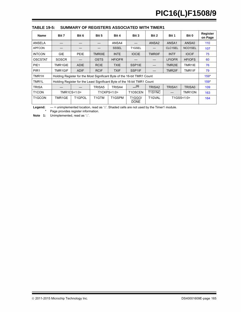
PIC16(L)F1508/9
TABLE 19-5: SUMMARY OF REGISTERS ASSOCIATED WITH TIMER1
Name Bit 7 Bit 6 Bit 5 Bit 4 Bit 3 Bit 2 Bit 1 Bit 0Register on Page
ANSELA — — — ANSA4 — ANSA2 ANSA1 ANSA0 110
APFCON — — — SSSEL T1GSEL — CLC1SEL NCO1SEL 107
INTCON GIE PEIE TMR0IE INTE IOCIE TMR0IF INTF IOCIF 75
OSCSTAT SOSCR — OSTS HFIOFR — — LFIOFR HFIOFS 60
PIE1 TMR1GIE ADIE RCIE TXIE SSP1IE — TMR2IE TMR1IE 76
PIR1 TMR1GIF ADIF RCIF TXIF SSP1IF — TMR2IF TMR1IF 79
TMR1H Holding Register for the Most Significant Byte of the 16-bit TMR1 Count 159*
TMR1L Holding Register for the Least Significant Byte of the 16-bit TMR1 Count 159*
TRISA — — TRISA5 TRISA4 —(1) TRISA2 TRISA1 TRISA0 109
T1CON TMR1CS<1:0> T1CKPS<1:0> T1OSCEN T1SYNC — TMR1ON 163
T1GCON TMR1GE T1GPOL T1GTM T1GSPM T1GGO/DONE
T1GVAL T1GSS<1:0> 164
Legend: — = unimplemented location, read as ‘0’. Shaded cells are not used by the Timer1 module.* Page provides register information.
Note 1: Unimplemented, read as ‘1’.
2011-2015 Microchip Technology Inc. DS40001609E-page 165

PIC16(L)F1508/9
20.0 TIMER2 MODULE
The Timer2 module incorporates the following features:
• 8-bit Timer and Period registers (TMR2 and PR2, respectively)
• Readable and writable (both registers)
• Software programmable prescaler (1:1, 1:4, 1:16, and 1:64)
• Software programmable postscaler (1:1 to 1:16)
• Interrupt on TMR2 match with PR2
See Figure 20-1 for a block diagram of Timer2.
FIGURE 20-1: TIMER2 BLOCK DIAGRAM
FIGURE 20-2: TIMER2 TIMING DIAGRAM
Prescaler1:1, 1:4, 1:16, 1:64Fosc/4
2
T2CKPS<1:0> Comparator Postscaler1:1 to 1:16
4
T2OUTPS<3:0>
set bitTMR2IF
TMR2 R
PR2
T2_matchTo Peripherals
Rev. 10-000019A7/30/2013
0x03
0x00 0x01 0x02 0x03 0x00 0x01 0x02
1:4
Pulse Width(1)
Note 1: The Pulse Width of T2_match is equal to the scaled input of TMR2.
FOSC/4
Prescale
PR2
TMR2
T2_match
Rev. 10-000020A7/30/2013
DS40001609E-page 166 2011-2015 Microchip Technology Inc.

PIC16(L)F1508/9
20.1 Timer2 Operation
The clock input to the Timer2 module is the systeminstruction clock (FOSC/4).
TMR2 increments from 00h on each clock edge.
A 4-bit counter/prescaler on the clock input allows directinput, divide-by-4 and divide-by-16 prescale options.These options are selected by the prescaler control bits,T2CKPS<1:0> of the T2CON register. The value ofTMR2 is compared to that of the Period register, PR2, oneach clock cycle. When the two values match, thecomparator generates a match signal as the timeroutput. This signal also resets the value of TMR2 to 00hon the next cycle and drives the output counter/postscaler (see Section 20.2 “Timer2 Interrupt”).
The TMR2 and PR2 registers are both directly readableand writable. The TMR2 register is cleared on anydevice Reset, whereas the PR2 register initializes toFFh. Both the prescaler and postscaler counters arecleared on the following events:
• a write to the TMR2 register
• a write to the T2CON register
• Power-on Reset (POR)
• Brown-out Reset (BOR)
• MCLR Reset
• Watchdog Timer (WDT) Reset
• Stack Overflow Reset
• Stack Underflow Reset
• RESET Instruction
20.2 Timer2 Interrupt
Timer2 can also generate an optional device interrupt.The Timer2 output signal (T2_match) provides the inputfor the 4-bit counter/postscaler. This counter generatesthe TMR2 match interrupt flag which is latched inTMR2IF of the PIR1 register. The interrupt is enabled bysetting the TMR2 Match Interrupt Enable bit, TMR2IE ofthe PIE1 register.
A range of 16 postscale options (from 1:1 through 1:16inclusive) can be selected with the postscaler controlbits, T2OUTPS<3:0>, of the T2CON register.
20.3 Timer2 Output
The output of TMR2 is T2_match. T2_match is availableto the following peripherals:
• Configurable Logic Cell (CLC)
• Master Synchronous Serial Port (MSSP)
• Numerically Controlled Oscillator (NCO)
• Pulse Width Modulator (PWM)
The T2_match signal is synchronous with the systemclock. Figure 20-3 shows two examples of the timing ofthe T2_match signal relative to FOSC and prescalevalue, T2CKPS<1:0>. The upper diagram illustrates 1:1prescale timing and the lower diagram, 1:X prescaletiming.
FIGURE 20-3: T2_MATCH TIMING DIAGRAM
20.4 Timer2 Operation During Sleep
Timer2 cannot be operated while the processor is inSleep mode. The contents of the TMR2 and PR2registers will remain unchanged while the processor isin Sleep mode.
Note: TMR2 is not cleared when T2CON iswritten.
T2_match
FOSC/4
TMR2 = PR2match
TMR2 = 0
...
PRESCALE = 1:X(T2CKPS<1:0> = 01,10,11)
TCY1 TCY2 TCYX...
...
Q1 Q2 Q3
FOSC
TMR2 = PR2match
TMR2 = 0
Q1Q4
T2_match
FOSC/4
PRESCALE = 1:1(T2CKPS<1:0> = 00)
TCY1
Rev. 10-000021A7/30/2013
2011-2015 Microchip Technology Inc. DS40001609E-page 167

PIC16(L)F1508/9
20.5 Register Definitions: Timer2 Control
TABLE 20-1: SUMMARY OF REGISTERS ASSOCIATED WITH TIMER2
REGISTER 20-1: T2CON: TIMER2 CONTROL REGISTER
U-0 R/W-0/0 R/W-0/0 R/W-0/0 R/W-0/0 R/W-0/0 R/W-0/0 R/W-0/0
— T2OUTPS<3:0> TMR2ON T2CKPS<1:0>
bit 7 bit 0
Legend:
R = Readable bit W = Writable bit U = Unimplemented bit, read as ‘0’
u = Bit is unchanged x = Bit is unknown -n/n = Value at POR and BOR/Value at all other Resets
‘1’ = Bit is set ‘0’ = Bit is cleared
bit 7 Unimplemented: Read as ‘0’
bit 6-3 T2OUTPS<3:0>: Timer2 Output Postscaler Select bits
0000 = 1:1 Postscaler0001 = 1:2 Postscaler0010 = 1:3 Postscaler0011 = 1:4 Postscaler0100 = 1:5 Postscaler0101 = 1:6 Postscaler0110 = 1:7 Postscaler0111 = 1:8 Postscaler1000 = 1:9 Postscaler1001 = 1:10 Postscaler1010 = 1:11 Postscaler1011 = 1:12 Postscaler1100 = 1:13 Postscaler1101 = 1:14 Postscaler1110 = 1:15 Postscaler1111 = 1:16 Postscaler
bit 2 TMR2ON: Timer2 On bit
1 = Timer2 is on0 = Timer2 is off
bit 1-0 T2CKPS<1:0>: Timer2 Clock Prescale Select bits
00 = Prescaler is 101 = Prescaler is 410 = Prescaler is 1611 = Prescaler is 64
Name Bit 7 Bit 6 Bit 5 Bit 4 Bit 3 Bit 2 Bit 1 Bit 0Register on Page
INTCON GIE PEIE TMR0IE INTE IOCIE TMR0IF INTF IOCIF 75
PIE1 TMR1GIE ADIE RCIE TXIE SSP1IE — TMR2IE TMR1IE 76
PIR1 TMR1GIF ADIF RCIF TXIF SSP1IF — TMR2IF TMR1IF 76
PR2 Timer2 Module Period Register 166*
T2CON — T2OUTPS<3:0> TMR2ON T2CKPS<1:0> 168
TMR2 Holding Register for the 8-bit TMR2 Count 166*
Legend: — = unimplemented location, read as ‘0’. Shaded cells are not used for Timer2 module.* Page provides register information.
DS40001609E-page 168 2011-2015 Microchip Technology Inc.

PIC16(L)F1508/9
21.0 MASTER SYNCHRONOUS SERIAL PORT (MSSP) MODULE
21.1 MSSP Module Overview
The Master Synchronous Serial Port (MSSPx) moduleis a serial interface useful for communicating with otherperipheral or microcontroller devices. These peripheraldevices may be serial EEPROMs, shift registers, dis-play drivers, A/D converters, etc. The MSSPx modulecan operate in one of two modes:
• Serial Peripheral Interface (SPI)
• Inter-Integrated Circuit (I2C™)
The SPI interface supports the following modes andfeatures:
• Master mode
• Slave mode
• Clock Parity
• Slave Select Synchronization (Slave mode only)
• Daisy-chain connection of slave devices
Figure 21-1 is a block diagram of the SPI interfacemodule.
FIGURE 21-1: MSSP BLOCK DIAGRAM (SPI MODE)
Read Write
SSPxBUF
8 8
SSPxSR
8
Bit 0Shift clock
SDI
SDO
Data bus
Control Enable
2 (CKP, CKE) clock select
Edge enable
Edge enable
SCK_outPrescaler 4, 16, 64
(T2_match)2
TOSC
Baud Rate Generator
(SSPxADD)TRIS bit
4SSPM<3:0>
Rev. 10-000076A12/16/2013
SSx
SDO_out
SCK
2011-2015 Microchip Technology Inc. DS40001609E-page 169

PIC16(L)F1508/9
The I2C interface supports the following modes andfeatures:
• Master mode
• Slave mode
• Byte NACKing (Slave mode)
• Limited Multi-master support
• 7-bit and 10-bit addressing
• Start and Stop interrupts
• Interrupt masking
• Clock stretching
• Bus collision detection
• General call address matching
• Address masking
• Address Hold and Data Hold modes
• Selectable SDAx hold times
Figure 21-2 is a block diagram of the I2C interface mod-ule in Master mode. Figure 21-3 is a diagram of the I2Cinterface module in Slave mode.
FIGURE 21-2: MSSPX BLOCK DIAGRAM (I2C™ MASTER MODE)
Note 1: In devices with more than one MSSPmodule, it is very important to pay closeattention to SSPxCONx register names.SSPxCON1 and SSPxCON2 registerscontrol different operational aspects ofthe same module, while SSPxCON1 andSSP2CON1 control the same features fortwo different modules.
2: Throughout this section, generic refer-ences to an MSSPx module in any of itsoperating modes may be interpreted asbeing equally applicable to MSSPx orMSSP2. Register names, module I/O sig-nals, and bit names may use the genericdesignator ‘x’ to indicate the use of anumeral to distinguish a particular mod-ule when required.
Read Write
SSPxBUF
8 8
SSPxSR
8
Internal databus
Start bit, Stop bit,Acknowledge
Generate(SSPxCON2)
Baud RateGenerator
(SSPxADD)
Shift clock
Start bit detectedStop bit detected
Write collsion detectClock arbitration
State counter for endof XMIT/RCV
Address match detect
Clo
ckC
ntl
SCLx in
Bus collision
Rec
eive
Ena
ble
(RC
EN
)
MSb LSb
SDAx
SCLx
SDAx in
Clo
ckar
bitra
te/B
CO
Lde
tect
(Hol
dof
fclo
ckso
urce
)
Set/Reset: S, P, SSPxSTAT,WCOL, SSPOVReset SEN, PEN (SSPxCON2)Set SSPxIF, BCLxIF
4
[SSPM <3:0>]
Rev. 10-000077A7/30/2013
DS40001609E-page 170 2011-2015 Microchip Technology Inc.

PIC16(L)F1508/9
FIGURE 21-3: MSSP BLOCK DIAGRAM (I2C™ SLAVE MODE)
Read Write
SSPxBUF
8 8
SSPxSR
8SCLx
SDAx
Internal data bus
MSb LSb
SSPxMSK
8
8
8
Match detect
SSPxADD
Start and Stopbit Detect
Addr Match
Set, Reset S, Pbits (SSPxSTAT)
Shift clock
Rev. 10-000078A7/30/2013
8
2011-2015 Microchip Technology Inc. DS40001609E-page 171

PIC16(L)F1508/9
21.2 SPI Mode Overview
The Serial Peripheral Interface (SPI) bus is asynchronous serial data communication bus thatoperates in Full-Duplex mode. Devices communicatein a master/slave environment where the master deviceinitiates the communication. A slave device iscontrolled through a Chip Select known as SlaveSelect.
The SPI bus specifies four signal connections:
• Serial Clock (SCKx)
• Serial Data Out (SDOx)
• Serial Data In (SDIx)
• Slave Select (SSx)
Figure 21-1 shows the block diagram of the MSSPmodule when operating in SPI mode.
The SPI bus operates with a single master device andone or more slave devices. When multiple slavedevices are used, an independent Slave Select con-nection is required from the master device to eachslave device.
Figure 21-4 shows a typical connection between amaster device and multiple slave devices.
The master selects only one slave at a time. Most slavedevices have tri-state outputs so their output signalappears disconnected from the bus when they are notselected.
Transmissions involve two shift registers, eight bits insize, one in the master and one in the slave. With eitherthe master or the slave device, data is always shiftedout one bit at a time, with the Most Significant bit (MSb)shifted out first. At the same time, a new LeastSignificant bit (LSb) is shifted into the same register.
Figure 21-5 shows a typical connection between twoprocessors configured as master and slave devices.
Data is shifted out of both shift registers on the pro-grammed clock edge and latched on the opposite edgeof the clock.
The master device transmits information out on itsSDOx output pin which is connected to, and receivedby, the slave’s SDIx input pin. The slave device trans-mits information out on its SDOx output pin, which isconnected to, and received by, the master’s SDIx inputpin.
To begin communication, the master device first sendsout the clock signal. Both the master and the slavedevices should be configured for the same clock polar-ity.
The master device starts a transmission by sending outthe MSb from its shift register. The slave device readsthis bit from that same line and saves it into the LSbposition of its shift register.
During each SPI clock cycle, a full-duplex datatransmission occurs. This means that while the masterdevice is sending out the MSb from its shift register (onits SDOx pin) and the slave device is reading this bitand saving it as the LSb of its shift register, that theslave device is also sending out the MSb from its shiftregister (on its SDOx pin) and the master device isreading this bit and saving it as the LSb of its shiftregister.
After eight bits have been shifted out, the master andslave have exchanged register values.
If there is more data to exchange, the shift registers areloaded with new data and the process repeats itself.
Whether the data is meaningful or not (dummy data),depends on the application software. This leads tothree scenarios for data transmission:
• Master sends useful data and slave sends dummy data.
• Master sends useful data and slave sends useful data.
• Master sends dummy data and slave sends useful data.
Transmissions may involve any number of clockcycles. When there is no more data to be transmitted,the master stops sending the clock signal and it dese-lects the slave.
Every slave device connected to the bus that has notbeen selected through its slave select line must disre-gard the clock and transmission signals and must nottransmit out any data of its own.
DS40001609E-page 172 2011-2015 Microchip Technology Inc.

PIC16(L)F1508/9
FIGURE 21-4: SPI MASTER AND MULTIPLE SLAVE CONNECTION
21.2.1 SPI MODE REGISTERS
The MSSP module has five registers for SPI modeoperation. These are:
• MSSP STATUS register (SSPxSTAT)
• MSSP Control Register 1 (SSPxCON1)
• MSSP Control Register 3 (SSPxCON3)
• MSSP Data Buffer register (SSPxBUF)
• MSSP Address register (SSPxADD)
• MSSP Shift register (SSPxSR) (Not directly accessible)
SSPxCON1 and SSPxSTAT are the control andSTATUS registers in SPI mode operation. TheSSPxCON1 register is readable and writable. Thelower six bits of the SSPxSTAT are read-only. Theupper two bits of the SSPxSTAT are read/write.
In SPI master mode, SSPxADD can be loaded with avalue used in the Baud Rate Generator. More informa-tion on the Baud Rate Generator is available inSection21.7 “Baud Rate Generator”.
SSPxSR is the shift register used for shifting data inand out. SSPxBUF provides indirect access to theSSPxSR register. SSPxBUF is the buffer register towhich data bytes are written, and from which databytes are read.
In receive operations, SSPxSR and SSPxBUFtogether create a buffered receiver. When SSPxSRreceives a complete byte, it is transferred to SSPxBUFand the SSPxIF interrupt is set.
During transmission, the SSPxBUF is not buffered. Awrite to SSPxBUF will write to both SSPxBUF andSSPxSR.
SCKx SCKx
SCKx
SCKx
SDOx
SDOx
SDOx
SDOx
SDIx
SDIx
SDIx
SDIxGeneral I/O
SPI Master SPI Slave #1
SPI Slave #2
SPI Slave #3
SSx
SSx
SSx
General I/OGeneral I/O
Rev. 10-000079A8/1/2013
2011-2015 Microchip Technology Inc. DS40001609E-page 173

PIC16(L)F1508/9
21.2.2 SPI MODE OPERATION
When initializing the SPI, several options need to bespecified. This is done by programming the appropriatecontrol bits (SSPxCON1<5:0> and SSPxSTAT<7:6>).These control bits allow the following to be specified:
• Master mode (SCKx is the clock output)
• Slave mode (SCKx is the clock input)
• Clock Polarity (Idle state of SCKx)
• Data Input Sample Phase (middle or end of data output time)
• Clock Edge (output data on rising/falling edge of SCKx)
• Clock Rate (Master mode only)
• Slave Select mode (Slave mode only)
To enable the serial port, SSP Enable bit, SSPEN of theSSPxCON1 register, must be set. To reset or reconfig-ure SPI mode, clear the SSPEN bit, re-initialize theSSPxCONx registers and then set the SSPEN bit. Thisconfigures the SDI, SDO, SCK and SS pins as serialport pins. For the pins to behave as the serial port func-tion, some must have their data direction bits (in theTRIS register) appropriately programmed as follows:
• SDIx must have corresponding TRIS bit set
• SDOx must have corresponding TRIS bit cleared
• SCKx (Master mode) must have corresponding TRIS bit cleared
• SCKx (Slave mode) must have corresponding TRIS bit set
• SSx must have corresponding TRIS bit set
Any serial port function that is not desired may beoverridden by programming the corresponding datadirection (TRIS) register to the opposite value.
The MSSP consists of a transmit/receive shift register(SSPxSR) and a buffer register (SSPxBUF). TheSSPxSR shifts the data in and out of the device, MSbfirst. The SSPxBUF holds the data that was written tothe SSPxSR until the received data is ready. Once theeight bits of data have been received, that byte ismoved to the SSPxBUF register. Then, the Buffer FullDetect bit, BF of the SSPxSTAT register, and theinterrupt flag bit, SSPxIF, are set. This double-bufferingof the received data (SSPxBUF) allows the next byte tostart reception before reading the data that was justreceived. Any write to the SSPxBUF register duringtransmission/reception of data will be ignored and thewrite collision detect bit, WCOL of the SSPxCON1register, will be set. User software must clear theWCOL bit to allow the following write(s) to theSSPxBUF register to complete successfully.
When the application software is expecting to receivevalid data, the SSPxBUF should be read before thenext byte of data to transfer is written to the SSPxBUF.The Buffer Full bit, BF of the SSPxSTAT register, indi-cates when SSPxBUF has been loaded with thereceived data (transmission is complete). When theSSPxBUF is read, the BF bit is cleared. This data maybe irrelevant if the SPI is only a transmitter. Generally,the MSSP interrupt is used to determine when thetransmission/reception has completed. If the interruptmethod is not going to be used, then software pollingcan be done to ensure that a write collision does notoccur.
The SSPxSR is not directly readable or writable andcan only be accessed by addressing the SSPxBUFregister. Additionally, the SSPxSTAT register indicatesthe various Status conditions.
DS40001609E-page 174 2011-2015 Microchip Technology Inc.

PIC16(L)F1508/9
FIGURE 21-5: SPI MASTER/SLAVE CONNECTION
SPI Master SSPM<3:0> = 00xx= 1010
SDOx
SDOx
SDIx
SDIx
Serial Input Buffer(SSPxBUF)
Serial Input Buffer(SSPxBUF)
Shift Register(SSPxSR)
Shift Register(SSPxSR)
SPI Slave SSPM<3:0> = 010x
MSb MSbLSb LSbSCKx SCKx
General I/O SSxSlave Select
(optional)
Serial clock
Processor 1 Processor 2
Rev. 10-000080A7/30/2013
2011-2015 Microchip Technology Inc. DS40001609E-page 175

PIC16(L)F1508/9
21.2.3 SPI MASTER MODE
The master can initiate the data transfer at any timebecause it controls the SCKx line. The masterdetermines when the slave (Processor 2, Figure 21-5)is to broadcast data by the software protocol.
In Master mode, the data is transmitted/received assoon as the SSPxBUF register is written to. If the SPIis only going to receive, the SDOx output could be dis-abled (programmed as an input). The SSPxSR registerwill continue to shift in the signal present on the SDIxpin at the programmed clock rate. As each byte isreceived, it will be loaded into the SSPxBUF register asif a normal received byte (interrupts and Status bitsappropriately set).
The clock polarity is selected by appropriatelyprogramming the CKP bit of the SSPxCON1 registerand the CKE bit of the SSPxSTAT register. This then,would give waveforms for SPI communication asshown in Figure 21-6, Figure 21-8, Figure 21-9 andFigure 21-10, where the MSb is transmitted first. InMaster mode, the SPI clock rate (bit rate) is userprogrammable to be one of the following:
• FOSC/4 (or TCY)
• FOSC/16 (or 4 * TCY)
• FOSC/64 (or 16 * TCY)
• Timer2 output/2
• Fosc/(4 * (SSPxADD + 1))
Figure 21-6 shows the waveforms for Master mode.
When the CKE bit is set, the SDOx data is valid beforethere is a clock edge on SCKx. The change of the inputsample is shown based on the state of the SMP bit. Thetime when the SSPxBUF is loaded with the receiveddata is shown.
FIGURE 21-6: SPI MODE WAVEFORM (MASTER MODE)
SCKx(CKP = 0
SCKx(CKP = 1
SCKx(CKP = 0
SCKx(CKP = 1
4 ClockModes
InputSample
InputSample
SDIx
bit 7 bit 0
SDOx bit 7 bit 6 bit 5 bit 4 bit 3 bit 2 bit 1 bit 0
bit 7
SDIx
SSPxIF
(SMP = 1)
(SMP = 0)
(SMP = 1)
CKE = 1)
CKE = 0)
CKE = 1)
CKE = 0)
(SMP = 0)
Write toSSPxBUF
SSPxSR toSSPxBUF
SDOx bit 7 bit 6 bit 5 bit 4 bit 3 bit 2 bit 1 bit 0
(CKE = 0)
(CKE = 1)
bit 0
DS40001609E-page 176 2011-2015 Microchip Technology Inc.

PIC16(L)F1508/9
21.2.4 SPI SLAVE MODE
In Slave mode, the data is transmitted and received asexternal clock pulses appear on SCKx. When the lastbit is latched, the SSPxIF interrupt flag bit is set.
Before enabling the module in SPI Slave mode, the clockline must match the proper Idle state. The clock line canbe observed by reading the SCKx pin. The Idle state isdetermined by the CKP bit of the SSPxCON1 register.
While in Slave mode, the external clock is supplied bythe external clock source on the SCKx pin. This exter-nal clock must meet the minimum high and low timesas specified in the electrical specifications.
While in Sleep mode, the slave can transmit/receivedata. The shift register is clocked from the SCKx pininput and when a byte is received, the device will gen-erate an interrupt. If enabled, the device will wake-upfrom Sleep.
21.2.4.1 Daisy-Chain Configuration
The SPI bus can sometimes be connected in adaisy-chain configuration. The first slave output is con-nected to the second slave input, the second slaveoutput is connected to the third slave input, and so on.The final slave output is connected to the master input.Each slave sends out, during a second group of clockpulses, an exact copy of what was received during thefirst group of clock pulses. The whole chain acts asone large communication shift register. Thedaisy-chain feature only requires a single Slave Selectline from the master device.
Figure 21-7 shows the block diagram of a typicaldaisy-chain connection when operating in SPI mode.
In a daisy-chain configuration, only the most recentbyte on the bus is required by the slave. Setting theBOEN bit of the SSPxCON3 register will enable writesto the SSPxBUF register, even if the previous byte hasnot been read. This allows the software to ignore datathat may not apply to it.
21.2.5 SLAVE SELECT SYNCHRONIZATION
The Slave Select can also be used to synchronize com-munication. The Slave Select line is held high until themaster device is ready to communicate. When theSlave Select line is pulled low, the slave knows that anew transmission is starting.
If the slave fails to receive the communication properly,it will be reset at the end of the transmission, when theSlave Select line returns to a high state. The slave isthen ready to receive a new transmission when theSlave Select line is pulled low again. If the Slave Selectline is not used, there is a risk that the slave will even-tually become out of sync with the master. If the slavemisses a bit, it will always be one bit off in future trans-missions. Use of the Slave Select line allows the slaveand master to align themselves at the beginning ofeach transmission.
The SSx pin allows a Synchronous Slave mode. TheSPI must be in Slave mode with SSx pin controlenabled (SSPxCON1<3:0> = 0100).
When the SSx pin is low, transmission and receptionare enabled and the SDOx pin is driven.
When the SSx pin goes high, the SDOx pin is no longerdriven, even if in the middle of a transmitted byte andbecomes a floating output. External pull-up/pull-downresistors may be desirable depending on the applica-tion.
When the SPI module resets, the bit counter is forcedto ‘0’. This can be done by either forcing the SSx pin toa high level or clearing the SSPEN bit.
Note 1: When the SPI is in Slave mode with SSxpin control enabled (SSPxCON1<3:0> =0100), the SPI module will reset if the SSxpin is set to VDD.
2: When the SPI is used in Slave mode withCKE set; the user must enable SSx pincontrol.
3: While operated in SPI Slave mode theSMP bit of the SSPxSTAT register mustremain clear.
2011-2015 Microchip Technology Inc. DS40001609E-page 177

PIC16(L)F1508/9
FIGURE 21-7: SPI DAISY-CHAIN CONNECTION
FIGURE 21-8: SLAVE SELECT SYNCHRONOUS WAVEFORM
SCK SCK
SCK
SCK
SDOxSDOx
SDOx
SDOxSDIx
SDIx
SDIxSDIx
General I/O
SPI Master SPI Slave#1
SPI Slave#2
SPI Slave#3
SSx
SSx
SSx
Rev. 10-000082A7/30/2013
SCKx(CKP = 1
SCKx(CKP = 0
InputSample
SDIx
bit 7
SDOx bit 7 bit 6 bit 7
SSPxIFInterrupt
CKE = 0)
CKE = 0)
Write toSSPxBUF
SSPxSR toSSPxBUF
SSx
Flag
bit 0
bit 7
bit 0
bit 6
SSPxBUF toSSPxSR
Shift register SSPxSRand bit count are reset
DS40001609E-page 178 2011-2015 Microchip Technology Inc.

PIC16(L)F1508/9
FIGURE 21-9: SPI MODE WAVEFORM (SLAVE MODE WITH CKE = 0)
FIGURE 21-10: SPI MODE WAVEFORM (SLAVE MODE WITH CKE = 1)
SCKx(CKP = 1
SCKx(CKP = 0
InputSample
SDIx
bit 7
SDOx bit 7 bit 6 bit 5 bit 4 bit 3 bit 2 bit 1 bit 0
SSPxIFInterrupt
CKE = 0)
CKE = 0)
Write toSSPxBUF
SSPxSR toSSPxBUF
SSx
Flag
Optional
bit 0
detection active
Write Collision
Valid
SCKx(CKP = 1
SCKx(CKP = 0
InputSample
SDIx
bit 7 bit 0
SDOx bit 7 bit 6 bit 5 bit 4 bit 3 bit 2 bit 1 bit 0
SSPxIFInterrupt
CKE = 1)
CKE = 1)
Write toSSPxBUF
SSPxSR toSSPxBUF
SSx
Flag
Not Optional
Write Collisiondetection active
Valid
2011-2015 Microchip Technology Inc. DS40001609E-page 179

PIC16(L)F1508/9
21.2.6 SPI OPERATION IN SLEEP MODE
In SPI Master mode, module clocks may be operatingat a different speed than when in Full-Power mode; inthe case of the Sleep mode, all clocks are halted.
Special care must be taken by the user when the MSSPclock is much faster than the system clock.
In Slave mode, when MSSP interrupts are enabled,after the master completes sending data, an MSSPinterrupt will wake the controller from Sleep.
If an exit from Sleep mode is not desired, MSSP inter-rupts should be disabled.
In SPI Master mode, when the Sleep mode is selected,all module clocks are halted and the transmis-sion/reception will remain in that state until the devicewakes. After the device returns to Run mode, the mod-ule will resume transmitting and receiving data.
In SPI Slave mode, the SPI Transmit/Receive Shiftregister operates asynchronously to the device. Thisallows the device to be placed in Sleep mode and datato be shifted into the SPI Transmit/Receive Shiftregister. When all eight bits have been received, theMSSP interrupt flag bit will be set and if enabled, willwake the device.
TABLE 21-1: SUMMARY OF REGISTERS ASSOCIATED WITH SPI OPERATION
Name Bit 7 Bit 6 Bit 5 Bit 4 Bit 3 Bit 2 Bit 1 Bit 0Register on Page
ANSELA — — — ANSA4 — ANSA2 ANSA1 ANSA0 110
INTCON GIE PEIE TMR0IE INTE IOCIE TMR0IF INTF IOCIF 75
PIE1 TMR1GIE ADIE RCIE TXIE SSP1IE — TMR2IE TMR1IE 76
PIR1 TMR1GIF ADIF RCIF TXIF SSP1IF — TMR2IF TMR1IF 79
SSP1BUF Synchronous Serial Port Receive Buffer/Transmit Register 173*
SSP1CON1 WCOL SSPOV SSPEN CKP SSPM<3:0> 219
SSP1CON3 ACKTIM PCIE SCIE BOEN SDAHT SBCDE AHEN DHEN 221
SSP1STAT SMP CKE D/A P S R/W UA BF 218
TRISA — — TRISA5 TRISA4 —(1)TRISA2 TRISA1 TRISA0 109
TRISC TRISC7 TRISC6 TRISC5 TRISC4 TRISC3 TRISC2 TRISC1 TRISC0 117
Legend: — = Unimplemented location, read as ‘0’. Shaded cells are not used by the MSSP in SPI mode.* Page provides register information.
Note 1: Unimplemented, read as ‘1’.
DS40001609E-page 180 2011-2015 Microchip Technology Inc.

PIC16(L)F1508/9
21.3 I2C MODE OVERVIEW
The Inter-Integrated Circuit Bus (I2C) is a multi-masterserial data communication bus. Devices communicatein a master/slave environment where the masterdevices initiate the communication. A slave device iscontrolled through addressing.
The I2C bus specifies two signal connections:
• Serial Clock (SCLx)
• Serial Data (SDAx)
Figure 21-2 and Figure 21-3 show the block diagramsof the MSSP module when operating in I2C mode.
Both the SCLx and SDAx connections are bidirectionalopen-drain lines, each requiring pull-up resistors for thesupply voltage. Pulling the line to ground is considereda logical zero and letting the line float is considered alogical one.
Figure 21-11 shows a typical connection between twoprocessors configured as master and slave devices.
The I2C bus can operate with one or more masterdevices and one or more slave devices.
There are four potential modes of operation for a givendevice:
• Master Transmit mode(master is transmitting data to a slave)
• Master Receive mode(master is receiving data from a slave)
• Slave Transmit mode(slave is transmitting data to a master)
• Slave Receive mode(slave is receiving data from the master)
To begin communication, a master device starts out inMaster Transmit mode. The master device sends out aStart bit followed by the address byte of the slave itintends to communicate with. This is followed by a sin-gle Read/Write bit, which determines whether the mas-ter intends to transmit to or receive data from the slavedevice.
If the requested slave exists on the bus, it will respondwith an Acknowledge bit, otherwise known as an ACK.The master then continues in either Transmit mode orReceive mode and the slave continues in the comple-ment, either in Receive mode or Transmit mode,respectively.
A Start bit is indicated by a high-to-low transition of theSDAx line while the SCLx line is held high. Address anddata bytes are sent out, Most Significant bit (MSb) first.The Read/Write bit is sent out as a logical one when themaster intends to read data from the slave, and is sentout as a logical zero when it intends to write data to theslave.
FIGURE 21-11: I2C MASTER/SLAVE CONNECTION
The Acknowledge bit (ACK) is an active-low signal,which holds the SDAx line low to indicate to the trans-mitter that the slave device has received the transmit-ted data and is ready to receive more.
The transition of a data bit is always performed whilethe SCLx line is held low. Transitions that occur whilethe SCLx line is held high are used to indicate Start andStop bits.
If the master intends to write to the slave, then it repeat-edly sends out a byte of data, with the slave respondingafter each byte with an ACK bit. In this example, themaster device is in Master Transmit mode and theslave is in Slave Receive mode.
If the master intends to read from the slave, then itrepeatedly receives a byte of data from the slave, andresponds after each byte with an ACK bit. In this exam-ple, the master device is in Master Receive mode andthe slave is Slave Transmit mode.
On the last byte of data communicated, the masterdevice may end the transmission by sending a Stop bit.If the master device is in Receive mode, it sends theStop bit in place of the last ACK bit. A Stop bit is indi-cated by a low-to-high transition of the SDAx line whilethe SCLx line is held high.
In some cases, the master may want to maintain con-trol of the bus and re-initiate another transmission. Ifso, the master device may send another Start bit inplace of the Stop bit or last ACK bit when it is in receivemode.
The I2C bus specifies three message protocols;
• Single message where a master writes data to a slave.
• Single message where a master reads data from a slave.
• Combined message where a master initiates a minimum of two writes, or two reads, or a combination of writes and reads, to one or more slaves.
SCLx
SDAx
MasterVDD
VDD
SCLx
SDAx
Slave
Rev. 10-000085A7/30/2013
2011-2015 Microchip Technology Inc. DS40001609E-page 181

PIC16(L)F1508/9
When one device is transmitting a logical one, or lettingthe line float, and a second device is transmitting a log-ical zero, or holding the line low, the first device candetect that the line is not a logical one. This detection,when used on the SCLx line, is called clock stretching.Clock stretching gives slave devices a mechanism tocontrol the flow of data. When this detection is used onthe SDAx line, it is called arbitration. Arbitrationensures that there is only one master device communi-cating at any single time.
21.3.1 CLOCK STRETCHING
When a slave device has not completed processingdata, it can delay the transfer of more data through theprocess of clock stretching. An addressed slave devicemay hold the SCLx clock line low after receiving orsending a bit, indicating that it is not yet ready to con-tinue. The master that is communicating with the slavewill attempt to raise the SCLx line in order to transferthe next bit, but will detect that the clock line has not yetbeen released. Because the SCLx connection isopen-drain, the slave has the ability to hold that line lowuntil it is ready to continue communicating.
Clock stretching allows receivers that cannot keep upwith a transmitter to control the flow of incoming data.
21.3.2 ARBITRATION
Each master device must monitor the bus for Start andStop bits. If the device detects that the bus is busy, itcannot begin a new message until the bus returns to anIdle state.
However, two master devices may try to initiate a trans-mission on or about the same time. When this occurs,the process of arbitration begins. Each transmitterchecks the level of the SDAx data line and compares itto the level that it expects to find. The first transmitter toobserve that the two levels do not match, loses arbitra-tion, and must stop transmitting on the SDAx line.
For example, if one transmitter holds the SDAx line toa logical one (lets it float) and a second transmitterholds it to a logical zero (pulls it low), the result is thatthe SDAx line will be low. The first transmitter thenobserves that the level of the line is different thanexpected and concludes that another transmitter iscommunicating.
The first transmitter to notice this difference is the onethat loses arbitration and must stop driving the SDAxline. If this transmitter is also a master device, it alsomust stop driving the SCLx line. It then can monitor thelines for a Stop condition before trying to reissue itstransmission. In the meantime, the other device thathas not noticed any difference between the expectedand actual levels on the SDAx line continues with itsoriginal transmission. It can do so without any compli-cations, because so far, the transmission appearsexactly as expected with no other transmitter disturbingthe message.
Slave Transmit mode can also be arbitrated, when amaster addresses multiple slaves, but this is less com-mon.
If two master devices are sending a message to two dif-ferent slave devices at the address stage, the mastersending the lower slave address always wins arbitra-tion. When two master devices send messages to thesame slave address, and addresses can sometimesrefer to multiple slaves, the arbitration process mustcontinue into the data stage.
Arbitration usually occurs very rarely, but it is a neces-sary process for proper multi-master support.
DS40001609E-page 182 2011-2015 Microchip Technology Inc.

PIC16(L)F1508/9
21.4 I2C MODE OPERATION
All MSSP I2C communication is byte oriented andshifted out MSb first. Six SFR registers and twointerrupt flags interface the module with the PIC®
microcontroller and user software. Two pins, SDAxand SCLx, are exercised by the module to communi-cate with other external I2C devices.
21.4.1 BYTE FORMAT
All communication in I2C is done in 9-bit segments. Abyte is sent from a master to a slave or vice-versa,followed by an Acknowledge bit sent back. After theeighth falling edge of the SCLx line, the device output-ting data on the SDAx changes that pin to an input andreads in an acknowledge value on the next clockpulse.
The clock signal, SCLx, is provided by the master.Data is valid to change while the SCLx signal is low,and sampled on the rising edge of the clock. Changeson the SDAx line while the SCLx line is high definespecial conditions on the bus, explained below.
21.4.2 DEFINITION OF I2C TERMINOLOGY
There is language and terminology in the descriptionof I2C communication that have definitions specific toI2C. That word usage is defined below and may beused in the rest of this document without explanation.This table was adapted from the Philips I2CTM
specification.
21.4.3 SDAX AND SCLX PINS
Selection of any I2C mode with the SSPEN bit set,forces the SCLx and SDAx pins to be open-drain.These pins should be set by the user to inputs by set-ting the appropriate TRIS bits.
21.4.4 SDAX HOLD TIME
The hold time of the SDAx pin is selected by theSDAHT bit of the SSPxCON3 register. Hold time is thetime SDAx is held valid after the falling edge of SCLx.Setting the SDAHT bit selects a longer 300 ns mini-mum hold time and may help on buses with largecapacitance.
TABLE 21-2: I2C BUS TERMS
Note: Data is tied to output zero when an I2Cmode is enabled.
TERM Description
Transmitter The device which shifts data out onto the bus.
Receiver The device which shifts data in from the bus.
Master The device that initiates a transfer, generates clock signals and termi-nates a transfer.
Slave The device addressed by the master.
Multi-master A bus with more than one device that can initiate data transfers.
Arbitration Procedure to ensure that only one master at a time controls the bus. Winning arbitration ensures that the message is not corrupted.
Synchronization Procedure to synchronize the clocks of two or more devices on the bus.
Idle No master is controlling the bus, and both SDAx and SCLx lines are high.
Active Any time one or more master devices are controlling the bus.
Addressed Slave
Slave device that has received a matching address and is actively being clocked by a master.
Matching Address
Address byte that is clocked into a slave that matches the value stored in SSPxADD.
Write Request Slave receives a matching address with R/W bit clear, and is ready to clock in data.
Read Request Master sends an address byte with the R/W bit set, indicating that it wishes to clock data out of the Slave. This data is the next and all following bytes until a Restart or Stop.
Clock Stretching When a device on the bus hold SCLx low to stall communication.
Bus Collision Any time the SDAx line is sampled low by the module while it is out-putting and expected high state.
2011-2015 Microchip Technology Inc. DS40001609E-page 183

PIC16(L)F1508/9
21.4.5 START CONDITION
The I2C specification defines a Start condition as atransition of SDAx from a high to a low state whileSCLx line is high. A Start condition is always gener-ated by the master and signifies the transition of thebus from an Idle to an Active state. Figure 21-12shows wave forms for Start and Stop conditions.
A bus collision can occur on a Start condition if themodule samples the SDAx line low before asserting itlow. This does not conform to the I2C Specification thatstates no bus collision can occur on a Start.
21.4.6 STOP CONDITION
A Stop condition is a transition of the SDAx line fromlow-to-high state while the SCLx line is high.
21.4.7 RESTART CONDITION
A Restart is valid any time that a Stop would be valid.A master can issue a Restart if it wishes to hold thebus after terminating the current transfer. A Restarthas the same effect on the slave that a Start would,resetting all slave logic and preparing it to clock in anaddress. The master may want to address the same oranother slave. Figure 21-13 shows the wave form for aRestart condition.
In 10-bit Addressing Slave mode a Restart is requiredfor the master to clock data out of the addressedslave. Once a slave has been fully addressed, match-ing both high and low address bytes, the master canissue a Restart and the high address byte with theR/W bit set. The slave logic will then hold the clockand prepare to clock out data.
After a full match with R/W clear in 10-bit mode, a priormatch flag is set and maintained. Until a Stop condi-tion, a high address with R/W clear, or high addressmatch fails.
21.4.8 START/STOP CONDITION INTERRUPT MASKING
The SCIE and PCIE bits of the SSPxCON3 registercan enable the generation of an interrupt in Slavemodes that do not typically support this function. Slavemodes where interrupt on Start and Stop detect arealready enabled, these bits will have no effect.
FIGURE 21-12: I2C START AND STOP CONDITIONS
FIGURE 21-13: I2C RESTART CONDITION
Note: At least one SCLx low time must appearbefore a Stop is valid, therefore, if the SDAxline goes low then high again while the SCLxline stays high, only the Start condition isdetected.
SDAx
SCLx
P
Stop
Condition
S
Start
Condition
Change of
Data Allowed
Change of
Data Allowed
Restart
Condition
Sr
Change of
Data AllowedChange of
Data Allowed
DS40001609E-page 184 2011-2015 Microchip Technology Inc.

PIC16(L)F1508/9
21.4.9 ACKNOWLEDGE SEQUENCE
The ninth SCLx pulse for any transferred byte in I2C isdedicated as an Acknowledge. It allows receivingdevices to respond back to the transmitter by pullingthe SDAx line low. The transmitter must release con-trol of the line during this time to shift in the response.The Acknowledge (ACK) is an active-low signal, pull-ing the SDAx line low indicated to the transmitter thatthe device has received the transmitted data and isready to receive more.
The result of an ACK is placed in the ACKSTAT bit ofthe SSPxCON2 register.
Slave software, when the AHEN and DHEN bits areset, allow the user to set the ACK value sent back tothe transmitter. The ACKDT bit of the SSPxCON2 reg-ister is set/cleared to determine the response.
Slave hardware will generate an ACK response if theAHEN and DHEN bits of the SSPxCON3 register areclear.
There are certain conditions where an ACK will not besent by the slave. If the BF bit of the SSPxSTAT regis-ter or the SSPOV bit of the SSPxCON1 register areset when a byte is received.
When the module is addressed, after the eighth fallingedge of SCLx on the bus, the ACKTIM bit of theSSPxCON3 register is set. The ACKTIM bit indicatesthe acknowledge time of the active bus. The ACKTIMStatus bit is only active when the AHEN bit or DHENbit is enabled.
21.5 I2C Slave Mode Operation
The MSSP Slave mode operates in one of four modesselected in the SSPM bits of SSPxCON1 register. Themodes can be divided into 7-bit and 10-bit Addressingmode. 10-bit Addressing modes operate the same as7-bit with some additional overhead for handling thelarger addresses.
Modes with Start and Stop bit interrupts operate thesame as the other modes with SSPxIF additionallygetting set upon detection of a Start, Restart, or Stopcondition.
21.5.1 SLAVE MODE ADDRESSES
The SSPxADD register (Register 21-6) contains theSlave mode address. The first byte received after aStart or Restart condition is compared against thevalue stored in this register. If the byte matches, thevalue is loaded into the SSPxBUF register and aninterrupt is generated. If the value does not match, themodule goes idle and no indication is given to the soft-ware that anything happened.
The SSP Mask register (Register 21-5) affects theaddress matching process. See Section21.5.9 “SSPxMask Register” for more information.
21.5.1.1 I2C Slave 7-bit Addressing Mode
In 7-bit Addressing mode, the LSb of the received databyte is ignored when determining if there is an addressmatch.
21.5.1.2 I2C Slave 10-bit Addressing Mode
In 10-bit Addressing mode, the first received byte iscompared to the binary value of ‘1 1 1 1 0 A9 A8 0’. A9and A8 are the two MSbs of the 10-bit address andstored in bits 2 and 1 of the SSPxADD register.
After the acknowledge of the high byte the UA bit is setand SCLx is held low until the user updates SSPxADDwith the low address. The low address byte is clockedin and all eight bits are compared to the low addressvalue in SSPxADD. Even if there is not an addressmatch; SSPxIF and UA are set, and SCLx is held lowuntil SSPxADD is updated to receive a high byteagain. When SSPxADD is updated the UA bit iscleared. This ensures the module is ready to receivethe high address byte on the next communication.
A high and low address match as a write request isrequired at the start of all 10-bit addressing communi-cation. A transmission can be initiated by issuing aRestart once the slave is addressed, and clocking inthe high address with the R/W bit set. The slave hard-ware will then acknowledge the read request and pre-pare to clock out data. This is only valid for a slaveafter it has received a complete high and low addressbyte match.
21.5.2 SLAVE RECEPTION
When the R/W bit of a matching received address byteis clear, the R/W bit of the SSPxSTAT register iscleared. The received address is loaded into theSSPxBUF register and acknowledged.
When the overflow condition exists for a receivedaddress, then not Acknowledge is given. An overflowcondition is defined as either bit BF of the SSPxSTATregister is set, or bit SSPOV of the SSPxCON1 registeris set. The BOEN bit of the SSPxCON3 register modi-fies this operation. For more information seeRegister 21-4.
An MSSP interrupt is generated for each transferreddata byte. Flag bit, SSPxIF, must be cleared by soft-ware.
When the SEN bit of the SSPxCON2 register is set,SCLx will be held low (clock stretch) following eachreceived byte. The clock must be released by settingthe CKP bit of the SSPxCON1 register, exceptsometimes in 10-bit mode. See Section21.2.3 “SPIMaster Mode” for more detail.
21.5.2.1 7-bit Addressing Reception
This section describes a standard sequence of eventsfor the MSSP module configured as an I2C slave in7-bit Addressing mode. Figure 21-14 and Figure 21-15are used as visual references for this description.
2011-2015 Microchip Technology Inc. DS40001609E-page 185

PIC16(L)F1508/9
This is a step by step process of what typically mustbe done to accomplish I2C communication.
1. Start bit detected.
2. S bit of SSPxSTAT is set; SSPxIF is set if inter-rupt on Start detect is enabled.
3. Matching address with R/W bit clear is received.
4. The slave pulls SDAx low sending an ACK to themaster, and sets SSPxIF bit.
5. Software clears the SSPxIF bit.
6. Software reads received address from SSPxBUF clearing the BF flag.
7. If SEN = 1; Slave software sets CKP bit torelease the SCLx line.
8. The master clocks out a data byte.
9. Slave drives SDAx low sending an ACK to themaster, and sets SSPxIF bit.
10. Software clears SSPxIF.
11. Software reads the received byte from SSPxBUF clearing BF.
12. Steps 8-12 are repeated for all received bytesfrom the Master.
13. Master sends Stop condition, setting P bit ofSSPxSTAT, and the bus goes idle.
21.5.2.2 7-bit Reception with AHEN and DHEN
Slave device reception with AHEN and DHEN setoperate the same as without these options with extrainterrupts and clock stretching added after the eighthfalling edge of SCLx. These additional interrupts allowthe slave software to decide whether it wants to ACKthe receive address or data byte, rather than the hard-ware. This functionality adds support for PMBus™ thatwas not present on previous versions of this module.
This list describes the steps that need to be taken byslave software to use these options for I2C communi-cation. Figure 21-16 displays a module using bothaddress and data holding. Figure 21-17 includes theoperation with the SEN bit of the SSPxCON2 registerset.
1. S bit of SSPxSTAT is set; SSPxIF is set if inter-rupt on Start detect is enabled.
2. Matching address with R/W bit clear is clockedin. SSPxIF is set and CKP cleared after theeighth falling edge of SCLx.
3. Slave clears the SSPxIF.
4. Slave can look at the ACKTIM bit of theSSPxCON3 register to determine if the SSPxIFwas after or before the ACK.
5. Slave reads the address value from SSPxBUF,clearing the BF flag.
6. Slave sets ACK value clocked out to the masterby setting ACKDT.
7. Slave releases the clock by setting CKP.
8. SSPxIF is set after an ACK, not after a NACK.
9. If SEN = 1 the slave hardware will stretch theclock after the ACK.
10. Slave clears SSPxIF.
11. SSPxIF set and CKP cleared after eighth fallingedge of SCLx for a received data byte.
12. Slave looks at ACKTIM bit of SSPxCON3 todetermine the source of the interrupt.
13. Slave reads the received data from SSPxBUFclearing BF.
14. Steps 7-14 are the same for each received databyte.
15. Communication is ended by either the slavesending an ACK = 1, or the master sending aStop condition. If a Stop is sent and Interrupt onStop Detect is disabled, the slave will only knowby polling the P bit of the SSPSTAT register.
Note: SSPxIF is still set after the ninth falling edgeof SCLx even if there is no clock stretchingand BF has been cleared. Only if NACK issent to master is SSPxIF not set
DS40001609E-page 186 2011-2015 Microchip Technology Inc.

PIC16(L)F1508/9
FIGURE 21-14: I2C SLAVE, 7-BIT ADDRESS, RECEPTION (SEN = 0, AHEN = 0, DHEN = 0)
Re
ceiv
ing
Add
ress
AC
K
Re
ceiv
ing
Da
ta
AC
K
Rec
eiv
ing
Dat
aA
CK
=1
A7
A6
A5
A4
A3
A2
A1
D7
D6
D5
D4
D3
D2
D1
D0
D7
D6
D5
D4
D3
D2
D1
D0
SD
Ax
SC
Lx
SS
PxI
F
BF
SS
PO
V
12
34
56
78
12
34
56
78
12
34
56
78
99
9
AC
K is
not
sen
t.
SS
PO
V s
et b
eca
use
SS
PxB
UF
is s
till f
ull.
Cle
ared
by
softw
are
Firs
t byt
e o
f da
ta is
ava
ilabl
e in
SS
PxB
UF
SS
PxB
UF
is r
ead
SS
PxI
F s
et o
n 9t
hfa
lling
edg
e o
f S
CL
xC
lea
red
by
softw
are
P
Bus
Ma
ster
sen
ds
Sto
p co
nditi
on
S
Fro
m S
lave
to
Mas
ter
2011-2015 Microchip Technology Inc. DS40001609E-page 187

PIC16(L)F1508/9
FIGURE 21-15: I2C SLAVE, 7-BIT ADDRESS, RECEPTION (SEN = 1, AHEN = 0, DHEN = 0)
SE
NS
EN
A7
A6
A5
A4
A3
A2
A1
D7
D6
D5
D4
D3
D2
D1
D0
D7
D6
D5
D4
D3
D2
D1
D0
SD
Ax
SC
Lx1
23
45
67
89
12
34
56
78
91
23
45
67
89
P
SS
PxI
F s
et o
n 9
th
SC
Lx
is n
ot h
eld
CK
P is
wri
tten
to ‘1
’ in
softw
are
, C
KP
is w
ritte
n to
‘1’ i
n so
ftwa
re,
AC
K
low
be
caus
e
falli
ng
ed
ge
of
SC
Lx
rele
asi
ng S
CLx A
CK
is n
ot s
ent.
Bus
Ma
ster
sen
ds
CK
P
SS
PO
V
BF
SS
PxI
F
SS
PO
V s
et b
eca
use
SS
PxB
UF
is s
till f
ull.
Cle
are
d b
y so
ftwar
e
Firs
t byt
e o
f da
ta is
ava
ilabl
e in
SS
PxB
UF
AC
K=1
Cle
are
d b
y so
ftwar
e
SS
PxB
UF
is r
ead
Clo
ck is
hel
d lo
w u
ntil
CK
P is
set
to
‘1’
rele
asin
g S
CLx
Sto
p co
nditi
on
S
AC
K
AC
KR
ecei
ve A
ddr
ess
Rec
eive
Dat
aR
ecei
ve D
ata
R/W
=0
DS40001609E-page 188 2011-2015 Microchip Technology Inc.

PIC16(L)F1508/9
FIGURE 21-16: I2C SLAVE, 7-BIT ADDRESS, RECEPTION (SEN = 0, AHEN = 1, DHEN = 1)
Rec
eiv
ing
Ad
dre
ssR
ece
ivin
g D
ata
Rec
eiv
ed D
ata
P
A7
A6
A5
A4
A3
A2
A1
D7
D6
D5
D4
D3
D2
D1
D0
D7
D6
D5
D4
D3
D2
D1
D0
SD
Ax
SC
Lx
BF
CK
P S P
12
34
56
78
91
23
45
67
89
12
34
56
78
Mas
ter
send
sS
top
cond
ition
S
Dat
a is
rea
d fr
om S
SP
xBU
F
Cle
ared
by
softw
are
SS
PxI
F is
se
t on
9th
falli
ng e
dge
of
SC
Lx, a
fter
AC
K
CK
P s
et b
y so
ftwa
re,
SC
Lx is
rel
eas
ed
Sla
ve s
oftw
are
9
AC
KT
IM c
lear
ed
by
hard
wa
re in
9th
ris
ing
edg
e o
f SC
Lx
sets
AC
KD
T t
o
not
AC
K
Whe
n D
HE
N=1
:C
KP
is c
lear
ed b
yh
ard
war
e o
n 8
th f
allin
ged
ge o
f SC
Lx
Sla
ve s
oftw
are
clea
rs A
CK
DT
to
AC
K th
e re
ceiv
edb
yte
AC
KT
IM s
et b
y ha
rdw
are
on 8
th fa
lling
ed
ge o
f S
CL
x
Wh
en A
HE
N=1
:C
KP
is c
lear
ed
by
hard
war
ea
nd S
CLx
is s
tre
tche
d
Add
ress
isre
ad f
rom
S
SB
UF
AC
KT
IM s
et b
y h
ardw
are
on 8
th fa
llin
g e
dge
of
SC
Lx
AC
K
Mas
ter
Rel
ease
s S
DA
xto
sla
ve fo
r A
CK
seq
uenc
e
No
inte
rru
ptaf
ter
not A
CK
from
Sla
ve
AC
K=1
AC
K
AC
KD
T
AC
KT
IM
SS
PxI
F
If A
HE
N=1
:S
SP
xIF
is s
et
2011-2015 Microchip Technology Inc. DS40001609E-page 189

PIC16(L)F1508/9
FIGURE 21-17: I2C SLAVE, 7-BIT ADDRESS, RECEPTION (SEN = 1, AHEN = 1, DHEN = 1)
Rec
eiv
ing
Ad
dres
sR
ecei
ve D
ata
Rec
eiv
e D
ata
A7
A6
A5
A4
A3
A2
A1
D7
D6
D5
D4
D3
D2
D1
D0
D7
D6
D5
D4
D3
D2
D1
D0
SD
Ax
SC
Lx
SS
PxI
F
BF
AC
KD
T
CK
P S P
AC
K
S1
23
45
67
89
12
34
56
78
91
23
45
67
89
AC
K
AC
K
Cle
ared
by
softw
are
AC
KT
IM is
cle
ared
by
har
dwar
e
SS
PxB
UF
ca
n b
e
Se
t by
softw
are,
read
any
tim
e b
efo
rene
xt b
yte
is lo
aded
rele
ase
SC
Lx
on
9th
risi
ng e
dge
of S
CLx
Rec
eiv
ed
addr
ess
is lo
aded
into
S
SP
xBU
F
Sla
ve s
oftw
are
cle
ars
AC
KD
T to
AC
K
R/W
= 0
Ma
ster
re
leas
esS
DA
x to
sla
ve f
or A
CK
seq
uen
ce
the
rece
ived
byt
e
Whe
n A
HE
N=1
;on
the
8th
fal
ling
edg
eof
SC
Lx o
f an
add
ress
byte
, C
KP
is c
lea
red
AC
KT
IM is
se
t by
hard
wa
reon
8th
falli
ng e
dge
of S
CLx
Wh
en D
HE
N =
1;
on
the
8th
fal
ling
edg
eo
f SC
Lx o
f a r
ece
ive
dd
ata
byt
e, C
KP
is c
lear
ed
Rec
eiv
ed d
ata
isav
aila
ble
on
SS
PxB
UF
Sla
ve s
ends
not A
CK
CK
P is
not
cle
ared
if n
ot A
CK
P
Mas
ter
send
sS
top
cond
ition
No
inte
rrup
t afte
r
if n
ot A
CK
from
Sla
ve
AC
KT
IM
DS40001609E-page 190 2011-2015 Microchip Technology Inc.

PIC16(L)F1508/9
21.5.3 SLAVE TRANSMISSION
When the R/W bit of the incoming address byte is setand an address match occurs, the R/W bit of theSSPxSTAT register is set. The received address isloaded into the SSPxBUF register, and an ACK pulse issent by the slave on the ninth bit.
Following the ACK, slave hardware clears the CKP bitand the SCLx pin is held low (seeSection21.5.6 “Clock Stretching” for more detail). Bystretching the clock, the master will be unable to assertanother clock pulse until the slave is done preparingthe transmit data.
The transmit data must be loaded into the SSPxBUFregister which also loads the SSPxSR register. Thenthe SCLx pin should be released by setting the CKP bitof the SSPxCON1 register. The eight data bits areshifted out on the falling edge of the SCLx input. Thisensures that the SDAx signal is valid during the SCLxhigh time.
The ACK pulse from the master-receiver is latched onthe rising edge of the ninth SCLx input pulse. This ACKvalue is copied to the ACKSTAT bit of the SSPxCON2register. If ACKSTAT is set (not ACK), then the datatransfer is complete. In this case, when the not ACK islatched by the slave, the slave goes idle and waits foranother occurrence of the Start bit. If the SDAx line waslow (ACK), the next transmit data must be loaded intothe SSPxBUF register. Again, the SCLx pin must bereleased by setting bit CKP.
An MSSP interrupt is generated for each data transferbyte. The SSPxIF bit must be cleared by software andthe SSPxSTAT register is used to determine the statusof the byte. The SSPxIF bit is set on the falling edge ofthe ninth clock pulse.
21.5.3.1 Slave Mode Bus Collision
A slave receives a Read request and begins shiftingdata out on the SDAx line. If a bus collision is detectedand the SBCDE bit of the SSPxCON3 register is set,the BCLxIF bit of the PIRx register is set. Once a buscollision is detected, the slave goes idle and waits to beaddressed again. User software can use the BCLxIF bitto handle a slave bus collision.
21.5.3.2 7-bit Transmission
A master device can transmit a read request to aslave, and then clock data out of the slave. The listbelow outlines what software for a slave will need todo to accomplish a standard transmission.Figure 21-18 can be used as a reference to this list.
1. Master sends a Start condition on SDAx andSCLx.
2. S bit of SSPxSTAT is set; SSPxIF is set if inter-rupt on Start detect is enabled.
3. Matching address with R/W bit set is received bythe slave setting SSPxIF bit.
4. Slave hardware generates an ACK and setsSSPxIF.
5. SSPxIF bit is cleared by user.
6. Software reads the received address fromSSPxBUF, clearing BF.
7. R/W is set so CKP was automatically clearedafter the ACK.
8. The slave software loads the transmit data intoSSPxBUF.
9. CKP bit is set releasing SCLx, allowing the mas-ter to clock the data out of the slave.
10. SSPxIF is set after the ACK response from themaster is loaded into the ACKSTAT register.
11. SSPxIF bit is cleared.
12. The slave software checks the ACKSTAT bit tosee if the master wants to clock out more data.
13. Steps 9-13 are repeated for each transmittedbyte.
14. If the master sends a not ACK; the clock is notheld, but SSPxIF is still set.
15. The master sends a Restart condition or a Stop.
16. The slave is no longer addressed.
Note 1: If the master ACKs the clock will bestretched.
2: ACKSTAT is the only bit updated on therising edge of SCLx (ninth) rather than thefalling.
2011-2015 Microchip Technology Inc. DS40001609E-page 191

PIC16(L)F1508/9
FIGURE 21-18: I2C SLAVE, 7-BIT ADDRESS, TRANSMISSION (AHEN = 0)
Rec
eivi
ng
Ad
dre
ssA
uto
ma
ticT
rans
mitt
ing
Dat
aA
uto
mat
icT
rans
mitt
ing
Da
ta
A7
A6
A5
A4
A3
A2
A1
D7
D6
D5
D4
D3
D2
D1
D0
D7
D6
D5
D4
D3
D2
D1
D0
12
34
56
78
91
23
45
67
89
12
34
56
78
9
SD
Ax
SC
Lx
SS
PxI
F
BF
CK
P
AC
KS
TA
T
R/W
D/A S P
Rec
eiv
ed a
ddr
ess
Whe
n R
/W is
set
R/W
is c
opie
d fr
om
the
Indi
cate
s an
add
ress
is r
ead
fro
m S
SP
xBU
F
SC
Lx is
alw
ays
held
low
afte
r 9t
h S
CLx
falli
ng e
dge
ma
tchi
ng
add
ress
byt
e
has
bee
n re
ceiv
ed
Ma
ster
s no
t AC
Kis
co
pie
d to
A
CK
ST
AT
CK
P is
not
he
ld fo
r n
ot
AC
K
BF
is a
uto
mat
ica
lly
cle
are
d a
fter
8th
falli
nged
ge
of S
CLx
Dat
a to
tran
smit
islo
ade
d in
to S
SP
xBU
F
Set
by
softw
are
Cle
are
d b
y so
ftwar
e
AC
KA
CK
AC
KR
/W=1
SP
Ma
ster
se
nds
Sto
p co
nditi
on
DS40001609E-page 192 2011-2015 Microchip Technology Inc.

PIC16(L)F1508/9
21.5.3.3 7-bit Transmission with Address Hold Enabled
Setting the AHEN bit of the SSPxCON3 registerenables additional clock stretching and interrupt gen-eration after the eighth falling edge of a receivedmatching address. Once a matching address hasbeen clocked in, CKP is cleared and the SSPxIF inter-rupt is set.
Figure 21-19 displays a standard waveform of a 7-bitAddress Slave Transmission with AHEN enabled.
1. Bus starts idle.
2. Master sends Start condition; the S bit of SSPxSTAT is set; SSPxIF is set if interrupt onStart detect is enabled.
3. Master sends matching address with R/W bitset. After the eighth falling edge of the SCLx linethe CKP bit is cleared and SSPxIF interrupt isgenerated.
4. Slave software clears SSPxIF.
5. Slave software reads ACKTIM bit of SSPxCON3register, and R/W and D/A of the SSPxSTATregister to determine the source of the interrupt.
6. Slave reads the address value from the SSPxBUF register clearing the BF bit.
7. Slave software decides from this information if itwishes to ACK or not ACK and sets the ACKDTbit of the SSPxCON2 register accordingly.
8. Slave sets the CKP bit releasing SCLx.
9. Master clocks in the ACK value from the slave.
10. Slave hardware automatically clears the CKP bitand sets SSPxIF after the ACK if the R/W bit isset.
11. Slave software clears SSPxIF.
12. Slave loads value to transmit to the master intoSSPxBUF setting the BF bit.
13. Slave sets the CKP bit, releasing the clock.
14. Master clocks out the data from the slave andsends an ACK value on the ninth SCLx pulse.
15. Slave hardware copies the ACK value into theACKSTAT bit of the SSPxCON2 register.
16. Steps 10-15 are repeated for each byte transmit-ted to the master from the slave.
17. If the master sends a not ACK the slavereleases the bus allowing the master to send aStop and end the communication.
Note: SSPxBUF cannot be loaded until after theACK.
Note: Master must send a not ACK on the last byteto ensure that the slave releases the SCLxline to receive a Stop.
2011-2015 Microchip Technology Inc. DS40001609E-page 193

PIC16(L)F1508/9
FIGURE 21-19: I2C SLAVE, 7-BIT ADDRESS, TRANSMISSION (AHEN = 1)
Re
ceiv
ing
Add
ress
Aut
omat
icT
rans
mitt
ing
Da
taA
utom
atic
Tra
nsm
ittin
g D
ata
A7
A6
A5
A4
A3
A2
A1
D7
D6
D5
D4
D3
D2
D1
D0
D7
D6
D5
D4
D3
D2
D1
D0
12
34
56
78
91
23
45
67
89
12
34
56
78
9
SD
Ax
SC
Lx
SS
PxI
F
BF
AC
KD
T
AC
KS
TAT
CK
P
R/W D/A
Re
ceiv
ed
add
ress
is r
ead
from
SS
PxB
UF
BF
is a
uto
mat
ical
ly
cle
ared
afte
r 8
th f
allin
ged
ge
of S
CLx
Da
ta t
o tr
ansm
it is
load
ed in
to S
SP
xBU
F
Cle
are
d b
y so
ftwa
re
Sla
ve c
lear
s
AC
KD
T to
AC
Ka
ddre
ss
Mas
ter’
s A
CK
resp
ons
e is
co
pied
to S
SP
xSTA
T
CK
P n
ot c
lea
red
afte
r n
ot A
CK
Set
by
softw
are
,re
leas
es
SC
Lx
AC
KT
IM is
cle
are
don
9th
ris
ing
ed
ge o
f S
CL
xA
CK
TIM
is s
et o
n 8
th fa
llin
ged
ge o
f SC
Lx
Wh
en A
HE
N =
1;
CK
P is
cle
are
d b
y ha
rdw
are
afte
r re
ceiv
ing
ma
tchi
ng
add
ress
.
Wh
en R
/W =
1;
CK
P is
alw
ays
cle
ared
afte
r A
CK
SP
Ma
ster
se
nds
Sto
p co
nditi
on
AC
KR
/W=1M
aste
r re
leas
es S
DA
xto
sla
ve fo
r A
CK
se
quen
ce
AC
KA
CK
AC
KT
IM
DS40001609E-page 194 2011-2015 Microchip Technology Inc.

PIC16(L)F1508/9
21.5.4 SLAVE MODE 10-BIT ADDRESS RECEPTION
This section describes a standard sequence of eventsfor the MSSP module configured as an I2C slave in10-bit Addressing mode.
Figure 21-20 is used as a visual reference for thisdescription.
This is a step by step process of what must be done byslave software to accomplish I2C communication.
1. Bus starts idle.
2. Master sends Start condition; S bit of SSPxSTATis set; SSPxIF is set if interrupt on Start detect isenabled.
3. Master sends matching high address with R/Wbit clear; UA bit of the SSPxSTAT register is set.
4. Slave sends ACK and SSPxIF is set.
5. Software clears the SSPxIF bit.
6. Software reads received address from SSPxBUF clearing the BF flag.
7. Slave loads low address into SSPxADD,releasing SCLx.
8. Master sends matching low address byte to theslave; UA bit is set.
9. Slave sends ACK and SSPxIF is set.
10. Slave clears SSPxIF.
11. Slave reads the received matching addressfrom SSPxBUF clearing BF.
12. Slave loads high address into SSPxADD.
13. Master clocks a data byte to the slave andclocks out the slaves ACK on the ninth SCLxpulse; SSPxIF is set.
14. If SEN bit of SSPxCON2 is set, CKP is clearedby hardware and the clock is stretched.
15. Slave clears SSPxIF.
16. Slave reads the received byte from SSPxBUFclearing BF.
17. If SEN is set the slave sets CKP to release theSCLx.
18. Steps 13-17 repeat for each received byte.
19. Master sends Stop to end the transmission.
21.5.5 10-BIT ADDRESSING WITH ADDRESS OR DATA HOLD
Reception using 10-bit addressing with AHEN orDHEN set is the same as with 7-bit modes. The onlydifference is the need to update the SSPxADD registerusing the UA bit. All functionality, specifically when theCKP bit is cleared and SCLx line is held low are thesame. Figure 21-21 can be used as a reference of aslave in 10-bit addressing with AHEN set.
Figure 21-22 shows a standard waveform for a slavetransmitter in 10-bit Addressing mode.
Note: Updates to the SSPxADD register are notallowed until after the ACK sequence.
Note: If the low address does not match, SSPxIFand UA are still set so that the slave soft-ware can set SSPxADD back to the highaddress. BF is not set because there is nomatch. CKP is unaffected.
2011-2015 Microchip Technology Inc. DS40001609E-page 195

PIC16(L)F1508/9
FIGURE 21-20: I2C SLAVE, 10-BIT ADDRESS, RECEPTION (SEN = 1, AHEN = 0, DHEN = 0)
SS
PxI
F
Rec
eive
Firs
t Add
ress
Byt
e
AC
K
Rec
eive
Sec
ond
Add
ress
Byt
e AC
K
Rec
eive
Dat
a
AC
K
Rec
eive
Dat
a
AC
K1
11
10
A9
A8
A7
A6
A5
A4
A3
A2
A1
A0
D7
D6
D5
D4
D3
D2
D1
D0
D7
D6
D5
D4
D3
D2
D1
D0
SD
Ax
SC
Lx UA
CK
P
12
34
56
78
91
23
45
67
89
12
34
56
78
91
23
45
67
89
P
Mas
ter
send
sS
top
cond
ition
Cle
ared
by
softw
are
Rec
eive
add
ress
is
Sof
twar
e up
date
s S
SP
xAD
D
Dat
a is
rea
d
SC
Lx is
hel
d lo
w
Set
by
softw
are,
whi
le C
KP
= 0
from
SS
PxB
UF
rele
asin
g S
CLx
Whe
n S
EN
= 1
;C
KP
is c
lear
ed a
fter
9th
falli
ng e
dge
of r
ecei
ved
byte
read
from
SS
PxB
UF
and
rele
ases
SC
LxW
hen
UA
= 1
;
If ad
dres
s m
atch
es
Set
by
hard
war
eon
9th
falli
ng e
dge
SS
PxA
DD
it is
load
ed in
to
SS
PxB
UF
SC
Lx is
hel
d lo
w
S
BF
DS40001609E-page 196 2011-2015 Microchip Technology Inc.

PIC16(L)F1508/9
FIGURE 21-21: I2C SLAVE, 10-BIT ADDRESS, RECEPTION (SEN = 0, AHEN = 1, DHEN = 0)
Rec
eiv
e F
irst
Ad
dres
s B
yte
UA
Rec
eive
Sec
ond
Add
ress
Byt
e
UA
Re
ceiv
e D
ata
AC
K
Rec
eiv
e D
ata
11
11
0A
9A
8A
7A
6A
5A
4A
3A
2A
1A
0D
7D
6D
5D
4D
3D
2D
1D
0D
7D
6D
5S
DA
x
SC
Lx
SS
PxI
F
BF
AC
KD
T
UA
CK
P
AC
KT
IM
12
34
56
78
9S
AC
KA
CK
12
34
56
78
91
23
45
67
89
12
SS
PxB
UF
is r
ead
from
R
ece
ive
d d
ata
SS
PxB
UF
can
be
rea
d a
nytim
e b
efo
reth
e n
ext
re
ceiv
ed
byt
e
Cle
ared
by
softw
are
falli
ng
edg
e of
SC
Lxno
t allo
wed
unt
il 9t
hU
pda
te t
o S
SP
xAD
D is
Se
t CK
P w
ith s
oftw
are
rele
ase
s S
CLx
SC
Lx
cle
ars
UA
an
d re
lea
ses
Up
date
of S
SP
xAD
D,
Set
by
har
dwar
eon
9th
falli
ng e
dge
Sla
ve s
oftw
are
cle
ars
AC
KD
T to
AC
Kth
e re
ceiv
ed b
yte
If w
hen
AH
EN
=1
;on
the
8th
falli
ng e
dge
of S
CLx
of a
n ad
dres
sby
te, C
KP
is c
lear
ed
AC
KT
IM is
se
t by
hard
wa
reon
8th
falli
ng
edg
e o
f S
CLx
Cle
are
d b
y so
ftwar
e
R/W
= 0
2011-2015 Microchip Technology Inc. DS40001609E-page 197

PIC16(L)F1508/9
FIGURE 21-22: I2C SLAVE, 10-BIT ADDRESS, TRANSMISSION (SEN = 0, AHEN = 0, DHEN = 0)
Rec
eivi
ng
Ad
dre
ss
AC
K
Re
ceiv
ing
Sec
ond
Add
ress
Byt
e
Sr
Rec
eiv
e F
irst
Ad
dres
s B
yte
AC
K
Tra
nsm
ittin
g D
ata
Byt
e
11
11
0A
9A
8A
7A
6A
5A
4A
3A
2A
1A
01
11
10
A9
A8
D7
D6
D5
D4
D3
D2
D1
D0
SD
Ax
SC
Lx
SS
PxI
F
BF
UA
CK
P
R/W D/A
12
34
56
78
91
23
45
67
89
12
34
56
78
91
23
45
67
89AC
K =
1
P
Mas
ter
send
s S
top
cond
ition
Mas
ter
send
s n
ot A
CK
Mas
ter
sen
ds
Res
tart
eve
nt
AC
K
R/W
= 0
S
Cle
ared
by
softw
are
Afte
r S
SP
xAD
D is
upda
ted,
UA
is c
lear
ed
and
SC
Lx
is r
elea
sed
Hig
h a
ddre
ss is
loa
ded
Rec
eive
d a
ddr
ess
isD
ata
to t
rans
mit
is
Set
by
softw
are
Ind
icat
es
an a
ddr
ess
Whe
n R
/W =
1;
R/W
is c
opi
ed fr
om
the
Set
by
har
dw
are
UA
indi
cate
s S
SP
xAD
D
SS
PxB
UF
load
edw
ith r
ece
ive
d a
ddre
ss
mus
t be
up
date
d
has
bee
n re
ceiv
ed
load
ed
into
SS
PxB
UF
rele
ase
s S
CLx
Mas
ters
not
AC
Kis
cop
ied
mat
chin
g a
ddr
ess
byt
e
CK
P is
cle
ared
on
9th
falli
ng e
dge
of S
CLx
read
fro
m S
SP
xBU
F
bac
k in
to S
SP
xAD
D
AC
KS
TAT
Set
by
hard
war
e
DS40001609E-page 198 2011-2015 Microchip Technology Inc.

PIC16(L)F1508/9
21.5.6 CLOCK STRETCHING
Clock stretching occurs when a device on the busholds the SCLx line low, effectively pausing communi-cation. The slave may stretch the clock to allow moretime to handle data or prepare a response for the mas-ter device. A master device is not concerned withstretching as anytime it is active on the bus and nottransferring data it is stretching. Any stretching doneby a slave is invisible to the master software and han-dled by the hardware that generates SCLx.
The CKP bit of the SSPxCON1 register is used to con-trol stretching in software. Any time the CKP bit iscleared, the module will wait for the SCLx line to golow and then hold it. Setting CKP will release SCLxand allow more communication.
21.5.6.1 Normal Clock Stretching
Following an ACK if the R/W bit of SSPxSTAT is set, aread request, the slave hardware will clear CKP. Thisallows the slave time to update SSPxBUF with data totransfer to the master. If the SEN bit of SSPxCON2 isset, the slave hardware will always stretch the clockafter the ACK sequence. Once the slave is ready, CKPis set by software and communication resumes.
21.5.6.2 10-bit Addressing Mode
In 10-bit Addressing mode, when the UA bit is set, theclock is always stretched. This is the only time theSCLx is stretched without CKP being cleared. SCLx isreleased immediately after a write to SSPxADD.
21.5.6.3 Byte NACKing
When the AHEN bit of SSPxCON3 is set; CKP iscleared by hardware after the eighth falling edge ofSCLx for a received matching address byte. When theDHEN bit of SSPxCON3 is set, CKP is cleared afterthe eighth falling edge of SCLx for received data.
Stretching after the eighth falling edge of SCLx allowsthe slave to look at the received address or data anddecide if it wants to ACK the received data.
21.5.7 CLOCK SYNCHRONIZATION AND THE CKP BIT
Any time the CKP bit is cleared, the module will waitfor the SCLx line to go low and then hold it. However,clearing the CKP bit will not assert the SCLx outputlow until the SCLx output is already sampled low.Therefore, the CKP bit will not assert the SCLx lineuntil an external I2C master device has alreadyasserted the SCLx line. The SCLx output will remainlow until the CKP bit is set and all other devices on theI2C bus have released SCLx. This ensures that a writeto the CKP bit will not violate the minimum high timerequirement for SCLx (see Figure 21-23).
FIGURE 21-23: CLOCK SYNCHRONIZATION TIMING
Note 1: The BF bit has no effect on if the clock willbe stretched or not. This is different thanprevious versions of the module thatwould not stretch the clock, clear CKP, ifSSPxBUF was read before the ninth fall-ing edge of SCLx.
2: Previous versions of the module did notstretch the clock for a transmission ifSSPxBUF was loaded before the ninthfalling edge of SCLx. It is now alwayscleared for read requests.
Note: Previous versions of the module did notstretch the clock if the second address bytedid not match.
SDAx
SCLx
DX ‚ – 1DX
WR
Q1 Q2 Q3 Q4 Q1 Q2 Q3 Q4 Q1 Q2 Q3 Q4 Q1 Q2 Q3 Q4 Q1 Q2 Q3 Q4 Q1 Q2 Q3 Q4 Q1 Q2 Q3 Q4
SSPxCON1
CKP
Master devicereleases clock
Master deviceasserts clock
2011-2015 Microchip Technology Inc. DS40001609E-page 199

PIC16(L)F1508/9
21.5.8 GENERAL CALL ADDRESS SUPPORT
The addressing procedure for the I2C bus is such thatthe first byte after the Start condition usually deter-mines which device will be the slave addressed by themaster device. The exception is the general calladdress which can address all devices. When thisaddress is used, all devices should, in theory, respondwith an acknowledge.
The general call address is a reserved address in theI2C protocol, defined as address 0x00. When theGCEN bit of the SSPxCON2 register is set, the slavemodule will automatically ACK the reception of thisaddress regardless of the value stored in SSPxADD.After the slave clocks in an address of all zeros withthe R/W bit clear, an interrupt is generated and slavesoftware can read SSPxBUF and respond.Figure 21-24 shows a General Call receptionsequence.
In 10-bit Address mode, the UA bit will not be set onthe reception of the general call address. The slavewill prepare to receive the second byte as data, just asit would in 7-bit mode.
If the AHEN bit of the SSPxCON3 register is set, justas with any other address reception, the slave hard-ware will stretch the clock after the eighth falling edgeof SCLx. The slave must then set its ACKDT value andrelease the clock with communication progressing as itwould normally.
FIGURE 21-24: SLAVE MODE GENERAL CALL ADDRESS SEQUENCE
21.5.9 SSPx MASK REGISTER
An SSPx Mask (SSPxMSK) register (Register 21-5) isavailable in I2C Slave mode as a mask for the valueheld in the SSPxSR register during an addresscomparison operation. A zero (‘0’) bit in the SSPxMSKregister has the effect of making the corresponding bitof the received address a “don’t care”.
This register is reset to all ‘1’s upon any Resetcondition and, therefore, has no effect on standardSSPx operation until written with a mask value.
The SSPx Mask register is active during:
• 7-bit Address mode: address compare of A<7:1>.
• 10-bit Address mode: address compare of A<7:0> only. The SSPx mask has no effect during the reception of the first (high) byte of the address.
SDAx
SCLx
S
SSPxIF
BF (SSPxSTAT<0>)
Cleared by software
SSPxBUF is read
R/W = 0
ACKGeneral Call Address
Address is compared to General Call Address
Receiving Data ACK
1 2 3 4 5 6 7 8 9 1 2 3 4 5 6 7 8 9
D7 D6 D5 D4 D3 D2 D1 D0
after ACK, set interrupt
GCEN (SSPxCON2<7>)
’1’
DS40001609E-page 200 2011-2015 Microchip Technology Inc.

PIC16(L)F1508/9
21.6 I2C MASTER MODE
Master mode is enabled by setting and clearing theappropriate SSPM bits in the SSPxCON1 register andby setting the SSPEN bit. In Master mode, the SDAxand SCKx pins must be configured as inputs. TheMSSP peripheral hardware will override the outputdriver TRIS controls when necessary to drive the pinslow.
Master mode of operation is supported by interruptgeneration on the detection of the Start and Stop con-ditions. The Stop (P) and Start (S) bits are cleared froma Reset or when the MSSPx module is disabled. Con-trol of the I2C bus may be taken when the P bit is set,or the bus is idle.
In Firmware Controlled Master mode, user codeconducts all I2C bus operations based on Start andStop bit condition detection. Start and Stop conditiondetection is the only active circuitry in this mode. Allother communication is done by the user softwaredirectly manipulating the SDAx and SCLx lines.
The following events will cause the SSPx Interrupt Flagbit, SSPxIF, to be set (SSPx interrupt, if enabled):
• Start condition detected
• Stop condition detected
• Data transfer byte transmitted/received
• Acknowledge transmitted/received
• Repeated Start generated
21.6.1 I2C MASTER MODE OPERATION
The master device generates all of the serial clockpulses and the Start and Stop conditions. A transfer isended with a Stop condition or with a Repeated Startcondition. Since the Repeated Start condition is alsothe beginning of the next serial transfer, the I2C bus willnot be released.
In Master Transmitter mode, serial data is outputthrough SDAx, while SCLx outputs the serial clock. Thefirst byte transmitted contains the slave address of thereceiving device (seven bits) and the Read/Write (R/W)bit. In this case, the R/W bit will be logic ‘0’. Serial datais transmitted eight bits at a time. After each byte istransmitted, an Acknowledge bit is received. Start andStop conditions are output to indicate the beginningand the end of a serial transfer.
In Master Receive mode, the first byte transmittedcontains the slave address of the transmitting device(seven bits) and the R/W bit. In this case, the R/W bitwill be logic ‘1’. Thus, the first byte transmitted is a 7-bitslave address followed by a ‘1’ to indicate the receivebit. Serial data is received via SDAx, while SCLx out-puts the serial clock. Serial data is received eight bits ata time. After each byte is received, an Acknowledge bitis transmitted. Start and Stop conditions indicate thebeginning and end of transmission.
A Baud Rate Generator is used to set the clockfrequency output on SCLx. See Section21.7 “BaudRate Generator” for more detail.
Note 1: The MSSPx module, when configured inI2C Master mode, does not allow queue-ing of events. For instance, the user is notallowed to initiate a Start condition andimmediately write the SSPxBUF registerto initiate transmission before the Startcondition is complete. In this case, theSSPxBUF will not be written to and theWCOL bit will be set, indicating that awrite to the SSPxBUF did not occur
2: When in Master mode, Start/Stop detec-tion is masked and an interrupt is gener-ated when the SEN/PEN bit is cleared andthe generation is complete.
2011-2015 Microchip Technology Inc. DS40001609E-page 201

PIC16(L)F1508/9
21.6.2 CLOCK ARBITRATION
Clock arbitration occurs when the master, during anyreceive, transmit or Repeated Start/Stop condition,releases the SCLx pin (SCLx allowed to float high).When the SCLx pin is allowed to float high, the BaudRate Generator (BRG) is suspended from countinguntil the SCLx pin is actually sampled high. When theSCLx pin is sampled high, the Baud Rate Generator isreloaded with the contents of SSPxADD<7:0> andbegins counting. This ensures that the SCLx high timewill always be at least one BRG rollover count in theevent that the clock is held low by an external device(Figure 21-25).
FIGURE 21-25: BAUD RATE GENERATOR TIMING WITH CLOCK ARBITRATION
21.6.3 WCOL STATUS FLAG
If the user writes the SSPxBUF when a Start, Restart,Stop, Receive or Transmit sequence is in progress, theWCOL bit is set and the contents of the buffer areunchanged (the write does not occur). Any time theWCOL bit is set it indicates that an action on SSPxBUFwas attempted while the module was not idle.
SDAx
SCLx
SCLx deasserted but slave holds
DX ‚ – 1DX
BRG
SCLx is sampled high, reload takesplace and BRG starts its count
03h 02h 01h 00h (hold off) 03h 02h
Reload
BRGValue
SCLx low (clock arbitration)SCLx allowed to transition high
BRG decrements onQ2 and Q4 cycles
Note: Because queuing of events is not allowed,writing to the lower five bits of SSPxCON2is disabled until the Start condition iscomplete.
DS40001609E-page 202 2011-2015 Microchip Technology Inc.

PIC16(L)F1508/9
21.6.4 I2C MASTER MODE START CONDITION TIMING
To initiate a Start condition (Figure 21-26), the usersets the Start Enable bit, SEN bit of the SSPxCON2register. If the SDAx and SCLx pins are sampled high,the Baud Rate Generator is reloaded with the contentsof SSPxADD<7:0> and starts its count. If SCLx andSDAx are both sampled high when the Baud RateGenerator times out (TBRG), the SDAx pin is drivenlow. The action of the SDAx being driven low whileSCLx is high is the Start condition and causes the S bitof the SSPxSTAT1 register to be set. Following this,the Baud Rate Generator is reloaded with the contentsof SSPxADD<7:0> and resumes its count. When theBaud Rate Generator times out (TBRG), the SEN bit ofthe SSPxCON2 register will be automatically cleared
by hardware; the Baud Rate Generator is suspended,leaving the SDAx line held low and the Start conditionis complete.
FIGURE 21-26: FIRST START BIT TIMING
Note 1: If at the beginning of the Start condition,the SDAx and SCLx pins are already sam-pled low, or if during the Start condition,the SCLx line is sampled low before theSDAx line is driven low, a bus collisionoccurs, the Bus Collision Interrupt Flag,BCLxIF, is set, the Start condition isaborted and the I2C module is reset intoits Idle state.
2: The Philips I2C Specification states that abus collision cannot occur on a Start.
SDAx
SCLxS
TBRG
1st bit 2nd bit
TBRG
SDAx = 1, At completion of Start bit,
SCLx = 1
Write to SSPxBUF occurs hereTBRG
hardware clears SEN bit
TBRG
Write to SEN bit occurs here Set S bit (SSPxSTAT<3>)
and sets SSPxIF bit
2011-2015 Microchip Technology Inc. DS40001609E-page 203

PIC16(L)F1508/9
21.6.5 I2C MASTER MODE REPEATED START CONDITION TIMING
A Repeated Start condition (Figure 21-27) occurs whenthe RSEN bit of the SSPxCON2 register is pro-grammed high and the master state machine is no lon-ger active. When the RSEN bit is set, the SCLx pin isasserted low. When the SCLx pin is sampled low, theBaud Rate Generator is loaded and begins counting.The SDAx pin is released (brought high) for one BaudRate Generator count (TBRG). When the Baud RateGenerator times out, if SDAx is sampled high, the SCLxpin will be deasserted (brought high). When SCLx issampled high, the Baud Rate Generator is reloadedand begins counting. SDAx and SCLx must be sam-pled high for one TBRG. This action is then followed byassertion of the SDAx pin (SDAx = 0) for one TBRG
while SCLx is high. SCLx is asserted low. Followingthis, the RSEN bit of the SSPxCON2 register will be
automatically cleared and the Baud Rate Generator willnot be reloaded, leaving the SDAx pin held low. Assoon as a Start condition is detected on the SDAx andSCLx pins, the S bit of the SSPxSTAT register will beset. The SSPxIF bit will not be set until the Baud RateGenerator has timed out.
FIGURE 21-27: REPEAT START CONDITION WAVEFORM
Note 1: If RSEN is programmed while any otherevent is in progress, it will not take effect.
2: A bus collision during the Repeated Startcondition occurs if:
• SDAx is sampled low when SCLx goes from low-to-high.
• SCLx goes low before SDAx is asserted low. This may indicate that another master is attempting to transmit a data ‘1’.
SDAx
SCLx
Repeated Start
Write to SSPxCON2
Write to SSPxBUF occurs here
At completion of Start bit, hardware clears RSEN bit
1st bit
S bit set by hardware
TBRG
TBRG
SDAx = 1, SDAx = 1,
SCLx (no change) SCLx = 1
occurs here
TBRG TBRG TBRG
and sets SSPxIF
Sr
DS40001609E-page 204 2011-2015 Microchip Technology Inc.

PIC16(L)F1508/9
21.6.6 I2C MASTER MODE TRANSMISSION
Transmission of a data byte, a 7-bit address or theother half of a 10-bit address is accomplished by simplywriting a value to the SSPxBUF register. This action willset the Buffer Full flag bit, BF, and allow the Baud RateGenerator to begin counting and start the next trans-mission. Each bit of address/data will be shifted outonto the SDAx pin after the falling edge of SCLx isasserted. SCLx is held low for one Baud Rate Genera-tor rollover count (TBRG). Data should be valid beforeSCLx is released high. When the SCLx pin is releasedhigh, it is held that way for TBRG. The data on the SDAxpin must remain stable for that duration and some holdtime after the next falling edge of SCLx. After the eighthbit is shifted out (the falling edge of the eighth clock),the BF flag is cleared and the master releases SDAx.This allows the slave device being addressed torespond with an ACK bit during the ninth bit time if anaddress match occurred, or if data was received prop-erly. The status of ACK is written into the ACKSTAT biton the rising edge of the ninth clock. If the masterreceives an Acknowledge, the Acknowledge Status bit,ACKSTAT, is cleared. If not, the bit is set. After the ninthclock, the SSPxIF bit is set and the master clock (BaudRate Generator) is suspended until the next data byteis loaded into the SSPxBUF, leaving SCLx low andSDAx unchanged (Figure 21-28).
After the write to the SSPxBUF, each bit of the addresswill be shifted out on the falling edge of SCLx until allseven address bits and the R/W bit are completed. Onthe falling edge of the eighth clock, the master willrelease the SDAx pin, allowing the slave to respondwith an Acknowledge. On the falling edge of the ninthclock, the master will sample the SDAx pin to see if theaddress was recognized by a slave. The status of theACK bit is loaded into the ACKSTAT Status bit of theSSPxCON2 register. Following the falling edge of theninth clock transmission of the address, the SSPxIF isset, the BF flag is cleared and the Baud Rate Generatoris turned off until another write to the SSPxBUF takesplace, holding SCLx low and allowing SDAx to float.
21.6.6.1 BF Status Flag
In Transmit mode, the BF bit of the SSPxSTAT registeris set when the CPU writes to SSPxBUF and is clearedwhen all eight bits are shifted out.
21.6.6.2 WCOL Status Flag
If the user writes the SSPxBUF when a transmit isalready in progress (i.e., SSPxSR is still shifting out adata byte), the WCOL bit is set and the contents of thebuffer are unchanged (the write does not occur).
WCOL must be cleared by software before the nexttransmission.
21.6.6.3 ACKSTAT Status Flag
In Transmit mode, the ACKSTAT bit of the SSPxCON2register is cleared when the slave has sent an Acknowl-edge (ACK = 0) and is set when the slave does notAcknowledge (ACK = 1). A slave sends an Acknowl-edge when it has recognized its address (including ageneral call), or when the slave has properly receivedits data.
21.6.6.4 Typical transmit sequence:
1. The user generates a Start condition by settingthe SEN bit of the SSPxCON2 register.
2. SSPxIF is set by hardware on completion of theStart.
3. SSPxIF is cleared by software.
4. The MSSPx module will wait the required starttime before any other operation takes place.
5. The user loads the SSPxBUF with the slaveaddress to transmit.
6. Address is shifted out the SDAx pin until all eightbits are transmitted. Transmission begins assoon as SSPxBUF is written to.
7. The MSSPx module shifts in the ACK bit fromthe slave device and writes its value into theACKSTAT bit of the SSPxCON2 register.
8. The MSSPx module generates an interrupt atthe end of the ninth clock cycle by setting theSSPxIF bit.
9. The user loads the SSPxBUF with eight bits ofdata.
10. Data is shifted out the SDAx pin until all eightbits are transmitted.
11. The MSSPx module shifts in the ACK bit fromthe slave device and writes its value into theACKSTAT bit of the SSPxCON2 register.
12. Steps 8-11 are repeated for all transmitted databytes.
13. The user generates a Stop or Restart conditionby setting the PEN or RSEN bits of theSSPxCON2 register. Interrupt is generated oncethe Stop/Restart condition is complete.
2011-2015 Microchip Technology Inc. DS40001609E-page 205

PIC16(L)F1508/9
FIGURE 21-28: I2C MASTER MODE WAVEFORM (TRANSMISSION, 7 OR 10-BIT ADDRESS)
SD
Ax
SC
Lx
SS
PxI
F
BF
(S
SP
xSTA
T<
0>)
SE
N
A7
A6
A5
A4
A3
A2
A1
AC
K =
0D
7D
6D
5D
4D
3D
2D
1D
0
AC
KT
rans
mitt
ing
Da
ta o
r S
eco
nd
Ha
lfR
/W =
0T
rans
mit
Add
ress
to S
lave
12
34
56
78
91
23
45
67
89
P
Cle
ared
by
softw
are
ser
vice
rou
tine
SS
PxB
UF
is w
ritte
n b
y so
ftwar
e
from
SS
P in
terr
upt
Afte
r S
tart
con
ditio
n, S
EN
cle
are
d b
y ha
rdw
are
S
SS
PxB
UF
writ
ten
with
7-b
it ad
dres
s a
nd R
/Wst
art
tra
nsm
it
SC
Lx
held
low
whi
le C
PU
resp
ond
s to
SS
PxI
F
SE
N =
0
of 1
0-bi
t Ad
dre
ss
Writ
e S
SP
xCO
N2<
0>
SE
N =
1S
tart
con
diti
on b
egin
sF
rom
sla
ve, c
lea
r A
CK
STA
T b
it S
SP
xCO
N2
<6>
AC
KS
TAT
in
SS
PxC
ON
2 =
1
Cle
are
d by
sof
twar
e
SS
PxB
UF
writ
ten
PE
N
R/W
Cle
ared
by
softw
are
DS40001609E-page 206 2011-2015 Microchip Technology Inc.
PIC16(L)F1508/9
21.6.7 I2C MASTER MODE RECEPTION
Master mode reception (Figure 21-29) is enabled byprogramming the Receive Enable bit, RCEN bit of theSSPxCON2 register.
The Baud Rate Generator begins counting and on eachrollover, the state of the SCLx pin changes(high-to-low/low-to-high) and data is shifted into theSSPxSR. After the falling edge of the eighth clock, thereceive enable flag is automatically cleared, the con-tents of the SSPxSR are loaded into the SSPxBUF, theBF flag bit is set, the SSPxIF flag bit is set and the BaudRate Generator is suspended from counting, holdingSCLx low. The MSSP is now in Idle state awaiting thenext command. When the buffer is read by the CPU,the BF flag bit is automatically cleared. The user canthen send an Acknowledge bit at the end of receptionby setting the Acknowledge Sequence Enable, ACKENbit of the SSPxCON2 register.
21.6.7.1 BF Status Flag
In receive operation, the BF bit is set when an addressor data byte is loaded into SSPxBUF from SSPxSR. Itis cleared when the SSPxBUF register is read.
21.6.7.2 SSPOV Status Flag
In receive operation, the SSPOV bit is set when eightbits are received into the SSPxSR and the BF flag bit isalready set from a previous reception.
21.6.7.3 WCOL Status Flag
If the user writes the SSPxBUF when a receive isalready in progress (i.e., SSPxSR is still shifting in adata byte), the WCOL bit is set and the contents of thebuffer are unchanged (the write does not occur).
21.6.7.4 Typical Receive Sequence:
1. The user generates a Start condition by settingthe SEN bit of the SSPxCON2 register.
2. SSPxIF is set by hardware on completion of theStart.
3. SSPxIF is cleared by software.
4. User writes SSPxBUF with the slave address totransmit and the R/W bit set.
5. Address is shifted out the SDAx pin until all eightbits are transmitted. Transmission begins assoon as SSPxBUF is written to.
6. The MSSP module shifts in the ACK bit from theslave device and writes its value into theACKSTAT bit of the SSPxCON2 register.
7. The MSSP module generates an interrupt at theend of the ninth clock cycle by setting theSSPxIF bit.
8. User sets the RCEN bit of the SSPxCON2 regis-ter and the master clocks in a byte from the slave.
9. After the eighth falling edge of SCLx, SSPxIFand BF are set.
10. Master clears SSPxIF and reads the receivedbyte from SSPxBUF, clears BF.
11. Master sets ACK value sent to slave in ACKDTbit of the SSPxCON2 register and initiates theACK by setting the ACKEN bit.
12. Masters ACK is clocked out to the slave andSSPxIF is set.
13. User clears SSPxIF.
14. Steps 8-13 are repeated for each received bytefrom the slave.
15. Master sends a not ACK or Stop to endcommunication.
Note: The MSSPx module must be in an Idlestate before the RCEN bit is set or theRCEN bit will be disregarded.
2011-2015 Microchip Technology Inc. DS40001609E-page 207

PIC16(L)F1508/9
FIGURE 21-29: I2C MASTER MODE WAVEFORM (RECEPTION, 7-BIT ADDRESS)
P9
87
65
D0
D1
D2
D3
D4
D5
D6
D7
S
A7
A6
A5
A4
A3
A2
A1
SD
Ax
SC
Lx1
23
45
67
89
12
34
56
78
91
23
4
Bu
s m
ast
erte
rmin
ate
str
an
sfer
AC
K
Re
ceiv
ing
Da
ta fr
om
Sla
veR
ece
ivin
g D
ata
fro
m S
lave
D0
D1
D2
D3
D4
D5
D6
D7
AC
KR
/W
Tra
nsm
it A
ddre
ss to
Sla
ve
SS
PxI
F
BF
AC
K is
no
t se
nt
Writ
e t
o S
SP
xCO
N2<
0>(S
EN
= 1
),
Writ
e t
o S
SP
xBU
F o
ccu
rs h
ere
,A
CK
fro
m S
laveM
aste
r co
nfig
ure
d a
s a
rece
ive
rb
y pr
og
ram
min
g S
SP
xCO
N2
<3
> (
RC
EN
= 1
)P
EN
bit
= 1
writ
ten
he
re
Dat
a sh
ifte
d in
on
fa
llin
g e
dg
e o
f C
LK
Cle
are
d b
y so
ftwa
re
star
t X
MIT
SE
N =
0
SS
PO
V
SD
Ax
= 0
, S
CLx
= 1
whi
le C
PU
(SS
PxS
TAT
<0
>)
AC
K
Cle
are
d b
y so
ftwa
reC
lea
red
by
softw
are
Se
t S
SP
xIF
inte
rru
pta
t en
d o
f re
ceiv
e
Se
t P b
it (S
SP
xSTA
T<
4>)
an
d S
SP
xIF
Cle
are
d in
softw
are
AC
K fr
om
Ma
ster
Se
t SS
PxI
F a
t en
d
Set
SS
PxI
F in
terr
up
ta
t e
nd o
f A
ckn
owle
dg
ese
qu
ence
Se
t SS
PxI
F in
terr
upt
at e
nd
of
Ack
no
w-
led
ge
seq
ue
nce
of r
ece
ive
Set
AC
KE
N,
sta
rt A
ckn
owle
dg
e s
equ
en
ce
SS
PO
V is
se
t be
cau
seS
SP
xBU
F is
stil
l ful
l
SD
Ax
= A
CK
DT
= 1
RC
EN
cle
are
dau
tom
atic
ally
RC
EN
= 1
, st
art
next
re
ceiv
e
Wri
te t
o S
SP
xCO
N2<
4>to
sta
rt A
ckn
owle
dg
e s
equ
en
ceS
DA
x =
AC
KD
T (
SS
PxC
ON
2<
5>
) =
0
RC
EN
cle
are
da
uto
ma
tical
ly
resp
ond
s to
SS
PxI
F
AC
KE
Nbe
gin
Sta
rt c
ond
itio
n
Cle
are
d b
y so
ftwa
re
SD
Ax
= A
CK
DT
= 0
Last
bit
is s
hifte
d in
to S
SP
xSR
an
dco
nte
nts
are
un
loa
ded
into
SS
PxB
UF
RC
EN
Mas
ter
con
figu
red
as
a r
ece
ive
rb
y pr
og
ram
min
g S
SP
xCO
N2
<3
> (
RC
EN
= 1
)R
CE
N c
lear
ed
auto
ma
tical
lyA
CK
fro
m M
ast
er
SD
Ax
= A
CK
DT
= 0
R
CE
N c
lea
red
auto
ma
tical
ly
DS40001609E-page 208 2011-2015 Microchip Technology Inc.
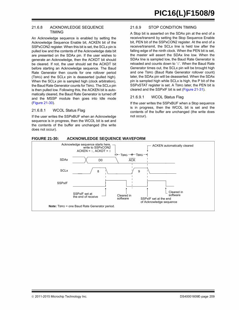
PIC16(L)F1508/9
21.6.8 ACKNOWLEDGE SEQUENCE TIMING
An Acknowledge sequence is enabled by setting theAcknowledge Sequence Enable bit, ACKEN bit of theSSPxCON2 register. When this bit is set, the SCLx pin ispulled low and the contents of the Acknowledge data bitare presented on the SDAx pin. If the user wishes togenerate an Acknowledge, then the ACKDT bit shouldbe cleared. If not, the user should set the ACKDT bitbefore starting an Acknowledge sequence. The BaudRate Generator then counts for one rollover period(TBRG) and the SCLx pin is deasserted (pulled high).When the SCLx pin is sampled high (clock arbitration),the Baud Rate Generator counts for TBRG. The SCLx pinis then pulled low. Following this, the ACKEN bit is auto-matically cleared, the Baud Rate Generator is turned offand the MSSP module then goes into Idle mode(Figure 21-30).
21.6.8.1 WCOL Status Flag
If the user writes the SSPxBUF when an Acknowledgesequence is in progress, then the WCOL bit is set andthe contents of the buffer are unchanged (the writedoes not occur).
21.6.9 STOP CONDITION TIMING
A Stop bit is asserted on the SDAx pin at the end of areceive/transmit by setting the Stop Sequence Enablebit, PEN bit of the SSPxCON2 register. At the end of areceive/transmit, the SCLx line is held low after thefalling edge of the ninth clock. When the PEN bit is set,the master will assert the SDAx line low. When theSDAx line is sampled low, the Baud Rate Generator isreloaded and counts down to ‘0’. When the Baud RateGenerator times out, the SCLx pin will be brought highand one TBRG (Baud Rate Generator rollover count)later, the SDAx pin will be deasserted. When the SDAxpin is sampled high while SCLx is high, the P bit of theSSPxSTAT register is set. A TBRG later, the PEN bit iscleared and the SSPxIF bit is set (Figure 21-31).
21.6.9.1 WCOL Status Flag
If the user writes the SSPxBUF when a Stop sequenceis in progress, then the WCOL bit is set and thecontents of the buffer are unchanged (the write doesnot occur).
FIGURE 21-30: ACKNOWLEDGE SEQUENCE WAVEFORM
Note: TBRG = one Baud Rate Generator period.
SDAx
SCLx
SSPxIF set at
Acknowledge sequence starts here,write to SSPxCON2
ACKEN automatically cleared
Cleared in
TBRG TBRG
the end of receive
8
ACKEN = 1, ACKDT = 0
D0
9
SSPxIF
software SSPxIF set at the endof Acknowledge sequence
Cleared insoftware
ACK
2011-2015 Microchip Technology Inc. DS40001609E-page 209

PIC16(L)F1508/9
FIGURE 21-31: STOP CONDITION RECEIVE OR TRANSMIT MODE
21.6.10 SLEEP OPERATION
While in Sleep mode, the I2C slave module can receiveaddresses or data and when an address match orcomplete byte transfer occurs, wake the processorfrom Sleep (if the MSSP interrupt is enabled).
21.6.11 EFFECTS OF A RESET
A Reset disables the MSSP module and terminates thecurrent transfer.
21.6.12 MULTI-MASTER MODE
In Multi-Master mode, the interrupt generation on thedetection of the Start and Stop conditions allows thedetermination of when the bus is free. The Stop (P) andStart (S) bits are cleared from a Reset or when theMSSP module is disabled. Control of the I2C bus maybe taken when the P bit of the SSPxSTAT register isset, or the bus is idle, with both the S and P bits clear.When the bus is busy, enabling the SSP interrupt willgenerate the interrupt when the Stop condition occurs.
In Multi-Master mode, the SDAx line must be monitoredfor arbitration to see if the signal level is the expectedoutput level. This check is performed by hardware withthe result placed in the BCLxIF bit.
The states where arbitration can be lost are:
• Address Transfer
• Data Transfer
• A Start Condition
• A Repeated Start Condition
• An Acknowledge Condition
21.6.13 MULTI -MASTER COMMUNICATION, BUS COLLISION AND BUS ARBITRATION
Multi-Master mode support is achieved by bus arbitra-tion. When the master outputs address/data bits ontothe SDAx pin, arbitration takes place when the masteroutputs a ‘1’ on SDAx, by letting SDAx float high andanother master asserts a ‘0’. When the SCLx pin floatshigh, data should be stable. If the expected data onSDAx is a ‘1’ and the data sampled on the SDAx pin is‘0’, then a bus collision has taken place. The master willset the Bus Collision Interrupt Flag, BCLxIF and resetthe I2C port to its Idle state (Figure 21-32).
If a transmit was in progress when the bus collisionoccurred, the transmission is halted, the BF flag iscleared, the SDAx and SCLx lines are deasserted andthe SSPxBUF can be written to. When the user ser-vices the bus collision Interrupt Service Routine and ifthe I2C bus is free, the user can resume communica-tion by asserting a Start condition.
If a Start, Repeated Start, Stop or Acknowledge condi-tion was in progress when the bus collision occurred, thecondition is aborted, the SDAx and SCLx lines are deas-serted and the respective control bits in the SSPxCON2register are cleared. When the user services the bus col-lision Interrupt Service Routine and if the I2C bus is free,the user can resume communication by asserting a Startcondition.
The master will continue to monitor the SDAx and SCLxpins. If a Stop condition occurs, the SSPxIF bit will be set.
A write to the SSPxBUF will start the transmission ofdata at the first data bit, regardless of where thetransmitter left off when the bus collision occurred.
In Multi-Master mode, the interrupt generation on thedetection of Start and Stop conditions allows the deter-mination of when the bus is free. Control of the I2C buscan be taken when the P bit is set in the SSPxSTATregister, or the bus is idle and the S and P bits arecleared.
SCLx
SDAx
SDAx asserted low before rising edge of clock
Write to SSPxCON2,set PEN
Falling edge of
SCLx = 1 for TBRG, followed by SDAx = 1 for TBRG
9th clock
SCLx brought high after TBRG
Note: TBRG = one Baud Rate Generator period.
TBRG TBRG
after SDAx sampled high. P bit (SSPxSTAT<4>) is set.
TBRG
to setup Stop condition
ACK
P
TBRG
PEN bit (SSPxCON2<2>) is cleared by hardware and the SSPxIF bit is set
DS40001609E-page 210 2011-2015 Microchip Technology Inc.

PIC16(L)F1508/9
FIGURE 21-32: BUS COLLISION TIMING FOR TRANSMIT AND ACKNOWLEDGE
SDAx
SCLx
BCLxIF
SDAx released
SDAx line pulled lowby another source
Sample SDAx. While SCLx is high,data does not match what is driven
Bus collision has occurred.
Set bus collisioninterrupt (BCLxIF)
by the master.
by master
Data changeswhile SCLx = 0
2011-2015 Microchip Technology Inc. DS40001609E-page 211

PIC16(L)F1508/9
21.6.13.1 Bus Collision During a Start Condition
During a Start condition, a bus collision occurs if:
a) SDA or SCL are sampled low at the beginning ofthe Start condition (Figure 21-33).
b) SCL is sampled low before SDAx is assertedlow (Figure 21-34).
During a Start condition, both the SDAx and the SCLpins are monitored.
If the SDA pin is already low, or the SCL pin is alreadylow, then all of the following occur:
• the Start condition is aborted,
• the BCL1IF flag is set and
• the MSSP module is reset to its Idle state (Figure 21-33).
The Start condition begins with the SDAx and SCLxpins deasserted. When the SDAx pin is sampled high,the Baud Rate Generator is loaded and counts down. Ifthe SCLx pin is sampled low while SDAx is high, a buscollision occurs because it is assumed that anothermaster is attempting to drive a data ‘1’ during the Startcondition.
If the SDAx pin is sampled low during this count, theBRG is reset and the SDAx line is asserted early(Figure 21-35). If, however, a ‘1’ is sampled on the SDApin, the SDA pin is asserted low at the end of the BRGcount. The Baud Rate Generator is then reloaded andcounts down to zero; if the SCL pin is sampled as ‘0’during this time, a bus collision does not occur. At theend of the BRG count, the SCL pin is asserted low.
FIGURE 21-33: BUS COLLISION DURING START CONDITION (SDAX ONLY)
Note: The reason that bus collision is not a fac-tor during a Start condition is that no twobus masters can assert a Start conditionat the exact same time. Therefore, onemaster will always assert SDAx before theother. This condition does not cause a buscollision because the two masters must beallowed to arbitrate the first address fol-lowing the Start condition. If the address isthe same, arbitration must be allowed tocontinue into the data portion, RepeatedStart or Stop conditions.
SDAx
SCLx
SEN
SDAx sampled low before
SDAx goes low before the SEN bit is set.
S bit and SSPxIF set because
SSP module reset into Idle state.SEN cleared automatically because of bus collision.
S bit and SSPxIF set because
Set SEN, enable Startcondition if SDAx = 1, SCLx = 1
SDAx = 0, SCLx = 1.
BCLxIF
S
SSPxIF
SDAx = 0, SCLx = 1.
SSPxIF and BCLxIF arecleared by software
SSPxIF and BCLxIF arecleared by software
Set BCLxIF,
Start condition. Set BCLxIF.
DS40001609E-page 212 2011-2015 Microchip Technology Inc.

PIC16(L)F1508/9
FIGURE 21-34: BUS COLLISION DURING START CONDITION (SCLX = 0)
FIGURE 21-35: BRG RESET DUE TO SDA ARBITRATION DURING START CONDITION
SDAx
SCLx
SENbus collision occurs. Set BCLxIF.SCLx = 0 before SDAx = 0,
Set SEN, enable Startsequence if SDAx = 1, SCLx = 1
TBRG TBRG
SDAx = 0, SCLx = 1
BCLxIF
S
SSPxIF
Interrupt clearedby software
bus collision occurs. Set BCLxIF.SCLx = 0 before BRG time-out,
‘0’ ‘0’
‘0’‘0’
SDAx
SCLx
SEN
Set SLess than TBRG
TBRG
SDAx = 0, SCLx = 1
BCLxIF
S
SSPxIF
S
Interrupts clearedby softwareset SSPxIF
SDAx = 0, SCLx = 1,
SCLx pulled low after BRGtime-out
Set SSPxIF
‘0’
SDAx pulled low by other master.Reset BRG and assert SDAx.
Set SEN, enable Startsequence if SDAx = 1, SCLx = 1
2011-2015 Microchip Technology Inc. DS40001609E-page 213

PIC16(L)F1508/9
21.6.13.2 Bus Collision During a Repeated Start Condition
During a Repeated Start condition, a bus collisionoccurs if:
a) A low level is sampled on SDAx when SCLxgoes from low level to high level (Case 1).
b) SCLx goes low before SDAx is asserted low,indicating that another master is attempting totransmit a data ‘1’ (Case 2).
When the user releases SDAx and the pin is allowed tofloat high, the BRG is loaded with SSPxADD andcounts down to zero. The SCLx pin is then deassertedand when sampled high, the SDAx pin is sampled.
If SDAx is low, a bus collision has occurred (i.e., anothermaster is attempting to transmit a data ‘0’, Figure 21-36).If SDAx is sampled high, the BRG is reloaded andbegins counting. If SDAx goes from high-to-low beforethe BRG times out, no bus collision occurs because notwo masters can assert SDAx at exactly the same time.
If SCLx goes from high-to-low before the BRG timesout and SDAx has not already been asserted, a buscollision occurs. In this case, another master isattempting to transmit a data ‘1’ during the RepeatedStart condition, see Figure 21-37.
If, at the end of the BRG time-out, both SCLx and SDAxare still high, the SDAx pin is driven low and the BRGis reloaded and begins counting. At the end of thecount, regardless of the status of the SCLx pin, theSCLx pin is driven low and the Repeated Startcondition is complete.
FIGURE 21-36: BUS COLLISION DURING A REPEATED START CONDITION (CASE 1)
FIGURE 21-37: BUS COLLISION DURING REPEATED START CONDITION (CASE 2)
SDAx
SCLx
RSEN
BCLxIF
S
SSPxIF
Sample SDAx when SCLx goes high.If SDAx = 0, set BCLxIF and release SDAx and SCLx.
Cleared by software
‘0’
‘0’
SDAx
SCLx
BCLxIF
RSEN
S
SSPxIF
Interrupt clearedby software
SCLx goes low before SDAx,set BCLxIF. Release SDAx and SCLx.
TBRG TBRG
‘0’
DS40001609E-page 214 2011-2015 Microchip Technology Inc.

PIC16(L)F1508/9
21.6.13.3 Bus Collision During a Stop Condition
Bus collision occurs during a Stop condition if:
a) After the SDAx pin has been deasserted andallowed to float high, SDAx is sampled low afterthe BRG has timed out (Case 1).
b) After the SCLx pin is deasserted, SCLx issampled low before SDAx goes high (Case 2).
The Stop condition begins with SDAx asserted low.When SDAx is sampled low, the SCLx pin is allowed tofloat. When the pin is sampled high (clock arbitration),the Baud Rate Generator is loaded with SSPxADD andcounts down to 0. After the BRG times out, SDAx issampled. If SDAx is sampled low, a bus collision hasoccurred. This is due to another master attempting todrive a data ‘0’ (Figure 21-38). If the SCLx pin issampled low before SDAx is allowed to float high, a buscollision occurs. This is another case of another masterattempting to drive a data ‘0’ (Figure 21-39).
FIGURE 21-38: BUS COLLISION DURING A STOP CONDITION (CASE 1)
FIGURE 21-39: BUS COLLISION DURING A STOP CONDITION (CASE 2)
SDAx
SCLx
BCLxIF
PEN
P
SSPxIF
TBRG TBRG TBRG
SDAx asserted low
SDAx sampledlow after TBRG,set BCLxIF
‘0’
‘0’
SDAx
SCLx
BCLxIF
PEN
P
SSPxIF
TBRG TBRG TBRG
Assert SDAx SCLx goes low before SDAx goes high,set BCLxIF
‘0’
‘0’
2011-2015 Microchip Technology Inc. DS40001609E-page 215

PIC16(L)F1508/9
TABLE 21-3: SUMMARY OF REGISTERS ASSOCIATED WITH I2C™ OPERATION
Name Bit 7 Bit 6 Bit 5 Bit 4 Bit 3 Bit 2 Bit 1 Bit 0Reset
Values on Page:
INTCON GIE PEIE TMR0IE INTE IOCIE TMR0IF INTF IOCIF 75
PIE1 TMR1GIE ADIE RCIE TXIE SSP1IE — TMR2IE TMR1IE 76
PIE2 OSFIE C2IE C1IE — BCL1IE NCO1IE — — 77
PIR1 TMR1GIF ADIF RCIF TXIF SSP1IF — TMR2IF TMR1IF 79
PIR2 OSFIF C2IF C1IF — BCL1IF NCO1IF — — 80
TRISA — — TRISA5 TRISA4 —(1) TRISA2 TRISA1 TRISA0 109
SSP1ADD ADD<7:0> 222
SSP1BUF MSSP Receive Buffer/Transmit Register 173*
SSP1CON1 WCOL SSPOV SSPEN CKP SSPM<3:0> 219
SSP1CON2 GCEN ACKSTAT ACKDT ACKEN RCEN PEN RSEN SEN 220
SSP1CON3 ACKTIM PCIE SCIE BOEN SDAHT SBCDE AHEN DHEN 221
SSP1MSK MSK<7:0> 222
SSP1STAT SMP CKE D/A P S R/W UA BF 218
Legend: — = unimplemented location, read as ‘0’. Shaded cells are not used by the MSSP module in I2C™ mode.* Page provides register information.
Note 1: Unimplemented, read as ‘1’.
DS40001609E-page 216 2011-2015 Microchip Technology Inc.

PIC16(L)F1508/9
21.7 BAUD RATE GENERATOR
The MSSP module has a Baud Rate Generator avail-able for clock generation in both I2C and SPI Mastermodes. The Baud Rate Generator (BRG) reload valueis placed in the SSPxADD register (Register 21-6).When a write occurs to SSPxBUF, the Baud Rate Gen-erator will automatically begin counting down.
Once the given operation is complete, the internal clockwill automatically stop counting and the clock pin willremain in its last state.
An internal signal “Reload” in Figure 21-40 triggers thevalue from SSPxADD to be loaded into the BRGcounter. This occurs twice for each oscillation of the
module clock line. The logic dictating when the reloadsignal is asserted depends on the mode the MSSP isbeing operated in.
Table 21-4 demonstrates clock rates based oninstruction cycles and the BRG value loaded intoSSPxADD.
EQUATION 21-1:
FIGURE 21-40: BAUD RATE GENERATOR BLOCK DIAGRAM
TABLE 21-4: MSSP CLOCK RATE W/BRG
FCLOCKFOSC
SSPxADD 1+ 4 -------------------------------------------------=
Note: Values of 0x00, 0x01 and 0x02 are not validfor SSPxADD when used as a Baud RateGenerator for I2C. This is an implementationlimitation.
FOSC FCY BRG ValueFCLOCK
(Two Rollovers of BRG)
16 MHz 4 MHz 09h 400 kHz
16 MHz 4 MHz 0Ch 308 kHz
16 MHz 4 MHz 27h 100 kHz
4 MHz 1 MHz 09h 100 kHz
Note: Refer to the I/O port electrical and timing specifications in Table 29-9 and Figure 29-7 to ensure the systemis designed to support the I/O timing requirements.
SSPM <3:0> SSPxADD<7:0>
SSPxCLKBRG Down CounterFOSC/2
SSPM <3:0>SCLx
ReloadControl Reload
8
8
4
4
Rev. 10-000112A7/30/2013
2011-2015 Microchip Technology Inc. DS40001609E-page 217

PIC16(L)F1508/9
21.8 Register Definitions: MSSP Control REGISTER 21-1: SSPxSTAT: SSP STATUS REGISTER
R/W-0/0 R/W-0/0 R-0/0 R-0/0 R-0/0 R-0/0 R-0/0 R-0/0
SMP CKE D/A P S R/W UA BF
bit 7 bit 0
Legend:
R = Readable bit W = Writable bit U = Unimplemented bit, read as ‘0’
u = Bit is unchanged x = Bit is unknown -n/n = Value at POR and BOR/Value at all other Resets
‘1’ = Bit is set ‘0’ = Bit is cleared
bit 7 SMP: SPI Data Input Sample bit
SPI Master mode:1 = Input data sampled at end of data output time0 = Input data sampled at middle of data output time
SPI Slave mode:SMP must be cleared when SPI is used in Slave modeIn I2 C Master or Slave mode: 1 = Slew rate control disabled0 = Slew rate control enabled
bit 6 CKE: SPI Clock Edge Select bit (SPI mode only)
In SPI Master or Slave mode:1 = Transmit occurs on transition from active to Idle clock state0 = Transmit occurs on transition from Idle to active clock state
In I2 C™ mode only: 1 = Enable input logic so that thresholds are compliant with SMBus specification0 = Disable SMBus specific inputs
bit 5 D/A: Data/Address bit (I2C mode only) 1 = Indicates that the last byte received or transmitted was data0 = Indicates that the last byte received or transmitted was address
bit 4 P: Stop bit
(I2C mode only. This bit is cleared when the MSSP module is disabled, SSPEN is cleared.)1 = Indicates that a Stop bit has been detected last (this bit is ‘0’ on Reset)0 = Stop bit was not detected last
bit 3 S: Start bit
(I2C mode only. This bit is cleared when the MSSP module is disabled, SSPEN is cleared.)1 = Indicates that a Start bit has been detected last (this bit is ‘0’ on Reset)0 = Start bit was not detected last
bit 2 R/W: Read/Write bit information (I2C mode only)This bit holds the R/W bit information following the last address match. This bit is only valid from the address matchto the next Start bit, Stop bit, or not ACK bit.In I2 C Slave mode:1 = Read0 = Write
In I2 C Master mode:1 = Transmit is in progress0 = Transmit is not in progress
OR-ing this bit with SEN, RSEN, PEN, RCEN or ACKEN will indicate if the MSSP is in Idle mode.
bit 1 UA: Update Address bit (10-bit I2C mode only)1 = Indicates that the user needs to update the address in the SSPxADD register0 = Address does not need to be updated
bit 0 BF: Buffer Full Status bit
Receive (SPI and I2 C modes):1 = Receive complete, SSPxBUF is full0 = Receive not complete, SSPxBUF is empty
Transmit (I2 C mode only):1 = Data transmit in progress (does not include the ACK and Stop bits), SSPxBUF is full0 = Data transmit complete (does not include the ACK and Stop bits), SSPxBUF is empty
DS40001609E-page 218 2011-2015 Microchip Technology Inc.

PIC16(L)F1508/9
REGISTER 21-2: SSPxCON1: SSP CONTROL REGISTER 1
R/C/HS-0/0 R/C/HS-0/0 R/W-0/0 R/W-0/0 R/W-0/0 R/W-0/0 R/W-0/0 R/W-0/0
WCOL SSPOV(1) SSPEN CKP SSPM<3:0>
bit 7 bit 0
Legend:
R = Readable bit W = Writable bit U = Unimplemented bit, read as ‘0’
u = Bit is unchanged x = Bit is unknown -n/n = Value at POR and BOR/Value at all other Resets
‘1’ = Bit is set ‘0’ = Bit is cleared HS = Bit is set by hardware C = User cleared
bit 7 WCOL: Write Collision Detect bitMaster mode:1 = A write to the SSPxBUF register was attempted while the I2C conditions were not valid for a transmission to be started0 = No collisionSlave mode:1 = The SSPxBUF register is written while it is still transmitting the previous word (must be cleared in software)0 = No collision
bit 6 SSPOV: Receive Overflow Indicator bit(1)
In SPI mode:1 = A new byte is received while the SSPxBUF register is still holding the previous data. In case of overflow, the data in SSPxSR is lost.
Overflow can only occur in Slave mode. In Slave mode, the user must read the SSPxBUF, even if only transmitting data, to avoid setting overflow. In Master mode, the overflow bit is not set since each new reception (and transmission) is initiated by writing to the SSPxBUF register (must be cleared in software).
0 = No overflowIn I2 C mode:1 = A byte is received while the SSPxBUF register is still holding the previous byte. SSPOV is a “don’t care” in Transmit mode
(must be cleared in software). 0 = No overflow
bit 5 SSPEN: Synchronous Serial Port Enable bitIn both modes, when enabled, these pins must be properly configured as input or outputIn SPI mode:1 = Enables serial port and configures SCKx, SDOx, SDIx and SSx as the source of the serial port pins(2)
0 = Disables serial port and configures these pins as I/O port pinsIn I2 C mode:1 = Enables the serial port and configures the SDAx and SCLx pins as the source of the serial port pins(3)
0 = Disables serial port and configures these pins as I/O port pins
bit 4 CKP: Clock Polarity Select bit In SPI mode:1 = Idle state for clock is a high level 0 = Idle state for clock is a low levelIn I2 C Slave mode:SCLx release control1 = Enable clock 0 = Holds clock low (clock stretch). (Used to ensure data setup time.)In I2 C Master mode:Unused in this mode
bit 3-0 SSPM<3:0>: Synchronous Serial Port Mode Select bits0000 = SPI Master mode, clock = FOSC/40001 = SPI Master mode, clock = FOSC/16 0010 = SPI Master mode, clock = FOSC/64 0011 = SPI Master mode, clock = T2_match/2 0100 = SPI Slave mode, clock = SCKx pin, SS pin control enabled 0101 = SPI Slave mode, clock = SCKx pin, SS pin control disabled, SSx can be used as I/O pin0110 = I2C Slave mode, 7-bit address 0111 = I2C Slave mode, 10-bit address 1000 = I2C Master mode, clock = FOSC/(4 * (SSPxADD+1))(4)
1001 = Reserved1010 = SPI Master mode, clock = FOSC/(4 * (SSPxADD+1))(5)
1011 = I2C firmware controlled Master mode (Slave idle) 1100 = Reserved 1101 = Reserved 1110 = I2C Slave mode, 7-bit address with Start and Stop bit interrupts enabled 1111 = I2C Slave mode, 10-bit address with Start and Stop bit interrupts enabled
Note 1: In Master mode, the overflow bit is not set since each new reception (and transmission) is initiated by writing to the SSPxBUF register.2: When enabled, these pins must be properly configured as input or output.3: When enabled, the SDAx and SCLx pins must be configured as inputs.4: SSPxADD values of 0, 1 or 2 are not supported for I2C mode.5: SSPxADD value of ‘0’ is not supported. Use SSPM = 0000 instead.
2011-2015 Microchip Technology Inc. DS40001609E-page 219

PIC16(L)F1508/9
REGISTER 21-3: SSPxCON2: SSP CONTROL REGISTER 2(1)
R/W-0/0 R-0/0 R/W-0/0 R/S/HS-0/0 R/S/HS-0/0 R/S/HS-0/0 R/S/HS-0/0 R/W/HS-0/0
GCEN ACKSTAT ACKDT ACKEN RCEN PEN RSEN SEN
bit 7 bit 0
Legend:
R = Readable bit W = Writable bit U = Unimplemented bit, read as ‘0’
u = Bit is unchanged x = Bit is unknown -n/n = Value at POR and BOR/Value at all other Resets
‘1’ = Bit is set ‘0’ = Bit is cleared HC = Cleared by hardware S = User set
bit 7 GCEN: General Call Enable bit (in I2C Slave mode only)1 = Enable interrupt when a general call address (0x00 or 00h) is received in the SSPxSR0 = General call address disabled
bit 6 ACKSTAT: Acknowledge Status bit (in I2C mode only)1 = Acknowledge was not received0 = Acknowledge was received
bit 5 ACKDT: Acknowledge Data bit (in I2C mode only)
In Receive mode:Value transmitted when the user initiates an Acknowledge sequence at the end of a receive1 = Not Acknowledge0 = Acknowledge
bit 4 ACKEN: Acknowledge Sequence Enable bit (in I2C Master mode only)
In Master Receive mode:1 = Initiate Acknowledge sequence on SDAx and SCLx pins, and transmit ACKDT data bit.
Automatically cleared by hardware.0 = Acknowledge sequence idle
bit 3 RCEN: Receive Enable bit (in I2C Master mode only)
1 = Enables Receive mode for I2C0 = Receive idle
bit 2 PEN: Stop Condition Enable bit (in I2C Master mode only)
SCKx Release Control:1 = Initiate Stop condition on SDAx and SCLx pins. Automatically cleared by hardware.0 = Stop condition idle
bit 1 RSEN: Repeated Start Condition Enable bit (in I2C Master mode only)
1 = Initiate Repeated Start condition on SDAx and SCLx pins. Automatically cleared by hardware.0 = Repeated Start condition idle
bit 0 SEN: Start Condition Enable/Stretch Enable bit
In Master mode:1 = Initiate Start condition on SDAx and SCLx pins. Automatically cleared by hardware.0 = Start condition idle
In Slave mode:1 = Clock stretching is enabled for both slave transmit and slave receive (stretch enabled)0 = Clock stretching is disabled
Note 1: For bits ACKEN, RCEN, PEN, RSEN, SEN: If the I2C module is not in the Idle mode, this bit may not be set (no spooling) and the SSPxBUF may not be written (or writes to the SSPxBUF are disabled).
DS40001609E-page 220 2011-2015 Microchip Technology Inc.

PIC16(L)F1508/9
REGISTER 21-4: SSPxCON3: SSP CONTROL REGISTER 3
R-0/0 R/W-0/0 R/W-0/0 R/W-0/0 R/W-0/0 R/W-0/0 R/W-0/0 R/W-0/0
ACKTIM(3) PCIE SCIE BOEN SDAHT SBCDE AHEN DHEN
bit 7 bit 0
Legend:
R = Readable bit W = Writable bit U = Unimplemented bit, read as ‘0’
u = Bit is unchanged x = Bit is unknown -n/n = Value at POR and BOR/Value at all other Resets
‘1’ = Bit is set ‘0’ = Bit is cleared
bit 7 ACKTIM: Acknowledge Time Status bit (I2C mode only)(3)
1 = Indicates the I2C bus is in an Acknowledge sequence, set on eighth falling edge of SCLx clock0 = Not an Acknowledge sequence, cleared on ninth rising edge of SCLx clock
bit 6 PCIE: Stop Condition Interrupt Enable bit (I2C mode only)
1 = Enable interrupt on detection of Stop condition0 = Stop detection interrupts are disabled(2)
bit 5 SCIE: Start Condition Interrupt Enable bit (I2C mode only)
1 = Enable interrupt on detection of Start or Restart conditions0 = Start detection interrupts are disabled(2)
bit 4 BOEN: Buffer Overwrite Enable bit
In SPI Slave mode:(1)
1 = SSPxBUF updates every time that a new data byte is shifted in ignoring the BF bit0 = If new byte is received with BF bit of the SSPxSTAT register already set, SSPOV bit of the
SSPxCON1 register is set, and the buffer is not updatedIn I2C Master mode:
This bit is ignored.In I2C Slave mode:
1 = SSPxBUF is updated and ACK is generated for a received address/data byte, ignoring thestate of the SSPOV bit only if the BF bit = 0.
0 = SSPxBUF is only updated when SSPOV is clear
bit 3 SDAHT: SDAx Hold Time Selection bit (I2C mode only)
1 = Minimum of 300 ns hold time on SDAx after the falling edge of SCLx0 = Minimum of 100 ns hold time on SDAx after the falling edge of SCLx
bit 2 SBCDE: Slave Mode Bus Collision Detect Enable bit (I2C Slave mode only)
If on the rising edge of SCLx, SDAx is sampled low when the module is outputting a high state, theBCLxIF bit of the PIR2 register is set, and bus goes idle
1 = Enable slave bus collision interrupts0 = Slave bus collision interrupts are disabled
bit 1 AHEN: Address Hold Enable bit (I2C Slave mode only)
1 = Following the eighth falling edge of SCLx for a matching received address byte, CKP bit of theSSPxCON1 register will be cleared and the SCLx will be held low.
0 = Address holding is disabled
bit 0 DHEN: Data Hold Enable bit (I2C Slave mode only)
1 = Following the eighth falling edge of SCLx for a received data byte, slave hardware clears the CKPbit of the SSPxCON1 register and SCLx is held low.
0 = Data holding is disabled
Note 1: For daisy-chained SPI operation, allows the user to ignore all but the last received byte. SSPOV is still set when a new byte is received and BF = 1, but hardware continues to write the most recent byte to SSPxBUF.
2: This bit has no effect in Slave modes that Start and Stop condition detection is explicitly listed as enabled.
3: The ACKTIM Status bit is only active when the AHEN bit or DHEN bit is set.
2011-2015 Microchip Technology Inc. DS40001609E-page 221

PIC16(L)F1508/9
REGISTER 21-5: SSPxMSK: SSP MASK REGISTER
R/W-1/1 R/W-1/1 R/W-1/1 R/W-1/1 R/W-1/1 R/W-1/1 R/W-1/1 R/W-1/1
MSK<7:0>
bit 7 bit 0
Legend:
R = Readable bit W = Writable bit U = Unimplemented bit, read as ‘0’
u = Bit is unchanged x = Bit is unknown -n/n = Value at POR and BOR/Value at all other Resets
‘1’ = Bit is set ‘0’ = Bit is cleared
bit 7-1 MSK<7:1>: Mask bits1 = The received address bit n is compared to SSPxADD<n> to detect I2C address match0 = The received address bit n is not used to detect I2C address match
bit 0 MSK<0>: Mask bit for I2C Slave mode, 10-bit AddressI2C Slave mode, 10-bit address (SSPM<3:0> = 0111 or 1111):1 = The received address bit 0 is compared to SSPxADD<0> to detect I2C address match0 = The received address bit 0 is not used to detect I2C address matchI2C Slave mode, 7-bit address, the bit is ignored
REGISTER 21-6: SSPxADD: MSSP ADDRESS AND BAUD RATE REGISTER (I2C MODE)
R/W-0/0 R/W-0/0 R/W-0/0 R/W-0/0 R/W-0/0 R/W-0/0 R/W-0/0 R/W-0/0
ADD<7:0>
bit 7 bit 0
Legend:
R = Readable bit W = Writable bit U = Unimplemented bit, read as ‘0’
u = Bit is unchanged x = Bit is unknown -n/n = Value at POR and BOR/Value at all other Resets
‘1’ = Bit is set ‘0’ = Bit is cleared
Master mode:
bit 7-0 ADD<7:0>: Baud Rate Clock Divider bitsSCLx pin clock period = ((ADD<7:0> + 1) *4)/FOSC
10-Bit Slave mode – Most Significant Address Byte:
bit 7-3 Not used: Unused for Most Significant Address Byte. Bit state of this register is a “don’t care”. Bit pat-tern sent by master is fixed by I2C specification and must be equal to ‘11110’. However, those bits are compared by hardware and are not affected by the value in this register.
bit 2-1 ADD<2:1>: Two Most Significant bits of 10-bit address
bit 0 Not used: Unused in this mode. Bit state is a “don’t care”.
10-Bit Slave mode – Least Significant Address Byte:
bit 7-0 ADD<7:0>: Eight Least Significant bits of 10-bit address
7-Bit Slave mode:
bit 7-1 ADD<7:1>: 7-bit address
bit 0 Not used: Unused in this mode. Bit state is a “don’t care”.
DS40001609E-page 222 2011-2015 Microchip Technology Inc.

PIC16(L)F1508/9
22.0 ENHANCED UNIVERSAL SYNCHRONOUS ASYNCHRONOUS RECEIVER TRANSMITTER (EUSART)
The Enhanced Universal Synchronous AsynchronousReceiver Transmitter (EUSART) module is a serial I/Ocommunications peripheral. It contains all the clockgenerators, shift registers and data buffers necessaryto perform an input or output serial data transferindependent of device program execution. TheEUSART, also known as a Serial CommunicationsInterface (SCI), can be configured as a full-duplexasynchronous system or half-duplex synchronoussystem. Full-Duplex mode is useful forcommunications with peripheral systems, such as CRTterminals and personal computers. Half-DuplexSynchronous mode is intended for communicationswith peripheral devices, such as A/D or D/A integratedcircuits, serial EEPROMs or other microcontrollers.These devices typically do not have internal clocks forbaud rate generation and require the external clocksignal provided by a master synchronous device.
The EUSART module includes the following capabilities:
• Full-duplex asynchronous transmit and receive
• Two-character input buffer
• One-character output buffer
• Programmable 8-bit or 9-bit character length
• Address detection in 9-bit mode
• Input buffer overrun error detection
• Received character framing error detection
• Half-duplex synchronous master
• Half-duplex synchronous slave
• Programmable clock polarity in synchronous modes
• Sleep operation
The EUSART module implements the followingadditional features, making it ideally suited for use inLocal Interconnect Network (LIN) bus systems:
• Automatic detection and calibration of the baud rate
• Wake-up on Break reception
• 13-bit Break character transmit
Block diagrams of the EUSART transmitter andreceiver are shown in Figure 22-1 and Figure 22-2.
The EUSART transmit output (TX_out) is available tothe TX/CK pin and internally to the following peripherals:
• Configurable Logic Cell (CLC)
FIGURE 22-1: EUSART TRANSMIT BLOCK DIAGRAM
TXREG register
8
Pin Buffer and Control
TXIF
TRMT
TX9D
Data bus
8 TXIE
Interrupt
TX/CK
TX_out
TX9
TXEN
Transmit Shift Register (TSR)
(8) 0
MSb LSb
÷ n
Multiplier x4
SYNC
BRGH
BRG16
x16 x64
1
1
1
1
1
x
x
x 0
0
0
0
0
0
0
n
+ 1
SPBRGH SPBRGL
Baud Rate GeneratorFOSC
BRG16
Rev. 10-000113A10/14/2013
2011-2015 Microchip Technology Inc. DS40001609E-page 223
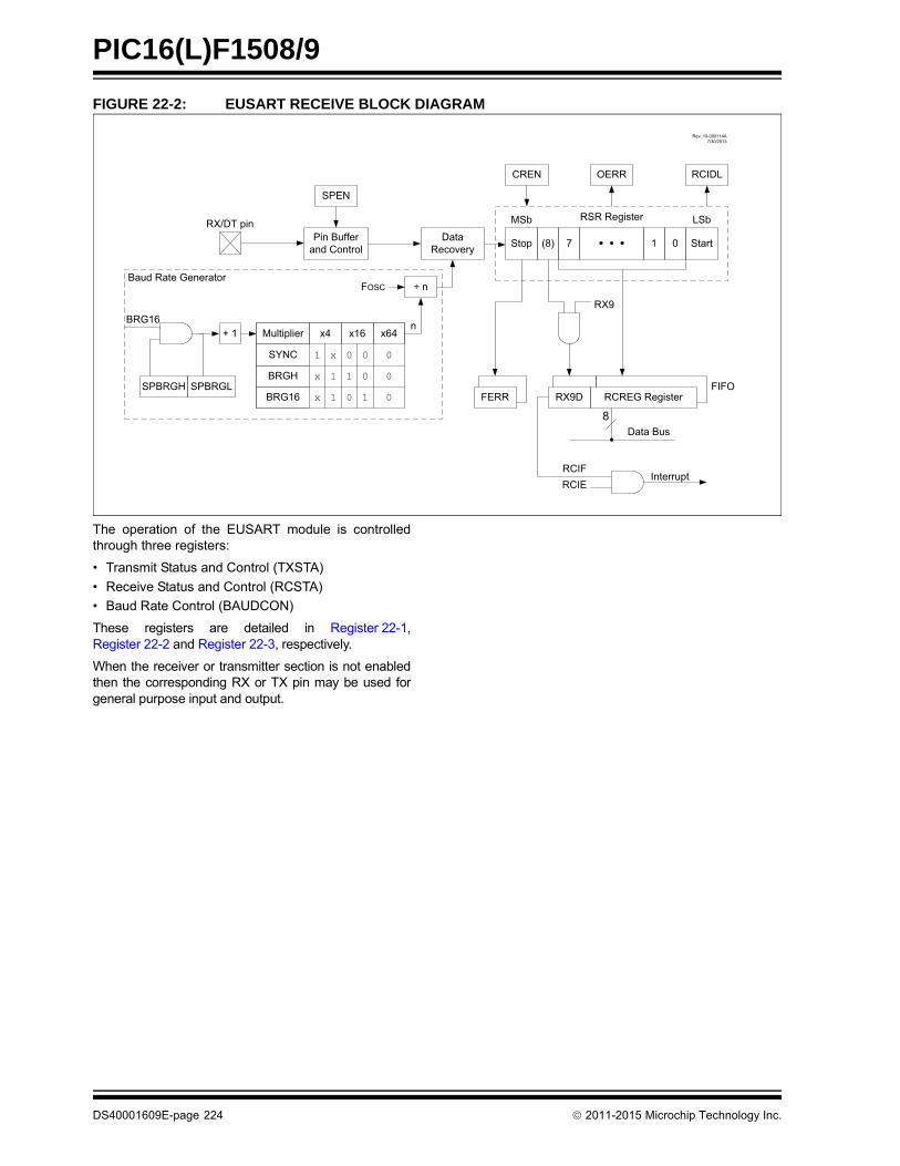
PIC16(L)F1508/9
FIGURE 22-2: EUSART RECEIVE BLOCK DIAGRAM
The operation of the EUSART module is controlledthrough three registers:
• Transmit Status and Control (TXSTA)
• Receive Status and Control (RCSTA)
• Baud Rate Control (BAUDCON)
These registers are detailed in Register 22-1,Register 22-2 and Register 22-3, respectively.
When the receiver or transmitter section is not enabledthen the corresponding RX or TX pin may be used forgeneral purpose input and output.
÷ n
Multiplier x4
SYNC
BRGH
BRG16
x16 x64
1
1
1
1
1
x
x
x 0
0
0
0
0
0
0
n+ 1
SPBRGH SPBRGL
Baud Rate GeneratorFOSC
BRG16
SPEN
CREN OERR RCIDL
Pin Bufferand Control
DataRecovery
RX/DT pin
Stop (8) 7 Start01
MSb LSbRSR Register
RX9
FERR RX9D RCREG RegisterFIFO
8Data Bus
RCIERCIF
Interrupt
Rev. 10-000114A7/30/2013
DS40001609E-page 224 2011-2015 Microchip Technology Inc.

PIC16(L)F1508/9
22.1 EUSART Asynchronous Mode
The EUSART transmits and receives data using thestandard non-return-to-zero (NRZ) format. NRZ isimplemented with two levels: a VOH mark state whichrepresents a ‘1’ data bit, and a VOL space state whichrepresents a ‘0’ data bit. NRZ refers to the fact thatconsecutively transmitted data bits of the same valuestay at the output level of that bit without returning to aneutral level between each bit transmission. An NRZtransmission port idles in the mark state. Each charactertransmission consists of one Start bit followed by eightor nine data bits and is always terminated by one ormore Stop bits. The Start bit is always a space and theStop bits are always marks. The most common dataformat is eight bits. Each transmitted bit persists for aperiod of 1/(Baud Rate). An on-chip dedicated8-bit/16-bit Baud Rate Generator is used to derivestandard baud rate frequencies from the systemoscillator. See Table 22-5 for examples of baud rateconfigurations.
The EUSART transmits and receives the LSb first. TheEUSART’s transmitter and receiver are functionallyindependent, but share the same data format and baudrate. Parity is not supported by the hardware, but canbe implemented in software and stored as the ninthdata bit.
22.1.1 EUSART ASYNCHRONOUS TRANSMITTER
The EUSART transmitter block diagram is shown inFigure 22-1. The heart of the transmitter is the serialTransmit Shift Register (TSR), which is not directlyaccessible by software. The TSR obtains its data fromthe transmit buffer, which is the TXREG register.
22.1.1.1 Enabling the Transmitter
The EUSART transmitter is enabled for asynchronousoperations by configuring the following three controlbits:
• TXEN = 1
• SYNC = 0
• SPEN = 1
All other EUSART control bits are assumed to be intheir default state.
Setting the TXEN bit of the TXSTA register enables thetransmitter circuitry of the EUSART. Clearing the SYNCbit of the TXSTA register configures the EUSART forasynchronous operation. Setting the SPEN bit of theRCSTA register enables the EUSART and automaticallyconfigures the TX/CK I/O pin as an output. If the TX/CKpin is shared with an analog peripheral, the analog I/Ofunction must be disabled by clearing the correspondingANSEL bit.
22.1.1.2 Transmitting Data
A transmission is initiated by writing a character to theTXREG register. If this is the first character, or theprevious character has been completely flushed fromthe TSR, the data in the TXREG is immediatelytransferred to the TSR register. If the TSR still containsall or part of a previous character, the new characterdata is held in the TXREG until the Stop bit of theprevious character has been transmitted. The pendingcharacter in the TXREG is then transferred to the TSRin one TCY immediately following the Stop bittransmission. The transmission of the Start bit, data bitsand Stop bit sequence commences immediatelyfollowing the transfer of the data to the TSR from theTXREG.
22.1.1.3 Transmit Data Polarity
The polarity of the transmit data can be controlled withthe SCKP bit of the BAUDCON register. The defaultstate of this bit is ‘0’ which selects high true transmit idleand data bits. Setting the SCKP bit to ‘1’ will invert thetransmit data resulting in low true idle and data bits. TheSCKP bit controls transmit data polarity inAsynchronous mode only. In Synchronous mode, theSCKP bit has a different function. SeeSection22.5.1.2 “Clock Polarity”.
22.1.1.4 Transmit Interrupt Flag
The TXIF interrupt flag bit of the PIR1 register is setwhenever the EUSART transmitter is enabled and nocharacter is being held for transmission in the TXREG.In other words, the TXIF bit is only clear when the TSRis busy with a character and a new character has beenqueued for transmission in the TXREG. The TXIF flag bitis not cleared immediately upon writing TXREG. TXIFbecomes valid in the second instruction cycle followingthe write execution. Polling TXIF immediately followingthe TXREG write will return invalid results. The TXIF bitis read-only, it cannot be set or cleared by software.
The TXIF interrupt can be enabled by setting the TXIEinterrupt enable bit of the PIE1 register. However, theTXIF flag bit will be set whenever the TXREG is empty,regardless of the state of TXIE enable bit.
To use interrupts when transmitting data, set the TXIEbit only when there is more data to send. Clear theTXIE interrupt enable bit upon writing the last characterof the transmission to the TXREG.
Note: The TXIF Transmitter Interrupt flag is setwhen the TXEN enable bit is set.
2011-2015 Microchip Technology Inc. DS40001609E-page 225

PIC16(L)F1508/9
22.1.1.5 TSR Status
The TRMT bit of the TXSTA register indicates thestatus of the TSR register. This is a read-only bit. TheTRMT bit is set when the TSR register is empty and iscleared when a character is transferred to the TSRregister from the TXREG. The TRMT bit remains clearuntil all bits have been shifted out of the TSR register.No interrupt logic is tied to this bit, so the user has topoll this bit to determine the TSR status.
22.1.1.6 Transmitting 9-Bit Characters
The EUSART supports 9-bit character transmissions.When the TX9 bit of the TXSTA register is set, theEUSART will shift nine bits out for each character trans-mitted. The TX9D bit of the TXSTA register is the ninth,and Most Significant, data bit. When transmitting 9-bitdata, the TX9D data bit must be written before writingthe eight Least Significant bits into the TXREG. All ninebits of data will be transferred to the TSR shift registerimmediately after the TXREG is written.
A special 9-bit Address mode is available for use withmultiple receivers. See Section22.1.2.7 “AddressDetection” for more information on the address mode.
22.1.1.7 Asynchronous Transmission Set-up:
1. Initialize the SPBRGH, SPBRGL register pair andthe BRGH and BRG16 bits to achieve the desiredbaud rate (see Section22.4 “EUSART BaudRate Generator (BRG)”).
2. Enable the asynchronous serial port by clearingthe SYNC bit and setting the SPEN bit.
3. If 9-bit transmission is desired, set the TX9 con-trol bit. A set ninth data bit will indicate that theeight Least Significant data bits are an addresswhen the receiver is set for address detection.
4. Set SCKP bit if inverted transmit is desired.
5. Enable the transmission by setting the TXENcontrol bit. This will cause the TXIF interrupt bitto be set.
6. If interrupts are desired, set the TXIE interruptenable bit of the PIE1 register. An interrupt willoccur immediately provided that the GIE andPEIE bits of the INTCON register are also set.
7. If 9-bit transmission is selected, the ninth bitshould be loaded into the TX9D data bit.
8. Load 8-bit data into the TXREG register. Thiswill start the transmission.
FIGURE 22-3: ASYNCHRONOUS TRANSMISSION
FIGURE 22-4: ASYNCHRONOUS TRANSMISSION (BACK-TO-BACK)
Note: The TSR register is not mapped in datamemory, so it is not available to the user.
Word 1Stop bit
Word 1Transmit Shift Reg.
Start bit bit 0 bit 1 bit 7/8
Write to TXREGWord 1
BRG Output(Shift Clock)
TX/CK
TXIF bit(Transmit Buffer
Reg. Empty Flag)
TRMT bit(Transmit Shift
Reg. Empty Flag)
1 TCY
pin
Transmit Shift Reg.
Write to TXREG
BRG Output(Shift Clock)
TX/CK
TRMT bit(Transmit Shift
Reg. Empty Flag)
Word 1 Word 2
Word 1 Word 2
Start bit Stop bit Start bit
Transmit Shift Reg.
Word 1 Word 2bit 0 bit 1 bit 7/8 bit 0
Note: This timing diagram shows two consecutive transmissions.
1 TCY
1 TCY
pin
TXIF bit(Transmit Buffer
Reg. Empty Flag)
DS40001609E-page 226 2011-2015 Microchip Technology Inc.

PIC16(L)F1508/9
TABLE 22-1: SUMMARY OF REGISTERS ASSOCIATED WITH ASYNCHRONOUS TRANSMISSION
Name Bit 7 Bit 6 Bit 5 Bit 4 Bit 3 Bit 2 Bit 1 Bit 0Register on Page
BAUDCON ABDOVF RCIDL — SCKP BRG16 — WUE ABDEN 235
INTCON GIE PEIE TMR0IE INTE IOCIE TMR0IF INTF IOCIF 75
PIE1 TMR1GIE ADIE RCIE TXIE SSP1IE — TMR2IE TMR1IE 76
PIR1 TMR1GIF ADIF RCIF TXIF SSP1IF — TMR2IF TMR1IF 79
RCSTA SPEN RX9 SREN CREN ADDEN FERR OERR RX9D 234*
SPBRGL BRG<7:0> 236*
SPBRGH BRG<15:8> 236*
TRISB TRISB7 TRISB6 TRISB5 TRISB4 TRISB3 TRISB2 TRISB1 TRISB0 113
TXREG EUSART Transmit Data Register 225
TXSTA CSRC TX9 TXEN SYNC SENDB BRGH TRMT TX9D 233
Legend: — = unimplemented location, read as ‘0’. Shaded cells are not used for asynchronous transmission.
* Page provides register information.
2011-2015 Microchip Technology Inc. DS40001609E-page 227

PIC16(L)F1508/9
22.1.2 EUSART ASYNCHRONOUS RECEIVER
The Asynchronous mode is typically used in RS-232systems. The receiver block diagram is shown inFigure 22-2. The data is received on the RX/DT pin anddrives the data recovery block. The data recovery blockis actually a high-speed shifter operating at 16 timesthe baud rate, whereas the serial Receive ShiftRegister (RSR) operates at the bit rate. When all eightor nine bits of the character have been shifted in, theyare immediately transferred to a two characterFirst-In-First-Out (FIFO) memory. The FIFO bufferingallows reception of two complete characters and thestart of a third character before software must startservicing the EUSART receiver. The FIFO and RSRregisters are not directly accessible by software.Access to the received data is via the RCREG register.
22.1.2.1 Enabling the Receiver
The EUSART receiver is enabled for asynchronousoperation by configuring the following three control bits:
• CREN = 1
• SYNC = 0
• SPEN = 1
All other EUSART control bits are assumed to be intheir default state.
Setting the CREN bit of the RCSTA register enables thereceiver circuitry of the EUSART. Clearing the SYNC bitof the TXSTA register configures the EUSART forasynchronous operation. Setting the SPEN bit of theRCSTA register enables the EUSART. The programmermust set the corresponding TRIS bit to configure theRX/DT I/O pin as an input.
22.1.2.2 Receiving Data
The receiver data recovery circuit initiates characterreception on the falling edge of the first bit. The first bit,also known as the Start bit, is always a zero. The datarecovery circuit counts one-half bit time to the center ofthe Start bit and verifies that the bit is still a zero. If it isnot a zero then the data recovery circuit abortscharacter reception, without generating an error, andresumes looking for the falling edge of the Start bit. Ifthe Start bit zero verification succeeds then the datarecovery circuit counts a full bit time to the center of thenext bit. The bit is then sampled by a majority detectcircuit and the resulting ‘0’ or ‘1’ is shifted into the RSR.This repeats until all data bits have been sampled andshifted into the RSR. One final bit time is measured andthe level sampled. This is the Stop bit, which is alwaysa ‘1’. If the data recovery circuit samples a ‘0’ in theStop bit position then a framing error is set for thischaracter, otherwise the framing error is cleared for thischaracter. See Section22.1.2.4 “Receive FramingError” for more information on framing errors.
Immediately after all data bits and the Stop bit havebeen received, the character in the RSR is transferredto the EUSART receive FIFO and the RCIF interruptflag bit of the PIR1 register is set. The top character inthe FIFO is transferred out of the FIFO by reading theRCREG register.
22.1.2.3 Receive Interrupts
The RCIF interrupt flag bit of the PIR1 register is setwhenever the EUSART receiver is enabled and there isan unread character in the receive FIFO. The RCIFinterrupt flag bit is read-only, it cannot be set or clearedby software.
RCIF interrupts are enabled by setting all of thefollowing bits:
• RCIE, Interrupt Enable bit of the PIE1 register
• PEIE, Peripheral Interrupt Enable bit of the INTCON register
• GIE, Global Interrupt Enable bit of the INTCON register
The RCIF interrupt flag bit will be set when there is anunread character in the FIFO, regardless of the state ofinterrupt enable bits.
Note: If the RX/DT function is on an analog pin,the corresponding ANSEL bit must becleared for the receiver to function.
Note: If the receive FIFO is overrun, no additionalcharacters will be received until the overruncondition is cleared. SeeSection22.1.2.5 “Receive OverrunError” for more information on overrunerrors.
DS40001609E-page 228 2011-2015 Microchip Technology Inc.

PIC16(L)F1508/9
22.1.2.4 Receive Framing Error
Each character in the receive FIFO buffer has acorresponding framing error Status bit. A framing errorindicates that a Stop bit was not seen at the expectedtime. The framing error status is accessed via theFERR bit of the RCSTA register. The FERR bitrepresents the status of the top unread character in thereceive FIFO. Therefore, the FERR bit must be readbefore reading the RCREG.
The FERR bit is read-only and only applies to the topunread character in the receive FIFO. A framing error(FERR = 1) does not preclude reception of additionalcharacters. It is not necessary to clear the FERR bit.Reading the next character from the FIFO buffer willadvance the FIFO to the next character and the nextcorresponding framing error.
The FERR bit can be forced clear by clearing the SPENbit of the RCSTA register which resets the EUSART.Clearing the CREN bit of the RCSTA register does notaffect the FERR bit. A framing error by itself does notgenerate an interrupt.
22.1.2.5 Receive Overrun Error
The receive FIFO buffer can hold two characters. Anoverrun error will be generated if a third character, in itsentirety, is received before the FIFO is accessed. Whenthis happens the OERR bit of the RCSTA register is set.The characters already in the FIFO buffer can be readbut no additional characters will be received until theerror is cleared. The error must be cleared by eitherclearing the CREN bit of the RCSTA register or byresetting the EUSART by clearing the SPEN bit of theRCSTA register.
22.1.2.6 Receiving 9-bit Characters
The EUSART supports 9-bit character reception. Whenthe RX9 bit of the RCSTA register is set the EUSARTwill shift nine bits into the RSR for each characterreceived. The RX9D bit of the RCSTA register is theninth and Most Significant data bit of the top unreadcharacter in the receive FIFO. When reading 9-bit datafrom the receive FIFO buffer, the RX9D data bit mustbe read before reading the eight Least Significant bitsfrom the RCREG.
22.1.2.7 Address Detection
A special Address Detection mode is available for usewhen multiple receivers share the same transmissionline, such as in RS-485 systems. Address detection isenabled by setting the ADDEN bit of the RCSTAregister.
Address detection requires 9-bit character reception.When address detection is enabled, only characterswith the ninth data bit set will be transferred to thereceive FIFO buffer, thereby setting the RCIF interruptbit. All other characters will be ignored.
Upon receiving an address character, user softwaredetermines if the address matches its own. Uponaddress match, user software must disable addressdetection by clearing the ADDEN bit before the nextStop bit occurs. When user software detects the end ofthe message, determined by the message protocolused, software places the receiver back into theAddress Detection mode by setting the ADDEN bit.
Note: If all receive characters in the receiveFIFO have framing errors, repeated readsof the RCREG will not clear the FERR bit.
2011-2015 Microchip Technology Inc. DS40001609E-page 229
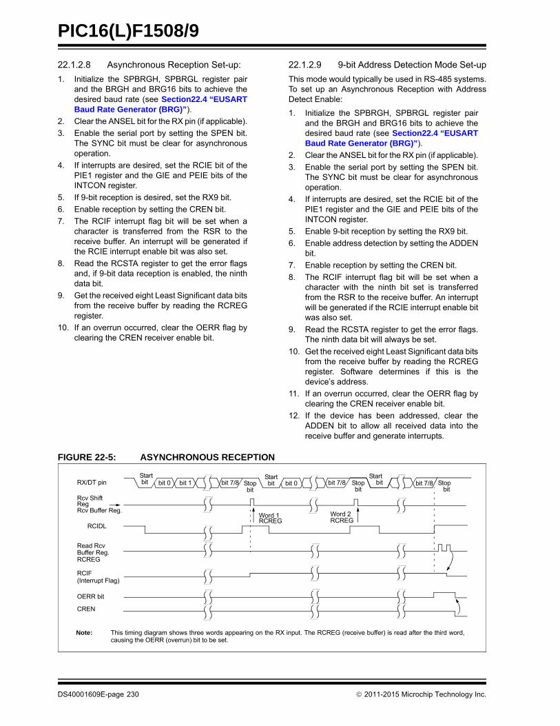
PIC16(L)F1508/9
22.1.2.8 Asynchronous Reception Set-up:
1. Initialize the SPBRGH, SPBRGL register pairand the BRGH and BRG16 bits to achieve thedesired baud rate (see Section22.4 “EUSARTBaud Rate Generator (BRG)”).
2. Clear the ANSEL bit for the RX pin (if applicable).
3. Enable the serial port by setting the SPEN bit.The SYNC bit must be clear for asynchronousoperation.
4. If interrupts are desired, set the RCIE bit of thePIE1 register and the GIE and PEIE bits of theINTCON register.
5. If 9-bit reception is desired, set the RX9 bit.
6. Enable reception by setting the CREN bit.
7. The RCIF interrupt flag bit will be set when acharacter is transferred from the RSR to thereceive buffer. An interrupt will be generated ifthe RCIE interrupt enable bit was also set.
8. Read the RCSTA register to get the error flagsand, if 9-bit data reception is enabled, the ninthdata bit.
9. Get the received eight Least Significant data bitsfrom the receive buffer by reading the RCREGregister.
10. If an overrun occurred, clear the OERR flag byclearing the CREN receiver enable bit.
22.1.2.9 9-bit Address Detection Mode Set-up
This mode would typically be used in RS-485 systems.To set up an Asynchronous Reception with AddressDetect Enable:
1. Initialize the SPBRGH, SPBRGL register pairand the BRGH and BRG16 bits to achieve thedesired baud rate (see Section22.4 “EUSARTBaud Rate Generator (BRG)”).
2. Clear the ANSEL bit for the RX pin (if applicable).
3. Enable the serial port by setting the SPEN bit.The SYNC bit must be clear for asynchronousoperation.
4. If interrupts are desired, set the RCIE bit of thePIE1 register and the GIE and PEIE bits of theINTCON register.
5. Enable 9-bit reception by setting the RX9 bit.
6. Enable address detection by setting the ADDENbit.
7. Enable reception by setting the CREN bit.
8. The RCIF interrupt flag bit will be set when acharacter with the ninth bit set is transferredfrom the RSR to the receive buffer. An interruptwill be generated if the RCIE interrupt enable bitwas also set.
9. Read the RCSTA register to get the error flags.The ninth data bit will always be set.
10. Get the received eight Least Significant data bitsfrom the receive buffer by reading the RCREGregister. Software determines if this is thedevice’s address.
11. If an overrun occurred, clear the OERR flag byclearing the CREN receiver enable bit.
12. If the device has been addressed, clear theADDEN bit to allow all received data into thereceive buffer and generate interrupts.
FIGURE 22-5: ASYNCHRONOUS RECEPTION
Startbit bit 7/8bit 1bit 0 bit 7/8 bit 0Stop
bit
Startbit
Startbitbit 7/8 Stop
bitRX/DT pin
RegRcv Buffer Reg.
Rcv Shift
Read RcvBuffer Reg.RCREG
RCIF(Interrupt Flag)
OERR bit
CREN
Word 1RCREG
Word 2RCREG
Stopbit
Note: This timing diagram shows three words appearing on the RX input. The RCREG (receive buffer) is read after the third word,causing the OERR (overrun) bit to be set.
RCIDL
DS40001609E-page 230 2011-2015 Microchip Technology Inc.

PIC16(L)F1508/9
TABLE 22-2: SUMMARY OF REGISTERS ASSOCIATED WITH ASYNCHRONOUS RECEPTION
Name Bit 7 Bit 6 Bit 5 Bit 4 Bit 3 Bit 2 Bit 1 Bit 0Register on Page
BAUDCON ABDOVF RCIDL — SCKP BRG16 — WUE ABDEN 235
INTCON GIE PEIE TMR0IE INTE IOCIE TMR0IF INTF IOCIF 75
PIE1 TMR1GIE ADIE RCIE TXIE SSP1IE — TMR2IE TMR1IE 76
PIR1 TMR1GIF ADIF RCIF TXIF SSP1IF — TMR2IF TMR1IF 79
RCREG EUSART Receive Data Register 228*
RCSTA SPEN RX9 SREN CREN ADDEN FERR OERR RX9D 234*
SPBRGL BRG<7:0> 236*
SPBRGH BRG<15:8> 236*
TRISB TRISB7 TRISB6 TRISB5 TRISB4 TRISB3 TRISB2 TRISB1 TRISB0 113
TXSTA CSRC TX9 TXEN SYNC SENDB BRGH TRMT TX9D 233
Legend: — = unimplemented location, read as ‘0’. Shaded cells are not used for asynchronous reception.
* Page provides register information.
2011-2015 Microchip Technology Inc. DS40001609E-page 231

PIC16(L)F1508/9
22.2 Clock Accuracy with Asynchronous Operation
The factory calibrates the internal oscillator block out-put (INTOSC). However, the INTOSC frequency maydrift as VDD or temperature changes, and this directlyaffects the asynchronous baud rate.
The Auto-Baud Detect feature (seeSection22.4.1 “Auto-Baud Detect”) can be used tocompensate for changes in the INTOSC frequency.
There may not be fine enough resolution whenadjusting the Baud Rate Generator to compensate fora gradual change in the peripheral clock frequency.
DS40001609E-page 232 2011-2015 Microchip Technology Inc.

PIC16(L)F1508/9
22.3 Register Definitions: EUSART Control
REGISTER 22-1: TXSTA: TRANSMIT STATUS AND CONTROL REGISTER
R/W-/0 R/W-0/0 R/W-0/0 R/W-0/0 R/W-0/0 R/W-0/0 R-1/1 R/W-0/0
CSRC TX9 TXEN(1) SYNC SENDB BRGH TRMT TX9D
bit 7 bit 0
Legend:
R = Readable bit W = Writable bit U = Unimplemented bit, read as ‘0’
u = Bit is unchanged x = Bit is unknown -n/n = Value at POR and BOR/Value at all other Resets
‘1’ = Bit is set ‘0’ = Bit is cleared
bit 7 CSRC: Clock Source Select bitAsynchronous mode: Don’t careSynchronous mode: 1 = Master mode (clock generated internally from BRG)0 = Slave mode (clock from external source)
bit 6 TX9: 9-bit Transmit Enable bit1 = Selects 9-bit transmission0 = Selects 8-bit transmission
bit 5 TXEN: Transmit Enable bit(1)
1 = Transmit enabled0 = Transmit disabled
bit 4 SYNC: EUSART Mode Select bit 1 = Synchronous mode 0 = Asynchronous mode
bit 3 SENDB: Send Break Character bitAsynchronous mode:1 = Send Sync Break on next transmission (cleared by hardware upon completion)0 = Sync Break transmission completedSynchronous mode:Don’t care
bit 2 BRGH: High Baud Rate Select bitAsynchronous mode: 1 = High speed 0 = Low speedSynchronous mode: Unused in this mode
bit 1 TRMT: Transmit Shift Register Status bit1 = TSR empty 0 = TSR full
bit 0 TX9D: Ninth bit of Transmit DataCan be address/data bit or a parity bit.
Note 1: SREN/CREN overrides TXEN in Sync mode.
2011-2015 Microchip Technology Inc. DS40001609E-page 233

PIC16(L)F1508/9
REGISTER 22-2: RCSTA: RECEIVE STATUS AND CONTROL REGISTER
R/W-0/0 R/W-0/0 R/W-0/0 R/W-0/0 R/W-0/0 R-0/0 R-0/0 R-0/0
SPEN RX9 SREN CREN ADDEN FERR OERR RX9D
bit 7 bit 0
Legend:
R = Readable bit W = Writable bit U = Unimplemented bit, read as ‘0’
u = Bit is unchanged x = Bit is unknown -n/n = Value at POR and BOR/Value at all other Resets
‘1’ = Bit is set ‘0’ = Bit is cleared
bit 7 SPEN: Serial Port Enable bit
1 = Serial port enabled (configures RX/DT and TX/CK pins as serial port pins)0 = Serial port disabled (held in Reset)
bit 6 RX9: 9-bit Receive Enable bit
1 = Selects 9-bit reception0 = Selects 8-bit reception
bit 5 SREN: Single Receive Enable bit
Asynchronous mode:
Don’t careSynchronous mode – Master:
1 = Enables single receive0 = Disables single receiveThis bit is cleared after reception is complete.Synchronous mode – Slave
Don’t care
bit 4 CREN: Continuous Receive Enable bit
Asynchronous mode:
1 = Enables receiver0 = Disables receiverSynchronous mode:
1 = Enables continuous receive until enable bit CREN is cleared (CREN overrides SREN)0 = Disables continuous receive
bit 3 ADDEN: Address Detect Enable bit
Asynchronous mode 9-bit (RX9 = 1):
1 = Enables address detection, enable interrupt and load the receive buffer when RSR<8> is set0 = Disables address detection, all bytes are received and ninth bit can be used as parity bitAsynchronous mode 8-bit (RX9 = 0):
Don’t care
bit 2 FERR: Framing Error bit
1 = Framing error (can be updated by reading RCREG register and receive next valid byte)0 = No framing error
bit 1 OERR: Overrun Error bit
1 = Overrun error (can be cleared by clearing bit CREN) 0 = No overrun error
bit 0 RX9D: Ninth bit of Received Data
This can be address/data bit or a parity bit and must be calculated by user firmware.
DS40001609E-page 234 2011-2015 Microchip Technology Inc.

PIC16(L)F1508/9
REGISTER 22-3: BAUDCON: BAUD RATE CONTROL REGISTER
R-0/0 R-1/1 U-0 R/W-0/0 R/W-0/0 U-0 R/W-0/0 R/W-0/0
ABDOVF RCIDL — SCKP BRG16 — WUE ABDEN
bit 7 bit 0
Legend:
R = Readable bit W = Writable bit U = Unimplemented bit, read as ‘0’
u = Bit is unchanged x = Bit is unknown -n/n = Value at POR and BOR/Value at all other Resets
‘1’ = Bit is set ‘0’ = Bit is cleared
bit 7 ABDOVF: Auto-Baud Detect Overflow bit
Asynchronous mode:1 = Auto-baud timer overflowed0 = Auto-baud timer did not overflowSynchronous mode:Don’t care
bit 6 RCIDL: Receive Idle Flag bit
Asynchronous mode:1 = Receiver is idle0 = Start bit has been received and the receiver is receivingSynchronous mode:Don’t care
bit 5 Unimplemented: Read as ‘0’
bit 4 SCKP: Synchronous Clock Polarity Select bit
Asynchronous mode:
1 = Transmit inverted data to the TX/CK pin0 = Transmit non-inverted data to the TX/CK pin
Synchronous mode:1 = Data is clocked on rising edge of the clock0 = Data is clocked on falling edge of the clock
bit 3 BRG16: 16-bit Baud Rate Generator bit
1 = 16-bit Baud Rate Generator is used0 = 8-bit Baud Rate Generator is used
bit 2 Unimplemented: Read as ‘0’
bit 1 WUE: Wake-up Enable bit
Asynchronous mode:
1 = Receiver is waiting for a falling edge. No character will be received, RCIF bit will be set. WUE willautomatically clear after RCIF is set.
0 = Receiver is operating normallySynchronous mode:
Don’t care
bit 0 ABDEN: Auto-Baud Detect Enable bit
Asynchronous mode:
1 = Auto-Baud Detect mode is enabled (clears when auto-baud is complete)0 = Auto-Baud Detect mode is disabledSynchronous mode:Don’t care
2011-2015 Microchip Technology Inc. DS40001609E-page 235

PIC16(L)F1508/9
22.4 EUSART Baud Rate Generator (BRG)
The Baud Rate Generator (BRG) is an 8-bit or 16-bittimer that is dedicated to the support of both theasynchronous and synchronous EUSART operation.By default, the BRG operates in 8-bit mode. Setting theBRG16 bit of the BAUDCON register selects 16-bitmode.
The SPBRGH, SPBRGL register pair determines theperiod of the free running baud rate timer. InAsynchronous mode the multiplier of the baud rateperiod is determined by both the BRGH bit of the TXSTAregister and the BRG16 bit of the BAUDCON register. InSynchronous mode, the BRGH bit is ignored.
Table 22-3 contains the formulas for determining thebaud rate. Example 22-1 provides a sample calculationfor determining the baud rate and baud rate error.
Typical baud rates and error values for variousasynchronous modes have been computed for yourconvenience and are shown in Table 22-3. It may beadvantageous to use the high baud rate (BRGH = 1),or the 16-bit BRG (BRG16 = 1) to reduce the baud rateerror. The 16-bit BRG mode is used to achieve slowbaud rates for fast oscillator frequencies.
Writing a new value to the SPBRGH, SPBRGL registerpair causes the BRG timer to be reset (or cleared). Thisensures that the BRG does not wait for a timer overflowbefore outputting the new baud rate.
If the system clock is changed during an active receiveoperation, a receive error or data loss may result. Toavoid this problem, check the status of the RCIDL bit tomake sure that the receive operation is idle beforechanging the system clock.
EXAMPLE 22-1: CALCULATING BAUD RATE ERROR
For a device with FOSC of 16 MHz, desired baud rateof 9600, Asynchronous mode, 8-bit BRG:
Solving for SPBRGH:SPBRGL:
X
FOSC
Desired Baud Rate---------------------------------------------
64--------------------------------------------- 1–=
Desired Baud Rate FOSC
64 [SPBRGH:SPBRGL] 1+ ------------------------------------------------------------------------=
160000009600
------------------------
64------------------------ 1–=
25.042 25= =
Calculated Baud Rate 16000000
64 25 1+ ---------------------------=
9615=
ErrorCalc. Baud Rate Desired Baud Rate –
Desired Baud Rate --------------------------------------------------------------------------------------------=
9615 9600–
9600---------------------------------- 0.16%= =
DS40001609E-page 236 2011-2015 Microchip Technology Inc.

PIC16(L)F1508/9
TABLE 22-3: BAUD RATE FORMULAS
TABLE 22-4: SUMMARY OF REGISTERS ASSOCIATED WITH THE BAUD RATE GENERATOR
Configuration BitsBRG/EUSART Mode Baud Rate Formula
SYNC BRG16 BRGH
0 0 0 8-bit/Asynchronous FOSC/[64 (n+1)]
0 0 1 8-bit/AsynchronousFOSC/[16 (n+1)]
0 1 0 16-bit/Asynchronous
0 1 1 16-bit/Asynchronous
FOSC/[4 (n+1)]1 0 x 8-bit/Synchronous
1 1 x 16-bit/Synchronous
Legend: x = Don’t care, n = value of SPBRGH, SPBRGL register pair.
Name Bit 7 Bit 6 Bit 5 Bit 4 Bit 3 Bit 2 Bit 1 Bit 0Register on Page
BAUDCON ABDOVF RCIDL — SCKP BRG16 — WUE ABDEN 235
RCSTA SPEN RX9 SREN CREN ADDEN FERR OERR RX9D 234
SPBRGL BRG<7:0> 236*
SPBRGH BRG<15:8> 236*
TXSTA CSRC TX9 TXEN SYNC SENDB BRGH TRMT TX9D 233
Legend: — = unimplemented location, read as ‘0’. Shaded cells are not used for the Baud Rate Generator.
* Page provides register information.
2011-2015 Microchip Technology Inc. DS40001609E-page 237

PIC16(L)F1508/9
TABLE 22-5: BAUD RATES FOR ASYNCHRONOUS MODES
BAUDRATE
SYNC = 0, BRGH = 0, BRG16 = 0
FOSC = 20.000 MHz FOSC = 18.432 MHz FOSC = 16.000 MHz FOSC = 11.0592 MHz
ActualRate
%Error
SPBRGvalue
(decimal)
ActualRate
%Error
SPBRGvalue
(decimal)
ActualRate
%Error
SPBRGvalue
(decimal)
ActualRate
%Error
SPBRGvalue
(decimal)
300 — — — — — — — — — — — —
1200 1221 1.73 255 1200 0.00 239 1202 0.16 207 1200 0.00 143
2400 2404 0.16 129 2400 0.00 119 2404 0.16 103 2400 0.00 71
9600 9470 -1.36 32 9600 0.00 29 9615 0.16 25 9600 0.00 17
10417 10417 0.00 29 10286 -1.26 27 10417 0.00 23 10165 -2.42 16
19.2k 19.53k 1.73 15 19.20k 0.00 14 19.23k 0.16 12 19.20k 0.00 8
57.6k — — — 57.60k 0.00 7 — — — 57.60k 0.00 2
115.2k — — — — — — — — — — — —
BAUDRATE
SYNC = 0, BRGH = 0, BRG16 = 0
FOSC = 8.000 MHz FOSC = 4.000 MHz FOSC = 3.6864 MHz FOSC = 1.000 MHz
ActualRate
%Error
SPBRGvalue
(decimal)
ActualRate
%Error
SPBRGvalue
(decimal)
ActualRate
%Error
SPBRGvalue
(decimal)
ActualRate
%Error
SPBRGvalue
(decimal)
300 — — — 300 0.16 207 300 0.00 191 300 0.16 51
1200 1202 0.16 103 1202 0.16 51 1200 0.00 47 1202 0.16 12
2400 2404 0.16 51 2404 0.16 25 2400 0.00 23 — — —
9600 9615 0.16 12 — — — 9600 0.00 5 — — —
10417 10417 0.00 11 10417 0.00 5 — — — — — —
19.2k — — — — — — 19.20k 0.00 2 — — —
57.6k — — — — — — 57.60k 0.00 0 — — —
115.2k — — — — — — — — — — — —
BAUDRATE
SYNC = 0, BRGH = 1, BRG16 = 0
FOSC = 20.000 MHz FOSC = 18.432 MHz FOSC = 16.000 MHz FOSC = 11.0592 MHz
ActualRate
%Error
SPBRGvalue
(decimal)
ActualRate
%Error
SPBRGvalue
(decimal)
ActualRate
%Error
SPBRGvalue
(decimal)
ActualRate
%Error
SPBRGvalue
(decimal)
300 — — — — — — — — — — — —
1200 — — — — — — — — — — — —
2400 — — — — — — — — — — — —
9600 9615 0.16 129 9600 0.00 119 9615 0.16 103 9600 0.00 71
10417 10417 0.00 119 10378 -0.37 110 10417 0.00 95 10473 0.53 65
19.2k 19.23k 0.16 64 19.20k 0.00 59 19.23k 0.16 51 19.20k 0.00 35
57.6k 56.82k -1.36 21 57.60k 0.00 19 58.82k 2.12 16 57.60k 0.00 11
115.2k 113.64k -1.36 10 115.2k 0.00 9 111.1k -3.55 8 115.2k 0.00 5
DS40001609E-page 238 2011-2015 Microchip Technology Inc.

PIC16(L)F1508/9
BAUDRATE
SYNC = 0, BRGH = 1, BRG16 = 0
FOSC = 8.000 MHz FOSC = 4.000 MHz FOSC = 3.6864 MHz FOSC = 1.000 MHz
ActualRate
%Error
SPBRGvalue
(decimal)
ActualRate
%Error
SPBRGvalue
(decimal)
ActualRate
%Error
SPBRGvalue
(decimal)
ActualRate
%Error
SPBRGvalue
(decimal)
300 — — — — — — — — — 300 0.16 207
1200 — — — 1202 0.16 207 1200 0.00 191 1202 0.16 51
2400 2404 0.16 207 2404 0.16 103 2400 0.00 95 2404 0.16 25
9600 9615 0.16 51 9615 0.16 25 9600 0.00 23 — — —
10417 10417 0.00 47 10417 0.00 23 10473 0.53 21 10417 0.00 5
19.2k 19231 0.16 25 19.23k 0.16 12 19.2k 0.00 11 — — —
57.6k 55556 -3.55 8 — — — 57.60k 0.00 3 — — —
115.2k — — — — — — 115.2k 0.00 1 — — —
BAUDRATE
SYNC = 0, BRGH = 0, BRG16 = 1
FOSC = 20.000 MHz FOSC = 18.432 MHz FOSC = 16.000 MHz FOSC = 11.0592 MHz
ActualRate
%Error
SPBRGvalue
(decimal)
ActualRate
%Error
SPBRGvalue
(decimal)
ActualRate
%Error
SPBRGvalue
(decimal)
ActualRate
%Error
SPBRGvalue
(decimal)
300 300.0 -0.01 4166 300.0 0.00 3839 300.03 0.01 3332 300.0 0.00 2303
1200 1200 -0.03 1041 1200 0.00 959 1200.5 0.04 832 1200 0.00 575
2400 2399 -0.03 520 2400 0.00 479 2398 -0.08 416 2400 0.00 287
9600 9615 0.16 129 9600 0.00 119 9615 0.16 103 9600 0.00 71
10417 10417 0.00 119 10378 -0.37 110 10417 0.00 95 10473 0.53 65
19.2k 19.23k 0.16 64 19.20k 0.00 59 19.23k 0.16 51 19.20k 0.00 35
57.6k 56.818 -1.36 21 57.60k 0.00 19 58.82k 2.12 16 57.60k 0.00 11
115.2k 113.636 -1.36 10 115.2k 0.00 9 111.11k -3.55 8 115.2k 0.00 5
BAUDRATE
SYNC = 0, BRGH = 0, BRG16 = 1
FOSC = 8.000 MHz FOSC = 4.000 MHz FOSC = 3.6864 MHz FOSC = 1.000 MHz
ActualRate
%Error
SPBRGvalue
(decimal)
ActualRate
%Error
SPBRGvalue
(decimal)
ActualRate
%Error
SPBRGvalue
(decimal)
ActualRate
%Error
SPBRGvalue
(decimal)
300 299.9 -0.02 1666 300.1 0.04 832 300.0 0.00 767 300.5 0.16 207
1200 1199 -0.08 416 1202 0.16 207 1200 0.00 191 1202 0.16 51
2400 2404 0.16 207 2404 0.16 103 2400 0.00 95 2404 0.16 25
9600 9615 0.16 51 9615 0.16 25 9600 0.00 23 — — —
10417 10417 0.00 47 10417 0.00 23 10473 0.53 21 10417 0.00 5
19.2k 19.23k 0.16 25 19.23k 0.16 12 19.20k 0.00 11 — — —
57.6k 55556 -3.55 8 — — — 57.60k 0.00 3 — — —
115.2k — — — — — — 115.2k 0.00 1 — — —
TABLE 22-5: BAUD RATES FOR ASYNCHRONOUS MODES (CONTINUED)
2011-2015 Microchip Technology Inc. DS40001609E-page 239

PIC16(L)F1508/9
BAUDRATE
SYNC = 0, BRGH = 1, BRG16 = 1 or SYNC = 1, BRG16 = 1
FOSC = 20.000 MHz FOSC = 18.432 MHz FOSC = 16.000 MHz FOSC = 11.0592 MHz
ActualRate
%Error
SPBRGvalue
(decimal)
ActualRate
%Error
SPBRGvalue
(decimal)
ActualRate
%Error
SPBRGvalue
(decimal)
ActualRate
%Error
SPBRGvalue
(decimal)
300 300.0 0.00 16665 300.0 0.00 15359 300.0 0.00 13332 300.0 0.00 9215
1200 1200 -0.01 4166 1200 0.00 3839 1200.1 0.01 3332 1200 0.00 2303
2400 2400 0.02 2082 2400 0.00 1919 2399.5 -0.02 1666 2400 0.00 1151
9600 9597 -0.03 520 9600 0.00 479 9592 -0.08 416 9600 0.00 287
10417 10417 0.00 479 10425 0.08 441 10417 0.00 383 10433 0.16 264
19.2k 19.23k 0.16 259 19.20k 0.00 239 19.23k 0.16 207 19.20k 0.00 143
57.6k 57.47k -0.22 86 57.60k 0.00 79 57.97k 0.64 68 57.60k 0.00 47
115.2k 116.3k 0.94 42 115.2k 0.00 39 114.29k -0.79 34 115.2k 0.00 23
BAUDRATE
SYNC = 0, BRGH = 1, BRG16 = 1 or SYNC = 1, BRG16 = 1
FOSC = 8.000 MHz FOSC = 4.000 MHz FOSC = 3.6864 MHz FOSC = 1.000 MHz
ActualRate
%Error
SPBRGvalue
(decimal)
ActualRate
%Error
SPBRGvalue
(decimal)
ActualRate
%Error
SPBRGvalue
(decimal)
ActualRate
%Error
SPBRGvalue
(decimal)
300 300.0 0.00 6666 300.0 0.01 3332 300.0 0.00 3071 300.1 0.04 832
1200 1200 -0.02 1666 1200 0.04 832 1200 0.00 767 1202 0.16 207
2400 2401 0.04 832 2398 0.08 416 2400 0.00 383 2404 0.16 103
9600 9615 0.16 207 9615 0.16 103 9600 0.00 95 9615 0.16 25
10417 10417 0 191 10417 0.00 95 10473 0.53 87 10417 0.00 23
19.2k 19.23k 0.16 103 19.23k 0.16 51 19.20k 0.00 47 19.23k 0.16 12
57.6k 57.14k -0.79 34 58.82k 2.12 16 57.60k 0.00 15 — — —
115.2k 117.6k 2.12 16 111.1k -3.55 8 115.2k 0.00 7 — — —
TABLE 22-5: BAUD RATES FOR ASYNCHRONOUS MODES (CONTINUED)
DS40001609E-page 240 2011-2015 Microchip Technology Inc.

PIC16(L)F1508/9
22.4.1 AUTO-BAUD DETECT
The EUSART module supports automatic detectionand calibration of the baud rate.
In the Auto-Baud Detect (ABD) mode, the clock to theBRG is reversed. Rather than the BRG clocking theincoming RX signal, the RX signal is timing the BRG.The Baud Rate Generator is used to time the period ofa received 55h (ASCII “U”) which is the Sync characterfor the LIN bus. The unique feature of this character isthat it has five rising edges including the Stop bit edge.
Setting the ABDEN bit of the BAUDCON register startsthe auto-baud calibration sequence (Figure 22-6).While the ABD sequence takes place, the EUSARTstate machine is held in Idle. On the first rising edge ofthe receive line, after the Start bit, the SPBRG beginscounting up using the BRG counter clock as shown inTable 22-6. The fifth rising edge will occur on the RX pinat the end of the eighth bit period. At that time, anaccumulated value totaling the proper BRG period isleft in the SPBRGH, SPBRGL register pair, the ABDENbit is automatically cleared and the RCIF interrupt flagis set. The value in the RCREG needs to be read toclear the RCIF interrupt. RCREG content should bediscarded. When calibrating for modes that do not usethe SPBRGH register the user can verify that theSPBRGL register did not overflow by checking for 00hin the SPBRGH register.
The BRG auto-baud clock is determined by the BRG16and BRGH bits as shown in Table 22-6. During ABD,both the SPBRGH and SPBRGL registers are used asa 16-bit counter, independent of the BRG16 bit setting.While calibrating the baud rate period, the SPBRGH
and SPBRGL registers are clocked at 1/8th the BRGbase clock rate. The resulting byte measurement is theaverage bit time when clocked at full speed.
TABLE 22-6: BRG COUNTER CLOCK RATES
FIGURE 22-6: AUTOMATIC BAUD RATE CALIBRATION
Note 1: If the WUE bit is set with the ABDEN bit,auto-baud detection will occur on the bytefollowing the Break character (seeSection22.4.3 “Auto-Wake-up onBreak”).
2: It is up to the user to determine that theincoming character baud rate is within therange of the selected BRG clock source.Some combinations of oscillator frequencyand EUSART baud rates are not possible.
3: During the auto-baud process, theauto-baud counter starts counting at 1.Upon completion of the auto-baudsequence, to achieve maximum accuracy,subtract 1 from the SPBRGH:SPBRGLregister pair.
BRG16 BRGHBRG Base
ClockBRG ABD
Clock
0 0 FOSC/64 FOSC/512
0 1 FOSC/16 FOSC/128
1 0 FOSC/16 FOSC/128
1 1 FOSC/4 FOSC/32
Note: During the ABD sequence, SPBRGL andSPBRGH registers are both used as a 16-bitcounter, independent of BRG16 setting.
BRG Value
RX pin
ABDEN bit
RCIF bit
bit 0 bit 1
(Interrupt)
ReadRCREG
BRG Clock
Start
Auto ClearedSet by User
XXXXh 0000h
Edge #1
bit 2 bit 3Edge #2
bit 4 bit 5Edge #3
bit 6 bit 7Edge #4
Stop bit
Edge #5
001Ch
Note 1: The ABD sequence requires the EUSART module to be configured in Asynchronous mode.
SPBRGL XXh 1Ch
SPBRGH XXh 00h
RCIDL
2011-2015 Microchip Technology Inc. DS40001609E-page 241

PIC16(L)F1508/9
22.4.2 AUTO-BAUD OVERFLOW
During the course of automatic baud detection, theABDOVF bit of the BAUDxCON register will be set if thebaud rate counter overflows before the fifth rising edgeis detected on the RX pin. The ABDOVF bit indicatesthat the counter has exceeded the maximum count thatcan fit in the 16 bits of the SPxBRGH:SPxBRGLregister pair. The overflow condition will set the RCIFflag. The counter continues to count until the fifth risingedge is detected on the RX pin. The RCIDL bit willremain false ('0') until the fifth rising edge, at which time,the RCIDL bit will be set. If the RCREG is read after theoverflow occurs, but before the fifth rising edge, thenthe fifth rising edge will set the RCIF again.
Terminating the auto-baud process early to clear anoverflow condition will prevent proper detection of thesync character fifth rising edge. If any falling edges ofthe sync character have not yet occurred when theABDEN bit is cleared, then those will be falsely detectedas start bits. The following steps are recommended toclear the overflow condition:
1. Read RCREG to clear RCIF.
2. If RCIDL is zero, then wait for RCIF and repeat step 1.
3. Clear the ABDOVF bit.
22.4.3 AUTO-WAKE-UP ON BREAK
During Sleep mode, all clocks to the EUSART aresuspended. Because of this, the Baud Rate Generatoris inactive and a proper character reception cannot beperformed. The Auto-Wake-up feature allows thecontroller to wake-up due to activity on the RX/DT line.This feature is available only in Asynchronous mode.
The Auto-Wake-up feature is enabled by setting theWUE bit of the BAUDCON register. Once set, the normalreceive sequence on RX/DT is disabled, and theEUSART remains in an Idle state, monitoring for awake-up event independent of the CPU mode. Awake-up event consists of a high-to-low transition on theRX/DT line. (This coincides with the start of a Sync Breakor a wake-up signal character for the LIN protocol.)
The EUSART module generates an RCIF interruptcoincident with the wake-up event. The interrupt isgenerated synchronously to the Q clocks in normal CPUoperating modes (Figure 22-7), and asynchronously ifthe device is in Sleep mode (Figure 22-8). The interruptcondition is cleared by reading the RCREG register.
The WUE bit is automatically cleared by the low-to-hightransition on the RX line at the end of the Break. Thissignals to the user that the Break event is over. At thispoint, the EUSART module is in Idle mode waiting toreceive the next character.
22.4.3.1 Special Considerations
Break Character
To avoid character errors or character fragments duringa wake-up event, the wake-up character must be allzeros.
When the wake-up is enabled the function worksindependent of the low time on the data stream. If theWUE bit is set and a valid non-zero character isreceived, the low time from the Start bit to the first risingedge will be interpreted as the wake-up event. Theremaining bits in the character will be received as afragmented character and subsequent characters canresult in framing or overrun errors.
Therefore, the initial character in the transmission mustbe all ‘0’s. This must be ten or more bit times, 13-bittimes recommended for LIN bus, or any number of bittimes for standard RS-232 devices.
Oscillator Start-up Time
Oscillator start-up time must be considered, especiallyin applications using oscillators with longer start-upintervals (i.e., LP, XT or HS/PLL mode). The SyncBreak (or wake-up signal) character must be ofsufficient length, and be followed by a sufficientinterval, to allow enough time for the selected oscillatorto start and provide proper initialization of the EUSART.
WUE Bit
The wake-up event causes a receive interrupt bysetting the RCIF bit. The WUE bit is cleared inhardware by a rising edge on RX/DT. The interruptcondition is then cleared in software by reading theRCREG register and discarding its contents.
To ensure that no actual data is lost, check the RCIDLbit to verify that a receive operation is not in processbefore setting the WUE bit. If a receive operation is notoccurring, the WUE bit may then be set just prior toentering the Sleep mode.
DS40001609E-page 242 2011-2015 Microchip Technology Inc.

PIC16(L)F1508/9
FIGURE 22-7: AUTO-WAKE-UP BIT (WUE) TIMING DURING NORMAL OPERATION
FIGURE 22-8: AUTO-WAKE-UP BIT (WUE) TIMINGS DURING SLEEP
Q1 Q2 Q3 Q4 Q1 Q2 Q3Q4 Q1Q2 Q3 Q4 Q1Q2 Q3 Q4 Q1Q2 Q3 Q4 Q1Q2 Q3 Q4 Q1 Q2 Q3 Q4 Q1Q2 Q3 Q4 Q1 Q2 Q3 Q4 Q1Q2 Q3 Q4
OSC1
WUE bit
RX/DT Line
RCIF
Bit set by user Auto Cleared
Cleared due to User Read of RCREG
Note 1: The EUSART remains in Idle while the WUE bit is set.
Q1Q2Q3 Q4 Q1Q2 Q3 Q4 Q1Q2 Q3 Q4 Q1 Q2 Q3 Q4 Q1Q2 Q3 Q4 Q1Q2 Q3 Q4 Q1 Q2Q3 Q4 Q1Q2 Q3 Q4
OSC1
WUE bit
RX/DT Line
RCIF
Bit Set by User Auto Cleared
Cleared due to User Read of RCREGSleep Command Executed
Note 1
Note 1: If the wake-up event requires long oscillator warm-up time, the automatic clearing of the WUE bit can occur while the stposc signal isstill active. This sequence should not depend on the presence of Q clocks.
2: The EUSART remains in Idle while the WUE bit is set.
Sleep Ends
2011-2015 Microchip Technology Inc. DS40001609E-page 243

PIC16(L)F1508/9
22.4.4 BREAK CHARACTER SEQUENCE
The EUSART module has the capability of sending thespecial Break character sequences that are required bythe LIN bus standard. A Break character consists of aStart bit, followed by 12 ‘0’ bits and a Stop bit.
To send a Break character, set the SENDB and TXENbits of the TXSTA register. The Break character trans-mission is then initiated by a write to the TXREG. Thevalue of data written to TXREG will be ignored and all‘0’s will be transmitted.
The SENDB bit is automatically reset by hardware afterthe corresponding Stop bit is sent. This allows the userto preload the transmit FIFO with the next transmit bytefollowing the Break character (typically, the Synccharacter in the LIN specification).
The TRMT bit of the TXSTA register indicates when thetransmit operation is active or idle, just as it does duringnormal transmission. See Figure 22-9 for the timing ofthe Break character sequence.
22.4.4.1 Break and Sync Transmit Sequence
The following sequence will start a message frameheader made up of a Break, followed by an auto-baudSync byte. This sequence is typical of a LIN busmaster.
1. Configure the EUSART for the desired mode.
2. Set the TXEN and SENDB bits to enable theBreak sequence.
3. Load the TXREG with a dummy character toinitiate transmission (the value is ignored).
4. Write ‘55h’ to TXREG to load the Sync characterinto the transmit FIFO buffer.
5. After the Break has been sent, the SENDB bit isreset by hardware and the Sync character isthen transmitted.
When the TXREG becomes empty, as indicated by theTXIF, the next data byte can be written to TXREG.
22.4.5 RECEIVING A BREAK CHARACTER
The Enhanced EUSART module can receive a Breakcharacter in two ways.
The first method to detect a Break character uses theFERR bit of the RCSTA register and the received dataas indicated by RCREG. The Baud Rate Generator isassumed to have been initialized to the expected baudrate.
A Break character has been received when;
• RCIF bit is set
• FERR bit is set
• RCREG = 00h
The second method uses the Auto-Wake-up featuredescribed in Section22.4.3 “Auto-Wake-up onBreak”. By enabling this feature, the EUSART willsample the next two transitions on RX/DT, cause anRCIF interrupt, and receive the next data byte followedby another interrupt.
Note that following a Break character, the user willtypically want to enable the Auto-Baud Detect feature.For both methods, the user can set the ABDEN bit ofthe BAUDCON register before placing the EUSART inSleep mode.
FIGURE 22-9: SEND BREAK CHARACTER SEQUENCE
Write to TXREGDummy Write
BRG Output(Shift Clock)
Start bit bit 0 bit 1 bit 11 Stop bit
Break
TXIF bit(Transmit
Interrupt Flag)
TX (pin)
TRMT bit(Transmit Shift
Empty Flag)
SENDB(send Break
control bit)
SENDB Sampled Here Auto Cleared
DS40001609E-page 244 2011-2015 Microchip Technology Inc.

PIC16(L)F1508/9
22.5 EUSART Synchronous Mode
Synchronous serial communications are typically usedin systems with a single master and one or moreslaves. The master device contains the necessary cir-cuitry for baud rate generation and supplies the clockfor all devices in the system. Slave devices can takeadvantage of the master clock by eliminating the inter-nal clock generation circuitry.
There are two signal lines in Synchronous mode: a bidi-rectional data line and a clock line. Slaves use theexternal clock supplied by the master to shift the serialdata into and out of their respective receive and trans-mit shift registers. Since the data line is bidirectional,synchronous operation is half-duplex only. Half-duplexrefers to the fact that master and slave devices canreceive and transmit data but not both simultaneously.The EUSART can operate as either a master or slavedevice.
Start and Stop bits are not used in synchronous trans-missions.
22.5.1 SYNCHRONOUS MASTER MODE
The following bits are used to configure the EUSARTfor synchronous master operation:
• SYNC = 1
• CSRC = 1
• SREN = 0 (for transmit); SREN = 1 (for receive)
• CREN = 0 (for transmit); CREN = 1 (for receive)
• SPEN = 1
Setting the SYNC bit of the TXSTA register configuresthe device for synchronous operation. Setting the CSRCbit of the TXSTA register configures the device as amaster. Clearing the SREN and CREN bits of the RCSTAregister ensures that the device is in the Transmit mode,otherwise the device will be configured to receive. Settingthe SPEN bit of the RCSTA register enables theEUSART.
22.5.1.1 Master Clock
Synchronous data transfers use a separate clock line,which is synchronous with the data. A device config-ured as a master transmits the clock on the TX/CK line.The TX/CK pin output driver is automatically enabledwhen the EUSART is configured for synchronoustransmit or receive operation. Serial data bits changeon the leading edge to ensure they are valid at the trail-ing edge of each clock. One clock cycle is generatedfor each data bit. Only as many clock cycles are gener-ated as there are data bits.
22.5.1.2 Clock Polarity
A clock polarity option is provided for Microwirecompatibility. Clock polarity is selected with the SCKPbit of the BAUDCON register. Setting the SCKP bit setsthe clock Idle state as high. When the SCKP bit is set,the data changes on the falling edge of each clock.
Clearing the SCKP bit sets the Idle state as low. Whenthe SCKP bit is cleared, the data changes on the risingedge of each clock.
22.5.1.3 Synchronous Master Transmission
Data is transferred out of the device on the RX/DT pin.The RX/DT and TX/CK pin output drivers are automat-ically enabled when the EUSART is configured for syn-chronous master transmit operation.
A transmission is initiated by writing a character to theTXREG register. If the TSR still contains all or part of aprevious character the new character data is held in theTXREG until the last bit of the previous character hasbeen transmitted. If this is the first character, or the pre-vious character has been completely flushed from theTSR, the data in the TXREG is immediately transferredto the TSR. The transmission of the character com-mences immediately following the transfer of the datato the TSR from the TXREG.
Each data bit changes on the leading edge of the mas-ter clock and remains valid until the subsequent leadingclock edge.
22.5.1.4 Synchronous Master Transmission Set-up:
1. Initialize the SPBRGH, SPBRGL register pairand the BRGH and BRG16 bits to achieve thedesired baud rate (see Section22.4 “EUSARTBaud Rate Generator (BRG)”).
2. Enable the synchronous master serial port bysetting bits SYNC, SPEN and CSRC.
3. Disable Receive mode by clearing bits SRENand CREN.
4. Enable Transmit mode by setting the TXEN bit.
5. If 9-bit transmission is desired, set the TX9 bit.
6. If interrupts are desired, set the TXIE bit of thePIE1 register and the GIE and PEIE bits of theINTCON register.
7. If 9-bit transmission is selected, the ninth bitshould be loaded in the TX9D bit.
8. Start transmission by loading data to the TXREGregister.
Note: The TSR register is not mapped in datamemory, so it is not available to the user.
2011-2015 Microchip Technology Inc. DS40001609E-page 245

PIC16(L)F1508/9
FIGURE 22-10: SYNCHRONOUS TRANSMISSION
FIGURE 22-11: SYNCHRONOUS TRANSMISSION (THROUGH TXEN)
TABLE 22-7: SUMMARY OF REGISTERS ASSOCIATED WITH SYNCHRONOUS MASTER TRANSMISSION
Name Bit 7 Bit 6 Bit 5 Bit 4 Bit 3 Bit 2 Bit 1 Bit 0Register on Page
BAUDCON ABDOVF RCIDL — SCKP BRG16 — WUE ABDEN 235
INTCON GIE PEIE TMR0IE INTE IOCIE TMR0IF INTF IOCIF 75
PIE1 TMR1GIE ADIE RCIE TXIE SSP1IE — TMR2IE TMR1IE 76
PIR1 TMR1GIF ADIF RCIF TXIF SSP1IF — TMR2IF TMR1IF 79
RCSTA SPEN RX9 SREN CREN ADDEN FERR OERR RX9D 234
SPBRGL BRG<7:0> 236*
SPBRGH BRG<15:8> 236*
TRISB TRISB7 TRISB6 TRISB5 TRISB4 TRISB3 TRISB2 TRISB1 TRISB0 113
TXREG EUSART Transmit Data Register 225*
TXSTA CSRC TX9 TXEN SYNC SENDB BRGH TRMT TX9D 233
Legend: — = unimplemented location, read as ‘0’. Shaded cells are not used for synchronous master transmission.* Page provides register information.
bit 0 bit 1 bit 7
Word 1
bit 2 bit 0 bit 1 bit 7RX/DT
Write toTXREG Reg
TXIF bit(Interrupt Flag)
TXEN bit‘1’ ‘1’
Word 2
TRMT bit
Write Word 1 Write Word 2
Note: Sync Master mode, SPBRGL = 0, continuous transmission of two 8-bit words.
pin
TX/CK pin
TX/CK pin
(SCKP = 0)
(SCKP = 1)
RX/DT pin
TX/CK pin
Write toTXREG reg
TXIF bit
TRMT bit
bit 0 bit 1 bit 2 bit 6 bit 7
TXEN bit
DS40001609E-page 246 2011-2015 Microchip Technology Inc.

PIC16(L)F1508/9
22.5.1.5 Synchronous Master Reception
Data is received at the RX/DT pin. The RX/DT pinoutput driver is automatically disabled when theEUSART is configured for synchronous master receiveoperation.
In Synchronous mode, reception is enabled by settingeither the Single Receive Enable bit (SREN of theRCSTA register) or the Continuous Receive Enable bit(CREN of the RCSTA register).
When SREN is set and CREN is clear, only as manyclock cycles are generated as there are data bits in asingle character. The SREN bit is automatically clearedat the completion of one character. When CREN is set,clocks are continuously generated until CREN iscleared. If CREN is cleared in the middle of a characterthe CK clock stops immediately and the partial charac-ter is discarded. If SREN and CREN are both set, thenSREN is cleared at the completion of the first characterand CREN takes precedence.
To initiate reception, set either SREN or CREN. Data issampled at the RX/DT pin on the trailing edge of theTX/CK clock pin and is shifted into the Receive ShiftRegister (RSR). When a complete character isreceived into the RSR, the RCIF bit is set and the char-acter is automatically transferred to the two characterreceive FIFO. The Least Significant eight bits of the topcharacter in the receive FIFO are available in RCREG.The RCIF bit remains set as long as there are unreadcharacters in the receive FIFO.
22.5.1.6 Slave Clock
Synchronous data transfers use a separate clock line,which is synchronous with the data. A device configuredas a slave receives the clock on the TX/CK line. TheTX/CK pin output driver is automatically disabled whenthe device is configured for synchronous slave transmitor receive operation. Serial data bits change on theleading edge to ensure they are valid at the trailing edgeof each clock. One data bit is transferred for each clockcycle. Only as many clock cycles should be received asthere are data bits.
22.5.1.7 Receive Overrun Error
The receive FIFO buffer can hold two characters. Anoverrun error will be generated if a third character, in itsentirety, is received before RCREG is read to accessthe FIFO. When this happens the OERR bit of theRCSTA register is set. Previous data in the FIFO willnot be overwritten. The two characters in the FIFObuffer can be read, however, no additional characters
will be received until the error is cleared. The OERR bitcan only be cleared by clearing the overrun condition.If the overrun error occurred when the SREN bit is setand CREN is clear then the error is cleared by readingRCREG. If the overrun occurred when the CREN bit isset then the error condition is cleared by either clearingthe CREN bit of the RCSTA register or by clearing theSPEN bit which resets the EUSART.
22.5.1.8 Receiving 9-bit Characters
The EUSART supports 9-bit character reception. Whenthe RX9 bit of the RCSTA register is set the EUSARTwill shift 9-bits into the RSR for each characterreceived. The RX9D bit of the RCSTA register is theninth, and Most Significant, data bit of the top unreadcharacter in the receive FIFO. When reading 9-bit datafrom the receive FIFO buffer, the RX9D data bit mustbe read before reading the eight Least Significant bitsfrom the RCREG.
22.5.1.9 Synchronous Master Reception Set-up:
1. Initialize the SPBRGH, SPBRGL register pair forthe appropriate baud rate. Set or clear theBRGH and BRG16 bits, as required, to achievethe desired baud rate.
2. Clear the ANSEL bit for the RX pin (if applicable).
3. Enable the synchronous master serial port bysetting bits SYNC, SPEN and CSRC.
4. Ensure bits CREN and SREN are clear.
5. If interrupts are desired, set the RCIE bit of thePIE1 register and the GIE and PEIE bits of theINTCON register.
6. If 9-bit reception is desired, set bit RX9.
7. Start reception by setting the SREN bit or forcontinuous reception, set the CREN bit.
8. Interrupt flag bit RCIF will be set when receptionof a character is complete. An interrupt will begenerated if the enable bit RCIE was set.
9. Read the RCSTA register to get the ninth bit (ifenabled) and determine if any error occurredduring reception.
10. Read the 8-bit received data by reading theRCREG register.
11. If an overrun error occurs, clear the error byeither clearing the CREN bit of the RCSTAregister or by clearing the SPEN bit which resetsthe EUSART.
Note: If the RX/DT function is on an analog pin,the corresponding ANSEL bit must becleared for the receiver to function.
Note: If the device is configured as a slave andthe TX/CK function is on an analog pin, thecorresponding ANSEL bit must becleared.
2011-2015 Microchip Technology Inc. DS40001609E-page 247

PIC16(L)F1508/9
FIGURE 22-12: SYNCHRONOUS RECEPTION (MASTER MODE, SREN)
TABLE 22-8: SUMMARY OF REGISTERS ASSOCIATED WITH SYNCHRONOUS MASTER RECEPTION
Name Bit 7 Bit 6 Bit 5 Bit 4 Bit 3 Bit 2 Bit 1 Bit 0Register on Page
BAUDCON ABDOVF RCIDL — SCKP BRG16 — WUE ABDEN 235
INTCON GIE PEIE TMR0IE INTE IOCIE TMR0IF INTF IOCIF 75
PIE1 TMR1GIE ADIE RCIE TXIE SSP1IE — TMR2IE TMR1IE 76
PIR1 TMR1GIF ADIF RCIF TXIF SSP1IF — TMR2IF TMR1IF 79
RCREG EUSART Receive Data Register 228*
RCSTA SPEN RX9 SREN CREN ADDEN FERR OERR RX9D 234
SPBRGL BRG<7:0> 236*
SPBRGH BRG<15:8> 236*
TRISB TRISB7 TRISB6 TRISB5 TRISB4 TRISB3 TRISB2 TRISB1 TRISB0 113
TXSTA CSRC TX9 TXEN SYNC SENDB BRGH TRMT TX9D 233
Legend: — = unimplemented location, read as ‘0’. Shaded cells are not used for synchronous master reception.
* Page provides register information.
CREN bit
RX/DT
Write tobit SREN
SREN bit
RCIF bit(Interrupt)
ReadRCREG
‘0’
bit 0 bit 1 bit 2 bit 3 bit 4 bit 5 bit 6 bit 7
‘0’
Note: Timing diagram demonstrates Sync Master mode with bit SREN = 1 and bit BRGH = 0.
TX/CK pin
TX/CK pin
pin
(SCKP = 0)
(SCKP = 1)
DS40001609E-page 248 2011-2015 Microchip Technology Inc.

PIC16(L)F1508/9
22.5.2 SYNCHRONOUS SLAVE MODE
The following bits are used to configure the EUSARTfor synchronous slave operation:
• SYNC = 1
• CSRC = 0
• SREN = 0 (for transmit); SREN = 1 (for receive)
• CREN = 0 (for transmit); CREN = 1 (for receive)
• SPEN = 1
Setting the SYNC bit of the TXSTA register configures thedevice for synchronous operation. Clearing the CSRC bitof the TXSTA register configures the device as a slave.Clearing the SREN and CREN bits of the RCSTA registerensures that the device is in the Transmit mode,otherwise the device will be configured to receive. Settingthe SPEN bit of the RCSTA register enables theEUSART.
22.5.2.1 EUSART Synchronous Slave Transmit
The operation of the Synchronous Master and Slavemodes are identical (seeSection22.5.1.3 “Synchronous MasterTransmission”), except in the case of the Sleep mode.
If two words are written to the TXREG and then theSLEEP instruction is executed, the following will occur:
1. The first character will immediately transfer tothe TSR register and transmit.
2. The second word will remain in the TXREGregister.
3. The TXIF bit will not be set.
4. After the first character has been shifted out ofTSR, the TXREG register will transfer the secondcharacter to the TSR and the TXIF bit will now beset.
5. If the PEIE and TXIE bits are set, the interruptwill wake the device from Sleep and execute thenext instruction. If the GIE bit is also set, theprogram will call the Interrupt Service Routine.
22.5.2.2 Synchronous Slave Transmission Set-up:
1. Set the SYNC and SPEN bits and clear theCSRC bit.
2. Clear the ANSEL bit for the CK pin (if applicable).
3. Clear the CREN and SREN bits.
4. If interrupts are desired, set the TXIE bit of thePIE1 register and the GIE and PEIE bits of theINTCON register.
5. If 9-bit transmission is desired, set the TX9 bit.
6. Enable transmission by setting the TXEN bit.
7. If 9-bit transmission is selected, insert the MostSignificant bit into the TX9D bit.
8. Start transmission by writing the LeastSignificant eight bits to the TXREG register.
TABLE 22-9: SUMMARY OF REGISTERS ASSOCIATED WITH SYNCHRONOUS SLAVE TRANSMISSION
Name Bit 7 Bit 6 Bit 5 Bit 4 Bit 3 Bit 2 Bit 1 Bit 0Register on Page
BAUDCON ABDOVF RCIDL — SCKP BRG16 — WUE ABDEN 235
INTCON GIE PEIE TMR0IE INTE IOCIE TMR0IF INTF IOCIF 75
PIE1 TMR1GIE ADIE RCIE TXIE SSP1IE — TMR2IE TMR1IE 76
PIR1 TMR1GIF ADIF RCIF TXIF SSP1IF — TMR2IF TMR1IF 79
RCSTA SPEN RX9 SREN CREN ADDEN FERR OERR RX9D 234
TRISB TRISB7 TRISB6 TRISB5 TRISB4 TRISB3 TRISB2 TRISB1 TRISB0 113
TXREG EUSART Transmit Data Register 225*
TXSTA CSRC TX9 TXEN SYNC SENDB BRGH TRMT TX9D 233
Legend: — = unimplemented location, read as ‘0’. Shaded cells are not used for synchronous slave transmission.
* Page provides register information.
2011-2015 Microchip Technology Inc. DS40001609E-page 249

PIC16(L)F1508/9
22.5.2.3 EUSART Synchronous Slave Reception
The operation of the Synchronous Master and Slavemodes is identical (Section22.5.1.5 “SynchronousMaster Reception”), with the following exceptions:
• Sleep
• CREN bit is always set, therefore the receiver is never idle
• SREN bit, which is a “don’t care” in Slave mode
A character may be received while in Sleep mode bysetting the CREN bit prior to entering Sleep. Once theword is received, the RSR register will transfer the datato the RCREG register. If the RCIE enable bit is set, theinterrupt generated will wake the device from Sleepand execute the next instruction. If the GIE bit is alsoset, the program will branch to the interrupt vector.
22.5.2.4 Synchronous Slave Reception Set-up:
1. Set the SYNC and SPEN bits and clear theCSRC bit.
2. Clear the ANSEL bit for both the CK and DT pins(if applicable).
3. If interrupts are desired, set the RCIE bit of thePIE1 register and the GIE and PEIE bits of theINTCON register.
4. If 9-bit reception is desired, set the RX9 bit.
5. Set the CREN bit to enable reception.
6. The RCIF bit will be set when reception iscomplete. An interrupt will be generated if theRCIE bit was set.
7. If 9-bit mode is enabled, retrieve the MostSignificant bit from the RX9D bit of the RCSTAregister.
8. Retrieve the eight Least Significant bits from thereceive FIFO by reading the RCREG register.
9. If an overrun error occurs, clear the error byeither clearing the CREN bit of the RCSTAregister or by clearing the SPEN bit which resetsthe EUSART.
TABLE 22-10: SUMMARY OF REGISTERS ASSOCIATED WITH SYNCHRONOUS SLAVE RECEPTION
Name Bit 7 Bit 6 Bit 5 Bit 4 Bit 3 Bit 2 Bit 1 Bit 0Register on Page
BAUDCON ABDOVF RCIDL — SCKP BRG16 — WUE ABDEN 235
INTCON GIE PEIE TMR0IE INTE IOCIE TMR0IF INTF IOCIF 75
PIE1 TMR1GIE ADIE RCIE TXIE SSP1IE — TMR2IE TMR1IE 76
PIR1 TMR1GIF ADIF RCIF TXIF SSP1IF — TMR2IF TMR1IF 79
RCREG EUSART Receive Data Register 228*
RCSTA SPEN RX9 SREN CREN ADDEN FERR OERR RX9D 234
TRISB TRISB7 TRISB6 TRISB5 TRISB4 TRISB3 TRISB2 TRISB1 TRISB0 113
TXSTA CSRC TX9 TXEN SYNC SENDB BRGH TRMT TX9D 233
Legend: — = unimplemented location, read as ‘0’. Shaded cells are not used for synchronous slave reception.
* Page provides register information.
DS40001609E-page 250 2011-2015 Microchip Technology Inc.

PIC16(L)F1508/9
23.0 PULSE-WIDTH MODULATION (PWM) MODULE
The PWM module generates a Pulse-Width Modulatedsignal determined by the duty cycle, period, and reso-lution that are configured by the following registers:
• PR2
• T2CON
• PWMxDCH
• PWMxDCL
• PWMxCON
Figure 23-1 shows a simplified block diagram of PWMoperation.
For a step-by-step procedure on how to set up thismodule for PWM operation, refer to Section23.1.9 “Setup for PWM Operation using PWMxPins”.
FIGURE 23-1: SIMPLIFIED PWM BLOCK DIAGRAM
Rev. 10-000022A8/5/2013
8-bit timer is concatenated with two bits generated by Fosc or two bits of the internal prescaler to create 10-bit time-base.
Note 1:
PWMxDCH
Duty cycle registers PWMxDCL<7:6>
10-bit Latch(Not visible to user)
Comparator
Comparator
PR2
(1)TMR2
TMR2 Module
0
1
PWMxPOL
PWMx
PWMx_outTo Peripherals
R TRIS Control
PWMxOE
R
S
Q
Q
T2_match
2011-2015 Microchip Technology Inc. DS40001609E-page 251

PIC16(L)F1508/9
23.1 PWMx Pin Configuration
All PWM outputs are multiplexed with the PORT datalatch. The user must configure the pins as outputs byclearing the associated TRIS bits.
23.1.1 FUNDAMENTAL OPERATION
The PWM module produces a 10-bit resolution output.Timer2 and PR2 set the period of the PWM. ThePWMxDCL and PWMxDCH registers configure theduty cycle. The period is common to all PWM modules,whereas the duty cycle is independently controlled.
All PWM outputs associated with Timer2 are set whenTMR2 is cleared. Each PWMx is cleared when TMR2is equal to the value specified in the correspondingPWMxDCH (8 MSb) and PWMxDCL<7:6> (2 LSb) reg-isters. When the value is greater than or equal to PR2,the PWM output is never cleared (100% duty cycle).
23.1.2 PWM OUTPUT POLARITY
The output polarity is inverted by setting the PWMxPOLbit of the PWMxCON register.
23.1.3 PWM PERIOD
The PWM period is specified by the PR2 register ofTimer2. The PWM period can be calculated using theformula of Equation 23-1.
EQUATION 23-1: PWM PERIOD
When TMR2 is equal to PR2, the following three eventsoccur on the next increment cycle:
• TMR2 is cleared
• The PWM output is active. (Exception: When the PWM duty cycle = 0%, the PWM output will remain inactive.)
• The PWMxDCH and PWMxDCL register values are latched into the buffers.
23.1.4 PWM DUTY CYCLE
The PWM duty cycle is specified by writing a 10-bitvalue to the PWMxDCH and PWMxDCL register pair.The PWMxDCH register contains the eight MSbs andthe PWMxDCL<7:6>, the two LSbs. The PWMxDCHand PWMxDCL registers can be written to at any time.
Equation 23-2 is used to calculate the PWM pulse width.
Equation 23-3 is used to calculate the PWM duty cycleratio.
EQUATION 23-2: PULSE WIDTH
EQUATION 23-3: DUTY CYCLE RATIO
The 8-bit timer TMR2 register is concatenated with thetwo Least Significant bits of 1/FOSC, adjusted by theTimer2 prescaler to create the 10-bit time base. Thesystem clock is used if the Timer2 prescaler is set to 1:1.
Figure 23-2 shows a waveform of the PWM signal whenthe duty cycle is set for the smallest possible pulse.
FIGURE 23-2: PWM OUTPUT
Note: Clearing the PWMxOE bit will relinquishcontrol of the PWMx pin.
Note: The Timer2 postscaler is not used in thedetermination of the PWM frequency. Thepostscaler could be used to have a servoupdate rate at a different frequency thanthe PWM output.
Note: The PWMxDCH and PWMxDCL registersare double buffered. The buffers areupdated when Timer2 matches PR2. Careshould be taken to update both registersbefore the timer match occurs.
PWM Period PR2 1+ 4 TOSC =
(TMR2 Prescale Value)
Note: TOSC = 1/FOSC
Note: The Timer2 postscaler has no effect onthe PWM operation.
Pulse Width PWMxDCH:PWMxDCL<7:6> =
TOSC (TMR2 Prescale Value)
Note: TOSC = 1/FOSC
Duty Cycle RatioPWMxDCH:PWMxDCL<7:6>
4 PR2 1+ -----------------------------------------------------------------------------------=
Pulse Width
TMR2 = PR2
TMR2 = 0
TMR2 = PWMxDC
FOSC
PWM
Q1 Q2 Q3 Q4 Rev. 10-000023A7/30/2013
DS40001609E-page 252 2011-2015 Microchip Technology Inc.

PIC16(L)F1508/9
23.1.5 PWM RESOLUTION
The resolution determines the number of available dutycycles for a given period. For example, a 10-bit resolu-tion will result in 1024 discrete duty cycles, whereas an8-bit resolution will result in 256 discrete duty cycles.
The maximum PWM resolution is ten bits when PR2 is255. The resolution is a function of the PR2 registervalue as shown by Equation 23-4.
EQUATION 23-4: PWM RESOLUTION
23.1.6 OPERATION IN SLEEP MODE
In Sleep mode, the TMR2 register will not incrementand the state of the module will not change. If thePWMx pin is driving a value, it will continue to drive thatvalue. When the device wakes up, TMR2 will continuefrom its previous state.
23.1.7 CHANGES IN SYSTEM CLOCK FREQUENCY
The PWM frequency is derived from the system clockfrequency (FOSC). Any changes in the system clockfrequency will result in changes to the PWM frequency.Refer to Section 5.0 “Oscillator Module (WithFail-Safe Clock Monitor)” for additional details.
23.1.8 EFFECTS OF RESET
Any Reset will force all ports to Input mode and thePWM registers to their Reset states.
Note: If the pulse width value is greater than theperiod the assigned PWM pin(s) willremain unchanged.
Resolution4 PR2 1+ log
2 log------------------------------------------ bits=
TABLE 23-1: EXAMPLE PWM FREQUENCIES AND RESOLUTIONS (FOSC = 20 MHz)
PWM Frequency 0.31 kHz 4.88 kHz 19.53 kHz 78.12 kHz 156.3 kHz 208.3 kHz
Timer Prescale 64 4 1 1 1 1
PR2 Value 0xFF 0xFF 0xFF 0x3F 0x1F 0x17
Maximum Resolution (bits) 10 10 10 8 7 6.6
TABLE 23-2: EXAMPLE PWM FREQUENCIES AND RESOLUTIONS (FOSC = 8 MHz)
PWM Frequency 0.31 kHz 4.90 kHz 19.61 kHz 76.92 kHz 153.85 kHz 200.0 kHz
Timer Prescale 64 4 1 1 1 1
PR2 Value 0x65 0x65 0x65 0x19 0x0C 0x09
Maximum Resolution (bits) 8 8 8 6 5 5
2011-2015 Microchip Technology Inc. DS40001609E-page 253

PIC16(L)F1508/9
23.1.9 SETUP FOR PWM OPERATION USING PWMx PINS
The following steps should be taken when configuringthe module for PWM operation using the PWMx pins:
1. Disable the PWMx pin output driver(s) by settingthe associated TRIS bit(s).
2. Clear the PWMxCON register.
3. Load the PR2 register with the PWM periodvalue.
4. Clear the PWMxDCH register and bits <7:6> ofthe PWMxDCL register.
5. Configure and start Timer2:
• Clear the TMR2IF interrupt flag bit of the PIR1 register. See note below.
• Configure the T2CKPS bits of the T2CON register with the Timer2 prescale value.
• Enable Timer2 by setting the TMR2ON bit of the T2CON register.
6. Enable PWM output pin and wait until Timer2overflows, TMR2IF bit of the PIR1 register is set.See note below.
7. Enable the PWMx pin output driver(s) by clear-ing the associated TRIS bit(s) and setting thePWMxOE bit of the PWMxCON register.
8. Configure the PWM module by loading thePWMxCON register with the appropriate values.
Note 1: In order to send a complete duty cycleand period on the first PWM output, theabove steps must be followed in the ordergiven. If it is not critical to start with acomplete PWM signal, then move Step 8to replace Step 4.
2: For operation with other peripherals only,disable PWMx pin outputs.
DS40001609E-page 254 2011-2015 Microchip Technology Inc.

PIC16(L)F1508/9
23.2 Register Definitions: PWM Control
REGISTER 23-1: PWMxCON: PWM CONTROL REGISTER
R/W-0/0 R/W-0/0 R-0/0 R/W-0/0 U-0 U-0 U-0 U-0
PWMxEN PWMxOE PWMxOUT PWMxPOL — — — —
bit 7 bit 0
Legend:
R = Readable bit W = Writable bit U = Unimplemented bit, read as ‘0’
u = Bit is unchanged x = Bit is unknown -n/n = Value at POR and BOR/Value at all other Resets
‘1’ = Bit is set ‘0’ = Bit is cleared
bit 7 PWMxEN: PWM Module Enable bit
1 = PWM module is enabled0 = PWM module is disabled
bit 6 PWMxOE: PWM Module Output Enable bit
1 = Output to PWMx pin is enabled0 = Output to PWMx pin is disabled
bit 5 PWMxOUT: PWM Module Output Value bit
bit 4 PWMxPOL: PWMx Output Polarity Select bit
1 = PWM output is active-low0 = PWM output is active-high
bit 3-0 Unimplemented: Read as ‘0’
2011-2015 Microchip Technology Inc. DS40001609E-page 255

PIC16(L)F1508/9
REGISTER 23-2: PWMxDCH: PWM DUTY CYCLE HIGH BITS
R/W-x/u R/W-x/u R/W-x/u R/W-x/u R/W-x/u R/W-x/u R/W-x/u R/W-x/u
PWMxDCH<7:0>
bit 7 bit 0
Legend:
R = Readable bit W = Writable bit U = Unimplemented bit, read as ‘0’
u = Bit is unchanged x = Bit is unknown -n/n = Value at POR and BOR/Value at all other Resets
‘1’ = Bit is set ‘0’ = Bit is cleared
bit 7-0 PWMxDCH<7:0>: PWM Duty Cycle Most Significant bitsThese bits are the MSbs of the PWM duty cycle. The two LSbs are found in the PWMxDCL register.
REGISTER 23-3: PWMxDCL: PWM DUTY CYCLE LOW BITS
R/W-x/u R/W-x/u U-0 U-0 U-0 U-0 U-0 U-0
PWMxDCL<7:6> — — — — — —
bit 7 bit 0
Legend:
R = Readable bit W = Writable bit U = Unimplemented bit, read as ‘0’
u = Bit is unchanged x = Bit is unknown -n/n = Value at POR and BOR/Value at all other Resets
‘1’ = Bit is set ‘0’ = Bit is cleared
bit 7-6 PWMxDCL<7:6>: PWM Duty Cycle Least Significant bitsThese bits are the LSbs of the PWM duty cycle. The MSbs are found in the PWMxDCH register.
bit 5-0 Unimplemented: Read as ‘0’
TABLE 23-3: SUMMARY OF REGISTERS ASSOCIATED WITH PWM
Name Bit 7 Bit 6 Bit 5 Bit 4 Bit 3 Bit 2 Bit 1 Bit 0Register on Page
PR2 Timer2 module Period Register 166*
PWM1CON PWM1EN PWM1OE PWM1OUT PWM1POL — — — — 255
PWM1DCH PWM1DCH<7:0> 256
PWM1DCL PWM1DCL<7:6> — — — — — — 256
PWM2CON PWM2EN PWM2OE PWM2OUT PWM2POL — — — — 255
PWM2DCH PWM2DCH<7:0> 256
PWM2DCL PWM2DCL<7:6> — — — — — — 256
PWM3CON PWM3EN PWM3OE PWM3OUT PWM3POL — — — — 255
PWM3DCH PWM3DCH<7:0> 256
PWM3DCL PWM3DCL<7:6> — — — — — — 256
PWM4CON PWM4EN PWM4OE PWM4OUT PWM4POL — — — — 255
PWM4DCH PWM4DCH<7:0> 256
PWM4DCL PWM4DCL<7:6> — — — — — — 256
T2CON — T2OUTPS<3:0> TMR2ON T2CKPS<1:0> 168
TMR2 Timer2 module Register 166*
TRISA — — TRISA5 TRISA4 —(1) TRISA2 TRISA1 TRISA0 109
TRISC TRISC7 TRISC6 TRISC5 TRISC4 TRISC3 TRISC2 TRISC1 TRISC0 117
Legend: - = Unimplemented locations, read as ‘0’, u = unchanged, x = unknown. Shaded cells are not used by the PWM.* Page provides register information.
Note 1: Unimplemented, read as ‘1’.
DS40001609E-page 256 2011-2015 Microchip Technology Inc.
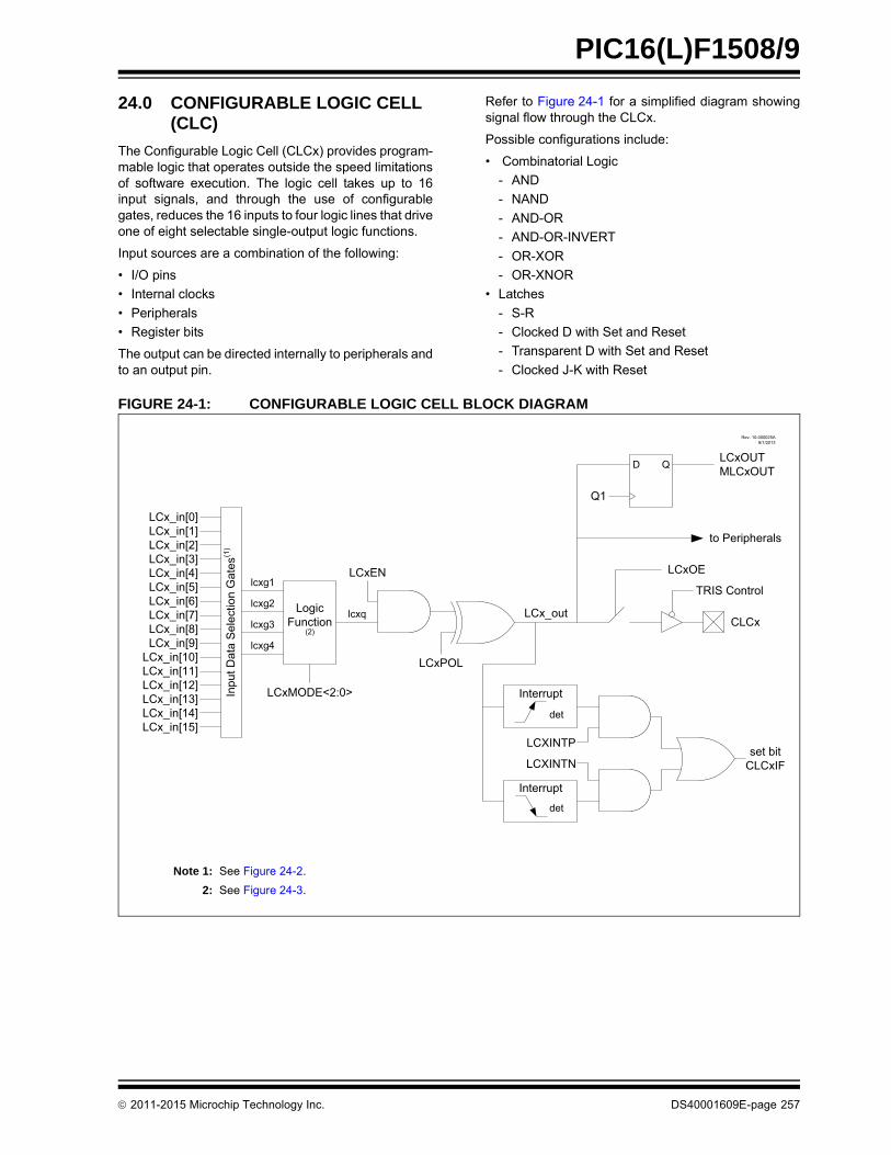
PIC16(L)F1508/9
24.0 CONFIGURABLE LOGIC CELL (CLC)
The Configurable Logic Cell (CLCx) provides program-mable logic that operates outside the speed limitationsof software execution. The logic cell takes up to 16input signals, and through the use of configurablegates, reduces the 16 inputs to four logic lines that driveone of eight selectable single-output logic functions.
Input sources are a combination of the following:
• I/O pins
• Internal clocks
• Peripherals
• Register bits
The output can be directed internally to peripherals andto an output pin.
Refer to Figure 24-1 for a simplified diagram showingsignal flow through the CLCx.
Possible configurations include:
• Combinatorial Logic
- AND
- NAND
- AND-OR
- AND-OR-INVERT
- OR-XOR
- OR-XNOR
• Latches
- S-R
- Clocked D with Set and Reset
- Transparent D with Set and Reset
- Clocked J-K with Reset
FIGURE 24-1: CONFIGURABLE LOGIC CELL BLOCK DIAGRAM
Inpu
t Dat
a S
elec
tion
Gat
es(1
)
LogicFunction
(2)
lcxg2
lcxg1
lcxg3
lcxg4
LCxMODE<2:0>
lcxq
LCxEN
LCx_in[0]LCx_in[1]LCx_in[2]LCx_in[3]LCx_in[4]LCx_in[5]LCx_in[6]LCx_in[7]LCx_in[8]LCx_in[9]
LCx_in[10]LCx_in[11]LCx_in[12]LCx_in[13]LCx_in[14]LCx_in[15]
LCxPOL
det
Interrupt
det
Interrupt
set bitCLCxIFLCXINTN
LCXINTP
LCxOE
TRIS Control
CLCx
to Peripherals
Q1
LCx_out
LCxOUTMLCxOUTD Q
Rev. 10-000025A8/1/2013
Note 1: See Figure 24-2.
2: See Figure 24-3.
2011-2015 Microchip Technology Inc. DS40001609E-page 257

PIC16(L)F1508/9
24.1 CLCx Setup
Programming the CLCx module is performed by config-uring the four stages in the logic signal flow. The fourstages are:
• Data selection
• Data gating
• Logic function selection
• Output polarity
Each stage is setup at run time by writing to the corre-sponding CLCx Special Function Registers. This hasthe added advantage of permitting logic reconfigurationon-the-fly during program execution.
24.1.1 DATA SELECTION
There are 16 signals available as inputs to the configu-rable logic. Four 8-input multiplexers are used to selectthe inputs to pass on to the next stage. The 16 inputs tothe multiplexers are arranged in groups of four. Eachgroup is available to two of the four multiplexers, in
each case, paired with a different group. This arrange-ment makes possible selection of up to two from agroup without precluding a selection from anothergroup.
Data selection is through four multiplexers as indicatedon the left side of Figure 24-2. Data inputs in the figureare identified by a generic numbered input name.
Table 24-1 correlates the generic input name to theactual signal for each CLC module. The columns labeledlcxd1 through lcxd4 indicate the MUX output for theselected data input. D1S through D4S are abbreviationsfor the MUX select input codes: LCxD1S<2:0> throughLCxD4S<2:0>, respectively. Selecting a data input in acolumn excludes all other inputs in that column.
Data inputs are selected with CLCxSEL0 andCLCxSEL1 registers (Register 24-3 and Register 24-5,respectively).
Note: Data selections are undefined at power-up.
TABLE 24-1: CLCx DATA INPUT SELECTION
Data Inputlcxd1D1S
lcxd2D2S
lcxd3D3S
lcxd4D4S
CLC 1 CLC 2 CLC 3 CLC 4
LCx_in[0] 000 — — 100 CLC1IN0 CLC2IN0 CLC3IN0 CLC4IN0
LCx_in[1] 001 — — 101 CLC1IN1 CLC2IN1 CLC3IN1 CLC4IN1
LCx_in[2] 010 — — 110 C1OUT_sync C1OUT_sync C1OUT_sync C1OUT_sync
LCx_in[3] 011 — — 111 C2OUT_sync C2OUT_sync C2OUT_sync C2OUT_sync
LCx_in[4] 100 000 — — FOSC FOSC FOSC FOSC
LCx_in[5] 101 001 — — T0_overflow T0_overflow T0_overflow T0_overflow
LCx_in[6] 110 010 — — T1_overflow T1_overflow T1_overflow T1_overflow
LCx_in[7] 111 011 — — T2_match T2_match T2_match T2_match
LCx_in[8] — 100 000 — LC1_out LC1_out LC1_out LC1_out
LCx_in[9] — 101 001 — LC2_out LC2_out LC2_out LC2_out
LCx_in[10] — 110 010 — LC3_out LC3_out LC3_out LC3_out
LCx_in[11] — 111 011 — LC4_out LC4_out LC4_out LC4_out
LCx_in[12] — — 100 000 NCO1_out LFINTOSC TX_out (EUSART)
SCK_out (MSSP)
LCx_in[13] — — 101 001 HFINTOSC FRC LFINTOSC SDO_out (MSSP)
LCx_in[14] — — 110 010 PWM3_out PWM1_out PWM2_out PWM1_out
LCx_in[15] — — 111 011 PWM4_out PWM2_out PWM3_out PWM4_out
DS40001609E-page 258 2011-2015 Microchip Technology Inc.

PIC16(L)F1508/9
24.1.2 DATA GATING
Outputs from the input multiplexers are directed to thedesired logic function input through the data gatingstage. Each data gate can direct any combination of thefour selected inputs.
The gate stage is more than just signal direction. Thegate can be configured to direct each input signal asinverted or non-inverted data. Directed signals areANDed together in each gate. The output of each gatecan be inverted before going on to the logic functionstage.
The gating is in essence a 1-to-4 inputAND/NAND/OR/NOR gate. When every input isinverted and the output is inverted, the gate is an OR ofall enabled data inputs. When the inputs and output arenot inverted, the gate is an AND or all enabled inputs.
Table 24-2 summarizes the basic logic that can be obtained in gate 1 by using the gate logic select bits. The table shows the logic of four input variables, but each gate can be configured to use less than four. If no inputs are selected, the output will be zero or one, depending on the gate output polarity bit.
It is possible (but not recommended) to select both thetrue and negated values of an input. When this is done,the gate output is zero, regardless of the other inputs,but may emit logic glitches (transient-induced pulses).If the output of the channel must be zero or one, therecommended method is to set all gate bits to zero anduse the gate polarity bit to set the desired level.
Data gating is configured with the logic gate selectregisters as follows:
• Gate 1: CLCxGLS0 (Register 24-5)
• Gate 2: CLCxGLS1 (Register 24-6)
• Gate 3: CLCxGLS2 (Register 24-7)
• Gate 4: CLCxGLS3 (Register 24-8)
Register number suffixes are different than the gatenumbers because other variations of this module havemultiple gate selections in the same register.
Data gating is indicated in the right side of Figure 24-2.Only one gate is shown in detail. The remaining threegates are configured identically with the exception thatthe data enables correspond to the enables for thatgate.
24.1.3 LOGIC FUNCTION
There are eight available logic functions including:
• AND-OR
• OR-XOR
• AND
• S-R Latch
• D Flip-Flop with Set and Reset
• D Flip-Flop with Reset
• J-K Flip-Flop with Reset
• Transparent Latch with Set and Reset
Logic functions are shown in Figure 24-3. Each logicfunction has four inputs and one output. The four inputsare the four data gate outputs of the previous stage.The output is fed to the inversion stage and from thereto other peripherals, an output pin, and back to theCLCx itself.
24.1.4 OUTPUT POLARITY
The last stage in the configurable logic cell is the outputpolarity. Setting the LCxPOL bit of the CLCxCON reg-ister inverts the output signal from the logic stage.Changing the polarity while the interrupts are enabledwill cause an interrupt for the resulting output transition.
Note: Data gating is undefined at power-up.
TABLE 24-2: DATA GATING LOGIC
CLCxGLS0 LCxG1POL Gate Logic
0x55 1 AND
0x55 0 NAND
0xAA 1 NOR
0xAA 0 OR
0x00 0 Logic 0
0x00 1 Logic 1
2011-2015 Microchip Technology Inc. DS40001609E-page 259

PIC16(L)F1508/9
24.1.5 CLCx SETUP STEPS
The following steps should be followed when setting upthe CLCx:
• Disable CLCx by clearing the LCxEN bit.
• Select desired inputs using CLCxSEL0 and CLCxSEL1 registers (See Table 24-1).
• Clear any associated ANSEL bits.• Set all TRIS bits associated with inputs.
• Clear all TRIS bits associated with outputs.
• Enable the chosen inputs through the four gates using CLCxGLS0, CLCxGLS1, CLCxGLS2, and CLCxGLS3 registers.
• Select the gate output polarities with the LCxPOLy bits of the CLCxPOL register.
• Select the desired logic function with the LCxMODE<2:0> bits of the CLCxCON register.
• Select the desired polarity of the logic output with the LCxPOL bit of the CLCxPOL register. (This step may be combined with the previous gate output polarity step).
• If driving a device, set the LCxOE bit in the CLCxCON register and also clear the TRIS bit corresponding to that output.
• If interrupts are desired, configure the following bits:
- Set the LCxINTP bit in the CLCxCON register for rising event.
- Set the LCxINTN bit in the CLCxCON register or falling event.
- Set the CLCxIE bit of the associated PIE registers.
- Set the GIE and PEIE bits of the INTCON register.
• Enable the CLCx by setting the LCxEN bit of the CLCxCON register.
24.2 CLCx Interrupts
An interrupt will be generated upon a change in theoutput value of the CLCx when the appropriate interruptenables are set. A rising edge detector and a fallingedge detector are present in each CLC for this purpose.
The CLCxIF bit of the associated PIR registers will beset when either edge detector is triggered and its asso-ciated enable bit is set. The LCxINTP enables risingedge interrupts and the LCxINTN bit enables fallingedge interrupts. Both are located in the CLCxCONregister.
To fully enable the interrupt, set the following bits:
• LCxON bit of the CLCxCON register
• CLCxIE bit of the associated PIE registers
• LCxINTP bit of the CLCxCON register (for a rising edge detection)
• LCxINTN bit of the CLCxCON register (for a falling edge detection)
• PEIE and GIE bits of the INTCON register
The CLCxIF bit of the associated PIR registers, mustbe cleared in software as part of the interrupt service. Ifanother edge is detected while this flag is beingcleared, the flag will still be set at the end of thesequence.
24.3 Output Mirror Copies
Mirror copies of all LCxCON output bits are containedin the CLCxDATA register. Reading this register readsthe outputs of all CLCs simultaneously. This preventsany reading skew introduced by testing or reading theCLCxOUT bits in the individual CLCxCON registers.
24.4 Effects of a Reset
The CLCxCON register is cleared to zero as the resultof a Reset. All other selection and gating values remainunchanged.
24.5 Operation During Sleep
The CLC module operates independently from the system clock and will continue to run during Sleep, provided that the input sources selected remain active.
The HFINTOSC remains active during Sleep when the CLC module is enabled and the HFINTOSC is selected as an input source, regardless of the system clock source selected.
In other words, if the HFINTOSC is simultaneously selected as the system clock and as a CLC input source, when the CLC is enabled, the CPU will go idle during Sleep, but the CLC will continue to operate and the HFINTOSC will remain active.
This will have a direct effect on the Sleep mode current.
DS40001609E-page 260 2011-2015 Microchip Technology Inc.

PIC16(L)F1508/9
FIGURE 24-2: INPUT DATA SELECTION AND GATING
lcxg1
LCxG1POL
Data GATE 1
LCxD1G1T
lcxg2
lcxg3
lcxg4
Data GATE 2
Data GATE 3
Data GATE 4
LCxD1G1N
LCxD2G1T
LCxD2G1N
LCxD3G1T
LCxD3G1N
LCxD4G1T
LCxD4G1N
LCxD1S<4:0>
LCxD2S<4:0>
LCxD3S<4:0>
LCxD4S<4:0>
LCx_in[0]
LCx_in[31]
00000
11111
Data Selection
Note: All controls are undefined at power-up.
lcxd1T
lcxd1N
lcxd2T
lcxd2N
lcxd3T
lcxd3N
lcxd4T
lcxd4N
(Same as Data GATE 1)
(Same as Data GATE 1)
(Same as Data GATE 1)
LCx_in[0]
LCx_in[31]
00000
11111
LCx_in[0]
LCx_in[31]
00000
11111
LCx_in[0]
LCx_in[31]
00000
11111
2011-2015 Microchip Technology Inc. DS40001609E-page 261

PIC16(L)F1508/9
FIGURE 24-3: PROGRAMMABLE LOGIC FUNCTIONS
lcxg1
lcxg2
lcxg3
lcxg4
lcxq
AND-OR OR-XOR
LCxMODE<2:0> = 000 LCxMODE<2:0> = 001
4-input AND S-R Latch
LCxMODE<2:0> = 010 LCxMODE<2:0> = 011
lcxg1
lcxg2
lcxg3
lcxg4
lcxq
S
R
Q lcxqlcxg1
lcxg2
lcxg3
lcxg4
lcxg1
lcxg2
lcxg3
lcxg4
lcxq
1-Input D Flip-Flop with S and R 2-Input D Flip-Flop with R
J-K Flip-Flop with R 1-Input Transparent Latch with S and R
LCxMODE<2:0> = 100 LCxMODE<2:0> = 101
LCxMODE<2:0> = 110 LCxMODE<2:0> = 111
D
R
Q lcxq
lcxg1
lcxg2
lcxg3
lcxg4D
R
QS
lcxg1
lcxg2
lcxg3
lcxg4
lcxq
J
R
Q
K
lcxg1
lcxg2
lcxg3
lcxg4
lcxqD
R
QS
LE
lcxq
lcxg1
lcxg2
lcxg3
lcxg4
Rev. 10-000122A7/30/2013
DS40001609E-page 262 2011-2015 Microchip Technology Inc.

PIC16(L)F1508/9
24.6 Register Definitions: CLC Control
REGISTER 24-1: CLCxCON: CONFIGURABLE LOGIC CELL CONTROL REGISTER
R/W-0/0 R/W-0/0 R-0/0 R/W-0/0 R/W-0/0 R/W-0/0 R/W-0/0 R/W-0/0
LCxEN LCxOE LCxOUT LCxINTP LCxINTN LCxMODE<2:0>
bit 7 bit 0
Legend:
R = Readable bit W = Writable bit U = Unimplemented bit, read as ‘0’
u = Bit is unchanged x = Bit is unknown -n/n = Value at POR and BOR/Value at all other Resets
‘1’ = Bit is set ‘0’ = Bit is cleared
bit 7 LCxEN: Configurable Logic Cell Enable bit
1 = Configurable logic cell is enabled and mixing input signals0 = Configurable logic cell is disabled and has logic zero output
bit 6 LCxOE: Configurable Logic Cell Output Enable bit
1 = Configurable logic cell port pin output enabled0 = Configurable logic cell port pin output disabled
bit 5 LCxOUT: Configurable Logic Cell Data Output bit
Read-only: logic cell output data, after LCxPOL; sampled from lcx_out wire.
bit 4 LCxINTP: Configurable Logic Cell Positive Edge Going Interrupt Enable bit
1 = CLCxIF will be set when a rising edge occurs on lcx_out0 = CLCxIF will not be set
bit 3 LCxINTN: Configurable Logic Cell Negative Edge Going Interrupt Enable bit
1 = CLCxIF will be set when a falling edge occurs on lcx_out0 = CLCxIF will not be set
bit 2-0 LCxMODE<2:0>: Configurable Logic Cell Functional Mode bits
111 = Cell is 1-input transparent latch with S and R110 = Cell is J-K flip-flop with R101 = Cell is 2-input D flip-flop with R100 = Cell is 1-input D flip-flop with S and R011 = Cell is S-R latch010 = Cell is 4-input AND001 = Cell is OR-XOR000 = Cell is AND-OR
2011-2015 Microchip Technology Inc. DS40001609E-page 263

PIC16(L)F1508/9
REGISTER 24-2: CLCxPOL: SIGNAL POLARITY CONTROL REGISTER
R/W-0/0 U-0 U-0 U-0 R/W-x/u R/W-x/u R/W-x/u R/W-x/u
LCxPOL — — — LCxG4POL LCxG3POL LCxG2POL LCxG1POL
bit 7 bit 0
Legend:
R = Readable bit W = Writable bit U = Unimplemented bit, read as ‘0’
u = Bit is unchanged x = Bit is unknown -n/n = Value at POR and BOR/Value at all other Resets
‘1’ = Bit is set ‘0’ = Bit is cleared
bit 7 LCxPOL: LCOUT Polarity Control bit
1 = The output of the logic cell is inverted0 = The output of the logic cell is not inverted
bit 6-4 Unimplemented: Read as ‘0’
bit 3 LCxG4POL: Gate 4 Output Polarity Control bit
1 = The output of gate 4 is inverted when applied to the logic cell0 = The output of gate 4 is not inverted
bit 2 LCxG3POL: Gate 3 Output Polarity Control bit
1 = The output of gate 3 is inverted when applied to the logic cell0 = The output of gate 3 is not inverted
bit 1 LCxG2POL: Gate 2 Output Polarity Control bit
1 = The output of gate 2 is inverted when applied to the logic cell0 = The output of gate 2 is not inverted
bit 0 LCxG1POL: Gate 1 Output Polarity Control bit
1 = The output of gate 1 is inverted when applied to the logic cell0 = The output of gate 1 is not inverted
DS40001609E-page 264 2011-2015 Microchip Technology Inc.

PIC16(L)F1508/9
REGISTER 24-3: CLCxSEL0: MULTIPLEXER DATA 1 AND 2 SELECT REGISTER
U-0 R/W-x/u R/W-x/u R/W-x/u U-0 R/W-x/u R/W-x/u R/W-x/u
— LCxD2S<2:0>(1) — LCxD1S<2:0>(1)
bit 7 bit 0
Legend:
R = Readable bit W = Writable bit U = Unimplemented bit, read as ‘0’
u = Bit is unchanged x = Bit is unknown -n/n = Value at POR and BOR/Value at all other Resets
‘1’ = Bit is set ‘0’ = Bit is cleared
bit 7 Unimplemented: Read as ‘0’
bit 6-4 LCxD2S<2:0>: Input Data 2 Selection Control bits(1)
111 = LCx_in[11] is selected for lcxd2110 = LCx_in[10] is selected for lcxd2101 = LCx_in[9] is selected for lcxd2100 = LCx_in[8] is selected for lcxd2011 = LCx_in[7] is selected for lcxd2010 = LCx_in[6] is selected for lcxd2001 = LCx_in[5] is selected for lcxd2000 = LCx_in[4] is selected for lcxd2
bit 3 Unimplemented: Read as ‘0’
bit 2-0 LCxD1S<2:0>: Input Data 1 Selection Control bits(1)
111 = LCx_in[7] is selected for lcxd1110 = LCx_in[6] is selected for lcxd1101 = LCx_in[5] is selected for lcxd1100 = LCx_in[4] is selected for lcxd1011 = LCx_in[3] is selected for lcxd1010 = LCx_in[2] is selected for lcxd1001 = LCx_in[1] is selected for lcxd1000 = LCx_in[0] is selected for lcxd1
Note 1: See Table 24-1 for signal names associated with inputs.
2011-2015 Microchip Technology Inc. DS40001609E-page 265

PIC16(L)F1508/9
REGISTER 24-4: CLCxSEL1: MULTIPLEXER DATA 3 AND 4 SELECT REGISTER
U-0 R/W-x/u R/W-x/u R/W-x/u U-0 R/W-x/u R/W-x/u R/W-x/u
— LCxD4S<2:0>(1) — LCxD3S<2:0>(1)
bit 7 bit 0
Legend:
R = Readable bit W = Writable bit U = Unimplemented bit, read as ‘0’
u = Bit is unchanged x = Bit is unknown -n/n = Value at POR and BOR/Value at all other Resets
‘1’ = Bit is set ‘0’ = Bit is cleared
bit 7 Unimplemented: Read as ‘0’
bit 6-4 LCxD4S<2:0>: Input Data 4 Selection Control bits(1)
111 = LCx_in[3] is selected for lcxd4110 = LCx_in[2] is selected for lcxd4101 = LCx_in[1] is selected for lcxd4100 = LCx_in[0] is selected for lcxd4011 = LCx_in[15] is selected for lcxd4010 = LCx_in[14] is selected for lcxd4001 = LCx_in[13] is selected for lcxd4000 = LCx_in[12] is selected for lcxd4
bit 3 Unimplemented: Read as ‘0’
bit 2-0 LCxD3S<2:0>: Input Data 3 Selection Control bits(1)
111 = LCx_in[15] is selected for lcxd3110 = LCx_in[14] is selected for lcxd3101 = LCx_in[13] is selected for lcxd3100 = LCx_in[12] is selected for lcxd3011 = LCx_in[11] is selected for lcxd3010 = LCx_in[10] is selected for lcxd3001 = LCx_in[9] is selected for lcxd3000 = LCx_in[8] is selected for lcxd3
Note 1: See Table 24-1 for signal names associated with inputs.
DS40001609E-page 266 2011-2015 Microchip Technology Inc.

PIC16(L)F1508/9
REGISTER 24-5: CLCxGLS0: GATE 1 LOGIC SELECT REGISTER
R/W-x/u R/W-x/u R/W-x/u R/W-x/u R/W-x/u R/W-x/u R/W-x/u R/W-x/u
LCxG1D4T LCxG1D4N LCxG1D3T LCxG1D3N LCxG1D2T LCxG1D2N LCxG1D1T LCxG1D1N
bit 7 bit 0
Legend:
R = Readable bit W = Writable bit U = Unimplemented bit, read as ‘0’
u = Bit is unchanged x = Bit is unknown -n/n = Value at POR and BOR/Value at all other Resets
‘1’ = Bit is set ‘0’ = Bit is cleared
bit 7 LCxG1D4T: Gate 1 Data 4 True (non-inverted) bit
1 = lcxd4T is gated into lcxg10 = lcxd4T is not gated into lcxg1
bit 6 LCxG1D4N: Gate 1 Data 4 Negated (inverted) bit
1 = lcxd4N is gated into lcxg10 = lcxd4N is not gated into lcxg1
bit 5 LCxG1D3T: Gate 1 Data 3 True (non-inverted) bit
1 = lcxd3T is gated into lcxg10 = lcxd3T is not gated into lcxg1
bit 4 LCxG1D3N: Gate 1 Data 3 Negated (inverted) bit
1 = lcxd3N is gated into lcxg10 = lcxd3N is not gated into lcxg1
bit 3 LCxG1D2T: Gate 1 Data 2 True (non-inverted) bit
1 = lcxd2T is gated into lcxg10 = lcxd2T is not gated into lcxg1
bit 2 LCxG1D2N: Gate 1 Data 2 Negated (inverted) bit
1 = lcxd2N is gated into lcxg10 = lcxd2N is not gated into lcxg1
bit 1 LCxG1D1T: Gate 1 Data 1 True (non-inverted) bit
1 = lcxd1T is gated into lcxg10 = lcxd1T is not gated into lcxg1
bit 0 LCxG1D1N: Gate 1 Data 1 Negated (inverted) bit
1 = lcxd1N is gated into lcxg10 = lcxd1N is not gated into lcxg1
2011-2015 Microchip Technology Inc. DS40001609E-page 267

PIC16(L)F1508/9
REGISTER 24-6: CLCxGLS1: GATE 2 LOGIC SELECT REGISTER
R/W-x/u R/W-x/u R/W-x/u R/W-x/u R/W-x/u R/W-x/u R/W-x/u R/W-x/u
LCxG2D4T LCxG2D4N LCxG2D3T LCxG2D3N LCxG2D2T LCxG2D2N LCxG2D1T LCxG2D1N
bit 7 bit 0
Legend:
R = Readable bit W = Writable bit U = Unimplemented bit, read as ‘0’
u = Bit is unchanged x = Bit is unknown -n/n = Value at POR and BOR/Value at all other Resets
‘1’ = Bit is set ‘0’ = Bit is cleared
bit 7 LCxG2D4T: Gate 2 Data 4 True (non-inverted) bit
1 = lcxd4T is gated into lcxg20 = lcxd4T is not gated into lcxg2
bit 6 LCxG2D4N: Gate 2 Data 4 Negated (inverted) bit
1 = lcxd4N is gated into lcxg20 = lcxd4N is not gated into lcxg2
bit 5 LCxG2D3T: Gate 2 Data 3 True (non-inverted) bit
1 = lcxd3T is gated into lcxg20 = lcxd3T is not gated into lcxg2
bit 4 LCxG2D3N: Gate 2 Data 3 Negated (inverted) bit
1 = lcxd3N is gated into lcxg20 = lcxd3N is not gated into lcxg2
bit 3 LCxG2D2T: Gate 2 Data 2 True (non-inverted) bit
1 = lcxd2T is gated into lcxg20 = lcxd2T is not gated into lcxg2
bit 2 LCxG2D2N: Gate 2 Data 2 Negated (inverted) bit
1 = lcxd2N is gated into lcxg20 = lcxd2N is not gated into lcxg2
bit 1 LCxG2D1T: Gate 2 Data 1 True (non-inverted) bit
1 = lcxd1T is gated into lcxg20 = lcxd1T is not gated into lcxg2
bit 0 LCxG2D1N: Gate 2 Data 1 Negated (inverted) bit
1 = lcxd1N is gated into lcxg20 = lcxd1N is not gated into lcxg2
DS40001609E-page 268 2011-2015 Microchip Technology Inc.

PIC16(L)F1508/9
REGISTER 24-7: CLCxGLS2: GATE 3 LOGIC SELECT REGISTER
R/W-x/u R/W-x/u R/W-x/u R/W-x/u R/W-x/u R/W-x/u R/W-x/u R/W-x/u
LCxG3D4T LCxG3D4N LCxG3D3T LCxG3D3N LCxG3D2T LCxG3D2N LCxG3D1T LCxG3D1N
bit 7 bit 0
Legend:
R = Readable bit W = Writable bit U = Unimplemented bit, read as ‘0’
u = Bit is unchanged x = Bit is unknown -n/n = Value at POR and BOR/Value at all other Resets
‘1’ = Bit is set ‘0’ = Bit is cleared
bit 7 LCxG3D4T: Gate 3 Data 4 True (non-inverted) bit
1 = lcxd4T is gated into lcxg30 = lcxd4T is not gated into lcxg3
bit 6 LCxG3D4N: Gate 3 Data 4 Negated (inverted) bit
1 = lcxd4N is gated into lcxg30 = lcxd4N is not gated into lcxg3
bit 5 LCxG3D3T: Gate 3 Data 3 True (non-inverted) bit
1 = lcxd3T is gated into lcxg30 = lcxd3T is not gated into lcxg3
bit 4 LCxG3D3N: Gate 3 Data 3 Negated (inverted) bit
1 = lcxd3N is gated into lcxg30 = lcxd3N is not gated into lcxg3
bit 3 LCxG3D2T: Gate 3 Data 2 True (non-inverted) bit
1 = lcxd2T is gated into lcxg30 = lcxd2T is not gated into lcxg3
bit 2 LCxG3D2N: Gate 3 Data 2 Negated (inverted) bit
1 = lcxd2N is gated into lcxg30 = lcxd2N is not gated into lcxg3
bit 1 LCxG3D1T: Gate 3 Data 1 True (non-inverted) bit
1 = lcxd1T is gated into lcxg30 = lcxd1T is not gated into lcxg3
bit 0 LCxG3D1N: Gate 3 Data 1 Negated (inverted) bit
1 = lcxd1N is gated into lcxg30 = lcxd1N is not gated into lcxg3
2011-2015 Microchip Technology Inc. DS40001609E-page 269

PIC16(L)F1508/9
REGISTER 24-8: CLCxGLS3: GATE 4 LOGIC SELECT REGISTER
R/W-x/u R/W-x/u R/W-x/u R/W-x/u R/W-x/u R/W-x/u R/W-x/u R/W-x/u
LCxG4D4T LCxG4D4N LCxG4D3T LCxG4D3N LCxG4D2T LCxG4D2N LCxG4D1T LCxG4D1N
bit 7 bit 0
Legend:
R = Readable bit W = Writable bit U = Unimplemented bit, read as ‘0’
u = Bit is unchanged x = Bit is unknown -n/n = Value at POR and BOR/Value at all other Resets
‘1’ = Bit is set ‘0’ = Bit is cleared
bit 7 LCxG4D4T: Gate 4 Data 4 True (non-inverted) bit
1 = lcxd4T is gated into lcxg40 = lcxd4T is not gated into lcxg4
bit 6 LCxG4D4N: Gate 4 Data 4 Negated (inverted) bit
1 = lcxd4N is gated into lcxg40 = lcxd4N is not gated into lcxg4
bit 5 LCxG4D3T: Gate 4 Data 3 True (non-inverted) bit
1 = lcxd3T is gated into lcxg40 = lcxd3T is not gated into lcxg4
bit 4 LCxG4D3N: Gate 4 Data 3 Negated (inverted) bit
1 = lcxd3N is gated into lcxg40 = lcxd3N is not gated into lcxg4
bit 3 LCxG4D2T: Gate 4 Data 2 True (non-inverted) bit
1 = lcxd2T is gated into lcxg40 = lcxd2T is not gated into lcxg4
bit 2 LCxG4D2N: Gate 4 Data 2 Negated (inverted) bit
1 = lcxd2N is gated into lcxg40 = lcxd2N is not gated into lcxg4
bit 1 LCxG4D1T: Gate 4 Data 1 True (non-inverted) bit
1 = lcxd1T is gated into lcxg40 = lcxd1T is not gated into lcxg4
bit 0 LCxG4D1N: Gate 4 Data 1 Negated (inverted) bit
1 = lcxd1N is gated into lcxg40 = lcxd1N is not gated into lcxg4
DS40001609E-page 270 2011-2015 Microchip Technology Inc.
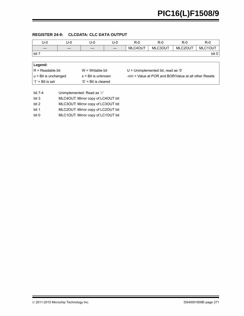
PIC16(L)F1508/9
REGISTER 24-9: CLCDATA: CLC DATA OUTPUT
U-0 U-0 U-0 U-0 R-0 R-0 R-0 R-0
— — — — MLC4OUT MLC3OUT MLC2OUT MLC1OUT
bit 7 bit 0
Legend:
R = Readable bit W = Writable bit U = Unimplemented bit, read as ‘0’
u = Bit is unchanged x = Bit is unknown -n/n = Value at POR and BOR/Value at all other Resets
‘1’ = Bit is set ‘0’ = Bit is cleared
bit 7-4 Unimplemented: Read as ‘0’
bit 3 MLC4OUT: Mirror copy of LC4OUT bit
bit 2 MLC3OUT: Mirror copy of LC3OUT bit
bit 1 MLC2OUT: Mirror copy of LC2OUT bit
bit 0 MLC1OUT: Mirror copy of LC1OUT bit
2011-2015 Microchip Technology Inc. DS40001609E-page 271

PIC16(L)F1508/9
TABLE 24-3: SUMMARY OF REGISTERS ASSOCIATED WITH CLCx
Name Bit7 Bit6 Bit5 Bit4 BIt3 Bit2 Bit1 Bit0Register on Page
ANSELA — — — ANSA4 — ANSA2 ANSA1 ANSA0 110
ANSELB — — ANSB5 ANSB4 — — — — 114
ANSELC ANSC7 ANSC6 — — ANSC3 ANSC2 ANSC1 ANSC0 118
CLC1CON LC1EN LC1OE LC1OUT LC1INTP LC1INTN LC1MODE<2:0> 263
CLCDATA — — — — — MLC3OUT MLC2OUT MLC1OUT 271
CLC1GLS0 LC1G1D4T LC1G1D4N LC1G1D3T LC1G1D3N LC1G1D2T LC1G1D2N LC1G1D1T LC1G1D1N 267
CLC1GLS1 LC1G2D4T LC1G2D4N LC1G2D3T LC1G2D3N LC1G2D2T LC1G2D2N LC1G2D1T LC1G2D1N 268
CLC1GLS2 LC1G3D4T LC1G3D4N LC1G3D3T LC1G3D3N LC1G3D2T LC1G3D2N LC1G3D1T LC1G3D1N 269
CLC1GLS3 LC1G4D4T LC1G4D4N LC1G4D3T LC1G4D3N LC1G4D2T LC1G4D2N LC1G4D1T LC1G4D1N 270
CLC1POL LC1POL — — — LC1G4POL LC1G3POL LC1G2POL LC1G1POL 264
CLC1SEL0 — LC1D2S<2:0> — LC1D1S<2:0> 265
CLC1SEL1 — LC1D4S<2:0> — LC1D3S<2:0> 266
CLC2CON LC2EN LC2OE LC2OUT LC2INTP LC2INTN LC2MODE<2:0> 263
CLC2GLS0 LC2G1D4T LC2G1D4N LC2G1D3T LC2G1D3N LC2G1D2T LC2G1D2N LC2G1D1T LC2G1D1N 267
CLC2GLS1 LC2G2D4T LC2G2D4N LC2G2D3T LC2G2D3N LC2G2D2T LC2G2D2N LC2G2D1T LC2G2D1N 268
CLC2GLS2 LC2G3D4T LC2G3D4N LC2G3D3T LC2G3D3N LC2G3D2T LC2G3D2N LC2G3D1T LC2G3D1N 269
CLC2GLS3 LC2G4D4T LC2G4D4N LC2G4D3T LC2G4D3N LC2G4D2T LC2G4D2N LC2G4D1T LC2G4D1N 270
CLC2POL LC2POL — — — LC2G4POL LC2G3POL LC2G2POL LC2G1POL 264
CLC2SEL0 — LC2D2S<2:0> — LC2D1S<2:0> 265
CLC2SEL1 — LC2D4S<2:0> — LC2D3S<2:0> 266
CLC3CON LC3EN LC3OE LC3OUT LC3INTP LC3INTN LC3MODE<2:0> 263
CLC3GLS0 LC3G1D4T LC3G1D4N LC3G1D3T LC3G1D3N LC3G1D2T LC3G1D2N LC3G1D1T LC3G1D1N 267
CLC3GLS1 LC3G2D4T LC3G2D4N LC3G2D3T LC3G2D3N LC3G2D2T LC3G2D2N LC3G2D1T LC3G2D1N 268
CLC3GLS2 LC3G3D4T LC3G3D4N LC3G3D3T LC3G3D3N LC3G3D2T LC3G3D2N LC3G3D1T LC3G3D1N 269
CLC3GLS3 LC3G4D4T LC3G4D4N LC3G4D3T LC3G4D3N LC3G4D2T LC3G4D2N LC3G4D1T LC3G4D1N 270
CLC3POL LC3POL — — — LC3G4POL LC3G3POL LC3G2POL LC3G1POL 264
CLC3SEL0 — LC3D2S<2:0> — LC3D1S<2:0> 265
CLC3SEL1 — LC3D4S<2:0> — LC3D3S<2:0> 266
CLC4CON LC4EN LC4OE LC4OUT LC4INTP LC4INTN LC4MODE<2:0> 263
CLC4GLS0 LC4G1D4T LC4G1D4N LC4G1D3T LC4G1D3N LC4G1D2T LC4G1D2N LC4G1D1T LC4G1D1N 267
CLC4GLS1 LC4G2D4T LC4G2D4N LC4G2D3T LC4G2D3N LC4G2D2T LC4G2D2N LC4G2D1T LC4G2D1N 268
CLC4GLS2 LC4G3D4T LC4G3D4N LC4G3D3T LC4G3D3N LC4G3D2T LC4G3D2N LC4G3D1T LC4G3D1N 269
CLC4GLS3 LC4G4D4T LC4G4D4N LC4G4D3T LC4G4D3N LC4G4D2T LC4G4D2N LC4G4D1T LC4G4D1N 270
CLC4POL LC4POL — — — LC4G4POL LC4G3POL LC4G2POL LC4G1POL 264
CLC4SEL0 — LC4D2S<2:0> — LC4D1S<2:0> 265
CLC4SEL1 — LC4D4S<2:0> — LC4D3S<2:0> 266
INTCON GIE PEIE TMR0IE INTE IOCIE TMR0IF INTF IOCIF 75
PIE3 — — — — CLC4IE CLC3IE CLC2IE CLC1IE 78
PIR3 — — — — CLC4IF CLC3IF CLC2IF CLC1IF 81
TRISA — — TRISA5 TRISA4 —(1) TRISA2 TRISA1 TRISA0 109
TRISB TRISB7 TRISB6 TRISB5 TRISB4 — — — — 113
TRISC TRISC7 TRISC6 TRISC5 TRISC4 TRISC3 TRISC2 TRISC1 TRISC0 117
Legend: — = unimplemented read as ‘0’,. Shaded cells are not used for CLC module.Note 1: Unimplemented, read as ‘1’.
DS40001609E-page 272 2011-2015 Microchip Technology Inc.

PIC16(L)F1508/9
25.0 NUMERICALLY CONTROLLED OSCILLATOR (NCO) MODULE
The Numerically Controlled Oscillator (NCOx) moduleis a timer that uses the overflow from the addition of anincrement value to divide the input frequency. Theadvantage of the addition method over simple counterdriven timer is that the resolution of division does notvary with the divider value. The NCOx is most useful forapplications that require frequency accuracy and fineresolution at a fixed duty cycle.
Features of the NCOx include:
• 16-bit increment function• Fixed Duty Cycle (FDC) mode• Pulse Frequency (PF) mode• Output pulse width control• Multiple clock input sources• Output polarity control• Interrupt capability
Figure 25-1 is a simplified block diagram of the NCOxmodule.
25.1 NCOx Operation
The NCOx operates by repeatedly adding a fixed valueto an accumulator. Additions occur at the input clock rate.The accumulator will overflow with a carry periodically,which is the raw NCOx output (NCO_overflow). Thiseffectively reduces the input clock by the ratio of theaddition value to the maximum accumulator value. SeeEquation 25-1.
The NCOx output can be further modified by stretchingthe pulse or toggling a flip-flop. The modified NCOxoutput is then distributed internally to other peripheralsand optionally output to a pin. The accumulatoroverflow also generates an interrupt (NCO_interrupt).
The NCOx period changes in discrete steps to createan average frequency. This output depends on theability of the receiving circuit (i.e., CWG or externalresonant converter circuitry) to average the NCOxoutput to reduce uncertainty.
25.1.1 NCOx CLOCK SOURCES
Clock sources available to the NCOx include:
• HFINTOSC• FOSC
• LC1_out• CLKIN pin
The NCOx clock source is selected by configuring theNxCKS<2:0> bits in the NCOxCLK register.
25.1.2 ACCUMULATOR
The accumulator is a 20-bit register. Read and writeaccess to the accumulator is available through threeregisters:
• NCOxACCL• NCOxACCH• NCOxACCU
25.1.3 ADDER
The NCOx adder is a full adder, which operatesindependently from the system clock. The addition of theprevious result and the increment value replaces theaccumulator value on the rising edge of each input clock.
25.1.4 INCREMENT REGISTERS
The increment value is stored in two 8-bit registersmaking up a 16-bit increment. In order of LSB to MSBthey are:
• NCOxINCL• NCOxINCH
When the NCO module is enabled, the NCOxINCHshould be written first, then the NCOxINCL register.Writing to the NCOxINCL register initiates the incre-ment buffer registers to be loaded simultaneously onthe second rising edge of the NCOx_clk signal.
The registers are readable and writable. The incrementregisters are double-buffered to allow value changes tobe made without first disabling the NCOx module.
When the NCO module is disabled, the incrementbuffers are loaded immediately after a write to theincrement registers.
EQUATION 25-1:
Note: The increment buffer registers are notuser-accessible.
FOVERFLOWNCO Clock Frequency Increment Value
2n----------------------------------------------------------------------------------------------------------------=
n = Accumulator width in bits
2011-2015 Microchip Technology Inc. DS40001609E-page 273

PIC
16(L
)F1
508
/9
DS
40
00
16
09
E-p
ag
e 2
74
Sta
tus
2
01
1-2
01
5 M
icroch
ip T
ech
no
log
y Inc.
DIAGRAM
TRIS bitNxOE
D Q
Q1
NxOUT
NCOx
set bitNCOxIF
rement value is loaded into the buffer registers on thesible and are shown here for reference.
NCOx_outTo Peripherals
Rev. 10-000028A7/30/2013
FIGURE 25-1: NUMERICALLY CONTROLLED OSCILLATOR (NCOx) MODULE SIMPLIFIED BLOCK
NCO1CLK
FOSC
LCx_out
D Q
00
01
10
11
NxCKS<1:0> 2
HFINTOSC
NCOxACCU NCOxACCH NCOxACCL
NCOxINCH NCOxINCL
INCBUFH INCBUFL
20
20
2016
16
NCO_overflow
D Q
Q_
S Q
Q_
R
0
1
NxPFM NxPOL
NCO_interrupt
EN
RippleCounter
3NxPWS<2:0>
R
Fixed DutyCycle Mode
Circuitry
PulseFrequency
Mode Circuitry
(1)
NCOx_clk
Note 1: The increment registers are double-buffered to allow for value changes to be made without first disabling the NCO module. The full incsecond rising edge of the NCOx_clk signal that occurs immediately after a write to NCOxINCL register. The buffers are not user-acces
Adder

PIC16(L)F1508/9
25.2 Fixed Duty Cycle (FDC) Mode
In Fixed Duty Cycle (FDC) mode, every time theaccumulator overflows (NCO_overflow), the output istoggled. This provides a 50% duty cycle, provided thatthe increment value remains constant. For moreinformation, see Figure 25-2.
The FDC mode is selected by clearing the NxPFM bitin the NCOxCON register.
25.3 Pulse Frequency (PF) Mode
In Pulse Frequency (PF) mode, every time the accumu-lator overflows (NCO_overflow), the output becomesactive for one or more clock periods. Once the clockperiod expires, the output returns to an inactive state.This provides a pulsed output.
The output becomes active on the rising clock edgeimmediately following the overflow event. For moreinformation, see Figure 25-2.
The value of the active and inactive states depends onthe polarity bit, NxPOL in the NCOxCON register.
The PF mode is selected by setting the NxPFM bit inthe NCOxCON register.
25.3.1 OUTPUT PULSE WIDTH CONTROL
When operating in PF mode, the active state of the out-put can vary in width by multiple clock periods. Variouspulse widths are selected with the NxPWS<2:0> bits inthe NCOxCLK register.
When the selected pulse width is greater than theaccumulator overflow time frame, the output of theNCOx operation is indeterminate.
25.4 Output Polarity Control
The last stage in the NCOx module is the output polar-ity. The NxPOL bit in the NCOxCON register selects theoutput polarity. Changing the polarity while the inter-rupts are enabled will cause an interrupt for the result-ing output transition.
The NCOx output can be used internally by sourcecode or other peripherals. Accomplish this by readingthe NxOUT (read-only) bit of the NCOxCON register.
The NCOx output signal is available to the followingperipherals:
• CLC
• CWG
25.5 Interrupts
When the accumulator overflows (NCO_overflow), theNCOx Interrupt Flag bit, NCOxIF, of the PIRx register isset. To enable the interrupt event (NCO_interrupt), thefollowing bits must be set:
• NxEN bit of the NCOxCON register• NCOxIE bit of the PIEx register• PEIE bit of the INTCON register• GIE bit of the INTCON register
The interrupt must be cleared by software by clearingthe NCOxIF bit in the Interrupt Service Routine.
25.6 Effects of a Reset
All of the NCOx registers are cleared to zero as theresult of a Reset.
25.7 Operation In Sleep
The NCO module operates independently from the system clock and will continue to run during Sleep, provided that the clock source selected remains active.
The HFINTOSC remains active during Sleep when the NCO module is enabled and the HFINTOSC is selected as the clock source, regardless of the system clock source selected.
In other words, if the HFINTOSC is simultaneously selected as the system clock and the NCO clock source, when the NCO is enabled, the CPU will go idle during Sleep, but the NCO will continue to operate and the HFINTOSC will remain active.
This will have a direct effect on the Sleep mode current.
25.8 Alternate Pin Locations
This module incorporates I/O pins that can be moved toother locations with the use of the alternate pin functionregister, APFCON. To determine which pins can bemoved and what their default locations are upon aReset, see Section 11.1 “Alternate Pin Function” formore information.
2011-2015 Microchip Technology Inc. DS40001609E-page 275

PIC
16(L
)F1
508
/9
DS
40
00
16
09
E-p
ag
e 2
76
Sta
tus
2
01
1-2
01
5 M
icroch
ip T
ech
no
log
y Inc.
OPERATION DIAGRAMRev. 10-000029A
11/7/2013
000h 00000h 04000h 08000h
4000h
FIGURE 25-2: NCO – FIXED DUTY CYCLE (FDC) AND PULSE FREQUENCY MODE (PFM) OUTPUT
00000h 04000h 08000h FC000h 00000h 04000h 08000h FC
4000h 4000h
NCO_interrupt
NCOx OutputFDC Mode
NCOx OutputPF Mode
NCOxPWS =
NCOx OutputPF Mode
NCOxPWS =
NCOxAccumulator
Value
NCOx Increment
Value
NCOx Clock
Source
000
001
NCO_overflow

PIC16(L)F1508/9
25.9 Register Definitions: NCOx Control Registers
REGISTER 25-2: NCOxCLK: NCOx INPUT CLOCK CONTROL REGISTER
REGISTER 25-1: NCOxCON: NCOx CONTROL REGISTER
R/W-0/0 R/W-0/0 R-0/0 R/W-0/0 U-0 U-0 U-0 R/W-0/0
NxEN NxOE NxOUT NxPOL — — — NxPFM
bit 7 bit 0
Legend:
R = Readable bit W = Writable bit U = Unimplemented bit, read as ‘0’
u = Bit is unchanged x = Bit is unknown -n/n = Value at POR and BOR/Value at all other Resets
‘1’ = Bit is set ‘0’ = Bit is cleared
bit 7 NxEN: NCOx Enable bit1 = NCOx module is enabled0 = NCOx module is disabled
bit 6 NxOE: NCOx Output Enable bit1 = NCOx output pin is enabled0 = NCOx output pin is disabled
bit 5 NxOUT: NCOx Output bit1 = NCOx output is high0 = NCOx output is low
bit 4 NxPOL: NCOx Polarity bit1 = NCOx output signal is active low (inverted)0 = NCOx output signal is active high (non-inverted)
bit 3-1 Unimplemented: Read as ‘0’
bit 0 NxPFM: NCOx Pulse Frequency Mode bit1 = NCOx operates in Pulse Frequency mode0 = NCOx operates in Fixed Duty Cycle mode
R/W-0/0 R/W-0/0 R/W-0/0 U-0 U-0 U-0 R/W-0/0 R/W-0/0
NxPWS<2:0>(1, 2) — — — NxCKS<1:0>
bit 7 bit 0
Legend:
R = Readable bit W = Writable bit U = Unimplemented bit, read as ‘0’
u = Bit is unchanged x = Bit is unknown -n/n = Value at POR and BOR/Value at all other Resets
‘1’ = Bit is set ‘0’ = Bit is cleared
bit 7-5 NxPWS<2:0>: NCOx Output Pulse Width Select bits(1, 2)
111 = 128 NCOx clock periods110 = 64 NCOx clock periods101 = 32 NCOx clock periods100 = 16 NCOx clock periods011 = 8 NCOx clock periods010 = 4 NCOx clock periods001 = 2 NCOx clock periods000 = 1 NCOx clock periods
bit 4-2 Unimplemented: Read as ‘0’
bit 1-0 NxCKS<1:0>: NCOx Clock Source Select bits11 = NCO1CLK pin10 = LC1_out01 = FOSC
00 = HFINTOSC (16 MHz)
Note 1: NxPWS applies only when operating in Pulse Frequency mode.2: If NCOx pulse width is greater than NCO_overflow period, operation is indeterminate.
2011-2015 Microchip Technology Inc. DS40001609E-page 277

PIC16(L)F1508/9
REGISTER 25-3: NCOxACCL: NCOx ACCUMULATOR REGISTER – LOW BYTE
REGISTER 25-4: NCOxACCH: NCOx ACCUMULATOR REGISTER – HIGH BYTE
REGISTER 25-5: NCOxACCU: NCOx ACCUMULATOR REGISTER – UPPER BYTE
R/W-0/0 R/W-0/0 R/W-0/0 R/W-0/0 R/W-0/0 R/W-0/0 R/W-0/0 R/W-0/0
NCOxACC<7:0>
bit 7 bit 0
Legend:
R = Readable bit W = Writable bit U = Unimplemented bit, read as ‘0’
u = Bit is unchanged x = Bit is unknown -n/n = Value at POR and BOR/Value at all other Resets
‘1’ = Bit is set ‘0’ = Bit is cleared
bit 7-0 NCOxACC<7:0>: NCOx Accumulator, Low Byte
R/W-0/0 R/W-0/0 R/W-0/0 R/W-0/0 R/W-0/0 R/W-0/0 R/W-0/0 R/W-0/0
NCOxACC<15:8>
bit 7 bit 0
Legend:
R = Readable bit W = Writable bit U = Unimplemented bit, read as ‘0’
u = Bit is unchanged x = Bit is unknown -n/n = Value at POR and BOR/Value at all other Resets
‘1’ = Bit is set ‘0’ = Bit is cleared
bit 7-0 NCOxACC<15:8>: NCOx Accumulator, High Byte
U-0 U-0 U-0 U-0 R/W-0/0 R/W-0/0 R/W-0/0 R/W-0/0
— — — — NCOxACC<19:16>
bit 7 bit 0
Legend:
R = Readable bit W = Writable bit U = Unimplemented bit, read as ‘0’
u = Bit is unchanged x = Bit is unknown -n/n = Value at POR and BOR/Value at all other Resets
‘1’ = Bit is set ‘0’ = Bit is cleared
bit 7-4 Unimplemented: Read as ‘0’
bit 3-0 NCOxACC<19:16>: NCOx Accumulator, Upper Byte
DS40001609E-page 278 2011-2015 Microchip Technology Inc.

PIC16(L)F1508/9
REGISTER 25-6: NCOxINCL: NCOx INCREMENT REGISTER – LOW BYTE(1)
REGISTER 25-7: NCOxINCH: NCOx INCREMENT REGISTER – HIGH BYTE(1)
TABLE 25-1: SUMMARY OF REGISTERS ASSOCIATED WITH NCOx
R/W-0/0 R/W-0/0 R/W-0/0 R/W-0/0 R/W-0/0 R/W-0/0 R/W-0/0 R/W-1/1
NCOxINC<7:0>
bit 7 bit 0
Legend:
R = Readable bit W = Writable bit U = Unimplemented bit, read as ‘0’
u = Bit is unchanged x = Bit is unknown -n/n = Value at POR and BOR/Value at all other Resets
‘1’ = Bit is set ‘0’ = Bit is cleared
bit 7-0 NCOxINC<7:0>: NCOx Increment, Low Byte
Note 1: Write the NCOxINCH register first, then the NCOxINCL register. See 25.1.4 “Increment Registers” for more information.
R/W-0/0 R/W-0/0 R/W-0/0 R/W-0/0 R/W-0/0 R/W-0/0 R/W-0/0 R/W-0/0
NCOxINC<15:8>
bit 7 bit 0
Legend:
R = Readable bit W = Writable bit U = Unimplemented bit, read as ‘0’
u = Bit is unchanged x = Bit is unknown -n/n = Value at POR and BOR/Value at all other Resets
‘1’ = Bit is set ‘0’ = Bit is cleared
bit 7-0 NCOxINC<15:8>: NCOx Increment, High Byte
Note 1: Write the NCOxINCH register first, then the NCOxINCL register. See 25.1.4 “Increment Registers” for more information.
Name Bit 7 Bit 6 Bit 5 Bit 4 Bit 3 Bit 2 Bit 1 Bit 0Register on
Page
APFCON — — — SSSEL T1GSEL — CLC1SEL NCO1SEL 107
INTCON GIE PEIE TMR0IE INTE IOCIE TMR0IF INTF IOCIF 75
NCO1ACCH NCO1ACC<15:8> 278
NCO1ACCL NCO1ACC<7:0> 278
NCO1ACCU — NCO1ACC<19:16> 278
NCO1CLK N1PWS<2:0> — — — N1CKS<1:0> 277
NCO1CON N1EN N1OE N1OUT N1POL — — — N1PFM 277
NCO1INCH NCO1INC<15:8> 279
NCO1INCL NCO1INC<7:0> 279
PIE2 OSFIE C2IE C1IE — BCL1IE NCO1IE — — 77
PIR2 OSFIF C2IF C1IF — BCL1IF NCO1IF — — 80
TRISA — — TRISA5 TRISA4 —(1) TRISA2 TRISA1 TRISA0 109
TRISC TRISC7 TRISC6 TRISC5 TRISC4 TRISC3 TRISC2 TRISC1 TRISC0 117
Legend: x = unknown, u = unchanged, — = unimplemented read as ‘0’, q = value depends on condition. Shaded cells are not used for NCOx module.
Note 1: Unimplemented, read as ‘1’.
2011-2015 Microchip Technology Inc. DS40001609E-page 279

PIC16(L)F1508/9
26.0 COMPLEMENTARY WAVEFORM GENERATOR (CWG) MODULE
The Complementary Waveform Generator (CWG)produces a complementary waveform with dead-banddelay from a selection of input sources.
The CWG module has the following features:
• Selectable dead-band clock source control
• Selectable input sources
• Output enable control
• Output polarity control
• Dead-band control with independent 6-bit rising and falling edge dead-band counters
• Auto-shutdown control with:
- Selectable shutdown sources
- Auto-restart enable
- Auto-shutdown pin override control
26.1 Fundamental Operation
The CWG generates two output waveforms from theselected input source.
The off-to-on transition of each output can be delayedfrom the on-to-off transition of the other output, thereby,creating a time delay immediately where neither outputis driven. This is referred to as dead time and is coveredin Section 26.5 “Dead-Band Control”. A typicaloperating waveform, with dead band, generated from asingle input signal is shown in Figure 26-2.
It may be necessary to guard against the possibility ofcircuit faults or a feedback event arriving too late or notat all. In this case, the active drive must be terminatedbefore the Fault condition causes damage. This isreferred to as auto-shutdown and is covered in Section26.9 “Auto-Shutdown Control”.
26.2 Clock Source
The CWG module allows the following clock sourcesto be selected:
• Fosc (system clock)• HFINTOSC (16 MHz only)
The clock sources are selected using the G1CS0 bit ofthe CWGxCON0 register (Register 26-1).
26.3 Selectable Input Sources
The CWG generates the output waveforms from theinput sources in Table 26-1.
The input sources are selected using the GxIS<2:0>bits in the CWGxCON1 register (Register 26-2).
26.4 Output Control
Immediately after the CWG module is enabled, thecomplementary drive is configured with both CWGxAand CWGxB drives cleared.
26.4.1 OUTPUT ENABLES
Each CWG output pin has individual output enablecontrol. Output enables are selected with the GxOEAand GxOEB bits of the CWGxCON0 register. When anoutput enable control is cleared, the module asserts nocontrol over the pin. When an output enable is set, theoverride value or active PWM waveform is applied tothe pin per the port priority selection. The output pinenables are dependent on the module enable bit,GxEN. When GxEN is cleared, CWG output enablesand CWG drive levels have no effect.
26.4.2 POLARITY CONTROL
The polarity of each CWG output can be selectedindependently. When the output polarity bit is set, thecorresponding output is active-high. Clearing the outputpolarity bit configures the corresponding output asactive-low. However, polarity does not affect theoverride levels. Output polarity is selected with theGxPOLA and GxPOLB bits of the CWGxCON0 register.
TABLE 26-1: SELECTABLE INPUT SOURCES
Source Peripheral Signal Name
Comparator C1 C1OUT_sync
Comparator C2 C2OUT_sync
PWM1 PWM1_out
PWM2 PWM2_out
PWM3 PWM3_out
PWM4 PWM4_out
NCO1 NCO1_out
CLC1 LC1_out
DS40001609E-page 280 2011-2015 Microchip Technology Inc.
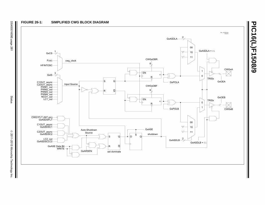
PIC
16(L
)F1
508
/9
DS
40
00
16
09
E-p
ag
e 2
81
Sta
tus
2
01
1-2
01
5 M
icroch
ip T
ech
no
log
y Inc.
11
10
00
11
10
00
0
1
1
0
2
2
‘0'
‘0'
‘1'
‘1'
TRISx
TRISx
GxASDLA = 01
GxASDLB = 01
GxOEA
GxOEB
CWGxB
CWGxA
Rev. 10-000123A7/9/2015
FIGURE 26-1: SIMPLIFIED CWG BLOCK DIAGRAM
S
QR
Q D QS
S
QR
Q
6
6
1
3
EN
R=
EN
R=
C1OUT_asyncC2OUT_async
PWM1_out
NCO1_outLC1_out
PWM2_outPWM3_outPWM4_out
GxIS
FOSC
HFINTOSC
GxCS
C1OUT_async
C2OUT_async
LC2_out
CWG1FLT (INT pin)GxASDSFLT
GxASDSC1
GxASDSC2
GxASDSCLC2
GxASE Data BitWRITE
GxARSEN
Auto-ShutdownSource
set dominate
GxASE
shutdown
Input Source
cwg_clock
GxPOLA
GxPOLB
CWGxDBR
CWGxDBF
GxASDLA
GxASDLB

PIC16(L)F1508/9
FIGURE 26-2: TYPICAL CWG OPERATION WITH PWM1 (NO AUTO-SHUTDOWN)
26.5 Dead-Band Control
Dead-band control provides for non-overlapping outputsignals to prevent shoot-through current in powerswitches. The CWG contains two 6-bit dead-bandcounters. One dead-band counter is used for the risingedge of the input source control. The other is used forthe falling edge of the input source control.
Dead band is timed by counting CWG clock periodsfrom zero up to the value in the rising or falling dead-band counter registers. See CWGxDBR andCWGxDBF registers (Register 26-4 and Register 26-5,respectively).
26.6 Rising Edge Dead Band
The rising edge dead-band delays the turn-on of theCWGxA output from when the CWGxB output is turnedoff. The rising edge dead-band time starts when therising edge of the input source signal goes true. Whenthis happens, the CWGxB output is immediately turnedoff and the rising edge dead-band delay time starts.When the rising edge dead-band delay time is reached,the CWGxA output is turned on.
The CWGxDBR register sets the duration of the dead-band interval on the rising edge of the input sourcesignal. This duration is from 0 to 64 counts of dead band.
Dead band is always counted off the edge on the inputsource signal. A count of 0 (zero), indicates that nodead band is present.
If the input source signal is not present for enough timefor the count to be completed, no output will be seen onthe respective output.
26.7 Falling Edge Dead Band
The falling edge dead band delays the turn-on of theCWGxB output from when the CWGxA output is turnedoff. The falling edge dead-band time starts when thefalling edge of the input source goes true. When thishappens, the CWGxA output is immediately turned offand the falling edge dead-band delay time starts. Whenthe falling edge dead-band delay time is reached, theCWGxB output is turned on.
The CWGxDBF register sets the duration of the dead-band interval on the falling edge of the input source sig-nal. This duration is from 0 to 64 counts of dead band.
Dead band is always counted off the edge on the inputsource signal. A count of 0 (zero), indicates that nodead band is present.
If the input source signal is not present for enough timefor the count to be completed, no output will be seen onthe respective output.
Refer to Figure 26-3 and Figure 26-4 for examples.
cwg_clock
PWM1
CWGxA
CWGxB
Rising Edge Dead Band
Rising Edge Dead Band
Rising Edge Dead BandFalling Edge
Dead BandFalling Edge Dead Band
DS40001609E-page 282 2011-2015 Microchip Technology Inc.

2
01
1-2
01
5 M
icroch
ip T
ech
no
log
y Inc.
Sta
tus
DS
40
00
16
09
E-p
ag
e 2
83
PIC
16(L
)F15
08/9
FIG
FIG AN DEAD BAND
URE 26-3: DEAD-BAND OPERATION, CWGxDBR = 01H, CWGxDBF = 02H
URE 26-4: DEAD-BAND OPERATION, CWGxDBR = 03H, CWGxDBF = 04H, SOURCE SHORTER TH
Input Source
CWGxA
CWGxB
cwg_clock
source shorter than dead band
Input Source
CWGxA
CWGxB
cwg_clock
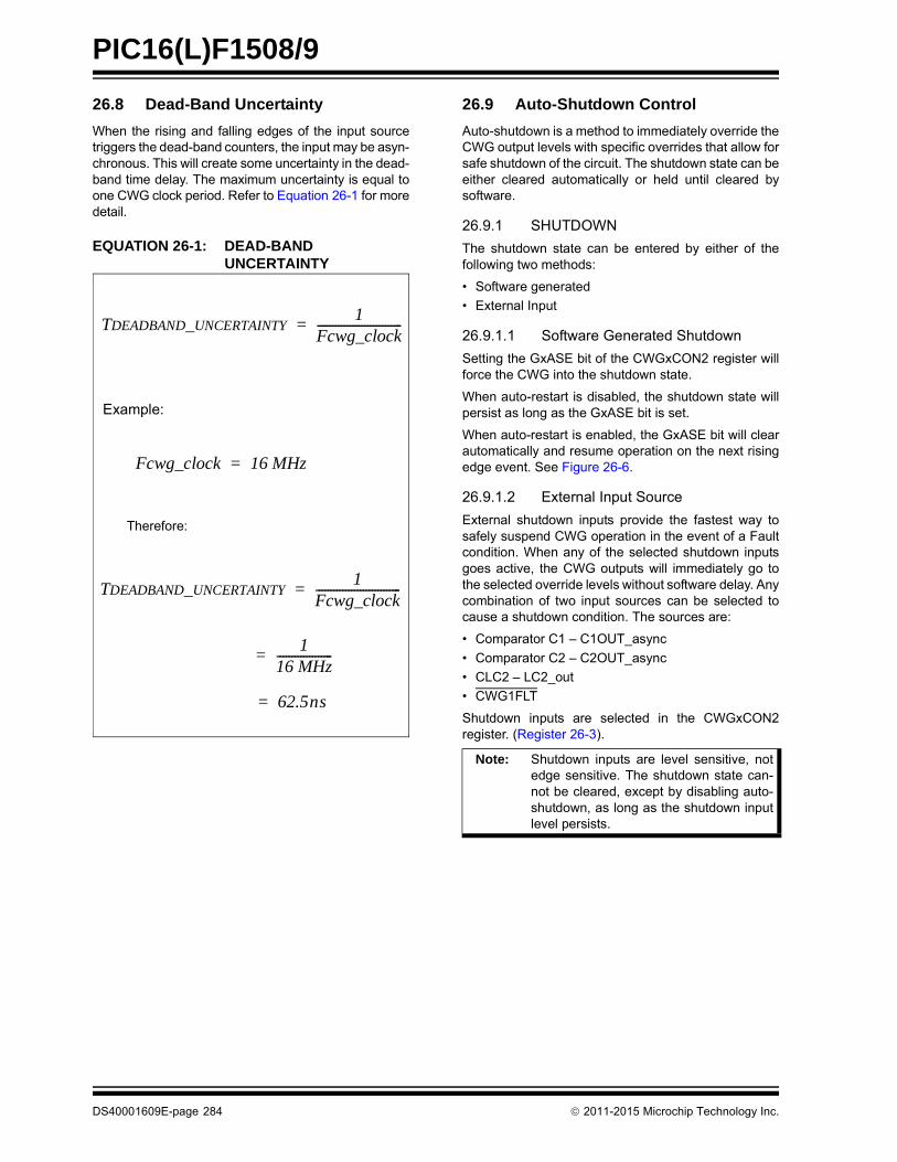
PIC16(L)F1508/9
26.8 Dead-Band Uncertainty
When the rising and falling edges of the input sourcetriggers the dead-band counters, the input may be asyn-chronous. This will create some uncertainty in the dead-band time delay. The maximum uncertainty is equal toone CWG clock period. Refer to Equation 26-1 for moredetail.
EQUATION 26-1: DEAD-BAND UNCERTAINTY
26.9 Auto-Shutdown Control
Auto-shutdown is a method to immediately override theCWG output levels with specific overrides that allow forsafe shutdown of the circuit. The shutdown state can beeither cleared automatically or held until cleared bysoftware.
26.9.1 SHUTDOWN
The shutdown state can be entered by either of thefollowing two methods:
• Software generated
• External Input
26.9.1.1 Software Generated Shutdown
Setting the GxASE bit of the CWGxCON2 register willforce the CWG into the shutdown state.
When auto-restart is disabled, the shutdown state willpersist as long as the GxASE bit is set.
When auto-restart is enabled, the GxASE bit will clearautomatically and resume operation on the next risingedge event. See Figure 26-6.
26.9.1.2 External Input Source
External shutdown inputs provide the fastest way tosafely suspend CWG operation in the event of a Faultcondition. When any of the selected shutdown inputsgoes active, the CWG outputs will immediately go tothe selected override levels without software delay. Anycombination of two input sources can be selected tocause a shutdown condition. The sources are:
• Comparator C1 – C1OUT_async
• Comparator C2 – C2OUT_async
• CLC2 – LC2_out
• CWG1FLT
Shutdown inputs are selected in the CWGxCON2register. (Register 26-3).
TDEADBAND_UNCERTAINTY1
Fcwg_clock-----------------------------=
Therefore:
Fcwg_clock 16 MHz=
1
16 MHz-------------------=
62.5ns=
TDEADBAND_UNCERTAINTY1
Fcwg_clock-----------------------------=
Example:
Note: Shutdown inputs are level sensitive, notedge sensitive. The shutdown state can-not be cleared, except by disabling auto-shutdown, as long as the shutdown inputlevel persists.
DS40001609E-page 284 2011-2015 Microchip Technology Inc.

PIC16(L)F1508/9
26.10 Operation During Sleep
The CWG module operates independently from the system clock and will continue to run during Sleep, provided that the clock and input sources selected remain active.
The HFINTOSC remains active during Sleep, provided that the CWG module is enabled, the input source is active, and the HFINTOSC is selected as the clock source, regardless of the system clock source selected.
In other words, if the HFINTOSC is simultaneously selected as the system clock and the CWG clock source, when the CWG is enabled and the input source is active, the CPU will go idle during Sleep, but the CWG will continue to operate and the HFINTOSC will remain active.
This will have a direct effect on the Sleep mode current.
26.11 Configuring the CWG
The following steps illustrate how to properly configurethe CWG to ensure a synchronous start:
1. Ensure that the TRIS control bits correspondingto CWGxA and CWGxB are set so that both areconfigured as inputs.
2. Clear the GxEN bit, if not already cleared.
3. Set desired dead-band times with the CWGxDBRand CWGxDBF registers.
4. Setup the following controls in CWGxCON2auto-shutdown register:
• Select desired shutdown source.
• Select both output overrides to the desired levels (this is necessary even if not using auto-shutdown because start-up will be from a shutdown state).
• Set the GxASE bit and clear the GxARSEN bit.
5. Select the desired input source using theCWGxCON1 register.
6. Configure the following controls in CWGxCON0register:
• Select desired clock source.
• Select the desired output polarities.
• Set the output enables for the outputs to be used.
7. Set the GxEN bit.
8. Clear TRIS control bits corresponding toCWGxA and CWGxB to be used to configurethose pins as outputs.
9. If auto-restart is to be used, set the GxARSENbit and the GxASE bit will be cleared automati-cally. Otherwise, clear the GxASE bit to start theCWG.
26.11.1 PIN OVERRIDE LEVELS
The levels driven to the output pins, while the shutdowninput is true, are controlled by the GxASDLA andGxASDLB bits of the CWGxCON1 register(Register 26-3). GxASDLA controls the CWG1Aoverride level and GxASDLB controls the CWG1Boverride level. The control bit logic level corresponds tothe output logic drive level while in the shutdown state.The polarity control does not apply to the override level.
26.11.2 AUTO-SHUTDOWN RESTART
After an auto-shutdown event has occurred, there aretwo ways to have resume operation:
• Software controlled
• Auto-restart
The restart method is selected with the GxARSEN bitof the CWGxCON2 register. Waveforms of softwarecontrolled and automatic restarts are shown inFigure 26-5 and Figure 26-6.
26.11.2.1 Software Controlled Restart
When the GxARSEN bit of the CWGxCON2 register iscleared, the CWG must be restarted after an auto-shut-down event by software.
Clearing the shutdown state requires all selected shut-down inputs to be low, otherwise the GxASE bit willremain set. The overrides will remain in effect until thefirst rising edge event after the GxASE bit is cleared.The CWG will then resume operation.
26.11.2.2 Auto-Restart
When the GxARSEN bit of the CWGxCON2 register isset, the CWG will restart from the auto-shutdown stateautomatically.
The GxASE bit will clear automatically when all shut-down sources go low. The overrides will remain ineffect until the first rising edge event after the GxASEbit is cleared. The CWG will then resume operation.
2011-2015 Microchip Technology Inc. DS40001609E-page 285

PIC
16(L
)F1
508
/9
DS
40
00
16
09
E-p
ag
e 2
86
Sta
tus
2
01
1-2
01
5 M
icroch
ip T
ech
no
log
y Inc.
1, GxASDLB = 01)
A = 01, GxASDLB = 01)
are
Output Resumes
ware
FIGURE 26-5: SHUTDOWN FUNCTIONALITY, AUTO-RESTART DISABLED (GxARSEN = 0,GxASDLA = 0
FIGURE 26-6: SHUTDOWN FUNCTIONALITY, AUTO-RESTART ENABLED (GxARSEN = 1,GxASDL
Shutdown
GxASE Cleared by Softw
No Shutdown
CWG Input
GxASE
CWG1A
Source
Shutdown Source
Shutdown Event Ceases
Tri-State (No Pulse)
CWG1B Tri-State (No Pulse)
Shutdown
Tri-State (No Pulse)
GxASE auto-cleared by hard
Output Resumes
No Shutdown
CWG Input
GxASE
CWG1A
Source
Shutdown Source
Shutdown Event Ceases
CWG1B
Tri-State (No Pulse)

PIC16(L)F1508/9
26.12 Register Definitions: CWG Control
REGISTER 26-1: CWGxCON0: CWG CONTROL REGISTER 0
R/W-0/0 R/W-0/0 R/W-0/0 R/W-0/0 R/W-0/0 U-0 U-0 R/W-0/0
GxEN GxOEB GxOEA GxPOLB GxPOLA — — GxCS0
bit 7 bit 0
Legend:
R = Readable bit W = Writable bit U = Unimplemented bit, read as ‘0’
u = Bit is unchanged x = Bit is unknown -n/n = Value at POR and BOR/Value at all other Resets
‘1’ = Bit is set ‘0’ = Bit is cleared q = Value depends on condition
bit 7 GxEN: CWGx Enable bit1 = Module is enabled0 = Module is disabled
bit 6 GxOEB: CWGxB Output Enable bit1 = CWGxB is available on appropriate I/O pin0 = CWGxB is not available on appropriate I/O pin
bit 5 GxOEA: CWGxA Output Enable bit1 = CWGxA is available on appropriate I/O pin 0 = CWGxA is not available on appropriate I/O pin
bit 4 GxPOLB: CWGxB Output Polarity bit1 = Output is inverted polarity0 = Output is normal polarity
bit 3 GxPOLA: CWGxA Output Polarity bit1 = Output is inverted polarity0 = Output is normal polarity
bit 2-1 Unimplemented: Read as ‘0’
bit 0 GxCS0: CWGx Clock Source Select bit1 = HFINTOSC0 = FOSC
2011-2015 Microchip Technology Inc. DS40001609E-page 287

PIC16(L)F1508/9
REGISTER 26-2: CWGxCON1: CWG CONTROL REGISTER 1
R/W-x/u R/W-x/u R/W-x/u R/W-x/u U-0 R/W-0/0 R/W-0/0 R/W-0/0
GxASDLB<1:0> GxASDLA<1:0> — GxIS<2:0>
bit 7 bit 0
Legend:
R = Readable bit W = Writable bit U = Unimplemented bit, read as ‘0’
u = Bit is unchanged x = Bit is unknown -n/n = Value at POR and BOR/Value at all other Resets
‘1’ = Bit is set ‘0’ = Bit is cleared q = Value depends on condition
bit 7-6 GxASDLB<1:0>: CWGx Shutdown State for CWGxBWhen an auto shutdown event is present (GxASE = 1):11 = CWGxB pin is driven to ‘1’, regardless of the setting of the GxPOLB bit.10 = CWGxB pin is driven to ‘0’, regardless of the setting of the GxPOLB bit.01 = CWGxB pin is tri-stated00 = CWGxB pin is driven to its inactive state after the selected dead-band interval. GxPOLB still will
control the polarity of the output.
bit 5-4 GxASDLA<1:0>: CWGx Shutdown State for CWGxAWhen an auto shutdown event is present (GxASE = 1):11 = CWGxA pin is driven to ‘1’, regardless of the setting of the GxPOLA bit.10 = CWGxA pin is driven to ‘0’, regardless of the setting of the GxPOLA bit.01 = CWGxA pin is tri-stated00 = CWGxA pin is driven to its inactive state after the selected dead-band interval. GxPOLA still will
control the polarity of the output.
bit 3 Unimplemented: Read as ‘0’
bit 2-0 GxIS<2:0>: CWGx Input Source Select bits111 = CLC1 – LC1_out110 = NCO1 – NCO1_out101 = PWM4 – PWM4_out100 = PWM3 – PWM3_out011 = PWM2 – PWM2_out010 = PWM1 – PWM1_out001 = Comparator C2– C2OUT_async000 = Comparator C1 – C1OUT_async
DS40001609E-page 288 2011-2015 Microchip Technology Inc.

PIC16(L)F1508/9
REGISTER 26-3: CWGxCON2: CWG CONTROL REGISTER 2
R/W-0/0 R/W-0/0 U-0 U-0 R/W-0/0 R/W-0/0 R/W-0/0 R/W-0/0
GxASE GxARSEN — — GxASDSC2 GxASDSC1 GxASDSFLT GxASDSCLC2
bit 7 bit 0
Legend:
R = Readable bit W = Writable bit U = Unimplemented bit, read as ‘0’
u = Bit is unchanged x = Bit is unknown -n/n = Value at POR and BOR/Value at all other Resets
‘1’ = Bit is set ‘0’ = Bit is cleared q = Value depends on condition
bit 7 GxASE: Auto-Shutdown Event Status bit1 = An auto-shutdown event has occurred0 = No auto-shutdown event has occurred
bit 6 GxARSEN: Auto-Restart Enable bit1 = Auto-restart is enabled0 = Auto-restart is disabled
bit 5-4 Unimplemented: Read as ‘0’
bit 3 GxASDSC2: CWG Auto-shutdown on Comparator C2 Enable bit1 = Shutdown when Comparator C2 output (C2OUT_async) is high0 = Comparator C2 output has no effect on shutdown
bit 2 GxASDSC1: CWG Auto-shutdown on Comparator C1 Enable bit1 = Shutdown when Comparator C1 output (C1OUT_async) is high0 = Comparator C1 output has no effect on shutdown
bit 1 GxASDSFLT: CWG Auto-shutdown on FLT Enable bit1 = Shutdown when CWG1FLT input is low0 = CWG1FLT input has no effect on shutdown
bit 0 GxASDSCLC2: CWG Auto-shutdown on CLC2 Enable bit1 = Shutdown when CLC2 output (LC2_out) is high0 = CLC2 output has no effect on shutdown
2011-2015 Microchip Technology Inc. DS40001609E-page 289

PIC16(L)F1508/9
REGISTER 26-4: CWGxDBR: COMPLEMENTARY WAVEFORM GENERATOR (CWGx) RISING DEAD-BAND COUNT REGISTER
REGISTER 26-5: CWGxDBF: COMPLEMENTARY WAVEFORM GENERATOR (CWGx) FALLING DEAD-BAND COUNT REGISTER
U-0 U-0 R/W-x/u R/W-x/u R/W-x/u R/W-x/u R/W-x/u R/W-x/u
— — CWGxDBR<5:0>
bit 7 bit 0
Legend:
R = Readable bit W = Writable bit U = Unimplemented bit, read as ‘0’
u = Bit is unchanged x = Bit is unknown -n/n = Value at POR and BOR/Value at all other Resets
‘1’ = Bit is set ‘0’ = Bit is cleared q = Value depends on condition
bit 7-6 Unimplemented: Read as ‘0’
bit 5-0 CWGxDBR<5:0>: Complementary Waveform Generator (CWGx) Rising Counts11 1111 = 63-64 counts of dead band11 1110 = 62-63 counts of dead band
00 0010 = 2-3 counts of dead band00 0001 = 1-2 counts of dead band00 0000 = 0 counts of dead band
U-0 U-0 R/W-x/u R/W-x/u R/W-x/u R/W-x/u R/W-x/u R/W-x/u
— — CWGxDBF<5:0>
bit 7 bit 0
Legend:
R = Readable bit W = Writable bit U = Unimplemented bit, read as ‘0’
u = Bit is unchanged x = Bit is unknown -n/n = Value at POR and BOR/Value at all other Resets
‘1’ = Bit is set ‘0’ = Bit is cleared q = Value depends on condition
bit 7-6 Unimplemented: Read as ‘0’
bit 5-0 CWGxDBF<5:0>: Complementary Waveform Generator (CWGx) Falling Counts
11 1111 = 63-64 counts of dead band11 1110 = 62-63 counts of dead band
00 0010 = 2-3 counts of dead band00 0001 = 1-2 counts of dead band00 0000 = 0 counts of dead band. Dead-band generation is bypassed.
DS40001609E-page 290 2011-2015 Microchip Technology Inc.

PIC16(L)F1508/9
TABLE 26-2: SUMMARY OF REGISTERS ASSOCIATED WITH CWG
Name Bit 7 Bit 6 Bit 5 Bit 4 Bit 3 Bit 2 Bit 1 Bit 0Register on Page
ANSELA — — — ANSA4 — ANSA2 ANSA1 ANSA0 110
CWG1CON0 G1EN G1OEB G1OEA G1POLB G1POLA — — G1CS0 287
CWG1CON1 G1ASDLB<1:0> G1ASDLA<1:0> — — G1IS<1:0> 288
CWG1CON2 G1ASE G1ARSEN — — G1ASDSC2 G1ASDSC1 G1ASDSFLT G1ASDSCLC2 289
CWG1DBF — — CWG1DBF<5:0> 290
CWG1DBR — — CWG1DBR<5:0> 290
TRISA — — TRISA5 TRISA4 —(1) TRISA2 TRISA1 TRISA0 109
TRISC TRISC7 TRISC6 TRISC5 TRISC4 TRISC3 TRISC2 TRISC1 TRISC0 117
Legend: x = unknown, u = unchanged, – = unimplemented locations read as ‘0’. Shaded cells are not used by CWG.Note 1: Unimplemented, read as ‘1’.
2011-2015 Microchip Technology Inc. DS40001609E-page 291

PIC16(L)F1508/9
27.0 IN-CIRCUIT SERIAL PROGRAMMING™ (ICSP™)
ICSP™ programming allows customers to manufacturecircuit boards with unprogrammed devices. Programmingcan be done after the assembly process allowing thedevice to be programmed with the most recent firmwareor a custom firmware. Five pins are needed for ICSP™programming:
• ICSPCLK
• ICSPDAT
• MCLR/VPP
• VDD
• VSS
In Program/Verify mode the program memory, user IDsand the Configuration Words are programmed throughserial communications. The ICSPDAT pin is a bidirec-tional I/O used for transferring the serial data and theICSPCLK pin is the clock input. For more information onICSP™ refer to the “PIC12(L)F1501/PIC16(L)F150XMemory Programming Specification” (DS41573).
27.1 High-Voltage Programming Entry Mode
The device is placed into High-Voltage ProgrammingEntry mode by holding the ICSPCLK and ICSPDATpins low then raising the voltage on MCLR/VPP to VIHH.
27.2 Low-Voltage Programming Entry Mode
The Low-Voltage Programming Entry mode allows thePIC® Flash MCUs to be programmed using VDD only,without high voltage. When the LVP bit of ConfigurationWords is set to ‘1’, the ICSP Low-Voltage ProgrammingEntry mode is enabled. To disable the Low-VoltageICSP mode, the LVP bit must be programmed to ‘0’.
Entry into the Low-Voltage Programming Entry moderequires the following steps:
1. MCLR is brought to VIL.
2. A 32-bit key sequence is presented onICSPDAT, while clocking ICSPCLK.
Once the key sequence is complete, MCLR must beheld at VIL for as long as Program/Verify mode is to bemaintained.
If low-voltage programming is enabled (LVP = 1), theMCLR Reset function is automatically enabled andcannot be disabled. See Section 6.5 “MCLR” for moreinformation.
The LVP bit can only be reprogrammed to ‘0’ by usingthe High-Voltage Programming mode.
27.3 Common Programming Interfaces
Connection to a target device is typically done throughan ICSP™ header. A commonly found connector ondevelopment tools is the RJ-11 in the 6P6C (6-pin,6-connector) configuration. See Figure 27-1.
FIGURE 27-1: ICD RJ-11 STYLE CONNECTOR INTERFACE
Another connector often found in use with the PICkit™programmers is a standard 6-pin header with 0.1 inchspacing. Refer to Figure 27-2.
1
2
3
4
5
6
Target
Bottom SidePC BoardVPP/MCLR VSS
ICSPCLKVDD
ICSPDATNC
Pin Description*
1 = VPP/MCLR
2 = VDD Target
3 = VSS (ground)
4 = ICSPDAT
5 = ICSPCLK
6 = No Connect
DS40001609E-page 292 2011-2015 Microchip Technology Inc.

PIC16(L)F1508/9
FIGURE 27-2: PICkit™ PROGRAMMER STYLE CONNECTOR INTERFACE
For additional interface recommendations, refer to yourspecific device programmer manual prior to PCBdesign.
It is recommended that isolation devices be used toseparate the programming pins from other circuitry.The type of isolation is highly dependent on the specificapplication and may include devices such as resistors,diodes, or even jumpers. See Figure 27-3 for moreinformation.
FIGURE 27-3: TYPICAL CONNECTION FOR ICSP™ PROGRAMMING
1
3
56
4
2
Pin 1 Indicator
Pin Description*
1 = VPP/MCLR
2 = VDD Target
3 = VSS (ground)
4 = ICSPDAT
5 = ICSPCLK
6 = No connect
* The 6-pin header (0.100" spacing) accepts 0.025" square pins
Rev. 10-000128A7/30/2013
Device to beProgrammed
VDD VDD
VSS VSS
VPP MCLR/VPP
VDD
Data
Clock
ICSPDAT
ICSPCLK
* * *
ExternalProgrammingSignals
To Normal Connections
* Isolation devices (as required).
Rev. 10-000129A7/30/2013
2011-2015 Microchip Technology Inc. DS40001609E-page 293

PIC16(L)F1508/9
28.0 INSTRUCTION SET SUMMARY
Each instruction is a 14-bit word containing the opera-tion code (opcode) and all required operands. Theopcodes are broken into three broad categories.
• Byte Oriented
• Bit Oriented
• Literal and Control
The literal and control category contains the mostvaried instruction word format.
Table 28-3 lists the instructions recognized by theMPASMTM assembler.
All instructions are executed within a single instructioncycle, with the following exceptions, which may taketwo or three cycles:
• Subroutine takes two cycles (CALL, CALLW)• Returns from interrupts or subroutines take two
cycles (RETURN, RETLW, RETFIE)• Program branching takes two cycles (GOTO, BRA, BRW, BTFSS, BTFSC, DECFSZ, INCSFZ)
• One additional instruction cycle will be used when any instruction references an indirect file register and the file select register is pointing to program memory.
One instruction cycle consists of 4 oscillator cycles; foran oscillator frequency of 4 MHz, this gives a nominalinstruction execution rate of 1 MHz.
All instruction examples use the format ‘0xhh’ torepresent a hexadecimal number, where ‘h’ signifies ahexadecimal digit.
28.1 Read-Modify-Write Operations
Any instruction that specifies a file register as part ofthe instruction performs a Read-Modify-Write (R-M-W)operation. The register is read, the data is modified,and the result is stored according to either the instruc-tion, or the destination designator ‘d’. A read operationis performed on a register even if the instruction writesto that register.
TABLE 28-1: OPCODE FIELD DESCRIPTIONS
TABLE 28-2: ABBREVIATION DESCRIPTIONS
Field Description
f Register file address (0x00 to 0x7F)
W Working register (accumulator)
b Bit address within an 8-bit file register
k Literal field, constant data or label
x Don’t care location (= 0 or 1). The assembler will generate code with x = 0. It is the recommended form of use for compatibility with all Microchip software tools.
d Destination select; d = 0: store result in W,d = 1: store result in file register f. Default is d = 1.
n FSR or INDF number. (0-1)
mm Pre-post increment-decrement mode selection
Field Description
PC Program Counter
TO Time-Out bit
C Carry bit
DC Digit Carry bit
Z Zero bit
PD Power-Down bit
DS40001609E-page 294 2011-2015 Microchip Technology Inc.

PIC16(L)F1508/9
FIGURE 28-1: GENERAL FORMAT FOR INSTRUCTIONS
Byte-oriented file register operations13 8 7 6 0
d = 0 for destination W
OPCODE d f (FILE #)
d = 1 for destination ff = 7-bit file register address
Bit-oriented file register operations13 10 9 7 6 0
OPCODE b (BIT #) f (FILE #)
b = 3-bit bit addressf = 7-bit file register address
Literal and control operations
13 8 7 0
OPCODE k (literal)
k = 8-bit immediate value
13 11 10 0
OPCODE k (literal)
k = 11-bit immediate value
General
CALL and GOTO instructions only
MOVLP instruction only
13 5 4 0
OPCODE k (literal)
k = 5-bit immediate value
MOVLB instruction only
13 9 8 0
OPCODE k (literal)
k = 9-bit immediate value
BRA instruction only
FSR Offset instructions
13 7 6 5 0
OPCODE n k (literal)
n = appropriate FSR
FSR Increment instructions
13 7 6 0
OPCODE k (literal)
k = 7-bit immediate value
13 3 2 1 0
OPCODE n m (mode)
n = appropriate FSRm = 2-bit mode value
k = 6-bit immediate value
13 0
OPCODE
OPCODE only
2011-2015 Microchip Technology Inc. DS40001609E-page 295

PIC16(L)F1508/9
TABLE 28-3: ENHANCED MID-RANGE INSTRUCTION SET
Mnemonic,Operands
Description Cycles14-Bit Opcode Status
AffectedNotes
MSb LSb
BYTE-ORIENTED FILE REGISTER OPERATIONS
ADDWFADDWFCANDWFASRFLSLFLSRFCLRFCLRWCOMFDECFINCFIORWFMOVFMOVWFRLFRRFSUBWFSUBWFBSWAPFXORWF
f, df, df, df, df, df, df–f, df, df, df, df, dff, df, df, df, df, df, d
Add W and fAdd with Carry W and fAND W with fArithmetic Right ShiftLogical Left ShiftLogical Right ShiftClear fClear WComplement fDecrement fIncrement fInclusive OR W with fMove fMove W to fRotate Left f through CarryRotate Right f through CarrySubtract W from fSubtract with Borrow W from fSwap nibbles in fExclusive OR W with f
11111111111111111111
0011001111110000000000000000000000110000
01111101010101110101011000010001100100111010010010000000110111000010101111100110
dfffdfffdfffdfffdfffdffflfff0000dfffdfffdfffdfffdfff1fffdfffdfffdfffdfffdfffdfff
ffffffffffffffffffffffffffff00xxffffffffffffffffffffffffffffffffffffffffffffffff
C, DC, ZC, DC, ZZC, ZC, ZC, ZZZZZZZZ
CCC, DC, ZC, DC, Z
Z
2222222
222222222222
BYTE ORIENTED SKIP OPERATIONS
DECFSZINCFSZ
f, df, d
Decrement f, Skip if 0Increment f, Skip if 0
1(2)1(2)
0000
10111111
dfffdfff
ffffffff
1, 21, 2
BIT-ORIENTED FILE REGISTER OPERATIONS
BCFBSF
f, bf, b
Bit Clear fBit Set f
11
0101
00bb01bb
bfffbfff
ffffffff
22
BIT-ORIENTED SKIP OPERATIONS
BTFSCBTFSS
f, bf, b
Bit Test f, Skip if ClearBit Test f, Skip if Set
1 (2)1 (2)
0101
10bb11bb
bfff bfff
ffffffff
1, 21, 2
LITERAL OPERATIONS
ADDLWANDLWIORLWMOVLBMOVLPMOVLWSUBLWXORLW
kkkkkkkk
Add literal and WAND literal with WInclusive OR literal with WMove literal to BSRMove literal to PCLATHMove literal to WSubtract W from literalExclusive OR literal with W
11111111
1111110011111111
11101001100000000001000011001010
kkkkkkkkkkkk001k1kkkkkkkkkkkkkkk
kkkkkkkkkkkkkkkkkkkkkkkkkkkkkkkk
C, DC, ZZZ
C, DC, ZZ
Note 1: If the Program Counter (PC) is modified, or a conditional test is true, the instruction requires two cycles. The second cycle is executed as a NOP.
2: If this instruction addresses an INDF register and the MSb of the corresponding FSR is set, this instruction will require one additional instruction cycle.
DS40001609E-page 296 2011-2015 Microchip Technology Inc.

PIC16(L)F1508/9
TABLE 28-3: ENHANCED MID-RANGE INSTRUCTION SET (CONTINUED)
Mnemonic,Operands
Description Cycles14-Bit Opcode Status
AffectedNotes
MSb LSb
CONTROL OPERATIONS
BRABRWCALLCALLWGOTORETFIERETLWRETURN
k–k–kkk–
Relative BranchRelative Branch with WCall SubroutineCall Subroutine with WGo to addressReturn from interruptReturn with literal in WReturn from Subroutine
22222222
1100100010001100
001k00000kkk00001kkk000001000000
kkkk0000kkkk0000kkkk0000kkkk0000
kkkk1011kkkk1010kkkk1001kkkk1000
INHERENT OPERATIONS
CLRWDTNOPOPTIONRESETSLEEPTRIS
–––––f
Clear Watchdog TimerNo OperationLoad OPTION_REG register with WSoftware device ResetGo into Standby modeLoad TRIS register with W
111111
000000000000
000000000000000000000000
011000000110000001100110
010000000010000100110fff
TO, PD
TO, PD
C-COMPILER OPTIMIZED
ADDFSRMOVIW
MOVWI
n, kn mm
k[n]n mm
k[n]
Add Literal k to FSRnMove Indirect FSRn to W with pre/post inc/dec modifier, mmMove INDFn to W, Indexed Indirect.Move W to Indirect FSRn with pre/post inc/dec modifier, mmMove W to INDFn, Indexed Indirect.
11
11
1
1100
1100
11
00010000
11110000
1111
0nkk0001
0nkk0001
1nkk
kkkk0nmmkkkk1nmmkkkk
Z
Z
2, 3
22, 3
2
Note 1: If the Program Counter (PC) is modified, or a conditional test is true, the instruction requires two cycles. The second cycle is executed as a NOP.
2: If this instruction addresses an INDF register and the MSb of the corresponding FSR is set, this instruction will require one additional instruction cycle.
3: See Table in the MOVIW and MOVWI instruction descriptions.
2011-2015 Microchip Technology Inc. DS40001609E-page 297

PIC16(L)F1508/9
28.2 Instruction Descriptions
ADDFSR Add Literal to FSRn
Syntax: [ label ] ADDFSR FSRn, k
Operands: -32 k 31n [ 0, 1]
Operation: FSR(n) + k FSR(n)
Status Affected: None
Description: The signed 6-bit literal ‘k’ is added to the contents of the FSRnH:FSRnL register pair.
FSRn is limited to the range 0000h - FFFFh. Moving beyond these bounds will cause the FSR to wrap-around.
ADDLW Add literal and W
Syntax: [ label ] ADDLW k
Operands: 0 k 255
Operation: (W) + k (W)
Status Affected: C, DC, Z
Description: The contents of the W register are added to the 8-bit literal ‘k’ and the result is placed in the W register.
ADDWF Add W and f
Syntax: [ label ] ADDWF f,d
Operands: 0 f 127d 0,1
Operation: (W) + (f) (destination)
Status Affected: C, DC, Z
Description: Add the contents of the W register with register ‘f’. If ‘d’ is ‘0’, the result is stored in the W register. If ‘d’ is ‘1’, the result is stored back in register ‘f’.
ADDWFC ADD W and CARRY bit to f
Syntax: [ label ] ADDWFC f {,d}
Operands: 0 f 127d [0,1]
Operation: (W) + (f) + (C) dest
Status Affected: C, DC, Z
Description: Add W, the Carry flag and data mem-ory location ‘f’. If ‘d’ is ‘0’, the result is placed in W. If ‘d’ is ‘1’, the result is placed in data memory location ‘f’.
ANDLW AND literal with W
Syntax: [ label ] ANDLW k
Operands: 0 k 255
Operation: (W) .AND. (k) (W)
Status Affected: Z
Description: The contents of W register are AND’ed with the 8-bit literal ‘k’. The result is placed in the W register.
ANDWF AND W with f
Syntax: [ label ] ANDWF f,d
Operands: 0 f 127d 0,1
Operation: (W) .AND. (f) (destination)
Status Affected: Z
Description: AND the W register with register ‘f’. If ‘d’ is ‘0’, the result is stored in the W register. If ‘d’ is ‘1’, the result is stored back in register ‘f’.
ASRF Arithmetic Right Shift
Syntax: [ label ] ASRF f {,d}
Operands: 0 f 127d [0,1]
Operation: (f<7>) dest<7>(f<7:1>) dest<6:0>,(f<0>) C,
Status Affected: C, Z
Description: The contents of register ‘f’ are shifted one bit to the right through the Carry flag. The MSb remains unchanged. If ‘d’ is ‘0’, the result is placed in W. If ‘d’ is ‘1’, the result is stored back in register ‘f’.
register f C
DS40001609E-page 298 2011-2015 Microchip Technology Inc.

PIC16(L)F1508/9
BCF Bit Clear f
Syntax: [ label ] BCF f,b
Operands: 0 f 1270 b 7
Operation: 0 (f<b>)
Status Affected: None
Description: Bit ‘b’ in register ‘f’ is cleared.
BRA Relative Branch
Syntax: [ label ] BRA label [ label ] BRA $+k
Operands: -256 label - PC + 1 255-256 k 255
Operation: (PC) + 1 + k PC
Status Affected: None
Description: Add the signed 9-bit literal ‘k’ to the PC. Since the PC will have incre-mented to fetch the next instruction, the new address will be PC + 1 + k. This instruction is a 2-cycle instruc-tion. This branch has a limited range.
BRW Relative Branch with W
Syntax: [ label ] BRW
Operands: None
Operation: (PC) + (W) PC
Status Affected: None
Description: Add the contents of W (unsigned) to the PC. Since the PC will have incre-mented to fetch the next instruction, the new address will be PC + 1 + (W). This instruction is a 2-cycle instruc-tion.
BSF Bit Set f
Syntax: [ label ] BSF f,b
Operands: 0 f 1270 b 7
Operation: 1 (f<b>)
Status Affected: None
Description: Bit ‘b’ in register ‘f’ is set.
BTFSC Bit Test f, Skip if Clear
Syntax: [ label ] BTFSC f,b
Operands: 0 f 1270 b 7
Operation: skip if (f<b>) = 0
Status Affected: None
Description: If bit ‘b’ in register ‘f’ is ‘1’, the next instruction is executed.If bit ‘b’, in register ‘f’, is ‘0’, the next instruction is discarded, and a NOP is executed instead, making this a 2-cycle instruction.
BTFSS Bit Test f, Skip if Set
Syntax: [ label ] BTFSS f,b
Operands: 0 f 1270 b < 7
Operation: skip if (f<b>) = 1
Status Affected: None
Description: If bit ‘b’ in register ‘f’ is ‘0’, the next instruction is executed.If bit ‘b’ is ‘1’, then the nextinstruction is discarded and a NOP is executed instead, making this a 2-cycle instruction.
2011-2015 Microchip Technology Inc. DS40001609E-page 299

PIC16(L)F1508/9
CALL Call Subroutine
Syntax: [ label ] CALL k
Operands: 0 k 2047
Operation: (PC)+ 1 TOS,k PC<10:0>,(PCLATH<6:3>) PC<14:11>
Status Affected: None
Description: Call Subroutine. First, return address (PC + 1) is pushed onto the stack. The 11-bit immediate address is loaded into PC bits <10:0>. The upper bits of the PC are loaded from PCLATH. CALL is a 2-cycle instruc-tion.
CALLW Subroutine Call With W
Syntax: [ label ] CALLW
Operands: None
Operation: (PC) +1 TOS,(W) PC<7:0>,(PCLATH<6:0>) PC<14:8>
Status Affected: None
Description: Subroutine call with W. First, the return address (PC + 1) is pushed onto the return stack. Then, the con-tents of W is loaded into PC<7:0>, and the contents of PCLATH into PC<14:8>. CALLW is a 2-cycle instruction.
CLRF Clear f
Syntax: [ label ] CLRF f
Operands: 0 f 127
Operation: 00h (f)1 Z
Status Affected: Z
Description: The contents of register ‘f’ are cleared and the Z bit is set.
CLRW Clear W
Syntax: [ label ] CLRW
Operands: None
Operation: 00h (W)1 Z
Status Affected: Z
Description: W register is cleared. Zero bit (Z) is set.
CLRWDT Clear Watchdog Timer
Syntax: [ label ] CLRWDT
Operands: None
Operation: 00h WDT0 WDT prescaler,1 TO1 PD
Status Affected: TO, PD
Description: CLRWDT instruction resets the Watch-dog Timer. It also resets the prescaler of the WDT. Status bits TO and PD are set.
COMF Complement f
Syntax: [ label ] COMF f,d
Operands: 0 f 127d [0,1]
Operation: (f) (destination)
Status Affected: Z
Description: The contents of register ‘f’ are com-plemented. If ‘d’ is ‘0’, the result is stored in W. If ‘d’ is ‘1’, the result is stored back in register ‘f’.
DECF Decrement f
Syntax: [ label ] DECF f,d
Operands: 0 f 127d [0,1]
Operation: (f) - 1 (destination)
Status Affected: Z
Description: Decrement register ‘f’. If ‘d’ is ‘0’, the result is stored in the W register. If ‘d’ is ‘1’, the result is stored back in register ‘f’.
DS40001609E-page 300 2011-2015 Microchip Technology Inc.

PIC16(L)F1508/9
DECFSZ Decrement f, Skip if 0
Syntax: [ label ] DECFSZ f,d
Operands: 0 f 127d [0,1]
Operation: (f) - 1 (destination); skip if result = 0
Status Affected: None
Description: The contents of register ‘f’ are decre-mented. If ‘d’ is ‘0’, the result is placed in the W register. If ‘d’ is ‘1’, the result is placed back in register ‘f’. If the result is ‘1’, the next instruction is executed. If the result is ‘0’, then a NOP is executed instead, making it a 2-cycle instruction.
GOTO Unconditional Branch
Syntax: [ label ] GOTO k
Operands: 0 k 2047
Operation: k PC<10:0>PCLATH<6:3> PC<14:11>
Status Affected: None
Description: GOTO is an unconditional branch. The 11-bit immediate value is loaded into PC bits <10:0>. The upper bits of PC are loaded from PCLATH<4:3>. GOTO is a 2-cycle instruction.
INCF Increment f
Syntax: [ label ] INCF f,d
Operands: 0 f 127d [0,1]
Operation: (f) + 1 (destination)
Status Affected: Z
Description: The contents of register ‘f’ are incre-mented. If ‘d’ is ‘0’, the result is placed in the W register. If ‘d’ is ‘1’, the result is placed back in register ‘f’.
INCFSZ Increment f, Skip if 0
Syntax: [ label ] INCFSZ f,d
Operands: 0 f 127d [0,1]
Operation: (f) + 1 (destination), skip if result = 0
Status Affected: None
Description: The contents of register ‘f’ are incre-mented. If ‘d’ is ‘0’, the result is placed in the W register. If ‘d’ is ‘1’, the result is placed back in register ‘f’.If the result is ‘1’, the next instruction is executed. If the result is ‘0’, a NOP is executed instead, making it a 2-cycle instruction.
IORLW Inclusive OR literal with W
Syntax: [ label ] IORLW k
Operands: 0 k 255
Operation: (W) .OR. k (W)
Status Affected: Z
Description: The contents of the W register are OR’ed with the 8-bit literal ‘k’. The result is placed in the W register.
IORWF Inclusive OR W with f
Syntax: [ label ] IORWF f,d
Operands: 0 f 127d [0,1]
Operation: (W) .OR. (f) (destination)
Status Affected: Z
Description: Inclusive OR the W register with regis-ter ‘f’. If ‘d’ is ‘0’, the result is placed in the W register. If ‘d’ is ‘1’, the result is placed back in register ‘f’.
2011-2015 Microchip Technology Inc. DS40001609E-page 301

PIC16(L)F1508/9
LSLF Logical Left Shift
Syntax: [ label ] LSLF f {,d}
Operands: 0 f 127d [0,1]
Operation: (f<7>) C(f<6:0>) dest<7:1>0 dest<0>
Status Affected: C, Z
Description: The contents of register ‘f’ are shifted one bit to the left through the Carry flag. A ‘0’ is shifted into the LSb. If ‘d’ is ‘0’, the result is placed in W. If ‘d’ is ‘1’, the result is stored back in register ‘f’.
LSRF Logical Right Shift
Syntax: [ label ] LSRF f {,d}
Operands: 0 f 127d [0,1]
Operation: 0 dest<7>(f<7:1>) dest<6:0>,(f<0>) C,
Status Affected: C, Z
Description: The contents of register ‘f’ are shifted one bit to the right through the Carry flag. A ‘0’ is shifted into the MSb. If ‘d’ is ‘0’, the result is placed in W. If ‘d’ is ‘1’, the result is stored back in register ‘f’.
register f 0C
register f C0
MOVF Move f
Syntax: [ label ] MOVF f,d
Operands: 0 f 127d [0,1]
Operation: (f) (dest)
Status Affected: Z
Description: The contents of register f is moved to a destination dependent upon the status of d. If d = 0,destination is W register. If d = 1, the destination is file register f itself. d = 1 is useful to test a file register since status flag Z is affected.
Words: 1
Cycles: 1
Example: MOVF FSR, 0
After InstructionW = value in FSR registerZ = 1
DS40001609E-page 302 2011-2015 Microchip Technology Inc.

PIC16(L)F1508/9
MOVIW Move INDFn to W
Syntax: [ label ] MOVIW ++FSRn[ label ] MOVIW --FSRn[ label ] MOVIW FSRn++[ label ] MOVIW FSRn--[ label ] MOVIW k[FSRn]
Operands: n [0,1]mm [00,01, 10, 11]-32 k 31
Operation: INDFn WEffective address is determined by• FSR + 1 (preincrement)• FSR - 1 (predecrement)• FSR + k (relative offset)After the Move, the FSR value will be either:• FSR + 1 (all increments)• FSR - 1 (all decrements)• Unchanged
Status Affected: Z
Mode Syntax mm
Preincrement ++FSRn 00
Predecrement --FSRn 01
Postincrement FSRn++ 10
Postdecrement FSRn-- 11
Description: This instruction is used to move data between W and one of the indirect registers (INDFn). Before/after this move, the pointer (FSRn) is updated by pre/post incrementing/decrementing it.
Note: The INDFn registers are not physical registers. Any instruction that accesses an INDFn register actually accesses the register at the address specified by the FSRn.
FSRn is limited to the range 0000h - FFFFh. Incrementing/decrementing it beyond these bounds will cause it to wrap-around.
MOVLB Move literal to BSR
Syntax: [ label ] MOVLB k
Operands: 0 k 31
Operation: k BSR
Status Affected: None
Description: The 5-bit literal ‘k’ is loaded into the Bank Select Register (BSR).
MOVLP Move literal to PCLATH
Syntax: [ label ] MOVLP k
Operands: 0 k 127
Operation: k PCLATH
Status Affected: None
Description: The 7-bit literal ‘k’ is loaded into the PCLATH register.
MOVLW Move literal to W
Syntax: [ label ] MOVLW k
Operands: 0 k 255
Operation: k (W)
Status Affected: None
Description: The 8-bit literal ‘k’ is loaded into W reg-ister. The “don’t cares” will assemble as ‘0’s.
Words: 1
Cycles: 1
Example: MOVLW 0x5A
After InstructionW = 0x5A
MOVWF Move W to f
Syntax: [ label ] MOVWF f
Operands: 0 f 127
Operation: (W) (f)
Status Affected: None
Description: Move data from W register to register ‘f’.
Words: 1
Cycles: 1
Example: MOVWF OPTION_REG
Before InstructionOPTION_REG = 0xFFW = 0x4FAfter InstructionOPTION_REG = 0x4FW = 0x4F
2011-2015 Microchip Technology Inc. DS40001609E-page 303

PIC16(L)F1508/9
MOVWI Move W to INDFn
Syntax: [ label ] MOVWI ++FSRn[ label ] MOVWI --FSRn[ label ] MOVWI FSRn++[ label ] MOVWI FSRn--[ label ] MOVWI k[FSRn]
Operands: n [0,1]mm [00,01, 10, 11]-32 k 31
Operation: W INDFnEffective address is determined by• FSR + 1 (preincrement)• FSR - 1 (predecrement)• FSR + k (relative offset)After the Move, the FSR value will be either:• FSR + 1 (all increments)• FSR - 1 (all decrements)Unchanged
Status Affected: None
Mode Syntax mm
Preincrement ++FSRn 00
Predecrement --FSRn 01
Postincrement FSRn++ 10
Postdecrement FSRn-- 11
Description: This instruction is used to move data between W and one of the indirect registers (INDFn). Before/after this move, the pointer (FSRn) is updated by pre/post incrementing/decrementing it.
Note: The INDFn registers are not physical registers. Any instruction that accesses an INDFn register actually accesses the register at the address specified by the FSRn.
FSRn is limited to the range 0000h - FFFFh. Incrementing/decrementing it beyond these bounds will cause it to wrap-around.
The increment/decrement operation on FSRn WILL NOT affect any Status bits.
NOP No Operation
Syntax: [ label ] NOP
Operands: None
Operation: No operation
Status Affected: None
Description: No operation.
Words: 1
Cycles: 1
Example: NOP
OPTIONLoad OPTION_REG Register with W
Syntax: [ label ] OPTION
Operands: None
Operation: (W) OPTION_REG
Status Affected: None
Description: Move data from W register to OPTION_REG register.
RESET Software Reset
Syntax: [ label ] RESET
Operands: None
Operation: Execute a device Reset. Resets the nRI flag of the PCON register.
Status Affected: None
Description: This instruction provides a way to execute a hardware Reset by soft-ware.
DS40001609E-page 304 2011-2015 Microchip Technology Inc.

PIC16(L)F1508/9
RETFIE Return from Interrupt
Syntax: [ label ] RETFIE
Operands: None
Operation: TOS PC,1 GIE
Status Affected: None
Description: Return from Interrupt. Stack is POPed and Top-of-Stack (TOS) is loaded in the PC. Interrupts are enabled by setting Global Interrupt Enable bit, GIE (INTCON<7>). This is a 2-cycle instruction.
Words: 1
Cycles: 2
Example: RETFIE
After InterruptPC = TOSGIE = 1
RETLW Return with literal in W
Syntax: [ label ] RETLW k
Operands: 0 k 255
Operation: k (W); TOS PC
Status Affected: None
Description: The W register is loaded with the 8-bit literal ‘k’. The program counter is loaded from the top of the stack (the return address). This is a 2-cycle instruction.
Words: 1
Cycles: 2
Example:
TABLE
CALL TABLE;W contains table;offset value
• ;W now has table value••ADDWF PC ;W = offsetRETLW k1 ;Begin tableRETLW k2 ;•••RETLW kn ; End of table
Before InstructionW = 0x07
After InstructionW = value of k8
RETURN Return from Subroutine
Syntax: [ label ] RETURN
Operands: None
Operation: TOS PC
Status Affected: None
Description: Return from subroutine. The stack is POPed and the top of the stack (TOS) is loaded into the program counter. This is a 2-cycle instruction.
RLF Rotate Left f through Carry
Syntax: [ label ] RLF f,d
Operands: 0 f 127d [0,1]
Operation: See description below
Status Affected: C
Description: The contents of register ‘f’ are rotated one bit to the left through the Carry flag. If ‘d’ is ‘0’, the result is placed in the W register. If ‘d’ is ‘1’, the result is stored back in register ‘f’.
Words: 1
Cycles: 1
Example: RLF REG1,0
Before InstructionREG1 = 1110 0110C = 0
After InstructionREG1 = 1110 0110W = 1100 1100C = 1
Register fC
2011-2015 Microchip Technology Inc. DS40001609E-page 305

PIC16(L)F1508/9
RRF Rotate Right f through Carry
Syntax: [ label ] RRF f,d
Operands: 0 f 127d [0,1]
Operation: See description below
Status Affected: C
Description: The contents of register ‘f’ are rotated one bit to the right through the Carry flag. If ‘d’ is ‘0’, the result is placed in the W register. If ‘d’ is ‘1’, the result is placed back in register ‘f’.
SLEEP Enter Sleep mode
Syntax: [ label ] SLEEP
Operands: None
Operation: 00h WDT,0 WDT prescaler,1 TO,0 PD
Status Affected: TO, PD
Description: The power-down Status bit, PD is cleared. Time-out Status bit, TO is set. Watchdog Timer and its pres-caler are cleared.The processor is put into Sleep mode with the oscillator stopped.
Register fC
SUBLW Subtract W from literal
Syntax: [ label ] SUBLW k
Operands: 0 k 255
Operation: k - (W) W)
Status Affected: C, DC, Z
Description: The W register is subtracted (2’s com-plement method) from the 8-bit literal ‘k’. The result is placed in the W regis-ter.
SUBWF Subtract W from f
Syntax: [ label ] SUBWF f,d
Operands: 0 f 127d [0,1]
Operation: (f) - (W) destination)
Status Affected: C, DC, Z
Description: Subtract (2’s complement method) W register from register ‘f’. If ‘d’ is ‘0’, the result is stored in the W register. If ‘d’ is ‘1’, the result is stored back in register ‘f.
SUBWFB Subtract W from f with Borrow
Syntax: SUBWFB f {,d}
Operands: 0 f 127d [0,1]
Operation: (f) – (W) – (B) dest
Status Affected: C, DC, Z
Description: Subtract W and the BORROW flag (CARRY) from register ‘f’ (2’s comple-ment method). If ‘d’ is ‘0’, the result is stored in W. If ‘d’ is ‘1’, the result is stored back in register ‘f’.
C = 0 W k
C = 1 W k
DC = 0 W<3:0> k<3:0>
DC = 1 W<3:0> k<3:0>
C = 0 W f
C = 1 W f
DC = 0 W<3:0> f<3:0>
DC = 1 W<3:0> f<3:0>
DS40001609E-page 306 2011-2015 Microchip Technology Inc.

PIC16(L)F1508/9
SWAPF Swap Nibbles in f
Syntax: [ label ] SWAPF f,d
Operands: 0 f 127d [0,1]
Operation: (f<3:0>) (destination<7:4>),(f<7:4>) (destination<3:0>)
Status Affected: None
Description: The upper and lower nibbles of regis-ter ‘f’ are exchanged. If ‘d’ is ‘0’, the result is placed in the W register. If ‘d’ is ‘1’, the result is placed in register ‘f’.
TRIS Load TRIS Register with W
Syntax: [ label ] TRIS f
Operands: 5 f 7
Operation: (W) TRIS register ‘f’
Status Affected: None
Description: Move data from W register to TRIS register.When ‘f’ = 5, TRISA is loaded.When ‘f’ = 6, TRISB is loaded.When ‘f’ = 7, TRISC is loaded.
XORLW Exclusive OR literal with W
Syntax: [ label ] XORLW k
Operands: 0 k 255
Operation: (W) .XOR. k W)
Status Affected: Z
Description: The contents of the W register are XOR’ed with the 8-bitliteral ‘k’. The result is placed in the W register.
XORWF Exclusive OR W with f
Syntax: [ label ] XORWF f,d
Operands: 0 f 127d [0,1]
Operation: (W) .XOR. (f) destination)
Status Affected: Z
Description: Exclusive OR the contents of the W register with register ‘f’. If ‘d’ is ‘0’, the result is stored in the W register. If ‘d’ is ‘1’, the result is stored back in regis-ter ‘f’.
2011-2015 Microchip Technology Inc. DS40001609E-page 307

PIC16(L)F1508/9
NOTES:
DS40001609E-page 308 2011-2015 Microchip Technology Inc.

PIC16(L)F1508/9
29.0 ELECTRICAL SPECIFICATIONS
29.1 Absolute Maximum Ratings(†)
Ambient temperature under bias...................................................................................................... -40°C to +125°C
Storage temperature ........................................................................................................................ -65°C to +150°C
Voltage on pins with respect to VSS
on VDD pin
PIC16F1508/9 ........................................................................................................... -0.3V to +6.5V
PIC16LF1508/9 ......................................................................................................... -0.3V to +4.0V
on MCLR pin ........................................................................................................................... -0.3V to +9.0V
on all other pins ............................................................................................................ -0.3V to (VDD + 0.3V)
Maximum current
on VSS pin(1)
-40°C TA +85°C .............................................................................................................. 250 mA
+85°C TA +125°C ............................................................................................................. 85 mA
on VDD pin(1)
-40°C TA +85°C .............................................................................................................. 250 mA
+85°C TA +125°C ............................................................................................................. 85 mA
Sunk by any standard I/O pin ............................................................................................................... 50 mA
Sourced by any standard I/O pin .......................................................................................................... 50 mA
Clamp current, IK (VPIN < 0 or VPIN > VDD) ................................................................................................... 20 mA
Total power dissipation(2) ............................................................................................................................... 800 mW
Note 1: Maximum current rating requires even load distribution across I/O pins. Maximum current rating may be limited by the device package power dissipation characterizations, see Table 29-6 to calculate device specifications.
2: Power dissipation is calculated as follows: PDIS = VDD x {IDD – IOH} + {(VDD – VOH) x IOH} + (VOl x IOL).
† NOTICE: Stresses above those listed under “Absolute Maximum Ratings” may cause permanent damage to thedevice. This is a stress rating only and functional operation of the device at those or any other conditions above thoseindicated in the operation listings of this specification is not implied. Exposure above maximum rating conditions forextended periods may affect device reliability.
2011-2015 Microchip Technology Inc. DS40001609E-page 309
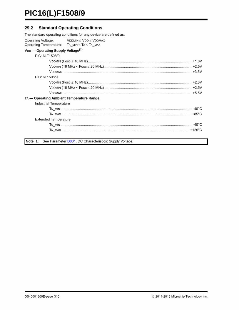
PIC16(L)F1508/9
29.2 Standard Operating Conditions
The standard operating conditions for any device are defined as:
Operating Voltage: VDDMIN VDD VDDMAX
Operating Temperature: TA_MIN TA TA_MAX
VDD — Operating Supply Voltage(1)
PIC16LF1508/9
VDDMIN (Fosc 16 MHz).......................................................................................................... +1.8V
VDDMIN (16 MHz < Fosc 20 MHz) ......................................................................................... +2.5V
VDDMAX .................................................................................................................................... +3.6V
PIC16F1508/9
VDDMIN (Fosc 16 MHz).......................................................................................................... +2.3V
VDDMIN (16 MHz < Fosc 20 MHz) ......................................................................................... +2.5V
VDDMAX .................................................................................................................................... +5.5V
TA — Operating Ambient Temperature Range
Industrial Temperature
TA_MIN ...................................................................................................................................... -40°C
TA_MAX .................................................................................................................................... +85°C
Extended Temperature
TA_MIN ...................................................................................................................................... -40°C
TA_MAX .................................................................................................................................. +125°C
Note 1: See Parameter D001, DC Characteristics: Supply Voltage.
DS40001609E-page 310 2011-2015 Microchip Technology Inc.

PIC16(L)F1508/9
FIGURE 29-1: VOLTAGE FREQUENCY GRAPH, -40°C TA +125°C, PIC16F1508/9 ONLY
FIGURE 29-2: VOLTAGE FREQUENCY GRAPH, -40°C TA +125°C, PIC16LF1508/9 ONLY
Rev. 10-000130A8/6/2013
5.5
2.5
2.3
0 16 20
VDD
(V)
Frequency (MHz)
Note 1: The shaded region indicates the permissible combinations of voltage and frequency.
2: Refer to Table 29-8 for each Oscillator mode’s supported frequencies.
3.6
2.5
1.8
0 16 20
VDD
(V)
Frequency (MHz)
Rev. 10-000131A8/5/2013
Note 1: The shaded region indicates the permissible combinations of voltage and frequency.
2: Refer to Table 29-8 for each Oscillator mode’s supported frequencies.
2011-2015 Microchip Technology Inc. DS40001609E-page 311

PIC16(L)F1508/9
29.3 DC Characteristics
TABLE 29-1: SUPPLY VOLTAGE
PIC16LF1508/9 Standard Operating Conditions (unless otherwise stated)
PIC16F1508/9
Param. No.
Sym. Characteristic Min. Typ† Max. Units Conditions
D001 VDD Supply Voltage
VDDMIN
1.82.5
——
VDDMAX
3.63.6
VV
FOSC 16 MHzFOSC 20 MHz
D001 2.32.5
——
5.55.5
VV
FOSC 16 MHzFOSC 20 MHz
D002* VDR RAM Data Retention Voltage(1)
1.5 — — V Device in Sleep mode
D002* 1.7 — — V Device in Sleep mode
D002A* VPOR Power-on Reset Release Voltage(2)
— 1.6 — V
D002A* — 1.6 — V
D002B* VPORR* Power-on Reset Rearm Voltage(2)
— 0.8 — V
D002B* — 1.5 — V
D003 VFVR Fixed Voltage Reference Voltage
1x gain (1.024V nominal)2x gain (2.048V nominal)4x gain (4.096V nominal)
-4-3
——
+4+7
%%
VDD 2.5V, -40°C TA +85°CVDD 2.5V, -40°C TA +85°CVDD 4.75V, -40°C TA +85°C
D004* SVDD VDD Rise Rate(2) 0.05 — — V/ms Ensures that the Power-on Reset signal is released properly.
* These parameters are characterized but not tested.† Data in “Typ” column is at 3.0V, 25°C unless otherwise stated. These parameters are for design guidance only and are not
tested.Note 1: This is the limit to which VDD can be lowered in Sleep mode without losing RAM data.
2: See Figure 29-3, POR and POR REARM with Slow Rising VDD.
DS40001609E-page 312 2011-2015 Microchip Technology Inc.

PIC16(L)F1508/9
FIGURE 29-3: POR AND POR REARM WITH SLOW RISING VDD
VDD
VPOR
VPORR
VSS
VSS
NPOR(1)
TPOR(2)
POR REARM
Note 1: When NPOR is low, the device is held in Reset.2: TPOR 1 s typical.3: TVLOW 2.7 s typical.
TVLOW(3)
SVDD
2011-2015 Microchip Technology Inc. DS40001609E-page 313

PIC16(L)F1508/9
TABLE 29-2: SUPPLY CURRENT (IDD)(1,2)
PIC16LF1508/9 Standard Operating Conditions (unless otherwise stated)
PIC16F1508/9
Param.No.
Device Characteristics
Min. Typ† Max. UnitsConditions
VDD Note
D010 — 8 20 A 1.8 FOSC = 32 kHz,LP Oscillator,-40°C TA +85°C
— 10 25 A 3.0
D010 — 15 31 A 2.3 FOSC = 32 kHz, LP Oscillator,-40°C TA +85°C
— 17 33 A 3.0
— 21 39 A 5.0
D011 — 60 100 A 1.8 FOSC = 1 MHz,XT Oscillator— 100 180 A 3.0
D011 — 100 180 A 2.3 FOSC = 1 MHz,XT Oscillator— 130 220 A 3.0
— 170 280 A 5.0
D012 — 140 240 A 1.8 FOSC = 4 MHz,XT Oscillator— 250 360 A 3.0
D012 — 210 320 A 2.3 FOSC = 4 MHz,XT Oscillator— 280 410 A 3.0
— 340 500 A 5.0
D013 — 30 65 A 1.8 FOSC = 1 MHz,External Clock (ECM),Medium Power mode
— 55 100 A 3.0
D013 — 65 110 A 2.3 FOSC = 1 MHz,External Clock (ECM),Medium Power mode
— 85 140 A 3.0
— 115 190 A 5.0
D014 — 115 190 A 1.8 FOSC = 4 MHz,External Clock (ECM),Medium Power mode
— 210 310 A 3.0
D014 — 180 270 A 2.3 FOSC = 4 MHz,External Clock (ECM),Medium Power mode
— 240 365 A 3.0
— 295 460 A 5.0
D015 — 3.2 12 A 1.8 FOSC = 31 kHz,LFINTOSC,-40°C TA +85°C
— 5.4 20 A 3.0
D015 — 13 28 A 2.3 FOSC = 31 kHz,LFINTOSC,-40°C TA +85°C
— 15 30 A 3.0
— 17 36 A 5.0
* These parameters are characterized but not tested.† Data in “Typ” column is at 3.0V, 25°C unless otherwise stated. These parameters are for design guidance
only and are not tested.Note 1: The test conditions for all IDD measurements in active operation mode are: OSC1 = external square wave,
from rail-to-rail; all I/O pins tri-stated, pulled to VSS; MCLR = VDD; WDT disabled.2: The supply current is mainly a function of the operating voltage and frequency. Other factors, such as I/O
pin loading and switching rate, oscillator type, internal code execution pattern and temperature, also have an impact on the current consumption.
3: For RC oscillator configurations, current through REXT is not included. The current through the resistor can be extended by the formula IR = VDD/2REXT (mA) with REXT in k.
DS40001609E-page 314 2011-2015 Microchip Technology Inc.

PIC16(L)F1508/9
D016 — 215 360 A 1.8 FOSC = 500 kHz, HFINTOSC— 275 480 A 3.0
D016 — 270 450 A 2.3 FOSC = 500 kHz, HFINTOSC— 300 500 A 3.0
— 350 620 A 5.0
D017* — 410 660 A 1.8 FOSC = 8 MHz,HFINTOSC— 630 970 A 3.0
D017* — 530 750 A 2.3 FOSC = 8 MHz,HFINTOSC— 660 1100 A 3.0
— 730 1200 A 5.0
D018 — 600 940 A 1.8 FOSC = 16 MHz,HFINTOSC — 970 1400 A 3.0
D018 — 780 1200 A 2.3 FOSC = 16 MHz,HFINTOSC — 1000 1550 A 3.0
— 1090 1700 A 5.0
D019A — 1030 1500 A 3.0 FOSC = 20 MHz,External Clock (ECH),High-Power mode
D019A — 1060 1600 A 3.0 FOSC = 20 MHz,External Clock (ECH),High-Power mode
— 1220 1800 A 5.0
TABLE 29-2: SUPPLY CURRENT (IDD)(1,2) (CONTINUED)
PIC16LF1508/9 Standard Operating Conditions (unless otherwise stated)
PIC16F1508/9
Param.No.
Device Characteristics
Min. Typ† Max. UnitsConditions
VDD Note
* These parameters are characterized but not tested.† Data in “Typ” column is at 3.0V, 25°C unless otherwise stated. These parameters are for design guidance
only and are not tested.Note 1: The test conditions for all IDD measurements in active operation mode are: OSC1 = external square wave,
from rail-to-rail; all I/O pins tri-stated, pulled to VSS; MCLR = VDD; WDT disabled.2: The supply current is mainly a function of the operating voltage and frequency. Other factors, such as I/O
pin loading and switching rate, oscillator type, internal code execution pattern and temperature, also have an impact on the current consumption.
3: For RC oscillator configurations, current through REXT is not included. The current through the resistor can be extended by the formula IR = VDD/2REXT (mA) with REXT in k.
2011-2015 Microchip Technology Inc. DS40001609E-page 315

PIC16(L)F1508/9
D019B — 6 16 A 1.8 FOSC = 32 kHz,External Clock (ECL),Low-Power mode
— 8 22 A 3.0
D019B — 13 28 A 2.3 FOSC = 32 kHz, External Clock (ECL),Low-Power mode
— 15 31 A 3.0
— 16 36 A 5.0
D019C — 19 35 A 1.8 FOSC = 500 kHz, External Clock (ECL),Low-Power mode
— 32 55 A 3.0
D019C — 31 52 A 2.3 FOSC = 500 kHz, External Clock (ECL),Low-Power mode
— 38 65 A 3.0
— 44 74 A 5.0
D020 — 140 210 A 1.8 FOSC = 4 MHz, EXTRC (Note 3)— 250 330 A 3.0
D020 — 210 290 A 2.3 FOSC = 4 MHz,EXTRC (Note 3)— 280 380 A 3.0
— 350 470 A 5.0
D021 — 1135 1700 A 3.0 FOSC = 20 MHz, HS Oscillator
D021 — 1170 1800 A 3.0 FOSC = 20 MHz,HS Oscillator— 1555 2300 A 5.0
TABLE 29-2: SUPPLY CURRENT (IDD)(1,2) (CONTINUED)
PIC16LF1508/9 Standard Operating Conditions (unless otherwise stated)
PIC16F1508/9
Param.No.
Device Characteristics
Min. Typ† Max. UnitsConditions
VDD Note
* These parameters are characterized but not tested.† Data in “Typ” column is at 3.0V, 25°C unless otherwise stated. These parameters are for design guidance
only and are not tested.Note 1: The test conditions for all IDD measurements in active operation mode are: OSC1 = external square wave,
from rail-to-rail; all I/O pins tri-stated, pulled to VSS; MCLR = VDD; WDT disabled.2: The supply current is mainly a function of the operating voltage and frequency. Other factors, such as I/O
pin loading and switching rate, oscillator type, internal code execution pattern and temperature, also have an impact on the current consumption.
3: For RC oscillator configurations, current through REXT is not included. The current through the resistor can be extended by the formula IR = VDD/2REXT (mA) with REXT in k.
DS40001609E-page 316 2011-2015 Microchip Technology Inc.

PIC16(L)F1508/9
TABLE 29-3: POWER-DOWN CURRENTS (IPD)(1,2)
PIC16LF1508/9Operating Conditions: (unless otherwise stated)Low-Power Sleep Mode
PIC16F1508/9 Low-Power Sleep Mode, VREGPM = 1
Param.No.
Device Characteristics Min. Typ†Max.
+85°CMax.
+125°CUnits
Conditions
VDD Note
D022 Base IPD — 0.020 1.0 8.0 A 1.8 WDT, BOR, FVR and SOSC disabled, all Peripherals inactive— 0.025 2.0 9.0 A 3.0
D022 Base IPD — 0.25 3.0 10 A 2.3 WDT, BOR, FVR and SOSC disabled, all Peripherals inactive,Low-Power Sleep mode
— 0.30 4.0 12 A 3.0
— 0.40 6.0 15 A 5.0
D022A Base IPD — 9.8 16 18 A 2.3 WDT, BOR, FVR and SOSC disabled, all Peripherals inactive,Normal Power Sleep mode, VREGPM = 0
— 10.3 18 20 A 3.0
— 11.5 21 26 A 5.0
D023 — 0.26 2.0 9.0 A 1.8 WDT Current
— 0.44 3.0 10 A 3.0
D023 — 0.43 6.0 15 A 2.3 WDT Current
— 0.53 7.0 20 A 3.0
— 0.64 8.0 22 A 5.0
D023A — 15 28 30 A 1.8 FVR Current
— 18 30 33 A 3.0
D023A — 18 33 35 A 2.3 FVR Current
— 19 35 37 A 3.0
— 20 37 39 A 5.0
D024 — 6.0 17 20 A 3.0 BOR Current
D024 — 7.0 17 30 A 3.0 BOR Current
— 8.0 20 40 A 5.0
D24A — 0.1 4.0 10 A 3.0 LPBOR Current
D24A — 0.35 5.0 14 A 3.0 LPBOR Current
— 0.45 8.0 17 A 5.0
* These parameters are characterized but not tested.† Data in “Typ” column is at 3.0V, 25°C unless otherwise stated. These parameters are for design guidance only and are
not tested.Note 1: The peripheral current can be determined by subtracting the base IPD current from this limit. Max. values should be
used when calculating total current consumption.2: The power-down current in Sleep mode does not depend on the oscillator type. Power-down current is measured with
the part in Sleep mode, with all I/O pins in high-impedance state and tied to VSS.3: ADC clock source is FRC.
2011-2015 Microchip Technology Inc. DS40001609E-page 317

PIC16(L)F1508/9
D025 — 0.7 4.0 9.0 A 1.8 SOSC Current
— 2.3 8.0 12 A 3.0
D025 — 1.0 6.0 11 A 2.3 SOSC Current
— 2.4 8.5 20 A 3.0
— 6.9 20 25 A 5.0
D026 — 0.11 1.5 9.0 A 1.8 ADC Current (Note 3),No conversion in progress— 0.12 2.7 10 A 3.0
D026 — 0.30 4.0 11 A 2.3 ADC Current (Note 3),No conversion in progress— 0.35 5.0 13 A 3.0
— 0.45 8.0 16 A 5.0
D026A* — 250 — — A 1.8 ADC Current (Note 3),Conversion in progress— 250 — — A 3.0
D026A* — 280 — — A 2.3 ADC Current (Note 3),Conversion in progress— 280 — — A 3.0
— 280 — — A 5.0
D027 — 7 22 25 A 1.8 Comparator,CxSP = 0— 8 23 27 A 3.0
D027 — 17 35 37 A 2.3 Comparator,CxSP = 0— 18 37 38 A 3.0
— 19 38 40 A 5.0
TABLE 29-3: POWER-DOWN CURRENTS (IPD)(1,2) (CONTINUED)
PIC16LF1508/9Operating Conditions: (unless otherwise stated)Low-Power Sleep Mode
PIC16F1508/9 Low-Power Sleep Mode, VREGPM = 1
Param.No.
Device Characteristics Min. Typ†Max.
+85°CMax.
+125°CUnits
Conditions
VDD Note
* These parameters are characterized but not tested.† Data in “Typ” column is at 3.0V, 25°C unless otherwise stated. These parameters are for design guidance only and are
not tested.Note 1: The peripheral current can be determined by subtracting the base IPD current from this limit. Max. values should be
used when calculating total current consumption.2: The power-down current in Sleep mode does not depend on the oscillator type. Power-down current is measured with
the part in Sleep mode, with all I/O pins in high-impedance state and tied to VSS.3: ADC clock source is FRC.
DS40001609E-page 318 2011-2015 Microchip Technology Inc.

PIC16(L)F1508/9
TABLE 29-4: I/O PORTSStandard Operating Conditions (unless otherwise stated)
Param.No.
Sym. Characteristic Min. Typ† Max. Units Conditions
VIL Input Low Voltage
I/O PORT:
D030 with TTL buffer — — 0.8 V 4.5V VDD 5.5V
D030A — — 0.15 VDD V 1.8V VDD 4.5V
D031 with Schmitt Trigger buffer — — 0.2 VDD V 2.0V VDD 5.5V
with I2C levels — — 0.3 VDD V
with SMbus levels — — 0.8 V 2.7V VDD 5.5V
D032 MCLR, OSC1 (EXTRC mode) — — 0.2 VDD V (Note 1)
D033 OSC1 (HS mode) — — 0.3 VDD V
VIH Input High Voltage
I/O PORT:
D040 with TTL buffer 2.0 — — V 4.5V VDD 5.5V
D040A 0.25 VDD + 0.8
— — V 1.8V VDD 4.5V
D041 with Schmitt Trigger buffer 0.8 VDD — — V 2.0V VDD 5.5V
with I2C levels 0.7 VDD — — V
with SMbus levels 2.1 — — V 2.7V VDD 5.5V
D042 MCLR 0.8 VDD — — V
D043A OSC1 (HS mode) 0.7 VDD — — V
D043B OSC1 (EXTRC mode) 0.9 VDD — — V VDD 2.0V (Note 1)
IIL Input Leakage Current(2)
D060 I/O Ports — ± 5 ± 125 nA VSS VPIN VDD, Pin at high-impedance, 85°C
— ± 5 ± 1000 nA VSS VPIN VDD, Pin at high-impedance, 125°C
D061 MCLR(3) — ± 50 ± 200 nA VSS VPIN VDD, Pin at high-impedance, 85°C
IPUR Weak Pull-up Current
D070* 25 100 200 A VDD = 3.3V, VPIN = VSS
25 140 300 A VDD = 5.0V, VPIN = VSS
VOL Output Low Voltage
D080 I/O Ports— — 0.6 V
IOL = 8 mA, VDD = 5VIOL = 6 mA, VDD = 3.3VIOL = 1.8 mA, VDD = 1.8V
VOH Output High Voltage
D090 I/O PortsVDD - 0.7 — — V
IOH = 3.5 mA, VDD = 5VIOH = 3 mA, VDD = 3.3VIOH = 1 mA, VDD = 1.8V
D101* COSC2 Capacitive Loading Specifications on Output Pins
OSC2 pin— — 15 pF
In XT, HS, LP modes when external clock is used to drive OSC1
D101A* CIO All I/O pins — — 50 pF
* These parameters are characterized but not tested.† Data in “Typ” column is at 3.0V, 25°C unless otherwise stated. These parameters are for design guidance only and are
not tested.Note 1: In EXTRC oscillator configuration, the OSC1/CLKIN pin is a Schmitt Trigger input. It is not recommended to use an
external clock in EXTRC mode.2: Negative current is defined as current sourced by the pin.3: The leakage current on the MCLR pin is strongly dependent on the applied voltage level. The specified levels represent
normal operating conditions. Higher leakage current may be measured at different input voltages.
2011-2015 Microchip Technology Inc. DS40001609E-page 319

PIC16(L)F1508/9
TABLE 29-6: THERMAL CHARACTERISTICS
TABLE 29-5: MEMORY PROGRAMMING SPECIFICATIONS
Standard Operating Conditions (unless otherwise stated)
Param.No.
Sym. Characteristic Min. Typ† Max. Units Conditions
Program Memory Programming Specifications
D110 VIHH Voltage on MCLR/VPP pin 8.0 — 9.0 V (Note 2)
D112 VPBE VDD for Bulk Erase 2.7 — VDDMAX V
D113 VPEW VDD for Write or Row Erase VDDMIN — VDDMAX V
D114 IPPPGM Current on MCLR/VPP during Erase/Write
— 1.0 — mA
D115 IDDPGM Current on VDD during Erase/Write
— 5.0 — mA
Program Flash Memory
D121 EP Cell Endurance 10K — — E/W -40C TA +85C (Note 1)
D122 VPRW VDD for Read/Write VDDMIN — VDDMAX V
D123 TIW Self-timed Write Cycle Time — 2 2.5 ms
D124 TRETD Characteristic Retention — 40 — Year Provided no other specifications are violated
D125 EHEFC High-Endurance Flash Cell 100K — — E/W 0C TA +60°C, lower byte last 128 addresses
† Data in “Typ” column is at 3.0V, 25°C unless otherwise stated. These parameters are for design guidance only and are not tested.
Note 1: Self-write and Block Erase.2: Required only if single-supply programming is disabled.
Standard Operating Conditions (unless otherwise stated)
Param.No.
Sym. Characteristic Typ. Units Conditions
TH01 JA Thermal Resistance Junction to Ambient 62.2 C/W 20-pin DIP package
77.7 C/W 20-pin SOIC package
87.3 C/W 20-pin SSOP package
46.2 C/W 20-pin QFN 4X4mm package
32.8 C/W 20-pin UQFN 4X4mm package
TH02 JC Thermal Resistance Junction to Case 27.5 C/W 20-pin DIP package
23.1 C/W 20-pin SOIC package
31.1 C/W 20-pin SSOP package
13.2 C/W 20-pin QFN 4X4mm package
27.4 C/W 20-pin UQFN 4X4mm package
TH03 TJMAX Maximum Junction Temperature 150 CTH04 PD Power Dissipation — W PD = PINTERNAL + PI/O
TH05 PINTERNAL Internal Power Dissipation — W PINTERNAL = IDD x VDD(1)
TH06 PI/O I/O Power Dissipation — W PI/O = (IOL * VOL) + (IOH * (VDD - VOH))
TH07 PDER Derated Power — W PDER = PDMAX (TJ - TA)/JA(2)
Note 1: IDD is current to run the chip alone without driving any load on the output pins.2: TA = Ambient Temperature; TJ = Junction Temperature
DS40001609E-page 320 2011-2015 Microchip Technology Inc.

PIC16(L)F1508/9
29.4 AC Characteristics
Timing Parameter Symbology has been created with one of the following formats:
FIGURE 29-4: LOAD CONDITIONS
1. TppS2ppS
2. TppS
T
F Frequency T Time
Lowercase letters (pp) and their meanings:
pp
cc CCP1 osc CLKIN
ck CLKOUT rd RD
cs CS rw RD or WR
di SDIx sc SCKx
do SDO ss SS
dt Data in t0 T0CKI
io I/O PORT t1 T1CKI
mc MCLR wr WR
Uppercase letters and their meanings:
S
F Fall P Period
H High R Rise
I Invalid (High-impedance) V Valid
L Low Z High-impedance
Load Condition
Legend: CL=50 pF for all pins
Pin
CL
VSS
Rev. 10-000133A8/1/2013
2011-2015 Microchip Technology Inc. DS40001609E-page 321

PIC16(L)F1508/9
FIGURE 29-5: CLOCK TIMING
TABLE 29-7: CLOCK OSCILLATOR TIMING REQUIREMENTS
Standard Operating Conditions (unless otherwise stated)
Param.No.
Sym. Characteristic Min. Typ† Max. Units Conditions
OS01 FOSC External CLKIN Frequency(1) DC — 0.5 MHz External Clock (ECL)
DC — 4 MHz External Clock (ECM)
DC — 20 MHz External Clock (ECH)
Oscillator Frequency(1) — 32.768 — kHz LP Oscillator
0.1 — 4 MHz XT Oscillator
1 — 4 MHz HS Oscillator
1 — 20 MHz HS Oscillator, VDD > 2.7V
DC — 4 MHz EXTRC, VDD > 2.0V
OS02 TOSC External CLKIN Period(1) 27 — µs LP Oscillator
250 — ns XT Oscillator
50 — ns HS Oscillator
50 — ns External Clock (EC)
Oscillator Period(1) — 30.5 — µs LP Oscillator
250 — 10,000 ns XT Oscillator
50 — 1,000 ns HS Oscillator
250 — — ns EXTRC
OS03 TCY Instruction Cycle Time(1) 200 TCY DC ns TCY = 4/FOSC
OS04* TosH,
TosL
External CLKIN High
External CLKIN Low
2 — — µs LP Oscillator
100 — — ns XT Oscillator
20 — — ns HS Oscillator
OS05* TosR,
TosF
External CLKIN Rise
External CLKIN Fall
0 — — ns LP Oscillator
0 — — ns XT Oscillator
0 — — ns HS Oscillator
* These parameters are characterized but not tested.† Data in “Typ” column is at 3.0V, 25°C unless otherwise stated. These parameters are for design guidance only and are not
tested.Note 1: Instruction cycle period (TCY) equals four times the input oscillator time base period. All specified values are based on
characterization data for that particular oscillator type under standard operating conditions with the device executing code. Exceeding these specified limits may result in an unstable oscillator operation and/or higher than expected current con-sumption. All devices are tested to operate at “min” values with an external clock applied to CLKIN pin. When an external clock input is used, the “max” cycle time limit is “DC” (no clock) for all devices.
CLKIN
CLKOUT
Q4 Q1 Q2 Q3 Q4 Q1
OS02
OS03
(CLKOUT mode)
Note: See Table 29-9.
OS11OS12
DS40001609E-page 322 2011-2015 Microchip Technology Inc.

PIC16(L)F1508/9
TABLE 29-8: OSCILLATOR PARAMETERS
FIGURE 29-6: HFINTOSC FREQUENCY ACCURACY OVER VDD AND TEMPERATURE
Standard Operating Conditions (unless otherwise stated)
Param. No.
Sym. CharacteristicFreq.
ToleranceMin. Typ† Max. Units Conditions
OS08 HFOSC Internal Calibrated HFINTOSC Frequency(1)
±2% — 16.0 — MHz VDD = 3.0V, TA = 25°C,(Note 2)
OS09 LFOSC Internal LFINTOSC Frequency — — 31 — kHz (Note 3)
OS10* TIOSC ST HFINTOSC Wake-up from Sleep Start-up Time
— — 5 15 s
OS10A* TLFOSC ST LFINTOSC Wake-up from Sleep Start-up Time
— — 0.5 — ms -40°C TA +125°C
* These parameters are characterized but not tested.† Data in “Typ” column is at 3.0V, 25°C unless otherwise stated. These parameters are for design guidance only and are
not tested.Note 1: To ensure these oscillator frequency tolerances, VDD and VSS must be capacitively decoupled as close to the device as
possible. 0.1 F and 0.01 F values in parallel are recommended.2: See Figure 29-6: “HFINTOSC Frequency Accuracy over Device VDD and Temperature”,
Figure 30-72: “HFINTOSC Accuracy Over Temperature, VDD = 1.8V, PIC16LF1508/9 Only”, and Figure 30-73: “HFINTOSC Accuracy Over Temperature, 2.3V VDD 5.5V”.
3: See Figure 30-70: “LFINTOSC Frequency over VDD and Temperature, PIC16LF1508/9 Only”, and Figure 30-71: “LFINTOSC Frequency over VDD and Temperature, PIC16F1508/9”.
VDD (V)
125
85
60
25
0
-401.8 2.3 5.5
±4.5%
-4.5% to +7%
±12%
±12%
Tem
pera
ture
(°C
)
Rev. 10-000135A7/30/2013
Note: See Figure 30-72: “HFINTOSC Accuracy Over Temperature, VDD = 1.8V, PIC16LF1508/9 Only”, andFigure 30-73: “HFINTOSC Accuracy Over Temperature, 2.3V VDD 5.5V”.
2011-2015 Microchip Technology Inc. DS40001609E-page 323

PIC16(L)F1508/9
FIGURE 29-7: CLKOUT AND I/O TIMING
TABLE 29-9: CLKOUT AND I/O TIMING PARAMETERS
Standard Operating Conditions (unless otherwise stated)
Param.No.
Sym. Characteristic Min. Typ† Max. Units Conditions
OS11 TosH2ckL FOSC to CLKOUT(1) — — 70 ns 3.3V VDD 5.0V
OS12 TosH2ckH FOSC to CLKOUT(1) — — 72 ns 3.3V VDD 5.0V
OS13 TckL2ioV CLKOUT to Port out valid(1) — — 20 ns
OS14 TioV2ckH Port input valid before CLKOUT(1) TOSC + 200 ns — — ns
OS15 TosH2ioV Fosc (Q1 cycle) to Port out valid — 50 70* ns 3.3V VDD 5.0V
OS16 TosH2ioI Fosc (Q2 cycle) to Port input invalid (I/O in setup time)
50 — — ns 3.3V VDD 5.0V
OS17 TioV2osH Port input valid to Fosc(Q2 cycle)(I/O in setup time)
20 — — ns
OS18* TioR Port output rise time ——
4015
7232
ns VDD = 1.8V3.3V VDD 5.0V
OS19* TioF Port output fall time ——
2815
5530
ns VDD = 1.8V3.3V VDD 5.0V
OS20* Tinp INT pin input high or low time 25 — — ns
OS21* Tioc Interrupt-on-change new input level time 25 — — ns
* These parameters are characterized but not tested.† Data in “Typ” column is at 3.0V, 25C unless otherwise stated.
Note 1: Measurements are taken in EXTRC mode where CLKOUT output is 4 x TOSC.
FOSC
CLKOUT
I/O pin(Input)
I/O pin(Output)
Q4 Q1 Q2 Q3
OS11
OS19
OS13
OS15
OS18, OS19
OS20OS21
OS17
OS16
OS14
OS12
OS18
Old Value New Value
Write Fetch Read ExecuteCycle
DS40001609E-page 324 2011-2015 Microchip Technology Inc.

PIC16(L)F1508/9
FIGURE 29-8: RESET, WATCHDOG TIMER, OSCILLATOR START-UP TIMER AND POWER-UP TIMER TIMING
VDD
MCLR
InternalPOR
PWRTTime-out
OSCStart-up Time
Internal Reset(1)
Watchdog Timer
33
32
30
3134
I/O pins
34
Note 1:Asserted low.
Reset(1)
2011-2015 Microchip Technology Inc. DS40001609E-page 325
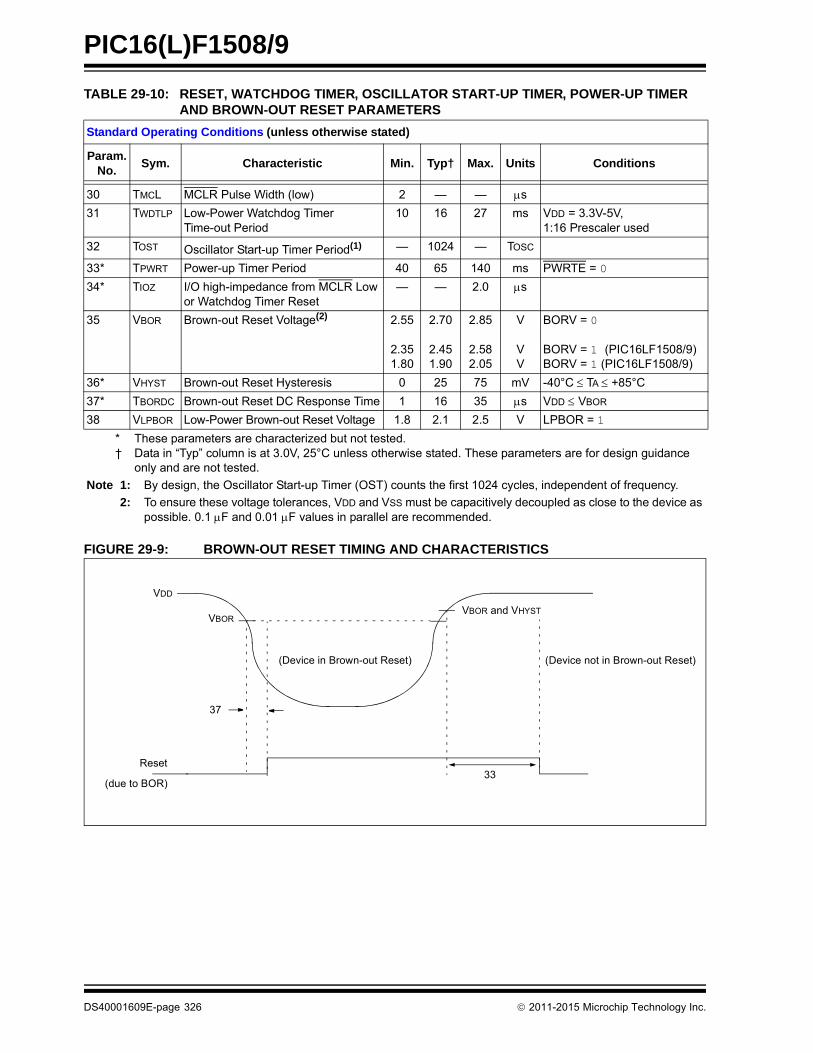
PIC16(L)F1508/9
TABLE 29-10: RESET, WATCHDOG TIMER, OSCILLATOR START-UP TIMER, POWER-UP TIMER AND BROWN-OUT RESET PARAMETERS
FIGURE 29-9: BROWN-OUT RESET TIMING AND CHARACTERISTICS
Standard Operating Conditions (unless otherwise stated)
Param. No.
Sym. Characteristic Min. Typ† Max. Units Conditions
30 TMCL MCLR Pulse Width (low) 2 — — s
31 TWDTLP Low-Power Watchdog Timer Time-out Period
10 16 27 ms VDD = 3.3V-5V,1:16 Prescaler used
32 TOST Oscillator Start-up Timer Period(1) — 1024 — TOSC
33* TPWRT Power-up Timer Period 40 65 140 ms PWRTE = 0
34* TIOZ I/O high-impedance from MCLR Low or Watchdog Timer Reset
— — 2.0 s
35 VBOR Brown-out Reset Voltage(2) 2.55
2.351.80
2.70
2.451.90
2.85
2.582.05
V
VV
BORV = 0
BORV = 1 (PIC16LF1508/9)BORV = 1 (PIC16LF1508/9)
36* VHYST Brown-out Reset Hysteresis 0 25 75 mV -40°C TA +85°C
37* TBORDC Brown-out Reset DC Response Time 1 16 35 s VDD VBOR
38 VLPBOR Low-Power Brown-out Reset Voltage 1.8 2.1 2.5 V LPBOR = 1
* These parameters are characterized but not tested.† Data in “Typ” column is at 3.0V, 25°C unless otherwise stated. These parameters are for design guidance
only and are not tested.
Note 1: By design, the Oscillator Start-up Timer (OST) counts the first 1024 cycles, independent of frequency.
2: To ensure these voltage tolerances, VDD and VSS must be capacitively decoupled as close to the device as possible. 0.1 F and 0.01 F values in parallel are recommended.
VBOR
VDD
(Device in Brown-out Reset) (Device not in Brown-out Reset)
33Reset
(due to BOR)
VBOR and VHYST
37
DS40001609E-page 326 2011-2015 Microchip Technology Inc.

PIC16(L)F1508/9
FIGURE 29-10: TIMER0 AND TIMER1 EXTERNAL CLOCK TIMINGS
TABLE 29-11: TIMER0 AND TIMER1 EXTERNAL CLOCK REQUIREMENTS
Standard Operating Conditions (unless otherwise stated)
Param. No.
Sym. Characteristic Min. Typ† Max. Units Conditions
40* TT0H T0CKI High Pulse Width No Prescaler 0.5 TCY + 20 — — ns
With Prescaler 10 — — ns
41* TT0L T0CKI Low Pulse Width No Prescaler 0.5 TCY + 20 — — ns
With Prescaler 10 — — ns
42* TT0P T0CKI Period Greater of:20 or TCY + 40
N
— — ns N = prescale value
45* TT1H T1CKI High Time
Synchronous, No Prescaler 0.5 TCY + 20 — — ns
Synchronous, with Prescaler 15 — — ns
Asynchronous 30 — — ns
46* TT1L T1CKI Low Time
Synchronous, No Prescaler 0.5 TCY + 20 — — ns
Synchronous, with Prescaler 15 — — ns
Asynchronous 30 — — ns
47* TT1P T1CKI Input Period
Synchronous Greater of:30 or TCY + 40
N
— — ns N = prescale value
Asynchronous 60 — — ns
48 FT1 Secondary Oscillator Input Frequency Range (Oscillator enabled by setting bit T1OSCEN)
32.4 32.768 33.1 kHz
49* TCKEZTMR1 Delay from External Clock Edge to Timer Increment
2 TOSC — 7 TOSC — Timers in Sync mode
* These parameters are characterized but not tested.† Data in “Typ” column is at 3.0V, 25°C unless otherwise stated. These parameters are for design guidance only and are not
tested.
T0CKI
T1CKI
40 41
42
45 46
47 49
TMR0 orTMR1
2011-2015 Microchip Technology Inc. DS40001609E-page 327

PIC16(L)F1508/9
FIGURE 29-11: CLC PROPAGATION TIMING
TABLE 29-12: CONFIGURATION LOGIC CELL (CLC) CHARACTERISTICS
Standard Operating Conditions (unless otherwise stated)
Param. No.
Sym. Characteristic Min. Typ† Max. Units Conditions
CLC01* TCLCIN CLC input time — 7 — ns
CLC02* TCLC CLC module input to output propagation time ——
2412
——
nsns
VDD = 1.8VVDD > 3.6V
CLC03* TCLCOUT CLC output time Rise Time — OS18 — — (Note 1)
Fall Time — OS19 — — (Note 1)
CLC04* FCLCMAX CLC maximum switching frequency — 45 — MHz
* These parameters are characterized but not tested.† Data in “Typ” column is at 3.0V, 25°C unless otherwise stated. These parameters are for design guidance
only and are not tested.Note 1:See Table 29-9 for OS18 and OS19 rise and fall times.
LCx_in[n](1)CLC
Output timeCLC
Input time LCx_out(1) CLCxCLCxINn CLCModule
CLC01 CLC02 CLC03
LCx_in[n](1)CLC
Output timeCLC
Input time LCx_out(1) CLCxCLCxINn CLCModule
Rev. 10-000031A7/30/2013
Note 1: See FIGURE 24-1:, Configurable Logic Cell Block Diagram, to identify specific CLC signals.
DS40001609E-page 328 2011-2015 Microchip Technology Inc.

PIC16(L)F1508/9
TABLE 29-13: ANALOG-TO-DIGITAL CONVERTER (ADC) CHARACTERISTICS(1,2,3)
Operating Conditions (unless otherwise stated)VDD = 3.0V, TA = 25°C
Param. No.
Sym. Characteristic Min. Typ† Max. Units Conditions
AD01 NR Resolution — — 10 bit
AD02 EIL Integral Error — ±1 ±1.7 LSb VREF = 3.0V
AD03 EDL Differential Error — ±1 ±1 LSb No missing codesVREF = 3.0V
AD04 EOFF Offset Error — ±1 ±2.5 LSb VREF = 3.0V
AD05 EGN Gain Error — ±1 ±2.0 LSb VREF = 3.0V
AD06 VREF Reference Voltage 1.8 — VDD V VREF = (VRPOS - VRNEG) (Note 4)
AD07 VAIN Full-Scale Range VSS — VREF V
AD08 ZAIN Recommended Impedance of Analog Voltage Source
— — 10 k Can go higher if external 0.01F capacitor is present on input pin.
* These parameters are characterized but not tested.† Data in “Typ” column is at 3.0V, 25°C unless otherwise stated. These parameters are for design guidance only and are not
tested.Note 1:Total Absolute Error includes integral, differential, offset and gain errors.
2: The ADC conversion result never decreases with an increase in the input voltage and has no missing codes.3: See Section 30.0 “DC and AC Characteristics Graphs and Charts” for operating characterization.4: ADC VREF is selected by ADPREF<0> bit.
2011-2015 Microchip Technology Inc. DS40001609E-page 329

PIC16(L)F1508/9
FIGURE 29-12: ADC CONVERSION TIMING (ADC CLOCK FOSC-BASED)
FIGURE 29-13: ADC CONVERSION TIMING (ADC CLOCK FROM FRC)
AD131
AD130
BSF ADCON0, GO
Q4
ADC_clk
ADC Data
ADRES
ADIF
GO
Sample
OLD_DATA
Sampling Stopped
DONE
NEW_DATA
9 8 7 3 2 1 0
1 TCY
6
AD133
1 TCY
AD132
AD132
AD131
AD130
BSF ADCON0, GO
Q4
ADC_clk
ADC Data
ADRES
ADIF
GO
Sample
OLD_DATA
Sampling Stopped
DONE
NEW_DATA
9 7 3 2 1 0
Note 1:If the ADC clock source is selected as FRC, a time of TCY is added before the ADC clock starts. This allows the SLEEP instruction to be executed.
AD133
68
1 TCY
1 TCY
DS40001609E-page 330 2011-2015 Microchip Technology Inc.

PIC16(L)F1508/9
TABLE 29-14: ADC CONVERSION REQUIREMENTS
TABLE 29-15: COMPARATOR SPECIFICATIONS(1)
Standard Operating Conditions (unless otherwise stated)
Param.No.
Sym. Characteristic Min. Typ† Max. Units Conditions
AD130* TAD ADC Clock Period (TADC) 1.0 — 6.0 s FOSC-based
ADC Internal FRC Oscillator Period (TFRC) 1.0 2.0 6.0 s ADCS<2:0> = x11 (ADC FRC mode)
AD131 TCNV Conversion Time (not including Acquisition Time)(1)
— 11 — TAD Set GO/DONE bit to conversioncomplete
AD132* TACQ Acquisition Time — 5.0 — s
AD133* THCD Holding Capacitor Disconnect Time ——
1/2 TAD
1/2 TAD + 1TCY
——
FOSC-basedADCS<2:0> = x11 (ADC FRC mode)
* These parameters are characterized but not tested.† Data in “Typ” column is at 3.0V, 25°C unless otherwise stated. These parameters are for design guidance only and are not
tested.Note 1: The ADRES register may be read on the following TCY cycle.
Operating Conditions (unless otherwise stated)VDD = 3.0V, TA = 25°C
Param.No.
Sym. Characteristics Min. Typ. Max. Units Comments
CM01 VIOFF Input Offset Voltage — ±7.5 ±60 mV CxSP = 1,VICM = VDD/2
CM02 VICM Input Common Mode Voltage 0 — VDD V
CM03 CMRR Common Mode Rejection Ration — 50 — dB
CM04A
TRESP(2)
Response Time Rising Edge — 400 800 ns CxSP = 1
CM04B Response Time Falling Edge — 200 400 ns CxSP = 1
CM04C Response Time Rising Edge — 1200 — ns CxSP = 0
CM04D Response Time Falling Edge — 550 — ns CxSP = 0
CM05* TMC2OV Comparator Mode Change to Output Valid
— — 10 s
CM06 CHYSTER Comparator Hysteresis — 25 — mV CxHYS = 1,CxSP = 1
* These parameters are characterized but not tested.
Note 1: See Section 30.0 “DC and AC Characteristics Graphs and Charts” for operating characterization.
2: Response time measured with one comparator input at VDD/2, while the other input transitions from VSS to VDD.
2011-2015 Microchip Technology Inc. DS40001609E-page 331

PIC16(L)F1508/9
TABLE 29-16: DIGITAL-TO-ANALOG CONVERTER (DAC) SPECIFICATIONS(1)
FIGURE 29-14: USART SYNCHRONOUS TRANSMISSION (MASTER/SLAVE) TIMING
TABLE 29-17: USART SYNCHRONOUS TRANSMISSION REQUIREMENTS
FIGURE 29-15: USART SYNCHRONOUS RECEIVE (MASTER/SLAVE) TIMING
Operating Conditions (unless otherwise stated)VDD = 3.0V, TA = 25°C
Param.No.
Sym. Characteristics Min. Typ. Max. Units Comments
DAC01* CLSB Step Size — VDD/32 — V
DAC02* CACC Absolute Accuracy — — 1/2 LSb
DAC03* CR Unit Resistor Value (R) — 5K —
DAC04* CST Settling Time(2) — — 10 s
* These parameters are characterized but not tested.
Note 1: See Section 30.0 “DC and AC Characteristics Graphs and Charts” for operating characterization.
2: Settling time measured while DACR<4:0> transitions from ‘00000’ to ‘01111’.
Standard Operating Conditions (unless otherwise stated)
Param. No.
Symbol Characteristic Min. Max. Units Conditions
US120 TCKH2DTV SYNC XMIT (Master and Slave)Clock high to data-out valid
— 80 ns 3.0V VDD 5.5V
— 100 ns 1.8V VDD 5.5V
US121 TCKRF Clock out rise time and fall time (Master mode)
— 45 ns 3.0V VDD 5.5V
— 50 ns 1.8V VDD 5.5V
US122 TDTRF Data-out rise time and fall time — 45 ns 3.0V VDD 5.5V
— 50 ns 1.8V VDD 5.5V
Note: Refer to Figure 29-4 for load conditions.
US121 US121
US120 US122
CK
DT
Note: Refer to Figure 29-4 for load conditions.
US125
US126
CK
DT
DS40001609E-page 332 2011-2015 Microchip Technology Inc.

PIC16(L)F1508/9
TABLE 29-18: USART SYNCHRONOUS RECEIVE REQUIREMENTS
Standard Operating Conditions (unless otherwise stated)
Param. No.
Symbol Characteristic Min. Max. Units Conditions
US125 TDTV2CKL SYNC RCV (Master and Slave)Data-hold before CK (DT hold time) 10 — ns
US126 TCKL2DTL Data-hold after CK (DT hold time) 15 — ns
2011-2015 Microchip Technology Inc. DS40001609E-page 333

PIC16(L)F1508/9
FIGURE 29-16: SPI MASTER MODE TIMING (CKE = 0, SMP = 0)
FIGURE 29-17: SPI MASTER MODE TIMING (CKE = 1, SMP = 1)
SS
SCK(CKP = 0)
SCK(CKP = 1)
SDO
SDI
SP81
SP71 SP72
SP73SP74
SP75, SP76
SP78SP79
SP80
SP79SP78
MSb LSbbit 6 - - - - - -1
MSb In LSb Inbit 6 - - - -1
Note: Refer to Figure 29-4 for load conditions.
SS
SCK(CKP = 0)
SCK(CKP = 1)
SDO
SDI
SP81
SP71 SP72
SP74
SP75, SP76
SP78SP80
MSb
SP79SP73
MSb In
bit 6 - - - - - -1
LSb Inbit 6 - - - -1
LSb
Note: Refer to Figure 29-4 for load conditions.
DS40001609E-page 334 2011-2015 Microchip Technology Inc.
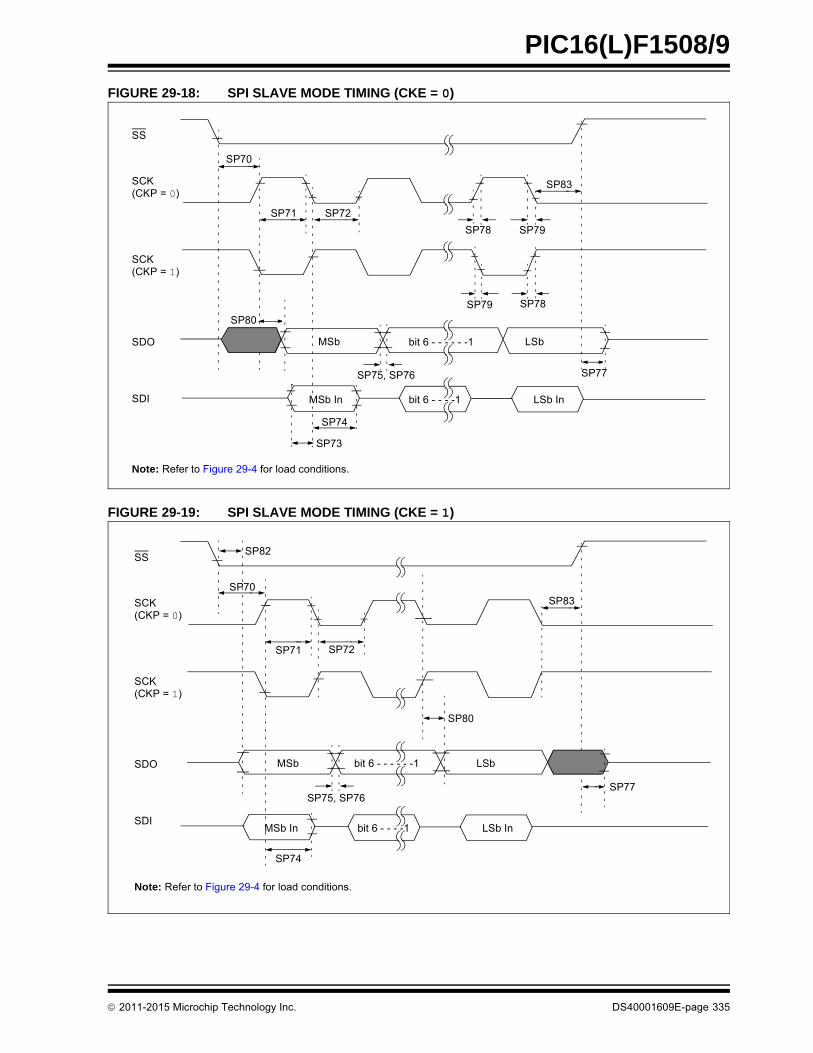
PIC16(L)F1508/9
FIGURE 29-18: SPI SLAVE MODE TIMING (CKE = 0)
FIGURE 29-19: SPI SLAVE MODE TIMING (CKE = 1)
SS
SCK(CKP = 0)
SCK(CKP = 1)
SDO
SDI
SP70
SP71 SP72
SP73
SP74
SP75, SP76 SP77
SP78SP79
SP80
SP79SP78
MSb LSbbit 6 - - - - - -1
MSb In bit 6 - - - -1 LSb In
SP83
Note: Refer to Figure 29-4 for load conditions.
SS
SCK(CKP = 0)
SCK(CKP = 1)
SDO
SDI
SP70
SP71 SP72
SP82
SP74
SP75, SP76
MSb bit 6 - - - - - -1 LSb
SP77
MSb In bit 6 - - - -1 LSb In
SP80
SP83
Note: Refer to Figure 29-4 for load conditions.
2011-2015 Microchip Technology Inc. DS40001609E-page 335

PIC16(L)F1508/9
TABLE 29-19: SPI MODE REQUIREMENTS
Standard Operating Conditions (unless otherwise stated)
Param. No.
Symbol Characteristic Min. Typ† Max. Units Conditions
SP70* TSSL2SCH, TSSL2SCL
SS to SCK or SCK input 2.25 TCY — — ns
SP71* TSCH SCK input high time (Slave mode) 1 TCY + 20 — — ns
SP72* TSCL SCK input low time (Slave mode) 1 TCY + 20 — — ns
SP73* TDIV2SCH, TDIV2SCL
Setup time of SDI data input to SCK edge
100 — — ns
SP74* TSCH2DIL, TSCL2DIL
Hold time of SDI data input to SCK edge
100 — — ns
SP75* TDOR SDO data output rise time — 10 25 ns 3.0V VDD 5.5V
— 25 50 ns 1.8V VDD 5.5V
SP76* TDOF SDO data output fall time — 10 25 ns
SP77* TSSH2DOZ SS to SDO output high-impedance 10 — 50 ns
SP78* TSCR SCK output rise time (Master mode)
— 10 25 ns 3.0V VDD 5.5V
— 25 50 ns 1.8V VDD 5.5V
SP79* TSCF SCK output fall time (Master mode) — 10 25 ns
SP80* TSCH2DOV,TSCL2DOV
SDO data output valid after SCK edge
— — 50 ns 3.0V VDD 5.5V
— — 145 ns 1.8V VDD 5.5V
SP81* TDOV2SCH,TDOV2SCL
SDO data output setup to SCK edge 1 Tcy — — ns
SP82* TSSL2DOV SDO data output valid after SS edge
— — 50 ns
SP83* TSCH2SSH,TSCL2SSH
SS after SCK edge 1.5 TCY + 40 — — ns
* These parameters are characterized but not tested.
† Data in “Typ” column is at 3.0V, 25°C unless otherwise stated. These parameters are for design guidance only and are not tested.
DS40001609E-page 336 2011-2015 Microchip Technology Inc.

PIC16(L)F1508/9
FIGURE 29-20: I2C BUS START/STOP BITS TIMING
TABLE 29-20: I2C BUS START/STOP BITS REQUIREMENTS
FIGURE 29-21: I2C BUS DATA TIMING
Standard Operating Conditions (unless otherwise stated)
Param.No.
Symbol Characteristic Min. Typ Max. Units Conditions
SP90* TSU:STA Start condition 100 kHz mode 4700 — — ns Only relevant for Repeated Start conditionSetup time 400 kHz mode 600 — —
SP91* THD:STA Start condition 100 kHz mode 4000 — — ns After this period, the first clock pulse is generatedHold time 400 kHz mode 600 — —
SP92* TSU:STO Stop condition 100 kHz mode 4700 — — ns
Setup time 400 kHz mode 600 — —
SP93 THD:STO Stop condition 100 kHz mode 4000 — — ns
Hold time 400 kHz mode 600 — —
* These parameters are characterized but not tested.
Note: Refer to Figure 29-4 for load conditions.
SP91
SP92
SP93SCL
SDA
StartCondition
StopCondition
SP90
Note: Refer to Figure 29-4 for load conditions.
SP90
SP91 SP92
SP100SP101
SP103
SP106SP107
SP109SP109
SP110
SP102
SCL
SDAIn
SDAOut
2011-2015 Microchip Technology Inc. DS40001609E-page 337

PIC16(L)F1508/9
TABLE 29-21: I2C BUS DATA REQUIREMENTS
Standard Operating Conditions (unless otherwise stated)
Param.No.
Symbol Characteristic Min. Max. Units Conditions
SP100* THIGH Clock high time 100 kHz mode 4.0 — s Device must operate at a minimum of 1.5 MHz
400 kHz mode 0.6 — s Device must operate at a minimum of 10 MHz
SSP module 1.5TCY —
SP101* TLOW Clock low time 100 kHz mode 4.7 — s Device must operate at a minimum of 1.5 MHz
400 kHz mode 1.3 — s Device must operate at a minimum of 10 MHz
SSP module 1.5TCY —
SP102* TR SDA and SCL rise time
100 kHz mode — 1000 ns
400 kHz mode 20 + 0.1CB 300 ns CB is specified to be from 10-400 pF
SP103* TF SDA and SCL fall time
100 kHz mode — 250 ns
400 kHz mode 20 + 0.1CB 250 ns CB is specified to be from 10-400 pF
SP106* THD:DAT Data input hold time 100 kHz mode 0 — ns
400 kHz mode 0 0.9 s
SP107* TSU:DAT Data input setup time
100 kHz mode 250 — ns (Note 2)
400 kHz mode 100 — ns
SP109* TAA Output valid from clock
100 kHz mode — 3500 ns (Note 1)
400 kHz mode — — ns
SP110* TBUF Bus free time 100 kHz mode 4.7 — s Time the bus must be free before a new transmission can start
400 kHz mode 1.3 — s
SP111 CB Bus capacitive loading — 400 pF
* These parameters are characterized but not tested.
Note 1: As a transmitter, the device must provide this internal minimum delay time to bridge the undefined region (min. 300 ns) of the falling edge of SCL to avoid unintended generation of Start or Stop conditions.
2: A Fast mode (400 kHz) I2C bus device can be used in a Standard mode (100 kHz) I2C bus system, but the requirement TSU:DAT 250 ns must then be met. This will automatically be the case if the device does not stretch the low period of the SCL signal. If such a device does stretch the low period of the SCL signal, it must output the next data bit to the SDA line TR max. + TSU:DAT = 1000 + 250 = 1250 ns (according to the Standard mode I2C bus specification), before the SCL line is released.
DS40001609E-page 338 2011-2015 Microchip Technology Inc.

PIC16(L)F1508/9
30.0 DC AND AC CHARACTERISTICS GRAPHS AND CHARTS
The graphs and tables provided in this section are for design guidance and are not tested.
In some graphs or tables, the data presented are outside specified operating range (i.e., outside specified VDD
range). This is for information only and devices are ensured to operate properly only within the specified range.
“Typical” represents the mean of the distribution at 25C. “MAXIMUM”, “Max.”, “MINIMUM” or “Min.”represents (mean + 3) or (mean - 3) respectively, where is a standard deviation, over eachtemperature range.
Note: The graphs and tables provided following this note are a statistical summary based on a limited number ofsamples and are provided for informational purposes only. The performance characteristics listed hereinare not tested or guaranteed. In some graphs or tables, the data presented may be outside the specifiedoperating range (e.g., outside specified power supply range) and therefore, outside the warranted range.
2011-2015 Microchip Technology Inc. DS40001609E-page 339

PIC16(L)F1508/9
FIGURE 30-1: IDD, LP OSCILLATOR, FOSC = 32 kHz, PIC16LF1508/9 ONLY
FIGURE 30-2: IDD, LP OSCILLATOR, FOSC = 32 kHz, PIC16F1508/9 ONLY
Typical
Max.
0
2
4
6
8
10
12
14
16
18
1.6 1.8 2.0 2.2 2.4 2.6 2.8 3.0 3.2 3.4 3.6 3.8
IDD
(µA
)
VDD (V)
Max: 85°C + 3Typical: 25°C
Typical
Max.
0
5
10
15
20
25
30
2.0 2.5 3.0 3.5 4.0 4.5 5.0 5.5 6.0
IDD
(µA
)
VDD (V)
Max: 85°C + 3Typical: 25°C
DS40001609E-page 340 2011-2015 Microchip Technology Inc.

PIC16(L)F1508/9
FIGURE 30-3: IDD TYPICAL, XT AND EXTRC OSCILLATOR, PIC16LF1508/9 ONLY
FIGURE 30-4: IDD MAXIMUM, XT AND EXTRC OSCILLATOR, PIC16LF1508/9 ONLY
4 MHz EXTRC
4 MHz XT
1 MHz EXTRC
1 MHz XT
0
50
100
150
200
250
300
350
1.6 1.8 2.0 2.2 2.4 2.6 2.8 3.0 3.2 3.4 3.6 3.8
IDD
(µA
)
VDD (V)
Typical: 25°C
4 MHz EXTRC
4 MHz XT
1 MHz EXTRC
1 MHz XT
0
50
100
150
200
250
300
350
400
1.6 1.8 2.0 2.2 2.4 2.6 2.8 3.0 3.2 3.4 3.6 3.8
IDD
(µA
)
VDD (V)
Max: 85°C + 3
2011-2015 Microchip Technology Inc. DS40001609E-page 341

PIC16(L)F1508/9
FIGURE 30-5: IDD TYPICAL, XT AND EXTRC OSCILLATOR, PIC16F1508/9 ONLY
FIGURE 30-6: IDD MAXIMUM, XT AND EXTRC OSCILLATOR, PIC16F1508/9 ONLY
4 MHz EXTRC
4 MHz XT
1 MHz EXTRC
1 MHz XT
0
50
100
150
200
250
300
350
400
2.0 2.5 3.0 3.5 4.0 4.5 5.0 5.5 6.0
IDD
(µA
)
VDD (V)
Typical: 25°C
4 MHz EXTRC
4 MHz XT
1 MHz EXTRC
1 MHz XT
0
50
100
150
200
250
300
350
400
450
500
2.0 2.5 3.0 3.5 4.0 4.5 5.0 5.5 6.0
IDD
(µA
)
VDD (V)
Max: 85°C + 3
DS40001609E-page 342 2011-2015 Microchip Technology Inc.

PIC16(L)F1508/9
FIGURE 30-7: IDD, EXTERNAL CLOCK (ECL), LOW-POWER MODE, FOSC = 32 kHz, PIC16LF1508/9 ONLY
FIGURE 30-8: IDD, EXTERNAL CLOCK (ECL), LOW-POWER MODE, FOSC = 32 kHz, PIC16F1508/9 ONLY
Typical
Max.
0
2
4
6
8
10
12
14
1.6 1.8 2.0 2.2 2.4 2.6 2.8 3.0 3.2 3.4 3.6 3.8
IDD
(µA
)
VDD (V)
Max: 85°C + 3Typical: 25°C
Typical
Max.
0
5
10
15
20
25
2.0 2.5 3.0 3.5 4.0 4.5 5.0 5.5 6.0
IDD
(µA
)
VDD (V)
Max: 85°C + 3Typical: 25°C
2011-2015 Microchip Technology Inc. DS40001609E-page 343

PIC16(L)F1508/9
FIGURE 30-9: IDD, EXTERNAL CLOCK (ECL), LOW-POWER MODE, FOSC = 500 kHz, PIC16LF1508/9 ONLY
FIGURE 30-10: IDD, EXTERNAL CLOCK (ECL), LOW-POWER MODE, FOSC = 500 kHz, PIC16F1508/9 ONLY
Max.
Typical
0
5
10
15
20
25
30
35
40
45
50
1.6 1.8 2.0 2.2 2.4 2.6 2.8 3.0 3.2 3.4 3.6 3.8
IDD
(µA
)
VDD (V)
Max: 85°C + 3Typical: 25°C
Typical
Max.
0
10
20
30
40
50
60
2.0 2.5 3.0 3.5 4.0 4.5 5.0 5.5 6.0
IDD
(µA
)
VDD (V)
Max: 85°C + 3Typical: 25°C
DS40001609E-page 344 2011-2015 Microchip Technology Inc.

PIC16(L)F1508/9
FIGURE 30-11: IDD TYPICAL, EXTERNAL CLOCK (ECM), MEDIUM POWER MODE, PIC16LF1508/9 ONLY
FIGURE 30-12: IDD MAXIMUM, EXTERNAL CLOCK (ECM), MEDIUM POWER MODE, PIC16LF1508/9 ONLY
4 MHz
1 MHz
0
50
100
150
200
250
300
1.6 1.8 2.0 2.2 2.4 2.6 2.8 3.0 3.2 3.4 3.6 3.8
IDD
(µA
)
VDD (V)
Typical: 25°C
4 MHz
1 MHz
0
50
100
150
200
250
300
350
1.6 1.8 2.0 2.2 2.4 2.6 2.8 3.0 3.2 3.4 3.6 3.8
IDD
(µA
)
VDD (V)
Max: 85°C + 3
2011-2015 Microchip Technology Inc. DS40001609E-page 345

PIC16(L)F1508/9
FIGURE 30-13: IDD TYPICAL, EXTERNAL CLOCK (ECM), MEDIUM POWER MODE, PIC16F1508/9 ONLY
FIGURE 30-14: IDD MAXIMUM, EXTERNAL CLOCK (ECM), MEDIUM POWER MODE, PIC16F1508/9 ONLY
4 MHz
1 MHz
0
50
100
150
200
250
300
350
2.0 2.5 3.0 3.5 4.0 4.5 5.0 5.5 6.0
IDD
(µA
)
VDD (V)
Typical: 25°C
4 MHz
1 MHz
0
50
100
150
200
250
300
350
400
2.0 2.5 3.0 3.5 4.0 4.5 5.0 5.5 6.0
IDD
(µA
)
VDD (V)
Max: 85°C + 3
DS40001609E-page 346 2011-2015 Microchip Technology Inc.

PIC16(L)F1508/9
FIGURE 30-15: IDD TYPICAL, EXTERNAL CLOCK (ECH), HIGH-POWER MODE, PIC16LF1508/9 ONLY
FIGURE 30-16: IDD MAXIMUM, EXTERNAL CLOCK (ECH), HIGH-POWER MODE, PIC16LF1508/9 ONLY
20 MHz
16 MHz
8 MHz
0.0
0.2
0.4
0.6
0.8
1.0
1.2
1.4
1.6 1.8 2.0 2.2 2.4 2.6 2.8 3.0 3.2 3.4 3.6 3.8
IDD
(mA
)
VDD (V)
Typical: 25°C
( )
20 MHz
16 MHz
8 MHz
0.0
0.2
0.4
0.6
0.8
1.0
1.2
1.4
1.6
1.6 1.8 2.0 2.2 2.4 2.6 2.8 3.0 3.2 3.4 3.6 3.8
IDD
(mA
)
VDD (V)
Max: 85°C + 3
2011-2015 Microchip Technology Inc. DS40001609E-page 347

PIC16(L)F1508/9
FIGURE 30-17: IDD TYPICAL, EXTERNAL CLOCK (ECH), HIGH-POWER MODE, PIC16F1508/9 ONLY
FIGURE 30-18: IDD MAXIMUM, EXTERNAL CLOCK (ECH), HIGH-POWER MODE, PIC16F1508/9 ONLY
20 MHz
16 MHz
8 MHz
0.0
0.2
0.4
0.6
0.8
1.0
1.2
1.4
2.0 2.5 3.0 3.5 4.0 4.5 5.0 5.5 6.0
IDD
(mA
)
VDD (V)
Typical: 25°C
20 MHz
16 MHz
8 MHz
0.0
0.2
0.4
0.6
0.8
1.0
1.2
1.4
1.6
2.0 2.5 3.0 3.5 4.0 4.5 5.0 5.5 6.0
IDD
(mA
)
VDD (V)
Max: 85°C + 3
DS40001609E-page 348 2011-2015 Microchip Technology Inc.

PIC16(L)F1508/9
FIGURE 30-19: IDD, LFINTOSC, FOSC = 31 kHz, PIC16LF1508/9 ONLY
FIGURE 30-20: IDD, LFINTOSC, FOSC = 31 kHz, PIC16F1508/9 ONLY
Typical
Max.
0
2
4
6
8
10
12
1.6 1.8 2.0 2.2 2.4 2.6 2.8 3.0 3.2 3.4 3.6 3.8
IDD
(µA
)
VDD (V)
Max: 85°C + 3Typical: 25°C
Typical
Max.
0
5
10
15
20
25
2.0 2.5 3.0 3.5 4.0 4.5 5.0 5.5 6.0
IDD
(µA
)
VDD (V)
Max: 85°C + 3Typical: 25°C
2011-2015 Microchip Technology Inc. DS40001609E-page 349

PIC16(L)F1508/9
FIGURE 30-21: IDD, MFINTOSC, FOSC = 500 kHz, PIC16LF1508/9 ONLY
FIGURE 30-22: IDD, MFINTOSC, FOSC = 500 kHz, PIC16F1508/9 ONLY
Typical
Max.
0
50
100
150
200
250
300
350
400
1.6 1.8 2.0 2.2 2.4 2.6 2.8 3.0 3.2 3.4 3.6 3.8
IDD
(µA
)
VDD (V)
Max: 85°C + 3Typical: 25°C
Typical
Max.
0
50
100
150
200
250
300
350
400
450
2.0 2.5 3.0 3.5 4.0 4.5 5.0 5.5 6.0
IDD
(µA
)
VDD (V)
Max: 85°C + 3Typical: 25°C
DS40001609E-page 350 2011-2015 Microchip Technology Inc.

PIC16(L)F1508/9
FIGURE 30-23: IDD TYPICAL, HFINTOSC, PIC16LF1508/9 ONLY
FIGURE 30-24: IDD MAXIMUM, HFINTOSC, PIC16LF1508/9 ONLY
16 MHz
8 MHz
4 MHz
0.0
0.2
0.4
0.6
0.8
1.0
1.2
1.4
1.6 1.8 2.0 2.2 2.4 2.6 2.8 3.0 3.2 3.4 3.6 3.8
IDD
(mA
)
VDD (V)
Typical: 25°C
16 MHz
8 MHz
4 MHz
0.0
0.2
0.4
0.6
0.8
1.0
1.2
1.4
1.6
1.6 1.8 2.0 2.2 2.4 2.6 2.8 3.0 3.2 3.4 3.6 3.8
IDD
(mA
)
VDD (V)
Max: 85°C + 3
2011-2015 Microchip Technology Inc. DS40001609E-page 351

PIC16(L)F1508/9
FIGURE 30-25: IDD TYPICAL, HFINTOSC, PIC16F1508/9 ONLY
FIGURE 30-26: IDD MAXIMUM, HFINTOSC, PIC16F1508/9 ONLY
16 MHz
8 MHz
4 MHz
0.0
0.2
0.4
0.6
0.8
1.0
1.2
2.0 2.5 3.0 3.5 4.0 4.5 5.0 5.5 6.0
IDD
(mA
)
VDD (V)
Typical: 25°C
16 MHz
8 MHz
4 MHz
0.0
0.2
0.4
0.6
0.8
1.0
1.2
1.4
2.0 2.5 3.0 3.5 4.0 4.5 5.0 5.5 6.0
IDD
(mA
)
VDD (V)
Max: 85°C + 3
DS40001609E-page 352 2011-2015 Microchip Technology Inc.

PIC16(L)F1508/9
FIGURE 30-27: IDD TYPICAL, HS OSCILLATOR, PIC16LF1508/9 ONLY
FIGURE 30-28: IDD MAXIMUM, HS OSCILLATOR, PIC16LF1508/9 ONLY
20 MHz
8 MHz
4 MHz
0.0
0.2
0.4
0.6
0.8
1.0
1.2
1.4
1.6
1.6 1.8 2.0 2.2 2.4 2.6 2.8 3.0 3.2 3.4 3.6 3.8
IDD
(mA
)
VDD (V)
Typical: 25°C
,
20 MHz
8 MHz
4 MHz
0.0
0.2
0.4
0.6
0.8
1.0
1.2
1.4
1.6
1.8
1.6 1.8 2.0 2.2 2.4 2.6 2.8 3.0 3.2 3.4 3.6 3.8
IDD
(mA
)
VDD (V)
Max: 85°C + 3
2011-2015 Microchip Technology Inc. DS40001609E-page 353

PIC16(L)F1508/9
FIGURE 30-29: IDD TYPICAL, HS OSCILLATOR, PIC16F1508/9 ONLY
FIGURE 30-30: IDD MAXIMUM, HS OSCILLATOR, PIC16F1508/9 ONLY
20 MHz
8 MHz
4 MHz
0.0
0.2
0.4
0.6
0.8
1.0
1.2
1.4
1.6
1.8
2.0 2.5 3.0 3.5 4.0 4.5 5.0 5.5 6.0
IDD
(mA
)
VDD (V)
Typical: 25°C
,
20 MHz
8 MHz
4 MHz
0.0
0.5
1.0
1.5
2.0
2.5
2.0 2.5 3.0 3.5 4.0 4.5 5.0 5.5 6.0
IDD
(mA
)
VDD (V)
Max: 85°C + 3
DS40001609E-page 354 2011-2015 Microchip Technology Inc.

PIC16(L)F1508/9
FIGURE 30-31: IPD BASE, LOW-POWER SLEEP MODE, PIC16LF1508/9 ONLY
FIGURE 30-32: IPD BASE, LOW-POWER SLEEP MODE, VREGPM = 1, PIC16F1508/9 ONLY
450
M 85°C 3Max.
250
300
350
400
450D
(nA)
Max: 85°C + 3Typical: 25°C
Typical
0
50
100
150
200
250
1.6 1.8 2.0 2.2 2.4 2.6 2.8 3.0 3.2 3.4 3.6 3.8
IPD
(nA)
01.6 1.8 2.0 2.2 2.4 2.6 2.8 3.0 3.2 3.4 3.6 3.8
VDD (V)
Max.600
Max.
300
400
500
600
PD(n
A)
Max: 85°C + 3Typical: 25°C
Typical
0
100
200
300
2.0 2.5 3.0 3.5 4.0 4.5 5.0 5.5 6.0
IPD
(nA)
02.0 2.5 3.0 3.5 4.0 4.5 5.0 5.5 6.0
VDD (V)
2011-2015 Microchip Technology Inc. DS40001609E-page 355
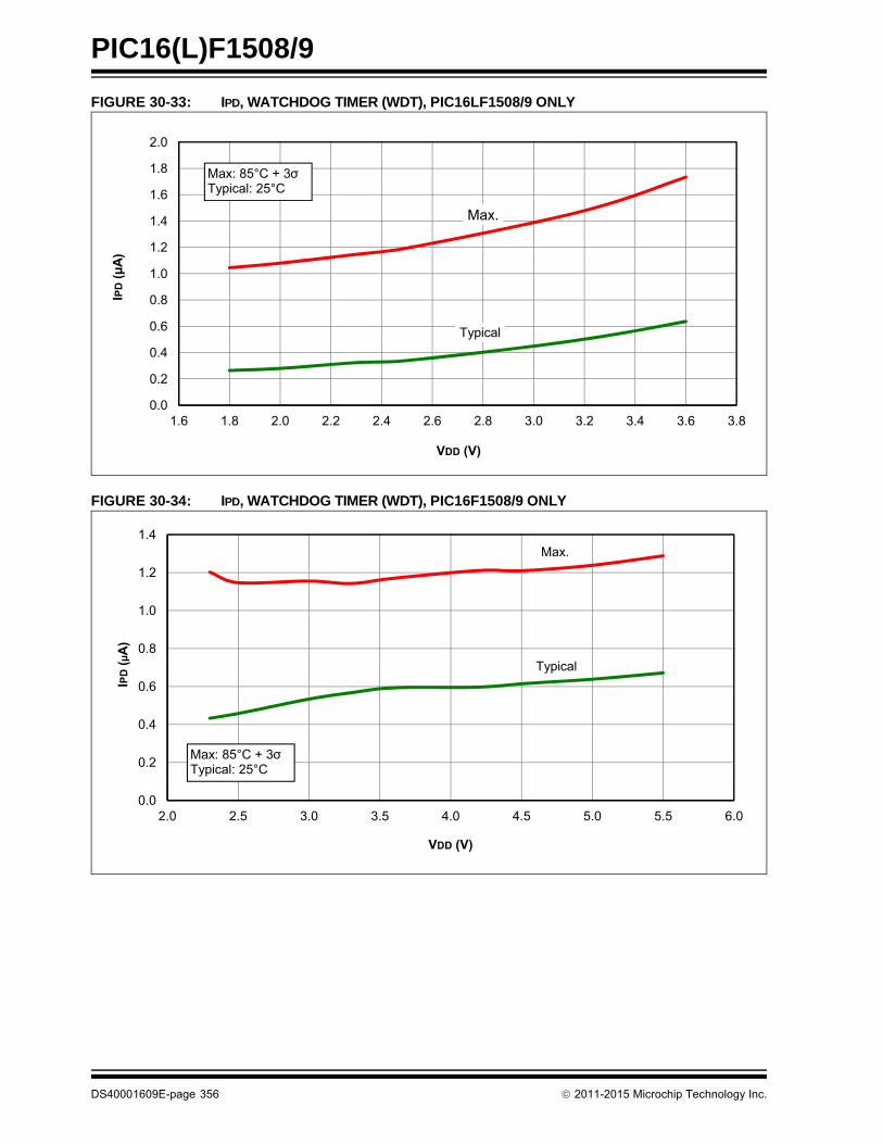
PIC16(L)F1508/9
FIGURE 30-33: IPD, WATCHDOG TIMER (WDT), PIC16LF1508/9 ONLY
FIGURE 30-34: IPD, WATCHDOG TIMER (WDT), PIC16F1508/9 ONLY
2.0
Max.
0 8
1.0
1.2
1.4
1.6
1.8
2.0
IPD
(µA)
Max: 85°C + 3Typical: 25°C
Typical
0.0
0.2
0.4
0.6
0.8
1.0
1.6 1.8 2.0 2.2 2.4 2.6 2.8 3.0 3.2 3.4 3.6 3.8
IPD
(µA
0.0
0.2
1.6 1.8 2.0 2.2 2.4 2.6 2.8 3.0 3.2 3.4 3.6 3.8
VDD (V)
Max1.4
Typical
Max.
0.6
0.8
1.0
1.2
1.4
IPD
(µA)
Typical
0.0
0.2
0.4
0.6
2.0 2.5 3.0 3.5 4.0 4.5 5.0 5.5 6.0
IPD
(µA
Max: 85°C + 3Typical: 25°C
0.02.0 2.5 3.0 3.5 4.0 4.5 5.0 5.5 6.0
VDD (V)
DS40001609E-page 356 2011-2015 Microchip Technology Inc.

PIC16(L)F1508/9
FIGURE 30-35: IPD, FIXED VOLTAGE REFERENCE (FVR), PIC16LF1508/9 ONLY
FIGURE 30-36: IPD, FIXED VOLTAGE REFERENCE (FVR), PIC16F1508/9 ONLY
45
Max: 85°C + 3
Typical
Max.
20
25
30
35
40
45IP
D(µ
A)Max: 85°C + 3Typical: 25°C
0
5
10
15
20
1.6 1.8 2.0 2.2 2.4 2.6 2.8 3.0 3.2 3.4 3.6 3.8
IPD
(µA
01.6 1.8 2.0 2.2 2.4 2.6 2.8 3.0 3.2 3.4 3.6 3.8
VDD (V)
30
Typical
Max.
15
20
25
30
IPD
(µA)
0
5
10
15
2.0 2.5 3.0 3.5 4.0 4.5 5.0 5.5 6.0
IPD
(µ
Max: 85°C + 3Typical: 25°C
02.0 2.5 3.0 3.5 4.0 4.5 5.0 5.5 6.0
VDD (V)
2011-2015 Microchip Technology Inc. DS40001609E-page 357

PIC16(L)F1508/9
FIGURE 30-37: IPD, BROWN-OUT RESET (BOR), BORV = 0, PIC16LF1508/9 ONLY
FIGURE 30-38: IPD, BROWN-OUT RESET (BOR), BORV = 1, PIC16LF1508/9 ONLY
Max.10
Typical
Max.
4
5
6
7
8
9
10D
(µA)
Max: 85°C + 3Typical: 25°C
0
1
2
3
4
5
1 6 1 8 2 0 2 2 2 4 2 6 2 8 3 0 3 2 3 4 3 6 3 8
IPD
(µA)
0
1
1.6 1.8 2.0 2.2 2.4 2.6 2.8 3.0 3.2 3.4 3.6 3.8
VDD (V)
12
Typical
Max.
6
8
10
12
µA)
Max: 85°C + 3Typical: 25°C
Typical
0
2
4
6
1.6 1.8 2.0 2.2 2.4 2.6 2.8 3.0 3.2 3.4 3.6 3.8
IPD
(µA)
01.6 1.8 2.0 2.2 2.4 2.6 2.8 3.0 3.2 3.4 3.6 3.8
VDD (V)
DS40001609E-page 358 2011-2015 Microchip Technology Inc.

PIC16(L)F1508/9
FIGURE 30-39: IPD, BROWN-OUT RESET (BOR), BORV = 0, PIC16F1508/9 ONLY
FIGURE 30-40: IPD, BROWN-OUT RESET (BOR), BORV = 1, PIC16F1508/9 ONLY
M
12
Typical
Max.
6
8
10
12IP
D(µ
A)
Max: 85°C + 3Typical: 25°C
0
2
4
6
2.0 2.5 3.0 3.5 4.0 4.5 5.0 5.5 6.0
IPD
(µA)
02.0 2.5 3.0 3.5 4.0 4.5 5.0 5.5 6.0
VDD (V)
Max
14
Typical
Max.
6
8
10
12
14
IPD
(µA)
Max: 85°C + 3Typical: 25°C
0
2
4
6
2.0 2.5 3.0 3.5 4.0 4.5 5.0 5.5 6.0
IPD
(µA)
02.0 2.5 3.0 3.5 4.0 4.5 5.0 5.5 6.0
VDD (V)
2011-2015 Microchip Technology Inc. DS40001609E-page 359

PIC16(L)F1508/9
FIGURE 30-41: IPD, SECONDARY OSCILLATOR, FOSC = 32 kHz, PIC16LF1508/9 ONLY
FIGURE 30-42: IPD, SECONDARY OSCILLATOR, FOSC = 32 kHz, PIC16F1508/9 ONLY
8.0
Max: 85°C + 3
Max.
3 0
4.0
5.0
6.0
7.0
8.0IP
D(µ
A)
Max: 85°C + 3Typical: 25°C
Typical
0.0
1.0
2.0
3.0
4.0
1.6 1.8 2.0 2.2 2.4 2.6 2.8 3.0 3.2 3.4 3.6 3.8
IPD
(µA
0.01.6 1.8 2.0 2.2 2.4 2.6 2.8 3.0 3.2 3.4 3.6 3.8
VDD (V)
16
Max: 85°C + 3
Typical
Max.
6
8
10
12
14
16
IPD
(µA)
Max: 85°C + 3Typical: 25°C
Typical
0
2
4
6
8
2.0 2.5 3.0 3.5 4.0 4.5 5.0 5.5 6.0
IPD
(µ
02.0 2.5 3.0 3.5 4.0 4.5 5.0 5.5 6.0
VDD (V)
DS40001609E-page 360 2011-2015 Microchip Technology Inc.

PIC16(L)F1508/9
FIGURE 30-43: IPD, COMPARATOR, LOW-POWER MODE (CxSP = 0), PIC16LF1508/9 ONLY
FIGURE 30-44: IPD, COMPARATOR, LOW-POWER MODE (CxSP = 0), PIC16F1508/9 ONLY
14
Typical
Max.
6
8
10
12
14IP
D(µ
A)
Typical
0
2
4
6
1.6 1.8 2.0 2.2 2.4 2.6 2.8 3.0 3.2 3.4 3.6 3.8
IPD
Max: 85°C + 3Typical: 25°C
01.6 1.8 2.0 2.2 2.4 2.6 2.8 3.0 3.2 3.4 3.6 3.8
VDD (V)
30
Typical
Max.
15
20
25
30
IPD
(µA) yp
0
5
10
15
2.0 2.5 3.0 3.5 4.0 4.5 5.0 5.5 6.0
IPD
(µ
Max: 85°C + 3Typical: 25°C
02.0 2.5 3.0 3.5 4.0 4.5 5.0 5.5 6.0
VDD (V)
2011-2015 Microchip Technology Inc. DS40001609E-page 361

PIC16(L)F1508/9
FIGURE 30-45: IPD, COMPARATOR, NORMAL POWER MODE (CxSP = 1), PIC16LF1508/9 ONLY
FIGURE 30-46: IPD, COMPARATOR, NORMAL POWER MODE (CxSP = 1), PIC16F1508/9 ONLY
40
Typical
Max.
15
20
25
30
35
40IP
D(µ
A)
Typical
0
5
10
15
20
1.6 1.8 2.0 2.2 2.4 2.6 2.8 3.0 3.2 3.4 3.6 3.8
IPD
(µA
Max: 85°C + 3Typical: 25°C
01.6 1.8 2.0 2.2 2.4 2.6 2.8 3.0 3.2 3.4 3.6 3.8
VDD (V)
Typical: 25 C
60
Typical
Max.
30
40
50
60
IPD
(µA)
Typical
0
10
20
30
2.0 2.5 3.0 3.5 4.0 4.5 5.0 5.5 6.0
IPD
(µA
Max: 85°C + 3Typical: 25°C
02.0 2.5 3.0 3.5 4.0 4.5 5.0 5.5 6.0
VDD (V)
DS40001609E-page 362 2011-2015 Microchip Technology Inc.

PIC16(L)F1508/9
FIGURE 30-47: VOH vs. IOH OVER TEMPERATURE, VDD = 5.5V, PIC16F1508/9 ONLY
FIGURE 30-48: VOL vs. IOL OVER TEMPERATURE, VDD = 5.5V, PIC16F1508/9 ONLY
Min. (-40°C)
Typical (25°C)
Max. (125°C)
0
1
2
3
4
5
6
-45 -40 -35 -30 -25 -20 -15 -10 -5 0
VOH
(V)
IOH (mA)
Max: 125°C + 3Typical: 25°CMin: -40°C - 3
Min. (-40°C)
Typical (25°C)
Max. (125°C)
0
1
2
3
4
5
0 10 20 30 40 50 60 70 80 90 100
VOL
(V)
IOL (mA)
Max: 125°C + 3Typical: 25°CMin: -40°C - 3
2011-2015 Microchip Technology Inc. DS40001609E-page 363

PIC16(L)F1508/9
FIGURE 30-49: VOH vs. IOH OVER TEMPERATURE, VDD = 3.0V
FIGURE 30-50: VOL vs. IOL OVER TEMPERATURE, VDD = 3.0V
Min. (-40°C) Typical (25°C) Max. (125°C)
0.0
0.5
1.0
1.5
2.0
2.5
3.0
3.5
-15 -13 -11 -9 -7 -5 -3 -1
VOH
(V)
IOH (mA)
Max: 125°C + 3Typical: 25°CMin: -40°C - 3
Min. (-40°C)Typical (25°C)Max. (125°C)
0.0
0.5
1.0
1.5
2.0
2.5
3.0
0 5 10 15 20 25 30 35 40
VOL
(V)
IOL (mA)
Max: 125°C + 3Typical: 25°CMin: -40°C - 3
DS40001609E-page 364 2011-2015 Microchip Technology Inc.

PIC16(L)F1508/9
FIGURE 30-51: VOH vs. IOH OVER TEMPERATURE, VDD = 1.8V, PIC16LF1508/9 ONLY
FIGURE 30-52: VOL vs. IOL OVER TEMPERATURE, VDD = 1.8V, PIC16LF1508/9 ONLY
Min. (-40°C) Typical (25°C) Max. (125°C)
0.0
0.2
0.4
0.6
0.8
1.0
1.2
1.4
1.6
1.8
2.0
-4.5 -4.0 -3.5 -3.0 -2.5 -2.0 -1.5 -1.0 -0.5 0.0
VOH
(V)
IOH (mA)
Max: 125°C + 3Typical: 25°CMin: -40°C - 3
Min. (-40°C)Typical (25°C)Max. (125°C)
0.0
0.2
0.4
0.6
0.8
1.0
1.2
1.4
1.6
1.8
0 1 2 3 4 5 6 7 8 9 10
VOL
(V)
IOL (mA)
Max: 125°C + 3Typical: 25°CMin: -40°C - 3
2011-2015 Microchip Technology Inc. DS40001609E-page 365

PIC16(L)F1508/9
FIGURE 30-53: POR RELEASE VOLTAGE
FIGURE 30-54: POR REARM VOLTAGE, PIC16F1508/9 ONLY
Typical
Max.
Min.
1.50
1.52
1.54
1.56
1.58
1.60
1.62
1.64
1.66
1.68
1.70
-60 -40 -20 0 20 40 60 80 100 120 140
Volta
ge (V
)
Temperature (°C)
Max: Typical + 3Typical: 25°C Min: Typical - 3
Typical
Max.
Min.
1.34
1.36
1.38
1.40
1.42
1.44
1.46
1.48
1.50
1.52
1.54
-60 -40 -20 0 20 40 60 80 100 120 140
Volta
ge (V
)
Temperature (°C)
Max: Typical + 3Typical: 25°C Min: Typical - 3
DS40001609E-page 366 2011-2015 Microchip Technology Inc.

PIC16(L)F1508/9
FIGURE 30-55: BROWN-OUT RESET VOLTAGE, BORV = 1, PIC16LF1508/9 ONLY
FIGURE 30-56: BROWN-OUT RESET HYSTERESIS, BORV = 1, PIC16LF1508/9 ONLY
Typical
Max.
Min.
1.80
1.85
1.90
1.95
2.00
-60 -40 -20 0 20 40 60 80 100 120 140
Volta
ge (V
)
Temperature (°C)
Max: Typical + 3Min: Typical - 3
Typical
Max.
Min.
0
10
20
30
40
50
60
-60 -40 -20 0 20 40 60 80 100 120 140
Volta
ge (m
V)
Temperature (°C)
Max: Typical + 3Typical: 25°C Min: Typical - 3
2011-2015 Microchip Technology Inc. DS40001609E-page 367

PIC16(L)F1508/9
FIGURE 30-57: BROWN-OUT RESET VOLTAGE, BORV = 1, PIC16F1508/9 ONLY
FIGURE 30-58: BROWN-OUT RESET HYSTERESIS, BORV = 1, PIC16F1508/9 ONLY
Typical
Max.
Min.
2.30
2.35
2.40
2.45
2.50
2.55
2.60
-60 -40 -20 0 20 40 60 80 100 120 140
Volta
ge (V
)
Temperature (°C)
Max: Typical + 3Min: Typical - 3
Typical
Max.
Min.
0
10
20
30
40
50
60
70
-60 -40 -20 0 20 40 60 80 100 120 140
Volta
ge (m
V)
Temperature (°C)
Max: Typical + 3Typical: 25°C Min: Typical - 3
DS40001609E-page 368 2011-2015 Microchip Technology Inc.

PIC16(L)F1508/9
FIGURE 30-59: BROWN-OUT RESET VOLTAGE, BORV = 0
Typical
Max.
Min.
2.55
2.60
2.65
2.70
2.75
2.80
-60 -40 -20 0 20 40 60 80 100 120 140
Volta
ge (V
)
Temperature (°C)
Max: Typical + 3Min: Typical - 3
2011-2015 Microchip Technology Inc. DS40001609E-page 369

PIC16(L)F1508/9
FIGURE 30-60: LOW-POWER BROWN-OUT RESET VOLTAGE, LPBOR = 0
FIGURE 30-61: LOW-POWER BROWN-OUT RESET HYSTERESIS, LPBOR = 0
Typical
Max.
Min.
1.80
1.90
2.00
2.10
2.20
2.30
2.40
2.50
-60 -40 -20 0 20 40 60 80 100 120 140
Volta
ge (V
)
Temperature (°C)
Max: Typical + 3Min: Typical - 3
Typical
Max.
Min.
0
5
10
15
20
25
30
35
40
45
-60 -40 -20 0 20 40 60 80 100 120 140
Volta
ge (m
V)
Temperature (°C)
Max: Typical + 3Typical: 25°C Min: Typical - 3
DS40001609E-page 370 2011-2015 Microchip Technology Inc.

PIC16(L)F1508/9
FIGURE 30-62: WDT TIME-OUT PERIOD
FIGURE 30-63: PWRT PERIOD
Typical
Max.
Min.
10
12
14
16
18
20
22
24
1.5 2.0 2.5 3.0 3.5 4.0 4.5 5.0 5.5 6.0
Tim
e (m
s)
VDD (V)
Max: Typical + 3 (-40°C to +125°C)Typical: statistical mean @ 25°CMin: Typical - 3 (-40°C to +125°C)
Typical
Max.
Min.
40
50
60
70
80
90
100
1.5 2.0 2.5 3.0 3.5 4.0 4.5 5.0 5.5 6.0
Tim
e (m
s)
VDD (V)
Max: Typical + 3 (-40°C to +125°C)Typical: statistical mean @ 25°CMin: Typical - 3 (-40°C to +125°C)
2011-2015 Microchip Technology Inc. DS40001609E-page 371

PIC16(L)F1508/9
FIGURE 30-64: FVR STABILIZATION PERIOD
Typical
Max.
0
10
20
30
40
50
60
1.6 1.8 2.0 2.2 2.4 2.6 2.8 3.0 3.2 3.4 3.6 3.8
Tim
e (u
s)
VDD (V)
Max: Typical + 3Typical: statistical mean @ 25°C
Note: The FVR Stabilization Period applies when:1) coming out of RESET or exiting Sleep mode for PIC12/16LFxxxx devices.2) when exiting sleep mode with VREGPM = 1 for PIC12/16Fxxxx devicesIn all other cases, the FVR is stable when released from RESET.
DS40001609E-page 372 2011-2015 Microchip Technology Inc.

PIC16(L)F1508/9
FIGURE 30-65: COMPARATOR HYSTERESIS, NORMAL POWER MODE (CxSP = 1, CxHYS = 1)
FIGURE 30-66: COMPARATOR HYSTERESIS, LOW-POWER MODE (CxSP = 0, CxHYS = 1)
Min.
Typical
Max.
0
5
10
15
20
25
30
35
40
1.5 2.0 2.5 3.0 3.5 4.0 4.5 5.0 5.5 6.0
Hys
tere
sis
(mV)
VDD (V)
Max: Typical + 3Typical: 25°C Min: Typical - 3
Min.
Typical
Max.
0
1
2
3
4
5
6
7
8
1.5 2.0 2.5 3.0 3.5 4.0 4.5 5.0 5.5 6.0
Hys
tere
sis
(mV)
VDD (V)
Max: Typical + 3Typical: 25°C Min: Typical - 3
2011-2015 Microchip Technology Inc. DS40001609E-page 373

PIC16(L)F1508/9
FIGURE 30-67: COMPARATOR RESPONSE TIME, NORMAL POWER MODE (CxSP = 1)
FIGURE 30-68: COMPARATOR RESPONSE TIME OVER TEMPERATURE,NORMAL POWER MODE (CxSP = 1)
Max.
Typical
0
50
100
150
200
250
300
350
1.5 2.0 2.5 3.0 3.5 4.0 4.5 5.0 5.5 6.0
Tim
e (n
s)
VDD (V)
Max: Typical + 3Typical: 25°C
Min. (-40°C)
Typical (25°C)
Max. (125°C)
0
50
100
150
200
250
300
350
400
1.5 2.0 2.5 3.0 3.5 4.0 4.5 5.0 5.5 6.0
Tim
e (n
s)
VDD (V)
Max: 125°C + 3Typical: 25°CMin: -45°C - 3
DS40001609E-page 374 2011-2015 Microchip Technology Inc.

PIC16(L)F1508/9
FIGURE 30-69: COMPARATOR INPUT OFFSET AT 25°C, NORMAL POWER MODE (CxSP = 1), PIC16F1508/9 ONLY
Max.
Typical
Min.
-50
-40
-30
-20
-10
0
10
20
30
40
50
0.0 1.0 2.0 3.0 4.0 5.0
Offs
et V
olta
ge (m
V)
Common Mode Voltage (V)
Max: Typical + 3Typical: 25°C Min: Typical - 3
2011-2015 Microchip Technology Inc. DS40001609E-page 375

PIC16(L)F1508/9
FIGURE 30-70: LFINTOSC FREQUENCY OVER VDD AND TEMPERATURE, PIC16LF1508/9 ONLY
FIGURE 30-71: LFINTOSC FREQUENCY OVER VDD AND TEMPERATURE, PIC16F1508/9 ONLY
Typical
Max.
Min.
20
22
24
26
28
30
32
34
36
1.6 1.8 2.0 2.2 2.4 2.6 2.8 3.0 3.2 3.4 3.6 3.8
Freq
uenc
y (k
Hz)
VDD (V)
Max: Typical + 3 (-40°C to +125°C)Typical: statistical mean @ 25°CMin: Typical - 3 (-40°C to +125°C)
Typical
Max.
Min.
20
22
24
26
28
30
32
34
36
2.0 2.5 3.0 3.5 4.0 4.5 5.0 5.5 6.0
Freq
uenc
y (k
Hz)
VDD (V)
Max: Typical + 3 (-40°C to +125°C)Typical: statistical mean @ 25°CMin: Typical - 3 (-40°C to +125°C)
DS40001609E-page 376 2011-2015 Microchip Technology Inc.

PIC16(L)F1508/9
FIGURE 30-72: HFINTOSC ACCURACY OVER TEMPERATURE, VDD = 1.8V, PIC16LF1508/9 ONLY
FIGURE 30-73: HFINTOSC ACCURACY OVER TEMPERATURE, 2.3V VDD 5.5V
Typical
Max.
Min.
-10%
-8%
-6%
-4%
-2%
0%
2%
4%
6%
8%
-60 -40 -20 0 20 40 60 80 100 120 140
Acc
urac
y (%
)
Temperature (°C)
Max: Typical + 3Typical: statistical meanMin: Typical - 3
Typical
Max.
Min.
-10%
-8%
-6%
-4%
-2%
0%
2%
4%
6%
8%
-60 -40 -20 0 20 40 60 80 100 120 140
Acc
urac
y (%
)
Temperature (°C)
Max: Typical + 3Typical: statistical meanMin: Typical - 3
2011-2015 Microchip Technology Inc. DS40001609E-page 377

PIC16(L)F1508/9
FIGURE 30-74: SLEEP MODE, WAKE PERIOD WITH HFINTOSC SOURCE, PIC16LF1508/9 ONLY
Typical
Max.
0.0
0.5
1.0
1.5
2.0
2.5
3.0
3.5
4.0
4.5
5.0
1.6 1.8 2.0 2.2 2.4 2.6 2.8 3.0 3.2 3.4 3.6 3.8
Tim
e (u
s)
VDD (V)
Max: 85°C + 3Typical: 25°C
DS40001609E-page 378 2011-2015 Microchip Technology Inc.

PIC16(L)F1508/9
FIGURE 30-75: LOW-POWER SLEEP MODE, WAKE PERIOD WITH HFINTOSC SOURCE, VREGPM = 1, PIC16F1508/9 ONLY
FIGURE 30-76: SLEEP MODE, WAKE PERIOD WITH HFINTOSC SOURCE, VREGPM = 0, PIC16F1508/9 ONLY
Typical
Max.
0
5
10
15
20
25
30
35
2.0 2.5 3.0 3.5 4.0 4.5 5.0 5.5 6.0
Tim
e (u
s)
VDD (V)
Max: 85°C + 3Typical: 25°C
Typical
Max.
0
2
4
6
8
10
12
2.0 2.5 3.0 3.5 4.0 4.5 5.0 5.5 6.0
Tim
e (u
s)
VDD (V)
Max: 85°C + 3Typical: 25°C
2011-2015 Microchip Technology Inc. DS40001609E-page 379

PIC16(L)F1508/9
31.0 DEVELOPMENT SUPPORT
The PIC® microcontrollers (MCU) and dsPIC® digitalsignal controllers (DSC) are supported with a full rangeof software and hardware development tools:
• Integrated Development Environment
- MPLAB® X IDE Software
• Compilers/Assemblers/Linkers
- MPLAB XC Compiler
- MPASMTM Assembler
- MPLINKTM Object Linker/MPLIBTM Object Librarian
- MPLAB Assembler/Linker/Librarian forVarious Device Families
• Simulators
- MPLAB X SIM Software Simulator
• Emulators
- MPLAB REAL ICE™ In-Circuit Emulator
• In-Circuit Debuggers/Programmers
- MPLAB ICD 3
- PICkit™ 3
• Device Programmers
- MPLAB PM3 Device Programmer
• Low-Cost Demonstration/Development Boards, Evaluation Kits and Starter Kits
• Third-party development tools
31.1 MPLAB X Integrated Development Environment Software
The MPLAB X IDE is a single, unified graphical userinterface for Microchip and third-party software, andhardware development tool that runs on Windows®,Linux and Mac OS® X. Based on the NetBeans IDE,MPLAB X IDE is an entirely new IDE with a host of freesoftware components and plug-ins for high-performance application development and debugging.Moving between tools and upgrading from softwaresimulators to hardware debugging and programmingtools is simple with the seamless user interface.
With complete project management, visual call graphs,a configurable watch window and a feature-rich editorthat includes code completion and context menus,MPLAB X IDE is flexible and friendly enough for newusers. With the ability to support multiple tools onmultiple projects with simultaneous debugging, MPLABX IDE is also suitable for the needs of experiencedusers.
Feature-Rich Editor:
• Color syntax highlighting
• Smart code completion makes suggestions and provides hints as you type
• Automatic code formatting based on user-defined rules
• Live parsing
User-Friendly, Customizable Interface:
• Fully customizable interface: toolbars, toolbar buttons, windows, window placement, etc.
• Call graph window
Project-Based Workspaces:
• Multiple projects
• Multiple tools
• Multiple configurations
• Simultaneous debugging sessions
File History and Bug Tracking:
• Local file history feature
• Built-in support for Bugzilla issue tracker
DS40001609E-page 380 2011-2015 Microchip Technology Inc.
PIC16(L)F1508/9
31.2 MPLAB XC Compilers
The MPLAB XC Compilers are complete ANSI Ccompilers for all of Microchip’s 8, 16, and 32-bit MCUand DSC devices. These compilers provide powerfulintegration capabilities, superior code optimization andease of use. MPLAB XC Compilers run on Windows,Linux or MAC OS X.
For easy source level debugging, the compilers providedebug information that is optimized to the MPLAB XIDE.
The free MPLAB XC Compiler editions support alldevices and commands, with no time or memoryrestrictions, and offer sufficient code optimization formost applications.
MPLAB XC Compilers include an assembler, linker andutilities. The assembler generates relocatable objectfiles that can then be archived or linked with other relo-catable object files and archives to create an execut-able file. MPLAB XC Compiler uses the assembler toproduce its object file. Notable features of the assem-bler include:
• Support for the entire device instruction set
• Support for fixed-point and floating-point data
• Command-line interface
• Rich directive set
• Flexible macro language
• MPLAB X IDE compatibility
31.3 MPASM Assembler
The MPASM Assembler is a full-featured, universalmacro assembler for PIC10/12/16/18 MCUs.
The MPASM Assembler generates relocatable objectfiles for the MPLINK Object Linker, Intel® standard HEXfiles, MAP files to detail memory usage and symbolreference, absolute LST files that contain source linesand generated machine code, and COFF files fordebugging.
The MPASM Assembler features include:
• Integration into MPLAB X IDE projects
• User-defined macros to streamline assembly code
• Conditional assembly for multipurpose source files
• Directives that allow complete control over the assembly process
31.4 MPLINK Object Linker/MPLIB Object Librarian
The MPLINK Object Linker combines relocatableobjects created by the MPASM Assembler. It can linkrelocatable objects from precompiled libraries, usingdirectives from a linker script.
The MPLIB Object Librarian manages the creation andmodification of library files of precompiled code. Whena routine from a library is called from a source file, onlythe modules that contain that routine will be linked inwith the application. This allows large libraries to beused efficiently in many different applications.
The object linker/library features include:
• Efficient linking of single libraries instead of many smaller files
• Enhanced code maintainability by grouping related modules together
• Flexible creation of libraries with easy module listing, replacement, deletion and extraction
31.5 MPLAB Assembler, Linker and Librarian for Various Device Families
MPLAB Assembler produces relocatable machinecode from symbolic assembly language for PIC24,PIC32 and dsPIC DSC devices. MPLAB XC Compileruses the assembler to produce its object file. Theassembler generates relocatable object files that canthen be archived or linked with other relocatable objectfiles and archives to create an executable file. Notablefeatures of the assembler include:
• Support for the entire device instruction set
• Support for fixed-point and floating-point data
• Command-line interface
• Rich directive set
• Flexible macro language
• MPLAB X IDE compatibility
2011-2015 Microchip Technology Inc. DS40001609E-page 381

PIC16(L)F1508/9
31.6 MPLAB X SIM Software Simulator
The MPLAB X SIM Software Simulator allows codedevelopment in a PC-hosted environment by simulat-ing the PIC MCUs and dsPIC DSCs on an instructionlevel. On any given instruction, the data areas can beexamined or modified and stimuli can be applied froma comprehensive stimulus controller. Registers can belogged to files for further run-time analysis. The tracebuffer and logic analyzer display extend the power ofthe simulator to record and track program execution,actions on I/O, most peripherals and internal registers.
The MPLAB X SIM Software Simulator fully supportssymbolic debugging using the MPLAB XC Compilers,and the MPASM and MPLAB Assemblers. The soft-ware simulator offers the flexibility to develop anddebug code outside of the hardware laboratory envi-ronment, making it an excellent, economical softwaredevelopment tool.
31.7 MPLAB REAL ICE In-Circuit Emulator System
The MPLAB REAL ICE In-Circuit Emulator System isMicrochip’s next generation high-speed emulator forMicrochip Flash DSC and MCU devices. It debugs andprograms all 8, 16 and 32-bit MCU, and DSC deviceswith the easy-to-use, powerful graphical user interface ofthe MPLAB X IDE.
The emulator is connected to the design engineer’sPC using a high-speed USB 2.0 interface and isconnected to the target with either a connectorcompatible with in-circuit debugger systems (RJ-11)or with the new high-speed, noise tolerant, Low-Voltage Differential Signal (LVDS) interconnection(CAT5).
The emulator is field upgradable through future firmwaredownloads in MPLAB X IDE. MPLAB REAL ICE offerssignificant advantages over competitive emulatorsincluding full-speed emulation, run-time variablewatches, trace analysis, complex breakpoints, logicprobes, a ruggedized probe interface and long (up tothree meters) interconnection cables.
31.8 MPLAB ICD 3 In-Circuit Debugger System
The MPLAB ICD 3 In-Circuit Debugger System isMicrochip’s most cost-effective, high-speed hardwaredebugger/programmer for Microchip Flash DSC andMCU devices. It debugs and programs PIC Flashmicrocontrollers and dsPIC DSCs with the powerful,yet easy-to-use graphical user interface of the MPLABIDE.
The MPLAB ICD 3 In-Circuit Debugger probe isconnected to the design engineer’s PC using a high-speed USB 2.0 interface and is connected to the targetwith a connector compatible with the MPLAB ICD 2 orMPLAB REAL ICE systems (RJ-11). MPLAB ICD 3supports all MPLAB ICD 2 headers.
31.9 PICkit 3 In-Circuit Debugger/Programmer
The MPLAB PICkit 3 allows debugging and program-ming of PIC and dsPIC Flash microcontrollers at a mostaffordable price point using the powerful graphical userinterface of the MPLAB IDE. The MPLAB PICkit 3 isconnected to the design engineer’s PC using a full-speed USB interface and can be connected to the tar-get via a Microchip debug (RJ-11) connector (compati-ble with MPLAB ICD 3 and MPLAB REAL ICE). Theconnector uses two device I/O pins and the Reset lineto implement in-circuit debugging and In-Circuit SerialProgramming™ (ICSP™).
31.10 MPLAB PM3 Device Programmer
The MPLAB PM3 Device Programmer is a universal,CE compliant device programmer with programmablevoltage verification at VDDMIN and VDDMAX formaximum reliability. It features a large LCD display(128 x 64) for menus and error messages, and a mod-ular, detachable socket assembly to support variouspackage types. The ICSP cable assembly is includedas a standard item. In Stand-Alone mode, the MPLABPM3 Device Programmer can read, verify and programPIC devices without a PC connection. It can also setcode protection in this mode. The MPLAB PM3connects to the host PC via an RS-232 or USB cable.The MPLAB PM3 has high-speed communications andoptimized algorithms for quick programming of largememory devices, and incorporates an MMC card for filestorage and data applications.
DS40001609E-page 382 2011-2015 Microchip Technology Inc.

PIC16(L)F1508/9
31.11 Demonstration/Development Boards, Evaluation Kits, and Starter Kits
A wide variety of demonstration, development andevaluation boards for various PIC MCUs and dsPICDSCs allows quick application development on fullyfunctional systems. Most boards include prototypingareas for adding custom circuitry and provide applica-tion firmware and source code for examination andmodification.
The boards support a variety of features, including LEDs,temperature sensors, switches, speakers, RS-232interfaces, LCD displays, potentiometers and additionalEEPROM memory.
The demonstration and development boards can beused in teaching environments, for prototyping customcircuits and for learning about various microcontrollerapplications.
In addition to the PICDEM™ and dsPICDEM™demonstration/development board series of circuits,Microchip has a line of evaluation kits and demonstra-tion software for analog filter design, KEELOQ® securityICs, CAN, IrDA®, PowerSmart battery management,SEEVAL® evaluation system, Sigma-Delta ADC, flowrate sensing, plus many more.
Also available are starter kits that contain everythingneeded to experience the specified device. This usuallyincludes a single application and debug capability, allon one board.
Check the Microchip web page (www.microchip.com)for the complete list of demonstration, developmentand evaluation kits.
31.12 Third-Party Development Tools
Microchip also offers a great collection of tools fromthird-party vendors. These tools are carefully selectedto offer good value and unique functionality.
• Device Programmers and Gang Programmers from companies, such as SoftLog and CCS
• Software Tools from companies, such as Gimpel and Trace Systems
• Protocol Analyzers from companies, such as Saleae and Total Phase
• Demonstration Boards from companies, such as MikroElektronika, Digilent® and Olimex
• Embedded Ethernet Solutions from companies, such as EZ Web Lynx, WIZnet and IPLogika®
2011-2015 Microchip Technology Inc. DS40001609E-page 383

PIC16(L)F1508/9
32.0 PACKAGING INFORMATION
32.1 Package Marking Information
* Standard PICmicro® device marking consists of Microchip part number, year code, week code andtraceability code. For PICmicro device marking beyond this, certain price adders apply. Please checkwith your Microchip Sales Office. For QTP devices, any special marking adders are included in QTPprice.
Legend: XX...X Customer-specific informationY Year code (last digit of calendar year)YY Year code (last 2 digits of calendar year)WW Week code (week of January 1 is week ‘01’)NNN Alphanumeric traceability code Pb-free JEDEC® designator for Matte Tin (Sn)* This package is Pb-free. The Pb-free JEDEC designator ( )
can be found on the outer packaging for this package.
Note: In the event the full Microchip part number cannot be marked on one line, it willbe carried over to the next line, thus limiting the number of availablecharacters for customer-specific information.
3e
3e
20-Lead PDIP (300 mil) Example
XXXXXXXXXXXXXXXXXXXXXXXXXXXXXXXXXX
YYWWNNN
PIC16F1508
-E/P 3e
1120123
20-Lead SOIC (7.50 mm) Example
PIC16F1508-E/SO 3e
1120123
DS40001609E-page 384 2011-2015 Microchip Technology Inc.

PIC16(L)F1508/9
Package Marking Information (Continued)
20-Lead SSOP (5.30 mm) Example
20-Lead QFN (4x4x0.9 mm)Example
PIN 1 PIN 1
-E/SS 3e
1120123
PIC16F1508
PIC16F1508E/ML
1201233e
20-Lead UQFN (4x4x0.5 mm)
2011-2015 Microchip Technology Inc. DS40001609E-page 385

PIC16(L)F1508/9
DS
32.2 Package DetailsThe following sections give the technical details of the packages.
���������� ������������������������������
�
�� ���!� "���!�#�$% ����&�'�(� )%���* ��# ��+�,%)�*%$)�,����� )�&�-�)����)���� )���&� �� ��� .������(�� �)�/� � �)���$)���0� ��*��$���$��� �&�1!�&����)�����%&��*��&�(� $��������)�%$���$�����&�(� $��������)�%$���$�$� �����)��'���&���!�2�����$�&���� ��*��$������� �&�)���� ������������1�3!�����
4�/5 4 $�����*��$�����������)�� �����' �)�# �%��$��-��-�)��%)�)���� ���$�
�� �� 6���)���*�$)��%����)�� �7 ���&� -���$+���� $��$���)�������������" �7 ����������(�� )������� )�&� )��))�588---�*�����������*8� �7 ����
9��)$ �:/;1���*��$����<�*�)$ ��: :=� �>
:%*,����(�"��$ : ��"�)�� � �!���4�/����)���� )����"� �� ? ? ��!����&�&�" �7 �������7��$$ � �!!� �!0� �!��4 $��)���� )����"� �� ! ��!� ? ?���%�&���)�����%�&���@�&)� 1 �0�� �0!� �0�����&�&�" �7 ���@�&)� 1! ���� ���� ��B�=#�� ���<���)� � ��B� !��0� !��D�����)���� )����"� �� < �!!� �!0� �!��<� &�����7��$$ � ���B ��!� ��!�9�����<� &�@�&)� ,! ���� ��D� ����<�-���<� &�@�&)� , ��!� ��!B ����=#�� ����-��� ������. �4 ? ? ��0�
N
E1NOTE 1
D
1 2 3
A
A1
A2
L
e
b1
b
E
c
eB
��������� ���������� �� -��� /����!�4
40001609E-page 386 2011-2015 Microchip Technology Inc.

PIC16(L)F1508/9
Note: For the most current package drawings, please see the Microchip Packaging Specification located at http://www.microchip.com/packaging
2011-2015 Microchip Technology Inc. DS40001609E-page 387

PIC16(L)F1508/9
Note: For the most current package drawings, please see the Microchip Packaging Specification located at http://www.microchip.com/packaging
DS40001609E-page 388 2011-2015 Microchip Technology Inc.

PIC16(L)F1508/9
Note: For the most current package drawings, please see the Microchip Packaging Specification located at http://www.microchip.com/packaging
2011-2015 Microchip Technology Inc. DS40001609E-page 389

PIC16(L)F1508/9
���������� �� !"��# ����$� ����� ��%&��������� $�
�� ���!� "���!�#�$% ����&�'�(� )%���* ��# ��+�,%)�*%$)�,����� )�&�-�)����)���� )���&� �� ��� ��*��$���$��� �&�1!�&����)�����%&��*��&�(� $��������)�%$���$�����&�(� $��������)�%$���$�$� �����)��'���&������**�����$�&��0� ��*��$������� �&�)���� ������������1�3!�����
4�/5 4 $�����*��$�����������)�� �����' �)�# �%��$��-��-�)��%)�)���� ���$�165 �(���������*��$���+�%$% ����-�)��%)�)���� ���+�(�����(��* )�����%���$�$������
�� �� 6���)���*�$)��%����)�� �7 ���&� -���$+���� $��$���)�������������" �7 ����������(�� )������� )�&� )��))�588---�*�����������*8� �7 ����
9��)$ ��<<��1�1���*��$����<�*�)$ ��: :=� �>
:%*,����(�"��$ : ��"�)�� � ��D��4�/=#�� ���;����) ? ? �������&�&�" �7 �������7��$$ � !�D� !��� !�B��) �&�((� ! ���� ? ?=#�� ���@�&)� 1 ���� ��B� B������&�&�" �7 ���@�&)� 1! ���� ��0� ��D�=#�� ���<���)� � D��� ���� ����6��)�<���)� < ���� ���� ����6��)����) <! !����16<� &�����7��$$ � ���� ? ����6��)����� � �E �E BE<� &�@�&)� , ���� ? ��0B
φ
LL1
A2c
eb
A1
A
1 2
NOTE 1
E1
E
D
N
��������� ���������� �� -��� /������4
DS40001609E-page 390 2011-2015 Microchip Technology Inc.

PIC16(L)F1508/9
Note: For the most current package drawings, please see the Microchip Packaging Specification located at http://www.microchip.com/packaging
2011-2015 Microchip Technology Inc. DS40001609E-page 391

PIC16(L)F1508/9
���������� ��'���(�� )��������#�*��+���,-,-�&.�������'(��
�
�� ���!� "���!�#�$% ����&�'�(� )%���* ��# ��+�,%)�*%$)�,����� )�&�-�)����)���� )���&� �� ��� " �7 ����$�$ -�$���%� )�&�0� ��*��$������� �&�)���� ������������1�3!�����
4�/5 4 $�����*��$�����������)�� �����' �)�# �%��$��-��-�)��%)�)���� ���$�165 �(���������*��$���+�%$% ����-�)��%)�)���� ���+�(�����(��* )�����%���$�$������
�� �� 6���)���*�$)��%����)�� �7 ���&� -���$+���� $��$���)�������������" �7 ����������(�� )������� )�&� )��))�588---�*�����������*8� �7 ����
9��)$ ��<<��1�1���*��$����<�*�)$ ��: :=� �>
:%*,����(�"��$ : ��"�)�� � �����4�/=#�� ���;����) ��B� ���� !����) �&�((� ! ���� ���� ����/��) �)�����7��$$ 0 �����16=#�� ���@�&)� 1 �����4�/1'��$�&�" &�@�&)� 1� ��D� ���� ��B�=#�� ���<���)� � �����4�/1'��$�&�" &�<���)� �� ��D� ���� ��B�/��) �)�@�&)� , ��!B ���� ��0�/��) �)�<���)� < ��0� ���� ����/��) �)�)��1'��$�&�" & G ���� ? ?
DEXPOSED
PAD
E
E2
2
1
N
TOP VIEW NOTE 1
N
L
K
b
e
D2
2
1
A
A1A3
BOTTOM VIEW
��������� ���������� �� -��� /���!�D4
DS40001609E-page 392 2011-2015 Microchip Technology Inc.

PIC16(L)F1508/9
�� �� 6���)���*�$)��%����)�� �7 ���&� -���$+���� $��$���)�������������" �7 ����������(�� )������� )�&� )��))�588---�*�����������*8� �7 ����
2011-2015 Microchip Technology Inc. DS40001609E-page 393

PIC16(L)F1508/9
BA
0.20 C
0.20 C
0.10 C A B
(DATUM B)(DATUM A)
CSEATING
PLANE
1
2
N
2XTOP VIEW
SIDE VIEW
BOTTOM VIEW
For the most current package drawings, please see the Microchip Packaging Specification located athttp://www.microchip.com/packaging
Note:
NOTE 1
1
2
N
0.10 C A B
0.10 C A B
0.10 C
0.08 C
A1
Microchip Technology Drawing C04-255A Sheet 1 of 2
20-Lead Ultra Thin Plastic Quad Flat, No Lead Package (GZ) - 4x4x0.5 mm Body [UQFN]
D
E
A
(A3)
20X b
e
2X
D2
E2
NOTE 1
L
K
20X
DS40001609E-page 394 2011-2015 Microchip Technology Inc.

PIC16(L)F1508/9
Microchip Technology Drawing C04-255A Sheet 2 of 2
For the most current package drawings, please see the Microchip Packaging Specification located athttp://www.microchip.com/packaging
Note:
Number of Terminals
Overall Height
Terminal Width
Overall Width
Overall Length
Terminal Length
Exposed Pad Width
Exposed Pad Length
Terminal Thickness
Pitch
Standoff
UnitsDimension Limits
A1A
b
DE2
D2
A3
e
L
E
N0.50 BSC
0.127 REF
2.60
2.60
0.300.20
0.450.00
0.25
4.00 BSC
0.40
2.70
2.70
0.500.02
4.00 BSC
MILLIMETERSMIN NOM
20
2.80
2.80
0.500.30
0.550.05
MAX
K -0.20 -
REF: Reference Dimension, usually without tolerance, for information purposes only.BSC: Basic Dimension. Theoretically exact value shown without tolerances.
1.2.3.
Notes:
Pin 1 visual index feature may vary, but must be located within the hatched area.Package is saw singulatedDimensioning and tolerancing per ASME Y14.5M
Terminal-to-Exposed-Pad
20-Lead Ultra Thin Plastic Quad Flat, No Lead Package (GZ) - 4x4x0.5 mm Body [UQFN]
2011-2015 Microchip Technology Inc. DS40001609E-page 395

PIC16(L)F1508/9
RECOMMENDED LAND PATTERN
For the most current package drawings, please see the Microchip Packaging Specification located athttp://www.microchip.com/packaging
Note:
Dimension LimitsUnits
C2
Optional Center Pad Width
Contact Pad Spacing
Optional Center Pad Length
Contact Pitch
Y2X2
2.802.80
MILLIMETERS
0.50 BSCMIN
EMAX
4.00
Contact Pad Length (X20)Contact Pad Width (X20)
Y1X1
0.800.30
BSC: Basic Dimension. Theoretically exact value shown without tolerances.
Notes:1. Dimensioning and tolerancing per ASME Y14.5M
Microchip Technology Drawing C04-2255A
NOM
20-Lead Ultra Thin Plastic Quad Flat, No Lead Package (GZ) - 4x4x0.5 mm Body [UQFN]
SILK SCREEN
12
20
C1
C2
E
X1
Y1
G1
Y2
X2
C1Contact Pad Spacing 4.00
Contact Pad to Center Pad (X20) G1 0.20
DS40001609E-page 396 2011-2015 Microchip Technology Inc.

2011-2015 Microchip Technology Inc. DS40001609E-page 397
PIC16(L)F1508/9
APPENDIX A: DATA SHEET REVISION HISTORY
Revision A (10/2011)
Original release.
Revision B (6/2013)
Updated Electrical Specifications and addedCharacterization Data.
Revision C (7/2013)
Corrected upper and lower bit definitions of address, Section 3.2. Added clarification of Buffer Gain Selection bits, Section 13.2. Removed "Preliminary" status from Section 30. Updated Figures 15-1, 29-9. Clarified information in Registers 7-1,13-1, 15-2. Clarified information in Tables 29-5, 29-10, 29-13. Removed Index.
Revision D (10/2014)
Document re-release.
Revision E (10/2015)
Added Section 3.2 High-Endurance Flash. UpdatedFigure 26-1; Registers 4-2, 7-5, and 26-3; Sections22.4.2, 24.1.5, 26.9.1.2, 26.11.1, and 29.1; and Table26-2.

PIC16(L)F1508/9
DS40001609E-page 398 2011-2015 Microchip Technology Inc.
THE MICROCHIP WEBSITE
Microchip provides online support via our website atwww.microchip.com. This website is used as a meansto make files and information easily available tocustomers. Accessible by using your favorite Internetbrowser, the website contains the following information:
• Product Support – Data sheets and errata, application notes and sample programs, design resources, user’s guides and hardware support documents, latest software releases and archived software
• General Technical Support – Frequently Asked Questions (FAQ), technical support requests, online discussion groups, Microchip consultant program member listing
• Business of Microchip – Product selector and ordering guides, latest Microchip press releases, listing of seminars and events, listings of Microchip sales offices, distributors and factory representatives
CUSTOMER CHANGE NOTIFICATION SERVICE
Microchip’s customer notification service helps keepcustomers current on Microchip products. Subscriberswill receive e-mail notification whenever there arechanges, updates, revisions or errata related to aspecified product family or development tool of interest.
To register, access the Microchip website atwww.microchip.com. Under “Support”, click on“Customer Change Notification” and follow theregistration instructions.
CUSTOMER SUPPORT
Users of Microchip products can receive assistancethrough several channels:
• Distributor or Representative
• Local Sales Office
• Field Application Engineer (FAE)
• Technical Support
Customers should contact their distributor,representative or Field Application Engineer (FAE) forsupport. Local sales offices are also available to helpcustomers. A listing of sales offices and locations isincluded in the back of this document.
Technical support is available through the websiteat: http://www.microchip.com/support

PIC16(L)F1508/9
PRODUCT IDENTIFICATION SYSTEM
To order or obtain information, e.g., on pricing or delivery, refer to the factory or the listed sales office.
PART NO. X /XX XXX
PatternPackageTemperatureRange
Device
Device: PIC16LF1508, PIC16F1508,PIC16LF1509, PIC16F1509
Tape and Reel Option:
Blank = Standard packaging (tube or tray) T = Tape and Reel(1)
Temperature Range:
I = -40C to +85C (Industrial)E = -40C to +125C (Extended)
Package:(2) GZ = UQFNML = QFNP = Plastic DIPSO = SOICSS = SSOP
Pattern: QTP, SQTP, Code or Special Requirements (blank otherwise)
Examples:
a) PIC16LF1508T - I/SO Tape and Reel,Industrial temperature,SOIC package
b) PIC16F1509 - I/PIndustrial temperaturePDIP package
c) PIC16F1508 - E/ML 298Extended temperature,QFN packageQTP pattern #298
Note 1: Tape and Reel identifier only appears in the catalog part number description. This identifier is used for ordering purposes and is not printed on the device package. Check with your Microchip Sales Office for package availability with the Tape and Reel option.
2: For other small form-factor package availability and marking information, please visit www.microchip.com/packaging or contact your local sales office.
[X](1)
Tape and ReelOption
-
2011-2015 Microchip Technology Inc. DS40001609E-page 399

PIC16(L)F1508/9
NOTES:
DS40001609E-page 400 2011-2015 Microchip Technology Inc.

PIC16(L)F1508/9
Note the following details of the code protection feature on Microchip devices:
• Microchip products meet the specification contained in their particular Microchip Data Sheet.
• Microchip believes that its family of products is one of the most secure families of its kind on the market today, when used in the intended manner and under normal conditions.
• There are dishonest and possibly illegal methods used to breach the code protection feature. All of these methods, to our knowledge, require using the Microchip products in a manner outside the operating specifications contained in Microchip’s Data Sheets. Most likely, the person doing so is engaged in theft of intellectual property.
• Microchip is willing to work with the customer who is concerned about the integrity of their code.
• Neither Microchip nor any other semiconductor manufacturer can guarantee the security of their code. Code protection does not mean that we are guaranteeing the product as “unbreakable.”
Code protection is constantly evolving. We at Microchip are committed to continuously improving the code protection features of ourproducts. Attempts to break Microchip’s code protection feature may be a violation of the Digital Millennium Copyright Act. If such actsallow unauthorized access to your software or other copyrighted work, you may have a right to sue for relief under that Act.
Information contained in this publication regarding deviceapplications and the like is provided only for your convenienceand may be superseded by updates. It is your responsibility toensure that your application meets with your specifications.MICROCHIP MAKES NO REPRESENTATIONS ORWARRANTIES OF ANY KIND WHETHER EXPRESS ORIMPLIED, WRITTEN OR ORAL, STATUTORY OROTHERWISE, RELATED TO THE INFORMATION,INCLUDING BUT NOT LIMITED TO ITS CONDITION,QUALITY, PERFORMANCE, MERCHANTABILITY ORFITNESS FOR PURPOSE. Microchip disclaims all liabilityarising from this information and its use. Use of Microchipdevices in life support and/or safety applications is entirely atthe buyer’s risk, and the buyer agrees to defend, indemnify andhold harmless Microchip from any and all damages, claims,suits, or expenses resulting from such use. No licenses areconveyed, implicitly or otherwise, under any Microchipintellectual property rights unless otherwise stated.
2011-2015 Microchip Technology Inc.
QUALITY MANAGEMENT SYSTEM CERTIFIED BY DNV
== ISO/TS 16949 ==
Trademarks
The Microchip name and logo, the Microchip logo, dsPIC, FlashFlex, flexPWR, JukeBlox, KEELOQ, KEELOQ logo, Kleer, LANCheck, MediaLB, MOST, MOST logo, MPLAB, OptoLyzer, PIC, PICSTART, PIC32 logo, RightTouch, SpyNIC, SST, SST Logo, SuperFlash and UNI/O are registered trademarks of Microchip Technology Incorporated in the U.S.A. and other countries.
The Embedded Control Solutions Company and mTouch are registered trademarks of Microchip Technology Incorporated in the U.S.A.
Analog-for-the-Digital Age, BodyCom, chipKIT, chipKIT logo, CodeGuard, dsPICDEM, dsPICDEM.net, ECAN, In-Circuit Serial Programming, ICSP, Inter-Chip Connectivity, KleerNet, KleerNet logo, MiWi, motorBench, MPASM, MPF, MPLAB Certified logo, MPLIB, MPLINK, MultiTRAK, NetDetach, Omniscient Code Generation, PICDEM, PICDEM.net, PICkit, PICtail, RightTouch logo, REAL ICE, SQI, Serial Quad I/O, Total Endurance, TSHARC, USBCheck, VariSense, ViewSpan, WiperLock, Wireless DNA, and ZENA are trademarks of Microchip Technology Incorporated in the U.S.A. and other countries.
SQTP is a service mark of Microchip Technology Incorporated in the U.S.A.
Silicon Storage Technology is a registered trademark of Microchip Technology Inc. in other countries.
GestIC is a registered trademark of Microchip Technology Germany II GmbH & Co. KG, a subsidiary of Microchip Technology Inc., in other countries.
All other trademarks mentioned herein are property of their respective companies.
© 2011-2015, Microchip Technology Incorporated, Printed in the U.S.A., All Rights Reserved.
ISBN: 978-1-63277-918-2
Microchip received ISO/TS-16949:2009 certification for its worldwide
DS40001609E-page 401
headquarters, design and wafer fabrication facilities in Chandler and Tempe, Arizona; Gresham, Oregon and design centers in California and India. The Company’s quality system processes and procedures are for its PIC® MCUs and dsPIC® DSCs, KEELOQ® code hopping devices, Serial EEPROMs, microperipherals, nonvolatile memory and analog products. In addition, Microchip’s quality system for the design and manufacture of development systems is ISO 9001:2000 certified.

DS40001609E-page 402 2011-2015 Microchip Technology Inc.
AMERICASCorporate Office2355 West Chandler Blvd.Chandler, AZ 85224-6199Tel: 480-792-7200 Fax: 480-792-7277Technical Support: http://www.microchip.com/supportWeb Address: www.microchip.com
AtlantaDuluth, GA Tel: 678-957-9614 Fax: 678-957-1455
Austin, TXTel: 512-257-3370
BostonWestborough, MA Tel: 774-760-0087 Fax: 774-760-0088
ChicagoItasca, IL Tel: 630-285-0071 Fax: 630-285-0075
ClevelandIndependence, OH Tel: 216-447-0464 Fax: 216-447-0643
DallasAddison, TX Tel: 972-818-7423 Fax: 972-818-2924
DetroitNovi, MI Tel: 248-848-4000
Houston, TX Tel: 281-894-5983
IndianapolisNoblesville, IN Tel: 317-773-8323Fax: 317-773-5453
Los AngelesMission Viejo, CA Tel: 949-462-9523 Fax: 949-462-9608
New York, NY Tel: 631-435-6000
San Jose, CA Tel: 408-735-9110
Canada - TorontoTel: 905-673-0699 Fax: 905-673-6509
ASIA/PACIFICAsia Pacific OfficeSuites 3707-14, 37th FloorTower 6, The GatewayHarbour City, Kowloon
Hong KongTel: 852-2943-5100Fax: 852-2401-3431
Australia - SydneyTel: 61-2-9868-6733Fax: 61-2-9868-6755
China - BeijingTel: 86-10-8569-7000 Fax: 86-10-8528-2104
China - ChengduTel: 86-28-8665-5511Fax: 86-28-8665-7889
China - ChongqingTel: 86-23-8980-9588Fax: 86-23-8980-9500
China - DongguanTel: 86-769-8702-9880
China - HangzhouTel: 86-571-8792-8115 Fax: 86-571-8792-8116
China - Hong Kong SARTel: 852-2943-5100 Fax: 852-2401-3431
China - NanjingTel: 86-25-8473-2460Fax: 86-25-8473-2470
China - QingdaoTel: 86-532-8502-7355Fax: 86-532-8502-7205
China - ShanghaiTel: 86-21-5407-5533 Fax: 86-21-5407-5066
China - ShenyangTel: 86-24-2334-2829Fax: 86-24-2334-2393
China - ShenzhenTel: 86-755-8864-2200 Fax: 86-755-8203-1760
China - WuhanTel: 86-27-5980-5300Fax: 86-27-5980-5118
China - XianTel: 86-29-8833-7252Fax: 86-29-8833-7256
ASIA/PACIFICChina - XiamenTel: 86-592-2388138 Fax: 86-592-2388130
China - ZhuhaiTel: 86-756-3210040 Fax: 86-756-3210049
India - BangaloreTel: 91-80-3090-4444 Fax: 91-80-3090-4123
India - New DelhiTel: 91-11-4160-8631Fax: 91-11-4160-8632
India - PuneTel: 91-20-3019-1500
Japan - OsakaTel: 81-6-6152-7160 Fax: 81-6-6152-9310
Japan - TokyoTel: 81-3-6880- 3770 Fax: 81-3-6880-3771
Korea - DaeguTel: 82-53-744-4301Fax: 82-53-744-4302
Korea - SeoulTel: 82-2-554-7200Fax: 82-2-558-5932 or 82-2-558-5934
Malaysia - Kuala LumpurTel: 60-3-6201-9857Fax: 60-3-6201-9859
Malaysia - PenangTel: 60-4-227-8870Fax: 60-4-227-4068
Philippines - ManilaTel: 63-2-634-9065Fax: 63-2-634-9069
SingaporeTel: 65-6334-8870Fax: 65-6334-8850
Taiwan - Hsin ChuTel: 886-3-5778-366Fax: 886-3-5770-955
Taiwan - KaohsiungTel: 886-7-213-7828
Taiwan - TaipeiTel: 886-2-2508-8600 Fax: 886-2-2508-0102
Thailand - BangkokTel: 66-2-694-1351Fax: 66-2-694-1350
EUROPEAustria - WelsTel: 43-7242-2244-39Fax: 43-7242-2244-393
Denmark - CopenhagenTel: 45-4450-2828 Fax: 45-4485-2829
France - ParisTel: 33-1-69-53-63-20 Fax: 33-1-69-30-90-79
Germany - DusseldorfTel: 49-2129-3766400
Germany - KarlsruheTel: 49-721-625370
Germany - MunichTel: 49-89-627-144-0 Fax: 49-89-627-144-44
Italy - Milan Tel: 39-0331-742611 Fax: 39-0331-466781
Italy - VeniceTel: 39-049-7625286
Netherlands - DrunenTel: 31-416-690399 Fax: 31-416-690340
Poland - WarsawTel: 48-22-3325737
Spain - MadridTel: 34-91-708-08-90Fax: 34-91-708-08-91
Sweden - StockholmTel: 46-8-5090-4654
UK - WokinghamTel: 44-118-921-5800Fax: 44-118-921-5820
Worldwide Sales and Service
07/14/15