pic16(l)f1574/5/8/9 · pic16(l)f1574/5/8/9 ds40001782c-page 4 2016 microchip technology inc. pin...
TRANSCRIPT

2016 Microchip Technology Inc. DS40001782C-page 1
PIC16(L)F1574/5/8/9
Description
PIC16(L)F1574/5/8/9 microcontrollers combine the capabilities of 16-bit PWMs with Analog to suit a variety of applications.These devices deliver four 16-bit PWMs with independent timers for applications where high resolution is needed, such asLED lighting, stepper motors, power supplies and other general purpose applications. The core independent peripherals(16-bit PWMs, Complementary Waveform Generator), Enhanced Universal Synchronous Asynchronous ReceiverTransceiver (EUSART) and Analog (ADCs, Comparator and DAC) enable closed-loop feedback and communication foruse in multiple market segments. The Peripheral Pin Select (PPS) functionality allows for I/O pin remapping of the digitalperipherals for increased flexibility. The EUSART peripheral enables the communication for applications such as LIN.
Core Features
• C Compiler Optimized RISC Architecture
• Only 49 Instructions
• Operating Speed:
- DC – 32 MHz clock input- 125 ns minimum instruction cycle
• Interrupt Capability
• 16-Level Deep Hardware Stack
• Two 8-Bit Timers
• One 16-Bit Timer
• Four additional 16-Bit Timers available using the 16-Bit PWMs
• Power-on Reset (POR)
• Power-up Timer (PWRT)
• Low-Power Brown-out Reset (LPBOR)
• Programmable Watchdog Timer (WDT) up to 256s
• Programmable Code Protection
Memory
• Up to 14 KB Flash Program Memory
• Up to 1024 Bytes Data SRAM Memory
• Direct, Indirect and Relative Addressing modes
• High-Endurance Flash Data Memory (HEF)- 128 bytes if nonvolatile data storage- 100k erase/write cycles
Operating Characteristics
• Operating Voltage Range:
- 1.8V to 3.6V (PIC16LF1574/5/8/9)- 2.3V to 5.5V (PIC16F1574/5/8/9)
• Temperature Range:
- Industrial: -40°C to 85°C- Extended: -40°C to 125°C
• Internal Voltage Reference module
• In-Circuit Serial Programming™ (ICSP™) via Two Pins
eXtreme Low-Power (XLP) Features:
• Sleep mode: 20 nA @ 1.8V, typical
• Watchdog Timer: 260 nA @ 1.8V, typical
• Operating Current:
- 30 µA/MHz @ 1.8V, typical
Digital Peripherals
• 16-Bit PWM:
- Four 16-bit PWMs with independent timers
- Multiple output modes (standard, center-aligned, set and toggle on register match)
- User settings for phase, duty cycle, period, offset and polarity
- 16-bit timer capability
- Interrupts generated based on timer matches with offset, duty cycle, period and phase registers
• Complementary Waveform Generator (CWG):
- Rising and falling edge dead-band control
- Multiple signal sources
• Enhanced Universal Synchronous Asynchronous Receiver Transceiver (EUSART):
- Supports LIN applications
• Peripheral Pin Select (PPS):
- I/O pin remapping of digital peripherals
Device I/O Port Features
• Up to 18 I/Os
• Individually Selectable Weak Pull-ups
• Interrupt-on-Change Pins Option with Edge-Selectable Option
14/20-Pin MCUs with High-Precision 16-Bit PWMs

PIC16(L)F1574/5/8/9
DS40001782C-page 2 2016 Microchip Technology Inc.
Analog Peripherals
• 10-Bit Analog-to-Digital Converter (ADC):
- Up to 12 external channels
- Conversion available during Sleep
• Two Comparators:
- Low-Power/High-Speed modes
- Fixed Voltage Reference at (non)inverting input(s)
- Comparator outputs externally accessible
- Synchronization with Timer1 clock source
- Software hysteresis enable
• 5-Bit Digital-to-Analog Converter (DAC):
- 5-bit resolution, rail-to-rail
- Positive Reference Selection
- Unbuffered I/O pin output
- Internal connections to ADCs and comparators
• Voltage Reference:
- Fixed Voltage Reference with 1.024V, 2.048V and 4.096V output levels
Clocking Structure
• Precision Internal Oscillator:
- Factory calibrated ±1%, typical
- Software-selectable clock speeds from 31 kHz to 32 MHz
• External Oscillator Block with:
- Two external clock modes up to 32 MHz
• Digital Oscillator Input Available
TABLE 1: PIC12(L)F1571/2 AND PIC16(L)F1574/5/8/9 FAMILY TYPES
Device
Dat
a S
hee
t In
de
x
Pro
gra
m F
lash
Me
mo
ry(K
wo
rds)
Pro
gra
m F
lash
Me
mo
ry(K
byt
es)
Da
ta S
RA
M (
by
tes
)
I/O
Pin
s
8-B
it/1
6-B
it T
imer
s
Co
mp
ara
tors
16-B
it P
WM
10
-Bit
AD
C (
ch
)
5-B
it D
AC
CW
G
EU
SA
RT
PP
S
Deb
ug
(1)
PIC12(L)F1571 (A) 1 1.75 128 6 2/4(2) 1 3 4 1 1 0 N I
PIC12(L)F1572 (A) 2 3.5 256 6 2/4(2) 1 3 4 1 1 1 N I
PIC16(L)F1574 (B) 4 7 512 12 2/5(3) 2 4 8 1 1 1 Y I
PIC16(L)F1575 (B) 8 14 1024 12 2/5(3) 2 4 8 1 1 1 Y I
PIC16(L)F1578 (B) 4 7 512 18 2/5(3) 2 4 12 1 1 1 Y I
PIC16(L)F1579 (B) 8 14 1024 18 2/5(3) 2 4 12 1 1 1 Y I
Note 1: I – Debugging integrated on chip.
2: Three additional 16-bit timers available when not using the 16-bit PWM outputs.
3: Four additional 16-bit timers available when not using the 16-bit PWM outputs.
Data Sheet Index:
A) DS-40001723 PIC12(L)F1571/2 Data Sheet, 8-Pin Flash, 8-bit MCU with High-Precision 16-bit PWM
B) Future Release PIC16(L)F1574/5/8/9 Data Sheet, 8-Pin Flash, 8-bit MCU with High-Precision 16-bitPWM
Note: For other small form-factor package availability and marking information, please visithttp://www.microchip.com/packaging or contact your local sales office.

2016 Microchip Technology Inc. DS40001782C-page 3
PIC16(L)F1574/5/8/9
TABLE 2: PACKAGES
Packages PDIP SOIC TSSOP SSOP UQFN
PIC16(L)F1574 PIC16(L)F1575 PIC16(L)F1578 PIC16(L)F1579
Note: Pin details are subject to change.
PIC16(L)F1574/5/8/9
DS40001782C-page 4 2016 Microchip Technology Inc.
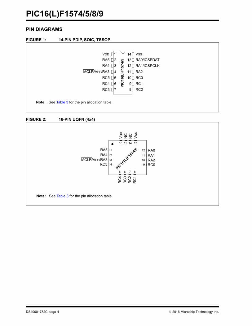
PIN DIAGRAMS
FIGURE 1: 14-PIN PDIP, SOIC, TSSOP
FIGURE 2: 16-PIN UQFN (4x4)P
IC1
6(L
)F1
574
/5
1
2
3
4
14
13
12
11
5
6
7
10
9
8
VDD
RA5
RA4
MCLR/VPP/RA3
RC5
RC4
RC3
VSS
RA0/ICSPDAT
RA1/ICSPCLK
RA2
RC0
RC1
RC2
Note: See Table 3 for the pin allocation table.
7 8
2
3
1
11
12
5
9
10
13141516
6
4
RA5RA4
MCLR/VPP/RA3
RC
4
RC
3
RC
1R
C2
RC0
RA0
RA2RA1
VS
S
VD
D
NC
RC5PIC
16(L
)F15
74/5
NC
Note: See Table 3 for the pin allocation table.
2016 Microchip Technology Inc. DS40001782C-page 5
PIC16(L)F1574/5/8/9
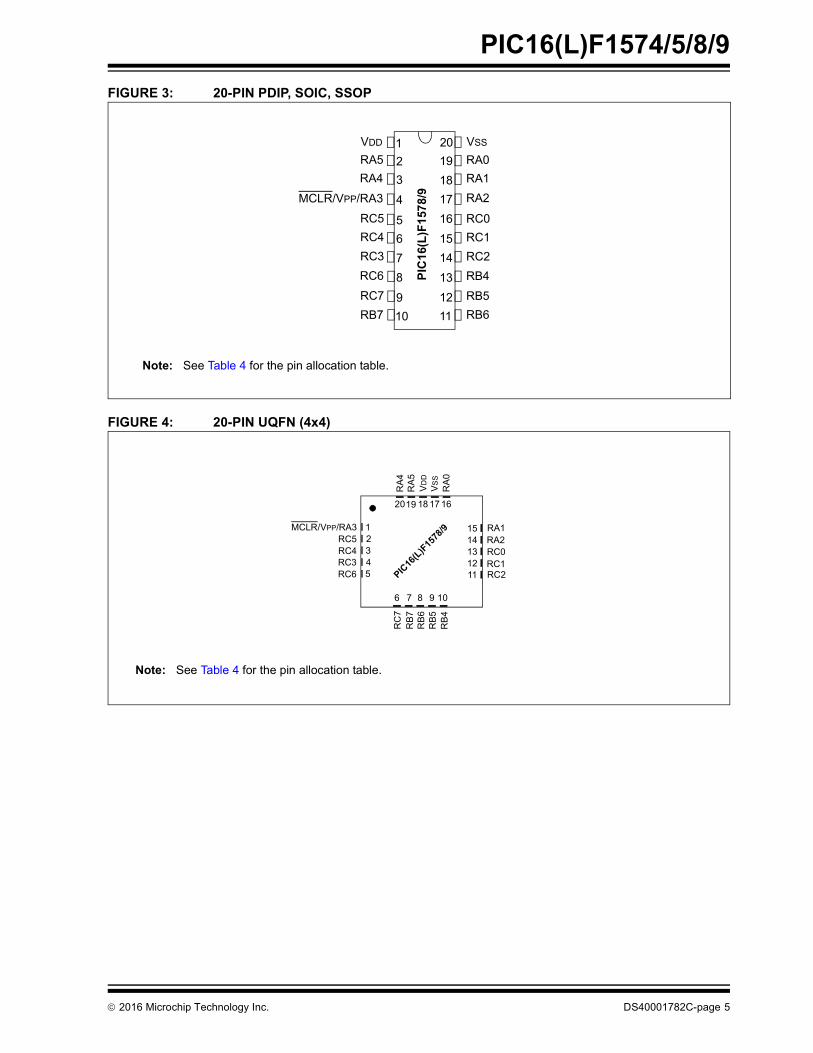
FIGURE 3: 20-PIN PDIP, SOIC, SSOP
FIGURE 4: 20-PIN UQFN (4x4)P
IC1
6(L
)F1
578/
9
1
2
3
4
20
19
18
17
5
6
7
16
15
14
VDD
RA5
RA4
MCLR/VPP/RA3
RC5
RC4
RC3
VSS
RA0
RA1
RA2
RC0
RC1
RC2
8
9
10
13
12
11
RC6
RC7
RB7
RB4
RB5
RB6
Note: See Table 4 for the pin allocation table.
8 9
23
11415
16
10
11
6
1213
17181920
7
54
PIC16
(L)F
1578
/9MCLR/VPP/RA3RC5RC4RC3RC6
RC
7R
B7
RB
4R
B5
RB
6
RC1RC0RA2RA1
RA
0V
SS
VD
D
RA
4R
A5
RC2
Note: See Table 4 for the pin allocation table.
PIC16(L)F1574/5/8/9
DS40001782C-page 6 2016 Microchip Technology Inc.
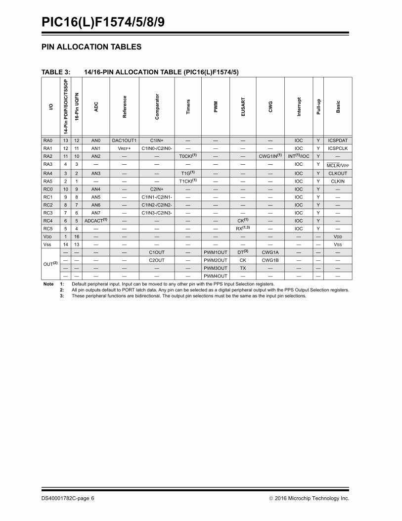
PIN ALLOCATION TABLES
TABLE 3: 14/16-PIN ALLOCATION TABLE (PIC16(L)F1574/5)
I/O
14-
Pin
PD
IP/S
OIC
/TS
SO
P
16-P
in U
QF
N
AD
C
Re
fere
nce
Co
mp
arat
or
Tim
ers
PW
M
EU
SA
RT
CW
G
Inte
rru
pt
Pu
ll-u
p
Ba
sic
RA0 13 12 AN0 DAC1OUT1 C1IN+ — — — — IOC Y ICSPDAT
RA1 12 11 AN1 VREF+ C1IN0-/C2IN0- — — — — IOC Y ICSPCLK
RA2 11 10 AN2 — — T0CKI(1) — — CWG1IN(1) INT(1)/IOC Y —
RA3 4 3 — — — — — — — IOC Y MCLR/VPP
RA4 3 2 AN3 — — T1G(1) — — — IOC Y CLKOUT
RA5 2 1 — — — T1CKI(1) — — — IOC Y CLKIN
RC0 10 9 AN4 — C2IN+ — — — — IOC Y —
RC1 9 8 AN5 — C1IN1-/C2IN1- — — — — IOC Y —
RC2 8 7 AN6 — C1IN2-/C2IN2- — — — — IOC Y —
RC3 7 6 AN7 — C1IN3-/C2IN3- — — — — IOC Y —
RC4 6 5 ADCACT(1) — — — — CK(1) — IOC Y —
RC5 5 4 — — — — — RX(1,3) — IOC Y —
VDD 1 16 — — — — — — — — — VDD
Vss 14 13 — — — — — — — — — VSS
OUT(2)
— — — — C1OUT — PWM1OUT DT(3) CWG1A — — —
— — — — C2OUT — PWM2OUT CK CWG1B — — —
— — — — — — PWM3OUT TX — — — —
— — — — — — PWM4OUT — — — — —
Note 1: Default peripheral input. Input can be moved to any other pin with the PPS Input Selection registers.2: All pin outputs default to PORT latch data. Any pin can be selected as a digital peripheral output with the PPS Output Selection registers.3: These peripheral functions are bidirectional. The output pin selections must be the same as the input pin selections.

2016 Microchip Technology Inc. DS40001782C-page 7
PIC16(L)F1574/5/8/9
TABLE 4: 20-PIN ALLOCATION TABLE (PIC16(L)F1578/9)I/O
20-P
in P
DIP
/SO
IC/S
SO
P
20-P
in U
QF
N
AD
C
Ref
eren
ce
Co
mp
arat
or
Tim
ers
PW
M
EU
SA
RT
CW
G
Inte
rru
pt
Pu
ll-u
p
Ba
sic
RA0 19 16 AN0 DAC1OUT1 C1IN+ — — — — IOC Y ICSPDAT
RA1 18 15 AN1 VREF+ C1IN0-/C2IN0- — — — — IOC Y ICSPCLK
RA2 17 14 AN2 — — T0CKI(1) — — CWG1IN(1) INT(1)/IOC Y —
RA3 4 1 — — — — — — — IOC Y MCLR/VPP
RA4 3 20 AN3 — — T1G(1) — — — IOC Y CLKOUT
RA5 2 19 — — — T1CKI(1) — — — IOC Y CLKIN
RB4 13 10 AN10 — — — — — — IOC Y —
RB5 12 9 AN11 — — — — RX(1,3) — IOC Y —
RB6 11 8 — — — — — — — IOC Y —
RB7 10 7 — — — — — CK(1) — IOC Y —
RC0 16 13 AN4 — C2IN+ — — — — IOC Y —
RC1 15 12 AN5 — C1IN1-/C2IN1- — — — — IOC Y —
RC2 14 11 AN6 — C1IN2-/C2IN2- — — — — IOC Y —
RC3 7 4 AN7 — C1IN3-/C2IN3- — — — — IOC Y —
RC4 6 3 ADCACT(1) — — — — — — IOC Y —
RC5 5 2 — — — — — — — IOC Y —
RC6 8 5 AN8 — — — — — — IOC Y —
RC7 9 6 AN9 — — — — — — IOC Y —
VDD 1 18 — — — — — — — — — VDD
Vss 20 17 — — — — — — — — — VSS
OUT(2)
— — — — C1OUT — PWM1OUT DT(3) CWG1A — — —
— — — — C2OUT — PWM2OUT CK CWG1B — — —
— — — — — — PWM3OUT TX — — — —
— — — — — — PWM4OUT — — — — —
Note 1: Default peripheral input. Input can be moved to any other pin with the PPS Input Selection registers.2: All pin outputs default to PORT latch data. Any pin can be selected as a digital peripheral output with the PPS Output Selection registers.3: These peripheral functions are bidirectional. The output pin selections must be the same as the input pin selections.
PIC16(L)F1574/5/8/9
DS40001782C-page 8 2016 Microchip Technology Inc.
TABLE OF CONTENTS
1.0 Device Overview ........................................................................................................................................................................ 102.0 Enhanced Mid-Range CPU ........................................................................................................................................................ 173.0 Memory Organization ................................................................................................................................................................. 194.0 Device Configuration .................................................................................................................................................................. 555.0 Oscillator Module........................................................................................................................................................................ 616.0 Resets ........................................................................................................................................................................................ 737.0 Interrupts .................................................................................................................................................................................... 818.0 Power-Down Mode (Sleep) ........................................................................................................................................................ 949.0 Watchdog Timer (WDT) ............................................................................................................................................................. 9710.0 Flash Program Memory Control ............................................................................................................................................... 10111.0 I/O Ports ................................................................................................................................................................................... 11712.0 Peripheral Pin Select (PPS) Module ........................................................................................................................................ 13513.0 Interrupt-On-Change ................................................................................................................................................................ 14114.0 Fixed Voltage Reference (FVR) ............................................................................................................................................... 14715.0 Temperature Indicator Module ................................................................................................................................................. 15016.0 Analog-to-Digital Converter (ADC) Module .............................................................................................................................. 15217.0 5-Bit Digital-to-Analog Converter (DAC) Module ...................................................................................................................... 16618.0 Comparator Module.................................................................................................................................................................. 16919.0 Timer0 Module ......................................................................................................................................................................... 17620.0 Timer1 Module with Gate Control............................................................................................................................................. 17921.0 Timer2 Module ......................................................................................................................................................................... 18922.0 Enhanced Universal Synchronous Asynchronous Receiver Transmitter (EUSART) ............................................................... 19223.0 16-bit Pulse-Width Modulation (PWM) Module ........................................................................................................................ 22024.0 Complementary Waveform Generator (CWG) Module ............................................................................................................ 24625.0 In-Circuit Serial Programming™ (ICSP™) ............................................................................................................................... 25826.0 Instruction Set Summary .......................................................................................................................................................... 26027.0 Electrical Specifications............................................................................................................................................................ 27428.0 DC and AC Characteristics Graphs and Charts ....................................................................................................................... 39829.0 Development Support............................................................................................................................................................... 31230.0 Packaging Information.............................................................................................................................................................. 316Appendix A: Data Sheet Revision History.......................................................................................................................................... 338The Microchip Website....................................................................................................................................................................... 339Customer Change Notification Service .............................................................................................................................................. 339Customer Support .............................................................................................................................................................................. 339Product Identification System............................................................................................................................................................. 340
2016 Microchip Technology Inc. DS40001782C-page 9
PIC16(L)F1574/5/8/9
TO OUR VALUED CUSTOMERS
It is our intention to provide our valued customers with the best documentation possible to ensure successful use of your Microchipproducts. To this end, we will continue to improve our publications to better suit your needs. Our publications will be refined andenhanced as new volumes and updates are introduced.
If you have any questions or comments regarding this publication, please contact the Marketing Communications Department viaE-mail at [email protected]. We welcome your feedback.
Most Current Data Sheet
To obtain the most up-to-date version of this data sheet, please register at our Worldwide Website at:
http://www.microchip.com
You can determine the version of a data sheet by examining its literature number found on the bottom outside corner of any page.The last character of the literature number is the version number, (e.g., DS30000000A is version A of document DS30000000).
Errata
An errata sheet, describing minor operational differences from the data sheet and recommended workarounds, may exist for currentdevices. As device/documentation issues become known to us, we will publish an errata sheet. The errata will specify the revisionof silicon and revision of document to which it applies.
To determine if an errata sheet exists for a particular device, please check with one of the following:
• Microchip’s Worldwide Website; http://www.microchip.com• Your local Microchip sales office (see last page)When contacting a sales office, please specify which device, revision of silicon and data sheet (include literature number) you areusing.
Customer Notification System
Register on our website at www.microchip.com to receive the most current information on all of our products.

PIC16(L)F1574/5/8/9
DS40001782C-page 10 2016 Microchip Technology Inc.
1.0 DEVICE OVERVIEW
The PIC16(L)F1574/5/8/9 are described within this datasheet. The block diagram of these devices are shown inFigure 1-1, the available peripherals are shown inTable 1-1, and the pinout descriptions are shown inTable 1-2 and Table 1-3.
TABLE 1-1: DEVICE PERIPHERAL SUMMARY
PeripheralP
IC1
6(L
)F1
574
PIC
16(L
)F15
75
PIC
16(
L)F
157
8
PIC
16(L
)F15
79
Analog-to-Digital Converter (ADC) ● ● ● ●
Complementary Wave Generator (CWG)
● ● ● ●
Digital-to-Analog Converter (DAC) ● ● ● ●
Enhanced UniversalSynchronous/Asynchronous Receiver/Transmitter (EUSART)
● ● ● ●
Fixed Voltage Reference (FVR) ● ● ● ●
Temperature Indicator ● ● ● ●
Comparators
C1 ● ● ● ●
C2 ● ● ● ●
PWM Modules
PWM1 ● ● ● ●
PWM2 ● ● ● ●
PWM3 ● ● ● ●
PWM4 ● ● ● ●
Timers
Timer0 ● ● ● ●
Timer1 ● ● ● ●
Timer2 ● ● ● ●
2016 Microchip Technology Inc. DS40001782C-page 11
PIC16(L)F1574/5/8/9
1.1 Register and Bit Naming Conventions
1.1.1 REGISTER NAMES
When there are multiple instances of the sameperipheral in a device, the peripheral control registerswill be depicted as the concatenation of a peripheralidentifier, peripheral instance, and control identifier.The control registers section will show just oneinstance of all the register names with an ‘x’ in the placeof the peripheral instance number. This namingconvention may also be applied to peripherals whenthere is only one instance of that peripheral in thedevice to maintain compatibility with other devices inthe family that contain more than one.
1.1.2 BIT NAMES
There are two variants for bit names:
• Short name: Bit function abbreviation
• Long name: Peripheral abbreviation + short name
1.1.2.1 Short Bit Names
Short bit names are an abbreviation for the bit function.For example, some peripherals are enabled with theEN bit. The bit names shown in the registers are theshort name variant.
Short bit names are useful when accessing bits in Cprograms. The general format for accessing bits by theshort name is RegisterNamebits.ShortName. Forexample, the enable bit, EN, in the COG1CON0 regis-ter can be set in C programs with the instructionCOG1CON0bits.EN = 1.
Short names are generally not useful in assemblyprograms because the same name may be used bydifferent peripherals in different bit positions. When thisoccurs, during the include file generation, all instancesof that short bit name are appended with an underscoreplus the name of the register in which the bit resides toavoid naming contentions.
1.1.2.2 Long Bit Names
Long bit names are constructed by adding a peripheralabbreviation prefix to the short name. The prefix isunique to the peripheral thereby making every long bitname unique. The long bit name for the COG1 enablebit is the COG1 prefix, G1, appended with the enablebit short name, EN, resulting in the unique bit nameG1EN.
Long bit names are useful in both C and assembly pro-grams. For example, in C the COG1CON0 enable bitcan be set with the G1EN = 1 instruction. In assembly,this bit can be set with the BSF COG1CON0,G1ENinstruction.
1.1.2.3 Bit Fields
Bit fields are two or more adjacent bits in the sameregister. Bit fields adhere only to the short bit namingconvention. For example, the three Least Significantbits of the COG1CON0 register contain the modecontrol bits. The short name for this field is MD. Thereis no long bit name variant. Bit field access is onlypossible in C programs. The following exampledemonstrates a C program instruction for setting theCOG1 to the Push-Pull mode:
COG1CON0bits.MD = 0x5;
Individual bits in a bit field can also be accessed withlong and short bit names. Each bit is the field nameappended with the number of the bit position within thefield. For example, the Most Significant mode bit hasthe short bit name MD2 and the long bit name isG1MD2. The following two examples demonstrateassembly program sequences for setting the COG1 toPush-Pull mode:
Example 1:
MOVLW ~(1<<G1MD1)ANDWF COG1CON0,FMOVLW 1<<G1MD2 | 1<<G1MD0IORWF COG1CON0,F
Example 2:
BSF COG1CON0,G1MD2BCF COG1CON0,G1MD1BSF COG1CON0,G1MD0
1.1.3 REGISTER AND BIT NAMING EXCEPTIONS
1.1.3.1 Status, Interrupt, and Mirror Bits
Status, interrupt enables, interrupt flags, and mirror bitsare contained in registers that span more than oneperipheral. In these cases, the bit name shown isunique so there is no prefix or short name variant.
1.1.3.2 Legacy Peripherals
There are some peripherals that do not strictly adhereto these naming conventions. Peripherals that haveexisted for many years and are present in almost everydevice are the exceptions. These exceptions werenecessary to limit the adverse impact of the newconventions on legacy code. Peripherals that doadhere to the new convention will include a table in theregisters section indicating the long name prefix foreach peripheral instance. Peripherals that fall into theexception category will not have this table. Theseperipherals include, but are not limited to, the following:
• EUSART
• MSSP

PIC16(L)F1574/5/8/9
DS40001782C-page 12 2016 Microchip Technology Inc.
FIGURE 1-1: PIC16(L)F1574/5/8/9 BLOCK DIAGRAM
Note 1: See applicable chapters for more information on peripherals.2: See Table 1-1 for peripherals available on specific devices.3: See Figure 2-1.4: PIC16(L)F1578/9 only.
CLKOUT
CLKIN
RAM
CPU
(Note 3)
TimingGeneration
INTRCOscillator
MCLR
ProgramFlash Memory
FVRADC10-bit
TempIndicatorTMR0TMR1TMR2
PWM1PWM2PWM3CWG1
PORTA
Rev. 10-000039I9/18/2014
DACC1
EUSART
C2
PWM4
PORTB(4)
PORTC
2016 Microchip Technology Inc. DS40001782C-page 13
PIC16(L)F1574/5/8/9
TABLE 1-2: PIC16(L)F1574/5 PINOUT DESCRIPTION
Name FunctionInput Type
Output Type
Description
RA0/AN0/C1IN+/DAC1OUT1/ICSPDAT
RA0 TTL/ST CMOS/OD General purpose input with IOC and WPU.
AN0 AN — ADC Channel input.
C1IN+ AN — Comparator positive input.
DAC1OUT1 — AN Digital-to-Analog Converter output.
ICSPDAT ST CMOS ICSP™ Data I/O.
RA1/AN1/VREF+/C1IN0-/C2IN0-/ICSPCLK
RA1 TTL/ST CMOS/OD General purpose input with IOC and WPU.
AN1 AN — ADC Channel input.
VREF+ AN — Voltage Reference input.
C1IN0- AN — Comparator negative input.
C2IN0- AN — Comparator negative input.
ICSPCLK ST — ICSP Programming Clock.
RA2/AN2/T0CKI(1)/CWG1IN(1)/INT(1)
RA2 TTL/ST CMOS/OD General purpose input with IOC and WPU.
AN2 AN — ADC Channel input.
T0CKI TTL/ST — Timer0 clock input.
CWG1IN TTL/ST — CWG complementary input.
INT TTL/ST — External interrupt.
RA3/VPP/MCLR RA3 TTL/ST — General purpose input with IOC and WPU.
VPP HV — Programming voltage.
MCLR ST — Master Clear with internal pull-up.
RA4/AN3/T1G(1)/CLKOUT RA4 TTL/ST CMOS/OD General purpose input with IOC and WPU.
AN3 AN — ADC Channel input.
T1G TTL/ST — Timer1 Gate input.
CLKOUT CMOS/OD CMOS FOSC/4 output.
RA5/CLKIN/T1CKI(1) RA5 TTL/ST CMOS/OD General purpose input with IOC and WPU.
CLKIN CMOS — External clock input (EC mode).
T1CKI TTL/ST — Timer1 clock input.
RC0/AN4/C2IN+ RC0 TTL/ST CMOS/OD General purpose input with IOC and WPU.
AN4 AN — ADC Channel input.
C2IN+ AN — Comparator positive input.
RC1/AN5/C1IN1-/C2IN1- RC1 TTL/ST CMOS/OD General purpose input with IOC and WPU.
AN5 AN — ADC Channel input.
C1IN1- AN — Comparator negative input.
C2IN1- AN — Comparator negative input.
RC2/AN6/C1IN2-/C2IN2- RC2 TTL/ST CMOS/OD General purpose input with IOC and WPU.
AN6 AN — ADC Channel input.
C1IN2- AN — Comparator negative input.
C2IN2- AN — Comparator negative input.
RC3/AN7/C1IN3-/C2IN3- RC3 TTL/ST CMOS/OD General purpose input with IOC and WPU.
AN7 AN — ADC Channel input.
C1IN3- AN — Comparator negative input.
C2IN3- AN — Comparator negative input.
Legend: AN = Analog input or output CMOS = CMOS compatible input or output OD = Open-DrainTTL = TTL compatible input ST = Schmitt Trigger input with CMOS levels I2C = Schmitt Trigger input with I2CHV = High Voltage XTAL = Crystal levels
Note 1: Default peripheral input. Input can be moved to any other pin with the PPS input selection registers.
2: All pin outputs default to PORT latch data. Any pin can be selected as a digital peripheral output with the PPS output selection registers. See Register 12-1.
3: These USART functions are bidirectional. The output pin selections must be the same as the input pin selections.

PIC16(L)F1574/5/8/9
DS40001782C-page 14 2016 Microchip Technology Inc.
RC4/ADCACT(1)/CK(1) RC4 TTL/ST CMOS/OD General purpose input with IOC and WPU.
ADCACT TTL/ST — ADC Auto-conversion Trigger input.
CK ST CMOS USART synchronous clock.
RC5/RX(1,3) RC5 TTL/ST CMOS/OD General purpose input with IOC and WPU.
RX ST — USART asynchronous input.
OUT(2) C1OUT — CMOS Comparator output.
C2OUT — CMOS Comparator output.
PWM1OUT — CMOS PWM1 output.
PWM2OUT — CMOS PWM2 output.
PWM3OUT — CMOS PWM3 output.
PWM4OUT — CMOS PWM4 output.
CWG1A — CMOS Complementary Output Generator Output A.
CWG1B — CMOS Complementary Output Generator Output B.
TX/CK — CMOS USART asynchronous TX data/synchronous clock output.
DT(3) — CMOS USART synchronous data output.
VDD VDD Power — Positive supply.
VSS VSS Power — Ground reference.
TABLE 1-2: PIC16(L)F1574/5 PINOUT DESCRIPTION (CONTINUED)
Name FunctionInput Type
Output Type
Description
Legend: AN = Analog input or output CMOS = CMOS compatible input or output OD = Open-DrainTTL = TTL compatible input ST = Schmitt Trigger input with CMOS levels I2C = Schmitt Trigger input with I2CHV = High Voltage XTAL = Crystal levels
Note 1: Default peripheral input. Input can be moved to any other pin with the PPS input selection registers.
2: All pin outputs default to PORT latch data. Any pin can be selected as a digital peripheral output with the PPS output selection registers. See Register 12-1.
3: These USART functions are bidirectional. The output pin selections must be the same as the input pin selections.
2016 Microchip Technology Inc. DS40001782C-page 15
PIC16(L)F1574/5/8/9
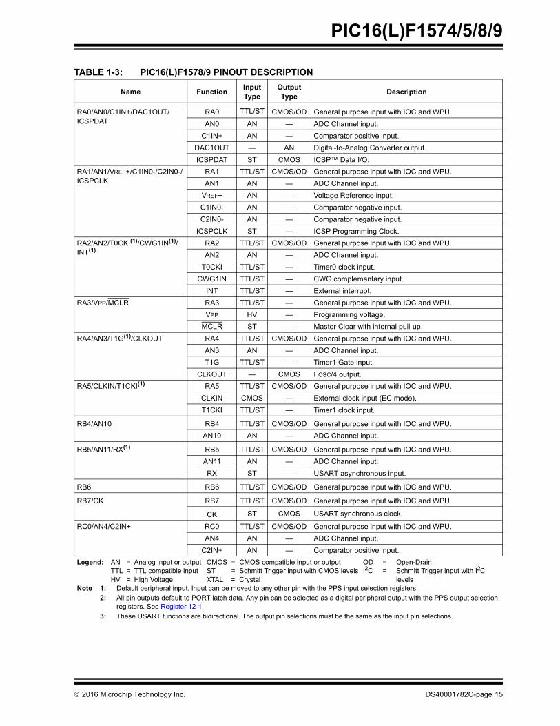
TABLE 1-3: PIC16(L)F1578/9 PINOUT DESCRIPTION
Name FunctionInput Type
Output Type
Description
RA0/AN0/C1IN+/DAC1OUT/ICSPDAT
RA0 TTL/ST CMOS/OD General purpose input with IOC and WPU.
AN0 AN — ADC Channel input.
C1IN+ AN — Comparator positive input.
DAC1OUT — AN Digital-to-Analog Converter output.
ICSPDAT ST CMOS ICSP™ Data I/O.
RA1/AN1/VREF+/C1IN0-/C2IN0-/ICSPCLK
RA1 TTL/ST CMOS/OD General purpose input with IOC and WPU.
AN1 AN — ADC Channel input.
VREF+ AN — Voltage Reference input.
C1IN0- AN — Comparator negative input.
C2IN0- AN — Comparator negative input.
ICSPCLK ST — ICSP Programming Clock.
RA2/AN2/T0CKI(1)/CWG1IN(1)/INT(1)
RA2 TTL/ST CMOS/OD General purpose input with IOC and WPU.
AN2 AN — ADC Channel input.
T0CKI TTL/ST — Timer0 clock input.
CWG1IN TTL/ST — CWG complementary input.
INT TTL/ST — External interrupt.
RA3/VPP/MCLR RA3 TTL/ST — General purpose input with IOC and WPU.
VPP HV — Programming voltage.
MCLR ST — Master Clear with internal pull-up.
RA4/AN3/T1G(1)/CLKOUT RA4 TTL/ST CMOS/OD General purpose input with IOC and WPU.
AN3 AN — ADC Channel input.
T1G TTL/ST — Timer1 Gate input.
CLKOUT — CMOS FOSC/4 output.
RA5/CLKIN/T1CKI(1) RA5 TTL/ST CMOS/OD General purpose input with IOC and WPU.
CLKIN CMOS — External clock input (EC mode).
T1CKI TTL/ST — Timer1 clock input.
RB4/AN10 RB4 TTL/ST CMOS/OD General purpose input with IOC and WPU.
AN10 AN — ADC Channel input.
RB5/AN11/RX(1) RB5 TTL/ST CMOS/OD General purpose input with IOC and WPU.
AN11 AN — ADC Channel input.
RX ST — USART asynchronous input.
RB6 RB6 TTL/ST CMOS/OD General purpose input with IOC and WPU.
RB7/CK RB7 TTL/ST CMOS/OD General purpose input with IOC and WPU.
CK ST CMOS USART synchronous clock.
RC0/AN4/C2IN+ RC0 TTL/ST CMOS/OD General purpose input with IOC and WPU.
AN4 AN — ADC Channel input.
C2IN+ AN — Comparator positive input.
Legend: AN = Analog input or output CMOS = CMOS compatible input or output OD = Open-DrainTTL = TTL compatible input ST = Schmitt Trigger input with CMOS levels I2C = Schmitt Trigger input with I2CHV = High Voltage XTAL = Crystal levels
Note 1: Default peripheral input. Input can be moved to any other pin with the PPS input selection registers.
2: All pin outputs default to PORT latch data. Any pin can be selected as a digital peripheral output with the PPS output selection registers. See Register 12-1.
3: These USART functions are bidirectional. The output pin selections must be the same as the input pin selections.

PIC16(L)F1574/5/8/9
DS40001782C-page 16 2016 Microchip Technology Inc.
RC1/AN5/C1IN1-/C2IN1- RC1 TTL/ST CMOS/OD General purpose input with IOC and WPU.
AN5 AN — ADC Channel input.
C1IN1- AN — Comparator negative input.
C2IN1- AN — Comparator negative input.
RC2/AN6/C1IN2-/C2IN2- RC2 TTL/ST CMOS/OD General purpose input with IOC and WPU.
AN6 AN — ADC Channel input.
C1IN2- AN — Comparator negative input.
C2IN2- AN — Comparator negative input.
RC3/AN7/C1IN3-/C2IN3- RC3 TTL/ST CMOS/OD General purpose input with IOC and WPU.
AN7 AN — ADC Channel input.
C1IN3- AN — Comparator negative input.
C2IN3- AN — Comparator negative input.
RC4/ADCACT(1) RC4 TTL/ST CMOS/OD General purpose input with IOC and WPU.
ADCACT TTL/ST — ADC Auto-conversion Trigger input.
RC5 RC5 TTL/ST CMOS/OD General purpose input with IOC and WPU.
OUT(2) C1OUT — CMOS Comparator output.
C2OUT — CMOS Comparator output.
PWM1OUT — CMOS PWM1 output.
PWM2OUT — CMOS PWM2 output.
PWM3OUT — CMOS PWM3 output.
PWM4OUT — CMOS PWM4 output.
CWG1A — CMOS Complementary Output Generator Output A.
CWG1B — CMOS Complementary Output Generator Output B.
TX/CK — CMOS USART asynchronous TX data/synchronous clock output.
DT(3) — CMOS USART synchronous data output.
VDD VDD Power — Positive supply.
VSS VSS Power — Ground reference.
TABLE 1-3: PIC16(L)F1578/9 PINOUT DESCRIPTION (CONTINUED)
Name FunctionInput Type
Output Type
Description
Legend: AN = Analog input or output CMOS = CMOS compatible input or output OD = Open-DrainTTL = TTL compatible input ST = Schmitt Trigger input with CMOS levels I2C = Schmitt Trigger input with I2CHV = High Voltage XTAL = Crystal levels
Note 1: Default peripheral input. Input can be moved to any other pin with the PPS input selection registers.
2: All pin outputs default to PORT latch data. Any pin can be selected as a digital peripheral output with the PPS output selection registers. See Register 12-1.
3: These USART functions are bidirectional. The output pin selections must be the same as the input pin selections.

2016 Microchip Technology Inc. DS40001782C-page 17
PIC16(L)F1574/5/8/9
2.0 ENHANCED MID-RANGE CPU
This family of devices contain an enhanced mid-range8-bit CPU core. The CPU has 49 instructions. Interruptcapability includes automatic context saving. Thehardware stack is 16 levels deep and has Overflow andUnderflow Reset capability. Direct, Indirect, andRelative addressing modes are available. Two FileSelect Registers (FSRs) provide the ability to readprogram and data memory.
• Automatic Interrupt Context Saving
• 16-level Stack with Overflow and Underflow
• File Select Registers
• Instruction Set
FIGURE 2-1: CORE BLOCK DIAGRAM
1515
15
15
8
8
8
1214
75
3
Program Counter
MUX
Addr MUX
16-Level Stack(15-bit)
Program MemoryRead (PMR)
Instruction Reg
Configuration
FSR0 Reg
FSR1 Reg
BSR Reg
STATUS Reg
RAM
W Reg
Power-upTimer
Power-onReset
WatchdogTimer
Brown-outReset
InstructionDecode and
Control
TimingGeneration
InternalOscillator
Block
ALU
FlashProgramMemoryM
UX
Data Bus
ProgramBus
Direct AddrIndirect
Addr
RAM Addr
CLKIN
CLKOUT
VDD VSS
Rev. 10-000055A7/30/2013
1212

PIC16(L)F1574/5/8/9
DS40001782C-page 18 2016 Microchip Technology Inc.
2.1 Automatic Interrupt Context Saving
During interrupts, certain registers are automaticallysaved in shadow registers and restored when returningfrom the interrupt. This saves stack space and usercode. See Section 7.5 “Automatic Context Saving”,for more information.
2.2 16-Level Stack with Overflow and Underflow
These devices have a hardware stack memory 15 bitswide and 16 words deep. A Stack Overflow or Under-flow will set the appropriate bit (STKOVF or STKUNF)in the PCON register, and if enabled, will cause a soft-ware Reset. See section Section 3.5 “Stack” for moredetails.
2.3 File Select Registers
There are two 16-bit File Select Registers (FSR).FSRs can access all file registers and program mem-ory, which allows one Data Pointer for all memory.When an FSR points to program memory, there is oneadditional instruction cycle in instructions using INDFto allow the data to be fetched. General purpose mem-ory can now also be addressed linearly, providing theability to access contiguous data larger than 80 bytes.There are also new instructions to support the FSRs.See Section 3.6 “Indirect Addressing” for moredetails.
2.4 Instruction Set
There are 49 instructions for the enhanced mid-rangeCPU to support the features of the CPU. See Section26.0 “Instruction Set Summary” for more details.
2016 Microchip Technology Inc. DS40001782C-page 19
PIC16(L)F1574/5/8/9
3.0 MEMORY ORGANIZATION
These devices contain the following types of memory:
• Program Memory
- Configuration Words
- Device ID
- User ID
- Flash Program Memory
• Data Memory
- Core Registers
- Special Function Registers
- General Purpose RAM
- Common RAM
The following features are associated with access andcontrol of program memory and data memory:
• PCL and PCLATH
• Stack
• Indirect Addressing
3.1 Program Memory Organization
The enhanced mid-range core has a 15-bit programcounter capable of addressing a 32K x 14 programmemory space. Table 3-1 shows the memory sizesimplemented. Accessing a location above theseboundaries will cause a wrap-around within theimplemented memory space. The Reset vector is at0000h and the interrupt vector is at 0004h (SeeFigure 3-1).
3.2 High-Endurance Flash
This device has a 128-byte section of high-enduranceProgram Flash Memory (PFM) in lieu of data EEPROM.This area is especially well suited for nonvolatile datastorage that is expected to be updated frequently overthe life of the end product. See Section 10.2 “FlashProgram Memory Overview” for more information onwriting data to PFM. See Section 3.3.2 “SpecialFunction Register” for more information about usingthe SFR registers to read byte data stored in PFM.
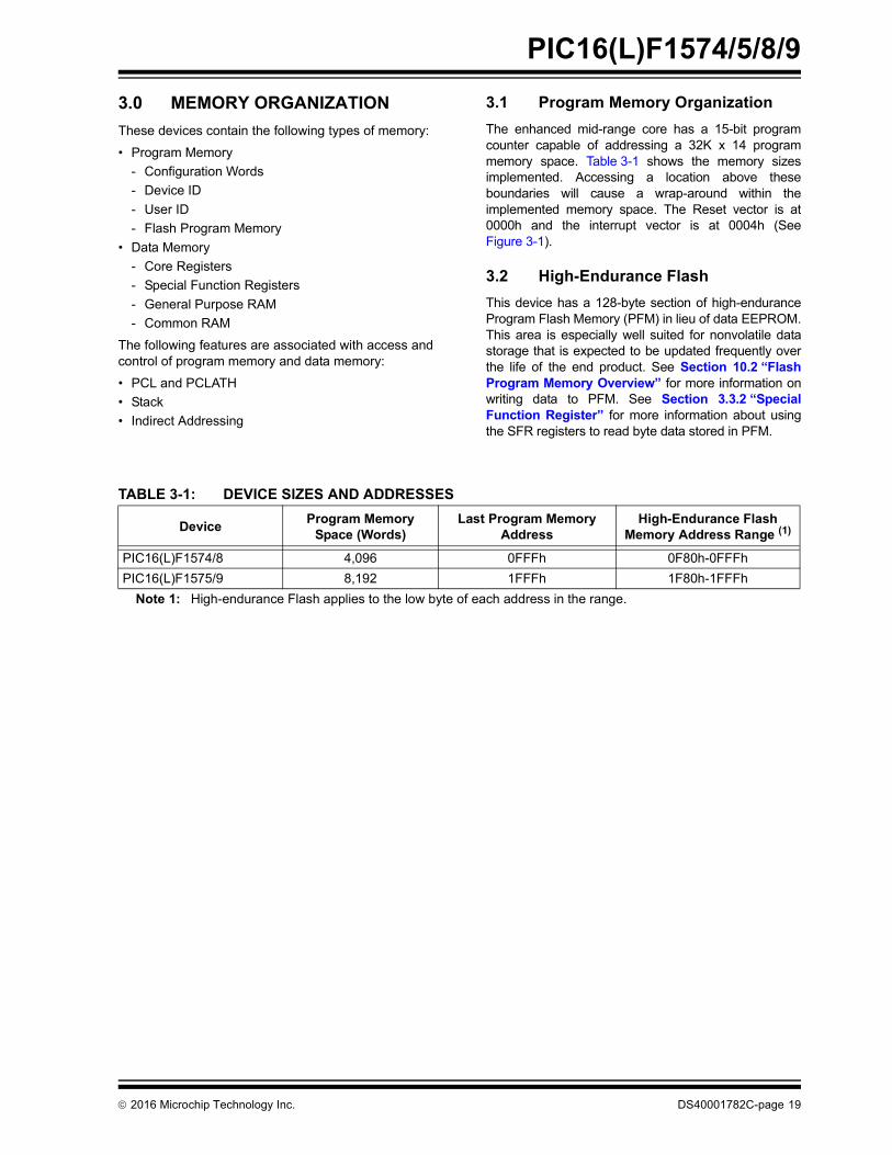
TABLE 3-1: DEVICE SIZES AND ADDRESSES
DeviceProgram Memory
Space (Words)Last Program Memory
AddressHigh-Endurance Flash
Memory Address Range (1)
PIC16(L)F1574/8 4,096 0FFFh 0F80h-0FFFh
PIC16(L)F1575/9 8,192 1FFFh 1F80h-1FFFh
Note 1: High-endurance Flash applies to the low byte of each address in the range.

PIC16(L)F1574/5/8/9
DS40001782C-page 20 2016 Microchip Technology Inc.
FIGURE 3-1: PROGRAM MEMORY MAP AND STACK FOR PIC16(L)F1574/8
FIGURE 3-2: PROGRAM MEMORY MAP AND STACK FOR PIC16(L)F1575/9
Stack Level 0
Stack Level 15
Stack Level 1
Reset Vector
PC<14:0>
Interrupt Vector
Page 1
Page 0
Rollover to Page 0
Rollover to Page 1
0000h
0004h0005h
07FFh0800h
0FFFh1000h
7FFFh
CALL, CALLW RETURN, RETLWInterrupt, RETFIE
On-chipProgramMemory
15
Rev. 10-000040A7/30/2013
CALL, CALLW RETURN, RETLWInterrupt, RETFIE
On-chipProgramMemory
Stack Level 0
Stack Level 15
Stack Level 1
Reset Vector
PC<14:0>
Interrupt Vector
Page 1
Page 0
0000h
0004h0005h
07FFh0800h
0FFFh1000h
7FFFh
Rollover to Page 0
Rollover to Page 3
Page 2
Page 3
17FFh1800h
1FFFh2000h
15
Rev. 10-000040B7/30/2013
2016 Microchip Technology Inc. DS40001782C-page 21
PIC16(L)F1574/5/8/9
3.2.1 READING PROGRAM MEMORY AS DATA
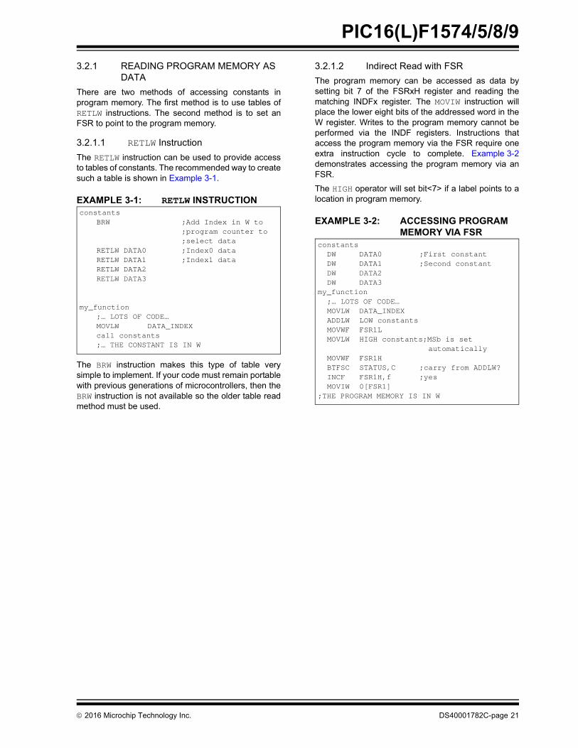
There are two methods of accessing constants inprogram memory. The first method is to use tables ofRETLW instructions. The second method is to set anFSR to point to the program memory.
3.2.1.1 RETLW Instruction
The RETLW instruction can be used to provide accessto tables of constants. The recommended way to createsuch a table is shown in Example 3-1.
EXAMPLE 3-1: RETLW INSTRUCTION
The BRW instruction makes this type of table verysimple to implement. If your code must remain portablewith previous generations of microcontrollers, then theBRW instruction is not available so the older table readmethod must be used.
3.2.1.2 Indirect Read with FSR
The program memory can be accessed as data bysetting bit 7 of the FSRxH register and reading thematching INDFx register. The MOVIW instruction willplace the lower eight bits of the addressed word in theW register. Writes to the program memory cannot beperformed via the INDF registers. Instructions thataccess the program memory via the FSR require oneextra instruction cycle to complete. Example 3-2demonstrates accessing the program memory via anFSR.
The HIGH operator will set bit<7> if a label points to alocation in program memory.
EXAMPLE 3-2: ACCESSING PROGRAM MEMORY VIA FSR
constantsBRW ;Add Index in W to
;program counter to;select data
RETLW DATA0 ;Index0 dataRETLW DATA1 ;Index1 dataRETLW DATA2RETLW DATA3
my_function;… LOTS OF CODE…MOVLW DATA_INDEXcall constants;… THE CONSTANT IS IN W
constantsDW DATA0 ;First constantDW DATA1 ;Second constantDW DATA2DW DATA3
my_function;… LOTS OF CODE…MOVLW DATA_INDEXADDLW LOW constantsMOVWF FSR1LMOVLW HIGH constants;MSb is set
automaticallyMOVWF FSR1HBTFSC STATUS,C ;carry from ADDLW?INCF FSR1H,f ;yesMOVIW 0[FSR1]
;THE PROGRAM MEMORY IS IN W
PIC16(L)F1574/5/8/9
DS40001782C-page 22 2016 Microchip Technology Inc.
3.3 Data Memory Organization
The data memory is partitioned in 32 memory bankswith 128 bytes in a bank. Each bank consists of(Figure 3-3):
• 12 core registers
• 20 Special Function Registers (SFR)
• Up to 80 bytes of General Purpose RAM (GPR)
• 16 bytes of common RAM
The active bank is selected by writing the bank numberinto the Bank Select Register (BSR). Unimplementedmemory will read as ‘0’. All data memory can beaccessed either directly (via instructions that use thefile registers) or indirectly via the two File SelectRegisters (FSR). See Section 3.6 “IndirectAddressing” for more information.
Data memory uses a 12-bit address. The upper five bitsof the address define the Bank address and the lowerseven bits select the registers/RAM in that bank.
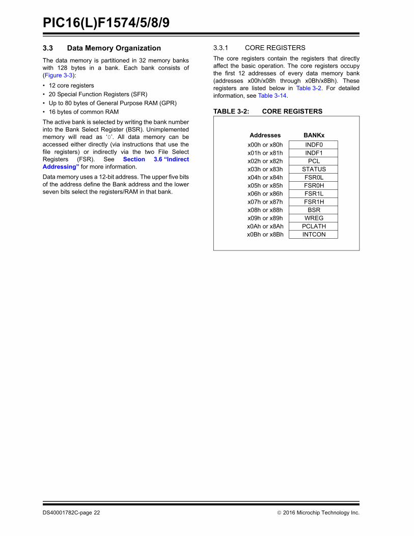
3.3.1 CORE REGISTERS
The core registers contain the registers that directlyaffect the basic operation. The core registers occupythe first 12 addresses of every data memory bank(addresses x00h/x08h through x0Bh/x8Bh). Theseregisters are listed below in Table 3-2. For detailedinformation, see Table 3-14.
TABLE 3-2: CORE REGISTERS
Addresses BANKx
x00h or x80h INDF0x01h or x81h INDF1x02h or x82h PCLx03h or x83h STATUSx04h or x84h FSR0Lx05h or x85h FSR0Hx06h or x86h FSR1Lx07h or x87h FSR1Hx08h or x88h BSRx09h or x89h WREGx0Ah or x8Ah PCLATHx0Bh or x8Bh INTCON
2016 Microchip Technology Inc. DS40001782C-page 23
PIC16(L)F1574/5/8/9
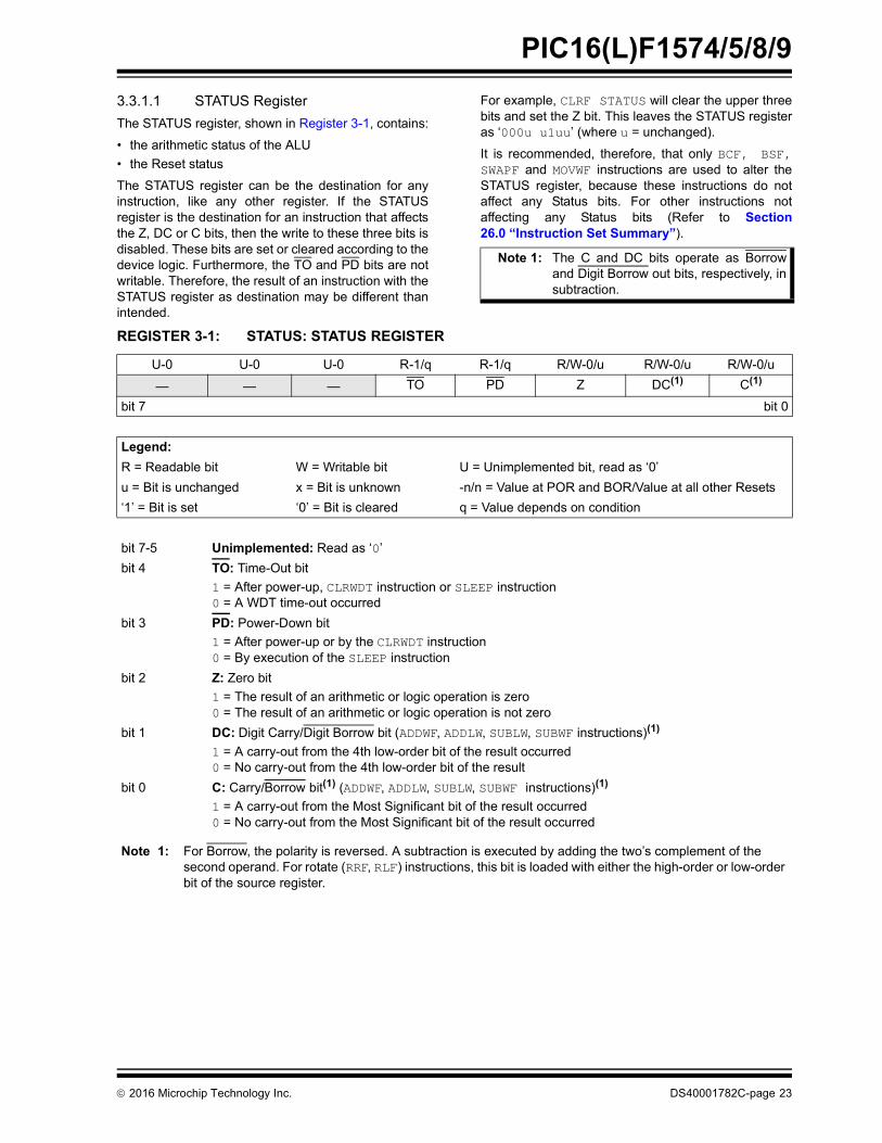
3.3.1.1 STATUS Register
The STATUS register, shown in Register 3-1, contains:
• the arithmetic status of the ALU
• the Reset status
The STATUS register can be the destination for anyinstruction, like any other register. If the STATUSregister is the destination for an instruction that affectsthe Z, DC or C bits, then the write to these three bits isdisabled. These bits are set or cleared according to thedevice logic. Furthermore, the TO and PD bits are notwritable. Therefore, the result of an instruction with theSTATUS register as destination may be different thanintended.
For example, CLRF STATUS will clear the upper threebits and set the Z bit. This leaves the STATUS registeras ‘000u u1uu’ (where u = unchanged).
It is recommended, therefore, that only BCF, BSF,SWAPF and MOVWF instructions are used to alter theSTATUS register, because these instructions do notaffect any Status bits. For other instructions notaffecting any Status bits (Refer to Section26.0 “Instruction Set Summary”).
Note 1: The C and DC bits operate as Borrowand Digit Borrow out bits, respectively, insubtraction.
REGISTER 3-1: STATUS: STATUS REGISTER
U-0 U-0 U-0 R-1/q R-1/q R/W-0/u R/W-0/u R/W-0/u
— — — TO PD Z DC(1) C(1)
bit 7 bit 0
Legend:
R = Readable bit W = Writable bit U = Unimplemented bit, read as ‘0’
u = Bit is unchanged x = Bit is unknown -n/n = Value at POR and BOR/Value at all other Resets
‘1’ = Bit is set ‘0’ = Bit is cleared q = Value depends on condition
bit 7-5 Unimplemented: Read as ‘0’
bit 4 TO: Time-Out bit
1 = After power-up, CLRWDT instruction or SLEEP instruction0 = A WDT time-out occurred
bit 3 PD: Power-Down bit
1 = After power-up or by the CLRWDT instruction0 = By execution of the SLEEP instruction
bit 2 Z: Zero bit
1 = The result of an arithmetic or logic operation is zero0 = The result of an arithmetic or logic operation is not zero
bit 1 DC: Digit Carry/Digit Borrow bit (ADDWF, ADDLW, SUBLW, SUBWF instructions)(1)
1 = A carry-out from the 4th low-order bit of the result occurred0 = No carry-out from the 4th low-order bit of the result
bit 0 C: Carry/Borrow bit(1) (ADDWF, ADDLW, SUBLW, SUBWF instructions)(1)
1 = A carry-out from the Most Significant bit of the result occurred0 = No carry-out from the Most Significant bit of the result occurred
Note 1: For Borrow, the polarity is reversed. A subtraction is executed by adding the two’s complement of the second operand. For rotate (RRF, RLF) instructions, this bit is loaded with either the high-order or low-order bit of the source register.

PIC16(L)F1574/5/8/9
DS40001782C-page 24 2016 Microchip Technology Inc.
3.3.2 SPECIAL FUNCTION REGISTER
The Special Function Registers are registers used bythe application to control the desired operation ofperipheral functions in the device. The Special FunctionRegisters occupy the 20 bytes after the core registers ofevery data memory bank (addresses x0Ch/x8Chthrough x1Fh/x9Fh). The registers associated with theoperation of the peripherals are described in the appro-priate peripheral chapter of this data sheet.
3.3.3 GENERAL PURPOSE RAM
There are up to 80 bytes of GPR in each data memorybank. The Special Function Registers occupy the 20bytes after the core registers of every data memorybank (addresses x0Ch/x8Ch through x1Fh/x9Fh).
3.3.3.1 Linear Access to GPR
The general purpose RAM can be accessed in anon-banked method via the FSRs. This can simplifyaccess to large memory structures. See Section3.6.2 “Linear Data Memory” for more information.
3.3.4 COMMON RAM
There are 16 bytes of common RAM accessible from allbanks.
3.3.5 DEVICE MEMORY MAPS
The memory maps are as shown in Table 3-3 throughTable 3-13.
FIGURE 3-3: BANKED MEMORY PARTITIONING
Memory Region7-bit Bank Offset
00h
0Bh0Ch
1Fh20h
6Fh
7Fh
70h
Core Registers(12 bytes)
Special Function Registers(20 bytes maximum)
General Purpose RAM(80 bytes maximum)
Common RAM(16 bytes)
Rev. 10-000041A7/30/2013
2
01
6 M
icroch
ip T
ech
no
log
y Inc.
DS
40
00
17
82
C-p
ag
e 2
5
PIC
16(L
)F15
74/5/8/9
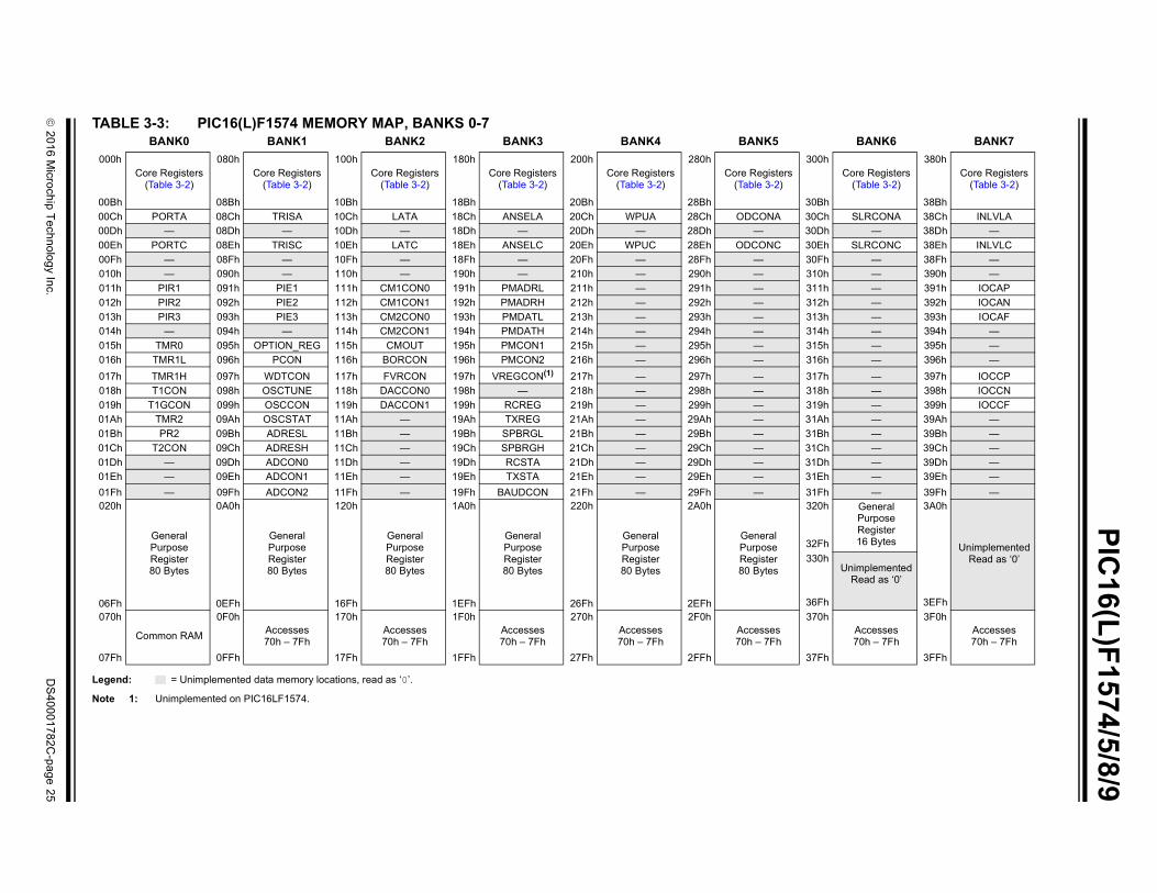
TABLE 3-3: PIC16(L)F1574 MEMORY MAP, BANKS 0-7
Legend: = Unimplemented data memory locations, read as ‘0’.
Note 1: Unimplemented on PIC16LF1574.
BANK0 BANK1 BANK2 BANK3 BANK4 BANK5 BANK6 BANK7
000hCore Registers
(Table 3-2)
080hCore Registers
(Table 3-2)
100hCore Registers
(Table 3-2)
180hCore Registers
(Table 3-2)
200hCore Registers
(Table 3-2)
280hCore Registers
(Table 3-2)
300hCore Registers
(Table 3-2)
380hCore Registers
(Table 3-2)
00Bh 08Bh 10Bh 18Bh 20Bh 28Bh 30Bh 38Bh
00Ch PORTA 08Ch TRISA 10Ch LATA 18Ch ANSELA 20Ch WPUA 28Ch ODCONA 30Ch SLRCONA 38Ch INLVLA
00Dh — 08Dh — 10Dh — 18Dh — 20Dh — 28Dh — 30Dh — 38Dh —
00Eh PORTC 08Eh TRISC 10Eh LATC 18Eh ANSELC 20Eh WPUC 28Eh ODCONC 30Eh SLRCONC 38Eh INLVLC
00Fh — 08Fh — 10Fh — 18Fh — 20Fh — 28Fh — 30Fh — 38Fh —
010h — 090h — 110h — 190h — 210h — 290h — 310h — 390h —
011h PIR1 091h PIE1 111h CM1CON0 191h PMADRL 211h — 291h — 311h — 391h IOCAP
012h PIR2 092h PIE2 112h CM1CON1 192h PMADRH 212h — 292h — 312h — 392h IOCAN
013h PIR3 093h PIE3 113h CM2CON0 193h PMDATL 213h — 293h — 313h — 393h IOCAF
014h — 094h — 114h CM2CON1 194h PMDATH 214h — 294h — 314h — 394h —
015h TMR0 095h OPTION_REG 115h CMOUT 195h PMCON1 215h — 295h — 315h — 395h —
016h TMR1L 096h PCON 116h BORCON 196h PMCON2 216h — 296h — 316h — 396h —
017h TMR1H 097h WDTCON 117h FVRCON 197h VREGCON(1) 217h — 297h — 317h — 397h IOCCP
018h T1CON 098h OSCTUNE 118h DACCON0 198h — 218h — 298h — 318h — 398h IOCCN
019h T1GCON 099h OSCCON 119h DACCON1 199h RCREG 219h — 299h — 319h — 399h IOCCF
01Ah TMR2 09Ah OSCSTAT 11Ah — 19Ah TXREG 21Ah — 29Ah — 31Ah — 39Ah —
01Bh PR2 09Bh ADRESL 11Bh — 19Bh SPBRGL 21Bh — 29Bh — 31Bh — 39Bh —
01Ch T2CON 09Ch ADRESH 11Ch — 19Ch SPBRGH 21Ch — 29Ch — 31Ch — 39Ch —
01Dh — 09Dh ADCON0 11Dh — 19Dh RCSTA 21Dh — 29Dh — 31Dh — 39Dh —
01Eh — 09Eh ADCON1 11Eh — 19Eh TXSTA 21Eh — 29Eh — 31Eh — 39Eh —
01Fh — 09Fh ADCON2 11Fh — 19Fh BAUDCON 21Fh — 29Fh — 31Fh — 39Fh —020h
GeneralPurposeRegister80 Bytes
0A0h
GeneralPurposeRegister80 Bytes
120h
GeneralPurposeRegister80 Bytes
1A0h
GeneralPurposeRegister80 Bytes
220h
GeneralPurposeRegister80 Bytes
2A0h
GeneralPurposeRegister80 Bytes
320h GeneralPurposeRegister16 Bytes
3A0h
UnimplementedRead as ‘0’
32Fh
330hUnimplemented
Read as ‘0’
06Fh 0EFh 16Fh 1EFh 26Fh 2EFh 36Fh 3EFh
070h
Common RAM
0F0hAccesses70h – 7Fh
170hAccesses70h – 7Fh
1F0hAccesses70h – 7Fh
270hAccesses70h – 7Fh
2F0hAccesses70h – 7Fh
370hAccesses70h – 7Fh
3F0hAccesses70h – 7Fh
07Fh 0FFh 17Fh 1FFh 27Fh 2FFh 37Fh 3FFh
PIC
16(L
)F1
574
/5/8
/9
DS
40
00
17
82
C-p
ag
e 2
6
20
16
Micro
chip
Te
chn
olo
gy In
c.
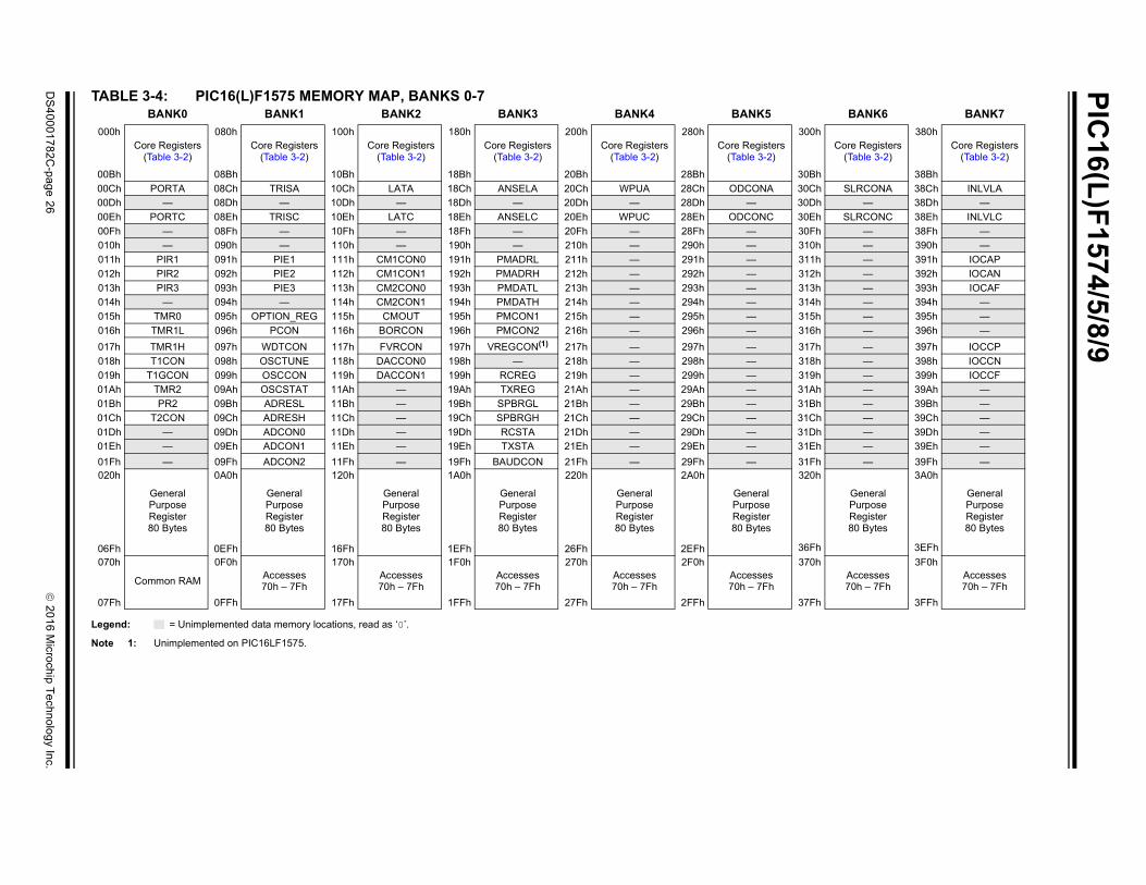
TABLE 3-4: PIC16(L)F1575 MEMORY MAP, BANKS 0-7
Legend: = Unimplemented data memory locations, read as ‘0’.
Note 1: Unimplemented on PIC16LF1575.
BANK0 BANK1 BANK2 BANK3 BANK4 BANK5 BANK6 BANK7
000hCore Registers
(Table 3-2)
080hCore Registers
(Table 3-2)
100hCore Registers
(Table 3-2)
180hCore Registers
(Table 3-2)
200hCore Registers
(Table 3-2)
280hCore Registers
(Table 3-2)
300hCore Registers
(Table 3-2)
380hCore Registers
(Table 3-2)
00Bh 08Bh 10Bh 18Bh 20Bh 28Bh 30Bh 38Bh
00Ch PORTA 08Ch TRISA 10Ch LATA 18Ch ANSELA 20Ch WPUA 28Ch ODCONA 30Ch SLRCONA 38Ch INLVLA
00Dh — 08Dh — 10Dh — 18Dh — 20Dh — 28Dh — 30Dh — 38Dh —
00Eh PORTC 08Eh TRISC 10Eh LATC 18Eh ANSELC 20Eh WPUC 28Eh ODCONC 30Eh SLRCONC 38Eh INLVLC
00Fh — 08Fh — 10Fh — 18Fh — 20Fh — 28Fh — 30Fh — 38Fh —
010h — 090h — 110h — 190h — 210h — 290h — 310h — 390h —
011h PIR1 091h PIE1 111h CM1CON0 191h PMADRL 211h — 291h — 311h — 391h IOCAP
012h PIR2 092h PIE2 112h CM1CON1 192h PMADRH 212h — 292h — 312h — 392h IOCAN
013h PIR3 093h PIE3 113h CM2CON0 193h PMDATL 213h — 293h — 313h — 393h IOCAF
014h — 094h — 114h CM2CON1 194h PMDATH 214h — 294h — 314h — 394h —
015h TMR0 095h OPTION_REG 115h CMOUT 195h PMCON1 215h — 295h — 315h — 395h —
016h TMR1L 096h PCON 116h BORCON 196h PMCON2 216h — 296h — 316h — 396h —
017h TMR1H 097h WDTCON 117h FVRCON 197h VREGCON(1) 217h — 297h — 317h — 397h IOCCP
018h T1CON 098h OSCTUNE 118h DACCON0 198h — 218h — 298h — 318h — 398h IOCCN
019h T1GCON 099h OSCCON 119h DACCON1 199h RCREG 219h — 299h — 319h — 399h IOCCF
01Ah TMR2 09Ah OSCSTAT 11Ah — 19Ah TXREG 21Ah — 29Ah — 31Ah — 39Ah —
01Bh PR2 09Bh ADRESL 11Bh — 19Bh SPBRGL 21Bh — 29Bh — 31Bh — 39Bh —
01Ch T2CON 09Ch ADRESH 11Ch — 19Ch SPBRGH 21Ch — 29Ch — 31Ch — 39Ch —
01Dh — 09Dh ADCON0 11Dh — 19Dh RCSTA 21Dh — 29Dh — 31Dh — 39Dh —
01Eh — 09Eh ADCON1 11Eh — 19Eh TXSTA 21Eh — 29Eh — 31Eh — 39Eh —
01Fh — 09Fh ADCON2 11Fh — 19Fh BAUDCON 21Fh — 29Fh — 31Fh — 39Fh —020h
GeneralPurposeRegister80 Bytes
0A0h
GeneralPurposeRegister80 Bytes
120h
GeneralPurposeRegister80 Bytes
1A0h
GeneralPurposeRegister80 Bytes
220h
GeneralPurposeRegister80 Bytes
2A0h
GeneralPurposeRegister80 Bytes
320h
GeneralPurposeRegister80 Bytes
3A0h
GeneralPurposeRegister80 Bytes
06Fh 0EFh 16Fh 1EFh 26Fh 2EFh 36Fh 3EFh
070h
Common RAM
0F0hAccesses70h – 7Fh
170hAccesses70h – 7Fh
1F0hAccesses70h – 7Fh
270hAccesses70h – 7Fh
2F0hAccesses70h – 7Fh
370hAccesses70h – 7Fh
3F0hAccesses70h – 7Fh
07Fh 0FFh 17Fh 1FFh 27Fh 2FFh 37Fh 3FFh

2
01
6 M
icroch
ip T
ech
no
log
y Inc.
DS
40
00
17
82
C-p
ag
e 2
7
PIC
16(L
)F15
74/5/8/9
TABLE 3-5: PIC16(L)F1578 MEMORY MAP, BANKS 0-7
Legend: = Unimplemented data memory locations, read as ‘0’.
Note 1: Unimplemented on PIC16LF1578.
BANK0 BANK1 BANK2 BANK3 BANK4 BANK5 BANK6 BANK7
000hCore Registers
(Table 3-2)
080hCore Registers
(Table 3-2)
100hCore Registers
(Table 3-2)
180hCore Registers
(Table 3-2)
200hCore Registers
(Table 3-2)
280hCore Registers
(Table 3-2)
300hCore Registers
(Table 3-2)
380hCore Registers
(Table 3-2)
00Bh 08Bh 10Bh 18Bh 20Bh 28Bh 30Bh 38Bh
00Ch PORTA 08Ch TRISA 10Ch LATA 18Ch ANSELA 20Ch WPUA 28Ch ODCONA 30Ch SLRCONA 38Ch INLVLA
00Dh PORTB 08Dh TRISB 10Dh LATB 18Dh ANSELB 20Dh WPUB 28Dh ODCONB 30Dh SLRCONB 38Dh INLVLB
00Eh PORTC 08Eh TRISC 10Eh LATC 18Eh ANSELC 20Eh WPUC 28Eh ODCONC 30Eh SLRCONC 38Eh INLVLC
00Fh — 08Fh — 10Fh — 18Fh — 20Fh — 28Fh — 30Fh — 38Fh —
010h — 090h — 110h — 190h — 210h — 290h — 310h — 390h —
011h PIR1 091h PIE1 111h CM1CON0 191h PMADRL 211h — 291h — 311h — 391h IOCAP
012h PIR2 092h PIE2 112h CM1CON1 192h PMADRH 212h — 292h — 312h — 392h IOCAN
013h PIR3 093h PIE3 113h CM2CON0 193h PMDATL 213h — 293h — 313h — 393h IOCAF
014h — 094h — 114h CM2CON1 194h PMDATH 214h — 294h — 314h — 394h IOCBP
015h TMR0 095h OPTION_REG 115h CMOUT 195h PMCON1 215h — 295h — 315h — 395h IOCBN
016h TMR1L 096h PCON 116h BORCON 196h PMCON2 216h — 296h — 316h — 396h IOCBF
017h TMR1H 097h WDTCON 117h FVRCON 197h VREGCON(1) 217h — 297h — 317h — 397h IOCCP
018h T1CON 098h OSCTUNE 118h DACCON0 198h — 218h — 298h — 318h — 398h IOCCN
019h T1GCON 099h OSCCON 119h DACCON1 199h RCREG 219h — 299h — 319h — 399h IOCCF
01Ah TMR2 09Ah OSCSTAT 11Ah — 19Ah TXREG 21Ah — 29Ah — 31Ah — 39Ah —
01Bh PR2 09Bh ADRESL 11Bh — 19Bh SPBRGL 21Bh — 29Bh — 31Bh — 39Bh —
01Ch T2CON 09Ch ADRESH 11Ch — 19Ch SPBRGH 21Ch — 29Ch — 31Ch — 39Ch —
01Dh — 09Dh ADCON0 11Dh — 19Dh RCSTA 21Dh — 29Dh — 31Dh — 39Dh —
01Eh — 09Eh ADCON1 11Eh — 19Eh TXSTA 21Eh — 29Eh — 31Eh — 39Eh —
01Fh — 09Fh ADCON2 11Fh — 19Fh BAUDCON 21Fh — 29Fh — 31Fh — 39Fh —020h
GeneralPurposeRegister80 Bytes
0A0h
GeneralPurposeRegister80 Bytes
120h
GeneralPurposeRegister80 Bytes
1A0h
GeneralPurposeRegister80 Bytes
220h
GeneralPurposeRegister80 Bytes
2A0h
GeneralPurposeRegister80 Bytes
320h GeneralPurposeRegister16 Bytes
3A0h
UnimplementedRead as ‘0’
32Fh
330hUnimplemented
Read as ‘0’
06Fh 0EFh 16Fh 1EFh 26Fh 2EFh 36Fh 3EFh
070h
Common RAM
0F0hAccesses70h – 7Fh
170hAccesses70h – 7Fh
1F0hAccesses70h – 7Fh
270hAccesses70h – 7Fh
2F0hAccesses70h – 7Fh
370hAccesses70h – 7Fh
3F0hAccesses70h – 7Fh
07Fh 0FFh 17Fh 1FFh 27Fh 2FFh 37Fh 3FFh

2
01
6 M
icroch
ip T
ech
no
log
y Inc.
DS
40
00
17
82
C-p
ag
e 2
8
PIC
16(L
)F15
74/5/8/9
TABLE 3-6: PIC16(L)F1579 MEMORY MAP, BANKS 0-7
Legend: = Unimplemented data memory locations, read as ‘0’.
Note 1: Unimplemented on PIC16LF1579.
BANK0 BANK1 BANK2 BANK3 BANK4 BANK5 BANK6 BANK7
000hCore Registers
(Table 3-2)
080hCore Registers
(Table 3-2)
100hCore Registers
(Table 3-2)
180hCore Registers
(Table 3-2)
200hCore Registers
(Table 3-2)
280hCore Registers
(Table 3-2)
300hCore Registers
(Table 3-2)
380hCore Registers
(Table 3-2)
00Bh 08Bh 10Bh 18Bh 20Bh 28Bh 30Bh 38Bh
00Ch PORTA 08Ch TRISA 10Ch LATA 18Ch ANSELA 20Ch WPUA 28Ch ODCONA 30Ch SLRCONA 38Ch INLVLA
00Dh PORTB 08Dh TRISB 10Dh LATB 18Dh ANSELB 20Dh WPUB 28Dh ODCONB 30Dh SLRCONB 38Dh INLVLB
00Eh PORTC 08Eh TRISC 10Eh LATC 18Eh ANSELC 20Eh WPUC 28Eh ODCONC 30Eh SLRCONC 38Eh INLVLC
00Fh — 08Fh — 10Fh — 18Fh — 20Fh — 28Fh — 30Fh — 38Fh —
010h — 090h — 110h — 190h — 210h — 290h — 310h — 390h —
011h PIR1 091h PIE1 111h CM1CON0 191h PMADRL 211h — 291h — 311h — 391h IOCAP
012h PIR2 092h PIE2 112h CM1CON1 192h PMADRH 212h — 292h — 312h — 392h IOCAN
013h PIR3 093h PIE3 113h CM2CON0 193h PMDATL 213h — 293h — 313h — 393h IOCAF
014h — 094h — 114h CM2CON1 194h PMDATH 214h — 294h — 314h — 394h IOCBP
015h TMR0 095h OPTION_REG 115h CMOUT 195h PMCON1 215h — 295h — 315h — 395h IOCBN
016h TMR1L 096h PCON 116h BORCON 196h PMCON2 216h — 296h — 316h — 396h IOCBF
017h TMR1H 097h WDTCON 117h FVRCON 197h VREGCON(1) 217h — 297h — 317h — 397h IOCCP
018h T1CON 098h OSCTUNE 118h DACCON0 198h — 218h — 298h — 318h — 398h IOCCN
019h T1GCON 099h OSCCON 119h DACCON1 199h RCREG 219h — 299h — 319h — 399h IOCCF
01Ah TMR2 09Ah OSCSTAT 11Ah — 19Ah TXREG 21Ah — 29Ah — 31Ah — 39Ah —
01Bh PR2 09Bh ADRESL 11Bh — 19Bh SPBRGL 21Bh — 29Bh — 31Bh — 39Bh —
01Ch T2CON 09Ch ADRESH 11Ch — 19Ch SPBRGH 21Ch — 29Ch — 31Ch — 39Ch —
01Dh — 09Dh ADCON0 11Dh — 19Dh RCSTA 21Dh — 29Dh — 31Dh — 39Dh —
01Eh — 09Eh ADCON1 11Eh — 19Eh TXSTA 21Eh — 29Eh — 31Eh — 39Eh —
01Fh — 09Fh ADCON2 11Fh — 19Fh BAUDCON 21Fh — 29Fh — 31Fh — 39Fh —020h
GeneralPurposeRegister80 Bytes
0A0h
GeneralPurposeRegister80 Bytes
120h
GeneralPurposeRegister80 Bytes
1A0h
GeneralPurposeRegister80 Bytes
220h
GeneralPurposeRegister80 Bytes
2A0h
GeneralPurposeRegister80 Bytes
320h
GeneralPurposeRegister80 Bytes
3A0h
GeneralPurposeRegister80 Bytes
06Fh 0EFh 16Fh 1EFh 26Fh 2EFh 36Fh 3EFh
070h
Common RAM
0F0hAccesses70h – 7Fh
170hAccesses70h – 7Fh
1F0hAccesses70h – 7Fh
270hAccesses70h – 7Fh
2F0hAccesses70h – 7Fh
370hAccesses70h – 7Fh
3F0hAccesses70h – 7Fh
07Fh 0FFh 17Fh 1FFh 27Fh 2FFh 37Fh 3FFh

PIC
16(L
)F1
574
/5/8
/9
DS
40
00
17
82
C-p
ag
e 2
9
20
16
Micro
chip
Te
chn
olo
gy In
c.
TABLE 3-7: PIC16(L)F1574/8 MEMORY MAP, BANKS 8-15
Legend: = Unimplemented data memory locations, read as ‘0’
BANK 8 BANK 9 BANK 10 BANK 11 BANK 12 BANK 13 BANK 14 BANK 15
400h
40Bh
Core Registers (Table 3-2)
480h
48Bh
Core Registers (Table 3-2)
500h
50Bh
Core Registers (Table 3-2)
580h
58Bh
Core Registers (Table 3-2)
600h
60Bh
Core Registers (Table 3-2)
680h
68Bh
Core Registers (Table 3-2)
700h
70Bh
Core Registers (Table 3-2)
780h
78Bh
Core Registers (Table 3-2)
40Ch — 48Ch — 50Ch — 58Ch — 60Ch — 68Ch — 70Ch — 78Ch —
40Dh — 48Dh — 50Dh — 58Dh — 60Dh — 68Dh — 70Dh — 78Dh —
40Eh — 48Eh — 50Eh — 58Eh — 60Eh — 68Eh — 70Eh — 78Eh —
40Fh — 48Fh — 50Fh — 58Fh — 60Fh — 68Fh — 70Fh — 78Fh —
410h — 490h — 510h — 590h — 610h — 690h — 710h — 790h —
411h — 491h — 511h — 591h — 611h — 691h CWG1DBR 711h — 791h —
412h — 492h — 512h — 592h — 612h — 692h CWG1DBF 712h — 792h —
413h — 493h — 513h — 593h — 613h — 693h CWG1CON0 713h — 793h —
414h — 494h — 514h — 594h — 614h — 694h CWG1CON1 714h — 794h —
415h — 495h — 515h — 595h — 615h — 695h CWG1CON2 715h — 795h —
416h — 496h — 516h — 596h — 616h — 696h — 716h — 796h —
417h — 497h — 517h — 597h — 617h — 697h — 717h — 797h —
418h — 498h — 518h — 598h — 618h — 698h — 718h — 798h —
419h — 499h — 519h — 599h — 619h — 699h — 719h — 799h —
41Ah — 49Ah — 51Ah — 59Ah — 61Ah — 69Ah — 71Ah — 79Ah —
41Bh — 49Bh — 51Bh — 59Bh — 61Bh — 69Bh — 71Bh — 79Bh —
41Ch — 49Ch — 51Ch — 59Ch — 61Ch — 69Ch — 71Ch — 79Ch —
41Dh — 49Dh — 51Dh — 59Dh — 61Dh — 69Dh — 71Dh — 79Dh —
41Eh — 49Eh — 51Eh — 59Eh — 61Eh — 69Eh — 71Eh — 79Eh —
41Fh — 49Fh — 51Fh — 59Fh — 61Fh — 69Fh — 71Fh — 79Fh —420h
UnimplementedRead as ‘0’
4A0h
UnimplementedRead as ‘0’
520h
UnimplementedRead as ‘0’
5A0h
UnimplementedRead as ‘0’
620h
UnimplementedRead as ‘0’
6A0h
UnimplementedRead as ‘0’
720h
UnimplementedRead as ‘0’
7A0h
UnimplementedRead as ‘0’
46Fh 4EFh 56Fh 5EFh 66Fh 6EFh 76Fh 7EFh470h
Accesses70h – 7Fh
4F0h
Accesses70h – 7Fh
570h
Accesses70h – 7Fh
5F0h
Accesses70h – 7Fh
670h
Accesses70h – 7Fh
6F0h
Accesses70h – 7Fh
770h
Accesses70h – 7Fh
7F0h
Accesses70h – 7Fh
47Fh 4FFh 57Fh 5FFh 67Fh 6FFh 77Fh 7FFh

2
01
6 M
icroch
ip T
ech
no
log
y Inc.
DS
40
00
17
82
C-p
ag
e 3
0
PIC
16(L
)F15
74/5/8/9
TABLE 3-8: PIC16(L)F1575/9 MEMORY MAP, BANKS 8-15
Legend: = Unimplemented data memory locations, read as ‘0’
BANK 8 BANK 9 BANK 10 BANK 11 BANK 12 BANK 13 BANK 14 BANK 15
400h
40Bh
Core Registers (Table 3-2)
480h
48Bh
Core Registers (Table 3-2)
500h
50Bh
Core Registers (Table 3-2)
580h
58Bh
Core Registers (Table 3-2)
600h
60Bh
Core Registers (Table 3-2)
680h
68Bh
Core Registers (Table 3-2)
700h
70Bh
Core Registers (Table 3-2)
780h
78Bh
Core Registers (Table 3-2)
40Ch — 48Ch — 50Ch — 58Ch — 60Ch — 68Ch — 70Ch — 78Ch —
40Dh — 48Dh — 50Dh — 58Dh — 60Dh — 68Dh — 70Dh — 78Dh —
40Eh — 48Eh — 50Eh — 58Eh — 60Eh — 68Eh — 70Eh — 78Eh —
40Fh — 48Fh — 50Fh — 58Fh — 60Fh — 68Fh — 70Fh — 78Fh —
410h — 490h — 510h — 590h — 610h — 690h — 710h — 790h —
411h — 491h — 511h — 591h — 611h — 691h CWG1DBR 711h — 791h —
412h — 492h — 512h — 592h — 612h — 692h CWG1DBF 712h — 792h —
413h — 493h — 513h — 593h — 613h — 693h CWG1CON0 713h — 793h —
414h — 494h — 514h — 594h — 614h — 694h CWG1CON1 714h — 794h —
415h — 495h — 515h — 595h — 615h — 695h CWG1CON2 715h — 795h —
416h — 496h — 516h — 596h — 616h — 696h — 716h — 796h —
417h — 497h — 517h — 597h — 617h — 697h — 717h — 797h —
418h — 498h — 518h — 598h — 618h — 698h — 718h — 798h —
419h — 499h — 519h — 599h — 619h — 699h — 719h — 799h —
41Ah — 49Ah — 51Ah — 59Ah — 61Ah — 69Ah — 71Ah — 79Ah —
41Bh — 49Bh — 51Bh — 59Bh — 61Bh — 69Bh — 71Bh — 79Bh —
41Ch — 49Ch — 51Ch — 59Ch — 61Ch — 69Ch — 71Ch — 79Ch —
41Dh — 49Dh — 51Dh — 59Dh — 61Dh — 69Dh — 71Dh — 79Dh —
41Eh — 49Eh — 51Eh — 59Eh — 61Eh — 69Eh — 71Eh — 79Eh —
41Fh — 49Fh — 51Fh — 59Fh — 61Fh — 69Fh — 71Fh — 79Fh —420h
GeneralPurposeRegister80 Bytes
4A0h
GeneralPurposeRegister80 Bytes
520h
GeneralPurposeRegister80 Bytes
5A0h
GeneralPurposeRegister80 Bytes
620h GeneralPurposeRegister32 Bytes
6A0h
UnimplementedRead as ‘0’
720h
UnimplementedRead as ‘0’
7A0h
UnimplementedRead as ‘0’
63Fh
640hUnimplemented
Read as ‘0’
46Fh 4EFh 56Fh 5EFh 66Fh 6EFh 76Fh 7EFh
470h
Accesses70h – 7Fh
4F0h
Accesses70h – 7Fh
570h
Accesses70h – 7Fh
5F0h
Accesses70h – 7Fh
670h
Accesses70h – 7Fh
6F0h
Accesses70h – 7Fh
770h
Accesses70h – 7Fh
7F0h
Accesses70h – 7Fh
47Fh 4FFh 57Fh 5FFh 67Fh 6FFh 77Fh 7FFh

PIC
16(L
)F1
574
/5/8
/9
DS
40
00
17
82
C-p
ag
e 3
1
20
16
Micro
chip
Te
chn
olo
gy In
c.
TABLE 3-9: PIC16(L)F1574/5/8/9 MEMORY MAP, BANKS 16-23
Legend: = Unimplemented data memory locations, read as ‘0’.
BANK16 BANK17 BANK18 BANK19 BANK20 BANK21 BANK22 BANK23
800h
80Bh
Core Registers (Table 3-2)
880h
88Bh
Core Registers (Table 3-2)
900h
90Bh
Core Registers (Table 3-2)
980h
98Bh
Core Registers (Table 3-2)
A00h
A0Bh
Core Registers (Table 3-2)
A80h
A8Bh
Core Registers (Table 3-2)
B00h
B0Bh
Core Registers (Table 3-2)
B80h
B8Bh
Core Registers (Table 3-2)
80Ch — 88Ch — 90Ch — 98Ch — A0Ch — A8Ch — B0Ch — B8Ch —
80Dh — 88Dh — 90Dh — 98Dh — A0Dh — A8Dh — B0Dh — B8Dh —
80Eh — 88Eh — 90Eh — 98Eh — A0Eh — A8Eh — B0Eh — B8Eh —
80Fh — 88Fh — 90Fh — 98Fh — A0Fh — A8Fh — B0Fh — B8Fh —
810h — 890h — 910h — 990h — A10h — A90h — B10h — B90h —
811h — 891h — 911h — 991h — A11h — A91h — B11h — B91h —
812h — 892h — 912h — 992h — A12h — A92h — B12h — B92h —
813h — 893h — 913h — 993h — A13h — A93h — B13h — B93h —
814h — 894h — 914h — 994h — A14h — A94h — B14h — B94h —
815h — 895h — 915h — 995h — A15h — A95h — B15h — B95h —
816h — 896h — 916h — 996h — A16h — A96h — B16h — B96h —
817h — 897h — 917h — 997h — A17h — A97h — B17h — B97h —
818h — 898h — 918h — 998h — A18h — A98h — B18h — B98h —
819h — 899h — 919h — 999h — A19h — A99h — B19h — B99h —
81Ah — 89Ah — 91Ah — 99Ah — A1Ah — A9Ah — B1Ah — B9Ah —
81Bh — 89Bh — 91Bh — 99Bh — A1Bh — A9Bh — B1Bh — B9Bh —
81Ch — 89Ch — 91Ch — 99Ch — A1Ch — A9Ch — B1Ch — B9Ch —
81Dh — 89Dh — 91Dh — 99Dh — A1Dh — A9Dh — B1Dh — B9Dh —
81Eh — 89Eh — 91Eh — 99Eh — A1Eh — A9Eh — B1Eh — B9Eh —
81Fh — 89Fh — 91Fh — 99Fh — A1Fh — A9Fh — B1Fh — B9Fh —820h
UnimplementedRead as ‘0’
8A0h
UnimplementedRead as ‘0’
920h
UnimplementedRead as ‘0’
9A0h
UnimplementedRead as ‘0’
A20h
UnimplementedRead as ‘0’
AA0h
UnimplementedRead as ‘0’
B20h
UnimplementedRead as ‘0’
BA0h
UnimplementedRead as ‘0’
86Fh 8EFh 96Fh 9EFh A6Fh AEFh B6Fh BEFh
870hAccesses70h – 7Fh
8F0hAccesses70h – 7Fh
970hAccesses70h – 7Fh
9F0hAccesses70h – 7Fh
A70hAccesses70h – 7Fh
AF0hAccesses70h – 7Fh
B70hAccesses70h – 7Fh
BF0hAccesses70h – 7Fh
87Fh 8FFh 97Fh 9FFh A7Fh AFFh B7Fh BFFh
2
01
6 M
icroch
ip T
ech
no
log
y Inc.
DS
40
00
17
82
C-p
ag
e 3
2
PIC
16(L
)F15
74/5/8/9
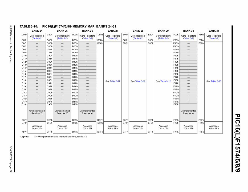
TABLE 3-10: PIC16(L)F1574/5/8/9 MEMORY MAP, BANKS 24-31
Legend: = Unimplemented data memory locations, read as ‘0’
BANK 24 BANK 25 BANK 26 BANK 27 BANK 28 BANK 29 BANK 30 BANK 31
C00h
C0Bh
Core Registers (Table 3-2)
C80h
C8Bh
Core Registers (Table 3-2)
D00h
D0Bh
Core Registers (Table 3-2)
D80h
D8Bh
Core Registers (Table 3-2)
E00h
E0Bh
Core Registers (Table 3-2)
E80h
E8Bh
Core Registers (Table 3-2)
F00h
F0Bh
Core Registers (Table 3-2)
F80h
F8Bh
Core Registers (Table 3-2)
C0Ch — C8Ch — D0Ch — D8Ch
See Table 3-11
E0Ch
See Table 3-12
E8Ch
See Table 3-12
F0Ch — F8Ch
See Table 3-13
C0Dh — C8Dh — D0Dh — F0Dh —
C0Eh — C8Eh — D0Eh — F0Eh —
C0Fh — C8Fh — D0Fh — F0Fh —
C10h — C90h — D10h — F10h —
C11h — C91h — D11h — F11h —
C12h — C92h — D12h — F12h —
C13h — C93h — D13h — F13h —
C14h — C94h — D14h — F14h —
C15h — C95h — D15h — F15h —
C16h — C96h — D16h — F16h —
C17h — C97h — D17h — F17h —
C18h — C98h — D18h — F18h —
C19h — C99h — D19h — F19h —
C1Ah — C9Ah — D1Ah — F1Ah —
C1Bh — C9Bh — D1Bh — F1Bh —
C1Ch — C9Ch — D1Ch — F1Ch —
C1Dh — C9Dh — D1Dh — F1Dh —
C1Eh — C9Eh — D1Eh — F1Eh —
C1Fh — C9Fh — D1Fh — F1Fh —C20h
UnimplementedRead as ‘0’
CA0h
UnimplementedRead as ‘0’
D20h
UnimplementedRead as ‘0’
F20h
UnimplementedRead as ‘0’
C6Fh CEFh D6Fh DEFh E6Fh EEFh F6Fh FEFhC70h
Accesses70h – 7Fh
CF0h
Accesses70h – 7Fh
D70h
Accesses70h – 7Fh
DF0h
Accesses70h – 7Fh
E70h
Accesses70h – 7Fh
EF0h
Accesses70h – 7Fh
F70h
Accesses70h – 7Fh
FF0h
Accesses70h – 7Fh
CFFh CFFh D7Fh DFFh E7Fh EFFh F7Fh FFFh
2016 Microchip Technology Inc. DS40001782C-page 33
PIC16(L)F1574/5/8/9
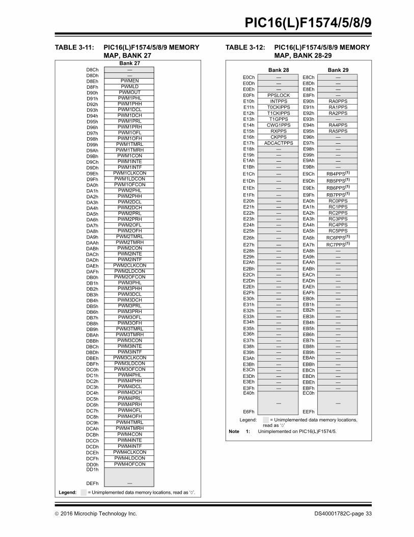
TABLE 3-11: PIC16(L)F1574/5/8/9 MEMORY MAP, BANK 27
TABLE 3-12: PIC16(L)F1574/5/8/9 MEMORY MAP, BANK 28-29
Bank 27D8Ch —D8Dh —D8Eh PWMEND8Fh PWMLDD90h PWMOUTD91h PWM1PHLD92h PWM1PHHD93h PWM1DCLD94h PWM1DCHD95h PWM1PRLD96h PWM1PRHD97h PWM1OFLD98h PWM1OFHD99h PWM1TMRLD9Ah PWM1TMRHD9Bh PWM1COND9Ch PWM1INTED9Dh PWM1INTFD9Eh PWM1CLKCOND9Fh PWM1LDCONDA0h PWM1OFCONDA1h PWM2PHLDA2h PWM2PHHDA3h PWM2DCLDA4h PWM2DCHDA5h PWM2PRLDA6h PWM2PRHDA7h PWM2OFLDA8h PWM2OFHDA9h PWM2TMRLDAAh PWM2TMRHDABh PWM2CONDACh PWM2INTEDADh PWM2INTFDAEh PWM2CLKCONDAFh PWM2LDCONDB0h PWM2OFCONDB1h PWM3PHLDB2h PWM3PHHDB3h PWM3DCLDB4h PWM3DCHDB5h PWM3PRLDB6h PWM3PRHDB7h PWM3OFLDB8h PWM3OFHDB9h PWM3TMRLDBAh PWM3TMRHDBBh PWM3CONDBCh PWM3INTEDBDh PWM3INTFDBEh PWM3CLKCONDBFh PWM3LDCONDC0h PWM3OFCONDC1h PWM4PHLDC2h PWM4PHHDC3h PWM4DCLDC4h PWM4DCH
DC5h PWM4PRL
DC6h PWM4PRHDC7h PWM4OFL
DC8h PWM4OFHDC9h PWM4TMRLDCAh PWM4TMRH
DCBh PWM4CONDCCh PWM4INTE
DCDh PWM4INTFDCEh PWM4CLKCONDCFh PWM4LDCON
DD0h PWM4OFCONDD1h
—DEFh
Legend: = Unimplemented data memory locations, read as ‘0’.
Legend: = Unimplemented data memory locations, read as ‘0’
Note 1: Unimplemented on PIC16(L)F1574/5.
Bank 28 Bank 29E0Ch — E8Ch —E0Dh — E8Dh —E0Eh — E8Eh —E0Fh PPSLOCK E8Fh —E10h INTPPS E90h RA0PPSE11h T0CKIPPS E91h RA1PPSE12h T1CKIPPS E92h RA2PPSE13h T1GPPS E93h —E14h CWG1PPS E94h RA4PPSE15h RXPPS E95h RA5PPSE16h CKPPS E96h —E17h ADCACTPPS E97h —E18h — E98h —E19h — E99h —E1Ah — E9Ah —E1Bh — E9Bh —
E1Ch — E9Ch RB4PPS(1)
E1Dh — E9Dh RB5PPS(1)
E1Eh — E9Eh RB6PPS(1)
E1Fh — E9Fh RB7PPS(1)
E20h — EA0h RC0PPSE21h — EA1h RC1PPSE22h — EA2h RC2PPSE23h — EA3h RC3PPSE24h — EA4h RC4PPSE25h — EA5h RC5PPS
E26h — EA6h RC6PPS(1)
E27h — EA7h RC7PPS(1)
E28h — EA8h —E29h — EA9h —E2Ah — EAAh —E2Bh — EABh —E2Ch — EACh —E2Dh — EADh —E2Eh — EAEh —E2Fh — EAFh —E30h — EB0h —E31h — EB1h —E32h — EB2h —E33h — EB3h —E34h — EB4h —E35h — EB5h —E36h — EB6h —E37h — EB7h —E38h — EB8h —E39h — EB9h —E3Ah — EBAh —E3Bh — EBBh —E3Ch — EBCh —E3Dh — EBDh —E3Eh — EBEh —E3Fh — EBFh —E40h
—
EC0h
—
E6Fh EEFh

PIC16(L)F1574/5/8/9
DS40001782C-page 34 2016 Microchip Technology Inc.
TABLE 3-13: PIC16(L)F1574/5/8/9 MEMORY MAP, BANK 31
Bank 31F8Ch
FE3h
UnimplementedRead as ‘0’
FE4h STATUS_SHADFE5h WREG_SHADFE6h BSR_SHADFE7h PCLATH_SHADFE8h FSR0L_SHADFE9h FSR0H_SHADFEAh FSR1L_SHADFEBh FSR1H_SHADFECh —FEDh STKPTRFEEh TOSLFEFh TOSH
Legend: = Unimplemented data memory locations, read as ‘0’.

2016 Microchip Technology Inc. DS40001782C-page 35
PIC16(L)F1574/5/8/9
3.3.6 CORE FUNCTION REGISTERS SUMMARY
The Core Function registers listed in Table 3-14 canbe addressed from any Bank.
TABLE 3-14: CORE FUNCTION REGISTERS SUMMARY
Addr Name Bit 7 Bit 6 Bit 5 Bit 4 Bit 3 Bit 2 Bit 1 Bit 0Value on
POR, BORValue on all other Resets
Bank 0-31
x00h or x80h
INDF0Addressing this location uses contents of FSR0H/FSR0L to address data memory(not a physical register)
xxxx xxxx uuuu uuuu
x01h or x81h
INDF1Addressing this location uses contents of FSR1H/FSR1L to address data memory(not a physical register)
xxxx xxxx uuuu uuuu
x02h or x82h
PCL Program Counter (PC) Least Significant Byte 0000 0000 0000 0000
x03h or x83h
STATUS — — — TO PD Z DC C ---1 1000 ---q quuu
x04h or x84h
FSR0L Indirect Data Memory Address 0 Low Pointer 0000 0000 uuuu uuuu
x05h or x85h
FSR0H Indirect Data Memory Address 0 High Pointer 0000 0000 0000 0000
x06h or x86h
FSR1L Indirect Data Memory Address 1 Low Pointer 0000 0000 uuuu uuuu
x07h or x87h
FSR1H Indirect Data Memory Address 1 High Pointer 0000 0000 0000 0000
x08h or x88h
BSR — — — BSR<4:0> ---0 0000 ---0 0000
x09h or x89h
WREG Working Register 0000 0000 uuuu uuuu
x0Ah or x8Ah
PCLATH — Write Buffer for the upper 7 bits of the Program Counter -000 0000 -000 0000
x0Bh or x8Bh
INTCON GIE PEIE TMR0IE INTE IOCIE TMR0IF INTF IOCIF 0000 0000 0000 0000
Legend: x = unknown, u = unchanged, q = value depends on condition, - = unimplemented, read as ‘0’, r = reserved. Shaded locations are unimplemented, read as ‘0’.
PIC
16(L
)F1
574
/5/8
/9
DS
40
00
17
82
C-p
ag
e 3
6
20
16
Micro
chip
Te
chn
olo
gy In
c.
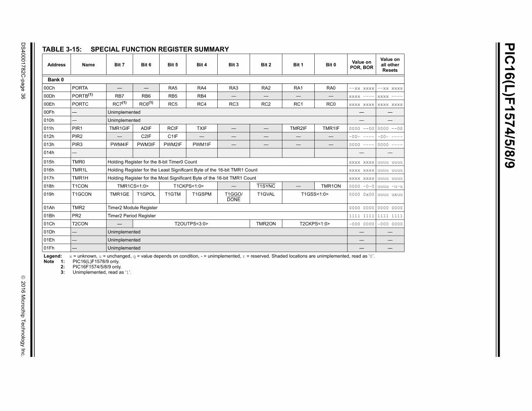
TABLE 3-15: SPECIAL FUNCTION REGISTER SUMMARY
Address Name Bit 7 Bit 6 Bit 5 Bit 4 Bit 3 Bit 2 Bit 1 Bit 0Value on
POR, BOR
Value on all other Resets
Bank 0
00Ch PORTA — — RA5 RA4 RA3 RA2 RA1 RA0 --xx xxxx --xx xxxx
00Dh PORTB(1) RB7 RB6 RB5 RB4 — — — — xxxx ---- xxxx ----
00Eh PORTC RC7(1) RC6(1) RC5 RC4 RC3 RC2 RC1 RC0 xxxx xxxx xxxx xxxx
00Fh — Unimplemented — —
010h — Unimplemented — —
011h PIR1 TMR1GIF ADIF RCIF TXIF — — TMR2IF TMR1IF 0000 --00 0000 --00
012h PIR2 — C2IF C1IF — — — — — -00- ---- -00- ----
013h PIR3 PWM4IF PWM3IF PWM2IF PWM1IF — — — — 0000 ---- 0000 ----
014h — — —
015h TMR0 Holding Register for the 8-bit Timer0 Count xxxx xxxx uuuu uuuu
016h TMR1L Holding Register for the Least Significant Byte of the 16-bit TMR1 Count xxxx xxxx uuuu uuuu
017h TMR1H Holding Register for the Most Significant Byte of the 16-bit TMR1 Count xxxx xxxx uuuu uuuu
018h T1CON TMR1CS<1:0> T1CKPS<1:0> — T1SYNC — TMR1ON 0000 -0-0 uuuu -u-u
019h T1GCON TMR1GE T1GPOL T1GTM T1GSPM T1GGO/DONE
T1GVAL T1GSS<1:0> 0000 0x00 uuuu uxuu
01Ah TMR2 Timer2 Module Register 0000 0000 0000 0000
01Bh PR2 Timer2 Period Register 1111 1111 1111 1111
01Ch T2CON — T2OUTPS<3:0> TMR2ON T2CKPS<1:0> -000 0000 -000 0000
01Dh — Unimplemented — —
01Eh — Unimplemented — —
01Fh — Unimplemented — —
Legend: x = unknown, u = unchanged, q = value depends on condition, - = unimplemented, r = reserved. Shaded locations are unimplemented, read as ‘0’.Note 1: PIC16(L)F1578/9 only.
2: PIC16F1574/5/8/9 only.3: Unimplemented, read as ‘1’.

2
01
6 M
icroch
ip T
ech
no
log
y Inc.
DS
40
00
17
82
C-p
ag
e 3
7
PIC
16(L
)F15
74/5/8/9
Bank 1
08Ch TRISA — — TRISA5 TRISA4 —(3) TRISA2 TRISA1 TRISA0 --11 1111 --11 1111
08Dh TRISB(1) TRISB7 TRISB6 TRISB5 TRISB4 — — — — 1111 ---- 1111 ----
08Eh TRISC TRISC7(1) TRISC6(1) TRISC5 TRISC4 TRISC3 TRISC2 TRISC1 TRISC0 1111 1111 1111 1111
08Fh — Unimplemented — —
090h — Unimplemented — —
091h PIE1 TMR1GIE ADIE RCIE TXIE — — TMR2IE TMR1IE 0000 --00 0000 --00
092h PIE2 — C2IE C1IE — — — — — -00- ---- -00- ----
093h PIE3 PWM4IE PWM3IE PWM2IE PWM1IE — — — — 0000 ---- 0000 ----
094h — — —
095h OPTION_REG WPUEN INTEDG TMR0CS TMR0SE PSA PS<2:0> 1111 1111 1111 1111
096h PCON STKOVF STKUNF — RWDT RMCLR RI POR BOR 00-1 11qq qq-q qquu
097h WDTCON — — WDTPS<4:0> SWDTEN --01 0110 --01 0110
098h OSCTUNE — — TUN<5:0> --00 0000 --00 0000
099h OSCCON SPLLEN IRCF<3:0> — SCS<1:0> 0011 1-00 0011 1-00
09Ah OSCSTAT — PLLR OSTS HFIOFR HFIOFL MFIOFR LFIOFR HFIOFS -0q0 0q00 -qqq qqqq
09Bh ADRESL ADC Result Register Low xxxx xxxx uuuu uuuu
09Ch ADRESH ADC Result Register High xxxx xxxx uuuu uuuu
09Dh ADCON0 — CHS<4:0> GO/DONE ADON -000 0000 -000 0000
09Eh ADCON1 ADFM ADCS<2:0> — — ADPREF<1:0> 0000 --00 0000 --00
09Fh ADCON2 TRIGSEL<3:0> — — — — 0000 ---- 0000 ----
TABLE 3-15: SPECIAL FUNCTION REGISTER SUMMARY (CONTINUED)
Address Name Bit 7 Bit 6 Bit 5 Bit 4 Bit 3 Bit 2 Bit 1 Bit 0Value on
POR, BOR
Value on all other Resets
Legend: x = unknown, u = unchanged, q = value depends on condition, - = unimplemented, r = reserved. Shaded locations are unimplemented, read as ‘0’.Note 1: PIC16(L)F1578/9 only.
2: PIC16F1574/5/8/9 only.3: Unimplemented, read as ‘1’.
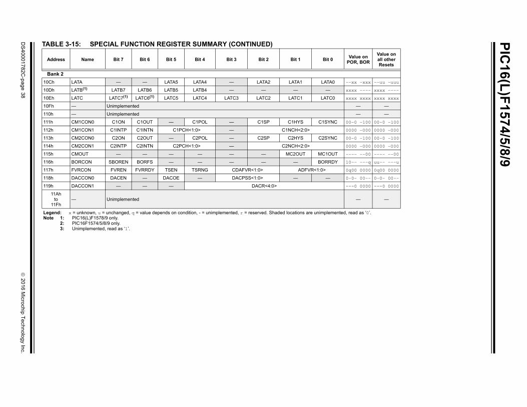
PIC
16(L
)F1
574
/5/8
/9
DS
40
00
17
82
C-p
ag
e 3
8
20
16
Micro
chip
Te
chn
olo
gy In
c.
Bank 2
10Ch LATA — — LATA5 LATA4 — LATA2 LATA1 LATA0 --xx -xxx --uu -uuu
10Dh LATB(1) LATB7 LATB6 LATB5 LATB4 — — — — xxxx ---- xxxx ----
10Eh LATC LATC7(1) LATC6(1) LATC5 LATC4 LATC3 LATC2 LATC1 LATC0 xxxx xxxx xxxx xxxx
10Fh — Unimplemented — —
110h — Unimplemented — —
111h CM1CON0 C1ON C1OUT — C1POL — C1SP C1HYS C1SYNC 00-0 -100 00-0 -100
112h CM1CON1 C1INTP C1INTN C1PCH<1:0> — C1NCH<2:0> 0000 -000 0000 -000
113h CM2CON0 C2ON C2OUT — C2POL — C2SP C2HYS C2SYNC 00-0 -100 00-0 -100
114h CM2CON1 C2INTP C2INTN C2PCH<1:0> — C2NCH<2:0> 0000 -000 0000 -000
115h CMOUT — — — — — — MC2OUT MC1OUT ---- --00 ---- --00
116h BORCON SBOREN BORFS — — — — — BORRDY 10-- ---q uu-- ---u
117h FVRCON FVREN FVRRDY TSEN TSRNG CDAFVR<1:0> ADFVR<1:0> 0q00 0000 0q00 0000
118h DACCON0 DACEN — DACOE — DACPSS<1:0> — — 0-0- 00-- 0-0- 00--
119h DACCON1 — — — DACR<4:0> ---0 0000 ---0 0000
11Ahto
11Fh— Unimplemented — —
TABLE 3-15: SPECIAL FUNCTION REGISTER SUMMARY (CONTINUED)
Address Name Bit 7 Bit 6 Bit 5 Bit 4 Bit 3 Bit 2 Bit 1 Bit 0Value on
POR, BOR
Value on all other Resets
Legend: x = unknown, u = unchanged, q = value depends on condition, - = unimplemented, r = reserved. Shaded locations are unimplemented, read as ‘0’.Note 1: PIC16(L)F1578/9 only.
2: PIC16F1574/5/8/9 only.3: Unimplemented, read as ‘1’.
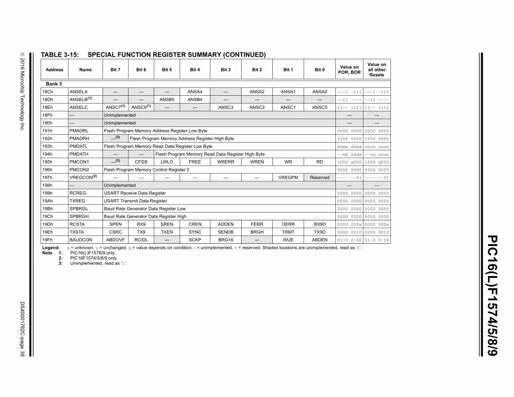
2
01
6 M
icroch
ip T
ech
no
log
y Inc.
DS
40
00
17
82
C-p
ag
e 3
9
PIC
16(L
)F15
74/5/8/9
Bank 3
18Ch ANSELA — — — ANSA4 — ANSA2 ANSA1 ANSA0 ---1 -111 ---1 -111
18Dh ANSELB(1) — — ANSB5 ANSB4 — — — — --11 ---- --11 ----
18Eh ANSELC ANSC7(1) ANSC6(1) — — ANSC3 ANSC2 ANSC1 ANSC0 11-- 1111 11-- 1111
18Fh — Unimplemented — —
190h — Unimplemented — —
191h PMADRL Flash Program Memory Address Register Low Byte 0000 0000 0000 0000
192h PMADRH —(3) Flash Program Memory Address Register High Byte 1000 0000 1000 0000
193h PMDATL Flash Program Memory Read Data Register Low Byte xxxx xxxx uuuu uuuu
194h PMDATH — — Flash Program Memory Read Data Register High Byte --xx xxxx --uu uuuu
195h PMCON1 —(3) CFGS LWLO FREE WRERR WREN WR RD 1000 x000 1000 q000
196h PMCON2 Flash Program Memory Control Register 2 0000 0000 0000 0000
197h VREGCON(2) — — — — — — VREGPM Reserved ---- --01 ---- --01
198h — Unimplemented — —
199h RCREG USART Receive Data Register 0000 0000 0000 0000
19Ah TXREG USART Transmit Data Register 0000 0000 0000 0000
19Bh SPBRGL Baud Rate Generator Data Register Low 0000 0000 0000 0000
19Ch SPBRGH Baud Rate Generator Data Register High 0000 0000 0000 0000
19Dh RCSTA SPEN RX9 SREN CREN ADDEN FERR OERR RX9D 0000 000x 0000 000x
19Eh TXSTA CSRC TX9 TXEN SYNC SENDB BRGH TRMT TX9D 0000 0010 0000 0010
19Fh BAUDCON ABDOVF RCIDL — SCKP BRG16 — WUE ABDEN 01-0 0-00 01-0 0-00
TABLE 3-15: SPECIAL FUNCTION REGISTER SUMMARY (CONTINUED)
Address Name Bit 7 Bit 6 Bit 5 Bit 4 Bit 3 Bit 2 Bit 1 Bit 0Value on
POR, BOR
Value on all other Resets
Legend: x = unknown, u = unchanged, q = value depends on condition, - = unimplemented, r = reserved. Shaded locations are unimplemented, read as ‘0’.Note 1: PIC16(L)F1578/9 only.
2: PIC16F1574/5/8/9 only.3: Unimplemented, read as ‘1’.
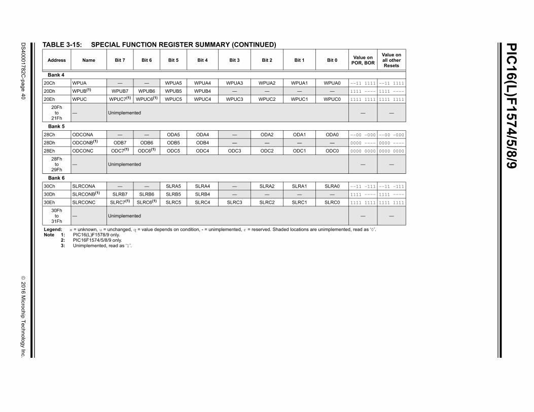
PIC
16(L
)F1
574
/5/8
/9
DS
40
00
17
82
C-p
ag
e 4
0
20
16
Micro
chip
Te
chn
olo
gy In
c.
Bank 4
20Ch WPUA — — WPUA5 WPUA4 WPUA3 WPUA2 WPUA1 WPUA0 --11 1111 --11 1111
20Dh WPUB(1) WPUB7 WPUB6 WPUB5 WPUB4 — — — — 1111 ---- 1111 ----
20Eh WPUC WPUC7(1) WPUC6(1) WPUC5 WPUC4 WPUC3 WPUC2 WPUC1 WPUC0 1111 1111 1111 1111
20Fhto
21Fh— Unimplemented — —
Bank 5
28Ch ODCONA — — ODA5 ODA4 — ODA2 ODA1 ODA0 --00 -000 --00 -000
28Dh ODCONB(1) ODB7 ODB6 ODB5 ODB4 — — — — 0000 ---- 0000 ----
28Eh ODCONC ODC7(1) ODC6(1) ODC5 ODC4 ODC3 ODC2 ODC1 ODC0 0000 0000 0000 0000
28Fhto
29Fh— Unimplemented — —
Bank 6
30Ch SLRCONA — — SLRA5 SLRA4 — SLRA2 SLRA1 SLRA0 --11 -111 --11 -111
30Dh SLRCONB(1) SLRB7 SLRB6 SLRB5 SLRB4 — — — — 1111 ---- 1111 ----
30Eh SLRCONC SLRC7(1) SLRC6(1) SLRC5 SLRC4 SLRC3 SLRC2 SLRC1 SLRC0 1111 1111 1111 1111
30Fhto
31Fh— Unimplemented — —
TABLE 3-15: SPECIAL FUNCTION REGISTER SUMMARY (CONTINUED)
Address Name Bit 7 Bit 6 Bit 5 Bit 4 Bit 3 Bit 2 Bit 1 Bit 0Value on
POR, BOR
Value on all other Resets
Legend: x = unknown, u = unchanged, q = value depends on condition, - = unimplemented, r = reserved. Shaded locations are unimplemented, read as ‘0’.Note 1: PIC16(L)F1578/9 only.
2: PIC16F1574/5/8/9 only.3: Unimplemented, read as ‘1’.
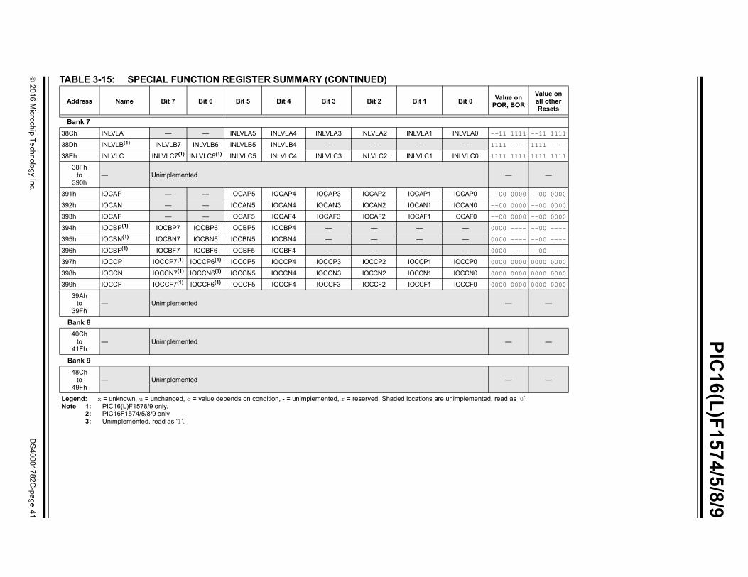
2
01
6 M
icroch
ip T
ech
no
log
y Inc.
DS
40
00
17
82
C-p
ag
e 4
1
PIC
16(L
)F15
74/5/8/9
Bank 7
38Ch INLVLA — — INLVLA5 INLVLA4 INLVLA3 INLVLA2 INLVLA1 INLVLA0 --11 1111 --11 1111
38Dh INLVLB(1) INLVLB7 INLVLB6 INLVLB5 INLVLB4 — — — — 1111 ---- 1111 ----
38Eh INLVLC INLVLC7(1) INLVLC6(1) INLVLC5 INLVLC4 INLVLC3 INLVLC2 INLVLC1 INLVLC0 1111 1111 1111 1111
38Fhto
390h— Unimplemented — —
391h IOCAP — — IOCAP5 IOCAP4 IOCAP3 IOCAP2 IOCAP1 IOCAP0 --00 0000 --00 0000
392h IOCAN — — IOCAN5 IOCAN4 IOCAN3 IOCAN2 IOCAN1 IOCAN0 --00 0000 --00 0000
393h IOCAF — — IOCAF5 IOCAF4 IOCAF3 IOCAF2 IOCAF1 IOCAF0 --00 0000 --00 0000
394h IOCBP(1) IOCBP7 IOCBP6 IOCBP5 IOCBP4 — — — — 0000 ---- --00 ----
395h IOCBN(1) IOCBN7 IOCBN6 IOCBN5 IOCBN4 — — — — 0000 ---- --00 ----
396h IOCBF(1) IOCBF7 IOCBF6 IOCBF5 IOCBF4 — — — — 0000 ---- --00 ----
397h IOCCP IOCCP7(1) IOCCP6(1) IOCCP5 IOCCP4 IOCCP3 IOCCP2 IOCCP1 IOCCP0 0000 0000 0000 0000
398h IOCCN IOCCN7(1) IOCCN6(1) IOCCN5 IOCCN4 IOCCN3 IOCCN2 IOCCN1 IOCCN0 0000 0000 0000 0000
399h IOCCF IOCCF7(1) IOCCF6(1) IOCCF5 IOCCF4 IOCCF3 IOCCF2 IOCCF1 IOCCF0 0000 0000 0000 0000
39Ahto
39Fh— Unimplemented — —
Bank 8
40Chto
41Fh— Unimplemented — —
Bank 9
48Chto
49Fh— Unimplemented — —
TABLE 3-15: SPECIAL FUNCTION REGISTER SUMMARY (CONTINUED)
Address Name Bit 7 Bit 6 Bit 5 Bit 4 Bit 3 Bit 2 Bit 1 Bit 0Value on
POR, BOR
Value on all other Resets
Legend: x = unknown, u = unchanged, q = value depends on condition, - = unimplemented, r = reserved. Shaded locations are unimplemented, read as ‘0’.Note 1: PIC16(L)F1578/9 only.
2: PIC16F1574/5/8/9 only.3: Unimplemented, read as ‘1’.

PIC
16(L
)F1
574
/5/8
/9
DS
40
00
17
82
C-p
ag
e 4
2
20
16
Micro
chip
Te
chn
olo
gy In
c.
Bank 10
50Chto
51Fh— Unimplemented — —
Bank 11
58Chto
59Fh— Unimplemented — —
Bank 12
60Chto
61Fh— Unimplemented — —
Bank 13
68Chto
690h— Unimplemented — —
691h CWG1DBR — — CWG1DBR<5:0> --00 0000 --00 0000
692h CWG1DBF — — CWG1DBF<5:0> --xx xxxx --xx xxxx
693h CWG1CON0 G1EN — — G1POLB G1POLA — — G1CS0 0--0 0--0 0--0 0--0
694h CWG1CON1 G1ASDLB<1:0> G1ASDLA<1:0> — G1IS<2:0> 0000 -000 0000 -000
695h CWG1CON2 G1ASE G1ARSEN — — G1ASDSC2 G1ASDSC1 G1ASDSPPS — 00-- 000- 00-- 000-
696hto
69Fh— Unimplemented — —
Banks 14-26
x0Ch/x8Ch —x1Fh/x9Fh
— Unimplemented — —
TABLE 3-15: SPECIAL FUNCTION REGISTER SUMMARY (CONTINUED)
Address Name Bit 7 Bit 6 Bit 5 Bit 4 Bit 3 Bit 2 Bit 1 Bit 0Value on
POR, BOR
Value on all other Resets
Legend: x = unknown, u = unchanged, q = value depends on condition, - = unimplemented, r = reserved. Shaded locations are unimplemented, read as ‘0’.Note 1: PIC16(L)F1578/9 only.
2: PIC16F1574/5/8/9 only.3: Unimplemented, read as ‘1’.

2
01
6 M
icroch
ip T
ech
no
log
y Inc.
DS
40
00
17
82
C-p
ag
e 4
3
PIC
16(L
)F15
74/5/8/9
Bank 27
D8Ch — Unimplemented — —
D8Dh — Unimplemented — —
D8Eh PWMEN — — — — PWM4EN_A PWM3EN_A PWM2EN_A PWM1EN_A ---- 0000 ---- 0000
D8Fh PWMLD — — — — PWM4LDA_A PWM3LDA_A PWM2LDA_A PWM1LDA_A ---- 0000 ---- 0000
D90h PWMOUT — — — — PWM4OUT_A PWM3OUT_A PWM2OUT_A PWM1OUT_A ---- 0000 ---- 0000
D91h PWM1PHL PH<7:0> xxxx xxxx uuuu uuuu
D92h PWM1PHH PH<15:8> xxxx xxxx uuuu uuuu
D93h PWM1DCL DC<7:0> xxxx xxxx uuuu uuuu
D94h PWM1DCH DC<15:8> xxxx xxxx uuuu uuuu
D95h PWM1PRL PR<7:0> xxxx xxxx uuuu uuuu
D96h PWM1PRH PR<15:8> xxxx xxxx uuuu uuuu
D97h PWM1OFL OF<7:0> xxxx xxxx uuuu uuuu
D98h PWM1OFH OF<15:8> xxxx xxxx uuuu uuuu
D99h PWM1TMRL TMR<7:0> xxxx xxxx uuuu uuuu
D9Ah PWM1TMRH TMR<15:8> xxxx xxxx uuuu uuuu
D9Bh PWM1CON EN — OUT POL MODE<1:0> — — 0-00 00-- 0-00 00--
D9Ch PWM1INTE — — — — OFIE PHIE DCIE PRIE ---- 000 ---- 000
D9Dh PWM1INTF — — — — OFIF PHIF DCIF PRIF ---- 000 ---- 000
D9Eh PWM1CLKCON — PS<2:0> — — CS<1:0> -000 -000 -000 --00
D9Fh PWM1LDCON LDA LDT — — — — LDS<1:0> 00-- -000 00-- --00
DA0h PWM1OFCON — OFM<1:0> OFO — — OFS<1:0> -000 -000 -000 --00
DA1h PWM2PHL PH<7:0> xxxx xxxx uuuu uuuu
DA2h PWM2PHH PH<15:8> xxxx xxxx uuuu uuuu
DA3h PWM2DCL DC<7:0> xxxx xxxx uuuu uuuu
DA4h PWM2DCH DC<15:8> xxxx xxxx uuuu uuuu
DA5h PWM2PRL PR<7:0> xxxx xxxx uuuu uuuu
DA6h PWM2PRH PR<15:8> xxxx xxxx uuuu uuuu
DA7h PWM2OFL OF<7:0> xxxx xxxx uuuu uuuu
DA8h PWM2OFH OF<15:8> xxxx xxxx uuuu uuuu
DA9h PWM2TMRL TMR<7:0> xxxx xxxx uuuu uuuu
DAAh PWM2TMRH TMR<15:8> xxxx xxxx uuuu uuuu
TABLE 3-15: SPECIAL FUNCTION REGISTER SUMMARY (CONTINUED)
Address Name Bit 7 Bit 6 Bit 5 Bit 4 Bit 3 Bit 2 Bit 1 Bit 0Value on
POR, BOR
Value on all other Resets
Legend: x = unknown, u = unchanged, q = value depends on condition, - = unimplemented, r = reserved. Shaded locations are unimplemented, read as ‘0’.Note 1: PIC16(L)F1578/9 only.
2: PIC16F1574/5/8/9 only.3: Unimplemented, read as ‘1’.
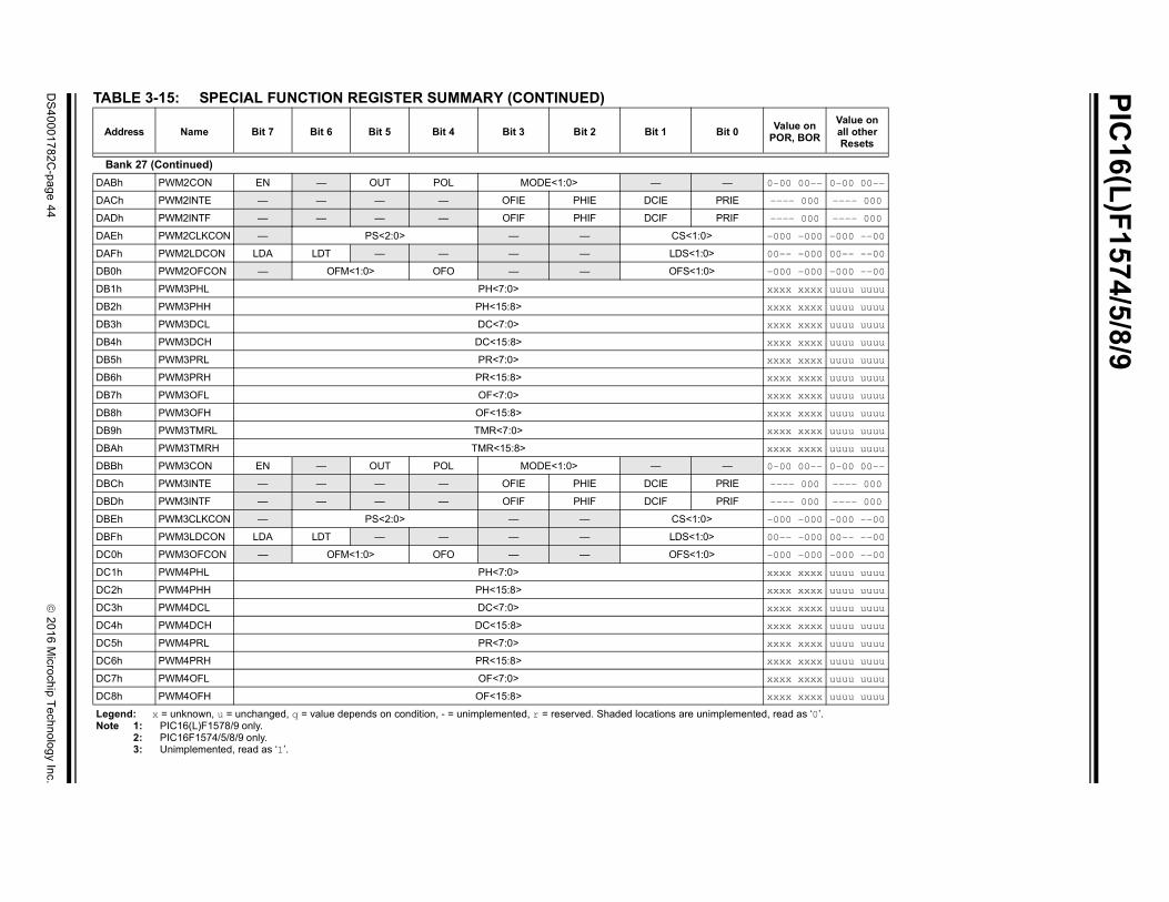
PIC
16(L
)F1
574
/5/8
/9
DS
40
00
17
82
C-p
ag
e 4
4
20
16
Micro
chip
Te
chn
olo
gy In
c.
Bank 27 (Continued)
DABh PWM2CON EN — OUT POL MODE<1:0> — — 0-00 00-- 0-00 00--
DACh PWM2INTE — — — — OFIE PHIE DCIE PRIE ---- 000 ---- 000
DADh PWM2INTF — — — — OFIF PHIF DCIF PRIF ---- 000 ---- 000
DAEh PWM2CLKCON — PS<2:0> — — CS<1:0> -000 -000 -000 --00
DAFh PWM2LDCON LDA LDT — — — — LDS<1:0> 00-- -000 00-- --00
DB0h PWM2OFCON — OFM<1:0> OFO — — OFS<1:0> -000 -000 -000 --00
DB1h PWM3PHL PH<7:0> xxxx xxxx uuuu uuuu
DB2h PWM3PHH PH<15:8> xxxx xxxx uuuu uuuu
DB3h PWM3DCL DC<7:0> xxxx xxxx uuuu uuuu
DB4h PWM3DCH DC<15:8> xxxx xxxx uuuu uuuu
DB5h PWM3PRL PR<7:0> xxxx xxxx uuuu uuuu
DB6h PWM3PRH PR<15:8> xxxx xxxx uuuu uuuu
DB7h PWM3OFL OF<7:0> xxxx xxxx uuuu uuuu
DB8h PWM3OFH OF<15:8> xxxx xxxx uuuu uuuu
DB9h PWM3TMRL TMR<7:0> xxxx xxxx uuuu uuuu
DBAh PWM3TMRH TMR<15:8> xxxx xxxx uuuu uuuu
DBBh PWM3CON EN — OUT POL MODE<1:0> — — 0-00 00-- 0-00 00--
DBCh PWM3INTE — — — — OFIE PHIE DCIE PRIE ---- 000 ---- 000
DBDh PWM3INTF — — — — OFIF PHIF DCIF PRIF ---- 000 ---- 000
DBEh PWM3CLKCON — PS<2:0> — — CS<1:0> -000 -000 -000 --00
DBFh PWM3LDCON LDA LDT — — — — LDS<1:0> 00-- -000 00-- --00
DC0h PWM3OFCON — OFM<1:0> OFO — — OFS<1:0> -000 -000 -000 --00
DC1h PWM4PHL PH<7:0> xxxx xxxx uuuu uuuu
DC2h PWM4PHH PH<15:8> xxxx xxxx uuuu uuuu
DC3h PWM4DCL DC<7:0> xxxx xxxx uuuu uuuu
DC4h PWM4DCH DC<15:8> xxxx xxxx uuuu uuuu
DC5h PWM4PRL PR<7:0> xxxx xxxx uuuu uuuu
DC6h PWM4PRH PR<15:8> xxxx xxxx uuuu uuuu
DC7h PWM4OFL OF<7:0> xxxx xxxx uuuu uuuu
DC8h PWM4OFH OF<15:8> xxxx xxxx uuuu uuuu
TABLE 3-15: SPECIAL FUNCTION REGISTER SUMMARY (CONTINUED)
Address Name Bit 7 Bit 6 Bit 5 Bit 4 Bit 3 Bit 2 Bit 1 Bit 0Value on
POR, BOR
Value on all other Resets
Legend: x = unknown, u = unchanged, q = value depends on condition, - = unimplemented, r = reserved. Shaded locations are unimplemented, read as ‘0’.Note 1: PIC16(L)F1578/9 only.
2: PIC16F1574/5/8/9 only.3: Unimplemented, read as ‘1’.
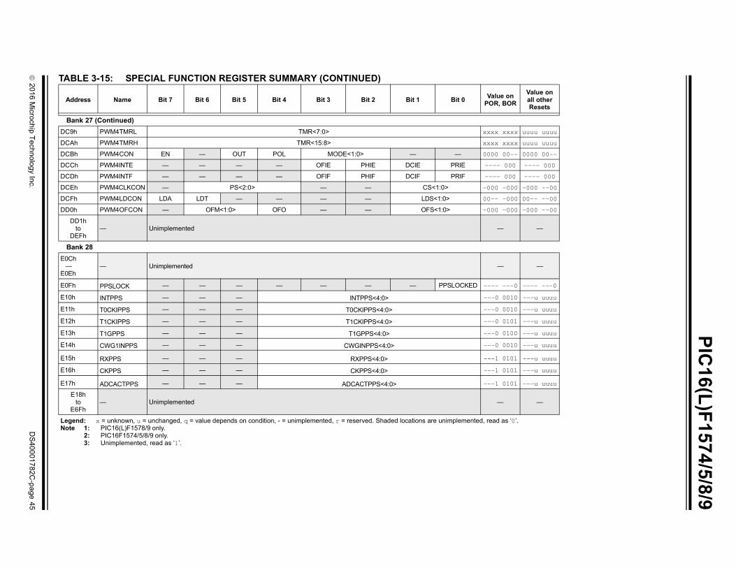
2
01
6 M
icroch
ip T
ech
no
log
y Inc.
DS
40
00
17
82
C-p
ag
e 4
5
PIC
16(L
)F15
74/5/8/9
Bank 27 (Continued)
DC9h PWM4TMRL TMR<7:0> xxxx xxxx uuuu uuuu
DCAh PWM4TMRH TMR<15:8> xxxx xxxx uuuu uuuu
DCBh PWM4CON EN — OUT POL MODE<1:0> — — 0000 00-- 0000 00--
DCCh PWM4INTE — — — — OFIE PHIE DCIE PRIE ---- 000 ---- 000
DCDh PWM4INTF — — — — OFIF PHIF DCIF PRIF ---- 000 ---- 000
DCEh PWM4CLKCON — PS<2:0> — — CS<1:0> -000 -000 -000 --00
DCFh PWM4LDCON LDA LDT — — — — LDS<1:0> 00-- -000 00-- --00
DD0h PWM4OFCON — OFM<1:0> OFO — — OFS<1:0> -000 -000 -000 --00
DD1hto
DEFh— Unimplemented — —
Bank 28
E0Ch —E0Eh
— Unimplemented — —
E0Fh PPSLOCK — — — — — — — PPSLOCKED ---- ---0 ---- ---0
E10h INTPPS — — — INTPPS<4:0> ---0 0010 ---u uuuu
E11h T0CKIPPS — — — T0CKIPPS<4:0> ---0 0010 ---u uuuu
E12h T1CKIPPS — — — T1CKIPPS<4:0> ---0 0101 ---u uuuu
E13h T1GPPS — — — T1GPPS<4:0> ---0 0100 ---u uuuu
E14h CWG1INPPS — — — CWGINPPS<4:0> ---0 0010 ---u uuuu
E15h RXPPS — — — RXPPS<4:0> ---1 0101 ---u uuuu
E16h CKPPS — — — CKPPS<4:0> ---1 0101 ---u uuuu
E17h ADCACTPPS — — — ADCACTPPS<4:0> ---1 0101 ---u uuuu
E18hto
E6Fh— Unimplemented — —
TABLE 3-15: SPECIAL FUNCTION REGISTER SUMMARY (CONTINUED)
Address Name Bit 7 Bit 6 Bit 5 Bit 4 Bit 3 Bit 2 Bit 1 Bit 0Value on
POR, BOR
Value on all other Resets
Legend: x = unknown, u = unchanged, q = value depends on condition, - = unimplemented, r = reserved. Shaded locations are unimplemented, read as ‘0’.Note 1: PIC16(L)F1578/9 only.
2: PIC16F1574/5/8/9 only.3: Unimplemented, read as ‘1’.

PIC
16(L
)F1
574
/5/8
/9
DS
40
00
17
82
C-p
ag
e 4
6
20
16
Micro
chip
Te
chn
olo
gy In
c.
Bank 29
E8Ch —E8Fh — Unimplemented — —
E90h RA0PPS — — — RA0PPS<4:0> ---0 0000 ---u uuuu
E91h RA1PPS — — — RA1PPS<4:0> ---0 0000 ---u uuuu
E92h RA2PPS — — — RA2PPS<4:0> ---0 0000 ---u uuuu
E93h — Unimplemented — —
E94h RA4PPS — — — RA4PPS<4:0> ---0 0000 ---u uuuu
E95h RA5PPS — — — RA5PPS<4:0> ---0 0000 ---u uuuu
E96h —E9Bh — Unimplemented — —
E9Ch RB4PPS(1) — — — RB4PPS<4:0> ---0 0000 ---u uuuu
E9Dh RB5PPS(1) — — — RB5PPS<4:0> ---0 0000 ---u uuuu
E9Eh RB6PPS(1 — — — RB6PPS<4:0> ---0 0000 ---u uuuu
E9Fh RB7PPS(1) — — — RB7PPS<4:0> ---0 0000 ---u uuuu
EA0h RC0PPS — — — RC0PPS<4:0> ---0 0000 ---u uuuu
EA1h RC1PPS — — — RC1PPS<4:0> ---0 0000 ---u uuuu
EA2h RC2PPS — — — RC2PPS<4:0> ---0 0000 ---u uuuu
EA3h RC3PPS — — — RC3PPS<4:0> ---0 0000 ---u uuuu
EA4h RC4PPS — — — RC4PPS<4:0> ---0 0000 ---u uuuu
EA5h RC5PPS — — — RC5PPS<4:0> ---0 0000 ---u uuuu
EA6h RC6PPS(1) — — — RC6PPS<4:0> ---0 0000 ---u uuuu
EA7h RC7PPS(1) — — — RC7PPS<4:0> ---0 0000 ---u uuuu
EA8h —EEFh — Unimplemented — —
Bank 30
F0Ch —F1Fh
— Unimplemented — —
TABLE 3-15: SPECIAL FUNCTION REGISTER SUMMARY (CONTINUED)
Address Name Bit 7 Bit 6 Bit 5 Bit 4 Bit 3 Bit 2 Bit 1 Bit 0Value on
POR, BOR
Value on all other Resets
Legend: x = unknown, u = unchanged, q = value depends on condition, - = unimplemented, r = reserved. Shaded locations are unimplemented, read as ‘0’.Note 1: PIC16(L)F1578/9 only.
2: PIC16F1574/5/8/9 only.3: Unimplemented, read as ‘1’.

2
01
6 M
icroch
ip T
ech
no
log
y Inc.
DS
40
00
17
82
C-p
ag
e 4
7
PIC
16(L
)F15
74/5/8/9
Bank 31
F8Ch —FE3h
— Unimplemented — —
FE4h STATUS_
SHAD
— — — — — Z_SHAD DC_SHAD C_SHAD ---- -xxx ---- -uuu
FE5h WREG_
SHAD
Working Register Shadow xxxx xxxx uuuu uuuu
FE6h BSR_
SHAD
— — — Bank Select Register Shadow ---x xxxx ---u uuuu
FE7h PCLATH_
SHAD
— Program Counter Latch High Register Shadow -xxx xxxx uuuu uuuu
FE8h FSR0L_
SHAD
Indirect Data Memory Address 0 Low Pointer Shadow xxxx xxxx uuuu uuuu
FE9h FSR0H_
SHAD
Indirect Data Memory Address 0 High Pointer Shadow xxxx xxxx uuuu uuuu
FEAh FSR1L_
SHAD
Indirect Data Memory Address 1 Low Pointer Shadow xxxx xxxx uuuu uuuu
FEBh FSR1H_
SHAD
Indirect Data Memory Address 1 High Pointer Shadow xxxx xxxx uuuu uuuu
FECh — Unimplemented — —
FEDh STKPTR — — — Current Stack Pointer ---1 1111 ---1 1111
FEEh TOSL Top-of-Stack Low byte xxxx xxxx uuuu uuuu
FEFh TOSH — Top-of-Stack High byte -xxx xxxx -uuu uuuu
TABLE 3-15: SPECIAL FUNCTION REGISTER SUMMARY (CONTINUED)
Address Name Bit 7 Bit 6 Bit 5 Bit 4 Bit 3 Bit 2 Bit 1 Bit 0Value on
POR, BOR
Value on all other Resets
Legend: x = unknown, u = unchanged, q = value depends on condition, - = unimplemented, r = reserved. Shaded locations are unimplemented, read as ‘0’.Note 1: PIC16(L)F1578/9 only.
2: PIC16F1574/5/8/9 only.3: Unimplemented, read as ‘1’.
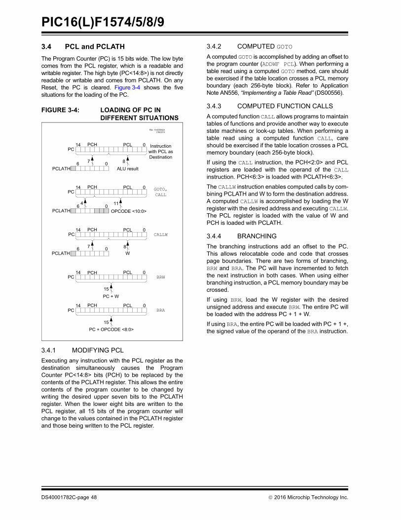
PIC16(L)F1574/5/8/9
DS40001782C-page 48 2016 Microchip Technology Inc.
3.4 PCL and PCLATH
The Program Counter (PC) is 15 bits wide. The low bytecomes from the PCL register, which is a readable andwritable register. The high byte (PC<14:8>) is not directlyreadable or writable and comes from PCLATH. On anyReset, the PC is cleared. Figure 3-4 shows the fivesituations for the loading of the PC.
FIGURE 3-4: LOADING OF PC IN DIFFERENT SITUATIONS
3.4.1 MODIFYING PCL
Executing any instruction with the PCL register as thedestination simultaneously causes the ProgramCounter PC<14:8> bits (PCH) to be replaced by thecontents of the PCLATH register. This allows the entirecontents of the program counter to be changed bywriting the desired upper seven bits to the PCLATHregister. When the lower eight bits are written to thePCL register, all 15 bits of the program counter willchange to the values contained in the PCLATH registerand those being written to the PCL register.
3.4.2 COMPUTED GOTO
A computed GOTO is accomplished by adding an offset tothe program counter (ADDWF PCL). When performing atable read using a computed GOTO method, care shouldbe exercised if the table location crosses a PCL memoryboundary (each 256-byte block). Refer to ApplicationNote AN556, “Implementing a Table Read” (DS00556).
3.4.3 COMPUTED FUNCTION CALLS
A computed function CALL allows programs to maintaintables of functions and provide another way to executestate machines or look-up tables. When performing atable read using a computed function CALL, careshould be exercised if the table location crosses a PCLmemory boundary (each 256-byte block).
If using the CALL instruction, the PCH<2:0> and PCLregisters are loaded with the operand of the CALLinstruction. PCH<6:3> is loaded with PCLATH<6:3>.
The CALLW instruction enables computed calls by com-bining PCLATH and W to form the destination address.A computed CALLW is accomplished by loading the Wregister with the desired address and executing CALLW.The PCL register is loaded with the value of W andPCH is loaded with PCLATH.
3.4.4 BRANCHING
The branching instructions add an offset to the PC.This allows relocatable code and code that crossespage boundaries. There are two forms of branching,BRW and BRA. The PC will have incremented to fetchthe next instruction in both cases. When using eitherbranching instruction, a PCL memory boundary may becrossed.
If using BRW, load the W register with the desiredunsigned address and execute BRW. The entire PC willbe loaded with the address PC + 1 + W.
If using BRA, the entire PC will be loaded with PC + 1 +,the signed value of the operand of the BRA instruction.
7 86
14
0
0
4 11
0
6 0
14
7 86 0
014
15
014
15
014
PCL
PCL
PCL
PCL
PCL
PCH
PCH
PCH
PCH
PCH
PC
PC
PC
PC
PC
PCLATH
PCLATH
PCLATH
Instructionwith PCL asDestination
GOTO, CALL
CALLW
BRW
BRA
ALU result
OPCODE <10:0>
W
PC + W
PC + OPCODE <8:0>
Rev. 10-000042A7/30/2013
2016 Microchip Technology Inc. DS40001782C-page 49
PIC16(L)F1574/5/8/9
3.5 Stack
All devices have a 16-level x 15-bit wide hardwarestack (refer to Figures 3-5 through 3-8). The stackspace is not part of either program or data space. ThePC is PUSHed onto the stack when CALL or CALLWinstructions are executed or an interrupt causes abranch. The stack is POPed in the event of a RETURN,RETLW or a RETFIE instruction execution. PCLATH isnot affected by a PUSH or POP operation.
The stack operates as a circular buffer if the STVRENbit is programmed to ‘0‘ (Configuration Words). Thismeans that after the stack has been PUSHed sixteentimes, the seventeenth PUSH overwrites the value thatwas stored from the first PUSH. The eighteenth PUSHoverwrites the second PUSH (and so on). TheSTKOVF and STKUNF flag bits will be set on an Over-flow/Underflow, regardless of whether the Reset isenabled.
3.5.1 ACCESSING THE STACK
The stack is available through the TOSH, TOSL andSTKPTR registers. STKPTR is the current value of theStack Pointer. TOSH:TOSL register pair points to theTOP of the stack. Both registers are read/writable. TOSis split into TOSH and TOSL due to the 15-bit size of thePC. To access the stack, adjust the value of STKPTR,which will position TOSH:TOSL, then read/write toTOSH:TOSL. STKPTR is five bits to allow detection ofoverflow and underflow.
During normal program operation, CALL, CALLW andInterrupts will increment STKPTR while RETLW,RETURN, and RETFIE will decrement STKPTR. At anytime STKPTR can be inspected to see how much stackis left. The STKPTR always points at the currently usedplace on the stack. Therefore, a CALL or CALLW willincrement the STKPTR and then write the PC, and areturn will unload the PC and then decrement theSTKPTR.
Reference Figure 3-5 through Figure 3-8 for examplesof accessing the stack.
FIGURE 3-5: ACCESSING THE STACK EXAMPLE 1
Note 1: There are no instructions/mnemonicscalled PUSH or POP. These are actionsthat occur from the execution of theCALL, CALLW, RETURN, RETLW andRETFIE instructions or the vectoring toan interrupt address.
Note: Care should be taken when modifying theSTKPTR while interrupts are enabled.
STKPTR = 0x1FStack Reset Disabled(STVREN = 0)
Stack Reset Enabled(STVREN = 1)
Initial Stack Configuration:
After Reset, the stack is empty. Theempty stack is initialized so the StackPointer is pointing at 0x1F. If the StackOverflow/Underflow Reset is enabled, theTOSH/TOSL register will return ‘0’. If theStack Overflow/Underflow Reset isdisabled, the TOSH/TOSL register willreturn the contents of stack address0x0F.
0x0000 STKPTR = 0x1F
TOSH:TOSL 0x0F
0x0E
0x0D
0x0C
0x0B
0x0A
0x09
0x08
0x07
0x06
0x04
0x05
0x03
0x02
0x01
0x00
0x1FTOSH:TOSL
Rev. 10-000043A7/30/2013
PIC16(L)F1574/5/8/9
DS40001782C-page 50 2016 Microchip Technology Inc.
FIGURE 3-6: ACCESSING THE STACK EXAMPLE 2
FIGURE 3-7: ACCESSING THE STACK EXAMPLE 3
STKPTR = 0x00Return Address
This figure shows the stack configurationafter the first CALL or a single interrupt.If a RETURN instruction is executed, thereturn address will be placed in theProgram Counter and the Stack Pointerdecremented to the empty state (0x1F).
0x0F
0x0E
0x0D
0x0C
0x0B
0x0A
0x09
0x08
0x07
0x06
0x04
0x05
0x03
0x02
0x01
0x00TOSH:TOSL
Rev. 10-000043B7/30/2013
STKPTR = 0x06
After seven CALLs or six CALLs and aninterrupt, the stack looks like the figure onthe left. A series of RETURN instructions willrepeatedly place the return addresses intothe Program Counter and pop the stack.
Return Address
0x0F
0x0E
0x0D
0x0C
0x0B
0x0A
0x09
0x08
0x07
0x06
0x04
0x05
0x03
0x02
0x01
0x00
Return Address
Return Address
Return Address
Return Address
Return Address
Return Address
TOSH:TOSL
Rev. 10-000043C7/30/2013

2016 Microchip Technology Inc. DS40001782C-page 51
PIC16(L)F1574/5/8/9
FIGURE 3-8: ACCESSING THE STACK EXAMPLE 4
3.5.2 OVERFLOW/UNDERFLOW RESET
If the STVREN bit in Configuration Words isprogrammed to ‘1’, the device will be reset if the stackis PUSHed beyond the sixteenth level or POPedbeyond the first level, setting the appropriate bits(STKOVF or STKUNF, respectively) in the PCONregister.
3.6 Indirect Addressing
The INDFn registers are not physical registers. Anyinstruction that accesses an INDFn register actuallyaccesses the register at the address specified by theFile Select Registers (FSR). If the FSRn addressspecifies one of the two INDFn registers, the read willreturn ‘0’ and the write will not occur (though Status bitsmay be affected). The FSRn register value is createdby the pair FSRnH and FSRnL.
The FSR registers form a 16-bit address that allows anaddressing space with 65536 locations. These locationsare divided into three memory regions:
• Traditional Data Memory
• Linear Data Memory
• Program Flash Memory
STKPTR = 0x10
When the stack is full, the next CALL oran interrupt will set the Stack Pointer to0x10. This is identical to address 0x00 sothe stack will wrap and overwrite thereturn address at 0x00. If the StackOverflow/Underflow Reset is enabled, aReset will occur and location 0x00 willnot be overwritten.
Return Address0x0F
0x0E
0x0D
0x0C
0x0B
0x0A
0x09
0x08
0x07
0x06
0x04
0x05
0x03
0x02
0x01
0x00
Return Address
Return Address
Return Address
Return Address
Return Address
Return Address
Return Address
Return Address
Return Address
Return Address
Return Address
Return Address
Return Address
Return Address
Return AddressTOSH:TOSL
Rev. 10-000043D7/30/2013

PIC16(L)F1574/5/8/9
DS40001782C-page 52 2016 Microchip Technology Inc.
FIGURE 3-9: INDIRECT ADDRESSING
0x0000
0x0FFF
0x0000
0x7FFF0xFFFF
0x0000
0x0FFF0x1000
0x1FFF0x2000
0x29AF0x29B0
0x7FFF0x8000
Reserved
Reserved
TraditionalData Memory
LinearData Memory
ProgramFlash Memory
FSRAddressRange
Note: Not all memory regions are completely implemented. Consult device memory tables for memory limits.
Rev. 10-000044A7/30/2013
2016 Microchip Technology Inc. DS40001782C-page 53
PIC16(L)F1574/5/8/9
3.6.1 TRADITIONAL DATA MEMORY
The traditional data memory is a region from FSRaddress 0x000 to FSR address 0xFFF. The addressescorrespond to the absolute addresses of all SFR, GPRand common registers.
FIGURE 3-10: TRADITIONAL DATA MEMORY MAP
Direct Addressing
4 0BSR 6 0From Opcode
007 FSRxH
0 0 007 FSRxL
Indirect Addressing
00000 00001 00010 11111
Bank Select Location Select
0x00
0x7F
Bank Select Location Select
Bank 0 Bank 1 Bank 2 Bank 31
Rev. 10-000056A7/31/2013

PIC16(L)F1574/5/8/9
DS40001782C-page 54 2016 Microchip Technology Inc.
3.6.2 LINEAR DATA MEMORY
The linear data memory is the region from FSRaddress 0x2000 to FSR address 0x29AF. This region isa virtual region that points back to the 80-byte blocks ofGPR memory in all the banks.
Unimplemented memory reads as 0x00. Use of thelinear data memory region allows buffers to be largerthan 80 bytes because incrementing the FSR beyondone bank will go directly to the GPR memory of the nextbank.
The 16 bytes of common memory are not included inthe linear data memory region.
FIGURE 3-11: LINEAR DATA MEMORY MAP
3.6.3 PROGRAM FLASH MEMORY
To make constant data access easier, the entireprogram Flash memory is mapped to the upper half ofthe FSR address space. When the MSb of FSRnH isset, the lower 15 bits are the address in programmemory which will be accessed through INDF. Only thelower eight bits of each memory location is accessiblevia INDF. Writing to the program Flash memory cannotbe accomplished via the FSR/INDF interface. Allinstructions that access program Flash memory via theFSR/INDF interface will require one additionalinstruction cycle to complete.
FIGURE 3-12: PROGRAM FLASH MEMORY MAP
0x020Bank 00x06F
0x0A0Bank 10x0EF
0x120Bank 20x16F
0xF20Bank 300xF6F
0 0 10 07 7FSRnH FSRnL
Location Select 0x2000
0x29AF
Rev. 10-000057A7/31/2013
0x0000
Program Flash
Memory (low 8 bits)
0x7FFF
10 07 7FSRnH FSRnL
Location Select 0x8000
0xFFFF
Rev. 10-000058A7/31/2013

2016 Microchip Technology Inc. DS40001782C-page 55
PIC16(L)F1574/5/8/9
4.0 DEVICE CONFIGURATION
Device configuration consists of Configuration Words,Code Protection and Device ID.
4.1 Configuration Words
There are several Configuration Word bits that allowdifferent oscillator and memory protection options.These are implemented as Configuration Word 1 at8007h and Configuration Word 2 at 8008h.
Note: The DEBUG bit in Configuration Words ismanaged automatically by devicedevelopment tools including debuggersand programmers. For normal deviceoperation, this bit should be maintained asa ‘1’.
PIC16(L)F1574/5/8/9
DS40001782C-page 56 2016 Microchip Technology Inc.
4.2 Register Definitions: Configuration Words
REGISTER 4-1: CONFIGURATION WORD 1
U-1 U-1 R/P-1 R/P-1 R/P-1 U-1
— — CLKOUTEN BOREN<1:0>(1) —
bit 13 bit 8
R/P-1 R/P-1 R/P-1 R/P-1 R/P-1 U-1 R/P-1 R/P-1
CP(2) MCLRE PWRTE(1) WDTE<1:0> — FOSC<1:0>
bit 7 bit 0
Legend:
R = Readable bit P = Programmable bit U = Unimplemented bit, read as ‘1’
‘0’ = Bit is cleared ‘1’ = Bit is set n = Value when blank or after Bulk Erase
bit 13-12 Unimplemented: Read as ‘1’
bit 11 CLKOUTEN: Clock Out Enable bit1 = OFF – CLKOUT function is disabled. I/O or oscillator function on CLKOUT pin0 = ON – CLKOUT function is enabled on CLKOUT pin
bit 10-9 BOREN<1:0>: Brown-out Reset Enable bits(1)
11 = ON – Brown-out Reset enabled. The SBOREN bit is ignored.10 = SLEEP – Brown-out Reset enabled while running and disabled in Sleep. The SBOREN bit is ignored.01 = SBODEN– Brown-out Reset controlled by the SBOREN bit in the BORCON register00 = OFF – Brown-out Reset disabled. The SBOREN bit is ignored.
bit 8 Unimplemented: Read as ‘1’
bit 7 CP: Flash Program Memory Code Protection bit(2)
1 = OFF – Code protection off. Program Memory can be read and written. 0 = ON – Code protection on. Program Memory cannot be read or written externally.
bit 6 MCLRE: MCLR/VPP Pin Function Select bitIf LVP bit = 1 (ON):
This bit is ignored. MCLR/VPP pin function is MCLR; Weak pull-up enabled. If LVP bit = 0 (OFF):
1 = ON – MCLR/VPP pin function is MCLR; Weak pull-up enabled.0 = OFF – MCLR/VPP pin function is digital input; MCLR internally disabled; Weak pull-up under control of pin’s WPU
control bit.
bit 5 PWRTE: Power-up Timer Enable bit(1)
1 = OFF– PWRT disabled0 = ON – PWRT enabled
bit 4-3 WDTE<1:0>: Watchdog Timer Enable bit11 = ON – WDT enabled. SWDTEN is ignored.10 = SLEEP – WDT enabled while running and disabled in Sleep. SWDTEN is ignored.01 = SWDTEN– WDT controlled by the SWDTEN bit in the WDTCON register00 = OFF – WDT disabled. SWDTEN is ignored.
bit 2 Unimplemented: Read as ‘1’
bit 1-0 FOSC<1:0>: Oscillator Selection bits11 = ECH – External Clock, High-Power mode: CLKI on CLKI10 = ECM – External Clock, Medium Power mode: CLKI on CLKI01 = ECL – External Clock, Low-Power mode: CLKI on CLKI00 = INTOSC– I/O function on CLKI
Note 1: Enabling Brown-out Reset does not automatically enable Power-up Timer.2: Once enabled, code-protect can only be disabled by bulk erasing the device.
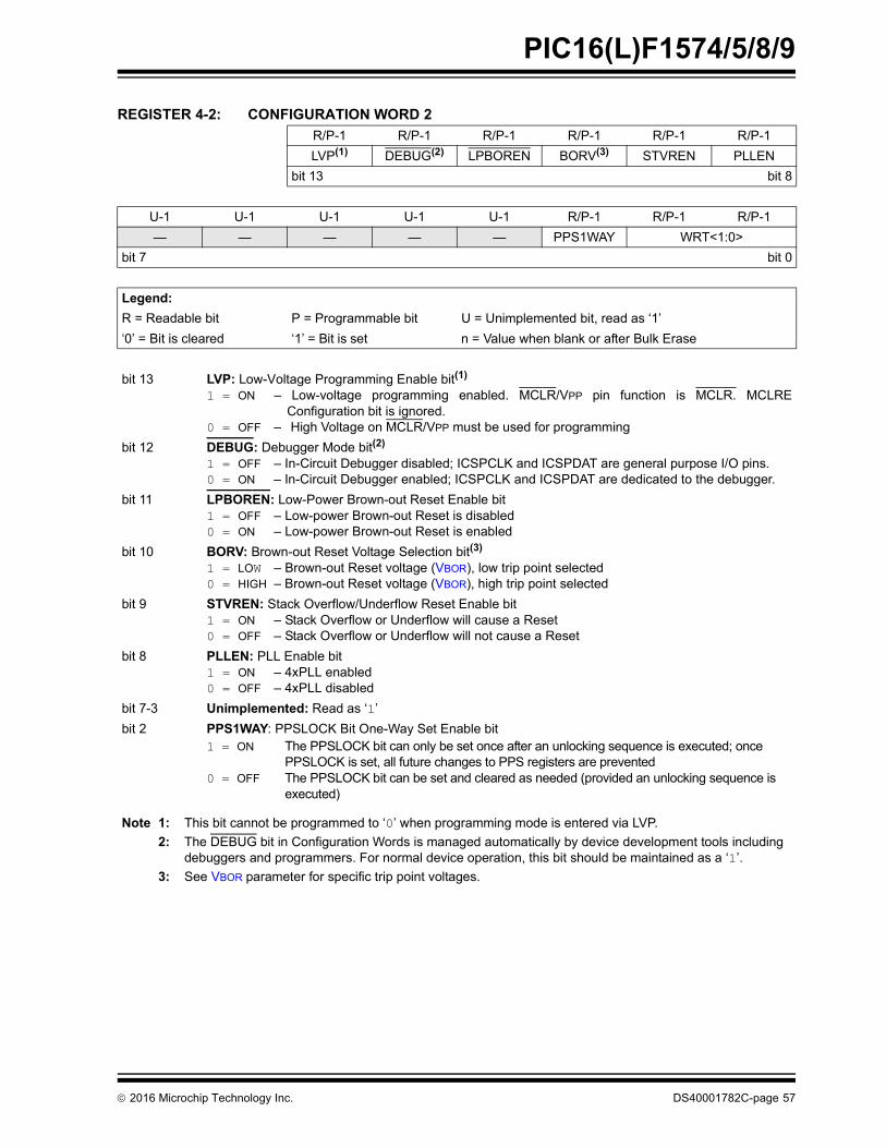
2016 Microchip Technology Inc. DS40001782C-page 57
PIC16(L)F1574/5/8/9
REGISTER 4-2: CONFIGURATION WORD 2
R/P-1 R/P-1 R/P-1 R/P-1 R/P-1 R/P-1
LVP(1) DEBUG(2) LPBOREN BORV(3) STVREN PLLEN
bit 13 bit 8
U-1 U-1 U-1 U-1 U-1 R/P-1 R/P-1 R/P-1
— — — — — PPS1WAY WRT<1:0>
bit 7 bit 0
Legend:
R = Readable bit P = Programmable bit U = Unimplemented bit, read as ‘1’
‘0’ = Bit is cleared ‘1’ = Bit is set n = Value when blank or after Bulk Erase
bit 13 LVP: Low-Voltage Programming Enable bit(1)
1 = ON – Low-voltage programming enabled. MCLR/VPP pin function is MCLR. MCLREConfiguration bit is ignored.
0 = OFF – High Voltage on MCLR/VPP must be used for programming
bit 12 DEBUG: Debugger Mode bit(2)
1 = OFF – In-Circuit Debugger disabled; ICSPCLK and ICSPDAT are general purpose I/O pins.0 = ON – In-Circuit Debugger enabled; ICSPCLK and ICSPDAT are dedicated to the debugger.
bit 11 LPBOREN: Low-Power Brown-out Reset Enable bit1 = OFF – Low-power Brown-out Reset is disabled0 = ON – Low-power Brown-out Reset is enabled
bit 10 BORV: Brown-out Reset Voltage Selection bit(3)
1 = LOW – Brown-out Reset voltage (VBOR), low trip point selected0 = HIGH – Brown-out Reset voltage (VBOR), high trip point selected
bit 9 STVREN: Stack Overflow/Underflow Reset Enable bit1 = ON – Stack Overflow or Underflow will cause a Reset0 = OFF – Stack Overflow or Underflow will not cause a Reset
bit 8 PLLEN: PLL Enable bit1 = ON – 4xPLL enabled0 = OFF – 4xPLL disabled
bit 7-3 Unimplemented: Read as ‘1’
bit 2 PPS1WAY: PPSLOCK Bit One-Way Set Enable bit1 = ON The PPSLOCK bit can only be set once after an unlocking sequence is executed; once
PPSLOCK is set, all future changes to PPS registers are prevented0 = OFF The PPSLOCK bit can be set and cleared as needed (provided an unlocking sequence is
executed)
Note 1: This bit cannot be programmed to ‘0’ when programming mode is entered via LVP.
2: The DEBUG bit in Configuration Words is managed automatically by device development tools including debuggers and programmers. For normal device operation, this bit should be maintained as a ‘1’.
3: See VBOR parameter for specific trip point voltages.

PIC16(L)F1574/5/8/9
DS40001782C-page 58 2016 Microchip Technology Inc.
bit 1-0 WRT<1:0>: Flash Memory Self-Write Protection bits
4 kW Flash memory: (PIC16(L)F1574/8):11 = OFF Write protection off10 = BOOT 0000h to 1FFh write protected, 0200h to 0FFFh may be modified by PMCON control01 = HALF 0000h to 07FFh write protected, 0800h to 0FFFh may be modified by PMCON control00 = ALL 0000h to 0FFFh write protected, no addresses may be modified by PMCON control
8 kW Flash memory: (PIC16(L)F1575/9)11 = OFF Write protection off10 = BOOT 0000h to 1FFh write protected, 0200h to 1FFFh may be modified by PMCON control01 = HALF 0000h to 0FFFh write protected, 1000h to 1FFFh may be modified by PMCON control00 = ALL 0000h to 1FFFh write protected, no addresses may be modified by PMCON control
REGISTER 4-2: CONFIGURATION WORD 2 (CONTINUED)
Note 1: This bit cannot be programmed to ‘0’ when programming mode is entered via LVP.
2: The DEBUG bit in Configuration Words is managed automatically by device development tools including debuggers and programmers. For normal device operation, this bit should be maintained as a ‘1’.
3: See VBOR parameter for specific trip point voltages.

2016 Microchip Technology Inc. DS40001782C-page 59
PIC16(L)F1574/5/8/9
4.3 Code Protection
Code protection allows the device to be protected fromunauthorized access. Internal access to the programmemory is unaffected by any code protection setting.
4.3.1 PROGRAM MEMORY PROTECTION
The entire program memory space is protected fromexternal reads and writes by the CP bit in ConfigurationWords. When CP = 0, external reads and writes ofprogram memory are inhibited and a read will return all‘0’s. The CPU can continue to read program memory,regardless of the protection bit settings. Writing theprogram memory is dependent upon the writeprotection setting. See Section 4.4 “WriteProtection” for more information.
4.4 Write Protection
Write protection allows the device to be protected fromunintended self-writes. Applications, such asbootloader software, can be protected while allowingother regions of the program memory to be modified.
The WRT<1:0> bits in Configuration Words define thesize of the program memory block that is protected.
4.5 User ID
Four memory locations (8000h-8003h) are designated asID locations where the user can store checksum or othercode identification numbers. These locations arereadable and writable during normal execution. SeeSection 10.4 “User ID, Device ID and ConfigurationWord Access” for more information on accessing thesememory locations. For more information on checksumcalculation, see the “PIC16(L)F157x MemoryProgramming Specification” (DS40001766).
4.6 Device ID and Revision ID
The 14-bit device ID word is located at 8006h and the14-bit revision ID is located at 8005h. These locationsare read-only and cannot be erased or modified. SeeSection 10.4 “User ID, Device ID and ConfigurationWord Access” for more information on accessingthese memory locations.
Development tools, such as device programmers anddebuggers, may be used to read the Device ID andRevision ID.

PIC16(L)F1574/5/8/9
DS40001782C-page 60 2016 Microchip Technology Inc.
4.7 Register Definitions: Device ID
REGISTER 4-3: DEVICEID: DEVICE ID REGISTER(1)
R R R R R R
DEV<13:8>
bit 13 bit 8
R R R R R R R R
DEV<7:0>
bit 7 bit 0
Legend:
x = Bit is unknown
R = Readable bit
‘0’ = Bit is cleared ‘1’ = Bit is set
bit 13-0 DEV<13:0>: Device ID bits
Refer to Table 4-1 to determine what these bits will read on which device. A value of 3FFFh is invalid.
Note 1: This location cannot be written.
REGISTER 4-4: REVISIONID: REVISION ID REGISTER(1)
R R R R R R
REV<13:8>
bit 13 bit 8
R R R R R R R R
REV<7:0>
bit 7 bit 0
Legend:
x = Bit is unknown
R = Readable bit
‘0’ = Bit is cleared ‘1’ = Bit is set
bit 13-0 REV<13:0>: Revision ID bits
These bits are used to identify the device revision.
Note 1: This location cannot be written.
TABLE 4-1: DEVICE ID VALUES
DEVICE Device ID Revision ID
PIC16F1574 3000h 2xxxh
PIC16F1575 3001h 2xxxh
PIC16F1578 3002h 2xxxh
PIC16F1579 3003h 2xxxh
PIC16LF1574 3004h 2xxxh
PIC16LF1575 3005h 2xxxh
PIC16LF1578 3006h 2xxxh
PIC16LF1579 3007h 2xxxh

2016 Microchip Technology Inc. DS40001782C-page 61
PIC16(L)F1574/5/8/9
5.0 OSCILLATOR MODULE
5.1 Overview
The oscillator module has a wide variety of clocksources and selection features that allow it to be usedin a wide range of applications while maximizing perfor-mance and minimizing power consumption. Figure 5-1illustrates a block diagram of the oscillator module.
Clock sources can be supplied from external logic levelclocks. In addition, the system clock source can besupplied from one of two internal oscillators and PLLcircuits, with a choice of speeds selectable via software.Additional clock features include:
• Selectable system clock source between external or internal sources via software.
The oscillator module can be configured in one of thefollowing clock modes.
1. ECL – External Clock Low-Power mode(0 MHz to 0.5 MHz)
2. ECM – External Clock Medium Power mode(0.5 MHz to 4 MHz)
3. ECH – External Clock High-Power mode(4 MHz to 32 MHz)
4. INTOSC – Internal oscillator (31 kHz to 32 MHz).
Clock Source modes are selected by the FOSC<1:0>bits in the Configuration Words. The FOSC bitsdetermine the type of oscillator that will be used whenthe device is first powered.
The ECH, ECM, and ECL clock modes rely on anexternal logic level signal as the device clock source.
The INTOSC internal oscillator block produces low,medium, and high-frequency clock sources,designated LFINTOSC, MFINTOSC and HFINTOSC.(see Internal Oscillator Block, Figure 5-1). A wideselection of device clock frequencies may be derivedfrom these three clock sources.

PIC16(L)F1574/5/8/9
DS40001782C-page 62 2016 Microchip Technology Inc.
FIGURE 5-1: SIMPLIFIED PIC® MCU CLOCK SOURCE BLOCK DIAGRAM
Note 1: See Section 5.2 “Clock Source Types”.
2: If FOSC<1:0> = 00, 4x PLL can only be used if IRCF<3:0> = 1110.
Rev. 10-000155A10/11/2013
31 kHzOscillator
Pre
scal
er
HFINTOSC(1)
16 MHz
8 MHz
4 MHz
2 MHz
1 MHz
*500 kHz
*250 kHz
*125 kHz
62.5 kHz
*31.25 kHz
*31 kHz
IRCF<3:0>
4
INTOSC
to CPU andPeripherals
Sleep
FOSC(1)
LFINTOSC(1)
to WDT, PWRT, and other Peripherals
* Available with more than one IRCF selection
SCS<1:0>
2
600 kHzOscillator
FRC(1)to ADC and
other Peripherals
CLKIN
1
0
4x PLL(2)
HFPLL16 MHz
500 kHzOscillator
MFINTOSC(1)
Internal Oscillator Block
to Peripherals
PLLEN
SPLLEN
FOSC<1:0>2
00
1x
01Reserved
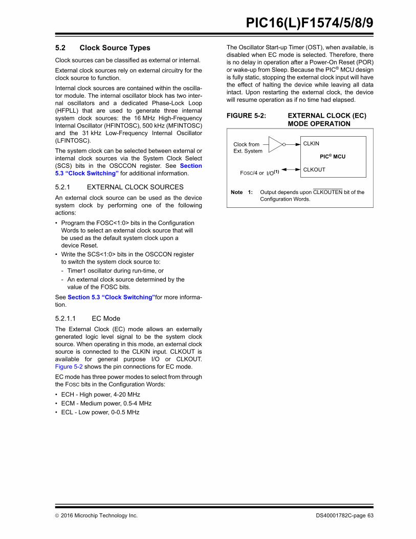
2016 Microchip Technology Inc. DS40001782C-page 63
PIC16(L)F1574/5/8/9
5.2 Clock Source Types
Clock sources can be classified as external or internal.
External clock sources rely on external circuitry for theclock source to function.
Internal clock sources are contained within the oscilla-tor module. The internal oscillator block has two inter-nal oscillators and a dedicated Phase-Lock Loop(HFPLL) that are used to generate three internalsystem clock sources: the 16 MHz High-FrequencyInternal Oscillator (HFINTOSC), 500 kHz (MFINTOSC)and the 31 kHz Low-Frequency Internal Oscillator(LFINTOSC).
The system clock can be selected between external orinternal clock sources via the System Clock Select(SCS) bits in the OSCCON register. See Section5.3 “Clock Switching” for additional information.
5.2.1 EXTERNAL CLOCK SOURCES
An external clock source can be used as the devicesystem clock by performing one of the followingactions:
• Program the FOSC<1:0> bits in the Configuration Words to select an external clock source that will be used as the default system clock upon a device Reset.
• Write the SCS<1:0> bits in the OSCCON register to switch the system clock source to:
- Timer1 oscillator during run-time, or
- An external clock source determined by the value of the FOSC bits.
See Section 5.3 “Clock Switching”for more informa-tion.
5.2.1.1 EC Mode
The External Clock (EC) mode allows an externallygenerated logic level signal to be the system clocksource. When operating in this mode, an external clocksource is connected to the CLKIN input. CLKOUT isavailable for general purpose I/O or CLKOUT.Figure 5-2 shows the pin connections for EC mode.
EC mode has three power modes to select from throughthe FOSC bits in the Configuration Words:
• ECH - High power, 4-20 MHz
• ECM - Medium power, 0.5-4 MHz
• ECL - Low power, 0-0.5 MHz
The Oscillator Start-up Timer (OST), when available, isdisabled when EC mode is selected. Therefore, thereis no delay in operation after a Power-On Reset (POR)or wake-up from Sleep. Because the PIC® MCU designis fully static, stopping the external clock input will havethe effect of halting the device while leaving all dataintact. Upon restarting the external clock, the devicewill resume operation as if no time had elapsed.
FIGURE 5-2: EXTERNAL CLOCK (EC) MODE OPERATION
CLKIN
CLKOUT
Clock fromExt. System
PIC® MCU
FOSC/4 or I/O(1)
Note 1: Output depends upon CLKOUTEN bit of the Configuration Words.

PIC16(L)F1574/5/8/9
DS40001782C-page 64 2016 Microchip Technology Inc.
5.2.2 INTERNAL CLOCK SOURCES
The device may be configured to use the internaloscillator block as the system clock by performing oneof the following actions:
• Program the FOSC<1:0> bits in Configuration Words to select the INTOSC clock source, which will be used as the default system clock upon a device Reset.
• Write the SCS<1:0> bits in the OSCCON register to switch the system clock source to the internal oscillator during run-time. See Section 5.3 “Clock Switching”for more information.
In INTOSC mode, CLKIN is available for generalpurpose I/O. CLKOUT is available for general purposeI/O or CLKOUT.
The function of the OSC2/CLKOUT pin is determinedby the CLKOUTEN bit in Configuration Words.
The internal oscillator block has two independentoscillators and a dedicated Phase Lock Loop, HFPLLthat can produce one of three internal system clocksources.
1. The HFINTOSC (High-Frequency InternalOscillator) is factory calibrated and operates at16 MHz. The HFINTOSC source is generatedfrom the 500 kHz MFINTOSC source and thededicated Phase Lock Loop, HFPLL. Thefrequency of the HFINTOSC can beuser-adjusted via software using the OSCTUNEregister (Register 5-3).
2. The MFINTOSC (Medium-Frequency InternalOscillator) is factory calibrated and operates at500 kHz. The frequency of the MFINTOSC canbe user-adjusted via software using theOSCTUNE register (Register 5-3).
3. The LFINTOSC (Low-Frequency InternalOscillator) is uncalibrated and operates at31 kHz.
5.2.2.1 HFINTOSC
The High-Frequency Internal Oscillator (HFINTOSC) isa factory calibrated 16 MHz internal clock source. Thefrequency of the HFINTOSC can be altered viasoftware using the OSCTUNE register (Register 5-3).
The output of the HFINTOSC connects to a postscalerand multiplexer (see Figure 5-1). One of multiplefrequencies derived from the HFINTOSC can beselected via software using the IRCF<3:0> bits of theOSCCON register. See Section 5.2.2.8 “InternalOscillator Clock Switch Timing” for more information.
The HFINTOSC is enabled by:
• Configure the IRCF<3:0> bits of the OSCCON register for the desired HF frequency, and
• FOSC<1:0> = 00, or
• Set the System Clock Source (SCS) bits of the OSCCON register to ‘1x’.
A fast start-up oscillator allows internal circuits to powerup and stabilize before switching to HFINTOSC.
The High-Frequency Internal Oscillator Ready bit(HFIOFR) of the OSCSTAT register indicates when theHFINTOSC is running.
The High-Frequency Internal Oscillator Status Lockedbit (HFIOFL) of the OSCSTAT register indicates whenthe HFINTOSC is running within 2% of its final value.
The High-Frequency Internal Oscillator Stable bit(HFIOFS) of the OSCSTAT register indicates when theHFINTOSC is running within 0.5% of its final value.
5.2.2.2 MFINTOSC
The Medium-Frequency Internal Oscillator(MFINTOSC) is a factory calibrated 500 kHz internalclock source. The frequency of the MFINTOSC can bealtered via software using the OSCTUNE register(Register 5-3).
The output of the MFINTOSC connects to a postscalerand multiplexer (see Figure 5-1). One of ninefrequencies derived from the MFINTOSC can beselected via software using the IRCF<3:0> bits of theOSCCON register. See Section 5.2.2.8 “InternalOscillator Clock Switch Timing” for more information.
The MFINTOSC is enabled by:
• Configure the IRCF<3:0> bits of the OSCCON register for the desired HF frequency, and
• FOSC<1:0> = 00, or
• Set the System Clock Source (SCS) bits of the OSCCON register to ‘1x’
The Medium-Frequency Internal Oscillator Ready bit(MFIOFR) of the OSCSTAT register indicates when theMFINTOSC is running.

2016 Microchip Technology Inc. DS40001782C-page 65
PIC16(L)F1574/5/8/9
5.2.2.3 Internal Oscillator Frequency Adjustment
The 500 kHz internal oscillator is factory calibrated.This internal oscillator can be adjusted in software bywriting to the OSCTUNE register (Register 5-3). Sincethe HFINTOSC and MFINTOSC clock sources arederived from the 500 kHz internal oscillator a change inthe OSCTUNE register value will apply to both.
The default value of the OSCTUNE register is ‘0’. Thevalue is a 6-bit two’s complement number. A value of1Fh will provide an adjustment to the maximumfrequency. A value of 20h will provide an adjustment tothe minimum frequency.
When the OSCTUNE register is modified, the oscillatorfrequency will begin shifting to the new frequency. Codeexecution continues during this shift. There is noindication that the shift has occurred.
OSCTUNE does not affect the LFINTOSC frequency.Operation of features that depend on the LFINTOSCclock source frequency, such as the Power-up Timer(PWRT), Watchdog Timer (WDT), and peripherals, arenot affected by the change in frequency.
5.2.2.4 LFINTOSC
The Low-Frequency Internal Oscillator (LFINTOSC) isan uncalibrated 31 kHz internal clock source.
The output of the LFINTOSC connects to a multiplexer(see Figure 5-1). Select 31 kHz, via software, using theIRCF<3:0> bits of the OSCCON register. See Section5.2.2.8 “Internal Oscillator Clock Switch Timing” formore information. The LFINTOSC is also the frequencyfor the Power-up Timer (PWRT) and Watchdog Timer(WDT).
The LFINTOSC is enabled by selecting 31 kHz(IRCF<3:0> bits of the OSCCON register = 000) as thesystem clock source (SCS bits of the OSCCONregister = 1x), or when any of the following areenabled:
• Configure the IRCF<3:0> bits of the OSCCON register for the desired LF frequency, and
• FOSC<1:0> = 00, or
• Set the System Clock Source (SCS) bits of the OSCCON register to ‘1x’
Peripherals that use the LFINTOSC are:
• Power-up Timer (PWRT)
• Watchdog Timer (WDT)
The Low-Frequency Internal Oscillator Ready bit(LFIOFR) of the OSCSTAT register indicates when theLFINTOSC is running.
5.2.2.5 FRC
The FRC clock is an uncalibrated, nominal 600 kHzperipheral clock source.
The FRC is automatically turned on by the peripheralsrequesting the FRC clock.
The FRC clock will continue to run during Sleep.
5.2.2.6 Internal Oscillator Frequency Selection
The system clock speed can be selected via softwareusing the Internal Oscillator Frequency Select bits,IRCF<3:0> of the OSCCON register.
The postscaler outputs of the 16 MHz HFINTOSC, 500kHz MFINTOSC, and 31 kHz LFINTOSC outputconnect to a multiplexer (see Figure 5-1). The InternalOscillator Frequency Select bits IRCF<3:0> of theOSCCON register select the frequency output of theinternal oscillators. One of the following frequenciescan be selected via software:
- 32 MHz (requires 4x PLL)
- 16 MHz
- 8 MHz
- 4 MHz
- 2 MHz
- 1 MHz
- 500 kHz (default after Reset)
- 250 kHz
- 125 kHz
- 62.5 kHz
- 31.25 kHz
- 31 kHz (LFINTOSC)
The IRCF<3:0> bits of the OSCCON register allowduplicate selections for some frequencies. These dupli-cate choices can offer system design trade-offs. Lowerpower consumption can be obtained when changingoscillator sources for a given frequency. Faster transi-tion times can be obtained between frequency changesthat use the same oscillator source.
Note: Following any Reset, the IRCF<3:0> bitsof the OSCCON register are set to ‘0111’and the frequency selection is set to500 kHz. The user can modify the IRCFbits to select a different frequency.
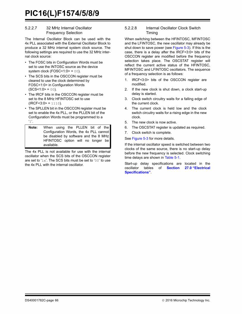
PIC16(L)F1574/5/8/9
DS40001782C-page 66 2016 Microchip Technology Inc.
5.2.2.7 32 MHz Internal Oscillator Frequency Selection
The Internal Oscillator Block can be used with the4x PLL associated with the External Oscillator Block toproduce a 32 MHz internal system clock source. Thefollowing settings are required to use the 32 MHz inter-nal clock source:
• The FOSC bits in Configuration Words must be set to use the INTOSC source as the device system clock (FOSC<1:0> = 00).
• The SCS bits in the OSCCON register must be cleared to use the clock determined by FOSC<1:0> in Configuration Words (SCS<1:0> = 00).
• The IRCF bits in the OSCCON register must be set to the 8 MHz HFINTOSC set to use (IRCF<3:0> = 1110).
• The SPLLEN bit in the OSCCON register must be set to enable the 4x PLL, or the PLLEN bit of the Configuration Words must be programmed to a ‘1’.
The 4x PLL is not available for use with the internaloscillator when the SCS bits of the OSCCON registerare set to ‘1x’. The SCS bits must be set to ‘00’ to usethe 4x PLL with the internal oscillator.
5.2.2.8 Internal Oscillator Clock Switch Timing
When switching between the HFINTOSC, MFINTOSCand the LFINTOSC, the new oscillator may already beshut down to save power (see Figure 5-3). If this is thecase, there is a delay after the IRCF<3:0> bits of theOSCCON register are modified before the frequencyselection takes place. The OSCSTAT register willreflect the current active status of the HFINTOSC,MFINTOSC and LFINTOSC oscillators. The sequenceof a frequency selection is as follows:
1. IRCF<3:0> bits of the OSCCON register aremodified.
2. If the new clock is shut down, a clock start-updelay is started.
3. Clock switch circuitry waits for a falling edge ofthe current clock.
4. The current clock is held low and the clockswitch circuitry waits for a rising edge in the newclock.
5. The new clock is now active.
6. The OSCSTAT register is updated as required.
7. Clock switch is complete.
See Figure 5-3 for more details.
If the internal oscillator speed is switched between twoclocks of the same source, there is no start-up delaybefore the new frequency is selected. Clock switchingtime delays are shown in Table 5-1.
Start-up delay specifications are located in theoscillator tables of Section 27.0 “ElectricalSpecifications”.
Note: When using the PLLEN bit of theConfiguration Words, the 4x PLL cannotbe disabled by software and the 8 MHzHFINTOSC option will no longer beavailable.
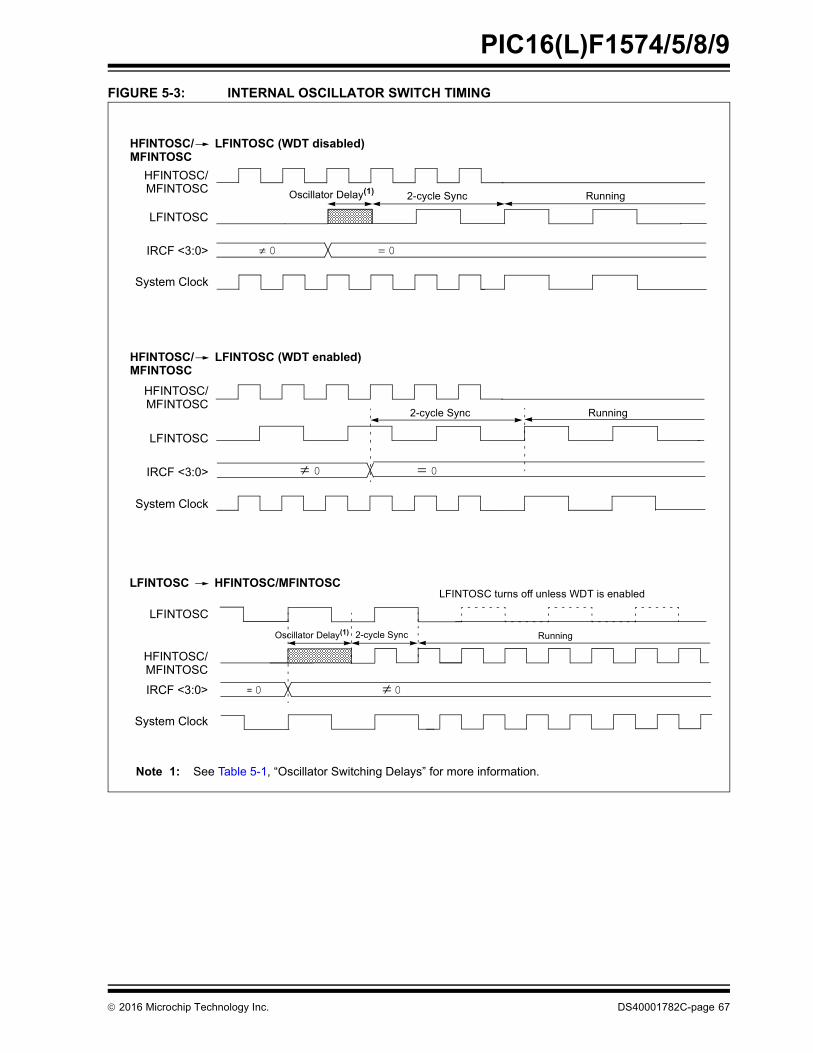
2016 Microchip Technology Inc. DS40001782C-page 67
PIC16(L)F1574/5/8/9
FIGURE 5-3: INTERNAL OSCILLATOR SWITCH TIMING
HFINTOSC/
LFINTOSC
IRCF <3:0>
System Clock
HFINTOSC/
LFINTOSC
IRCF <3:0>
System Clock
0 0
0 0
Oscillator Delay(1) 2-cycle Sync Running
2-cycle Sync Running
HFINTOSC/ LFINTOSC (WDT disabled)
HFINTOSC/ LFINTOSC (WDT enabled)
LFINTOSC
HFINTOSC/
IRCF <3:0>
System Clock
= 0 0
2-cycle Sync Running
LFINTOSC HFINTOSC/MFINTOSCLFINTOSC turns off unless WDT is enabled
MFINTOSC
MFINTOSC
MFINTOSC
MFINTOSC
MFINTOSC
Oscillator Delay(1)
Note 1: See Table 5-1, “Oscillator Switching Delays” for more information.

PIC16(L)F1574/5/8/9
DS40001782C-page 68 2016 Microchip Technology Inc.
5.3 Clock Switching
The system clock source can be switched betweenexternal and internal clock sources via software usingthe System Clock Select (SCS) bits of the OSCCONregister. The following clock sources can be selectedusing the SCS bits:
• Default system oscillator determined by FOSC bits in Configuration Words
• Internal Oscillator Block (INTOSC)
5.3.1 SYSTEM CLOCK SELECT (SCS) BITS
The System Clock Select (SCS) bits of the OSCCONregister selects the system clock source that is used forthe CPU and peripherals.
• When the SCS bits of the OSCCON register = 00, the system clock source is determined by value of the FOSC<1:0> bits in the Configuration Words.
• When the SCS bits of the OSCCON register = 01, the system clock source is the Timer1 oscillator.
• When the SCS bits of the OSCCON register = 1x, the system clock source is chosen by the internal oscillator frequency selected by the IRCF<3:0> bits of the OSCCON register. After a Reset, the SCS bits of the OSCCON register are always cleared.
When switching between clock sources, a delay isrequired to allow the new clock to stabilize. Theseoscillator delays are shown in Table 5-1.
5.4 Clock Switching Before Sleep
When clock switching from an old clock to a new clockis requested just prior to entering Sleep mode, it isnecessary to confirm that the switch is complete beforethe SLEEP instruction is executed. Failure to do so mayresult in an incomplete switch and consequential loss ofthe system clock altogether. Clock switching isconfirmed by monitoring the clock Status bits in theOSCSTAT register. Switch confirmation can beaccomplished by sensing that the ready bit for the newclock is set or the ready bit for the old clock is cleared.For example, when switching between the internaloscillator with the PLL and the internal oscillator withoutthe PLL, monitor the PLLR bit. When PLLR is set, theswitch to 32 MHz operation is complete. Conversely,when PLLR is cleared, the switch from 32 MHzoperation to the selected internal clock is complete.
TABLE 5-1: OSCILLATOR SWITCHING DELAYS
Note: Any automatic clock switch does notupdate the SCS bits of the OSCCONregister. The user can monitor the OSTSbit of the OSCSTAT register to determinethe current system clock source.
Switch From Switch To Frequency Oscillator Delay
Sleep/PORLFINTOSC(1)
MFINTOSC(1)
HFINTOSC(1)
31 kHz31.25 kHz-500 kHz31.25 kHz-16 MHz
Oscillator Warm-up Delay (TWARM)(2)
Sleep/POR EC(1) DC – 32 MHz 2 cycles
LFINTOSC EC(1) DC – 32 MHz 1 cycle of each
Any clock sourceMFINTOSC(1)
HFINTOSC(1)31.25 kHz-500 kHz31.25 kHz-16 MHz
2 s (approx.)
Any clock source LFINTOSC(1) 31 kHz 1 cycle of each
PLL inactive PLL active 16-32 MHz 2 ms (approx.)
Note 1: PLL inactive.
2: See Section 27.0 “Electrical Specifications”.

2016 Microchip Technology Inc. DS40001782C-page 69
PIC16(L)F1574/5/8/9
5.5 Register Definitions: Oscillator Control
REGISTER 5-1: OSCCON: OSCILLATOR CONTROL REGISTER
R/W-0/0 R/W-0/0 R/W-1/1 R/W-1/1 R/W-1/1 U-0 R/W-0/0 R/W-0/0
SPLLEN IRCF<3:0> — SCS<1:0>
bit 7 bit 0
Legend:
R = Readable bit W = Writable bit U = Unimplemented bit, read as ‘0’
u = Bit is unchanged x = Bit is unknown -n/n = Value at POR and BOR/Value at all other Resets
‘1’ = Bit is set ‘0’ = Bit is cleared
bit 7 SPLLEN: Software PLL Enable bitIf PLLEN in Configuration Words = 1:SPLLEN bit is ignored. 4x PLL is always enabled (subject to oscillator requirements)
If PLLEN in Configuration Words = 0:1 = 4x PLL Is enabled0 = 4x PLL is disabled
bit 6-3 IRCF<3:0>: Internal Oscillator Frequency Select bits1111 = 16 MHz HF1110 = 8 MHz or 32 MHz HF (see Section 5.2.2.1 “HFINTOSC”)1101 = 4 MHz HF1100 = 2 MHz HF1011 = 1 MHz HF1010 = 500 kHz HF(1)
1001 = 250 kHz HF(1)
1000 = 125 kHz HF(1)
0111 = 500 kHz MF (default upon Reset)0110 = 250 kHz MF0101 = 125 kHz MF0100 = 62.5 kHz MF0011 = 31.25 kHz HF(1)
0010 = 31.25 kHz MF000x = 31 kHz LF
bit 2 Unimplemented: Read as ‘0’
bit 1-0 SCS<1:0>: System Clock Select bits1x = Internal oscillator block01 = Reserved00 = Clock determined by FOSC<1:0> in Configuration Words.
Note 1: Duplicate frequency derived from HFINTOSC.
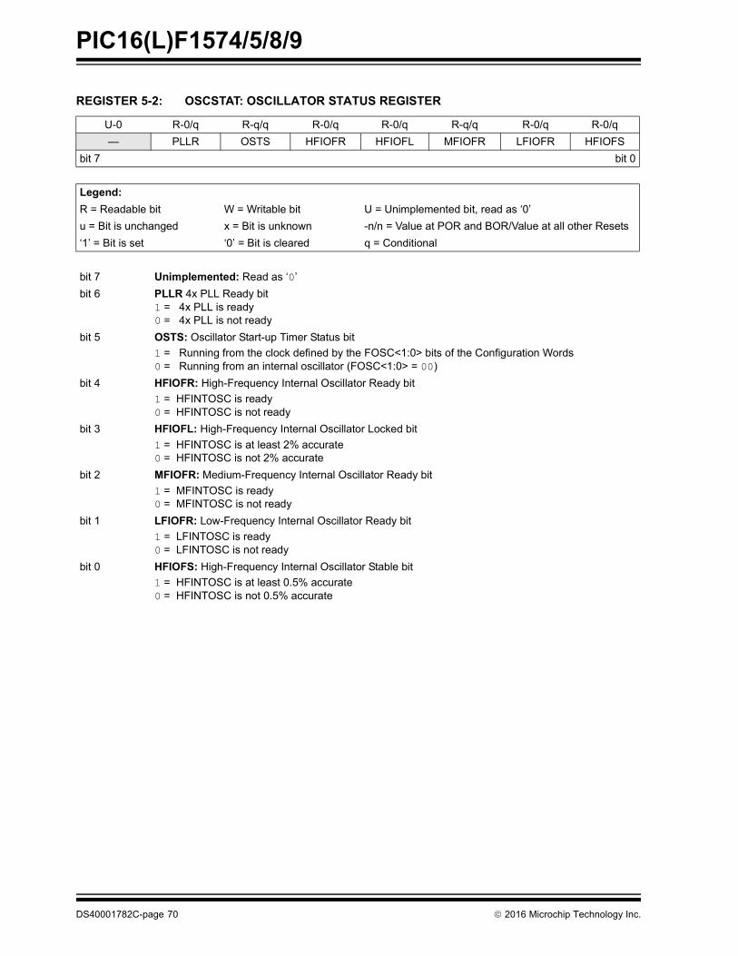
PIC16(L)F1574/5/8/9
DS40001782C-page 70 2016 Microchip Technology Inc.
REGISTER 5-2: OSCSTAT: OSCILLATOR STATUS REGISTER
U-0 R-0/q R-q/q R-0/q R-0/q R-q/q R-0/q R-0/q
— PLLR OSTS HFIOFR HFIOFL MFIOFR LFIOFR HFIOFS
bit 7 bit 0
Legend:
R = Readable bit W = Writable bit U = Unimplemented bit, read as ‘0’
u = Bit is unchanged x = Bit is unknown -n/n = Value at POR and BOR/Value at all other Resets
‘1’ = Bit is set ‘0’ = Bit is cleared q = Conditional
bit 7 Unimplemented: Read as ‘0’
bit 6 PLLR 4x PLL Ready bit1 = 4x PLL is ready0 = 4x PLL is not ready
bit 5 OSTS: Oscillator Start-up Timer Status bit
1 = Running from the clock defined by the FOSC<1:0> bits of the Configuration Words0 = Running from an internal oscillator (FOSC<1:0> = 00)
bit 4 HFIOFR: High-Frequency Internal Oscillator Ready bit
1 = HFINTOSC is ready0 = HFINTOSC is not ready
bit 3 HFIOFL: High-Frequency Internal Oscillator Locked bit
1 = HFINTOSC is at least 2% accurate0 = HFINTOSC is not 2% accurate
bit 2 MFIOFR: Medium-Frequency Internal Oscillator Ready bit
1 = MFINTOSC is ready 0 = MFINTOSC is not ready
bit 1 LFIOFR: Low-Frequency Internal Oscillator Ready bit
1 = LFINTOSC is ready0 = LFINTOSC is not ready
bit 0 HFIOFS: High-Frequency Internal Oscillator Stable bit
1 = HFINTOSC is at least 0.5% accurate0 = HFINTOSC is not 0.5% accurate

2016 Microchip Technology Inc. DS40001782C-page 71
PIC16(L)F1574/5/8/9
REGISTER 5-3: OSCTUNE: OSCILLATOR TUNING REGISTER
U-0 U-0 R/W-0/0 R/W-0/0 R/W-0/0 R/W-0/0 R/W-0/0 R/W-0/0
— — TUN<5:0>
bit 7 bit 0
Legend:
R = Readable bit W = Writable bit U = Unimplemented bit, read as ‘0’
u = Bit is unchanged x = Bit is unknown -n/n = Value at POR and BOR/Value at all other Resets
‘1’ = Bit is set ‘0’ = Bit is cleared
bit 7-6 Unimplemented: Read as ‘0’
bit 5-0 TUN<5:0>: Frequency Tuning bits100000 = Minimum frequency•••111111 = 000000 = Oscillator module is running at the factory-calibrated frequency.000001 = •••011110 = 011111 = Maximum frequency

PIC16(L)F1574/5/8/9
DS40001782C-page 72 2016 Microchip Technology Inc.
TABLE 5-2: SUMMARY OF REGISTERS ASSOCIATED WITH CLOCK SOURCES
TABLE 5-3: SUMMARY OF CONFIGURATION WORD WITH CLOCK SOURCES
Name Bit 7 Bit 6 Bit 5 Bit 4 Bit 3 Bit 2 Bit 1 Bit 0Register on Page
OSCCON SPLLEN IRCF<3:0> — SCS<1:0> 69
OSCSTAT — PLLR OSTS HFIOFR HFIOFL MFIOFR LFIOFR HFIOFS 70
OSCTUNE — — TUN<5:0> 71
Legend: — = unimplemented location, read as ‘0’. Shaded cells are not used by clock sources.
Name Bits Bit -/7 Bit -/6 Bit 13/5 Bit 12/4 Bit 11/3 Bit 10/2 Bit 9/1 Bit 8/0Register on Page
CONFIG113:8 — — — — CLKOUTEN BOREN<1:0> —
567:0 CP MCLRE PWRTE WDTE<1:0> — FOSC<1:0>
Legend: — = unimplemented location, read as ‘0’. Shaded cells are not used by clock sources.

2016 Microchip Technology Inc. DS40001782C-page 73
PIC16(L)F1574/5/8/9
6.0 RESETS
There are multiple ways to reset this device:
• Power-On Reset (POR)
• Brown-Out Reset (BOR)
• Low-Power Brown-Out Reset (LPBOR)
• MCLR Reset
• WDT Reset
• RESET instruction
• Stack Overflow
• Stack Underflow
• Programming mode exit
To allow VDD to stabilize, an optional Power-up Timercan be enabled to extend the Reset time after a BORor POR event.
A simplified block diagram of the On-chip Reset Circuitis shown in Figure 6-1.
FIGURE 6-1: SIMPLIFIED BLOCK DIAGRAM OF ON-CHIP RESET CIRCUIT
Note 1: See Table 6-1 for BOR active conditions.
DeviceReset
Power-on Reset
WDT Time-out
Brown-out Reset
LPBOR Reset
RESET Instruction
MCLRE
Sleep
BOR Active(1)
PWRTELFINTOSC
VDD
ICSP™ Programming Mode Exit
Stack UnderflowStack Overlfow
VPP/MCLR
R Power-up Timer
Rev. 10-000006A8/14/2013

PIC16(L)F1574/5/8/9
DS40001782C-page 74 2016 Microchip Technology Inc.
6.1 Power-On Reset (POR)
The POR circuit holds the device in Reset until VDD hasreached an acceptable level for minimum operation.Slow rising VDD, fast operating speeds or analogperformance may require greater than minimum VDD.The PWRT, BOR or MCLR features can be used toextend the start-up period until all device operationconditions have been met.
6.1.1 POWER-UP TIMER (PWRT)
The Power-up Timer provides a nominal 64 mstime-out on POR or Brown-out Reset.
The device is held in Reset as long as PWRT is active.The PWRT delay allows additional time for the VDD torise to an acceptable level. The Power-up Timer isenabled by clearing the PWRTE bit in ConfigurationWords.
The Power-up Timer starts after the release of the PORand BOR.
For additional information, refer to Application NoteAN607, “Power-up Trouble Shooting” (DS00607).
6.2 Brown-Out Reset (BOR)
The BOR circuit holds the device in Reset when VDD
reaches a selectable minimum level. Between thePOR and BOR, complete voltage range coverage forexecution protection can be implemented.
The Brown-out Reset module has four operatingmodes controlled by the BOREN<1:0> bits in Configu-ration Words. The four operating modes are:
• BOR is always on
• BOR is off when in Sleep
• BOR is controlled by software
• BOR is always off
Refer to Table 6-1 for more information.
The Brown-out Reset voltage level is selectable byconfiguring the BORV bit in Configuration Words.
A VDD noise rejection filter prevents the BOR fromtriggering on small events. If VDD falls below VBOR fora duration greater than parameter TBORDC, the devicewill reset. See Figure 6-2 for more information.
TABLE 6-1: BOR OPERATING MODES
6.2.1 BOR IS ALWAYS ON
When the BOREN bits of Configuration Words are pro-grammed to ‘11’, the BOR is always on. The devicestart-up will be delayed until the BOR is ready and VDD
is higher than the BOR threshold.
BOR protection is active during Sleep. The BOR doesnot delay wake-up from Sleep.
6.2.2 BOR IS OFF IN SLEEP
When the BOREN bits of Configuration Words are pro-grammed to ‘10’, the BOR is on, except in Sleep. Thedevice start-up will be delayed until the BOR is readyand VDD is higher than the BOR threshold.
BOR protection is not active during Sleep. The devicewake-up will be delayed until the BOR is ready.
6.2.3 BOR CONTROLLED BY SOFTWARE
When the BOREN bits of Configuration Words areprogrammed to ‘01’, the BOR is controlled by theSBOREN bit of the BORCON register. The devicestart-up is not delayed by the BOR ready condition orthe VDD level.
BOR protection begins as soon as the BOR circuit isready. The status of the BOR circuit is reflected in theBORRDY bit of the BORCON register.
BOR protection is unchanged by Sleep.
BOREN<1:0> SBOREN Device Mode BOR ModeInstruction Execution upon:
Release of POR or Wake-up from Sleep
11 X X Active Waits for BOR ready(1) (BORRDY = 1)
10 XAwake Active Waits for BOR ready (BORRDY = 1)
Sleep Disabled
011 X Active Waits for BOR ready(1) (BORRDY = 1)
0 X Disabled Begins immediately (BORRDY = x)
00 X X Disabled
Note 1: In these specific cases, “release of POR” and “wake-up from Sleep,” there is no delay in start-up. The BORready flag, (BORRDY = 1), will be set before the CPU is ready to execute instructions because the BORcircuit is forced on by the BOREN<1:0> bits.
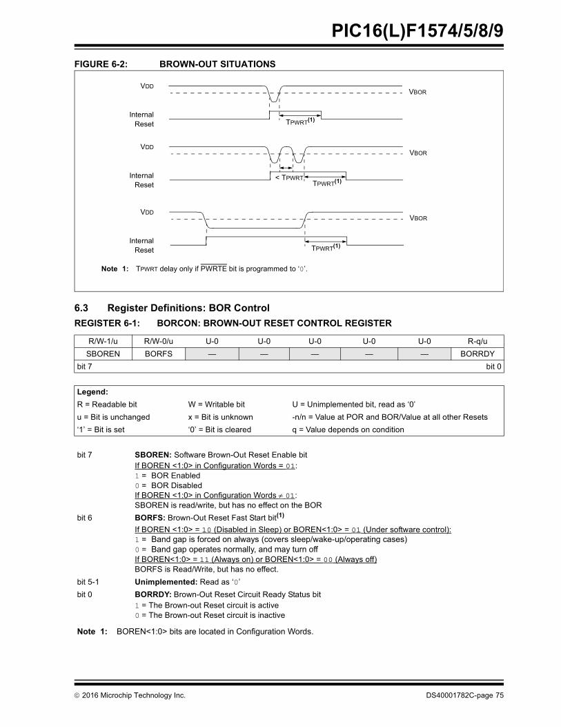
2016 Microchip Technology Inc. DS40001782C-page 75
PIC16(L)F1574/5/8/9
FIGURE 6-2: BROWN-OUT SITUATIONS
6.3 Register Definitions: BOR Control
REGISTER 6-1: BORCON: BROWN-OUT RESET CONTROL REGISTER
R/W-1/u R/W-0/u U-0 U-0 U-0 U-0 U-0 R-q/u
SBOREN BORFS — — — — — BORRDY
bit 7 bit 0
Legend:
R = Readable bit W = Writable bit U = Unimplemented bit, read as ‘0’
u = Bit is unchanged x = Bit is unknown -n/n = Value at POR and BOR/Value at all other Resets
‘1’ = Bit is set ‘0’ = Bit is cleared q = Value depends on condition
bit 7 SBOREN: Software Brown-Out Reset Enable bitIf BOREN <1:0> in Configuration Words = 01:1 = BOR Enabled0 = BOR DisabledIf BOREN <1:0> in Configuration Words 01:SBOREN is read/write, but has no effect on the BOR
bit 6 BORFS: Brown-Out Reset Fast Start bit(1)
If BOREN <1:0> = 10 (Disabled in Sleep) or BOREN<1:0> = 01 (Under software control):1 = Band gap is forced on always (covers sleep/wake-up/operating cases)0 = Band gap operates normally, and may turn offIf BOREN<1:0> = 11 (Always on) or BOREN<1:0> = 00 (Always off)BORFS is Read/Write, but has no effect.
bit 5-1 Unimplemented: Read as ‘0’
bit 0 BORRDY: Brown-Out Reset Circuit Ready Status bit1 = The Brown-out Reset circuit is active0 = The Brown-out Reset circuit is inactive
Note 1: BOREN<1:0> bits are located in Configuration Words.
TPWRT(1)
VBOR VDD
InternalReset
VBOR VDD
InternalReset TPWRT(1)< TPWRT
TPWRT(1)
VBOR VDD
InternalReset
Note 1: TPWRT delay only if PWRTE bit is programmed to ‘0’.

PIC16(L)F1574/5/8/9
DS40001782C-page 76 2016 Microchip Technology Inc.
6.4 Low-Power Brown-Out Reset (LPBOR)
The Low-Power Brown-Out Reset (LPBOR) operateslike the BOR to detect low voltage conditions on theVDD pin. When too low of a voltage is detected, thedevice is held in Reset. When this occurs, a register bit(BOR) is changed to indicate that a BOR Reset hasoccurred. The BOR bit in PCON is used for both BORand the LPBOR. Refer to Register 6-2.
The LPBOR voltage threshold (VLPBOR) has a widertolerance than the BOR (VBOR), but requires muchless current (LPBOR current) to operate. The LPBORis intended for use when the BOR is configured asdisabled (BOREN = 00) or disabled in Sleep mode(BOREN = 10).
Refer to Figure 6-1 to see how the LPBOR interactswith other modules.
6.4.1 ENABLING LPBOR
The LPBOR is controlled by the LPBOR bit ofConfiguration Words. When the device is erased, theLPBOR module defaults to disabled.
6.5 MCLR
The MCLR is an optional external input that can resetthe device. The MCLR function is controlled by theMCLRE bit of Configuration Words and the LVP bit ofConfiguration Words (Table 6-2).
6.5.1 MCLR ENABLED
When MCLR is enabled and the pin is held low, thedevice is held in Reset. The MCLR pin is connected toVDD through an internal weak pull-up.
The device has a noise filter in the MCLR Reset path.The filter will detect and ignore small pulses.
6.5.2 MCLR DISABLED
When MCLR is disabled, the pin functions as a generalpurpose input and the internal weak pull-up is undersoftware control. See Section 11.1 “PORTA Regis-ters” for more information.
6.6 Watchdog Timer (WDT) Reset
The Watchdog Timer generates a Reset if the firmwaredoes not issue a CLRWDT instruction within the time-outperiod. The TO and PD bits in the STATUS register arechanged to indicate the WDT Reset. See Section9.0 “Watchdog Timer (WDT)” for more information.
6.7 RESET Instruction
A RESET instruction will cause a device Reset. The RIbit in the PCON register will be set to ‘0’. See Table 6-4for default conditions after a RESET instruction hasoccurred.
6.8 Stack Overflow/Underflow Reset
The device can reset when the Stack Overflows orUnderflows. The STKOVF or STKUNF bits of the PCONregister indicate the Reset condition. These Resets areenabled by setting the STVREN bit in ConfigurationWords. See Section 3.5.2 “Overflow/UnderflowReset” for more information.
6.9 Programming Mode Exit
Upon exit of Programming mode, the device willbehave as if a POR had just occurred.
6.10 Power-Up Timer
The Power-up Timer optionally delays device executionafter a BOR or POR event. This timer is typically used toallow VDD to stabilize before allowing the device to startrunning.
The Power-up Timer is controlled by the PWRTE bit ofConfiguration Words.
6.11 Start-up Sequence
Upon the release of a POR or BOR, the following mustoccur before the device will begin executing:
1. Power-up Timer runs to completion (if enabled).
2. MCLR must be released (if enabled).
The total time-out will vary based on oscillator configu-ration and Power-up Timer configuration. See Section5.0 “Oscillator Module” for more information.
The Power-up Timer runs independently of MCLRReset. If MCLR is kept low long enough, the Power-upTimer will expire. Upon bringing MCLR high, the devicewill begin execution after 10 FOSC cycles (seeFigure 6-3). This is useful for testing purposes or tosynchronize more than one device operating in parallel.
TABLE 6-2: MCLR CONFIGURATION
MCLRE LVP MCLR
0 0 Disabled
1 0 Enabled
x 1 Enabled
Note: A Reset does not drive the MCLR pin low.

2016 Microchip Technology Inc. DS40001782C-page 77
PIC16(L)F1574/5/8/9
FIGURE 6-3: RESET START-UP SEQUENCE
Note 1: Code execution begins 10 FOSC cycles after the FOSC clock is released.
VDD
Internal POR
External Clock (EC modes), PWRTEN = 0
Internal RESET
MCLR
FOSC
Begin Execution
Ext. Clock (EC)
Power-up Timer
External Clock (EC modes), PWRTEN = 1
code execution (1)code execution (1)
TPWRT
Int. Oscillator
code execution (1)
Internal Oscillator, PWRTEN = 0 Internal Oscillator, PWRTEN = 1
code execution (1)
TPWRT
VDD
Internal POR
Internal RESET
MCLR
FOSC
Begin Execution
Power-up Timer
Rev. 10-000032B7/30/2013

PIC16(L)F1574/5/8/9
DS40001782C-page 78 2016 Microchip Technology Inc.
6.12 Determining the Cause of a Reset
Upon any Reset, multiple bits in the STATUS andPCON registers are updated to indicate the cause ofthe Reset. Table 6-3 and Table 6-4 show the Resetconditions of these registers.
TABLE 6-3: RESET STATUS BITS AND THEIR SIGNIFICANCE
TABLE 6-4: RESET CONDITION FOR SPECIAL REGISTERS
STKOVF STKUNF RWDT RMCLR RI POR BOR TO PD Condition
0 0 1 1 1 0 x 1 1 Power-on Reset
0 0 1 1 1 0 x 0 x Illegal, TO is set on POR
0 0 1 1 1 0 x x 0 Illegal, PD is set on POR
0 0 u 1 1 u 0 1 1 Brown-out Reset
u u 0 u u u u 0 u WDT Reset
u u u u u u u 0 0 WDT Wake-up from Sleep
u u u u u u u 1 0 Interrupt Wake-up from Sleep
u u u 0 u u u u u MCLR Reset during normal operation
u u u 0 u u u 1 0 MCLR Reset during Sleep
u u u u 0 u u u u RESET Instruction Executed
1 u u u u u u u u Stack Overflow Reset (STVREN = 1)
u 1 u u u u u u u Stack Underflow Reset (STVREN = 1)
ConditionProgramCounter
STATUSRegister
PCONRegister
Power-on Reset 0000h ---1 1000 00-- 110x
MCLR Reset during normal operation 0000h ---u uuuu uu-- 0uuu
MCLR Reset during Sleep 0000h ---1 0uuu uu-- 0uuu
WDT Reset 0000h ---0 uuuu uu-- uuuu
WDT Wake-up from Sleep PC + 1 ---0 0uuu uu-- uuuu
Brown-out Reset 0000h ---1 1uuu 00-- 11u0
Interrupt Wake-up from Sleep PC + 1(1) ---1 0uuu uu-- uuuu
RESET Instruction Executed 0000h ---u uuuu uu-- u0uu
Stack Overflow Reset (STVREN = 1) 0000h ---u uuuu 1u-- uuuu
Stack Underflow Reset (STVREN = 1) 0000h ---u uuuu u1-- uuuu
Legend: u = unchanged, x = unknown, - = unimplemented bit, reads as ‘0’.Note 1: When the wake-up is due to an interrupt and the Global Interrupt Enable bit (GIE) is set, the return address
is pushed on the stack and PC is loaded with the interrupt vector (0004h) after execution of PC + 1.

2016 Microchip Technology Inc. DS40001782C-page 79
PIC16(L)F1574/5/8/9
6.13 Power Control (PCON) Register
The Power Control (PCON) register contains flag bitsto differentiate between a:
• Power-On Reset (POR)
• Brown-Out Reset (BOR)
• Reset Instruction Reset (RI)
• MCLR Reset (RMCLR)
• Watchdog Timer Reset (RWDT)
• Stack Underflow Reset (STKUNF)
• Stack Overflow Reset (STKOVF)
The PCON register bits are shown in Register 6-2.
6.14 Register Definitions: Power Control
REGISTER 6-2: PCON: POWER CONTROL REGISTER
R/W/HS-0/q R/W/HS-0/q U-0 R/W/HC-1/q R/W/HC-1/q R/W/HC-1/q R/W/HC-q/u R/W/HC-q/u
STKOVF STKUNF — RWDT RMCLR RI POR BOR
bit 7 bit 0
Legend:
HC = Bit is cleared by hardware HS = Bit is set by hardware
R = Readable bit W = Writable bit U = Unimplemented bit, read as ‘0’
u = Bit is unchanged x = Bit is unknown -n/n = Value at POR and BOR/Value at all other Resets
‘1’ = Bit is set ‘0’ = Bit is cleared q = Value depends on condition
bit 7 STKOVF: Stack Overflow Flag bit
1 = A Stack Overflow occurred0 = A Stack Overflow has not occurred or cleared by firmware
bit 6 STKUNF: Stack Underflow Flag bit
1 = A Stack Underflow occurred0 = A Stack Underflow has not occurred or cleared by firmware
bit 5 Unimplemented: Read as ‘0’
bit 4 RWDT: Watchdog Timer Reset Flag bit
1 = A Watchdog Timer Reset has not occurred or set by firmware0 = A Watchdog Timer Reset has occurred (cleared by hardware)
bit 3 RMCLR: MCLR Reset Flag bit
1 = A MCLR Reset has not occurred or set by firmware0 = A MCLR Reset has occurred (cleared by hardware)
bit 2 RI: RESET Instruction Flag bit
1 = A RESET instruction has not been executed or set by firmware0 = A RESET instruction has been executed (cleared by hardware)
bit 1 POR: Power-On Reset Status bit
1 = No Power-on Reset occurred0 = A Power-on Reset occurred (must be set in software after a Power-on Reset occurs)
bit 0 BOR: Brown-Out Reset Status bit
1 = No Brown-out Reset occurred0 = A Brown-out Reset occurred (must be set in software after a Power-on Reset or Brown-out Reset
occurs)

PIC16(L)F1574/5/8/9
DS40001782C-page 80 2016 Microchip Technology Inc.
TABLE 6-5: SUMMARY OF REGISTERS ASSOCIATED WITH RESETS
TABLE 6-6: SUMMARY OF CONFIGURATION WORD WITH RESETS
Name Bit 7 Bit 6 Bit 5 Bit 4 Bit 3 Bit 2 Bit 1 Bit 0Register on Page
BORCON SBOREN BORFS — — — — — BORRDY 75
PCON STKOVF STKUNF — RWDT RMCLR RI POR BOR 79
STATUS — — — TO PD Z DC C 23
WDTCON — — WDTPS<4:0> SWDTEN 99
Legend: — = unimplemented bit, reads as ‘0’. Shaded cells are not used by Resets.Note 1: Other (non Power-up) Resets include MCLR Reset and Watchdog Timer Reset during normal operation.
Name Bits Bit -/7 Bit -/6 Bit 13/5 Bit 12/4 Bit 11/3 Bit 10/2 Bit 9/1 Bit 8/0Register on Page
CONFIG113:8 — — — — CLKOUTEN BOREN<1:0> —
567:0 CP MCLRE PWRTE WDTE<1:0> — FOSC<1:0>
CONFIG213:8 — — LVP DEBUG LPBOREN BORV STVREN PLLEN
577:0 — — — — — PPS1WAY WRT<1:0>
Legend: — = unimplemented location, read as ‘0’. Shaded cells are not used by Resets.
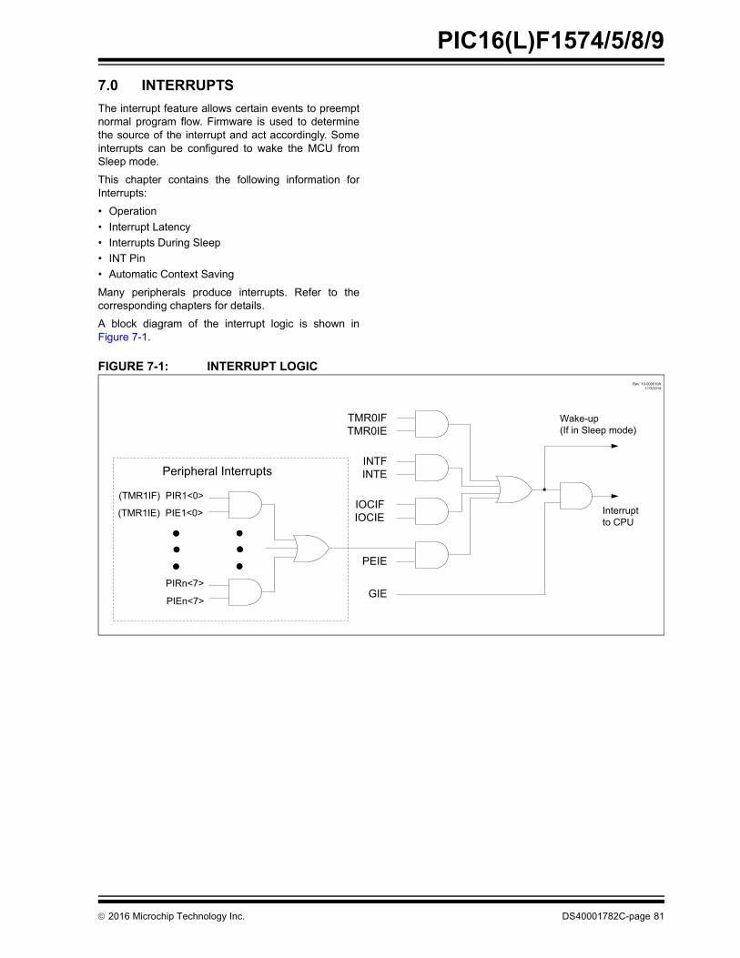
2016 Microchip Technology Inc. DS40001782C-page 81
PIC16(L)F1574/5/8/9
7.0 INTERRUPTS
The interrupt feature allows certain events to preemptnormal program flow. Firmware is used to determinethe source of the interrupt and act accordingly. Someinterrupts can be configured to wake the MCU fromSleep mode.
This chapter contains the following information forInterrupts:
• Operation
• Interrupt Latency
• Interrupts During Sleep
• INT Pin
• Automatic Context Saving
Many peripherals produce interrupts. Refer to thecorresponding chapters for details.
A block diagram of the interrupt logic is shown inFigure 7-1.
FIGURE 7-1: INTERRUPT LOGIC
TMR0IFTMR0IE
INTFINTE
IOCIFIOCIE
Interruptto CPU
Wake-up(If in Sleep mode)
GIE
(TMR1IF) PIR1<0>
PIRn<7>
PEIE
(TMR1IE) PIE1<0>
Peripheral Interrupts
PIEn<7>
Rev. 10-000010A1/13/2014
PIC16(L)F1574/5/8/9
DS40001782C-page 82 2016 Microchip Technology Inc.
7.1 Operation
Interrupts are disabled upon any device Reset. Theyare enabled by setting the following bits:
• GIE bit of the INTCON register
• Interrupt Enable bit(s) for the specific interrupt event(s)
• PEIE bit of the INTCON register (if the Interrupt Enable bit of the interrupt event is contained in the PIE1, PIE2 and PIE3 registers)
The INTCON, PIR1, PIR2 and PIR3 registers recordindividual interrupts via interrupt flag bits. Interrupt flagbits will be set, regardless of the status of the GIE, PEIEand individual interrupt enable bits.
The following events happen when an interrupt eventoccurs while the GIE bit is set:
• Current prefetched instruction is flushed
• GIE bit is cleared
• Current Program Counter (PC) is pushed onto the stack
• Critical registers are automatically saved to the shadow registers (See “Section 7.5 “Automatic Context Saving”.”)
• PC is loaded with the interrupt vector 0004h
The firmware within the Interrupt Service Routine (ISR)should determine the source of the interrupt by pollingthe interrupt flag bits. The interrupt flag bits must becleared before exiting the ISR to avoid repeatedinterrupts. Because the GIE bit is cleared, any interruptthat occurs while executing the ISR will be recordedthrough its interrupt flag, but will not cause theprocessor to redirect to the interrupt vector.
The RETFIE instruction exits the ISR by popping theprevious address from the stack, restoring the savedcontext from the shadow registers and setting the GIEbit.
For additional information on a specific interrupt’soperation, refer to its peripheral chapter.
7.2 Interrupt Latency
Interrupt latency is defined as the time from when theinterrupt event occurs to the time code execution at theinterrupt vector begins. The latency for synchronousinterrupts is three or four instruction cycles. Forasynchronous interrupts, the latency is three to fiveinstruction cycles, depending on when the interruptoccurs. See Figure 7-2 and Figure 7-3 for more details.
Note 1: Individual interrupt flag bits are set,regardless of the state of any otherenable bits.
2: All interrupts will be ignored while the GIEbit is cleared. Any interrupt occurringwhile the GIE bit is clear will be servicedwhen the GIE bit is set again.

2016 Microchip Technology Inc. DS40001782C-page 83
PIC16(L)F1574/5/8/9
FIGURE 7-2: INTERRUPT LATENCY
Q1 Q2 Q3 Q4 Q1 Q2 Q3 Q4 Q1 Q2 Q3 Q4 Q1 Q2 Q3 Q4 Q1 Q2 Q3 Q4 Q1 Q2 Q3 Q4
Fosc
CLKR
PC 0004h 0005hPC
Inst(0004h)NOP
GIE
Q1 Q2 Q3 Q4Q1 Q2 Q3 Q4
1-Cycle Instruction at PC
PC
Inst(0004h)NOP2-Cycle Instruction at PC
FSR ADDR PC+1 PC+2 0004h 0005hPC
Inst(0004h)NOP
GIE
PCPC-1
3-Cycle Instruction at PC
Execute
Interrupt
Inst(PC)
Interrupt Sampled during Q1
Inst(PC)
PC-1 PC+1
NOP
PCNew PC/
PC+10005hPC-1
PC+1/FSR ADDR
0004h
NOP
Interrupt
GIE
Interrupt
INST(PC) NOPNOP
FSR ADDR PC+1 PC+2 0004h 0005hPC
Inst(0004h)NOP
GIE
PCPC-1
3-Cycle Instruction at PC
Interrupt
INST(PC) NOPNOP NOP
Inst(0005h)
Execute
Execute
Execute

PIC16(L)F1574/5/8/9
DS40001782C-page 84 2016 Microchip Technology Inc.
FIGURE 7-3: INT PIN INTERRUPT TIMING
Q2Q1 Q3 Q4 Q2Q1 Q3 Q4 Q2Q1 Q3 Q4 Q2Q1 Q3 Q4 Q2Q1 Q3 Q4
FOSC
CLKOUT
INT pin
INTF
GIE
INSTRUCTION FLOW
PC
InstructionFetched
InstructionExecuted
Interrupt Latency
PC PC + 1 PC + 1 0004h 0005h
Inst (0004h) Inst (0005h)
Forced NOP
Inst (PC) Inst (PC + 1)
Inst (PC – 1) Inst (0004h) Forced NOPInst (PC)
—
Note 1: INTF flag is sampled here (every Q1).
2: Asynchronous interrupt latency = 3-5 TCY. Synchronous latency = 3-4 TCY, where TCY = instruction cycle time.Latency is the same whether Inst (PC) is a single cycle or a 2-cycle instruction.
3: For minimum width of INT pulse, refer to AC specifications in Section 27.0 “Electrical Specifications”.
4: INTF is enabled to be set any time during the Q4-Q1 cycles.
(1)
(2)
(3)
(4)(1)
2016 Microchip Technology Inc. DS40001782C-page 85
PIC16(L)F1574/5/8/9
7.3 Interrupts During Sleep
Some interrupts can be used to wake from Sleep. Towake from Sleep, the peripheral must be able tooperate without the system clock. The interrupt sourcemust have the appropriate Interrupt Enable bit(s) setprior to entering Sleep.
On waking from Sleep, if the GIE bit is also set, theprocessor will branch to the interrupt vector. Otherwise,the processor will continue executing instructions afterthe SLEEP instruction. The instruction directly after theSLEEP instruction will always be executed beforebranching to the ISR. Refer to Section 8.0 “Power-Down Mode (Sleep)” for more details.
7.4 INT Pin
The INT pin can be used to generate an asynchronousedge-triggered interrupt. This interrupt is enabled bysetting the INTE bit of the INTCON register. TheINTEDG bit of the OPTION_REG register determines onwhich edge the interrupt will occur. When the INTEDGbit is set, the rising edge will cause the interrupt. Whenthe INTEDG bit is clear, the falling edge will cause theinterrupt. The INTF bit of the INTCON register will be setwhen a valid edge appears on the INT pin. If the GIE andINTE bits are also set, the processor will redirectprogram execution to the interrupt vector.
7.5 Automatic Context Saving
Upon entering an interrupt, the return PC address issaved on the stack. Additionally, the following registersare automatically saved in the shadow registers:
• W register
• STATUS register (except for TO and PD)
• BSR register
• FSR registers
• PCLATH register
Upon exiting the Interrupt Service Routine, these regis-ters are automatically restored. Any modifications tothese registers during the ISR will be lost. If modifica-tions to any of these registers are desired, the corre-sponding shadow register should be modified and thevalue will be restored when exiting the ISR. Theshadow registers are available in Bank 31 and arereadable and writable. Depending on the user’sapplication, other registers may also need to be saved.

PIC16(L)F1574/5/8/9
DS40001782C-page 86 2016 Microchip Technology Inc.
7.6 Register Definitions: Interrupt Control
REGISTER 7-1: INTCON: INTERRUPT CONTROL REGISTER
R/W-0/0 R/W-0/0 R/W-0/0 R/W-0/0 R/W-0/0 R/W-0/0 R/W-0/0 R-0/0
GIE(1) PEIE(2) TMR0IE INTE IOCIE TMR0IF INTF IOCIF(3)
bit 7 bit 0
Legend:
R = Readable bit W = Writable bit U = Unimplemented bit, read as ‘0’
u = Bit is unchanged x = Bit is unknown -n/n = Value at POR and BOR/Value at all other Resets
‘1’ = Bit is set ‘0’ = Bit is cleared
bit 7 GIE: Global Interrupt Enable bit(1)
1 = Enables all active interrupts0 = Disables all interrupts
bit 6 PEIE: Peripheral Interrupt Enable bit(2)
1 = Enables all active peripheral interrupts0 = Disables all peripheral interrupts
bit 5 TMR0IE: Timer0 Overflow Interrupt Enable bit1 = Enables the Timer0 interrupt0 = Disables the Timer0 interrupt
bit 4 INTE: INT External Interrupt Enable bit1 = Enables the INT external interrupt0 = Disables the INT external interrupt
bit 3 IOCIE: Interrupt-on-Change Enable bit1 = Enables the interrupt-on-change0 = Disables the interrupt-on-change
bit 2 TMR0IF: Timer0 Overflow Interrupt Flag bit1 = TMR0 register has overflowed0 = TMR0 register did not overflow
bit 1 INTF: INT External Interrupt Flag bit1 = The INT external interrupt occurred0 = The INT external interrupt did not occur
bit 0 IOCIF: Interrupt-on-Change Interrupt Flag bit(3)
1 = When at least one of the interrupt-on-change pins changed state0 = None of the interrupt-on-change pins have changed state
Note 1: Interrupt flag bits are set when an interrupt condition occurs, regardless of the state of its correspondingenable bit or the Global Interrupt Enable bit, GIE of the INTCON register. User software should ensure theappropriate interrupt flag bits are clear prior to enabling an interrupt.
2: Bit PEIE of the INTCON register must be set to enable any peripheral interrupt.
3: The IOCIF Flag bit is read-only and cleared when all the interrupt-on-change flags in the IOCxF registershave been cleared by software.

2016 Microchip Technology Inc. DS40001782C-page 87
PIC16(L)F1574/5/8/9
REGISTER 7-2: PIE1: PERIPHERAL INTERRUPT ENABLE REGISTER 1
R/W-0/0 R/W-0/0 R/W-0/0 R/W-0/0 U-0 U-0 R/W-0/0 R/W-0/0
TMR1GIE ADIE RCIE TXIE — — TMR2IE TMR1IE
bit 7 bit 0
Legend:
R = Readable bit W = Writable bit U = Unimplemented bit, read as ‘0’
u = Bit is unchanged x = Bit is unknown -n/n = Value at POR and BOR/Value at all other Resets
‘1’ = Bit is set ‘0’ = Bit is cleared
bit 7 TMR1GIE: Timer1 Gate Interrupt Enable bit
1 = Enables the Timer1 gate acquisition interrupt0 = Disables the Timer1 gate acquisition interrupt
bit 6 ADIE: Analog-to-Digital Converter (ADC) Interrupt Enable bit
1 = Enables the ADC interrupt0 = Disables the ADC interrupt
bit 5 RCIE: USART Receive Interrupt Enable bit
1 = Enables the USART receive interrupt0 = Disables the USART receive interrupt
bit 4 TXIE: USART Transmit Interrupt Enable bit
1 = Enables the USART transmit interrupt0 = Disables the USART transmit interrupt
bit 3-2 Unimplemented: Read as ‘0’
bit 1 TMR2IE: TMR2 to PR2 Match Interrupt Enable bit
1 = Enables the Timer2 to PR2 match interrupt0 = Disables the Timer2 to PR2 match interrupt
bit 0 TMR1IE: Timer1 Overflow Interrupt Enable bit
1 = Enables the Timer1 overflow interrupt0 = Disables the Timer1 overflow interrupt
Note: Bit PEIE of the INTCON register must beset to enable any peripheral interrupt.
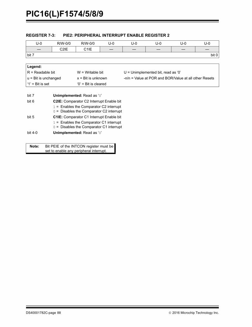
PIC16(L)F1574/5/8/9
DS40001782C-page 88 2016 Microchip Technology Inc.
REGISTER 7-3: PIE2: PERIPHERAL INTERRUPT ENABLE REGISTER 2
U-0 R/W-0/0 R/W-0/0 U-0 U-0 U-0 U-0 U-0
— C2IE C1IE — — — — —
bit 7 bit 0
Legend:
R = Readable bit W = Writable bit U = Unimplemented bit, read as ‘0’
u = Bit is unchanged x = Bit is unknown -n/n = Value at POR and BOR/Value at all other Resets
‘1’ = Bit is set ‘0’ = Bit is cleared
bit 7 Unimplemented: Read as ‘0’
bit 6 C2IE: Comparator C2 Interrupt Enable bit
1 = Enables the Comparator C2 interrupt0 = Disables the Comparator C2 interrupt
bit 5 C1IE: Comparator C1 Interrupt Enable bit
1 = Enables the Comparator C1 interrupt0 = Disables the Comparator C1 interrupt
bit 4-0 Unimplemented: Read as ‘0’
Note: Bit PEIE of the INTCON register must beset to enable any peripheral interrupt.

2016 Microchip Technology Inc. DS40001782C-page 89
PIC16(L)F1574/5/8/9
REGISTER 7-4: PIE3: PERIPHERAL INTERRUPT ENABLE REGISTER 3
R/W-0/0 R/W-0/0 R/W-0/0 R/W-0/0 U-0 U-0 U-0 U-0
PWM4IE PWM3IE PWM2IE PWM1IE — — — —
bit 7 bit 0
Legend:
R = Readable bit W = Writable bit U = Unimplemented bit, read as ‘0’
u = Bit is unchanged x = Bit is unknown -n/n = Value at POR and BOR/Value at all other Resets
‘1’ = Bit is set ‘0’ = Bit is cleared
bit 7 PWM4IE: PWM4 Interrupt Enable bit
1 = Enables the PWM4 interrupt0 = Disables the PWM4 interrupt
bit 6 PWM3IE: PWM3 Interrupt Enable bit
1 = Enables the PWM3 interrupt0 = Disables the PWM3 interrupt
bit 5 PWM2IE: PWM2 Interrupt Enable bit
1 = Enables the PWM2 interrupt0 = Disables the PWM2 interrupt
bit 4 PWM1IE: PWM1 Interrupt Enable bit
1 = Enables the PWM1 interrupt0 = Disables the PWM1 interrupt
bit 3-0 Unimplemented: Read as ‘0’
Note: Bit PEIE of the INTCON register must beset to enable any peripheral interrupt.
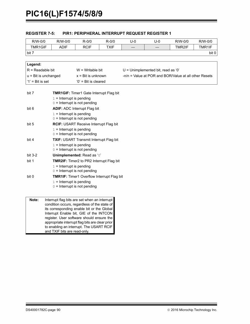
PIC16(L)F1574/5/8/9
DS40001782C-page 90 2016 Microchip Technology Inc.
REGISTER 7-5: PIR1: PERIPHERAL INTERRUPT REQUEST REGISTER 1
R/W-0/0 R/W-0/0 R-0/0 R-0/0 U-0 U-0 R/W-0/0 R/W-0/0
TMR1GIF ADIF RCIF TXIF — — TMR2IF TMR1IF
bit 7 bit 0
Legend:
R = Readable bit W = Writable bit U = Unimplemented bit, read as ‘0’
u = Bit is unchanged x = Bit is unknown -n/n = Value at POR and BOR/Value at all other Resets
‘1’ = Bit is set ‘0’ = Bit is cleared
bit 7 TMR1GIF: Timer1 Gate Interrupt Flag bit
1 = Interrupt is pending0 = Interrupt is not pending
bit 6 ADIF: ADC Interrupt Flag bit
1 = Interrupt is pending0 = Interrupt is not pending
bit 5 RCIF: USART Receive Interrupt Flag bit
1 = Interrupt is pending0 = Interrupt is not pending
bit 4 TXIF: USART Transmit Interrupt Flag bit
1 = Interrupt is pending0 = Interrupt is not pending
bit 3-2 Unimplemented: Read as ‘0’
bit 1 TMR2IF: Timer2 to PR2 Interrupt Flag bit
1 = Interrupt is pending0 = Interrupt is not pending
bit 0 TMR1IF: Timer1 Overflow Interrupt Flag bit
1 = Interrupt is pending0 = Interrupt is not pending
Note: Interrupt flag bits are set when an interruptcondition occurs, regardless of the state ofits corresponding enable bit or the GlobalInterrupt Enable bit, GIE of the INTCONregister. User software should ensure theappropriate interrupt flag bits are clear priorto enabling an interrupt. The USART RCIFand TXIF bits are read-only.

2016 Microchip Technology Inc. DS40001782C-page 91
PIC16(L)F1574/5/8/9
REGISTER 7-6: PIR2: PERIPHERAL INTERRUPT REQUEST REGISTER 2
U-0 R/W-0/0 R/W-0/0 U-0 U-0 U-0 U-0 U-0
— C2IF C1IF — — — — —
bit 7 bit 0
Legend:
R = Readable bit W = Writable bit U = Unimplemented bit, read as ‘0’
u = Bit is unchanged x = Bit is unknown -n/n = Value at POR and BOR/Value at all other Resets
‘1’ = Bit is set ‘0’ = Bit is cleared
bit 7 Unimplemented: Read as ‘0’
bit 6 C2IF: Comparator C2 Interrupt Flag bit
1 = Interrupt is pending0 = Interrupt is not pending
bit 5 C1IF: Comparator C1 Interrupt Flag bit
1 = Interrupt is pending0 = Interrupt is not pending
bit 4-0 Unimplemented: Read as ‘0’
Note: Interrupt flag bits are set when an interruptcondition occurs, regardless of the state ofits corresponding enable bit or the GlobalInterrupt Enable bit, GIE of the INTCONregister. User software should ensure theappropriate interrupt flag bits are clear priorto enabling an interrupt.
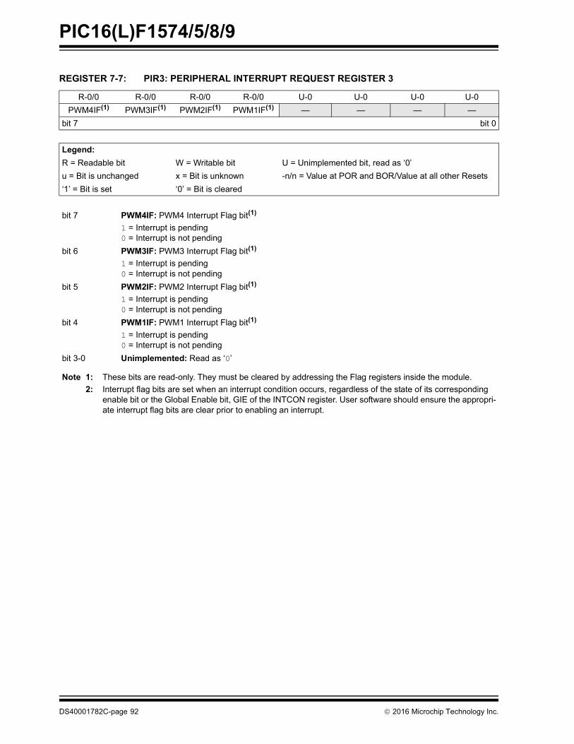
PIC16(L)F1574/5/8/9
DS40001782C-page 92 2016 Microchip Technology Inc.
REGISTER 7-7: PIR3: PERIPHERAL INTERRUPT REQUEST REGISTER 3
R-0/0 R-0/0 R-0/0 R-0/0 U-0 U-0 U-0 U-0
PWM4IF(1) PWM3IF(1) PWM2IF(1) PWM1IF(1) — — — —
bit 7 bit 0
Legend:
R = Readable bit W = Writable bit U = Unimplemented bit, read as ‘0’
u = Bit is unchanged x = Bit is unknown -n/n = Value at POR and BOR/Value at all other Resets
‘1’ = Bit is set ‘0’ = Bit is cleared
bit 7 PWM4IF: PWM4 Interrupt Flag bit(1)
1 = Interrupt is pending0 = Interrupt is not pending
bit 6 PWM3IF: PWM3 Interrupt Flag bit(1)
1 = Interrupt is pending0 = Interrupt is not pending
bit 5 PWM2IF: PWM2 Interrupt Flag bit(1)
1 = Interrupt is pending0 = Interrupt is not pending
bit 4 PWM1IF: PWM1 Interrupt Flag bit(1)
1 = Interrupt is pending0 = Interrupt is not pending
bit 3-0 Unimplemented: Read as ‘0’
Note 1: These bits are read-only. They must be cleared by addressing the Flag registers inside the module.
2: Interrupt flag bits are set when an interrupt condition occurs, regardless of the state of its corresponding enable bit or the Global Enable bit, GIE of the INTCON register. User software should ensure the appropri-ate interrupt flag bits are clear prior to enabling an interrupt.

2016 Microchip Technology Inc. DS40001782C-page 93
PIC16(L)F1574/5/8/9
TABLE 7-1: SUMMARY OF REGISTERS ASSOCIATED WITH INTERRUPTS
Name Bit 7 Bit 6 Bit 5 Bit 4 Bit 3 Bit 2 Bit 1 Bit 0Register on Page
INTCON GIE PEIE TMR0IE INTE IOCIE TMR0IF INTF IOCIF 86
OPTION_REG WPUEN INTEDG TMR0CS TMR0SE PSA PS<2:0> 178
PIE1 TMR1GIE ADIE RCIE TXIE — — TMR2IE TMR1IE 87
PIE2 — C2IE C1IE — — — — — 88
PIE3 PWM4IE PWM3IE PWM2IE PWM1IE — — — — 89
PIR1 TMR1GIF ADIF RCIF TXIF — — TMR2IF TMR1IF 90
PIR2 — C2IF C1IF — — — — — 91
PIR3 PWM4IF PWM3IF PWM2IF PWM1IF — — — — 92
Legend: — = unimplemented location, read as ‘0’. Shaded cells are not used by interrupts.
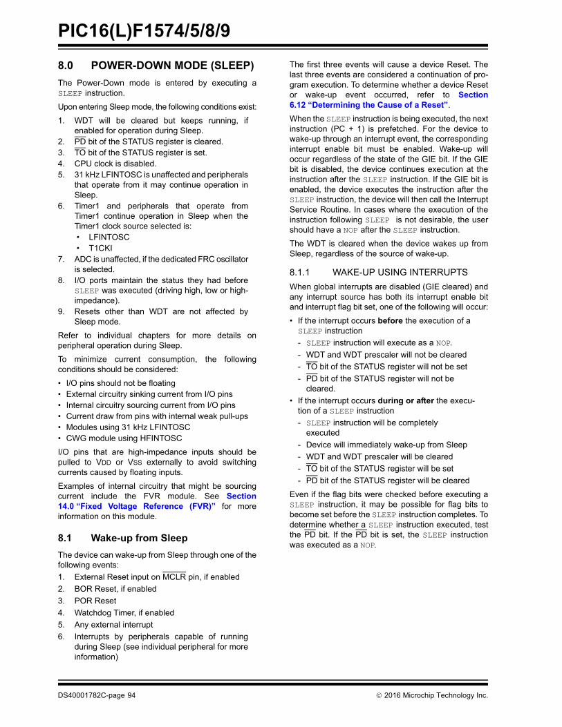
PIC16(L)F1574/5/8/9
DS40001782C-page 94 2016 Microchip Technology Inc.
8.0 POWER-DOWN MODE (SLEEP)
The Power-Down mode is entered by executing aSLEEP instruction.
Upon entering Sleep mode, the following conditions exist:
1. WDT will be cleared but keeps running, ifenabled for operation during Sleep.
2. PD bit of the STATUS register is cleared.3. TO bit of the STATUS register is set.4. CPU clock is disabled.5. 31 kHz LFINTOSC is unaffected and peripherals
that operate from it may continue operation inSleep.
6. Timer1 and peripherals that operate fromTimer1 continue operation in Sleep when theTimer1 clock source selected is:• LFINTOSC• T1CKI
7. ADC is unaffected, if the dedicated FRC oscillatoris selected.
8. I/O ports maintain the status they had beforeSLEEP was executed (driving high, low or high-impedance).
9. Resets other than WDT are not affected bySleep mode.
Refer to individual chapters for more details onperipheral operation during Sleep.
To minimize current consumption, the followingconditions should be considered:
• I/O pins should not be floating• External circuitry sinking current from I/O pins• Internal circuitry sourcing current from I/O pins• Current draw from pins with internal weak pull-ups• Modules using 31 kHz LFINTOSC• CWG module using HFINTOSC
I/O pins that are high-impedance inputs should bepulled to VDD or VSS externally to avoid switchingcurrents caused by floating inputs.
Examples of internal circuitry that might be sourcingcurrent include the FVR module. See Section14.0 “Fixed Voltage Reference (FVR)” for moreinformation on this module.
8.1 Wake-up from Sleep
The device can wake-up from Sleep through one of thefollowing events:
1. External Reset input on MCLR pin, if enabled
2. BOR Reset, if enabled
3. POR Reset
4. Watchdog Timer, if enabled
5. Any external interrupt
6. Interrupts by peripherals capable of runningduring Sleep (see individual peripheral for moreinformation)
The first three events will cause a device Reset. Thelast three events are considered a continuation of pro-gram execution. To determine whether a device Resetor wake-up event occurred, refer to Section6.12 “Determining the Cause of a Reset”.
When the SLEEP instruction is being executed, the nextinstruction (PC + 1) is prefetched. For the device towake-up through an interrupt event, the correspondinginterrupt enable bit must be enabled. Wake-up willoccur regardless of the state of the GIE bit. If the GIEbit is disabled, the device continues execution at theinstruction after the SLEEP instruction. If the GIE bit isenabled, the device executes the instruction after theSLEEP instruction, the device will then call the InterruptService Routine. In cases where the execution of theinstruction following SLEEP is not desirable, the usershould have a NOP after the SLEEP instruction.
The WDT is cleared when the device wakes up fromSleep, regardless of the source of wake-up.
8.1.1 WAKE-UP USING INTERRUPTS
When global interrupts are disabled (GIE cleared) andany interrupt source has both its interrupt enable bitand interrupt flag bit set, one of the following will occur:
• If the interrupt occurs before the execution of a SLEEP instruction
- SLEEP instruction will execute as a NOP.
- WDT and WDT prescaler will not be cleared
- TO bit of the STATUS register will not be set
- PD bit of the STATUS register will not be cleared.
• If the interrupt occurs during or after the execu-tion of a SLEEP instruction
- SLEEP instruction will be completely executed
- Device will immediately wake-up from Sleep
- WDT and WDT prescaler will be cleared
- TO bit of the STATUS register will be set
- PD bit of the STATUS register will be cleared
Even if the flag bits were checked before executing aSLEEP instruction, it may be possible for flag bits tobecome set before the SLEEP instruction completes. Todetermine whether a SLEEP instruction executed, testthe PD bit. If the PD bit is set, the SLEEP instructionwas executed as a NOP.
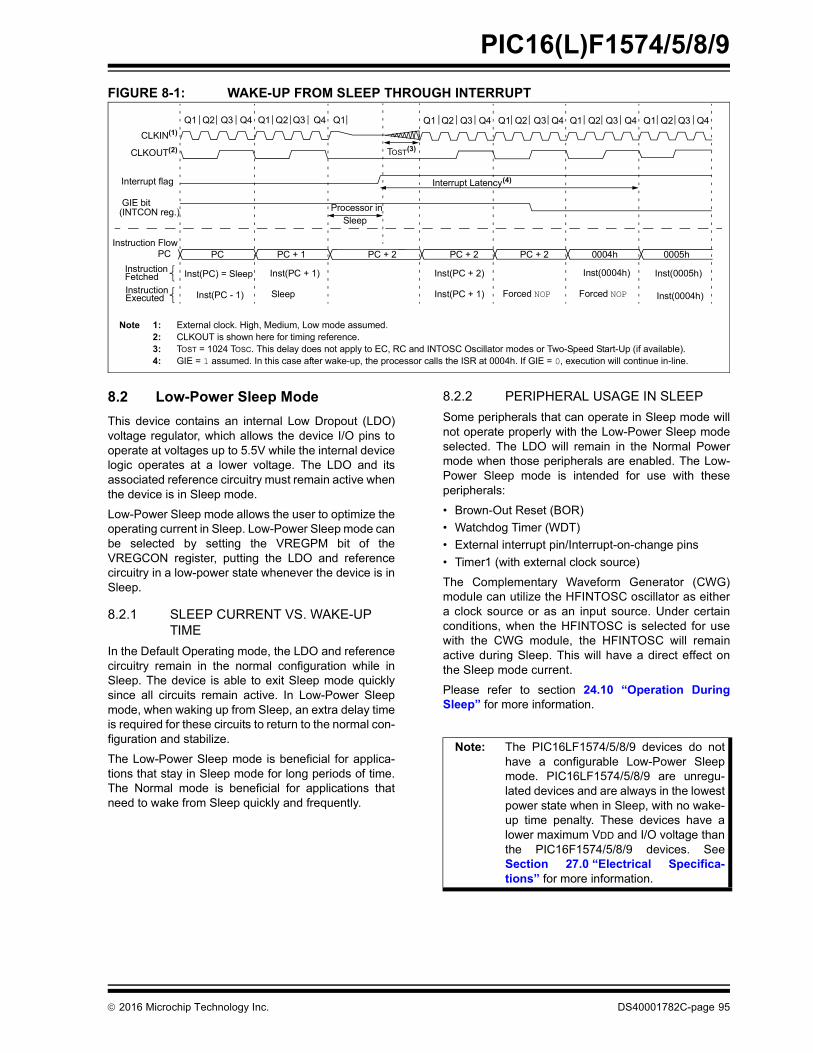
2016 Microchip Technology Inc. DS40001782C-page 95
PIC16(L)F1574/5/8/9
FIGURE 8-1: WAKE-UP FROM SLEEP THROUGH INTERRUPT
8.2 Low-Power Sleep Mode
This device contains an internal Low Dropout (LDO)voltage regulator, which allows the device I/O pins tooperate at voltages up to 5.5V while the internal devicelogic operates at a lower voltage. The LDO and itsassociated reference circuitry must remain active whenthe device is in Sleep mode.
Low-Power Sleep mode allows the user to optimize theoperating current in Sleep. Low-Power Sleep mode canbe selected by setting the VREGPM bit of theVREGCON register, putting the LDO and referencecircuitry in a low-power state whenever the device is inSleep.
8.2.1 SLEEP CURRENT VS. WAKE-UP TIME
In the Default Operating mode, the LDO and referencecircuitry remain in the normal configuration while inSleep. The device is able to exit Sleep mode quicklysince all circuits remain active. In Low-Power Sleepmode, when waking up from Sleep, an extra delay timeis required for these circuits to return to the normal con-figuration and stabilize.
The Low-Power Sleep mode is beneficial for applica-tions that stay in Sleep mode for long periods of time.The Normal mode is beneficial for applications thatneed to wake from Sleep quickly and frequently.
8.2.2 PERIPHERAL USAGE IN SLEEP
Some peripherals that can operate in Sleep mode willnot operate properly with the Low-Power Sleep modeselected. The LDO will remain in the Normal Powermode when those peripherals are enabled. The Low-Power Sleep mode is intended for use with theseperipherals:
• Brown-Out Reset (BOR)
• Watchdog Timer (WDT)
• External interrupt pin/Interrupt-on-change pins
• Timer1 (with external clock source)
The Complementary Waveform Generator (CWG)module can utilize the HFINTOSC oscillator as eithera clock source or as an input source. Under certainconditions, when the HFINTOSC is selected for usewith the CWG module, the HFINTOSC will remainactive during Sleep. This will have a direct effect onthe Sleep mode current.
Please refer to section 24.10 “Operation DuringSleep” for more information.
Q1 Q2 Q3 Q4 Q1 Q2 Q3 Q4 Q1 Q1 Q2 Q3 Q4 Q1 Q2 Q3 Q4 Q1 Q2 Q3 Q4 Q1 Q2 Q3 Q4
CLKIN(1)
CLKOUT(2)
Interrupt flag
GIE bit(INTCON reg.)
Instruction FlowPC
InstructionFetched
InstructionExecuted
PC PC + 1 PC + 2
Inst(PC) = Sleep
Inst(PC - 1)
Inst(PC + 1)
Sleep
Processor inSleep
Interrupt Latency(4)
Inst(PC + 2)
Inst(PC + 1)
Inst(0004h) Inst(0005h)
Inst(0004h)Forced NOP
PC + 2 0004h 0005h
Forced NOP
TOST(3)
PC + 2
Note 1: External clock. High, Medium, Low mode assumed.2: CLKOUT is shown here for timing reference.3: TOST = 1024 TOSC. This delay does not apply to EC, RC and INTOSC Oscillator modes or Two-Speed Start-Up (if available).4: GIE = 1 assumed. In this case after wake-up, the processor calls the ISR at 0004h. If GIE = 0, execution will continue in-line.
Note: The PIC16LF1574/5/8/9 devices do nothave a configurable Low-Power Sleepmode. PIC16LF1574/5/8/9 are unregu-lated devices and are always in the lowestpower state when in Sleep, with no wake-up time penalty. These devices have alower maximum VDD and I/O voltage thanthe PIC16F1574/5/8/9 devices. SeeSection 27.0 “Electrical Specifica-tions” for more information.

PIC16(L)F1574/5/8/9
DS40001782C-page 96 2016 Microchip Technology Inc.
8.3 Register Definitions: Voltage Regulator Control
TABLE 8-1: SUMMARY OF REGISTERS ASSOCIATED WITH POWER-DOWN MODE
REGISTER 8-1: VREGCON: VOLTAGE REGULATOR CONTROL REGISTER(1)
U-0 U-0 U-0 U-0 U-0 U-0 R/W-0/0 R/W-1/1
— — — — — — VREGPM Reserved
bit 7 bit 0
Legend:
R = Readable bit W = Writable bit U = Unimplemented bit, read as ‘0’
u = Bit is unchanged x = Bit is unknown -n/n = Value at POR and BOR/Value at all other Resets
‘1’ = Bit is set ‘0’ = Bit is cleared
bit 7-2 Unimplemented: Read as ‘0’
bit 1 VREGPM: Voltage Regulator Power Mode Selection bit
1 = Low-Power Sleep mode enabled in Sleep(2)
Draws lowest current in Sleep, slower wake-up
0 = Normal Power mode enabled in Sleep(2)
Draws higher current in Sleep, faster wake-up
bit 0 Reserved: Read as ‘1’. Maintain this bit set.
Note 1: PIC16F1574/5/8/9 only.
2: See Section 27.0 “Electrical Specifications”.
Name Bit 7 Bit 6 Bit 5 Bit 4 Bit 3 Bit 2 Bit 1 Bit 0Register on
Page
INTCON GIE PEIE TMR0IE INTE IOCIE TMR0IF INTF IOCIF 86
IOCAF — — IOCAF5 IOCAF4 IOCAF3 IOCAF2 IOCAF1 IOCAF0 143
IOCAN — — IOCAN5 IOCAN4 IOCAN3 IOCAN2 IOCAN1 IOCAN0 143
IOCAP — — IOCAP5 IOCAP4 IOCAP3 IOCAP2 IOCAP1 IOCAP0 143
PIE1 TMR1GIE ADIE RCIE TXIE — — TMR2IE TMR1IE 87
PIE2 — C2IE C1IE — — — — — 88
PIE3 PWM4IE PWM3IE PWM2IE PWM1IE — — — — 89
PIR1 TMR1GIF ADIF RCIF TXIF — — TMR2IF TMR1IF 90
PIR2 — C2IF C1IF — — — — — 91
PIR3 PWM4IF PWM3IF PWM2IF PWM1IF — — — — 92
STATUS — — — TO PD Z DC C 23
WDTCON — — WDTPS<4:0> SWDTEN 99
Legend: — = unimplemented, read as ‘0’. Shaded cells are not used in Power-Down mode.
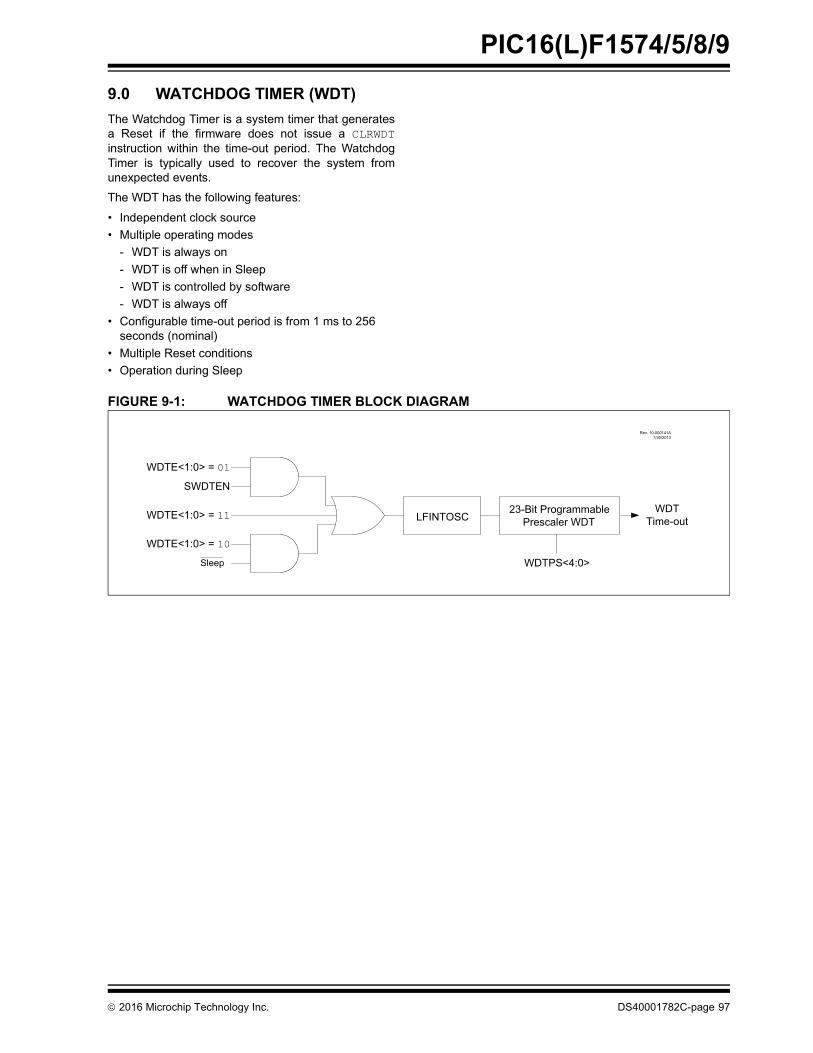
2016 Microchip Technology Inc. DS40001782C-page 97
PIC16(L)F1574/5/8/9
9.0 WATCHDOG TIMER (WDT)
The Watchdog Timer is a system timer that generatesa Reset if the firmware does not issue a CLRWDTinstruction within the time-out period. The WatchdogTimer is typically used to recover the system fromunexpected events.
The WDT has the following features:
• Independent clock source
• Multiple operating modes
- WDT is always on
- WDT is off when in Sleep
- WDT is controlled by software
- WDT is always off
• Configurable time-out period is from 1 ms to 256 seconds (nominal)
• Multiple Reset conditions
• Operation during Sleep
FIGURE 9-1: WATCHDOG TIMER BLOCK DIAGRAM
WDTE<1:0> = 01
SWDTEN
WDTE<1:0> = 11
WDTE<1:0> = 10
23- it Programmable Prescaler WDTLFINTOSC
WDTPS<4:0>
WDT Time-out
Sleep
Rev. 10-000141A7/30/2013

PIC16(L)F1574/5/8/9
DS40001782C-page 98 2016 Microchip Technology Inc.
9.1 Independent Clock Source
The WDT derives its time base from the 31 kHzLFINTOSC internal oscillator. Time intervals in thischapter are based on a nominal interval of 1 ms. SeeSection 27.0 “Electrical Specifications” for theLFINTOSC tolerances.
9.2 WDT Operating Modes
The Watchdog Timer module has four operating modescontrolled by the WDTE<1:0> bits in ConfigurationWords. See Table 9-1.
9.2.1 WDT IS ALWAYS ON
When the WDTE bits of Configuration Words are set to‘11’, the WDT is always on.
WDT protection is active during Sleep.
9.2.2 WDT IS OFF IN SLEEP
When the WDTE bits of Configuration Words are set to‘10’, the WDT is on, except in Sleep.
WDT protection is not active during Sleep.
9.2.3 WDT CONTROLLED BY SOFTWARE
When the WDTE bits of Configuration Words are set to‘01’, the WDT is controlled by the SWDTEN bit of theWDTCON register.
WDT protection is unchanged by Sleep. See Table 9-1for more details.
TABLE 9-1: WDT OPERATING MODES
9.3 Time-Out Period
The WDTPS bits of the WDTCON register set thetime-out period from 1 ms to 256 seconds (nominal).After a Reset, the default time-out period is twoseconds.
9.4 Clearing the WDT
The WDT is cleared when any of the followingconditions occur:
• Any Reset
• CLRWDT instruction is executed
• Device enters Sleep
• Device wakes up from Sleep
• Oscillator fail
• WDT is disabled
• Oscillator Start-up Timer (OST) is running
See Table 9-2 for more information.
9.5 Operation During Sleep
When the device enters Sleep, the WDT is cleared. Ifthe WDT is enabled during Sleep, the WDT resumescounting. When the device exits Sleep, the WDT iscleared again.
The WDT remains clear until the OST, if enabled,completes. See Section 5.0 “Oscillator Module” formore information on the OST.
When a WDT time-out occurs while the device is inSleep, no Reset is generated. Instead, the devicewakes up and resumes operation. The TO and PD bitsin the STATUS register are changed to indicate theevent. The RWDT bit in the PCON register can also beused. See Section 3.0 “Memory Organization” formore information.
WDTE<1:0> SWDTENDevice Mode
WDT Mode
11 X X Active
10 XAwake Active
Sleep Disabled
011 X Active
0 X Disabled
00 X X Disabled
TABLE 9-2: WDT CLEARING CONDITIONS
Conditions WDT
WDTE<1:0> = 00
Cleared
WDTE<1:0> = 01 and SWDTEN = 0
WDTE<1:0> = 10 and enter Sleep
CLRWDT Command
Oscillator Fail Detected
Exit Sleep + System Clock = EXTRC, INTOSC, EXTCLK
Change INTOSC divider (IRCF bits) Unaffected

2016 Microchip Technology Inc. DS40001782C-page 99
PIC16(L)F1574/5/8/9
9.6 Register Definitions: Watchdog Control
REGISTER 9-1: WDTCON: WATCHDOG TIMER CONTROL REGISTER
U-0 U-0 R/W-0/0 R/W-1/1 R/W-0/0 R/W-1/1 R/W-1/1 R/W-0/0
— — WDTPS<4:0> SWDTEN
bit 7 bit 0
Legend:
R = Readable bit W = Writable bit U = Unimplemented bit, read as ‘0’
u = Bit is unchanged x = Bit is unknown -n/n = Value at POR and BOR/Value at all other Resets
‘1’ = Bit is set ‘0’ = Bit is cleared
bit 7-6 Unimplemented: Read as ‘0’
bit 5-1 WDTPS<4:0>: Watchdog Timer Period Select bits(1)
Bit Value = Prescale Rate
11111 = Reserved. Results in minimum interval (1:32) • • •
10011 = Reserved. Results in minimum interval (1:32)
10010 = 1:8388608 (223) (Interval 256s nominal)10001 = 1:4194304 (222) (Interval 128s nominal)10000 = 1:2097152 (221) (Interval 64s nominal)01111 = 1:1048576 (220) (Interval 32s nominal)01110 = 1:524288 (219) (Interval 16s nominal)01101 = 1:262144 (218) (Interval 8s nominal)01100 = 1:131072 (217) (Interval 4s nominal)01011 = 1:65536 (Interval 2s nominal) (Reset value)01010 = 1:32768 (Interval 1s nominal)01001 = 1:16384 (Interval 512 ms nominal)01000 = 1:8192 (Interval 256 ms nominal)00111 = 1:4096 (Interval 128 ms nominal)00110 = 1:2048 (Interval 64 ms nominal)00101 = 1:1024 (Interval 32 ms nominal)00100 = 1:512 (Interval 16 ms nominal)00011 = 1:256 (Interval 8 ms nominal)00010 = 1:128 (Interval 4 ms nominal)00001 = 1:64 (Interval 2 ms nominal)00000 = 1:32 (Interval 1 ms nominal)
bit 0 SWDTEN: Software Enable/Disable for Watchdog Timer bit
If WDTE<1:0> = 1x:This bit is ignored.If WDTE<1:0> = 01:1 = WDT is turned on0 = WDT is turned offIf WDTE<1:0> = 00:This bit is ignored.
Note 1: Times are approximate. WDT time is based on 31 kHz LFINTOSC.
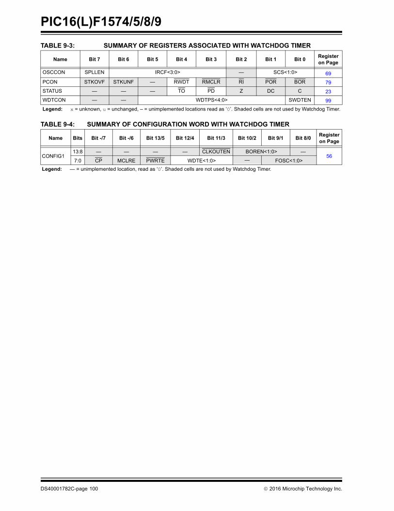
PIC16(L)F1574/5/8/9
DS40001782C-page 100 2016 Microchip Technology Inc.
TABLE 9-3: SUMMARY OF REGISTERS ASSOCIATED WITH WATCHDOG TIMER
TABLE 9-4: SUMMARY OF CONFIGURATION WORD WITH WATCHDOG TIMER
Name Bit 7 Bit 6 Bit 5 Bit 4 Bit 3 Bit 2 Bit 1 Bit 0Register on Page
OSCCON SPLLEN IRCF<3:0> — SCS<1:0> 69
PCON STKOVF STKUNF — RWDT RMCLR RI POR BOR 79
STATUS — — — TO PD Z DC C 23
WDTCON — — WDTPS<4:0> SWDTEN 99
Legend: x = unknown, u = unchanged, – = unimplemented locations read as ‘0’. Shaded cells are not used by Watchdog Timer.
Name Bits Bit -/7 Bit -/6 Bit 13/5 Bit 12/4 Bit 11/3 Bit 10/2 Bit 9/1 Bit 8/0Register on Page
CONFIG113:8 — — — — CLKOUTEN BOREN<1:0> —
567:0 CP MCLRE PWRTE WDTE<1:0> — FOSC<1:0>
Legend: — = unimplemented location, read as ‘0’. Shaded cells are not used by Watchdog Timer.

2016 Microchip Technology Inc. DS40001782C-page 101
PIC16(L)F1574/5/8/9
10.0 FLASH PROGRAM MEMORY CONTROL
The Flash program memory is readable and writableduring normal operation over the full VDD range.Program memory is indirectly addressed using SpecialFunction Registers (SFRs). The SFRs used to accessprogram memory are:
• PMCON1
• PMCON2
• PMDATL
• PMDATH
• PMADRL
• PMADRH
When accessing the program memory, thePMDATH:PMDATL register pair forms a 2-byte wordthat holds the 14-bit data for read/write, and thePMADRH:PMADRL register pair forms a 2-byte wordthat holds the 15-bit address of the program memorylocation being read.
The write time is controlled by an on-chip timer. Thewrite/erase voltages are generated by an on-chip chargepump.
The Flash program memory can be protected in twoways; by code protection (CP bit in Configuration Words)and write protection (WRT<1:0> bits in ConfigurationWords).
Code protection (CP = 0)(1), disables access, readingand writing, to the Flash program memory via externaldevice programmers. Code protection does not affectthe self-write and erase functionality. Code protectioncan only be reset by a device programmer performinga Bulk Erase to the device, clearing all Flash programmemory, Configuration bits and User IDs.
Write protection prohibits self-write and erase to aportion or all of the Flash program memory as definedby the bits WRT<1:0>. Write protection does not affecta device programmers ability to read, write or erase thedevice.
10.1 PMADRL and PMADRH Registers
The PMADRH:PMADRL register pair can address upto a maximum of 16K words of program memory. Whenselecting a program address value, the MSB of theaddress is written to the PMADRH register and the LSBis written to the PMADRL register.
10.1.1 PMCON1 AND PMCON2 REGISTERS
PMCON1 is the control register for Flash programmemory accesses.
Control bits RD and WR initiate read and write,respectively. These bits cannot be cleared, only set, insoftware. They are cleared by hardware at completionof the read or write operation. The inability to clear theWR bit in software prevents the accidental, prematuretermination of a write operation.
The WREN bit, when set, will allow a write operation tooccur. On power-up, the WREN bit is clear. TheWRERR bit is set when a write operation is interruptedby a Reset during normal operation. In these situations,following Reset, the user can check the WRERR bitand execute the appropriate error handling routine.
The PMCON2 register is a write-only register. Attemptingto read the PMCON2 register will return all ‘0’s.
To enable writes to the program memory, a specificpattern (the unlock sequence), must be written to thePMCON2 register. The required unlock sequenceprevents inadvertent writes to the program memorywrite latches and Flash program memory.
10.2 Flash Program Memory Overview
It is important to understand the Flash program memorystructure for erase and programming operations. Flashprogram memory is arranged in rows. A row consists ofa fixed number of 14-bit program memory words. A rowis the minimum size that can be erased by user software.
After a row has been erased, the user can reprogramall or a portion of this row. Data to be written into theprogram memory row is written to 14-bit wide data writelatches. These write latches are not directly accessibleto the user, but may be loaded via sequential writes tothe PMDATH:PMDATL register pair.
Note 1: Code protection of the entire Flashprogram memory array is enabled byclearing the CP bit of Configuration Words.
Note: If the user wants to modify only a portionof a previously programmed row, then thecontents of the entire row must be readand saved in RAM prior to the erase.Then, new data and retained data can bewritten into the write latches to reprogramthe row of Flash program memory. How-ever, any unprogrammed locations can bewritten without first erasing the row. In thiscase, it is not necessary to save andrewrite the other previously programmedlocations.
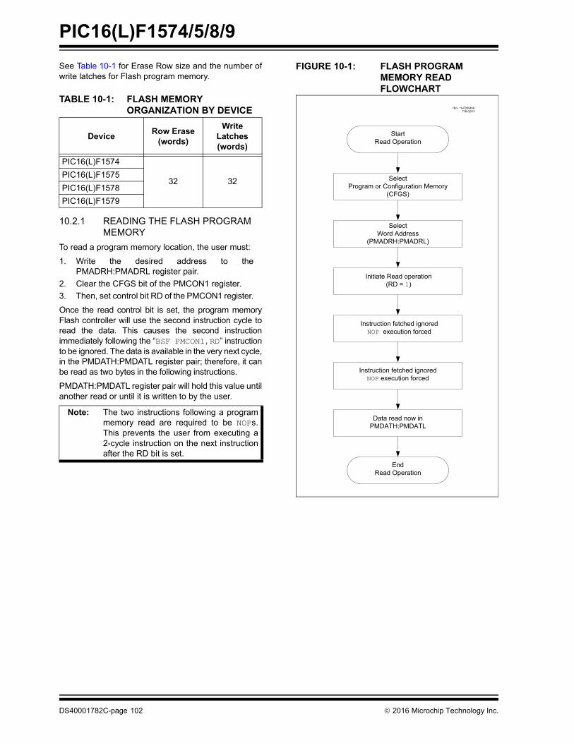
PIC16(L)F1574/5/8/9
DS40001782C-page 102 2016 Microchip Technology Inc.
See Table 10-1 for Erase Row size and the number ofwrite latches for Flash program memory.
10.2.1 READING THE FLASH PROGRAM MEMORY
To read a program memory location, the user must:
1. Write the desired address to thePMADRH:PMADRL register pair.
2. Clear the CFGS bit of the PMCON1 register.
3. Then, set control bit RD of the PMCON1 register.
Once the read control bit is set, the program memoryFlash controller will use the second instruction cycle toread the data. This causes the second instructionimmediately following the “BSF PMCON1,RD” instructionto be ignored. The data is available in the very next cycle,in the PMDATH:PMDATL register pair; therefore, it canbe read as two bytes in the following instructions.
PMDATH:PMDATL register pair will hold this value untilanother read or until it is written to by the user.
FIGURE 10-1: FLASH PROGRAM MEMORY READ FLOWCHART
TABLE 10-1: FLASH MEMORY ORGANIZATION BY DEVICE
DeviceRow Erase
(words)
Write Latches (words)
PIC16(L)F1574
32 32PIC16(L)F1575
PIC16(L)F1578
PIC16(L)F1579
Note: The two instructions following a programmemory read are required to be NOPs.This prevents the user from executing a2-cycle instruction on the next instructionafter the RD bit is set.
StartRead Operation
SelectProgram or Configuration Memory
(CFGS)
SelectWord Address
(PMADRH:PMADRL)
Initiate Read operation(RD = 1)
Instruction fetched ignoredNOP execution forced
Data read now inPMDATH:PMDATL
Instruction fetched ignoredNOP execution forced
EndRead Operation
Rev. 10-000046A7/30/2013
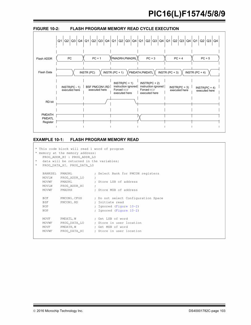
2016 Microchip Technology Inc. DS40001782C-page 103
PIC16(L)F1574/5/8/9
FIGURE 10-2: FLASH PROGRAM MEMORY READ CYCLE EXECUTION
EXAMPLE 10-1: FLASH PROGRAM MEMORY READ
Q1 Q2 Q3 Q4 Q1 Q2 Q3 Q4 Q1 Q2 Q3 Q4 Q1 Q2 Q3 Q4 Q1 Q2 Q3 Q4 Q1 Q2 Q3 Q4
BSF PMCON1,RDexecuted here
INSTR(PC + 1)
executed here
PC PC + 1 PMADRH,PMADRL PC+3 PC + 5Flash ADDR
RD bit
PMDATH,PMDATL
PC + 3 PC + 4
INSTR (PC + 1)
INSTR(PC - 1)executed here
INSTR(PC + 3)executed here
INSTR(PC + 4)executed here
Flash Data
PMDATHPMDATLRegister
INSTR (PC) INSTR (PC + 3) INSTR (PC + 4)
instruction ignoredForced NOP
INSTR(PC + 2)
executed here
instruction ignoredForced NOP
* This code block will read 1 word of program* memory at the memory address:
PROG_ADDR_HI : PROG_ADDR_LO* data will be returned in the variables;* PROG_DATA_HI, PROG_DATA_LO
BANKSEL PMADRL ; Select Bank for PMCON registersMOVLW PROG_ADDR_LO ; MOVWF PMADRL ; Store LSB of addressMOVLW PROG_ADDR_HI ; MOVWF PMADRH ; Store MSB of address
BCF PMCON1,CFGS ; Do not select Configuration SpaceBSF PMCON1,RD ; Initiate readNOP ; Ignored (Figure 10-2)NOP ; Ignored (Figure 10-2)
MOVF PMDATL,W ; Get LSB of wordMOVWF PROG_DATA_LO ; Store in user locationMOVF PMDATH,W ; Get MSB of wordMOVWF PROG_DATA_HI ; Store in user location
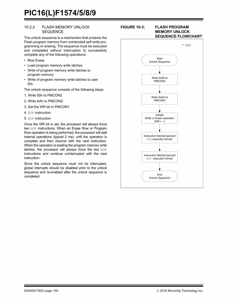
PIC16(L)F1574/5/8/9
DS40001782C-page 104 2016 Microchip Technology Inc.
10.2.2 FLASH MEMORY UNLOCK SEQUENCE
The unlock sequence is a mechanism that protects theFlash program memory from unintended self-write pro-gramming or erasing. The sequence must be executedand completed without interruption to successfullycomplete any of the following operations:
• Row Erase
• Load program memory write latches
• Write of program memory write latches to program memory
• Write of program memory write latches to user IDs
The unlock sequence consists of the following steps:
1. Write 55h to PMCON2
2. Write AAh to PMCON2
3. Set the WR bit in PMCON1
4. NOP instruction
5. NOP instruction
Once the WR bit is set, the processor will always forcetwo NOP instructions. When an Erase Row or ProgramRow operation is being performed, the processor will stallinternal operations (typical 2 ms), until the operation iscomplete and then resume with the next instruction.When the operation is loading the program memory writelatches, the processor will always force the two NOPinstructions and continue uninterrupted with the nextinstruction.
Since the unlock sequence must not be interrupted,global interrupts should be disabled prior to the unlocksequence and re-enabled after the unlock sequence iscompleted.
FIGURE 10-3: FLASH PROGRAM MEMORY UNLOCK SEQUENCE FLOWCHART
StartUnlock Sequence
EndUnlock Sequence
Write 0x55 toPMCON2
Write 0xAA toPMCON2
InitiateWrite or Erase operation
(WR = 1)
Instruction fetched ignoredNOP execution forced
Instruction fetched ignoredNOP execution forced
Rev. 10-000047A7/30/2013
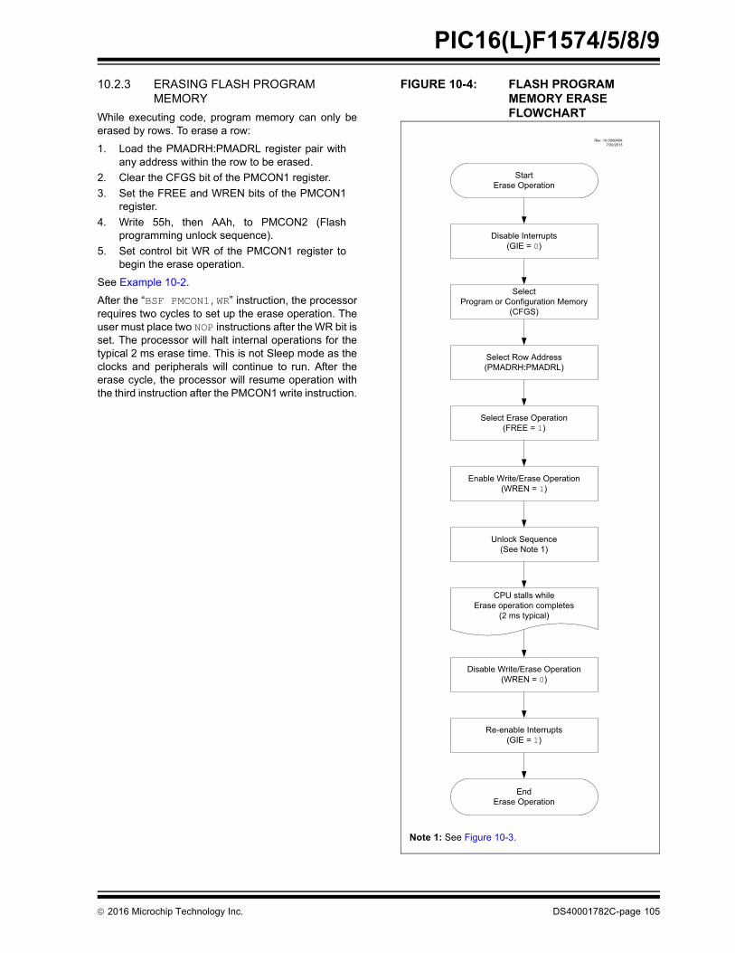
2016 Microchip Technology Inc. DS40001782C-page 105
PIC16(L)F1574/5/8/9
10.2.3 ERASING FLASH PROGRAM MEMORY
While executing code, program memory can only beerased by rows. To erase a row:
1. Load the PMADRH:PMADRL register pair withany address within the row to be erased.
2. Clear the CFGS bit of the PMCON1 register.
3. Set the FREE and WREN bits of the PMCON1register.
4. Write 55h, then AAh, to PMCON2 (Flashprogramming unlock sequence).
5. Set control bit WR of the PMCON1 register tobegin the erase operation.
See Example 10-2.
After the “BSF PMCON1,WR” instruction, the processorrequires two cycles to set up the erase operation. Theuser must place two NOP instructions after the WR bit isset. The processor will halt internal operations for thetypical 2 ms erase time. This is not Sleep mode as theclocks and peripherals will continue to run. After theerase cycle, the processor will resume operation withthe third instruction after the PMCON1 write instruction.
FIGURE 10-4: FLASH PROGRAM MEMORY ERASE FLOWCHART
Note 1: See Figure 10-3.
StartErase Operation
EndErase Operation
Disable Interrupts(GIE = 0)
SelectProgram or Configuration Memory
(CFGS)
Select Erase Operation(FREE = 1)
Select Row Address(PMADRH:PMADRL)
Enable Write/Erase Operation(WREN = 1)
Unlock Sequence(See Note 1)
Re-enable Interrupts(GIE = 1)
Disable Write/Erase Operation(WREN = 0)
CPU stalls whileErase operation completes
(2 ms typical)
Rev. 10-000048A7/30/2013
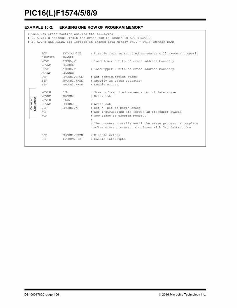
PIC16(L)F1574/5/8/9
DS40001782C-page 106 2016 Microchip Technology Inc.
EXAMPLE 10-2: ERASING ONE ROW OF PROGRAM MEMORY
; This row erase routine assumes the following:; 1. A valid address within the erase row is loaded in ADDRH:ADDRL; 2. ADDRH and ADDRL are located in shared data memory 0x70 - 0x7F (common RAM)
BCF INTCON,GIE ; Disable ints so required sequences will execute properlyBANKSEL PMADRLMOVF ADDRL,W ; Load lower 8 bits of erase address boundaryMOVWF PMADRLMOVF ADDRH,W ; Load upper 6 bits of erase address boundaryMOVWF PMADRHBCF PMCON1,CFGS ; Not configuration spaceBSF PMCON1,FREE ; Specify an erase operationBSF PMCON1,WREN ; Enable writes
MOVLW 55h ; Start of required sequence to initiate eraseMOVWF PMCON2 ; Write 55hMOVLW 0AAh ;MOVWF PMCON2 ; Write AAhBSF PMCON1,WR ; Set WR bit to begin eraseNOP ; NOP instructions are forced as processor startsNOP ; row erase of program memory.
;; The processor stalls until the erase process is complete; after erase processor continues with 3rd instruction
BCF PMCON1,WREN ; Disable writesBSF INTCON,GIE ; Enable interrupts
Re
qu
ire
dS
eq
ue
nce

2016 Microchip Technology Inc. DS40001782C-page 107
PIC16(L)F1574/5/8/9
10.2.4 WRITING TO FLASH PROGRAM MEMORY
Program memory is programmed using the followingsteps:
1. Load the address in PMADRH:PMADRL of therow to be programmed.
2. Load each write latch with data.
3. Initiate a programming operation.
4. Repeat steps 1 through 3 until all data is written.
Before writing to program memory, the word(s) to bewritten must be erased or previously unwritten. Pro-gram memory can only be erased one row at a time. Noautomatic erase occurs upon the initiation of the write.
Program memory can be written one or more words ata time. The maximum number of words written at onetime is equal to the number of write latches. SeeFigure 10-5 (row writes to program memory with 16write latches) for more details.
The write latches are aligned to the Flash row addressboundary defined by the upper 11 bits ofPMADRH:PMADRL, (PMADRH<6:0>:PMADRL<7:4>)with the lower 4 bits of PMADRL, (PMADRL<3:0>)determining the write latch being loaded. Write opera-tions do not cross these boundaries. At the completionof a program memory write operation, the data in thewrite latches is reset to contain 0x3FFF.
The following steps should be completed to load thewrite latches and program a row of program memory.These steps are divided into two parts. First, each writelatch is loaded with data from the PMDATH:PMDATLusing the unlock sequence with LWLO = 1. When thelast word to be loaded into the write latch is ready, theLWLO bit is cleared and the unlock sequenceexecuted. This initiates the programming operation,writing all the latches into Flash program memory.
1. Set the WREN bit of the PMCON1 register.
2. Clear the CFGS bit of the PMCON1 register.
3. Set the LWLO bit of the PMCON1 register.When the LWLO bit of the PMCON1 register is‘1’, the write sequence will only load the writelatches and will not initiate the write to Flashprogram memory.
4. Load the PMADRH:PMADRL register pair withthe address of the location to be written.
5. Load the PMDATH:PMDATL register pair withthe program memory data to be written.
6. Execute the unlock sequence (Section10.2.2 “Flash Memory Unlock Sequence”).The write latch is now loaded.
7. Increment the PMADRH:PMADRL register pairto point to the next location.
8. Repeat steps 5 through 7 until all but the lastwrite latch has been loaded.
9. Clear the LWLO bit of the PMCON1 register.When the LWLO bit of the PMCON1 register is‘0’, the write sequence will initiate the write toFlash program memory.
10. Load the PMDATH:PMDATL register pair withthe program memory data to be written.
11. Execute the unlock sequence (Section10.2.2 “Flash Memory Unlock Sequence”).The entire program memory latch content is nowwritten to Flash program memory.
An example of the complete write sequence is shown inExample 10-3. The initial address is loaded into thePMADRH:PMADRL register pair; the data is loadedusing indirect addressing.
Note: The special unlock sequence is requiredto load a write latch with data or initiate aFlash programming operation. If theunlock sequence is interrupted, writing tothe latches or program memory will not beinitiated.
Note: The program memory write latches arereset to the blank state (0x3FFF) at thecompletion of every write or eraseoperation. As a result, it is not necessaryto load all the program memory writelatches. Unloaded latches will remain inthe blank state.
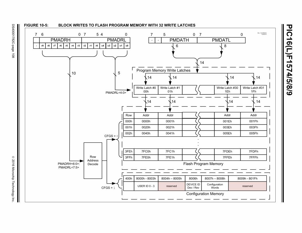
PIC
16(L
)F1
574
/5/8
/9
DS
40
00
17
82
C-p
ag
e 1
08
2
01
6 M
icroch
ip T
ech
no
log
y Inc.
FIGURE 10-5: BLOCK WRITES TO FLASH PROGRAM MEMORY WITH 32 WRITE LATCHES
6 8
14
1414
Write Latch #311Fh
1414
Program Memory Write Latches
14 14 14
PMADRH<6:0>:PMADRL<7:5>
Flash Program Memory
Row
RowAddressDecode
Addr
Write Latch #301Eh
Write Latch #101h
Write Latch #000h
Addr Addr Addr
000h 001Fh001Eh0000h 0001h
001h 003Fh003Eh0020h 0021h
002h 005Fh005Eh0040h 0041h
3FEh 7FDFh7FDEh7FC0h 7FC1h
3FFh 7FFFh7FFEh7FE0h 7FE1h
14
PMADRL<4:0>
400h 8009h - 801Fh8000h - 8003h
ConfigurationWordsUSER ID 0 - 3
8007h – 8008h8006h
DEVICE IDDev / Revreserved reserved
Configuration Memory
CFGS = 0
CFGS = 1
PMADRH PMADRL7 6 0 7 5 4 0
c4 c3 c2 c1 c0r9 r8 r7 r6 r5 r4 r3- r1 r0r2
510
PMDATH PMDATL7 5 0 7 0
--
8004h – 8005h
Rev. 10-000004A7/30/2013
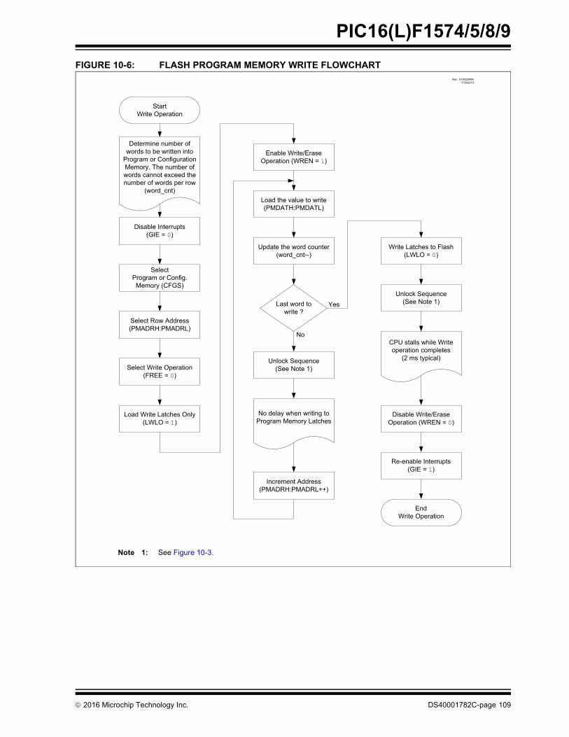
2016 Microchip Technology Inc. DS40001782C-page 109
PIC16(L)F1574/5/8/9
FIGURE 10-6: FLASH PROGRAM MEMORY WRITE FLOWCHART
Note 1: See Figure 10-3.
StartWrite Operation
EndWrite Operation
CPU stalls while Writeoperation completes
(2 ms typical)
No delay when writing toProgram Memory Latches
Determine number ofwords to be written into
Program or ConfigurationMemory. The number ofwords cannot exceed thenumber of words per row
(word_cnt)
Last word towrite ?
Disable Interrupts(GIE = 0)
SelectProgram or Config.
Memory (CFGS)
Select Row Address(PMADRH:PMADRL)
Select Write Operation(FREE = 0)
Load Write Latches Only(LWLO = 1)
Enable Write/EraseOperation (WREN = 1)
Load the value to write(PMDATH:PMDATL)
Update the word counter(word_cnt--)
Unlock Sequence(See Note 1)
Increment Address(PMADRH:PMADRL++)
Write Latches to Flash(LWLO = 0)
Unlock Sequence(See Note 1)
Disable Write/EraseOperation (WREN = 0)
Re-enable Interrupts(GIE = 1)
Yes
No
Rev. 10-000049A7/30/2013

PIC16(L)F1574/5/8/9
DS40001782C-page 110 2016 Microchip Technology Inc.
EXAMPLE 10-3: WRITING TO FLASH PROGRAM MEMORY
; This write routine assumes the following:; 1. 64 bytes of data are loaded, starting at the address in DATA_ADDR; 2. Each word of data to be written is made up of two adjacent bytes in DATA_ADDR,; stored in little endian format; 3. A valid starting address (the Least Significant bits = 00000) is loaded in ADDRH:ADDRL; 4. ADDRH and ADDRL are located in shared data memory 0x70 - 0x7F (common RAM);
BCF INTCON,GIE ; Disable ints so required sequences will execute properlyBANKSEL PMADRH ; Bank 3MOVF ADDRH,W ; Load initial addressMOVWF PMADRH ;MOVF ADDRL,W ;MOVWF PMADRL ;MOVLW LOW DATA_ADDR ; Load initial data addressMOVWF FSR0L ;MOVLW HIGH DATA_ADDR ; Load initial data addressMOVWF FSR0H ;BCF PMCON1,CFGS ; Not configuration spaceBSF PMCON1,WREN ; Enable writesBSF PMCON1,LWLO ; Only Load Write Latches
LOOPMOVIW FSR0++ ; Load first data byte into lowerMOVWF PMDATL ;MOVIW FSR0++ ; Load second data byte into upperMOVWF PMDATH ;
MOVF PMADRL,W ; Check if lower bits of address are '00000'XORLW 0x1F ; Check if we're on the last of 32 addressesANDLW 0x1F ;BTFSC STATUS,Z ; Exit if last of 32 words,GOTO START_WRITE ;
MOVLW 55h ; Start of required write sequence:MOVWF PMCON2 ; Write 55hMOVLW 0AAh ;MOVWF PMCON2 ; Write AAhBSF PMCON1,WR ; Set WR bit to begin writeNOP ; NOP instructions are forced as processor
; loads program memory write latchesNOP ;
INCF PMADRL,F ; Still loading latches Increment addressGOTO LOOP ; Write next latches
START_WRITEBCF PMCON1,LWLO ; No more loading latches - Actually start Flash program
; memory write
MOVLW 55h ; Start of required write sequence:MOVWF PMCON2 ; Write 55hMOVLW 0AAh ;MOVWF PMCON2 ; Write AAhBSF PMCON1,WR ; Set WR bit to begin writeNOP ; NOP instructions are forced as processor writes
; all the program memory write latches simultaneouslyNOP ; to program memory.
; After NOPs, the processor; stalls until the self-write process in complete; after write processor continues with 3rd instruction
BCF PMCON1,WREN ; Disable writesBSF INTCON,GIE ; Enable interrupts
Re
qu
ire
dS
eq
ue
nce
Re
qu
ire
dS
eq
ue
nce
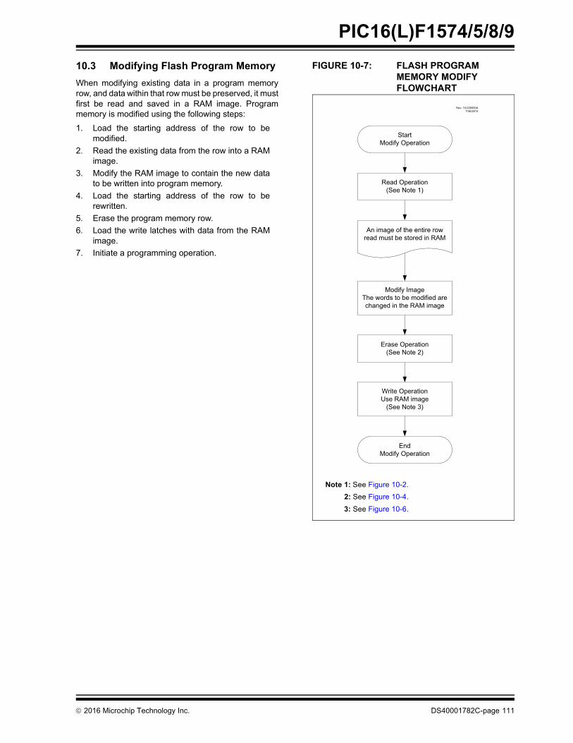
2016 Microchip Technology Inc. DS40001782C-page 111
PIC16(L)F1574/5/8/9
10.3 Modifying Flash Program Memory
When modifying existing data in a program memoryrow, and data within that row must be preserved, it mustfirst be read and saved in a RAM image. Programmemory is modified using the following steps:
1. Load the starting address of the row to bemodified.
2. Read the existing data from the row into a RAMimage.
3. Modify the RAM image to contain the new datato be written into program memory.
4. Load the starting address of the row to berewritten.
5. Erase the program memory row.
6. Load the write latches with data from the RAMimage.
7. Initiate a programming operation.
FIGURE 10-7: FLASH PROGRAM MEMORY MODIFY FLOWCHART
Note 1: See Figure 10-2.
2: See Figure 10-4.
3: See Figure 10-6.
StartModify Operation
EndModify Operation
Read Operation(See Note 1)
An image of the entire rowread must be stored in RAM
Erase Operation(See Note 2)
Modify ImageThe words to be modified arechanged in the RAM image
Write OperationUse RAM image
(See Note 3)
Rev. 10-000050A7/30/2013

PIC16(L)F1574/5/8/9
DS40001782C-page 112 2016 Microchip Technology Inc.
10.4 User ID, Device ID and Configuration Word Access
Instead of accessing program memory, the User ID’s,Device ID/Revision ID and Configuration Words can beaccessed when CFGS = 1 in the PMCON1 register.This is the region that would be pointed to byPC<15> = 1, but not all addresses are accessible.Different access may exist for reads and writes. Referto Table 10-2.
When read access is initiated on an address outsidethe parameters listed in Table 10-2, thePMDATH:PMDATL register pair is cleared, readingback ‘0’s.
TABLE 10-2: USER ID, DEVICE ID AND CONFIGURATION WORD ACCESS (CFGS = 1)
EXAMPLE 10-4: CONFIGURATION WORD AND DEVICE ID ACCESS
Address Function Read Access Write Access
8000h-8003h User IDs Yes Yes
8006h/8005h Device ID/Revision ID Yes No
8007h-8008h Configuration Words 1 and 2 Yes No
* This code block will read 1 word of program memory at the memory address:* PROG_ADDR_LO (must be 00h-08h) data will be returned in the variables;* PROG_DATA_HI, PROG_DATA_LO
BANKSEL PMADRL ; Select correct BankMOVLW PROG_ADDR_LO ; MOVWF PMADRL ; Store LSB of addressCLRF PMADRH ; Clear MSB of address
BSF PMCON1,CFGS ; Select Configuration Space BCF INTCON,GIE ; Disable interruptsBSF PMCON1,RD ; Initiate readNOP ; Executed (See Figure 10-2)NOP ; Ignored (See Figure 10-2)BSF INTCON,GIE ; Restore interrupts
MOVF PMDATL,W ; Get LSB of wordMOVWF PROG_DATA_LO ; Store in user locationMOVF PMDATH,W ; Get MSB of wordMOVWF PROG_DATA_HI ; Store in user location

2016 Microchip Technology Inc. DS40001782C-page 113
PIC16(L)F1574/5/8/9
10.5 Write Verify
It is considered good programming practice to verify thatprogram memory writes agree with the intended value.Since program memory is stored as a full page then thestored program memory contents are compared with theintended data stored in RAM after the last write iscomplete.
FIGURE 10-8: FLASH PROGRAM MEMORY VERIFY FLOWCHART
Note 1: See Figure 10-1.
StartVerify Operation
This routine assumes that the lastrow of data written was from an
image saved on RAM. This imagewill be used to verify the data
currently stored in Flash ProgramMemory
FailVerify Operation
Last word ?
PMDAT =RAM image ?
Read Operation(See Note 1)
EndVerify Operation
No
No
Yes
Yes
Rev. 10-000051A7/30/2013

PIC16(L)F1574/5/8/9
DS40001782C-page 114 2016 Microchip Technology Inc.
10.6 Register Definitions: Flash Program Memory Control
REGISTER 10-1: PMDATL: PROGRAM MEMORY DATA LOW BYTE REGISTER
R/W-x/u R/W-x/u R/W-x/u R/W-x/u R/W-x/u R/W-x/u R/W-x/u R/W-x/u
PMDAT<7:0>
bit 7 bit 0
Legend:
R = Readable bit W = Writable bit U = Unimplemented bit, read as ‘0’
u = Bit is unchanged x = Bit is unknown -n/n = Value at POR and BOR/Value at all other Resets
‘1’ = Bit is set ‘0’ = Bit is cleared
bit 7-0 PMDAT<7:0>: Read/write value for Least Significant bits of program memory
REGISTER 10-2: PMDATH: PROGRAM MEMORY DATA HIGH BYTE REGISTER
U-0 U-0 R/W-x/u R/W-x/u R/W-x/u R/W-x/u R/W-x/u R/W-x/u
— — PMDAT<13:8>
bit 7 bit 0
Legend:
R = Readable bit W = Writable bit U = Unimplemented bit, read as ‘0’
u = Bit is unchanged x = Bit is unknown -n/n = Value at POR and BOR/Value at all other Resets
‘1’ = Bit is set ‘0’ = Bit is cleared
bit 7-6 Unimplemented: Read as ‘0’
bit 5-0 PMDAT<13:8>: Read/write value for Most Significant bits of program memory
REGISTER 10-3: PMADRL: PROGRAM MEMORY ADDRESS LOW BYTE REGISTER
R/W-0/0 R/W-0/0 R/W-0/0 R/W-0/0 R/W-0/0 R/W-0/0 R/W-0/0 R/W-0/0
PMADR<7:0>
bit 7 bit 0
Legend:
R = Readable bit W = Writable bit U = Unimplemented bit, read as ‘0’
u = Bit is unchanged x = Bit is unknown -n/n = Value at POR and BOR/Value at all other Resets
‘1’ = Bit is set ‘0’ = Bit is cleared
bit 7-0 PMADR<7:0>: Specifies the Least Significant bits for program memory address
REGISTER 10-4: PMADRH: PROGRAM MEMORY ADDRESS HIGH BYTE REGISTER
U-1 R/W-0/0 R/W-0/0 R/W-0/0 R/W-0/0 R/W-0/0 R/W-0/0 R/W-0/0
—(1) PMADR<14:8>
bit 7 bit 0
Legend:
R = Readable bit W = Writable bit U = Unimplemented bit, read as ‘0’
u = Bit is unchanged x = Bit is unknown -n/n = Value at POR and BOR/Value at all other Resets
‘1’ = Bit is set ‘0’ = Bit is cleared
bit 7 Unimplemented: Read as ‘1’
bit 6-0 PMADR<14:8>: Specifies the Most Significant bits for program memory address
Note 1: Unimplemented, read as ‘1’.

2016 Microchip Technology Inc. DS40001782C-page 115
PIC16(L)F1574/5/8/9
REGISTER 10-5: PMCON1: PROGRAM MEMORY CONTROL 1 REGISTER
U-1 R/W-0/0 R/W-0/0 R/W/HC-0/0 R/W/HC-x/q(2) R/W-0/0 R/S/HC-0/0 R/S/HC-0/0
—(1) CFGS LWLO(3) FREE WRERR WREN WR RD
bit 7 bit 0
Legend:
R = Readable bit W = Writable bit U = Unimplemented bit, read as ‘0’
S = Bit can only be set x = Bit is unknown -n/n = Value at POR and BOR/Value at all other Resets
‘1’ = Bit is set ‘0’ = Bit is cleared HC = Bit is cleared by hardware
bit 7 Unimplemented: Read as ‘1’
bit 6 CFGS: Configuration Select bit1 = Access Configuration, User ID and Device ID Registers0 = Access Flash program memory
bit 5 LWLO: Load Write Latches Only bit(3)
1 = Only the addressed program memory write latch is loaded/updated on the next WR command0 = The addressed program memory write latch is loaded/updated and a write of all program memory write latches
will be initiated on the next WR command
bit 4 FREE: Program Flash Erase Enable bit 1 = Performs an erase operation on the next WR command (hardware cleared upon completion)0 = Performs an write operation on the next WR command
bit 3 WRERR: Program/Erase Error Flag bit(2)
1 = Condition indicates an improper program or erase sequence attempt or termination (bit is set automaticallyon any set attempt (write ‘1’) of the WR bit).
0 = The program or erase operation completed normally.
bit 2 WREN: Program/Erase Enable bit1 = Allows program/erase cycles0 = Inhibits programming/erasing of program Flash
bit 1 WR: Write Control bit1 = Initiates a program Flash program/erase operation.
The operation is self-timed and the bit is cleared by hardware once operation is complete. The WR bit can only be set (not cleared) in software.
0 = Program/erase operation to the Flash is complete and inactive.
bit 0 RD: Read Control bit1 = Initiates a program Flash read. Read takes one cycle. RD is cleared in hardware. The RD bit can only be set
(not cleared) in software.0 = Does not initiate a program Flash read.
Note 1: Unimplemented bit, read as ‘1’.2: The WRERR bit is automatically set by hardware when a program memory write or erase operation is started (WR = 1).3: The LWLO bit is ignored during a program memory erase operation (FREE = 1).

PIC16(L)F1574/5/8/9
DS40001782C-page 116 2016 Microchip Technology Inc.
TABLE 10-3: SUMMARY OF REGISTERS ASSOCIATED WITH FLASH PROGRAM MEMORY
TABLE 10-4: SUMMARY OF CONFIGURATION WORD WITH FLASH PROGRAM MEMORY
REGISTER 10-6: PMCON2: PROGRAM MEMORY CONTROL 2 REGISTER
W-0/0 W-0/0 W-0/0 W-0/0 W-0/0 W-0/0 W-0/0 W-0/0
Program Memory Control Register 2
bit 7 bit 0
Legend:
R = Readable bit W = Writable bit U = Unimplemented bit, read as ‘0’
S = Bit can only be set x = Bit is unknown -n/n = Value at POR and BOR/Value at all other Resets
‘1’ = Bit is set ‘0’ = Bit is cleared
bit 7-0 Flash Memory Unlock Pattern bits
To unlock writes, a 55h must be written first, followed by an AAh, before setting the WR bit of thePMCON1 register. The value written to this register is used to unlock the writes. There are specifictiming requirements on these writes.
Name Bit 7 Bit 6 Bit 5 Bit 4 Bit 3 Bit 2 Bit 1 Bit 0Register on
Page
INTCON GIE PEIE TMR0IE INTE IOCIE TMR0IF INTF IOCIF 86
PMCON1 —(1) CFGS LWLO FREE WRERR WREN WR RD 115
PMCON2 Program Memory Control Register 2 116
PMADRL PMADRL<7:0> 114
PMADRH —(1) PMADRH<6:0> 114
PMDATL PMDATL<7:0> 114
PMDATH — — PMDATH<5:0> 114
Legend: — = unimplemented location, read as ‘0’. Shaded cells are not used by Flash program memory.Note 1: Unimplemented, read as ‘1’.
Name Bits Bit -/7 Bit -/6 Bit 13/5 Bit 12/4 Bit 11/3 Bit 10/2 Bit 9/1 Bit 8/0Register on Page
CONFIG113:8 — — — — CLKOUTEN BOREN<1:0> —
567:0 CP MCLRE PWRTE WDTE<1:0> — FOSC<1:0>
CONFIG213:8 — — LVP DEBUG LPBOR BORV STVREN PLLEN
577:0 — — — — — PPS1WAY WRT<1:0>
Legend: — = unimplemented location, read as ‘0’. Shaded cells are not used by Flash program memory.

2016 Microchip Technology Inc. DS40001782C-page 117
PIC16(L)F1574/5/8/9
11.0 I/O PORTS
Each port has three standard registers for its operation.These registers are:
• TRISx registers (data direction)
• PORTx registers (reads the levels on the pins of the device)
• LATx registers (output latch)
• INLVLx (input level control)
• ODCONx registers (open-drain)
• SLRCONx registers (slew rate
Some ports may have one or more of the followingadditional registers. These registers are:
• ANSELx (analog select)
• WPUx (weak pull-up)
In general, when a peripheral is enabled on a port pin,that pin cannot be used as a general purpose output.However, the pin can still be read.
The Data Latch (LATx registers) is useful forread-modify-write operations on the value that the I/Opins are driving.
A write operation to the LATx register has the sameeffect as a write to the corresponding PORTx register.A read of the LATx register reads of the values held inthe I/O PORT latches, while a read of the PORTxregister reads the actual I/O pin value.
Ports that support analog inputs have an associatedANSELx register. When an ANSEL bit is set, the digitalinput buffer associated with that bit is disabled.Disabling the input buffer prevents analog signal levelson the pin between a logic high and low from causingexcessive current in the logic input circuitry. Asimplified model of a generic I/O port, without theinterfaces to other peripherals, is shown in Figure 11-1.
FIGURE 11-1: GENERIC I/O PORT OPERATION
TABLE 11-1: PORT AVAILABILITY PER DEVICE
Device
PO
RTA
PO
RT
B
PO
RT
C
PIC16(L)F1574 ● ●
PIC16(L)F1575 ● ●
PIC16(L)F1578 ● ● ●
PIC16(L)F1579 ● ● ●
Write LATxWrite PORTx
Data bus
Read PORTx
To digital peripherals
To analog peripherals
Data Register
TRISx
VSS
I/O pin
ANSELx
D Q
CK
Read LATx
VDD
Rev. 10-000052A7/30/2013

PIC16(L)F1574/5/8/9
DS40001782C-page 118 2016 Microchip Technology Inc.
11.1 PORTA Registers
11.1.1 DATA REGISTER
PORTA is a 6-bit wide, bidirectional port. Thecorresponding data direction register is TRISA(Register 11-2). Setting a TRISA bit (= 1) will make thecorresponding PORTA pin an input (i.e., disable theoutput driver). Clearing a TRISA bit (= 0) will make thecorresponding PORTA pin an output (i.e., enablesoutput driver and puts the contents of the output latchon the selected pin). The exception is RA3, which isinput-only and its TRIS bit will always read as ‘1’.Example 11-1 shows how to initialize an I/O port.
Reading the PORTA register (Register 11-1) reads thestatus of the pins, whereas writing to it will write to thePORT latch. All write operations are read-modify-writeoperations. Therefore, a write to a port implies that theport pins are read, this value is modified and thenwritten to the PORT data latch (LATA).
11.1.2 DIRECTION CONTROL
The TRISA register (Register 11-2) controls thePORTA pin output drivers, even when they are beingused as analog inputs. The user should ensure the bitsin the TRISA register are maintained set when usingthem as analog inputs. I/O pins configured as analoginput always read ‘0’.
11.1.3 OPEN-DRAIN CONTROL
The ODCONA register (Register 11-6) controls theopen-drain feature of the port. Open-drain operation isindependently selected for each pin. When anODCONA bit is set, the corresponding port outputbecomes an open-drain driver capable of sinkingcurrent only. When an ODCONA bit is cleared, thecorresponding port output pin is the standard push-pulldrive capable of sourcing and sinking current.
11.1.4 SLEW RATE CONTROL
The SLRCONA register (Register 11-7) controls theslew rate option for each port pin. Slew rate control isindependently selectable for each port pin. When anSLRCONA bit is set, the corresponding port pin drive isslew rate limited. When an SLRCONA bit is cleared,The corresponding port pin drive slews at the maximumrate possible.
11.1.5 INPUT THRESHOLD CONTROL
The INLVLA register (Register 11-8) controls the inputvoltage threshold for each of the available PORTA inputpins. A selection between the Schmitt Trigger CMOS orthe TTL Compatible thresholds is available. The inputthreshold is important in determining the value of aread of the PORTA register and also the level at whichan interrupt-on-change occurs, if that feature isenabled. See Table 27-4 for more information onthreshold levels.
11.1.6 ANALOG CONTROL
The ANSELA register (Register 11-4) is used toconfigure the Input mode of an I/O pin to analog.Setting the appropriate ANSELA bit high will cause alldigital reads on the pin to be read as ‘0’ and allowanalog functions on the pin to operate correctly.
The state of the ANSELA bits has no effect on digitaloutput functions. A pin with TRIS clear and ANSEL setwill still operate as a digital output, but the Input modewill be analog. This can cause unexpected behaviorwhen executing read-modify-write instructions on theaffected port.
EXAMPLE 11-1: INITIALIZING PORTA
Note: Changing the input threshold selectionshould be performed while all peripheralmodules are disabled. Changing thethreshold level during the time a module isactive may inadvertently generate a tran-sition associated with an input pin, regard-less of the actual voltage level on that pin.
Note: The ANSELA bits default to the Analogmode after Reset. To use any pins asdigital general purpose or peripheralinputs, the corresponding ANSEL bitsmust be initialized to ‘0’ by user software.
; This code example illustrates ; initializig the PORTA register. The; other ports are initialized in the same; manner.
BANKSEL PORTA ;CLRF PORTA ;Init PORTABANKSEL LATA ;Data LatchCLRF LATA ;BANKSEL ANSELA ;CLRF ANSELA ;digital I/OBANKSEL TRISA ;MOVLW B'00111000' ;Set RA<5:3> as inputsMOVWF TRISA ;and set RA<2:0> as
;outputs
2016 Microchip Technology Inc. DS40001782C-page 119
PIC16(L)F1574/5/8/9
11.1.7 PORTA FUNCTIONS AND OUTPUT PRIORITIES
Each pin defaults to the PORT latch data after Reset.Other functions are selected with the peripheral pinselect logic. See Section 12.0 “Peripheral Pin Select(PPS) Module” for more information. Analog inputfunctions, such as ADC inputs, are not shown in theperipheral pin select lists. These inputs are active whenthe I/O pin is set for Analog mode using the ANSELAregister. Digital output functions may continue tocontrol the pin when it is in Analog mode.
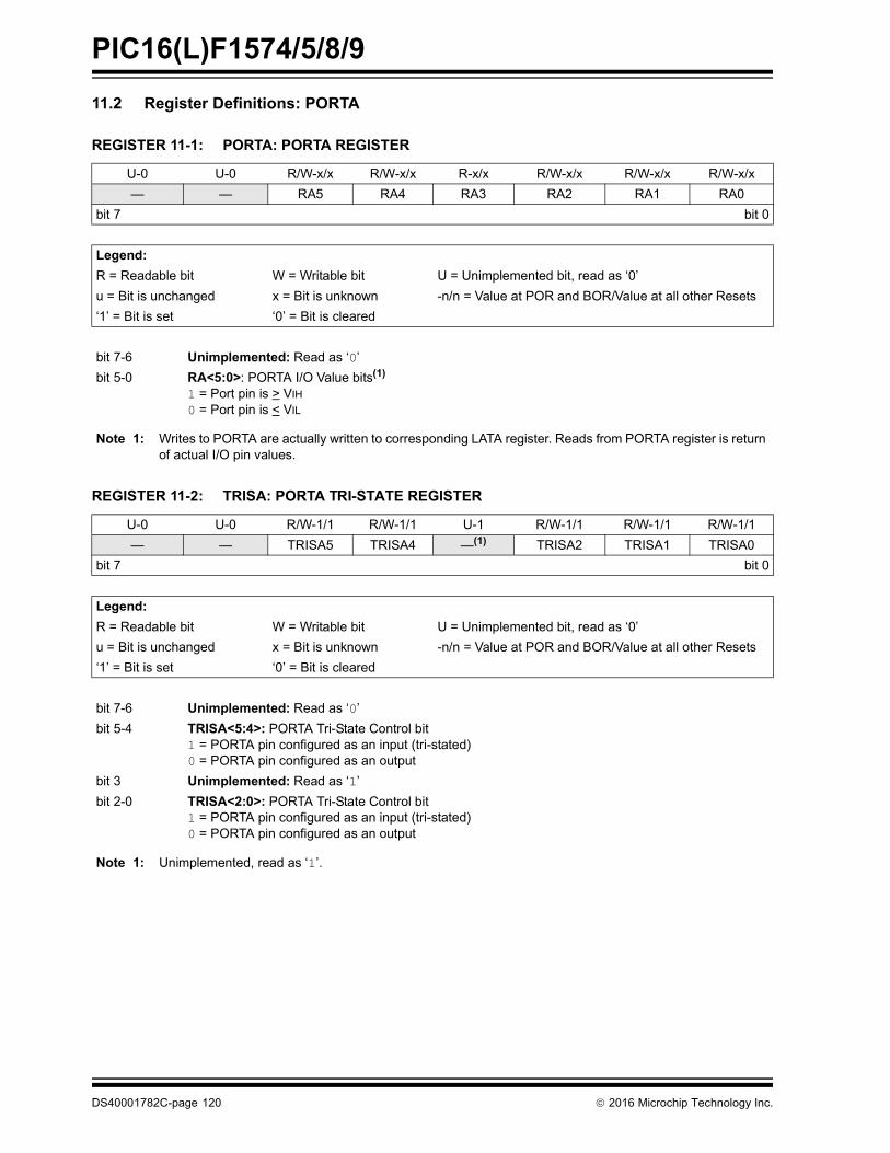
PIC16(L)F1574/5/8/9
DS40001782C-page 120 2016 Microchip Technology Inc.
11.2 Register Definitions: PORTA
REGISTER 11-1: PORTA: PORTA REGISTER
U-0 U-0 R/W-x/x R/W-x/x R-x/x R/W-x/x R/W-x/x R/W-x/x
— — RA5 RA4 RA3 RA2 RA1 RA0
bit 7 bit 0
Legend:
R = Readable bit W = Writable bit U = Unimplemented bit, read as ‘0’
u = Bit is unchanged x = Bit is unknown -n/n = Value at POR and BOR/Value at all other Resets
‘1’ = Bit is set ‘0’ = Bit is cleared
bit 7-6 Unimplemented: Read as ‘0’
bit 5-0 RA<5:0>: PORTA I/O Value bits(1)
1 = Port pin is > VIH
0 = Port pin is < VIL
Note 1: Writes to PORTA are actually written to corresponding LATA register. Reads from PORTA register is return of actual I/O pin values.
REGISTER 11-2: TRISA: PORTA TRI-STATE REGISTER
U-0 U-0 R/W-1/1 R/W-1/1 U-1 R/W-1/1 R/W-1/1 R/W-1/1
— — TRISA5 TRISA4 —(1) TRISA2 TRISA1 TRISA0
bit 7 bit 0
Legend:
R = Readable bit W = Writable bit U = Unimplemented bit, read as ‘0’
u = Bit is unchanged x = Bit is unknown -n/n = Value at POR and BOR/Value at all other Resets
‘1’ = Bit is set ‘0’ = Bit is cleared
bit 7-6 Unimplemented: Read as ‘0’
bit 5-4 TRISA<5:4>: PORTA Tri-State Control bit1 = PORTA pin configured as an input (tri-stated)0 = PORTA pin configured as an output
bit 3 Unimplemented: Read as ‘1’
bit 2-0 TRISA<2:0>: PORTA Tri-State Control bit1 = PORTA pin configured as an input (tri-stated)0 = PORTA pin configured as an output
Note 1: Unimplemented, read as ‘1’.

2016 Microchip Technology Inc. DS40001782C-page 121
PIC16(L)F1574/5/8/9
REGISTER 11-3: LATA: PORTA DATA LATCH REGISTER
U-0 U-0 R/W-x/u R/W-x/u U-0 R/W-x/u R/W-x/u R/W-x/u
— — LATA5 LATA4 — LATA2 LATA1 LATA0
bit 7 bit 0
Legend:
R = Readable bit W = Writable bit U = Unimplemented bit, read as ‘0’
u = Bit is unchanged x = Bit is unknown -n/n = Value at POR and BOR/Value at all other Resets
‘1’ = Bit is set ‘0’ = Bit is cleared
bit 7-6 Unimplemented: Read as ‘0’
bit 5-4 LATA<5:4>: RA<5:4> Output Latch Value bits(1)
bit 3 Unimplemented: Read as ‘0’
bit 2-0 LATA<2:0>: RA<2:0> Output Latch Value bits(1)
Note 1: Writes to PORTA are actually written to corresponding LATA register. Reads from PORTA register is return of actual I/O pin values.
REGISTER 11-4: ANSELA: PORTA ANALOG SELECT REGISTER
U-0 U-0 U-0 R/W-1/1 U-0 R/W-1/1 R/W-1/1 R/W-1/1
— — — ANSA4 — ANSA2 ANSA1 ANSA0
bit 7 bit 0
Legend:
R = Readable bit W = Writable bit U = Unimplemented bit, read as ‘0’
u = Bit is unchanged x = Bit is unknown -n/n = Value at POR and BOR/Value at all other Resets
‘1’ = Bit is set ‘0’ = Bit is cleared
bit 7-5 Unimplemented: Read as ‘0’
bit 4 ANSA4: Analog Select between Analog or Digital Function on pins RA4, respectively1 = Analog input. Pin is assigned as analog input(1). Digital input buffer disabled.0 = Digital I/O. Pin is assigned to port or digital special function.
bit 3 Unimplemented: Read as ‘0’
bit 2-0 ANSA<2:0>: Analog Select between Analog or Digital Function on pins RA<2:0>, respectively1 = Analog input. Pin is assigned as analog input(1). Digital input buffer disabled.0 = Digital I/O. Pin is assigned to port or digital special function.
Note 1: When setting a pin to an analog input, the corresponding TRIS bit must be set to Input mode in order to allow external control of the voltage on the pin.
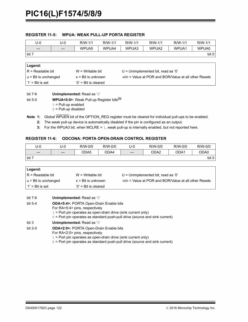
PIC16(L)F1574/5/8/9
DS40001782C-page 122 2016 Microchip Technology Inc.
REGISTER 11-5: WPUA: WEAK PULL-UP PORTA REGISTER
U-0 U-0 R/W-1/1 R/W-1/1 R/W-1/1 R/W-1/1 R/W-1/1 R/W-1/1
— — WPUA5 WPUA4 WPUA3 WPUA2 WPUA1 WPUA0
bit 7 bit 0
Legend:
R = Readable bit W = Writable bit U = Unimplemented bit, read as ‘0’
u = Bit is unchanged x = Bit is unknown -n/n = Value at POR and BOR/Value at all other Resets
‘1’ = Bit is set ‘0’ = Bit is cleared
bit 7-6 Unimplemented: Read as ‘0’
bit 5-0 WPUA<5:0>: Weak Pull-up Register bits(3)
1 = Pull-up enabled0 = Pull-up disabled
Note 1: Global WPUEN bit of the OPTION_REG register must be cleared for individual pull-ups to be enabled.
2: The weak pull-up device is automatically disabled if the pin is configured as an output.
3: For the WPUA3 bit, when MCLRE = 1, weak pull-up is internally enabled, but not reported here.
REGISTER 11-6: ODCONA: PORTA OPEN-DRAIN CONTROL REGISTER
U-0 U-0 R/W-0/0 R/W-0/0 U-0 R/W-0/0 R/W-0/0 R/W-0/0
— — ODA5 ODA4 — ODA2 ODA1 ODA0
bit 7 bit 0
Legend:
R = Readable bit W = Writable bit U = Unimplemented bit, read as ‘0’
u = Bit is unchanged x = Bit is unknown -n/n = Value at POR and BOR/Value at all other Resets
‘1’ = Bit is set ‘0’ = Bit is cleared
bit 7-6 Unimplemented: Read as ‘0’
bit 5-4 ODA<5:4>: PORTA Open-Drain Enable bitsFor RA<5:4> pins, respectively1 = Port pin operates as open-drain drive (sink current only)0 = Port pin operates as standard push-pull drive (source and sink current)
bit 3 Unimplemented: Read as ‘0’
bit 2-0 ODA<2:0>: PORTA Open-Drain Enable bitsFor RA<2:0> pins, respectively1 = Port pin operates as open-drain drive (sink current only)0 = Port pin operates as standard push-pull drive (source and sink current)
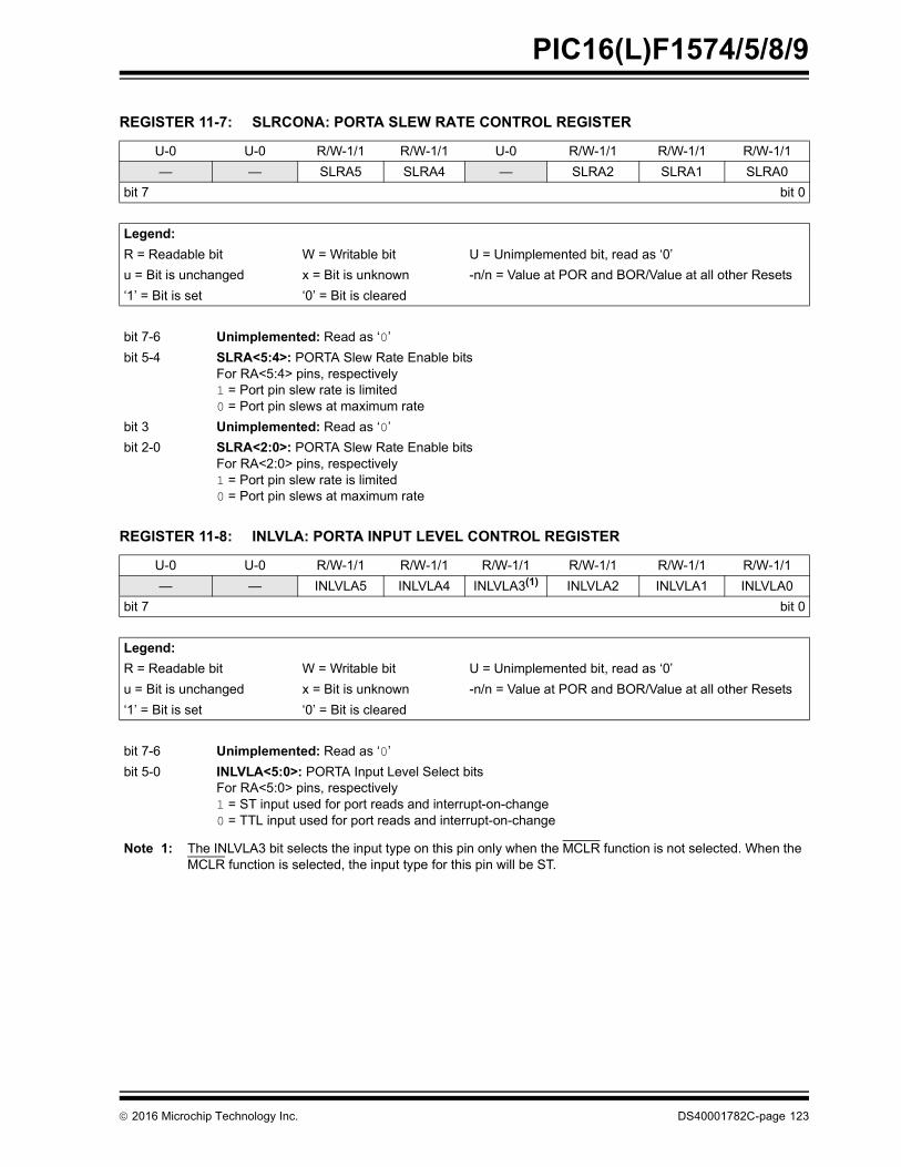
2016 Microchip Technology Inc. DS40001782C-page 123
PIC16(L)F1574/5/8/9
REGISTER 11-7: SLRCONA: PORTA SLEW RATE CONTROL REGISTER
U-0 U-0 R/W-1/1 R/W-1/1 U-0 R/W-1/1 R/W-1/1 R/W-1/1
— — SLRA5 SLRA4 — SLRA2 SLRA1 SLRA0
bit 7 bit 0
Legend:
R = Readable bit W = Writable bit U = Unimplemented bit, read as ‘0’
u = Bit is unchanged x = Bit is unknown -n/n = Value at POR and BOR/Value at all other Resets
‘1’ = Bit is set ‘0’ = Bit is cleared
bit 7-6 Unimplemented: Read as ‘0’
bit 5-4 SLRA<5:4>: PORTA Slew Rate Enable bitsFor RA<5:4> pins, respectively1 = Port pin slew rate is limited0 = Port pin slews at maximum rate
bit 3 Unimplemented: Read as ‘0’
bit 2-0 SLRA<2:0>: PORTA Slew Rate Enable bitsFor RA<2:0> pins, respectively1 = Port pin slew rate is limited0 = Port pin slews at maximum rate
REGISTER 11-8: INLVLA: PORTA INPUT LEVEL CONTROL REGISTER
U-0 U-0 R/W-1/1 R/W-1/1 R/W-1/1 R/W-1/1 R/W-1/1 R/W-1/1
— — INLVLA5 INLVLA4 INLVLA3(1) INLVLA2 INLVLA1 INLVLA0
bit 7 bit 0
Legend:
R = Readable bit W = Writable bit U = Unimplemented bit, read as ‘0’
u = Bit is unchanged x = Bit is unknown -n/n = Value at POR and BOR/Value at all other Resets
‘1’ = Bit is set ‘0’ = Bit is cleared
bit 7-6 Unimplemented: Read as ‘0’
bit 5-0 INLVLA<5:0>: PORTA Input Level Select bitsFor RA<5:0> pins, respectively1 = ST input used for port reads and interrupt-on-change0 = TTL input used for port reads and interrupt-on-change
Note 1: The INLVLA3 bit selects the input type on this pin only when the MCLR function is not selected. When the MCLR function is selected, the input type for this pin will be ST.
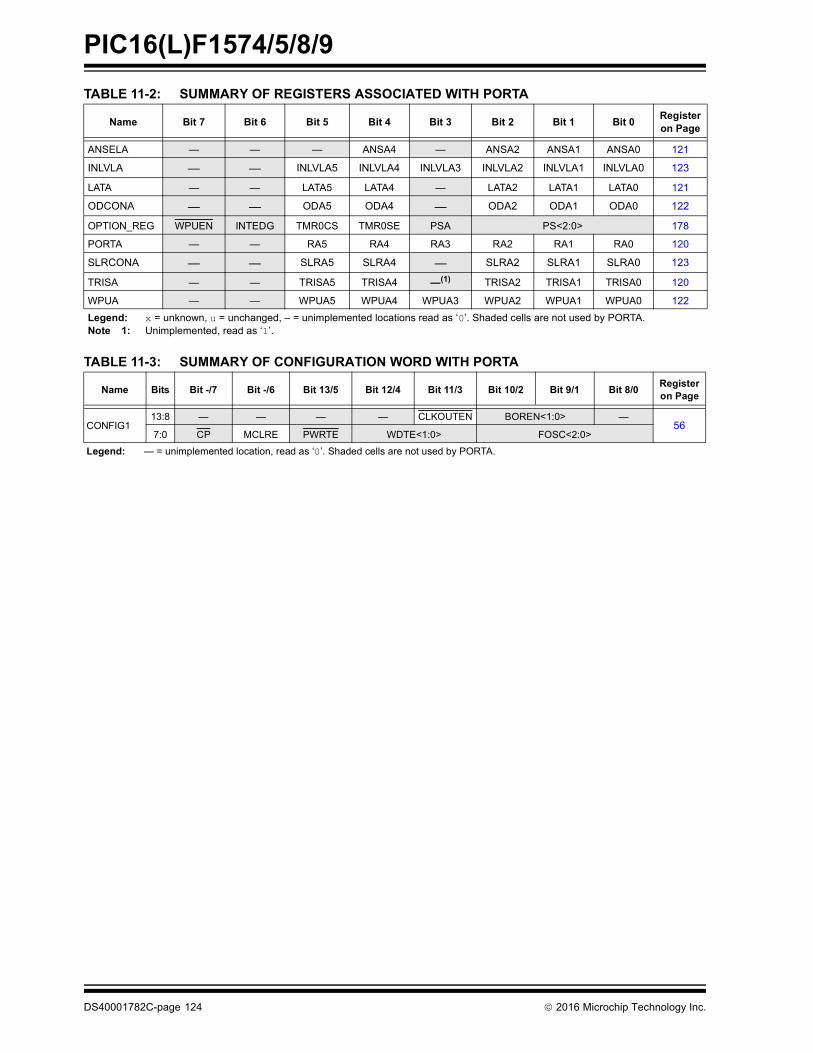
PIC16(L)F1574/5/8/9
DS40001782C-page 124 2016 Microchip Technology Inc.
TABLE 11-2: SUMMARY OF REGISTERS ASSOCIATED WITH PORTA
TABLE 11-3: SUMMARY OF CONFIGURATION WORD WITH PORTA
Name Bit 7 Bit 6 Bit 5 Bit 4 Bit 3 Bit 2 Bit 1 Bit 0Register on Page
ANSELA — — — ANSA4 — ANSA2 ANSA1 ANSA0 121
INLVLA — — INLVLA5 INLVLA4 INLVLA3 INLVLA2 INLVLA1 INLVLA0 123
LATA — — LATA5 LATA4 — LATA2 LATA1 LATA0 121
ODCONA — — ODA5 ODA4 — ODA2 ODA1 ODA0 122
OPTION_REG WPUEN INTEDG TMR0CS TMR0SE PSA PS<2:0> 178
PORTA — — RA5 RA4 RA3 RA2 RA1 RA0 120
SLRCONA — — SLRA5 SLRA4 — SLRA2 SLRA1 SLRA0 123
TRISA — — TRISA5 TRISA4 —(1) TRISA2 TRISA1 TRISA0 120
WPUA — — WPUA5 WPUA4 WPUA3 WPUA2 WPUA1 WPUA0 122
Legend: x = unknown, u = unchanged, – = unimplemented locations read as ‘0’. Shaded cells are not used by PORTA.Note 1: Unimplemented, read as ‘1’.
Name Bits Bit -/7 Bit -/6 Bit 13/5 Bit 12/4 Bit 11/3 Bit 10/2 Bit 9/1 Bit 8/0Register on Page
CONFIG113:8 — — — — CLKOUTEN BOREN<1:0> —
567:0 CP MCLRE PWRTE WDTE<1:0> FOSC<2:0>
Legend: — = unimplemented location, read as ‘0’. Shaded cells are not used by PORTA.

2016 Microchip Technology Inc. DS40001782C-page 125
PIC16(L)F1574/5/8/9
11.3 PORTB Registers(PIC16(L)F1578/9 only)
PORTB is a 4-bit wide, bidirectional port. Thecorresponding data direction register is TRISB(Register 11-10). Setting a TRISB bit (= 1) will make thecorresponding PORTB pin an input (i.e., put thecorresponding output driver in a High-Impedance mode).Clearing a TRISB bit (= 0) will make the correspondingPORTB pin an output (i.e., enable the output driver andput the contents of the output latch on the selected pin).Example 11-1 shows how to initialize an I/O port.
Reading the PORTB register (Register 11-9) reads thestatus of the pins, whereas writing to it will write to thePORT latch. All write operations are read-modify-writeoperations. Therefore, a write to a port implies that theport pins are read, this value is modified and then writtento the PORT data latch (LATB).
11.3.1 DIRECTION CONTROL
The TRISB register (Register 11-10) controls thePORTB pin output drivers, even when they are beingused as analog inputs. The user should ensure the bits inthe TRISB register are maintained set when using themas analog inputs. I/O pins configured as analog inputsalways read ‘0’.
11.3.2 OPEN-DRAIN CONTROL
The ODCONB register (Register 11-14) controls theopen-drain feature of the port. Open-drain operation isindependently selected for each pin. When anODCONB bit is set, the corresponding port outputbecomes an open-drain driver capable of sinkingcurrent only. When an ODCONB bit is cleared, thecorresponding port output pin is the standard push-pulldrive capable of sourcing and sinking current.
11.3.3 SLEW RATE CONTROL
The SLRCONB register (Register 11-15) controls theslew rate option for each port pin. Slew rate control isindependently selectable for each port pin. When anSLRCONB bit is set, the corresponding port pin drive isslew rate limited. When an SLRCONB bit is cleared,The corresponding port pin drive slews at the maximumrate possible.
11.3.4 INPUT THRESHOLD CONTROL
The INLVLB register (Register 11-16) controls the inputvoltage threshold for each of the available PORTB inputpins. A selection between the Schmitt Trigger CMOS orthe TTL Compatible thresholds is available. The inputthreshold is important in determining the value of a readof the PORTB register and also the level at which aninterrupt-on-change occurs, if that feature is enabled.See Table 27-4 for more information on thresholdlevels.
11.3.5 ANALOG CONTROL
The ANSELB register (Register 11-12) is used toconfigure the Input mode of an I/O pin to analog.Setting the appropriate ANSELB bit high will cause alldigital reads on the pin to be read as ‘0’ and allowanalog functions on the pin to operate correctly.
The state of the ANSELB bits has no effect on digital out-put functions. A pin with TRIS clear and ANSELB set willstill operate as a digital output, but the Input mode will beanalog. This can cause unexpected behavior when exe-cuting read-modify-write instructions on the affectedport.
11.3.6 PORTB FUNCTIONS AND OUTPUT PRIORITIES
Each pin defaults to the PORT latch data after Reset.Other functions are selected with the peripheral pinselect logic. See Section 12.0 “Peripheral Pin Select(PPS) Module” for more information. Analog inputfunctions, such as ADC and op amp inputs, are notshown in the peripheral pin select lists. These inputsare active when the I/O pin is set for Analog mode usingthe ANSELB register. Digital output functions maycontinue to control the pin when it is in Analog mode.
Note: Changing the input threshold selectionshould be performed while all peripheralmodules are disabled. Changing thethreshold level during the time a module isactive may inadvertently generate atransition associated with an input pin,regardless of the actual voltage level onthat pin.
Note: The ANSELB bits default to the Analogmode after Reset. To use any pins asdigital general purpose or peripheralinputs, the corresponding ANSEL bitsmust be initialized to ‘0’ by user software.
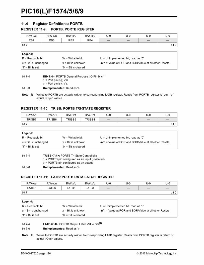
PIC16(L)F1574/5/8/9
DS40001782C-page 126 2016 Microchip Technology Inc.
11.4 Register Definitions: PORTB
REGISTER 11-9: PORTB: PORTB REGISTER
R/W-x/u R/W-x/u R/W-x/u R/W-x/u U-0 U-0 U-0 U-0
RB7 RB6 RB5 RB4 — — — —
bit 7 bit 0
Legend:
R = Readable bit W = Writable bit U = Unimplemented bit, read as ‘0’
u = Bit is unchanged x = Bit is unknown -n/n = Value at POR and BOR/Value at all other Resets
‘1’ = Bit is set ‘0’ = Bit is cleared
bit 7-4 RB<7:4>: PORTB General Purpose I/O Pin bits(1)
1 = Port pin is > VIH
0 = Port pin is < VIL
bit 3-0 Unimplemented: Read as ‘0’
Note 1: Writes to PORTB are actually written to corresponding LATB register. Reads from PORTB register is return of actual I/O pin values.
REGISTER 11-10: TRISB: PORTB TRI-STATE REGISTER
R/W-1/1 R/W-1/1 R/W-1/1 R/W-1/1 U-0 U-0 U-0 U-0
TRISB7 TRISB6 TRISB5 TRISB4 — — — —
bit 7 bit 0
Legend:
R = Readable bit W = Writable bit U = Unimplemented bit, read as ‘0’
u = Bit is unchanged x = Bit is unknown -n/n = Value at POR and BOR/Value at all other Resets
‘1’ = Bit is set ‘0’ = Bit is cleared
bit 7-4 TRISB<7:4>: PORTB Tri-State Control bits1 = PORTB pin configured as an input (tri-stated)0 = PORTB pin configured as an output
bit 3-0 Unimplemented: Read as ‘0’
REGISTER 11-11: LATB: PORTB DATA LATCH REGISTER
R/W-x/u R/W-x/u R/W-x/u R/W-x/u U-0 U-0 U-0 U-0
LATB7 LATB6 LATB5 LATB4 — — — —
bit 7 bit 0
Legend:
R = Readable bit W = Writable bit U = Unimplemented bit, read as ‘0’
u = Bit is unchanged x = Bit is unknown -n/n = Value at POR and BOR/Value at all other Resets
‘1’ = Bit is set ‘0’ = Bit is cleared
bit 7-4 LATB<7:4>: PORTB Output Latch Value bits(1)
bit 3-0 Unimplemented: Read as ‘0’
Note 1: Writes to PORTB are actually written to corresponding LATB register. Reads from PORTB register is return of actual I/O pin values.

2016 Microchip Technology Inc. DS40001782C-page 127
PIC16(L)F1574/5/8/9
REGISTER 11-12: ANSELB: PORTB ANALOG SELECT REGISTER
U-0 U-0 R/W-1/1 R/W-1/1 U-0 U-0 U-0 U-0
— — ANSB5 ANSB4 — — — —
bit 7 bit 0
Legend:
R = Readable bit W = Writable bit U = Unimplemented bit, read as ‘0’
u = Bit is unchanged x = Bit is unknown -n/n = Value at POR and BOR/Value at all other Resets
‘1’ = Bit is set ‘0’ = Bit is cleared
bit 7-6 Unimplemented: Read as ‘0’
bit 5-4 ANSB<5:4>: Analog Select between Analog or Digital Function on pins RB<5:4>, respectively0 = Digital I/O. Pin is assigned to port or digital special function.1 = Analog input. Pin is assigned as analog input(1). Digital input buffer disabled.
bit 3-0 Unimplemented: Read as ‘0’
Note 1: When setting a pin to an analog input, the corresponding TRIS bit must be set to Input mode in order to allow external control of the voltage on the pin.
REGISTER 11-13: WPUB: WEAK PULL-UP PORTB REGISTER
R/W-1/1 R/W-1/1 R/W-1/1 R/W-1/1 U-0 U-0 U-0 U-0
WPUB7 WPUB6 WPUB5 WPUB4 — — — —
bit 7 bit 0
Legend:
R = Readable bit W = Writable bit U = Unimplemented bit, read as ‘0’
u = Bit is unchanged x = Bit is unknown -n/n = Value at POR and BOR/Value at all other Resets
‘1’ = Bit is set ‘0’ = Bit is cleared
bit 7-4 WPUB<7:4>: Weak Pull-up Register bits1 = Pull-up enabled0 = Pull-up disabled
bit 3-0 Unimplemented: Read as ‘0’
Note 1: Global WPUEN bit of the OPTION_REG register must be cleared for individual pull-ups to be enabled.2: The weak pull-up device is automatically disabled if the pin is configured as an output.
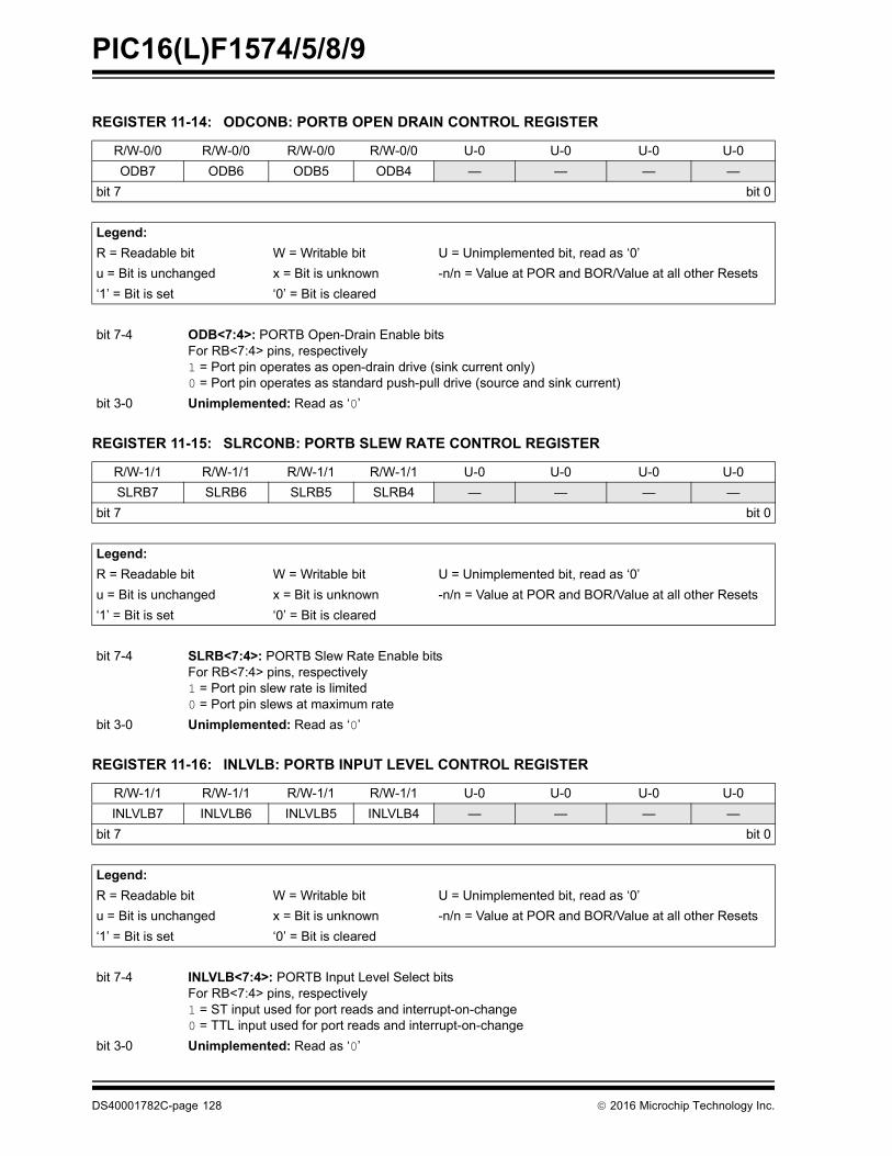
PIC16(L)F1574/5/8/9
DS40001782C-page 128 2016 Microchip Technology Inc.
REGISTER 11-14: ODCONB: PORTB OPEN DRAIN CONTROL REGISTER
R/W-0/0 R/W-0/0 R/W-0/0 R/W-0/0 U-0 U-0 U-0 U-0
ODB7 ODB6 ODB5 ODB4 — — — —
bit 7 bit 0
Legend:
R = Readable bit W = Writable bit U = Unimplemented bit, read as ‘0’
u = Bit is unchanged x = Bit is unknown -n/n = Value at POR and BOR/Value at all other Resets
‘1’ = Bit is set ‘0’ = Bit is cleared
bit 7-4 ODB<7:4>: PORTB Open-Drain Enable bitsFor RB<7:4> pins, respectively1 = Port pin operates as open-drain drive (sink current only)0 = Port pin operates as standard push-pull drive (source and sink current)
bit 3-0 Unimplemented: Read as ‘0’
REGISTER 11-15: SLRCONB: PORTB SLEW RATE CONTROL REGISTER
R/W-1/1 R/W-1/1 R/W-1/1 R/W-1/1 U-0 U-0 U-0 U-0
SLRB7 SLRB6 SLRB5 SLRB4 — — — —
bit 7 bit 0
Legend:
R = Readable bit W = Writable bit U = Unimplemented bit, read as ‘0’
u = Bit is unchanged x = Bit is unknown -n/n = Value at POR and BOR/Value at all other Resets
‘1’ = Bit is set ‘0’ = Bit is cleared
bit 7-4 SLRB<7:4>: PORTB Slew Rate Enable bitsFor RB<7:4> pins, respectively1 = Port pin slew rate is limited0 = Port pin slews at maximum rate
bit 3-0 Unimplemented: Read as ‘0’
REGISTER 11-16: INLVLB: PORTB INPUT LEVEL CONTROL REGISTER
R/W-1/1 R/W-1/1 R/W-1/1 R/W-1/1 U-0 U-0 U-0 U-0
INLVLB7 INLVLB6 INLVLB5 INLVLB4 — — — —
bit 7 bit 0
Legend:
R = Readable bit W = Writable bit U = Unimplemented bit, read as ‘0’
u = Bit is unchanged x = Bit is unknown -n/n = Value at POR and BOR/Value at all other Resets
‘1’ = Bit is set ‘0’ = Bit is cleared
bit 7-4 INLVLB<7:4>: PORTB Input Level Select bitsFor RB<7:4> pins, respectively1 = ST input used for port reads and interrupt-on-change0 = TTL input used for port reads and interrupt-on-change
bit 3-0 Unimplemented: Read as ‘0’

2016 Microchip Technology Inc. DS40001782C-page 129
PIC16(L)F1574/5/8/9
TABLE 11-4: SUMMARY OF REGISTERS ASSOCIATED WITH PORTB
Name Bit 7 Bit 6 Bit 5 Bit 4 Bit 3 Bit 2 Bit 1 Bit 0Register on Page
ANSELB — — ANSB5 ANSB4 — — — — 127
INLVLB INLVLB7 INLVLB6 INLVLB5 INLVLB4 — — — — 128
LATB LATB7 LATB6 LATB5 LATB4 — — — — 126
ODCONB ODB7 ODB6 ODB5 ODB4 — — — — 128
PORTB RB7 RB6 RB5 RB4 — — — — 126
SLRCONB SLRB7 SLRB6 SLRB5 SLRB4 — — — — 128
TRISB TRISB7 TRISB6 TRISB5 TRISB4 — — — — 128
WPUB WPUB7 WPUB6 WPUB5 WPUB4 — — — — 127
Legend: x = unknown, u = unchanged, - = unimplemented locations read as ‘0’. Shaded cells are not used by PORTB.

PIC16(L)F1574/5/8/9
DS40001782C-page 130 2016 Microchip Technology Inc.
11.5 PORTC Registers
11.5.1 DATA REGISTER
PORTC is a 6-bit wide bidirectional port in thePIC16(L)F1574/5 device and 8-bit wide bidirectional portin the PIC16(L)F1578/9 device. The corresponding datadirection register is TRISC (Register 11-18). Setting aTRISC bit (= 1) will make the corresponding PORTC pinan input (i.e., put the corresponding output driver in aHigh-Impedance mode). Clearing a TRISC bit (= 0) willmake the corresponding PORTC pin an output (i.e.,enable the output driver and put the contents of theoutput latch on the selected pin). Example 11-1 showshow to initialize an I/O port.
Reading the PORTC register (Register 11-17) reads thestatus of the pins, whereas writing to it will write to thePORT latch. All write operations are read-modify-writeoperations. Therefore, a write to a port implies that theport pins are read, this value is modified and then writtento the PORT data latch (LATC).
11.5.2 DIRECTION CONTROL
The TRISC register (Register 11-18) controls thePORTC pin output drivers, even when they are beingused as analog inputs. The user should ensure the bits inthe TRISC register are maintained set when using themas analog inputs. I/O pins configured as analog inputsalways read ‘0’.
11.5.3 INPUT THRESHOLD CONTROL
The INLVLC register (Register 11-24) controls the inputvoltage threshold for each of the available PORTCinput pins. A selection between the Schmitt TriggerCMOS or the TTL Compatible thresholds is available.The input threshold is important in determining thevalue of a read of the PORTC register and also thelevel at which an interrupt-on-change occurs, if thatfeature is enabled. See Table 27-4 for more informationon threshold levels.
11.5.4 OPEN DRAIN CONTROL
The ODCONC register (Register 11-22) controls theopen-drain feature of the port. Open-drain operation isindependently selected for each pin. When anODCONC bit is set, the corresponding port outputbecomes an open-drain driver capable of sinkingcurrent only. When an ODCONC bit is cleared, thecorresponding port output pin is the standard push-pulldrive capable of sourcing and sinking current.
11.5.5 SLEW RATE CONTROL
The SLRCONC register (Register 11-23) controls theslew rate option for each port pin. Slew rate control isindependently selectable for each port pin. When anSLRCONC bit is set, the corresponding port pin drive isslew rate limited. When an SLRCONC bit is cleared,The corresponding port pin drive slews at the maximumrate possible.
11.5.6 ANALOG CONTROL
The ANSELC register (Register 11-20) is used toconfigure the Input mode of an I/O pin to analog.Setting the appropriate ANSELC bit high will cause alldigital reads on the pin to be read as ‘0’ and allowanalog functions on the pin to operate correctly.
The state of the ANSELC bits has no effect on digital out-put functions. A pin with TRIS clear and ANSELC set willstill operate as a digital output, but the Input mode will beanalog. This can cause unexpected behavior when exe-cuting read-modify-write instructions on the affectedport.
11.5.7 PORTC FUNCTIONS AND OUTPUT PRIORITIES
Each pin defaults to the PORT latch data after Reset.Other functions are selected with the peripheral pinselect logic. See Section 12.0 “Peripheral Pin Select(PPS) Module” for more information.
Analog input functions, such as ADC inputs, are notshown in the peripheral pin select lists. These inputsare active when the I/O pin is set for Analog mode usingthe ANSELC register. Digital output functions maycontinue to control the pin when it is in Analog mode.
Note: Changing the input threshold selectionshould be performed while all peripheralmodules are disabled. Changing thethreshold level during the time a module isactive may inadvertently generate atransition associated with an input pin,regardless of the actual voltage level onthat pin.
Note: The ANSELC bits default to the Analogmode after Reset. To use any pins asdigital general purpose or peripheralinputs, the corresponding ANSEL bitsmust be initialized to ‘0’ by user software.

2016 Microchip Technology Inc. DS40001782C-page 131
PIC16(L)F1574/5/8/9
11.6 Register Definitions: PORTC
REGISTER 11-17: PORTC: PORTC REGISTER
R/W-x/u R/W-x/u R/W-x/u R/W-x/u R/W-x/u R/W-x/u R/W-x/u R/W-x/u
RC7(2) RC6(2) RC5 RC4 RC3 RC2 RC1 RC0
bit 7 bit 0
Legend:
R = Readable bit W = Writable bit U = Unimplemented bit, read as ‘0’
u = Bit is unchanged x = Bit is unknown -n/n = Value at POR and BOR/Value at all other Resets
‘1’ = Bit is set ‘0’ = Bit is cleared
bit 7-0 RC<7:0>: PORTC General Purpose I/O Pin bits(1, 2)
1 = Port pin is > VIH
0 = Port pin is < VIL
Note 1: Writes to PORTC are actually written to corresponding LATC register. Reads from PORTC register is return of actual I/O pin values.
2: RC<7:6> are available on PIC16(L)F1578/9 only.
REGISTER 11-18: TRISC: PORTC TRI-STATE REGISTER
R/W-1/1 R/W-1/1 R/W-1/1 R/W-1/1 R/W-1/1 R/W-1/1 R/W-1/1 R/W-1/1
TRISC7(1) TRISC6(1) TRISC5 TRISC4 TRISC3 TRISC2 TRISC1 TRISC0
bit 7 bit 0
Legend:
R = Readable bit W = Writable bit U = Unimplemented bit, read as ‘0’
u = Bit is unchanged x = Bit is unknown -n/n = Value at POR and BOR/Value at all other Resets
‘1’ = Bit is set ‘0’ = Bit is cleared
bit 7-0 TRISC<7:0>: PORTC Tri-State Control bits(1)
1 = PORTC pin configured as an input (tri-stated)0 = PORTC pin configured as an output
Note 1: TRISC<7:6> are available on PIC16(L)F1578/9 only.
REGISTER 11-19: LATC: PORTC DATA LATCH REGISTER
R/W-x/u R/W-x/u R/W-x/u R/W-x/u R/W-x/u R/W-x/u R/W-x/u R/W-x/u
LATC7(1) LATC6(1) LATC5 LATC4 LATC3 LATC2 LATC1 LATC0
bit 7 bit 0
Legend:
R = Readable bit W = Writable bit U = Unimplemented bit, read as ‘0’
u = Bit is unchanged x = Bit is unknown -n/n = Value at POR and BOR/Value at all other Resets
‘1’ = Bit is set ‘0’ = Bit is cleared
bit 7-0 LATC<7:0>: PORTC Output Latch Value bits(1)
Note 1: LATC<7:6> are available on PIC16(L)F1578/9 only.2: Writes to PORTC are actually written to corresponding LATC register. Reads from PORTC register is return of actual
I/O pin values.
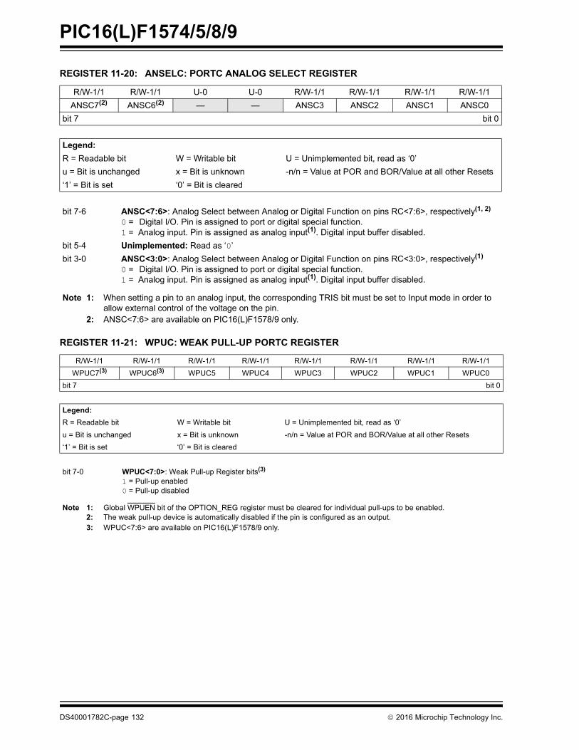
PIC16(L)F1574/5/8/9
DS40001782C-page 132 2016 Microchip Technology Inc.
REGISTER 11-20: ANSELC: PORTC ANALOG SELECT REGISTER
R/W-1/1 R/W-1/1 U-0 U-0 R/W-1/1 R/W-1/1 R/W-1/1 R/W-1/1
ANSC7(2) ANSC6(2) — — ANSC3 ANSC2 ANSC1 ANSC0
bit 7 bit 0
Legend:
R = Readable bit W = Writable bit U = Unimplemented bit, read as ‘0’
u = Bit is unchanged x = Bit is unknown -n/n = Value at POR and BOR/Value at all other Resets
‘1’ = Bit is set ‘0’ = Bit is cleared
bit 7-6 ANSC<7:6>: Analog Select between Analog or Digital Function on pins RC<7:6>, respectively(1, 2)
0 = Digital I/O. Pin is assigned to port or digital special function.1 = Analog input. Pin is assigned as analog input(1). Digital input buffer disabled.
bit 5-4 Unimplemented: Read as ‘0’
bit 3-0 ANSC<3:0>: Analog Select between Analog or Digital Function on pins RC<3:0>, respectively(1)
0 = Digital I/O. Pin is assigned to port or digital special function.1 = Analog input. Pin is assigned as analog input(1). Digital input buffer disabled.
Note 1: When setting a pin to an analog input, the corresponding TRIS bit must be set to Input mode in order to allow external control of the voltage on the pin.
2: ANSC<7:6> are available on PIC16(L)F1578/9 only.
REGISTER 11-21: WPUC: WEAK PULL-UP PORTC REGISTER
R/W-1/1 R/W-1/1 R/W-1/1 R/W-1/1 R/W-1/1 R/W-1/1 R/W-1/1 R/W-1/1
WPUC7(3) WPUC6(3) WPUC5 WPUC4 WPUC3 WPUC2 WPUC1 WPUC0
bit 7 bit 0
Legend:
R = Readable bit W = Writable bit U = Unimplemented bit, read as ‘0’
u = Bit is unchanged x = Bit is unknown -n/n = Value at POR and BOR/Value at all other Resets
‘1’ = Bit is set ‘0’ = Bit is cleared
bit 7-0 WPUC<7:0>: Weak Pull-up Register bits(3)
1 = Pull-up enabled0 = Pull-up disabled
Note 1: Global WPUEN bit of the OPTION_REG register must be cleared for individual pull-ups to be enabled.2: The weak pull-up device is automatically disabled if the pin is configured as an output.3: WPUC<7:6> are available on PIC16(L)F1578/9 only.

2016 Microchip Technology Inc. DS40001782C-page 133
PIC16(L)F1574/5/8/9
REGISTER 11-22: ODCONC: PORTC OPEN DRAIN CONTROL REGISTER
R/W-0/0 R/W-0/0 R/W-0/0 R/W-0/0 R/W-0/0 R/W-0/0 R/W-0/0 R/W-0/0
ODC7(1) ODC6(1) ODC5 ODC4 ODC3 ODC2 ODC1 ODC0
bit 7 bit 0
Legend:
R = Readable bit W = Writable bit U = Unimplemented bit, read as ‘0’
u = Bit is unchanged x = Bit is unknown -n/n = Value at POR and BOR/Value at all other Resets
‘1’ = Bit is set ‘0’ = Bit is cleared
bit 7-0 ODC<7:0>: PORTC Open-Drain Enable bits(1)
For RC<7:0> pins, respectively1 = Port pin operates as open-drain drive (sink current only)0 = Port pin operates as standard push-pull drive (source and sink current)
Note 1: ODC<7:6> are available on PIC16(L)F1578/9 only.
REGISTER 11-23: SLRCONC: PORTC SLEW RATE CONTROL REGISTER
R/W-1/1 R/W-1/1 R/W-1/1 R/W-1/1 R/W-1/1 R/W-1/1 R/W-1/1 R/W-1/1
SLRC7(1) SLRC6(1) SLRC5 SLRC4 SLRC3 SLRC2 SLRC1 SLRC0
bit 7 bit 0
Legend:
R = Readable bit W = Writable bit U = Unimplemented bit, read as ‘0’
u = Bit is unchanged x = Bit is unknown -n/n = Value at POR and BOR/Value at all other Resets
‘1’ = Bit is set ‘0’ = Bit is cleared
bit 7-0 SLRC<7:0>: PORTC Slew Rate Enable bits(1)
For RC<7:0> pins, respectively1 = Port pin slew rate is limited0 = Port pin slews at maximum rate
Note 1: SLRC<7:6> are available on PIC16(L)F1578/9 only.
REGISTER 11-24: INLVLC: PORTC INPUT LEVEL CONTROL REGISTER
R/W-1/1 R/W-1/1 R/W-1/1 R/W-1/1 R/W-1/1 R/W-1/1 R/W-1/1 R/W-1/1
INLVLC7(1) INLVLC6(1) INLVLC5 INLVLC4 INLVLC3 INLVLC2 INLVLC1 INLVLC0
bit 7 bit 0
Legend:
R = Readable bit W = Writable bit U = Unimplemented bit, read as ‘0’
u = Bit is unchanged x = Bit is unknown -n/n = Value at POR and BOR/Value at all other Resets
‘1’ = Bit is set ‘0’ = Bit is cleared
bit 7-0 INLVLC<7:0>: PORTC Input Level Select bits(1)
For RC<7:0> pins, respectively1 = ST input used for port reads and interrupt-on-change0 = TTL input used for port reads and interrupt-on-change
Note 1: INLVLC<7:6> are available on PIC16(L)F1578/9 only.
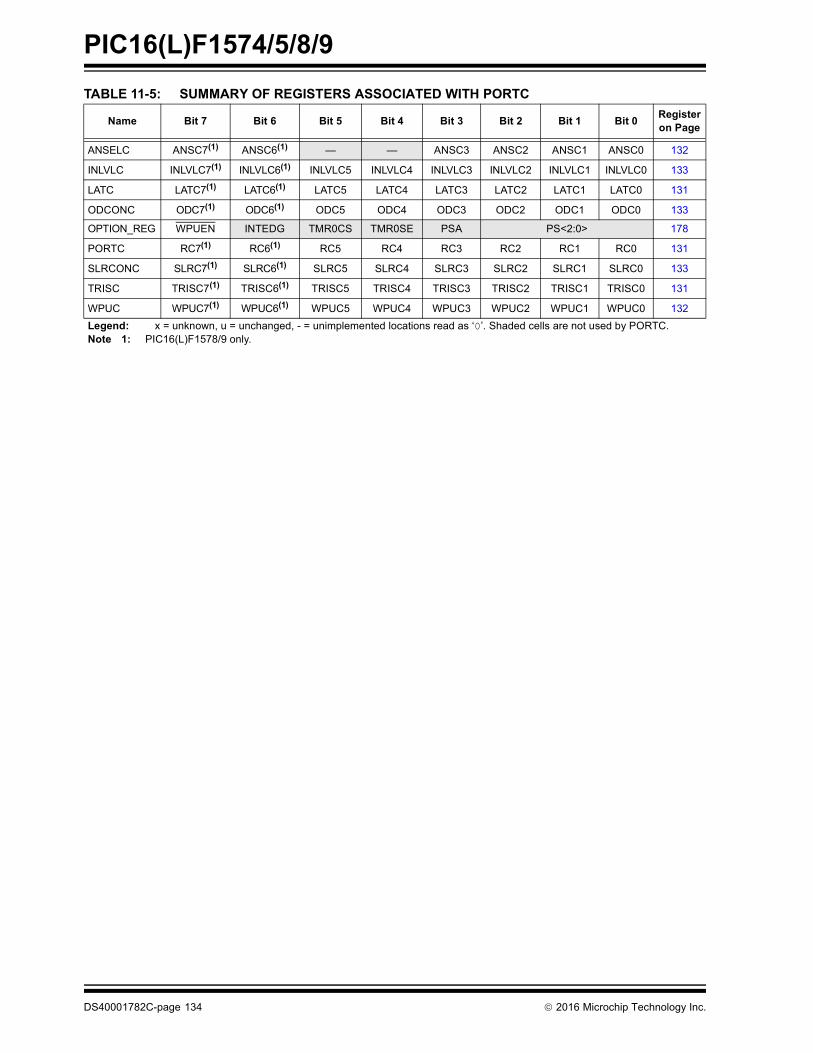
PIC16(L)F1574/5/8/9
DS40001782C-page 134 2016 Microchip Technology Inc.
TABLE 11-5: SUMMARY OF REGISTERS ASSOCIATED WITH PORTC
Name Bit 7 Bit 6 Bit 5 Bit 4 Bit 3 Bit 2 Bit 1 Bit 0Register on Page
ANSELC ANSC7(1) ANSC6(1) — — ANSC3 ANSC2 ANSC1 ANSC0 132
INLVLC INLVLC7(1) INLVLC6(1) INLVLC5 INLVLC4 INLVLC3 INLVLC2 INLVLC1 INLVLC0 133
LATC LATC7(1) LATC6(1) LATC5 LATC4 LATC3 LATC2 LATC1 LATC0 131
ODCONC ODC7(1) ODC6(1) ODC5 ODC4 ODC3 ODC2 ODC1 ODC0 133
OPTION_REG WPUEN INTEDG TMR0CS TMR0SE PSA PS<2:0> 178
PORTC RC7(1) RC6(1) RC5 RC4 RC3 RC2 RC1 RC0 131
SLRCONC SLRC7(1) SLRC6(1) SLRC5 SLRC4 SLRC3 SLRC2 SLRC1 SLRC0 133
TRISC TRISC7(1) TRISC6(1) TRISC5 TRISC4 TRISC3 TRISC2 TRISC1 TRISC0 131
WPUC WPUC7(1) WPUC6(1) WPUC5 WPUC4 WPUC3 WPUC2 WPUC1 WPUC0 132
Legend: x = unknown, u = unchanged, - = unimplemented locations read as ‘0’. Shaded cells are not used by PORTC.Note 1: PIC16(L)F1578/9 only.

2016 Microchip Technology Inc. DS40001782C-page 135
PIC16(L)F1574/5/8/9
12.0 PERIPHERAL PIN SELECT (PPS) MODULE
The Peripheral Pin Select (PPS) module connectsperipheral inputs and outputs to the device I/O pins.Only digital signals are included in the selections. Allanalog inputs and outputs remain fixed to theirassigned pins. Input and output selections are indepen-dent as shown in the simplified block diagramFigure 12-1.
12.1 PPS Inputs
Each peripheral has a PPS register with which theinputs to the peripheral are selected. Inputs include thedevice pins.
Multiple peripherals can operate from the same sourcesimultaneously. Port reads always return the pin levelregardless of peripheral PPS selection. If a pin also hasassociated analog functions, the ANSEL bit for that pinmust be cleared to enable the digital input buffer.
Although every peripheral has its own PPS input selec-tion register, the selections are identical for everyperipheral as shown in Register 12-1.
12.2 PPS Outputs
Each I/O pin has a PPS register with which the pin out-put source is selected. With few exceptions, the portTRIS control associated with that pin retains controlover the pin output driver. Peripherals that control thepin output driver as part of the peripheral operation willoverride the TRIS control as needed. These peripher-als include:
• EUSART (synchronous operation)
• MSSP (I2C)
• CWG (auto-shutdown)
Although every pin has its own PPS peripheral selec-tion register, the selections are identical for every pin asshown in Register 12-2.
FIGURE 12-1: SIMPLIFIED PPS BLOCK DIAGRAM
Note: The notation “xxx” in the register name isa place holder for the peripheral identifier.For example, CLC1PPS.
Note: The notation “Rxy” is a place holder for thepin identifier. For example, RA0PPS.
RA0
Rxy
RA0PPS
RxyPPS
RC7
RC7PPS
PPS Outputs
PPS Inputs
Peripheral abc
Peripheral xyz
abcPPS
xyzPPS
RA0
RC7

PIC16(L)F1574/5/8/9
DS40001782C-page 136 2016 Microchip Technology Inc.
12.3 Bidirectional Pins
PPS selections for peripherals with bidirectionalsignals on a single pin must be made so that the PPSinput and PPS output select the same pin. Peripheralsthat have bidirectional signals include:
• EUSART (synchronous operation)
• MSSP (I2C)
12.4 PPS Lock
The PPS includes a mode in which all input and outputselections can be locked to prevent inadvertentchanges. PPS selections are locked by setting thePPSLOCKED bit of the PPSLOCK register. Setting andclearing this bit requires a special sequence as an extraprecaution against inadvertent changes. Examples ofsetting and clearing the PPSLOCKED bit are shown inExample 12-1.
EXAMPLE 12-1: PPS LOCK/UNLOCK SEQUENCE
12.5 PPS Permanent Lock
The PPS can be permanently locked by setting thePPS1WAY Configuration bit. When this bit is set, thePPSLOCKED bit can only be cleared and set one timeafter a device Reset. This allows for clearing thePPSLOCKED bit so that the input and output selectionscan be made during initialization. When thePPSLOCKED bit is set after all selections have beenmade, it will remain set and cannot be cleared until afterthe next device Reset event.
12.6 Operation During Sleep
PPS input and output selections are unaffected bySleep.
12.7 Effects of a Reset
A device Power-On-Reset (POR) clears all PPS inputand output selections to their default values. All otherResets leave the selections unchanged. Default inputselections are shown in Table 12-1.
Note: The I2C default input pins are I2C andSMBus compatible and are the only pinson the device with this compatibility.
; suspend interruptsbcf INTCON,GIE
; BANKSEL PPSLOCK ; set bank; required sequence, next 5 instructions
movlw 0x55movwf PPSLOCKmovlw 0xAAmovwf PPSLOCK
; Set PPSLOCKED bit to disable writes or; Clear PPSLOCKED bit to enable writes
bsf PPSLOCK,PPSLOCKED; restore interrupts
bsf INTCON,GIE
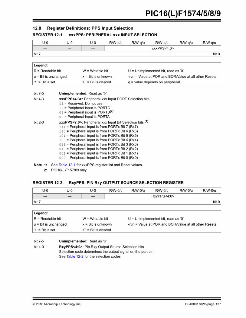
2016 Microchip Technology Inc. DS40001782C-page 137
PIC16(L)F1574/5/8/9
12.8 Register Definitions: PPS Input Selection
REGISTER 12-1: xxxPPS: PERIPHERAL xxx INPUT SELECTION
U-0 U-0 U-0 R/W-q/u R/W-q/u R/W-q/u R/W-q/u R/W-q/u
— — — xxxPPS<4:0>
bit 7 bit 0
Legend:
R = Readable bit W = Writable bit U = Unimplemented bit, read as ‘0’
u = Bit is unchanged x = Bit is unknown -n/n = Value at POR and BOR/Value at all other Resets
‘1’ = Bit is set ‘0’ = Bit is cleared q = value depends on peripheral
bit 7-5 Unimplemented: Read as ‘0’
bit 4-3 xxxPPS<4:3>: Peripheral xxx Input PORT Selection bits11 = Reserved. Do not use.10 = Peripheral input is PORTC01 = Peripheral input is PORTB(2)
00 = Peripheral input is PORTA
bit 2-0 xxxPPS<2:0>: Peripheral xxx Input Bit Selection bits (1)
111 = Peripheral input is from PORTx Bit 7 (Rx7)110 = Peripheral input is from PORTx Bit 6 (Rx6)101 = Peripheral input is from PORTx Bit 5 (Rx5)100 = Peripheral input is from PORTx Bit 4 (Rx4)011 = Peripheral input is from PORTx Bit 3 (Rx3)010 = Peripheral input is from PORTx Bit 2 (Rx2)001 = Peripheral input is from PORTx Bit 1 (Rx1)000 = Peripheral input is from PORTx Bit 0 (Rx0)
Note 1: See Table 12-1 for xxxPPS register list and Reset values.
2: PIC16(L)F1578/9 only.
REGISTER 12-2: RxyPPS: PIN Rxy OUTPUT SOURCE SELECTION REGISTER
U-0 U-0 U-0 R/W-0/u R/W-0/u R/W-0/u R/W-0/u R/W-0/u
— — — RxyPPS<4:0>
bit 7 bit 0
Legend:
R = Readable bit W = Writable bit U = Unimplemented bit, read as ‘0’
u = Bit is unchanged x = Bit is unknown -n/n = Value at POR and BOR/Value at all other Resets
‘1’ = Bit is set ‘0’ = Bit is cleared
bit 7-5 Unimplemented: Read as ‘0’
bit 4-0 RxyPPS<4:0>: Pin Rxy Output Source Selection bitsSelection code determines the output signal on the port pin.See Table 12-2 for the selection codes
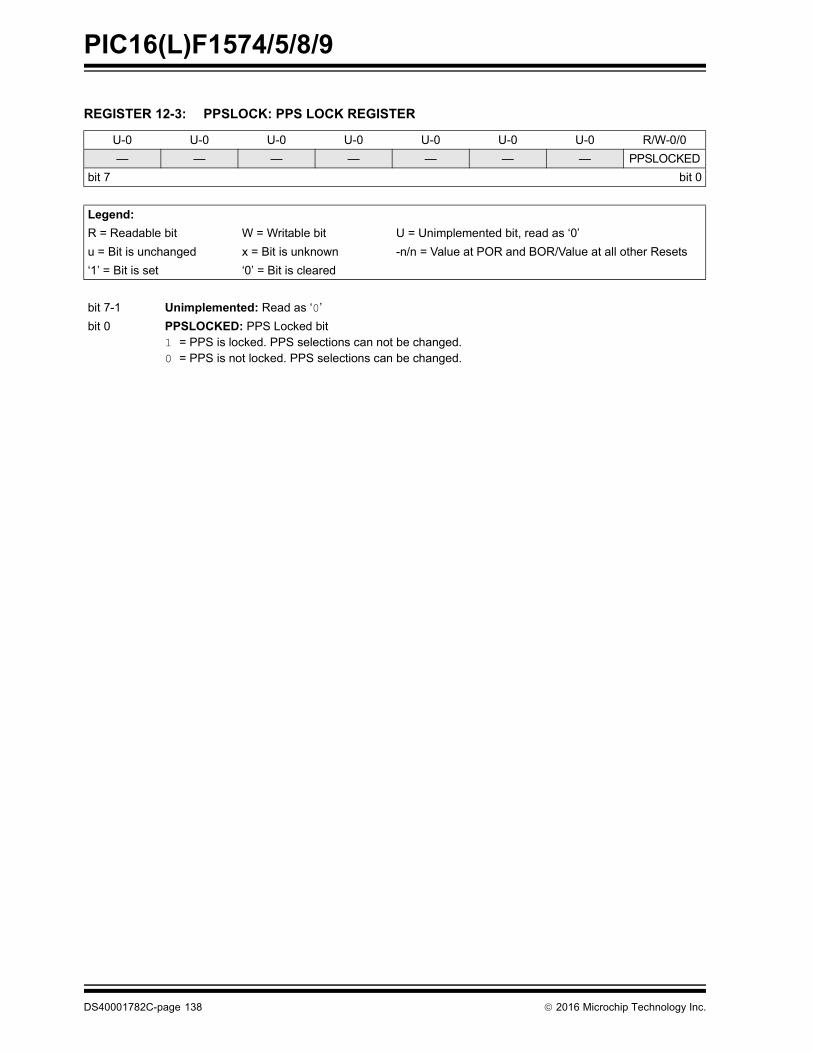
PIC16(L)F1574/5/8/9
DS40001782C-page 138 2016 Microchip Technology Inc.
REGISTER 12-3: PPSLOCK: PPS LOCK REGISTER
U-0 U-0 U-0 U-0 U-0 U-0 U-0 R/W-0/0
— — — — — — — PPSLOCKED
bit 7 bit 0
Legend:
R = Readable bit W = Writable bit U = Unimplemented bit, read as ‘0’
u = Bit is unchanged x = Bit is unknown -n/n = Value at POR and BOR/Value at all other Resets
‘1’ = Bit is set ‘0’ = Bit is cleared
bit 7-1 Unimplemented: Read as ‘0’
bit 0 PPSLOCKED: PPS Locked bit1 = PPS is locked. PPS selections can not be changed.0 = PPS is not locked. PPS selections can be changed.
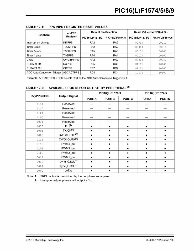
2016 Microchip Technology Inc. DS40001782C-page 139
PIC16(L)F1574/5/8/9
TABLE 12-1: PPS INPUT REGISTER RESET VALUES
PeripheralxxxPPSRegister
Default Pin Selection Reset Value (xxxPPS<4:0>)
PIC16(L)F1578/9 PIC16(L)F1574/5 PIC16(L)F1578/9 PIC16(L)F1574/5
Interrupt-on-change INTPPS RA2 RA2 00010 00010
Timer 0clock T0CKIPPS RA2 RA2 00010 00010
Timer 1clock T1CKIPPS RA5 RA5 00101 00101
Timer 1 gate T1GPPS RA4 RA4 00100 00100
CWG1 CWG1INPPS RA2 RA2 00010 00010
EUSART RX RXPPS RB5 RC5 01101 10101
EUSART CK CKPPS RB7 RC4 01111 10100
ADC Auto-Conversion Trigger ADCACTPPS RC4 RC4 10100 10100
Example: ADCACTPPS = 0x14 selects RC4 as the ADC Auto-Conversion Trigger input.
TABLE 12-2: AVAILABLE PORTS FOR OUTPUT BY PERIPHERAL(2)
RxyPPS<3:0> Output SignalPIC16(L)F1578/9 PIC16(L)F1574/5
PORTA PORTB PORTC PORTA PORTC
1111 Reserved — — — — —
1110 Reserved — — — — —
1101 Reserved — — — — —
1100 Reserved — — — — —
1011 Reserved — — — — —
1010 DT(1) ● ● ● ● ●
1001 TX/CK(1) ● ● ● ● ●
1000 CWG1OUTB(1) ● ● ● ● ●
0111 CWG1OUTA(1) ● ● ● ● ●
0110 PWM4_out ● ● ● ● ●
0101 PWM3_out ● ● ● ● ●
0100 PWM2_out ● ● ● ● ●
0011 PWM1_out ● ● ● ● ●
0010 sync_C2OUT ● ● ● ● ●
0001 sync_C1OUT ● ● ● ● ●
0000 LATxy ● ● ● ● ●
Note 1: TRIS control is overridden by the peripheral as required.
2: Unsupported peripherals will output a ‘0’.

PIC16(L)F1574/5/8/9
DS40001782C-page 140 2016 Microchip Technology Inc.
TABLE 12-3: SUMMARY OF REGISTERS ASSOCIATED WITH THE PPS MODULE
Name Bit 7 Bit 6 Bit 5 Bit 4 Bit 3 Bit 2 Bit 1 Bit 0Register on page
PPSLOCK — — — — — — — PPSLOCKED 138
INTPPS — — — INTPPS<4:0> 137
T0CKIPPS — — — T0CKIPPS<4:0> 137
T1CKIPPS — — — T1CKIPPS<4:0> 137
T1GPPS — — — T1GPPS<4:0> 137
CWG1INPPS — — — CWG1INPPS<4:0> 137
RXPPS — — — RXPPS<4:0> 137
CKPPS — — — CKPPS<4:0> 137
ADCACTPPS — — — ADCACTPPS<4:0> 137
RA0PPS — — — — RA0PPS<3:0> 137
RA1PPS — — — — RA1PPS<3:0> 137
RA2PPS — — — — RA2PPS<3:0> 137
RA4PPS — — — — RA4PPS<3:0> 137
RA5PPS — — — — RA5PPS<3:0> 137
RB4PPS(1) — — — — RB4PPS<3:0> 137
RB5PPS(1) — — — — RB5PPS<3:0> 137
RB6PPS(1) — — — — RB6PPS<3:0> 137
RB7PPS(1) — — — — RB7PPS<3:0> 137
RC0PPS — — — — RC0PPS<3:0> 137
RC1PPS — — — — RC1PPS<3:0> 137
RC2PPS — — — — RC2PPS<3:0> 137
RC3PPS — — — — RC3PPS<3:0> 137
RC4PPS — — — — RC4PPS<3:0> 137
RC5PPS — — — — RC5PPS<3:0> 137
RC6PPS(1) — — — — RC6PPS<3:0> 137
RC7PPS(1) — — — — RC7PPS<3:0> 137
Note 1: PIC16(L)F1578/9 only.

2016 Microchip Technology Inc. DS40001782C-page 141
PIC16(L)F1574/5/8/9
13.0 INTERRUPT-ON-CHANGE
The PORTA, PORTB(1) AND PORTC pins can beconfigured to operate as Interrupt-On-Change (IOC)pins. An interrupt can be generated by detecting a signalthat has either a rising edge or a falling edge. Anyindividual port pin, or combination of port pins, can beconfigured to generate an interrupt. Theinterrupt-on-change module has the following features:
• Interrupt-on-Change enable (Master Switch)
• Individual pin configuration
• Rising and falling edge detection
• Individual pin interrupt flags
Figure 13-1 is a block diagram of the IOC module.
13.1 Enabling the Module
To allow individual port pins to generate an interrupt, theIOCIE bit of the INTCON register must be set. If theIOCIE bit is disabled, the edge detection on the pin willstill occur, but an interrupt will not be generated.
13.2 Individual Pin Configuration
For each port pin, a rising edge detector and a fallingedge detector are present. To enable a pin to detect arising edge, the associated bit of the IOCxP register isset. To enable a pin to detect a falling edge, theassociated bit of the IOCxN register is set.
A pin can be configured to detect rising and fallingedges simultaneously by setting both associated bits ofthe IOCxP and IOCxN registers, respectively.
13.3 Interrupt Flags
The IOCAFx, IOCBFx and IOCCFx bits located in theIOCAF, IOCBF and IOCCF registers, respectively, arestatus flags that correspond to the interrupt-on-changepins of the associated port. If an expected edge isdetected on an appropriately enabled pin, then thestatus flag for that pin will be set, and an interrupt will begenerated if the IOCIE bit is set. The IOCIF bit of theINTCON register reflects the status of all IOCAFx,IOCBFx and IOCCFx bits.
13.4 Clearing Interrupt Flags
The individual status flags, (IOCAFx, IOCBFx andIOCCFx bits), can be cleared by resetting them to zero.If another edge is detected during this clearingoperation, the associated status flag will be set at theend of the sequence, regardless of the value actuallybeing written.
In order to ensure that no detected edge is lost whileclearing flags, only AND operations masking out knownchanged bits should be performed. The followingsequence is an example of what should be performed.
EXAMPLE 13-1: CLEARING INTERRUPT FLAGS (PORTA EXAMPLE)
13.5 Operation in Sleep
The interrupt-on-change interrupt sequence will wakethe device from Sleep mode, if the IOCIE bit is set.
If an edge is detected while in Sleep mode, the IOCxFregister will be updated prior to the first instructionexecuted out of Sleep.
Note 1: PORTB available on PIC16(L)F1578/9only.
MOVLW 0xffXORWF IOCAF, WANDWF IOCAF, F
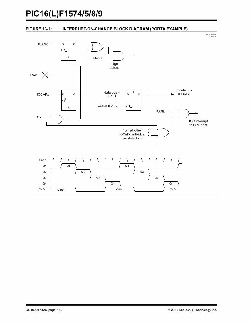
PIC16(L)F1574/5/8/9
DS40001782C-page 142 2016 Microchip Technology Inc.
FIGURE 13-1: INTERRUPT-ON-CHANGE BLOCK DIAGRAM (PORTA EXAMPLE)
IOCANx
IOCAPx
Q2
Q4Q1
data bus =0 or 1
write IOCAFxIOCIE
to data busIOCAFx
edgedetect
IOC interruptto CPU core
from all other IOCnFx individual
pin detectors
D QS
D Q
R
D Q
R
RAx
Q1
Q2
Q3
Q4
Q4Q1
Q1
Q2
Q3
Q4
Q1
Q2
Q3
Q4
Q4Q1 Q4Q1Q4Q1
FOSC
Rev. 10-000 037A6/2/201 4

2016 Microchip Technology Inc. DS40001782C-page 143
PIC16(L)F1574/5/8/9
13.6 Register Definitions: Interrupt-on-Change Control
REGISTER 13-1: IOCAP: INTERRUPT-ON-CHANGE PORTA POSITIVE EDGE REGISTER
U-0 U-0 R/W-0/0 R/W-0/0 R/W-0/0 R/W-0/0 R/W-0/0 R/W-0/0
— — IOCAP5 IOCAP4 IOCAP3 IOCAP2 IOCAP1 IOCAP0
bit 7 bit 0
Legend:
R = Readable bit W = Writable bit U = Unimplemented bit, read as ‘0’
u = Bit is unchanged x = Bit is unknown -n/n = Value at POR and BOR/Value at all other Resets
‘1’ = Bit is set ‘0’ = Bit is cleared
bit 7-6 Unimplemented: Read as ‘0’
bit 5-0 IOCAP<5:0>: Interrupt-on-Change PORTA Positive Edge Enable bits1 = Interrupt-on-Change enabled on the pin for a positive going edge. IOCAFx bit and IOCIF flag will be set
upon detecting an edge.0 = Interrupt-on-Change disabled for the associated pin.
REGISTER 13-2: IOCAN: INTERRUPT-ON-CHANGE PORTA NEGATIVE EDGE REGISTER
U-0 U-0 R/W-0/0 R/W-0/0 R/W-0/0 R/W-0/0 R/W-0/0 R/W-0/0
— — IOCAN5 IOCAN4 IOCAN3 IOCAN2 IOCAN1 IOCAN0
bit 7 bit 0
Legend:
R = Readable bit W = Writable bit U = Unimplemented bit, read as ‘0’
u = Bit is unchanged x = Bit is unknown -n/n = Value at POR and BOR/Value at all other Resets
‘1’ = Bit is set ‘0’ = Bit is cleared
bit 7-6 Unimplemented: Read as ‘0’
bit 5-0 IOCAN<5:0>: Interrupt-on-Change PORTA Negative Edge Enable bits1 = Interrupt-on-Change enabled on the pin for a negative going edge. IOCAFx bit and IOCIF flag will be set
upon detecting an edge.0 = Interrupt-on-Change disabled for the associated pin.
REGISTER 13-3: IOCAF: INTERRUPT-ON-CHANGE PORTA FLAG REGISTER
U-0 U-0 R/W/HS-0/0 R/W/HS-0/0 R/W/HS-0/0 R/W/HS-0/0 R/W/HS-0/0 R/W/HS-0/0
— — IOCAF5 IOCAF4 IOCAF3 IOCAF2 IOCAF1 IOCAF0
bit 7 bit 0
Legend:
R = Readable bit W = Writable bit U = Unimplemented bit, read as ‘0’
u = Bit is unchanged x = Bit is unknown -n/n = Value at POR and BOR/Value at all other Resets
‘1’ = Bit is set ‘0’ = Bit is cleared HS - Bit is set in hardware
bit 7-6 Unimplemented: Read as ‘0’
bit 5-0 IOCAF<5:0>: Interrupt-on-Change PORTA Flag bits1 = An enabled change was detected on the associated pin.
Set when IOCAPx = 1 and a rising edge was detected on RAx, or when IOCANx = 1 and a falling edge wasdetected on RAx.
0 = No change was detected, or the user cleared the detected change.

PIC16(L)F1574/5/8/9
DS40001782C-page 144 2016 Microchip Technology Inc.
REGISTER 13-4: IOCBP: INTERRUPT-ON-CHANGE PORTB POSITIVE EDGE REGISTER(1)
R/W-0/0 R/W-0/0 R/W-0/0 R/W-0/0 U-0 U-0 U-0 U-0
IOCBP7 IOCBP6 IOCBP5 IOCBP4 — — — —
bit 7 bit 0
Legend:
R = Readable bit W = Writable bit U = Unimplemented bit, read as ‘0’
u = Bit is unchanged x = Bit is unknown -n/n = Value at POR and BOR/Value at all other Resets
‘1’ = Bit is set ‘0’ = Bit is cleared
bit 7-4 IOCBP<7:4>: Interrupt-on-Change PORTB Positive Edge Enable bits1 = Interrupt-on-Change enabled on the pin for a positive going edge. IOCBFx bit and IOCIF flag will be set upon
detecting an edge.0 = Interrupt-on-Change disabled for the associated pin.
bit 3-0 Unimplemented: Read as ‘0’
Note 1: PORTB functions available on PIC16(L)F1578/9 devices only.
REGISTER 13-5: IOCBN: INTERRUPT-ON-CHANGE PORTB NEGATIVE EDGE REGISTER(1)
R/W-0/0 R/W-0/0 R/W-0/0 R/W-0/0 U-0 U-0 U-0 U-0
IOCBN7 IOCBN6 IOCBN5 IOCBN4 — — — —
bit 7 bit 0
Legend:
R = Readable bit W = Writable bit U = Unimplemented bit, read as ‘0’
u = Bit is unchanged x = Bit is unknown -n/n = Value at POR and BOR/Value at all other Resets
‘1’ = Bit is set ‘0’ = Bit is cleared
bit 7-4 IOCBN<7:4>: Interrupt-on-Change PORTB Negative Edge Enable bits1 = Interrupt-on-Change enabled on the pin for a negative going edge. IOCBFx bit and IOCIF flag will be set upon
detecting an edge.0 = Interrupt-on-Change disabled for the associated pin.
bit 3-0 Unimplemented: Read as ‘0’
Note 1: PORTB functions available on PIC16(L)F1578/9 devices only.
REGISTER 13-6: IOCBF: INTERRUPT-ON-CHANGE PORTB FLAG REGISTER(1)
R/W/HS-0/0 R/W/HS-0/0 R/W/HS-0/0 R/W/HS-0/0 U-0 U-0 U-0 U-0
IOCBF7 IOCBF6 IOCBF5 IOCBF4 — — — —
bit 7 bit 0
Legend:
R = Readable bit W = Writable bit U = Unimplemented bit, read as ‘0’
u = Bit is unchanged x = Bit is unknown -n/n = Value at POR and BOR/Value at all other Resets
‘1’ = Bit is set ‘0’ = Bit is cleared HS - Bit is set in hardware
bit 7-4 IOCBF<7:4>: Interrupt-on-Change PORTB Flag bits1 = An enabled change was detected on the associated pin.
Set when IOCBPx = 1 and a rising edge was detected on RBx, or when IOCBNx = 1 and a falling edge wasdetected on RBx.
0 = No change was detected, or the user cleared the detected change.
bit 3-0 Unimplemented: Read as ‘0’
Note 1: PORTB functions available on PIC16(L)F1578/9 devices only.

2016 Microchip Technology Inc. DS40001782C-page 145
PIC16(L)F1574/5/8/9
REGISTER 13-7: IOCCP: INTERRUPT-ON-CHANGE PORTC POSITIVE EDGE REGISTER(1)
R/W-0/0 R/W-0/0 R/W-0/0 R/W-0/0 R/W-0/0 R/W-0/0 R/W-0/0 R/W-0/0
IOCCP7(1) IOCCP6(1) IOCCP5 IOCCP4 IOCCP3 IOCCP2 IOCCP1 IOCCP0
bit 7 bit 0
Legend:
R = Readable bit W = Writable bit U = Unimplemented bit, read as ‘0’
u = Bit is unchanged x = Bit is unknown -n/n = Value at POR and BOR/Value at all other Resets
‘1’ = Bit is set ‘0’ = Bit is cleared
bit 7-0 IOCCP<7:0>: Interrupt-on-Change PORTC Positive Edge Enable bits(1)1 = Interrupt-on-Change enabled on the pin for a positive going edge. IOCCFx bit and IOCIF flag will be set upon
detecting an edge.0 = Interrupt-on-Change disabled for the associated pin.
Note 1: IOCCP<7:6> available on PIC16(L)F1578/9 devices only.
REGISTER 13-8: IOCCN: INTERRUPT-ON-CHANGE PORTC NEGATIVE EDGE REGISTER(1)
R/W-0/0 R/W-0/0 R/W-0/0 R/W-0/0 R/W-0/0 R/W-0/0 R/W-0/0 R/W-0/0
IOCCN7(1) IOCCN6(1) IOCCN5 IOCCN4 IOCCN3 IOCCN2 IOCCN1 IOCCN0
bit 7 bit 0
Legend:
R = Readable bit W = Writable bit U = Unimplemented bit, read as ‘0’
u = Bit is unchanged x = Bit is unknown -n/n = Value at POR and BOR/Value at all other Resets
‘1’ = Bit is set ‘0’ = Bit is cleared
bit 7-0 IOCCN<7:0>: Interrupt-on-Change PORTC Negative Edge Enable bits(1)1 = Interrupt-on-Change enabled on the pin for a negative going edge. IOCCFx bit and IOCIF flag will be set upon
detecting an edge.0 = Interrupt-on-Change disabled for the associated pin.
Note 1: IOCCN<7:6> available on PIC16(L)F1578/9 devices only.
REGISTER 13-9: IOCCF: INTERRUPT-ON-CHANGE PORTC FLAG REGISTER(1)
R/W/HS-0/0 R/W/HS-0/0 R/W/HS-0/0 R/W/HS-0/0 R/W/HS-0/0 R/W/HS-0/0 R/W/HS-0/0 R/W/HS-0/0
IOCCF(1) IOCCF6(1) IOCCF5 IOCCF4 IOCCF3 IOCCF2 IOCCF1 IOCCF0
bit 7 bit 0
Legend:
R = Readable bit W = Writable bit U = Unimplemented bit, read as ‘0’
u = Bit is unchanged x = Bit is unknown -n/n = Value at POR and BOR/Value at all other Resets
‘1’ = Bit is set ‘0’ = Bit is cleared HS - Bit is set in hardware
bit 7-0 IOCCF<7:0>: Interrupt-on-Change PORTC Flag bits(1)1 = An enabled change was detected on the associated pin.
Set when IOCCPx = 1 and a rising edge was detected on RCx, or when IOCCNx = 1 and a falling edge wasdetected on RCx.
0 = No change was detected, or the user cleared the detected change.
Note 1: IOCCF<7:6> available on PIC16(L)F1578/9 devices only.
PIC16(L)F1574/5/8/9
DS40001782C-page 146 2016 Microchip Technology Inc.
TABLE 13-1: SUMMARY OF REGISTERS ASSOCIATED WITH INTERRUPT-ON-CHANGE
Name Bit 7 Bit 6 Bit 5 Bit 4 Bit 3 Bit 2 Bit 1 Bit 0Register on Page
ANSELA — — — ANSA4 — ANSA2 ANSA1 ANSA0 121
INTCON GIE PEIE TMR0IE INTE IOCIE TMR0IF INTF IOCIF 86
IOCAF — — IOCAF5 IOCAF4 IOCAF3 IOCAF2 IOCAF1 IOCAF0 143
IOCAN — — IOCAN5 IOCAN4 IOCAN3 IOCAN2 IOCAN1 IOCAN0 143
IOCAP — — IOCAP5 IOCAP4 IOCAP3 IOCAP2 IOCAP1 IOCAP0 143
IOCBP(2) IOCBP7 IOCBP6 IOCBP5 IOCBP4 — — — — 144
IOCBN(2) IOCBN7 IOCBN6 IOCBN5 IOCBN4 — — — — 144
IOCBF(2) IOCBF7 IOCBF6 IOCBF5 IOCBF4 — — — — 144
IOCCP IOCCP7(2) IOCCP6(2) IOCCP5 IOCCP4 IOCCP3 IOCCP2 IOCCP1 IOCCP0 145
IOCCN IOCCN7(2) IOCCN6(2) IOCCN5 IOCCN4 IOCCN3 IOCCN2 IOCCN1 IOCCN0 145
IOCCF IOCCF7(2) IOCCF6(2) IOCCF5 IOCCF4 IOCCF3 IOCCF2 IOCCF1 IOCCF0 145
TRISA — — TRISA5 TRISA4 —(1) TRISA2 TRISA1 TRISA0 120
TRISC TRISC7(2) TRISC7(2) TRISC5 TRISC4 TRISC3 TRISC2 TRISC1 TRISC0 131
Legend: — = unimplemented location, read as ‘0’. Shaded cells are not used by interrupt-on-change.Note 1: Unimplemented, read as ‘1’.
2: PIC16(L)F1578/9 only.
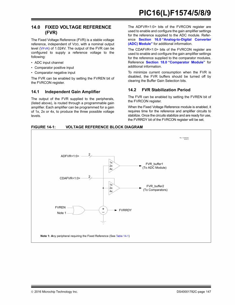
2016 Microchip Technology Inc. DS40001782C-page 147
PIC16(L)F1574/5/8/9
14.0 FIXED VOLTAGE REFERENCE (FVR)
The Fixed Voltage Reference (FVR) is a stable voltagereference, independent of VDD, with a nominal outputlevel (VFVR) of 1.024V. The output of the FVR can beconfigured to supply a reference voltage to thefollowing:
• ADC input channel
• Comparator positive input
• Comparator negative input
The FVR can be enabled by setting the FVREN bit ofthe FVRCON register.
14.1 Independent Gain Amplifier
The output of the FVR supplied to the peripherals,(listed above), is routed through a programmable gainamplifier. Each amplifier can be programmed for a gainof 1x, 2x or 4x, to produce the three possible voltagelevels.
The ADFVR<1:0> bits of the FVRCON register areused to enable and configure the gain amplifier settingsfor the reference supplied to the ADC module. Refer-ence Section 16.0 “Analog-to-Digital Converter(ADC) Module” for additional information.
The CDAFVR<1:0> bits of the FVRCON register areused to enable and configure the gain amplifier settingsfor the reference supplied to the comparator modules.Reference Section 18.0 “Comparator Module” foradditional information.
To minimize current consumption when the FVR isdisabled, the FVR buffers should be turned off byclearing the Buffer Gain Selection bits.
14.2 FVR Stabilization Period
The FVR can be enabled by setting the FVREN bit ofthe FVRCON register.
When the Fixed Voltage Reference module is enabled, itrequires time for the reference and amplifier circuits tostabilize. Once the circuits stabilize and are ready for use,the FVRRDY bit of the FVRCON register will be set.
FIGURE 14-1: VOLTAGE REFERENCE BLOCK DIAGRAM
Note 1: Any peripheral requiring the Fixed Reference (See Table 14-1)
1x 2x4x
1x 2x4x
ADFVR<1:0>
CDAFVR<1:0>
FVR_buffer1 (To ADC Module)
FVR_buffer2 (To Comparators)
+_FVREN
FVRRDYNote 1
2
2
Rev. 10-000053A8/6/2013

PIC16(L)F1574/5/8/9
DS40001782C-page 148 2016 Microchip Technology Inc.
TABLE 14-1: PERIPHERALS REQUIRING THE FIXED VOLTAGE REFERENCE (FVR)
Peripheral Conditions Description
HFINTOSC FOSC<2:0> = 010 and IRCF<3:0> = 000x
INTOSC is active and device is not in Sleep.
BOR
BOREN<1:0> = 11 BOR always enabled.
BOREN<1:0> = 10 and BORFS = 1 BOR disabled in Sleep mode, BOR Fast Start enabled.
BOREN<1:0> = 01 and BORFS = 1 BOR under software control, BOR Fast Start enabled.
LDO All PIC16F1574/5/8/9 devices, when VREGPM = 1 and not in Sleep
The device runs off of the Low-Power Regulator when in Sleep mode.

2016 Microchip Technology Inc. DS40001782C-page 149
PIC16(L)F1574/5/8/9
14.3 Register Definitions: FVR Control
TABLE 14-2: SUMMARY OF REGISTERS ASSOCIATED WITH THE FIXED VOLTAGE REFERENCE
REGISTER 14-1: FVRCON: FIXED VOLTAGE REFERENCE CONTROL REGISTER
R/W-0/0 R-q/q R/W-0/0 R/W-0/0 R/W-0/0 R/W-0/0 R/W-0/0 R/W-0/0
FVREN(1) FVRRDY(2) TSEN(3) TSRNG(3) CDAFVR<1:0>(1) ADFVR<1:0>(1)
bit 7 bit 0
Legend:
R = Readable bit W = Writable bit U = Unimplemented bit, read as ‘0’
u = Bit is unchanged x = Bit is unknown -n/n = Value at POR and BOR/Value at all other Resets
‘1’ = Bit is set ‘0’ = Bit is cleared q = Value depends on condition
bit 7 FVREN: Fixed Voltage Reference Enable bit(1)
1 = Fixed Voltage Reference is enabled0 = Fixed Voltage Reference is disabled
bit 6 FVRRDY: Fixed Voltage Reference Ready Flag bit(2)
1 = Fixed Voltage Reference output is ready for use0 = Fixed Voltage Reference output is not ready or not enabled
bit 5 TSEN: Temperature Indicator Enable bit(3)
1 = Temperature Indicator is enabled0 = Temperature Indicator is disabled
bit 4 TSRNG: Temperature Indicator Range Selection bit(3)
1 = VOUT = VDD - 4VT (High Range)0 = VOUT = VDD - 2VT (Low Range)
bit 3-2 CDAFVR<1:0>: Comparator FVR Buffer Gain Selection bits(1)
11 = Comparator FVR Buffer Gain is 4x, with output VCDAFVR = 4x VFVR(4)
10 = Comparator FVR Buffer Gain is 2x, with output VCDAFVR = 2x VFVR(4)
01 = Comparator FVR Buffer Gain is 1x, with output VCDAFVR = 1x VFVR
00 = Comparator FVR Buffer is off
bit 1-0 ADFVR<1:0>: ADC FVR Buffer Gain Selection bit(1)
11 = ADC FVR Buffer Gain is 4x, with output VADFVR = 4x VFVR(4)
10 = ADC FVR Buffer Gain is 2x, with output VADFVR = 2x VFVR(4)
01 = ADC FVR Buffer Gain is 1x, with output VADFVR = 1x VFVR
00 = ADC FVR Buffer is off
Note 1: To minimize current consumption when the FVR is disabled, the FVR buffers should be turned off by clear-ing the Buffer Gain Selection bits.
2: FVRRDY is always ‘1’ for the PIC16F1574/5/8/9 devices.
3: See Section 15.0 “Temperature Indicator Module” for additional information.
4: Fixed Voltage Reference output cannot exceed VDD.
Name Bit 7 Bit 6 Bit 5 Bit 4 Bit 3 Bit 2 Bit 1 Bit 0Register on page
FVRCON FVREN FVRRDY TSEN TSRNG CDAFVR>1:0> ADFVR<1:0> 149
Legend: Shaded cells are unused by the Fixed Voltage Reference module.

PIC16(L)F1574/5/8/9
DS40001782C-page 150 2016 Microchip Technology Inc.
15.0 TEMPERATURE INDICATOR MODULE
This family of devices is equipped with a temperaturecircuit designed to measure the operating temperatureof the silicon die. The circuit’s range of operatingtemperature falls between -40°C and +85°C. Theoutput is a voltage that is proportional to the devicetemperature. The output of the temperature indicator isinternally connected to the device ADC.
The circuit may be used as a temperature thresholddetector or a more accurate temperature indicator,depending on the level of calibration performed. A one-point calibration allows the circuit to indicate atemperature closely surrounding that point. A two-pointcalibration allows the circuit to sense the entire rangeof temperature more accurately. Reference ApplicationNote AN1333, “Use and Calibration of the InternalTemperature Indicator” (DS01333) for more detailsregarding the calibration process.
15.1 Circuit Operation
Figure 15-1 shows a simplified block diagram of thetemperature circuit. The proportional voltage output isachieved by measuring the forward voltage drop acrossmultiple silicon junctions.
Equation 15-1 describes the output characteristics ofthe temperature indicator.
EQUATION 15-1: VOUT RANGES
The temperature sense circuit is integrated with theFixed Voltage Reference (FVR) module. See Section14.0 “Fixed Voltage Reference (FVR)” for moreinformation.
The circuit is enabled by setting the TSEN bit of theFVRCON register. When disabled, the circuit draws nocurrent.
The circuit operates in either high or low range. The highrange, selected by setting the TSRNG bit of theFVRCON register, provides a wider output voltage. Thisprovides more resolution over the temperature range,but may be less consistent from part to part. This rangerequires a higher bias voltage to operate and thus, ahigher VDD is needed.
The low range is selected by clearing the TSRNG bit ofthe FVRCON register. The low range generates a lowervoltage drop and thus, a lower bias voltage is needed tooperate the circuit. The low range is provided for lowvoltage operation.
FIGURE 15-1: TEMPERATURE CIRCUIT DIAGRAM
15.2 Minimum Operating VDD
When the temperature circuit is operated in low range,the device may be operated at any operating voltagethat is within specifications.
When the temperature circuit is operated in high range,the device operating voltage, VDD, must be highenough to ensure that the temperature circuit iscorrectly biased.
Table 15-1 shows the recommended minimum VDD vs.range setting.
TABLE 15-1: RECOMMENDED VDD VS. RANGE
15.3 Temperature Output
The output of the circuit is measured using the internalAnalog-to-Digital Converter. A channel is reserved forthe temperature circuit output. Refer to Section16.0 “Analog-to-Digital Converter (ADC) Module” fordetailed information.
15.4 ADC Acquisition Time
To ensure accurate temperature measurements, theuser must wait at least 200 s after the ADC inputmultiplexer is connected to the temperature indicatoroutput before the conversion is performed. In addition,the user must wait 200 s between sequentialconversions of the temperature indicator output.
High Range: VOUT = VDD - 4VT
Low Range: VOUT = VDD - 2VT
Min. VDD, TSRNG = 1 Min. VDD, TSRNG = 0
3.6V 1.8V
VOUT
Temp. IndicatorTo ADC
TSRNG
TSEN
Rev. 10-000069A7/31/2013VDD

2016 Microchip Technology Inc. DS40001782C-page 151
PIC16(L)F1574/5/8/9
TABLE 15-2: SUMMARY OF REGISTERS ASSOCIATED WITH THE TEMPERATURE INDICATOR
Name Bit 7 Bit 6 Bit 5 Bit 4 Bit 3 Bit 2 Bit 1 Bit 0Register on page
FVRCON FVREN FVRRDY TSEN TSRNG CDAFVR<1:0> ADFVR<1:0> 118
Legend: Shaded cells are unused by the temperature indicator module.

PIC16(L)F1574/5/8/9
DS40001782C-page 152 2016 Microchip Technology Inc.
16.0 ANALOG-TO-DIGITAL CONVERTER (ADC) MODULE
The Analog-to-Digital Converter (ADC) allowsconversion of an analog input signal to a 10-bit binaryrepresentation of that signal. This device uses analoginputs, which are multiplexed into a single sample andhold circuit. The output of the sample and hold isconnected to the input of the converter. The convertergenerates a 10-bit binary result via successiveapproximation and stores the conversion result into theADC result registers (ADRESH:ADRESL register pair).Figure 16-1 shows the block diagram of the ADC.
The ADC voltage reference is software selectable to beeither internally generated or externally supplied.
The ADC can generate an interrupt upon completion ofa conversion. This interrupt can be used to wake-up thedevice from Sleep.
FIGURE 16-1: ADC BLOCK DIAGRAM
VRPOSVRNEG
Enable
DACx_output
FVR_buffer1
Temp Indicator
CHS<4:0>
ExternalChannel
Inputs
GO/DONEcomplete
start
ADCSample Circuit
Write to bitGO/DONE
VSS
VDD
VREF+ pin
VDD
ADPREF
10-bit Result
ADRESH ADRESL
16
ADFM
10
InternalChannel
Inputs
.
.
.
AN0
ANa
ANz
set bit ADIF
VSS
ADON
sampledinput
Q1
Q2Q4
FoscDivider FOSC
FOSC/n
FRC
ADCClockSelect
ADC_clk
ADCS<2:0>
FRC
ADC CLOCK SOURCE
Trigger Select
Trigger Sources
. . .TRIGSEL<3:0>
AUTO CONVERSIONTRIGGER
PositiveReference
Select
Rev. 10-000033A7/30/2013

2016 Microchip Technology Inc. DS40001782C-page 153
PIC16(L)F1574/5/8/9
16.1 ADC Configuration
When configuring and using the ADC the followingfunctions must be considered:
• Port configuration
• Channel selection
• ADC voltage reference selection
• ADC conversion clock source
• Interrupt control
• Result formatting
16.1.1 PORT CONFIGURATION
The ADC can be used to convert both analog anddigital signals. When converting analog signals, the I/Opin should be configured for analog by setting theassociated TRIS and ANSEL bits. Refer to Section11.0 “I/O Ports” for more information.
16.1.2 CHANNEL SELECTION
There are up to 15 channel selections available:
• AN<7:0> pins (PIC16(L)F1574/5 only)
• AN<11:0> pins (PIC16(L)F1578/9 only)
• Temperature Indicator
• DAC1_output
• FVR_buffer1
The CHS bits of the ADCON0 register determine whichchannel is connected to the sample and hold circuit.
When changing channels, a delay (TACQ) is requiredbefore starting the next conversion. Refer to Section16.2.6 “ADC Conversion Procedure” for moreinformation.
16.1.3 ADC VOLTAGE REFERENCE
The ADC module uses a positive and a negativevoltage reference. The positive reference is labeledref+ and the negative reference is labeled ref-.
The positive voltage reference (ref+) is selected by theADPREF bits in the ADCON1 register. The positivevoltage reference source can be:
• VREF+ pin
• VDD
• FVR_buffer1
The negative voltage reference (ref-) source is:
• VSS
16.1.4 CONVERSION CLOCK
The source of the conversion clock is software select-able via the ADCS bits of the ADCON1 register. Thereare seven possible clock options:
• FOSC/2
• FOSC/4
• FOSC/8
• FOSC/16
• FOSC/32
• FOSC/64
• FRC (internal RC oscillator)
The time to complete one bit conversion is defined asTAD. One full 10-bit conversion requires 11.5 TAD
periods as shown in Figure 16-2.
For correct conversion, the appropriate TAD specifica-tion must be met. Refer to the ADC conversion require-ments in Section 27.0 “Electrical Specifications” formore information. Table 16-1 gives examples ofappropriate ADC clock selections.
Note: Analog voltages on any pin that is definedas a digital input may cause the inputbuffer to conduct excess current.
Note: Unless using the FRC, any changes in thesystem clock frequency will change theADC clock frequency, which mayadversely affect the ADC result.

PIC16(L)F1574/5/8/9
DS40001782C-page 154 2016 Microchip Technology Inc.
TABLE 16-1: ADC CLOCK PERIOD (TAD) VS. DEVICE OPERATING FREQUENCIES
FIGURE 16-2: ANALOG-TO-DIGITAL CONVERSION TAD CYCLES
ADC Clock Period (TAD) Device Frequency (FOSC)
ADCClock
Source
ADCS<2:0>
20 MHz 16 MHz 8 MHz 4 MHz 1 MHz
Fosc/2 000 100 ns 125 ns 250 ns 500 ns 2.0 s
Fosc/4 100 200 ns 250 ns 500 ns 1.0 s 4.0 s
Fosc/8 001 400 ns 500 ns 1.0 s 2.0 s 8.0 s
Fosc/16 101 800 ns 1.0 s 2.0 s 4.0 s 16.0 s
Fosc/32 010 1.6 s 2.0 s 4.0 s 8.0 s 32.0 s
Fosc/64 110 3.2 s 4.0 s 8.0 s 16.0 s 64.0 s
FRC x11 1.0-6.0 s 1.0-6.0 s 1.0-6.0 s 1.0-6.0 s 1.0-6.0 s
Legend: Shaded cells are outside of recommended range.
Note: The TAD period when using the FRC clock source can fall within a specified range, (see TAD parameter).The TAD period when using the FOSC-based clock source can be configured for a more precise TAD period.However, the FRC clock source must be used when conversions are to be performed with the device inSleep mode.
TAD1 TAD2 TAD3 TAD4 TAD5 TAD6 TAD7 TAD8 TAD9 TAD10 TAD11
Set GO bit
Conversion Starts
Holding capacitor disconnectedfrom analog input (THCD).
On the following cycle:
ADRESH:ADRESL is loaded,GO bit is cleared,
ADIF bit is set,holding capacitor is reconnected to analog input.
b9 b8 b7 b6 b5 b4 b3 b2 b1 b0
Enable ADC (ADON bit)and
Select channel (ACS bits)
THCD
TACQ
Rev. 10-000035A7/30/2013
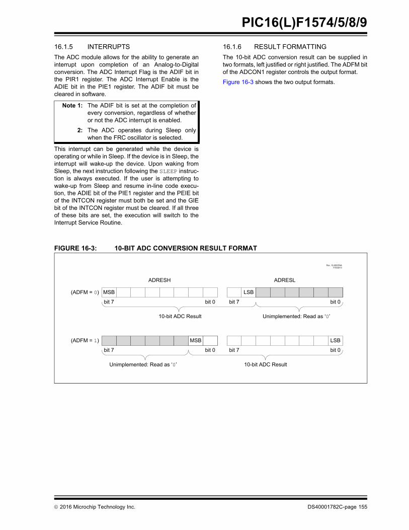
2016 Microchip Technology Inc. DS40001782C-page 155
PIC16(L)F1574/5/8/9
16.1.5 INTERRUPTS
The ADC module allows for the ability to generate aninterrupt upon completion of an Analog-to-Digitalconversion. The ADC Interrupt Flag is the ADIF bit inthe PIR1 register. The ADC Interrupt Enable is theADIE bit in the PIE1 register. The ADIF bit must becleared in software.
This interrupt can be generated while the device isoperating or while in Sleep. If the device is in Sleep, theinterrupt will wake-up the device. Upon waking fromSleep, the next instruction following the SLEEP instruc-tion is always executed. If the user is attempting towake-up from Sleep and resume in-line code execu-tion, the ADIE bit of the PIE1 register and the PEIE bitof the INTCON register must both be set and the GIEbit of the INTCON register must be cleared. If all threeof these bits are set, the execution will switch to theInterrupt Service Routine.
16.1.6 RESULT FORMATTING
The 10-bit ADC conversion result can be supplied intwo formats, left justified or right justified. The ADFM bitof the ADCON1 register controls the output format.
Figure 16-3 shows the two output formats.
FIGURE 16-3: 10-BIT ADC CONVERSION RESULT FORMAT
Note 1: The ADIF bit is set at the completion ofevery conversion, regardless of whetheror not the ADC interrupt is enabled.
2: The ADC operates during Sleep onlywhen the FRC oscillator is selected.
MSB
MSB
LSB
LSB
(ADFM = 0)
(ADFM = 1)
bit 7 bit 7
bit 7bit 7
bit 0
bit 0
bit 0
bit 0
10-bit ADC Result
10-bit ADC ResultUnimplemented: Read as ‘0’
Unimplemented: Read as ‘0’
ADRESH ADRESL
Rev. 10-000054A7/30/2013

PIC16(L)F1574/5/8/9
DS40001782C-page 156 2016 Microchip Technology Inc.
16.2 ADC Operation
16.2.1 STARTING A CONVERSION
To enable the ADC module, the ADON bit of theADCON0 register must be set to a ‘1’. Setting theGO/DONE bit of the ADCON0 register to a ‘1’ will startthe Analog-to-Digital conversion.
16.2.2 COMPLETION OF A CONVERSION
When the conversion is complete, the ADC module will:
• Clear the GO/DONE bit
• Set the ADIF Interrupt Flag bit
• Update the ADRESH and ADRESL registers with new conversion result
16.2.3 TERMINATING A CONVERSION
If a conversion must be terminated before completion,the GO/DONE bit can be cleared in software. TheADRESH and ADRESL registers will be updated withthe partially complete Analog-to-Digital conversionsample. Incomplete bits will match the last bitconverted.
16.2.4 ADC OPERATION DURING SLEEP
The ADC module can operate during Sleep. Thisrequires the ADC clock source to be set to the FRCoption. Performing the ADC conversion during Sleepcan reduce system noise. If the ADC interrupt isenabled, the device will wake-up from Sleep when theconversion completes. If the ADC interrupt is disabled,the ADC module is turned off after the conversioncompletes, although the ADON bit remains set.
When the ADC clock source is something other thanFRC, a SLEEP instruction causes the present conver-sion to be aborted and the ADC module is turned off,although the ADON bit remains set.
16.2.5 AUTO-CONVERSION TRIGGER
The auto-conversion trigger allows periodic ADC mea-surements without software intervention. When a risingedge of the selected source occurs, the GO/DONE bitis set by hardware.
The auto-conversion trigger source is selected with theTRIGSEL<3:0> bits of the ADCON2 register.
Using the auto-conversion trigger does not assureproper ADC timing. It is the user’s responsibility toensure that the ADC timing requirements are met.
The PWM module can trigger the ADC in two ways,directly through the PWMx_OF_match or through theinterrupts generated by all four match signals. SeeSection 23.0 “16-bit Pulse-Width Modulation (PWM)Module”. If the interrupts are chosen, each enabledinterrupt in PWMxINTE will trigger a conversion. Referto Figure 16-4 for more information.
See Table 16-2 for auto-conversion sources.
FIGURE 16-4: 16-BIT PWM INTERRUPT BLOCK DIAGRAM
Note: The GO/DONE bit should not be set in thesame instruction that turns on the ADC.Refer to Section 16.2.6 “ADC Conver-sion Procedure”.
Note: A device Reset forces all registers to theirReset state. Thus, the ADC module isturned off and any pending conversion isterminated.
TABLE 16-2: AUTO-CONVERSION SOURCES
Source Peripheral Signal Name
Timer0 T0_overflow
Timer1 T1_overflow
Timer2 T2_match
Comparator C1 C1OUT_sync
Comparator C2 C2OUT_sync
PWM1 PWM1_OF_match
PWM1 PWM1_interrupt
PWM2 PWM2_OF_match
PWM2 PWM2_interrupt
PWM3 PWM3_OF_match
PWM3 PWM3_interrupt
PWM4 PWM4_OF_match
PWM4 PWM4_interrupt
ADC Trigger ADCACT
CWG Input Pin CWGIN
Rev. 10-000154A10/24/2013
PWMx_interrupt
PWMxOFIE
PWMxPHIE
PWMxDCIE
PWMxPRIE
OFx_match
PRx_match
DCx_match
PHx_match
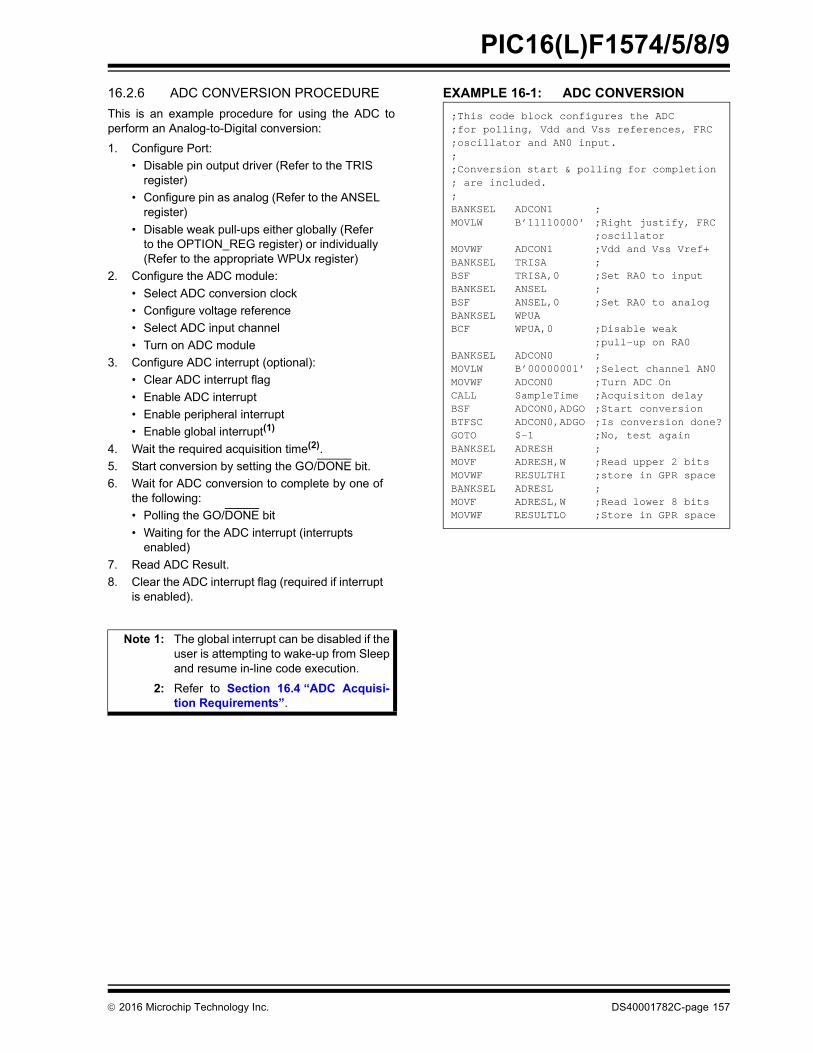
2016 Microchip Technology Inc. DS40001782C-page 157
PIC16(L)F1574/5/8/9
16.2.6 ADC CONVERSION PROCEDURE
This is an example procedure for using the ADC toperform an Analog-to-Digital conversion:
1. Configure Port:
• Disable pin output driver (Refer to the TRIS register)
• Configure pin as analog (Refer to the ANSEL register)
• Disable weak pull-ups either globally (Refer to the OPTION_REG register) or individually (Refer to the appropriate WPUx register)
2. Configure the ADC module:
• Select ADC conversion clock
• Configure voltage reference
• Select ADC input channel
• Turn on ADC module
3. Configure ADC interrupt (optional):
• Clear ADC interrupt flag
• Enable ADC interrupt
• Enable peripheral interrupt
• Enable global interrupt(1)
4. Wait the required acquisition time(2).
5. Start conversion by setting the GO/DONE bit.
6. Wait for ADC conversion to complete by one ofthe following:
• Polling the GO/DONE bit
• Waiting for the ADC interrupt (interrupts enabled)
7. Read ADC Result.
8. Clear the ADC interrupt flag (required if interruptis enabled).
EXAMPLE 16-1: ADC CONVERSION
Note 1: The global interrupt can be disabled if theuser is attempting to wake-up from Sleepand resume in-line code execution.
2: Refer to Section 16.4 “ADC Acquisi-tion Requirements”.
;This code block configures the ADC;for polling, Vdd and Vss references, FRC ;oscillator and AN0 input.;;Conversion start & polling for completion ; are included.;BANKSEL ADCON1 ;MOVLW B’11110000’ ;Right justify, FRC
;oscillatorMOVWF ADCON1 ;Vdd and Vss Vref+BANKSEL TRISA ;BSF TRISA,0 ;Set RA0 to inputBANKSEL ANSEL ;BSF ANSEL,0 ;Set RA0 to analogBANKSEL WPUABCF WPUA,0 ;Disable weak
;pull-up on RA0BANKSEL ADCON0 ;MOVLW B’00000001’ ;Select channel AN0MOVWF ADCON0 ;Turn ADC OnCALL SampleTime ;Acquisiton delayBSF ADCON0,ADGO ;Start conversionBTFSC ADCON0,ADGO ;Is conversion done?GOTO $-1 ;No, test againBANKSEL ADRESH ;MOVF ADRESH,W ;Read upper 2 bitsMOVWF RESULTHI ;store in GPR spaceBANKSEL ADRESL ;MOVF ADRESL,W ;Read lower 8 bitsMOVWF RESULTLO ;Store in GPR space
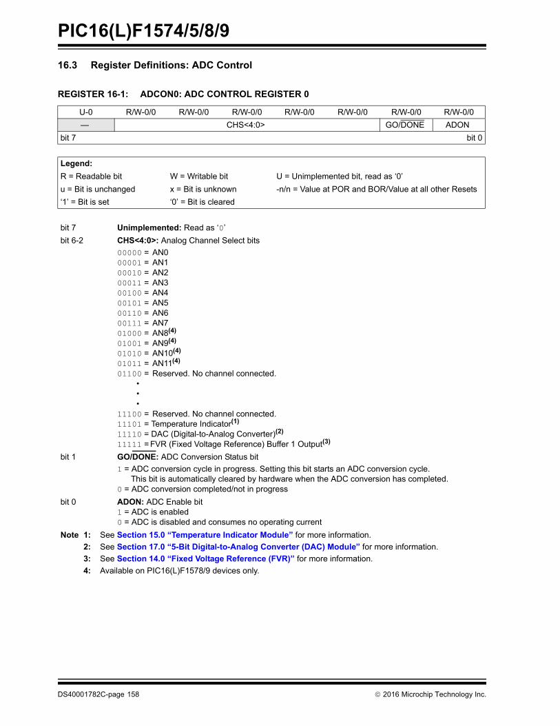
PIC16(L)F1574/5/8/9
DS40001782C-page 158 2016 Microchip Technology Inc.
16.3 Register Definitions: ADC Control
REGISTER 16-1: ADCON0: ADC CONTROL REGISTER 0
U-0 R/W-0/0 R/W-0/0 R/W-0/0 R/W-0/0 R/W-0/0 R/W-0/0 R/W-0/0
— CHS<4:0> GO/DONE ADON
bit 7 bit 0
Legend:
R = Readable bit W = Writable bit U = Unimplemented bit, read as ‘0’
u = Bit is unchanged x = Bit is unknown -n/n = Value at POR and BOR/Value at all other Resets
‘1’ = Bit is set ‘0’ = Bit is cleared
bit 7 Unimplemented: Read as ‘0’
bit 6-2 CHS<4:0>: Analog Channel Select bits
00000 = AN000001 = AN100010 = AN200011 = AN300100 = AN400101 = AN500110 = AN600111 = AN701000 = AN8(4)
01001 = AN9(4)
01010 = AN10(4)
01011 = AN11(4)
01100 = Reserved. No channel connected. • • •
11100 = Reserved. No channel connected.11101 = Temperature Indicator(1)
11110 = DAC (Digital-to-Analog Converter)(2)
11111 = FVR (Fixed Voltage Reference) Buffer 1 Output(3)
bit 1 GO/DONE: ADC Conversion Status bit
1 = ADC conversion cycle in progress. Setting this bit starts an ADC conversion cycle. This bit is automatically cleared by hardware when the ADC conversion has completed.0 = ADC conversion completed/not in progress
bit 0 ADON: ADC Enable bit1 = ADC is enabled0 = ADC is disabled and consumes no operating current
Note 1: See Section 15.0 “Temperature Indicator Module” for more information.
2: See Section 17.0 “5-Bit Digital-to-Analog Converter (DAC) Module” for more information.
3: See Section 14.0 “Fixed Voltage Reference (FVR)” for more information.
4: Available on PIC16(L)F1578/9 devices only.
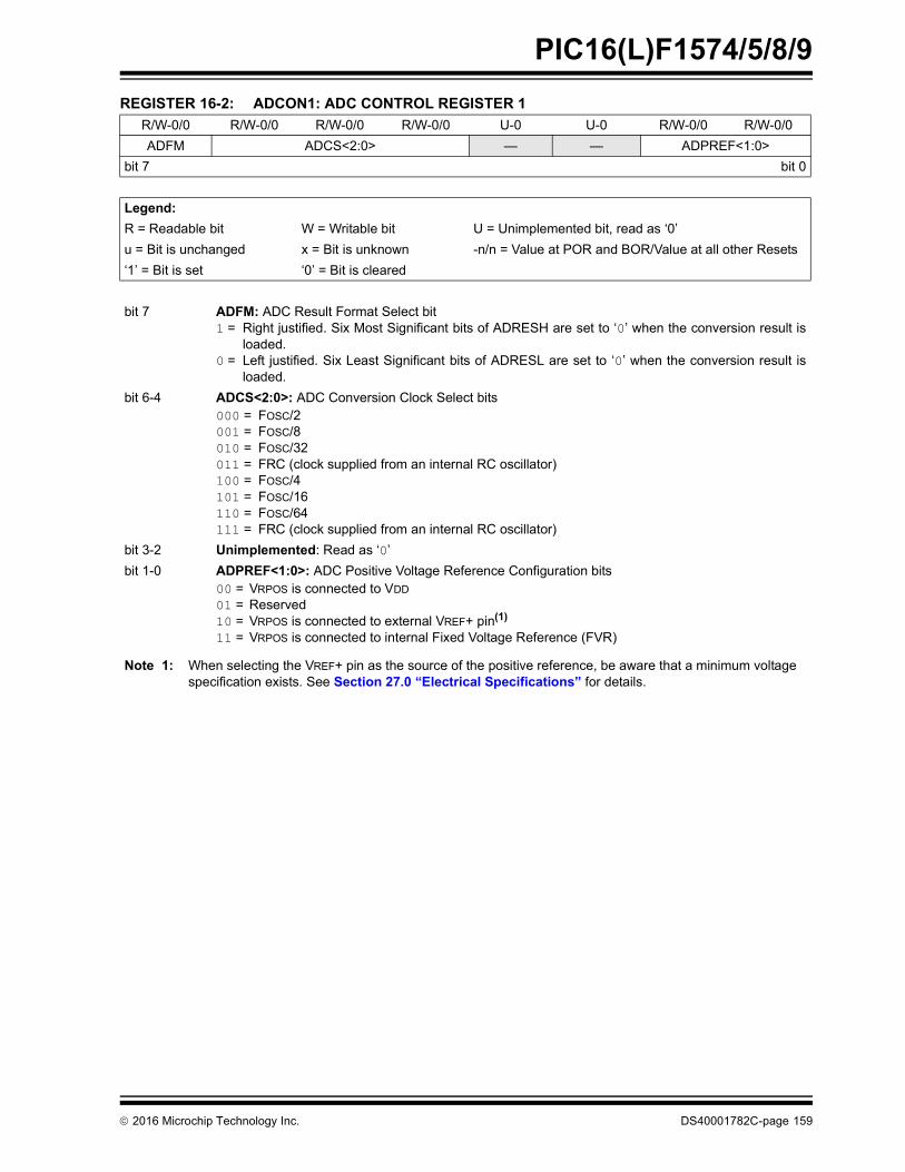
2016 Microchip Technology Inc. DS40001782C-page 159
PIC16(L)F1574/5/8/9
REGISTER 16-2: ADCON1: ADC CONTROL REGISTER 1
R/W-0/0 R/W-0/0 R/W-0/0 R/W-0/0 U-0 U-0 R/W-0/0 R/W-0/0
ADFM ADCS<2:0> — — ADPREF<1:0>
bit 7 bit 0
Legend:
R = Readable bit W = Writable bit U = Unimplemented bit, read as ‘0’
u = Bit is unchanged x = Bit is unknown -n/n = Value at POR and BOR/Value at all other Resets
‘1’ = Bit is set ‘0’ = Bit is cleared
bit 7 ADFM: ADC Result Format Select bit1 = Right justified. Six Most Significant bits of ADRESH are set to ‘0’ when the conversion result is
loaded.0 = Left justified. Six Least Significant bits of ADRESL are set to ‘0’ when the conversion result is
loaded.
bit 6-4 ADCS<2:0>: ADC Conversion Clock Select bits000 = FOSC/2001 = FOSC/8010 = FOSC/32011 = FRC (clock supplied from an internal RC oscillator)100 = FOSC/4101 = FOSC/16110 = FOSC/64111 = FRC (clock supplied from an internal RC oscillator)
bit 3-2 Unimplemented: Read as ‘0’
bit 1-0 ADPREF<1:0>: ADC Positive Voltage Reference Configuration bits00 = VRPOS is connected to VDD
01 = Reserved10 = VRPOS is connected to external VREF+ pin(1)
11 = VRPOS is connected to internal Fixed Voltage Reference (FVR)
Note 1: When selecting the VREF+ pin as the source of the positive reference, be aware that a minimum voltage specification exists. See Section 27.0 “Electrical Specifications” for details.

PIC16(L)F1574/5/8/9
DS40001782C-page 160 2016 Microchip Technology Inc.
REGISTER 16-3: ADCON2: ADC CONTROL REGISTER 2
R/W-0/0 R/W-0/0 R/W-0/0 R/W-0/0 U-0 U-0 U-0 U-0
TRIGSEL<3:0>(1) — — — —
bit 7 bit 0
Legend:
R = Readable bit W = Writable bit U = Unimplemented bit, read as ‘0’
u = Bit is unchanged x = Bit is unknown -n/n = Value at POR and BOR/Value at all other Resets
‘1’ = Bit is set ‘0’ = Bit is cleared
bit 7-4 TRIGSEL<3:0>: Auto-Conversion Trigger Selection bits(1)
0000 = No auto-conversion trigger selected0001 = PWM1 – PWM1_interrupt0010 = PWM2 – PWM2_interrupt0011 = Timer0 – T0_overflow(2)
0100 = Timer1 – T1_overflow(2)
0101 = Timer2 – T2_match0110 = Comparator C1 – C1OUT_sync0111 = Comparator C2 – C2OUT_sync1000 = PWM1 – PWM1_OF_match1001 = PWM2 – PWM2_OF_match1010 = PWM3 – PWM3_OF_match1011 = PWM3 – PWM3_interrupt1100 = PWM4 – PWM4_OF_match1101 = PWM4 – PWM4_interrupt1110 = ADC Auto-Conversion Trigger input pin1111 = CWG input pin
bit 3-0 Unimplemented: Read as ‘0’
Note 1: This is a rising edge sensitive input for all sources.
2: Signal also sets its corresponding interrupt flag.

2016 Microchip Technology Inc. DS40001782C-page 161
PIC16(L)F1574/5/8/9
REGISTER 16-4: ADRESH: ADC RESULT REGISTER HIGH (ADRESH) ADFM = 0
R/W-x/u R/W-x/u R/W-x/u R/W-x/u R/W-x/u R/W-x/u R/W-x/u R/W-x/u
ADRES<9:2>
bit 7 bit 0
Legend:
R = Readable bit W = Writable bit U = Unimplemented bit, read as ‘0’
u = Bit is unchanged x = Bit is unknown -n/n = Value at POR and BOR/Value at all other Resets
‘1’ = Bit is set ‘0’ = Bit is cleared
bit 7-0 ADRES<9:2>: ADC Result Register bitsUpper eight bits of 10-bit conversion result
REGISTER 16-5: ADRESL: ADC RESULT REGISTER LOW (ADRESL) ADFM = 0
R/W-x/u R/W-x/u R/W-x/u R/W-x/u R/W-x/u R/W-x/u R/W-x/u R/W-x/u
ADRES<1:0> — — — — — —
bit 7 bit 0
Legend:
R = Readable bit W = Writable bit U = Unimplemented bit, read as ‘0’
u = Bit is unchanged x = Bit is unknown -n/n = Value at POR and BOR/Value at all other Resets
‘1’ = Bit is set ‘0’ = Bit is cleared
bit 7-6 ADRES<1:0>: ADC Result Register bitsLower two bits of 10-bit conversion result
bit 5-0 Reserved: Do not use.

PIC16(L)F1574/5/8/9
DS40001782C-page 162 2016 Microchip Technology Inc.
REGISTER 16-6: ADRESH: ADC RESULT REGISTER HIGH (ADRESH) ADFM = 1
R/W-x/u R/W-x/u R/W-x/u R/W-x/u R/W-x/u R/W-x/u R/W-x/u R/W-x/u
— — — — — — ADRES<9:8>
bit 7 bit 0
Legend:
R = Readable bit W = Writable bit U = Unimplemented bit, read as ‘0’
u = Bit is unchanged x = Bit is unknown -n/n = Value at POR and BOR/Value at all other Resets
‘1’ = Bit is set ‘0’ = Bit is cleared
bit 7-2 Reserved: Do not use.
bit 1-0 ADRES<9:8>: ADC Result Register bitsUpper two bits of 10-bit conversion result
REGISTER 16-7: ADRESL: ADC RESULT REGISTER LOW (ADRESL) ADFM = 1
R/W-x/u R/W-x/u R/W-x/u R/W-x/u R/W-x/u R/W-x/u R/W-x/u R/W-x/u
ADRES<7:0>
bit 7 bit 0
Legend:
R = Readable bit W = Writable bit U = Unimplemented bit, read as ‘0’
u = Bit is unchanged x = Bit is unknown -n/n = Value at POR and BOR/Value at all other Resets
‘1’ = Bit is set ‘0’ = Bit is cleared
bit 7-0 ADRES<7:0>: ADC Result Register bitsLower eight bits of 10-bit conversion result

2016 Microchip Technology Inc. DS40001782C-page 163
PIC16(L)F1574/5/8/9
16.4 ADC Acquisition Requirements
For the ADC to meet its specified accuracy, the chargeholding capacitor (CHOLD) must be allowed to fullycharge to the input channel voltage level. The AnalogInput model is shown in Figure 16-5. The sourceimpedance (RS) and the internal sampling switch (RSS)impedance directly affect the time required to chargethe capacitor CHOLD. The sampling switch (RSS)impedance varies over the device voltage (VDD), referto Figure 16-5. The maximum recommendedimpedance for analog sources is 10 k. As the
source impedance is decreased, the acquisition timemay be decreased. After the analog input channel isselected (or changed), an ADC acquisition must bedone before the conversion can be started. To calculatethe minimum acquisition time, Equation 16-1 may beused. This equation assumes that 1/2 LSb error is used(1,024 steps for the ADC). The 1/2 LSb error is themaximum error allowed for the ADC to meet itsspecified resolution.
EQUATION 16-1: ACQUISITION TIME EXAMPLE
TACQ Amplifier Settling Time Hold Capacitor Charging Time Temperature Coefficient+ +=
TAMP TC TCOFF+ +=
2µs TC Temperature - 25°C 0.05µs/°C + +=
TC CHOLD RIC RSS RS+ + ln(1/2047)–=
12.5pF 1k 7k 10k+ + – ln(0.0004885)=
1.715= µs
VAPPLIED 1 e
Tc–RC---------
–
VAPPLIED 11
2n 1+ 1–
--------------------------– =
VAPPLIED 11
2n 1+ 1–
--------------------------– VCHOLD=
VAPPLIED 1 e
TC–RC----------
–
VCHOLD=
;[1] VCHOLD charged to within 1/2 lsb
;[2] VCHOLD charge response to VAPPLIED
;combining [1] and [2]
The value for TC can be approximated with the following equations:
Solving for TC:
Therefore:
Temperature 50°C and external impedance of 10k 5.0V VDD=Assumptions:
Note: Where n = number of bits of the ADC.
TACQ 2µs 1.715µs 50°C- 25°C 0.05µs/°C + +=
4.96µs=
Note 1: The reference voltage (VRPOS) has no effect on the equation, since it cancels itself out.
2: The charge holding capacitor (CHOLD) is not discharged after each conversion.
3: The maximum recommended impedance for analog sources is 10 k. This is required to meet the pin leakage specification.
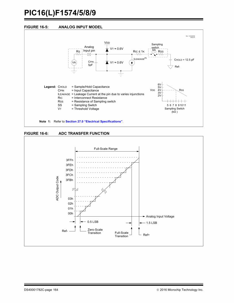
PIC16(L)F1574/5/8/9
DS40001782C-page 164 2016 Microchip Technology Inc.
FIGURE 16-5: ANALOG INPUT MODEL
FIGURE 16-6: ADC TRANSFER FUNCTION
Note 1: Refer to Section 27.0 “Electrical Specifications”.
VDD
Analog Input pin
CPIN5pF
VT 0.6V
VT 0.6V
ILEAKAGE(1)
RIC 1K
Legend: CHOLD = Sample/Hold CapacitanceCPIN = Input CapacitanceILEAKAGE = Leakage Current at the pin due to varies injunctionsRIC = Interconnect ResistanceRSS = Resistance of Sampling switchSS = Sampling SwitchVT = Threshold Voltage
VA
RS RSSSS
Sampling switch
CHOLD = 12.5 pF
Ref-
5 6 7 8 91011
2V3V4V5V6V
VDD RSS
Sampling Switch(k )
Rev. 10-000070B8/5/2014
3FFh
3FEh
AD
C O
utp
ut
Co
de
3FDh
3FCh
03h
02h
01h
00h
Full-Scale
3FBh
0.5 LSB
Ref- Zero-ScaleTransition
Ref+Transition
1.5 LSB
Full-Scale Range
Analog Input Voltage

2016 Microchip Technology Inc. DS40001782C-page 165
PIC16(L)F1574/5/8/9
TABLE 16-3: SUMMARY OF REGISTERS ASSOCIATED WITH ADC
Name Bit 7 Bit 6 Bit 5 Bit 4 Bit 3 Bit 2 Bit 1 Bit 0Register on Page
ADCON0 — CHS<4:0> GO/DONE ADON 158
ADCON1 ADFM ADCS<2:0> — — ADPREF<1:0> 159
ADCON2 TRIGSEL<3:0> — — — — 160
ADRESH ADC Result Register High 161, 162
ADRESL ADC Result Register Low 161, 162
ANSELA — — — ANSA4 — ANSA2 ANSA1 ANSA0 121
INTCON GIE PEIE TMR0IE INTE IOCIE TMR0IF INTF IOCIF 86
PIE1 TMR1GIE ADIE RCIE TXIE — — TMR2IE TMR1IE 87
PIR1 TMR1GIF ADIF RCIF TXIF — — TMR2IF TMR1IF 90
TRISA — — TRISA5 TRISA4 —(1) TRISA2 TRISA1 TRISA0 120
FVRCON FVREN FVRRDY TSEN TSRNG CDAFVR<1:0> ADFVR<1:0> 149
Legend: x = unknown, u = unchanged, — = unimplemented read as ‘0’, q = value depends on condition. Shaded cells are not used for ADC module.
Note 1: Unimplemented, read as ‘1’.

PIC16(L)F1574/5/8/9
DS40001782C-page 166 2016 Microchip Technology Inc.
17.0 5-BIT DIGITAL-TO-ANALOG CONVERTER (DAC) MODULE
The Digital-to-Analog Converter supplies a variablevoltage reference, ratiometric with the input source,with 32 selectable output levels.
The positive input source (VSOURCE+) of the DAC canbe connected to:
• External VREF+ pin
• VDD supply voltage
• FVR_buffer1
The negative input source (VSOURCE-) of the DAC canbe connected to:
• Vss
The output of the DAC (DACx_output) can be selectedas a reference voltage to the following:
• Comparator positive input
• ADC input channel
• DACxOUT1 pin
The Digital-to-Analog Converter (DAC) can be enabledby setting the DACEN bit of the DACxCON0 register.
FIGURE 17-1: DIGITAL-TO-ANALOG CONVERTER BLOCK DIAGRAM
VREF+
VDD
VSOURCE+
VSOURCE-VSS
R
32Steps
R
R
R
R
R
R
32-to
-1 M
UX
To Peripherals
DACxOUT1 (1)
DACOE1
DACx_output
DACEN
DACR<4:0>5
Note 1: The unbuffered DACx_output is provided on the DACxOUT pin(s).
Rev. 10-000026B9/6/2013
00
11
10
01
FVR_buffer2
Reserved
DACPSS
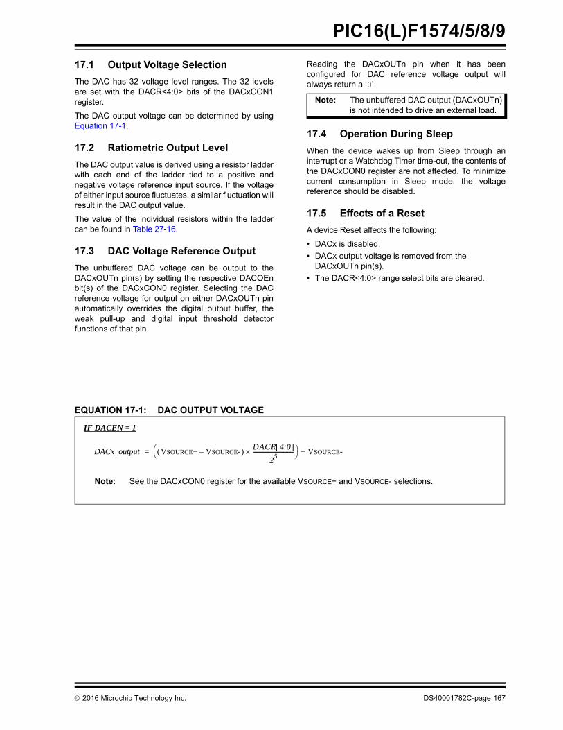
2016 Microchip Technology Inc. DS40001782C-page 167
PIC16(L)F1574/5/8/9
17.1 Output Voltage Selection
The DAC has 32 voltage level ranges. The 32 levelsare set with the DACR<4:0> bits of the DACxCON1register.
The DAC output voltage can be determined by usingEquation 17-1.
17.2 Ratiometric Output Level
The DAC output value is derived using a resistor ladderwith each end of the ladder tied to a positive andnegative voltage reference input source. If the voltageof either input source fluctuates, a similar fluctuation willresult in the DAC output value.
The value of the individual resistors within the laddercan be found in Table 27-16.
17.3 DAC Voltage Reference Output
The unbuffered DAC voltage can be output to theDACxOUTn pin(s) by setting the respective DACOEnbit(s) of the DACxCON0 register. Selecting the DACreference voltage for output on either DACxOUTn pinautomatically overrides the digital output buffer, theweak pull-up and digital input threshold detectorfunctions of that pin.
Reading the DACxOUTn pin when it has beenconfigured for DAC reference voltage output willalways return a ‘0’.
17.4 Operation During Sleep
When the device wakes up from Sleep through aninterrupt or a Watchdog Timer time-out, the contents ofthe DACxCON0 register are not affected. To minimizecurrent consumption in Sleep mode, the voltagereference should be disabled.
17.5 Effects of a Reset
A device Reset affects the following:
• DACx is disabled.
• DACX output voltage is removed from the DACxOUTn pin(s).
• The DACR<4:0> range select bits are cleared.
EQUATION 17-1: DAC OUTPUT VOLTAGE
Note: The unbuffered DAC output (DACxOUTn)is not intended to drive an external load.
IF DACEN = 1
DACx_output VSOURCE+ VSOURCE-– DACR 4:0
25
----------------------------- VSOURCE-+=
Note: See the DACxCON0 register for the available VSOURCE+ and VSOURCE- selections.

PIC16(L)F1574/5/8/9
DS40001782C-page 168 2016 Microchip Technology Inc.
17.6 Register Definitions: DAC Control
TABLE 17-1: SUMMARY OF REGISTERS ASSOCIATED WITH THE DAC MODULE
REGISTER 17-1: DACCON0: VOLTAGE REFERENCE CONTROL REGISTER 0
R/W-0/0 U-0 R/W-0/0 U-0 R/W-0/0 R/W-0/0 U-0 U-0
DACEN — DACOE — DACPSS<1:0> — —
bit 7 bit 0
Legend:
R = Readable bit W = Writable bit U = Unimplemented bit, read as ‘0’
u = Bit is unchanged x = Bit is unknown -n/n = Value at POR and BOR/Value at all other Resets
‘1’ = Bit is set ‘0’ = Bit is cleared
bit 7 DACEN: DAC Enable bit1 = DAC is enabled0 = DAC is disabled
bit 6 Unimplemented: Read as ‘0’
bit 5 DACOE: DAC Voltage Output Enable bit1 = DAC voltage level is output on the DACOUT1 pin0 = DAC voltage level is disconnected from the DACOUT1 pin
bit 4 Unimplemented: Read as ‘0’
bit 3-2 DACPSS<1:0>: DAC Positive Source Select bits11 = Reserved10 = FVR_buffer201 = VREF+ pin00 = VDD
bit 1-0 Unimplemented: Read as ‘0’
REGISTER 17-2: DACCON1: VOLTAGE REFERENCE CONTROL REGISTER 1
U-0 U-0 U-0 R/W-0/0 R/W-0/0 R/W-0/0 R/W-0/0 R/W-0/0
— — — DACR<4:0>
bit 7 bit 0
Legend:
R = Readable bit W = Writable bit U = Unimplemented bit, read as ‘0’
u = Bit is unchanged x = Bit is unknown -n/n = Value at POR and BOR/Value at all other Resets
‘1’ = Bit is set ‘0’ = Bit is cleared
bit 7-5 Unimplemented: Read as ‘0’
bit 4-0 DACR<4:0>: DAC Voltage Output Select bits
Name Bit 7 Bit 6 Bit 5 Bit 4 Bit 3 Bit 2 Bit 1 Bit 0Register on page
DACCON0 DACEN — DACOE — DACPSS<1:0> — — 168
DACCON1 — — — DACR<4:0> 168
Legend: — = Unimplemented location, read as ‘0’. Shaded cells are not used with the DAC module.
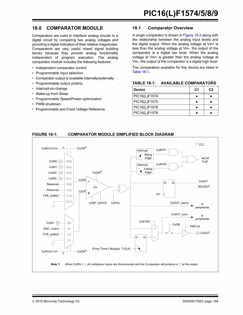
2016 Microchip Technology Inc. DS40001782C-page 169
PIC16(L)F1574/5/8/9
18.0 COMPARATOR MODULE
Comparators are used to interface analog circuits to adigital circuit by comparing two analog voltages andproviding a digital indication of their relative magnitudes.Comparators are very useful mixed signal buildingblocks because they provide analog functionalityindependent of program execution. The analogcomparator module includes the following features:
• Independent comparator control
• Programmable input selection
• Comparator output is available internally/externally
• Programmable output polarity
• Interrupt-on-change
• Wake-up from Sleep
• Programmable Speed/Power optimization
• PWM shutdown
• Programmable and Fixed Voltage Reference
18.1 Comparator Overview
A single comparator is shown in Figure 18-2 along withthe relationship between the analog input levels andthe digital output. When the analog voltage at VIN+ isless than the analog voltage at VIN-, the output of thecomparator is a digital low level. When the analogvoltage at VIN+ is greater than the analog voltage atVIN-, the output of the comparator is a digital high level.
The comparators available for this device are listed inTable 18-1.
FIGURE 18-1: COMPARATOR MODULE SIMPLIFIED BLOCK DIAGRAM
TABLE 18-1: AVAILABLE COMPARATORS
Device C1 C2
PIC16(L)F1574 ● ●
PIC16(L)F1575 ● ●
PIC16(L)F1578 ● ●
PIC16(L)F1579 ● ●
Rev. 10-000027G10/29/2014
CxIN0-
CxIN1-
CxIN+
FVR_buffer2
DAC_output
+
CxVN
CxVP
CxPCH<1:0>
CxNCH<2:0>
2
3
CxON(1)
CxON(1)
CxON(1)
CxSP CxHYS
InterruptRisingEdge
D Q
Q1
CxINTP
CxINTN
CxOUT
MCxOUT
D Q
0
1
CxSYNC
set bitCxIF
TRIS bit
CxOUT
CxOUT_sync
CxOE
-
InterruptFallingEdge
FVR_buffer2
CxPOL
Cx
(From Timer1 Module) T1CLK
toperipherals
Note 1: When CxON = 0, all multiplexer inputs are disconnected and the Comparator will produce a ‘0’ at the output.
000
011
010
001
100
101
110
111
Reserved
Reserved
00
11
10
01
CxIN2-
CxIN3-
CxOUT_async toperipherals
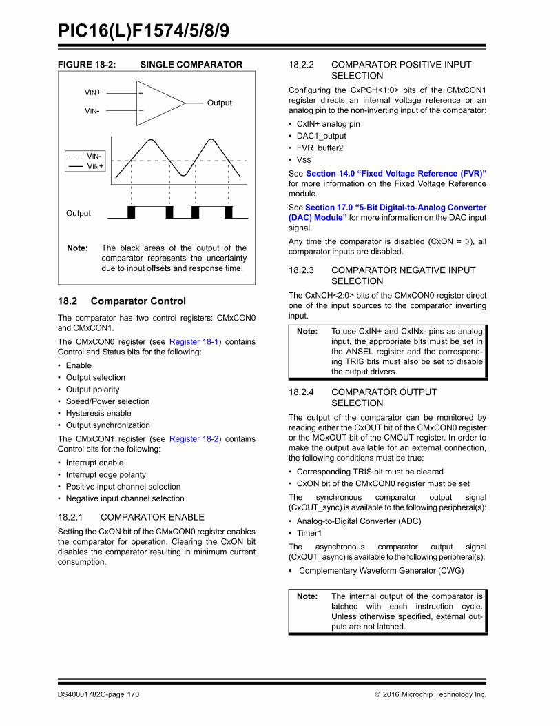
PIC16(L)F1574/5/8/9
DS40001782C-page 170 2016 Microchip Technology Inc.
FIGURE 18-2: SINGLE COMPARATOR
18.2 Comparator Control
The comparator has two control registers: CMxCON0and CMxCON1.
The CMxCON0 register (see Register 18-1) containsControl and Status bits for the following:
• Enable
• Output selection
• Output polarity
• Speed/Power selection
• Hysteresis enable
• Output synchronization
The CMxCON1 register (see Register 18-2) containsControl bits for the following:
• Interrupt enable
• Interrupt edge polarity
• Positive input channel selection
• Negative input channel selection
18.2.1 COMPARATOR ENABLE
Setting the CxON bit of the CMxCON0 register enablesthe comparator for operation. Clearing the CxON bitdisables the comparator resulting in minimum currentconsumption.
18.2.2 COMPARATOR POSITIVE INPUT SELECTION
Configuring the CxPCH<1:0> bits of the CMxCON1register directs an internal voltage reference or ananalog pin to the non-inverting input of the comparator:
• CxIN+ analog pin
• DAC1_output
• FVR_buffer2
• VSS
See Section 14.0 “Fixed Voltage Reference (FVR)”for more information on the Fixed Voltage Referencemodule.
See Section 17.0 “5-Bit Digital-to-Analog Converter(DAC) Module” for more information on the DAC inputsignal.
Any time the comparator is disabled (CxON = 0), allcomparator inputs are disabled.
18.2.3 COMPARATOR NEGATIVE INPUT SELECTION
The CxNCH<2:0> bits of the CMxCON0 register directone of the input sources to the comparator invertinginput.
18.2.4 COMPARATOR OUTPUT SELECTION
The output of the comparator can be monitored byreading either the CxOUT bit of the CMxCON0 registeror the MCxOUT bit of the CMOUT register. In order tomake the output available for an external connection,the following conditions must be true:
• Corresponding TRIS bit must be cleared
• CxON bit of the CMxCON0 register must be set
The synchronous comparator output signal(CxOUT_sync) is available to the following peripheral(s):
• Analog-to-Digital Converter (ADC)
• Timer1
The asynchronous comparator output signal(CxOUT_async) is available to the following peripheral(s):
• Complementary Waveform Generator (CWG)
–
+VIN+
VIN-Output
Output
VIN+VIN-
Note: The black areas of the output of thecomparator represents the uncertaintydue to input offsets and response time.
Note: To use CxIN+ and CxINx- pins as analoginput, the appropriate bits must be set inthe ANSEL register and the correspond-ing TRIS bits must also be set to disablethe output drivers.
Note: The internal output of the comparator islatched with each instruction cycle.Unless otherwise specified, external out-puts are not latched.
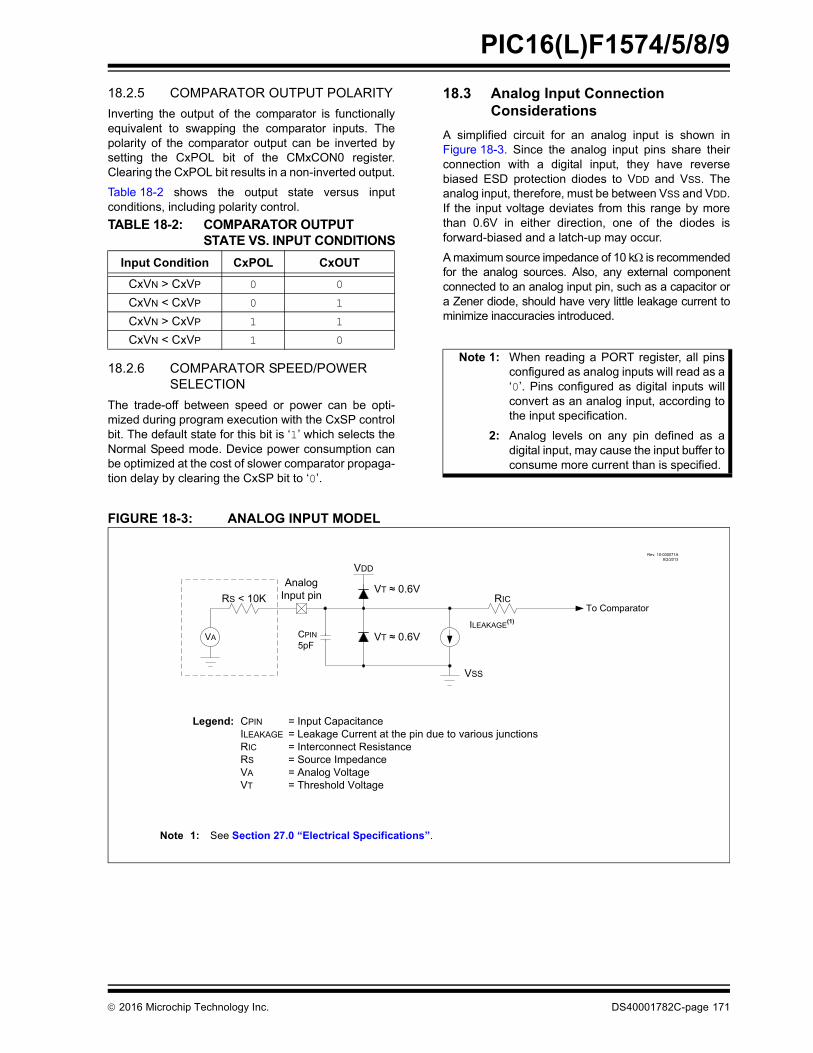
2016 Microchip Technology Inc. DS40001782C-page 171
PIC16(L)F1574/5/8/9
18.2.5 COMPARATOR OUTPUT POLARITY
Inverting the output of the comparator is functionallyequivalent to swapping the comparator inputs. Thepolarity of the comparator output can be inverted bysetting the CxPOL bit of the CMxCON0 register.Clearing the CxPOL bit results in a non-inverted output.
Table 18-2 shows the output state versus inputconditions, including polarity control.
18.2.6 COMPARATOR SPEED/POWER SELECTION
The trade-off between speed or power can be opti-mized during program execution with the CxSP controlbit. The default state for this bit is ‘1’ which selects theNormal Speed mode. Device power consumption canbe optimized at the cost of slower comparator propaga-tion delay by clearing the CxSP bit to ‘0’.
18.3 Analog Input Connection Considerations
A simplified circuit for an analog input is shown inFigure 18-3. Since the analog input pins share theirconnection with a digital input, they have reversebiased ESD protection diodes to VDD and VSS. Theanalog input, therefore, must be between VSS and VDD.If the input voltage deviates from this range by morethan 0.6V in either direction, one of the diodes isforward-biased and a latch-up may occur.
A maximum source impedance of 10 k is recommendedfor the analog sources. Also, any external componentconnected to an analog input pin, such as a capacitor ora Zener diode, should have very little leakage current tominimize inaccuracies introduced.
FIGURE 18-3: ANALOG INPUT MODEL
TABLE 18-2: COMPARATOR OUTPUT STATE VS. INPUT CONDITIONS
Input Condition CxPOL CxOUT
CxVN > CxVP 0 0
CxVN < CxVP 0 1
CxVN > CxVP 1 1
CxVN < CxVP 1 0
Note 1: When reading a PORT register, all pinsconfigured as analog inputs will read as a‘0’. Pins configured as digital inputs willconvert as an analog input, according tothe input specification.
2: Analog levels on any pin defined as adigital input, may cause the input buffer toconsume more current than is specified.
Note 1: See Section 27.0 “Electrical Specifications”.
VA
RS < 10K
VDD
Analog Input pin
CPIN 5pF
VT 0.6V
VT 0.6V
ILEAKAGE(1)
VSS
RICTo Comparator
Legend: CPIN = Input CapacitanceILEAKAGE = Leakage Current at the pin due to various junctionsRIC = Interconnect ResistanceRS = Source ImpedanceVA = Analog VoltageVT = Threshold Voltage
Rev. 10-000071A8/2/2013

PIC16(L)F1574/5/8/9
DS40001782C-page 172 2016 Microchip Technology Inc.
18.4 Comparator Hysteresis
A selectable amount of separation voltage can beadded to the input pins of each comparator to provide ahysteresis function to the overall operation. Hysteresisis enabled by setting the CxHYS bit of the CMxCON0register.
See Section 27.0 “Electrical Specifications” formore information.
18.5 Timer1 Gate Operation
The output resulting from a comparator operation canbe used as a source for gate control of Timer1. SeeSection 20.5 “Timer1 Gate” for more information.This feature is useful for timing the duration or intervalof an analog event.
It is recommended that the comparator output besynchronized to Timer1. This ensures that Timer1 doesnot increment while a change in the comparator isoccurring.
18.5.1 COMPARATOR OUTPUT SYNCHRONIZATION
The output from the Cx comparator can besynchronized with Timer1 by setting the CxSYNC bit ofthe CMxCON0 register.
Once enabled, the comparator output is latched on thefalling edge of the Timer1 source clock. If a prescaler isused with Timer1, the comparator output is latched afterthe prescaling function. To prevent a race condition, thecomparator output is latched on the falling edge of theTimer1 clock source and Timer1 increments on therising edge of its clock source. See the ComparatorBlock Diagram (Figure 18-2) and the Timer1 BlockDiagram (Figure 20-1) for more information.
18.6 Comparator Interrupt
An interrupt can be generated upon a change in theoutput value of the comparator for each comparator, arising edge detector and a falling edge detector arepresent.
When either edge detector is triggered and its associ-ated enable bit is set (CxINTP and/or CxINTN bits ofthe CMxCON1 register), the Corresponding InterruptFlag bit (CxIF bit of the PIR2 register) will be set.
To enable the interrupt, you must set the following bits:
• CxON and CxPOL bits of the CMxCON0 register
• CxIE bit of the PIE2 register
• CxINTP bit of the CMxCON1 register (for a rising edge detection)
• CxINTN bit of the CMxCON1 register (for a falling edge detection)
• PEIE and GIE bits of the INTCON register
The associated interrupt flag bit, CxIF bit of the PIR2register, must be cleared in software. If another edge isdetected while this flag is being cleared, the flag will stillbe set at the end of the sequence.
18.7 Comparator Response Time
The comparator output is indeterminate for a period oftime after the change of an input source or the selectionof a new reference voltage. This period is referred to asthe response time. The response time of the comparatordiffers from the settling time of the voltage reference.Therefore, both of these times must be considered whendetermining the total response time to a comparatorinput change. See the Comparator and VoltageReference Specifications in Section 27.0 “ElectricalSpecifications” for more details.
Note: Although a comparator is disabled, aninterrupt can be generated by changingthe output polarity with the CxPOL bit ofthe CMxCON0 register, or by switchingthe comparator on or off with the CxON bitof the CMxCON0 register.
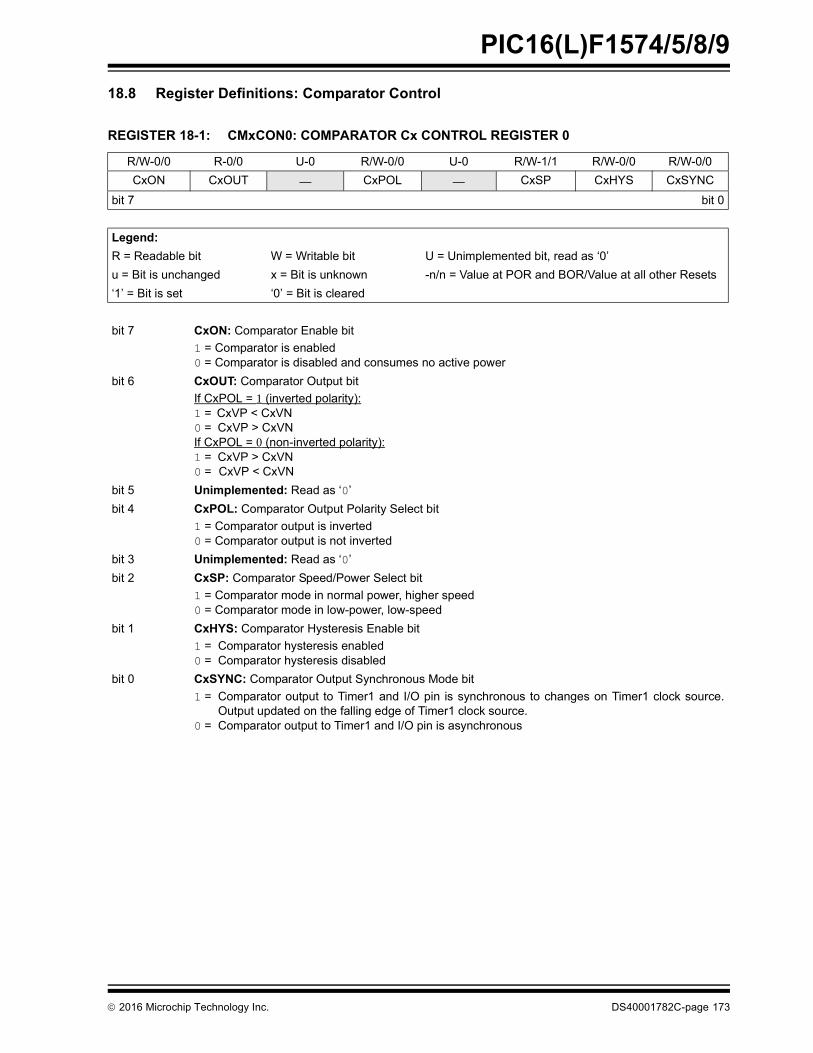
2016 Microchip Technology Inc. DS40001782C-page 173
PIC16(L)F1574/5/8/9
18.8 Register Definitions: Comparator Control
REGISTER 18-1: CMxCON0: COMPARATOR Cx CONTROL REGISTER 0
R/W-0/0 R-0/0 U-0 R/W-0/0 U-0 R/W-1/1 R/W-0/0 R/W-0/0
CxON CxOUT — CxPOL — CxSP CxHYS CxSYNC
bit 7 bit 0
Legend:
R = Readable bit W = Writable bit U = Unimplemented bit, read as ‘0’
u = Bit is unchanged x = Bit is unknown -n/n = Value at POR and BOR/Value at all other Resets
‘1’ = Bit is set ‘0’ = Bit is cleared
bit 7 CxON: Comparator Enable bit
1 = Comparator is enabled0 = Comparator is disabled and consumes no active power
bit 6 CxOUT: Comparator Output bit
If CxPOL = 1 (inverted polarity):1 = CxVP < CxVN0 = CxVP > CxVNIf CxPOL = 0 (non-inverted polarity):1 = CxVP > CxVN0 = CxVP < CxVN
bit 5 Unimplemented: Read as ‘0’
bit 4 CxPOL: Comparator Output Polarity Select bit
1 = Comparator output is inverted0 = Comparator output is not inverted
bit 3 Unimplemented: Read as ‘0’
bit 2 CxSP: Comparator Speed/Power Select bit
1 = Comparator mode in normal power, higher speed0 = Comparator mode in low-power, low-speed
bit 1 CxHYS: Comparator Hysteresis Enable bit
1 = Comparator hysteresis enabled0 = Comparator hysteresis disabled
bit 0 CxSYNC: Comparator Output Synchronous Mode bit
1 = Comparator output to Timer1 and I/O pin is synchronous to changes on Timer1 clock source.Output updated on the falling edge of Timer1 clock source.
0 = Comparator output to Timer1 and I/O pin is asynchronous
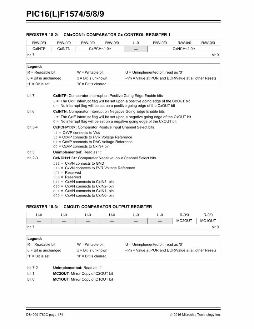
PIC16(L)F1574/5/8/9
DS40001782C-page 174 2016 Microchip Technology Inc.
REGISTER 18-2: CMxCON1: COMPARATOR Cx CONTROL REGISTER 1
R/W-0/0 R/W-0/0 R/W-0/0 R/W-0/0 U-0 R/W-0/0 R/W-0/0 R/W-0/0
CxINTP CxINTN CxPCH<1:0> — CxNCH<2:0>
bit 7 bit 0
Legend:
R = Readable bit W = Writable bit U = Unimplemented bit, read as ‘0’
u = Bit is unchanged x = Bit is unknown -n/n = Value at POR and BOR/Value at all other Resets
‘1’ = Bit is set ‘0’ = Bit is cleared
bit 7 CxINTP: Comparator Interrupt on Positive Going Edge Enable bits
1 = The CxIF interrupt flag will be set upon a positive going edge of the CxOUT bit0 = No interrupt flag will be set on a positive going edge of the CxOUT bit
bit 6 CxINTN: Comparator Interrupt on Negative Going Edge Enable bits
1 = The CxIF interrupt flag will be set upon a negative going edge of the CxOUT bit0 = No interrupt flag will be set on a negative going edge of the CxOUT bit
bit 5-4 CxPCH<1:0>: Comparator Positive Input Channel Select bits
11 = CxVP connects to VSS
10 = CxVP connects to FVR Voltage Reference01 = CxVP connects to DAC Voltage Reference00 = CxVP connects to CxIN+ pin
bit 3 Unimplemented: Read as ‘0’
bit 2-0 CxNCH<1:0>: Comparator Negative Input Channel Select bits
111 = CxVN connects to GND110 = CxVN connects to FVR Voltage Reference101 = Reserved100 = Reserved011 = CxVN connects to CxIN3- pin010 = CxVN connects to CxIN2- pin001 = CxVN connects to CxIN1- pin000 = CxVN connects to CxIN0- pin
REGISTER 18-3: CMOUT: COMPARATOR OUTPUT REGISTER
U-0 U-0 U-0 U-0 U-0 U-0 R-0/0 R-0/0
— — — — — — MC2OUT MC1OUT
bit 7 bit 0
Legend:
R = Readable bit W = Writable bit U = Unimplemented bit, read as ‘0’
u = Bit is unchanged x = Bit is unknown -n/n = Value at POR and BOR/Value at all other Resets
‘1’ = Bit is set ‘0’ = Bit is cleared
bit 7-2 Unimplemented: Read as ‘0’
bit 1 MC2OUT: Mirror Copy of C2OUT bit
bit 0 MC1OUT: Mirror Copy of C1OUT bit
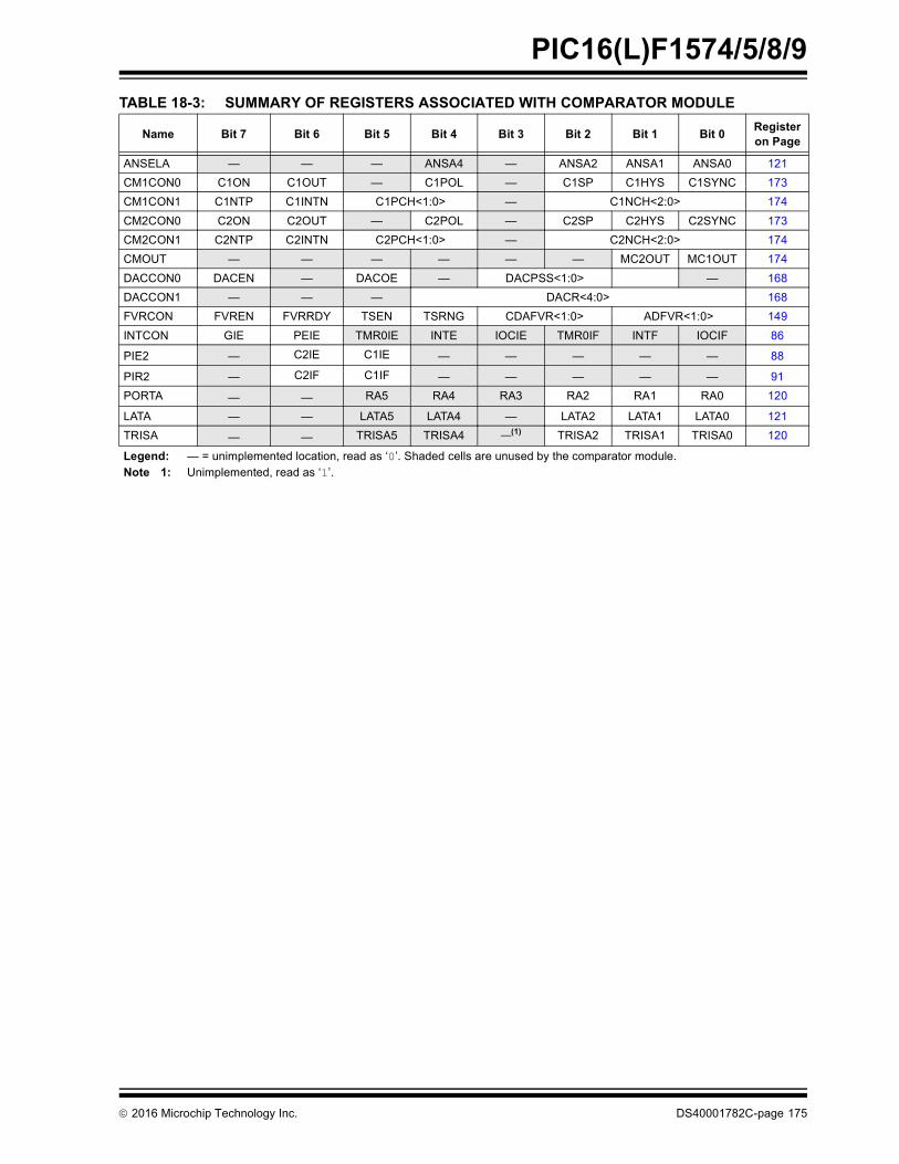
2016 Microchip Technology Inc. DS40001782C-page 175
PIC16(L)F1574/5/8/9
TABLE 18-3: SUMMARY OF REGISTERS ASSOCIATED WITH COMPARATOR MODULE
Name Bit 7 Bit 6 Bit 5 Bit 4 Bit 3 Bit 2 Bit 1 Bit 0Register on Page
ANSELA — — — ANSA4 — ANSA2 ANSA1 ANSA0 121
CM1CON0 C1ON C1OUT — C1POL — C1SP C1HYS C1SYNC 173
CM1CON1 C1NTP C1INTN C1PCH<1:0> — C1NCH<2:0> 174
CM2CON0 C2ON C2OUT — C2POL — C2SP C2HYS C2SYNC 173
CM2CON1 C2NTP C2INTN C2PCH<1:0> — C2NCH<2:0> 174
CMOUT — — — — — — MC2OUT MC1OUT 174
DACCON0 DACEN — DACOE — DACPSS<1:0> — 168
DACCON1 — — — DACR<4:0> 168
FVRCON FVREN FVRRDY TSEN TSRNG CDAFVR<1:0> ADFVR<1:0> 149
INTCON GIE PEIE TMR0IE INTE IOCIE TMR0IF INTF IOCIF 86
PIE2 — C2IE C1IE — — — — — 88
PIR2 — C2IF C1IF — — — — — 91
PORTA — — RA5 RA4 RA3 RA2 RA1 RA0 120
LATA — — LATA5 LATA4 — LATA2 LATA1 LATA0 121
TRISA — — TRISA5 TRISA4 —(1) TRISA2 TRISA1 TRISA0 120
Legend: — = unimplemented location, read as ‘0’. Shaded cells are unused by the comparator module.Note 1: Unimplemented, read as ‘1’.

PIC16(L)F1574/5/8/9
DS40001782C-page 176 2016 Microchip Technology Inc.
19.0 TIMER0 MODULE
The Timer0 module is an 8-bit timer/counter with thefollowing features:
• 8-bit timer/counter register (TMR0)
• 3-bit prescaler (independent of Watchdog Timer)
• Programmable internal or external clock source
• Programmable external clock edge selection
• Interrupt on overflow
• TMR0 can be used to gate Timer1
Figure 19-1 is a block diagram of the Timer0 module.
19.1 Timer0 Operation
The Timer0 module can be used as either an 8-bit timeror an 8-bit counter.
19.1.1 8-BIT TIMER MODE
The Timer0 module will increment every instructioncycle, if used without a prescaler. 8-bit Timer mode isselected by clearing the TMR0CS bit of theOPTION_REG register.
When TMR0 is written, the increment is inhibited fortwo instruction cycles immediately following the write.
19.1.2 8-BIT COUNTER MODE
In 8-Bit Counter mode, the Timer0 module will incrementon every rising or falling edge of the T0CKI pin.
8-Bit Counter mode using the T0CKI pin is selected bysetting the TMR0CS bit in the OPTION_REG register to‘1’.
The rising or falling transition of the incrementing edgefor either input source is determined by the TMR0SE bitin the OPTION_REG register.
FIGURE 19-1: TIMER0 BLOCK DIAGRAM
Note: The value written to the TMR0 registercan be adjusted, in order to account forthe two instruction cycle delay whenTMR0 is written.
Rev. 10-000017A8/5/2013
TMR0SE
0
1
Fosc/4
Prescaler
T0_overflow
Rwrite to
TMR0set bit
TMR0IF
T0CKISync CircuitFOSC/2
TMR0CS
T0CKI(1)
Note 1: The T0CKI prescale output frequency should not exceed FOSC/8.
PS<2:0>
0
1
PSA
TMR0Q1
2016 Microchip Technology Inc. DS40001782C-page 177
PIC16(L)F1574/5/8/9
19.1.3 SOFTWARE PROGRAMMABLE PRESCALER
A software programmable prescaler is available forexclusive use with Timer0. The prescaler is enabled byclearing the PSA bit of the OPTION_REG register.
There are eight prescaler options for the Timer0 mod-ule ranging from 1:2 to 1:256. The prescale values areselectable via the PS<2:0> bits of the OPTION_REGregister. In order to have a 1:1 prescaler value for theTimer0 module, the prescaler must be disabled by set-ting the PSA bit of the OPTION_REG register.
The prescaler is not readable or writable. All instructionswriting to the TMR0 register will clear the prescaler.
19.1.4 TIMER0 INTERRUPT
Timer0 will generate an interrupt when the TMR0register overflows from FFh to 00h. The TMR0IFinterrupt flag bit of the INTCON register is set everytime the TMR0 register overflows, regardless ofwhether or not the Timer0 interrupt is enabled. TheTMR0IF bit can only be cleared in software. The Timer0interrupt enable is the TMR0IE bit of the INTCONregister.
19.1.5 8-BIT COUNTER MODE SYNCHRONIZATION
When in 8-Bit Counter mode, the incrementing edge onthe T0CKI pin must be synchronized to the instructionclock. Synchronization can be accomplished bysampling the prescaler output on the Q2 and Q4 cyclesof the instruction clock. The high and low periods of theexternal clocking source must meet the timingrequirements as shown in Section 27.0 “ElectricalSpecifications”.
19.1.6 OPERATION DURING SLEEP
Timer0 cannot operate while the processor is in Sleepmode. The contents of the TMR0 register will remainunchanged while the processor is in Sleep mode.
Note: The Watchdog Timer (WDT) uses its ownindependent prescaler.
Note: The Timer0 interrupt cannot wake theprocessor from Sleep since the timer isfrozen during Sleep.

PIC16(L)F1574/5/8/9
DS40001782C-page 178 2016 Microchip Technology Inc.
19.2 Register Definitions: Option Register
TABLE 19-1: SUMMARY OF REGISTERS ASSOCIATED WITH TIMER0
REGISTER 19-1: OPTION_REG: OPTION REGISTER
R/W-1/1 R/W-1/1 R/W-1/1 R/W-1/1 R/W-1/1 R/W-1/1 R/W-1/1 R/W-1/1
WPUEN INTEDG TMR0CS TMR0SE PSA PS<2:0>
bit 7 bit 0
Legend:
R = Readable bit W = Writable bit U = Unimplemented bit, read as ‘0’
u = Bit is unchanged x = Bit is unknown -n/n = Value at POR and BOR/Value at all other Resets
‘1’ = Bit is set ‘0’ = Bit is cleared
bit 7 WPUEN: Weak Pull-Up Enable bit1 = All weak pull-ups are disabled (except MCLR, if it is enabled)0 = Weak pull-ups are enabled by individual WPUx latch values
bit 6 INTEDG: Interrupt Edge Select bit1 = Interrupt on rising edge of INT pin0 = Interrupt on falling edge of INT pin
bit 5 TMR0CS: Timer0 Clock Source Select bit1 = Transition on T0CKI pin0 = Internal instruction cycle clock (FOSC/4)
bit 4 TMR0SE: Timer0 Source Edge Select bit1 = Increment on high-to-low transition on T0CKI pin0 = Increment on low-to-high transition on T0CKI pin
bit 3 PSA: Prescaler Assignment bit1 = Prescaler is not assigned to the Timer0 module0 = Prescaler is assigned to the Timer0 module
bit 2-0 PS<2:0>: Prescaler Rate Select bits
Name Bit 7 Bit 6 Bit 5 Bit 4 Bit 3 Bit 2 Bit 1 Bit 0Register on Page
ADCON2 TRIGSEL<3:0> — — — — 160
INTCON GIE PEIE TMR0IE INTE IOCIE TMR0IF INTF IOCIF 86
OPTION_REG WPUEN INTEDG TMR0CS TMR0SE PSA PS<2:0> 178
TMR0 Holding Register for the 8-bit Timer0 Count 176*
TRISA — — TRISA5 TRISA4 —(1) TRISA2 TRISA1 TRISA0 120
Legend: — = Unimplemented location, read as ‘0’. Shaded cells are not used by the Timer0 module.* Page provides register information.
Note 1: Unimplemented, read as ‘1’.
000001010011100101110111
1 : 21 : 41 : 81 : 161 : 321 : 641 : 1281 : 256
Bit Value Timer0 Rate

2016 Microchip Technology Inc. DS40001782C-page 179
PIC16(L)F1574/5/8/9
20.0 TIMER1 MODULE WITH GATE CONTROL
The Timer1 module is a 16-bit timer/counter with thefollowing features:
• 16-bit timer/counter register pair (TMR1H:TMR1L)
• Programmable internal or external clock source
• 2-bit prescaler
• Optionally synchronized comparator out
• Multiple Timer1 gate (count enable) sources
• Interrupt on overflow
• Wake-up on overflow (external clock, Asynchronous mode only)
• ADC Auto-Conversion Trigger(s)
• Selectable Gate Source Polarity
• Gate Toggle mode
• Gate Single-Pulse mode
• Gate Value Status
• Gate Event Interrupt
Figure 20-1 is a block diagram of the Timer1 module.
FIGURE 20-1: TIMER1 BLOCK DIAGRAM
00
11
10
01
T1G
T0_overflow
C1OUT_sync
Reserved
T1GSS<1:0>
T1GPOL
0
1
Single PulseAcq. Control
1
0
T1GSPM
TMR1ON
T1GTM
TMR1GE
TMR1ON
DQ
EN
TMR1LTMR1HT1_overflow
set flag bitTMR1IF
TMR1(2)
1
0
FoscInternal Clock
Fosc/4Internal Clock
LFINTOSC
TMR1CS<1:0>
00
11
10
01
Prescaler1,2,4,8
T1SYNC
SleepInput
Fosc/2InternalClock
T1CKPS<1:0>
Synchronized Clock Input
2
det
Synchronize(3)
1: ST Buffer is high speed type when using T1CKI.2: Timer1 register increments on rising edge.3: Synchronize does not operate while in Sleep.
(1)
D
QCK
R
Q
Note
T1GGO/DONE
T1CLK
T1CKI
D Q
set bitTMR1GIF
T1GVAL
Q1
det
Interrupt
Rev. 10-000018D8/5/2013
PIC16(L)F1574/5/8/9
DS40001782C-page 180 2016 Microchip Technology Inc.
20.1 Timer1 Operation
The Timer1 module is a 16-bit incrementing counterwhich is accessed through the TMR1H:TMR1L registerpair. Writes to TMR1H or TMR1L directly update thecounter.
When used with an internal clock source, the module isa timer and increments on every instruction cycle.When used with an external clock source, the modulecan be used as either a timer or counter and incre-ments on every selected edge of the external source.
Timer1 is enabled by configuring the TMR1ON andTMR1GE bits in the T1CON and T1GCON registers,respectively. Table 20-1 displays the Timer1 enableselections.
20.2 Clock Source Selection
The TMR1CS<1:0> bits of the T1CON register are usedto select the clock source for Timer1. Table 20-2displays the clock source selections.
20.2.1 INTERNAL CLOCK SOURCE
When the internal clock source is selected, theTMR1H:TMR1L register pair will increment on multiplesof FOSC as determined by the Timer1 prescaler.
When the FOSC internal clock source is selected, theTimer1 register value will increment by four counts everyinstruction clock cycle. Due to this condition, a 2 LSBerror in resolution will occur when reading the Timer1value. To utilize the full resolution of Timer1, anasynchronous input signal must be used to gate theTimer1 clock input.
The following asynchronous sources may be used:
• Asynchronous event on the T1G pin to Timer1 gate
• C1 or C2 comparator input to Timer1 gate
20.2.2 EXTERNAL CLOCK SOURCE
When the external clock source is selected, the Timer1module may work as a timer or a counter.
When enabled to count, Timer1 is incremented on therising edge of the external clock input T1CKI. Theexternal clock source can be synchronized to themicrocontroller system clock or it can runasynchronously.
TABLE 20-1: TIMER1 ENABLE SELECTIONS
TMR1ON TMR1GETimer1
Operation
0 0 Off
0 1 Off
1 0 Always On
1 1 Count Enabled
Note: In Counter mode, a falling edge must beregistered by the counter prior to the firstincrementing rising edge after any one ormore of the following conditions:
• Timer1 enabled after POR
• Write to TMR1H or TMR1L
• Timer1 is disabled
• Timer1 is disabled (TMR1ON = 0) when T1CKI is high then Timer1 is enabled (TMR1ON=1) when T1CKI is low.
TABLE 20-2: CLOCK SOURCE SELECTIONS
TMR1CS<1:0> T1OSCEN(1) Clock Source
11 x LFINTOSC
10 x External Clocking on T1CKI Pin
01 x System Clock (FOSC)
00 x Instruction Clock (FOSC/4)
Note 1: T1OSC is not available on all devices.

2016 Microchip Technology Inc. DS40001782C-page 181
PIC16(L)F1574/5/8/9
20.3 Timer1 Prescaler
Timer1 has four prescaler options allowing 1, 2, 4 or 8divisions of the clock input. The T1CKPS bits of theT1CON register control the prescale counter. Theprescale counter is not directly readable or writable;however, the prescaler counter is cleared upon a write toTMR1H or TMR1L.
20.4 Timer1 Operation in Asynchronous Counter Mode
If control bit T1SYNC of the T1CON register is set, theexternal clock input is not synchronized. The timerincrements asynchronously to the internal phaseclocks. If the external clock source is selected then thetimer will continue to run during Sleep and cangenerate an interrupt on overflow, which will wake-upthe processor. However, special precautions insoftware are needed to read/write the timer (seeSection 20.4.1 “Reading and Writing Timer1 inAsynchronous Counter Mode”).
20.4.1 READING AND WRITING TIMER1 IN ASYNCHRONOUS COUNTER MODE
Reading TMR1H or TMR1L while the timer is runningfrom an external asynchronous clock will ensure a validread (taken care of in hardware). However, the usershould keep in mind that reading the 16-bit timer in two8-bit values itself, poses certain problems, since thetimer may overflow between the reads.
For writes, it is recommended that the user simply stopthe timer and write the desired values. A writecontention may occur by writing to the timer registers,while the register is incrementing. This may produce anunpredictable value in the TMR1H:TMR1L register pair.
20.5 Timer1 Gate
Timer1 can be configured to count freely or the countcan be enabled and disabled using Timer1 gatecircuitry. This is also referred to as Timer1 Gate Enable.
Timer1 gate can also be driven by multiple selectablesources.
20.5.1 TIMER1 GATE ENABLE
The Timer1 Gate Enable mode is enabled by settingthe TMR1GE bit of the T1GCON register. The polarityof the Timer1 Gate Enable mode is configured usingthe T1GPOL bit of the T1GCON register.
When Timer1 Gate Enable mode is enabled, Timer1will increment on the rising edge of the Timer1 clocksource. When Timer1 Gate Enable mode is disabled,no incrementing will occur and Timer1 will hold thecurrent count. See Figure 20-3 for timing details.
20.5.2 TIMER1 GATE SOURCE SELECTION
Timer1 gate source selections are shown in Table 20-4.Source selection is controlled by the T1GSS<1:0> bitsof the T1GCON register. The polarity for each availablesource is also selectable. Polarity selection is controlledby the T1GPOL bit of the T1GCON register.
TABLE 20-4: TIMER1 GATE SOURCES
Note: When switching from synchronous toasynchronous operation, it is possible toskip an increment. When switching fromasynchronous to synchronous operation,it is possible to produce an additionalincrement.
TABLE 20-3: TIMER1 GATE ENABLE SELECTIONS
T1CLK T1GPOL T1G Timer1 Operation
0 0 Counts
0 1 Holds Count
1 0 Holds Count
1 1 Counts
T1GSS Timer1 Gate Source
00 Timer1 Gate pin (T1G)
01 Overflow of Timer0 (T0_overflow)(TMR0 increments from FFh to 00h)
10 Comparator 1 Output (C1OUT_sync)(1)
11 Comparator 2 Output (C2OUT_sync)(1)
Note 1: Optionally synchronized comparator output.

PIC16(L)F1574/5/8/9
DS40001782C-page 182 2016 Microchip Technology Inc.
20.5.2.1 T1G Pin Gate Operation
The T1G pin is one source for Timer1 gate control. Itcan be used to supply an external source to the Timer1gate circuitry.
20.5.2.2 Timer0 Overflow Gate Operation
When Timer0 increments from FFh to 00h, a low-to-high pulse will automatically be generated and inter-nally supplied to the Timer1 gate circuitry.
20.5.3 TIMER1 GATE TOGGLE MODE
When Timer1 Gate Toggle mode is enabled, it is possi-ble to measure the full-cycle length of a Timer1 gatesignal, as opposed to the duration of a single levelpulse.
The Timer1 gate source is routed through a flip-flop thatchanges state on every incrementing edge of the sig-nal. See Figure 20-4 for timing details.
Timer1 Gate Toggle mode is enabled by setting theT1GTM bit of the T1GCON register. When the T1GTMbit is cleared, the flip-flop is cleared and held clear. Thisis necessary in order to control which edge ismeasured.
20.5.4 TIMER1 GATE SINGLE-PULSE MODE
When Timer1 Gate Single-Pulse mode is enabled, it ispossible to capture a single pulse gate event. Timer1Gate Single-Pulse mode is first enabled by setting theT1GSPM bit in the T1GCON register. Next, the T1GGO/DONE bit in the T1GCON register must be set. TheTimer1 will be fully enabled on the next incrementingedge. On the next trailing edge of the pulse, the T1GGO/DONE bit will automatically be cleared. No other gateevents will be allowed to increment Timer1 until theT1GGO/DONE bit is once again set in software. SeeFigure 20-5 for timing details.
If the Single Pulse Gate mode is disabled by clearing theT1GSPM bit in the T1GCON register, the T1GGO/DONEbit should also be cleared.
Enabling the Toggle mode and the Single-Pulse modesimultaneously will permit both sections to worktogether. This allows the cycle times on the Timer1 gatesource to be measured. See Figure 20-6 for timingdetails.
20.5.5 TIMER1 GATE VALUE STATUS
When Timer1 Gate Value Status is utilized, it is possibleto read the most current level of the gate control value.The value is stored in the T1GVAL bit in the T1GCONregister. The T1GVAL bit is valid even when the Timer1gate is not enabled (TMR1GE bit is cleared).
20.5.6 TIMER1 GATE EVENT INTERRUPT
When Timer1 Gate Event Interrupt is enabled, it ispossible to generate an interrupt upon the completionof a gate event. When the falling edge of T1GVALoccurs, the TMR1GIF flag bit in the PIR1 register will beset. If the TMR1GIE bit in the PIE1 register is set, thenan interrupt will be recognized.
The TMR1GIF flag bit operates even when the Timer1gate is not enabled (TMR1GE bit is cleared).
Note: Enabling Toggle mode at the same timeas changing the gate polarity may result inindeterminate operation.

2016 Microchip Technology Inc. DS40001782C-page 183
PIC16(L)F1574/5/8/9
20.6 Timer1 Interrupt
The Timer1 register pair (TMR1H:TMR1L) incrementsto FFFFh and rolls over to 0000h. When Timer1 rollsover, the Timer1 interrupt flag bit of the PIR1 register isset. To enable the interrupt on rollover, you must setthese bits:
• TMR1ON bit of the T1CON register
• TMR1IE bit of the PIE1 register
• PEIE bit of the INTCON register
• GIE bit of the INTCON register
The interrupt is cleared by clearing the TMR1IF bit inthe Interrupt Service Routine.
20.7 Timer1 Operation During Sleep
Timer1 can only operate during Sleep when setup inAsynchronous Counter mode. In this mode, an externalcrystal or clock source can be used to increment thecounter. To set up the timer to wake the device:
• TMR1ON bit of the T1CON register must be set
• TMR1IE bit of the PIE1 register must be set
• PEIE bit of the INTCON register must be set
• T1SYNC bit of the T1CON register must be set
• TMR1CS bits of the T1CON register must be configured
The device will wake-up on an overflow and executethe next instructions. If the GIE bit of the INTCONregister is set, the device will call the Interrupt ServiceRoutine.
Timer1 oscillator will continue to operate in Sleepregardless of the T1SYNC bit setting.
FIGURE 20-2: TIMER1 INCREMENTING EDGE
FIGURE 20-3: TIMER1 GATE ENABLE MODE
Note: The TMR1H:TMR1L register pair and theTMR1IF bit should be cleared beforeenabling interrupts.
T1CKI = 1
when TMR1Enabled
T1CKI = 0
when TMR1Enabled
Note 1: Arrows indicate counter increments.
2: In Counter mode, a falling edge must be registered by the counter prior to the first incrementing rising edge of the clock.
TMR1GE
T1GPOL
t1g_in
T1CKI
T1GVAL
Timer1 N N + 1 N + 2 N + 3 N + 4

PIC16(L)F1574/5/8/9
DS40001782C-page 184 2016 Microchip Technology Inc.
FIGURE 20-4: TIMER1 GATE TOGGLE MODE
FIGURE 20-5: TIMER1 GATE SINGLE-PULSE MODE
TMR1GE
T1GPOL
T1GTM
t1g_in
T1CKI
T1GVAL
Timer1 N N + 1 N + 2 N + 3 N + 4 N + 5 N + 6 N + 7 N + 8
TMR1GE
T1GPOL
t1g_in
T1CKI
T1GVAL
Timer1 N N + 1 N + 2
T1GSPM
T1GGO/
DONE
Set by softwareCleared by hardware onfalling edge of T1GVAL
Set by hardware onfalling edge of T1GVAL
Cleared by softwareCleared bysoftwareTMR1GIF
Counting enabled onrising edge of T1G
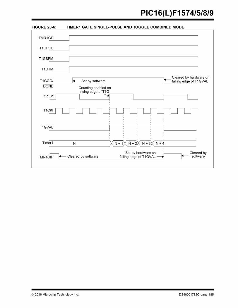
2016 Microchip Technology Inc. DS40001782C-page 185
PIC16(L)F1574/5/8/9
FIGURE 20-6: TIMER1 GATE SINGLE-PULSE AND TOGGLE COMBINED MODE
TMR1GE
T1GPOL
t1g_in
T1CKI
T1GVAL
Timer1 N N + 1 N + 2
T1GSPM
T1GGO/
DONE
Set by softwareCleared by hardware onfalling edge of T1GVAL
Set by hardware onfalling edge of T1GVALCleared by software
Cleared bysoftwareTMR1GIF
T1GTM
Counting enabled onrising edge of T1G
N + 4N + 3
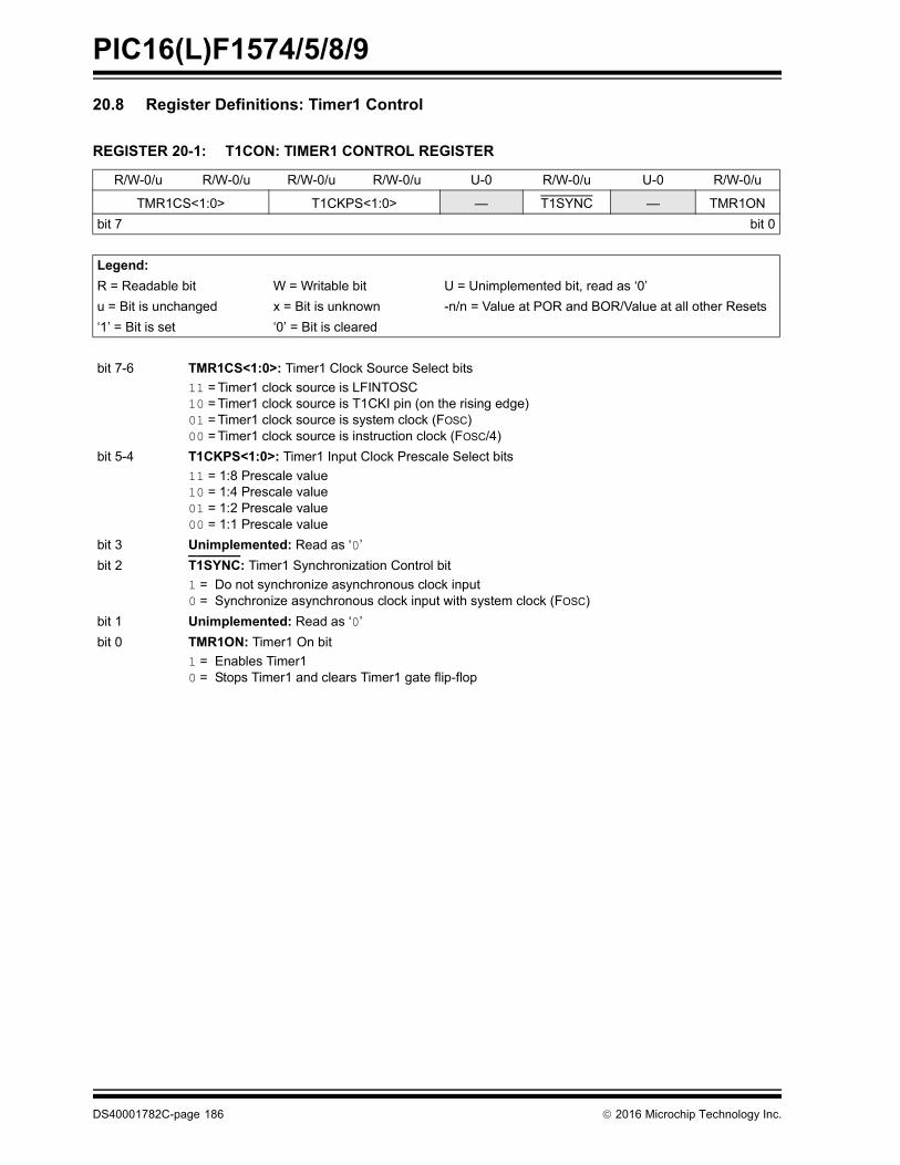
PIC16(L)F1574/5/8/9
DS40001782C-page 186 2016 Microchip Technology Inc.
20.8 Register Definitions: Timer1 Control
REGISTER 20-1: T1CON: TIMER1 CONTROL REGISTER
R/W-0/u R/W-0/u R/W-0/u R/W-0/u U-0 R/W-0/u U-0 R/W-0/u
TMR1CS<1:0> T1CKPS<1:0> — T1SYNC — TMR1ON
bit 7 bit 0
Legend:
R = Readable bit W = Writable bit U = Unimplemented bit, read as ‘0’
u = Bit is unchanged x = Bit is unknown -n/n = Value at POR and BOR/Value at all other Resets
‘1’ = Bit is set ‘0’ = Bit is cleared
bit 7-6 TMR1CS<1:0>: Timer1 Clock Source Select bits
11 = Timer1 clock source is LFINTOSC10 = Timer1 clock source is T1CKI pin (on the rising edge)01 = Timer1 clock source is system clock (FOSC)00 = Timer1 clock source is instruction clock (FOSC/4)
bit 5-4 T1CKPS<1:0>: Timer1 Input Clock Prescale Select bits
11 = 1:8 Prescale value10 = 1:4 Prescale value01 = 1:2 Prescale value00 = 1:1 Prescale value
bit 3 Unimplemented: Read as ‘0’
bit 2 T1SYNC: Timer1 Synchronization Control bit
1 = Do not synchronize asynchronous clock input0 = Synchronize asynchronous clock input with system clock (FOSC)
bit 1 Unimplemented: Read as ‘0’
bit 0 TMR1ON: Timer1 On bit
1 = Enables Timer10 = Stops Timer1 and clears Timer1 gate flip-flop
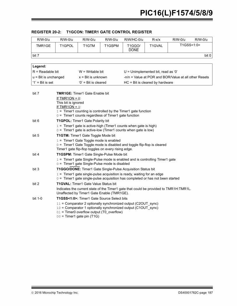
2016 Microchip Technology Inc. DS40001782C-page 187
PIC16(L)F1574/5/8/9
REGISTER 20-2: T1GCON: TIMER1 GATE CONTROL REGISTER
R/W-0/u R/W-0/u R/W-0/u R/W-0/u R/W/HC-0/u R-x/x R/W-0/u R/W-0/u
TMR1GE T1GPOL T1GTM T1GSPM T1GGO/DONE
T1GVAL T1GSS<1:0>
bit 7 bit 0
Legend:
R = Readable bit W = Writable bit U = Unimplemented bit, read as ‘0’
u = Bit is unchanged x = Bit is unknown -n/n = Value at POR and BOR/Value at all other Resets
‘1’ = Bit is set ‘0’ = Bit is cleared HC = Bit is cleared by hardware
bit 7 TMR1GE: Timer1 Gate Enable bit
If TMR1ON = 0:This bit is ignoredIf TMR1ON = 1:1 = Timer1 counting is controlled by the Timer1 gate function0 = Timer1 counts regardless of Timer1 gate function
bit 6 T1GPOL: Timer1 Gate Polarity bit
1 = Timer1 gate is active-high (Timer1 counts when gate is high)0 = Timer1 gate is active-low (Timer1 counts when gate is low)
bit 5 T1GTM: Timer1 Gate Toggle Mode bit
1 = Timer1 Gate Toggle mode is enabled0 = Timer1 Gate Toggle mode is disabled and toggle flip-flop is clearedTimer1 gate flip-flop toggles on every rising edge.
bit 4 T1GSPM: Timer1 Gate Single-Pulse Mode bit
1 = Timer1 gate Single-Pulse mode is enabled and is controlling Timer1 gate0 = Timer1 gate Single-Pulse mode is disabled
bit 3 T1GGO/DONE: Timer1 Gate Single-Pulse Acquisition Status bit
1 = Timer1 gate single-pulse acquisition is ready, waiting for an edge0 = Timer1 gate single-pulse acquisition has completed or has not been started
bit 2 T1GVAL: Timer1 Gate Value Status bit
Indicates the current state of the Timer1 gate that could be provided to TMR1H:TMR1L.Unaffected by Timer1 Gate Enable (TMR1GE).
bit 1-0 T1GSS<1:0>: Timer1 Gate Source Select bits
11 = Comparator 2 optionally synchronized output (C2OUT_sync)10 = Comparator 1 optionally synchronized output (C1OUT_sync)01 = Timer0 overflow output (T0_overflow)00 = Timer1 gate pin (T1G)
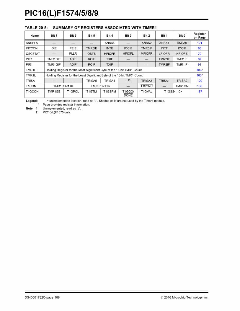
PIC16(L)F1574/5/8/9
DS40001782C-page 188 2016 Microchip Technology Inc.
TABLE 20-5: SUMMARY OF REGISTERS ASSOCIATED WITH TIMER1
Name Bit 7 Bit 6 Bit 5 Bit 4 Bit 3 Bit 2 Bit 1 Bit 0Register on Page
ANSELA — — — ANSA4 — ANSA2 ANSA1 ANSA0 121
INTCON GIE PEIE TMR0IE INTE IOCIE TMR0IF INTF IOCIF 86
OSCSTAT — PLLR OSTS HFIOFR HFIOFL MFIOFR LFIOFR HFIOFS 70
PIE1 TMR1GIE ADIE RCIE TXIE — — TMR2IE TMR1IE 87
PIR1 TMR1GIF ADIF RCIF TXIF — — TMR2IF TMR1IF 91
TMR1H Holding Register for the Most Significant Byte of the 16-bit TMR1 Count 183*
TMR1L Holding Register for the Least Significant Byte of the 16-bit TMR1 Count 183*
TRISA — — TRISA5 TRISA4 —(1) TRISA2 TRISA1 TRISA0 120
T1CON TMR1CS<1:0> T1CKPS<1:0> — T1SYNC — TMR1ON 186
T1GCON TMR1GE T1GPOL T1GTM T1GSPM T1GGO/DONE
T1GVAL T1GSS<1:0> 187
Legend: — = unimplemented location, read as ‘0’. Shaded cells are not used by the Timer1 module.* Page provides register information.
Note 1: Unimplemented, read as ‘1’.2: PIC16(L)F1575 only.

2016 Microchip Technology Inc. DS40001782C-page 189
PIC16(L)F1574/5/8/9
21.0 TIMER2 MODULE
The Timer2 module incorporates the following features:
• 8-bit Timer and Period registers (TMR2 and PR2, respectively)
• Readable and writable (both registers)
• Software programmable prescaler (1:1, 1:4, 1:16, and 1:64)
• Software programmable postscaler (1:1 to 1:16)
• Interrupt on TMR2 match with PR2
See Figure 21-1 for a block diagram of Timer2.
FIGURE 21-1: TIMER2 BLOCK DIAGRAM
FIGURE 21-2: TIMER2 TIMING DIAGRAM
Prescaler1:1, 1:4, 1:16, 1:64Fosc/4
2
T2CKPS<1:0> Comparator Postscaler1:1 to 1:16
4
T2OUTPS<3:0>
set bitTMR2IF
TMR2 R
PR2
T2_matchTo Peripherals
Rev. 10-000019A7/30/2013
0x03
0x00 0x01 0x02 0x03 0x00 0x01 0x02
1:4
Pulse Width(1)
Note 1: The Pulse Width of T2_match is equal to the scaled input of TMR2.
FOSC/4
Prescale
PR2
TMR2
T2_match
Rev. 10-000020A7/30/2013
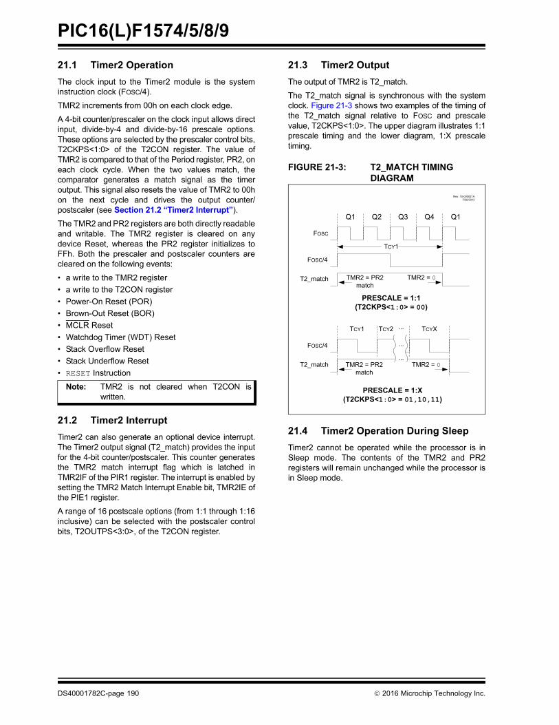
PIC16(L)F1574/5/8/9
DS40001782C-page 190 2016 Microchip Technology Inc.
21.1 Timer2 Operation
The clock input to the Timer2 module is the systeminstruction clock (FOSC/4).
TMR2 increments from 00h on each clock edge.
A 4-bit counter/prescaler on the clock input allows directinput, divide-by-4 and divide-by-16 prescale options.These options are selected by the prescaler control bits,T2CKPS<1:0> of the T2CON register. The value ofTMR2 is compared to that of the Period register, PR2, oneach clock cycle. When the two values match, thecomparator generates a match signal as the timeroutput. This signal also resets the value of TMR2 to 00hon the next cycle and drives the output counter/postscaler (see Section 21.2 “Timer2 Interrupt”).
The TMR2 and PR2 registers are both directly readableand writable. The TMR2 register is cleared on anydevice Reset, whereas the PR2 register initializes toFFh. Both the prescaler and postscaler counters arecleared on the following events:
• a write to the TMR2 register
• a write to the T2CON register
• Power-On Reset (POR)
• Brown-Out Reset (BOR)
• MCLR Reset
• Watchdog Timer (WDT) Reset
• Stack Overflow Reset
• Stack Underflow Reset
• RESET Instruction
21.2 Timer2 Interrupt
Timer2 can also generate an optional device interrupt.The Timer2 output signal (T2_match) provides the inputfor the 4-bit counter/postscaler. This counter generatesthe TMR2 match interrupt flag which is latched inTMR2IF of the PIR1 register. The interrupt is enabled bysetting the TMR2 Match Interrupt Enable bit, TMR2IE ofthe PIE1 register.
A range of 16 postscale options (from 1:1 through 1:16inclusive) can be selected with the postscaler controlbits, T2OUTPS<3:0>, of the T2CON register.
21.3 Timer2 Output
The output of TMR2 is T2_match.
The T2_match signal is synchronous with the systemclock. Figure 21-3 shows two examples of the timing ofthe T2_match signal relative to FOSC and prescalevalue, T2CKPS<1:0>. The upper diagram illustrates 1:1prescale timing and the lower diagram, 1:X prescaletiming.
FIGURE 21-3: T2_MATCH TIMING DIAGRAM
21.4 Timer2 Operation During Sleep
Timer2 cannot be operated while the processor is inSleep mode. The contents of the TMR2 and PR2registers will remain unchanged while the processor isin Sleep mode.
Note: TMR2 is not cleared when T2CON iswritten.
T2_match
FOSC/4
TMR2 = PR2match
TMR2 = 0
...
PRESCALE = 1:X(T2CKPS<1:0> = 01,10,11)
TCY1 TCY2 TCYX...
...
Q1 Q2 Q3
FOSC
TMR2 = PR2match
TMR2 = 0
Q1Q4
T2_match
FOSC/4
PRESCALE = 1:1(T2CKPS<1:0> = 00)
TCY1
Rev. 10-000021A7/30/2013

2016 Microchip Technology Inc. DS40001782C-page 191
PIC16(L)F1574/5/8/9
21.5 Register Definitions: Timer2 Control
TABLE 21-1: SUMMARY OF REGISTERS ASSOCIATED WITH TIMER2
REGISTER 21-1: T2CON: TIMER2 CONTROL REGISTER
U-0 R/W-0/0 R/W-0/0 R/W-0/0 R/W-0/0 R/W-0/0 R/W-0/0 R/W-0/0
— T2OUTPS<3:0> TMR2ON T2CKPS<1:0>
bit 7 bit 0
Legend:
R = Readable bit W = Writable bit U = Unimplemented bit, read as ‘0’
u = Bit is unchanged x = Bit is unknown -n/n = Value at POR and BOR/Value at all other Resets
‘1’ = Bit is set ‘0’ = Bit is cleared
bit 7 Unimplemented: Read as ‘0’
bit 6-3 T2OUTPS<3:0>: Timer2 Output Postscaler Select bits
0000 = 1:1 Postscaler0001 = 1:2 Postscaler0010 = 1:3 Postscaler0011 = 1:4 Postscaler0100 = 1:5 Postscaler0101 = 1:6 Postscaler0110 = 1:7 Postscaler0111 = 1:8 Postscaler1000 = 1:9 Postscaler1001 = 1:10 Postscaler1010 = 1:11 Postscaler1011 = 1:12 Postscaler1100 = 1:13 Postscaler1101 = 1:14 Postscaler1110 = 1:15 Postscaler1111 = 1:16 Postscaler
bit 2 TMR2ON: Timer2 On bit
1 = Timer2 is on0 = Timer2 is off
bit 1-0 T2CKPS<1:0>: Timer2 Clock Prescale Select bits
00 = Prescaler is 101 = Prescaler is 410 = Prescaler is 1611 = Prescaler is 64
Name Bit 7 Bit 6 Bit 5 Bit 4 Bit 3 Bit 2 Bit 1 Bit 0Register on Page
INTCON GIE PEIE TMR0IE INTE IOCIE TMR0IF INTF IOCIF 86
PIE1 TMR1GIE ADIE RCIE TXIE — — TMR2IE TMR1IE 87
PIR1 TMR1GIF ADIF RCIF TXIF — — TMR2IF TMR1IF 90
PR2 Timer2 Module Period Register 189*
T2CON — T2OUTPS<3:0> TMR2ON T2CKPS<1:0> 191
TMR2 Holding Register for the 8-bit TMR2 Count 189*
Legend: — = unimplemented location, read as ‘0’. Shaded cells are not used for Timer2 module.* Page provides register information.
Note 1: PIC16(L)F1575 only.
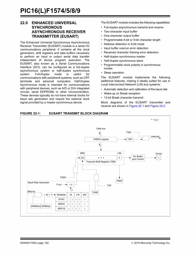
PIC16(L)F1574/5/8/9
DS40001782C-page 192 2016 Microchip Technology Inc.
22.0 ENHANCED UNIVERSAL SYNCHRONOUS ASYNCHRONOUS RECEIVER TRANSMITTER (EUSART)
The Enhanced Universal Synchronous AsynchronousReceiver Transmitter (EUSART) module is a serial I/Ocommunications peripheral. It contains all the clockgenerators, shift registers and data buffers necessaryto perform an input or output serial data transferindependent of device program execution. TheEUSART, also known as a Serial CommunicationsInterface (SCI), can be configured as a full-duplexasynchronous system or half-duplex synchronoussystem. Full-Duplex mode is useful forcommunications with peripheral systems, such as CRTterminals and personal computers. Half-DuplexSynchronous mode is intended for communicationswith peripheral devices, such as A/D or D/A integratedcircuits, serial EEPROMs or other microcontrollers.These devices typically do not have internal clocks forbaud rate generation and require the external clocksignal provided by a master synchronous device.
The EUSART module includes the following capabilities:
• Full-duplex asynchronous transmit and receive
• Two-character input buffer
• One-character output buffer
• Programmable 8-bit or 9-bit character length
• Address detection in 9-bit mode
• Input buffer overrun error detection
• Received character framing error detection
• Half-duplex synchronous master
• Half-duplex synchronous slave
• Programmable clock polarity in synchronous modes
• Sleep operation
The EUSART module implements the followingadditional features, making it ideally suited for use inLocal Interconnect Network (LIN) bus systems:
• Automatic detection and calibration of the baud rate
• Wake-up on Break reception
• 13-bit Break character transmit
Block diagrams of the EUSART transmitter andreceiver are shown in Figure 22-1 and Figure 22-2.
FIGURE 22-1: EUSART TRANSMIT BLOCK DIAGRAM
TXREG register
8
Pin Buffer and Control
TXIF
TRMT
TX9D
Data bus
8 TXIE
Interrupt
TX/CK
TX9
TXEN
Transmit Shift Register (TSR)
(8) 0
MSb LSb
÷ n
Multiplier x4
SYNC
BRGH
BRG16
x16 x64
1
1
1
1
1
x
x
x 0
0
0
0
0
0
0
n
+ 1
SPBRGH SPBRGL
Baud Rate GeneratorFOSC
BRG16
Rev. 10-000113B7/14/2015
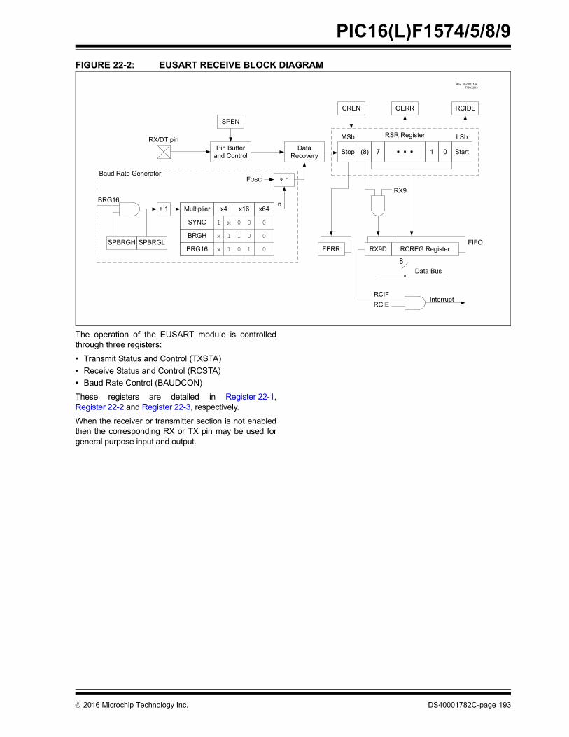
2016 Microchip Technology Inc. DS40001782C-page 193
PIC16(L)F1574/5/8/9
FIGURE 22-2: EUSART RECEIVE BLOCK DIAGRAM
The operation of the EUSART module is controlledthrough three registers:
• Transmit Status and Control (TXSTA)
• Receive Status and Control (RCSTA)
• Baud Rate Control (BAUDCON)
These registers are detailed in Register 22-1,Register 22-2 and Register 22-3, respectively.
When the receiver or transmitter section is not enabledthen the corresponding RX or TX pin may be used forgeneral purpose input and output.
÷ n
Multiplier x4
SYNC
BRGH
BRG16
x16 x64
1
1
1
1
1
x
x
x 0
0
0
0
0
0
0
n+ 1
SPBRGH SPBRGL
Baud Rate GeneratorFOSC
BRG16
SPEN
CREN OERR RCIDL
Pin Bufferand Control
DataRecovery
RX/DT pin
Stop (8) 7 Start01
MSb LSbRSR Register
RX9
FERR RX9D RCREG RegisterFIFO
8Data Bus
RCIERCIF
Interrupt
Rev. 10-000114A7/30/2013

PIC16(L)F1574/5/8/9
DS40001782C-page 194 2016 Microchip Technology Inc.
22.1 EUSART Asynchronous Mode
The EUSART transmits and receives data using thestandard non-return-to-zero (NRZ) format. NRZ isimplemented with two levels: a VOH Mark state whichrepresents a ‘1’ data bit, and a VOL Space state whichrepresents a ‘0’ data bit. NRZ refers to the fact thatconsecutively transmitted data bits of the same valuestay at the output level of that bit without returning to aneutral level between each bit transmission. An NRZtransmission port idles in the Mark state. Each charactertransmission consists of one Start bit followed by eightor nine data bits and is always terminated by one ormore Stop bits. The Start bit is always a space and theStop bits are always marks. The most common dataformat is eight bits. Each transmitted bit persists for aperiod of 1/(Baud Rate). An on-chip dedicated8-bit/16-bit Baud Rate Generator is used to derivestandard baud rate frequencies from the systemoscillator. See Table 22-5 for examples of baud rateconfigurations.
The EUSART transmits and receives the LSb first. TheEUSART’s transmitter and receiver are functionallyindependent, but share the same data format and baudrate. Parity is not supported by the hardware, but canbe implemented in software and stored as the ninthdata bit.
22.1.1 EUSART ASYNCHRONOUS TRANSMITTER
The EUSART transmitter block diagram is shown inFigure 22-1. The heart of the transmitter is the serialTransmit Shift Register (TSR), which is not directlyaccessible by software. The TSR obtains its data fromthe transmit buffer, which is the TXREG register.
22.1.1.1 Enabling the Transmitter
The EUSART transmitter is enabled for asynchronousoperations by configuring the following three controlbits:
• TXEN = 1
• SYNC = 0
• SPEN = 1
All other EUSART control bits are assumed to be intheir default state.
Setting the TXEN bit of the TXSTA register enables thetransmitter circuitry of the EUSART. Clearing the SYNCbit of the TXSTA register configures the EUSART forasynchronous operation. Setting the SPEN bit of theRCSTA register enables the EUSART and automaticallyconfigures the TX/CK I/O pin as an output. If the TX/CKpin is shared with an analog peripheral, the analog I/Ofunction must be disabled by clearing the correspondingANSEL bit.
22.1.1.2 Transmitting Data
A transmission is initiated by writing a character to theTXREG register. If this is the first character, or theprevious character has been completely flushed fromthe TSR, the data in the TXREG is immediatelytransferred to the TSR register. If the TSR still containsall or part of a previous character, the new characterdata is held in the TXREG until the Stop bit of theprevious character has been transmitted. The pendingcharacter in the TXREG is then transferred to the TSRin one TCY immediately following the Stop bittransmission. The transmission of the Start bit, data bitsand Stop bit sequence commences immediatelyfollowing the transfer of the data to the TSR from theTXREG.
22.1.1.3 Transmit Data Polarity
The polarity of the transmit data can be controlled withthe SCKP bit of the BAUDCON register. The defaultstate of this bit is ‘0’ which selects high true transmit idleand data bits. Setting the SCKP bit to ‘1’ will invert thetransmit data resulting in low true idle and data bits. TheSCKP bit controls transmit data polarity inAsynchronous mode only. In Synchronous mode, theSCKP bit has a different function. See Section22.5.1.2 “Clock Polarity”.
22.1.1.4 Transmit Interrupt Flag
The TXIF interrupt flag bit of the PIR1 register is setwhenever the EUSART transmitter is enabled and nocharacter is being held for transmission in the TXREG.In other words, the TXIF bit is only clear when the TSRis busy with a character and a new character has beenqueued for transmission in the TXREG. The TXIF flag bitis not cleared immediately upon writing TXREG. TXIFbecomes valid in the second instruction cycle followingthe write execution. Polling TXIF immediately followingthe TXREG write will return invalid results. The TXIF bitis read-only, it cannot be set or cleared by software.
The TXIF interrupt can be enabled by setting the TXIEinterrupt enable bit of the PIE1 register. However, theTXIF flag bit will be set whenever the TXREG is empty,regardless of the state of TXIE enable bit.
To use interrupts when transmitting data, set the TXIEbit only when there is more data to send. Clear theTXIE interrupt enable bit upon writing the last characterof the transmission to the TXREG.
Note: The TXIF Transmitter Interrupt flag is setwhen the TXEN enable bit is set.

2016 Microchip Technology Inc. DS40001782C-page 195
PIC16(L)F1574/5/8/9
22.1.1.5 TSR Status
The TRMT bit of the TXSTA register indicates thestatus of the TSR register. This is a read-only bit. TheTRMT bit is set when the TSR register is empty and iscleared when a character is transferred to the TSRregister from the TXREG. The TRMT bit remains clearuntil all bits have been shifted out of the TSR register.No interrupt logic is tied to this bit, so the user has topoll this bit to determine the TSR status.
22.1.1.6 Transmitting 9-Bit Characters
The EUSART supports 9-bit character transmissions.When the TX9 bit of the TXSTA register is set, theEUSART will shift nine bits out for each character trans-mitted. The TX9D bit of the TXSTA register is the ninth,and Most Significant, data bit. When transmitting 9-bitdata, the TX9D data bit must be written before writingthe eight Least Significant bits into the TXREG. All ninebits of data will be transferred to the TSR shift registerimmediately after the TXREG is written.
A special 9-bit Address mode is available for use withmultiple receivers. See Section 22.1.2.7 “AddressDetection” for more information on the address mode.
22.1.1.7 Asynchronous Transmission Set-up:
1. Initialize the SPBRGH, SPBRGL register pair andthe BRGH and BRG16 bits to achieve the desiredbaud rate (see Section 22.4 “EUSART BaudRate Generator (BRG)”).
2. Enable the asynchronous serial port by clearingthe SYNC bit and setting the SPEN bit.
3. If 9-bit transmission is desired, set the TX9control bit. A set ninth data bit will indicate thatthe eight Least Significant data bits are anaddress when the receiver is set for addressdetection.
4. Set SCKP bit if inverted transmit is desired.
5. Enable the transmission by setting the TXENcontrol bit. This will cause the TXIF interrupt bitto be set.
6. If interrupts are desired, set the TXIE interruptenable bit of the PIE1 register. An interrupt willoccur immediately provided that the GIE andPEIE bits of the INTCON register are also set.
7. If 9-bit transmission is selected, the ninth bitshould be loaded into the TX9D data bit.
8. Load 8-bit data into the TXREG register. Thiswill start the transmission.
FIGURE 22-3: ASYNCHRONOUS TRANSMISSION
FIGURE 22-4: ASYNCHRONOUS TRANSMISSION (BACK-TO-BACK)
Note: The TSR register is not mapped in datamemory, so it is not available to the user.
Word 1Stop bit
Word 1Transmit Shift Reg.
Start bit bit 0 bit 1 bit 7/8
Write to TXREGWord 1
BRG Output(Shift Clock)
TX/CK
TXIF bit(Transmit Buffer
Reg. Empty Flag)
TRMT bit(Transmit Shift
Reg. Empty Flag)
1 TCY
pin
Transmit Shift Reg.
Write to TXREG
BRG Output(Shift Clock)
TX/CK
TRMT bit(Transmit Shift
Reg. Empty Flag)
Word 1 Word 2
Word 1 Word 2
Start bit Stop bit Start bit
Transmit Shift Reg.
Word 1 Word 2bit 0 bit 1 bit 7/8 bit 0
Note: This timing diagram shows two consecutive transmissions.
1 TCY
1 TCY
pin
TXIF bit(Transmit Buffer
Reg. Empty Flag)
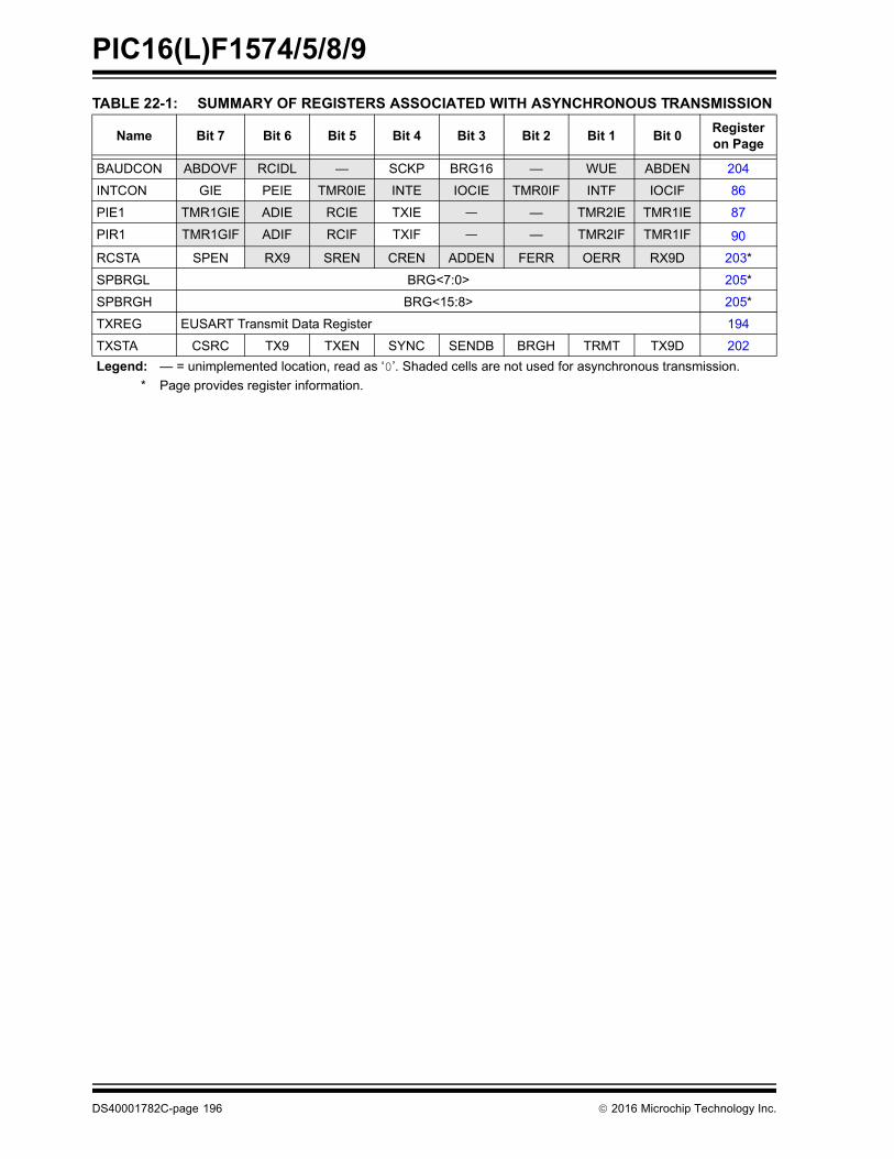
PIC16(L)F1574/5/8/9
DS40001782C-page 196 2016 Microchip Technology Inc.
TABLE 22-1: SUMMARY OF REGISTERS ASSOCIATED WITH ASYNCHRONOUS TRANSMISSION
Name Bit 7 Bit 6 Bit 5 Bit 4 Bit 3 Bit 2 Bit 1 Bit 0Register on Page
BAUDCON ABDOVF RCIDL — SCKP BRG16 — WUE ABDEN 204
INTCON GIE PEIE TMR0IE INTE IOCIE TMR0IF INTF IOCIF 86
PIE1 TMR1GIE ADIE RCIE TXIE — — TMR2IE TMR1IE 87
PIR1 TMR1GIF ADIF RCIF TXIF — — TMR2IF TMR1IF 90
RCSTA SPEN RX9 SREN CREN ADDEN FERR OERR RX9D 203*
SPBRGL BRG<7:0> 205*
SPBRGH BRG<15:8> 205*
TXREG EUSART Transmit Data Register 194
TXSTA CSRC TX9 TXEN SYNC SENDB BRGH TRMT TX9D 202
Legend: — = unimplemented location, read as ‘0’. Shaded cells are not used for asynchronous transmission.
* Page provides register information.
2016 Microchip Technology Inc. DS40001782C-page 197
PIC16(L)F1574/5/8/9
22.1.2 EUSART ASYNCHRONOUS RECEIVER
The Asynchronous mode is typically used in RS-232systems. The receiver block diagram is shown inFigure 22-2. The data is received on the RX/DT pin anddrives the data recovery block. The data recovery blockis actually a high-speed shifter operating at 16 timesthe baud rate, whereas the serial Receive ShiftRegister (RSR) operates at the bit rate. When all eightor nine bits of the character have been shifted in, theyare immediately transferred to a two characterFirst-In-First-Out (FIFO) memory. The FIFO bufferingallows reception of two complete characters and thestart of a third character before software must startservicing the EUSART receiver. The FIFO and RSRregisters are not directly accessible by software.Access to the received data is via the RCREG register.
22.1.2.1 Enabling the Receiver
The EUSART receiver is enabled for asynchronousoperation by configuring the following three control bits:
• CREN = 1
• SYNC = 0
• SPEN = 1
All other EUSART control bits are assumed to be intheir default state.
Setting the CREN bit of the RCSTA register enables thereceiver circuitry of the EUSART. Clearing the SYNC bitof the TXSTA register configures the EUSART forasynchronous operation. Setting the SPEN bit of theRCSTA register enables the EUSART. The programmermust set the corresponding TRIS bit to configure theRX/DT I/O pin as an input.
22.1.2.2 Receiving Data
The receiver data recovery circuit initiates characterreception on the falling edge of the first bit. The first bit,also known as the Start bit, is always a zero. The datarecovery circuit counts one-half bit time to the center ofthe Start bit and verifies that the bit is still a zero. If it isnot a zero then the data recovery circuit abortscharacter reception, without generating an error, andresumes looking for the falling edge of the Start bit. Ifthe Start bit zero verification succeeds then the datarecovery circuit counts a full bit time to the center of thenext bit. The bit is then sampled by a majority detectcircuit and the resulting ‘0’ or ‘1’ is shifted into the RSR.This repeats until all data bits have been sampled andshifted into the RSR. One final bit time is measured andthe level sampled. This is the Stop bit, which is alwaysa ‘1’. If the data recovery circuit samples a ‘0’ in theStop bit position then a framing error is set for thischaracter, otherwise the framing error is cleared for thischaracter. See Section 22.1.2.4 “Receive FramingError” for more information on framing errors.
Immediately after all data bits and the Stop bit havebeen received, the character in the RSR is transferredto the EUSART receive FIFO and the RCIF interruptflag bit of the PIR1 register is set. The top character inthe FIFO is transferred out of the FIFO by reading theRCREG register.
22.1.2.3 Receive Interrupts
The RCIF interrupt flag bit of the PIR1 register is setwhenever the EUSART receiver is enabled and there isan unread character in the receive FIFO. The RCIFinterrupt flag bit is read-only, it cannot be set or clearedby software.
RCIF interrupts are enabled by setting all of thefollowing bits:
• RCIE, Interrupt Enable bit of the PIE1 register
• PEIE, Peripheral Interrupt Enable bit of the INTCON register
• GIE, Global Interrupt Enable bit of the INTCON register
The RCIF interrupt flag bit will be set when there is anunread character in the FIFO, regardless of the state ofinterrupt enable bits.
Note: If the RX/DT function is on an analog pin,the corresponding ANSEL bit must becleared for the receiver to function.
Note: If the receive FIFO is overrun, no additionalcharacters will be received until the overruncondition is cleared. See Section22.1.2.5 “Receive Overrun Error” formore information on overrun errors.
PIC16(L)F1574/5/8/9
DS40001782C-page 198 2016 Microchip Technology Inc.
22.1.2.4 Receive Framing Error
Each character in the receive FIFO buffer has acorresponding framing error Status bit. A framing errorindicates that a Stop bit was not seen at the expectedtime. The framing error status is accessed via theFERR bit of the RCSTA register. The FERR bitrepresents the status of the top unread character in thereceive FIFO. Therefore, the FERR bit must be readbefore reading the RCREG.
The FERR bit is read-only and only applies to the topunread character in the receive FIFO. A framing error(FERR = 1) does not preclude reception of additionalcharacters. It is not necessary to clear the FERR bit.Reading the next character from the FIFO buffer willadvance the FIFO to the next character and the nextcorresponding framing error.
The FERR bit can be forced clear by clearing the SPENbit of the RCSTA register which resets the EUSART.Clearing the CREN bit of the RCSTA register does notaffect the FERR bit. A framing error by itself does notgenerate an interrupt.
22.1.2.5 Receive Overrun Error
The receive FIFO buffer can hold two characters. Anoverrun error will be generated if a third character, in itsentirety, is received before the FIFO is accessed. Whenthis happens the OERR bit of the RCSTA register is set.The characters already in the FIFO buffer can be readbut no additional characters will be received until theerror is cleared. The error must be cleared by eitherclearing the CREN bit of the RCSTA register or byresetting the EUSART by clearing the SPEN bit of theRCSTA register.
22.1.2.6 Receiving 9-bit Characters
The EUSART supports 9-bit character reception. Whenthe RX9 bit of the RCSTA register is set the EUSARTwill shift nine bits into the RSR for each characterreceived. The RX9D bit of the RCSTA register is theninth and Most Significant data bit of the top unreadcharacter in the receive FIFO. When reading 9-bit datafrom the receive FIFO buffer, the RX9D data bit mustbe read before reading the eight Least Significant bitsfrom the RCREG.
22.1.2.7 Address Detection
A special Address Detection mode is available for usewhen multiple receivers share the same transmissionline, such as in RS-485 systems. Address detection isenabled by setting the ADDEN bit of the RCSTAregister.
Address detection requires 9-bit character reception.When address detection is enabled, only characterswith the ninth data bit set will be transferred to thereceive FIFO buffer, thereby setting the RCIF interruptbit. All other characters will be ignored.
Upon receiving an address character, user softwaredetermines if the address matches its own. Uponaddress match, user software must disable addressdetection by clearing the ADDEN bit before the nextStop bit occurs. When user software detects the end ofthe message, determined by the message protocolused, software places the receiver back into theAddress Detection mode by setting the ADDEN bit.
Note: If all receive characters in the receiveFIFO have framing errors, repeated readsof the RCREG will not clear the FERR bit.
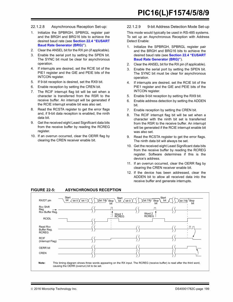
2016 Microchip Technology Inc. DS40001782C-page 199
PIC16(L)F1574/5/8/9
22.1.2.8 Asynchronous Reception Set-up:
1. Initialize the SPBRGH, SPBRGL register pairand the BRGH and BRG16 bits to achieve thedesired baud rate (see Section 22.4 “EUSARTBaud Rate Generator (BRG)”).
2. Clear the ANSEL bit for the RX pin (if applicable).
3. Enable the serial port by setting the SPEN bit.The SYNC bit must be clear for asynchronousoperation.
4. If interrupts are desired, set the RCIE bit of thePIE1 register and the GIE and PEIE bits of theINTCON register.
5. If 9-bit reception is desired, set the RX9 bit.
6. Enable reception by setting the CREN bit.
7. The RCIF interrupt flag bit will be set when acharacter is transferred from the RSR to thereceive buffer. An interrupt will be generated ifthe RCIE interrupt enable bit was also set.
8. Read the RCSTA register to get the error flagsand, if 9-bit data reception is enabled, the ninthdata bit.
9. Get the received eight Least Significant data bitsfrom the receive buffer by reading the RCREGregister.
10. If an overrun occurred, clear the OERR flag byclearing the CREN receiver enable bit.
22.1.2.9 9-bit Address Detection Mode Set-up
This mode would typically be used in RS-485 systems.To set up an Asynchronous Reception with AddressDetect Enable:
1. Initialize the SPBRGH, SPBRGL register pairand the BRGH and BRG16 bits to achieve thedesired baud rate (see Section 22.4 “EUSARTBaud Rate Generator (BRG)”).
2. Clear the ANSEL bit for the RX pin (if applicable).
3. Enable the serial port by setting the SPEN bit.The SYNC bit must be clear for asynchronousoperation.
4. If interrupts are desired, set the RCIE bit of thePIE1 register and the GIE and PEIE bits of theINTCON register.
5. Enable 9-bit reception by setting the RX9 bit.
6. Enable address detection by setting the ADDENbit.
7. Enable reception by setting the CREN bit.
8. The RCIF interrupt flag bit will be set when acharacter with the ninth bit set is transferredfrom the RSR to the receive buffer. An interruptwill be generated if the RCIE interrupt enable bitwas also set.
9. Read the RCSTA register to get the error flags.The ninth data bit will always be set.
10. Get the received eight Least Significant data bitsfrom the receive buffer by reading the RCREGregister. Software determines if this is thedevice’s address.
11. If an overrun occurred, clear the OERR flag byclearing the CREN receiver enable bit.
12. If the device has been addressed, clear theADDEN bit to allow all received data into thereceive buffer and generate interrupts.
FIGURE 22-5: ASYNCHRONOUS RECEPTION
Startbit bit 7/8bit 1bit 0 bit 7/8 bit 0Stop
bit
Startbit
Startbitbit 7/8 Stop
bitRX/DT pin
RegRcv Buffer Reg.
Rcv Shift
Read RcvBuffer Reg.RCREG
RCIF(Interrupt Flag)
OERR bit
CREN
Word 1RCREG
Word 2RCREG
Stopbit
Note: This timing diagram shows three words appearing on the RX input. The RCREG (receive buffer) is read after the third word,causing the OERR (overrun) bit to be set.
RCIDL

PIC16(L)F1574/5/8/9
DS40001782C-page 200 2016 Microchip Technology Inc.
TABLE 22-2: SUMMARY OF REGISTERS ASSOCIATED WITH ASYNCHRONOUS RECEPTION
Name Bit 7 Bit 6 Bit 5 Bit 4 Bit 3 Bit 2 Bit 1 Bit 0Register on Page
BAUDCON ABDOVF RCIDL — SCKP BRG16 — WUE ABDEN 204
INTCON GIE PEIE TMR0IE INTE IOCIE TMR0IF INTF IOCIF 86
PIE1 TMR1GIE ADIE RCIE TXIE — — TMR2IE TMR1IE 87
PIR1 TMR1GIF ADIF RCIF TXIF — — TMR2IF TMR1IF 90
RCREG EUSART Receive Data Register 197*
RCSTA SPEN RX9 SREN CREN ADDEN FERR OERR RX9D 203*
SPBRGL BRG<7:0> 205*
SPBRGH BRG<15:8> 205*
TXSTA CSRC TX9 TXEN SYNC SENDB BRGH TRMT TX9D 202
Legend: — = unimplemented location, read as ‘0’. Shaded cells are not used for asynchronous reception.
* Page provides register information.
2016 Microchip Technology Inc. DS40001782C-page 201
PIC16(L)F1574/5/8/9
22.2 Clock Accuracy with Asynchronous Operation
The factory calibrates the internal oscillator blockoutput (INTOSC). However, the INTOSC frequencymay drift as VDD or temperature changes, and thisdirectly affects the asynchronous baud rate.
The Auto-Baud Detect feature (see Section22.4.1 “Auto-Baud Detect”) can be used tocompensate for changes in the INTOSC frequency.
There may not be fine enough resolution whenadjusting the Baud Rate Generator to compensate fora gradual change in the peripheral clock frequency.

PIC16(L)F1574/5/8/9
DS40001782C-page 202 2016 Microchip Technology Inc.
22.3 Register Definitions: EUSART Control
REGISTER 22-1: TXSTA: TRANSMIT STATUS AND CONTROL REGISTER
R/W-/0 R/W-0/0 R/W-0/0 R/W-0/0 R/W-0/0 R/W-0/0 R-1/1 R/W-0/0
CSRC TX9 TXEN(1) SYNC SENDB BRGH TRMT TX9D
bit 7 bit 0
Legend:
R = Readable bit W = Writable bit U = Unimplemented bit, read as ‘0’
u = Bit is unchanged x = Bit is unknown -n/n = Value at POR and BOR/Value at all other Resets
‘1’ = Bit is set ‘0’ = Bit is cleared
bit 7 CSRC: Clock Source Select bitAsynchronous mode: Don’t careSynchronous mode: 1 = Master mode (clock generated internally from BRG)0 = Slave mode (clock from external source)
bit 6 TX9: 9-bit Transmit Enable bit1 = Selects 9-bit transmission0 = Selects 8-bit transmission
bit 5 TXEN: Transmit Enable bit(1)
1 = Transmit enabled0 = Transmit disabled
bit 4 SYNC: EUSART Mode Select bit 1 = Synchronous mode 0 = Asynchronous mode
bit 3 SENDB: Send Break Character bitAsynchronous mode:1 = Send Sync Break on next transmission (cleared by hardware upon completion)0 = Sync Break transmission completedSynchronous mode:Don’t care
bit 2 BRGH: High Baud Rate Select bitAsynchronous mode: 1 = High speed 0 = Low speedSynchronous mode: Unused in this mode
bit 1 TRMT: Transmit Shift Register Status bit1 = TSR empty 0 = TSR full
bit 0 TX9D: Ninth bit of Transmit DataCan be address/data bit or a parity bit.
Note 1: SREN/CREN overrides TXEN in Sync mode.
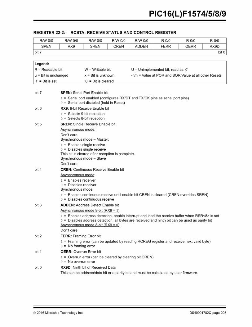
2016 Microchip Technology Inc. DS40001782C-page 203
PIC16(L)F1574/5/8/9
REGISTER 22-2: RCSTA: RECEIVE STATUS AND CONTROL REGISTER
R/W-0/0 R/W-0/0 R/W-0/0 R/W-0/0 R/W-0/0 R-0/0 R-0/0 R-0/0
SPEN RX9 SREN CREN ADDEN FERR OERR RX9D
bit 7 bit 0
Legend:
R = Readable bit W = Writable bit U = Unimplemented bit, read as ‘0’
u = Bit is unchanged x = Bit is unknown -n/n = Value at POR and BOR/Value at all other Resets
‘1’ = Bit is set ‘0’ = Bit is cleared
bit 7 SPEN: Serial Port Enable bit
1 = Serial port enabled (configures RX/DT and TX/CK pins as serial port pins)0 = Serial port disabled (held in Reset)
bit 6 RX9: 9-bit Receive Enable bit
1 = Selects 9-bit reception0 = Selects 8-bit reception
bit 5 SREN: Single Receive Enable bit
Asynchronous mode:
Don’t careSynchronous mode – Master:
1 = Enables single receive0 = Disables single receiveThis bit is cleared after reception is complete.Synchronous mode – Slave
Don’t care
bit 4 CREN: Continuous Receive Enable bit
Asynchronous mode:
1 = Enables receiver0 = Disables receiverSynchronous mode:
1 = Enables continuous receive until enable bit CREN is cleared (CREN overrides SREN)0 = Disables continuous receive
bit 3 ADDEN: Address Detect Enable bit
Asynchronous mode 9-bit (RX9 = 1):
1 = Enables address detection, enable interrupt and load the receive buffer when RSR<8> is set0 = Disables address detection, all bytes are received and ninth bit can be used as parity bitAsynchronous mode 8-bit (RX9 = 0):
Don’t care
bit 2 FERR: Framing Error bit
1 = Framing error (can be updated by reading RCREG register and receive next valid byte)0 = No framing error
bit 1 OERR: Overrun Error bit
1 = Overrun error (can be cleared by clearing bit CREN) 0 = No overrun error
bit 0 RX9D: Ninth bit of Received Data
This can be address/data bit or a parity bit and must be calculated by user firmware.

PIC16(L)F1574/5/8/9
DS40001782C-page 204 2016 Microchip Technology Inc.
REGISTER 22-3: BAUDCON: BAUD RATE CONTROL REGISTER
R/W-0/0 R-1/1 U-0 R/W-0/0 R/W-0/0 U-0 R/W-0/0 R/W-0/0
ABDOVF RCIDL — SCKP BRG16 — WUE ABDEN
bit 7 bit 0
Legend:
R = Readable bit W = Writable bit U = Unimplemented bit, read as ‘0’
u = Bit is unchanged x = Bit is unknown -n/n = Value at POR and BOR/Value at all other Resets
‘1’ = Bit is set ‘0’ = Bit is cleared
bit 7 ABDOVF: Auto-Baud Detect Overflow bit
Asynchronous mode:1 = Auto-baud timer overflowed0 = Auto-baud timer did not overflowSynchronous mode:Don’t care
bit 6 RCIDL: Receive Idle Flag bit
Asynchronous mode:1 = Receiver is idle0 = Start bit has been received and the receiver is receivingSynchronous mode:Don’t care
bit 5 Unimplemented: Read as ‘0’
bit 4 SCKP: Synchronous Clock Polarity Select bit
Asynchronous mode:
1 = Transmit inverted data to the TX/CK pin0 = Transmit non-inverted data to the TX/CK pin
Synchronous mode:1 = Data is clocked on rising edge of the clock0 = Data is clocked on falling edge of the clock
bit 3 BRG16: 16-bit Baud Rate Generator bit
1 = 16-bit Baud Rate Generator is used0 = 8-bit Baud Rate Generator is used
bit 2 Unimplemented: Read as ‘0’
bit 1 WUE: Wake-up Enable bit
Asynchronous mode:
1 = Receiver is waiting for a falling edge. No character will be received, RCIF bit will be set. WUE willautomatically clear after RCIF is set.
0 = Receiver is operating normallySynchronous mode:
Don’t care
bit 0 ABDEN: Auto-Baud Detect Enable bit
Asynchronous mode:
1 = Auto-Baud Detect mode is enabled (clears when auto-baud is complete)0 = Auto-Baud Detect mode is disabledSynchronous mode:Don’t care

2016 Microchip Technology Inc. DS40001782C-page 205
PIC16(L)F1574/5/8/9
22.4 EUSART Baud Rate Generator (BRG)
The Baud Rate Generator (BRG) is an 8-bit or 16-bittimer that is dedicated to the support of both theasynchronous and synchronous EUSART operation.By default, the BRG operates in 8-bit mode. Setting theBRG16 bit of the BAUDCON register selects 16-bitmode.
The SPBRGH, SPBRGL register pair determines theperiod of the free running baud rate timer. InAsynchronous mode the multiplier of the baud rateperiod is determined by both the BRGH bit of the TXSTAregister and the BRG16 bit of the BAUDCON register. InSynchronous mode, the BRGH bit is ignored.
Table 22-3 contains the formulas for determining thebaud rate. Example 22-1 provides a sample calculationfor determining the baud rate and baud rate error.
Typical baud rates and error values for variousAsynchronous modes have been computed for yourconvenience and are shown in Table 22-3. It may beadvantageous to use the high baud rate (BRGH = 1),or the 16-bit BRG (BRG16 = 1) to reduce the baud rateerror. The 16-bit BRG mode is used to achieve slowbaud rates for fast oscillator frequencies.
Writing a new value to the SPBRGH, SPBRGL registerpair causes the BRG timer to be reset (or cleared). Thisensures that the BRG does not wait for a timer overflowbefore outputting the new baud rate.
If the system clock is changed during an active receiveoperation, a receive error or data loss may result. Toavoid this problem, check the status of the RCIDL bit tomake sure that the receive operation is idle beforechanging the system clock.
EXAMPLE 22-1: CALCULATING BAUD RATE ERROR
For a device with FOSC of 16 MHz, desired baud rateof 9600, Asynchronous mode, 8-bit BRG:
Solving for SPBRGH:SPBRGL:
X
FOSC
Desired Baud Rate---------------------------------------------
64--------------------------------------------- 1–=
Desired Baud Rate FOSC
64 [SPBRGH:SPBRGL] 1+ ------------------------------------------------------------------------=
160000009600
------------------------
64------------------------ 1–=
25.042 25= =
Calculated Baud Rate 16000000
64 25 1+ ---------------------------=
9615=
ErrorCalc. Baud Rate Desired Baud Rate –
Desired Baud Rate --------------------------------------------------------------------------------------------=
9615 9600–
9600---------------------------------- 0.16%= =

PIC16(L)F1574/5/8/9
DS40001782C-page 206 2016 Microchip Technology Inc.
TABLE 22-3: BAUD RATE FORMULAS
TABLE 22-4: SUMMARY OF REGISTERS ASSOCIATED WITH THE BAUD RATE GENERATOR
Configuration BitsBRG/EUSART Mode Baud Rate Formula
SYNC BRG16 BRGH
0 0 0 8-bit/Asynchronous FOSC/[64 (n+1)]
0 0 1 8-bit/AsynchronousFOSC/[16 (n+1)]
0 1 0 16-bit/Asynchronous
0 1 1 16-bit/Asynchronous
FOSC/[4 (n+1)]1 0 x 8-bit/Synchronous
1 1 x 16-bit/Synchronous
Legend: x = Don’t care, n = value of SPBRGH, SPBRGL register pair.
Name Bit 7 Bit 6 Bit 5 Bit 4 Bit 3 Bit 2 Bit 1 Bit 0Register on Page
BAUDCON ABDOVF RCIDL — SCKP BRG16 — WUE ABDEN 204
RCSTA SPEN RX9 SREN CREN ADDEN FERR OERR RX9D 203
SPBRGL BRG<7:0> 205*
SPBRGH BRG<15:8> 205*
TXSTA CSRC TX9 TXEN SYNC SENDB BRGH TRMT TX9D 202
Legend: — = unimplemented location, read as ‘0’. Shaded cells are not used for the Baud Rate Generator.
* Page provides register information.

2016 Microchip Technology Inc. DS40001782C-page 207
PIC16(L)F1574/5/8/9
TABLE 22-5: BAUD RATES FOR ASYNCHRONOUS MODES
BAUDRATE
SYNC = 0, BRGH = 0, BRG16 = 0
FOSC = 20.000 MHz FOSC = 18.432 MHz FOSC = 16.000 MHz FOSC = 11.0592 MHz
ActualRate
%Error
SPBRGvalue
(decimal)
ActualRate
%Error
SPBRGvalue
(decimal)
ActualRate
%Error
SPBRGvalue
(decimal)
ActualRate
%Error
SPBRGvalue
(decimal)
300 — — — — — — — — — — — —
1200 1221 1.73 255 1200 0.00 239 1202 0.16 207 1200 0.00 143
2400 2404 0.16 129 2400 0.00 119 2404 0.16 103 2400 0.00 71
9600 9470 -1.36 32 9600 0.00 29 9615 0.16 25 9600 0.00 17
10417 10417 0.00 29 10286 -1.26 27 10417 0.00 23 10165 -2.42 16
19.2k 19.53k 1.73 15 19.20k 0.00 14 19.23k 0.16 12 19.20k 0.00 8
57.6k — — — 57.60k 0.00 7 — — — 57.60k 0.00 2
115.2k — — — — — — — — — — — —
BAUDRATE
SYNC = 0, BRGH = 0, BRG16 = 0
FOSC = 8.000 MHz FOSC = 4.000 MHz FOSC = 3.6864 MHz FOSC = 1.000 MHz
ActualRate
%Error
SPBRGvalue
(decimal)
ActualRate
%Error
SPBRGvalue
(decimal)
ActualRate
%Error
SPBRGvalue
(decimal)
ActualRate
%Error
SPBRGvalue
(decimal)
300 — — — 300 0.16 207 300 0.00 191 300 0.16 51
1200 1202 0.16 103 1202 0.16 51 1200 0.00 47 1202 0.16 12
2400 2404 0.16 51 2404 0.16 25 2400 0.00 23 — — —
9600 9615 0.16 12 — — — 9600 0.00 5 — — —
10417 10417 0.00 11 10417 0.00 5 — — — — — —
19.2k — — — — — — 19.20k 0.00 2 — — —
57.6k — — — — — — 57.60k 0.00 0 — — —
115.2k — — — — — — — — — — — —
BAUDRATE
SYNC = 0, BRGH = 1, BRG16 = 0
FOSC = 20.000 MHz FOSC = 18.432 MHz FOSC = 16.000 MHz FOSC = 11.0592 MHz
ActualRate
%Error
SPBRGvalue
(decimal)
ActualRate
%Error
SPBRGvalue
(decimal)
ActualRate
%Error
SPBRGvalue
(decimal)
ActualRate
%Error
SPBRGvalue
(decimal)
300 — — — — — — — — — — — —
1200 — — — — — — — — — — — —
2400 — — — — — — — — — — — —
9600 9615 0.16 129 9600 0.00 119 9615 0.16 103 9600 0.00 71
10417 10417 0.00 119 10378 -0.37 110 10417 0.00 95 10473 0.53 65
19.2k 19.23k 0.16 64 19.20k 0.00 59 19.23k 0.16 51 19.20k 0.00 35
57.6k 56.82k -1.36 21 57.60k 0.00 19 58.82k 2.12 16 57.60k 0.00 11
115.2k 113.64k -1.36 10 115.2k 0.00 9 111.1k -3.55 8 115.2k 0.00 5
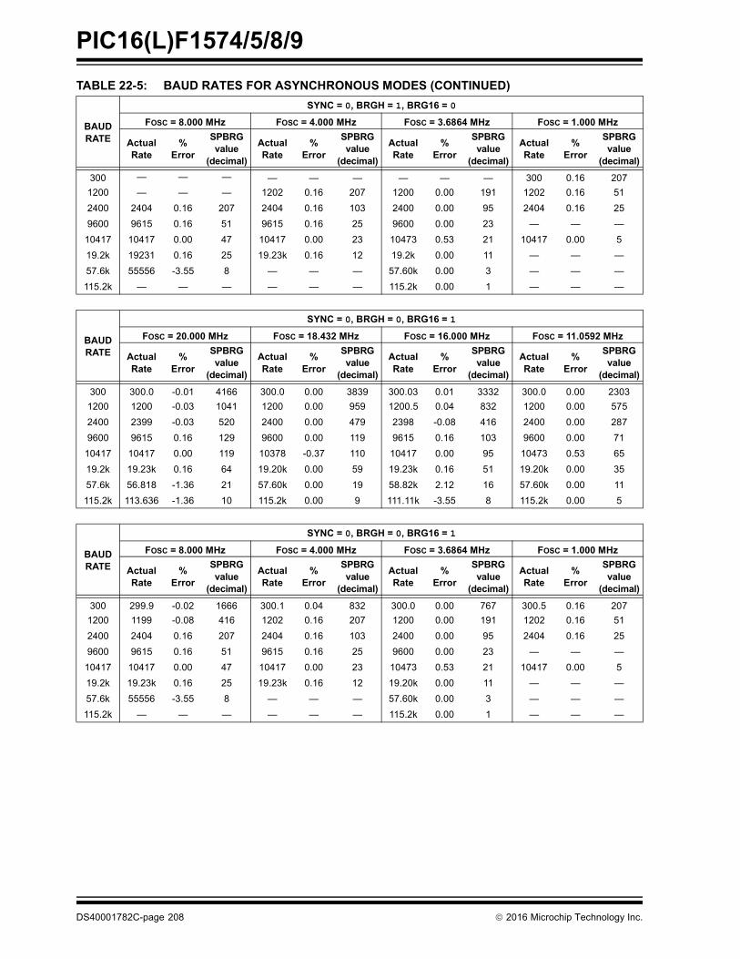
PIC16(L)F1574/5/8/9
DS40001782C-page 208 2016 Microchip Technology Inc.
BAUDRATE
SYNC = 0, BRGH = 1, BRG16 = 0
FOSC = 8.000 MHz FOSC = 4.000 MHz FOSC = 3.6864 MHz FOSC = 1.000 MHz
ActualRate
%Error
SPBRGvalue
(decimal)
ActualRate
%Error
SPBRGvalue
(decimal)
ActualRate
%Error
SPBRGvalue
(decimal)
ActualRate
%Error
SPBRGvalue
(decimal)
300 — — — — — — — — — 300 0.16 207
1200 — — — 1202 0.16 207 1200 0.00 191 1202 0.16 51
2400 2404 0.16 207 2404 0.16 103 2400 0.00 95 2404 0.16 25
9600 9615 0.16 51 9615 0.16 25 9600 0.00 23 — — —
10417 10417 0.00 47 10417 0.00 23 10473 0.53 21 10417 0.00 5
19.2k 19231 0.16 25 19.23k 0.16 12 19.2k 0.00 11 — — —
57.6k 55556 -3.55 8 — — — 57.60k 0.00 3 — — —
115.2k — — — — — — 115.2k 0.00 1 — — —
BAUDRATE
SYNC = 0, BRGH = 0, BRG16 = 1
FOSC = 20.000 MHz FOSC = 18.432 MHz FOSC = 16.000 MHz FOSC = 11.0592 MHz
ActualRate
%Error
SPBRGvalue
(decimal)
ActualRate
%Error
SPBRGvalue
(decimal)
ActualRate
%Error
SPBRGvalue
(decimal)
ActualRate
%Error
SPBRGvalue
(decimal)
300 300.0 -0.01 4166 300.0 0.00 3839 300.03 0.01 3332 300.0 0.00 2303
1200 1200 -0.03 1041 1200 0.00 959 1200.5 0.04 832 1200 0.00 575
2400 2399 -0.03 520 2400 0.00 479 2398 -0.08 416 2400 0.00 287
9600 9615 0.16 129 9600 0.00 119 9615 0.16 103 9600 0.00 71
10417 10417 0.00 119 10378 -0.37 110 10417 0.00 95 10473 0.53 65
19.2k 19.23k 0.16 64 19.20k 0.00 59 19.23k 0.16 51 19.20k 0.00 35
57.6k 56.818 -1.36 21 57.60k 0.00 19 58.82k 2.12 16 57.60k 0.00 11
115.2k 113.636 -1.36 10 115.2k 0.00 9 111.11k -3.55 8 115.2k 0.00 5
BAUDRATE
SYNC = 0, BRGH = 0, BRG16 = 1
FOSC = 8.000 MHz FOSC = 4.000 MHz FOSC = 3.6864 MHz FOSC = 1.000 MHz
ActualRate
%Error
SPBRGvalue
(decimal)
ActualRate
%Error
SPBRGvalue
(decimal)
ActualRate
%Error
SPBRGvalue
(decimal)
ActualRate
%Error
SPBRGvalue
(decimal)
300 299.9 -0.02 1666 300.1 0.04 832 300.0 0.00 767 300.5 0.16 207
1200 1199 -0.08 416 1202 0.16 207 1200 0.00 191 1202 0.16 51
2400 2404 0.16 207 2404 0.16 103 2400 0.00 95 2404 0.16 25
9600 9615 0.16 51 9615 0.16 25 9600 0.00 23 — — —
10417 10417 0.00 47 10417 0.00 23 10473 0.53 21 10417 0.00 5
19.2k 19.23k 0.16 25 19.23k 0.16 12 19.20k 0.00 11 — — —
57.6k 55556 -3.55 8 — — — 57.60k 0.00 3 — — —
115.2k — — — — — — 115.2k 0.00 1 — — —
TABLE 22-5: BAUD RATES FOR ASYNCHRONOUS MODES (CONTINUED)

2016 Microchip Technology Inc. DS40001782C-page 209
PIC16(L)F1574/5/8/9
BAUDRATE
SYNC = 0, BRGH = 1, BRG16 = 1 or SYNC = 1, BRG16 = 1
FOSC = 20.000 MHz FOSC = 18.432 MHz FOSC = 16.000 MHz FOSC = 11.0592 MHz
ActualRate
%Error
SPBRGvalue
(decimal)
ActualRate
%Error
SPBRGvalue
(decimal)
ActualRate
%Error
SPBRGvalue
(decimal)
ActualRate
%Error
SPBRGvalue
(decimal)
300 300.0 0.00 16665 300.0 0.00 15359 300.0 0.00 13332 300.0 0.00 9215
1200 1200 -0.01 4166 1200 0.00 3839 1200.1 0.01 3332 1200 0.00 2303
2400 2400 0.02 2082 2400 0.00 1919 2399.5 -0.02 1666 2400 0.00 1151
9600 9597 -0.03 520 9600 0.00 479 9592 -0.08 416 9600 0.00 287
10417 10417 0.00 479 10425 0.08 441 10417 0.00 383 10433 0.16 264
19.2k 19.23k 0.16 259 19.20k 0.00 239 19.23k 0.16 207 19.20k 0.00 143
57.6k 57.47k -0.22 86 57.60k 0.00 79 57.97k 0.64 68 57.60k 0.00 47
115.2k 116.3k 0.94 42 115.2k 0.00 39 114.29k -0.79 34 115.2k 0.00 23
BAUDRATE
SYNC = 0, BRGH = 1, BRG16 = 1 or SYNC = 1, BRG16 = 1
FOSC = 8.000 MHz FOSC = 4.000 MHz FOSC = 3.6864 MHz FOSC = 1.000 MHz
ActualRate
%Error
SPBRGvalue
(decimal)
ActualRate
%Error
SPBRGvalue
(decimal)
ActualRate
%Error
SPBRGvalue
(decimal)
ActualRate
%Error
SPBRGvalue
(decimal)
300 300.0 0.00 6666 300.0 0.01 3332 300.0 0.00 3071 300.1 0.04 832
1200 1200 -0.02 1666 1200 0.04 832 1200 0.00 767 1202 0.16 207
2400 2401 0.04 832 2398 0.08 416 2400 0.00 383 2404 0.16 103
9600 9615 0.16 207 9615 0.16 103 9600 0.00 95 9615 0.16 25
10417 10417 0 191 10417 0.00 95 10473 0.53 87 10417 0.00 23
19.2k 19.23k 0.16 103 19.23k 0.16 51 19.20k 0.00 47 19.23k 0.16 12
57.6k 57.14k -0.79 34 58.82k 2.12 16 57.60k 0.00 15 — — —
115.2k 117.6k 2.12 16 111.1k -3.55 8 115.2k 0.00 7 — — —
TABLE 22-5: BAUD RATES FOR ASYNCHRONOUS MODES (CONTINUED)

PIC16(L)F1574/5/8/9
DS40001782C-page 210 2016 Microchip Technology Inc.
22.4.1 AUTO-BAUD DETECT
The EUSART module supports automatic detectionand calibration of the baud rate.
In the Auto-Baud Detect (ABD) mode, the clock to theBRG is reversed. Rather than the BRG clocking theincoming RX signal, the RX signal is timing the BRG.The Baud Rate Generator is used to time the period ofa received 55h (ASCII “U”) which is the Sync characterfor the LIN bus. The unique feature of this character isthat it has five rising edges including the Stop bit edge.
Setting the ABDEN bit of the BAUDCON register startsthe auto-baud calibration sequence (Figure 22-6).While the ABD sequence takes place, the EUSARTstate machine is held in Idle. On the first rising edge ofthe receive line, after the Start bit, the SPBRG beginscounting up using the BRG counter clock as shown inTable 22-6. The fifth rising edge will occur on the RX pinat the end of the eighth bit period. At that time, anaccumulated value totaling the proper BRG period isleft in the SPBRGH, SPBRGL register pair, the ABDENbit is automatically cleared and the RCIF interrupt flagis set. The value in the RCREG needs to be read toclear the RCIF interrupt. RCREG content should bediscarded. When calibrating for modes that do not usethe SPBRGH register the user can verify that theSPBRGL register did not overflow by checking for 00hin the SPBRGH register.
The BRG auto-baud clock is determined by the BRG16and BRGH bits as shown in Table 22-6. During ABD,both the SPBRGH and SPBRGL registers are used asa 16-bit counter, independent of the BRG16 bit setting.While calibrating the baud rate period, the SPBRGH
and SPBRGL registers are clocked at 1/8th the BRGbase clock rate. The resulting byte measurement is theaverage bit time when clocked at full speed.
TABLE 22-6: BRG COUNTER CLOCK RATES
FIGURE 22-6: AUTOMATIC BAUD RATE CALIBRATION
Note 1: If the WUE bit is set with the ABDEN bit,auto-baud detection will occur on the bytefollowing the Break character (seeSection 22.4.3 “Auto-Wake-up onBreak”).
2: It is up to the user to determine that theincoming character baud rate is within therange of the selected BRG clock source.Some combinations of oscillator frequencyand EUSART baud rates are not possible.
3: During the auto-baud process, theauto-baud counter starts counting at 1.Upon completion of the auto-baudsequence, to achieve maximum accuracy,subtract 1 from the SPBRGH:SPBRGLregister pair.
BRG16 BRGHBRG Base
ClockBRG ABD
Clock
0 0 FOSC/64 FOSC/512
0 1 FOSC/16 FOSC/128
1 0 FOSC/16 FOSC/128
1 1 FOSC/4 FOSC/32
Note: During the ABD sequence, SPBRGL andSPBRGH registers are both used as a 16-bitcounter, independent of BRG16 setting.
BRG Value
RX pin
ABDEN bit
RCIF bit
bit 0 bit 1
(Interrupt)
ReadRCREG
BRG Clock
Start
Auto ClearedSet by User
XXXXh 0000h
Edge #1
bit 2 bit 3Edge #2
bit 4 bit 5Edge #3
bit 6 bit 7Edge #4
Stop bit
Edge #5
001Ch
Note 1: The ABD sequence requires the EUSART module to be configured in Asynchronous mode.
SPBRGL XXh 1Ch
SPBRGH XXh 00h
RCIDL
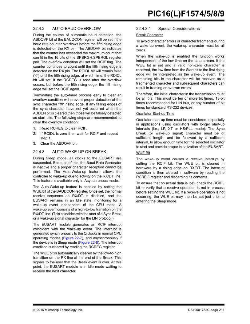
2016 Microchip Technology Inc. DS40001782C-page 211
PIC16(L)F1574/5/8/9
22.4.2 AUTO-BAUD OVERFLOW
During the course of automatic baud detection, theABDOVF bit of the BAUDCON register will be set if thebaud rate counter overflows before the fifth rising edgeis detected on the RX pin. The ABDOVF bit indicatesthat the counter has exceeded the maximum count thatcan fit in the 16 bits of the SPBRGH:SPBRGL registerpair. The overflow condition will set the RCIF flag. Thecounter continues to count until the fifth rising edge isdetected on the RX pin. The RCIDL bit will remain false(‘0’) until the fifth rising edge, at which time, the RDICLbit will set. If the RCREG is read after the overflowoccurs, but before the fifth rising edge, the fifth risingedge will set the RCIF again.
Terminating the auto-baud process early to clear anoverflow condition will prevent proper detection of thesync character fifth rising edge. If any falling edges ofthe sync character have not yet occurred when theABDEN bit is cleared then those will be falsely detectedas start bits. The following steps are recommended toclear the overflow condition:
1. Read RCREG to clear RCIF.
2. If RCIDL is zero then wait for RCIF and repeatstep 1.
3. Clear the ABDOVF bit.
22.4.3 AUTO-WAKE-UP ON BREAK
During Sleep mode, all clocks to the EUSART aresuspended. Because of this, the Baud Rate Generatoris inactive and a proper character reception cannot beperformed. The Auto-Wake-up feature allows thecontroller to wake-up due to activity on the RX/DT line.This feature is available only in Asynchronous mode.
The Auto-Wake-up feature is enabled by setting theWUE bit of the BAUDCON register. Once set, the normalreceive sequence on RX/DT is disabled, and theEUSART remains in an Idle state, monitoring for awake-up event independent of the CPU mode. Awake-up event consists of a high-to-low transition on theRX/DT line. (This coincides with the start of a Sync Breakor a wake-up signal character for the LIN protocol.)
The EUSART module generates an RCIF interruptcoincident with the wake-up event. The interrupt isgenerated synchronously to the Q clocks in normal CPUoperating modes (Figure 22-7), and asynchronously ifthe device is in Sleep mode (Figure 22-8). The interruptcondition is cleared by reading the RCREG register.
The WUE bit is automatically cleared by the low-to-hightransition on the RX line at the end of the Break. Thissignals to the user that the Break event is over. At thispoint, the EUSART module is in Idle mode waiting toreceive the next character.
22.4.3.1 Special Considerations
Break Character
To avoid character errors or character fragments duringa wake-up event, the wake-up character must be allzeros.
When the wake-up is enabled the function worksindependent of the low time on the data stream. If theWUE bit is set and a valid non-zero character isreceived, the low time from the Start bit to the first risingedge will be interpreted as the wake-up event. Theremaining bits in the character will be received as afragmented character and subsequent characters canresult in framing or overrun errors.
Therefore, the initial character in the transmission mustbe all ‘0’s. This must be ten or more bit times, 13-bittimes recommended for LIN bus, or any number of bittimes for standard RS-232 devices.
Oscillator Start-up Time
Oscillator start-up time must be considered, especiallyin applications using oscillators with longer start-upintervals (i.e., LP, XT or HS/PLL mode). The SyncBreak (or wake-up signal) character must be ofsufficient length, and be followed by a sufficientinterval, to allow enough time for the selected oscillatorto start and provide proper initialization of the EUSART.
WUE Bit
The wake-up event causes a receive interrupt bysetting the RCIF bit. The WUE bit is cleared inhardware by a rising edge on RX/DT. The interruptcondition is then cleared in software by reading theRCREG register and discarding its contents.
To ensure that no actual data is lost, check the RCIDLbit to verify that a receive operation is not in processbefore setting the WUE bit. If a receive operation is notoccurring, the WUE bit may then be set just prior toentering the Sleep mode.

PIC16(L)F1574/5/8/9
DS40001782C-page 212 2016 Microchip Technology Inc.
FIGURE 22-7: AUTO-WAKE-UP BIT (WUE) TIMING DURING NORMAL OPERATION
FIGURE 22-8: AUTO-WAKE-UP BIT (WUE) TIMINGS DURING SLEEP
Q1 Q2 Q3 Q4 Q1 Q2 Q3Q4 Q1Q2 Q3 Q4 Q1Q2 Q3 Q4 Q1Q2 Q3 Q4 Q1Q2 Q3 Q4 Q1 Q2 Q3 Q4 Q1Q2 Q3 Q4 Q1 Q2 Q3 Q4 Q1Q2 Q3 Q4
OSC1
WUE bit
RX/DT Line
RCIF
Bit set by user Auto Cleared
Cleared due to User Read of RCREG
Note 1: The EUSART remains in Idle while the WUE bit is set.
Q1Q2Q3 Q4 Q1Q2 Q3 Q4 Q1Q2 Q3 Q4 Q1 Q2 Q3 Q4 Q1Q2 Q3 Q4 Q1Q2 Q3 Q4 Q1Q2 Q3 Q4 Q1Q2 Q3 Q4
OSC1
WUE bit
RX/DT Line
RCIF
Bit Set by User Auto Cleared
Cleared due to User Read of RCREGSleep Command Executed
Note 1
Note 1: If the wake-up event requires long oscillator warm-up time, the automatic clearing of the WUE bit can occur while the stposc signal isstill active. This sequence should not depend on the presence of Q clocks.
2: The EUSART remains in Idle while the WUE bit is set.
Sleep Ends
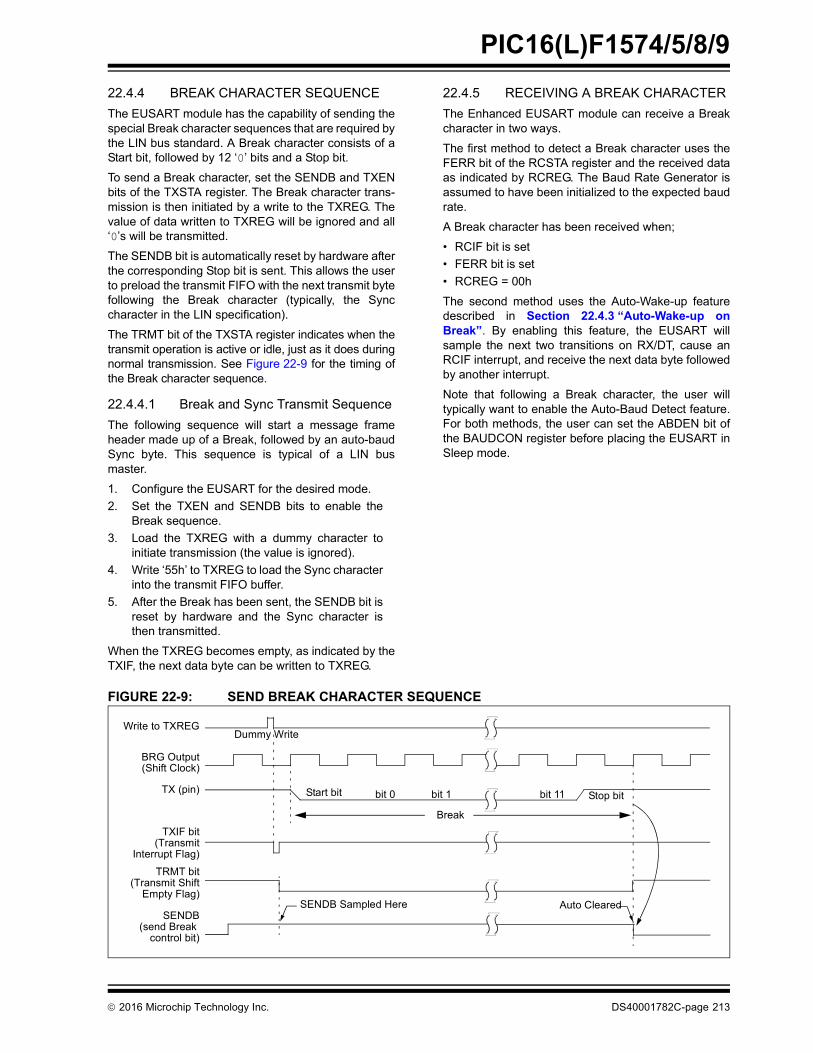
2016 Microchip Technology Inc. DS40001782C-page 213
PIC16(L)F1574/5/8/9
22.4.4 BREAK CHARACTER SEQUENCE
The EUSART module has the capability of sending thespecial Break character sequences that are required bythe LIN bus standard. A Break character consists of aStart bit, followed by 12 ‘0’ bits and a Stop bit.
To send a Break character, set the SENDB and TXENbits of the TXSTA register. The Break character trans-mission is then initiated by a write to the TXREG. Thevalue of data written to TXREG will be ignored and all‘0’s will be transmitted.
The SENDB bit is automatically reset by hardware afterthe corresponding Stop bit is sent. This allows the userto preload the transmit FIFO with the next transmit bytefollowing the Break character (typically, the Synccharacter in the LIN specification).
The TRMT bit of the TXSTA register indicates when thetransmit operation is active or idle, just as it does duringnormal transmission. See Figure 22-9 for the timing ofthe Break character sequence.
22.4.4.1 Break and Sync Transmit Sequence
The following sequence will start a message frameheader made up of a Break, followed by an auto-baudSync byte. This sequence is typical of a LIN busmaster.
1. Configure the EUSART for the desired mode.
2. Set the TXEN and SENDB bits to enable theBreak sequence.
3. Load the TXREG with a dummy character toinitiate transmission (the value is ignored).
4. Write ‘55h’ to TXREG to load the Sync characterinto the transmit FIFO buffer.
5. After the Break has been sent, the SENDB bit isreset by hardware and the Sync character isthen transmitted.
When the TXREG becomes empty, as indicated by theTXIF, the next data byte can be written to TXREG.
22.4.5 RECEIVING A BREAK CHARACTER
The Enhanced EUSART module can receive a Breakcharacter in two ways.
The first method to detect a Break character uses theFERR bit of the RCSTA register and the received dataas indicated by RCREG. The Baud Rate Generator isassumed to have been initialized to the expected baudrate.
A Break character has been received when;
• RCIF bit is set
• FERR bit is set
• RCREG = 00h
The second method uses the Auto-Wake-up featuredescribed in Section 22.4.3 “Auto-Wake-up onBreak”. By enabling this feature, the EUSART willsample the next two transitions on RX/DT, cause anRCIF interrupt, and receive the next data byte followedby another interrupt.
Note that following a Break character, the user willtypically want to enable the Auto-Baud Detect feature.For both methods, the user can set the ABDEN bit ofthe BAUDCON register before placing the EUSART inSleep mode.
FIGURE 22-9: SEND BREAK CHARACTER SEQUENCE
Write to TXREGDummy Write
BRG Output(Shift Clock)
Start bit bit 0 bit 1 bit 11 Stop bit
Break
TXIF bit(Transmit
Interrupt Flag)
TX (pin)
TRMT bit(Transmit Shift
Empty Flag)
SENDB(send Break
control bit)
SENDB Sampled Here Auto Cleared

PIC16(L)F1574/5/8/9
DS40001782C-page 214 2016 Microchip Technology Inc.
22.5 EUSART Synchronous Mode
Synchronous serial communications are typically usedin systems with a single master and one or moreslaves. The master device contains the necessarycircuitry for baud rate generation and supplies the clockfor all devices in the system. Slave devices can takeadvantage of the master clock by eliminating theinternal clock generation circuitry.
There are two signal lines in Synchronous mode: abidirectional data line and a clock line. Slaves use theexternal clock supplied by the master to shift the serialdata into and out of their respective receive and trans-mit shift registers. Since the data line is bidirectional,synchronous operation is half-duplex only. Half-duplexrefers to the fact that master and slave devices canreceive and transmit data but not both simultaneously.The EUSART can operate as either a master or slavedevice.
Start and Stop bits are not used in synchronoustransmissions.
22.5.1 SYNCHRONOUS MASTER MODE
The following bits are used to configure the EUSARTfor synchronous master operation:
• SYNC = 1
• CSRC = 1
• SREN = 0 (for transmit); SREN = 1 (for receive)
• CREN = 0 (for transmit); CREN = 1 (for receive)
• SPEN = 1
Setting the SYNC bit of the TXSTA register configuresthe device for synchronous operation. Setting the CSRCbit of the TXSTA register configures the device as amaster. Clearing the SREN and CREN bits of the RCSTAregister ensures that the device is in the Transmit mode,otherwise the device will be configured to receive. Settingthe SPEN bit of the RCSTA register enables theEUSART.
22.5.1.1 Master Clock
Synchronous data transfers use a separate clock line,which is synchronous with the data. A device config-ured as a master transmits the clock on the TX/CK line.The TX/CK pin output driver is automatically enabledwhen the EUSART is configured for synchronoustransmit or receive operation. Serial data bits changeon the leading edge to ensure they are valid at thetrailing edge of each clock. One clock cycle is gener-ated for each data bit. Only as many clock cycles aregenerated as there are data bits.
22.5.1.2 Clock Polarity
A clock polarity option is provided for Microwirecompatibility. Clock polarity is selected with the SCKPbit of the BAUDCON register. Setting the SCKP bit setsthe clock Idle state as high. When the SCKP bit is set,the data changes on the falling edge of each clock.
Clearing the SCKP bit sets the Idle state as low. Whenthe SCKP bit is cleared, the data changes on the risingedge of each clock.
22.5.1.3 Synchronous Master Transmission
Data is transferred out of the device on the RX/DT pin.The RX/DT and TX/CK pin output drivers are automat-ically enabled when the EUSART is configured forsynchronous master transmit operation.
A transmission is initiated by writing a character to theTXREG register. If the TSR still contains all or part of aprevious character the new character data is held in theTXREG until the last bit of the previous character hasbeen transmitted. If this is the first character, or theprevious character has been completely flushed fromthe TSR, the data in the TXREG is immediately trans-ferred to the TSR. The transmission of the charactercommences immediately following the transfer of thedata to the TSR from the TXREG.
Each data bit changes on the leading edge of themaster clock and remains valid until the subsequentleading clock edge.
22.5.1.4 Synchronous Master Transmission Set-up:
1. Initialize the SPBRGH, SPBRGL register pairand the BRGH and BRG16 bits to achieve thedesired baud rate (see Section 22.4 “EUSARTBaud Rate Generator (BRG)”).
2. Enable the synchronous master serial port bysetting bits SYNC, SPEN and CSRC.
3. Disable Receive mode by clearing bits SRENand CREN.
4. Enable Transmit mode by setting the TXEN bit.
5. If 9-bit transmission is desired, set the TX9 bit.
6. If interrupts are desired, set the TXIE bit of thePIE1 register and the GIE and PEIE bits of theINTCON register.
7. If 9-bit transmission is selected, the ninth bitshould be loaded in the TX9D bit.
8. Start transmission by loading data to the TXREGregister.
Note: The TSR register is not mapped in datamemory, so it is not available to the user.
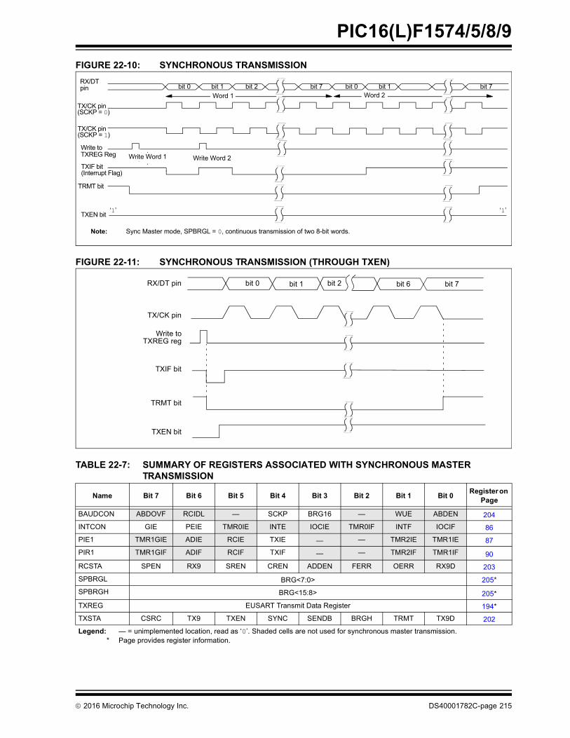
2016 Microchip Technology Inc. DS40001782C-page 215
PIC16(L)F1574/5/8/9
FIGURE 22-10: SYNCHRONOUS TRANSMISSION
FIGURE 22-11: SYNCHRONOUS TRANSMISSION (THROUGH TXEN)
TABLE 22-7: SUMMARY OF REGISTERS ASSOCIATED WITH SYNCHRONOUS MASTER TRANSMISSION
Name Bit 7 Bit 6 Bit 5 Bit 4 Bit 3 Bit 2 Bit 1 Bit 0Register on
Page
BAUDCON ABDOVF RCIDL — SCKP BRG16 — WUE ABDEN 204
INTCON GIE PEIE TMR0IE INTE IOCIE TMR0IF INTF IOCIF 86
PIE1 TMR1GIE ADIE RCIE TXIE — — TMR2IE TMR1IE 87
PIR1 TMR1GIF ADIF RCIF TXIF — — TMR2IF TMR1IF 90
RCSTA SPEN RX9 SREN CREN ADDEN FERR OERR RX9D 203
SPBRGL BRG<7:0> 205*
SPBRGH BRG<15:8> 205*
TXREG EUSART Transmit Data Register 194*
TXSTA CSRC TX9 TXEN SYNC SENDB BRGH TRMT TX9D 202
Legend: — = unimplemented location, read as ‘0’. Shaded cells are not used for synchronous master transmission.* Page provides register information.
bit 0 bit 1 bit 7
Word 1
bit 2 bit 0 bit 1 bit 7RX/DT
Write toTXREG Reg
TXIF bit(Interrupt Flag)
TXEN bit‘1’ ‘1’
Word 2
TRMT bit
Write Word 1 Write Word 2
Note: Sync Master mode, SPBRGL = 0, continuous transmission of two 8-bit words.
pin
TX/CK pin
TX/CK pin
(SCKP = 0)
(SCKP = 1)
RX/DT pin
TX/CK pin
Write toTXREG reg
TXIF bit
TRMT bit
bit 0 bit 1 bit 2 bit 6 bit 7
TXEN bit
PIC16(L)F1574/5/8/9
DS40001782C-page 216 2016 Microchip Technology Inc.
22.5.1.5 Synchronous Master Reception
Data is received at the RX/DT pin. The RX/DT pinoutput driver is automatically disabled when theEUSART is configured for synchronous master receiveoperation.
In Synchronous mode, reception is enabled by settingeither the Single Receive Enable bit (SREN of theRCSTA register) or the Continuous Receive Enable bit(CREN of the RCSTA register).
When SREN is set and CREN is clear, only as manyclock cycles are generated as there are data bits in asingle character. The SREN bit is automatically clearedat the completion of one character. When CREN is set,clocks are continuously generated until CREN iscleared. If CREN is cleared in the middle of a characterthe CK clock stops immediately and the partial charac-ter is discarded. If SREN and CREN are both set, thenSREN is cleared at the completion of the first characterand CREN takes precedence.
To initiate reception, set either SREN or CREN. Data issampled at the RX/DT pin on the trailing edge of theTX/CK clock pin and is shifted into the Receive ShiftRegister (RSR). When a complete character isreceived into the RSR, the RCIF bit is set and thecharacter is automatically transferred to the twocharacter receive FIFO. The Least Significant eight bitsof the top character in the receive FIFO are available inRCREG. The RCIF bit remains set as long as there areunread characters in the receive FIFO.
22.5.1.6 Slave Clock
Synchronous data transfers use a separate clock line,which is synchronous with the data. A device configuredas a slave receives the clock on the TX/CK line. TheTX/CK pin output driver is automatically disabled whenthe device is configured for synchronous slave transmitor receive operation. Serial data bits change on theleading edge to ensure they are valid at the trailing edgeof each clock. One data bit is transferred for each clockcycle. Only as many clock cycles should be received asthere are data bits.
22.5.1.7 Receive Overrun Error
The receive FIFO buffer can hold two characters. Anoverrun error will be generated if a third character, in itsentirety, is received before RCREG is read to accessthe FIFO. When this happens the OERR bit of theRCSTA register is set. Previous data in the FIFO willnot be overwritten. The two characters in the FIFObuffer can be read, however, no additional characters
will be received until the error is cleared. The OERR bitcan only be cleared by clearing the overrun condition.If the overrun error occurred when the SREN bit is setand CREN is clear then the error is cleared by readingRCREG. If the overrun occurred when the CREN bit isset then the error condition is cleared by either clearingthe CREN bit of the RCSTA register or by clearing theSPEN bit which resets the EUSART.
22.5.1.8 Receiving 9-bit Characters
The EUSART supports 9-bit character reception. Whenthe RX9 bit of the RCSTA register is set the EUSARTwill shift nine bits into the RSR for each characterreceived. The RX9D bit of the RCSTA register is theninth, and Most Significant, data bit of the top unreadcharacter in the receive FIFO. When reading 9-bit datafrom the receive FIFO buffer, the RX9D data bit mustbe read before reading the eight Least Significant bitsfrom the RCREG.
22.5.1.9 Synchronous Master Reception Set-up:
1. Initialize the SPBRGH, SPBRGL register pair forthe appropriate baud rate. Set or clear theBRGH and BRG16 bits, as required, to achievethe desired baud rate.
2. Clear the ANSEL bit for the RX pin (if applicable).
3. Enable the synchronous master serial port bysetting bits SYNC, SPEN and CSRC.
4. Ensure bits CREN and SREN are clear.
5. If interrupts are desired, set the RCIE bit of thePIE1 register and the GIE and PEIE bits of theINTCON register.
6. If 9-bit reception is desired, set bit RX9.
7. Start reception by setting the SREN bit or forcontinuous reception, set the CREN bit.
8. Interrupt flag bit RCIF will be set when receptionof a character is complete. An interrupt will begenerated if the enable bit RCIE was set.
9. Read the RCSTA register to get the ninth bit (ifenabled) and determine if any error occurredduring reception.
10. Read the 8-bit received data by reading theRCREG register.
11. If an overrun error occurs, clear the error byeither clearing the CREN bit of the RCSTAregister or by clearing the SPEN bit which resetsthe EUSART.
Note: If the RX/DT function is on an analog pin,the corresponding ANSEL bit must becleared for the receiver to function.
Note: If the device is configured as a slave andthe TX/CK function is on an analog pin, thecorresponding ANSEL bit must becleared.
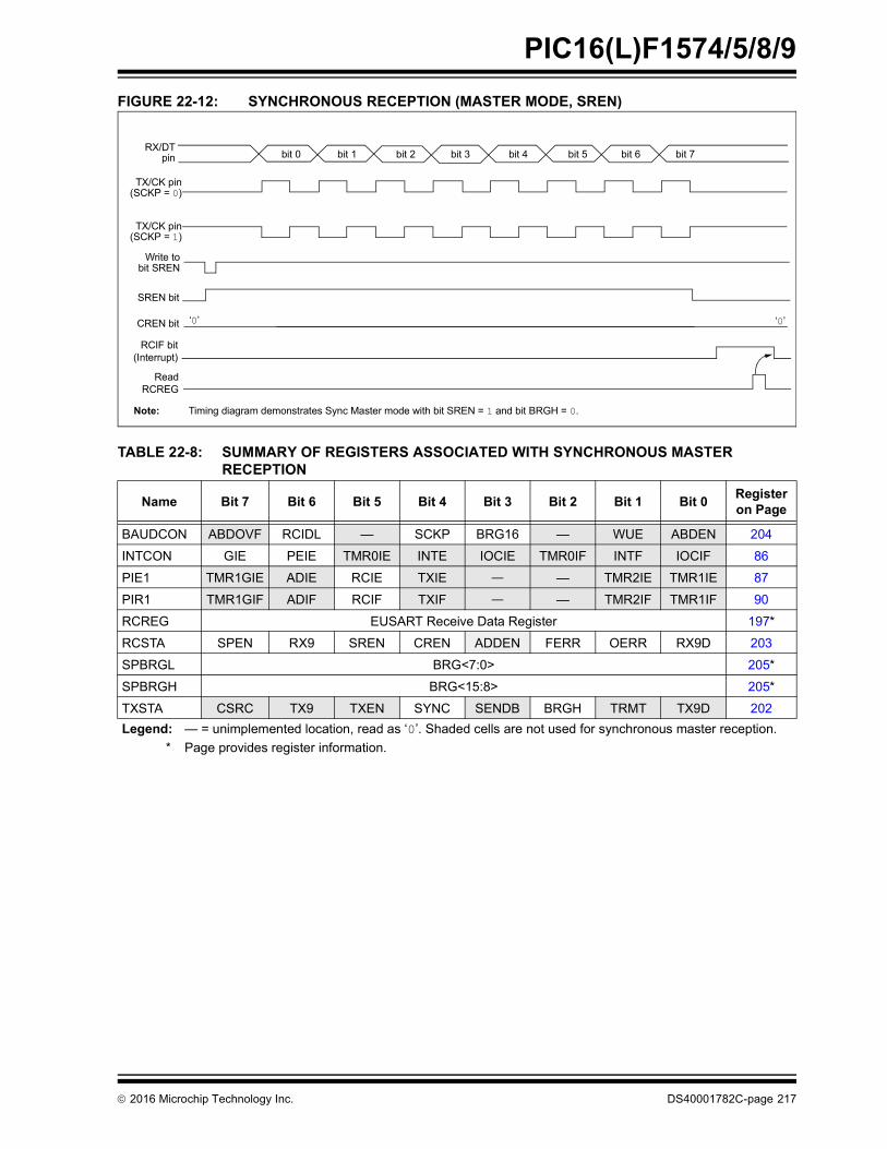
2016 Microchip Technology Inc. DS40001782C-page 217
PIC16(L)F1574/5/8/9
FIGURE 22-12: SYNCHRONOUS RECEPTION (MASTER MODE, SREN)
TABLE 22-8: SUMMARY OF REGISTERS ASSOCIATED WITH SYNCHRONOUS MASTER RECEPTION
Name Bit 7 Bit 6 Bit 5 Bit 4 Bit 3 Bit 2 Bit 1 Bit 0Register on Page
BAUDCON ABDOVF RCIDL — SCKP BRG16 — WUE ABDEN 204
INTCON GIE PEIE TMR0IE INTE IOCIE TMR0IF INTF IOCIF 86
PIE1 TMR1GIE ADIE RCIE TXIE — — TMR2IE TMR1IE 87
PIR1 TMR1GIF ADIF RCIF TXIF — — TMR2IF TMR1IF 90
RCREG EUSART Receive Data Register 197*
RCSTA SPEN RX9 SREN CREN ADDEN FERR OERR RX9D 203
SPBRGL BRG<7:0> 205*
SPBRGH BRG<15:8> 205*
TXSTA CSRC TX9 TXEN SYNC SENDB BRGH TRMT TX9D 202
Legend: — = unimplemented location, read as ‘0’. Shaded cells are not used for synchronous master reception.
* Page provides register information.
CREN bit
RX/DT
Write tobit SREN
SREN bit
RCIF bit(Interrupt)
ReadRCREG
‘0’
bit 0 bit 1 bit 2 bit 3 bit 4 bit 5 bit 6 bit 7
‘0’
Note: Timing diagram demonstrates Sync Master mode with bit SREN = 1 and bit BRGH = 0.
TX/CK pin
TX/CK pin
pin
(SCKP = 0)
(SCKP = 1)
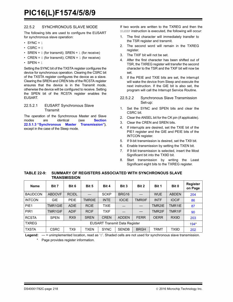
PIC16(L)F1574/5/8/9
DS40001782C-page 218 2016 Microchip Technology Inc.
22.5.2 SYNCHRONOUS SLAVE MODE
The following bits are used to configure the EUSARTfor synchronous slave operation:
• SYNC = 1
• CSRC = 0
• SREN = 0 (for transmit); SREN = 1 (for receive)
• CREN = 0 (for transmit); CREN = 1 (for receive)
• SPEN = 1
Setting the SYNC bit of the TXSTA register configures thedevice for synchronous operation. Clearing the CSRC bitof the TXSTA register configures the device as a slave.Clearing the SREN and CREN bits of the RCSTA registerensures that the device is in the Transmit mode,otherwise the device will be configured to receive. Settingthe SPEN bit of the RCSTA register enables theEUSART.
22.5.2.1 EUSART Synchronous Slave Transmit
The operation of the Synchronous Master and Slavemodes are identical (see Section22.5.1.3 “Synchronous Master Transmission”),except in the case of the Sleep mode.
If two words are written to the TXREG and then theSLEEP instruction is executed, the following will occur:
1. The first character will immediately transfer tothe TSR register and transmit.
2. The second word will remain in the TXREGregister.
3. The TXIF bit will not be set.
4. After the first character has been shifted out ofTSR, the TXREG register will transfer the secondcharacter to the TSR and the TXIF bit will now beset.
5. If the PEIE and TXIE bits are set, the interruptwill wake the device from Sleep and execute thenext instruction. If the GIE bit is also set, theprogram will call the Interrupt Service Routine.
22.5.2.2 Synchronous Slave Transmission Set-up:
1. Set the SYNC and SPEN bits and clear theCSRC bit.
2. Clear the ANSEL bit for the CK pin (if applicable).
3. Clear the CREN and SREN bits.
4. If interrupts are desired, set the TXIE bit of thePIE1 register and the GIE and PEIE bits of theINTCON register.
5. If 9-bit transmission is desired, set the TX9 bit.
6. Enable transmission by setting the TXEN bit.
7. If 9-bit transmission is selected, insert the MostSignificant bit into the TX9D bit.
8. Start transmission by writing the LeastSignificant eight bits to the TXREG register.
TABLE 22-9: SUMMARY OF REGISTERS ASSOCIATED WITH SYNCHRONOUS SLAVE TRANSMISSION
Name Bit 7 Bit 6 Bit 5 Bit 4 Bit 3 Bit 2 Bit 1 Bit 0Register on Page
BAUDCON ABDOVF RCIDL — SCKP BRG16 — WUE ABDEN 204
INTCON GIE PEIE TMR0IE INTE IOCIE TMR0IF INTF IOCIF 86
PIE1 TMR1GIE ADIE RCIE TXIE — — TMR2IE TMR1IE 87
PIR1 TMR1GIF ADIF RCIF TXIF — — TMR2IF TMR1IF 90
RCSTA SPEN RX9 SREN CREN ADDEN FERR OERR RX9D 203
TXREG EUSART Transmit Data Register 194*
TXSTA CSRC TX9 TXEN SYNC SENDB BRGH TRMT TX9D 202
Legend: — = unimplemented location, read as ‘0’. Shaded cells are not used for synchronous slave transmission.
* Page provides register information.
2016 Microchip Technology Inc. DS40001782C-page 219
PIC16(L)F1574/5/8/9
22.5.2.3 EUSART Synchronous Slave Reception
The operation of the Synchronous Master and Slavemodes is identical (Section 22.5.1.5 “SynchronousMaster Reception”), with the following exceptions:
• Sleep
• CREN bit is always set, therefore the receiver is never idle
• SREN bit, which is a “don’t care” in Slave mode
A character may be received while in Sleep mode bysetting the CREN bit prior to entering Sleep. Once theword is received, the RSR register will transfer the datato the RCREG register. If the RCIE enable bit is set, theinterrupt generated will wake the device from Sleepand execute the next instruction. If the GIE bit is alsoset, the program will branch to the interrupt vector.
22.5.2.4 Synchronous Slave Reception Set-up:
1. Set the SYNC and SPEN bits and clear theCSRC bit.
2. Clear the ANSEL bit for both the CK and DT pins(if applicable).
3. If interrupts are desired, set the RCIE bit of thePIE1 register and the GIE and PEIE bits of theINTCON register.
4. If 9-bit reception is desired, set the RX9 bit.
5. Set the CREN bit to enable reception.
6. The RCIF bit will be set when reception iscomplete. An interrupt will be generated if theRCIE bit was set.
7. If 9-bit mode is enabled, retrieve the MostSignificant bit from the RX9D bit of the RCSTAregister.
8. Retrieve the eight Least Significant bits from thereceive FIFO by reading the RCREG register.
9. If an overrun error occurs, clear the error byeither clearing the CREN bit of the RCSTAregister or by clearing the SPEN bit which resetsthe EUSART.
TABLE 22-10: SUMMARY OF REGISTERS ASSOCIATED WITH SYNCHRONOUS SLAVE RECEPTION
Name Bit 7 Bit 6 Bit 5 Bit 4 Bit 3 Bit 2 Bit 1 Bit 0Register on Page
BAUDCON ABDOVF RCIDL — SCKP BRG16 — WUE ABDEN 204
INTCON GIE PEIE TMR0IE INTE IOCIE TMR0IF INTF IOCIF 86
PIE1 TMR1GIE ADIE RCIE TXIE — — TMR2IE TMR1IE 87
PIR1 TMR1GIF ADIF RCIF TXIF — — TMR2IF TMR1IF 90
RCREG EUSART Receive Data Register 197*
RCSTA SPEN RX9 SREN CREN ADDEN FERR OERR RX9D 203
TXSTA CSRC TX9 TXEN SYNC SENDB BRGH TRMT TX9D 202
Legend: — = unimplemented location, read as ‘0’. Shaded cells are not used for synchronous slave reception.
* Page provides register information.
PIC16(L)F1574/5/8/9
DS40001782C-page 220 2016 Microchip Technology Inc.
23.0 16-BIT PULSE-WIDTH MODULATION (PWM) MODULE
The Pulse-Width Modulation (PWM) module generatesa pulse width modulated signal determined by thephase, duty cycle, period, and offset event counts thatare contained in the following registers:
• PWMxPH register
• PWMxDC register
• PWMxPR register
• PWMxOF register
Figure 23-1 shows a simplified block diagram of thePWM operation.
Each PWM module has four modes of operation:
• Standard
• Set On Match
• Toggle On Match
• Center-Aligned
For a more detailed description of each PWM mode,refer to Section 23.2 “PWM Modes”.
Each PWM module has four offset modes:
• Independent Run
• Slave Run with Synchronous Start
• One-Shot Slave with Synchronous Start
• Continuous Run Slave with Synchronous Start and Timer Reset
Using the offset modes, each PWM module can offsetits waveform relative to any other PWM module in thesame device. For a more detailed description of theoffset modes refer to Section 23.3 “Offset Modes”.
Every PWM module has a configurable reload opera-tion to ensure all event count buffers change at the endof a period thereby avoiding signal glitches.Figure 23-2 shows a simplified block diagram of thereload operation. For a more detailed description of thereload operation, refer to Section Section 23.4“Reload Operation”.
FIGURE 23-1: 16-BIT PWM BLOCK DIAGRAM
Rev. 10-000152A4/21/2014
PWM ControlUnit
MODE<1:0>
PWMxPR
Comparator
PWMxTMR
PRx_match
PWMxDC
Comparator
16-bt Latch
DCx_match
PWMxOF
Comparator
16-bt Latch
OFx_match
PWMxPH
Comparator
16-bt Latch
PHx_match
16-bt Latch LDx_trigger LDx_trigger LDx_trigger LDx_trigger
PWMxPOL
PWMx
PWMxOUT
To Peripherals
TRIS Control
PWMxOE
set PRIF set PHIF set OFIF set DCIF
D
CK
Q
Q4
PWMx_output
OffsetControl
E R U/D
OFM<1:0>
PRx_match
00
11
10
01
OF3_match(1)
OF2_match(1)
OF1_match(1)
Reserved
OFS
OF_match
ENPHx_match
DCx_match
Note 1: A PWM module cannot trigger from its own offset match event.The input corresponding to a PWM module’s own offset match is reserved.
PWM_clock
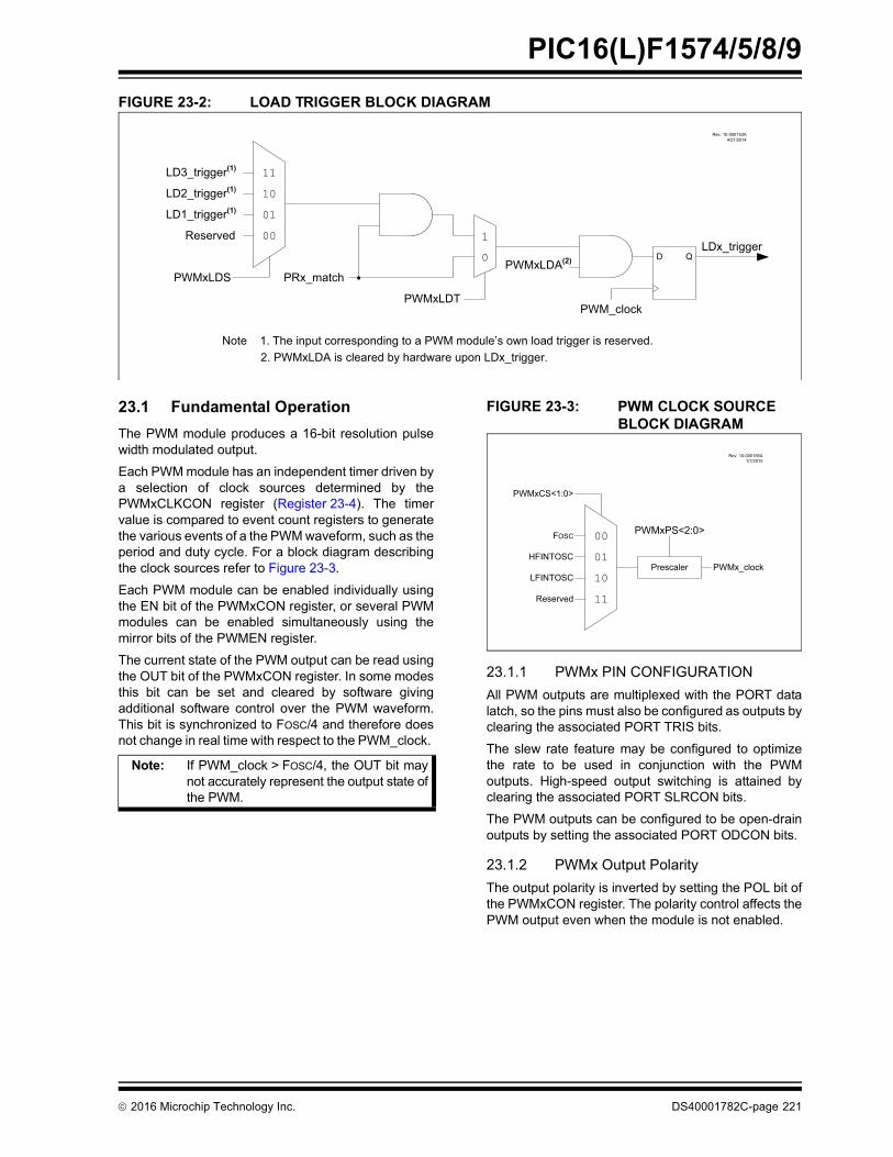
2016 Microchip Technology Inc. DS40001782C-page 221
PIC16(L)F1574/5/8/9
FIGURE 23-2: LOAD TRIGGER BLOCK DIAGRAM
23.1 Fundamental Operation
The PWM module produces a 16-bit resolution pulsewidth modulated output.
Each PWM module has an independent timer driven bya selection of clock sources determined by thePWMxCLKCON register (Register 23-4). The timervalue is compared to event count registers to generatethe various events of a the PWM waveform, such as theperiod and duty cycle. For a block diagram describingthe clock sources refer to Figure 23-3.
Each PWM module can be enabled individually usingthe EN bit of the PWMxCON register, or several PWMmodules can be enabled simultaneously using themirror bits of the PWMEN register.
The current state of the PWM output can be read usingthe OUT bit of the PWMxCON register. In some modesthis bit can be set and cleared by software givingadditional software control over the PWM waveform.This bit is synchronized to FOSC/4 and therefore doesnot change in real time with respect to the PWM_clock.
FIGURE 23-3: PWM CLOCK SOURCE BLOCK DIAGRAM
23.1.1 PWMx PIN CONFIGURATION
All PWM outputs are multiplexed with the PORT datalatch, so the pins must also be configured as outputs byclearing the associated PORT TRIS bits.
The slew rate feature may be configured to optimizethe rate to be used in conjunction with the PWMoutputs. High-speed output switching is attained byclearing the associated PORT SLRCON bits.
The PWM outputs can be configured to be open-drainoutputs by setting the associated PORT ODCON bits.
23.1.2 PWMx Output Polarity
The output polarity is inverted by setting the POL bit ofthe PWMxCON register. The polarity control affects thePWM output even when the module is not enabled.
Rev. 10-000153A4/21/2014
00
11
10
01
LD3_trigger(1)
LD2_trigger(1)
LD1_trigger(1)
Reserved
PWMxLDS PRx_match
1
0PWMxLDA(2) D Q
PWM_clock
LDx_trigger
PWMxLDT
Note 1. The input corresponding to a PWM module’s own load trigger is reserved.2. PWMxLDA is cleared by hardware upon LDx_trigger.
Note: If PWM_clock > FOSC/4, the OUT bit maynot accurately represent the output state ofthe PWM.
Rev. 10-000156A1/7/2015
00
11
10
01HFINTOSC
LFINTOSC
FOSC
Reserved
PWMxCS<1:0>
Prescaler PWMx_clock
PWMxPS<2:0>

PIC16(L)F1574/5/8/9
DS40001782C-page 222 2016 Microchip Technology Inc.
23.2 PWM Modes
PWM Modes are selected with MODE<1:0> bits of thePWMxCON register (Register 23-1).
In all PWM modes an offset match event can also beused to synchronize the PWMxTMR in three offsetmodes. See Section 23.3 “Offset Modes” for moreinformation.
23.2.1 STANDARD MODE
The Standard mode (MODE = 00) selects a singlephase PWM output. The PWM output in this mode isdetermined by when the period, duty cycle, and phasecounts match the PWMxTMR value. The start of theduty cycle occurs on the phase match and the end ofthe duty cycle occurs on the duty cycle match. Theperiod match resets the timer. The offset match canalso be used to synchronize the PWMxTMR in theoffset modes. See Section 23.3 “Offset Modes” formore information.
Equation 23-1 is used to calculate the PWM period inStandard mode.
Equation 23-2 is used to calculate the PWM duty-cycleratio in Standard mode.
EQUATION 23-1: PWM PERIOD IN STANDARD MODE
EQUATION 23-2: PWM DUTY CYCLE IN STANDARD MODE
A detailed timing diagram for Standard mode is shownin Figure 23-4.
23.2.2 SET ON MATCH MODE
The Set On Match mode (MODE = 01) generates anactive output when the phase count matches thePWMxTMR value. The output stays active until theOUT bit of the PWMxCON register is cleared or thePWM module is disabled. The duty cycle count has noeffect in this mode. The period count only determinesthe maximum PWMxTMR value above which no phasematches can occur.
The PWMxOUT bit can be used to set or clear theoutput of the PWM in this mode. Writes to this bit willtake place on the next rising edge of the PWM_clockafter the bit is written.
A detailed timing diagram for Set On Match is shown inFigure 23-5.
23.2.3 TOGGLE ON MATCH MODE
The Toggle On Match mode (MODE = 10) generates a50% duty cycle PWM with a period twice as long as thatcomputed for the standard PWM mode. Duty cyclecount has no effect in this mode. The phase countdetermines how many PWMxTMR periods after aperiod event the output will toggle.
Writes to the OUT bit of the PWMxCON register willhave no effect in this mode.
A detailed timing diagram for Toggle On Match isshown in Figure 23-6.
23.2.4 CENTER-ALIGNED MODE
The Center-Aligned mode (MODE = 11) generates aPWM waveform that is centered in the period. In thismode the period is two times the PWMxPR count. ThePWMxTMR counts up to the period value then countsback down to 0. The duty cycle count determines boththe start and end of the active PWM output. The start ofthe duty cycle occurs at the match event whenPWMxTMR is incrementing and the duty cycle ends atthe match event when PWMxTMR is decrementing.The incrementing match value is the period countminus the duty cycle count. The decrementing matchvalue is the incrementing match value plus 1.
Equation 23-3 is used to calculate the PWM period inCenter-Aligned mode.
EQUATION 23-3: PWM PERIOD IN CENTER-ALIGNED MODE
Equation 23-4 is used to calculate the PWM duty cycleratio in Center-Aligned mode
EQUATION 23-4: PWM DUTY CYCLE IN CENTER-ALIGNED MODE
Writes to PWMxOUT will have no effect in this mode.
A detailed timing diagram for Center-Aligned mode isshown in Figure 23-7.
PeriodPWMxPR 1+ Prescale
PWMxCLK--------------------------------------------------------------------=
Duty CyclePWMxDC PWMxPH–
PWMxPR 1+-----------------------------------------------------------------=
PeriodPWMxPR 1+ Prescale 2
PWMxCLK---------------------------------------------------------------------------=
Duty CyclePWMxDC 2
PWMxPR 1+ 2-------------------------------------------------=

2
01
6 M
icroch
ip T
ech
no
log
y Inc.
DS
40
00
17
82
C-p
ag
e 2
23
PIC
16(L
)F15
74/5/8/9
FIGURE 23-4: STANDARD PWM MODE TIMING DIAGRAM
FIGURE 23-5: SET ON MATCH PWM MODE TIMING DIAGRAM
Rev. 10-000142A9/5/2013
PWMxCLK
10
4
9
PWMxPR
PWMxPH
PWMxDC
Phase
Duty Cycle
Period
0 1 2 3 4 5 6 7 8 9 10 0 1 2 3 4 5 6PWMxTMR
PWMxOUT
Rev. 10-000143A9/5/2013
PWMxCLK
10
4
PWMxPR
PWMxPH
Phase
Period
0 1 2 3 4 5 6 7 8 9 10 0 1 2 3 4 5 6PWMxTMR
PWMxOUT

PIC
16(L
)F1
574
/5/8
/9
DS
40
00
17
82
C-p
ag
e 2
24
2
01
6 M
icroch
ip T
ech
no
log
y Inc.
FIGURE 23-6: TOGGLE-ON MATCH PWM MODE TIMING DIAGRAM
FIGURE 23-7: CENTER-ALIGNED PWM MODE TIMING DIAGRAM
Rev. 10-000144A9/5/2013
PWMxCLK
10
4
PWMxPR
PWMxPH
Phase
Period
0 1 2 3 4 5 6 7 8 9 10 0 1 2 3 4 5 6PWMxTMR
PWMxOUT
Rev. 10-000 145A4/22/201 4
PWMxCLK
6
4
PWMxPR
PWMxDC
Duty Cycle
Period
0 1 2 3 4 5 6 6 5 4 3 2 1 0 0 1 2 3PWMxTMR
PWMxOUT
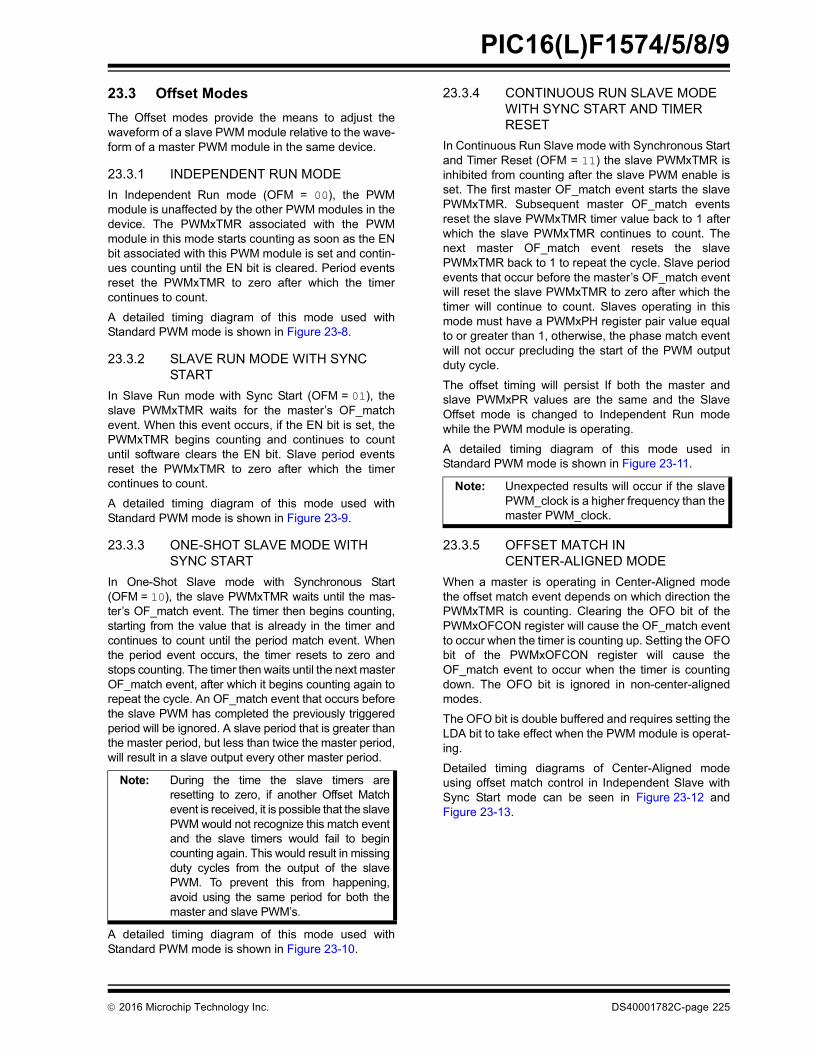
2016 Microchip Technology Inc. DS40001782C-page 225
PIC16(L)F1574/5/8/9
23.3 Offset Modes
The Offset modes provide the means to adjust thewaveform of a slave PWM module relative to the wave-form of a master PWM module in the same device.
23.3.1 INDEPENDENT RUN MODE
In Independent Run mode (OFM = 00), the PWMmodule is unaffected by the other PWM modules in thedevice. The PWMxTMR associated with the PWMmodule in this mode starts counting as soon as the ENbit associated with this PWM module is set and contin-ues counting until the EN bit is cleared. Period eventsreset the PWMxTMR to zero after which the timercontinues to count.
A detailed timing diagram of this mode used withStandard PWM mode is shown in Figure 23-8.
23.3.2 SLAVE RUN MODE WITH SYNC START
In Slave Run mode with Sync Start (OFM = 01), theslave PWMxTMR waits for the master’s OF_matchevent. When this event occurs, if the EN bit is set, thePWMxTMR begins counting and continues to countuntil software clears the EN bit. Slave period eventsreset the PWMxTMR to zero after which the timercontinues to count.
A detailed timing diagram of this mode used withStandard PWM mode is shown in Figure 23-9.
23.3.3 ONE-SHOT SLAVE MODE WITH SYNC START
In One-Shot Slave mode with Synchronous Start(OFM = 10), the slave PWMxTMR waits until the mas-ter’s OF_match event. The timer then begins counting,starting from the value that is already in the timer andcontinues to count until the period match event. Whenthe period event occurs, the timer resets to zero andstops counting. The timer then waits until the next masterOF_match event, after which it begins counting again torepeat the cycle. An OF_match event that occurs beforethe slave PWM has completed the previously triggeredperiod will be ignored. A slave period that is greater thanthe master period, but less than twice the master period,will result in a slave output every other master period.
A detailed timing diagram of this mode used withStandard PWM mode is shown in Figure 23-10.
23.3.4 CONTINUOUS RUN SLAVE MODE WITH SYNC START AND TIMER RESET
In Continuous Run Slave mode with Synchronous Startand Timer Reset (OFM = 11) the slave PWMxTMR isinhibited from counting after the slave PWM enable isset. The first master OF_match event starts the slavePWMxTMR. Subsequent master OF_match eventsreset the slave PWMxTMR timer value back to 1 afterwhich the slave PWMxTMR continues to count. Thenext master OF_match event resets the slavePWMxTMR back to 1 to repeat the cycle. Slave periodevents that occur before the master’s OF_match eventwill reset the slave PWMxTMR to zero after which thetimer will continue to count. Slaves operating in thismode must have a PWMxPH register pair value equalto or greater than 1, otherwise, the phase match eventwill not occur precluding the start of the PWM outputduty cycle.
The offset timing will persist If both the master andslave PWMxPR values are the same and the SlaveOffset mode is changed to Independent Run modewhile the PWM module is operating.
A detailed timing diagram of this mode used inStandard PWM mode is shown in Figure 23-11.
23.3.5 OFFSET MATCH IN CENTER-ALIGNED MODE
When a master is operating in Center-Aligned modethe offset match event depends on which direction thePWMxTMR is counting. Clearing the OFO bit of thePWMxOFCON register will cause the OF_match eventto occur when the timer is counting up. Setting the OFObit of the PWMxOFCON register will cause theOF_match event to occur when the timer is countingdown. The OFO bit is ignored in non-center-alignedmodes.
The OFO bit is double buffered and requires setting theLDA bit to take effect when the PWM module is operat-ing.
Detailed timing diagrams of Center-Aligned modeusing offset match control in Independent Slave withSync Start mode can be seen in Figure 23-12 andFigure 23-13.
Note: During the time the slave timers areresetting to zero, if another Offset Matchevent is received, it is possible that the slavePWM would not recognize this match eventand the slave timers would fail to begincounting again. This would result in missingduty cycles from the output of the slavePWM. To prevent this from happening,avoid using the same period for both themaster and slave PWM’s.
Note: Unexpected results will occur if the slavePWM_clock is a higher frequency than themaster PWM_clock.
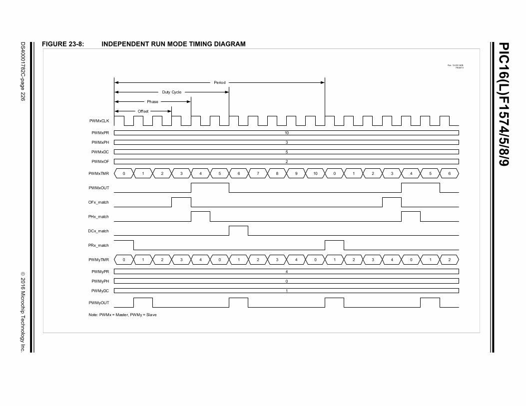
PIC
16(L
)F1
574
/5/8
/9
DS
40
00
17
82
C-p
ag
e 2
26
2
01
6 M
icroch
ip T
ech
no
log
y Inc.
FIGURE 23-8: INDEPENDENT RUN MODE TIMING DIAGRAM
Rev. 10-000 146B7/8/201 5
PWMxCLK
10
3
5
2
PWMxPR
PWMxPH
PWMxDC
PWMxOF
Offset
Phase
Duty Cycle
Period
0 1 2 3 4 5 6 7 8 9 10 0 1 2 3 4 5 6PWMxTMR
PWMxOUT
OFx_match
PHx_match
DCx_match
PRx_match
0 1 2 3 4 0 1 2 3 4 0 1 2 3 4 0 1 2PWMyTMR
4
0
1
PWMyPR
PWMyPH
PWMyDC
PWMyOUT
Note: PWMx = Master, PWMy = Slave

2
01
6 M
icroch
ip T
ech
no
log
y Inc.
DS
40
00
17
82
C-p
ag
e 2
27
PIC
16(L
)F15
74/5/8/9
FIGURE 23-9: SLAVE RUN MODE WITH SYNC START TIMING DIAGRAM
Rev. 10-000 147B7/8/201 5
PWMxCLK
10
3
5
2
PWMxPR
PWMxPH
PWMxDC
PWMxOF
Offset
Phase
Duty Cycle
Period
0 1 2 3 4 5 6 7 8 9 10 0 1 2 3 4 5 6PWMxTMR
PWMxOUT
OFx_match
PWMyTMR
4
0
1
PWMyPR
PWMyPH
PWMyDC
PWMyOUT
10 2 3 4 0 1 2 3 4 0 1 2 3 4 0
Note: Master = PWMx, Slave = PWMy
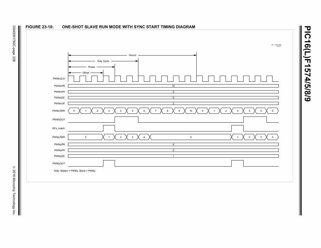
PIC
16(L
)F1
574
/5/8
/9
DS
40
00
17
82
C-p
ag
e 2
28
2
01
6 M
icroch
ip T
ech
no
log
y Inc.
FIGURE 23-10: ONE-SHOT SLAVE RUN MODE WITH SYNC START TIMING DIAGRAM
Rev. 10-000 148B7/8/201 5
PWMxCLK
10
3
5
2
PWMxPR
PWMxPH
PWMxDC
PWMxOF
Offset
Phase
Duty Cycle
Period
0 1 2 3 4 5 6 7 8 9 10 0 1 2 3 4 5 6PWMxTMR
PWMxOUT
OFx_match
PWMyTMR
4
0
1
PWMyPR
PWMyPH
PWMyDC
PWMyOUT
10 2 3 4 1 2 3 40
Note: Master = PWMx, Slave = PWMy
2
01
6 M
icroch
ip T
ech
no
log
y Inc.
DS
40
00
17
82
C-p
ag
e 2
29
PIC
16(L
)F15
74/5/8/9
FIGURE 23-11: CONTINUOUS SLAVE RUN MODE WITH IMMEDIATE RESET AND SYNC START TIMING DIAGRAM
Rev. 10-000 149B7/8/201 5
PWMxCLK
10
3
5
2
PWMxPR
PWMxPH
PWMxDC
PWMxOF
Offset
Phase
Duty Cycle
Period
0 1 2 3 4 5 6 7 8 9 10 0 1 2 3 4 5 6PWMxTMR
PWMxOUT
OFx_match
PWMyTMR
4
1
2
PWMyPR
PWMyPH
PWMyDC
PWMyOUT
10 2 3 4 1 2 3 401 2 3 40 1
Note: Master= PWMx, Slave=PWMy
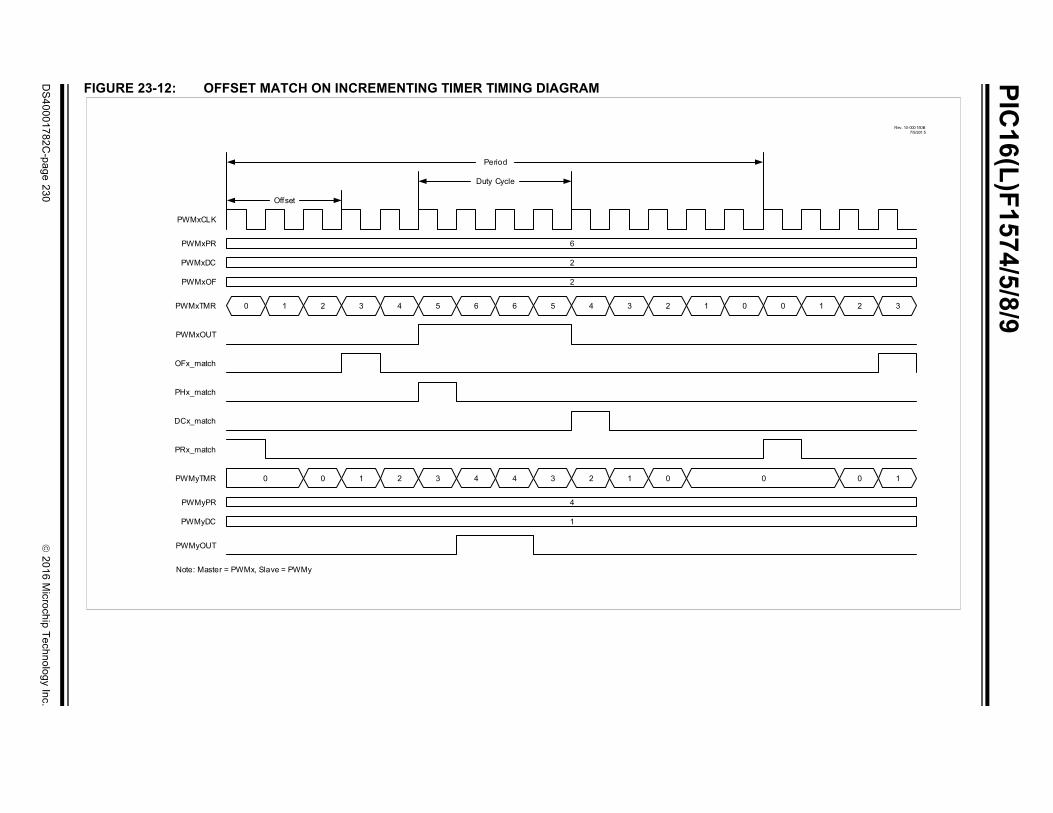
PIC
16(L
)F1
574
/5/8
/9
DS
40
00
17
82
C-p
ag
e 2
30
2
01
6 M
icroch
ip T
ech
no
log
y Inc.
FIGURE 23-12: OFFSET MATCH ON INCREMENTING TIMER TIMING DIAGRAM
Rev. 10-000 150B7/9/201 5
PWMxCLK
6
2
2
PWMxPR
PWMxDC
PWMxOF
Offset
Duty Cycle
Period
0 1 2 3 4 5 6 6 5 4 3 2 1 0 0 1 2 3PWMxTMR
PWMxOUT
OFx_match
PHx_match
DCx_match
PRx_match
0 12 3 4 4 3 2 1 0PWMyTMR
4
1
PWMyPR
PWMyDC
PWMyOUT
0100
Note: Master = PWMx, Slave = PWMy

2
01
6 M
icroch
ip T
ech
no
log
y Inc.
DS
40
00
17
82
C-p
ag
e 2
31
PIC
16(L
)F15
74/5/8/9
FIGURE 23-13: OFFSET MATCH ON DECREMENTING TIMER TIMING DIAGRAM
Rev. 10-000 151B7/9/201 5
PWMxCLK
6
2
2
PWMxPR
PWMxDC
PWMxOF
Offset
Duty Cycle
Period
0 1 2 3 4 5 6 6 5 4 3 2 1 0 0 1 2 3PWMxTMR
PWMxOUT
OF5_match
PH5_match
DC5_match
PR5_match
PWMyTMR
4
1
PWMyPR
PWMyDC
PWMyOUT
0 1 2 3 4 4 30
Note: Master = PWMx, Slave = PWMy
PIC16(L)F1574/5/8/9
DS40001782C-page 232 2016 Microchip Technology Inc.
23.4 Reload Operation
Four of the PWM module control register pairs and onecontrol bit are double buffered so that all can beupdated simultaneously. These include:
• PWMxPHH:PWMxPHL register pair
• PWMxDCH:PWMxDCL register pair
• PWMxPRH:PWMxPRL register pair
• PWMxOFH:PWMxOFL register pair
• OFO control bit
When written to, these registers do not immediatelyaffect the operation of the PWM. By default, writes tothese registers will not be loaded into the PWM operat-ing buffer registers until after the arming conditions aremet. The arming control has two methods of operation:
• Immediate
• Triggered
The LDT bit of the PWMxLDCON register controls thearming method. Both methods require the LDA bit to beset. All four buffer pairs will load simultaneously at theloading event.
23.4.1 IMMEDIATE RELOAD
When the LDT bit is clear then the immediate mode isselected and the buffers will be loaded at the first periodevent after the LDA bit is set. Immediate reloading isused when a PWM module is operating stand-alone orwhen the PWM module is operating as a master toother slave PWM modules.
23.4.2 TRIGGERED RELOAD
When the LDT bit is set then the Triggered mode isselected and a trigger event is required for the LDA bitto take effect. The trigger source is the buffer loadevent of one of the other PWM modules in the device.The triggering source is selected by the LDS<1:0> bitsof the PWMxLDCON register. The buffers will beloaded at the first period event following the triggerevent. Triggered reloading is used when a PWM mod-ule is operating as a slave to another PWM and it isnecessary to synchronize the buffer reloads in bothmodules.
23.5 Operation in Sleep Mode
Each PWM module will continue to operate in Sleepmode when either the HFINTOSC or LFINTOSC isselected as the clock source by PWMxCLKCON<1:0>.
23.6 Interrupts
Each PWM module has four independent interruptsbased on the phase, duty cycle, period, and offsetmatch events. The interrupt flag is set on the risingedge of each of these signals. Refer to Figures 23-8and 23-12 for detailed timing diagrams of the matchsignals.
Note 1: The buffer load operation clears the LDAbit.
2: If the LDA bit is set at the same time asPWMxTMR = PWMxPR, the LDA bit isignored until the next period event. Such isthe case when triggered reload is selectedand the triggering event occurssimultaneously with the target’s periodevent

2016 Microchip Technology Inc. DS40001782C-page 233
PIC16(L)F1574/5/8/9
23.7 Register Definitions: PWM Control
Long bit name prefixes for the 16-bit PWM peripheralsare shown in Table 23-1. Refer to Section1.1 “Register and Bit Naming Conventions” for moreinformation
TABLE 23-1:
Peripheral Bit Name Prefix
PWM1 PWM1
PWM2 PWM2
PWM3 PWM3
PWM4 PWM4
REGISTER 23-1: PWMxCON: PWM CONTROL REGISTER
R/W-0/0 U-0 R/HS/HC-0/0 R/W-0/0 R/W-0/0 R/W-0/0 U-0 U-0
EN — OUT POL MODE<1:0> — —
bit 7 bit 0
Legend:
HC = Bit is cleared by hardware HS = Bit is set by hardware
R = Readable bit W = Writable bit U = Unimplemented bit, read as ‘0’
u = Bit is unchanged x = Bit is unknown -n/n = Value at POR and BOR/Value at all other Resets
‘1’ = Bit is set ‘0’ = Bit is cleared
bit 7 EN: PWM Module Enable bit1 = Module is enabled0 = Module is disabled
bit 6 Unimplemented: Read as ‘0’
bit 5 OUT: Output State of the PWM module
bit 4 POL: PWM Output Polarity Control bit1 = PWM output active state is low0 = PWM output active state is high
bit 3-2 MODE<1:0>: PWM Mode Control bits11 = Center-Aligned mode10 = Toggle On Match mode01 = Set On Match mode00 = Standard PWM mode
bit 1-0 Unimplemented: Read as ‘0’
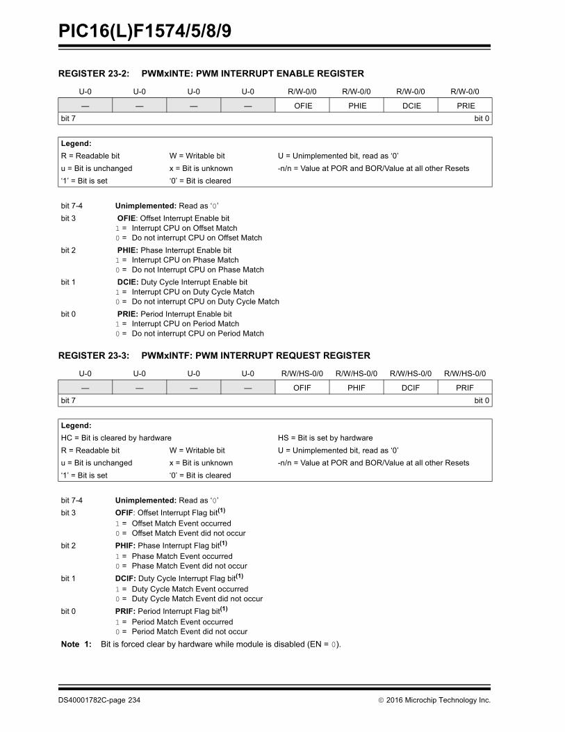
PIC16(L)F1574/5/8/9
DS40001782C-page 234 2016 Microchip Technology Inc.
REGISTER 23-2: PWMxINTE: PWM INTERRUPT ENABLE REGISTER
U-0 U-0 U-0 U-0 R/W-0/0 R/W-0/0 R/W-0/0 R/W-0/0
— — — — OFIE PHIE DCIE PRIE
bit 7 bit 0
Legend:
R = Readable bit W = Writable bit U = Unimplemented bit, read as ‘0’
u = Bit is unchanged x = Bit is unknown -n/n = Value at POR and BOR/Value at all other Resets
‘1’ = Bit is set ‘0’ = Bit is cleared
bit 7-4 Unimplemented: Read as ‘0’
bit 3 OFIE: Offset Interrupt Enable bit1 = Interrupt CPU on Offset Match0 = Do not interrupt CPU on Offset Match
bit 2 PHIE: Phase Interrupt Enable bit1 = Interrupt CPU on Phase Match0 = Do not Interrupt CPU on Phase Match
bit 1 DCIE: Duty Cycle Interrupt Enable bit1 = Interrupt CPU on Duty Cycle Match0 = Do not interrupt CPU on Duty Cycle Match
bit 0 PRIE: Period Interrupt Enable bit1 = Interrupt CPU on Period Match0 = Do not interrupt CPU on Period Match
REGISTER 23-3: PWMxINTF: PWM INTERRUPT REQUEST REGISTER
U-0 U-0 U-0 U-0 R/W/HS-0/0 R/W/HS-0/0 R/W/HS-0/0 R/W/HS-0/0
— — — — OFIF PHIF DCIF PRIF
bit 7 bit 0
Legend:
HC = Bit is cleared by hardware HS = Bit is set by hardware
R = Readable bit W = Writable bit U = Unimplemented bit, read as ‘0’
u = Bit is unchanged x = Bit is unknown -n/n = Value at POR and BOR/Value at all other Resets
‘1’ = Bit is set ‘0’ = Bit is cleared
bit 7-4 Unimplemented: Read as ‘0’
bit 3 OFIF: Offset Interrupt Flag bit(1)
1 = Offset Match Event occurred0 = Offset Match Event did not occur
bit 2 PHIF: Phase Interrupt Flag bit(1)
1 = Phase Match Event occurred0 = Phase Match Event did not occur
bit 1 DCIF: Duty Cycle Interrupt Flag bit(1)
1 = Duty Cycle Match Event occurred0 = Duty Cycle Match Event did not occur
bit 0 PRIF: Period Interrupt Flag bit(1)
1 = Period Match Event occurred0 = Period Match Event did not occur
Note 1: Bit is forced clear by hardware while module is disabled (EN = 0).

2016 Microchip Technology Inc. DS40001782C-page 235
PIC16(L)F1574/5/8/9
REGISTER 23-4: PWMxCLKCON: PWM CLOCK CONTROL REGISTER
U-0 R/W-0/0 R/W-0/0 R/W-0/0 U-0 U-0 R/W-0/0 R/W-0/0
— PS<2:0> — — CS<1:0>
bit 7 bit 0
Legend:
R = Readable bit W = Writable bit U = Unimplemented bit, read as ‘0’
u = Bit is unchanged x = Bit is unknown -n/n = Value at POR and BOR/Value at all other Resets
‘1’ = Bit is set ‘0’ = Bit is cleared
bit 7 Unimplemented: Read as ‘0’
bit 6-4 PS<2:0>: Clock Source Prescaler Select bits111 = Divide clock source by 128110 = Divide clock source by 64101 = Divide clock source by 32100 = Divide clock source by 16011 = Divide clock source by 8010 = Divide clock source by 4001 = Divide clock source by 2000 = No Prescaler
bit 3-2 Unimplemented: Read as ‘0’
bit 1-0 CS<1:0>: Clock Source Select bits11 = Reserved10 = LFINTOSC (continues to operate during Sleep)01 = HFINTOSC (continues to operate during Sleep)00 = FOSC

PIC16(L)F1574/5/8/9
DS40001782C-page 236 2016 Microchip Technology Inc.
REGISTER 23-5: PWMxLDCON: PWM RELOAD TRIGGER SOURCE SELECT REGISTER
R/W-0/0 R/W-0/0 U-0 U-0 U-0 U-0 R/W-0/0 R/W-0/0
LDA(1) LDT — — — — LDS<1:0>
bit 7 bit 0
Legend:
R = Readable bit W = Writable bit U = Unimplemented bit, read as ‘0’
u = Bit is unchanged x = Bit is unknown -n/n = Value at POR and BOR/Value at all other Resets
‘1’ = Bit is set ‘0’ = Bit is cleared
bit 7 LDA: Load Buffer Armed bit(1)
If LDT = 1:1 = Load the OFx, PHx, DCx and PRx buffers at the end of the period when the selected trigger occurs.0 = Do not load buffers/load has completedIf LDT = 0:1 = Load OF, PH, DC and PR buffers at the end of the current period0 = Do not load buffers or load has completed
bit 6 LDT: Load Buffer on Trigger bit1 = Load buffers on trigger enabled0 = Load on trigger disabledLoad the OFx, PHx, DCx and PRx buffers at the end of every period after the selected trigger occurs.Reload internal double buffers at the end of current period. PWMxLDS bits are ignored.
bit 5-2 Unimplemented: Read as ‘0’
bit 1-0 LDS<1:0>: Load Trigger Source Select bits11 = LD4_trigger(2)
10 = LD3_trigger(2)
01 = LD2_trigger(2)
00 = LD1_trigger(2)
Note 1: This bit is cleared by the module after a reload operation. It can be cleared in software to clear an existing arming event.
2: The LD_trigger corresponding to the PWM used becomes reserved.
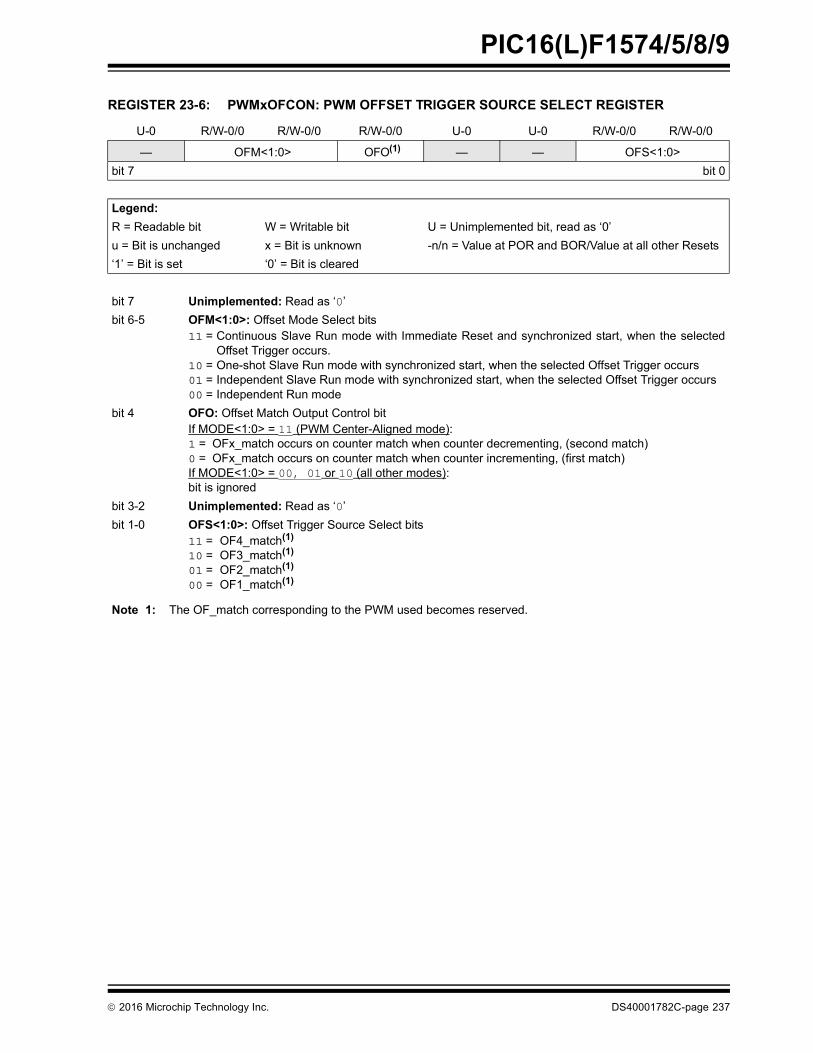
2016 Microchip Technology Inc. DS40001782C-page 237
PIC16(L)F1574/5/8/9
REGISTER 23-6: PWMxOFCON: PWM OFFSET TRIGGER SOURCE SELECT REGISTER
U-0 R/W-0/0 R/W-0/0 R/W-0/0 U-0 U-0 R/W-0/0 R/W-0/0
— OFM<1:0> OFO(1) — — OFS<1:0>
bit 7 bit 0
Legend:
R = Readable bit W = Writable bit U = Unimplemented bit, read as ‘0’
u = Bit is unchanged x = Bit is unknown -n/n = Value at POR and BOR/Value at all other Resets
‘1’ = Bit is set ‘0’ = Bit is cleared
bit 7 Unimplemented: Read as ‘0’
bit 6-5 OFM<1:0>: Offset Mode Select bits11 = Continuous Slave Run mode with Immediate Reset and synchronized start, when the selected
Offset Trigger occurs.10 = One-shot Slave Run mode with synchronized start, when the selected Offset Trigger occurs01 = Independent Slave Run mode with synchronized start, when the selected Offset Trigger occurs00 = Independent Run mode
bit 4 OFO: Offset Match Output Control bitIf MODE<1:0> = 11 (PWM Center-Aligned mode):1 = OFx_match occurs on counter match when counter decrementing, (second match)0 = OFx_match occurs on counter match when counter incrementing, (first match)If MODE<1:0> = 00, 01 or 10 (all other modes):bit is ignored
bit 3-2 Unimplemented: Read as ‘0’
bit 1-0 OFS<1:0>: Offset Trigger Source Select bits11 = OF4_match(1)
10 = OF3_match(1)
01 = OF2_match(1)
00 = OF1_match(1)
Note 1: The OF_match corresponding to the PWM used becomes reserved.
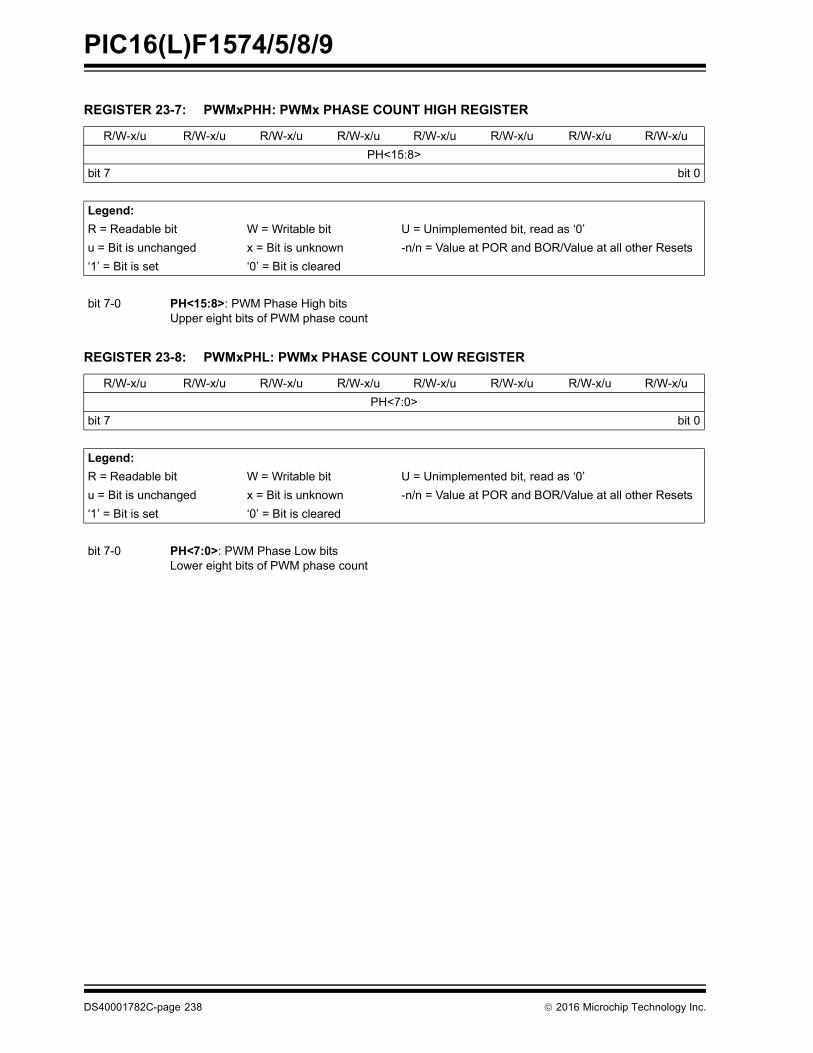
PIC16(L)F1574/5/8/9
DS40001782C-page 238 2016 Microchip Technology Inc.
REGISTER 23-7: PWMxPHH: PWMx PHASE COUNT HIGH REGISTER
R/W-x/u R/W-x/u R/W-x/u R/W-x/u R/W-x/u R/W-x/u R/W-x/u R/W-x/u
PH<15:8>
bit 7 bit 0
Legend:
R = Readable bit W = Writable bit U = Unimplemented bit, read as ‘0’
u = Bit is unchanged x = Bit is unknown -n/n = Value at POR and BOR/Value at all other Resets
‘1’ = Bit is set ‘0’ = Bit is cleared
bit 7-0 PH<15:8>: PWM Phase High bitsUpper eight bits of PWM phase count
REGISTER 23-8: PWMxPHL: PWMx PHASE COUNT LOW REGISTER
R/W-x/u R/W-x/u R/W-x/u R/W-x/u R/W-x/u R/W-x/u R/W-x/u R/W-x/u
PH<7:0>
bit 7 bit 0
Legend:
R = Readable bit W = Writable bit U = Unimplemented bit, read as ‘0’
u = Bit is unchanged x = Bit is unknown -n/n = Value at POR and BOR/Value at all other Resets
‘1’ = Bit is set ‘0’ = Bit is cleared
bit 7-0 PH<7:0>: PWM Phase Low bitsLower eight bits of PWM phase count

2016 Microchip Technology Inc. DS40001782C-page 239
PIC16(L)F1574/5/8/9
REGISTER 23-9: PWMxDCH: PWMx DUTY CYCLE COUNT HIGH REGISTER
R/W-x/u R/W-x/u R/W-x/u R/W-x/u R/W-x/u R/W-x/u R/W-x/u R/W-x/u
DC<15:8>
bit 7 bit 0
Legend:
R = Readable bit W = Writable bit U = Unimplemented bit, read as ‘0’
u = Bit is unchanged x = Bit is unknown -n/n = Value at POR and BOR/Value at all other Resets
‘1’ = Bit is set ‘0’ = Bit is cleared
bit 7-0 DC<15:8>: PWM Duty Cycle High bitsUpper eight bits of PWM duty cycle count
REGISTER 23-10: PWMxDCL: PWMx DUTY CYCLE COUNT LOW REGISTER
R/W-x/u R/W-x/u R/W-x/u R/W-x/u R/W-x/u R/W-x/u R/W-x/u R/W-x/u
DC<7:0>
bit 7 bit 0
Legend:
R = Readable bit W = Writable bit U = Unimplemented bit, read as ‘0’
u = Bit is unchanged x = Bit is unknown -n/n = Value at POR and BOR/Value at all other Resets
‘1’ = Bit is set ‘0’ = Bit is cleared
bit 7-0 DC<7:0>: PWM Duty Cycle Low bitsLower eight bits of PWM duty cycle count

PIC16(L)F1574/5/8/9
DS40001782C-page 240 2016 Microchip Technology Inc.
REGISTER 23-11: PWMxPRH: PWMx PERIOD COUNT HIGH REGISTER
R/W-x/u R/W-x/u R/W-x/u R/W-x/u R/W-x/u R/W-x/u R/W-x/u R/W-x/u
PR<15:8>
bit 7 bit 0
Legend:
R = Readable bit W = Writable bit U = Unimplemented bit, read as ‘0’
u = Bit is unchanged x = Bit is unknown -n/n = Value at POR and BOR/Value at all other Resets
‘1’ = Bit is set ‘0’ = Bit is cleared
bit 7-0 PR<15:8>: PWM Period High bitsUpper eight bits of PWM period count
REGISTER 23-12: PWMxPRL: PWMx PERIOD COUNT LOW REGISTER
R/W-x/u R/W-x/u R/W-x/u R/W-x/u R/W-x/u R/W-x/u R/W-x/u R/W-x/u
PR<7:0>
bit 7 bit 0
Legend:
R = Readable bit W = Writable bit U = Unimplemented bit, read as ‘0’
u = Bit is unchanged x = Bit is unknown -n/n = Value at POR and BOR/Value at all other Resets
‘1’ = Bit is set ‘0’ = Bit is cleared
bit 7-0 PR<7:0>: PWM Period Low bitsLower eight bits of PWM period count

2016 Microchip Technology Inc. DS40001782C-page 241
PIC16(L)F1574/5/8/9
REGISTER 23-13: PWMxOFH: PWMx OFFSET COUNT HIGH REGISTER
R/W-x/u R/W-x/u R/W-x/u R/W-x/u R/W-x/u R/W-x/u R/W-x/u R/W-x/u
OF<15:8>
bit 7 bit 0
Legend:
R = Readable bit W = Writable bit U = Unimplemented bit, read as ‘0’
u = Bit is unchanged x = Bit is unknown -n/n = Value at POR and BOR/Value at all other Resets
‘1’ = Bit is set ‘0’ = Bit is cleared
bit 7-0 OF<15:8>: PWM Offset High bitsUpper eight bits of PWM offset count
REGISTER 23-14: PWMxOFL: PWMx OFFSET COUNT LOW REGISTER
R/W-x/u R/W-x/u R/W-x/u R/W-x/u R/W-x/u R/W-x/u R/W-x/u R/W-x/u
OF<7:0>
bit 7 bit 0
Legend:
R = Readable bit W = Writable bit U = Unimplemented bit, read as ‘0’
u = Bit is unchanged x = Bit is unknown -n/n = Value at POR and BOR/Value at all other Resets
‘1’ = Bit is set ‘0’ = Bit is cleared
bit 7-0 OF<7:0>: PWM Offset Low bitsLower eight bits of PWM offset count

PIC16(L)F1574/5/8/9
DS40001782C-page 242 2016 Microchip Technology Inc.
REGISTER 23-15: PWMxTMRH: PWMx TIMER HIGH REGISTER
R/W-x/u R/W-x/u R/W-x/u R/W-x/u R/W-x/u R/W-x/u R/W-x/u R/W-x/u
TMR<15:8>
bit 7 bit 0
Legend:
R = Readable bit W = Writable bit U = Unimplemented bit, read as ‘0’
u = Bit is unchanged x = Bit is unknown -n/n = Value at POR and BOR/Value at all other Resets
‘1’ = Bit is set ‘0’ = Bit is cleared
bit 7-0 TMR<15:8>: PWM Timer High bitsUpper eight bits of PWM timer counter
REGISTER 23-16: PWMxTMRL: PWMx TIMER LOW REGISTER
R/W-x/u R/W-x/u R/W-x/u R/W-x/u R/W-x/u R/W-x/u R/W-x/u R/W-x/u
TMR<7:0>
bit 7 bit 0
Legend:
R = Readable bit W = Writable bit U = Unimplemented bit, read as ‘0’
u = Bit is unchanged x = Bit is unknown -n/n = Value at POR and BOR/Value at all other Resets
‘1’ = Bit is set ‘0’ = Bit is cleared
bit 7-0 TMR<7:0>: PWM Timer Low bitsLower eight bits of PWM timer counter
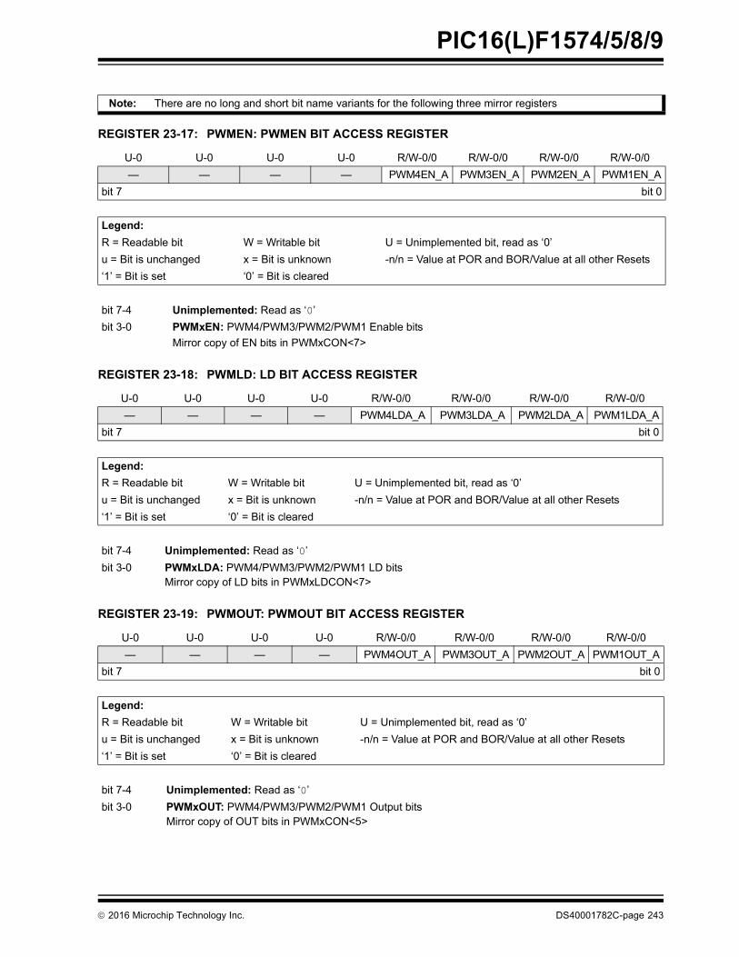
2016 Microchip Technology Inc. DS40001782C-page 243
PIC16(L)F1574/5/8/9
Note: There are no long and short bit name variants for the following three mirror registers
REGISTER 23-17: PWMEN: PWMEN BIT ACCESS REGISTER
U-0 U-0 U-0 U-0 R/W-0/0 R/W-0/0 R/W-0/0 R/W-0/0
— — — — PWM4EN_A PWM3EN_A PWM2EN_A PWM1EN_A
bit 7 bit 0
Legend:
R = Readable bit W = Writable bit U = Unimplemented bit, read as ‘0’
u = Bit is unchanged x = Bit is unknown -n/n = Value at POR and BOR/Value at all other Resets
‘1’ = Bit is set ‘0’ = Bit is cleared
bit 7-4 Unimplemented: Read as ‘0’
bit 3-0 PWMxEN: PWM4/PWM3/PWM2/PWM1 Enable bits
Mirror copy of EN bits in PWMxCON<7>
REGISTER 23-18: PWMLD: LD BIT ACCESS REGISTER
U-0 U-0 U-0 U-0 R/W-0/0 R/W-0/0 R/W-0/0 R/W-0/0
— — — — PWM4LDA_A PWM3LDA_A PWM2LDA_A PWM1LDA_A
bit 7 bit 0
Legend:
R = Readable bit W = Writable bit U = Unimplemented bit, read as ‘0’
u = Bit is unchanged x = Bit is unknown -n/n = Value at POR and BOR/Value at all other Resets
‘1’ = Bit is set ‘0’ = Bit is cleared
bit 7-4 Unimplemented: Read as ‘0’
bit 3-0 PWMxLDA: PWM4/PWM3/PWM2/PWM1 LD bitsMirror copy of LD bits in PWMxLDCON<7>
REGISTER 23-19: PWMOUT: PWMOUT BIT ACCESS REGISTER
U-0 U-0 U-0 U-0 R/W-0/0 R/W-0/0 R/W-0/0 R/W-0/0
— — — — PWM4OUT_A PWM3OUT_A PWM2OUT_A PWM1OUT_A
bit 7 bit 0
Legend:
R = Readable bit W = Writable bit U = Unimplemented bit, read as ‘0’
u = Bit is unchanged x = Bit is unknown -n/n = Value at POR and BOR/Value at all other Resets
‘1’ = Bit is set ‘0’ = Bit is cleared
bit 7-4 Unimplemented: Read as ‘0’
bit 3-0 PWMxOUT: PWM4/PWM3/PWM2/PWM1 Output bitsMirror copy of OUT bits in PWMxCON<5>

PIC16(L)F1574/5/8/9
DS40001782C-page 244 2016 Microchip Technology Inc.
TABLE 23-2: SUMMARY OF REGISTERS ASSOCIATED WITH PWM
Name Bit 7 Bit 6 Bit 5 Bit 4 Bit 3 Bit 2 Bit 1 Bit 0Register on Page
OSCCON SPLLEN IRCF<3:0> — SCS<1:0> 69
PIE3 PWM4IE PWM3IE PWM2IE PWM1IE — — — — 89
PIR3 PWM4IF PWM3IF PWM2IF PWM1IF — — — — 92
PWMEN — — — — PWM4EN_A PWM3EN_A PWM2EN_A PWM1EN_A 243
PWMLD — — — — PWM4LDA_A PWM3LDA_A PWM2LDA_A PWM1LDA_A 243
PWMOUT — — — — PWM4OUT_A PWM3OUT_A PWM2OUT_A PWM1OUT_A 243
PWM1PHL PH<7:0> 238
PWM1PHH PH<15:8> 238
PWM1DCL DC<7:0> 239
PWM1DCH DC<15:8> 239
PWM1PRL PR<7:0> 240
PWM1PRH PR<15:8> 240
PWM1OFL OF<7:0> 241
PWM1OFH OF<15:8> 241
PWM1TMRL TMR<7:0> 242
PWM1TMRH TMR<15:8> 242
PWM1CON EN — OUT POL MODE<1:0> — — 233
PWM1INTE — — — — OFIE PHIE DCIE PRIE 234
PWM1INTF — — — — OFIF PHIF DCIF PRIF 234
PWM1CLKCON — PS<2:0> — — CS<1:0> 235
PWM1LDCON LDA LDT — — — — LDS<1:0> 236
PWM1OFCON — OFM<1:0> OFO — — OFS<1:0> 237
PWM2PHL PH<7:0> 238
PWM2PHH PH<15:8> 238
PWM2DCL DC<7:0> 239
PWM2DCH DC<15:8> 239
PWM2PRL PR<7:0> 240
PWM2PRH PR<15:8> 240
PWM2OFL OF<7:0> 241
PWM2OFH OF<15:8> 241
PWM2TMRL TMR<7:0> 242
PWM2TMRH TMR<15:8> 242
PWM2CON EN — OUT POL MODE<1:0> — — 233
PWM2INTE — — — — OFIE PHIE DCIE PRIE 234
PWM2INTF — — — — OFIF PHIF DCIF PRIF 234
PWM2CLKCON — PS<2:0> — — CS<1:0> 235
PWM2LDCON LDA LDT — — — — LDS<1:0> 236
PWM2OFCON — OFM<1:0> OFO — — OFS<1:0> 237
PWM3PHL PH<7:0> 238
PWM3PHH PH<15:8> 238
PWM3DCL DC<7:0> 239
PWM3DCH DC<15:8> 239
PWM3PRL PR<7:0> 240
PWM3PRH PR<15:8> 240
PWM3OFL OF<7:0> 241
PWM3OFH OF<15:8> 241
PWM3TMRL TMR<7:0> 242
PWM3TMRH TMR<15:8> 242
PWM3CON EN — OUT POL MODE<1:0> — — 233
PWM3INTE — — — — OFIE PHIE DCIE PRIE 234
PWM3INTF — — — — OFIF PHIF DCIF PRIF 234
Legend: — = unimplemented location, read as ‘0’. Shaded cells are not used by PWM.

2016 Microchip Technology Inc. DS40001782C-page 245
PIC16(L)F1574/5/8/9
TABLE 23-2: SUMMARY OF REGISTERS ASSOCIATED WITH PWM (CONTINUED)
TABLE 23-3: SUMMARY OF CONFIGURATION WORD WITH CLOCK SOURCES
Name Bit 7 Bit 6 Bit 5 Bit 4 Bit 3 Bit 2 Bit 1 Bit 0Register on Page
PWM3CLKCON — PS<2:0> — — CS<1:0> 235
PWM3LDCON LDA LDT — — — — LDS<1:0> 236
PWM3OFCON — OFM<1:0> OFO — — OFS<1:0> 237
PWM4PHL PH<7:0> 238
PWM4PHH PH<15:8> 238
PWM4DCL DC<7:0> 239
PWM4DCH DC<15:8> 239
PWM4PRL PR<7:0> 240
PWM4PRH PR<15:8> 240
PWM4OFL OF<7:0> 241
PWM4OFH OF<15:8> 241
PWM4TMRL TMR<7:0> 242
PWM4TMRH TMR<15:8> 242
PWM4CON EN — OUT POL MODE<1:0> — — 233
PWM4INTE — — — — OFIE PHIE DCIE PRIE 234
PWM4INTF — — — — OFIF PHIF DCIF PRIF 234
PWM4CLKCON — PS<2:0> — — CS<1:0> 235
PWM4LDCON LDA LDT — — — — LDS<1:0> 236
PWM4OFCON — OFM<1:0> OFO — — OFS<1:0> 237
Legend: — = unimplemented location, read as ‘0’. Shaded cells are not used by PWM.
Name Bits Bit -/7 Bit -/6 Bit 13/5 Bit 12/4 Bit 11/3 Bit 10/2 Bit 9/1 Bit 8/0Register on Page
CONFIG113:8 — — — — CLKOUTEN BOREN<1:0> —
567:0 CP MCLRE PWRTE WDTE<1:0> — FOSC<1:0>
Legend: — = unimplemented location, read as ‘0’. Shaded cells are not used by clock sources.
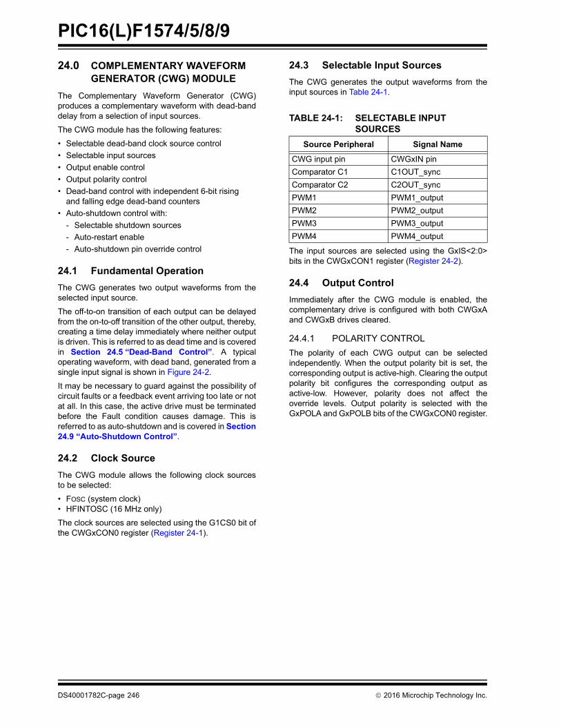
PIC16(L)F1574/5/8/9
DS40001782C-page 246 2016 Microchip Technology Inc.
24.0 COMPLEMENTARY WAVEFORM GENERATOR (CWG) MODULE
The Complementary Waveform Generator (CWG)produces a complementary waveform with dead-banddelay from a selection of input sources.
The CWG module has the following features:
• Selectable dead-band clock source control
• Selectable input sources
• Output enable control
• Output polarity control
• Dead-band control with independent 6-bit rising and falling edge dead-band counters
• Auto-shutdown control with:
- Selectable shutdown sources
- Auto-restart enable
- Auto-shutdown pin override control
24.1 Fundamental Operation
The CWG generates two output waveforms from theselected input source.
The off-to-on transition of each output can be delayedfrom the on-to-off transition of the other output, thereby,creating a time delay immediately where neither outputis driven. This is referred to as dead time and is coveredin Section 24.5 “Dead-Band Control”. A typicaloperating waveform, with dead band, generated from asingle input signal is shown in Figure 24-2.
It may be necessary to guard against the possibility ofcircuit faults or a feedback event arriving too late or notat all. In this case, the active drive must be terminatedbefore the Fault condition causes damage. This isreferred to as auto-shutdown and is covered in Section24.9 “Auto-Shutdown Control”.
24.2 Clock Source
The CWG module allows the following clock sourcesto be selected:
• FOSC (system clock)• HFINTOSC (16 MHz only)
The clock sources are selected using the G1CS0 bit ofthe CWGxCON0 register (Register 24-1).
24.3 Selectable Input Sources
The CWG generates the output waveforms from theinput sources in Table 24-1.
The input sources are selected using the GxIS<2:0>bits in the CWGxCON1 register (Register 24-2).
24.4 Output Control
Immediately after the CWG module is enabled, thecomplementary drive is configured with both CWGxAand CWGxB drives cleared.
24.4.1 POLARITY CONTROL
The polarity of each CWG output can be selectedindependently. When the output polarity bit is set, thecorresponding output is active-high. Clearing the outputpolarity bit configures the corresponding output asactive-low. However, polarity does not affect theoverride levels. Output polarity is selected with theGxPOLA and GxPOLB bits of the CWGxCON0 register.
TABLE 24-1: SELECTABLE INPUT SOURCES
Source Peripheral Signal Name
CWG input pin CWGxIN pin
Comparator C1 C1OUT_sync
Comparator C2 C2OUT_sync
PWM1 PWM1_output
PWM2 PWM2_output
PWM3 PWM3_output
PWM4 PWM4_output

PIC
16(L
)F1
574
/5/8
/9
DS
40
00
17
82
C-p
ag
e 2
47
2
01
6 M
icroch
ip T
ech
no
log
y Inc.
FIGURE 24-1: SIMPLIFIED CWG BLOCK DIAGRAM
Rev. 10-000123F7/28/2015
11
10
00
11
10
00
0
1
1
0
S
QR
Q D QS
S
QR
Q
6
6
2
2
1
3
EN
R=
EN
R=
C1OUT_syncC2OUT_sync
PWM1_out
CWG Input PinReserved
PWM2_outPWM3_outPWM4_out
GxIS
FOSC
HFINTOSC
GxCS
C2OUT_sync
C1OUT_sync
CWG Input PinGxASDSPPS
GxASDSC2
GxASDSC1GxASE Data Bit
WRITEGxARSEN
Auto-ShutdownSource
set dominate
GxASE
shutdown
Input Source
cwg_clock
GxPOLA
GxPOLB
CWGxDBR
CWGxDBF
‘0'
‘0'
‘1'
‘1'
GxASDLA
GxASDLB
TRISx
TRISx
GxASDLA = 01
GxASDLB = 01
CWGxB
CWGxA
x = CWG module number

PIC16(L)F1574/5/8/9
DS40001782C-page 248 2016 Microchip Technology Inc.
FIGURE 24-2: TYPICAL CWG OPERATION WITH PWM1 (NO AUTO-SHUTDOWN)
24.5 Dead-Band Control
Dead-band control provides for non-overlapping outputsignals to prevent shoot-through current in powerswitches. The CWG contains two 6-bit dead-bandcounters. One dead-band counter is used for the risingedge of the input source control. The other is used forthe falling edge of the input source control.
Dead band is timed by counting CWG clock periodsfrom zero up to the value in the rising or falling dead-band counter registers. See CWGxDBR andCWGxDBF registers (Register 24-4 and Register 24-5,respectively).
24.6 Rising Edge Dead Band
The rising edge dead-band delays the turn-on of theCWGxA output from when the CWGxB output is turnedoff. The rising edge dead-band time starts when therising edge of the input source signal goes true. Whenthis happens, the CWGxB output is immediately turnedoff and the rising edge dead-band delay time starts.When the rising edge dead-band delay time is reached,the CWGxA output is turned on.
The CWGxDBR register sets the duration of the dead-band interval on the rising edge of the input sourcesignal. This duration is from 0 to 64 counts of dead band.
Dead band is always counted off the edge on the inputsource signal. A count of 0 (zero), indicates that nodead band is present.
If the input source signal is not present for enough timefor the count to be completed, no output will be seen onthe respective output.
24.7 Falling Edge Dead Band
The falling edge dead band delays the turn-on of theCWGxB output from when the CWGxA output is turnedoff. The falling edge dead-band time starts when thefalling edge of the input source goes true. When thishappens, the CWGxA output is immediately turned offand the falling edge dead-band delay time starts. Whenthe falling edge dead-band delay time is reached, theCWGxB output is turned on.
The CWGxDBF register sets the duration of the dead-band interval on the falling edge of the input sourcesignal. This duration is from 0 to 64 counts of deadband.
Dead band is always counted off the edge on the inputsource signal. A count of 0 (zero), indicates that nodead band is present.
If the input source signal is not present for enough timefor the count to be completed, no output will be seen onthe respective output.
Refer to Figure 24-3 and Figure 24-4 for examples.
Rising Edge DFalling Edge Dead Band
Rising Edge Dead BandFalling Edge Dead Band
cwg_clock
PWM1
CWGxA
CWGxB
Rising Edge Dead Band
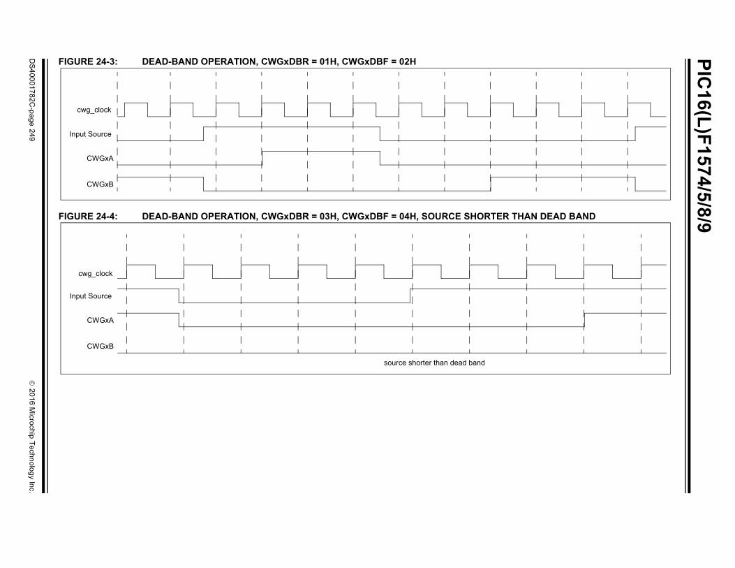
PIC
16(L
)F1
574
/5/8
/9
DS
40
00
17
82
C-p
ag
e 2
49
2
01
6 M
icroch
ip T
ech
no
log
y Inc.
FIGURE 24-3: DEAD-BAND OPERATION, CWGxDBR = 01H, CWGxDBF = 02H
FIGURE 24-4: DEAD-BAND OPERATION, CWGxDBR = 03H, CWGxDBF = 04H, SOURCE SHORTER THAN DEAD BAND
Input Source
CWGxA
CWGxB
cwg_clock
source shorter than dead band
Input Source
CWGxA
CWGxB
cwg_clock

PIC16(L)F1574/5/8/9
DS40001782C-page 250 2016 Microchip Technology Inc.
24.8 Dead-Band Uncertainty
When the rising and falling edges of the input sourcetriggers the dead-band counters, the input may beasynchronous. This will create some uncertainty in thedead-band time delay. The maximum uncertainty isequal to one CWG clock period. Refer to Equation 24-1for more detail.
EQUATION 24-1: DEAD-BAND UNCERTAINTY
24.9 Auto-Shutdown Control
Auto-shutdown is a method to immediately override theCWG output levels with specific overrides that allow forsafe shutdown of the circuit. The shutdown state can beeither cleared automatically or held until cleared bysoftware.
24.9.1 SHUTDOWN
The shutdown state can be entered by either of thefollowing two methods:
• Software generated
• External Input
24.9.1.1 Software Generated Shutdown
Setting the GxASE bit of the CWGxCON2 register willforce the CWG into the shutdown state.
When auto-restart is disabled, the shutdown state willpersist as long as the GxASE bit is set.
When auto-restart is enabled, the GxASE bit will clearautomatically and resume operation on the next risingedge event. See Figure 24-6.
24.9.1.2 External Input Source
External shutdown inputs provide the fastest way tosafely suspend CWG operation in the event of a Faultcondition. When any of the selected shutdown inputsgoes active, the CWG outputs will immediately go tothe selected override levels without software delay. Anycombination of two input sources can be selected tocause a shutdown condition. The sources are:
• Comparator C1 – C1OUT_sync
• Comparator C2 – C2OUT_sync
• CWG1FLT
Shutdown inputs are selected in the CWGxCON2register. (Register 24-3).
TDEADBAND_UNCERTAINTY1
Fcwg_clock-----------------------------=
Therefore:
Fcwg_clock 16 MHz=
1
16 MHz-------------------=
62.5ns=
TDEADBAND_UNCERTAINTY1
Fcwg_clock-----------------------------=
Example:
Note: Shutdown inputs are level sensitive, notedge sensitive. The shutdown statecannot be cleared, except by disablingauto-shutdown, as long as the shutdowninput level persists.
2016 Microchip Technology Inc. DS40001782C-page 251
PIC16(L)F1574/5/8/9
24.10 Operation During Sleep
The CWG module operates independently from the system clock and will continue to run during Sleep, provided that the clock and input sources selected remain active.
The HFINTOSC remains active during Sleep, provided that the CWG module is enabled, the input source is active, and the HFINTOSC is selected as the clock source, regardless of the system clock source selected.
In other words, if the HFINTOSC is simultaneously selected as the system clock and the CWG clock source, when the CWG is enabled and the input source is active, the CPU will go idle during Sleep, but the CWG will continue to operate and the HFINTOSC will remain active.
This will have a direct effect on the Sleep mode current.
24.11 Configuring the CWG
The following steps illustrate how to properly configurethe CWG to ensure a synchronous start:
1. Ensure that the TRIS control bits correspondingto CWGxA and CWGxB are set so that both areconfigured as inputs.
2. Clear the GxEN bit, if not already cleared.
3. Set desired dead-band times with the CWGxDBRand CWGxDBF registers.
4. Setup the following controls in CWGxCON2auto-shutdown register:
• Select desired shutdown source.
• Select both output overrides to the desired levels (this is necessary even if not using auto-shutdown because start-up will be from a shutdown state).
• Set the GxASE bit and clear the GxARSEN bit.
5. Select the desired input source using theCWGxCON1 register.
6. Configure the following controls in CWGxCON0register:
• Select desired clock source.
• Select the desired output polarities.
7. Set the GxEN bit.
8. Clear TRIS control bits corresponding toCWGxA and CWGxB to be used to configurethose pins as outputs.
9. If auto-restart is to be used, set the GxARSENbit and the GxASE bit will be cleared automati-cally. Otherwise, clear the GxASE bit to start theCWG.
24.11.1 PIN OVERRIDE LEVELS
The levels driven to the output pins, while the shutdowninput is true, are controlled by the GxASDLA andGxASDLB bits of the CWGxCON1 register(Register 24-3). GxASDLA controls the CWG1Aoverride level and GxASDLB controls the CWG1Boverride level. The control bit logic level corresponds tothe output logic drive level while in the shutdown state.The polarity control does not apply to the override level.
24.11.2 AUTO-SHUTDOWN RESTART
After an auto-shutdown event has occurred, there aretwo ways to have resume operation:
• Software controlled
• Auto-restart
The restart method is selected with the GxARSEN bitof the CWGxCON2 register. Waveforms of softwarecontrolled and automatic restarts are shown inFigure 24-5 and Figure 24-6.
24.11.2.1 Software Controlled Restart
When the GxARSEN bit of the CWGxCON2 register iscleared, the CWG must be restarted after an auto-shut-down event by software.
Clearing the shutdown state requires all selected shut-down inputs to be low, otherwise the GxASE bit willremain set. The overrides will remain in effect until thefirst rising edge event after the GxASE bit is cleared.The CWG will then resume operation.
24.11.2.2 Auto-Restart
When the GxARSEN bit of the CWGxCON2 register isset, the CWG will restart from the auto-shutdown stateautomatically.
The GxASE bit will clear automatically when all shut-down sources go low. The overrides will remain ineffect until the first rising edge event after the GxASEbit is cleared. The CWG will then resume operation.

2
01
6 M
icroch
ip T
ech
no
log
y Inc.
DS
40
00
17
82
C-p
ag
e 2
52
PIC
16(L
)F15
74/5/8/9
FIGURE 24-5: SHUTDOWN FUNCTIONALITY, AUTO-RESTART DISABLED (GxARSEN = 0,GxASDLA = 01, GxASDLB = 01)
FIGURE 24-6: SHUTDOWN FUNCTIONALITY, AUTO-RESTART ENABLED (GxARSEN = 1,GxASDLA = 01, GxASDLB = 01)
Shutdown
GxASE Cleared by Software
Output Resumes
No Shutdown
CWG Input
GxASE
CWG1A
Source
Shutdown Source
Shutdown Event Ceases
Tri-State (No Pulse)
CWG1B Tri-State (No Pulse)
Shutdown
Tri-State (No Pulse)
GxASE auto-cleared by hardware
Output Resumes
No Shutdown
CWG Input
GxASE
CWG1A
Source
Shutdown Source
Shutdown Event Ceases
CWG1B
Tri-State (No Pulse)

2016 Microchip Technology Inc. DS40001782C-page 253
PIC16(L)F1574/5/8/9
24.12 Register Definitions: CWG Control
REGISTER 24-1: CWGxCON0: CWG CONTROL REGISTER 0
R/W-0/0 U-0 U-0 R/W-0/0 R/W-0/0 U-0 U-0 R/W-0/0
GxEN — — GxPOLB GxPOLA — — GxCS0
bit 7 bit 0
Legend:
R = Readable bit W = Writable bit U = Unimplemented bit, read as ‘0’
u = Bit is unchanged x = Bit is unknown -n/n = Value at POR and BOR/Value at all other Resets
‘1’ = Bit is set ‘0’ = Bit is cleared q = Value depends on condition
bit 7 GxEN: CWGx Enable bit1 = Module is enabled0 = Module is disabled
bit 6-5 Unimplemented: Read as ‘0’
bit 4 GxPOLB: CWGxB Output Polarity bit1 = Output is inverted polarity0 = Output is normal polarity
bit 3 GxPOLA: CWGxA Output Polarity bit1 = Output is inverted polarity0 = Output is normal polarity
bit 2-1 Unimplemented: Read as ‘0’
bit 0 GxCS0: CWGx Clock Source Select bit1 = HFINTOSC0 = FOSC

PIC16(L)F1574/5/8/9
DS40001782C-page 254 2016 Microchip Technology Inc.
REGISTER 24-2: CWGxCON1: CWG CONTROL REGISTER 1
R/W-x/u R/W-x/u R/W-x/u R/W-x/u U-0 R/W-0/0 R/W-0/0 R/W-0/0
GxASDLB<1:0> GxASDLA<1:0> — GxIS<2:0>
bit 7 bit 0
Legend:
R = Readable bit W = Writable bit U = Unimplemented bit, read as ‘0’
u = Bit is unchanged x = Bit is unknown -n/n = Value at POR and BOR/Value at all other Resets
‘1’ = Bit is set ‘0’ = Bit is cleared q = Value depends on condition
bit 7-6 GxASDLB<1:0>: CWGx Shutdown State for CWGxBWhen an auto shutdown event is present (GxASE = 1):11 = CWGxB pin is driven to ‘1’, regardless of the setting of the GxPOLB bit.10 = CWGxB pin is driven to ‘0’, regardless of the setting of the GxPOLB bit.01 = CWGxB pin is tri-stated00 = CWGxB pin is driven to its inactive state after the selected dead-band interval. GxPOLB still will
control the polarity of the output.
bit 5-4 GxASDLA<1:0>: CWGx Shutdown State for CWGxAWhen an auto shutdown event is present (GxASE = 1):11 = CWGxA pin is driven to ‘1’, regardless of the setting of the GxPOLA bit.10 = CWGxA pin is driven to ‘0’, regardless of the setting of the GxPOLA bit.01 = CWGxA pin is tri-stated00 = CWGxA pin is driven to its inactive state after the selected dead-band interval. GxPOLA still will
control the polarity of the output.
bit 3 Unimplemented: Read as ‘0’
bit 2-0 GxIS<2:0>: CWGx Input Source Select bits111 = Reserved110 = CWG input pin101 = PWM4 – PWM4_out100 = PWM3 – PWM3_out011 = PWM2 – PWM2_out010 = PWM1 – PWM1_out001 = Comparator C2 – C2OUT_sync000 = Comparator C1 – C1OUT_sync

2016 Microchip Technology Inc. DS40001782C-page 255
PIC16(L)F1574/5/8/9
REGISTER 24-3: CWGxCON2: CWG CONTROL REGISTER 2
R/W-0/0 R/W-0/0 U-0 U-0 R/W-0/0 R/W-0/0 R/W-0/0 U-0
GxASE GxARSEN — — GxASDSC2 GxASDSC1 GxASDSPPS —
bit 7 bit 0
Legend:
R = Readable bit W = Writable bit U = Unimplemented bit, read as ‘0’
u = Bit is unchanged x = Bit is unknown -n/n = Value at POR and BOR/Value at all other Resets
‘1’ = Bit is set ‘0’ = Bit is cleared q = Value depends on condition
bit 7 GxASE: Auto-Shutdown Event Status bit1 = An auto-shutdown event has occurred0 = No auto-shutdown event has occurred
bit 6 GxARSEN: Auto-Restart Enable bit1 = Auto-restart is enabled0 = Auto-restart is disabled
bit 5-4 Unimplemented: Read as ‘0’
bit 3 GxASDSC2: CWG Auto-shutdown on Comparator C2 Enable bit1 = Shutdown when Comparator C2 output (C2OUT_sync) is high0 = Comparator C2 output has no effect on shutdown
bit 2 GxASDSC1: CWG Auto-shutdown on Comparator C1 Enable bit1 = Shutdown when Comparator C1 output (C1OUT_sync) is high0 = Comparator C1 output has no effect on shutdown
bit 1 GxASDSPPS: CWG Input Pin Enable bit1 = Shutdown when CWG input pin (CWGxIN) is high0 = CWG input pin (CWGxIN) signal has no effect on shutdown
bit 0 Unimplemented: Read as ‘0’

PIC16(L)F1574/5/8/9
DS40001782C-page 256 2016 Microchip Technology Inc.
REGISTER 24-4: CWGxDBR: COMPLEMENTARY WAVEFORM GENERATOR (CWGx) RISING DEAD-BAND COUNT REGISTER
REGISTER 24-5: CWGxDBF: COMPLEMENTARY WAVEFORM GENERATOR (CWGx) FALLING DEAD-BAND COUNT REGISTER
U-0 U-0 R/W-x/u R/W-x/u R/W-x/u R/W-x/u R/W-x/u R/W-x/u
— — CWGxDBR<5:0>
bit 7 bit 0
Legend:
R = Readable bit W = Writable bit U = Unimplemented bit, read as ‘0’
u = Bit is unchanged x = Bit is unknown -n/n = Value at POR and BOR/Value at all other Resets
‘1’ = Bit is set ‘0’ = Bit is cleared q = Value depends on condition
bit 7-6 Unimplemented: Read as ‘0’
bit 5-0 CWGxDBR<5:0>: Complementary Waveform Generator (CWGx) Rising Counts11 1111 = 63-64 counts of dead band11 1110 = 62-63 counts of dead band
00 0010 = 2-3 counts of dead band00 0001 = 1-2 counts of dead band00 0000 = 0 counts of dead band
U-0 U-0 R/W-x/u R/W-x/u R/W-x/u R/W-x/u R/W-x/u R/W-x/u
— — CWGxDBF<5:0>
bit 7 bit 0
Legend:
R = Readable bit W = Writable bit U = Unimplemented bit, read as ‘0’
u = Bit is unchanged x = Bit is unknown -n/n = Value at POR and BOR/Value at all other Resets
‘1’ = Bit is set ‘0’ = Bit is cleared q = Value depends on condition
bit 7-6 Unimplemented: Read as ‘0’
bit 5-0 CWGxDBF<5:0>: Complementary Waveform Generator (CWGx) Falling Counts
11 1111 = 63-64 counts of dead band11 1110 = 62-63 counts of dead band
00 0010 = 2-3 counts of dead band00 0001 = 1-2 counts of dead band00 0000 = 0 counts of dead band. Dead-band generation is bypassed.
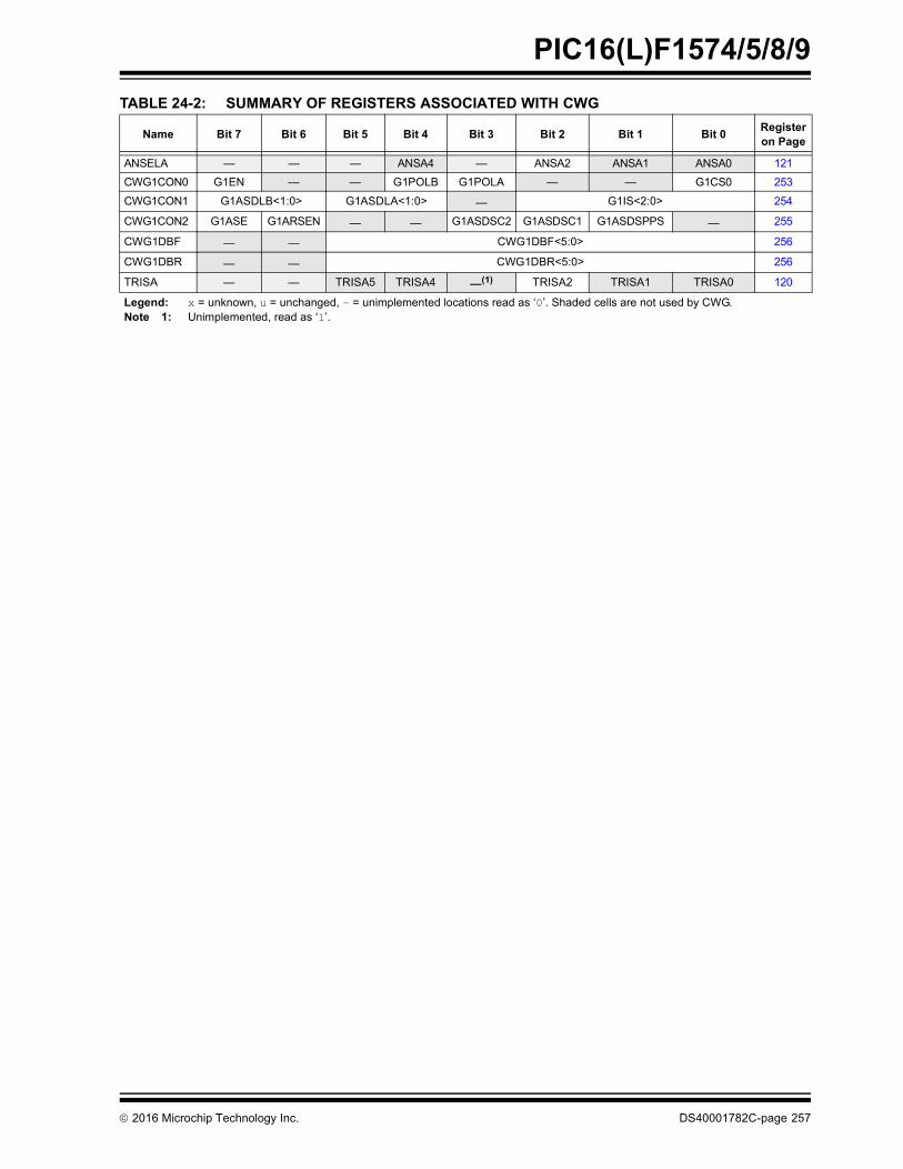
2016 Microchip Technology Inc. DS40001782C-page 257
PIC16(L)F1574/5/8/9
TABLE 24-2: SUMMARY OF REGISTERS ASSOCIATED WITH CWG
Name Bit 7 Bit 6 Bit 5 Bit 4 Bit 3 Bit 2 Bit 1 Bit 0Register on Page
ANSELA — — — ANSA4 — ANSA2 ANSA1 ANSA0 121
CWG1CON0 G1EN — — G1POLB G1POLA — — G1CS0 253
CWG1CON1 G1ASDLB<1:0> G1ASDLA<1:0> — G1IS<2:0> 254
CWG1CON2 G1ASE G1ARSEN — — G1ASDSC2 G1ASDSC1 G1ASDSPPS — 255
CWG1DBF — — CWG1DBF<5:0> 256
CWG1DBR — — CWG1DBR<5:0> 256
TRISA — — TRISA5 TRISA4 —(1) TRISA2 TRISA1 TRISA0 120
Legend: x = unknown, u = unchanged, – = unimplemented locations read as ‘0’. Shaded cells are not used by CWG.Note 1: Unimplemented, read as ‘1’.

PIC16(L)F1574/5/8/9
DS40001782C-page 258 2016 Microchip Technology Inc.
25.0 IN-CIRCUIT SERIAL PROGRAMMING™ (ICSP™)
ICSP™ programming allows customers to manufacturecircuit boards with unprogrammed devices. Programmingcan be done after the assembly process allowing thedevice to be programmed with the most recent firmwareor a custom firmware. Five pins are needed for ICSP™programming:
• ICSPCLK
• ICSPDAT
• MCLR/VPP
• VDD
• VSS
In Program/Verify mode the program memory, user IDsand the Configuration Words are programmed throughserial communications. The ICSPDAT pin is a bidirec-tional I/O used for transferring the serial data and theICSPCLK pin is the clock input. For more information onICSP™ refer to the “PIC16(L)F157x Memory Program-ming Specification” (DS40001766).
25.1 High-Voltage Programming Entry Mode
The device is placed into High-Voltage ProgrammingEntry mode by holding the ICSPCLK and ICSPDATpins low then raising the voltage on MCLR/VPP to VIHH.
25.2 Low-Voltage Programming Entry Mode
The Low-Voltage Programming Entry mode allows thePIC® Flash MCUs to be programmed using VDD only,without high voltage. When the LVP bit of ConfigurationWords is set to ‘1’, the ICSP Low-Voltage ProgrammingEntry mode is enabled. To disable the Low-VoltageICSP mode, the LVP bit must be programmed to ‘0’.
Entry into the Low-Voltage Programming Entry moderequires the following steps:
1. MCLR is brought to VIL.
2. A 32-bit key sequence is presented onICSPDAT, while clocking ICSPCLK.
Once the key sequence is complete, MCLR must beheld at VIL for as long as Program/Verify mode is to bemaintained.
If low-voltage programming is enabled (LVP = 1), theMCLR Reset function is automatically enabled andcannot be disabled. See Section 6.5 “MCLR” for moreinformation.
The LVP bit can only be reprogrammed to ‘0’ by usingthe High-Voltage Programming mode.
25.3 Common Programming Interfaces
Connection to a target device is typically done throughan ICSP™ header. A commonly found connector ondevelopment tools is the RJ-11 in the 6P6C (6-pin,6-connector) configuration. See Figure 25-1.
FIGURE 25-1: ICD RJ-11 STYLE CONNECTOR INTERFACE
Another connector often found in use with the PICkit™programmers is a standard 6-pin header with 0.1 inchspacing. Refer to Figure 25-2.
1
2
3
4
5
6
Target
Bottom SidePC BoardVPP/MCLR VSS
ICSPCLKVDD
ICSPDATNC
Pin Description*
1 = VPP/MCLR
2 = VDD Target
3 = VSS (ground)
4 = ICSPDAT
5 = ICSPCLK
6 = No Connect

2016 Microchip Technology Inc. DS40001782C-page 259
PIC16(L)F1574/5/8/9
FIGURE 25-2: PICkit™ PROGRAMMER STYLE CONNECTOR INTERFACE
For additional interface recommendations, refer to yourspecific device programmer manual prior to PCBdesign.
It is recommended that isolation devices be used toseparate the programming pins from other circuitry.The type of isolation is highly dependent on the specificapplication and may include devices such as resistors,diodes, or even jumpers. See Figure 25-3 for moreinformation.
FIGURE 25-3: TYPICAL CONNECTION FOR ICSP™ PROGRAMMING
1
3
56
4
2
Pin 1 Indicator
Pin Description*
1 = VPP/MCLR
2 = VDD Target
3 = VSS (ground)
4 = ICSPDAT
5 = ICSPCLK
6 = No connect
* The 6-pin header (0.100" spacing) accepts 0.025" square pins
Rev. 10-000128A7/30/2013
Device to beProgrammed
VDD VDD
VSS VSS
VPP MCLR/VPP
VDD
Data
Clock
ICSPDAT
ICSPCLK
* * *
ExternalProgrammingSignals
To Normal Connections
* Isolation devices (as required).
Rev. 10-000129A7/30/2013

PIC16(L)F1574/5/8/9
DS40001782C-page 260 2016 Microchip Technology Inc.
26.0 INSTRUCTION SET SUMMARY
Each instruction is a 14-bit word containing the opera-tion code (opcode) and all required operands. Theopcodes are broken into three broad categories.
• Byte Oriented
• Bit Oriented
• Literal and Control
The literal and control category contains the mostvaried instruction word format.
Table 26-3 lists the instructions recognized by theMPASMTM assembler.
All instructions are executed within a single instructioncycle, with the following exceptions, which may taketwo or three cycles:
• Subroutine takes two cycles (CALL, CALLW)• Returns from interrupts or subroutines take two
cycles (RETURN, RETLW, RETFIE)• Program branching takes two cycles (GOTO, BRA, BRW, BTFSS, BTFSC, DECFSZ, INCSFZ)
• One additional instruction cycle will be used when any instruction references an indirect file register and the file select register is pointing to program memory.
One instruction cycle consists of 4 oscillator cycles; foran oscillator frequency of 4 MHz, this gives a nominalinstruction execution rate of 1 MHz.
All instruction examples use the format ‘0xhh’ torepresent a hexadecimal number, where ‘h’ signifies ahexadecimal digit.
26.1 Read-Modify-Write Operations
Any instruction that specifies a file register as part ofthe instruction performs a Read-Modify-Write (R-M-W)operation. The register is read, the data is modified,and the result is stored according to either the instruc-tion, or the destination designator ‘d’. A read operationis performed on a register even if the instruction writesto that register.
TABLE 26-1: OPCODE FIELD DESCRIPTIONS
TABLE 26-2: ABBREVIATION DESCRIPTIONS
Field Description
f Register file address (0x00 to 0x7F)
W Working register (accumulator)
b Bit address within an 8-bit file register
k Literal field, constant data or label
x Don’t care location (= 0 or 1). The assembler will generate code with x = 0. It is the recommended form of use for compatibility with all Microchip software tools.
d Destination select; d = 0: store result in W,d = 1: store result in file register f. Default is d = 1.
n FSR or INDF number. (0-1)
mm Pre-post increment-decrement mode selection
Field Description
PC Program Counter
TO Time-Out bit
C Carry bit
DC Digit Carry bit
Z Zero bit
PD Power-Down bit

2016 Microchip Technology Inc. DS40001782C-page 261
PIC16(L)F1574/5/8/9
FIGURE 26-1: GENERAL FORMAT FOR INSTRUCTIONS
Byte-oriented file register operations13 8 7 6 0
d = 0 for destination W
OPCODE d f (FILE #)
d = 1 for destination ff = 7-bit file register address
Bit-oriented file register operations13 10 9 7 6 0
OPCODE b (BIT #) f (FILE #)
b = 3-bit bit addressf = 7-bit file register address
Literal and control operations
13 8 7 0
OPCODE k (literal)
k = 8-bit immediate value
13 11 10 0
OPCODE k (literal)
k = 11-bit immediate value
General
CALL and GOTO instructions only
MOVLP instruction only
13 5 4 0
OPCODE k (literal)
k = 5-bit immediate value
MOVLB instruction only
13 9 8 0
OPCODE k (literal)
k = 9-bit immediate value
BRA instruction only
FSR Offset instructions
13 7 6 5 0
OPCODE n k (literal)
n = appropriate FSR
FSR Increment instructions
13 7 6 0
OPCODE k (literal)
k = 7-bit immediate value
13 3 2 1 0
OPCODE n m (mode)
n = appropriate FSRm = 2-bit mode value
k = 6-bit immediate value
13 0
OPCODE
OPCODE only

PIC16(L)F1574/5/8/9
DS40001782C-page 262 2016 Microchip Technology Inc.
TABLE 26-3: ENHANCED MID-RANGE INSTRUCTION SET
Mnemonic,Operands
Description Cycles14-Bit Opcode Status
AffectedNotes
MSb LSb
BYTE-ORIENTED FILE REGISTER OPERATIONS
ADDWFADDWFCANDWFASRFLSLFLSRFCLRFCLRWCOMFDECFINCFIORWFMOVFMOVWFRLFRRFSUBWFSUBWFBSWAPFXORWF
f, df, df, df, df, df, df–f, df, df, df, df, dff, df, df, df, df, df, d
Add W and fAdd with Carry W and fAND W with fArithmetic Right ShiftLogical Left ShiftLogical Right ShiftClear fClear WComplement fDecrement fIncrement fInclusive OR W with fMove fMove W to fRotate Left f through CarryRotate Right f through CarrySubtract W from fSubtract with Borrow W from fSwap nibbles in fExclusive OR W with f
11111111111111111111
0011001111110000000000000000000000110000
01111101010101110101011000010001100100111010010010000000110111000010101111100110
dfffdfffdfffdfffdfffdffflfff0000dfffdfffdfffdfffdfff1fffdfffdfffdfffdfffdfffdfff
ffffffffffffffffffffffffffff00xxffffffffffffffffffffffffffffffffffffffffffffffff
C, DC, ZC, DC, ZZC, ZC, ZC, ZZZZZZZZ
CCC, DC, ZC, DC, Z
Z
2222222
222222222222
BYTE ORIENTED SKIP OPERATIONS
DECFSZINCFSZ
f, df, d
Decrement f, Skip if 0Increment f, Skip if 0
1(2)1(2)
0000
10111111
dfffdfff
ffffffff
1, 21, 2
BIT-ORIENTED FILE REGISTER OPERATIONS
BCFBSF
f, bf, b
Bit Clear fBit Set f
11
0101
00bb01bb
bfffbfff
ffffffff
22
BIT-ORIENTED SKIP OPERATIONS
BTFSCBTFSS
f, bf, b
Bit Test f, Skip if ClearBit Test f, Skip if Set
1 (2)1 (2)
0101
10bb11bb
bfff bfff
ffffffff
1, 21, 2
LITERAL OPERATIONS
ADDLWANDLWIORLWMOVLBMOVLPMOVLWSUBLWXORLW
kkkkkkkk
Add literal and WAND literal with WInclusive OR literal with WMove literal to BSRMove literal to PCLATHMove literal to WSubtract W from literalExclusive OR literal with W
11111111
1111110011111111
11101001100000000001000011001010
kkkkkkkkkkkk001k1kkkkkkkkkkkkkkk
kkkkkkkkkkkkkkkkkkkkkkkkkkkkkkkk
C, DC, ZZZ
C, DC, ZZ
Note 1: If the Program Counter (PC) is modified, or a conditional test is true, the instruction requires two cycles. The second cycle is executed as a NOP.
2: If this instruction addresses an INDF register and the MSb of the corresponding FSR is set, this instruction will require one additional instruction cycle.
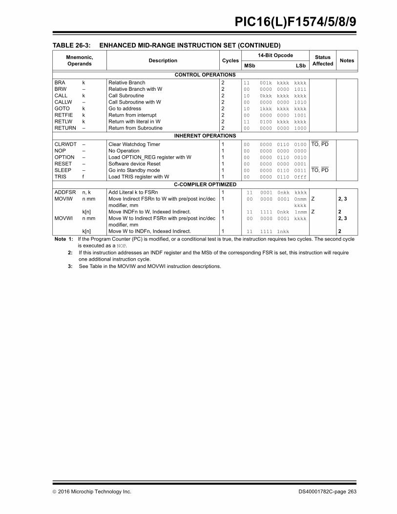
2016 Microchip Technology Inc. DS40001782C-page 263
PIC16(L)F1574/5/8/9
TABLE 26-3: ENHANCED MID-RANGE INSTRUCTION SET (CONTINUED)
Mnemonic,Operands
Description Cycles14-Bit Opcode Status
AffectedNotes
MSb LSb
CONTROL OPERATIONS
BRABRWCALLCALLWGOTORETFIERETLWRETURN
k–k–kkk–
Relative BranchRelative Branch with WCall SubroutineCall Subroutine with WGo to addressReturn from interruptReturn with literal in WReturn from Subroutine
22222222
1100100010001100
001k00000kkk00001kkk000001000000
kkkk0000kkkk0000kkkk0000kkkk0000
kkkk1011kkkk1010kkkk1001kkkk1000
INHERENT OPERATIONS
CLRWDTNOPOPTIONRESETSLEEPTRIS
–––––f
Clear Watchdog TimerNo OperationLoad OPTION_REG register with WSoftware device ResetGo into Standby modeLoad TRIS register with W
111111
000000000000
000000000000000000000000
011000000110000001100110
010000000010000100110fff
TO, PD
TO, PD
C-COMPILER OPTIMIZED
ADDFSRMOVIW
MOVWI
n, kn mm
k[n]n mm
k[n]
Add Literal k to FSRnMove Indirect FSRn to W with pre/post inc/dec modifier, mmMove INDFn to W, Indexed Indirect.Move W to Indirect FSRn with pre/post inc/dec modifier, mmMove W to INDFn, Indexed Indirect.
11
11
1
1100
1100
11
00010000
11110000
1111
0nkk0001
0nkk0001
1nkk
kkkk0nmmkkkk1nmmkkkk
Z
Z
2, 3
22, 3
2
Note 1: If the Program Counter (PC) is modified, or a conditional test is true, the instruction requires two cycles. The second cycle is executed as a NOP.
2: If this instruction addresses an INDF register and the MSb of the corresponding FSR is set, this instruction will require one additional instruction cycle.
3: See Table in the MOVIW and MOVWI instruction descriptions.

PIC16(L)F1574/5/8/9
DS40001782C-page 264 2016 Microchip Technology Inc.
26.2 Instruction Descriptions
ADDFSR Add Literal to FSRn
Syntax: [ label ] ADDFSR FSRn, k
Operands: -32 k 31n [ 0, 1]
Operation: FSR(n) + k FSR(n)
Status Affected: None
Description: The signed 6-bit literal ‘k’ is added to the contents of the FSRnH:FSRnL register pair.
FSRn is limited to the range 0000h - FFFFh. Moving beyond these bounds will cause the FSR to wrap-around.
ADDLW Add literal and W
Syntax: [ label ] ADDLW k
Operands: 0 k 255
Operation: (W) + k (W)
Status Affected: C, DC, Z
Description: The contents of the W register are added to the 8-bit literal ‘k’ and the result is placed in the W register.
ADDWF Add W and f
Syntax: [ label ] ADDWF f,d
Operands: 0 f 127d 0,1
Operation: (W) + (f) (destination)
Status Affected: C, DC, Z
Description: Add the contents of the W register with register ‘f’. If ‘d’ is ‘0’, the result is stored in the W register. If ‘d’ is ‘1’, the result is stored back in register ‘f’.
ADDWFC ADD W and CARRY bit to f
Syntax: [ label ] ADDWFC f {,d}
Operands: 0 f 127d [0,1]
Operation: (W) + (f) + (C) dest
Status Affected: C, DC, Z
Description: Add W, the Carry flag and data mem-ory location ‘f’. If ‘d’ is ‘0’, the result is placed in W. If ‘d’ is ‘1’, the result is placed in data memory location ‘f’.
ANDLW AND literal with W
Syntax: [ label ] ANDLW k
Operands: 0 k 255
Operation: (W) .AND. (k) (W)
Status Affected: Z
Description: The contents of W register are AND’ed with the 8-bit literal ‘k’. The result is placed in the W register.
ANDWF AND W with f
Syntax: [ label ] ANDWF f,d
Operands: 0 f 127d 0,1
Operation: (W) .AND. (f) (destination)
Status Affected: Z
Description: AND the W register with register ‘f’. If ‘d’ is ‘0’, the result is stored in the W register. If ‘d’ is ‘1’, the result is stored back in register ‘f’.
ASRF Arithmetic Right Shift
Syntax: [ label ] ASRF f {,d}
Operands: 0 f 127d [0,1]
Operation: (f<7>) dest<7>(f<7:1>) dest<6:0>,(f<0>) C,
Status Affected: C, Z
Description: The contents of register ‘f’ are shifted one bit to the right through the Carry flag. The MSb remains unchanged. If ‘d’ is ‘0’, the result is placed in W. If ‘d’ is ‘1’, the result is stored back in register ‘f’.
register f C
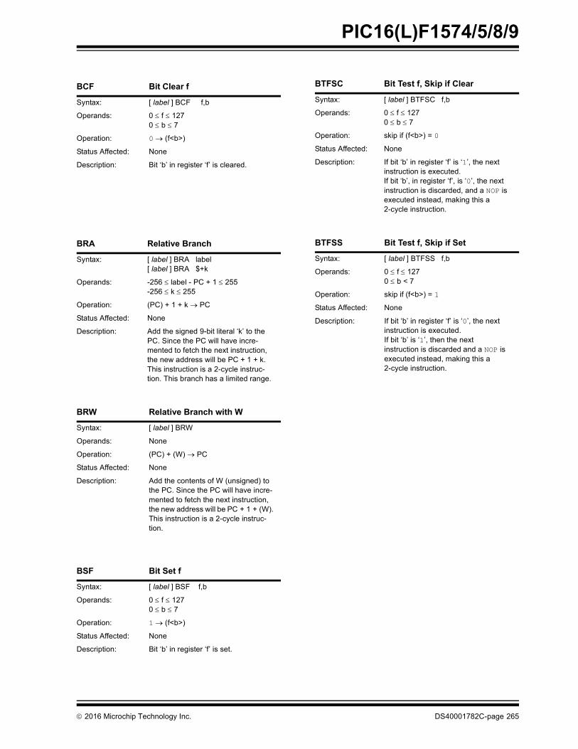
2016 Microchip Technology Inc. DS40001782C-page 265
PIC16(L)F1574/5/8/9
BCF Bit Clear f
Syntax: [ label ] BCF f,b
Operands: 0 f 1270 b 7
Operation: 0 (f<b>)
Status Affected: None
Description: Bit ‘b’ in register ‘f’ is cleared.
BRA Relative Branch
Syntax: [ label ] BRA label [ label ] BRA $+k
Operands: -256 label - PC + 1 255-256 k 255
Operation: (PC) + 1 + k PC
Status Affected: None
Description: Add the signed 9-bit literal ‘k’ to the PC. Since the PC will have incre-mented to fetch the next instruction, the new address will be PC + 1 + k. This instruction is a 2-cycle instruc-tion. This branch has a limited range.
BRW Relative Branch with W
Syntax: [ label ] BRW
Operands: None
Operation: (PC) + (W) PC
Status Affected: None
Description: Add the contents of W (unsigned) to the PC. Since the PC will have incre-mented to fetch the next instruction, the new address will be PC + 1 + (W). This instruction is a 2-cycle instruc-tion.
BSF Bit Set f
Syntax: [ label ] BSF f,b
Operands: 0 f 1270 b 7
Operation: 1 (f<b>)
Status Affected: None
Description: Bit ‘b’ in register ‘f’ is set.
BTFSC Bit Test f, Skip if Clear
Syntax: [ label ] BTFSC f,b
Operands: 0 f 1270 b 7
Operation: skip if (f<b>) = 0
Status Affected: None
Description: If bit ‘b’ in register ‘f’ is ‘1’, the next instruction is executed.If bit ‘b’, in register ‘f’, is ‘0’, the next instruction is discarded, and a NOP is executed instead, making this a 2-cycle instruction.
BTFSS Bit Test f, Skip if Set
Syntax: [ label ] BTFSS f,b
Operands: 0 f 1270 b < 7
Operation: skip if (f<b>) = 1
Status Affected: None
Description: If bit ‘b’ in register ‘f’ is ‘0’, the next instruction is executed.If bit ‘b’ is ‘1’, then the nextinstruction is discarded and a NOP is executed instead, making this a 2-cycle instruction.
PIC16(L)F1574/5/8/9
DS40001782C-page 266 2016 Microchip Technology Inc.
CALL Call Subroutine
Syntax: [ label ] CALL k
Operands: 0 k 2047
Operation: (PC)+ 1 TOS,k PC<10:0>,(PCLATH<6:3>) PC<14:11>
Status Affected: None
Description: Call Subroutine. First, return address (PC + 1) is pushed onto the stack. The 11-bit immediate address is loaded into PC bits <10:0>. The upper bits of the PC are loaded from PCLATH. CALL is a 2-cycle instruc-tion.
CALLW Subroutine Call With W
Syntax: [ label ] CALLW
Operands: None
Operation: (PC) +1 TOS,(W) PC<7:0>,(PCLATH<6:0>) PC<14:8>
Status Affected: None
Description: Subroutine call with W. First, the return address (PC + 1) is pushed onto the return stack. Then, the contents of W is loaded into PC<7:0>, and the contents of PCLATH into PC<14:8>. CALLW is a 2-cycle instruction.
CLRF Clear f
Syntax: [ label ] CLRF f
Operands: 0 f 127
Operation: 00h (f)1 Z
Status Affected: Z
Description: The contents of register ‘f’ are cleared and the Z bit is set.
CLRW Clear W
Syntax: [ label ] CLRW
Operands: None
Operation: 00h (W)1 Z
Status Affected: Z
Description: W register is cleared. Zero bit (Z) is set.
CLRWDT Clear Watchdog Timer
Syntax: [ label ] CLRWDT
Operands: None
Operation: 00h WDT0 WDT prescaler,1 TO1 PD
Status Affected: TO, PD
Description: CLRWDT instruction resets the Watch-dog Timer. It also resets the prescaler of the WDT. Status bits TO and PD are set.
COMF Complement f
Syntax: [ label ] COMF f,d
Operands: 0 f 127d [0,1]
Operation: (f) (destination)
Status Affected: Z
Description: The contents of register ‘f’ are complemented. If ‘d’ is ‘0’, the result is stored in W. If ‘d’ is ‘1’, the result is stored back in register ‘f’.
DECF Decrement f
Syntax: [ label ] DECF f,d
Operands: 0 f 127d [0,1]
Operation: (f) - 1 (destination)
Status Affected: Z
Description: Decrement register ‘f’. If ‘d’ is ‘0’, the result is stored in the W register. If ‘d’ is ‘1’, the result is stored back in register ‘f’.

2016 Microchip Technology Inc. DS40001782C-page 267
PIC16(L)F1574/5/8/9
DECFSZ Decrement f, Skip if 0
Syntax: [ label ] DECFSZ f,d
Operands: 0 f 127d [0,1]
Operation: (f) - 1 (destination); skip if result = 0
Status Affected: None
Description: The contents of register ‘f’ are decre-mented. If ‘d’ is ‘0’, the result is placed in the W register. If ‘d’ is ‘1’, the result is placed back in register ‘f’. If the result is ‘1’, the next instruction is executed. If the result is ‘0’, then a NOP is executed instead, making it a 2-cycle instruction.
GOTO Unconditional Branch
Syntax: [ label ] GOTO k
Operands: 0 k 2047
Operation: k PC<10:0>PCLATH<6:3> PC<14:11>
Status Affected: None
Description: GOTO is an unconditional branch. The 11-bit immediate value is loaded into PC bits <10:0>. The upper bits of PC are loaded from PCLATH<4:3>. GOTO is a 2-cycle instruction.
INCF Increment f
Syntax: [ label ] INCF f,d
Operands: 0 f 127d [0,1]
Operation: (f) + 1 (destination)
Status Affected: Z
Description: The contents of register ‘f’ are incre-mented. If ‘d’ is ‘0’, the result is placed in the W register. If ‘d’ is ‘1’, the result is placed back in register ‘f’.
INCFSZ Increment f, Skip if 0
Syntax: [ label ] INCFSZ f,d
Operands: 0 f 127d [0,1]
Operation: (f) + 1 (destination), skip if result = 0
Status Affected: None
Description: The contents of register ‘f’ are incre-mented. If ‘d’ is ‘0’, the result is placed in the W register. If ‘d’ is ‘1’, the result is placed back in register ‘f’.If the result is ‘1’, the next instruction is executed. If the result is ‘0’, a NOP is executed instead, making it a 2-cycle instruction.
IORLW Inclusive OR literal with W
Syntax: [ label ] IORLW k
Operands: 0 k 255
Operation: (W) .OR. k (W)
Status Affected: Z
Description: The contents of the W register are OR’ed with the 8-bit literal ‘k’. The result is placed in the W register.
IORWF Inclusive OR W with f
Syntax: [ label ] IORWF f,d
Operands: 0 f 127d [0,1]
Operation: (W) .OR. (f) (destination)
Status Affected: Z
Description: Inclusive OR the W register with regis-ter ‘f’. If ‘d’ is ‘0’, the result is placed in the W register. If ‘d’ is ‘1’, the result is placed back in register ‘f’.

PIC16(L)F1574/5/8/9
DS40001782C-page 268 2016 Microchip Technology Inc.
LSLF Logical Left Shift
Syntax: [ label ] LSLF f {,d}
Operands: 0 f 127d [0,1]
Operation: (f<7>) C(f<6:0>) dest<7:1>0 dest<0>
Status Affected: C, Z
Description: The contents of register ‘f’ are shifted one bit to the left through the Carry flag. A ‘0’ is shifted into the LSb. If ‘d’ is ‘0’, the result is placed in W. If ‘d’ is ‘1’, the result is stored back in register ‘f’.
LSRF Logical Right Shift
Syntax: [ label ] LSRF f {,d}
Operands: 0 f 127d [0,1]
Operation: 0 dest<7>(f<7:1>) dest<6:0>,(f<0>) C,
Status Affected: C, Z
Description: The contents of register ‘f’ are shifted one bit to the right through the Carry flag. A ‘0’ is shifted into the MSb. If ‘d’ is ‘0’, the result is placed in W. If ‘d’ is ‘1’, the result is stored back in register ‘f’.
register f 0C
register f C0
MOVF Move f
Syntax: [ label ] MOVF f,d
Operands: 0 f 127d [0,1]
Operation: (f) (dest)
Status Affected: Z
Description: The contents of register f is moved to a destination dependent upon the status of d. If d = 0,destination is W register. If d = 1, the destination is file register f itself. d = 1 is useful to test a file register since status flag Z is affected.
Words: 1
Cycles: 1
Example: MOVF FSR, 0
After InstructionW = value in FSR registerZ = 1

2016 Microchip Technology Inc. DS40001782C-page 269
PIC16(L)F1574/5/8/9
MOVIW Move INDFn to W
Syntax: [ label ] MOVIW ++FSRn[ label ] MOVIW --FSRn[ label ] MOVIW FSRn++[ label ] MOVIW FSRn--[ label ] MOVIW k[FSRn]
Operands: n [0,1]mm [00,01, 10, 11]-32 k 31
Operation: INDFn WEffective address is determined by• FSR + 1 (preincrement)• FSR - 1 (predecrement)• FSR + k (relative offset)After the Move, the FSR value will be either:• FSR + 1 (all increments)• FSR - 1 (all decrements)• Unchanged
Status Affected: Z
Mode Syntax mm
Preincrement ++FSRn 00
Predecrement --FSRn 01
Postincrement FSRn++ 10
Postdecrement FSRn-- 11
Description: This instruction is used to move data between W and one of the indirect registers (INDFn). Before/after this move, the pointer (FSRn) is updated by pre/post incrementing/decrementing it.
Note: The INDFn registers are not physical registers. Any instruction that accesses an INDFn register actually accesses the register at the address specified by the FSRn.
FSRn is limited to the range 0000h - FFFFh. Incrementing/decrementing it beyond these bounds will cause it to wrap-around.
MOVLB Move literal to BSR
Syntax: [ label ] MOVLB k
Operands: 0 k 31
Operation: k BSR
Status Affected: None
Description: The 5-bit literal ‘k’ is loaded into the Bank Select Register (BSR).
MOVLP Move literal to PCLATH
Syntax: [ label ] MOVLP k
Operands: 0 k 127
Operation: k PCLATH
Status Affected: None
Description: The 7-bit literal ‘k’ is loaded into the PCLATH register.
MOVLW Move literal to W
Syntax: [ label ] MOVLW k
Operands: 0 k 255
Operation: k (W)
Status Affected: None
Description: The 8-bit literal ‘k’ is loaded into W reg-ister. The “don’t cares” will assemble as ‘0’s.
Words: 1
Cycles: 1
Example: MOVLW 0x5A
After InstructionW = 0x5A
MOVWF Move W to f
Syntax: [ label ] MOVWF f
Operands: 0 f 127
Operation: (W) (f)
Status Affected: None
Description: Move data from W register to register ‘f’.
Words: 1
Cycles: 1
Example: MOVWF OPTION_REG
Before InstructionOPTION_REG = 0xFFW = 0x4FAfter InstructionOPTION_REG = 0x4FW = 0x4F

PIC16(L)F1574/5/8/9
DS40001782C-page 270 2016 Microchip Technology Inc.
MOVWI Move W to INDFn
Syntax: [ label ] MOVWI ++FSRn[ label ] MOVWI --FSRn[ label ] MOVWI FSRn++[ label ] MOVWI FSRn--[ label ] MOVWI k[FSRn]
Operands: n [0,1]mm [00,01, 10, 11]-32 k 31
Operation: W INDFnEffective address is determined by• FSR + 1 (preincrement)• FSR - 1 (predecrement)• FSR + k (relative offset)After the Move, the FSR value will be either:• FSR + 1 (all increments)• FSR - 1 (all decrements)Unchanged
Status Affected: None
Mode Syntax mm
Preincrement ++FSRn 00
Predecrement --FSRn 01
Postincrement FSRn++ 10
Postdecrement FSRn-- 11
Description: This instruction is used to move data between W and one of the indirect registers (INDFn). Before/after this move, the pointer (FSRn) is updated by pre/post incrementing/decrementing it.
Note: The INDFn registers are not physical registers. Any instruction that accesses an INDFn register actually accesses the register at the address specified by the FSRn.
FSRn is limited to the range 0000h - FFFFh. Incrementing/decrementing it beyond these bounds will cause it to wrap-around.
The increment/decrement operation on FSRn WILL NOT affect any Status bits.
NOP No Operation
Syntax: [ label ] NOP
Operands: None
Operation: No operation
Status Affected: None
Description: No operation.
Words: 1
Cycles: 1
Example: NOP
OPTIONLoad OPTION_REG Register with W
Syntax: [ label ] OPTION
Operands: None
Operation: (W) OPTION_REG
Status Affected: None
Description: Move data from W register to OPTION_REG register.
RESET Software Reset
Syntax: [ label ] RESET
Operands: None
Operation: Execute a device Reset. Resets the nRI flag of the PCON register.
Status Affected: None
Description: This instruction provides a way to execute a hardware Reset by software.

2016 Microchip Technology Inc. DS40001782C-page 271
PIC16(L)F1574/5/8/9
RETFIE Return from Interrupt
Syntax: [ label ] RETFIE
Operands: None
Operation: TOS PC,1 GIE
Status Affected: None
Description: Return from Interrupt. Stack is POPed and Top-of-Stack (TOS) is loaded in the PC. Interrupts are enabled by setting Global Interrupt Enable bit, GIE (INTCON<7>). This is a 2-cycle instruction.
Words: 1
Cycles: 2
Example: RETFIE
After InterruptPC = TOSGIE = 1
RETLW Return with literal in W
Syntax: [ label ] RETLW k
Operands: 0 k 255
Operation: k (W); TOS PC
Status Affected: None
Description: The W register is loaded with the 8-bit literal ‘k’. The program counter is loaded from the top of the stack (the return address). This is a 2-cycle instruction.
Words: 1
Cycles: 2
Example:
TABLE
CALL TABLE;W contains table;offset value
• ;W now has table value••ADDWF PC ;W = offsetRETLW k1 ;Begin tableRETLW k2 ;•••RETLW kn ; End of table
Before InstructionW = 0x07
After InstructionW = value of k8
RETURN Return from Subroutine
Syntax: [ label ] RETURN
Operands: None
Operation: TOS PC
Status Affected: None
Description: Return from subroutine. The stack is POPed and the top of the stack (TOS) is loaded into the program counter. This is a 2-cycle instruction.
RLF Rotate Left f through Carry
Syntax: [ label ] RLF f,d
Operands: 0 f 127d [0,1]
Operation: See description below
Status Affected: C
Description: The contents of register ‘f’ are rotated one bit to the left through the Carry flag. If ‘d’ is ‘0’, the result is placed in the W register. If ‘d’ is ‘1’, the result is stored back in register ‘f’.
Words: 1
Cycles: 1
Example: RLF REG1,0
Before InstructionREG1 = 1110 0110C = 0
After InstructionREG1 = 1110 0110W = 1100 1100C = 1
Register fC

PIC16(L)F1574/5/8/9
DS40001782C-page 272 2016 Microchip Technology Inc.
RRF Rotate Right f through Carry
Syntax: [ label ] RRF f,d
Operands: 0 f 127d [0,1]
Operation: See description below
Status Affected: C
Description: The contents of register ‘f’ are rotated one bit to the right through the Carry flag. If ‘d’ is ‘0’, the result is placed in the W register. If ‘d’ is ‘1’, the result is placed back in register ‘f’.
SLEEP Enter Sleep mode
Syntax: [ label ] SLEEP
Operands: None
Operation: 00h WDT,0 WDT prescaler,1 TO,0 PD
Status Affected: TO, PD
Description: The power-down Status bit, PD is cleared. Time-out Status bit, TO is set. Watchdog Timer and its pres-caler are cleared.The processor is put into Sleep mode with the oscillator stopped.
Register fC
SUBLW Subtract W from literal
Syntax: [ label ] SUBLW k
Operands: 0 k 255
Operation: k - (W) W)
Status Affected: C, DC, Z
Description: The W register is subtracted (2’s com-plement method) from the 8-bit literal ‘k’. The result is placed in the W regis-ter.
SUBWF Subtract W from f
Syntax: [ label ] SUBWF f,d
Operands: 0 f 127d [0,1]
Operation: (f) - (W) destination)
Status Affected: C, DC, Z
Description: Subtract (2’s complement method) W register from register ‘f’. If ‘d’ is ‘0’, the result is stored in the W register. If ‘d’ is ‘1’, the result is stored back in register ‘f.
SUBWFB Subtract W from f with Borrow
Syntax: SUBWFB f {,d}
Operands: 0 f 127d [0,1]
Operation: (f) – (W) – (B) dest
Status Affected: C, DC, Z
Description: Subtract W and the BORROW flag (CARRY) from register ‘f’ (2’s comple-ment method). If ‘d’ is ‘0’, the result is stored in W. If ‘d’ is ‘1’, the result is stored back in register ‘f’.
C = 0 W k
C = 1 W k
DC = 0 W<3:0> k<3:0>
DC = 1 W<3:0> k<3:0>
C = 0 W f
C = 1 W f
DC = 0 W<3:0> f<3:0>
DC = 1 W<3:0> f<3:0>
2016 Microchip Technology Inc. DS40001782C-page 273
PIC16(L)F1574/5/8/9
SWAPF Swap Nibbles in f
Syntax: [ label ] SWAPF f,d
Operands: 0 f 127d [0,1]
Operation: (f<3:0>) (destination<7:4>),(f<7:4>) (destination<3:0>)
Status Affected: None
Description: The upper and lower nibbles of regis-ter ‘f’ are exchanged. If ‘d’ is ‘0’, the result is placed in the W register. If ‘d’ is ‘1’, the result is placed in register ‘f’.
TRIS Load TRIS Register with W
Syntax: [ label ] TRIS f
Operands: 5 f 7
Operation: (W) TRIS register ‘f’
Status Affected: None
Description: Move data from W register to TRIS register.When ‘f’ = 5, TRISA is loaded.When ‘f’ = 6, TRISB is loaded.When ‘f’ = 7, TRISC is loaded.
XORLW Exclusive OR literal with W
Syntax: [ label ] XORLW k
Operands: 0 k 255
Operation: (W) .XOR. k W)
Status Affected: Z
Description: The contents of the W register are XOR’ed with the 8-bit literal ‘k’. The result is placed in the W register.
XORWF Exclusive OR W with f
Syntax: [ label ] XORWF f,d
Operands: 0 f 127d [0,1]
Operation: (W) .XOR. (f) destination)
Status Affected: Z
Description: Exclusive OR the contents of the W register with register ‘f’. If ‘d’ is ‘0’, the result is stored in the W register. If ‘d’ is ‘1’, the result is stored back in register ‘f’.
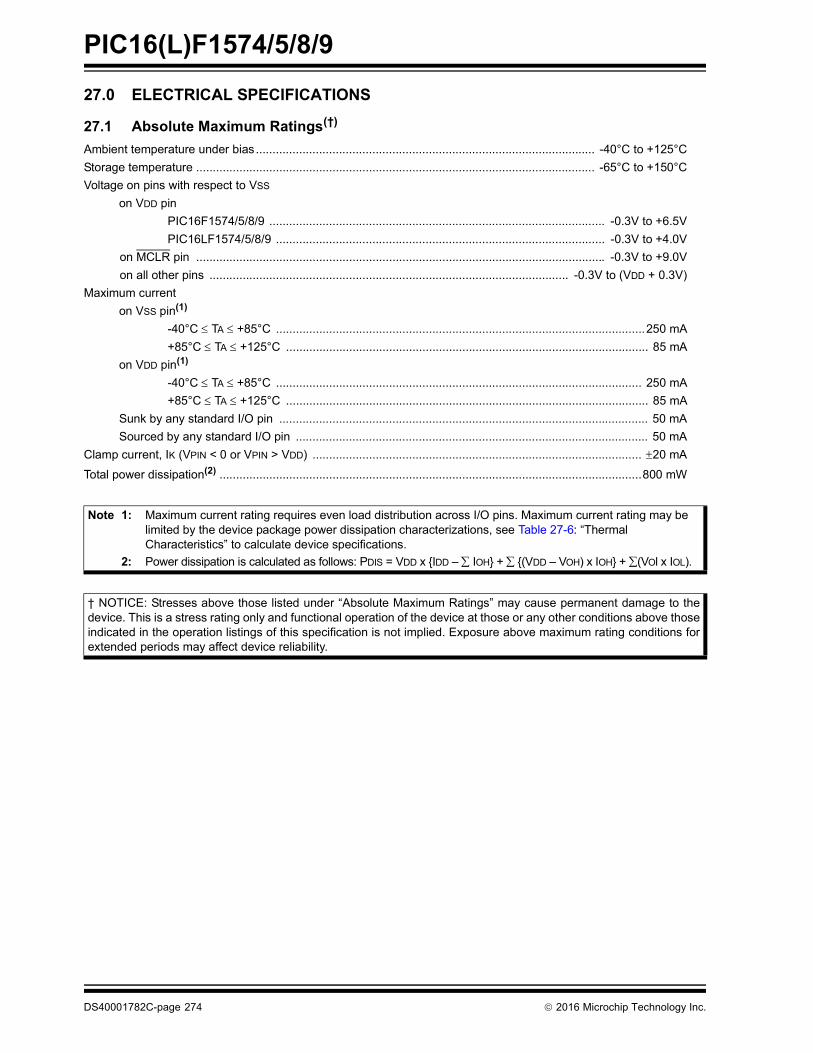
PIC16(L)F1574/5/8/9
DS40001782C-page 274 2016 Microchip Technology Inc.
27.0 ELECTRICAL SPECIFICATIONS
27.1 Absolute Maximum Ratings(†)
Ambient temperature under bias ...................................................................................................... -40°C to +125°C
Storage temperature ........................................................................................................................ -65°C to +150°C
Voltage on pins with respect to VSS
on VDD pin
PIC16F1574/5/8/9 ..................................................................................................... -0.3V to +6.5V
PIC16LF1574/5/8/9 ................................................................................................... -0.3V to +4.0V
on MCLR pin ........................................................................................................................... -0.3V to +9.0V
on all other pins ............................................................................................................ -0.3V to (VDD + 0.3V)
Maximum current
on VSS pin(1)
-40°C TA +85°C ...............................................................................................................250 mA
+85°C TA +125°C ............................................................................................................. 85 mA
on VDD pin(1)
-40°C TA +85°C .............................................................................................................. 250 mA
+85°C TA +125°C ............................................................................................................. 85 mA
Sunk by any standard I/O pin ............................................................................................................... 50 mA
Sourced by any standard I/O pin .......................................................................................................... 50 mA
Clamp current, IK (VPIN < 0 or VPIN > VDD) ................................................................................................... 20 mA
Total power dissipation(2) ...............................................................................................................................800 mW
Note 1: Maximum current rating requires even load distribution across I/O pins. Maximum current rating may be limited by the device package power dissipation characterizations, see Table 27-6: “Thermal Characteristics” to calculate device specifications.
2: Power dissipation is calculated as follows: PDIS = VDD x {IDD – IOH} + {(VDD – VOH) x IOH} + (VOl x IOL).
† NOTICE: Stresses above those listed under “Absolute Maximum Ratings” may cause permanent damage to thedevice. This is a stress rating only and functional operation of the device at those or any other conditions above thoseindicated in the operation listings of this specification is not implied. Exposure above maximum rating conditions forextended periods may affect device reliability.
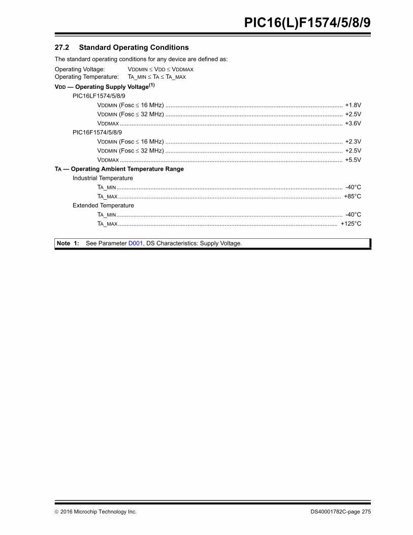
2016 Microchip Technology Inc. DS40001782C-page 275
PIC16(L)F1574/5/8/9
27.2 Standard Operating Conditions
The standard operating conditions for any device are defined as:
Operating Voltage: VDDMIN VDD VDDMAX
Operating Temperature: TA_MIN TA TA_MAX
VDD — Operating Supply Voltage(1)
PIC16LF1574/5/8/9
VDDMIN (Fosc 16 MHz) ......................................................................................................... +1.8V
VDDMIN (Fosc 32 MHz) ......................................................................................................... +2.5V
VDDMAX .................................................................................................................................... +3.6V
PIC16F1574/5/8/9
VDDMIN (Fosc 16 MHz) ......................................................................................................... +2.3V
VDDMIN (Fosc 32 MHz) ......................................................................................................... +2.5V
VDDMAX .................................................................................................................................... +5.5V
TA — Operating Ambient Temperature Range
Industrial Temperature
TA_MIN...................................................................................................................................... -40°C
TA_MAX.................................................................................................................................... +85°C
Extended Temperature
TA_MIN...................................................................................................................................... -40°C
TA_MAX.................................................................................................................................. +125°C
Note 1: See Parameter D001, DS Characteristics: Supply Voltage.

PIC16(L)F1574/5/8/9
DS40001782C-page 276 2016 Microchip Technology Inc.
FIGURE 27-1: VOLTAGE FREQUENCY GRAPH, -40°C TA +125°C, PIC16F1574/5/8/9 ONLY
FIGURE 27-2: VOLTAGE FREQUENCY GRAPH, -40°C TA +125°C, PIC16LF1574/5/8/9 ONLY
Note 1: The shaded region indicates the permissible combinations of voltage and frequency.
2: Refer to Table 27-7 for each Oscillator mode’s supported frequencies.
3.6
2.5
1.8
0 16 20
VDD
(V)
Frequency (MHz)
Rev. 10-000131A8/5/2013
Note 1: The shaded region indicates the permissible combinations of voltage and frequency.
2: Refer to Table 27-7 for each Oscillator mode’s supported frequencies.
Rev. 10-000131B9/19/2013
3.6
2.5
1.8
0 16 32
VDD
(V)
Frequency (MHz)

2016 Microchip Technology Inc. DS40001782C-page 277
PIC16(L)F1574/5/8/9
27.3 DC Characteristics
TABLE 27-1: SUPPLY VOLTAGE
PIC16LF1574/5/8/9 Standard Operating Conditions (unless otherwise stated)
PIC16F1574/5/8/9
Param. No.
Sym. Characteristic Min. Typ† Max. Units Conditions
D001 VDD Supply Voltage
VDDMIN
1.82.5
——
VDDMAX
3.63.6
VV
FOSC 16 MHzFOSC 32 MHz (Note 3)
D001 2.32.5
——
5.55.5
VV
FOSC 16 MHzFOSC 32 MHz (Note 3)
D002* VDR RAM Data Retention Voltage(1)
1.5 — — V Device in Sleep mode
D002* 1.7 — — V Device in Sleep mode
D002A* VPOR Power-on Reset Release Voltage(2)
— 1.6 — V
D002A* — 1.6 — V
D002B* VPORR* Power-on Reset Rearm Voltage(2)
— 0.8 — V
D002B* — 1.5 — V
D003 VFVR Fixed Voltage Reference Voltage — 1.024 — V -40°C TA +85°C
D003A VADFVR FVR Gain Voltage Accuracy for ADC
-4-4-5
—445
%1x VFVR, ADFVR = 01, VDD 2.5V2x VFVR, ADFVR = 10, VDD 2.5V4x VFVR, ADFVR = 11, VDD 4.75V
D003B VCDAFVR FVR Gain Voltage Accuracy for Comparator
-4-4-5
—445
%1x VFVR, CDAFVR = 01, VDD 2.5V2x VFVR, CDAFVR = 10, VDD 2.5V4x VFVR, CDAFVR = 11, VDD 4.75V
D004* SVDD VDD Rise Rate(2) 0.05 — — V/ms Ensures that the Power-on Reset signal is released properly.
* These parameters are characterized but not tested.† Data in “Typ” column is at 3.0V, 25°C unless otherwise stated. These parameters are for design guidance only and are not
tested.Note 1: This is the limit to which VDD can be lowered in Sleep mode without losing RAM data.
2: See Figure 27-3, POR and POR REARM with Slow Rising VDD.3: PLL required for 32 MHz operation.
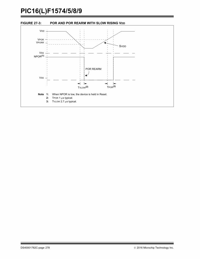
PIC16(L)F1574/5/8/9
DS40001782C-page 278 2016 Microchip Technology Inc.
FIGURE 27-3: POR AND POR REARM WITH SLOW RISING VDD
VDD
VPOR
VPORR
VSS
VSS
NPOR(1)
TPOR(3)
POR REARM
Note 1: When NPOR is low, the device is held in Reset.2: TPOR 1 s typical.3: TVLOW 2.7 s typical.
TVLOW(2)
SVDD

2016 Microchip Technology Inc. DS40001782C-page 279
PIC16(L)F1574/5/8/9
TABLE 27-2: SUPPLY CURRENT (IDD)(1,2)
PIC16LF1574/5/8/9 Standard Operating Conditions (unless otherwise stated)
PIC16F1574/5/8/9
Param.No.
Device Characteristics
Min. Typ† Max. UnitsConditions
VDD Note
D013 — 41 51 A 1.8 FOSC = 1 MHz,External Clock (ECM),Medium Power mode
— 69 80 A 3.0
D013 — 79 107 A 2.3 FOSC = 1 MHz,External Clock (ECM),Medium Power mode
— 105 138 A 3.0
— 151 184 A 5.0
D014 — 134 152 A 1.8 FOSC = 4 MHz,External Clock (ECM),Medium Power mode
— 234 268 A 3.0
D014 — 201 255 A 2.3 FOSC = 4 MHz,External Clock (ECM),Medium Power mode
— 270 329 A 3.0
— 344 431 A 5.0
D015 — 7 19 A 1.8 FOSC = 31 kHz,LFINTOSC,-40°C TA +85°C
— 9 20 A 3.0
D015 — 15 25 A 2.3 FOSC = 31 kHz,LFINTOSC,-40°C TA +85°C
— 18 28 A 3.0
— 20 29 A 5.0
D016 — 128 174 A 1.8 FOSC = 500 kHz, MFINTOSC— 153 203 A 3.0
D016 — 166 241 A 2.3 FOSC = 500 kHz, MFINTOSC— 187 273 A 3.0
— 249 332 A 5.0
D017* — 0.6 0.7 mA 1.8 FOSC = 8 MHz,HFINTOSC— 0.9 1.1 mA 3.0
D017* — 0.7 1.0 mA 2.3 FOSC = 8 MHz,HFINTOSC— 1.0 1.1 mA 3.0
— 1.1 1.2 mA 5.0
D018 — 0.9 1.0 mA 1.8 FOSC = 16 MHz,HFINTOSC — 1.3 1.4 mA 3.0
D018 — 1.1 1.3 mA 2.3 FOSC = 16 MHz,HFINTOSC — 1.3 1.5 mA 3.0
— 1.5 1.8 mA 5.0
* These parameters are characterized but not tested.† Data in “Typ” column is at 3.0V, 25°C unless otherwise stated. These parameters are for design guidance
only and are not tested.Note 1: The test conditions for all IDD measurements in active operation mode are: CLKIN = external square wave,
from rail-to-rail; all I/O pins tri-stated, pulled to VSS; MCLR = VDD; WDT disabled.2: The supply current is mainly a function of the operating voltage and frequency. Other factors, such as I/O
pin loading and switching rate, oscillator type, internal code execution pattern and temperature, also have an impact on the current consumption.
3: PLL required for 32 MHz operation.
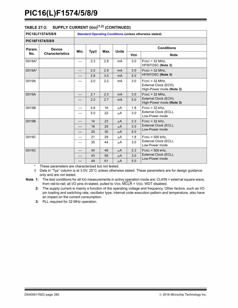
PIC16(L)F1574/5/8/9
DS40001782C-page 280 2016 Microchip Technology Inc.
D018A* — 2.3 2.8 mA 3.0 FOSC = 32 MHz,HFINTOSC (Note 3)
D018A* — 2.5 2.9 mA 3.0 FOSC = 32 MHz,HFINTOSC (Note 3)— 2.6 3.0 mA 5.0
D019A — 2.0 2.2 mA 3.0 FOSC = 32 MHz,External Clock (ECH),High-Power mode (Note 3)
D019A — 2.1 2.3 mA 3.0 FOSC = 32 MHz,External Clock (ECH),High-Power mode (Note 3)
— 2.2 2.7 mA 5.0
D019B — 2.6 16 A 1.8 FOSC = 32 kHz,External Clock (ECL),Low-Power mode
— 5.0 22 A 3.0
D019B — 14 23 A 2.3 FOSC = 32 kHz, External Clock (ECL),Low-Power mode
— 18 29 A 3.0
— 20 30 A 5.0
D019C — 21 29 A 1.8 FOSC = 500 kHz, External Clock (ECL),Low-Power mode
— 35 44 A 3.0
D019C — 34 46 A 2.3 FOSC = 500 kHz, External Clock (ECL),Low-Power mode
— 43 59 A 3.0
— 49 61 A 5.0
TABLE 27-2: SUPPLY CURRENT (IDD)(1,2) (CONTINUED)
PIC16LF1574/5/8/9 Standard Operating Conditions (unless otherwise stated)
PIC16F1574/5/8/9
Param.No.
Device Characteristics
Min. Typ† Max. UnitsConditions
VDD Note
* These parameters are characterized but not tested.† Data in “Typ” column is at 3.0V, 25°C unless otherwise stated. These parameters are for design guidance
only and are not tested.Note 1: The test conditions for all IDD measurements in active operation mode are: CLKIN = external square wave,
from rail-to-rail; all I/O pins tri-stated, pulled to VSS; MCLR = VDD; WDT disabled.2: The supply current is mainly a function of the operating voltage and frequency. Other factors, such as I/O
pin loading and switching rate, oscillator type, internal code execution pattern and temperature, also have an impact on the current consumption.
3: PLL required for 32 MHz operation.
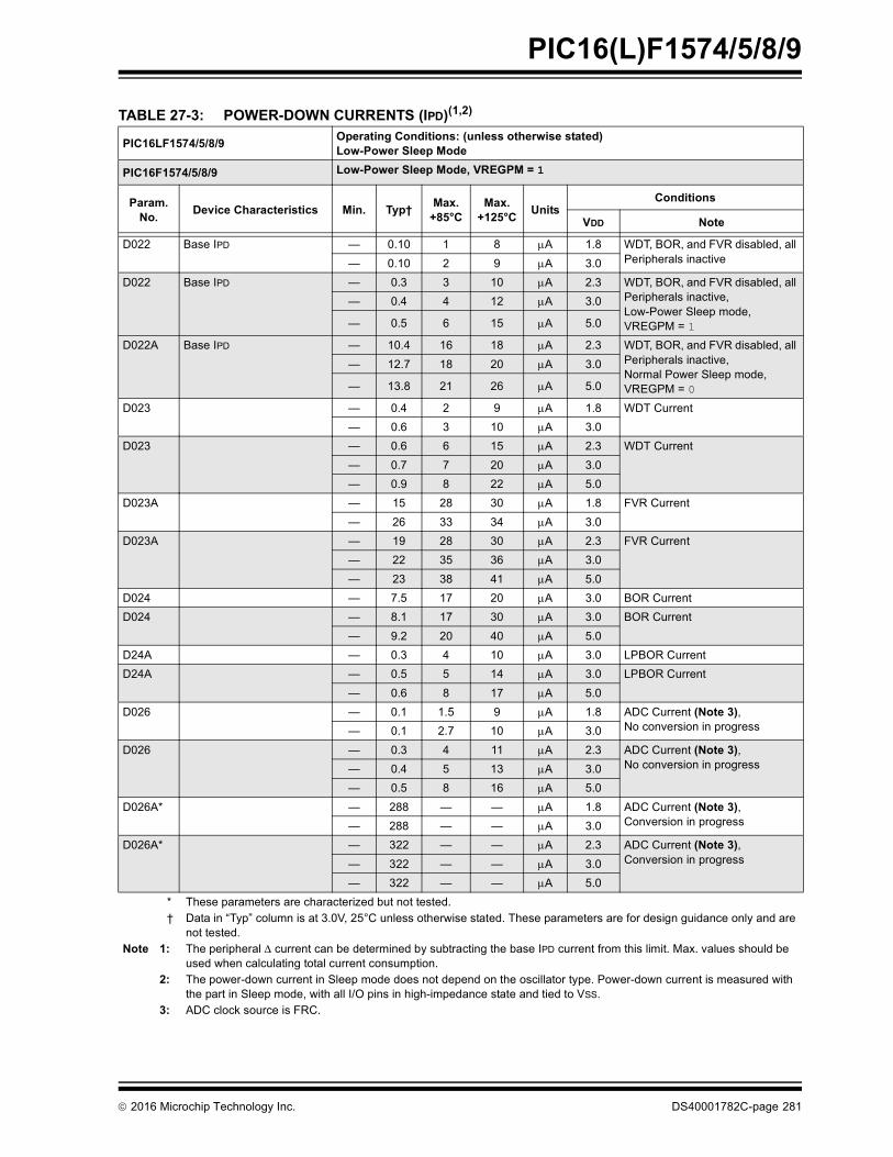
2016 Microchip Technology Inc. DS40001782C-page 281
PIC16(L)F1574/5/8/9
TABLE 27-3: POWER-DOWN CURRENTS (IPD)(1,2)
PIC16LF1574/5/8/9Operating Conditions: (unless otherwise stated)Low-Power Sleep Mode
PIC16F1574/5/8/9 Low-Power Sleep Mode, VREGPM = 1
Param.No.
Device Characteristics Min. Typ†Max.
+85°CMax.
+125°CUnits
Conditions
VDD Note
D022 Base IPD — 0.10 1 8 A 1.8 WDT, BOR, and FVR disabled, all Peripherals inactive— 0.10 2 9 A 3.0
D022 Base IPD — 0.3 3 10 A 2.3 WDT, BOR, and FVR disabled, all Peripherals inactive,Low-Power Sleep mode,VREGPM = 1
— 0.4 4 12 A 3.0
— 0.5 6 15 A 5.0
D022A Base IPD — 10.4 16 18 A 2.3 WDT, BOR, and FVR disabled, all Peripherals inactive,Normal Power Sleep mode, VREGPM = 0
— 12.7 18 20 A 3.0
— 13.8 21 26 A 5.0
D023 — 0.4 2 9 A 1.8 WDT Current
— 0.6 3 10 A 3.0
D023 — 0.6 6 15 A 2.3 WDT Current
— 0.7 7 20 A 3.0
— 0.9 8 22 A 5.0
D023A — 15 28 30 A 1.8 FVR Current
— 26 33 34 A 3.0
D023A — 19 28 30 A 2.3 FVR Current
— 22 35 36 A 3.0
— 23 38 41 A 5.0
D024 — 7.5 17 20 A 3.0 BOR Current
D024 — 8.1 17 30 A 3.0 BOR Current
— 9.2 20 40 A 5.0
D24A — 0.3 4 10 A 3.0 LPBOR Current
D24A — 0.5 5 14 A 3.0 LPBOR Current
— 0.6 8 17 A 5.0
D026 — 0.1 1.5 9 A 1.8 ADC Current (Note 3),No conversion in progress— 0.1 2.7 10 A 3.0
D026 — 0.3 4 11 A 2.3 ADC Current (Note 3),No conversion in progress— 0.4 5 13 A 3.0
— 0.5 8 16 A 5.0
D026A* — 288 — — A 1.8 ADC Current (Note 3),Conversion in progress— 288 — — A 3.0
D026A* — 322 — — A 2.3 ADC Current (Note 3),Conversion in progress— 322 — — A 3.0
— 322 — — A 5.0
* These parameters are characterized but not tested.† Data in “Typ” column is at 3.0V, 25°C unless otherwise stated. These parameters are for design guidance only and are
not tested.Note 1: The peripheral current can be determined by subtracting the base IPD current from this limit. Max. values should be
used when calculating total current consumption.2: The power-down current in Sleep mode does not depend on the oscillator type. Power-down current is measured with
the part in Sleep mode, with all I/O pins in high-impedance state and tied to VSS.3: ADC clock source is FRC.

PIC16(L)F1574/5/8/9
DS40001782C-page 282 2016 Microchip Technology Inc.
D027 — 5 22 25 A 1.8 Comparator,CxSP = 0— 5 23 27 A 3.0
D027 — 15 23 25 A 2.3 Comparator,CxSP = 0— 17 27 29 A 3.0
— 19 28 30 A 5.0
D028A — 23 41 42 A 1.8 Comparator, Normal Power, CxSP = 1 (Note 1)
— 25 42 44 A 3.0
D028A — 33 55 56 A 2.3 Comparator, Normal Power, CxSP = 1VREGPM = 1 (Note 1)
— 34 59 60 A 3.0
— 36 60 61 A 5.0
TABLE 27-3: POWER-DOWN CURRENTS (IPD)(1,2) (CONTINUED)
PIC16LF1574/5/8/9Operating Conditions: (unless otherwise stated)Low-Power Sleep Mode
PIC16F1574/5/8/9 Low-Power Sleep Mode, VREGPM = 1
Param.No.
Device Characteristics Min. Typ†Max.
+85°CMax.
+125°CUnits
Conditions
VDD Note
* These parameters are characterized but not tested.† Data in “Typ” column is at 3.0V, 25°C unless otherwise stated. These parameters are for design guidance only and are
not tested.Note 1: The peripheral current can be determined by subtracting the base IPD current from this limit. Max. values should be
used when calculating total current consumption.2: The power-down current in Sleep mode does not depend on the oscillator type. Power-down current is measured with
the part in Sleep mode, with all I/O pins in high-impedance state and tied to VSS.3: ADC clock source is FRC.

2016 Microchip Technology Inc. DS40001782C-page 283
PIC16(L)F1574/5/8/9
TABLE 27-4: I/O PORTSStandard Operating Conditions (unless otherwise stated)
Param.No.
Sym. Characteristic Min. Typ† Max. Units Conditions
VIL Input Low Voltage
I/O PORT:
D030 with TTL buffer — — 0.8 V 4.5V VDD 5.5V
D030A — — 0.15 VDD V 1.8V VDD 4.5V
D031 with Schmitt Trigger buffer — — 0.2 VDD V 2.0V VDD 5.5V
with I2C levels — — 0.3 VDD V
with SMbus levels — — 0.8 V 2.7V VDD 5.5V
D032 MCLR — — 0.2 VDD V
VIH Input High Voltage
I/O PORT:
D040 with TTL buffer 2.0 — — V 4.5V VDD 5.5V
D040A 0.25 VDD + 0.8
— — V 1.8V VDD 4.5V
D041 with Schmitt Trigger buffer 0.8 VDD — — V 2.0V VDD 5.5V
with I2C levels 0.7 VDD — — V
with SMbus levels 2.1 — — V 2.7V VDD 5.5V
D042 MCLR 0.8 VDD — — V
IIL Input Leakage Current(1)
D060 I/O Ports — ± 5 ± 125 nA VSS VPIN VDD, Pin at high-impedance, 85°C
— ± 5 ± 1000 nA VSS VPIN VDD, Pin at high-impedance, 125°C
D061 MCLR(2) — ± 50 ± 200 nA VSS VPIN VDD, Pin at high-impedance, 85°C
IPUR Weak Pull-up Current
D070* 25 100 200 A VDD = 3.3V, VPIN = VSS
25 140 300 A VDD = 5.0V, VPIN = VSS
VOL Output Low Voltage
D080 I/O Ports— — 0.6 V
IOL = 8 mA, VDD = 5VIOL = 6 mA, VDD = 3.3VIOL = 1.8 mA, VDD = 1.8V
VOH Output High Voltage
D090 I/O PortsVDD - 0.7 — — V
IOH = 3.5 mA, VDD = 5VIOH = 3 mA, VDD = 3.3VIOH = 1 mA, VDD = 1.8V
Capacitive Loading Specifications on Output Pins
D101A* CIO All I/O pins — — 50 pF
* These parameters are characterized but not tested.† Data in “Typ” column is at 3.0V, 25°C unless otherwise stated. These parameters are for design guidance only and are
not tested.Note 1: Negative current is defined as current sourced by the pin.
2: The leakage current on the MCLR pin is strongly dependent on the applied voltage level. The specified levels represent normal operating conditions. Higher leakage current may be measured at different input voltages.

PIC16(L)F1574/5/8/9
DS40001782C-page 284 2016 Microchip Technology Inc.
TABLE 27-5: MEMORY PROGRAMMING SPECIFICATIONS
Standard Operating Conditions (unless otherwise stated)
Param.No.
Sym. Characteristic Min. Typ† Max. Units Conditions
Program Memory Programming Specifications
D110 VIHH Voltage on MCLR/VPP pin 8.0 — 9.0 V (Note 2)
D111 IDDP Supply Current during Programming
— — 10 mA
D112 VBE VDD for Bulk Erase 2.7 — VDDMAX V
D113 VPEW VDD for Write or Row Erase VDDMIN — VDDMAX V
D114 IPPPGM Current on MCLR/VPP during Erase/Write
— 1.0 — mA
D115 IDDPGM Current on VDD during Erase/Write
— 5.0 — mA
Program Flash Memory
D121 EP Cell Endurance 10K — — E/W -40C TA +85C (Note 1)
D122 VPRW VDD for Read/Write VDDMIN — VDDMAX V
D123 TIW Self-timed Write Cycle Time — 2 2.5 ms
D124 TRETD Characteristic Retention — 40 — Year Provided no other specifications are violated
D125 EHEFC High-Endurance Flash Cell 100K — — E/W 0C TA +60°C, lower byte last 128 addresses
† Data in “Typ” column is at 3.0V, 25°C unless otherwise stated. These parameters are for design guidance only and are not tested.
Note 1: Self-write and Block Erase.2: Required only if single-supply programming is disabled.

2016 Microchip Technology Inc. DS40001782C-page 285
PIC16(L)F1574/5/8/9
TABLE 27-6: THERMAL CHARACTERISTICS
Standard Operating Conditions (unless otherwise stated)
Param.No.
Sym. Characteristic Typ. Units Conditions
TH01 JA Thermal Resistance Junction to Ambient 70 C/W 14-pin PDIP package
95.3 C/W 14-pin SOIC package
100 C/W 14-pin TSSOP package
31.8 C/W 16-pin UQFN 4x4mm package
62.2 C/W 20-pin PDIP package
77.7 C/W 20-pin SOIC package
87.3 C/W 20-pin SSOP package
32.8 C/W 20-pin UQFN 4x4mm package
TH02 JC Thermal Resistance Junction to Case 32.75 C/W 14-pin PDIP package
31 C/W 14-pin SOIC package
24.4 C/W 14-pin TSSOP package
24.4 C/W 16-pin UQFN 4x4mm package
27.5 C/W 20-pin PDIP package
23.1 C/W 20-pin SOIC package
31.1 C/W 20-pin SSOP package
27.4 C/W 20-pin UQFN 4x4mm package
TH03 TJMAX Maximum Junction Temperature 150 CTH04 PD Power Dissipation — W PD = PINTERNAL + PI/O
TH05 PINTERNAL Internal Power Dissipation — W PINTERNAL = IDD x VDD(1)
TH06 PI/O I/O Power Dissipation — W PI/O = (IOL * VOL) + (IOH * (VDD - VOH))
TH07 PDER Derated Power — W PDER = PDMAX (TJ - TA)/JA(2)
Note 1: IDD is current to run the chip alone without driving any load on the output pins.2: TA = Ambient Temperature; TJ = Junction Temperature

PIC16(L)F1574/5/8/9
DS40001782C-page 286 2016 Microchip Technology Inc.
27.4 AC Characteristics
Timing Parameter Symbology has been created with one of the following formats:
FIGURE 27-4: LOAD CONDITIONS
1. TppS2ppS
2. TppS
T
F Frequency T Time
Lowercase letters (pp) and their meanings:
pp
cc CCP1 osc CLKIN
ck CLKOUT rd RD
cs CS rw RD or WR
di SDIx sc SCKx
do SDO ss SS
dt Data in t0 T0CKI
io I/O PORT t1 T1CKI
mc MCLR wr WR
Uppercase letters and their meanings:
S
F Fall P Period
H High R Rise
I Invalid (High-impedance) V Valid
L Low Z High-impedance
Load Condition
Legend: CL=50 pF for all pins
Pin
CL
VSS
Rev. 10-000133A8/1/2013
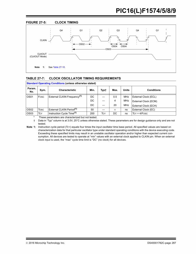
2016 Microchip Technology Inc. DS40001782C-page 287
PIC16(L)F1574/5/8/9
FIGURE 27-5: CLOCK TIMING
TABLE 27-7: CLOCK OSCILLATOR TIMING REQUIREMENTS
Standard Operating Conditions (unless otherwise stated)
Param.No.
Sym. Characteristic Min. Typ† Max. Units Conditions
OS01 FOSC External CLKIN Frequency(1) DC — 0.5 MHz External Clock (ECL)
DC — 4 MHz External Clock (ECM)
DC — 20 MHz External Clock (ECH)
OS02 TOSC External CLKIN Period(1) 50 — ns External Clock (EC)
OS03 TCY Instruction Cycle Time(1) 200 TCY DC ns TCY = 4/FOSC
* These parameters are characterized but not tested.† Data in “Typ” column is at 3.0V, 25°C unless otherwise stated. These parameters are for design guidance only and are not
tested.Note 1: Instruction cycle period (TCY) equals four times the input oscillator time base period. All specified values are based on
characterization data for that particular oscillator type under standard operating conditions with the device executing code. Exceeding these specified limits may result in an unstable oscillator operation and/or higher than expected current con-sumption. All devices are tested to operate at “min” values with an external clock applied to CLKIN pin. When an external clock input is used, the “max” cycle time limit is “DC” (no clock) for all devices.
CLKIN
CLKOUT
Q4 Q1 Q2 Q3 Q4 Q1
OS02
OS03OS04 OS04
(CLKOUT Mode)
Note 1: See Table 27-10.
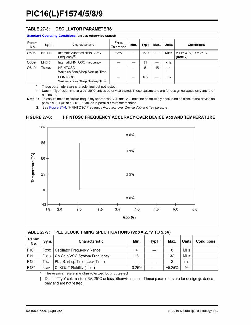
PIC16(L)F1574/5/8/9
DS40001782C-page 288 2016 Microchip Technology Inc.
TABLE 27-8: OSCILLATOR PARAMETERS
FIGURE 27-6: HFINTOSC FREQUENCY ACCURACY OVER DEVICE VDD AND TEMPERATURE
TABLE 27-9: PLL CLOCK TIMING SPECIFICATIONS (VDD = 2.7V TO 5.5V)
Standard Operating Conditions (unless otherwise stated)
Param. No.
Sym. CharacteristicFreq.
ToleranceMin. Typ† Max. Units Conditions
OS08 HFOSC Internal Calibrated HFINTOSC Frequency(1)
±2% — 16.0 — MHz VDD = 3.0V, TA = 25°C,(Note 2)
OS09 LFOSC Internal LFINTOSC Frequency — — 31 — kHz
OS10* TWARM HFINTOSC Wake-up from Sleep Start-up Time
— — 5 15 s
LFINTOSC Wake-up from Sleep Start-up Time
— — 0.5 — ms
* These parameters are characterized but not tested.† Data in “Typ” column is at 3.0V, 25°C unless otherwise stated. These parameters are for design guidance only and are
not tested.Note 1: To ensure these oscillator frequency tolerances, VDD and VSS must be capacitively decoupled as close to the device as
possible. 0.1 F and 0.01 F values in parallel are recommended.2: See Figure 27-6: “HFINTOSC Frequency Accuracy over Device VDD and Temperature.
Param No.
Sym. Characteristic Min. Typ† Max. Units Conditions
F10 FOSC Oscillator Frequency Range 4 — 8 MHz
F11 FSYS On-Chip VCO System Frequency 16 — 32 MHz
F12 TRC PLL Start-up Time (Lock Time) — — 2 ms
F13* CLK CLKOUT Stability (Jitter) -0.25% — +0.25% %
* These parameters are characterized but not tested.
† Data in “Typ” column is at 3V, 25C unless otherwise stated. These parameters are for design guidance only and are not tested.
125
25
2.0
0
60
85
VDD (V)
4.0 5.04.5
Tem
per
atu
re (
°C)
2.5 3.0 3.5 5.51.8-40
± 5%
± 2%
± 5%
± 3%

2016 Microchip Technology Inc. DS40001782C-page 289
PIC16(L)F1574/5/8/9
FIGURE 27-7: CLKOUT AND I/O TIMING
TABLE 27-10: CLKOUT AND I/O TIMING PARAMETERS
Standard Operating Conditions (unless otherwise stated)
Param.No.
Sym. Characteristic Min. Typ† Max. Units Conditions
OS11 TosH2ckL FOSC to CLKOUT(1) — — 70 ns 3.3V VDD 5.0V
OS12 TosH2ckH FOSC to CLKOUT(1) — — 72 ns 3.3V VDD 5.0V
OS13 TckL2ioV CLKOUT to Port out valid(1) — — 20 ns
OS14 TioV2ckH Port input valid before CLKOUT(1) TOSC + 200 ns — — ns
OS15 TosH2ioV Fosc (Q1 cycle) to Port out valid — 50 70* ns 3.3V VDD 5.0V
OS16 TosH2ioI Fosc (Q2 cycle) to Port input invalid (I/O in setup time)
50 — — ns 3.3V VDD 5.0V
OS17 TioV2osH Port input valid to Fosc(Q2 cycle)(I/O in setup time)
20 — — ns
OS18* TioR Port output rise time ——
4015
7232
ns VDD = 1.8V3.3V VDD 5.0V
OS19* TioF Port output fall time ——
2815
5530
ns VDD = 1.8V3.3V VDD 5.0V
OS20* Tinp INT pin input high or low time 25 — — ns
OS21* Tioc Interrupt-on-change new input level time 25 — — ns
* These parameters are characterized but not tested.† Data in “Typ” column is at 3.0V, 25C unless otherwise stated.
Note 1: Measurements are taken in EXTRC mode where CLKOUT output is 4 x TOSC.
FOSC
CLKOUT
I/O pin(Input)
I/O pin(Output)
Q4 Q1 Q2 Q3
OS11
OS19
OS13
OS15
OS18, OS19
OS20OS21
OS17
OS16
OS14
OS12
OS18
Old Value New Value
Write Fetch Read ExecuteCycle
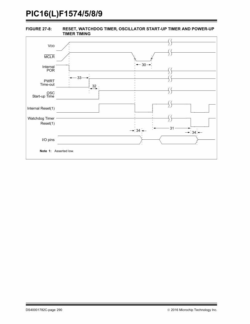
PIC16(L)F1574/5/8/9
DS40001782C-page 290 2016 Microchip Technology Inc.
FIGURE 27-8: RESET, WATCHDOG TIMER, OSCILLATOR START-UP TIMER AND POWER-UP TIMER TIMING
VDD
MCLR
InternalPOR
PWRTTime-out
OSCStart-up Time
Internal Reset(1)
Watchdog Timer
33
32
30
3134
I/O pins
34
Note 1: Asserted low.
Reset(1)

2016 Microchip Technology Inc. DS40001782C-page 291
PIC16(L)F1574/5/8/9
TABLE 27-11: RESET, WATCHDOG TIMER, OSCILLATOR START-UP TIMER, POWER-UP TIMER AND BROWN-OUT RESET PARAMETERS
FIGURE 27-9: BROWN-OUT RESET TIMING AND CHARACTERISTICS
Standard Operating Conditions (unless otherwise stated)
Param. No.
Sym. Characteristic Min. Typ† Max. Units Conditions
30 TMCL MCLR Pulse Width (low) 2 — — s
31 TWDTLP Low-Power Watchdog Timer Time-out Period
10 16 27 ms VDD = 3.3V-5V,1:512 Prescaler used
32 TOST Oscillator Start-up Timer Period(1) — 1024 — TOSC
33* TPWRT Power-up Timer Period 40 65 140 ms PWRTE = 0
34* TIOZ I/O high-impedance from MCLR Low or Watchdog Timer Reset
— — 2.0 s
35 VBOR Brown-out Reset Voltage(2) 2.55
2.351.80
2.70
2.451.90
2.85
2.582.05
V
VV
BORV = 0
BORV = 1 (PIC16F1574/5/8/9)BORV = 1 (PIC16LF1574/5/8/9)
36* VHYST Brown-out Reset Hysteresis 0 25 60 mV -40°C TA +85°C
37* TBORDC Brown-out Reset DC Response Time 1 16 35 s VDD VBOR
38 VLPBOR Low-Power Brown-Out Reset Voltage 1.8 2.1 2.5 V LPBOR = 1
* These parameters are characterized but not tested.† Data in “Typ” column is at 3.0V, 25°C unless otherwise stated. These parameters are for design guidance
only and are not tested.
Note 1: By design, the Oscillator Start-up Timer (OST) counts the first 1024 cycles, independent of frequency.
2: To ensure these voltage tolerances, VDD and VSS must be capacitively decoupled as close to the device as possible. 0.1 F and 0.01 F values in parallel are recommended.
VBOR
VDD
(Device in Brown-out Reset) (Device not in Brown-out Reset)
33Reset
(due to BOR)
VBOR and VHYST
37

PIC16(L)F1574/5/8/9
DS40001782C-page 292 2016 Microchip Technology Inc.
FIGURE 27-10: TIMER0 AND TIMER1 EXTERNAL CLOCK TIMINGS
TABLE 27-12: TIMER0 AND TIMER1 EXTERNAL CLOCK REQUIREMENTS
Standard Operating Conditions (unless otherwise stated)
Param. No.
Sym. Characteristic Min. Typ† Max. Units Conditions
40* TT0H T0CKI High Pulse Width No Prescaler 0.5 TCY + 20 — — ns
With Prescaler 10 — — ns
41* TT0L T0CKI Low Pulse Width No Prescaler 0.5 TCY + 20 — — ns
With Prescaler 10 — — ns
42* TT0P T0CKI Period Greater of:20 or TCY + 40
N
— — ns N = prescale value
45* TT1H T1CKI High Time
Synchronous, No Prescaler 0.5 TCY + 20 — — ns
Synchronous, with Prescaler 15 — — ns
Asynchronous 30 — — ns
46* TT1L T1CKI Low Time
Synchronous, No Prescaler 0.5 TCY + 20 — — ns
Synchronous, with Prescaler 15 — — ns
Asynchronous 30 — — ns
47* TT1P T1CKI Input Period
Synchronous Greater of:30 or TCY + 40
N
— — ns N = prescale value
Asynchronous 60 — — ns
49* TCKEZTMR1 Delay from External Clock Edge to Timer Increment
2 TOSC — 7 TOSC — Timers in Sync mode
* These parameters are characterized but not tested.† Data in “Typ” column is at 3.0V, 25°C unless otherwise stated. These parameters are for design guidance only and are not
tested.
T0CKI
T1CKI
40 41
42
45 46
47 49
TMR0 orTMR1
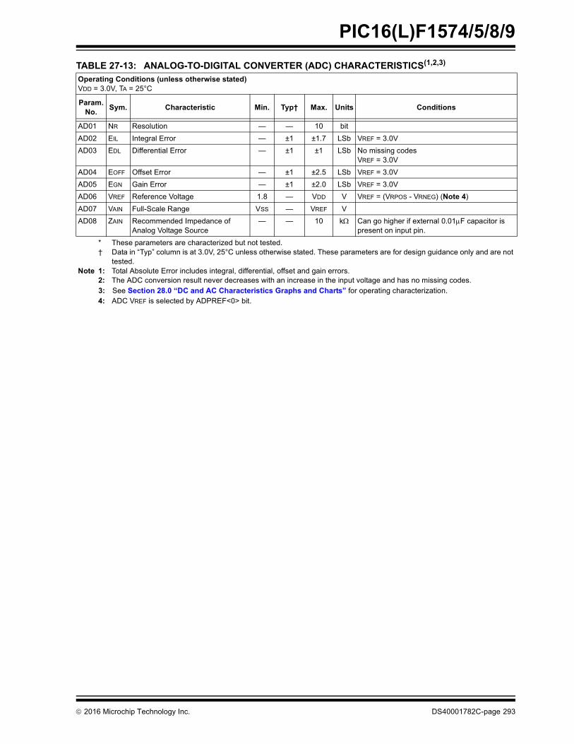
2016 Microchip Technology Inc. DS40001782C-page 293
PIC16(L)F1574/5/8/9
TABLE 27-13: ANALOG-TO-DIGITAL CONVERTER (ADC) CHARACTERISTICS(1,2,3)
Operating Conditions (unless otherwise stated)VDD = 3.0V, TA = 25°C
Param. No.
Sym. Characteristic Min. Typ† Max. Units Conditions
AD01 NR Resolution — — 10 bit
AD02 EIL Integral Error — ±1 ±1.7 LSb VREF = 3.0V
AD03 EDL Differential Error — ±1 ±1 LSb No missing codesVREF = 3.0V
AD04 EOFF Offset Error — ±1 ±2.5 LSb VREF = 3.0V
AD05 EGN Gain Error — ±1 ±2.0 LSb VREF = 3.0V
AD06 VREF Reference Voltage 1.8 — VDD V VREF = (VRPOS - VRNEG) (Note 4)
AD07 VAIN Full-Scale Range VSS — VREF V
AD08 ZAIN Recommended Impedance of Analog Voltage Source
— — 10 k Can go higher if external 0.01F capacitor is present on input pin.
* These parameters are characterized but not tested.† Data in “Typ” column is at 3.0V, 25°C unless otherwise stated. These parameters are for design guidance only and are not
tested.Note 1: Total Absolute Error includes integral, differential, offset and gain errors.
2: The ADC conversion result never decreases with an increase in the input voltage and has no missing codes.3: See Section 28.0 “DC and AC Characteristics Graphs and Charts” for operating characterization.4: ADC VREF is selected by ADPREF<0> bit.

PIC16(L)F1574/5/8/9
DS40001782C-page 294 2016 Microchip Technology Inc.
FIGURE 27-11: ADC CONVERSION TIMING (ADC CLOCK FOSC-BASED)
FIGURE 27-12: ADC CONVERSION TIMING (ADC CLOCK FROM FRC)
AD131
AD130
BSF ADCON0, GO
Q4
ADC_clk
ADC Data
ADRES
ADIF
GO
Sample
OLD_DATA
Sampling Stopped
DONE
NEW_DATA
9 8 7 3 2 1 0
1 TCY
6
AD133
1 TCY
AD132
AD132
AD131
AD130
BSF ADCON0, GO
Q4
ADC_clk
ADC Data
ADRES
ADIF
GO
Sample
OLD_DATA
Sampling Stopped
DONE
NEW_DATA
9 7 3 2 1 0
Note 1: If the ADC clock source is selected as FRC, a time of TCY is added before the ADC clock starts. This allows the SLEEP instruction to be executed.
AD133
68
1 TCY
1 TCY
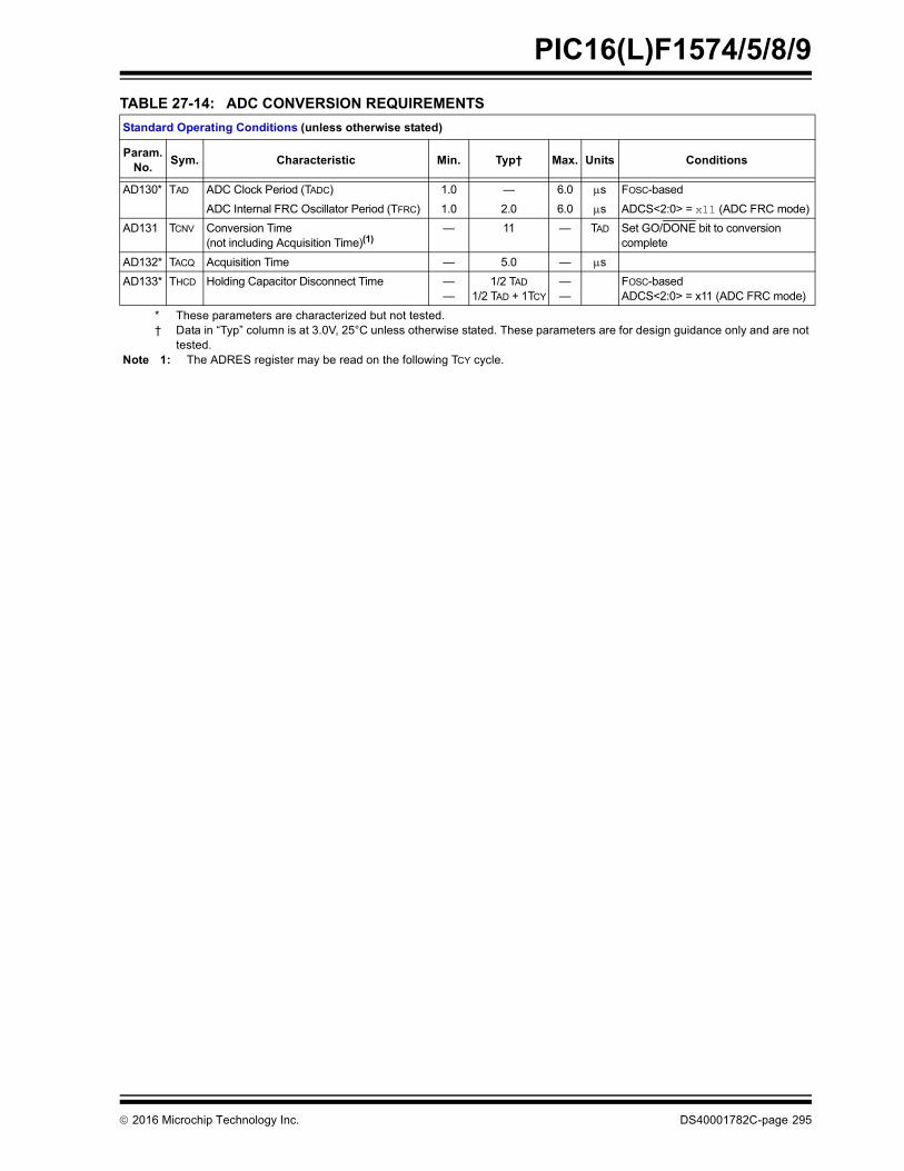
2016 Microchip Technology Inc. DS40001782C-page 295
PIC16(L)F1574/5/8/9
TABLE 27-14: ADC CONVERSION REQUIREMENTS
Standard Operating Conditions (unless otherwise stated)
Param.No.
Sym. Characteristic Min. Typ† Max. Units Conditions
AD130* TAD ADC Clock Period (TADC) 1.0 — 6.0 s FOSC-based
ADC Internal FRC Oscillator Period (TFRC) 1.0 2.0 6.0 s ADCS<2:0> = x11 (ADC FRC mode)
AD131 TCNV Conversion Time (not including Acquisition Time)(1)
— 11 — TAD Set GO/DONE bit to conversioncomplete
AD132* TACQ Acquisition Time — 5.0 — s
AD133* THCD Holding Capacitor Disconnect Time ——
1/2 TAD
1/2 TAD + 1TCY
——
FOSC-basedADCS<2:0> = x11 (ADC FRC mode)
* These parameters are characterized but not tested.† Data in “Typ” column is at 3.0V, 25°C unless otherwise stated. These parameters are for design guidance only and are not
tested.Note 1: The ADRES register may be read on the following TCY cycle.

PIC16(L)F1574/5/8/9
DS40001782C-page 296 2016 Microchip Technology Inc.
TABLE 27-15: COMPARATOR SPECIFICATIONS(1)
TABLE 27-16: DIGITAL-TO-ANALOG CONVERTER (DAC) SPECIFICATIONS(1)
Operating Conditions (unless otherwise stated)VDD = 3.0V, TA = 25°C
Param.No.
Sym. Characteristics Min. Typ. Max. Units Comments
CM01 VIOFF Input Offset Voltage — ±7.5 ±60 mV CxSP = 1,VICM = VDD/2
CM02 VICM Input Common Mode Voltage 0 — VDD V
CM03 CMRR Common Mode Rejection Ration — 50 — dB
CM04A
TRESP(2)
Response Time Rising Edge — 400 800 ns CxSP = 1
CM04B Response Time Falling Edge — 200 400 ns CxSP = 1
CM04C Response Time Rising Edge — 1200 — ns CxSP = 0
CM04D Response Time Falling Edge — 550 — ns CxSP = 0
CM05* TMC2OV Comparator Mode Change to Output Valid
— — 10 s
CM06 CHYSTER Comparator Hysteresis — 25 — mV CxHYS = 1,CxSP = 1
* These parameters are characterized but not tested.
Note 1: See Section 28.0 “DC and AC Characteristics Graphs and Charts” for operating characterization.
2: Response time measured with one comparator input at VDD/2, while the other input transitions from VSS to VDD.
Operating Conditions (unless otherwise stated)VDD = 3.0V, TA = 25°C
Param.No.
Sym. Characteristics Min. Typ. Max. Units Comments
DAC01* CLSB Step Size — VDD/32 — V
DAC02* CACC Absolute Accuracy — — 1/2 LSb
DAC03* CR Unit Resistor Value (R) — 5K —
DAC04* CST Settling Time(2) — — 10 s
* These parameters are characterized but not tested.
Note 1: See Section 28.0 “DC and AC Characteristics Graphs and Charts” for operating characterization.
2: Settling time measured while DACR<4:0> transitions from ‘0000’ to ‘1111’.

2016 Microchip Technology Inc. DS40001782C-page 297
PIC16(L)F1574/5/8/9
FIGURE 27-13: USART SYNCHRONOUS TRANSMISSION (MASTER/SLAVE) TIMING
TABLE 27-17: USART SYNCHRONOUS TRANSMISSION REQUIREMENTS
FIGURE 27-14: USART SYNCHRONOUS RECEIVE (MASTER/SLAVE) TIMING
TABLE 27-18: USART SYNCHRONOUS RECEIVE REQUIREMENTS
Standard Operating Conditions (unless otherwise stated)
Param. No.
Symbol Characteristic Min. Max. Units Conditions
US120 TCKH2DTV SYNC XMIT (Master and Slave)Clock high to data-out valid
— 80 ns 3.0V VDD 5.5V
— 100 ns 1.8V VDD 5.5V
US121 TCKRF Clock out rise time and fall time (Master mode)
— 45 ns 3.0V VDD 5.5V
— 50 ns 1.8V VDD 5.5V
US122 TDTRF Data-out rise time and fall time — 45 ns 3.0V VDD 5.5V
— 50 ns 1.8V VDD 5.5V
Standard Operating Conditions (unless otherwise stated)
Param. No.
Symbol Characteristic Min. Max. Units Conditions
US125 TDTV2CKL SYNC RCV (Master and Slave)Data-hold before CK (DT hold time) 10 — ns
US126 TCKL2DTL Data-hold after CK (DT hold time) 15 — ns
Note: Refer to Figure 27-4 for load conditions.
US121 US121
US120 US122
CK
DT
Note: Refer to Figure 27-4 for load conditions.
US125
US126
CK
DT

PIC16(L)F1574/5/8/9
DS40001782C-page 298 2016 Microchip Technology Inc.
28.0 DC AND AC CHARACTERISTICS GRAPHS AND CHARTS
The graphs and tables provided in this section are for design guidance and are not tested.
In some graphs or tables, the data presented are outside specified operating range (i.e., outside specified VDD
range). This is for information only and devices are ensured to operate properly only within the specified range.
Unless otherwise noted, all graphs apply to both the L and LF devices.
“Typical” represents the mean of the distribution at 25C. “Maximum”, “Max.”, “Minimum” or “Min.”represents (mean + 3) or (mean - 3) respectively, where is a standard deviation, over eachtemperature range.
Note: The graphs and tables provided following this note are a statistical summary based on a limited number ofsamples and are provided for informational purposes only. The performance characteristics listed hereinare not tested or guaranteed. In some graphs or tables, the data presented may be outside the specifiedoperating range (e.g., outside specified power supply range) and therefore, outside the warranted range.
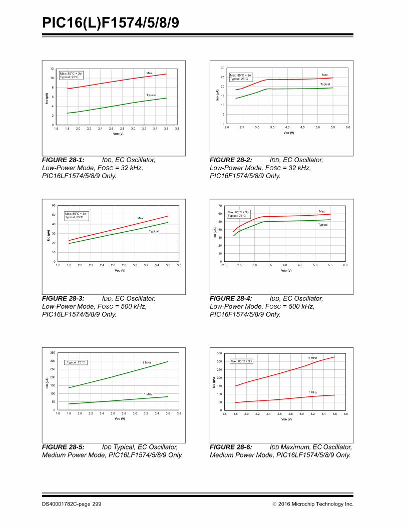
PIC16(L)F1574/5/8/9
DS40001782C-page 299 2016 Microchip Technology Inc.
FIGURE 28-1: IDD, EC Oscillator, Low-Power Mode, FOSC = 32 kHz, PIC16LF1574/5/8/9 Only.
FIGURE 28-2: IDD, EC Oscillator, Low-Power Mode, FOSC = 32 kHz, PIC16F1574/5/8/9 Only.
Typical
Max.
0
2
4
6
8
10
12
1.6 1.8 2.0 2.2 2.4 2.6 2.8 3.0 3.2 3.4 3.6 3.8
IDD
(µA
)
VDD (V)
Max: 85°C + 3Typical: 25°C
Typical
Max.
0
5
10
15
20
25
30
2.0 2.5 3.0 3.5 4.0 4.5 5.0 5.5 6.0
IDD
(µA
)
VDD (V)
Max: 85°C + 3Typical: 25°C
FIGURE 28-3: IDD, EC Oscillator, Low-Power Mode, FOSC = 500 kHz, PIC16LF1574/5/8/9 Only.
FIGURE 28-4: IDD, EC Oscillator, Low-Power Mode, FOSC = 500 kHz, PIC16F1574/5/8/9 Only.
Max.
Typical
0
10
20
30
40
50
60
1.6 1.8 2.0 2.2 2.4 2.6 2.8 3.0 3.2 3.4 3.6 3.8
IDD
(µA
)
VDD (V)
Max: 85°C + 3Typical: 25°C
Typical
Max.
0
10
20
30
40
50
60
70
2.0 2.5 3.0 3.5 4.0 4.5 5.0 5.5 6.0
IDD
(µA
)
VDD (V)
Max: 85°C + 3Typical: 25°C
FIGURE 28-5: IDD Typical, EC Oscillator, Medium Power Mode, PIC16LF1574/5/8/9 Only.
FIGURE 28-6: IDD Maximum, EC Oscillator, Medium Power Mode, PIC16LF1574/5/8/9 Only.
4 MHz
1 MHz
0
50
100
150
200
250
300
350
1.6 1.8 2.0 2.2 2.4 2.6 2.8 3.0 3.2 3.4 3.6 3.8
IDD
(µA
)
VDD (V)
Typical: 25°C
, ,
4 MHz
1 MHz
0
50
100
150
200
250
300
350
1.6 1.8 2.0 2.2 2.4 2.6 2.8 3.0 3.2 3.4 3.6 3.8
IDD
(µA
)
VDD (V)
Max: 85°C + 3

2016 Microchip Technology Inc. DS40001782C-page 300
PIC16(L)F1574/5/8/9
FIGURE 28-7: IDD Typical, EC Oscillator, Medium Power Mode, PIC16F1574/5/8/9 Only.
FIGURE 28-8: IDD Maximum, EC Oscillator, Medium Power Mode, PIC16F1574/5/8/9 Only.
4 MHz
1 MHz
0
50
100
150
200
250
300
350
400
2.0 2.5 3.0 3.5 4.0 4.5 5.0 5.5 6.0
IDD
(µA
)
VDD (V)
Typical: 25°C 4 MHz
1 MHz
0
50
100
150
200
250
300
350
400
450
2.0 2.5 3.0 3.5 4.0 4.5 5.0 5.5 6.0
IDD
(µA
)
VDD (V)
Max: 85°C + 3
FIGURE 28-9: IDD Typical, EC Oscillator, High-Power Mode, FOSC = 32 kHz, PIC16LF1574/5/8/9 Only.
FIGURE 28-10: IDD Typical, EC Oscillator, High-Power Mode, FOSC = 32 kHz, PIC16F1574/5/8/9 Only.
Typical
Max.
0.0
0.5
1.0
1.5
2.0
2.5
3.0
1.6 1.8 2.0 2.2 2.4 2.6 2.8 3.0 3.2 3.4 3.6 3.8
IDD
(mA
)
VDD (V)
Max: 85°C + 3Typical: 25°C
Typical
Max.
0.0
0.5
1.0
1.5
2.0
2.5
3.0
2.0 2.5 3.0 3.5 4.0 4.5 5.0 5.5 6.0
IDD
(mA
)
VDD (V)
Typical: 25°CMax: 85°C + 3Typical: 25°C
FIGURE 28-11: IDD, LFINTOSC Mode, FOSC = 31 kHz, PIC16LF1574/5/8/9 Only.
FIGURE 28-12: IDD, LFINTOSC Mode, FOSC = 31 kHz, PIC16F1574/5/8/9 Only.
Typical
Max.
0
2
4
6
8
10
12
14
16
18
1.6 1.8 2.0 2.2 2.4 2.6 2.8 3.0 3.2 3.4 3.6 3.8
IDD
(µA
)
VDD (V)
Max: 85°C + 3Typical: 25°C
, ,
Typical
Max.
0
5
10
15
20
25
30
2.0 2.5 3.0 3.5 4.0 4.5 5.0 5.5 6.0
IDD
(µA
)
VDD (V)
Max: 85°C + 3Typical: 25°C

PIC16(L)F1574/5/8/9
DS40001782C-page 301 2016 Microchip Technology Inc.
FIGURE 28-13: IDD, MFINTOSC Mode, FOSC = 500 kHz, PIC16LF1574/5/8/9 Only.
FIGURE 28-14: IDD, MFINTOSC Mode, FOSC = 500 kHz, PIC16F1574/5/8/9 Only.
Typical
Max.
100
120
140
160
180
200
220
1.6 1.8 2.0 2.2 2.4 2.6 2.8 3.0 3.2 3.4 3.6 3.8
IDD
(µA
)
VDD (V)
Max: 85°C + 3Typical: 25°C
Typical
Max.
100
120
140
160
180
200
220
240
260
280
300
2.0 2.5 3.0 3.5 4.0 4.5 5.0 5.5 6.0
IDD
(µA
)
VDD (V)
Max: 85°C + 3Typical: 25°C
FIGURE 28-15: IDD Typical, HFINTOSC Mode, PIC16LF1574/5/8/9 Only.
FIGURE 28-16: IDD Maximum, HFINTOSC Mode, PIC16LF1574/5/8/9 Only.
32 MHz PLL
32 MHz PLL
16 MHz
8 MHz
0.0
0.5
1.0
1.5
2.0
2.5
3.0
1.6 1.8 2.0 2.2 2.4 2.6 2.8 3.0 3.2 3.4 3.6 3.8
IDD
(mA
)
VDD (V)
Typical: 25°C
32 MHz PLL
32 MHz PLL
16 MHz
8 MHz
0.0
0.5
1.0
1.5
2.0
2.5
3.0
3.5
4.0
1.6 1.8 2.0 2.2 2.4 2.6 2.8 3.0 3.2 3.4 3.6 3.8
IDD
(mA
)
VDD (V)
Max: 85°C + 3
FIGURE 28-17: IDD Typical, HFINTOSC Mode, PIC16F1574/5/8/9 Only.
FIGURE 28-18: IDD Maximum, HFINTOSC Mode, PIC16F1574/5/8/9 Only.
32 MHz PLL
32 MHz PLL
16 MHz
8 MHz
0.0
0.5
1.0
1.5
2.0
2.5
3.0
2.0 2.5 3.0 3.5 4.0 4.5 5.0 5.5 6.0
IDD
(mA
)
VDD (V)
Typical: 25°C
,
32 MHz PLL32 MHz PLL
16 MHz
8 MHz
0.0
0.5
1.0
1.5
2.0
2.5
3.0
3.5
2.0 2.5 3.0 3.5 4.0 4.5 5.0 5.5 6.0
IDD
(mA
)
VDD (V)
Max: 85°C + 3

2016 Microchip Technology Inc. DS40001782C-page 302
PIC16(L)F1574/5/8/9
FIGURE 28-19: Ipd Base, Low-Power Sleep Mode, PIC16LF1574/5/8/9 Only.
FIGURE 28-20: Ipd Base, Low-Power Sleep Mode (VREGPM = 1), PIC16F1574/5/8/9 Only.
p
Max.
Typical
0
50
100
150
200
250
300
350
400
450
1.6 1.8 2.0 2.2 2.4 2.6 2.8 3.0 3.2 3.4 3.6 3.8
IDD
(nA)
VDD (V)
Max: 85°C + 3Typical: 25°C
Max.
Typical
0
0.2
0.4
0.6
0.8
1
1.2
2.0 2.5 3.0 3.5 4.0 4.5 5.0 5.5 6.0
IPD
(µA)
VDD (V)
Max: 85°C + 3Typical: 25°C
FIGURE 28-21: Ipd, Watchdog Timer (WDT), PIC16LF1574/5/8/9 Only.
FIGURE 28-22: Ipd, Watchdog Timer (WDT), PIC16F1574/5/8/9 Only.
Max.
Typical
0
0.5
1
1.5
2
2.5
3
1.6 1.8 2.0 2.2 2.4 2.6 2.8 3.0 3.2 3.4 3.6 3.8
IPD
(µA)
VDD (V)
Max: 85°C + 3Typical: 25°C
Max.
Typical
0
0.5
1
1.5
2
2.5
2.0 2.5 3.0 3.5 4.0 4.5 5.0 5.5 6.0
IPD
(µA)
VDD (V)
Max: 85°C + 3Typical: 25°C
FIGURE 28-23: Ipd, Fixed Voltage Reference (FVR), PIC16LF1574/5/8/9 Only.
FIGURE 28-24: Ipd, Fixed Voltage Reference (FVR), PIC16F1574/5/8/9 Only.
Max.
Typical
5
10
15
20
25
30
35
1.6 1.8 2.0 2.2 2.4 2.6 2.8 3.0 3.2 3.4 3.6 3.8
IDD
(nA)
VDD (V)
Max: 85°C + 3Typical: 25°C
Max.
Typical
0
5
10
15
20
25
30
35
2.0 2.5 3.0 3.5 4.0 4.5 5.0 5.5 6.0
IDD
(nA)
VDD (V)
Max: 85°C + 3Typical: 25°C
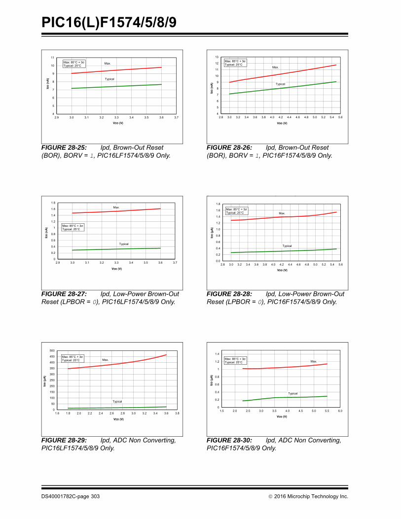
PIC16(L)F1574/5/8/9
DS40001782C-page 303 2016 Microchip Technology Inc.
FIGURE 28-25: Ipd, Brown-Out Reset (BOR), BORV = 1, PIC16LF1574/5/8/9 Only.
FIGURE 28-26: Ipd, Brown-Out Reset (BOR), BORV = 1, PIC16F1574/5/8/9 Only.
Max.
Typical
4
5
6
7
8
9
10
11
2.9 3.0 3.1 3.2 3.3 3.4 3.5 3.6 3.7
IDD
(nA)
VDD (V)
Max: 85°C + 3Typical: 25°C Max.
Typical
4
5
6
7
8
9
10
11
12
13
2.8 3.0 3.2 3.4 3.6 3.8 4.0 4.2 4.4 4.6 4.8 5.0 5.2 5.4 5.6
IDD
(nA)
VDD (V)
Max: 85°C + 3Typical: 25°C
FIGURE 28-27: Ipd, Low-Power Brown-Out Reset (LPBOR = 0), PIC16LF1574/5/8/9 Only.
FIGURE 28-28: Ipd, Low-Power Brown-Out Reset (LPBOR = 0), PIC16F1574/5/8/9 Only.
Max.
Typical
0
0.2
0.4
0.6
0.8
1
1.2
1.4
1.6
1.8
2.9 3.0 3.1 3.2 3.3 3.4 3.5 3.6 3.7
IDD
(nA)
VDD (V)
Max: 85°C + 3Typical: 25°C
p ( )
Max.
Typical
0.0
0.2
0.4
0.6
0.8
1.0
1.2
1.4
1.6
1.8
2.8 3.0 3.2 3.4 3.6 3.8 4.0 4.2 4.4 4.6 4.8 5.0 5.2 5.4 5.6
IDD
(µA)
VDD (V)
Max: 85°C + 3Typical: 25°C
FIGURE 28-29: Ipd, ADC Non Converting, PIC16LF1574/5/8/9 Only.
FIGURE 28-30: Ipd, ADC Non Converting, PIC16F1574/5/8/9 Only.
Max.
Typical
0
50
100
150
200
250
300
350
400
450
500
1.6 1.8 2.0 2.2 2.4 2.6 2.8 3.0 3.2 3.4 3.6 3.8
IDD
(µA)
VDD (V)
Max: 85°C + 3Typical: 25°C Max.
Typical
0
0.2
0.4
0.6
0.8
1
1.2
1.4
1.5 2.0 2.5 3.0 3.5 4.0 4.5 5.0 5.5 6.0
IDD
(µA)
VDD (V)
Max: 85°C + 3Typical: 25°C

2016 Microchip Technology Inc. DS40001782C-page 304
PIC16(L)F1574/5/8/9
FIGURE 28-31: Ipd, Comparator, Low-Power Mode (CxSP = 0), PIC16LF1574/5/8/9 Only.
FIGURE 28-32: Ipd, Comparator, Low-Power Mode (CxSP = 0), PIC16F1574/5/8/9 Only.
p ( )
Max.
Typical
0
100
200
300
400
500
600
700
800
1.6 1.8 2.0 2.2 2.4 2.6 2.8 3.0 3.2 3.4 3.6 3.8
IDD
(µA)
VDD (V)
Max: 85°C + 3Typical: 25°C
p , , ( )
Max.
Typical
0
100
200
300
400
500
600
700
800
2.0 2.5 3.0 3.5 4.0 4.5 5.0 5.5 6.0
IDD
(µA)
VDD (V)
Max: 85°C + 3Typical: 25°C
FIGURE 28-33: Ipd, Comparator, Normal Power Mode (CxSP = 1), PIC16LF1574/5/8/9 Only.
FIGURE 28-34: Ipd, Comparator, Normal Power Mode (CxSP = 1), PIC16F1574/5/8/9 Only.
( )
Max.
Typical
200
300
400
500
600
700
800
1.6 1.8 2.0 2.2 2.4 2.6 2.8 3.0 3.2 3.4 3.6 3.8
IDD
(µA)
VDD (V)
Max: -40°C + 3Typical: 25°C
Max.
Typical
200
300
400
500
600
700
800
2.0 2.5 3.0 3.5 4.0 4.5 5.0 5.5 6.0
IDD
(µA)
VDD (V)
Max: -40°C + 3Typical: 25°C
FIGURE 28-35: VOH vs. IOH Over Temperature, VDD = 5.5V, PIC16F1574/5/8/9 Only.
FIGURE 28-36: VOL vs. IOL Over Temperature, VDD = 5.5V, PIC16F1574/5/8/9 Only.
Max.
Typical Min.
0
1
2
3
4
5
6
-45 -40 -35 -30 -25 -20 -15 -10 -5 0
VOH
(V)
IOH (mA)
Max: -40°C max + 3Typical: statistical mean @ 25°CMin: +125°C min - 3
Max.
Typical
Min.
0
1
2
3
4
5
0 10 20 30 40 50 60 70 80 90 100
VOL
(V)
IOL (mA)
Max: -40°C max + 3Typical: statistical mean @ 25°CMin: +125°C min - 3

PIC16(L)F1574/5/8/9
DS40001782C-page 305 2016 Microchip Technology Inc.
FIGURE 28-37: VOH vs. IOH Over Temperature, VDD = 3.0V.
FIGURE 28-38: VOL vs. IOL Over Temperature, VDD = 3.0V.
Max.
Typical
Min.
0.0
0.5
1.0
1.5
2.0
2.5
3.0
3.5
-15 -13 -11 -9 -7 -5 -3 -1
VOH
(V)
IOH (mA)
Max: -40°C max + 3Typical: statistical mean @ 25°CMin: +125°C min - 3
Max.
Typical
Min.
0.0
0.5
1.0
1.5
2.0
2.5
3.0
0 5 10 15 20 25 30 35 40
VOL
(V)
IOL (mA)
Max: -40°C max + 3Typical: statistical mean @ 25°CMin: +125°C min - 3
FIGURE 28-39: VOH vs. IOH Over Temperature, VDD = 1.8V, PIC16LF1574/5/8/9 Only.
FIGURE 28-40: VOL vs. IOL Over Temperature, VDD = 1.8V, PIC16LF1574/5/8/9 Only.
Max.
Typical
Min.
0.0
0.2
0.4
0.6
0.8
1.0
1.2
1.4
1.6
1.8
2.0
-4.5 -4 -3.5 -3 -2.5 -2 -1.5 -1 -0.5 0
VOH
(V)
IOH (mA)
Max: -40°C max + 3Typical: statistical mean @ 25°CMin: +125°C min - 3
Max.
Typical
Min.
0.0
0.2
0.4
0.6
0.8
1.0
1.2
1.4
1.6
1.8
0 1 2 3 4 5 6 7 8 9 10
VOL
(V)
IOL (mA)
Max: -40°C max + 3Typical: statistical mean @ 25°CMin: +125°C min - 3
FIGURE 28-41: LFINTOSC Frequency Over VDD and Temperature, PIC16LF1574/5/8/9 Only.
FIGURE 28-42: LFINTOSC Frequency Over VDD and Temperature, PIC16F1574/5/8/9 Only.
Typical
Max.
Min.
20
22
24
26
28
30
32
34
36
1.6 1.8 2.0 2.2 2.4 2.6 2.8 3.0 3.2 3.4 3.6 3.8
Freq
uenc
y (k
Hz)
VDD (V)
Max: Typical + 3 (-40°C to +125°C)Typical: statistical mean @ 25°CMin: Typical - 3 (-40°C to +125°C)
Typical
Max.
Min.
20
22
24
26
28
30
32
34
36
2 2.5 3 3.5 4 4.5 5 5.5 6
Freq
uenc
y (k
Hz)
VDD (V)
Max: Typical + 3 (-40°C to +125°C)Typical: statistical mean @ 25°CMin: Typical - 3 (-40°C to +125°C)

2016 Microchip Technology Inc. DS40001782C-page 306
PIC16(L)F1574/5/8/9
FIGURE 28-43: HFINTOSC Accuracy Over Temperature, VDD = 1.8V, LF Devices Only.
FIGURE 28-44: HFINTOSC Accuracy Over Temperature, 2.3V ≤ VDD ≤ 5.5V.
Typical
Max.
Min.
-10%
-8%
-6%
-4%
-2%
0%
2%
4%
6%
8%
-50 0 50 100 150
Acc
urac
y (%
)
Temperature (°C)
Max: Typical + 3Typical: statistical meanMin: Typical - 3
Typical
Max.
Min.
-10%
-8%
-6%
-4%
-2%
0%
2%
4%
6%
8%
-50 0 50 100 150
Max: Typical + 3Typical: statistical meanMin: Typical - 3
FIGURE 28-45: Brown-Out Reset Voltage, BORV = 1, PIC16LF1574/5/8/9 Only.
FIGURE 28-46: Brown-Out Reset Hysteresis, BORV = 1, PIC16LF1574/5/8/9 Only.
Typical
Max.
Min.
1.80
1.85
1.90
1.95
2.00
-60 -40 -20 0 20 40 60 80 100 120 140
Volta
ge (V
)
Temperature (°C)
Max: Typical + 3Min: Typical - 3
BROWN OUT RESET HYSTERESIS, BORV
Typical
Max.
Min.
0
10
20
30
40
50
60
-60 -40 -20 0 20 40 60 80 100 120 140
Volta
ge (m
V)
Temperature (°C)
Max: Typical + 3Min: Typical - 3
FIGURE 28-47: Brown-Out Reset Voltage, BORV = 1, PIC16F1574/5/8/9 Only.
FIGURE 28-48: Brown-Out Reset Hysteresis, BORV = 1, PIC16F1574/5/8/9 Only.
Typical
Max.
Min.
2.30
2.35
2.40
2.45
2.50
2.55
2.60
-60 -40 -20 0 20 40 60 80 100 120 140
Volta
ge (V
)
Temperature (°C)
Max: Typical + 3Min: Typical - 3
Typical
Max.
Min.
0
10
20
30
40
50
60
70
-60 -40 -20 0 20 40 60 80 100 120 140
Volta
ge (m
V)
Temperature (°C)
Max: Typical + 3Min: Typical - 3
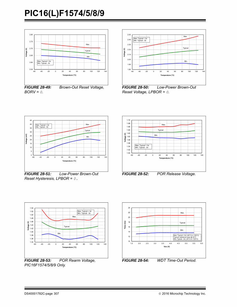
PIC16(L)F1574/5/8/9
DS40001782C-page 307 2016 Microchip Technology Inc.
FIGURE 28-49: Brown-Out Reset Voltage, BORV = 0.
FIGURE 28-50: Low-Power Brown-Out Reset Voltage, LPBOR = 0.
Typical
Max.
Min.
2.55
2.60
2.65
2.70
2.75
2.80
-60 -40 -20 0 20 40 60 80 100 120 140
Volta
ge (V
)
Temperature (°C)
Max: Typical + 3Min: Typical - 3
Typical
Max.
Min.
1.80
1.90
2.00
2.10
2.20
2.30
2.40
2.50
-60 -40 -20 0 20 40 60 80 100 120 140
Volta
ge (V
)
Temperature (°C)
Max: Typical + 3Min: Typical - 3
FIGURE 28-51: Low-Power Brown-Out Reset Hysteresis, LPBOR = 0.
FIGURE 28-52: POR Release Voltage.
Typical
Max.
Min.
0
5
10
15
20
25
30
35
40
45
-60 -40 -20 0 20 40 60 80 100 120 140
Volta
ge (m
V)
Temperature (°C)
Max: Typical + 3Min: Typical - 3
Typical
Max.
Min.
1.50
1.52
1.54
1.56
1.58
1.60
1.62
1.64
1.66
1.68
1.70
-60 -40 -20 0 20 40 60 80 100 120 140
Volta
ge (V
)
Temperature (°C)
Max: Typical + 3Min: Typical - 3
FIGURE 28-53: POR Rearm Voltage, PIC16F1574/5/8/9 Only.
FIGURE 28-54: WDT Time-Out Period.
Typical
Max.
Min.
1.34
1.36
1.38
1.40
1.42
1.44
1.46
1.48
1.50
1.52
1.54
-60 -40 -20 0 20 40 60 80 100 120 140
Volta
ge (V
)
Temperature (°C)
Max: Typical + 3Min: Typical - 3
Typical
Max.
Min.
10
12
14
16
18
20
22
24
1.5 2.0 2.5 3.0 3.5 4.0 4.5 5.0 5.5 6.0
Tim
e (m
s)
VDD (V)
Max: Typical + 3 (-40°C to +125°C)Typical: statistical mean @ 25°CMin: Typical - 3 (-40°C to +125°C)
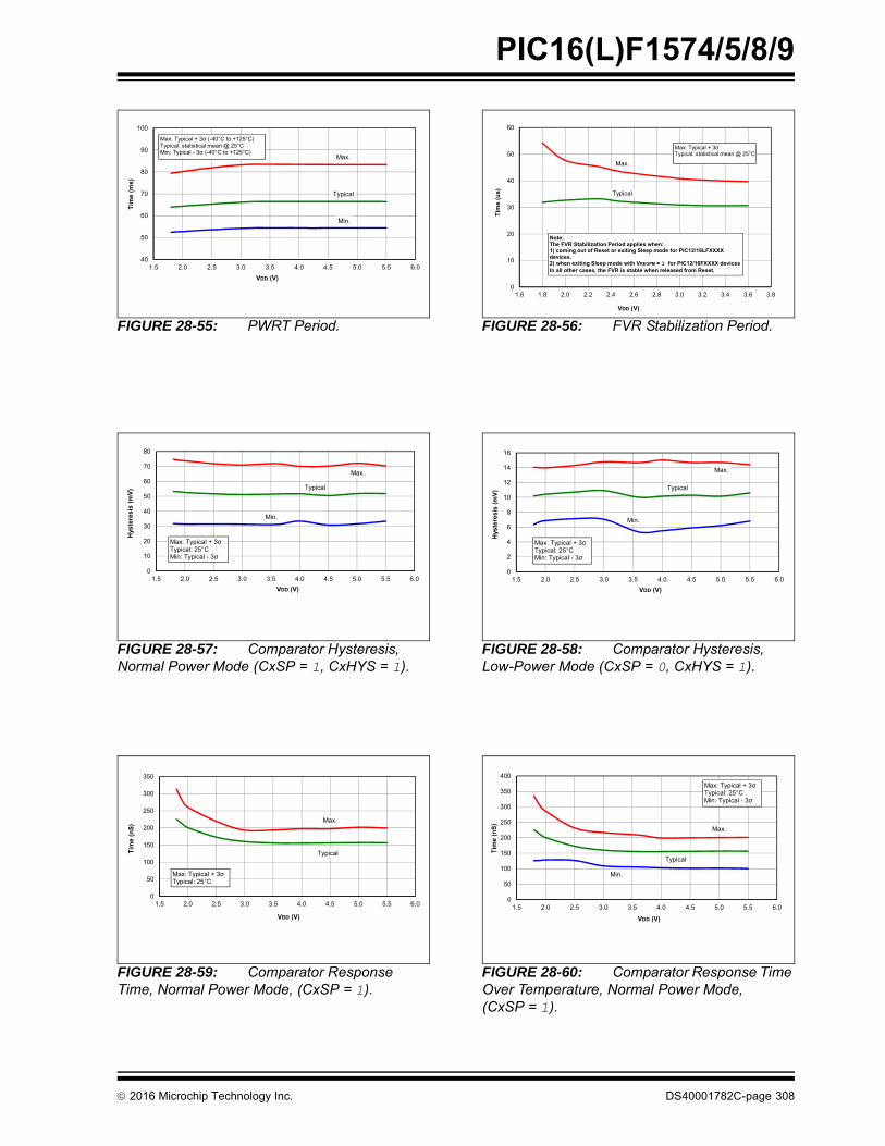
2016 Microchip Technology Inc. DS40001782C-page 308
PIC16(L)F1574/5/8/9
FIGURE 28-55: PWRT Period. FIGURE 28-56: FVR Stabilization Period.
Typical
Max.
Min.
40
50
60
70
80
90
100
1.5 2.0 2.5 3.0 3.5 4.0 4.5 5.0 5.5 6.0
Tim
e (m
s)
VDD (V)
Max: Typical + 3 (-40°C to +125°C)Typical: statistical mean @ 25°CMin: Typical - 3 (-40°C to +125°C)
Typical
Max.
0
10
20
30
40
50
60
1.6 1.8 2.0 2.2 2.4 2.6 2.8 3.0 3.2 3.4 3.6 3.8
Tim
e (u
s)
VDD (V)
Max: Typical + 3Typical: statistical mean @ 25°C
Note: The FVR Stabilization Period applies when:1) coming out of Reset or exiting Sleep mode for PIC12/16LFdevices.2) when exiting Sleep mode with VREGPM = 1 for PIC12/16F devicesIn all other cases, the FVR is stable when released from Reset.
FIGURE 28-57: Comparator Hysteresis, Normal Power Mode (CxSP = 1, CxHYS = 1).
FIGURE 28-58: Comparator Hysteresis, Low-Power Mode (CxSP = 0, CxHYS = 1).
Min.
Typical
Max.
0
10
20
30
40
50
60
70
80
1.5 2.0 2.5 3.0 3.5 4.0 4.5 5.0 5.5 6.0
Hys
tere
sis
(mV)
VDD (V)
Max: Typical + 3Typical: 25°C Min: Typical - 3
Min.
Typical
Max.
0
2
4
6
8
10
12
14
16
1.5 2.0 2.5 3.0 3.5 4.0 4.5 5.0 5.5 6.0
Hys
tere
sis
(mV)
VDD (V)
Max: Typical + 3Typical: 25°C Min: Typical - 3
FIGURE 28-59: Comparator Response Time, Normal Power Mode, (CxSP = 1).
FIGURE 28-60: Comparator Response Time Over Temperature, Normal Power Mode, (CxSP = 1).
Max.
Typical
0
50
100
150
200
250
300
350
1.5 2.0 2.5 3.0 3.5 4.0 4.5 5.0 5.5 6.0
Tim
e (n
S)
VDD (V)
Max: Typical + 3Typical: 25°C
Min.
Typical
Max.
0
50
100
150
200
250
300
350
400
1.5 2.0 2.5 3.0 3.5 4.0 4.5 5.0 5.5 6.0
Tim
e (n
S)
VDD (V)
Max: Typical + 3Typical: 25°C Min: Typical - 3
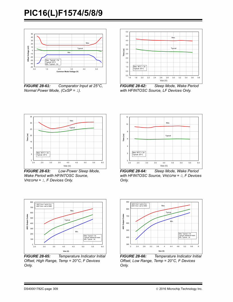
PIC16(L)F1574/5/8/9
DS40001782C-page 309 2016 Microchip Technology Inc.
FIGURE 28-61: Comparator Input at 25°C, Normal Power Mode, (CxSP = 1).
FIGURE 28-62: Sleep Mode, Wake Period with HFINTOSC Source, LF Devices Only.
Max.
Typical
Min.
-50
-40
-30
-20
-10
0
10
20
30
40
50
0.0 1.0 2.0 3.0 4.0 5.0
Offs
et V
olta
ge (m
V)
Common Mode Voltage (V)
Max: Typical + 3Typical: 25°C Min: Typical - 3
Typical
Max.
0.0
0.5
1.0
1.5
2.0
2.5
3.0
3.5
4.0
4.5
5.0
1.6 1.8 2.0 2.2 2.4 2.6 2.8 3.0 3.2 3.4 3.6 3.8
Tim
e (u
s)
Max: 85°C + 3Typical: 25°C
V (V)
FIGURE 28-63: Low-Power Sleep Mode, Wake Period with HFINTOSC Source, VREGPM = 1, F Devices Only.
FIGURE 28-64: Sleep Mode, Wake Period with HFINTOSC Source, VREGPM = 0, F Devices Only.
Typical
Max.
0
5
10
15
20
25
30
35
2.0 2.5 3.0 3.5 4.0 4.5 5.0 5.5 6.0
Tim
e (u
s)
Max: 85°C + 3Typical: 25°C
V (V)
Typical
Max.
0
2
4
6
8
10
12
2.0 2.5 3.0 3.5 4.0 4.5 5.0 5.5 6.0
Tim
e (u
s)
Max: 85°C + 3Typical: 25°C
V (V)
FIGURE 28-65: Temperature Indicator Initial Offset, High Range, Temp = 20°C, F Devices Only.
FIGURE 28-66: Temperature Indicator Initial Offset, Low Range, Temp = 20°C, F Devices Only.
Typical
Max.
Min.
0
100
200
300
400
500
600
700
800
2.5 3.0 3.5 4.0 4.5 5.0 5.5 6.0
AD
C O
utpu
t Cod
es
VDD (V)
ADC V + set to VADC - set to G
Max: Typical + 3σTypical; statistical mean Min: Typical - 3σ
Typical
Max.
Min.
300
400
500
600
700
800
900
2 2.4 2.8 3.2 3.6 4 4.4 4.8 5.2 5.6 6
AD
C O
utpu
t Cod
es
VDD (V)
ADC V + set to VADC V - set to G
Max: Typical + 3σTypical; statistical mean Min: Typical - 3σ
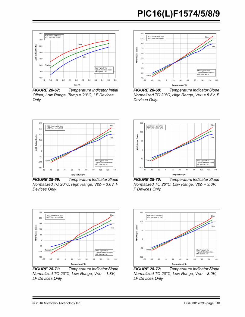
2016 Microchip Technology Inc. DS40001782C-page 310
PIC16(L)F1574/5/8/9
FIGURE 28-67: Temperature Indicator Initial Offset, Low Range, Temp = 20°C, LF Devices Only.
FIGURE 28-68: Temperature Indicator Slope Normalized TO 20°C, High Range, VDD = 5.5V, F Devices Only.
Typical
Max.
Min.
100
200
300
400
500
600
700
800
1.6 1.8 2.0 2.2 2.4 2.6 2.8 3.0 3.2 3.4 3.6 3.8
AD
C O
utpu
t Cod
es
VDD (V)
ADC V + set to VADC V - set to G
Max: Typical + 3σTypical; statistical mean Min: Typical - 3σ
Typical
Max.
Min.
-75
-50
-25
0
25
50
75
100
125
150
-60 -40 -20 0 20 40 60 80 100 120 140
AD
C O
utpu
t Cod
es
Temperature (°C)
ADC V + set to VADC V - set to G
Max: Typical + 3σTypical; statistical mean Min: Typical - 3σ
FIGURE 28-69: Temperature Indicator Slope Normalized TO 20°C, High Range, VDD = 3.6V, F Devices Only.
FIGURE 28-70: Temperature Indicator Slope Normalized TO 20°C, Low Range, VDD = 3.0V, F Devices Only.
Typical
Max.
Min.
-150
-100
-50
0
50
100
150
200
250
-60 -40 -20 0 20 40 60 80 100 120 140
AD
C O
utpu
t Cod
es
Temperature (°C)
ADC V + set to VADC V - set to G
Max: Typical + 3σTypical; statistical mean Min: Typical - 3σ
Typical
Max.
Min.
-100
-50
0
50
100
150
-60 -40 -20 0 20 40 60 80 100 120 140
AD
C O
utpu
t Cod
es
Temperature (°C)
ADC V + set to VADC V - set to G
Max: Typical + 3σTypical; statistical mean Min: Typical - 3σ
FIGURE 28-71: Temperature Indicator Slope Normalized TO 20°C, Low Range, VDD = 1.8V, LF Devices Only.
FIGURE 28-72: Temperature Indicator Slope Normalized TO 20°C, Low Range, VDD = 3.0V, LF Devices Only.
Typical
Max.
Min.
-150
-100
-50
0
50
100
150
200
250
-60 -40 -20 0 20 40 60 80 100 120 140
AD
C O
utpu
t Cod
es
Temperature (°C)
ADC V + set to VADC V - set to G
Max: Typical + 3σTypical; statistical mean Min: Typical - 3σ
Typical
Max.
Min.
-100
-50
0
50
100
150
-60 -40 -20 0 20 40 60 80 100 120 140
AD
C O
utpu
t Cod
es
Temperature (°C)
ADC V + set to VADC V - set to G
Max: Typical + 3σTypical; statistical mean Min: Typical - 3σ

PIC16(L)F1574/5/8/9
DS40001782C-page 311 2016 Microchip Technology Inc.
FIGURE 28-73: Temperature Indicator Slope Normalized TO 20°C, High Range, VDD = 3.6V, LF Devices Only.
Typical
Max.
Min.
-150
-100
-50
0
50
100
150
200
250
-60 -40 -20 0 20 40 60 80 100 120 140
AD
C O
utpu
t Cod
es
Temperature (°C)
Max: Typical + 3σTypical; statistical mean Min: Typical - 3σ
ADC V + set to VADC V - set to G

PIC16(L)F1574/5/8/9
DS40001782C-page 312 2016 Microchip Technology Inc.
29.0 DEVELOPMENT SUPPORT
The PIC® microcontrollers (MCU) and dsPIC® digitalsignal controllers (DSC) are supported with a full rangeof software and hardware development tools:
• Integrated Development Environment
- MPLAB® X IDE Software
• Compilers/Assemblers/Linkers
- MPLAB XC Compiler
- MPASMTM Assembler
- MPLINKTM Object Linker/MPLIBTM Object Librarian
- MPLAB Assembler/Linker/Librarian forVarious Device Families
• Simulators
- MPLAB X SIM Software Simulator
• Emulators
- MPLAB REAL ICE™ In-Circuit Emulator
• In-Circuit Debuggers/Programmers
- MPLAB ICD 3
- PICkit™ 3
• Device Programmers
- MPLAB PM3 Device Programmer
• Low-Cost Demonstration/Development Boards, Evaluation Kits and Starter Kits
• Third-party development tools
29.1 MPLAB X Integrated Development Environment Software
The MPLAB X IDE is a single, unified graphical userinterface for Microchip and third-party software, andhardware development tool that runs on Windows®,Linux and Mac OS® X. Based on the NetBeans IDE,MPLAB X IDE is an entirely new IDE with a host of freesoftware components and plug-ins for high-performance application development and debugging.Moving between tools and upgrading from softwaresimulators to hardware debugging and programmingtools is simple with the seamless user interface.
With complete project management, visual call graphs,a configurable watch window and a feature-rich editorthat includes code completion and context menus,MPLAB X IDE is flexible and friendly enough for newusers. With the ability to support multiple tools onmultiple projects with simultaneous debugging, MPLABX IDE is also suitable for the needs of experiencedusers.
Feature-Rich Editor:
• Color syntax highlighting
• Smart code completion makes suggestions and provides hints as you type
• Automatic code formatting based on user-defined rules
• Live parsing
User-Friendly, Customizable Interface:
• Fully customizable interface: toolbars, toolbar buttons, windows, window placement, etc.
• Call graph window
Project-Based Workspaces:
• Multiple projects
• Multiple tools
• Multiple configurations
• Simultaneous debugging sessions
File History and Bug Tracking:
• Local file history feature
• Built-in support for Bugzilla issue tracker
2016 Microchip Technology Inc. DS40001782C-page 313
PIC16(L)F1574/5/8/9
29.2 MPLAB XC Compilers
The MPLAB XC Compilers are complete ANSI Ccompilers for all of Microchip’s 8, 16, and 32-bit MCUand DSC devices. These compilers provide powerfulintegration capabilities, superior code optimization andease of use. MPLAB XC Compilers run on Windows,Linux or MAC OS X.
For easy source level debugging, the compilers providedebug information that is optimized to the MPLAB XIDE.
The free MPLAB XC Compiler editions support alldevices and commands, with no time or memoryrestrictions, and offer sufficient code optimization formost applications.
MPLAB XC Compilers include an assembler, linker andutilities. The assembler generates relocatable objectfiles that can then be archived or linked with other relo-catable object files and archives to create an execut-able file. MPLAB XC Compiler uses the assembler toproduce its object file. Notable features of the assem-bler include:
• Support for the entire device instruction set
• Support for fixed-point and floating-point data
• Command-line interface
• Rich directive set
• Flexible macro language
• MPLAB X IDE compatibility
29.3 MPASM Assembler
The MPASM Assembler is a full-featured, universalmacro assembler for PIC10/12/16/18 MCUs.
The MPASM Assembler generates relocatable objectfiles for the MPLINK Object Linker, Intel® standard HEXfiles, MAP files to detail memory usage and symbolreference, absolute LST files that contain source linesand generated machine code, and COFF files fordebugging.
The MPASM Assembler features include:
• Integration into MPLAB X IDE projects
• User-defined macros to streamline assembly code
• Conditional assembly for multipurpose source files
• Directives that allow complete control over the assembly process
29.4 MPLINK Object Linker/MPLIB Object Librarian
The MPLINK Object Linker combines relocatableobjects created by the MPASM Assembler. It can linkrelocatable objects from precompiled libraries, usingdirectives from a linker script.
The MPLIB Object Librarian manages the creation andmodification of library files of precompiled code. Whena routine from a library is called from a source file, onlythe modules that contain that routine will be linked inwith the application. This allows large libraries to beused efficiently in many different applications.
The object linker/library features include:
• Efficient linking of single libraries instead of many smaller files
• Enhanced code maintainability by grouping related modules together
• Flexible creation of libraries with easy module listing, replacement, deletion and extraction
29.5 MPLAB Assembler, Linker and Librarian for Various Device Families
MPLAB Assembler produces relocatable machinecode from symbolic assembly language for PIC24,PIC32 and dsPIC DSC devices. MPLAB XC Compileruses the assembler to produce its object file. Theassembler generates relocatable object files that canthen be archived or linked with other relocatable objectfiles and archives to create an executable file. Notablefeatures of the assembler include:
• Support for the entire device instruction set
• Support for fixed-point and floating-point data
• Command-line interface
• Rich directive set
• Flexible macro language
• MPLAB X IDE compatibility
PIC16(L)F1574/5/8/9
DS40001782C-page 314 2016 Microchip Technology Inc.
29.6 MPLAB X SIM Software Simulator
The MPLAB X SIM Software Simulator allows codedevelopment in a PC-hosted environment by simulat-ing the PIC MCUs and dsPIC DSCs on an instructionlevel. On any given instruction, the data areas can beexamined or modified and stimuli can be applied froma comprehensive stimulus controller. Registers can belogged to files for further run-time analysis. The tracebuffer and logic analyzer display extend the power ofthe simulator to record and track program execution,actions on I/O, most peripherals and internal registers.
The MPLAB X SIM Software Simulator fully supportssymbolic debugging using the MPLAB XC Compilers,and the MPASM and MPLAB Assemblers. The soft-ware simulator offers the flexibility to develop anddebug code outside of the hardware laboratory envi-ronment, making it an excellent, economical softwaredevelopment tool.
29.7 MPLAB REAL ICE In-Circuit Emulator System
The MPLAB REAL ICE In-Circuit Emulator System isMicrochip’s next generation high-speed emulator forMicrochip Flash DSC and MCU devices. It debugs andprograms all 8, 16 and 32-bit MCU, and DSC deviceswith the easy-to-use, powerful graphical user interface ofthe MPLAB X IDE.
The emulator is connected to the design engineer’sPC using a high-speed USB 2.0 interface and isconnected to the target with either a connectorcompatible with in-circuit debugger systems (RJ-11)or with the new high-speed, noise tolerant, Low-Voltage Differential Signal (LVDS) interconnection(CAT5).
The emulator is field upgradable through future firmwaredownloads in MPLAB X IDE. MPLAB REAL ICE offerssignificant advantages over competitive emulatorsincluding full-speed emulation, run-time variablewatches, trace analysis, complex breakpoints, logicprobes, a ruggedized probe interface and long (up tothree meters) interconnection cables.
29.8 MPLAB ICD 3 In-Circuit Debugger System
The MPLAB ICD 3 In-Circuit Debugger System isMicrochip’s most cost-effective, high-speed hardwaredebugger/programmer for Microchip Flash DSC andMCU devices. It debugs and programs PIC Flashmicrocontrollers and dsPIC DSCs with the powerful,yet easy-to-use graphical user interface of the MPLABIDE.
The MPLAB ICD 3 In-Circuit Debugger probe isconnected to the design engineer’s PC using a high-speed USB 2.0 interface and is connected to the targetwith a connector compatible with the MPLAB ICD 2 orMPLAB REAL ICE systems (RJ-11). MPLAB ICD 3supports all MPLAB ICD 2 headers.
29.9 PICkit 3 In-Circuit Debugger/Programmer
The MPLAB PICkit 3 allows debugging and program-ming of PIC and dsPIC Flash microcontrollers at a mostaffordable price point using the powerful graphical userinterface of the MPLAB IDE. The MPLAB PICkit 3 isconnected to the design engineer’s PC using a full-speed USB interface and can be connected to the tar-get via a Microchip debug (RJ-11) connector (compati-ble with MPLAB ICD 3 and MPLAB REAL ICE). Theconnector uses two device I/O pins and the Reset lineto implement in-circuit debugging and In-Circuit SerialProgramming™ (ICSP™).
29.10 MPLAB PM3 Device Programmer
The MPLAB PM3 Device Programmer is a universal,CE compliant device programmer with programmablevoltage verification at VDDMIN and VDDMAX formaximum reliability. It features a large LCD display(128 x 64) for menus and error messages, and a mod-ular, detachable socket assembly to support variouspackage types. The ICSP cable assembly is includedas a standard item. In Stand-Alone mode, the MPLABPM3 Device Programmer can read, verify and programPIC devices without a PC connection. It can also setcode protection in this mode. The MPLAB PM3connects to the host PC via an RS-232 or USB cable.The MPLAB PM3 has high-speed communications andoptimized algorithms for quick programming of largememory devices, and incorporates an MMC card for filestorage and data applications.

2016 Microchip Technology Inc. DS40001782C-page 315
PIC16(L)F1574/5/8/9
29.11 Demonstration/Development Boards, Evaluation Kits, and Starter Kits
A wide variety of demonstration, development andevaluation boards for various PIC MCUs and dsPICDSCs allows quick application development on fullyfunctional systems. Most boards include prototypingareas for adding custom circuitry and provide applica-tion firmware and source code for examination andmodification.
The boards support a variety of features, including LEDs,temperature sensors, switches, speakers, RS-232interfaces, LCD displays, potentiometers and additionalEEPROM memory.
The demonstration and development boards can beused in teaching environments, for prototyping customcircuits and for learning about various microcontrollerapplications.
In addition to the PICDEM™ and dsPICDEM™demonstration/development board series of circuits,Microchip has a line of evaluation kits and demonstra-tion software for analog filter design, KEELOQ® securityICs, CAN, IrDA®, PowerSmart battery management,SEEVAL® evaluation system, Sigma-Delta ADC, flowrate sensing, plus many more.
Also available are starter kits that contain everythingneeded to experience the specified device. This usuallyincludes a single application and debug capability, allon one board.
Check the Microchip web page (www.microchip.com)for the complete list of demonstration, developmentand evaluation kits.
29.12 Third-Party Development Tools
Microchip also offers a great collection of tools fromthird-party vendors. These tools are carefully selectedto offer good value and unique functionality.
• Device Programmers and Gang Programmers from companies, such as SoftLog and CCS
• Software Tools from companies, such as Gimpel and Trace Systems
• Protocol Analyzers from companies, such as Saleae and Total Phase
• Demonstration Boards from companies, such as MikroElektronika, Digilent® and Olimex
• Embedded Ethernet Solutions from companies, such as EZ Web Lynx, WIZnet and IPLogika®

PIC16(L)F1574/5/8/9
DS40001782C-page 316 2016 Microchip Technology Inc.
30.0 PACKAGING INFORMATION
30.1 Package Marking Information
Legend: XX...X Customer-specific informationY Year code (last digit of calendar year)YY Year code (last 2 digits of calendar year)WW Week code (week of January 1 is week ‘01’)NNN Alphanumeric traceability code Pb-free JEDEC® designator for Matte Tin (Sn)* This package is Pb-free. The Pb-free JEDEC designator ( )
can be found on the outer packaging for this package.
Note: In the event the full Microchip part number cannot be marked on one line, it willbe carried over to the next line, thus limiting the number of availablecharacters for customer-specific information.
3e
3e
14-Lead PDIP (300 mil) Example
PIC16LF1574
1420123
-P 3e
14-Lead SOIC (3.90 mm) Example
PIC16LF1575-SL
1420123
3e
Example
YYWWNNN
XXXXXXXX L1575ST
1420
123
14-Lead TSSOP (4.4 mm)
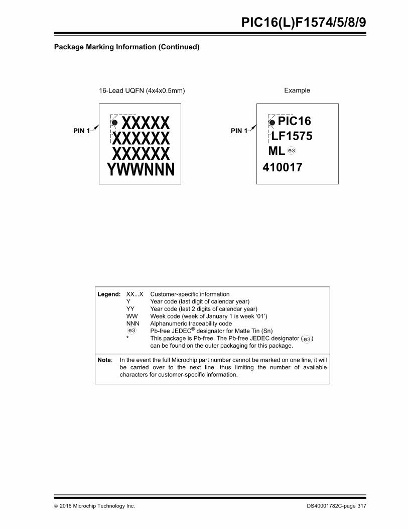
2016 Microchip Technology Inc. DS40001782C-page 317
PIC16(L)F1574/5/8/9
Package Marking Information (Continued)
Example
PIN 1 PIN 1
ML410017
PIC16LF1575
3e
16-Lead UQFN (4x4x0.5mm)
Legend: XX...X Customer-specific informationY Year code (last digit of calendar year)YY Year code (last 2 digits of calendar year)WW Week code (week of January 1 is week ‘01’)NNN Alphanumeric traceability code Pb-free JEDEC® designator for Matte Tin (Sn)* This package is Pb-free. The Pb-free JEDEC designator ( )
can be found on the outer packaging for this package.
Note: In the event the full Microchip part number cannot be marked on one line, it willbe carried over to the next line, thus limiting the number of availablecharacters for customer-specific information.
3e
3e
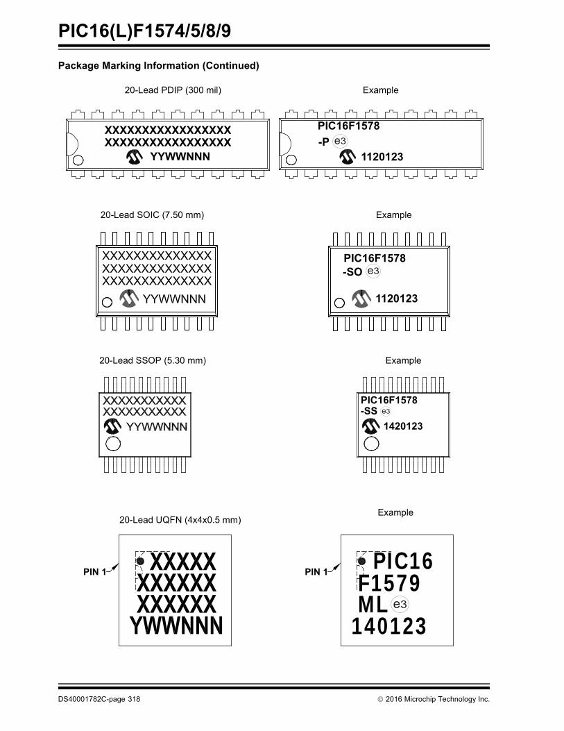
PIC16(L)F1574/5/8/9
DS40001782C-page 318 2016 Microchip Technology Inc.
Package Marking Information (Continued)
20-Lead PDIP (300 mil) Example
XXXXXXXXXXXXXXXXXXXXXXXXXXXXXXXXXX
YYWWNNN
PIC16F1578
-P 3e
1120123
20-Lead SOIC (7.50 mm) Example
PIC16F1578-SO 3e
1120123
20-Lead SSOP (5.30 mm) Example
-SS 3e
1420123
PIC16F1578
Example
PIN 1 PIN 1 PIC16F1579ML
1401233e
20-Lead UQFN (4x4x0.5 mm)
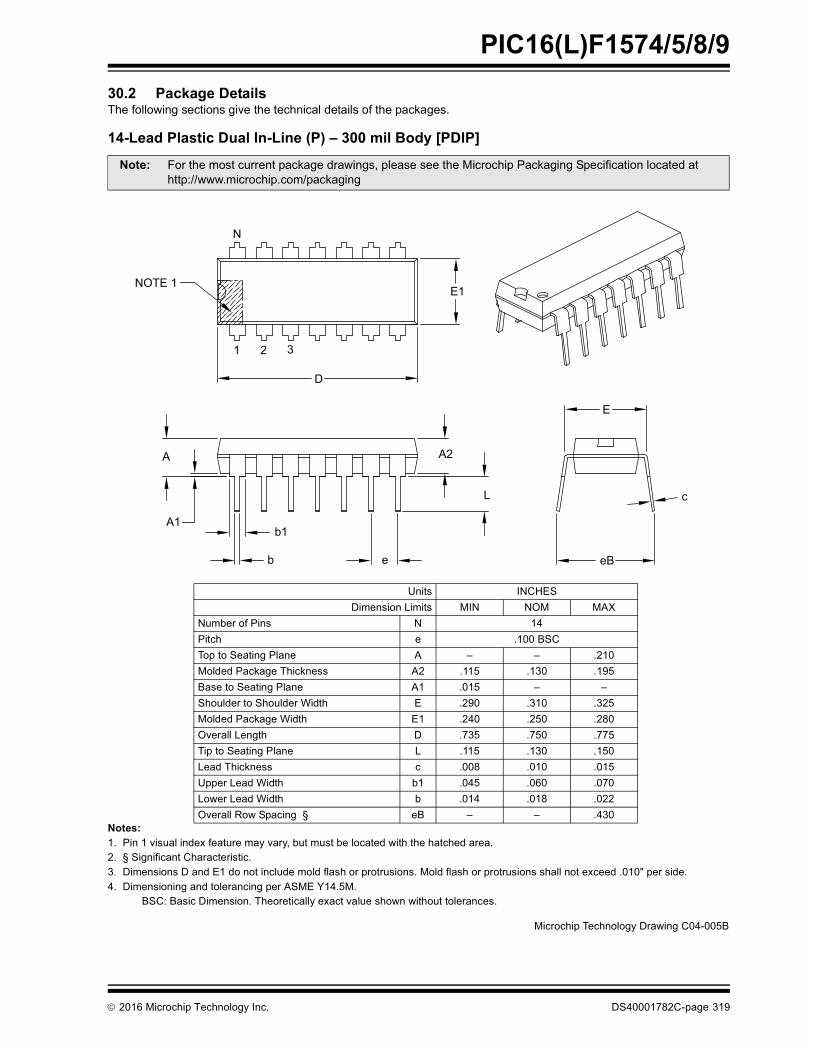
2016 Microchip Technology Inc. DS40001782C-page 319
PIC16(L)F1574/5/8/9
30.2 Package DetailsThe following sections give the technical details of the packages.
���������� ������������������������������
�� �� �� ������!�"#�����$�%�&��'#��(���!��)�*#'�(#"'�*�����'�$�+�'��'�����'��$������� ,������&���'�-���'��"'��.� ��(��"���"�����$�/��$����'����#$��(��$�&��"���� �'#"���"�����$�&��"���� �'#"���"�"�������'��%��$�����0� ��"�$���� ��(��"���������$�'��������� �����/�1���2��
3�-4�3�"����(��"����������'�������%�'�!��#��"��+��+�'��#'�'������"�
�� � 5��'���(�"'�#��'� �6����$�+���")� ���"��"���'�������� ���6������� ��&��'�������'�$��'��'' 477+++�(���� ��(7 �6�����
8��'" �9-:/���(��"����;�(�'" ��9 9<� ��=
9#(*���&����" 9 ����'� � �����3�-�� �'�����'��������� � > > �������$�$���6�������6��"" �� ���2 ��.� ���23�"��'�����'��������� �� ���2 > >���#�$��'�����#�$��?�$'� / ���� �.�� �.�2���$�$���6����?�$'� /� ���� ��2� ��@�<!�����;���'� � ��.2 ��2� ���2�� �'�����'��������� ; ���2 ��.� ��2�;��$����6��"" ���@ ���� ���28 ��;��$�?�$'� *� ���2 ��A� ����;�+��;��$�?�$'� * ���� ���@ ����<!�������+�� ������, �3 > > ��.�
N
E1
D
NOTE 1
1 2 3
E
c
eB
A2
L
A
A1b1
b e
����� ��������� ��+��� -�����23
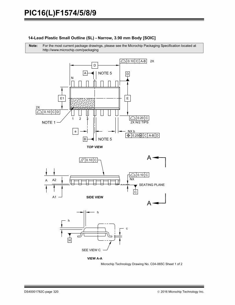
PIC16(L)F1574/5/8/9
DS40001782C-page 320 2016 Microchip Technology Inc.
Note: For the most current package drawings, please see the Microchip Packaging Specification located at http://www.microchip.com/packaging
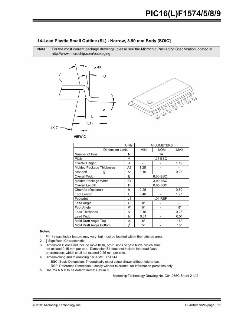
2016 Microchip Technology Inc. DS40001782C-page 321
PIC16(L)F1574/5/8/9
Note: For the most current package drawings, please see the Microchip Packaging Specification located at http://www.microchip.com/packaging
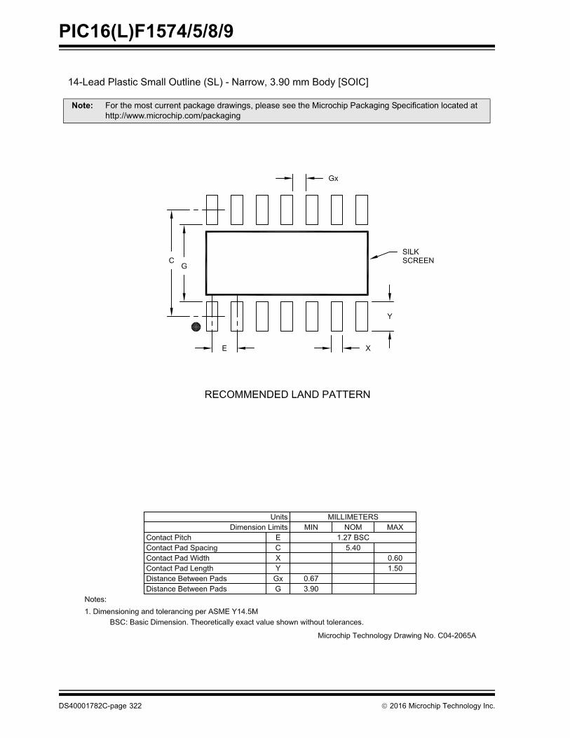
PIC16(L)F1574/5/8/9
DS40001782C-page 322 2016 Microchip Technology Inc.
�� � 5��'���(�"'�#��'� �6����$�+���")� ���"��"���'�������� ���6������� ��&��'�������'�$��'��'' 477+++�(���� ��(7 �6�����

2016 Microchip Technology Inc. DS40001782C-page 323
PIC16(L)F1574/5/8/9
Note: For the most current package drawings, please see the Microchip Packaging Specification located at http://www.microchip.com/packaging
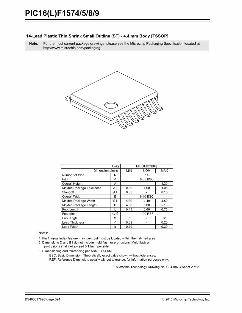
PIC16(L)F1574/5/8/9
DS40001782C-page 324 2016 Microchip Technology Inc.
Note: For the most current package drawings, please see the Microchip Packaging Specification located at http://www.microchip.com/packaging

2016 Microchip Technology Inc. DS40001782C-page 325
PIC16(L)F1574/5/8/9
Note: For the most current package drawings, please see the Microchip Packaging Specification located at http://www.microchip.com/packaging

PIC16(L)F1574/5/8/9
DS40001782C-page 326 2016 Microchip Technology Inc.
BA
0.20 C
0.20 C
0.10 C A B
(DATUM B)(DATUM A)
CSEATING
PLANE
NOTE 1
1
2
N
2XTOP VIEW
SIDE VIEW
BOTTOM VIEW
For the most current package drawings, please see the Microchip Packaging Specification located athttp://www.microchip.com/packaging
Note:
NOTE 1
1
2
N
0.10 C A B
0.10 C A B
0.10 C
0.08 C
A1
Microchip Technology Drawing C04-257A Sheet 1 of 2
16-Lead Ultra Thin Plastic Quad Flat, No Lead Package (JQ) - 4x4x0.5 mm Body [UQFN]
D
E
A
(A3)
16X b
e
e2
2X
D2
E2
K
L
16X

2016 Microchip Technology Inc. DS40001782C-page 327
PIC16(L)F1574/5/8/9
Microchip Technology Drawing C04-257A Sheet 2 of 2
For the most current package drawings, please see the Microchip Packaging Specification located athttp://www.microchip.com/packaging
Note:
Number of Pins
Overall Height
Terminal Width
Overall Width
Overall Length
Terminal Length
Exposed Pad Width
Exposed Pad Length
Terminal Thickness
Pitch
Standoff
UnitsDimension Limits
A1A
b
DE2
D2
A3
e
L
E
N0.65 BSC
0.127 REF
2.50
2.50
0.300.25
0.450.00
0.30
4.00 BSC
0.40
2.60
2.60
0.500.02
4.00 BSC
MILLIMETERSMIN NOM
16
2.70
2.70
0.500.35
0.550.05
MAX
K -0.20 -
REF: Reference Dimension, usually without tolerance, for information purposes only.BSC: Basic Dimension. Theoretically exact value shown without tolerances.
1.2.3.
Notes:
Pin 1 visual index feature may vary, but must be located within the hatched area.Package is saw singulatedDimensioning and tolerancing per ASME Y14.5M
Terminal-to-Exposed-Pad
16-Lead Ultra Thin Plastic Quad Flat, No Lead Package (JQ) - 4x4x0.5 mm Body [UQFN]
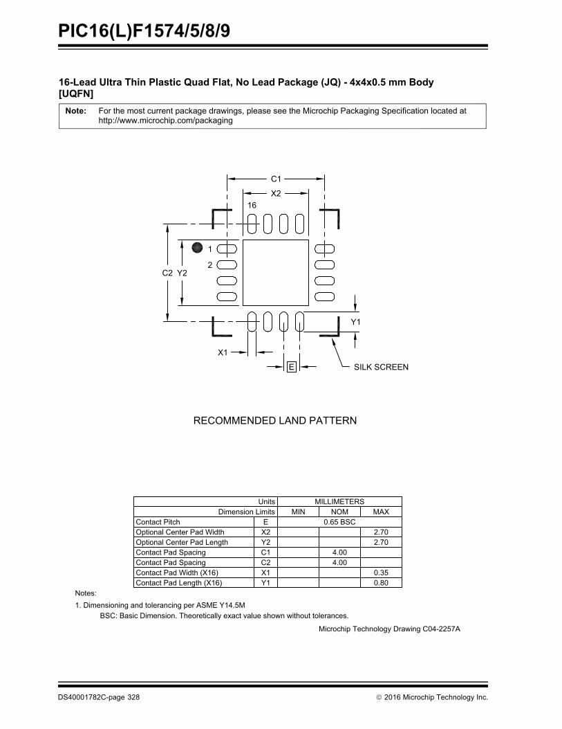
PIC16(L)F1574/5/8/9
DS40001782C-page 328 2016 Microchip Technology Inc.
RECOMMENDED LAND PATTERN
For the most current package drawings, please see the Microchip Packaging Specification located athttp://www.microchip.com/packaging
Note:
SILK SCREEN
Dimension LimitsUnits
C2
Optional Center Pad Width
Contact Pad Spacing
Optional Center Pad Length
Contact Pitch
Y2X2
2.702.70
MILLIMETERS
0.65 BSCMIN
EMAX
4.00
Contact Pad Length (X16)Contact Pad Width (X16)
Y1X1
0.800.35
BSC: Basic Dimension. Theoretically exact value shown without tolerances.
Notes:1. Dimensioning and tolerancing per ASME Y14.5M
Microchip Technology Drawing C04-2257A
NOM
16-Lead Ultra Thin Plastic Quad Flat, No Lead Package (JQ) - 4x4x0.5 mm Body
C2
C1
X2
Y2
X1
E
Y1
C1 4.00Contact Pad Spacing
1
2
16
[UQFN]
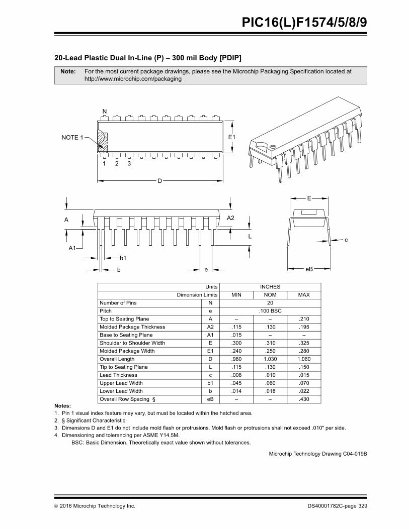
2016 Microchip Technology Inc. DS40001782C-page 329
PIC16(L)F1574/5/8/9
!��������� ������������������������������
�
�� �� �� ������!�"#�����$�%�&��'#��(���!��)�*#'�(#"'�*�����'�$�+�'����'�����'��$������� ,������&���'�-���'��"'��.� ��(��"���"�����$�/��$����'����#$��(��$�&��"���� �'#"���"�����$�&��"���� �'#"���"�"�������'��%��$�����0� ��"�$���� ��(��"���������$�'��������� �����/�1���2��
3�-4 3�"����(��"����������'�������%�'�!��#��"��+��+�'��#'�'������"�
�� � 5��'���(�"'�#��'� �6����$�+���")� ���"��"���'�������� ���6������� ��&��'�������'�$��'��'' 477+++�(���� ��(7 �6�����
8��'" �9-:/���(��"����;�(�'" ��9 9<� ��=
9#(*���&����" 9 ����'� � �����3�-�� �'�����'��������� � > > �������$�$���6�������6��"" �� ���2 ��.� ���23�"��'�����'��������� �� ���2 > >���#�$��'�����#�$��?�$'� / �.�� �.�� �.�2���$�$���6����?�$'� /� ���� ��2� ��@�<!�����;���'� � ��@� ���.� ���A��� �'�����'��������� ; ���2 ��.� ��2�;��$����6��"" ���@ ���� ���28 ��;��$�?�$'� *� ���2 ��A� ����;�+��;��$�?�$'� * ���� ���@ ����<!�������+�� ������, �3 > > ��.�
N
E1NOTE 1
D
1 2 3
A
A1
A2
L
e
b1
b
E
c
eB
����� ��������� ��+��� -������3
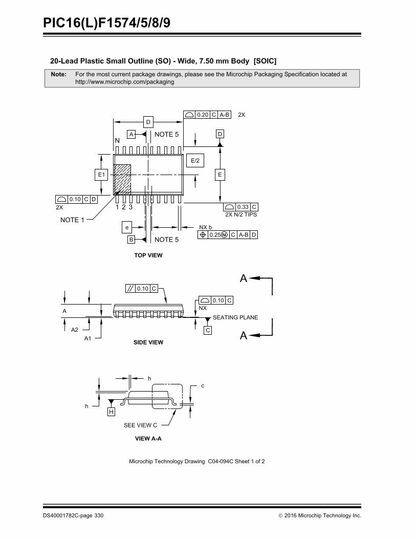
PIC16(L)F1574/5/8/9
DS40001782C-page 330 2016 Microchip Technology Inc.
Note: For the most current package drawings, please see the Microchip Packaging Specification located at http://www.microchip.com/packaging
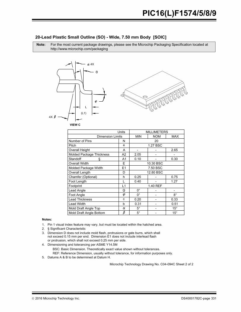
2016 Microchip Technology Inc. DS40001782C-page 331
PIC16(L)F1574/5/8/9
Note: For the most current package drawings, please see the Microchip Packaging Specification located at http://www.microchip.com/packaging

PIC16(L)F1574/5/8/9
DS40001782C-page 332 2016 Microchip Technology Inc.
Note: For the most current package drawings, please see the Microchip Packaging Specification located at http://www.microchip.com/packaging

2016 Microchip Technology Inc. DS40001782C-page 333
PIC16(L)F1574/5/8/9
!��������� ��"#$��%"����&� �����""��'(���������""&�
�� �� �� ������!�"#�����$�%�&��'#��(���!��)�*#'�(#"'�*�����'�$�+�'����'�����'��$������� ��(��"���"�����$�/��$����'����#$��(��$�&��"���� �'#"���"�����$�&��"���� �'#"���"�"�������'��%��$������((� ��"�$��.� ��(��"���������$�'��������� �����/�1���2��
3�-4 3�"����(��"����������'�������%�'�!��#��"��+��+�'��#'�'������"��/54 ��&�������(��"���)�#"#�����+�'��#'�'������)�&����&�(�'���� # �"�"������
�� � 5��'���(�"'�#��'� �6����$�+���")� ���"��"���'�������� ���6������� ��&��'�������'�$��'��'' 477+++�(���� ��(7 �6�����
8��'" ��;;��/�/����(��"����;�(�'" ��9 9<� ��=
9#(*���&����" 9 ����'� � ��A2�3�-<!�����:����' � > > �������$�$���6�������6��"" �� ��A2 ���2 ��@2�'��$�&&� �� ���2 > ><!�����?�$'� / ���� ��@� @������$�$���6����?�$'� /� 2��� 2�.� 2�A�<!�����;���'� � A��� ���� ��2�5��'�;���'� ; ��22 ���2 ���25��' ��' ;� ���2��/5;��$����6��"" ���� > ���25��'������ � �Z �Z @Z;��$�?�$'� * ���� > ��.@
φ
LL1
A2c
eb
A1
A
1 2
NOTE 1
E1
E
D
N
����� ��������� ��+��� -������3

PIC16(L)F1574/5/8/9
DS40001782C-page 334 2016 Microchip Technology Inc.
Note: For the most current package drawings, please see the Microchip Packaging Specification located at http://www.microchip.com/packaging

2016 Microchip Technology Inc. DS40001782C-page 335
PIC16(L)F1574/5/8/9
BA
0.20 C
0.20 C
0.10 C A B
(DATUM B)(DATUM A)
CSEATING
PLANE
1
2
N
2XTOP VIEW
SIDE VIEW
BOTTOM VIEW
For the most current package drawings, please see the Microchip Packaging Specification located athttp://www.microchip.com/packaging
Note:
NOTE 1
1
2
N
0.10 C A B
0.10 C A B
0.10 C
0.08 C
A1
Microchip Technology Drawing C04-255A Sheet 1 of 2
20-Lead Ultra Thin Plastic Quad Flat, No Lead Package (GZ) - 4x4x0.5 mm Body [UQFN]
D
E
A
(A3)
20X b
e
2X
D2
E2
NOTE 1
L
K
20X

PIC16(L)F1574/5/8/9
DS40001782C-page 336 2016 Microchip Technology Inc.
Microchip Technology Drawing C04-255A Sheet 2 of 2
For the most current package drawings, please see the Microchip Packaging Specification located athttp://www.microchip.com/packaging
Note:
Number of Terminals
Overall Height
Terminal Width
Overall Width
Overall Length
Terminal Length
Exposed Pad Width
Exposed Pad Length
Terminal Thickness
Pitch
Standoff
UnitsDimension Limits
A1A
b
DE2
D2
A3
e
L
E
N0.50 BSC
0.127 REF
2.60
2.60
0.300.20
0.450.00
0.25
4.00 BSC
0.40
2.70
2.70
0.500.02
4.00 BSC
MILLIMETERSMIN NOM
20
2.80
2.80
0.500.30
0.550.05
MAX
K -0.20 -
REF: Reference Dimension, usually without tolerance, for information purposes only.BSC: Basic Dimension. Theoretically exact value shown without tolerances.
1.2.3.
Notes:
Pin 1 visual index feature may vary, but must be located within the hatched area.Package is saw singulatedDimensioning and tolerancing per ASME Y14.5M
Terminal-to-Exposed-Pad
20-Lead Ultra Thin Plastic Quad Flat, No Lead Package (GZ) - 4x4x0.5 mm Body [UQFN]
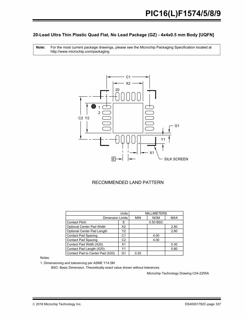
2016 Microchip Technology Inc. DS40001782C-page 337
PIC16(L)F1574/5/8/9
RECOMMENDED LAND PATTERN
For the most current package drawings, please see the Microchip Packaging Specification located athttp://www.microchip.com/packaging
Note:
Dimension LimitsUnits
C2
Optional Center Pad Width
Contact Pad Spacing
Optional Center Pad Length
Contact Pitch
Y2X2
2.802.80
MILLIMETERS
0.50 BSCMIN
EMAX
4.00
Contact Pad Length (X20)Contact Pad Width (X20)
Y1X1
0.800.30
BSC: Basic Dimension. Theoretically exact value shown without tolerances.
Notes:1. Dimensioning and tolerancing per ASME Y14.5M
Microchip Technology Drawing C04-2255A
NOM
20-Lead Ultra Thin Plastic Quad Flat, No Lead Package (GZ) - 4x4x0.5 mm Body [UQFN]
SILK SCREEN
12
20
C1
C2
E
X1
Y1
G1
Y2
X2
C1Contact Pad Spacing 4.00
Contact Pad to Center Pad (X20) G1 0.20

PIC16(L)F1574/5/8/9
DS40001782C-page 338 2016 Microchip Technology Inc.
APPENDIX A: DATA SHEET REVISION HISTORY
Revision A (2/2015)
Initial release of this document.
Revision B (09/2015)
Added Section 5.4: Clock Switching Before Sleep.
Updated Low-Power Features and Memory sectionson cover page.
Updated Examples 3-2 and 16-1; Figures 8-1, 22-1,and 23-8 through 23-13; Registers 8-1, 23-6, 24-2, and24-3; Sections 8.2.2, 16.2.6, 22.0, 23.3.3, 24.9.1.2,24.11.1 and 27.1; and Tables 27-1, 27-2, 27-3, 27-8and 27-11.
Revision C (01/2016)
Added graphs to chapter “DC and AC CharacteristicsGraphs and Charts”. Other minor corrections.

2016 Microchip Technology Inc. DS40001782C-page 339
PIC16(L)F1574/5/8/9
THE MICROCHIP WEBSITE
Microchip provides online support via our website atwww.microchip.com. This website is used as a meansto make files and information easily available tocustomers. Accessible by using your favorite Internetbrowser, the website contains the following information:
• Product Support – Data sheets and errata, application notes and sample programs, design resources, user’s guides and hardware support documents, latest software releases and archived software
• General Technical Support – Frequently Asked Questions (FAQ), technical support requests, online discussion groups, Microchip consultant program member listing
• Business of Microchip – Product selector and ordering guides, latest Microchip press releases, listing of seminars and events, listings of Microchip sales offices, distributors and factory representatives
CUSTOMER CHANGE NOTIFICATION SERVICE
Microchip’s customer notification service helps keepcustomers current on Microchip products. Subscriberswill receive e-mail notification whenever there arechanges, updates, revisions or errata related to aspecified product family or development tool of interest.
To register, access the Microchip website atwww.microchip.com. Under “Support”, click on“Customer Change Notification” and follow theregistration instructions.
CUSTOMER SUPPORT
Users of Microchip products can receive assistancethrough several channels:
• Distributor or Representative
• Local Sales Office
• Field Application Engineer (FAE)
• Technical Support
Customers should contact their distributor,representative or Field Application Engineer (FAE) forsupport. Local sales offices are also available to helpcustomers. A listing of sales offices and locations isincluded in the back of this document.
Technical support is available through the websiteat: http://www.microchip.com/support
PIC16(L)F1574/5/8/9
DS40001782C-page 340 2016 Microchip Technology Inc.
PRODUCT IDENTIFICATION SYSTEM
To order or obtain information, e.g., on pricing or delivery, refer to the factory or the listed sales office.
PART NO. X /XX XXX
PatternPackageTemperatureRange
Device
Device: PIC16LF1574, PIC16F1574, PIC16LF1575, PIC16F1575PIC16LF1578, PIC16F1578, PIC16LF1579, PIC16F1579
Tape and Reel Option:
Blank = Standard packaging (tube or tray) T = Tape and Reel(1)
Temperature Range:
I = -40C to +85C (Industrial)E = -40C to +125C (Extended)
Package:(2) GZ = UQFN, 20-Lead (4x4x0.5mm)JQ = UQFN, 16-Lead (4x4x0.5mm)P = Plastic DIPSL = SOIC, 14-LeadSO = SOIC, 20-LeadSS = SSOP, 20-LeadST = TSSOP, 14-Lead
Pattern: QTP, SQTP, Code or Special Requirements (blank otherwise)
Examples:
a) PIC16LF1578T - I/SO Tape and Reel,Industrial temperature,SOIC package
b) PIC16F1575 - I/PIndustrial temperaturePDIP package
c) PIC16LF1574-E/JQExtended TemperatureUQFN Package
Note 1: Tape and Reel identifier only appears in the catalog part number description. This identifier is used for ordering purposes and is not printed on the device package. Check with your Microchip Sales Office for package availability with the Tape and Reel option.
2: For other small form-factor package availability and marking information, please visit www.microchip.com/packaging or contact your local sales office.
[X](1)
Tape and ReelOption
-
2016 Microchip Technology Inc. DS40001782C-page 341
Information contained in this publication regarding deviceapplications and the like is provided only for your convenienceand may be superseded by updates. It is your responsibility toensure that your application meets with your specifications.MICROCHIP MAKES NO REPRESENTATIONS ORWARRANTIES OF ANY KIND WHETHER EXPRESS ORIMPLIED, WRITTEN OR ORAL, STATUTORY OROTHERWISE, RELATED TO THE INFORMATION,INCLUDING BUT NOT LIMITED TO ITS CONDITION,QUALITY, PERFORMANCE, MERCHANTABILITY ORFITNESS FOR PURPOSE. Microchip disclaims all liabilityarising from this information and its use. Use of Microchipdevices in life support and/or safety applications is entirely atthe buyer’s risk, and the buyer agrees to defend, indemnify andhold harmless Microchip from any and all damages, claims,suits, or expenses resulting from such use. No licenses areconveyed, implicitly or otherwise, under any Microchipintellectual property rights unless otherwise stated.
Trademarks
The Microchip name and logo, the Microchip logo, dsPIC, FlashFlex, flexPWR, JukeBlox, KEELOQ, KEELOQ logo, Kleer, LANCheck, MediaLB, MOST, MOST logo, MPLAB, OptoLyzer, PIC, PICSTART, PIC32 logo, RightTouch, SpyNIC, SST, SST Logo, SuperFlash and UNI/O are registered trademarks of Microchip Technology Incorporated in the U.S.A. and other countries.
The Embedded Control Solutions Company and mTouch are registered trademarks of Microchip Technology Incorporated in the U.S.A.
Analog-for-the-Digital Age, BodyCom, chipKIT, chipKIT logo, CodeGuard, dsPICDEM, dsPICDEM.net, ECAN, In-Circuit Serial Programming, ICSP, Inter-Chip Connectivity, KleerNet, KleerNet logo, MiWi, motorBench, MPASM, MPF, MPLAB Certified logo, MPLIB, MPLINK, MultiTRAK, NetDetach, Omniscient Code Generation, PICDEM, PICDEM.net, PICkit, PICtail, RightTouch logo, REAL ICE, SQI, Serial Quad I/O, Total Endurance, TSHARC, USBCheck, VariSense, ViewSpan, WiperLock, Wireless DNA, and ZENA are trademarks of Microchip Technology Incorporated in the U.S.A. and other countries.
SQTP is a service mark of Microchip Technology Incorporated in the U.S.A.
Silicon Storage Technology is a registered trademark of Microchip Technology Inc. in other countries.
GestIC is a registered trademark of Microchip Technology Germany II GmbH & Co. KG, a subsidiary of Microchip Technology Inc., in other countries.
All other trademarks mentioned herein are property of their respective companies.
© 2016, Microchip Technology Incorporated, Printed in the U.S.A., All Rights Reserved.
ISBN: 978-1-5224-0190-2
Note the following details of the code protection feature on Microchip devices:
• Microchip products meet the specification contained in their particular Microchip Data Sheet.
• Microchip believes that its family of products is one of the most secure families of its kind on the market today, when used in the intended manner and under normal conditions.
• There are dishonest and possibly illegal methods used to breach the code protection feature. All of these methods, to our knowledge, require using the Microchip products in a manner outside the operating specifications contained in Microchip’s Data Sheets. Most likely, the person doing so is engaged in theft of intellectual property.
• Microchip is willing to work with the customer who is concerned about the integrity of their code.
• Neither Microchip nor any other semiconductor manufacturer can guarantee the security of their code. Code protection does not mean that we are guaranteeing the product as “unbreakable.”
Code protection is constantly evolving. We at Microchip are committed to continuously improving the code protection features of ourproducts. Attempts to break Microchip’s code protection feature may be a violation of the Digital Millennium Copyright Act. If such actsallow unauthorized access to your software or other copyrighted work, you may have a right to sue for relief under that Act.
Microchip received ISO/TS-16949:2009 certification for its worldwide headquarters, design and wafer fabrication facilities in Chandler and Tempe, Arizona; Gresham, Oregon and design centers in California and India. The Company’s quality system processes and procedures are for its PIC® MCUs and dsPIC® DSCs, KEELOQ® code hopping devices, Serial EEPROMs, microperipherals, nonvolatile memory and analog products. In addition, Microchip’s quality system for the design and manufacture of development systems is ISO 9001:2000 certified.
QUALITY MANAGEMENT SYSTEM CERTIFIED BY DNV
== ISO/TS 16949 ==

DS40001782C-page 342 2016 Microchip Technology Inc.
AMERICASCorporate Office2355 West Chandler Blvd.Chandler, AZ 85224-6199Tel: 480-792-7200 Fax: 480-792-7277Technical Support: http://www.microchip.com/supportWeb Address: www.microchip.com
AtlantaDuluth, GA Tel: 678-957-9614 Fax: 678-957-1455
Austin, TXTel: 512-257-3370
BostonWestborough, MA Tel: 774-760-0087 Fax: 774-760-0088
ChicagoItasca, IL Tel: 630-285-0071 Fax: 630-285-0075
ClevelandIndependence, OH Tel: 216-447-0464 Fax: 216-447-0643
DallasAddison, TX Tel: 972-818-7423 Fax: 972-818-2924
DetroitNovi, MI Tel: 248-848-4000
Houston, TX Tel: 281-894-5983
IndianapolisNoblesville, IN Tel: 317-773-8323Fax: 317-773-5453
Los AngelesMission Viejo, CA Tel: 949-462-9523 Fax: 949-462-9608
New York, NY Tel: 631-435-6000
San Jose, CA Tel: 408-735-9110
Canada - TorontoTel: 905-673-0699 Fax: 905-673-6509
ASIA/PACIFICAsia Pacific OfficeSuites 3707-14, 37th FloorTower 6, The GatewayHarbour City, Kowloon
Hong KongTel: 852-2943-5100Fax: 852-2401-3431
Australia - SydneyTel: 61-2-9868-6733Fax: 61-2-9868-6755
China - BeijingTel: 86-10-8569-7000 Fax: 86-10-8528-2104
China - ChengduTel: 86-28-8665-5511Fax: 86-28-8665-7889
China - ChongqingTel: 86-23-8980-9588Fax: 86-23-8980-9500
China - DongguanTel: 86-769-8702-9880
China - HangzhouTel: 86-571-8792-8115 Fax: 86-571-8792-8116
China - Hong Kong SARTel: 852-2943-5100 Fax: 852-2401-3431
China - NanjingTel: 86-25-8473-2460Fax: 86-25-8473-2470
China - QingdaoTel: 86-532-8502-7355Fax: 86-532-8502-7205
China - ShanghaiTel: 86-21-5407-5533 Fax: 86-21-5407-5066
China - ShenyangTel: 86-24-2334-2829Fax: 86-24-2334-2393
China - ShenzhenTel: 86-755-8864-2200 Fax: 86-755-8203-1760
China - WuhanTel: 86-27-5980-5300Fax: 86-27-5980-5118
China - XianTel: 86-29-8833-7252Fax: 86-29-8833-7256
ASIA/PACIFICChina - XiamenTel: 86-592-2388138 Fax: 86-592-2388130
China - ZhuhaiTel: 86-756-3210040 Fax: 86-756-3210049
India - BangaloreTel: 91-80-3090-4444 Fax: 91-80-3090-4123
India - New DelhiTel: 91-11-4160-8631Fax: 91-11-4160-8632
India - PuneTel: 91-20-3019-1500
Japan - OsakaTel: 81-6-6152-7160 Fax: 81-6-6152-9310
Japan - TokyoTel: 81-3-6880- 3770 Fax: 81-3-6880-3771
Korea - DaeguTel: 82-53-744-4301Fax: 82-53-744-4302
Korea - SeoulTel: 82-2-554-7200Fax: 82-2-558-5932 or 82-2-558-5934
Malaysia - Kuala LumpurTel: 60-3-6201-9857Fax: 60-3-6201-9859
Malaysia - PenangTel: 60-4-227-8870Fax: 60-4-227-4068
Philippines - ManilaTel: 63-2-634-9065Fax: 63-2-634-9069
SingaporeTel: 65-6334-8870Fax: 65-6334-8850
Taiwan - Hsin ChuTel: 886-3-5778-366Fax: 886-3-5770-955
Taiwan - KaohsiungTel: 886-7-213-7828
Taiwan - TaipeiTel: 886-2-2508-8600 Fax: 886-2-2508-0102
Thailand - BangkokTel: 66-2-694-1351Fax: 66-2-694-1350
EUROPEAustria - WelsTel: 43-7242-2244-39Fax: 43-7242-2244-393
Denmark - CopenhagenTel: 45-4450-2828 Fax: 45-4485-2829
France - ParisTel: 33-1-69-53-63-20 Fax: 33-1-69-30-90-79
Germany - DusseldorfTel: 49-2129-3766400
Germany - KarlsruheTel: 49-721-625370
Germany - MunichTel: 49-89-627-144-0 Fax: 49-89-627-144-44
Italy - Milan Tel: 39-0331-742611 Fax: 39-0331-466781
Italy - VeniceTel: 39-049-7625286
Netherlands - DrunenTel: 31-416-690399 Fax: 31-416-690340
Poland - WarsawTel: 48-22-3325737
Spain - MadridTel: 34-91-708-08-90Fax: 34-91-708-08-91
Sweden - StockholmTel: 46-8-5090-4654
UK - WokinghamTel: 44-118-921-5800Fax: 44-118-921-5820
Worldwide Sales and Service
07/14/15

Mouser Electronics
Authorized Distributor
Click to View Pricing, Inventory, Delivery & Lifecycle Information: Microchip:
PIC16LF1574-E/ST PIC16LF1574-E/SL PIC16LF1578-I/SS PIC16LF1578T-I/SS PIC16LF1575-E/ST
PIC16LF1578-E/P PIC16LF1575-I/JQ PIC16LF1579-I/P PIC16LF1578-E/SO PIC16LF1579-I/SO PIC16LF1579-E/GZ
PIC16LF1575-I/P PIC16LF1578-I/SO PIC16LF1579-I/GZ PIC16LF1575T-I/SL PIC16LF1579-E/P PIC16LF1575-I/SL
PIC16LF1579T-I/SS PIC16LF1574-E/P PIC16LF1579T-I/SO PIC16LF1575T-I/ST PIC16LF1574T-I/SL
PIC16LF1574T-I/JQ PIC16LF1578-E/SS PIC16LF1575-E/P PIC16LF1574-I/ST PIC16LF1578T-I/SO PIC16LF1578T-
I/GZ PIC16LF1579-E/SS PIC16LF1579-E/SO PIC16LF1575-E/SL PIC16LF1579T-I/GZ PIC16LF1574-I/JQ
PIC16LF1574-E/JQ PIC16LF1579-I/SS PIC16LF1578-I/GZ PIC16LF1574-I/P PIC16LF1575T-I/JQ PIC16LF1578-I/P
PIC16LF1575-E/JQ PIC16LF1574T-I/ST PIC16LF1578-E/GZ PIC16LF1574-I/SL PIC16LF1575-I/ST PIC16F1578-
I/GZ PIC16F1579-E/ML PIC16F1575-I/SL PIC16F1578-I/ML PIC16F1578-E/SS PIC16F1575-I/P PIC16F1579-I/P
PIC16F1574-I/SL PIC16F1574-E/ML PIC16F1574-E/ST PIC16F1578-I/P PIC16F1579-E/SS PIC16F1575-I/ST
PIC16F1579-I/ML PIC16F1574-E/JQ PIC16F1579-I/SO PIC16F1575-E/ST PIC16F1574-E/SL PIC16F1575-E/SL
PIC16F1578-E/SO PIC16F1574-I/ML PIC16F1579-I/SS PIC16F1575-E/JQ PIC16F1578-E/GZ PIC16F1578-I/SS
PIC16F1579-E/GZ PIC16F1574-I/JQ PIC16F1574-I/ST PIC16F1574-E/P PIC16F1579-E/P PIC16F1575-E/P
PIC16F1578-I/SO PIC16F1575-I/JQ PIC16F1574-I/P PIC16F1578-E/P PIC16F1579-E/SO PIC16F1579-I/GZ
PIC16F1575T-I/ML PIC16F1574T-I/ML PIC16F1575T-I/JQ PIC16F1579T-I/SS PIC16F1578T-I/SO PIC16F1579T-
I/SO PIC16F1574T-I/JQ PIC16F1574T-I/ST PIC16F1575T-I/ST PIC16F1575T-I/SL PIC16F1578T-I/GZ
PIC16F1579T-I/GZ PIC16F1575-I/ML PIC16F1578T-I/SS PIC16F1579T-I/ML PIC16F1578T-I/ML PIC16F1575-E/ML
PIC16F1578-E/ML PIC16F1574T-I/SL