pic18f87j10 family data sheet - microchip...
TRANSCRIPT

© 2009 Microchip Technology Inc. DS39663F
PIC18F87J10 FamilyData Sheet
64/80-Pin, High-Performance1-Mbit Flash Microcontrollers
with nanoWatt Technology

Note the following details of the code protection feature on Microchip devices:• Microchip products meet the specification contained in their particular Microchip Data Sheet.
• Microchip believes that its family of products is one of the most secure families of its kind on the market today, when used in the intended manner and under normal conditions.
• There are dishonest and possibly illegal methods used to breach the code protection feature. All of these methods, to our knowledge, require using the Microchip products in a manner outside the operating specifications contained in Microchip’s Data Sheets. Most likely, the person doing so is engaged in theft of intellectual property.
• Microchip is willing to work with the customer who is concerned about the integrity of their code.
• Neither Microchip nor any other semiconductor manufacturer can guarantee the security of their code. Code protection does not mean that we are guaranteeing the product as “unbreakable.”
Code protection is constantly evolving. We at Microchip are committed to continuously improving the code protection features of ourproducts. Attempts to break Microchip’s code protection feature may be a violation of the Digital Millennium Copyright Act. If such actsallow unauthorized access to your software or other copyrighted work, you may have a right to sue for relief under that Act.
Information contained in this publication regarding deviceapplications and the like is provided only for your convenienceand may be superseded by updates. It is your responsibility toensure that your application meets with your specifications.MICROCHIP MAKES NO REPRESENTATIONS ORWARRANTIES OF ANY KIND WHETHER EXPRESS ORIMPLIED, WRITTEN OR ORAL, STATUTORY OROTHERWISE, RELATED TO THE INFORMATION,INCLUDING BUT NOT LIMITED TO ITS CONDITION,QUALITY, PERFORMANCE, MERCHANTABILITY ORFITNESS FOR PURPOSE. Microchip disclaims all liabilityarising from this information and its use. Use of Microchipdevices in life support and/or safety applications is entirely atthe buyer’s risk, and the buyer agrees to defend, indemnify andhold harmless Microchip from any and all damages, claims,suits, or expenses resulting from such use. No licenses areconveyed, implicitly or otherwise, under any Microchipintellectual property rights.
DS39663F-page ii
Trademarks
The Microchip name and logo, the Microchip logo, dsPIC, KEELOQ, KEELOQ logo, MPLAB, PIC, PICmicro, PICSTART, rfPIC and UNI/O are registered trademarks of Microchip Technology Incorporated in the U.S.A. and other countries.
FilterLab, Hampshire, HI-TECH C, Linear Active Thermistor, MXDEV, MXLAB, SEEVAL and The Embedded Control Solutions Company are registered trademarks of Microchip Technology Incorporated in the U.S.A.
Analog-for-the-Digital Age, Application Maestro, CodeGuard, dsPICDEM, dsPICDEM.net, dsPICworks, dsSPEAK, ECAN, ECONOMONITOR, FanSense, HI-TIDE, In-Circuit Serial Programming, ICSP, Mindi, MiWi, MPASM, MPLAB Certified logo, MPLIB, MPLINK, mTouch, Octopus, Omniscient Code Generation, PICC, PICC-18, PICDEM, PICDEM.net, PICkit, PICtail, PIC32 logo, REAL ICE, rfLAB, Select Mode, Total Endurance, TSHARC, UniWinDriver, WiperLock and ZENA are trademarks of Microchip Technology Incorporated in the U.S.A. and other countries.
SQTP is a service mark of Microchip Technology Incorporated in the U.S.A.
All other trademarks mentioned herein are property of their respective companies.
© 2009, Microchip Technology Incorporated, Printed in the U.S.A., All Rights Reserved.
Printed on recycled paper.
© 2009 Microchip Technology Inc.
Microchip received ISO/TS-16949:2002 certification for its worldwide headquarters, design and wafer fabrication facilities in Chandler and Tempe, Arizona; Gresham, Oregon and design centers in California and India. The Company’s quality system processes and procedures are for its PIC® MCUs and dsPIC® DSCs, KEELOQ® code hopping devices, Serial EEPROMs, microperipherals, nonvolatile memory and analog products. In addition, Microchip’s quality system for the design and manufacture of development systems is ISO 9001:2000 certified.

PIC18F87J10 FAMILY64/80-Pin, High-Performance, 1-Mbit Flash Microcontrollers
with nanoWatt Technology
Special Microcontroller Features:• Operating Voltage Range: 2.0V to 3.6V• 5.5V Tolerant Input (digital pins only)• On-Chip 2.5V Regulator• Low-Power, High-Speed CMOS Flash Technology• C Compiler Optimized Architecture:
- Optional extended instruction set designed to optimize re-entrant code
• Priority Levels for Interrupts• 8 x 8 Single-Cycle Hardware Multiplier• Extended Watchdog Timer (WDT):
- Programmable period from 4 ms to 131s• Single-Supply In-Circuit Serial Programming™
(ICSP™) via Two Pins• In-Circuit Debug (ICD) with Three Break points via
Two Pins• Power-Managed modes:
- Run: CPU on, peripherals on- Idle: CPU off, peripherals on- Sleep: CPU off, peripherals off
• Flash Program Memory:- 1000 erase/write cycle endurance typical- 20 year retention minimum- Self-write capability during normal operation
Flexible Oscillator Structure:• Two Crystal modes, up to 40 MHz• 4x Phase Lock Loop (PLL)• Two External Clock modes, up to 40 MHz• Internal 31 kHz Oscillator• Secondary Oscillator using Timer1 @ 32 kHz• Two-Speed Oscillator Start-up• Fail-Safe Clock Monitor:
- Allows for safe shutdown if peripheral clock stops
Peripheral Highlights:• High-Current Sink/Source 25 mA/25 mA
(PORTB and PORTC)• Four Programmable External Interrupts• Four Input Change Interrupts• Two Capture/Compare/PWM (CCP) modules• Three Enhanced Capture/Compare/PWM (ECCP)
modules:- One, two or four PWM outputs- Selectable polarity- Programmable dead time- Auto-shutdown and auto-restart
• Two Master Synchronous Serial Port (MSSP) modules Supporting 3-Wire SPI (all 4 modes) and I2C™ Master and Slave modes
• Two Enhanced Addressable USART modules:- Supports RS-485, RS-232 and LIN/2602- Auto-wake-up on Start bit- Auto-Baud Detect (ABD)
• 10-Bit, up to 15-Channel Analog-to-Digital Converter module (A/D): - Auto-acquisition capability- Conversion available during Sleep- Self-calibration feature
• Dual Analog Comparators with Input Multiplexing
External Memory Bus (PIC18F8XJ10/8XJ15 only):• Address Capability of up to 2 Mbytes• 8-Bit or 16-Bit Interface• 12-Bit, 16-Bit and 20-Bit Addressing modes
© 2009 Microchip Technology Inc. DS39663F-page 1

PIC18F87J10 FAMILY
Pin Diagrams
Device
Program MemorySRAM Data
Memory(bytes)
I/O 10-BitA/D (ch)
CCP/ECCP(PWM)
MSSP
EUSA
RT
Com
para
tors
Tim
ers
8/16
-Bit
Exte
rnal
Bus
Flash(bytes)
# Single-WordInstructions SPI Master
I2C™
PIC18F65J10 32K 16384 2048 50 11 2/3 2 Y Y 2 2 2/3 NPIC18F65J15 48K 24576 2048 50 11 2/3 2 Y Y 2 2 2/3 NPIC18F66J10 64K 32768 2048 50 11 2/3 2 Y Y 2 2 2/3 NPIC18F66J15 96K 49152 3936 50 11 2/3 2 Y Y 2 2 2/3 NPIC18F67J10 128K 65536 3936 50 11 2/3 2 Y Y 2 2 2/3 NPIC18F85J10 32K 16384 2048 66 15 2/3 2 Y Y 2 2 2/3 YPIC18F85J15 48K 24576 2048 66 15 2/3 2 Y Y 2 2 2/3 YPIC18F86J10 64K 32768 2048 66 15 2/3 2 Y Y 2 2 2/3 YPIC18F86J15 96K 49152 3936 66 15 2/3 2 Y Y 2 2 2/3 YPIC18F87J10 128K 65536 3936 66 15 2/3 2 Y Y 2 2 2/3 Y
64-Pin TQFP
PIC18F6XJ10
1234567891011121314
383736353433
50 49
17 18 19 20 21 22 23 24 25 26
RE
2/C
S/P
2BR
E3/
P3C
RE
4/P
3BR
E5/
P1C
RE
6/P
1BR
E7/
EC
CP
2(1) /P
2A(1
)
RD
0/P
SP
0V
DD
VS
S
RD
1/P
SP
1R
D2/
PS
P2
RD
3/P
SP
3R
D4/
PS
P4/
SD
O2
RD
5/P
SP
5/S
DI2
/SD
A2
RD
6/P
SP
6/S
CK
2/S
CL2
RD
7/P
SP
7/S
S2
RE1/WR/P2CRE0/RD/P2D
RG0/ECCP3/P3ARG1/TX2/CK2RG2/RX2/DT2
RG3/CCP4/P3DMCLR
RG4/CCP5/P1DVSS
VDDCORE/VCAP
RF7/SS1RF6/AN11
RF5/AN10/CVREF
RF4/AN9RF3/AN8
RF2/AN7/C1OUT
RB0/INT0/FLT0RB1/INT1RB2/INT2RB3/INT3RB4/KBI0RB5/KBI1RB6/KBI2/PGCVSS
OSC2/CLKOOSC1/CLKIVDD
RB7/KBI3/PGD
RC4/SDI1/SDA1RC3/SCK1/SCL1RC2/ECCP1/P1A
EN
VR
EG
RF1
/AN
6/C
2OU
T
AVD
D
AVS
S
RA
3/AN
3/VR
EF+
RA
2/A
N2/
VRE
F-R
A1/
AN
1R
A0/
AN
0V
SS
VD
D
RA
4/T0
CK
IR
A5/
AN
4
RC
1/T1
OSI
/EC
CP2
(1) /P
2A(1
)
RC
0/T1
OS
O/T
13C
KI
RC
7/R
X1/D
T1R
C6/
TX1/
CK
1
RC5/SDO1
1516
31
4039
27 28 29 30 32
4847464544434241
54 53 52 5158 57 56 5560 5964 63 62 61
Note 1: The ECCP2/P2A pin placement depends on the setting of the CCP2MX Configuration bit.
PIC18F6XJ15
Pins are up to 5.5V tolerant
DS39663F-page 2 © 2009 Microchip Technology Inc.

PIC18F87J10 FAMILY
Pin Diagrams (Continued)80-Pin TQFP
PIC18F8XJ10
345678910111213141516
4847464544434241
4039
64 63 62 61
21 22 23 24 25 26 27 28 29 30 31 32
RE
2/AD
10/C
S/P2
BR
E3/
AD11
/P3C
(2)
RE
4/AD
12/P
3B(2
)
RE
5/AD
13/P
1C(2
)
RE
6/AD
14/P
1B(2
)
RE
7/AD
15/E
CC
P2(1
) /P2A
(1)
RD
0/A
D0/
PS
P0
VD
D
VS
S
RD
1/A
D1/
PS
P1
RD
2/A
D2/
PS
P2
RD
3/A
D3/
PS
P3
RD
4/A
D4/
PS
P4/
SD
O2
RD
5/A
D5/
PS
P5/
SD
I2/S
DA
2R
D6/
AD
6/P
SP
6/S
CK
2/S
CL2
RD
7/A
D7/
PS
P7/
SS
2
RE1/AD9/WR/P2CRE0/AD8/RD/P2DRG0/ECCP3/P3A
RG1/TX2/CK2RG2/RX2/DT2
RG3/CCP4/P3DMCLR
RG4/CCP5/P1DVSS
VDDCORE/VCAP
RF7/SS1
RB0/INT0/FLT0RB1/INT1RB2/INT2RB3/INT3/ECCP2(1)/P2A(1)
RB4/KBI0RB5/KBI1RB6/KBI2/PGCVSS
OSC2/CLKOOSC1/CLKIVDD
RB7/KBI3/PGD
RC4/SDI1/SDA1RC3/SCK1/SCL1RC2/ECCP1/P1A
EN
VR
EG
RF1
/AN
6/C
2OU
T
AVD
D
AVS
S
RA
3/A
N3/
VRE
F+R
A2/
AN
2/VR
EF-
RA
1/A
N1
RA
0/A
N0
VS
S
VD
D
RA
4/T0
CK
IR
A5/A
N4
RC
1/T1
OS
I/EC
CP
2(1) /P
2A(1
)
RC
0/T1
OS
O/T
13C
KI
RC
7/R
X1/
DT1
RC
6/TX
1/C
K1
RC5/SDO1R
J0/A
LER
J1/O
E
RH
1/A
17R
H0/
A16
12
RH2/A18RH3/A19
1718
RH7/AN15/P1B(2)
RH6/AN14/P1C(2)
RH
5/A
N13
/P3B
(2)
RH
4/A
N12
/P3C
(2)
RJ5
/CE
RJ4
/BA
0
37
RJ7/UBRJ6/LB
5049
RJ2/WRLRJ3/WRH
1920
33 34 35 36 38
5857565554535251
6059
68 67 66 6572 71 70 6974 7378 77 76 757980
Note 1: The ECCP2/P2A pin placement depends on the setting of the CCP2MX Configuration bit and the program memory mode.2: P1B, P1C, P3B and P3C pin placement depends on the setting of the ECCPMX Configuration bit.
RF5/AN10/CVREF
RF4/AN9RF3/AN8
RF2/AN7/C1OUT
RF6/AN11
PIC18F8XJ15
Pins are up to 5.5V tolerant
© 2009 Microchip Technology Inc. DS39663F-page 3

PIC18F87J10 FAMILY
Table of Contents1.0 Device Overview .......................................................................................................................................................................... 52.0 Guidelines for Getting Started with PIC18FJ Microcontrollers ................................................................................................... 273.0 Oscillator Configurations ............................................................................................................................................................ 314.0 Power-Managed Modes ............................................................................................................................................................. 395.0 Reset .......................................................................................................................................................................................... 476.0 Memory Organization ................................................................................................................................................................. 597.0 Flash Program Memory.............................................................................................................................................................. 858.0 External Memory Bus ................................................................................................................................................................. 959.0 8 x 8 Hardware Multiplier.......................................................................................................................................................... 10710.0 Interrupts .................................................................................................................................................................................. 10911.0 I/O Ports ................................................................................................................................................................................... 12512.0 Timer0 Module ......................................................................................................................................................................... 15113.0 Timer1 Module ......................................................................................................................................................................... 15514.0 Timer2 Module ......................................................................................................................................................................... 16115.0 Timer3 Module ......................................................................................................................................................................... 16316.0 Timer4 Module ......................................................................................................................................................................... 16717.0 Capture/Compare/PWM (CCP) Modules ................................................................................................................................. 16918.0 Enhanced Capture/Compare/PWM (ECCP) Module................................................................................................................ 17719.0 Master Synchronous Serial Port (MSSP) Module .................................................................................................................... 19320.0 Enhanced Universal Synchronous Asynchronous Receiver Transmitter (EUSART) ............................................................... 23921.0 10-Bit Analog-to-Digital Converter (A/D) Module ..................................................................................................................... 26122.0 Comparator Module.................................................................................................................................................................. 27123.0 Comparator Voltage Reference Module................................................................................................................................... 27724.0 Special Features of the CPU.................................................................................................................................................... 28125.0 Instruction Set Summary .......................................................................................................................................................... 29326.0 Development Support............................................................................................................................................................... 34327.0 Electrical Characteristics .......................................................................................................................................................... 34728.0 Packaging Information.............................................................................................................................................................. 385Appendix A: Migration Between High-End Device Families............................................................................................................... 391Appendix B: Revision History............................................................................................................................................................. 393Index .................................................................................................................................................................................................. 395The Microchip Web Site ..................................................................................................................................................................... 405Customer Change Notification Service .............................................................................................................................................. 405Customer Support .............................................................................................................................................................................. 405Reader Response .............................................................................................................................................................................. 406Product Identification System............................................................................................................................................................. 407TO OUR VALUED CUSTOMERSIt is our intention to provide our valued customers with the best documentation possible to ensure successful use of your Microchipproducts. To this end, we will continue to improve our publications to better suit your needs. Our publications will be refined andenhanced as new volumes and updates are introduced. If you have any questions or comments regarding this publication, please contact the Marketing Communications Department viaE-mail at [email protected] or fax the Reader Response Form in the back of this data sheet to (480) 792-4150. Wewelcome your feedback.
Most Current Data SheetTo obtain the most up-to-date version of this data sheet, please register at our Worldwide Web site at:
http://www.microchip.comYou can determine the version of a data sheet by examining its literature number found on the bottom outside corner of any page.The last character of the literature number is the version number, (e.g., DS30000A is version A of document DS30000).
ErrataAn errata sheet, describing minor operational differences from the data sheet and recommended workarounds, may exist for currentdevices. As device/documentation issues become known to us, we will publish an errata sheet. The errata will specify the revisionof silicon and revision of document to which it applies.To determine if an errata sheet exists for a particular device, please check with one of the following:• Microchip’s Worldwide Web site; http://www.microchip.com• Your local Microchip sales office (see last page)When contacting a sales office, please specify which device, revision of silicon and data sheet (include literature number) you areusing.
Customer Notification SystemRegister on our web site at www.microchip.com to receive the most current information on all of our products.
DS39663F-page 4 © 2009 Microchip Technology Inc.

PIC18F87J10 FAMILY
1.0 DEVICE OVERVIEWThis document contains device specific information forthe following devices:
This family introduces a new line of low-voltage deviceswith the main traditional advantage of all PIC18 micro-controllers – namely, high computational performanceand a rich feature set – at an extremely competitiveprice point. These features make the PIC18F87J10family a logical choice for many high-performanceapplications where cost is a primary consideration.
1.1 Core Features
1.1.1 nanoWatt TECHNOLOGYAll of the devices in the PIC18F87J10 family incorporatea range of features that can significantly reduce powerconsumption during operation. Key items include:• Alternate Run Modes: By clocking the controller
from the Timer1 source or the internal RC oscilla-tor, power consumption during code execution can be reduced by as much as 90%.
• Multiple Idle Modes: The controller can also run with its CPU core disabled but the peripherals still active. In these states, power consumption can be reduced even further, to as little as 4% of normal operation requirements.
• On-the-Fly Mode Switching: The power-managed modes are invoked by user code during operation, allowing the user to incorporate power-saving ideas into their application’s software design.
1.1.2 OSCILLATOR OPTIONS AND FEATURES
All of the devices in the PIC18F87J10 family offer fivedifferent oscillator options, allowing users a range ofchoices in developing application hardware. Theseinclude:• Two Crystal modes, using crystals or ceramic
resonators.• Two External Clock modes, offering the option of
a divide-by-4 clock output.• A Phase Lock Loop (PLL) frequency multiplier,
available to the external oscillator modes which allows clock speeds of up to 40 MHz.
• An internal RC oscillator with a fixed 31-kHz output which provides an extremely low-power option for timing-insensitive applications.
The internal oscillator block provides a stable referencesource that gives the family additional features forrobust operation:• Fail-Safe Clock Monitor: This option constantly
monitors the main clock source against a reference signal provided by the internal oscillator. If a clock failure occurs, the controller is switched to the internal oscillator, allowing for continued low-speed operation or a safe application shutdown.
• Two-Speed Start-up: This option allows the internal oscillator to serve as the clock source from Power-on Reset, or wake-up from Sleep mode, until the primary clock source is available.
1.1.3 EXPANDED MEMORYThe PIC18F87J10 family provides ample room forapplication code, from 32 Kbytes to 128 Kbytes of codespace. The Flash cells for program memory are ratedto last up to 100 erase/write cycles. The PIC18F87J10family also provides plenty of room for dynamicapplication data, with up to 3936 bytes of data RAM.
1.1.4 EXTERNAL MEMORY BUSIn the unlikely event that 128 Kbytes of memory areinadequate for an application, the 80-pin members ofthe PIC18F87J10 family also implement an externalmemory bus. This allows the controller’s internalprogram counter to address a memory space of up to2 Mbytes, permitting a level of data access that few8-bit devices can claim. This allows additional memoryoptions, including:• Using combinations of on-chip and external
memory up to the 2-Mbyte limit• Using external Flash memory for reprogrammable
application code or large data tables• Using external RAM devices for storing large
amounts of variable data
1.1.5 EXTENDED INSTRUCTION SETThe PIC18F87J10 family implements the optionalextension to the PIC18 instruction set, adding 8 newinstructions and an Indexed Addressing mode.Enabled as a device configuration option, the extensionhas been specifically designed to optimize re-entrantapplication code originally developed in high-levellanguages, such as ‘C’.
• PIC18F65J10 • PIC18F85J10• PIC18F65J15 • PIC18F85J15• PIC18F66J10 • PIC18F86J10• PIC18F66J15 • PIC18F86J15• PIC18F67J10 • PIC18F87J10
© 2009 Microchip Technology Inc. DS39663F-page 5
PIC18F87J10 FAMILY
1.1.6 EASY MIGRATIONRegardless of the memory size, all devices share thesame rich set of peripherals, allowing for a smoothmigration path as applications grow and evolve.The consistent pinout scheme used throughout theentire family also aids in migrating to the next largerdevice. This is true when moving between the 64-pinmembers, between the 80-pin members, or evenjumping from 64-pin to 80-pin devices.
The PIC18F87J10 family is also pin compatible withother PIC18 families, such as the PIC18F8720 andPIC18F8722. This allows a new dimension to theevolution of applications, allowing developers to selectdifferent price points within Microchip’s PIC18 portfolio,while maintaining the same feature set.
1.2 Other Special Features• Communications: The PIC18F87J10 family
incorporates a range of serial communication peripherals, including 2 independent Enhanced USARTs and 2 Master SSP modules, capable of both SPI and I2C™ (Master and Slave) modes of operation. In addition, one of the general purpose I/O ports can be reconfigured as an 8-bit Parallel Slave Port for direct processor-to-processor communications.
• CCP Modules: All devices in the family incorporate two Capture/Compare/PWM (CCP) modules and three Enhanced CCP modules to maximize flexibility in control applications. Up to four different time bases may be used to perform several different operations at once. Each of the three ECCPs offers up to four PWM outputs, allowing for a total of 12 PWMs. The ECCPs also offer many beneficial features, including polarity selection, programmable dead time, auto-shutdown and restart and Half-Bridge and Full-Bridge Output modes.
• 10-Bit A/D Converter: This module incorporates programmable acquisition time, allowing for a channel to be selected and a conversion to be initiated without waiting for a sampling period and thus, reducing code overhead.
• Extended Watchdog Timer (WDT): This enhanced version incorporates a 16-bit prescaler, allowing an extended time-out range that is stable across operating voltage and temperature. See Section 27.0 “Electrical Characteristics” for time-out periods.
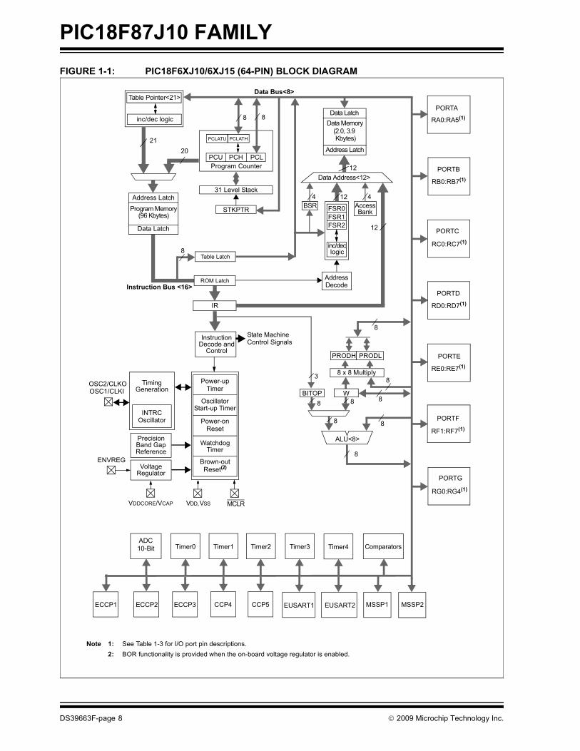
1.3 Details on Individual Family Members
Devices in the PIC18F87J10 family are available in64-pin and 80-pin packages. Block diagrams for thetwo groups are shown in Figure 1-1 and Figure 1-2.
The devices are differentiated from each other in fourways:
1. Flash program memory (six sizes, ranging from32 Kbytes for PIC18FX5J10 devices to128 Kbytes for PIC18FX7J10).
2. Data RAM (2048 bytes forPIC18FX5J10/X5J15/X6J10 devices, 3936bytes for PIC18FX6J15/X7J10 devices).
3. A/D channels (11 for 64-pin devices, 15 for80-pin devices).
4. I/O ports (7 bidirectional ports on 64-pin devices,9 bidirectional ports on 80-pin devices).
All other features for devices in this family are identical.These are summarized in Table 1-1 and Table 1-2.
The pinouts for all devices are listed in Table 1-3 andTable 1-4.
DS39663F-page 6 © 2009 Microchip Technology Inc.

PIC18F87J10 FAMILY
TABLE 1-1: DEVICE FEATURES FOR THE PIC18F87J10 FAMILY (64-PIN DEVICES)TABLE 1-2: DEVICE FEATURES FOR THE PIC18F87J10 FAMILY (80-PIN DEVICES)
Features PIC18F65J10 PIC18F65J15 PIC18F66J10 PIC18F66J15 PIC18F67J10
Operating Frequency DC – 40 MHz DC – 40 MHz DC – 40 MHz DC – 40 MHz DC – 40 MHzProgram Memory (Bytes) 32K 48K 64K 96K 128KProgram Memory (Instructions) 16384 24576 32768 49152 65536Data Memory (Bytes) 2048 2048 2048 3936 3936Interrupt Sources 27I/O Ports Ports A, B, C, D, E, F, GTimers 5Capture/Compare/PWM Modules 2Enhanced Capture/Compare/PWM Modules
3
Serial Communications MSSP (2), Enhanced USART (2)Parallel Communications (PSP) Yes10-Bit Analog-to-Digital Module 11 Input Channels
Resets (and Delays) POR, BOR, RESET Instruction, Stack Full, Stack Underflow, MCLR, WDT (PWRT, OST)
Instruction Set 75 Instructions, 83 with Extended Instruction Set enabledPackages 64-pin TQFP
Features PIC18F85J10 PIC18F85J15 PIC18F86J10 PIC18F86J15 PIC18F87J10
Operating Frequency DC – 40 MHz DC – 40 MHz DC – 40 MHz DC – 40 MHz DC – 40 MHzProgram Memory (Bytes) 32K 48K 64K 96K 128KProgram Memory (Instructions) 16384 24576 32768 49152 65536Data Memory (Bytes) 2048 2048 2048 3936 3936Interrupt Sources 27I/O Ports Ports A, B, C, D, E, F, G, H, JTimers 5Capture/Compare/PWM Modules 2Enhanced Capture/Compare/PWM Modules
3
Serial Communications MSSP (2), Enhanced USART (2)Parallel Communications (PSP) Yes10-Bit Analog-to-Digital Module 15 Input Channels
Resets (and Delays) POR, BOR, RESET Instruction, Stack Full, Stack Underflow, MCLR, WDT (PWRT, OST)
Instruction Set 75 Instructions, 83 with Extended Instruction Set enabledPackages 80-pin TQFP
© 2009 Microchip Technology Inc. DS39663F-page 7
PIC18F87J10 FAMILY
FIGURE 1-1: PIC18F6XJ10/6XJ15 (64-PIN) BLOCK DIAGRAMInstructionDecode and
Control
PORTAData Latch
Data Memory(2.0, 3.9
Address Latch
Data Address<12>12
AccessBSR FSR0FSR1FSR2
inc/declogic
Address
4 12 4
PCH PCL
PCLATH
8
31 Level Stack
Program Counter
PRODLPRODH
8 x 8 Multiply
8
BITOP88
ALU<8>
Address Latch
Program Memory(96 Kbytes)
Data Latch
20
8
8
Table Pointer<21>
inc/dec logic
21
8
Data Bus<8>
Table Latch8
IR
12
3
PCLATU
PCU
Note 1: See Table 1-3 for I/O port pin descriptions.2: BOR functionality is provided when the on-board voltage regulator is enabled.
EUSART1
Comparators
MSSP1
Timer2Timer1 Timer3Timer0
ECCP1
ADC10-Bit
W
Instruction Bus <16>
STKPTR Bank
8
State MachineControl Signals
Decode
8
8
EUSART2ECCP2
ROM Latch
ECCP3 MSSP2CCP4 CCP5
PORTC
PORTD
PORTE
PORTF
PORTG
RA0:RA5(1)
RC0:RC7(1)
RD0:RD7(1)
RE0:RE7(1)
RF1:RF7(1)
RG0:RG4(1)
PORTB
RB0:RB7(1)
Timer4
OSC1/CLKIOSC2/CLKO
VDD,
TimingGeneration
VSS MCLR
Power-upTimer
OscillatorStart-up Timer
Power-onReset
WatchdogTimer
Brown-outReset(2)
Precision
ReferenceBand Gap
INTRCOscillator
RegulatorVoltage
VDDCORE/VCAP
ENVREG
Kbytes)
DS39663F-page 8 © 2009 Microchip Technology Inc.
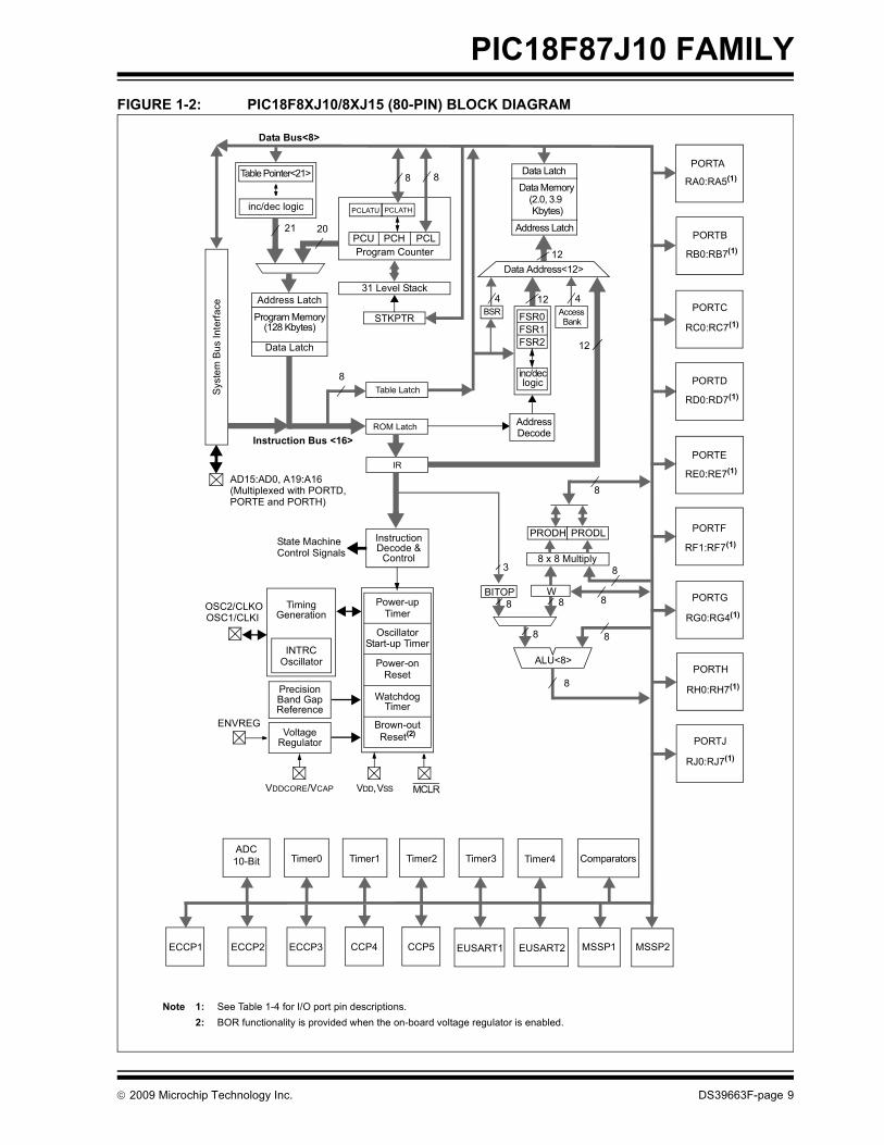
PIC18F87J10 FAMILY
FIGURE 1-2: PIC18F8XJ10/8XJ15 (80-PIN) BLOCK DIAGRAMPRODLPRODH
8 x 8 Multiply
8
BITOP88
ALU<8>
8
83
W8
8
8
InstructionDecode &
Control
Data Latch
Address Latch
Data Address<12>12
AccessBSR FSR0FSR1FSR2
inc/declogic
Address
4 12 4
PCH PCL
PCLATH
8
31 Level Stack
Program Counter
Address Latch
Program Memory(128 Kbytes)
Data Latch
20
Table Pointer<21>
inc/dec logic
21
8
Data Bus<8>
Table Latch8
IR
12
ROM Latch
PCLATU
PCU
Instruction Bus <16>
STKPTR Bank
State MachineControl Signals
Decode
Sys
tem
Bus
Inte
rface
AD15:AD0, A19:A16(Multiplexed with PORTD,PORTE and PORTH)
PORTA
PORTC
PORTD
PORTE
PORTF
PORTG
RA0:RA5(1)
RC0:RC7(1)
RD0:RD7(1)
RE0:RE7(1)
RF1:RF7(1)
RG0:RG4(1)
PORTB
RB0:RB7(1)
PORTH
RH0:RH7(1)
PORTJ
RJ0:RJ7(1)
EUSART1
Comparators
MSSP1
Timer2Timer1 Timer3Timer0
ECCP1
ADC10-Bit
EUSART2ECCP2 ECCP3 MSSP2CCP4 CCP5
Timer4
Note 1: See Table 1-4 for I/O port pin descriptions.2: BOR functionality is provided when the on-board voltage regulator is enabled.
OSC1/CLKIOSC2/CLKO
VDD,
TimingGeneration
VSS MCLR
Power-upTimer
OscillatorStart-up Timer
Power-onReset
WatchdogTimer
Brown-outReset(2)
Precision
ReferenceBand Gap
INTRCOscillator
RegulatorVoltage
VDDCORE/VCAP
ENVREG
Data Memory(2.0, 3.9Kbytes)
© 2009 Microchip Technology Inc. DS39663F-page 9

PIC18F87J10 FAMILY
TABLE 1-3: PIC18F6XJ10/6XJ15 PINOUT I/O DESCRIPTIONSPin NamePin Number Pin
TypeBufferType Description
TQFP
MCLR 7 I ST Master Clear (Reset) input. This pin is an active-low Reset to the device.
OSC1/CLKIOSC1
CLKI
39I
I
ST
CMOS
Oscillator crystal or external clock input.Oscillator crystal input or external clock source input. ST buffer when configured in RC mode; CMOS otherwise.External clock source input. Always associated with pin function OSC1. (See related OSC1/CLKI, OSC2/CLKO pins.)
OSC2/CLKOOSC2
CLKO
40O
O
—
—
Oscillator crystal or clock output.Oscillator crystal output. Connects to crystal or resonator in Crystal Oscillator mode.In RC mode, OSC2 pin outputs CLKO which has 1/4 the frequency of OSC1 and denotes the instruction cycle rate.
PORTA is a bidirectional I/O port.RA0/AN0
RA0AN0
24I/OI
TTLAnalog
Digital I/O.Analog input 0.
RA1/AN1RA1AN1
23I/OI
TTLAnalog
Digital I/O.Analog input 1.
RA2/AN2/VREF-RA2AN2VREF-
22I/OII
TTLAnalogAnalog
Digital I/O.Analog input 2.A/D reference voltage (low) input.
RA3/AN3/VREF+RA3AN3VREF+
21I/OII
TTLAnalogAnalog
Digital I/O.Analog input 3.A/D reference voltage (high) input.
RA4/T0CKIRA4T0CKI
28I/OI
STST
Digital I/O.Timer0 external clock input.
RA5/AN4RA5AN4
27I/OI
TTLAnalog
Digital I/O.Analog input 4.
Legend: TTL = TTL compatible input CMOS = CMOS compatible input or output ST = Schmitt Trigger input with CMOS levels Analog = Analog input I = Input O = Output P = Power OD = Open-Drain (no P diode to VDD) I2C/SMB = I2C™/SMBus input buffer
Note 1: Default assignment for ECCP2/P2A when Configuration bit, CCP2MX, is set.2: Alternate assignment for ECCP2/P2A when Configuration bit, CCP2MX, is cleared.
DS39663F-page 10 © 2009 Microchip Technology Inc.
PIC18F87J10 FAMILY
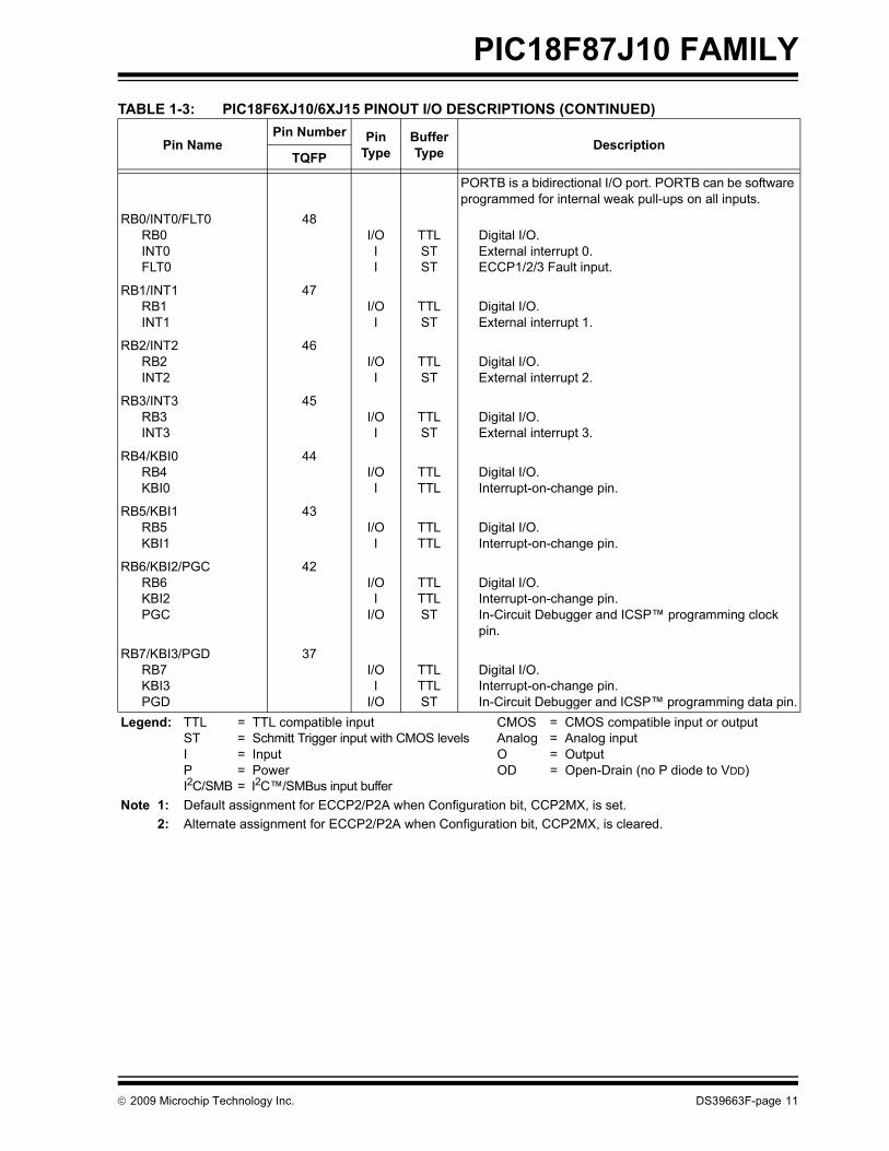
PORTB is a bidirectional I/O port. PORTB can be software programmed for internal weak pull-ups on all inputs.
RB0/INT0/FLT0RB0INT0FLT0
48I/OII
TTLSTST
Digital I/O.External interrupt 0.ECCP1/2/3 Fault input.
RB1/INT1RB1INT1
47I/OI
TTLST
Digital I/O.External interrupt 1.
RB2/INT2RB2INT2
46I/OI
TTLST
Digital I/O.External interrupt 2.
RB3/INT3RB3INT3
45I/OI
TTLST
Digital I/O.External interrupt 3.
RB4/KBI0RB4KBI0
44I/OI
TTLTTL
Digital I/O.Interrupt-on-change pin.
RB5/KBI1RB5KBI1
43I/OI
TTLTTL
Digital I/O.Interrupt-on-change pin.
RB6/KBI2/PGCRB6KBI2PGC
42I/OI
I/O
TTLTTLST
Digital I/O.Interrupt-on-change pin. In-Circuit Debugger and ICSP™ programming clock pin.
RB7/KBI3/PGDRB7KBI3PGD
37I/OI
I/O
TTLTTLST
Digital I/O.Interrupt-on-change pin. In-Circuit Debugger and ICSP™ programming data pin.
TABLE 1-3: PIC18F6XJ10/6XJ15 PINOUT I/O DESCRIPTIONS (CONTINUED)
Pin NamePin Number Pin
TypeBufferType Description
TQFP
Legend: TTL = TTL compatible input CMOS = CMOS compatible input or output ST = Schmitt Trigger input with CMOS levels Analog = Analog input I = Input O = Output P = Power OD = Open-Drain (no P diode to VDD) I2C/SMB = I2C™/SMBus input buffer
Note 1: Default assignment for ECCP2/P2A when Configuration bit, CCP2MX, is set.2: Alternate assignment for ECCP2/P2A when Configuration bit, CCP2MX, is cleared.
© 2009 Microchip Technology Inc. DS39663F-page 11

PIC18F87J10 FAMILY
PORTC is a bidirectional I/O port.RC0/T1OSO/T13CKI
RC0T1OSOT13CKI
30I/OOI
ST—ST
Digital I/O.Timer1 oscillator output. Timer1/Timer3 external clock input.
RC1/T1OSI/ECCP2/P2ARC1T1OSIECCP2(1)
P2A(1)
29I/OI
I/OO
STCMOS
ST—
Digital I/O.Timer1 oscillator input.Capture 2 input/Compare 2 output/PWM 2 output.ECCP2 PWM output A.
RC2/ECCP1/P1ARC2ECCP1P1A
33I/OI/OO
STST—
Digital I/O.Capture 1 input/Compare 1 output/PWM 1 output.ECCP1 PWM output A.
RC3/SCK1/SCL1RC3SCK1SCL1
34I/OI/OI/O
STST
I2C/SMB
Digital I/O.Synchronous serial clock input/output for SPI mode.Synchronous serial clock input/output for I2C™ mode.
RC4/SDI1/SDA1RC4SDI1SDA1
35I/OI
I/O
STST
I2C/SMB
Digital I/O.SPI data in.I2C data I/O.
RC5/SDO1RC5SDO1
36I/OO
ST—
Digital I/O.SPI data out.
RC6/TX1/CK1RC6TX1CK1
31I/OO
I/O
ST—ST
Digital I/O.EUSART1 asynchronous transmit. EUSART1 synchronous clock (see related RX1/DT1).
RC7/RX1/DT1RC7RX1DT1
32I/OI
I/O
STSTST
Digital I/O.EUSART1 asynchronous receive.EUSART1 synchronous data (see related TX1/CK1).
TABLE 1-3: PIC18F6XJ10/6XJ15 PINOUT I/O DESCRIPTIONS (CONTINUED)
Pin NamePin Number Pin
TypeBufferType Description
TQFP
Legend: TTL = TTL compatible input CMOS = CMOS compatible input or output ST = Schmitt Trigger input with CMOS levels Analog = Analog input I = Input O = Output P = Power OD = Open-Drain (no P diode to VDD) I2C/SMB = I2C™/SMBus input buffer
Note 1: Default assignment for ECCP2/P2A when Configuration bit, CCP2MX, is set.2: Alternate assignment for ECCP2/P2A when Configuration bit, CCP2MX, is cleared.
DS39663F-page 12 © 2009 Microchip Technology Inc.

PIC18F87J10 FAMILY
PORTD is a bidirectional I/O port.RD0/PSP0
RD0PSP0
58I/OI/O
STTTL
Digital I/O.Parallel Slave Port data.
RD1/PSP1RD1PSP1
55I/OI/O
STTTL
Digital I/O.Parallel Slave Port data.
RD2/PSP2RD2PSP2
54I/OI/O
STTTL
Digital I/O.Parallel Slave Port data.
RD3/PSP3RD3PSP3
53I/OI/O
STTTL
Digital I/O.Parallel Slave Port data.
RD4/PSP4/SDO2RD4PSP4SDO2
52I/OI/OO
STTTL—
Digital I/O.Parallel Slave Port data.SPI data out.
RD5/PSP5/SDI2/SDA2RD5PSP5SDI2SDA2
51I/OI/OI
I/O
STTTLST
I2C/SMB
Digital I/O.Parallel Slave Port data.SPI data in.I2C™ data I/O.
RD6/PSP6/SCK2/SCL2RD6PSP6SCK2SCL2
50I/OI/OI/OI/O
STTTLST
I2C/SMB
Digital I/O.Parallel Slave Port data.Synchronous serial clock input/output for SPI mode.Synchronous serial clock input/output for I2C mode.
RD7/PSP7/SS2RD7PSP7SS2
49I/OI/OI
STTTLTTL
Digital I/O.Parallel Slave Port data.SPI slave select input.
TABLE 1-3: PIC18F6XJ10/6XJ15 PINOUT I/O DESCRIPTIONS (CONTINUED)
Pin NamePin Number Pin
TypeBufferType Description
TQFP
Legend: TTL = TTL compatible input CMOS = CMOS compatible input or output ST = Schmitt Trigger input with CMOS levels Analog = Analog input I = Input O = Output P = Power OD = Open-Drain (no P diode to VDD) I2C/SMB = I2C™/SMBus input buffer
Note 1: Default assignment for ECCP2/P2A when Configuration bit, CCP2MX, is set.2: Alternate assignment for ECCP2/P2A when Configuration bit, CCP2MX, is cleared.
© 2009 Microchip Technology Inc. DS39663F-page 13

PIC18F87J10 FAMILY
PORTE is a bidirectional I/O port.
RE0/RD/P2DRE0RDP2D
2I/OIO
STTTL—
Digital I/O.Read control for Parallel Slave Port.ECCP2 PWM output D.
RE1/WR/P2CRE1WRP2C
1I/OIO
STTTL—
Digital I/O.Write control for Parallel Slave Port.ECCP2 PWM output C.
RE2/CS/P2BRE2CSP2B
64I/OIO
STTTL—
Digital I/O.Chip select control for Parallel Slave Port.ECCP2 PWM output B.
RE3/P3CRE3P3C
63I/OO
ST—
Digital I/O.ECCP3 PWM output C.
RE4/P3BRE4P3B
62I/OO
ST—
Digital I/O.ECCP3 PWM output B.
RE5/P1CRE5P1C
61I/OO
ST—
Digital I/O.ECCP1 PWM output C.
RE6/P1BRE6P1B
60I/OO
ST—
Digital I/O.ECCP1 PWM output B.
RE7/ECCP2/P2ARE7ECCP2(2)
P2A(2)
59I/OI/OO
STST—
Digital I/O.Capture 2 input/Compare 2 output/PWM 2 output.ECCP2 PWM output A.
TABLE 1-3: PIC18F6XJ10/6XJ15 PINOUT I/O DESCRIPTIONS (CONTINUED)
Pin NamePin Number Pin
TypeBufferType Description
TQFP
Legend: TTL = TTL compatible input CMOS = CMOS compatible input or output ST = Schmitt Trigger input with CMOS levels Analog = Analog input I = Input O = Output P = Power OD = Open-Drain (no P diode to VDD) I2C/SMB = I2C™/SMBus input buffer
Note 1: Default assignment for ECCP2/P2A when Configuration bit, CCP2MX, is set.2: Alternate assignment for ECCP2/P2A when Configuration bit, CCP2MX, is cleared.
DS39663F-page 14 © 2009 Microchip Technology Inc.

PIC18F87J10 FAMILY
PORTF is a bidirectional I/O port.RF1/AN6/C2OUT
RF1AN6C2OUT
17I/OIO
STAnalog
—
Digital I/O.Analog input 6.Comparator 2 output.
RF2/AN7/C1OUTRF2AN7C1OUT
16I/OIO
STAnalog
—
Digital I/O.Analog input 7.Comparator 1 output.
RF3/AN8RF3AN8
15I/OI
STAnalog
Digital I/O.Analog input 8.
RF4/AN9RF4AN9
14I/OI
STAnalog
Digital I/O.Analog input 9.
RF5/AN10/CVREFRF5AN10CVREF
13I/OIO
STAnalog
—
Digital I/O.Analog input 10. Comparator reference voltage output.
RF6/AN11RF6AN11
12I/OI
STAnalog
Digital I/O.Analog input 11.
RF7/SS1RF7SS1
11I/OI
STTTL
Digital I/O.SPI slave select input.
TABLE 1-3: PIC18F6XJ10/6XJ15 PINOUT I/O DESCRIPTIONS (CONTINUED)
Pin NamePin Number Pin
TypeBufferType Description
TQFP
Legend: TTL = TTL compatible input CMOS = CMOS compatible input or output ST = Schmitt Trigger input with CMOS levels Analog = Analog input I = Input O = Output P = Power OD = Open-Drain (no P diode to VDD) I2C/SMB = I2C™/SMBus input buffer
Note 1: Default assignment for ECCP2/P2A when Configuration bit, CCP2MX, is set.2: Alternate assignment for ECCP2/P2A when Configuration bit, CCP2MX, is cleared.
© 2009 Microchip Technology Inc. DS39663F-page 15

PIC18F87J10 FAMILY
PORTG is a bidirectional I/O port.RG0/ECCP3/P3A
RG0ECCP3P3A
3I/OI/OO
STST—
Digital I/O.Capture 3 input/Compare 3 output/PWM 3 output.ECCP3 PWM output A.
RG1/TX2/CK2RG1TX2CK2
4I/OO
I/O
ST—ST
Digital I/O.EUSART2 asynchronous transmit. EUSART2 synchronous clock (see related RX2/DT2).
RG2/RX2/DT2RG2RX2DT2
5I/OI
I/O
STSTST
Digital I/O.EUSART2 asynchronous receive.EUSART2 synchronous data (see related TX2/CK2).
RG3/CCP4/P3DRG3CCP4P3D
6I/OI/OO
STST—
Digital I/O.Capture 4 input/Compare 4 output/PWM 4 output.ECCP3 PWM output D.
RG4/CCP5/P1DRG4CCP5P1D
8I/OI/OO
STST—
Digital I/O.Capture 5 input/Compare 5 output/PWM 5 output.ECCP1 PWM output D.
VSS 9, 25, 41, 56 P — Ground reference for logic and I/O pins.VDD 26, 38, 57 P — Positive supply for peripheral digital logic and I/O pins.AVSS 20 P — Ground reference for analog modules.AVDD 19 P — Positive supply for analog modules.ENVREG 18 I ST Enable for on-chip voltage regulator.VDDCORE/VCAP
VDDCORE
VCAP
10P
P
—
—
Core logic power or external filter capacitor connection.Positive supply for microcontroller core logic (regulator disabled).External filter capacitor connection (regulator enabled).
TABLE 1-3: PIC18F6XJ10/6XJ15 PINOUT I/O DESCRIPTIONS (CONTINUED)
Pin NamePin Number Pin
TypeBufferType Description
TQFP
Legend: TTL = TTL compatible input CMOS = CMOS compatible input or output ST = Schmitt Trigger input with CMOS levels Analog = Analog input I = Input O = Output P = Power OD = Open-Drain (no P diode to VDD) I2C/SMB = I2C™/SMBus input buffer
Note 1: Default assignment for ECCP2/P2A when Configuration bit, CCP2MX, is set.2: Alternate assignment for ECCP2/P2A when Configuration bit, CCP2MX, is cleared.
DS39663F-page 16 © 2009 Microchip Technology Inc.
PIC18F87J10 FAMILY
TABLE 1-4: PIC18F8XJ10/8XJ15 PINOUT I/O DESCRIPTIONSPin NamePin Number Pin
TypeBufferType Description
TQFP
MCLR 9 I ST Master Clear (Reset) input. This pin is an active-low Reset to the device.
OSC1/CLKIOSC1
CLKI
49I
I
ST
CMOS
Oscillator crystal or external clock input.Oscillator crystal input or external clock source input. ST buffer when configured in RC mode; CMOS otherwise.External clock source input. Always associated with pin function OSC1. (See related OSC1/CLKI, OSC2/CLKO pins.)
OSC2/CLKOOSC2
CLKO
50O
O
—
—
Oscillator crystal or clock output.Oscillator crystal output. Connects to crystal or resonator in Crystal Oscillator mode.In RC mode, OSC2 pin outputs CLKO which has 1/4 the frequency of OSC1 and denotes theinstruction cycle rate.
PORTA is a bidirectional I/O port.RA0/AN0
RA0AN0
30I/OI
TTLAnalog
Digital I/O.Analog input 0.
RA1/AN1RA1AN1
29I/OI
TTLAnalog
Digital I/O.Analog input 1.
RA2/AN2/VREF-RA2AN2VREF-
28I/OII
TTLAnalogAnalog
Digital I/O.Analog input 2.A/D reference voltage (low) input.
RA3/AN3/VREF+RA3AN3VREF+
27I/OII
TTLAnalogAnalog
Digital I/O.Analog input 3.A/D reference voltage (high) input.
RA4/T0CKIRA4T0CKI
34I/OI
STST
Digital I/O. Timer0 external clock input.
RA5/AN4RA5AN4
33I/OI
TTLAnalog
Digital I/O.Analog input 4.
Legend: TTL = TTL compatible input CMOS = CMOS compatible input or output ST = Schmitt Trigger input with CMOS levels Analog = Analog input I = Input O = Output P = Power OD = Open-Drain (no P diode to VDD) I2C/SMB = I2C™/SMBus input buffer
Note 1: Alternate assignment for ECCP2/P2A when Configuration bit, CCP2MX, is cleared (Extended Microcontroller mode).2: Default assignment for ECCP2/P2A for all devices in all operating modes (CCP2MX is set). 3: Default assignments for P1B/P1C/P3B/P3C (ECCPMX Configuration bit is set).4: Alternate assignment for ECCP2/P2A when CCP2MX is cleared (Microcontroller mode).5: Alternate assignments for P1B/P1C/P3B/P3C (ECCPMX Configuration bit is cleared).
© 2009 Microchip Technology Inc. DS39663F-page 17

PIC18F87J10 FAMILY
PORTB is a bidirectional I/O port. PORTB can be software programmed for internal weak pull-ups on all inputs.
RB0/INT0/FLT0RB0INT0FLT0
58I/OII
TTLSTST
Digital I/O.External interrupt 0.ECCP1/2/3 Fault input.
RB1/INT1RB1INT1
57I/OI
TTLST
Digital I/O.External interrupt 1.
RB2/INT2RB2INT2
56I/OI
TTLST
Digital I/O.External interrupt 2.
RB3/INT3/ECCP2/P2ARB3INT3ECCP2(1)
P2A(1)
55I/OI
I/OO
TTLSTST—
Digital I/O.External interrupt 3.Capture 2 input/Compare 2 output/PWM 2 output.ECCP2 PWM output A.
RB4/KBI0RB4KBI0
54I/OI
TTLTTL
Digital I/O.Interrupt-on-change pin.
RB5/KBI1RB5KBI1
53I/OI
TTLTTL
Digital I/O.Interrupt-on-change pin.
RB6/KBI2/PGCRB6KBI2PGC
52I/OI
I/O
TTLTTLST
Digital I/O.Interrupt-on-change pin. In-Circuit Debugger and ICSP™ programming clock pin.
RB7/KBI3/PGDRB7KBI3PGD
47I/OI
I/O
TTLTTLST
Digital I/O.Interrupt-on-change pin. In-Circuit Debugger and ICSP™ programming data pin.
TABLE 1-4: PIC18F8XJ10/8XJ15 PINOUT I/O DESCRIPTIONS (CONTINUED)
Pin NamePin Number Pin
TypeBufferType Description
TQFP
Legend: TTL = TTL compatible input CMOS = CMOS compatible input or output ST = Schmitt Trigger input with CMOS levels Analog = Analog input I = Input O = Output P = Power OD = Open-Drain (no P diode to VDD) I2C/SMB = I2C™/SMBus input buffer
Note 1: Alternate assignment for ECCP2/P2A when Configuration bit, CCP2MX, is cleared (Extended Microcontroller mode).2: Default assignment for ECCP2/P2A for all devices in all operating modes (CCP2MX is set). 3: Default assignments for P1B/P1C/P3B/P3C (ECCPMX Configuration bit is set).4: Alternate assignment for ECCP2/P2A when CCP2MX is cleared (Microcontroller mode).5: Alternate assignments for P1B/P1C/P3B/P3C (ECCPMX Configuration bit is cleared).
DS39663F-page 18 © 2009 Microchip Technology Inc.
PIC18F87J10 FAMILY
PORTC is a bidirectional I/O port.RC0/T1OSO/T13CKI
RC0T1OSOT13CKI
36I/OOI
ST—ST
Digital I/O.Timer1 oscillator output. Timer1/Timer3 external clock input.
RC1/T1OSI/ECCP2/P2ARC1T1OSIECCP2(2)
P2A(2)
35I/OI
I/OO
STCMOS
ST—
Digital I/O.Timer1 oscillator input.Capture 2 input/Compare 2 output/PWM 2 output.ECCP2 PWM output A.
RC2/ECCP1/P1ARC2ECCP1P1A
43I/OI/OO
STST—
Digital I/O.Capture 1 input/Compare 1 output/PWM 1 output.ECCP1 PWM output A.
RC3/SCK1/SCL1RC3SCK1SCL1
44I/OI/OI/O
STST
I2C/SMB
Digital I/O.Synchronous serial clock input/output for SPI mode.Synchronous serial clock input/output for I2C™ mode.
RC4/SDI1/SDA1RC4SDI1SDA1
45I/OI
I/O
STST
I2C/SMB
Digital I/O.SPI data in.I2C data I/O.
RC5/SDO1RC5SDO1
46I/OO
ST—
Digital I/O.SPI data out.
RC6/TX1/CK1RC6TX1CK1
37I/OO
I/O
ST—ST
Digital I/O.EUSART1 asynchronous transmit. EUSART1 synchronous clock (see related RX1/DT1).
RC7/RX1/DT1RC7RX1DT1
38I/OI
I/O
STSTST
Digital I/O.EUSART1 asynchronous receive.EUSART1 synchronous data (see related TX1/CK1).
TABLE 1-4: PIC18F8XJ10/8XJ15 PINOUT I/O DESCRIPTIONS (CONTINUED)
Pin NamePin Number Pin
TypeBufferType Description
TQFP
Legend: TTL = TTL compatible input CMOS = CMOS compatible input or output ST = Schmitt Trigger input with CMOS levels Analog = Analog input I = Input O = Output P = Power OD = Open-Drain (no P diode to VDD) I2C/SMB = I2C™/SMBus input buffer
Note 1: Alternate assignment for ECCP2/P2A when Configuration bit, CCP2MX, is cleared (Extended Microcontroller mode).2: Default assignment for ECCP2/P2A for all devices in all operating modes (CCP2MX is set). 3: Default assignments for P1B/P1C/P3B/P3C (ECCPMX Configuration bit is set).4: Alternate assignment for ECCP2/P2A when CCP2MX is cleared (Microcontroller mode).5: Alternate assignments for P1B/P1C/P3B/P3C (ECCPMX Configuration bit is cleared).
© 2009 Microchip Technology Inc. DS39663F-page 19

PIC18F87J10 FAMILY
PORTD is a bidirectional I/O port.RD0/AD0/PSP0
RD0AD0PSP0
72I/OI/OI/O
STTTLTTL
Digital I/O.External memory address/data 0.Parallel Slave Port data.
RD1/AD1/PSP1RD1AD1PSP1
69I/OI/OI/O
STTTLTTL
Digital I/O.External memory address/data 1.Parallel Slave Port data.
RD2/AD2/PSP2RD2AD2PSP2
68I/OI/OI/O
STTTLTTL
Digital I/O.External memory address/data 2.Parallel Slave Port data.
RD3/AD3/PSP3RD3AD3PSP3
67I/OI/OI/O
STTTLTTL
Digital I/O.External memory address/data 3.Parallel Slave Port data.
RD4/AD4/PSP4/SDO2RD4AD4PSP4SDO2
66I/OI/OI/OO
STTTLTTL—
Digital I/O.External memory address/data 4.Parallel Slave Port data.SPI data out.
RD5/AD5/PSP5/SDI2/SDA2
RD5AD5PSP5SDI2SDA2
65
I/OI/OI/OI
I/O
STTTLTTLST
I2C/SMB
Digital I/O.External memory address/data 5.Parallel Slave Port data.SPI data in.I2C™ data I/O.
RD6/AD6/PSP6/SCK2/SCL2
RD6AD6PSP6SCK2SCL2
64
I/OI/OI/OI/OI/O
STTTLTTLST
I2C/SMB
Digital I/O.External memory address/data 6.Parallel Slave Port data.Synchronous serial clock input/output for SPI mode.Synchronous serial clock input/output for I2C mode.
RD7/AD7/PSP7/SS2RD7AD7PSP7SS2
63I/OI/OI/OI
STTTLTTLTTL
Digital I/O.External memory address/data 7.Parallel Slave Port data.SPI slave select input.
TABLE 1-4: PIC18F8XJ10/8XJ15 PINOUT I/O DESCRIPTIONS (CONTINUED)
Pin NamePin Number Pin
TypeBufferType Description
TQFP
Legend: TTL = TTL compatible input CMOS = CMOS compatible input or output ST = Schmitt Trigger input with CMOS levels Analog = Analog input I = Input O = Output P = Power OD = Open-Drain (no P diode to VDD) I2C/SMB = I2C™/SMBus input buffer
Note 1: Alternate assignment for ECCP2/P2A when Configuration bit, CCP2MX, is cleared (Extended Microcontroller mode).2: Default assignment for ECCP2/P2A for all devices in all operating modes (CCP2MX is set). 3: Default assignments for P1B/P1C/P3B/P3C (ECCPMX Configuration bit is set).4: Alternate assignment for ECCP2/P2A when CCP2MX is cleared (Microcontroller mode).5: Alternate assignments for P1B/P1C/P3B/P3C (ECCPMX Configuration bit is cleared).
DS39663F-page 20 © 2009 Microchip Technology Inc.

PIC18F87J10 FAMILY
PORTE is a bidirectional I/O port.RE0/AD8/RD/P2D
RE0AD8RDP2D
4I/OI/OIO
STTTLTTL—
Digital I/O.External memory address/data 8.Read control for Parallel Slave Port.ECCP2 PWM output D.
RE1/AD9/WR/P2CRE1AD9WRP2C
3I/OI/OIO
STTTLTTL—
Digital I/O.External memory address/data 9.Write control for Parallel Slave Port.ECCP2 PWM output C.
RE2/AD10/CS/P2BRE2AD10CSP2B
78I/OI/OIO
STTTLTTL—
Digital I/O.External memory address/data 10.Chip select control for Parallel Slave Port.ECCP2 PWM output B.
RE3/AD11/P3CRE3AD11P3C(3)
77I/OI/OO
STTTL—
Digital I/O.External memory address/data 11.ECCP3 PWM output C.
RE4/AD12/P3BRE4AD12P3B(3)
76I/OI/OO
STTTL—
Digital I/O.External memory address/data 12.ECCP3 PWM output B.
RE5/AD13/P1CRE5AD13P1C(3)
75I/OI/OO
STTTL—
Digital I/O.External memory address/data 13.ECCP1 PWM output C.
RE6/AD14/P1BRE6AD14P1B(3)
74I/OI/OO
STTTL—
Digital I/O.External memory address/data 14.ECCP1 PWM output B.
RE7/AD15/ECCP2/P2ARE7AD15ECCP2(4)
P2A(4)
73I/OI/OI/OO
STTTLST—
Digital I/O.External memory address/data 15.Capture 2 input/Compare 2 output/PWM 2 output.ECCP2 PWM output A.
TABLE 1-4: PIC18F8XJ10/8XJ15 PINOUT I/O DESCRIPTIONS (CONTINUED)
Pin NamePin Number Pin
TypeBufferType Description
TQFP
Legend: TTL = TTL compatible input CMOS = CMOS compatible input or output ST = Schmitt Trigger input with CMOS levels Analog = Analog input I = Input O = Output P = Power OD = Open-Drain (no P diode to VDD) I2C/SMB = I2C™/SMBus input buffer
Note 1: Alternate assignment for ECCP2/P2A when Configuration bit, CCP2MX, is cleared (Extended Microcontroller mode).2: Default assignment for ECCP2/P2A for all devices in all operating modes (CCP2MX is set). 3: Default assignments for P1B/P1C/P3B/P3C (ECCPMX Configuration bit is set).4: Alternate assignment for ECCP2/P2A when CCP2MX is cleared (Microcontroller mode).5: Alternate assignments for P1B/P1C/P3B/P3C (ECCPMX Configuration bit is cleared).
© 2009 Microchip Technology Inc. DS39663F-page 21

PIC18F87J10 FAMILY
PORTF is a bidirectional I/O port.RF1/AN6/C2OUT
RF1AN6C2OUT
23I/OIO
STAnalog
—
Digital I/O.Analog input 6.Comparator 2 output.
RF2/AN7/C1OUTRF2AN7C1OUT
18I/OIO
STAnalog
—
Digital I/O.Analog input 7.Comparator 1 output.
RF3/AN8RF3AN8
17I/OI
STAnalog
Digital I/O.Analog input 8.
RF4/AN9RF4AN9
16I/OI
STAnalog
Digital I/O.Analog input 9.
RF5/AN10/CVREFRF5AN10CVREF
15I/OIO
STAnalog
—
Digital I/O.Analog input 10. Comparator reference voltage output.
RF6/AN11RF6AN11
14I/OI
STAnalog
Digital I/O.Analog input 11.
RF7/SS1RF7SS1
13I/OI
STTTL
Digital I/O.SPI slave select input.
TABLE 1-4: PIC18F8XJ10/8XJ15 PINOUT I/O DESCRIPTIONS (CONTINUED)
Pin NamePin Number Pin
TypeBufferType Description
TQFP
Legend: TTL = TTL compatible input CMOS = CMOS compatible input or output ST = Schmitt Trigger input with CMOS levels Analog = Analog input I = Input O = Output P = Power OD = Open-Drain (no P diode to VDD) I2C/SMB = I2C™/SMBus input buffer
Note 1: Alternate assignment for ECCP2/P2A when Configuration bit, CCP2MX, is cleared (Extended Microcontroller mode).2: Default assignment for ECCP2/P2A for all devices in all operating modes (CCP2MX is set). 3: Default assignments for P1B/P1C/P3B/P3C (ECCPMX Configuration bit is set).4: Alternate assignment for ECCP2/P2A when CCP2MX is cleared (Microcontroller mode).5: Alternate assignments for P1B/P1C/P3B/P3C (ECCPMX Configuration bit is cleared).
DS39663F-page 22 © 2009 Microchip Technology Inc.
PIC18F87J10 FAMILY
PORTG is a bidirectional I/O port.RG0/ECCP3/P3A
RG0ECCP3P3A
5I/OI/OO
STST—
Digital I/O.Capture 3 input/Compare 3 output/PWM 3 output.ECCP3 PWM output A.
RG1/TX2/CK2RG1TX2CK2
6I/OO
I/O
ST—ST
Digital I/O.EUSART2 asynchronous transmit. EUSART2 synchronous clock (see related RX2/DT2).
RG2/RX2/DT2RG2RX2DT2
7I/OI
I/O
STSTST
Digital I/O.EUSART2 asynchronous receive.EUSART2 synchronous data (see related TX2/CK2).
RG3/CCP4/P3DRG3CCP4P3D
8I/OI/OO
STST—
Digital I/O.Capture 4 input/Compare 4 output/PWM 4 output.ECCP3 PWM output D.
RG4/CCP5/P1DRG4CCP5P1D
10I/OI/OO
STST—
Digital I/O.Capture 5 input/Compare 5 output/PWM 5 output.ECCP1 PWM output D.
TABLE 1-4: PIC18F8XJ10/8XJ15 PINOUT I/O DESCRIPTIONS (CONTINUED)
Pin NamePin Number Pin
TypeBufferType Description
TQFP
Legend: TTL = TTL compatible input CMOS = CMOS compatible input or output ST = Schmitt Trigger input with CMOS levels Analog = Analog input I = Input O = Output P = Power OD = Open-Drain (no P diode to VDD) I2C/SMB = I2C™/SMBus input buffer
Note 1: Alternate assignment for ECCP2/P2A when Configuration bit, CCP2MX, is cleared (Extended Microcontroller mode).2: Default assignment for ECCP2/P2A for all devices in all operating modes (CCP2MX is set). 3: Default assignments for P1B/P1C/P3B/P3C (ECCPMX Configuration bit is set).4: Alternate assignment for ECCP2/P2A when CCP2MX is cleared (Microcontroller mode).5: Alternate assignments for P1B/P1C/P3B/P3C (ECCPMX Configuration bit is cleared).
© 2009 Microchip Technology Inc. DS39663F-page 23

PIC18F87J10 FAMILY
PORTH is a bidirectional I/O port.RH0/A16
RH0A16
79I/OI/O
STTTL
Digital I/O.External memory address/data 16.
RH1/A17RH1A17
80I/OI/O
STTTL
Digital I/O.External memory address/data 17.
RH2/A18RH2A18
1I/OI/O
STTTL
Digital I/O.External memory address/data 18.
RH3/A19RH3A19
2I/OI/O
STTTL
Digital I/O.External memory address/data 19.
RH4/AN12/P3CRH4AN12P3C(5)
22I/OIO
STAnalog
—
Digital I/O.Analog input 12.ECCP3 PWM output C.
RH5/AN13/P3BRH5AN13P3B(5)
21I/OIO
STAnalog
—
Digital I/O.Analog input 13.ECCP3 PWM output B.
RH6/AN14/P1CRH6AN14P1C(5)
20I/OIO
STAnalog
—
Digital I/O.Analog input 14.ECCP1 PWM output C.
RH7/AN15/P1BRH7AN15P1B(5)
19I/OIO
STAnalog
—
Digital I/O.Analog input 15.ECCP1 PWM output B.
TABLE 1-4: PIC18F8XJ10/8XJ15 PINOUT I/O DESCRIPTIONS (CONTINUED)
Pin NamePin Number Pin
TypeBufferType Description
TQFP
Legend: TTL = TTL compatible input CMOS = CMOS compatible input or output ST = Schmitt Trigger input with CMOS levels Analog = Analog input I = Input O = Output P = Power OD = Open-Drain (no P diode to VDD) I2C/SMB = I2C™/SMBus input buffer
Note 1: Alternate assignment for ECCP2/P2A when Configuration bit, CCP2MX, is cleared (Extended Microcontroller mode).2: Default assignment for ECCP2/P2A for all devices in all operating modes (CCP2MX is set). 3: Default assignments for P1B/P1C/P3B/P3C (ECCPMX Configuration bit is set).4: Alternate assignment for ECCP2/P2A when CCP2MX is cleared (Microcontroller mode).5: Alternate assignments for P1B/P1C/P3B/P3C (ECCPMX Configuration bit is cleared).
DS39663F-page 24 © 2009 Microchip Technology Inc.

PIC18F87J10 FAMILY
PORTJ is a bidirectional I/O port.RJ0/ALE
RJ0ALE
62I/OO
ST—
Digital I/O.External memory address latch enable.
RJ1/OERJ1OE
61I/OO
ST—
Digital I/O.External memory output enable.
RJ2/WRLRJ2WRL
60I/OO
ST—
Digital I/O.External memory write low control.
RJ3/WRHRJ3WRH
59I/OO
ST—
Digital I/O.External memory write high control.
RJ4/BA0RJ4BA0
39I/OO
ST—
Digital I/O.External memory byte address 0 control.
RJ5/CERJ5CE
40I/OO
ST—
Digital I/OExternal memory chip enable control.
RJ6/LBRJ6LB
41I/OO
ST—
Digital I/O.External memory low byte control.
RJ7/UBRJ7UB
42I/OO
ST—
Digital I/O.External memory high byte control.
VSS 11, 31, 51, 70 P — Ground reference for logic and I/O pins.VDD 32, 48, 71 P — Positive supply for peripheral digital logic and I/O pins.AVSS 26 P — Ground reference for analog modules.AVDD 25 P — Positive supply for analog modules.ENVREG 24 I ST Enable for on-chip voltage regulator.VDDCORE/VCAP
VDDCORE
VCAP
12P
P
—
—
Core logic power or external filter capacitor connection.Positive supply for microcontroller core logic (regulator disabled).External filter capacitor connection (regulator enabled).
TABLE 1-4: PIC18F8XJ10/8XJ15 PINOUT I/O DESCRIPTIONS (CONTINUED)
Pin NamePin Number Pin
TypeBufferType Description
TQFP
Legend: TTL = TTL compatible input CMOS = CMOS compatible input or output ST = Schmitt Trigger input with CMOS levels Analog = Analog input I = Input O = Output P = Power OD = Open-Drain (no P diode to VDD) I2C/SMB = I2C™/SMBus input buffer
Note 1: Alternate assignment for ECCP2/P2A when Configuration bit, CCP2MX, is cleared (Extended Microcontroller mode).2: Default assignment for ECCP2/P2A for all devices in all operating modes (CCP2MX is set). 3: Default assignments for P1B/P1C/P3B/P3C (ECCPMX Configuration bit is set).4: Alternate assignment for ECCP2/P2A when CCP2MX is cleared (Microcontroller mode).5: Alternate assignments for P1B/P1C/P3B/P3C (ECCPMX Configuration bit is cleared).
© 2009 Microchip Technology Inc. DS39663F-page 25

PIC18F87J10 FAMILY
NOTES:DS39663F-page 26 © 2009 Microchip Technology Inc.

PIC18F87J10 FAMILY
2.0 GUIDELINES FOR GETTING STARTED WITH PIC18FJ MICROCONTROLLERS
2.1 Basic Connection RequirementsGetting started with the PIC18F87J10 family of 8-bitmicrocontrollers requires attention to a minimal set ofdevice pin connections before proceeding withdevelopment.
The following pins must always be connected:
• All VDD and VSS pins (see Section 2.2 “Power Supply Pins”)
• All AVDD and AVSS pins, regardless of whether or not the analog device features are used (see Section 2.2 “Power Supply Pins”)
• MCLR pin (see Section 2.3 “Master Clear (MCLR) Pin”)
• ENVREG (if implemented) and VCAP/VDDCORE pins (see Section 2.4 “Voltage Regulator Pins (ENVREG and VCAP/VDDCORE)”)
These pins must also be connected if they are beingused in the end application:
• PGC/PGD pins used for In-Circuit Serial Programming™ (ICSP™) and debugging purposes (see Section 2.5 “ICSP Pins”)
• OSCI and OSCO pins when an external oscillator source is used (see Section 2.6 “External Oscillator Pins”)
Additionally, the following pins may be required:
• VREF+/VREF- pins used when external voltage reference for analog modules is implemented
The minimum mandatory connections are shown inFigure 2-1.
FIGURE 2-1: RECOMMENDED MINIMUM CONNECTIONS
Note: The AVDD and AVSS pins must always beconnected, regardless of whether any ofthe analog modules are being used.
PIC18FXXJXX
VD
D
VS
S
VDD
VSS
VSS
VDD
AVD
D
AVS
S
VD
D
VS
S
C1
R1
VDD
MCLRVCAP/VDDCORE
R2ENVREG
(1)
C7
C2(2)
C3(2)
C4(2)C5(2)
C6(2)
Key (all values are recommendations):C1 through C6: 0.1 μF, 20V ceramicC7: 10 μF, 6.3V or greater, tantalum or ceramicR1: 10 kΩR2: 100Ω to 470ΩNote 1: See Section 2.4 “Voltage Regulator Pins
(ENVREG and VCAP/VDDCORE)” for explanation of ENVREG pin connections.
2: The example shown is for a PIC18FJ device with five VDD/VSS and AVDD/AVSS pairs. Other devices may have more or less pairs; adjust the number of decoupling capacitors appropriately.
(1)
© 2009 Microchip Technology Inc. DS39663F-page 27
PIC18F87J10 FAMILY
2.2 Power Supply Pins2.2.1 DECOUPLING CAPACITORSThe use of decoupling capacitors on every pair ofpower supply pins, such as VDD, VSS, AVDD andAVSS, is required.
Consider the following criteria when using decouplingcapacitors:
• Value and type of capacitor: A 0.1 μF (100 nF), 10-20V capacitor is recommended. The capacitor should be a low-ESR device with a resonance frequency in the range of 200 MHz and higher. Ceramic capacitors are recommended.
• Placement on the printed circuit board: The decoupling capacitors should be placed as close to the pins as possible. It is recommended to place the capacitors on the same side of the board as the device. If space is constricted, the capacitor can be placed on another layer on the PCB using a via; however, ensure that the trace length from the pin to the capacitor is no greater than 0.25 inch (6 mm).
• Handling high-frequency noise: If the board is experiencing high-frequency noise (upward of tens of MHz), add a second ceramic type capaci-tor in parallel to the above described decoupling capacitor. The value of the second capacitor can be in the range of 0.01 μF to 0.001 μF. Place this second capacitor next to each primary decoupling capacitor. In high-speed circuit designs, consider implementing a decade pair of capacitances as close to the power and ground pins as possible (e.g., 0.1 μF in parallel with 0.001 μF).
• Maximizing performance: On the board layout from the power supply circuit, run the power and return traces to the decoupling capacitors first, and then to the device pins. This ensures that the decoupling capacitors are first in the power chain. Equally important is to keep the trace length between the capacitor and the power pins to a minimum, thereby reducing PCB trace inductance.
2.2.2 TANK CAPACITORSOn boards with power traces running longer than sixinches in length, it is suggested to use a tank capacitorfor integrated circuits including microcontrollers tosupply a local power source. The value of the tankcapacitor should be determined based on the traceresistance that connects the power supply source tothe device and the maximum current drawn by thedevice in the application. In other words, select the tankcapacitor so that it meets the acceptable voltage sag atthe device. Typical values range from 4.7 μF to 47 μF.
2.3 Master Clear (MCLR) PinThe MCLR pin provides two specific devicefunctions: device Reset, and device programmingand debugging. If programming and debugging arenot required in the end application, a directconnection to VDD may be all that is required. Theaddition of other components, to help increase theapplication’s resistance to spurious Resets fromvoltage sags, may be beneficial. A typicalconfiguration is shown in Figure 2-1. Other circuitdesigns may be implemented depending on theapplication’s requirements.
During programming and debugging, the resistanceand capacitance that can be added to the pin mustbe considered. Device programmers and debuggersdrive the MCLR pin. Consequently, specific voltagelevels (VIH and VIL) and fast signal transitions mustnot be adversely affected. Therefore, specific valuesof R1 and C1 will need to be adjusted based on theapplication and PCB requirements. For example, it isrecommended that the capacitor, C1, be isolatedfrom the MCLR pin during programming anddebugging operations by using a jumper (Figure 2-2).The jumper is replaced for normal run-timeoperations.
Any components associated with the MCLR pinshould be placed within 0.25 inch (6 mm) of the pin.
FIGURE 2-2: EXAMPLE OF MCLR PIN CONNECTIONS
Note 1: R1 ≤ 10 kΩ is recommended. A suggestedstarting value is 10 kΩ. Ensure that theMCLR pin VIH and VIL specifications are met.
2: R2 ≤ 470Ω will limit any current flowing intoMCLR from the external capacitor, C, in theevent of MCLR pin breakdown, due toElectrostatic Discharge (ESD) or ElectricalOverstress (EOS). Ensure that the MCLR pinVIH and VIL specifications are met.
C1
R2R1
VDD
MCLR
PIC18FXXJXXJP
DS39663F-page 28 © 2009 Microchip Technology Inc.
PIC18F87J10 FAMILY
2.4 Voltage Regulator Pins (ENVREGand VCAP/VDDCORE)The on-chip voltage regulator enable pin, ENVREG,must always be connected directly to either a supplyvoltage or to ground. Tying ENVREG to VDD enablesthe regulator, while tying it to ground disables theregulator. Refer to Section 24.3 “On-Chip VoltageRegulator” for details on connecting and using theon-chip regulator.
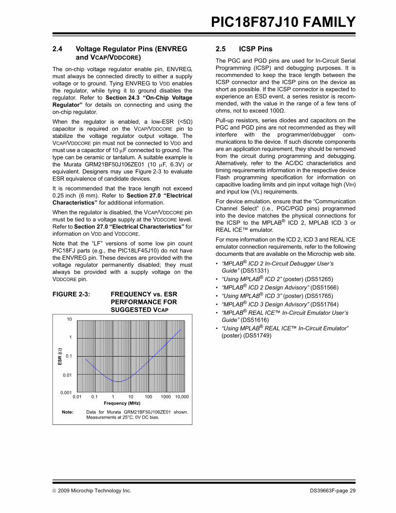
When the regulator is enabled, a low-ESR (<5Ω)capacitor is required on the VCAP/VDDCORE pin tostabilize the voltage regulator output voltage. TheVCAP/VDDCORE pin must not be connected to VDD andmust use a capacitor of 10 μF connected to ground. Thetype can be ceramic or tantalum. A suitable example isthe Murata GRM21BF50J106ZE01 (10 μF, 6.3V) orequivalent. Designers may use Figure 2-3 to evaluateESR equivalence of candidate devices.
It is recommended that the trace length not exceed0.25 inch (6 mm). Refer to Section 27.0 “ElectricalCharacteristics” for additional information.
When the regulator is disabled, the VCAP/VDDCORE pinmust be tied to a voltage supply at the VDDCORE level.Refer to Section 27.0 “Electrical Characteristics” forinformation on VDD and VDDCORE.
Note that the “LF” versions of some low pin countPIC18FJ parts (e.g., the PIC18LF45J10) do not havethe ENVREG pin. These devices are provided with thevoltage regulator permanently disabled; they mustalways be provided with a supply voltage on theVDDCORE pin.
FIGURE 2-3: FREQUENCY vs. ESR PERFORMANCE FOR SUGGESTED VCAP
2.5 ICSP PinsThe PGC and PGD pins are used for In-Circuit SerialProgramming (ICSP) and debugging purposes. It isrecommended to keep the trace length between theICSP connector and the ICSP pins on the device asshort as possible. If the ICSP connector is expected toexperience an ESD event, a series resistor is recom-mended, with the value in the range of a few tens ofohms, not to exceed 100Ω.
Pull-up resistors, series diodes and capacitors on thePGC and PGD pins are not recommended as they willinterfere with the programmer/debugger com-munications to the device. If such discrete componentsare an application requirement, they should be removedfrom the circuit during programming and debugging.Alternatively, refer to the AC/DC characteristics andtiming requirements information in the respective deviceFlash programming specification for information oncapacitive loading limits and pin input voltage high (VIH)and input low (VIL) requirements.
For device emulation, ensure that the “CommunicationChannel Select” (i.e., PGC/PGD pins) programmedinto the device matches the physical connections forthe ICSP to the MPLAB® ICD 2, MPLAB ICD 3 orREAL ICE™ emulator.
For more information on the ICD 2, ICD 3 and REAL ICEemulator connection requirements, refer to the followingdocuments that are available on the Microchip web site.
• “MPLAB® ICD 2 In-Circuit Debugger User’s Guide” (DS51331)
• “Using MPLAB® ICD 2” (poster) (DS51265)• “MPLAB® ICD 2 Design Advisory” (DS51566)• “Using MPLAB® ICD 3” (poster) (DS51765)• “MPLAB® ICD 3 Design Advisory” (DS51764)• “MPLAB® REAL ICE™ In-Circuit Emulator User’s
Guide” (DS51616)• “Using MPLAB® REAL ICE™ In-Circuit Emulator”
(poster) (DS51749)
10
1
0.1
0.01
0.0010.01 0.1 1 10 100 1000 10,000
Frequency (MHz)
ESR
(Ω)
Note: Data for Murata GRM21BF50J106ZE01 shown.Measurements at 25°C, 0V DC bias.
© 2009 Microchip Technology Inc. DS39663F-page 29
PIC18F87J10 FAMILY
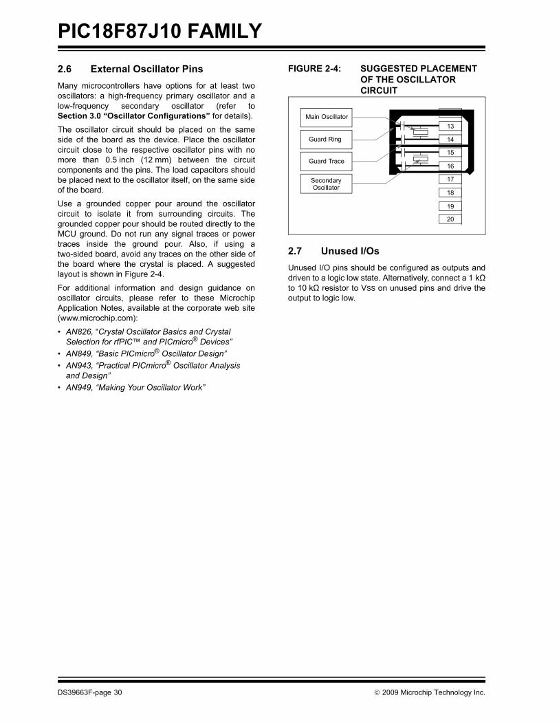
2.6 External Oscillator PinsMany microcontrollers have options for at least twooscillators: a high-frequency primary oscillator and alow-frequency secondary oscillator (refer toSection 3.0 “Oscillator Configurations” for details).The oscillator circuit should be placed on the sameside of the board as the device. Place the oscillatorcircuit close to the respective oscillator pins with nomore than 0.5 inch (12 mm) between the circuitcomponents and the pins. The load capacitors shouldbe placed next to the oscillator itself, on the same sideof the board.
Use a grounded copper pour around the oscillatorcircuit to isolate it from surrounding circuits. Thegrounded copper pour should be routed directly to theMCU ground. Do not run any signal traces or powertraces inside the ground pour. Also, if using atwo-sided board, avoid any traces on the other side ofthe board where the crystal is placed. A suggestedlayout is shown in Figure 2-4.
For additional information and design guidance onoscillator circuits, please refer to these MicrochipApplication Notes, available at the corporate web site(www.microchip.com):
• AN826, “Crystal Oscillator Basics and Crystal Selection for rfPIC™ and PICmicro® Devices”
• AN849, “Basic PICmicro® Oscillator Design”• AN943, “Practical PICmicro® Oscillator Analysis
and Design”• AN949, “Making Your Oscillator Work”
FIGURE 2-4: SUGGESTED PLACEMENT OF THE OSCILLATOR CIRCUIT
2.7 Unused I/OsUnused I/O pins should be configured as outputs anddriven to a logic low state. Alternatively, connect a 1 kΩto 10 kΩ resistor to VSS on unused pins and drive theoutput to logic low.
13Main Oscillator
Guard Ring
Guard Trace
SecondaryOscillator
14
15
16
17
18
19
20
DS39663F-page 30 © 2009 Microchip Technology Inc.

PIC18F87J10 FAMILY
3.0 OSCILLATOR CONFIGURATIONS
3.1 Oscillator TypesThe PIC18F87J10 family of devices can be operated infive different oscillator modes:
1. HS High-Speed Crystal/Resonator2. HSPLL High-Speed Crystal/Resonator
with Software PLL Control3. EC External Clock with FOSC/4 Output4. ECPLL External Clock with Software PLL
Control5. INTRC Internal 31 kHz Oscillator
Four of these are selected by the user by programmingthe FOSC<2:0> Configuration bits. The fifth mode(INTRC) may be invoked under software control; it canalso be configured as the default mode on deviceResets.
3.2 Crystal Oscillator/Ceramic Resonators (HS Modes)
In HS or HSPLL Oscillator modes, a crystal or ceramicresonator is connected to the OSC1 and OSC2 pins toestablish oscillation. Figure 3-1 shows the pinconnections.
The oscillator design requires the use of a parallel cutcrystal.
FIGURE 3-1: CRYSTAL/CERAMIC RESONATOR OPERATION (HS OR HSPLL CONFIGURATION)
TABLE 3-1: CAPACITOR SELECTION FOR CERAMIC RESONATORS
Note: Use of a series cut crystal may give a fre-quency out of the crystal manufacturer’sspecifications.
Typical Capacitor Values Used:
Mode Freq. OSC1 OSC2
HS 8.0 MHz16.0 MHz
27 pF22 pF
27 pF22 pF
Capacitor values are for design guidance only. These capacitors were tested with the resonatorslisted below for basic start-up and operation. Thesevalues are not optimized.
Different capacitor values may be required to produceacceptable oscillator operation. The user should testthe performance of the oscillator over the expectedVDD and temperature range for the application.
See the notes following Table 3-2 for additionalinformation.
Resonators Used:
4.0 MHz8.0 MHz
16.0 MHz
Note 1: See Table 3-1 and Table 3-2 for initial values ofC1 and C2.
2: A series resistor (RS) may be required for ATstrip cut crystals.
3: RF varies with the oscillator mode chosen.
C1(1)
C2(1)
XTAL
OSC2
OSC1
RF(3)
Sleep
To
Logic
PIC18F87J10RS(2)
Internal
© 2009 Microchip Technology Inc. DS39663F-page 31

PIC18F87J10 FAMILY
TABLE 3-2: CAPACITOR SELECTION FORCRYSTAL OSCILLATOR
3.3 External Clock Input (EC Modes)The EC and ECPLL Oscillator modes require an exter-nal clock source to be connected to the OSC1 pin.There is no oscillator start-up time required after aPower-on Reset or after an exit from Sleep mode.
In the EC Oscillator mode, the oscillator frequencydivided by 4 is available on the OSC2 pin. This signalmay be used for test purposes or to synchronize otherlogic. Figure 3-2 shows the pin connections for the ECOscillator mode.
FIGURE 3-2: EXTERNAL CLOCK INPUT OPERATION (EC CONFIGURATION)
An external clock source may also be connected to theOSC1 pin in the HS mode, as shown in Figure 3-3. Inthis configuration, the divide-by-4 output on OSC2 isnot available.
FIGURE 3-3: EXTERNAL CLOCK INPUT OPERATION (HS OSC CONFIGURATION)
Osc Type Crystal Freq.
Typical Capacitor Values Tested:
C1 C2
HS 4 MHz 27 pF 27 pF8 MHz 22 pF 22 pF20 MHz 15 pF 15 pF
Capacitor values are for design guidance only. These capacitors were tested with the crystals listedbelow for basic start-up and operation. These valuesare not optimized.Different capacitor values may be required to produceacceptable oscillator operation. The user should testthe performance of the oscillator over the expectedVDD and temperature range for the application.
See the notes following this table for additionalinformation.
Crystals Used:
4 MHz8 MHz
20 MHz
Note 1: Higher capacitance increases the stabilityof oscillator but also increases thestart-up time.
2: Since each resonator/crystal has its owncharacteristics, the user should consultthe resonator/crystal manufacturer forappropriate values of externalcomponents.
3: Rs may be required to avoid overdrivingcrystals with low drive level specification.
4: Always verify oscillator performance overthe VDD and temperature range that isexpected for the application.
OSC1/CLKI
OSC2/CLKOFOSC/4
Clock fromExt. System PIC18F87J10
OSC1
OSC2Open
Clock fromExt. System PIC18F87J10
(HS Mode)
DS39663F-page 32 © 2009 Microchip Technology Inc.

PIC18F87J10 FAMILY
3.4 PLL Frequency MultiplierA Phase Locked Loop (PLL) circuit is provided as anoption for users who want to use a lower frequencyoscillator circuit, or to clock the device up to its highestrated frequency from a crystal oscillator. This may beuseful for customers who are concerned with EMI dueto high-frequency crystals, or users who require higherclock speeds from an internal oscillator. For thesereasons, the HSPLL and ECPLL modes are available.The HSPLL and ECPLL modes provide the ability toselectively run the device at 4 times the external oscil-lating source to produce frequencies up to 40 MHz.The PLL is enabled by setting the PLLEN bit in theOSCTUNE register (Register 3-1).
FIGURE 3-4: PLL BLOCK DIAGRAM
MU
X
VCO
LoopFilter
OSC2
OSC1
PLL Enable (OSCTUNE)
FIN
FOUT
SYSCLK
PhaseComparator
HSPLL or ECPLL (CONFIG2L)
÷4
HS or ECMode
REGISTER 3-1: OSCTUNE: PLL CONTROL REGISTER
U-0 R/W-0 U-0 U-0 U-0 U-0 U-0 U-0 — PLLEN(1) — — — — — —
bit 7 bit 0
Legend:R = Readable bit W = Writable bit U = Unimplemented bit, read as ‘0’-n = Value at POR ‘1’ = Bit is set ‘0’ = Bit is cleared x = Bit is unknown
bit 7 Unimplemented: Read as ‘0’bit 6 PLLEN: Frequency Multiplier PLL Enable bit(1)
1 = PLL enabled0 = PLL disabled
bit 5-0 Unimplemented: Read as ‘0’
Note 1: Available only for ECPLL and HSPLL oscillator configurations; otherwise, this bit is unavailable and read as ‘0’.
© 2009 Microchip Technology Inc. DS39663F-page 33

PIC18F87J10 FAMILY
3.5 Internal Oscillator BlockThe PIC18F87J10 family of devices includes an inter-nal oscillator source (INTRC) which provides a nominal31 kHz output. The INTRC is enabled on devicepower-up and clocks the device during its configurationcycle until it enters operating mode. INTRC is alsoenabled if it is selected as the device clock source or ifany of the following are enabled:• Fail-Safe Clock Monitor• Watchdog Timer• Two-Speed Start-upThese features are discussed in greater detail inSection 24.0 “Special Features of the CPU”.
The INTRC can also be optionally configured as thedefault clock source on device start-up by setting theFOSC2 Configuration bit. This is discussed inSection 3.6.1 “Oscillator Control Register”.
3.6 Clock Sources and Oscillator Switching
The PIC18F87J10 family includes a feature that allowsthe device clock source to be switched from the mainoscillator to an alternate clock source. PIC18F87J10family devices offer two alternate clock sources. Whenan alternate clock source is enabled, the variouspower-managed operating modes are available.
Essentially, there are three clock sources for thesedevices:• Primary oscillators• Secondary oscillators• Internal oscillator
The primary oscillators include the External Crystaland Resonator modes and the External Clock modes.The particular mode is defined by the FOSC<2:0>Configuration bits. The details of these modes arecovered earlier in this chapter.
The secondary oscillators are those external sourcesnot connected to the OSC1 or OSC2 pins. Thesesources may continue to operate even after thecontroller is placed in a power-managed mode.
PIC18F87J10 family devices offer the Timer1 oscillatoras a secondary oscillator. This oscillator, in allpower-managed modes, is often the time base forfunctions such as a real-time clock.
Most often, a 32.768 kHz watch crystal is connectedbetween the RC0/T1OSO/T13CKI and RC1/T1OSIpins. Loading capacitors are also connected from eachpin to ground.
The Timer1 oscillator is discussed in greater detail inSection 13.3 “Timer1 Oscillator”.
In addition to being a primary clock source, the internaloscillator is available as a power-managed modeclock source. The INTRC source is also used as theclock source for several special features, such as theWDT and Fail-Safe Clock Monitor.
The clock sources for the PIC18F87J10 family devicesare shown in Figure 3-5. See Section 24.0 “SpecialFeatures of the CPU” for Configuration register details.
FIGURE 3-5: PIC18F87J10 FAMILY CLOCK DIAGRAM
PIC18F87J10 Family
4 x PLL
FOSC<2:0>
T1OSCENEnableOscillator
T1OSO
T1OSI
Clock Source Option for Other Modules
OSC1
OSC2
Sleep HSPLL, ECPLL
HS, EC
T1OSC
CPU
Peripherals
IDLEN
MU
X
INTRCSource
WDT, PWRT, FSCM
Internal Oscillator
ClockControl
OSCCON<1:0>
and Two-Speed Start-up
Primary Oscillator
Secondary Oscillator
DS39663F-page 34 © 2009 Microchip Technology Inc.
PIC18F87J10 FAMILY
3.6.1 OSCILLATOR CONTROL REGISTERThe OSCCON register (Register 3-2) controls severalaspects of the device clock’s operation, both infull-power operation and in power-managed modes.The System Clock Select bits, SCS<1:0>, select theclock source. The available clock sources are theprimary clock (defined by the FOSC<2:0> Configura-tion bits), the secondary clock (Timer1 oscillator) andthe internal oscillator. The clock source changes afterone or more of the bits are written to, following a briefclock transition interval.
The OSTS (OSCCON<3>) and T1RUN (T1CON<6>)bits indicate which clock source is currently providingthe device clock. The OSTS bit indicates that theOscillator Start-up Timer (OST) has timed out and theprimary clock is providing the device clock in primaryclock modes. The T1RUN bit indicates when theTimer1 oscillator is providing the device clock insecondary clock modes. In power-managed modes,only one of these bits will be set at any time. If neitherof these bits are set, the INTRC is providing the clock,or the internal oscillator has just started and is not yetstable.
The IDLEN bit determines if the device goes into Sleepmode or one of the Idle modes when the SLEEPinstruction is executed.
The use of the flag and control bits in the OSCCONregister is discussed in more detail in Section 4.0“Power-Managed Modes”.
3.6.1.1 System Clock Selection and the FOSC2 Configuration Bit
The SCS bits are cleared on all forms of Reset. In thedevice’s default configuration, this means the primaryoscillator defined by FOSC<1:0> (that is, one of the HCor EC modes) is used as the primary clock source ondevice Resets.
The default clock configuration on Reset can bechanged with the FOSC2 Configuration bit. The effect ofthis bit is to set the clock source selected whenSCS<1:0> = 00. When FOSC2 = 1 (default), theoscillator source defined by FOSC<1:0> is selectedwhenever SCS<1:0> = 00. When FOSC2 = 0, theINTRC oscillator is selected whenever SCS<1:2> = 00.Because the SCS bits are cleared on Reset, the FOSC2setting also changes the default oscillator mode onReset.
Regardless of the setting of FOSC2, INTRC will alwaysbe enabled on device power-up. It will serve as theclock source until the device has loaded its configura-tion values from memory. It is at this point that theFOSC Configuration bits are read and the oscillatorselection of the operational mode is made.
Note that either the primary clock or the internaloscillator will have two bit setting options, at any giventime, depending on the setting of FOSC2.
3.6.2 OSCILLATOR TRANSITIONSPIC18F87J10 family devices contain circuitry toprevent clock “glitches” when switching between clocksources. A short pause in the device clock occursduring the clock switch. The length of this pause is thesum of two cycles of the old clock source and three tofour cycles of the new clock source. This formulaassumes that the new clock source is stable.
Clock transitions are discussed in greater detail inSection 4.1.2 “Entering Power-Managed Modes”.
Note 1: The Timer1 oscillator must be enabled toselect the secondary clock source. TheTimer1 oscillator is enabled by setting theT1OSCEN bit in the Timer1 Control regis-ter (T1CON<3>). If the Timer1 oscillator isnot enabled, then any attempt to select asecondary clock source when executing aSLEEP instruction will be ignored.
2: It is recommended that the Timer1oscillator be operating and stable beforeexecuting the SLEEP instruction or a verylong delay may occur while the Timer1oscillator starts.
© 2009 Microchip Technology Inc. DS39663F-page 35

PIC18F87J10 FAMILY
REGISTER 3-2: OSCCON: OSCILLATOR CONTROL REGISTERR/W-0 U-0 U-0 U-0 R-q(1) U-0 R/W-0 R/W-0IDLEN — — — OSTS — SCS1 SCS0
bit 7 bit 0
Legend: q = Value determined by configurationR = Readable bit W = Writable bit U = Unimplemented bit, read as ‘0’-n = Value at POR ‘1’ = Bit is set ‘0’ = Bit is cleared x = Bit is unknown
bit 7 IDLEN: Idle Enable bit1 = Device enters Idle mode on SLEEP instruction0 = Device enters Sleep mode on SLEEP instruction
bit 6-4 Unimplemented: Read as ‘0’bit 3 OSTS: Oscillator Start-up Time-out Status bit(1)
1 = Oscillator Start-up Timer time-out has expired; primary oscillator is running0 = Oscillator Start-up Timer time-out is running; primary oscillator is not ready
bit 2 Unimplemented: Read as ‘0’bit 1-0 SCS<1:0>: System Clock Select bits
11 = Internal oscillator10 = Primary oscillator01 = Timer1 oscillatorWhen FOSC2 = 1:00 = Primary oscillatorWhen FOSC2 = 0:00 = Internal oscillator
Note 1: The Reset value is ‘0’ when HS mode and Two-Speed Start-up are both enabled; otherwise, it is ‘1’.
DS39663F-page 36 © 2009 Microchip Technology Inc.

PIC18F87J10 FAMILY
3.7 Effects of Power-Managed Modeson the Various Clock SourcesWhen PRI_IDLE mode is selected, the designatedprimary oscillator continues to run without interruption.For all other power-managed modes, the oscillatorusing the OSC1 pin is disabled. The OSC1 pin (andOSC2 pin if used by the oscillator) will stop oscillating.
In secondary clock modes (SEC_RUN andSEC_IDLE), the Timer1 oscillator is operating andproviding the device clock. The Timer1 oscillator mayalso run in all power-managed modes if required toclock Timer1 or Timer3.
In RC_RUN and RC_IDLE modes, the internal oscilla-tor provides the device clock source. The 31 kHzINTRC output can be used directly to provide the clockand may be enabled to support various specialfeatures, regardless of the power-managed mode (seeSection 24.2 “Watchdog Timer (WDT)” throughSection 24.5 “Fail-Safe Clock Monitor” for moreinformation on WDT, Fail-Safe Clock Monitor andTwo-Speed Start-up).
If the Sleep mode is selected, all clock sources arestopped. Since all the transistor switching currentshave been stopped, Sleep mode achieves the lowestcurrent consumption of the device (only leakagecurrents).
Enabling any on-chip feature that will operate duringSleep will increase the current consumed during Sleep.The INTRC is required to support WDT operation. The
Timer1 oscillator may be operating to support aReal-Time Clock. Other features may be operating thatdo not require a device clock source (i.e., MSSP slave,PSP, INTx pins and others). Peripherals that may addsignificant current consumption are listed inSection 27.2 “DC Characteristics: Power-Down andSupply Current”.
3.8 Power-up DelaysPower-up delays are controlled by two timers, so thatno external Reset circuitry is required for most applica-tions. The delays ensure that the device is kept inReset until the device power supply is stable undernormal circumstances and the primary clock is operat-ing and stable. For additional information on power-updelays, see Section 5.5 “Power-up Timer (PWRT)”.
The first timer is the Power-up Timer (PWRT), whichprovides a fixed delay on power-up (parameter 33,Table 27-12). It is always enabled.
The second timer is the Oscillator Start-up Timer(OST), intended to keep the chip in Reset until thecrystal oscillator is stable (HS modes). The OST doesthis by counting 1024 oscillator cycles before allowingthe oscillator to clock the device.
There is a delay of interval, TCSD (parameter 38,Table 27-12), following POR, while the controllerbecomes ready to execute instructions.
TABLE 3-3: OSC1 AND OSC2 PIN STATES IN SLEEP MODE Oscillator Mode OSC1 Pin OSC2 Pin
EC, ECPLL Floating, pulled by external clock At logic low (clock/4 output)HS, HSPLL Feedback inverter disabled at quiescent
voltage levelFeedback inverter disabled at quiescent voltage level
Note: See Table 5-2 in Section 5.0 “Reset” for time-outs due to Sleep and MCLR Reset.
© 2009 Microchip Technology Inc. DS39663F-page 37

PIC18F87J10 FAMILY
NOTES:DS39663F-page 38 © 2009 Microchip Technology Inc.

PIC18F87J10 FAMILY
4.0 POWER-MANAGED MODESThe PIC18F87J10 family devices provide the ability tomanage power consumption by simply managing clock-ing to the CPU and the peripherals. In general, a lowerclock frequency and a reduction in the number of circuitsbeing clocked constitutes lower consumed power. Forthe sake of managing power in an application, there arethree primary modes of operation:
• Run mode• Idle mode • Sleep mode
These modes define which portions of the device areclocked and at what speed. The Run and Idle modesmay use any of the three available clock sources(primary, secondary or internal oscillator block); theSleep mode does not use a clock source.
The power-managed modes include severalpower-saving features offered on previous PIC®
devices. One is the clock switching feature, offered inother PIC18 devices, allowing the controller to use theTimer1 oscillator in place of the primary oscillator. Alsoincluded is the Sleep mode, offered by all PIC devices,where all device clocks are stopped.
4.1 Selecting Power-Managed ModesSelecting a power-managed mode requires twodecisions: if the CPU is to be clocked or not and whichclock source is to be used. The IDLEN bit(OSCCON<7>) controls CPU clocking, while theSCS<1:0> bits (OSCCON<1:0>) select the clocksource. The individual modes, bit settings, clocksources and affected modules are summarized inTable 4-1.
4.1.1 CLOCK SOURCESThe SCS<1:0> bits allow the selection of one of threeclock sources for power-managed modes. They are:
• The primary clock, as defined by the FOSC<2:0> Configuration bits
• The secondary clock (Timer1 oscillator)• The internal oscillator
4.1.2 ENTERING POWER-MANAGED MODES
Switching from one power-managed mode to anotherbegins by loading the OSCCON register. TheSCS<1:0> bits select the clock source and determinewhich Run or Idle mode is to be used. Changing thesebits causes an immediate switch to the new clocksource, assuming that it is running. The switch mayalso be subject to clock transition delays. These arediscussed in Section 4.1.3 “Clock Transitions andStatus Indicators” and subsequent sections.
Entry to the power-managed Idle or Sleep modes istriggered by the execution of a SLEEP instruction. Theactual mode that results depends on the status of theIDLEN bit.
Depending on the current mode and the mode beingswitched to, a change to a power-managed mode doesnot always require setting all of these bits. Manytransitions may be done by changing the oscillatorselect bits, or changing the IDLEN bit, prior to issuing aSLEEP instruction. If the IDLEN bit is alreadyconfigured correctly, it may only be necessary toperform a SLEEP instruction to switch to the desiredmode.
TABLE 4-1: POWER-MANAGED MODES
ModeOSCCON Bits<7,1:0> Module Clocking
Available Clock and Oscillator SourceIDLEN(1) SCS<1:0> CPU Peripherals
Sleep 0 N/A Off Off None – All clocks are disabledPRI_RUN N/A 10 Clocked Clocked Primary – HS, EC, HSPLL, ECPLL;
this is the normal full-power execution mode.SEC_RUN N/A 01 Clocked Clocked Secondary – Timer1 OscillatorRC_RUN N/A 11 Clocked Clocked Internal OscillatorPRI_IDLE 1 10 Off Clocked Primary – HS, EC, HSPLL, ECPLLSEC_IDLE 1 01 Off Clocked Secondary – Timer1 OscillatorRC_IDLE 1 11 Off Clocked Internal OscillatorNote 1: IDLEN reflects its value when the SLEEP instruction is executed.
© 2009 Microchip Technology Inc. DS39663F-page 39

PIC18F87J10 FAMILY
4.1.3 CLOCK TRANSITIONS AND STATUSINDICATORSThe length of the transition between clock sources isthe sum of two cycles of the old clock source and threeto four cycles of the new clock source. This formulaassumes that the new clock source is stable.
Two bits indicate the current clock source and itsstatus: OSTS (OSCCON<3>) and T1RUN(T1CON<6>). In general, only one of these bits will beset while in a given power-managed mode. When theOSTS bit is set, the primary clock is providing thedevice clock. When the T1RUN bit is set, the Timer1oscillator is providing the clock. If neither of these bitsis set, INTRC is clocking the device.
4.1.4 MULTIPLE SLEEP COMMANDSThe power-managed mode that is invoked with theSLEEP instruction is determined by the setting of theIDLEN bit at the time the instruction is executed. Ifanother SLEEP instruction is executed, the device willenter the power-managed mode specified by IDLEN atthat time. If IDLEN has changed, the device will enterthe new power-managed mode specified by the newsetting.
4.2 Run ModesIn the Run modes, clocks to both the core andperipherals are active. The difference between thesemodes is the clock source.
4.2.1 PRI_RUN MODEThe PRI_RUN mode is the normal, full-power execu-tion mode of the microcontroller. This is also the defaultmode upon a device Reset unless Two-Speed Start-upis enabled (see Section 24.4 “Two-Speed Start-up”for details). In this mode, the OSTS bit is set. (seeSection 3.6.1 “Oscillator Control Register”).
4.2.2 SEC_RUN MODEThe SEC_RUN mode is the compatible mode to the“clock switching” feature offered in other PIC18devices. In this mode, the CPU and peripherals areclocked from the Timer1 oscillator. This gives users theoption of lower power consumption while still using ahigh-accuracy clock source.
SEC_RUN mode is entered by setting the SCS<1:0>bits to ‘01’. The device clock source is switched to theTimer1 oscillator (see Figure 4-1), the primary oscilla-tor is shut down, the T1RUN bit (T1CON<6>) is set andthe OSTS bit is cleared.
Note: Executing a SLEEP instruction does notnecessarily place the device into Sleepmode. It acts as the trigger to place thecontroller into either the Sleep mode orone of the Idle modes, depending on thesetting of the IDLEN bit.
DS39663F-page 40 © 2009 Microchip Technology Inc.
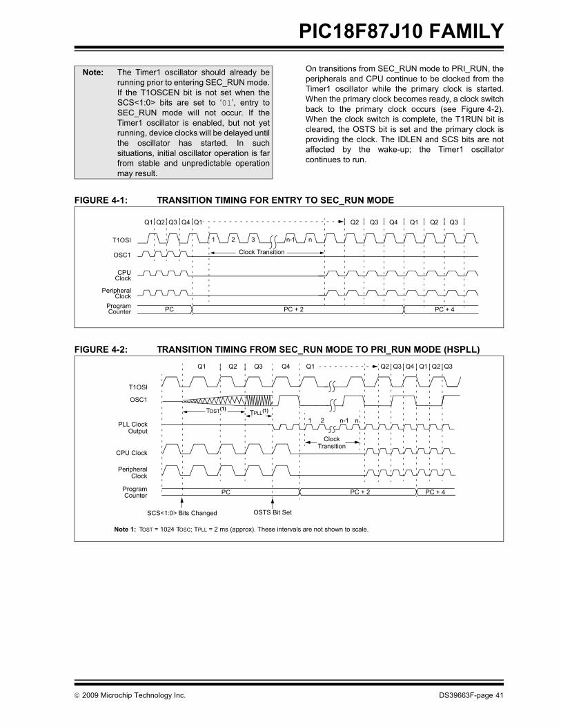
PIC18F87J10 FAMILY
On transitions from SEC_RUN mode to PRI_RUN, theperipherals and CPU continue to be clocked from theTimer1 oscillator while the primary clock is started.When the primary clock becomes ready, a clock switchback to the primary clock occurs (see Figure 4-2).When the clock switch is complete, the T1RUN bit iscleared, the OSTS bit is set and the primary clock isproviding the clock. The IDLEN and SCS bits are notaffected by the wake-up; the Timer1 oscillatorcontinues to run.FIGURE 4-1: TRANSITION TIMING FOR ENTRY TO SEC_RUN MODE
FIGURE 4-2: TRANSITION TIMING FROM SEC_RUN MODE TO PRI_RUN MODE (HSPLL)
Note: The Timer1 oscillator should already berunning prior to entering SEC_RUN mode.If the T1OSCEN bit is not set when theSCS<1:0> bits are set to ‘01’, entry toSEC_RUN mode will not occur. If theTimer1 oscillator is enabled, but not yetrunning, device clocks will be delayed untilthe oscillator has started. In suchsituations, initial oscillator operation is farfrom stable and unpredictable operationmay result.
Q4Q3Q2
OSC1
Peripheral
Program
Q1
T1OSI
Q1
Counter
Clock
CPUClock
PC + 2PC
1 2 3 n-1 n
Clock Transition
Q4Q3Q2 Q1 Q3Q2
PC + 4
Q1 Q3 Q4
OSC1
Peripheral
Program PC
T1OSI
PLL Clock
Q1
PC + 4
Q2
Output
Q3 Q4 Q1
CPU Clock
PC + 2
Clock
Counter
Q2 Q2 Q3
Note 1: TOST = 1024 TOSC; TPLL = 2 ms (approx). These intervals are not shown to scale.
SCS<1:0> Bits Changed
TPLL(1)
1 2 n-1 n
Clock
OSTS Bit Set
Transition
TOST(1)
© 2009 Microchip Technology Inc. DS39663F-page 41

PIC18F87J10 FAMILY
4.2.3 RC_RUN MODEIn RC_RUN mode, the CPU and peripherals areclocked from the internal oscillator; the primary clock isshut down. This mode provides the best power conser-vation of all the Run modes while still executing code.It works well for user applications which are not highlytiming sensitive or do not require high-speed clocks atall times.This mode is entered by setting the SCS bits to ‘11’.When the clock source is switched to the INTRC (seeFigure 4-3), the primary oscillator is shut down and theOSTS bit is cleared.
On transitions from RC_RUN mode to PRI_RUN mode,the device continues to be clocked from the INTRCwhile the primary clock is started. When the primaryclock becomes ready, a clock switch to the primaryclock occurs (see Figure 4-4). When the clock switch iscomplete, the OSTS bit is set and the primary clock isproviding the device clock. The IDLEN and SCS bitsare not affected by the switch. The INTRC source willcontinue to run if either the WDT or the Fail-Safe ClockMonitor is enabled.
FIGURE 4-3: TRANSITION TIMING TO RC_RUN MODE
FIGURE 4-4: TRANSITION TIMING FROM RC_RUN MODE TO PRI_RUN MODE
Q4Q3Q2
OSC1
Peripheral
Program
Q1
INTRC
Q1
Counter
Clock
CPUClock
PC + 2PC
1 2 3 n-1 n
Clock Transition
Q4Q3Q2 Q1 Q3Q2
PC + 4
Q1 Q3 Q4
OSC1
Peripheral
Program PC
INTRC
PLL Clock
Q1
PC + 4
Q2
Output
Q3 Q4 Q1
CPU Clock
PC + 2
Clock
Counter
Q2 Q2 Q3
Note 1: TOST = 1024 TOSC; TPLL = 2 ms (approx). These intervals are not shown to scale.
SCS<1:0> Bits Changed
TPLL(1)
1 2 n-1 n
Clock
OSTS Bit Set
Transition
TOST(1)
DS39663F-page 42 © 2009 Microchip Technology Inc.

PIC18F87J10 FAMILY
4.3 Sleep ModeThe power-managed Sleep mode is identical to thelegacy Sleep mode offered in all other PIC devices. It isentered by clearing the IDLEN bit (the default state ondevice Reset) and executing the SLEEP instruction.This shuts down the selected oscillator (Figure 4-5). Allclock source status bits are cleared.Entering the Sleep mode from any other mode does notrequire a clock switch. This is because no clocks areneeded once the controller has entered Sleep. If theWDT is selected, the INTRC source will continue tooperate. If the Timer1 oscillator is enabled, it will alsocontinue to run.
When a wake event occurs in Sleep mode (by interrupt,Reset or WDT time-out), the device will not be clockeduntil the clock source selected by the SCS<1:0> bitsbecomes ready (see Figure 4-6), or it will be clockedfrom the internal oscillator if either the Two-SpeedStart-up or the Fail-Safe Clock Monitor are enabled(see Section 24.0 “Special Features of the CPU”). Ineither case, the OSTS bit is set when the primary clockis providing the device clocks. The IDLEN and SCS bitsare not affected by the wake-up.
4.4 Idle ModesThe Idle modes allow the controller’s CPU to beselectively shut down while the peripherals continue tooperate. Selecting a particular Idle mode allows usersto further manage power consumption.
If the IDLEN bit is set to a ‘1’ when a SLEEP instruction isexecuted, the peripherals will be clocked from the clocksource selected using the SCS<1:0> bits; however, theCPU will not be clocked. The clock source status bits arenot affected. Setting IDLEN and executing a SLEEPinstruction provides a quick method of switching from agiven Run mode to its corresponding Idle mode.
If the WDT is selected, the INTRC source will continueto operate. If the Timer1 oscillator is enabled, it will alsocontinue to run.
Since the CPU is not executing instructions, the onlyexits from any of the Idle modes are by interrupt, WDTtime-out or a Reset. When a wake event occurs, CPUexecution is delayed by an interval of TCSD(parameter 38, Table 27-12) while it becomes ready toexecute code. When the CPU begins executing code,it resumes with the same clock source for the currentIdle mode. For example, when waking from RC_IDLEmode, the internal oscillator block will clock the CPUand peripherals (in other words, RC_RUN mode). TheIDLEN and SCS bits are not affected by the wake-up.
While in any Idle mode or the Sleep mode, a WDTtime-out will result in a WDT wake-up to the Run modecurrently specified by the SCS<1:0> bits.
FIGURE 4-5: TRANSITION TIMING FOR ENTRY TO SLEEP MODE
FIGURE 4-6: TRANSITION TIMING FOR WAKE FROM SLEEP (HSPLL)
Q4Q3Q2
OSC1
Peripheral
Sleep
Program
Q1Q1
Counter
Clock
CPUClock
PC + 2PC
Q3 Q4 Q1 Q2
OSC1
Peripheral
Program PC
PLL Clock
Q3 Q4
Output
CPU Clock
Q1 Q2 Q3 Q4 Q1 Q2
Clock
Counter PC + 6PC + 4
Q1 Q2 Q3 Q4
Wake Event
Note1: TOST = 1024 TOSC; TPLL = 2 ms (approx). These intervals are not shown to scale.
TOST(1) TPLL(1)
OSTS Bit Set
PC + 2
© 2009 Microchip Technology Inc. DS39663F-page 43

PIC18F87J10 FAMILY
4.4.1 PRI_IDLE MODEThis mode is unique among the three low-power Idlemodes, in that it does not disable the primary deviceclock. For timing-sensitive applications, this allows forthe fastest resumption of device operation with its moreaccurate primary clock source, since the clock sourcedoes not have to “warm up” or transition from anotheroscillator.PRI_IDLE mode is entered from PRI_RUN mode bysetting the IDLEN bit and executing a SLEEP instruc-tion. If the device is in another Run mode, set IDLENfirst, then set the SCS bits to ‘10’ and execute SLEEP.Although the CPU is disabled, the peripherals continueto be clocked from the primary clock source specifiedby the FOSC<1:0> Configuration bits. The OSTS bitremains set (see Figure 4-7).
When a wake event occurs, the CPU is clocked from theprimary clock source. A delay of interval, TCSD, isrequired between the wake event and when codeexecution starts. This is required to allow the CPU tobecome ready to execute instructions. After thewake-up, the OSTS bit remains set. The IDLEN andSCS bits are not affected by the wake-up (seeFigure 4-8).
4.4.2 SEC_IDLE MODEIn SEC_IDLE mode, the CPU is disabled but theperipherals continue to be clocked from the Timer1oscillator. This mode is entered from SEC_RUN by set-ting the IDLEN bit and executing a SLEEP instruction. Ifthe device is in another Run mode, set IDLEN first, thenset SCS<1:0> to ‘01’ and execute SLEEP. When theclock source is switched to the Timer1 oscillator, theprimary oscillator is shut down, the OSTS bit is clearedand the T1RUN bit is set.
When a wake event occurs, the peripherals continue tobe clocked from the Timer1 oscillator. After an intervalof TCSD following the wake event, the CPU begins exe-cuting code being clocked by the Timer1 oscillator. TheIDLEN and SCS bits are not affected by the wake-up;the Timer1 oscillator continues to run (see Figure 4-8).
FIGURE 4-7: TRANSITION TIMING FOR ENTRY TO IDLE MODE
FIGURE 4-8: TRANSITION TIMING FOR WAKE FROM IDLE TO RUN MODE
Note: The Timer1 oscillator should already berunning prior to entering SEC_IDLE mode.If the T1OSCEN bit is not set when theSLEEP instruction is executed, the SLEEPinstruction will be ignored and entry toSEC_IDLE mode will not occur. If theTimer1 oscillator is enabled, but not yetrunning, peripheral clocks will be delayeduntil the oscillator has started. In suchsituations, initial oscillator operation is farfrom stable and unpredictable operationmay result.
Q1
Peripheral
Program PC PC + 2
OSC1
Q3 Q4 Q1
CPU Clock
Clock
Counter
Q2
OSC1
Peripheral
Program PC
CPU Clock
Q1 Q3 Q4
Clock
Counter
Q2
Wake Event
TCSD
DS39663F-page 44 © 2009 Microchip Technology Inc.

PIC18F87J10 FAMILY
4.4.3 RC_IDLE MODEIn RC_IDLE mode, the CPU is disabled but theperipherals continue to be clocked from the internaloscillator. This mode allows for controllable powerconservation during Idle periods.From RC_RUN, this mode is entered by setting theIDLEN bit and executing a SLEEP instruction. If thedevice is in another Run mode, first set IDLEN, thenclear the SCS bits and execute SLEEP. When the clocksource is switched to the INTRC, the primary oscillatoris shut down and the OSTS bit is cleared.
When a wake event occurs, the peripherals continue tobe clocked from the INTRC. After a delay of TCSDfollowing the wake event, the CPU begins executingcode being clocked by the INTRC. The IDLEN andSCS bits are not affected by the wake-up. The INTRCsource will continue to run if either the WDT or theFail-Safe Clock Monitor is enabled.
4.5 Exiting Idle and Sleep ModesAn exit from Sleep mode, or any of the Idle modes, istriggered by an interrupt, a Reset or a WDT time-out.This section discusses the triggers that cause exitsfrom power-managed modes. The clocking subsystemactions are discussed in each of the power-managedmodes sections (see Section 4.2 “Run Modes”,Section 4.3 “Sleep Mode” and Section 4.4 “IdleModes”).
4.5.1 EXIT BY INTERRUPTAny of the available interrupt sources can cause thedevice to exit from an Idle mode, or the Sleep mode, toa Run mode. To enable this functionality, an interruptsource must be enabled by setting its enable bit in oneof the INTCON or PIE registers. The exit sequence isinitiated when the corresponding interrupt flag bit is set.
On all exits from Idle or Sleep modes by interrupt, codeexecution branches to the interrupt vector if theGIE/GIEH bit (INTCON<7>) is set. Otherwise, codeexecution continues or resumes without branching(see Section 10.0 “Interrupts”).
A fixed delay of interval TCSD following the wake eventis required when leaving Sleep and Idle modes. Thisdelay is required for the CPU to prepare for execution.Instruction execution resumes on the first clock cyclefollowing this delay.
4.5.2 EXIT BY WDT TIME-OUTA WDT time-out will cause different actions dependingon which power-managed mode the device is in whenthe time-out occurs.
If the device is not executing code (all Idle modes andSleep mode), the time-out will result in an exit from thepower-managed mode (see Section 4.2 “RunModes” and Section 4.3 “Sleep Mode”). If the deviceis executing code (all Run modes), the time-out willresult in a WDT Reset (see Section 24.2 “WatchdogTimer (WDT)”).
The Watchdog Timer and postscaler are cleared by oneof the following events:
• executing a SLEEP or CLRWDT instruction • the loss of a currently selected clock source (if the
Fail-Safe Clock Monitor is enabled)
4.5.3 EXIT BY RESETExiting an Idle or Sleep mode by Reset automaticallyforces the device to run from the INTRC.
4.5.4 EXIT WITHOUT AN OSCILLATOR START-UP DELAY
Certain exits from power-managed modes do notinvoke the OST at all. There are two cases:
• PRI_IDLE mode, where the primary clock source is not stopped; and
• the primary clock source is either the EC or ECPLL mode.
In these instances, the primary clock source eitherdoes not require an oscillator start-up delay, since it isalready running (PRI_IDLE), or normally does notrequire an oscillator start-up delay (EC). However, afixed delay of interval, TCSD, following the wake eventis still required when leaving Sleep and Idle modes toallow the CPU to prepare for execution. Instructionexecution resumes on the first clock cycle following thisdelay.
© 2009 Microchip Technology Inc. DS39663F-page 45

PIC18F87J10 FAMILY
NOTES:DS39663F-page 46 © 2009 Microchip Technology Inc.

PIC18F87J10 FAMILY
5.0 RESETThe PIC18F87J10 family of devices differentiatebetween various kinds of Reset:
a) Power-on Reset (POR) b) MCLR Reset during normal operationc) MCLR Reset during power-managed modes d) Watchdog Timer (WDT) Reset (during
execution)e) Brown-out Reset (BOR) f) RESET Instructiong) Stack Full Reseth) Stack Underflow Reset
This section discusses Resets generated by MCLR,POR and BOR and covers the operation of the variousstart-up timers. Stack Reset events are covered inSection 6.1.6.4 “Stack Full and Underflow Resets”.WDT Resets are covered in Section 24.2 “WatchdogTimer (WDT)”.
A simplified block diagram of the on-chip Reset circuitis shown in Figure 5-1.
5.1 RCON RegisterDevice Reset events are tracked through the RCONregister (Register ). The lower five bits of the registerindicate that a specific Reset event has occurred. Inmost cases, these bits can only be set by the event andmust be cleared by the application after the event. Thestate of these flag bits, taken together, can be read toindicate the type of Reset that just occurred. This isdescribed in more detail in Section 5.6 “Reset Stateof Registers”.
The RCON register also has a control bit for settinginterrupt priority (IPEN). Interrupt priority is discussedin Section 10.0 “Interrupts”.
FIGURE 5-1: SIMPLIFIED BLOCK DIAGRAM OF ON-CHIP RESET CIRCUIT
S
R Q
External Reset
MCLR
VDD
WDTTime-out
VDD RiseDetect
PWRT
INTRC
POR Pulse
PWRT Chip_Reset
11-Bit Ripple Counter
Brown-outReset(1)
RESETInstruction
StackPointer
Stack Full/Underflow Reset
Sleep( )_IDLE
65.5 ms32 μs
Note 1: The ENVREG pin must be tied high to enable Brown-out Reset. The Brown-out Reset is provided by the on-chipvoltage regulator when there is insufficient source voltage to maintain regulation.
© 2009 Microchip Technology Inc. DS39663F-page 47

PIC18F87J10 FAMILY
REGISTER 5-1: RCON: RESET CONTROL REGISTER
R/W-0 U-0 U-0 R/W-1 R-1 R-1 R/W-0 R/W-0
IPEN — — RI TO PD POR BORbit 7 bit 0
Legend:R = Readable bit W = Writable bit U = Unimplemented bit, read as ‘0’-n = Value at POR ‘1’ = Bit is set ‘0’ = Bit is cleared x = Bit is unknown
bit 7 IPEN: Interrupt Priority Enable bit 1 = Enable priority levels on interrupts0 = Disable priority levels on interrupts (PIC16CXXX Compatibility mode)
bit 6-5 Unimplemented: Read as ‘0’bit 4 RI: RESET Instruction Flag bit
1 = The RESET instruction was not executed (set by firmware only)0 = The RESET instruction was executed causing a device Reset (must be set in software after a
Brown-out Reset occurs)bit 3 TO: Watchdog Time-out Flag bit
1 = Set by power-up, CLRWDT instruction or SLEEP instruction 0 = A WDT time-out occurred
bit 2 PD: Power-Down Detection Flag bit 1 = Set by power-up or by the CLRWDT instruction 0 = Set by execution of the SLEEP instruction
bit 1 POR: Power-on Reset Status bit1 = A Power-on Reset has not occurred (set by firmware only)0 = A Power-on Reset occurred (must be set in software after a Power-on Reset occurs)
bit 0 BOR: Brown-out Reset Status bit1 = A Brown-out Reset has not occurred (set by firmware only)0 = A Brown-out Reset occurred (must be set in software after a Brown-out Reset occurs)
Note 1: It is recommended that the POR bit be set after a Power-on Reset has been detected, so that subsequentPower-on Resets may be detected.
2: If the on-chip voltage regulator is disabled, BOR remains ‘0’ at all times. See Section 5.4.1 “DetectingBOR” for more information.
3: Brown-out Reset is said to have occurred when BOR is ‘0’ and POR is ‘1’ (assuming that POR was set to‘1’ by software immediately after a Power-on Reset.
DS39663F-page 48 © 2009 Microchip Technology Inc.
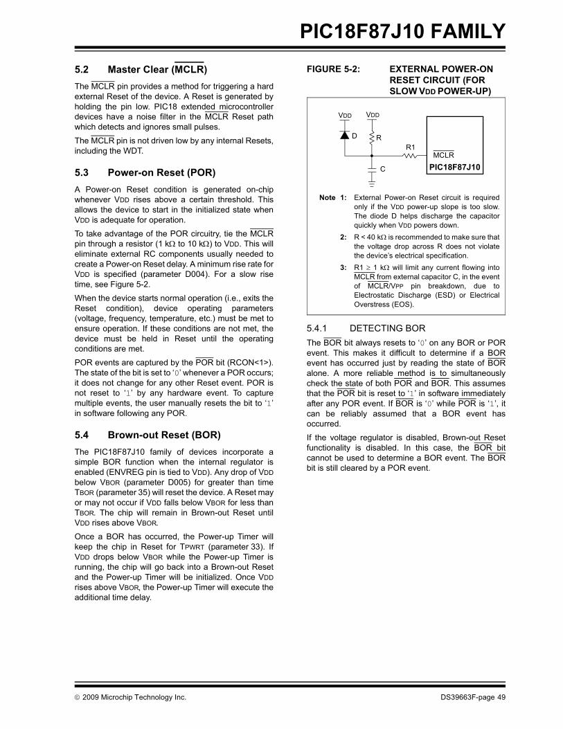
PIC18F87J10 FAMILY
5.2 Master Clear (MCLR)The MCLR pin provides a method for triggering a hardexternal Reset of the device. A Reset is generated byholding the pin low. PIC18 extended microcontrollerdevices have a noise filter in the MCLR Reset pathwhich detects and ignores small pulses.The MCLR pin is not driven low by any internal Resets,including the WDT.
5.3 Power-on Reset (POR)A Power-on Reset condition is generated on-chipwhenever VDD rises above a certain threshold. Thisallows the device to start in the initialized state whenVDD is adequate for operation.
To take advantage of the POR circuitry, tie the MCLRpin through a resistor (1 kΩ to 10 kΩ) to VDD. This willeliminate external RC components usually needed tocreate a Power-on Reset delay. A minimum rise rate forVDD is specified (parameter D004). For a slow risetime, see Figure 5-2.
When the device starts normal operation (i.e., exits theReset condition), device operating parameters(voltage, frequency, temperature, etc.) must be met toensure operation. If these conditions are not met, thedevice must be held in Reset until the operatingconditions are met.
POR events are captured by the POR bit (RCON<1>).The state of the bit is set to ‘0’ whenever a POR occurs;it does not change for any other Reset event. POR isnot reset to ‘1’ by any hardware event. To capturemultiple events, the user manually resets the bit to ‘1’in software following any POR.
5.4 Brown-out Reset (BOR)The PIC18F87J10 family of devices incorporate asimple BOR function when the internal regulator isenabled (ENVREG pin is tied to VDD). Any drop of VDDbelow VBOR (parameter D005) for greater than timeTBOR (parameter 35) will reset the device. A Reset mayor may not occur if VDD falls below VBOR for less thanTBOR. The chip will remain in Brown-out Reset untilVDD rises above VBOR.
Once a BOR has occurred, the Power-up Timer willkeep the chip in Reset for TPWRT (parameter 33). IfVDD drops below VBOR while the Power-up Timer isrunning, the chip will go back into a Brown-out Resetand the Power-up Timer will be initialized. Once VDDrises above VBOR, the Power-up Timer will execute theadditional time delay.
FIGURE 5-2: EXTERNAL POWER-ON RESET CIRCUIT (FOR SLOW VDD POWER-UP)
5.4.1 DETECTING BORThe BOR bit always resets to ‘0’ on any BOR or PORevent. This makes it difficult to determine if a BORevent has occurred just by reading the state of BORalone. A more reliable method is to simultaneouslycheck the state of both POR and BOR. This assumesthat the POR bit is reset to ‘1’ in software immediatelyafter any POR event. If BOR is ‘0’ while POR is ‘1’, itcan be reliably assumed that a BOR event hasoccurred.
If the voltage regulator is disabled, Brown-out Resetfunctionality is disabled. In this case, the BOR bitcannot be used to determine a BOR event. The BORbit is still cleared by a POR event.
Note 1: External Power-on Reset circuit is requiredonly if the VDD power-up slope is too slow.The diode D helps discharge the capacitorquickly when VDD powers down.
2: R < 40 kΩ is recommended to make sure thatthe voltage drop across R does not violatethe device’s electrical specification.
3: R1 ≥ 1 kΩ will limit any current flowing intoMCLR from external capacitor C, in the eventof MCLR/VPP pin breakdown, due toElectrostatic Discharge (ESD) or ElectricalOverstress (EOS).
C
R1RD
VDD
MCLR
PIC18F87J10
VDD
© 2009 Microchip Technology Inc. DS39663F-page 49
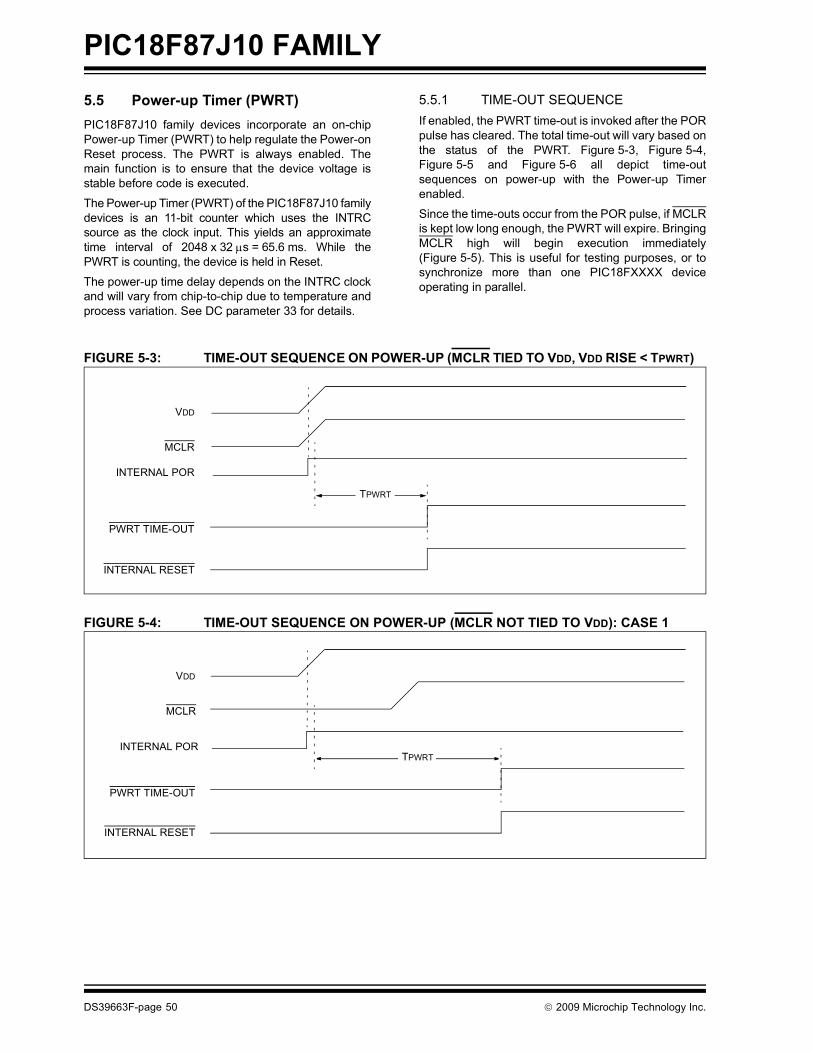
PIC18F87J10 FAMILY
5.5 Power-up Timer (PWRT)PIC18F87J10 family devices incorporate an on-chipPower-up Timer (PWRT) to help regulate the Power-onReset process. The PWRT is always enabled. Themain function is to ensure that the device voltage isstable before code is executed.The Power-up Timer (PWRT) of the PIC18F87J10 familydevices is an 11-bit counter which uses the INTRCsource as the clock input. This yields an approximatetime interval of 2048 x 32 μs = 65.6 ms. While thePWRT is counting, the device is held in Reset.
The power-up time delay depends on the INTRC clockand will vary from chip-to-chip due to temperature andprocess variation. See DC parameter 33 for details.
5.5.1 TIME-OUT SEQUENCEIf enabled, the PWRT time-out is invoked after the PORpulse has cleared. The total time-out will vary based onthe status of the PWRT. Figure 5-3, Figure 5-4,Figure 5-5 and Figure 5-6 all depict time-outsequences on power-up with the Power-up Timerenabled.
Since the time-outs occur from the POR pulse, if MCLRis kept low long enough, the PWRT will expire. BringingMCLR high will begin execution immediately(Figure 5-5). This is useful for testing purposes, or tosynchronize more than one PIC18FXXXX deviceoperating in parallel.
FIGURE 5-3: TIME-OUT SEQUENCE ON POWER-UP (MCLR TIED TO VDD, VDD RISE < TPWRT)
FIGURE 5-4: TIME-OUT SEQUENCE ON POWER-UP (MCLR NOT TIED TO VDD): CASE 1
TPWRT
VDD
MCLR
INTERNAL POR
PWRT TIME-OUT
INTERNAL RESET
TPWRT
VDD
MCLR
INTERNAL POR
PWRT TIME-OUT
INTERNAL RESET
DS39663F-page 50 © 2009 Microchip Technology Inc.

PIC18F87J10 FAMILY
FIGURE 5-5: TIME-OUT SEQUENCE ON POWER-UP (MCLR NOT TIED TO VDD): CASE 2FIGURE 5-6: SLOW RISE TIME (MCLR TIED TO VDD, VDD RISE > TPWRT)
VDD
MCLR
INTERNAL POR
PWRT TIME-OUT
INTERNAL RESET
TPWRT
VDD
MCLR
INTERNAL POR
PWRT TIME-OUT
INTERNAL RESET
0V 1V
3.3V
TPWRT
© 2009 Microchip Technology Inc. DS39663F-page 51

PIC18F87J10 FAMILY
5.6 Reset State of RegistersMost registers are unaffected by a Reset. Their statusis unknown on POR and unchanged by all otherResets. The other registers are forced to a “Resetstate” depending on the type of Reset that occurred.Most registers are not affected by a WDT wake-up,since this is viewed as the resumption of normaloperation. Status bits from the RCON register, RI, TO,PD, POR and BOR, are set or cleared differently indifferent Reset situations, as indicated in Table 5-1.These bits are used in software to determine the natureof the Reset.
Table 5-2 describes the Reset states for all of theSpecial Function Registers. These are categorized byPower-on and Brown-out Resets, Master Clear andWDT Resets and WDT wake-ups.
TABLE 5-1: STATUS BITS, THEIR SIGNIFICANCE AND THE INITIALIZATION CONDITION FOR RCON REGISTER
Condition Program Counter(1)
RCON Register STKPTR Register
RI TO PD POR BOR STKFUL STKUNF
Power-on Reset 0000h 1 1 1 0 0 0 0
RESET Instruction 0000h 0 u u u u u u
Brown-out 0000h 1 1 1 u 0 u u
MCLR during power-managed Run modes
0000h u 1 u u u u u
MCLR during power-managed Idle modes and Sleep mode
0000h u 1 0 u u u u
WDT time-out during full-power or power-managed Run modes
0000h u 0 u u u u u
MCLR during full-power execution
0000h u u u u u u u
Stack Full Reset (STVREN = 1) 0000h u u u u u 1 u
Stack Underflow Reset (STVREN = 1)
0000h u u u u u u 1
Stack Underflow Error (not an actual Reset, STVREN = 0)
0000h u u u u u u 1
WDT time-out during power-managed Idle or Sleep modes
PC + 2 u 0 0 u u u u
Interrupt exit from power-managed modes
PC + 2 u u 0 u u u u
Legend: u = unchangedNote 1: When the wake-up is due to an interrupt and the GIEH or GIEL bits are set, the PC is loaded with the
interrupt vector (0008h or 0018h).
DS39663F-page 52 © 2009 Microchip Technology Inc.
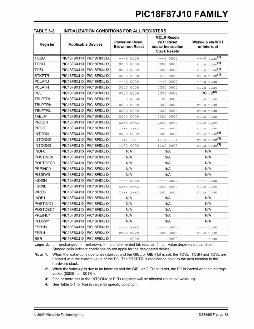
PIC18F87J10 FAMILY
TABLE 5-2: INITIALIZATION CONDITIONS FOR ALL REGISTERSRegister Applicable Devices Power-on Reset,Brown-out Reset
MCLR ResetsWDT Reset
RESET InstructionStack Resets
Wake-up via WDT or Interrupt
TOSU PIC18F6XJ1X PIC18F8XJ1X ---0 0000 ---0 0000 ---0 uuuu(1)
TOSH PIC18F6XJ1X PIC18F8XJ1X 0000 0000 0000 0000 uuuu uuuu(1)
TOSL PIC18F6XJ1X PIC18F8XJ1X 0000 0000 0000 0000 uuuu uuuu(1)
STKPTR PIC18F6XJ1X PIC18F8XJ1X 00-0 0000 uu-0 0000 uu-u uuuu(1)
PCLATU PIC18F6XJ1X PIC18F8XJ1X ---0 0000 ---0 0000 ---u uuuu
PCLATH PIC18F6XJ1X PIC18F8XJ1X 0000 0000 0000 0000 uuuu uuuu
PCL PIC18F6XJ1X PIC18F8XJ1X 0000 0000 0000 0000 PC + 2(2)
TBLPTRU PIC18F6XJ1X PIC18F8XJ1X --00 0000 --00 0000 --uu uuuu
TBLPTRH PIC18F6XJ1X PIC18F8XJ1X 0000 0000 0000 0000 uuuu uuuu
TBLPTRL PIC18F6XJ1X PIC18F8XJ1X 0000 0000 0000 0000 uuuu uuuu
TABLAT PIC18F6XJ1X PIC18F8XJ1X 0000 0000 0000 0000 uuuu uuuu
PRODH PIC18F6XJ1X PIC18F8XJ1X xxxx xxxx uuuu uuuu uuuu uuuu
PRODL PIC18F6XJ1X PIC18F8XJ1X xxxx xxxx uuuu uuuu uuuu uuuu
INTCON PIC18F6XJ1X PIC18F8XJ1X 0000 000x 0000 000u uuuu uuuu(3)
INTCON2 PIC18F6XJ1X PIC18F8XJ1X 1111 1111 1111 1111 uuuu uuuu(3)
INTCON3 PIC18F6XJ1X PIC18F8XJ1X 1100 0000 1100 0000 uuuu uuuu(3)
INDF0 PIC18F6XJ1X PIC18F8XJ1X N/A N/A N/APOSTINC0 PIC18F6XJ1X PIC18F8XJ1X N/A N/A N/APOSTDEC0 PIC18F6XJ1X PIC18F8XJ1X N/A N/A N/APREINC0 PIC18F6XJ1X PIC18F8XJ1X N/A N/A N/APLUSW0 PIC18F6XJ1X PIC18F8XJ1X N/A N/A N/AFSR0H PIC18F6XJ1X PIC18F8XJ1X ---- xxxx ---- uuuu ---- uuuu
FSR0L PIC18F6XJ1X PIC18F8XJ1X xxxx xxxx uuuu uuuu uuuu uuuu
WREG PIC18F6XJ1X PIC18F8XJ1X xxxx xxxx uuuu uuuu uuuu uuuu
INDF1 PIC18F6XJ1X PIC18F8XJ1X N/A N/A N/APOSTINC1 PIC18F6XJ1X PIC18F8XJ1X N/A N/A N/APOSTDEC1 PIC18F6XJ1X PIC18F8XJ1X N/A N/A N/APREINC1 PIC18F6XJ1X PIC18F8XJ1X N/A N/A N/APLUSW1 PIC18F6XJ1X PIC18F8XJ1X N/A N/A N/AFSR1H PIC18F6XJ1X PIC18F8XJ1X ---- xxxx ---- uuuu ---- uuuu
FSR1L PIC18F6XJ1X PIC18F8XJ1X xxxx xxxx uuuu uuuu uuuu uuuu
BSR PIC18F6XJ1X PIC18F8XJ1X ---- 0000 ---- 0000 ---- uuuu
Legend: u = unchanged, x = unknown, - = unimplemented bit, read as ‘0’, q = value depends on condition.Shaded cells indicate conditions do not apply for the designated device.
Note 1: When the wake-up is due to an interrupt and the GIEL or GIEH bit is set, the TOSU, TOSH and TOSL are updated with the current value of the PC. The STKPTR is modified to point to the next location in the hardware stack.
2: When the wake-up is due to an interrupt and the GIEL or GIEH bit is set, the PC is loaded with the interrupt vector (0008h or 0018h).
3: One or more bits in the INTCONx or PIRx registers will be affected (to cause wake-up).4: See Table 5-1 for Reset value for specific condition.
© 2009 Microchip Technology Inc. DS39663F-page 53
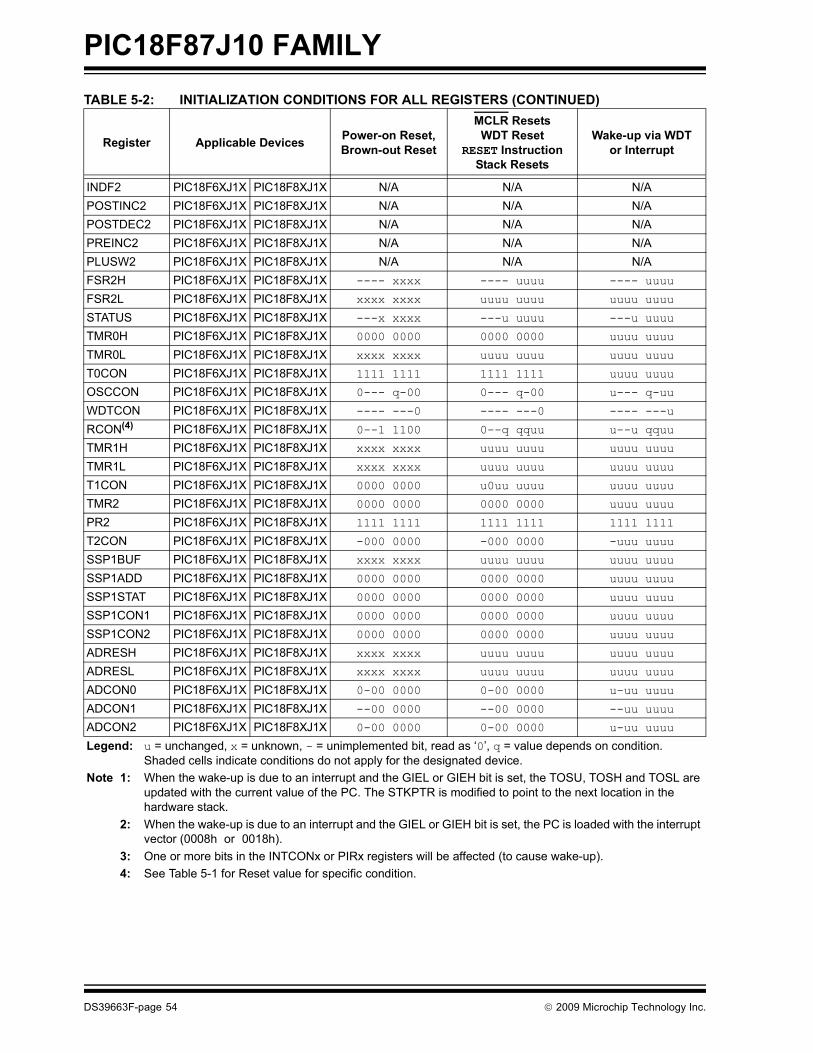
PIC18F87J10 FAMILY
INDF2 PIC18F6XJ1X PIC18F8XJ1X N/A N/A N/APOSTINC2 PIC18F6XJ1X PIC18F8XJ1X N/A N/A N/APOSTDEC2 PIC18F6XJ1X PIC18F8XJ1X N/A N/A N/APREINC2 PIC18F6XJ1X PIC18F8XJ1X N/A N/A N/APLUSW2 PIC18F6XJ1X PIC18F8XJ1X N/A N/A N/AFSR2H PIC18F6XJ1X PIC18F8XJ1X ---- xxxx ---- uuuu ---- uuuu
FSR2L PIC18F6XJ1X PIC18F8XJ1X xxxx xxxx uuuu uuuu uuuu uuuu
STATUS PIC18F6XJ1X PIC18F8XJ1X ---x xxxx ---u uuuu ---u uuuu
TMR0H PIC18F6XJ1X PIC18F8XJ1X 0000 0000 0000 0000 uuuu uuuu
TMR0L PIC18F6XJ1X PIC18F8XJ1X xxxx xxxx uuuu uuuu uuuu uuuu
T0CON PIC18F6XJ1X PIC18F8XJ1X 1111 1111 1111 1111 uuuu uuuu
OSCCON PIC18F6XJ1X PIC18F8XJ1X 0--- q-00 0--- q-00 u--- q-uu
WDTCON PIC18F6XJ1X PIC18F8XJ1X ---- ---0 ---- ---0 ---- ---u
RCON(4) PIC18F6XJ1X PIC18F8XJ1X 0--1 1100 0--q qquu u--u qquu
TMR1H PIC18F6XJ1X PIC18F8XJ1X xxxx xxxx uuuu uuuu uuuu uuuu
TMR1L PIC18F6XJ1X PIC18F8XJ1X xxxx xxxx uuuu uuuu uuuu uuuu
T1CON PIC18F6XJ1X PIC18F8XJ1X 0000 0000 u0uu uuuu uuuu uuuu
TMR2 PIC18F6XJ1X PIC18F8XJ1X 0000 0000 0000 0000 uuuu uuuu
PR2 PIC18F6XJ1X PIC18F8XJ1X 1111 1111 1111 1111 1111 1111
T2CON PIC18F6XJ1X PIC18F8XJ1X -000 0000 -000 0000 -uuu uuuu
SSP1BUF PIC18F6XJ1X PIC18F8XJ1X xxxx xxxx uuuu uuuu uuuu uuuu
SSP1ADD PIC18F6XJ1X PIC18F8XJ1X 0000 0000 0000 0000 uuuu uuuu
SSP1STAT PIC18F6XJ1X PIC18F8XJ1X 0000 0000 0000 0000 uuuu uuuu
SSP1CON1 PIC18F6XJ1X PIC18F8XJ1X 0000 0000 0000 0000 uuuu uuuu
SSP1CON2 PIC18F6XJ1X PIC18F8XJ1X 0000 0000 0000 0000 uuuu uuuu
ADRESH PIC18F6XJ1X PIC18F8XJ1X xxxx xxxx uuuu uuuu uuuu uuuu
ADRESL PIC18F6XJ1X PIC18F8XJ1X xxxx xxxx uuuu uuuu uuuu uuuu
ADCON0 PIC18F6XJ1X PIC18F8XJ1X 0-00 0000 0-00 0000 u-uu uuuu
ADCON1 PIC18F6XJ1X PIC18F8XJ1X --00 0000 --00 0000 --uu uuuu
ADCON2 PIC18F6XJ1X PIC18F8XJ1X 0-00 0000 0-00 0000 u-uu uuuu
TABLE 5-2: INITIALIZATION CONDITIONS FOR ALL REGISTERS (CONTINUED)
Register Applicable Devices Power-on Reset,Brown-out Reset
MCLR ResetsWDT Reset
RESET InstructionStack Resets
Wake-up via WDT or Interrupt
Legend: u = unchanged, x = unknown, - = unimplemented bit, read as ‘0’, q = value depends on condition.Shaded cells indicate conditions do not apply for the designated device.
Note 1: When the wake-up is due to an interrupt and the GIEL or GIEH bit is set, the TOSU, TOSH and TOSL are updated with the current value of the PC. The STKPTR is modified to point to the next location in the hardware stack.
2: When the wake-up is due to an interrupt and the GIEL or GIEH bit is set, the PC is loaded with the interrupt vector (0008h or 0018h).
3: One or more bits in the INTCONx or PIRx registers will be affected (to cause wake-up).4: See Table 5-1 for Reset value for specific condition.
DS39663F-page 54 © 2009 Microchip Technology Inc.

PIC18F87J10 FAMILY
CCPR1H PIC18F6XJ1X PIC18F8XJ1X xxxx xxxx uuuu uuuu uuuu uuuu
CCPR1L PIC18F6XJ1X PIC18F8XJ1X xxxx xxxx uuuu uuuu uuuu uuuu
CCP1CON PIC18F6XJ1X PIC18F8XJ1X 0000 0000 0000 0000 uuuu uuuu
CCPR2H PIC18F6XJ1X PIC18F8XJ1X xxxx xxxx uuuu uuuu uuuu uuuu
CCPR2L PIC18F6XJ1X PIC18F8XJ1X xxxx xxxx uuuu uuuu uuuu uuuu
CCP2CON PIC18F6XJ1X PIC18F8XJ1X 0000 0000 0000 0000 uuuu uuuu
CCPR3H PIC18F6XJ1X PIC18F8XJ1X xxxx xxxx uuuu uuuu uuuu uuuu
CCPR3L PIC18F6XJ1X PIC18F8XJ1X xxxx xxxx uuuu uuuu uuuu uuuu
CCP3CON PIC18F6XJ1X PIC18F8XJ1X 0000 0000 0000 0000 uuuu uuuu
ECCP1AS PIC18F6XJ1X PIC18F8XJ1X 0000 0000 0000 0000 uuuu uuuu
CVRCON PIC18F6XJ1X PIC18F8XJ1X 0000 0000 0000 0000 uuuu uuuu
CMCON PIC18F6XJ1X PIC18F8XJ1X 0000 0111 0000 0111 uuuu uuuu
TMR3H PIC18F6XJ1X PIC18F8XJ1X xxxx xxxx uuuu uuuu uuuu uuuu
TMR3L PIC18F6XJ1X PIC18F8XJ1X xxxx xxxx uuuu uuuu uuuu uuuu
T3CON PIC18F6XJ1X PIC18F8XJ1X 0000 0000 uuuu uuuu uuuu uuuu
PSPCON PIC18F6XJ1X PIC18F8XJ1X 0000 ---- 0000 ---- uuuu ----
SPBRG1 PIC18F6XJ1X PIC18F8XJ1X 0000 0000 0000 0000 uuuu uuuu
RCREG1 PIC18F6XJ1X PIC18F8XJ1X 0000 0000 0000 0000 uuuu uuuu
TXREG1 PIC18F6XJ1X PIC18F8XJ1X xxxx xxxx uuuu uuuu uuuu uuuu
TXSTA1 PIC18F6XJ1X PIC18F8XJ1X 0000 0010 0000 0010 uuuu uuuu
RCSTA1 PIC18F6XJ1X PIC18F8XJ1X 0000 000x 0000 000x uuuu uuuu
EECON2 PIC18F6XJ1X PIC18F8XJ1X ---- ---- ---- ---- ---- ----
EECON1 PIC18F6XJ1X PIC18F8XJ1X ---0 x00- ---0 u00- ---0 u00-
IPR3 PIC18F6XJ1X PIC18F8XJ1X 1111 1111 1111 1111 uuuu uuuu
PIR3 PIC18F6XJ1X PIC18F8XJ1X 0000 0000 0000 0000 uuuu uuuu(3)
PIE3 PIC18F6XJ1X PIC18F8XJ1X 0000 0000 0000 0000 uuuu uuuu
IPR2 PIC18F6XJ1X PIC18F8XJ1X 11-- 1-11 11-- 1-11 uu-- u-uu
PIR2 PIC18F6XJ1X PIC18F8XJ1X 00-- 0-00 00-- 0-00 uu-- u-uu(3)
PIE2 PIC18F6XJ1X PIC18F8XJ1X 00-- 0-00 00-- 0-00 uu-- u-uu
IPR1 PIC18F6XJ1X PIC18F8XJ1X 1111 1111 1111 1111 uuuu uuuu
PIR1 PIC18F6XJ1X PIC18F8XJ1X 0000 0000 0000 0000 uuuu uuuu(3)
PIE1 PIC18F6XJ1X PIC18F8XJ1X 0000 0000 0000 0000 uuuu uuuu
MEMCON PIC18F6XJ1X PIC18F8XJ1X 0-00 --00 0-00 --00 u-uu --uu
OSCTUNE PIC18F6XJ1X PIC18F8XJ1X -0-- ---- -0-- ---- -u-- ----
TABLE 5-2: INITIALIZATION CONDITIONS FOR ALL REGISTERS (CONTINUED)
Register Applicable Devices Power-on Reset,Brown-out Reset
MCLR ResetsWDT Reset
RESET InstructionStack Resets
Wake-up via WDT or Interrupt
Legend: u = unchanged, x = unknown, - = unimplemented bit, read as ‘0’, q = value depends on condition.Shaded cells indicate conditions do not apply for the designated device.
Note 1: When the wake-up is due to an interrupt and the GIEL or GIEH bit is set, the TOSU, TOSH and TOSL are updated with the current value of the PC. The STKPTR is modified to point to the next location in the hardware stack.
2: When the wake-up is due to an interrupt and the GIEL or GIEH bit is set, the PC is loaded with the interrupt vector (0008h or 0018h).
3: One or more bits in the INTCONx or PIRx registers will be affected (to cause wake-up).4: See Table 5-1 for Reset value for specific condition.
© 2009 Microchip Technology Inc. DS39663F-page 55

PIC18F87J10 FAMILY
TRISJ PIC18F6XJ1X PIC18F8XJ1X 1111 1111 1111 1111 uuuu uuuu
TRISH PIC18F6XJ1X PIC18F8XJ1X 1111 1111 1111 1111 uuuu uuuu
TRISG PIC18F6XJ1X PIC18F8XJ1X ---1 1111 ---1 1111 ---u uuuu
TRISF PIC18F6XJ1X PIC18F8XJ1X 1111 111- 1111 111- uuuu uuu-
TRISE PIC18F6XJ1X PIC18F8XJ1X 1111 1111 1111 1111 uuuu uuuu
TRISD PIC18F6XJ1X PIC18F8XJ1X 1111 1111 1111 1111 uuuu uuuu
TRISC PIC18F6XJ1X PIC18F8XJ1X 1111 1111 1111 1111 uuuu uuuu
TRISB PIC18F6XJ1X PIC18F8XJ1X 1111 1111 1111 1111 uuuu uuuu
TRISA PIC18F6XJ1X PIC18F8XJ1X --11 1111 --11 1111 --uu uuuu
LATJ PIC18F6XJ1X PIC18F8XJ1X xxxx xxxx uuuu uuuu uuuu uuuu
LATH PIC18F6XJ1X PIC18F8XJ1X xxxx xxxx uuuu uuuu uuuu uuuu
LATG PIC18F6XJ1X PIC18F8XJ1X ---x xxxx ---u uuuu ---u uuuu
LATF PIC18F6XJ1X PIC18F8XJ1X xxxx xxx- uuuu uuu- uuuu uuu-
LATE PIC18F6XJ1X PIC18F8XJ1X xxxx xxxx uuuu uuuu uuuu uuuu
LATD PIC18F6XJ1X PIC18F8XJ1X xxxx xxxx uuuu uuuu uuuu uuuu
LATC PIC18F6XJ1X PIC18F8XJ1X xxxx xxxx uuuu uuuu uuuu uuuu
LATB PIC18F6XJ1X PIC18F8XJ1X xxxx xxxx uuuu uuuu uuuu uuuu
LATA PIC18F6XJ1X PIC18F8XJ1X --xx xxxx --uu uuuu --uu uuuu
PORTJ PIC18F6XJ1X PIC18F8XJ1X xxxx xxxx uuuu uuuu uuuu uuuu
PORTH PIC18F6XJ1X PIC18F8XJ1X 0000 xxxx uuuu uuuu uuuu uuuu
PORTG PIC18F6XJ1X PIC18F8XJ1X 111x xxxx 111u uuuu uuuu uuuu
PORTF PIC18F6XJ1X PIC18F8XJ1X x000 000- x000 000- uuuu uuu-
PORTE PIC18F6XJ1X PIC18F8XJ1X xxxx xxxx uuuu uuuu uuuu uuuu
PORTD PIC18F6XJ1X PIC18F8XJ1X xxxx xxxx uuuu uuuu uuuu uuuu
PORTC PIC18F6XJ1X PIC18F8XJ1X xxxx xxxx uuuu uuuu uuuu uuuu
PORTB PIC18F6XJ1X PIC18F8XJ1X xxxx xxxx uuuu uuuu uuuu uuuu
PORTA PIC18F6XJ1X PIC18F8XJ1X --0x 0000 --0u 0000 --uu uuuu
SPBRGH1 PIC18F6XJ1X PIC18F8XJ1X 0000 0000 0000 0000 uuuu uuuu
BAUDCON1 PIC18F6XJ1X PIC18F8XJ1X 01-0 0-00 01-0 0-00 uu-u u-uu
SPBRG2 PIC18F6XJ1X PIC18F8XJ1X 0000 0000 0000 0000 uuuu uuuu
BAUDCON2 PIC18F6XJ1X PIC18F8XJ1X 01-0 0-00 01-0 0-00 uu-u u-uu
TABLE 5-2: INITIALIZATION CONDITIONS FOR ALL REGISTERS (CONTINUED)
Register Applicable Devices Power-on Reset,Brown-out Reset
MCLR ResetsWDT Reset
RESET InstructionStack Resets
Wake-up via WDT or Interrupt
Legend: u = unchanged, x = unknown, - = unimplemented bit, read as ‘0’, q = value depends on condition.Shaded cells indicate conditions do not apply for the designated device.
Note 1: When the wake-up is due to an interrupt and the GIEL or GIEH bit is set, the TOSU, TOSH and TOSL are updated with the current value of the PC. The STKPTR is modified to point to the next location in the hardware stack.
2: When the wake-up is due to an interrupt and the GIEL or GIEH bit is set, the PC is loaded with the interrupt vector (0008h or 0018h).
3: One or more bits in the INTCONx or PIRx registers will be affected (to cause wake-up).4: See Table 5-1 for Reset value for specific condition.
DS39663F-page 56 © 2009 Microchip Technology Inc.

PIC18F87J10 FAMILY
ECCP1DEL PIC18F6XJ1X PIC18F8XJ1X 0000 0000 0000 0000 uuuu uuuu
TMR4 PIC18F6XJ1X PIC18F8XJ1X 0000 0000 0000 0000 uuuu uuuu
PR4 PIC18F6XJ1X PIC18F8XJ1X 1111 1111 1111 1111 1111 1111
T4CON PIC18F6XJ1X PIC18F8XJ1X -000 0000 -000 0000 -uuu uuuu
CCPR4H PIC18F6XJ1X PIC18F8XJ1X xxxx xxxx uuuu uuuu uuuu uuuu
CCPR4L PIC18F6XJ1X PIC18F8XJ1X xxxx xxxx uuuu uuuu uuuu uuuu
CCP4CON PIC18F6XJ1X PIC18F8XJ1X --00 0000 --00 0000 --uu uuuu
CCPR5H PIC18F6XJ1X PIC18F8XJ1X xxxx xxxx uuuu uuuu uuuu uuuu
CCPR5L PIC18F6XJ1X PIC18F8XJ1X xxxx xxxx uuuu uuuu uuuu uuuu
CCP5CON PIC18F6XJ1X PIC18F8XJ1X --00 0000 --00 0000 --uu uuuu
SPBRG2 PIC18F6XJ1X PIC18F8XJ1X 0000 0000 0000 0000 uuuu uuuu
RCREG2 PIC18F6XJ1X PIC18F8XJ1X 0000 0000 0000 0000 uuuu uuuu
TXREG2 PIC18F6XJ1X PIC18F8XJ1X 0000 0000 0000 0000 uuuu uuuu
TXSTA2 PIC18F6XJ1X PIC18F8XJ1X 0000 0010 0000 0010 uuuu uuuu
RCSTA2 PIC18F6XJ1X PIC18F8XJ1X 0000 000x 0000 000x uuuu uuuu
ECCP3AS PIC18F6XJ1X PIC18F8XJ1X 0000 0000 0000 0000 uuuu uuuu
ECCP3DEL PIC18F6XJ1X PIC18F8XJ1X 0000 0000 0000 0000 uuuu uuuu
ECCP2AS PIC18F6XJ1X PIC18F8XJ1X 0000 0000 0000 0000 uuuu uuuu
ECCP2DEL PIC18F6XJ1X PIC18F8XJ1X 0000 0000 0000 0000 uuuu uuuu
SSP2BUF PIC18F6XJ1X PIC18F8XJ1X xxxx xxxx uuuu uuuu uuuu uuuu
SSP2ADD PIC18F6XJ1X PIC18F8XJ1X 0000 0000 0000 0000 uuuu uuuu
SSP2STAT PIC18F6XJ1X PIC18F8XJ1X 0000 0000 0000 0000 uuuu uuuu
SSP2CON1 PIC18F6XJ1X PIC18F8XJ1X 0000 0000 0000 0000 uuuu uuuu
SSP2CON2 PIC18F6XJ1X PIC18F8XJ1X 0000 0000 0000 0000 uuuu uuuu
TABLE 5-2: INITIALIZATION CONDITIONS FOR ALL REGISTERS (CONTINUED)
Register Applicable Devices Power-on Reset,Brown-out Reset
MCLR ResetsWDT Reset
RESET InstructionStack Resets
Wake-up via WDT or Interrupt
Legend: u = unchanged, x = unknown, - = unimplemented bit, read as ‘0’, q = value depends on condition.Shaded cells indicate conditions do not apply for the designated device.
Note 1: When the wake-up is due to an interrupt and the GIEL or GIEH bit is set, the TOSU, TOSH and TOSL are updated with the current value of the PC. The STKPTR is modified to point to the next location in the hardware stack.
2: When the wake-up is due to an interrupt and the GIEL or GIEH bit is set, the PC is loaded with the interrupt vector (0008h or 0018h).
3: One or more bits in the INTCONx or PIRx registers will be affected (to cause wake-up).4: See Table 5-1 for Reset value for specific condition.
© 2009 Microchip Technology Inc. DS39663F-page 57

PIC18F87J10 FAMILY
NOTES:DS39663F-page 58 © 2009 Microchip Technology Inc.

PIC18F87J10 FAMILY
6.0 MEMORY ORGANIZATIONThere are two types of memory in PIC18 Flashmicrocontroller devices:
• Program Memory• Data RAM
As Harvard architecture devices, the data and programmemories use separate busses; this allows forconcurrent access of the two memory spaces.
Additional detailed information on the operation of theFlash program memory is provided in Section 7.0“Flash Program Memory”.
6.1 Program Memory OrganizationPIC18 microcontrollers implement a 21-bit programcounter which is capable of addressing a 2-Mbyteprogram memory space. Accessing a location betweenthe upper boundary of the physically implementedmemory and the 2-Mbyte address will return all ‘0’s (aNOP instruction).
The entire PIC18F87J10 family offers a range ofon-chip Flash program memory sizes, from 32 Kbytes(up to 16,384 single-word instructions) to 128 Kbytes(65,536 single-word instructions). The programmemory maps for individual family members are shownin Figure 6-3.
FIGURE 6-1: MEMORY MAPS FOR PIC18F87J10 FAMILY DEVICES
Note: Sizes of memory areas are not to scale. Sizes of program memory areas are enhanced to show detail.
UnimplementedRead as ‘0’
UnimplementedRead as ‘0’
UnimplementedRead as ‘0’
UnimplementedRead as ‘0’
UnimplementedRead as ‘0’
000000h
1FFFFFh
01FFFFh
PIC18FX5J10 PIC18FX5J15 PIC18FX6J10 PIC18FX6J15 PIC18FX7J10
007FFFh005FFFh
00BFFFh
00FFFFh
017FFFh
PC<20:0>
Stack Level 1•
Stack Level 31
••
CALL, CALLW, RCALL,RETURN, RETFIE, RETLW,
21
Use
r Mem
ory
Spac
e
On-ChipMemory
On-ChipMemory
On-ChipMemory
On-ChipMemory
On-ChipMemory
ADDULNK, SUBULNK
Config. Words
Config. Words
Config. Words
Config. Words
Config. Words
© 2009 Microchip Technology Inc. DS39663F-page 59

PIC18F87J10 FAMILY
6.1.1 HARD MEMORY VECTORSAll PIC18 devices have a total of three hard-codedreturn vectors in their program memory space. TheReset vector address is the default value to which theprogram counter returns on all device Resets; it islocated at 0000h.PIC18 devices also have two interrupt vectoraddresses for the handling of high-priority andlow-priority interrupts. The high-priority interrupt vectoris located at 0008h and the low-priority interrupt vectoris at 0018h. Their locations in relation to the programmemory map are shown in Figure 6-2.
FIGURE 6-2: HARD VECTOR AND CONFIGURATION WORD LOCATIONS FOR PIC18F87J10 FAMILY DEVICES
6.1.2 FLASH CONFIGURATION WORDSBecause PIC18F87J10 family devices do not have per-sistent configuration memory, the top four words ofon-chip program memory are reserved for configurationinformation. On Reset, the configuration information iscopied into the Configuration registers.
The Configuration Words are stored in their programmemory location in numerical order, starting with thelower byte of CONFIG1 at the lowest address and end-ing with the upper byte of CONFIG4. For these devices,only Configuration Words, CONFIG1 throughCONFIG3, are used; CONFIG4 is reserved. The actualaddresses of the Flash Configuration Word for devicesin the PIC18F87J10 family are shown in Table 6-1.Their location in the memory map is shown with theother memory vectors in Figure 6-2.
Additional details on the device Configuration Wordsare provided in Section 24.1 “Configuration Bits”.
TABLE 6-1: FLASH CONFIGURATION WORD FOR PIC18F87J10 FAMILY DEVICES
Reset Vector
Low-Priority Interrupt Vector
0000h
0018h
On-ChipProgram Memory
High-Priority Interrupt Vector 0008h
1FFFFFh
(Top of Memory)(Top of Memory-7)Flash Configuration Words
Read ‘0’
Legend: (Top of Memory) represents upper boundary of on-chip program memory space (see Figure 6-1 for device-specific values). Shaded area represents unimplemented memory. Areas are not shown to scale.
DeviceProgram Memory (Kbytes)
Configuration Word
Addresses
PIC18F65J1032 7FF8h to 7FFFh
PIC18F85J10PIC18F65J15
48 BFF8h to BFFFhPIC18F85J15PIC18F66J10
64 FFF8h to FFFFhPIC18F86J10PIC18F66J15
96 17FF8h to to 17FFFhPIC18F86J15
PIC18F67J10128 1FFF8h to to
1FFFFhPIC18F87J10
DS39663F-page 60 © 2009 Microchip Technology Inc.

PIC18F87J10 FAMILY
6.1.3 PIC18F8XJ10/8XJ15 PROGRAMMEMORY MODES
The 80-pin devices in this family can address up to atotal of 2 Mbytes of program memory. This is achievedthrough the external memory bus. There are twodistinct operating modes available to the controllers:
• Microcontroller (MC)• Extended Microcontroller (EMC)
The program memory mode is determined by settingthe EMB Configuration bits (CONFIG3L<5:4>), asshown in Register 6-1. (See also Section 24.1“Configuration Bits” for additional details on thedevice Configuration bits.)
The program memory modes operate as follows:
• The Microcontroller Mode accesses only on-chip Flash memory. Attempts to read above the top of on-chip memory causes a read of all ‘0’s (a NOP instruction).
The Microcontroller mode is also the only operatingmode available to 64-pin devices.
• The Extended Microcontroller Mode allows access to both internal and external program memories as a single block. The device can access its entire on-chip program memory; above this, the device accesses external program memory up to the 2-Mbyte program space limit. Execution automatically switches between the two memories as required.
The setting of the EMB Configuration bits also controlsthe address bus width of the external memory bus. Thisis covered in more detail in Section 8.0 “ExternalMemory Bus”.
In all modes, the microcontroller has complete accessto data RAM.
Figure 6-3 compares the memory maps of the differentprogram memory modes. The differences betweenon-chip and external memory access limitations aremore fully explained in Table 6-2.
REGISTER 6-1: CONFIG3L: CONFIGURATION REGISTER 3 LOW
R/WO-1 R/WO-1 R/WO-1 R/WO-1 R/WO-1 U-0 U-0 U-0WAIT BW EMB1 EMB0 EASHFT — — —
bit 7 bit 0
Legend:R = Readable bit WO = Write-Once bit U = Unimplemented bit, read as ‘0’-n = Value after erase ‘1’ = Bit is set ‘0’ = Bit is cleared x = Bit is unknown
bit 7 Wait: External Bus Wait Enable bit1 = Wait states on the external bus are disabled0 = Wait states on the external bus are enabled and selected by MEMCON<5:4>
bit 6 BW: Data Bus Width Select bit1 = 16-Bit Data Width modes0 = 8-Bit Data Width modes
bit 5-4 EMB<1:0>: External Memory Bus Configuration bits11 = Microcontroller mode, external bus disabled10 = Extended Microcontroller mode, 12-bit address width for external bus01 = Extended Microcontroller mode, 16-bit address width for external bus00 = Extended Microcontroller mode, 20-bit address width for external bus
bit 3 EASHFT: External Address Bus Shift Enable bit1 = Address shifting enabled – external address bus is shifted to start at 000000h0 = Address shifting disabled – external address bus reflects the PC value
bit 2-0 Unimplemented: Read as ‘0’
© 2009 Microchip Technology Inc. DS39663F-page 61

PIC18F87J10 FAMILY
6.1.4 EXTENDED MICROCONTROLLERMODE AND ADDRESS SHIFTINGBy default, devices in Extended Microcontroller modedirectly present the program counter value on theexternal address bus for those addresses in the rangeof the external memory space. In practical terms, thismeans addresses in the external memory device belowthe top of on-chip memory are unavailable.
To avoid this, the Extended Microcontroller modeimplements an address shifting option to enable auto-matic address translation. In this mode, addressespresented on the external bus are shifted down by thesize of the on-chip program memory and are remappedto start at 0000h. This allows the complete use of theexternal memory device’s memory space.
FIGURE 6-3: MEMORY MAPS FOR PIC18F87J10 FAMILY PROGRAM MEMORY MODES
TABLE 6-2: MEMORY ACCESS FOR PIC18F8XJ10/8XJ15 PROGRAM MEMORY MODES
Operating ModeInternal Program Memory External Program Memory
ExecutionFrom
Table Read From
Table Write To
ExecutionFrom
Table Read From
Table Write To
Microcontroller Yes Yes Yes No Access No Access No AccessExtended Microcontroller Yes Yes Yes Yes Yes Yes
ExternalMemory
On-ChipProgramMemory
Microcontroller Mode(1)
000000hOn-ChipProgramMemory
1FFFFFh
Reads ‘0’s
External On-ChipMemory Memory
(Top of Memory)(Top of Memory) + 1
Legend: (Top of Memory) represents upper boundary of on-chip program memory space (see Figure 6-1 for device-specific values). Shaded areas represent unimplemented, or inaccessible areas, depending on the mode.
Note 1: This mode is the only available mode on 64-pin devices and the default on 80-pin devices.2: These modes are only available on 80-pin devices.
Extended Microcontroller Mode(2)
000000h
1FFFFFh
(Top of Memory)(Top of Memory) + 1
ExternalMemory
On-ChipProgramMemory
000000h
1FFFFFh
(Top of Memory)(Top of Memory) + 1
NoAccess
Space
On-ChipMemorySpace
External On-ChipMemory Memory
Space
Mappedto
ExternalMemorySpace
Space Space
Mappedto
ExternalMemorySpace (Top of Memory)
Extended Microcontroller Modewith Address Shifting(2)
1FFFFFh –
DS39663F-page 62 © 2009 Microchip Technology Inc.
PIC18F87J10 FAMILY
6.1.5 PROGRAM COUNTERThe Program Counter (PC) specifies the address of theinstruction to fetch for execution. The PC is 21 bits wideand is contained in three separate 8-bit registers. Thelow byte, known as the PCL register, is both readableand writable. The high byte, or PCH register, containsthe PC<15:8> bits; it is not directly readable or writable.Updates to the PCH register are performed through thePCLATH register. The upper byte is called PCU. Thisregister contains the PC<20:16> bits; it is also notdirectly readable or writable. Updates to the PCUregister are performed through the PCLATU register.The contents of PCLATH and PCLATU are transferredto the program counter by any operation that writesPCL. Similarly, the upper two bytes of the programcounter are transferred to PCLATH and PCLATU by anoperation that reads PCL. This is useful for computedoffsets to the PC (see Section 6.1.8.1 “ComputedGOTO”).
The PC addresses bytes in the program memory. Toprevent the PC from becoming misaligned with wordinstructions, the Least Significant bit of PCL is fixed toa value of ‘0’. The PC increments by 2 to addresssequential instructions in the program memory.
The CALL, RCALL, GOTO and program branchinstructions write to the program counter directly. Forthese instructions, the contents of PCLATH andPCLATU are not transferred to the program counter.
6.1.6 RETURN ADDRESS STACKThe return address stack allows any combination of upto 31 program calls and interrupts to occur. The PC ispushed onto the stack when a CALL or RCALL instruc-tion is executed, or an interrupt is Acknowledged. ThePC value is pulled off the stack on a RETURN, RETLWor a RETFIE instruction (and on ADDULNK andSUBULNK instructions if the extended instruction set isenabled). PCLATU and PCLATH are not affected byany of the RETURN or CALL instructions.
The stack operates as a 31-word by 21-bit RAM and a5-bit Stack Pointer, STKPTR. The stack space is notpart of either program or data space. The Stack Pointeris readable and writable and the address on the top ofthe stack is readable and writable through theTop-of-Stack Special Function Registers. Data can alsobe pushed to, or popped from the stack, using theseregisters.
A CALL type instruction causes a push onto the stack.The Stack Pointer is first incremented and the locationpointed to by the Stack Pointer is written with thecontents of the PC (already pointing to the instructionfollowing the CALL). A RETURN type instruction causesa pop from the stack. The contents of the locationpointed to by the STKPTR are transferred to the PCand then the Stack Pointer is decremented.
The Stack Pointer is initialized to ‘00000’ after allResets. There is no RAM associated with the locationcorresponding to a Stack Pointer value of ‘00000’; thisis only a Reset value. Status bits indicate if the stack isfull, has overflowed or has underflowed.
6.1.6.1 Top-of-Stack AccessOnly the top of the return address stack (TOS) is read-able and writable. A set of three registers,TOSU:TOSH:TOSL, hold the contents of the stacklocation pointed to by the STKPTR register(Figure 6-4). This allows users to implement a softwarestack if necessary. After a CALL, RCALL or interrupt(and ADDULNK and SUBULNK instructions if theextended instruction set is enabled), the software canread the pushed value by reading theTOSU:TOSH:TOSL registers. These values can beplaced on a user-defined software stack. At return time,the software can return these values toTOSU:TOSH:TOSL and do a return.
The user must disable the global interrupt enable bitswhile accessing the stack to prevent inadvertent stackcorruption.
FIGURE 6-4: RETURN ADDRESS STACK AND ASSOCIATED REGISTERS
00011001A34h
111111111011101
000100000100000
00010
Return Address Stack<20:0>
Top-of-Stack000D58h
TOSLTOSHTOSU34h1Ah00h
STKPTR<4:0>
Top-of-Stack Registers Stack Pointer
© 2009 Microchip Technology Inc. DS39663F-page 63
PIC18F87J10 FAMILY
6.1.6.2 Return Stack Pointer (STKPTR)The STKPTR register (Register 6-2) contains the StackPointer value, the STKFUL (Stack Full) status bit andthe STKUNF (Stack Underflow) status bit. The value ofthe Stack Pointer can be 0 through 31. The StackPointer increments before values are pushed onto thestack and decrements after values are popped off thestack. On Reset, the Stack Pointer value will be zero.The user may read and write the Stack Pointer value.This feature can be used by a Real-Time OperatingSystem (RTOS) for return stack maintenance.After the PC is pushed onto the stack 31 times (withoutpopping any values off the stack), the STKFUL bit isset. The STKFUL bit is cleared by software or by aPOR.
The action that takes place when the stack becomesfull depends on the state of the STVREN (Stack Over-flow Reset Enable) Configuration bit. (Refer toSection 24.1 “Configuration Bits” for a description ofthe device Configuration bits.) If STVREN is set(default), the 31st push will push the (PC + 2) valueonto the stack, set the STKFUL bit and reset thedevice. The STKFUL bit will remain set and the StackPointer will be set to zero.
If STVREN is cleared, the STKFUL bit will be set on the31st push and the Stack Pointer will increment to 31.Any additional pushes will not overwrite the 31st pushand the STKPTR will remain at 31.
When the stack has been popped enough times tounload the stack, the next pop will return a value of zeroto the PC and set the STKUNF bit, while the StackPointer remains at zero. The STKUNF bit will remainset until cleared by software or until a POR occurs.
6.1.6.3 PUSH and POP InstructionsSince the Top-of-Stack is readable and writable, theability to push values onto the stack and pull values offthe stack, without disturbing normal program execu-tion, is a desirable feature. The PIC18 instruction setincludes two instructions, PUSH and POP, that permitthe TOS to be manipulated under software control.TOSU, TOSH and TOSL can be modified to place dataor a return address on the stack.
The PUSH instruction places the current PC value ontothe stack. This increments the Stack Pointer and loadsthe current PC value onto the stack.
The POP instruction discards the current TOS bydecrementing the Stack Pointer. The previous valuepushed onto the stack then becomes the TOS value.
Note: Returning a value of zero to the PC on anunderflow has the effect of vectoring theprogram to the Reset vector, where thestack conditions can be verified andappropriate actions can be taken. This isnot the same as a Reset, as the contentsof the SFRs are not affected.
REGISTER 6-2: STKPTR: STACK POINTER REGISTER
R/C-0 R/C-0 U-0 R/W-0 R/W-0 R/W-0 R/W-0 R/W-0STKFUL(1) STKUNF(1) — SP4 SP3 SP2 SP1 SP0
bit 7 bit 0
Legend: C = Clearable bitR = Readable bit W = Writable bit U = Unimplemented bit, read as ‘0’-n = Value at POR ‘1’ = Bit is set ‘0’ = Bit is cleared x = Bit is unknown
bit 7 STKFUL: Stack Full Flag bit(1)
1 = Stack became full or overflowed 0 = Stack has not become full or overflowed
bit 6 STKUNF: Stack Underflow Flag bit(1)
1 = Stack underflow occurred 0 = Stack underflow did not occur
bit 5 Unimplemented: Read as ‘0’bit 4-0 SP<4:0>: Stack Pointer Location bits
Note 1: Bit 7 and bit 6 are cleared by user software or by a POR.
DS39663F-page 64 © 2009 Microchip Technology Inc.
PIC18F87J10 FAMILY
6.1.6.4 Stack Full and Underflow ResetsDevice Resets on stack overflow and stack underflowconditions are enabled by setting the STVREN bit inConfiguration Register 1L. When STVREN is set, a fullor underflow condition will set the appropriate STKFULor STKUNF bit and then cause a device Reset. WhenSTVREN is cleared, a full or underflow condition will setthe appropriate STKFUL or STKUNF bit, but not causea device Reset. The STKFUL or STKUNF bit is clearedby the user software or a Power-on Reset.6.1.7 FAST REGISTER STACKA Fast Register Stack is provided for the STATUS,WREG and BSR registers to provide a “fast return”option for interrupts. This stack is only one level deepand is neither readable nor writable. It is loaded with thecurrent value of the corresponding register when theprocessor vectors for an interrupt. All interrupt sourceswill push values into the Stack registers. The values inthe registers are then loaded back into the workingregisters if the RETFIE, FAST instruction is used toreturn from the interrupt.
If both low and high-priority interrupts are enabled, theStack registers cannot be used reliably to return fromlow-priority interrupts. If a high-priority interrupt occurswhile servicing a low-priority interrupt, the Stackregister values stored by the low-priority interrupt willbe overwritten. In these cases, users must save the keyregisters in software during a low-priority interrupt.
If interrupt priority is not used, all interrupts may use theFast Register Stack for returns from interrupt. If nointerrupts are used, the Fast Register Stack can beused to restore the STATUS, WREG and BSR registersat the end of a subroutine call. To use the Fast RegisterStack for a subroutine call, a CALL label, FASTinstruction must be executed to save the STATUS,WREG and BSR registers to the Fast Register Stack. ARETURN, FAST instruction is then executed to restorethese registers from the Fast Register Stack.
Example 6-1 shows a source code example that usesthe Fast Register Stack during a subroutine call andreturn.
EXAMPLE 6-1: FAST REGISTER STACK CODE EXAMPLE
6.1.8 LOOK-UP TABLES IN PROGRAM MEMORY
There may be programming situations that require thecreation of data structures, or look-up tables, inprogram memory. For PIC18 devices, look-up tablescan be implemented in two ways:
• Computed GOTO • Table Reads
6.1.8.1 Computed GOTOA computed GOTO is accomplished by adding an offsetto the program counter. An example is shown inExample 6-2.
A look-up table can be formed with an ADDWF PCLinstruction and a group of RETLW nn instructions. TheW register is loaded with an offset into the table beforeexecuting a call to that table. The first instruction of thecalled routine is the ADDWF PCL instruction. The nextinstruction executed will be one of the RETLW nninstructions that returns the value ‘nn’ to the callingfunction.
The offset value (in WREG) specifies the number ofbytes that the program counter should advance andshould be multiples of 2 (LSb = 0).
In this method, only one data byte may be stored ineach instruction location and room on the returnaddress stack is required.
EXAMPLE 6-2: COMPUTED GOTO USING AN OFFSET VALUE
6.1.8.2 Table ReadsA better method of storing data in program memoryallows two bytes of data to be stored in each instructionlocation.
Look-up table data may be stored two bytes perprogram word while programming. The Table Pointer(TBLPTR) specifies the byte address and the TableLatch (TABLAT) contains the data that is read from theprogram memory. Data is transferred from programmemory one byte at a time.
Table read operation is discussed further inSection 7.1 “Table Reads and Table Writes”.
CALL SUB1, FAST ;STATUS, WREG, BSR;SAVED IN FAST REGISTER;STACK
••
SUB1 ••
RETURN FAST ;RESTORE VALUES SAVED;IN FAST REGISTER STACK
MOVF OFFSET, WCALL TABLE
ORG nn00hTABLE ADDWF PCL
RETLW nnhRETLW nnhRETLW nnh...
© 2009 Microchip Technology Inc. DS39663F-page 65
PIC18F87J10 FAMILY
6.2 PIC18 Instruction Cycle6.2.1 CLOCKING SCHEMEThe microcontroller clock input, whether from aninternal or external source, is internally divided by fourto generate four non-overlapping quadrature clocks(Q1, Q2, Q3 and Q4). Internally, the program counter isincremented on every Q1; the instruction is fetchedfrom the program memory and latched into the instruc-tion register during Q4. The instruction is decoded andexecuted during the following Q1 through Q4. Theclocks and instruction execution flow are shown inFigure 6-5.
6.2.2 INSTRUCTION FLOW/PIPELININGAn “Instruction Cycle” consists of four Q cycles, Q1through Q4. The instruction fetch and execute are pipe-lined in such a manner that a fetch takes one instructioncycle, while the decode and execute takes anotherinstruction cycle. However, due to the pipelining, eachinstruction effectively executes in one cycle. If aninstruction causes the program counter to change (e.g.,GOTO), then two cycles are required to complete theinstruction (Example 6-3).
A fetch cycle begins with the Program Counter (PC)incrementing in Q1.
In the execution cycle, the fetched instruction is latchedinto the Instruction Register (IR) in cycle Q1. Thisinstruction is then decoded and executed during theQ2, Q3 and Q4 cycles. Data memory is read during Q2(operand read) and written during Q4 (destinationwrite).
FIGURE 6-5: CLOCK/INSTRUCTION CYCLE
EXAMPLE 6-3: INSTRUCTION PIPELINE FLOW
Q1 Q2 Q3 Q4 Q1 Q2 Q3 Q4 Q1 Q2 Q3 Q4OSC1
Q1
Q2Q3
Q4
PC
OSC2/CLKO(RC mode)
PC PC + 2 PC + 4
Fetch INST (PC)Execute INST (PC – 2)
Fetch INST (PC + 2)Execute INST (PC)
Fetch INST (PC + 4)Execute INST (PC + 2)
InternalPhaseClock
All instructions are single cycle, except for any program branches. These take two cycles since the fetch instructionis “flushed” from the pipeline while the new instruction is being fetched and then executed.
TCY0 TCY1 TCY2 TCY3 TCY4 TCY51. MOVLW 55h Fetch 1 Execute 12. MOVWF PORTB Fetch 2 Execute 23. BRA SUB_1 Fetch 3 Execute 34. BSF PORTA, BIT3 (Forced NOP) Fetch 4 Flush (NOP)5. Instruction @ address SUB_1 Fetch SUB_1 Execute SUB_1
DS39663F-page 66 © 2009 Microchip Technology Inc.

PIC18F87J10 FAMILY
6.2.3 INSTRUCTIONS IN PROGRAMMEMORYThe program memory is addressed in bytes. Instruc-tions are stored as two bytes or four bytes in programmemory. The Least Significant Byte of an instructionword is always stored in a program memory locationwith an even address (LSB = 0). To maintain alignmentwith instruction boundaries, the PC increments in stepsof 2 and the LSB will always read ‘0’ (see Section 6.1.5“Program Counter”).
Figure 6-6 shows an example of how instruction wordsare stored in the program memory.
The CALL and GOTO instructions have the absoluteprogram memory address embedded into the instruc-tion. Since instructions are always stored on wordboundaries, the data contained in the instruction is aword address. The word address is written to PC<20:1>which accesses the desired byte address in programmemory. Instruction #2 in Figure 6-6 shows how theinstruction, GOTO 0006h, is encoded in the programmemory. Program branch instructions, which encode arelative address offset, operate in the same manner. Theoffset value stored in a branch instruction represents thenumber of single-word instructions that the PC will beoffset by. Section 25.0 “Instruction Set Summary”provides further details of the instruction set.
FIGURE 6-6: INSTRUCTIONS IN PROGRAM MEMORY
6.2.4 TWO-WORD INSTRUCTIONSThe standard PIC18 instruction set has four two-wordinstructions: CALL, MOVFF, GOTO and LSFR. In allcases, the second word of the instructions always has‘1111’ as its four Most Significant bits; the other 12 bitsare literal data, usually a data memory address.
The use of ‘1111’ in the 4 MSbs of an instructionspecifies a special form of NOP. If the instruction isexecuted in proper sequence – immediately after thefirst word – the data in the second word is accessed
and used by the instruction sequence. If the first wordis skipped for some reason and the second word isexecuted by itself, a NOP is executed instead. This isnecessary for cases when the two-word instruction ispreceded by a conditional instruction that changes thePC. Example 6-4 shows how this works.
EXAMPLE 6-4: TWO-WORD INSTRUCTIONS
Word AddressLSB = 1 LSB = 0 ↓
Program MemoryByte Locations →
000000h000002h000004h000006h
Instruction 1: MOVLW 055h 0Fh 55h 000008hInstruction 2: GOTO 0006h EFh 03h 00000Ah
F0h 00h 00000ChInstruction 3: MOVFF 123h, 456h C1h 23h 00000Eh
F4h 56h 000010h000012h000014h
Note: See Section 6.5 “Program Memory andthe Extended Instruction Set” forinformation on two-word instructions in theextended instruction set.
CASE 1:Object Code Source Code0110 0110 0000 0000 TSTFSZ REG1 ; is RAM location 0?
1100 0001 0010 0011 MOVFF REG1, REG2 ; No, skip this word
1111 0100 0101 0110 ; Execute this word as a NOP
0010 0100 0000 0000 ADDWF REG3 ; continue code
CASE 2:Object Code Source Code0110 0110 0000 0000 TSTFSZ REG1 ; is RAM location 0?
1100 0001 0010 0011 MOVFF REG1, REG2 ; Yes, execute this word
1111 0100 0101 0110 ; 2nd word of instruction
0010 0100 0000 0000 ADDWF REG3 ; continue code
© 2009 Microchip Technology Inc. DS39663F-page 67
PIC18F87J10 FAMILY
6.3 Data Memory OrganizationThe data memory in PIC18 devices is implemented asstatic RAM. Each register in the data memory has a12-bit address, allowing up to 4096 bytes of datamemory. The memory space is divided into as many as16 banks that contain 256 bytes each. ThePIC18FX5J10/X5J15/X6J10 devices, with up to64 Kbytes of program memory, implement 8 completebanks for a total of 2048 bytes. PIC18FX6J15 andPIC18FX7J10 devices, with 96 or 128 Kbytes ofprogram memory, implement all available banks andprovide 3936 bytes of data memory available to theuser. Figure 6-7 and Figure 6-8 show the data memoryorganization for the devices.
The data memory contains Special Function Registers(SFRs) and General Purpose Registers (GPRs). TheSFRs are used for control and status of the controllerand peripheral functions, while GPRs are used for datastorage and scratchpad operations in the user’sapplication. Any read of an unimplemented location willread as ‘0’s.
The instruction set and architecture allow operationsacross all banks. The entire data memory may beaccessed by Direct, Indirect or Indexed Addressingmodes. Addressing modes are discussed later in thissection.
To ensure that commonly used registers (select SFRsand select GPRs) can be accessed in a single cycle,PIC18 devices implement an Access Bank. This is a256-byte memory space that provides fast access toselect SFRs and the lower portion of GPR Bank 0 with-out using the BSR. Section 6.3.2 “Access Bank”provides a detailed description of the Access RAM.
6.3.1 BANK SELECT REGISTERLarge areas of data memory require an efficientaddressing scheme to make rapid access to anyaddress possible. Ideally, this means that an entireaddress does not need to be provided for each read orwrite operation. For PIC18 devices, this is accom-plished with a RAM banking scheme. This divides thememory space into 16 contiguous banks of 256 bytes.Depending on the instruction, each location can beaddressed directly by its full 12-bit address, or an 8-bitlow-order address and a 4-bit Bank Pointer.
Most instructions in the PIC18 instruction set make useof the Bank Pointer, known as the Bank Select Register(BSR). This SFR holds the 4 Most Significant bits of alocation’s address; the instruction itself includes the8 Least Significant bits. Only the four lower bits of theBSR are implemented (BSR<3:0>). The upper four bitsare unused; they will always read ‘0’ and cannot bewritten to. The BSR can be loaded directly by using theMOVLB instruction.
The value of the BSR indicates the bank in datamemory. The 8 bits in the instruction show the locationin the bank and can be thought of as an offset from thebank’s lower boundary. The relationship between theBSR’s value and the bank division in data memory isshown in Figure 6-9.
Since up to 16 registers may share the same low-orderaddress, the user must always be careful to ensure thatthe proper bank is selected before performing a dataread or write. For example, writing what should beprogram data to an 8-bit address of F9h while the BSRis 0Fh, will end up resetting the program counter.
While any bank can be selected, only those banks thatare actually implemented can be read or written to.Writes to unimplemented banks are ignored, whilereads from unimplemented banks will return ‘0’s. Evenso, the STATUS register will still be affected as if theoperation was successful. The data memory map inFigure 6-7 indicates which banks are implemented.
In the core PIC18 instruction set, only the MOVFFinstruction fully specifies the 12-bit address of thesource and target registers. This instruction ignores theBSR completely when it executes. All other instructionsinclude only the low-order address as an operand andmust use either the BSR or the Access Bank to locatetheir target registers.
Note: The operation of some aspects of datamemory are changed when the PIC18extended instruction set is enabled. SeeSection 6.6 “Data Memory and theExtended Instruction Set” for moreinformation.
DS39663F-page 68 © 2009 Microchip Technology Inc.

PIC18F87J10 FAMILY
FIGURE 6-7: DATA MEMORY MAP FOR PIC18FX5J10/X5J15/X6J10 DEVICES00h5Fh60h
FFh
Access Bank
When a = 0: The BSR is ignored and theAccess Bank is used.The first 96 bytes are generalpurpose RAM (from Bank 0). The second 160 bytes areSpecial Function Registers(from Bank 15).
When a = 1: The BSR specifies the bankused by the instruction.
Access RAM High
Access RAM Low
(SFRs)
Bank 0
Bank 1
Bank 14
Bank 15
Data Memory MapBSR<3:0>
= 0000
= 0001
= 1111
060h05Fh
F60hFFFh
F5FhF00hEFFh
1FFh
100h0FFh
000hAccess RAM
FFh
00h
FFh
00h
FFh
00h
GPR
GPR
SFR
Bank 2= 0010
2FFh
200h
Bank 3
FFh
00hGPR
FFh
= 0011
Unused
GPR
GPR
GPR
GPR
GPR
4FFh
400h
5FFh
500h
3FFh
300h
FFh
00h
FFh
00h
FFh
00h
FFh
00h
FFh
00h
00h
= 0110
= 0111
= 1000
= 0101
= 0100Bank 4
Bank 5
Bank 6
Bank 7
Bank 8
= 1110
6FFh
600h
7FFh
700h
800h
toUnused
Read as ‘0’
© 2009 Microchip Technology Inc. DS39663F-page 69
PIC18F87J10 FAMILY
FIGURE 6-8: DATA MEMORY MAP FOR PIC18FX6J15/X7J10 DEVICESBank 0
Bank 1
Bank 14
Bank 15
Data Memory MapBSR<3:0>
= 0000
= 0001
= 1111
060h05Fh
F60hFFFh
00h5Fh60h
FFh
Access Bank
When a = 0: The BSR is ignored and theAccess Bank is used.The first 96 bytes are generalpurpose RAM (from Bank 0). The remaining 160 bytes areSpecial Function Registers(from Bank 15).
When a = 1: The BSR specifies the bankused by the instruction.
F5FhF00hEFFh
1FFh
100h0FFh
000hAccess RAM
FFh
00h
FFh
00h
FFh
00h
GPR
GPR
SFR
Access RAM High
Access RAM Low
Bank 2= 0010
(SFRs)
2FFh
200h
Bank 3
FFh
00hGPR
FFh
= 0011
= 1101
GPR
GPR
GPR
GPR
GPR
GPR
GPR
GPR
GPR
GPR
GPR
4FFh
400h
5FFh
500h
3FFh
300h
FFh
00h
FFh
00h
FFh
00h
FFh
00h
FFh
00h
FFh
00h
FFh
00h
FFh
00h
FFh
00h
FFh
00h
FFh
00h
00h
GPR
GPR
= 0110
= 0111
= 1010
= 1100
= 1000
= 0101
= 1001
= 1011
= 0100Bank 4
Bank 5
Bank 6
Bank 7
Bank 8
Bank 9
Bank 10
Bank 11
Bank 12
Bank 13
= 1110
6FFh
600h
7FFh
700h
8FFh
800h
9FFh
900h
AFFh
A00h
BFFh
B00h
CFFh
C00h
DFFh
D00h
E00h
DS39663F-page 70 © 2009 Microchip Technology Inc.

PIC18F87J10 FAMILY
FIGURE 6-9: USE OF THE BANK SELECT REGISTER (DIRECT ADDRESSING)6.3.2 ACCESS BANKWhile the use of the BSR with an embedded 8-bitaddress allows users to address the entire range ofdata memory, it also means that the user must alwaysensure that the correct bank is selected. Otherwise,data may be read from or written to the wrong location.This can be disastrous if a GPR is the intended targetof an operation, but an SFR is written to instead.Verifying and/or changing the BSR for each read orwrite to data memory can become very inefficient.
To streamline access for the most commonly used datamemory locations, the data memory is configured withan Access Bank, which allows users to access amapped block of memory without specifying a BSR.The Access Bank consists of the first 96 bytes ofmemory (00h-5Fh) in Bank 0 and the last 160 bytes ofmemory (60h-FFh) in Bank 15. The lower half is knownas the “Access RAM” and is composed of GPRs. Theupper half is where the device’s SFRs are mapped.These two areas are mapped contiguously in theAccess Bank and can be addressed in a linear fashionby an 8-bit address (Figure 6-7).
The Access Bank is used by core PIC18 instructionsthat include the Access RAM bit (the ‘a’ parameter inthe instruction). When ‘a’ is equal to ‘1’, the instructionuses the BSR and the 8-bit address included in theopcode for the data memory address. When ‘a’ is ‘0’,however, the instruction is forced to use the AccessBank address map; the current value of the BSR isignored entirely.
Using this “forced” addressing allows the instruction tooperate on a data address in a single cycle withoutupdating the BSR first. For 8-bit addresses of 60h andabove, this means that users can evaluate and operateon SFRs more efficiently. The Access RAM below 60his a good place for data values that the user might needto access rapidly, such as immediate computationalresults or common program variables. Access RAMalso allows for faster and more code efficient contextsaving and switching of variables.
The mapping of the Access Bank is slightly differentwhen the extended instruction set is enabled (XINSTConfiguration bit = 1). This is discussed in more detailin Section 6.6.3 “Mapping the Access Bank inIndexed Literal Offset Mode”.
6.3.3 GENERAL PURPOSE REGISTER FILE
PIC18 devices may have banked memory in the GPRarea. This is data RAM which is available for use by allinstructions. GPRs start at the bottom of Bank 0(address 000h) and grow upwards towards the bottomof the SFR area. GPRs are not initialized by aPower-on Reset and are unchanged on all otherResets.
Note 1: The Access RAM bit of the instruction can be used to force an override of the selected bank (BSR<3:0>) to the registers of the Access Bank.
2: The MOVFF instruction embeds the entire 12-bit address in the instruction.
Data Memory
Bank Select(2)
7 0From Opcode(2)
0 0 0 0
000h
100h
200h
300h
F00h
E00h
FFFh
Bank 0
Bank 1
Bank 2
Bank 14
Bank 15
00h
FFh00h
FFh00h
FFh
00h
FFh00h
FFh
00h
FFh
Bank 3throughBank 13
0 0 1 0 1 1 1 1 1 1 1 1
7 0BSR(1)
1 1 1 1 1 1 1 1
© 2009 Microchip Technology Inc. DS39663F-page 71
PIC18F87J10 FAMILY
6.3.4 SPECIAL FUNCTION REGISTERSThe Special Function Registers (SFRs) are registersused by the CPU and peripheral modules for controllingthe desired operation of the device. These registers areimplemented as static RAM. SFRs start at the top ofdata memory (FFFh) and extend downward to occupymore than the top half of Bank 15 (F60h to FFFh). A listof these registers is given in Table 6-3 and Table 6-4.
The SFRs can be classified into two sets: thoseassociated with the “core” device functionality (ALU,Resets and interrupts) and those related to theperipheral functions. The Reset and Interrupt registersare described in their respective chapters, while theALU’s STATUS register is described later in thissection. Registers related to the operation of theperipheral features are described in the chapter for thatperipheral.
The SFRs are typically distributed among theperipherals whose functions they control. Unused SFRlocations are unimplemented and read as ‘0’s.
TABLE 6-3: SPECIAL FUNCTION REGISTER MAP FOR PIC18F87J10 FAMILY DEVICES
Address Name Address Name Address Name Address Name Address Name
FFFh TOSU FDFh INDF2(1) FBFh CCPR1H F9Fh IPR1 F7Fh SPBRGH1FFEh TOSH FDEh POSTINC2(1) FBEh CCPR1L F9Eh PIR1 F7Eh BAUDCON1FFDh TOSL FDDh POSTDEC2(1) FBDh CCP1CON F9Dh PIE1 F7Dh SPBRGH2 FFCh STKPTR FDCh PREINC2(1) FBCh CCPR2H F9Ch MEMCON(3) F7Ch BAUDCON2 FFBh PCLATU FDBh PLUSW2(1) FBBh CCPR2L F9Bh OSCTUNE F7Bh —(2)
FFAh PCLATH FDAh FSR2H FBAh CCP2CON F9Ah TRISJ(3) F7Ah —(2)
FF9h PCL FD9h FSR2L FB9h CCPR3H F99h TRISH(3) F79h ECCP1DELFF8h TBLPTRU FD8h STATUS FB8h CCPR3L F98h TRISG F78h TMR4FF7h TBLPTRH FD7h TMR0H FB7h CCP3CON F97h TRISF F77h PR4 FF6h TBLPTRL FD6h TMR0L FB6h ECCP1AS F96h TRISE F76h T4CON FF5h TABLAT FD5h T0CON FB5h CVRCON F95h TRISD F75h CCPR4HFF4h PRODH FD4h —(2) FB4h CMCON F94h TRISC F74h CCPR4LFF3h PRODL FD3h OSCCON FB3h TMR3H F93h TRISB F73h CCP4CON FF2h INTCON FD2h —(2) FB2h TMR3L F92h TRISA F72h CCPR5H FF1h INTCON2 FD1h WDTCON FB1h T3CON F91h LATJ(3) F71h CCPR5LFF0h INTCON3 FD0h RCON FB0h PSPCON F90h LATH(3) F70h CCP5CONFEFh INDF0(1) FCFh TMR1H FAFh SPBRG1 F8Fh LATG F6Fh SPBRG2FEEh POSTINC0(1) FCEh TMR1L FAEh RCREG1 F8Eh LATF F6Eh RCREG2 FEDh POSTDEC0(1) FCDh T1CON FADh TXREG1 F8Dh LATE F6Dh TXREG2 FECh PREINC0(1) FCCh TMR2 FACh TXSTA1 F8Ch LATD F6Ch TXSTA2FEBh PLUSW0(1) FCBh PR2 FABh RCSTA1 F8Bh LATC F6Bh RCSTA2FEAh FSR0H FCAh T2CON FAAh —(2) F8Ah LATB F6Ah ECCP3ASFE9h FSR0L FC9h SSP1BUF FA9h —(2) F89h LATA F69h ECCP3DELFE8h WREG FC8h SSP1ADD FA8h —(2) F88h PORTJ(3) F68h ECCP2ASFE7h INDF1(1) FC7h SSP1STAT FA7h EECON2 F87h PORTH(3) F67h ECCP2DELFE6h POSTINC1(1) FC6h SSP1CON1 FA6h EECON1 F86h PORTG F66h SSP2BUFFE5h POSTDEC1(1) FC5h SSP1CON2 FA5h IPR3 F85h PORTF F65h SSP2ADDFE4h PREINC1(1) FC4h ADRESH FA4h PIR3 F84h PORTE F64h SSP2STATFE3h PLUSW1(1) FC3h ADRESL FA3h PIE3 F83h PORTD F63h SSP2CON1FE2h FSR1H FC2h ADCON0 FA2h IPR2 F82h PORTC F62h SSP2CON2FE1h FSR1L FC1h ADCON1 FA1h PIR2 F81h PORTB F61h —(2)
FE0h BSR FC0h ADCON2 FA0h PIE2 F80h PORTA F60h —(2)
Note 1: This is not a physical register.2: Unimplemented registers are read as ‘0’.3: This register is not available on 64-pin devices.
DS39663F-page 72 © 2009 Microchip Technology Inc.

PIC18F87J10 FAMILY
TABLE 6-4: REGISTER FILE SUMMARY (PIC18F87J10 FAMILY)File Name Bit 7 Bit 6 Bit 5 Bit 4 Bit 3 Bit 2 Bit 1 Bit 0 Value on POR, BOR
Details on page:
TOSU — — — Top-of-Stack Upper Byte (TOS<20:16>) ---0 0000 53, 63
TOSH Top-of-Stack High Byte (TOS<15:8>) 0000 0000 53, 63
TOSL Top-of-Stack Low Byte (TOS<7:0>) 0000 0000 53, 63
STKPTR STKFUL STKUNF — SP4 SP3 SP2 SP1 SP0 00-0 0000 53, 64
PCLATU — — bit 21(1) Holding Register for PC<20:16> ---0 0000 53, 63
PCLATH Holding Register for PC<15:8> 0000 0000 53, 63
PCL PC Low Byte (PC<7:0>) 0000 0000 53, 63
TBLPTRU — — bit 21 Program Memory Table Pointer Upper Byte (TBLPTR<20:16>) --00 0000 53, 93
TBLPTRH Program Memory Table Pointer High Byte (TBLPTR<15:8>) 0000 0000 53, 93
TBLPTRL Program Memory Table Pointer Low Byte (TBLPTR<7:0>) 0000 0000 53, 93
TABLAT Program Memory Table Latch 0000 0000 53, 93
PRODH Product Register High Byte xxxx xxxx 53, 107
PRODL Product Register Low Byte xxxx xxxx 53, 107
INTCON GIE/GIEH PEIE/GIEL TMR0IE INT0IE RBIE TMR0IF INT0IF RBIF 0000 000x 53, 111
INTCON2 RBPU INTEDG0 INTEDG1 INTEDG2 INTEDG3 TMR0IP INT3IP RBIP 1111 1111 53, 112
INTCON3 INT2IP INT1IP INT3IE INT2IE INT1IE INT3IF INT2IF INT1IF 1100 0000 53, 113
INDF0 Uses contents of FSR0 to address data memory – value of FSR0 not changed (not a physical register) N/A 53, 79
POSTINC0 Uses contents of FSR0 to address data memory – value of FSR0 post-incremented (not a physical register) N/A 53, 80
POSTDEC0 Uses contents of FSR0 to address data memory – value of FSR0 post-decremented (not a physical register) N/A 53, 80
PREINC0 Uses contents of FSR0 to address data memory – value of FSR0 pre-incremented (not a physical register) N/A 53, 80
PLUSW0 Uses contents of FSR0 to address data memory – value of FSR0 pre-incremented (not a physical register) – value of FSR0 offset by W
N/A 53, 80
FSR0H — — — — Indirect Data Memory Address Pointer 0 High Byte ---- xxxx 53, 79
FSR0L Indirect Data Memory Address Pointer 0 Low Byte xxxx xxxx 53, 79
WREG Working Register xxxx xxxx 53
INDF1 Uses contents of FSR1 to address data memory – value of FSR1 not changed (not a physical register) N/A 53, 79
POSTINC1 Uses contents of FSR1 to address data memory – value of FSR1 post-incremented (not a physical register) N/A 53, 80
POSTDEC1 Uses contents of FSR1 to address data memory – value of FSR1 post-decremented (not a physical register) N/A 53, 80
PREINC1 Uses contents of FSR1 to address data memory – value of FSR1 pre-incremented (not a physical register) N/A 53, 80
PLUSW1 Uses contents of FSR1 to address data memory – value of FSR1 pre-incremented (not a physical register) – value of FSR1 offset by W
N/A 53, 80
FSR1H — — — — Indirect Data Memory Address Pointer 1 High Byte ---- xxxx 53, 79
FSR1L Indirect Data Memory Address Pointer 1 Low Byte xxxx xxxx 53, 79
BSR — — — — Bank Select Register ---- 0000 53, 68
INDF2 Uses contents of FSR2 to address data memory – value of FSR2 not changed (not a physical register) N/A 54, 79
POSTINC2 Uses contents of FSR2 to address data memory – value of FSR2 post-incremented (not a physical register) N/A 54, 80
POSTDEC2 Uses contents of FSR2 to address data memory – value of FSR2 post-decremented (not a physical register) N/A 54, 80
PREINC2 Uses contents of FSR2 to address data memory – value of FSR2 pre-incremented (not a physical register) N/A 54, 80
PLUSW2 Uses contents of FSR2 to address data memory – value of FSR2 pre-incremented (not a physical register) – value of FSR2 offset by W
N/A 54, 80
FSR2H — — — — Indirect Data Memory Address Pointer 2 High Byte ---- xxxx 54, 79
FSR2L Indirect Data Memory Address Pointer 2 Low Byte xxxx xxxx 54, 79
STATUS — — — N OV Z DC C ---x xxxx 54, 78
Legend: x = unknown, u = unchanged, - = unimplemented, q = value depends on conditionNote 1: Bit 21 of the PC is only available in Serial Programming modes.
2: These bits and/or registers are only available in 80-pin devices; otherwise, they are unimplemented and read as ‘0’. Reset values are shown for 80-pin devices.
3: This register and its bits are not implemented in 64-pin devices. In 80-pin devices, the bits are unwritable and read as ‘0’ in Microcontroller mode.
4: The PLLEN bit is available only when either ECPLL or HSPLL Oscillator modes are selected; otherwise, the bit is read as ‘0’.5: Reset value is ‘0’ when Two-Speed Start-up is enabled and ‘1’ if disabled.
© 2009 Microchip Technology Inc. DS39663F-page 73
PIC18F87J10 FAMILY
TMR0H Timer0 Register High Byte 0000 0000 54, 153
TMR0L Timer0 Register Low Byte xxxx xxxx 54, 153
T0CON TMR0ON T08BIT T0CS T0SE PSA T0PS2 T0PS1 T0PS0 1111 1111 54, 151
OSCCON IDLEN — — — OSTS(5) — SCS1 SCS0 0--- q-00 36, 54
WDTCON — — — — — — — SWDTEN --- ---0 54, 287
RCON IPEN — — RI TO PD POR BOR 0--1 1100 48, 54, 123
TMR1H Timer1 Register High Byte xxxx xxxx 54, 159
TMR1L Timer1 Register Low Byte xxxx xxxx 54, 159
T1CON RD16 T1RUN T1CKPS1 T1CKPS0 T1OSCEN T1SYNC TMR1CS TMR1ON 0000 0000 54, 155
TMR2 Timer2 Register 0000 0000 54, 162
PR2 Timer2 Period Register 1111 1111 54, 162
T2CON — T2OUTPS3 T2OUTPS2 T2OUTPS1 T2OUTPS0 TMR2ON T2CKPS1 T2CKPS0 -000 0000 54, 161
SSP1BUF MSSP1 Receive Buffer/Transmit Register xxxx xxxx 54, 203, 238
SSP1ADD MSSP1 Address Register (I2C™ Slave mode), MSSP1 Baud Rate Reload Register (I2C Master mode) 0000 0000 54, 203
SSP1STAT SMP CKE D/A P S R/W UA BF 0000 0000 54, 194, 204
SSP1CON1 WCOL SSPOV SSPEN CKP SSPM3 SSPM2 SSPM1 SSPM0 0000 0000 54, 195, 204
SSP1CON2 GCEN ACKSTAT ACKDT/ADMSK5
ACKEN/ADMSK4
RCEN/ADMSK3
PEN/ADMSK2
RSEN/ADMSK1
SEN 0000 0000 54, 206
ADRESH A/D Result Register High Byte xxxx xxxx 54, 269
ADRESL A/D Result Register Low Byte xxxx xxxx 54, 269
ADCON0 ADCAL — CHS3 CHS2 CHS1 CHS0 GO/DONE ADON 0-00 0000 54, 261
ADCON1 — — VCFG1 VCFG0 PCFG3 PCFG2 PCFG1 PCFG0 --00 0000 54, 262
ADCON2 ADFM — ACQT2 ACQT1 ACQT0 ADCS2 ADCS1 ADCS0 0-00 0000 54, 263
CCPR1H Capture/Compare/PWM Register 1 High Byte xxxx xxxx 55, 192
CCPR1L Capture/Compare/PWM Register 1 Low Byte xxxx xxxx 55, 192
CCP1CON P1M1 P1M0 DC1B1 DC1B0 CCP1M3 CCP1M2 CCP1M1 CCP1M0 0000 0000 55, 177
CCPR2H Capture/Compare/PWM Register 2 High Byte xxxx xxxx 55, 192
CCPR2L Capture/Compare/PWM Register 2 Low Byte xxxx xxxx 55, 192
CCP2CON P2M1 P2M0 DC2B1 DC2B0 CCP2M3 CCP2M2 CCP2M1 CCP2M0 0000 0000 55, 177
CCPR3H Capture/Compare/PWM Register 1 High Byte xxxx xxxx 55, 192
CCPR3L Capture/Compare/PWM Register 1 Low Byte xxxx xxxx 55, 192
CCP3CON P3M1 P3M0 DC3B1 DC3B0 CCP3M3 CCP3M2 CCP3M1 CCP3M0 0000 0000 55, 177
ECCP1AS ECCP1ASE ECCP1AS2 ECCP1AS1 ECCP1AS0 PSS1AC1 PSS1AC0 PSS1BD1(2) PSS1BD0(2) 0000 0000 55, 189
CVRCON CVREN CVROE CVRR CVRSS CVR3 CVR2 CVR1 CVR0 0000 0000 55, 277
CMCON C2OUT C1OUT C2INV C1INV CIS CM2 CM1 CM0 0000 0111 55, 271
TMR3H Timer3 Register High Byte xxxx xxxx 55, 165
TMR3L Timer3 Register Low Byte xxxx xxxx 55, 165
T3CON RD16 T3CCP2 T3CKPS1 T3CKPS0 T3CCP1 T3SYNC TMR3CS TMR3ON 0000 0000 55, 163
PSPCON IBF OBF IBOV PSPMODE — — — — 0000 ---- 55, 149
SPBRG1 EUSART1 Baud Rate Generator Register Low Byte 0000 0000 55, 243
RCREG1 EUSART1 Receive Register 0000 0000 55, 251, 252
TABLE 6-4: REGISTER FILE SUMMARY (PIC18F87J10 FAMILY) (CONTINUED)
File Name Bit 7 Bit 6 Bit 5 Bit 4 Bit 3 Bit 2 Bit 1 Bit 0 Value on POR, BOR
Details on page:
Legend: x = unknown, u = unchanged, - = unimplemented, q = value depends on conditionNote 1: Bit 21 of the PC is only available in Serial Programming modes.
2: These bits and/or registers are only available in 80-pin devices; otherwise, they are unimplemented and read as ‘0’. Reset values are shown for 80-pin devices.
3: This register and its bits are not implemented in 64-pin devices. In 80-pin devices, the bits are unwritable and read as ‘0’ in Microcontroller mode.
4: The PLLEN bit is available only when either ECPLL or HSPLL Oscillator modes are selected; otherwise, the bit is read as ‘0’.5: Reset value is ‘0’ when Two-Speed Start-up is enabled and ‘1’ if disabled.
DS39663F-page 74 © 2009 Microchip Technology Inc.

PIC18F87J10 FAMILY
TXREG1 EUSART1 Transmit Register xxxx xxxx 55, 249, 250
TXSTA1 CSRC TX9 TXEN SYNC SENDB BRGH TRMT TX9D 0000 0010 55, 240
RCSTA1 SPEN RX9 SREN CREN ADDEN FERR OERR RX9D 0000 000x 55, 241
EECON2 Program Memory Control Register 2 (not a physical register) ---- ---- 55
EECON1 — — — FREE WRERR WREN WR — ---0 x00- 55
IPR3 SSP2IP BCL2IP RC2IP TX2IP TMR4IP CCP5IP CCP4IP CCP3IP 1111 1111 55, 123
PIR3 SSP2IF BCL2IF RC2IF TX2IF TMR4IF CCP5IF CCP4IF CCP3IF 0000 0000 55, 117
PIE3 SSP2IE BCL2IE RC2IE TX2IE TMR4IE CCP5IE CCP4IE CCP3IE 0000 0000 55, 120
IPR2 OSCFIP CMIP — — BCL1IP — TMR3IP CCP2IP 11-- 1-11 55, 121
PIR2 OSCFIF CMIF — — BCL1IF — TMR3IF CCP2IF 00-- 0-00 55, 115
PIE2 OSCFIE CMIE — — BCL1IE — TMR3IE CCP2IE 00-- 0-00 55, 120
IPR1 PSPIP ADIP RC1IP TX1IP SSP1IP CCP1IP TMR2IP TMR1IP 1111 1111 55, 120
PIR1 PSPIF ADIF RC1IF TX1IF SSP1IF CCP1IF TMR2IF TMR1IF 0000 0000 55, 114
PIE1 PSPIE ADIE RC1IE TX1IE SSP1IE CCP1IE TMR2IE TMR1IE 0000 0000 55, 117
MEMCON(3) EBDIS — WAIT1 WAIT0 — — WM1 WM0 0-00 --00 55, 96
OSCTUNE — PLLEN(4) — — — — — — -0-- ---- 33, 55
TRISJ(2) TRISJ7 TRISJ6 TRISJ5 TRISJ4 TRISJ3 TRISJ2 TRISJ1 TRISJ0 1111 1111 56, 147
TRISH(2) TRISH7 TRISH6 TRISH5 TRISH4 TRISH3 TRISH2 TRISH1 TRISH0 1111 1111 56, 145
TRISG — — — TRISG4 TRISG3 TRISG2 TRISG1 TRISG0 ---1 1111 56, 143
TRISF TRISF7 TRISF6 TRISF5 TRISF4 TRISF3 TRISF2 TRISF1 — 1111 111- 56, 141
TRISE TRISE7 TRISE6 TRISE5 TRISE4 TRISE3 TRISE2 TRISE1 TRISE0 1111 1111 56, 139
TRISD TRISD7 TRISD6 TRISD5 TRISD4 TRISD3 TRISD2 TRISD1 TRISD0 1111 1111 56, 136
TRISC TRISC7 TRISC6 TRISC5 TRISC4 TRISC3 TRISC2 TRISC1 TRISC0 1111 1111 56, 133
TRISB TRISB7 TRISB6 TRISB5 TRISB4 TRISB3 TRISB2 TRISB1 TRISB0 1111 1111 56, 130
TRISA — — TRISA5 TRISA4 TRISA3 TRISA2 TRISA1 TRISA0 --11 1111 56, 127
LATJ(2) LATJ7 LATJ6 LATJ5 LATJ4 LATJ3 LATJ2 LATJ1 LATJ0 xxxx xxxx 56, 147
LATH(2) LATH7 LATH6 LATH5 LATH4 LATH3 LATH2 LATH1 LATH0 xxxx xxxx 56, 145
LATG — — — LATG4 LATG3 LATG2 LATG1 LATG0 ---x xxxx 56, 143
LATF LATF7 LATF6 LATF5 LATF4 LATF3 LATF2 LATF1 — xxxx xxx- 56, 141
LATE LATE7 LATE6 LATE5 LATE4 LATE3 LATE2 LATE1 LATE0 xxxx xxxx 56, 139
LATD LATD7 LATD6 LATD5 LATD4 LATD3 LATD2 LATD1 LATD0 xxxx xxxx 56, 136
LATC LATC7 LATC6 LATC5 LATC4 LATC3 LATC2 LATC1 LATC0 xxxx xxxx 56, 133
LATB LATB7 LATB6 LATB5 LATB4 LATB3 LATB2 LATB1 LATB0 xxxx xxxx 56, 130
LATA — — LATA5 LATA4 LATA3 LATA2 LATA1 LATA0 --xx xxxx 56, 127
PORTJ(2) RJ7 RJ6 RJ5 RJ4 RJ3 RJ2 RJ1 RJ0 xxxx xxxx 56, 147
PORTH(2) RH7 RH6 RH5 RH4 RH3 RH2 RH1 RH0 0000 xxxx 56, 145
PORTG RDPU REPU RJPU(2) RG4 RG3 RG2 RG1 RG0 111x xxxx 56, 143
PORTF RF7 RF6 RF5 RF4 RF3 RF2 RF1 — x000 000- 56, 141
PORTE RE7 RE6 RE5 RE4 RE3 RE2 RE1 RE0 xxxx xxxx 56, 139
PORTD RD7 RD6 RD5 RD4 RD3 RD2 RD1 RD0 xxxx xxxx 56, 136
PORTC RC7 RC6 RC5 RC4 RC3 RC2 RC1 RC0 xxxx xxxx 56, 133
PORTB RB7 RB6 RB5 RB4 RB3 RB2 RB1 RB0 xxxx xxxx 56, 130
PORTA — — RA5 RA4 RA3 RA2 RA1 RA0 --0x 0000 56, 127
TABLE 6-4: REGISTER FILE SUMMARY (PIC18F87J10 FAMILY) (CONTINUED)
File Name Bit 7 Bit 6 Bit 5 Bit 4 Bit 3 Bit 2 Bit 1 Bit 0 Value on POR, BOR
Details on page:
Legend: x = unknown, u = unchanged, - = unimplemented, q = value depends on conditionNote 1: Bit 21 of the PC is only available in Serial Programming modes.
2: These bits and/or registers are only available in 80-pin devices; otherwise, they are unimplemented and read as ‘0’. Reset values are shown for 80-pin devices.
3: This register and its bits are not implemented in 64-pin devices. In 80-pin devices, the bits are unwritable and read as ‘0’ in Microcontroller mode.
4: The PLLEN bit is available only when either ECPLL or HSPLL Oscillator modes are selected; otherwise, the bit is read as ‘0’.5: Reset value is ‘0’ when Two-Speed Start-up is enabled and ‘1’ if disabled.
© 2009 Microchip Technology Inc. DS39663F-page 75

PIC18F87J10 FAMILY
SPBRGH1 EUSART1 Baud Rate Generator Register High Byte 0000 0000 56, 243
BAUDCON1 ABDOVF RCIDL — SCKP BRG16 — WUE ABDEN 01-0 0-00 56, 242
SPBRGH2 EUSART2 Baud Rate Generator Register High Byte 0000 0000 56, 243
BAUDCON2 ABDOVF RCIDL — SCKP BRG16 — WUE ABDEN 01-0 0-00 56, 242
ECCP1DEL P1RSEN P1DC6 P1DC5 P1DC4 P1DC3 P1DC2 P1DC1 P1DC0 0000 0000 57, 188
TMR4 Timer4 Register 0000 0000 57, 168
PR4 Timer4 Period Register 1111 1111 57, 168
T4CON — T4OUTPS3 T4OUTPS2 T4OUTPS1 T4OUTPS0 TMR4ON T4CKPS1 T4CKPS0 -000 0000 57, 167
CCPR4H Capture/Compare/PWM Register 4 High Byte xxxx xxxx 57, 170
CCPR4L Capture/Compare/PWM Register 4 Low Byte xxxx xxxx 57, 170
CCP4CON — — DC4B1 DC4B0 CCP4M3 CCP4M2 CCP4M1 CCP4M0 --00 0000 57, 169
CCPR5H Capture/Compare/PWM Register 5 High Byte xxxx xxxx 57, 170
CCPR5L Capture/Compare/PWM Register 5 Low Byte xxxx xxxx 57, 170
CCP5CON — — DC5B1 DC5B0 CCP5M3 CCP5M2 CCP5M1 CCP5M0 --00 0000 57, 169
SPBRG2 EUSART2 Baud Rate Generator Register Low Byte 0000 0000 57, 243
RCREG2 EUSART2 Receive Register 0000 0000 57, 251, 252
TXREG2 EUSART2 Transmit Register 0000 0000 57, 249, 250
TXSTA2 CSRC TX9 TXEN SYNC SENDB BRGH TRMT TX9D 0000 0010 57, 240
RCSTA2 SPEN RX9 SREN CREN ADDEN FERR OERR RX9D 0000 000x 57, 241
ECCP3AS ECCP3ASE ECCP3AS2 ECCP3AS1 ECCP3AS0 PSS3AC1 PSS3AC0 PSS3BD1 PSS3BD0 0000 0000 57, 189
ECCP3DEL P3RSEN P3DC6 P3DC5 P3DC4 P3DC3 P3DC2 P3DC1 P3DC0 0000 0000 57, 188
ECCP2AS ECCP2ASE ECCP2AS2 ECCP2AS1 ECCP2AS0 PSS2AC1 PSS2AC0 PSS2BD1 PSS2BD0 0000 0000 57, 189
ECCP2DEL P2RSEN P2DC6 P2DC5 P2DC4 P2DC3 P2DC2 P2DC1 P2DC0 0000 0000 57, 188
SSP2BUF MSSP2 Receive Buffer/Transmit Register xxxx xxxx 57, 203, 238
SSP2ADD MSSP2 Address Register (I2C™ Slave mode), MSSP2 Baud Rate Reload Register (I2C Master mode) 0000 0000 57, 203
SSP2STAT SMP CKE D/A P S R/W UA BF 0000 0000 57, 194, 204
SSP2CON1 WCOL SSPOV SSPEN CKP SSPM3 SSPM2 SSPM1 SSPM0 0000 0000 57, 206, 205
SSP2CON2 GCEN ACKSTAT ACKDT/ADMSK5
ACKEN/ADMSK4
RCEN/ADMSK3
PEN/ADMSK2
RSEN/ADMSK1
SEN 0000 0000 57, 206
TABLE 6-4: REGISTER FILE SUMMARY (PIC18F87J10 FAMILY) (CONTINUED)
File Name Bit 7 Bit 6 Bit 5 Bit 4 Bit 3 Bit 2 Bit 1 Bit 0 Value on POR, BOR
Details on page:
Legend: x = unknown, u = unchanged, - = unimplemented, q = value depends on conditionNote 1: Bit 21 of the PC is only available in Serial Programming modes.
2: These bits and/or registers are only available in 80-pin devices; otherwise, they are unimplemented and read as ‘0’. Reset values are shown for 80-pin devices.
3: This register and its bits are not implemented in 64-pin devices. In 80-pin devices, the bits are unwritable and read as ‘0’ in Microcontroller mode.
4: The PLLEN bit is available only when either ECPLL or HSPLL Oscillator modes are selected; otherwise, the bit is read as ‘0’.5: Reset value is ‘0’ when Two-Speed Start-up is enabled and ‘1’ if disabled.
DS39663F-page 76 © 2009 Microchip Technology Inc.

PIC18F87J10 FAMILY
6.3.5 STATUS REGISTERThe STATUS register, shown in Register 6.4, containsthe arithmetic status of the ALU. The STATUS registercan be the operand for any instruction, as with anyother register. If the STATUS register is the destinationfor an instruction that affects the Z, DC, C, OV or N bits,then the write to these five bits is disabled.These bits are set or cleared according to the devicelogic. Therefore, the result of an instruction with theSTATUS register as destination may be different thanintended. For example, CLRF STATUS will set the Z bitbut leave the other bits unchanged. The STATUS
register then reads back as ‘000u u1uu’. It is recom-mended, therefore, that only BCF, BSF, SWAPF, MOVFFand MOVWF instructions are used to alter the STATUSregister because these instructions do not affect the Z,C, DC, OV or N bits in the STATUS register.
For other instructions not affecting any Status bits, seethe instruction set summaries in Table 25-2 andTable 25-3.
Note: The C and DC bits operate as a Borrowand Digit Borrow bit respectively, insubtraction.
REGISTER 6-3: STATUS REGISTER
U-0 U-0 U-0 R/W-x R/W-x R/W-x R/W-x R/W-x— — — N OV Z DC(1) C(2)
bit 7 bit 0
Legend:R = Readable bit W = Writable bit U = Unimplemented bit, read as ‘0’-n = Value at POR ‘1’ = Bit is set ‘0’ = Bit is cleared x = Bit is unknown
bit 7-5 Unimplemented: Read as ‘0’bit 4 N: Negative bit
This bit is used for signed arithmetic (2’s complement). It indicates whether the result was negative (ALU MSB = 1).1 = Result was negative 0 = Result was positive
bit 3 OV: Overflow bit This bit is used for signed arithmetic (2’s complement). It indicates an overflow of the 7-bit magnitude which causes the sign bit (bit 7 of the result) to change state.1 = Overflow occurred for signed arithmetic (in this arithmetic operation) 0 = No overflow occurred
bit 2 Z: Zero bit 1 = The result of an arithmetic or logic operation is zero 0 = The result of an arithmetic or logic operation is not zero
bit 1 DC: Digit Carry/Borrow bit(1) For ADDWF, ADDLW, SUBLW and SUBWF instructions: 1 = A carry-out from the 4th low-order bit of the result occurred 0 = No carry-out from the 4th low-order bit of the result
bit 0 C: Carry/Borrow bit(2) For ADDWF, ADDLW, SUBLW and SUBWF instructions: 1 = A carry-out from the Most Significant bit of the result occurred 0 = No carry-out from the Most Significant bit of the result occurred
Note 1: For Borrow, the polarity is reversed. A subtraction is executed by adding the 2’s complement of the second operand. For rotate (RRF, RLF) instructions, this bit is loaded with either bit 4 or bit 3 of the source register.
2: For Borrow, the polarity is reversed. A subtraction is executed by adding the 2’s complement of the second operand. For rotate (RRF, RLF) instructions, this bit is loaded with either the high or low-order bit of the source register.
© 2009 Microchip Technology Inc. DS39663F-page 77

PIC18F87J10 FAMILY
6.4 Data Addressing ModesWhile the program memory can be addressed in onlyone way – through the program counter – informationin the data memory space can be addressed in severalways. For most instructions, the addressing mode isfixed. Other instructions may use up to three modes,depending on which operands are used and whether ornot the extended instruction set is enabled.
The addressing modes are:
• Inherent• Literal• Direct• Indirect
An additional addressing mode, Indexed Literal Offset,is available when the extended instruction set isenabled (XINST Configuration bit = 1). Its operation isdiscussed in greater detail in Section 6.6.1 “IndexedAddressing with Literal Offset”.
6.4.1 INHERENT AND LITERAL ADDRESSING
Many PIC18 control instructions do not need anyargument at all; they either perform an operation thatglobally affects the device, or they operate implicitly onone register. This addressing mode is known asInherent Addressing. Examples include SLEEP, RESETand DAW.
Other instructions work in a similar way, but require anadditional explicit argument in the opcode. This isknown as Literal Addressing mode, because theyrequire some literal value as an argument. Examplesinclude ADDLW and MOVLW, which respectively, add ormove a literal value to the W register. Other examplesinclude CALL and GOTO, which include a 20-bitprogram memory address.
6.4.2 DIRECT ADDRESSINGDirect Addressing specifies all or part of the sourceand/or destination address of the operation within theopcode itself. The options are specified by thearguments accompanying the instruction.
In the core PIC18 instruction set, bit-oriented andbyte-oriented instructions use some version of DirectAddressing by default. All of these instructions includesome 8-bit Literal Address as their Least SignificantByte. This address specifies either a register address inone of the banks of data RAM (Section 6.3.3 “General
Purpose Register File”), or a location in the AccessBank (Section 6.3.2 “Access Bank”) as the datasource for the instruction.
The Access RAM bit ‘a’ determines how the address isinterpreted. When ‘a’ is ‘1’, the contents of the BSR(Section 6.3.1 “Bank Select Register”) are used withthe address to determine the complete 12-bit addressof the register. When ‘a’ is ‘0’, the address is interpretedas being a register in the Access Bank. Addressing thatuses the Access RAM is sometimes also known asDirect Forced Addressing mode.
A few instructions, such as MOVFF, include the entire12-bit address (either source or destination) in theiropcodes. In these cases, the BSR is ignored entirely.
The destination of the operation’s results is determinedby the destination bit, ‘d’. When ‘d’ is ‘1’, the results arestored back in the source register, overwriting its origi-nal contents. When ‘d’ is ‘0’, the results are stored inthe W register. Instructions without the ‘d’ argumenthave a destination that is implicit in the instruction; theirdestination is either the target register being operatedon or the W register.
6.4.3 INDIRECT ADDRESSINGIndirect Addressing allows the user to access a locationin data memory without giving a fixed address in theinstruction. This is done by using File Select Registers(FSRs) as pointers to the locations to be read or writtento. Since the FSRs are themselves located in RAM asSpecial Function Registers, they can also be directlymanipulated under program control. This makes FSRsvery useful in implementing data structures such astables and arrays in data memory.
The registers for Indirect Addressing are alsoimplemented with Indirect File Operands (INDFs) thatpermit automatic manipulation of the pointer value withauto-incrementing, auto-decrementing or offsettingwith another value. This allows for efficient code usingloops, such as the example of clearing an entire RAMbank in Example 6-5. It also enables users to performIndexed Addressing and other Stack Pointeroperations for program memory in data memory.
EXAMPLE 6-5: HOW TO CLEAR RAM (BANK 1) USING INDIRECT ADDRESSING
Note: The execution of some instructions in thecore PIC18 instruction set are changedwhen the PIC18 extended instruction set isenabled. See Section 6.6 “Data Memoryand the Extended Instruction Set” formore information.
LFSR FSR0, 100h ; NEXT CLRF POSTINC0 ; Clear INDF
; register then ; inc pointer
BTFSS FSR0H, 1 ; All done with; Bank1?
BRA NEXT ; NO, clear next CONTINUE ; YES, continue
DS39663F-page 78 © 2009 Microchip Technology Inc.

PIC18F87J10 FAMILY
6.4.3.1 FSR Registers and theINDF OperandAt the core of Indirect Addressing are three sets ofregisters: FSR0, FSR1 and FSR2. Each represents apair of 8-bit registers, FSRnH and FSRnL. The fourupper bits of the FSRnH register are not used, so eachFSR pair holds a 12-bit value. This represents a valuethat can address the entire range of the data memoryin a linear fashion. The FSR register pairs, then, serveas pointers to data memory locations.
Indirect Addressing is accomplished with a set of Indi-rect File Operands, INDF0 through INDF2. These canbe thought of as “virtual” registers: they are mapped in
the SFR space but are not physically implemented.Reading or writing to a particular INDF register actuallyaccesses its corresponding FSR register pair. A readfrom INDF1, for example, reads the data at the addressindicated by FSR1H:FSR1L. Instructions that use theINDF registers as operands actually use the contentsof their corresponding FSR as a pointer to the instruc-tion’s target. The INDF operand is just a convenientway of using the pointer.
Because Indirect Addressing uses a full 12-bit address,data RAM banking is not necessary. Thus, the currentcontents of the BSR and the Access RAM bit have noeffect on determining the target address.
FIGURE 6-10: INDIRECT ADDRESSING
FSR1H:FSR1L
07
Data Memory
000h
100h
200h
300h
F00h
E00h
FFFh
Bank 0
Bank 1
Bank 2
Bank 14
Bank 15
Bank 3throughBank 13
ADDWF, INDF1, 1
07
Using an instruction with one of theIndirect Addressing registers as theoperand....
...uses the 12-bit address stored inthe FSR pair associated with thatregister....
...to determine the data memorylocation to be used in that operation.
In this case, the FSR1 pair containsFCCh. This means the contents oflocation FCCh will be added to thatof the W register and stored back inFCCh.
x x x x 1 1 1 1 1 1 0 0 1 1 0 0
© 2009 Microchip Technology Inc. DS39663F-page 79

PIC18F87J10 FAMILY
6.4.3.2 FSR Registers and POSTINC,POSTDEC, PREINC and PLUSWIn addition to the INDF operand, each FSR register pairalso has four additional indirect operands. Like INDF,these are “virtual” registers that cannot be indirectlyread or written to. Accessing these registers actuallyaccesses the associated FSR register pair, but alsoperforms a specific action on its stored value. They are:
• POSTDEC: accesses the FSR value, then automatically decrements it by ‘1’ afterwards
• POSTINC: accesses the FSR value, then automatically increments it by ‘1’ afterwards
• PREINC: increments the FSR value by ‘1’, then uses it in the operation
• PLUSW: adds the signed value of the W register (range of -127 to 128) to that of the FSR and uses the new value in the operation
In this context, accessing an INDF register uses thevalue in the FSR registers without changing them.Similarly, accessing a PLUSW register gives the FSRvalue offset by the value in the W register; neither valueis actually changed in the operation. Accessing theother virtual registers changes the value of the FSRregisters.
Operations on the FSRs with POSTDEC, POSTINCand PREINC affect the entire register pair; that is, roll-overs of the FSRnL register from FFh to 00h carry overto the FSRnH register. On the other hand, results ofthese operations do not change the value of any flagsin the STATUS register (e.g., Z, N, OV, etc.).
The PLUSW register can be used to implement a formof Indexed Addressing in the data memory space. Bymanipulating the value in the W register, users canreach addresses that are fixed offsets from pointeraddresses. In some applications, this can be used toimplement some powerful program control structure,such as software stacks, inside of data memory.
6.4.3.3 Operations by FSRs on FSRsIndirect Addressing operations that target other FSRsor virtual registers represent special cases. Forexample, using an FSR to point to one of the virtual reg-isters will not result in successful operations. As aspecific case, assume that FSR0H:FSR0L containsFE7h, the address of INDF1. Attempts to read thevalue of the INDF1, using INDF0 as an operand, willreturn 00h. Attempts to write to INDF1, using INDF0 asthe operand, will result in a NOP.
On the other hand, using the virtual registers to write toan FSR pair may not occur as planned. In these cases,the value will be written to the FSR pair but without anyincrementing or decrementing. Thus, writing to INDF2or POSTDEC2 will write the same value to theFSR2H:FSR2L.
Since the FSRs are physical registers mapped in theSFR space, they can be manipulated through all directoperations. Users should proceed cautiously whenworking on these registers, particularly if their codeuses Indirect Addressing.
Similarly, operations by Indirect Addressing are gener-ally permitted on all other SFRs. Users should exercisethe appropriate caution that they do not inadvertentlychange settings that might affect the operation of thedevice.
DS39663F-page 80 © 2009 Microchip Technology Inc.
PIC18F87J10 FAMILY
6.5 Program Memory and theExtended Instruction SetThe operation of program memory is unaffected by theuse of the extended instruction set.
Enabling the extended instruction set adds fiveadditional two-word commands to the existing PIC18instruction set: ADDFSR, CALLW, MOVSF, MOVSS andSUBFSR. These instructions are executed as describedin Section 6.2.4 “Two-Word Instructions”.
6.6 Data Memory and the Extended Instruction Set
Enabling the PIC18 extended instruction set (XINSTConfiguration bit = 1) significantly changes certainaspects of data memory and its addressing. Specifically,the use of the Access Bank for many of the core PIC18instructions is different; this is due to the introduction ofa new addressing mode for the data memory space.This mode also alters the behavior of IndirectAddressing using FSR2 and its associated operands.
What does not change is just as important. The size ofthe data memory space is unchanged, as well as itslinear addressing. The SFR map remains the same.Core PIC18 instructions can still operate in both Directand Indirect Addressing mode; inherent and literalinstructions do not change at all. Indirect Addressingwith FSR0 and FSR1 also remains unchanged.
6.6.1 INDEXED ADDRESSING WITH LITERAL OFFSET
Enabling the PIC18 extended instruction set changesthe behavior of Indirect Addressing using the FSR2register pair and its associated file operands. Under theproper conditions, instructions that use the AccessBank – that is, most bit-oriented and byte-orientedinstructions – can invoke a form of Indexed Addressingusing an offset specified in the instruction. This specialaddressing mode is known as Indexed Addressing withLiteral Offset, or Indexed Literal Offset mode.
When using the extended instruction set, thisaddressing mode requires the following:
• The use of the Access Bank is forced (‘a’ = 0); and
• The file address argument is less than or equal to 5Fh.
Under these conditions, the file address of theinstruction is not interpreted as the lower byte of anaddress (used with the BSR in Direct Addressing) or asan 8-bit address in the Access Bank. Instead, the valueis interpreted as an offset value to an Address Pointerspecified by FSR2. The offset and the contents ofFSR2 are added to obtain the target address of theoperation.
6.6.2 INSTRUCTIONS AFFECTED BY INDEXED LITERAL OFFSET MODE
Any of the core PIC18 instructions that can use DirectAddressing are potentially affected by the IndexedLiteral Offset Addressing mode. This includes allbyte-oriented and bit-oriented instructions, or almostone-half of the standard PIC18 instruction set. Instruc-tions that only use Inherent or Literal Addressingmodes are unaffected.
Additionally, byte-oriented and bit-oriented instructionsare not affected if they do not use the Access Bank(Access RAM bit is ‘1’) or include a file address of 60hor above. Instructions meeting these criteria willcontinue to execute as before. A comparison of the dif-ferent possible addressing modes when the extendedinstruction set is enabled is shown in Figure 6-11.
Those who desire to use byte-oriented or bit-orientedinstructions in the Indexed Literal Offset mode shouldnote the changes to assembler syntax for this mode.This is described in more detail in Section 25.2.1“Extended Instruction Syntax”.
© 2009 Microchip Technology Inc. DS39663F-page 81

PIC18F87J10 FAMILY
FIGURE 6-11: COMPARING ADDRESSING OPTIONS FOR BIT-ORIENTED ANDBYTE-ORIENTED INSTRUCTIONS (EXTENDED INSTRUCTION SET ENABLED)
EXAMPLE INSTRUCTION: ADDWF, f, d, a (Opcode: 0010 01da ffff ffff)
When a = 0 and f ≥ 60h:The instruction executes inDirect Forced mode. ‘f’ isinterpreted as a location in theAccess RAM between 060hand FFFh. This is the same aslocations F60h to FFFh(Bank 15) of data memory.
Locations below 060h are notavailable in this addressingmode.
When a = 0 and f ≤ 5Fh:The instruction executes inIndexed Literal Offset mode. ‘f’is interpreted as an offset to theaddress value in FSR2. Thetwo are added together toobtain the address of the targetregister for the instruction. Theaddress can be anywhere inthe data memory space.
Note that in this mode, thecorrect syntax is now:ADDWF [k], dwhere ‘k’ is the same as ‘f’.
When a = 1 (all values of f):The instruction executes inDirect mode (also known asDirect Long mode). ‘f’ isinterpreted as a location inone of the 16 banks of the datamemory space. The bank isdesignated by the Bank SelectRegister (BSR). The addresscan be in any implementedbank in the data memoryspace.
000h
060h
100h
F00h
F60h
FFFh
Valid range
00h
60h
FFh
Data Memory
Access RAM
Bank 0
Bank 1throughBank 14
Bank 15
SFRs
000h
060h
100h
F00h
F60h
FFFhData Memory
Bank 0
Bank 1throughBank 14
Bank 15
SFRs
FSR2H FSR2L
ffffffff001001da
ffffffff001001da
000h
060h
100h
F00h
F60h
FFFhData Memory
Bank 0
Bank 1throughBank 14
Bank 15
SFRs
for ‘f’
BSR00000000
DS39663F-page 82 © 2009 Microchip Technology Inc.

PIC18F87J10 FAMILY
6.6.3 MAPPING THE ACCESS BANK ININDEXED LITERAL OFFSET MODEThe use of Indexed Literal Offset Addressing modeeffectively changes how the lower part of Access RAM(00h to 5Fh) is mapped. Rather than containing just thecontents of the bottom part of Bank 0, this mode mapsthe contents from Bank 0 and a user-defined “window”that can be located anywhere in the data memoryspace. The value of FSR2 establishes the lower bound-ary of the addresses mapped into the window, while theupper boundary is defined by FSR2 plus 95 (5Fh).Addresses in the Access RAM above 5Fh are mappedas previously described (see Section 6.3.2 “AccessBank”). An example of Access Bank remapping in thisaddressing mode is shown in Figure 6-12.
Remapping of the Access Bank applies only to opera-tions using the Indexed Literal Offset mode. Operationsthat use the BSR (Access RAM bit is ‘1’) will continueto use Direct Addressing as before. Any Indirect orIndexed Addressing operation that explicitly uses anyof the indirect file operands (including FSR2) will con-tinue to operate as standard Indirect Addressing. Anyinstruction that uses the Access Bank, but includes aregister address of greater than 05Fh, will use DirectAddressing and the normal Access Bank map.
6.6.4 BSR IN INDEXED LITERAL OFFSET MODE
Although the Access Bank is remapped when theextended instruction set is enabled, the operation of theBSR remains unchanged. Direct Addressing, using theBSR to select the data memory bank, operates in thesame manner as previously described.
FIGURE 6-12: REMAPPING THE ACCESS BANK WITH INDEXED LITERAL OFFSET ADDRESSING
Data Memory
000h
100h
200h
F60h
F00h
FFFh
Bank 1
Bank 15
Bank 2throughBank 14
SFRs
05FhADDWF f, d, a
FSR2H:FSR2L = 120h
Locations in the regionfrom the FSR2 Pointer(120h) to the pointer plus05Fh (17Fh) are mappedto the bottom of theAccess RAM (000h-05Fh).
Special Function Regis-ters at F60h through FFFhare mapped to 60hthrough FFh, as usual.
Bank 0 addresses below5Fh are not available inthis mode. They can stillbe addressed by using theBSR.
Access Bank
00h
FFh
Bank 0
SFRs
Bank 1 “Window”
Not Accessible
Window
Example Situation:
120h17Fh
5Fh60h
© 2009 Microchip Technology Inc. DS39663F-page 83

PIC18F87J10 FAMILY
NOTES:DS39663F-page 84 © 2009 Microchip Technology Inc.

PIC18F87J10 FAMILY
7.0 FLASH PROGRAM MEMORYThe Flash program memory is readable, writable anderasable during normal operation over the entire VDDrange.
A read from program memory is executed on one byteat a time. A write to program memory is executed onblocks of 64 bytes at a time. Program memory iserased in blocks of 1024 bytes at a time. A bulk eraseoperation may not be issued from user code.
Writing or erasing program memory will ceaseinstruction fetches until the operation is complete. Theprogram memory cannot be accessed during the writeor erase, therefore, code cannot execute. An internalprogramming timer terminates program memory writesand erases.
A value written to program memory does not need to bea valid instruction. Executing a program memorylocation that forms an invalid instruction results in aNOP.
7.1 Table Reads and Table WritesIn order to read and write program memory, there aretwo operations that allow the processor to move bytesbetween the program memory space and the data RAM:
• Table Read (TBLRD)• Table Write (TBLWT)
The program memory space is 16 bits wide, while thedata RAM space is 8 bits wide. Table reads and tablewrites move data between these two memory spacesthrough an 8-bit register (TABLAT).
Table read operations retrieve data from programmemory and place it into the data RAM space.Figure 7-1 shows the operation of a table read withprogram memory and data RAM.
Table write operations store data from the data memoryspace into holding registers in program memory. Theprocedure to write the contents of the holding registersinto program memory is detailed in Section 7.5 “Writingto Flash Program Memory”. Figure 7-2 shows theoperation of a table write with program memory and dataRAM.
Table operations work with byte entities. A table blockcontaining data, rather than program instructions, is notrequired to be word-aligned. Therefore, a table block canstart and end at any byte address. If a table write is beingused to write executable code into program memory,program instructions will need to be word-aligned.
FIGURE 7-1: TABLE READ OPERATION
Table Pointer(1)Table Latch (8-bit)
Program Memory
TBLPTRH TBLPTRLTABLAT
TBLPTRU
Instruction: TBLRD*
Note 1: The Table Pointer register points to a byte in program memory.
Program Memory(TBLPTR)
© 2009 Microchip Technology Inc. DS39663F-page 85

PIC18F87J10 FAMILY
FIGURE 7-2: TABLE WRITE OPERATION7.2 Control RegistersSeveral control registers are used in conjunction withthe TBLRD and TBLWT instructions. These include the:
• EECON1 register• EECON2 register• TABLAT register• TBLPTR registers
7.2.1 EECON1 AND EECON2 REGISTERSThe EECON1 register (Register 7.2.2) is the controlregister for memory accesses. The EECON2 register isnot a physical register; it is used exclusively in thememory write and erase sequences. ReadingEECON2 will read all ‘0’s.
The FREE bit, when set, will allow a program memoryerase operation. When FREE is set, the eraseoperation is initiated on the next WR command. WhenFREE is clear, only writes are enabled.
The WREN bit, when set, will allow a write operation.On power-up, the WREN bit is clear. The WRERR bit isset in hardware when the WR bit is set and clearedwhen the internal programming timer expires and thewrite operation is complete.
The WR control bit initiates write operations. The bitcannot be cleared, only set, in software. It is cleared inhardware at the completion of the write operation.
Table Pointer(1) Table Latch (8-bit)
TBLPTRH TBLPTRL TABLAT
Program Memory(TBLPTR)
TBLPTRU
Instruction: TBLWT*
Note 1: The Table Pointer actually points to one of 64 holding registers, the address of which is determined byTBLPTRL<5:0>. The process for physically writing data to the program memory array is discussed inSection 7.5 “Writing to Flash Program Memory”.
Holding Registers Program Memory
Note: During normal operation, the WRERR isread as ‘1’. This can indicate that a writeoperation was prematurely terminated bya Reset, or a write operation wasattempted improperly.
DS39663F-page 86 © 2009 Microchip Technology Inc.
PIC18F87J10 FAMILY
REGISTER 7-1: EECON1: EEPROM CONTROL REGISTER 1U-0 U-0 U-0 R/W-0 R/W-x R/W-0 R/S-0 U-0— — — FREE WRERR WREN WR —
bit 7 bit 0
Legend: S = Settable bitR = Readable bit W = Writable bit U = Unimplemented bit, read as ‘0’-n = Value at POR ‘1’ = Bit is set ‘0’ = Bit is cleared x = Bit is unknown
bit 7-5 Unimplemented: Read as ‘0’bit 4 FREE: Flash Erase Enable bit
1 = Erase the program memory block addressed by TBLPTR on the next WR command (cleared bycompletion of erase operation)
0 = Perform write-onlybit 3 WRERR: Flash Program Error Flag bit
1 = A write operation is prematurely terminated (any Reset during self-timed programming in normaloperation or an improper write attempt)
0 = The write operation completedbit 2 WREN: Flash Program Write Enable bit
1 = Allows write cycles to Flash program memory0 = Inhibits write cycles to Flash program memory
bit 1 WR: Write Control bit1 = Initiates a program memory erase cycle or write cycle
(The operation is self-timed and the bit is cleared by hardware once the write is complete. The WR bit can only be set (not cleared) in software.)
0 = Write cycle is completebit 0 Unimplemented: Read as ‘0’
© 2009 Microchip Technology Inc. DS39663F-page 87
PIC18F87J10 FAMILY
7.2.2 TABLE LATCH REGISTER (TABLAT)The Table Latch (TABLAT) is an 8-bit register mappedinto the SFR space. The Table Latch register is used tohold 8-bit data during data transfers between programmemory and data RAM.7.2.3 TABLE POINTER REGISTER (TBLPTR)
The Table Pointer (TBLPTR) register addresses a bytewithin the program memory. The TBLPTR is comprisedof three SFR registers: Table Pointer Upper Byte, TablePointer High Byte and Table Pointer Low Byte(TBLPTRU:TBLPTRH:TBLPTRL). These three regis-ters join to form a 22-bit wide pointer. The low-order21 bits allow the device to address up to 2 Mbytes ofprogram memory space. The 22nd bit allows access tothe Device ID, the User ID and the Configuration bits.
The Table Pointer register, TBLPTR, is used by theTBLRD and TBLWT instructions. These instructions canupdate the TBLPTR in one of four ways based on thetable operation. These operations are shown inTable 7-1. These operations on the TBLPTR only affectthe low-order 21 bits.
7.2.4 TABLE POINTER BOUNDARIESTBLPTR is used in reads, writes and erases of theFlash program memory.
When a TBLRD is executed, all 22 bits of the TBLPTRdetermine which byte is read from program memoryinto TABLAT.
When a TBLWT is executed, the seven LSbs of theTable Pointer register (TBLPTR<6:0>) determine whichof the 64 program memory holding registers is writtento. When the timed write to program memory begins(via the WR bit), the 12 MSbs of the TBLPTR(TBLPTR<21:10>) determine which program memoryblock of 1024 bytes is written to. For more detail, seeSection 7.5 “Writing to Flash Program Memory”.
When an erase of program memory is executed, the12 MSbs of the Table Pointer register point to the1024-byte block that will be erased. The LeastSignificant bits are ignored.
Figure 7-3 describes the relevant boundaries ofTBLPTR based on Flash program memory operations.
TABLE 7-1: TABLE POINTER OPERATIONS WITH TBLRD AND TBLWT INSTRUCTIONS
FIGURE 7-3: TABLE POINTER BOUNDARIES BASED ON OPERATION
Example Operation on Table Pointer
TBLRD*TBLWT*
TBLPTR is not modified
TBLRD*+TBLWT*+
TBLPTR is incremented after the read/write
TBLRD*-TBLWT*-
TBLPTR is decremented after the read/write
TBLRD+*TBLWT+*
TBLPTR is incremented before the read/write
21 16 15 8 7 0
ERASE: TBLPTR<21:10>
TABLE WRITE: TBLPTR<21:6>
TABLE READ: TBLPTR<21:0>
TBLPTRLTBLPTRHTBLPTRU
DS39663F-page 88 © 2009 Microchip Technology Inc.

PIC18F87J10 FAMILY
7.3 Reading the Flash ProgramMemoryThe TBLRD instruction is used to retrieve data fromprogram memory and places it into data RAM. Tablereads from program memory are performed one byte ata time.
TBLPTR points to a byte address in program space.Executing TBLRD places the byte pointed to intoTABLAT. In addition, TBLPTR can be modifiedautomatically for the next table read operation.
The internal program memory is typically organized bywords. The Least Significant bit of the address selectsbetween the high and low bytes of the word. Figure 7-4shows the interface between the internal programmemory and the TABLAT.
FIGURE 7-4: READS FROM FLASH PROGRAM MEMORY
EXAMPLE 7-1: READING A FLASH PROGRAM MEMORY WORD
(Even Byte Address)
Program Memory
(Odd Byte Address)
TBLRD TABLAT
TBLPTR = xxxxx1
FETCHInstruction Register (IR) Read Register
TBLPTR = xxxxx0
MOVLW CODE_ADDR_UPPER ; Load TBLPTR with the baseMOVWF TBLPTRU ; address of the wordMOVLW CODE_ADDR_HIGHMOVWF TBLPTRHMOVLW CODE_ADDR_LOWMOVWF TBLPTRL
READ_WORDTBLRD*+ ; read into TABLAT and incrementMOVF TABLAT, W ; get dataMOVWF WORD_EVENTBLRD*+ ; read into TABLAT and incrementMOVF TABLAT, W ; get dataMOVF WORD_ODD
© 2009 Microchip Technology Inc. DS39663F-page 89
PIC18F87J10 FAMILY
7.4 Erasing Flash Program MemoryThe minimum erase block is 512 words or 1024 bytes.Only through the use of an external programmer, orthrough ICSP control, can larger blocks of programmemory be bulk erased. Word erase in the Flash arrayis not supported.When initiating an erase sequence from the micro-controller itself, a block of 1024 bytes of programmemory is erased. The Most Significant 12 bits of theTBLPTR<21:10> point to the block being erased.TBLPTR<9:0> are ignored.
The EECON1 register commands the erase operation.The WREN bit must be set to enable write operations.The FREE bit is set to select an erase operation. Forprotection, the write initiate sequence for EECON2must be used.
A long write is necessary for erasing the internal Flash.Instruction execution is halted while in a long writecycle. The long write will be terminated by the internalprogramming timer.
7.4.1 FLASH PROGRAM MEMORY ERASE SEQUENCE
The sequence of events for erasing a block of internalprogram memory location is:
1. Load Table Pointer register with the address ofthe block being erased.
2. Set the WREN and FREE bits (EECON1<2,4>)to enable the erase operation.
3. Disable interrupts.4. Write 55h to EECON2.5. Write 0AAh to EECON2.6. Set the WR bit. This will begin the erase cycle.7. The CPU will stall for duration of the erase for
TIE (see parameter D133B).8. Re-enable interrupts.
EXAMPLE 7-2: ERASING FLASH PROGRAM MEMORY MOVLW CODE_ADDR_UPPER ; load TBLPTR with the baseMOVWF TBLPTRU ; address of the memory blockMOVLW CODE_ADDR_HIGHMOVWF TBLPTRH MOVLW CODE_ADDR_LOWMOVWF TBLPTRL
ERASE_BLOCK BSF EECON1, WREN ; enable write to memoryBSF EECON1, FREE ; enable Erase operationBCF INTCON, GIE ; disable interrupts
Required MOVLW 55hSequence MOVWF EECON2 ; write 55h
MOVLW 0AAhMOVWF EECON2 ; write 0AAhBSF EECON1, WR ; start erase (CPU stall)BSF INTCON, GIE ; re-enable interrupts
DS39663F-page 90 © 2009 Microchip Technology Inc.

PIC18F87J10 FAMILY
7.5 Writing to Flash Program MemoryThe minimum programming block is 32 words or64 bytes. Word or byte programming is not supported.Table writes are used internally to load the holdingregisters needed to program the Flash memory. Thereare 64 holding registers used by the table writes forprogramming.Since the Table Latch (TABLAT) is only a single byte, theTBLWT instruction may need to be executed 64 times foreach programming operation. All of the table writeoperations will essentially be short writes because onlythe holding registers are written. At the end of updatingthe 64 holding registers, the EECON1 register must bewritten to in order to start the programming operationwith a long write.The long write is necessary for programming the inter-nal Flash. Instruction execution is halted while in a longwrite cycle. The long write will be terminated by theinternal programming timer.The on-chip timer controls the write time. Thewrite/erase voltages are generated by an on-chipcharge pump, rated to operate over the voltage rangeof the device.
FIGURE 7-5: TABLE WRITES TO FLASH PROGRAM MEMORY
7.5.1 FLASH PROGRAM MEMORY WRITE SEQUENCE
The sequence of events for programming an internalprogram memory location should be:1. Read 1024 bytes into RAM.2. Update data values in RAM as necessary.3. Load Table Pointer register with address being
erased.4. Execute the erase procedure.5. Load Table Pointer register with address of first
byte being written, minus 1.6. Write the 64 bytes into the holding registers with
auto-increment.7. Set the WREN bit (EECON1<2>) to enable byte
writes.
8. Disable interrupts.9. Write 55h to EECON2.10. Write 0AAh to EECON2.11. Set the WR bit. This will begin the write cycle.12. The CPU will stall for duration of the write for TIW
(see parameter D133A).13. Re-enable interrupts.14. Repeat steps 6 through 13 until all 1024 bytes
are written to program memory.15. Verify the memory (table read).An example of the required code is shown inExample 7-3 on the following page.
Note 1: Unlike previous PIC devices, members ofthe PIC18F87J10 family do not reset theholding registers after a write occurs. Theholding registers must be cleared oroverwritten before a programmingsequence.
2: To maintain the endurance of the programmemory cells, each Flash byte should notbe programmed more than one timebetween erase operations. Beforeattempting to modify the contents of thetarget cell a second time, a block erase,or a bulk erase of the entire memory, mustbe performed.
TABLAT
TBLPTR = xxxx3FTBLPTR = xxxxx1TBLPTR = xxxxx0
Write Register
TBLPTR = xxxxx2
Program Memory
Holding Register Holding Register Holding Register Holding Register
8 8 8 8
Note: Before setting the WR bit, the TablePointer address needs to be within theintended address range of the 64 bytes inthe holding register.
© 2009 Microchip Technology Inc. DS39663F-page 91

PIC18F87J10 FAMILY
EXAMPLE 7-3: WRITING TO FLASH PROGRAM MEMORYMOVLW CODE_ADDR_UPPER ; Load TBLPTR with the base addressMOVWF TBLPTRU ; of the memory block, minus 1MOVLW CODE_ADDR_HIGHMOVWF TBLPTRHMOVLW CODE_ADDR_LOWMOVWF TBLPTRL
ERASE_BLOCKBSF EECON1, WREN ; enable write to memoryBSF EECON1, FREE ; enable Erase operationBCF INTCON, GIE ; disable interruptsMOVLW 55hMOVWF EECON2 ; write 55hMOVLW 0AAhMOVWF EECON2 ; write 0AAhBSF EECON1, WR ; start erase (CPU stall)BSF INTCON, GIE ; re-enable interruptsMOVLW D'16'MOVWF WRITE_COUNTER ; Need to write 16 blocks of 64 to write
; one erase block of 1024RESTART_BUFFER
MOVLW D'64'MOVWF COUNTERMOVLW BUFFER_ADDR_HIGH ; point to bufferMOVWF FSR0HMOVLW BUFFER_ADDR_LOWMOVWF FSR0L
FILL_BUFFER... ; read the new data from I2C, SPI,
; PSP, USART, etc. WRITE_BUFFER
MOVLW D’64 ; number of bytes in holding registerMOVWF COUNTER
WRITE_BYTE_TO_HREGSMOVFF POSTINC0, WREG ; get low byte of buffer dataMOVWF TABLAT ; present data to table latchTBLWT+* ; write data, perform a short write
; to internal TBLWT holding register.DECFSZ COUNTER ; loop until buffers are fullBRA WRITE_WORD_TO_HREGS
PROGRAM_MEMORYBSF EECON1, WREN ; enable write to memoryBCF INTCON, GIE ; disable interruptsMOVLW 55h
Required MOVWF EECON2 ; write 55hSequence MOVLW 0AAh
MOVWF EECON2 ; write 0AAhBSF EECON1, WR ; start program (CPU stall)BSF INTCON, GIE ; re-enable interruptsBCF EECON1, WREN ; disable write to memory
DECFSZ WRITE_COUNTER ; done with one write cycleBRA RESTART_BUFFER ; if not done replacing the erase block
DS39663F-page 92 © 2009 Microchip Technology Inc.

PIC18F87J10 FAMILY
7.5.2 WRITE VERIFYDepending on the application, good programmingpractice may dictate that the value written to thememory should be verified against the original value.This should be used in applications where excessivewrites can stress bits near the specification limit.7.5.3 UNEXPECTED TERMINATION OF WRITE OPERATION
If a write is terminated by an unplanned event, such asloss of power or an unexpected Reset, the memorylocation just programmed should be verified and repro-grammed if needed. If the write operation is interruptedby a MCLR Reset or a WDT Time-out Reset duringnormal operation, the user can check the WRERR bitand rewrite the location(s) as needed.
7.6 Flash Program Operation During Code Protection
See Section 24.6 “Program Verification and CodeProtection” for details on code protection of Flashprogram memory.
TABLE 7-2: REGISTERS ASSOCIATED WITH PROGRAM FLASH MEMORY
Name Bit 7 Bit 6 Bit 5 Bit 4 Bit 3 Bit 2 Bit 1 Bit 0Reset
Values on page
TBLPTRU — — bit 21 Program Memory Table Pointer Upper Byte (TBLPTR<20:16>) 53TBPLTRH Program Memory Table Pointer High Byte (TBLPTR<15:8>) 53TBLPTRL Program Memory Table Pointer Low Byte (TBLPTR<7:0>) 53TABLAT Program Memory Table Latch 53INTCON GIE/GIEH PEIE/GIEL TMR0IE INT0IE RBIE TMR0IF INT0IF RBIF 53EECON2 Program Memory Control Register 2 (not a physical register) 55EECON1 — — — FREE WRERR WREN WR — 55Legend: — = unimplemented, read as ‘0’. Shaded cells are not used during program memory access.
© 2009 Microchip Technology Inc. DS39663F-page 93

PIC18F87J10 FAMILY
NOTES:DS39663F-page 94 © 2009 Microchip Technology Inc.
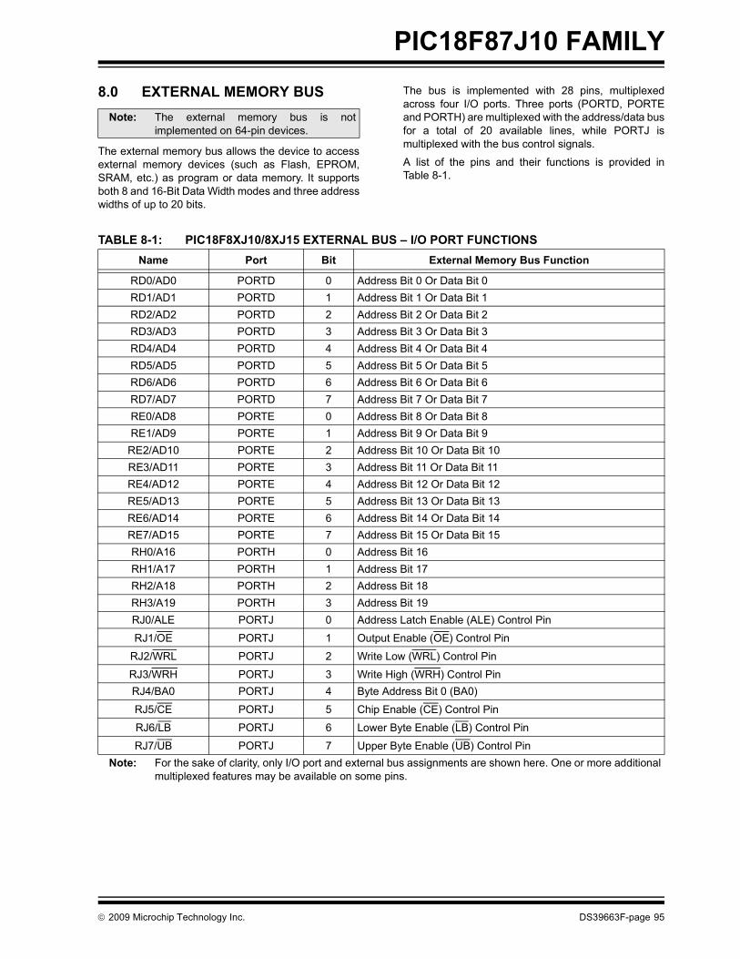
PIC18F87J10 FAMILY
8.0 EXTERNAL MEMORY BUS
The external memory bus allows the device to accessexternal memory devices (such as Flash, EPROM,SRAM, etc.) as program or data memory. It supportsboth 8 and 16-Bit Data Width modes and three addresswidths of up to 20 bits.
The bus is implemented with 28 pins, multiplexedacross four I/O ports. Three ports (PORTD, PORTEand PORTH) are multiplexed with the address/data busfor a total of 20 available lines, while PORTJ ismultiplexed with the bus control signals.
A list of the pins and their functions is provided inTable 8-1.
TABLE 8-1: PIC18F8XJ10/8XJ15 EXTERNAL BUS – I/O PORT FUNCTIONS
Note: The external memory bus is notimplemented on 64-pin devices.
Name Port Bit External Memory Bus Function
RD0/AD0 PORTD 0 Address Bit 0 Or Data Bit 0RD1/AD1 PORTD 1 Address Bit 1 Or Data Bit 1RD2/AD2 PORTD 2 Address Bit 2 Or Data Bit 2RD3/AD3 PORTD 3 Address Bit 3 Or Data Bit 3RD4/AD4 PORTD 4 Address Bit 4 Or Data Bit 4RD5/AD5 PORTD 5 Address Bit 5 Or Data Bit 5RD6/AD6 PORTD 6 Address Bit 6 Or Data Bit 6RD7/AD7 PORTD 7 Address Bit 7 Or Data Bit 7RE0/AD8 PORTE 0 Address Bit 8 Or Data Bit 8RE1/AD9 PORTE 1 Address Bit 9 Or Data Bit 9
RE2/AD10 PORTE 2 Address Bit 10 Or Data Bit 10RE3/AD11 PORTE 3 Address Bit 11 Or Data Bit 11RE4/AD12 PORTE 4 Address Bit 12 Or Data Bit 12RE5/AD13 PORTE 5 Address Bit 13 Or Data Bit 13RE6/AD14 PORTE 6 Address Bit 14 Or Data Bit 14RE7/AD15 PORTE 7 Address Bit 15 Or Data Bit 15RH0/A16 PORTH 0 Address Bit 16RH1/A17 PORTH 1 Address Bit 17RH2/A18 PORTH 2 Address Bit 18RH3/A19 PORTH 3 Address Bit 19RJ0/ALE PORTJ 0 Address Latch Enable (ALE) Control Pin
RJ1/OE PORTJ 1 Output Enable (OE) Control Pin
RJ2/WRL PORTJ 2 Write Low (WRL) Control Pin
RJ3/WRH PORTJ 3 Write High (WRH) Control PinRJ4/BA0 PORTJ 4 Byte Address Bit 0 (BA0)
RJ5/CE PORTJ 5 Chip Enable (CE) Control Pin
RJ6/LB PORTJ 6 Lower Byte Enable (LB) Control Pin
RJ7/UB PORTJ 7 Upper Byte Enable (UB) Control PinNote: For the sake of clarity, only I/O port and external bus assignments are shown here. One or more additional
multiplexed features may be available on some pins.
© 2009 Microchip Technology Inc. DS39663F-page 95

PIC18F87J10 FAMILY
8.1 External Memory Bus ControlThe operation of the interface is controlled by theMEMCON register (Register 8-1). This register isavailable in all program memory operating modesexcept Microcontroller mode. In this mode, the registeris disabled and cannot be written to.The EBDIS bit (MEMCON<7>) controls the operationof the bus and related port functions. Clearing EBDISenables the interface and disables the I/O functions ofthe ports, as well as any other functions multiplexed tothose pins. Setting the bit enables the I/O ports andother functions, but allows the interface to overrideeverything else on the pins when an external memoryoperation is required. By default, the external bus isalways enabled and disables all other I/O.
The operation of the EBDIS bit is also influenced by theprogram memory mode being used. This is discussedin more detail in Section 8.5 “Program MemoryModes and the External Memory Bus”.
The WAIT bits allow for the addition of wait states toexternal memory operations. The use of these bits isdiscussed in Section 8.3 “Wait States”.
The WM bits select the particular operating mode usedwhen the bus is operating in 16-Bit Data Width mode.These are discussed in more detail in Section 8.6“16-Bit Data Width Modes”. These bits have no effectwhen an 8-Bit Data Width mode is selected.
REGISTER 8-1: MEMCON: EXTERNAL MEMORY BUS CONTROL REGISTER
R/W-0 U-0 R/W-0 R/W-0 U-0 U-0 R/W-0 R/W-0EBDIS — WAIT1 WAIT0 — — WM1 WM0
bit 7 bit 0
Legend: S = Settable bitR = Readable bit W = Writable bit U = Unimplemented bit, read as ‘0’-n = Value at POR ‘1’ = Bit is set ‘0’ = Bit is cleared x = Bit is unknown
bit 7 EBDIS: External Bus Disable bit1 = External bus enabled when microcontroller accesses external memory; otherwise, all external bus
drivers are mapped as I/O ports0 = External bus always enabled, I/O ports are disabled
bit 6 Unimplemented: Read as ‘0’bit 5-4 WAIT<1:0>: Table Reads and Writes Bus Cycle Wait Count bits
11 = Table reads and writes will wait 0 TCY10 = Table reads and writes will wait 1 TCY01 = Table reads and writes will wait 2 TCY00 = Table reads and writes will wait 3 TCY
bit 3-2 Unimplemented: Read as ‘0bit 1-0 WM<1:0>: TBLWT Operation with 16-Bit Data Bus Width Select bits
1x = Word Write mode: TABLAT0 and TABLAT1 word output; WRH active when TABLAT1 written01 = Byte Select mode: TABLAT data copied on both MSB and LSB; WRH and (UB or LB) will activate00 = Byte Write mode: TABLAT data copied on both MSB and LSB; WRH or WRL will activate
DS39663F-page 96 © 2009 Microchip Technology Inc.

PIC18F87J10 FAMILY
8.2 Address and Data WidthThe PIC18F87J10 family of devices can be indepen-dently configured for different address and data widthson the same memory bus. Both address and data widthare set by Configuration bits in the CONFIG3L register.As Configuration bits, this means that these optionscan only be configured by programming the device andare not controllable in software.The BW bit selects an 8-bit or 16-bit data bus width.Setting this bit (default) selects a data width of 16 bits.
The EMB<1:0> bits determine both the programmemory operating mode and the address bus width.The available options are 20-bit, 16-bit and 12-bit, aswell as Microcontroller mode (external bus disabled).Selecting a 16-bit or 12-bit width makes a correspond-ing number of high-order lines available for I/Ofunctions. These pins are no longer affected by thesetting of the EBDIS bit. For example, selecting a16-Bit Addressing mode (EMB<1:0> = 01) disablesA<19:16> and allows PORTH<3:0> to function withoutinterruptions from the bus. Using the smaller addresswidths allows users to tailor the memory bus to the sizeof the external memory space for a particular designwhile freeing up pins for dedicated I/O operation.
Because the EMB bits have the effect of disabling pinsfor memory bus operations, it is important to alwaysselect an address width at least equal to the data width.If a 12-bit address width is used with a 16-bit datawidth, the upper four bits of data will not be available onthe bus.
All combinations of address and data widths requiremultiplexing of address and data information on thesame lines. The address and data multiplexing, as wellas I/O ports made available by the use of smalleraddress widths, are summarized in Table 8-2.
8.2.1 ADDRESS SHIFTING ON THE EXTERNAL BUS
By default, the address presented on the external busis the value of the PC. In practical terms, this meansthat addresses in the external memory device belowthe top of on-chip memory are unavailable to the micro-controller. To access these physical locations, the gluelogic between the microcontroller and the externalmemory must somehow translate addresses.
To simplify the interface, the external bus offers anextension of Extended Microcontroller mode thatautomatically performs address shifting. This feature iscontrolled by the EASHFT Configuration bit. Settingthis bit offsets addresses on the bus by the size of themicrocontroller’s on-chip program memory and setsthe bottom address at 0000h. This allows the device touse the entire range of physical addresses of theexternal memory.
8.2.2 21-BIT ADDRESSINGAs an extension of 20-bit address width operation, theexternal memory bus can also fully address a 2-Mbytememory space. This is done by using the Bus Addressbit 0 (BA0) control line as the Least Significant bit of theaddress. The UB and LB control signals may also beused with certain memory devices to select the upperand lower bytes within a 16-bit wide data word.
This addressing mode is available in both 8-Bit andcertain 16-Bit Data Width modes. Additional details areprovided in Section 8.6.3 “16-Bit Byte Select Mode”and Section 8.7 “8-Bit Mode”.
TABLE 8-2: ADDRESS AND DATA LINES FOR DIFFERENT ADDRESS AND DATA WIDTHS
Data Width Address WidthMultiplexed Data and Address Lines (and
Corresponding Ports)
Address Only Lines (and Corresponding Ports)
Ports Available for I/O
8-Bit
12-Bit
AD<7:0>(PORTD<7:0>)
AD<11:8>(PORTE<3:0>)
PORTE<7:4>,All of PORTH
16-Bit AD<15:8>(PORTE<7:0>) All of PORTH
20-BitA<19:16>, AD<15:8>
(PORTH<3:0>,PORTE<7:0>)
—
16-Bit16-Bit AD<15:0>
(PORTD<7:0>,PORTE<7:0>)
— All of PORTH
20-Bit A<19:16>(PORTH<3:0>) —
© 2009 Microchip Technology Inc. DS39663F-page 97
PIC18F87J10 FAMILY
8.3 Wait States While it may be assumed that external memory deviceswill operate at the microcontroller clock rate, this isoften not the case. In fact, many devices require longertimes to write or retrieve data than the time allowed bythe execution of table read or table write operations.To compensate for this, the external memory bus canbe configured to add a fixed delay to each table opera-tion using the bus. Wait states are enabled by settingthe WAIT Configuration bit. When enabled, the amountof delay is set by the WAIT<1:0> bits (MEMCON<5:4>).The delay is based on multiples of microcontrollerinstruction cycle time and are added following theinstruction cycle when the table operation is executed.The range is from no delay to 3 TCY (default value).
8.4 Port Pin Weak Pull-upsWith the exception of the upper address lines,A<19:16>, the pins associated with the externalmemory bus are equipped with weak pull-ups. Thepull-ups are controlled by the upper three bits of thePORTG register. They are named RDPU, REPU andRJPU and control pull-ups on PORTD, PORTE andPORTJ, respectively. Clearing one of these bitsenables the corresponding pull-ups for that port. Allpull-ups are disabled by default on all device Resets.
8.5 Program Memory Modes and the External Memory Bus
The PIC18F87J10 family of devices is capable ofoperating in one of two program memory modes, usingcombinations of on-chip and external program memory.The functions of the multiplexed port pins depend onthe program memory mode selected, as well as thesetting of the EBDIS bit.
In Microcontroller Mode, the bus is not active and thepins have their port functions only. Writes to theMEMCOM register are not permitted. The Reset valueof EBDIS (‘0’) is ignored and EMB pins behave as I/Oports.
In Extended Microcontroller Mode, the externalprogram memory bus shares I/O port functions on thepins. When the device is fetching or doing tableread/table write operations on the external programmemory space, the pins will have the external busfunction.
If the device is fetching and accessing internal programmemory locations only, the EBDIS control bit willchange the pins from external memory to I/O portfunctions. When EBDIS = 0, the pins function as theexternal bus. When EBDIS = 1, the pins function as I/Oports.
If the device fetches or accesses external memorywhile EBDIS = 1, the pins will switch to external bus. Ifthe EBDIS bit is set by a program executing from exter-nal memory, the action of setting the bit will be delayeduntil the program branches into the internal memory. Atthat time, the pins will change from external bus to I/Oports.
If the device is executing out of internal memory whenEBDIS = 0, the memory bus address/data and controlpins will not be active. They will go to a state where theactive address/data pins are tri-state; the CE, OE,WRH, WRL, UB and LB signals are ‘1’ and ALE andBA0 are ‘0’. Note that only those pins associated withthe current address width are forced to tri-state; theother pins continue to function as I/O. In the case of16-bit address width, for example, only AD<15:0>(PORTD and PORTE) are affected; A<19:16>(PORTH<3:0>) continue to function as I/O.
In all external memory modes, the bus takes priorityover any other peripherals that may share pins with it.This includes the Parallel Slave Port and serial commu-nications modules which would otherwise take priorityover the I/O port.
8.6 16-Bit Data Width ModesIn 16-Bit Data Width mode, the external memoryinterface can be connected to external memories inthree different configurations:
• 16-Bit Byte Write• 16-Bit Word Write• 16-Bit Byte Select
The configuration to be used is determined by theWM<1:0> bits in the MEMCON register(MEMCON<1:0>). These three different configurationsallow the designer maximum flexibility in using both8-bit and 16-bit devices with 16-bit data.
For all 16-bit modes, the Address Latch Enable (ALE)pin indicates that the address bits, AD<15:0>, are avail-able on the external memory interface bus. Followingthe address latch, the Output Enable signal (OE) willenable both bytes of program memory at once to forma 16-bit instruction word. The Chip Enable signal (CE)is active at any time that the microcontroller accessesexternal memory, whether reading or writing; it isinactive (asserted high) whenever the device is inSleep mode.
In Byte Select mode, JEDEC standard Flash memorieswill require BA0 for the byte address line and one I/Oline to select between Byte and Word mode. The other16-bit modes do not need BA0. JEDEC standard staticRAM memories will use the UB or LB signals for byteselection.
DS39663F-page 98 © 2009 Microchip Technology Inc.
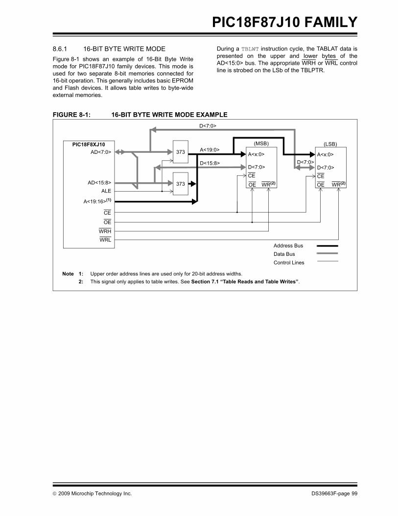
PIC18F87J10 FAMILY
8.6.1 16-BIT BYTE WRITE MODEFigure 8-1 shows an example of 16-Bit Byte Writemode for PIC18F87J10 family devices. This mode isused for two separate 8-bit memories connected for16-bit operation. This generally includes basic EPROMand Flash devices. It allows table writes to byte-wideexternal memories.During a TBLWT instruction cycle, the TABLAT data ispresented on the upper and lower bytes of theAD<15:0> bus. The appropriate WRH or WRL controlline is strobed on the LSb of the TBLPTR.
FIGURE 8-1: 16-BIT BYTE WRITE MODE EXAMPLE
AD<7:0>
A<19:16>(1)
ALE
D<15:8>
373 A<x:0>
D<7:0>
A<19:0>A<x:0>
D<7:0>
373
OE
WRH
OE OEWR(2) WR(2)CE CE
Note 1: Upper order address lines are used only for 20-bit address widths.2: This signal only applies to table writes. See Section 7.1 “Table Reads and Table Writes”.
WRL
D<7:0>
(LSB)(MSB)PIC18F8XJ10
D<7:0>
AD<15:8>
Address BusData BusControl Lines
CE
© 2009 Microchip Technology Inc. DS39663F-page 99

PIC18F87J10 FAMILY
8.6.2 16-BIT WORD WRITE MODEFigure 8-2 shows an example of 16-Bit Word Writemode for PIC18F65J10 devices. This mode is used forword-wide memories which include some of theEPROM and Flash type memories. This mode allowsopcode fetches and table reads from all forms of 16-bitmemory and table writes to any type of word-wideexternal memories. This method makes a distinctionbetween TBLWT cycles to even or odd addresses.During a TBLWT cycle to an even address(TBLPTR<0> = 0), the TABLAT data is transferred to aholding latch and the external address data bus istri-stated for the data portion of the bus cycle. No writesignals are activated.
During a TBLWT cycle to an odd address(TBLPTR<0> = 1), the TABLAT data is presented onthe upper byte of the AD<15:0> bus. The contents ofthe holding latch are presented on the lower byte of theAD<15:0> bus.
The WRH signal is strobed for each write cycle; theWRL pin is unused. The signal on the BA0 pin indicatesthe LSb of the TBLPTR, but it is left unconnected.Instead, the UB and LB signals are active to select bothbytes. The obvious limitation to this method is that thetable write must be done in pairs on a specific wordboundary to correctly write a word location.
FIGURE 8-2: 16-BIT WORD WRITE MODE EXAMPLE
AD<7:0>PIC18F8XJ10
AD<15:8>
ALE
373A<20:1>
373
OEWRH
A<19:16>(1)
A<x:0>
D<15:0>
OE WR(2)CE
D<15:0>
JEDEC Word EPROM Memory
Address BusData BusControl Lines
Note 1: Upper order address lines are used only for 20-bit address widths.2: This signal only applies to table writes. See Section 7.1 “Table Reads and Table Writes”.
CE
DS39663F-page 100 © 2009 Microchip Technology Inc.

PIC18F87J10 FAMILY
8.6.3 16-BIT BYTE SELECT MODEFigure 8-3 shows an example of 16-Bit Byte Selectmode. This mode allows table write operations toword-wide external memories with byte selectioncapability. This generally includes both word-wideFlash and SRAM devices.During a TBLWT cycle, the TABLAT data is presentedon the upper and lower byte of the AD<15:0> bus. TheWRH signal is strobed for each write cycle; the WRLpin is not used. The BA0 or UB/LB signals are used toselect the byte to be written, based on the LeastSignificant bit of the TBLPTR register.
Flash and SRAM devices use different control signalcombinations to implement Byte Select mode. JEDECstandard Flash memories require that a controller I/Oport pin be connected to the memory’s BYTE/WORDpin to provide the select signal. They also use the BA0signal from the controller as a byte address. JEDECstandard static RAM memories, on the other hand, usethe UB or LB signals to select the byte.
FIGURE 8-3: 16-BIT BYTE SELECT MODE EXAMPLE
AD<7:0>PIC18F8XJ10
AD<15:8>
ALE
373A<20:1>
373
OE
WRH
A<19:16>(2)
WRL
BA0
JEDEC WordA<x:1>
D<15:0>
A<20:1>
CE
D<15:0>
I/O
OE WR(1)A0BYTE/WORD
FLASH Memory
JEDEC WordA<x:1>
D<15:0>CED<15:0>
OE WR(1)LBUB
SRAM Memory
LBUB
138(3)
Address BusData BusControl Lines
Note 1: This signal only applies to table writes. See Section 7.1 “Table Reads and Table Writes”.2: Upper order address lines are used only for 20-bit address width.3: Demultiplexing is only required when multiple memory devices are accessed.
© 2009 Microchip Technology Inc. DS39663F-page 101

PIC18F87J10 FAMILY
8.6.4 16-BIT MODE TIMINGThe presentation of control signals on the externalmemory bus is different for the various operatingmodes. Typical signal timing diagrams are shown inFigure 8-4 and Figure 8-5.FIGURE 8-4: EXTERNAL MEMORY BUS TIMING FOR TBLRD (EXTENDED MICROCONTROLLER MODE)
FIGURE 8-5: EXTERNAL MEMORY BUS TIMING FOR SLEEP (EXTENDED MICROCONTROLLER MODE)
Q2Q1 Q3 Q4 Q2Q1 Q3 Q4 Q2Q1 Q3 Q4
A<19:16>
ALE
OE
AD<15:0>
CE
Opcode Fetch Opcode Fetch Opcode FetchTBLRD *
TBLRD Cycle 1
ADDLW 55hfrom 000100h
Q2Q1 Q3 Q4
0Ch
CF33h
TBLRD 92hfrom 199E67h
9256h
from 000104h
MemoryCycle
InstructionExecution INST(PC – 2) TBLRD Cycle 2
MOVLW 55hfrom 000102h
MOVLW
Q2Q1 Q3 Q4 Q2Q1 Q3 Q4
A<19:16>
ALE
OE
3AAAhAD<15:0>
00h 00h
CE
Opcode Fetch Opcode FetchSLEEP
SLEEP
from 007554h
Q1
Bus Inactive
0003h 3AABh 0E55h
MemoryCycle
InstructionExecution INST(PC – 2)
Sleep Mode, MOVLW 55h
from 007556h
DS39663F-page 102 © 2009 Microchip Technology Inc.

PIC18F87J10 FAMILY
8.7 8-Bit ModeIn 8-Bit Data Width mode, the external memory busoperates only in Multiplexed mode; that is, data sharesthe 8 Least Significant bits of the address bus.Figure 8-6 shows an example of 8-Bit Multiplexedmode for 80-pin devices. This mode is used for a single8-bit memory connected for 16-bit operation. Theinstructions will be fetched as two 8-bit bytes on ashared data/address bus. The two bytes are sequen-tially fetched within one instruction cycle (TCY).Therefore, the designer must choose external memorydevices according to timing calculations based on1/2 TCY (2 times the instruction rate). For proper mem-ory speed selection, glue logic propagation delay timesmust be considered, along with setup and hold times.
The Address Latch Enable (ALE) pin indicates that theaddress bits, AD<15:0>, are available on the externalmemory interface bus. The Output Enable signal (OE)
will enable one byte of program memory for a portion ofthe instruction cycle, then BA0 will change and thesecond byte will be enabled to form the 16-bit instruc-tion word. The Least Significant bit of the address, BA0,must be connected to the memory devices in thismode. The Chip Enable signal (CE) is active at anytime that the microcontroller accesses externalmemory, whether reading or writing. It is inactive(asserted high) whenever the device is in Sleep mode.
This generally includes basic EPROM and Flashdevices. It allows table writes to byte-wide externalmemories.
During a TBLWT instruction cycle, the TABLAT data ispresented on the upper and lower bytes of theAD<15:0> bus. The appropriate level of the BA0 controlline is strobed on the LSb of the TBLPTR.
FIGURE 8-6: 8-BIT MULTIPLEXED MODE EXAMPLE
AD<7:0>
A<19:16>(1)
ALE D<15:8>
373A<19:0>
A<x:1>
D<7:0>
OE
OE WR(2)
CE
Note 1: Upper order address bits are only used for 20-bit address width. The upper AD byte is used for all address widths except 8-bit.
2: This signal only applies to table writes. See Section 7.1 “Table Reads and Table Writes”.
WRL
D<7:0>
PIC18F8XJ10
AD<15:8>(1)
Address BusData BusControl Lines
CE
A0
BA0
© 2009 Microchip Technology Inc. DS39663F-page 103

PIC18F87J10 FAMILY
8.7.1 8-BIT MODE TIMINGThe presentation of control signals on the externalmemory bus is different for the various operatingmodes. Typical signal timing diagrams are shown inFigure 8-7 and Figure 8-8.FIGURE 8-7: EXTERNAL MEMORY BUS TIMING FOR TBLRD (EXTENDED MICROCONTROLLER MODE)
FIGURE 8-8: EXTERNAL MEMORY BUS TIMING FOR SLEEP (EXTENDED MICROCONTROLLER MODE)
Q2Q1 Q3 Q4 Q2Q1 Q3 Q4 Q2Q1 Q3 Q4
A<19:16>
ALE
OE
AD<7:0>
CE
Opcode Fetch Opcode Fetch Opcode FetchTBLRD *
TBLRD Cycle 1
ADDLW 55hfrom 000100h
Q2Q1 Q3 Q4
0Ch
33h
TBLRD 92hfrom 199E67h
92h
from 000104h
MemoryCycle
InstructionExecution INST(PC – 2) TBLRD Cycle 2
MOVLW 55hfrom 000102h
MOVLW
AD<15:8> CFh
Q2Q1 Q3 Q4 Q2Q1 Q3 Q4
A<19:16>
ALE
OE
AAhAD<7:0>
00h 00h
CE
Opcode Fetch Opcode FetchSLEEP
SLEEP
from 007554h
Q1
Bus Inactive
00h ABh 55h
MemoryCycle
InstructionExecution INST(PC – 2)
Sleep Mode, MOVLW 55h
from 007556h
AD<15:8> 3Ah 3Ah
03h 0Eh
BA0
DS39663F-page 104 © 2009 Microchip Technology Inc.

PIC18F87J10 FAMILY
8.8 Operation in Power-ManagedModesIn alternate power-managed Run modes, the externalbus continues to operate normally. If a clock sourcewith a lower speed is selected, bus operations will runat that speed. In these cases, excessive access timesfor the external memory may result if wait states havebeen enabled and added to external memory opera-tions. If operations in a lower power Run mode areanticipated, users should provide in their applicationsfor adjusting memory access times at the lower clockspeeds.
In Sleep and Idle modes, the microcontroller core doesnot need to access data; bus operations aresuspended. The state of the external bus is frozen, withthe address/data pins and most of the control pins hold-ing at the same state they were in when the mode wasinvoked. The only potential changes are the CE, LBand UB pins, which are held at logic high.
© 2009 Microchip Technology Inc. DS39663F-page 105

PIC18F87J10 FAMILY
NOTES:DS39663F-page 106 © 2009 Microchip Technology Inc.

PIC18F87J10 FAMILY
9.0 8 x 8 HARDWARE MULTIPLIER
9.1 IntroductionAll PIC18 devices include an 8 x 8 hardware multiplieras part of the ALU. The multiplier performs an unsignedoperation and yields a 16-bit result that is stored in theproduct register pair, PRODH:PRODL. The multiplier’soperation does not affect any flags in the STATUSregister.
Making multiplication a hardware operation allows it tobe completed in a single instruction cycle. This has theadvantages of higher computational throughput andreduced code size for multiplication algorithms andallows the PIC18 devices to be used in many applica-tions previously reserved for digital signal processors.A comparison of various hardware and softwaremultiply operations, along with the savings in memoryand execution time, is shown in Table 9-1.
9.2 OperationExample 9-1 shows the instruction sequence for an 8 x 8unsigned multiplication. Only one instruction is requiredwhen one of the arguments is already loaded in theWREG register.
Example 9-2 shows the sequence to do an 8 x 8 signedmultiplication. To account for the sign bits of the argu-ments, each argument’s Most Significant bit (MSb) istested and the appropriate subtractions are done.
EXAMPLE 9-1: 8 x 8 UNSIGNED MULTIPLY ROUTINE
EXAMPLE 9-2: 8 x 8 SIGNED MULTIPLY ROUTINE
TABLE 9-1: PERFORMANCE COMPARISON FOR VARIOUS MULTIPLY OPERATIONS
MOVF ARG1, W ; MULWF ARG2 ; ARG1 * ARG2 ->
; PRODH:PRODL
MOVF ARG1, W MULWF ARG2 ; ARG1 * ARG2 ->
; PRODH:PRODL BTFSC ARG2, SB ; Test Sign Bit SUBWF PRODH, F ; PRODH = PRODH
; - ARG1 MOVF ARG2, WBTFSC ARG1, SB ; Test Sign Bit SUBWF PRODH, F ; PRODH = PRODH
; - ARG2
Routine Multiply MethodProgramMemory(Words)
Cycles(Max)
Time
@ 40 MHz @ 10 MHz @ 4 MHz
8 x 8 unsignedWithout Hardware Multiply 13 69 6.9 μs 27.6 μs 69 μs
Hardware Multiply 1 1 100 ns 400 ns 1 μs
8 x 8 signedWithout Hardware Multiply 33 91 9.1 μs 36.4 μs 91 μs
Hardware Multiply 6 6 600 ns 2.4 μs 6 μs
16 x 16 unsignedWithout Hardware Multiply 21 242 24.2 μs 96.8 μs 242 μs
Hardware Multiply 28 28 2.8 μs 11.2 μs 28 μs
16 x 16 signedWithout Hardware Multiply 52 254 25.4 μs 102.6 μs 254 μs
Hardware Multiply 35 40 4.0 μs 16.0 μs 40 μs
© 2009 Microchip Technology Inc. DS39663F-page 107

PIC18F87J10 FAMILY
Example 9-3 shows the sequence to do a 16 x 16unsigned multiplication. Equation 9-1 shows thealgorithm that is used. The 32-bit result is stored in fourregisters (RES3:RES0).EQUATION 9-1: 16 x 16 UNSIGNED MULTIPLICATION ALGORITHM
EXAMPLE 9-3: 16 x 16 UNSIGNED MULTIPLY ROUTINE
Example 9-4 shows the sequence to do a 16 x 16signed multiply. Equation 9-2 shows the algorithmused. The 32-bit result is stored in four registers(RES3:RES0). To account for the sign bits of thearguments, the MSb for each argument pair is testedand the appropriate subtractions are done.
EQUATION 9-2: 16 x 16 SIGNED MULTIPLICATION ALGORITHM
EXAMPLE 9-4: 16 x 16 SIGNED MULTIPLY ROUTINE
RES3:RES0 = ARG1H:ARG1L • ARG2H:ARG2L= (ARG1H • ARG2H • 216) +
(ARG1H • ARG2L • 28) +(ARG1L • ARG2H • 28) +(ARG1L • ARG2L)
MOVF ARG1L, W MULWF ARG2L ; ARG1L * ARG2L->
; PRODH:PRODL MOVFF PRODH, RES1 ; MOVFF PRODL, RES0 ;
; MOVF ARG1H, W MULWF ARG2H ; ARG1H * ARG2H->
; PRODH:PRODL MOVFF PRODH, RES3 ; MOVFF PRODL, RES2 ;
; MOVF ARG1L, W MULWF ARG2H ; ARG1L * ARG2H->
; PRODH:PRODL MOVF PRODL, W ; ADDWF RES1, F ; Add cross MOVF PRODH, W ; products ADDWFC RES2, F ; CLRF WREG ; ADDWFC RES3, F ;
; MOVF ARG1H, W ; MULWF ARG2L ; ARG1H * ARG2L->
; PRODH:PRODL MOVF PRODL, W ; ADDWF RES1, F ; Add cross MOVF PRODH, W ; products ADDWFC RES2, F ; CLRF WREG ; ADDWFC RES3, F ;
RES3:RES0 = ARG1H:ARG1L • ARG2H:ARG2L= (ARG1H • ARG2H • 216) +
(ARG1H • ARG2L • 28) +(ARG1L • ARG2H • 28) +(ARG1L • ARG2L) +(-1 • ARG2H<7> • ARG1H:ARG1L • 216) +(-1 • ARG1H<7> • ARG2H:ARG2L • 216)
MOVF ARG1L, W MULWF ARG2L ; ARG1L * ARG2L ->
; PRODH:PRODL MOVFF PRODH, RES1 ; MOVFF PRODL, RES0 ;
; MOVF ARG1H, W MULWF ARG2H ; ARG1H * ARG2H ->
; PRODH:PRODL MOVFF PRODH, RES3 ; MOVFF PRODL, RES2 ;
; MOVF ARG1L, W MULWF ARG2H ; ARG1L * ARG2H ->
; PRODH:PRODL MOVF PRODL, W ; ADDWF RES1, F ; Add cross MOVF PRODH, W ; products ADDWFC RES2, F ; CLRF WREG ; ADDWFC RES3, F ;
; MOVF ARG1H, W ; MULWF ARG2L ; ARG1H * ARG2L ->
; PRODH:PRODL MOVF PRODL, W ; ADDWF RES1, F ; Add cross MOVF PRODH, W ; products ADDWFC RES2, F ; CLRF WREG ; ADDWFC RES3, F ;
; BTFSS ARG2H, 7 ; ARG2H:ARG2L neg? BRA SIGN_ARG1 ; no, check ARG1 MOVF ARG1L, W ; SUBWF RES2 ; MOVF ARG1H, W ; SUBWFB RES3
; SIGN_ARG1
BTFSS ARG1H, 7 ; ARG1H:ARG1L neg? BRA CONT_CODE ; no, done MOVF ARG2L, W ; SUBWF RES2 ; MOVF ARG2H, W ; SUBWFB RES3
; CONT_CODE :
DS39663F-page 108 © 2009 Microchip Technology Inc.

PIC18F87J10 FAMILY
10.0 INTERRUPTSMembers of the PIC18F87J10 family of devices havemultiple interrupt sources and an interrupt priorityfeature that allows most interrupt sources to beassigned a high-priority level or a low-priority level. Thehigh-priority interrupt vector is at 0008h and thelow-priority interrupt vector is at 0018h. High-priorityinterrupt events will interrupt any low-priority interruptsthat may be in progress.
There are thirteen registers which are used to controlinterrupt operation. These registers are:
• RCON• INTCON• INTCON2• INTCON3• PIR1, PIR2, PIR3• PIE1, PIE2, PIE3• IPR1, IPR2, IPR3
It is recommended that the Microchip header filessupplied with MPLAB® IDE be used for the symbolic bitnames in these registers. This allows theassembler/compiler to automatically take care of theplacement of these bits within the specified register.
In general, interrupt sources have three bits to controltheir operation. They are:
• Flag bit to indicate that an interrupt event occurred
• Enable bit that allows program execution to branch to the interrupt vector address when the flag bit is set
• Priority bit to select high priority or low priority
The interrupt priority feature is enabled by setting theIPEN bit (RCON<7>). When interrupt priority isenabled, there are two bits which enable interruptsglobally. Setting the GIEH bit (INTCON<7>) enables allinterrupts that have the priority bit set (high priority).Setting the GIEL bit (INTCON<6>) enables allinterrupts that have the priority bit cleared (low priority).When the interrupt flag, enable bit and appropriateglobal interrupt enable bit are set, the interrupt willvector immediately to address 0008h or 0018h,depending on the priority bit setting. Individualinterrupts can be disabled through their correspondingenable bits.
When the IPEN bit is cleared (default state), theinterrupt priority feature is disabled and interrupts arecompatible with PIC® mid-range devices. InCompatibility mode, the interrupt priority bits for eachsource have no effect. INTCON<6> is the PEIE bitwhich enables/disables all peripheral interrupt sources.INTCON<7> is the GIE bit which enables/disables allinterrupt sources. All interrupts branch to address0008h in Compatibility mode.
When an interrupt is responded to, the global interruptenable bit is cleared to disable further interrupts. If theIPEN bit is cleared, this is the GIE bit. If interrupt prioritylevels are used, this will be either the GIEH or GIEL bit.High-priority interrupt sources can interrupt alow-priority interrupt. Low-priority interrupts are notprocessed while high-priority interrupts are in progress.
The return address is pushed onto the stack and thePC is loaded with the interrupt vector address (0008hor 0018h). Once in the Interrupt Service Routine, thesource(s) of the interrupt can be determined by pollingthe interrupt flag bits. The interrupt flag bits must becleared in software before re-enabling interrupts toavoid recursive interrupts.
The “return from interrupt” instruction, RETFIE, exitsthe interrupt routine and sets the GIE bit (GIEH or GIELif priority levels are used) which re-enables interrupts.
For external interrupt events, such as the INTx pins orthe PORTB input change interrupt, the interrupt latencywill be three to four instruction cycles. The exactlatency is the same for one or two-cycle instructions.Individual interrupt flag bits are set regardless of thestatus of their corresponding enable bit or the GIE bit.
Note: Do not use the MOVFF instruction to modifyany of the interrupt control registers whileany interrupt is enabled. Doing so maycause erratic microcontroller behavior.
© 2009 Microchip Technology Inc. DS39663F-page 109
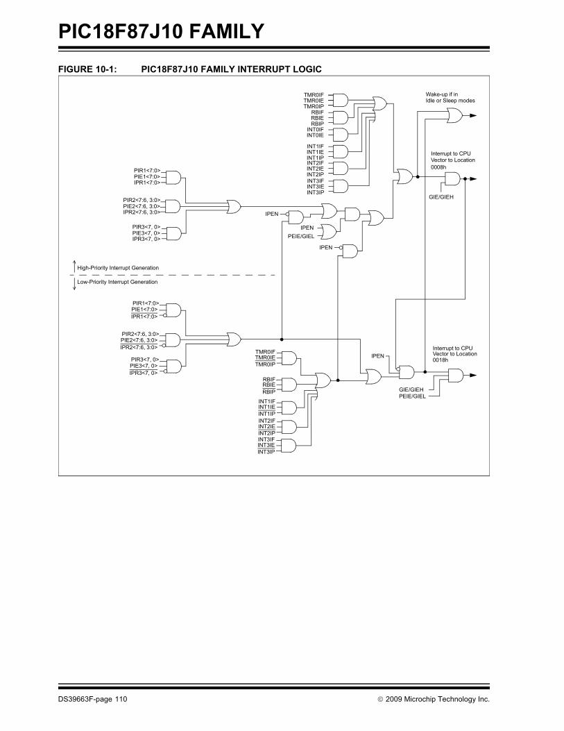
PIC18F87J10 FAMILY
FIGURE 10-1: PIC18F87J10 FAMILY INTERRUPT LOGICTMR0IE
GIE/GIEH
PEIE/GIEL
Wake-up if in
Interrupt to CPUVector to Location0008h
INT2IFINT2IEINT2IP
INT1IFINT1IEINT1IP
TMR0IFTMR0IETMR0IP
RBIFRBIERBIP
IPEN
TMR0IF
TMR0IP
INT1IFINT1IEINT1IPINT2IFINT2IEINT2IP
RBIFRBIERBIP
INT0IFINT0IE
PEIE/GIEL
Interrupt to CPUVector to Location
IPEN
IPEN
0018h
PIR1<7:0>PIE1<7:0> IPR1<7:0>
High-Priority Interrupt Generation
Low-Priority Interrupt Generation
Idle or Sleep modes
GIE/GIEH
INT3IFINT3IEINT3IP
INT3IFINT3IEINT3IP
PIR2<7:6, 3:0>PIE2<7:6, 3:0> IPR2<7:6, 3:0>
PIR3<7, 0>PIE3<7, 0> IPR3<7, 0>
PIR1<7:0>PIE1<7:0> IPR1<7:0>
PIR2<7:6, 3:0>PIE2<7:6, 3:0> IPR2<7:6, 3:0>
PIR3<7, 0>PIE3<7, 0> IPR3<7, 0>
IPEN
DS39663F-page 110 © 2009 Microchip Technology Inc.

PIC18F87J10 FAMILY
10.1 INTCON RegistersThe INTCON registers are readable and writableregisters which contain various enable, priority and flagbits.Note: Interrupt flag bits are set when an interruptcondition occurs regardless of the state ofits corresponding enable bit or the globalinterrupt enable bit. User software shouldensure the appropriate interrupt flag bitsare clear prior to enabling an interrupt.This feature allows for software polling.
REGISTER 10-1: INTCON: INTERRUPT CONTROL REGISTER
R/W-0 R/W-0 R/W-0 R/W-0 R/W-0 R/W-0 R/W-0 R/W-xGIE/GIEH PEIE/GIEL TMR0IE INT0IE RBIE TMR0IF INT0IF RBIF(1)
bit 7 bit 0
Legend:R = Readable bit W = Writable bit U = Unimplemented bit, read as ‘0’-n = Value at POR ‘1’ = Bit is set ‘0’ = Bit is cleared x = Bit is unknown
bit 7 GIE/GIEH: Global Interrupt Enable bitWhen IPEN = 0:1 = Enables all unmasked interrupts0 = Disables all interrupts When IPEN = 1:1 = Enables all high-priority interrupts 0 = Disables all interrupts
bit 6 PEIE/GIEL: Peripheral Interrupt Enable bitWhen IPEN = 0:1 = Enables all unmasked peripheral interrupts0 = Disables all peripheral interrupts When IPEN = 1:1 = Enables all low-priority peripheral interrupts0 = Disables all low-priority peripheral interrupts
bit 5 TMR0IE: TMR0 Overflow Interrupt Enable bit 1 = Enables the TMR0 overflow interrupt 0 = Disables the TMR0 overflow interrupt
bit 4 INT0IE: INT0 External Interrupt Enable bit 1 = Enables the INT0 external interrupt 0 = Disables the INT0 external interrupt
bit 3 RBIE: RB Port Change Interrupt Enable bit 1 = Enables the RB port change interrupt 0 = Disables the RB port change interrupt
bit 2 TMR0IF: TMR0 Overflow Interrupt Flag bit 1 = TMR0 register has overflowed (must be cleared in software) 0 = TMR0 register did not overflow
bit 1 INT0IF: INT0 External Interrupt Flag bit 1 = The INT0 external interrupt occurred (must be cleared in software) 0 = The INT0 external interrupt did not occur
bit 0 RBIF: RB Port Change Interrupt Flag bit(1) 1 = At least one of the RB<7:4> pins changed state (must be cleared in software) 0 = None of the RB<7:4> pins have changed state
Note 1: A mismatch condition will continue to set this bit. Reading PORTB will end the mismatch condition and allow the bit to be cleared.
© 2009 Microchip Technology Inc. DS39663F-page 111

PIC18F87J10 FAMILY
REGISTER 10-2: INTCON2: INTERRUPT CONTROL REGISTER 2
R/W-1 R/W-1 R/W-1 R/W-1 R/W-1 R/W-1 R/W-1 R/W-1
RBPU INTEDG0 INTEDG1 INTEDG2 INTEDG3 TMR0IP INT3IP RBIPbit 7 bit 0
Legend:R = Readable bit W = Writable bit U = Unimplemented bit, read as ‘0’-n = Value at POR ‘1’ = Bit is set ‘0’ = Bit is cleared x = Bit is unknown
bit 7 RBPU: PORTB Pull-up Enable bit 1 = All PORTB pull-ups are disabled 0 = PORTB pull-ups are enabled by individual port latch values
bit 6 INTEDG0: External Interrupt 0 Edge Select bit 1 = Interrupt on rising edge 0 = Interrupt on falling edge
bit 5 INTEDG1: External Interrupt 1 Edge Select bit 1 = Interrupt on rising edge 0 = Interrupt on falling edge
bit 4 INTEDG2: External Interrupt 2 Edge Select bit 1 = Interrupt on rising edge 0 = Interrupt on falling edge
bit 3 INTEDG3: External Interrupt 3 Edge Select bit 1 = Interrupt on rising edge 0 = Interrupt on falling edge
bit 2 TMR0IP: TMR0 Overflow Interrupt Priority bit 1 = High priority 0 = Low priority
bit 1 INT3IP: INT3 External Interrupt Priority bit1 = High priority 0 = Low priority
bit 0 RBIP: RB Port Change Interrupt Priority bit1 = High priority 0 = Low priority
Note: Interrupt flag bits are set when an interrupt condition occurs regardless of the state of its correspondingenable bit or the global interrupt enable bit. User software should ensure the appropriate interrupt flag bitsare clear prior to enabling an interrupt. This feature allows for software polling.
DS39663F-page 112 © 2009 Microchip Technology Inc.

PIC18F87J10 FAMILY
REGISTER 10-3: INTCON3: INTERRUPT CONTROL REGISTER 3
R/W-1 R/W-1 R/W-0 R/W-0 R/W-0 R/W-0 R/W-0 R/W-0INT2IP INT1IP INT3IE INT2IE INT1IE INT3IF INT2IF INT1IF
bit 7 bit 0
Legend:R = Readable bit W = Writable bit U = Unimplemented bit, read as ‘0’-n = Value at POR ‘1’ = Bit is set ‘0’ = Bit is cleared x = Bit is unknown
bit 7 INT2IP: INT2 External Interrupt Priority bit1 = High priority 0 = Low priority
bit 6 INT1IP: INT1 External Interrupt Priority bit1 = High priority 0 = Low priority
bit 5 INT3IE: INT3 External Interrupt Enable bit1 = Enables the INT3 external interrupt 0 = Disables the INT3 external interrupt
bit 4 INT2IE: INT2 External Interrupt Enable bit1 = Enables the INT2 external interrupt 0 = Disables the INT2 external interrupt
bit 3 INT1IE: INT1 External Interrupt Enable bit1 = Enables the INT1 external interrupt 0 = Disables the INT1 external interrupt
bit 2 INT3IF: INT3 External Interrupt Flag bit1 = The INT3 external interrupt occurred (must be cleared in software) 0 = The INT3 external interrupt did not occur
bit 1 INT2IF: INT2 External Interrupt Flag bit1 = The INT2 external interrupt occurred (must be cleared in software) 0 = The INT2 external interrupt did not occur
bit 0 INT1IF: INT1 External Interrupt Flag bit1 = The INT1 external interrupt occurred (must be cleared in software) 0 = The INT1 external interrupt did not occur
Note: Interrupt flag bits are set when an interrupt condition occurs regardless of the state of its correspondingenable bit or the global interrupt enable bit. User software should ensure the appropriate interrupt flag bitsare clear prior to enabling an interrupt. This feature allows for software polling.
© 2009 Microchip Technology Inc. DS39663F-page 113

PIC18F87J10 FAMILY
10.2 PIR RegistersThe PIR registers contain the individual flag bits for theperipheral interrupts. Due to the number of peripheralinterrupt sources, there are three Peripheral InterruptRequest (Flag) registers (PIR1, PIR2, PIR3).Note 1: Interrupt flag bits are set when an interruptcondition occurs regardless of the state ofits corresponding enable bit or the GlobalInterrupt Enable bit, GIE (INTCON<7>).
2: User software should ensure theappropriate interrupt flag bits are clearedprior to enabling an interrupt and afterservicing that interrupt.
REGISTER 10-4: PIR1: PERIPHERAL INTERRUPT REQUEST (FLAG) REGISTER 1
R/W-0 R/W-0 R-0 R-0 R/W-0 R/W-0 R/W-0 R/W-0PSPIF ADIF RC1IF TX1IF SSP1IF CCP1IF TMR2IF TMR1IF
bit 7 bit 0
Legend:R = Readable bit W = Writable bit U = Unimplemented bit, read as ‘0’-n = Value at POR ‘1’ = Bit is set ‘0’ = Bit is cleared x = Bit is unknown
bit 7 PSPIF: Parallel Slave Port Read/Write Interrupt Flag bit1 = A read or write operation has taken place (must be cleared in software) 0 = No read or write has occurred
bit 6 ADIF: A/D Converter Interrupt Flag bit 1 = An A/D conversion completed (must be cleared in software) 0 = The A/D conversion is not complete
bit 5 RC1IF: EUSART1 Receive Interrupt Flag bit 1 = The EUSART1 receive buffer, RCREGx, is full (cleared when RCREGx is read) 0 = The EUSART1 receive buffer is empty
bit 4 TX1IF: EUSART1 Transmit Interrupt Flag bit 1 = The EUSART1 transmit buffer, TXREGx, is empty (cleared when TXREGx is written) 0 = The EUSART1 transmit buffer is full
bit 3 SSP1IF: Master Synchronous Serial Port 1 Interrupt Flag bit 1 = The transmission/reception is complete (must be cleared in software)0 = Waiting to transmit/receive
bit 2 CCP1IF: ECCP1 Interrupt Flag bit Capture mode: 1 = A TMR1/TMR3 register capture occurred (must be cleared in software) 0 = No TMR1/TMR3 register capture occurred Compare mode: 1 = A TMR1/TMR3 register compare match occurred (must be cleared in software) 0 = No TMR1/TMR3 register compare match occurredPWM mode: Unused in this mode.
bit 1 TMR2IF: TMR2 to PR2 Match Interrupt Flag bit 1 = TMR2 to PR2 match occurred (must be cleared in software)0 = No TMR2 to PR2 match occurred
bit 0 TMR1IF: TMR1 Overflow Interrupt Flag bit 1 = TMR1 register overflowed (must be cleared in software)0 = TMR1 register did not overflow
DS39663F-page 114 © 2009 Microchip Technology Inc.
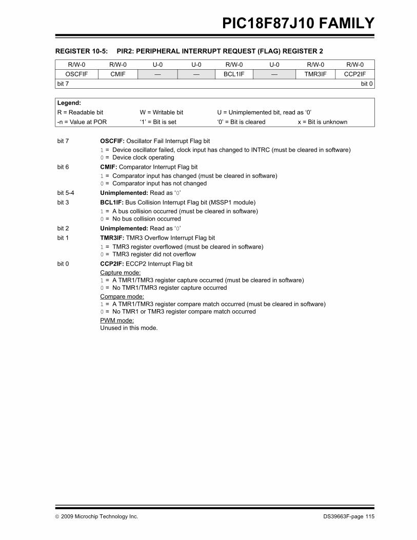
PIC18F87J10 FAMILY
REGISTER 10-5: PIR2: PERIPHERAL INTERRUPT REQUEST (FLAG) REGISTER 2R/W-0 R/W-0 U-0 U-0 R/W-0 U-0 R/W-0 R/W-0OSCFIF CMIF — — BCL1IF — TMR3IF CCP2IF
bit 7 bit 0
Legend:R = Readable bit W = Writable bit U = Unimplemented bit, read as ‘0’-n = Value at POR ‘1’ = Bit is set ‘0’ = Bit is cleared x = Bit is unknown
bit 7 OSCFIF: Oscillator Fail Interrupt Flag bit1 = Device oscillator failed, clock input has changed to INTRC (must be cleared in software)0 = Device clock operating
bit 6 CMIF: Comparator Interrupt Flag bit1 = Comparator input has changed (must be cleared in software)0 = Comparator input has not changed
bit 5-4 Unimplemented: Read as ‘0’bit 3 BCL1IF: Bus Collision Interrupt Flag bit (MSSP1 module)
1 = A bus collision occurred (must be cleared in software)0 = No bus collision occurred
bit 2 Unimplemented: Read as ‘0’bit 1 TMR3IF: TMR3 Overflow Interrupt Flag bit
1 = TMR3 register overflowed (must be cleared in software)0 = TMR3 register did not overflow
bit 0 CCP2IF: ECCP2 Interrupt Flag bitCapture mode: 1 = A TMR1/TMR3 register capture occurred (must be cleared in software) 0 = No TMR1/TMR3 register capture occurred Compare mode: 1 = A TMR1/TMR3 register compare match occurred (must be cleared in software) 0 = No TMR1 or TMR3 register compare match occurredPWM mode:Unused in this mode.
© 2009 Microchip Technology Inc. DS39663F-page 115
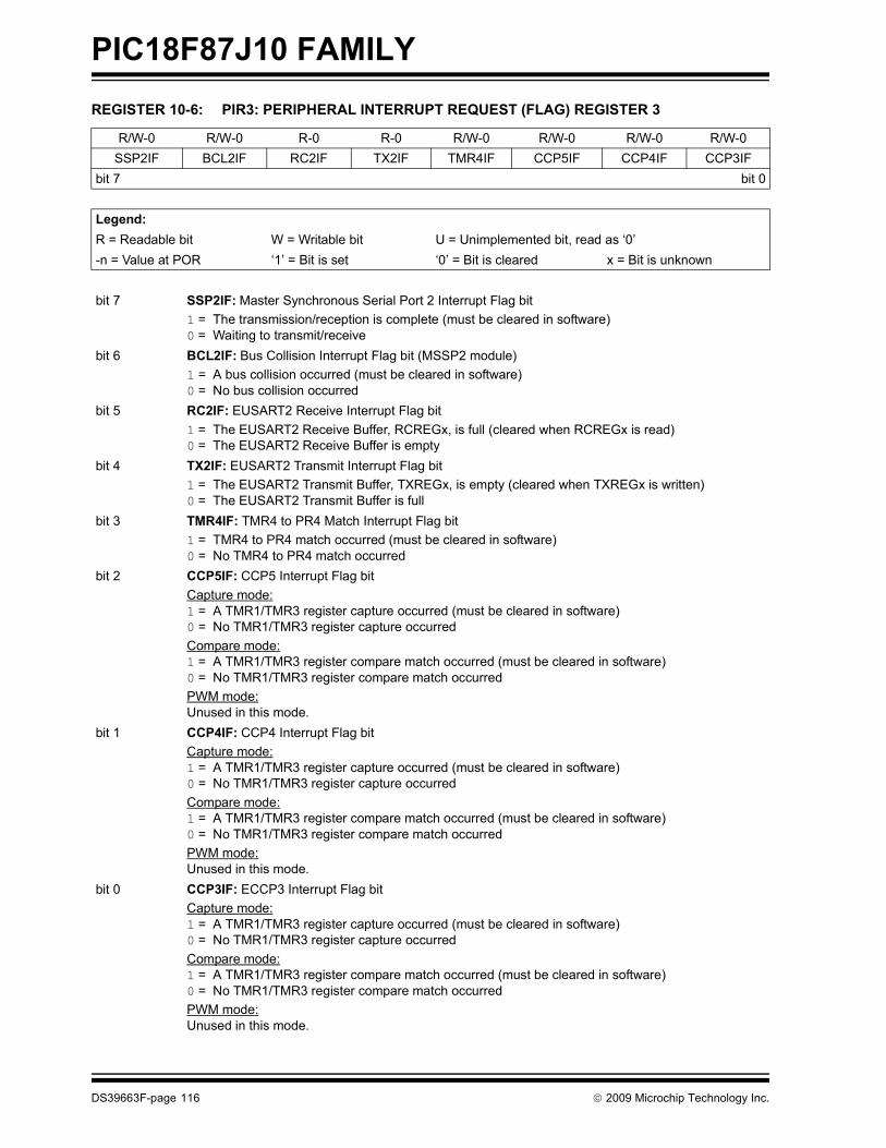
PIC18F87J10 FAMILY
REGISTER 10-6: PIR3: PERIPHERAL INTERRUPT REQUEST (FLAG) REGISTER 3R/W-0 R/W-0 R-0 R-0 R/W-0 R/W-0 R/W-0 R/W-0SSP2IF BCL2IF RC2IF TX2IF TMR4IF CCP5IF CCP4IF CCP3IF
bit 7 bit 0
Legend:R = Readable bit W = Writable bit U = Unimplemented bit, read as ‘0’-n = Value at POR ‘1’ = Bit is set ‘0’ = Bit is cleared x = Bit is unknown
bit 7 SSP2IF: Master Synchronous Serial Port 2 Interrupt Flag bit 1 = The transmission/reception is complete (must be cleared in software)0 = Waiting to transmit/receive
bit 6 BCL2IF: Bus Collision Interrupt Flag bit (MSSP2 module)1 = A bus collision occurred (must be cleared in software)0 = No bus collision occurred
bit 5 RC2IF: EUSART2 Receive Interrupt Flag bit 1 = The EUSART2 Receive Buffer, RCREGx, is full (cleared when RCREGx is read) 0 = The EUSART2 Receive Buffer is empty
bit 4 TX2IF: EUSART2 Transmit Interrupt Flag bit 1 = The EUSART2 Transmit Buffer, TXREGx, is empty (cleared when TXREGx is written) 0 = The EUSART2 Transmit Buffer is full
bit 3 TMR4IF: TMR4 to PR4 Match Interrupt Flag bit1 = TMR4 to PR4 match occurred (must be cleared in software) 0 = No TMR4 to PR4 match occurred
bit 2 CCP5IF: CCP5 Interrupt Flag bit Capture mode: 1 = A TMR1/TMR3 register capture occurred (must be cleared in software) 0 = No TMR1/TMR3 register capture occurred Compare mode: 1 = A TMR1/TMR3 register compare match occurred (must be cleared in software) 0 = No TMR1/TMR3 register compare match occurredPWM mode:Unused in this mode.
bit 1 CCP4IF: CCP4 Interrupt Flag bit Capture mode: 1 = A TMR1/TMR3 register capture occurred (must be cleared in software) 0 = No TMR1/TMR3 register capture occurred Compare mode: 1 = A TMR1/TMR3 register compare match occurred (must be cleared in software) 0 = No TMR1/TMR3 register compare match occurredPWM mode:Unused in this mode.
bit 0 CCP3IF: ECCP3 Interrupt Flag bit Capture mode: 1 = A TMR1/TMR3 register capture occurred (must be cleared in software) 0 = No TMR1/TMR3 register capture occurred Compare mode: 1 = A TMR1/TMR3 register compare match occurred (must be cleared in software) 0 = No TMR1/TMR3 register compare match occurredPWM mode:Unused in this mode.
DS39663F-page 116 © 2009 Microchip Technology Inc.

PIC18F87J10 FAMILY
10.3 PIE RegistersThe PIE registers contain the individual enable bits forthe peripheral interrupts. Due to the number ofperipheral interrupt sources, there are three PeripheralInterrupt Enable registers (PIE1, PIE2, PIE3). WhenIPEN = 0, the PEIE bit must be set to enable any ofthese peripheral interrupts.REGISTER 10-7: PIE1: PERIPHERAL INTERRUPT ENABLE REGISTER 1
R/W-0 R/W-0 R/W-0 R/W-0 R/W-0 R/W-0 R/W-0 R/W-0PSPIE ADIE RC1IE TX1IE SSP1IE CCP1IE TMR2IE TMR1IE
bit 7 bit 0
Legend:R = Readable bit W = Writable bit U = Unimplemented bit, read as ‘0’-n = Value at POR ‘1’ = Bit is set ‘0’ = Bit is cleared x = Bit is unknown
bit 7 PSPIE: Parallel Slave Port Read/Write Interrupt Enable bit1 = Enables the PSP read/write interrupt 0 = Disables the PSP read/write interrupt
bit 6 ADIE: A/D Converter Interrupt Enable bit 1 = Enables the A/D interrupt0 = Disables the A/D interrupt
bit 5 RC1IE: EUSART1 Receive Interrupt Enable bit 1 = Enables the EUSART1 receive interrupt 0 = Disables the EUSART1 receive interrupt
bit 4 TX1IE: EUSART1 Transmit Interrupt Enable bit 1 = Enables the EUSART1 transmit interrupt0 = Disables the EUSART1 transmit interrupt
bit 3 SSP1IE: Master Synchronous Serial Port 1 Interrupt Enable bit1 = Enables the MSSP1 interrupt 0 = Disables the MSSP1 interrupt
bit 2 CCP1IE: ECCP1 Interrupt Enable bit 1 = Enables the ECCP1 interrupt0 = Disables the ECCP1 interrupt
bit 1 TMR2IE: TMR2 to PR2 Match Interrupt Enable bit1 = Enables the TMR2 to PR2 match interrupt 0 = Disables the TMR2 to PR2 match interrupt
bit 0 TMR1IE: TMR1 Overflow Interrupt Enable bit 1 = Enables the TMR1 overflow interrupt0 = Disables the TMR1 overflow interrupt
© 2009 Microchip Technology Inc. DS39663F-page 117
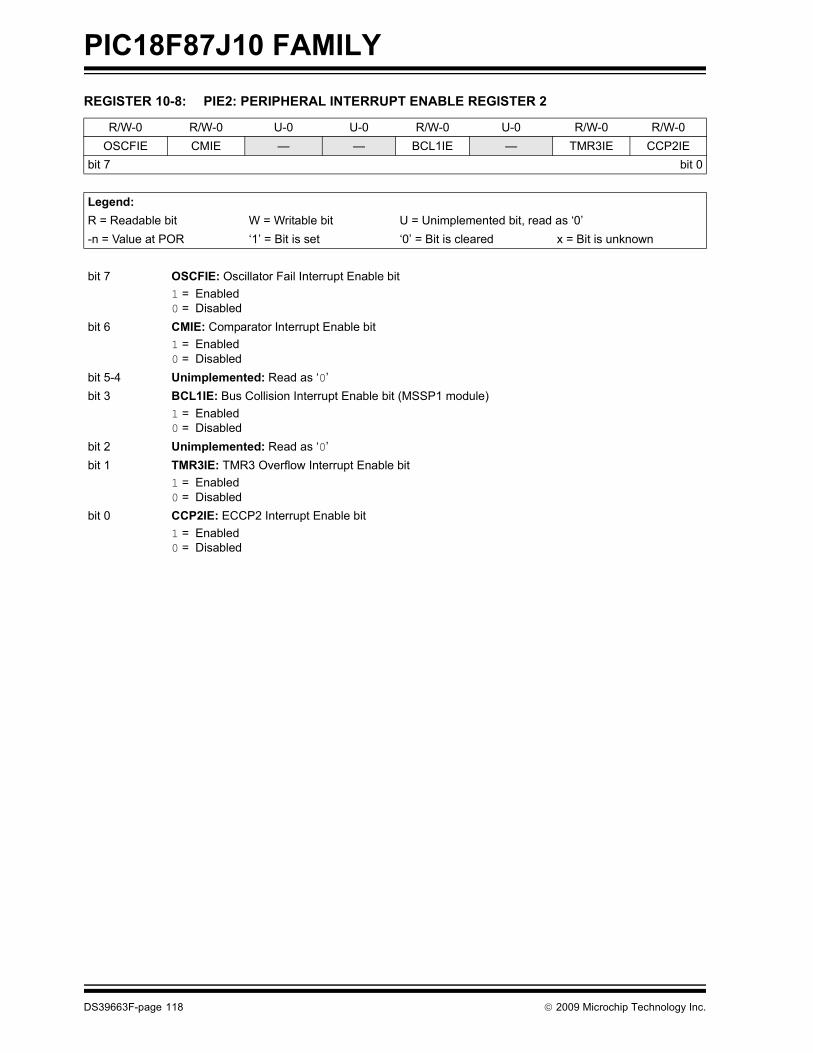
PIC18F87J10 FAMILY
REGISTER 10-8: PIE2: PERIPHERAL INTERRUPT ENABLE REGISTER 2R/W-0 R/W-0 U-0 U-0 R/W-0 U-0 R/W-0 R/W-0OSCFIE CMIE — — BCL1IE — TMR3IE CCP2IE
bit 7 bit 0
Legend:R = Readable bit W = Writable bit U = Unimplemented bit, read as ‘0’-n = Value at POR ‘1’ = Bit is set ‘0’ = Bit is cleared x = Bit is unknown
bit 7 OSCFIE: Oscillator Fail Interrupt Enable bit1 = Enabled0 = Disabled
bit 6 CMIE: Comparator Interrupt Enable bit1 = Enabled0 = Disabled
bit 5-4 Unimplemented: Read as ‘0’bit 3 BCL1IE: Bus Collision Interrupt Enable bit (MSSP1 module)
1 = Enabled0 = Disabled
bit 2 Unimplemented: Read as ‘0’bit 1 TMR3IE: TMR3 Overflow Interrupt Enable bit
1 = Enabled0 = Disabled
bit 0 CCP2IE: ECCP2 Interrupt Enable bit1 = Enabled0 = Disabled
DS39663F-page 118 © 2009 Microchip Technology Inc.
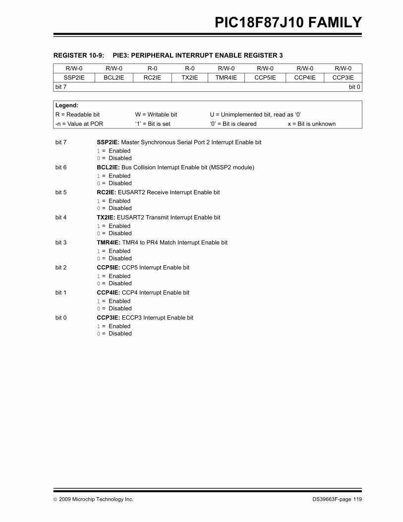
PIC18F87J10 FAMILY
REGISTER 10-9: PIE3: PERIPHERAL INTERRUPT ENABLE REGISTER 3R/W-0 R/W-0 R-0 R-0 R/W-0 R/W-0 R/W-0 R/W-0SSP2IE BCL2IE RC2IE TX2IE TMR4IE CCP5IE CCP4IE CCP3IE
bit 7 bit 0
Legend:R = Readable bit W = Writable bit U = Unimplemented bit, read as ‘0’-n = Value at POR ‘1’ = Bit is set ‘0’ = Bit is cleared x = Bit is unknown
bit 7 SSP2IE: Master Synchronous Serial Port 2 Interrupt Enable bit1 = Enabled0 = Disabled
bit 6 BCL2IE: Bus Collision Interrupt Enable bit (MSSP2 module)1 = Enabled0 = Disabled
bit 5 RC2IE: EUSART2 Receive Interrupt Enable bit 1 = Enabled0 = Disabled
bit 4 TX2IE: EUSART2 Transmit Interrupt Enable bit 1 = Enabled0 = Disabled
bit 3 TMR4IE: TMR4 to PR4 Match Interrupt Enable bit1 = Enabled0 = Disabled
bit 2 CCP5IE: CCP5 Interrupt Enable bit 1 = Enabled0 = Disabled
bit 1 CCP4IE: CCP4 Interrupt Enable bit 1 = Enabled0 = Disabled
bit 0 CCP3IE: ECCP3 Interrupt Enable bit 1 = Enabled0 = Disabled
© 2009 Microchip Technology Inc. DS39663F-page 119

PIC18F87J10 FAMILY
10.4 IPR RegistersThe IPR registers contain the individual priority bits forthe peripheral interrupts. Due to the number ofperipheral interrupt sources, there are three PeripheralInterrupt Priority registers (IPR1, IPR2, IPR3). Usingthe priority bits requires that the Interrupt PriorityEnable (IPEN) bit be set.REGISTER 10-10: IPR1: PERIPHERAL INTERRUPT PRIORITY REGISTER 1
R/W-1 R/W-1 R/W-1 R/W-1 R/W-1 R/W-1 R/W-1 R/W-1PSPIP ADIP RC1IP TX1IP SSP1IP CCP1IP TMR2IP TMR1IP
bit 7 bit 0
Legend:R = Readable bit W = Writable bit U = Unimplemented bit, read as ‘0’-n = Value at POR ‘1’ = Bit is set ‘0’ = Bit is cleared x = Bit is unknown
bit 7 PSPIP: Parallel Port Read/Write Interrupt Priority bit1 = High priority 0 = Low priority
bit 6 ADIP: A/D Converter Interrupt Priority bit1 = High priority 0 = Low priority
bit 5 RC1IP: EUSART1 Receive Interrupt Priority bit 1 = High priority 0 = Low priority
bit 4 TX1IP: EUSART1 Transmit Interrupt Priority bit
1 = High priority 0 = Low priority
bit 3 SSP1IP: Master Synchronous Serial Port 1 Interrupt Priority bit 1 = High priority 0 = Low priority
bit 2 CCP1IP: ECCP1 Interrupt Priority bit 1 = High priority 0 = Low priority
bit 1 TMR2IP: TMR2 to PR2 Match Interrupt Priority bit 1 = High priority 0 = Low priority
bit 0 TMR1IP: TMR1 Overflow Interrupt Priority bit 1 = High priority 0 = Low priority
DS39663F-page 120 © 2009 Microchip Technology Inc.
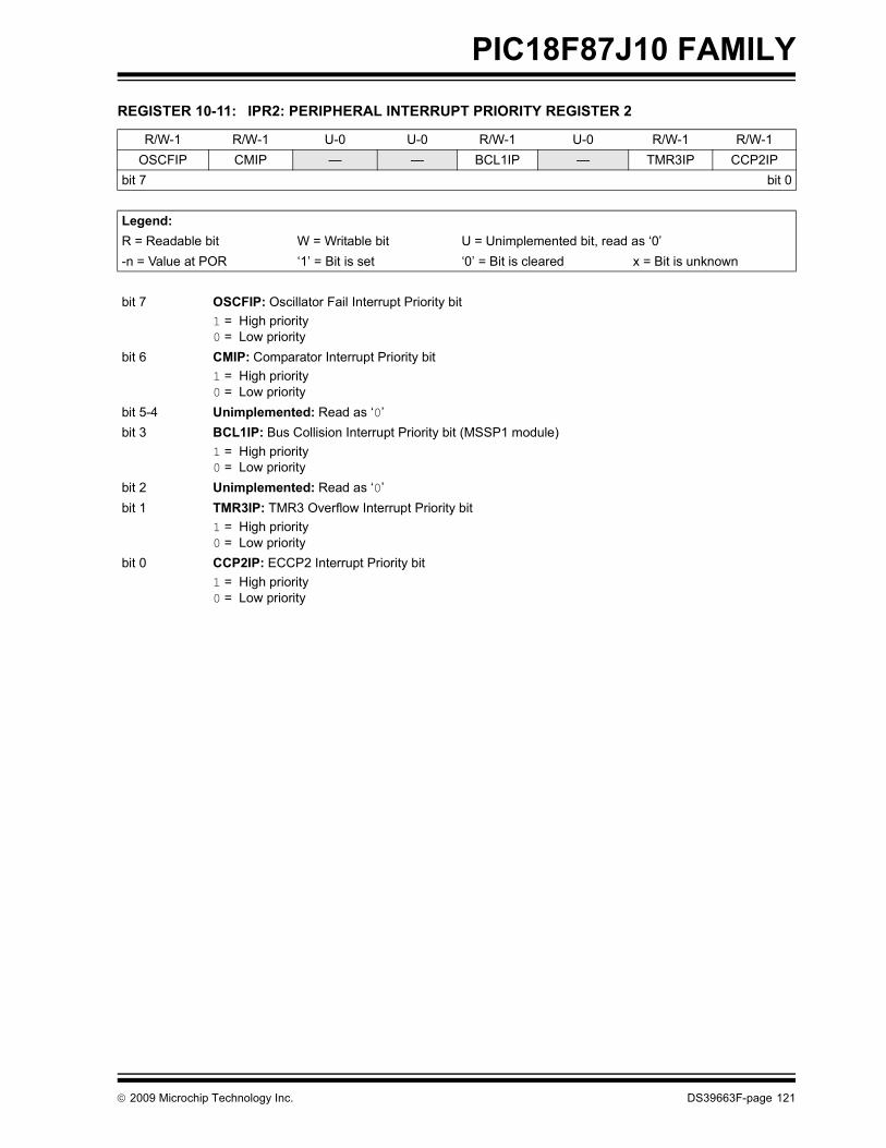
PIC18F87J10 FAMILY
REGISTER 10-11: IPR2: PERIPHERAL INTERRUPT PRIORITY REGISTER 2R/W-1 R/W-1 U-0 U-0 R/W-1 U-0 R/W-1 R/W-1OSCFIP CMIP — — BCL1IP — TMR3IP CCP2IP
bit 7 bit 0
Legend:R = Readable bit W = Writable bit U = Unimplemented bit, read as ‘0’-n = Value at POR ‘1’ = Bit is set ‘0’ = Bit is cleared x = Bit is unknown
bit 7 OSCFIP: Oscillator Fail Interrupt Priority bit1 = High priority0 = Low priority
bit 6 CMIP: Comparator Interrupt Priority bit1 = High priority0 = Low priority
bit 5-4 Unimplemented: Read as ‘0’bit 3 BCL1IP: Bus Collision Interrupt Priority bit (MSSP1 module)
1 = High priority0 = Low priority
bit 2 Unimplemented: Read as ‘0’bit 1 TMR3IP: TMR3 Overflow Interrupt Priority bit
1 = High priority0 = Low priority
bit 0 CCP2IP: ECCP2 Interrupt Priority bit1 = High priority0 = Low priority
© 2009 Microchip Technology Inc. DS39663F-page 121
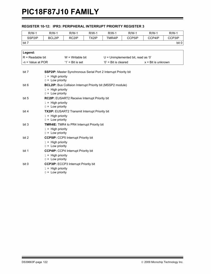
PIC18F87J10 FAMILY
REGISTER 10-12: IPR3: PERIPHERAL INTERRUPT PRIORITY REGISTER 3R/W-1 R/W-1 R/W-1 R/W-1 R/W-1 R/W-1 R/W-1 R/W-1SSP2IP BCL2IP RC2IP TX2IP TMR4IP CCP5IP CCP4IP CCP3IP
bit 7 bit 0
Legend:R = Readable bit W = Writable bit U = Unimplemented bit, read as ‘0’-n = Value at POR ‘1’ = Bit is set ‘0’ = Bit is cleared x = Bit is unknown
bit 7 SSP2IP: Master Synchronous Serial Port 2 Interrupt Priority bit1 = High priority0 = Low priority
bit 6 BCL2IP: Bus Collision Interrupt Priority bit (MSSP2 module)1 = High priority0 = Low priority
bit 5 RC2IP: EUSART2 Receive Interrupt Priority bit 1 = High priority0 = Low priority
bit 4 TX2IP: EUSART2 Transmit Interrupt Priority bit 1 = High priority0 = Low priority
bit 3 TMR4IE: TMR4 to PR4 Interrupt Priority bit1 = High priority0 = Low priority
bit 2 CCP5IP: CCP5 Interrupt Priority bit1 = High priority0 = Low priority
bit 1 CCP4IP: CCP4 Interrupt Priority bit1 = High priority0 = Low priority
bit 0 CCP3IP: ECCP3 Interrupt Priority bit1 = High priority0 = Low priority
DS39663F-page 122 © 2009 Microchip Technology Inc.

PIC18F87J10 FAMILY
10.5 RCON RegisterThe RCON register contains bits used to determine thecause of the last Reset or wake-up from Idle or Sleepmodes. RCON also contains the bit that enablesinterrupt priorities (IPEN).REGISTER 10-13: RCON: RESET CONTROL REGISTER
R/W-0 U-0 U-0 R/W-1 R-1 R-1 R/W-0 R/W-0
IPEN — — RI TO PD POR BORbit 7 bit 0
Legend:R = Readable bit W = Writable bit U = Unimplemented bit, read as ‘0’-n = Value at POR ‘1’ = Bit is set ‘0’ = Bit is cleared x = Bit is unknown
bit 7 IPEN: Interrupt Priority Enable bit 1 = Enable priority levels on interrupts0 = Disable priority levels on interrupts (PIC16CXXX Compatibility mode)
bit 6-5 Unimplemented: Read as ‘0’bit 4 RI: RESET Instruction Flag bit
For details of bit operation, see Register 4-1.bit 3 TO: Watchdog Time-out Flag bit
For details of bit operation, see Register 4-1.bit 2 PD: Power-Down Detection Flag bit
For details of bit operation, see Register 4-1.bit 1 POR: Power-on Reset Status bit(2)
For details of bit operation, see Register 4-1.bit 0 BOR: Brown-out Reset Status bit
For details of bit operation, see Register 4-1.
© 2009 Microchip Technology Inc. DS39663F-page 123
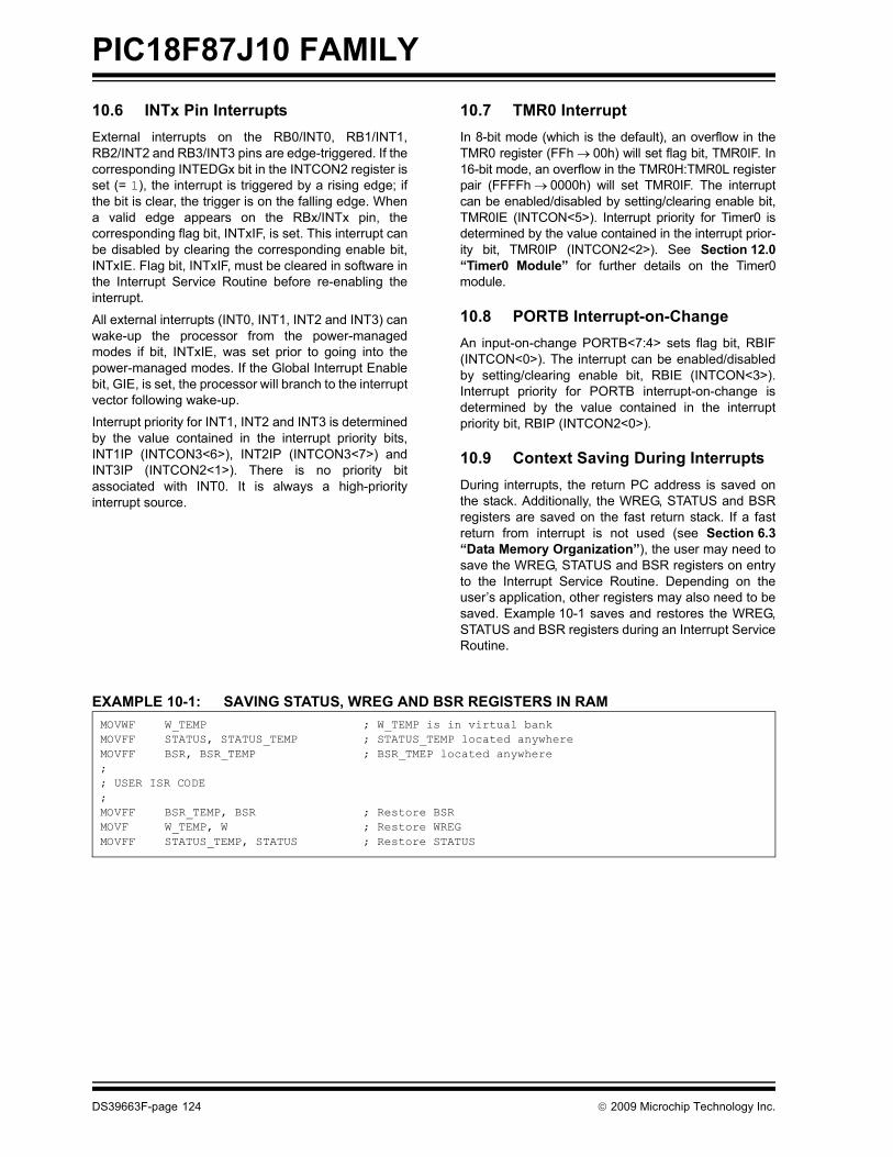
PIC18F87J10 FAMILY
10.6 INTx Pin InterruptsExternal interrupts on the RB0/INT0, RB1/INT1,RB2/INT2 and RB3/INT3 pins are edge-triggered. If thecorresponding INTEDGx bit in the INTCON2 register isset (= 1), the interrupt is triggered by a rising edge; ifthe bit is clear, the trigger is on the falling edge. Whena valid edge appears on the RBx/INTx pin, thecorresponding flag bit, INTxIF, is set. This interrupt canbe disabled by clearing the corresponding enable bit,INTxIE. Flag bit, INTxIF, must be cleared in software inthe Interrupt Service Routine before re-enabling theinterrupt.All external interrupts (INT0, INT1, INT2 and INT3) canwake-up the processor from the power-managedmodes if bit, INTxIE, was set prior to going into thepower-managed modes. If the Global Interrupt Enablebit, GIE, is set, the processor will branch to the interruptvector following wake-up.
Interrupt priority for INT1, INT2 and INT3 is determinedby the value contained in the interrupt priority bits,INT1IP (INTCON3<6>), INT2IP (INTCON3<7>) andINT3IP (INTCON2<1>). There is no priority bitassociated with INT0. It is always a high-priorityinterrupt source.
10.7 TMR0 InterruptIn 8-bit mode (which is the default), an overflow in theTMR0 register (FFh → 00h) will set flag bit, TMR0IF. In16-bit mode, an overflow in the TMR0H:TMR0L registerpair (FFFFh → 0000h) will set TMR0IF. The interruptcan be enabled/disabled by setting/clearing enable bit,TMR0IE (INTCON<5>). Interrupt priority for Timer0 isdetermined by the value contained in the interrupt prior-ity bit, TMR0IP (INTCON2<2>). See Section 12.0“Timer0 Module” for further details on the Timer0module.
10.8 PORTB Interrupt-on-ChangeAn input-on-change PORTB<7:4> sets flag bit, RBIF(INTCON<0>). The interrupt can be enabled/disabledby setting/clearing enable bit, RBIE (INTCON<3>).Interrupt priority for PORTB interrupt-on-change isdetermined by the value contained in the interruptpriority bit, RBIP (INTCON2<0>).
10.9 Context Saving During InterruptsDuring interrupts, the return PC address is saved onthe stack. Additionally, the WREG, STATUS and BSRregisters are saved on the fast return stack. If a fastreturn from interrupt is not used (see Section 6.3“Data Memory Organization”), the user may need tosave the WREG, STATUS and BSR registers on entryto the Interrupt Service Routine. Depending on theuser’s application, other registers may also need to besaved. Example 10-1 saves and restores the WREG,STATUS and BSR registers during an Interrupt ServiceRoutine.
EXAMPLE 10-1: SAVING STATUS, WREG AND BSR REGISTERS IN RAM MOVWF W_TEMP ; W_TEMP is in virtual bankMOVFF STATUS, STATUS_TEMP ; STATUS_TEMP located anywhereMOVFF BSR, BSR_TEMP ; BSR_TMEP located anywhere;; USER ISR CODE;MOVFF BSR_TEMP, BSR ; Restore BSRMOVF W_TEMP, W ; Restore WREGMOVFF STATUS_TEMP, STATUS ; Restore STATUS
DS39663F-page 124 © 2009 Microchip Technology Inc.

PIC18F87J10 FAMILY
11.0 I/O PORTSDepending on the device selected and featuresenabled, there are up to nine ports available. Somepins of the I/O ports are multiplexed with an alternatefunction from the peripheral features on the device. Ingeneral, when a peripheral is enabled, that pin may notbe used as a general purpose I/O pin.
Each port has three registers for its operation. Theseregisters are:
• TRIS register (Data Direction register)• PORT register (reads the levels on the pins of the
device)• LAT register (Output Latch register)
The Output Latch (LAT register) is useful forread-modify-write operations on the value that the I/Opins are driving.
A simplified model of a generic I/O port, without theinterfaces to other peripherals, is shown in Figure 11-1.
FIGURE 11-1: GENERIC I/O PORT OPERATION
11.1 I/O Port Pin CapabilitiesWhen developing an application, the capabilities of theport pins must be considered. Outputs on some pinshave higher output drive strength than others. Similarly,some pins can tolerate higher than VDD input levels.
11.1.1 PIN OUTPUT DRIVEThe output pin drive strengths vary for groups of pinsintended to meet the needs for a variety of applications.PORTB and PORTC are designed to drive higherloads, such as LEDs. The external memory interfaceports (PORTD, PORTE and PORTJ) are designed todrive medium loads. All other ports are designed forsmall loads, typically indication only. Table 11-1 sum-marizes the output capabilities. Refer to Section 27.0“Electrical Characteristics” for more details.
TABLE 11-1: OUTPUT DRIVE LEVELS
DataBus
WR LAT
WR TRIS
RD Port
Data Latch
TRIS Latch
RD TRIS
InputBuffer
I/O pin(1)
QD
CK
QD
CK
EN
Q D
EN
RD LAT
or Port
Port Drive Description
PORTA Minimum Intended for indication. PORTFPORTGPORTH(1)
PORTD Medium Sufficient drive levels for external memory interfacing as well as indication.
PORTEPORTJ(1)
PORTB High Suitable for direct LED drive levels.PORTC
Note 1: These ports are not available on 64-pin devices.
© 2009 Microchip Technology Inc. DS39663F-page 125

PIC18F87J10 FAMILY
11.1.2 INPUT PINS AND VOLTAGECONSIDERATIONSThe voltage tolerance of pins used as device inputs isdependent on the pin’s input function. Pins that are usedas digital only inputs are able to handle DC voltages upto 5.5V, a level typical for digital logic circuits. In contrast,pins that also have analog input functions of any kindcan only tolerate voltages up to VDD. Voltage excursionsbeyond VDD on these pins should be avoided.Table 11-2 summarizes the input capabilities. Refer toSection 27.0 “Electrical Characteristics” for moredetails.
TABLE 11-2: INPUT VOLTAGE LEVELS
11.2 PORTA, TRISA and LATA Registers
PORTA is a 6-bit wide, bidirectional port. The corre-sponding Data Direction register is TRISA. Setting aTRISA bit (= 1) will make the corresponding PORTA pinan input (i.e., put the corresponding output driver in ahigh-impedance mode). Clearing a TRISA bit (= 0) willmake the corresponding PORTA pin an output (i.e., putthe contents of the output latch on the selected pin).
Reading the PORTA register reads the status of thepins, whereas writing to it, will write to the port latch.
The Output Latch register (LATA) is also memorymapped. Read-modify-write operations on the LATAregister read and write the latched output value forPORTA.
The RA4 pin is multiplexed with the Timer0 moduleclock input to become the RA4/T0CKI pin. The otherPORTA pins are multiplexed with the analog VREF+ andVREF- inputs. The operation of pins RA<5:0> as A/DConverter inputs is selected by clearing or setting thePCFG<3:0> control bits in the ADCON1 register.
The RA4/T0CKI pin is a Schmitt Trigger input. All otherPORTA pins have TTL input levels and full CMOSoutput drivers.
The TRISA register controls the direction of the PORTApins, even when they are being used as analog inputs.The user must ensure the bits in the TRISA register aremaintained set when using them as analog inputs.
EXAMPLE 11-1: INITIALIZING PORTA
Port or Pin Tolerated Input Description
PORTA<5:0> VDD Only VDD input levels tolerated.PORTC<1:0>
PORTF<6:1>PORTH<7:4>(1)
PORTB<7:0> 5.5V Tolerates input levels above VDD, useful for most standard logic.
PORTC<7:2>PORTD<7:0>PORTE<7:0>PORTF<7>PORTG<4:0>PORTH<3:0>(1)
PORTJ<7:0>(1)
Note 1: These ports are not available on 64-pin devices.
Note: RA5 and RA<3:0> are configured asanalog inputs on any Reset and are readas ‘0’. RA4 is configured as a digital input.
CLRF PORTA ; Initialize PORTA by; clearing output; data latches
CLRF LATA ; Alternate method; to clear output; data latches
MOVLW 07h ; Configure A/D MOVWF ADCON1 ; for digital inputsMOVWF 07h ; Configure comparatorsMOVWF CMCON ; for digital inputMOVLW 0CFh ; Value used to
; initialize data ; direction
MOVWF TRISA ; Set RA<3:0> as inputs; RA<5:4> as outputs
DS39663F-page 126 © 2009 Microchip Technology Inc.
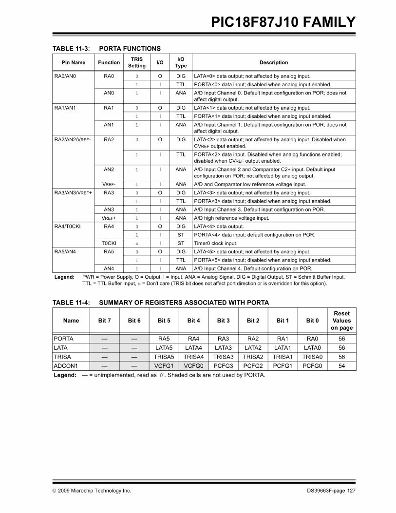
PIC18F87J10 FAMILY
TABLE 11-3: PORTA FUNCTIONSTABLE 11-4: SUMMARY OF REGISTERS ASSOCIATED WITH PORTA
Pin Name Function TRIS Setting I/O I/O
Type Description
RA0/AN0 RA0 0 O DIG LATA<0> data output; not affected by analog input.1 I TTL PORTA<0> data input; disabled when analog input enabled.
AN0 1 I ANA A/D Input Channel 0. Default input configuration on POR; does not affect digital output.
RA1/AN1 RA1 0 O DIG LATA<1> data output; not affected by analog input.1 I TTL PORTA<1> data input; disabled when analog input enabled.
AN1 1 I ANA A/D Input Channel 1. Default input configuration on POR; does not affect digital output.
RA2/AN2/VREF- RA2 0 O DIG LATA<2> data output; not affected by analog input. Disabled when CVREF output enabled.
1 I TTL PORTA<2> data input. Disabled when analog functions enabled; disabled when CVREF output enabled.
AN2 1 I ANA A/D Input Channel 2 and Comparator C2+ input. Default input configuration on POR; not affected by analog output.
VREF- 1 I ANA A/D and Comparator low reference voltage input. RA3/AN3/VREF+ RA3 0 O DIG LATA<3> data output; not affected by analog input.
1 I TTL PORTA<3> data input; disabled when analog input enabled.AN3 1 I ANA A/D Input Channel 3. Default input configuration on POR.
VREF+ 1 I ANA A/D high reference voltage input.RA4/T0CKI RA4 0 O DIG LATA<4> data output.
1 I ST PORTA<4> data input; default configuration on POR.T0CKI x I ST Timer0 clock input.
RA5/AN4 RA5 0 O DIG LATA<5> data output; not affected by analog input.1 I TTL PORTA<5> data input; disabled when analog input enabled.
AN4 1 I ANA A/D Input Channel 4. Default configuration on POR.Legend: PWR = Power Supply, O = Output, I = Input, ANA = Analog Signal, DIG = Digital Output, ST = Schmitt Buffer Input,
TTL = TTL Buffer Input, x = Don’t care (TRIS bit does not affect port direction or is overridden for this option).
Name Bit 7 Bit 6 Bit 5 Bit 4 Bit 3 Bit 2 Bit 1 Bit 0Reset Values
on page
PORTA — — RA5 RA4 RA3 RA2 RA1 RA0 56LATA — — LATA5 LATA4 LATA3 LATA2 LATA1 LATA0 56TRISA — — TRISA5 TRISA4 TRISA3 TRISA2 TRISA1 TRISA0 56ADCON1 — — VCFG1 VCFG0 PCFG3 PCFG2 PCFG1 PCFG0 54Legend: — = unimplemented, read as ‘0’. Shaded cells are not used by PORTA.
© 2009 Microchip Technology Inc. DS39663F-page 127

PIC18F87J10 FAMILY
11.3 PORTB, TRISB andLATB RegistersPORTB is an 8-bit wide, bidirectional port. The corre-sponding Data Direction register is TRISB. Setting aTRISB bit (= 1) will make the corresponding PORTBpin an input (i.e., put the corresponding output driver ina high-impedance mode). Clearing a TRISB bit (= 0)will make the corresponding PORTB pin an output (i.e.,put the contents of the output latch on the selected pin).All pins on PORTB are digital only and tolerate voltagesup to 5.5V.
The Output Latch register (LATB) is also memorymapped. Read-modify-write operations on the LATBregister read and write the latched output value forPORTB.
EXAMPLE 11-2: INITIALIZING PORTB
Each of the PORTB pins has a weak internal pull-up. Asingle control bit can turn on all the pull-ups. This isperformed by clearing bit, RBPU (INTCON2<7>). Theweak pull-up is automatically turned off when the portpin is configured as an output. The pull-ups aredisabled on a Power-on Reset.
Four of the PORTB pins (RB<7:4>) have aninterrupt-on-change feature. Only pins configured asinputs can cause this interrupt to occur (i.e., anyRB<7:4> pin configured as an output is excluded fromthe interrupt-on-change comparison). The input pins (ofRB<7:4>) are compared with the old value latched onthe last read of PORTB. The “mismatch” outputs ofRB<7:4> are ORed together to generate the RB PortChange Interrupt with Flag bit, RBIF (INTCON<0>).
This interrupt can wake the device frompower-managed modes. The user, in the InterruptService Routine, can clear the interrupt in the followingmanner:
a) Any read or write of PORTB (except with theMOVFF (ANY), PORTB instruction). This willend the mismatch condition.
b) Clear flag bit, RBIF.
A mismatch condition will continue to set flag bit, RBIF.Reading PORTB will end the mismatch condition andallow flag bit, RBIF, to be cleared.
The interrupt-on-change feature is recommended forwake-up on key depression operation and operationswhere PORTB is only used for the interrupt-on-changefeature. Polling of PORTB is not recommended whileusing the interrupt-on-change feature.
For 80-pin devices, RB3 can be configured as thealternate peripheral pin for the ECCP2 module andEnhanced PWM Output 2A by clearing the CCP2MXConfiguration bit. This applies only to 80-pin devicesoperating in Extended Microcontroller mode. If thedevice is in Microcontroller mode, the alternateassignment for ECCP2 is RE7. As with other ECCP2configurations, the user must ensure that the TRISB<3>bit is set appropriately for the intended operation.
CLRF PORTB ; Initialize PORTB by; clearing output; data latches
CLRF LATB ; Alternate method; to clear output; data latches
MOVLW 0CFh ; Value used to; initialize data ; direction
MOVWF TRISB ; Set RB<3:0> as inputs; RB<5:4> as outputs; RB<7:6> as inputs
DS39663F-page 128 © 2009 Microchip Technology Inc.

PIC18F87J10 FAMILY
TABLE 11-5: PORTB FUNCTIONSPin Name Function TRIS Setting I/O I/O
Type Description
RB0/INT0/FLT0 RB0 0 O DIG LATB<0> data output.
1 I TTL PORTB<0> data input; weak pull-up when RBPU bit is cleared.INT0 1 I ST External Interrupt 0 input.FLT0 1 I ST Enhanced PWM Fault input (ECCP1 module); enabled in software.
RB1/INT1 RB1 0 O DIG LATB<1> data output.
1 I TTL PORTB<1> data input; weak pull-up when RBPU bit is cleared.INT1 1 I ST External Interrupt 1 input.
RB2/INT2 RB2 0 O DIG LATB<2> data output.
1 I TTL PORTB<2> data input; weak pull-up when RBPU bit is cleared.INT2 1 I ST External Interrupt 2 input.
RB3/INT3/ECCP2/P2A
RB3 0 O DIG LATB<3> data output.
1 I TTL PORTB<3> data input; weak pull-up when RBPU bit is cleared.INT3 1 I ST External Interrupt 3 input.
ECCP2(1) 0 O DIG CCP2 compare output and CCP2 PWM output; takes priority over port data.1 I ST CCP2 capture input.
P2A(1) 0 O DIG ECCP2 Enhanced PWM output, Channel A. May be configured for tri-state during Enhanced PWM shutdown events. Takes priority over port data.
RB4/KBI0 RB4 0 O DIG LATB<4> data output.
1 I TTL PORTB<4> data input; weak pull-up when RBPU bit is cleared.KBI0 I TTL Interrupt-on-pin change.
RB5/KBI1 RB5 0 O DIG LATB<5> data output.
1 I TTL PORTB<5> data input; weak pull-up when RBPU bit is cleared.KBI1 I TTL Interrupt-on-pin change.
RB6/KBI2/PGC RB6 0 O DIG LATB<6> data output.
1 I TTL PORTB<6> data input; weak pull-up when RBPU bit is cleared.KBI2 1 I TTL Interrupt-on-pin change.PGC x I ST Serial execution (ICSP™) clock input for ICSP and ICD operation.(2)
RB7/KBI3/PGD RB7 0 O DIG LATB<7> data output.
1 I TTL PORTB<7> data input; weak pull-up when RBPU bit is cleared.KBI3 1 I TTL Interrupt-on-pin change.PGD x O DIG Serial execution data output for ICSP and ICD operation.(2)
x I ST Serial execution data input for ICSP and ICD operation.(2)
Legend: PWR = Power Supply, O = Output, I = Input, ANA = Analog Signal, DIG = Digital Output, ST = Schmitt Buffer Input, TTL = TTL Buffer Input, x = Don’t care (TRIS bit does not affect port direction or is overridden for this option).
Note 1: Alternate assignment for ECCP2/P2A when the CCP2MX Configuration bit is cleared (Extended Microcontroller mode, 80-pin devices only); default assignment is RC1.
2: All other pin functions are disabled when ICSP or ICD are enabled.
© 2009 Microchip Technology Inc. DS39663F-page 129

PIC18F87J10 FAMILY
TABLE 11-6: SUMMARY OF REGISTERS ASSOCIATED WITH PORTBName Bit 7 Bit 6 Bit 5 Bit 4 Bit 3 Bit 2 Bit 1 Bit 0Reset Values
on page
PORTB RB7 RB6 RB5 RB4 RB3 RB2 RB1 RB0 56LATB LATB7 LATB6 LATB5 LATB4 LATB3 LATB2 LATB1 LATB0 56TRISB TRISB7 TRISB6 TRISB5 TRISB4 TRISB3 TRISB2 TRISB1 TRISB0 56INTCON GIE/GIEH PEIE/GIEL TMR0IE INT0IE RBIE TMR0IF INT0IF RBIF 53
INTCON2 RBPU INTEDG0 INTEDG1 INTEDG2 INTEDG3 TMR0IP INT3IP RBIP 53INTCON3 INT2IP INT1IP INT3IE INT2IE INT1IE INT3IF INT2IF INT1IF 53Legend: Shaded cells are not used by PORTB.
DS39663F-page 130 © 2009 Microchip Technology Inc.

PIC18F87J10 FAMILY
11.4 PORTC, TRISC andLATC RegistersPORTC is an 8-bit wide, bidirectional port. The corre-sponding Data Direction register is TRISC. Setting aTRISC bit (= 1) will make the corresponding PORTCpin an input (i.e., put the corresponding output driver ina high-impedance mode). Clearing a TRISC bit (= 0)will make the corresponding PORTC pin an output (i.e.,put the contents of the output latch on the selected pin).Only PORTC pins, RC2 through RC7, are digital onlypins and can tolerate input voltages up to 5.5V.
The Output Latch register (LATC) is also memorymapped. Read-modify-write operations on the LATCregister read and write the latched output value forPORTC.
PORTC is multiplexed with several peripheral functions(Table 11-7). The pins have Schmitt Trigger inputbuffers. RC1 is normally configured by Configurationbit, CCP2MX, as the default peripheral pin for theECCP2 module and enhanced PWM output, P2A(default state, CCP2MX = 1).
When enabling peripheral functions, care should betaken in defining TRIS bits for each PORTC pin. Someperipherals override the TRIS bit to make a pin an output,while other peripherals override the TRIS bit to make apin an input. The user should refer to the correspondingperipheral section for the correct TRIS bit settings.
The contents of the TRISC register are affected byperipheral overrides. Reading TRISC always returnsthe current contents, even though a peripheral devicemay be overriding one or more of the pins.
EXAMPLE 11-3: INITIALIZING PORTC
Note: These pins are configured as digital inputson any device Reset.
CLRF PORTC ; Initialize PORTC by; clearing output; data latches
CLRF LATC ; Alternate method; to clear output; data latches
MOVLW 0CFh ; Value used to ; initialize data ; direction
MOVWF TRISC ; Set RC<3:0> as inputs; RC<5:4> as outputs; RC<7:6> as inputs
© 2009 Microchip Technology Inc. DS39663F-page 131

PIC18F87J10 FAMILY
TABLE 11-7: PORTC FUNCTIONSPin Name Function TRIS Setting I/O I/O Type Description
RC0/T1OSO/T13CKI
RC0 0 O DIG LATC<0> data output.1 I ST PORTC<0> data input.
T1OSO x O ANA Timer1 oscillator output; enabled when Timer1 oscillator enabled. Disables digital I/O.
T13CKI 1 I ST Timer1/Timer3 counter input.RC1/T1OSI/ECCP2/P2A
RC1 0 O DIG LATC<1> data output.1 I ST PORTC<1> data input.
T1OSI x I ANA Timer1 oscillator input; enabled when Timer1 oscillator enabled. Disables digital I/O.
ECCP2(1) 0 O DIG CCP2 compare output and CCP2 PWM output; takes priority over port data.1 I ST CCP2 capture input.
P2A(1) 0 O DIG ECCP2 Enhanced PWM output, Channel A. May be configured for tri-state during Enhanced PWM shutdown events. Takes priority over port data.
RC2/ECCP1/P1A
RC2 0 O DIG LATC<2> data output.1 I ST PORTC<2> data input.
ECCP1 0 O DIG CCP1 compare output and CCP1 PWM output; takes priority over port data.1 I ST CCP1 capture input.
P1A 0 O DIG ECCP1 Enhanced PWM output, Channel A. May be configured for tri-state during Enhanced PWM shutdown events. Takes priority over port data.
RC3/SCK1/SCL1
RC3 0 O DIG LATC<3> data output.1 I ST PORTC<3> data input.
SCK1 0 O DIG SPI clock output (MSSP1 module); takes priority over port data.1 I ST SPI clock input (MSSP1 module).
SCL1 0 O DIG I2C™ clock output (MSSP1 module); takes priority over port data.1 I I2C/SMB I2C clock input (MSSP1 module); input type depends on module setting.
RC4/SDI1/SDA1
RC4 0 O DIG LATC<4> data output.1 I ST PORTC<4> data input.
SDI1 1 I ST SPI data input (MSSP1 module).SDA1 1 O DIG I2C data output (MSSP1 module); takes priority over port data.
1 I I2C/SMB I2C data input (MSSP1 module); input type depends on module setting.RC5/SDO1 RC5 0 O DIG LATC<5> data output.
1 I ST PORTC<5> data input.SDO1 0 O DIG SPI data output (MSSP1 module); takes priority over port data.
RC6/TX1/CK1 RC6 0 O DIG LATC<6> data output.1 I ST PORTC<6> data input.
TX1 1 O DIG Synchronous serial data output (EUSART1 module); takes priority over port data.CK1 1 O DIG Synchronous serial data input (EUSART1 module). User must configure as
an input.1 I ST Synchronous serial clock input (EUSART1 module).
RC7/RX1/DT1 RC7 0 O DIG LATC<7> data output.1 I ST PORTC<7> data input.
RX1 1 I ST Asynchronous serial receive data input (EUSART1 module).DT1 1 O DIG Synchronous serial data output (EUSART1 module); takes priority over port
data.1 I ST Synchronous serial data input (EUSART1 module). User must configure as
an input.Legend: PWR = Power Supply, O = Output, I = Input, I2C™/SMB = I2C/SMBus input buffer, ANA = Analog Signal, DIG = Digital Out-
put, ST = Schmitt Buffer Input, TTL = TTL Buffer Input, x = Don’t care (TRIS bit does not affect port direction or is overridden for this option).
Note 1: Default assignment for ECCP2/P2A when the CCP2MX Configuration bit is set.
DS39663F-page 132 © 2009 Microchip Technology Inc.

PIC18F87J10 FAMILY
TABLE 11-8: SUMMARY OF REGISTERS ASSOCIATED WITH PORTCName Bit 7 Bit 6 Bit 5 Bit 4 Bit 3 Bit 2 Bit 1 Bit 0Reset Values
on page
PORTC RC7 RC6 RC5 RC4 RC3 RC2 RC1 RC0 56LATC LATC7 LATBC6 LATC5 LATCB4 LATC3 LATC2 LATC1 LATC0 56TRISC TRISC7 TRISC6 TRISC5 TRISC4 TRISC3 TRISC2 TRISC1 TRISC0 56
© 2009 Microchip Technology Inc. DS39663F-page 133

PIC18F87J10 FAMILY
11.5 PORTD, TRISD andLATD RegistersPORTD is an 8-bit wide, bidirectional port. The corre-sponding Data Direction register is TRISD. Setting aTRISD bit (= 1) will make the corresponding PORTDpin an input (i.e., put the corresponding output driver ina high-impedance mode). Clearing a TRISD bit (= 0)will make the corresponding PORTD pin an output (i.e.,put the contents of the output latch on the selected pin).All pins on PORTD are digital only and tolerate voltagesup to 5.5V.
The Output Latch register (LATD) is also memorymapped. Read-modify-write operations on the LATDregister read and write the latched output value forPORTD.
All pins on PORTD are implemented with SchmittTrigger input buffers. Each pin is individuallyconfigurable as an input or output.
On 80-pin devices, PORTD is multiplexed with thesystem bus as part of the external memory interface.I/O port and other functions are only available when theinterface is disabled by setting the EBDIS bit(MEMCON<7>). When the interface is enabled,PORTD is the low-order byte of the multiplexedaddress/data bus (AD<7:0>). The TRISD bits are alsooverridden.
Each of the PORTD pins has a weak internal pull-up.The pull-ups are provided to keep the inputs at a knownstate for the external memory interface while poweringup. A single control bit can turn off all the pull-ups. Thisis performed by clearing bit, RDPU (PORTG<7>). Theweak pull-up is automatically turned off when the portpin is configured as an output. The pull-ups aredisabled on all device Resets.
PORTD can also be configured to function as an 8-bitwide, parallel microprocessor port by setting thePSPMODE control bit (PSPCON<4>). In this mode,parallel port data takes priority over other digital I/O (butnot the external memory interface). When the parallelport is active, the input buffers are TTL. For moreinformation, refer to Section 11.11 “Parallel SlavePort”.
EXAMPLE 11-4: INITIALIZING PORTD
Note: These pins are configured as digital inputson any device Reset.
CLRF PORTD ; Initialize PORTD by ; clearing output ; data latchesCLRF LATD ; Alternate method
; to clear output; data latches
MOVLW 0CFh ; Value used to ; initialize data ; direction
MOVWF TRISD ; Set RD<3:0> as inputs; RD<5:4> as outputs; RD<7:6> as inputs
DS39663F-page 134 © 2009 Microchip Technology Inc.

PIC18F87J10 FAMILY
TABLE 11-9: PORTD FUNCTIONSPin Name Function TRIS Setting I/O I/O Type Description
RD0/AD0/PSP0 RD0 0 O DIG LATD<0> data output.1 I ST PORTD<0> data input.
AD0(2) x O DIG External memory interface, address/data bit 0 output.(1)
x I TTL External memory interface, data bit 0 input.(1)
PSP0 O DIG PSP read output data (LATD<0>); takes priority over port data.I TTL PSP write data input.
RD1/AD1/PSP1 RD1 0 O DIG LATD<1> data output.1 I ST PORTD<1> data input.
AD1(2) x O DIG External memory interface, address/data bit 1 output.(1)
x I TTL External memory interface, data bit 1 input.(1)
PSP1 x O DIG PSP read output data (LATD<1>); takes priority over port data.x I TTL PSP write data input.
RD2/AD2/PSP2 RD2 0 O DIG LATD<2> data output.1 I ST PORTD<2> data input.
AD2(2) x O DIG External memory interface, address/data bit 2 output.(1)
x I TTL External memory interface, data bit 2 input.(1)
PSP2 x O DIG PSP read output data (LATD<2>); takes priority over port data.x I TTL PSP write data input.
RD3/AD3/PSP3 RD3 0 O DIG LATD<3> data output.1 I ST PORTD<3> data input.
AD3(2) x O DIG External memory interface, address/data bit 3 output.(1)
x I TTL External memory interface, data bit 3 input.(1)
PSP3 x O DIG PSP read output data (LATD<3>); takes priority over port data.x I TTL PSP write data input.
RD4/AD4/PSP4/SDO2
RD4 0 O DIG LATD<4> data output.1 I ST PORTD<4> data input.
AD4(2) x O DIG External memory interface, address/data bit 4 output.(1)
x I TTL External memory interface, data bit 4 input.(1)
PSP4 x O DIG PSP read output data (LATD<4>); takes priority over port data.x I TTL PSP write data input.
SDO2 0 O DIG SPI data output (MSSP2 module); takes priority over port data.RD5/AD5/PSP5/SDI2/SDA2
RD5 0 O DIG LATD<5> data output.1 I ST PORTD<5> data input.
AD5(2) x O DIG External memory interface, address/data bit 5 output.(1)
x I TTL External memory interface, data bit 5 input.(1)
PSP5 x O DIG PSP read output data (LATD<5>); takes priority over port data.x I TTL PSP write data input.
SDI2 1 I ST SPI data input (MSSP2 module).SDA2 1 O DIG I2C™ data output (MSSP2 module); takes priority over port data.
1 I I2C/SMB I2C data input (MSSP2 module); input type depends on module setting.
Legend: PWR = Power Supply, O = Output, I = Input, I2C™/SMB = I2C/SMBus input buffer, ANA = Analog Signal, DIG = Digital Output, ST = Schmitt Buffer Input, TTL = TTL Buffer Input, x = Don’t care (TRIS bit does not affect port direction or is overridden for this option).
Note 1: External memory interface I/O takes priority over all other digital and PSP I/O.2: Available on 80-pin devices only.
© 2009 Microchip Technology Inc. DS39663F-page 135

PIC18F87J10 FAMILY
TABLE 11-10: SUMMARY OF REGISTERS ASSOCIATED WITH PORTD
RD6/AD6/PSP6/SCK2/SCL2
RD6 0 O DIG LATD<6> data output.1 I ST PORTD<6> data input.
AD6(2) x O DIG-3 External memory interface, address/data bit 6 output.(1)
x I TTL External memory interface, data bit 6 input.(1)
PSP6 x O DIG PSP read output data (LATD<6>); takes priority over port data.x I TTL PSP write data input.
SCK2 0 O DIG SPI clock output (MSSP2 module); takes priority over port data.1 I ST SPI clock input (MSSP2 module).
SCL2 0 O DIG I2C™ clock output (MSSP2 module); takes priority over port data.1 I I2C/SMB I2C clock input (MSSP2 module); input type depends on module
setting.RD7/AD7/PSP7/SS2
RD7 0 O DIG LATD<7> data output.1 I ST PORTD<7> data input.
AD7(2) x O DIG External memory interface, address/data bit 7 output.(1)
x I TTL External memory interface, data bit 7 input.(1)
PSP7 x O DIG PSP read output data (LATD<7>); takes priority over port data.x I TTL PSP write data input.
SS2 x I TTL Slave select input for MSSP (MSSP2 module).
Name Bit 7 Bit 6 Bit 5 Bit 4 Bit 3 Bit 2 Bit 1 Bit 0Reset Values
on page
PORTD RD7 RD6 RD5 RD4 RD3 RD2 RD1 RD0 56LATD LATD7 LATD6 LATD5 LATD4 LATD3 LATD2 LATD1 LATD0 56TRISD TRISD7 TRISD6 TRISD5 TRISD4 TRISD3 TRISD2 TRISD1 TRISD0 56PORTG RDPU REPU RJPU(1) RG4 RG3 RG2 RG1 RG0 56Legend: Shaded cells are not used by PORTD.Note 1: Unimplemented on 64-pin devices, read as ‘0’.
TABLE 11-9: PORTD FUNCTIONS (CONTINUED)
Pin Name Function TRIS Setting I/O I/O Type Description
Legend: PWR = Power Supply, O = Output, I = Input, I2C™/SMB = I2C/SMBus input buffer, ANA = Analog Signal, DIG = Digital Output, ST = Schmitt Buffer Input, TTL = TTL Buffer Input, x = Don’t care (TRIS bit does not affect port direction or is overridden for this option).
Note 1: External memory interface I/O takes priority over all other digital and PSP I/O.2: Available on 80-pin devices only.
DS39663F-page 136 © 2009 Microchip Technology Inc.
PIC18F87J10 FAMILY
11.6 PORTE, TRISE andLATE RegistersPORTE is a 7-bit wide, bidirectional port. The corre-sponding Data Direction register is TRISE. Setting aTRISE bit (= 1) will make the corresponding PORTEpin an input (i.e., put the corresponding output driver ina high-impedance mode). Clearing a TRISE bit (= 0)will make the corresponding PORTE pin an output (i.e.,put the contents of the output latch on the selected pin).All pins on PORTE are digital only and tolerate voltagesup to 5.5V.
The Output Latch register (LATE) is also memorymapped. Read-modify-write operations on the LATEregister read and write the latched output value forPORTE.
All pins on PORTE are implemented with SchmittTrigger input buffers. Each pin is individuallyconfigurable as an input or output.
On 80-pin devices, PORTE is multiplexed with thesystem bus as part of the external memory interface.I/O port and other functions are only available when theinterface is disabled, by setting the EBDIS bit(MEMCON<7>). When the interface is enabled,PORTE is the high-order byte of the multiplexedaddress/data bus (AD<15:8>). The TRISE bits are alsooverridden.
Each of the PORTE pins has a weak internal pull-up.The pull-ups are provided to keep the inputs at a knownstate for the external memory interface while poweringup. A single control bit can turn off all the pull-ups. Thisis performed by clearing bit, REPU (PORTG<6>). Theweak pull-up is automatically turned off when the portpin is configured as an output. The pull-ups aredisabled on any device Reset.
PORTE is also multiplexed with Enhanced PWMoutputs B and C for ECCP1 and ECCP3 and outputs B,C and D for ECCP2. For all devices, their defaultassignments are on PORTE<6:3>. On 80-pin devices,the multiplexing for the outputs of ECCP1 and ECCP3is controlled by the ECCPMX Configuration bit.Clearing this bit reassigns the P1B/P1C and P3B/P3Coutputs to PORTH.
For devices operating in Microcontroller mode, pin RE7can be configured as the alternate peripheral pin for theECCP2 module and Enhanced PWM output 2A. This isdone by clearing the CCP2MX Configuration bit.
When the Parallel Slave Port is active on PORTD, threeof the PORTE pins (RE0, RE1 and RE2) are configuredas digital control inputs for the port. The controlfunctions are summarized in Table 11-11. The reconfig-uration occurs automatically when the PSPMODEcontrol bit (PSPCON<4>) is set. Users must still makecertain the corresponding TRISE bits are set toconfigure these pins as digital inputs.
EXAMPLE 11-5: INITIALIZING PORTE
Note: These pins are configured as digital inputson any device Reset.
CLRF PORTE ; Initialize PORTE by; clearing output; data latches
CLRF LATE ; Alternate method; to clear output; data latches
MOVLW 03h ; Value used to ; initialize data ; direction
MOVWF TRISE ; Set RE<1:0> as inputs; RE<7:2> as outputs
© 2009 Microchip Technology Inc. DS39663F-page 137

PIC18F87J10 FAMILY
TABLE 11-11: PORTE FUNCTIONSPin Name Function TRIS Setting I/O I/O
Type Description
RE0/AD8/RD/P2D
RE0 0 O DIG LATE<0> data output.1 I ST PORTE<0> data input.
AD8(3) x O DIG External memory interface, address/data bit 8 output.(2)
x I TTL External memory interface, data bit 8 input.(2)
RD 1 I TTL Parallel Slave Port read enable control input.P2D 0 O DIG ECCP2 Enhanced PWM output, Channel D; takes priority over port
and PSP data. May be configured for tri-state during Enhanced PWM shutdown events.
RE1/AD9/WR/P2C
RE1 0 O DIG LATE<1> data output.1 I ST PORTE<1> data input.
AD9(3) x O DIG External memory interface, address/data bit 9 output.(2)
x I TTL External memory interface, data bit 9 input.(2)
WR 1 I TTL Parallel Slave Port write enable control input.P2C 0 O DIG ECCP2 Enhanced PWM output, Channel C; takes priority over port
and PSP data. May be configured for tri-state during Enhanced PWM shutdown events.
RE2/AD10/CS/P2B
RE2 0 O DIG LATE<2> data output.1 I ST PORTE<2> data input.
AD10(3) x O DIG External memory interface, address/data bit 10 output.(2)
x I TTL External memory interface, data bit 10 input.(2)
CS 1 I TTL Parallel Slave Port chip select control input. P2B 0 O DIG ECCP2 Enhanced PWM output, Channel B; takes priority over port
and PSP data. May be configured for tri-state during Enhanced PWM shutdown events.
RE3/AD11/P3C
RE3 0 O DIG LATE<3> data output.1 I ST PORTE<3> data input.
AD11(3) x O DIG External memory interface, address/data bit 11 output.(2)
x I TTL External memory interface, data bit 11 input.(2)
P3C(1) 0 O DIG ECCP3 Enhanced PWM output, Channel C; takes priority over port and PSP data. May be configured for tri-state during Enhanced PWM shutdown events.
RE4/AD12/P3B
RE4 0 O DIG LATE<4> data output.1 I ST PORTE<4> data input.
AD12(3) x O DIG External memory interface, address/data bit 12 output.(2)
x I TTL External memory interface, data bit 12 input.(2)
P3B(1) 0 O DIG ECCP3 Enhanced PWM output, Channel B; takes priority over port and PSP data. May be configured for tri-state during Enhanced PWM shutdown events.
RE5/AD13/P1C
RE5 0 O DIG LATE<5> data output.1 I ST PORTE<5> data input.
AD13(3) x O DIG External memory interface, address/data bit 13 output.(2)
x I TTL External memory interface, data bit 13 input.(2)
P1C(1) 0 O DIG ECCP1 Enhanced PWM output, Channel C; takes priority over port and PSP data. May be configured for tri-state during Enhanced PWM shutdown events.
Legend: PWR = Power Supply, O = Output, I = Input, ANA = Analog Signal, DIG = Digital Output, ST = Schmitt Buffer Input, TTL = TTL Buffer Input, x = Don’t care (TRIS bit does not affect port direction or is overridden for this option).
Note 1: Default assignments for P1B/P1C and P3B/P3C when ECCPMX Configuration bit is set (80-pin devices only).2: External memory interface I/O takes priority over all other digital and PSP I/O.3: Available on 80-pin devices only.4: Alternate assignment for ECCP2/P2A when the CCP2MX Configuration bit is cleared (all devices in Microcontroller mode).
DS39663F-page 138 © 2009 Microchip Technology Inc.

PIC18F87J10 FAMILY
TABLE 11-12: SUMMARY OF REGISTERS ASSOCIATED WITH PORTE
RE6/AD14/P1B
RE6 0 O DIG LATE<6> data output.1 I ST PORTE<6> data input.
AD14(3) x O DIG External memory interface, address/data bit 14 output.(2)
x I TTL External memory interface, data bit 14 input.(2)
P1B(1) 0 O DIG ECCP1 Enhanced PWM output, Channel B; takes priority over port and PSP data. May be configured for tri-state during Enhanced PWM shutdown events.
RE7/AD15/ECCP2/P2A
RE7 0 O DIG LATE<7> data output.1 I ST PORTE<7> data input.
AD15(3) x O DIG External memory interface, address/data bit 15 output.(2)
x I TTL External memory interface, data bit 15 input.(2)
ECCP2(4) 0 O DIG CCP2 compare output and CCP2 PWM output; takes priority over port data.
1 I ST CCP2 capture input.P2A(4) 0 O DIG ECCP2 Enhanced PWM output, Channel A; takes priority over port
and PSP data. May be configured for tri-state during Enhanced PWM shutdown events.
Name Bit 7 Bit 6 Bit 5 Bit 4 Bit 3 Bit 2 Bit 1 Bit 0Reset Values
on page
PORTE RE7 RE6 RE5 RE4 RE3 RE2 RE1 RE0 56LATE LATE7 LATE6 LATE5 LATE4 LATE3 LATE2 LATE1 LATE0 56TRISE TRISE7 TRISE6 TRISE5 TRISE4 TRISE3 TRISE2 TRISE1 TRISE0 56PORTG RDPU REPU RJPU(1) RG4 RG3 RG2 RG1 RG0 56Legend: Shaded cells are not used by PORTE.Note 1: Unimplemented on 64-pin devices, read as ‘0’.
TABLE 11-11: PORTE FUNCTIONS (CONTINUED)
Pin Name Function TRIS Setting I/O I/O
Type Description
Legend: PWR = Power Supply, O = Output, I = Input, ANA = Analog Signal, DIG = Digital Output, ST = Schmitt Buffer Input, TTL = TTL Buffer Input, x = Don’t care (TRIS bit does not affect port direction or is overridden for this option).
Note 1: Default assignments for P1B/P1C and P3B/P3C when ECCPMX Configuration bit is set (80-pin devices only).2: External memory interface I/O takes priority over all other digital and PSP I/O.3: Available on 80-pin devices only.4: Alternate assignment for ECCP2/P2A when the CCP2MX Configuration bit is cleared (all devices in Microcontroller mode).
© 2009 Microchip Technology Inc. DS39663F-page 139

PIC18F87J10 FAMILY
11.7 PORTF, LATF and TRISF RegistersPORTF is a 7-bit wide, bidirectional port. The corre-sponding Data Direction register is TRISF. Setting aTRISF bit (= 1) will make the corresponding PORTF pinan input (i.e., put the corresponding output driver in ahigh-impedance mode). Clearing a TRISF bit (= 0) willmake the corresponding PORTF pin an output (i.e., putthe contents of the output latch on the selected pin).Only pin 7 of PORTF has no analog input; it is the onlypin that can tolerate voltages up to 5.5V.The Output Latch register (LATF) is also memorymapped. Read-modify-write operations on the LATFregister read and write the latched output value forPORTF.
All pins on PORTF are implemented with SchmittTrigger input buffers. Each pin is individuallyconfigurable as an input or output.
PORTF is multiplexed with several analog peripheralfunctions, including the A/D Converter and comparatorinputs, as well as the comparator outputs. Pins, RF2through RF6, may be used as comparator inputs oroutputs by setting the appropriate bits in the CMCONregister. To use RF<6:3> as digital inputs, it is alsonecessary to turn off the comparators.
EXAMPLE 11-6: INITIALIZING PORTF
Note 1: On device Resets, pins, RF<6:1>, areconfigured as analog inputs and are readas ‘0’.
2: To configure PORTF as digital I/O, turn offcomparators and set ADCON1 value.
CLRF PORTF ; Initialize PORTF by; clearing output; data latches
CLRF LATF ; Alternate method; to clear output; data latches
MOVLW 07h ; MOVWF CMCON ; Turn off comparatorsMOVLW 0Fh; MOVWF ADCON1 ; Set PORTF as digital I/OMOVLW 0CEh ; Value used to
; initialize data ; direction
MOVWF TRISF ; Set RF3:RF1 as inputs; RF5:RF4 as outputs ; RF7:RF6 as inputs
DS39663F-page 140 © 2009 Microchip Technology Inc.

PIC18F87J10 FAMILY
TABLE 11-13: PORTF FUNCTIONSTABLE 11-14: SUMMARY OF REGISTERS ASSOCIATED WITH PORTF
Pin Name Function TRIS Setting I/O I/O
Type Description
RF1/AN6/C2OUT
RF1 0 O DIG LATF<1> data output; not affected by analog input.1 I ST PORTF<1> data input; disabled when analog input enabled.
AN6 1 I ANA A/D Input Channel 6. Default configuration on POR.C2OUT 0 O DIG Comparator 2 output; takes priority over port data.
RF2/AN7/C1OUT
RF2 0 O DIG LATF<2> data output; not affected by analog input. 1 I ST PORTF<2> data input; disabled when analog input enabled.
AN7 1 I ANA A/D Input Channel 7. Default configuration on POR.C1OUT 0 O TTL Comparator 1 output; takes priority over port data.
RF3/AN8 RF3 0 O DIG LATF<3> data output; not affected by analog input. 1 I ST PORTF<3> data input; disabled when analog input enabled.
AN8 1 I ANA A/D Input Channel 8 and Comparator C2+ input. Default input configuration on POR; not affected by analog output.
RF4/AN9 RF4 0 O DIG LATF<4> data output; not affected by analog input.1 I ST PORTF<4> data input; disabled when analog input enabled.
AN9 1 I ANA A/D Input Channel 9 and Comparator C2- input. Default input configuration on POR; does not affect digital output.
RF5/AN10/CVREF
RF5 0 O DIG LATF<5> data output; not affected by analog input. Disabled when CVREF output enabled.
1 I ST PORTF<5> data input; disabled when analog input enabled. Disabled when CVREF output enabled.
AN10 1 I ANA A/D Input Channel 10 and Comparator C1+ input. Default input configuration on POR.
CVREF x O ANA Comparator voltage reference output. Enabling this feature disables digital I/O.
RF6/AN11 RF6 0 O DIG LATF<6> data output; not affected by analog input.1 I ST PORTF<6> data input; disabled when analog input enabled.
AN11 1 I ANA A/D Input Channel 11 and Comparator C1- input. Default input configuration on POR; does not affect digital output.
RF7/SS1 RF7 0 O DIG LATF<7> data output.1 I ST PORTF<7> data input.
SS1 1 I TTL Slave select input for MSSP (MSSP1 module).Legend: PWR = Power Supply, O = Output, I = Input, ANA = Analog Signal, DIG = Digital Output, ST = Schmitt Buffer Input,
TTL = TTL Buffer Input, x = Don’t care (TRIS bit does not affect port direction or is overridden for this option).
Name Bit 7 Bit 6 Bit 5 Bit 4 Bit 3 Bit 2 Bit 1 Bit 0Reset Values
on page
PORTF RF7 RF6 RF5 RF4 RF3 RF2 RF1 — 56LATF LATF7 LATF6 LATF5 LATF4 LATF3 LATF2 LATF1 — 56TRISF TRISF7 TRISF6 TRISF5 TRISF4 TRISF3 TRISF2 TRISF1 — 56ADCON1 — — VCFG1 VCFG0 PCFG3 PCFG2 PCFG1 PCFG0 54CMCON C2OUT C1OUT C2INV C1INV CIS CM2 CM1 CM0 55CVRCON CVREN CVROE CVRR CVRSS CVR3 CVR2 CVR1 CVR0 55Legend: — = unimplemented, read as ‘0’. Shaded cells are not used by PORTF.
© 2009 Microchip Technology Inc. DS39663F-page 141

PIC18F87J10 FAMILY
11.8 PORTG, TRISG andLATG RegistersPORTG is a 5-bit wide, bidirectional port. The corre-sponding Data Direction register is TRISG. Setting aTRISG bit (= 1) will make the corresponding PORTGpin an input (i.e., put the corresponding output driver ina high-impedance mode). Clearing a TRISG bit (= 0)will make the corresponding PORTG pin an output (i.e.,put the contents of the output latch on the selected pin).All pins on PORTG are digital only and toleratevoltages up to 5.5V.
The Output Latch register (LATG) is also memorymapped. Read-modify-write operations on the LATGregister read and write the latched output value forPORTG.
PORTG is multiplexed with EUSART2 functions(Table 11-15). PORTG pins have Schmitt Trigger inputbuffers.
When enabling peripheral functions, care should betaken in defining TRIS bits for each PORTG pin. Someperipherals override the TRIS bit to make a pin anoutput, while other peripherals override the TRIS bit tomake a pin an input. The user should refer to thecorresponding peripheral section for the correct TRISbit settings. The pin override value is not loaded intothe TRIS register. This allows read-modify-write of theTRIS register without concern due to peripheraloverrides.
Although the port is only five bits wide, PORTG<7:5>bits are still implemented. These are used to control theweak pull-ups on the I/O ports associated with theexternal memory bus (PORTD, PORTE and PORTJ).Setting these bits enables the pull-ups. Since these arecontrol bits and are not associated with port I/O, thecorresponding TRISG and LATG bits are notimplemented.
EXAMPLE 11-7: INITIALIZING PORTG CLRF PORTG ; Initialize PORTG by
; clearing output; data latches
CLRF LATG ; Alternate method; to clear output; data latches
MOVLW 04h ; Value used to ; initialize data ; direction
MOVWF TRISG ; Set RG1:RG0 as outputs; RG2 as input; RG4:RG3 as inputs
DS39663F-page 142 © 2009 Microchip Technology Inc.

PIC18F87J10 FAMILY
TABLE 11-15: PORTG FUNCTIONSTABLE 11-16: SUMMARY OF REGISTERS ASSOCIATED WITH PORTG
Pin Name Function TRIS Setting I/O I/O
Type Description
RG0/ECCP3/P3A
RG0 0 O DIG LATG<0> data output.1 I ST PORTG<0> data input.
ECCP3 O DIG CCP3 compare and PWM output; takes priority over port data.I ST CCP3 capture input.
P3A 0 O DIG ECCP3 Enhanced PWM output, Channel A; takes priority over port and PSP data. May be configured for tri-state during Enhanced PWM shutdown events.
RG1/TX2/CK2 R21 0 O DIG LATG<1> data output.1 I ST PORTG<1> data input.
TX2 1 O DIG Synchronous serial data output (EUSART2 module); takes priority over port data.
CK2 1 O DIG Synchronous serial data input (EUSART2 module). User must configure as an input.
1 I ST Synchronous serial clock input (EUSART2 module).RG2/RX2/DT2 RG2 0 O DIG LATG<2> data output.
1 I ST PORTG<2> data input.RX2 1 I ST Asynchronous serial receive data input (EUSART2 module).DT2 1 O DIG Synchronous serial data output (EUSART2 module); takes priority over
port data.1 I ST Synchronous serial data input (EUSART2 module). User must configure
as an input.RG3/CCP4/P3D
RG3 0 O DIG LATG<3> data output.1 I ST PORTG<3> data input.
CCP4 0 O DIG CCP4 compare output and CCP4 PWM output; takes priority over port data.1 I ST CCP4 capture input.
P3D 0 O DIG ECCP3 Enhanced PWM output, Channel D; takes priority over port and PSP data. May be configured for tri-state during Enhanced PWM shutdown events.
RG4/CCP5/P1D
RG4 0 O DIG LATG<4> data output.1 I ST PORTG<4> data input.
CCP5 0 O DIG CCP5 compare output and CCP5 PWM output; takes priority over port data.1 I ST CCP5 capture input.
P1D 0 O DIG ECCP1 Enhanced PWM output, Channel D; takes priority over port and PSP data. May be configured for tri-state during Enhanced PWM shutdown events.
Legend: PWR = Power Supply, O = Output, I = Input, ANA = Analog Signal, DIG = Digital Output, ST = Schmitt Buffer Input, TTL = TTL Buffer Input, x = Don’t care (TRIS bit does not affect port direction or is overridden for this option).
Name Bit 7 Bit 6 Bit 5 Bit 4 Bit 3 Bit 2 Bit 1 Bit 0Reset
Values on page
PORTG RDPU REPU RJPU(1) RG4 RG3 RG2 RG1 RG0 56LATG — — — LATG4 LATG3 LATG2 LATG1 LATG0 56TRISG — — — TRISG4 TRISG3 TRISG2 TRISG1 TRISG0 56Legend: — = unimplemented, read as ‘0’. Shaded cells are not used by PORTG.Note 1: Unimplemented on 64-pin devices, read as ‘0’.
© 2009 Microchip Technology Inc. DS39663F-page 143
PIC18F87J10 FAMILY
11.9 PORTH, LATH andTRISH Registers
PORTH is an 8-bit wide, bidirectional I/O port. The cor-responding Data Direction register is TRISH. Setting aTRISH bit (= 1) will make the corresponding PORTHpin an input (i.e., put the corresponding output driver ina high-impedance mode). Clearing a TRISH bit (= 0)will make the corresponding PORTH pin an output (i.e.,put the contents of the output latch on the selected pin).PORTH<3:0> pins are digital only and tolerate voltagesup to 5.5V.
The Output Latch register (LATH) is also memorymapped. Read-modify-write operations on the LATHregister read and write the latched output value forPORTH.
All pins on PORTH are implemented with SchmittTrigger input buffers. Each pin is individuallyconfigurable as an input or output.
When the external memory interface is enabled, four ofthe PORTH pins function as the high-order addresslines for the interface. The address output from theinterface takes priority over other digital I/O. Thecorresponding TRISH bits are also overridden.
PORTH pins, RH4 through RH7, are multiplexed withanalog converter inputs. The operation of these pins asanalog inputs is selected by clearing or setting thePCFG<3:0> control bits in the ADCON1 register.
PORTH can also be configured as the alternateEnhanced PWM output Channels B and C for theECCP1 and ECCP3 modules. This is done by clearingthe ECCPMX Configuration bit.
EXAMPLE 11-8: INITIALIZING PORTH
Note: PORTH is available only on 80-pindevices.
CLRF PORTH ; Initialize PORTH by ; clearing output ; data latches
CLRF LATH ; Alternate method ; to clear output ; data latches
MOVLW 0Fh ; Configure PORTH asMOVWF ADCON1 ; digital I/OMOVLW 0CFh ; Value used to
; initialize data ; direction
MOVWF TRISH ; Set RH3:RH0 as inputs; RH5:RH4 as outputs ; RH7:RH6 as inputs
DS39663F-page 144 © 2009 Microchip Technology Inc.
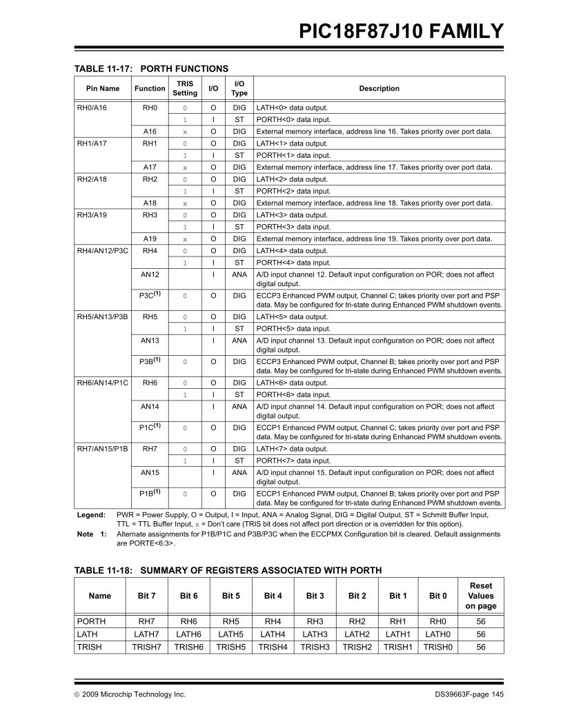
PIC18F87J10 FAMILY
TABLE 11-17: PORTH FUNCTIONSTABLE 11-18: SUMMARY OF REGISTERS ASSOCIATED WITH PORTH
Pin Name Function TRIS Setting I/O I/O
Type Description
RH0/A16 RH0 0 O DIG LATH<0> data output.1 I ST PORTH<0> data input.
A16 x O DIG External memory interface, address line 16. Takes priority over port data.RH1/A17 RH1 0 O DIG LATH<1> data output.
1 I ST PORTH<1> data input.A17 x O DIG External memory interface, address line 17. Takes priority over port data.
RH2/A18 RH2 0 O DIG LATH<2> data output.1 I ST PORTH<2> data input.
A18 x O DIG External memory interface, address line 18. Takes priority over port data.RH3/A19 RH3 0 O DIG LATH<3> data output.
1 I ST PORTH<3> data input.A19 x O DIG External memory interface, address line 19. Takes priority over port data.
RH4/AN12/P3C RH4 0 O DIG LATH<4> data output.1 I ST PORTH<4> data input.
AN12 I ANA A/D input channel 12. Default input configuration on POR; does not affect digital output.
P3C(1) 0 O DIG ECCP3 Enhanced PWM output, Channel C; takes priority over port and PSP data. May be configured for tri-state during Enhanced PWM shutdown events.
RH5/AN13/P3B RH5 0 O DIG LATH<5> data output.1 I ST PORTH<5> data input.
AN13 I ANA A/D input channel 13. Default input configuration on POR; does not affect digital output.
P3B(1) 0 O DIG ECCP3 Enhanced PWM output, Channel B; takes priority over port and PSP data. May be configured for tri-state during Enhanced PWM shutdown events.
RH6/AN14/P1C RH6 0 O DIG LATH<6> data output.1 I ST PORTH<6> data input.
AN14 I ANA A/D input channel 14. Default input configuration on POR; does not affect digital output.
P1C(1) 0 O DIG ECCP1 Enhanced PWM output, Channel C; takes priority over port and PSP data. May be configured for tri-state during Enhanced PWM shutdown events.
RH7/AN15/P1B RH7 0 O DIG LATH<7> data output.1 I ST PORTH<7> data input.
AN15 I ANA A/D input channel 15. Default input configuration on POR; does not affect digital output.
P1B(1) 0 O DIG ECCP1 Enhanced PWM output, Channel B; takes priority over port and PSP data. May be configured for tri-state during Enhanced PWM shutdown events.
Legend: PWR = Power Supply, O = Output, I = Input, ANA = Analog Signal, DIG = Digital Output, ST = Schmitt Buffer Input, TTL = TTL Buffer Input, x = Don’t care (TRIS bit does not affect port direction or is overridden for this option).
Note 1: Alternate assignments for P1B/P1C and P3B/P3C when the ECCPMX Configuration bit is cleared. Default assignments are PORTE<6:3>.
Name Bit 7 Bit 6 Bit 5 Bit 4 Bit 3 Bit 2 Bit 1 Bit 0Reset Values
on page
PORTH RH7 RH6 RH5 RH4 RH3 RH2 RH1 RH0 56LATH LATH7 LATH6 LATH5 LATH4 LATH3 LATH2 LATH1 LATH0 56TRISH TRISH7 TRISH6 TRISH5 TRISH4 TRISH3 TRISH2 TRISH1 TRISH0 56
© 2009 Microchip Technology Inc. DS39663F-page 145

PIC18F87J10 FAMILY
11.10 PORTJ, TRISJ andLATJ Registers
PORTJ is an 8-bit wide, bidirectional port. The corre-sponding Data Direction register is TRISJ. Setting aTRISJ bit (= 1) will make the corresponding PORTJ pinan input (i.e., put the corresponding output driver in ahigh-impedance mode). Clearing a TRISJ bit (= 0) willmake the corresponding PORTJ pin an output (i.e., putthe contents of the output latch on the selected pin). Allpins on PORTJ are digital only and tolerate voltages upto 5.5V.
The Output Latch register (LATJ) is also memorymapped. Read-modify-write operations on the LATJregister read and write the latched output value forPORTJ.
All pins on PORTJ are implemented with SchmittTrigger input buffers. Each pin is individuallyconfigurable as an input or output.
When the external memory interface is enabled, all ofthe PORTJ pins function as control outputs for theinterface. This occurs automatically when the interfaceis enabled by clearing the EBDIS control bit(MEMCON<7>). The TRISJ bits are also overridden.
Each of the PORTJ pins has a weak internal pull-up.The pull-ups are provided to keep the inputs at a knownstate for the external memory interface while poweringup. A single control bit can turn off all the pull-ups. Thisis performed by clearing bit, RJPU (PORTG<5>). Theweak pull-up is automatically turned off when the portpin is configured as an output. The pull-ups aredisabled on any device Reset.
EXAMPLE 11-9: INITIALIZING PORTJ
Note: PORTJ is available only on 80-pin devices.
Note: These pins are configured as digital inputson any device Reset.
CLRF PORTJ ; Initialize PORTG by; clearing output; data latches
CLRF LATJ ; Alternate method; to clear output; data latches
MOVLW 0CFh ; Value used to ; initialize data ; direction
MOVWF TRISJ ; Set RJ3:RJ0 as inputs; RJ5:RJ4 as output; RJ7:RJ6 as inputs
DS39663F-page 146 © 2009 Microchip Technology Inc.

PIC18F87J10 FAMILY
TABLE 11-19: PORTJ FUNCTIONSTABLE 11-20: SUMMARY OF REGISTERS ASSOCIATED WITH PORTJ
Pin Name Function TRIS Setting I/O I/O
Type Description
RJ0/ALE RJ0 0 O DIG LATJ<0> data output.
1 I ST PORTJ<0> data input.ALE x O DIG External memory interface address latch enable control output; takes
priority over digital I/O.
RJ1/OE RJ1 0 O DIG LATJ<1> data output.1 I ST PORTJ<1> data input.
OE x O DIG External memory interface output enable control output; takes priority over digital I/O.
RJ2/WRL RJ2 0 O DIG LATJ<2> data output.1 I ST PORTJ<2> data input.
WRL x O DIG External memory bus write low byte control; takes priority over digital I/O.
RJ3/WRH RJ3 0 O DIG LATJ<3> data output.1 I ST PORTJ<3> data input.
WRH x O DIG External memory interface write high byte control output; takes priority over digital I/O.
RJ4/BA0 RJ4 0 O DIG LATJ<4> data output.1 I ST PORTJ<4> data input.
BA0 x O DIG External memory interface byte address 0 control output; takes priority over digital I/O.
RJ5/CE RJ5 0 O DIG LATJ<5> data output.1 I ST PORTJ<5> data input.
CE x O DIG External memory interface chip enable control output; takes priority over digital I/O.
RJ6/LB RJ6 0 O DIG LATJ<6> data output.1 I ST PORTJ<6> data input.
LB x O DIG External memory interface lower byte enable control output; takes priority over digital I/O.
RJ7/UB RJ7 0 O DIG LATJ<7> data output.1 I ST PORTJ<7> data input.
UB x O DIG External memory interface upper byte enable control output; takes priority over digital I/O.
Legend: PWR = Power Supply, O = Output, I = Input, ANA = Analog Signal, DIG = Digital Output, ST = Schmitt Buffer Input, TTL = TTL Buffer Input, x = Don’t care (TRIS bit does not affect port direction or is overridden for this option).
Name Bit 7 Bit 6 Bit 5 Bit 4 Bit 3 Bit 2 Bit 1 Bit 0Reset Values
on page
PORTJ RJ7 RJ6 RJ5 RJ4 RJ3 RJ2 RJ1 RJ0 56LATJ LATJ7 LATJ6 LATJ5 LATJ4 LATJ3 LATJ2 LATJ1 LATJ0 56TRISJ TRISJ7 TRISJ6 TRISJ5 TRISJ4 TRISJ3 TRISJ2 TRISJ1 TRISJ0 56PORTG RDPU REPU RJPU RG4 RG3 RG2 RG1 RG0 56Legend: Shaded cells are not used by PORTJ.
© 2009 Microchip Technology Inc. DS39663F-page 147

PIC18F87J10 FAMILY
11.11 Parallel Slave PortPORTD can also function as an 8-bit wide ParallelSlave Port, or microprocessor port, when control bit,PSPMODE (PSPCON<4>), is set. It is asynchronouslyreadable and writable by the external world through RDcontrol input pin (RE0/RD) and WR control input pin(RE1/WR).The PSP can directly interface to an 8-bit micro-processor data bus. The external microprocessor canread or write the PORTD latch as an 8-bit latch. Settingthe PSPMODE bit enables port pin, RE0/RD, to be theRD input, RE1/WR to be the WR input and RE2/CS tobe the CS (Chip Select) input. For this functionality, thecorresponding data direction bits of the TRISE register(TRISE<2:0>) must be configured as inputs (set).
A write to the PSP occurs when both the CS and WRlines are first detected low and ends when either aredetected high. The PSPIF and IBF flag bits are both setwhen the write ends.
A read from the PSP occurs when both the CS and RDlines are first detected low. The data in PORTD is readout and the OBF bit is set. If the user writes new datato PORTD to set OBF, the data is immediately read out;however, the OBF bit is not set.
When either the CS or RD lines are detected high, thePORTD pins return to the input state and the PSPIF bitis set. User applications should wait for PSPIF to be setbefore servicing the PSP. When this happens, the IBFand OBF bits can be polled and the appropriate actiontaken.
The timing for the control signals in Write and Readmodes is shown in Figure 11-3 and Figure 11-4,respectively.
FIGURE 11-2: PORTD AND PORTE BLOCK DIAGRAM (PARALLEL SLAVE PORT)
Note: For 80-pin devices, the Parallel Slave Portis available only in Microcontroller mode.
Data Bus
WR LATDRDx
QD
CK
EN
Q D
ENRD PORTD
Pin
One bit of PORTD
Set Interrupt Flag
PSPIF (PIR1<7>)
Read
Chip Select
Write
RD
CS
WR
Note: I/O pin has protection diodes to VDD and VSS.
TTL
TTL
TTL
TTL
orPORTD
RD LATD
Data Latch
TRIS Latch
DS39663F-page 148 © 2009 Microchip Technology Inc.

PIC18F87J10 FAMILY
FIGURE 11-3: PARALLEL SLAVE PORT WRITE WAVEFORMS
REGISTER 11-1: PSPCON: PARALLEL SLAVE PORT CONTROL REGISTER
R-0 R-0 R/W-0 R/W-0 U-0 U-0 U-0 U-0
IBF OBF IBOV PSPMODE — — — —bit 7 bit 0
Legend:R = Readable bit W = Writable bit U = Unimplemented bit, read as ‘0’-n = Value at POR ‘1’ = Bit is set ‘0’ = Bit is cleared x = Bit is unknown
bit 7 IBF: Input Buffer Full Status bit1 = A word has been received and is waiting to be read by the CPU0 = No word has been received
bit 6 OBF: Output Buffer Full Status bit1 = The output buffer still holds a previously written word0 = The output buffer has been read
bit 5 IBOV: Input Buffer Overflow Detect bit1 = A write occurred when a previously input word had not been read
(must be cleared in software)0 = No overflow occurred
bit 4 PSPMODE: Parallel Slave Port Mode Select bit1 = Parallel Slave Port mode0 = General Purpose I/O mode
bit 3-0 Unimplemented: Read as ‘0’
Q1 Q2 Q3 Q4
CS
Q1 Q2 Q3 Q4 Q1 Q2 Q3 Q4
WR
RD
IBF
OBF
PSPIF
PORTD<7:0>
© 2009 Microchip Technology Inc. DS39663F-page 149

PIC18F87J10 FAMILY
FIGURE 11-4: PARALLEL SLAVE PORT READ WAVEFORMSTABLE 11-21: REGISTERS ASSOCIATED WITH PARALLEL SLAVE PORT
Name Bit 7 Bit 6 Bit 5 Bit 4 Bit 3 Bit 2 Bit 1 Bit 0Reset Values
on page
PORTD RD7 RD6 RD5 RD4 RD3 RD2 RD1 RD0 56LATD LATD7 LATD6 LATD5 LATD4 LATD3 LATD2 LATD1 LATD0 56TRISD TRISD7 TRISD6 TRISD5 TRISD4 TRISD3 TRISD2 TRISD1 TRISD0 56PORTE RE7 RE6 RE5 RE4 RE3 RE2 RE1 RE0 56LATE LATE7 LATE6 LATE5 LATE4 LATE3 LATE2 LATE1 LATE0 56TRISE TRISE7 TRISE6 TRISE5 TRISE4 TRISE3 TRISE2 TRISE1 TRISE0 56PSPCON IBF OBF IBOV PSPMODE — — — — 55INTCON GIE/GIEH PEIE/GIEL TMR0IE INT0IE RBIE TMR0IF INT0IF RBIF 53PIR1 PSPIF ADIF RC1IF TX1IF SSP1IF CCP1IF TMR2IF TMR1IF 55PIE1 PSPIE ADIE RC1IE TX1IE SSP1IE CCP1IE TMR2IE TMR1IE 55IPR1 PSPIP ADIP RC1IP TX1IP SSP1IP CCP1IP TMR2IP TMR1IP 55Legend: — = unimplemented, read as ‘0’. Shaded cells are not used by the Parallel Slave Port.
Q1 Q2 Q3 Q4
CS
Q1 Q2 Q3 Q4 Q1 Q2 Q3 Q4
WR
IBF
PSPIF
RD
OBF
PORTD<7:0>
DS39663F-page 150 © 2009 Microchip Technology Inc.

PIC18F87J10 FAMILY
12.0 TIMER0 MODULEThe Timer0 module incorporates the following features:
• Software-selectable operation as a timer or counter in both 8-bit or 16-bit modes
• Readable and writable registers• Dedicated 8-bit, software programmable
prescaler• Selectable clock source (internal or external)• Edge select for external clock• Interrupt-on-overflow
The T0CON register (Register 12-1) controls allaspects of the module’s operation, including theprescale selection. It is both readable and writable.
A simplified block diagram of the Timer0 module in 8-bitmode is shown in Figure 12-1. Figure 12-2 shows asimplified block diagram of the Timer0 module in 16-bitmode.
REGISTER 12-1: T0CON: TIMER0 CONTROL REGISTER
R/W-1 R/W-1 R/W-1 R/W-1 R/W-1 R/W-1 R/W-1 R/W-1TMR0ON T08BIT T0CS T0SE PSA T0PS2 T0PS1 T0PS0
bit 7 bit 0
Legend:R = Readable bit W = Writable bit U = Unimplemented bit, read as ‘0’-n = Value at POR ‘1’ = Bit is set ‘0’ = Bit is cleared x = Bit is unknown
bit 7 TMR0ON: Timer0 On/Off Control bit 1 = Enables Timer0 0 = Stops Timer0
bit 6 T08BIT: Timer0 8-Bit/16-Bit Control bit 1 = Timer0 is configured as an 8-bit timer/counter 0 = Timer0 is configured as a 16-bit timer/counter
bit 5 T0CS: Timer0 Clock Source Select bit 1 = Transition on T0CKI pin 0 = Internal instruction cycle clock (CLKO)
bit 4 T0SE: Timer0 Source Edge Select bit1 = Increment on high-to-low transition on T0CKI pin 0 = Increment on low-to-high transition on T0CKI pin
bit 3 PSA: Timer0 Prescaler Assignment bit 1 = TImer0 prescaler is NOT assigned. Timer0 clock input bypasses prescaler. 0 = Timer0 prescaler is assigned. Timer0 clock input comes from prescaler output.
bit 2-0 T0PS<2:0>: Timer0 Prescaler Select bits 111 = 1:256 Prescale value110 = 1:128 Prescale value101 = 1:64 Prescale value100 = 1:32 Prescale value011 = 1:16 Prescale value010 = 1:8 Prescale value001 = 1:4 Prescale value000 = 1:2 Prescale value
© 2009 Microchip Technology Inc. DS39663F-page 151

PIC18F87J10 FAMILY
12.1 Timer0 OperationTimer0 can operate as either a timer or a counter. Themode is selected with the T0CS bit (T0CON<5>). InTimer mode (T0CS = 0), the module increments onevery clock by default unless a different prescaler valueis selected (see Section 12.3 “Prescaler”). If theTMR0 register is written to, the increment is inhibitedfor the following two instruction cycles. The user canwork around this by writing an adjusted value to theTMR0 register.The Counter mode is selected by setting the T0CS bit(= 1). In this mode, Timer0 increments either on everyrising or falling edge of pin RA4/T0CKI. The increment-ing edge is determined by the Timer0 Source EdgeSelect bit, T0SE (T0CON<4>); clearing this bit selectsthe rising edge. Restrictions on the external clock inputare discussed below.
An external clock source can be used to drive Timer0;however, it must meet certain requirements to ensurethat the external clock can be synchronized with the
internal phase clock (TOSC). There is a delay betweensynchronization and the onset of incrementing thetimer/counter.
12.2 Timer0 Reads and Writes in 16-Bit Mode
TMR0H is not the actual high byte of Timer0 in 16-bitmode. It is actually a buffered version of the real highbyte of Timer0 which is not directly readable nor writ-able (refer to Figure 12-2). TMR0H is updated with thecontents of the high byte of Timer0 during a read ofTMR0L. This provides the ability to read all 16 bits ofTimer0 without having to verify that the read of the highand low byte were valid, due to a rollover betweensuccessive reads of the high and low byte.
Similarly, a write to the high byte of Timer0 must alsotake place through the TMR0H Buffer register. The highbyte is updated with the contents of TMR0H when awrite occurs to TMR0L. This allows all 16 bits of Timer0to be updated at once.
FIGURE 12-1: TIMER0 BLOCK DIAGRAM (8-BIT MODE)
FIGURE 12-2: TIMER0 BLOCK DIAGRAM (16-BIT MODE)
Note: Upon Reset, Timer0 is enabled in 8-bit mode with clock input from T0CKI max. prescale.
T0CKI Pin
T0SE
0
1
1
0
T0CS
FOSC/4
ProgrammablePrescaler
Sync withInternalClocks
TMR0L
(2 TCY Delay)
Internal Data BusPSAT0PS<2:0>
Set TMR0IFon Overflow
3 8
8
Note: Upon Reset, Timer0 is enabled in 8-bit mode with clock input from T0CKI max. prescale.
T0CKI Pin
T0SE
0
1
1
0
T0CS
FOSC/4
Sync withInternalClocks
TMR0L
(2 TCY Delay)
Internal Data Bus
8
PSAT0PS<2:0>
Set TMR0IFon Overflow
3
TMR0
TMR0H
High Byte
88
8
Read TMR0L
Write TMR0L
8
ProgrammablePrescaler
DS39663F-page 152 © 2009 Microchip Technology Inc.

PIC18F87J10 FAMILY
12.3 PrescalerAn 8-bit counter is available as a prescaler for the Timer0module. The prescaler is not directly readable or writable.Its value is set by the PSA and T0PS<2:0> bits(T0CON<3:0>) which determine the prescalerassignment and prescale ratio.Clearing the PSA bit assigns the prescaler to theTimer0 module. When it is assigned, prescale valuesfrom 1:2 through 1:256 in power-of-2 increments areselectable.
When assigned to the Timer0 module, all instructionswriting to the TMR0 register (e.g., CLRF TMR0, MOVWFTMR0, BSF TMR0, etc.) clear the prescaler count.
12.3.1 SWITCHING PRESCALER ASSIGNMENT
The prescaler assignment is fully under softwarecontrol and can be changed “on-the-fly” during programexecution.
12.4 Timer0 InterruptThe TMR0 interrupt is generated when the TMR0register overflows from FFh to 00h in 8-bit mode, orfrom FFFFh to 0000h in 16-bit mode. This overflow setsthe TMR0IF flag bit. The interrupt can be masked byclearing the TMR0IE bit (INTCON<5>). Beforere-enabling the interrupt, the TMR0IF bit must becleared in software by the Interrupt Service Routine.
Since Timer0 is shut down in Sleep mode, the TMR0interrupt cannot awaken the processor from Sleep.
TABLE 12-1: REGISTERS ASSOCIATED WITH TIMER0
Note: Writing to TMR0 when the prescaler isassigned to Timer0 will clear the prescalercount but will not change the prescalerassignment.
Name Bit 7 Bit 6 Bit 5 Bit 4 Bit 3 Bit 2 Bit 1 Bit 0Reset Values
on page
TMR0L Timer0 Register Low Byte 54TMR0H Timer0 Register High Byte 54INTCON GIE/GIEH PEIE/GIEL TMR0IE INT0IE RBIE TMR0IF INT0IF RBIF 53T0CON TMR0ON T08BIT T0CS T0SE PSA T0PS2 T0PS1 T0PS0 54TRISA — — TRISA5 TRISA4 TRISA3 TRISA2 TRISA1 TRISA0 56Legend: — = unimplemented, read as ‘0’. Shaded cells are not used by Timer0.
© 2009 Microchip Technology Inc. DS39663F-page 153

PIC18F87J10 FAMILY
NOTES:DS39663F-page 154 © 2009 Microchip Technology Inc.
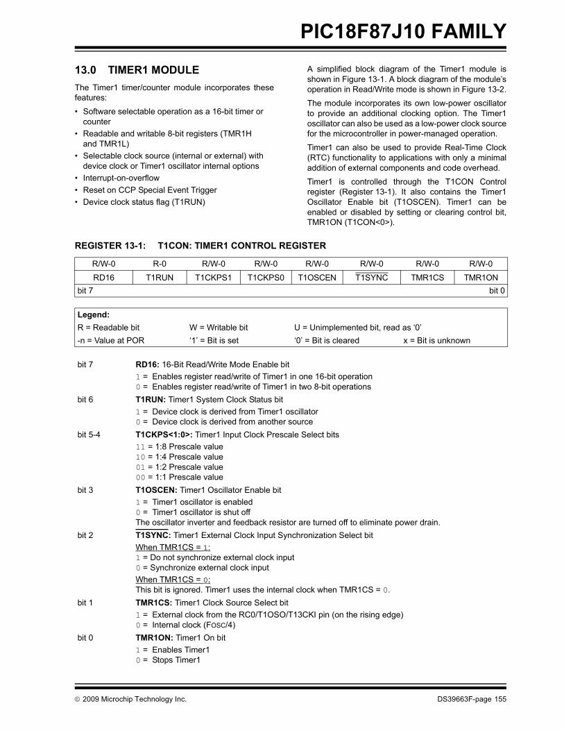
PIC18F87J10 FAMILY
13.0 TIMER1 MODULEThe Timer1 timer/counter module incorporates thesefeatures:
• Software selectable operation as a 16-bit timer or counter
• Readable and writable 8-bit registers (TMR1H and TMR1L)
• Selectable clock source (internal or external) with device clock or Timer1 oscillator internal options
• Interrupt-on-overflow• Reset on CCP Special Event Trigger• Device clock status flag (T1RUN)
A simplified block diagram of the Timer1 module isshown in Figure 13-1. A block diagram of the module’soperation in Read/Write mode is shown in Figure 13-2.
The module incorporates its own low-power oscillatorto provide an additional clocking option. The Timer1oscillator can also be used as a low-power clock sourcefor the microcontroller in power-managed operation.
Timer1 can also be used to provide Real-Time Clock(RTC) functionality to applications with only a minimaladdition of external components and code overhead.
Timer1 is controlled through the T1CON Controlregister (Register 13-1). It also contains the Timer1Oscillator Enable bit (T1OSCEN). Timer1 can beenabled or disabled by setting or clearing control bit,TMR1ON (T1CON<0>).
REGISTER 13-1: T1CON: TIMER1 CONTROL REGISTER
R/W-0 R-0 R/W-0 R/W-0 R/W-0 R/W-0 R/W-0 R/W-0
RD16 T1RUN T1CKPS1 T1CKPS0 T1OSCEN T1SYNC TMR1CS TMR1ONbit 7 bit 0
Legend:R = Readable bit W = Writable bit U = Unimplemented bit, read as ‘0’-n = Value at POR ‘1’ = Bit is set ‘0’ = Bit is cleared x = Bit is unknown
bit 7 RD16: 16-Bit Read/Write Mode Enable bit1 = Enables register read/write of Timer1 in one 16-bit operation0 = Enables register read/write of Timer1 in two 8-bit operations
bit 6 T1RUN: Timer1 System Clock Status bit1 = Device clock is derived from Timer1 oscillator0 = Device clock is derived from another source
bit 5-4 T1CKPS<1:0>: Timer1 Input Clock Prescale Select bits11 = 1:8 Prescale value 10 = 1:4 Prescale value 01 = 1:2 Prescale value 00 = 1:1 Prescale value
bit 3 T1OSCEN: Timer1 Oscillator Enable bit1 = Timer1 oscillator is enabled 0 = Timer1 oscillator is shut off The oscillator inverter and feedback resistor are turned off to eliminate power drain.
bit 2 T1SYNC: Timer1 External Clock Input Synchronization Select bitWhen TMR1CS = 1: 1 = Do not synchronize external clock input 0 = Synchronize external clock inputWhen TMR1CS = 0: This bit is ignored. Timer1 uses the internal clock when TMR1CS = 0.
bit 1 TMR1CS: Timer1 Clock Source Select bit1 = External clock from the RC0/T1OSO/T13CKI pin (on the rising edge)0 = Internal clock (FOSC/4)
bit 0 TMR1ON: Timer1 On bit1 = Enables Timer1 0 = Stops Timer1
© 2009 Microchip Technology Inc. DS39663F-page 155
PIC18F87J10 FAMILY
13.1 Timer1 OperationTimer1 can operate in one of these modes:• Timer• Synchronous Counter• Asynchronous Counter
The operating mode is determined by the clock selectbit, TMR1CS (T1CON<1>). When TMR1CS is cleared(= 0), Timer1 increments on every internal instruction
cycle (FOSC/4). When the bit is set, Timer1 incrementson every rising edge of the Timer1 external clock inputor the Timer1 oscillator, if enabled.
When Timer1 is enabled, the RC1/T1OSI andRC0/T1OSO/T13CKI pins become inputs. This meansthe values of TRISC<1:0> are ignored and the pins areread as ‘0’.
FIGURE 13-1: TIMER1 BLOCK DIAGRAM
FIGURE 13-2: TIMER1 BLOCK DIAGRAM (16-BIT READ/WRITE MODE)
T1SYNC
TMR1CS
T1CKPS<1:0>
Sleep InputT1OSCEN(1)
FOSC/4InternalClock
On/Off
Prescaler1, 2, 4, 8
SynchronizeDetect
1
0
2
T1OSO/T13CKI
T1OSI
1
0
TMR1ON
TMR1LSet TMR1IFon Overflow
TMR1High ByteClear TMR1
(CCP Special Event Trigger)
Timer1 Oscillator
Note 1: When enable bit, T1OSCEN, is cleared, the inverter and feedback resistor are turned off to eliminate power drain.
On/OffTimer1
Timer1 Clock Input
T1SYNC
TMR1CST1CKPS<1:0>
Sleep InputT1OSCEN(1)
FOSC/4InternalClock
Prescaler1, 2, 4, 8
SynchronizeDetect
1
0
2
T1OSO/T13CKI
T1OSI
Note 1: When enable bit, T1OSCEN, is cleared, the inverter and feedback resistor are turned off to eliminate power drain.
1
0
TMR1L
Internal Data Bus
8
Set TMR1IFon Overflow
TMR1
TMR1H
High Byte
88
8
Read TMR1L
Write TMR1L
8
TMR1ON
Clear TMR1(CCP Special Event Trigger)
Timer1 Oscillator
On/OffTimer1
Timer1 Clock Input
DS39663F-page 156 © 2009 Microchip Technology Inc.
PIC18F87J10 FAMILY
13.2 Timer1 16-Bit Read/Write ModeTimer1 can be configured for 16-bit reads and writes(see Figure 13-2). When the RD16 control bit(T1CON<7>) is set, the address for TMR1H is mappedto a buffer register for the high byte of Timer1. A readfrom TMR1L will load the contents of the high byte ofTimer1 into the Timer1 High Byte Buffer register. Thisprovides the user with the ability to accurately read all16 bits of Timer1 without having to determine whethera read of the high byte, followed by a read of the lowbyte, has become invalid due to a rollover betweenreads.A write to the high byte of Timer1 must also take placethrough the TMR1H Buffer register. The Timer1 highbyte is updated with the contents of TMR1H when awrite occurs to TMR1L. This allows a user to write all16 bits to both the high and low bytes of Timer1 at once.
The high byte of Timer1 is not directly readable orwritable in this mode. All reads and writes must takeplace through the Timer1 High Byte Buffer register.Writes to TMR1H do not clear the Timer1 prescaler.The prescaler is only cleared on writes to TMR1L.
13.3 Timer1 OscillatorAn on-chip crystal oscillator circuit is incorporatedbetween pins T1OSI (input) and T1OSO (amplifieroutput). It is enabled by setting the Timer1 OscillatorEnable bit, T1OSCEN (T1CON<3>). The oscillator is alow-power circuit rated for 32 kHz crystals. It willcontinue to run during all power-managed modes. Thecircuit for a typical LP oscillator is shown in Figure 13-3.Table 13-1 shows the capacitor selection for the Timer1oscillator.
The user must provide a software time delay to ensureproper start-up of the Timer1 oscillator.
FIGURE 13-3: EXTERNAL COMPONENTS FOR THE TIMER1 LP OSCILLATOR
TABLE 13-1: CAPACITOR SELECTION FOR THE TIMER OSCILLATOR(2,3,4)
13.3.1 USING TIMER1 AS A CLOCK SOURCE
The Timer1 oscillator is also available as a clock sourcein power-managed modes. By setting the clock selectbits, SCS<1:0> (OSCCON<1:0>), to ‘01’, the deviceswitches to SEC_RUN mode; both the CPU andperipherals are clocked from the Timer1 oscillator. If theIDLEN bit (OSCCON<7>) is cleared and a SLEEPinstruction is executed, the device enters SEC_IDLEmode. Additional details are available in Section 4.0“Power-Managed Modes”.
Whenever the Timer1 oscillator is providing the clocksource, the Timer1 System Clock Status Flag, T1RUN(T1CON<6>), is set. This can be used to determine thecontroller’s current clocking mode. It can also indicatethe clock source being currently used by the Fail-SafeClock Monitor. If the Clock Monitor is enabled and theTimer1 oscillator fails while providing the clock, pollingthe T1RUN bit will indicate whether the clock is beingprovided by the Timer1 oscillator or another source.
13.3.2 LOW-POWER TIMER1 OPTION The Timer1 oscillator can operate at two distinct levelsof power consumption based on device configuration.When the LPT1OSC Configuration bit is set, the Timer1oscillator operates in a low-power mode. WhenLPT1OSC is not set, Timer1 operates at a higher powerlevel. Power consumption for a particular mode is rela-tively constant regardless of the device’s operatingmode. The default Timer1 configuration is the higherpower mode.
As the low-power Timer1 mode tends to be moresensitive to interference, high noise environments maycause some oscillator instability. The low-power option is,therefore, best suited for low noise applications wherepower conservation is an important design consideration.
Note: See the Notes with Table 13-1 for additionalinformation about capacitor selection.
C1
C2
XTAL
PIC18F87J10T1OSI
T1OSO
32.768 kHz
27 pF
27 pF
Oscillator Type Freq. C1 C2
LP 32 kHz 27 pF(1) 27 pF(1)
Note 1: Microchip suggests these values as astarting point in validating the oscillatorcircuit.
2: Higher capacitance increases the stabilityof the oscillator but also increases thestart-up time.
3: Since each resonator/crystal has its owncharacteristics, the user should consultthe resonator/crystal manufacturer forappropriate values of externalcomponents.
4: Capacitor values are for design guidanceonly.
© 2009 Microchip Technology Inc. DS39663F-page 157
PIC18F87J10 FAMILY
13.3.3 TIMER1 OSCILLATOR LAYOUTCONSIDERATIONS
The Timer1 oscillator circuit draws very little powerduring operation. Due to the low-power nature of theoscillator, it may also be sensitive to rapidly changingsignals in close proximity.
The oscillator circuit, shown in Figure 13-3, should belocated as close as possible to the microcontroller.There should be no circuits passing within the oscillatorcircuit boundaries other than VSS or VDD.
If a high-speed circuit must be located near the oscilla-tor (such as the ECCP1 pin in Output Compare or PWMmode, or the primary oscillator using the OSC2 pin), agrounded guard ring around the oscillator circuit, asshown in Figure 13-4, may be helpful when used on asingle-sided PCB or in addition to a ground plane.
FIGURE 13-4: OSCILLATOR CIRCUIT WITH GROUNDED GUARD RING
13.4 Timer1 InterruptThe TMR1 register pair (TMR1H:TMR1L) incrementsfrom 0000h to FFFFh and rolls over to 0000h. TheTimer1 interrupt, if enabled, is generated on overflowwhich is latched in interrupt flag bit, TMR1IF(PIR1<0>). This interrupt can be enabled or disabledby setting or clearing the Timer1 Interrupt Enable bit,TMR1IE (PIE1<0>).
13.5 Resetting Timer1 Using the ECCP Special Event Trigger
If ECCP1 or ECCP2 is configured to use Timer1 and togenerate a Special Event Trigger in Compare mode(CCPxM<3:0> = 1011), this signal will reset Timer3.The trigger from ECCP2 will also start an A/D conver-sion if the A/D module is enabled (see Section 18.2.1“Special Event Trigger” for more information).
The module must be configured as either a timer or asynchronous counter to take advantage of this feature.When used this way, the CCPRxH:CCPRxL registerpair effectively becomes a period register for Timer1.
If Timer1 is running in Asynchronous Counter mode,this Reset operation may not work.
In the event that a write to Timer1 coincides with aSpecial Event Trigger, the write operation will takeprecedence.
13.6 Using Timer1 as a Real-Time ClockAdding an external LP oscillator to Timer1 (such as theone described in Section 13.3 “Timer1 Oscillator”above) gives users the option to include RTC function-ality to their applications. This is accomplished with aninexpensive watch crystal to provide an accurate timebase and several lines of application code to calculatethe time. When operating in Sleep mode and using abattery or supercapacitor as a power source, it cancompletely eliminate the need for a separate RTCdevice and battery backup.
The application code routine, RTCisr, shown inExample 13-1, demonstrates a simple method toincrement a counter at one-second intervals using anInterrupt Service Routine. Incrementing the TMR1register pair to overflow triggers the interrupt and callsthe routine which increments the seconds counter byone. Additional counters for minutes and hours areincremented as the previous counter overflows.
Since the register pair is 16 bits wide, counting up tooverflow the register directly from a 32.768 kHz clockwould take 2 seconds. To force the overflow at therequired one-second intervals, it is necessary to pre-load it. The simplest method is to set the MSb ofTMR1H with a BSF instruction. Note that the TMR1Lregister is never preloaded or altered; doing so mayintroduce cumulative error over many cycles.
For this method to be accurate, Timer1 must operate inAsynchronous mode and the Timer1 overflow interruptmust be enabled (PIE1<0> = 1) as shown in theroutine, RTCinit. The Timer1 oscillator must also beenabled and running at all times.
VDD
OSC1
VSS
OSC2
RC0
RC1
RC2
Note: Not drawn to scale.
Note: The Special Event Triggers from theECCPx module will not set the TMR1IFinterrupt flag bit (PIR1<0>).
DS39663F-page 158 © 2009 Microchip Technology Inc.
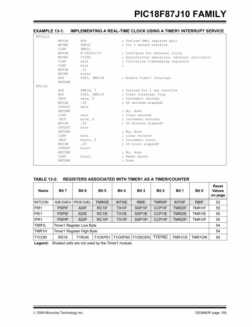
PIC18F87J10 FAMILY
EXAMPLE 13-1: IMPLEMENTING A REAL-TIME CLOCK USING A TIMER1 INTERRUPT SERVICETABLE 13-2: REGISTERS ASSOCIATED WITH TIMER1 AS A TIMER/COUNTER
RTCinitMOVLW 80h ; Preload TMR1 register pairMOVWF TMR1H ; for 1 second overflowCLRF TMR1LMOVLW b’00001111’ ; Configure for external clock,MOVWF T1CON ; Asynchronous operation, external oscillatorCLRF secs ; Initialize timekeeping registersCLRF mins ; MOVLW .12MOVWF hoursBSF PIE1, TMR1IE ; Enable Timer1 interruptRETURN
RTCisrBSF TMR1H, 7 ; Preload for 1 sec overflowBCF PIR1, TMR1IF ; Clear interrupt flagINCF secs, F ; Increment secondsMOVLW .59 ; 60 seconds elapsed?CPFSGT secsRETURN ; No, doneCLRF secs ; Clear secondsINCF mins, F ; Increment minutesMOVLW .59 ; 60 minutes elapsed?CPFSGT minsRETURN ; No, doneCLRF mins ; clear minutesINCF hours, F ; Increment hoursMOVLW .23 ; 24 hours elapsed?CPFSGT hoursRETURN ; No, doneCLRF hours ; Reset hoursRETURN ; Done
Name Bit 7 Bit 6 Bit 5 Bit 4 Bit 3 Bit 2 Bit 1 Bit 0Reset Values
on page
INTCON GIE/GIEH PEIE/GIEL TMR0IE INT0IE RBIE TMR0IF INT0IF RBIF 53PIR1 PSPIF ADIF RC1IF TX1IF SSP1IF CCP1IF TMR2IF TMR1IF 55PIE1 PSPIE ADIE RC1IE TX1IE SSP1IE CCP1IE TMR2IE TMR1IE 55IPR1 PSPIP ADIP RC1IP TX1IP SSP1IP CCP1IP TMR2IP TMR1IP 55TMR1L Timer1 Register Low Byte 54TMR1H Timer1 Register High Byte 54
T1CON RD16 T1RUN T1CKPS1 T1CKPS0 T1OSCEN T1SYNC TMR1CS TMR1ON 54Legend: Shaded cells are not used by the Timer1 module.
© 2009 Microchip Technology Inc. DS39663F-page 159

PIC18F87J10 FAMILY
NOTES:DS39663F-page 160 © 2009 Microchip Technology Inc.

PIC18F87J10 FAMILY
14.0 TIMER2 MODULEThe Timer2 module incorporates the following features:
• 8-Bit Timer and Period registers (TMR2 and PR2, respectively)
• Readable and writable (both registers) • Software programmable prescaler
(1:1, 1:4 and 1:16)• Software programmable postscaler
(1:1 through 1:16)• Interrupt on TMR2 to PR2 match• Optional use as the shift clock for the
MSSP module
The module is controlled through the T2CON register(Register 14-1) which enables or disables the timer andconfigures the prescaler and postscaler. Timer2 can beshut off by clearing control bit, TMR2ON (T2CON<2>),to minimize power consumption.
A simplified block diagram of the module is shown inFigure 14-1.
14.1 Timer2 OperationIn normal operation, TMR2 is incremented from 00h oneach clock (FOSC/4). A 4-bit counter/prescaler on theclock input gives direct input, divide-by-4 anddivide-by-16 prescale options. These are selected bythe prescaler control bits, T2CKPS<1:0>(T2CON<1:0>). The value of TMR2 is compared to thatof the Period register, PR2, on each clock cycle. Whenthe two values match, the comparator generates amatch signal as the timer output. This signal also resetsthe value of TMR2 to 00h on the next cycle and drivesthe output counter/postscaler (see Section 14.2“Timer2 Interrupt”).
The TMR2 and PR2 registers are both directly readableand writable. The TMR2 register is cleared on anydevice Reset, while the PR2 register initializes at FFh.Both the prescaler and postscaler counters are clearedon the following events:
• a write to the TMR2 register• a write to the T2CON register• any device Reset (Power-on Reset, MCLR Reset,
Watchdog Timer Reset or Brown-out Reset)
TMR2 is not cleared when T2CON is written.
REGISTER 14-1: T2CON: TIMER2 CONTROL REGISTER
U-0 R/W-0 R/W-0 R/W-0 R/W-0 R/W-0 R/W-0 R/W-0— T2OUTPS3 T2OUTPS2 T2OUTPS1 T2OUTPS0 TMR2ON T2CKPS1 T2CKPS0
bit 7 bit 0
Legend:R = Readable bit W = Writable bit U = Unimplemented bit, read as ‘0’-n = Value at POR ‘1’ = Bit is set ‘0’ = Bit is cleared x = Bit is unknown
bit 7 Unimplemented: Read as ‘0’bit 6-3 T2OUTPS<3:0>: Timer2 Output Postscale Select bits
0000 = 1:1 Postscale 0001 = 1:2 Postscale • • • 1111 = 1:16 Postscale
bit 2 TMR2ON: Timer2 On bit1 = Timer2 is on 0 = Timer2 is off
bit 1-0 T2CKPS<1:0>: Timer2 Clock Prescale Select bits00 = Prescaler is 1 01 = Prescaler is 4 1x = Prescaler is 16
© 2009 Microchip Technology Inc. DS39663F-page 161
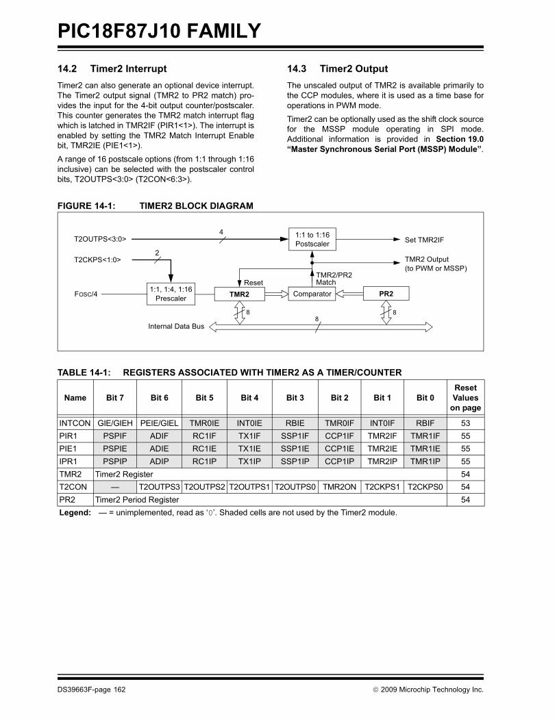
PIC18F87J10 FAMILY
14.2 Timer2 InterruptTimer2 can also generate an optional device interrupt.The Timer2 output signal (TMR2 to PR2 match) pro-vides the input for the 4-bit output counter/postscaler.This counter generates the TMR2 match interrupt flagwhich is latched in TMR2IF (PIR1<1>). The interrupt isenabled by setting the TMR2 Match Interrupt Enablebit, TMR2IE (PIE1<1>).A range of 16 postscale options (from 1:1 through 1:16inclusive) can be selected with the postscaler controlbits, T2OUTPS<3:0> (T2CON<6:3>).
14.3 Timer2 OutputThe unscaled output of TMR2 is available primarily tothe CCP modules, where it is used as a time base foroperations in PWM mode.
Timer2 can be optionally used as the shift clock sourcefor the MSSP module operating in SPI mode.Additional information is provided in Section 19.0“Master Synchronous Serial Port (MSSP) Module”.
FIGURE 14-1: TIMER2 BLOCK DIAGRAM
TABLE 14-1: REGISTERS ASSOCIATED WITH TIMER2 AS A TIMER/COUNTER
Name Bit 7 Bit 6 Bit 5 Bit 4 Bit 3 Bit 2 Bit 1 Bit 0Reset Values
on page
INTCON GIE/GIEH PEIE/GIEL TMR0IE INT0IE RBIE TMR0IF INT0IF RBIF 53PIR1 PSPIF ADIF RC1IF TX1IF SSP1IF CCP1IF TMR2IF TMR1IF 55PIE1 PSPIE ADIE RC1IE TX1IE SSP1IE CCP1IE TMR2IE TMR1IE 55IPR1 PSPIP ADIP RC1IP TX1IP SSP1IP CCP1IP TMR2IP TMR1IP 55TMR2 Timer2 Register 54T2CON — T2OUTPS3 T2OUTPS2 T2OUTPS1 T2OUTPS0 TMR2ON T2CKPS1 T2CKPS0 54PR2 Timer2 Period Register 54Legend: — = unimplemented, read as ‘0’. Shaded cells are not used by the Timer2 module.
Comparator
TMR2 Output
TMR2
Postscaler
Prescaler PR2
2
FOSC/4
1:1 to 1:16
1:1, 1:4, 1:16
4T2OUTPS<3:0>
T2CKPS<1:0>
Set TMR2IF
Internal Data Bus8
ResetTMR2/PR2
88
(to PWM or MSSP)
Match
DS39663F-page 162 © 2009 Microchip Technology Inc.

PIC18F87J10 FAMILY
15.0 TIMER3 MODULEThe Timer3 timer/counter module incorporates thesefeatures:
• Software selectable operation as a 16-bit timer or counter
• Readable and writable 8-bit registers (TMR3H and TMR3L)
• Selectable clock source (internal or external) with device clock or Timer1 oscillator internal options
• Interrupt-on-overflow• Module Reset on CCP Special Event Trigger
A simplified block diagram of the Timer3 module isshown in Figure 15-1. A block diagram of the module’soperation in Read/Write mode is shown in Figure 15-2.
The Timer3 module is controlled through the T3CONregister (Register 15-1). It also selects the clock sourceoptions for the CCP and ECCP modules; seeSection 17.1.1 “CCP Modules and TimerResources” for more information.
REGISTER 15-1: T3CON: TIMER3 CONTROL REGISTER
R/W-0 R/W-0 R/W-0 R/W-0 R/W-0 R/W-0 R/W-0 R/W-0
RD16 T3CCP2 T3CKPS1 T3CKPS0 T3CCP1 T3SYNC TMR3CS TMR3ONbit 7 bit 0
Legend:R = Readable bit W = Writable bit U = Unimplemented bit, read as ‘0’-n = Value at POR ‘1’ = Bit is set ‘0’ = Bit is cleared x = Bit is unknown
bit 7 RD16: 16-Bit Read/Write Mode Enable bit1 = Enables register read/write of Timer3 in one 16-bit operation0 = Enables register read/write of Timer3 in two 8-bit operations
bit 6,3 T3CCP<2:1>: Timer3 and Timer1 to CCPx Enable bits11 = Timer3 and Timer4 are the clock sources for all CCP/ECCP modules10 = Timer3 and Timer4 are the clock sources for ECCP3, CCP4 and CCP5;
Timer1 and Timer2 are the clock sources for ECCP1 and ECCP201 = Timer3 and Timer4 are the clock sources for ECCP2, ECCP3, CCP4 and CCP5;
Timer1 and Timer2 are the clock sources for ECCP100 = Timer1 and Timer2 are the clock sources for all CCP/ECCP modules
bit 5-4 T3CKPS<1:0>: Timer3 Input Clock Prescale Select bits11 = 1:8 Prescale value 10 = 1:4 Prescale value 01 = 1:2 Prescale value 00 = 1:1 Prescale value
bit 2 T3SYNC: Timer3 External Clock Input Synchronization Control bit(Not usable if the device clock comes from Timer1/Timer3.)When TMR3CS = 1: 1 = Do not synchronize external clock input 0 = Synchronize external clock inputWhen TMR3CS = 0: This bit is ignored. Timer3 uses the internal clock when TMR3CS = 0.
bit 1 TMR3CS: Timer3 Clock Source Select bit1 = External clock input from Timer1 oscillator or T13CKI (on the rising edge after the first falling edge)0 = Internal clock (FOSC/4)
bit 0 TMR3ON: Timer3 On bit1 = Enables Timer3 0 = Stops Timer3
© 2009 Microchip Technology Inc. DS39663F-page 163

PIC18F87J10 FAMILY
15.1 Timer3 OperationTimer3 can operate in one of three modes:• Timer• Synchronous Counter• Asynchronous Counter
The operating mode is determined by the clock selectbit, TMR3CS (T3CON<1>). When TMR3CS is cleared(= 0), Timer3 increments on every internal instructioncycle (FOSC/4). When the bit is set, Timer3 incrementson every rising edge of the Timer1 external clock inputor the Timer1 oscillator, if enabled.
As with Timer1, the RC1/T1OSI andRC0/T1OSO/T13CKI pins become inputs when theTimer1 oscillator is enabled. This means the values ofTRISC<1:0> are ignored and the pins are read as ‘0’.
FIGURE 15-1: TIMER3 BLOCK DIAGRAM
FIGURE 15-2: TIMER3 BLOCK DIAGRAM (16-BIT READ/WRITE MODE)
T3SYNC
TMR3CS
T3CKPS<1:0>
Sleep InputT1OSCEN(1)
FOSC/4InternalClock
Prescaler1, 2, 4, 8
SynchronizeDetect
1
0
2
T1OSO/T13CKI
T1OSI
1
0
TMR3ON
TMR3LSet TMR3IFon Overflow
TMR3High Byte
Timer1 Oscillator
Note 1: When enable bit, T1OSCEN, is cleared, the inverter and feedback resistor are turned off to eliminate power drain.
On/OffTimer3
CCPx Special Event TriggerCCPx Select from T3CON<6,3>
Clear TMR3
Timer1 Clock Input
T3SYNC
TMR3CST3CKPS<1:0>
Sleep InputT1OSCEN(1)
FOSC/4InternalClock
Prescaler1, 2, 4, 8
SynchronizeDetect
1
0
2
T13CKI/T1OSO
T1OSI
Note 1: When enable bit, T1OSCEN, is cleared, the inverter and feedback resistor are turned off to eliminate power drain.
1
0
TMR3L
Internal Data Bus
8
Set TMR3IFon Overflow
TMR3
TMR3H
High Byte
88
8
Read TMR1L
Write TMR1L
8
TMR3ON
CCPx Special Event Trigger
Timer1 Oscillator
On/OffTimer3
Timer1 Clock Input
CCPx Select from T3CON<6,3>Clear TMR3
DS39663F-page 164 © 2009 Microchip Technology Inc.
PIC18F87J10 FAMILY
15.2 Timer3 16-Bit Read/Write ModeTimer3 can be configured for 16-bit reads and writes(see Figure 15-2). When the RD16 control bit(T3CON<7>) is set, the address for TMR3H is mappedto a buffer register for the high byte of Timer3. A readfrom TMR3L will load the contents of the high byte ofTimer3 into the Timer3 High Byte Buffer register. Thisprovides the user with the ability to accurately read all16 bits of Timer1 without having to determine whethera read of the high byte, followed by a read of the lowbyte, has become invalid due to a rollover betweenreads.A write to the high byte of Timer3 must also take placethrough the TMR3H Buffer register. The Timer3 highbyte is updated with the contents of TMR3H when awrite occurs to TMR3L. This allows a user to write all16 bits to both the high and low bytes of Timer3 at once.
The high byte of Timer3 is not directly readable orwritable in this mode. All reads and writes must takeplace through the Timer3 High Byte Buffer register.
Writes to TMR3H do not clear the Timer3 prescaler.The prescaler is only cleared on writes to TMR3L.
15.3 Using the Timer1 Oscillator as the Timer3 Clock Source
The Timer1 internal oscillator may be used as the clocksource for Timer3. The Timer1 oscillator is enabled bysetting the T1OSCEN (T1CON<3>) bit. To use it as theTimer3 clock source, the TMR3CS bit must also be set.As previously noted, this also configures Timer3 toincrement on every rising edge of the oscillator source.
The Timer1 oscillator is described in Section 13.0“Timer1 Module”.
15.4 Timer3 InterruptThe TMR3 register pair (TMR3H:TMR3L) incrementsfrom 0000h to FFFFh and overflows to 0000h. TheTimer3 interrupt, if enabled, is generated on overflowand is latched in interrupt flag bit, TMR3IF (PIR2<1>).This interrupt can be enabled or disabled by setting orclearing the Timer3 Interrupt Enable bit, TMR3IE(PIE2<1>).
15.5 Resetting Timer3 Using the ECCP Special Event Trigger
If ECCP1 or ECCP2 is configured to use Timer3 and togenerate a Special Event Trigger in Compare mode(CCPxM<3:0> = 1011), this signal will reset Timer3.The trigger from ECCP2 will also start an A/D conver-sion if the A/D module is enabled (see Section 18.2.1“Special Event Trigger” for more information).
The module must be configured as either a timer orsynchronous counter to take advantage of this feature.When used this way, the CCPRxH:CCPRxL registerpair effectively becomes a period register for Timer3.
If Timer3 is running in Asynchronous Counter mode,the Reset operation may not work.
In the event that a write to Timer3 coincides with aSpecial Event Trigger from an ECCP module, the writewill take precedence.
TABLE 15-1: REGISTERS ASSOCIATED WITH TIMER3 AS A TIMER/COUNTER
Note: The Special Event Triggers from theECCPx module will not set the TMR3IFinterrupt flag bit (PIR1<0>).
Name Bit 7 Bit 6 Bit 5 Bit 4 Bit 3 Bit 2 Bit 1 Bit 0Reset Values
on page
INTCON GIE/GIEH PEIE/GIEL TMR0IE INT0IE RBIE TMR0IF INT0IF RBIF 53PIR2 OSCFIF CMIF — — BCL1IF — TMR3IF CCP2IF 55PIE2 OSCFIE CMIE — — BCL1IE — TMR3IE CCP2IE 55IPR2 OSCFIP CMIP — — BCL1IP — TMR3IP CCP2IP 55TMR3L Timer3 Register Low Byte 55TMR3H Timer3 Register High Byte 55
T1CON RD16 T1RUN T1CKPS1 T1CKPS0 T1OSCEN T1SYNC TMR1CS TMR1ON 54
T3CON RD16 T3CCP2 T3CKPS1 T3CKPS0 T3CCP1 T3SYNC TMR3CS TMR3ON 55Legend: — = unimplemented, read as ‘0’. Shaded cells are not used by the Timer3 module.
© 2009 Microchip Technology Inc. DS39663F-page 165

PIC18F87J10 FAMILY
NOTES:DS39663F-page 166 © 2009 Microchip Technology Inc.
PIC18F87J10 FAMILY
16.0 TIMER4 MODULEThe Timer4 timer module has the following features:
• 8-Bit Timer register (TMR4)• 8-Bit Period register (PR4)• Readable and writable (both registers)• Software programmable prescaler (1:1, 1:4, 1:16)• Software programmable postscaler (1:1 to 1:16)• Interrupt on TMR4 match of PR4
Timer4 has a control register shown in Register 16-1.Timer4 can be shut off by clearing control bit, TMR4ON(T4CON<2>), to minimize power consumption. Theprescaler and postscaler selection of Timer4 are alsocontrolled by this register. Figure 16-1 is a simplifiedblock diagram of the Timer4 module.
16.1 Timer4 OperationTimer4 can be used as the PWM time base for thePWM mode of the CCP module. The TMR4 register isreadable and writable and is cleared on any deviceReset. The input clock (FOSC/4) has a prescale optionof 1:1, 1:4 or 1:16, selected by control bitsT4CKPS<1:0> (T4CON<1:0>). The match output ofTMR4 goes through a 4-bit postscaler (which gives a1:1 to 1:16 scaling inclusive) to generate a TMR4interrupt, latched in flag bit, TMR4IF (PIR3<3>).
The prescaler and postscaler counters are clearedwhen any of the following occurs:
• a write to the TMR4 register• a write to the T4CON register• any device Reset (Power-on Reset, MCLR Reset,
Watchdog Timer Reset or Brown-out Reset)
TMR4 is not cleared when T4CON is written.
REGISTER 16-1: T4CON: TIMER4 CONTROL REGISTER
U-0 R/W-0 R/W-0 R/W-0 R/W-0 R/W-0 R/W-0 R/W-0
— T4OUTPS3 T4OUTPS2 T4OUTPS1 T4OUTPS0 TMR4ON T4CKPS1 T4CKPS0bit 7 bit 0
Legend:R = Readable bit W = Writable bit U = Unimplemented bit, read as ‘0’-n = Value at POR ‘1’ = Bit is set ‘0’ = Bit is cleared x = Bit is unknown
bit 7 Unimplemented: Read as ‘0’bit 6-3 T4OUTPS<3:0>: Timer4 Output Postscale Select bits
0000 = 1:1 Postscale 0001 = 1:2 Postscale • • • 1111 = 1:16 Postscale
bit 2 TMR4ON: Timer4 On bit1 = Timer4 is on 0 = Timer4 is off
bit 1-0 T4CKPS<1:0>: Timer4 Clock Prescale Select bits00 = Prescaler is 1 01 = Prescaler is 4 1x = Prescaler is 16
© 2009 Microchip Technology Inc. DS39663F-page 167

PIC18F87J10 FAMILY
16.2 Timer4 InterruptThe Timer4 module has an 8-Bit Period register, PR4,which is both readable and writable. Timer4 incrementsfrom 00h until it matches PR4 and then resets to 00h onthe next increment cycle. The PR4 register is initializedto FFh upon Reset.16.3 Output of TMR4The output of TMR4 (before the postscaler) is usedonly as a PWM time base for the CCP modules. It is notused as a baud rate clock for the MSSP as is theTimer2 output.
FIGURE 16-1: TIMER4 BLOCK DIAGRAM
TABLE 16-1: REGISTERS ASSOCIATED WITH TIMER4 AS A TIMER/COUNTER
Comparator
TMR4 Output
TMR4
Postscaler
PrescalerPR4
2
FOSC/4
1:1 to 1:16
1:1, 1:4, 1:16
4T4OUTPS<3:0>
T4CKPS<1:0>
Set TMR4IF
Internal Data Bus8
ResetTMR4/PR4
88
(to PWM)
Match
Name Bit 7 Bit 6 Bit 5 Bit 4 Bit 3 Bit 2 Bit 1 Bit 0Reset Values
on page
INTCON GIE/GIEH PEIE/GIEL TMR0IE INT0IE RBIE TMR0IF INT0IF RBIF 53IPR3 SSP2IP BCL2IP RC2IP TX2IP TMR4IP CCP5IP CCP4IP CCP3IP 55PIR3 SSP2IF BCL2IF RC2IF TX2IF TMR4IF CCP5IF CCP4IF CCP3IF 55PIE3 SSP2IE BCL2IE RC2IE TX2IE TMR4IE CCP5IE CCP4IE CCP3IE 55TMR4 Timer4 Register 57T4CON — T4OUTPS3 T4OUTPS2 T4OUTPS1 T4OUTPS0 TMR4ON T4CKPS1 T4CKPS0 57PR4 Timer4 Period Register 57Legend: — = unimplemented, read as ‘0’. Shaded cells are not used by the Timer4 module.
DS39663F-page 168 © 2009 Microchip Technology Inc.

PIC18F87J10 FAMILY
17.0 CAPTURE/COMPARE/PWM (CCP) MODULES
Members of the PIC18F87J10 family of devices all havea total of five CCP (Capture/Compare/PWM) modules.Two of these (CCP4 and CCP5) implement standardCapture, Compare and Pulse-Width Modulation (PWM)modes and are discussed in this section. The other threemodules (ECCP1, ECCP2, ECCP3) implementstandard Capture and Compare modes, as well asEnhanced PWM modes. These are discussed inSection 18.0 “Enhanced Capture/Compare/PWM(ECCP) Module”.
Each CCP/ECCP module contains a 16-bit registerwhich can operate as a 16-Bit Capture register, a 16-BitCompare register or a PWM Master/Slave Duty Cycle
register. For the sake of clarity, all CCP module opera-tion in the following sections is described with respectto CCP4, but is equally applicable to CCP5.
Capture and compare operations described in thischapter apply to all standard and Enhanced CCPmodules. The operations of PWM mode, described inSection 17.4 “PWM Mode”, apply to CCP4 and CCP5only.
Note: Throughout this section and Section 18.0“Enhanced Capture/Compare/PWM (ECCP)Module”, references to register and bit namesthat may be associated with a specific CCPmodule are referred to generically by the use of‘x’ or ‘y’ in place of the specific module number.Thus, “CCPxCON” might refer to the controlregister for ECCP1, ECCP2, ECCP3, CCP4 orCCP5.
REGISTER 17-1: CCPxCON: CCPx CONTROL REGISTER (CCP4 AND CCP5)
U0 U-0 R/W-0 R/W-0 R/W-0 R/W-0 R/W-0 R/W-0— — DCxB1 DCxB0 CCPxM3 CCPxM2 CCPxM1 CCPxM0
bit 7 bit 0
Legend:R = Readable bit W = Writable bit U = Unimplemented bit, read as ‘0’-n = Value at POR ‘1’ = Bit is set ‘0’ = Bit is cleared x = Bit is unknown
bit 7-6 Unimplemented: Read as ‘0’bit 5-4 DCxB<1:0>: CCP Module x PWM Duty Cycle bit 1 and bit 0
Capture mode:Unused.Compare mode:Unused.PWM mode:These bits are the two Least Significant bits (bit 1 and bit 0) of the 10-bit PWM duty cycle. The eightMost Significant bits (DCxB<9:2>) of the duty cycle are found in CCPRxL.
bit 3-0 CCPxM<3:0>: CCP Module x Mode Select bits0000 = Capture/Compare/PWM disabled (resets CCPx module) 0001 = Reserved 0010 = Compare mode, toggle output on match (CCPxIF bit is set) 0011 = Reserved 0100 = Capture mode, every falling edge 0101 = Capture mode, every rising edge0110 = Capture mode, every 4th rising edge 0111 = Capture mode, every 16th rising edge1000 = Compare mode; initialize CCPx pin low; on compare match, force CCPx pin high (CCPxIF bit
is set) 1001 = Compare mode; initialize CCPx pin high; on compare match, force CCPx pin low (CCPxIF bit
is set) 1010 = Compare mode; generate software interrupt on compare match (CCPxIF bit is set, CCPx pin
reflects I/O state) 1011 = Reserved11xx = PWM mode
© 2009 Microchip Technology Inc. DS39663F-page 169
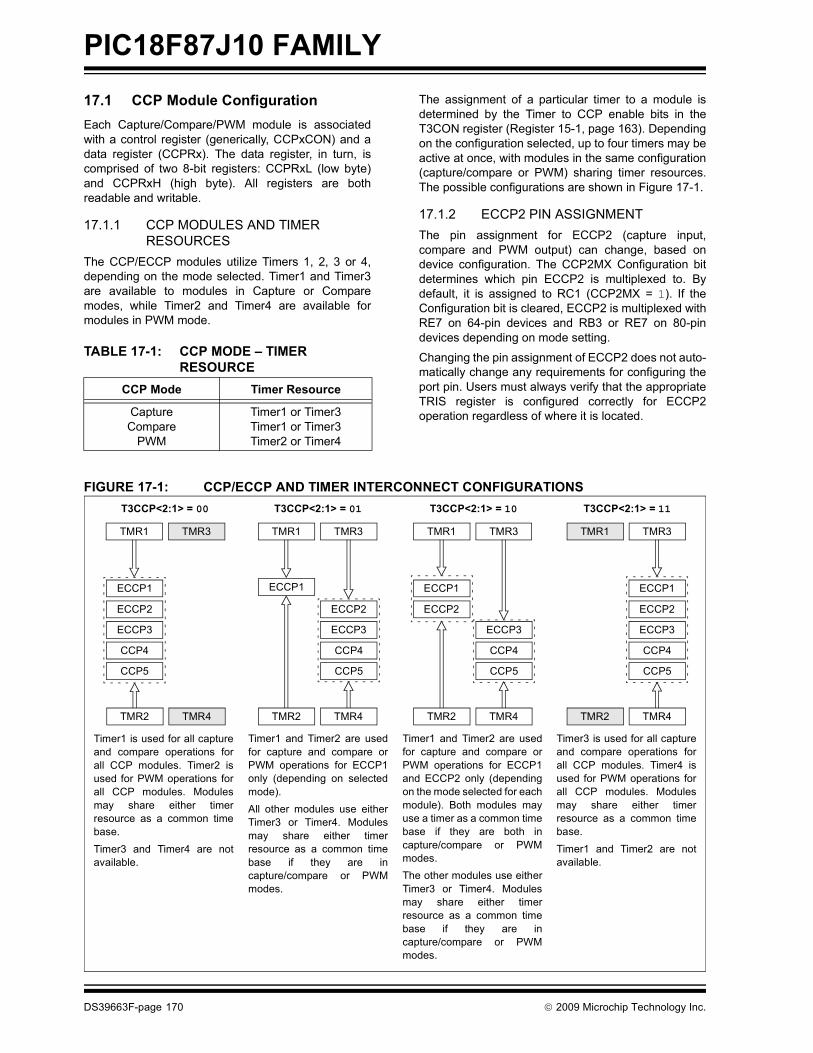
PIC18F87J10 FAMILY
17.1 CCP Module ConfigurationEach Capture/Compare/PWM module is associatedwith a control register (generically, CCPxCON) and adata register (CCPRx). The data register, in turn, iscomprised of two 8-bit registers: CCPRxL (low byte)and CCPRxH (high byte). All registers are bothreadable and writable.17.1.1 CCP MODULES AND TIMER RESOURCES
The CCP/ECCP modules utilize Timers 1, 2, 3 or 4,depending on the mode selected. Timer1 and Timer3are available to modules in Capture or Comparemodes, while Timer2 and Timer4 are available formodules in PWM mode.
TABLE 17-1: CCP MODE – TIMER RESOURCE
The assignment of a particular timer to a module isdetermined by the Timer to CCP enable bits in theT3CON register (Register 15-1, page 163). Dependingon the configuration selected, up to four timers may beactive at once, with modules in the same configuration(capture/compare or PWM) sharing timer resources.The possible configurations are shown in Figure 17-1.
17.1.2 ECCP2 PIN ASSIGNMENTThe pin assignment for ECCP2 (capture input,compare and PWM output) can change, based ondevice configuration. The CCP2MX Configuration bitdetermines which pin ECCP2 is multiplexed to. Bydefault, it is assigned to RC1 (CCP2MX = 1). If theConfiguration bit is cleared, ECCP2 is multiplexed withRE7 on 64-pin devices and RB3 or RE7 on 80-pindevices depending on mode setting.
Changing the pin assignment of ECCP2 does not auto-matically change any requirements for configuring theport pin. Users must always verify that the appropriateTRIS register is configured correctly for ECCP2operation regardless of where it is located.
FIGURE 17-1: CCP/ECCP AND TIMER INTERCONNECT CONFIGURATIONS
CCP Mode Timer Resource
CaptureCompare
PWM
Timer1 or Timer3Timer1 or Timer3Timer2 or Timer4
TMR1
CCP5
TMR2
TMR3
TMR4
CCP4
ECCP3
ECCP2
ECCP1
TMR1
TMR2
TMR3
CCP5
TMR4
CCP4
ECCP3
ECCP2
ECCP1
TMR1
TMR2
TMR3
CCP5
TMR4
CCP4
ECCP3
ECCP2
ECCP1
TMR1
TMR2
TMR3
CCP5
TMR4
CCP4
ECCP3
ECCP2
ECCP1
T3CCP<2:1> = 00 T3CCP<2:1> = 01 T3CCP<2:1> = 10 T3CCP<2:1> = 11
Timer1 is used for all captureand compare operations forall CCP modules. Timer2 isused for PWM operations forall CCP modules. Modulesmay share either timerresource as a common timebase.Timer3 and Timer4 are notavailable.
Timer1 and Timer2 are usedfor capture and compare orPWM operations for ECCP1only (depending on selectedmode). All other modules use eitherTimer3 or Timer4. Modulesmay share either timerresource as a common timebase if they are incapture/compare or PWMmodes.
Timer1 and Timer2 are usedfor capture and compare orPWM operations for ECCP1and ECCP2 only (dependingon the mode selected for eachmodule). Both modules mayuse a timer as a common timebase if they are both incapture/compare or PWMmodes.The other modules use eitherTimer3 or Timer4. Modulesmay share either timerresource as a common timebase if they are incapture/compare or PWMmodes.
Timer3 is used for all captureand compare operations forall CCP modules. Timer4 isused for PWM operations forall CCP modules. Modulesmay share either timerresource as a common timebase.Timer1 and Timer2 are notavailable.
DS39663F-page 170 © 2009 Microchip Technology Inc.

PIC18F87J10 FAMILY
17.2 Capture ModeIn Capture mode, the CCPRxH:CCPRxL register paircaptures the 16-bit value of the TMR1 or TMR3registers when an event occurs on the correspondingCCPx pin. An event is defined as one of the following:• every falling edge• every rising edge• every 4th rising edge• every 16th rising edge
The event is selected by the mode select bits,CCPxM<3:0> (CCPxCON<3:0>). When a capture ismade, the interrupt request flag bit, CCPxIF, is set; itmust be cleared in software. If another capture occursbefore the value in register CCPRx is read, the oldcaptured value is overwritten by the new captured value.
17.2.1 CCP PIN CONFIGURATIONIn Capture mode, the appropriate CCPx pin should beconfigured as an input by setting the correspondingTRIS direction bit.
17.2.2 TIMER1/TIMER3 MODE SELECTIONThe timers that are to be used with the capture feature(Timer1 and/or Timer3) must be running in Timer mode orSynchronized Counter mode. In Asynchronous Countermode, the capture operation will not work. The timer to beused with each CCP module is selected in the T3CONregister (see Section 17.1.1 “CCP Modules and TimerResources”).
17.2.3 SOFTWARE INTERRUPTWhen the Capture mode is changed, a false captureinterrupt may be generated. The user should keep theCCPxIE interrupt enable bit clear to avoid falseinterrupts. The interrupt flag bit, CCPxIF, should also becleared following any such change in operating mode.
17.2.4 CCP PRESCALERThere are four prescaler settings in Capture mode.They are specified as part of the operating modeselected by the mode select bits (CCPxM<3:0>).Whenever the CCP module is turned off or Capturemode is disabled, the prescaler counter is cleared. Thismeans that any Reset will clear the prescaler counter.
Switching from one capture prescaler to another maygenerate an interrupt. Also, the prescaler counter willnot be cleared; therefore, the first capture may be froma non-zero prescaler. Example 17-1 shows therecommended method for switching between captureprescalers. This example also clears the prescalercounter and will not generate the “false” interrupt.
EXAMPLE 17-1: CHANGING BETWEEN CAPTURE PRESCALERS(CCP5 SHOWN)
FIGURE 17-2: CAPTURE MODE OPERATION BLOCK DIAGRAM
Note: If RG4/CCP5 is configured as an output, awrite to the port can cause a capturecondition.
CLRF CCP5CON ; Turn CCP module offMOVLW NEW_CAPT_PS ; Load WREG with the
; new prescaler mode; value and CCP ON
MOVWF CCP5CON ; Load CCP5CON with; this value
CCPR4H CCPR4L
TMR1H TMR1L
Set CCP4IFTMR3Enable
Q1:Q4CCP4CON<3:0>
CCP4 pinPrescaler÷ 1, 4, 16
andEdge Detect
TMR1Enable
T3CCP2
T3CCP2
CCPR5H CCPR5L
TMR1H TMR1L
Set CCP5IF
TMR3Enable
CCP5CON<3:0>
CCP5 pinPrescaler÷ 1, 4, 16
TMR3H TMR3L
TMR1Enable
T3CCP2T3CCP1
T3CCP2T3CCP1
TMR3H TMR3L
andEdge Detect
44
4
© 2009 Microchip Technology Inc. DS39663F-page 171

PIC18F87J10 FAMILY
17.3 Compare ModeIn Compare mode, the 16-Bit CCPRx register value isconstantly compared against either the TMR1 or TMR3register pair value. When a match occurs, the CCPx pincan be:• driven high• driven low• toggled (high-to-low or low-to-high) • remains unchanged (that is, reflects the state of
the I/O latch)
The action on the pin is based on the value of the modeselect bits (CCPxM<3:0>). At the same time, theinterrupt flag bit, CCPxIF, is set.
17.3.1 CCP PIN CONFIGURATIONThe user must configure the CCPx pin as an output byclearing the appropriate TRIS bit.
17.3.2 TIMER1/TIMER3 MODE SELECTIONTimer1 and/or Timer3 must be running in Timer modeor Synchronized Counter mode if the CCP module isusing the compare feature. In Asynchronous Countermode, the compare operation may not work.
17.3.3 SOFTWARE INTERRUPT MODE When the Generate Software Interrupt mode is chosen(CCPxM<3:0> = 1010), the corresponding CCPx pin isnot affected. Only a CCP interrupt is generated, ifenabled and the CCPxIE bit is set.
FIGURE 17-3: COMPARE MODE OPERATION BLOCK DIAGRAM
Note: Clearing the CCP5CON register will forcethe RG4 compare output latch (depend-ing on device configuration) to the defaultlow level. This is not the PORTB orPORTC I/O data latch.
CCPR4H CCPR4L
TMR1H TMR1L
ComparatorQS
R
OutputLogic
Set CCP4IF
CCP4 Pin
TRIS
CCP4CON<3:0>
Output Enable
TMR3H TMR3L
CCPR5H CCPR5L
Comparator
1
0
T3CCP2T3CCP1
Set CCP5IF
1
0
Compare
4
QS
R
OutputLogic
CCP5 Pin
TRIS
CCP5CON<3:0>
Output Enable4
Match
CompareMatch
DS39663F-page 172 © 2009 Microchip Technology Inc.

PIC18F87J10 FAMILY
TABLE 17-2: REGISTERS ASSOCIATED WITH CAPTURE, COMPARE, TIMER1 AND TIMER3Name Bit 7 Bit 6 Bit 5 Bit 4 Bit 3 Bit 2 Bit 1 Bit 0Reset Values
on page
INTCON GIE/GIEH PEIE/GIEL TMR0IE INT0IE RBIE TMR0IF INT0IF RBIF 53
RCON IPEN — — RI TO PD POR BOR 54PIR1 PSPIF ADIF RC1IF TX1IF SSP1IF CCP1IF TMR2IF TMR1IF 55PIE1 PSPIE ADIE RC1IE TX1IE SSP1IE CCP1IE TMR2IE TMR1IE 55IPR1 PSPIP ADIP RC1IP TX1IP SSP1IP CCP1IP TMR2IP TMR1IP 55PIR2 OSCFIF CMIF — — BCL1IF — TMR3IF CCP2IF 55PIE2 OSCFIE CMIE — — BCL1IE — TMR3IE CCP2IE 55IPR2 OSCFIP CMIP — — BCL1IP — TMR3IP CCP2IP 55PIR3 SSP2IF BCL2IF RC2IF TX2IF TMR4IF CCP5IF CCP4IF CCP3IF 55PIE3 SSP2IE BCL2IE RC2IE TX2IE TMR4IE CCP5IE CCP4IE CCP3IE 55IPR3 SSP2IP BCL2IP RC2IP TX2IP TMR4IP CCP5IP CCP4IP CCP3IP 55TRISG — — — TRISG4 TRISG3 TRISG2 TRISG1 TRISG0 56TMR1L Timer1 Register Low Byte 54TMR1H Timer1 Register High Byte 54
T1CON RD16 T1RUN T1CKPS1 T1CKPS0 T1OSCEN T1SYNC TMR1CS TMR1ON 54TMR3H Timer3 Register High Byte 55TMR3L Timer3 Register Low Byte 55
T3CON RD16 T3CCP2 T3CKPS1 T3CKPS0 T3CCP1 T3SYNC TMR3CS TMR3ON 55CCPR4L Capture/Compare/PWM Register 4 Low Byte 57CCPR4H Capture/Compare/PWM Register 4 High Byte 57CCPR5L Capture/Compare/PWM Register 5 Low Byte 57CCPR5H Capture/Compare/PWM Register 5 High Byte 57CCP4CON — — DC4B1 DC4B0 CCP4M3 CCP4M2 CCP4M1 CCP4M0 57CCP5CON — — DC5B1 DC5B0 CCP5M3 CCP5M2 CCP5M1 CCP5M0 57Legend: — = unimplemented, read as ‘0’. Shaded cells are not used by capture/compare, Timer1 or Timer3.
© 2009 Microchip Technology Inc. DS39663F-page 173
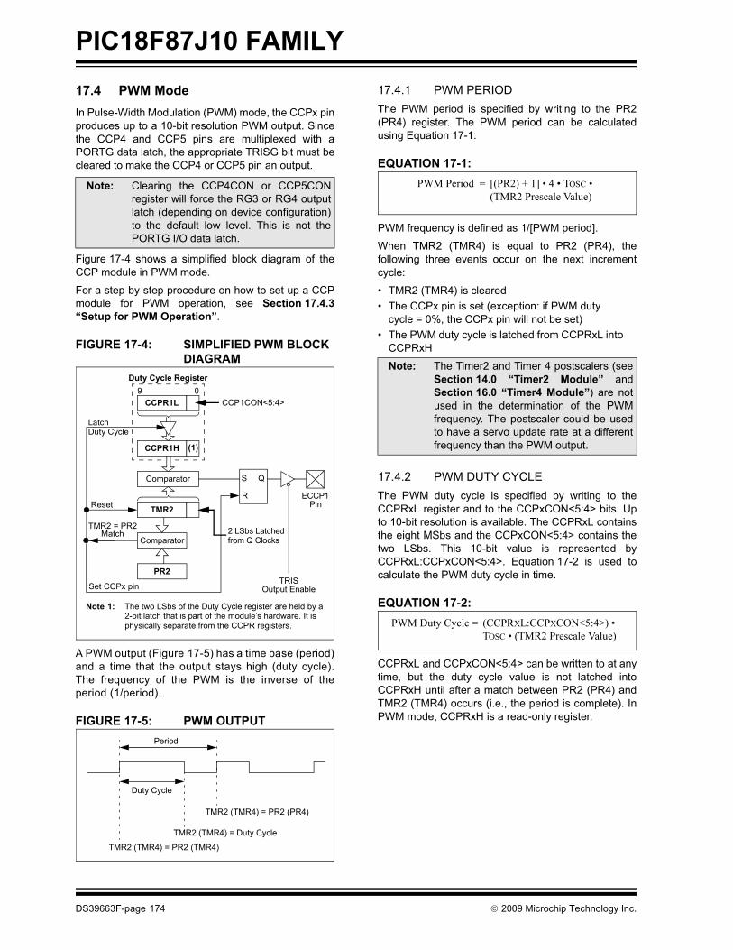
PIC18F87J10 FAMILY
17.4 PWM ModeIn Pulse-Width Modulation (PWM) mode, the CCPx pinproduces up to a 10-bit resolution PWM output. Sincethe CCP4 and CCP5 pins are multiplexed with aPORTG data latch, the appropriate TRISG bit must becleared to make the CCP4 or CCP5 pin an output.Figure 17-4 shows a simplified block diagram of theCCP module in PWM mode.
For a step-by-step procedure on how to set up a CCPmodule for PWM operation, see Section 17.4.3“Setup for PWM Operation”.
FIGURE 17-4: SIMPLIFIED PWM BLOCK DIAGRAM
A PWM output (Figure 17-5) has a time base (period)and a time that the output stays high (duty cycle).The frequency of the PWM is the inverse of theperiod (1/period).
FIGURE 17-5: PWM OUTPUT
17.4.1 PWM PERIODThe PWM period is specified by writing to the PR2(PR4) register. The PWM period can be calculatedusing Equation 17-1:
EQUATION 17-1:
PWM frequency is defined as 1/[PWM period].
When TMR2 (TMR4) is equal to PR2 (PR4), thefollowing three events occur on the next incrementcycle:
• TMR2 (TMR4) is cleared• The CCPx pin is set (exception: if PWM duty
cycle = 0%, the CCPx pin will not be set)• The PWM duty cycle is latched from CCPRxL into
CCPRxH
17.4.2 PWM DUTY CYCLEThe PWM duty cycle is specified by writing to theCCPRxL register and to the CCPxCON<5:4> bits. Upto 10-bit resolution is available. The CCPRxL containsthe eight MSbs and the CCPxCON<5:4> contains thetwo LSbs. This 10-bit value is represented byCCPRxL:CCPxCON<5:4>. Equation 17-2 is used tocalculate the PWM duty cycle in time.
EQUATION 17-2:
CCPRxL and CCPxCON<5:4> can be written to at anytime, but the duty cycle value is not latched intoCCPRxH until after a match between PR2 (PR4) andTMR2 (TMR4) occurs (i.e., the period is complete). InPWM mode, CCPRxH is a read-only register.
Note: Clearing the CCP4CON or CCP5CONregister will force the RG3 or RG4 outputlatch (depending on device configuration)to the default low level. This is not thePORTG I/O data latch.
CCPR1L
Comparator
Comparator
PR2
CCP1CON<5:4>
QS
R ECCP1
TRISOutput Enable
CCPR1H
TMR2
2 LSbs Latchedfrom Q Clocks
Reset
MatchTMR2 = PR2
Latch
09
(1)
Note 1: The two LSbs of the Duty Cycle register are held by a 2-bit latch that is part of the module’s hardware. It is physically separate from the CCPR registers.
Duty Cycle Register
Set CCPx pin
Duty Cycle
Pin
Period
Duty Cycle
TMR2 (TMR4) = PR2 (TMR4)
TMR2 (TMR4) = Duty Cycle
TMR2 (TMR4) = PR2 (PR4)
Note: The Timer2 and Timer 4 postscalers (seeSection 14.0 “Timer2 Module” andSection 16.0 “Timer4 Module”) are notused in the determination of the PWMfrequency. The postscaler could be usedto have a servo update rate at a differentfrequency than the PWM output.
PWM Period = [(PR2) + 1] • 4 • TOSC •(TMR2 Prescale Value)
PWM Duty Cycle = (CCPRXL:CCPXCON<5:4>) •TOSC • (TMR2 Prescale Value)
DS39663F-page 174 © 2009 Microchip Technology Inc.

PIC18F87J10 FAMILY
The CCPRxH register and a 2-bit internal latch areused to double-buffer the PWM duty cycle. Thisdouble-buffering is essential for glitchless PWMoperation.When the CCPRxH and 2-bit latch match TMR2(TMR4), concatenated with an internal 2-bit Q clock or2 bits of the TMR2 (TMR4) prescaler, the CCPx pin iscleared.
The maximum PWM resolution (bits) for a given PWMfrequency is given by Equation 17-3:
EQUATION 17-3:
17.4.3 SETUP FOR PWM OPERATIONThe following steps should be taken when configuringthe CCP module for PWM operation:
1. Set the PWM period by writing to the PR2 (PR4)register.
2. Set the PWM duty cycle by writing to theCCPRxL register and CCPxCON<5:4> bits.
3. Make the CCPx pin an output by clearing theappropriate TRIS bit.
4. Set the TMR2 (TMR4) prescale value, thenenable Timer2 (Timer4) by writing to T2CON(T4CON).
5. Configure the CCPx module for PWM operation.
TABLE 17-3: EXAMPLE PWM FREQUENCIES AND RESOLUTIONS AT 40 MHz
Note: If the PWM duty cycle value is longer thanthe PWM period, the CCPx pin will not becleared.
log(FPWMlog(2)
FOSC )bitsPWM Resolution (max) =
PWM Frequency 2.44 kHz 9.77 kHz 39.06 kHz 156.25 kHz 312.50 kHz 416.67 kHz
Timer Prescaler (1, 4, 16) 16 4 1 1 1 1PR2 Value FFh FFh FFh 3Fh 1Fh 17hMaximum Resolution (bits) 10 10 10 8 7 6.58
© 2009 Microchip Technology Inc. DS39663F-page 175

PIC18F87J10 FAMILY
TABLE 17-4: REGISTERS ASSOCIATED WITH PWM, TIMER2 AND TIMER4Name Bit 7 Bit 6 Bit 5 Bit 4 Bit 3 Bit 2 Bit 1 Bit 0Reset Values
on page
INTCON GIE/GIEH PEIE/GIEL TMR0IE INT0IE RBIE TMR0IF INT0IF RBIF 53
RCON IPEN — — RI TO PD POR BOR 54PIR1 PSPIF ADIF RC1IF TX1IF SSP1IF CCP1IF TMR2IF TMR1IF 55PIE1 PSPIE ADIE RC1IE TX1IE SSP1IE CCP1IE TMR2IE TMR1IE 55IPR1 PSPIP ADIP RC1IP TX1IP SSP1IP CCP1IP TMR2IP TMR1IP 55PIR3 SSP2IF BCL2IF RC2IF TX2IF TMR4IF CCP5IF CCP4IF CCP3IF 55PIE3 SSP2IE BCL2IE RC2IE TX2IE TMR4IE CCP5IE CCP4IE CCP3IE 55IPR3 SSP2IP BCL2IP RC2IP TX2IP TMR4IP CCP5IP CCP4IP CCP3IP 55TRISG — — — TRISG4 TRISG3 TRISG2 TRISG1 TRISG0 56TMR2 Timer2 Register 54PR2 Timer2 Period Register 54T2CON — T2OUTPS3 T2OUTPS2 T2OUTPS1 T2OUTPS0 TMR2ON T2CKPS1 T2CKPS0 54TMR4 Timer4 Register 57PR4 Timer4 Period Register 57T4CON — T4OUTPS3 T4OUTPS2 T4OUTPS1 T4OUTPS0 TMR4ON T4CKPS1 T4CKPS0 57CCPR4L Capture/Compare/PWM Register 4 Low Byte 57CCPR4H Capture/Compare/PWM Register 4 High Byte 57CCPR5L Capture/Compare/PWM Register 5 Low Byte 57CCPR5H Capture/Compare/PWM Register 5 High Byte 57CCP4CON — — DC4B1 DC4B0 CCP4M3 CCP4M2 CCP4M1 CCP4M0 57CCP5CON — — DC5B1 DC5B0 CCP5M3 CCP5M2 CCP5M1 CCP5M0 57Legend: — = unimplemented, read as ‘0’. Shaded cells are not used by PWM, Timer2 or Timer4.
DS39663F-page 176 © 2009 Microchip Technology Inc.
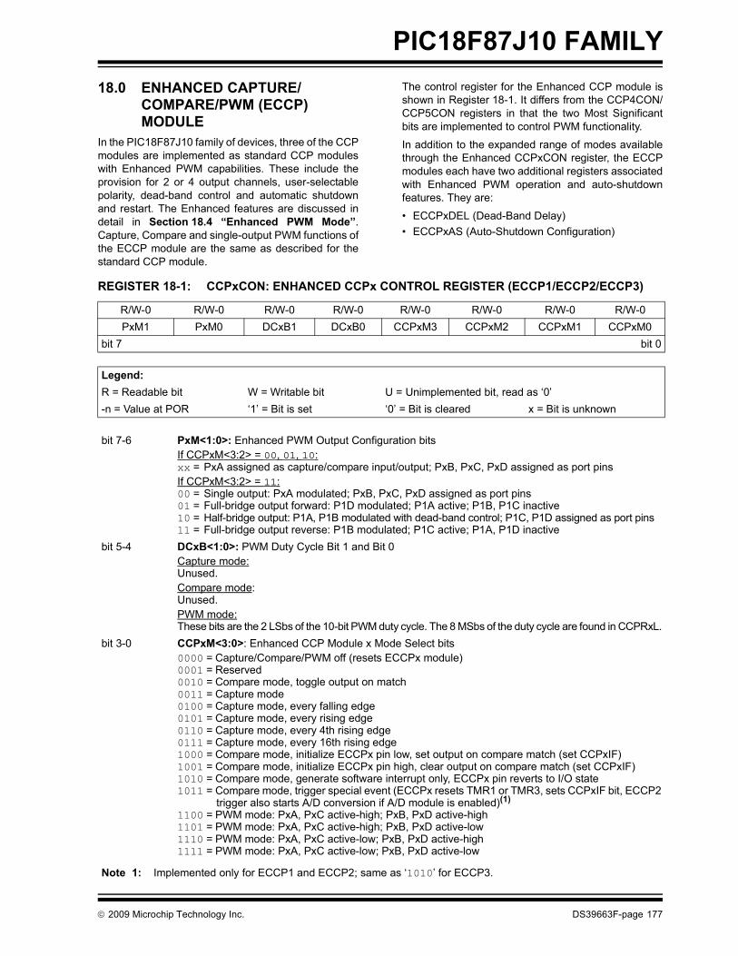
PIC18F87J10 FAMILY
18.0 ENHANCED CAPTURE/COMPARE/PWM (ECCP) MODULE
In the PIC18F87J10 family of devices, three of the CCPmodules are implemented as standard CCP moduleswith Enhanced PWM capabilities. These include theprovision for 2 or 4 output channels, user-selectablepolarity, dead-band control and automatic shutdownand restart. The Enhanced features are discussed indetail in Section 18.4 “Enhanced PWM Mode”.Capture, Compare and single-output PWM functions ofthe ECCP module are the same as described for thestandard CCP module.
The control register for the Enhanced CCP module isshown in Register 18-1. It differs from the CCP4CON/CCP5CON registers in that the two Most Significantbits are implemented to control PWM functionality.
In addition to the expanded range of modes availablethrough the Enhanced CCPxCON register, the ECCPmodules each have two additional registers associatedwith Enhanced PWM operation and auto-shutdownfeatures. They are:
• ECCPxDEL (Dead-Band Delay)• ECCPxAS (Auto-Shutdown Configuration)
REGISTER 18-1: CCPxCON: ENHANCED CCPx CONTROL REGISTER (ECCP1/ECCP2/ECCP3)
R/W-0 R/W-0 R/W-0 R/W-0 R/W-0 R/W-0 R/W-0 R/W-0PxM1 PxM0 DCxB1 DCxB0 CCPxM3 CCPxM2 CCPxM1 CCPxM0
bit 7 bit 0
Legend:R = Readable bit W = Writable bit U = Unimplemented bit, read as ‘0’-n = Value at POR ‘1’ = Bit is set ‘0’ = Bit is cleared x = Bit is unknown
bit 7-6 PxM<1:0>: Enhanced PWM Output Configuration bitsIf CCPxM<3:2> = 00, 01, 10:xx = PxA assigned as capture/compare input/output; PxB, PxC, PxD assigned as port pinsIf CCPxM<3:2> = 11:00 = Single output: PxA modulated; PxB, PxC, PxD assigned as port pins01 = Full-bridge output forward: P1D modulated; P1A active; P1B, P1C inactive10 = Half-bridge output: P1A, P1B modulated with dead-band control; P1C, P1D assigned as port pins11 = Full-bridge output reverse: P1B modulated; P1C active; P1A, P1D inactive
bit 5-4 DCxB<1:0>: PWM Duty Cycle Bit 1 and Bit 0Capture mode:Unused.Compare mode:Unused.PWM mode:These bits are the 2 LSbs of the 10-bit PWM duty cycle. The 8 MSbs of the duty cycle are found in CCPRxL.
bit 3-0 CCPxM<3:0>: Enhanced CCP Module x Mode Select bits0000 = Capture/Compare/PWM off (resets ECCPx module)0001 = Reserved 0010 = Compare mode, toggle output on match0011 = Capture mode0100 = Capture mode, every falling edge 0101 = Capture mode, every rising edge0110 = Capture mode, every 4th rising edge 0111 = Capture mode, every 16th rising edge1000 = Compare mode, initialize ECCPx pin low, set output on compare match (set CCPxIF)1001 = Compare mode, initialize ECCPx pin high, clear output on compare match (set CCPxIF)1010 = Compare mode, generate software interrupt only, ECCPx pin reverts to I/O state1011 = Compare mode, trigger special event (ECCPx resets TMR1 or TMR3, sets CCPxIF bit, ECCP2
trigger also starts A/D conversion if A/D module is enabled)(1)
1100 = PWM mode: PxA, PxC active-high; PxB, PxD active-high1101 = PWM mode: PxA, PxC active-high; PxB, PxD active-low1110 = PWM mode: PxA, PxC active-low; PxB, PxD active-high1111 = PWM mode: PxA, PxC active-low; PxB, PxD active-low
Note 1: Implemented only for ECCP1 and ECCP2; same as ‘1010’ for ECCP3.
© 2009 Microchip Technology Inc. DS39663F-page 177
PIC18F87J10 FAMILY
18.1 ECCP Outputs and Configuration Each of the Enhanced CCP modules may have up tofour PWM outputs, depending on the selectedoperating mode. These outputs, designated PxAthrough PxD, are multiplexed with various I/O pins.Some ECCP pin assignments are constant, whileothers change based on device configuration. Forthose pins that do change, the controlling bits are:• CCP2MX Configuration bit• ECCPMX Configuration bit (80-pin devices only)• Program Memory Operating mode, set by the
EMB Configuration bits (80-pin devices only)
The pin assignments for the Enhanced CCP modulesare summarized in Table 18-1, Table 18-2 andTable 18-3. To configure the I/O pins as PWM outputs,the proper PWM mode must be selected by setting thePxMx and CCPxMx bits (CCPxCON<7:6> and <3:0>,respectively). The appropriate TRIS direction bits forthe corresponding port pins must also be set asoutputs.
18.1.1 ECCP1/ECCP3 OUTPUTS AND PROGRAM MEMORY MODE
In 80-pin devices, the use of Extended Microcontrollermode has an indirect effect on the use of ECCP1 andECCP3 in Enhanced PWM modes. By default, PWMoutputs, P1B/P1C and P3B/P3C, are multiplexed toPORTE pins, along with the high-order byte of theexternal memory bus. When the bus is active inExtended Microcontroller mode, it overrides theEnhanced CCP outputs and makes them unavailable.Because of this, ECCP1 and ECCP3 can only be usedin compatible (single-output) PWM modes when thedevice is in Extended Microcontroller mode and defaultpin configuration.
An exception to this configuration is when a 12-bitaddress width is selected for the external bus(EMB<1:0> Configuration bits = 01). In this case, theupper pins of PORTE continue to operate as digital I/O,even when the external bus is active. P1B/P1C andP3B/P3C remain available for use as Enhanced PWMoutputs.
If an application requires the use of additional PWMoutputs during Enhanced microcontroller operation, theP1B/P1C and P3B/P3C outputs can be reassigned tothe upper bits of PORTH. This is done by clearing theECCPMX Configuration bit.
18.1.2 ECCP2 OUTPUTS AND PROGRAM MEMORY MODES
For 80-pin devices, the program memory mode of thedevice (Section 6.1.3 “PIC18F8XJ10/8XJ15 ProgramMemory Modes”) also impacts pin multiplexing for themodule.
The ECCP2 input/output (ECCP2/P2A) can be multi-plexed to one of three pins. The default assignment(CCP2MX Configuration bit is set) for all devices isRC1. Clearing CCP2MX reassigns ECCP2/P2A toRE7.
An additional option exists for 80-pin devices. Whenthese devices are operating in Microcontroller mode,the multiplexing options described above still apply. InExtended Microcontroller mode, clearing CCP2MXreassigns ECCP2/P2A to RB3.
18.1.3 USE OF CCP4 AND CCP5 WITH ECCP1 AND ECCP3
Only the ECCP2 module has four dedicated output pinsthat are available for use. Assuming that the I/O portsor other multiplexed functions on those pins are notneeded, they may be used whenever needed withoutinterfering with any other CCP module.
ECCP1 and ECCP3, on the other hand, only havethree dedicated output pins: ECCPx/PxA, PxB andPxC. Whenever these modules are configured forQuad PWM mode, the pin normally used for CCP4 orCCP5 becomes the PxD output pins for ECCP3 andECCP1, respectively. The CCP4 and CCP5 modulesremain functional but their outputs are overridden.
18.1.4 ECCP MODULES AND TIMER RESOURCES
Like the standard CCP modules, the ECCP modulescan utilize Timers 1, 2, 3 or 4, depending on the modeselected. Timer1 and Timer3 are available for modulesin Capture or Compare modes, while Timer2 andTimer4 are available for modules in PWM mode.Additional details on timer resources are provided inSection 17.1.1 “CCP Modules and TimerResources”.
DS39663F-page 178 © 2009 Microchip Technology Inc.

PIC18F87J10 FAMILY
TABLE 18-1: PIN CONFIGURATIONS FOR ECCP1TABLE 18-2: PIN CONFIGURATIONS FOR ECCP2
ECCP Mode CCP1CONConfiguration RC2 RE6 RE5 RG4 RH7 RH6
All PIC18F6XJ10/6XJ15 Devices:Compatible CCP 00xx 11xx ECCP1 RE6 RE5 RG4/CCP5 N/A N/ADual PWM 10xx 11xx P1A P1B RE5 RG4/CCP5 N/A N/AQuad PWM x1xx 11xx P1A P1B P1C P1D N/A N/A
PIC18F8XJ10/8XJ15 Devices, ECCPMX = 0, Microcontroller mode:Compatible CCP 00xx 11xx ECCP1 RE6/AD14 RE5/AD13 RG4/CCP5 RH7/AN15 RH6/AN14Dual PWM 10xx 11xx P1A RE6/AD14 RE5/AD13 RG4/CCP5 P1B RH6/AN14Quad PWM x1xx 11xx P1A RE6/AD14 RE5/AD13 P1D P1B P1CPIC18F8XJ10/8XJ15 Devices, ECCPMX = 1, Extended Microcontroller mode, 16-Bit or 20-Bit Address Width:
Compatible CCP 00xx 11xx ECCP1 RE6/AD14 RE5/AD13 RG4/CCP5 RH7/AN15 RH6/AN14PIC18F8XJ10/8XJ15 Devices, ECCPMX = 1,
Microcontroller mode or Extended Microcontroller mode, 12-Bit Address Width:Compatible CCP 00xx 11xx ECCP1 RE6/AD14 RE5/AD13 RG4/CCP5 RH7/AN15 RH6/AN14Dual PWM 10xx 11xx P1A P1B RE5/AD13 RG4/CCP5 RH7/AN15 RH6/AN14Quad PWM x1xx 11xx P1A P1B P1C P1D RH7/AN15 RH6/AN14Legend: x = Don’t care, N/A = Not available. Shaded cells indicate pin assignments not used by ECCP1 in a given mode.Note 1: With ECCP1 in Quad PWM mode, CCP5’s output is overridden by P1D; otherwise, CCP5 is fully operational.
ECCP Mode CCP2CONConfiguration RB3 RC1 RE7 RE2 RE1 RE0
All Devices, CCP2MX = 1, Either Operating mode:Compatible CCP 00xx 11xx RB3/INT3 ECCP2 RE7 RE2 RE1 RE0Dual PWM 10xx 11xx RB3/INT3 P2A RE7 P2B RE1 RE0Quad PWM x1xx 11xx RB3/INT3 P2A RE7 P2B P2C P2D
All Devices, CCP2MX = 0, Microcontroller mode:Compatible CCP 00xx 11xx RB3/INT3 RC1/T1OS1 ECCP2 RE2 RE1 RE0Dual PWM 10xx 11xx RB3/INT3 RC1/T1OS1 P2A P2B RE1 RE0Quad PWM x1xx 11xx RB3/INT3 RC1/T1OS1 P2A P2B P2C P2D
PIC18F8XJ10/8XJ15 Devices, CCP2MX = 0, Extended Microcontroller mode:Compatible CCP 00xx 11xx ECCP2 RC1/T1OS1 RE7/AD15 RE2/CS RE1/WR RE0/RD
Dual PWM 10xx 11xx P2A RC1/T1OS1 RE7/AD15 P2B RE1/WR RE0/RDQuad PWM x1xx 11xx P2A RC1/T1OS1 RE7/AD15 P2B P2C P2DLegend: x = Don’t care. Shaded cells indicate pin assignments not used by ECCP2 in a given mode.
© 2009 Microchip Technology Inc. DS39663F-page 179
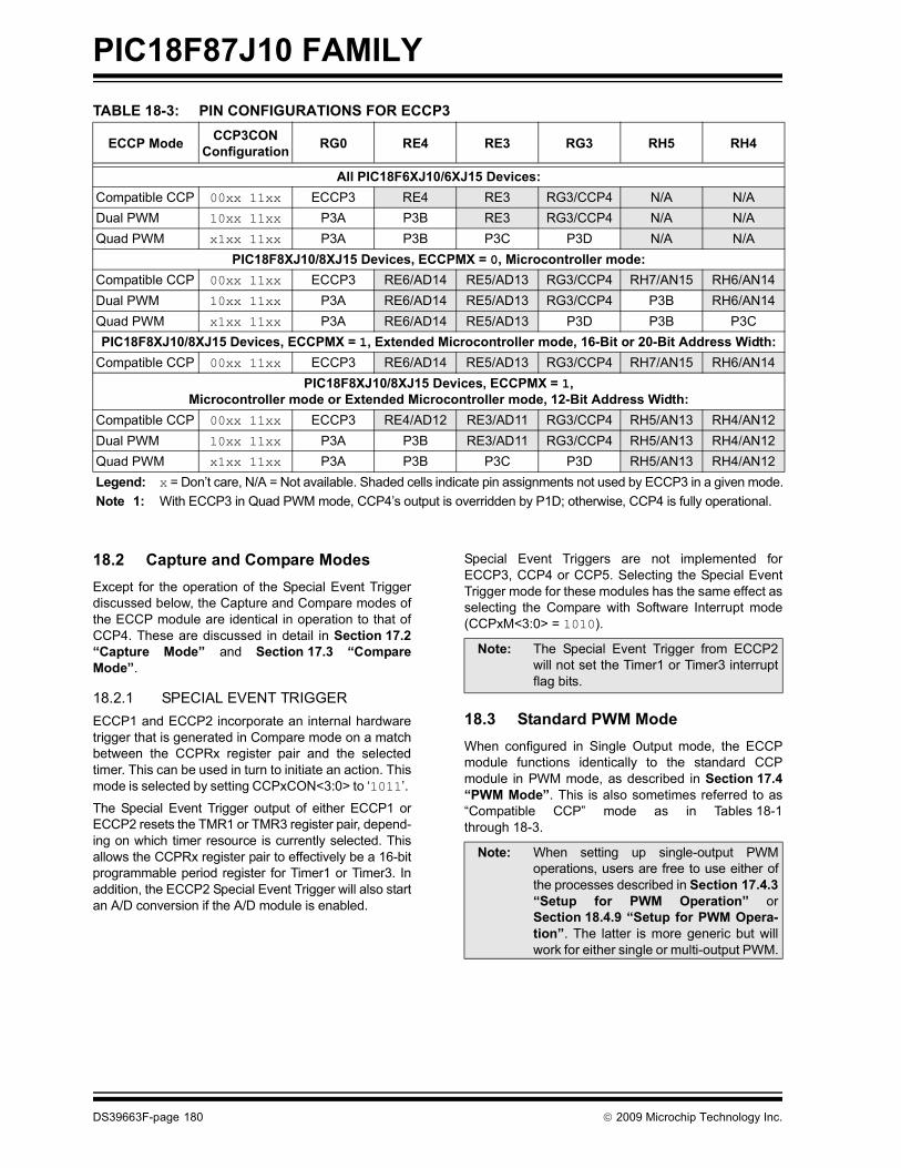
PIC18F87J10 FAMILY
TABLE 18-3: PIN CONFIGURATIONS FOR ECCP318.2 Capture and Compare ModesExcept for the operation of the Special Event Triggerdiscussed below, the Capture and Compare modes ofthe ECCP module are identical in operation to that ofCCP4. These are discussed in detail in Section 17.2“Capture Mode” and Section 17.3 “CompareMode”.
18.2.1 SPECIAL EVENT TRIGGERECCP1 and ECCP2 incorporate an internal hardwaretrigger that is generated in Compare mode on a matchbetween the CCPRx register pair and the selectedtimer. This can be used in turn to initiate an action. Thismode is selected by setting CCPxCON<3:0> to ‘1011’.
The Special Event Trigger output of either ECCP1 orECCP2 resets the TMR1 or TMR3 register pair, depend-ing on which timer resource is currently selected. Thisallows the CCPRx register pair to effectively be a 16-bitprogrammable period register for Timer1 or Timer3. Inaddition, the ECCP2 Special Event Trigger will also startan A/D conversion if the A/D module is enabled.
Special Event Triggers are not implemented forECCP3, CCP4 or CCP5. Selecting the Special EventTrigger mode for these modules has the same effect asselecting the Compare with Software Interrupt mode(CCPxM<3:0> = 1010).
18.3 Standard PWM ModeWhen configured in Single Output mode, the ECCPmodule functions identically to the standard CCPmodule in PWM mode, as described in Section 17.4“PWM Mode”. This is also sometimes referred to as“Compatible CCP” mode as in Tables 18-1through 18-3.
ECCP Mode CCP3CONConfiguration RG0 RE4 RE3 RG3 RH5 RH4
All PIC18F6XJ10/6XJ15 Devices:Compatible CCP 00xx 11xx ECCP3 RE4 RE3 RG3/CCP4 N/A N/ADual PWM 10xx 11xx P3A P3B RE3 RG3/CCP4 N/A N/AQuad PWM x1xx 11xx P3A P3B P3C P3D N/A N/A
PIC18F8XJ10/8XJ15 Devices, ECCPMX = 0, Microcontroller mode:Compatible CCP 00xx 11xx ECCP3 RE6/AD14 RE5/AD13 RG3/CCP4 RH7/AN15 RH6/AN14Dual PWM 10xx 11xx P3A RE6/AD14 RE5/AD13 RG3/CCP4 P3B RH6/AN14Quad PWM x1xx 11xx P3A RE6/AD14 RE5/AD13 P3D P3B P3CPIC18F8XJ10/8XJ15 Devices, ECCPMX = 1, Extended Microcontroller mode, 16-Bit or 20-Bit Address Width:
Compatible CCP 00xx 11xx ECCP3 RE6/AD14 RE5/AD13 RG3/CCP4 RH7/AN15 RH6/AN14PIC18F8XJ10/8XJ15 Devices, ECCPMX = 1,
Microcontroller mode or Extended Microcontroller mode, 12-Bit Address Width:Compatible CCP 00xx 11xx ECCP3 RE4/AD12 RE3/AD11 RG3/CCP4 RH5/AN13 RH4/AN12Dual PWM 10xx 11xx P3A P3B RE3/AD11 RG3/CCP4 RH5/AN13 RH4/AN12Quad PWM x1xx 11xx P3A P3B P3C P3D RH5/AN13 RH4/AN12Legend: x = Don’t care, N/A = Not available. Shaded cells indicate pin assignments not used by ECCP3 in a given mode.Note 1: With ECCP3 in Quad PWM mode, CCP4’s output is overridden by P1D; otherwise, CCP4 is fully operational.
Note: The Special Event Trigger from ECCP2will not set the Timer1 or Timer3 interruptflag bits.
Note: When setting up single-output PWMoperations, users are free to use either ofthe processes described in Section 17.4.3“Setup for PWM Operation” orSection 18.4.9 “Setup for PWM Opera-tion”. The latter is more generic but willwork for either single or multi-output PWM.
DS39663F-page 180 © 2009 Microchip Technology Inc.

PIC18F87J10 FAMILY
18.4 Enhanced PWM ModeThe Enhanced PWM mode provides additional PWMoutput options for a broader range of control applica-tions. The module is a backward compatible version ofthe standard CCP module and offers up to four outputs,designated PxA through PxD. Users are also able toselect the polarity of the signal (either active-high oractive-low). The module’s output mode and polarityare configured by setting the PxM<1:0> andCCPxM<3:0> bits of the CCPxCON register(CCPxCON<7:6> and CCPxCON<3:0>, respectively).For the sake of clarity, Enhanced PWM mode operationis described generically throughout this section withrespect to ECCP1 and TMR2 modules. Control registernames are presented in terms of ECCP1. All threeEnhanced modules, as well as the two timer resources,can be used interchangeably and function identically.TMR2 or TMR4 can be selected for PWM operation byselecting the proper bits in T3CON.
Figure 18-1 shows a simplified block diagram of PWMoperation. All control registers are double-buffered andare loaded at the beginning of a new PWM cycle (theperiod boundary when Timer2 resets) in order to pre-vent glitches on any of the outputs. The exception is thePWM Delay register, ECCP1DEL, which is loaded ateither the duty cycle boundary or the boundary period(whichever comes first). Because of the buffering, themodule waits until the assigned timer resets instead ofstarting immediately. This means that Enhanced PWM
waveforms do not exactly match the standard PWMwaveforms, but are instead offset by one full instructioncycle (4 TOSC).
As before, the user must manually configure theappropriate TRIS bits for output.
18.4.1 PWM PERIODThe PWM period is specified by writing to the PR2register. The PWM period can be calculated using theequation:
EQUATION 18-1:
PWM frequency is defined as 1/[PWM period]. WhenTMR2 is equal to PR2, the following three events occuron the next increment cycle:
• TMR2 is cleared• The ECCP1 pin is set (if PWM duty cycle = 0%,
the ECCP1 pin will not be set)• The PWM duty cycle is copied from CCPR1L into
CCPR1H
FIGURE 18-1: SIMPLIFIED BLOCK DIAGRAM OF THE ENHANCED PWM MODULE
Note: The Timer2 postscaler (see Section 14.0“Timer2 Module”) is not used in thedetermination of the PWM frequency. Thepostscaler could be used to have a servoupdate rate at a different frequency thanthe PWM output.
PWM Period = [(PR2) + 1] • 4 • TOSC •(TMR2 Prescale Value)
CCPR1L
CCPR1H (Slave)
Comparator
TMR2
Comparator
PR2
(Note 1)
R Q
S
Duty Cycle RegistersCCP1CON<5:4>
Clear Timer,set ECCP1 pin and latch D.C.
Note: The 8-bit timer TMR2 register is concatenated with the 2-bit internal Q clock, or 2 bits of the prescaler, to create the 10-bittime base.
TRISx<x>
ECCP1/P1A
TRISx<x>
P1B
TRISx<x>
TRISx<x>
P1D
OutputController
P1M1<1:0>2
CCP1M<3:0>4
ECCP1DEL
ECCP1/P1A
P1B
P1C
P1D
P1C
© 2009 Microchip Technology Inc. DS39663F-page 181

PIC18F87J10 FAMILY
18.4.2 PWM DUTY CYCLEThe PWM duty cycle is specified by writing to theCCPR1L register and to the CCP1CON<5:4> bits. Upto 10-bit resolution is available. The CCPR1L containsthe eight MSbs and the CCP1CON<5:4> contains thetwo LSbs. This 10-bit value is represented byCCPR1L:CCP1CON<5:4>. The PWM duty cycle iscalculated by the equation:EQUATION 18-2:
CCPR1L and CCP1CON<5:4> can be written to at anytime but the duty cycle value is not copied intoCCPR1H until a match between PR2 and TMR2 occurs(i.e., the period is complete). In PWM mode, CCPR1His a read-only register.
The CCPR1H register and a 2-bit internal latch areused to double-buffer the PWM duty cycle. Thisdouble-buffering is essential for glitchless PWM opera-tion. When the CCPR1H and 2-bit latch match TMR2,concatenated with an internal 2-bit Q clock or two bitsof the TMR2 prescaler, the ECCP1 pin is cleared. Themaximum PWM resolution (bits) for a given PWMfrequency is given by the equation:
EQUATION 18-3:
18.4.3 PWM OUTPUT CONFIGURATIONSThe P1M<1:0> bits in the CCP1CON register allow oneof four configurations:
• Single Output• Half-Bridge Output • Full-Bridge Output, Forward mode• Full-Bridge Output, Reverse mode
The Single Output mode is the standard PWM modediscussed in Section 18.4 “Enhanced PWM Mode”.The Half-Bridge and Full-Bridge Output modes arecovered in detail in the sections that follow.
The general relationship of the outputs in allconfigurations is summarized in Figure 18-2.
TABLE 18-4: EXAMPLE PWM FREQUENCIES AND RESOLUTIONS AT 40 MHz
PWM Duty Cycle = (CCPR1L:CCP1CON<5:4>) •TOSC • (TMR2 Prescale Value)
( )PWM Resolution (max) =
FOSCFPWM
log
log(2)bits
Note: If the PWM duty cycle value is longer thanthe PWM period, the ECCP1 pin will notbe cleared.
PWM Frequency 2.44 kHz 9.77 kHz 39.06 kHz 156.25 kHz 312.50 kHz 416.67 kHz
Timer Prescaler (1, 4, 16) 16 4 1 1 1 1PR2 Value FFh FFh FFh 3Fh 1Fh 17hMaximum Resolution (bits) 10 10 10 8 7 6.58
DS39663F-page 182 © 2009 Microchip Technology Inc.
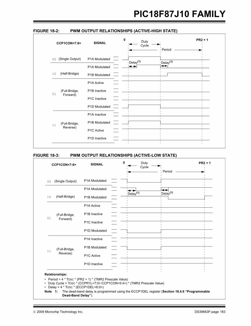
PIC18F87J10 FAMILY
FIGURE 18-2: PWM OUTPUT RELATIONSHIPS (ACTIVE-HIGH STATE)FIGURE 18-3: PWM OUTPUT RELATIONSHIPS (ACTIVE-LOW STATE)
0
Period
00
10
01
11
SIGNALPR2 + 1
CCP1CON<7:6>
P1A Modulated
P1A Modulated
P1B Modulated
P1A Active
P1B Inactive
P1C Inactive
P1D Modulated
P1A Inactive
P1B Modulated
P1C Active
P1D Inactive
DutyCycle
(Single Output)
(Half-Bridge)
(Full-Bridge,Forward)
(Full-Bridge,Reverse)
Delay(1) Delay(1)
0
Period
00
10
01
11
SIGNAL PR2 + 1CCP1CON<7:6> DutyCycle
(Single Output)
(Half-Bridge)
(Full-Bridge,Forward)
(Full-Bridge,Reverse)
Delay(1) Delay(1)
Relationships:• Period = 4 * TOSC * (PR2 + 1) * (TMR2 Prescale Value)• Duty Cycle = TOSC * (CCPR1L<7:0>:CCP1CON<5:4>) * (TMR2 Prescale Value)• Delay = 4 * TOSC * (ECCP1DEL<6:0>)Note 1: The dead-band delay is programmed using the ECCP1DEL register (Section 18.4.6 “Programmable
Dead-Band Delay”).
P1A Modulated
P1A Modulated
P1B Modulated
P1A Active
P1B Inactive
P1C Inactive
P1D Modulated
P1A Inactive
P1B Modulated
P1C Active
P1D Inactive
© 2009 Microchip Technology Inc. DS39663F-page 183

PIC18F87J10 FAMILY
18.4.4 HALF-BRIDGE MODEIn the Half-Bridge Output mode, two pins are used asoutputs to drive push-pull loads. The PWM outputsignal is output on the P1A pin, while the complemen-tary PWM output signal is output on the P1B pin(Figure 18-4). This mode can be used for half-bridgeapplications, as shown in Figure 18-5, or for full-bridgeapplications, where four power switches are beingmodulated with two PWM signals.In Half-Bridge Output mode, the programmabledead-band delay can be used to prevent shoot-throughcurrent in half-bridge power devices. The value of bits,P1DC<6:0>, sets the number of instruction cyclesbefore the output is driven active. If the value is greaterthan the duty cycle, the corresponding output remainsinactive during the entire cycle. See Section 18.4.6“Programmable Dead-Band Delay” for more detailson dead-band delay operations.
Since the P1A and P1B outputs are multiplexed withthe PORTC<2> and PORTE<6> data latches, theTRISC<2> and TRISE<6> bits must be cleared toconfigure P1A and P1B as outputs.
FIGURE 18-4: HALF-BRIDGE PWM OUTPUT
FIGURE 18-5: EXAMPLES OF HALF-BRIDGE OUTPUT MODE APPLICATIONS
Period
Duty Cycle
td
td
(1)
P1A(2)
P1B(2)
td = Dead Band Delay
Period
(1) (1)
Note 1: At this time, the TMR2 register is equal to thePR2 register.
2: The output signals are shown as active-high.
PIC18F87J10
P1A
P1B
FETDriver
FETDriver
V+
V-
Load
+V-
+V-
FETDriver
FETDriver
V+
V-
Load
FETDriver
FETDriver
PIC18F87J10
P1A
P1B
Standard Half-Bridge Circuit (“Push-Pull”)
Half-Bridge Output Driving a Full-Bridge Circuit
DS39663F-page 184 © 2009 Microchip Technology Inc.
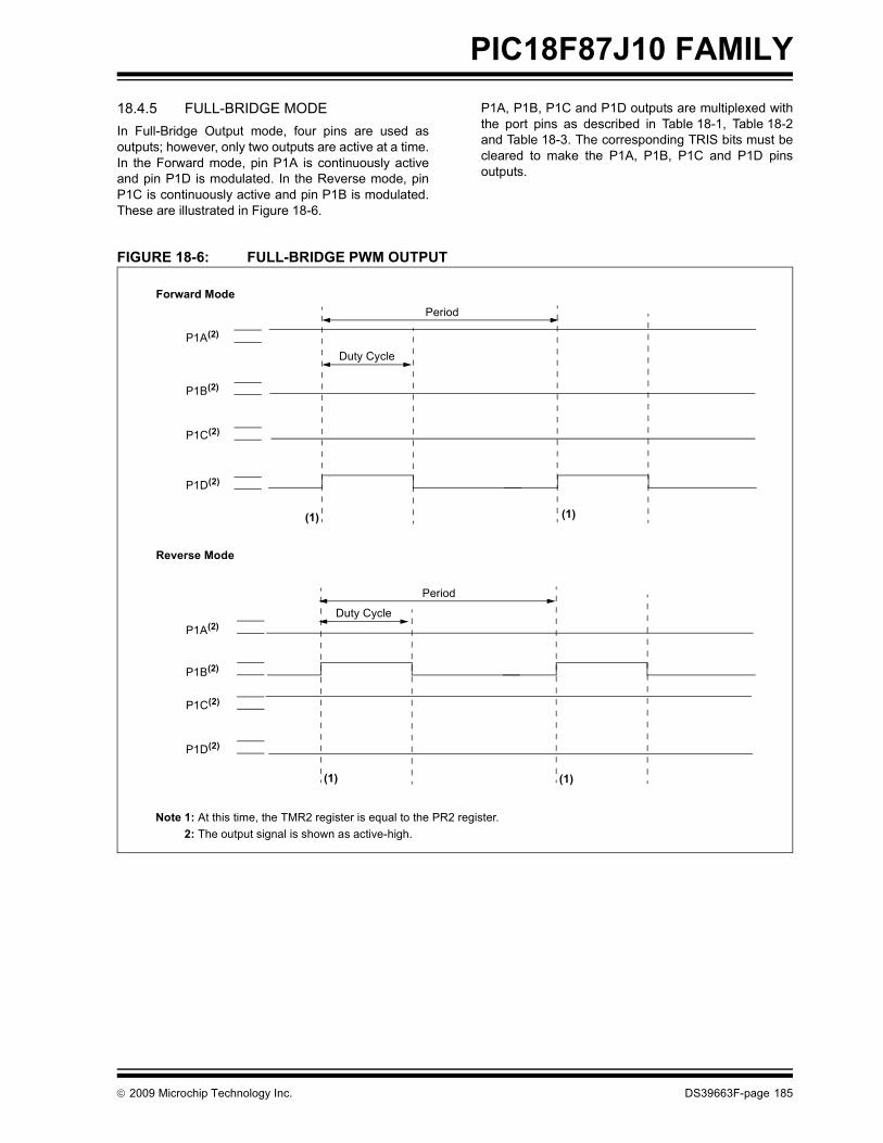
PIC18F87J10 FAMILY
18.4.5 FULL-BRIDGE MODEIn Full-Bridge Output mode, four pins are used asoutputs; however, only two outputs are active at a time.In the Forward mode, pin P1A is continuously activeand pin P1D is modulated. In the Reverse mode, pinP1C is continuously active and pin P1B is modulated.These are illustrated in Figure 18-6.P1A, P1B, P1C and P1D outputs are multiplexed withthe port pins as described in Table 18-1, Table 18-2and Table 18-3. The corresponding TRIS bits must becleared to make the P1A, P1B, P1C and P1D pinsoutputs.
FIGURE 18-6: FULL-BRIDGE PWM OUTPUT
Period
Duty CycleP1A(2)
P1B(2)
P1C(2)
P1D(2)
Forward Mode
(1)
Period
Duty CycleP1A(2)
P1C(2)
P1D(2)
P1B(2)
Reverse Mode
(1)
(1)(1)
Note 1: At this time, the TMR2 register is equal to the PR2 register.Note 2: The output signal is shown as active-high.
© 2009 Microchip Technology Inc. DS39663F-page 185
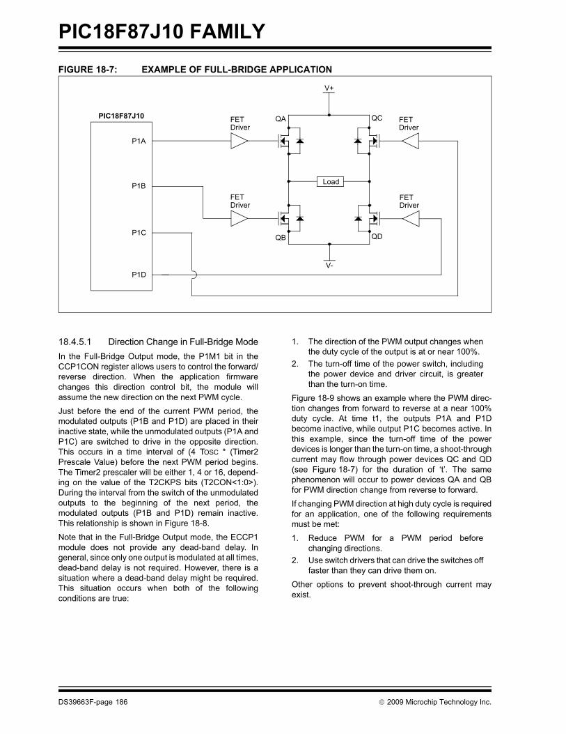
PIC18F87J10 FAMILY
FIGURE 18-7: EXAMPLE OF FULL-BRIDGE APPLICATION18.4.5.1 Direction Change in Full-Bridge ModeIn the Full-Bridge Output mode, the P1M1 bit in theCCP1CON register allows users to control the forward/reverse direction. When the application firmwarechanges this direction control bit, the module willassume the new direction on the next PWM cycle.
Just before the end of the current PWM period, themodulated outputs (P1B and P1D) are placed in theirinactive state, while the unmodulated outputs (P1A andP1C) are switched to drive in the opposite direction.This occurs in a time interval of (4 TOSC * (Timer2Prescale Value) before the next PWM period begins.The Timer2 prescaler will be either 1, 4 or 16, depend-ing on the value of the T2CKPS bits (T2CON<1:0>).During the interval from the switch of the unmodulatedoutputs to the beginning of the next period, themodulated outputs (P1B and P1D) remain inactive.This relationship is shown in Figure 18-8.
Note that in the Full-Bridge Output mode, the ECCP1module does not provide any dead-band delay. Ingeneral, since only one output is modulated at all times,dead-band delay is not required. However, there is asituation where a dead-band delay might be required.This situation occurs when both of the followingconditions are true:
1. The direction of the PWM output changes whenthe duty cycle of the output is at or near 100%.
2. The turn-off time of the power switch, includingthe power device and driver circuit, is greaterthan the turn-on time.
Figure 18-9 shows an example where the PWM direc-tion changes from forward to reverse at a near 100%duty cycle. At time t1, the outputs P1A and P1Dbecome inactive, while output P1C becomes active. Inthis example, since the turn-off time of the powerdevices is longer than the turn-on time, a shoot-throughcurrent may flow through power devices QC and QD(see Figure 18-7) for the duration of ‘t’. The samephenomenon will occur to power devices QA and QBfor PWM direction change from reverse to forward.
If changing PWM direction at high duty cycle is requiredfor an application, one of the following requirementsmust be met:
1. Reduce PWM for a PWM period beforechanging directions.
2. Use switch drivers that can drive the switches offfaster than they can drive them on.
Other options to prevent shoot-through current mayexist.
PIC18F87J10
P1A
P1C
FETDriver
FETDriver
V+
V-
Load
FETDriver
FETDriver
P1B
P1D
QA
QB QD
QC
DS39663F-page 186 © 2009 Microchip Technology Inc.
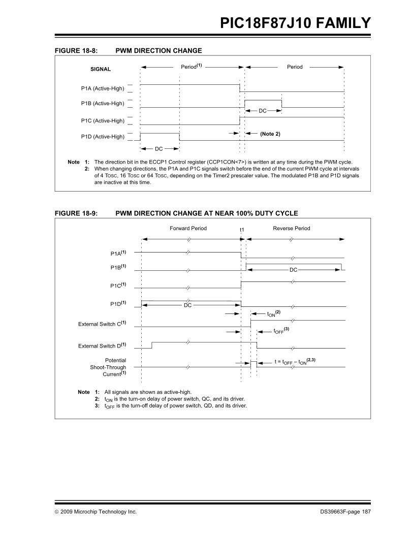
PIC18F87J10 FAMILY
FIGURE 18-8: PWM DIRECTION CHANGEFIGURE 18-9: PWM DIRECTION CHANGE AT NEAR 100% DUTY CYCLE
DC
Period(1)SIGNAL
Note 1: The direction bit in the ECCP1 Control register (CCP1CON<7>) is written at any time during the PWM cycle.2: When changing directions, the P1A and P1C signals switch before the end of the current PWM cycle at intervals
of 4 TOSC, 16 TOSC or 64 TOSC, depending on the Timer2 prescaler value. The modulated P1B and P1D signals are inactive at this time.
Period
(Note 2)
P1A (Active-High)
P1B (Active-High)
P1C (Active-High)
P1D (Active-High)
DC
Forward Period Reverse Period
P1A(1)
tON(2)
tOFF(3)
t = tOFF – tON(2,3)
P1B(1)
P1C(1)
P1D(1)
External Switch D(1)
PotentialShoot-Through
Current(1)
Note 1: All signals are shown as active-high.2: tON is the turn-on delay of power switch, QC, and its driver.3: tOFF is the turn-off delay of power switch, QD, and its driver.
External Switch C(1)
t1
DC
DC
© 2009 Microchip Technology Inc. DS39663F-page 187

PIC18F87J10 FAMILY
18.4.6 PROGRAMMABLE DEAD-BANDDELAYIn half-bridge applications, where all power switchesare modulated at the PWM frequency at all times, thepower switches normally require more time to turn offthan to turn on. If both the upper and lower powerswitches are switched at the same time (one turned onand the other turned off), both switches may be on fora short period of time until one switch completely turnsoff. During this brief interval, a very high current(shoot-through current) may flow through both powerswitches, shorting the bridge supply. To avoid thispotentially destructive shoot-through current from flow-ing during switching, turning on either of the powerswitches is normally delayed to allow the other switchto completely turn off.
In the Half-Bridge Output mode, a digitally program-mable dead-band delay is available to avoidshoot-through current from destroying the bridgepower switches. The delay occurs at the signaltransition from the non-active state to the active state.See Figure 18-4 for illustration. The lower seven bits ofthe ECCP1DEL register (Register 18-2) set the delayperiod in terms of microcontroller instruction cycles(TCY or 4 TOSC).
18.4.7 ENHANCED PWM AUTO-SHUTDOWN
When the ECCP1 is programmed for any of theEnhanced PWM modes, the active output pins may beconfigured for auto-shutdown. Auto-shutdown immedi-ately places the Enhanced PWM output pins into adefined shutdown state when a shutdown eventoccurs.
A shutdown event can be caused by either of the twocomparator modules or the FLT0 pin (or any combinationof these three sources). The comparators may be usedto monitor a voltage input proportional to a current beingmonitored in the bridge circuit. If the voltage exceeds athreshold, the comparator switches state and triggers ashutdown. Alternatively, a low-level digital signal on theFLT0 pin can also trigger a shutdown. Theauto-shutdown feature can be disabled by not selectingany auto-shutdown sources. The auto-shutdown sourcesto be used are selected using the ECCP1AS<2:0> bits(bits<6:4> of the ECCP1AS register).
When a shutdown occurs, the output pins areasynchronously placed in their shutdown states,specified by the PSS1AC<1:0> and PSS1BD<1:0> bits(ECCP1AS<3:0>). Each pin pair (P1A/P1C and P1B/P1D) may be set to drive high, drive low or be tri-stated(not driving). The ECCP1ASE bit (ECCP1AS<7>) isalso set to hold the Enhanced PWM outputs in theirshutdown states.
The ECCP1ASE bit is set by hardware when ashutdown event occurs. If automatic restarts are notenabled, the ECCP1ASE bit is cleared by firmwarewhen the cause of the shutdown clears. If automaticrestarts are enabled, the ECCP1ASE bit is automati-cally cleared when the cause of the auto-shutdown hascleared.
If the ECCP1ASE bit is set when a PWM period begins,the PWM outputs remain in their shutdown state for thatentire PWM period. When the ECCP1ASE bit iscleared, the PWM outputs will return to normaloperation at the beginning of the next PWM period.
Note: Writing to the ECCP1ASE bit is disabledwhile a shutdown condition is active.
REGISTER 18-2: ECCPxDEL: PWM DEAD-BAND DELAY REGISTER
R/W-0 R/W-0 R/W-0 R/W-0 R/W-0 R/W-0 R/W-0 R/W-0PxRSEN PxDC6 PxDC5 PxDC4 PxDC3 PxDC2 PxDC1 PxDC0
bit 7 bit 0
Legend:R = Readable bit W = Writable bit U = Unimplemented bit, read as ‘0’-n = Value at POR ‘1’ = Bit is set ‘0’ = Bit is cleared x = Bit is unknown
bit 7 PxRSEN: PWM Restart Enable bit1 = Upon auto-shutdown, the ECCPxASE bit clears automatically once the shutdown event goes
away; the PWM restarts automatically0 = Upon auto-shutdown, ECCPxASE must be cleared in software to restart the PWM
bit 6-0 PxDC<6:0>: PWM Delay Count bitsDelay time, in number of FOSC/4 (4 * TOSC) cycles, between the scheduled and actual time for a PWMsignal to transition to active.
DS39663F-page 188 © 2009 Microchip Technology Inc.
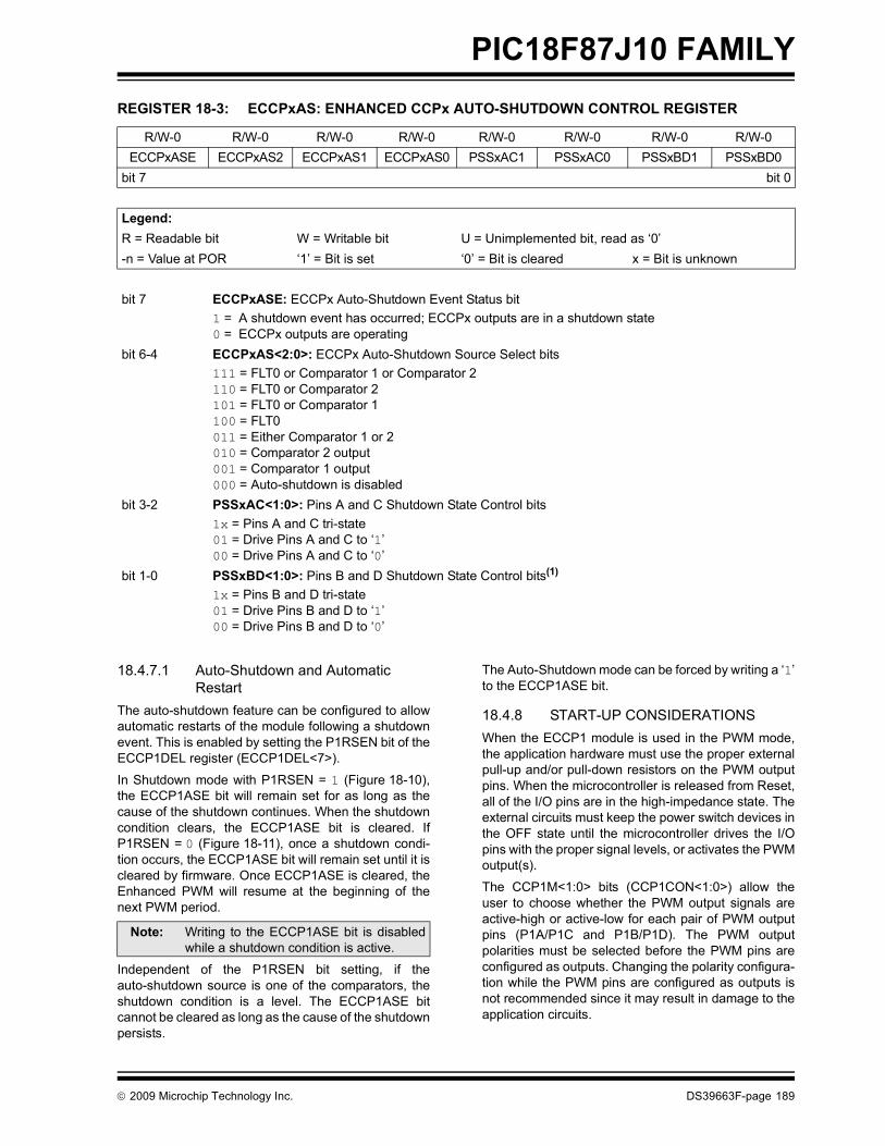
PIC18F87J10 FAMILY
18.4.7.1 Auto-Shutdown and Automatic Restart
The auto-shutdown feature can be configured to allowautomatic restarts of the module following a shutdownevent. This is enabled by setting the P1RSEN bit of theECCP1DEL register (ECCP1DEL<7>).
In Shutdown mode with P1RSEN = 1 (Figure 18-10),the ECCP1ASE bit will remain set for as long as thecause of the shutdown continues. When the shutdowncondition clears, the ECCP1ASE bit is cleared. IfP1RSEN = 0 (Figure 18-11), once a shutdown condi-tion occurs, the ECCP1ASE bit will remain set until it iscleared by firmware. Once ECCP1ASE is cleared, theEnhanced PWM will resume at the beginning of thenext PWM period.
Independent of the P1RSEN bit setting, if theauto-shutdown source is one of the comparators, theshutdown condition is a level. The ECCP1ASE bitcannot be cleared as long as the cause of the shutdownpersists.
The Auto-Shutdown mode can be forced by writing a ‘1’to the ECCP1ASE bit.
18.4.8 START-UP CONSIDERATIONSWhen the ECCP1 module is used in the PWM mode,the application hardware must use the proper externalpull-up and/or pull-down resistors on the PWM outputpins. When the microcontroller is released from Reset,all of the I/O pins are in the high-impedance state. Theexternal circuits must keep the power switch devices inthe OFF state until the microcontroller drives the I/Opins with the proper signal levels, or activates the PWMoutput(s).
The CCP1M<1:0> bits (CCP1CON<1:0>) allow theuser to choose whether the PWM output signals areactive-high or active-low for each pair of PWM outputpins (P1A/P1C and P1B/P1D). The PWM outputpolarities must be selected before the PWM pins areconfigured as outputs. Changing the polarity configura-tion while the PWM pins are configured as outputs isnot recommended since it may result in damage to theapplication circuits.
REGISTER 18-3: ECCPxAS: ENHANCED CCPx AUTO-SHUTDOWN CONTROL REGISTER
R/W-0 R/W-0 R/W-0 R/W-0 R/W-0 R/W-0 R/W-0 R/W-0ECCPxASE ECCPxAS2 ECCPxAS1 ECCPxAS0 PSSxAC1 PSSxAC0 PSSxBD1 PSSxBD0
bit 7 bit 0
Legend:R = Readable bit W = Writable bit U = Unimplemented bit, read as ‘0’-n = Value at POR ‘1’ = Bit is set ‘0’ = Bit is cleared x = Bit is unknown
bit 7 ECCPxASE: ECCPx Auto-Shutdown Event Status bit1 = A shutdown event has occurred; ECCPx outputs are in a shutdown state0 = ECCPx outputs are operating
bit 6-4 ECCPxAS<2:0>: ECCPx Auto-Shutdown Source Select bits111 = FLT0 or Comparator 1 or Comparator 2110 = FLT0 or Comparator 2101 = FLT0 or Comparator 1100 = FLT0011 = Either Comparator 1 or 2010 = Comparator 2 output001 = Comparator 1 output000 = Auto-shutdown is disabled
bit 3-2 PSSxAC<1:0>: Pins A and C Shutdown State Control bits1x = Pins A and C tri-state01 = Drive Pins A and C to ‘1’00 = Drive Pins A and C to ‘0’
bit 1-0 PSSxBD<1:0>: Pins B and D Shutdown State Control bits(1)
1x = Pins B and D tri-state01 = Drive Pins B and D to ‘1’00 = Drive Pins B and D to ‘0’
Note: Writing to the ECCP1ASE bit is disabledwhile a shutdown condition is active.
© 2009 Microchip Technology Inc. DS39663F-page 189

PIC18F87J10 FAMILY
The P1A, P1B, P1C and P1D output latches may not bein the proper states when the PWM module is initialized.Enabling the PWM pins for output at the same time asthe ECCP1 module may cause damage to the applica-tion circuit. The ECCP1 module must be enabled in theproper output mode and complete a full PWM cyclebefore configuring the PWM pins as outputs. The com-pletion of a full PWM cycle is indicated by the TMR2IFbit being set as the second PWM period begins.
FIGURE 18-10: PWM AUTO-SHUTDOWN (P1RSEN = 1, AUTO-RESTART ENABLED)
FIGURE 18-11: PWM AUTO-SHUTDOWN (P1RSEN = 0, AUTO-RESTART DISABLED)
Shutdown
PWM
ECCP1ASE bit
Activity
Event
ShutdownEvent Occurs
ShutdownEvent Clears
PWMResumes
Normal PWM
Start ofPWM Period
PWM Period
Shutdown
PWM
ECCP1ASE bit
Activity
Event
ShutdownEvent Occurs
ShutdownEvent Clears
PWMResumes
Normal PWM
Start ofPWM Period
ECCP1ASECleared byFirmware
PWM Period
DS39663F-page 190 © 2009 Microchip Technology Inc.

PIC18F87J10 FAMILY
18.4.9 SETUP FOR PWM OPERATIONThe following steps should be taken when configuringthe ECCPx module for PWM operation:1. Configure the PWM pins, PxA and PxB (andPxC and PxD, if used), as inputs by setting thecorresponding TRIS bits.
2. Set the PWM period by loading the PR2 (PR4)register.
3. Configure the ECCPx module for the desiredPWM mode and configuration by loading theCCPxCON register with the appropriate values:• Select one of the available output
configurations and direction with the PxM<1:0> bits.
• Select the polarities of the PWM output signals with the CCPxM<3:0> bits.
4. Set the PWM duty cycle by loading the CCPRxLregister and the CCPxCON<5:4> bits.
5. For auto-shutdown:• Disable auto-shutdown; ECCP1ASE = 0.• Configure auto-shutdown source.• Wait for Run condition.
6. For Half-Bridge Output mode, set thedead-band delay by loading ECCPxDEL<6:0>with the appropriate value.
7. If auto-shutdown operation is required, load theECCPxAS register:• Select the auto-shutdown sources using the
ECCPxAS<2:0> bits.• Select the shutdown states of the PWM
output pins using the PSSxAC<1:0> and PSSxBD<1:0> bits.
• Set the ECCPxASE bit (ECCPxAS<7>).
8. If auto-restart operation is required, set thePxRSEN bit (ECCPxDEL<7>).
9. Configure and start TMRx (TMR2 or TMR4):• Clear the TMRx interrupt flag bit by clearing
the TMRxIF bit (PIR1<1> for Timer2 or PIR3<3> for Timer4).
• Set the TMRx prescale value by loading the TxCKPS bits (TxCON<1:0>).
• Enable Timer2 (or Timer4) by setting the TMRxON bit (TxCON<2>).
10. Enable PWM outputs after a new PWM cyclehas started:• Wait until TMRx overflows (TMRxIF bit is set).• Enable the ECCPx/PxA, PxB, PxC and/or
PxD pin outputs by clearing the respective TRIS bits.
• Clear the ECCPxASE bit (ECCPxAS<7>).
18.4.10 EFFECTS OF A RESETBoth Power-on Reset and subsequent Resets will forceall ports to Input mode and the ECCP registers to theirReset states.
This forces the Enhanced CCP module to reset to astate compatible with the standard CCP module.
© 2009 Microchip Technology Inc. DS39663F-page 191

PIC18F87J10 FAMILY
TABLE 18-5: REGISTERS ASSOCIATED WITH ECCP MODULES AND TIMER1 TO TIMER4Name Bit 7 Bit 6 Bit 5 Bit 4 Bit 3 Bit 2 Bit 1 Bit 0Reset Values
on page
INTCON GIE/GIEH PEIE/GIEL TMR0IE INT0IE RBIE TMR0IF INT0IF RBIF 53
RCON IPEN — — RI TO PD POR BOR 54PIR1 PSPIF ADIF RC1IF TX1IF SSP1IF CCP1IF TMR2IF TMR1IF 55PIE1 PSPIE ADIE RC1IE TX1IE SSP1IE CCP1IE TMR2IE TMR1IE 55IPR1 PSPIP ADIP RC1IP TX1IP SSP1IP CCP1IP TMR2IP TMR1IP 55PIR2 OSCFIF CMIF — — BCL1IF — TMR3IF CCP2IF 55PIE2 OSCFIE CMIE — — BCL1IE — TMR3IE CCP2IE 55IPR2 OSCFIP CMIP — — BCL1IP — TMR3IP CCP2IP 55PIR3 SSP2IF BCL2IF RC2IF TX2IF TMR4IF CCP5IF CCP4IF CCP3IF 55PIE3 SSP2IE BCL2IE RC2IE TX2IE TMR4IE CCP5IE CCP4IE CCP3IE 55IPR3 SSP2IP BCL2IP RC2IP TX2IP TMR4IP CCP5IP CCP4IP CCP3IP 55TRISB TRISB7 TRISB6 TRISB5 TRISB4 TRISB3 TRISB2 TRISB1 TRISB0 56TRISC TRISC7 TRISC6 TRISC5 TRISC4 TRISC3 TRISC2 TRISC1 TRISC0 56TRISE TRISE7 TRISE6 TRISE5 TRISE4 TRISE3 TRISE2 TRISE1 TRISE0 56TRISG — — — TRISG4 TRISG3 TRISG2 TRISG1 TRISG0 56TRISH TRISH7 TRISH6 TRISH5 TRISH4 TRISH3 TRISH2 TRISH1 TRISH0 56TMR1L Timer1 Register Low Byte 54TMR1H Timer1 Register High Byte 54
T1CON RD16 T1RUN T1CKPS1 T1CKPS0 T1OSCEN T1SYNC TMR1CS TMR1ON 54TMR2 Timer2 Register 54T2CON — T2OUTPS3 T2OUTPS2 T2OUTPS1 T2OUTPS0 TMR2ON T2CKPS1 T2CKPS0 54PR2 Timer2 Period Register 54TMR3L Timer3 Register Low Byte 55TMR3H Timer3 Register High Byte 55
T3CON RD16 T3CCP2 T3CKPS1 T3CKPS0 T3CCP1 T3SYNC TMR3CS TMR3ON 55TMR4 Timer4 Register 57T4CON — T4OUTPS3 T4OUTPS2 T4OUTPS1 T4OUTPS0 TMR4ON T4CKPS1 T4CKPS0 57PR4 Timer4 Period Register 57CCPRxL(1) Capture/Compare/PWM Register x Low Byte 55CCPRxH(1) Capture/Compare/PWM Register x High Byte 55,CCPxCON(1) PxM1 PxM0 DCxB1 DCxB0 CCPxM3 CCPxM2 CCPxM1 CCPxM0 55ECCPxAS(1) ECCPxASE ECCPxAS2 ECCPxAS1 ECCPxAS0 PSSxAC1 PSSxAC0 PSSxBD1 PSSxBD0 55, 57ECCPxDEL(1) PxRSEN PxDC6 PxDC5 PxDC4 PxDC3 PxDC2 PxDC1 PxDC0 57Legend: — = unimplemented, read as ‘0’. Shaded cells are not used during ECCP operation.Note 1: Generic term for all of the identical registers of this name for all Enhanced CCP modules, where ‘x’ identifies the
individual module (ECCP1, ECCP2 or ECCP3). Bit assignments and Reset values for all registers of the same generic name are identical.
DS39663F-page 192 © 2009 Microchip Technology Inc.

PIC18F87J10 FAMILY
19.0 MASTER SYNCHRONOUS SERIAL PORT (MSSP) MODULE
19.1 Master SSP (MSSP) Module Overview
The Master Synchronous Serial Port (MSSP) module isa serial interface, useful for communicating with otherperipheral or microcontroller devices. These peripheraldevices may be serial EEPROMs, shift registers,display drivers, A/D Converters, etc. The MSSPmodule can operate in one of two modes:
• Serial Peripheral Interface (SPI)• Inter-Integrated Circuit (I2C™)
- Full Master mode- Slave mode (with general address call)
The I2C interface supports the following modes inhardware:
• Master mode• Multi-Master mode• Slave mode (with address masking for both 10-bit
and 7-bit addressing)
All members of the PIC18F87J10 family have twoMSSP modules, designated as MSSP1 and MSSP2.Each module operates independently of the other.
19.2 Control RegistersEach MSSP module has three associated control regis-ters. These include a status register (SSPxSTAT) andtwo control registers (SSPxCON1 and SSPxCON2). Theuse of these registers and their individual Configurationbits differ significantly depending on whether the MSSPmodule is operated in SPI or I2C mode.
Additional details are provided under the individualsections.
19.3 SPI ModeThe SPI mode allows 8 bits of data to be synchronouslytransmitted and received simultaneously. All fourmodes of SPI are supported. To accomplishcommunication, typically three pins are used:
• Serial Data Out (SDOx) – RC5/SDO1 or RD4/SDO2
• Serial Data In (SDIx) – RC4/SDI1/SDA1 or RD5/SDI2/SDA2
• Serial Clock (SCKx) – RC3/SCK1/SCL1 or RD6/SCK2/SCL2
Additionally, a fourth pin may be used when in a Slavemode of operation:
• Slave Select (SSx) – RF7/SS1 or RD7/SS2
Figure 19-1 shows the block diagram of the MSSPmodule when operating in SPI mode.
FIGURE 19-1: MSSP BLOCK DIAGRAM (SPI MODE)
Note: Throughout this section, generic refer-ences to an MSSP module in any of itsoperating modes may be interpreted asbeing equally applicable to MSSP1 orMSSP2. Register names and module I/Osignals use the generic designator ‘x’ toindicate the use of a numeral to distinguisha particular module when required. Controlbit names are not individuated.
Note: In devices with more than one MSSPmodule, it is very important to pay closeattention to SSPCON register names.SSP1CON1 and SSP1CON2 controldifferent operational aspects of the samemodule, while SSP1CON1 andSSP2CON1 control the same features fortwo different modules.
( )
Read Write
InternalData Bus
SSPxSR reg
SSPM<3:0>
bit 0 ShiftClock
SSx ControlEnable
EdgeSelect
Clock Select
TMR2 Output
TOSCPrescaler4, 16, 64
2EdgeSelect
2
4
Data to TXx/RXx in SSPxSRTRIS bit
2SMP:CKE
SDOx
SSPxBUF reg
SDIx
SSx
SCKx
Note: Only port I/O names are used in this diagram forthe sake of brevity. Refer to the text for a full list ofmultiplexed functions.
© 2009 Microchip Technology Inc. DS39663F-page 193
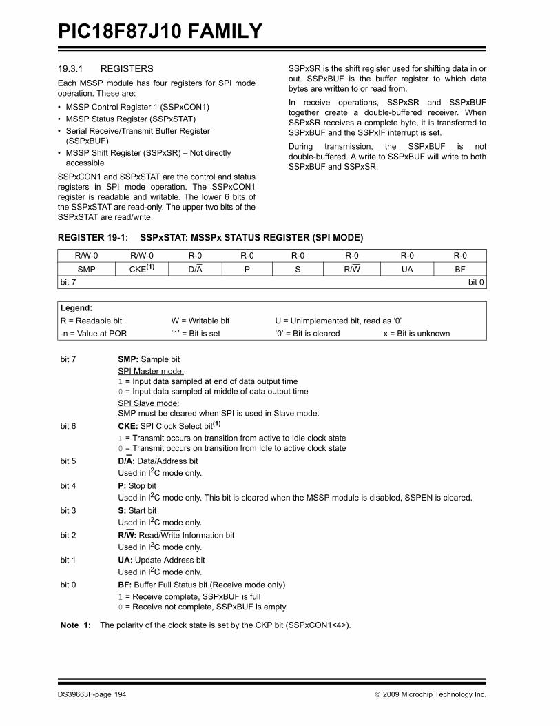
PIC18F87J10 FAMILY
19.3.1 REGISTERSEach MSSP module has four registers for SPI modeoperation. These are:• MSSP Control Register 1 (SSPxCON1)• MSSP Status Register (SSPxSTAT)• Serial Receive/Transmit Buffer Register
(SSPxBUF)• MSSP Shift Register (SSPxSR) – Not directly
accessible
SSPxCON1 and SSPxSTAT are the control and statusregisters in SPI mode operation. The SSPxCON1register is readable and writable. The lower 6 bits ofthe SSPxSTAT are read-only. The upper two bits of theSSPxSTAT are read/write.
SSPxSR is the shift register used for shifting data in orout. SSPxBUF is the buffer register to which databytes are written to or read from.
In receive operations, SSPxSR and SSPxBUFtogether create a double-buffered receiver. WhenSSPxSR receives a complete byte, it is transferred toSSPxBUF and the SSPxIF interrupt is set.
During transmission, the SSPxBUF is notdouble-buffered. A write to SSPxBUF will write to bothSSPxBUF and SSPxSR.
REGISTER 19-1: SSPxSTAT: MSSPx STATUS REGISTER (SPI MODE)
R/W-0 R/W-0 R-0 R-0 R-0 R-0 R-0 R-0
SMP CKE(1) D/A P S R/W UA BFbit 7 bit 0
Legend:R = Readable bit W = Writable bit U = Unimplemented bit, read as ‘0’-n = Value at POR ‘1’ = Bit is set ‘0’ = Bit is cleared x = Bit is unknown
bit 7 SMP: Sample bitSPI Master mode:1 = Input data sampled at end of data output time0 = Input data sampled at middle of data output timeSPI Slave mode:SMP must be cleared when SPI is used in Slave mode.
bit 6 CKE: SPI Clock Select bit(1)
1 = Transmit occurs on transition from active to Idle clock state0 = Transmit occurs on transition from Idle to active clock state
bit 5 D/A: Data/Address bit Used in I2C mode only.
bit 4 P: Stop bit Used in I2C mode only. This bit is cleared when the MSSP module is disabled, SSPEN is cleared.
bit 3 S: Start bitUsed in I2C mode only.
bit 2 R/W: Read/Write Information bitUsed in I2C mode only.
bit 1 UA: Update Address bitUsed in I2C mode only.
bit 0 BF: Buffer Full Status bit (Receive mode only)1 = Receive complete, SSPxBUF is full 0 = Receive not complete, SSPxBUF is empty
Note 1: The polarity of the clock state is set by the CKP bit (SSPxCON1<4>).
DS39663F-page 194 © 2009 Microchip Technology Inc.
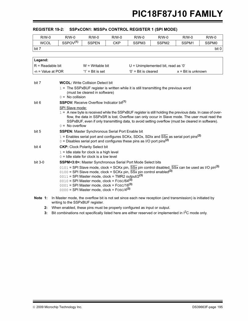
PIC18F87J10 FAMILY
REGISTER 19-2: SSPxCON1: MSSPx CONTROL REGISTER 1 (SPI MODE)R/W-0 R/W-0 R/W-0 R/W-0 R/W-0 R/W-0 R/W-0 R/W-0WCOL SSPOV(1) SSPEN CKP SSPM3 SSPM2 SSPM1 SSPM0
bit 7 bit 0
Legend:R = Readable bit W = Writable bit U = Unimplemented bit, read as ‘0’-n = Value at POR ‘1’ = Bit is set ‘0’ = Bit is cleared x = Bit is unknown
bit 7 WCOL: Write Collision Detect bit1 = The SSPxBUF register is written while it is still transmitting the previous word
(must be cleared in software) 0 = No collision
bit 6 SSPOV: Receive Overflow Indicator bit(1) SPI Slave mode: 1 = A new byte is received while the SSPxBUF register is still holding the previous data. In case of over-
flow, the data in SSPxSR is lost. Overflow can only occur in Slave mode. The user must read theSSPxBUF, even if only transmitting data, to avoid setting overflow (must be cleared in software).
0 = No overflowbit 5 SSPEN: Master Synchronous Serial Port Enable bit
1 = Enables serial port and configures SCKx, SDOx, SDIx and SSx as serial port pins(2) 0 = Disables serial port and configures these pins as I/O port pins(2)
bit 4 CKP: Clock Polarity Select bit 1 = Idle state for clock is a high level 0 = Idle state for clock is a low level
bit 3-0 SSPM<3:0>: Master Synchronous Serial Port Mode Select bits0101 = SPI Slave mode, clock = SCKx pin, SSx pin control disabled, SSx can be used as I/O pin(3) 0100 = SPI Slave mode, clock = SCKx pin, SSx pin control enabled(3)
0011 = SPI Master mode, clock = TMR2 output/2(3) 0010 = SPI Master mode, clock = FOSC/64(3) 0001 = SPI Master mode, clock = FOSC/16(3) 0000 = SPI Master mode, clock = FOSC/4(3)
Note 1: In Master mode, the overflow bit is not set since each new reception (and transmission) is initiated by writing to the SSPxBUF register.
2: When enabled, these pins must be properly configured as input or output.3: Bit combinations not specifically listed here are either reserved or implemented in I2C mode only.
© 2009 Microchip Technology Inc. DS39663F-page 195

PIC18F87J10 FAMILY
19.3.2 OPERATIONWhen initializing the SPI, several options need to bespecified. This is done by programming the appropriatecontrol bits (SSPxCON1<5:0> and SSPxSTAT<7:6>).These control bits allow the following to be specified:• Master mode (SCKx is the clock output)• Slave mode (SCKx is the clock input)• Clock Polarity (Idle state of SCKx)• Data Input Sample Phase (middle or end of data
output time)• Clock Edge (output data on rising/falling edge of
SCKx)• Clock Rate (Master mode only)• Slave Select mode (Slave mode only)
Each MSSP module consists of a transmit/receive shiftregister (SSPxSR) and a buffer register (SSPxBUF).The SSPxSR shifts the data in and out of the device,MSb first. The SSPxBUF holds the data that was writtento the SSPxSR until the received data is ready. Once the8 bits of data have been received, that byte is moved tothe SSPxBUF register. Then, the Buffer Full detect bit,BF (SSPxSTAT<0>), and the interrupt flag bit, SSPxIF,are set. This double-buffering of the received data(SSPxBUF) allows the next byte to start reception before
reading the data that was just received. Any write to theSSPxBUF register during transmission/reception of datawill be ignored and the Write Collision Detect bit, WCOL(SSPxCON1<7>), will be set. User software must clearthe WCOL bit so that it can be determined if the followingwrite(s) to the SSPxBUF register completedsuccessfully.
When the application software is expecting to receivevalid data, the SSPxBUF should be read before the nextbyte of data to transfer is written to the SSPxBUF. TheBuffer Full bit, BF (SSPxSTAT<0>), indicates whenSSPxBUF has been loaded with the received data(transmission is complete). When the SSPxBUF is read,the BF bit is cleared. This data may be irrelevant if theSPI is only a transmitter. Generally, the MSSP interruptis used to determine when the transmission/receptionhas completed. If the interrupt method is not going to beused, then software polling can be done to ensure that awrite collision does not occur. Example 19-1 shows theloading of the SSPxBUF (SSPxSR) for datatransmission.
The SSPxSR is not directly readable or writable andcan only be accessed by addressing the SSPxBUFregister. Additionally, the SSPxSTAT register indicatesthe various status conditions.
EXAMPLE 19-1: LOADING THE SSP1BUF (SSP1SR) REGISTER LOOP BTFSS SSP1STAT, BF ;Has data been received (transmit complete)?
BRA LOOP ;No MOVF SSP1BUF, W ;WREG reg = contents of SSP1BUF
MOVWF RXDATA ;Save in user RAM, if data is meaningful
MOVF TXDATA, W ;W reg = contents of TXDATA MOVWF SSP1BUF ;New data to xmit
DS39663F-page 196 © 2009 Microchip Technology Inc.
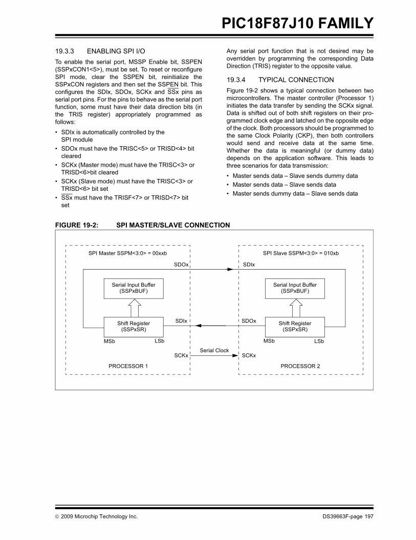
PIC18F87J10 FAMILY
19.3.3 ENABLING SPI I/OTo enable the serial port, MSSP Enable bit, SSPEN(SSPxCON1<5>), must be set. To reset or reconfigureSPI mode, clear the SSPEN bit, reinitialize theSSPxCON registers and then set the SSPEN bit. Thisconfigures the SDIx, SDOx, SCKx and SSx pins asserial port pins. For the pins to behave as the serial portfunction, some must have their data direction bits (inthe TRIS register) appropriately programmed asfollows:• SDIx is automatically controlled by the SPI module
• SDOx must have the TRISC<5> or TRISD<4> bit cleared
• SCKx (Master mode) must have the TRISC<3> or TRISD<6>bit cleared
• SCKx (Slave mode) must have the TRISC<3> or TRISD<6> bit set
• SSx must have the TRISF<7> or TRISD<7> bit set
Any serial port function that is not desired may beoverridden by programming the corresponding DataDirection (TRIS) register to the opposite value.
19.3.4 TYPICAL CONNECTIONFigure 19-2 shows a typical connection between twomicrocontrollers. The master controller (Processor 1)initiates the data transfer by sending the SCKx signal.Data is shifted out of both shift registers on their pro-grammed clock edge and latched on the opposite edgeof the clock. Both processors should be programmed tothe same Clock Polarity (CKP), then both controllerswould send and receive data at the same time.Whether the data is meaningful (or dummy data)depends on the application software. This leads tothree scenarios for data transmission:
• Master sends data – Slave sends dummy data• Master sends data – Slave sends data• Master sends dummy data – Slave sends data
FIGURE 19-2: SPI MASTER/SLAVE CONNECTION
Serial Input Buffer(SSPxBUF)
Shift Register(SSPxSR)
MSb LSb
SDOx
SDIx
PROCESSOR 1
SCKx
SPI Master SSPM<3:0> = 00xxb
Serial Input Buffer(SSPxBUF)
Shift Register(SSPxSR)
LSbMSb
SDIx
SDOx
PROCESSOR 2
SCKx
SPI Slave SSPM<3:0> = 010xb
Serial Clock
© 2009 Microchip Technology Inc. DS39663F-page 197
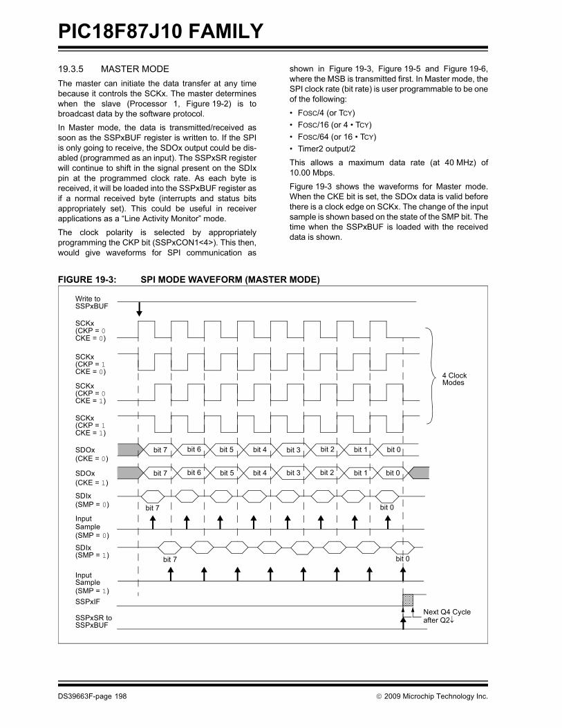
PIC18F87J10 FAMILY
19.3.5 MASTER MODEThe master can initiate the data transfer at any timebecause it controls the SCKx. The master determineswhen the slave (Processor 1, Figure 19-2) is tobroadcast data by the software protocol.In Master mode, the data is transmitted/received assoon as the SSPxBUF register is written to. If the SPIis only going to receive, the SDOx output could be dis-abled (programmed as an input). The SSPxSR registerwill continue to shift in the signal present on the SDIxpin at the programmed clock rate. As each byte isreceived, it will be loaded into the SSPxBUF register asif a normal received byte (interrupts and status bitsappropriately set). This could be useful in receiverapplications as a “Line Activity Monitor” mode.
The clock polarity is selected by appropriatelyprogramming the CKP bit (SSPxCON1<4>). This then,would give waveforms for SPI communication as
shown in Figure 19-3, Figure 19-5 and Figure 19-6,where the MSB is transmitted first. In Master mode, theSPI clock rate (bit rate) is user programmable to be oneof the following:
• FOSC/4 (or TCY)• FOSC/16 (or 4 • TCY)• FOSC/64 (or 16 • TCY)• Timer2 output/2
This allows a maximum data rate (at 40 MHz) of10.00 Mbps.
Figure 19-3 shows the waveforms for Master mode.When the CKE bit is set, the SDOx data is valid beforethere is a clock edge on SCKx. The change of the inputsample is shown based on the state of the SMP bit. Thetime when the SSPxBUF is loaded with the receiveddata is shown.
FIGURE 19-3: SPI MODE WAVEFORM (MASTER MODE)
SCKx(CKP = 0
SCKx(CKP = 1
SCKx(CKP = 0
SCKx(CKP = 1
4 ClockModes
InputSample
InputSample
SDIx
bit 7 bit 0
SDOx bit 7 bit 6 bit 5 bit 4 bit 3 bit 2 bit 1 bit 0
bit 7SDIx
SSPxIF(SMP = 1)
(SMP = 0)
(SMP = 1)
CKE = 1)
CKE = 0)
CKE = 1)
CKE = 0)
(SMP = 0)
Write toSSPxBUF
SSPxSR toSSPxBUF
SDOx bit 7 bit 6 bit 5 bit 4 bit 3 bit 2 bit 1 bit 0
(CKE = 0)
(CKE = 1)
Next Q4 Cycleafter Q2↓
bit 0
DS39663F-page 198 © 2009 Microchip Technology Inc.

PIC18F87J10 FAMILY
19.3.6 SLAVE MODEIn Slave mode, the data is transmitted and received asthe external clock pulses appear on SCKx. When thelast bit is latched, the SSPxIF interrupt flag bit is set.While in Slave mode, the external clock is supplied bythe external clock source on the SCKx pin. Thisexternal clock must meet the minimum high and lowtimes as specified in the electrical specifications.
While in Sleep mode, the slave can transmit/receivedata. When a byte is received, the device can beconfigured to wake-up from Sleep.
19.3.7 SLAVE SELECT SYNCHRONIZATION
The SSx pin allows a Synchronous Slave mode. TheSPI must be in Slave mode with the SSx pin controlenabled (SSPxCON1<3:0> = 04h). When the SSx pinis low, transmission and reception are enabled and theSDOx pin is driven. When the SSx pin goes high, theSDOx pin is no longer driven, even if in the middle of a
transmitted byte and becomes a floating output.External pull-up/pull-down resistors may be desirabledepending on the application.
When the SPI module resets, the bit counter is forcedto ‘0’. This can be done by either forcing the SSx pin toa high level or clearing the SSPEN bit.
To emulate two-wire communication, the SDOx pin canbe connected to the SDIx pin. When the SPI needs tooperate as a receiver, the SDOx pin can be configuredas an input. This disables transmissions from theSDOx. The SDIx can always be left as an input (SDIfunction) since it cannot create a bus conflict.
FIGURE 19-4: SLAVE SYNCHRONIZATION WAVEFORM
Note 1: When the SPI is in Slave modewith SSx pin control enabled(SSPxCON1<3:0> = 0100), the SPImodule will reset if the SSx pin is set to VDD.
2: If the SPI is used in Slave mode with CKEset, then the SSx pin control must beenabled.
SCKx(CKP = 1
SCKx(CKP = 0
InputSample
SDIx
bit 7
SDOx bit 7 bit 6 bit 7
SSPxIFInterrupt
(SMP = 0)
CKE = 0)
CKE = 0)
(SMP = 0)
Write toSSPxBUF
SSPxSR toSSPxBUF
SSx
Flag
bit 0
bit 7bit 0
Next Q4 Cycleafter Q2↓
© 2009 Microchip Technology Inc. DS39663F-page 199

PIC18F87J10 FAMILY
FIGURE 19-5: SPI MODE WAVEFORM (SLAVE MODE WITH CKE = 0)FIGURE 19-6: SPI MODE WAVEFORM (SLAVE MODE WITH CKE = 1)
SCKx(CKP = 1
SCKx(CKP = 0
InputSample
SDIxbit 7
SDOx bit 7 bit 6 bit 5 bit 4 bit 3 bit 2 bit 1 bit 0
SSPxIFInterrupt
(SMP = 0)
CKE = 0)
CKE = 0)
(SMP = 0)
Write toSSPxBUF
SSPxSR toSSPxBUF
SSx
Flag
Optional
Next Q4 Cycleafter Q2↓
bit 0
SCKx(CKP = 1
SCKx(CKP = 0
InputSample
SDIx
bit 7 bit 0
SDOx bit 7 bit 6 bit 5 bit 4 bit 3 bit 2 bit 1 bit 0
SSPxIFInterrupt
(SMP = 0)
CKE = 1)
CKE = 1)
(SMP = 0)
Write toSSPxBUF
SSPxSR toSSPxBUF
SSx
Flag
Not Optional
Next Q4 Cycleafter Q2↓
DS39663F-page 200 © 2009 Microchip Technology Inc.
PIC18F87J10 FAMILY
19.3.8 OPERATION IN POWER-MANAGEDMODES
In SPI Master mode, module clocks may be operatingat a different speed than when in Full-Power mode; inthe case of the Sleep mode, all clocks are halted.
In Idle modes, a clock is provided to the peripherals.That clock can be from the primary clock source, thesecondary clock (Timer1 oscillator) or the INTOSCsource. See Section 3.6 “Clock Sources andOscillator Switching” for additional information.
In most cases, the speed that the master clocks SPIdata is not important; however, this should beevaluated for each system.
If MSSP interrupts are enabled, they can wake the con-troller from Sleep mode, or one of the Idle modes, whenthe master completes sending data. If an exit fromSleep or Idle mode is not desired, MSSP interruptsshould be disabled.
If the Sleep mode is selected, all module clocks arehalted and the transmission/reception will remain inthat state until the devices wakes. After the devicereturns to Run mode, the module will resumetransmitting and receiving data.
In SPI Slave mode, the SPI Transmit/Receive Shiftregister operates asynchronously to the device. Thisallows the device to be placed in any power-managedmode and data to be shifted into the SPITransmit/Receive Shift register. When all 8 bits havebeen received, the MSSP interrupt flag bit will be setand if enabled, will wake the device.
19.3.9 EFFECTS OF A RESETA Reset disables the MSSP module and terminates thecurrent transfer.
19.3.10 BUS MODE COMPATIBILITYTable 19-1 shows the compatibility between thestandard SPI modes and the states of the CKP andCKE control bits.
TABLE 19-1: SPI BUS MODES
There is also an SMP bit which controls when the datais sampled.
19.3.11 SPI CLOCK SPEED AND MODULE INTERACTIONS
Because MSSP1 and MSSP2 are independentmodules, they can operate simultaneously at differentdata rates. Setting the SSPM<3:0> bits of theSSPxCON1 register determines the rate for thecorresponding module.
An exception is when both modules use Timer2 as atime base in Master mode. In this instance, anychanges to the Timer2 module’s operation will affectboth MSSP modules equally. If different bit rates arerequired for each module, the user should select one ofthe other three time base options for one of themodules.
Standard SPI Mode Terminology
Control Bits State
CKP CKE
0, 0 0 1
0, 1 0 0
1, 0 1 1
1, 1 1 0
© 2009 Microchip Technology Inc. DS39663F-page 201

PIC18F87J10 FAMILY
TABLE 19-2: REGISTERS ASSOCIATED WITH SPI OPERATIONName Bit 7 Bit 6 Bit 5 Bit 4 Bit 3 Bit 2 Bit 1 Bit 0Reset Values
on page
INTCON GIE/GIEH PEIE/GIEL TMR0IE INT0IE RBIE TMR0IF INT0IF RBIF 53PIR1 PSPIF ADIF RC1IF TX1IF SSP1IF CCP1IF TMR2IF TMR1IF 55PIE1 PSPIE ADIE RC1IE TX1IE SSP1IE CCP1IE TMR2IE TMR1IE 55IPR1 PSPIP ADIP RC1IP TX1IP SSP1IP CCP1IP TMR2IP TMR1IP 55PIR3 SSP2IF BCL2IF RC2IF TX2IF TMR4IF CCP5IF CCP4IF CCP3IF 55PIE3 SSP2IE BCL2IE RC2IE TX2IE TMR4IE CCP5IE CCP4IE CCP3IE 55IPR3 SSP2IP BCL2IP RC2IP TX2IP TMR4IP CCP5IP CCP4IP CCP3IP 55TRISC TRISC7 TRISC6 TRISC5 TRISC4 TRISC3 TRISC2 TRISC1 TRISC0 56TRISD TRISD7 TRISD6 TRISD5 TRISD4 TRISD3 TRISD2 TRISD1 TRISD0 56TRISF TRISF7 TRISF6 TRISF5 TRISF4 TRISF3 TRISF2 TRISF1 — 56SSP1BUF MSSP1 Receive Buffer/Transmit Register 54SSPxCON1 WCOL SSPOV SSPEN CKP SSPM3 SSPM2 SSPM1 SSPM0 54, 57
SSPxSTAT SMP CKE D/A P S R/W UA BF 54, 57SSP2BUF MSSP2 Receive Buffer/Transmit Register 57Legend: Shaded cells are not used by the MSSP module in SPI mode.
DS39663F-page 202 © 2009 Microchip Technology Inc.

PIC18F87J10 FAMILY
19.4 I2C ModeThe MSSP module in I2C mode fully implements allmaster and slave functions (including general callsupport) and provides interrupts on Start and Stop bitsin hardware to determine a free bus (multi-masterfunction). The MSSP module implements the standardmode specifications, as well as 7-bit and 10-bitaddressing.
Two pins are used for data transfer:
• Serial clock (SCLx) – RC3/SCK1/SCL1 or RD6/SCK2/SCL2
• Serial data (SDAx) – RC4/SDI1/SDA1 or RD5/SDI2/SDA2
The user must configure these pins as inputs by settingthe associated TRIS bits.
FIGURE 19-7: MSSP BLOCK DIAGRAM (I2C™ MODE)
19.4.1 REGISTERSThe MSSP module has six registers for I2C operation.These are:
• MSSP Control Register 1 (SSPxCON1)• MSSP Control Register 2 (SSPxCON2)• MSSP Status Register (SSPxSTAT)• Serial Receive/Transmit Buffer Register
(SSPxBUF)• MSSP Shift Register (SSPxSR) – Not directly
accessible• MSSP Address Register (SSPxADD)
SSPxCON1, SSPxCON2 and SSPxSTAT are thecontrol and status registers in I2C mode operation. TheSSPxCON1 and SSPxCON2 registers are readable andwritable. The lower 6 bits of the SSPxSTAT areread-only. The upper two bits of the SSPxSTAT areread/write.
SSPxSR is the shift register used for shifting data in orout. SSPxBUF is the buffer register to which databytes are written to or read from.
SSPxADD register holds the slave device addresswhen the MSSP is configured in I2C Slave mode.When the MSSP is configured in Master mode, thelower seven bits of SSPxADD act as the Baud RateGenerator reload value.
In receive operations, SSPxSR and SSPxBUFtogether create a double-buffered receiver. WhenSSPxSR receives a complete byte, it is transferred toSSPxBUF and the SSPxIF interrupt is set.
During transmission, the SSPxBUF is notdouble-buffered. A write to SSPxBUF will write to bothSSPxBUF and SSPxSR.
Read Write
SSPxSR reg
Match Detect
SSPxADD reg
SSPxBUF reg
InternalData Bus
Addr Match
Set, ResetS, P bits(SSPxSTAT reg)
ShiftClock
MSb LSb
Note: Only port I/O names are used in this diagram forthe sake of brevity. Refer to the text for a full list ofmultiplexed functions.
SCLx
SDAx
Start andStop bit Detect
Address Mask
© 2009 Microchip Technology Inc. DS39663F-page 203
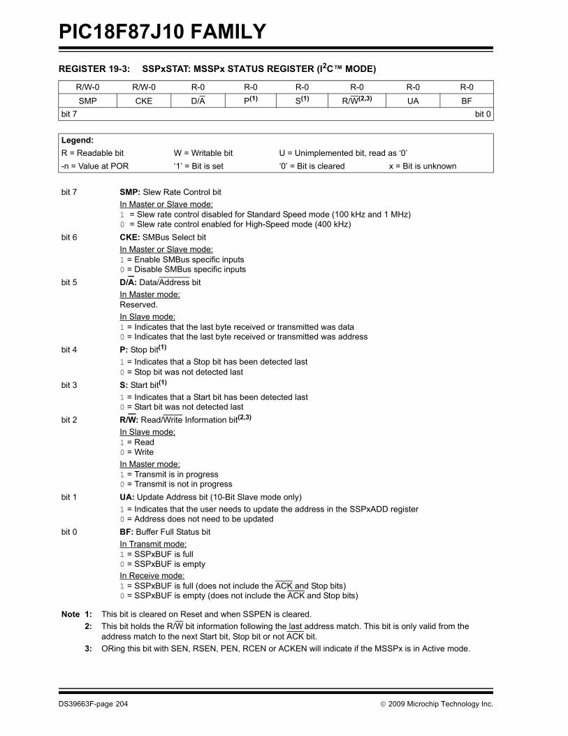
PIC18F87J10 FAMILY
REGISTER 19-3: SSPxSTAT: MSSPx STATUS REGISTER (I2C™ MODE)R/W-0 R/W-0 R-0 R-0 R-0 R-0 R-0 R-0
SMP CKE D/A P(1) S(1) R/W(2,3) UA BFbit 7 bit 0
Legend:R = Readable bit W = Writable bit U = Unimplemented bit, read as ‘0’-n = Value at POR ‘1’ = Bit is set ‘0’ = Bit is cleared x = Bit is unknown
bit 7 SMP: Slew Rate Control bitIn Master or Slave mode:1 = Slew rate control disabled for Standard Speed mode (100 kHz and 1 MHz) 0 = Slew rate control enabled for High-Speed mode (400 kHz)
bit 6 CKE: SMBus Select bitIn Master or Slave mode:1 = Enable SMBus specific inputs 0 = Disable SMBus specific inputs
bit 5 D/A: Data/Address bit In Master mode:Reserved.In Slave mode:1 = Indicates that the last byte received or transmitted was data0 = Indicates that the last byte received or transmitted was address
bit 4 P: Stop bit(1) 1 = Indicates that a Stop bit has been detected last0 = Stop bit was not detected last
bit 3 S: Start bit(1)
1 = Indicates that a Start bit has been detected last0 = Start bit was not detected last
bit 2 R/W: Read/Write Information bit(2,3)
In Slave mode:1 = Read0 = WriteIn Master mode:1 = Transmit is in progress0 = Transmit is not in progress
bit 1 UA: Update Address bit (10-Bit Slave mode only)1 = Indicates that the user needs to update the address in the SSPxADD register 0 = Address does not need to be updated
bit 0 BF: Buffer Full Status bitIn Transmit mode: 1 = SSPxBUF is full 0 = SSPxBUF is emptyIn Receive mode:1 = SSPxBUF is full (does not include the ACK and Stop bits)0 = SSPxBUF is empty (does not include the ACK and Stop bits)
Note 1: This bit is cleared on Reset and when SSPEN is cleared.2: This bit holds the R/W bit information following the last address match. This bit is only valid from the
address match to the next Start bit, Stop bit or not ACK bit.3: ORing this bit with SEN, RSEN, PEN, RCEN or ACKEN will indicate if the MSSPx is in Active mode.
DS39663F-page 204 © 2009 Microchip Technology Inc.
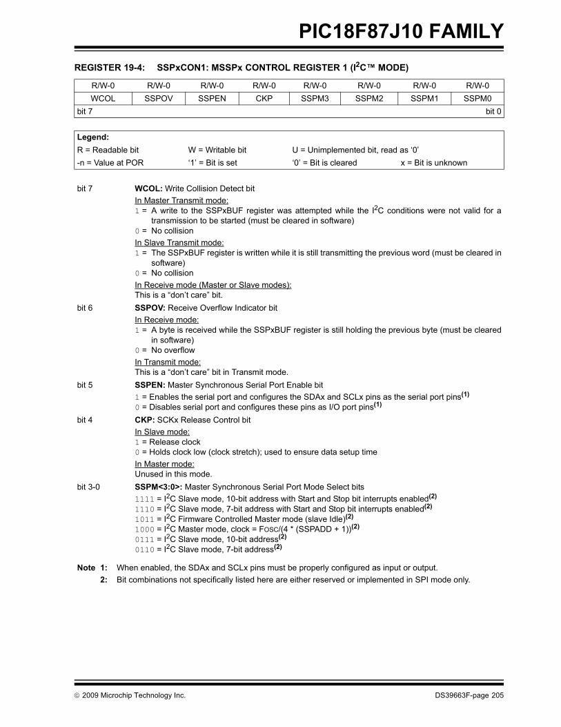
PIC18F87J10 FAMILY
REGISTER 19-4: SSPxCON1: MSSPx CONTROL REGISTER 1 (I2C™ MODE)R/W-0 R/W-0 R/W-0 R/W-0 R/W-0 R/W-0 R/W-0 R/W-0WCOL SSPOV SSPEN CKP SSPM3 SSPM2 SSPM1 SSPM0
bit 7 bit 0
Legend:R = Readable bit W = Writable bit U = Unimplemented bit, read as ‘0’-n = Value at POR ‘1’ = Bit is set ‘0’ = Bit is cleared x = Bit is unknown
bit 7 WCOL: Write Collision Detect bitIn Master Transmit mode:1 = A write to the SSPxBUF register was attempted while the I2C conditions were not valid for a
transmission to be started (must be cleared in software)0 = No collisionIn Slave Transmit mode:1 = The SSPxBUF register is written while it is still transmitting the previous word (must be cleared in
software)0 = No collision In Receive mode (Master or Slave modes):This is a “don’t care” bit.
bit 6 SSPOV: Receive Overflow Indicator bit In Receive mode:1 = A byte is received while the SSPxBUF register is still holding the previous byte (must be cleared
in software)0 = No overflowIn Transmit mode: This is a “don’t care” bit in Transmit mode.
bit 5 SSPEN: Master Synchronous Serial Port Enable bit 1 = Enables the serial port and configures the SDAx and SCLx pins as the serial port pins(1) 0 = Disables serial port and configures these pins as I/O port pins(1)
bit 4 CKP: SCKx Release Control bit In Slave mode: 1 = Release clock 0 = Holds clock low (clock stretch); used to ensure data setup timeIn Master mode: Unused in this mode.
bit 3-0 SSPM<3:0>: Master Synchronous Serial Port Mode Select bits1111 = I2C Slave mode, 10-bit address with Start and Stop bit interrupts enabled(2)
1110 = I2C Slave mode, 7-bit address with Start and Stop bit interrupts enabled(2)
1011 = I2C Firmware Controlled Master mode (slave Idle)(2)
1000 = I2C Master mode, clock = FOSC/(4 * (SSPADD + 1))(2) 0111 = I2C Slave mode, 10-bit address(2)
0110 = I2C Slave mode, 7-bit address(2)
Note 1: When enabled, the SDAx and SCLx pins must be properly configured as input or output.2: Bit combinations not specifically listed here are either reserved or implemented in SPI mode only.
© 2009 Microchip Technology Inc. DS39663F-page 205

PIC18F87J10 FAMILY
REGISTER 19-5: SSPxCON2: MSSPx CONTROL REGISTER 2 (I2C™ MODE)R/W-0 R/W-0 R/W-0 R/W-0 R/W-0 R/W-0 R/W-0 R/W-0GCEN ACKSTAT ACKDT/
ADMSK5(1)ACKEN/ADMSK4
RCEN/ADMSK3
PEN/ADMSK2
RSEN/ADMSK1
SEN(2)
bit 7 bit 0
Legend:R = Readable bit W = Writable bit U = Unimplemented bit, read as ‘0’-n = Value at POR ‘1’ = Bit is set ‘0’ = Bit is cleared x = Bit is unknown
bit 7 GCEN: General Call Enable bit (Slave mode only) 1 = Enable interrupt when a general call address (0000h) is received in the SSPxSR 0 = General call address disabled
bit 6 ACKSTAT: Acknowledge Status bit (Master Transmit mode only)1 = Acknowledge was not received from slave 0 = Acknowledge was received from slave
bit 5 ACKDT/ADMSK5: Acknowledge Data bit (Master Receive mode only)(1)
In Master Receive mode: 1 = Not Acknowledge 0 = Acknowledge In Slave mode:1 = Address masking of ADD5 enabled 0 = Address masking of ADD5 disabled
bit 4 ACKEN/ADMSK4: Acknowledge Sequence Enable bitIn Master Receive mode:(2)
1 = Initiate Acknowledge sequence on SDAx and SCLx pins and transmit ACKDT data bit.Automatically cleared by hardware.
0 = Acknowledge sequence IdleIn Slave mode:1 = Address masking of ADD4 enabled 0 = Address masking of ADD4 disabled
bit 3 RCEN/ADMSK3: Receive Enable bit (Master Receive mode only)In Master Receive mode:(2)
1 = Enables Receive mode for I2C 0 = Receive IdleIn Slave mode:1 = Address masking of ADD3 enabled 0 = Address masking of ADD3 disabled
bit 2 PEN/ADMSK2: Stop Condition Enable bitIn Master mode:(2)
1 = Initiate Stop condition on SDAx and SCLx pins. Automatically cleared by hardware. 0 = Stop condition IdleIn Slave mode:1 = Address masking of ADD2 enabled 0 = Address masking of ADD2 disabled
Note 1: Value that will be transmitted when the user initiates an Acknowledge sequence at the end of a receive.2: For bits, ACKEN, RCEN, PEN, RSEN, SEN: If the I2C module is active, these bits may not be set (no
spooling) and the SSPxBUF may not be written (or writes to the SSPxBUF are disabled).
DS39663F-page 206 © 2009 Microchip Technology Inc.
PIC18F87J10 FAMILY
bit 1 RSEN/ADMSK1: Repeated Start Condition Enable bitIn Master mode:(2)
1 = Initiate Repeated Start condition on SDAx and SCLx pins. Automatically cleared by hardware. 0 = Repeated Start condition IdleIn Slave mode (7-Bit Addressing mode):1 = Address masking of ADD1 enabled 0 = Address masking of ADD1 disabledIn Slave mode (10-Bit Addressing mode):1 = Address masking of ADD1 and ADD0 enabled 0 = Address masking of ADD1 and ADD0 disabled
bit 0 SEN: Start Condition Enable/Stretch Enable bit(2)
In Master mode:1 = Initiate Start condition on SDAx and SCLx pins. Automatically cleared by hardware. 0 = Start condition IdleIn Slave mode:1 = Clock stretching is enabled for both slave transmit and slave receive (stretch enabled)0 = Clock stretching is disabled
REGISTER 19-5: SSPxCON2: MSSPx CONTROL REGISTER 2 (I2C™ MODE) (CONTINUED)
Note 1: Value that will be transmitted when the user initiates an Acknowledge sequence at the end of a receive.2: For bits, ACKEN, RCEN, PEN, RSEN, SEN: If the I2C module is active, these bits may not be set (no
spooling) and the SSPxBUF may not be written (or writes to the SSPxBUF are disabled).
© 2009 Microchip Technology Inc. DS39663F-page 207
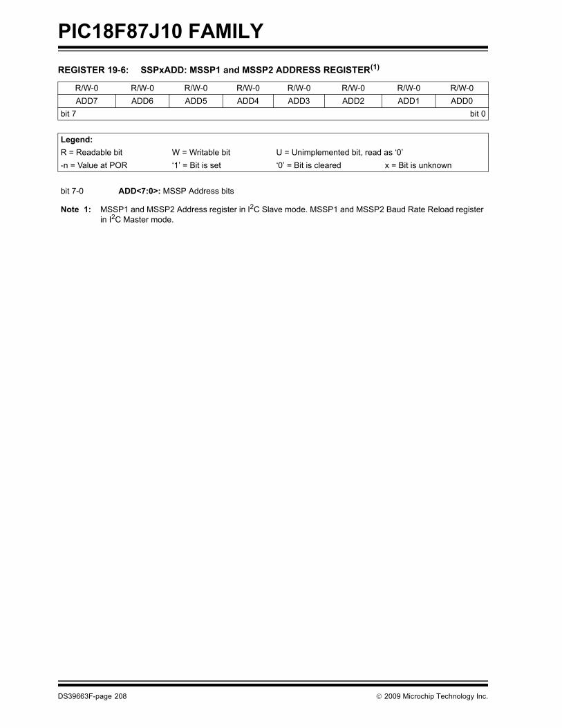
PIC18F87J10 FAMILY
REGISTER 19-6: SSPxADD: MSSP1 and MSSP2 ADDRESS REGISTER(1)R/W-0 R/W-0 R/W-0 R/W-0 R/W-0 R/W-0 R/W-0 R/W-0ADD7 ADD6 ADD5 ADD4 ADD3 ADD2 ADD1 ADD0
bit 7 bit 0
Legend:R = Readable bit W = Writable bit U = Unimplemented bit, read as ‘0’-n = Value at POR ‘1’ = Bit is set ‘0’ = Bit is cleared x = Bit is unknown
bit 7-0 ADD<7:0>: MSSP Address bits
Note 1: MSSP1 and MSSP2 Address register in I2C Slave mode. MSSP1 and MSSP2 Baud Rate Reload register in I2C Master mode.
DS39663F-page 208 © 2009 Microchip Technology Inc.
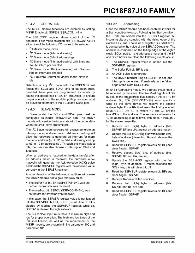
PIC18F87J10 FAMILY
19.4.2 OPERATIONThe MSSP module functions are enabled by settingMSSP Enable bit, SSPEN (SSPxCON1<5>).The SSPxCON1 register allows control of the I2Coperation. Four mode selection bits (SSPxCON1<3:0>)allow one of the following I2C modes to be selected:
• I2C Master mode, clock• I2C Slave mode (7-bit addressing)• I2C Slave mode (10-bit addressing)• I2C Slave mode (7-bit addressing) with Start and
Stop bit interrupts enabled• I2C Slave mode (10-bit addressing) with Start and
Stop bit interrupts enabled• I2C Firmware Controlled Master mode, slave is
Idle
Selection of any I2C mode with the SSPEN bit setforces the SCLx and SDAx pins to be open-drain,provided these pins are programmed as inputs bysetting the appropriate TRISC or TRISD bits. To ensureproper operation of the module, pull-up resistors mustbe provided externally to the SCLx and SDAx pins.
19.4.3 SLAVE MODEIn Slave mode, the SCLx and SDAx pins must beconfigured as inputs (TRISC<4:3> set). The MSSPmodule will override the input state with the output datawhen required (slave-transmitter).
The I2C Slave mode hardware will always generate aninterrupt on an address match. Address masking willallow the hardware to generate an interrupt for morethan one address (up to 31 in 7-bit addressing and upto 63 in 10-bit addressing). Through the mode selectbits, the user can also choose to interrupt on Start andStop bits.
When an address is matched, or the data transfer afteran address match is received, the hardware auto-matically will generate the Acknowledge (ACK) pulseand load the SSPxBUF register with the received valuecurrently in the SSPxSR register.
Any combination of the following conditions will causethe MSSP module not to give this ACK pulse:
• The Buffer Full bit, BF (SSPxSTAT<0>), was set before the transfer was received.
• The overflow bit, SSPOV (SSPxCON1<6>), was set before the transfer was received.
In this case, the SSPxSR register value is not loadedinto the SSPxBUF, but bit, SSPxIF, is set. The BF bit iscleared by reading the SSPxBUF register, while bit,SSPOV, is cleared through software.
The SCLx clock input must have a minimum high andlow for proper operation. The high and low times of theI2C specification, as well as the requirement of theMSSP module, are shown in timing parameter 100 andparameter 101.
19.4.3.1 AddressingOnce the MSSP module has been enabled, it waits fora Start condition to occur. Following the Start condition,the 8 bits are shifted into the SSPxSR register. Allincoming bits are sampled with the rising edge of theclock (SCLx) line. The value of register, SSPxSR<7:1>,is compared to the value of the SSPxADD register. Theaddress is compared on the falling edge of the eighthclock (SCLx) pulse. If the addresses match and the BFand SSPOV bits are clear, the following events occur:
1. The SSPxSR register value is loaded into theSSPxBUF register.
2. The Buffer Full bit, BF, is set.3. An ACK pulse is generated.4. The MSSP Interrupt Flag bit, SSPxIF, is set (and
interrupt is generated, if enabled) on the fallingedge of the ninth SCLx pulse.
In 10-Bit Addressing mode, two address bytes need tobe received by the slave. The five Most Significant bits(MSbs) of the first address byte specify if this is a 10-bitaddress. Bit, R/W (SSPxSTAT<2>), must specify awrite so the slave device will receive the secondaddress byte. For a 10-bit address, the first byte wouldequal ‘11110 A9 A8 0’, where ‘A9’ and ‘A8’ are thetwo MSbs of the address. The sequence of events for10-bit addressing is as follows, with steps 7 through 9for the slave-transmitter:
1. Receive first (high) byte of address (bits,SSPxIF, BF and UA, are set on address match).
2. Update the SSPxADD register with second (low)byte of address (clears bit, UA, and releases theSCLx line).
3. Read the SSPxBUF register (clears bit, BF) andclear flag bit, SSPxIF.
4. Receive second (low) byte of address (bits,SSPxIF, BF and UA, are set).
5. Update the SSPxADD register with the first(high) byte of address. If match releases theSCLx line, this will clear bit, UA.
6. Read the SSPxBUF register (clears bit, BF) andclear flag bit, SSPxIF.
7. Receive Repeated Start condition.8. Receive first (high) byte of address (bits,
SSPxIF and BF, are set).9. Read the SSPxBUF register (clears bit, BF) and
clear flag bit, SSPxIF.
© 2009 Microchip Technology Inc. DS39663F-page 209

PIC18F87J10 FAMILY
19.4.3.2 Address MaskingMasking an address bit causes that bit to become a“don’t care”. When one address bit is masked, twoaddresses will be Acknowledged and cause aninterrupt. It is possible to mask more than one addressbit at a time, which makes it possible to Acknowledgeup to 31 addresses in 7-bit mode and up to63 addresses in 10-bit mode (see Example 19-2).The I2C slave behaves the same way whether addressmasking is used or not. However, when addressmasking is used, the I2C slave can Acknowledgemultiple addresses and cause interrupts. When thisoccurs, it is necessary to determine which addresscaused the interrupt by checking SSPxBUF.
• 7-Bit Addressing mode
Address Mask bits, ADMSK<5:1>, mask thecorresponding address bits in the SSPxADDregister. For any ADMSK bits that are active(ADMSK<x> = 1), the corresponding address bit isignored (ADD<x> = x). For the module to issue anaddress Acknowledge, it is sufficient to match onlyon addresses that do not have an active addressmask.
• 10-Bit Addressing mode
Address Mask bits, ADMSK<5:2>, mask thecorresponding address bits in the SSPxADDregister. In addition, ADMSK<1> simultaneouslymasks the two LSBs of the address, ADD<1:0>.For any ADMSK bits that are active(ADMSK<x> = 1), the corresponding address bit isignored (ADD<x> = x). Also note, that although in10-Bit Addressing mode, the upper address bitsreuse part of the SSPxADD register bits; theaddress mask bits do not interact with those bits.They only affect the lower address bits.
EXAMPLE 19-2: ADDRESS MASKING
Note 1: ADMSK<1> masks the two LeastSignificant bits of the address.
2: The two Most Significant bits of theaddress are not affected by addressmasking.
7-Bit Addressing:SSPxADD<7:1> = 1010 0000
ADMSK<5:1> = 00 111
Addresses Acknowledged = 0xA0, 0xA2, 0xA4, 0xA60xA8, 0xAA, 0xAC, 0xAE
10-Bit Addressing:SSPxADD<7:0> = 1010 0000 (The two MSbs are ignored in this example since they are not affected.)
ADMSK<5:1> = 00 111
Addresses Acknowledged = 0xA0, 0xA1, 0xA2, 0xA30xA4, 0xA5, 0xA6, 0xA70xA8, 0xA9, 0xAA 0xAB0xAC, 0xAD, 0xAE, 0xAF
The upper two bits are not affected by the address masking.
DS39663F-page 210 © 2009 Microchip Technology Inc.

PIC18F87J10 FAMILY
19.4.3.3 ReceptionWhen the R/W bit of the address byte is clear and anaddress match occurs, the R/W bit of the SSPxSTATregister is cleared. The received address is loaded intothe SSPxBUF register and the SDAx line is held low(ACK).When the address byte overflow condition exists, thenthe no Acknowledge (ACK) pulse is given. An overflowcondition is defined as either bit, BF (SSPxSTAT<0>),is set, or bit, SSPOV (SSPxCON1<6>), is set.
An MSSP interrupt is generated for each data transferbyte. The interrupt flag bit, SSPxIF, must be cleared insoftware. The SSPxSTAT register is used to determinethe status of the byte.
If SEN is enabled (SSPxCON2<0> = 1), SCLx will beheld low (clock stretch) following each data transfer. Theclock must be released by setting bit, CKP(SSPxCON1<4>). See Section 19.4.4 “ClockStretching” for more detail.
19.4.3.4 TransmissionWhen the R/W bit of the incoming address byte is setand an address match occurs, the R/W bit of theSSPxSTAT register is set. The received address isloaded into the SSPxBUF register. The ACK pulse willbe sent on the ninth bit and the SCLx pin is held lowregardless of SEN (see Section 19.4.4 “ClockStretching” for more detail). By stretching the clock,the master will be unable to assert another clock pulseuntil the slave is done preparing the transmit data. Thetransmit data must be loaded into the SSPxBUF regis-ter which also loads the SSPxSR register. Then pin,SCLx, should be enabled by setting bit, CKP(SSPxCON1<4>). The eight data bits are shifted out onthe falling edge of the SCLx input. This ensures that theSDAx signal is valid during the SCLx high time(Figure 19-10).
The ACK pulse from the master-receiver is latched onthe rising edge of the ninth SCLx input pulse. If theSDAx line is high (not ACK), then the data transfer iscomplete. In this case, when the ACK is latched by theslave, the slave logic is reset and the slave monitors foranother occurrence of the Start bit. If the SDAx line waslow (ACK), the next transmit data must be loaded intothe SSPxBUF register. Again, pin, SCLx, must beenabled by setting bit, CKP.
An MSSP interrupt is generated for each data transferbyte. The SSPxIF bit must be cleared in software andthe SSPxSTAT register is used to determine the statusof the byte. The SSPxIF bit is set on the falling edge ofthe ninth clock pulse.
© 2009 Microchip Technology Inc. DS39663F-page 211

PIC18F87J10 FAMILY
FIGURE 19-8: I2C™ SLAVE MODE TIMING WITH SEN = 0 (RECEPTION, 7-BIT ADDRESSING)SDAx
SCLx
SSP
xIF
(PIR
1<3>
or P
IR3<
7>)
BF (S
SPx
STAT
<0>)
SSP
OV
(SS
PxC
ON
1<6>
)
S1
23
45
67
89
12
34
56
78
91
23
45
78
9P
A7
A6A
5A
4A
3A
2A
1D
7D
6D
5D
4D
3D
2D
1D
0D
7D
6D
5D
4D
3D
1D
0
ACK
Rec
eivi
ng D
ata
AC
KR
ecei
ving
Dat
aR
/W =
0 AC
K
Rec
eivi
ng A
ddre
ss
Cle
ared
in s
oftw
are
SSP
xBU
F is
read
Bus
mas
ter
term
inat
estra
nsfe
r
SSP
OV
is s
etbe
caus
e SS
PxB
UF
isst
ill fu
ll. A
CK
is n
ot s
ent.
D2 6
CK
P(C
KP d
oes
not r
eset
to ‘0
’ whe
n SE
N =
0)
DS39663F-page 212 © 2009 Microchip Technology Inc.
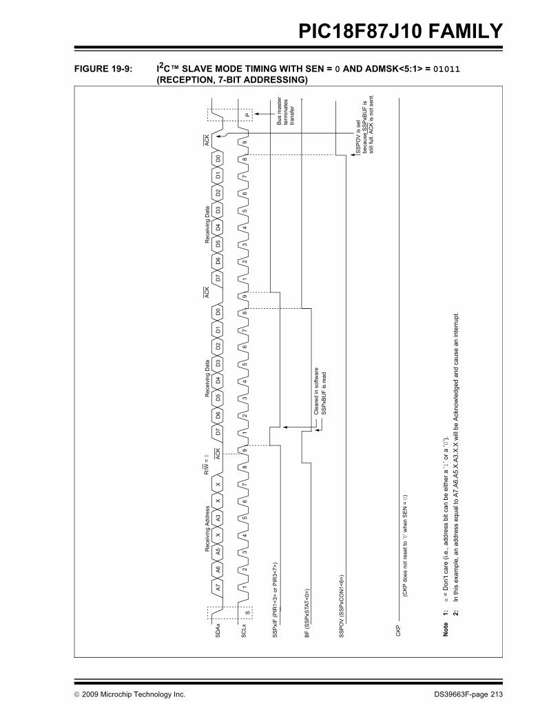
PIC18F87J10 FAMILY
FIGURE 19-9: I2C™ SLAVE MODE TIMING WITH SEN = 0 AND ADMSK<5:1> = 01011(RECEPTION, 7-BIT ADDRESSING)
SDA
x
SCLx
SSP
xIF
(PIR
1<3>
or P
IR3<
7>)
BF (S
SPxS
TAT<
0>)
SSP
OV
(SSP
xCO
N1<
6>)
S1
23
45
67
89
12
34
56
78
91
23
45
78
9P
A7
A6A5
XA3
XX
D7
D6
D5
D4
D3
D2
D1
D0
D7
D6
D5
D4
D3
D1
D0
ACK
Rec
eivi
ng D
ata
ACK
Rec
eivi
ng D
ata
R/W
= 0 AC
K
Rec
eivi
ng A
ddre
ss
Cle
ared
in s
oftw
are
SSPx
BUF
is re
ad
Bus
mas
ter
term
inat
estra
nsfe
r
SSPO
V is
set
beca
use
SSP
xBU
F is
still
full.
AC
K is
not
sen
t.
D2 6
CKP
(CKP
doe
s no
t res
et to
‘0’ w
hen
SEN
= 0
)
Not
e1:
x =
Don
’t ca
re (i
.e.,
addr
ess
bit c
an b
e ei
ther
a ‘1
’ or a
‘0’).
2:In
this
exa
mpl
e, a
n ad
dres
s eq
ual t
o A
7.A
6.A
5.X
.A3.
X.X
will
be
Ack
now
ledg
ed a
nd c
ause
an
inte
rrupt
.
© 2009 Microchip Technology Inc. DS39663F-page 213

PIC18F87J10 FAMILY
FIGURE 19-10: I2C™ SLAVE MODE TIMING (TRANSMISSION, 7-BIT ADDRESSING)SDAx
SCLx
BF (S
SPxS
TAT<
0>)
A6A5
A4A3
A2A1
D6
D5
D4
D3
D2
D1
D0
12
34
56
78
23
45
67
89
SSPx
BUF
is w
ritte
n in
sof
twar
e
Cle
ared
in s
oftw
are
Dat
a in
sa
mpl
ed
S
ACK
Tran
smitt
ing
Dat
aR
/W =
0
ACK
Rec
eivi
ng A
ddre
ss
A7D
7
91
D6
D5
D4
D3
D2
D1
D0
23
45
67
89
SSPx
BUF
is w
ritte
n in
sof
twar
e
Cle
ared
in s
oftw
are
From
SSP
xIF
ISR
Tran
smitt
ing
Dat
a
D7 1
CK
P (S
SPxC
ON
<4>)
P
ACK
CKP
is s
et in
sof
twar
eC
KP is
set
in s
oftw
are
SCLx
hel
d lo
ww
hile
CPU
resp
onds
to S
SPxI
F
SSPx
IF (P
IR1<
3> o
r PIR
3<7>
)
From
SSP
xIF
ISR
Cle
ar b
y re
adin
g
DS39663F-page 214 © 2009 Microchip Technology Inc.

PIC18F87J10 FAMILY
FIGURE 19-11: I2C™ SLAVE MODE TIMING WITH SEN = 0 AND ADMSK<5:1> = 01001(RECEPTION, 10-BIT ADDRESSING)
SDA
x
SCLx
SSPx
IF (P
IR1<
3> o
r PIR
3<7>
)
BF (S
SPxS
TAT<
0>)
S1
23
45
67
89
12
34
56
78
91
23
45
78
9P
11
11
0A9
A8A7
A6A5
XA
3A2
XX
D7
D6
D5
D4
D3
D1
D0
Rec
eive
Dat
a B
yte
ACK
R/W
= 0 AC
K
Rec
eive
Firs
t Byt
e of
Add
ress
Cle
ared
in s
oftw
are
D2
6
Cle
ared
in s
oftw
are
Rec
eive
Sec
ond
Byte
of A
ddre
ss
Cle
ared
by
hard
war
ew
hen
SSP
xAD
D is
upd
ated
with
low
byt
e of
add
ress
UA
(SS
PxST
AT<1
>)
Clo
ck is
hel
d lo
w u
ntil
upda
te o
f SSP
xAD
D h
as
take
n pl
ace
UA
is s
et in
dica
ting
that
the
SSP
xAD
D n
eeds
to b
eup
date
d
UA
is s
et in
dica
ting
that
SSP
xAD
D n
eeds
to b
eup
date
d
Cle
ared
by
hard
war
e w
hen
SSP
xAD
D is
upd
ated
with
hig
hby
te o
f add
ress
SS
PxB
UF
is w
ritte
n w
ithco
nten
ts o
f SS
PxSR
Dum
my
read
of S
SPx
BUF
to c
lear
BF
flag
AC
K
CKP
12
34
57
89
D7
D6
D5
D4
D3
D1
D0
Rec
eive
Dat
a B
yte
Bus
mas
ter
term
inat
estra
nsfe
r
D2 6
ACK
Cle
ared
in s
oftw
are
Cle
ared
in s
oftw
are
SSPO
V (S
SPxC
ON
1<6>
)
SSP
OV
is s
etbe
caus
e S
SPxB
UF
isst
ill fu
ll. A
CK
is n
ot s
ent.
(CK
P do
es n
ot re
set t
o ‘0
’ whe
n S
EN =
0)
Clo
ck is
hel
d lo
w u
ntil
upda
te o
f SSP
xAD
D h
as
take
n pl
ace
Not
e1:
x =
Don
’t ca
re (i
.e.,
addr
ess
bit c
an b
e ei
ther
a ‘1
’ or a
‘0’).
2:In
this
exa
mpl
e, a
n ad
dres
s eq
ual t
o A
9.A
8.A7
.A6.
A5.
X.A
3.A
2.X
.X w
ill b
e A
ckno
wle
dged
and
cau
se a
n in
terr
upt.
3:N
ote
that
the
Mos
t Sig
nific
ant b
its o
f the
add
ress
are
not
affe
cted
by
the
bit m
aski
ng.
© 2009 Microchip Technology Inc. DS39663F-page 215

PIC18F87J10 FAMILY
FIGURE 19-12: I2C™ SLAVE MODE TIMING WITH SEN = 0 (RECEPTION, 10-BIT ADDRESSING)SDA
x
SCLx
SSPx
IF (P
IR1<
3> o
r PIR
3<7>
)
BF (S
SPxS
TAT<
0>)
S1
23
45
67
89
12
34
56
78
91
23
45
78
9P
11
11
0A9
A8A7
A6A5
A4A
3A2
A1
A0D
7D
6D
5D
4D
3D
1D
0
Rec
eive
Dat
a B
yte
ACK
R/W
= 0 AC
K
Rec
eive
Firs
t Byt
e of
Add
ress
Cle
ared
in s
oftw
are
D2
6
Cle
ared
in s
oftw
are
Rec
eive
Sec
ond
Byte
of A
ddre
ss
Cle
ared
by
hard
war
ew
hen
SSP
xAD
D is
upd
ated
with
low
byt
e of
add
ress
UA
(SS
PxST
AT<1
>)
Clo
ck is
hel
d lo
w u
ntil
upda
te o
f SSP
xAD
D h
as
take
n pl
ace
UA
is s
et in
dica
ting
that
the
SSP
xAD
D n
eeds
to b
eup
date
d
UA
is s
et in
dica
ting
that
SSP
xAD
D n
eeds
to b
eup
date
d
Cle
ared
by
hard
war
e w
hen
SSP
xAD
D is
upd
ated
with
hig
hby
te o
f add
ress
SS
PxB
UF
is w
ritte
n w
ithco
nten
ts o
f SS
PxSR
Dum
my
read
of S
SPx
BUF
to c
lear
BF
flag
AC
K
CKP
12
34
57
89
D7
D6
D5
D4
D3
D1
D0
Rec
eive
Dat
a B
yte
Bus
mas
ter
term
inat
estra
nsfe
r
D2 6
ACK
Cle
ared
in s
oftw
are
Cle
ared
in s
oftw
are
SSPO
V (S
SPxC
ON
1<6>
)
SSP
OV
is s
etbe
caus
e S
SPxB
UF
isst
ill fu
ll. A
CK
is n
ot s
ent.
(CK
P do
es n
ot re
set t
o ‘0
’ whe
n S
EN =
0)
Clo
ck is
hel
d lo
w u
ntil
upda
te o
f SSP
xAD
D h
as
take
n pl
ace
DS39663F-page 216 © 2009 Microchip Technology Inc.

PIC18F87J10 FAMILY
FIGURE 19-13: I2C™ SLAVE MODE TIMING (TRANSMISSION, 10-BIT ADDRESSING)SD
Ax
SC
Lx
SSP
xIF
(PIR
1<3>
or P
IR3<
7>)
BF
(SS
PxST
AT<0
>)
S1
23
45
67
89
12
34
56
78
91
23
45
78
9P
11
11
0A
9A
8A7
A6A
5A
4A3
A2A1
A0
11
11
0A8
R/W
= 1 A
CK
AC
K
R/W
= 0
ACK
Rec
eive
Firs
t Byt
e of
Add
ress
Cle
ared
in s
oftw
are
Bus
mas
ter
term
inat
estra
nsfe
r
A9 6
Rec
eive
Sec
ond
Byte
of A
ddre
ss
Cle
ared
by
hard
war
e w
hen
SSPx
ADD
is u
pdat
ed w
ith lo
wby
te o
f add
ress
UA
(SSP
xSTA
T<1>
)
Clo
ck is
hel
d lo
w u
ntil
upda
te o
f SS
PxAD
D h
as
take
n pl
ace
UA
is s
et in
dica
ting
that
the
SSP
xAD
D n
eeds
to b
eup
date
d
UA
is s
et in
dica
ting
that
SSP
xAD
D n
eeds
to b
eup
date
d
Cle
ared
by
hard
war
e w
hen
SSP
xAD
D is
upd
ated
with
hig
hby
te o
f add
ress
.
SSPx
BUF
is w
ritte
n w
ithco
nten
ts o
f SSP
xSR
Dum
my
read
of S
SPxB
UF
to c
lear
BF
flag
Rec
eive
Firs
t Byt
e of
Add
ress
12
34
57
89
D7
D6
D5
D4
D3
D1
AC
K
D2
6
Tran
smitt
ing
Dat
a B
yte
D0
Dum
my
read
of S
SPxB
UF
to c
lear
BF
flag
Sr
Cle
ared
in s
oftw
are
Writ
e of
SS
PxBU
Fin
itiat
es tr
ansm
it
Cle
ared
in s
oftw
are
Com
plet
ion
of
clea
rs B
F fla
g
CKP
(SSP
xCO
N1<
4>)
CKP
is s
et in
sof
twar
e
CK
P is
aut
omat
ical
ly c
lear
ed in
har
dwar
e, h
oldi
ng S
CLx
low
Clo
ck is
hel
d lo
w u
ntil
upda
te o
f SSP
xAD
D h
as
take
n pl
ace
data
tran
smis
sion
Clo
ck is
hel
d lo
w u
ntil
CKP
is s
et to
‘1’
third
add
ress
seq
uenc
e
BF fl
ag is
cle
arat
the
end
of th
e
© 2009 Microchip Technology Inc. DS39663F-page 217

PIC18F87J10 FAMILY
19.4.4 CLOCK STRETCHINGBoth 7-Bit and 10-Bit Slave modes implementautomatic clock stretching during a transmit sequence.The SEN bit (SSPxCON2<0>) allows clock stretchingto be enabled during receives. Setting SEN will causethe SCLx pin to be held low at the end of each datareceive sequence.
19.4.4.1 Clock Stretching for 7-Bit Slave Receive Mode (SEN = 1)
In 7-Bit Slave Receive mode, on the falling edge of theninth clock at the end of the ACK sequence, if the BFbit is set, the CKP bit in the SSPxCON1 register isautomatically cleared, forcing the SCLx output to beheld low. The CKP being cleared to ‘0’ will assert theSCLx line low. The CKP bit must be set in the user’sISR before reception is allowed to continue. By holdingthe SCLx line low, the user has time to service the ISRand read the contents of the SSPxBUF before themaster device can initiate another receive sequence.This will prevent buffer overruns from occurring (seeFigure 19-15).
19.4.4.2 Clock Stretching for 10-Bit Slave Receive Mode (SEN = 1)
In 10-Bit Slave Receive mode during the addresssequence, clock stretching automatically takes placebut CKP is not cleared. During this time, if the UA bit isset after the ninth clock, clock stretching is initiated.The UA bit is set after receiving the upper byte of the10-bit address and following the receive of the secondbyte of the 10-bit address with the R/W bit cleared to‘0’. The release of the clock line occurs upon updatingSSPxADD. Clock stretching will occur on each datareceive sequence as described in 7-bit mode.
19.4.4.3 Clock Stretching for 7-Bit Slave Transmit Mode
The 7-Bit Slave Transmit mode implements clockstretching by clearing the CKP bit after the falling edgeof the ninth clock if the BF bit is clear. This occursregardless of the state of the SEN bit.
The user’s ISR must set the CKP bit before transmis-sion is allowed to continue. By holding the SCLx linelow, the user has time to service the ISR and load thecontents of the SSPxBUF before the master devicecan initiate another transmit sequence (seeFigure 19-10).
19.4.4.4 Clock Stretching for 10-Bit Slave Transmit Mode
In 10-Bit Slave Transmit mode, clock stretching iscontrolled during the first two address sequences bythe state of the UA bit, just as it is in 10-Bit SlaveReceive mode. The first two addresses are followedby a third address sequence which contains thehigh-order bits of the 10-bit address and the R/W bitset to ‘1’. After the third address sequence isperformed, the UA bit is not set, the module is nowconfigured in Transmit mode and clock stretching iscontrolled by the BF flag as in 7-Bit Slave Transmitmode (see Figure 19-13).
Note 1: If the user reads the contents of theSSPxBUF before the falling edge of theninth clock, the BF bit will be cleared. TheCKP bit will not be cleared and clockstretching will not occur.
2: The CKP bit can be set in softwareregardless of the state of the BF bit. Theuser should be careful to clear the BF bitin the ISR before the next receivesequence in order to prevent an overflowcondition.
Note: If the user polls the UA bit and clears it byupdating the SSPxADD register before thefalling edge of the ninth clock occurs, andif the user hasn’t cleared the BF bit byreading the SSPxBUF register before thattime, then the CKP bit will still NOT beasserted low. Clock stretching on the basisof the state of the BF bit only occurs duringa data sequence, not an addresssequence.
Note 1: If the user loads the contents ofSSPxBUF, setting the BF bit before thefalling edge of the ninth clock, the CKP bitwill not be cleared and clock stretchingwill not occur.
2: The CKP bit can be set in softwareregardless of the state of the BF bit.
DS39663F-page 218 © 2009 Microchip Technology Inc.

PIC18F87J10 FAMILY
19.4.4.5 Clock Synchronization andthe CKP BitWhen the CKP bit is cleared, the SCLx output is forcedto ‘0’. However, clearing the CKP bit will not assert theSCLx output low until the SCLx output is alreadysampled low. Therefore, the CKP bit will not assert theSCLx line until an external I2C master device has
already asserted the SCLx line. The SCLx output willremain low until the CKP bit is set and all otherdevices on the I2C bus have deasserted SCLx. Thisensures that a write to the CKP bit will not violate theminimum high time requirement for SCLx (seeFigure 19-14).
FIGURE 19-14: CLOCK SYNCHRONIZATION TIMING
SDAx
SCLx
DX – 1DX
WR
Q1 Q2 Q3 Q4 Q1 Q2 Q3 Q4 Q1 Q2 Q3 Q4 Q1 Q2 Q3 Q4 Q1 Q2 Q3 Q4 Q1 Q2 Q3 Q4 Q1 Q2 Q3 Q4
SSPxCON1
CKP
Master devicedeasserts clock
Master deviceasserts clock
© 2009 Microchip Technology Inc. DS39663F-page 219

PIC18F87J10 FAMILY
FIGURE 19-15: I2C™ SLAVE MODE TIMING WITH SEN = 1 (RECEPTION, 7-BIT ADDRESSING)SDA
x
SCLx
SSPx
IF (P
IR1<
3> o
r PIR
3<7>
)
BF (S
SPxS
TAT<
0>)
SSP
OV
(SSP
xCO
N1<
6>)
S1
23
45
67
89
12
34
56
78
91
23
45
78
9P
A7
A6A
5A4
A3
A2
A1
D7
D6
D5
D4
D3
D2
D1
D0
D7
D6
D5
D4
D3
D1
D0
ACK
Rec
eivi
ng D
ata
ACK
Rec
eivi
ng D
ata
R/W
= 0 AC
K
Rec
eivi
ng A
ddre
ss
Cle
ared
in s
oftw
are
SSP
xBU
F is
read
Bus
mas
ter
term
inat
estra
nsfe
r
SSP
OV
is s
etbe
caus
e SS
PxBU
F is
still
full.
AC
K is
not
sen
t.
D2 6
CK
P
CK
Pw
ritte
nto
‘1’ i
nIf
BF is
cle
ared
prio
r to
the
falli
nged
ge o
f the
9th
clo
ck,
CK
P w
ill no
t be
rese
tto
‘0’ a
nd n
o cl
ock
stre
tchi
ng w
ill oc
cur
softw
are
Clo
ck is
hel
d lo
w u
ntil
CKP
is s
et to
‘1’
Clo
ck is
not
hel
d lo
wbe
caus
e bu
ffer f
ull b
it is
cl
ear p
rior t
o fa
lling
edg
e of
9th
clo
ck
Clo
ck is
not
hel
d lo
wbe
caus
e AC
K =
1
BF
is s
et a
fter f
allin
g ed
ge o
f the
9th
clo
ck,
CKP
is re
set t
o ‘0
’ and
cloc
k st
retc
hing
occ
urs
DS39663F-page 220 © 2009 Microchip Technology Inc.

PIC18F87J10 FAMILY
FIGURE 19-16: I2C™ SLAVE MODE TIMING WITH SEN = 1 (RECEPTION, 10-BIT ADDRESSING)SD
Ax
SC
Lx
SSP
xIF
(PIR
1<3>
or P
IR3<
7>)
BF
(SS
PxST
AT<0
>)
S1
23
45
67
89
12
34
56
78
91
23
45
78
9P
11
11
0A9
A8A7
A6
A5
A4
A3A2
A1A0
D7
D6
D5
D4
D3
D1
D0
Rec
eive
Dat
a B
yte
AC
KR
/W =
0
ACK
Rec
eive
Firs
t Byt
e of
Add
ress
Cle
ared
in s
oftw
are
D2 6
Cle
ared
in s
oftw
are
Rec
eive
Sec
ond
Byte
of A
ddre
ss
Cle
ared
by
hard
war
e w
hen
SSP
xAD
D is
upd
ated
with
low
byte
of a
ddre
ss a
fter f
allin
g ed
ge
UA
(SSP
xSTA
T<1>
)
Clo
ck is
hel
d lo
w u
ntil
upda
te o
f SS
PxAD
D h
as
take
n pl
ace
UA
is s
et in
dica
ting
that
the
SSPx
ADD
nee
ds to
be
upda
ted
UA
is s
et in
dica
ting
that
SSP
xAD
D n
eeds
to b
eup
date
d
Cle
ared
by
hard
war
e w
hen
SSPx
ADD
is u
pdat
ed w
ith h
igh
byte
of a
ddre
ss a
fter f
allin
g ed
ge
SSPx
BUF
is w
ritte
n w
ithco
nten
ts o
f SSP
xSR
Dum
my
read
of S
SPx
BUF
to c
lear
BF
flag
AC
K
CKP
12
34
57
89
D7
D6
D5
D4
D3
D1
D0
Rec
eive
Dat
a B
yte
Bus
mas
ter
term
inat
estra
nsfe
r
D2 6
ACK
Cle
ared
in s
oftw
are
Cle
ared
in s
oftw
are
SSP
OV
(SSP
xCO
N1<
6>)
CKP
writ
ten
to ‘1
’
Not
e:An
upd
ate
of t
he S
SPx
ADD
reg
iste
r be
fore
the
fallin
g ed
ge o
f the
nin
th c
lock
will
hav
e no
effe
ct o
n U
A an
d U
A w
ill re
mai
n se
t.
Not
e:An
upd
ate
of th
e SS
PxAD
Dre
gist
er
befo
re
the
falli
nged
ge o
f th
e ni
nth
cloc
k w
illha
ve n
o ef
fect
on
UA
and
UA
will
rem
ain
set.
in s
oftw
are
Clo
ck is
hel
d lo
w u
ntil
upda
te o
f SSP
xAD
D h
as
take
n pl
ace of
nin
th c
lock
of n
inth
clo
ck
SSPO
V is
set
beca
use
SSP
xBU
F is
still
full.
AC
K is
not
sen
t.
Dum
my
read
of S
SPx
BUF
to c
lear
BF
flag
Clo
ck is
hel
d lo
w u
ntil
CKP
is s
et to
‘1’
Clo
ck is
not
hel
d lo
wbe
caus
e A
CK
= 1
© 2009 Microchip Technology Inc. DS39663F-page 221

PIC18F87J10 FAMILY
19.4.5 GENERAL CALL ADDRESSSUPPORTThe addressing procedure for the I2C bus is such thatthe first byte after the Start condition usuallydetermines which device will be the slave addressed bythe master. The exception is the general call addresswhich can address all devices. When this address isused, all devices should, in theory, respond with anAcknowledge.
The general call address is one of eight addressesreserved for specific purposes by the I2C protocol. Itconsists of all ‘0’s with R/W = 0.
The general call address is recognized when theGeneral Call Enable bit, GCEN, is enabled(SSPxCON2<7> set). Following a Start bit detect, 8 bitsare shifted into the SSPxSR and the address iscompared against the SSPxADD. It is also compared tothe general call address and fixed in hardware.
If the general call address matches, the SSPxSR istransferred to the SSPxBUF, the BF flag bit is set(eighth bit) and on the falling edge of the ninth bit (ACKbit), the SSPxIF interrupt flag bit is set.
When the interrupt is serviced, the source for theinterrupt can be checked by reading the contents of theSSPxBUF. The value can be used to determine if theaddress was device specific or a general call address.
In 10-bit mode, the SSPxADD is required to be updatedfor the second half of the address to match and the UAbit is set (SSPxSTAT<1>). If the general call address issampled when the GCEN bit is set, while the slave isconfigured in 10-Bit Addressing mode, then the secondhalf of the address is not necessary, the UA bit will notbe set and the slave will begin receiving data after theAcknowledge (Figure 19-17).
FIGURE 19-17: SLAVE MODE GENERAL CALL ADDRESS SEQUENCE (7 OR 10-BIT ADDRESSING MODE)
SDAx
SCLxS
SSPxIF
BF (SSPxSTAT<0>)
SSPOV (SSPxCON1<6>)
Cleared in software
SSPxBUF is read
R/W = 0ACKGeneral Call Address
Address is compared to General Call Address
GCEN (SSPxCON2<7>)
Receiving Data ACK
1 2 3 4 5 6 7 8 9 1 2 3 4 5 6 7 8 9
D7 D6 D5 D4 D3 D2 D1 D0
after ACK, set interrupt
‘0’
‘1’
DS39663F-page 222 © 2009 Microchip Technology Inc.
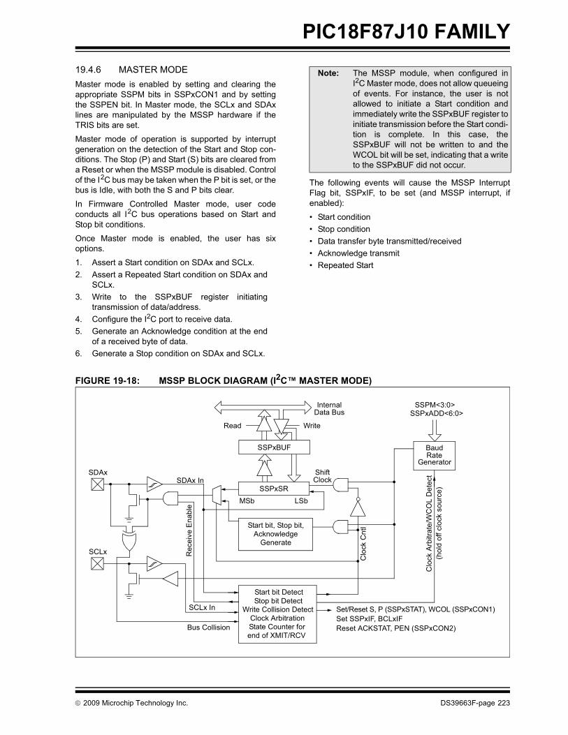
PIC18F87J10 FAMILY
19.4.6 MASTER MODEMaster mode is enabled by setting and clearing theappropriate SSPM bits in SSPxCON1 and by settingthe SSPEN bit. In Master mode, the SCLx and SDAxlines are manipulated by the MSSP hardware if theTRIS bits are set.Master mode of operation is supported by interruptgeneration on the detection of the Start and Stop con-ditions. The Stop (P) and Start (S) bits are cleared froma Reset or when the MSSP module is disabled. Controlof the I2C bus may be taken when the P bit is set, or thebus is Idle, with both the S and P bits clear.
In Firmware Controlled Master mode, user codeconducts all I2C bus operations based on Start andStop bit conditions.
Once Master mode is enabled, the user has sixoptions.
1. Assert a Start condition on SDAx and SCLx.2. Assert a Repeated Start condition on SDAx and
SCLx.3. Write to the SSPxBUF register initiating
transmission of data/address.4. Configure the I2C port to receive data.5. Generate an Acknowledge condition at the end
of a received byte of data.6. Generate a Stop condition on SDAx and SCLx.
The following events will cause the MSSP InterruptFlag bit, SSPxIF, to be set (and MSSP interrupt, ifenabled):
• Start condition• Stop condition• Data transfer byte transmitted/received• Acknowledge transmit• Repeated Start
FIGURE 19-18: MSSP BLOCK DIAGRAM (I2C™ MASTER MODE)
Note: The MSSP module, when configured inI2C Master mode, does not allow queueingof events. For instance, the user is notallowed to initiate a Start condition andimmediately write the SSPxBUF register toinitiate transmission before the Start condi-tion is complete. In this case, theSSPxBUF will not be written to and theWCOL bit will be set, indicating that a writeto the SSPxBUF did not occur.
Read Write
SSPxSR
Start bit, Stop bit,
SSPxBUF
InternalData Bus
Set/Reset S, P (SSPxSTAT), WCOL (SSPxCON1)
ShiftClock
MSb LSb
SDAx
AcknowledgeGenerate
Stop bit DetectWrite Collision Detect
Clock ArbitrationState Counter forend of XMIT/RCV
SCLx
SCLx In
Bus Collision
SDAx In
Rec
eive
Ena
ble
Clo
ck C
ntl
Clo
ck A
rbitr
ate/
WC
OL
Det
ect
(hol
d of
f clo
ck s
ourc
e)
SSPxADD<6:0>
Baud
Set SSPxIF, BCLxIFReset ACKSTAT, PEN (SSPxCON2)
RateGenerator
SSPM<3:0>
Start bit Detect
© 2009 Microchip Technology Inc. DS39663F-page 223

PIC18F87J10 FAMILY
19.4.6.1 I2C Master Mode OperationThe master device generates all of the serial clockpulses and the Start and Stop conditions. A transfer isended with a Stop condition or with a Repeated Startcondition. Since the Repeated Start condition is alsothe beginning of the next serial transfer, the I2C bus willnot be released.In Master Transmitter mode, serial data is outputthrough SDAx, while SCLx outputs the serial clock. Thefirst byte transmitted contains the slave address of thereceiving device (7 bits) and the Read/Write (R/W) bit.In this case, the R/W bit will be logic ‘0’. Serial data istransmitted 8 bits at a time. After each byte is transmit-ted, an Acknowledge bit is received. Start and Stopconditions are output to indicate the beginning and theend of a serial transfer.
In Master Receive mode, the first byte transmittedcontains the slave address of the transmitting device(7 bits) and the R/W bit. In this case, the R/W bit will belogic ‘1’. Thus, the first byte transmitted is a 7-bit slaveaddress, followed by a ‘1’ to indicate the receive bit.Serial data is received via SDAx, while SCLx outputsthe serial clock. Serial data is received 8 bits at a time.After each byte is received, an Acknowledge bit istransmitted. Start and Stop conditions indicate thebeginning and end of transmission.
The Baud Rate Generator used for the SPI modeoperation is used to set the SCLx clock frequency foreither 100 kHz, 400 kHz or 1 MHz I2C operation. SeeSection 19.4.7 “Baud Rate” for more detail.
A typical transmit sequence would go as follows:
1. The user generates a Start condition by settingthe Start Enable bit, SEN (SSPxCON2<0>).
2. SSPxIF is set. The MSSP module will wait therequired start time before any other operationtakes place.
3. The user loads the SSPxBUF with the slaveaddress to transmit.
4. Address is shifted out the SDAx pin until all 8 bitsare transmitted.
5. The MSSP module shifts in the ACK bit from theslave device and writes its value into theSSPxCON2 register (SSPxCON2<6>).
6. The MSSP module generates an interrupt at theend of the ninth clock cycle by setting theSSPxIF bit.
7. The user loads the SSPxBUF with eight bits ofdata.
8. Data is shifted out the SDAx pin until all 8 bitsare transmitted.
9. The MSSP module shifts in the ACK bit from theslave device and writes its value into theSSPxCON2 register (SSPxCON2<6>).
10. The MSSP module generates an interrupt at theend of the ninth clock cycle by setting theSSPxIF bit.
11. The user generates a Stop condition by settingthe Stop Enable bit, PEN (SSPxCON2<2>).
12. Interrupt is generated once the Stop condition iscomplete.
DS39663F-page 224 © 2009 Microchip Technology Inc.
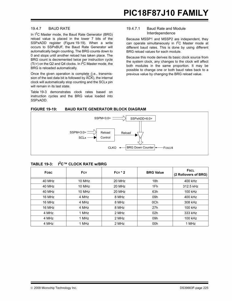
PIC18F87J10 FAMILY
19.4.7 BAUD RATE In I2C Master mode, the Baud Rate Generator (BRG)reload value is placed in the lower 7 bits of theSSPxADD register (Figure 19-19). When a writeoccurs to SSPxBUF, the Baud Rate Generator willautomatically begin counting. The BRG counts down to0 and stops until another reload has taken place. TheBRG count is decremented twice per instruction cycle(TCY) on the Q2 and Q4 clocks. In I2C Master mode, theBRG is reloaded automatically.Once the given operation is complete (i.e., transmis-sion of the last data bit is followed by ACK), the internalclock will automatically stop counting and the SCLx pinwill remain in its last state.
Table 19-3 demonstrates clock rates based oninstruction cycles and the BRG value loaded intoSSPxADD.
19.4.7.1 Baud Rate and Module Interdependence
Because MSSP1 and MSSP2 are independent, theycan operate simultaneously in I2C Master mode atdifferent baud rates. This is done by using differentBRG reload values for each module.
Because this mode derives its basic clock source fromthe system clock, any changes to the clock will affectboth modules in the same proportion. It may bepossible to change one or both baud rates back to aprevious value by changing the BRG reload value.
FIGURE 19-19: BAUD RATE GENERATOR BLOCK DIAGRAM
TABLE 19-3: I2C™ CLOCK RATE w/BRG
FOSC FCY FCY * 2 BRG Value FSCL (2 Rollovers of BRG)
40 MHz 10 MHz 20 MHz 18h 400 kHz40 MHz 10 MHz 20 MHz 1Fh 312.5 kHz40 MHz 10 MHz 20 MHz 63h 100 kHz16 MHz 4 MHz 8 MHz 09h 400 kHz16 MHz 4 MHz 8 MHz 0Ch 308 kHz16 MHz 4 MHz 8 MHz 27h 100 kHz4 MHz 1 MHz 2 MHz 02h 333 kHz4 MHz 1 MHz 2 MHz 09h 100 kHz4 MHz 1 MHz 2 MHz 00h 1 MHz
SSPM<3:0>
BRG Down CounterCLKO FOSC/4
SSPxADD<6:0>
SSPM<3:0>
SCLx
ReloadControl
Reload
© 2009 Microchip Technology Inc. DS39663F-page 225
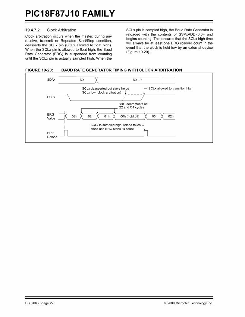
PIC18F87J10 FAMILY
19.4.7.2 Clock ArbitrationClock arbitration occurs when the master, during anyreceive, transmit or Repeated Start/Stop condition,deasserts the SCLx pin (SCLx allowed to float high).When the SCLx pin is allowed to float high, the BaudRate Generator (BRG) is suspended from countinguntil the SCLx pin is actually sampled high. When theSCLx pin is sampled high, the Baud Rate Generator isreloaded with the contents of SSPxADD<6:0> andbegins counting. This ensures that the SCLx high timewill always be at least one BRG rollover count in theevent that the clock is held low by an external device(Figure 19-20).
FIGURE 19-20: BAUD RATE GENERATOR TIMING WITH CLOCK ARBITRATION
SDAx
SCLx
SCLx deasserted but slave holds
DX – 1DX
BRG
SCLx is sampled high, reload takesplace and BRG starts its count
03h 02h 01h 00h (hold off) 03h 02h
Reload
BRGValue
SCLx low (clock arbitration)SCLx allowed to transition high
BRG decrements onQ2 and Q4 cycles
DS39663F-page 226 © 2009 Microchip Technology Inc.

PIC18F87J10 FAMILY
19.4.8 I2C MASTER MODE STARTCONDITION TIMINGTo initiate a Start condition, the user sets the StartEnable bit, SEN (SSPxCON2<0>). If the SDAx andSCLx pins are sampled high, the Baud Rate Generatoris reloaded with the contents of SSPxADD<6:0> andstarts its count. If SCLx and SDAx are both sampledhigh when the Baud Rate Generator times out (TBRG),the SDAx pin is driven low. The action of the SDAxbeing driven low while SCLx is high is the Start condi-tion and causes the S bit (SSPxSTAT<3>) to be set.Following this, the Baud Rate Generator is reloadedwith the contents of SSPxADD<6:0> and resumes itscount. When the Baud Rate Generator times out(TBRG), the SEN bit (SSPxCON2<0>) will be auto-matically cleared by hardware; the Baud Rate Generatoris suspended, leaving the SDAx line held low and theStart condition is complete.
19.4.8.1 WCOL Status FlagIf the user writes the SSPxBUF when a Start sequenceis in progress, the WCOL bit is set and the contents ofthe buffer are unchanged (the write doesn’t occur).
FIGURE 19-21: FIRST START BIT TIMING
Note: If at the beginning of the Start condition, theSDAx and SCLx pins are already sampledlow, or if during the Start condition, theSCLx line is sampled low before the SDAxline is driven low, a bus collision occurs, theBus Collision Interrupt Flag, BCLxIF, is set,the Start condition is aborted and the I2Cmodule is reset into its Idle state.
Note: Because queueing of events is notallowed, writing to the lower 5 bits ofSSPxCON2 is disabled until the Startcondition is complete.
SDAx
SCLx
S
TBRG
1st bit 2nd bit
TBRG
SDAx = 1, At completion of Start bit,SCLx = 1
Write to SSPxBUF occurs hereTBRG
hardware clears SEN bit
TBRG
Write to SEN bit occurs hereSet S bit (SSPxSTAT<3>)
and sets SSPxIF bit
© 2009 Microchip Technology Inc. DS39663F-page 227

PIC18F87J10 FAMILY
19.4.9 I2C MASTER MODE REPEATEDSTART CONDITION TIMINGA Repeated Start condition occurs when the RSEN bit(SSPxCON2<1>) is programmed high and the I2C logicmodule is in the Idle state. When the RSEN bit is set,the SCLx pin is asserted low. When the SCLx pin issampled low, the Baud Rate Generator is loaded withthe contents of SSPxADD<5:0> and begins counting.The SDAx pin is released (brought high) for one BaudRate Generator count (TBRG). When the Baud RateGenerator times out, if SDAx is sampled high, the SCLxpin will be deasserted (brought high). When SCLx issampled high, the Baud Rate Generator is reloadedwith the contents of SSPxADD<6:0> and beginscounting. SDAx and SCLx must be sampled high forone TBRG. This action is then followed by assertion ofthe SDAx pin (SDAx = 0) for one TBRG while SCLx ishigh. Following this, the RSEN bit (SSPxCON2<1>) willbe automatically cleared and the Baud Rate Generatorwill not be reloaded, leaving the SDAx pin held low. Assoon as a Start condition is detected on the SDAx andSCLx pins, the S bit (SSPxSTAT<3>) will be set. TheSSPxIF bit will not be set until the Baud Rate Generatorhas timed out.
Immediately following the SSPxIF bit getting set, theuser may write the SSPxBUF with the 7-bit address in7-bit mode or the default first address in 10-bit mode.After the first eight bits are transmitted and an ACK isreceived, the user may then transmit an additional eightbits of address (10-bit mode) or eight bits of data (7-bitmode).
19.4.9.1 WCOL Status FlagIf the user writes the SSPxBUF when a Repeated Startsequence is in progress, the WCOL is set and thecontents of the buffer are unchanged (the write doesn’toccur).
FIGURE 19-22: REPEATED START CONDITION WAVEFORM
Note 1: If RSEN is programmed while any otherevent is in progress, it will not take effect.
2: A bus collision during the Repeated Startcondition occurs if:
• SDAx is sampled low when SCLx goes from low-to-high.
• SCLx goes low before SDAx is asserted low. This may indicate that another master is attempting to transmit a data ‘1’.
Note: Because queueing of events is notallowed, writing of the lower 5 bits ofSSPxCON2 is disabled until the RepeatedStart condition is complete.
SDAx
SCLx
Sr = Repeated Start
Write to SSPxCON2
Write to SSPxBUF occurs hereon falling edge of ninth clock,end of Xmit
At completion of Start bit, hardware clears RSEN bit
1st bit
S bit set by hardware
TBRG
SDAx = 1,SDAx = 1,
SCLx (no change).SCLx = 1occurs here:
and sets SSPxIF
RSEN bit set by hardware
TBRG
TBRG TBRG TBRG
DS39663F-page 228 © 2009 Microchip Technology Inc.
PIC18F87J10 FAMILY
19.4.10 I2C MASTER MODE TRANSMISSIONTransmission of a data byte, a 7-bit address, or theother half of a 10-bit address, is accomplished by sim-ply writing a value to the SSPxBUF register. This actionwill set the Buffer Full flag bit, BF, and allow the BaudRate Generator to begin counting and start the nexttransmission. Each bit of address/data will be shiftedout onto the SDAx pin after the falling edge of SCLx isasserted (see data hold time specificationparameter 106). SCLx is held low for one Baud RateGenerator rollover count (TBRG). Data should be validbefore SCLx is released high (see data setup timespecification parameter 107). When the SCLx pin isreleased high, it is held that way for TBRG. The data onthe SDAx pin must remain stable for that duration andsome hold time after the next falling edge of SCLx.After the eighth bit is shifted out (the falling edge of theeighth clock), the BF flag is cleared and the masterreleases SDAx. This allows the slave device beingaddressed to respond with an ACK bit during the ninthbit time if an address match occurred, or if data wasreceived properly. The status of ACK is written into theACKDT bit on the falling edge of the ninth clock. If themaster receives an Acknowledge, the AcknowledgeStatus bit, ACKSTAT, is cleared; if not, the bit is set.After the ninth clock, the SSPxIF bit is set and themaster clock (Baud Rate Generator) is suspended untilthe next data byte is loaded into the SSPxBUF, leavingSCLx low and SDAx unchanged (Figure 19-23).After the write to the SSPxBUF, each bit of the addresswill be shifted out on the falling edge of SCLx until allseven address bits and the R/W bit are completed. Onthe falling edge of the eighth clock, the master willdeassert the SDAx pin, allowing the slave to respondwith an Acknowledge. On the falling edge of the ninthclock, the master will sample the SDAx pin to see if theaddress was recognized by a slave. The status of theACK bit is loaded into the ACKSTAT status bit(SSPxCON2<6>). Following the falling edge of theninth clock transmission of the address, the SSPxIF isset, the BF flag is cleared and the Baud Rate Generatoris turned off until another write to the SSPxBUF takesplace, holding SCLx low and allowing SDAx to float.
19.4.10.1 BF Status FlagIn Transmit mode, the BF bit (SSPxSTAT<0>) is setwhen the CPU writes to SSPxBUF and is cleared whenall 8 bits are shifted out.
19.4.10.2 WCOL Status FlagIf the user writes the SSPxBUF when a transmit isalready in progress (i.e., SSPxSR is still shifting out adata byte), the WCOL bit is set and the contents of thebuffer are unchanged (the write doesn’t occur) 2 TCYafter the SSPxBUF write. If SSPxBUF is rewrittenwithin 2 TCY, the WCOL bit is set and SSPxBUF isupdated. This may result in a corrupted transfer.
The user should verify that the WCOL bit is clear aftereach write to SSPxBUF to ensure the transfer is correct.In all cases, WCOL must be cleared in software.
19.4.10.3 ACKSTAT Status FlagIn Transmit mode, the ACKSTAT bit (SSPxCON2<6>)is cleared when the slave has sent an Acknowledge(ACK = 0) and is set when the slave does not Acknowl-edge (ACK = 1). A slave sends an Acknowledge whenit has recognized its address (including a general call),or when the slave has properly received its data.
19.4.11 I2C MASTER MODE RECEPTIONMaster mode reception is enabled by programming theReceive Enable bit, RCEN (SSPxCON2<3>).
The Baud Rate Generator begins counting and on eachrollover, the state of the SCLx pin changes(high-to-low/low-to-high) and data is shifted into theSSPxSR. After the falling edge of the eighth clock, thereceive enable flag is automatically cleared, the con-tents of the SSPxSR are loaded into the SSPxBUF, theBF flag bit is set, the SSPxIF flag bit is set and the BaudRate Generator is suspended from counting, holdingSCLx low. The MSSP is now in Idle state awaiting thenext command. When the buffer is read by the CPU,the BF flag bit is automatically cleared. The user canthen send an Acknowledge bit at the end of receptionby setting the Acknowledge Sequence Enable bit,ACKEN (SSPxCON2<4>).
19.4.11.1 BF Status FlagIn receive operation, the BF bit is set when an addressor data byte is loaded into SSPxBUF from SSPxSR. Itis cleared when the SSPxBUF register is read.
19.4.11.2 SSPOV Status FlagIn receive operation, the SSPOV bit is set when 8 bitsare received into the SSPxSR and the BF flag bit isalready set from a previous reception.
19.4.11.3 WCOL Status FlagIf the user writes the SSPxBUF when a receive isalready in progress (i.e., SSPxSR is still shifting in adata byte), the WCOL bit is set and the contents of thebuffer are unchanged (the write doesn’t occur).
Note: The MSSP module must be in an inactivestate before the RCEN bit is set or theRCEN bit will be disregarded.
© 2009 Microchip Technology Inc. DS39663F-page 229

PIC18F87J10 FAMILY
FIGURE 19-23: I2C™ MASTER MODE WAVEFORM (TRANSMISSION, 7 OR 10-BIT ADDRESSING)SD
Ax
SC
Lx
SS
PxI
F
BF
(SS
PxS
TAT<
0>)
SE
N
A7A
6A5
A4A
3A
2A1
AC
K =
0D
7D
6D
5D
4D
3D
2D
1D
0
AC
KTr
ansm
ittin
g D
ata
or S
econ
d H
alf
R/W
= 0
Tran
smit
Addr
ess
to S
lave
12
34
56
78
91
23
45
67
89
P
Cle
ared
in s
oftw
are
serv
ice
rout
ine
SS
PxB
UF
is w
ritte
n in
sof
twar
e
from
MS
SP
inte
rrup
t
Afte
r Sta
rt co
nditi
on, S
EN c
lear
ed b
y ha
rdw
are
S
SS
PxB
UF
writ
ten
with
7-b
it ad
dres
s an
d R
/W,
star
t tra
nsm
it
SC
Lx h
eld
low
whi
le C
PU
resp
onds
to S
SP
xIF
SE
N =
0
of 1
0-bi
t Add
ress
Writ
e S
SP
xCO
N2<
0> (S
EN =
1),
Star
t con
ditio
n be
gins
From
sla
ve, c
lear
AC
KS
TAT
bit (
SS
PxC
ON
2<6>
)
AC
KS
TAT
in
SS
PxC
ON
2 = 1
Cle
ared
in s
oftw
are
SSP
xBU
F w
ritte
n
PE
N
R/W
Cle
ared
in s
oftw
are
DS39663F-page 230 © 2009 Microchip Technology Inc.

PIC18F87J10 FAMILY
FIGURE 19-24: I2C™ MASTER MODE WAVEFORM (RECEPTION, 7-BIT ADDRESSING)P9
87
65
D0
D1
D2
D3
D4
D5
D6
D7
S
A7
A6
A5
A4
A3
A2
A1
SD
A
SC
L1
23
45
67
89
12
34
56
78
91
23
4
Bus
mas
ter
term
inat
estra
nsfe
r
ACK
Rec
eivi
ng D
ata
from
Sla
veR
ecei
ving
Dat
a fro
m S
lave
D0
D1
D2
D3
D4
D5
D6
D7
ACK
R/W
= 1
Tran
smit
Addr
ess
to S
lave
SS
PIF
BF
AC
K is
not
sen
t
Writ
e to
SS
PCO
N2<
0> (S
EN =
1),
Writ
e to
SS
PBU
F oc
curs
her
e,AC
K fro
m S
laveM
aste
r con
figur
ed a
s a
rece
iver
by p
rogr
amm
ing
SSP
CO
N2<
3> (R
CEN
= 1
)PE
N b
it = 1
writ
ten
here
Dat
a sh
ifted
in o
n fa
lling
edge
of C
LK
Cle
ared
in s
oftw
are
star
t XM
IT
SEN
= 0
SS
PO
V
SDA
= 0
, SC
L = 1
whi
le C
PU
ACK
Cle
ared
in s
oftw
are
Cle
ared
in s
oftw
are
Set
SSP
IF in
terr
upt
at e
nd o
f rec
eive
Set P
bit
(SSP
STA
T<4>
)an
d SS
PIF
AC
K fro
m M
aste
r,
Set S
SPIF
at e
nd
Set S
SPIF
inte
rrup
tat
end
of A
ckno
wle
dge
sequ
ence
Set S
SPI
F in
terru
ptat
end
of A
ckno
wle
dge
sequ
ence
of re
ceiv
e
Set
AC
KEN
, sta
rt Ac
know
ledg
e se
quen
ce,
SDA
= A
CKD
T = 1
RC
EN c
lear
edau
tom
atic
ally
RC
EN =
1, s
tart
next
rece
ive
Writ
e to
SS
PCO
N2<
4>to
sta
rt Ac
know
ledg
e se
quen
ce,
SDA
= A
CKD
T (S
SPC
ON
2<5>
) = 0
RC
EN c
lear
edau
tom
atic
ally
AC
KE
Nbegi
n St
art c
ondi
tion
Cle
ared
in s
oftw
are
SD
A =
AC
KDT
= 0
Last
bit
is s
hifte
d in
to S
SPSR
and
cont
ents
are
unl
oade
d in
to S
SPB
UF
Cle
ared
inso
ftwar
e
SSP
OV
is s
et b
ecau
seS
SPB
UF
is s
till f
ull
resp
onds
to S
SPI
F
© 2009 Microchip Technology Inc. DS39663F-page 231

PIC18F87J10 FAMILY
19.4.12 ACKNOWLEDGE SEQUENCETIMINGAn Acknowledge sequence is enabled by setting theAcknowledge Sequence Enable bit, ACKEN(SSPxCON2<4>). When this bit is set, the SCLx pin ispulled low and the contents of the Acknowledge data bitare presented on the SDAx pin. If the user wishes togenerate an Acknowledge, then the ACKDT bit shouldbe cleared. If not, the user should set the ACKDT bitbefore starting an Acknowledge sequence. The BaudRate Generator then counts for one rollover period(TBRG) and the SCLx pin is deasserted (pulled high).When the SCLx pin is sampled high (clock arbitration),the Baud Rate Generator counts for TBRG. The SCLx pinis then pulled low. Following this, the ACKEN bit is auto-matically cleared, the Baud Rate Generator is turned offand the MSSP module then goes into an inactive state(Figure 19-25).
19.4.12.1 WCOL Status FlagIf the user writes the SSPxBUF when an Acknowledgesequence is in progress, then WCOL is set and thecontents of the buffer are unchanged (the write doesn’toccur).
19.4.13 STOP CONDITION TIMINGA Stop bit is asserted on the SDAx pin at the end of areceive/transmit by setting the Stop Sequence Enablebit, PEN (SSPxCON2<2>). At the end of areceive/transmit, the SCLx line is held low after thefalling edge of the ninth clock. When the PEN bit is set,the master will assert the SDAx line low. When theSDAx line is sampled low, the Baud Rate Generator isreloaded and counts down to ‘0’. When the Baud RateGenerator times out, the SCLx pin will be brought highand one TBRG (Baud Rate Generator rollover count)later, the SDAx pin will be deasserted. When the SDAxpin is sampled high while SCLx is high, the P bit(SSPxSTAT<4>) is set. A TBRG later, the PEN bit iscleared and the SSPxIF bit is set (Figure 19-26).
19.4.13.1 WCOL Status FlagIf the user writes the SSPxBUF when a Stop sequenceis in progress, then the WCOL bit is set and thecontents of the buffer are unchanged (the write doesn’toccur).
FIGURE 19-25: ACKNOWLEDGE SEQUENCE WAVEFORM
FIGURE 19-26: STOP CONDITION RECEIVE OR TRANSMIT MODE
Note: TBRG = one Baud Rate Generator period.
SDAx
SCLx
SSPxIF set at
Acknowledge sequence starts here,write to SSPxCON2,
ACKEN automatically cleared
Cleared in
TBRG TBRG
the end of receive
8
ACKEN = 1, ACKDT = 0
D0
9
SSPxIF
software SSPxIF set at the endof Acknowledge sequence
Cleared insoftware
ACK
SCLx
SDAx
SDAx asserted low before rising edge of clock
Write to SSPxCON2,set PEN
Falling edge of
SCLx = 1 for TBRG, followed by SDAx = 1 for TBRG
9th clock
SCLx brought high after TBRG
Note: TBRG = one Baud Rate Generator period.
TBRG TBRG
after SDAx sampled high. P bit (SSPxSTAT<4>) is set.
TBRG
to setup Stop condition
ACK
PTBRG
PEN bit (SSPxCON2<2>) is cleared by hardware and the SSPxIF bit is set
DS39663F-page 232 © 2009 Microchip Technology Inc.

PIC18F87J10 FAMILY
19.4.14 SLEEP OPERATIONWhile in Sleep mode, the I2C module can receiveaddresses or data and when an address match orcomplete byte transfer occurs, wake the processorfrom Sleep (if the MSSP interrupt is enabled).19.4.15 EFFECTS OF A RESETA Reset disables the MSSP module and terminates thecurrent transfer.
19.4.16 MULTI-MASTER MODEIn Multi-Master mode, the interrupt generation on thedetection of the Start and Stop conditions allows thedetermination of when the bus is free. The Stop (P) andStart (S) bits are cleared from a Reset or when theMSSP module is disabled. Control of the I2C bus maybe taken when the P bit (SSPxSTAT<4>) is set, or thebus is Idle, with both the S and P bits clear. When thebus is busy, enabling the MSSP interrupt will generatethe interrupt when the Stop condition occurs.
In multi-master operation, the SDAx line must bemonitored for arbitration to see if the signal level is theexpected output level. This check is performed inhardware with the result placed in the BCLxIF bit.
The states where arbitration can be lost are:
• Address Transfer • Data Transfer• A Start Condition • A Repeated Start Condition• An Acknowledge Condition
19.4.17 MULTI -MASTER COMMUNICATION, BUS COLLISION AND BUS ARBITRATION
Multi-Master mode support is achieved by bus arbitra-tion. When the master outputs address/data bits ontothe SDAx pin, arbitration takes place when the masteroutputs a ‘1’ on SDAx, by letting SDAx float high andanother master asserts a ‘0’. When the SCLx pin floatshigh, data should be stable. If the expected data onSDAx is a ‘1’ and the data sampled on the SDAxpin = 0, then a bus collision has taken place. Themaster will set the Bus Collision Interrupt Flag, BCLxIF,and reset the I2C port to its Idle state (Figure 19-27).
If a transmit was in progress when the bus collisionoccurred, the transmission is halted, the BF flag iscleared, the SDAx and SCLx lines are deasserted andthe SSPxBUF can be written to. When the user servicesthe bus collision Interrupt Service Routine and if the I2Cbus is free, the user can resume communication byasserting a Start condition.
If a Start, Repeated Start, Stop or Acknowledge conditionwas in progress when the bus collision occurred, the con-dition is aborted, the SDAx and SCLx lines aredeasserted and the respective control bits in theSSPxCON2 register are cleared. When the user servicesthe bus collision Interrupt Service Routine and if the I2Cbus is free, the user can resume communication byasserting a Start condition.
The master will continue to monitor the SDAx and SCLxpins. If a Stop condition occurs, the SSPxIF bit will be set.
A write to the SSPxBUF will start the transmission ofdata at the first data bit regardless of where thetransmitter left off when the bus collision occurred.
In Multi-Master mode, the interrupt generation on thedetection of Start and Stop conditions allows the deter-mination of when the bus is free. Control of the I2C buscan be taken when the P bit is set in the SSPxSTATregister, or the bus is Idle and the S and P bits arecleared.
FIGURE 19-27: BUS COLLISION TIMING FOR TRANSMIT AND ACKNOWLEDGE
SDAx
SCLx
BCLxIF
SDAx released
SDAx line pulled lowby another source
Sample SDAx. While SCLx is high,data doesn’t match what is driven
Bus collision has occurred.
Set bus collisioninterrupt (BCLxIF)
by the master.
by master
Data changeswhile SCLx = 0
© 2009 Microchip Technology Inc. DS39663F-page 233

PIC18F87J10 FAMILY
19.4.17.1 Bus Collision During a StartConditionDuring a Start condition, a bus collision occurs if:
a) SDAx or SCLx are sampled low at the beginningof the Start condition (Figure 19-28).
b) SCLx is sampled low before SDAx is assertedlow (Figure 19-29).
During a Start condition, both the SDAx and the SCLxpins are monitored.
If the SDAx pin is already low, or the SCLx pin isalready low, then all of the following occur:• the Start condition is aborted, • the BCLxIF flag is set and• the MSSP module is reset to its inactive state
(Figure 19-28).
The Start condition begins with the SDAx and SCLxpins deasserted. When the SDAx pin is sampled high,the Baud Rate Generator is loaded fromSSPxADD<6:0> and counts down to 0. If the SCLx pinis sampled low while SDAx is high, a bus collisionoccurs because it is assumed that another master isattempting to drive a data ‘1’ during the Start condition.
If the SDAx pin is sampled low during this count, theBRG is reset and the SDAx line is asserted early(Figure 19-30). If, however, a ‘1’ is sampled on theSDAx pin, the SDAx pin is asserted low at the end ofthe BRG count. The Baud Rate Generator is thenreloaded and counts down to 0. If the SCLx pin issampled as ‘0’ during this time, a bus collision does notoccur. At the end of the BRG count, the SCLx pin isasserted low.
FIGURE 19-28: BUS COLLISION DURING START CONDITION (SDAx ONLY)
Note: The reason that bus collision is not a factorduring a Start condition is that no two busmasters can assert a Start condition at theexact same time. Therefore, one masterwill always assert SDAx before the other.This condition does not cause a bus colli-sion because the two masters must beallowed to arbitrate the first addressfollowing the Start condition. If the addressis the same, arbitration must be allowed tocontinue into the data portion, RepeatedStart or Stop conditions.
SDAx
SCLx
SENSDAx sampled low before
SDAx goes low before the SEN bit is set.
S bit and SSPxIF set because
MSSP module reset into Idle state.SEN cleared automatically because of bus collision.
S bit and SSPxIF set because
Set SEN, enable Startcondition if SDAx = 1, SCLx = 1
SDAx = 0, SCLx = 1.
BCLxIF
S
SSPxIF
SDAx = 0, SCLx = 1.
SSPxIF and BCLxIF arecleared in software
SSPxIF and BCLxIF arecleared in software
Set BCLxIF,
Start condition. Set BCLxIF.
DS39663F-page 234 © 2009 Microchip Technology Inc.

PIC18F87J10 FAMILY
FIGURE 19-29: BUS COLLISION DURING START CONDITION (SCLx = 0)FIGURE 19-30: BRG RESET DUE TO SDAx ARBITRATION DURING START CONDITION
SDAx
SCLx
SENbus collision occurs. Set BCLxIF.SCLx = 0 before SDAx = 0,
Set SEN, enable Startsequence if SDAx = 1, SCLx = 1
TBRG TBRG
SDAx = 0, SCLx = 1
BCLxIF
S
SSPxIF
Interrupt clearedin software
bus collision occurs. Set BCLxIF.SCLx = 0 before BRG time-out,
‘0’ ‘0’
‘0’‘0’
SDAx
SCLx
SEN
Set SLess than TBRG TBRG
SDAx = 0, SCLx = 1
BCLxIF
S
SSPxIF
S
Interrupts clearedin softwareset SSPxIF
SDAx = 0, SCLx = 1,
SCLx pulled low after BRGtime-out
Set SSPxIF
‘0’
SDAx pulled low by other master.Reset BRG and assert SDAx.
Set SEN, enable Startsequence if SDAx = 1, SCLx = 1
© 2009 Microchip Technology Inc. DS39663F-page 235
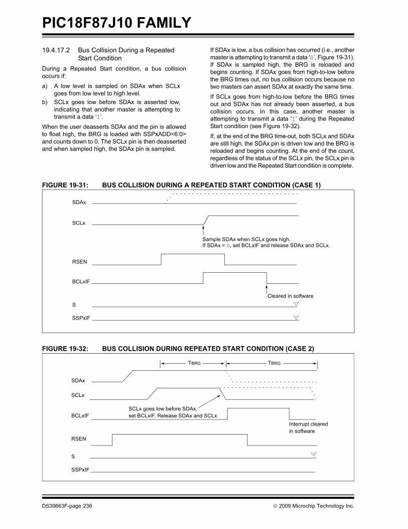
PIC18F87J10 FAMILY
19.4.17.2 Bus Collision During a RepeatedStart ConditionDuring a Repeated Start condition, a bus collisionoccurs if:
a) A low level is sampled on SDAx when SCLxgoes from low level to high level.
b) SCLx goes low before SDAx is asserted low,indicating that another master is attempting totransmit a data ‘1’.
When the user deasserts SDAx and the pin is allowedto float high, the BRG is loaded with SSPxADD<6:0>and counts down to 0. The SCLx pin is then deassertedand when sampled high, the SDAx pin is sampled.
If SDAx is low, a bus collision has occurred (i.e., anothermaster is attempting to transmit a data ‘0’, Figure 19-31).If SDAx is sampled high, the BRG is reloaded andbegins counting. If SDAx goes from high-to-low beforethe BRG times out, no bus collision occurs because notwo masters can assert SDAx at exactly the same time.
If SCLx goes from high-to-low before the BRG timesout and SDAx has not already been asserted, a buscollision occurs. In this case, another master isattempting to transmit a data ‘1’ during the RepeatedStart condition (see Figure 19-32).
If, at the end of the BRG time-out, both SCLx and SDAxare still high, the SDAx pin is driven low and the BRG isreloaded and begins counting. At the end of the count,regardless of the status of the SCLx pin, the SCLx pin isdriven low and the Repeated Start condition is complete.
FIGURE 19-31: BUS COLLISION DURING A REPEATED START CONDITION (CASE 1)
FIGURE 19-32: BUS COLLISION DURING REPEATED START CONDITION (CASE 2)
SDAx
SCLx
RSEN
BCLxIF
S
SSPxIF
Sample SDAx when SCLx goes high.If SDAx = 0, set BCLxIF and release SDAx and SCLx.
Cleared in software
‘0’
‘0’
SDAx
SCLx
BCLxIF
RSEN
S
SSPxIF
Interrupt clearedin software
SCLx goes low before SDAx,set BCLxIF. Release SDAx and SCLx.
TBRG TBRG
‘0’
DS39663F-page 236 © 2009 Microchip Technology Inc.
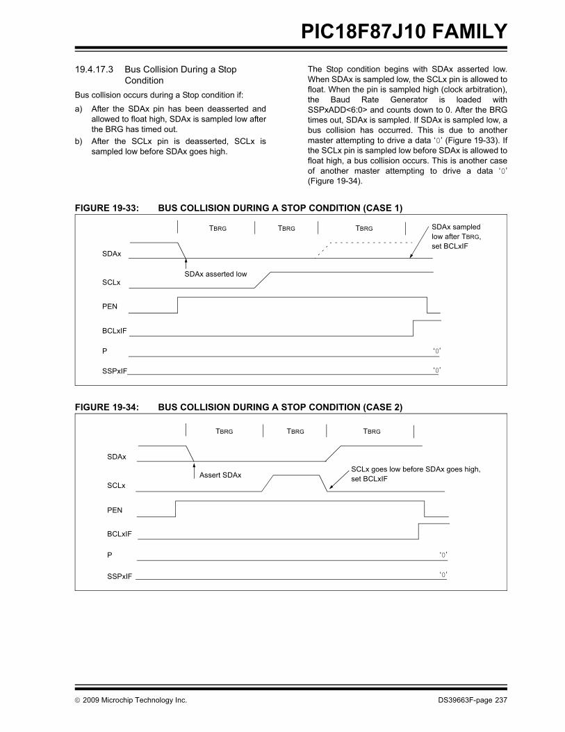
PIC18F87J10 FAMILY
19.4.17.3 Bus Collision During a StopConditionBus collision occurs during a Stop condition if:
a) After the SDAx pin has been deasserted andallowed to float high, SDAx is sampled low afterthe BRG has timed out.
b) After the SCLx pin is deasserted, SCLx issampled low before SDAx goes high.
The Stop condition begins with SDAx asserted low.When SDAx is sampled low, the SCLx pin is allowed tofloat. When the pin is sampled high (clock arbitration),the Baud Rate Generator is loaded withSSPxADD<6:0> and counts down to 0. After the BRGtimes out, SDAx is sampled. If SDAx is sampled low, abus collision has occurred. This is due to anothermaster attempting to drive a data ‘0’ (Figure 19-33). Ifthe SCLx pin is sampled low before SDAx is allowed tofloat high, a bus collision occurs. This is another caseof another master attempting to drive a data ‘0’(Figure 19-34).
FIGURE 19-33: BUS COLLISION DURING A STOP CONDITION (CASE 1)
FIGURE 19-34: BUS COLLISION DURING A STOP CONDITION (CASE 2)
SDAx
SCLx
BCLxIF
PEN
P
SSPxIF
TBRG TBRG TBRG
SDAx asserted low
SDAx sampledlow after TBRG,set BCLxIF
‘0’
‘0’
SDAx
SCLx
BCLxIF
PEN
P
SSPxIF
TBRG TBRG TBRG
Assert SDAxSCLx goes low before SDAx goes high,set BCLxIF
‘0’
‘0’
© 2009 Microchip Technology Inc. DS39663F-page 237

PIC18F87J10 FAMILY
TABLE 19-4: REGISTERS ASSOCIATED WITH I2C™ OPERATIONName Bit 7 Bit 6 Bit 5 Bit 4 Bit 3 Bit 2 Bit 1 Bit 0Reset Values
on Page
INTCON GIE/GIEH PEIE/GIEL TMR0IE INT0IE RBIE TMR0IF INT0IF RBIF 53PIR1 PSPIF ADIF RC1IF TX1IF SSP1IF CCP1IF TMR2IF TMR1IF 55PIE1 PSPIE ADIE RC1IE TX1IE SSP1IE CCP1IE TMR2IE TMR1IE 55IPR1 PSPIP ADIP RC1IP TX1IP SSP1IP CCP1IP TMR2IP TMR1IP 55PIR2 OSCFIF CMIF — — BCL1IF — TMR3IF CCP2IF 55PIE2 OSCFIE CMIE — — BCL1IE — TMR3IE CCP2IE 55IPR2 OSCFIP CMIP — — BCL1IP — TMR3IP CCP2IP 55PIR3 SSP2IF BCL2IF RC2IF TX2IF TMR4IF CCP5IF CCP4IF CCP3IF 55PIE3 SSP2IE BCL2IE RC2IE TX2IE TMR4IE CCP5IE CCP4IE CCP3IE 55IPR3 SSP2IP BCL2IP RC2IP TX2IP TMR4IP CCP5IP CCP4IP CCP3IP 55TRISC TRISC7 TRISC6 TRISC5 TRISC4 TRISC3 TRISC2 TRISC1 TRISC0 56TRISD TRISD7 TRISD6 TRISD5 TRISD4 TRISD3 TRISD2 TRISD1 TRISD0 56SSP1BUF MSSP1 Receive Buffer/Transmit Register 54SSP1ADD MSSP1 Address Register (I2C™ Slave mode),
MSSP1 Baud Rate Reload Register (I2C Master mode)57
SSPxCON1 WCOL SSPOV SSPEN CKP SSPM3 SSPM2 SSPM1 SSPM0 54, 57SSPxCON2 GCEN ACKSTAT ACKDT/
ADMSK5ACKEN/ADMSK4
RCEN/ADMSK3
PEN/ADMSK2
RSEN/ADMSK1
SEN 54, 57
SSPxSTAT SMP CKE D/A P S R/W UA BF 54, 57SSP2BUF MSSP2 Receive Buffer/Transmit Register 54SSP2ADD MSSP2 Address Register (I2C Slave mode),
MSSP2 Baud Rate Reload Register (I2C Master mode)57
Legend: — = unimplemented, read as ‘0’. Shaded cells are not used by the MSSP module in I2C™ mode.
DS39663F-page 238 © 2009 Microchip Technology Inc.

PIC18F87J10 FAMILY
20.0 ENHANCED UNIVERSAL SYNCHRONOUS ASYNCHRONOUS RECEIVER TRANSMITTER (EUSART)
The Enhanced Universal Synchronous AsynchronousReceiver Transmitter (EUSART) module is one of twoserial I/O modules. (Generically, the EUSART is alsoknown as a Serial Communications Interface or SCI.)The EUSART can be configured as a full-duplexasynchronous system that can communicate withperipheral devices, such as CRT terminals andpersonal computers. It can also be configured as ahalf-duplex synchronous system that can communicatewith peripheral devices, such as A/D or D/A integratedcircuits, serial EEPROMs, etc.
The Enhanced USART module implements additionalfeatures, including automatic baud rate detection andcalibration, automatic wake-up on Sync Break recep-tion and 12-bit Break character transmit. These make itideally suited for use in Local Interconnect Network bus(LIN bus) systems.
All members of the PIC18F87J10 family are equippedwith two independent EUSART modules, referred to asEUSART1 and EUSART2. They can be configured inthe following modes:
• Asynchronous (full duplex) with:- Auto-Wake-up on character reception- Auto-Baud calibration- 12-bit Break character transmission
• Synchronous – Master (half duplex) with selectable clock polarity
• Synchronous – Slave (half duplex) with selectable clock polarity
The pins of EUSART1 and EUSART2 are multiplexedwith the functions of PORTC (RC6/TX1/CK1 andRC7/RX1/DT1) and PORTG (RG1/TX2/CK2 andRG2/RX2/DT2), respectively. In order to configurethese pins as an EUSART:
• For EUSART1:- bit, SPEN (RCSTA1<7>), must be set (= 1)- bit, TRISC<7>, must be set (= 1)- bit, TRISC<6>, must be cleared (= 0) for
Asynchronous and Synchronous Master modes
- bit, TRISC<6>, must be set (= 1) for Synchronous Slave mode
• For EUSART2:- bit, SPEN (RCSTA2<7>), must be set (= 1)- bit, TRISG<2>, must be set (= 1)- bit, TRISG<1>, must be cleared (= 0) for
Asynchronous and Synchronous Master modes
- bit, TRISC<6> must be set (= 1) for Synchronous Slave mode
The operation of each Enhanced USART module iscontrolled through three registers:
• Transmit Status and Control (TXSTAx)• Receive Status and Control (RCSTAx)• Baud Rate Control (BAUDCONx)
These are detailed on the following pages inRegister 20-1, Register 20-2 and Register 20-3,respectively.
Note: The EUSART control will automaticallyreconfigure the pin from input to output asneeded.
Note: Throughout this section, references toregister and bit names that may be associ-ated with a specific EUSART module arereferred to generically by the use of ‘x’ inplace of the specific module number.Thus, “RCSTAx” might refer to theReceive Status register for eitherEUSART1 or EUSART2.
© 2009 Microchip Technology Inc. DS39663F-page 239
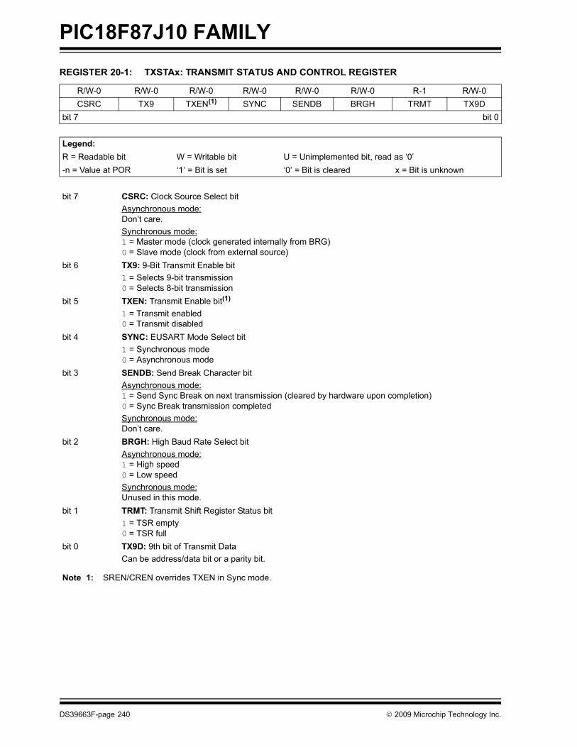
PIC18F87J10 FAMILY
REGISTER 20-1: TXSTAx: TRANSMIT STATUS AND CONTROL REGISTERR/W-0 R/W-0 R/W-0 R/W-0 R/W-0 R/W-0 R-1 R/W-0CSRC TX9 TXEN(1) SYNC SENDB BRGH TRMT TX9D
bit 7 bit 0
Legend:R = Readable bit W = Writable bit U = Unimplemented bit, read as ‘0’-n = Value at POR ‘1’ = Bit is set ‘0’ = Bit is cleared x = Bit is unknown
bit 7 CSRC: Clock Source Select bitAsynchronous mode: Don’t care.Synchronous mode: 1 = Master mode (clock generated internally from BRG)0 = Slave mode (clock from external source)
bit 6 TX9: 9-Bit Transmit Enable bit 1 = Selects 9-bit transmission 0 = Selects 8-bit transmission
bit 5 TXEN: Transmit Enable bit(1)
1 = Transmit enabled0 = Transmit disabled
bit 4 SYNC: EUSART Mode Select bit 1 = Synchronous mode 0 = Asynchronous mode
bit 3 SENDB: Send Break Character bitAsynchronous mode:1 = Send Sync Break on next transmission (cleared by hardware upon completion)0 = Sync Break transmission completedSynchronous mode:Don’t care.
bit 2 BRGH: High Baud Rate Select bit Asynchronous mode: 1 = High speed 0 = Low speedSynchronous mode: Unused in this mode.
bit 1 TRMT: Transmit Shift Register Status bit1 = TSR empty 0 = TSR full
bit 0 TX9D: 9th bit of Transmit DataCan be address/data bit or a parity bit.
Note 1: SREN/CREN overrides TXEN in Sync mode.
DS39663F-page 240 © 2009 Microchip Technology Inc.

PIC18F87J10 FAMILY
REGISTER 20-2: RCSTAx: RECEIVE STATUS AND CONTROL REGISTERR/W-0 R/W-0 R/W-0 R/W-0 R/W-0 R-0 R-0 R-xSPEN RX9 SREN CREN ADDEN FERR OERR RX9D
bit 7 bit 0
Legend:R = Readable bit W = Writable bit U = Unimplemented bit, read as ‘0’-n = Value at POR ‘1’ = Bit is set ‘0’ = Bit is cleared x = Bit is unknown
bit 7 SPEN: Serial Port Enable bit1 = Serial port enabled (configures RXx/DTx and TXx/CKx pins as serial port pins)0 = Serial port disabled (held in Reset)
bit 6 RX9: 9-Bit Receive Enable bit1 = Selects 9-bit reception 0 = Selects 8-bit reception
bit 5 SREN: Single Receive Enable bit Asynchronous mode: Don’t care.Synchronous mode – Master: 1 = Enables single receive0 = Disables single receive This bit is cleared after reception is complete.Synchronous mode – Slave: Don’t care.
bit 4 CREN: Continuous Receive Enable bit Asynchronous mode: 1 = Enables receiver0 = Disables receiverSynchronous mode: 1 = Enables continuous receive until enable bit, CREN, is cleared (CREN overrides SREN) 0 = Disables continuous receive
bit 3 ADDEN: Address Detect Enable bitAsynchronous mode 9-bit (RX9 = 1):1 = Enables address detection, enables interrupt and loads the receive buffer when RSR<8> is set0 = Disables address detection, all bytes are received and ninth bit can be used as parity bitAsynchronous mode 8-bit (RX9 = 0):Don’t care.
bit 2 FERR: Framing Error bit 1 = Framing error (can be updated by reading the RCREGx register and receiving the next valid byte)0 = No framing error
bit 1 OERR: Overrun Error bit 1 = Overrun error (can be cleared by clearing bit, CREN) 0 = No overrun error
bit 0 RX9D: 9th bit of Received Data This can be address/data bit or a parity bit and must be calculated by user firmware.
© 2009 Microchip Technology Inc. DS39663F-page 241

PIC18F87J10 FAMILY
REGISTER 20-3: BAUDCONx: BAUD RATE CONTROL REGISTERR/W-0 R-1 U-0 R/W-0 R/W-0 U-0 R/W-0 R/W-0ABDOVF RCIDL — SCKP BRG16 — WUE ABDEN
bit 7 bit 0
Legend:R = Readable bit W = Writable bit U = Unimplemented bit, read as ‘0’-n = Value at POR ‘1’ = Bit is set ‘0’ = Bit is cleared x = Bit is unknown
bit 7 ABDOVF: Auto-Baud Acquisition Rollover Status bit1 = A BRG rollover has occurred during Auto-Baud Rate Detect mode (must be cleared in software)0 = No BRG rollover has occurred
bit 6 RCIDL: Receive Operation Idle Status bit1 = Receive operation is Idle0 = Receive operation is active
bit 5 Unimplemented: Read as ‘0’bit 4 SCKP: Synchronous Clock Polarity Select bit
Asynchronous mode:Unused in this mode.Synchronous modes:1 = Idle state for clock (CKx) is a high level0 = Idle state for clock (CKx) is a low level
bit 3 BRG16: 16-Bit Baud Rate Register Enable bit1 = 16-bit Baud Rate Generator – SPBRGHx and SPBRGx0 = 8-bit Baud Rate Generator – SPBRGx only (Compatible mode), SPBRGHx value ignored
bit 2 Unimplemented: Read as ‘0’bit 1 WUE: Wake-up Enable bit
Asynchronous mode:1 = EUSART will continue to sample the RXx pin – interrupt generated on falling edge; bit cleared in
hardware on the following rising edge0 = RXx pin not monitored or rising edge detectedSynchronous mode:Unused in this mode.
bit 0 ABDEN: Auto-Baud Detect Enable bitAsynchronous mode:1 = Enable baud rate measurement on the next character. Requires reception of a Sync field (55h);
cleared in hardware upon completion.0 = Baud rate measurement disabled or completedSynchronous mode:Unused in this mode.
DS39663F-page 242 © 2009 Microchip Technology Inc.

PIC18F87J10 FAMILY
20.1 Baud Rate Generator (BRG)The BRG is a dedicated 8-bit or 16-bit generator thatsupports both the Asynchronous and Synchronousmodes of the EUSART. By default, the BRG operatesin 8-bit mode; setting the BRG16 bit (BAUDCONx<3>)selects 16-bit mode.The SPBRGHx:SPBRGx register pair controls the periodof a free-running timer. In Asynchronous mode, bitsBRGH (TXSTAx<2>) and BRG16 (BAUDCONx<3>) alsocontrol the baud rate. In Synchronous mode, BRGH isignored. Table 20-1 shows the formula for computation ofthe baud rate for different EUSART modes which onlyapply in Master mode (internally generated clock).
Given the desired baud rate and FOSC, the nearestinteger value for the SPBRGHx:SPBRGx registers canbe calculated using the formulas in Table 20-1. From this,the error in baud rate can be determined. An examplecalculation is shown in Example 20-1. Typical baud ratesand error values for the various Asynchronous modesare shown in Table 20-2. It may be advantageous to use
the high baud rate (BRGH = 1) or the 16-bit BRG toreduce the baud rate error, or achieve a slow baud ratefor a fast oscillator frequency.
Writing a new value to the SPBRGHx:SPBRGx regis-ters causes the BRG timer to be reset (or cleared). Thisensures the BRG does not wait for a timer overflowbefore outputting the new baud rate.
20.1.1 OPERATION IN POWER-MANAGED MODES
The device clock is used to generate the desired baudrate. When one of the power-managed modes isentered, the new clock source may be operating at adifferent frequency. This may require an adjustment tothe value in the SPBRGx register pair.
20.1.2 SAMPLINGThe data on the RXx pin (either RC7/RX1/DT1 orRG2/RX2/DT2) is sampled three times by a majoritydetect circuit to determine if a high or a low level ispresent at the RXx pin.
TABLE 20-1: BAUD RATE FORMULASConfiguration Bits
BRG/EUSART Mode Baud Rate FormulaSYNC BRG16 BRGH
0 0 0 8-Bit/Asynchronous FOSC/[64 (n + 1)]0 0 1 8-Bit/Asynchronous
FOSC/[16 (n + 1)]0 1 0 16-Bit/Asynchronous0 1 1 16-Bit/Asynchronous
FOSC/[4 (n + 1)]1 0 x 8-Bit/Synchronous1 1 x 16-Bit/Synchronous
Legend: x = Don’t care, n = value of SPBRGHx:SPBRGx register pair
© 2009 Microchip Technology Inc. DS39663F-page 243

PIC18F87J10 FAMILY
EXAMPLE 20-1: CALCULATING BAUD RATE ERRORTABLE 20-2: REGISTERS ASSOCIATED WITH BAUD RATE GENERATOR
Name Bit 7 Bit 6 Bit 5 Bit 4 Bit 3 Bit 2 Bit 1 Bit 0 Reset Values on page
TXSTAx CSRC TX9 TXEN SYNC SENDB BRGH TRMT TX9D 55RCSTAx SPEN RX9 SREN CREN ADDEN FERR OERR RX9D 55BAUDCONx ABDOVF RCIDL — SCKP BRG16 — WUE ABDEN 56SPBRGHx EUSARTx Baud Rate Generator Register High Byte 56SPBRGx EUSARTx Baud Rate Generator Register Low Byte 56Legend: — = unimplemented, read as ‘0’. Shaded cells are not used by the BRG.
For a device with FOSC of 16 MHz, desired baud rate of 9600, Asynchronous mode, 8-bit BRG:Desired Baud Rate = FOSC/(64 ([SPBRGHx:SPBRGx] + 1)) Solving for SPBRGHx:SPBRGx:
X = ((FOSC/Desired Baud Rate)/64) – 1= ((16000000/9600)/64) – 1 = [25.042] = 25
Calculated Baud Rate = 16000000/(64 (25 + 1)) = 9615
Error = (Calculated Baud Rate – Desired Baud Rate)/Desired Baud Rate= (9615 – 9600)/9600 = 0.16%
DS39663F-page 244 © 2009 Microchip Technology Inc.

PIC18F87J10 FAMILY
TABLE 20-3: BAUD RATES FOR ASYNCHRONOUS MODESBAUDRATE
(K)
SYNC = 0, BRGH = 0, BRG16 = 0
FOSC = 40.000 MHz FOSC = 20.000 MHz FOSC = 10.000 MHz FOSC = 8.000 MHzActual Rate (K)
%Error
SPBRGValue
(decimal)
Actual Rate (K)
%Error
SPBRGValue
(decimal)
Actual Rate (K)
%Error
SPBRGValue
(decimal)
Actual Rate (K)
%Error
SPBRGValue
(decimal)
0.3 — — — — — — — — — — — —1.2 — — — 1.221 1.73 255 1.202 0.16 129 1.201 -0.16 1032.4 2.441 1.73 255 2.404 0.16 129 2.404 0.16 64 2.403 -0.16 519.6 9.615 0.16 64 9.766 1.73 31 9.766 1.73 15 9.615 -0.16 12
19.2 19.531 1.73 31 19.531 1.73 15 19.531 1.73 7 — — —57.6 56.818 -1.36 10 62.500 8.51 4 52.083 -9.58 2 — — —115.2 125.000 8.51 4 104.167 -9.58 2 78.125 -32.18 1 — — —
BAUDRATE
(K)
SYNC = 0, BRGH = 0, BRG16 = 0
FOSC = 4.000 MHz FOSC = 2.000 MHz FOSC = 1.000 MHzActual Rate (K)
%Error
SPBRGValue
(decimal)
Actual Rate (K)
%Error
SPBRGValue
(decimal)
Actual Rate (K)
%Error
SPBRGValue
(decimal)
0.3 0.300 0.16 207 0.300 -0.16 103 0.300 -0.16 511.2 1.202 0.16 51 1.201 -0.16 25 1.201 -0.16 122.4 2.404 0.16 25 2.403 -0.16 12 — — —9.6 8.929 -6.99 6 — — — — — —
19.2 20.833 8.51 2 — — — — — —57.6 62.500 8.51 0 — — — — — —115.2 62.500 -45.75 0 — — — — — —
BAUDRATE
(K)
SYNC = 0, BRGH = 1, BRG16 = 0
FOSC = 40.000 MHz FOSC = 20.000 MHz FOSC = 10.000 MHz FOSC = 8.000 MHzActual Rate (K)
%Error
SPBRGValue
(decimal)
Actual Rate (K)
%Error
SPBRGValue
(decimal)
Actual Rate (K)
%Error
SPBRGValue
(decimal)
Actual Rate (K)
%Error
SPBRGValue
(decimal)
0.3 — — — — — — — — — — — —1.2 — — — — — — — — — — — —2.4 — — — — — — 2.441 1.73 255 2.403 -0.16 2079.6 9.766 1.73 255 9.615 0.16 129 9.615 0.16 64 9.615 -0.16 51
19.2 19.231 0.16 129 19.231 0.16 64 19.531 1.73 31 19.230 -0.16 2557.6 58.140 0.94 42 56.818 -1.36 21 56.818 -1.36 10 55.555 3.55 8115.2 113.636 -1.36 21 113.636 -1.36 10 125.000 8.51 4 — — —
BAUDRATE
(K)
SYNC = 0, BRGH = 1, BRG16 = 0
FOSC = 4.000 MHz FOSC = 2.000 MHz FOSC = 1.000 MHzActual Rate (K)
%Error
SPBRGValue
(decimal)
Actual Rate (K)
%Error
SPBRGValue
(decimal)
Actual Rate (K)
%Error
SPBRGValue
(decimal)
0.3 — — — — — — 0.300 -0.16 2071.2 1.202 0.16 207 1.201 -0.16 103 1.201 -0.16 512.4 2.404 0.16 103 2.403 -0.16 51 2.403 -0.16 259.6 9.615 0.16 25 9.615 -0.16 12 — — —
19.2 19.231 0.16 12 — — — — — —57.6 62.500 8.51 3 — — — — — —115.2 125.000 8.51 1 — — — — — —
© 2009 Microchip Technology Inc. DS39663F-page 245
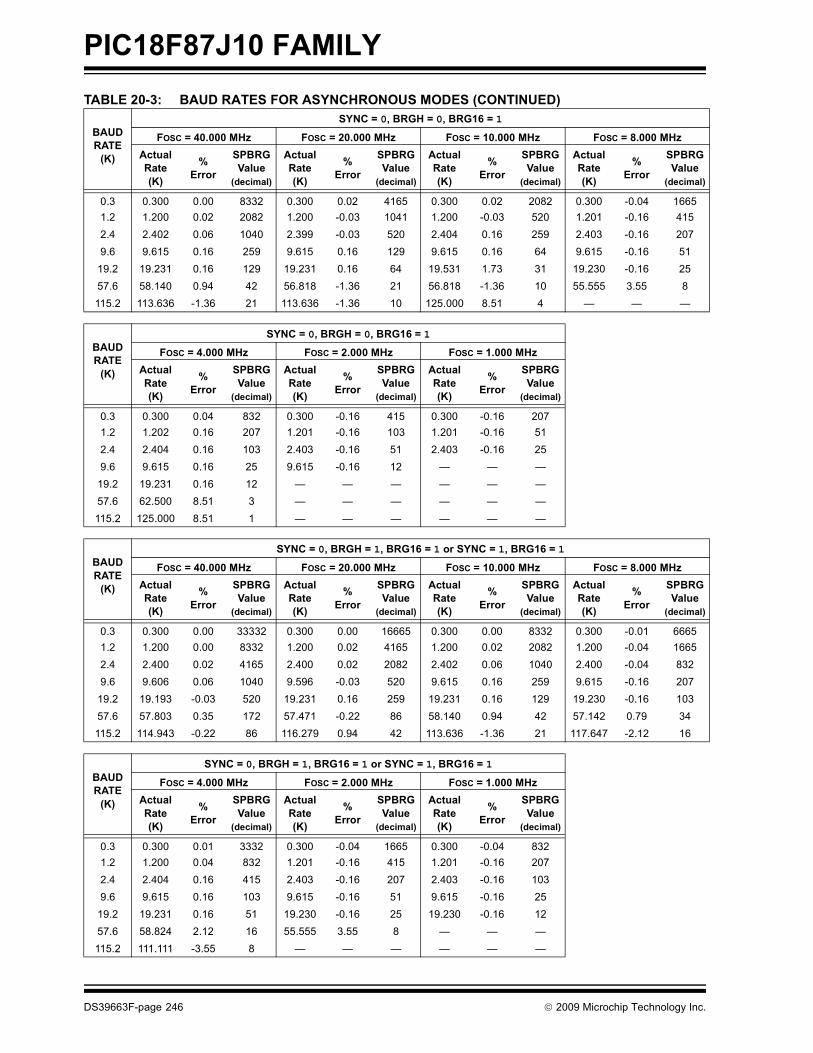
PIC18F87J10 FAMILY
BAUDRATE
(K)
SYNC = 0, BRGH = 0, BRG16 = 1
FOSC = 40.000 MHz FOSC = 20.000 MHz FOSC = 10.000 MHz FOSC = 8.000 MHzActual Rate (K)
%Error
SPBRGValue
(decimal)
Actual Rate (K)
%Error
SPBRGValue
(decimal)
Actual Rate (K)
%Error
SPBRGValue
(decimal)
Actual Rate (K)
%Error
SPBRGValue
(decimal)
0.3 0.300 0.00 8332 0.300 0.02 4165 0.300 0.02 2082 0.300 -0.04 16651.2 1.200 0.02 2082 1.200 -0.03 1041 1.200 -0.03 520 1.201 -0.16 4152.4 2.402 0.06 1040 2.399 -0.03 520 2.404 0.16 259 2.403 -0.16 2079.6 9.615 0.16 259 9.615 0.16 129 9.615 0.16 64 9.615 -0.16 51
19.2 19.231 0.16 129 19.231 0.16 64 19.531 1.73 31 19.230 -0.16 2557.6 58.140 0.94 42 56.818 -1.36 21 56.818 -1.36 10 55.555 3.55 8115.2 113.636 -1.36 21 113.636 -1.36 10 125.000 8.51 4 — — —
BAUDRATE
(K)
SYNC = 0, BRGH = 0, BRG16 = 1
FOSC = 4.000 MHz FOSC = 2.000 MHz FOSC = 1.000 MHzActual Rate (K)
%Error
SPBRGValue
(decimal)
Actual Rate (K)
%Error
SPBRGValue
(decimal)
Actual Rate (K)
%Error
SPBRGValue
(decimal)
0.3 0.300 0.04 832 0.300 -0.16 415 0.300 -0.16 2071.2 1.202 0.16 207 1.201 -0.16 103 1.201 -0.16 512.4 2.404 0.16 103 2.403 -0.16 51 2.403 -0.16 259.6 9.615 0.16 25 9.615 -0.16 12 — — —
19.2 19.231 0.16 12 — — — — — —57.6 62.500 8.51 3 — — — — — —115.2 125.000 8.51 1 — — — — — —
BAUDRATE
(K)
SYNC = 0, BRGH = 1, BRG16 = 1 or SYNC = 1, BRG16 = 1
FOSC = 40.000 MHz FOSC = 20.000 MHz FOSC = 10.000 MHz FOSC = 8.000 MHzActual Rate (K)
%Error
SPBRGValue
(decimal)
Actual Rate (K)
%Error
SPBRGValue
(decimal)
Actual Rate (K)
%Error
SPBRGValue
(decimal)
Actual Rate (K)
%Error
SPBRGValue
(decimal)
0.3 0.300 0.00 33332 0.300 0.00 16665 0.300 0.00 8332 0.300 -0.01 66651.2 1.200 0.00 8332 1.200 0.02 4165 1.200 0.02 2082 1.200 -0.04 16652.4 2.400 0.02 4165 2.400 0.02 2082 2.402 0.06 1040 2.400 -0.04 8329.6 9.606 0.06 1040 9.596 -0.03 520 9.615 0.16 259 9.615 -0.16 207
19.2 19.193 -0.03 520 19.231 0.16 259 19.231 0.16 129 19.230 -0.16 10357.6 57.803 0.35 172 57.471 -0.22 86 58.140 0.94 42 57.142 0.79 34115.2 114.943 -0.22 86 116.279 0.94 42 113.636 -1.36 21 117.647 -2.12 16
BAUDRATE
(K)
SYNC = 0, BRGH = 1, BRG16 = 1 or SYNC = 1, BRG16 = 1
FOSC = 4.000 MHz FOSC = 2.000 MHz FOSC = 1.000 MHzActual Rate (K)
%Error
SPBRGValue
(decimal)
Actual Rate (K)
%Error
SPBRGValue
(decimal)
Actual Rate (K)
%Error
SPBRGValue
(decimal)
0.3 0.300 0.01 3332 0.300 -0.04 1665 0.300 -0.04 8321.2 1.200 0.04 832 1.201 -0.16 415 1.201 -0.16 2072.4 2.404 0.16 415 2.403 -0.16 207 2.403 -0.16 1039.6 9.615 0.16 103 9.615 -0.16 51 9.615 -0.16 25
19.2 19.231 0.16 51 19.230 -0.16 25 19.230 -0.16 1257.6 58.824 2.12 16 55.555 3.55 8 — — —115.2 111.111 -3.55 8 — — — — — —
TABLE 20-3: BAUD RATES FOR ASYNCHRONOUS MODES (CONTINUED)
DS39663F-page 246 © 2009 Microchip Technology Inc.
PIC18F87J10 FAMILY
20.1.3 AUTO-BAUD RATE DETECTThe Enhanced USART module supports the automaticdetection and calibration of baud rate. This feature isactive only in Asynchronous mode and while the WUEbit is clear.The automatic baud rate measurement sequence(Figure 20-1) begins whenever a Start bit is receivedand the ABDEN bit is set. The calculation isself-averaging.
In the Auto-Baud Rate Detect (ABD) mode, the clock tothe BRG is reversed. Rather than the BRG clocking theincoming RXx signal, the RXx signal is timing the BRG.In ABD mode, the internal Baud Rate Generator isused as a counter to time the bit period of the incomingserial byte stream.
Once the ABDEN bit is set, the state machine will clearthe BRG and look for a Start bit. The Auto-Baud RateDetect must receive a byte with the value 55h (ASCII“U”, which is also the LIN bus Sync character) in order tocalculate the proper bit rate. The measurement is takenover both a low and a high bit time in order to minimizeany effects caused by asymmetry of the incoming signal.After a Start bit, the SPBRGx begins counting up, usingthe preselected clock source on the first rising edge ofRXx. After eight bits on the RXx pin or the fifth risingedge, an accumulated value totalling the proper BRGperiod is left in the SPBRGHx:SPBRGx register pair.Once the 5th edge is seen (this should correspond to theStop bit), the ABDEN bit is automatically cleared.
If a rollover of the BRG occurs (an overflow from FFFFhto 0000h), the event is trapped by the ABDOVF statusbit (BAUDCONx<7>). It is set in hardware by BRG roll-overs and can be set or cleared by the user in software.ABD mode remains active after rollover events and theABDEN bit remains set (Figure 20-2).
While calibrating the baud rate period, the BRGregisters are clocked at 1/8th the preconfigured clockrate. Note that the BRG clock can be configured by theBRG16 and BRGH bits. The BRG16 bit must be set touse both SPBRG1 and SPBRGH1 as a 16-bit counter.This allows the user to verify that no carry occurred for8-bit modes by checking for 00h in the SPBRGHxregister. Refer to Table 20-4 for counter clock rates tothe BRG.
While the ABD sequence takes place, the EUSARTstate machine is held in Idle. The RCxIF interrupt is setonce the fifth rising edge on RXx is detected. The valuein the RCREGx needs to be read to clear the RCxIFinterrupt. The contents of RCREGx should bediscarded.
TABLE 20-4: BRG COUNTER CLOCK RATES
20.1.3.1 ABD and EUSART TransmissionSince the BRG clock is reversed during ABD acquisi-tion, the EUSART transmitter cannot be used duringABD. This means that whenever the ABDEN bit is set,TXREGx cannot be written to. Users should alsoensure that ABDEN does not become set during atransmit sequence. Failing to do this may result inunpredictable EUSART operation.
Note 1: If the WUE bit is set with the ABDEN bit,Auto-Baud Rate Detection will occur onthe byte following the Break character.
2: It is up to the user to determine that theincoming character baud rate is within therange of the selected BRG clock source.Some combinations of oscillator frequencyand EUSART baud rates are not possibledue to bit error rates. Overall system tim-ing and communication baud rates mustbe taken into consideration when using theAuto-Baud Rate Detection feature.
3: To maximize baud rate range, it is recom-mended to set the BRG16 bit if theauto-baud feature is used.
BRG16 BRGH BRG Counter Clock
0 0 FOSC/5120 1 FOSC/1281 0 FOSC/1281 1 FOSC/32
© 2009 Microchip Technology Inc. DS39663F-page 247

PIC18F87J10 FAMILY
FIGURE 20-1: AUTOMATIC BAUD RATE CALCULATIONFIGURE 20-2: BRG OVERFLOW SEQUENCE
BRG Value
RXx pin
ABDEN bit
RCxIF bit
Bit 0 Bit 1
(Interrupt)
ReadRCREGx
BRG Clock
Start
Auto-ClearedSet by User
XXXXh 0000h
Edge #1Bit 2 Bit 3Edge #2
Bit 4 Bit 5Edge #3
Bit 6 Bit 7Edge #4
001Ch
Note: The ABD sequence requires the EUSART module to be configured in Asynchronous mode and WUE = 0.
SPBRGx XXXXh 1Ch
SPBRGHx XXXXh 00h
Edge #5Stop Bit
Start Bit 0
XXXXh 0000h 0000hFFFFh
BRG Clock
ABDEN bit
RXx pin
ABDOVF bit
BRG Value
DS39663F-page 248 © 2009 Microchip Technology Inc.
PIC18F87J10 FAMILY
20.2 EUSART Asynchronous ModeThe Asynchronous mode of operation is selected byclearing the SYNC bit (TXSTAx<4>). In this mode, theEUSART uses standard Non-Return-to-Zero (NRZ)format (one Start bit, eight or nine data bits and one Stopbit). The most common data format is 8 bits. An on-chipdedicated 8-bit/16-bit Baud Rate Generator can be usedto derive standard baud rate frequencies from theoscillator.The EUSART transmits and receives the LSb first. TheEUSART’s transmitter and receiver are functionallyindependent but use the same data format and baudrate. The Baud Rate Generator produces a clock, eitherx16 or x64 of the bit shift rate, depending on the BRGHand BRG16 bits (TXSTAx<2> and BAUDCONx<3>).Parity is not supported by the hardware but can beimplemented in software and stored as the 9th data bit.When operating in Asynchronous mode, the EUSARTmodule consists of the following important elements:• Baud Rate Generator• Sampling Circuit• Asynchronous Transmitter• Asynchronous Receiver• Auto-Wake-up on Sync Break Character• 12-Bit Break Character Transmit• Auto-Baud Rate Detection20.2.1 EUSART ASYNCHRONOUS TRANSMITTER
The EUSART transmitter block diagram is shown inFigure 20-3. The heart of the transmitter is the Transmit(Serial) Shift Register (TSR). The Shift register obtainsits data from the Read/Write Transmit Buffer register,TXREGx. The TXREGx register is loaded with data insoftware. The TSR register is not loaded until the Stopbit has been transmitted from the previous load. Assoon as the Stop bit is transmitted, the TSR is loadedwith new data from the TXREGx register (if available).
Once the TXREGx register transfers the data to the TSRregister (occurs in one TCY), the TXREGx register isempty and the TXxIF flag bit is set. This interrupt can beenabled or disabled by setting or clearing the interruptenable bit, TXxIE. TXxIF will be set regardless of thestate of TXxIE; it cannot be cleared in software. TXxIF isalso not cleared immediately upon loading TXREGx, butbecomes valid in the second instruction cycle followingthe load instruction. Polling TX1IF immediately followinga load of TXREGx will return invalid results.
While TXxIF indicates the status of the TXREGx regis-ter, another bit, TRMT (TXSTAx<1>), shows the statusof the TSR register. TRMT is a read-only bit which is setwhen the TSR register is empty. No interrupt logic istied to this bit so the user has to poll this bit in order todetermine if the TSR register is empty.
To set up an Asynchronous Transmission:1. Initialize the SPBRGHx:SPBRGx registers for
the appropriate baud rate. Set or clear theBRGH and BRG16 bits, as required, to achievethe desired baud rate.
2. Enable the asynchronous serial port by clearingbit, SYNC, and setting bit, SPEN.
3. If interrupts are desired, set enable bit, TXxIE.4. If 9-bit transmission is desired, set transmit bit,
TX9; can be used as address/data bit.5. Enable the transmission by setting bit, TXEN,
which will also set bit, TXxIF.6. If 9-bit transmission is selected, the ninth bit
should be loaded in bit, TX9D.7. Load data to the TXREGx register (starts
transmission).8. If using interrupts, ensure that the GIE and PEIE
bits in the INTCON register (INTCON<7:6>) areset.
FIGURE 20-3: EUSART TRANSMIT BLOCK DIAGRAM
Note 1: The TSR register is not mapped in datamemory, so it is not available to the user.
2: Flag bit, TX1IF, is set when enable bitTXEN is set.
TXxIFTXxIE
Interrupt
TXEN Baud Rate CLK
SPBRGx
Baud Rate Generator TX9D
MSb LSb
Data Bus
TXREGx Register
TSR Register
(8) 0
TX9
TRMT SPEN
TXx Pin
Pin Bufferand Control
8
• • •
SPBRGHxBRG16
© 2009 Microchip Technology Inc. DS39663F-page 249

PIC18F87J10 FAMILY
FIGURE 20-4: ASYNCHRONOUS TRANSMISSIONFIGURE 20-5: ASYNCHRONOUS TRANSMISSION (BACK TO BACK)
TABLE 20-5: REGISTERS ASSOCIATED WITH ASYNCHRONOUS TRANSMISSION
Name Bit 7 Bit 6 Bit 5 Bit 4 Bit 3 Bit 2 Bit 1 Bit 0Reset Values
on page
INTCON GIE/GIEH PEIE/GIEL TMR0IE INT0IE RBIE TMR0IF INT0IF RBIF 53PIR1 PSPIF ADIF RC1IF TX1IF SSP1IF CCP1IF TMR2IF TMR1IF 55PIE1 PSPIE ADIE RC1IE TX1IE SSP1IE CCP1IE TMR2IE TMR1IE 55IPR1 PSPIP ADIP RC1IP TX1IP SSP1IP CCP1IP TMR2IP TMR1IP 55PIR3 SSP2IF BCL2IF RC2IF TX2IF TMR4IF CCP5IF CCP4IF CCP3IF 55PIE3 SSP2IE BCL2IE RC2IE TX2IE TMR4IE CCP5IE CCP4IE CCP3IE 55IPR3 SSP2IP BCL2IP RC2IP TX2IP TMR4IP CCP5IP CCP4IP CCP3IP 55RCSTAx SPEN RX9 SREN CREN ADDEN FERR OERR RX9D 55TXREGx EUSARTx Transmit Register 55TXSTAx CSRC TX9 TXEN SYNC SENDB BRGH TRMT TX9D 55BAUDCONx ABDOVF RCIDL — SCKP BRG16 — WUE ABDEN 56SPBRGHx EUSARTx Baud Rate Generator Register High Byte 56SPBRGx EUSARTx Baud Rate Generator Register Low Byte 56Legend: — = unimplemented locations read as ‘0’. Shaded cells are not used for asynchronous transmission.
Word 1
Word 1Transmit Shift Reg
Start bit bit 0 bit 1 bit 7/8
Write to TXREGx
BRG Output(Shift Clock)
TXx (pin)
TXxIF bit(Transmit Buffer
Reg. Empty Flag)
TRMT bit(Transmit Shift
Reg. Empty Flag)
1 TCY
Stop bit
Word 1
Transmit Shift Reg.
Write to TXREGx
BRG Output(Shift Clock)
TXx (pin)
TXxIF bit(Interrupt Reg. Flag)
TRMT bit(Transmit Shift
Reg. Empty Flag)
Word 1 Word 2
Word 1 Word 2
Stop bit Start bit
Transmit Shift Reg.
Word 1 Word 2
bit 0 bit 1 bit 7/8 bit 0
Note: This timing diagram shows two consecutive transmissions.
1 TCY
1 TCY
Start bit
DS39663F-page 250 © 2009 Microchip Technology Inc.

PIC18F87J10 FAMILY
20.2.2 EUSART ASYNCHRONOUSRECEIVERThe receiver block diagram is shown in Figure 20-6.The data is received on the RXx pin and drives the datarecovery block. The data recovery block is actually ahigh-speed shifter operating at x16 times the baud rate,whereas the main receive serial shifter operates at thebit rate or at FOSC. This mode would typically be usedin RS-232 systems.
To set up an Asynchronous Reception:
1. Initialize the SPBRGHx:SPBRGx registers forthe appropriate baud rate. Set or clear theBRGH and BRG16 bits, as required, to achievethe desired baud rate.
2. Enable the asynchronous serial port by clearingbit, SYNC, and setting bit, SPEN.
3. If interrupts are desired, set enable bit, RCxIE.4. If 9-bit reception is desired, set bit, RX9.5. Enable the reception by setting bit, CREN.6. Flag bit, RCxIF, will be set when reception is
complete and an interrupt will be generated ifenable bit, RCxIE, was set.
7. Read the RCSTAx register to get the 9th bit (ifenabled) and determine if any error occurredduring reception.
8. Read the 8-bit received data by reading theRCREGx register.
9. If any error occurred, clear the error by clearingenable bit, CREN.
10. If using interrupts, ensure that the GIE and PEIEbits in the INTCON register (INTCON<7:6>) areset.
20.2.3 SETTING UP 9-BIT MODE WITH ADDRESS DETECT
This mode would typically be used in RS-485 systems.To set up an Asynchronous Reception with AddressDetect Enable:
1. Initialize the SPBRGHx:SPBRGx registers forthe appropriate baud rate. Set or clear theBRGH and BRG16 bits, as required, to achievethe desired baud rate.
2. Enable the asynchronous serial port by clearingthe SYNC bit and setting the SPEN bit.
3. If interrupts are required, set the RCEN bit andselect the desired priority level with the RCxIP bit.
4. Set the RX9 bit to enable 9-bit reception. 5. Set the ADDEN bit to enable address detect.6. Enable reception by setting the CREN bit.7. The RCxIF bit will be set when reception is
complete. The interrupt will be Acknowledged ifthe RCxIE and GIE bits are set.
8. Read the RCSTAx register to determine if anyerror occurred during reception, as well as readbit 9 of data (if applicable).
9. Read RCREGx to determine if the device isbeing addressed.
10. If any error occurred, clear the CREN bit. 11. If the device has been addressed, clear the
ADDEN bit to allow all received data into thereceive buffer and interrupt the CPU.
FIGURE 20-6: EUSART RECEIVE BLOCK DIAGRAM
x64 Baud Rate CLK
Baud Rate Generator
RXx
Pin Bufferand Control
SPEN
DataRecovery
CREN OERR FERR
RSR RegisterMSb LSb
RX9D RCREGx RegisterFIFO
Interrupt RCxIF
RCxIEData Bus
8
÷ 64
÷ 16or
Stop Start(8) 7 1 0
RX9
• • •
SPBRGxSPBRGHxBRG16
or÷ 4
© 2009 Microchip Technology Inc. DS39663F-page 251
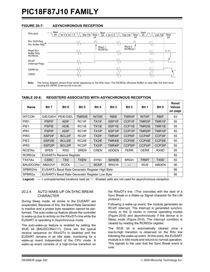
PIC18F87J10 FAMILY
FIGURE 20-7: ASYNCHRONOUS RECEPTIONTABLE 20-6: REGISTERS ASSOCIATED WITH ASYNCHRONOUS RECEPTION
20.2.4 AUTO-WAKE-UP ON SYNC BREAK CHARACTER
During Sleep mode, all clocks to the EUSART aresuspended. Because of this, the Baud Rate Generatoris inactive and a proper byte reception cannot be per-formed. The auto-wake-up feature allows the controllerto wake-up due to activity on the RXx/DTx line while theEUSART is operating in Asynchronous mode.
The auto-wake-up feature is enabled by setting theWUE bit (BAUDCONx<1>). Once set, the typicalreceive sequence on RXx/DTx is disabled and theEUSART remains in an Idle state, monitoring for awake-up event independent of the CPU mode. Awake-up event consists of a high-to-low transition on
the RXx/DTx line. (This coincides with the start of aSync Break or a Wake-up Signal character for the LINprotocol.)
Following a wake-up event, the module generates anRCxIF interrupt. The interrupt is generated synchro-nously to the Q clocks in normal operating modes(Figure 20-8) and asynchronously if the device is inSleep mode (Figure 20-9). The interrupt condition iscleared by reading the RCREGx register.
The WUE bit is automatically cleared once alow-to-high transition is observed on the RXx linefollowing the wake-up event. At this point, the EUSARTmodule is in Idle mode and returns to normal operation.This signals to the user that the Sync Break event isover.
Name Bit 7 Bit 6 Bit 5 Bit 4 Bit 3 Bit 2 Bit 1 Bit 0Reset Values
on page
INTCON GIE/GIEH PEIE/GIEL TMR0IE INT0IE RBIE TMR0IF INT0IF RBIF 53PIR1 PSPIF ADIF RC1IF TX1IF SSP1IF CCP1IF TMR2IF TMR1IF 55PIE1 PSPIE ADIE RC1IE TX1IE SSP1IE CCP1IE TMR2IE TMR1IE 55IPR1 PSPIP ADIP RC1IP TX1IP SSP1IP CCP1IP TMR2IP TMR1IP 55PIR3 SSP2IF BCL2IF RC2IF TX2IF TMR4IF CCP5IF CCP4IF CCP3IF 55PIE3 SSP2IE BCL2IE RC2IE TX2IE TMR4IE CCP5IE CCP4IE CCP3IE 55IPR3 SSP2IP BCL2IP RC2IP TX2IP TMR4IP CCP5IP CCP4IP CCP3IP 55RCSTAx SPEN RX9 SREN CREN ADDEN FERR OERR RX9D 55RCREGx EUSARTx Receive Register 55TXSTAx CSRC TX9 TXEN SYNC SENDB BRGH TRMT TX9D 55BAUDCONx ABDOVF RCIDL — SCKP BRG16 — WUE ABDEN 56SPBRGHx EUSARTx Baud Rate Generator Register High Byte 56SPBRGx EUSARTx Baud Rate Generator Register Low Byte 56Legend: — = unimplemented locations read as ‘0’. Shaded cells are not used for asynchronous reception.
Startbit bit 7/8bit 1bit 0 bit 7/8 bit 0Stop
bit
Startbit
Startbitbit 7/8 Stop
bitRXx (pin)
Rcv Buffer RegRcv Shift Reg
Read RcvBuffer RegRCREGx
RCxIF(Interrupt Flag)
OERR bit
CREN
Word 1RCREGx
Word 2RCREGx
Stopbit
Note: This timing diagram shows three words appearing on the RXx input. The RCREGx (Receive Buffer) is read after the third wordcausing the OERR (Overrun) bit to be set.
DS39663F-page 252 © 2009 Microchip Technology Inc.
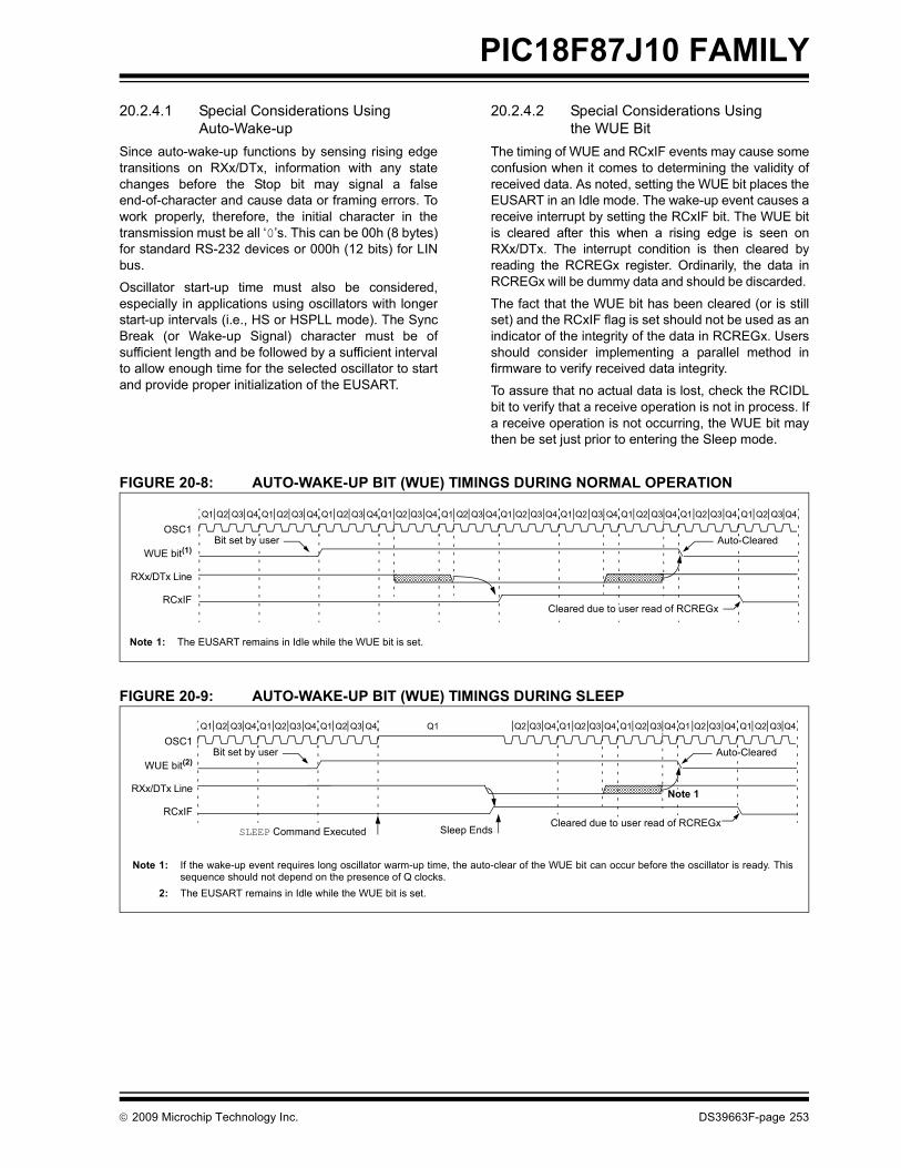
PIC18F87J10 FAMILY
20.2.4.1 Special Considerations UsingAuto-Wake-upSince auto-wake-up functions by sensing rising edgetransitions on RXx/DTx, information with any statechanges before the Stop bit may signal a falseend-of-character and cause data or framing errors. Towork properly, therefore, the initial character in thetransmission must be all ‘0’s. This can be 00h (8 bytes)for standard RS-232 devices or 000h (12 bits) for LINbus.
Oscillator start-up time must also be considered,especially in applications using oscillators with longerstart-up intervals (i.e., HS or HSPLL mode). The SyncBreak (or Wake-up Signal) character must be ofsufficient length and be followed by a sufficient intervalto allow enough time for the selected oscillator to startand provide proper initialization of the EUSART.
20.2.4.2 Special Considerations Using the WUE Bit
The timing of WUE and RCxIF events may cause someconfusion when it comes to determining the validity ofreceived data. As noted, setting the WUE bit places theEUSART in an Idle mode. The wake-up event causes areceive interrupt by setting the RCxIF bit. The WUE bitis cleared after this when a rising edge is seen onRXx/DTx. The interrupt condition is then cleared byreading the RCREGx register. Ordinarily, the data inRCREGx will be dummy data and should be discarded.
The fact that the WUE bit has been cleared (or is stillset) and the RCxIF flag is set should not be used as anindicator of the integrity of the data in RCREGx. Usersshould consider implementing a parallel method infirmware to verify received data integrity.
To assure that no actual data is lost, check the RCIDLbit to verify that a receive operation is not in process. Ifa receive operation is not occurring, the WUE bit maythen be set just prior to entering the Sleep mode.
FIGURE 20-8: AUTO-WAKE-UP BIT (WUE) TIMINGS DURING NORMAL OPERATION
FIGURE 20-9: AUTO-WAKE-UP BIT (WUE) TIMINGS DURING SLEEP
Q1 Q2 Q3 Q4 Q1 Q2 Q3 Q4 Q1 Q2 Q3 Q4 Q1 Q2 Q3 Q4 Q1 Q2 Q3 Q4 Q1 Q2 Q3 Q4 Q1 Q2 Q3 Q4 Q1 Q2 Q3 Q4 Q1 Q2 Q3 Q4 Q1 Q2 Q3 Q4
OSC1
WUE bit(1)
RXx/DTx Line
RCxIF
Note 1: The EUSART remains in Idle while the WUE bit is set.
Bit set by user
Cleared due to user read of RCREGx
Auto-Cleared
Q1 Q2 Q3 Q4 Q1 Q2 Q3 Q4 Q1 Q2 Q3 Q4 Q1 Q2 Q3 Q4 Q1 Q2 Q3 Q4 Q1 Q2 Q3 Q4 Q1 Q2 Q3 Q4 Q1 Q2 Q3 Q4
OSC1
WUE bit(2)
RXx/DTx Line
RCxIFCleared due to user read of RCREGx
SLEEP Command Executed
Note 1: If the wake-up event requires long oscillator warm-up time, the auto-clear of the WUE bit can occur before the oscillator is ready. Thissequence should not depend on the presence of Q clocks.
2: The EUSART remains in Idle while the WUE bit is set.
Sleep Ends
Note 1
Auto-ClearedBit set by user
© 2009 Microchip Technology Inc. DS39663F-page 253

PIC18F87J10 FAMILY
20.2.5 BREAK CHARACTER SEQUENCEThe EUSART module has the capability of sending thespecial Break character sequences that are required bythe LIN bus standard. The Break character transmitconsists of a Start bit, followed by twelve ‘0’ bits and aStop bit. The Frame Break character is sent wheneverthe SENDB and TXEN bits (TXSTAx<3> andTXSTAx<5>) are set while the Transmit Shift Registeris loaded with data. Note that the value of data writtento TXREGx will be ignored and all ‘0’s will betransmitted.The SENDB bit is automatically reset by hardware afterthe corresponding Stop bit is sent. This allows the userto preload the transmit FIFO with the next transmit bytefollowing the Break character (typically, the Synccharacter in the LIN specification).
Note that the data value written to the TXREGx for theBreak character is ignored. The write simply serves thepurpose of initiating the proper sequence.
The TRMT bit indicates when the transmit operation isactive or Idle, just as it does during normal transmis-sion. See Figure 20-10 for the timing of the Breakcharacter sequence.
20.2.5.1 Break and Sync Transmit SequenceThe following sequence will send a message frameheader made up of a Break, followed by an Auto-BaudSync byte. This sequence is typical of a LIN busmaster.
1. Configure the EUSART for the desired mode.2. Set the TXEN and SENDB bits to set up the
Break character.3. Load the TXREGx with a dummy character to
initiate transmission (the value is ignored).4. Write ‘55h’ to TXREGx to load the Sync
character into the transmit FIFO buffer.5. After the Break has been sent, the SENDB bit is
reset by hardware. The Sync character nowtransmits in the preconfigured mode.
When the TXREGx becomes empty, as indicated bythe TXxIF, the next data byte can be written toTXREGx.
20.2.6 RECEIVING A BREAK CHARACTERThe Enhanced USART module can receive a Breakcharacter in two ways.
The first method forces configuration of the baud rateat a frequency of 9/13 the typical speed. This allows forthe Stop bit transition to be at the correct samplinglocation (13 bits for Break versus Start bit and 8 databits for typical data).
The second method uses the auto-wake-up featuredescribed in Section 20.2.4 “Auto-Wake-up on SyncBreak Character”. By enabling this feature, theEUSART will sample the next two transitions onRXx/DTx, cause an RCxIF interrupt and receive thenext data byte followed by another interrupt.
Note that following a Break character, the user willtypically want to enable the Auto-Baud Rate Detectfeature. For both methods, the user can set the ABDENbit once the TXxIF interrupt is observed.
FIGURE 20-10: SEND BREAK CHARACTER SEQUENCE
Write to TXREGx
BRG Output(Shift Clock)
Start Bit Bit 0 Bit 1 Bit 11 Stop Bit
Break
TXxIF bit(Transmit Buffer
Reg. Empty Flag)
TXx (pin)
TRMT bit(Transmit Shift
Reg. Empty Flag)
SENDB bit(Transmit Shift
Reg. Empty Flag)
SENDB sampled here Auto-Cleared
Dummy Write
DS39663F-page 254 © 2009 Microchip Technology Inc.

PIC18F87J10 FAMILY
20.3 EUSART SynchronousMaster ModeThe Synchronous Master mode is entered by settingthe CSRC bit (TXSTAx<7>). In this mode, the data istransmitted in a half-duplex manner (i.e., transmissionand reception do not occur at the same time). Whentransmitting data, the reception is inhibited and viceversa. Synchronous mode is entered by setting bit,SYNC (TXSTAx<4>). In addition, enable bit, SPEN(RCSTAx<7>), is set in order to configure the TXx andRXx pins to CKx (clock) and DTx (data) lines,respectively.
The Master mode indicates that the processor trans-mits the master clock on the CKx line. Clock polarity isselected with the SCKP bit (BAUDCONx<4>); settingSCKP sets the Idle state on CKx as high, while clearingthe bit sets the Idle state as low. This option is providedto support Microwire devices with this module.
20.3.1 EUSART SYNCHRONOUS MASTER TRANSMISSION
The EUSART transmitter block diagram is shown inFigure 20-3. The heart of the transmitter is the Transmit(Serial) Shift Register (TSR). The Shift register obtainsits data from the Read/Write Transmit Buffer register,TXREGx. The TXREGx register is loaded with data insoftware. The TSR register is not loaded until the lastbit has been transmitted from the previous load. Assoon as the last bit is transmitted, the TSR is loadedwith new data from the TXREGx (if available).
Once the TXREGx register transfers the data to theTSR register (occurs in one TCY), the TXREGx is emptyand the TXxIF flag bit is set. The interrupt can beenabled or disabled by setting or clearing the interruptenable bit, TXxIE. TXxIF is set regardless of the stateof enable bit, TXxIE; it cannot be cleared in software. Itwill reset only when new data is loaded into theTXREGx register.
While flag bit, TXxIF, indicates the status of the TXREGxregister, another bit, TRMT (TXSTAx<1>), shows thestatus of the TSR register. TRMT is a read-only bit whichis set when the TSR is empty. No interrupt logic is tied tothis bit, so the user must poll this bit in order to determineif the TSR register is empty. The TSR is not mapped indata memory so it is not available to the user.
To set up a Synchronous Master Transmission:
1. Initialize the SPBRGHx:SPBRGx registers for theappropriate baud rate. Set or clear the BRG16bit, as required, to achieve the desired baud rate.
2. Enable the synchronous master serial port bysetting bits, SYNC, SPEN and CSRC.
3. If interrupts are desired, set enable bit, TXxIE.4. If 9-bit transmission is desired, set bit, TX9.5. Enable the transmission by setting bit, TXEN.6. If 9-bit transmission is selected, the ninth bit
should be loaded in bit, TX9D.7. Start transmission by loading data to the
TXREGx register.8. If using interrupts, ensure that the GIE and PEIE
bits in the INTCON register (INTCON<7:6>) areset.
FIGURE 20-11: SYNCHRONOUS TRANSMISSION
bit 0 bit 1 bit 7Word 1
Q1 Q2 Q3Q4 Q1 Q2 Q3 Q4 Q1Q2 Q3 Q4 Q1Q2 Q3 Q4 Q1 Q2 Q3 Q4 Q3 Q4 Q1 Q2 Q3Q4 Q1Q2 Q3Q4 Q1 Q2Q3Q4 Q1 Q2Q3 Q4Q1 Q2 Q3 Q4 Q1 Q2 Q3 Q4
bit 2 bit 0 bit 1 bit 7RC7/RX1/DT1
RC6/TX1/CK1 pin
Write toTXREG1 Reg
TX1IF bit(Interrupt Flag)
TXEN bit ‘1’ ‘1’
Word 2
TRMT bit
Write Word 1 Write Word 2
Note: Sync Master mode, SPBRGx = 0, continuous transmission of two 8-bit words. This example is equally applicable to EUSART2(RG1/TX2/CK2 and RG2/RX2/DT2).
RC6/TX1/CK1 pin(SCKP = 0)
(SCKP = 1)
© 2009 Microchip Technology Inc. DS39663F-page 255

PIC18F87J10 FAMILY
FIGURE 20-12: SYNCHRONOUS TRANSMISSION (THROUGH TXEN)TABLE 20-7: REGISTERS ASSOCIATED WITH SYNCHRONOUS MASTER TRANSMISSION
Name Bit 7 Bit 6 Bit 5 Bit 4 Bit 3 Bit 2 Bit 1 Bit 0Reset Values
on page
INTCON GIE/GIEH PEIE/GIEL TMR0IE INT0IE RBIE TMR0IF INT0IF RBIF 53PIR1 PSPIF ADIF RC1IF TX1IF SSP1IF CCP1IF TMR2IF TMR1IF 55PIE1 PSPIE ADIE RC1IE TX1IE SSP1IE CCP1IE TMR2IE TMR1IE 55IPR1 PSPIP ADIP RC1IP TX1IP SSP1IP CCP1IP TMR2IP TMR1IP 55PIR3 SSP2IF BCL2IF RC2IF TX2IF TMR4IF CCP5IF CCP4IF CCP3IF 55PIE3 SSP2IE BCL2IE RC2IE TX2IE TMR4IE CCP5IE CCP4IE CCP3IE 55IPR3 SSP2IP BCL2IP RC2IP TX2IP TMR4IP CCP5IP CCP4IP CCP3IP 55RCSTAx SPEN RX9 SREN CREN ADDEN FERR OERR RX9D 55TXREGx EUSARTx Transmit Register 55TXSTAx CSRC TX9 TXEN SYNC SENDB BRGH TRMT TX9D 55BAUDCONx ABDOVF RCIDL — SCKP BRG16 — WUE ABDEN 56SPBRGHx EUSARTx Baud Rate Generator Register High Byte 56SPBRGx EUSARTx Baud Rate Generator Register Low Byte 56Legend: — = unimplemented, read as ‘0’. Shaded cells are not used for synchronous master transmission.
RC7/RX1/DT1 pin
RC6/TX1/CK1 pin
Write toTXREG1 reg
TX1IF bit
TRMT bit
bit 0 bit 1 bit 2 bit 6 bit 7
TXEN bit
Note: This example is equally applicable to EUSART2 (RG1/TX2/CK2 and RG2/RX2/DT2).
DS39663F-page 256 © 2009 Microchip Technology Inc.

PIC18F87J10 FAMILY
20.3.2 EUSART SYNCHRONOUSMASTER RECEPTIONOnce Synchronous mode is selected, reception isenabled by setting either the Single Receive Enable bit,SREN (RCSTAx<5>), or the Continuous ReceiveEnable bit, CREN (RCSTAx<4>). Data is sampled onthe RXx pin on the falling edge of the clock.If enable bit, SREN, is set, only a single word isreceived. If enable bit, CREN, is set, the reception iscontinuous until CREN is cleared. If both bits are set,then CREN takes precedence.To set up a Synchronous Master Reception:1. Initialize the SPBRGHx:SPBRGx registers for the
appropriate baud rate. Set or clear the BRG16bit, as required, to achieve the desired baud rate.
2. Enable the synchronous master serial port bysetting bits, SYNC, SPEN and CSRC.
3. Ensure bits, CREN and SREN, are clear.4. If interrupts are desired, set enable bit, RCxIE.5. If 9-bit reception is desired, set bit, RX9.6. If a single reception is required, set bit, SREN.
For continuous reception, set bit, CREN.7. Interrupt flag bit, RCxIF, will be set when recep-
tion is complete and an interrupt will be generatedif the enable bit, RCxIE, was set.
8. Read the RCSTAx register to get the 9th bit (ifenabled) and determine if any error occurredduring reception.
9. Read the 8-bit received data by reading theRCREGx register.
10. If any error occurred, clear the error by clearingbit, CREN.
11. If using interrupts, ensure that the GIE and PEIE bitsin the INTCON register (INTCON<7:6>) are set.
FIGURE 20-13: SYNCHRONOUS RECEPTION (MASTER MODE, SREN)
TABLE 20-8: REGISTERS ASSOCIATED WITH SYNCHRONOUS MASTER RECEPTION
Name Bit 7 Bit 6 Bit 5 Bit 4 Bit 3 Bit 2 Bit 1 Bit 0 Reset Values on page
INTCON GIE/GIEH PEIE/GIEL TMR0IE INT0IE RBIE TMR0IF INT0IF RBIF 53PIR1 PSPIF ADIF RC1IF TX1IF SSP1IF CCP1IF TMR2IF TMR1IF 55PIE1 PSPIE ADIE RC1IE TX1IE SSP1IE CCP1IE TMR2IE TMR1IE 55IPR1 PSPIP ADIP RC1IP TX1IP SSP1IP CCP1IP TMR2IP TMR1IP 55PIR3 SSP2IF BCL2IF RC2IF TX2IF TMR4IF CCP5IF CCP4IF CCP3IF 55PIE3 SSP2IE BCL2IE RC2IE TX2IE TMR4IE CCP5IE CCP4IE CCP3IE 55IPR3 SSP2IP BCL2IP RC2IP TX2IP TMR4IP CCP5IP CCP4IP CCP3IP 55RCSTAx SPEN RX9 SREN CREN ADDEN FERR OERR RX9D 55RCREGx EUSARTx Receive Register 55TXSTAx CSRC TX9 TXEN SYNC SENDB BRGH TRMT TX9D 55BAUDCONx ABDOVF RCIDL — SCKP BRG16 — WUE ABDEN 56SPBRGHx EUSARTx Baud Rate Generator Register High Byte 56SPBRGx EUSARTx Baud Rate Generator Register Low Byte 56Legend: — = unimplemented, read as ‘0’. Shaded cells are not used for synchronous master reception.
CREN bit
RC7/RX1/DT1
RC6/TX1/CK1 pin
Write tobit SREN
SREN bit
RC1IF bit(Interrupt)
ReadRCREG1
Q3 Q4 Q1 Q2 Q3 Q4 Q1 Q2 Q3 Q4Q2 Q1 Q2 Q3 Q4 Q1 Q2 Q3 Q4 Q1 Q2 Q3 Q4 Q1 Q2 Q3 Q4 Q1Q2 Q3 Q4 Q1 Q2 Q3 Q4 Q1 Q2 Q3 Q4
‘0’
bit 0 bit 1 bit 2 bit 3 bit 4 bit 5 bit 6 bit 7
‘0’
Q1 Q2 Q3 Q4
Note: Timing diagram demonstrates Sync Master mode with bit SREN = 1 and bit BRGH = 0. This example is equally applicable to EUSART2(RG1/TX2/CK2 and RG2/RX2/DT2).
RC6/TX1/CK1 pin
pin
(SCKP = 0)
(SCKP = 1)
© 2009 Microchip Technology Inc. DS39663F-page 257
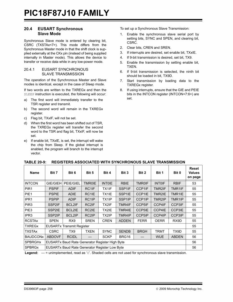
PIC18F87J10 FAMILY
20.4 EUSART SynchronousSlave ModeSynchronous Slave mode is entered by clearing bit,CSRC (TXSTAx<7>). This mode differs from theSynchronous Master mode in that the shift clock is sup-plied externally at the CKx pin (instead of being suppliedinternally in Master mode). This allows the device totransfer or receive data while in any low-power mode.
20.4.1 EUSART SYNCHRONOUS SLAVE TRANSMISSION
The operation of the Synchronous Master and Slavemodes is identical, except in the case of Sleep mode.
If two words are written to the TXREGx and then theSLEEP instruction is executed, the following will occur:
a) The first word will immediately transfer to theTSR register and transmit.
b) The second word will remain in the TXREGxregister.
c) Flag bit, TXxIF, will not be set. d) When the first word has been shifted out of TSR,
the TXREGx register will transfer the secondword to the TSR and flag bit, TXxIF, will now beset.
e) If enable bit, TXxIE, is set, the interrupt will wakethe chip from Sleep. If the global interrupt isenabled, the program will branch to the interruptvector.
To set up a Synchronous Slave Transmission:
1. Enable the synchronous slave serial port bysetting bits, SYNC and SPEN, and clearing bit,CSRC.
2. Clear bits, CREN and SREN.3. If interrupts are desired, set enable bit, TXxIE.4. If 9-bit transmission is desired, set bit, TX9.5. Enable the transmission by setting enable bit,
TXEN.6. If 9-bit transmission is selected, the ninth bit
should be loaded in bit, TX9D.7. Start transmission by loading data to the
TXREGx register.8. If using interrupts, ensure that the GIE and PEIE
bits in the INTCON register (INTCON<7:6>) areset.
TABLE 20-9: REGISTERS ASSOCIATED WITH SYNCHRONOUS SLAVE TRANSMISSION
Name Bit 7 Bit 6 Bit 5 Bit 4 Bit 3 Bit 2 Bit 1 Bit 0Reset Values
on page
INTCON GIE/GIEH PEIE/GIEL TMR0IE INT0IE RBIE TMR0IF INT0IF RBIF 53PIR1 PSPIF ADIF RC1IF TX1IF SSP1IF CCP1IF TMR2IF TMR1IF 55PIE1 PSPIE ADIE RC1IE TX1IE SSP1IE CCP1IE TMR2IE TMR1IE 55IPR1 PSPIP ADIP RC1IP TX1IP SSP1IP CCP1IP TMR2IP TMR1IP 55PIR3 SSP2IF BCL2IF RC2IF TX2IF TMR4IF CCP5IF CCP4IF CCP3IF 55PIE3 SSP2IE BCL2IE RC2IE TX2IE TMR4IE CCP5IE CCP4IE CCP3IE 55IPR3 SSP2IP BCL2IP RC2IP TX2IP TMR4IP CCP5IP CCP4IP CCP3IP 55RCSTAx SPEN RX9 SREN CREN ADDEN FERR OERR RX9D 55TXREGx EUSARTx Transmit Register 55TXSTAx CSRC TX9 TXEN SYNC SENDB BRGH TRMT TX9D 55BAUDCONx ABDOVF RCIDL — SCKP BRG16 — WUE ABDEN 56SPBRGHx EUSARTx Baud Rate Generator Register High Byte 56SPBRGx EUSARTx Baud Rate Generator Register Low Byte 56Legend: — = unimplemented, read as ‘0’. Shaded cells are not used for synchronous slave transmission.
DS39663F-page 258 © 2009 Microchip Technology Inc.
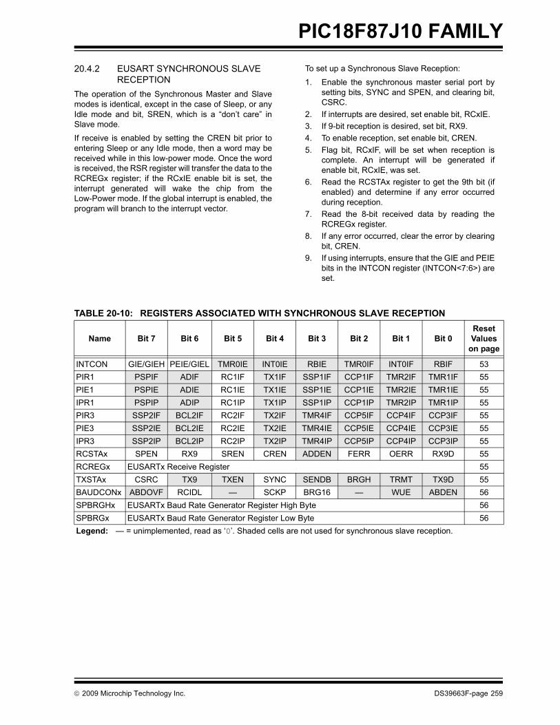
PIC18F87J10 FAMILY
20.4.2 EUSART SYNCHRONOUS SLAVERECEPTIONThe operation of the Synchronous Master and Slavemodes is identical, except in the case of Sleep, or anyIdle mode and bit, SREN, which is a “don’t care” inSlave mode.
If receive is enabled by setting the CREN bit prior toentering Sleep or any Idle mode, then a word may bereceived while in this low-power mode. Once the wordis received, the RSR register will transfer the data to theRCREGx register; if the RCxIE enable bit is set, theinterrupt generated will wake the chip from theLow-Power mode. If the global interrupt is enabled, theprogram will branch to the interrupt vector.
To set up a Synchronous Slave Reception:
1. Enable the synchronous master serial port bysetting bits, SYNC and SPEN, and clearing bit,CSRC.
2. If interrupts are desired, set enable bit, RCxIE.3. If 9-bit reception is desired, set bit, RX9.4. To enable reception, set enable bit, CREN.5. Flag bit, RCxIF, will be set when reception is
complete. An interrupt will be generated ifenable bit, RCxIE, was set.
6. Read the RCSTAx register to get the 9th bit (ifenabled) and determine if any error occurredduring reception.
7. Read the 8-bit received data by reading theRCREGx register.
8. If any error occurred, clear the error by clearingbit, CREN.
9. If using interrupts, ensure that the GIE and PEIEbits in the INTCON register (INTCON<7:6>) areset.
TABLE 20-10: REGISTERS ASSOCIATED WITH SYNCHRONOUS SLAVE RECEPTION
Name Bit 7 Bit 6 Bit 5 Bit 4 Bit 3 Bit 2 Bit 1 Bit 0Reset Values
on page
INTCON GIE/GIEH PEIE/GIEL TMR0IE INT0IE RBIE TMR0IF INT0IF RBIF 53PIR1 PSPIF ADIF RC1IF TX1IF SSP1IF CCP1IF TMR2IF TMR1IF 55PIE1 PSPIE ADIE RC1IE TX1IE SSP1IE CCP1IE TMR2IE TMR1IE 55IPR1 PSPIP ADIP RC1IP TX1IP SSP1IP CCP1IP TMR2IP TMR1IP 55PIR3 SSP2IF BCL2IF RC2IF TX2IF TMR4IF CCP5IF CCP4IF CCP3IF 55PIE3 SSP2IE BCL2IE RC2IE TX2IE TMR4IE CCP5IE CCP4IE CCP3IE 55IPR3 SSP2IP BCL2IP RC2IP TX2IP TMR4IP CCP5IP CCP4IP CCP3IP 55RCSTAx SPEN RX9 SREN CREN ADDEN FERR OERR RX9D 55RCREGx EUSARTx Receive Register 55TXSTAx CSRC TX9 TXEN SYNC SENDB BRGH TRMT TX9D 55BAUDCONx ABDOVF RCIDL — SCKP BRG16 — WUE ABDEN 56SPBRGHx EUSARTx Baud Rate Generator Register High Byte 56SPBRGx EUSARTx Baud Rate Generator Register Low Byte 56Legend: — = unimplemented, read as ‘0’. Shaded cells are not used for synchronous slave reception.
© 2009 Microchip Technology Inc. DS39663F-page 259

PIC18F87J10 FAMILY
NOTES:DS39663F-page 260 © 2009 Microchip Technology Inc.
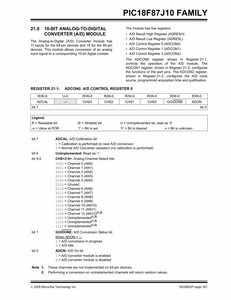
PIC18F87J10 FAMILY
21.0 10-BIT ANALOG-TO-DIGITAL CONVERTER (A/D) MODULE
The Analog-to-Digital (A/D) Converter module has11 inputs for the 64-pin devices and 15 for the 80-pindevices. This module allows conversion of an analoginput signal to a corresponding 10-bit digital number.
The module has five registers:
• A/D Result High Register (ADRESH)• A/D Result Low Register (ADRESL)• A/D Control Register 0 (ADCON0)• A/D Control Register 1 (ADCON1)• A/D Control Register 2 (ADCON2)
The ADCON0 register, shown in Register 21-1,controls the operation of the A/D module. TheADCON1 register, shown in Register 21-2, configuresthe functions of the port pins. The ADCON2 register,shown in Register 21-3, configures the A/D clocksource, programmed acquisition time and justification.
REGISTER 21-1: ADCON0: A/D CONTROL REGISTER 0
R/W-0 U-0 R/W-0 R/W-0 R/W-0 R/W-0 R/W-0 R/W-0
ADCAL — CHS3 CHS2 CHS1 CHS0 GO/DONE ADONbit 7 bit 0
Legend:R = Readable bit W = Writable bit U = Unimplemented bit, read as ‘0’-n = Value at POR ‘1’ = Bit is set ‘0’ = Bit is cleared x = Bit is unknown
bit 7 ADCAL: A/D Calibration bit1 = Calibration is performed on next A/D conversion 0 = Normal A/D Converter operation (no calibration is performed)
bit 6 Unimplemented: Read as ‘0’bit 5-2 CHS<3:0>: Analog Channel Select bits
0000 = Channel 0 (AN0)0001 = Channel 1 (AN1)0010 = Channel 2 (AN2)0011 = Channel 3 (AN3)0100 = Channel 4 (AN4)0101 = Unused0110 = Channel 6 (AN6)0111 = Channel 7 (AN7)1000 = Channel 8 (AN8)1001 = Channel 9 (AN9)1010 = Channel 10 (AN10)1011 = Channel 11 (AN11)1100 = Channel 12 (AN12)(1,2)
1101 = Unimplemented(1,2)
1110 = Unimplemented(1,2)
1111 = Unimplemented(1,2)
bit 1 GO/DONE: A/D Conversion Status bitWhen ADON = 1: 1 = A/D conversion in progress0 = A/D Idle
bit 0 ADON: A/D On bit1 = A/D converter module is enabled 0 = A/D converter module is disabled
Note 1: These channels are not implemented on 64-pin devices.2: Performing a conversion on unimplemented channels will return random values.
© 2009 Microchip Technology Inc. DS39663F-page 261
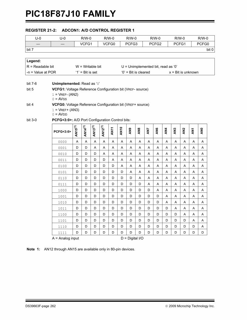
PIC18F87J10 FAMILY
REGISTER 21-2: ADCON1: A/D CONTROL REGISTER 1U-0 U-0 R/W-0 R/W-0 R/W-0 R/W-0 R/W-0 R/W-0— — VCFG1 VCFG0 PCFG3 PCFG2 PCFG1 PCFG0
bit 7 bit 0
Legend:R = Readable bit W = Writable bit U = Unimplemented bit, read as ‘0’-n = Value at POR ‘1’ = Bit is set ‘0’ = Bit is cleared x = Bit is unknown
bit 7-6 Unimplemented: Read as ‘0’bit 5 VCFG1: Voltage Reference Configuration bit (VREF- source)
1 = VREF- (AN2)0 = AVSS
bit 4 VCFG0: Voltage Reference Configuration bit (VREF+ source)1 = VREF+ (AN3)0 = AVDD
bit 3-0 PCFG<3:0>: A/D Port Configuration Control bits:
Note 1: AN12 through AN15 are available only in 80-pin devices.
A = Analog input D = Digital I/O
PCFG<3:0>
AN
15(1
)
AN
14(1
)
AN
13(1
)
AN
12(1
)
AN
11
AN
10
AN
9
AN
8
AN
7
AN
6
AN
4
AN
3
AN
2
AN
1
AN
0
0000 A A A A A A A A A A A A A A A
0001 D D A A A A A A A A A A A A A
0010 D D D A A A A A A A A A A A A
0011 D D D D A A A A A A A A A A A
0100 D D D D D A A A A A A A A A A
0101 D D D D D D A A A A A A A A A
0110 D D D D D D D A A A A A A A A
0111 D D D D D D D D A A A A A A A
1000 D D D D D D D D D A A A A A A
1001 D D D D D D D D D D A A A A A
1010 D D D D D D D D D D A A A A A
1011 D D D D D D D D D D D A A A A
1100 D D D D D D D D D D D D A A A
1101 D D D D D D D D D D D D D A A
1110 D D D D D D D D D D D D D D A
1111 D D D D D D D D D D D D D D D
DS39663F-page 262 © 2009 Microchip Technology Inc.

PIC18F87J10 FAMILY
REGISTER 21-3: ADCON2: A/D CONTROL REGISTER 2R/W-0 U-0 R/W-0 R/W-0 R/W-0 R/W-0 R/W-0 R/W-0ADFM — ACQT2 ACQT1 ACQT0 ADCS2 ADCS1 ADCS0
bit 7 bit 0
Legend:R = Readable bit W = Writable bit U = Unimplemented bit, read as ‘0’-n = Value at POR ‘1’ = Bit is set ‘0’ = Bit is cleared x = Bit is unknown
bit 7 ADFM: A/D Result Format Select bit1 = Right justified 0 = Left justified
bit 6 Unimplemented: Read as ‘0’bit 5-3 ACQT<2:0>: A/D Acquisition Time Select bits
111 = 20 TAD110 = 16 TAD101 = 12 TAD100 = 8 TAD011 = 6 TAD010 = 4 TAD001 = 2 TAD000 = 0 TAD(1)
bit 2-0 ADCS<2:0>: A/D Conversion Clock Select bits111 = FRC (clock derived from A/D RC oscillator)(1) 110 = FOSC/64 101 = FOSC/16 100 = FOSC/4 011 = FRC (clock derived from A/D RC oscillator)(1) 010 = FOSC/32 001 = FOSC/8 000 = FOSC/2
Note 1: If the A/D FRC clock source is selected, a delay of one TCY (instruction cycle) is added before the A/D clock starts. This allows the SLEEP instruction to be executed before starting a conversion.
© 2009 Microchip Technology Inc. DS39663F-page 263

PIC18F87J10 FAMILY
The analog reference voltage is software selectable toeither the device’s positive and negative supply voltage(AVDD and AVSS), or the voltage level on theRA3/AN3/VREF+ and RA2/AN2/VREF- pins.The A/D Converter has a unique feature of being ableto operate while the device is in Sleep mode. Tooperate in Sleep, the A/D conversion clock must bederived from the A/D’s internal RC oscillator.The output of the sample and hold is the input into theconverter, which generates the result via successiveapproximation.Each port pin associated with the A/D Converter can beconfigured as an analog input or as a digital I/O. TheADRESH and ADRESL registers contain the result ofthe A/D conversion. When the A/D conversion is com-plete, the result is loaded into the ADRESH:ADRESLregister pair, the GO/DONE bit (ADCON0<1>) iscleared and A/D Interrupt Flag bit, ADIF, is set. A device Reset forces all registers to their Reset state.This forces the A/D module to be turned off and anyconversion in progress is aborted. The value in theADRESH:ADRESL register pair is not modified for aPower-on Reset. These registers will contain unknowndata after a Power-on Reset.The block diagram of the A/D module is shown inFigure 21-1.
FIGURE 21-1: A/D BLOCK DIAGRAM
(Input Voltage)VAIN
VREF+ReferenceVoltage
VDD(2)
VCFG<1:0>
CHS<3:0>
AN7
AN6
AN4
AN3
AN2
AN1
AN0
0111
0110
0100
0011
0010
0001
0000
10-BitA/D
VREF-
VSS(2)
Converter
AN15(1)
AN14(1)
AN13(1)
AN12(1)
AN11
AN10
AN9
AN8
1111
1110
1101
1100
1011
1010
1001
1000
Note 1: Channels AN15 through AN12 are not available on 64-pin devices.2: I/O pins have diode protection to VDD and VSS.
DS39663F-page 264 © 2009 Microchip Technology Inc.

PIC18F87J10 FAMILY
After the A/D module has been configured as desired,the selected channel must be acquired before theconversion is started. The analog input channels musthave their corresponding TRIS bits selected as aninput. To determine acquisition time, see Section 21.1“A/D Acquisition Requirements”. After this acquisi-tion time has elapsed, the A/D conversion can bestarted. An acquisition time can be programmed tooccur between setting the GO/DONE bit and the actualstart of the conversion.The following steps should be followed to do an A/Dconversion:
1. Configure the A/D module:• Configure analog pins, voltage reference and
digital I/O (ADCON1)• Select A/D input channel (ADCON0)• Select A/D acquisition time (ADCON2)• Select A/D conversion clock (ADCON2)• Turn on A/D module (ADCON0)
2. Configure A/D interrupt (if desired):• Clear ADIF bit • Set ADIE bit • Set GIE bit
3. Wait the required acquisition time (if required).4. Start conversion:
• Set GO/DONE bit (ADCON0<1>)5. Wait for A/D conversion to complete, by either:
• Polling for the GO/DONE bit to be cleared
OR
• Waiting for the A/D interrupt6. Read A/D Result registers (ADRESH:ADRESL);
clear bit, ADIF, if required.7. For next conversion, go to step 1 or step 2, as
required. The A/D conversion time per bit isdefined as TAD. A minimum wait of 2 TAD isrequired before next acquisition starts.
FIGURE 21-2: ANALOG INPUT MODEL
VAIN CPIN
RS ANx
5 pF
VDD
VT = 0.6V
VT = 0.6VILEAKAGE
RIC ≤ 1k
SamplingSwitch
SS RSS
CHOLD = 25 pF
VSS
6V
Sampling Switch
5V4V3V2V
1 2 3 4(kΩ)
VDD
±100 nA
Legend: CPIN
VTILEAKAGE
RIC
SSCHOLD
= Input Capacitance= Threshold Voltage= Leakage Current at the pin due to
= Interconnect Resistance= Sampling Switch= Sample/Hold Capacitance (from DAC)
various junctions
= Sampling Switch ResistanceRSS
© 2009 Microchip Technology Inc. DS39663F-page 265

PIC18F87J10 FAMILY
21.1 A/D Acquisition RequirementsFor the A/D Converter to meet its specified accuracy,the charge holding capacitor (CHOLD) must be allowedto fully charge to the input channel voltage level. Theanalog input model is shown in Figure 21-2. Thesource impedance (RS) and the internal samplingswitch (RSS) impedance directly affect the timerequired to charge the capacitor, CHOLD. The samplingswitch (RSS) impedance varies over the device voltage(VDD). The source impedance affects the offset voltageat the analog input (due to pin leakage current). Themaximum recommended impedance for analogsources is 2.5 kΩ. After the analog input channel isselected (changed), the channel must be sampled forat least the minimum acquisition time before starting aconversion.To calculate the minimum acquisition time,Equation 21-1 may be used. This equation assumesthat 1/2 LSb error is used (1024 steps for the A/D). The1/2 LSb error is the maximum error allowed for the A/Dto meet its specified resolution.
Equation 21-3 shows the calculation of the minimumrequired acquisition time, TACQ. This calculation isbased on the following application systemassumptions:
CHOLD = 25 pF Rs = 2.5 kΩ Conversion Error ≤ 1/2 LSb VDD = 3V → Rss = 2 kΩ Temperature = 85°C (system max.)
EQUATION 21-1: ACQUISITION TIME
EQUATION 21-2: A/D MINIMUM CHARGING TIME
EQUATION 21-3: CALCULATING THE MINIMUM REQUIRED ACQUISITION TIME
Note: When the conversion is started, theholding capacitor is disconnected from theinput pin.
TACQ = Amplifier Settling Time + Holding Capacitor Charging Time + Temperature Coefficient
= TAMP + TC + TCOFF
VHOLD = (VREF – (VREF/2048)) • (1 – e(-TC/CHOLD(RIC + RSS + RS))) or TC = -(CHOLD)(RIC + RSS + RS) ln(1/2048)
TACQ = TAMP + TC + TCOFF
TAMP = 0.2 μs
TCOFF = (Temp – 25°C)(0.02 μs/°C)(85°C – 25°C)(0.02 μs/°C)1.2 μs
Temperature coefficient is only required for temperatures > 25°C. Below 25°C, TCOFF = 0 ms.
TC = -(CHOLD)(RIC + RSS + RS) ln(1/2048) μs-(25 pF) (1 kΩ + 2 kΩ + 2.5 kΩ) ln(0.0004883) μs 1.05 μs
TACQ = 0.2 μs + 1 μs + 1.2 μs2.4 μs
DS39663F-page 266 © 2009 Microchip Technology Inc.

PIC18F87J10 FAMILY
21.2 Selecting and ConfiguringAutomatic Acquisition TimeThe ADCON2 register allows the user to select anacquisition time that occurs each time the GO/DONEbit is set.
When the GO/DONE bit is set, sampling is stopped anda conversion begins. The user is responsible for ensur-ing the required acquisition time has passed betweenselecting the desired input channel and setting theGO/DONE bit. This occurs when the ACQT<2:0> bits(ADCON2<5:3>) remain in their Reset state (‘000’) andis compatible with devices that do not offerprogrammable acquisition times.
If desired, the ACQT bits can be set to select a pro-grammable acquisition time for the A/D module. Whenthe GO/DONE bit is set, the A/D module continues tosample the input for the selected acquisition time, thenautomatically begins a conversion. Since the acquisi-tion time is programmed, there may be no need to waitfor an acquisition time between selecting a channel andsetting the GO/DONE bit.
In either case, when the conversion is completed, theGO/DONE bit is cleared, the ADIF flag is set and theA/D begins sampling the currently selected channelagain. If an acquisition time is programmed, there isnothing to indicate if the acquisition time has ended orif the conversion has begun.
21.3 Selecting the A/D Conversion Clock
The A/D conversion time per bit is defined as TAD. TheA/D conversion requires 11 TAD per 10-bit conversion.The source of the A/D conversion clock is softwareselectable.
There are seven possible options for TAD:
• 2 TOSC
• 4 TOSC
• 8 TOSC
• 16 TOSC
• 32 TOSC • 64 TOSC
• Internal RC Oscillator
For correct A/D conversions, the A/D conversion clock(TAD) must be as short as possible but greater than theminimum TAD (see parameter 130 in Table 27-27 formore information).
Table 21-1 shows the resultant TAD times derived fromthe device operating frequencies and the A/D clocksource selected.
TABLE 21-1: TAD vs. DEVICE OPERATING FREQUENCIES
21.4 Configuring Analog Port PinsThe ADCON1, TRISA, TRISF and TRISH registerscontrol the operation of the A/D port pins. The port pinsneeded as analog inputs must have their correspond-ing TRIS bits set (input). If the TRIS bit is cleared(output), the digital output level (VOH or VOL) will beconverted.
The A/D operation is independent of the state of theCHS<3:0> bits and the TRIS bits.
AD Clock Source (TAD) Maximum Device
FrequencyOperation ADCS<2:0>
2 TOSC 000 2.86 MHz4 TOSC 100 5.71 MHz8 TOSC 001 11.43 MHz
16 TOSC 101 22.86 MHz32 TOSC 010 40.0 MHz64 TOSC 110 40.0 MHz
RC(2) x11 1.00 MHz(1)
Note 1: The RC source has a typical TAD time of 4 μs.
2: For device frequencies above 1 MHz, the device must be in Sleep mode for the entire conversion or the A/D accuracy may be out of specification.
Note 1: When reading the port register, all pinsconfigured as analog input channels willread as cleared (a low level). Pins config-ured as digital inputs will convert ananalog input. Analog levels on a digitallyconfigured input will be accuratelyconverted.
2: Analog levels on any pin defined as adigital input may cause the digital inputbuffer to consume current out of thedevice’s specification limits.
© 2009 Microchip Technology Inc. DS39663F-page 267

PIC18F87J10 FAMILY
21.5 A/D Conversions Figure 21-3 shows the operation of the A/D Converterafter the GO/DONE bit has been set and theACQT<2:0> bits are cleared. A conversion is startedafter the following instruction to allow entry into Sleepmode before the conversion begins.Figure 21-4 shows the operation of the A/D Converterafter the GO/DONE bit has been set, the ACQT<2:0>bits are set to ‘010’ and a 4 TAD acquisition time hasbeen selected before the conversion starts.
Clearing the GO/DONE bit during a conversion willabort the current conversion. The A/D Result registerpair will NOT be updated with the partially completedA/D conversion sample. This means theADRESH:ADRESL registers will continue to containthe value of the last completed conversion (or the lastvalue written to the ADRESH:ADRESL registers).
After the A/D conversion is completed or aborted, a2 TAD wait is required before the next acquisition can bestarted. After this wait, acquisition on the selectedchannel is automatically started.
21.6 Use of the ECCP2 TriggerAn A/D conversion can be started by the “Special EventTrigger” of the ECCP2 module. This requires that theCCP2M<3:0> bits (CCP2CON<3:0>) be programmedas ‘1011’ and that the A/D module is enabled (ADONbit is set). When the trigger occurs, the GO/DONE bitwill be set, starting the A/D acquisition and conversionand the Timer1 (or Timer3) counter will be reset to zero.Timer1 (or Timer3) is reset to automatically repeat theA/D acquisition period with minimal software overhead(moving ADRESH/ADRESL to the desired location).The appropriate analog input channel must be selectedand the minimum acquisition period is either timed bythe user, or an appropriate TACQ time is selected beforethe Special Event Trigger sets the GO/DONE bit (startsa conversion).
If the A/D module is not enabled (ADON is cleared), theSpecial Event Trigger will be ignored by the A/D modulebut will still reset the Timer1 (or Timer3) counter.
FIGURE 21-3: A/D CONVERSION TAD CYCLES (ACQT<2:0> = 000, TACQ = 0)
FIGURE 21-4: A/D CONVERSION TAD CYCLES (ACQT<2:0> = 010, TACQ = 4 TAD)
Note: The GO/DONE bit should NOT be set inthe same instruction that turns on the A/D.
TAD1 TAD2 TAD3 TAD4 TAD5 TAD6 TAD7 TAD8 TAD11
Set GO/DONE bit
Holding capacitor is disconnected from analog input (typically 100 ns)
TAD9 TAD10TCY - TAD
Next Q4: ADRESH/ADRESL is loaded, GO/DONE bit is cleared, ADIF bit is set, holding capacitor is connected to analog input.
Conversion starts
b0b9 b6 b5 b4 b3 b2 b1b8 b7
1 2 3 4 5 6 7 8 11
Set GO/DONE bit
(Holding capacitor is disconnected)
9 10
Next Q4: ADRESH:ADRESL is loaded, GO/DONE bit is cleared, ADIF bit is set, holding capacitor is reconnected to analog input.
Conversion starts
1 2 3 4
(Holding capacitor continuesacquiring input)
TACQT Cycles TAD Cycles
AutomaticAcquisitionTime
b0b9 b6 b5 b4 b3 b2 b1b8 b7
DS39663F-page 268 © 2009 Microchip Technology Inc.

©
PIC18F87J10 FAMILY
21.7 A/D Converter CalibrationThe A/D Converter in the PIC18F87J10 family ofdevices includes a self-calibration feature which com-pensates for any offset generated within the module.The calibration process is automated and is initiated bysetting the ADCAL bit (ADCON0<7>). The next timethe GO/DONE bit is set, the module will perform a“dummy” conversion (that is, with reading none of theinput channels) and store the resulting value internallyto compensate for offset. Thus, subsequent offsets willbe compensated.
The calibration process assumes that the device is in arelatively steady-state operating condition. If A/Dcalibration is used, it should be performed after eachdevice Reset or if there are other major changes inoperating conditions.
21.8 Operation in Power-Managed Modes
The selection of the automatic acquisition time and A/Dconversion clock is determined in part by the clocksource and frequency while in a power-managedmode.
If the A/D is expected to operate while the device is ina power-managed mode, the ACQT<2:0> andADCS<2:0> bits in ADCON2 should be updated inaccordance with the power-managed mode clock thatwill be used. After the power-managed mode is entered(either of the power-managed Run modes), an A/Dacquisition or conversion may be started. Once anacquisition or conversion is started, the device shouldcontinue to be clocked by the same power-managedmode clock source until the conversion has been com-pleted. If desired, the device may be placed into thecorresponding power-managed Idle mode during theconversion.
If the power-managed mode clock frequency is lessthan 1 MHz, the A/D RC clock source should beselected.
Operation in the Sleep mode requires the A/D RC clockto be selected. If bits, ACQT<2:0>, are set to ‘000’ anda conversion is started, the conversion will be delayedone instruction cycle to allow execution of the SLEEPinstruction and entry to Sleep mode. The IDLEN andSCS bits in the OSCCON register must have alreadybeen cleared prior to starting the conversion.
TABLE 21-2: SUMMARY OF A/D REGISTERS
Name Bit 7 Bit 6 Bit 5 Bit 4 Bit 3 Bit 2 Bit 1 Bit 0Reset Values
on page
INTCON GIE/GIEH PEIE/GIEL TMR0IE INT0IE RBIE TMR0IF INT0IF RBIF 53PIR1 PSPIF ADIF RC1IF TX1IF SSP1IF CCP1IF TMR2IF TMR1IF 55PIE1 PSPIE ADIE RC1IE TX1IE SSP1IE CCP1IE TMR2IE TMR1IE 55IPR1 PSPIP ADIP RC1IP TX1IP SSP1IP CCP1IP TMR2IP TMR1IP 55PIR2 OSCFIF CMIF — — BCL1IF — TMR3IF CCP2IF 55PIE2 OSCFIE CMIE — — BCL1IE — TMR3IE CCP2IE 55IPR2 OSCFIP CMIP — — BCL1IP — TMR3IP CCP2IP 55ADRESH A/D Result Register High Byte 54ADRESL A/D Result Register Low Byte 54
ADCON0 ADCAL — CHS3 CHS3 CHS1 CHS0 GO/DONE ADON 54ADCON1 — — VCFG1 VCFG0 PCFG3 PCFG2 PCFG1 PCFG0 54ADCON2 ADFM — ACQT2 ACQT1 ACQT0 ADCS2 ADCS1 ADCS0 54CCP2CON P2M1 P2M0 DC2B1 DC2B0 CCP2M3 CCP2M2 CCP2M1 CCP2M0 55PORTA — — RA5 RA4 RA3 RA2 RA1 RA0 56TRISA — — TRISA5 TRISA4 TRISA3 TRISA2 TRISA1 TRISA0 56PORTF RF7 RF6 RF5 RF4 RF3 RF2 RF1 — 56TRISF TRISF5 TRISF4 TRISF5 TRISF4 TRISF3 TRISF2 TRISF1 — 56PORTH(1) RH7 RH6 RH5 RH4 RH3 RH2 RH1 RH0 56TRISH(1) TRISH7 TRISH6 TRISH5 TRISH4 TRISH3 TRISH2 TRISH1 TRISH0 56Legend: — = unimplemented, read as ‘0’. Shaded cells are not used for A/D conversion.Note 1: This register is not implemented on 64-pin devices.
2009 Microchip Technology Inc. DS39663F-page 269

PIC18F87J10 FAMILY
NOTES:DS39663F-page 270 © 2009 Microchip Technology Inc.
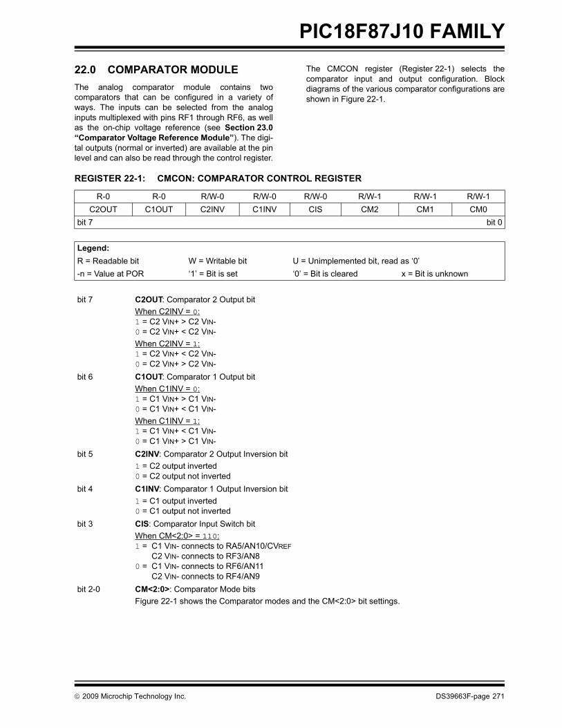
PIC18F87J10 FAMILY
22.0 COMPARATOR MODULEThe analog comparator module contains twocomparators that can be configured in a variety ofways. The inputs can be selected from the analoginputs multiplexed with pins RF1 through RF6, as wellas the on-chip voltage reference (see Section 23.0“Comparator Voltage Reference Module”). The digi-tal outputs (normal or inverted) are available at the pinlevel and can also be read through the control register.
The CMCON register (Register 22-1) selects thecomparator input and output configuration. Blockdiagrams of the various comparator configurations areshown in Figure 22-1.
REGISTER 22-1: CMCON: COMPARATOR CONTROL REGISTER
R-0 R-0 R/W-0 R/W-0 R/W-0 R/W-1 R/W-1 R/W-1C2OUT C1OUT C2INV C1INV CIS CM2 CM1 CM0
bit 7 bit 0
Legend:R = Readable bit W = Writable bit U = Unimplemented bit, read as ‘0’-n = Value at POR ‘1’ = Bit is set ‘0’ = Bit is cleared x = Bit is unknown
bit 7 C2OUT: Comparator 2 Output bitWhen C2INV = 0:1 = C2 VIN+ > C2 VIN-0 = C2 VIN+ < C2 VIN-When C2INV = 1:1 = C2 VIN+ < C2 VIN-0 = C2 VIN+ > C2 VIN-
bit 6 C1OUT: Comparator 1 Output bitWhen C1INV = 0:1 = C1 VIN+ > C1 VIN-0 = C1 VIN+ < C1 VIN-When C1INV = 1:1 = C1 VIN+ < C1 VIN-0 = C1 VIN+ > C1 VIN-
bit 5 C2INV: Comparator 2 Output Inversion bit1 = C2 output inverted0 = C2 output not inverted
bit 4 C1INV: Comparator 1 Output Inversion bit1 = C1 output inverted0 = C1 output not inverted
bit 3 CIS: Comparator Input Switch bitWhen CM<2:0> = 110:1 = C1 VIN- connects to RA5/AN10/CVREF
C2 VIN- connects to RF3/AN80 = C1 VIN- connects to RF6/AN11
C2 VIN- connects to RF4/AN9bit 2-0 CM<2:0>: Comparator Mode bits
Figure 22-1 shows the Comparator modes and the CM<2:0> bit settings.
© 2009 Microchip Technology Inc. DS39663F-page 271

PIC18F87J10 FAMILY
22.1 Comparator ConfigurationThere are eight modes of operation for the compara-tors, shown in Figure 22-1. Bits, CM<2:0>, of theCMCON register are used to select these modes. TheTRISF register controls the data direction of thecomparator pins for each mode. If the Comparatormode is changed, the comparator output level may notbe valid for the specified mode change delay shown inSection 27.0 “Electrical Characteristics”.
FIGURE 22-1: COMPARATOR I/O OPERATING MODES
Note: Comparator interrupts should be disabledduring a Comparator mode change;otherwise, a false interrupt may occur.
C1
VIN-
VIN+ Off (Read as ‘0’)
Comparator Outputs Disabled
A
A
CM<2:0> = 000
C2
VIN-
VIN+ Off (Read as ‘0’)
A
A
C1
VIN-
VIN+ C1OUT
Two Independent Comparators
A
A
CM<2:0> = 010
C2
VIN-
VIN+ C2OUT
A
A
C1
VIN-
VIN+ C1OUT
Two Common Reference Comparators
A
A
CM<2:0> = 100
C2
VIN-
VIN+ C2OUT
A
D
C2
VIN-
VIN+ Off (Read as ‘0’)
One Independent Comparator with Output
D
D
CM<2:0> = 001
C1
VIN-
VIN+ C1OUT
A
A
C1
VIN-
VIN+ Off (Read as ‘0’)
Comparators Off (POR Default Value)
D
D
CM<2:0> = 111
C2
VIN-
VIN+ Off (Read as ‘0’)
D
D
C1
VIN-
VIN+ C1OUT
Four Inputs Multiplexed to Two Comparators
A
A
CM<2:0> = 110
C2
VIN-
VIN+ C2OUT
A
A
From VREF module
CIS = 0CIS = 1
CIS = 0CIS = 1
C1
VIN-
VIN+ C1OUT
Two Common Reference Comparators with Outputs
A
A
CM<2:0> = 101
C2
VIN-
VIN+ C2OUT
A
D
A = Analog Input, port reads zeros always D = Digital Input CIS (CMCON<3>) is the Comparator Input Switch
CVREF
C1
VIN-
VIN+ C1OUT
Two Independent Comparators with Outputs
A
A
CM<2:0> = 011
C2
VIN-
VIN+ C2OUT
A
A
RF1/AN6/C2OUT*
RF2/AN7/C1OUT*
* Setting the TRISF<2:1> bits will disable the comparator outputs by configuring the pins as inputs.
RF6/AN11
RF5/AN10/
RF4/AN9
RF3/AN8
CVREF
RF6/AN11
RF5/AN10/
RF4/AN9
RF3/AN8
CVREF
RF6/AN11
RF5/AN10/
RF4/AN9
RF3/AN8
CVREF
RF6/AN11
RF5/AN10/
RF4/AN9
RF3/AN8
CVREF
RF6/AN11
RF5/AN10/
RF4/AN9
RF3/AN8
CVREF
RF2/AN7/C1OUT*
RF6/AN11
RF5/AN10/
RF4/AN9
RF3/AN8
CVREF
RF1/AN6/C2OUT*
RF2/AN7/C1OUT*
RF6/AN11
RF5/AN10/
RF4/AN9
RF3/AN8
CVREF
RF6/AN11
RF5/AN10/
RF4/AN9
RF3/AN8
CVREF
DS39663F-page 272 © 2009 Microchip Technology Inc.

PIC18F87J10 FAMILY
22.2 Comparator OperationA single comparator is shown in Figure 22-2, along withthe relationship between the analog input levels andthe digital output. When the analog input at VIN+ is lessthan the analog input VIN-, the output of the comparatoris a digital low level. When the analog input at VIN+ isgreater than the analog input VIN-, the output of thecomparator is a digital high level. The shaded areas ofthe output of the comparator in Figure 22-2 representthe uncertainty due to input offsets and response time.22.3 Comparator ReferenceDepending on the comparator operating mode, eitheran external or internal voltage reference may be used.The analog signal present at VIN- is compared to thesignal at VIN+ and the digital output of the comparatoris adjusted accordingly (Figure 22-2).
FIGURE 22-2: SINGLE COMPARATOR
22.3.1 EXTERNAL REFERENCE SIGNALWhen external voltage references are used, thecomparator module can be configured to have the com-parators operate from the same or different referencesources. However, threshold detector applications mayrequire the same reference. The reference signal mustbe between VSS and VDD and can be applied to eitherpin of the comparator(s).
22.3.2 INTERNAL REFERENCE SIGNAL
The comparator module also allows the selection of aninternally generated voltage reference from thecomparator voltage reference module. This module isdescribed in more detail in Section 23.0 “ComparatorVoltage Reference Module”.
The internal reference is only available in the modewhere four inputs are multiplexed to two comparators(CM<2:0> = 110). In this mode, the internal voltagereference is applied to the VIN+ pin of bothcomparators.
22.4 Comparator Response TimeResponse time is the minimum time, after selecting anew reference voltage or input source, before thecomparator output has a valid level. If the internal ref-erence is changed, the maximum delay of the internalvoltage reference must be considered when using thecomparator outputs. Otherwise, the maximum delay ofthe comparators should be used (see Section 27.0“Electrical Characteristics”).
22.5 Comparator OutputsThe comparator outputs are read through the CMCONregister. These bits are read-only. The comparatoroutputs may also be directly output to the RF1 and RF2I/O pins. When enabled, multiplexors in the output pathof the RF1 and RF2 pins will switch and the output ofeach pin will be the unsynchronized output of thecomparator. The uncertainty of each of thecomparators is related to the input offset voltage andthe response time given in the specifications.Figure 22-3 shows the comparator output blockdiagram.
The TRISF bits will still function as an output enable/disable for the RF1 and RF2 pins while in this mode.
The polarity of the comparator outputs can be changedusing the C2INV and C1INV bits (CMCON<5:4>).
–
+VIN+
VIN-Output
Output
VIN-
VIN+
Note 1: When reading the PORT register, all pinsconfigured as analog inputs will read as a‘0’. Pins configured as digital inputs willconvert an analog input according to theSchmitt Trigger input specification.
2: Analog levels on any pin defined as adigital input may cause the input buffer toconsume more current than is specified.
© 2009 Microchip Technology Inc. DS39663F-page 273
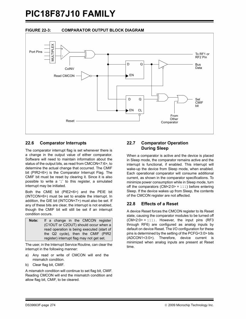
PIC18F87J10 FAMILY
FIGURE 22-3: COMPARATOR OUTPUT BLOCK DIAGRAM22.6 Comparator InterruptsThe comparator interrupt flag is set whenever there isa change in the output value of either comparator.Software will need to maintain information about thestatus of the output bits, as read from CMCON<7:6>, todetermine the actual change that occurred. The CMIFbit (PIR2<6>) is the Comparator Interrupt Flag. TheCMIF bit must be reset by clearing it. Since it is alsopossible to write a ‘1’ to this register, a simulatedinterrupt may be initiated.
Both the CMIE bit (PIE2<6>) and the PEIE bit(INTCON<6>) must be set to enable the interrupt. Inaddition, the GIE bit (INTCON<7>) must also be set. Ifany of these bits are clear, the interrupt is not enabled,though the CMIF bit will still be set if an interruptcondition occurs.
The user, in the Interrupt Service Routine, can clear theinterrupt in the following manner:
a) Any read or write of CMCON will end themismatch condition.
b) Clear flag bit, CMIF.
A mismatch condition will continue to set flag bit, CMIF.Reading CMCON will end the mismatch condition andallow flag bit, CMIF, to be cleared.
22.7 Comparator Operation During Sleep
When a comparator is active and the device is placedin Sleep mode, the comparator remains active and theinterrupt is functional, if enabled. This interrupt willwake-up the device from Sleep mode, when enabled.Each operational comparator will consume additionalcurrent, as shown in the comparator specifications. Tominimize power consumption while in Sleep mode, turnoff the comparators (CM<2:0> = 111) before enteringSleep. If the device wakes up from Sleep, the contentsof the CMCON register are not affected.
22.8 Effects of a ResetA device Reset forces the CMCON register to its Resetstate, causing the comparator modules to be turned off(CM<2:0> = 111). However, the input pins (RF3through RF6) are configured as analog inputs bydefault on device Reset. The I/O configuration for thesepins is determined by the setting of the PCFG<3:0> bits(ADCON1<3:0>). Therefore, device current isminimized when analog inputs are present at Resettime.
D Q
EN
To RF1 orRF2 Pin
BusData
Set
MU
LTIP
LEX
CMIFbit
-+
Port Pins
Read CMCON
ResetFromOther
Comparator
CxINV
D Q
EN CL
Note: If a change in the CMCON register(C1OUT or C2OUT) should occur when aread operation is being executed (start ofthe Q2 cycle), then the CMIF (PIR2register) interrupt flag may not get set.
DS39663F-page 274 © 2009 Microchip Technology Inc.
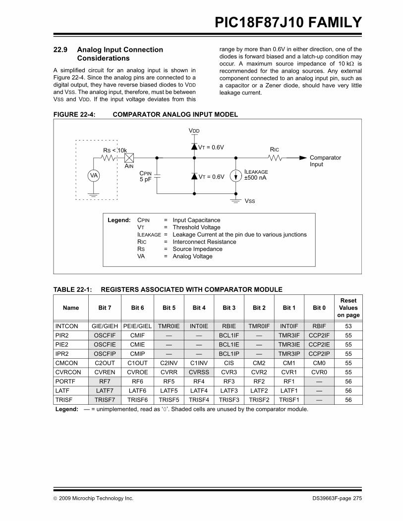
PIC18F87J10 FAMILY
22.9 Analog Input ConnectionConsiderationsA simplified circuit for an analog input is shown inFigure 22-4. Since the analog pins are connected to adigital output, they have reverse biased diodes to VDDand VSS. The analog input, therefore, must be betweenVSS and VDD. If the input voltage deviates from this
range by more than 0.6V in either direction, one of thediodes is forward biased and a latch-up condition mayoccur. A maximum source impedance of 10 kΩ isrecommended for the analog sources. Any externalcomponent connected to an analog input pin, such asa capacitor or a Zener diode, should have very littleleakage current.
FIGURE 22-4: COMPARATOR ANALOG INPUT MODEL
TABLE 22-1: REGISTERS ASSOCIATED WITH COMPARATOR MODULE
Name Bit 7 Bit 6 Bit 5 Bit 4 Bit 3 Bit 2 Bit 1 Bit 0Reset Values
on page
INTCON GIE/GIEH PEIE/GIEL TMR0IE INT0IE RBIE TMR0IF INT0IF RBIF 53PIR2 OSCFIF CMIF — — BCL1IF — TMR3IF CCP2IF 55PIE2 OSCFIE CMIE — — BCL1IE — TMR3IE CCP2IE 55IPR2 OSCFIP CMIP — — BCL1IP — TMR3IP CCP2IP 55CMCON C2OUT C1OUT C2INV C1INV CIS CM2 CM1 CM0 55CVRCON CVREN CVROE CVRR CVRSS CVR3 CVR2 CVR1 CVR0 55PORTF RF7 RF6 RF5 RF4 RF3 RF2 RF1 — 56LATF LATF7 LATF6 LATF5 LATF4 LATF3 LATF2 LATF1 — 56TRISF TRISF7 TRISF6 TRISF5 TRISF4 TRISF3 TRISF2 TRISF1 — 56Legend: — = unimplemented, read as ‘0’. Shaded cells are unused by the comparator module.
VA
RS < 10k
AINCPIN5 pF
VDD
VT = 0.6V
VT = 0.6V
RIC
ILEAKAGE±500 nA
VSS
Legend: CPIN = Input CapacitanceVT = Threshold VoltageILEAKAGE = Leakage Current at the pin due to various junctionsRIC = Interconnect ResistanceRS = Source ImpedanceVA = Analog Voltage
ComparatorInput
© 2009 Microchip Technology Inc. DS39663F-page 275

PIC18F87J10 FAMILY
NOTES:DS39663F-page 276 © 2009 Microchip Technology Inc.

PIC18F87J10 FAMILY
23.0 COMPARATOR VOLTAGE REFERENCE MODULE
The comparator voltage reference is a 16-tap resistorladder network that provides a selectable referencevoltage. Although its primary purpose is to provide areference for the analog comparators, it may also beused independently of them.
A block diagram of the module is shown in Figure 23-1.The resistor ladder is segmented to provide two rangesof CVREF values and has a power-down function toconserve power when the reference is not being used.The module’s supply reference can be provided fromeither device VDD/VSS or an external voltage reference.
23.1 Configuring the Comparator Voltage Reference
The comparator voltage reference module is controlledthrough the CVRCON register (Register 23-1). Thecomparator voltage reference provides two ranges ofoutput voltage, each with 16 distinct levels. The range
to be used is selected by the CVRR bit (CVRCON<5>).The primary difference between the ranges is the sizeof the steps selected by the CVREF Selection bits(CVR<3:0>), with one range offering finer resolution.The equations used to calculate the output of thecomparator voltage reference are as follows:
If CVRR = 1: CVREF = ((CVR<3:0>)/24) x (CVRSRC)
If CVRR = 0: CVREF = (CVRSRC/4) + ((CVR<3:0>)/32) x(CVRSRC)
The comparator reference supply voltage can comefrom either VDD and VSS, or the external VREF+ andVREF- that are multiplexed with RA2 and RA3. Thevoltage source is selected by the CVRSS bit(CVRCON<4>).
The settling time of the comparator voltage referencemust be considered when changing the CVREFoutput (see Table 27-3 in Section 27.0 “ElectricalCharacteristics”).
REGISTER 23-1: CVRCON: COMPARATOR VOLTAGE REFERENCE CONTROL REGISTER
R/W-0 R/W-0 R/W-0 R/W-0 R/W-0 R/W-0 R/W-0 R/W-0CVREN CVROE(1) CVRR CVRSS CVR3 CVR2 CVR1 CVR0
bit 7 bit 0
Legend:R = Readable bit W = Writable bit U = Unimplemented bit, read as ‘0’-n = Value at POR ‘1’ = Bit is set ‘0’ = Bit is cleared x = Bit is unknown
bit 7 CVREN: Comparator Voltage Reference Enable bit1 = CVREF circuit powered on 0 = CVREF circuit powered down
bit 6 CVROE: Comparator VREF Output Enable bit(1)
1 = CVREF voltage level is also output on the RF5/AN10/CVREF pin 0 = CVREF voltage is disconnected from the RF5/AN10/CVREF pin
bit 5 CVRR: Comparator VREF Range Selection bit1 = 0 to 0.667 CVRSRC, with CVRSRC/24 step size (low range)0 = 0.25 CVRSRC to 0.75 CVRSRC, with CVRSRC/32 step size (high range)
bit 4 CVRSS: Comparator VREF Source Selection bit1 = Comparator reference source, CVRSRC = (VREF+) – (VREF-)0 = Comparator reference source, CVRSRC = VDD – VSS
bit 3-0 CVR<3:0>: Comparator VREF Value Selection bits (0 ≤ (CVR<3:0>) ≤ 15) When CVRR = 1: CVREF = ((CVR<3:0>)/24) • (CVRSRC)When CVRR = 0: CVREF = (CVRSRC/4) + ((CVR<3:0>)/32) • (CVRSRC)
Note 1: CVROE overrides the TRISF<5> bit setting.
© 2009 Microchip Technology Inc. DS39663F-page 277

PIC18F87J10 FAMILY
FIGURE 23-1: COMPARATOR VOLTAGE REFERENCE BLOCK DIAGRAM23.2 Voltage Reference Accuracy/ErrorThe full range of voltage reference cannot be realizeddue to the construction of the module. The transistorson the top and bottom of the resistor ladder network(Figure 23-1) keep CVREF from approaching the refer-ence source rails. The voltage reference is derivedfrom the reference source; therefore, the CVREF outputchanges with fluctuations in that source. The testedabsolute accuracy of the voltage reference can befound in Section 27.0 “Electrical Characteristics”.
23.3 Operation During SleepWhen the device wakes up from Sleep through aninterrupt or a Watchdog Timer time-out, the contents ofthe CVRCON register are not affected. To minimizecurrent consumption in Sleep mode, the voltagereference should be disabled.
23.4 Effects of a ResetA device Reset disables the voltage reference byclearing bit, CVREN (CVRCON<7>). This Reset alsodisconnects the reference from the RA2 pin by clearingbit, CVROE (CVRCON<6>), and selects the high-voltage range by clearing bit, CVRR (CVRCON<5>).The CVR value select bits are also cleared.
23.5 Connection ConsiderationsThe voltage reference module operates independentlyof the comparator module. The output of the referencegenerator may be connected to the RF5 pin if theCVROE bit is set. Enabling the voltage reference out-put onto RA2 when it is configured as a digital input willincrease current consumption. Connecting RF5 as adigital output with CVRSS enabled will also increasecurrent consumption.
The RF5 pin can be used as a simple D/A output withlimited drive capability. Due to the limited current drivecapability, a buffer must be used on the voltagereference output for external connections to VREF.Figure 23-2 shows an example buffering technique.
16-to
-1 M
UX
CVR<3:0>8R
RCVREN
CVRSS = 0VDD
VREF+CVRSS = 1
8R
CVRSS = 0
VREF-CVRSS = 1
R
R
R
R
R
R
16 Steps
CVRR
CVREF
DS39663F-page 278 © 2009 Microchip Technology Inc.

PIC18F87J10 FAMILY
FIGURE 23-2: COMPARATOR VOLTAGE REFERENCE OUTPUT BUFFER EXAMPLETABLE 23-1: REGISTERS ASSOCIATED WITH COMPARATOR VOLTAGE REFERENCE
Name Bit 7 Bit 6 Bit 5 Bit 4 Bit 3 Bit 2 Bit 1 Bit 0Reset Values
on page
CVRCON CVREN CVROE CVRR CVRSS CVR3 CVR2 CVR1 CVR0 55CMCON C2OUT C1OUT C2INV C1INV CIS CM2 CM1 CM0 55TRISF TRISF7 TRISF6 TRISF5 TRISF4 TRISF3 TRISF2 TRISF1 — 56Legend: — = unimplemented, read as ‘0’. Shaded cells are not used with the comparator voltage reference.
CVREF Output+–
CVREF Module
Voltage Reference
Output Impedance
R(1)
RF5
Note 1: R is dependent upon the comparator voltage reference Configuration bits, CVRCON<5> and CVRCON<3:0>.
PIC18F87J10
© 2009 Microchip Technology Inc. DS39663F-page 279

PIC18F87J10 FAMILY
NOTES:DS39663F-page 280 © 2009 Microchip Technology Inc.

PIC18F87J10 FAMILY
24.0 SPECIAL FEATURES OF THECPUPIC18F87J10 family devices include several featuresintended to maximize reliability and minimize costthrough elimination of external components. These are:• Oscillator Selection• Resets:
- Power-on Reset (POR)- Power-up Timer (PWRT)- Oscillator Start-up Timer (OST)- Brown-out Reset (BOR)
• Interrupts• Watchdog Timer (WDT)• Fail-Safe Clock Monitor• Two-Speed Start-up• Code Protection• In-Circuit Serial ProgrammingThe oscillator can be configured for the applicationdepending on frequency, power, accuracy and cost. Allof the options are discussed in detail in Section 3.0“Oscillator Configurations”.A complete discussion of device Resets and interruptsis available in previous sections of this data sheet.In addition to their Power-up and Oscillator Start-upTimers provided for Resets, the PIC18F87J10 family ofdevices have a configurable Watchdog Timer which iscontrolled in software.
The inclusion of an internal RC oscillator also providesthe additional benefits of a Fail-Safe Clock Monitor(FSCM) and Two-Speed Start-up. FSCM provides forbackground monitoring of the peripheral clock andautomatic switchover in the event of its failure.Two-Speed Start-up enables code to be executedalmost immediately on start-up, while the primary clocksource completes its start-up delays. All of these features are enabled and configured bysetting the appropriate Configuration register bits.
24.1 Configuration BitsThe Configuration bits can be programmed (read as‘0’) or left unprogrammed (read as ‘1’) to select variousdevice configurations. These bits are mapped startingat program memory location 300000h. A complete listis shown in Table 24-2. A detailed explanation of thevarious bit functions is provided in Register 24-1through Register 24-6.
24.1.1 CONSIDERATIONS FOR CONFIGURING THE PIC18F87J10 FAMILY DEVICES
Unlike previous PIC18 microcontrollers, devices of thePIC18F87J10 family do not use persistent memoryregisters to store configuration information. The config-uration bytes are implemented as volatile memorywhich means that configuration data must beprogrammed each time the device is powered up.
Configuration data is stored in the four words at the topof the on-chip program memory space, known as theFlash Configuration Words. It is stored in programmemory in the same order shown in Table 24-2, withCONFIG1L at the lowest address and CONFIG3H atthe highest. The data is automatically loaded in theproper Configuration registers during device power-up.
When creating applications for these devices, usersshould always specifically allocate the location of theFlash Configuration Word for configuration data; this isto make certain that program code is not stored in thisaddress when the code is compiled.
The volatile memory cells used for the Configurationbits always reset to ‘1’ on Power-on Resets. For allother type of Reset events, the previously programmedvalues are maintained and used without reloading fromprogram memory.
The four Most Significant bits of CONFIG1H,CONFIG2H and CONFIG3H in program memoryshould also be ‘1111’. This makes these ConfigurationWords appear to be NOP instructions in the remoteevent that their locations are ever executed byaccident. Since Configuration bits are not implementedin the corresponding locations, writing ‘1’s to theselocations has no effect on device operation.
To prevent inadvertent configuration changes duringcode execution, all programmable Configuration bitsare write-once. After a bit is initially programmed duringa power cycle, it cannot be written to again. Changinga device configuration requires that power to the devicebe cycled.
TABLE 24-1: MAPPING OF THE FLASH CONFIGURATION WORDS TO THE CONFIGURATION REGISTERS
Configuration Byte Code Space Address
Configuration RegisterAddress
CONFIG1L XXXF8h 300000h
CONFIG1H XXXF9h 300001h
CONFIG2L XXXFAh 300002h
CONFIG2H XXXFBh 300003h
CONFIG3L XXXFCh 300004h
CONFIG3H XXXFDh 300005h
CONFIG4L(1) XXXFEh 300006h
CONFIG4H(1) XXXFFh 300007h
Note 1: Unimplemented in PIC18F87J10 family devices.
© 2009 Microchip Technology Inc. DS39663F-page 281

PIC18F87J10 FAMILY
TABLE 24-2: CONFIGURATION BITS AND DEVICE IDsFile Name Bit 7 Bit 6 Bit 5 Bit 4 Bit 3 Bit 2 Bit 1 Bit 0Default/
UnprogrammedValue(1)
300000h CONFIG1L DEBUG XINST STVREN — — — — WDTEN 111- ---1
300001h CONFIG1H —(2) —(2) —(2) —(2) —(3) CP0 — — ---- 01--
300002h CONFIG2L IESO FCMEN — — — FOSC2 FOSC1 FOSC0 11-- -111
300003h CONFIG2H —(2) —(2) —(2) —(2) WDTPS3 WDTPS2 WDTPS1 WDTPS0 ---- 1111
300004h CONFIG3L WAIT(4) BW(4) EMB1(4) EMB0(4) EASHFT(4) — — — 1111 1---
300005h CONFIG3H —(2) —(2) —(2) —(2) — — ECCPMX(4) CCP2MX ---- --11
3FFFFEh DEVID1 DEV2 DEV1 DEV0 REV4 REV3 REV2 REV1 REV0 xxxx xxxx(5)
3FFFFFh DEVID2 DEV10 DEV9 DEV8 DEV7 DEV6 DEV5 DEV4 DEV3 0000 10x1(5)
Legend: x = unknown, u = unchanged, - = unimplemented. Shaded cells are unimplemented, read as ‘0’.Note 1: Values reflect the unprogrammed state as received from the factory and following Power-on Resets. In all other Reset
states, the configuration bytes maintain their previously programmed states.2: The value of these bits in program memory should always be ‘1’. This ensures that the location is executed as a NOP if it
is accidentally executed.3: This bit should always be maintained as ‘0’.4: Implemented in 80-pin devices only. On 64-pin devices, these bits are reserved and should always be maintained as ‘1’.5: See Register 24-7 and Register 24-8 for DEVID values. These registers are read-only and cannot be programmed by
the user.
DS39663F-page 282 © 2009 Microchip Technology Inc.
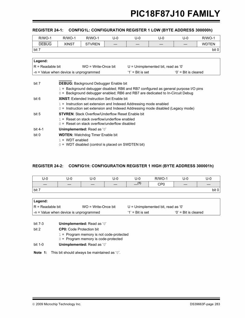
PIC18F87J10 FAMILY
REGISTER 24-1: CONFIG1L: CONFIGURATION REGISTER 1 LOW (BYTE ADDRESS 300000h)
R/WO-1 R/WO-1 R/WO-1 U-0 U-0 U-0 U-0 R/WO-1
DEBUG XINST STVREN — — — — WDTENbit 7 bit 0
Legend:R = Readable bit WO = Write-Once bit U = Unimplemented bit, read as ‘0’-n = Value when device is unprogrammed ‘1’ = Bit is set ‘0’ = Bit is cleared
bit 7 DEBUG: Background Debugger Enable bit1 = Background debugger disabled; RB6 and RB7 configured as general purpose I/O pins0 = Background debugger enabled; RB6 and RB7 are dedicated to In-Circuit Debug
bit 6 XINST: Extended Instruction Set Enable bit1 = Instruction set extension and Indexed Addressing mode enabled0 = Instruction set extension and Indexed Addressing mode disabled (Legacy mode)
bit 5 STVREN: Stack Overflow/Underflow Reset Enable bit1 = Reset on stack overflow/underflow enabled 0 = Reset on stack overflow/underflow disabled
bit 4-1 Unimplemented: Read as ‘0’bit 0 WDTEN: Watchdog Timer Enable bit
1 = WDT enabled0 = WDT disabled (control is placed on SWDTEN bit)
REGISTER 24-2: CONFIG1H: CONFIGURATION REGISTER 1 HIGH (BYTE ADDRESS 300001h)
U-0 U-0 U-0 U-0 U-0 R/WO-1 U-0 U-0— — — — —(1) CP0 — —
bit 7 bit 0
Legend:R = Readable bit WO = Write-Once bit U = Unimplemented bit, read as ‘0’-n = Value when device is unprogrammed ‘1’ = Bit is set ‘0’ = Bit is cleared
bit 7-3 Unimplemented: Read as ‘0’bit 2 CP0: Code Protection bit
1 = Program memory is not code-protected0 = Program memory is code-protected
bit 1-0 Unimplemented: Read as ‘0’
Note 1: This bit should always be maintained as ‘0’.
© 2009 Microchip Technology Inc. DS39663F-page 283

PIC18F87J10 FAMILY
REGISTER 24-3: CONFIG2L: CONFIGURATION REGISTER 2 LOW (BYTE ADDRESS 300002h)
R/WO-1 R/WO-1 U-0 U-0 U-0 R/WO-1 R/WO-1 R/WO-1IESO FCMEN — — — FOSC2 FOSC1 FOSC0
bit 7 bit 0
Legend:R = Readable bit WO = Write-Once bit U = Unimplemented bit, read as ‘0’-n = Value when device is unprogrammed ‘1’ = Bit is set ‘0’ = Bit is cleared
bit 7 IESO: Two-Speed Start-up (Internal/External Oscillator Switchover) Control bit1 = Two-Speed Start-up enabled0 = Two-Speed Start-up disabled
bit 6 FCMEN: Fail-Safe Clock Monitor Enable bit1 = Fail-Safe Clock Monitor enabled0 = Fail-Safe Clock Monitor disabled
bit 5-3 Unimplemented: Read as ‘0’bit 2 FOSC2: Default/Reset System Clock Select bit
1 = Clock selected by FOSC<1:0> as a system clock is enabled when OSCCON<1:0> = 000 = INTRC enabled as a system clock when OSCCON<1:0> = 00
bit 1-0 FOSC<1:0>: Oscillator Selection bits11 = EC oscillator, PLL enabled and under software control, CLKO function on OSC210 = EC oscillator, CLKO function on OSC201 = HS oscillator, PLL enabled and under software control00 = HS oscillator
REGISTER 24-4: CONFIG2H: CONFIGURATION REGISTER 2 HIGH (BYTE ADDRESS 300003h)
U-0 U-0 U-0 U-0 R/WO-1 R/WO-1 R/WO-1 R/WO-1
— — — — WDTPS3 WDTPS2 WDTPS1 WDTPS0
bit 7 bit 0
Legend:R = Readable bit WO = Write-Once bit U = Unimplemented bit, read as ‘0’-n = Value when device is unprogrammed ‘1’ = Bit is set ‘0’ = Bit is cleared
bit 7-4 Unimplemented: Read as ‘0’bit 3-0 WDTPS<3:0>: Watchdog Timer Postscale Select bits
1111 = 1:32,7681110 = 1:16,3841101 = 1:8,1921100 = 1:4,0961011 = 1:2,0481010 = 1:1,0241001 = 1:5121000 = 1:2560111 = 1:1280110 = 1:640101 = 1:320100 = 1:160011 = 1:80010 = 1:40001 = 1:20000 = 1:1
DS39663F-page 284 © 2009 Microchip Technology Inc.

PIC18F87J10 FAMILY
REGISTER 24-5: CONFIG3L: CONFIGURATION REGISTER 3 LOW (BYTE ADDRESS 300004h)
R/WO-1 R/WO-1 R/WO-1 R/WO-1 R/WO-1 U-0 U-0 U-0WAIT(1) BW(1) EMB1(1) EMB0(1) EASHFT(1) — — —
bit 7 bit 0
Legend:R = Readable bit WO = Write-Once bit U = Unimplemented bit, read as ‘0’-n = Value when device is unprogrammed ‘1’ = Bit is set ‘0’ = Bit is cleared
bit 7 WAIT: External Bus Wait Enable bit(1)
1 = Wait states for operations on external memory bus disabled 0 = Wait states for operations on external memory bus enabled
bit 6 BW: Data Bus Width Select bit(1)
1 = 16-Bit External Bus mode0 = 8-Bit External Bus mode
bit 5-4 EMB<1:0>: External Memory Bus Configuration bits(1)
11 = Microcontroller mode – external bus disabled10 = Extended Microcontroller mode,12-Bit Address mode01 = Extended Microcontroller mode,16-Bit Address mode00 = Extended Microcontroller mode, 20-Bit Address mode
bit 3 EASHFT: External Address Bus Shift Enable bit(1)
1 = Address shifting enabled; address on external bus is offset to start at 000000h0 = Address shifting disabled; address on external bus reflects the PC value
bit 2-0 Unimplemented: Read as ‘0’
Note 1: Implemented only on 80-pin devices.
REGISTER 24-6: CONFIG3H: CONFIGURATION REGISTER 3 HIGH (BYTE ADDRESS 300005h)
U-0 U-0 U-0 U-0 U-0 U-0 R/WO-1 R/WO-1— — — — — — ECCPMX(1) CCP2MX
bit 7 bit 0
Legend:R = Readable bit WO = Write-Once bit U = Unimplemented bit, read as ‘0’-n = Value when device is unprogrammed ‘1’ = Bit is set ‘0’ = Bit is cleared
bit 7-2 Unimplemented: Read as ‘0’bit 1 ECCPMX: ECCPx MUX bit(1)
1 = ECCP1 outputs (P1B/P1C) are multiplexed with RE6 and RE5;ECCP3 outputs (P3B/P3C) are multiplexed with RE4 and RE3
0 = ECCP1 outputs (P1B/P1C) are multiplexed with RH7 and RH6;ECCP3 outputs (P3B/P3C) are multiplexed with RH5 and RH4
bit 0 CCP2MX: ECCP2 MUX bit1 = ECCP2/P2A is multiplexed with RC10 = ECCP2/P2A is multiplexed with RE7 in Microcontroller mode (all devices) or with RB3 in Extended
Microcontroller mode (80-pin devices only)
Note 1: Available only on 80-pin devices.
© 2009 Microchip Technology Inc. DS39663F-page 285
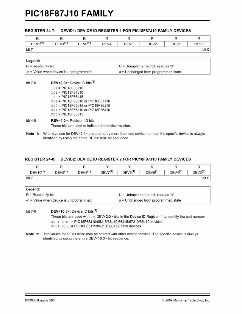
PIC18F87J10 FAMILY
REGISTER 24-7: DEVID1: DEVICE ID REGISTER 1 FOR PIC18F87J10 FAMILY DEVICES
R R R R R R R RDEV2(1) DEV1(1) DEV0(1) REV4 REV3 REV2 REV1 REV0
bit 7 bit 0
Legend:R = Read-only bit U = Unimplemented bit, read as ‘0’-n = Value when device is unprogrammed u = Unchanged from programmed state
bit 7-5 DEV<2:0>: Device ID bits(1)
111 = PIC18F85J10101 = PIC18F67J10100 = PIC18F66J15011 = PIC18F66J10 or PIC18F87J10010 = PIC18F65J15 or PIC18F86J15001 = PIC18F65J10 or PIC18F86J10000 = PIC18F85J15
bit 4-0 REV<4:0>: Revision ID bitsThese bits are used to indicate the device revision.
Note 1: Where values for DEV<2:0> are shared by more than one device number, the specific device is always identified by using the entire DEV<10:0> bit sequence.
REGISTER 24-8: DEVID2: DEVICE ID REGISTER 2 FOR PIC18F87J10 FAMILY DEVICES
R R R R R R R RDEV10(1) DEV9(1) DEV8(1) DEV7(1) DEV6(1) DEV5(1) DEV4(1) DEV3(1)
bit 7 bit 0
Legend:R = Read-only bit U = Unimplemented bit, read as ‘0’-n = Value when device is unprogrammed u = Unchanged from programmed state
bit 7-0 DEV<10:3>: Device ID bits(1)
These bits are used with the DEV<2:0> bits in the Device ID Register 1 to identify the part number.0001 0101 = PIC18F65J10/65J15/66J10/66J15/67J10/85J10 devices0001 0111 = PIC18F85J15/86J10/86J15/87J10 devices
Note 1: The values for DEV<10:3> may be shared with other device families. The specific device is always identified by using the entire DEV<10:0> bit sequence.
DS39663F-page 286 © 2009 Microchip Technology Inc.

PIC18F87J10 FAMILY
24.2 Watchdog Timer (WDT)For PIC18F87J10 family devices, the WDT is driven bythe INTRC oscillator. When the WDT is enabled, theclock source is also enabled. The nominal WDT period is4 ms and has the same stability as the INTRC oscillator.The 4 ms period of the WDT is multiplied by a 16-bitpostscaler. Any output of the WDT postscaler is selectedby a multiplexor, controlled by the WDTPS bits in Config-uration Register 2H. Available periods range from about4 ms to 135 seconds (2.25 minutes depending onvoltage, temperature and WDT postscaler). The WDTand postscaler are cleared whenever a SLEEP orCLRWDT instruction is executed, or a clock failure(primary or Timer1 oscillator) has occurred.
24.2.1 CONTROL REGISTER
The WDTCON register (Register 24-9) is a readableand writable register. The SWDTEN bit enables or dis-ables WDT operation. This allows software to overridethe WDTEN Configuration bit and enable the WDT onlyif it has been disabled by the Configuration bit.
FIGURE 24-1: WDT BLOCK DIAGRAM
TABLE 24-3: SUMMARY OF WATCHDOG TIMER REGISTERS
Note 1: The CLRWDT and SLEEP instructionsclear the WDT and postscaler countswhen executed.
2: When a CLRWDT instruction is executed,the postscaler count will be cleared.
REGISTER 24-9: WDTCON: WATCHDOG TIMER CONTROL REGISTER
U-0 U-0 U-0 U-0 U-0 U-0 U-0 R/W-0— — — — — — — SWDTEN(1)
bit 7 bit 0
Legend:R = Readable bit W = Writable bit U = Unimplemented bit, read as ‘0’-n = Value at POR ‘1’ = Bit is set ‘0’ = Bit is cleared x = Bit is unknown
bit 7-1 Unimplemented: Read as ‘0’bit 0 SWDTEN: Software Controlled Watchdog Timer Enable bit(1)
1 = Watchdog Timer is on0 = Watchdog Timer is off
Note 1: This bit has no effect if the Configuration bit, WDTEN, is enabled.
Name Bit 7 Bit 6 Bit 5 Bit 4 Bit 3 Bit 2 Bit 1 Bit 0 Reset Values on page
RCON IPEN — — RI TO PD POR BOR 54WDTCON — — — — — — — SWDTEN 54Legend: — = unimplemented, read as ‘0’. Shaded cells are not used by the Watchdog Timer.
INTRC Oscillator
WDT
Wake-up from
Reset
WDT
WDT Counter
Programmable Postscaler1:1 to 1:32,768
Enable WDT
WDTPS<3:0>
SWDTEN
CLRWDT
4
Power-Managed
ResetAll Device Resets
Sleep
INTRC Control
÷128
Modes
© 2009 Microchip Technology Inc. DS39663F-page 287
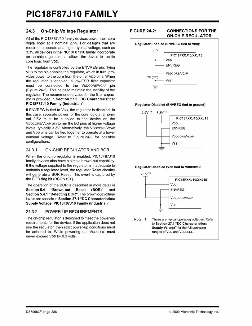
PIC18F87J10 FAMILY
24.3 On-Chip Voltage RegulatorAll of the PIC18F87J10 family devices power their coredigital logic at a nominal 2.5V. For designs that arerequired to operate at a higher typical voltage, such as3.3V, all devices in the PIC18F87J10 family incorporatean on-chip regulator that allows the device to run itscore logic from VDD.The regulator is controlled by the ENVREG pin. TyingVDD to the pin enables the regulator, which in turn, pro-vides power to the core from the other VDD pins. Whenthe regulator is enabled, a low-ESR filter capacitormust be connected to the VDDCORE/VCAP pin(Figure 24-2). This helps to maintain the stability of theregulator. The recommended value for the filter capac-itor is provided in Section 27.3 “DC Characteristics:PIC18F87J10 Family (Industrial)”.
If ENVREG is tied to VSS, the regulator is disabled. Inthis case, separate power for the core logic at a nomi-nal 2.5V must be supplied to the device on theVDDCORE/VCAP pin to run the I/O pins at higher voltagelevels, typically 3.3V. Alternatively, the VDDCORE/VCAPand VDD pins can be tied together to operate at a lowernominal voltage. Refer to Figure 24-2 for possibleconfigurations.
24.3.1 ON-CHIP REGULATOR AND BORWhen the on-chip regulator is enabled, PIC18F87J10family devices also have a simple brown-out capability.If the voltage supplied to the regulator is inadequate tomaintain a regulated level, the regulator Reset circuitrywill generate a BOR Reset. This event is captured bythe BOR flag bit (RCON<0>).
The operation of the BOR is described in more detail inSection 5.4 “Brown-out Reset (BOR)” andSection 5.4.1 “Detecting BOR”. The brown-out voltagelevels are specific in Section 27.1 “DC Characteristics:Supply Voltage, PIC18F87J10 Family (Industrial)”.
24.3.2 POWER-UP REQUIREMENTSThe on-chip regulator is designed to meet the power-uprequirements for the device. If the application does notuse the regulator, then strict power-up conditions mustbe adhered to. While powering up, VDDCORE mustnever exceed VDD by 0.3 volts.
FIGURE 24-2: CONNECTIONS FOR THE ON-CHIP REGULATOR
VDD
ENVREG
VDDCORE/VCAP
VSS
PIC18FXXJ10/XXJ153.3V(1)2.5V(1)
VDD
ENVREG
VDDCORE/VCAP
VSS
PIC18FXXJ10/XXJ15
CF
3.3V
Regulator Enabled (ENVREG tied to VDD):
Regulator Disabled (ENVREG tied to ground):
VDD
ENVREG
VDDCORE/VCAP
VSS
PIC18FXXJ10/XXJ152.5V(1)
Regulator Disabled (VDD tied to VDDCORE):
Note 1: These are typical operating voltages. Refer to Section 27.1 “DC Characteristics: Supply Voltage” for the full operating ranges of VDD and VDDCORE.
DS39663F-page 288 © 2009 Microchip Technology Inc.
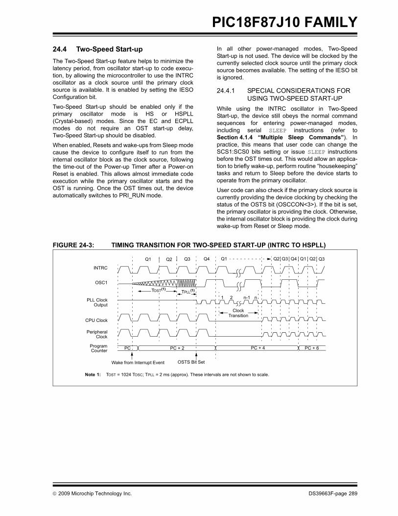
PIC18F87J10 FAMILY
24.4 Two-Speed Start-upThe Two-Speed Start-up feature helps to minimize thelatency period, from oscillator start-up to code execu-tion, by allowing the microcontroller to use the INTRCoscillator as a clock source until the primary clocksource is available. It is enabled by setting the IESOConfiguration bit.Two-Speed Start-up should be enabled only if theprimary oscillator mode is HS or HSPLL(Crystal-based) modes. Since the EC and ECPLLmodes do not require an OST start-up delay,Two-Speed Start-up should be disabled.
When enabled, Resets and wake-ups from Sleep modecause the device to configure itself to run from theinternal oscillator block as the clock source, followingthe time-out of the Power-up Timer after a Power-onReset is enabled. This allows almost immediate codeexecution while the primary oscillator starts and theOST is running. Once the OST times out, the deviceautomatically switches to PRI_RUN mode.
In all other power-managed modes, Two-SpeedStart-up is not used. The device will be clocked by thecurrently selected clock source until the primary clocksource becomes available. The setting of the IESO bitis ignored.
24.4.1 SPECIAL CONSIDERATIONS FOR USING TWO-SPEED START-UP
While using the INTRC oscillator in Two-SpeedStart-up, the device still obeys the normal commandsequences for entering power-managed modes,including serial SLEEP instructions (refer toSection 4.1.4 “Multiple Sleep Commands”). Inpractice, this means that user code can change theSCS1:SCS0 bits setting or issue SLEEP instructionsbefore the OST times out. This would allow an applica-tion to briefly wake-up, perform routine “housekeeping”tasks and return to Sleep before the device starts tooperate from the primary oscillator.
User code can also check if the primary clock source iscurrently providing the device clocking by checking thestatus of the OSTS bit (OSCCON<3>). If the bit is set,the primary oscillator is providing the clock. Otherwise,the internal oscillator block is providing the clock duringwake-up from Reset or Sleep mode.
FIGURE 24-3: TIMING TRANSITION FOR TWO-SPEED START-UP (INTRC TO HSPLL)
Q1 Q3 Q4
OSC1
Peripheral
Program PC PC + 2
INTRC
PLL Clock
Q1
PC + 6
Q2
Output
Q3 Q4 Q1
CPU Clock
PC + 4
Clock
Counter
Q2 Q2 Q3
Note 1: TOST = 1024 TOSC; TPLL = 2 ms (approx). These intervals are not shown to scale.
Wake from Interrupt Event
TPLL(1)
1 2 n-1 n
Clock
OSTS Bit Set
Transition
TOST(1)
© 2009 Microchip Technology Inc. DS39663F-page 289

PIC18F87J10 FAMILY
24.5 Fail-Safe Clock MonitorThe Fail-Safe Clock Monitor (FSCM) allows themicrocontroller to continue operation in the event of anexternal oscillator failure by automatically switching thedevice clock to the internal oscillator block. The FSCMfunction is enabled by setting the FCMEN Configurationbit.When FSCM is enabled, the INTRC oscillator runs atall times to monitor clocks to peripherals and provide abackup clock in the event of a clock failure. Clockmonitoring (shown in Figure 24-4) is accomplished bycreating a sample clock signal which is the INTRC out-put divided by 64. This allows ample time betweenFSCM sample clocks for a peripheral clock edge tooccur. The peripheral device clock and the sampleclock are presented as inputs to the Clock Monitor latch(CM). The CM is set on the falling edge of the deviceclock source but cleared on the rising edge of thesample clock.
FIGURE 24-4: FSCM BLOCK DIAGRAM
Clock failure is tested for on the falling edge of thesample clock. If a sample clock falling edge occurswhile CM is still set, a clock failure has been detected(Figure 24-5). This causes the following:
• the FSCM generates an oscillator fail interrupt by setting bit, OSCFIF (PIR2<7>);
• the device clock source is switched to the internal oscillator block (OSCCON is not updated to show the current clock source – this is the fail-safe condition); and
• the WDT is reset.
During switchover, the postscaler frequency from theinternal oscillator block may not be sufficiently stablefor timing sensitive applications. In these cases, it maybe desirable to select another clock configuration andenter an alternate power-managed mode. This can bedone to attempt a partial recovery or execute acontrolled shutdown. See Section 4.1.4 “MultipleSleep Commands” and Section 24.4.1 “SpecialConsiderations for Using Two-Speed Start-up” formore details.
The FSCM will detect failures of the primary or second-ary clock sources only. If the internal oscillator blockfails, no failure would be detected, nor would any actionbe possible.
24.5.1 FSCM AND THE WATCHDOG TIMERBoth the FSCM and the WDT are clocked by theINTRC oscillator. Since the WDT operates with aseparate divider and counter, disabling the WDT hasno effect on the operation of the INTRC oscillator whenthe FSCM is enabled.
As already noted, the clock source is switched to theINTRC clock when a clock failure is detected; this maymean a substantial change in the speed of code execu-tion. If the WDT is enabled with a small prescale value,a decrease in clock speed allows a WDT time-out tooccur and a subsequent device Reset. For this reason,fail-safe clock events also reset the WDT andpostscaler, allowing it to start timing from when execu-tion speed was changed and decreasing the likelihoodof an erroneous time-out.
24.5.2 EXITING FAIL-SAFE OPERATIONThe fail-safe condition is terminated by either a deviceReset or by entering a power-managed mode. OnReset, the controller starts the primary clock sourcespecified in Configuration Register 2H (with anyrequired start-up delays that are required for the oscil-lator mode, such as OST or PLL timer). The INTRCoscillator provides the device clock until the primaryclock source becomes ready (similar to a Two-SpeedStart-up). The clock source is then switched to theprimary clock (indicated by the OSTS bit in theOSCCON register becoming set). The Fail-Safe ClockMonitor then resumes monitoring the peripheral clock.
The primary clock source may never become readyduring start-up. In this case, operation is clocked by theINTRC oscillator. The OSCCON register will remain inits Reset state until a power-managed mode is entered.
Peripheral
INTRC÷ 64
S
C
Q
(32 μs) 488 Hz(2.048 ms)
Clock MonitorLatch (CM)
(edge-triggered)
ClockFailure
Detected
Source
Clock
Q
DS39663F-page 290 © 2009 Microchip Technology Inc.

PIC18F87J10 FAMILY
FIGURE 24-5: FSCM TIMING DIAGRAM24.5.3 FSCM INTERRUPTS IN POWER-MANAGED MODES
By entering a power-managed mode, the clockmultiplexor selects the clock source selected by theOSCCON register. Fail-Safe Monitoring of thepower-managed clock source resumes in thepower-managed mode.
If an oscillator failure occurs during power-managedoperation, the subsequent events depend on whetheror not the oscillator failure interrupt is enabled. Ifenabled (OSCFIF = 1), code execution will be clockedby the INTRC multiplexor. An automatic transition backto the failed clock source will not occur.
If the interrupt is disabled, subsequent interrupts whilein Idle mode will cause the CPU to begin executinginstructions while being clocked by the INTRC source.
24.5.4 POR OR WAKE-UP FROM SLEEPThe FSCM is designed to detect oscillator failure at anypoint after the device has exited Power-on Reset(POR) or low-power Sleep mode. When the primarydevice clock is either EC or INTRC modes, monitoringcan begin immediately following these events.
For HS or HSPLL modes, the situation is somewhat dif-ferent. Since the oscillator may require a start-up timeconsiderably longer than the FSCM sample clock time,a false clock failure may be detected. To prevent this,the internal oscillator block is automatically configuredas the device clock and functions until the primary clockis stable (the OST and PLL timers have timed out). Thisis identical to Two-Speed Start-up mode. Once theprimary clock is stable, the INTRC returns to its role asthe FSCM source.
As noted in Section 24.4.1 “Special Considerationsfor Using Two-Speed Start-up”, it is also possible toselect another clock configuration and enter an alternatepower-managed mode while waiting for the primaryclock to become stable. When the new power-managedmode is selected, the primary clock is disabled.
OSCFIF
CM Output
DeviceClock
Output
Sample Clock
FailureDetected
OscillatorFailure
Note: The device clock is normally at a much higher frequency than the sample clock. The relative frequencies inthis example have been chosen for clarity.
(Q)
CM Test CM Test CM Test
Note: The same logic that prevents false oscilla-tor failure interrupts on POR, or wake fromSleep, will also prevent the detection ofthe oscillator’s failure to start at all follow-ing these events. This can be avoided bymonitoring the OSTS bit and using atiming routine to determine if the oscillatoris taking too long to start. Even so, nooscillator failure interrupt will be flagged.
© 2009 Microchip Technology Inc. DS39663F-page 291
PIC18F87J10 FAMILY
24.6 Program Verification andCode ProtectionFor all devices in the PIC18F87J10 family of devices,the on-chip program memory space is treated as asingle block. Code protection for this block is controlledby one Configuration bit, CP0. This bit inhibits externalreads and writes to the program memory space. It hasno direct effect in normal execution mode.
24.6.1 CONFIGURATION REGISTER PROTECTION
The Configuration registers are protected againstuntoward changes or reads in two ways. The primaryprotection is the write-once feature of the Configurationbits which prevents reconfiguration once the bit hasbeen programmed during a power cycle. To safeguardagainst unpredictable events, Configuration bitchanges resulting from individual cell-level disruptions(such as ESD events) will cause a parity error andtrigger a device Reset.
The data for the Configuration registers is derived fromthe Flash Configuration Words in program memory.When the CP0 bit set, the source data for deviceconfiguration is also protected as a consequence.
24.7 In-Circuit Serial ProgrammingPIC18F87J10 family microcontrollers can be seriallyprogrammed while in the end application circuit. This issimply done with two lines for clock and data and threeother lines for power, ground and the programmingvoltage. This allows customers to manufacture boardswith unprogrammed devices and then program themicrocontroller just before shipping the product. Thisalso allows the most recent firmware or a customfirmware to be programmed.
24.8 In-Circuit DebuggerWhen the DEBUG Configuration bit is programmed toa ‘0’, the In-Circuit Debugger functionality is enabled.This function allows simple debugging functions whenused with MPLAB® IDE. When the microcontroller hasthis feature enabled, some resources are not availablefor general use. Table 24-4 shows which resources arerequired by the background debugger.
TABLE 24-4: DEBUGGER RESOURCES I/O pins: RB6, RB7Stack: 2 levelsProgram Memory: 512 bytesData Memory: 10 bytes
DS39663F-page 292 © 2009 Microchip Technology Inc.
PIC18F87J10 FAMILY
25.0 INSTRUCTION SET SUMMARYThe PIC18F87J10 family of devices incorporate thestandard set of 75 PIC18 core instructions, as well asan extended set of 8 new instructions for the optimiza-tion of code that is recursive or that utilizes a softwarestack. The extended set is discussed later in thissection.
25.1 Standard Instruction SetThe standard PIC18 instruction set adds manyenhancements to the previous PIC® MCU instructionsets, while maintaining an easy migration from thesePIC MCU instruction sets. Most instructions are asingle program memory word (16 bits), but there arefour instructions that require two program memorylocations.
Each single-word instruction is a 16-bit word dividedinto an opcode, which specifies the instruction type andone or more operands, which further specify theoperation of the instruction.
The instruction set is highly orthogonal and is groupedinto four basic categories:
• Byte-oriented operations• Bit-oriented operations• Literal operations• Control operations
The PIC18 instruction set summary in Table 25-2 listsbyte-oriented, bit-oriented, literal and controloperations. Table 25-1 shows the opcode fielddescriptions.
Most byte-oriented instructions have three operands:
1. The file register (specified by ‘f’) 2. The destination of the result (specified by ‘d’) 3. The accessed memory (specified by ‘a’)
The file register designator, ‘f’, specifies which file reg-ister is to be used by the instruction. The destinationdesignator, ‘d’, specifies where the result of theoperation is to be placed. If ‘d’ is zero, the result isplaced in the WREG register. If ‘d’ is one, the result isplaced in the file register specified in the instruction.
All bit-oriented instructions have three operands:
1. The file register (specified by ‘f’) 2. The bit in the file register (specified by ‘b’) 3. The accessed memory (specified by ‘a’)
The bit field designator, ‘b’, selects the number of the bitaffected by the operation, while the file registerdesignator, ‘f’, represents the number of the file inwhich the bit is located.
The literal instructions may use some of the followingoperands:
• A literal value to be loaded into a file register (specified by ‘k’)
• The desired FSR register to load the literal value into (specified by ‘f’)
• No operand required (specified by ‘—’)
The control instructions may use some of the followingoperands:
• A program memory address (specified by ‘n’)• The mode of the CALL or RETURN instructions
(specified by ‘s’)• The mode of the table read and table write
instructions (specified by ‘m’)• No operand required
(specified by ‘—’)
All instructions are a single word, except for fourdouble-word instructions. These instructions weremade double-word to contain the required informationin 32 bits. In the second word, the 4 MSbs are ‘1’s. Ifthis second word is executed as an instruction (byitself), it will execute as a NOP.
All single-word instructions are executed in a singleinstruction cycle, unless a conditional test is true or theprogram counter is changed as a result of the instruc-tion. In these cases, the execution takes two instructioncycles with the additional instruction cycle(s) executedas a NOP.
The double-word instructions execute in two instructioncycles.
One instruction cycle consists of four oscillator periods.Thus, for an oscillator frequency of 4 MHz, the normalinstruction execution time is 1 μs. If a conditional test istrue, or the program counter is changed as a result ofan instruction, the instruction execution time is 2 μs.Two-word branch instructions (if true) would take 3 μs.
Figure 25-1 shows the general formats that the instruc-tions can have. All examples use the convention ‘nnh’to represent a hexadecimal number.
The Instruction Set Summary, shown in Table 25-2,lists the standard instructions recognized by theMicrochip MPASMTM Assembler.
Section 25.1.1 “Standard Instruction Set” providesa description of each instruction.
© 2009 Microchip Technology Inc. DS39663F-page 293

PIC18F87J10 FAMILY
TABLE 25-1: OPCODE FIELD DESCRIPTIONSField Description
a RAM access bit:a = 0: RAM location in Access RAM (BSR register is ignored)a = 1: RAM bank is specified by BSR register
bbb Bit address within an 8-bit file register (0 to 7).BSR Bank Select Register. Used to select the current RAM bank.C, DC, Z, OV, N ALU Status bits: Carry, Digit Carry, Zero, Overflow, Negative.d Destination select bit:
d = 0: store result in WREGd = 1: store result in file register f
dest Destination: either the WREG register or the specified register file location.f 8-bit Register file address (00h to FFh) or 2-bit FSR designator (0h to 3h).fs 12-bit Register file address (000h to FFFh). This is the source address. fd 12-bit Register file address (000h to FFFh). This is the destination address. GIE Global Interrupt Enable bit.k Literal field, constant data or label (may be either an 8-bit, 12-bit or a 20-bit value).label Label name.mm The mode of the TBLPTR register for the table read and table write instructions.
Only used with table read and table write instructions:* No Change to register (such as TBLPTR with table reads and writes)*+ Post-Increment register (such as TBLPTR with table reads and writes)*- Post-Decrement register (such as TBLPTR with table reads and writes)+* Pre-Increment register (such as TBLPTR with table reads and writes)n The relative address (2’s complement number) for relative branch instructions or the direct address for
Call/Branch and Return instructions.PC Program Counter.PCL Program Counter Low Byte.PCH Program Counter High Byte.PCLATH Program Counter High Byte Latch.PCLATU Program Counter Upper Byte Latch.PD Power-Down bit.PRODH Product of Multiply High Byte.PRODL Product of Multiply Low Byte.s Fast Call/Return mode select bit:
s = 0: do not update into/from shadow registerss = 1: certain registers loaded into/from shadow registers (Fast mode)
TBLPTR 21-bit Table Pointer (points to a Program Memory location).TABLAT 8-bit Table Latch.TO Time-out bit.TOS Top-of-Stack.u Unused or Unchanged.WDT Watchdog Timer.WREG Working register (accumulator).x Don’t care (‘0’ or ‘1’). The assembler will generate code with x = 0. It is the recommended form of use for
compatibility with all Microchip software tools.zs 7-bit offset value for Indirect Addressing of register files (source).zd 7-bit offset value for Indirect Addressing of register files (destination). Optional argument.[text] Indicates an Indexed Address.(text) The contents of text.[expr]<n> Specifies bit n of the register indicated by the pointer expr.→ Assigned to.< > Register bit field.∈ In the set of.italics User-defined term (font is Courier).
DS39663F-page 294 © 2009 Microchip Technology Inc.

PIC18F87J10 FAMILY
FIGURE 25-1: GENERAL FORMAT FOR INSTRUCTIONSByte-oriented file register operations
15 10 9 8 7 0
d = 0 for result destination to be WREG register
OPCODE d a f (FILE #)
d = 1 for result destination to be file register (f)a = 0 to force Access Bank
Bit-oriented file register operations
15 12 11 9 8 7 0OPCODE b (BIT #) a f (FILE #)
b = 3-bit position of bit in file register (f)
Literal operations
15 8 7 0 OPCODE k (literal)
k = 8-bit immediate value
Byte to Byte move operations (2-word)
15 12 11 0OPCODE f (Source FILE #)
CALL, GOTO and Branch operations 15 8 7 0
OPCODE n<7:0> (literal)
n = 20-bit immediate value
a = 1 for BSR to select bankf = 8-bit file register address
a = 0 to force Access Banka = 1 for BSR to select bankf = 8-bit file register address
15 12 11 01111 n<19:8> (literal)
15 12 11 0 1111 f (Destination FILE #)
f = 12-bit file register address
Control operations
Example Instruction
ADDWF MYREG, W, B
MOVFF MYREG1, MYREG2
BSF MYREG, bit, B
MOVLW 7Fh
GOTO Label
15 8 7 0
OPCODE n<7:0> (literal)
15 12 11 0
1111 n<19:8> (literal)
CALL MYFUNC
15 11 10 0
OPCODE n<10:0> (literal)
S = Fast bit
BRA MYFUNC
15 8 7 0
OPCODE n<7:0> (literal) BC MYFUNC
S
© 2009 Microchip Technology Inc. DS39663F-page 295

PIC18F87J10 FAMILY
TABLE 25-2: PIC18F87J10 FAMILY INSTRUCTION SETMnemonic,Operands Description Cycles
16-bit Instruction Word StatusAffected Notes
MSb LSb
BYTE-ORIENTED OPERATIONSADDWFADDWFCANDWFCLRFCOMFCPFSEQCPFSGTCPFSLTDECFDECFSZDCFSNZINCFINCFSZINFSNZIORWFMOVFMOVFF
MOVWFMULWFNEGFRLCFRLNCFRRCFRRNCFSETFSUBFWB
SUBWFSUBWFB
SWAPFTSTFSZXORWF
f, d, af, d, af, d, af, af, d, af, af, af, af, d, af, d, af, d, af, d, af, d, af, d, af, d, af, d, afs, fd
f, af, af, af, d, af, d, af, d, af, d, af, af, d, a
f, d, af, d, a
f, d, af, af, d, a
Add WREG and fAdd WREG and Carry bit to fAND WREG with fClear fComplement fCompare f with WREG, Skip =Compare f with WREG, Skip >Compare f with WREG, Skip <Decrement fDecrement f, Skip if 0Decrement f, Skip if Not 0Increment fIncrement f, Skip if 0Increment f, Skip if Not 0Inclusive OR WREG with fMove fMove fs (source) to 1st word
fd (destination) 2nd wordMove WREG to fMultiply WREG with fNegate fRotate Left f through CarryRotate Left f (No Carry)Rotate Right f through CarryRotate Right f (No Carry)Set fSubtract f from WREG with Borrow Subtract WREG from fSubtract WREG from f with BorrowSwap Nibbles in fTest f, Skip if 0Exclusive OR WREG with f
111111 (2 or 3)1 (2 or 3)1 (2 or 3)11 (2 or 3)1 (2 or 3)11 (2 or 3)1 (2 or 3)112
111111111
11
11 (2 or 3)1
001000100001011000010110011001100000001001000010001101000001010111001111011000000110001101000011010001100101
01010101
001101100001
01da00da01da101a11da001a010a000a01da11da11da10da11da10da00da00daffffffff111a001a110a01da01da00da00da100a01da
11da10da
10da011a10da
ffffffffffffffffffffffffffffffffffffffffffffffffffffffffffffffffffffffffffffffffffffffffffffffffffffffffffff
ffffffff
ffffffffffff
ffffffffffffffffffffffffffffffffffffffffffffffffffffffffffffffffffffffffffffffffffffffffffffffffffffffffffff
ffffffff
ffffffffffff
C, DC, Z, OV, NC, DC, Z, OV, NZ, NZZ, NNoneNoneNoneC, DC, Z, OV, NNoneNoneC, DC, Z, OV, NNoneNoneZ, NZ, NNone
NoneNoneC, DC, Z, OV, NC, Z, NZ, NC, Z, NZ, NNoneC, DC, Z, OV, N
C, DC, Z, OV, NC, DC, Z, OV, N
NoneNoneZ, N
1, 21, 21,221, 2441, 21, 2, 3, 41, 2, 3, 41, 21, 2, 3, 441, 21, 21
1, 2
1, 2
1, 2
1, 2
41, 2
Note 1: When a PORT register is modified as a function of itself (e.g., MOVF PORTB, 1, 0), the value used will be that value present on the pins themselves. For example, if the data latch is ‘1’ for a pin configured as an input and is driven low by an external device, the data will be written back with a ‘0’.
2: If this instruction is executed on the TMR0 register (and, where applicable, d = 1), the prescaler will be cleared if assigned.
3: If the Program Counter (PC) is modified or a conditional test is true, the instruction requires two cycles. The second cycle is executed as a NOP.
4: Some instructions are two-word instructions. The second word of these instructions will be executed as a NOP unless the first word of the instruction retrieves the information embedded in these 16-bits. This ensures that all program memory locations have a valid instruction.
DS39663F-page 296 © 2009 Microchip Technology Inc.
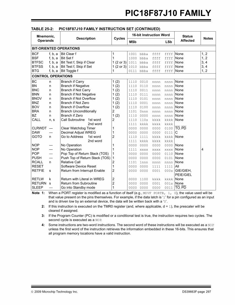
PIC18F87J10 FAMILY
BIT-ORIENTED OPERATIONSBCFBSFBTFSCBTFSSBTG
f, b, af, b, af, b, af, b, af, b, a
Bit Clear fBit Set fBit Test f, Skip if ClearBit Test f, Skip if SetBit Toggle f
111 (2 or 3)1 (2 or 3)1
10011000101110100111
bbbabbbabbbabbbabbba
ffffffffffffffffffff
ffffffffffffffffffff
NoneNoneNoneNoneNone
1, 21, 23, 43, 41, 2
CONTROL OPERATIONSBCBNBNCBNNBNOVBNZBOVBRABZCALL
CLRWDTDAWGOTO
NOPNOPPOPPUSHRCALLRESETRETFIE
RETLWRETURNSLEEP
nnnnnnnnnn, s
——n
————n
s
ks—
Branch if CarryBranch if NegativeBranch if Not CarryBranch if Not NegativeBranch if Not OverflowBranch if Not ZeroBranch if OverflowBranch Unconditionally Branch if ZeroCall Subroutine 1st word
2nd wordClear Watchdog TimerDecimal Adjust WREGGo to Address 1st word
2nd wordNo OperationNo OperationPop Top of Return Stack (TOS)Push Top of Return Stack (TOS)Relative CallSoftware Device ResetReturn from Interrupt Enable
Return with Literal in WREG Return from SubroutineGo into Standby mode
1 (2)1 (2)1 (2)1 (2)1 (2)1 (2)1 (2)21 (2)2
112
1111212
221
1110111011101110111011101110110111101110111100000000111011110000111100000000110100000000
000000000000
00100110001101110101000101000nnn0000110skkkk000000001111kkkk0000xxxx000000001nnn00000000
110000000000
nnnnnnnnnnnnnnnnnnnnnnnnnnnnnnnnnnnnkkkkkkkk00000000kkkkkkkk0000xxxx00000000nnnn11110001
kkkk00010000
nnnnnnnnnnnnnnnnnnnnnnnnnnnnnnnnnnnnkkkkkkkk01000111kkkkkkkk0000xxxx01100101nnnn1111000s
kkkk001s0011
NoneNoneNoneNoneNoneNoneNoneNoneNoneNone
TO, PDCNone
NoneNoneNoneNoneNoneAllGIE/GIEH, PEIE/GIELNoneNoneTO, PD
4
TABLE 25-2: PIC18F87J10 FAMILY INSTRUCTION SET (CONTINUED)
Mnemonic,Operands Description Cycles
16-bit Instruction Word StatusAffected Notes
MSb LSb
Note 1: When a PORT register is modified as a function of itself (e.g., MOVF PORTB, 1, 0), the value used will be that value present on the pins themselves. For example, if the data latch is ‘1’ for a pin configured as an input and is driven low by an external device, the data will be written back with a ‘0’.
2: If this instruction is executed on the TMR0 register (and, where applicable, d = 1), the prescaler will be cleared if assigned.
3: If the Program Counter (PC) is modified or a conditional test is true, the instruction requires two cycles. The second cycle is executed as a NOP.
4: Some instructions are two-word instructions. The second word of these instructions will be executed as a NOP unless the first word of the instruction retrieves the information embedded in these 16-bits. This ensures that all program memory locations have a valid instruction.
© 2009 Microchip Technology Inc. DS39663F-page 297

PIC18F87J10 FAMILY
LITERAL OPERATIONSADDLWANDLWIORLWLFSR
MOVLBMOVLWMULLWRETLWSUBLWXORLW
kkkf, k
kkkkkk
Add Literal and WREGAND Literal with WREGInclusive OR Literal with WREGMove Literal (12-bit) 2nd word
to FSR(f) 1st wordMove Literal to BSR<3:0>Move Literal to WREGMultiply Literal with WREGReturn with Literal in WREG Subtract WREG from LiteralExclusive OR Literal with WREG
1112
111211
00000000000011101111000000000000000000000000
11111011100111100000000111101101110010001010
kkkkkkkkkkkk00ffkkkk0000kkkkkkkkkkkkkkkkkkkk
kkkkkkkkkkkkkkkkkkkkkkkkkkkkkkkkkkkkkkkkkkkk
C, DC, Z, OV, NZ, NZ, NNone
NoneNoneNoneNoneC, DC, Z, OV, NZ, N
DATA MEMORY ↔ PROGRAM MEMORY OPERATIONSTBLRD*TBLRD*+TBLRD*-TBLRD+*TBLWT*TBLWT*+TBLWT*-TBLWT+*
Table ReadTable Read with Post-IncrementTable Read with Post-DecrementTable Read with Pre-IncrementTable WriteTable Write with Post-IncrementTable Write with Post-DecrementTable Write with Pre-Increment
2
2
00000000000000000000000000000000
00000000000000000000000000000000
00000000000000000000000000000000
10001001101010111100110111101111
NoneNoneNoneNoneNoneNoneNoneNone
TABLE 25-2: PIC18F87J10 FAMILY INSTRUCTION SET (CONTINUED)
Mnemonic,Operands Description Cycles
16-bit Instruction Word StatusAffected Notes
MSb LSb
Note 1: When a PORT register is modified as a function of itself (e.g., MOVF PORTB, 1, 0), the value used will be that value present on the pins themselves. For example, if the data latch is ‘1’ for a pin configured as an input and is driven low by an external device, the data will be written back with a ‘0’.
2: If this instruction is executed on the TMR0 register (and, where applicable, d = 1), the prescaler will be cleared if assigned.
3: If the Program Counter (PC) is modified or a conditional test is true, the instruction requires two cycles. The second cycle is executed as a NOP.
4: Some instructions are two-word instructions. The second word of these instructions will be executed as a NOP unless the first word of the instruction retrieves the information embedded in these 16-bits. This ensures that all program memory locations have a valid instruction.
DS39663F-page 298 © 2009 Microchip Technology Inc.
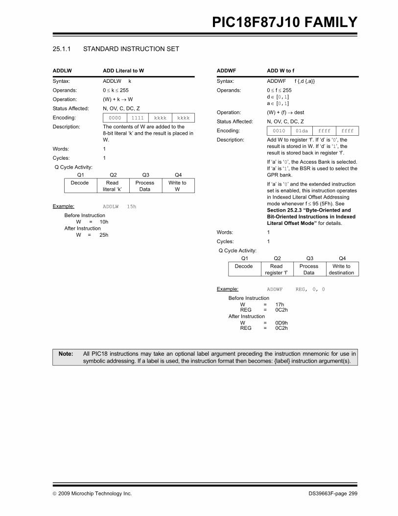
PIC18F87J10 FAMILY
25.1.1 STANDARD INSTRUCTION SETADDLW ADD Literal to W
Syntax: ADDLW k
Operands: 0 ≤ k ≤ 255
Operation: (W) + k → W
Status Affected: N, OV, C, DC, Z
Encoding: 0000 1111 kkkk kkkk
Description: The contents of W are added to the 8-bit literal ‘k’ and the result is placed in W.
Words: 1
Cycles: 1
Q Cycle Activity:Q1 Q2 Q3 Q4
Decode Readliteral ‘k’
Process Data
Write to W
Example: ADDLW 15h
Before InstructionW = 10h
After InstructionW = 25h
ADDWF ADD W to f
Syntax: ADDWF f ,d ,a
Operands: 0 ≤ f ≤ 255d ∈ [0,1]a ∈ [0,1]
Operation: (W) + (f) → dest
Status Affected: N, OV, C, DC, Z
Encoding: 0010 01da ffff ffff
Description: Add W to register ‘f’. If ‘d’ is ‘0’, the result is stored in W. If ‘d’ is ‘1’, the result is stored back in register ‘f’.
If ‘a’ is ‘0’, the Access Bank is selected. If ‘a’ is ‘1’, the BSR is used to select the GPR bank.
If ‘a’ is ‘0’ and the extended instruction set is enabled, this instruction operates in Indexed Literal Offset Addressing mode whenever f ≤ 95 (5Fh). See Section 25.2.3 “Byte-Oriented and Bit-Oriented Instructions in Indexed Literal Offset Mode” for details.
Words: 1
Cycles: 1
Q Cycle Activity:Q1 Q2 Q3 Q4
Decode Readregister ‘f’
Process Data
Write todestination
Example: ADDWF REG, 0, 0
Before InstructionW = 17hREG = 0C2h
After InstructionW = 0D9hREG = 0C2h
Note: All PIC18 instructions may take an optional label argument preceding the instruction mnemonic for use insymbolic addressing. If a label is used, the instruction format then becomes: label instruction argument(s).
© 2009 Microchip Technology Inc. DS39663F-page 299

PIC18F87J10 FAMILY
ADDWFC ADD W and Carry bit to f
Syntax: ADDWFC f ,d ,a
Operands: 0 ≤ f ≤ 255d ∈ [0,1]a ∈ [0,1]
Operation: (W) + (f) + (C) → dest
Status Affected: N,OV, C, DC, Z
Encoding: 0010 00da ffff ffff
Description: Add W, the Carry flag and data memory location, ‘f’. If ‘d’ is ‘0’, the result is placed in W. If ‘d’ is ‘1’, the result is placed in data memory location ‘f’.
If ‘a’ is ‘0’, the Access Bank is selected. If ‘a’ is ‘1’, the BSR is used to select the GPR bank.
If ‘a’ is ‘0’ and the extended instruction set is enabled, this instruction operates in Indexed Literal Offset Addressing mode whenever f ≤ 95 (5Fh). See Section 25.2.3 “Byte-Oriented and Bit-Oriented Instructions in Indexed Literal Offset Mode” for details.
Words: 1
Cycles: 1
Q Cycle Activity:Q1 Q2 Q3 Q4
Decode Readregister ‘f’
Process Data
Write to destination
Example: ADDWFC REG, 0, 1
Before InstructionCarry bit = 1REG = 02hW = 4Dh
After InstructionCarry bit = 0REG = 02hW = 50h
ANDLW AND Literal with W
Syntax: ANDLW k
Operands: 0 ≤ k ≤ 255
Operation: (W) .AND. k → W
Status Affected: N, Z
Encoding: 0000 1011 kkkk kkkk
Description: The contents of W are ANDed with the 8-bit literal ‘k’. The result is placed in W.
Words: 1
Cycles: 1
Q Cycle Activity:Q1 Q2 Q3 Q4
Decode Read literal ‘k’
Process Data
Write to W
Example: ANDLW 05Fh
Before InstructionW = A3h
After InstructionW = 03h
DS39663F-page 300 © 2009 Microchip Technology Inc.

PIC18F87J10 FAMILY
ANDWF AND W with f
Syntax: ANDWF f ,d ,a
Operands: 0 ≤ f ≤ 255d ∈ [0,1]a ∈ [0,1]
Operation: (W) .AND. (f) → dest
Status Affected: N, Z
Encoding: 0001 01da ffff ffff
Description: The contents of W are ANDed with register ‘f’. If ‘d’ is ‘0’, the result is stored in W. If ‘d’ is ‘1’, the result is stored back in register ‘f’.
If ‘a’ is ‘0’, the Access Bank is selected. If ‘a’ is ‘1’, the BSR is used to select the GPR bank.
If ‘a’ is ‘0’ and the extended instruction set is enabled, this instruction operates in Indexed Literal Offset Addressing mode whenever f ≤ 95 (5Fh). See Section 25.2.3 “Byte-Oriented and Bit-Oriented Instructions in Indexed Literal Offset Mode” for details.
Words: 1
Cycles: 1
Q Cycle Activity:Q1 Q2 Q3 Q4
Decode Readregister ‘f’
Process Data
Write to destination
Example: ANDWF REG, 0, 0
Before InstructionW = 17hREG = C2h
After InstructionW = 02hREG = C2h
BC Branch if Carry
Syntax: BC n
Operands: -128 ≤ n ≤ 127
Operation: if Carry bit is ‘1’,(PC) + 2 + 2n → PC
Status Affected: None
Encoding: 1110 0010 nnnn nnnn
Description: If the Carry bit is ’1’, then the program will branch.
The 2’s complement number ‘2n’ is added to the PC. Since the PC will have incremented to fetch the next instruction, the new address will be PC + 2 + 2n. This instruction is then a two-cycle instruction.
Words: 1
Cycles: 1(2)
Q Cycle Activity:If Jump:
Q1 Q2 Q3 Q4Decode Read literal
‘n’Process
DataWrite to
PCNo
operationNo
operationNo
operationNo
operationIf No Jump:
Q1 Q2 Q3 Q4Decode Read literal
‘n’Process
DataNo
operation
Example: HERE BC 5
Before InstructionPC = address (HERE)
After InstructionIf Carry = 1;
PC = address (HERE + 12)If Carry = 0;
PC = address (HERE + 2)
© 2009 Microchip Technology Inc. DS39663F-page 301
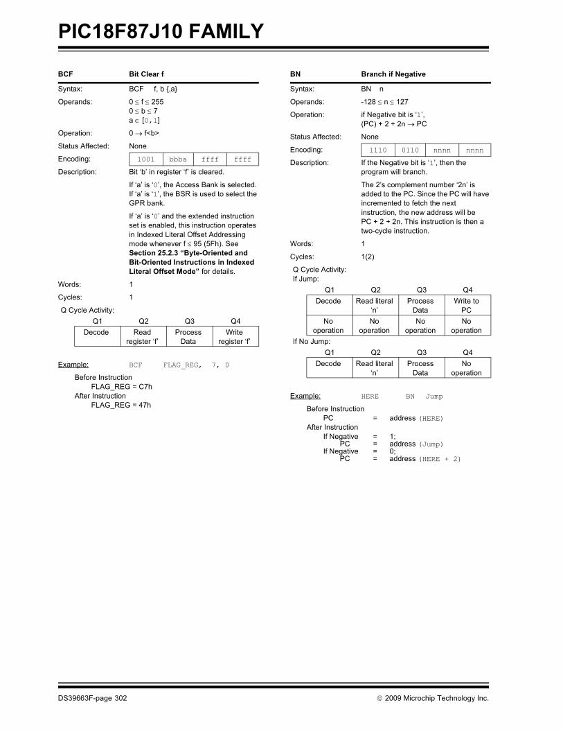
PIC18F87J10 FAMILY
BCF Bit Clear f
Syntax: BCF f, b ,a
Operands: 0 ≤ f ≤ 2550 ≤ b ≤ 7a ∈ [0,1]
Operation: 0 → f<b>
Status Affected: None
Encoding: 1001 bbba ffff ffff
Description: Bit ‘b’ in register ‘f’ is cleared.
If ‘a’ is ‘0’, the Access Bank is selected. If ‘a’ is ‘1’, the BSR is used to select the GPR bank.
If ‘a’ is ‘0’ and the extended instruction set is enabled, this instruction operates in Indexed Literal Offset Addressing mode whenever f ≤ 95 (5Fh). See Section 25.2.3 “Byte-Oriented and Bit-Oriented Instructions in Indexed Literal Offset Mode” for details.
Words: 1
Cycles: 1
Q Cycle Activity:Q1 Q2 Q3 Q4
Decode Readregister ‘f’
Process Data
Writeregister ‘f’
Example: BCF FLAG_REG, 7, 0
Before InstructionFLAG_REG = C7h
After InstructionFLAG_REG = 47h
BN Branch if Negative
Syntax: BN n
Operands: -128 ≤ n ≤ 127
Operation: if Negative bit is ‘1’,(PC) + 2 + 2n → PC
Status Affected: None
Encoding: 1110 0110 nnnn nnnn
Description: If the Negative bit is ‘1’, then the program will branch.
The 2’s complement number ‘2n’ is added to the PC. Since the PC will have incremented to fetch the next instruction, the new address will be PC + 2 + 2n. This instruction is then a two-cycle instruction.
Words: 1
Cycles: 1(2)
Q Cycle Activity:If Jump:
Q1 Q2 Q3 Q4Decode Read literal
‘n’Process
DataWrite to
PCNo
operationNo
operationNo
operationNo
operationIf No Jump:
Q1 Q2 Q3 Q4Decode Read literal
‘n’Process
DataNo
operation
Example: HERE BN Jump
Before InstructionPC = address (HERE)
After InstructionIf Negative = 1;
PC = address (Jump)If Negative = 0;
PC = address (HERE + 2)
DS39663F-page 302 © 2009 Microchip Technology Inc.

PIC18F87J10 FAMILY
BNC Branch if Not Carry
Syntax: BNC n
Operands: -128 ≤ n ≤ 127
Operation: if Carry bit is ‘0’,(PC) + 2 + 2n → PC
Status Affected: None
Encoding: 1110 0011 nnnn nnnn
Description: If the Carry bit is ‘0’, then the program will branch.
The 2’s complement number ‘2n’ is added to the PC. Since the PC will have incremented to fetch the next instruction, the new address will be PC + 2 + 2n. This instruction is then a two-cycle instruction.
Words: 1
Cycles: 1(2)
Q Cycle Activity:If Jump:
Q1 Q2 Q3 Q4Decode Read literal
‘n’Process
DataWrite to
PCNo
operationNo
operationNo
operationNo
operationIf No Jump:
Q1 Q2 Q3 Q4Decode Read literal
‘n’Process
DataNo
operation
Example: HERE BNC Jump
Before InstructionPC = address (HERE)
After InstructionIf Carry = 0;
PC = address (Jump)If Carry = 1;
PC = address (HERE + 2)
BNN Branch if Not Negative
Syntax: BNN n
Operands: -128 ≤ n ≤ 127
Operation: if Negative bit is ‘0’,(PC) + 2 + 2n → PC
Status Affected: None
Encoding: 1110 0111 nnnn nnnn
Description: If the Negative bit is ‘0’, then the program will branch.
The 2’s complement number ‘2n’ is added to the PC. Since the PC will have incremented to fetch the next instruction, the new address will be PC + 2 + 2n. This instruction is then a two-cycle instruction.
Words: 1
Cycles: 1(2)
Q Cycle Activity:If Jump:
Q1 Q2 Q3 Q4Decode Read literal
‘n’Process
DataWrite to
PCNo
operationNo
operationNo
operationNo
operationIf No Jump:
Q1 Q2 Q3 Q4Decode Read literal
‘n’Process
DataNo
operation
Example: HERE BNN Jump
Before InstructionPC = address (HERE)
After InstructionIf Negative = 0;
PC = address (Jump)If Negative = 1;
PC = address (HERE + 2)
© 2009 Microchip Technology Inc. DS39663F-page 303
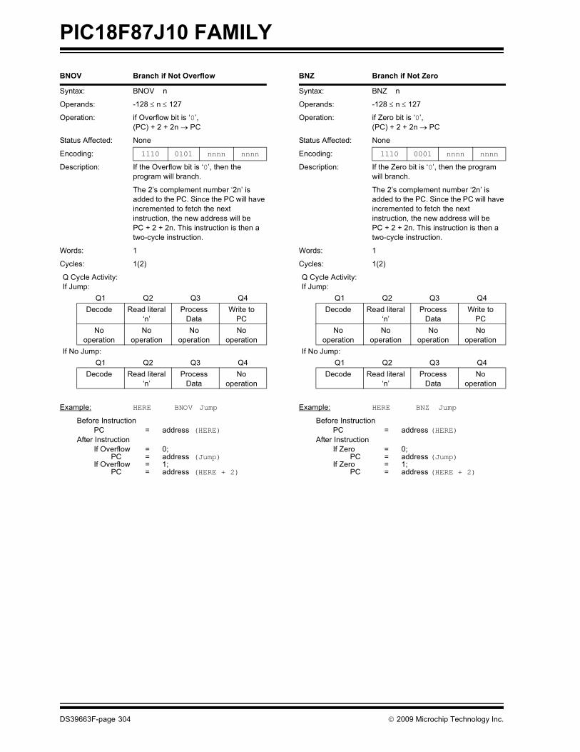
PIC18F87J10 FAMILY
BNOV Branch if Not Overflow
Syntax: BNOV n
Operands: -128 ≤ n ≤ 127
Operation: if Overflow bit is ‘0’,(PC) + 2 + 2n → PC
Status Affected: None
Encoding: 1110 0101 nnnn nnnn
Description: If the Overflow bit is ‘0’, then the program will branch.
The 2’s complement number ‘2n’ is added to the PC. Since the PC will have incremented to fetch the next instruction, the new address will be PC + 2 + 2n. This instruction is then a two-cycle instruction.
Words: 1
Cycles: 1(2)
Q Cycle Activity:If Jump:
Q1 Q2 Q3 Q4Decode Read literal
‘n’Process
DataWrite to
PCNo
operationNo
operationNo
operationNo
operationIf No Jump:
Q1 Q2 Q3 Q4Decode Read literal
‘n’Process
DataNo
operation
Example: HERE BNOV Jump
Before InstructionPC = address (HERE)
After InstructionIf Overflow = 0;
PC = address (Jump)If Overflow = 1;
PC = address (HERE + 2)
BNZ Branch if Not Zero
Syntax: BNZ n
Operands: -128 ≤ n ≤ 127
Operation: if Zero bit is ‘0’,(PC) + 2 + 2n → PC
Status Affected: None
Encoding: 1110 0001 nnnn nnnn
Description: If the Zero bit is ‘0’, then the program will branch.
The 2’s complement number ‘2n’ is added to the PC. Since the PC will have incremented to fetch the next instruction, the new address will be PC + 2 + 2n. This instruction is then a two-cycle instruction.
Words: 1
Cycles: 1(2)
Q Cycle Activity:If Jump:
Q1 Q2 Q3 Q4Decode Read literal
‘n’Process
DataWrite to
PCNo
operationNo
operationNo
operationNo
operationIf No Jump:
Q1 Q2 Q3 Q4Decode Read literal
‘n’Process
DataNo
operation
Example: HERE BNZ Jump
Before InstructionPC = address (HERE)
After InstructionIf Zero = 0;
PC = address (Jump)If Zero = 1;
PC = address (HERE + 2)
DS39663F-page 304 © 2009 Microchip Technology Inc.

PIC18F87J10 FAMILY
BRA Unconditional Branch
Syntax: BRA n
Operands: -1024 ≤ n ≤ 1023
Operation: (PC) + 2 + 2n → PC
Status Affected: None
Encoding: 1101 0nnn nnnn nnnn
Description: Add the 2’s complement number ‘2n’ to the PC. Since the PC will have incremented to fetch the next instruction, the new address will be PC + 2 + 2n. This instruction is a two-cycle instruction.
Words: 1
Cycles: 2
Q Cycle Activity:Q1 Q2 Q3 Q4
Decode Read literal ‘n’
Process Data
Write to PC
No operation
No operation
No operation
No operation
Example: HERE BRA Jump
Before InstructionPC = address (HERE)
After InstructionPC = address (Jump)
BSF Bit Set f
Syntax: BSF f, b ,a
Operands: 0 ≤ f ≤ 2550 ≤ b ≤ 7a ∈ [0,1]
Operation: 1 → f<b>
Status Affected: None
Encoding: 1000 bbba ffff ffff
Description: Bit ‘b’ in register ‘f’ is set.
If ‘a’ is ‘0’, the Access Bank is selected. If ‘a’ is ‘1’, the BSR is used to select the GPR bank.
If ‘a’ is ‘0’ and the extended instruction set is enabled, this instruction operates in Indexed Literal Offset Addressing mode whenever f ≤ 95 (5Fh). See Section 25.2.3 “Byte-Oriented and Bit-Oriented Instructions in Indexed Literal Offset Mode” for details.
Words: 1
Cycles: 1
Q Cycle Activity:Q1 Q2 Q3 Q4
Decode Readregister ‘f’
Process Data
Writeregister ‘f’
Example: BSF FLAG_REG, 7, 1
Before InstructionFLAG_REG = 0Ah
After InstructionFLAG_REG = 8Ah
© 2009 Microchip Technology Inc. DS39663F-page 305

PIC18F87J10 FAMILY
BTFSC Bit Test File, Skip if Clear
Syntax: BTFSC f, b ,a
Operands: 0 ≤ f ≤ 2550 ≤ b ≤ 7a ∈ [0,1]
Operation: skip if (f<b>) = 0
Status Affected: None
Encoding: 1011 bbba ffff ffff
Description: If bit ‘b’ in register ‘f’ is ‘0’, then the next instruction is skipped. If bit ‘b’ is ‘0’, then the next instruction fetched during the current instruction execution is discarded and a NOP is executed instead, making this a two-cycle instruction.
If ‘a’ is ‘0’, the Access Bank is selected. If ‘a’ is ‘1’, the BSR is used to select the GPR bank.
If ‘a’ is ‘0’ and the extended instruction set is enabled, this instruction operates in Indexed Literal Offset Addressing mode whenever f ≤ 95 (5Fh). See Section 25.2.3 “Byte-Oriented and Bit-Oriented Instructions in Indexed Literal Offset Mode” for details.
Words: 1
Cycles: 1(2)Note: 3 cycles if skip and followed
by a 2-word instruction.
Q Cycle Activity:Q1 Q2 Q3 Q4
Decode Readregister ‘f’
Process Data
No operation
If skip:Q1 Q2 Q3 Q4No
operationNo
operationNo
operationNo
operationIf skip and followed by 2-word instruction:
Q1 Q2 Q3 Q4No
operationNo
operationNo
operationNo
operationNo
operationNo
operationNo
operationNo
operation
Example: HEREFALSETRUE
BTFSC::
FLAG, 1, 0
Before InstructionPC = address (HERE)
After InstructionIf FLAG<1> = 0;
PC = address (TRUE)If FLAG<1> = 1;
PC = address (FALSE)
BTFSS Bit Test File, Skip if Set
Syntax: BTFSS f, b ,a
Operands: 0 ≤ f ≤ 2550 ≤ b < 7a ∈ [0,1]
Operation: skip if (f<b>) = 1
Status Affected: None
Encoding: 1010 bbba ffff ffff
Description: If bit ‘b’ in register ‘f’ is ‘1’, then the next instruction is skipped. If bit ‘b’ is ‘1’, then the next instruction fetched during the current instruction execution is discarded and a NOP is executed instead, making this a two-cycle instruction.
If ‘a’ is ‘0’, the Access Bank is selected. If ‘a’ is ‘1’, the BSR is used to select the GPR bank.
If ‘a’ is ‘0’ and the extended instruction set is enabled, this instruction operates in Indexed Literal Offset Addressing mode whenever f ≤ 95 (5Fh). See Section 25.2.3 “Byte-Oriented and Bit-Oriented Instructions in Indexed Literal Offset Mode” for details.
Words: 1
Cycles: 1(2)Note: 3 cycles if skip and followed
by a 2-word instruction.
Q Cycle Activity:Q1 Q2 Q3 Q4
Decode Readregister ‘f’
Process Data
No operation
If skip:Q1 Q2 Q3 Q4No
operationNo
operationNo
operationNo
operationIf skip and followed by 2-word instruction:
Q1 Q2 Q3 Q4No
operationNo
operationNo
operationNo
operationNo
operationNo
operationNo
operationNo
operation
Example: HEREFALSETRUE
BTFSS::
FLAG, 1, 0
Before InstructionPC = address (HERE)
After InstructionIf FLAG<1> = 0;
PC = address (FALSE)If FLAG<1> = 1;
PC = address (TRUE)
DS39663F-page 306 © 2009 Microchip Technology Inc.

PIC18F87J10 FAMILY
BTG Bit Toggle f
Syntax: BTG f, b ,a
Operands: 0 ≤ f ≤ 2550 ≤ b < 7a ∈ [0,1]
Operation: (f<b>) → f<b>
Status Affected: None
Encoding: 0111 bbba ffff ffff
Description: Bit ‘b’ in data memory location ‘f’ is inverted.
If ‘a’ is ‘0’, the Access Bank is selected. If ‘a’ is ‘1’, the BSR is used to select the GPR bank.
If ‘a’ is ‘0’ and the extended instruction set is enabled, this instruction operates in Indexed Literal Offset Addressing mode whenever f ≤ 95 (5Fh). See Section 25.2.3 “Byte-Oriented and Bit-Oriented Instructions in Indexed Literal Offset Mode” for details.
Words: 1
Cycles: 1
Q Cycle Activity:Q1 Q2 Q3 Q4
Decode Readregister ‘f’
Process Data
Writeregister ‘f’
Example: BTG PORTC, 4, 0
Before Instruction:PORTC = 0111 0101 [75h]
After Instruction:PORTC = 0110 0101 [65h]
BOV Branch if Overflow
Syntax: BOV n
Operands: -128 ≤ n ≤ 127
Operation: if Overflow bit is ‘1’,(PC) + 2 + 2n → PC
Status Affected: None
Encoding: 1110 0100 nnnn nnnn
Description: If the Overflow bit is ‘1’, then the program will branch.
The 2’s complement number ‘2n’ is added to the PC. Since the PC will have incremented to fetch the next instruction, the new address will be PC + 2 + 2n. This instruction is then a two-cycle instruction.
Words: 1
Cycles: 1(2)
Q Cycle Activity:If Jump:
Q1 Q2 Q3 Q4Decode Read literal
‘n’Process
DataWrite to PC
No operation
No operation
No operation
No operation
If No Jump:Q1 Q2 Q3 Q4
Decode Read literal ‘n’
Process Data
No operation
Example: HERE BOV Jump
Before InstructionPC = address (HERE)
After InstructionIf Overflow = 1;
PC = address (Jump)If Overflow = 0;
PC = address (HERE + 2)
© 2009 Microchip Technology Inc. DS39663F-page 307

PIC18F87J10 FAMILY
BZ Branch if Zero
Syntax: BZ n
Operands: -128 ≤ n ≤ 127
Operation: if Zero bit is ‘1’,(PC) + 2 + 2n → PC
Status Affected: None
Encoding: 1110 0000 nnnn nnnn
Description: If the Zero bit is ‘1’, then the program will branch.
The 2’s complement number ‘2n’ is added to the PC. Since the PC will have incremented to fetch the next instruction, the new address will be PC + 2 + 2n. This instruction is then a two-cycle instruction.
Words: 1
Cycles: 1(2)
Q Cycle Activity:If Jump:
Q1 Q2 Q3 Q4Decode Read literal
‘n’Process
DataWrite to
PCNo
operationNo
operationNo
operationNo
operationIf No Jump:
Q1 Q2 Q3 Q4Decode Read literal
‘n’Process
DataNo
operation
Example: HERE BZ Jump
Before InstructionPC = address (HERE)
After InstructionIf Zero = 1;
PC = address (Jump)If Zero = 0;
PC = address (HERE + 2)
CALL Subroutine Call
Syntax: CALL k ,s
Operands: 0 ≤ k ≤ 1048575s ∈ [0,1]
Operation: (PC) + 4 → TOS,k → PC<20:1>;if s = 1,(W) → WS,(STATUS) → STATUSS,(BSR) → BSRS
Status Affected: None
Encoding:1st word (k<7:0>)2nd word(k<19:8>)
11101111
110sk19kkk
k7kkkkkkk
kkkk0kkkk8
Description: Subroutine call of entire 2-Mbyte memory range. First, return address (PC+ 4) is pushed onto the return stack. If ‘s’ = 1, the W, STATUS and BSR registers are also pushed into their respective shadow registers, WS, STATUSS and BSRS. If ‘s’ = 0, no update occurs. Then, the 20-bit value ‘k’ is loaded into PC<20:1>. CALL is a two-cycle instruction.
Words: 2
Cycles: 2
Q Cycle Activity:Q1 Q2 Q3 Q4
Decode Read literal ‘k’<7:0>,
Push PC to stack
Read literal ’k’<19:8>,
Write to PCNo
operationNo
operationNo
operationNo
operation
Example: HERE CALL THERE,1
Before InstructionPC = address (HERE)
After InstructionPC = address (THERE)TOS = address (HERE + 4)WS = WBSRS = BSRSTATUSS = STATUS
DS39663F-page 308 © 2009 Microchip Technology Inc.
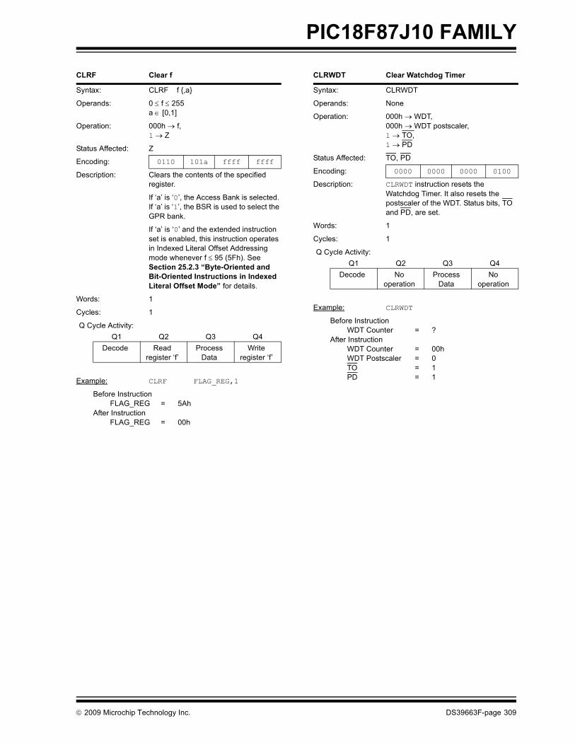
PIC18F87J10 FAMILY
CLRF Clear f
Syntax: CLRF f ,a
Operands: 0 ≤ f ≤ 255a ∈ [0,1]
Operation: 000h → f,1 → Z
Status Affected: Z
Encoding: 0110 101a ffff ffff
Description: Clears the contents of the specified register.
If ‘a’ is ‘0’, the Access Bank is selected. If ‘a’ is ‘1’, the BSR is used to select the GPR bank.
If ‘a’ is ‘0’ and the extended instruction set is enabled, this instruction operates in Indexed Literal Offset Addressing mode whenever f ≤ 95 (5Fh). See Section 25.2.3 “Byte-Oriented and Bit-Oriented Instructions in Indexed Literal Offset Mode” for details.
Words: 1
Cycles: 1
Q Cycle Activity:Q1 Q2 Q3 Q4
Decode Readregister ‘f’
Process Data
Writeregister ‘f’
Example: CLRF FLAG_REG,1
Before InstructionFLAG_REG = 5Ah
After InstructionFLAG_REG = 00h
CLRWDT Clear Watchdog Timer
Syntax: CLRWDT
Operands: None
Operation: 000h → WDT,000h → WDT postscaler,1 → TO,1 → PD
Status Affected: TO, PD
Encoding: 0000 0000 0000 0100
Description: CLRWDT instruction resets the Watchdog Timer. It also resets the postscaler of the WDT. Status bits, TO and PD, are set.
Words: 1
Cycles: 1
Q Cycle Activity:Q1 Q2 Q3 Q4
Decode No operation
Process Data
No operation
Example: CLRWDT
Before InstructionWDT Counter = ?
After InstructionWDT Counter = 00hWDT Postscaler = 0TO = 1PD = 1
© 2009 Microchip Technology Inc. DS39663F-page 309

PIC18F87J10 FAMILY
COMF Complement f
Syntax: COMF f ,d ,a
Operands: 0 ≤ f ≤ 255d ∈ [0,1]a ∈ [0,1]
Operation: f → dest
Status Affected: N, Z
Encoding: 0001 11da ffff ffff
Description: The contents of register ‘f’ are complemented. If ‘d’ is ‘0’, the result is stored in W. If ‘d’ is ‘1’, the result is stored back in register ‘f’.
If ‘a’ is ‘0’, the Access Bank is selected. If ‘a’ is ‘1’, the BSR is used to select the GPR bank.
If ‘a’ is ‘0’ and the extended instruction set is enabled, this instruction operates in Indexed Literal Offset Addressing mode whenever f ≤ 95 (5Fh). See Section 25.2.3 “Byte-Oriented and Bit-Oriented Instructions in Indexed Literal Offset Mode” for details.
Words: 1
Cycles: 1
Q Cycle Activity:Q1 Q2 Q3 Q4
Decode Readregister ‘f’
Process Data
Write todestination
Example: COMF REG, 0, 0
Before InstructionREG = 13h
After InstructionREG = 13hW = ECh
CPFSEQ Compare f with W, Skip if f = W
Syntax: CPFSEQ f ,aOperands: 0 ≤ f ≤ 255
a ∈ [0,1]Operation: (f) – (W),
skip if (f) = (W) (unsigned comparison)
Status Affected: NoneEncoding: 0110 001a ffff ffff
Description: Compares the contents of data memory location ‘f’ to the contents of W by performing an unsigned subtraction.
If ‘f’ = W, then the fetched instruction is discarded and a NOP is executed instead, making this a two-cycle instruction.
If ‘a’ is ‘0’, the Access Bank is selected. If ‘a’ is ‘1’, the BSR is used to select the GPR bank.
If ‘a’ is ‘0’ and the extended instruction set is enabled, this instruction operates in Indexed Literal Offset Addressing mode whenever f ≤ 95 (5Fh). See Section 25.2.3 “Byte-Oriented and Bit-Oriented Instructions in Indexed Literal Offset Mode” for details.
Words: 1Cycles: 1(2)
Note: 3 cycles if skip and followedby a 2-word instruction.
Q Cycle Activity:Q1 Q2 Q3 Q4
Decode Readregister ‘f’
Process Data
No operation
If skip:Q1 Q2 Q3 Q4No
operationNo
operationNo
operationNo
operationIf skip and followed by 2-word instruction:
Q1 Q2 Q3 Q4No
operationNo
operationNo
operationNo
operationNo
operationNo
operationNo
operationNo
operation
Example: HERE CPFSEQ REG, 0NEQUAL :EQUAL :
Before InstructionPC Address = HEREW = ?REG = ?
After InstructionIf REG = W;
PC = Address (EQUAL)If REG ≠ W;
PC = Address (NEQUAL)
DS39663F-page 310 © 2009 Microchip Technology Inc.

PIC18F87J10 FAMILY
CPFSGT Compare f with W, Skip if f > W
Syntax: CPFSGT f ,aOperands: 0 ≤ f ≤ 255
a ∈ [0,1]Operation: (f) – (W),
skip if (f) > (W) (unsigned comparison)
Status Affected: NoneEncoding: 0110 010a ffff ffff
Description: Compares the contents of data memory location ‘f’ to the contents of the W by performing an unsigned subtraction.
If the contents of ‘f’ are greater than the contents of WREG, then the fetched instruction is discarded and a NOP is executed instead, making this a two-cycle instruction.
If ‘a’ is ‘0’, the Access Bank is selected. If ‘a’ is ‘1’, the BSR is used to select the GPR bank.
If ‘a’ is ‘0’ and the extended instruction set is enabled, this instruction operates in Indexed Literal Offset Addressing mode whenever f ≤ 95 (5Fh). See Section 25.2.3 “Byte-Oriented and Bit-Oriented Instructions in Indexed Literal Offset Mode” for details.
Words: 1Cycles: 1(2)
Note: 3 cycles if skip and followedby a 2-word instruction.
Q Cycle Activity:Q1 Q2 Q3 Q4
Decode Readregister ‘f’
Process Data
No operation
If skip:Q1 Q2 Q3 Q4No
operationNo
operationNo
operationNo
operationIf skip and followed by 2-word instruction:
Q1 Q2 Q3 Q4No
operationNo
operationNo
operationNo
operationNo
operationNo
operationNo
operationNo
operation
Example: HERE CPFSGT REG, 0NGREATER :GREATER :
Before InstructionPC = Address (HERE)W = ?
After InstructionIf REG > W;
PC = Address (GREATER)If REG ≤ W;
PC = Address (NGREATER)
CPFSLT Compare f with W, Skip if f < W
Syntax: CPFSLT f ,a
Operands: 0 ≤ f ≤ 255a ∈ [0,1]
Operation: (f) – (W),skip if (f) < (W) (unsigned comparison)
Status Affected: None
Encoding: 0110 000a ffff ffff
Description: Compares the contents of data memory location ‘f’ to the contents of W by performing an unsigned subtraction.
If the contents of ‘f’ are less than the contents of W, then the fetched instruction is discarded and a NOP is executed instead, making this a two-cycle instruction.
If ‘a’ is ‘0’, the Access Bank is selected. If ‘a’ is ‘1’, the BSR is used to select the GPR bank.
Words: 1
Cycles: 1(2)Note: 3 cycles if skip and followed
by a 2-word instruction.
Q Cycle Activity:Q1 Q2 Q3 Q4
Decode Readregister ‘f’
Process Data
No operation
If skip:Q1 Q2 Q3 Q4No
operationNo
operationNo
operationNo
operationIf skip and followed by 2-word instruction:
Q1 Q2 Q3 Q4No
operationNo
operationNo
operationNo
operationNo
operationNo
operationNo
operationNo
operation
Example: HERE CPFSLT REG, 1NLESS :LESS :
Before InstructionPC = Address (HERE)W = ?
After InstructionIf REG < W;PC = Address (LESS)If REG ≥ W;PC = Address (NLESS)
© 2009 Microchip Technology Inc. DS39663F-page 311

PIC18F87J10 FAMILY
DAW Decimal Adjust W Register
Syntax: DAW
Operands: None
Operation: If [W<3:0> > 9] or [DC = 1] then,(W<3:0>) + 6 → W<3:0>;else, (W<3:0>) → W<3:0>;
If [W<7:4> > 9] or [C = 1] then,(W<7:4>) + 6 → W<7:4>;C = 1,else, (W<7:4>) → W<7:4>
Status Affected: C
Encoding: 0000 0000 0000 0111
Description: DAW adjusts the eight-bit value in W, resulting from the earlier addition of two variables (each in packed BCD format) and produces a correct packed BCD result.
Words: 1
Cycles: 1
Q Cycle Activity:Q1 Q2 Q3 Q4
Decode Readregister W
Process Data
WriteW
Example 1: DAW
Before InstructionW = A5hC = 0DC = 0
After InstructionW = 05hC = 1DC = 0
Example 2:Before Instruction
W = CEhC = 0DC = 0
After InstructionW = 34hC = 1DC = 0
DECF Decrement f
Syntax: DECF f ,d ,a
Operands: 0 ≤ f ≤ 255d ∈ [0,1]a ∈ [0,1]
Operation: (f) – 1 → dest
Status Affected: C, DC, N, OV, Z
Encoding: 0000 01da ffff ffff
Description: Decrement register ‘f’. If ‘d’ is ‘0’, the result is stored in W. If ‘d’ is ‘1’, the result is stored back in register ‘f’.
If ‘a’ is ‘0’, the Access Bank is selected. If ‘a’ is ‘1’, the BSR is used to select the GPR bank.
If ‘a’ is ‘0’ and the extended instruction set is enabled, this instruction operates in Indexed Literal Offset Addressing mode whenever f ≤ 95 (5Fh). See Section 25.2.3 “Byte-Oriented and Bit-Oriented Instructions in Indexed Literal Offset Mode” for details.
Words: 1
Cycles: 1
Q Cycle Activity:Q1 Q2 Q3 Q4
Decode Readregister ‘f’
Process Data
Write to destination
Example: DECF CNT, 1, 0
Before InstructionCNT = 01hZ = 0
After InstructionCNT = 00hZ = 1
DS39663F-page 312 © 2009 Microchip Technology Inc.

PIC18F87J10 FAMILY
DECFSZ Decrement f, Skip if 0
Syntax: DECFSZ f ,d ,a
Operands: 0 ≤ f ≤ 255d ∈ [0,1]a ∈ [0,1]
Operation: (f) – 1 → dest,skip if result = 0
Status Affected: None
Encoding: 0010 11da ffff ffff
Description: The contents of register ‘f’ are decremented. If ‘d’ is ‘0’, the result is placed in W. If ‘d’ is ‘1’, the result is placed back in register ‘f’.
If the result is ‘0’, the next instruction which is already fetched is discarded and a NOP is executed instead, making it a two-cycle instruction.
If ‘a’ is ‘0’, the Access Bank is selected. If ‘a’ is ‘1’, the BSR is used to select the GPR bank.
If ‘a’ is ‘0’ and the extended instruction set is enabled, this instruction operates in Indexed Literal Offset Addressing mode whenever f ≤ 95 (5Fh). See Section 25.2.3 “Byte-Oriented and Bit-Oriented Instructions in Indexed Literal Offset Mode” for details.
Words: 1
Cycles: 1(2)Note: 3 cycles if skip and followed
by a 2-word instruction.
Q Cycle Activity:Q1 Q2 Q3 Q4
Decode Readregister ‘f’
Process Data
Write to destination
If skip:Q1 Q2 Q3 Q4No
operationNo
operationNo
operationNo
operationIf skip and followed by 2-word instruction:
Q1 Q2 Q3 Q4No
operationNo
operationNo
operationNo
operationNo
operationNo
operationNo
operationNo
operation
Example: HERE DECFSZ CNT, 1, 1 GOTO LOOPCONTINUE
Before InstructionPC = Address (HERE)
After InstructionCNT = CNT – 1If CNT = 0;
PC = Address (CONTINUE)If CNT ≠ 0;
PC = Address (HERE + 2)
DCFSNZ Decrement f, Skip if not 0
Syntax: DCFSNZ f ,d ,a
Operands: 0 ≤ f ≤ 255d ∈ [0,1]a ∈ [0,1]
Operation: (f) – 1 → dest,skip if result ≠ 0
Status Affected: None
Encoding: 0100 11da ffff ffff
Description: The contents of register ‘f’ are decremented. If ‘d’ is ‘0’, the result is placed in W. If ‘d’ is ‘1’, the result is placed back in register ‘f’.
If the result is not ‘0’, the next instruction which is already fetched is discarded and a NOP is executed instead, making it a two-cycle instruction.
If ‘a’ is ‘0’, the Access Bank is selected. If ‘a’ is ‘1’, the BSR is used to select the GPR bank.
If ‘a’ is ‘0’ and the extended instruction set is enabled, this instruction operates in Indexed Literal Offset Addressing mode whenever f ≤ 95 (5Fh). See Section 25.2.3 “Byte-Oriented and Bit-Oriented Instructions in Indexed Literal Offset Mode” for details.
Words: 1
Cycles: 1(2)Note: 3 cycles if skip and followed
by a 2-word instruction.
Q Cycle Activity:Q1 Q2 Q3 Q4
Decode Readregister ‘f’
Process Data
Write to destination
If skip:Q1 Q2 Q3 Q4No
operationNo
operationNo
operationNo
operationIf skip and followed by 2-word instruction:
Q1 Q2 Q3 Q4No
operationNo
operationNo
operationNo
operationNo
operationNo
operationNo
operationNo
operation
Example: HERE DCFSNZ TEMP, 1, 0ZERO : NZERO :
Before InstructionTEMP = ?
After InstructionTEMP = TEMP – 1,If TEMP = 0;
PC = Address (ZERO)If TEMP ≠ 0;
PC = Address (NZERO)
© 2009 Microchip Technology Inc. DS39663F-page 313

PIC18F87J10 FAMILY
GOTO Unconditional Branch
Syntax: GOTO k
Operands: 0 ≤ k ≤ 1048575
Operation: k → PC<20:1>
Status Affected: None
Encoding:1st word (k<7:0>)2nd word(k<19:8>)
11101111
1111k19kkk
k7kkkkkkk
kkkk0kkkk8
Description: GOTO allows an unconditional branch anywhere within entire 2-Mbyte memory range. The 20-bit value ‘k’ is loaded into PC<20:1>. GOTO is always a two-cycle instruction.
Words: 2
Cycles: 2
Q Cycle Activity:Q1 Q2 Q3 Q4
Decode Read literal ‘k’<7:0>,
No operation
Read literal ‘k’<19:8>,
Write to PCNo
operationNo
operationNo
operationNo
operation
Example: GOTO THERE
After InstructionPC = Address (THERE)
INCF Increment f
Syntax: INCF f ,d ,a
Operands: 0 ≤ f ≤ 255d ∈ [0,1]a ∈ [0,1]
Operation: (f) + 1 → dest
Status Affected: C, DC, N, OV, Z
Encoding: 0010 10da ffff ffff
Description: The contents of register ‘f’ are incremented. If ‘d’ is ‘0’, the result is placed in W. If ‘d’ is ‘1’, the result is placed back in register ‘f’.
If ‘a’ is ‘0’, the Access Bank is selected. If ‘a’ is ‘1’, the BSR is used to select the GPR bank.
If ‘a’ is ‘0’ and the extended instruction set is enabled, this instruction operates in Indexed Literal Offset Addressing mode whenever f ≤ 95 (5Fh). See Section 25.2.3 “Byte-Oriented and Bit-Oriented Instructions in Indexed Literal Offset Mode” for details.
Words: 1
Cycles: 1
Q Cycle Activity:Q1 Q2 Q3 Q4
Decode Readregister ‘f’
Process Data
Write to destination
Example: INCF CNT, 1, 0
Before InstructionCNT = FFhZ = 0C = ?DC = ?
After InstructionCNT = 00hZ = 1C = 1DC = 1
DS39663F-page 314 © 2009 Microchip Technology Inc.

PIC18F87J10 FAMILY
INCFSZ Increment f, Skip if 0
Syntax: INCFSZ f ,d ,a
Operands: 0 ≤ f ≤ 255d ∈ [0,1]a ∈ [0,1]
Operation: (f) + 1 → dest,skip if result = 0
Status Affected: None
Encoding: 0011 11da ffff ffff
Description: The contents of register ‘f’ are incremented. If ‘d’ is ‘0’, the result is placed in W. If ‘d’ is ‘1’, the result is placed back in register ‘f’.
If the result is ‘0’, the next instruction which is already fetched is discarded and a NOP is executed instead, making it a two-cycle instruction.
If ‘a’ is ‘0’, the Access Bank is selected. If ‘a’ is ‘1’, the BSR is used to select the GPR bank.
If ‘a’ is ‘0’ and the extended instruction set is enabled, this instruction operates in Indexed Literal Offset Addressing mode whenever f ≤ 95 (5Fh). See Section 25.2.3 “Byte-Oriented and Bit-Oriented Instructions in Indexed Literal Offset Mode” for details.
Words: 1
Cycles: 1(2)Note: 3 cycles if skip and followed
by a 2-word instruction.
Q Cycle Activity:Q1 Q2 Q3 Q4
Decode Readregister ‘f’
Process Data
Write to destination
If skip:Q1 Q2 Q3 Q4No
operationNo
operationNo
operationNo
operationIf skip and followed by 2-word instruction:
Q1 Q2 Q3 Q4No
operationNo
operationNo
operationNo
operationNo
operationNo
operationNo
operationNo
operation
Example: HERE INCFSZ CNT, 1, 0NZERO : ZERO :
Before InstructionPC = Address (HERE)
After InstructionCNT = CNT + 1If CNT = 0;PC = Address (ZERO)If CNT ≠ 0;PC = Address (NZERO)
INFSNZ Increment f, Skip if not 0
Syntax: INFSNZ f ,d ,aOperands: 0 ≤ f ≤ 255
d ∈ [0,1]a ∈ [0,1]
Operation: (f) + 1 → dest, skip if result ≠ 0
Status Affected: NoneEncoding: 0100 10da ffff ffff
Description: The contents of register ‘f’ are incremented. If ‘d’ is ‘0’, the result is placed in W. If ‘d’ is ‘1’, the result is placed back in register ‘f’.
If the result is not ‘0’, the next instruction which is already fetched is discarded and a NOP is executed instead, making it a two-cycle instruction.
If ‘a’ is ‘0’, the Access Bank is selected. If ‘a’ is ‘1’, the BSR is used to select the GPR bank.
If ‘a’ is ‘0’ and the extended instruction set is enabled, this instruction operates in Indexed Literal Offset Addressing mode whenever f ≤ 95 (5Fh). See Section 25.2.3 “Byte-Oriented and Bit-Oriented Instructions in Indexed Literal Offset Mode” for details.
Words: 1Cycles: 1(2)
Note: 3 cycles if skip and followedby a 2-word instruction.
Q Cycle Activity:Q1 Q2 Q3 Q4
Decode Readregister ‘f’
Process Data
Write to destination
If skip:Q1 Q2 Q3 Q4No
operationNo
operationNo
operationNo
operationIf skip and followed by 2-word instruction:
Q1 Q2 Q3 Q4No
operationNo
operationNo
operationNo
operationNo
operationNo
operationNo
operationNo
operation
Example: HERE INFSNZ REG, 1, 0ZERONZERO
Before InstructionPC = Address (HERE)
After InstructionREG = REG + 1If REG ≠ 0;PC = Address (NZERO)If REG = 0;PC = Address (ZERO)
© 2009 Microchip Technology Inc. DS39663F-page 315
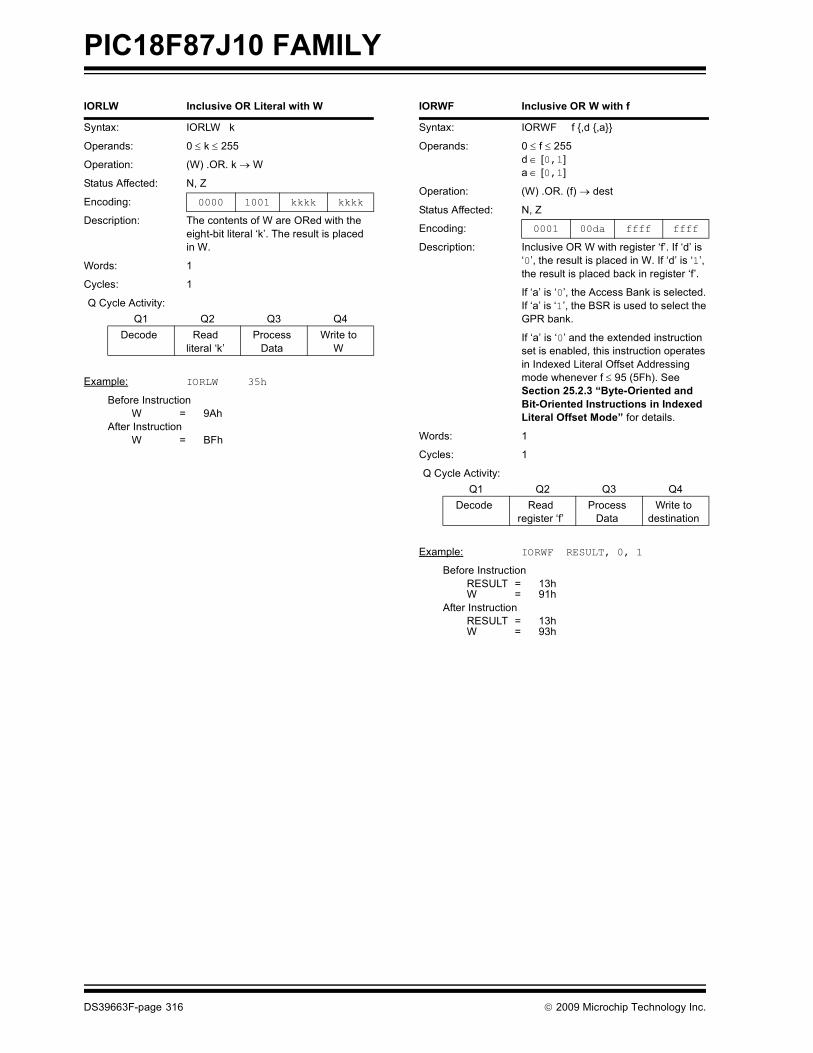
PIC18F87J10 FAMILY
IORLW Inclusive OR Literal with W
Syntax: IORLW k
Operands: 0 ≤ k ≤ 255
Operation: (W) .OR. k → W
Status Affected: N, Z
Encoding: 0000 1001 kkkk kkkk
Description: The contents of W are ORed with the eight-bit literal ‘k’. The result is placed in W.
Words: 1
Cycles: 1
Q Cycle Activity:Q1 Q2 Q3 Q4
Decode Read literal ‘k’
Process Data
Write to W
Example: IORLW 35h
Before InstructionW = 9Ah
After InstructionW = BFh
IORWF Inclusive OR W with f
Syntax: IORWF f ,d ,a
Operands: 0 ≤ f ≤ 255d ∈ [0,1]a ∈ [0,1]
Operation: (W) .OR. (f) → dest
Status Affected: N, Z
Encoding: 0001 00da ffff ffff
Description: Inclusive OR W with register ‘f’. If ‘d’ is ‘0’, the result is placed in W. If ‘d’ is ‘1’, the result is placed back in register ‘f’.
If ‘a’ is ‘0’, the Access Bank is selected. If ‘a’ is ‘1’, the BSR is used to select the GPR bank.
If ‘a’ is ‘0’ and the extended instruction set is enabled, this instruction operates in Indexed Literal Offset Addressing mode whenever f ≤ 95 (5Fh). See Section 25.2.3 “Byte-Oriented and Bit-Oriented Instructions in Indexed Literal Offset Mode” for details.
Words: 1
Cycles: 1
Q Cycle Activity:Q1 Q2 Q3 Q4
Decode Readregister ‘f’
Process Data
Write to destination
Example: IORWF RESULT, 0, 1
Before InstructionRESULT = 13hW = 91h
After InstructionRESULT = 13hW = 93h
DS39663F-page 316 © 2009 Microchip Technology Inc.

PIC18F87J10 FAMILY
LFSR Load FSR
Syntax: LFSR f, k
Operands: 0 ≤ f ≤ 20 ≤ k ≤ 4095
Operation: k → FSRf
Status Affected: None
Encoding: 11101111
11100000
00ffk7kkk
k11kkkkkkk
Description: The 12-bit literal ‘k’ is loaded into the file select register pointed to by ‘f’.
Words: 2
Cycles: 2
Q Cycle Activity:Q1 Q2 Q3 Q4
Decode Read literal ‘k’ MSB
Process Data
Writeliteral ‘k’ MSB to FSRfH
Decode Read literal ‘k’ LSB
Process Data
Write literal ‘k’ to FSRfL
Example: LFSR 2, 3ABh
After InstructionFSR2H = 03hFSR2L = ABh
MOVF Move f
Syntax: MOVF f ,d ,a
Operands: 0 ≤ f ≤ 255d ∈ [0,1]a ∈ [0,1]
Operation: f → dest
Status Affected: N, Z
Encoding: 0101 00da ffff ffff
Description: The contents of register ‘f’ are moved to a destination dependent upon the status of ‘d’. If ‘d’ is ‘0’, the result is placed in W. If ‘d’ is ‘1’, the result is placed back in register ‘f’. Location ‘f’ can be anywhere in the 256-byte bank.
If ‘a’ is ‘0’, the Access Bank is selected. If ‘a’ is ‘1’, the BSR is used to select the GPR bank.
If ‘a’ is ‘0’ and the extended instruction set is enabled, this instruction operates in Indexed Literal Offset Addressing mode whenever f ≤ 95 (5Fh). See Section 25.2.3 “Byte-Oriented and Bit-Oriented Instructions in Indexed Literal Offset Mode” for details.
Words: 1
Cycles: 1
Q Cycle Activity:Q1 Q2 Q3 Q4
Decode Readregister ‘f’
Process Data
Write W
Example: MOVF REG, 0, 0
Before InstructionREG = 22hW = FFh
After InstructionREG = 22hW = 22h
© 2009 Microchip Technology Inc. DS39663F-page 317

PIC18F87J10 FAMILY
MOVFF Move f to f
Syntax: MOVFF fs,fdOperands: 0 ≤ fs ≤ 4095
0 ≤ fd ≤ 4095
Operation: (fs) → fdStatus Affected: None
Encoding:1st word (source)2nd word (destin.)
11001111
ffffffff
ffffffff
ffffsffffd
Description: The contents of source register ‘fs’ are moved to destination register ‘fd’. Location of source ‘fs’ can be anywhere in the 4096-byte data space (000h to FFFh) and location of destination ‘fd’ can also be anywhere from 000h to FFFh.
Either source or destination can be W (a useful special situation).
MOVFF is particularly useful for transferring a data memory location to a peripheral register (such as the transmit buffer or an I/O port).
The MOVFF instruction cannot use the PCL, TOSU, TOSH or TOSL as the destination register
Words: 2
Cycles: 2
Q Cycle Activity:Q1 Q2 Q3 Q4
Decode Readregister ‘f’
(src)
Process Data
No operation
Decode No operation
No dummy read
No operation
Write register ‘f’
(dest)
Example: MOVFF REG1, REG2
Before InstructionREG1 = 33hREG2 = 11h
After InstructionREG1 = 33hREG2 = 33h
MOVLB Move Literal to Low Nibble in BSR
Syntax: MOVLW k
Operands: 0 ≤ k ≤ 255
Operation: k → BSR
Status Affected: None
Encoding: 0000 0001 kkkk kkkk
Description: The eight-bit literal ‘k’ is loaded into the Bank Select Register (BSR). The value of BSR<7:4> always remains ‘0’ regardless of the value of k7:k4.
Words: 1
Cycles: 1
Q Cycle Activity:Q1 Q2 Q3 Q4
Decode Readliteral ‘k’
Process Data
Write literal ‘k’ to BSR
Example: MOVLB 5
Before InstructionBSR Register = 02h
After InstructionBSR Register = 05h
DS39663F-page 318 © 2009 Microchip Technology Inc.

PIC18F87J10 FAMILY
MOVLW Move Literal to W
Syntax: MOVLW k
Operands: 0 ≤ k ≤ 255
Operation: k → W
Status Affected: None
Encoding: 0000 1110 kkkk kkkk
Description: The eight-bit literal ‘k’ is loaded into W.
Words: 1
Cycles: 1
Q Cycle Activity:Q1 Q2 Q3 Q4
Decode Readliteral ‘k’
Process Data
Write to W
Example: MOVLW 5Ah
After InstructionW = 5Ah
MOVWF Move W to f
Syntax: MOVWF f ,a
Operands: 0 ≤ f ≤ 255a ∈ [0,1]
Operation: (W) → f
Status Affected: None
Encoding: 0110 111a ffff ffff
Description: Move data from W to register ‘f’. Location ‘f’ can be anywhere in the 256-byte bank.
If ‘a’ is ‘0’, the Access Bank is selected. If ‘a’ is ‘1’, the BSR is used to select the GPR bank.
If ‘a’ is ‘0’ and the extended instruction set is enabled, this instruction operates in Indexed Literal Offset Addressing mode whenever f ≤ 95 (5Fh). See Section 25.2.3 “Byte-Oriented and Bit-Oriented Instructions in Indexed Literal Offset Mode” for details.
Words: 1
Cycles: 1
Q Cycle Activity:Q1 Q2 Q3 Q4
Decode Readregister ‘f’
Process Data
Writeregister ‘f’
Example: MOVWF REG, 0
Before InstructionW = 4FhREG = FFh
After InstructionW = 4FhREG = 4Fh
© 2009 Microchip Technology Inc. DS39663F-page 319

PIC18F87J10 FAMILY
MULLW Multiply Literal with W
Syntax: MULLW k
Operands: 0 ≤ k ≤ 255
Operation: (W) x k → PRODH:PRODL
Status Affected: None
Encoding: 0000 1101 kkkk kkkk
Description: An unsigned multiplication is carried out between the contents of W and the 8-bit literal ‘k’. The 16-bit result is placed in PRODH:PRODL register pair. PRODH contains the high byte.
W is unchanged.
None of the Status flags are affected.
Note that neither Overflow nor Carry is possible in this operation. A Zero result is possible but not detected.
Words: 1
Cycles: 1
Q Cycle Activity:Q1 Q2 Q3 Q4
Decode Read literal ‘k’
Process Data
Write registers PRODH:PRODL
Example: MULLW 0C4h
Before InstructionW = E2hPRODH = ?PRODL = ?
After InstructionW = E2hPRODH = ADhPRODL = 08h
MULWF Multiply W with f
Syntax: MULWF f ,a
Operands: 0 ≤ f ≤ 255a ∈ [0,1]
Operation: (W) x (f) → PRODH:PRODL
Status Affected: None
Encoding: 0000 001a ffff ffff
Description: An unsigned multiplication is carried out between the contents of W and the register file location ‘f’. The 16-bit result is stored in the PRODH:PRODL register pair. PRODH contains the high byte. Both W and ‘f’ are unchanged.
None of the Status flags are affected.
Note that neither Overflow nor Carry is possible in this operation. A Zero result is possible but not detected.
If ‘a’ is ‘0’, the Access Bank is selected. If ‘a’ is ‘1’, the BSR is used to select the GPR bank.
If ‘a’ is ‘0’ and the extended instruction set is enabled, this instruction operates in Indexed Literal Offset Addressing mode whenever f ≤ 95 (5Fh). See Section 25.2.3 “Byte-Oriented and Bit-Oriented Instructions in Indexed Literal Offset Mode” for details.
Words: 1
Cycles: 1
Q Cycle Activity:Q1 Q2 Q3 Q4
Decode Readregister ‘f’
Process Data
Writeregisters PRODH:PRODL
Example: MULWF REG, 1
Before InstructionW = C4hREG = B5hPRODH = ?PRODL = ?
After InstructionW = C4hREG = B5hPRODH = 8AhPRODL = 94h
DS39663F-page 320 © 2009 Microchip Technology Inc.

PIC18F87J10 FAMILY
NEGF Negate f
Syntax: NEGF f ,a
Operands: 0 ≤ f ≤ 255a ∈ [0,1]
Operation: (f) + 1 → f
Status Affected: N, OV, C, DC, Z
Encoding: 0110 110a ffff ffff
Description: Location ‘f’ is negated using two’s complement. The result is placed in the data memory location ‘f’.
If ‘a’ is ‘0’, the Access Bank is selected. If ‘a’ is ‘1’, the BSR is used to select the GPR bank.
If ‘a’ is ‘0’ and the extended instruction set is enabled, this instruction operates in Indexed Literal Offset Addressing mode whenever f ≤ 95 (5Fh). See Section 25.2.3 “Byte-Oriented and Bit-Oriented Instructions in Indexed Literal Offset Mode” for details.
Words: 1
Cycles: 1
Q Cycle Activity:Q1 Q2 Q3 Q4
Decode Readregister ‘f’
Process Data
Write register ‘f’
Example: NEGF REG, 1
Before InstructionREG = 0011 1010 [3Ah]
After InstructionREG = 1100 0110 [C6h]
NOP No Operation
Syntax: NOP
Operands: None
Operation: No operation
Status Affected: None
Encoding: 00001111
0000xxxx
0000xxxx
0000xxxx
Description: No operation.
Words: 1
Cycles: 1
Q Cycle Activity:Q1 Q2 Q3 Q4
Decode No operation
No operation
No operation
Example:
None.
© 2009 Microchip Technology Inc. DS39663F-page 321
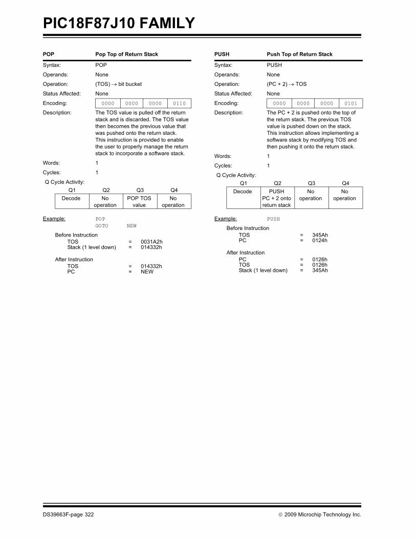
PIC18F87J10 FAMILY
POP Pop Top of Return Stack
Syntax: POP
Operands: None
Operation: (TOS) → bit bucket
Status Affected: None
Encoding: 0000 0000 0000 0110
Description: The TOS value is pulled off the return stack and is discarded. The TOS value then becomes the previous value that was pushed onto the return stack.This instruction is provided to enable the user to properly manage the return stack to incorporate a software stack.
Words: 1
Cycles: 1
Q Cycle Activity:Q1 Q2 Q3 Q4
Decode Nooperation
POP TOS value
Nooperation
Example: POPGOTO NEW
Before InstructionTOS = 0031A2hStack (1 level down) = 014332h
After InstructionTOS = 014332hPC = NEW
PUSH Push Top of Return Stack
Syntax: PUSH
Operands: None
Operation: (PC + 2) → TOS
Status Affected: None
Encoding: 0000 0000 0000 0101
Description: The PC + 2 is pushed onto the top of the return stack. The previous TOS value is pushed down on the stack.This instruction allows implementing a software stack by modifying TOS and then pushing it onto the return stack.
Words: 1
Cycles: 1
Q Cycle Activity:Q1 Q2 Q3 Q4
Decode PUSH PC + 2 onto return stack
No operation
No operation
Example: PUSH
Before InstructionTOS = 345AhPC = 0124h
After InstructionPC = 0126hTOS = 0126hStack (1 level down) = 345Ah
DS39663F-page 322 © 2009 Microchip Technology Inc.
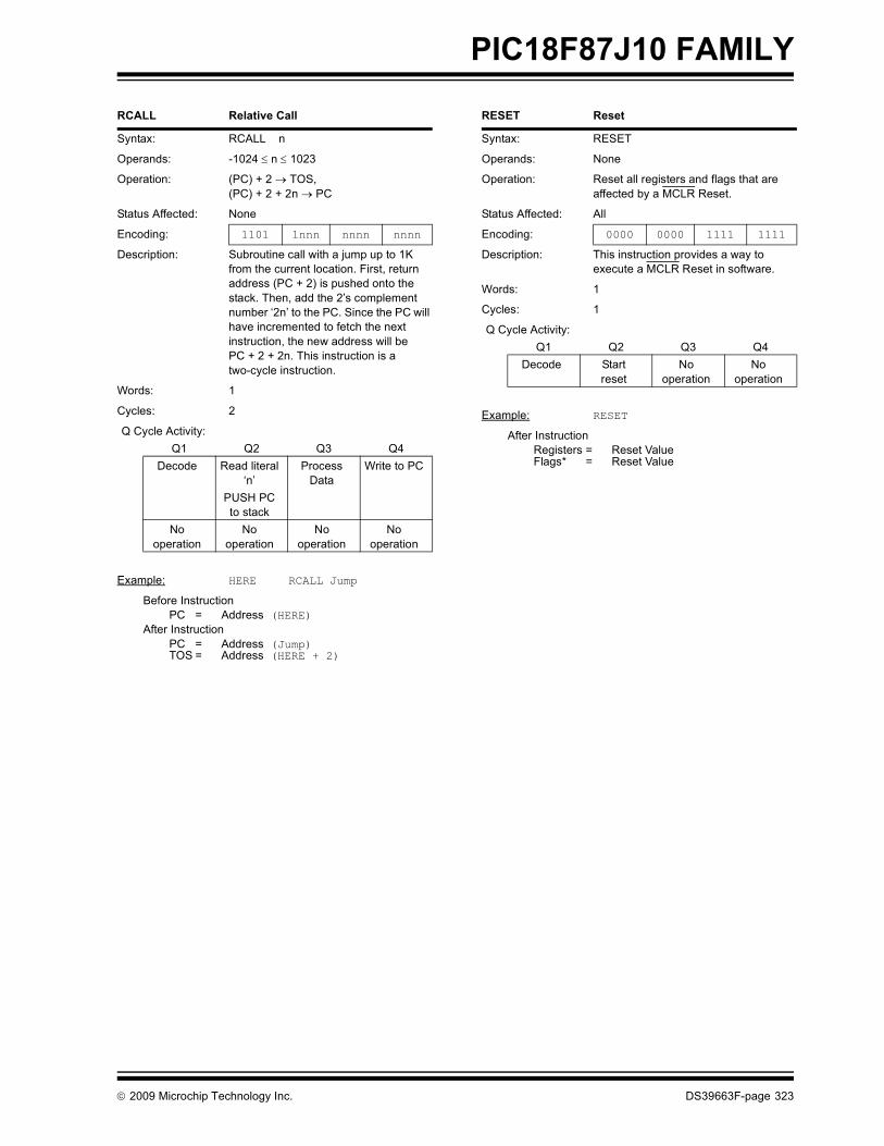
PIC18F87J10 FAMILY
RCALL Relative Call
Syntax: RCALL n
Operands: -1024 ≤ n ≤ 1023
Operation: (PC) + 2 → TOS,(PC) + 2 + 2n → PC
Status Affected: None
Encoding: 1101 1nnn nnnn nnnn
Description: Subroutine call with a jump up to 1K from the current location. First, return address (PC + 2) is pushed onto the stack. Then, add the 2’s complement number ‘2n’ to the PC. Since the PC will have incremented to fetch the next instruction, the new address will be PC + 2 + 2n. This instruction is a two-cycle instruction.
Words: 1
Cycles: 2
Q Cycle Activity:Q1 Q2 Q3 Q4
Decode Read literal ‘n’
PUSH PC to stack
Process Data
Write to PC
No operation
No operation
No operation
No operation
Example: HERE RCALL Jump
Before InstructionPC = Address (HERE)
After InstructionPC = Address (Jump)TOS = Address (HERE + 2)
RESET Reset
Syntax: RESET
Operands: None
Operation: Reset all registers and flags that are affected by a MCLR Reset.
Status Affected: All
Encoding: 0000 0000 1111 1111
Description: This instruction provides a way to execute a MCLR Reset in software.
Words: 1
Cycles: 1
Q Cycle Activity:Q1 Q2 Q3 Q4
Decode Start reset
No operation
No operation
Example: RESET
After InstructionRegisters = Reset ValueFlags* = Reset Value
© 2009 Microchip Technology Inc. DS39663F-page 323

PIC18F87J10 FAMILY
RETFIE Return from Interrupt
Syntax: RETFIE s
Operands: s ∈ [0,1]
Operation: (TOS) → PC,1 → GIE/GIEH or PEIE/GIEL;if s = 1,(WS) → W,(STATUSS) → STATUS,(BSRS) → BSR,PCLATU, PCLATH are unchanged
Status Affected: GIE/GIEH, PEIE/GIEL.
Encoding: 0000 0000 0001 000s
Description: Return from interrupt. Stack is popped and Top-of-Stack (TOS) is loaded into the PC. Interrupts are enabled by setting either the high or low-priority global interrupt enable bit. If ‘s’ = 1, the contents of the shadow registers WS, STATUSS and BSRS are loaded into their corresponding registers W, STATUS and BSR. If ‘s’ = 0, no update of these registers occurs.
Words: 1
Cycles: 2
Q Cycle Activity:Q1 Q2 Q3 Q4
Decode No operation
No operation
POP PC from stack
Set GIEH or GIEL
No operation
No operation
No operation
No operation
Example: RETFIE 1
After InterruptPC = TOSW = WSBSR = BSRSSTATUS = STATUSSGIE/GIEH, PEIE/GIEL = 1
RETLW Return Literal to W
Syntax: RETLW k
Operands: 0 ≤ k ≤ 255
Operation: k → W,(TOS) → PC,PCLATU, PCLATH are unchanged
Status Affected: None
Encoding: 0000 1100 kkkk kkkk
Description: W is loaded with the eight-bit literal ‘k’. The program counter is loaded from the top of the stack (the return address). The high address latch (PCLATH) remains unchanged.
Words: 1
Cycles: 2
Q Cycle Activity:Q1 Q2 Q3 Q4
Decode Readliteral ‘k’
Process Data
POP PC from stack, write to W
No operation
No operation
No operation
No operation
Example:
CALL TABLE ; W contains table ; offset value ; W now has ; table value :TABLE
ADDWF PCL ; W = offsetRETLW k0 ; Begin tableRETLW k1 ;
: :
RETLW kn ; End of table
Before InstructionW = 07h
After InstructionW = value of kn
DS39663F-page 324 © 2009 Microchip Technology Inc.
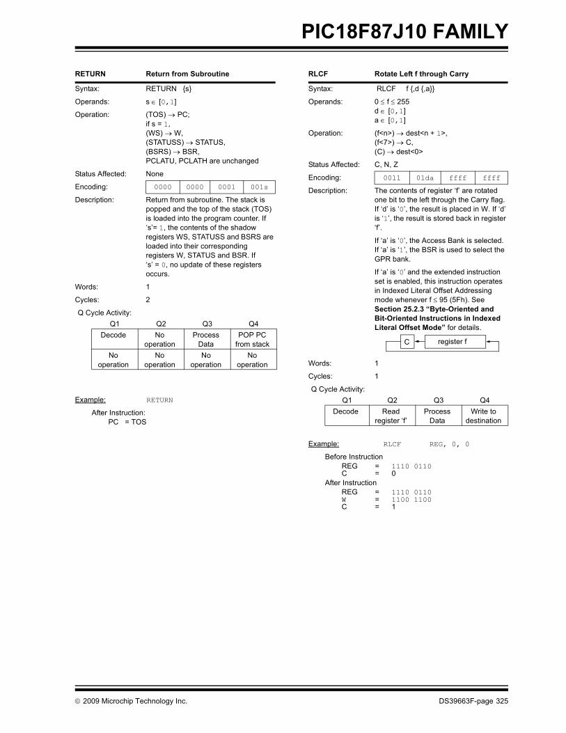
PIC18F87J10 FAMILY
RETURN Return from Subroutine
Syntax: RETURN s
Operands: s ∈ [0,1]
Operation: (TOS) → PC;if s = 1,(WS) → W,(STATUSS) → STATUS,(BSRS) → BSR,PCLATU, PCLATH are unchanged
Status Affected: None
Encoding: 0000 0000 0001 001s
Description: Return from subroutine. The stack is popped and the top of the stack (TOS) is loaded into the program counter. If ‘s’= 1, the contents of the shadow registers WS, STATUSS and BSRS are loaded into their corresponding registers W, STATUS and BSR. If ‘s’ = 0, no update of these registers occurs.
Words: 1
Cycles: 2
Q Cycle Activity:Q1 Q2 Q3 Q4
Decode No operation
Process Data
POP PC from stack
No operation
No operation
No operation
No operation
Example: RETURN
After Instruction:PC = TOS
RLCF Rotate Left f through Carry
Syntax: RLCF f ,d ,a
Operands: 0 ≤ f ≤ 255d ∈ [0,1]a ∈ [0,1]
Operation: (f<n>) → dest<n + 1>,(f<7>) → C,(C) → dest<0>
Status Affected: C, N, Z
Encoding: 0011 01da ffff ffff
Description: The contents of register ‘f’ are rotated one bit to the left through the Carry flag. If ‘d’ is ‘0’, the result is placed in W. If ‘d’ is ‘1’, the result is stored back in register ‘f’.
If ‘a’ is ‘0’, the Access Bank is selected. If ‘a’ is ‘1’, the BSR is used to select the GPR bank.
If ‘a’ is ‘0’ and the extended instruction set is enabled, this instruction operates in Indexed Literal Offset Addressing mode whenever f ≤ 95 (5Fh). See Section 25.2.3 “Byte-Oriented and Bit-Oriented Instructions in Indexed Literal Offset Mode” for details.
Words: 1
Cycles: 1
Q Cycle Activity:Q1 Q2 Q3 Q4
Decode Readregister ‘f’
Process Data
Write to destination
Example: RLCF REG, 0, 0
Before InstructionREG = 1110 0110C = 0
After InstructionREG = 1110 0110W = 1100 1100C = 1
C register f
© 2009 Microchip Technology Inc. DS39663F-page 325

PIC18F87J10 FAMILY
RLNCF Rotate Left f (No Carry)
Syntax: RLNCF f ,d ,a
Operands: 0 ≤ f ≤ 255d ∈ [0,1]a ∈ [0,1]
Operation: (f<n>) → dest<n + 1>,(f<7>) → dest<0>
Status Affected: N, Z
Encoding: 0100 01da ffff ffff
Description: The contents of register ‘f’ are rotated one bit to the left. If ‘d’ is ‘0’, the result is placed in W. If ‘d’ is ‘1’, the result is stored back in register ‘f’.
If ‘a’ is ‘0’, the Access Bank is selected. If ‘a’ is ‘1’, the BSR is used to select the GPR bank.
If ‘a’ is ‘0’ and the extended instruction set is enabled, this instruction operates in Indexed Literal Offset Addressing mode whenever f ≤ 95 (5Fh). See Section 25.2.3 “Byte-Oriented and Bit-Oriented Instructions in Indexed Literal Offset Mode” for details.
Words: 1
Cycles: 1
Q Cycle Activity:Q1 Q2 Q3 Q4
Decode Readregister ‘f’
Process Data
Write to destination
Example: RLNCF REG, 1, 0
Before InstructionREG = 1010 1011
After InstructionREG = 0101 0111
register f
RRCF Rotate Right f through Carry
Syntax: RRCF f ,d ,a
Operands: 0 ≤ f ≤ 255d ∈ [0,1]a ∈ [0,1]
Operation: (f<n>) → dest<n – 1>,(f<0>) → C,(C) → dest<7>
Status Affected: C, N, Z
Encoding: 0011 00da ffff ffff
Description: The contents of register ‘f’ are rotated one bit to the right through the Carry flag. If ‘d’ is ‘0’, the result is placed in W. If ‘d’ is ‘1’, the result is placed back in register ‘f’.
If ‘a’ is ‘0’, the Access Bank is selected. If ‘a’ is ‘1’, the BSR is used to select the GPR bank.
If ‘a’ is ‘0’ and the extended instruction set is enabled, this instruction operates in Indexed Literal Offset Addressing mode whenever f ≤ 95 (5Fh). See Section 25.2.3 “Byte-Oriented and Bit-Oriented Instructions in Indexed Literal Offset Mode” for details.
Words: 1
Cycles: 1
Q Cycle Activity:Q1 Q2 Q3 Q4
Decode Readregister ‘f’
Process Data
Write to destination
Example: RRCF REG, 0, 0
Before InstructionREG = 1110 0110C = 0
After InstructionREG = 1110 0110W = 0111 0011C = 0
C register f
DS39663F-page 326 © 2009 Microchip Technology Inc.

PIC18F87J10 FAMILY
RRNCF Rotate Right f (No Carry)
Syntax: RRNCF f ,d ,a
Operands: 0 ≤ f ≤ 255d ∈ [0,1]a ∈ [0,1]
Operation: (f<n>) → dest<n – 1>,(f<0>) → dest<7>
Status Affected: N, Z
Encoding: 0100 00da ffff ffff
Description: The contents of register ‘f’ are rotated one bit to the right. If ‘d’ is ‘0’, the result is placed in W. If ‘d’ is ‘1’, the result is placed back in register ‘f’.
If ‘a’ is ‘0’, the Access Bank will be selected, overriding the BSR value. If ‘a’ is ‘1’, then the bank will be selected as per the BSR value.
If ‘a’ is ‘0’ and the extended instruction set is enabled, this instruction operates in Indexed Literal Offset Addressing mode whenever f ≤ 95 (5Fh). See Section 25.2.3 “Byte-Oriented and Bit-Oriented Instructions in Indexed Literal Offset Mode” for details.
Words: 1
Cycles: 1
Q Cycle Activity:Q1 Q2 Q3 Q4
Decode Readregister ‘f’
Process Data
Write to destination
Example 1: RRNCF REG, 1, 0
Before InstructionREG = 1101 0111
After InstructionREG = 1110 1011
Example 2: RRNCF REG, 0, 0
Before InstructionW = ?REG = 1101 0111
After InstructionW = 1110 1011REG = 1101 0111
register f
SETF Set f
Syntax: SETF f ,a
Operands: 0 ≤ f ≤ 255a ∈ [0,1]
Operation: FFh → f
Status Affected: None
Encoding: 0110 100a ffff ffff
Description: The contents of the specified register are set to FFh.
If ‘a’ is ‘0’, the Access Bank is selected. If ‘a’ is ‘1’, the BSR is used to select the GPR bank.
If ‘a’ is ‘0’ and the extended instruction set is enabled, this instruction operates in Indexed Literal Offset Addressing mode whenever f ≤ 95 (5Fh). See Section 25.2.3 “Byte-Oriented and Bit-Oriented Instructions in Indexed Literal Offset Mode” for details.
Words: 1
Cycles: 1
Q Cycle Activity:Q1 Q2 Q3 Q4
Decode Readregister ‘f’
Process Data
Writeregister ‘f’
Example: SETF REG,1
Before InstructionREG = 5Ah
After InstructionREG = FFh
© 2009 Microchip Technology Inc. DS39663F-page 327
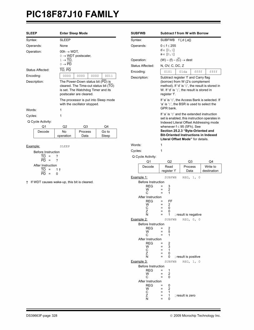
PIC18F87J10 FAMILY
SLEEP Enter Sleep Mode
Syntax: SLEEP
Operands: None
Operation: 00h → WDT,0 → WDT postscaler,1 → TO,0 → PD
Status Affected: TO, PD
Encoding: 0000 0000 0000 0011
Description: The Power-Down status bit (PD) is cleared. The Time-out status bit (TO) is set. The Watchdog Timer and its postscaler are cleared.
The processor is put into Sleep mode with the oscillator stopped.
Words: 1
Cycles: 1
Q Cycle Activity:Q1 Q2 Q3 Q4
Decode No operation
Process Data
Go toSleep
Example: SLEEP
Before InstructionTO = ?PD = ?
After InstructionTO = 1 †PD = 0
† If WDT causes wake-up, this bit is cleared.
SUBFWB Subtract f from W with Borrow
Syntax: SUBFWB f ,d ,a
Operands: 0 ≤ f ≤ 255d ∈ [0,1]a ∈ [0,1]
Operation: (W) – (f) – (C) → dest
Status Affected: N, OV, C, DC, Z
Encoding: 0101 01da ffff ffff
Description: Subtract register ‘f’ and Carry flag (borrow) from W (2’s complement method). If ‘d’ is ‘0’, the result is stored in W. If ‘d’ is ‘1’, the result is stored in register ‘f’.
If ‘a’ is ‘0’, the Access Bank is selected. If ‘a’ is ‘1’, the BSR is used to select the GPR bank.
If ‘a’ is ‘0’ and the extended instruction set is enabled, this instruction operates in Indexed Literal Offset Addressing mode whenever f ≤ 95 (5Fh). See Section 25.2.3 “Byte-Oriented and Bit-Oriented Instructions in Indexed Literal Offset Mode” for details.
Words: 1
Cycles: 1
Q Cycle Activity:Q1 Q2 Q3 Q4
Decode Readregister ‘f’
Process Data
Write to destination
Example 1: SUBFWB REG, 1, 0Before Instruction
REG = 3W = 2C = 1
After InstructionREG = FFW = 2C = 0Z = 0N = 1 ; result is negative
Example 2: SUBFWB REG, 0, 0
Before InstructionREG = 2W = 5C = 1
After InstructionREG = 2W = 3C = 1Z = 0N = 0 ; result is positive
Example 3: SUBFWB REG, 1, 0
Before InstructionREG = 1W = 2C = 0
After InstructionREG = 0W = 2C = 1Z = 1 ; result is zeroN = 0
DS39663F-page 328 © 2009 Microchip Technology Inc.

PIC18F87J10 FAMILY
SUBLW Subtract W from Literal
Syntax: SUBLW k
Operands: 0 ≤ k ≤ 255
Operation: k – (W) → W
Status Affected: N, OV, C, DC, Z
Encoding: 0000 1000 kkkk kkkk
Description: W is subtracted from the eight-bit literal ‘k’. The result is placed in W.
Words: 1
Cycles: 1
Q Cycle Activity:Q1 Q2 Q3 Q4
Decode Readliteral ‘k’
Process Data
Write to W
Example 1: SUBLW 02h
Before InstructionW = 01hC = ?
After InstructionW = 01hC = 1 ; result is positiveZ = 0N = 0
Example 2: SUBLW 02h
Before InstructionW = 02hC = ?
After InstructionW = 00hC = 1 ; result is zeroZ = 1N = 0
Example 3: SUBLW 02h
Before InstructionW = 03hC = ?
After InstructionW = FFh ; (2’s complement)C = 0 ; result is negativeZ = 0N = 1
SUBWF Subtract W from f
Syntax: SUBWF f ,d ,a
Operands: 0 ≤ f ≤ 255d ∈ [0,1]a ∈ [0,1]
Operation: (f) – (W) → dest
Status Affected: N, OV, C, DC, Z
Encoding: 0101 11da ffff ffff
Description: Subtract W from register ‘f’ (2’s complement method). If ‘d’ is ‘0’, the result is stored in W. If ‘d’ is ‘1’, the result is stored back in register ‘f’.
If ‘a’ is ‘0’, the Access Bank is selected. If ‘a’ is ‘1’, the BSR is used to select the GPR bank.
If ‘a’ is ‘0’ and the extended instruction set is enabled, this instruction operates in Indexed Literal Offset Addressing mode whenever f ≤ 95 (5Fh). See Section 25.2.3 “Byte-Oriented and Bit-Oriented Instructions in Indexed Literal Offset Mode” for details.
Words: 1
Cycles: 1
Q Cycle Activity:Q1 Q2 Q3 Q4
Decode Readregister ‘f’
Process Data
Write to destination
Example 1: SUBWF REG, 1, 0
Before InstructionREG = 3W = 2C = ?
After InstructionREG = 1W = 2C = 1 ; result is positiveZ = 0N = 0
Example 2: SUBWF REG, 0, 0
Before InstructionREG = 2W = 2C = ?
After InstructionREG = 2W = 0C = 1 ; result is zeroZ = 1N = 0
Example 3: SUBWF REG, 1, 0
Before InstructionREG = 1W = 2C = ?
After InstructionREG = FFh ;(2’s complement)W = 2C = 0 ; result is negativeZ = 0N = 1
© 2009 Microchip Technology Inc. DS39663F-page 329

PIC18F87J10 FAMILY
SUBWFB Subtract W from f with Borrow
Syntax: SUBWFB f ,d ,aOperands: 0 ≤ f ≤ 255
d ∈ [0,1]a ∈ [0,1]
Operation: (f) – (W) – (C) → destStatus Affected: N, OV, C, DC, ZEncoding: 0101 10da ffff ffff
Description: Subtract W and the Carry flag (borrow) from register ‘f’ (2’s complement method). If ‘d’ is ‘0’, the result is stored in W. If ‘d’ is ‘1’, the result is stored back in register ‘f’.
If ‘a’ is ‘0’, the Access Bank is selected. If ‘a’ is ‘1’, the BSR is used to select the GPR bank.
If ‘a’ is ‘0’ and the extended instruction set is enabled, this instruction operates in Indexed Literal Offset Addressing mode whenever f ≤ 95 (5Fh). See Section 25.2.3 “Byte-Oriented and Bit-Oriented Instructions in Indexed Literal Offset Mode” for details.
Words: 1Cycles: 1Q Cycle Activity:
Q1 Q2 Q3 Q4Decode Read
register ‘f’Process
DataWrite to
destination
Example 1: SUBWFB REG, 1, 0
Before InstructionREG = 19h (0001 1001)W = 0Dh (0000 1101)C = 1
After InstructionREG = 0Ch (0000 1011)W = 0Dh (0000 1101)C = 1Z = 0N = 0 ; result is positive
Example 2: SUBWFB REG, 0, 0
Before InstructionREG = 1Bh (0001 1011)W = 1Ah (0001 1010)C = 0
After InstructionREG = 1Bh (0001 1011)W = 00hC = 1Z = 1 ; result is zeroN = 0
Example 3: SUBWFB REG, 1, 0
Before InstructionREG = 03h (0000 0011)W = 0Eh (0000 1101)C = 1
After InstructionREG = F5h (1111 0100)
; [2’s comp]W = 0Eh (0000 1101)C = 0Z = 0N = 1 ; result is negative
SWAPF Swap f
Syntax: SWAPF f ,d ,a
Operands: 0 ≤ f ≤ 255d ∈ [0,1]a ∈ [0,1]
Operation: (f<3:0>) → dest<7:4>,(f<7:4>) → dest<3:0>
Status Affected: None
Encoding: 0011 10da ffff ffff
Description: The upper and lower nibbles of register ‘f’ are exchanged. If ‘d’ is ‘0’, the result is placed in W. If ‘d’ is ‘1’, the result is placed in register ‘f’.
If ‘a’ is ‘0’, the Access Bank is selected. If ‘a’ is ‘1’, the BSR is used to select the GPR bank.
If ‘a’ is ‘0’ and the extended instruction set is enabled, this instruction operates in Indexed Literal Offset Addressing mode whenever f ≤ 95 (5Fh). See Section 25.2.3 “Byte-Oriented and Bit-Oriented Instructions in Indexed Literal Offset Mode” for details.
Words: 1
Cycles: 1
Q Cycle Activity:Q1 Q2 Q3 Q4
Decode Readregister ‘f’
Process Data
Write to destination
Example: SWAPF REG, 1, 0
Before InstructionREG = 53h
After InstructionREG = 35h
DS39663F-page 330 © 2009 Microchip Technology Inc.

PIC18F87J10 FAMILY
TBLRD Table Read
Syntax: TBLRD ( *; *+; *-; +*)
Operands: None
Operation: if TBLRD *,(Prog Mem (TBLPTR)) → TABLAT,TBLPTR – No Change;if TBLRD *+,(Prog Mem (TBLPTR)) → TABLAT,(TBLPTR) + 1 → TBLPTR;if TBLRD *-,(Prog Mem (TBLPTR)) → TABLAT,(TBLPTR) – 1 → TBLPTR;if TBLRD +*,(TBLPTR) + 1 → TBLPTR,(Prog Mem (TBLPTR)) → TABLAT
Status Affected: None
Encoding: 0000 0000 0000 10nn nn=0 * =1 *+ =2 *- =3 +*
Description: This instruction is used to read the contents of Program Memory (P.M.). To address the program memory, a pointer called Table Pointer (TBLPTR) is used.
The TBLPTR (a 21-bit pointer) points to each byte in the program memory. TBLPTR has a 2-Mbyte address range.
TBLPTR[0] = 0: Least Significant Byte of Program Memory Word
TBLPTR[0] = 1: Most Significant Byte of Program Memory Word
The TBLRD instruction can modify the value of TBLPTR as follows:• no change• post-increment• post-decrement• pre-increment
Words: 1
Cycles: 2
Q Cycle Activity:Q1 Q2 Q3 Q4
Decode No operation
No operation
No operation
No operation
No operation(Read Program
Memory)
No operation
No operation(Write
TABLAT)
TBLRD Table Read (Continued)
Example 1: TBLRD *+ ;
Before InstructionTABLAT = 55hTBLPTR = 00A356hMEMORY(00A356h) = 34h
After InstructionTABLAT = 34hTBLPTR = 00A357h
Example 2: TBLRD +* ;
Before InstructionTABLAT = AAhTBLPTR = 01A357hMEMORY(01A357h) = 12hMEMORY(01A358h) = 34h
After InstructionTABLAT = 34hTBLPTR = 01A358h
© 2009 Microchip Technology Inc. DS39663F-page 331

PIC18F87J10 FAMILY
TBLWT Table Write
Syntax: TBLWT ( *; *+; *-; +*)Operands: NoneOperation: if TBLWT*,
(TABLAT) → Holding Register,TBLPTR – No Change;if TBLWT*+,(TABLAT) → Holding Register,(TBLPTR) + 1 → TBLPTR;if TBLWT*-,(TABLAT) → Holding Register,(TBLPTR) – 1 → TBLPTR;if TBLWT+*,(TBLPTR) + 1 → TBLPTR,(TABLAT) → Holding Register
Status Affected: NoneEncoding: 0000 0000 0000 11nn
nn=0 * =1 *+ =2 *- =3 +*
Description: This instruction uses the 3 LSBs of TBLPTR to determine which of the 8 holding registers the TABLAT is written to. The holding registers are used to program the contents of Program Memory (P.M.). (Refer to Section 6.0 “Memory Organization” for additional details on programming Flash memory.)
The TBLPTR (a 21-bit pointer) points to each byte in the program memory. TBLPTR has a 2-Mbyte address range. The LSb of the TBLPTR selects which byte of the program memory location to access.
TBLPTR[0] = 0: Least Significant Byte of Program Memory Word
TBLPTR[0] = 1: Most Significant Byte of Program Memory Word
The TBLWT instruction can modify the value of TBLPTR as follows:• no change• post-increment• post-decrement• pre-increment
Words: 1Cycles: 2 Q Cycle Activity:
Q1 Q2 Q3 Q4Decode No
operationNo
operationNo
operationNo
operationNo
operation(Read
TABLAT)
No operation
No operation(Write to Holding
Register)
TBLWT Table Write (Continued)
Example 1: TBLWT *+;
Before InstructionTABLAT = 55hTBLPTR = 00A356hHOLDING REGISTER (00A356h) = FFh
After Instructions (table write completion)TABLAT = 55hTBLPTR = 00A357hHOLDING REGISTER (00A356h) = 55h
Example 2: TBLWT +*;
Before InstructionTABLAT = 34hTBLPTR = 01389AhHOLDING REGISTER (01389Ah) = FFhHOLDING REGISTER (01389Bh) = FFh
After Instruction (table write completion)TABLAT = 34hTBLPTR = 01389BhHOLDING REGISTER (01389Ah) = FFhHOLDING REGISTER (01389Bh) = 34h
DS39663F-page 332 © 2009 Microchip Technology Inc.

PIC18F87J10 FAMILY
TSTFSZ Test f, Skip if 0
Syntax: TSTFSZ f ,a
Operands: 0 ≤ f ≤ 255a ∈ [0,1]
Operation: skip if f = 0
Status Affected: None
Encoding: 0110 011a ffff ffff
Description: If ‘f’ = 0, the next instruction fetched during the current instruction execution is discarded and a NOP is executed, making this a two-cycle instruction.
If ‘a’ is ‘0’, the Access Bank is selected. If ‘a’ is ‘1’, the BSR is used to select the GPR bank.
If ‘a’ is ‘0’ and the extended instruction set is enabled, this instruction operates in Indexed Literal Offset Addressing mode whenever f ≤ 95 (5Fh). See Section 25.2.3 “Byte-Oriented and Bit-Oriented Instructions in Indexed Literal Offset Mode” for details.
Words: 1
Cycles: 1(2)Note: 3 cycles if skip and followed
by a 2-word instruction.
Q Cycle Activity:Q1 Q2 Q3 Q4
Decode Readregister ‘f’
Process Data
No operation
If skip:Q1 Q2 Q3 Q4No
operationNo
operationNo
operationNo
operationIf skip and followed by 2-word instruction:
Q1 Q2 Q3 Q4No
operationNo
operationNo
operationNo
operationNo
operationNo
operationNo
operationNo
operation
Example: HERE TSTFSZ CNT, 1NZERO :ZERO :
Before InstructionPC = Address (HERE)
After InstructionIf CNT = 00h,PC = Address (ZERO)If CNT ≠ 00h,PC = Address (NZERO)
XORLW Exclusive OR Literal with W
Syntax: XORLW k
Operands: 0 ≤ k ≤ 255
Operation: (W) .XOR. k → W
Status Affected: N, Z
Encoding: 0000 1010 kkkk kkkk
Description: The contents of W are XORed with the 8-bit literal ‘k’. The result is placed in W.
Words: 1
Cycles: 1
Q Cycle Activity:Q1 Q2 Q3 Q4
Decode Readliteral ‘k’
Process Data
Write to W
Example: XORLW 0AFh
Before InstructionW = B5h
After InstructionW = 1Ah
© 2009 Microchip Technology Inc. DS39663F-page 333

PIC18F87J10 FAMILY
XORWF Exclusive OR W with f
Syntax: XORWF f ,d ,a
Operands: 0 ≤ f ≤ 255d ∈ [0,1]a ∈ [0,1]
Operation: (W) .XOR. (f) → dest
Status Affected: N, Z
Encoding: 0001 10da ffff ffff
Description: Exclusive OR the contents of W with register ‘f’. If ‘d’ is ‘0’, the result is stored in W. If ‘d’ is ‘1’, the result is stored back in the register ‘f’.
If ‘a’ is ‘0’, the Access Bank is selected. If ‘a’ is ‘1’, the BSR is used to select the GPR bank.
If ‘a’ is ‘0’ and the extended instruction set is enabled, this instruction operates in Indexed Literal Offset Addressing mode whenever f ≤ 95 (5Fh). See Section 25.2.3 “Byte-Oriented and Bit-Oriented Instructions in Indexed Literal Offset Mode” for details.
Words: 1
Cycles: 1
Q Cycle Activity:Q1 Q2 Q3 Q4
Decode Readregister ‘f’
Process Data
Write to destination
Example: XORWF REG, 1, 0
Before InstructionREG = AFhW = B5h
After InstructionREG = 1AhW = B5h
DS39663F-page 334 © 2009 Microchip Technology Inc.

PIC18F87J10 FAMILY
25.2 Extended Instruction SetIn addition to the standard 75 instructions of the PIC18instruction set, the PIC18F87J10 family of devices alsoprovide an optional extension to the core CPU function-ality. The added features include eight additionalinstructions that augment Indirect and IndexedAddressing operations and the implementation ofIndexed Literal Offset Addressing for many of thestandard PIC18 instructions.The additional features of the extended instruction setare disabled by default on unprogrammed devices.Users must properly set or clear the XINST Configura-tion bit during programming to enable or disable thesefeatures.
The instructions in the extended set can all beclassified as literal operations, which either manipulatethe File Select Registers, or use them for IndexedAddressing. Two of the instructions, ADDFSR andSUBFSR, each have an additional special instantiationfor using FSR2. These versions (ADDULNK andSUBULNK) allow for automatic return after execution.
The extended instructions are specifically implementedto optimize re-entrant program code (that is, code thatis recursive or that uses a software stack) written inhigh-level languages, particularly C. Among otherthings, they allow users working in high-levellanguages to perform certain operations on datastructures more efficiently. These include:
• dynamic allocation and deallocation of software stack space when entering and leaving subroutines
• function pointer invocation• software Stack Pointer manipulation• manipulation of variables located in a software
stack
A summary of the instructions in the extended instruc-tion set is provided in Table 25-3. Detailed descriptionsare provided in Section 25.2.2 “Extended InstructionSet”. The opcode field descriptions in Table 25-1 (page294) apply to both the standard and extended PIC18instruction sets.
25.2.1 EXTENDED INSTRUCTION SYNTAXMost of the extended instructions use indexed argu-ments, using one of the File Select Registers and someoffset to specify a source or destination register. Whenan argument for an instruction serves as part ofIndexed Addressing, it is enclosed in square brackets(“[ ]”). This is done to indicate that the argument is usedas an index or offset. The MPASM™ Assembler willflag an error if it determines that an index or offset valueis not bracketed.
When the extended instruction set is enabled, bracketsare also used to indicate index arguments inbyte-oriented and bit-oriented instructions. This is inaddition to other changes in their syntax. For moredetails, see Section 25.2.3.1 “Extended InstructionSyntax with Standard PIC18 Commands”.
TABLE 25-3: EXTENSIONS TO THE PIC18 INSTRUCTION SET
Note: The instruction set extension and theIndexed Literal Offset Addressing modewere designed for optimizing applicationswritten in C; the user may likely never usethese instructions directly in assembler.The syntax for these commands isprovided as a reference for users who maybe reviewing code that has beengenerated by a compiler.
Note: In the past, square brackets have beenused to denote optional arguments in thePIC18 and earlier instruction sets. In thistext and going forward, optionalarguments are denoted by braces (“ ”).
Mnemonic,Operands Description Cycles
16-Bit Instruction Word StatusAffectedMSb LSb
ADDFSRADDULNKCALLWMOVSF
MOVSS
PUSHL
SUBFSRSUBULNK
f, kk
zs, fd
zs, zd
k
f, kk
Add Literal to FSRAdd Literal to FSR2 and ReturnCall Subroutine using WREGMove zs (source) to 1st word
fd (destination) 2nd wordMove zs (source) to 1st word
zd (destination) 2nd wordStore Literal at FSR2, Decrement FSR2Subtract Literal from FSRSubtract Literal from FSR2 and Return
1222
2
1
12
11101110000011101111111011111110
11101110
1000100000001011ffff1011xxxx1010
10011001
ffkk 11kk 00010zzzffff1zzzxzzzkkkk
ffkk11kk
kkkkkkkk0100zzzzffffzzzzzzzzkkkk
kkkkkkkk
NoneNoneNoneNone
None
None
NoneNone
© 2009 Microchip Technology Inc. DS39663F-page 335

PIC18F87J10 FAMILY
25.2.2 EXTENDED INSTRUCTION SETADDFSR Add Literal to FSR
Syntax: ADDFSR f, kOperands: 0 ≤ k ≤ 63
f ∈ [ 0, 1, 2 ]Operation: FSR(f) + k → FSR(f)Status Affected: NoneEncoding: 1110 1000 ffkk kkkk
Description: The 6-bit literal ‘k’ is added to the contents of the FSR specified by ‘f’.
Words: 1Cycles: 1Q Cycle Activity:
Q1 Q2 Q3 Q4Decode Read
literal ‘k’Process
DataWrite to
FSR
Example: ADDFSR 2, 23h
Before InstructionFSR2 = 03FFh
After InstructionFSR2 = 0422h
ADDULNK Add Literal to FSR2 and Return
Syntax: ADDULNK kOperands: 0 ≤ k ≤ 63Operation: FSR2 + k → FSR2,
(TOS) → PCStatus Affected: NoneEncoding: 1110 1000 11kk kkkk
Description: The 6-bit literal ‘k’ is added to the contents of FSR2. A RETURN is then executed by loading the PC with the TOS.
The instruction takes two cycles to execute; a NOP is performed during the second cycle.
This may be thought of as a special case of the ADDFSR instruction, where f = 3 (binary ‘11’); it operates only on FSR2.
Words: 1Cycles: 2Q Cycle Activity:
Q1 Q2 Q3 Q4Decode Read
literal ‘k’Process
DataWrite to
FSRNo
OperationNo
OperationNo
OperationNo
Operation
Example: ADDULNK 23h
Before InstructionFSR2 = 03FFhPC = 0100h
After InstructionFSR2 = 0422hPC = (TOS)
Note: All PIC18 instructions may take an optional label argument preceding the instruction mnemonic for use insymbolic addressing. If a label is used, the instruction format then becomes: label instruction argument(s).
DS39663F-page 336 © 2009 Microchip Technology Inc.

PIC18F87J10 FAMILY
CALLW Subroutine Call using WREG
Syntax: CALLW
Operands: None
Operation: (PC + 2) → TOS,(W) → PCL,(PCLATH) → PCH,(PCLATU) → PCU
Status Affected: None
Encoding: 0000 0000 0001 0100
Description First, the return address (PC + 2) is pushed onto the return stack. Next, the contents of W are written to PCL; the existing value is discarded. Then, the contents of PCLATH and PCLATU are latched into PCH and PCU, respectively. The second cycle is executed as a NOP instruction while the new next instruction is fetched.
Unlike CALL, there is no option to update W, STATUS or BSR.
Words: 1
Cycles: 2
Q Cycle Activity:Q1 Q2 Q3 Q4
Decode Read WREG
Push PC to stack
No operation
No operation
No operation
No operation
No operation
Example: HERE CALLW
Before InstructionPC = address (HERE)PCLATH = 10hPCLATU = 00hW = 06h
After InstructionPC = 001006hTOS = address (HERE + 2)PCLATH = 10hPCLATU = 00hW = 06h
MOVSF Move Indexed to f
Syntax: MOVSF [zs], fdOperands: 0 ≤ zs ≤ 127
0 ≤ fd ≤ 4095
Operation: ((FSR2) + zs) → fdStatus Affected: None
Encoding:1st word (source)2nd word (destin.)
11101111
1011ffff
0zzzffff
zzzzsffffd
Description: The contents of the source register are moved to destination register ‘fd’. The actual address of the source register is determined by adding the 7-bit literal offset ‘zs’, in the first word, to the value of FSR2. The address of the destination register is specified by the 12-bit literal ‘fd’ in the second word. Both addresses can be anywhere in the 4096-byte data space (000h to FFFh).
The MOVSF instruction cannot use the PCL, TOSU, TOSH or TOSL as the destination register.
If the resultant source address points to an Indirect Addressing register, the value returned will be 00h.
Words: 2
Cycles: 2
Q Cycle Activity:Q1 Q2 Q3 Q4
Decode Determine source addr
Determinesource addr
Read source reg
Decode No operation
No dummy read
No operation
Write register ‘f’
(dest)
Example: MOVSF [05h], REG2
Before InstructionFSR2 = 80hContents of 85h = 33hREG2 = 11h
After InstructionFSR2 = 80hContentsof 85h = 33hREG2 = 33h
© 2009 Microchip Technology Inc. DS39663F-page 337

PIC18F87J10 FAMILY
MOVSS Move Indexed to Indexed
Syntax: MOVSS [zs], [zd]Operands: 0 ≤ zs ≤ 127
0 ≤ zd ≤ 127Operation: ((FSR2) + zs) → ((FSR2) + zd)Status Affected: NoneEncoding:1st word (source)2nd word (dest.)
11101111
1011xxxx
1zzzxzzz
zzzzszzzzd
Description The contents of the source register are moved to the destination register. The addresses of the source and destination registers are determined by adding the 7-bit literal offsets ‘zs’ or ‘zd’, respectively, to the value of FSR2. Both registers can be located anywhere in the 4096-byte data memory space (000h to FFFh).
The MOVSS instruction cannot use the PCL, TOSU, TOSH or TOSL as the destination register.
If the resultant source address points to an Indirect Addressing register, the value returned will be 00h. If the resultant destination address points to an Indirect Addressing register, the instruction will execute as a NOP.
Words: 2Cycles: 2Q Cycle Activity:
Q1 Q2 Q3 Q4Decode Determine
source addrDetermine
source addrRead
source regDecode Determine
dest addrDeterminedest addr
Write to dest reg
Example: MOVSS [05h], [06h]
Before InstructionFSR2 = 80hContentsof 85h = 33hContentsof 86h = 11h
After InstructionFSR2 = 80hContentsof 85h = 33hContentsof 86h = 33h
PUSHL Store Literal at FSR2, Decrement FSR2
Syntax: PUSHL k
Operands: 0 ≤ k ≤ 255
Operation: k → (FSR2),FSR2 – 1 → FSR2
Status Affected: None
Encoding: 1111 1010 kkkk kkkk
Description: The 8-bit literal ‘k’ is written to the data memory address specified by FSR2. FSR2 is decremented by 1 after the operation.
This instruction allows users to push values onto a software stack.
Words: 1
Cycles: 1
Q Cycle Activity:Q1 Q2 Q3 Q4
Decode Read ‘k’ Processdata
Write todestination
Example: PUSHL 08h
Before InstructionFSR2H:FSR2L = 01EChMemory (01ECh) = 00h
After InstructionFSR2H:FSR2L = 01EBhMemory (01ECh) = 08h
DS39663F-page 338 © 2009 Microchip Technology Inc.
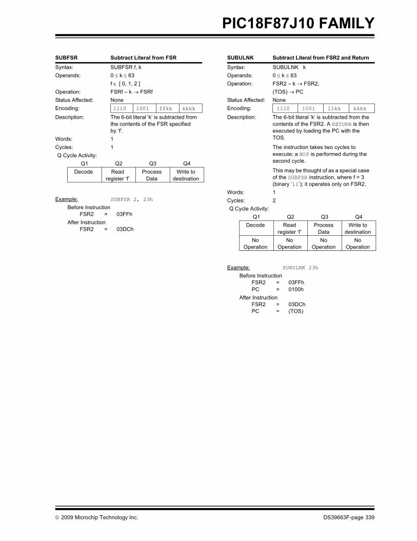
PIC18F87J10 FAMILY
SUBFSR Subtract Literal from FSR
Syntax: SUBFSR f, kOperands: 0 ≤ k ≤ 63
f ∈ [ 0, 1, 2 ]Operation: FSRf – k → FSRfStatus Affected: NoneEncoding: 1110 1001 ffkk kkkk
Description: The 6-bit literal ‘k’ is subtracted from the contents of the FSR specified by ‘f’.
Words: 1Cycles: 1Q Cycle Activity:
Q1 Q2 Q3 Q4Decode Read
register ‘f’Process
DataWrite to
destination
Example: SUBFSR 2, 23h
Before InstructionFSR2 = 03FFh
After InstructionFSR2 = 03DCh
SUBULNK Subtract Literal from FSR2 and Return
Syntax: SUBULNK kOperands: 0 ≤ k ≤ 63Operation: FSR2 – k → FSR2,
(TOS) → PCStatus Affected: NoneEncoding: 1110 1001 11kk kkkk
Description: The 6-bit literal ‘k’ is subtracted from the contents of the FSR2. A RETURN is then executed by loading the PC with the TOS.
The instruction takes two cycles to execute; a NOP is performed during the second cycle.
This may be thought of as a special case of the SUBFSR instruction, where f = 3 (binary ‘11’); it operates only on FSR2.
Words: 1Cycles: 2Q Cycle Activity:
Q1 Q2 Q3 Q4Decode Read
register ‘f’Process
DataWrite to
destinationNo
OperationNo
OperationNo
OperationNo
Operation
Example: SUBULNK 23h
Before InstructionFSR2 = 03FFhPC = 0100h
After InstructionFSR2 = 03DChPC = (TOS)
© 2009 Microchip Technology Inc. DS39663F-page 339

PIC18F87J10 FAMILY
25.2.3 BYTE-ORIENTED ANDBIT-ORIENTED INSTRUCTIONS IN INDEXED LITERAL OFFSET MODE
In addition to eight new commands in the extended set,enabling the extended instruction set also enablesIndexed Literal Offset Addressing (Section 6.6.1“Indexed Addressing with Literal Offset”). This hasa significant impact on the way that many commands ofthe standard PIC18 instruction set are interpreted.
When the extended set is disabled, addresses embed-ded in opcodes are treated as literal memory locations:either as a location in the Access Bank (a = 0) or in aGPR bank designated by the BSR (a = 1). When theextended instruction set is enabled and a = 0, however,a file register argument of 5Fh or less is interpreted asan offset from the pointer value in FSR2 and not as aliteral address. For practical purposes, this means thatall instructions that use the Access RAM bit as anargument – that is, all byte-oriented and bit-orientedinstructions, or almost half of the core PIC18 instruc-tions – may behave differently when the extendedinstruction set is enabled.
When the content of FSR2 is 00h, the boundaries of theAccess RAM are essentially remapped to their originalvalues. This may be useful in creatingbackward-compatible code. If this technique is used, itmay be necessary to save the value of FSR2 andrestore it when moving back and forth between C andassembly routines in order to preserve the StackPointer. Users must also keep in mind the syntaxrequirements of the extended instruction set (seeSection 25.2.3.1 “Extended Instruction Syntax withStandard PIC18 Commands”).
Although the Indexed Literal Offset mode can be veryuseful for dynamic stack and pointer manipulation, itcan also be very annoying if a simple arithmetic opera-tion is carried out on the wrong register. Users who areaccustomed to the PIC18 programming must keep inmind that, when the extended instruction set isenabled, register addresses of 5Fh or less are used forIndexed Literal Offset Addressing.
Representative examples of typical byte-oriented andbit-oriented instructions in the Indexed Literal Offsetmode are provided on the following page to show howexecution is affected. The operand conditions shown inthe examples are applicable to all instructions of thesetypes.
25.2.3.1 Extended Instruction Syntax with Standard PIC18 Commands
When the extended instruction set is enabled, the fileregister argument ‘f’ in the standard byte-oriented andbit-oriented commands is replaced with the literal offsetvalue ‘k’. As already noted, this occurs only when ‘f’ isless than or equal to 5Fh. When an offset value is used,it must be indicated by square brackets (“[ ]”). As withthe extended instructions, the use of brackets indicatesto the compiler that the value is to be interpreted as anindex or an offset. Omitting the brackets, or using avalue greater than 5Fh within the brackets, willgenerate an error in the MPASM Assembler.
If the index argument is properly bracketed for IndexedLiteral Offset Addressing, the Access RAM argument isnever specified; it will automatically be assumed to be‘0’. This is in contrast to standard operation (extendedinstruction set disabled), when ‘a’ is set on the basis ofthe target address. Declaring the Access RAM bit inthis mode will also generate an error in the MPASMAssembler.
The destination argument ‘d’ functions as before.
In the latest versions of the MPASM Assembler,language support for the extended instruction set mustbe explicitly invoked. This is done with either thecommand line option, /y, or the PE directive in thesource listing.
25.2.4 CONSIDERATIONS WHEN ENABLING THE EXTENDED INSTRUCTION SET
It is important to note that the extensions to the instruc-tion set may not be beneficial to all users. In particular,users who are not writing code that uses a softwarestack may not benefit from using the extensions to theinstruction set.
Additionally, the Indexed Literal Offset Addressingmode may create issues with legacy applicationswritten to the PIC18 assembler. This is becauseinstructions in the legacy code may attempt to addressregisters in the Access Bank below 5Fh. Since theseaddresses are interpreted as literal offsets to FSR2when the instruction set extension is enabled, theapplication may read or write to the wrong dataaddresses.
When porting an application to the PIC18F87J10family, it is very important to consider the type of code.A large, re-entrant application that is written in C andwould benefit from efficient compilation will do wellwhen using the instruction set extensions. Legacyapplications that heavily use the Access Bank will mostlikely not benefit from using the extended instructionset.
Note: Enabling the PIC18 instruction set exten-sion may cause legacy applications tobehave erratically or fail entirely.
DS39663F-page 340 © 2009 Microchip Technology Inc.

PIC18F87J10 FAMILY
ADDWF ADD W to Indexed(Indexed Literal Offset mode)
Syntax: ADDWF [k] ,d
Operands: 0 ≤ k ≤ 95d ∈ [0,1]
Operation: (W) + ((FSR2) + k) → dest
Status Affected: N, OV, C, DC, Z
Encoding: 0010 01d0 kkkk kkkk
Description: The contents of W are added to the contents of the register indicated by FSR2, offset by the value ‘k’.
If ‘d’ is ‘0’, the result is stored in W. If ‘d’ is ‘1’, the result is stored back in register ‘f’.
Words: 1
Cycles: 1
Q Cycle Activity:Q1 Q2 Q3 Q4
Decode Read ‘k’ Process Data
Write todestination
Example: ADDWF [OFST] ,0
Before InstructionW = 17hOFST = 2ChFSR2 = 0A00hContentsof 0A2Ch = 20h
After InstructionW = 37hContentsof 0A2Ch = 20h
BSF Bit Set Indexed (Indexed Literal Offset mode)
Syntax: BSF [k], b
Operands: 0 ≤ f ≤ 950 ≤ b ≤ 7
Operation: 1 → ((FSR2) + k)<b>
Status Affected: None
Encoding: 1000 bbb0 kkkk kkkk
Description: Bit ‘b’ of the register indicated by FSR2, offset by the value ‘k’, is set.
Words: 1
Cycles: 1
Q Cycle Activity:Q1 Q2 Q3 Q4
Decode Readregister ‘f’
Process Data
Write todestination
Example: BSF [FLAG_OFST], 7
Before InstructionFLAG_OFST = 0AhFSR2 = 0A00hContents of 0A0Ah = 55h
After InstructionContentsof 0A0Ah = D5h
SETF Set Indexed(Indexed Literal Offset mode)
Syntax: SETF [k]
Operands: 0 ≤ k ≤ 95
Operation: FFh → ((FSR2) + k)
Status Affected: None
Encoding: 0110 1000 kkkk kkkk
Description: The contents of the register indicated by FSR2, offset by ‘k’, are set to FFh.
Words: 1
Cycles: 1
Q Cycle Activity:Q1 Q2 Q3 Q4
Decode Read ‘k’ Process Data
Writeregister
Example: SETF [OFST]
Before InstructionOFST = 2ChFSR2 = 0A00hContentsof 0A2Ch = 00h
After InstructionContentsof 0A2Ch = FFh
© 2009 Microchip Technology Inc. DS39663F-page 341

PIC18F87J10 FAMILY
25.2.5 SPECIAL CONSIDERATIONS WITHMICROCHIP MPLAB® IDE TOOLS
The latest versions of Microchip’s software tools havebeen designed to fully support the extended instructionset for the PIC18F87J10 family. This includes theMPLAB C18 C Compiler, MPASM assembly languageand MPLAB Integrated Development Environment(IDE).
When selecting a target device for softwaredevelopment, MPLAB IDE will automatically set defaultConfiguration bits for that device. The default setting forthe XINST Configuration bit is ‘0’, disabling theextended instruction set and Indexed Literal OffsetAddressing. For proper execution of applicationsdeveloped to take advantage of the extended instruc-tion set, XINST must be set during programming.
To develop software for the extended instruction set,the user must enable support for the instructions andthe Indexed Addressing mode in their language tool(s).Depending on the environment being used, this may bedone in several ways:
• A menu option or dialog box within the environment that allows the user to configure the language tool and its settings for the project
• A command line option• A directive in the source code
These options vary between different compilers,assemblers and development environments. Users areencouraged to review the documentation accompany-ing their development systems for the appropriateinformation.
DS39663F-page 342 © 2009 Microchip Technology Inc.
PIC18F87J10 FAMILY
26.0 DEVELOPMENT SUPPORTThe PIC® microcontrollers are supported with a fullrange of hardware and software development tools:
• Integrated Development Environment- MPLAB® IDE Software
• Assemblers/Compilers/Linkers- MPASMTM Assembler- MPLAB C18 and MPLAB C30 C Compilers- MPLINKTM Object Linker/
MPLIBTM Object Librarian- MPLAB ASM30 Assembler/Linker/Library
• Simulators- MPLAB SIM Software Simulator
• Emulators- MPLAB ICE 2000 In-Circuit Emulator- MPLAB REAL ICE™ In-Circuit Emulator
• In-Circuit Debugger- MPLAB ICD 2
• Device Programmers- PICSTART® Plus Development Programmer- MPLAB PM3 Device Programmer- PICkit™ 2 Development Programmer
• Low-Cost Demonstration and Development Boards and Evaluation Kits
26.1 MPLAB Integrated Development Environment Software
The MPLAB IDE software brings an ease of softwaredevelopment previously unseen in the 8/16-bit micro-controller market. The MPLAB IDE is a Windows®
operating system-based application that contains:
• A single graphical interface to all debugging tools- Simulator- Programmer (sold separately)- Emulator (sold separately)- In-Circuit Debugger (sold separately)
• A full-featured editor with color-coded context• A multiple project manager• Customizable data windows with direct edit of
contents• High-level source code debugging• Visual device initializer for easy register
initialization• Mouse over variable inspection• Drag and drop variables from source to watch
windows• Extensive on-line help• Integration of select third party tools, such as
HI-TECH Software C Compilers and IAR C Compilers
The MPLAB IDE allows you to:
• Edit your source files (either assembly or C)• One touch assemble (or compile) and download
to PIC MCU emulator and simulator tools (automatically updates all project information)
• Debug using:- Source files (assembly or C)- Mixed assembly and C- Machine code
MPLAB IDE supports multiple debugging tools in asingle development paradigm, from the cost-effectivesimulators, through low-cost in-circuit debuggers, tofull-featured emulators. This eliminates the learningcurve when upgrading to tools with increased flexibilityand power.
© 2009 Microchip Technology Inc. DS39663F-page 343

PIC18F87J10 FAMILY
26.2 MPASM AssemblerThe MPASM Assembler is a full-featured, universalmacro assembler for all PIC MCUs.The MPASM Assembler generates relocatable objectfiles for the MPLINK Object Linker, Intel® standard HEXfiles, MAP files to detail memory usage and symbolreference, absolute LST files that contain source linesand generated machine code and COFF files fordebugging.
The MPASM Assembler features include:
• Integration into MPLAB IDE projects• User-defined macros to streamline
assembly code• Conditional assembly for multi-purpose
source files• Directives that allow complete control over the
assembly process
26.3 MPLAB C18 and MPLAB C30 C Compilers
The MPLAB C18 and MPLAB C30 Code DevelopmentSystems are complete ANSI C compilers forMicrochip’s PIC18 and PIC24 families of microcon-trollers and the dsPIC30 and dsPIC33 family of digitalsignal controllers. These compilers provide powerfulintegration capabilities, superior code optimization andease of use not found with other compilers.
For easy source level debugging, the compilers providesymbol information that is optimized to the MPLAB IDEdebugger.
26.4 MPLINK Object Linker/MPLIB Object Librarian
The MPLINK Object Linker combines relocatableobjects created by the MPASM Assembler and theMPLAB C18 C Compiler. It can link relocatable objectsfrom precompiled libraries, using directives from alinker script.
The MPLIB Object Librarian manages the creation andmodification of library files of precompiled code. Whena routine from a library is called from a source file, onlythe modules that contain that routine will be linked inwith the application. This allows large libraries to beused efficiently in many different applications.
The object linker/library features include:
• Efficient linking of single libraries instead of many smaller files
• Enhanced code maintainability by grouping related modules together
• Flexible creation of libraries with easy module listing, replacement, deletion and extraction
26.5 MPLAB ASM30 Assembler, Linker and Librarian
MPLAB ASM30 Assembler produces relocatablemachine code from symbolic assembly language fordsPIC30F devices. MPLAB C30 C Compiler uses theassembler to produce its object file. The assemblergenerates relocatable object files that can then bearchived or linked with other relocatable object files andarchives to create an executable file. Notable featuresof the assembler include:
• Support for the entire dsPIC30F instruction set• Support for fixed-point and floating-point data• Command line interface• Rich directive set• Flexible macro language• MPLAB IDE compatibility
26.6 MPLAB SIM Software SimulatorThe MPLAB SIM Software Simulator allows codedevelopment in a PC-hosted environment by simulat-ing the PIC MCUs and dsPIC® DSCs on an instructionlevel. On any given instruction, the data areas can beexamined or modified and stimuli can be applied froma comprehensive stimulus controller. Registers can belogged to files for further run-time analysis. The tracebuffer and logic analyzer display extend the power ofthe simulator to record and track program execution,actions on I/O, most peripherals and internal registers.
The MPLAB SIM Software Simulator fully supportssymbolic debugging using the MPLAB C18 andMPLAB C30 C Compilers, and the MPASM andMPLAB ASM30 Assemblers. The software simulatoroffers the flexibility to develop and debug code outsideof the hardware laboratory environment, making it anexcellent, economical software development tool.
DS39663F-page 344 © 2009 Microchip Technology Inc.
PIC18F87J10 FAMILY
26.7 MPLAB ICE 2000High-Performance In-Circuit Emulator
The MPLAB ICE 2000 In-Circuit Emulator is intendedto provide the product development engineer with acomplete microcontroller design tool set for PICmicrocontrollers. Software control of the MPLAB ICE2000 In-Circuit Emulator is advanced by the MPLABIntegrated Development Environment, which allowsediting, building, downloading and source debuggingfrom a single environment.
The MPLAB ICE 2000 is a full-featured emulatorsystem with enhanced trace, trigger and data monitor-ing features. Interchangeable processor modules allowthe system to be easily reconfigured for emulation ofdifferent processors. The architecture of the MPLABICE 2000 In-Circuit Emulator allows expansion tosupport new PIC microcontrollers.
The MPLAB ICE 2000 In-Circuit Emulator system hasbeen designed as a real-time emulation system withadvanced features that are typically found on moreexpensive development tools. The PC platform andMicrosoft® Windows® 32-bit operating system werechosen to best make these features available in asimple, unified application.
26.8 MPLAB REAL ICE In-Circuit Emulator System
MPLAB REAL ICE In-Circuit Emulator System isMicrochip’s next generation high-speed emulator forMicrochip Flash DSC and MCU devices. It debugs andprograms PIC® Flash MCUs and dsPIC® Flash DSCswith the easy-to-use, powerful graphical user interface ofthe MPLAB Integrated Development Environment (IDE),included with each kit.
The MPLAB REAL ICE probe is connected to the designengineer’s PC using a high-speed USB 2.0 interface andis connected to the target with either a connectorcompatible with the popular MPLAB ICD 2 system(RJ11) or with the new high-speed, noise tolerant, Low-Voltage Differential Signal (LVDS) interconnection(CAT5).
MPLAB REAL ICE is field upgradeable through futurefirmware downloads in MPLAB IDE. In upcomingreleases of MPLAB IDE, new devices will be supported,and new features will be added, such as software break-points and assembly code trace. MPLAB REAL ICEoffers significant advantages over competitive emulatorsincluding low-cost, full-speed emulation, real-timevariable watches, trace analysis, complex breakpoints, aruggedized probe interface and long (up to three meters)interconnection cables.
26.9 MPLAB ICD 2 In-Circuit DebuggerMicrochip’s In-Circuit Debugger, MPLAB ICD 2, is apowerful, low-cost, run-time development tool,connecting to the host PC via an RS-232 or high-speedUSB interface. This tool is based on the Flash PICMCUs and can be used to develop for these and otherPIC MCUs and dsPIC DSCs. The MPLAB ICD 2 utilizesthe in-circuit debugging capability built into the Flashdevices. This feature, along with Microchip’s In-CircuitSerial ProgrammingTM (ICSPTM) protocol, offers cost-effective, in-circuit Flash debugging from the graphicaluser interface of the MPLAB Integrated DevelopmentEnvironment. This enables a designer to develop anddebug source code by setting breakpoints, single step-ping and watching variables, and CPU status andperipheral registers. Running at full speed enablestesting hardware and applications in real time. MPLABICD 2 also serves as a development programmer forselected PIC devices.
26.10 MPLAB PM3 Device ProgrammerThe MPLAB PM3 Device Programmer is a universal,CE compliant device programmer with programmablevoltage verification at VDDMIN and VDDMAX formaximum reliability. It features a large LCD display(128 x 64) for menus and error messages and a modu-lar, detachable socket assembly to support variouspackage types. The ICSP™ cable assembly is includedas a standard item. In Stand-Alone mode, the MPLABPM3 Device Programmer can read, verify and programPIC devices without a PC connection. It can also setcode protection in this mode. The MPLAB PM3connects to the host PC via an RS-232 or USB cable.The MPLAB PM3 has high-speed communications andoptimized algorithms for quick programming of largememory devices and incorporates an SD/MMC card forfile storage and secure data applications.
© 2009 Microchip Technology Inc. DS39663F-page 345

PIC18F87J10 FAMILY
26.11 PICSTART Plus DevelopmentProgrammerThe PICSTART Plus Development Programmer is aneasy-to-use, low-cost, prototype programmer. Itconnects to the PC via a COM (RS-232) port. MPLABIntegrated Development Environment software makesusing the programmer simple and efficient. ThePICSTART Plus Development Programmer supportsmost PIC devices in DIP packages up to 40 pins.Larger pin count devices, such as the PIC16C92X andPIC17C76X, may be supported with an adapter socket.The PICSTART Plus Development Programmer is CEcompliant.
26.12 PICkit 2 Development ProgrammerThe PICkit™ 2 Development Programmer is a low-costprogrammer and selected Flash device debugger withan easy-to-use interface for programming many ofMicrochip’s baseline, mid-range and PIC18F families ofFlash memory microcontrollers. The PICkit 2 Starter Kitincludes a prototyping development board, twelvesequential lessons, software and HI-TECH’s PICC™Lite C compiler, and is designed to help get up to speedquickly using PIC® microcontrollers. The kit provideseverything needed to program, evaluate and developapplications using Microchip’s powerful, mid-rangeFlash memory family of microcontrollers.
26.13 Demonstration, Development and Evaluation Boards
A wide variety of demonstration, development andevaluation boards for various PIC MCUs and dsPICDSCs allows quick application development on fully func-tional systems. Most boards include prototyping areas foradding custom circuitry and provide application firmwareand source code for examination and modification.
The boards support a variety of features, including LEDs,temperature sensors, switches, speakers, RS-232interfaces, LCD displays, potentiometers and additionalEEPROM memory.
The demonstration and development boards can beused in teaching environments, for prototyping customcircuits and for learning about various microcontrollerapplications.
In addition to the PICDEM™ and dsPICDEM™ demon-stration/development board series of circuits, Microchiphas a line of evaluation kits and demonstration softwarefor analog filter design, KEELOQ® security ICs, CAN,IrDA®, PowerSmart battery management, SEEVAL®
evaluation system, Sigma-Delta ADC, flow ratesensing, plus many more.
Check the Microchip web page (www.microchip.com)for the complete list of demonstration, developmentand evaluation kits.
DS39663F-page 346 © 2009 Microchip Technology Inc.
PIC18F87J10 FAMILY
27.0 ELECTRICAL CHARACTERISTICS
Absolute Maximum Ratings(†) Ambient temperature under bias............................................................................................................ .-40°C to +125°C
Storage temperature .............................................................................................................................. -65°C to +150°C
Voltage on any digital only I/O pin or MCLR with respect to VSS (except VDD) ........................................... -0.3V to 6.0V
Voltage on any combined digital and analog pin with respect to VSS (except VDD)........................ -0.3V to (VDD + 0.3V)
Voltage on VDDCORE with respect to VSS................................................................................................... -0.3V to 2.75V
Voltage on VDD with respect to VSS ........................................................................................................... -0.3V to 3.6V
Total power dissipation (Note 1) ...............................................................................................................................1.0W
Maximum current out of VSS pin ...........................................................................................................................300 mA
Maximum current into VDD pin ..............................................................................................................................250 mA
Maximum output current sunk by any PORTB and PORTC I/O pin........................................................................25 mA
Maximum output current sunk by any PORTD, PORTE and PORTJ I/O pin ............................................................8 mA
Maximum output current sunk by any PORTA, PORTF, PORTG and PORTH I/O pin .............................................4 mA
Maximum output current sourced by any PORTB and PORTC I/O pin ..................................................................25 mA
Maximum output current sourced by any PORTD, PORTE and PORTJ I/O pin.......................................................8 mA
Maximum output current sourced by any PORTA, PORTF, PORTG and PORTH I/O pin ........................................4 mA
Maximum current sunk by all ports .......................................................................................................................200 mA
Maximum current sourced by all ports ..................................................................................................................200 mA
Note 1: Power dissipation is calculated as follows: Pdis = VDD x IDD – ∑ IOH + ∑ (VDD – VOH) x IOH + ∑(VOL x IOL)
† NOTICE: Stresses above those listed under “Absolute Maximum Ratings” may cause permanent damage to the device. This is a stress rating only and functional operation of the device at those or any other conditions above those indicated in the operation listings of this specification is not implied. Exposure to maximum rating conditions for extended periods may affect device reliability.
© 2009 Microchip Technology Inc. DS39663F-page 347

PIC18F87J10 FAMILY
FIGURE 27-1: PIC18F87J10 FAMILY VOLTAGE-FREQUENCY GRAPH,REGULATOR DISABLED (INDUSTRIAL)
Frequency
Volta
ge (V
DD
CO
RE)
(1)
3.00V
2.00V
40 MHz
2.75V
2.50V
2.25V
2.7V
4 MHz
2.35V
Note 1: For devices without the voltage regulator, VDD and VDDCORE must be maintained so that VDDCORE ≤ VDD ≤ 3.6V.
For VDDCORE values, 2V to 2.35V, FMAX = (102.85 MHz/V) * (VDDCORE – 2V) + 4 MHz
PIC18F6XJ10/6XJ15/8XJ10/8XJ15
DS39663F-page 348 © 2009 Microchip Technology Inc.

PIC18F87J10 FAMILY
FIGURE 27-2: PIC18F87J10 FAMILY VOLTAGE-FREQUENCY GRAPH,REGULATOR ENABLED (INDUSTRIAL)
Frequency
Volta
ge (V
DD
)4.0V
40 MHz
3.5V
3.0V
2.5V
3.6V
4 MHz
PIC18F6XJ10/6XJ15/8XJ10/8XJ152.7V
• FMAX = 25 MHz in 8-bit External Memory mode.• FMAX = 40 MHz in all other modes for VDD > 2.35V.
© 2009 Microchip Technology Inc. DS39663F-page 349

PIC18F87J10 FAMILY
27.1 DC Characteristics: Supply Voltage, PIC18F87J10 Family (Industrial)
PIC18F87J10 Family (Industrial)
Standard Operating Conditions (unless otherwise stated)Operating temperature -40°C ≤ TA ≤ +85°C for industrial
Param No. Symbol Characteristic Min Typ Max Units Conditions
D001 VDD Supply Voltage VDDCORE2.7
——
3.63.6
VV
ENVREG = 0ENVREG = 1
D001B VDDCORE External Supply for Microcontroller Core
2.0 — 2.7 V ENVREG = 0
D001C AVDD Analog Supply Voltage VDD – 0.3 — VDD + 0.3 VD001D AVSS Analog Ground Voltage VSS – 0.3 — VSS + 0.3 VD002 VDR RAM Data Retention
Voltage(1)1.5 — — V
D003 VPOR VDD Start Voltage to ensure Internal Power-on Reset Signal
— — 0.15 V See Section 5.3 “Power-on Reset (POR)” for details
D004 SVDD VDD Rise Rateto Ensure Internal Power-on Reset Signal
0.05 — — V/ms See Section 5.3 “Power-on Reset (POR)” for details
D005 VBOR Brown-out Reset (BOR) Voltage
2.35 2.5 2.7 V
Note 1: This is the limit to which VDD can be lowered in Sleep mode, or during a device Reset, without losing RAM data.
DS39663F-page 350 © 2009 Microchip Technology Inc.
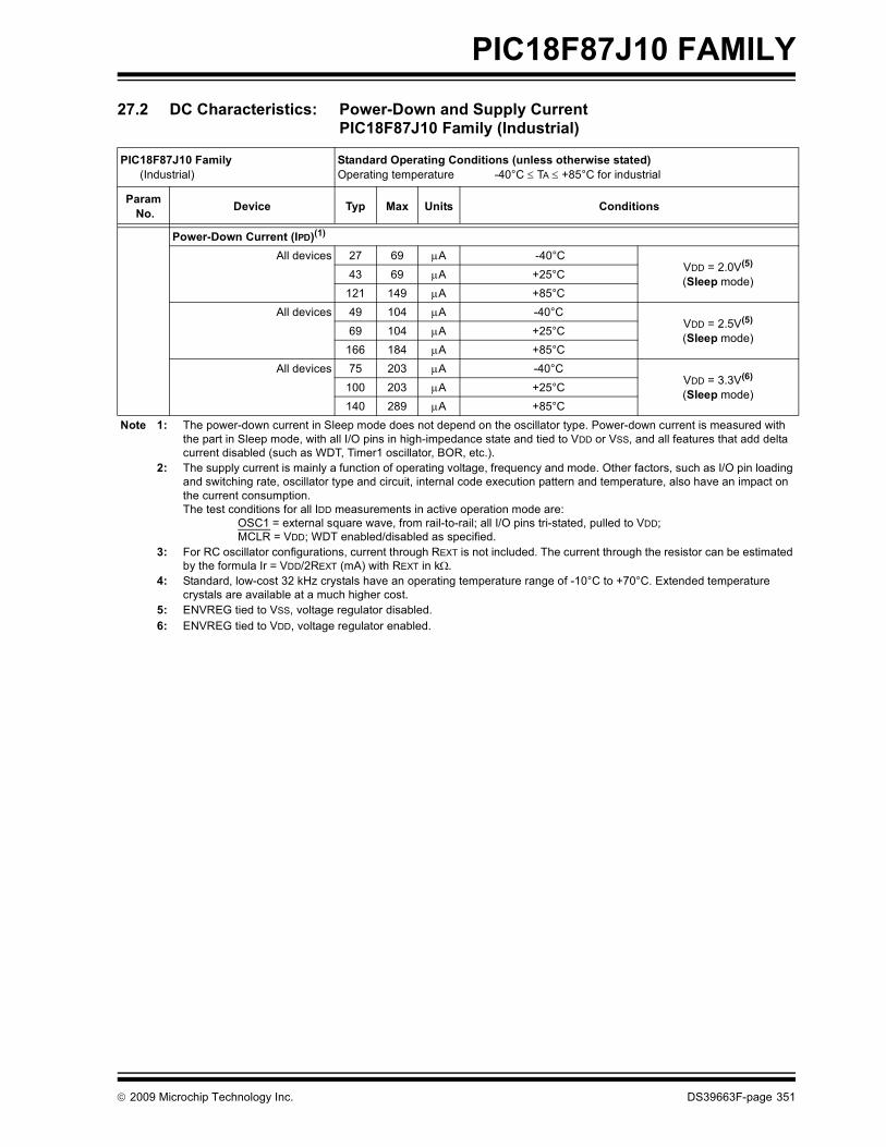
PIC18F87J10 FAMILY
27.2 DC Characteristics: Power-Down and Supply CurrentPIC18F87J10 Family (Industrial)
PIC18F87J10 Family (Industrial)
Standard Operating Conditions (unless otherwise stated)Operating temperature -40°C ≤ TA ≤ +85°C for industrial
Param No. Device Typ Max Units Conditions
Power-Down Current (IPD)(1)
All devices 27 69 μA -40°CVDD = 2.0V(5)
(Sleep mode)43 69 μA +25°C121 149 μA +85°C
All devices 49 104 μA -40°CVDD = 2.5V(5)
(Sleep mode)69 104 μA +25°C166 184 μA +85°C
All devices 75 203 μA -40°CVDD = 3.3V(6)
(Sleep mode)100 203 μA +25°C140 289 μA +85°C
Note 1: The power-down current in Sleep mode does not depend on the oscillator type. Power-down current is measured with the part in Sleep mode, with all I/O pins in high-impedance state and tied to VDD or VSS, and all features that add delta current disabled (such as WDT, Timer1 oscillator, BOR, etc.).
2: The supply current is mainly a function of operating voltage, frequency and mode. Other factors, such as I/O pin loading and switching rate, oscillator type and circuit, internal code execution pattern and temperature, also have an impact on the current consumption.The test conditions for all IDD measurements in active operation mode are:
OSC1 = external square wave, from rail-to-rail; all I/O pins tri-stated, pulled to VDD;MCLR = VDD; WDT enabled/disabled as specified.
3: For RC oscillator configurations, current through REXT is not included. The current through the resistor can be estimated by the formula Ir = VDD/2REXT (mA) with REXT in kΩ.
4: Standard, low-cost 32 kHz crystals have an operating temperature range of -10°C to +70°C. Extended temperature crystals are available at a much higher cost.
5: ENVREG tied to VSS, voltage regulator disabled.6: ENVREG tied to VDD, voltage regulator enabled.
© 2009 Microchip Technology Inc. DS39663F-page 351

PIC18F87J10 FAMILY
Supply Current (IDD)(2,3)
All devices 1.8 3.27 mA -40°C
FOSC = 31 kHz(RC_RUN mode,
internal oscillator source)
1.8 3.27 mA +25°C VDD = 2.0V1.9 3.27 mA +85°C
All devices 4.0 5.57 mA -40°C3.7 5.57 mA +25°C VDD = 2.5V3.5 5.57 mA +85°C
All devices 4.0 5.97 mA -40°C3.8 5.97 mA +25°C VDD = 3.3V3.7 5.97 mA +85°C
All devices 1.8 3.27 mA -40°C
FOSC = 31 kHz(RC_IDLE mode,
internal oscillator source)
1.8 3.27 mA +25°C VDD = 2.0V1.9 3.27 mA +85°C
All devices 4.0 5.57 mA -40°C3.7 5.57 mA +25°C VDD = 2.5V3.5 5.57 mA +85°C
All devices 4.0 5.97 mA -40°C3.8 5.97 mA +25°C VDD = 3.3V3.7 5.97 mA +85°C
27.2 DC Characteristics: Power-Down and Supply CurrentPIC18F87J10 Family (Industrial) (Continued)
PIC18F87J10 Family (Industrial)
Standard Operating Conditions (unless otherwise stated)Operating temperature -40°C ≤ TA ≤ +85°C for industrial
Param No. Device Typ Max Units Conditions
Note 1: The power-down current in Sleep mode does not depend on the oscillator type. Power-down current is measured with the part in Sleep mode, with all I/O pins in high-impedance state and tied to VDD or VSS, and all features that add delta current disabled (such as WDT, Timer1 oscillator, BOR, etc.).
2: The supply current is mainly a function of operating voltage, frequency and mode. Other factors, such as I/O pin loading and switching rate, oscillator type and circuit, internal code execution pattern and temperature, also have an impact on the current consumption.The test conditions for all IDD measurements in active operation mode are:
OSC1 = external square wave, from rail-to-rail; all I/O pins tri-stated, pulled to VDD;MCLR = VDD; WDT enabled/disabled as specified.
3: For RC oscillator configurations, current through REXT is not included. The current through the resistor can be estimated by the formula Ir = VDD/2REXT (mA) with REXT in kΩ.
4: Standard, low-cost 32 kHz crystals have an operating temperature range of -10°C to +70°C. Extended temperature crystals are available at a much higher cost.
5: ENVREG tied to VSS, voltage regulator disabled.6: ENVREG tied to VDD, voltage regulator enabled.
DS39663F-page 352 © 2009 Microchip Technology Inc.

PIC18F87J10 FAMILY
Supply Current (IDD)(2,3)
All devices 1.8 3.27 mA -40°C
FOSC = 1 MHZ(PRI_RUN mode,
EC oscillator)
1.8 3.27 mA +25°C VDD = 2.0V(5)
1.9 3.27 mA +85°CAll devices 4.0 5.57 mA -40°C
3.7 5.57 mA +25°C VDD = 2.5V(5)
3.5 5.57 mA +85°CAll devices 4.0 5.97 mA -40°C
3.8 5.97 mA +25°C VDD = 3.3V(6)
3.7 5.97 mA +85°CAll devices 2.4 4.47 mA -40°C
FOSC = 4 MHz(PRI_RUN mode,
EC oscillator)
2.4 4.47 mA +25°C VDD = 2.0V(5)
2.5 4.47 mA +85°CAll devices 4.7 6.97 mA -40°C
4.4 6.97 mA +25°C VDD = 2.5V(5)
4.3 6.97 mA +85°CAll devices 5.1 7.47 mA -40°C
4.9 7.47 mA +25°C VDD = 3.3V(6)
4.7 7.47 mA +85°CAll devices 13.4 18.7 mA -40°C
FOSC = 40 MHZ(PRI_RUN mode,
EC oscillator)
13.0 18.7 mA +25°C VDD = 2.5V(5)
13.0 18.7 mA +85°CAll devices 14.5 19.7 mA -40°C
14.4 19.7 mA +25°C VDD = 3.3V(6)
14.5 19.7 mA +85°C
27.2 DC Characteristics: Power-Down and Supply CurrentPIC18F87J10 Family (Industrial) (Continued)
PIC18F87J10 Family (Industrial)
Standard Operating Conditions (unless otherwise stated)Operating temperature -40°C ≤ TA ≤ +85°C for industrial
Param No. Device Typ Max Units Conditions
Note 1: The power-down current in Sleep mode does not depend on the oscillator type. Power-down current is measured with the part in Sleep mode, with all I/O pins in high-impedance state and tied to VDD or VSS, and all features that add delta current disabled (such as WDT, Timer1 oscillator, BOR, etc.).
2: The supply current is mainly a function of operating voltage, frequency and mode. Other factors, such as I/O pin loading and switching rate, oscillator type and circuit, internal code execution pattern and temperature, also have an impact on the current consumption.The test conditions for all IDD measurements in active operation mode are:
OSC1 = external square wave, from rail-to-rail; all I/O pins tri-stated, pulled to VDD;MCLR = VDD; WDT enabled/disabled as specified.
3: For RC oscillator configurations, current through REXT is not included. The current through the resistor can be estimated by the formula Ir = VDD/2REXT (mA) with REXT in kΩ.
4: Standard, low-cost 32 kHz crystals have an operating temperature range of -10°C to +70°C. Extended temperature crystals are available at a much higher cost.
5: ENVREG tied to VSS, voltage regulator disabled.6: ENVREG tied to VDD, voltage regulator enabled.
© 2009 Microchip Technology Inc. DS39663F-page 353

PIC18F87J10 FAMILY
Supply Current (IDD)(2)
All devices 7.2 12.1 mA -40°CVDD = 2.5V(5)
FOSC = 4 MHZ,16 MHz internal
(PRI_RUN HSPLL mode)6.8 12.1 mA +25°C6.9 12.1 mA +85°C
All devices 7.6 13.1 mA -40°CVDD = 3.3V(6)
FOSC = 4 MHZ,16 MHz internal
(PRI_RUN HSPLL mode)7.5 13.1 mA +25°C7.3 13.1 mA +85°C
All devices 10.9 18.7 mA -40°CVDD = 2.5V(5)
FOSC = 10 MHZ,40 MHz internal
(PRI_RUN HSPLL mode)10.6 18.7 mA +25°C10.3 18.7 mA +85°C
All devices 11.9 19.7 mA -40°CVDD = 3.3V(6)
FOSC = 10 MHZ,40 MHz internal
(PRI_RUN HSPLL mode)11.8 19.7 mA +25°C11.7 19.7 mA +85°C
27.2 DC Characteristics: Power-Down and Supply CurrentPIC18F87J10 Family (Industrial) (Continued)
PIC18F87J10 Family (Industrial)
Standard Operating Conditions (unless otherwise stated)Operating temperature -40°C ≤ TA ≤ +85°C for industrial
Param No. Device Typ Max Units Conditions
Note 1: The power-down current in Sleep mode does not depend on the oscillator type. Power-down current is measured with the part in Sleep mode, with all I/O pins in high-impedance state and tied to VDD or VSS, and all features that add delta current disabled (such as WDT, Timer1 oscillator, BOR, etc.).
2: The supply current is mainly a function of operating voltage, frequency and mode. Other factors, such as I/O pin loading and switching rate, oscillator type and circuit, internal code execution pattern and temperature, also have an impact on the current consumption.The test conditions for all IDD measurements in active operation mode are:
OSC1 = external square wave, from rail-to-rail; all I/O pins tri-stated, pulled to VDD;MCLR = VDD; WDT enabled/disabled as specified.
3: For RC oscillator configurations, current through REXT is not included. The current through the resistor can be estimated by the formula Ir = VDD/2REXT (mA) with REXT in kΩ.
4: Standard, low-cost 32 kHz crystals have an operating temperature range of -10°C to +70°C. Extended temperature crystals are available at a much higher cost.
5: ENVREG tied to VSS, voltage regulator disabled.6: ENVREG tied to VDD, voltage regulator enabled.
DS39663F-page 354 © 2009 Microchip Technology Inc.

PIC18F87J10 FAMILY
Supply Current (IDD)(2,3)
All devices 1.8 3.27 mA -40°C
FOSC = 1 MHz(PRI_IDLE mode,
EC oscillator)
1.8 3.27 mA +25°C VDD = 2.0V(5)
1.9 3.27 mA +85°CAll devices 4.0 5.57 mA -40°C
3.7 5.57 mA +25°C VDD = 2.5V(5)
3.5 5.57 mA +85°CAll devices 4.2 5.97 mA -40°C
4.0 5.97 mA +25°C VDD = 3.3V(6)
3.8 5.97 mA +85°CAll devices 2.4 4.47 mA -40°C
FOSC = 4 MHz(PRI_IDLE mode,
EC oscillator)
2.4 4.47 mA +25°C VDD = 2.0V(5)
2.5 4.47 mA +85°CAll devices 4.7 6.97 mA -40°C
4.4 6.97 mA +25°C VDD = 2.5V(5)
4.8 6.97 mA +85°CAll devices 5.1 7.47 mA -40°C
4.9 7.47 mA +25°C VDD = 3.3V(6)
4.8 7.47 mA +85°CAll devices 13.4 18.7 mA -40°C
FOSC = 40 MHz(PRI_IDLE mode,
EC oscillator)
13.0 18.7 mA +25°C VDD = 2.5V(5)
13.0 18.7 mA +85°CAll devices 14.8 19.7 mA -40°C
14.4 19.7 mA +25°C VDD = 3.3V(6)
14.5 19.7 mA +85°C
27.2 DC Characteristics: Power-Down and Supply CurrentPIC18F87J10 Family (Industrial) (Continued)
PIC18F87J10 Family (Industrial)
Standard Operating Conditions (unless otherwise stated)Operating temperature -40°C ≤ TA ≤ +85°C for industrial
Param No. Device Typ Max Units Conditions
Note 1: The power-down current in Sleep mode does not depend on the oscillator type. Power-down current is measured with the part in Sleep mode, with all I/O pins in high-impedance state and tied to VDD or VSS, and all features that add delta current disabled (such as WDT, Timer1 oscillator, BOR, etc.).
2: The supply current is mainly a function of operating voltage, frequency and mode. Other factors, such as I/O pin loading and switching rate, oscillator type and circuit, internal code execution pattern and temperature, also have an impact on the current consumption.The test conditions for all IDD measurements in active operation mode are:
OSC1 = external square wave, from rail-to-rail; all I/O pins tri-stated, pulled to VDD;MCLR = VDD; WDT enabled/disabled as specified.
3: For RC oscillator configurations, current through REXT is not included. The current through the resistor can be estimated by the formula Ir = VDD/2REXT (mA) with REXT in kΩ.
4: Standard, low-cost 32 kHz crystals have an operating temperature range of -10°C to +70°C. Extended temperature crystals are available at a much higher cost.
5: ENVREG tied to VSS, voltage regulator disabled.6: ENVREG tied to VDD, voltage regulator enabled.
© 2009 Microchip Technology Inc. DS39663F-page 355
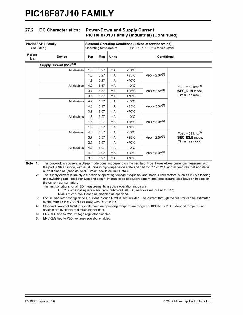
PIC18F87J10 FAMILY
Supply Current (IDD)(2,3)
All devices 1.8 3.27 mA -10°C
FOSC = 32 kHz(4)
(SEC_RUN mode, Timer1 as clock)
1.8 3.27 mA +25°C VDD = 2.0V(5)
1.9 3.27 mA +70°CAll devices 4.0 5.57 mA -10°C
3.7 5.57 mA +25°C VDD = 2.5V(5)
3.5 5.57 mA +70°CAll devices 4.2 5.97 mA -10°C
4.0 5.97 mA +25°C VDD = 3.3V(6)
3.8 5.97 mA +70°CAll devices 1.8 3.27 mA -10°C
FOSC = 32 kHz(4)
(SEC_IDLE mode, Timer1 as clock)
1.8 3.27 mA +25°C VDD = 2.0V(5)
1.9 3.27 mA +70°CAll devices 4.0 5.57 mA -10°C
3.7 5.57 mA +25°C VDD = 2.5V(5)
3.5 5.57 mA +70°CAll devices 4.2 5.97 mA -10°C
4.0 5.97 mA +25°C VDD = 3.3V(6)
3.8 5.97 mA +70°C
27.2 DC Characteristics: Power-Down and Supply CurrentPIC18F87J10 Family (Industrial) (Continued)
PIC18F87J10 Family (Industrial)
Standard Operating Conditions (unless otherwise stated)Operating temperature -40°C ≤ TA ≤ +85°C for industrial
Param No. Device Typ Max Units Conditions
Note 1: The power-down current in Sleep mode does not depend on the oscillator type. Power-down current is measured with the part in Sleep mode, with all I/O pins in high-impedance state and tied to VDD or VSS, and all features that add delta current disabled (such as WDT, Timer1 oscillator, BOR, etc.).
2: The supply current is mainly a function of operating voltage, frequency and mode. Other factors, such as I/O pin loading and switching rate, oscillator type and circuit, internal code execution pattern and temperature, also have an impact on the current consumption.The test conditions for all IDD measurements in active operation mode are:
OSC1 = external square wave, from rail-to-rail; all I/O pins tri-stated, pulled to VDD;MCLR = VDD; WDT enabled/disabled as specified.
3: For RC oscillator configurations, current through REXT is not included. The current through the resistor can be estimated by the formula Ir = VDD/2REXT (mA) with REXT in kΩ.
4: Standard, low-cost 32 kHz crystals have an operating temperature range of -10°C to +70°C. Extended temperature crystals are available at a much higher cost.
5: ENVREG tied to VSS, voltage regulator disabled.6: ENVREG tied to VDD, voltage regulator enabled.
DS39663F-page 356 © 2009 Microchip Technology Inc.

PIC18F87J10 FAMILY
D022(ΔIWDT)
Module Differential Currents (ΔIWDT, ΔIOSCB, ΔIAD)Watchdog Timer 1.9 4.5 μA -40°C
VDD = 2.0V1.9 5.1 μA +25°C1.3 5.1 μA +85°C2.7 5.4 μA -40°C
VDD = 2.5V2.75 6.0 μA +25°C1.7 6.0 μA +85°C1.3 10.5 μA -40°C
VDD = 3.3V2.1 10.5 μA +25°C2.0 10.5 μA +85°C
D025(ΔIOSCB)
Timer1 Oscillator 8.1 18.5 μA -40°CVDD = 2.0V 32 kHz on Timer1(3)10.8 19.1 μA +25°C
13.9 19.1 μA +85°C8.2 18.5 μA -40°C
VDD = 2.5V 32 kHz on Timer1(3)11.0 19.1 μA +25°C13.9 19.1 μA +85°C7.9 19.1 μA -40°C
VDD = 3.3V 32 kHz on Timer1(3)10.7 19.1 μA +25°C13.5 19.1 μA +85°C
D026(ΔIAD)
A/D Converter 1.2 10.9 μA -40°C to +85°C VDD = 2.0VA/D on, not converting1.2 11.4 μA -40°C to +85°C VDD = 2.5V
1.2 11.9 μA -40°C to +85°C VDD = 3.3V
27.2 DC Characteristics: Power-Down and Supply CurrentPIC18F87J10 Family (Industrial) (Continued)
PIC18F87J10 Family (Industrial)
Standard Operating Conditions (unless otherwise stated)Operating temperature -40°C ≤ TA ≤ +85°C for industrial
Param No. Device Typ Max Units Conditions
Note 1: The power-down current in Sleep mode does not depend on the oscillator type. Power-down current is measured with the part in Sleep mode, with all I/O pins in high-impedance state and tied to VDD or VSS, and all features that add delta current disabled (such as WDT, Timer1 oscillator, BOR, etc.).
2: The supply current is mainly a function of operating voltage, frequency and mode. Other factors, such as I/O pin loading and switching rate, oscillator type and circuit, internal code execution pattern and temperature, also have an impact on the current consumption.The test conditions for all IDD measurements in active operation mode are:
OSC1 = external square wave, from rail-to-rail; all I/O pins tri-stated, pulled to VDD;MCLR = VDD; WDT enabled/disabled as specified.
3: For RC oscillator configurations, current through REXT is not included. The current through the resistor can be estimated by the formula Ir = VDD/2REXT (mA) with REXT in kΩ.
4: Standard, low-cost 32 kHz crystals have an operating temperature range of -10°C to +70°C. Extended temperature crystals are available at a much higher cost.
5: ENVREG tied to VSS, voltage regulator disabled.6: ENVREG tied to VDD, voltage regulator enabled.
© 2009 Microchip Technology Inc. DS39663F-page 357
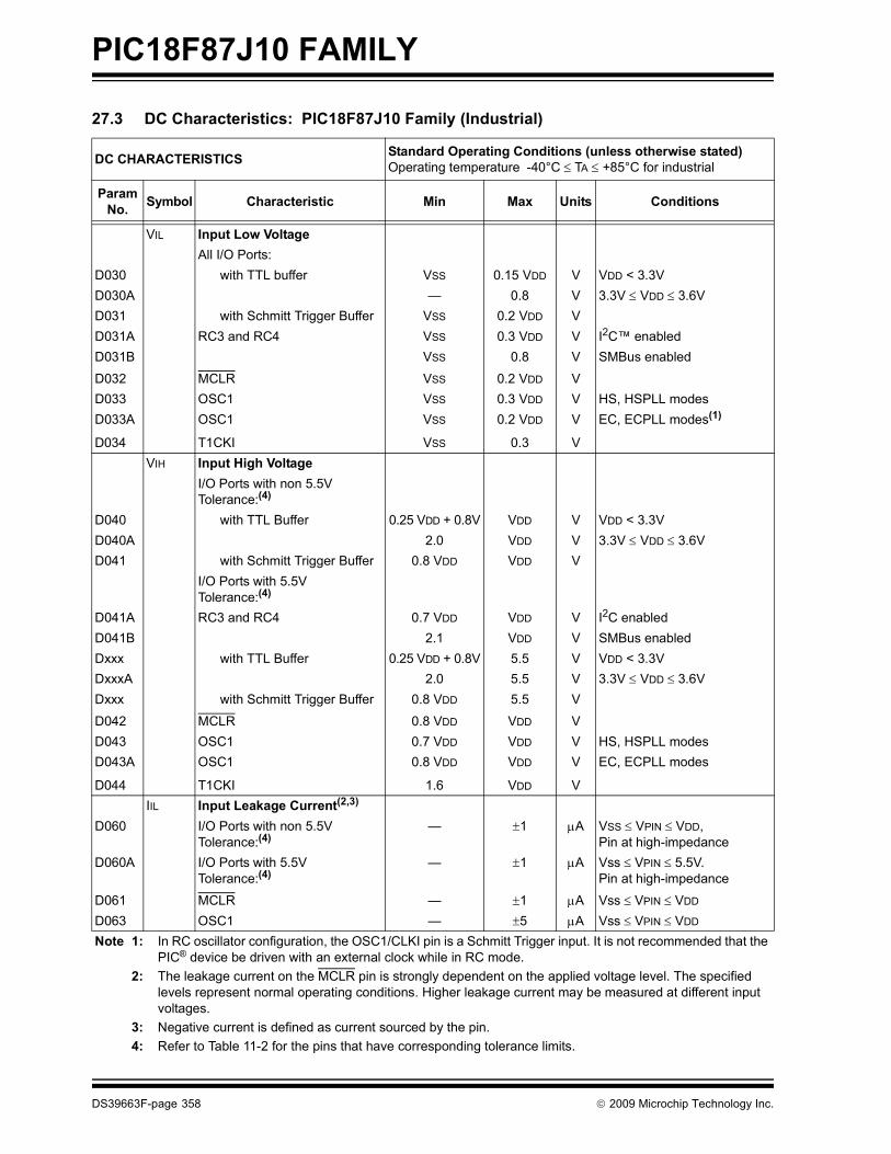
PIC18F87J10 FAMILY
27.3 DC Characteristics: PIC18F87J10 Family (Industrial)
DC CHARACTERISTICS Standard Operating Conditions (unless otherwise stated)Operating temperature -40°C ≤ TA ≤ +85°C for industrial
ParamNo. Symbol Characteristic Min Max Units Conditions
VIL Input Low VoltageAll I/O Ports:
D030 with TTL buffer VSS 0.15 VDD V VDD < 3.3V D030A — 0.8 V 3.3V ≤ VDD ≤ 3.6V D031 with Schmitt Trigger Buffer VSS 0.2 VDD VD031A RC3 and RC4 VSS 0.3 VDD V I2C™ enabledD031B VSS 0.8 V SMBus enabled
D032 MCLR VSS 0.2 VDD VD033 OSC1 VSS 0.3 VDD V HS, HSPLL modesD033A
D034
OSC1
T1CKI
VSS
VSS
0.2 VDD
0.3
V
V
EC, ECPLL modes(1)
VIH Input High VoltageI/O Ports with non 5.5V Tolerance:(4)
D040 with TTL Buffer 0.25 VDD + 0.8V VDD V VDD < 3.3VD040A 2.0 VDD V 3.3V ≤ VDD ≤ 3.6V D041 with Schmitt Trigger Buffer 0.8 VDD VDD V
I/O Ports with 5.5V Tolerance:(4)
D041A RC3 and RC4 0.7 VDD VDD V I2C enabledD041B 2.1 VDD V SMBus enabledDxxx with TTL Buffer 0.25 VDD + 0.8V 5.5 V VDD < 3.3VDxxxA 2.0 5.5 V 3.3V ≤ VDD ≤ 3.6V Dxxx with Schmitt Trigger Buffer 0.8 VDD 5.5 V
D042 MCLR 0.8 VDD VDD VD043 OSC1 0.7 VDD VDD V HS, HSPLL modesD043A
D044
OSC1
T1CKI
0.8 VDD
1.6
VDD
VDD
V
V
EC, ECPLL modes
IIL Input Leakage Current(2,3) D060 I/O Ports with non 5.5V
Tolerance:(4)— ±1 μA VSS ≤ VPIN ≤ VDD,
Pin at high-impedanceD060A I/O Ports with 5.5V
Tolerance:(4)— ±1 μA Vss ≤ VPIN ≤ 5.5V.
Pin at high-impedance
D061 MCLR — ±1 μA Vss ≤ VPIN ≤ VDD
D063 OSC1 — ±5 μA Vss ≤ VPIN ≤ VDD Note 1: In RC oscillator configuration, the OSC1/CLKI pin is a Schmitt Trigger input. It is not recommended that the
PIC® device be driven with an external clock while in RC mode.2: The leakage current on the MCLR pin is strongly dependent on the applied voltage level. The specified
levels represent normal operating conditions. Higher leakage current may be measured at different input voltages.
3: Negative current is defined as current sourced by the pin.4: Refer to Table 11-2 for the pins that have corresponding tolerance limits.
DS39663F-page 358 © 2009 Microchip Technology Inc.

PIC18F87J10 FAMILY
IPU Weak Pull-up CurrentD070 IPURB PORTB Weak Pull-up Current 30 240 μA VDD = 3.3V, VPIN = VSS
VOL Output Low VoltageD080 I/O Ports (PORTB, PORTC) — 0.4 V IOL = 8.5 mA, VDD 3.3V
I/O Ports (PORTD, PORTE, PORTJ)
— 0.4 V IOL = 3.4 mA, VDD 3.3V
I/O Ports (PORTA, PORTF, PORTG, PORTH)
— 0.4 V IOL = 3.4 mA, VDD 3.3V
D083 OSC2/CLKO(EC, ECIO modes)
— 0.4 V IOL = 1.0 mA, VDD 3.3V
VOH Output High Voltage(3)
D090 I/O Ports (PORTB, PORTC) 2.4 — V IOL = -6 mA, VDD 3.3VI/O Ports (PORTD, PORTE, PORTJ)
2.4 — V IOL = -2 mA, VDD 3.3V
I/O Ports (PORTA, PORTF, PORTG, PORTH)
2.4 — V IOL = -2 mA, VDD 3.3V
D092 OSC2/CLKO (EC, ECIO modes)
2.4 — V IOL = 1 mA, VDD 3.3V
Capacitive Loading Specson Output Pins
D100(4) COSC2 OSC2 Pin — 15 pF In HS mode when external clock is used to drive OSC1
D101 CIO All I/O Pins — 50 pF To meet the AC Timing Specifications
D102 CB SCLx, SDAx — 400 pF I2C™ Specification
27.3 DC Characteristics: PIC18F87J10 Family (Industrial) (Continued)
DC CHARACTERISTICS Standard Operating Conditions (unless otherwise stated)Operating temperature -40°C ≤ TA ≤ +85°C for industrial
ParamNo. Symbol Characteristic Min Max Units Conditions
Note 1: In RC oscillator configuration, the OSC1/CLKI pin is a Schmitt Trigger input. It is not recommended that the PIC® device be driven with an external clock while in RC mode.
2: The leakage current on the MCLR pin is strongly dependent on the applied voltage level. The specified levels represent normal operating conditions. Higher leakage current may be measured at different input voltages.
3: Negative current is defined as current sourced by the pin.4: Refer to Table 11-2 for the pins that have corresponding tolerance limits.
© 2009 Microchip Technology Inc. DS39663F-page 359

PIC18F87J10 FAMILY
TABLE 27-1: MEMORY PROGRAMMING REQUIREMENTSDC CHARACTERISTICS Standard Operating Conditions (unless otherwise stated)Operating temperature -40°C ≤ TA ≤ +85°C for industrial
ParamNo. Sym Characteristic Min Typ† Max Units Conditions
Program Flash MemoryD130 EP Cell Endurance 100 1K — E/W -40°C to +85°CD131 VPR VDD for Read VMIN — 3.6 V VMIN = Minimum operating
voltageD132 VPEW Voltage for Self-Timed Erase or
Write VDD 2.35 — 3.6 V ENVREG = 0 VDDCORE 2.25 — 2.7 V ENVREG = 1
D133A TIW Self-Timed Write Cycle Time — 2.8 — msD133B TIE Self-Timed Page Erase Cycle
Time— 33.0 — ms
D134 TRETD Characteristic Retention 20 — — Year Provided no other specifications are violated
D135 IDDP Supply Current during Programming
— 10 — mA
D140 TWE Writes per Erase Cycle — — 1 For each physical address† Data in “Typ” column is at 3.3V, 25°C unless otherwise stated. These parameters are for design guidance
only and are not tested.
DS39663F-page 360 © 2009 Microchip Technology Inc.
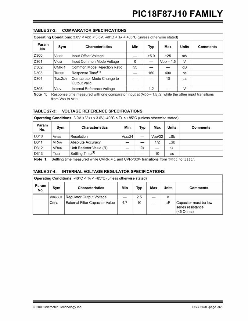
PIC18F87J10 FAMILY
TABLE 27-2: COMPARATOR SPECIFICATIONSTABLE 27-3: VOLTAGE REFERENCE SPECIFICATIONS
TABLE 27-4: INTERNAL VOLTAGE REGULATOR SPECIFICATIONS
Operating Conditions: 3.0V < VDD < 3.6V, -40°C < TA < +85°C (unless otherwise stated)
ParamNo. Sym Characteristics Min Typ Max Units Comments
D300 VIOFF Input Offset Voltage — ±5.0 ±25 mVD301 VICM Input Common Mode Voltage 0 — VDD – 1.5 VD302 CMRR Common Mode Rejection Ratio 55 — — dBD303 TRESP Response Time(1) — 150 400 nsD304 TMC2OV Comparator Mode Change to
Output Valid— — 10 μs
D305 VIRV Internal Reference Voltage — 1.2 — VNote 1: Response time measured with one comparator input at (VDD – 1.5)/2, while the other input transitions
from VSS to VDD.
Operating Conditions: 3.0V < VDD < 3.6V, -40°C < TA < +85°C (unless otherwise stated)
ParamNo. Sym Characteristics Min Typ Max Units Comments
D310 VRES Resolution VDD/24 — VDD/32 LSbD311 VRAA Absolute Accuracy — — 1/2 LSbD312 VRUR Unit Resistor Value (R) — 2k — Ω
D313 TSET Settling Time(1) — — 10 μsNote 1: Settling time measured while CVRR = 1 and CVR<3:0> transitions from ‘0000’ to ‘1111’.
Operating Conditions: -40°C < TA < +85°C (unless otherwise stated)
ParamNo. Sym Characteristics Min Typ Max Units Comments
VRGOUT Regulator Output Voltage — 2.5 — VCEFC External Filter Capacitor Value 4.7 10 — μF Capacitor must be low
series resistance (<5 Ohms)
© 2009 Microchip Technology Inc. DS39663F-page 361
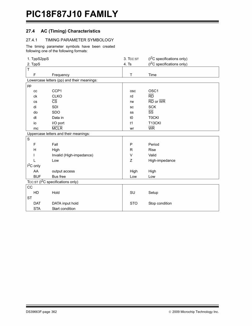
PIC18F87J10 FAMILY
27.4 AC (Timing) Characteristics27.4.1 TIMING PARAMETER SYMBOLOGYThe timing parameter symbols have been createdfollowing one of the following formats:
1. TppS2ppS 3. TCC:ST (I2C specifications only)2. TppS 4. Ts (I2C specifications only)T
F Frequency T TimeLowercase letters (pp) and their meanings:pp
cc CCP1 osc OSC1ck CLKO rd RDcs CS rw RD or WRdi SDI sc SCKdo SDO ss SSdt Data in t0 T0CKIio I/O port t1 T13CKImc MCLR wr WR
Uppercase letters and their meanings:S
F Fall P PeriodH High R RiseI Invalid (High-impedance) V ValidL Low Z High-impedance
I2C onlyAA output access High HighBUF Bus free Low Low
TCC:ST (I2C specifications only)CC
HD Hold SU SetupST
DAT DATA input hold STO Stop conditionSTA Start condition
DS39663F-page 362 © 2009 Microchip Technology Inc.
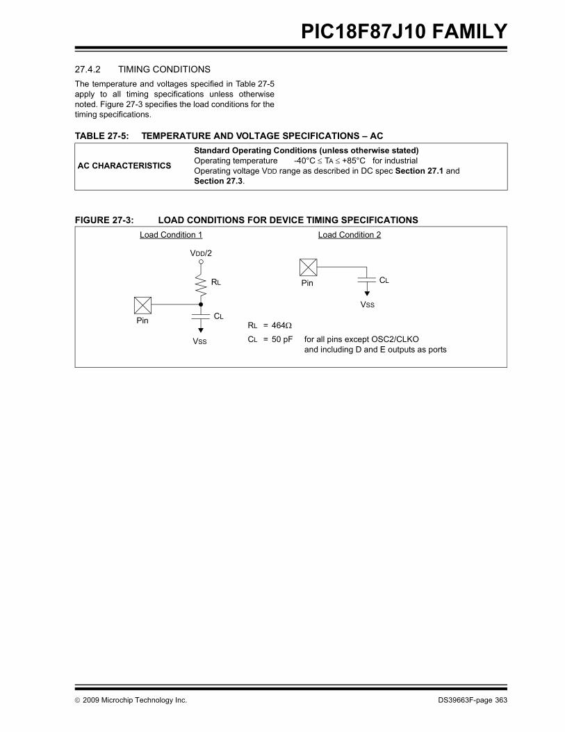
PIC18F87J10 FAMILY
27.4.2 TIMING CONDITIONSThe temperature and voltages specified in Table 27-5apply to all timing specifications unless otherwisenoted. Figure 27-3 specifies the load conditions for thetiming specifications.TABLE 27-5: TEMPERATURE AND VOLTAGE SPECIFICATIONS – AC
FIGURE 27-3: LOAD CONDITIONS FOR DEVICE TIMING SPECIFICATIONS
AC CHARACTERISTICS
Standard Operating Conditions (unless otherwise stated)Operating temperature -40°C ≤ TA ≤ +85°C for industrialOperating voltage VDD range as described in DC spec Section 27.1 and Section 27.3.
VDD/2
CL
RL
Pin
Pin
VSS
VSS
CL
RL = 464Ω
CL = 50 pF for all pins except OSC2/CLKOand including D and E outputs as ports
Load Condition 1 Load Condition 2
© 2009 Microchip Technology Inc. DS39663F-page 363
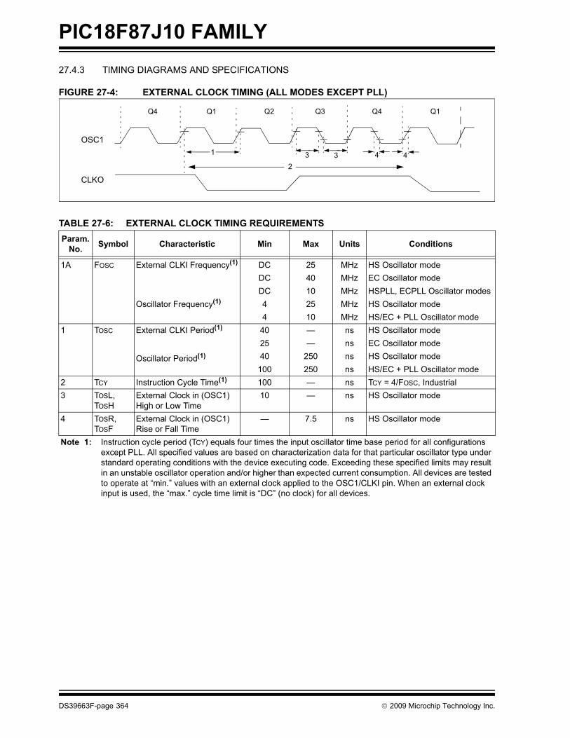
PIC18F87J10 FAMILY
27.4.3 TIMING DIAGRAMS AND SPECIFICATIONSFIGURE 27-4: EXTERNAL CLOCK TIMING (ALL MODES EXCEPT PLL)
TABLE 27-6: EXTERNAL CLOCK TIMING REQUIREMENTS Param.
No. Symbol Characteristic Min Max Units Conditions
1A FOSC External CLKI Frequency(1) DC 25 MHz HS Oscillator modeDC 40 MHz EC Oscillator modeDC 10 MHz HSPLL, ECPLL Oscillator modes
Oscillator Frequency(1) 4 25 MHz HS Oscillator mode4 10 MHz HS/EC + PLL Oscillator mode
1 TOSC External CLKI Period(1) 40 — ns HS Oscillator mode25 — ns EC Oscillator mode
Oscillator Period(1) 40 250 ns HS Oscillator mode100 250 ns HS/EC + PLL Oscillator mode
2 TCY Instruction Cycle Time(1) 100 — ns TCY = 4/FOSC, Industrial3 TOSL,
TOSHExternal Clock in (OSC1) High or Low Time
10 — ns HS Oscillator mode
4 TOSR,TOSF
External Clock in (OSC1) Rise or Fall Time
— 7.5 ns HS Oscillator mode
Note 1: Instruction cycle period (TCY) equals four times the input oscillator time base period for all configurations except PLL. All specified values are based on characterization data for that particular oscillator type under standard operating conditions with the device executing code. Exceeding these specified limits may result in an unstable oscillator operation and/or higher than expected current consumption. All devices are tested to operate at “min.” values with an external clock applied to the OSC1/CLKI pin. When an external clock input is used, the “max.” cycle time limit is “DC” (no clock) for all devices.
OSC1
CLKO
Q4 Q1 Q2 Q3 Q4 Q1
1
23 3 4 4
DS39663F-page 364 © 2009 Microchip Technology Inc.
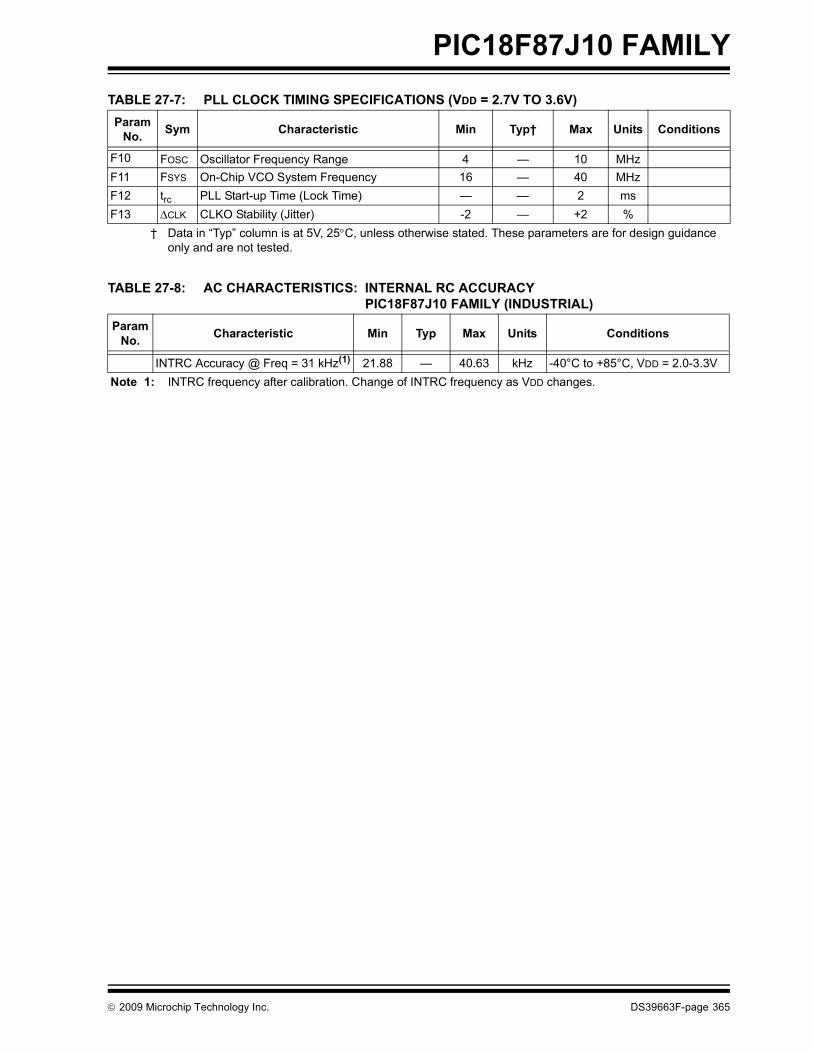
PIC18F87J10 FAMILY
TABLE 27-7: PLL CLOCK TIMING SPECIFICATIONS (VDD = 2.7V TO 3.6V)TABLE 27-8: AC CHARACTERISTICS: INTERNAL RC ACCURACYPIC18F87J10 FAMILY (INDUSTRIAL)
Param No. Sym Characteristic Min Typ† Max Units Conditions
F10 FOSC Oscillator Frequency Range 4 — 10 MHzF11 FSYS On-Chip VCO System Frequency 16 — 40 MHzF12 trc PLL Start-up Time (Lock Time) — — 2 msF13 ΔCLK CLKO Stability (Jitter) -2 — +2 %
† Data in “Typ” column is at 5V, 25°C, unless otherwise stated. These parameters are for design guidance only and are not tested.
ParamNo. Characteristic Min Typ Max Units Conditions
INTRC Accuracy @ Freq = 31 kHz(1) 21.88 — 40.63 kHz -40°C to +85°C, VDD = 2.0-3.3VNote 1: INTRC frequency after calibration. Change of INTRC frequency as VDD changes.
© 2009 Microchip Technology Inc. DS39663F-page 365

PIC18F87J10 FAMILY
FIGURE 27-5: CLKO AND I/O TIMINGTABLE 27-9: CLKO AND I/O TIMING REQUIREMENTS Param
No. Symbol Characteristic Min Typ Max Units Conditions
10 TOSH2CKL OSC1 ↑ to CLKO ↓ — 75 200 ns (Note 1)11 TOSH2CKH OSC1 ↑ to CLKO ↑ — 75 200 ns (Note 1)12 TCKR CLKO Rise Time — 15 30 ns (Note 1)13 TCKF CLKO Fall Time — 15 30 ns (Note 1)14 TCKL2IOV CLKO ↓ to Port Out Valid — — 0.5 TCY + 20 ns15 TIOV2CKH Port In Valid before CLKO ↑ 0.25 TCY + 25 — — ns 16 TCKH2IOI Port In Hold after CLKO ↑ 0 — — ns17 TOSH2IOV OSC1 ↑ (Q1 cycle) to Port Out Valid — 50 150 ns18 TOSH2IOI OSC1 ↑ (Q2 cycle) to Port Input Invalid
(I/O in hold time)100 — — ns
18A 200 — — ns VDD = 2.0V19 TIOV2OSH Port Input Valid to OSC1 ↑
(I/O in setup time)0 — — ns
20 TIOR Port Output Rise Time — — 6 ns20A — — — —21 TIOF Port Output Fall Time — — 5 ns21A — — — —22† TINP INTx Pin High or Low Time TCY — — ns23† TRBP RB<7:4> Change INTx High or Low Time TCY — — nsLegend: TBD = To Be Determined
† These parameters are asynchronous events not related to any internal clock edges.Note 1: Measurements are taken in RC mode, where CLKO output is 4 x TOSC.
Note: Refer to Figure 27-3 for load conditions.
OSC1
CLKO
I/O pin(Input)
I/O pin(Output)
Q4 Q1 Q2 Q3
10
1314
17
20, 21
19 18
15
11
12
16
Old Value New Value
DS39663F-page 366 © 2009 Microchip Technology Inc.

PIC18F87J10 FAMILY
FIGURE 27-6: PROGRAM MEMORY FETCH TIMING DIAGRAM (8-BIT)TABLE 27-7: PROGRAM MEMORY FETCH TIMING REQUIREMENTS (8-BIT) Param
No Symbol Characteristics Min Typ Max Units
150 TadV2aIL Address Out Valid to ALE ↓ (address setup time) 0.25 TCY – 10 — — ns151 TaIL2adl ALE ↓ to Address Out Invalid (address hold time) 5 — — ns153 BA01 BA0 ↑ to Most Significant Data Valid 0.125 TCY — — ns154 BA02 BA0 ↓ to Least Significant Data Valid 0.125 TCY — — ns
155 TaIL2oeL ALE ↓ to OE ↓ 0.125 TCY — — ns
161 ToeH2adD OE ↑ to A/D Driven 0.125 TCY – 5 — — ns
162 TadV2oeH Least Significant Data Valid Before OE ↑ (data setup time
20 — — ns
162A TadV2oeH Most Significant Data Valid Before OE ↑ (data setup time)
0.25 TCY + 20 — — ns
163 ToeH2adI OE ↑ to Data in Invalid (data Hold Time) 0 — — ns166 TaIH2aIH ALE ↑ to ALE ↑ (cycle time) — TCY — ns167 TACC Address Valid to Data Valid 0.5 TCY – 10 — — ns
168 Toe OE ↓ to Data Valid — — 0.125 TCY + 5 ns
170 TubH2oeH BA0 = 0 Valid Before OE ↑ 0.25 TCY — — ns
170A TubL2oeH BA0 = 1 Valid Before OE ↑ 0.5 TCY — — ns
Q1 Q2 Q3 Q4 Q1 Q2
OSC1
ALE
OE
Address Data
170
161
162
AD<7:0> Address
AddressA<19:8> Address
162A
BA0
Data
170A
151150
166167
155
153
163154
168CE
© 2009 Microchip Technology Inc. DS39663F-page 367

PIC18F87J10 FAMILY
FIGURE 27-8: PROGRAM MEMORY READ TIMING DIAGRAMTABLE 27-10: CLKO AND I/O TIMING REQUIREMENTS Param.
No Symbol Characteristics Min Typ Max Units
150 TadV2alL Address Out Valid to ALE ↓ (address setup time)
0.25 TCY – 10 — — ns
151 TalL2adl ALE ↓ to Address Out Invalid (address hold time)
5 — — ns
155 TalL2oeL ALE ↓ to OE ↓ 10 0.125 TCY — ns160 TadZ2oeL AD High-Z to OE ↓ (bus release to OE) 0 — — ns161 ToeH2adD OE ↑ to AD Driven 0.125 TCY – 5 — — ns162 TadV2oeH LS Data Valid before OE ↑ (data setup time) 20 — — ns163 ToeH2adl OE ↑ to Data In Invalid (data hold time) 0 — — ns164 TalH2alL ALE Pulse Width — 0.25 TCY — ns165 ToeL2oeH OE Pulse Width 0.5 TCY – 5 0.5 TCY — ns166 TalH2alH ALE ↑ to ALE ↑ (cycle time) — TCY — ns167 Tacc Address Valid to Data Valid 0.75 TCY – 25 — — ns168 Toe OE ↓ to Data Valid — 0.5 TCY – 25 ns169 TalL2oeH ALE ↓ to OE ↑ 0.625 TCY – 10 — 0.625 TCY + 10 ns171 TalH2csL Chip Enable Active to ALE ↓ 0.25 TCY – 20 — — ns171A TubL2oeH AD Valid to Chip Enable Active — — 10 ns
Q1 Q2 Q3 Q4 Q1 Q2
OSC1
ALE
OE
Address Data from External
164
166
160
165
161151 162
163AD<15:0>
167168
155
Address
Address
150
A<19:16> Address
169
BA0
CE171
171A
Operating Conditions: 2.0V < VCC < 3.6V, -40°C < TA < +125°C unless otherwise stated.
DS39663F-page 368 © 2009 Microchip Technology Inc.

PIC18F87J10 FAMILY
FIGURE 27-9: PROGRAM MEMORY WRITE TIMING DIAGRAMTABLE 27-11: PROGRAM MEMORY WRITE TIMING REQUIREMENTS
Param. No Symbol Characteristics Min Typ Max Units
150 TadV2alL Address Out Valid to ALE ↓ (address setup time) 0.25 TCY – 10 — — ns151 TalL2adl ALE ↓ to Address Out Invalid (address hold time) 5 — — ns153 TwrH2adl WRn ↑ to Data Out Invalid (data hold time) 5 — — ns154 TwrL WRn Pulse Width 0.5 TCY – 5 0.5 TCY — ns156 TadV2wrH Data Valid before WRn ↑ (data setup time) 0.5 TCY – 10 — — ns157 TbsV2wrL Byte Select Valid before WRn ↓
(byte select setup time)0.25 TCY — — ns
157A TwrH2bsI WRn ↑ to Byte Select Invalid (byte select hold time) 0.125 TCY – 5 — — ns166 TalH2alH ALE ↑ to ALE ↑ (cycle time) — TCY — ns171 TalH2csL Chip Enable Active to ALE ↓ 0.25 TCY – 20 — — ns171A TubL2oeH AD Valid to Chip Enable Active — — 10 ns
Q1 Q2 Q3 Q4 Q1 Q2
OSC1
ALE
Address Data
156150
151
153
AD<15:0> Address
WRH orWRL
UB orLB
157
154
157A
AddressA<19:16> AddressBA0
166
CE
171
171A
Operating Conditions: 2.0V < VCC < 3.6V, -40°C < TA < +125°C unless otherwise stated.
© 2009 Microchip Technology Inc. DS39663F-page 369

PIC18F87J10 FAMILY
FIGURE 27-10: RESET, WATCHDOG TIMER, OSCILLATOR START-UP TIMER ANDPOWER-UP TIMER TIMING
TABLE 27-12: RESET, WATCHDOG TIMER, OSCILLATOR START-UP TIMER, POWER-UP TIMER AND BROWN-OUT RESET REQUIREMENTS
Param. No. Symbol Characteristic Min Typ Max Units Conditions
30 TMCL MCLR Pulse Width (low) 2 — — μs31 TWDT Watchdog Timer Time-out Period
(no postscaler)3.5 4.1 4.9 ms
32 TOST Oscillation Start-up Timer Period 1024 TOSC — 1024 TOSC — TOSC = OSC1 period33 TPWRT Power-up Timer Period 57.4 66 77.7 ms 34 TIOZ I/O High-Impedance from MCLR
Low or Watchdog Timer Reset— 2 — μs
38 TCSD CPU Start-up Time — 200 — μs
VDD
MCLR
InternalPOR
PWRTTime-out
OscillatorTime-out
InternalReset
WatchdogTimerReset
33
32
30
3134
I/O pins
34
Note: Refer to Figure 27-3 for load conditions.
DS39663F-page 370 © 2009 Microchip Technology Inc.

PIC18F87J10 FAMILY
FIGURE 27-11: TIMER0 AND TIMER1 EXTERNAL CLOCK TIMINGSTABLE 27-13: TIMER0 AND TIMER1 EXTERNAL CLOCK REQUIREMENTS Param
No. Symbol Characteristic Min Max Units Conditions
40 TT0H T0CKI High Pulse Width No prescaler 0.5 TCY + 20 — nsWith prescaler 10 — ns
41 TT0L T0CKI Low Pulse Width No prescaler 0.5 TCY + 20 — nsWith prescaler 10 — ns
42 TT0P T0CKI Period No prescaler TCY + 10 — nsWith prescaler Greater of:
20 ns or (TCY + 40)/N
— ns N = prescalevalue (1, 2, 4,..., 256)
45 TT1H T13CKI High Time
Synchronous, no prescaler 0.5 TCY + 20 — nsSynchronous, with prescaler 10 — nsAsynchronous 30 — ns
46 TT1L T13CKI Low Time
Synchronous, no prescaler 0.5 TCY + 5 — nsSynchronous, with prescaler 10 — nsAsynchronous 30 — ns
47 TT1P T13CKI Input Period
Synchronous Greater of:20 ns or
(TCY + 40)/N
— ns N = prescalevalue (1, 2, 4, 8)
Asynchronous 60 — nsFT1 T13CKI Oscillator Input Frequency Range DC 50 kHz
48 TCKE2TMRI Delay from External T13CKI Clock Edge to Timer Increment
2 TOSC 7 TOSC —
Note: Refer to Figure 27-3 for load conditions.
46
47
45
48
41
42
40
T0CKI
T1OSO/T13CKI
TMR0 orTMR1
© 2009 Microchip Technology Inc. DS39663F-page 371

PIC18F87J10 FAMILY
FIGURE 27-12: CAPTURE/COMPARE/PWM TIMINGS (INCLUDING ECCP MODULES)TABLE 27-14: CAPTURE/COMPARE/PWM REQUIREMENTS (INCLUDING ECCP MODULES)
TABLE 27-15: PARALLEL SLAVE PORT REQUIREMENTS
Param No. Symbol Characteristic Min Max Units Conditions
50 TCCL CCPx Input Low Time
No prescaler 0.5 TCY + 20 — nsWith prescaler 10 — ns
51 TCCH CCPx Input High Time
No prescaler 0.5 TCY + 20 — nsWith prescaler 10 — ns
52 TCCP CCPx Input Period 3 TCY + 40N
— ns N = prescale value (1, 4 or 16)
53 TCCR CCPx Output Fall Time — 25 ns54 TCCF CCPx Output Fall Time — 25 ns
Param.No. Symbol Characteristic Min Max Units Conditions
62 TdtV2wrH Data In Valid before WR ↑ or CS ↑ (setup time) 20 — ns63 TwrH2dtI WR ↑ or CS ↑ to Data–In Invalid (hold time) 20 — ns64 TrdL2dtV RD ↓ and CS ↓ to Data–Out Valid — 80 ns65 TrdH2dtI RD ↑ or CS ↓ to Data–Out Invalid 10 30 ns66 TibfINH Inhibit of the IBF Flag bit being Cleared from
WR ↑ or CS ↑— 3 TCY
Note: Refer to Figure 27-3 for load conditions.
CCPx(Capture Mode)
50 51
52
CCPx
53 54(Compare or PWM Mode)
DS39663F-page 372 © 2009 Microchip Technology Inc.

PIC18F87J10 FAMILY
FIGURE 27-13: EXAMPLE SPI MASTER MODE TIMING (CKE = 0)TABLE 27-16: EXAMPLE SPI MODE REQUIREMENTS (MASTER MODE, CKE = 0) Param
No. Symbol Characteristic Min Max Units Conditions
70 TSSL2SCH, TSSL2SCL
SSx ↓ to SCKx ↓ or SCKx ↑ Input TCY — ns
73 TDIV2SCH, TDIV2SCL
Setup Time of SDIx Data Input to SCKx Edge 20 — ns
73A TB2B Last Clock Edge of Byte 1 to the 1st Clock Edge of Byte 2
1.5 TCY + 40 — ns (Note 1)
74 TSCH2DIL, TSCL2DIL
Hold Time of SDIx Data Input to SCKx Edge 40 — ns
75 TDOR SDOx Data Output Rise Time — 25 ns76 TDOF SDOx Data Output Fall Time — 25 ns78 TSCR SCKx Output Rise Time (Master mode) — 25 ns79 TSCF SCKx Output Fall Time (Master mode) — 25 ns80 TSCH2DOV,
TSCL2DOVSDOx Data Output Valid after SCKx Edge — 50 ns
Note 1: Only if Parameter #71A and #72A are used.
SSx
SCKx(CKP = 0)
SCKx(CKP = 1)
SDOx
SDIx
70
71 72
7374
75, 76
787980
7978
MSb LSbbit 6 - - - - - - 1
MSb In LSb Inbit 6 - - - - 1
Note: Refer to Figure 27-3 for load conditions.
© 2009 Microchip Technology Inc. DS39663F-page 373

PIC18F87J10 FAMILY
FIGURE 27-14: EXAMPLE SPI MASTER MODE TIMING (CKE = 1)TABLE 27-17: EXAMPLE SPI MODE REQUIREMENTS (MASTER MODE, CKE = 1) Param.
No. Symbol Characteristic Min Max Units Conditions
73 TDIV2SCH, TDIV2SCL
Setup Time of SDIx Data Input to SCKx Edge 20 — ns
73A TB2B Last Clock Edge of Byte 1 to the 1st Clock Edge of Byte 2
1.5 TCY + 40 — ns (Note 1)
74 TSCH2DIL, TSCL2DIL
Hold Time of SDIx Data Input to SCKx Edge 40 — ns
75 TDOR SDOx Data Output Rise Time — 25 ns76 TDOF SDOx Data Output Fall Time — 25 ns78 TSCR SCKx Output Rise Time (Master mode) — 25 ns79 TSCF SCKx Output Fall Time (Master mode) — 25 ns80 TSCH2DOV,
TSCL2DOVSDOx Data Output Valid after SCKx Edge — 50 ns
81 TDOV2SCH,TDOV2SCL
SDOx Data Output Setup to SCKx Edge TCY — ns
Note 1: Only if Parameter #71A and #72A are used.
SSx
SCKx(CKP = 0)
SCKx(CKP = 1)
SDOx
SDIx
81
71 72
74
75, 76
78
80
MSb
7973
MSb In
bit 6 - - - - - - 1
LSb Inbit 6 - - - - 1
LSb
Note: Refer to Figure 27-3 for load conditions.
DS39663F-page 374 © 2009 Microchip Technology Inc.

PIC18F87J10 FAMILY
FIGURE 27-15: EXAMPLE SPI SLAVE MODE TIMING (CKE = 0)TABLE 27-18: EXAMPLE SPI MODE REQUIREMENTS (SLAVE MODE TIMING, CKE = 0) Param
No. Symbol Characteristic Min Max Units Conditions
70 TSSL2SCH, TSSL2SCL
SSx ↓ to SCKx ↓ or SCKx ↑ Input TCY — ns
71 TSCH SCKx Input High Time (Slave mode)
Continuous 1.25 TCY + 30 — ns71A Single Byte 40 — ns (Note 1)72 TSCL SCKx Input Low Time
(Slave mode)Continuous 1.25 TCY + 30 — ns
72A Single Byte 40 — ns (Note 1)73 TDIV2SCH,
TDIV2SCLSetup Time of SDIx Data Input to SCKx Edge 20 — ns
73A TB2B Last Clock Edge of Byte 1 to the First Clock Edge of Byte 2 1.5 TCY + 40 — ns (Note 2)74 TSCH2DIL,
TSCL2DILHold Time of SDIx Data Input to SCKx Edge 40 — ns
75 TDOR SDOx Data Output Rise Time — 25 ns76 TDOF SDOx Data Output Fall Time — 25 ns77 TSSH2DOZ SSx ↑ to SDOx Output High-Impedance 10 50 ns80 TSCH2DOV,
TSCL2DOVSDOx Data Output Valid after SCKx Edge — 50 ns
83 TSCH2SSH,TSCL2SSH
SSx ↑ after SCKx Edge 1.5 TCY + 40 — ns
Note 1: Requires the use of Parameter #73A.2: Only if Parameter #71A and #72A are used.
SSx
SCKx(CKP = 0)
SCKx(CKP = 1)
SDOx
SDI
70
71 72
7374
75, 76 77
787980
7978
SDIx
MSb LSbbit 6 - - - - - - 1
MSb In bit 6 - - - - 1 LSb In
83
Note: Refer to Figure 27-3 for load conditions.
© 2009 Microchip Technology Inc. DS39663F-page 375

PIC18F87J10 FAMILY
FIGURE 27-16: EXAMPLE SPI SLAVE MODE TIMING (CKE = 1)TABLE 27-19: EXAMPLE SPI SLAVE MODE REQUIREMENTS (CKE = 1) Param
No. Symbol Characteristic Min Max Units Conditions
70 TSSL2SCH, TSSL2SCL
SSx ↓ to SCKx ↓ or SCKx ↑ Input TCY — ns
71 TSCH SCKx Input High Time (Slave mode)
Continuous 1.25 TCY + 30 — ns71A Single Byte 40 — ns (Note 1)72 TSCL SCKx Input Low Time
(Slave mode)Continuous 1.25 TCY + 30 — ns
72A Single Byte 40 — ns (Note 1)73A TB2B Last Clock Edge of Byte 1 to the First Clock Edge of Byte 2 1.5 TCY + 40 — ns (Note 2)74 TSCH2DIL,
TSCL2DILHold Time of SDIx Data Input to SCKx Edge 20 — ns
75 TDOR SDOx Data Output Rise Time — 25 ns76 TDOF SDOx Data Output Fall Time — 25 ns77 TSSH2DOZ SSx ↑ to SDOx Output High-Impedance 10 50 ns80 TSCH2DOV,
TSCL2DOVSDOx Data Output Valid after SCKx Edge — 50 ns
82 TSSL2DOV SDOx Data Output Valid after SSx ↓ Edge — 50 ns83 TSCH2SSH,
TSCL2SSHSSx ↑ after SCKx Edge 1.5 TCY + 40 — ns
Note 1: Requires the use of Parameter #73A.2: Only if Parameter #71A and #72A are used.
SSx
SCKx(CKP = 0)
SCKx(CKP = 1)
SDOx
SDI
70
71 72
82
SDIx
74
75, 76
MSb bit 6 - - - - - - 1 LSb
77
MSb In bit 6 - - - - 1 LSb In
80
83
Note: Refer to Figure 27-3 for load conditions.
DS39663F-page 376 © 2009 Microchip Technology Inc.

PIC18F87J10 FAMILY
FIGURE 27-17: I2C™ BUS START/STOP BITS TIMINGTABLE 27-20: I2C™ BUS START/STOP BITS REQUIREMENTS (SLAVE MODE)
FIGURE 27-18: I2C™ BUS DATA TIMING
Param. No. Symbol Characteristic Min Max Units Conditions
90 TSU:STA Start Condition 100 kHz mode 4700 — ns Only relevant for Repeated Start conditionSetup Time 400 kHz mode 600 —
91 THD:STA Start Condition 100 kHz mode 4000 — ns After this period, the first clock pulse is generatedHold Time 400 kHz mode 600 —
92 TSU:STO Stop Condition 100 kHz mode 4700 — nsSetup Time 400 kHz mode 600 —
93 THD:STO Stop Condition 100 kHz mode 4000 — nsHold Time 400 kHz mode 600 —
Note: Refer to Figure 27-3 for load conditions.
91
92
93SCLx
SDAx
StartCondition
StopCondition
90
Note: Refer to Figure 27-3 for load conditions.
90
91 92
100
101
103
106 107
109 109110
102
SCLx
SDAxIn
SDAxOut
© 2009 Microchip Technology Inc. DS39663F-page 377

PIC18F87J10 FAMILY
TABLE 27-21: I2C™ BUS DATA REQUIREMENTS (SLAVE MODE)Param. No. Symbol Characteristic Min Max Units Conditions
100 THIGH Clock High Time 100 kHz mode 4.0 — μs400 kHz mode 0.6 — μsMSSP Module 1.5 TCY —
101 TLOW Clock Low Time 100 kHz mode 4.7 — μs400 kHz mode 1.3 — μsMSSP Module 1.5 TCY —
102 TR SDAx and SCLx Rise Time 100 kHz mode — 1000 ns400 kHz mode 20 + 0.1 CB 300 ns CB is specified to be from
10 to 400 pF 103 TF SDAx and SCLx Fall Time 100 kHz mode — 300 ns
400 kHz mode 20 + 0.1 CB 300 ns CB is specified to be from 10 to 400 pF
90 TSU:STA Start Condition Setup Time 100 kHz mode 4.7 — μs Only relevant for Repeated Start condition400 kHz mode 0.6 — μs
91 THD:STA Start Condition Hold Time 100 kHz mode 4.0 — μs After this period, the first clock pulse is generated400 kHz mode 0.6 — μs
106 THD:DAT Data Input Hold Time 100 kHz mode 0 — ns400 kHz mode — 0.9 μs
107 TSU:DAT Data Input Setup Time 100 kHz mode 250 — ns (Note 2)400 kHz mode — — ns
92 TSU:STO Stop Condition Setup Time 100 kHz mode 4.7 — μs400 kHz mode 0.6 — μs
109 TAA Output Valid from Clock 100 kHz mode — 3500 ns (Note 1)400 kHz mode — — ns
110 TBUF Bus Free Time 100 kHz mode 4.7 — μs Time the bus must be free before a new transmission can start
400 kHz mode — — μs
D102 CB Bus Capacitive Loading — 400 pF Note 1: As a transmitter, the device must provide this internal minimum delay time to bridge the undefined region (min. 300 ns)
of the falling edge of SCLx to avoid unintended generation of Start or Stop conditions.2: A Fast mode I2C™ bus device can be used in a Standard mode I2C bus system, but the requirement, TSU:DAT ≥ 250 ns,
must then be met. This will automatically be the case if the device does not stretch the LOW period of the SCLx signal. If such a device does stretch the LOW period of the SCLx signal, it must output the next data bit to the SDAx line,TR max. + TSU:DAT = 1000 + 250 = 1250 ns (according to the Standard mode I2C bus specification), before the SCLx line is released.
DS39663F-page 378 © 2009 Microchip Technology Inc.

PIC18F87J10 FAMILY
FIGURE 27-19: MASTER SSP I2C™ BUS START/STOP BITS TIMING WAVEFORMSTABLE 27-22: MASTER SSP I2C™ BUS START/STOP BITS REQUIREMENTS
FIGURE 27-20: MASTER SSP I2C™ BUS DATA TIMING
Param.No. Symbol Characteristic Min Max Units Conditions
90 TSU:STA Start Condition 100 kHz mode 2(TOSC)(BRG + 1) — ns Only relevant for Repeated Start condition
Setup Time 400 kHz mode 2(TOSC)(BRG + 1) —1 MHz mode(1) 2(TOSC)(BRG + 1) —
91 THD:STA Start Condition 100 kHz mode 2(TOSC)(BRG + 1) — ns After this period, the first clock pulse is generated
Hold Time 400 kHz mode 2(TOSC)(BRG + 1) —1 MHz mode(1) 2(TOSC)(BRG + 1) —
92 TSU:STO Stop Condition 100 kHz mode 2(TOSC)(BRG + 1) — nsSetup Time 400 kHz mode 2(TOSC)(BRG + 1) —
1 MHz mode(1) 2(TOSC)(BRG + 1) —93 THD:STO Stop Condition 100 kHz mode 2(TOSC)(BRG + 1) — ns
Hold Time 400 kHz mode 2(TOSC)(BRG + 1) —1 MHz mode(1) 2(TOSC)(BRG + 1) —
Note 1: Maximum pin capacitance = 10 pF for all I2C™ pins.
Note: Refer to Figure 27-3 for load conditions.
91 93SCLx
SDAx
StartCondition
StopCondition
90 92
Note: Refer to Figure 27-3 for load conditions.
9091 92
100101
103
106107
109 109 110
102
SCLx
SDAxIn
SDAxOut
© 2009 Microchip Technology Inc. DS39663F-page 379
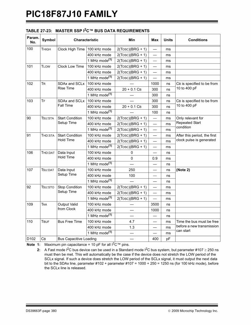
PIC18F87J10 FAMILY
TABLE 27-23: MASTER SSP I2C™ BUS DATA REQUIREMENTS Param.No. Symbol Characteristic Min Max Units Conditions
100 THIGH Clock High Time 100 kHz mode 2(TOSC)(BRG + 1) — ms400 kHz mode 2(TOSC)(BRG + 1) — ms1 MHz mode(1) 2(TOSC)(BRG + 1) — ms
101 TLOW Clock Low Time 100 kHz mode 2(TOSC)(BRG + 1) — ms400 kHz mode 2(TOSC)(BRG + 1) — ms1 MHz mode(1) 2(TOSC)(BRG + 1) — ms
102 TR SDAx and SCLx Rise Time
100 kHz mode — 1000 ns CB is specified to be from 10 to 400 pF 400 kHz mode 20 + 0.1 CB 300 ns
1 MHz mode(1) — 300 ns103 TF SDAx and SCLx
Fall Time100 kHz mode — 300 ns CB is specified to be from
10 to 400 pF 400 kHz mode 20 + 0.1 CB 300 ns1 MHz mode(1) — 100 ns
90 TSU:STA Start Condition Setup Time
100 kHz mode 2(TOSC)(BRG + 1) — ms Only relevant for Repeated Start condition
400 kHz mode 2(TOSC)(BRG + 1) — ms1 MHz mode(1) 2(TOSC)(BRG + 1) — ms
91 THD:STA Start Condition Hold Time
100 kHz mode 2(TOSC)(BRG + 1) — ms After this period, the first clock pulse is generated400 kHz mode 2(TOSC)(BRG + 1) — ms
1 MHz mode(1) 2(TOSC)(BRG + 1) — ms106 THD:DAT Data Input
Hold Time100 kHz mode 0 — ns400 kHz mode 0 0.9 ms1 MHz mode(1) — — ns
107 TSU:DAT Data Input Setup Time
100 kHz mode 250 — ns (Note 2)400 kHz mode 100 — ns1 MHz mode(1) — — ns
92 TSU:STO Stop Condition Setup Time
100 kHz mode 2(TOSC)(BRG + 1) — ms400 kHz mode 2(TOSC)(BRG + 1) — ms1 MHz mode(1) 2(TOSC)(BRG + 1) — ms
109 TAA Output Valid from Clock
100 kHz mode — 3500 ns400 kHz mode — 1000 ns1 MHz mode(1) — — ns
110 TBUF Bus Free Time 100 kHz mode 4.7 — ms Time the bus must be free before a new transmission can start
400 kHz mode 1.3 — ms1 MHz mode(1) — — ms
D102 CB Bus Capacitive Loading — 400 pF Note 1: Maximum pin capacitance = 10 pF for all I2C™ pins.
2: A Fast mode I2C bus device can be used in a Standard mode I2C bus system, but parameter #107 ≥ 250 ns must then be met. This will automatically be the case if the device does not stretch the LOW period of the SCLx signal. If such a device does stretch the LOW period of the SCLx signal, it must output the next data bit to the SDAx line, parameter #102 + parameter #107 = 1000 + 250 = 1250 ns (for 100 kHz mode), before the SCLx line is released.
DS39663F-page 380 © 2009 Microchip Technology Inc.

PIC18F87J10 FAMILY
FIGURE 27-21: EUSART SYNCHRONOUS TRANSMISSION (MASTER/SLAVE) TIMINGTABLE 27-24: EUSART SYNCHRONOUS TRANSMISSION REQUIREMENTS
FIGURE 27-22: EUSART SYNCHRONOUS RECEIVE (MASTER/SLAVE) TIMING
TABLE 27-25: EUSART SYNCHRONOUS RECEIVE REQUIREMENTS
Param No. Symbol Characteristic Min Max Units Conditions
120 TCKH2DTV SYNC XMIT (MASTER and SLAVE) Clock High to Data Out Valid — 40 ns
121 TCKRF Clock Out Rise Time and Fall Time (Master mode) — 20 ns122 TDTRF Data Out Rise Time and Fall Time — 20 ns
Param. No. Symbol Characteristic Min Max Units Conditions
125 TDTV2CKL SYNC RCV (MASTER and SLAVE)Data Hold before CKx ↓ (DTx hold time) 10 — ns
126 TCKL2DTL Data Hold after CKx ↓ (DTx hold time) 15 — ns
121 121
120122
TXx/CKx
RXx/DTxpin
pin
Note: Refer to Figure 27-3 for load conditions.
125
126
TXx/CKx
RXx/DTx
pin
pin
Note: Refer to Figure 27-3 for load conditions.
© 2009 Microchip Technology Inc. DS39663F-page 381
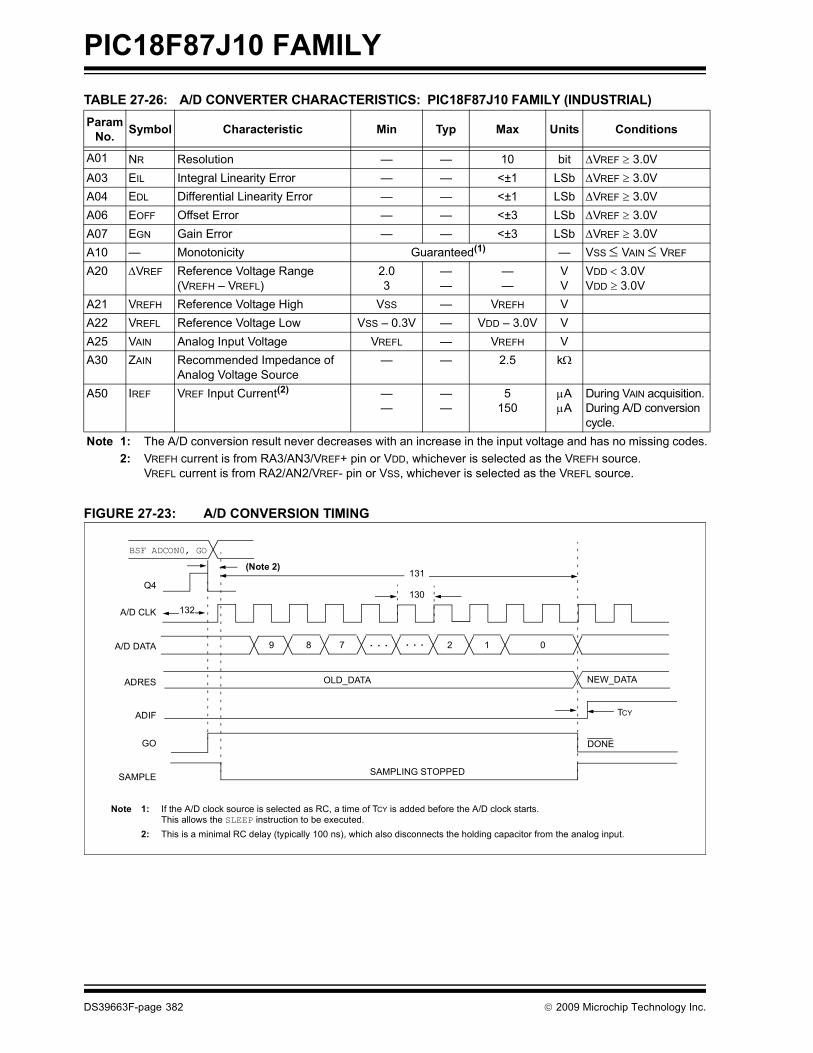
PIC18F87J10 FAMILY
TABLE 27-26: A/D CONVERTER CHARACTERISTICS: PIC18F87J10 FAMILY (INDUSTRIAL)FIGURE 27-23: A/D CONVERSION TIMING
Param No. Symbol Characteristic Min Typ Max Units Conditions
A01 NR Resolution — — 10 bit ΔVREF ≥ 3.0V A03 EIL Integral Linearity Error — — <±1 LSb ΔVREF ≥ 3.0V A04 EDL Differential Linearity Error — — <±1 LSb ΔVREF ≥ 3.0V A06 EOFF Offset Error — — <±3 LSb ΔVREF ≥ 3.0V A07 EGN Gain Error — — <±3 LSb ΔVREF ≥ 3.0V A10 — Monotonicity Guaranteed(1) — VSS ≤ VAIN ≤ VREF
A20 ΔVREF Reference Voltage Range(VREFH – VREFL)
2.03
——
——
VV
VDD < 3.0VVDD ≥ 3.0V
A21 VREFH Reference Voltage High VSS — VREFH VA22 VREFL Reference Voltage Low VSS – 0.3V — VDD – 3.0V VA25 VAIN Analog Input Voltage VREFL — VREFH VA30 ZAIN Recommended Impedance of
Analog Voltage Source— — 2.5 kΩ
A50 IREF VREF Input Current(2) ——
——
5150
μAμA
During VAIN acquisition.During A/D conversion cycle.
Note 1: The A/D conversion result never decreases with an increase in the input voltage and has no missing codes.2: VREFH current is from RA3/AN3/VREF+ pin or VDD, whichever is selected as the VREFH source.
VREFL current is from RA2/AN2/VREF- pin or VSS, whichever is selected as the VREFL source.
131
130
132
BSF ADCON0, GO
Q4
A/D CLK
A/D DATA
ADRES
ADIF
GO
SAMPLE
OLD_DATA
SAMPLING STOPPED
DONE
NEW_DATA
(Note 2)
9 8 7 2 1 0
Note 1: If the A/D clock source is selected as RC, a time of TCY is added before the A/D clock starts. This allows the SLEEP instruction to be executed.
2: This is a minimal RC delay (typically 100 ns), which also disconnects the holding capacitor from the analog input.
. . . . . .
TCY
DS39663F-page 382 © 2009 Microchip Technology Inc.

PIC18F87J10 FAMILY
TABLE 27-27: A/D CONVERSION REQUIREMENTS ParamNo. Symbol Characteristic Min Max Units Conditions
130 TAD A/D Clock Period 0.7 25.0(1) μs TOSC based, VREF ≥ 3.0V131 TCNV Conversion Time
(not including acquisition time) (Note 2)11 12 TAD
132 TACQ Acquisition Time (Note 3) 1.4 — μs -40°C to +85°C135 TSWC Switching Time from Convert → Sample — (Note 4)136 TDIS Discharge Time 0.2 — μsNote 1: The time of the A/D clock period is dependent on the device frequency and the TAD clock divider.
2: ADRES registers may be read on the following TCY cycle.3: The time for the holding capacitor to acquire the “New” input voltage when the voltage changes full scale
after the conversion (VDD to VSS or VSS to VDD). The source impedance (RS) on the input channels is 50Ω.4: On the following cycle of the device clock.
© 2009 Microchip Technology Inc. DS39663F-page 383

PIC18F87J10 FAMILY
NOTES:DS39663F-page 384 © 2009 Microchip Technology Inc.
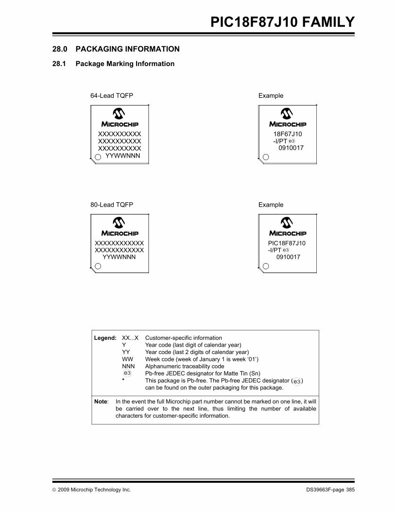
PIC18F87J10 FAMILY
28.0 PACKAGING INFORMATION
28.1 Package Marking Information
64-Lead TQFP
XXXXXXXXXXXXXXXXXXXXXXXXXXXXXX
YYWWNNN
Example
18F67J10-I/PT
0910017
80-Lead TQFP
XXXXXXXXXXXXXXXXXXXXXXXX
YYWWNNN
Example
PIC18F87J10-I/PT
0910017
Legend: XX...X Customer-specific informationY Year code (last digit of calendar year)YY Year code (last 2 digits of calendar year)WW Week code (week of January 1 is week ‘01’)NNN Alphanumeric traceability code Pb-free JEDEC designator for Matte Tin (Sn)* This package is Pb-free. The Pb-free JEDEC designator ( )
can be found on the outer packaging for this package.
Note: In the event the full Microchip part number cannot be marked on one line, it willbe carried over to the next line, thus limiting the number of availablecharacters for customer-specific information.
3e
3e
3e
3e
© 2009 Microchip Technology Inc. DS39663F-page 385

PIC18F87J10 FAMILY
28.2 Package Details The following sections give the technical details of thepackages.!"#$%&
' ( !"# $% &" ' ()"&'"!&) & #*&& & # +'% !& ! &,!- ' ' !!#.#&"# '#%!&"!!#%!&"!!!& $ #/'' !# ' !#& .0/
1+2 1!' ! & $& " !**&"&& !.32 % ' !("!"*&"&& (%%'&"! !
' ( 3& '!&" &4 #*!( ! ! & 4 %&& #&&&255***''54
6&! 77..' !7'&! 8 89 :
8"') %7 #! 8 ;7 #& /1+9 < & = = # #4 4 !! / /&#%% / = /3&7 & 7 / ; /3&& 7 .33& > /> >9 ?#& . 1+9 7 & 1+# #4 ?#& . 1+# #4 7 & 1+7 #4 !! = 7 #?#& ) #%& > > >#%& 1&&' > > >
D
D1
E
E1
e
b
N
NOTE 1 1 2 3 NOTE 2
c
LA1
L1
A2
Aφ
β
α
* +@/1
DS39663F-page 386 © 2009 Microchip Technology Inc.

PIC18F87J10 FAMILY
!"#$%&
' ( 3& '!&" &4 #*!( ! ! & 4 %&& #&&&255***''54
© 2009 Microchip Technology Inc. DS39663F-page 387

PIC18F87J10 FAMILY
) ## !"#$%&
' ( !"# $% &" ' ()"&'"!&) & #*&& & # +'% !& ! &,!- ' ' !!#.#&"# '#%!&"!!#%!&"!!!& $ #/'' !# ' !#& .0/
1+2 1!' ! & $& " !**&"&& !.32 % ' !("!"*&"&& (%%'&"! !
' ( 3& '!&" &4 #*!( ! ! & 4 %&& #&&&255***''54
6&! 77..' !7'&! 8 89 :
8"') %7 #! 8 @7 #& /1+9 < & = = # #4 4 !! / /&#%% / = /3&7 & 7 / ; /3&& 7 .33& > /> >9 ?#& . 1+9 7 & 1+# #4 ?#& . 1+# #4 7 & 1+7 #4 !! = 7 #?#& ) #%& > > >#%& 1&&' > > >
D
D1
E
E1e
b N
NOTE 1123 NOTE 2
A
A2L1
A1L
c
α
βφ
* +1
DS39663F-page 388 © 2009 Microchip Technology Inc.
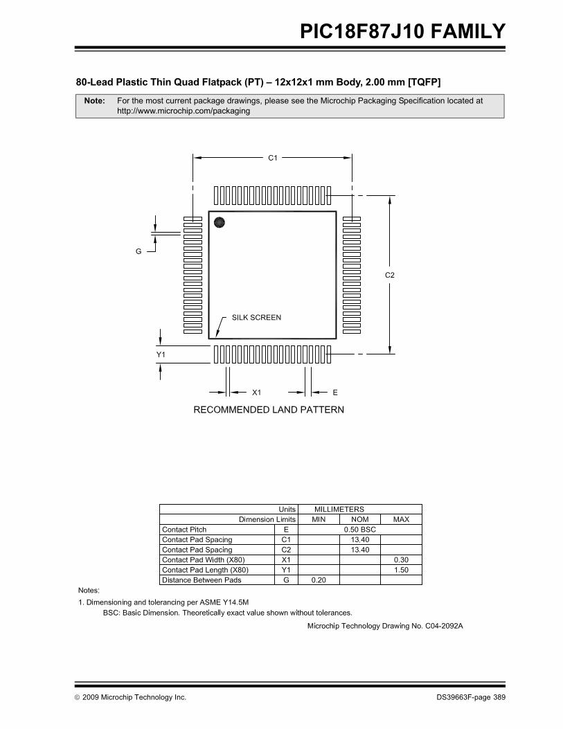
PIC18F87J10 FAMILY
) ## !"#$%&
' ( 3& '!&" &4 #*!( ! ! & 4 %&& #&&&255***''54
© 2009 Microchip Technology Inc. DS39663F-page 389

PIC18F87J10 FAMILY
NOTES:DS39663F-page 390 © 2009 Microchip Technology Inc.
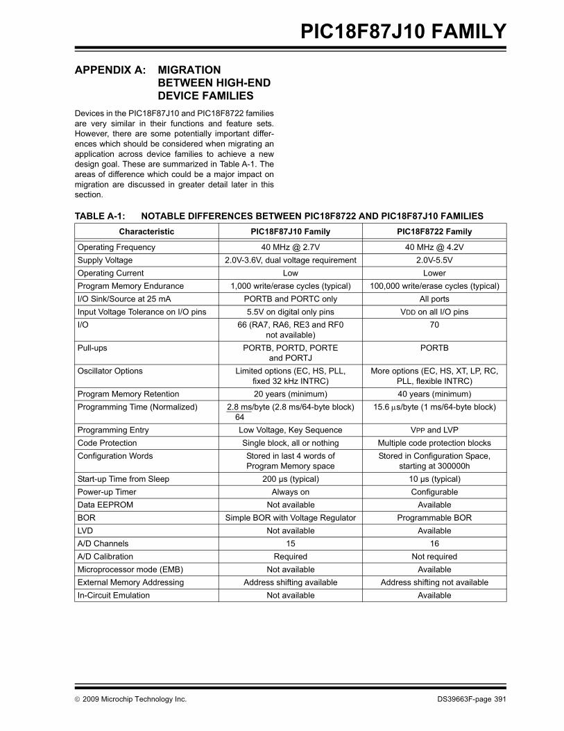
PIC18F87J10 FAMILY
APPENDIX A: MIGRATION BETWEEN HIGH-END DEVICE FAMILIES
Devices in the PIC18F87J10 and PIC18F8722 familiesare very similar in their functions and feature sets.However, there are some potentially important differ-ences which should be considered when migrating anapplication across device families to achieve a newdesign goal. These are summarized in Table A-1. Theareas of difference which could be a major impact onmigration are discussed in greater detail later in thissection.
TABLE A-1: NOTABLE DIFFERENCES BETWEEN PIC18F8722 AND PIC18F87J10 FAMILIES Characteristic PIC18F87J10 Family PIC18F8722 Family
Operating Frequency 40 MHz @ 2.7V 40 MHz @ 4.2VSupply Voltage 2.0V-3.6V, dual voltage requirement 2.0V-5.5VOperating Current Low LowerProgram Memory Endurance 1,000 write/erase cycles (typical) 100,000 write/erase cycles (typical)I/O Sink/Source at 25 mA PORTB and PORTC only All portsInput Voltage Tolerance on I/O pins 5.5V on digital only pins VDD on all I/O pinsI/O 66 (RA7, RA6, RE3 and RF0
not available)70
Pull-ups PORTB, PORTD, PORTE and PORTJ
PORTB
Oscillator Options Limited options (EC, HS, PLL, fixed 32 kHz INTRC)
More options (EC, HS, XT, LP, RC, PLL, flexible INTRC)
Program Memory Retention 20 years (minimum) 40 years (minimum)Programming Time (Normalized) 2.8 ms/byte (2.8 ms/64-byte block)
6415.6 μs/byte (1 ms/64-byte block)
Programming Entry Low Voltage, Key Sequence VPP and LVPCode Protection Single block, all or nothing Multiple code protection blocksConfiguration Words Stored in last 4 words of
Program Memory spaceStored in Configuration Space,
starting at 300000hStart-up Time from Sleep 200 µs (typical) 10 µs (typical)Power-up Timer Always on ConfigurableData EEPROM Not available AvailableBOR Simple BOR with Voltage Regulator Programmable BORLVD Not available AvailableA/D Channels 15 16A/D Calibration Required Not requiredMicroprocessor mode (EMB) Not available AvailableExternal Memory Addressing Address shifting available Address shifting not availableIn-Circuit Emulation Not available Available
© 2009 Microchip Technology Inc. DS39663F-page 391

PIC18F87J10 FAMILY
A.1 Power Requirement DifferencesThe most significant difference between thePIC18F87J10 and PIC18F8722 device families is thepower requirements. PIC18F87J10 devices aredesigned on a smaller process; this results in lowermaximum voltage and higher leakage current.The operating voltage range for PIC18F87J10 devicesis 2.0V to 3.6V. In addition, these devices have splitpower requirements: one for the core logic and one forthe I/O. One of the VDD pins is separated for the corelogic supply (VDDCORE). This pin has specific voltageand capacitor requirements as described inSection 27.0 “Electrical Characteristics”.
A.2 Pin DifferencesThere are several differences in the pinouts betweenthe PIC18F87J10 and the PIC18F8722 families:
• Input voltage tolerance• Output current capabilities• Available I/O
Pins on the PIC18F87J10 that have digital only inputcapability will tolerate voltages up to 5.5V and are thustolerant to voltages above VDD. Table 11-1 inSection 11.0 “I/O Ports” contains the complete list.
In addition to input differences, there are output differ-ences as well. PIC18F87J10 devices have threeclasses of pin output current capability: high, mediumand low. Not all I/O pins can source or sink equal levelsof current. Only PORTB and PORTC support the25 mA source/sink capability that is supported by alloutput pins on the PIC18F8722. Table 11-2 inSection 11.0 “I/O Ports” contains the complete list ofoutput capabilities.
There are additional differences in how some pin func-tions are implemented on PIC18F87J10 devices. First,the OSC1/OSC2 oscillator pins are strictly dedicated tothe external oscillator function; there is no option tore-allocate these pins to I/O (RA6 or RA7) as onPIC18F8722 devices. Second, the MCLR pin isdedicated only to MCLR and cannot be configured asan input (RG5). Finally, RF0 does not exist onPIC18F87J10 devices.
All of these pin differences (including power pindifferences) should be accounted for when making aconversion between PIC18F8722 and PIC18F87J10devices.
A.3 Oscillator DifferencesPIC18F8722 devices have a greater range of oscillatoroptions than PIC18F87J10 devices. The latter family islimited primarily to operating modes that support HSand EC oscillators.
In addition, the PIC18F87J10 has an internal RCoscillator with only a fixed 32 kHz output. The higherfrequency RC modes of the PIC18F8722 family are notavailable.
Both device families have an internal PLL. For thePIC18F87J10 family, however, the PLL must beenabled in software.
The clocking differences should be considered whenmaking a conversion between the PIC18F8722 andPIC18F87J10 device families.
A.4 PeripheralsPeripherals must also be considered when making aconversion between the PIC18F87J10 and thePIC18F8722 families:
• External Memory Bus: The external memory bus on the PIC18F87J10 does not support Micro-controller mode; however, it does support external address offset.
• A/D Converter: There are only 15 channels on PIC18F87J10 devices. The converters for these devices also require a calibration step prior to normal operation.
• Data EEPROM: PIC18F87J10 devices do not have this module.
• BOR: PIC18F87J10 devices do not have a programmable BOR. Simple brown-out capability is provided through the use of the internal voltage regulator.
• LVD: PIC18F87J10 devices do not have this module.
DS39663F-page 392 © 2009 Microchip Technology Inc.

PIC18F87J10 FAMILY
APPENDIX B: REVISION HISTORY
Revision A (December 2004)Original data sheet for PIC18F87J10 family devices.
Revision B (July 2005)Packaging diagrams have been updated. Documentupdated from Advanced to Preliminary. Updated allTBDs in Section 27.0 “Electrical Characteristics”.Edits to text throughout document.
Revision C (December 2005)Packaging diagrams have been updated. Minor edits totext throughout document.
Revision D (June 2006)Electrical characteristics and packaging diagrams havebeen updated. Minor edits to text throughoutdocument.
Revision E (June 2009)Pin diagrams have been edited to indicate 5.5V tolerantinput pins. Packaging diagrams have been updated.Section 2.0 “Guidelines for Getting Started withPIC18FJ Microcontrollers” has been added. Minor textedits throughout the document.
Revision F (September 2009)Added Appendix B: “Revision History”.
© 2009 Microchip Technology Inc. DS39663F-page 393

PIC18F87J10 FAMILY
NOTES:DS39663F-page 394 © 2009 Microchip Technology Inc.

PIC18F87J10 FAMILY
INDEXAA/D ................................................................................... 261
A/D Converter Interrupt, Configuring ....................... 265Acquisition Requirements ........................................ 266ADCAL Bit ................................................................ 269ADCON0 Register .................................................... 261ADCON1 Register .................................................... 261ADCON2 Register .................................................... 261ADRESH Register ............................................ 261, 264ADRESL Register .................................................... 261Analog Port Pins ...................................................... 148Analog Port Pins, Configuring .................................. 267Associated Registers ............................................... 269Automatic Acquisition Time ...................................... 267Calculating the Minimum Required
Acquisition Time .............................................. 266Calibration ................................................................ 269Configuring the Module ............................................ 265Conversion Clock (TAD) ........................................... 267Conversion Requirements ....................................... 383Conversion Status (GO/DONE Bit) .......................... 264Conversions ............................................................. 268Converter Characteristics ........................................ 382Operation in Power-Managed Modes ...................... 269Special Event Trigger (ECCP) ......................... 180, 268Use of the ECCP2 Trigger ....................................... 268
Absolute Maximum Ratings ............................................. 347AC (Timing) Characteristics ............................................. 362
Load Conditions for Device Timing Specifications ................................................... 363
Parameter Symbology ............................................. 362Temperature and Voltage Specifications ................. 363Timing Conditions .................................................... 363
ACKSTAT ........................................................................ 229ACKSTAT Status Flag ..................................................... 229ADCAL Bit ........................................................................ 269ADCON0 Register ............................................................ 261
GO/DONE Bit ........................................................... 264ADCON1 Register ............................................................ 261ADCON2 Register ............................................................ 261ADDFSR .......................................................................... 336ADDLW ............................................................................ 299ADDULNK ........................................................................ 336ADDWF ............................................................................ 299ADDWFC ......................................................................... 300ADRESH Register ............................................................ 261ADRESL Register .................................................... 261, 264Analog-to-Digital Converter. See A/D.ANDLW ............................................................................ 300ANDWF ............................................................................ 301Assembler
MPASM Assembler .................................................. 344Auto-Wake-up on Sync Break Character ......................... 252
BBasic Connection Requirements ........................................ 27Baud Rate Generator ....................................................... 225BC .................................................................................... 301BCF .................................................................................. 302BF .................................................................................... 229BF Status Flag ................................................................. 229
Block Diagrams16-Bit Byte Select Mode .......................................... 10116-Bit Byte Write Mode .............................................. 9916-Bit Word Write Mode .......................................... 1008-Bit Multiplexed Modes .......................................... 103A/D ........................................................................... 264Analog Input Model .................................................. 265Baud Rate Generator .............................................. 225Capture Mode Operation ......................................... 171Comparator Analog Input Model .............................. 275Comparator I/O Operating Modes ........................... 272Comparator Output .................................................. 274Comparator Voltage Reference ............................... 278Comparator Voltage Reference Output
Buffer Example ................................................ 279Compare Mode Operation ....................................... 172Connections for On-Chip Voltage Regulator ........... 288Device Clock .............................................................. 34Enhanced PWM Simplified ...................................... 181EUSART Receive .................................................... 251EUSART Transmit ................................................... 249External Power-on Reset Circuit
(Slow VDD Power-up) ........................................ 49Fail-Safe Clock Monitor ........................................... 290Generic I/O Port Operation ...................................... 125Interrupt Logic .......................................................... 110MSSP (I2C Master Mode) ........................................ 223MSSP (I2C Mode) .................................................... 203MSSP (SPI Mode) ................................................... 193On-Chip Reset Circuit ................................................ 47PIC18F6XJ10/6XJ15 ................................................... 8PIC18F8XJ10/8XJ15 ................................................... 9PLL ............................................................................ 33PORTD and PORTE (Parallel Slave Port) ............... 148PWM Operation (Simplified) .................................... 174Reads from Flash Program Memory ......................... 89Recommended Minimum Connections ...................... 27Single Comparator ................................................... 273Table Read Operation ............................................... 85Table Write Operation ............................................... 86Table Writes to Flash Program Memory .................... 91Timer0 in 16-Bit Mode ............................................. 152Timer0 in 8-Bit Mode ............................................... 152Timer1 ..................................................................... 156Timer1 (16-Bit Read/Write Mode) ............................ 156Timer2 ..................................................................... 162Timer3 ..................................................................... 164Timer3 (16-Bit Read/Write Mode) ............................ 164Timer4 ..................................................................... 168Watchdog Timer ...................................................... 287
BN .................................................................................... 302BNC ................................................................................. 303BNN ................................................................................. 303BNOV .............................................................................. 304BNZ ................................................................................. 304BOR. See Brown-out Reset.BOV ................................................................................. 307BRA ................................................................................. 305Break Character (12-Bit) Transmit and Receive .............. 254BRG. See Baud Rate Generator.Brown-out Reset (BOR) ..................................................... 49
and On-Chip Voltage Regulator .............................. 288Detecting ................................................................... 49
© 2009 Microchip Technology Inc. DS39663F-page 395

PIC18F87J10 FAMILY
BSF .................................................................................. 305BTFSC ............................................................................. 306BTFSS .............................................................................. 306BTG .................................................................................. 307BZ ..................................................................................... 308CC Compilers
MPLAB C18 ............................................................. 344MPLAB C30 ............................................................. 344
Calibration (A/D Converter) .............................................. 269CALL ................................................................................ 308CALLW ............................................................................. 337Capture (CCP Module) ..................................................... 171
Associated Registers ............................................... 173CCP Pin Configuration ............................................. 171CCPRxH:CCPRxL Registers ................................... 171Prescaler .................................................................. 171Software Interrupt .................................................... 171Timer1/Timer3 Mode Selection ................................ 171
Capture (ECCP Module) .................................................. 180Capture/Compare/PWM (CCP) ........................................ 169
Capture Mode. See Capture.CCP Mode and Timer Resources ............................ 170CCPRxH Register .................................................... 170CCPRxL Register ..................................................... 170Compare Mode. See Compare.Module Configuration ............................................... 170Timer Interconnect Configurations ........................... 170
Clock Sources .................................................................... 34Selection and the FOSC2 Configuration Bit ............... 35Selection Using OSCCON Register ........................... 35
CLRF ................................................................................ 309CLRWDT .......................................................................... 309Code Examples
16 x 16 Signed Multiply Routine .............................. 10816 x 16 Unsigned Multiply Routine .......................... 1088 x 8 Signed Multiply Routine .................................. 1078 x 8 Unsigned Multiply Routine .............................. 107Changing Between Capture Prescalers ................... 171Computed GOTO Using an Offset Value ................... 65Erasing Flash Program Memory ................................ 90Fast Register Stack .................................................... 65How to Clear RAM (Bank 1) Using
Indirect Addressing ............................................ 78Implementing a Real-Time Clock Using a
Timer1 Interrupt Service .................................. 159Initializing PORTA .................................................... 126Initializing PORTB .................................................... 128Initializing PORTC .................................................... 131Initializing PORTD .................................................... 134Initializing PORTE .................................................... 137Initializing PORTF .................................................... 140Initializing PORTG ................................................... 142Initializing PORTH .................................................... 144Initializing PORTJ .................................................... 146Loading the SSP1BUF (SSP1SR) Register ............. 196Reading a Flash Program Memory Word .................. 89Saving STATUS, WREG and BSR
Registers in RAM ............................................. 124Writing to Flash Program Memory ............................. 92
Code Protection ............................................................... 281COMF ............................................................................... 310
Comparator ...................................................................... 271Analog Input Connection Considerations ................ 275Associated Registers ............................................... 275Configuration ........................................................... 272Effects of a Reset .................................................... 274Interrupts ................................................................. 274Operation ................................................................. 273Operation During Sleep ........................................... 274Outputs .................................................................... 273Reference ................................................................ 273
External Signal ................................................ 273Internal Signal .................................................. 273
Response Time ........................................................ 273Comparator Specifications ............................................... 361Comparator Voltage Reference ....................................... 277
Accuracy and Error .................................................. 278Associated Registers ............................................... 279Configuring .............................................................. 277Connection Considerations ...................................... 278Effects of a Reset .................................................... 278Operation During Sleep ........................................... 278
Compare (CCP Module) .................................................. 172Associated Registers ............................................... 173CCPRx Register ...................................................... 172Pin Configuration ..................................................... 172Software Interrupt .................................................... 172Timer1/Timer3 Mode Selection ................................ 172
Compare (ECCP Module) ................................................ 180Special Event Trigger .............................. 165, 180, 268
Computed GOTO ............................................................... 65Configuration Bits ............................................................ 281Configuration Register Protection .................................... 292Core Features
Easy Migration ............................................................. 6Expanded Memory ....................................................... 5Extended Instruction Set ............................................. 5External Memory Bus .................................................. 5nanoWatt Technology .................................................. 5Oscillator Options and Features .................................. 5
CPFSEQ .......................................................................... 310CPFSGT .......................................................................... 311CPFSLT ........................................................................... 311Crystal Oscillator/Ceramic Resonator ................................ 31Customer Change Notification Service ............................ 405Customer Notification Service ......................................... 405Customer Support ............................................................ 405
DData Addressing Modes .................................................... 78
Comparing Addressing Modes with the Extended Instruction Set Enabled ............... 82
Direct ......................................................................... 78Indexed Literal Offset ................................................ 81
BSR ................................................................... 83Instructions Affected .......................................... 81Mapping Access Bank ....................................... 83
Indirect ....................................................................... 78Inherent and Literal .................................................... 78
Data Memory ..................................................................... 68Access Bank .............................................................. 71Bank Select Register (BSR) ...................................... 68Extended Instruction Set ........................................... 81General Purpose Registers ....................................... 71
DS39663F-page 396 © 2009 Microchip Technology Inc.

PIC18F87J10 FAMILY
Memory MapsPIC18FX5J10/X5J15/X6J10 Devices ................ 69PIC18FX6J15/X7J10 Devices ........................... 70Special Function Registers ................................ 72
Special Function Registers ........................................ 72DAW ................................................................................. 312DC Characteristics ........................................................... 358
Power-Down and Supply Current ............................ 351Supply Voltage ......................................................... 350
DCFSNZ .......................................................................... 313DECF ............................................................................... 312DECFSZ ........................................................................... 313Development Support ...................................................... 343Device Overview .................................................................. 5
Details on Individual Family Members ......................... 6Features (64-Pin Devices) ........................................... 7Features (80-Pin Devices) ........................................... 7
Direct Addressing ............................................................... 79
EECCP
Associated Registers ............................................... 192Capture and Compare Modes .................................. 180Enhanced PWM Mode ............................................. 181Standard PWM Mode ............................................... 180
Effect on Standard PIC MCU Instructions ........................ 340Effects of Power-Managed Modes on
Various Clock Sources ............................................... 37Electrical Characteristics .................................................. 347Enhanced Capture/Compare/PWM (ECCP) .................... 177
Capture Mode. See Capture (ECCP Module).ECCP1/ECCP3 Outputs and
Program Memory Mode ................................... 178ECCP2 Outputs and Program
Memory Modes ................................................ 178Outputs and Configuration ....................................... 178Pin Configurations for ECCP1 ................................. 179Pin Configurations for ECCP2 ................................. 179Pin Configurations for ECCP3 ................................. 180PWM Mode. See PWM (ECCP Module).Timer Resources ...................................................... 178Use of CCP4/CCP5 with ECCP1/ECCP3 ................ 178
Enhanced Universal Synchronous Asynchronous ReceiverTransmitter (EUSART). See EUSART.
ENVREG Pin .................................................................... 288Equations
A/D Acquisition Time ................................................ 266A/D Minimum Charging Time ................................... 266
Errata ................................................................................... 4EUSART
Asynchronous Mode ................................................ 24912-Bit Break Transmit and Receive ................. 254Associated Registers, Receive ........................ 252Associated Registers, Transmit ....................... 250Auto-Wake-up on Sync Break ......................... 252Receiver ........................................................... 251Setting Up 9-Bit Mode with Address Detect ..... 251Transmitter ....................................................... 249
Baud Rate GeneratorOperation in Power-Managed Mode ................ 243
Baud Rate Generator (BRG) ................................... 243Associated Registers ....................................... 244Auto-Baud Rate Detect .................................... 247Baud Rate Error, Calculating ........................... 244Baud Rates, Asynchronous Modes ................. 245High Baud Rate Select (BRGH Bit) ................. 243Sampling ......................................................... 243
Synchronous Master Mode ...................................... 255Associated Registers, Receive ........................ 257Associated Registers, Transmit ....................... 256Reception ........................................................ 257Transmission ................................................... 255
Synchronous Slave Mode ........................................ 258Associated Registers, Receive ........................ 259Associated Registers, Transmit ....................... 258Reception ........................................................ 259Transmission ................................................... 258
Extended Instruction SetADDFSR .................................................................. 336ADDULNK ............................................................... 336CALLW .................................................................... 337MOVSF .................................................................... 337MOVSS .................................................................... 338PUSHL ..................................................................... 338SUBFSR .................................................................. 339SUBULNK ................................................................ 339
External Clock Input (EC Modes) ...................................... 32External Memory Bus ........................................................ 95
16-Bit Byte Select Mode .......................................... 10116-Bit Byte Write Mode .............................................. 9916-Bit Data Width Modes ........................................... 9816-Bit Mode Timing ................................................. 10216-Bit Word Write Mode .......................................... 1008-Bit Mode ............................................................... 1038-Bit Mode Timing ................................................... 104Address and Data Line Usage (table) ....................... 97Address and Data Width ............................................ 97Address Shifting ........................................................ 97Control ....................................................................... 96I/O Port Functions ...................................................... 95Operation in Power-Managed Modes ...................... 105Program Memory Modes ........................................... 98
Extended Microcontroller ................................... 98Microcontroller ................................................... 98
Wait States ................................................................ 98Weak Pull-ups on Port Pins ....................................... 98
FFail-Safe Clock Monitor ........................................... 281, 290
Interrupts in Power-Managed Modes ...................... 291POR or Wake-up from Sleep ................................... 291WDT During Oscillator Failure ................................. 290
Fast Register Stack ........................................................... 65Firmware Instructions ...................................................... 293Flash Configuration Words .............................................. 281Flash Program Memory ..................................................... 85
Associated Registers ................................................. 93Control Registers ....................................................... 86
EECON1 and EECON2 ..................................... 86TABLAT (Table Latch) Register ........................ 88TBLPTR (Table Pointer) Register ...................... 88
© 2009 Microchip Technology Inc. DS39663F-page 397

PIC18F87J10 FAMILY
Erase Sequence ........................................................ 90Erasing ....................................................................... 90Operation During Code-Protect ................................. 93Reading ...................................................................... 89Table PointerBoundaries Based on Operation ........................ 88Table Pointer Boundaries .......................................... 88Table Reads and Table Writes .................................. 85Write Sequence ......................................................... 91Writing ........................................................................ 91
Unexpected Termination .................................... 93Write Verify ........................................................ 93
FSCM. See Fail-Safe Clock Monitor.
GGOTO ............................................................................... 314
HHardware Multiplier .......................................................... 107
Introduction .............................................................. 107Operation ................................................................. 107
Hardware Various MultiplyPerformance Comparisons ...................................... 107
II/O Ports ........................................................................... 125
Pin Capabilities ........................................................ 125I2C Mode (MSSP)
Acknowledge Sequence Timing ............................... 232Associated Registers ............................................... 238Baud Rate Generator ............................................... 225Bus Collision
During a Repeated Start Condition .................. 236During a Stop Condition ................................... 237
Clock Arbitration ....................................................... 226Clock Stretching ....................................................... 218
10-Bit Slave Receive Mode (SEN = 1) ............. 21810-Bit Slave Transmit Mode ............................. 2187-Bit Slave Receive Mode (SEN = 1) ............... 2187-Bit Slave Transmit Mode ............................... 218
Clock Synchronization and the CKP bit ................... 219Effects of a Reset ..................................................... 233General Call Address Support ................................. 222I2C Clock Rate w/BRG ............................................. 225Master Mode ............................................................ 223
Operation ......................................................... 224Reception ......................................................... 229Repeated Start Condition Timing ..................... 228Start Condition Timing ..................................... 227Transmission .................................................... 229
Multi-Master Communication, Bus Collision and Arbitration .................................................. 233
Multi-Master Mode ................................................... 233Operation ................................................................. 209Read/Write Bit Information (R/W Bit) ............... 209, 211Registers .................................................................. 203Serial Clock (RC3/SCKx/SCLx) ............................... 211Slave Mode .............................................................. 209
Addressing ....................................................... 209Reception ......................................................... 211Transmission .................................................... 211
Sleep Operation ....................................................... 233Stop Condition Timing .............................................. 232
INCF ................................................................................. 314INCFSZ ............................................................................ 315In-Circuit Debugger .......................................................... 292
In-Circuit Serial Programming (ICSP) ...................... 281, 292Indexed Literal Offset Addressing
and Standard PIC18 Instructions ............................. 340Indexed Literal Offset Mode ............................................. 340Indirect Addressing ............................................................ 79INFSNZ ............................................................................ 315Initialization Conditions for all Registers ...................... 53–57Instruction Cycle ................................................................ 66
Clocking Scheme ....................................................... 66Flow/Pipelining ........................................................... 66
Instruction Set .................................................................. 293ADDLW .................................................................... 299ADDWF .................................................................... 299ADDWF (Indexed Literal Offset Mode) .................... 341ADDWFC ................................................................. 300ANDLW .................................................................... 300ANDWF .................................................................... 301BC ............................................................................ 301BCF ......................................................................... 302BN ............................................................................ 302BNC ......................................................................... 303BNN ......................................................................... 303BNOV ...................................................................... 304BNZ ......................................................................... 304BOV ......................................................................... 307BRA ......................................................................... 305BSF .......................................................................... 305BSF (Indexed Literal Offset Mode) .......................... 341BTFSC ..................................................................... 306BTFSS ..................................................................... 306BTG ......................................................................... 307BZ ............................................................................ 308CALL ........................................................................ 308CLRF ....................................................................... 309CLRWDT ................................................................. 309COMF ...................................................................... 310CPFSEQ .................................................................. 310CPFSGT .................................................................. 311CPFSLT ................................................................... 311DAW ........................................................................ 312DCFSNZ .................................................................. 313DECF ....................................................................... 312DECFSZ .................................................................. 313Extended Instructions .............................................. 335
Considerations when Enabling ........................ 340Syntax .............................................................. 335Use with MPLAB IDE Tools ............................. 342
General Format ........................................................ 295GOTO ...................................................................... 314INCF ........................................................................ 314INCFSZ .................................................................... 315INFSNZ .................................................................... 315IORLW ..................................................................... 316IORWF ..................................................................... 316LFSR ....................................................................... 317MOVF ...................................................................... 317MOVFF .................................................................... 318MOVLB .................................................................... 318MOVLW ................................................................... 319MOVWF ................................................................... 319MULLW .................................................................... 320MULWF .................................................................... 320NEGF ....................................................................... 321NOP ......................................................................... 321Opcode Field Descriptions ....................................... 294
DS39663F-page 398 © 2009 Microchip Technology Inc.

PIC18F87J10 FAMILY
POP ......................................................................... 322PUSH ....................................................................... 322RCALL ..................................................................... 323RESET ..................................................................... 323RETFIE .................................................................... 324RETLW .................................................................... 324RETURN .................................................................. 325RLCF ........................................................................ 325RLNCF ..................................................................... 326RRCF ....................................................................... 326RRNCF .................................................................... 327SETF ........................................................................ 327SETF (Indexed Literal Offset Mode) ........................ 341SLEEP ..................................................................... 328Standard Instructions ............................................... 293SUBFWB .................................................................. 328SUBLW .................................................................... 329SUBWF .................................................................... 329SUBWFB .................................................................. 330SWAPF .................................................................... 330TBLRD ..................................................................... 331TBLWT ..................................................................... 332TSTFSZ ................................................................... 333XORLW .................................................................... 333XORWF .................................................................... 334INTCON RegisterRBIF Bit .................................................................... 128
INTCON Registers ........................................................... 111Inter-Integrated Circuit. See I2C.Internal Oscillator Block ..................................................... 34Internal RC Oscillator
Use with WDT .......................................................... 287Internal Voltage Reference Specifications ....................... 361Internet Address ............................................................... 405Interrupt Sources ............................................................. 281
A/D Conversion Complete ....................................... 265Capture Complete (CCP) ......................................... 171Compare Complete (CCP) ....................................... 172Interrupt-on-Change (RB7:RB4) .............................. 128TMR0 Overflow ........................................................ 153TMR1 Overflow ........................................................ 155TMR2 to PR2 Match (PWM) .................................... 181TMR3 Overflow ................................................ 163, 165TMR4 to PR4 Match ................................................ 168TMR4 to PR4 Match (PWM) .................................... 167
Interrupts .......................................................................... 109During Context Saving ............................................. 124INTx Pin ................................................................... 124PORTB, Interrupt-on-Change .................................. 124TMR0 ....................................................................... 124
Interrupts, Flag BitsInterrupt-on-Change (RB7:RB4) Flag (RBIF Bit) ..... 128
IORLW ............................................................................. 316IORWF ............................................................................. 316IPR Registers ................................................................... 120
LLFSR ................................................................................ 317
MMaster Clear (MCLR) ......................................................... 49Master Synchronous Serial Port (MSSP). See MSSP.Memory Organization ......................................................... 59
Data Memory ............................................................. 68Program Memory ....................................................... 59
Memory Programming Requirements .............................. 360
Microchip Internet Web Site ............................................. 405MOVF .............................................................................. 317MOVFF ............................................................................ 318MOVLB ............................................................................ 318MOVLW ........................................................................... 319MOVSF ............................................................................ 337MOVSS ............................................................................ 338MOVWF ........................................................................... 319MPLAB ASM30 Assembler, Linker, Librarian .................. 344MPLAB ICD 2 In-Circuit Debugger .................................. 345MPLAB ICE 2000 High-Performance Universal
In-Circuit Emulator ................................................... 345MPLAB Integrated Development
Environment Software ............................................. 343MPLAB PM3 Device Programmer ................................... 345MPLAB REAL ICE In-Circuit Emulator System ............... 345MPLINK Object Linker/MPLIB Object Librarian ............... 344MSSP
ACK Pulse ....................................................... 209, 211Control Registers (general) ..................................... 193I2C Mode. See I2C Mode.Module Overview ..................................................... 193SPI Master/Slave Connection .................................. 197TMR4 Output for Clock Shift .................................... 168
MULLW ............................................................................ 320MULWF ............................................................................ 320
NNEGF ............................................................................... 321NOP ................................................................................. 321Notable Differences Between PIC18F8722
and PIC18F87J10 Families ..................................... 391Oscillator Options .................................................... 392Peripherals .............................................................. 392Power Requirements ............................................... 392
OOscillator Configuration ..................................................... 31
EC .............................................................................. 31ECPLL ....................................................................... 31HS .............................................................................. 31HS Modes .................................................................. 31HSPLL ....................................................................... 31INTRC ........................................................................ 31
Oscillator Selection .......................................................... 281Oscillator Start-up Timer (OST) ......................................... 37Oscillator Switching ........................................................... 34Oscillator Transitions ......................................................... 35Oscillator, Timer1 ..................................................... 155, 165Oscillator, Timer3 ............................................................. 163
PPackaging ........................................................................ 385
Details ...................................................................... 386Marking .................................................................... 385
Parallel Slave Port (PSP) ................................................. 148Associated Registers ............................................... 150PORTD .................................................................... 148RE0/RD Pin ............................................................. 148RE1/WR Pin ............................................................ 148RE2/CS Pin ............................................................. 148Select (PSPMODE Bit) ............................................ 148
PICSTART Plus Development Programmer .................... 346PIE Registers ................................................................... 117
© 2009 Microchip Technology Inc. DS39663F-page 399

PIC18F87J10 FAMILY
Pin FunctionsAVDD .......................................................................... 16AVDD .......................................................................... 25AVSS .......................................................................... 16AVSS .......................................................................... 25ENVREG .............................................................. 16, 25MCLR ................................................................... 10, 17OSC1/CLKI .......................................................... 10, 17OSC2/CLKO ........................................................ 10, 17RA0/AN0 .............................................................. 10, 17RA1/AN1 .............................................................. 10, 17RA2/AN2/VREF- .................................................... 10, 17RA3/AN3/VREF+ ................................................... 10, 17RA4/T0CKI ........................................................... 10, 17RA5/AN4 .............................................................. 10, 17RB0/INT0/FLT0 .................................................... 11, 18RB1/INT1 ............................................................. 11, 18RB2/INT2 ............................................................. 11, 18RB3/INT3 ................................................................... 11RB3/INT3/ECCP2/P2A .............................................. 18RB4/KBI0 ............................................................. 11, 18RB5/KBI1 ............................................................. 11, 18RB6/KBI2/PGC .................................................... 11, 18RB7/KBI3/PGD .................................................... 11, 18RC0/T1OSO/T13CKI ........................................... 12, 19RC1/T1OSI/ECCP2/P2A ...................................... 12, 19RC2/ECCP1/P1A ................................................. 12, 19RC3/SCK1/SCL1 ................................................. 12, 19RC4/SDI1/SDA1 .................................................. 12, 19RC5/SDO1 ........................................................... 12, 19RC6/TX1/CK1 ...................................................... 12, 19RC7/RX1/DT1 ...................................................... 12, 19RD0/AD0/PSP0 .......................................................... 20RD0/PSP0 .................................................................. 13RD1/AD1/PSP1 .......................................................... 20RD1/PSP1 .................................................................. 13RD2/AD2/PSP2 .......................................................... 20RD2/PSP2 .................................................................. 13RD3/AD3/PSP3 .......................................................... 20RD3/PSP3 .................................................................. 13RD4/AD4/PSP4/SDO2 ............................................... 20RD4/PSP4/SDO2 ....................................................... 13RD5/AD5/PSP5/SDI2/SDA2 ...................................... 20RD5/PSP5/SDI2/SDA2 .............................................. 13RD6/AD6/PSP6/SCK2/SCL2 ..................................... 20RD6/PSP6/SCK2/SCL2 ............................................. 13RD7/AD7/PSP7/SS2 .................................................. 20RD7/PSP7/SS2 .......................................................... 13RE0/AD8/RD/P2D ...................................................... 21RE0/RD/P2D .............................................................. 14RE1/AD9/WR/P2C ..................................................... 21RE1/WR/P2C ............................................................. 14RE2/AD10/CS/P2B .................................................... 21RE2/CS/P2D .............................................................. 14RE3/AD11/P3C .......................................................... 21RE3/P3C .................................................................... 14RE4/AD12/P3B .......................................................... 21RE4/P3B .................................................................... 14RE5/AD13/P1C .......................................................... 21RE5/P1C .................................................................... 14RE6/AD14/P1B .......................................................... 21RE6/P1B .................................................................... 14RE7/AD15/ECCP2/P2A ............................................. 21RE7/ECCP2/P2A ....................................................... 14RF1/AN6/C2OUT ................................................. 15, 22
RF2/AN7/C1OUT ................................................. 15, 22RF3/AN8 .............................................................. 15, 22RF4/AN9 .............................................................. 15, 22RF5/AN10/CVREF ................................................ 15, 22RF6/AN11 ............................................................ 15, 22RF7/SS1 .............................................................. 15, 22RG0/ECCP3/P3A ................................................. 16, 23RG1/TX2/CK2 ...................................................... 16, 23RG2/RX2/DT2 ...................................................... 16, 23RG3/CCP4/P3D ................................................... 16, 23RG4/CCP5/P1D ................................................... 16, 23RH0/A16 .................................................................... 24RH1/A17 .................................................................... 24RH2/A18 .................................................................... 24RH3/A19 .................................................................... 24RH4/AN12/P3C .......................................................... 24RH5/AN13/P3B .......................................................... 24RH6/AN14/P1C .......................................................... 24RH7/AN15/P1B .......................................................... 24RJ0/ALE .................................................................... 25RJ1/OE ...................................................................... 25RJ2/WRL ................................................................... 25RJ3/WRH ................................................................... 25RJ4/BA0 .................................................................... 25RJ5/CE ...................................................................... 25RJ6/LB ....................................................................... 25RJ7/UB ...................................................................... 25VDD ............................................................................ 16VDD ............................................................................ 25VDDCORE/VCAP ..................................................... 16, 25VSS ............................................................................ 16VSS ............................................................................ 25
Pinout I/O DescriptionsPIC18F6XJ10/6XJ15 ................................................. 10PIC18F8XJ10/8XJ15 ................................................. 17
PinsENVREG ................................................................... 29External Oscillator ...................................................... 30ICSP .......................................................................... 29Master Clear (MCLR .................................................. 28Power Supply ............................................................ 28VCAP/VDDCORE ........................................................... 29
PIR Registers ................................................................... 114PLL .................................................................................... 33
ECPLL Oscillator Mode ............................................. 33HSPLL Oscillator Mode ............................................. 33
POP ................................................................................. 322POR. See Power-on Reset.PORTA
Associated Registers ............................................... 127LATA Register ......................................................... 126PORTA Register ...................................................... 126TRISA Register ........................................................ 126
PORTBAssociated Registers ............................................... 130LATB Register ......................................................... 128PORTB Register ...................................................... 128RB7:RB4 Interrupt-on-Change Flag (RBIF Bit) ........ 128TRISB Register ........................................................ 128
PORTCAssociated Registers ............................................... 133LATC Register ......................................................... 131PORTC Register ...................................................... 131RC3/SCKx/SCLx Pin ............................................... 211TRISC Register ........................................................ 131
DS39663F-page 400 © 2009 Microchip Technology Inc.
PIC18F87J10 FAMILY
PORTDAssociated Registers ............................................... 136LATD Register ......................................................... 134PORTD Register ...................................................... 134TRISD Register ........................................................ 134
PORTEAnalog Port Pins ...................................................... 148Associated Registers ............................................... 139LATE Register .......................................................... 137PORTE Register ...................................................... 137PSP Mode Select (PSPMODE Bit) .......................... 148RE0/RD Pin .............................................................. 148RE1/WR Pin ............................................................. 148RE2/CS Pin .............................................................. 148TRISE Register ........................................................ 137
PORTFAssociated Registers ............................................... 141LATF Register .......................................................... 140PORTF Register ...................................................... 140TRISF Register ........................................................ 140
PORTGAssociated Registers ............................................... 143LATG Register ......................................................... 142PORTG Register ...................................................... 142TRISG Register ........................................................ 142
PORTHAssociated Registers ............................................... 145LATH Register ......................................................... 144PORTH Register ...................................................... 144TRISH Register ........................................................ 144
PORTJAssociated Registers ............................................... 147LATJ Register .......................................................... 146PORTJ Register ....................................................... 146TRISJ Register ......................................................... 146
Power-Managed Modes ..................................................... 39and EUSART Operation ........................................... 243and SPI Operation ................................................... 201Clock Transitions and Status Indicators ..................... 40Entering ...................................................................... 39Exiting Idle and Sleep Modes .................................... 45
By Interrupt ........................................................ 45By Reset ............................................................ 45By WDT Time-out .............................................. 45Without an Oscillator Start-up Delay .................. 45
Idle Modes ................................................................. 43PRI_IDLE ........................................................... 44RC_IDLE ............................................................ 45SEC_IDLE ......................................................... 44
Multiple Sleep Commands ......................................... 40Run Modes ................................................................. 40
PRI_RUN ........................................................... 40RC_RUN ............................................................ 42SEC_RUN .......................................................... 40
Selecting .................................................................... 39Sleep Mode ................................................................ 43Summary (table) ........................................................ 39
Power-on Reset (POR) ...................................................... 49Power-up Delays ................................................................ 37Power-up Timer (PWRT) ............................................. 37, 50
Time-out Sequence .................................................... 50Prescaler
Timer2 ...................................................................... 182Prescaler, Timer0 ............................................................. 153Prescaler, Timer2 (Timer4) .............................................. 175PRI_IDLE Mode ................................................................. 44
PRI_RUN Mode ................................................................. 40Program Counter ............................................................... 63
PCL, PCH and PCU Registers .................................. 63PCLATH and PCLATU Registers .............................. 63
Program MemoryExtended Instruction Set ........................................... 81Flash Configuration Words ........................................ 60Hard Memory Vectors ................................................ 60Instructions ................................................................ 67
Two-Word .......................................................... 67Interrupt Vector .......................................................... 60Look-up Tables .......................................................... 65Memory Maps ............................................................ 59
Hard Vectors and Configuration Words ............. 60Modes
Extended Microcontroller ................................... 61Extended Microcontroller (Address Shifting) ..... 62Memory Access (table) ...................................... 62Microcontroller ................................................... 61
Modes (PIC18F8XJ10/8XJ15) ................................... 61Reset Vector .............................................................. 60
Program Verification and Code Protection ...................... 292Programming, Device Instructions ................................... 293PSP.See Parallel Slave Port.Pulse-Width Modulation. See PWM (CCP Module)
and PWM (ECCP Module).PUSH ............................................................................... 322PUSH and POP Instructions .............................................. 64PUSHL ............................................................................. 338PWM (CCP Module)
Associated Registers ............................................... 176Duty Cycle ............................................................... 174Example Frequencies/Resolutions .......................... 175Operation Setup ...................................................... 175Period ...................................................................... 174PR2/PR4 Registers ................................................. 174TMR2 (TMR4) to PR2 (PR4) Match ........................ 174TMR2 to PR2 Match ................................................ 181TMR4 to PR4 Match ................................................ 167
PWM (ECCP Module) ...................................................... 181CCPR1H:CCPR1L Registers .................................. 181Direction Change in Full-Bridge Output Mode ......... 186Duty Cycle ............................................................... 182Effects of a Reset .................................................... 191Enhanced PWM Auto-Shutdown ............................. 188Example Frequencies/Resolutions .......................... 182Full-Bridge Application Example .............................. 186Full-Bridge Mode ..................................................... 185Half-Bridge Mode ..................................................... 184Half-Bridge Output Mode Applications Example ..... 184Output Configurations .............................................. 182Output Relationships (Active-High) ......................... 183Output Relationships (Active-Low) .......................... 183Period ...................................................................... 181Programmable Dead-Band Delay ............................ 188Setup for PWM Operation ....................................... 191Start-up Considerations ........................................... 189
QQ Clock .................................................................... 175, 182
RRAM. See Data Memory.RC_IDLE Mode .................................................................. 45RC_RUN Mode .................................................................. 42RCALL ............................................................................. 323
© 2009 Microchip Technology Inc. DS39663F-page 401

PIC18F87J10 FAMILY
RCON RegisterBit Status During Initialization .................................... 52Reader Response ............................................................ 406Register File ....................................................................... 71Register File Summary ................................................. 73–76Registers
ADCON0 (A/D Control 0) ......................................... 261ADCON1 (A/D Control 1) ......................................... 262ADCON2 (A/D Control 2) ......................................... 263BAUDCONx (Baud Rate Control) ............................ 242CCPxCON (CCPx Control) ...................................... 169CCPxCON (ECCPx Control) .................................... 177CMCON (Comparator Control) ................................ 271CONFIG1H (Configuration 1 High) .......................... 283CONFIG1L (Configuration 1 Low) ............................ 283CONFIG2H (Configuration 2 High) .......................... 284CONFIG2L (Configuration 2 Low) ............................ 284CONFIG3H (Configuration 3 High) .......................... 285CONFIG3L (Configuration 3 Low) ...................... 61, 285CVRCON (Comparator Voltage
Reference Control) ........................................... 277DEVID1 (Device ID 1) .............................................. 286DEVID2 (Device ID 2) .............................................. 286ECCPxAS (Enhanced CCPx Auto-Shutdown
Control) ............................................................ 189ECCPxDEL (PWM Dead-Band Delay) ..................... 188EECON1 (EEPROM Control 1) .................................. 87INTCON (Interrupt Control) ...................................... 111INTCON2 (Interrupt Control 2) ................................. 112INTCON3 (Interrupt Control 3) ................................. 113IPR1 (Peripheral Interrupt Priority 1) ........................ 120IPR2 (Peripheral Interrupt Priority 2) ........................ 121IPR3 (Peripheral Interrupt Priority 3) ........................ 122MEMCON (External Memory Bus Control) ................ 96OSCCON (Oscillator Control) .................................... 36OSCTUNE (PLL Control) ........................................... 33PIE1 (Peripheral Interrupt Enable 1) ........................ 117PIE2 (Peripheral Interrupt Enable 2) ........................ 118PIE3 (Peripheral Interrupt Enable 3) ........................ 119PIR1 (Peripheral Interrupt Request (Flag) 1) ........... 114PIR2 (Peripheral Interrupt Request (Flag) 2) ........... 115PIR3 (Peripheral Interrupt Request (Flag) 3) ........... 116PSPCON (Parallel Slave Port Control) .................... 149RCON (Reset Control) ....................................... 48, 123RCSTAx (Receive Status and Control) .................... 241SSPxADD (MSSP1 and MSSP2 Address) .............. 208SSPxCON1 (MSSPx Control 1, I2C Mode) .............. 205SSPxCON1 (MSSPx Control 1, SPI Mode) ............. 195SSPxCON2 (MSSPx Control 2,
I2C Master Mode) ............................................. 206SSPxSTAT (MSSPx Status, I2C Mode) ................... 204SSPxSTAT (MSSPx Status, SPI Mode) .................. 194STATUS ..................................................................... 77STKPTR (Stack Pointer) ............................................ 64T0CON (Timer0 Control) .......................................... 151T1CON (Timer1 Control) .......................................... 155T2CON (Timer2 Control) .......................................... 161T3CON (Timer3 Control) .......................................... 163T4CON (Timer4 Control) .......................................... 167TXSTAx (Transmit Status and Control) ................... 240WDTCON (Watchdog Timer Control) ....................... 287
RESET ............................................................................. 323
Reset ................................................................................. 47Brown-out Reset (BOR) ............................................. 47MCLR Reset, During Power-Managed Modes .......... 47MCLR Reset, Normal Operation ................................ 47Power-on Reset (POR) .............................................. 47RESET Instruction ..................................................... 47Stack Full Reset ......................................................... 47Stack Underflow Reset .............................................. 47Watchdog Timer (WDT) Reset .................................. 47
Resets .............................................................................. 281Brown-out Reset (BOR) ........................................... 281Oscillator Start-up Timer (OST) ............................... 281Power-on Reset (POR) ............................................ 281Power-up Timer (PWRT) ......................................... 281
RETFIE ............................................................................ 324RETLW ............................................................................ 324RETURN .......................................................................... 325Return Address Stack ........................................................ 63Return Stack Pointer (STKPTR) ........................................ 64RLCF ............................................................................... 325RLNCF ............................................................................. 326RRCF ............................................................................... 326RRNCF ............................................................................ 327
SSCKx ................................................................................ 193SDIx ................................................................................. 193SDOx ............................................................................... 193SEC_IDLE Mode ............................................................... 44SEC_RUN Mode ................................................................ 40Serial Clock, SCKx .......................................................... 193Serial Data In (SDIx) ........................................................ 193Serial Data Out (SDOx) ................................................... 193Serial Peripheral Interface. See SPI Mode.SETF ................................................................................ 327Slave Select (SSx) ........................................................... 193SLEEP ............................................................................. 328Sleep
OSC1 and OSC2 Pin States ...................................... 37Software Simulator (MPLAB SIM) ................................... 344Special Event Trigger. See Compare (ECCP Module).Special Features of the CPU ........................................... 281SPI Mode (MSSP) ........................................................... 193
Associated Registers ............................................... 202Bus Mode Compatibility ........................................... 201Clock Speed, Interactions ........................................ 201Effects of a Reset .................................................... 201Enabling SPI I/O ...................................................... 197Master Mode ............................................................ 198Master/Slave Connection ......................................... 197Operation ................................................................. 196Operation in Power-Managed Modes ...................... 201Serial Clock .............................................................. 193Serial Data In ........................................................... 193Serial Data Out ........................................................ 193Slave Mode .............................................................. 199Slave Select ............................................................. 193Slave Select Synchronization .................................. 199SPI Clock ................................................................. 198SSPxBUF Register .................................................. 198SSPxSR Register .................................................... 198Typical Connection .................................................. 197
SSPOV ............................................................................ 229
DS39663F-page 402 © 2009 Microchip Technology Inc.
PIC18F87J10 FAMILY
SSPOV Status Flag ......................................................... 229SSPxSTAT RegisterR/W Bit ............................................................. 209, 211SSx .................................................................................. 193Stack Full/Underflow Resets .............................................. 65SUBFSR .......................................................................... 339SUBFWB .......................................................................... 328SUBLW ............................................................................ 329SUBULNK ........................................................................ 339SUBWF ............................................................................ 329SUBWFB .......................................................................... 330SWAPF ............................................................................ 330
TTable Pointer Operations (table) ........................................ 88Table Reads/Table Writes ................................................. 65TBLRD ............................................................................. 331TBLWT ............................................................................. 332Timer0 .............................................................................. 151
Associated Registers ............................................... 153Operation ................................................................. 152Overflow Interrupt .................................................... 153Prescaler .................................................................. 153
Switching Assignment ...................................... 153Prescaler Assignment (PSA Bit) .............................. 153Prescaler Select (T0PS2:T0PS0 Bits) ..................... 153Prescaler. See Prescaler, Timer0.Reads and Writes in 16-Bit Mode ............................ 152Source Edge Select (T0SE Bit) ................................ 152Source Select (T0CS Bit) ......................................... 152
Timer1 .............................................................................. 15516-Bit Read/Write Mode ........................................... 157Associated Registers ............................................... 159Interrupt .................................................................... 158Low-Power Option ................................................... 157Operation ................................................................. 156Oscillator .......................................................... 155, 157
Layout Considerations ..................................... 158Oscillator, as Secondary Clock .................................. 34Overflow Interrupt .................................................... 155Resetting, Using the ECCP
Special Event Trigger ...................................... 158Special Event Trigger (ECCP) ................................. 180TMR1H Register ...................................................... 155TMR1L Register ....................................................... 155Use as a Clock Source ............................................ 157Use as a Real-Time Clock ....................................... 158
Timer2 .............................................................................. 161Associated Registers ............................................... 162Interrupt .................................................................... 162Operation ................................................................. 161Output ...................................................................... 162PR2 Register ............................................................ 181TMR2 to PR2 Match Interrupt .................................. 181
Timer3 .............................................................................. 16316-Bit Read/Write Mode ........................................... 165Associated Registers ............................................... 165Operation ................................................................. 164Oscillator .......................................................... 163, 165Overflow Interrupt ............................................ 163, 165Special Event Trigger (ECCP) ................................. 165TMR3H Register ...................................................... 163TMR3L Register ....................................................... 163
Timer4 ............................................................................. 167Associated Registers ............................................... 168MSSP Clock Shift .................................................... 168Operation ................................................................. 167Postscaler. See Postscaler, Timer4.PR4 Register ........................................................... 167Prescaler. See Prescaler, Timer4.TMR4 Register ........................................................ 167TMR4 to PR4 Match Interrupt .......................... 167, 168
Timing DiagramsA/D Conversion ....................................................... 382Asynchronous Reception ......................................... 252Asynchronous Transmission ................................... 250Asynchronous Transmission (Back to Back) ........... 250Automatic Baud Rate Calculation ............................ 248Auto-Wake-up Bit (WUE) During
Normal Operation ............................................ 253Auto-Wake-up Bit (WUE) During Sleep ................... 253Baud Rate Generator with Clock Arbitration ............ 226BRG Overflow Sequence ........................................ 248BRG Reset Due to SDAx Arbitration During
Start Condition ................................................. 235Bus Collision During a Repeated Start
Condition (Case 1) ........................................... 236Bus Collision During a Repeated Start
Condition (Case 2) ........................................... 236Bus Collision During a Start Condition
(SCLx = 0) ....................................................... 235Bus Collision During a Stop
Condition (Case 1) ........................................... 237Bus Collision During a Stop
Condition (Case 2) ........................................... 237Bus Collision During Start Condition
(SDAx Only) ..................................................... 234Bus Collision for Transmit and Acknowledge .......... 233Capture/Compare/PWM (Including
ECCP Modules) ............................................... 372CLKO and I/O .......................................................... 366Clock Synchronization ............................................. 219Clock/Instruction Cycle .............................................. 66EUSART Synchronous Receive
(Master/Slave) ................................................. 381EUSART Synchronous Transmission
(Master/Slave) ................................................. 381Example SPI Master Mode (CKE = 0) ..................... 373Example SPI Master Mode (CKE = 1) ..................... 374Example SPI Slave Mode (CKE = 0) ....................... 375Example SPI Slave Mode (CKE = 1) ....................... 376External Clock (All Modes Except PLL) ................... 364External Memory Bus for Sleep
(Extended Microcontroller Mode) ............ 102, 104External Memory Bus for TBLRD
(Extended Microcontroller Mode) ............ 102, 104Fail-Safe Clock Monitor ........................................... 291First Start Bit Timing ................................................ 227Full-Bridge PWM Output .......................................... 185Half-Bridge PWM Output ......................................... 184I2C Acknowledge Sequence .................................... 232I2C Bus Data ............................................................ 377I2C Bus Start/Stop Bits ............................................ 377I2C Master Mode (7 or 10-Bit Transmission) ........... 230I2C Master Mode (7-Bit Reception) ......................... 231
© 2009 Microchip Technology Inc. DS39663F-page 403
PIC18F87J10 FAMILY
I2C Slave Mode (10-Bit Reception, SEN = 0,ADMSK = 01001) ............................................. 215I2C Slave Mode (10-Bit Reception, SEN = 0) .......... 216I2C Slave Mode (10-Bit Reception, SEN = 1) .......... 221I2C Slave Mode (10-Bit Transmission) ..................... 217I2C Slave Mode (7-Bit Reception, SEN = 0,
ADMSK = 01011) ............................................. 213I2C Slave Mode (7-Bit Reception, SEN = 0) ............ 212I2C Slave Mode (7-Bit Reception, SEN = 1) ............ 220I2C Slave Mode (7-Bit Transmission) ....................... 214I2C Slave Mode General Call Address Sequence
(7 or 10-Bit Addressing Mode) ......................... 222I2C Stop Condition Receive or Transmit Mode ........ 232Master SSP I2C Bus Data ........................................ 379Master SSP I2C Bus Start/Stop Bits ........................ 379Parallel Slave Port (PSP) Read ............................... 150Parallel Slave Port (PSP) Write ............................... 149Program Memory Read ............................................ 368Program Memory Write ............................................ 369PWM Auto-Shutdown (P1RSEN = 0,
Auto-Restart Disabled) ..................................... 190PWM Auto-Shutdown (P1RSEN = 1,
Auto-Restart Enabled) ..................................... 190PWM Direction Change ........................................... 187PWM Direction Change at Near
100% Duty Cycle ............................................. 187PWM Output ............................................................ 174Repeated Start Condition ......................................... 228Reset, Watchdog Timer (WDT), Oscillator Start-up
Timer (OST) and Power-up Timer (PWRT) ..... 370Send Break Character Sequence ............................ 254Slave Synchronization ............................................. 199Slow Rise Time (MCLR Tied to VDD,
VDD Rise > TPWRT) ............................................ 51SPI Mode (Master Mode) ......................................... 198SPI Mode (Slave Mode, CKE = 0) ........................... 200SPI Mode (Slave Mode, CKE = 1) ........................... 200Synchronous Reception (Master Mode, SREN) ...... 257Synchronous Transmission ...................................... 255Synchronous Transmission (Through TXEN) .......... 256Time-out Sequence on Power-up
(MCLR Not Tied to VDD), Case 1 ....................... 50Time-out Sequence on Power-up
(MCLR Not Tied to VDD), Case 2 ....................... 51Time-out Sequence on Power-up
(MCLR Tied to VDD, VDD Rise < TPWRT) ........... 50Timer0 and Timer1 External Clock .......................... 371Transition for Entry to Idle Mode ................................ 44Transition for Entry to SEC_RUN Mode .................... 41Transition for Entry to Sleep Mode ............................ 43Transition for Two-Speed Start-up
(INTRC to HSPLL) ........................................... 289Transition for Wake From Idle to Run Mode .............. 44Transition for Wake From Sleep (HSPLL) ................. 43Transition From RC_RUN Mode to
PRI_RUN Mode ................................................. 42Transition from SEC_RUN Mode to
PRI_RUN Mode (HSPLL) .................................. 41Transition to RC_RUN Mode ..................................... 42
Timing Diagrams and SpecificationsAC Characteristics
Internal RC Accuracy ....................................... 365
Capture/Compare/PWM Requirements (Including ECCP Modules) .............................. 372
CLKO and I/O Requirements ........................... 366, 368EUSART Synchronous Receive
Requirements .................................................. 381EUSART Synchronous Transmission
Requirements .................................................. 381Example SPI Mode Requirements
(Master Mode, CKE = 0) .................................. 373Example SPI Mode Requirements
(Master Mode, CKE = 1) .................................. 374Example SPI Mode Requirements
(Slave Mode, CKE = 0) .................................... 375Example SPI Slave Mode Requirements
(CKE = 1) ......................................................... 376External Clock Requirements .................................. 364I2C Bus Data Requirements (Slave Mode) .............. 378I2C Bus Start/Stop Bits Requirements
(Slave Mode) ................................................... 377Master SSP I2C Bus Data Requirements ................ 380Master SSP I2C Bus Start/Stop Bits
Requirements .................................................. 379Parallel Slave Port Requirements ............................ 372PLL Clock ................................................................ 365Program Memory Write Requirements .................... 369Reset, Watchdog Timer, Oscillator Start-up
Timer, Power-up Timer and Brown-out Reset Requirements ........................................ 370
Timer0 and Timer1 External Clock Requirements .................................................. 371
Top-of-Stack Access .......................................................... 63TRISE Register
PSPMODE Bit .......................................................... 148TSTFSZ ........................................................................... 333Two-Speed Start-up ................................................. 281, 289Two-Word Instructions
Example Cases .......................................................... 67TXSTAx Register
BRGH Bit ................................................................. 243
UUnused I/Os ....................................................................... 30
VVDDCORE/VCAP Pin .......................................................... 288Voltage Reference Specifications .................................... 361Voltage Regulator (On-Chip) ........................................... 288
WWatchdog Timer (WDT) ........................................... 281, 287
Associated Registers ............................................... 287Control Register ....................................................... 287During Oscillator Failure .......................................... 290Programming Considerations .................................. 287
WCOL ...................................................... 227, 228, 229, 232WCOL Status Flag ................................... 227, 228, 229, 232WWW Address ................................................................ 405WWW, On-Line Support ...................................................... 4
XXORLW ............................................................................ 333XORWF ........................................................................... 334
DS39663F-page 404 © 2009 Microchip Technology Inc.

PIC18F87J10 FAMILY
THE MICROCHIP WEB SITEMicrochip provides online support via our WWW site atwww.microchip.com. This web site is used as a meansto make files and information easily available tocustomers. Accessible by using your favorite Internetbrowser, the web site contains the followinginformation:
• Product Support – Data sheets and errata, application notes and sample programs, design resources, user’s guides and hardware support documents, latest software releases and archived software
• General Technical Support – Frequently Asked Questions (FAQ), technical support requests, online discussion groups, Microchip consultant program member listing
• Business of Microchip – Product selector and ordering guides, latest Microchip press releases, listing of seminars and events, listings of Microchip sales offices, distributors and factory representatives
CUSTOMER CHANGE NOTIFICATION SERVICEMicrochip’s customer notification service helps keepcustomers current on Microchip products. Subscriberswill receive e-mail notification whenever there arechanges, updates, revisions or errata related to aspecified product family or development tool of interest.
To register, access the Microchip web site atwww.microchip.com, click on Customer ChangeNotification and follow the registration instructions.
CUSTOMER SUPPORTUsers of Microchip products can receive assistancethrough several channels:
• Distributor or Representative• Local Sales Office• Field Application Engineer (FAE)• Technical Support• Development Systems Information Line
Customers should contact their distributor,representative or field application engineer (FAE) forsupport. Local sales offices are also available to helpcustomers. A listing of sales offices and locations isincluded in the back of this document.
Technical support is available through the web siteat: http://support.microchip.com
© 2009 Microchip Technology Inc. DS39663F-page 405

PIC18F87J10 FAMILY
READER RESPONSEIt is our intention to provide you with the best documentation possible to ensure successful use of your Microchip prod-uct. If you wish to provide your comments on organization, clarity, subject matter, and ways in which our documentationcan better serve you, please FAX your comments to the Technical Publications Manager at (480) 792-4150.
Please list the following information, and use this outline to provide us with your comments about this document.
To: Technical Publications Manager
RE: Reader ResponseTotal Pages Sent ________
From: Name
CompanyAddressCity / State / ZIP / Country
Telephone: (_______) _________ - _________
Application (optional):
Would you like a reply? Y N
Device: Literature Number:
Questions:
FAX: (______) _________ - _________
DS39663FPIC18F87J10 Family
1. What are the best features of this document?
2. How does this document meet your hardware and software development needs?
3. Do you find the organization of this document easy to follow? If not, why?
4. What additions to the document do you think would enhance the structure and subject?
5. What deletions from the document could be made without affecting the overall usefulness?
6. Is there any incorrect or misleading information (what and where)?
7. How would you improve this document?
DS39663F-page 406 © 2009 Microchip Technology Inc.
© 2009 Microchip Technology Inc. DS39663F-page 407
PIC18F87J10 FAMILY
PRODUCT IDENTIFICATION SYSTEMTo order or obtain information, e.g., on pricing or delivery, refer to the factory or the listed sales office.
PART NO. X /XX XXX
PatternPackageTemperatureRange
Device
Device PIC18F65J10/65J15/66J10/66J15/67J10(1),
PIC18F85J10/85J15/86J10/86J15/87J10(1), PIC18F65J10/65J15/66J10/66J15/67J10T(2), PIC18F85J10/85J15/86J10/86J15/87J10T(2)
Temperature Range I = -40°C to +85°C (Industrial)
Package PT = TQFP (Thin Quad Flatpack)
Pattern QTP, SQTP, Code or Special Requirements (blank otherwise)
Examples:a) PIC18F86J10-I/PT 301 = Industrial temp.,
TQFP package, QTP pattern #301.b) PIC18F65J15T-I/PT = Tape and reel, Industrial
temp., TQFP package.
Note 1: F = Standard Voltage Range2: T = in tape and reel

DS39663F-page 408 © 2009 Microchip Technology Inc.
AMERICASCorporate Office2355 West Chandler Blvd.Chandler, AZ 85224-6199Tel: 480-792-7200 Fax: 480-792-7277Technical Support: http://support.microchip.comWeb Address: www.microchip.comAtlantaDuluth, GA Tel: 678-957-9614 Fax: 678-957-1455BostonWestborough, MA Tel: 774-760-0087 Fax: 774-760-0088ChicagoItasca, IL Tel: 630-285-0071 Fax: 630-285-0075ClevelandIndependence, OH Tel: 216-447-0464 Fax: 216-447-0643DallasAddison, TX Tel: 972-818-7423 Fax: 972-818-2924DetroitFarmington Hills, MI Tel: 248-538-2250Fax: 248-538-2260KokomoKokomo, IN Tel: 765-864-8360Fax: 765-864-8387Los AngelesMission Viejo, CA Tel: 949-462-9523 Fax: 949-462-9608Santa ClaraSanta Clara, CA Tel: 408-961-6444Fax: 408-961-6445TorontoMississauga, Ontario, CanadaTel: 905-673-0699 Fax: 905-673-6509
ASIA/PACIFICAsia Pacific OfficeSuites 3707-14, 37th FloorTower 6, The GatewayHarbour City, KowloonHong KongTel: 852-2401-1200Fax: 852-2401-3431Australia - SydneyTel: 61-2-9868-6733Fax: 61-2-9868-6755China - BeijingTel: 86-10-8528-2100 Fax: 86-10-8528-2104China - ChengduTel: 86-28-8665-5511Fax: 86-28-8665-7889China - Hong Kong SARTel: 852-2401-1200 Fax: 852-2401-3431China - NanjingTel: 86-25-8473-2460Fax: 86-25-8473-2470China - QingdaoTel: 86-532-8502-7355Fax: 86-532-8502-7205China - ShanghaiTel: 86-21-5407-5533 Fax: 86-21-5407-5066China - ShenyangTel: 86-24-2334-2829Fax: 86-24-2334-2393China - ShenzhenTel: 86-755-8203-2660 Fax: 86-755-8203-1760China - WuhanTel: 86-27-5980-5300Fax: 86-27-5980-5118China - XiamenTel: 86-592-2388138 Fax: 86-592-2388130China - XianTel: 86-29-8833-7252Fax: 86-29-8833-7256China - ZhuhaiTel: 86-756-3210040 Fax: 86-756-3210049
ASIA/PACIFICIndia - BangaloreTel: 91-80-3090-4444 Fax: 91-80-3090-4080India - New DelhiTel: 91-11-4160-8631Fax: 91-11-4160-8632India - PuneTel: 91-20-2566-1512Fax: 91-20-2566-1513Japan - YokohamaTel: 81-45-471- 6166 Fax: 81-45-471-6122Korea - DaeguTel: 82-53-744-4301Fax: 82-53-744-4302Korea - SeoulTel: 82-2-554-7200Fax: 82-2-558-5932 or 82-2-558-5934Malaysia - Kuala LumpurTel: 60-3-6201-9857Fax: 60-3-6201-9859Malaysia - PenangTel: 60-4-227-8870Fax: 60-4-227-4068Philippines - ManilaTel: 63-2-634-9065Fax: 63-2-634-9069SingaporeTel: 65-6334-8870Fax: 65-6334-8850Taiwan - Hsin ChuTel: 886-3-6578-300Fax: 886-3-6578-370Taiwan - KaohsiungTel: 886-7-536-4818Fax: 886-7-536-4803Taiwan - TaipeiTel: 886-2-2500-6610 Fax: 886-2-2508-0102Thailand - BangkokTel: 66-2-694-1351Fax: 66-2-694-1350
EUROPEAustria - WelsTel: 43-7242-2244-39Fax: 43-7242-2244-393Denmark - CopenhagenTel: 45-4450-2828 Fax: 45-4485-2829France - ParisTel: 33-1-69-53-63-20 Fax: 33-1-69-30-90-79Germany - MunichTel: 49-89-627-144-0 Fax: 49-89-627-144-44Italy - Milan Tel: 39-0331-742611 Fax: 39-0331-466781Netherlands - DrunenTel: 31-416-690399 Fax: 31-416-690340Spain - MadridTel: 34-91-708-08-90Fax: 34-91-708-08-91UK - WokinghamTel: 44-118-921-5869Fax: 44-118-921-5820
WORLDWIDE SALES AND SERVICE
03/26/09