pic24fj1024ga610/gb610 family flash...
TRANSCRIPT

PIC24FJ1024GA610/GB610 FAMILY
PIC24FJ1024GA610/GB610 Family Flash Programming Specification
1.0 DEVICE OVERVIEW
This document defines the programming specificationfor the PIC24FJ1024GA610/GB610 family of 16-bitmicrocontrollers with dual partition Flash functionality.This programming specification is required only for thosedeveloping programming support for the followingdevices:
Topics covered include:
• Section 1.0 “Device Overview”
• Section 2.0 “Programming Overview”
• Section 3.0 “Device Programming – ICSP”
• Section 4.0 “Device Programming – Enhanced ICSP”
• Section 5.0 “Programming the Programming Executive to Memory”
• Section 6.0 “The Programming Executive”
• Section 7.0 “Dual Partition Flash Programming Considerations”
• Section 8.0 “Device ID”
• Section 9.0 “Checksum Computation”
• Section 10.0 “AC/DC Characteristics and Timing Requirements”
• PIC24FJ1024GB610 • PIC24FJ1024GA610
• PIC24FJ512GB610 • PIC24FJ512GA610
• PIC24FJ256GB610 • PIC24FJ256GA610
• PIC24FJ128GB610 • PIC24FJ128GA610
• PIC24FJ1024GB606 • PIC24FJ1024GA606
• PIC24FJ512GB606 • PIC24FJ512GA606
• PIC24FJ256GB606 • PIC24FJ256GA606
• PIC24FJ128GB606 • PIC24FJ128GA606
2014-2016 Microchip Technology Inc. DS30010057F-page 1

PIC24FJ1024GA610/GB610 FAMILY
2.0 PROGRAMMING OVERVIEW
There are two methods of programming that arediscussed in this programming specification:
• In-Circuit Serial Programming™ (ICSP™)
• Enhanced In-Circuit Serial Programming
The ICSP programming method is the most directmethod to program the device; however, it is also theslower of the two methods. It provides native, low-levelprogramming capability to erase, program and verifythe device.
The Enhanced ICSP protocol uses a faster method thattakes advantage of the Programming Executive (PE), asillustrated in Figure 2-1. The PE provides all the neces-sary functionality to erase, program and verify the chipthrough a small command set. The command set allowsthe programmer to program a PIC24FJ1024GA610/GB610 family device without dealing with the low-levelprogramming protocols.
FIGURE 2-1: PROGRAMMING SYSTEM OVERVIEW FOR ENHANCED ICSP™
This programming specification is divided into twomajor sections that describe the programming methodsindependently. Section 3.0 “Device Programming –ICSP” describes the ICSP method. Section 4.0“Device Programming – Enhanced ICSP” describesthe Enhanced ICSP method.
2.1 Required Connections
These devices require specific connections for program-ming to take place. These connections include power,VCAP, MCLR and one programming pair (PGEDx/PGECx). Table 2-1 describes these connections (referto the specific device data sheet for pin descriptions andpower connection requirements).
2.2 Power Requirements
All PIC24FJ1024GA610/GB610 family devices powertheir core digital logic at a nominal 1.8V. To simplify sys-tem design, all devices in the PIC24FJ1024GA610/GB610 family incorporate an on-chip regulator thatallows the device to run its core logic from VDD.
The regulator provides power to the core from the otherVDD pins. A low-ESR capacitor (such as ceramic ortantalum) must be connected to the VCAP pin (seeTable 2-1 and Figure 2-2). This helps to maintain thestability of the regulator. The specifications for core volt-age and capacitance are listed in Section 10.0 “AC/DCCharacteristics and Timing Requirements”.
FIGURE 2-2: CONNECTIONS FOR THE ON-CHIP REGULATOR
TABLE 2-1: PINS USED DURING PROGRAMMING
PIC24FJ1024GA610/GB610
Programmer ProgrammingExecutive
On-Chip Memory
VDD
VCAP
VSS
PIC24FJ1024GA610/GB610
CEFC
3.3V
(10 µF typ)
AVDD
AVSS
Pin Name Pin Type Pin Description
MCLR I Programming Enable
VDD and AVDD(1) P Power Supply(1)
VSS and AVSS(1) P Ground(1)
VCAP P On-Chip Voltage Regulator Filter Capacitor
PGECx I Programming Pin Pair: Serial Clock
PGEDx I/O Programming Pin Pair: Serial Data
Legend: I = Input O = Output P = Power
Note 1: All power supply and ground pins must be connected, including AVDD and AVSS.
DS30010057F-page 2 2014-2016 Microchip Technology Inc.

PIC24FJ1024GA610/GB610 FAMILY
2.3 Pin Diagrams
Figure 2-3 through Figure 2-5 show the pin diagramsfor the PIC24FJ1024GA610/GB610 family. The pinsthat are required for programming are listed inTable 2-1 and are indicated in bold text in the figures.Refer to the appropriate device data sheet for completepin descriptions.
2.3.1 PGECx AND PGEDx PIN PAIRS
All devices in the PIC24FJ1024GA610/GB610 familyhave three separate pairs of programming pins, labeledas PGEC1/PGED1, PGEC2/PGED2 and PGEC3/PGED3. Any one of these pin pairs may be used fordevice programming by either ICSP or Enhanced ICSP.Unlike voltage supply and ground pins, it is not neces-sary to connect all three pin pairs to program thedevice. However, the programming method must useboth pins of the same pair.
FIGURE 2-3: PIN DIAGRAMS (64-PIN PACKAGES)
2
3
4
5
6
7
8
9
10
11
12
13
14
15
16
48
47
22
44
24
25
26
27
28
29
30
31
32
1
46
45
23
43
42
41
40
39
63
62
61
59
60
58
57
56
54
55
53
52
51
49
50
38
37
34
36
35
33
17
19
20
21
18
64
VDD
VSS
RG9
MCLR
RG8
RG7
RG6
RE7
RE6
RE5
PGEC3
PGED3
RB3
RB2
PGEC1
PGED1
OSCI/RC12
OSCO/RC15
VSS
RD8
RD9
RD10
RD11
RD0
RC13
RC14
VDD
D+/RG2
D-/RG3
VUSB3V3(2)
VBUS/RF7(2)
RF3
VD
D
VS
S
RB
11R
B10
RB
9R
B8
AV
SS
AV
DD
PG
ED
2P
GE
C2
RB
12
RB
13R
B14
RB
15R
F4
RF
5
RD
7V
CA
P
N/C
RF
0R
F1
RE
0R
E1
RE
2R
E3
RE
4
RD
6R
D5
RD
4R
D3
RD
2R
D1
PIC24FJXXXXGB606
64-Pin TQFP
64-Pin QFN(1)
Legend: Red indicates pin functions present on PIC24FJXXXXGB606 devices only. Bold indicates pins used in device programming; the complete list of functions associated with programming/emulation pins is shown in the accompanying table.
Note 1: It is recommended to connect the metal pad on the bottom of the 64-pin QFN package to VSS.2: RF2 and RF6 are on Pins 34 and 35 of PIC24FJXXXXGA606 devices.
PIC24FJXXXXGA606
Pin Complete Programming Pin Functions
11 PGEC3/AN5/C1INA/RP18/OCM3A/RB5
12 PGED3/AN4/C1INB/RP28/USBOEN/OCM3B/RB4
15 PGEC1/CVREF-/VREF-/AN1/RP1/CTED12/RB1
16 PGED1/CVREF+/VREF+/AN0/RP0/PMA6/RB0
17 PGEC2/AN6/RP6/RB6
18 PGED2/AN7/RP7/U6TX/RB7
2014-2016 Microchip Technology Inc. DS30010057F-page 3

PIC24FJ1024GA610/GB610 FAMILY
FIGURE 2-4: PIN DIAGRAMS (100-PIN TQFP)
Legend: Red indicates pin functions present on PIC24FJXXXXGB610 devices only. Bold indicates pins used in device programming; the complete list of functions associated with programming/emulation pins is shown in the accompanying table.
Note 1: RF2 and RF6 are on pins 54 and 55 of PIC24FJXXXXGA610 devices.
92
94
93
91
90
89
88
87
86
85
84
83
82
81
80
79
78
20
2
3
4
5
6
7
8
9
10
11
12
13
14
15
16
65
64
63
62
61
60
59
26
56
4544434241403928
29
30
31
32
33
34
35
36
37
38
17
18
19
21
22
95
1
76
77
72
71
70
69
68
67
66
75
74
73
58
57
24
23
25
96
98
97
99
27 46 47 48 49 50
55
54
53
52
51
10
0
RD
5R
D4
RD
13
RD
12R
D3
RD
2R
D1
RA
7
RA
6
RE
2R
G1
3R
G1
2R
G1
4
RE
1R
E0
RG
0
RE
4
RE
3
RF
0
VC
AP
RC13
RD0
RD10
RD9
RD8
RD11
RA15
RA14
OSCO/RC15
OSCI/RC12
VDD
D+/RG2
VUSB3V3(1)
VBUS/RF7(1)
RF8
D-/RG3
RF2
RF3
VSS
RC14
RA
10
RA
9
AV
DD
AV
SS
RB
8
RB
9
RB
10
RB
11
VD
D
RF
12
RF
13
VS
S
VD
D
RD
15
RD
14
PG
EC
2
PG
ED
2
RF
5
RF
4
RE5
RE6
RE7
RC1
RC2
RC3
RC4
RG6
VDD
RA0
RE8
RE9
PGEC3
PGED3
RB3
RB2
RG7
RG8
PGEC1
PGED1
RG15
VDD
RG9
MCLR
RB
12
RB
13
RB
14
RB
15
RG
1R
F1
RD
7R
D6
RA5
RA3
RA2
VSS
VS
S
VSS
N/C
RA4
RA
1
PIC24FJXXXXGB610PIC24FJXXXXGA610
Pin Complete Programming Pin Functions
20 PGEC3/AN5/C1INA/RP18/OCM3A/RB5
21 PGED3/AN4/C1INB/RP28/USBOEN/OCM3B/RB4
24 PGEC1/CVREF-/VREF-/AN1/RP1/CTED12/RB1
25 PGED1/CVREF+/VREF+/AN0/RP0/PMA6/RB0
26 PGEC2/AN6/RP6/RB6
27 PGED2/AN7/RP7/U6TX/RB7
DS30010057F-page 4 2014-2016 Microchip Technology Inc.

PIC24FJ1024GA610/GB610 FAMILY
FIGURE 2-5: PIN DIAGRAMS (121-PIN BGA)
Legend: Red indicates pin functions present on PIC24FJXXXXGB610 (BGA) devices only. Bold indicates pins used in device programming; the complete list of functions associated with programming/emulation pins is shown in the accompanying table.
Note 1: RF2 and RF6 are on balls H8 and H9 of PIC24FJXXXXGA610 devices.
RE4 RE3 RG13 RE0 RG0 RF1 RD12 RD2 RD1
RG15 RE2 RE1 RA7 RF0 VCAP RD5 RD3 VSS RC14
RE6 VDD RG12 RG14 RA6 RD7 RD4 RC13 RD11
RC1 RE7 RE5 RD6 RD13 RD0 RD10
RC4 RC3 RG6 RC2 RG1 RA15 RD8 RD9 RA14
MCLR RG8 RG9 RG7 VSS VDD RC12 VSS RC15
RE8 RE9 RA0 VDD VSS VSS RA5 RA3 RA4
PGEC3 PGED3 VDD VBUS/RF7(1) VUSB3V3(1) D+/RG2 RA2
RB3 RB2 PGED2 AVDD RB11 RA1 RB12 RF8 D-/RG3
PGEC1 PGED1 RA10 RB8 RF12 RB14 VDD RD15 RF3 RF2
PGEC2 RA9 AVSS RB9 RB10 RF13 RB13 RB15 RD14 RF4 RF5
1 2 3 4 5 6 7 8 9 10 11
A
B
C
D
E
F
G
H
J
K
L
N/C N/C
N/C
N/C
N/CN/CN/C
N/C N/C
N/C
N/C
N/C N/C
N/C N/C
N/C N/C N/C
N/C N/C
N/C
N/C
Pin Complete Programming Pin Functions
H1 PGEC3/AN5/C1INA/RP18/OCM3A/RB5
H2 PGED3/AN4/C1INB/RP28/USBOEN/OCM3B/RB4
K1 PGEC1/CVREF-/VREF-/AN1/RP1/CTED12/RB1
K2 PGED1/CVREF+/VREF+/AN0/RP0/PMA6/RB0
26 PGEC2/AN6/RP6/RB6
27 PGED2/AN7/RP7/U6TX/RB7
2014-2016 Microchip Technology Inc. DS30010057F-page 5

PIC24FJ1024GA610/GB610 FAMILY
2.4 Program Memory Write/Erase Requirements
The program Flash memory has a specific write/eraserequirement that must be adhered to for proper deviceoperation. The rule is that any given word in memorymust not be written without first erasing the page inwhich it is located. Thus, the easiest way to conform tothis rule is to write all the data in a programming blockwithin one write cycle. The programming methodsspecified in this document comply with this requirement.
2.5 Memory Map
The Flash program memory can be set as ‘SinglePartition’ or ‘Dual Partition’ Flash mode. Single Parti-tion has one contiguous Flash block with designatedareas for Reset vectors, Configuration Words, OTPand Device ID Words. Dual Partition Flash mode splitsthe Flash memory into two halves, beginning ataddress, 0x40000. Each half has these same areas, atdifferent addresses, to allow two sets of possibledevice behavior at boot time, based on which partitionis used. These partitions are referred to as the ‘Active’or the ‘Inactive’ Partition.
The Single Partition memory map extends from 000000hto FFFFFEh. Code storage is located at the base of thememory map. The last locations of implemented programmemory are reserved for the device Configuration bits.
Locations, 800100h through 800FFEh, are reserved forexecutive code memory. This region stores the PE andthe debugging executive, which are used for device pro-gramming. This region of memory cannot be used tostore user code. See Section 6.0 “The ProgrammingExecutive” for more information.
Locations, 801700h through 8017FEh, are reserved forthe customer OTP data. This area can be used for stor-ing product information, such as serial numbers, systemmanufacturing dates, manufacturing lot numbers andother application-specific information. It is described inSection 2.6.3 “Customer OTP Memory”.
Locations, FF0000h and FF0002h, are reserved for theDevice ID Word registers. These bits can be used bythe programmer to identify which device type is beingprogrammed. They are described in Section 8.0“Device ID”. The Device ID registers read out normally,even after code protection is applied.
Figure 2-6 and Figure 2-7 show the generic memorymaps for the devices described in this specification. Seethe “Memory Organization” chapter in the specificdevice data sheet for exact memory addresses.
Table 2-2 lists the code memory size, the size of theerase blocks and the number of erase blocks presentin each device variant.
TABLE 2-2: PROGRAM MEMORY SIZES AND BOUNDARIES
Device
Program Memory Upper Boundary (Instruction Words)
Write Blocks(1)
Erase Blocks(1)
Single Partition ModeDual Partition Mode
Active Partition Inactive Partition
PIC24FJ1024GX6XX 0ABFFEh (352,256 x 24) 055FFEh (176,128K x 24) 455FFEh (176,128 x 24) 5504 688
PIC24FJ512GX6XX 055FFEh (176,128 x 24) 02AFFEh (88,064 x 24) 42AFFEh (88,064 x 24) 2752 344
PIC24FJ256GX6XX 02AFFEh (88,064 x 24) 0157FEh (44,032 x 24) 4157FEh (44,032 x 24) 1376 172
PIC24FJ128GX6XX 15FFEh (45,056 x 24)(2) 0AFFEh (22,528 x 24)(2) 40AFFEh (22,528 x 24)(2) 704 88
Note 1: 1 Write Block = 128 Instruction Words; 1 Erase Block = 1024 Instruction Words.2: To maintain integer page sizes, the 128K variant is slightly larger than half of the 256K variant.
DS30010057F-page 6 2014-2016 Microchip Technology Inc.

PIC24FJ1024GA610/GB610 FAMILY
FIGURE 2-6: PROGRAM MEMORY MAP FOR SINGLE PARTITION MODE
000000h
FA00FEhFA0100h
FEFFFEh
FFFFFFh
Co
nfi
gu
rati
on
Me
mo
ry S
pa
ce
Us
er
Me
mo
ry S
pa
ce
Legend: Memory areas are not shown to scale.
Note 1: Exact boundary addresses are determined by the size of the implemented program memory. See Table 2-2 for details.
Flash Write Latches
DEVID (2)
Reserved
FF0000h
F9FFFEhFA0000h
800000h7FFFFFh
Reserved
Configuration Words0xxx00h(1)0xxxFEh(1)
UnimplementedRead ‘0’
User Program Memory
FBOOT801802h801800h
Reserved
FF0004hReserved
Executive Code Memory 800FFEh800100h
Customer OTP Memory 8017FEh
801700h
Reserved801000h
801804h
8016FEh
2014-2016 Microchip Technology Inc. DS30010057F-page 7

PIC24FJ1024GA610/GB610 FAMILY
FIGURE 2-7: PROGRAM MEMORY MAP FOR DUAL PARTITION MODES
000000hC
on
fig
ura
tio
n M
em
ory
Sp
ac
eU
se
r M
em
ory
Sp
ac
e
Legend: Memory areas are not shown to scale.
Note 1: Exact boundary addresses are determined by the size of the implemented program memory. See Table 2-2 for details.
800000h7FFFFFh
Reserved
Configuration Words0xxx00h(1)0xxxFEh(1)
UnimplementedRead ‘0’
User Program Memory
FBOOT 801802h801800h
Reserved
Executive Code Memory 800FFEh800100h
Customer OTP Memory 8017FEh
801700h
Reserved801000h
801804h
8016FEh
400000h
Configuration Words
User Program Memory
4xxx00h(1)4xxxFEh(1)
Unimplemented
Read ‘0’
Active Partition
Inactive Partition
FA00FEhFA0100h
FEFFFEh
FFFFFFh
Flash Write Latches
DEVID (2)
Reserved
FF0000h
F9FFFEhFA0000h
FF0004hReserved
DS30010057F-page 8 2014-2016 Microchip Technology Inc.

PIC24FJ1024GA610/GB610 FAMILY
2.6 Configuration Bits
2.6.1 OVERVIEW
The Configuration bits are stored in locations based onif the part is in Single or Dual Partition Flash mode.These bits can be set or cleared to select variousdevice configurations. There are two types of Configu-ration bits: system operation bits and code-protect bits.The system operation bits determine the power-on set-tings for system-level components, such as the oscillatorand the Watchdog Timer. The code-protect bits preventprogram memory from being read and written.
Table 2-3 lists the Configuration register address rangefor each device in Single and Dual Partition Flashmodes. Table 2-4 lists all of the Configuration bits foundin PIC24FJ1024GA610/GB610 family devices, as wellas their Configuration register locations. Refer to the“Special Features” chapter in the specific device datasheet for the full Configuration register description for aspecific device.
2.6.2 CODE-PROTECT CONFIGURATION BITS
The device implements an intermediate security featuredefined by the FSEC register. The Boot Segment (BS) isthe higher privileged segment and the General Segment(GS) is the lower privileged segment. The total usercode memory can be split into BS or GS. The size of thesegments is determined by BSLIM<12:0>. The relativelocation of the segments within user space does notchange, such that BS (if present) occupies the memoryarea just after the Interrupt Vector Table (IVT) and theGS occupies the space just after the BS (or if theAlternate IVT is enabled, just after it).
The Configuration Segment (CS) is a small segment(less than a page, typically just one row) within userFlash address space. It contains all user configurationdata that is loaded by the NVM controller during theReset sequence.
TABLE 2-3: CONFIGURATION WORD ADDRESSES
Configuration Register
Single Partition Mode
PIC24FJ1024GX6XX PIC24FJ512GX6XX PIC24FJ256GX6XX PIC24FJ128GX6XX
FSEC 0ABF00h 055F00h 02AF00h 015F00h
FBSLIM 0ABF10h 055F10h 02AF10h 015F10h
FSIGN 0ABF14h 055F14h 02AF14h 015F14h
FOSCSEL 0ABF18h 055F18h 02AF18h 015F18h
FOSC 0ABF1Ch 055F1Ch 02AF1Ch 015F1Ch
FWDT 0ABF20h 055F20h 02AF20h 015F20h
FPOR 0ABF24h 055F24h 02AF24h 015F24h
FICD 0ABF28h 055F28h 02AF28h 015F28h
FDEVOPT1 0ABF2Ch 055F2Ch 02AF2Ch 015F2Ch
FBOOT 801800h
Dual Partition Modes(1)
FSEC(2) 055F00h/455F00h 02AF00h/42AF00h 015700h/415700h 00AF00h/40AF00h
FBSLIM(2) 055F10h/455F10h 02AF10h/42AF10h 015710h/415710h 00AF10h/40AF10h
FSIGN(2) 055F14h/455F14h 02AF14h/42AF14h 015714h/ 415714h 00AF14h/40AF14h
FOSCSEL 055F18h/455F18h 02AF18h/42AF18h 015718h/415718h 00AF18h/40AF18h
FOSC 055F1Ch/455F1Ch 02AF1Ch/42AF1Ch 01571Ch/41571Ch 00AF1Ch/40AF1Ch
FWDT 055F20h/455F20h 02AF20h/42AF20h 015720h/415720h 00AF20h/40AF20h
FPOR 055F24h/ 455F24h 02AF24h/42AF24h 015724h/415724h 00AF24h/40AF24h
FICD 055F28h/455F28h 02AF28h/42AF28h 015728h/415728h 00AF28h/40AF28h
FDEVOPT1 055F2Ch/455F2Ch 02AF2Ch/42AF2Ch 01572Ch/41572Ch 00AF2Ch/40AF2Ch
FBTSEQ(3) 055FFCh/455FFCh 02AFFCh/42AFFCh 0157FCh/4157FCh 00AFFCh/40AFFCh
FBOOT 801800h
Note 1: Addresses shown for Dual Partition modes are for the Active/Inactive Partitions, respectively.
2: Changes to these Inactive Partition Configuration Words affect how the Active Partition accesses the Inactive Partition.
3: FBTSEQ is a 24-bit Configuration Word that uses all three bytes of the program memory width.
2014-2016 Microchip Technology Inc. DS30010057F-page 9

PIC24FJ1024GA610/GB610 FAMILY
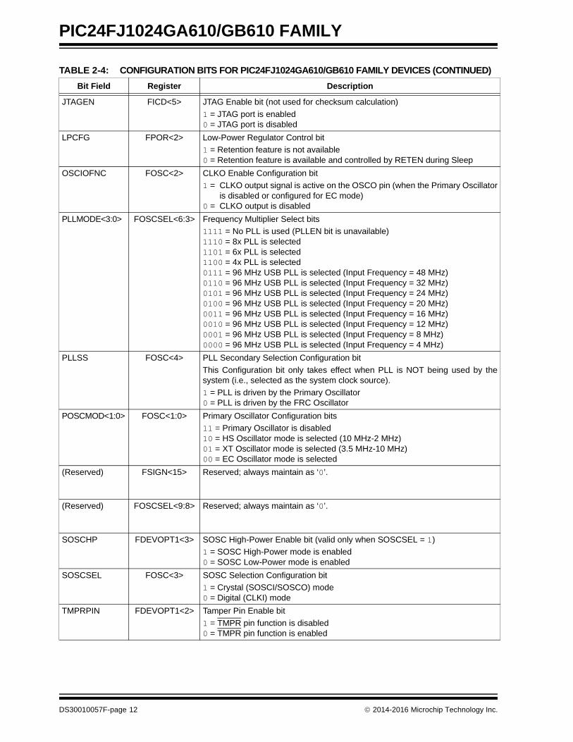
TABLE 2-4: CONFIGURATION BITS FOR PIC24FJ1024GA610/GB610 FAMILY DEVICES
Bit Field Register Description
AIVTDIS FSEC<15> Alternate Interrupt Vector Table Disable bit
1 = Disables AIVT; INTCON2<8> (AIVTEN) bit is not available0 = Enables AIVT; INTCON2<8> (AIVTEN) bit is available
ALTCMPI FDEVOPT1<1> Alternate Comparator Input Enable bit
1 = C1INC, C2INC and C3INC are on their standard pin locations0 = C1INC, C2INC and C3INC are on RG9
ALTVREF FDEVOPT1<14> Alternate Voltage Reference Location Enable bit(100-pin and 121-pin devices only)
1 = VREF+ and CVREF+ on RA10, VREF- and CVREF- on RA90 = VREF+ and CVREF+ on RB0, VREF- and CVREF- on RB1
BOREN<1:0> FPOR<1:0> Brown-out Reset Enable bits
11 = Brown-out Reset is enabled in hardware; SBOREN bit is disabled10 = Brown-out Reset is enabled only while device is active and disabled in
Sleep; SBOREN bit is disabled01 = Brown-out Reset is controlled with the SBOREN bit setting00 = Brown-out Reset is disabled in hardware; SBOREN bit is disabled
BSLIM<12:0> FBSLIM<12:0> Boot Segment Code Flash Page Address Limit bits
Specifies the last Boot Segment page + 1 (the first page of the General Segment). As this value is inverted, the default unprogrammed value (1FFFh) sets the Boot Segment size to 0.
BSS<1:0> FSEC<2:1> Boot Segment Code Protection Level bits
11 = No protection (other than BWRP)10 = Standard security0x = High security
BSEN FSEC<3> Boot Segment Control bit
1 = No Boot Segment is enabled0 = Boot Segment size is determined by BSLIM<12:0>
BTMODE<1:0> FBOOT<1:0> Device Partition Mode Configuration bits
11 = Single Partition Flash mode10 = Dual Partition Flash mode01 = Protected Dual Partition Flash mode (Partition 1 is write-protected
when inactive)00 = Reserved; do not use
BSEQ<11:0> FBTSEQ<11:0> Boot Sequence Number bits (Dual Partition Flash modes only)
Relative value defining which partition will be active after a device Reset; the partition containing a lower boot number will be active.
BTSWP FICD<15> BOOTSWP Instruction Enable bit
1 = BOOTSWP instruction is disabled0 = BOOTSWP instruction is enabled
BWRP FSEC<0> Boot Segment Program Write Protection bit
1 = Boot Segment can be written0 = Boot Segment is write-protected
CSS<2:0> FSEC<11:9> Configuration Segment Code Protection Level bits
111 = No protection (other than CWRP)110 = Standard security10x = Enhanced security0xx = High security
CWRP FSEC<8> Configuration Segment Program Write Protection bit
1 = Configuration Segment is not write-protected0 = Configuration Segment is write-protected
DS30010057F-page 10 2014-2016 Microchip Technology Inc.

PIC24FJ1024GA610/GB610 FAMILY
DEBUG FICD<7> Background Debugger Enable bit
1 = Background debugger is disabled0 = Background debugger is enabled
DNVPEN FPOR<3> Downside Voltage Protection Enable bit
1 = Downside protection is enabled using BOR; BOR re-arms POR as needed0 = Downside protection is disabled when BOR is inactive
FCKSM<1:0> FOSC<7:6> Clock Switching and Monitor Selection bits
1x = Clock switching and the Fail-Safe Clock Monitor are disabled01 = Clock switching is enabled, Fail-Safe Clock Monitor is disabled00 = Clock switching and the Fail-Safe Clock Monitor are enabled
FNOSC<2:0> FOSCSEL<2:0> Oscillator Selection bits
111 = Oscillator with Frequency Divider (OSCFDIV)110 = Digitally Controlled Oscillator (DCO)101 = Low-Power RC Oscillator (LPRC)100 = Secondary Oscillator (SOSC)011 = Primary Oscillator with PLL (XTPLL, HSPLL, ECPLL)010 = Primary Oscillator (XT, HS, EC)001 = Fast RC Oscillator with PLL (FRCPLL)000 = Fast RC Oscillator (FRC)
FWDTEN<1:0> FWDT<6:5> Watchdog Timer Enable bits
11 = WDT is enabled10 = WDT is disabled (control is placed on the SWDTEN bit)01 = WDT is enabled only while device is active and disabled in Sleep;
SWDTEN bit is disabled00 = WDT and SWDTEN are disabled
FWPSA FWDT<4> Watchdog Timer Prescaler bit
1 = WDT prescaler ratio of 1:1280 = WDT prescaler ratio of 1:32
GCP<1:0> FSEC<7:6> General Segment Code Protection Level bits
11 = No protection (other than GWRP)10 = Standard security0x = High security
GWRP FSEC<5> General Segment Program Write Protection bit
1 = General Segment is not write-protected0 = General Segment is write-protected
IBSEQ<11:0> FBTSEQ<23:12> Inverse Boot Sequence Number bits (Dual Partition Flash modes only)
The one’s complement of BSEQ<11:0>; must be calculated by the user and written into device programming.
ICS<1:0> FICD<1:0> ICD Communication Channel Select bits
11 = Communicates on PGEC1/PGED110 = Communicates on PGEC2/PGED201 = Communicates on PGEC3/PGED300 = Reserved; do not use
IESO FOSCSEL<7> Two-Speed Oscillator Start-up Enable bit
1 = Starts up the device with FRC, then automatically switches to theuser-selected oscillator when ready
0 = Starts up the device with the user-selected oscillator source
IOL1WAY FOSC<5> Peripheral Pin Select Configuration bit
1 = The IOLOCK bit can be set only once (with unlock sequence).0 = The IOLOCK bit can be set and cleared as needed (with unlock sequence)
TABLE 2-4: CONFIGURATION BITS FOR PIC24FJ1024GA610/GB610 FAMILY DEVICES (CONTINUED)
Bit Field Register Description
2014-2016 Microchip Technology Inc. DS30010057F-page 11
PIC24FJ1024GA610/GB610 FAMILY
JTAGEN FICD<5> JTAG Enable bit (not used for checksum calculation)
1 = JTAG port is enabled0 = JTAG port is disabled
LPCFG FPOR<2> Low-Power Regulator Control bit
1 = Retention feature is not available0 = Retention feature is available and controlled by RETEN during Sleep
OSCIOFNC FOSC<2> CLKO Enable Configuration bit
1 = CLKO output signal is active on the OSCO pin (when the Primary Oscillatoris disabled or configured for EC mode)
0 = CLKO output is disabled
PLLMODE<3:0> FOSCSEL<6:3> Frequency Multiplier Select bits
1111 = No PLL is used (PLLEN bit is unavailable)1110 = 8x PLL is selected1101 = 6x PLL is selected1100 = 4x PLL is selected0111 = 96 MHz USB PLL is selected (Input Frequency = 48 MHz)0110 = 96 MHz USB PLL is selected (Input Frequency = 32 MHz)0101 = 96 MHz USB PLL is selected (Input Frequency = 24 MHz)0100 = 96 MHz USB PLL is selected (Input Frequency = 20 MHz)0011 = 96 MHz USB PLL is selected (Input Frequency = 16 MHz)0010 = 96 MHz USB PLL is selected (Input Frequency = 12 MHz)0001 = 96 MHz USB PLL is selected (Input Frequency = 8 MHz)0000 = 96 MHz USB PLL is selected (Input Frequency = 4 MHz)
PLLSS FOSC<4> PLL Secondary Selection Configuration bit
This Configuration bit only takes effect when PLL is NOT being used by thesystem (i.e., selected as the system clock source).
1 = PLL is driven by the Primary Oscillator0 = PLL is driven by the FRC Oscillator
POSCMOD<1:0> FOSC<1:0> Primary Oscillator Configuration bits
11 = Primary Oscillator is disabled10 = HS Oscillator mode is selected (10 MHz-2 MHz)01 = XT Oscillator mode is selected (3.5 MHz-10 MHz)00 = EC Oscillator mode is selected
(Reserved) FSIGN<15> Reserved; always maintain as ‘0’.
(Reserved) FOSCSEL<9:8> Reserved; always maintain as ‘0’.
SOSCHP FDEVOPT1<3> SOSC High-Power Enable bit (valid only when SOSCSEL = 1)
1 = SOSC High-Power mode is enabled0 = SOSC Low-Power mode is enabled
SOSCSEL FOSC<3> SOSC Selection Configuration bit
1 = Crystal (SOSCI/SOSCO) mode0 = Digital (CLKI) mode
TMPRPIN FDEVOPT1<2> Tamper Pin Enable bit
1 = TMPR pin function is disabled0 = TMPR pin function is enabled
TABLE 2-4: CONFIGURATION BITS FOR PIC24FJ1024GA610/GB610 FAMILY DEVICES (CONTINUED)
Bit Field Register Description
DS30010057F-page 12 2014-2016 Microchip Technology Inc.

PIC24FJ1024GA610/GB610 FAMILY
2.6.3 CUSTOMER OTP MEMORY
PIC24FJ1024GA610/GB610 family devices provide384 bytes of One-Time-Programmable (OTP) memory,located at addresses, 801700h through 8017FEh.This memory can be used for persistent storage ofapplication-specific information that will not be erasedby reprogramming the device. This includes manytypes of information, such as:
• Application checksums• Code revision information• Product information• Serial numbers• System manufacturing dates• Manufacturing lot numbers
Customer OTP memory may be programmed in anymode, including user RTSP mode, but it cannot beerased. Data is not cleared by a Chip Erase.
WDTCLK<1:0> FWDT<14:13> Watchdog Timer Clock Select bits
11 = Always uses INTOSC/LPRC10 = Uses FRC when WINDIS = 0, system clock is not INTOSC/LPRC and
device is not in Sleep; otherwise, uses INTOSC/LPRC01 = Always uses SOSC00 = Uses peripheral clock when system clock is not INTOSC/LPRC and device
is not in Sleep; otherwise, uses INTOSC/LPRC
WDTCMX FWDT<11> WDT Clock MUX Control bit
1 = Enables WDT clock MUX0 = WDT clock MUX is disabled
WDTPS<3:0> FWDT<3:0> Watchdog Timer Postscaler bits
1111 = 1:32,7681110 = 1:16,3841101 = 1:8,1921100 = 1:4,0961011 = 1:2,0481010 = 1:1,0241001 = 1:5121000 = 1:2560111 = 1:1280110 = 1:640101 = 1:320100 = 1:160011 = 1:80010 = 1:40001 = 1:20000 = 1:1
WDTWIN<1:0> FWDT<9:8> Watchdog Timer Window Width bits
11 = WDT window is 25% of the WDT period10 = WDT window is 37.5% of the WDT period01 = WDT window is 50% of the WDT period00 = WDT window is 75% of the WDT period
WINDIS FWDT<7> Windowed Watchdog Timer Disable bit
1 = Windowed WDT is disabled0 = Windowed WDT is enabled
TABLE 2-4: CONFIGURATION BITS FOR PIC24FJ1024GA610/GB610 FAMILY DEVICES (CONTINUED)
Bit Field Register Description
Note: OTP memory should only be written toonce or ECC errors/traps may occur.
2014-2016 Microchip Technology Inc. DS30010057F-page 13

PIC24FJ1024GA610/GB610 FAMILY
3.0 DEVICE PROGRAMMING – ICSP
ICSP mode is a special programming protocol thatallows you to read and write to device memory. TheICSP mode is the most direct method used to programthe device, which is accomplished by applying controlcodes and instructions serially to the device, using thePGECx and PGEDx pins. ICSP mode also has theability to read executive memory to determine if theProgramming Executive (PE) is present and to writethe PE to executive memory if Enhanced ICSP modewill be used.
In ICSP mode, the system clock is taken from thePGECx pin, regardless of the device’s oscillator Con-figuration bits. All instructions are shifted serially into aninternal buffer, then loaded into the Instruction Register(IR) and executed. No program fetching occurs frominternal memory. Instructions are fed in 24 bits at atime. PGEDx is used to shift data in, and PGECx isused as both the serial shift clock and the CPUexecution clock.
3.1 Overview of the Programming Process
Figure 3-1 illustrates the high-level overview of theprogramming process. After entering ICSP mode, thefirst action is to Chip Erase program memory. Next, thecode memory is programmed, followed by the deviceConfiguration bits. Code memory (including the Config-uration bits) is then verified to ensure that programmingwas successful. Then, the code-protect Configurationbits are programmed, if required.
FIGURE 3-1: HIGH-LEVEL ICSP™ PROGRAMMING FLOW
Note 1: During ICSP operation, the operatingfrequency of PGECx must not exceed5 MHz.
2: ICSP mode is slower than EnhancedICSP mode for programming.
Start
Perform ChipErase
Program Memory,
Verify Program Memory,
End
Enter ICSP™
Program Code-Protect
Exit ICSP
Configuration Wordsand User ID Words
Configuration Wordsand User ID Words
Configuration Bits
DS30010057F-page 14 2014-2016 Microchip Technology Inc.
PIC24FJ1024GA610/GB610 FAMILY
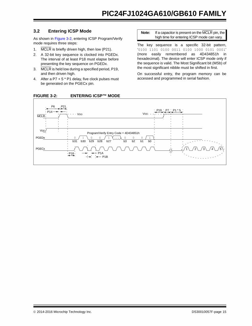
3.2 Entering ICSP Mode
As shown in Figure 3-2, entering ICSP Program/Verifymode requires three steps:
1. MCLR is briefly driven high, then low (P21).
2. A 32-bit key sequence is clocked into PGEDx.The interval of at least P18 must elapse beforepresenting the key sequence on PGEDx.
3. MCLR is held low during a specified period, P19,and then driven high.
4. After a P7 + 5 * P1 delay, five clock pulses mustbe generated on the PGECx pin.
The key sequence is a specific 32-bit pattern,‘0100 1101 0100 0011 0100 1000 0101 0001’(more easily remembered as 4D434851h inhexadecimal). The device will enter ICSP mode only ifthe sequence is valid. The Most Significant bit (MSb) ofthe most significant nibble must be shifted in first.
On successful entry, the program memory can beaccessed and programmed in serial fashion.
FIGURE 3-2: ENTERING ICSP™ MODE
Note: If a capacitor is present on the MCLR pin, thehigh time for entering ICSP mode can vary.
MCLR
PGEDx
PGECx
VDD
P6
P14
b31 b30 b29 b28 b27 b2 b1 b0b3...
Program/Verify Entry Code = 4D434851h
P1AP1B
P18
P19
0 1 0 0 1 0 0 0 1
P7VDD VDD
P21P1 * 5
1 2 3 4 5
2014-2016 Microchip Technology Inc. DS30010057F-page 15

PIC24FJ1024GA610/GB610 FAMILY
3.3 ICSP Operation
After entering into ICSP mode, the CPU is Idle.Execution of the CPU is governed by an internal statemachine. A 4-bit control code is clocked in usingPGECx and PGEDx, and this control code is used tocommand the CPU (see Table 3-1).
The SIX control code is used to send instructions to theCPU for execution and the REGOUT control code isused to read data out of the device through the VISIregister.
TABLE 3-1: CPU CONTROL CODES IN ICSP™ MODE
3.3.1 SIX SERIAL INSTRUCTION EXECUTION
The SIX control code allows execution of assemblyinstructions. When the SIX code is received, the CPU issuspended for 24 clock cycles as the instruction is thenclocked into the internal buffer. Once the instruction isshifted in, the state machine allows it to be executed overthe next four clock cycles. While the received instructionis executed, the state machine simultaneously shifts inthe next 4-bit command (see Figure 3-3).
FIGURE 3-3: SIX SERIAL EXECUTION
4-Bit Control Code
Mnemonic Description
0000 SIX Shift in 24-bit instruction and execute.
0001 REGOUT Shift out the VISIregister.
0010-1111 N/A Reserved.
Note 1: The device will latch input PGEDx dataon the rising edge of PGECx. For all datatransmissions, the Least Significant bit(LSb) is transmitted first.
2: TBLRDH, TBLRDL, TBLWTH and TBLWTLinstructions must be followed by two NOPinstructions.
3: During ISCP programming, the CLKO pinwill toggle. If external logic is connected toCLKO, be sure that this toggling will noteffect the circuitry during the programmingsequence.
P4
1 2 3 23 24 1 2 3 4
P1
PGECx
P4a
PGEDx
24-Bit Instruction Fetch Execute 24-Bit Instruction,Execute PC – 1,Fetch SIX Control Code Fetch Next Control Code
4 5 6 7 8 18 19 20 21 2217
LSB X X X X X X X X X X X X X X MSB
PGEDx = Input
P2
P3
P1B
P1A
1 2
0 0 0 00 0
3 4
0 0
DS30010057F-page 16 2014-2016 Microchip Technology Inc.

PIC24FJ1024GA610/GB610 FAMILY
3.3.2 REGOUT SERIAL INSTRUCTION EXECUTION
The REGOUT control code allows for data to beextracted from the device in ICSP mode. It is used toclock the contents of the VISI register, out of the device,over the PGEDx pin. After the REGOUT control code isreceived, the CPU is held Idle for eight cycles. Afterthese eight cycles, an additional 16 cycles are requiredto clock the data out (see Figure 3-4).
The REGOUT code is unique because the PGEDx pin isan input when the control code is transmitted to thedevice. However, after the control code is processed,the PGEDx pin becomes an output as the VISI registeris shifted out.
FIGURE 3-4: REGOUT SERIAL EXECUTION
Note: The device will output data on the PGEDxline on the rising edge of PGECx. For alldata transmissions, the Least Significantbit (LSb) is transmitted first.
1 2 3 4 1 2 7 8
PGECx
P4
PGEDx
PGEDx = Input
Execute Previous Instruction, CPU Held in Idle Shift Out VISI Register<15:0>
P5
PGEDx = Output
1 2 3 1 2 3 4
P4a
11 13 15 161412
No Execution Takes Place,Fetch Next Control Code
0 0 0 0 0
PGEDx = Input
MSb1 2 3 41
4 5 6
LSb 141312... 11100
Fetch REGOUT Control Code
0
2014-2016 Microchip Technology Inc. DS30010057F-page 17

PIC24FJ1024GA610/GB610 FAMILY
3.4 Flash Memory Programming in ICSP Mode
3.4.1 PROGRAMMING OPERATIONS
Flash memory write/erase operations are controlled bythe NVMCON register. Programming is performed bysetting NVMCON to select the type of erase operation(Table 3-2) or write operation (Table 3-3) and initiatingthe programming by setting the WR control bit(NVMCON<15>).
In ICSP mode, all programming operations areself-timed. The WR control bit is cleared by hardwarewhen the programming operation is complete. TheICSP programmer must supply enough clock pulses onthe PGECx pin to complete the erase or program oper-ation. Refer to Section 10.0 “AC/DC Characteristicsand Timing Requirements” for detailed informationabout the maximum number of clock pulses requiredfor erase or write operations.
TABLE 3-2: NVMCON ERASE OPERATIONS
TABLE 3-3: NVMCON WRITE OPERATIONS
3.4.2 STARTING AND STOPPING A PROGRAMMING CYCLE
For protection against accidental operations, the erase/write initiate sequence must be written to the NVMKEYregister to allow any erase or program operation toproceed. The three instructions following the start ofthe programming sequence should be NOPs. To start anerase or write sequence, the following steps must becompleted:
1. Write 55h to the NVMKEY register.
2. Write AAh to the NVMKEY register.
3. Set the WR bit in the NVMCON register.
4. Execute three NOP instructions.
All erase and write cycles are self-timed. The WR bitcan be polled to supply enough PGECx clock pulses forthe operation and determine if the erase or write cyclehas been completed.
NVMCONValue
Erase Operation
400Eh Chip Erase (erases user memory, does not erase executive memory, Device ID or customer OTP).
4003h Erases a page of program or executive memory.
4004h Erases user memory and Configuration Words in the Inactive Partition (Dual Partition Flash modes only).
NVMCONValue
Write Operation
4001h Double-word program operation.
4002h Row programming operation.
4008h The next WR command will perform a Boot mode program (writing to FBOOT) and then program the Dual Partition Sig-nature (FSIGN) bit. Device must be reset before the newly programmed mode can take effect.
DS30010057F-page 18 2014-2016 Microchip Technology Inc.

PIC24FJ1024GA610/GB610 FAMILY
3.5 Erasing Program Memory
The general procedure for erasing user memory isshown in Figure 3-5. The process for Chip Erase, PageErase and Inactive Partition Erase are all similar, andare described in Table 3-4 through Table 3-6.
The last row of the last page of program memorycontains the Configuration Words. Before programmingthese Words, they must be erased. If they are erasedwith a Page Erase operation, all other rows in the pagewill also be erased. Users may want to either avoidusing the rest of this page for application code or ensurethat the non-configuration data in the CS page is copiedbefore the erase and reprogrammed afterwards.
FIGURE 3-5: ERASE FLOW
TABLE 3-4: SERIAL EXECUTION FOR CHIP ERASE
Note 1: Program memory must be erased beforewriting any data to program memory.
2: For Page Erase operations, theNVMADR/NVMADRU registers mustalso be loaded with the address of thepage to be erased.
Start
End
Set the WR bit to Initiate Erase
Write Appropriate Value to NVMCON<3:0>
Poll WR bit to Supply Enough Clock Pulsesand Determine when Erase Cycle
is Completed
Command (Binary)
Data (Hex)
Description
Step 1: Exit the Reset vector.
000000000000
000000040200000000
NOPGOTO 0x200NOP
Step 2: Configure the NVMCON register to perform a Chip Erase.
00000000
2400E0883B00
MOV #0x400E, W0MOV W0, NVMCON
Step 3: Set the WR bit.
00000000000000000000000000000000
200550883B30200AA0883B30A8E761000000000000000000
MOV #0x55, W0MOV W0, NVMKEYMOV #0xAA, W0MOV W0, NVMKEYBSET NVMCON, #WRNOPNOPNOP
Step 4: Repeat this step to poll the WR bit until it is cleared by hardware.
00000000000000000000000000010000
040200000000803B02000000883C22000000<VISI>000000
GOTO 0x200NOPMOV NVMCON, W2NOPMOV W2, VISINOP; Clock out the contents of the VISI register.NOP
Step 5: Clear the WREN bit.
00000000
200000883B00
MOV #0000, W0MOV W0, NVMCON
2014-2016 Microchip Technology Inc. DS30010057F-page 19

PIC24FJ1024GA610/GB610 FAMILY
TABLE 3-5: SERIAL EXECUTION FOR PAGE ERASE
Command (Binary)
Data (Hex)
Description
Step 1: Exit the Reset vector.
000000000000
000000 040200 000000
NOPGOTO 0x200NOP
Step 2: Set the NVMCON register to erase a page.
00000000
240030 883B00
MOV #0x4003, W0MOV W0, NVMCON
Step 3: Load the address of the page to be erased into the NVMADR register pair.
0000000000000000
200000 883B10 200000 883B20
MOV #PAGE_ADDR_LO, W0MOV W0, NVMADRMOV #PAGE_ADDR_HI, W0MOV W0, NVMADRU
Step 4: Set the WR bit.
00000000000000000000000000000000
200550 883B30 200AA0 883B30 A8E761 000000 000000 000000
MOV #0x55, W0MOV W0, NVMKEYMOV #0xAA, W0MOV W0, NVMKEYBSET NVMCON, #WRNOPNOPNOP
Step 5: Repeat this step to poll the WR bit until it is cleared by hardware.
00000000000000000000000000010000
040200 000000 803B02 000000883C22 000000 <VISI>000000
GOTO 0x200NOPMOV NVMCON, W2NOPMOV W2, VISINOP; Clock out the contents of the VISI register.NOP
Step 6: Clear the WREN bit.
00000000
200000 883B00
MOV #0000, W0MOV W0, NVMCON
DS30010057F-page 20 2014-2016 Microchip Technology Inc.

PIC24FJ1024GA610/GB610 FAMILY
TABLE 3-6: SERIAL EXECUTION FOR INACTIVE PARTITION ERASE
Command (Binary)
Data (Hex)
Description
Step 1: Exit the Reset vector.
000000000000
000000 040200 000000
NOPGOTO 0x200NOP
Step 2: Set the NVMCON register to erase a page.
00000000
240040 883B00
MOV #0x4004, W0MOV W0, NVMCON
Step 3: Set the WR bit.
00000000000000000000000000000000
200550 883B30 200AA0 883B30 A8E761 000000 000000 000000
MOV #0x55, W0MOV W0, NVMKEYMOV #0xAA, W0MOV W0, NVMKEYBSET NVMCON, #WRNOPNOPNOP
Step 4: Repeat this step to poll the WR bit until it is cleared by hardware.
0000000000000000000000010000
040200 000000 803B02 883C22 000000 <VISI>000000
GOTO 0x200NOPMOV NVMCON, W2MOV W2, VISINOP; Clock out the contents of the VISI register.NOP
Step 5: Clear the WREN bit.
00000000
200000 883B00
MOV #0000, W0MOV W0, NVMCON
2014-2016 Microchip Technology Inc. DS30010057F-page 21

PIC24FJ1024GA610/GB610 FAMILY
3.6 Writing Code Memory
For PIC24FJ1024GA610/GB610 devices, code memoryis written in three steps:
• Writing the data to memory-mapped write latches (located in the configuration memory space at addresses, FA0000h through FA00FEh);
• Setting a destination address
• Initiating the memory write sequence
There are two methods available for writing to codememory: double-word writes using the write latches or128-word row writes. Figure 3-7 provides a high-leveldescription of the two methods.
Double-word writes program code memory with twoinstruction words at a time. Two words are loaded intothe write latches. Next, the write sequence is initiated,and finally, the WR bit is checked for the sequence tobe complete. This process continues for all the data tobe programmed.
Table 3-7 provides an example of ICSP programmingfor a double-word write operation.
The data loaded into the programming latches must bein the packed format, as shown in Figure 3-6.
FIGURE 3-6: PACKED INSTRUCTION WORD FORMAT
FIGURE 3-7: PROGRAM CODE MEMORY FLOW
Note: When the number of instruction wordstransferred is odd, MSB2 is zero andLSW2 cannot be transmitted.
15 8 7 0
LSW1
MSB2 MSB1
LSW2
LSWx: Least Significant 16 bits of instruction wordMSBx: Most Significant Byte of instruction word
Start
Configure Devicefor Writes
All Data Written?
No
Yes
Initiate WriteSequence and Poll
WR bit to be Cleared
Initialize Write Pointerwith Row Address
(DestinationAddress)
Load Two Words intoWrite Latches
IncrementWrite Pointer
End
No
Using RAM RowProgramming
Using Two-WordProgramming
Load 128 Words
into Write Latches
DS30010057F-page 22 2014-2016 Microchip Technology Inc.
PIC24FJ1024GA610/GB610 FAMILY
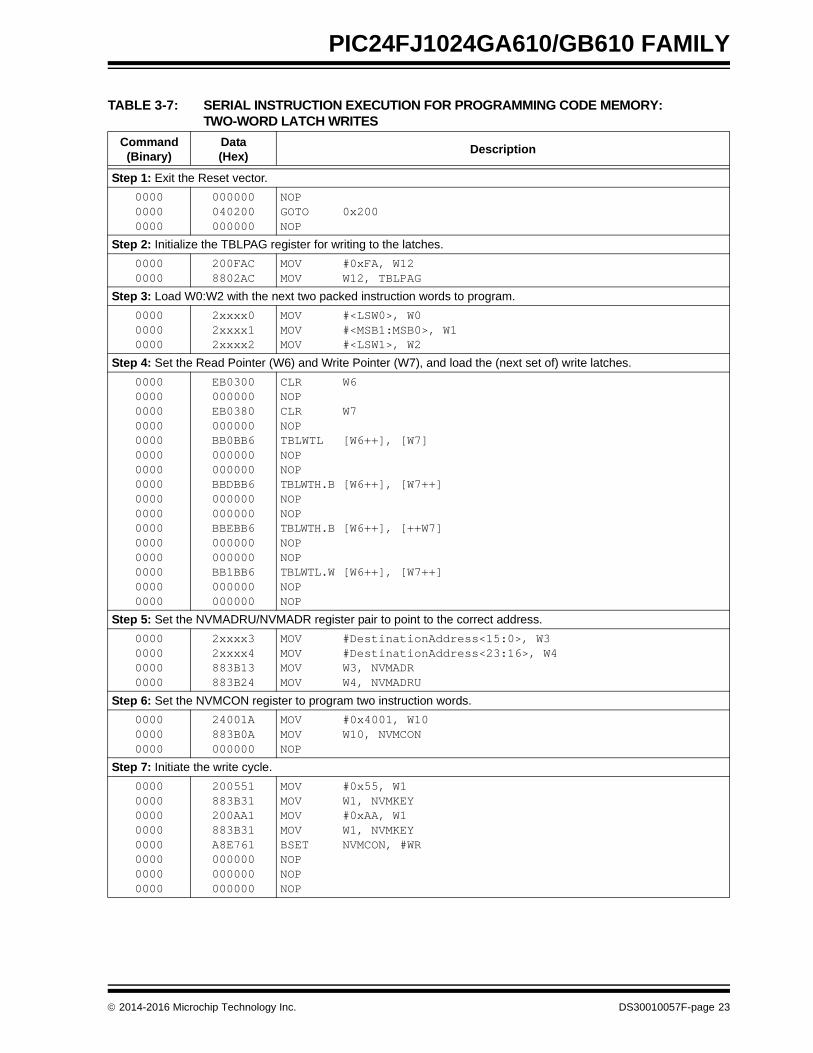
TABLE 3-7: SERIAL INSTRUCTION EXECUTION FOR PROGRAMMING CODE MEMORY:TWO-WORD LATCH WRITES
Command(Binary)
Data(Hex)
Description
Step 1: Exit the Reset vector.
000000000000
000000040200000000
NOPGOTO 0x200NOP
Step 2: Initialize the TBLPAG register for writing to the latches.
00000000
200FAC8802AC
MOV #0xFA, W12MOV W12, TBLPAG
Step 3: Load W0:W2 with the next two packed instruction words to program.
000000000000
2xxxx02xxxx12xxxx2
MOV #<LSW0>, W0MOV #<MSB1:MSB0>, W1MOV #<LSW1>, W2
Step 4: Set the Read Pointer (W6) and Write Pointer (W7), and load the (next set of) write latches.
0000000000000000000000000000000000000000000000000000000000000000
EB0300000000EB0380000000BB0BB6000000000000BBDBB6000000000000BBEBB6000000000000BB1BB6000000000000
CLR W6NOPCLR W7NOPTBLWTL [W6++], [W7]NOPNOPTBLWTH.B [W6++], [W7++]NOPNOPTBLWTH.B [W6++], [++W7]NOPNOPTBLWTL.W [W6++], [W7++]NOP NOP
Step 5: Set the NVMADRU/NVMADR register pair to point to the correct address.
0000000000000000
2xxxx32xxxx4883B13883B24
MOV #DestinationAddress<15:0>, W3MOV #DestinationAddress<23:16>, W4MOV W3, NVMADRMOV W4, NVMADRU
Step 6: Set the NVMCON register to program two instruction words.
000000000000
24001A883B0A000000
MOV #0x4001, W10MOV W10, NVMCONNOP
Step 7: Initiate the write cycle.
00000000000000000000000000000000
200551883B31200AA1883B31A8E761000000000000000000
MOV #0x55, W1MOV W1, NVMKEYMOV #0xAA, W1MOV W1, NVMKEYBSET NVMCON, #WRNOPNOPNOP
2014-2016 Microchip Technology Inc. DS30010057F-page 23

PIC24FJ1024GA610/GB610 FAMILY
Step 8: Wait for the program operation to complete and make sure the WR bit is clear.
0000000000000001000000000000
—
803B00883C20000000<VISI>000000040200000000
—
MOV NVMCON, W0MOV W0, VISINOP; Clock out the contents of the VISI register.NOPGOTO 0x200NOP; Repeat until the WR bit is clear.
Step 9: Repeat Steps 3-8 until all code memory is programmed.
Step 10: Clear the WREN bit.
00000000
200000 883B00
MOV #0000, W0MOV W0, NVMCON
TABLE 3-7: SERIAL INSTRUCTION EXECUTION FOR PROGRAMMING CODE MEMORY:TWO-WORD LATCH WRITES (CONTINUED)
Command(Binary)
Data(Hex)
Description
DS30010057F-page 24 2014-2016 Microchip Technology Inc.

PIC24FJ1024GA610/GB610 FAMILY
Row writes program one row (128 instruction words) ata time. First, the Table Pointer is initialized to point tothe program latches and data is written into them withTable Writes. Next, the Write Pointer is initialized(NVMADRU and NVMADR register pair) with the rowaddress (DestinationAddress). Finally, the writesequence is initiated and the WR bit is checked for therow programming to be complete. This process isrepeated for all data to be programmed. Table 3-8shows the ICSP programming details for row writes.
To minimize programming time, the data to be pro-grammed is stored in the W0:W5 registers in a packeddata format (Figure 3-8). This is the same packedformat used by the PE. See Section 6.2.2 “PackedData Format” for additional information.
FIGURE 3-8: PACKED INSTRUCTION WORD STORAGE IN W0:W5
MSB0MSB1
LSW1
LSW0
0715
MSB2MSB3
LSW3
LSW2
W0
W1
W2
W3
W4
W5
TABLE 3-8: SERIAL INSTRUCTION EXECUTION FOR PROGRAMMING CODE MEMORY: ROW WRITES
Command(Binary)
Data(Hex)
Description
Step 1: Exit the Reset vector.
000000000000
000000040200000000
NOPGOTO 0x200NOP
Step 2: Set the NVMCON register to program 128 instruction words.
00000000
240020883B00
MOV #0X4002, W0MOV W0, NVMCON
Step 3: Initialize the TBLPAG register for writing to the latches.
00000000
200FAC8802AC
MOV #0xFA, W12MOV W12, TBLPAG
Step 4: Load W0:W5 with the next 4 instruction words to program.
000000000000000000000000
2xxxx02xxxx12xxxx22xxxx32xxxx42xxxx5
MOV #<LSW0>, W0MOV #<MSB1:MSB0>, W1MOV #<LSW1>, W2MOV #<LSW2>, W3MOV #<MSB3:MSB2>, W4MOV #<LSW3>, W5
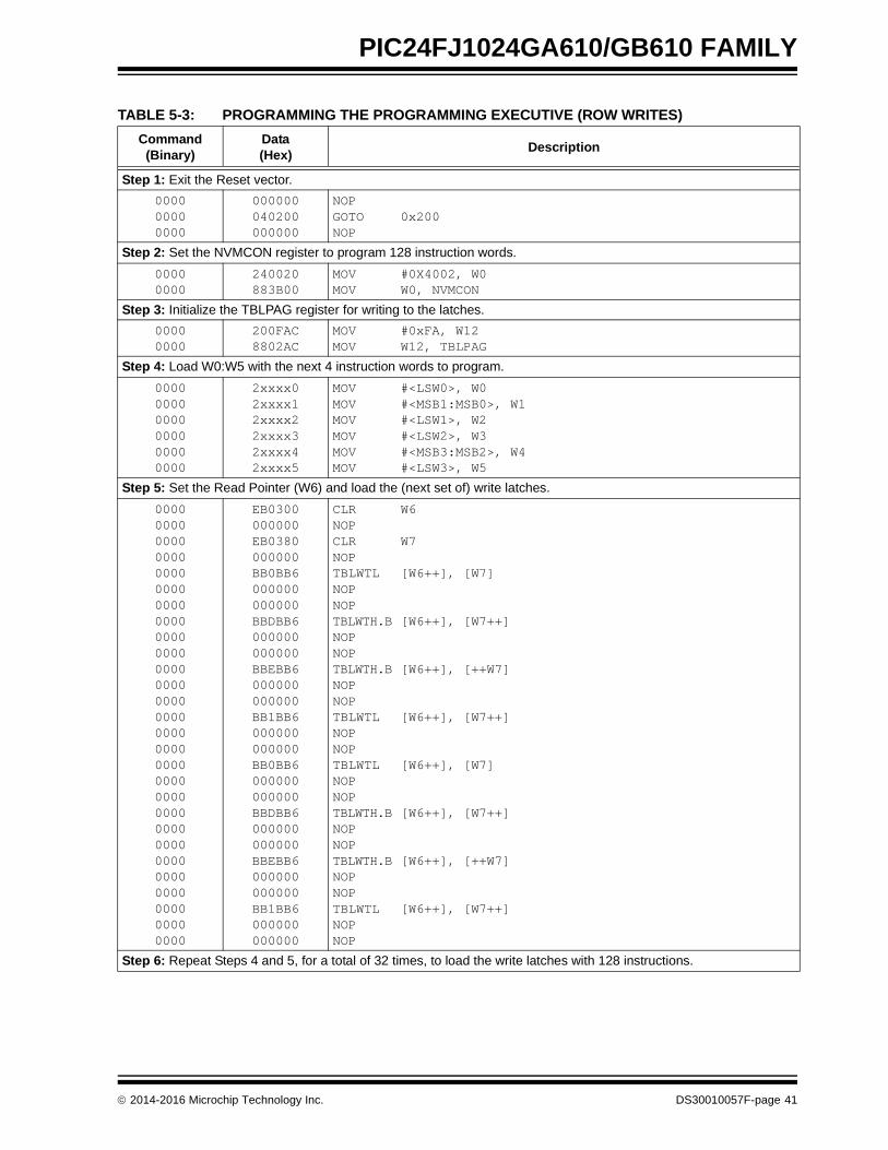
Step 5: Set the Read Pointer (W6) and load the (next set of) write latches.
0000000000000000000000000000
EB0300000000EB0380000000BB0BB6000000000000
CLR W6NOPCLR W7NOPTBLWTL [W6++], [W7]NOPNOP
2014-2016 Microchip Technology Inc. DS30010057F-page 25

PIC24FJ1024GA610/GB610 FAMILY
Step 5: Set the Read Pointer (W6) and load the (next set of) write latches. (Continued)
000000000000000000000000000000000000000000000000000000000000000000000000000000000000
BBDBB6000000000000BBEBB6000000000000BB1BB6000000000000BB0BB6000000000000BBDBB6000000000000BBEBB6000000000000BB1BB6000000000000
TBLWTH.B [W6++], [W7++]NOPNOPTBLWTH.B [W6++], [++W7]NOPNOPTBLWTL [W6++], [W7++]NOPNOPTBLWTL [W6++], [W7]NOPNOPTBLWTH.B [W6++], [W7++]NOPNOPTBLWTH.B [W6++], [++W7]NOPNOPTBLWTL [W6++], [W7++]NOPNOP
Step 6: Repeat Steps 4 and 5, for a total of 32 times, to load the write latches with 128 instructions.
Step 7: Set the NVMADRU/NVMADR register pair to point to the correct address.
0000000000000000
2xxxx32xxxx4883B13883B24
MOV #DestinationAddress<15:0>, W3MOV #DestinationAddress<23:16>, W4MOV W3, NVMADRMOV W4, NVMADRU
Step 8: Execute the WR bit unlock sequence and initiate the write cycle.
00000000000000000000000000000000
200550883B30200AA0883B30A8E761000000000000000000
MOV #0x55, W0MOV W0, NVMKEYMOV #0xAA, W0MOV W0, NVMKEYBSET NVMCON, #WRNOPNOPNOP
Step 9: Repeat this step to poll the WR bit until it is cleared by hardware.
0000000000000000000000010000
040200 000000 803B02 883C22 000000 <VISI>000000
GOTO 0x200NOPMOV NVMCON, W2MOV W2, VISINOP; Clock out the contents of the VISI register.NOP
Step 10: Reset the device’s internal Program Counter (PC).
00000000
040200000000
GOTO 0x200NOP
Step 11: Repeat Steps 3 through 9 until all code memory is programmed.
Step 12: Clear the WREN bit.
00000000
200000 883B00
MOV #0000, W0MOV W0, NVMCON
TABLE 3-8: SERIAL INSTRUCTION EXECUTION FOR PROGRAMMING CODE MEMORY: ROW WRITES (CONTINUED)
Command(Binary)
Data(Hex)
Description
DS30010057F-page 26 2014-2016 Microchip Technology Inc.

PIC24FJ1024GA610/GB610 FAMILY
3.7 Writing Configuration Bits
The procedure for writing Configuration bits is similar tothe procedure for writing code memory. Table 3-9shows the ICSP programming details for writing theConfiguration bits.
For all Configuration Words, except FBTSEQ, only thelower two bytes of the word contain configuration data;the upper byte is unused. It is recommended that theupper byte be programmed with FFFFh, as indicatedin Step 3. FBTSEQ (implemented only in Dual Parti-tion Flash modes) uses all 24 bits of the programmemory’s width to store the Boot Sequence Numberbits, BSEQ<11:0> (FBTSEQ<11:0>), and its one’scomplement, IBSEQ<11:0> (FBTSEQ<23:12>).
To change the values of the Configuration bits once theyhave been programmed, the device must be erased, asdescribed in Section 3.5 “Erasing Program Memory”,and reprogrammed to the desired value. Note that it isonly possible to program a Configuration bit from ‘1’ to‘0’ to enable code protection; it is not possible toprogram it from ‘0’ to ‘1’.
TABLE 3-9: SERIAL INSTRUCTION EXECUTION FOR PROGRAMMING CONFIGURATION WORDS:TWO-WORD LATCH WRITES
Command(Binary)
Data(Hex)
Description
Step 1: Exit the Reset vector.
000000000000
000000040200000000
NOPGOTO 0x200NOP
Step 2: Initialize the TBLPAG register for writing to the latches.
00000000
200FAC8802AC
MOV #0xFA, W12MOV W12, TBLPAG
Step 3: Load W0:W1 with the next two Configuration Words to program.
00000000—
0000
2xxxx02FFxx1
—2FFFF2
MOV #<Config lower word data>, W0MOV #<Config upper word data>, W1; Upper word is 0xFFFF for all Configuration Words except FBTSEQMOV #0xFFFF, W2
Step 4: Set the Read Pointer (W6) and Write Pointer (W7), and load the (next set of) write latches.
0000000000000000000000000000000000000000000000000000000000000000
EB0300000000EB0380000000BB0BB6000000000000BBDBB6000000000000BBEBB6000000000000BB1BB6000000000000
CLR W6NOPCLR W7NOPTBLWTL [W6++], [W7]NOPNOPTBLWTH.B [W6++], [W7++]NOPNOPTBLWTH.B [W6++], [++W7] NOPNOPTBLWTL.W [W6++], [W7++] NOPNOP
Step 5: Set the NVMADRU/NVMADR register pair to point to the correct address.
0000000000000000
2xxxx32xxxx4883B13883B24
MOV #DestinationAddress<15:0>, W3MOV #DestinationAddress<23:16>, W4MOV W3, NVMADRMOV W4, NVMADRU
2014-2016 Microchip Technology Inc. DS30010057F-page 27

PIC24FJ1024GA610/GB610 FAMILY
Step 6: Set the NVMCON register to program two instruction words.
000000000000
24001A883B0A000000
MOV #0x4001, W10MOV W10, NVMCONNOP
Step 7: Initiate the write cycle.
00000000000000000000000000000000
200551883B31200AA1883B31A8E761000000000000000000
MOV #0x55, W1MOV W1, NVMKEYMOV #0xAA, W1MOV W1, NVMKEYBSET NVMCON, #WRNOPNOPNOP
Step 8: Wait for program operation to complete and make sure the WR bit is clear.
0000000000000001000000000000
—
803B00883C20000000<VISI>000000040200000000
—
MOV NVMCON, W0MOV W0, VISINOP; Clock out the contents of the VISI register.NOPGOTO 0x200NOP; Repeat until the WR bit is clear.
Step 9: Repeat Steps 3-8 until all code memory is programmed.
Step 10: Clear the WREN bit.
00000000
200000 883B00
MOV #0000, W0MOV W0, NVMCON
TABLE 3-9: SERIAL INSTRUCTION EXECUTION FOR PROGRAMMING CONFIGURATION WORDS:TWO-WORD LATCH WRITES (CONTINUED)
Command(Binary)
Data(Hex)
Description
DS30010057F-page 28 2014-2016 Microchip Technology Inc.

PIC24FJ1024GA610/GB610 FAMILY
3.8 Reading Code Memory
Reading from code memory is performed by executinga series of TBLRD instructions and clocking out the datausing the REGOUT command.
Table 3-10 shows the ICSP programming details forreading code memory.
To minimize reading time, the same packed data formatthat the PE uses is utilized. See Section 6.2 “Pro-gramming Executive Commands” for more detailson the packed data format.
3.9 Reading Configuration Words
The procedure for reading Configuration Words is iden-tical to the procedure for reading code memory, shownin Table 3-10. Since there are multiple ConfigurationWords, they are read one at a time.
TABLE 3-10: SERIAL INSTRUCTION EXECUTION FOR READING CODE MEMORY
Command(Binary)
Data(Hex)
Description
Step 1: Exit the Reset vector.
000000000000
000000040200000000
NOPGOTO 0x200NOP
Step 2: Initialize the Write Pointer (W7) to point to the VISI register.
00000000
207847000000
MOV # VISI, W7NOP
Step 3: Initialize the TBLPAG register and the Read Pointer (W6) for a TBLRD instruction.
000000000000
200xx08802A02xxxx6
MOV #<SourceAddress23:16>, W0MOV W0, TBLPAGMOV #<SourceAddress15:0>, W6
Step 4: Read and clock out the contents of the next two locations of code memory, through the VISI register, using the REGOUT command.
000000000000000100000000000000000000000000000001000000000000000000010000
BA0B96000000000000<VISI>000000BADBB6000000000000BAD3D6000000000000<VISI>000000BA0BB6000000000000<VISI>000000
TBLRDL [W6], [W7]NOPNOP; Clock out the contents of the VISI register.NOPTBLRDH.B [W6++], [W7++]NOPNOPTBLRDH.B [++W6], [W7--]NOPNOP; Clock out the contents of the VISI register.NOPTBLRDL [W6++], [W7]NOPNOP; Clock out the contents of the VISI register.NOP
Step 5: Reset the device’s internal Program Counter.
00000000
040200000000
GOTO 0x200NOP
Step 6: Repeat Steps 3 through 5 until all desired code memory is read (note that “Reset the device’s internal Program Counter” will be Step 5).
2014-2016 Microchip Technology Inc. DS30010057F-page 29

PIC24FJ1024GA610/GB610 FAMILY
3.10 Verify Code Memory and Configuration Bits
The verify step involves reading back the code memoryspace and comparing it against the copy held in theprogrammer’s buffer. The Configuration Words areverified with the rest of the code.
The verify process is illustrated in Figure 3-9. Thelower word of the instruction is read, and then thelower byte of the upper word is read and comparedagainst the instruction stored in the programmer’sbuffer. Refer to Section 3.8 “Reading Code Memory”for implementation details of reading code memory.
FIGURE 3-9: VERIFY CODE MEMORY FLOW
3.11 Exiting ICSP Mode
Exiting Program/Verify mode is done by removing VIH
from MCLR, as illustrated in Figure 3-10. The onlyrequirement for exit is that an interval, P16, shouldelapse between the last clock, and program signals onPGECx and PGEDx, before removing VIH.
FIGURE 3-10: EXITING ICSP™ MODE
Note: Because the Configuration bytes includethe device code protection bit, code mem-ory should be verified immediately afterwriting if the code protection is to beenabled. This is because the device willnot be readable or verifiable if a deviceReset occurs after the code-protect bithas been cleared.
Read Low Word
Read High Byte
Data?
AllCode Memory
Verified?
No
Yes
No
Set Table Pointer to 0
Start
Yes
End
with Post-Increment
with Post-Increment
FailureReport Error
DoesInstruction Word
= Expected
MCLR
P16
PGEDx
PGEDx = Input
PGECx
VDD
VIH
VIH
P17
DS30010057F-page 30 2014-2016 Microchip Technology Inc.

PIC24FJ1024GA610/GB610 FAMILY
4.0 DEVICE PROGRAMMING – ENHANCED ICSP
This section discusses programming the device throughEnhanced ICSP and the Programming Executive (PE).The PE resides in executive memory (separate fromcode memory) and is executed when Enhanced ICSPProgramming mode is entered. The PE provides themechanism for the programmer (host device) toprogram and verify the PIC24FJ1024GA610/GB610family devices, using a simple command set and com-munication protocol. There are several basic functionsprovided by the PE:
• Read Memory
• Erase Memory
• Program Memory
• Blank Check
The PE performs the low-level tasks required forerasing, programming and verifying a device. Thisallows the programmer to program the device byissuing the appropriate commands and data. Adetailed description for each command is provided inSection 6.2 “Programming Executive Commands”.
4.1 Overview of the Programming Process
Figure 4-1 shows the high-level overview of theprogramming process. First, it must be determined if thePE is present in executive memory, and then, EnhancedICSP mode is entered. The program memory is thenerased, and the program memory and ConfigurationWords are programmed and verified. Last, thecode-protect Configuration bits are programmed (ifrequired) and Enhanced ICSP mode is exited.
FIGURE 4-1: HIGH-LEVEL ENHANCED ICSP™ PROGRAMMING FLOW
Note: The PE uses the device’s data RAM forvariable storage and program execution.After running the PE, no assumptionsshould be made about the contents ofdata RAM.
Start
End
Program Memory,
Verify Program Memory,
Erase
Program Code-Protect
Exit Enhanced ICSP
Enter Enhanced
Configuration Words
Configuration Bits
ICSP™ Mode
Program Memory
Configuration Wordsand User ID Words
and User ID Words
Confirm Presence ofProgramming Executive
2014-2016 Microchip Technology Inc. DS30010057F-page 31

PIC24FJ1024GA610/GB610 FAMILY
4.2 Confirming the Presence of the Programming Executive
Before programming, the programmer must confirmthat the PE is stored in executive memory. Theprocedure for this task is illustrated in Figure 4-2.
First, ICSP mode is entered. Then, the unique Applica-tion ID Word, stored in executive memory, is read. If theApplication ID has the value, E0h, the ProgrammingExecutive is resident in memory and the device can beprogrammed. However, if the Application ID Word is notpresent, the PE must be programmed to executive codememory using the method described in Section 5.0“Programming the Programming Executive toMemory”.
Section 3.0 “Device Programming – ICSP”describes the ICSP programming method. Section 4.3“Reading the Application ID Word” describes theprocedure for reading the Application ID Word in ICSPmode.
FIGURE 4-2: CONFIRMING PRESENCE OF PROGRAMMING EXECUTIVE
Is
Start
Enter ICSP™ Mode
Content = E0h?
Yes
No
Application IDCheck the
be ProgrammedProg. Executive must
by Reading Address800FF0h
End
Exit ICSP Mode
Enter Enhanced
Sanity Check
ICSP Mode
DS30010057F-page 32 2014-2016 Microchip Technology Inc.

PIC24FJ1024GA610/GB610 FAMILY
4.3 Reading the Application ID Word
The Application ID Word is stored at address,800FF0h, in executive code memory. To read thismemory location, you must use the SIX control code tomove this program memory location to the VISI regis-ter. Then, the REGOUT control code must be used toclock the contents of the VISI register out of the device.The corresponding control and instruction codes thatmust be serially transmitted to the device to performthis operation are shown in Table 4-1.
If the Application ID has the value, E0h, the Program-ming Executive is resident in memory and the devicecan be programmed using the mechanism describedin this section. However, if the Application ID has anyother value, the PE is not resident in memory; it mustbe loaded to memory before the device can beprogrammed. The procedure for loading the PE tomemory is described in Section 5.0 “Programmingthe Programming Executive to Memory”.
TABLE 4-1: SERIAL INSTRUCTION EXECUTION FOR READING THE APPLICATION ID WORD
Command(Binary)
Data(Hex)
Description
Step 1: Exit the Reset vector.
000000000000
000000040200000000
NOPGOTO 0x200NOP
Step 2: Initialize TBLPAG and the Read Pointer (W0) for the TBLRD instruction.
000000000000000000000000000000000000
2008008802A020FF00207841000000BA0890000000000000000000
MOV #0x80, W0 MOV W0, TBLPAGMOV #0xFF0, W0 MOV #VISI, W1 NOP TBLRDL [W0], [W1] NOPNOPNOP
Step 3: Output the VISI register using the REGOUT command.
0001 <VISI> ; Clock out the contents of the VISI register.
2014-2016 Microchip Technology Inc. DS30010057F-page 33

PIC24FJ1024GA610/GB610 FAMILY
4.4 Entering Enhanced ICSP Mode
As illustrated in Figure 4-3, entering Enhanced ICSPProgram/Verify mode requires three steps:
1. The MCLR pin is briefly driven high and thenlow.
2. A 32-bit key sequence is clocked into PGEDx.
3. MCLR is then driven high within a specifiedperiod of time and held.
The programming voltage applied to MCLR is VIH,which is essentially VDD in PIC24FJ1024GA610/GB610 family devices. There is no minimum timerequirement for holding at VIH. After VIH is removed, aninterval of at least P18 must elapse before presentingthe key sequence on PGEDx.
The key sequence is a specific 32-bit pattern,‘0100 1101 0100 0011 0100 1000 0101 0000’(more easily remembered as 4D434850h in hexa-decimal format). The device will enter Program/Verifymode only if the key sequence is valid. The MostSignificant bit (MSb) of the most significant nibble mustbe shifted in first.
Once the key sequence is complete, VIH must beapplied to MCLR and held at that level for as long asProgram/Verify mode is to be maintained. An intervaltime of at least P19, P7 and P1 * 5 must elapse beforepresenting data on PGEDx. During the P7 interval, theprogrammer’s PGEDx and PGECx lines must betri-stated.
On successful entry, the program memory can beaccessed and programmed in serial fashion. While inthe Program/Verify mode, all unused I/Os are placed inthe high-impedance state.
4.5 Blank Check
The term, “Blank Check”, implies verifying that thedevice has been successfully erased and has noprogrammed memory locations. A blank or erasedmemory location is always read as ‘1’.
The Device ID registers (FF0000h:FF0002h) can beignored by the Blank Check, since this region storesdevice information that cannot be erased. Additionally,all unimplemented memory space should be ignored bythe Blank Check.
The QBLANK command is used for the Blank Check. Itdetermines if the code memory is erased by testingthese memory regions. A ‘BLANK’ or ‘NOT BLANK’response is returned. If it is determined that the deviceis not blank, it must be erased before attempting toprogram the chip.
FIGURE 4-3: ENTERING ENHANCED ICSP™ MODE
MCLR
PGEDx
PGECx
VDD
P6P14
b31 b30 b29 b28 b27 b2 b1 b0b3...
Program/Verify Entry Code = 4D434850h
P1A
P1BP18
P19
0 1 0 0 1 0 0 0 0
P7
VIH VIH
P21P1 * 5
PGEDx/PGECx must bein a High-Impedance State
during P7 Interval
X
X
DS30010057F-page 34 2014-2016 Microchip Technology Inc.

PIC24FJ1024GA610/GB610 FAMILY
4.6 Code Memory Programming
4.6.1 PROGRAMMING METHODOLOGY
There are two commands that can be used forprogramming code memory when utilizing the PE. ThePROG2W command programs and verifies two 24-bitinstruction words into the program memory, starting at theaddress specified. The second and faster command,PROGP, allows up to 128 instruction words (each 24 bits)to be programmed and verified into program memory,starting at the address specified. See Section 6.0 “TheProgramming Executive” for a full description for eachof these commands.
Figure 4-4 and Figure 4-5 show the programmingmethodology for the PROG2W and PROGP commands. Inboth instances, 87552 instruction words of the deviceare programmed.
FIGURE 4-4: FLOWCHART FOR DOUBLE-WORD PROGRAMMING
FIGURE 4-5: FLOWCHART FOR MULTIPLE WORD PROGRAMMING
Note: If a bootloader needs to be programmed, itscode must not be programmed into the firstpage of code memory. For example, if a boot-loader, located at address, 200h, attempts toerase the first page, it would inadvertentlyerase itself. Instead, program the bootloaderinto the second page (e.g., 400h).
BaseAddress = 0hRemainingCmds = 43776
Start
FailureReport ErrorEnd
Yes
No
RemainingCmds =RemainingCmds – 1
Yes
PASS?
No
BaseAddressCommand to Program
Send PROG2W
RemainingCmdsIs
‘0’?
BaseAddress + 04hBaseAddress =
PROG2W ResponseIs
BaseAddress = 0hRemainingCmds = 684
Start
FailureReport ErrorEnd
Yes
No
RemainingCmds =RemainingCmds – 1
Yes
PASS?
No
BaseAddressCommand to Program
Send PROGP
RemainingCmdsIs
‘0’?
BaseAddress + 100hBaseAddress =
PROGP ResponseIs
2014-2016 Microchip Technology Inc. DS30010057F-page 35

PIC24FJ1024GA610/GB610 FAMILY
4.7 Configuration Bit Programming
Configuration bits are programmed one at a time usingthe PROG2W command. This command specifies theconfiguration data and address. When Configurationbits are programmed, any unimplemented bits must beprogrammed with a ‘1’.
Multiple PROG2W commands are required to programall Configuration bits. A flowchart for Configuration bitprogramming is shown in Figure 4-6.
FIGURE 4-6: CONFIGURATION BIT PROGRAMMING FLOW
4.8 Programming Verification
After code memory is programmed, the contents ofmemory can be verified to ensure that programmingwas successful. Verification requires code memory tobe read back and compared against the copy held inthe programmer’s buffer.
The READP command can be used to read back all theprogrammed code memory and Configuration Words.
Alternatively, you can have the programmer performthe verification after the entire device is programmedusing a checksum computation.
See Section 9.0 “Checksum Computation” for moreinformation on calculating the checksum.
4.9 Exiting Enhanced ICSP Mode
Exiting Program/Verify mode is done by removing VIH
from MCLR, as illustrated in Figure 4-7. The onlyrequirement for exit is that an interval, P16, shouldelapse between the last clock, and program signals onPGECx and PGEDx, before removing VIH.
FIGURE 4-7: EXITING ENHANCED ICSP™ MODE
Send PROG2WCommand
IsPROG2W Response
PASS?
No
Yes
No
FailureReport Error
Start
End
Yes
LastConfiguration
Byte?
ConfigAddress =ConfigAddress +
04h
MCLR
P16
PGEDx
PGEDx = Input
PGECx
VDD
VIH
VIH
P17
DS30010057F-page 36 2014-2016 Microchip Technology Inc.

PIC24FJ1024GA610/GB610 FAMILY
5.0 PROGRAMMING THE PROGRAMMING EXECUTIVETO MEMORY
5.1 Overview
If it is determined that the PE is not present in executivememory (as described in Section 4.2 “Confirming thePresence of the Programming Executive”), the PEmust be programmed to executive memory.
Figure 5-1 shows the high-level process of program-ming the PE into executive memory. First, ICSP modemust be entered, and executive memory and usermemory are erased; then, the PE is programmed andverified. Finally, ICSP mode is exited.
FIGURE 5-1: HIGH-LEVEL PROGRAMMING EXECUTIVE PROGRAM FLOW
5.2 Erasing Executive Memory
Executive memory can be erased through a series ofPage Erase operations, as shown in Figure 5-2. Thisconsists of setting NVMCON to 4003h, executing theprogramming cycle and repeating for the rest of thepages of executive memory.
Table 5-1 illustrates the ICSP programming process forBulk Erasing memory.
FIGURE 5-2: BULK ERASE FLOW
Note: The Programming Executive (PE) can beobtained from each device page on theMicrochip web site: www.microchip.com.
Start
End
Read/Verify the
Program the
Enter ICSP™ Mode
Erase
Programming Executive
Programming Executive
Memory
Exit ICSP Mode
Note: The PE must always be erased before itis programmed, as described inFigure 5-1.
Start
i = 4Address = 800000h
Write 4003h
Set WR bit
Delay P11 + P10
i = 0?
i = i – 1
N
End
Y
Address =
to NVMCON
to Initiate EraseAddress + 1024
2014-2016 Microchip Technology Inc. DS30010057F-page 37

PIC24FJ1024GA610/GB610 FAMILY
TABLE 5-1: SERIAL INSTRUCTION EXECUTION FOR ERASING EXECUTIVE MEMORY
Command (Binary)
Data (Hex)
Description
Step 1: Exit the Reset vector.
0000000000000000
000000040200000000000000
NOPGOTO 0x200NOPNOP
Step 2: Set the NVMCON register to erase a page.
00000000
240030883B00
MOV #0x4003, W0MOV W0, NVMCON
Step 3: Load the address of the page to be erased into the NVMADR register pair.
0000000000000000
200004883B14200800883B20
MOV #0000, W4MOV W4, NVMADRMOV #0080, W0MOV W0, NVMADRU
Step 4: Set the WR bit.
00000000000000000000000000000000
200550883B30200AA0883B30A8E761000000000000000000
MOV #0x55, W0MOV W0, NVMKEYMOV #0xAA, W0MOV W0, NVMKEYBSET NVMCON, #WRNOPNOPNOP
Step 5: Repeat this step to poll the WR bit until it is cleared by hardware.
0000000000000000000000010000
040200000000803B02883C22000000<VISI>000000
GOTO 0x200NOPMOV NVMCON, W2MOV W2, VISINOP; Clock out the contents of the VISI register.NOP
Step 6: Increment W4 by 1024 (400h).
000000000000
204003418204883B14
MOV #400, W3ADD W3, W4, W4MOV W4, NVMADR
Step 7: Repeat Steps 4-6 until the entire test memory has been erased.
Step 8: Clear the WREN bit.
00000000
200000 883B00
MOV# 0000, W0MOV W0, NVMCON
DS30010057F-page 38 2014-2016 Microchip Technology Inc.

PIC24FJ1024GA610/GB610 FAMILY
5.3 Program the Programming Executive
Storing the PE to executive memory is similar to normalprogramming of code memory. The executive memorymust first be erased and then programmed, usingeither two-word writes (two instruction words) or rowwrites (128 instruction words). The control flow for bothmethods is identical to that for programming codememory, as shown in Figure 3-7.
Table 5-2 and Table 5-3 illustrate the ICSP programmingprocesses for PE memory. To minimize programmingtime, the same packed data format that the PE uses isutilized. See Section 6.2 “Programming ExecutiveCommands” for more details on the packed dataformat.
TABLE 5-2: PROGRAMMING THE PROGRAMMING EXECUTIVE (TWO-WORD LATCH WRITES)
Command(Binary)
Data(Hex)
Description
Step 1: Exit the Reset vector.
000000000000
000000040200000000
NOPGOTO 0x200NOP
Step 2: Initialize the TBLPAG register for writing to the latches.
00000000
200FAC8802AC
MOV #0xFA, W12MOV W12, TBLPAG
Step 3: Load W0:W2 with the next two packed instruction words to program.
000000000000
2xxxx02xxxx12xxxx2
MOV #<LSW0>, W0MOV #<MSB1:MSB0>, W1MOV #<LSW1>, W2
Step 4: Set the Read Pointer (W6) and the Write Pointer (W7), and load the write latches.
0000000000000000000000000000000000000000000000000000000000000000
EB0300000000EB0380000000BB0BB6000000000000BBDBB6000000000000BBEBB6000000000000BB1BB6000000000000
CLR W6NOPCLR W7NOPTBLWTL [W6++], [W7] NOPNOPTBLWTH.B [W6++], [W7++] NOPNOPTBLWTH.B [W6++], [++W7] NOPNOPTBLWTL.W [W6++], [W7++] NOPNOP
Step 5: Set the NVMADRU/NVMADR register pair to point to the correct row.
0000000000000000
2xxxx32xxxx4883B13883B24
MOV #DestinationAddress<15:0>, W3MOV #DestinationAddress<23:16>, W4MOV W3, NVMADRMOV W4, NVMADRU
Step 6: Set the NVMCON register to program two instruction words.
00000000000000000000
24001A000000883B0A000000000000
MOV #0x4001, W10NOPMOV W10, NVMCONNOPNOP
2014-2016 Microchip Technology Inc. DS30010057F-page 39

PIC24FJ1024GA610/GB610 FAMILY
Step 7: Initiate the write cycle.
00000000000000000000000000000000
200551883B31200AA1883B31A8E761000000000000000000
MOV #0x55, W1MOV W1, NVMKEYMOV #0xAA, W1MOV W1, NVMKEYBSET NVMCON, #WRNOPNOPNOP
Step 8: Wait for program operation to complete and make sure the WR bit is clear.
000000000000000000000001000000000000
—
000000803B00000000883C20000000<VISI>000000040200000000
—
NOPMOV NVMCON, W0NOPMOV W0, VISINOP; Clock out the contents of the VISI register.NOPGOTO 0x200NOP; Repeat until the WR bit is clear.
Step 9: Repeat Steps 3-8 until all code memory is programmed.
Step 10: Clear the WREN bit.
00000000
200000 883B00
MOV #0000, W0MOV W0, NVMCON
TABLE 5-2: PROGRAMMING THE PROGRAMMING EXECUTIVE (TWO-WORD LATCH WRITES) (CONTINUED)
Command(Binary)
Data(Hex)
Description
DS30010057F-page 40 2014-2016 Microchip Technology Inc.
PIC24FJ1024GA610/GB610 FAMILY
TABLE 5-3: PROGRAMMING THE PROGRAMMING EXECUTIVE (ROW WRITES)
Command(Binary)
Data(Hex)
Description
Step 1: Exit the Reset vector.
000000000000
000000040200000000
NOPGOTO 0x200NOP
Step 2: Set the NVMCON register to program 128 instruction words.
00000000
240020883B00
MOV #0X4002, W0MOV W0, NVMCON
Step 3: Initialize the TBLPAG register for writing to the latches.
00000000
200FAC8802AC
MOV #0xFA, W12MOV W12, TBLPAG
Step 4: Load W0:W5 with the next 4 instruction words to program.
000000000000000000000000
2xxxx02xxxx12xxxx22xxxx32xxxx42xxxx5
MOV #<LSW0>, W0MOV #<MSB1:MSB0>, W1MOV #<LSW1>, W2MOV #<LSW2>, W3MOV #<MSB3:MSB2>, W4MOV #<LSW3>, W5
Step 5: Set the Read Pointer (W6) and load the (next set of) write latches.
0000000000000000000000000000000000000000000000000000000000000000000000000000000000000000000000000000000000000000
EB0300000000EB0380000000BB0BB6000000000000BBDBB6000000000000BBEBB6000000000000BB1BB6000000000000BB0BB6000000000000BBDBB6000000000000BBEBB6000000000000BB1BB6000000000000
CLR W6NOPCLR W7NOPTBLWTL [W6++], [W7]NOPNOPTBLWTH.B [W6++], [W7++]NOPNOPTBLWTH.B [W6++], [++W7]NOPNOPTBLWTL [W6++], [W7++]NOPNOPTBLWTL [W6++], [W7]NOPNOPTBLWTH.B [W6++], [W7++]NOPNOPTBLWTH.B [W6++], [++W7]NOPNOPTBLWTL [W6++], [W7++]NOPNOP
Step 6: Repeat Steps 4 and 5, for a total of 32 times, to load the write latches with 128 instructions.
2014-2016 Microchip Technology Inc. DS30010057F-page 41

PIC24FJ1024GA610/GB610 FAMILY
Step 7: Set the NVMADRU/NVMADR register pair to point to the correct address.
0000000000000000
2xxxx32xxxx4883B13883B24
MOV #DestinationAddress<15:0>, W3MOV #DestinationAddress<23:16>, W4MOV W3, NVMADRMOV W4, NVMADRU
Step 8: Execute the WR bit unlock sequence and initiate the write cycle.
0000000000000000000000000000000000000000
200550883B30200AA0883B30A8E761000000000000000000000000000000
MOV #0x55, W0MOV W0, NVMKEYMOV #0xAA, W0MOV W0, NVMKEYBSET NVMCON, #WRNOPNOPNOPNOPNOP
Step 9: Repeat this step to poll the WR bit until it is cleared by hardware.
0000000000000000000000010000
040200 000000 803B00 A8E761 000000 <VISI>000000
GOTO 0x200NOPMOV NVMCON, W2MOV W2, VISINOP; Clock out the contents of the VISI register.NOP
Step 10: Reset the device’s internal Program Counter.
00000000
040200000000
GOTO 0x200NOP
Step 11: Repeat Steps 3 through 9 until all code memory is programmed.
Step 12: Clear the WREN bit.
00000000
200000 883B00
MOV #0000, W0MOV W0, NVMCON
TABLE 5-3: PROGRAMMING THE PROGRAMMING EXECUTIVE (ROW WRITES) (CONTINUED)
Command(Binary)
Data(Hex)
Description
DS30010057F-page 42 2014-2016 Microchip Technology Inc.

PIC24FJ1024GA610/GB610 FAMILY
5.4 Reading Executive Memory
Reading from executive memory is performed byexecuting a series of TBLRD instructions and clockingout the data using the REGOUT command.
Table 5-4 shows the ICSP programming details forreading executive memory.
To minimize reading time, the same packed dataformat that the PE uses is utilized. See Section 6.2“Programming Executive Commands” for moredetails on the packed data format.
TABLE 5-4: SERIAL EXECUTION FOR READING EXECUTIVE MEMORY
Command (Binary)
Data (Hex)
Description
Step 1: Exit the Reset vector.
000000000000
000000040200000000
NOPGOTO 0x200NOP
Step 2: Initialize the TBLPAG register and the Read Pointer (W6) for the TBLRD instruction.
000000000000
200xx08802A02xxxx6
MOV #<SourceAddress23:16>, W0MOV W0, TBLPAGMOV #<SourceAddress15:0>, W6
Step 3: Initialize the Write Pointer (W7) and store the next four locations of code memory in W0:W5.
00000000000000000000000000000000000000000000000000000000000000000000000000000000000000000000000000000000
EB0380000000BA1B96000000000000BADBB6000000000000BADBD6000000000000BA1BB6000000000000BA1B96000000000000BADBB6000000000000BADBD6000000000000BA0BB6000000000000
CLR W7NOPTBLRDL [W6], [W7++]NOPNOPTBLRDH.B [W6++], [W7++]NOPNOPTBLRDH.B [++W6], [W7++]NOPNOPTBLRDL [W6++], [W7++]NOPNOPTBLRDL [W6], [W7++]NOPNOPTBLRDH.B [W6++], [W7++]NOPNOPTBLRDH.B [++W6], [W7++]NOPNOPTBLRDL [W6++], [W7]NOPNOP
2014-2016 Microchip Technology Inc. DS30010057F-page 43

PIC24FJ1024GA610/GB610 FAMILY
Step 4: Output W0:W5 using the VISI register and the REGOUT command.
000000000001000000000000000100000000000000010000000000000001000000000000000100000000000000010000
883C20000000<VISI>000000883C21000000<VISI>000000883C22000000<VISI>000000883C23000000<VISI>000000883C24000000<VISI>000000883C25000000<VISI>000000
MOV W0, VISINOP; Clock out the contents of the VISI register.NOPMOV W1, VISINOP; Clock out the contents of the VISI register.NOPMOV W2, VISINOP; Clock out the contents of the VISI register.NOPMOV W3, VISINOP; Clock out the contents of the VISI register.NOPMOV W4, VISINOP; Clock out the contents of the VISI register.NOPMOV W5, VISINOP; Clock out the contents of the VISI register.NOP
Step 5: Reset the device’s internal Program Counter.
000000000000
000000040200000000
NOPGOTO 0x200NOP
Step 6: Repeat Steps 3 through 5 until all desired code memory is read (note that “Reset the device’s internal Program Counter” will be Step 5).
TABLE 5-4: SERIAL EXECUTION FOR READING EXECUTIVE MEMORY (CONTINUED)
Command (Binary)
Data (Hex)
Description
DS30010057F-page 44 2014-2016 Microchip Technology Inc.

PIC24FJ1024GA610/GB610 FAMILY
5.5 Verify Programming Executive
The verify step involves reading back the executivememory space and comparing it against the copy heldin the programmer’s buffer.
The verify process is illustrated in Figure 5-3. The lowerword of the instruction is read, and then the lower byteof the upper word is read and compared against theinstruction stored in the programmer’s buffer. Referto Section 5.4 “Reading Executive Memory” forimplementation details of reading executive memory.
FIGURE 5-3: VERIFY PROGRAMMING EXECUTIVE MEMORY FLOW
Read Low Word
Read High Byte
Does
= ExpectedData?
AllExecutive Memory
Verified?
No
Yes
No
Set Table Pointer to 0
Start
Yes
End
with Post-Increment
with Post-Increment
FailureReport Error
Instruction Word
2014-2016 Microchip Technology Inc. DS30010057F-page 45

PIC24FJ1024GA610/GB610 FAMILY
6.0 THE PROGRAMMING EXECUTIVE
6.1 Programming Executive Communication
The programmer and PE have a master-slaverelationship, where the programmer is the masterprogramming device and the PE is the slave.
All communication is initiated by the programmer in theform of a command. Only one command at a time canbe sent to the PE. In turn, the PE only sends oneresponse to the programmer after receiving andprocessing a command. The PE command set isdescribed in Section 6.2 “Programming ExecutiveCommands”. The response set is described inSection 6.3 “Programming Executive Responses”.
6.1.1 COMMUNICATION INTERFACE AND PROTOCOL
The ICSP/Enhanced ICSP interface is a 2-wire SPI,implemented using the PGECx and PGEDx pins. ThePGECx pin is used as a clock input pin and the clocksource must be provided by the programmer. ThePGEDx pin is used for sending command data to, andreceiving response data from, the PE.
Since a 2-wire SPI is used, and data transmissions arebidirectional, a simple protocol is used to control thedirection of PGEDx. When the programmer completesa command transmission, it releases the PGEDx lineand allows the PE to drive this line high. The PE keepsthe PGEDx line high to indicate that it is processing thecommand.
FIGURE 6-1: PROGRAMMING EXECUTIVE SERIAL TIMING
After the PE has processed the command, it bringsPGEDx low (P9b) to indicate to the programmer that theresponse is available to be clocked out. The programmercan begin to clock out the response after a maximum wait(P9b) and it must provide the necessary amount of clockpulses to receive the entire response from the PE.
After the entire response is clocked out, theprogrammer should terminate the clock on PGECx untilit is time to send another command to the PE. Thisprotocol is illustrated in Figure 6-2.
6.1.2 SPI RATE
In Enhanced ICSP mode, the PIC24FJ1024GA610/GB610 family devices operate from the Fast InternalRC (FRC) Oscillator, which has a nominal frequency of8 MHz. This oscillator frequency yields an effectivesystem clock frequency of 4 MHz. To ensure that theprogrammer does not clock too fast, it is recommendedthat a 2 MHz clock be provided by the programmer.
6.1.3 SPI PORT SCANNING
In order to detect the proper SPI port used for the PE, aspecific software routine must be used. This software isincluded in Appendix A: “SPI Port Scanning SoftwareRoutine” and must be used for all PIC24FJ1024GA610/GB610 family devices.
FIGURE 6-2: PROGRAMMING EXECUTIVE – PROGRAMMER COMMUNICATION PROTOCOL
Note: For Enhanced ICSP, all serial data istransmitted on the falling edge of PGECxand latched on the rising edge of PGECx.All data transmissions are sent to the MSbfirst, using 16-bit mode (see Figure 6-1).
PGECx
PGEDx
1 2 3 11 13 15 161412
LSb14 13 12 11
4 5 6
MSb 123... 45
P2
P3
P1
P1B
P1A
1 2 15 16 1 2 15 16
PGECx
PGEDx
PGECx = Input PGECx = Input (Idle)
Host TransmitsLast Command Word
PGEDx = Input PGEDx = Output
P8
1 2 15 16
MSB X X X LSB1 0
P9B
PGECx = InputPGEDx = Output
P9A
Programming ExecutiveProcesses Command Host Clocks Out Response
Note 1: A delay of 25 ms is required between commands.
MSB X X X LSB MSB X X X LSB
DS30010057F-page 46 2014-2016 Microchip Technology Inc.

PIC24FJ1024GA610/GB610 FAMILY
6.1.4 TIME-OUTS
The PE uses no Watchdog Timer or time-out fortransmitting responses to the programmer. If theprogrammer does not follow the flow control mecha-nism using PGECx, as described in Section 6.1.1“Communication Interface and Protocol”, it ispossible that the PE will behave unexpectedly whiletrying to send a response to the programmer. Since thePE has no time-out, it is imperative that the programmercorrectly follow the described communication protocol.
As a safety measure, the programmer should use thecommand time-outs identified in Table 6-1. If the com-mand time-out expires, the programmer should resetthe PE and start programming the device again.
6.2 Programming Executive Commands
The PE command set is shown in Table 6-1. This tablecontains the opcode, mnemonic, length, time-out anddescription for each command. Functional details on eachcommand are provided in the command descriptions(Section 6.2.4 “Command Descriptions”).
6.2.1 COMMAND FORMAT
All PE commands have a general format, consisting ofa 16-bit header and any required data for the command(see Figure 6-3). The 16-bit header consists of a 4-bitopcode field, which is used to identify the command,followed by a 12-bit command length field.
FIGURE 6-3: COMMAND FORMAT
The command opcode must match one of those in thecommand set. Any command that is received, whichdoes not match the list in Table 6-1, will return a “NACK”response (see Section 6.3.1.1 “Opcode Field”).
The command length is represented in 16-bit wordssince the SPI operates in 16-bit mode. The PE uses thecommand length field to determine the number ofwords to read from the SPI port. If the value of this fieldis incorrect, the command will not be properly receivedby the PE.
TABLE 6-1: PROGRAMMING EXECUTIVE COMMAND SET
15 12 11 0
Opcode Length
Command Data First Word (if required)
•
•
Command Data Last Word (if required)
Opcode MnemonicLength
(16-bit words)Time-out Description
0x0 SCHECK 1 1 ms Sanity check.
0x1 READC 3 1 ms Read an 8-bit word from the specified Configuration register or Device ID register.
0x2 READP 4 1 ms/row Read ‘N’ 24-bit instruction words of primary Flash memory,starting from the specified address.
0x3 PROG2W 6 5 ms Program a double instruction word of code memory at the specified address and verify.
0x4 Reserved N/A N/A This command is reserved; it will return a NACK.
0x5 PROGP 99 5 ms Program 128 words of program memory at the specified starting address, then verify.
0x6 Reserved N/A N/A This command is reserved; it will return a NACK.
0x7 ERASEB 1 125 ms Chip Erase the device.
0x8 Reserved N/A N/A This command is reserved; it will return a NACK.
0x9 ERASEP 3 25 ms/page Command to erase a page.
0xA Reserved N/A N/A This command is reserved; it will return a NACK.
0xB QVER 1 1 ms Query the PE software version.
0xC CRCP 5 1s Performs a CRC-16 on the specified range of memory.
0xD Reserved N/A N/A This command is reserved; it will return a NACK.
0xE QBLANK 5 700 ms Query to check whether the code memory is blank.
2014-2016 Microchip Technology Inc. DS30010057F-page 47

PIC24FJ1024GA610/GB610 FAMILY
6.2.2 PACKED DATA FORMAT
When 24-bit instruction words are transferred acrossthe 16-bit SPI interface, they are packed to conservespace using the format illustrated in Figure 6-4. Thisformat minimizes traffic over the SPI and provides thePE with data that is properly aligned for performingTable Write operations.
FIGURE 6-4: PACKED INSTRUCTION WORD FORMAT
6.2.3 PROGRAMMING EXECUTIVE ERROR HANDLING
The PE will “NACK” all unsupported commands. Addi-tionally, due to the memory constraints of the PE, nochecking is performed on the data contained in theprogrammer command. It is the responsibility of theprogrammer to command the PE with valid commandarguments or the programming operation may fail.Additional information on error handling is provided inSection 6.3.1.3 “QE_Code Field”.
6.2.4 COMMAND DESCRIPTIONS
All commands supported by the PE are described inSection 6.2.4.1 “SCHECK Command” throughSection 6.2.4.10 “QBLANK Command”.
6.2.4.1 SCHECK Command
Table 6-2 shows the description for the SCHECKcommand.
TABLE 6-2: COMMAND DESCRIPTION
The SCHECK command instructs the PE to do nothingbut generate a response. This command is used as a“Sanity Check” to verify that the PE is operational.
Expected Response (2 words):
0x1000 0x0002
Note: When the number of instruction wordstransferred is odd, MSB2 is zero andLSW2 cannot be transmitted.
15 8 7 0
LSW1
MSB2 MSB1
LSW2
LSWx: Least Significant 16 bits of instruction wordMSBx: Most Significant Byte of instruction word
15 12 11 0
Opcode Length
Field Description
Opcode 0x0
Length 0x1
Note: This instruction is not required forprogramming, but is provided fordevelopment purposes only.
DS30010057F-page 48 2014-2016 Microchip Technology Inc.

PIC24FJ1024GA610/GB610 FAMILY
6.2.4.2 READC Command
Table 6-3 shows the description for the READCcommand.
TABLE 6-3: COMMAND DESCRIPTION
The READC command instructs the PE to readN Configuration registers or Device ID registers,starting from the 24-bit address specified by Addr_MSBand Addr_LS. This command can only be used to read8-bit or 16-bit data.
When this command is used to read Configurationregisters, the upper byte in every data word returnedby the PE is 0x00 and the lower byte contains theConfiguration register value.
Expected Response ((2 + N) words):
0x1100
2 + N
Configuration Register or Device ID Register 1
...
Configuration Register or Device ID Register N
6.2.4.3 READP Command
Table 6-4 shows the description for the READPcommand.
TABLE 6-4: COMMAND DESCRIPTION
The READP command instructs the PE to read N 24-bitwords of code memory, starting from the 24-bit addressspecified by Addr_MSB and Addr_LS. This commandcan only be used to read 24-bit data. All data returned inresponse to this command uses the packed data formatdescribed in Section 6.2.2 “Packed Data Format”.
Expected Response (2 + 3 * N/2 words for N even):
0x1200
2 + 3 * N/2
Least Significant Program Memory Word 1
...
Least Significant Data Word N
Expected Response (4 + 3 * (N – 1)/2 words for N odd):
0x1200
4 + 3 * (N – 1)/2
Least Significant Program Memory Word 1
...
MSB of Program Memory Word N (zero-padded)
15 12 11 8 7 0
Opcode Length
N Addr_MSB
Addr_LS
Field Description
Opcode 0x1
Length 0x3
N Number of 8-bit Configuration registers or Device ID registers to read (maximum of 256)
Addr_MSB MSB of 24-bit source address
Addr_LS Least Significant 16 bits of 24-bit source address
Note: Reading unimplemented memory willcause the PE to reset. To prevent this fromoccurring, ensure that only memory loca-tions present on a particular device areaccessed.
15 12 11 8 7 0
Opcode Length
N
Reserved Addr_MSB
Addr_LS
Field Description
Opcode 0x2
Length 0x4
N Number of 24-bit instructions to read (maximum of 32768)
Reserved 0x0
Addr_MSB MSB of 24-bit source address
Addr_LS Least Significant 16 bits of 24-bit source address
Note: Reading unimplemented memory willcause the PE to reset. To prevent this fromoccurring, ensure that only memory loca-tions present on a particular device areaccessed.
2014-2016 Microchip Technology Inc. DS30010057F-page 49

PIC24FJ1024GA610/GB610 FAMILY
6.2.4.4 PROG2W Command
Table 6-5 shows the description for the PROG2Wcommand.
TABLE 6-5: COMMAND DESCRIPTION
The PROG2W command instructs the PE to programtwo instruction words of code memory (6 bytes) to thespecified memory address.
After the words have been programmed to codememory, the PE verifies the programmed data againstthe data in the command.
Expected Response (2 words):
0x1300
0x0002
6.2.4.5 PROGP Command
Table 6-6 shows the description for the PROGPcommand.
TABLE 6-6: COMMAND DESCRIPTION
The PROGP command instructs the PE to program onerow of code memory (128 instruction words) to thespecified memory address. Programming begins withthe row address specified in the command. Thedestination address should be a multiple of 0x100.
The data to program the memory, located in commandwords, D_1 through D_192, must be arranged usingthe packed instruction word format illustrated inFigure 6-4.
After all data has been programmed to code memory,the PE verifies the programmed data against the datain the command.
Expected Response (2 words):
0x1500
0x0002
15 12 11 8 7 0
Opcode Length
Reserved Addr_MSB
Addr_LS
DataL_LS
DataH_MSB DataL_MSB
DataH_LS
Field Description
Opcode 0x3
Length 0x6
DataL_MSB MSB of 24-bit data for low instruction word
DataH_MSB MSB of 24-bit data for high instruction word
Addr_MSB MSB of 24-bit destination address
Addr_LS Least Significant 16 bits of 24-bit destination address
DataL_LS Least Significant 16 bits of 24-bit data for low instruction word
DataH_LS Least Significant 16 bits of 24-bit data for high instruction word
15 12 11 8 7 0
Opcode Length
Reserved Addr_MSB
Addr_LS
D_1
D_2
...
D_N
Field Description
Opcode 0x5
Length 0xC3
Reserved 0x0
Addr_MSB MSB of 24-bit destination address
Addr_LS Least Significant 16 bits of 24-bit destination address
D_1 16-bit Data Word 1
D_2 16-bit Data Word 2
... 16-bit Data Word 3 through 191
D_192 16-bit Data Word 192
Note: Refer to Table 2-2 for code memory sizeinformation.
DS30010057F-page 50 2014-2016 Microchip Technology Inc.

PIC24FJ1024GA610/GB610 FAMILY
6.2.4.6 ERASEB Command
Table 6-7 shows the description for the ERASEBcommand.
TABLE 6-7: COMMAND DESCRIPTION
The ERASEB command instructs the PE to perform aChip Erase (i.e., erase all of the primary Flash memoryand code-protect bits).
Expected Response (2 words):
0x1700
0x0002
6.2.4.7 ERASEP Command
Table 6-6 shows the description for the ERASEPcommand.
TABLE 6-8: COMMAND DESCRIPTION
The ERASEP command instructs the PE to Page Erase[NUM_PAGES] of code memory. The code memorymust be erased at an “even” 1024 instruction wordsaddress boundary.
Expected Response (2 words):
0x1900
0x0002
6.2.4.8 QVER Command
Table 6-9 shows the description for the QVER command.
TABLE 6-9: COMMAND DESCRIPTION
The QVER command queries the version of the PEsoftware stored in test memory. The “version.revision”information is returned in the response’s QE_Code,using a single byte with the following format: mainversion in upper nibble and revision in the lower nibble(i.e., 0x23 means Version 2.3 of PE software).
Expected Response (2 words):
0x1BMN (where “MN” stands for Version M.N)
0x0002
15 12 11 8 7 0
Opcode Length
Field Description
Opcode 0x7
Length 0x1
15 12 11 8 7 0
Opcode Length
NUM_PAGES Addr_MSB
Addr_LS
Field Description
Opcode 0x9
Length 0x3
NUM_PAGES Up to 255
Addr_MSB Most Significant Byte of the 24-bit address
Addr_LS Least Significant 16 bits of the 24-bit address
15 12 11 0
Opcode Length
Field Description
Opcode 0xB
Length 0x1
2014-2016 Microchip Technology Inc. DS30010057F-page 51
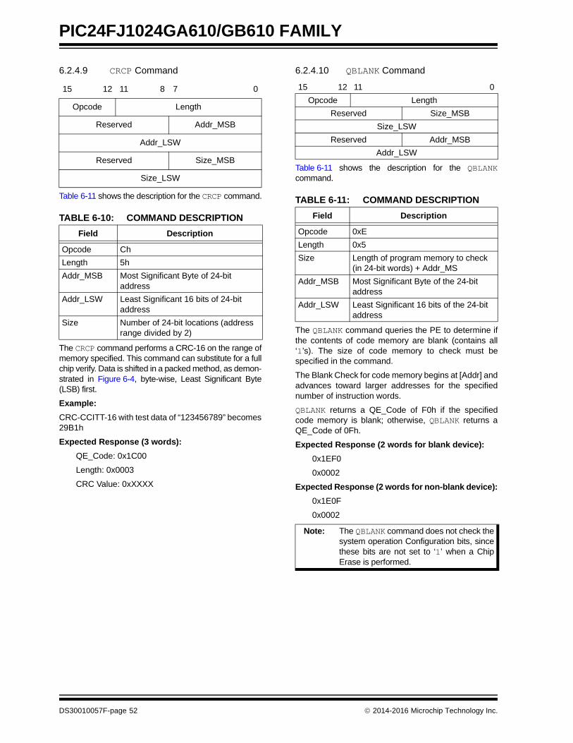
PIC24FJ1024GA610/GB610 FAMILY
6.2.4.9 CRCP Command
Table 6-11 shows the description for the CRCP command.
TABLE 6-10: COMMAND DESCRIPTION
The CRCP command performs a CRC-16 on the range ofmemory specified. This command can substitute for a fullchip verify. Data is shifted in a packed method, as demon-strated in Figure 6-4, byte-wise, Least Significant Byte(LSB) first.
Example:
CRC-CCITT-16 with test data of “123456789” becomes29B1h
Expected Response (3 words):
QE_Code: 0x1C00
Length: 0x0003
CRC Value: 0xXXXX
6.2.4.10 QBLANK Command
Table 6-11 shows the description for the QBLANKcommand.
TABLE 6-11: COMMAND DESCRIPTION
The QBLANK command queries the PE to determine ifthe contents of code memory are blank (contains all‘1’s). The size of code memory to check must bespecified in the command.
The Blank Check for code memory begins at [Addr] andadvances toward larger addresses for the specifiednumber of instruction words.
QBLANK returns a QE_Code of F0h if the specifiedcode memory is blank; otherwise, QBLANK returns aQE_Code of 0Fh.
Expected Response (2 words for blank device):
0x1EF0
0x0002
Expected Response (2 words for non-blank device):
0x1E0F
0x0002
15 12 11 8 7 0
Opcode Length
Reserved Addr_MSB
Addr_LSW
Reserved Size_MSB
Size_LSW
Field Description
Opcode Ch
Length 5h
Addr_MSB Most Significant Byte of 24-bit address
Addr_LSW Least Significant 16 bits of 24-bit address
Size Number of 24-bit locations (address range divided by 2)
15 12 11 0
Opcode Length
Reserved Size_MSB
Size_LSW
Reserved Addr_MSB
Addr_LSW
Field Description
Opcode 0xE
Length 0x5
Size Length of program memory to check(in 24-bit words) + Addr_MS
Addr_MSB Most Significant Byte of the 24-bit address
Addr_LSW Least Significant 16 bits of the 24-bit address
Note: The QBLANK command does not check thesystem operation Configuration bits, sincethese bits are not set to ‘1’ when a ChipErase is performed.
DS30010057F-page 52 2014-2016 Microchip Technology Inc.

PIC24FJ1024GA610/GB610 FAMILY
6.3 Programming Executive Responses
The PE sends a response to the programmer for eachcommand that it receives. The response indicates if thecommand was processed correctly. It includes anyrequired response data or error data.
The PE response set is shown in Table 6-12. This tablecontains the opcode, mnemonic and description foreach response. The response format is described inSection 6.3.1 “Response Format”.
TABLE 6-12: PROGRAMMING EXECUTIVE RESPONSE OPCODES
6.3.1 RESPONSE FORMAT
All PE responses have a general format, consisting of atwo-word header and any required data for thecommand.
Table 6-13 shows the description of the responseformat.
TABLE 6-13: RESPONSE FORMAT DESCRIPTION
6.3.1.1 Opcode Field
The opcode is a 4-bit field in the first word of theresponse. The opcode indicates how the commandwas processed (see Table 6-12). If the command wasprocessed successfully, the response opcode is PASS.If there was an error in processing the command, theresponse opcode is FAIL and the QE_Code indicatesthe reason for the failure. If the command sent to thePE is not identified, the PE returns a NACK response.
6.3.1.2 Last_Cmd Field
The Last_Cmd is a 4-bit field in the first word of theresponse and indicates the command that the PE pro-cessed. Since the PE can only process one commandat a time, this field is technically not required. However,it can be used to verify that the PE correctly receivedthe command that the programmer transmitted.
Opcode Mnemonic Description
0x1 PASS Command successfully processed.
0x2 FAIL Command unsuccessfully processed.
0x3 NACK Command not known.
15 12 11 8 7 0
Opcode Last_Cmd QE_Code
Length
D_1 (if applicable)
...
D_N (if applicable)
Field Description
Opcode Response opcode.
Last_Cmd Programmer command that generated the response.
QE_Code Query code or error code.
Length Response length in 16-bit words (includes 2 header words).
D_1 First 16-bit data word (if applicable).
D_N Last 16-bit data word (if applicable).
2014-2016 Microchip Technology Inc. DS30010057F-page 53

PIC24FJ1024GA610/GB610 FAMILY
6.3.1.3 QE_Code Field
The QE_Code is a byte in the first word of theresponse. This byte is used to return data for querycommands and error codes for all other commands.
When the PE processes one of the two query com-mands (QBLANK or QVER), the returned opcode isalways PASS and the QE_Code holds the queryresponse data. The format of the QE_Code for bothqueries is shown in Table 6-14.
TABLE 6-14: QE_Code FOR QUERIES
When the PE processes any command other than aquery, the QE_Code represents an error code.Supported error codes are shown in Table 6-15. If acommand is successfully processed, the returnedQE_Code is set to 0x0, which indicates that there is noerror in the command processing. If the verify of theprogramming for the PROGW command fails, theQE_Code is set to 0x1. For all other PE errors, theQE_Code is set to 0x02.
TABLE 6-15: QE_Code FOR NON-QUERY COMMANDS
6.3.1.4 Response Length
The response length indicates the length of the PE’sresponse in 16-bit words. This field includes the2 words of the response header.
With the exception of the response for the readcommands, the length of each response is only 2 words.
The response to the READP commands uses the packedinstruction word format described in Section 6.2.2“Packed Data Format”. When reading an odd numberof program memory words (N odd), the response to theREADP command is (3 * (N + 1)/2 + 2) words. Whenreading an even number of program memory words(N even), the response to the READP command is(3 * N/2 + 2) words.
Query QE_Code
QBLANK 0x0F = Code memory is NOT blank0xF0 = Code memory is blank
QVER 0xMN, where PE Software Version = M.N(i.e., 0x32 means Software Version 3.2).
QE_Code Description
0x0 No error
0x1 Verify failed
0x2 Other error
DS30010057F-page 54 2014-2016 Microchip Technology Inc.

PIC24FJ1024GA610/GB610 FAMILY
7.0 DUAL PARTITION FLASH PROGRAMMING CONSIDERATIONS
The PIC24FJ1024GB610 devices supports a SinglePartition Flash mode and two Dual Partition Flashmodes. The Dual Partition modes allow the device tobe programmed with two separate applications tofacilitate bootloading or to allow an application to beprogrammed at run time without stalling the CPU.
The part’s Partition Flash mode is determined by theBTMODE<1:0> bits in the FBOOT Configuration register(Table 7-1). The device will automatically check FBOOTon Reset and determine the appropriate Partition mode.
TABLE 7-1: PARTITION MODE SELECT
7.1 Dual Participation Memory Organization
In the Dual Partition modes, the device’s memory isdivided evenly into two physical sections, known asPartition 1 and Partition 2. Each of these partitionscontains its own program memory and ConfigurationWords. During program execution, the code on onlyone of these partitions is executed; this is the ActivePartition. The other partition, or the Inactive Partition, isnot used, but can be programmed.
The Active Partition is always mapped to logicaladdress, 000000h, while the Inactive Partition willalways be mapped to logical address, 400000h. Notethat even when the code partitions are switchedbetween Active and Inactive by the user, the address ofthe Active Partition will still be 000000h and theaddress of the Inactive Partition will still be at 400000h.
The Boot Sequence Configuration Word (FBTSEQ)determines whether Partition 1 or Partition 2 will beactive after Reset. If the part is operating in Dual Parti-tion mode, the partition with the lower Boot SequenceNumber will operate as the Active Partition (FBTSEQ isunused in Single Partition mode). The partitions can beswitched between Active and Inactive by reprogram-ming their Boot Sequence Numbers, but the ActivePartition will not change until a device Reset isperformed. If both Boot Sequence Numbers are thesame, or if both are corrupted, the part will usePartition 1 as the Active Partition. If only one BootSequence Number is corrupted, the device will use thepartition without a corrupted Boot Sequence Numberas the Active Partition.
The user can also change which partition is active atrun time using the BOOTSWP instruction. Issuing aBOOTSWP instruction does not affect which partition willbe the Active Partition after a Reset. Figure 7-1 demon-strates how the relationship between Partitions 1 and 2,shown in red and blue, respectively, and the Active andInactive Partitions are affected by reprogramming theBoot Sequence Number or issuing a BOOTSWPinstruction.
The P2ACTIV bit (NVMCON<10>) can be used to deter-mine which physical partition is the Active Partition. IfP2ACTIV = 1, Partition 2 is Active; if P2ACTIV = 0,Partition 1 is the Active Partition.
7.2 Erase Operations with Dual Partition
PIC24FJ1024GB610 devices support three eraseoperations: Chip Erase, Inactive Partition Erase andPage Erase.
A Chip Erase operation erases all of user memory,including the Flash Configuration Words and theFBOOT Configuration register. This resets the Partitionmode of the device to its default, Single Partition mode.Chip Erase is not available during run-time operation.
An Inactive Partition Erase operation can be executedat run time from the Active Partition. It will erase all usermemory and Flash Configuration Words in the InactivePartition. Note that the Inactive Partition Erasecommand is only functional when the device is in oneof the Dual Partition modes.
Since the Flash Configuration Words reside in the lastlocations of user program space, they may be erasedusing a Chip Erase, an Inactive Partition Erase or aPage Erase that targets the last page of user Flashmemory.
FBOOT<1:0> Partition Mode
00 Reserved
01 Protected Dual Partition Flash mode
10 Dual Partition Flash mode
11 Single Partition Flash mode (default)
2014-2016 Microchip Technology Inc. DS30010057F-page 55

PIC24FJ1024GA610/GB610 FAMILY
FIGURE 7-1: RELATIONSHIP BETWEEN PARTITIONS 1 AND 2 AND ACTIVE/INACTIVE PARTITIONS
Partition 1
FBTSEQ = 10
Partition 2
FBTSEQ = 15
000000h
400000h
Partition 2
FBTSEQ = 5
Partition 1
FBTSEQ = 10
000000h
400000h
000000h
Reprogram FBTSEQ Reset
400000h
Partition 1
FBTSEQ = 10
Partition 2
FBTSEQ = 5
Partition 1
FBTSEQ = 10
Partition 2
FBTSEQ = 15
000000h
400000h
Partition 2
FBTSEQ = 15
Partition 1
FBTSEQ = 10
000000h
400000h
Partition 2
FBTSEQ = 15
Partition 1
FBTSEQ = 10
000000h
400000h
BOOTSWP Instruction Reset
Active Partition
Active Partition
Inactive Partition
Inactive Partition
DS30010057F-page 56 2014-2016 Microchip Technology Inc.

PIC24FJ1024GA610/GB610 FAMILY
7.3 Dual Partition Configuration Words
In Dual Partition modes, each partition has its own set ofFlash Configuration Words. The full set of Configurationregisters in the Active Partition is used to determine thedevice’s configuration; the Configuration Words in theInactive Partition are used to determine the device’sconfiguration when that partition becomes active. How-ever, some of the Configuration registers in the InactivePartition (FSEC, FBSLIM and FSIGN) may be used todetermine how the Active Partition is able or allowed toaccess the Inactive Partition.
7.4 Programming in Dual Partition Mode
When programming a PIC24FJ1024GB610 device withmultiple applications, the following sequence of steps isrecommended to program the device correctly:
1. Perform a Chip Erase on the device.
2. Program the FBOOT register to one of the DualPartition modes, then reset the device to put it inDual Partition mode. At this point, the device’sprogram memory is functionally divided into twopartitions.
3. Program the first application (including its BootSequence Number and Configuration Words)into the Active Partition at address, 000000h.
4. Program the second application, its BootSequence Number and its Configuration Wordsinto the Inactive Partition at address, 400000h.
5. Finally, perform a device Reset. The Active/Inactive Partitions may switch at this point,depending on the values that the user used for theBoot Sequence Numbers for each application.
2014-2016 Microchip Technology Inc. DS30010057F-page 57

PIC24FJ1024GA610/GB610 FAMILY
8.0 DEVICE ID
The Device ID region of memory can be used todetermine variant and manufacturing information aboutthe chip. This region of memory is read-only and can beread when code protection is enabled. The DEVIDregister (FF0000h) identifies the specific part numberof the device, while DEVREV (FF0002h) shows thesilicon revision level.
Table 8-1 lists the identification information for eachdevice. Table 8-2 shows the Device ID registers andTable 8-3 describes the bit field of each register.
TABLE 8-1: DEVICE IDs
TABLE 8-2: PIC24FJ1024GA610/GB610 FAMILY DEVICE ID REGISTERS
TABLE 8-3: DEVICE ID BIT FIELD DESCRIPTIONS
Device DEVID
PIC24FJ128GA606 6000h
PIC24FJ256GA606 6008h
PIC24FJ512GA606 6010h
PIC24FJ1024GA606 6018h
PIC24FJ128GA610 6001h
PIC24FJ256GA610 6009h
PIC24FJ512GA610 6011h
PIC24FJ1024GA610 6019h
PIC24FJ128GB606 6004h
PIC24FJ256GB606 600Ch
PIC24FJ512GB606 6014h
PIC24FJ1024GB606 601Ch
PIC24FJ128GB610 6005h
PIC24FJ256GB610 600Dh
PIC24FJ512GB610 6015h
PIC24FJ1024GB610 601Dh
Address NameBit
15 14 13 12 11 10 9 8 7 6 5 4 3 2 1 0
FF0000h DEVID FAMID<7:0> DEV<7:0>
FF0002h DEVREV — REV<3:0>
Bit Field Register Description
FAMID<7:0> DEVID Encodes the family ID of the device.
DEV<7:0> DEVID Encodes the individual ID of the device.
REV<3:0> DEVREV Encodes the sequential (numerical) revision identifier of the device.
DS30010057F-page 58 2014-2016 Microchip Technology Inc.

PIC24FJ1024GA610/GB610 FAMILY
8.1 Unique Device Identifier (UDID)
All PIC24FJ1024GA610/GB610 family devices areindividually encoded during final manufacturing with aUnique Device Identifier, or UDID. The UDID cannot beerased by a Bulk Erase command or any otheruser-accessible means. This feature allows for manu-facturing traceability of Microchip Technology devicesin applications where this is a requirement. It may alsobe used by the application manufacturer for anynumber of things that may require unique identification,such as:
• Tracking the device
• Unique serial number
• Unique security key
The UDID comprises five 24-bit program words. Whentaken together, these fields form a unique 120-bitidentifier.
The UDID is stored in five read-only locations, locatedbetween 801600h and 801608h in the deviceConfiguration space. Table 8-4 lists the addresses ofthe identifier words and shows their contents.
TABLE 8-4: UDID ADDRESSES
UDID Address Description
UDID1 801600 UDID Word 1
UDID2 801602 UDID Word 2
UDID3 801604 UDID Word 3
UDID4 801606 UDID Word 4
UDID5 801608 UDID Word 5
2014-2016 Microchip Technology Inc. DS30010057F-page 59

PIC24FJ1024GA610/GB610 FAMILY
9.0 CHECKSUM COMPUTATION
Checksums for devices are 16 bits in size. Thechecksum is calculated by summing the following:
• Contents of code memory locations
• Contents of Flash Configuration Words
All memory locations, including Configuration Words,are summed by adding all three bytes of each memoryaddress.
Since the configuration memory space in this device isFlash-based, the erased value of all memory bits,except FSIGN, is a ‘1’. Certain Configuration bits will bereserved and these bits may require a ‘0’ or a ‘1’ to bewritten in order for the device to operate properly. If aConfiguration bit is defaulted to a ‘0’ (for example,JTAGEN), the erased state is still a ‘1’. The bit is set to‘0’ by the device programmer and is masked whencomputing the checksum. Therefore, the term, ‘blankchecksum’, when used by MPLAB X IDE or otherprogrammers, must take masked Configuration bits intoaccount. There is no error checking in either hardware orin MPLAB® X IDE to prevent the user from improperlyprogramming these bits. The device checksum is calcu-lated based on the contents of the Hex file, even if thereserved bits are left unprogrammed.
This device uses a Dual Partition Flash memory whosebehavior is controlled by the FBOOT register. Table 9-1shows a Single Partition set of checksums andTable 9-2 shows a Dual Partition set of checksums.The difference in the two is the inclusion of a secondFSIGN register in Dual Partition mode and the valuesfor FBOOT; this will alter the computed checksum.
The entire Flash-based Configuration Word area isused when computing the checksum, with the excep-tion of the Configuration Word, FBTSEQ. FBTSEQ isnot used in the checksum calculation since it can bealtered by a bootloader.
The checksum is computed “bytewise”, with the finalresult truncated to 16 bits. In the PIC24 architecture,each Flash memory address contains two bytes (if aneven address) or one byte (if an odd address, since theupper byte is always 0x00). When computing thechecksum, both the upper and lower bytes of the wordat a given address should be added to the running sumseparately as bytes, instead of as a single 16-bit word.
For example, in a program that contains two words withcontents such as:
Contents at address 0x0000 = 0xABCD
Contents at address 0x0001 = 0x00EF
The checksum over the [0x0000:0x0001] region is:0xCD + 0xAB + 0xEF + 0x00 = 0x0267.
The CFGB block checksum is also a “bytewise” sum of allcontents of the configuration block address region, and iscomputed identically to the PROG region, with the excep-tion of the FBTSEQ, FICD and FSIGN ConfigurationWords. The FSIGN and FICD Configuration Wordscontain a reserved bit that should be AND masked outand excluded during the checksum computation.
The checksum mask values are as follows:
• FSIGN – FF7FFFh, which masks bit 15
• FICD – FFFFDFh, which masks bit 5 (JTAGEN bit)
DS30010057F-page 60 2014-2016 Microchip Technology Inc.

PIC24FJ1024GA610/GB610 FAMILY
TABLE 9-1: CHECKSUM COMPUTATION (SINGLE PARTITION)
DeviceRead CodeProtection
Checksum ComputationBlankValue
Value with0xAAAAAA at 0x0
and LastCode Address
PIC24FJ1024GB610Disabled PROG[0:ABEFEh] + CFGB[ABF00h:ABFFEh] DC63h DA65h
Enabled 0 0000h 0000h
PIC24FJ512GB610Disabled PROG[0:55EFEh] + CFGB[55F00h:55FFEh] EC63h EA65h
Enabled 0 0000h 0000h
PIC24FJ256GB610Disabled PROG[0:2AEFEh] + CFGB[2AF00h:2AFFEh] F463h F265h
Enabled 0 0000h 0000h
PIC24FJ128GB610Disabled PROG[0:15EFEh] + CFGB[15F00h:15FFEh] EC63h EA65h
Enabled 0 0000h 0000h
Legend: PROG[a:b] = Program memory byte sum of locations, a to b inclusive (all 3 bytes of code memory)CFGB[c:d] = Configuration memory byte sum of locations, c to d inclusive, with FSIGN<15> and FICD<5> masked, and FBTSEQ omitted
TABLE 9-2: CHECKSUM COMPUTATION (DUAL PARTITION)
DeviceRead CodeProtection
Checksum ComputationBlankValue
Value with0xAAAAAA at 0x0
and LastCode Address
PIC24FJ1024GB610Disabled PROG[0:55EFEh] + CFGB[55F00h:55FFEh] +
PROG[400000:455EFEh] + CFGB[455F00h:455FFEh]D8C6h D4CAh
Enabled 0 0000h 0000h
PIC24FJ512GB610Disabled PROG[0:2AEFEh] + CFGB[2AF00h:2AFFEh] +
PROG[400000:42AEFEh] + CFGB[42AF00h:42AFFEh]E8C6h E4CAh
Enabled 0 0000h 0000h
PIC24FJ256GB610Disabled PROG[0:156FEh] + CFGB[15700h:157FEh] +
PROG[400000:4156FEh] + CFGB[415700h:4157FEh]F0C6h ECCAh
Enabled 0 0000h 0000h
PIC24FJ128GB610Disabled PROG[0:0AEFEh] + CFGB[0AF00h:0AFFEh] +
PROG[400000:40AEFEh] + CFGB[40AF00h:40AFFEh]E8C6h E4CAh
Enabled 0 0000h 0000h
Legend: PROG[a:b] = Program memory byte sum of locations, a to b inclusive (all 3 bytes of code memory)CFGB[c:d] = Configuration memory byte sum of locations, c to d inclusive, with FSIGN<15> and FICD<5> masked, and FBTSEQ omitted
2014-2016 Microchip Technology Inc. DS30010057F-page 61

PIC24FJ1024GA610/GB610 FAMILY
10.0 AC/DC CHARACTERISTICS AND TIMING REQUIREMENTS
Table 10-1 lists the AC/DC characteristics and timingrequirements.
TABLE 10-1: AC/DC CHARACTERISTICS AND TIMING REQUIREMENTS
Standard Operating ConditionsOperating Temperature: -40ºC to +85ºC. Programming at +25ºC is recommended.
Param. No.
Symbol Characteristic Min. Max. Units Conditions
D111 VDD Supply Voltage During Programming 2.0 3.6 V See Note 1 and Note 2
D113 IDDP Supply Current During Programming — 8 mA See Note 2
D114 IPEAK Instantaneous Peak Current During Start-up — — mA See Note 2
D031 VIL Input Low Voltage — 0.2 VDD V See Note 2
D041 VIH Input High Voltage 0.8 VDD VDD V See Note 2
D080 VOL Output Low Voltage — 0.8 V See Note 2
D090 VOH Output High Voltage 0.8 VDD VDD V See Note 2
D012 CIO Capacitive Loading on I/O Pin (PGEDx) — 50 pF See Note 2
P1 TPGC Serial Clock (PGECx) Period (ICSP™) 200 — ns
P1 TPGC Serial Clock (PGECx) Period (Enhanced ICSP)
500 — ns
P1A TPGCL Serial Clock (PGECx) Low Time (ICSP) 80 — ns
P1A TPGCL Serial Clock (PGECx) Low Time (Enhanced ICSP)
200 — ns
P1B TPGCH Serial Clock (PGECx) High Time (ICSP) 80 — ns
P1B TPGCH Serial Clock (PGECx) High Time (Enhanced ICSP)
200 — ns
P2 TSET1 Input Data Setup Time to Serial Clock 15 — ns
P3 THLD1 Input Data Hold Time from PGECx 15 — ns
P4 TDLY1 Delay Between 4-Bit Command and Command Operand
40 — ns
P4A TDLY1A Delay Between Command Operand and Next 4-Bit Command
40 — ns
P5 TDLY2 Delay Between Last PGECx of Command to First PGECx of Read of Data Word
20 — ns
P6 TSET2 VDD Setup Time to MCLR 100 — ns
P7 THLD2 Input Data Hold Time from MCLR 50 — ms
P8 TDLY3 Delay Between Last PGECx of Command Byte to PGEDx by PE
12 — s
Note 1: VDD must also be supplied to the AVDD pins during programming. AVDD and AVSS should always be within ±0.3V of VDD and VSS, respectively.
2: Time depends on the FRC accuracy and the value of the FRC Oscillator Tuning register. Refer to the “Electrical Characteristics” chapter in the specific device data sheet.
3: This time applies to Program Memory Words, Configuration Words and User ID Words.
DS30010057F-page 62 2014-2016 Microchip Technology Inc.

PIC24FJ1024GA610/GB610 FAMILY
P9A TDLY4 PE Command Processing Time 10 — s
P9B TDLY5 Delay Between PGEDx by PE to PGEDx Released by PE
15 23 s
P10 TDLY6 PGECx Low Time After Programming 400 — ns
P11 TDLY7 Chip Erase Time 16 25 ms
P12 TDLY8 Page Erase Time 16 25 ms See Note 2
P13 TDLY9 Double-Word Programming Time 16 20 s See Note 2 and Note 3
P14 TR MCLR Rise Time to Enter ICSP mode — 1.0 s
P15 TVALID Data Out Valid from PGECx 10 — ns
P16 TDLY10 Delay Between Last PGECx and MCLR 0 — s
P17 THLD3 MCLR to VDD 100 — ns
P18 TKEY1 Delay from First MCLR to First PGECx for Key Sequence on PGEDx
1 — ms
P19 TKEY2 Delay from Last PGECx for Key Sequence on PGEDx to Second MCLR
25 — ns
P21 TMCLRH MCLR High Time — 500 s
TABLE 10-1: AC/DC CHARACTERISTICS AND TIMING REQUIREMENTS (CONTINUED)
Standard Operating ConditionsOperating Temperature: -40ºC to +85ºC. Programming at +25ºC is recommended.
Param. No.
Symbol Characteristic Min. Max. Units Conditions
Note 1: VDD must also be supplied to the AVDD pins during programming. AVDD and AVSS should always be within ±0.3V of VDD and VSS, respectively.
2: Time depends on the FRC accuracy and the value of the FRC Oscillator Tuning register. Refer to the “Electrical Characteristics” chapter in the specific device data sheet.
3: This time applies to Program Memory Words, Configuration Words and User ID Words.
2014-2016 Microchip Technology Inc. DS30010057F-page 63

PIC24FJ1024GA610/GB610 FAMILY
APPENDIX A: SPI PORT SCANNING SOFTWARE ROUTINE
Software License AgreementThe software supplied herewith by Microchip Technology Incorporated (the “Company”) is intended and supplied to you, theCompany’s customer, for use solely and exclusively with products manufactured by the Company.The software is owned by the Company and/or its supplier, and is protected under applicable copyright laws. All rights are reserved.Any use in violation of the foregoing restrictions may subject the user to criminal sanctions under applicable laws, as well as to civilliability for the breach of the terms and conditions of this license.THIS SOFTWARE IS PROVIDED IN AN “AS IS” CONDITION. NO WARRANTIES, WHETHER EXPRESS, IMPLIED OR STATU-TORY, INCLUDING, BUT NOT LIMITED TO, IMPLIED WARRANTIES OF MERCHANTABILITY AND FITNESS FOR A PARTICU-LAR PURPOSE APPLY TO THIS SOFTWARE. THE COMPANY SHALL NOT, IN ANY CIRCUMSTANCES, BE LIABLE FORSPECIAL, INCIDENTAL OR CONSEQUENTIAL DAMAGES, FOR ANY REASON WHATSOEVER.
/************************************************************************* * © 2015 Microchip Technology Inc. * * FileName: spi_search.s * Dependencies: none * Processor: PIC24 * Compiler: XC16 * IDE: MPLAB® X * ~~~~~~~~~~~~~~~~~~~~~~~~~~~~~~~~~~~~~~~~~~~~~~~~~~~~~~~~~~~~~~~~~~~~~~~ * Description: This file performs a search of the correct * PGEC/PGED port and connect SPI2 slave to it. * *************************************************************************//************************************************************************** * MICROCHIP SOFTWARE NOTICE AND DISCLAIMER: You may use this software, and * any derivatives created by any person or entity by or on your behalf, * exclusively with Microchip's products in accordance with applicable * software license terms and conditions, a copy of which is provided for * your reference in accompanying documentation. Microchip and its licensors * retain all ownership and intellectual property rights in the * accompanying software and in all derivatives hereto. * * This software and any accompanying information is for suggestion only. * It does not modify Microchip's standard warranty for its products. You * agree that you are solely responsible for testing the software and * determining its suitability. Microchip has no obligation to modify, * test, certify, or support the software. * * THIS SOFTWARE IS SUPPLIED BY MICROCHIP "AS IS". NO WARRANTIES, WHETHER * EXPRESS, IMPLIED OR STATUTORY, INCLUDING, BUT NOT LIMITED TO, IMPLIED * WARRANTIES OF NON-INFRINGEMENT, MERCHANTABILITY, AND FITNESS FOR A * PARTICULAR PURPOSE APPLY TO THIS SOFTWARE, ITS INTERACTION WITH * MICROCHIP'S PRODUCTS, COMBINATION WITH ANY OTHER PRODUCTS, OR USE IN ANY * APPLICATION. * * IN NO EVENT, WILL MICROCHIP BE LIABLE, WHETHER IN CONTRACT, WARRANTY, * TORT (INCLUDING NEGLIGENCE OR BREACH OF STATUTORY DUTY), STRICT * LIABILITY, INDEMNITY, CONTRIBUTION, OR OTHERWISE, FOR ANY INDIRECT, * SPECIAL, PUNITIVE, EXEMPLARY, INCIDENTAL OR CONSEQUENTIAL LOSS, DAMAGE, * FOR COST OR EXPENSE OF ANY KIND WHATSOEVER RELATED TO THE SOFTWARE, * HOWSOEVER CAUSED, EVEN IF MICROCHIP HAS BEEN ADVISED OF THE POSSIBILITY * OR THE DAMAGES ARE FORESEEABLE. TO THE FULLEST EXTENT ALLOWABLE BY LAW, * MICROCHIP'S TOTAL LIABILITY ON ALL CLAIMS IN ANY WAY RELATED TO THIS * SOFTWARE WILL NOT EXCEED THE AMOUNT OF FEES, IF ANY, THAT YOU HAVE PAID * DIRECTLY TO MICROCHIP FOR THIS SOFTWARE. * * MICROCHIP PROVIDES THIS SOFTWARE CONDITIONALLY UPON YOUR ACCEPTANCE OF * THESE TERMS. *************************************************************************/
DS30010057F-page 64 2014-2016 Microchip Technology Inc.

PIC24FJ1024GA610/GB610 FAMILY
APPENDIX A: SPI PORT SCANNING SOFTWARE ROUTINE (CONTINUED).global _sd_Port_Search .section.text;;;;;;;;;;;;;;;;;;;;;;;;;;;;;;;;;;;;;;;;;;;;;;;;;;;;;;;;;;;;;;;;;;;;;;;;;;;;;;;;;;;;;;;;;;;;;;;;;;;;;;;;;;;;;;;;;;;;;;;;;;;;;;;;;;;;;;;;;;;;;;;;;;;;;;;;;;;;;;;;;;;;;;;;;;;;;;;;;;_sd_Port_Search:
;;;;;;;;;;;;;;;;;;;;;;;;;;;;;;;;;;;;;;;;;;;;;; ; Unlock PPS;;;;;;;;;;;;;;;;;;;;;;;;;;;;;;;;;;;;;;;;;;;;;; ; place zero in w0 to unlock PPSmov #0, w0; OSCCONL (low byte) unlock sequencemov #OSCCONL, w1mov #0x46, w2mov #0x57, w3mov.b w2, [w1] ; write 0x46mov.b w3, [w1] ; write 0x9A; unlock PPS (IOLOCK bit = 0)mov.b w0, [w1]
;;;;;;;;;;;;;;;;;;;;;;;;;;;;;;;;;;;;;;;;;;;;;; ; Initialize SPI1 as master and SPI2 as slave; for loopback test on each programming port;;;;;;;;;;;;;;;;;;;;;;;;;;;;;;;;;;;;;;;;;;;;;; clr SPI1BRGL ; clear SPI1BRGL clr SPI1CON1H ; clear SPI1CON1H clr SPI1CON1L ; clear SPI1CON1Lmov #0x8120, w0 ; set SPIEN, CKE and MSTEN (master)mov w0, SPI1CON1L
clr SPI2CON1H ; clear SPI2CON1H clr SPI2CON1L ; clear SPI2CON1Lmov #0x0100, w0 ; set CKE (slave)mov w0, SPI2CON1L
;;;;;;;;;;;;;;;;;;;;;;;;;;;;;;;;;;;;;;;;;;;;;; ; Connect SPI2 to the 1st port, ; if loopback test works then port is found.;;;;;;;;;;;;;;;;;;;;;;;;;;;;;;;;;;;;;;;;;;;;;; mov #0x0100, w0 ; SCK2R to RP1 and SDI2R to RP0mov w0, RPINR22 ; connect SPI2mov #0x0b0a, w0mov w0, RPOR0rcall _sd_Loopback_Test
mov #1, w1cp0 w0bra z, port_found
;;;;;;;;;;;;;;;;;;;;;;;;;;;;;;;;;;;;;;;;;;;;;; ; Connect SPI2 to the 2nd port, ; if loopback test works then port is found.;;;;;;;;;;;;;;;;;;;;;;;;;;;;;;;;;;;;;;;;;;;;;; mov #0x0607, w0 ; SCK2R to RP6 and SDI2R to RP7mov w0, RPINR22 ; connect SPI2mov #0x0a0b, w0mov w0, RPOR3rcall _sd_Loopback_Test
mov #2, w1 cp0 w0bra z, port_found
2014-2016 Microchip Technology Inc. DS30010057F-page 65

PIC24FJ1024GA610/GB610 FAMILY
APPENDIX A: SPI PORT SCANNING SOFTWARE ROUTINE (CONTINUED);;;;;;;;;;;;;;;;;;;;;;;;;;;;;;;;;;;;;;;;;;;;;;
; Connect SPI2 to the 3rd port, ; if loopback test works then port is found.;;;;;;;;;;;;;;;;;;;;;;;;;;;;;;;;;;;;;;;;;;;;;; mov #0x121c, w0 ; SCK2R to RP18 and SDI2R to RP28mov w0, RPINR22 ; connect SPI2mov #0x0b, w0mov w0, RPOR9mov #0x0a, w0mov w0, RPOR14rcall _sd_Loopback_Test
mov #3, w1 cp0 w0bra z, port_found
bclr SPI1CON1L, #15 ; disable SPI1 clr w0return
port_found:
bclr SPI1CON1L, #15 ; disable SPI1 mov w1, w0return
;;;;;;;;;;;;;;;;;;;;;;;;;;;;;;;;;;;;;;;;;;;;;;;;;;;;;;;;;;;;;;;;;;;;;;;;;;;;;;;;;;;;;;;;;;;;;;;;;;;;;;;;;;;;;;;;;;;;;;;;;;;;;;;;;;;;;;;;;;;;;;;;;;;;;;;;;;;;;;;;;;;;;;;;;;;;;;;;;;;; _sd_Loopback_Test:
bset SPI2CON1L, #15 ; enable SPI2
mov #0x00a5, w0 ; 0xa5 patternmov w0, SPI1BUFL ; send
wait_data:
btss SPI1STATL, #0 ; wait for the databra wait_data
mov SPI1BUFL, w1mov SPI2BUFL, w1 ; read data
cp w0, w1bra z, found
mov #1, w0bclr SPI2CON1L, #15 ; disable SPI2return
found:
clr w0bclr SPI2CON1L, #15 ; disable SPI2 return
;;;;;;;;;;;;;;;;;;;;;;;;;;;;;;;;;;;;;;;;;;;;;;;;;;;;;;;;;;;;;;;;;;;;;;;;;;;;;;;;;;;;;;;;;;;;;;;;;;;;;;;;;;;;;;;;;;;;;;;;;;;;;;;;;;;;;;;;;;;;;;;;;;;;;;;;;;;;;;;;;;;;;;;;;;;;;;;;;;;; .end
DS30010057F-page 66 2014-2016 Microchip Technology Inc.

PIC24FJ1024GA610/GB610 FAMILY
APPENDIX B: REVISION HISTORY
Revision A (April 2014)
Original version of the programming specification.
Revision B (February 2015)
The terms for Dual Boot and Single Boot modes havechanged to Dual Partition and Single Partition modes,respectively. All checksum values have changed andthere are minor edits throughout text.
Revision C (November 2015)
Updated Table 2-2, Table 2-3, Table 3-3, Table 5-3,Table 6-1, Table 6-6.
In Section 6.2.4.2 “READC Command”, the ExpectedResponse was changed to (2 + N) words.
In Section 6.2.4.2 “READC Command”, the ExpectedResponse for a blank device was changed to 0x1EF0,and the Expected Response for a non-blank device waschanged to 0x1E0F.
Added Section 6.1.3 “SPI Port Scanning”, Section 8.1“Unique Device Identifier (UDID)” and Appendix A:“SPI Port Scanning Software Routine”.
Revision D (January 2016)
Updated Table 2-4, Table 9-1 and Table 9-2.
Updated Section 9.0 “Checksum Computation”.
Revision E (March 2016)
Updated Section 9.0 “Checksum Computation”.
Updated Table 9-1.
Revision F (September 2016)
Revised last sentence in Section 4.4 “EnteringEnhanced ICSP Mode”.
Updated Figure 4-3.
2014-2016 Microchip Technology Inc. DS30010057F-page 67
PIC24FJ1024GA610/GB610 FAMILY
NOTES:
DS30010057F-page 68 2014-2016 Microchip Technology Inc.

Note the following details of the code protection feature on Microchip devices:
• Microchip products meet the specification contained in their particular Microchip Data Sheet.
• Microchip believes that its family of products is one of the most secure families of its kind on the market today, when used in the intended manner and under normal conditions.
• There are dishonest and possibly illegal methods used to breach the code protection feature. All of these methods, to our knowledge, require using the Microchip products in a manner outside the operating specifications contained in Microchip’s Data Sheets. Most likely, the person doing so is engaged in theft of intellectual property.
• Microchip is willing to work with the customer who is concerned about the integrity of their code.
• Neither Microchip nor any other semiconductor manufacturer can guarantee the security of their code. Code protection does not mean that we are guaranteeing the product as “unbreakable.”
Code protection is constantly evolving. We at Microchip are committed to continuously improving the code protection features of ourproducts. Attempts to break Microchip’s code protection feature may be a violation of the Digital Millennium Copyright Act. If such actsallow unauthorized access to your software or other copyrighted work, you may have a right to sue for relief under that Act.
Information contained in this publication regarding deviceapplications and the like is provided only for your convenienceand may be superseded by updates. It is your responsibility toensure that your application meets with your specifications.MICROCHIP MAKES NO REPRESENTATIONS ORWARRANTIES OF ANY KIND WHETHER EXPRESS ORIMPLIED, WRITTEN OR ORAL, STATUTORY OROTHERWISE, RELATED TO THE INFORMATION,INCLUDING BUT NOT LIMITED TO ITS CONDITION,QUALITY, PERFORMANCE, MERCHANTABILITY ORFITNESS FOR PURPOSE. Microchip disclaims all liabilityarising from this information and its use. Use of Microchipdevices in life support and/or safety applications is entirely atthe buyer’s risk, and the buyer agrees to defend, indemnify andhold harmless Microchip from any and all damages, claims,suits, or expenses resulting from such use. No licenses areconveyed, implicitly or otherwise, under any Microchipintellectual property rights unless otherwise stated.
2014-2016 Microchip Technology Inc.
Microchip received ISO/TS-16949:2009 certification for its worldwide headquarters, design and wafer fabrication facilities in Chandler and Tempe, Arizona; Gresham, Oregon and design centers in California and India. The Company’s quality system processes and procedures are for its PIC® MCUs and dsPIC® DSCs, KEELOQ® code hopping devices, Serial EEPROMs, microperipherals, nonvolatile memory and analog products. In addition, Microchip’s quality system for the design and manufacture of development systems is ISO 9001:2000 certified.
QUALITY MANAGEMENT SYSTEM CERTIFIED BY DNV
== ISO/TS 16949 ==
Trademarks
The Microchip name and logo, the Microchip logo, AnyRate, dsPIC, FlashFlex, flexPWR, Heldo, JukeBlox, KeeLoq, KeeLoq logo, Kleer, LANCheck, LINK MD, MediaLB, MOST, MOST logo, MPLAB, OptoLyzer, PIC, PICSTART, PIC32 logo, RightTouch, SpyNIC, SST, SST Logo, SuperFlash and UNI/O are registered trademarks of Microchip Technology Incorporated in the U.S.A. and other countries.
ClockWorks, The Embedded Control Solutions Company, ETHERSYNCH, Hyper Speed Control, HyperLight Load, IntelliMOS, mTouch, Precision Edge, and QUIET-WIRE are registered trademarks of Microchip Technology Incorporated in the U.S.A.
Analog-for-the-Digital Age, Any Capacitor, AnyIn, AnyOut, BodyCom, chipKIT, chipKIT logo, CodeGuard, dsPICDEM, dsPICDEM.net, Dynamic Average Matching, DAM, ECAN, EtherGREEN, In-Circuit Serial Programming, ICSP, Inter-Chip Connectivity, JitterBlocker, KleerNet, KleerNet logo, MiWi, motorBench, MPASM, MPF, MPLAB Certified logo, MPLIB, MPLINK, MultiTRAK, NetDetach, Omniscient Code Generation, PICDEM, PICDEM.net, PICkit, PICtail, PureSilicon, RightTouch logo, REAL ICE, Ripple Blocker, Serial Quad I/O, SQI, SuperSwitcher, SuperSwitcher II, Total Endurance, TSHARC, USBCheck, VariSense, ViewSpan, WiperLock, Wireless DNA, and ZENA are trademarks of Microchip Technology Incorporated in the U.S.A. and other countries.
SQTP is a service mark of Microchip Technology Incorporated in the U.S.A.
Silicon Storage Technology is a registered trademark of Microchip Technology Inc. in other countries.
GestIC is a registered trademarks of Microchip Technology Germany II GmbH & Co. KG, a subsidiary of Microchip Technology Inc., in other countries.
All other trademarks mentioned herein are property of their respective companies.
© 2014-2016, Microchip Technology Incorporated, Printed in the U.S.A., All Rights Reserved.
ISBN: 978-1-5224-0989-2
DS30010057F-page 69

DS30010057F-page 70 2014-2016 Microchip Technology Inc.
AMERICASCorporate Office2355 West Chandler Blvd.Chandler, AZ 85224-6199Tel: 480-792-7200 Fax: 480-792-7277Technical Support: http://www.microchip.com/supportWeb Address: www.microchip.com
AtlantaDuluth, GA Tel: 678-957-9614 Fax: 678-957-1455
Austin, TXTel: 512-257-3370
BostonWestborough, MA Tel: 774-760-0087 Fax: 774-760-0088
ChicagoItasca, IL Tel: 630-285-0071 Fax: 630-285-0075
ClevelandIndependence, OH Tel: 216-447-0464 Fax: 216-447-0643
DallasAddison, TX Tel: 972-818-7423 Fax: 972-818-2924
DetroitNovi, MI Tel: 248-848-4000
Houston, TX Tel: 281-894-5983
IndianapolisNoblesville, IN Tel: 317-773-8323Fax: 317-773-5453
Los AngelesMission Viejo, CA Tel: 949-462-9523 Fax: 949-462-9608
New York, NY Tel: 631-435-6000
San Jose, CA Tel: 408-735-9110
Canada - TorontoTel: 905-695-1980 Fax: 905-695-2078
ASIA/PACIFICAsia Pacific OfficeSuites 3707-14, 37th FloorTower 6, The GatewayHarbour City, Kowloon
Hong KongTel: 852-2943-5100Fax: 852-2401-3431
Australia - SydneyTel: 61-2-9868-6733Fax: 61-2-9868-6755
China - BeijingTel: 86-10-8569-7000 Fax: 86-10-8528-2104
China - ChengduTel: 86-28-8665-5511Fax: 86-28-8665-7889
China - ChongqingTel: 86-23-8980-9588Fax: 86-23-8980-9500
China - DongguanTel: 86-769-8702-9880
China - GuangzhouTel: 86-20-8755-8029
China - HangzhouTel: 86-571-8792-8115 Fax: 86-571-8792-8116
China - Hong Kong SARTel: 852-2943-5100 Fax: 852-2401-3431
China - NanjingTel: 86-25-8473-2460Fax: 86-25-8473-2470
China - QingdaoTel: 86-532-8502-7355Fax: 86-532-8502-7205
China - ShanghaiTel: 86-21-5407-5533 Fax: 86-21-5407-5066
China - ShenyangTel: 86-24-2334-2829Fax: 86-24-2334-2393
China - ShenzhenTel: 86-755-8864-2200 Fax: 86-755-8203-1760
China - WuhanTel: 86-27-5980-5300Fax: 86-27-5980-5118
China - XianTel: 86-29-8833-7252Fax: 86-29-8833-7256
ASIA/PACIFICChina - XiamenTel: 86-592-2388138 Fax: 86-592-2388130
China - ZhuhaiTel: 86-756-3210040 Fax: 86-756-3210049
India - BangaloreTel: 91-80-3090-4444 Fax: 91-80-3090-4123
India - New DelhiTel: 91-11-4160-8631Fax: 91-11-4160-8632
India - PuneTel: 91-20-3019-1500
Japan - OsakaTel: 81-6-6152-7160 Fax: 81-6-6152-9310
Japan - TokyoTel: 81-3-6880- 3770 Fax: 81-3-6880-3771
Korea - DaeguTel: 82-53-744-4301Fax: 82-53-744-4302
Korea - SeoulTel: 82-2-554-7200Fax: 82-2-558-5932 or 82-2-558-5934
Malaysia - Kuala LumpurTel: 60-3-6201-9857Fax: 60-3-6201-9859
Malaysia - PenangTel: 60-4-227-8870Fax: 60-4-227-4068
Philippines - ManilaTel: 63-2-634-9065Fax: 63-2-634-9069
SingaporeTel: 65-6334-8870Fax: 65-6334-8850
Taiwan - Hsin ChuTel: 886-3-5778-366Fax: 886-3-5770-955
Taiwan - KaohsiungTel: 886-7-213-7828
Taiwan - TaipeiTel: 886-2-2508-8600 Fax: 886-2-2508-0102
Thailand - BangkokTel: 66-2-694-1351Fax: 66-2-694-1350
EUROPEAustria - WelsTel: 43-7242-2244-39Fax: 43-7242-2244-393
Denmark - CopenhagenTel: 45-4450-2828 Fax: 45-4485-2829
France - ParisTel: 33-1-69-53-63-20 Fax: 33-1-69-30-90-79
Germany - DusseldorfTel: 49-2129-3766400
Germany - KarlsruheTel: 49-721-625370
Germany - MunichTel: 49-89-627-144-0 Fax: 49-89-627-144-44
Italy - Milan Tel: 39-0331-742611 Fax: 39-0331-466781
Italy - VeniceTel: 39-049-7625286
Netherlands - DrunenTel: 31-416-690399 Fax: 31-416-690340
Poland - WarsawTel: 48-22-3325737
Spain - MadridTel: 34-91-708-08-90Fax: 34-91-708-08-91
Sweden - StockholmTel: 46-8-5090-4654
UK - WokinghamTel: 44-118-921-5800Fax: 44-118-921-5820
Worldwide Sales and Service
06/23/16