piero spezzigu - diee · piero spezzigu pour obtenir le grade de docteur ... paramètres clés du...
TRANSCRIPT

N° d’ordre : 4149
THÈSE
Présentée et soutenue publiquement le 3 décembre 2010 à
L’UNIVERSITÉ BORDEAUX 1
ÉCOLE DOCTORALE DES SCIENCES PHYSIQUES ET DE L’INGENIEUR
par
Piero SPEZZIGU
pour obtenir le grade de DOCTEUR
Spécialité : ÉLECTRONIQUE
“Reliability Investigations of Bipolar Silicon Phototransistor Arrays for Space Applications”
« Évaluation des méthodes d'analyse de la fiabilité des matrices de phototransistors
bipolaires en silicium pour des applications spatiales »
Après avis de : M. Fausto FANTINI, Professeur, Università di Modena e Reggio Emilia Rapporteur M. Frédéric SAIGNÉ, Professeur, Université Montpellier II Rapporteur
Devant la commission formée de : M. Yann DEVAL, Professeur, Institut Polytechnique de Bordeaux Président M. Laurent BECHOU, Professeur, Université Bordeaux 1 Dir. Thèse M. Yves OUSTEN, Professeur, Université Bordeaux 1 Dir. Thèse M. Massimo VANZI, Professeur, Università di Cagliari (Italie) Dir. Thèse M. Gianandrea QUADRI, Docteur, CNES Toulouse Examinateur Mme Agata JOZWICKA, Docteur, Astri Polska (Pologne) Examinateur M. Jean-Luc POLLEUX, M. de Conférences, Université Paris-Est Examinateur
Thèse préparée au Laboratoire IMS (CNRS UMR 5218) en cotutelle avec l’Université de Cagliari, Département d’Ingénierie Electrique et Electronique.


RELIABILITY INVESTIGATIONS OF BIPOLAR SILICON PHOTOTRANSISTOR ARRAYS FOR
SPACE APPLICATIONS
PIERO SPEZZIGU
Laboratoire IMS (CNRS UMR 5218) – Université Bordeaux 1, Bordeaux (France)
DIEE – Università degli Studi di Cagliari, Cagliari (Italy)


To my dear zi’Antonia
whose memory will stay in me forever.


A C K N O W L E D G M E N T S
It is with immense pleasure I begun to write this section to thank the many people who made this thesis possible.
I want first to express my deeply-felt thank to my thesis advisors Laurent, Yves and Massimo, which gave me the tools that turned out to be essential in my PhD researches, and which answered quickly all the questions I had about topics of their expertise. It has been an honour for me to work with such a special cluster of Professors.
A very special thank to Gianandrea and Olivier, for their precious help and suggestions and for having supported and guided me before and during my doctoral studies.
Deep thanks to Professors Fausto Fantini and Frédéric Saigné, that accepted to be my thesis reviewers, and whose fine suggestions have been really appreciated.
I would like to thank the Professor Yann Deval, the president of my PhD defence committee. Many thanks also to the other members of the committee, Dr. Agata Jozwicka and Dr. Jean-Luc Polleux.
Thanks to the IMS laboratory Director, Mr. Pascal Fouillat, and to the other laboratory technical staff.
I thank all people in my team EDMiNA and the other IMS lab present and past PhD students with which it was a pleasure to share doctoral studies and that allow me to work in a pleasant environment.
There are many other friends I have and I would like to thank. It was also their presence and advices that helped me to achieve this important goal.
So, my friends,


A B S T R A C T
[EN] The research activities presented in this thesis are related to the specific context of the qualification tests, for space missions, of new sources of silicon phototransistor arrays for optical angular encoders. Our studies on a first source revealed the fragility of that technology in active storage and ionizing radiation because of its sensitivity to oxides trapped charges. Then, a study on a second set of components was performed in order to analyze the reliability of phototransistors subjected to several constraints in terms of both ionizing and displacement doses. The methodology of “Design of Experiments” was for the first time implemented and validated in this context. Thanks to this methodology, it is possible to obtain an estimate of the degradation of one or more key parameters of the component in environmental conditions for a given mission profile with a limited number of experiments. [FR] Les travaux de thèse s'inscrivent dans le contexte d'une évaluation de la fiabilité de matrices de phototransistors bipolaires en technologie silicium pour des applications de codage optique angulaire en environnement spatial. Après un état de l'art relatif aux technologies des phototransistors et un rappel sur leur fonctionnement physique, les conditions environnementales spécifiques liées au domaine spatial sont décrites. La caractérisation des paramètres électro-optiques des phototransistors, associée à une phase préliminaire de métrologie, a été effectuée à partir de bancs dédiés. L'étude de la sensibilité aux charges mobiles de technologies issues de différents fondeurs, habituellement piégées aux interfaces et identifiée comme un mécanisme fortement pénalisant en terme de durée de vie opérationnelle, a permis d'optimiser et fiabiliser une nouvelle source européenne. Une méthodologie originale basée sur le concept des plans d'expérience « D-optimal » a été mise en œuvre et validée. L'objectif est d'estimer le taux de dégradation d'un ou de plusieurs paramètres clés du composant en fonction des conditions environnementales imposées par l'orbite de rotation du satellite à partir d'un nombre limité d'expériences réalisées au sol.
[IT] Il lavoro di tesi s’inscrive nel contesto particolare della valutazione dell'affidabilità di matrici di fototransistori in tecnologia bipolare in silicio per applicazioni di codifica ottica angolare in ambiente spaziale. Dopo uno stato dell’arte riguardante le tecnologie di fototransistori, una breve descrizione dell’applicazione per cui i dispositivi studiati sono intesi, ed infine un richiamo sul loro funzionamento fisico, vengono descritte le condizioni ambientali specifiche legate al settore spaziale. La caratterizzazione dei parametri elettro-ottici dei fototransistori, associata ad una fase preliminare di metrologia, è stata effettuata a partire da banchi dedicati. Lo studio della sensibilità di diversi design di fototransistori agli effetti di cariche mobili intrappolate alle interfacce ossido-silicio, di solito identificata come un meccanismo fortemente penalizzante in termini di durata di vita operativa del dispositivo, ha permesso d'ottimizzare e accrescere l’affidabilità di fototransistori di un nuovo fabbricante europeo. Una metodologia originale basata sul concetto dei piani d'esperienza “D-optimal” è stata attuata e convalidata. L'obiettivo è di ottenere il tasso di degradazione di uno o più parametri chiave del dispositivo in funzione delle condizioni ambientali imposte dall'orbita in cui il satellite si troverà a operare, e a partire da un numero limitato d'esperienze realizzate a terra.


RELIABILITY INVESTIGATIONS OF BIPOLAR SILICON PHOTOTRANSISTOR ARRAYS FOR SPACE APPLICATIONS
C O N T E N T S
Acknowledgments i
Abstract iii
Contents v
Preface vii
Introduction 1
Chapter 1 : Bipolar Silicon Phototransistor Arrays 7
1.1 PLEIADES Project 7
1.1.1 PLEIADES Satel l i te System 7
1.1.2 Optical Angular Encoder 9
1.1.3 Encoder receiving device: the phototransistor array 11
1.2 The Phototransistor 13
1.2.1 The Phototransistor Operat ing Principle 13
1.2.2 The Phototransistors Array Technologies 16
1.3 Phototransistor Arrays Characterization Benches 20
1.3.1 The Photocurrent Measurement Bench 21
1.3.2 The Electr ical Character ist ics Measurement Bench 23
1.3.3 The Spectral Responsiv ity Measurement Bench 25
Conclusions 28
Chapter 2 : Space Environment and its Effects on Bipolar Devices 31
2.1 The Space Environment and its Effects on Electronics 31
2.1.1 Space Environment General i t ies 32
2.1.2 Radiat ion-Matter Interact ion 36
2.1.3 Total Ionizing Dose Ef fects 40
2.1.4 Displacement Damage Ef fects 40
2.1.5 Single Event Ef fects 42
2.2 Bipolar Devices Damages in Space Environment 43
2.2.1 Ionis ing Dose Ef fects on BJTs 43
2.2.2 Enhanced Low Dose Rate Ef fects 47

CONTENTS
RELIABILITY INVESTIGATIONS OF BIPOLAR SILICON PHOTOTRANSISTOR ARRAYS FOR SPACE APPLICATIONS vi
2.2.3 Displacement Damage Ef fects on BJTs 49
Conclusions 51
Chapter 3: Bipolar Silicon Phototransistor Arrays Sensitivity to Oxide
Trapped Mobile Charges 53
3.1 Experimental Demonstration of the BPSA Sensit ivity to Mobile
Charges Trapped in Passivation Layers 53
3.1.1 Etic -Honeywel l Devices Sensit ivity 54
3.1.2 Light Emission Microscopy Technique and Fai lure Model l ing 58
3.2 Mobile Charges Sensitivity Check Methodology 63
3.2.1 From Isochronal Anneal ing to the Ramp Test 63
3.3 Emerging Optoi Technologies 67
3.3.1 First Design pre-Evaluation Act ivit ies 67
3.3.2 BPSA Optimizat ions and Perspect ives 79
Conclusions 83
Chapter 4 : DoE Methodology for Bipolar Silicon Phototransistor Arrays
Degradation Estimation in Space Environment 85
4.1 Design of Experiment Approach 85
4.1.1 Study Domain Def init ion 86
4.1.2 D-Optimal Plan for Design of Experiments 88
4.1.3 Response Model l ing and D-Optimal ity Cri ter ion 91
4.2 Experimental Results 92
4.2.1 Unbiased Irradiat ion Results 93
4.2.2 Biased Irradiat ion Results 98
4.2.3 DoE Results Summary and Methodology Validat ion 101
4.3 DoE data analysis 103
4.3.1 DoE Methodology Optimization 103
4.3.2 Devices EOL Evaluat ion 107
Conclusions 118
General Conclusion 121
Index of Figures and Tables 127
Scientific Production 131
References 133

RELIABILITY INVESTIGATIONS OF BIPOLAR SILICON PHOTOTRANSISTOR ARRAYS FOR SPACE APPLICATIONS
P R E F A C E
An expert is a man who has made all the mistakes which can be made in a very narrow field. (Niels Bohr)
After graduating in Electronic Engineering at the University of Cagliari after an internship at CNES (Centre National d’Etudes Spatiales) in Toulouse in 2006, I joined the IMS Laboratory (Intégration du Matériau au Système) (CNRS UMR 5218) at the University Bordeaux 1 in May 2007 when I began my doctoral studies. These were done in partnership between the Universities of Bordeaux and Cagliari with the France-Italy agreement named “cotutelle de thèse”.
My research activities were performed in a group working on reliability and failure physics of electronic and optoelectronic devices for applications from automotive, to avionics, to space. In particular, all activities were performed within the team EDMiNA (Evaluation des Dispositifs Micro et Nano Assemblés – “Reliability” group) under the direction of Prof. Yves OUSTEN and co-direction of Prof. Laurent BECHOU. The co-direction at the University of Cagliari was provided by Prof. Massimo VANZI of the Department of Electric and Electronic Engineering (DIEE) of the Faculty of Engineering. All the research activities have been done in partnership and with the precious support of Dr. Gianandrea QUADRI and Dr. Olivier GILARD of CNES.

PREFACE
RELIABILITY INVESTIGATIONS OF BIPOLAR SILICON PHOTOTRANSISTOR ARRAYS FOR SPACE APPLICATIONS viii
This book is a summary of the work I have done during the preparation of my PhD thesis at the IMS Laboratory. The research activities I was involved in are related to the general theme of the silicon photo-detectors reliability for space applications. I started them during my graduation internship at CNES and then continued during the doctoral studies.
There is a widely used old saying that states that “an author never finishes a book, he merely abandons it”. Me too, I can not resist from using it, having appreciated its big truth during both stages of writing and printing the manuscript. I am sure that so many things could have been done better and explained more clearly. If I abandon the book nevertheless, it is in the modest hope that it may be useful to others despite its shortcomings.
Bordeaux, November 2010

RELIABILITY INVESTIGATIONS OF BIPOLAR SILICON PHOTOTRANSISTOR ARRAYS FOR SPACE APPLICATIONS
I N T R O D U C T I O N
In June of 1948, the Bell Telephone Laboratories announced and demonstrated publicly a semiconductor amplifier invented by Bardeen and Brattain, and coined for it the name “transistor”, a contraction of transfer-resistor. That transistor was a point-contact transistor that consisted of a very small piece of germanium with two fine wires contacting its surface, separated from each other. In the following years, Shockley’s classic paper on junction diodes and transistors was published. On the basis of theory, a junction transistor different in structure would have useful properties. The idea was to have in a germanium crystal a very thin region of one electrical type separating the two adjoining end regions of different electrical type. The two boundaries or junctions between the thin region and the two end regions were to serve the same functions as the two points in the point-contact device[1]. The first junction bipolar transistor was demonstrated in 1951. Since then the silicon replaced the germanium and many breakthroughs have been made in transistor technology, particularly in the area of crystal growth, epitaxy, diffusion, ion implantation, lithography, dry etch, surface passivation, and metallization[2]. The historical development of the bipolar transistor has been detailed in the well known Shockley’s paper, issued on “Transactions on Electron Devices” in 1976[3].
The fact that traditional transistors, i.e. the Bipolar Junction Transistors, the BJTs, are photosensitive has been known ever since they were invented. Phototransistors are very similar to ordinary BJTs except they are designed for use as detectors. Transistors are amplifiers and in a phototransistor the amplifier gain is controlled by the amount of light striking the device. Light arriving in the device is absorbed and creates charge carrier pairs that cause a current to flow in the collector-base circuit which is then amplified by the transistor action of the device. Thus, with respect to APDs or photodiodes, phototransistors have a higher output but are significantly less responsive.
Several semiconductors could be used to make phototransistors with different characteristics. Silicon or gallium arsenide materials, because of their great energy bandgap are limited to detecting wavelengths shorter than about 1 micron. Germanium is usable in the 1300nm band. While it is easily possible to build transistors with smaller bandgap materials (such as InP) there is no established technology to do that. This takes away much of the potential cost advantage in the 1550nm region. The major use of phototransistors is in applications, other than telecommunications, which use visible or near-visible light. Alarm systems (light beam detection) and remote controls for TV sets and automobiles are among the
INTRODUCTION
RELIABILITY INVESTIGATIONS OF BIPOLAR SILICON PHOTOTRANSISTOR ARRAYS FOR SPACE APPLICATIONS 2
most common uses. Phototransistors are occasionally built as part of an integrated circuit[1].
Since the earlier phototransistor history, several systems and applications using them have been proposed, for instance a phototransistor galvanometer relay[4], a temperature controller[5], and even integrated arrays of silicon photodetectors for image sensing[6]. For this last application a modified bipolar-phototransistor structure suitable for use in large imaging arrays is proposed[7].
With the aim to increase device performances, heterojunction phototransistors (HPT) in AlGaAs-GaAs for fiber-optical communications[8, 9] or high-sensitivity InGaAsP-InP phototransistors have been studied[10]. In fact, HPT are widely used in digital optical communication systems[11, 12] as optical receivers for lightwave signals.
Studies on hybrid integrated optical circuits using silicon phototransistors and semiconductor laser diodes have been also reported[13, 14]. The integration of the photodetector is essential for optical communication circuits. The heterojunction phototransistor is processed using the SiGe HBT technology and can be also easily modelled for circuit simulation[15]. Phototransistor integrated circuits have been used to build an integrated biosensor for use in medical detection, DNA diagnostics, and gene mapping [16]. Moreover, the interest for integrated photodetectors with high responsivity to UV/blue photons is usually related to the need for increasing data storage capacity while reducing size and cost through new optical storage systems (DVD-ROMs and DVRs) employing shorter wavelength laser diodes[17].
A standard bipolar phototransistor is the most common output device available in optocouplers. They are available with different ratings to fit most applications, including versions without access to the base of the transistor to reduce noise transmission. Darlington transistor outputs offer high gain with reduced input current requirements, but typically trade off speed. The most common industrial use of the optocouplers (or optically-coupled isolators) is as a signal converter between high-voltage devices (limit switches etc.) and low voltage solid-state logic circuits. Optical isolators can be employed in any situation where a signal must be passed between two circuits which are isolated from each other. Complete electrical isolation between two circuits (i.e. the two circuits have no conductors in common) is often necessary to prevent noise generated in one circuit from being passed to the other circuit. This is especially necessary for the coupling between high-voltage information-gathering circuits and low-voltage digital logic circuits. Among other applications, opto-isolators can help cut down on ground loops, block voltage spikes, and provide electrical isolation. Optocouplers has often used in medical equipments, oscilloscopes and digital multimeters with computer interfaces. One of the requirements of the MIDI (Musical Instrument Digital Interface) standard is that input connections must be opto-isolated.

INTRODUCTION
RELIABILITY INVESTIGATIONS OF BIPOLAR SILICON PHOTOTRANSISTOR ARRAYS FOR SPACE APPLICATIONS 3
Of course the presented list of applications of phototransistors and optocouplers is not exhaustive and have to be intended as a quick survey on these devices developments, studies, and applications.
The reliability of an electronic device or a system is usually defined as the probability that it will perform its function for a specified time interval under stated operating conditions. Of course, a great endurance of electronic devices and system is always well suited, at least greater than its obsolescence. But environmental conditions could have a high impact on device performances reducing its operating life. So, depending on the applications to which it is intended to be integrated in, its reliability can be a really critical parameter. For instance, for all that applications whence the human health or life depends, like medical or safety applications, electronic systems reliability is dramatically important. Otherwise, it is as much important in applications where defective part replacement is extremely expensive or outright impossible; for instance, submarine telecommunication systems that have to operate under the sea without any human intervention. It is even more the case of telecommunication or military satellites around Earth or other spacecrafts for space exploration. The degradations and disturbances induced by space environment on the materials and the electronic components are phenomena that have been extensively studied since many years. The research activities presented in this thesis are related to the evaluation of these phenomena impacting on performances and reliability of phototransistor arrays for optical angular encoders.
As previously hinted, a phototransistor is a type of photodetector able to convert light into either current or voltage, depending upon the mode of operation. It is a transistor that uses light rather than electricity to cause an electrical current to flow from one side to the other. It is used in a variety of sensors that detect the presence of light. Actually it is a transistor with a larger base surface than a classical transistor. In silicon bipolar npn devices, the base-collector junction acts as a photodiode which, if lighted-up, controls the response of the device. Due to the inherent current gain (of the transistor), the response of the phototransistor is greater than that of photodiodes. These optoelectronic devices, in silicon technology, are widely used as the main part of the receiving circuits in optical encoders for space applications. The effects induced by the space environment on electronics no longer need to be demonstrated. The nature of this environment varies greatly between low and higher orbits. Given the particular application of these custom devices, the study of the space environment and its effects on those particular components become essential.
The work presented in this dissertation is related to the specific context of the qualification tests of new sources of silicon phototransistors arrays for optical angular encoders for space missions such PLEIADES. In this context, three different technologies of as many providers (from US and Europe) have been submitted to evaluation programs. Our studies related to the first phototransistors source have
INTRODUCTION
RELIABILITY INVESTIGATIONS OF BIPOLAR SILICON PHOTOTRANSISTOR ARRAYS FOR SPACE APPLICATIONS 4
highlighted the fragility of that technology under active storage and ionizing radiations. The degradation model based on the assumption of the presence of mobile charges trapped in the oxide (triggering a parasitic MOS transistor) that we proposed was validated through results from pSpice simulations and through the light emission microscopy (LEM) analysis technique. In parallel, a new methodology to assess the ionizing radiation hardness based on the dose rate switching, has allowed the demonstration of the enhanced low-dose-rate sensitivity (ELDRS) of this family of components.
A second batch of devices from another provider from US has then evaluated. The aim of this study, which extends the study begun during the internship at CNES, was to analyze the phototransistors reliability with respect to different space mission profiles constraints in terms of both ionizing and displacement dose. The statistical “Design of Experiments” methodology has been for the first time implemented and validated for these contexts. Thanks to this methodology, it is possible to estimate degradation rate of one or more key functional parameters of the component in the environmental conditions expected for a given mission profile and included in the study domain, using a limited number of experiences. Analysis of the results allowed retaining this technology to the space mission and considering it as a reference for choosing other sources.
According the results obtained after the evaluation programs of the two first technologies, a new generation of eight-channels phototransistors for optical angular encoders for space applications has been developed in partnership with a third source from Europe. So, a pre-evaluation program of this new phototransistor technology has been started, analyzing in particular, different technological options as oxide passivation quality and thickness, contact topology, and bonding process. During the pre-evaluation stage, the feedback with the manufacturer was a constant and fruitful way to improve their technology.
Outline
This manuscript is divided into two major parts: after this short general introduction, the first part, constituted by the first two chapters, is dedicated to present the context of our studies, the particular device, the phototransistors arrays, the space environment, and devices degradations in performances due to space radiations. Then, the second part (chapters three and four) concerns the research activities and experimental results that have been done on phototransistor arrays for reliability assessment and test methodology validation.
• The first chapter deals with the context of PLEIADES project, the optical encoder receiving device, and a short phototransistor overview. Subsequently a call-back of phototransistor basic operating principles and the phototransistor arrays technologies are presented. Finally we will give a short description of the dedicated measurement benches mainly developed at IMS Laboratory.
INTRODUCTION
RELIABILITY INVESTIGATIONS OF BIPOLAR SILICON PHOTOTRANSISTOR ARRAYS FOR SPACE APPLICATIONS 5
• In the second chapter, the space environment and its effect on electronics in general and on bipolar devices in particular are briefly described.
• The third chapter recalls at first the studies relative to the evaluation of the phototransistors batch provided by Microtel/Etic-Honeywell companies. Light Emission Microscopy (LEM) was performed (on faulty devices) in order to localize a leakage path and transistor Gummel-Poon parameters are extracted in order to obtain a model for a spice-like simulation tool and to formulate hypothesis on physical phenomena. The sensitivity to oxide trapped charges of this device technology has been verified. Thanks to these experiences, a rapid test to foresee the component behaviour in life test and then make an initial screening is investigated. Following these studies, pre-assessment of a new source for European phototransistors was undertaken, analyzing in different technological options with respect to the mobile charge sensitivity.
• The final chapter focuses on an original statistical methodology to test components in radiative environments based on the principle of Design of Experiments (DoE). Thanks to this methodology, it is possible to obtain an estimate of the degradation of some key component parameters in the environmental conditions expected for a given mission profile and included in the study area, with a restricted number of experiences. A study on the possibility to reduce the number of experiences keeping the prevision error acceptable is also presented.
The manuscript comes out, as usual, with a general conclusion on the work that has been done and on perspectives of our studies.


RELIABILITY INVESTIGATIONS OF BIPOLAR SILICON PHOTOTRANSISTOR ARRAYS FOR SPACE APPLICATIONS
BIPOLAR SILICON PHOTOTRANSISTOR ARRAYS
This first chapter is intended to introduce the context that the research activities are inserted in. In this context, the PLEIADES project is shortly presented in terms of historical developments and main characteristics. Then, the optical angular encoder used in PLEIADES satellites is briefly described in order to introduce the device under study: the phototransistor array. Over the years, several device providers’ components have been submitted to evaluation plans, as described in the last subsection of first paragraph. Subsequently, a call-back of phototransistor basic operating principles is introduced before giving a description of the principal characteristics of the different components designs and technologies of the different providers. Finally, the phototransistors arrays parameters and performances measurement benches presentation concludes this first chapter.
1.1 PLEIADES PROJECT
In 2001 a cooperation program was launched between France and Italy to develop ORFEO: an Earth observation dual system with metric resolution. Italy is in charge of the radar component development (COSMO-Skymed), and France of the optical part (PLEIADES). With respect to the constraints of the France-Italy agreement, cooperation has been extended in particular for the PLEIADES optical component with Sweden, Belgium, Spain and Austria.
1.1.1 PLEIADES SATELLITE SYSTEM
The PLEIADES system is an optical observation system with a metric resolution designed to offer a high acquisition capability with a revisit lower than 24 hours to satisfy both civilian and military needs. Moreover, to meet the needs for a detailed mapping, especially in urban areas and to complement aerial photography, PLEIADES will offer instantaneous stereoscopic acquisition joined to a large areas coverage capability. The great agility of PLEIADES satellites enables a daily access all over the world and a coverage capacity necessary for the cartography kind of

CHAPTER 1
RELIABILITY INVESTIGATIONS OF BIPOLAR SILICON PHOTOTRANSISTOR ARRAYS FOR SPACE APPLICATIONS 8
applications. In particular for forestry, geology and marine environments, thanks to its spectral characteristics and its three-dimensional characterization of surfaces, PLEIADES should complete the information supplied by other sensors, such as Spot 5, by offering information with a better spatial resolution, and also complete information given by aerial photography. Regarding defence and civil security missions, PLEIADES system should enable to:
• Supply the information in a very short delay (typically less than 24 hours). • Insure to the defence users a priority in the daily programming of the 50
acquisition demands. • Insure to the defence users the confidentiality of these demands as well as the
security of the communications. • Enable the capability of preferential acquisitions on a predefined area with a
“crisis” mode implementation.
Hence, the PLEIADES system consists in a constellation of two optical “small satellites” (mass of one ton) (Figure 1.1) for visible and near infrared domain on a Sun-synchronous orbit at 694km offering a spatial resolution at nadir of 0.7m and a field of view of 20km. This number of satellites is essential to guarantee the accessibility and revisit frequency required to operationally answer to defence and civil security missions.
Figure 1.1 – Representation of PLEIADES satellite system
The main design drivers for the satellite architecture are the image quality, the agility and the image location accuracy. The image quality drives the instrument size. A high agility requires a very compact design, with a few stiff appendages. As a consequence, the instrument is integrated inside the bus. High image location accuracy is achieved by minimizing the interface between the instrument and the bus. The star trackers and the gyroscope heads are directly supported by the instrument to avoid any thermal distortion that could be induced by the bus. The bus structure is built on a hexagonal shape, with three solar arrays at 120 degrees, and three star trackers in a quasi tetrahedron configuration, optimizing the attitude

BIPOLAR SILICON PHOTOTRANSISOTR ARRAYS TECHNOLOGY
RELIABILITY INVESTIGATIONS OF BIPOLAR SILICON PHOTOTRANSISTOR ARRAYS FOR SPACE APPLICATIONS 9
determination accuracy (Figure 1.2). This configuration authorizes accommodation of the instrument focal plane radiator for maximum heat dissipation. An antenna support structure is used to carry the Earth-pointing antennas and for the instrument baffle. The solar arrays are mounted directly on the bus structure without any drive mechanism to ensure a maximum stability. Their first flexion mode frequency is increased by the use of stiffeners when deployed. Moreover the high compactness and low mass of the satellite (<1000kg) make it compatible with a large series of low cost small launchers (among them Soyouz and Rockot). The two PLEIADES satellites will be launched by Soyouz from Europe's spaceport in Kourou, French Guiana. The expected duration of the PLEIADES mission is 5 years [18, 19].
Figure 1.2 – PLEIADES satellite packaging
1.1.2 OPTICAL ANGULAR ENCODER
In order to reach very high level of ground location accuracy new very high precision technological developments have been taken into account for PLEIADES satellite attitude restitution. The attitude determination is performed by a gyro-stellar system. Very accurate solid state gyroscopes are used to ensure high accuracy attitude determination while manoeuvring. In order to fulfil the high imaging capacity coming from mission requirements, very demanding manoeuvring capabilities are necessary for the Pleiades satellites, and Control Moment Gyros (CMGs) become mandatory (Figure 1.3-a). A cluster of four 15Nms1 actuators is used (Figure 1.3-b). Innovative guiding techniques are used to avoid the usual drawbacks of CMGs: instead of following a pre-defined attitude profile that always lock the cluster in singularities in some cases, a cluster re-orientation is realized taking into account the satellite trajectory and the cluster history to globally optimize the system. It has been shown that this reorientation strategy always avoids singularities, while ensuring a correct convergence towards the imaging
1 Nms (Newton metre second) is the derived SI units of angular momentum: 1N·m·s=1J·s=1kg·m2·s−1.

CHAPTER 1
RELIABILITY INVESTIGATIONS OF BIPOLAR SILICON PHOTOTRANSISTOR ARRAYS FOR SPACE APPLICATIONS 10
dynamics. This new approach allows the use of the complete angular momentum capacity envelope, that is about 3.2 times elementary CMG momentum in roll and pitch direction. Moreover, this open-loop guidance law can be realized autonomously on analysis of the programming message. It results a dramatic simplification of CMG cluster management in the flight software [18, 19].
Figure 1.3 – (a) Scheme of the satellite; (b) the actuator
The heart of these actuators is the optical angular encoder supplied from Codechamp, which is a French SME specialized in the design and the realization of high precision optical encoders. An optical encoder is an electromechanical device, which has an electrical output in digital form proportional to the angular position of the input shaft. It has a shaft mechanically coupled to an input driver that rotates a disc rigidly fixed to it. A succession of opaque and clear segments is marked on the disc surface [20]. In Figure 1.4 a scheme of encoder operating principles is shown.
Figure 1.4 – Operating principle of an optical encoder
(a) (b)

BIPOLAR SILICON PHOTOTRANSISOTR ARRAYS TECHNOLOGY
RELIABILITY INVESTIGATIONS OF BIPOLAR SILICON PHOTOTRANSISTOR ARRAYS FOR SPACE APPLICATIONS 11
Light from infrared emitter (LED) reaches the infrared receivers (the phototransistors) through the transparent slits of rotating disc (Figure 1.5). An angular position-dependent analog signal is generated. Then it is amplified and converted in digital form.
Figure 1.5 – The coded disc of the optical encoder
1.1.3 ENCODER RECEIVING DEVICE: THE PHOTOTRANSISTOR ARRAY
The receiving device is an array of eight silicon phototransistors in a SMD package (Figure 1.6). In order to obtain optimal performances, the receiver must have eight independent channels with a weak dark current. The constraints of optical alignment between LEDs and phototransistors require a small size surface-mount package. These technical specifications, combined with very low production volumes and very high reliability requirements (narrow technological dispersion, radiations hardness, tightened lifetime, etc.), make very difficult to find a secure provisioning source for these components including foundry and packaging developments.
Figure 1.6 – (a) Phototransistor array in SMD package; (b) internal connections and package pinout
(*) Reference: metalized corner
(b)(a)
(*) (*)

CHAPTER 1
RELIABILITY INVESTIGATIONS OF BIPOLAR SILICON PHOTOTRANSISTOR ARRAYS FOR SPACE APPLICATIONS 12
Initially, the Codechamp’s angular encoder phototransistors were provided by Optek (USA). However, this manufacturer meant his disengagement of the space sector in May 2000. An alternative solution was temporarily found at Optotechno (Japan) for chip supply and Microtel (Italy) for the packaging. After a phase of industrialization at Microtel, the qualification of the component with Optotechno chips was launched in 2002. Large drifts of the photocurrent were observed in particular under high temperature storage and accelerated life tests. The investigations carried out thereafter at CNES showed that these degradations were related to the chip. Then, Codechamp in collaboration with Blue élec (France) has identified products which can meet the needs at East Texas Integrated Circuits (ETIC, USA). After some preliminary tests on a mono-channel phototransistor, a new design and realization of the eight-channels phototransistor was launched in August 2003. Phototransistor design was made by ETIC and the fabrication by Honeywell (USA). In 2006, our studies related to the ETIC-Honeywell phototransistors have highlighted the fragility of that technology under active storage and ionizing radiations.
The degradation model based on the assumption of the presence of mobile charges trapped in the oxide triggering a parasitic MOS transistor. This study is detailed in the third chapter of this manuscript. The formation of this parasitic structure leads to a dramatic increase of leakage collector-emitter darkness current. In parallel, thanks to a new methodology to assess the ionizing radiation hardness based on the dose rate switching (detailed in the 2nd chapter), enhanced low-dose-rate sensitivity (ELDRS) of this family of components has been demonstrated. Then, another phototransistors manufacturer that could satisfy the needs was found at Micropac. Micropac Industries Inc. provides microelectronic and optoelectronic components and modules along with contract electronic manufacturing services. The Company offers a wide range of products to the industrial, medical, military, aerospace and space markets [21]. An evaluation program including active storage, ionizing and non-ionizing irradiations have been started on Micropac phototransistors. Analysis of the results allowed retaining this technology to the space mission and considering it as a reference for choosing other sources. Consequently to an active search of new European producers of custom devices, Optoi Group (Italy) was identified. Optoi follows the evolution and natural development of the original Company Optoelettronica Italia S.r.l funded in 1995 as a spin-off enterprise of the institute for scientific and technological research ITC-IRST, now FBK (Fondazione Bruno Kessler), located in Trento. In the last few years Optoi has specialized in the study, design and development of specific solutions requested by collaborating Companies, although standard products have also been grouped in the portfolio[22]. From 2007 different architectures of Optoi phototransistors have been tested. At IMS Laboratory, we have performed temperature/voltage and radiations ageing tests in order to evaluate those different technological options and we shared results with Optoi laboratories with the aim of improving phototransistor arrays reliability. The evaluation program on the last design is still in progress.

BIPOLAR SILICON PHOTOTRANSISOTR ARRAYS TECHNOLOGY
RELIABILITY INVESTIGATIONS OF BIPOLAR SILICON PHOTOTRANSISTOR ARRAYS FOR SPACE APPLICATIONS 13
1.2 THE PHOTOTRANSISTOR
A phototransistor belongs to the bipolar junction transistor family considering that its base-collector junction acts as a photodiode, which, if irradiated, controls the response of the device. Due to the inherent current gain (of the transistor), the response of the phototransistor is greater than that of conventional p-i-n photodiodes. On the other hand, the inherent larger capacitances and the Miller effect (due to the combined effect of base-collector capacitance and transistor gain) limit their maximum operating frequency. Nevertheless, silicon bipolar phototransistors are used in a number of commercially-relevant applications, such as light-activated switches, light meters, opto-isolators and position encoders. In these applications, which do not require demanding dynamic performance, the use of a bipolar phototransistor allows for a substantial reduction of the complexity of the read-out circuitry, enabling the desired signal level to be achieved without any further amplification of the detector output current. This has evident beneficial effects in terms of system simplification and cost reduction.
1.2.1 THE PHOTOTRANSISTOR OPERATING PRINCIPLE
Illumination of the top of the planar npn phototransistor shown in Figure 1.7 by an uniform photon flux density F(ν) causes generation of excess electron-hole pairs throughout the whole device. To achieve good phototransistor performance the emitter area is relatively small to suppress the photo-generated leakage current flowing across the base-emitter (B-E) junction. Reflection and absorption of incoming light by the emitter metal contact also helps in this sense.
Figure 1.7 – Cross-sectional view of a planar phototransistor
Consequently, the base-collector (B-C) photodiode will be regarded as a photodiode in parallel with the collector-base junction of a conventional transistor. This modeling is shown in Figure 1.8. Excess electron-hole pairs are continuously generated on both sides of the collector-base photodiode. The excess majority carriers stay in their corresponding side of the junction whereas the excess minority
Collector Base
Emitter
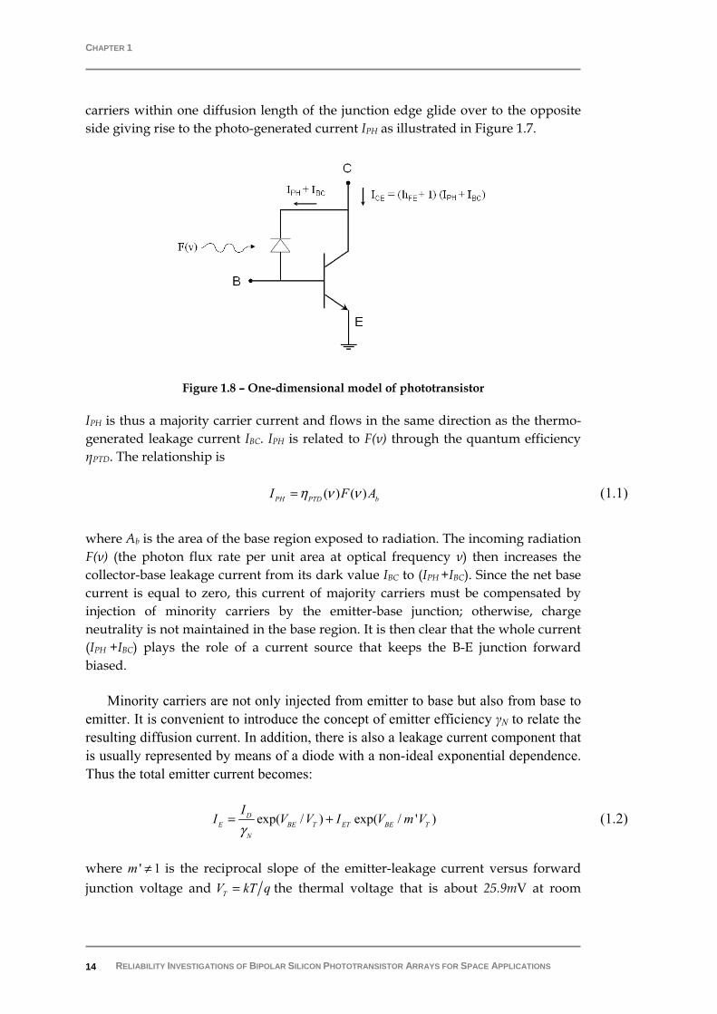
CHAPTER 1
RELIABILITY INVESTIGATIONS OF BIPOLAR SILICON PHOTOTRANSISTOR ARRAYS FOR SPACE APPLICATIONS 14
carriers within one diffusion length of the junction edge glide over to the opposite side giving rise to the photo-generated current IPH as illustrated in Figure 1.7.
Figure 1.8 – One-dimensional model of phototransistor
IPH is thus a majority carrier current and flows in the same direction as the thermo-generated leakage current IBC. IPH is related to F(ν) through the quantum efficiency ηPTD. The relationship is
( ) ( )PH PTD bI F Aη ν ν= (1.1)
where Ab is the area of the base region exposed to radiation. The incoming radiation F(ν) (the photon flux rate per unit area at optical frequency ν) then increases the collector-base leakage current from its dark value IBC to (IPH +IBC). Since the net base current is equal to zero, this current of majority carriers must be compensated by injection of minority carriers by the emitter-base junction; otherwise, charge neutrality is not maintained in the base region. It is then clear that the whole current (IPH +IBC) plays the role of a current source that keeps the B-E junction forward biased.
Minority carriers are not only injected from emitter to base but also from base to emitter. It is convenient to introduce the concept of emitter efficiency γN to relate the resulting diffusion current. In addition, there is also a leakage current component that is usually represented by means of a diode with a non-ideal exponential dependence. Thus the total emitter current becomes:
exp( / ) exp( / ' )DE BE T ET BE T
N
II V V I V m V
γ= + (1.2)
where ' 1m ≠ is the reciprocal slope of the emitter-leakage current versus forward junction voltage and TV kT q= the thermal voltage that is about 25.9mV at room
BIPOLAR SILICON PHOTOTRANSISOTR ARRAYS TECHNOLOGY
RELIABILITY INVESTIGATIONS OF BIPOLAR SILICON PHOTOTRANSISTOR ARRAYS FOR SPACE APPLICATIONS 15
temperature. ID and IET are the coefficients of the electron current injected from emitter to base and of the emitter-junction leakage current respectively.
The collector current is composed of the current ( )PH BCI I+ and the fraction αF of the current injected by the emitter reaching the collector:
exp( / ) ( )α= + +C F D BE T PH BCI I V V I I (1.3)
The net base current must be zero. This constraint combined with equations (1.2) and (1.3) yields to:
( ) exp( / ' ) exp( / )
(1 )PH BC ET BE TD
BE TN N F
I I I V m VIV V
γ γ α+ −
=−
. (1.4)
This expression clearly shows how the forward bias of emitter junction is controlled by IPH. Substituting (1.4) in (1.3) we can determine the expression of the output current ICE0 as a function of IPH. The subscript here indicates that IC=IE=ICE0 with the base floating:
0
1[( ) exp( / ' )]
(1 )CE PH BC N F ET BE TN F
I I I I V m Vγ αγ α
= + −−
. (1.5)
It has already been pointed out that ( )PH BCI I+ play the role of a current base source.
Hence, by rearranging (1.5) to yield the ratio 0 ( )CE PH BCI I I+ , the current gain of the
phototransistor, ( 1)FEh + , is obtained.
1
0
exp( / ' )( 1) (1 ) N F ET BE T
FE N FCE
I V m Vh
Iγ α
γ α−+ = − + (1.6)
This last expression indicates the dependence of hFE on current bias due to emitter leakage. Finally, from the well known definition of transistor current gain2 and (1.1), the output ICE0 can also be expressed in terms of the input photon flux:
0 ( ) ( 1) ( ) ( )CE FE PTD bI h F Aν η ν ν= + . (1.7)
This relationship clearly shows that the phototransistor has an effective quantum efficiency that is ( 1)FEh + times larger than that of the base-collector photodiode[2, 23-
26]. As shown by equation (1.6), the current gain depends on ICE0, so ( 1)FEh + includes an intrinsic dependence on the striking photons wavelength. 2 ( 1)C FE BI h I= + ⋅ where IB≈IPH neglecting the thermo-generated leakage IBC<<IPH.

CHAPTER 1
RELIABILITY INVESTIGATIONS OF BIPOLAR SILICON PHOTOTRANSISTOR ARRAYS FOR SPACE APPLICATIONS 16
1.2.2 THE PHOTOTRANSISTORS ARRAY TECHNOLOGIES
As already mentioned, different phototransistor technologies from several sources have followed during the advancement of the PLEIADES project. Differences were in all devices manufacturing process, from design to packaging. Anyway, there are several common characteristics. Devices are eight-channel array chips as said in paragraph 1.1.3 and shown in Figure 1.6. Every channel is a silicon bipolar-technology npn phototransistor. The constructive technology is quite classical: an epitaxial n-doped layer (the common collector to all the channels) on which the eight p-type bases are created. In the base area, it is made the n+-emitter well. Over the base, the photo-sensible area, there is a passivation layer optimized to play the role of antireflective coating. The metallization used is aluminium for emitter and base pads and for the light shield. The collector contact is in the bottom side of chip (die attach).
• The phototransistors provided by Optek (USA) have layout as shown in Figure 1.9. The p-type base diffusion of about 5.7μm, on which the n+-emitter (3.6μm) is diffused, is done on the epitaxial n-doped layer (the common collector to all the channels, of about 29μm). Over the base, on the photo sensible area, there is an antireflective coating constituted by a double layer Si3N4/SiO2. The photosensitive area is about 0.12mm2.
Figure 1.9 – (a) Optek phototransistor array into SMD package; (b) zoom on one channel
• The second phototransistor design was made by ETIC, the fabrication by Honeywell, and the packaging by Microtel. The structure is quite similar to the Optek one, but substantial layout differences could be seen in the following Figure 1.10 and, in detail, in Figure 1.11.
(a) (b)

BIPOLAR SILICON PHOTOTRANSISOTR ARRAYS TECHNOLOGY
RELIABILITY INVESTIGATIONS OF BIPOLAR SILICON PHOTOTRANSISTOR ARRAYS FOR SPACE APPLICATIONS 17
Figure 1.10 – ETIC-Honeywell phototransistor: packaged device (a); chip (b)
An epitaxial layer of about 28μm constitutes the common collector. Emitter and base diffusions thickness are 3μm and 4μm respectively. The emitter doping is 1021at/cm3. Front-side and back-side metallizations are in aluminium and gold respectively. The passivation is about 1μm of SiO2 except in the photo-sensible area where it is constituted by an 80nm Si3N4 layer and a 35nm SiO2 layer. This two-layer passivation has been optimized to play the role of antireflective coating in the 800-900 nm range.
Figure 1.11 – Detail of one channel layout of the Etic-Honeywell device
Die (array) dimensions are 1.75x2.26 mm. Thickness is 300±25µm. The collector contact is taken at the backside of the die. The pads on top of the die are the eight sets of base and emitter contacts. The aluminium light shield (thickness 1.2μm) is common to the collector.
antireflective coating
Emitter Pad
Base Pad
Emitter Base contact
Light Shield
380μm
490μm
Photobase area
(a) (b)

CHAPTER 1
RELIABILITY INVESTIGATIONS OF BIPOLAR SILICON PHOTOTRANSISTOR ARRAYS FOR SPACE APPLICATIONS 18
• Concerning Micropac phototransistors, technological data are not clearly available. Of course, the physical characteristics are common to the other technologies. The only information that we have comes from visual inspection as shown in Figure 1.12 and is relative to channel layout and concerns photobase area and contacts shape and dimensions. The photosensitive area is also equal to 0.12mm2.
Figure 1.12 – Micropac phototransistor: packaged device (a); chip (b)
• Optoi phototransistors were developed on the basis of Optoi know-how[25] and results obtained by CNES on previous tested technologies. The physical characteristics are always the same and the channels layout is quite similar to the Micropac devices one. In order to achieve high doping concentration profiles more easily controllable and reproducible, the ion implantation is used instead of the diffusion. Several technology options and designs have been tested. These concern the channel layout, the wafer thickness (500μm or 300μm), the passivation oxide thickness, the emitter metal contact type (large and small area filled-in or ring shaped), and the antireflection layer (silicon oxide or nitride). In Figure 1.13, several phototransistor Optoi different designs are shown, from the older to the latest generation. Figure 1.13 (a) and (b) show the first Optoi phototransistor layout. The main difference consists in the antireflection coating (ARC) onto the photobase. In devices type (a), the ARC consists of thermally grown silicon oxide only and the metal has no overglass cover. In devices type (b), the ARC is deposited by LPCVD before the metal layer, and the overglass is selectively removed from the active area. The ARC consists of a sandwich of silicon oxide and silicon nitride. In both technologies there are two types of emitter contact depending on emitter implantation area:
140μmx140μm, as device in (a) 70μmx70μm, as device in (b).
(b)(a)
400μm
BIPOLAR SILICON PHOTOTRANSISOTR ARRAYS TECHNOLOGY
RELIABILITY INVESTIGATIONS OF BIPOLAR SILICON PHOTOTRANSISTOR ARRAYS FOR SPACE APPLICATIONS 19
Figure 1.13 – Several Optoi phototransistor layout designs
In the last design (Figure 1.13 (c) and (d)), the nitride option in passivation was avoided because of worst results during the first evaluation test series. The ARC consists of thermally grown silicon oxide only, 450μm-thick (c) or 775μm-thick (d). Two types of emitter contact were implemented according to the passivation aperture type:
filled-in aperture: the emitter metal lays within the whole oxide aperture. The contact area of the oxide aperture makes the device comparable to that of the previous run with emitter contact area of 140μmx140μm.
100μm 100μm
100μm 100μm
(a) (b)
(c) (d)

CHAPTER 1
RELIABILITY INVESTIGATIONS OF BIPOLAR SILICON PHOTOTRANSISTOR ARRAYS FOR SPACE APPLICATIONS 20
ring-shaped aperture: the contact for the emitter is ring-shaped. The equivalent contact area of the oxide aperture makes the device comparable to that of the previous run with the contact area 70μmx70μm.
Two types of wafers have been manufactured, featuring the same properties except from their thickness. In fact, devices integrated in 500μm and 300μm-thick (non back-lapped) wafers have been compared. In agreement with CNES and IMS, devices from the 300μm-thick non-back-lapped wafers have been selected for the evaluation program considering their overall performances.
In conclusion, four different types of phototransistor arrays have been evaluated and submitted to space qualification plans. These devices come from the four producers as indicated in Table 1.1. In the same table, the results of the main evaluation and qualification activities are summarized.
Temp./Bias ageing Radiations Notes
Optek ok ok USA producer. Space application devices production stopped in May 2000
Etic/Honeywell fail fail USA producer (see chapter 3)
Micropac ok ok USA producer. Devices considered as a “reference” to which compare others (see chapter 4)
Optoi in progress in progress European producer. Evaluation and the improving process are in progress (see chapter 3)
Table 1.1 – Summary of all device technologies evaluation activities
Evaluation activities concerning Optek devices are partially described in our previous work3. Both technologies of ETIC/Honeywell and Optoi evaluation activities related to thermal/ageing tests will be described in the chapter 3. A first part of the radiation hardness evaluation of Micropac devices has been performed by CNES previously and will not be reported in this book. We worked instead on the second part of that activity applying the “Design of Experiment” methodology. This one will be described in the chapter 4 where also the main results of that evaluation will be illustrated.
1.3 PHOTOTRANSISTOR ARRAYS CHARACTERIZATION BENCHES
As will be discussed in the second chapter, space environment could have a high impact on the phototransistor performances. This impact is related to the interaction of the space particles with both the semiconductor and the oxides generating atomic displacements and matter ionization. Temperature, or bias, or both together could
3 P. Spezzigu, “Optical Angular Encoder Phototransistor Reliability for Space Applications”, Master degree Thesis, DIEE - University of Cagliari, Italy - 2006

BIPOLAR SILICON PHOTOTRANSISOTR ARRAYS TECHNOLOGY
RELIABILITY INVESTIGATIONS OF BIPOLAR SILICON PHOTOTRANSISTOR ARRAYS FOR SPACE APPLICATIONS 21
also degrade devices performances. On the whole, a phototransistor could be characterized from both points of view electrical and optical. The electrical characteristics are the same as those of standard BJTs (i.e. current vs. voltage curves and gain, in the darkness). In the case of the studied phototransistors arrays, only one out of all characteristics can be measured because they do not have base external connection: the darkness current (IDARK). Special phototransistors have been assembled with bases bonded in order to complete the electrical characterizations. Actually, because the package is the same as in standard devices, these special devices have a modified pinout with respect to that one shown in Figure 1.6-(b). Thus, only four out of eight phototransistors can be characterized. On the other hand, for these components Gummel plots4 and standard IC-VCE curves can be traced.
The optical phototransistor characteristic is represented by the Spectral Responsivity (S(λ)). Spectral responsivity measures how a device responds to selected narrow (spectral) bands of irradiance (350nm to 1100nm for Si photodetectors). Responsivity is measured in units of amps per watt versus wavelength. As in the actual application phototransistors will be lightened with and infrared LED, an important parameter is the channel emitter current under illumination, which in the following is simply named photocurrent (IPH). This one is clearly related to the S(λ) because it is the device response measured at a fixed wavelength. Simply measuring the photocurrent is possible to obtain, in relatively short time, information on phototransistor degradation after whatever test, at least from a macroscopic point of view. In fact, photocurrent degradation reflects of course the degradation of S(λ), or of the transistor gain, or of the darkness current, or of all of these. For this reason, it could be considered as a first order indicator of the overall phototransistor performances deterioration.
1.3.1 THE PHOTOCURRENT MEASUREMENT BENCH
The photocurrent measurement bench consists in a device illumination system, a test board with a specific socket to accommodate the phototransistors (SMD package), and eight load resistances of 10kΩ. Two calibrated multimeters and power supplies complete the bench. The illumination system is composed of an infrared LED (emission peak at 850nm, spectrum about 40nm-wide, the same of the actual application) that is fixed at the top of a 10cm plastic tube whose internal diameter matches with the device socket external one. This assures that the photocurrent measurements are not distorted by parasitic light. At 1.6cm inside the tube, a light
4 The Gummel plot is the combined plot of the electric currents IC and IB of a transistor vs. the base-emitter voltage, VBE, on a semi-logarithmic scale. This plot is very useful in device characterization because it reflects on the quality of the emitter-base junction while the base-collector bias, VBC, is kept constant. A number of other device parameters can be obtained either quantitatively or qualitatively directly from the Gummel plot: the d.c. gain, β; base and collector ideality factors, ηIb and ηIc; series resistances and leakage currents.

CHAPTER 1
RELIABILITY INVESTIGATIONS OF BIPOLAR SILICON PHOTOTRANSISTOR ARRAYS FOR SPACE APPLICATIONS 22
scatterer is placed to make uniform the light beam. The optical power density at the phototransistor level was about 0.2mW/cm2. In Figure 1.14, both the test board and the light source used to bias and to illuminate the component respectively are shown. The components were biased at 5V for the collector voltage, the emitters connected to ground through the load resistances, and the bases are kept floating.
Figure 1.14 – The test board and the illumination system
The collector-emitter current, i.e. the photocurrent, is measured indirectly by measuring the voltage drop VR on the 10kΩ emitter resistor. The VR measurements precision is 1mV, which means that the precision for the photocurrent measurements is 0.1μA. In Figure 1.15 a diagram of the illuminating system (a) and an electric scheme of the test board used to perform the measures (b) are shown.
Figure 1.15 – Diagram of the illuminating system (a) and the photocurrent measurement principle (b)
In order to identify potential measurement drift errors, a reference device was also regularly measured. The illumination level has been fixed in order to obtain a
(b) (a)
Phototransistor socket
10kΩ load resistences
Infrared LED

BIPOLAR SILICON PHOTOTRANSISOTR ARRAYS TECHNOLOGY
RELIABILITY INVESTIGATIONS OF BIPOLAR SILICON PHOTOTRANSISTOR ARRAYS FOR SPACE APPLICATIONS 23
photocurrent level of about 20µA at the beginning of the test. This photocurrent value corresponds to that one expected for the actual application. A calibrated reference device guarantees this condition. A metrology study has been conducted on such measurement bench. To do that, two devices photocurrents have been measured in at least five different instants and by two different operators. The overall Repeatability and reproducibility (R&r) for these measurements is lower then ±1%.
1.3.2 THE ELECTRICAL CHARACTERISTICS MEASUREMENT BENCH
BJTs electrical characterizations have been performed thanks to a specific bench including the well known Agilent 4156C Precision Semiconductor Parameter Analyzer. The HP 16442A test fixture, Kelvin cables, and a test board complete the bench (Figure 1.16). The 4156C is computer-controlled thanks to the Agilent’s IC-CAP5 software. Regarding the darkness current characterization, the measurement is performed as follows: the collector voltage is set to 5V, and the emitter nodes are connected to the ground in turn to perform current measurements. The devices are in the darkness and the environment temperature is regulated to 22°C±1°C. Also for this bench, a metrology study has been conducted with the previously described procedure. Because of the temperature dependence of IDARK, the overall R&r for this kind of measurements of about 100% can be considered as quite reasonable, especially for low current values (of about few pA). Expected IDARK values are about 100pA (normally less) and must not exceed 10nA.
Figure 1.16 – Semiconductor devices electrical characterization bench
5 The Agilent Technologies’ IC-CAP (Integrated Circuit Characterization and Analysis Program) is device modelling software that provides powerful characterization and analysis capabilities for semiconductor modelling.
Agilent 4156C
Agilent IC-CAP
HP 16442A

CHAPTER 1
RELIABILITY INVESTIGATIONS OF BIPOLAR SILICON PHOTOTRANSISTOR ARRAYS FOR SPACE APPLICATIONS 24
As already mentioned, on the special devices that have packaged with external contact to the transistor base, with such bench we can perform complete electrical characterizations in the darkness. These include IC-VC measurements, Gummel-plots, and junction breakdown voltage measurements for both direct and reverse conditions. In particular, two types of Gummel-plots have been measured: the classical one for which the base-collector bias is kept constant (VBC = 0V), and the other one for which the collector-emitter bias is kept constant, at the actual application value (VCE = 5V). As will be shown in the chapter 3, leakages due to mobile charges induced channels are not detected by the first type of those plots. This is the reason why both types are systematically measured. Figure 1.17 shows an example of both Gummel-plots. From these measurements we can easily obtain the gain vs. collector current plots, as show in the Figure 1.18.
Figure 1.17 – Example of the two types of Gummel-plots
Figure 1.18 – Transistor gain vs. collector current plots. β1 and β2 correspond to the current gain in the VBC=0V and VCE=5V measurements conditions respectively
0.0 0.2 0.4 0.6 0.8 1.010f
1p
100p
10n
1µ
100µ
10m
1
I B, IC [A
]
VBE [V]
IB I
C
VBC = 0V
0.0 0.2 0.4 0.6 0.8 1.0
VCE = 5V
VBE [V]
IB
IC
1n 100n 10µ 1m 100m0
200
400
600
800
1000
Cur
rent
Gai
n [A
/A]
IC [A]
β1 (VBC = 0V) β2 (VCE = 5V)

BIPOLAR SILICON PHOTOTRANSISOTR ARRAYS TECHNOLOGY
RELIABILITY INVESTIGATIONS OF BIPOLAR SILICON PHOTOTRANSISTOR ARRAYS FOR SPACE APPLICATIONS 25
1.3.3 THE SPECTRAL RESPONSIVITY MEASUREMENT BENCH
The phototransistor Spectral Responsivity (S(λ)) has been measured thanks to a dedicated measurement bench that is constituted by the following elements, as shown in Figure 1.19:
• Monochromator Spectral Products DK240, 240mm of focal length, with integrated automated filter wheel, resolution 8nm with 2.4mm in/out slit width.
• Halogen lamp with collimating/focusing lens system, 250W max power. • 2” integrating sphere with one input and two outputs with a diameter of ¼”. • A calibrated reference photometer (Si photodiode) is placed at the top
output port and the DUT socket support at the lateral one (Figure 1.20). • Picoammeter/Voltage Source Keithley 6487 (resolution: 20fA).
Electronic instruments are computer-controlled with the aid of software specifically developed for this bench.
Figure 1.19 – The “Spectral Responsivity Measurement” bench
SP DK240 monochromator
BMS Software
Halogen Lamp
250W Lamp Power supply
Int. Sphere
Ref. photometer
Keithley 6487
CHAPTER 1
RELIABILITY INVESTIGATIONS OF BIPOLAR SILICON PHOTOTRANSISTOR ARRAYS FOR SPACE APPLICATIONS 26
The integrating sphere is placed at the output of the monochromator, as shown in Figure 1.20. The input flux is perfectly diffused by the initial reflection. So, the output flux is ideally the same at the two exit ports. In order to avoid errors in irradiance measurements because of the sphere non-idealities, the reference device has been calibrated with respect to the lateral output port exiting irradiance. The halogen source produces a halogen lamp classical irradiance spectrum (range 350nm-1100nm) that has its emission peak at 700nm. At the testing device level its value is around 65μW/cm2. The source irradiance spectrum is presented in Figure 1.21.
Figure 1.20 – The integrating sphere, the reference photometer, and the DUT socket support
Thanks to the reference photometer, the spectrum of irradiance in the range 350nm-1100nm at the device level is calculated by means of the photometer photocurrent measurements (IrPh(λ)).
Filter wheel
Si reference photometer
DUT socket support
2” Integrating Sphere
BIPOLAR SILICON PHOTOTRANSISOTR ARRAYS TECHNOLOGY
RELIABILITY INVESTIGATIONS OF BIPOLAR SILICON PHOTOTRANSISTOR ARRAYS FOR SPACE APPLICATIONS 27
Figure 1.21 – Source irradiance spectrum at the device level
The conversion factor (S’rPh(λ)) that allows the calculation of the irradiance, Irr(λ), is proportional to the photometer responsivity. That factor has been obtained experimentally through the bench calibration procedure. Thus, considering the area ArPh of the photometer, the irradiance is given by:
( )'
( )( )rPh
rPh rPh
IIrr
S Aλ
λλ
=⋅
Then, the DUT response is measured in terms of its photocurrent IDUT(λ). DUT responsivity is calculated as the ratio between that photocurrent and the power of light striking on it:
( )( )( ) DUT
DUTDUT
IIrr
SAλλλ =
⋅,
where ADUT is the active area of the phototransistor. We point out on the fact that both IrPh(λ) and IDUT(λ) indicate photometer and phototransistor photocurrents respectively. This means that terms involve only the photo-generated contributions. Thus, the darkness or the offset current contributions must be deducted from the total current measurements in order to avoid incorrect responsivity calculations. An example of the phototransistor spectral responsivity is done in Figure 1.22 (Micropac device). Typical peak values of phototransistor S(λ) are from 100A/W to 800A/W depending on technological characteristics.
Measurements are performed after more than thirty minutes of lamp warm-up and stabilization. The room temperature is set to 25°C±1°C. Source irradiance is measured once for each device. In the case of the phototransistor array, the irradiance is assumed to be the same for all eight channels. Before each
300 400 500 600 700 800 900 1000 1100 1200
0
10µ
20µ
30µ
40µ
50µ
60µ
70µ
Spe
ctra
l Irra
dian
ce [W
/cm
2 ]
wavelength [nm]

CHAPTER 1
RELIABILITY INVESTIGATIONS OF BIPOLAR SILICON PHOTOTRANSISTOR ARRAYS FOR SPACE APPLICATIONS 28
measurement session, a reference device (a phototransistor) is used in order to verify all alignment system.
Figure 1.22 – Example of the phototransistor spectral responsivity shape (Micropac device)
As well as the other benches, also this last has been submitted to a metrological evaluation with the same procedure. We used two different channels of the reference device in order to evaluate the responsivity measurement bench R&r. The overall R&r for S(λ) measurements is lower than ±3% in the wavelength range of interest (500-900nm). It is lower than ±10% in the range 350-500nm and lower then ±5% in the range 900-1100nm.
Conclusions
This first chapter has introduced the context in which the research activities have been developed. To do that, the PLEIADES project and its historical development are shortly presented in the first chapter section. The PLEIADES system is an optical observation system with a metric resolution designed to offer a high acquisition capability with a revisit lower than 24 hours to satisfy both civilian and military requirements. Satellites will operate in a Sun-synchronous orbit at 694km offering a spatial resolution at nadir of 0.7m and a field of view of 20km. The expected duration of the mission is five years. In order to introduce the device under study, the phototransistors array, the optical angular encoder used in PLEIADES satellites is briefly described. In fact, innovative Control Moment Gyros using a cluster of four actuators are used. The heart of these actuators is the optical angular encoder supplied by the French SME Codechamp. Inside that, arrays of eight silicon phototransistors act as receiving devices in front of a series of infrared LED. Those phototransistors arrays must have particular technical specifications and predominantly high reliability requirements. These facts and taking into account the very low production volumes, make very difficult to find a secure provisioning source for these components including foundry and packaging developments. For these reasons and considering the severe environment in
300 400 500 600 700 800 900 1000 1100 12000
50
100
150
200
250
Spec
tral R
espo
nsiv
ity [A
/W]
wavelength [nm]

BIPOLAR SILICON PHOTOTRANSISOTR ARRAYS TECHNOLOGY
RELIABILITY INVESTIGATIONS OF BIPOLAR SILICON PHOTOTRANSISTOR ARRAYS FOR SPACE APPLICATIONS 29
which they will operate, over the years of project development, several device providers’ components have been submitted to evaluation tests, as described in the last subsection of first paragraph. Research activities described in this thesis are related to a part of those evaluation tests.
Some useful concepts concerning the phototransistor basic operating principles are then called-back in the second section. A simplified model is presented in which the base-collector photodiode will be regarded as a standard photodiode in parallel with the collector-base junction of a conventional transistor. So, the photogenerated current in that photodiode is amplified thanks to the transistor gain. It is clearly shown that the phototransistor has an effective quantum efficiency that is larger than the collector-base photodiode one. After that, we have described the principal characteristics of the different components designs and technologies of the different providers: Optek, ETIC/Honeywell, Micropac, and Optoi.
Finally, in the third section, the phototransistors arrays parameters and performances measurement benches presentation concludes the chapter one. Space radiations, temperature, and bias could severely degrade device physical structure. As a consequence, from a macroscopic point of view, the measurable quantities degrade too. Because of the particular device packaging, only three main parameters could be measured and monitored during the test activities: the photocurrent under fixed illumination (typical value: 20μA), the darkness current (<100pA), and the spectral responsivity (in the range 350nm-1100nm). For each parameter are presented both the dedicated bench and the measurement procedure.
As the studied phototransistors arrays used in the optical encoders in the PLEIADES satellites system will operate in severe environment that the space one is, in order to evaluate their reliability, the knowledge of that environment and its effects on this kind of devices becomes essential. For this reason, in the second chapter, the space environment and its effect on electronics in general and on bipolar devices in particular are briefly presented.


RELIABILITY INVESTIGATIONS OF BIPOLAR SILICON PHOTOTRANSISTOR ARRAYS FOR SPACE APPLICATIONS
SPACE ENVIRONMENT AND ITS EFFECTS ON BIPOLAR DEVICES
The effects induced by the space environment on space vehicles, on-board electronics and astronauts no longer need to be demonstrated. In particular, it is largely responsible of failures occurring on satellites onboard electronics and a better knowledge of that environment could only increase the average lifetime of space vehicles. In this second chapter, the space environment and its effect on electronics in general and on bipolar devices in particular are briefly presented. The first section describes such an environment mainly in terms of space radiations that can be divided into different categories depending on type of involved particles, their energies, their localization, and their origins. Then, in order to analyze and understand failures occurring in electronic components and circuits it is essential to be able to quantify the effect of radiation on matter, particularly and mainly in terms of deposited energy. In this context, definitions of the concepts of stopping power, LET, and NIEL are called-back. The main effects of space radiations on electronics are related to the Total Ionizing Dose, depending on the creation of electron-hole pairs within dielectric layers, to the Displacement Damage, caused mainly by energetic particles impacts displacing atoms in the crystal lattice, and to the Single Events, from the interaction of single particles. All those effects on devices performances will be discussed in the last three subsections. In the second chapter section, we will specifically focus on bipolar devices characteristics degradations dues to both the ionizing and the displacement damage doses. Moreover, as bipolar devices normally degrade more at low ionizing dose rates, this Enhanced Low Dose Rate Sensitivity and the methodology to assess its effect are also discussed.
2.1 THE SPACE ENVIRONMENT AND ITS EFFECTS ON ELECTRONICS
Before the space era the only manifestations of radiations in space was the deformation of the comets ionized tail caused by the solar wind, the aurora borealis whose origin was not well understood and the ionization of air. Since 1958, when the Van Allen belts are discovered, it has become evident that the space environment is a highly aggressive medium. Beyond the natural protection provided by Earth atmosphere, various types of radiation can be encountered. Their
CHAPTER 2
RELIABILITY INVESTIGATIONS OF BIPOLAR SILICON PHOTOTRANSISTOR ARRAYS FOR SPACE APPLICATIONS 32
characteristics (energy and nature), their origins and their distributions in space are extremely variable. This environment degrades electronic systems and on-board equipments in particular and creates radiobiological hazards during manned space flights. The degradations and disturbances induced by space radiation in the materials and the electronic components are phenomena that have been studied since many years. Since the subject is very wide, in the following will be recalled some basic concepts that could be useful for readers.
2.1.1 SPACE ENVIRONMENT GENERALITIES
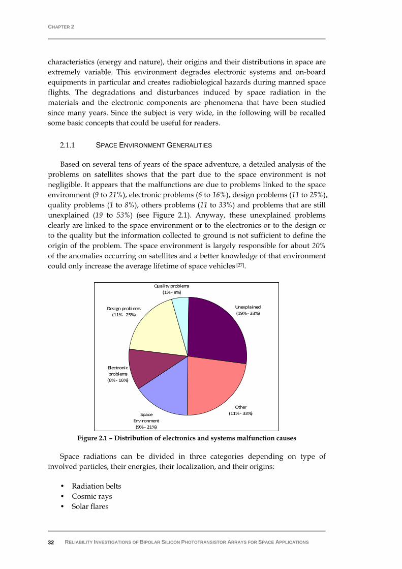
Based on several tens of years of the space adventure, a detailed analysis of the problems on satellites shows that the part due to the space environment is not negligible. It appears that the malfunctions are due to problems linked to the space environment (9 to 21%), electronic problems (6 to 16%), design problems (11 to 25%), quality problems (1 to 8%), others problems (11 to 33%) and problems that are still unexplained (19 to 53%) (see Figure 2.1). Anyway, these unexplained problems clearly are linked to the space environment or to the electronics or to the design or to the quality but the information collected to ground is not sufficient to define the origin of the problem. The space environment is largely responsible for about 20% of the anomalies occurring on satellites and a better knowledge of that environment could only increase the average lifetime of space vehicles [27].
Figure 2.1 – Distribution of electronics and systems malfunction causes
Space radiations can be divided in three categories depending on type of involved particles, their energies, their localization, and their origins:
• Radiation belts • Cosmic rays • Solar flares
Design problems (11% - 25%)
Quality problems (1% - 8%)
Unexplained (19% - 33%)
Other (11% - 33%)
Electronic problems (6% - 16%)
Space Environment (9% - 21%)

SPACE ENVIRONMENT AND ITS EFFECTS ON BIPOLAR DEVICES
RELIABILITY INVESTIGATIONS OF BIPOLAR SILICON PHOTOTRANSISTOR ARRAYS FOR SPACE APPLICATIONS 33
Radiation belts are constituted by the particles flying around Earth at a distance between one and ten terrestrial radii (i.e. up to 70000km from the ground). These particles are mainly electrons with energies up to few MeV and protons with energies up to several hundreds of MeV, with fluxes up to 106cm-2 s-1; they are trapped by the Earth’s magnetic field and form the so-called Radiation Belts (Van Allen belts). In Figure 2.2 and in Figure 2.3 the qualitative behaviour of protons and electrons belts in terms of omni-directional flux is shown. In these plots, the length unit is normalized to the terrestrial radius. A single maximum is observed for the proton belt (Figure 2.2) for a value of the distance from the Earth’s centre (L, in terrestrial radii, i.e. R⊕ ≈6371km in average) that depends on the energy (L=1.7 for 10MeV protons); the flux is very stable there and the maximum energies can reach between some MeV and some hundreds of MeV depending on the position.
Figure 2.2 – The protons radiation belt
The electron belt is more complex (Figure 2.3) exhibiting two maximums respectively corresponding to the internal and external zones: • the first one centered on L=1.4 extends up to L=2.8; the electron concentration is
relatively stable there and can reach maximum energy levels of the order of 10 till 30MeV;
• the second one, centered on L = 5, extends from L = 2.8 to L = 10; the electron flows there are much more variable and the energy levels can be as high as 7MeV.
At zero order the radiation belts can be considered to be symmetrical in longitude in a region going from the Earth's surface up to the geostationary orbit, i.e. as long as the magnetic field is not too different from a dipole. However, at high altitudes, the field differs from a dipole and the belts are no longer axisymmetric. At the level of the geostationary orbit, the fluxes of high-energy particles (electrons between 100keV and some MeV and protons between 100keV and 1MeV) then have a maximum on the day side and a minimum on the night side. So, we can talk of a
Axes: terrestrial radii, L

CHAPTER 2
RELIABILITY INVESTIGATIONS OF BIPOLAR SILICON PHOTOTRANSISTOR ARRAYS FOR SPACE APPLICATIONS 34
day-night asymmetry. At the geostationary orbit (that is at 36000km from the ground, i.e. at 6.6 terrestrial radii) the main component of the radiation comes from electrons with 1-2MeV energies and fluxes of 106cm-2 s-1. The importance of the geostationary orbit is soon understood if one thinks that most of the meteorological and telecommunications satellites are located in this orbit. Thus, there is a crucial commercial interest in understanding what happens to electronic devices in those environments.
Figure 2.3 – The electrons radiation belt
Representations of protons and electrons radiation belts shown in Figure 2.2 and in Figure 2.3 are relative to the NASA empirical models and have been derived from measurements, giving a general but static view of the belts. There are other empirical models based on different measurements developed in different times. Within these models, there are both static and dynamic models and the updating work is still ongoing. In this context, the model shortly presented, that is considered obsolete, gives, at least, a qualitative representation of radiation belts.
Since the Earth’s dipole is tilted and off-centred by 500km towards the West Pacific, the radiation belt (protons and electrons) goes down to a low altitude over the South Atlantic, the concentration of charged particles being attached to the magnetic field. A satellite in low Earth orbit (LEO) will thus only be exposed to radiation on certain fractions of the orbit as far as the trapped particles are concerned when passing through (Figure 2.4):
• the polar horns (electrons below 1000km, electrons and protons above that altitude)
• the South Atlantic Anomaly, SAA (protons and electrons at all altitudes).
Axes: terrestrial radii, L

SPACE ENVIRONMENT AND ITS EFFECTS ON BIPOLAR DEVICES
RELIABILITY INVESTIGATIONS OF BIPOLAR SILICON PHOTOTRANSISTOR ARRAYS FOR SPACE APPLICATIONS 35
Figure 2.4 – (a) South Atlantic Anomaly origins; (b) SAA particles Omnidirectional Flux higher than 10MeV (cm-2s-1) at 500km
As can be seen in Figure 2.4 (b), the position of Kourou, close to the SAA, means that the launcher trajectory passes through a zone with a great flux of energetic trapped protons when being injected into geostationary transfer orbit. This must be taken into account when designing the on-board electronics which may be sensitive to the singular effects induced by protons.
The origin of cosmic rays lies outside the solar system. It comes from very distant galactic and extragalactic point sources. It is propagated throughout space that is not occupied by dense matter. The interactions with matter (approximately 7g/cm2 of interstellar gas), shock waves and interstellar electromagnetic fields scatter and accelerate these particles which, at the level of the solar system, have isotropic angular distributions and are completely ionized. The cosmic rays represent a continuous background of ions whose energy levels can be very high. Cosmic rays are classified in primary and secondary radiation:
• The primary is related to galactic and solar particles travelling in the Cosmos: these particles are mainly heavy ions (covering the whole periodic table) with energies up to the TeV and low fluxes.
• Secondary cosmic rays are produced by collisions when the primary ones reach the outer shells of the Earth atmosphere.
Particular transient events occur that disturb on-board systems in space. This concerns Solar Flares. These are bursts occurring during solar storms. A flare consists basically of an ejection of protons, but the exact composition of the particles produced is not yet well known. Although the protons always represent the majority among the ions, particular flares are accompanied by emissions of heavy ions whose spectrums, charge states and relative abundances are variable from one event to another, and are consequently difficult to model. These emissions last between some hours and some days. The spectrums, which vary greatly from one flare to the next and during the event itself, can extend up to energy levels as high as some hundreds of MeV. The time profiles very often show a sudden increase of
~ 500 km
GeographicEquator
SAA
Magnetic Axis
Rotation Axis
MagneticEquator
Belts
~ 500 km
GeographicEquator
SAA
Magnetic Axis
Rotation Axis
MagneticEquator
Belts
(a) (b)
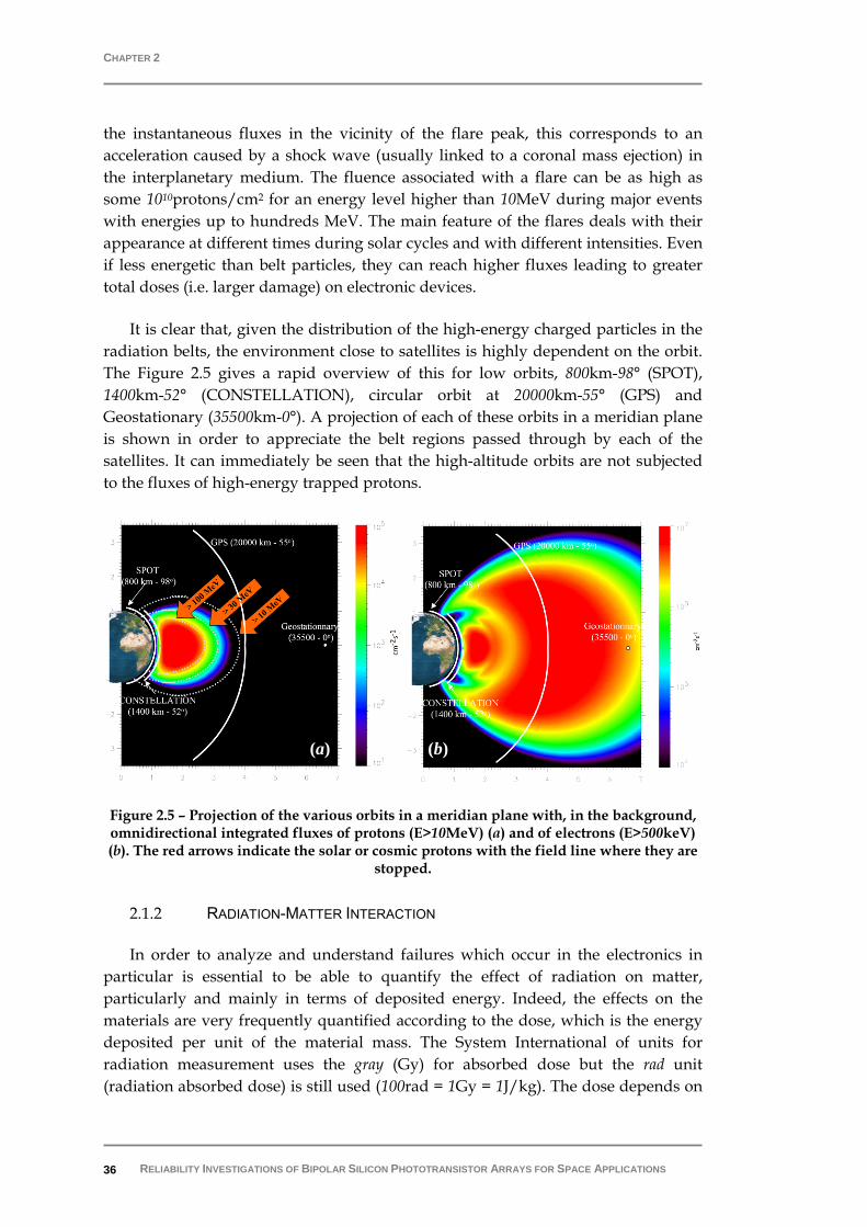
CHAPTER 2
RELIABILITY INVESTIGATIONS OF BIPOLAR SILICON PHOTOTRANSISTOR ARRAYS FOR SPACE APPLICATIONS 36
the instantaneous fluxes in the vicinity of the flare peak, this corresponds to an acceleration caused by a shock wave (usually linked to a coronal mass ejection) in the interplanetary medium. The fluence associated with a flare can be as high as some 1010protons/cm2 for an energy level higher than 10MeV during major events with energies up to hundreds MeV. The main feature of the flares deals with their appearance at different times during solar cycles and with different intensities. Even if less energetic than belt particles, they can reach higher fluxes leading to greater total doses (i.e. larger damage) on electronic devices.
It is clear that, given the distribution of the high-energy charged particles in the radiation belts, the environment close to satellites is highly dependent on the orbit. The Figure 2.5 gives a rapid overview of this for low orbits, 800km-98° (SPOT), 1400km-52° (CONSTELLATION), circular orbit at 20000km-55° (GPS) and Geostationary (35500km-0°). A projection of each of these orbits in a meridian plane is shown in order to appreciate the belt regions passed through by each of the satellites. It can immediately be seen that the high-altitude orbits are not subjected to the fluxes of high-energy trapped protons.
Figure 2.5 – Projection of the various orbits in a meridian plane with, in the background, omnidirectional integrated fluxes of protons (E>10MeV) (a) and of electrons (E>500keV) (b). The red arrows indicate the solar or cosmic protons with the field line where they are
stopped.
2.1.2 RADIATION-MATTER INTERACTION
In order to analyze and understand failures which occur in the electronics in particular is essential to be able to quantify the effect of radiation on matter, particularly and mainly in terms of deposited energy. Indeed, the effects on the materials are very frequently quantified according to the dose, which is the energy deposited per unit of the material mass. The System International of units for radiation measurement uses the gray (Gy) for absorbed dose but the rad unit (radiation absorbed dose) is still used (100rad = 1Gy = 1J/kg). The dose depends on
(a) (b)

SPACE ENVIRONMENT AND ITS EFFECTS ON BIPOLAR DEVICES
RELIABILITY INVESTIGATIONS OF BIPOLAR SILICON PHOTOTRANSISTOR ARRAYS FOR SPACE APPLICATIONS 37
the incident stopping power (dE/dx). This energy loss per unit of length precisely characterizes the way in which the incident radiation is slowed down and attenuated.
Energy loss and consequently the stopping power will be closely associated with reaction under consideration. Therefore, a stopping power for each type of interaction occurring between the incident particle and the target can be defined and it is necessary to list all the interactions that could occur.
As matter is primarily made up of electrons moving around their nucleus, a distinction shall be made between two types of interaction:
• the interaction of the incident particles with the electrons; • the interaction of the incident particles with the target nucleus.
The consequence of an interaction with an electron is the motion of the latter with the possibility of separating it from its original atom. Electron/hole pairs are created, corresponding to the ionization of the medium. The energy loss associated with this type of interaction is called the electronic stopping power. The result of an interaction with one of the target nucleus is an energy transfer with, as a possible consequence, the ejection of the nucleus from its original site in the crystal lattice. Vacancies and interstitials are created, which is called atomic displacement damage. The energy loss associated with this type of interaction is called the NIEL (Non Ionizing Energy Loss). Moreover, there is another type of interaction: the interaction of a charged incident particle, and in particular an electron, with the target atoms electrical field, which produces the emission of Gamma radiation. This photon flow, called Bremsstrahlung, in turn produce ionization [28].
To summarize, we therefore have the following contributions:
• Electronic stopping power: − ⎞
⎟⎠electronic
dEdx
, interactions with the electrons,
• Nuclear stopping power: − ⎞
⎟⎠nuclear
dEdx
, interactions with the nuclei,
• Radiative stopping power: − ⎞
⎟⎠radiative
dEdx
, Bremsstrahlung emission.
On a relatively large energy range, the nuclear stopping power can be reduced to the NIEL:
nuclear
dENIELdx
− ⎞≈ ⎟⎠
. (2.1)

CHAPTER 2
RELIABILITY INVESTIGATIONS OF BIPOLAR SILICON PHOTOTRANSISTOR ARRAYS FOR SPACE APPLICATIONS 38
The medium ionization, which is characterized by the sum of the electronic stopping power and of the radiative stopping power, is called LET (Linear Energy Transfer):
radiative electronic
dE dELETdx dx
− −⎞ ⎞≈ +⎟ ⎟⎠ ⎠
. (2.2)
Both NIEL and LET are usually given in MeV·cm2/g. In Figure 2.6 are plotted the electronic (black squares) and nuclear (red circles) stopping power of Silicon with respect to protons as a function of the particles kinetic energy. In Figure 2.7 are plotted the electronic (black squares) and radiative (red circles) stopping power Silicon relatively to electrons as a function of the particles kinetic energy. In both plots, straight blue line represents the total stopping power [29].
Figure 2.6 – Protons Stopping Powers
Figure 2.7 – Electrons Stopping Powers
1E-3 0,01 0,1 1 10 100 1000 100001E-5
1E-4
1E-3
0,01
0,1
1
10
100
1000
Electron. Nuclear Total
Stp
. Pow
. (M
eV c
m2/
g)
Kinetic Energy (MeV)
0,01 0,1 1 10 100 10001E-3
0,01
0,1
1
10
100
Electron. Radiative Total
Stp
. Pow
. (M
eV c
m2/
g)
Kinetic Energy (MeV)

SPACE ENVIRONMENT AND ITS EFFECTS ON BIPOLAR DEVICES
RELIABILITY INVESTIGATIONS OF BIPOLAR SILICON PHOTOTRANSISTOR ARRAYS FOR SPACE APPLICATIONS 39
As said, many of the electronic devices degradations which are linked to the space environment radiations can be characterised by the dose. It is therefore important to evaluate the absorbed dose for elements that are sensitive to this parameter. As a general rule, the dose is equated with the ionising dose. The absorbed dose is the mean energy deposited by ionisation, per unit of mass of the irradiated material.
Figure 2.8 – Interaction with matter of a flux Ф of particles depositing an energy dE in a volume with cross section S and thickness dx.
If we take, as shown in Figure 2.8, a cross section S of a material with a specific mass ρ irradiated by a fluence Φ of particles depositing energy dE in the thickness dx by ionisation, the deposited ionising energy per unit of mass is, assuming particles with linear trajectories:
1particles
dE dE dEDose N S
mass S dx dxρ ρ= ⋅ = Φ ⋅ ⋅ = Φ ⋅
⋅ ⋅⎛ ⎞⎜ ⎟⎝ ⎠
(2.3)
Then, considering the LET definition in equation (2.2), we get:
Dose LET= Φ ⋅ (in rads). (2.4)
In equations (2.3) and (2.4) LET is the mass LET, energy transferred by unit of mass, expressed in eV·cm2/g, as found in tables in practice [30].
By analogy we can define a non-ionising dose which characterises the quantity of displacements generated in the volume by the expression:
NIDose NIEL= Φ ⋅ (2.5)
where the DoseNI is given in MeV/g and the NIEL is defined in (2.1).
η atoms/cm3
Ф

CHAPTER 2
RELIABILITY INVESTIGATIONS OF BIPOLAR SILICON PHOTOTRANSISTOR ARRAYS FOR SPACE APPLICATIONS 40
2.1.3 TOTAL IONIZING DOSE EFFECTS
Total ionizing dose (TID) effects in semiconductor devices mainly depend on the creation of electron-hole pairs within dielectric layers (oxides, nitrides etc.) and subsequent generation of traps at or near the interface with the semiconductor or of trapped charge in the dielectric. This can produce a variety of device effects such as flatband and threshold voltages shifts and surface leakage currents. There is an extensive literature on total dose effects.
Although the concept of total ionizing dose is a useful first order approximation for quantifying effects, there are dependencies on a number of other parameters. Notably, the LET of the radiation and the applied electric field both influence the rate of recombination of electron-hole pairs, while the dose-rate more influences the relative importance of the hole traps and interface states. In general, issues which are important for total dose effects are:
• Dependence on bias during irradiation (irradiation whilst the device is biased is usually worst case).
• Annealing effects (trapped charge reduces after irradiation, while interface traps tend to build-up).
• Dependence on dose rate (mainly because of annealing effects). • Dependence on package (especially for some types of plastic package). • Variability from batch to batch and device to device (especially for
commercial-off-the-shelf devices). • In linear devices with isolated bipolar junction transistors there is a
pronounced "enhanced low dose rate sensitivity" (ELDRS) effect where the damage is greater at low dose rates.
• Problems of dose-enhancement under electron or Bremsstrahlung irradiation where there are boundaries between materials of widely differing atomic number. These can occur in packaging and shielding as well as on the die (e.g. copper interconnects, high-impedance bump bonds, metalized layers, Au-Si die attachments). Enhancement factors can approach a factor two [31].
2.1.4 DISPLACEMENT DAMAGE EFFECTS
Energetic particles such as neutrons, protons, electrons, α-particles and heavy ions can create damage in semiconductor materials by displacing atoms in the crystal lattice. Secondary electrons produced by high-energy photons will also produce displacement effects. The result is that stable defect states are created within the band gap that can give rise to any of the five effects illustrated in Figure 2.9, depending on the temperature, carriers concentration and the location at which the defect resides [32, 33]:

SPACE ENVIRONMENT AND ITS EFFECTS ON BIPOLAR DEVICES
RELIABILITY INVESTIGATIONS OF BIPOLAR SILICON PHOTOTRANSISTOR ARRAYS FOR SPACE APPLICATIONS 41
• generation of electron-hole pairs (leading to thermal dark current in detectors); • recombination of electron-hole pairs (leading to reduction of minority carrier
lifetime and effects in LEDs and laser diodes); • trapping of carriers, leading to loss in charge transfer efficiency in CCDs
(minority carrier trapping) or carrier removal (majority carrier trapping); • compensation of donors or acceptors, also leading to carriers removal in some
devices (for example the resistance in a lightly doped collector in a bipolar transistor can increase);
• tunnelling of carriers, leading to increased current in reverse biased junctions - particularly for small band gap materials and high electric fields.
Figure 2.9 - Illustration of the five basic effects of a defect energy level (Et) on the device electrical performances deterioration.
The usually accepted approach considers that displacement damage is proportional to the non-ionising energy loss, NIEL (usually defined in units of keVcm2/g or MeVcm2/g). The NIEL hypothesis can be used to relate damage due to different particles and energies: this greatly reduces the amount of testing needed (usually only one particle and energy is used). The NIEL scaling hypothesis leads to the concept of displacement damage equivalent dose, as defined in (2.5):
dD NIEL= × Φ
where Φ is the particle fluence (time-integrated flux) [34]. Equivalent dose can be measured in keV/g or in (non-ionizing) rads.
It is now well established that the amount of formation of defect clusters depends on the particle type. Electron irradiation gives primary knock-on atoms (PKA) with low recoil energies and hence leads to almost exclusive production of

CHAPTER 2
RELIABILITY INVESTIGATIONS OF BIPOLAR SILICON PHOTOTRANSISTOR ARRAYS FOR SPACE APPLICATIONS 42
point defects, whereas neutrons give a flat PKA spectrum and a much greater proportion of cluster formation. For protons, the situation is in between. In some cases the amount of clustering may not matter, only the total number of defects. However, the clustering can be expected to affect the defect kinetics. The implication for space instrumentation is that tests at single proton energy may not allow an accurate prediction in all cases. Fortunately there are still many cases where the NIEL hypothesis is valid, in particular where non-impurity related defects, such as divacancies are involved.
Other factors that can affect the generation of defects are the irradiation temperature and post-irradiation annealing. Usually it is assumed that neither irradiation temperature nor bias has a significant effect and that annealing at room temperature takes place in only the first few weeks after irradiation [33].
2.1.5 SINGLE EVENTS EFFECTS
Single event effects arise from the interaction of single particles (e.g. protons, neutrons or heavy ions) with the semiconductor causing either transient or permanent effects [35]:
• Single dark current generation centers (spikes) and single electron traps in imagers (permanent) due to individual lattice defects such as vacancy-phosphorous complexes and divacancies.
• Single event upset in memories (i.e. bit-flips leading to change of stored information.
• Single event transients in imagers or linear circuits (i.e. a current transient which can be interpreted as a false signal or be propagated to cause an output error in combinational logic).
• Single event latch-up in CMOS circuits (a potentially destructive triggering of a parasitic pnpn thyristor structure in the device).
• Single event burnout in power transistors (a destructive triggering of a vertical n-channel transistor accompanied by regenerative feedback).
• Single event snapback in NMOS devices, particularly in SOI devices (a destructive triggering of a lateral npn transistor accompanied by regenerative feedback).
• Single event functional interrupt in control circuitry, e.g. in processors or ADCs, (transient corruption of a control path).
• Single event gate rupture (destructive rupture of gate dielectric due to high field generated by high current).
As SEEs are not critical for the application for which the components under study are intended, in the following will be discussed the effects of both ionizing dose and displacement damage on electrical characteristics of silicon bipolar devices, including the phototransistors.

SPACE ENVIRONMENT AND ITS EFFECTS ON BIPOLAR DEVICES
RELIABILITY INVESTIGATIONS OF BIPOLAR SILICON PHOTOTRANSISTOR ARRAYS FOR SPACE APPLICATIONS 43
2.2 BIPOLAR DEVICES DAMAGES IN SPACE ENVIRONMENT
As discussed in the previous section, the main effects of space radiations on electronics are related to the Total Ionizing Dose, depending on the creation of electron-hole pairs within dielectric layers, to the Displacement Damage, caused mainly by energetic particles impacts displacing atoms in the crystal lattice.
As the main effect of ionising dose is to trap positive charges in the oxide bulk, this leads to create a negative mirror charges concentration in the substrate. In MOS devices for instance, the channel creation between the source and the drain is then facilitated in NMOS devices (p substrate), thus the positive oxide trapped charge decreases the threshold voltage. For a PMOS device (n substrate) the positive charge trapping opposes the creation of the channel which causes the threshold voltage to increase. With no gate oxide, BJTs should be more rad-tolerant. Unfortunately, due to the field oxides the current gain can be severely degraded with ionizing radiations. Moreover, the degradation appears to be enhanced at low dose rate irradiations.
During an irradiation of energetic particles, they collide with the semiconductor lattice. After diffusion, various displacement defects appear, such as vacancies and vacancy-doping defects. These defects are stable and introduce new energy levels in the band gap. From a macroscopic point of view, the displacement damages can significantly alter the electrical characteristics of the devices[30].
2.2.1 IONISING DOSE EFFECTS ON BJTS
Once electron-hole pairs are generated in the oxide, electrons are swept out of the oxide in a short time during which a fraction of them recombine with the holes6. The fraction of the holes that escape this initial recombination is mainly determined by the magnitude of the electric field, which separate the pairs, and by the initial density of pairs created by the incident particle. Pairs line density is determined by the LET, and is, therefore, a function of the incident particle type and energy. The carriers escape recombination move through the oxide under the influence of any electric field. This holes transport is taking place over many decades of time. The transport is assumed to occur via hopping phenomenon between localized shallow trap states randomly distributed in space[36]. A fraction of the holes reaching the SiO2/Si interface are trapped. Hole traps near the Si/SiO2 interface arise due to a transition region where oxidation is not complete7. The most often encountered hole
6 Electrons are assumed to be swept out of the oxide immediately after they are created, then not
supposed to be trapped. However, electron trapping exists, but the oxide trapped charge is globally positive and trapped electrons only compensate a part of the trapped holes.
7 When silicon is thermally oxidized, the interface between the amorphous oxide and the crystalline silicon is generally deficient of oxygen, giving rise to strained as well as uncompleted, or “dangling”,

CHAPTER 2
RELIABILITY INVESTIGATIONS OF BIPOLAR SILICON PHOTOTRANSISTOR ARRAYS FOR SPACE APPLICATIONS 44
trap corresponds to a missing oxygen atom in the usual lattice configuration, leaving a weak Si-Si bond, where a positive charge can be trapped [30].
The holes are not permanently trapped on the SiO2 deep levels. Instead, they usually disappear from the oxide after a duration ranging from milliseconds to years. The annealing of the trapped holes has two origins, the tunnelling or the thermal excitation, that may reflect different hole-removal processes. Both processes are assumed to be independent [37].
In Bipolar Junction Transistors the current gain (hFE) degrades with ionizing radiations, especially at low bias levels. The current gain degradation is primarily induced by an increase of the base current under a given emitter bias whereas the collector current is shown to remains roughly constant. The difference between the base current value before and after the irradiation is called the excess base current. In BJTs, as illustrated in Figure 2.10, three components participate to the base current:
• Ir,d: current due to recombination in the emitter-base depletion region • IE,p: current due to back-injection of carriers from base to emitter • Ir,B: current due to recombination in the neutral base.
Figure 2.10 – Illustration of different components of base, emitter, and collector currents in a bipolar transistor
For devices that have not been irradiated, IE,p dominates while for devices that have been irradiated, Ir,d and Ir,B increase, with Ir,d dominating for ionizing radiation and Ir,B normally dominating for displacement damage. Thus, in the case of ionizing dose, the main degradation process is recombination in the emitter-base depletion region. Due to interface states that serve as recombination centers, the recombination-rate increase occurs mainly where the depletion region intersects the
silicon bonds. These dangling bonds act as interface traps with energy levels within the forbidden band-gap at the SiO2/Si interface.
n p n

SPACE ENVIRONMENT AND ITS EFFECTS ON BIPOLAR DEVICES
RELIABILITY INVESTIGATIONS OF BIPOLAR SILICON PHOTOTRANSISTOR ARRAYS FOR SPACE APPLICATIONS 45
Si/SiO2 interface increasing the recombination current. The recombination rate also changes with the electrostatic effect of oxide trapped charge that tends to equilibrate the number of holes and electrons.
Thus, as previously said, the base current is the sum of the hole diffusion current, IE,p, the base recombination current, Ir,B, and the base-emitter depletion layer recombination current, Ir,d.
, , ,B E p r B r dI I I I= + + (2.6)
The total emitter current corresponds to the sum of the electron diffusion current, IE,n, the hole diffusion current, IE,p and the base-emitter depletion layer recombination current, Ir,d.
, , ,E E n E p r dI I I I= + + (2.7)
The total collector current is the electron diffusion current, IE,n, minus the base recombination current, Ir,B.
, ,C E n r BI I I= − (2.8)
The transport factor, α, is defined as the ratio of the collector and emitter current:
, ,
, , ,
E n r BC
E E n E p r d
I III I I I
α−
= =+ +
(2.9)
Using Kirchoff’s current law and the sign convention shown in Figure 2.10, we find the well known definition of the transistor current gain, β [2]:
1
C
B
II
αβα
= =−
(2.10)
The transport factor, α, can be rewritten as the product of the emitter efficiency, γE, the base transport factor, αT, and the depletion layer recombination factor, δr:
T E rα α γ δ= (2.11)
The emitter efficiency, γE, is defined as the ratio of the electron current in the emitter, IE,n, to the sum of the electron and hole current diffusing across the base-emitter junction, (IE,n + IE,p):

CHAPTER 2
RELIABILITY INVESTIGATIONS OF BIPOLAR SILICON PHOTOTRANSISTOR ARRAYS FOR SPACE APPLICATIONS 46
,
, ,
E nE
E n E p
II I
γ =+
(2.12)
The base transport factor, αT, equals the ratio of the current due to electrons injected in the collector, to the current due to electrons injected in the base:
, ,
,
E n r BT
E n
I II
α−
= (2.13)
The depletion layer recombination factor, δr, equals the ratio of the current due to electrons and holes diffusion across the base-emitter junction to the total emitter current:
,E r dr
E
I II
δ−
= (2.14)
Combining equations (2.9) and (2.10) yields:
, ,
, , ,
E n r B
r B r d E p
I II I I
β−
=+ +
(2.15)
Thus, equation (2.15) shows that ionizing radiation-induced increase of Ir,d causes β drop. In other terms, recombination in the depletion-region of the base-emitter junction further reduces the current gain, as it increases the emitter current without increasing the collector current (equation (2.14)).
The effective degradation of bipolar devices electrical characteristics due to ionizing radiations could vary a lot depending on many factors. There could be a dependency on bias during irradiation, on annealing effects, on package type, and normally is observed a great variability from batch to batch and device to device [31. Moreover, it is well known that bipolar devices could degrade under ionizing radiation with a strong dependence on dose rate; this point will be discussed in the next paragraph.
Another possible effect of ionizing radiations is to create surface leakage paths. Trapped positive charges in the oxide create a negative mirror charge in the substrate. As trapped charges are positive, a p-region lightly doped could invert its carrier population crating channel, like in MOS devices for instance. If this p-doped region is the base region in an npn lateral transistor, a channel in that zone behaves as a leakage path between collector and emitter. Thus, this means that in phototransistors, for instance, oxide ionization could increase the darkness current. In any case, this phenomenon depends strongly on device technology. Oxide

SPACE ENVIRONMENT AND ITS EFFECTS ON BIPOLAR DEVICES
RELIABILITY INVESTIGATIONS OF BIPOLAR SILICON PHOTOTRANSISTOR ARRAYS FOR SPACE APPLICATIONS 47
thickness and quality, doping level, and device layout are the main technological parameters that could affect bipolar components radiation hardness.
2.2.2 ENHANCED LOW DOSE RATE EFFECTS
As previously seen, ionizing radiation often has a deleterious effect on Si-based microelectronic devices and this effect has been found to be enhanced as the dose rate is decreased for a given total dose. This dependence on dose rate is called enhanced low-dose-rate sensitivity (ELDRS). There is an extensive literature on ELDRS and various models have been proposed [38], 39-50]. For BJT the main effect is a reduction in a transistor gain because of the increase of base excess current. The primary mechanism appears to be the increased carriers recombination at the Si/SiO2 interface near the emitter-base junction. This enhanced recombination is ascribed to an increase in the density of interface traps [38]. For npn transistors, an additional contribution can arise relatively to the enhancement of the recombination rate of the existing traps. This increased recombination occurs because the electron concentration at the interface is increased by the electric field arising from positive trapped charge in the oxide overlying the base. This sensitivity is technology-dependent and generally observed on relatively poor quality oxides irradiated at low electric field like field oxides covering the base region of BJTs. Among the physical models that have been proposed to explain ELDRS, the space charge model is currently considered as the best choice to explain the obtained experimental results[39]. In this case, it has been reported that ELDRS is related to space-charge effects due to slowly-transporting holes. At low dose rate, in field oxides the electric field magnitude induced by the work function difference only is low. Thus holes transport is slow. At high dose rate, the electron-hole pair generation time is short compared with the time needed to transport holes to the interface. A space charge is then created in the oxide bulk inhibiting the transport of holes and generated protons to the Si/SiO2 interface reducing then the degradation. In Figure 2.11 is shown a simplified illustration of the space charge model for enhanced low dose rate oxide degradation in a MOS system [51].
As the proton mobility is lower than the holes one (from 4 to 6 orders of magnitude), a revised version of this model has been proposed that consider two limiting cases[38]. At very low dose rate, the interface state creation rate is very low. Protons have time to be released, to reach the Si/SiO2 interface and then to create interface states. In this case protons participate to both bulk oxide trapped charge and interface state creation. At very high dose rate, holes reach the interface earlier than protons. When the density of trapped holes is high enough to create an electrostatic barrier, following holes and protons can no longer reach the interface. On the whole, less protons reach the interface and less interface states are generated. This could explain the lower degradation observed at high dose rate.
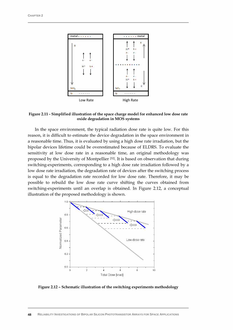
CHAPTER 2
RELIABILITY INVESTIGATIONS OF BIPOLAR SILICON PHOTOTRANSISTOR ARRAYS FOR SPACE APPLICATIONS 48
Figure 2.11 - Simplified illustration of the space charge model for enhanced low dose rate oxide degradation in MOS systems
In the space environment, the typical radiation dose rate is quite low. For this reason, it is difficult to estimate the device degradation in the space environment in a reasonable time. Thus, it is evaluated by using a high dose rate irradiation, but the bipolar devices lifetime could be overestimated because of ELDRS. To evaluate the sensitivity at low dose rate in a reasonable time, an original methodology was proposed by the University of Montpellier [52]. It is based on observation that during switching-experiments, corresponding to a high dose rate irradiation followed by a low dose rate irradiation, the degradation rate of devices after the switching process is equal to the degradation rate recorded for low dose rate. Therefore, it may be possible to rebuild the low dose rate curve shifting the curves obtained from switching-experiments until an overlap is obtained. In Figure 2.12, a conceptual illustration of the proposed methodology is shown.
Figure 2.12 – Schematic illustration of the switching experiments methodology
High RateLow Rate
metal metal
N
orm
aliz
ed P
aram
eter

SPACE ENVIRONMENT AND ITS EFFECTS ON BIPOLAR DEVICES
RELIABILITY INVESTIGATIONS OF BIPOLAR SILICON PHOTOTRANSISTOR ARRAYS FOR SPACE APPLICATIONS 49
One set of devices will be irradiated at low dose rate only (the first blue line segment on the left) and four sets of devices will be irradiated first at high, then at low, dose rate (dose rate switching). The two pale grey lines represent the continuous low and high dose rate degradation curves of the parameter of interest. The five blue lines correspond to short low dose rate irradiations: the first one without a switch in the dose rate and the four others derived from switching-experiments. The low dose rate irradiations are stopped when an overlap of the degradation values is observed on all the line segments. From these data, we can rebuild the low dose rate curve by shifting the four line segments. The shift is determined experimentally: the line segments are translated to the left (to decreasing values of total dose, parallel to x-axis) until the degradation values are equal as shown in Figure 2.12.
The main interest of this methodology is to obtain the low dose rate curve in a short period. For instance, only thirty days of irradiation tests are needed to evaluate the low dose rate degradation of these devices up to 5krad of total dose at a constant dose rate of 2rad/h, instead of more than one hundred days necessary to reach the same total dose at the same dose rate. In other words, using this method allows us to decrease the irradiation test time by a factor of about 3.5 in this example.
2.2.3 DISPLACEMENT DAMAGE EFFECTS ON BJTS
As discussed in paragraph 2.1.4, the result of an irradiation of energetic particles such as neutrons, protons, electrons, α-particles and heavy ions can create damage in semiconductor materials by displacing atoms in the crystal lattice. Thus stable defect states created within the band gap that can give rise in bipolar devices to the effects mentioned in the same section.
First of all, generation centers are behind the increase of thermal darkness current in photodetectors. Generation current in the depletion region of a diode is proportional to the density of recombination-generation centers and the depletion volume. The concentration of centers is increased by irradiation. Space charge generation current increases proportionately to particle fluence and become the dominant factor of darkness current. Following irradiation, the amplified dark current, ICE0, sets the minimum usable signal current.
Trapping centers lead to the reduction of the minority carrier lifetime. This normally induces a degradation of base-collector photodiode response in bipolar phototransistors. Assuming that there is not carrier collection in the p-base layer (because of its thinness) all carrier collection occurs in both depletion and epitaxial region. Because collection is lightly modified in depletion zone after irradiation but dramatically reduced in the epitaxial region, response degradation depends on how much was the ratio between collection in these two zones before the irradiation.

CHAPTER 2
RELIABILITY INVESTIGATIONS OF BIPOLAR SILICON PHOTOTRANSISTOR ARRAYS FOR SPACE APPLICATIONS 50
Traps centers in the base-emitter space charge region cause an excess base current. As mentioned in paragraph 2.2.1, this reduces the transistor current gain, β, and this effect is more significant as collector current is low. The parameter affected is the component of base current due to recombination in the neutral base, Ir,B. As can be seen in equation (2.13), an increase of Ir,B leads to a decrease of the base transport factor, αT, leading to a reduction of β. Moreover, this phenomenon is enhanced if devices are irradiated with particles like protons or electrons because of their ionizing effect.
The effect of the compensation of donors or acceptors is carrier removal. In a lightly doped collector in a bipolar transistor (normally is the case), the series resistance can increase [33, 53, 54].
Most of all variations in device physical parameters due to radiation-induced crystal defects lead to the decrease of transistor current gain. Both base excess current and collector series resistance contribute to reduce β: the first one causes gain reduction at lower biasing level; the second one, in the high-injection operating region.
In the case of bipolar phototransistor, the overall degradation is related to the responsivity deterioration. The causes are the decrease of both gain and the photobase responsivity, and the rise of the darkness current. The schematic representation of the is shown in Figure 2.13 where IPH is the current photo-generated in the base-collector junction by the photon flux F(ν), hFE is the current gain, and Idark the darkness current. The quantities IPH’ and hFE’ indicate the same quantities after irradiation and, as said, are lower than those pre-irradiation.
Figure 2.13 – Schematic representation of overall degradations in phototransistors: (a) pre-
irradiated simplified model; (b) irradiated model
(a) (b)
SPACE ENVIRONMENT AND ITS EFFECTS ON BIPOLAR DEVICES
RELIABILITY INVESTIGATIONS OF BIPOLAR SILICON PHOTOTRANSISTOR ARRAYS FOR SPACE APPLICATIONS 51
Conclusions
As discussed in this second chapter, the effects induced by the space environment are largely responsible for the anomalies occurring on satellites onboard electronics. These effects on electronics in general and on bipolar devices in particular have been presented. Since the subject is very vast, only some basic concepts that could be useful for readers have been called-back.
The first section has described such environment, mainly in terms of space radiations. They can be divided in three categories depending on type of involved particles, their energies, their localization, and their origins. Then, the concepts of stopping power, LET, and NIEL have been introduced in order to analyze and understand failures which occur in the electronics. This is essential to be able to quantify the effect of radiation on matter, particularly and mainly in terms of deposited energy. Actually, the main effects of space radiations on electronics are related to the Total Ionizing Dose, depending on the creation of electron-hole pairs within dielectric layers (related to the LET), to the Displacement Damage, caused mainly by energetic particles impacts displacing atoms in the crystal lattice (related to the NIEL), and to the Single Events, from the interaction of single particles. All those effects on electronic devices performances have been discussed in the last three subsections.
In the second chapter section, we focused on bipolar devices characteristics degradations in correlation with both ionizing and displacement damage doses. Moreover, as BJTs are low-dose rate sensitive, the ELDRS and a methodology to assess its effect have been also discussed. The space environment induced degradations on bipolar devices is presented focusing on the “measurable” electrical characteristics variations. The main effects on devices performance are:
• the reduction of the transistor current gain • the increase of the darkness leakage current • the spectral responsivity degradation.
This chapter concludes the general description of the context in which the research activities on phototransistors reliability have been performed. Thus, in the next part of this manuscript we will focus on the most of all the performed experimental activities and we will discuss them individually. The next chapter is now going to detail the activities related to the development and the test of a new phototransistor technology with regards the past experiences, mainly taking into account the mobile charges sensitivity.


RELIABILITY INVESTIGATIONS OF BIPOLAR SILICON PHOTOTRANSISTOR ARRAYS FOR SPACE APPLICATIONS
BIPOLAR SILICON PHOTOTRANSISTOR ARRAYS SENSITIVITY TO OXIDE TRAPPED MOBILE CHARGES
Passivations in silicon bipolar technologies have only structural functions. But their quality could impact on devices functionality. In particular, mobile charges trapped in passivation layers could degrade performances and introduce instabilities during accelerated life tests.
In this third chapter, we will recall at first the studies relative to the evaluation of the Bipolar Silicon Phototransistor Arrays (BPSA) batch provided by Etic-Honeywell for which the sensitivity to oxide trapped charges has been verified. In fact, previous studies on such devices conducted at CNES highlight channel photocurrent instabilities during thermal/bias ageing tests. Consequently, we performed specific tests and analyses in order to understand the causes of these instabilities, as will be discussed in the first section. Moreover, a recovery of phototransistor characteristics after zero-bias storage has been observed. We will demonstrate, in agreement with already published data, that this is the classical signature of the presence of oxide trapped charges. Actually, during ageing tests they are at the origin of the dramatic increase of leakage current. Thanks to Spice-like software we will simulate this device post-test behaviour. The leakage path will be localized by using the Light Emission Microscopy (LEM) technique. Then, we will discuss about a device selection methodology based on a temperature ramp test and validate it for Etic-Honeywell devices.
In the second section, we will discuss the activities related to pre-evaluation of new BSPA designs from an emerging European founder. In particular, these studies were undertaken analyzing various technological options with respect toward results previously obtained and concerning mobile charges sensitivity.
3.1 EXPERIMENTAL DEMONSTRATION OF THE BPSA SENSITIVITY TO MOBILE CHARGES TRAPPED IN PASSIVATION LAYERS
As discussed in previous sections, studied phototransistors will be used in satellites and so they will be exposed to both ionizing and non-ionizing (displacement damage) radiations. As said in the second chapter, such

CHAPTER 3
RELIABILITY INVESTIGATIONS OF BIPOLAR SILICON PHOTOTRANSISTOR ARRAYS FOR SPACE APPLICATIONS 54
environmental stresses can severely degrade electrical properties of silicon devices. In particular, ionic contaminants in or upper the passivation can cause soft reverse “I-V” characteristics, such as presence of excess reverse current. Moreover, a poor surface condition at the silicon-passivation interface will affect reverse characteristic through specific mechanisms that generate excess charges in the oxide which invert population in semiconductor material. So, assessing both the quality of passivation layer and the tolerance of overall device to mobile charges becomes mandatory. In paragraph 1.1.3, we anticipated that the angular encoder phototransistors were provided by Optek (USA). However, this manufacturer meant his disengagement of the space sector in May 2000. Then, the CNES had identified in Etic-Honeywell (USA) as a new provider for commercial BSPA that meet the needs in terms of performances and costs. In this paragraph we will describe the analyses we performed on these devices in order to understand the failure mechanisms that caused photocurrent instabilities during the thermal/bias ageing tests conducted previously by CNES in the frame of the qualification activities.
3.1.1 ETIC-HONEYWELL DEVICES SENSITIVITY
The Etic-Honeywell device has been described in paragraph 1.2.2 and the channels layout shown in Figure 1.10 and Figure 1.11. In the past, CNES has conducted an evaluation program such BSPA, including life test, storage, thermal cycles, and radiations. These tests gave satisfactory results. On the other hand, in the frame of the qualification activities, photocurrent decrease followed by a recovery was observed on certain channels during accelerated ageing test (2000h/125°C) on some devices. Figure 3.1 shows the variation in percent of the collector current versus time for 200 channels.
Figure 3.1 – Collector current drift in percent during life test
-50
-40
-30
-20
-10
0
10
20
30
40
0 200 400 600 800 1000 1200 1400 1600 1800 2000
Time (h)
Col
lect
or c
urre
nt d
rift (
%)

BIPOLAR SILICON PHOTOTRANSISTOR ARRAYS SENSITIVITY TO OXIDE TRAPPED MOBILE CHARGES
RELIABILITY INVESTIGATIONS OF BIPOLAR SILICON PHOTOTRANSISTOR ARRAYS FOR SPACE APPLICATIONS 55
As a consequence, several analyses to check the measurement procedures were conducted. The ageing test was repeated more times and again these photocurrent instabilities have been observed. Moreover, an increase of the collector current after the 125°C/40V-bias test followed by a decrease of the current when the device is stored at 125°C with collectors and emitters shortened has been observed. The storage performed under vacuum show no significant improvement. This indicates that the problem is related to the die itself and it is not a packaging issue (outgassing of the adhesives inside the package for instance).
In order to understand these test results, we performed a High-Temperature-Reverse-Bias8 test (HTRB), that is 48h at 125°C with VCE=40V, followed by a storage test (i.e. 48h at 125°C, collectors and emitters short-circuited). The tested device is a specific one with the transistor bases bonded. Current-bias (I-V) characteristics and Gummel plots, measured before and after the HTRB and the storage tests, are shown in Figure 3.2 and in Figure 3.3 respectively.
Figure 3.2 – I-V characteristics: at the initial stage, before HTRB test and before storage test
IC-VCE plots in Figure 3.2 are relative to the classic phototransistor operating mode, i.e. an infrared LED (850nm) drives the transistor base. So, in the different
8 The bias is “reverse” for the base-collector junction.
after HTRB
(HTRB test)
(HTRB test)
(storage test)
initial stage
0.0 0.1 0.2 0.3 0.4 0.5
0.0
200.0µ
400.0µ
600.0µ
800.0µ
1.0m
1.2m
IC [A
]
VCE [V]
ILED
0mA 5mA 10mA 15mA 20mA 25mA 30mA 35mA 40mA
0.0 0.1 0.2 0.3 0.4 0.5
0.0
200.0µ
400.0µ
600.0µ
800.0µ
1.0m
1.2m
IC [A
]
VCE [V]
ILED
0mA 5mA 10mA 15mA 20mA 25mA 30mA 35mA 40mA
after storage
0.0 0.1 0.2 0.3 0.4 0.5
0.0
200.0µ
400.0µ
600.0µ
800.0µ
1.0m
1.2m
IC [A
]
VCE [V]
ILED
0mA 5mA 10mA 15mA 20mA 25mA 30mA 35mA 40mA
Measurement setup:
VCE = 0 ÷ 0.5V (step 5mV)
Floating base
ILED = 0 ÷ 40mA (step 5mA)

CHAPTER 3
RELIABILITY INVESTIGATIONS OF BIPOLAR SILICON PHOTOTRANSISTOR ARRAYS FOR SPACE APPLICATIONS 56
curves in IC-VCE plots the LED current (that is directly proportional to the emitted light power) is taken as a parameter. Figure 3.2 shows that that for a given LED current (i.e. emitted light power) and emitter-collector bias, the collector current tends to increase after HTRB test. After the subsequent storage test, we observe a recovery of the initial characteristics. If HTRB test is repeated, the photocurrent rise again and decrease again after another storage test.
Figure 3.3 – Gummel plots: at the initial stage, before HTRB test and before storage test
Figure 3.3 shows Gummel plots measured at the different steps of the test. Before test we note that the base and the collector ideality factor (η) are close to 1 indicating that recombination mainly occurs in the quasi-neutral regions. After the HTRB test, an emitter-collector leakage current appears and then disappears after the storage test. Such a cyclic behaviour has been already observed in the literature and is usually attributed to the presence of mobile charges in the passivation layer[55]. The leakage current was also measured in darkness after HTRB and after recovery. Results are shown in Figure 3.4. After HTRB test the leakage current for this channel is slightly higher than twenty micro-amps while it was about few nano-amps before test.
initial stage
after HTRB
after storage
(HTRB test)
(storage test)
(HTRB test)
0.0 0.2 0.4 0.6 0.8 1.0-35
-30
-25
-20
-15
-10
-5
0 ln(Ic) ln(Ib)
ln(Ic
), ln
(Ib)
VBE
0.0 0.2 0.4 0.6 0.8 1.0-35
-30
-25
-20
-15
-10
-5
0 ln(Ic) ln(Ib)
ln(Ic
), ln
(Ib)
VBE
η=0.9845 η=1.1066
η=1.2262
η=1.1017
η=1.1648
η=0.9866 η=1.099
η=1.1743
0.0 0.2 0.4 0.6 0.8 1.0-35
-30
-25
-20
-15
-10
-5
0 ln(Ic) ln(Ib)
ln(Ic
), ln
(Ib)
VBE
NB: Currents are in A
Measurement setup:
VCE = 5V
VBE = 0 ÷ 1V (step
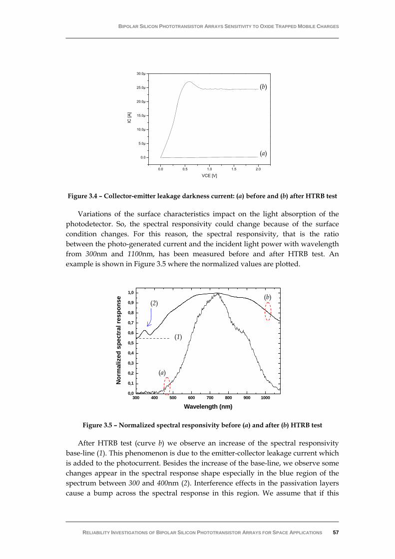
BIPOLAR SILICON PHOTOTRANSISTOR ARRAYS SENSITIVITY TO OXIDE TRAPPED MOBILE CHARGES
RELIABILITY INVESTIGATIONS OF BIPOLAR SILICON PHOTOTRANSISTOR ARRAYS FOR SPACE APPLICATIONS 57
Figure 3.4 – Collector-emitter leakage darkness current: (a) before and (b) after HTRB test
Variations of the surface characteristics impact on the light absorption of the photodetector. So, the spectral responsivity could change because of the surface condition changes. For this reason, the spectral responsivity, that is the ratio between the photo-generated current and the incident light power with wavelength from 300nm and 1100nm, has been measured before and after HTRB test. An example is shown in Figure 3.5 where the normalized values are plotted.
Figure 3.5 – Normalized spectral responsivity before (a) and after (b) HTRB test
After HTRB test (curve b) we observe an increase of the spectral responsivity base-line (1). This phenomenon is due to the emitter-collector leakage current which is added to the photocurrent. Besides the increase of the base-line, we observe some changes appear in the spectral response shape especially in the blue region of the spectrum between 300 and 400nm (2). Interference effects in the passivation layers cause a bump across the spectral response in this region. We assume that if this
300 400 500 600 700 800 900 10000,0
0,1
0,2
0,3
0,4
0,5
0,6
0,7
0,8
0,9
1,0
before step1or after step 2
Nor
mal
ized
spe
ctra
l res
pons
e
Wavelength (nm)
after step1
(a)
(b)
(1)
(2)
0.0 0.5 1.0 1.5 2.0
0.0
5.0µ
10.0µ
15.0µ
20.0µ
25.0µ
30.0µ
IC [A
]
VCE [V]
(b)
(a)
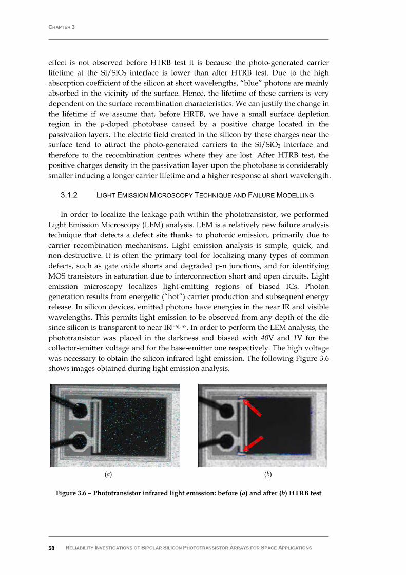
CHAPTER 3
RELIABILITY INVESTIGATIONS OF BIPOLAR SILICON PHOTOTRANSISTOR ARRAYS FOR SPACE APPLICATIONS 58
effect is not observed before HTRB test it is because the photo-generated carrier lifetime at the Si/SiO2 interface is lower than after HTRB test. Due to the high absorption coefficient of the silicon at short wavelengths, “blue” photons are mainly absorbed in the vicinity of the surface. Hence, the lifetime of these carriers is very dependent on the surface recombination characteristics. We can justify the change in the lifetime if we assume that, before HRTB, we have a small surface depletion region in the p-doped photobase caused by a positive charge located in the passivation layers. The electric field created in the silicon by these charges near the surface tend to attract the photo-generated carriers to the Si/SiO2 interface and therefore to the recombination centres where they are lost. After HTRB test, the positive charges density in the passivation layer upon the photobase is considerably smaller inducing a longer carrier lifetime and a higher response at short wavelength.
3.1.2 LIGHT EMISSION MICROSCOPY TECHNIQUE AND FAILURE MODELLING
In order to localize the leakage path within the phototransistor, we performed Light Emission Microscopy (LEM) analysis. LEM is a relatively new failure analysis technique that detects a defect site thanks to photonic emission, primarily due to carrier recombination mechanisms. Light emission analysis is simple, quick, and non-destructive. It is often the primary tool for localizing many types of common defects, such as gate oxide shorts and degraded p-n junctions, and for identifying MOS transistors in saturation due to interconnection short and open circuits. Light emission microscopy localizes light-emitting regions of biased ICs. Photon generation results from energetic (“hot”) carrier production and subsequent energy release. In silicon devices, emitted photons have energies in the near IR and visible wavelengths. This permits light emission to be observed from any depth of the die since silicon is transparent to near IR[56], 57. In order to perform the LEM analysis, the phototransistor was placed in the darkness and biased with 40V and 1V for the collector-emitter voltage and for the base-emitter one respectively. The high voltage was necessary to obtain the silicon infrared light emission. The following Figure 3.6 shows images obtained during light emission analysis.
Figure 3.6 – Phototransistor infrared light emission: before (a) and after (b) HTRB test
(a) (b)
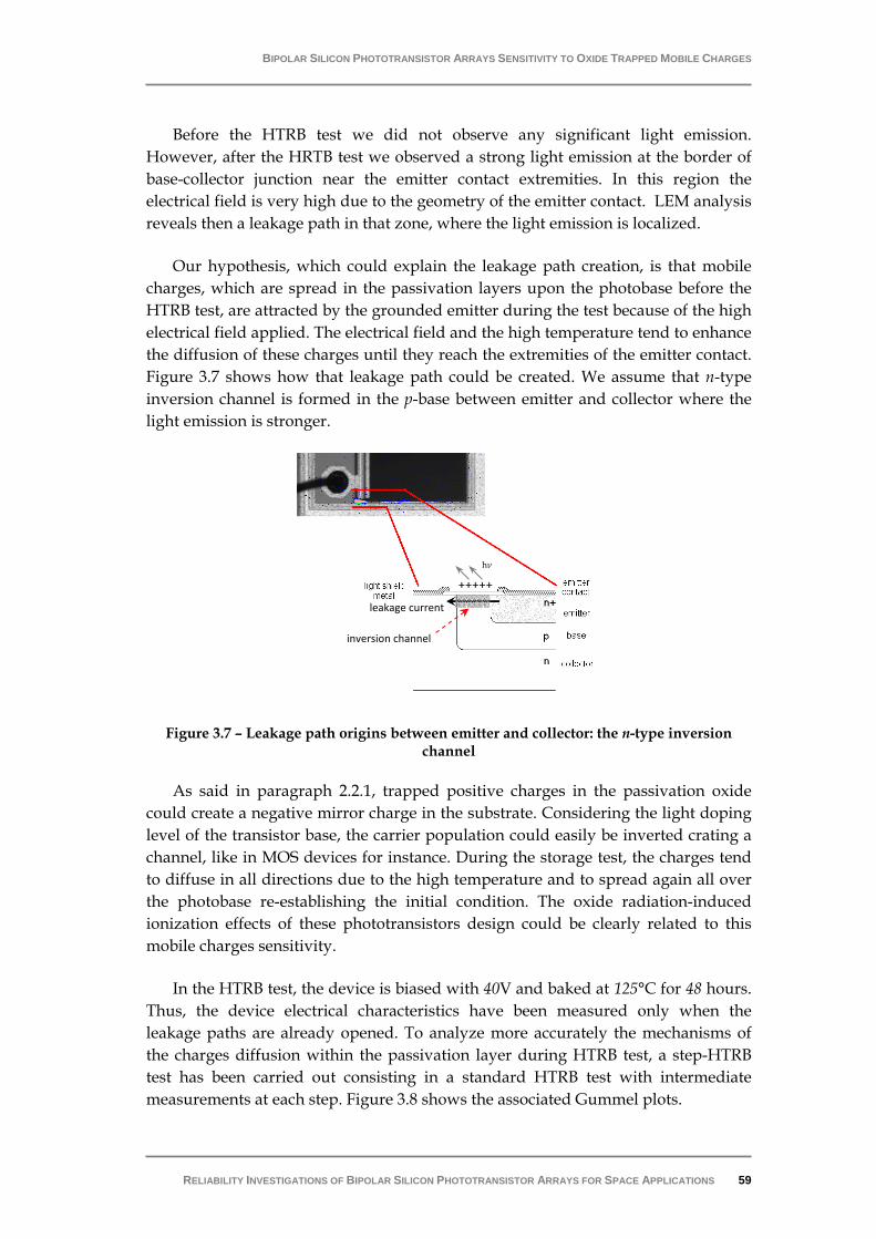
BIPOLAR SILICON PHOTOTRANSISTOR ARRAYS SENSITIVITY TO OXIDE TRAPPED MOBILE CHARGES
RELIABILITY INVESTIGATIONS OF BIPOLAR SILICON PHOTOTRANSISTOR ARRAYS FOR SPACE APPLICATIONS 59
Before the HTRB test we did not observe any significant light emission. However, after the HRTB test we observed a strong light emission at the border of base-collector junction near the emitter contact extremities. In this region the electrical field is very high due to the geometry of the emitter contact. LEM analysis reveals then a leakage path in that zone, where the light emission is localized.
Our hypothesis, which could explain the leakage path creation, is that mobile charges, which are spread in the passivation layers upon the photobase before the HTRB test, are attracted by the grounded emitter during the test because of the high electrical field applied. The electrical field and the high temperature tend to enhance the diffusion of these charges until they reach the extremities of the emitter contact. Figure 3.7 shows how that leakage path could be created. We assume that n-type inversion channel is formed in the p-base between emitter and collector where the light emission is stronger.
Figure 3.7 – Leakage path origins between emitter and collector: the n-type inversion channel
As said in paragraph 2.2.1, trapped positive charges in the passivation oxide could create a negative mirror charge in the substrate. Considering the light doping level of the transistor base, the carrier population could easily be inverted crating a channel, like in MOS devices for instance. During the storage test, the charges tend to diffuse in all directions due to the high temperature and to spread again all over the photobase re-establishing the initial condition. The oxide radiation-induced ionization effects of these phototransistors design could be clearly related to this mobile charges sensitivity.
In the HTRB test, the device is biased with 40V and baked at 125°C for 48 hours. Thus, the device electrical characteristics have been measured only when the leakage paths are already opened. To analyze more accurately the mechanisms of the charges diffusion within the passivation layer during HTRB test, a step-HTRB test has been carried out consisting in a standard HTRB test with intermediate measurements at each step. Figure 3.8 shows the associated Gummel plots.
+++++
leakage current
inversion channel
hν
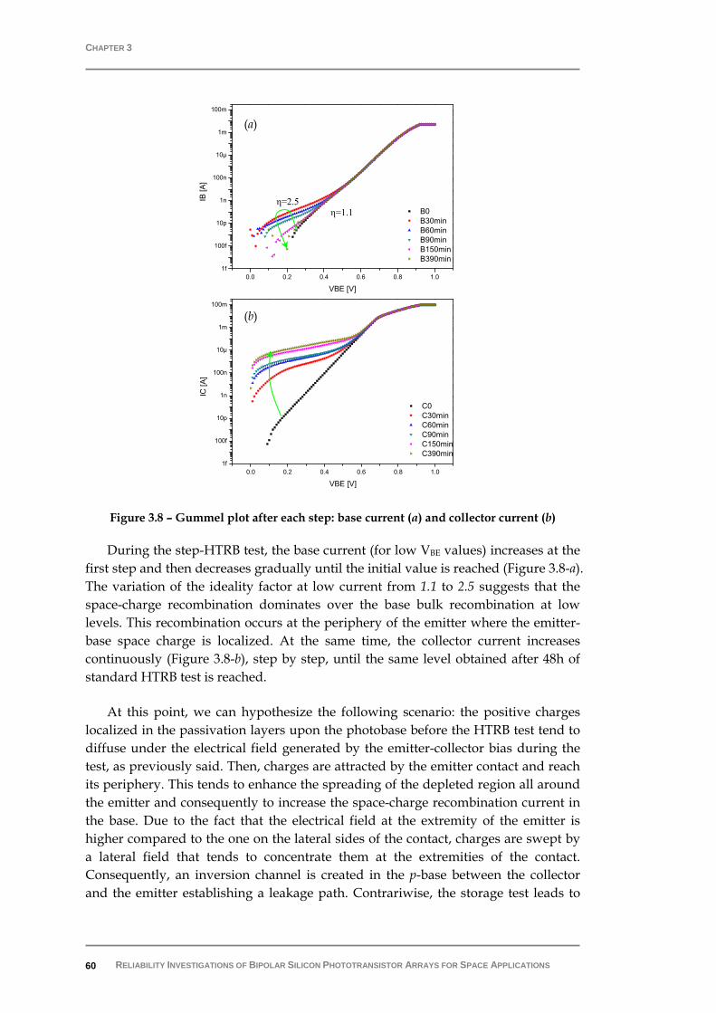
CHAPTER 3
RELIABILITY INVESTIGATIONS OF BIPOLAR SILICON PHOTOTRANSISTOR ARRAYS FOR SPACE APPLICATIONS 60
Figure 3.8 – Gummel plot after each step: base current (a) and collector current (b)
During the step-HTRB test, the base current (for low VBE values) increases at the first step and then decreases gradually until the initial value is reached (Figure 3.8-a). The variation of the ideality factor at low current from 1.1 to 2.5 suggests that the space-charge recombination dominates over the base bulk recombination at low levels. This recombination occurs at the periphery of the emitter where the emitter-base space charge is localized. At the same time, the collector current increases continuously (Figure 3.8-b), step by step, until the same level obtained after 48h of standard HTRB test is reached.
At this point, we can hypothesize the following scenario: the positive charges localized in the passivation layers upon the photobase before the HTRB test tend to diffuse under the electrical field generated by the emitter-collector bias during the test, as previously said. Then, charges are attracted by the emitter contact and reach its periphery. This tends to enhance the spreading of the depleted region all around the emitter and consequently to increase the space-charge recombination current in the base. Due to the fact that the electrical field at the extremity of the emitter is higher compared to the one on the lateral sides of the contact, charges are swept by a lateral field that tends to concentrate them at the extremities of the contact. Consequently, an inversion channel is created in the p-base between the collector and the emitter establishing a leakage path. Contrariwise, the storage test leads to
0.0 0.2 0.4 0.6 0.8 1.01f
100f
10p
1n
100n
10µ
1m
100m
B0 B30min B60min B90min B150min B390min
IB [A
]
VBE [V]
(a)
η=2.5 η=1.1
0.0 0.2 0.4 0.6 0.8 1.01f
100f
10p
1n
100n
10µ
1m
100m
C0 C30min C60min C90min C150min C390min
IC [A
]
VBE [V]
(b)

BIPOLAR SILICON PHOTOTRANSISTOR ARRAYS SENSITIVITY TO OXIDE TRAPPED MOBILE CHARGES
RELIABILITY INVESTIGATIONS OF BIPOLAR SILICON PHOTOTRANSISTOR ARRAYS FOR SPACE APPLICATIONS 61
spread the charges throughout in the phototransistor and to re-establish the initial state.
In order to confirm these hypotheses we performed some simulations with a SPICE-like simulation tool. The leakage path has been simulated by a discrete MOSFET between emitter and collector of phototransistor, as shown in the schematic in Figure 3.9. Some parameters of the phototransistor Gummel-Poon model (phtmic in the figure) are extracted from the Gummel plot and from the I-V characteristics. The MOSFET parameters are calculated on the basis of device dimensions. These parameters are not all the needed ones to obtain an accurate model but are adequate for a qualitative evaluation of the device behaviour.
Figure 3.9 – SPICE schematic of Phototransistor with parasitic MOSFET
In Figure 3.10, a comparison between the simulated and measured Gummel plots is shown. We note that the simulation curves fit well the experimental ones in both the ideal and the non-ideal regions of Gummel plot.
Figure 3.10 – Comparison between simulated and measured Gummel-plots
0.0 0.2 0.4 0.6 0.8 1.010f
1p
100p
10n
1µ
100µ
10m
1
Ic Experimental Data Simulation Data
Ib Experimental Data Simulation Data
Ic, I
b [A
]
Vbe [V]

CHAPTER 3
RELIABILITY INVESTIGATIONS OF BIPOLAR SILICON PHOTOTRANSISTOR ARRAYS FOR SPACE APPLICATIONS 62
As said, positive charges, which are trapped into the base passivation in the region between collector and emitter during the HTRB test, create the inversion channel simulated by the MOSFET in the schematic in Figure 3.9. The charge concentration is simulated by a positive bias applied to the gate of that MOSFET. The good agreement between the simulated leakage behaviour and the real one is presented in Figure 3.11-a. We already have shown that after HTRB test also the Gummel-plot reveals the presence of leakage collector current. The comparison between the simulated and the measured Gummel-plots presented in Figure 3.11-b confirms the simulation-experiment agreement.
Figure 3.11 –Comparison between simulated and measured Collector-Emitter leakage (a) and simulated and measured post-HTRB test Gummel-plots (b)
In conclusion, we demonstrated that a large batch of ETIC-Honeywell BPSA is highly sensitive to oxide trapped charges. But, in this case, and more in general in the case of COTS components, the re-design of device was not foreseen. Thus, we had to develop a screening strategy to select devices that do not present these problems at all or, at least, that are less sensitive in order to qualify them for PLEIADES mission. In the following paragraph, such methodology will be presented.
0.0 0.2 0.4 0.6 0.8 1.010f
1p
100p
10n
1µ
100µ
10m
1
Simulated: IC IB
Experimental: IC IB
I C, I
B [A
]
VBE [V]
0.0 0.5 1.0 1.5 2.0
0
5µ
10µ
15µ
20µ
25µ
30µ
Simulated Experimental
I C [A
]
VCE [V]
(a)
(b)

BIPOLAR SILICON PHOTOTRANSISTOR ARRAYS SENSITIVITY TO OXIDE TRAPPED MOBILE CHARGES
RELIABILITY INVESTIGATIONS OF BIPOLAR SILICON PHOTOTRANSISTOR ARRAYS FOR SPACE APPLICATIONS 63
3.2 MOBILE CHARGES SENSITIVITY CHECK METHODOLOGY
As discussed in the previous paragraphs, the presence of mobiles charges in the passivation layers, that causes ETIC-Honeywell devices instabilities, has been confirmed. These instabilities have been revealed after the long duration life-test performed in the framework of the qualification program.
In next paragraphs, an original timesaving methodology is proposed with two objectives: the selection of new wafers for flight models manufacturing and the prediction of photocurrent degradation during life-test. This method (called Ramp Test) is derived from isochronal annealing experiments.
3.2.1 FROM ISOCHRONAL ANNEALING TO THE RAMP TEST
In order to analyze the transport and the trap/release phenomena of mobile charges in the Si/SiO2 system a single isochronal annealing is done[58, 59, 60]. An isochronal anneal consists of a succession of temperature steps of fixed duration typically ranging from room temperature to a maximum temperature by fixed temperature intervals. Between each high temperature step, the sample is cooled down to room temperature for electrical characterization. We performed such test on ETIC-Honeywell devices in the following conditions:
• Temperature range: 20°C to 220°C • Temperature step: 20°C • Step duration: 6 minutes • Bias: 5V (VCE).
Figure 3.12 shows the scheme of isochronal annealing test.
Figure 3.12 – Scheme of the isochronal annealing test
equivalent ramp rate: 3.33°C/min
0 10 20 30 40 50 60 700
40
80
120
160
200
240
Tem
pera
ture
[°C
]
Time [min]

CHAPTER 3
RELIABILITY INVESTIGATIONS OF BIPOLAR SILICON PHOTOTRANSISTOR ARRAYS FOR SPACE APPLICATIONS 64
The equivalent ramp rate is 3.33°C/min. The result of this test on few components shows a channel current behaviour as represented in Figure 3.13. The photocurrent of the different channels shows oscillations with the annealing temperature. However, some channels exhibit an abnormal photocurrent drift compared to the other ones. The difference in behaviour between the “normal” and the “anomalous” channels is maximum around 150°C. This behaviour could be compared to the one observed during qualification life-test where some channels also show some oscillations of their associated photocurrent.
Figure 3.13 – Isochronal annealing test results: normalized photocurrent
This led us to assume that the drifts recorded during isochronal annealing are correlated to the life test drifts. In consequence, we can use this method to select the devices for flight models manufacturing. There is an extensive literature on isothermal and isochronal annealing that show how one can predict the isothermal behaviour of interface traps and radiation-induced trapped charge of irradiated devices from a single isochronal test[51, 61-64].
Because a full isochronal annealing is not easy to implement and is time consuming to sort several hundred of devices, a new selection methodology is proposed based on a constant temperature ramp. The slope of this ramp is equivalent to the one used during isochronal annealing with an initial current measurement and a final one when the temperature reaches 150°C. In our tests, the ramp rate was about 2°C/min. In the Figure 3.14 an example of results of ramp test is shown.
0 20 40 60 80 100 120 140 160 180 200 220 240
0.850
0.875
0.900
0.925
0.950
0.975
1.000
1.025
1.050
norm
aliz
ed p
hoto
curr
ent
Temperature (°C)
(ramp rate = 3,33°C/min)
“anomalous” channels

BIPOLAR SILICON PHOTOTRANSISTOR ARRAYS SENSITIVITY TO OXIDE TRAPPED MOBILE CHARGES
RELIABILITY INVESTIGATIONS OF BIPOLAR SILICON PHOTOTRANSISTOR ARRAYS FOR SPACE APPLICATIONS 65
Figure 3.14 – Ramp test results example: a normal device without photocurrent drifts (a); a device that presents irregular photocurrent drifts (b)
Different responses to ramp test of some phototransistor belonging to the same array clearly indicate a different impact of mobile charges. On the other hand, the light degradation (about -3%) exhibited by all channels in device in (a) and six channels out of eight in device in (b) indicates the same light sensitivity to mobile charges. Contrariwise, the two highly degraded channels of device in (b) are largely affected by that sensitivity, so the whole BSPA can not be qualified because it could exhibit photocurrent drifts during ageing tests.
Thus, the last point is to demonstrate that there is a correlation between the Ramp Test and the life-test drifts. So, we performed two temperature/bias ageing tests at CNES and at Microtel on another batch of ETIC-Honeywell BSPA. In Figure 3.15 we report the maximum life-test photocurrent drifts as a function of the ramp test drifts. We clearly observe a correlation between the life-test and the ramp test drifts. Data are relative to CNES session of life-test.
Figure 3.15 – Life test maximum drifts vs. ramp test drifts (CNES test session)
0% 10% 20% 30% 40% 50% 60%
0%
20%
40%
60%
80%
100%
120%
140%
Life
Test
MAX
Drif
t
Ramp Test Drift
0 20 40 60 80 100 120 140 1600.65
0.70
0.75
0.80
0.85
0.90
0.95
1.00
1.05
Nor
mal
ized
Pho
tocu
rrent
Temperature [°C]
ch1 ch2 ch3 ch4 ch5 ch6 ch7 ch8
0 20 40 60 80 100 120 140 1600.65
0.70
0.75
0.80
0.85
0.90
0.95
1.00
1.05
N
orm
aliz
ed P
hoto
curre
nt
Temperature [°C]
ch1 ch2 ch3 ch4 ch5 ch6 ch7 ch8
(a) (b)

CHAPTER 3
RELIABILITY INVESTIGATIONS OF BIPOLAR SILICON PHOTOTRANSISTOR ARRAYS FOR SPACE APPLICATIONS 66
In Figure 3.16 is shown the correlation between the tests after one thousand hours of life-test performed at Microtel’s.
Figure 3.16 – Life test vs. ramp test at Microtel’s
Our work concludes that Temperature Ramp Test current drifts are well correlated to the degradations observed during life-test. So, such test could be very fruitful to rapidly assess the degradation of bipolar microcircuits during life-test. We consider that the use of this method could be generalized in the screening sequence of devices likely to be affected by mobile charges, in particular bipolar and MOS devices.
The studies presented in the first part of this third chapter have put in evidence that charges and impurities trapped into passivation layers or the intrinsic quality of that passivation could affect BPSA reliability. We also demonstrated that the ETIC-Honeywell devices are largely affected by the sensitivity to mobile charges, so those BSPA can not be qualified for space missions. As a consequence, CNES has actively looked for a European phototransistor arrays manufacturer that could guarantee devices performances and reliability. As anticipated in the first chapter, that one was found in Optoi (Italy). Optoi devices were developed in agreement with CNES and on the basis of their know-how and results obtained after our studies.
IMS Laboratory, in close collaboration with industrial and academic partners, is deep involved in developing new original methodologies for reliability assessment. In particular, they are turned to an “active” approach to reliability, the so-called built-in reliability. According to this approach, high reliability basis must be integrated, as early as possible, at the beginning of the device development[65]. In the next section, we will discuss about the activities performed at IMS in order to achieve the built-in reliability of the Optoi BSPA, in close collaboration with CNES and with a continuous feedback with the manufacturer.
0% 10% 20% 30%0%
10%
20%
30%
40%
Life
Tes
t MAX
Drif
t
Ramp Test Drift

BIPOLAR SILICON PHOTOTRANSISTOR ARRAYS SENSITIVITY TO OXIDE TRAPPED MOBILE CHARGES
RELIABILITY INVESTIGATIONS OF BIPOLAR SILICON PHOTOTRANSISTOR ARRAYS FOR SPACE APPLICATIONS 67
3.3 EMERGING OPTOI TECHNOLOGIES
In paragraph 1.2.2, we have described Optoi phototransistors arrays. In the context of the built-in reliability achievement, several successive Optoi BSPA designs have been submitted to pre-evaluation plans. To this purpose, specific ageing tests based on temperature/bias stresses have been conducted at the IMS Laboratory. At the beginning, 40V bias was applied, but first test results let us to consider it too much severe. So, another life-test with a lower applied bias, that was 20V, has been performed on another device batch. We conducted also a storage test on several devices after both the 40V and 20V life-tests, an isochronal annealing on virgin devices, a specific step test at different temperatures and voltages, and a 20V-125°C life-test on specific devices in special Optoi package. Thanks to results obtained during these testing activities, new designs have been developed. These activities and main results will be described in the following.
In parallel to that pre-evaluation phase, we conduced radiation hardness evaluation tests including both gamma and proton irradiations. These tests were globally satisfactory, but they are still ongoing. Moreover, an irradiation DoE plan, which will be described in the chapter four, will be applied to Optoi devices.
3.3.1 FIRST DESIGN PRE-EVALUATION ACTIVITIES
We submitted the first Optoi BSPA design run to a pre-evaluation plan. This first run is described shortly in the following. Devices under test come from three different wafers, named #1, #2, and #3. Wafers #1 and #2 are about 500μm thick and wafer #3 is about 300μm thick (thinned wafer). In all wafers, the oxide is 450nm thick. A lightly-doped n epitaxial layer (Phosphorous, 2·1014 cm-3) of about 10-15μm is processed on the substrate that is n+-doped (Antimony, 1018–5·1018cm-3). Figure 3.17 illustrate e schematic cross sectional view of a single channel of Optoi BPSA.
Figure 3.17 – Cross sectional view representation of a single Optoi phototransistor
Wafers differ in emitter doping level that was tuned to achieve different levels of electrical transistor gain. Different device layouts have been implemented by varying the antireflective coating, the emitter area, and the light metal shield. This
10-15μm
450nm
300-500μm
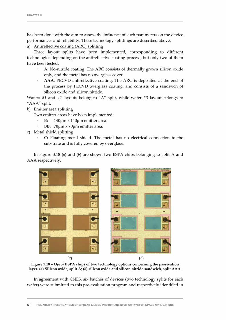
CHAPTER 3
RELIABILITY INVESTIGATIONS OF BIPOLAR SILICON PHOTOTRANSISTOR ARRAYS FOR SPACE APPLICATIONS 68
has been done with the aim to assess the influence of such parameters on the device performances and reliability. These technology splittings are described above. a) Antireflective coating (ARC) splitting
Three layout splits have been implemented, corresponding to different technologies depending on the antireflective coating process, but only two of them have been tested.
A: No-nitride coating. The ARC consists of thermally grown silicon oxide only, and the metal has no overglass cover.
AAA: PECVD antireflective coating. The ARC is deposited at the end of the process by PECVD overglass coating, and consists of a sandwich of silicon oxide and silicon nitride.
Wafers #1 and #2 layouts belong to “A” split, while wafer #3 layout belongs to “AAA” split. b) Emitter area splitting
Two emitter areas have been implemented: B: 140μm x 140μm emitter area. BB: 70μm x 70μm emitter area.
c) Metal shield splitting C: Floating metal shield. The metal has no electrical connection to the
substrate and is fully covered by overglass.
In Figure 3.18 (a) and (b) are shown two BSPA chips belonging to split A and AAA respectively.
Figure 3.18 – Optoi BSPA chips of two technology options concerning the passivation
layer. (a) Silicon oxide, split A; (b) silicon oxide and silicon nitride sandwich, split AAA.
In agreement with CNES, six batches of devices (two technology splits for each wafer) were submitted to this pre-evaluation program and respectively identified in
(a) (b)

BIPOLAR SILICON PHOTOTRANSISTOR ARRAYS SENSITIVITY TO OXIDE TRAPPED MOBILE CHARGES
RELIABILITY INVESTIGATIONS OF BIPOLAR SILICON PHOTOTRANSISTOR ARRAYS FOR SPACE APPLICATIONS 69
the following by: W#1–ABC, W#1–ABBC, W#2–ABC, W#2–ABBC, W#3–AAABC, and W#3–AAABBC.
The Table 3.1 summarizes the main technological parameters of devices under test issued from all wafers.
W#1 W#2 W#3 Emitter Area 140x140μm 70x70μm 140x140μm 70x70μm 140x140μm 70x70μm Wafer Thickness 500μm 500μm 300μm (thinned) Bulk resistivity (n+ type) 8-25 mΩ·cm EPI layer thickness 10-16μm EPI layer resistivity (n type) 10-16 Ω·cm P implant sheet resistance 208 Ω/square N+ implant sheet resistance 110 Ω /□ 94 Ω /□ P contact resistance 6.9 Ω 6 Ω 7.1 Ω N contact resistance 2.8 Ω 2.9 Ω 3 Ω Gain (Hfe) 692±29 617±37.6 716±29.2 664±41.4 677±29 595±32.3 leakage Current [A] 841p±300p 681p±160p 1.09n±510p 867p±3.510p 844p±270p 1.14n±820p
Table 3.1 – Technological parameters of first run of Optoi BSPA
The Pre-Evaluation tests program is detailed in the following Figure 3.19 consisting in three groups of tests:
• isochronal annealing • thermal/voltage life-test • protons and γ-ray irradiations. The radiation testing activities will not be discussed in this manuscript but an
overview on their main results will be shortly presented for completeness. To these tests, a specific step-test was added, as will be described in the following.
Figure 3.19 – Pre-Evaluation tests program scheme
Isochronal Annealing test results
The isochronal annealing on two devices per technology option was performed as described in paragraph 3.2.1. The temperature range was from 20°C up to 200°C with a step of 20°C. During the annealing, a fixed collector-emitter bias of 5V was
Pre-Evaluation Program
336h Life-test (40V – 125°C)
336h Life-test (20V – 125°C)
Isochronal Annealing
γ -ray and p+ irradiations
Step-test (10-15V – 85-125°C)

CHAPTER 3
RELIABILITY INVESTIGATIONS OF BIPOLAR SILICON PHOTOTRANSISTOR ARRAYS FOR SPACE APPLICATIONS 70
applied. The collector current is measured at room temperature between each annealing step at fixed illumination. Results are plotted in the following Figure 3.20.
Figure 3.20 – Devices photocurrent variations during isochronal annealing. Graphs are
relative to all wafers and all technology splits
This test highlights that for all wafers the temperature starts to impact on performances after the last annealing step, i.e. when it is higher than 180°C. Higher photocurrent variations are registered in both wafers #1 and #2, split ABC. Moreover, wafer #3–AAABBC devices photocurrent starts to vary at a lower temperature, around 100-120°C. We can also note that some channels have demonstrated both positive and negative drifts of photocurrent.
0 20 40 60 80 100 120 140 160 180 200 220-80
-70
-60
-50
-40
-30
-20
-10
0
10
0 20 40 60 80 100 120 140 160 180 200 220
-6
-4
-2
0
2
Pht
ocur
rent
Var
iatio
n (%
)
Temperature (°C)
W8 ABC
0 20 40 60 80 100 120 140 160 180 200 220-80
-70
-60
-50
-40
-30
-20
-10
0
10
0 20 40 60 80 100 120 140 160 180 200 220
-4
-2
0
2
4
6
8
10
Pht
ocur
rent
Var
iatio
n (%
)
Temperature (°C)
W8 ABBC
(W#1–ABC) (W#1–ABBC)
(W#2–ABBC) (W#2–ABC)
(W#3–AAABC)
0 20 40 60 80 100 120 140 160 180 200 220-80
-70
-60
-50
-40
-30
-20
-10
0
10
0 20 40 60 80 100 120 140 160 180 200 220
-4
-2
0
2
Pht
ocur
rent
Var
iatio
n (%
)
Temperature (°C)
W11 AAABC
0 20 40 60 80 100 120 140 160 180 200 220-80
-70
-60
-50
-40
-30
-20
-10
0
10
Phto
curr
ent V
aria
tion
(%)
Temperature (°C)
W12 ABC
0 20 40 60 80 100 120 140 160 180 200 220-80
-70
-60
-50
-40
-30
-20
-10
0
10
0 20 40 60 80 100 120 140 160 180 200 220
-2
0
2
4
6
Pht
ocur
rent
Var
iatio
n (%
)
Temperature (°C)
W12 ABBC
(W#3–AAABBC)
0 20 40 60 80 100 120 140 160 180 200 220-80
-70
-60
-50
-40
-30
-20
-10
0
10
0 20 40 60 80 100 120 140 160 180 200 220-15-10
-505
101520253035
Phto
curr
ent V
aria
tion
(%)
Temperature (°C)
W11 AAABBC

BIPOLAR SILICON PHOTOTRANSISTOR ARRAYS SENSITIVITY TO OXIDE TRAPPED MOBILE CHARGES
RELIABILITY INVESTIGATIONS OF BIPOLAR SILICON PHOTOTRANSISTOR ARRAYS FOR SPACE APPLICATIONS 71
On the whole, the isochronal annealing test shows a weak sensitivity of Optoi BSPA to this test. In any case, due to the photocurrent variations on some channels, even if of low level and at high temperatures, we can assume a low sensitivity to mobile charges. Moreover, “BB” option shows the highest photocurrent variations. This fact, which is in agreement with ionizing dose test results (see further in this section), tends to confirm suspects on passivation trapped charges.
Temperature/Bias ageing tests results
We have conducted three types of accelerated life test. At first, a “40V” test was conducted on a first batch of devices, but, because of first 48 hours results, it was stopped because 40V bias appeared to be too severe regarding photocurrent variations. Hence, a 20V-life-test was conducted on all technology splits. Because of results of this test, we performed another specific step life-test in order to evaluate the real impact of voltage and temperature coupled and separately. All these tests and their results are described and discussed in the following.
The accelerated life-test conditions were originally planned to be 40V of bias applied on transistor collector, RLOAD of 10kΩ between emitter and the ground, 125°C in the darkness, and 336 hours duration with intermediate measurements at 48h and 168h. The monitored parameters were the photocurrent and darkness current. This first test was conducted on devices from wafer #1 split ABBC and from both splits of wafer #2. The first step results of this test are presented in the following Figure 3.21 and Figure 3.22.
Figure 3.21 – Photocurrent variations after 48h of life-test (40V, 125°C)
0 10 20 30 40 50
-500
0
500
1000
1500
Pho
tocu
rren
t var
iatio
ns (%
)
Time (h)
0 10 20 30 40 50
-500
0
500
1000
1500
Pho
tocu
rren
t var
iatio
ns (%
)
Time (h)
W#1–ABBC
W#2–ABBC
W#2–ABC
0 10 20 30 40 50
-500
0
500
1000
1500
Pho
tocu
rren
t var
iatio
ns (%
)
Time (h)
Average + 3σ Average – 3σ

CHAPTER 3
RELIABILITY INVESTIGATIONS OF BIPOLAR SILICON PHOTOTRANSISTOR ARRAYS FOR SPACE APPLICATIONS 72
Figure 3.22 – Increase of darkness leakage current after test (48h, 40V, 125°C)
Variations of photocurrent at fixed illuminating level after test are presented in Figure 3.21. Higher variations are registered on wafer #1. Figure 3.22 shows the dramatic increase of the leakage darkness current, that is about six decades for almost all devices. This explains the photocurrent variations for all wafer devices. Because of these results, we stopped the test at 48 hours and we considered test conditions too higher for this specific device technology. So, we performed a second ageing test, where the applied voltage was set to 20V. This “20V” life-test was performed on two devices for all technology splits of all three wafers. Figure 3.23, Figure 3.24, and Figure 3.25 show the main results concerning photocurrent. In spite of the lower applied bias, photocurrent variations are still high.
Figure 3.23 – Photocurrent variations after 48h of test under 20V and 125°C (W#1)
0 10 20 30 40 501p
10p
100p
1n
10n
100n
1µ
10µ
100µ
1mD
arkn
ess
Cur
rent
(A)
Time (h)
0 10 20 30 40 501p
10p
100p
1n
10n
100n
1µ
10µ
100µ
1m
Dar
knes
s C
urre
nt (A
)
Time (h)
W#1–ABBC W#2–ABC
W#2–ABBC
0 10 20 30 40 501p
10p
100p
1n
10n
100n
1µ
10µ
100µ
1m
Dar
knes
s C
urre
nt (A
)
Time (h)
0 10 20 30 40 50-200
0
200
400
600
800
1000
0 10 20 30 40 50
0
40
80
120
160
200
240
280
Phot
ocur
rent
var
iatio
ns (%
)
Time (h)
W#1–ABC W#1–ABBC
0 10 20 30 40 50-200
0
200
400
600
800
1000
Pho
tocu
rren
t var
iatio
ns (%
)
Time (h)

BIPOLAR SILICON PHOTOTRANSISTOR ARRAYS SENSITIVITY TO OXIDE TRAPPED MOBILE CHARGES
RELIABILITY INVESTIGATIONS OF BIPOLAR SILICON PHOTOTRANSISTOR ARRAYS FOR SPACE APPLICATIONS 73
Figure 3.24 – Photocurrent variations after 48h of test under 20V and 125°C (W#2)
Figure 3.25 – Photocurrent variations after 48h of test under 20V and 125°C (W#3)
Wafer #3 devices showed the lowest photocurrent variation after “20V” life-test. This behaviour is also seen in darkness current measurements, as shown in the following Figure 3.26, Figure 3.27, and Figure 3.28.
Figure 3.26 – Darkness current measurements: wafer #1 drifts
0 10 20 30 40 50-200
0
200
400
600
800
1000
0 10 20 30 40 50
-30
0
30
60
90
120
Phot
ocur
rent
var
iatio
ns (%
)
Time (h)0 10 20 30 40 50
-200
0
200
400
600
800
1000
0 10 20 30 40 50-20
0
20
40
60
80
Phot
ocur
rent
var
iatio
ns (%
)
Time (h)
W#3–ABC W#3–ABBC
0 10 20 30 40 50-200
0
200
400
600
800
1000Ph
otoc
urre
nt v
aria
tions
(%)
Time (h)0 10 20 30 40 50
-200
0
200
400
600
800
1000
Pho
tocu
rrent
var
iatio
ns (%
)
Time (h)
W#2–ABBCW#2–ABC
0 10 20 30 40 501p
10p
100p
1n
10n
100n
1µ
10µ
100µ
1m
Dar
knes
s C
urre
nt (A
)
Time (h)
W#1–ABC W#1–ABBC
0 10 20 30 40 501p
10p
100p
1n
10n
100n
1µ
10µ
100µ
1m
Dar
knes
s C
urre
nt (A
)
Time (h)

CHAPTER 3
RELIABILITY INVESTIGATIONS OF BIPOLAR SILICON PHOTOTRANSISTOR ARRAYS FOR SPACE APPLICATIONS 74
Figure 3.27 – Darkness current measurements: wafer #2 drifts
In fact, darkness current of devices from wafers #1 and #2 dramatically increases from few hundreds of pico-Amps up to some tenths of micro-Amps. Contrariwise, wafer #3 devices darkness current increases only up to 20nA, for the “B” split, and 10μA for the “BB” one.
Figure 3.28 – Darkness current measurements: wafer #3 drifts
In all life-test versions, we demonstrated that an increase of photocurrent is actually in relation with an increase of leakage darkness current. After test, darkness current is often higher than photocurrent. As shown as example in Figure 3.29, and more clearly in Figure 3.30, the electrical transistor gain did not vary a lot after life-test (Gummel plots refer to the “40V” life test). This means that the transistor action is still present, but the overall device performances are dramatically degraded by the increase of the leakage current. On the whole, the fact that both junctions are not degraded is shown in Figure 3.29-b, where both IC and IB plots do not show variations in junction ideality factors.
0 10 20 30 40 501p
10p
100p
1n
10n
100n
1µ
10µ
100µ
1m
Dar
knes
s C
urre
nt (A
)
Time (h)0 10 20 30 40 50
1p
10p
100p
1n
10n
100n
1µ
10µ
100µ
1m
Dar
knes
s C
urre
nt (A
)
Time (h)
W#3–ABBCW#3–ABC
0 10 20 30 40 501p
10p
100p
1n
10n
100n
1µ
10µ
100µ
1m
Dar
knes
s C
urre
nt (A
)
Time (h)
W#2–ABBC
0 10 20 30 40 501p
10p
100p
1n
10n
100n
1µ
10µ
100µ
1m
Dar
knes
s C
urre
nt (A
)
Time (h)
W#2–ABC

BIPOLAR SILICON PHOTOTRANSISTOR ARRAYS SENSITIVITY TO OXIDE TRAPPED MOBILE CHARGES
RELIABILITY INVESTIGATIONS OF BIPOLAR SILICON PHOTOTRANSISTOR ARRAYS FOR SPACE APPLICATIONS 75
Figure 3.29 – Gummel plots on the same device: VCE = 2V (a) and VBC = 0V (b). Dotted curves are collector and base currents measured before life-test. Solid line curves
represent after-test measurements.
Figure 3.30 – β measurements before and after test (ref. Figure 3.29)
Definitely, both “40V” and “20V” life-tests revealed a high sensitivity of this first Optoi phototransistor design to both voltage and temperature constraints. That sensitivity appears to be similar to that one observed on Etic-Honeywell devices. For this reason, we performed on W#1 and W#2 devices issued from both ageing tests a storage test, with no bias applied and at the same temperature. This allowed us to assess the mobile charges sensitivity. In fact, as results presented in Figure 3.31 and Figure 3.33 demonstrate that sensitivity, at least on a batch of devices.
The results of both storage tests show that wafer #1 devices of both splits regain the initial conditions after the test. Only wafer #2 split “BB” devices show the same behaviour. Contrariwise, on split “B” devices we observed two different tendencies. A first batch of channels shows an increase of photocurrent after the life test and a decrease till levels lower than initial after storage. In the second group, photocurrents decrease during life test and that tendency continues during storage. This has been observed in both ageing tests. So, excluding W#2–ABC devices,
0.0 0.2 0.4 0.6 0.8 1.01f
10f100f
1p10p
100p1n
10n100n
1µ10µ
100µ1m
10m100m
1VBC=0V
IB before I
B after
IC before IC after
VBE [V]
(a) (b)
IC IC
IB IB
0.0 0.2 0.4 0.6 0.8 1.00
100
200
300
400
500
600
700
800
900VBC=0V β before
β after
VBE [V]0.0 0.2 0.4 0.6 0.8 1.0
0
100
200
300
400
500
600
700
800
900VCE=2V
β before β after
β [A
/A]
VBE [V]
0.0 0.2 0.4 0.6 0.8 1.01f
10f100f
1p10p
100p1n
10n100n
1µ10µ
100µ1m
10m100m
1
IB before IB after I
C before
IC after
I B, IC [A
]
VBE [V]
VCE=2V

CHAPTER 3
RELIABILITY INVESTIGATIONS OF BIPOLAR SILICON PHOTOTRANSISTOR ARRAYS FOR SPACE APPLICATIONS 76
because of recovery after storage we can exclude failures deriving from contaminants inside the package. In contrast, this is the typical signature of sensitivity to mobile charges trapped in passivation oxides.
Figure 3.31 – Storage after “40V” life-test results
Figure 3.32 – Wafer #1: storage after “20V” life-test results
initial LT T-Amb Storage H-T Storage
0
300
600
900
1200
1500
Pho
tocu
rrent
Var
iatio
ns [%
]
Steps
W#1-ABBC
initial LT T-Amb Storage H-T Storage-100
-50
0
50
100
150
200
250
300
Steps
W#2-ABC
initial LT T-Amb Storage H-T Storage
0
300
600
900
Pho
tocu
rren
t Var
iatio
ns [%
]
Steps
W#2-ABBC
initial LT T-Amb Storage H-T Storage-50
0
50
100
150W#1-ABC
Pho
tocu
rrent
Var
iatio
ns [%
]
Stepsinitial LT T-Amb Storage H-T Storage
0
300
600
900
1200
1500W#1-ABBC
Steps

BIPOLAR SILICON PHOTOTRANSISTOR ARRAYS SENSITIVITY TO OXIDE TRAPPED MOBILE CHARGES
RELIABILITY INVESTIGATIONS OF BIPOLAR SILICON PHOTOTRANSISTOR ARRAYS FOR SPACE APPLICATIONS 77
Figure 3.33 – Wafer #2: storage after “20V” life-test results
The results of both storage tests show that wafer #1 devices of both splits regain the initial conditions after the test. Only wafer #2 split “BB” devices show the same behaviour. Contrariwise, on split “B” devices we observed two different tendencies. A first batch of channels shows an increase of photocurrent after the life test and a decrease till levels lower than initial after storage. In the second group, photocurrents decrease during life test and that tendency continues during storage. This has been observed in both ageing tests. So, excluding W#2–ABC devices, because of recovery after storage we can exclude failures deriving from contaminants inside the package. In contrast, this is the typical signature of sensitivity to mobile charges trapped in passivation oxides[55, 66, 67].
The nitride layer wafers, as W#3 is, showed poor mechanical performances since layer delamination was observed. Thus, as nitride AR-coating will not be implemented in next runs, wafer #3 will not be considered in the following.
Temperature/Bias four-step test results
Another important result that has been obtained through the two accelerated ageing tests is related to the fact that the photocurrent degradation level is quite the same in both tests. This means that bias is a secondary cause of degradation, whereas the temperature seems to be the primary one. This has been investigated through a specific four-step test. The following Table 3.2 summarizes that test plan.
Step Number Temperature Voltage
Step 1 85°C 15V Step 2 85°C 10V Step 3 125°C 15V Step 4 125°C 10V
Table 3.2 – Four-step test plan
initial LT T-Amb Storage H-T Storage
-100
0
100
200
300W#2-ABC
Pho
tocu
rrent
Var
iatio
ns [%
]
Stepsinitial LT T-Amb Storage H-T Storage
0
100
200
300
400
500W#2-ABBC
Steps
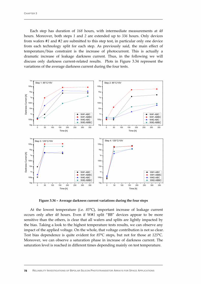
CHAPTER 3
RELIABILITY INVESTIGATIONS OF BIPOLAR SILICON PHOTOTRANSISTOR ARRAYS FOR SPACE APPLICATIONS 78
Each step has duration of 168 hours, with intermediate measurements at 48 hours. Moreover, both steps 1 and 2 are extended up to 336 hours. Only devices from wafers #1 and #2 are submitted to this step test, in particular only one device from each technology split for each step. As previously said, the main effect of temperature/bias constraint is the increase of photocurrent. This is actually a dramatic increase of leakage darkness current. Thus, in the following we will discuss only darkness current-related results. Plots in Figure 3.34 represent the variations of the average darkness current during the four tests.
Figure 3.34 – Average darkness current variations during the four steps
At the lowest temperature (i.e. 85°C), important increase of leakage current occurs only after 48 hours. Even if W#1 split “BB” devices appear to be more sensitive than the others, is clear that all wafers and splits are lightly impacted by the bias. Taking a look to the highest temperature tests results, we can observe any impact of the applied voltage. On the whole, that voltage contribution is not so clear. Test bias dependence is quite evident for 85°C steps, but not for those at 125°C. Moreover, we can observe a saturation phase in increase of darkness current. The saturation level is reached in different times depending mainly on test temperature.
0 50 100 150 200 250 300 35010p
100p
1n
10n
100n
1µ
10µ
100µ
1mStep 3: 125°C/15V
Dar
knes
s C
urre
nt [A
]
Time [h]
W#1-ABC W#1-ABBC W#2-ABC W#2-ABBC
0 50 100 150 200 250 300 35010p
100p
1n
10n
100n
1µ
10µ
100µ
1mStep 4: 125°C/10V
Time [h]
W#1-ABC W#1-ABBC W#2-ABC W#2-ABBC
0 50 100 150 200 250 300 35010p
100p
1n
10n
100n
1µ
10µ
100µ
1m
Dar
knes
s C
urre
nt [A
]
Time [h]
W#1-ABC W#1-ABBC W#2-ABC W#2-ABBC
Step 1: 85°C/15V
0 50 100 150 200 250 300 35010p
100p
1n
10n
100n
1µ
10µ
100µ
1mStep 2: 85°C/10V
Time [h]
W#1-ABC W#1-ABBC W#2-ABC W#2-ABBC

BIPOLAR SILICON PHOTOTRANSISTOR ARRAYS SENSITIVITY TO OXIDE TRAPPED MOBILE CHARGES
RELIABILITY INVESTIGATIONS OF BIPOLAR SILICON PHOTOTRANSISTOR ARRAYS FOR SPACE APPLICATIONS 79
Protons and γ-ray irradiations results overview
Proton irradiation was performed on three devices per technology option in the darkness and without biasing with 60MeV energy protons. The displacement dose is 2.5·108MeV/g. After test we can conclude that W#3 devices show the higher degradation with a variation of channel photocurrent of about -45%. Wafers #1 and #2 devices photocurrents were less degraded, with a worst case variation of -12% and -25% respectively.
Also for the ionizing dose test, three devices from each batch have been irradiated “biased” at the dose rate of 50rad/h up to 9.5krad of total dose. This test revealed that “BB” option devices are more sensitive to ionizing radiation than the “B” one. In fact, photocurrent decreases of about 10% and 25% are recorded for “B” and “BB” splits respectively. Contrariwise, darkness current, spectral responsivity shape, and electrical transistor gain appear to be not affected by ionizing radiation.
3.3.2 BPSA TECHNOLOGICAL OPTIMIZATIONS AND PERSPECTIVES
As discussed in previous paragraph, the passivation oxide is clearly suspected to be at the origin of life-test degradations. For this reason, wafers with a new technological option featuring thicker passivation (1000nm) are submitted to evaluation tests. Three different test sessions have been performed. Results demonstrated that photocurrent variations are in the interval of about ±20%, which is less than variation reported after thin-oxide devices tests. Actually, maximum after-test photocurrent variations for 450nm-thick devices were close to +200%. So, we can say that thicker passivation layer could really improve device hardness regarding thermal/voltage ageing tests.
Thanks to results obtained during the pre-evaluation activities, a new design was proposed to CNES. New devices have quite the same technological characteristics of previous design, but different channel layout and improved passivation and metallization layers. Concerning the layout, the main difference is represented by a ring-shaped contact for the emitter aperture enhancing the robustness of the device during the assembling through ball bonding process.
The following Figure 3.35 shows that new layout and both typologies of emitter contacts. Two passivation thicknesses have been implemented for testing purposes, 450nm and 775nm. As previously said, nitride AR-coating has not been implemented and actually the ARC consists of thermally grown silicon oxide only. Two emitter contact types will be implemented, the “filled-in” and the “ring-shaped” oxide aperture:
• In the first one, the emitter metal lays within the whole oxide aperture. The contact area of the oxide aperture makes the device comparable to the “B” split of the previous run (~140x140μm).

CHAPTER 3
RELIABILITY INVESTIGATIONS OF BIPOLAR SILICON PHOTOTRANSISTOR ARRAYS FOR SPACE APPLICATIONS 80
• In the second one the contact for the emitter is ring-shaped. The equivalent contact area of the oxide aperture makes the device comparable to the “BB” split of the previous run, where the contact area was 70x70μm.
Incremental voltage storage test results
Devices belonging to this new design have been aged related to voltage/temperature conditions. This study aims to assess the improved robustness, thanks to the thicker passivation oxide, the emitter contact shape, or both. A bias step-test was planned consisting in three 48-hours-steps of 10, 20, and 30V at the temperature of 125°C. Further 48-hours storage follows the last step.
Figure 3.35 – New design of Optoi BSPA. (a) new channel layout; (b) “ring-shaped” and (c) “filled-in” emitter contact
Results of this test have confirmed the improvements of the overall devices quality especially concerning the darkness current, as presented in Figure 3.36 and in Figure 3.37. In fact, even devices featuring the thin-oxide option showed a darkness current degradation that is in average (of about 100nA after the third step) not as dramatic as previous design had shown. Instead, in thick-oxide devices the darkness current increases significantly less. The maximum recorded value is close to 10nA after the 30V step. This last result is really interesting because that darkness current value is the one accepted as maximum limit after a 48-hours thermal/bias test.
(a)
(b)
(c)
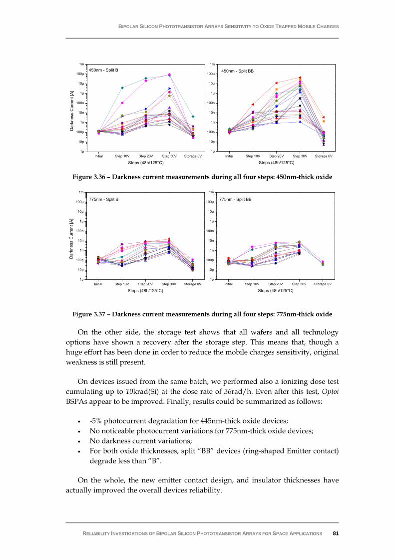
BIPOLAR SILICON PHOTOTRANSISTOR ARRAYS SENSITIVITY TO OXIDE TRAPPED MOBILE CHARGES
RELIABILITY INVESTIGATIONS OF BIPOLAR SILICON PHOTOTRANSISTOR ARRAYS FOR SPACE APPLICATIONS 81
Figure 3.36 – Darkness current measurements during all four steps: 450nm-thick oxide
Figure 3.37 – Darkness current measurements during all four steps: 775nm-thick oxide
On the other side, the storage test shows that all wafers and all technology options have shown a recovery after the storage step. This means that, though a huge effort has been done in order to reduce the mobile charges sensitivity, original weakness is still present.
On devices issued from the same batch, we performed also a ionizing dose test cumulating up to 10krad(Si) at the dose rate of 36rad/h. Even after this test, Optoi BSPAs appear to be improved. Finally, results could be summarized as follows:
• -5% photocurrent degradation for 445nm-thick oxide devices; • No noticeable photocurrent variations for 775nm-thick oxide devices; • No darkness current variations; • For both oxide thicknesses, split “BB” devices (ring-shaped Emitter contact)
degrade less than “B”.
On the whole, the new emitter contact design, and insulator thicknesses have actually improved the overall devices reliability.
Initial Step 10V Step 20V Step 30V Storage 0V1p
10p
100p
1n
10n
100n
1µ
10µ
100µ
1m
775nm - Split B
Dar
knes
s C
urre
nt [A
]
Steps (48h/125°C)Initial Step 10V Step 20V Step 30V Storage 0V
1p
10p
100p
1n
10n
100n
1µ
10µ
100µ
1m
775nm - Split BB
Steps (48h/125°C)
Initial Step 10V Step 20V Step 30V Storage 0V1p
10p
100p
1n
10n
100n
1µ
10µ
100µ
1m
Dar
knes
s C
urre
nt [A
]
Steps (48h/125°C)
450nm - Split B
Initial Step 10V Step 20V Step 30V Storage 0V1p
10p
100p
1n
10n
100n
1µ
10µ
100µ
1m
450nm - Split BB
Steps (48h/125°C)
CHAPTER 3
RELIABILITY INVESTIGATIONS OF BIPOLAR SILICON PHOTOTRANSISTOR ARRAYS FOR SPACE APPLICATIONS 82
Failure mechanisms analysis
The leakage channel creation and the subsequent recovery after the thermal storage are mechanisms already studied and modelled[68, 69]. In fact, improvement in processing conditions, cleanliness, and increased insulator thicknesses (passivation under and over metallization) are steps which were taken to control this mechanism. In the literature, three categories of charges have been identified within the bulk of the SiO2 structure.
• Mobile/ionic charges due to sodium, (Na+) and other alkali elements • Fixed positive charge (surface-state charge) • Interface charges.
The last two categories are strongly dependent on the oxidation process, the crystal orientation of silicon, and the annealing steps. They could affect entire production lots. The surface state charge is characteristic of the Si-SiO2 system. It is believed to be set up by the way the oxidation process terminates the silicon lattice and forms the SiO2 structure. Since it is positive it has a tendency to cause underlying silicon structures to become more n-type. It cannot be moved by use of electric fields or high temperatures and is kept to a minimum by proper processing and annealing. Interface states are energy levels in the silicon band-gap which can capture and emit electrons or holes. These energy levels act as traps exchanging electronic charges with the silicon but not with themselves. These charges are affected by both bias and temperature. As the fixed surface charge, they are controlled by proper processing and annealing.
The structure of silicon dioxide is relatively open allowing movement of alkali metal ions. Sodium (Na+) is one of the most abundant elements and because of its small ionic diameter it moves faster through the oxide than any of the other alkali ions. As result, sodium is the contaminant for the mobile/ionic surcharge degradation mechanism. The Na+, or any other mobile ion, moves toward the Si-SiO2 interface under the influence of a perpendicular electric field. The Si-SiO2 interface acts as a barrier preventing further motion of Na+ and causes a sheet of charge to be set up. This positive charge causes electrons to gather near the top of the silicon surface. As a result the top layers of the p-type silicon look like n-type (inversion). High temperatures and electric fields accelerate the mechanism. A high temperature bake (i.e., 200°C) will remove the instability within a few hours while a high temperature operating life will cause it to reappear. Burn-in can be used for screening. Better cleaning and processing procedures were the immediate corrective actions.
So, globally surface state charges, interface charges, and even smaller amounts of contamination on the surface of SiO2 would cause inversion of the high resistivity p regions of bipolar transistors and formation of channels with leakage currents flowing. Concerning the specific layout of studied phototransistors, the inversion of

BIPOLAR SILICON PHOTOTRANSISTOR ARRAYS SENSITIVITY TO OXIDE TRAPPED MOBILE CHARGES
RELIABILITY INVESTIGATIONS OF BIPOLAR SILICON PHOTOTRANSISTOR ARRAYS FOR SPACE APPLICATIONS 83
the base p-type material gives rise to a leakage channel between collector and emitter region. The solution would be to add around the emitter implant a p+ annular ring (guard ring) which interrupts that channel thus preventing current flow [55].
In this context, a new phototransistor arrays design has been proposed by Optoi, and validated by CNES, implements both thick passivation and the guard ring. In the schematic cross-sectional view shown in Figure 3.38 are highlighted the p+ guard ring surrounding the emitter implant and the ring-shaped emitter contact.
Figure 3.38 – Single channel cross-sectional view of the next phototransistor generation: the thick oxide, the ring-shaped emitter contact, and the channel-stop guard ring (p+
implants)
Conclusions
The main objective of this chapter was to point out on how both the overall quality of passivation layers in bipolar devices and device layout could impact on their performance and reliability. In particular, mobile charges trapped in passivation layers could degrade performances and introduce instabilities during accelerated life tests. We have recalled at first the studies relative to the evaluation of the phototransistors batch provided by Etic-Honeywell, chosen by CNES after the disengagement of the space sector of the previous manufacturer, Optek. For Etic-Honeywell BSPA the sensitivity to oxide trapped charges has been verified. To do that, we performed several kind of temperature/bias ageing tests and electro-optical characterizations. In the first section, we discussed about the performed analyses conducted on Etic-Honeywell devices after the first ageing tests. In fact, recorded photocurrent instabilities induced us to perform specific tests in order to understand the failure origins. A recovery of phototransistor characteristics after zero-bias thermal storage has led us to suspect a problem oxide trapped charges. These caused a dramatic increase of leakage current during ageing tests, from few pico-amps up to tenths of micro-amps. The leakage path has been localized thanks to the LEM analysis. Our hypothesis on passivation mobile charges inducing a parasitic n-channel has been verified and validated using
Guard ring: channel-stop
Base
Collector
Emitter

CHAPTER 3
RELIABILITY INVESTIGATIONS OF BIPOLAR SILICON PHOTOTRANSISTOR ARRAYS FOR SPACE APPLICATIONS 84
electrical simulations under SPICE environment. So, we developed an original device selection methodology based on the observation of the behaviour of fail channels during an isochronal annealing. Thanks to this test, we experimentally found a critical temperature at which the failure occurs, i.e. 150°C for ETIC-Honeywell devices. The proposed methodology is based on a temperature ramp, with the same slope of the isochronal annealing, from ambient temperature up to the founded critical one (i.e. 150°C in our case). Our work concludes that Temperature Ramp Test (TRT) current drifts are well correlated to the degradations observed during life-test and could be very fruitful to rapidly assess the degradation of bipolar microcircuits during life-test. We consider that the use of this method could be generalized in the screening sequence of devices likely to be affected by mobile charges, in particular bipolar and MOS devices.
As discussed in the first chapter, the new European producer of custom BSPA was identified by CNES. According to the built-in reliability approach, the high reliability basis must be integrated, as early as possible, at the beginning of the device development in order to reduce technology optimization times. In this context, pre-evaluation of Optoi phototransistors have followed the studies presented in the first section, analyzing different technological options with respect to the mobile charge sensitivity. These activities are described in the last section of this third chapter. Several different designs have been submitted to successive specific ageing tests based on voltage/temperature stresses at the IMS Laboratory. 40V and 20V ageing tests at the temperature of 125°C have been performed on a device batches featuring all technology options. Both tests highlight a dramatic increase of the phototransistors leakage darkness current. The storage test conduced on several devices after both the 40V and 20V life-tests, has revealed the same behaviour observed on Etic-Honeywell devices: most of all phototransistors recovered their initial characteristics after the storage, indicating the sensitivity to mobile charges effects. BSPA belonging to the new design and featuring a thicker passivation and optimized channel layout have then evaluated. A specific three-step test (10V, 20V, 30V at 125°C) revealed the achieved hardness of the thick-oxide option. The success consists in the fact that devices belonging to that batch attain the darkness current levels lower than 10nA after the third step (30V). Unfortunately, the successive storage test highlights again the mobile charges sensitivity, even less severe. Thus, a third phototransistor design has been studied. The major improvement that has been introduced addresses the guard ring around the emitter implant. This consists in a p+ implant that will prevent the parasitic channel formation in the base region between emitter and collector under the action of trapped charges into the overlying oxide.
In the next and final chapter, we will now point up the application of the DoE methodology to devices qualification for space applications. This approach, which does not need any physical model, combines protons and gamma rays irradiations and provides the engineers with analytical degradation models of the device performance.

RELIABILITY INVESTIGATIONS OF BIPOLAR SILICON PHOTOTRANSISTOR ARRAYS FOR SPACE APPLICATIONS
DOE METHODOLOGY FOR BIPOLAR SILICON PHOTOTRANSISTOR ARRAYS DEGRADATION ESTIMATION IN SPACE ENVIRONMENT
In all scientific experiences, one or more process variables or factors can be deliberately modified in order to investigate the effect the changes have on one or more response parameters. The (statistical) design of experiments (DoE) is an efficient procedure for planning experiments so that the data obtained can be analyzed to yield valid and objective conclusions.
In this last chapter, we are going to illustrate the application of the DoE methodology to devices qualification for space applications. This approach, which does not need any physical model of the device degradation, combines protons and gamma rays irradiations and provides the engineers with analytical degradation models of the device performance.
First of all, we will define the study domain of the environmental constraints, i.e. the displacement and ionizing doses susceptible to impact the device, and the optimized experiments plan. In the frame of Micropac BPSA qualification activities, a batch of that devices has been submitted to that plan as a test vehicle for methodology validation purposes and at the same time to evaluate their hardness toward several space mission profiles mainly by taking into account radiation aspects. Experimental results concerning two testing sessions will be presented. The possibility to optimize the methodology by reducing the total number of experiments is also discussed. Finally, DoE collected data will be analyzed in order to obtain useful information for quality engineers. We will present few examples of that analysis results concerning Micropac BSPA reliability evaluation for space applications.
4.1 DESIGN OF EXPERIMENT APPROACH
Design of Experiments is a structured, organized method for determining the relationship between factors affecting a process and the output of this process[70, 71-76]. This approach is widely deployed in many contexts and for different applications: for example in industrial settings. The primary goal is usually to extract the maximum amount of unbiased information regarding the factors affecting a production process from as few costly observations as possible.

CHAPTER 4
RELIABILITY INVESTIGATIONS OF BIPOLAR SILICON PHOTOTRANSISTOR ARRAYS FOR SPACE APPLICATIONS 86
One of the most critical issues in the domain of the reliability of optoelectronic and electronic devices for space applications is to correctly evaluate their degradation with respect to the constraints of various mission profiles. Indeed, the wide range of satellite missions in LEO (Low Earth Orbit), MEO (Medium Earth Orbit), and GEO (Geostationary Earth Orbit) environments makes the qualification activities very challenging especially when it focuses on with radiation aspects. The correct estimation of the main performance degradation as a function of the total ionizing dose (TID) and the displacement damage dose (DDD) received by the devices in the framework of a specific mission profile remains a problem to overcome. In this context, DoE can represent a helpful and powerful tool to solve this issue.
In this chapter, we put forward a new qualification approach based on this methodology. It combines protons and gamma rays irradiations realized according to an optimized test plan and provides the radiation engineer with analytical degradation models of the device performance. This approach does not need any physical model of the device degradation, which would be very complex to obtain anyway. In addition it does not require any specific knowledge regarding the devices technology which makes it very useful for qualification purposes. The DoE approach has been used in various contexts, but this is, at our knowledge, the first time that this methodology is applied for the prediction of device degradation with respect to the radiation constraints of a potential space mission profile.
4.1.1 STUDY DOMAIN DEFINIT ION
The Total Ionizing Dose (TID) and the Displacement Damage Dose (DDD) represent the two experimental factors used in this test, and they define the study domain. The goal of DoE methodology focuses on determining an empirical relationship that relates device performance to these two factors. This relationship will only be valid within a dose domain called study domain. It is defined by the highest and lowest levels of the two factors and by constraints among the factors. Ionizing dose facilities allow deposing TID between 0.1 and 100krad(Si). Proton facilities allow fluencies between 106 and 109MeV/g and energies of 30MeV and 184MeV. Therefore, the study domain will be partially defined by the two following inequalities:
0.1 krad(Si) 100 krad(Si)TID≤ ≤ (4.1)
and
6 910 MeV/g 10 MeV/gDDD≤ ≤ . (4.2)
This domain allows us to cover the overwhelming majority of orbits and a wide range of equivalent shields.

DOE METHODOLOGY FOR BSPA DEGRADATIONS ESTIMATION IN SPACE ENVIRONMENT
RELIABILITY INVESTIGATIONS OF BIPOLAR SILICON PHOTOTRANSISTOR ARRAYS FOR SPACE APPLICATIONS 87
However, the TID and the DDD deposited by protons within a device are not completely independent. They are defined for a given proton energy and a given fluence by: ( )111.6 10TID LET E−= ⋅ ⋅ ⋅ Φ (4.3) and ( )DDD NIEL E= ⋅ Φ (4.4)
where LET represents the Linear Energy Transfer and NIEL the Non-Ionizing Energy Loss, as already defined in Chapter 2. TID is expressed in krad(Si) while DDD is given in MeV/g when the LET and the NIEL are given in MeV·cm2/g.
This means that is not always possible to deposit any couple (DDD, TID) during a single proton irradiation. So, because the available proton energies are 30MeV and 184MeV, combining equations (4.1), (4.2) and (4.3), (4.4) leads to:
11log( ) log( (184)) log(1.6 10 ) log( (184)) log( )TID LET NIEL DDD−≥ + ⋅ − + (4.5) and 11log( ) log( (30)) log(1.6 10 ) log( (30)) log( )TID LET NIEL DDD−≤ + ⋅ − + (4.6)
where logarithm notation is used to cover the largest dose dynamics. From now, the logarithm of TID and DDD are considered as the real damage factors of the plan of experiments. These two inequalities define a domain in which any couple (DDD, TID) could be deposited by protons whose energy and fluence are the solutions of the system constituted by equations (4.3) and (4.4). This is illustrated in Figure 4.1 where the domain defined by the inequalities (4.5) and (4.6), in which a (DDD, TID) couple could be deposited with protons, is included between the two red lines.
Figure 4.1 – Definition of the “study domain” of the experience plan
5,0 5,5 6,0 6,5 7,0 7,5 8,0 8,5 9,0 9,5 10,0-2,0
-1,5
-1,0
-0,5
0,0
0,5
1,0
1,5
2,0
2,5
Study domain
GEO - 10 years GEO - 20 years LEO - 5 years LEO - 10 years
log(
TID
(kra
d(Si
)))
log(DDD (MeV/g))
"Forbidden" domain
Eq. (4)
Domain in which TID and DDD
could be deposited with protons
only
Eq. (5)
shield thickness
Eq. 4.5
Eq. 4.6

CHAPTER 4
RELIABILITY INVESTIGATIONS OF BIPOLAR SILICON PHOTOTRANSISTOR ARRAYS FOR SPACE APPLICATIONS 88
Moreover, several TID versus DDD curves calculated using the tool OMERE 9 3.2[77] for different mission scenarios (LEO and GEO) and aluminium shield thicknesses are also shown in the same figure. It is worth pointing out that the biggest part of these curves lies within the domain chosen to design our test plan. The area under the bottom line defined by inequality (4.6) represents the “forbidden domain”. In this domain (the patterned area in Figure 4.1), a given couple (DDD, TID) could not be deposited with proton of energy ranging from 30 to 184MeV. Finally the domain (in blue) selected for this test is shown.
The selection of the energy range for proton irradiation has been implemented taking into account several test concerns. First, the presence of a 500µm thickness glass window upon the die for the devices under test imposes to limit the lower limit for the energy beam: in fact, all the protons beams with energies lower than about 8MeV would be stopped by the window, avoiding any impact with the silicon die. Moreover, in order to preserve a good uniformity of the proton beam even at low energies, it was decided to choose the lower limit at 30MeV. In addition to that, we must take into account that the irradiation test facilities have a limited selection range, as already mentioned.
4.1.2 “D-OPTIMAL” PLAN FOR DESIGN OF EXPERIMENTS
Once the variation domain of each factor and the associated constraints are known, a grid has to be constructed in the study domain by taking into account all the combinations of factor levels. This grid should contain only realistic experimental points; that is to say, it should contain points in the allowed study domain. These points form the candidate set. Then, an a priori function that relates the response of the parameter under study to the factors has to be chosen. For this study, we use a polynomial model to approximate the response
( ){ }( ){ } ( ){ }
( ){ } ( ){ } ( ){ }
0 1
2
2 3
2
4 5
log
log log
log log log
R B B DDD
B TID B DDD
B TID B DDD TID
= + ⋅ +
+ ⋅ + ⋅ +
+ ⋅ + ⋅ ⋅
(4.7)
where R is the response of interest (the electro-optical device parameters) and Bi the coefficients of the polynomial. In the following, the polynomial will be in the form of (4.8), in the notation of the used software tool:
2 2( , ) 0R x y Z A x B y C x D y F x y= + ⋅ + ⋅ + ⋅ + ⋅ + ⋅ ⋅ (4.8) 9 OMERE is a free-software dedicated to space environment and radiation effects on electronic devices. This tool has been developed by TRAD (a French SME) with the support of the CNES. OMERE computes the space environment and the radiation effects on electronic equipment in term of dose, displacement damage, single event effect and solar cell degradation.

DOE METHODOLOGY FOR BSPA DEGRADATIONS ESTIMATION IN SPACE ENVIRONMENT
RELIABILITY INVESTIGATIONS OF BIPOLAR SILICON PHOTOTRANSISTOR ARRAYS FOR SPACE APPLICATIONS 89
where log( )x DDD= and log( )y TID= .
Then, we have to select, according to a chosen optimality criterion, the number and placement of most useful experimental points to model the phenomenon. The selection of the experimental points is done by DoE software, the commercial JMP® software[78], according to a chosen optimality criterion that was the D-optimality (described in the following paragraph 4.1.3). Nine experiments were selected by JMP® software, which provides us with the D-optimal plan shown in Figure 4.2.
Figure 4.2 – Nine experiments of D-optimal design proposed by the JMP® software providing the DDD and TID values
As shown in Figure 4.2 only the points number 6 and 9 of the plan could be obtained using with a single proton irradiation only. For the other ones, a complementary ionizing irradiation has to be carried out. So, to achieve the irradiation constraints specified in the test plan a preliminary proton irradiations followed by complementary gamma rays irradiations must be carried out. Taking into account these constraints, we have summarized in Table 4.1 the irradiation conditions corresponding to the test plan given in Figure 4.2.
Proton irradiation conditions Exp.
N° log(TID) log(DDD)
Energy (MeV) Fluence (p/cm2)
Compl. ionizing
dose (krad)
1 -1 6 30 2.3 x10⁸ 0.044 2 0.5 6 30 2.3 x 10⁸ 3.1 3 2 6 30 2.3 x 10⁸ 99.9 4 2 7.5 30 7.2 x 10⁹ 98.3 5 2 9 30 2.3 x 10¹¹ 43.9 6 1.52 9 184 5.4 x 10¹¹ 0 7 0.5 7.5 30 7.24 x 10⁹ 1.39 8 0.381 7.51 30 7.4 x 10⁹ 0.59 9 -0.99 6.49 184 1.63 x 10⁹ 0
Table 4.1 – Irradiation conditions for the calculated plan of experiments
5,0 5,5 6,0 6,5 7,0 7,5 8,0 8,5 9,0 9,5 10,0-2,0
-1,5
-1,0
-0,5
0,0
0,5
1,0
1,5
2,0
2,5
Domain in which TID and DDD
could be deposited with protons
only
9
87
6
543
2
log(
TID
(kra
d(Si
)))
log(DDD (MeV/g))
1

CHAPTER 4
RELIABILITY INVESTIGATIONS OF BIPOLAR SILICON PHOTOTRANSISTOR ARRAYS FOR SPACE APPLICATIONS 90
The appropriate energy-fluence couples were determined using equations (4.3), (4.4) and (4.6). The same dose rate was applied for both protons and Co60 irradiations (17.6krad(Si)/hour). One of the main assumption deals with that the tested devices do not exhibit any Enhanced Low Dose Rate Sensitivity (ELDRS).
Caution has to be taken regarding the secondary effects associated to the gamma rays exposure. In fact, Co60 radiation can also enhance the creation of displacement damage on the devices under test. Gamma rays interact with the shield and/or device materials to produce both photoelectrons and Compton electrons having enough energy to produce displacements. Summers[79] estimated the equivalent 1MeV electron fluence introduced by a Co60 exposure. In addition to that, Tada and Carter[80] defined some empirical rules to rely 1MeV electron fluence to 10MeV protons fluence: a ratio of about 3000 subsists between 1MeV electrons and 10MeV protons fluences. In the context of our study domain, the highest Co60 irradiation is well lower than 1Mrad(Si) and the effects of parasitic displacement damage dose are considered as negligible. Nevertheless, in case of wider study domain regarding ionizing dose, the possibility to use X rays instead of Co60 has to be evaluated in order to limit the generation of parasitic displacement damage dose.
To validate our methodology, we irradiated three additional devices using an experimental simulator of space environment developed by TRAD and CNES that reproduces the differential fluence of energetic protons encountered during the satellite lifespan[81]. It is based on the degradation of a 190MeV-proton beam using several polycarbonate shields of different thickness. Moreover, thanks to the software OMERE, we have calculated the proton differential fluence spectrum for a target mission at 800km Low-Earth-Orbit (LEO) (inclination of 98°) and considering a 7mm-thick spherical aluminium shield. The mission duration has been set to 18 years. Figure 4.3 compares proton differential fluence after shielding calculated using OMERE and simulated at the output of the beam degrader.
Figure 4.3 – Proton differential fluence spectrum calculated with OMERE and simulated
with the beam degrader
0 50 100 150 200108
2x10⁸
3x10⁸
4x10⁸
5x10⁸
calculated with OMERE simulated using the beam degrader
Diff
eren
tial f
luen
ce (M
eV-1cm
-2)
Proton energy (MeV)

DOE METHODOLOGY FOR BSPA DEGRADATIONS ESTIMATION IN SPACE ENVIRONMENT
RELIABILITY INVESTIGATIONS OF BIPOLAR SILICON PHOTOTRANSISTOR ARRAYS FOR SPACE APPLICATIONS 91
The targeted TID and DDD are 9.38krad(Si) and 2.1·108MeV/g respectively while the doses simulated with the beam degrader are 9.32krad(Si) and 1.8·108MeV/g. The TID and DDD values have been used to compare the measured and the predicted results all parameters of interest. The corresponding logarithm values are respectively 0.9694 (log(TID)) and 8.2553 (log(DDD)).
4.1.3 RESPONSE MODELLING AND D-OPTIMALITY CRITERION
This paragraph is dedicated to the description, shortly, the calculations required to determine the coefficients of the polynomial response defined in equations (4.7) and (4.8). As said, this response is modelled by a polynomial whose coefficients are unknowns that must be determined. Performing the experiments reported in Figure 4.2 and in Table 4.1 we can record the experimental response value of the parameter under study. The experimental design results in a system of nine equations (corresponding to nine experiments) and six unknowns (for the six coefficients of the a priori model). This system can be written in a simple way using matrix notation:
exp 9 1 9 6 6 1x x xR X B= ⋅ (4.9)
where expR is the vector corresponding to the nine experimental values of the
response obtained at each point of the plan, B the coefficient vector and X the design matrix which depends on the experimental points used in the design and on the postulated model. That matrix is given by:
,1 ,2 ,3 ,4 ,5 ,69 6 i i i i i ixX X X X X X X= ⎡ ⎤⎣ ⎦ (4.10)
where:
( ){ }( ){ }( ){ }( ){ }( ){ } ( ){ }
,1
,2
,3
2
,4
2
,5
,6
1
log
log
log
log
log log
i
i i
i i
i i
i i
i i i
X
X DDD
X TID
X DDD
X TID
X TID DDD
=
=
=
=
=
= ⋅
(4.11)
where i varies from 1 to 9, and DDD and TID are respectively the displacement damage dose and the total ionizing dose as defined in paragraph 4.1.1.
System of equations (4.10) is overdetermined (more equations than unknowns), it could be solved by a standard Least-Square method. One can demonstrate that:
( ) 1
expT TB X X X R
−= ⋅ ⋅ ⋅ (4.12)

CHAPTER 4
RELIABILITY INVESTIGATIONS OF BIPOLAR SILICON PHOTOTRANSISTOR ARRAYS FOR SPACE APPLICATIONS 92
where TX is the transpose of X and ( )TX X⋅ is called the information matrix.
Designs generated from a computer algorithm, i.e. computer-aided designs, are experimental designs that are generated based on a particular optimality criterion and are generally “optimal” only for a specified model. The design treatment runs that are generated by the algorithms are chosen from an overall candidate set of possible treatment combinations. The candidate set consists of all the possible treatment combinations that one wishes to consider in an experiment. There are various forms of optimality criteria that are used to select the points for a design. One of the most popular criterions is the D-optimality.
These types of computer-aided designs are particularly useful when classical designs do not apply. Unlike standard classical designs such as factorials and fractional factorials, D-optimal design matrices are usually not orthogonal and effect estimates are correlated. These types of designs are always an option regardless of the type of model the experimenter wishes to fit (for example, first order, first order plus some interactions, full quadratic, cubic, etc.) or the objective specified for the experiment (for example, screening, response surface, etc.). D-optimal designs are straight optimizations based on a chosen optimality criterion and the model that will be fit. The optimality criterion used in generating D-optimal designs is one of maximizing TX X⋅ , the determinant of the information matrix. This results in
minimizing the generalized variance of the parameter estimates for the a priori model. Finally, once all the experiments are performed, using equation (4.12) and then the (4.9), one can calculate the response at any point of the study domain.
4.2 EXPERIMENTAL RESULTS
As previously indicated, the proposed DoE plan combines protons and gamma rays irradiations realized according to an optimized test. Two series of irradiation experiences have been conducted on Micropac phototransistors (see paragraph 1.2.2) between November 2008 and Mars 2009 with the procedure of the DoE.
Two specific test conditions have been used:
• the first irradiation was performed on unbiased devices • the second one on biased devices.
For testing purposes, devices have been characterized by three main electro-optical parameters: the channel emitter current under illumination or photocurrent (IPH), the darkness current (IDARK), and the Spectral Responsivity (S(λ)).
Previous studies show that these Micropac phototransistors present a good robustness versus Enhanced Low Dose Rate Sensitivity (ELDRS) phenomenon. This is shown in Figure 4.4, whereas the emitter photocurrent degradation is plotted

DOE METHODOLOGY FOR BSPA DEGRADATIONS ESTIMATION IN SPACE ENVIRONMENT
RELIABILITY INVESTIGATIONS OF BIPOLAR SILICON PHOTOTRANSISTOR ARRAYS FOR SPACE APPLICATIONS 93
versus TID for three different dose rates: 2rad(Si)/h, 10rad(Si)/h and 17.6krad(Si)/h. This limited ELDRS allows us to implement DoE on this device batch and to expect a realistic prediction of the degradation.
Figure 4.4 – -3σ normalized photocurrent versus TID (krad(Si)) for three different dose rates
All the devices used for this study were selected from the same wafer and the same packaging batch, in order to limit a potential technological dispersion between devices.
4.2.1 “UNBIASED” IRRADIATIONS RESULTS
First experiences were conducted in November 2008 on 27 devices (i.e. three devices for each experiment). During those first irradiation activities, i.e. proton and gamma irradiations, devices were not biased and placed in the darkness. Concerning monitored device parameters, at first only photocurrent and the overall darkness current (i.e. the sum of the eight channels darkness currents) were observed. These measurements were conducted at CNES, Toulouse. At IMS Laboratory, single channel darkness currents and Spectral Responsivity (S) were measured in June 2009 after irradiation. The ratio between photocurrents after and before irradiation, IPH/IPH0 (measured by CNES), the IDARK after irradiation, and S represent the responses R that have been used in order to estimate polynomial parameters. As already mentioned, single channel IDARK has been measured at IMS in June 2009. At that time, not all tested devices were available thus only eight experimental points have been used in order to foresee the degradation of the IDARK response. The possibility to reduce the number of experiments down to six maintaining an acceptable estimation error will be discussed further in this chapter. Spectral responsivity has been measured for the eight groups of devices (24 devices) corresponding to eight experimental conditions out of nine. In this case, the wavelength step is set to 50nm and the range is 400-1000nm.
-0,5 0,0 0,5 1,0 1,5 2,0 2,5 3,0 3,5 4,0 4,5 5,0 5,50,0
0,1
0,2
0,3
0,4
0,5
0,6
0,7
0,8
0,9
1,0
1,1
- 3σ
norm
aliz
ed p
hoto
curre
nt
TID (krad(Si))
10 rad(Si)/hour 2 rad(Si)/hour 17.6 krad(Si)/hour
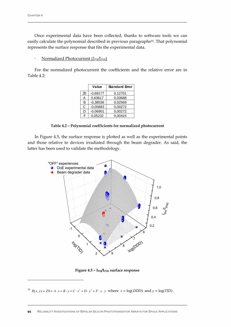
CHAPTER 4
RELIABILITY INVESTIGATIONS OF BIPOLAR SILICON PHOTOTRANSISTOR ARRAYS FOR SPACE APPLICATIONS 94
Once experimental data have been collected, thanks to software tools we can easily calculate the polynomial described in previous paragraphs10. That polynomial represents the surface response that fits the experimental data.
Normalized Photocurrent (IPH/IPH0)
For the normalized photocurrent the coefficients and the relative error are in Table 4.2:
Value Standard Error
Z0 -0,69177 0,12701 A 0,63617 0,03688 B -0,38536 0,02569 C -0,05883 0,00272 D -0,06901 0,00272 F 0,05232 0,00424
Table 4.2 – Polynomial coefficients for normalized photocurrent
In Figure 4.5, the surface response is plotted as well as the experimental points and those relative to devices irradiated through the beam degrader. As said, the latter has been used to validate the methodology.
Figure 4.5 – IPH/IPH0 surface response
10 2 2( , ) 0R x y Z A x B y C x D y F x y= + ⋅ + ⋅ + ⋅ + ⋅ + ⋅ ⋅ where log( )x DDD= and log( )y TID= .
6
7
8
9
-1
0
1
2
0,2
0,4
0,6
0,8
1,0
"OFF" experiences DoE experimental data Beam degrader data
I PH/I PH
0
log(DDD)log(TID)

DOE METHODOLOGY FOR BSPA DEGRADATIONS ESTIMATION IN SPACE ENVIRONMENT
RELIABILITY INVESTIGATIONS OF BIPOLAR SILICON PHOTOTRANSISTOR ARRAYS FOR SPACE APPLICATIONS 95
Thanks to the surface plot in Figure 4.5, we can have a quick overview of the expected degradation of photocurrent for any couple ionizing/displacement doses included in the study domain. Thanks to the obtained polynomial we can easily calculate the normalized photocurrent for the target mission11 , as described in paragraph 4.1.2. Thus, the predicted photocurrents ratio is:
0/ (8.2553,0.9694) 0.531PH PHI I =
Darkness Current (IDARK)
The same calculus gives the polynomial for the overall darkness current. The coefficients and the relative errors are in Table 4.3:
Value Standard Error
Z0 -5,09668E-10 6,78316E-10 A 1,74253E-10 1,9409E-10 B -9,64861E-10 1,5015E-10 C -1,5467E-11 1,41977E-11 D 8,99109E-11 1,42742E-11 F 1,58216E-10 2,39024E-11
Table 4.3 – Polynomial coefficients for darkness current
The expected value for IDARK for the target mission is:
(8.2553,0.9694) 290pDARKI A=
In Figure 4.6, once again the beam degrader data confirm the goodness of prevision provided by calculated polynomial.
In the damage factor domain indicated by the pale grey area surrounded by red dotted lines in Figure 4.6, i.e. {-1,0.5} for log(TID) and {6,7.5} for log(DDD), the darkness current surface response assumes negative values. Actually, as the experimental results show, in that domain the darkness current variations are too low to be detected considering the measurement error. Therefore, we can assume that negative values of the surface response have not physical sense. As initial darkness current values were around 10pA, actually we can conclude that in that domain darkness current has not been impacted by both gamma and proton radiations.
11 Target mission: 800km Low-Earth-Orbit (LEO) (inclination 98°); 7mm-thick spherical aluminium shield; duration: 18 years. Doses simulated by beam degrader: 9.32krad(Si) and 1.8·108MeV/g.

CHAPTER 4
RELIABILITY INVESTIGATIONS OF BIPOLAR SILICON PHOTOTRANSISTOR ARRAYS FOR SPACE APPLICATIONS 96
Figure 4.6 – Overall darkness current surface response
Figure 4.6 shows also that for the experience “3” (30MeV, 2.3·108p/cm2, 99.9krad(Si), i.e. log(DDD)=6 and log(TID)=2) darkness current values are distributed in two groups as indicated with (1) and (2). The experience “4” have near the same value of total dose and the recorded darkness current values are quite higher than those recorded in the group (1) of experience “3”. So, for almost the same values of degradation factors would be normal to obtain almost the same level of degradation, also considering the low technological dispersion of Micropac devices. If we recalculate the polynomial fit after removing results relative to group (2) (because of their low leakage current values after irradiation), we obtain the darkness current surface response shown in Figure 4.7.
Figure 4.7 – Darkness current surface response after data removal
6
7
8
9
-1
0
12
0,0
200,0p
400,0p
600,0p
800,0p
1,0n
1,2n
1,4n"OFF" experiences
DoE experimental data beam degrader data
log(TID)
I DA
RK [A
]
log(DDD)
(1)
(2)
6
7
8
9
-1
0
12
0,0
200,0p
400,0p
600,0p
800,0p
1,0n
1,2n"OFF" experiences
DoE experimental data beam degrader data
log(TID)
I DA
RK [A
]
log(DDD)

DOE METHODOLOGY FOR BSPA DEGRADATIONS ESTIMATION IN SPACE ENVIRONMENT
RELIABILITY INVESTIGATIONS OF BIPOLAR SILICON PHOTOTRANSISTOR ARRAYS FOR SPACE APPLICATIONS 97
In this case, the expected value for IDARK for the target mission is:
(8.2553,0.9694) 308pDARKI A= .
This value is considered as acceptable, also considering the measurement error for low values of currents.
Anyway, both surface plots presented in Figure 4.6 and Figure 4.7 highlight a kind of “threshold” effect in the darkness current degradation, which appears mainly related to TID. In fact, for doses higher than few krads the darkness current starts to grow from its initial value. This could be explained if we consider that the amount of oxide ionization-trapped charges needed to create an inversion leakage channel (see paragraph 2.2.1) depends on the amount of doping charges of the semiconductor underlying the oxide. So, the leakage path is not created until that amount is not reached.
Spectral Responsivity (S(λ))
In order to give a quick overview of polynomial calculation results for the spectral responsivity, it has been calculated only for seven wavelengths values of S(λ) (400, 500, 600, 700, 800, 900, and 1000nm). Of course, all measurement points could be used in order to obtain a complete spectral responsivity prediction. In Figure 4.8, the coefficients for each S(λ), the estimated S(λ) values for the target mission, and the relative graph are presented.
Figure 4.8 – Polynomial parameters for the spectral responsivity and the S foreseen for the target mission
400 Value Standard errorZ0 139.98 28.83A -104.70 6.38B 14.07 8.25C -8.92 0.61D -2.82 0.60F 11.50 1.02
500 Value Standard errorZ0 544.54 82.90A -254.14 18.35B 12.88 23.72C -24.70 1.74D -6.16 1.74F 27.95 2.92
600 Value Standard errorZ0 698.20 100.39A -270.17 22.22B 9.66 28.72C -25.77 2.11D -7.14 2.10F 30.21 3.54
700 Value Standard errorZ0 889.91 145.06A -339.02 32.11B 37.05 41.51C -33.35 3.05D -11.44 3.04F 37.65 5.11
800 Value Standard errorZ0 890.12 167.90A -412.88 37.17B 114.75 48.04C -40.43 3.53D -19.52 3.51F 46.18 5.92
900 Value Standard errorZ0 473.41 120.86A -351.29 26.75B 166.03 34.58C -34.88 2.54D -21.74 2.53F 41.52 4.26
1000 Value Standard errorZ0 121.45254 39.4684A -123.95769 8.73659B 65.91839 11.29328C -12.68344 0.83056D -8.22067 0.82611F 15.23842 1.39078
S_Poly400 46.03500 184.91600 246.82700 357.29800 438.33900 321.07
1000 121.45
log_TID = 0.9694log_DDD = 8.2553
400 500 600 700 800 900 10000
100
200
300
400
500 S_DOE S_real
S [A
/W]
wavelength [nm]

CHAPTER 4
RELIABILITY INVESTIGATIONS OF BIPOLAR SILICON PHOTOTRANSISTOR ARRAYS FOR SPACE APPLICATIONS 98
The expected phototransistor S(λ) can be compared to the real one. In the plot in Figure 4.8, both estimated (red dots) and real (blue straight line) S(λ) plots are shown. We can observe the good agreement between those plots.
4.2.2 “BIASED” IRRADIATIONS RESULTS
A second set of experiences was conducted in Mars 2009 on 27 devices (3 devices for each experiment). During those irradiation activities, proton and gamma irradiations, devices were biased at 5V and placed in the darkness. The monitored device parameters are the photocurrent, the darkness current, and the spectral responsivity. The photocurrent measurements were conducted at CNES, Toulouse. Single channels darkness current and Spectral Responsivity (S(λ)) were measured at IMS laboratory. The ratio IPH/IPH0, IDARK after irradiation, and S(λ)/S(λ)0 have been set as the test responses to be used in order to estimate polynomial parameters.
Normalized Photocurrent (IPH/IPH0)
For the normalized photocurrent the polynomial coefficients and the relative errors are given in Table 4.4, and the surface response is plotted in Figure 4.9.
Value Standard Error
Z0 -1,19747 0,12252 A -0,44357 0,01923 B 0,75096 0,03545 C -0,06226 0,00248 D -0,06539 0,00256 F 0,05806 0,0031
Table 4.4 – Polynomial coefficients for the normalized photocurrent
Figure 4.9 – IPH/IPH0 surface response and experimental data
67
8
9
-1
0
1
2
0,2
0,4
0,6
0,8
1,0
"ON" Experiences DoE Experimental data Beam degrader data
I PH/I PH
0
log(DDD)log(TID)

DOE METHODOLOGY FOR BSPA DEGRADATIONS ESTIMATION IN SPACE ENVIRONMENT
RELIABILITY INVESTIGATIONS OF BIPOLAR SILICON PHOTOTRANSISTOR ARRAYS FOR SPACE APPLICATIONS 99
In Figure 4.9, the surface response is plotted together to the experiments data and those relative to the beam degrader experience. Once again, data from beam degrader experience confirm that the calculated polynomial can provide the correct prevision for the photocurrent.
The photocurrents ratio predicted value for the target mission is:
0/ (8.2553, 0.9694) 0.5219PH PHI I = .
Darkness Current (IDARK)
The same calculations give the polynomial for the darkness current (in nA). The relative coefficients and the relative error are in the following Table 4.5, and the surface response is plotted in Figure 4.10.
Value Standard Error
Z0 -24,13529 0,98595 A -0,41122 0,19927 B 7,15995 0,28636 C 0,71821 0,02116 D -0,53043 0,0211 F 0,1472 0,0329
Table 4.5 – Polynomial coefficients for darkness current
Figure 4.10 – Darkness current surface response
As usual, experiments data are reported with those of beam degrader. These are in agreement to the prediction surface.
The expected value for IDARK for the target mission is:
6
7
89
-1
0
1
2 0n
1n
2n
3n
4n
5n
"ON" Experiences DoE Experimental data Beam degrader data
log(TID)
I DAR
K [A
]
log(DDD)
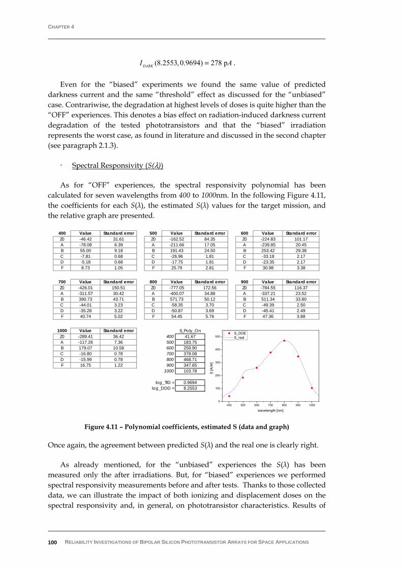
CHAPTER 4
RELIABILITY INVESTIGATIONS OF BIPOLAR SILICON PHOTOTRANSISTOR ARRAYS FOR SPACE APPLICATIONS 100
(8.2553, 0.9694) 278 pDARKI A= .
Even for the “biased” experiments we found the same value of predicted darkness current and the same “threshold” effect as discussed for the “unbiased” case. Contrariwise, the degradation at highest levels of doses is quite higher than the “OFF” experiences. This denotes a bias effect on radiation-induced darkness current degradation of the tested phototransistors and that the “biased” irradiation represents the worst case, as found in literature and discussed in the second chapter (see paragraph 2.1.3).
Spectral Responsivity (S(λ))
As for “OFF” experiences, the spectral responsivity polynomial has been calculated for seven wavelengths from 400 to 1000nm. In the following Figure 4.11, the coefficients for each S(λ), the estimated S(λ) values for the target mission, and the relative graph are presented.
Figure 4.11 – Polynomial coefficients, estimated S (data and graph)
Once again, the agreement between predicted S(λ) and the real one is clearly right.
As already mentioned, for the “unbiased” experiences the S(λ) has been measured only the after irradiations. But, for “biased” experiences we performed spectral responsivity measurements before and after tests. Thanks to those collected data, we can illustrate the impact of both ionizing and displacement doses on the spectral responsivity and, in general, on phototransistor characteristics. Results of
400 Value Standard errorZ0 -46.42 31.61A -78.08 6.39B 55.00 9.18C -7.81 0.68D -5.18 0.68F 8.73 1.05
500 Value Standard errorZ0 -162.52 84.35A -211.66 17.05B 191.43 24.50C -26.96 1.81D -17.75 1.81F 25.79 2.81
600 Value Standard errorZ0 -224.83 101.17A -239.85 20.45B 253.42 29.38C -33.18 2.17D -23.35 2.17F 30.98 3.38
700 Value Standard errorZ0 -426.01 150.51A -311.57 30.42B 390.73 43.71C -44.01 3.23D -35.28 3.22F 40.74 5.02
800 Value Standard errorZ0 -777.05 172.56A -400.07 34.88B 571.73 50.12C -58.35 3.70D -50.87 3.69F 54.45 5.76
900 Value Standard errorZ0 -784.55 116.37A -337.21 23.52B 511.34 33.80C -49.39 2.50D -45.41 2.49F 47.36 3.88
1000 Value Standard errorZ0 -289.41 36.42A -117.26 7.36B 179.07 10.58C -16.80 0.78D -15.99 0.78F 16.75 1.22
400 500 600 700 800 900 10000
100
200
300
400
500 S_DOE S_real
S [A
/W]
wavelength [nm]
S_Poly_On400 41.67500 183.75600 259.90700 378.08800 468.71900 347.65
1000 103.78
log_TID = 0.9694log_DDD = 8.2553

DOE METHODOLOGY FOR BSPA DEGRADATIONS ESTIMATION IN SPACE ENVIRONMENT
RELIABILITY INVESTIGATIONS OF BIPOLAR SILICON PHOTOTRANSISTOR ARRAYS FOR SPACE APPLICATIONS 101
the experience 5 (30MeV, 2.3·1011p/cm2 – 43.9krad(Si)) plotted in Figure 4.12 could be useful to this purpose. As shown, phototransistors spectral responsivity degrades dramatically. In fact, the reason of the S(λ) decrease (1) could be explained by the decrease of both the photodiode responsivity and the transistor current gain as they are the main effects of both TID and DDD. Moreover, the displacement dose induces also a shift in the peak of spectrum (2). Actually, this due to a greater decrease of S(λ) for higher than for smaller wavelengths. This is because of the degradation in deeper device zones (i.e. the collector space-charge zone) where the high wavelengths are absorbed [82, 83].
Figure 4.12 – S(λ) degradations: DoE experience 5 (30MeV, 2.3·1011p/cm2 - 43.9krad(Si))
4.2.3 DOE RESULTS SUMMARY AND METHODOLOGY VALIDATION
In previous paragraphs, both results of DoE plans “unbiased” and “biased” have been detailed. In the following, after a quick overview of those results, data coming from the beam degrader experience will be used to validate the DoE methodology. To do that, as already mentioned, target mission constraints have been simulated through the beam degrader. That target mission parameters are the following:
• 800km Low-Earth-Orbit (LEO) • inclination 98° • 7mm of spherical aluminium shield thickness • duration of 18 years
These conditions imply 2.1·108MeV/g and 9.38krad(Si) for displacement and ionizing doses respectively. The doses simulated with the beam degrader are 1.8·108MeV/g and 9.32krad(Si). These last values have been used to compare the
300 400 500 600 700 800 900 1000 11000
200
400
600
800
1000 before after
S [A
/W]
wavelength [nm]
Y76
(1)
(2)
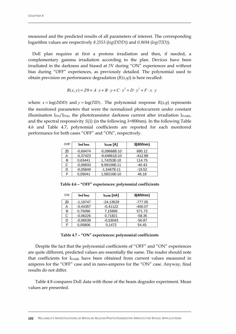
CHAPTER 4
RELIABILITY INVESTIGATIONS OF BIPOLAR SILICON PHOTOTRANSISTOR ARRAYS FOR SPACE APPLICATIONS 102
measured and the predicted results of all parameters of interest. The corresponding logarithm values are respectively 8.2553 (log(DDD)) and 0.9694 (log(TID)).
DoE plan requires at first a protons irradiation and then, if needed, a complementary gamma irradiation according to the plan. Devices have been irradiated in the darkness and biased at 5V during “ON” experiences and without bias during “OFF” experiences, as previously detailed. The polynomial used to obtain prevision on performance degradation (R(x,y)) is here recalled:
2 2( , ) 0R x y Z A x B y C x D y F x y= + ⋅ + ⋅ + ⋅ + ⋅ + ⋅ ⋅
where log( )x DDD= and log( )y TID= . The polynomial response R(x,y) represents the monitored parameters that were the normalized photocurrent under constant illumination IPH/IPH0, the phototransistor darkness current after irradiation IDARK, and the spectral responsivity S(λ) (in the following λ=800nm). In the following Table 4.6 and Table 4.7, polynomial coefficients are reported for each monitored performance for both cases “OFF” and ”ON”, respectively.
OFF IPH/IPH0 IDARK [A] S(800nm)
Z0 -0,69474 -5,09668E-10 890.12 A -0,37423 -9,64861E-10 -412.88 B 0,63441 1,74253E-10 114.75 C -0,06833 8,99109E-11 -40.43 D -0,05849 -1,5467E-11 -19.52 F 0,05041 1,58216E-10 46.18
Table 4.6 – “OFF” experiences: polynomial coefficients
ON IPH/IPH0 IDARK [nA] S(800nm)
Z0 -1,19747 -24,13529 -777.05 A -0,44357 -0,41122 -400.07 B 0,75096 7,15995 571.73 C -0,06226 0,71821 -58.35 D -0,06539 -0,53043 -50.87 F 0,05806 0,1472 54.45
Table 4.7 – “ON” experiences: polynomial coefficients
Despite the fact that the polynomial coefficients of “OFF” and “ON” experiences are quite different, predicted values are essentially the same. The reader should note that coefficients for IDARK have been obtained from current values measured in amperes for the “OFF” case and in nano-amperes for the “ON” case. Anyway, final results do not differ.
Table 4.8 compares DoE data with those of the beam degrader experiment. Mean values are presented.

DOE METHODOLOGY FOR BSPA DEGRADATIONS ESTIMATION IN SPACE ENVIRONMENT
RELIABILITY INVESTIGATIONS OF BIPOLAR SILICON PHOTOTRANSISTOR ARRAYS FOR SPACE APPLICATIONS 103
Beam degrader DOE OFF ON OFF ON
IPH/IPH0 0.53 0.55 0.53 0.52
IDARK [nA] 0.231 0.227 0.29 0.278
S(800nm) [A/W] n.a. 520 438 468
Table 4.8 – Comparison between beam degrader simulation and DoE prevision
DoE previsions for photocurrent and darkness current are in very good agreement with the proton-beam degrader experience data. Contrariwise, prevision for spectral responsivity appears less accurate. Nevertheless, note that data fitting has been conducted on S absolute values and not on the ratio S/S0, for instance. So, the predicted value of S is strongly dependent on its value before irradiation. For this reason, obtained prevision can be considered satisfying. Moreover, the overall spectral responsivity rebuilt from predicted values fit really well the real S shape, as shown in sections 4.2.1 and 4.2.2.
4.3 DOE DATA ANALYSIS
The comparison of the prevision data for the target mission with those obtained from the proton-beam degrader experience validates a posteriori the “Design of Experiments” methodology. So, now it could be useful to analyze collected data in order to try to optimize the methodology and to obtain other information than that described in previous sections. So, in the following will be investigated the impact of the number of experiences on the overall quality of the calculated parameter expectation. Then, a possibility to obtain some information that could be useful for quality engineers to evaluate impact of damage factors on device parameters and then estimate the devices EOL for a given space mission.
4.3.1 METHODOLOGY OPTIMIZATION
As seen in paragraph 4.1.3, the polynomial modeling put forward in this chapter necessitates the determination of the six coordinates of the BT vector. So, in theory, only six equations (i.e. six experiments) would be necessary to obtain these coordinates. As a consequence, it would be tempting to investigate how the prediction accuracy degrades with the number of experiments of the plan when the number of experiments decreases from nine to six. The result of this analysis is shown in the Figure 4.14 in which the plots represent the evolution of the surface responses relative to the ratio IPH/IPH0 for “OFF” irradiations when the number of experiments is progressively reduced. The experiment reference numbers are already reported in Figure 4.2 and in Table 4.1. In order to facilitate the reading, such data are recalled in Table 4.9.
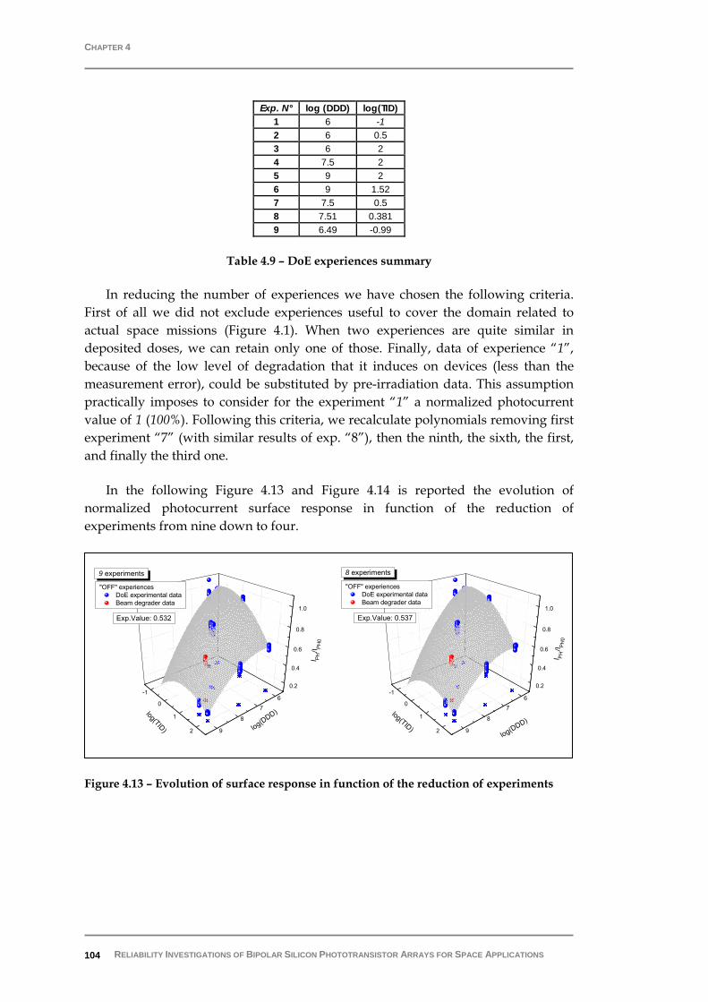
CHAPTER 4
RELIABILITY INVESTIGATIONS OF BIPOLAR SILICON PHOTOTRANSISTOR ARRAYS FOR SPACE APPLICATIONS 104
Exp. N° log (DDD) log(TID) 1 6 -1 2 6 0.5 3 6 2 4 7.5 2 5 9 2 6 9 1.52 7 7.5 0.5 8 7.51 0.381 9 6.49 -0.99
Table 4.9 – DoE experiences summary
In reducing the number of experiences we have chosen the following criteria. First of all we did not exclude experiences useful to cover the domain related to actual space missions (Figure 4.1). When two experiences are quite similar in deposited doses, we can retain only one of those. Finally, data of experience “1”, because of the low level of degradation that it induces on devices (less than the measurement error), could be substituted by pre-irradiation data. This assumption practically imposes to consider for the experiment “1” a normalized photocurrent value of 1 (100%). Following this criteria, we recalculate polynomials removing first experiment “7” (with similar results of exp. “8”), then the ninth, the sixth, the first, and finally the third one.
In the following Figure 4.13 and Figure 4.14 is reported the evolution of normalized photocurrent surface response in function of the reduction of experiments from nine down to four.
Figure 4.13 – Evolution of surface response in function of the reduction of experiments
6
7
8
9
-1
0
1
2
0.2
0.4
0.6
0.8
1.0
9 experiments
Exp.Value: 0.532
"OFF" experiences DoE experimental data Beam degrader data
I PH/I P
H0
log(DDD)log(TID)
6
7
8
9
-1
0
1
2
0.2
0.4
0.6
0.8
1.0
Exp.Value: 0.537
"OFF" experiences DoE experimental data Beam degrader data
I PH
/I PH
0
log(DDD)log(TID)
8 experiments
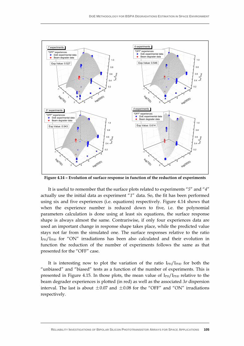
DOE METHODOLOGY FOR BSPA DEGRADATIONS ESTIMATION IN SPACE ENVIRONMENT
RELIABILITY INVESTIGATIONS OF BIPOLAR SILICON PHOTOTRANSISTOR ARRAYS FOR SPACE APPLICATIONS 105
Figure 4.14 – Evolution of surface response in function of the reduction of experiments
It is useful to remember that the surface plots related to experiments “5” and “4” actually use the initial data as experiment “1” data. So, the fit has been performed using six and five experiences (i.e. equations) respectively. Figure 4.14 shows that when the experience number is reduced down to five, i.e. the polynomial parameters calculation is done using at least six equations, the surface response shape is always almost the same. Contrariwise, if only four experiences data are used an important change in response shape takes place, while the predicted value stays not far from the simulated one. The surface responses relative to the ratio IPH/IPH0 for “ON” irradiations has been also calculated and their evolution in function the reduction of the number of experiments follows the same as that presented for the “OFF” case.
It is interesting now to plot the variation of the ratio IPH/IPH0 for both the “unbiased” and “biased” tests as a function of the number of experiments. This is presented in Figure 4.15. In those plots, the mean value of IPH/IPH0 relative to the beam degrader experiences is plotted (in red) as well as the associated 3σ dispersion interval. The last is about ±0.07 and ±0.08 for the “OFF” and “ON” irradiations respectively.
6
7
8
9
-1
0
1
2
0.2
0.4
0.6
0.8
1.0
Exp.Value: 0.527
7 experiments
"OFF" experiences DoE experimental data Beam degrader data
I PH/I P
H0
log(DDD)log(TID)
6
7
8
9
-1
0
1
2
0.2
0.4
0.6
0.8
1.0Exp.Value: 0.546
6 experiments
"OFF" experiences DoE experimental data Beam degrader data
I PH/I PH
0
log(DDD)log(TID)
6
7
8
9
-1
0
1
2
0.2
0.4
0.6
0.8
1.0
Exp.Value: 0.543
5* experiments
"OFF" experiences DoE experimental data Beam degrader data
I PH/I PH
0
log(DDD)log(TID)
6
7
8
9
-1
0
1
2
0.2
0.4
0.6
0.8
1.0Exp.Value: 0.614
4 experiments
"OFF" experiences DoE experimental data Beam degrader data
I PH/I PH
0
log(DDD)log(TID)
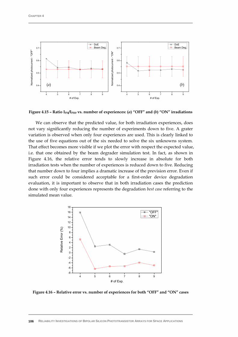
CHAPTER 4
RELIABILITY INVESTIGATIONS OF BIPOLAR SILICON PHOTOTRANSISTOR ARRAYS FOR SPACE APPLICATIONS 106
Figure 4.15 – Ratio IPH/IPH0 vs. number of experiences: (a) “OFF” and (b) “ON” irradiations
We can observe that the predicted value, for both irradiation experiences, does not vary significantly reducing the number of experiments down to five. A grater variation is observed when only four experiences are used. This is clearly linked to the use of five equations out of the six needed to solve the six unknowns system. That effect becomes more visible if we plot the error with respect the expected value, i.e. that one obtained by the beam degrader simulation test. In fact, as shown in Figure 4.16, the relative error tends to slowly increase in absolute for both irradiation tests when the number of experiences is reduced down to five. Reducing that number down to four implies a dramatic increase of the prevision error. Even if such error could be considered acceptable for a first-order device degradation evaluation, it is important to observe that in both irradiation cases the prediction done with only four experiences represents the degradation best case referring to the simulated mean value.
Figure 4.16 – Relative error vs. number of experiences for both “OFF” and “ON” cases
4 5 6 7 8 9
0.4
0.5
0.6
0.7
Nor
mal
ized
pho
tocu
rren
t - "O
FF"
# of Exp.
DoE Beam Deg.
4 5 6 7 8 9
0.4
0.5
0.6
0.7
Nor
mal
ized
pho
tocu
rren
t - "O
N"
# of Exp.
DoE Beam Deg.
(a) (b)
4 5 6 7 8 9-8
-6
-4
-2
0
2
4
6
8
10
12
14
16
18
Rel
ativ
e E
rror (
%)
# of Exp.
"OFF" "ON"

DOE METHODOLOGY FOR BSPA DEGRADATIONS ESTIMATION IN SPACE ENVIRONMENT
RELIABILITY INVESTIGATIONS OF BIPOLAR SILICON PHOTOTRANSISTOR ARRAYS FOR SPACE APPLICATIONS 107
Concluding this analysis, we have shown in this paragraph that it is possible to reduce the number of experiments down to five, preserving an acceptable agreement between the prediction and the experimental data obtained with the proton beam degrader. As already mentioned, this reduction in experiments number is actually done considering that, for this particular device, the weak degradation induced by experience “1” could be neglected and then the corresponding data substituted by those of pre-irradiated devices.
Finally, the full DoE methodology, i.e. with nine experiments, can very useful in order to obtain an overall tendency of the main device parameters degradation under the typical constraints relative to a particular space mission included in the study domain (Figure 4.1). That methodology could be optimized in order to reduce both testing and characterization times and the relative costs by reducing the number of experiments down to five.
4.3.2 DEVICES EOL EVALUATION
In previous paragraphs we have described the DoE methodology, how to define the study domain, how to perform the test and collect data, how to calculate the polynomial coefficients, and finally how to optimize the methodology. Moreover, we have summarized main results of the testing activities concerning the test vehicle, i.e. the Micropac phototransistors array. In the following, we will give some examples of information that can be extracted from DoE collected data. First of all, we present space mission data available thanks to OMERE software calculations of space environment characteristics. Three mission profiles corresponding to three orbits have been taken as example with duration from two to thirty years. Different aluminum spherical shield thicknesses have also been considered from 0.1mm to 100mm. The shield thickness ranges have been chosen accordingly to the deposed doses included in the study domain.
The three mission-examples are characterized by the orbit data in Table 4.10, as provided by OMERE database:
Perigee Apogee Inclination Period # of orbits LEO (Low Earth Orbit) 800km 800km 98° 6043s 100
MEO (Medium Earth Orbit) 1000km 26768km 63.4° 28689s 300 GEO (Geostationary Earth Orbit) 35870km 35870km 0° 86400s 1
Table 4.10 – LEO, MEO, and GEO orbits main data
Thanks to OMERE we can then trace ionizing vs. displacement doses plots in terms of their logarithms for the described different mission profiles. Environment protons and electrons displacement damage doses data are relative to the equivalent fluences of 10MeV protons (NIEL 7.86·10-3MeV·cm2/g). In Figure 4.17 and in Figure

CHAPTER 4
RELIABILITY INVESTIGATIONS OF BIPOLAR SILICON PHOTOTRANSISTOR ARRAYS FOR SPACE APPLICATIONS 108
4.18 are represented these plots for LEO, MEO, and GEO orbits. In all that plots, the pale grey area represents the study domain as previously defined.
Figure 4.17 – LEO and MEO: log(TID) vs. log(DDD) for different durations and shield thicknesses
6 7 8 9-1.5
-1.0
-0.5
0.0
0.5
1.0
1.5
2.0
2.5MEO-1000km/26768km - 63.4°
Duration (yrs) 2 5 7.5 10 12.5 15 17.5 20 22.5 25 27.5 30
log(
TID
)
log(DDD)
6 7 8 9-1.5
-1.0
-0.5
0.0
0.5
1.0
1.5
2.0
2.5LEO - 800km/800km - 98°
Duration (yrs) 2 5 7.5 10 12.5 15 17.5 20 22.5 25 27.5 30
log(
TID
)
log(DDD)

DOE METHODOLOGY FOR BSPA DEGRADATIONS ESTIMATION IN SPACE ENVIRONMENT
RELIABILITY INVESTIGATIONS OF BIPOLAR SILICON PHOTOTRANSISTOR ARRAYS FOR SPACE APPLICATIONS 109
Figure 4.18 – GEO: log(TID) vs. log(DDD) for different durations and shield thicknesses
The same data could be plotted in a different way in order to better evaluate the effect of the aluminium shield thickness on both ionizing and displacement doses that devices receive in the different orbits. This is shown in charts in the following Figure 4.19 and Figure 4.20.
Figure 4.19 – Plots of log(DDD) and log(TID) as function of the shield thickness for LEO and MEO mission profiles (durations from 2 to 30 years)
6 7 8 9-1.5
-1.0
-0.5
0.0
0.5
1.0
1.5
2.0
2.5GEO - 35870km - 0°
Duration (yrs) 2 5 7.5 10 12.5 15 17.5 20 22.5 25 27.5 30
log(
TID
)
log(DDD)
1 10 1006.0
6.5
7.0
7.5
8.0
8.5
9.0
9.5LEO - 800km/800km - 98°
log 10
(DD
D)
Al Shield thickness [mm]1 10 100
-1.5
-1.0
-0.5
0.0
0.5
1.0
1.5
2.0
2.5
2 5 7.5 10 12.5 15 17.5 20 22.5 25 27.5 30
log 10
(TID
)
Al Shield thickness [mm]
LEO - 800km/800km - 98°
1 10 1006.0
6.5
7.0
7.5
8.0
8.5
9.0
9.5
log 10
(DD
D)
Al Shield thickness [mm]
MEO-1000km/26768km - 63.4°
1 10 100-1.5
-1.0
-0.5
0.0
0.5
1.0
1.5
2.0
2.5
2 5 7.5 10 12.5 15 17.5 20 22.5 25 27.5 30
log 10
(TID
)
Al Shield thickness [mm]
MEO-1000km/26768km - 63.4°

CHAPTER 4
RELIABILITY INVESTIGATIONS OF BIPOLAR SILICON PHOTOTRANSISTOR ARRAYS FOR SPACE APPLICATIONS 110
Figure 4.20 – Plots of log(DDD) and log(TID) as function of the shield thickness for GEO
mission profiles (durations from 2 to 30 years)
We can now use these data in order to calculate the variation of the phototransistors arrays degradations for a specific profile mission. In the following, we will show as example the calculations and plots relative to the main phototransistor parameter, i.e. the photocurrent at fixed illumination. To this purpose, we will use the polynomial calculated for the “biased” experiences in paragraph 4.2.2, as that case represents the worst one. That polynomial represents the surface response (Figure 4.9) that fits the experimental data. For the normalized photocurrent the polynomial is the following:
2 2
0
( , ) 0.636 0.385 0.059 0.069 0.052 0.692PH
PH
Ix y x y x y x y
I= ⋅ − ⋅ − ⋅ − ⋅ + ⋅ ⋅ −
where log( )x DDD= and log( )y TID= .
So, for each orbit we can obtain a chart representing the photocurrent degradations, as illustrated with the Figure 4.21, Figure 4.22, and Figure 4.23. In those figures, the degradation is plotted in function of the mission duration, as in charts type (a), where each curve is relative to an Al shield thickness, or in function of the shield thickness, as in charts type (b), where each curve is relative to one mission duration.
1 10 100-1.5
-1.0
-0.5
0.0
0.5
1.0
1.5
2.0
2.5GEO - 35870km - 0°
2 5 7.5 10 12.5 15 17.5 20 22.5 25 27.5 30
log 10
(TID
)
Al Shield thickness [mm]
1 10 1006.0
6.5
7.0
7.5
8.0
8.5
9.0
9.5GEO - 35870km - 0°
log 10
(DD
D)
Al Shield thickness [mm]

DOE METHODOLOGY FOR BSPA DEGRADATIONS ESTIMATION IN SPACE ENVIRONMENT
RELIABILITY INVESTIGATIONS OF BIPOLAR SILICON PHOTOTRANSISTOR ARRAYS FOR SPACE APPLICATIONS 111
Figure 4.21 – LEO orbit: photocurrent degradation in function of the mission duration (a) and of the Al shield thickness (b)
0 10 20 30-80%
-70%
-60%
-50%
-40%
-30%
-20%
-10%
0%LEO - 800km/800km - 98°
Pho
tocu
rren
t Deg
rada
tion
Mission Duration (years)
3mm 5mm 7mm 10mm 15mm 20mm 30mm 50mm 100mm
0 20 40 60 80 100-80%
-70%
-60%
-50%
-40%
-30%
-20%
-10%
0%
LEO - 800km/800km - 98°
Pho
tocu
rren
t deg
rada
tion
Al Shield Thickness (mm)
2yrs 5yrs 10yrs 15yrs 20yrs 25yrs
(a)
(b)
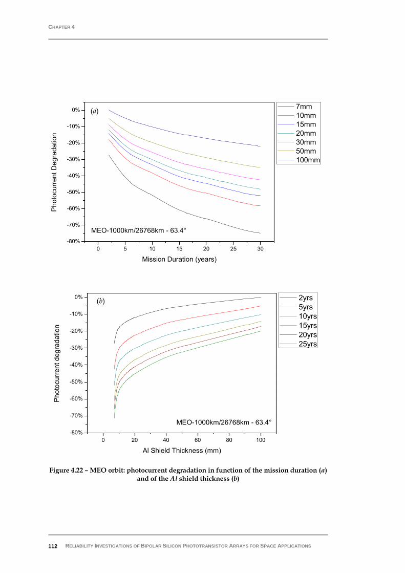
CHAPTER 4
RELIABILITY INVESTIGATIONS OF BIPOLAR SILICON PHOTOTRANSISTOR ARRAYS FOR SPACE APPLICATIONS 112
Figure 4.22 – MEO orbit: photocurrent degradation in function of the mission duration (a) and of the Al shield thickness (b)
0 5 10 15 20 25 30-80%
-70%
-60%
-50%
-40%
-30%
-20%
-10%
0%
MEO-1000km/26768km - 63.4°
Pho
tocu
rren
t Deg
rada
tion
Mission Duration (years)
7mm 10mm 15mm 20mm 30mm 50mm 100mm
0 20 40 60 80 100-80%
-70%
-60%
-50%
-40%
-30%
-20%
-10%
0%
MEO-1000km/26768km - 63.4°
Pho
tocu
rren
t deg
rada
tion
Al Shield Thickness (mm)
2yrs 5yrs 10yrs 15yrs 20yrs 25yrs
(a)
(b)

DOE METHODOLOGY FOR BSPA DEGRADATIONS ESTIMATION IN SPACE ENVIRONMENT
RELIABILITY INVESTIGATIONS OF BIPOLAR SILICON PHOTOTRANSISTOR ARRAYS FOR SPACE APPLICATIONS 113
Figure 4.23 – GEO orbit: photocurrent degradation in function of the mission duration (a) and of the Al shield thickness (b)
0 20 40 60 80 100-70%
-60%
-50%
-40%
-30%
-20%
-10%
0%
10%
GEO - 35870km - 0°
Pho
tocu
rren
t deg
rada
tion
Al Shield Thickness (mm)
2yrs 5yrs 10yrs 15yrs 20yrs 25yrs
0 10 20 30-80%
-70%
-60%
-50%
-40%
-30%
-20%
-10%
0%
10%
GEO - 35870km - 0°
Pho
tocu
rren
t Deg
rada
tion
Mission Duration (years)
5mm 7mm 10mm 15mm 20mm 30mm 50mm 100mm
(a)
(b)

CHAPTER 4
RELIABILITY INVESTIGATIONS OF BIPOLAR SILICON PHOTOTRANSISTOR ARRAYS FOR SPACE APPLICATIONS 114
We can now fix a realistic failure criterion regarding the photocurrent, for example 40% of degradation, and from data previously plotted we can obtain the useful chart in Figure 4.24.
Figure 4.24 – Al shield thickness vs. mission duration for the LEO, MEO, and GEO orbits once the 40% failure criterion has been chosen
The utility of this kind of charts for the quality engineers resides in the fact that they could have quickly an overview of the amount of shielding needed for specific orbit and a fixed duration. Or, if the shield thickness is fixed from contingent constraints (the total charge allowed on the rocket, for instance) they get from that chart the limit of the mission duration.
The devices mean time to failure (MTTF) evaluation can be easily obtained from the collected DoE data. As detailed in subsection of paragraph 4.2, the DoE plan has been applied to three devices per experience. If we consider only one channel response out of eight of each device per experience we can use until 24 devices in order to calculate the surface response polynomial. So, we can obtain a distribution of 24 polynomials. In order to give an example of this calculation, we calculate only twelve polynomials. Then we have to enter the mission related data in those polynomials. We retain the photocurrent degradation of 40% as failure criterion and e fix the shield thickness to 10mm, and we calculate the instant of device failure. Data used in this calculation are detailed in tables in Figure 4.25 and are relative to the three orbits LEO, MEO, and GEO, as usual.
0 5 10 15 20 25 30
0
10
20
30
40
50 LEO MEO GEO
Al S
hiel
d th
ickn
ess
(mm
)
Mission Duration (years)
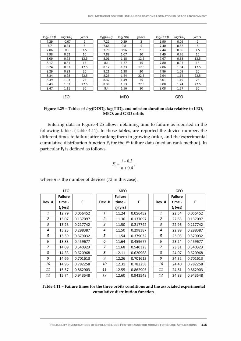
DOE METHODOLOGY FOR BSPA DEGRADATIONS ESTIMATION IN SPACE ENVIRONMENT
RELIABILITY INVESTIGATIONS OF BIPOLAR SILICON PHOTOTRANSISTOR ARRAYS FOR SPACE APPLICATIONS 115
Figure 4.25 – Tables of log(DDD), log(TID), and mission duration data relative to LEO, MEO, and GEO orbits
Entering data in Figure 4.25 allows obtaining time to failure as reported in the following tables (Table 4.11). In those tables, are reported the device number, the different times to failure after ranking them in growing order, and the experimental cumulative distribution function Fi for the ith failure data (median rank method). In particular Fi is defined as follows:
0.30.4i
iF
n−
=+
,
where n is the number of devices (12 in this case).
LEO MEO GEO
Dev. # Failure time - tf (yrs)
F
1 12.79 0.056452 2 13.07 0.137097 3 13.23 0.217742 4 13.23 0.298387 5 13.39 0.379032 6 13.83 0.459677 7 14.09 0.540323 8 14.33 0.620968 9 14.66 0.701613
10 14.96 0.782258 11 15.57 0.862903 12 15.74 0.943548
Dev. # Failure time - tf (yrs)
F
1 11.24 0.056452 2 11.30 0.137097 3 11.50 0.217742 4 11.50 0.298387 5 11.54 0.379032 6 11.64 0.459677 7 11.68 0.540323 8 12.11 0.620968 9 12.26 0.701613
10 12.31 0.782258 11 12.55 0.862903 12 12.60 0.943548
Dev. # Failure time - tf (yrs)
F
1 22.54 0.056452 2 22.63 0.137097 3 22.96 0.217742 4 22.99 0.298387 5 23.03 0.379032 6 23.24 0.459677 7 23.31 0.540323 8 24.07 0.620968 9 24.32 0.701613
10 24.40 0.782258 11 24.81 0.862903 12 24.88 0.943548
Table 4.11 – Failure times for the three orbits conditions and the associated experimental cumulative distribution function
log(DDD) log(TID) years7.29 -0.07 27.7 0.34 5
7.86 0.5 7.57.98 0.62 108.09 0.72 12.58.17 0.81 158.24 0.87 17.58.29 0.93 208.34 0.98 22.58.39 1.03 258.43 1.07 27.58.47 1.11 30
log(DDD) log(TID) years7.22 0.39 27.66 0.8 57.78 0.96 7.57.88 1.07 108.01 1.18 12.58.1 1.27 15
8.17 1.33 17.58.21 1.38 208.26 1.44 22.58.32 1.49 258.38 1.53 27.58.4 1.56 30
log(DDD) log(TID) years6.90 0.09 27.40 0.52 57.44 0.66 7.57.49 0.76 107.67 0.88 12.57.80 0.97 157.86 1.04 17.57.86 1.08 207.94 1.14 22.58.01 1.19 258.08 1.24 27.58.08 1.27 30
LEO MEO GEO

CHAPTER 4
RELIABILITY INVESTIGATIONS OF BIPOLAR SILICON PHOTOTRANSISTOR ARRAYS FOR SPACE APPLICATIONS 116
Data corresponding to the experimental cumulative distribution function could be fit to a log-normal12 one, for instance, and given by:
ln1 1( ; , )2 2 2
fX f
tF t erf
μμ σ
σ−⎡ ⎤
= + ⎢ ⎥⎣ ⎦
where σ is the standard deviation and μ the natural logarithm of the median life. Results of this fit are presented in the following plots.
Figure 4.26 – Lognormal fit for LEO experimental data
Figure 4.27 – Lognormal fit for MEO experimental data
12 The probability density function of a log-normal distribution is:
( )2
2
(ln )
21
( ; , ) 2x
Xf x exμ
σμ σ σ π−
−−=
7 14 21
0.0
0.5
1.0LEO
F experimental F(t) LogNorm
Cum
ulat
ive
desi
ty fu
nctio
n
tf (years)
14.16
8 12 16
0.0
0.5
1.0MEO
F Experimental F(t) LogNorm
Cum
ulat
ive
desi
ty fu
nctio
n
tf (years)
11.90

DOE METHODOLOGY FOR BSPA DEGRADATIONS ESTIMATION IN SPACE ENVIRONMENT
RELIABILITY INVESTIGATIONS OF BIPOLAR SILICON PHOTOTRANSISTOR ARRAYS FOR SPACE APPLICATIONS 117
Figure 4.28 – Lognormal fit for GEO experimental data
Lognormal fits are in good agreement with the experimental data. Anyway, the lognormal distribution has been chosen only as example and because is one of the most used in reliability extrapolations. For instance, Weibull distribution could be used, too. Under the hypothesis of lognormal distributed times, we can easily calculate the median life times, as indicated in plots in Figure 4.26, Figure 4.27, and Figure 4.28 in the case of LEO, MEO, and GEO respectively. These data and the associated standard deviation are also reported in Table 4.12. We can now calculate the MTTF defined by:
2
2mMTTF t e
σ
= .
Because of the narrowness of distributions, the MTTF is quite similar to the median life time.
median life (years) standard deviation MTTF (years) LEO 14.16 0.066259 14.19 MEO 11.90 0.039161 11.91 GEO 23.68 0.034253 23.70
Table 4.12 – Median life times and standard deviations for LEO, MEO, and GEO
Obtained results concerning the MTTF of Micropac phototransistor arrays with respect to the three different mission profiles have to be considered satisfying. This is in terms of both good MTTF and the amount of useful and easy-to-use data provided by DoE methodology. We have illustrated few examples of data exploitation, but deeper investigations are actually ongoing, and among them there is the possibility to extend collected data with Montecarlo methods.
20 24 28
0.0
0.5
1.0
23.68
GEO F Experimental F(t) LogNorm
Cum
ulat
ive
desi
ty fu
nctio
n
tf (years)

CHAPTER 4
RELIABILITY INVESTIGATIONS OF BIPOLAR SILICON PHOTOTRANSISTOR ARRAYS FOR SPACE APPLICATIONS 118
Conclusions
This chapter emphasized the interest of a “Design of Experiment” approach to define an irradiation test plan and to assess the degradation of the main parameters (normalized photocurrent, darkness current, and spectral responsivity) of silicon based phototransistors over a wide range of potential missions. The (statistical) design of experiments (DoE) is an efficient procedure for planning experiments so that the data obtained can be analyzed to yield valid and objective conclusions. This approach, that does not need any physical model of the device and its degradation, combines protons and gamma rays irradiations and provides the engineers with analytical degradation models of the device performance. At first, we have defined the study domain of the environmental constraints, i.e. the displacement and ionizing doses, and the optimized experiments plan. Micropac phototransistors have been submitted to that plan as a test vehicle for methodology validation purposes and, at the same time, to evaluate their hardness toward several space mission profiles. Then, experimental results concerning both “unbiased” and “biased” irradiation sessions have been presented. Thanks to the data collected during these testing activities, we were able to obtain the degradation empirical model of the three monitored BSPAs parameters. That model is represented by a surface polynomial function of the logarithms of the total ionizing dose and the displacement damage dose. The excellent agreement existing between the predicted results and those experimental obtained after a multienergy proton beam irradiation validates a posteriori the proposed DoE methodology.
After presenting the methodology, results of its application, and its validation, we discussed in the paragraph 4.3.1 the possibility to optimize the methodology reducing the total number of experiments. In fact, we have demonstrated that by using only six experiments (i.e. six equations) to calculate the six parameters of the polynomial the prevision of degradation is always in good agreement with the simulated one (by means of the beam degrader experience). Moreover, considering the particular case of the tested phototransistors, as the first of nine experiences weakly degrades devices, its data can be substituted by those relative to the pre-irradiation state. This let us to reduce the number of effective experiments down to five without degrading the quality of the prevision. Contrariwise, on the basis of only one validation point we can affirm that it is not suitable reducing down to four experiences because of the increased prevision error. This last point is object of our ongoing activities that are just related to the evaluation of that error when only four experiences are performed. We will compare results with four simulated points (beam degrader experiences) to evaluate the validity of such optimized plan.
Finally, DoE collected data have been analyzed in order to obtain useful information for quality engineers. In the last subsection, we have presented few examples of that analysis results concerning Micropac BSPA reliability evaluation for space applications. In particular for each orbit (LEO, MEO, and GEO) we have obtained a useful chart representing the photocurrent degradations in function of the mission duration, for different shield thicknesses, or in function of the shield thickness, for some mission durations. Then, once we fixed a photocurrent failure criterion (photocurrent degradation of 40%) we can easily use collected data in order to calculate MTTF of devices accordingly to a chosen distribution that fit the experimental data.

DOE METHODOLOGY FOR BSPA DEGRADATIONS ESTIMATION IN SPACE ENVIRONMENT
RELIABILITY INVESTIGATIONS OF BIPOLAR SILICON PHOTOTRANSISTOR ARRAYS FOR SPACE APPLICATIONS 119
In conclusion, the proposed Design of Experiments methodology is suitable as a qualification method for devices that are sensitive to both ionizing and displacement doses and that are used over a wide range of potential mission profiles. This methodology, which does not require an accurate physical knowledge of the device under test, has to be evaluated with other kinds of devices and can be potentially extended to other families of components.


RELIABILITY INVESTIGATIONS OF BIPOLAR SILICON PHOTOTRANSISTOR ARRAYS FOR SPACE APPLICATIONS
G E N E R A L C O N C L U S I O N
The reliability of an electronic device or a system is usually defined as the probability that it will perform its function for a specified time interval under stated operating conditions. Of course, a great endurance of electronic devices and system is always well suited, at least greater than its obsolescence. But environmental conditions could have a high impact on device performances reducing its operating life. So, depending on the applications to which it is intended to be integrated in, its reliability can be a really critical parameter. For instance, for all that applications whence the human health or life depends, like medical or safety applications, electronic systems reliability is dramatically important. Otherwise, it is as much important in applications where defective part replacement is extremely expensive or outright impossible; for instance, submarine telecommunication systems that have to operate under the sea without any human intervention. It is even more the case of telecommunication or military satellites around Earth or other spacecrafts for space exploration. The degradations and disturbances induced by space environment on the materials and the electronic components are phenomena that have been extensively studied since many years. The research activities presented in this thesis are related to the evaluation of these phenomena impacting on performances and reliability of phototransistor arrays for optical angular encoders.
The first chapter has introduced the context in which the research activities have been developed. To do that, the PLEIADES project and its historical development are shortly presented in the first chapter section. The PLEIADES system is an optical observation system with a metric resolution designed to offer a high acquisition capability with a revisit lower than 24 hours to satisfy both civilian and military needs. Satellites will operate in a Sun-synchronous orbit at 694km offering a spatial resolution at nadir of 0.7m and a field of view of 20km. The expected duration of the mission is five years. In order to introduce the device under study, the Bipolar Silicon Phototransistors Array (BSPA), the optical angular encoder used in PLEIADES satellites has been briefly described. In fact, innovative Control Moment Gyros using a cluster of four actuators are used and the heart of these actuators is the optical angular encoder supplied by the French SME Codechamp. Inside that, arrays of eight silicon phototransistors are placed as receiving devices in front of a series of infrared LED. Those phototransistors arrays must have particular technical specifications and high reliability requirements. These facts and taking into account the very low production volumes, make very difficult to find a secure provisioning source for these components including foundry and packaging developments. For these reasons and considering the severe environment in which they will operate, over the years of project development, several device providers’
GENERAL CONCLUSION
RELIABILITY INVESTIGATIONS OF BIPOLAR SILICON PHOTOTRANSISTOR ARRAYS FOR SPACE APPLICATIONS 122
components have been submitted to evaluation tests, as described in the last subsection of first paragraph. Research activities described in this thesis are related to a part of those evaluation tests.
Some useful concepts concerning the phototransistor basic operating principles are then called-back in the second section. A simplified model is presented in which the base-collector photodiode will be considered as a standard pn-junction photodiode in parallel with the base-collector junction of a conventional transistor. In this context, the photogenerated current in that photodiode is amplified thanks to the transistor gain. It is clearly shown that the phototransistor has an effective quantum efficiency that is larger than the collector-base photodiode one.
After that, we have described the principal characteristics of the different components designs and technologies of the different manufacturer: Optek, ETIC-Honeywell, Micropac, and Optoi. This last European manufacturer is of strategic importance to the CNES since it could become the sole founder of phototransistors allowing detachment from the U.S. markets.
Finally, in the third section, the phototransistors arrays parameters and performances measurement benches presentation concludes the chapter one. These benches have been developed at IMS in order to measure the three main parameters monitored during the test activities: the photocurrent under fixed illumination, the darkness current, and the spectral responsivity. For each parameter are presented both the dedicated bench and the measurement procedure.
• The first bench allows the measurement of the single channel photocurrent that is fixed at the level of about 20µA for non-aged devices. This photocurrent value corresponds to that one expected for the actual application. The overall Repeatability and reproducibility (R&r) for these measurements is lower then ±1%.
• Phototransistor electrical characterizations in the darkness have been performed thanks to a specific bench including the Agilent 4156C semiconductor analyzer. Among the characterizations that could be done with such bench, the darkness current is considered as a key parameter to identify the device degradation. Expected IDARK values are about 100pA (normally less) and must not exceed 10nA. For these kind of measurements the overall R&r is about 100%, that can be considered as quite reasonable, especially for low current values (of about few pA).
• Spectral Responsivity S(λ) has been measured with the specific bench described in the last subsection of the last paragraph. The halogen source produces a halogen lamp classical irradiance spectrum including the wavelength range 350nm-1100nm, and has its emission peak at 700nm. At the testing device level its value is around 65μW/cm2. Typical values of phototransistor S(λ) are from 200 to 800A/W, depending on device technological characteristics. As well as the other benches, also this last has been submitted to a metrological evaluation with the same procedure. The overall R&r for S(λ) measurements is lower than

GENERAL CONCLUSION
RELIABILITY INVESTIGATIONS OF BIPOLAR SILICON PHOTOTRANSISTOR ARRAYS FOR SPACE APPLICATIONS 123
±3% in the wavelength range of interest (500-900nm). It is lower than ±10% in the range 350-500nm and lower then ±5% in the range 900-1100nm.
As the studied phototransistors arrays used in the optical encoders in the PLEIADES satellites system will operate in severe environment that the space one is, in order to evaluate their reliability, the knowledge of that environment and its effects on this kind of devices becomes essential. For this reason, in the second chapter, the space environment and its effect on electronics in general and on bipolar devices in particular are presented.
The effects induced by the space environment are largely responsible for the anomalies occurring on satellites onboard electronics. These effects on electronics in general and on bipolar devices in particular have been presented. Since the subject is very vast, only some basic concepts that could be useful for readers have been called-back. In fact, the first section describes that environment mainly in terms of space radiations. They can be divided in three categories depending on type of involved particles, their energies, their localization, and their origins. Then, the concepts of stopping power, LET, and NIEL have been introduced in order to analyze and understand failures which occur in the electronics. This is essential to be able to quantify the effect of radiation on matter, particularly and mainly in terms of deposited energy. Actually, the main effects of space radiations on electronics are related to the Total Ionizing Dose, depending on the creation of electron-hole pairs within dielectric layers (related to the LET), to the Displacement Damage, caused mainly by energetic particles impacts displacing atoms in the crystal lattice (related to the NIEL), and to the Single Events, from the interaction of single particles. All those effects on electronic devices performances have been discussed in the last three subsections. In the second chapter section, we will focus on bipolar devices characteristics degradations dues to both the ionizing and the displacement damage doses. Moreover, as BJTs are low-dose rate sensitive, the ELDRS and a methodology to assess its effect are also discussed. The space environment induced degradations on bipolar devices is presented focusing on the “measurable” electrical characteristics variations. The main effects on devices performance are the reduction of the transistor current gain, the growth of the darkness leakage current, and often the spectral responsivity degradation.
Passivations in silicon bipolar technologies have only structural functions. But their quality could largely impact on devices functionality. In particular, it is now well-established that mobile charges trapped in passivation layers could degrade performances and introduce instabilities during accelerated life tests. The main objective of the third chapter was to point out on how both the overall quality of passivation layers in bipolar devices and device layout could impact on their performance and reliability. We have recalled at first the studies relative to the evaluation of the phototransistors batch provided by ETIC-Honeywell, chosen by CNES after the disengagement from the space sector of the previous manufacturer, Optek. For ETIC-Honeywell BSPA the sensitivity to oxide trapped charges has been
GENERAL CONCLUSION
RELIABILITY INVESTIGATIONS OF BIPOLAR SILICON PHOTOTRANSISTOR ARRAYS FOR SPACE APPLICATIONS 124
verified. To do that, we performed several kind of temperature/bias ageing tests and electro-optical characterizations. In the first section, we discussed about the performed analyses conducted on ETIC-Honeywell devices after the first ageing tests. In fact, recorded photocurrent instabilities induced us to perform specific tests in order to understand the failure origins. A recovery of phototransistor characteristics after zero-bias thermal storage has led us to suspect a problem oxide trapped charges. These caused a dramatic increase of leakage current during ageing tests, from few pico-amps up to tenths of micro-amps. The leakage path has been localized thanks to the LEM analysis. Our hypothesis on passivation mobile charges inducing a parasitic n-channel has been verified and validated using electrical simulations under SPICE environment. So, we developed an original device selection methodology based on the observation of the behaviour of fail channels during an isochronal annealing. Thanks to this test, we experimentally found a critical temperature at which the failure occurs, i.e. 150°C for ETIC-Honeywell devices. The proposed methodology is based on a temperature ramp, with the same slope of the isochronal annealing, from ambient temperature up to the founded critical one (i.e. 150°C in our case). Our work concludes that Temperature Ramp Test (TRT) current drifts are well correlated to the degradations observed during life-test and could be very fruitful to rapidly assess the degradation of bipolar microcircuits during life-test. We consider that the use of this method could be generalized in the screening sequence of devices likely to be affected by mobile charges, in particular bipolar and MOS devices.
As discussed in the first chapter, a new European producer of custom BSPA was identified by CNES. According to the built-in reliability approach, the high reliability basis must be integrated, as early as possible, at the beginning of the device development in order to reduce technology optimization times. In this context, pre-evaluation of Optoi phototransistors have followed the studies presented in the first section, analyzing different technological options with respect to the mobile charge sensitivity. These activities are described in the last section of this third chapter. Several different designs have been submitted to successive specific ageing tests based on voltage/temperature stresses at the IMS Laboratory. 40V and 20V ageing tests at the temperature of 125°C have been performed on a device batches featuring all technology options. Both tests highlight a dramatic increase of the phototransistors leakage darkness current. The storage test conduced on several devices after both the 40V and 20V life-tests, has revealed the same behaviour observed on ETIC-Honeywell devices: most of all phototransistors recovered their initial characteristics after the storage, indicating the sensitivity to mobile charges effects. BSPA belonging to the new design and featuring a thicker passivation and optimized channel layout have then evaluated. A specific three-step test (10V, 20V, 30V at 125°C) revealed the achieved hardness of the thick-oxide option. The success consists in the fact that devices belonging to that batch attain the darkness current levels lower than 10nA after the third step (30V). Unfortunately, the successive storage test highlights again the mobile charges sensitivity, even less

GENERAL CONCLUSION
RELIABILITY INVESTIGATIONS OF BIPOLAR SILICON PHOTOTRANSISTOR ARRAYS FOR SPACE APPLICATIONS 125
severe. Thus, a third phototransistor design has been studied. The major improvement that has been introduced addresses the guard ring around the emitter implant. This consists in a p+ implant that will prevent the parasitic channel formation in the base region between emitter and collector under the action of trapped charges into the overlying oxide.
The final fourth chapter emphasized the interest of an original “Design of Experiment” approach to define an irradiation test plan and to assess the degradation of the main parameters (normalized photocurrent, darkness current, and spectral responsivity) of silicon based phototransistors over a wide range of potential missions. The (statistical) design of experiments (DoE) is an efficient procedure for planning experiments so that the data obtained can be analyzed to yield valid and objective conclusions. This approach, that does not need any physical model of the device and its degradation, combines protons and gamma rays irradiations and provides the engineers with analytical degradation models of the device performance. At first, we have defined the study domain of the environmental constraints, i.e. the displacement and ionizing doses, and the optimized experiments plan. Micropac phototransistors have been submitted to that plan as a test vehicle for methodology validation purposes and, at the same time, to evaluate their hardness toward several space mission profiles. Then, experimental results concerning both “unbiased” and “biased” irradiation sessions have been presented. Thanks to the data collected during these testing activities, we were able to obtain the degradation empirical model of the three monitored BSPA parameters. That model is represented by a surface polynomial function of the logarithms of the total ionizing dose and the displacement damage dose. The excellent agreement existing between the predicted results and those experimental obtained after a multienergy proton beam irradiation validates a posteriori the proposed DoE methodology.
After presenting the methodology, results of its application, and its validation, we discussed in the paragraph 4.3.1 the possibility to optimize the methodology reducing the total number of experiments. In fact, we have demonstrated that by using only six experiments (i.e. six equations) to calculate the six parameters of the polynomial the prevision of degradation is always in good agreement with the simulated one (by means of the beam degrader experience). Moreover, considering the particular case of the tested phototransistors, as the first of nine experiences weakly degrades devices, its data can be substituted by those relative to the pre-irradiation state. This let us to reduce the number of effective experiments down to five without degrading the quality of the prevision. Contrariwise, on the basis of only one validation point we can affirm that it is not suitable reducing down to four experiences because of the increased prevision error. This last point is object of our ongoing activities that are just related to the evaluation of that error when only four experiences are performed. We will compare results with four simulated points (beam degrader experiences) to evaluate the validity of such optimized plan.

GENERAL CONCLUSION
RELIABILITY INVESTIGATIONS OF BIPOLAR SILICON PHOTOTRANSISTOR ARRAYS FOR SPACE APPLICATIONS 126
Finally, DoE collected data have been analyzed in order to obtain useful information for quality engineers. In the last subsection, we have presented few examples of that analysis results concerning Micropac BSPA reliability evaluation for space applications. In particular for each orbit (LEO, MEO, and GEO) we have obtained a useful chart representing the photocurrent degradations in function of the mission duration, for different shield thicknesses, or in function of the shield thickness, for some mission durations. Then, once we fixed a photocurrent failure criterion (degradation of 40%) we can easily use collected data in order to calculate MTTF of devices accordingly to a chosen distribution that fit the experimental data.
In conclusion, the proposed Design on Experiments methodology is suitable as a qualification method for devices that are sensitive to both ionizing and displacement doses and that are used over a wide range of potential mission profiles. This methodology, which does not require a physical knowledge of the device under test, has to be evaluated with other kinds of devices and can be potentially extended to other families of components.
“Prediction is very difficult, especially about the future.”

RELIABILITY INVESTIGATIONS OF BIPOLAR SILICON PHOTOTRANSISTOR ARRAYS FOR SPACE APPLICATIONS
I N D E X O F F I G U R E S A N D T A B L E S
C h a p t e r O n e
Figure 1.1 – Representation of PLEIADES satellite system .....................................................................8 Figure 1.2 – PLEIADES satellite packaging...............................................................................................9 Figure 1.3 – (a) Scheme of the satellite; (b) the actuator.....................................................................10 Figure 1.4 – Operating principle of an optical encoder ........................................................................10 Figure 1.5 – The coded disc and the receiver/emitter circuitry board .................................................11 Figure 1.6 – (a) Phototransistor array in SMD package; (b) internal connections and package pinout11 Figure 1.7 – Cross-sectional view of a planar phototransistor .............................................................13 Figure 1.8 – One-dimensional model of phototransistor .....................................................................14 Figure 1.9 – (a) Optek phototransistor array into SMD package; (b) zoom on one channel ................16 Figure 1.10 – ETIC-Honeywell phototransistor: packaged device (a); chip (b) .....................................17 Figure 1.11 – Detail of one channel layout of the Etic-Honeywell device.............................................17 Figure 1.12 – Micropac phototransistor: packaged device (a); chip (b) ...............................................18 Figure 1.13 – Several Optoi phototransistor layout designs.................................................................19 Figure 1.14 – The test board and the illumination system ...................................................................22 Figure 1.15 – Diagram of the illuminating system (a) and the photocurrent measurement principle (b)..............................................................................................................................................................22 Figure 1.16 – Semiconductor devices electrical characterization bench..............................................23 Figure 1.17 – Example of the two types of Gummel-plots ...................................................................24 Figure 1.18 – Transistor gain vs. collector current plots. β1 and β2 correspond to the current gain in the VBC=0V and VCE=5V measurements conditions respectively...........................................................24 Figure 1.19 – The “Spectral Responsivity Measurement” bench .........................................................25 Figure 1.20 – The integrating sphere, the reference photometer, and the DUT socket support.........26 Figure 1.21 – Source irradiance spectrum at the device level ..............................................................27 Figure 1.22 – Example of the phototransistor spectral responsivity shape (Micropac device)............28
C h a p t e r T w o Figure 2.1 – Distribution of electronics and system malfunctions causes............................................32 Figure 2.2 – The protons radiation belt ................................................................................................33 Figure 2.3 – The electrons radiation belt..............................................................................................34 Figure 2.4 – (a) South Atlantic Anomaly origins; (b) SAA particles Omnidirectional Flux higher than 10MeV (cm-2s-1) at 500km.....................................................................................................................35 Figure 2.5 – Projection of the various orbits in a meridian plane with, in the background, ................36 Figure 2.6 – Protons Stopping Powers..................................................................................................38 Figure 2.7 – Electrons Stopping Powers ...............................................................................................38 Figure 2.8 – Interaction with matter of a flux Ф of particles depositing an energy dE in a volume with cross section S and thickness dx. ..........................................................................................................39 Figure 2.9 - Illustration of the five basic effects of a defect energy level (Et) on the device electrical performances deterioration. ................................................................................................................41

FIGURES AND TABLES INDEX
RELIABILITY INVESTIGATIONS OF BIPOLAR SILICON PHOTOTRANSISTOR ARRAYS FOR SPACE APPLICATIONS 128
Figure 2.10 – Illustration of different components of base, emitter, and collector currents in a bipolar transistor...............................................................................................................................................44 Figure 2.11 - Simplified illustration of the space charge model for enhanced low dose rate oxide degradation in MOS systems ................................................................................................................48 Figure 2.12 – Schematic illustration of the switching experiments methodology................................48 Figure 2.13 – Schematic representation of overall degradations in phototransistors: (a) pre-irradiated simplified model; (b) irradiated model .................................................................................................50
C h a p t e r T h r e e
Figure 3.1 – Collector current drift in percent during life test..............................................................54 Figure 3.2 – I-V characteristics: at the initial stage, before HTRB test and before storage test ...........55 Figure 3.3 – Gummel plots: at the initial stage, before HTRB test and before storage test .................56 Figure 3.4 – Collector-emitter leakage darkness current: (a) before and (b) after HTRB test..............57 Figure 3.5 – Normalized spectral responsivity before (a) and after (b) HTRB test ...............................57 Figure 3.6 – Phototransistor infrared light emission: before (a) and after (b) HTRB test.....................58 Figure 3.7 – Leakage path origins between emitter and collector: the n-type inversion channel .......59 Figure 3.8 – Gummel plot after each step: base current (a) and collector current (b).........................60 Figure 3.9 – SPICE schematic of Phototransistor with parasitic MOSFET .............................................61 Figure 3.10 – Comparison between simulated and measured Gummel-plots .....................................61 Figure 3.11 –Comparison between simulated and measured Collector-Emitter leakage (a) and simulated and measured post-HTRB test Gummel-plots (b) ................................................................62 Figure 3.12 – Scheme of the isochronal annealing test ........................................................................63 Figure 3.13 – Isochronal annealing test results: normalized photocurrent ..........................................64 Figure 3.14 – Ramp test results example: a normal device without photocurrent drifts (a); a device that presents irregular photocurrent drifts (b) .....................................................................................65 Figure 3.15 – Life test maximum drifts vs. ramp test drifts (CNES test session)...................................65 Figure 3.16 – Life test vs. ramp test at Microtel’s.................................................................................66 Figure 3.17 – Cross sectional view representation of a single Optoi phototransistor ..........................67 Figure 3.18 – Optoi BSPA chips of two technology options concerning the passivation layer. (a) Silicon oxide, split A; (b) silicon oxide and silicon nitride sandwich, split AAA.................................................68 Figure 3.19 – Pre-Evaluation tests program scheme ............................................................................69 Figure 3.20 – Devices photocurrent variations during isochronal annealing. Graphs are relative to all wafers and all technology splits ............................................................................................................70 Figure 3.21 – Photocurrent variations after 48h of life-test (40V, 125°C) ............................................71 Figure 3.22 – Increase of darkness leakage current after test (48h, 40V, 125°C).................................72 Figure 3.23 – Photocurrent variations after 48h of test under 20V and 125°C (W#1)..........................72 Figure 3.24 – Photocurrent variations after 48h of test under 20V and 125°C (W#2)..........................73 Figure 3.25 – Photocurrent variations after 48h of test under 20V and 125°C (W#3)..........................73 Figure 3.26 – Darkness current measurements: wafer #1 drifts...........................................................73 Figure 3.27 – Darkness current measurements: wafer #2 drifts...........................................................74 Figure 3.28 – Darkness current measurements: wafer #3 drifts...........................................................74 Figure 3.29 – Gummel plots on the same device: VCE = 2V (a) and VBC = 0V (b). Dotted curves are collector and base currents measured before life-test. Solid line curves represent after-test measurements. .....................................................................................................................................75 Figure 3.30 – β measurements before and after test (ref. Figure 3.29) ...............................................75 Figure 3.31 – Storage after “40V” life-test results ................................................................................76 Figure 3.32 – Wafer #1: storage after “20V” life-test results................................................................76 Figure 3.33 – Wafer #2: storage after “20V” life-test results................................................................77 Figure 3.34 – Average darkness current variations during the four steps ............................................78

FIGURES AND TABLES INDEX
RELIABILITY INVESTIGATIONS OF BIPOLAR SILICON PHOTOTRANSISTOR ARRAYS FOR SPACE APPLICATIONS 129
Figure 3.35 – New design of Optoi BSPA. (a) new channel layout; (b) “ring-shaped” and (c) “filled-in” emitter contact .....................................................................................................................................80 Figure 3.36 – Darkness current measurements during all four steps: 450nm-thick oxide...................81 Figure 3.37 – Darkness current measurements during all four steps: 775nm-thick oxide...................81 Figure 3.38 – Single channel cross-sectional view of the next phototransistor generation: the thick oxide, the ring-shaped emitter contact, and the channel-stop guard ring (p+-implants).....................83
C h a p t e r F o u r
Figure 4.1 – Definition of the “study domain” of the experience plan.................................................87 Figure 4.2 – Nine experiments of D-optimal design proposed by the JMP® software providing the DDD and TID values.......................................................................................................................................89 Figure 4.3 – Proton differential fluence spectrum calculated with OMERE and simulated with the beam degrader .....................................................................................................................................90 Figure 4.4 – -3σ normalized photocurrent versus TID (krad(Si)) for three different dose rates...........93 Figure 4.5 – IPH/IPH0 surface response ...................................................................................................94 Figure 4.6 – Overall darkness current surface response.......................................................................96 Figure 4.7 – Darkness current surface response after data removal....................................................96 Figure 4.8 – Polynomial parameters for the spectral responsivity and the S foreseen for the target mission..................................................................................................................................................97 Figure 4.9 – IPH/IPH0 surface response and experimental data ..............................................................98 Figure 4.10 – Darkness current surface response.................................................................................99 Figure 4.11 – Polynomial coefficients, estimated S (data and graph) ................................................100 Figure 4.12 – S(λ) degradations: DoE experience 5 (30MeV, 2.3∙1011p/cm2 - 43.9krad(Si))...............101 Figure 4.13 – Evolution of surface response in function of the reduction of experiments ................104 Figure 4.14 – Evolution of surface response in function of the reduction of experiments ................105 Figure 4.15 – Ratio IPH/IPH0 vs. number of experiences: (a) “OFF” and (b) “ON” irradiations .............106 Figure 4.16 – Relative error vs. number of experiences for both “OFF” and “ON” cases ..................106 Figure 4.17 – LEO and MEO: log(TID) vs. log(DDD) for different durations and shield thicknesses ...108 Figure 4.18 – GEO: log(TID) vs. log(DDD) for different durations and shield thicknesses ..................109 Figure 4.19 – Plots of log(DDD) and log(TID) as function of the shield thickness for LEO and MEO mission profiles (durations from 2 to 30 years)..................................................................................109 Figure 4.20 – Plots of log(DDD) and log(TID) as function of the shield thickness for GEO mission profiles (durations from 2 to 30 years)...............................................................................................110 Figure 4.21 – LEO orbit: photocurrent degradation in function of the mission duration (a) and of the Al shield thickness (b) .........................................................................................................................111 Figure 4.22 – MEO orbit: photocurrent degradation in function of the mission duration (a) and of the Al shield thickness (b) .........................................................................................................................112 Figure 4.23 – GEO orbit: photocurrent degradation in function of the mission duration (a) and of the Al shield thickness (b) .........................................................................................................................113 Figure 4.24 – Al shield thickness vs. mission duration for the LEO, MEO, and GEO orbits once the 40% failure criterion has been chosen .......................................................................................................114 Figure 4.25 – Tables of log(DDD), log(TID), and mission duration data relative to LEO, MEO, and GEO orbits...................................................................................................................................................115 Figure 4.26 – Lognormal fit for LEO experimental data......................................................................116 Figure 4.27 – Lognormal fit for MEO experimental data ....................................................................116 Figure 4.28 – Lognormal fit for GEO experimental data.....................................................................117

FIGURES AND TABLES INDEX
RELIABILITY INVESTIGATIONS OF BIPOLAR SILICON PHOTOTRANSISTOR ARRAYS FOR SPACE APPLICATIONS 130
Table 4.1 – Irradiation conditions for the calculated plan of experiments...........................................89 Table 4.2 – Polynomial coefficients for normalized photocurrent .......................................................94 Table 4.3 – Polynomial coefficients for darkness current.....................................................................95 Table 4.4 – Polynomial coefficients for the normalized photocurrent .................................................98 Table 4.5 – Polynomial coefficients for darkness current.....................................................................99 Table 4.6 – “OFF” experiences: polynomial coefficients.....................................................................102 Table 4.7 – “ON” experiences: polynomial coefficients......................................................................102 Table 4.8 – Comparison between beam degrader simulation and DoE prevision..............................103 Table 4.9 – DoE experiences summary ...............................................................................................104 Table 4.10 – LEO, MEO, and GEO orbits main data.............................................................................107 Table 4.11 – Failure times for the three orbits conditions and the associated experimental cumulative distribution function ...........................................................................................................................115 Table 4.12 – Median life times and standard deviations for LEO, MEO, and GEO..............................117

RELIABILITY INVESTIGATIONS OF BIPOLAR SILICON PHOTOTRANSISTOR ARRAYS FOR SPACE APPLICATIONS
S C I E N T I F I C P R O D U C T I O N
[C.1] P. Spezzigu, G. Quadri, O. Gilard, J.L. Roux, et al., "Assessing space radiation environment effects on silicon-based bipolar phototransistors" - RADECS 2006 Workshop - September 2006, Athens (Greece)
[C.2] O. Gilard, G. Quadri, P. Spezzigu, J.L. Roux, "Bipolar phototransistor Reliability Assessment for space applications", IEEE, Radiation Effects Data Workshop, pp. 85-91, Honolulu (Hawaii), July 2007, ISBN: 978-1-4244-1464-2
[C.3] P. Spezzigu, G. Quadri, O. Gilard, L.Bechou, Y. Ousten, M. Vanzi, "Impact of trapped mobile charges on electro-optical performances in silicon phototransistors for space applications", JNRDM 2008 – May 2008, Bordeaux (France)
[C.4] P. Spezzigu, L. Bechou, G. Quadri, O. Gilard, Y. Deshayes, Y. Ousten, M. Vanzi, "Silicon phototransistor reliability assessment and new selection strategies for space applications", SPIE Europe, Photonics Europe 2008 Conference – April 2008, Strasbourg (France), Optical Sensors 2008 (Proceedings), Vol. 7003, 70030O (2008), ISBN: 9780819472014
[C.5] G. Quadri, O. Gilard, J.L. Roux, P. Spezzigu, L. Bechou, M. Vanzi, Y. Ousten, D. Gibard, "Evaluation of static and dynamic performance of silicon-based bipolar phototransistors under radiations", IEEE, Radiation Effects Data Workshop – pp. 131-134, Tucson (Arizona, US), July 2008 - ISBN: 978-1-4244-2545-7
[C.6] P. Spezzigu, G. Quadri, O. Gilard, L. Bechou, Y. Ousten, M. Vanzi, "Trapped mobile charges effects on electro-optical performances in silicon phototransistors for space applications", ISROS conference - May 2009, Cagliari (Italy)
[C.7] M. Bregoli, A. Maglione, A. Collini, P. Bellutti, P. Spezzigu, L. Bechou, M. Vanzi, "Customized and highly reliable 8-channel phototransistor array for aerospace optical encoders", ISROS conference - May 2009, Cagliari (Italy)
[C.8] P. Spezzigu, M.L. Bourqui, "Radiation effects on photoreceivers", Invited Tutorial for OPTORAD thematic day - ISROS conference - May 2009, Cagliari (Italy)
[C.9] P. Spezzigu, L. Bechou, G. Quadri, O. Gilard, C. Caddeo, Y. Ousten, M. Vanzi, "Prediction of Phototransistor Spectral Responsivity Degradation in a Space Environment using DOE methodology", ISROS conference -April 2010, Cagliari (Italy)
[C.10] G. Quadri, P. Spezzigu, C. Caddeo, O. Gilard, L. Bechou, M. Vanzi, "Optimized “Design of Experiments” Methodology for the Prediction of Phototransistor Degradation in a Space Environment", ISROS conference - April 2010, Cagliari (Italy)
[R.1] P. Spezzigu, C. Caddeo, G. Quadri, O. Gilard, L. Bechou, Y. Ousten, M. Vanzi,
"Implementation of a design of experiments methodology for the prediction of phototransistor degradation in a space environment", IEEE Trans. Nuclear Sci., Vol. 56, n°4, August 2009


RELIABILITY INVESTIGATIONS OF BIPOLAR SILICON PHOTOTRANSISTOR ARRAYS FOR SPACE APPLICATIONS
R E F E R E N C E S
[1] Ward S.: Electrical engineering - Global Media - 2007. [2] Sze S.M., Kwog K.N.: Physics of semiconductor devices - Wiley-Interscience - 2007. [3] Shockley W.: "The path to the conception of the junction transistor", IEEE
Transactions on Electron Devices - Vol. 23, n°7 - (pp 597-620) - 1976 [4] Buckland N.M., Ackland R.G.: "A phototransistor galvanometer relay", Journal of
Scientific Instruments - Vol. 39, n°11 - (pp 554-555) - 1962 [5] Cockett G.H., Harris R.: "A simple phototransistor temperature controller", Journal of
Scientific Instruments - Vol. 41, n°3 - (pp 186-187) - 1964 [6] Dyck R.H., Weckler G.P.: "Integrated arrays of silicon photodetectors for image
sensing", IEEE Transactions on Electron Devices - Vol. 15, n°4 - (pp 196-201) - 1968 [7] Holmes F.E., Salama C.A.T.: "A modified bipolar-phototransistor structure suitable
for use in large imaging arrays is described.", Electronics Letters - Vol. 8, n°2 - (pp 23-24) - 1972
[8] Milano R.A., Windhorn T.H., Anderson E.R. et al.: "AlGaAs-GaAs heterojunction phototransistors for fiber-optical communications", International Electron Device Meeting - Vol. 24 - (pp 650-652) - 1978
[9] Milano R.A., Dapkus P.D., Stillman G.E.: "An analysis of the performance of heterojunction phototransistors for fiber optic communications", IEEE Transaction on Electron Devices - Vol. 29, n°2 - (pp 266-274) - 1982
[10] Tobe M., Amemiya Y., Sakai S. et al.: "High-sensitivity InGaAsP/InP phototransistors", Applied Physics Letters - Vol. 37, n°1 - (pp 73-75) - 1980
[11] Brain M., Smith D.: "Phototransistors in digital optical communication systems", IEEE Journal of Quantum Electronics - Vol. 19, n°6 - (pp 1139-1148) - 1983
[12] Brain M., Tien-Pei Lee: "Optical receivers for lightwave communication systems", Journal of Lightwave Technology - Vol. 3, n°6 - (pp 1281-1300) - 1985
[13] Sun-Yuan H., Esener S., Lee S.H.: "n-p-n silicon lateral phototransistors for hybrid integrated optical circuits", IEEE Transaction on Electron Devices - Vol. 33, n°4 - (pp 433-441) - 1986
[14] Dong Jie, Huang Xiao-Kang, Sun Bao-Yin: "Hybrid optical bistability and optical logic gates with avalanche heterojunction phototransistor and semiconductor laser diodes", IEEE Journal of Quantum Electronics - Vol. 23, n°11 - (pp 1868-1874) - 1987
[15] Yuan F., Shi J., Pei Z. et al.: "Mextram modeling of Si–SiGe HPTS", IEEE Transaction on Electron Devices - Vol. 51, n°6 - (pp 870-876) - 2004
[16] Vo-Dinh T., Alarie J.P., Isola N. et al.: "DNA biochip using a phototransistor integrated circuit", Analytical Chemistry - Vol. 71, n°2 - (pp n.d.) - 1998
[17] Tibuzzi A., Dalla Betta G., Piemonte C. et al.: "High gain bipolar junction phototransistors with finger-shaped emitter for improved optical gas sensing in the blue spectral region", Sensors and Actuators A - Vol. 136 - (pp 588-596) - 2007
[18] CNES: "Pleiades Program" [http://smsc.cnes.fr/PLEIADES/]; 2000

REFERENCES
RELIABILITY INVESTIGATIONS OF BIPOLAR SILICON PHOTOTRANSISTOR ARRAYS FOR SPACE APPLICATIONS 134
[19] Baudoin A., Boussarie E., Damilano P. et al.: "Pléiades: a multi mission and multi co-operative program", Acta Astronautica - Vol. 51, n°1-9 - (pp 317-327 ) - 2002
[20] Codechamp: "Optical Encoders" [http://www.optical-encoders.eu/optical-encoder.html]; 2010
[21] Micropac Industries Inc.: "Company" [http://www.micropac.com/]; 2010 [22] Optoi group: "Company" [http://www.optoi.com/eng/company.html]; 2010 [23] De la Moneda F.H., Chenette E.R., Van Der Ziel A.: "Noise in phototransistors", IEEE
Transactions on Electron Devices - Vol. 18, n°6 - (pp 340-346) - 1971 [24] Gary P.A., Linvill J.G.: "A planar silicon photosensor with an optimal spectral
response for detecting printed material", IEEE Transactions on Electron Devices - Vol. ED-15, n° 1 - (pp 30-39) - 1968
[25] Dalla Betta G.F., Pignatel G.U., Verzellesi G. et al.: "Design and optimization of an npn silicon bipolar phototransistor for optical position encoders", Microelectronics Journal - Vol. 29 - (pp 49-58) - 1998
[26] Shih N.F., Pai F.J., Chuang W.J. et al.: "Current gain control of near infrared C-Si phototransistors", Solid-State Electronics - Vol. 44 - (pp 1399-1404) - 2000
[27] Bourdarie S, Boscher D: Space Radiation Environment - The Space Radiation Environment and its effects on Spacecraft Components and Systems (SREC); 2004
[28] Inguimbert C: Radiation-Matter Interaction - The Space Radiation Environment and its effects on Spacecraft Components and Systems (SREC); 2004
[29] Berger MJ, Coursey JS, Zucker MA, Chang J: "Stopping-Power And Range Tables For Electrons, Protons, And Helium Ions" [http://www.nist.gov/physlab/data/star/index.cfm]; 1998
[30] Dusseau L, Saigné F, Gasiot J: Basic Mechanisms - The Space Radiation Environment and its effects on Spacecraft Components and Systems (SREC); 2004
[31] Solin J.R.: "Electron collision dose enhancement", IEEE Transactions on Nuclear Science - Vol. 47, n°6 - (pp 2447 - 2450) - 2000
[32] Marshall PW, Marshall CJ: Proton Effects And Test Issues For Satellite Designers - IEEE NSREC Short Course Notes; 1999
[33] Hopkinson G: Displacement Damage: Analysis And Characterization Of Effects On Devices - The Space Radiation Environment and its effects on Spacecraft Components and Systems (SREC); 2004
[34] Dale C.J., Marshall P.W., Summers G.P. et al.: "Displacement damage equivalent to dose in silicon devices", Applied Physics Letters - Vol. 54, n°5 - (pp 451 - 453) - 1989
[35] Johnston A.H., Swift G.M., Miyahira T. et al.: "Single-event upset effects in optocouplers", IEEE Transactions on Nuclear Science - Vol. 45, n°6, p-1 - (pp 2867-2875) - 1998
[36] Ma T.P., Dressendorfer P.V.: Ionizing radiation effects in mos devices and circuits - Ma TP, Paul V. Dressendorfer PV - 1989.
[37] McWhorter P.J., Miller S.L., Miller W.M.: "Modeling the anneal of radiation-induced trapped holes in a varying thermal environment", IEEE Transactions on Nuclear Science - Vol. 37, n°6, p-1 - (pp 1682 - 1689) - 1990
[38] Rashkeev S.N., Cirba C.R., Fleetwood D.M. et al.: "Physical model for enhanced interface-trap formation at low dose rates", IEEE Transactions on Nuclear Science - Vol. 49, n°6, p-1 - (pp 2650 - 2655) - 2002
[39] Fleetwood D.M., Kosier S.L., Nowlin R.N. et al.: "Physical mechanisms contributing to enhanced bipolar gain degradation at low dose rates", IEEE Transactions on Nuclear Science - Vol. 41, n°6, p-1 - (pp 1871 - 1883) - 1994
REFERENCES
RELIABILITY INVESTIGATIONS OF BIPOLAR SILICON PHOTOTRANSISTOR ARRAYS FOR SPACE APPLICATIONS 135
[40] Graves R.J., Cirba C.R., Schrimpf R.D. et al.: "Modeling low-dose-rate effects in irradiated bipolar-base oxides", IEEE Transactions on Nuclear Science - Vol. 45, n°6, p-1 - (pp 2352-2360) - 1998
[41] Hjalmarson H.P., Pease R.L., Witczak S.C. et al.: "Mechanisms for radiation dose-rate sensitivity of bipolar transistors", IEEE Transactions on Nuclear Science - Vol. 50, n°6, p-1 - (pp 1901 - 1909) - 2003
[42] Freitag R.K., Brown D.B.: "Low dose rate effects on linear bipolar IC's: experiments on the time dependence", IEEE Transactions on Nuclear Science - Vol. 44, n°6, p-1 - (pp 1906 - 1913) - 1997
[43] Ullán M., Dorfan D., Dubbs T. et al.: "Low dose rate effects and ionization radiation tolerance of the atlas tracker front-end electronics", 7th Workshop on Electronics for LHC Experiments - Vol. - (pp 122-126) - 2001
[44] Hjalmarson H.P., Pease R.L., Hembree C.E. et al.: "Dose-rate dependence of radiation-induced interface trap density in silicon bipolar transistors", Nuclear Instruments and Methods in Physics Research B - Vol. 250 - (pp 269–273) - 2006
[45] Titus J.L., Emily D., Krieg J.F. et al.: "Enhanced low dose rate sensitivity (ELDRS) of linear circuits in a space environment", IEEE Transactions on Nuclear Science - Vol. 46, n°6 - (pp 1608 - 1615) - 1999
[46] Johnston A.H., Lee C.I., Rax B.G.: "Enhanced damage in bipolar devices at low dose rates: effects at very low dose rates", IEEE Transactions on Nuclear Science - Vol. 43, n°6, p-1 - (pp 3049 - 3059) - 1996
[47] Hjalmarson H.P., Pease R.L., Hembree C.E. et al.: "Dose-rate dependence of radiation-induced interface trap density in silicon bipolar transistors", Nuclear Instruments and Methods in Physics Research B - Vol. 250 - (pp 269–273) - 2007
[48] Hayama K., Takakura K., Ohyama H. et al.: "Dose rate dependence of radiation-induced lattice defects and performance degradation in npn Si bipolar transistors by 2-MeV electron irradiation", Physica B - Vol. 401-402 - (pp 469–472) - 2007
[49] Tsetseris L., Schrimpf R.D., Fleetwood D.M. et al.: "Common origin for enhanced low-dose-rate sensitivity and bias temperature instability under negative bias", IEEE Transactions on Nuclear Science - Vol. 52, n°6 - (pp 2265-2271) - 2005
[50] Hjalmarson H.P., Witczak S.C., Schultz P.A. et al.: "A mechanism for enhanced low-dose-rate sensitivity of bipolar transistors", IEEE Transactions on Nuclear Science - Vol. 50, n°6 - (pp 1901 - 1909) - 2003
[51] Witczak S.C., Lacoe R.C., Mayer D.C. et al.: "Space charge limited degradation of bipolar oxides at low electric fields", IEEE Transactions on Nuclear Science - Vol. 45, n°6 - (pp 2339-2351) - 1998
[52] Boch J., Saigne F., Schrimpf R.D. et al.: "Estimation of low-dose-rate degradation on bipolar linear integrated circuits using switching experiments", IEEE Transactions on Nuclear Science - Vol. 52, n°6, p-1 - (pp 2616 - 2621) - 2005
[53] Matzen W.T., Hawthorne R.A., Kilian W.T.: "Radiation-hardened phototransistor", IEEE Transactions on Nuclear Science - Vol. 38, n°6, p-1 - (pp 1323-1328) - 1991
[54] Barnaby H.J., Smith S.K., Schrimpf R.D. et al.: "Analytical model for proton radiation effects in bipolar devices", IEEE Transactions on Nuclear Science - Vol. 49, n°6 - (pp 2643 - 2649) - 2002
[55] Lycoudes N.E., Childers C.C.: "Semiconductor instability failure mechanisms review", IEEE Transactions of Reliability - Vol. R-29, n°3 - (pp 237) - 1980
[56] Shaneyfelt M.R., Paiboon T., Hill T.A. et al.: "Identification of radiation-induced parasitic leakage paths using light emission microscopy", IEEE Transactions on Nuclear Science - Vol. 51, n°5 - (pp 2782-2786) - 2004

REFERENCES
RELIABILITY INVESTIGATIONS OF BIPOLAR SILICON PHOTOTRANSISTOR ARRAYS FOR SPACE APPLICATIONS 136
[57] Soden J.M., Anderson R.E.: "IC failure analysis: techniques and tools for quality reliability improvement", Proceedings of the IEEE - Vol. 81, n°5 - (pp 703-715 ) - 1993
[58] Saigné F., Dusseau L., Fesquet J. et al.: "Experimental validation of an accelerated method of oxide-trap-level characterization for predicting long term thermal effects in metal oxide semiconductor devices.", IEEE Transactions on Nuclear Science - Vol. 44, n°6 - (pp 2001-2006) - 1997
[59] Saigné F., Dusseau L., Albert L. et al.: "Experimental determination of the frequency factor of thermal annealing processes in metal–oxide–semiconductor gate-oxide structures", Journal of Applied Physics - Vol. 82-8 - (pp 4102-4107) - 1997
[60] Flament O., Paillet P., Leray J.L. et al.: "Considerations on isochronal anneal technique : from measurement to physics", IEEE Transactions on Nuclear Science - Vol. 46, n°6 - (pp 1526-1533) - 1999
[61] Lelis A.J., Oldham T.R., DeLancey W.M.: "Response of interface traps during high-temperature anneals", IEEE Transactions on Nuclear Science - Vol. 38, n°6 - (pp 1590-1597) - 1991
[62] Chabrerie C., Musseau O., Flament O. et al.: "Post-irradiation effects in a rad-hard technology", IEEE Transactions on Nuclear Science - Vol. 43, n°3 - (pp 826-830) - 1996
[63] Chabrerie C., Autran J.L., Paillet P. et al.: "Isothermal and isochronal annealing methodology to study post-irradiation temperature activated phenomena", IEEE Transactions on Nuclear Science - Vol. 44, n°6, p-1 - (pp 2007 - 2012) - 1997
[64] Fleetwood D.M., Winokur P.S., Shaneyfelt M.R. et al.: "Effects of isochronal annealing and irradiation temperature on radiation-induced trapped charge", IEEE Transactions on Nuclear Science - Vol. 45, n°6 - (pp 2366 - 2374) - 1998
[65] Bechou L., Danto Y., Deletage J. et al.: "Challenges and potential of new approaches for reliability assessment of nanotechnologies", Comptes Rendus Physique - Vol. 9, n°1 - (pp 95-109) - 2008
[66] Ingvarson F., Ragnarsson L., Lundgren P.: "Recovery and stress dynamics in bipolar transistors and mos devices", Microelectronics Reliability - Vol. 38 - (pp 1109-1113) - 1998
[67] Lelis A.J., Boesch H.E., Oldham T.R. et al.: "Reversibility of trapped hole annealing", IEEE Transactions on Nuclear Science - Vol. 35, n°6 - (pp 1186-1191) - 1988
[68] Fitzgerald D.J., Grove A.S.: "Mechanisms of channel current formation in silicon p-n junctions", Fourth Annual Symposium on the Physics of Failure in Electronics - Vol. n.d. - (pp 315-332) - 1965
[69] Atalla M.M., Bray A.R., Lindner R.: "Stability of thermally oxidized silicon junctions in wet atmospheres", Proceedings of the IEE - Part B: Electronic and Communication Engineering - Vol. 106, n°17 - (pp 1130-1137) - 1959
[70] Montevechi J.A.B., de Pinho A.F., Leal F. et al.: "Application of design of experiments on the simulation of a process in automotive industry", Winter Simulation Conference - Vol. - (pp 1601-1609) - 2007
[71] Gwyer D., Misselbrook P., Philpott D. et al.: "Thermal, mechanical and optical modelling of vcsel packaging", The Ninth Intersociety Conference on Thermal and Thermomechanical Phenomena in Electronic Systems, 2004. ITHERM '04. - Vol. 2 - (pp 405-410) - 2004
[72] Gleixner S., Young G., Vanasupa L. et al.: "Teaching design of experiments and statistical analysis of data through laboratory experiments", 32nd Annual Frontiers in Education (FIE'02) - Vol. 1 - (pp T2D1-5) - 2002
[73] Lochner R.H., Matar J.E.: Designing for quality: an introduction to the best of taguchi and western methods of statistical experimental design - ASQC Quality Press - 1990.

REFERENCES
RELIABILITY INVESTIGATIONS OF BIPOLAR SILICON PHOTOTRANSISTOR ARRAYS FOR SPACE APPLICATIONS 137
[74] Box G.E.P., Hunter J.S., Hunter W.G.: Statistics for experimenters: design, innovation, and discovery , 2nd edition - John Wiley & Sons Inc - 2005.
[75] Diamond W.J.: Practical experiment designs for engineers and scientists - John Wiley & Sons Inc - 2001.
[76] Launsby R.G., Weese D.L.: Straight talk on designing experiments - Launsby Consulting - 1993.
[77] Beutier T., Alozy J., Ostendorf R.W. et al.: "Experimental simulator of space environment proton fluences" - RADECS Workshop, Athens, Greece - Sept. 2006
[78] Sall J., Creighton L., Lehman A.: Jmp® start statistics: a guide to statistics and data analysis using jmp®, fourth edition. - Cary NC: SAS Institute Inc. - 2007.
[79] Summers G.P., Burke E.A., Shapiro P. et al.: "Damage correlations in semiconductors exposed to gamma, electron and proton radiations", IEEE Transactions on Nuclear Science - Vol. 40, n°6 - (pp 1372 - 1379) - 1993
[80] Tada H.Y., Carter J.R.: Solar cell radiation handbook - TRW Systems Group, Redondo Beach, Calif. - 1977.
[81] Peyrard P.F., Beutier T., Serres O. et al.: "Omere 2.0: a toolkit for space environment", Proceedings of IEEE 7th Eur. Conf. Radiation and Its Effects on Components and Systems (RADECS 2003) - Vol. 03TH8776 - (pp 639-641 ) - 2003
[82] Pedroza G., Gilard O., Bourqui M. et al.: "Proton effects on low noise and high responsivity silicon-based photodiodes for space environment", Journal of Applied Physics - Vol. 105 - (pp n.d.) - 2009
[83] Bourqui M.L., Béchou L., Gilard O. et al.: "Reliability investigations of 850 nm silicon photodiodes under proton irradiation for space applications", Microelectronics Reliability - Vol. 48 - (pp 1202–1207) - 2008


RELIABILITY INVESTIGATIONS OF BIPOLAR SILICON PHOTOTRANSISTOR ARRAYS FOR SPACE APPLICATIONS
Cagliari/Bordeaux, 03 November 2010