plasma etching review
TRANSCRIPT

8/16/2019 Plasma etching review
http://slidepdf.com/reader/full/plasma-etching-review 1/48
REVIEW ARTICLE
Plasma etching: Yesterday, today, and tomorrowVincent M. Donnelly a) and Avinoam Kornblit b)
Department of Chemical and Biomolecular Engineering, University of Houston, Houston, Texas 77204
(Received 19 July 2013; accepted 13 August 2013; published 5 September 2013)
The eld of plasma etching is reviewed. Plasma etching, a revolutionary extension of the techniqueof physical sputtering, was introduced to integrated circuit manufacturing as early as the mid 1960sand more widely in the early 1970s, in an effort to reduce liquid waste disposal in manufacturingand achieve selectivities that were difcult to obtain with wet chemistry. Quickly, the ability toanisotropically etch silicon, aluminum, and silicon dioxide in plasmas became the breakthroughthat allowed the features in integrated circuits to continue to shrink over the next 40 years. Someof this early history is reviewed, and a discussion of the evolution in plasma reactor design isincluded. Some basic principles related to plasma etching such as evaporation rates andLangmuir–Hinshelwood adsorption are introduced. Etching mechanisms of selected materials,silicon, silicon dioxide, and low dielectric-constant materials are discussed in detail. A detailedtreatment is presented of applications in current silicon integrated circuit fabrication. Finally, somepredictions are offered for future needs and advances in plasma etching for silicon and nonsilicon-based devices. VC 2013 American Vacuum Society . [http://dx.doi.org/10.1116/1.4819316 ]
I. INTRODUCTIONPlasmas have been used to etch ne features in Si inte-
grated circuits for nearly 40 years. Without this technology,we would be stuck in the 1970s listening through tinny head-phones to disco music on our “small” portable cassette tapeplayer. Carrying laptops around would be more for tnessthan for convenience and mobile “smart” phones wouldrequire wheels. Today, instead we take these marvelous devi-ces for granted. Among the many important breakthroughsthat were required to make this all possible, plasma etchingplays a major role in allowing complex circuit patternsprinted in a photolithgraphically dened polymer to be trans-ferred to the silicon, silicon dioxide, and metals that make upthe integrated circuits at the heart of these devices.
The rst commercially available microprocessor, the Intel4004, was launched in 1971. It was a 4 bit processor,contained 2300 transistors, operated at 1.08 MHz clock-frequency, and a minimum feature size of 10 l m.1 Intel’s thirdgeneration multicore processors, launched in late 2012, are64 bit processors, containing 1.4 109 transistors, operating atroughly 3 GHz clock-frequency and a minimum feature size of 22 nm.2 Although many factors contributed to the advances inmicroprocessors’ performance, a key element has been theability to fabricate smaller transistors. This is attributed toadvancements in lithography and pattern-transfer methods.The purpose of this review is to cover the advancements in thelatter. In the early days of integrated circuit fabrication,pattern-transfer was accomplished by wet etching. However,with time, plasma etching became the preferred method.
Here we attempt to provide a modern review of this eldin a comprehensive as possible manner. Given the scope of this undertaking, this is a nearly impossible task. Many im-portant studies will be left out. We also note that there areseveral earlier books on plasma etching 3,4 as well as moredetailed treatments of important aspects such as plasmaphysics and electrical engineering. 5 – 7 Instead, the attempthere is to cover in some detail the applications of plasma
etching in integrated circuits and to a lesser extent, in micro-electromechanical systems (MEMS) devices. The subject isplaced in historical perspective and is accompanied by a dis-cussion of mechanisms of plasma etching and selected diag-nostics that provide both fundamental insights into plasmaetching processes and are in widespread use in manufactur-ing. An attempt is also made to predict the future needs for plasma etching, looming problems, and possible solutions.
II. BRIEF HISTORYThe use of glow discharges dates back to the late 19th
century where sputtering, rst discovered by Grove 8 andalso observed near the electrodes in vacuum tubes, was usedfor the production of mirror surfaces. 9 The term “plasma” todesignate partially ionized gas is attributed to IrvingLangmuir who studied glow-discharges, and according to hiscolleague and collaborator, Lewi Tonks, 10 coined the termduring a discussion between them. The rst known use of the term in the literature is dated 1928. 11
In the early days of integrated-circuit processing, wet-etching was used for pattern transfer. With time, however,plasma-based pattern transfer replaced wet chemistry for most if not all the steps. The development of modernplasma-etching equipment for pattern-transfer evolved along
a) Electronic mail: [email protected]) Electronic mail: [email protected]
050825-1 J. Vac. Sci. Technol. A 31(5), Sep/Oct 2013 0734-2101/2013/31(5)/050825/48/$30.00 VC 2013 American Vacuum Society 050825-1

8/16/2019 Plasma etching review
http://slidepdf.com/reader/full/plasma-etching-review 2/48
two paths that eventually merged into the current congura-tion, where the substrate to be etched is placed on a radiofrequency (RF)-powered electrode, with or without an addi-tional plasma-generation source. The two approaches, physi-cal (i.e., sputtering) and chemical, had different goals. Theformer was needed for pattern transfer that could not beaccomplished by wet-chemical means, while the latter wasintended to replace wet chemicals in IC fabrication.
The rst path, sputtering, was used in the early 1960s for the fabrication of beam-lead devices (beam-leads were analternate technology to wire-bonding, where gold semirigidcantilevered leads were used to connect the device to theoutside world). In the process, developed by MartinLepselter from Bell Laboratories, 12 – 14 gold leads, 12.5 l m inthickness, were electroplated onto a metal stack consistingof an adhesion-promoting layer or a “glue-layer” (titaniumor zirconium) and platinum (needed to prevent a chemicalreaction between the gold and the glue-layer). The etchingof the metal stack below the gold could not be easily accom-plished by wet etching. For instance, aqua regia (one partconcentrated HCl plus three parts concentrated HNO 3), one
of the few chemicals that will etch platinum, 15 will etch goldabout 190 times faster, 16 leading to severe undercutting of the gold. Back-sputtering of the platinum solved the prob-lem, sometimes with the downstream addition of oxygen 17
to increase the selectivity to the glue-layer. In a further de-velopment, an RF sputtering method (using an argon plasma)was implemented by Davidse 18 ,19 from IBM, utilizing a“blocking” capacitor 20 to couple the RF generator to theelectrode on which the substrate had been placed. The result-ing negative bias led to ion acceleration toward the biasedelectrode and was used to pattern cermet-lm resistors.
The chemical approach for plasma etching in the semi-conductor industry started in the late-1960s when StephenIrving from Signetics demonstrated the ability to strip photo-resist in oxygen plasma. 21 – 23 The reactor, that had been usedto remove organic residues from various substrates by“burning” or “ashing” them, was manufactured by Tracer Labs, a division of LFE Corporation. 24 It consisted of a reac-tion vessel, where an external coil was used to generate theplasma by an electrodeless discharge [the concept was notnew and was used rst by Thomson in 1891 (Ref. 25)].However other issues, such as residues and device damage 23
[associated with ultraviolet (UV) radiation] had to beaddressed before plasma-ashing became a viable alternativeto wet stripping. Irving recognized the wider implication for etching other materials as well by using either uorine or chlorine-based compounds to etch SiO 2 or aluminum,respectively. 26 The motivation for use of plasma to clean or pattern semiconductor devices was driven primarily by theneed to reduce chemical waste associated with the use of wetetchants, 23 ,27 but other advantages became apparent as well.As silicon-nitride became the material of choice for theencapsulating layer, there was no wet etchant that could beused to pattern it to form the contact to the aluminum metallayer below. 27 Fluorine based plasmas became the obviouschoice to pattern the nitride without eroding the aluminummetal in the contact-pads.
While etching SiO 2 with uorine-compound based plasmalooked attractive, it would not be practical if the selectivity(i.e., the etch-rate ratio of SiO 2 to the underlying substrate)were low. For instance, CF 4 plasmas can etch silicon faster than SiO2. The issue of additives (e.g., H 2) or alternativegases (C 2F6, C3F8, CHF3) to increase selectivity with respectto silicon was discussed extensively by Heinecke. 28 ,29
The early plasma reactors were barrel type, where wafers
were placed in a quartz chamber with external electrodes30
(or a coil—Fig. 1). The appropriate gas was introduced intothe chamber while RF was applied across the electrodes togenerate the plasma. These etchers, while adequate for resiststripping, lacked wafer temperature control and, at least ini-tially, suffered from poor etch uniformity, required for de-vice processing. It was not until the radial-ow reactor wasintroduced that plasma etching became a viable productionalternative to wet etching for patterning. In this reactor (known also as the Reinberg reactor 31 ), wafers were placedon the grounded electrode, while RF is applied to the oppo-site electrode (Fig. 2).
The convergence of the two approaches for plasma etch-
ing took place when Hosokawa et al. 32 introduced uorineand chlorine-containing gases (e.g., CF 4 , CCl3F, CCl 2F2,etc.) instead of Ar to a RF sputtering apparatus. The motiva-tion was to increase the etch rate of various materials, suchas silicon, glass, aluminum, molybdenum, stainless steel,and photoresist. However, there was no discussion of theapplicability of the technique to pattern transfer. The tech-nique, now called reactive ion etching (RIE), 33 – 35 reactivesputter etching (RSE), 36 ,37 or ion-assisted plasma etching, 38
became the method of choice (with some enhancements thatwill be discussed in the next section) for patterning devices.
The rst all dry-etched device was processed in 1975 byTexas Instruments. 27 The motivation was to reduce theamount of solvents in the processing line as well as the abil-ity to pattern the silicon nitride passivation-layer to accessthe bond-pads. However, as critical dimensions (CD)became smaller and smaller, vertical dimensions approachedand exceeded horizontal dimensions, mask undercuttingbecame intolerable, and anisotropic etching became the pri-mary motivation for using plasmas for pattern-transfer.
FIG. 1. Barrel reactor. Wafers are mounted on a quartz boat inserted througha door (on left) into a quartz tube. After pumpdown, gas ow is initiated fol-lowed by RF power applied to a coil wrapping around the quartz tube.
050825-2 V. M. Donnelly and A. Kornblit: Plasma etching: Yesterday, today, and tomorrow 050825-2
J. Vac. Sci. Technol. A, Vol. 31, No. 5, Sep/Oct 2013

8/16/2019 Plasma etching review
http://slidepdf.com/reader/full/plasma-etching-review 3/48
III. EQUIPMENT EVOLUTIONThe etching tools used in the early days for pattern trans-
fer were diode reactors with the wafers placed either on thegrounded or RF-powered electrode that was capacitivelycoupled to the plasma with an excitation frequency of 13.56MHz. Tools with the former conguration were referred to“plasma reactors” while those with the latter congurationwere dubbed “reactive-ion-etchers” (RIE) or “reactive-sputter etchers” (RSE). The plasma reactors operated at rela-tively high pressures (hundreds of mTorr) with the twoelectrodes roughly equal in area [Fig. 3(a)], while reactive-ion-etchers operated at lower pressures, with the poweredelectrode smaller than the grounded electrode [Fig. 3(b)].The asymmetry of the two electrodes, coupled with the useof a blocking capacitor, yielded a negative dc self-bias volt-age on the smaller (usually powered) electrode. The ratio of voltages across the sheaths near the powered and groundedelectrodes was originally thought to vary as the ratio of areasof the grounded and powered electrodes to the forth power. 39
While the area ratio dependence was later shown to be muchless severe, 40 the smaller electrode was nonetheless found to
obtain a much larger sheath potential than the larger elec-trode. This causes more energetic ion bombardment of sub-strates placed on the smaller electrode, enabling anisotropicetching.
As the industry migrated toward plasma etching processesand replaced wet etching as the preferred method for pattern-transfer, throughput became an important issue.Reactive ion etchers that could process large batches of
wafers were the early solution for the problem.38 ,41 ,42
Anexample is shown in Fig. 4. Although these etchers couldhandle up to eighteen 150 mm diameter wafers, the chal-lenges were the control of etching uniformity (within a wafer as well as wafer-to-wafer) and wafer handling (automaticloading and unloading). As the industry migrated to 200 mmwafers, with the need to achieve better etching uniformity(both within-wafer as well as wafer-to-wafer), batch reactorsbecame less attractive, and enhanced etching-rate single-wa-fer-etchers took their place.
The key to high-throughput single-wafer etchers isenhanced etching-rate and the ability to integrate multipleetching chambers on a single platform. Depending on the
application, the higher etching rate can be achieved byincreased pressure ( > 100mTorr), the use of magnetic eldsto conne the electrons, referred to as magnetically enhancedRIE (MERIE), or by using inductive coupling or microwavefrequencies to achieve high-density plasmas ( > 1011 positiveions/cm 2). In this case, the source is decoupled from power delivered to the stage to allow ion-energy control independentof plasma density. 43
A. Magnetic enhanced reactive ion etching
In this method, electrons spiral around imposed magneticeld lines, increasing their trajectory toward the chamber
walls. The end result is higher number of collisions per elec-tron, leading to a higher ionization rate. Early MERIE toolsutilized either permanent magnets 44 (e.g., MRC MIE-710) or moving magnets behind the wafers 45 (e.g., Tylan/TokudaHiRRIE 500). The more common designs, however,
FIG. 2. Reinberg reactor. Wafers are placed on a platen at ground potential.After pumpdown, gases are owed over the wafers from edge to center,while RF power is applied to the upper electrode.
FIG. 3. Parallel plate reactors: (a) “Plasma mode”—wafer on grounded elec-trode; (b) “RIE mode”—Wafer on RF-powered electrode.
FIG. 4. Batch RIE reactor where wafers are mounted on a multifacet cathode.With a six facet cathode (hexode), twenty-four 100 mm wafers could beetched simultaneously (or eighteen 125 and 150mm wafers). The 200mmversion (pentode conguration) could accommodate ten 200 mm wafers.The electrode ratio for this conguration is greater than 2.
050825-3 V. M. Donnelly and A. Kornblit: Plasma etching: Yesterday, today, and tomorrow 050825-3
JVSTA - Vacuum, Surfaces, and Films

8/16/2019 Plasma etching review
http://slidepdf.com/reader/full/plasma-etching-review 4/48
involved magnetic elds generated outside the chamber walls either by rotating magnets (TEL DRM) or rotatingmagnetic-eld generated by varying currents in two sets of perpendicular coils 45 (Applied Materials—a number of mod-els). In the latter case (Fig. 5), the magnetic eld could beturned on and off as needed with the additional control of rotation frequency. At low pressures, the magnetic eldenhances etching rates—the electrons’ path to the chamber
wall is longer, leading to higher ionization due to increasedcollision rate with neutrals. At higher pressures ( 100mTorr), its effects are smaller, as the inelastic mean freepath becomes much smaller than the reactor dimensions.Above 200 mTorr, contributions of the magnetic-eld to etchrate are negligible.
B. Multiple-frequency capacitively coupled plasmaetchers
The need to decouple plasma generation from ion-energycontrol was realized as early as 1979. 46 Etchers with dual RFpowered electrodes were introduced in the mid-1980s (e.g.,
Drytek 384T and Tegal 1500). The former had two opposingelectrodes powered with the same frequency (13.56 MHz),with a grounded chamber wall and a grid, 47 while in the lat-ter, the two electrodes were powered with different frequen-cies, with a grounded third electrode. 48 Later generations of the Tegal triode etchers included magnetic connement 49 ,50
as well.In current dual-frequency capacitively coupled plasma
(CCP) reactors, marketed by TEL and Lam Research, high-frequency ( 13.56 MHz) is applied to the upper electrode,and the lower electrode that holds the substrate is poweredby the lower frequency. In newer congurations, there is theoption to couple both frequencies to the lower electrode,
with additional hardware to conne the plasma. 51 ,52 Thisminimizes interaction with the chamber wall and facilitatesmore efcient chamber cleans that can be carried out after every wafer. The exact frequencies will vary by application,manufacturer, and equipment-generation. A schematic of a
dual-frequency reactor is shown in Fig. 6(a). These reactorsnormally operate at higher pressures than the high-densityreactors discussed below and are usually used for dielectric-etch applications.
More recently, Lam Research has introduced a CCP etcher where three frequencies, 2, 27, and 60 MHz, are utilized. 53 ,54
In this conguration, the upper electrode is either RF pow-ered with one frequency or grounded. In the former, two fre-
quencies are applied to the lower electrode, while in the latter all frequencies are coupled to the lower electrode. 55
In another twist, introduced by TEL, the top electrode, inaddition or instead of being RF-powered, may be DC-biased,while the lower electrode is RF biased [DC/RF hybridreactor, 56 – 60 Fig. 6(b)]. The reason for DC biasing is to gen-erate high-energy ballistic electrons 59 that will accelerate to-ward the opposite RF powered electrode, with some reportedbenets of reduced electron-shading and improved resistintegrity. 61
C. High density etchers
Numerous plasma etchers have been introduced where theplasma is generated by a source that is not capacitivelycoupled to the plasma. The ion-density in these etchers is gen-erally about an order of magnitude or more higher than in theCCP etchers described above. The wafer is placed on an RF-biased lower electrode, and plasma is generated by a sourceplaced a short distance above the wafer. Common high-density sources are inductive, electron–cyclotron-resonance(ECR), surface-wave-plasma (SWP), and helicon. These andother sources are discussed extensively elsewhere. 43
1. Inductively coupled source
In these systems, a coil (or multiple coils to control uni-formity) outside the chamber is used for plasma generation.The coil could be planar 62 [Fig. 7(a)] placed on a dielectricwindow (Lam Research transformer-coupled plasma, or TCPVR ), three-dimensional bowl shaped (Applied MaterialsDPSVR ), or simply a cylindrical coil. The walls are at ground
FIG. 5. Applied Materials MERIE chamber. The current in the four coilscould be varied to generate a rotating magnetic eld. The coils are placedoutside the chamber walls.
FIG. 6. Capacitively coupled plasma etcher with the two electrodes powered.In another version, the top electrode is grounded and the two RF generatorsare coupled to the lower electrode. (a) Both electrodes are RF powered (b) aRF/DC hybrid reactor with the top electrode DC powered.
050825-4 V. M. Donnelly and A. Kornblit: Plasma etching: Yesterday, today, and tomorrow 050825-4
J. Vac. Sci. Technol. A, Vol. 31, No. 5, Sep/Oct 2013

8/16/2019 Plasma etching review
http://slidepdf.com/reader/full/plasma-etching-review 5/48
potential, but they are usually coated with an insulating, ce-ramic layer and are often behind an insulating liner. The sub-strate is placed on the stage that is capacitively coupled to aRF source. As in CCP systems, the small electrode holdingthe wafer develops a negative dc self bias when RF power isimposed; hence, it can be thought of as a cathode. In someetchers, the plasma is conned by a magnetic eld generatedby xed magnets.
Inductively coupled etchers generally operate at pressures
of a few mTorr to tens of mTorr and are used for the etchingof trenches, gate-electrodes, high- j dielectrics, aluminumand its alloys. There are also special congurations to etchmaterials that do not form volatile compounds (Hitachioffers such a system), including alloys of nickel and iron,noble metals, lead zirconate titanate (PZT), barium strontiumtitanate (BST), and others. In these cases, where sputtering isthe mechanism for pattern transfer, the by-products accumu-late on the chamber walls, which then have to be physicallycleaned from time to time. If the etch by-products are con-ductive, however, they may coat the dielectric window; acapacitively coupled plasma reactor is preferred in theseinstances. 63
2. Electron–cyclotron-resonance source
In an ECR plasma, 64 radiation is launched through adielectric window into a low-pressure volume containing thegas to be ionized [Fig. 7(b)]. The frequency of the radiationin commercial etchers is typically in the microwave regime(2.45GHz), but UHF (450GHz) was used in some etchers aswell mainly for dielectric etch applications. 65 The electronsgenerated are conned by a magnetic eld generated by afew magnets and are forced to move in a circular motion.The frequency of rotation (cyclotron frequency) is given by
¼ ð1=2p
ÞðeB=m
Þ, where e and m are the electron charge
and mass, respectively, and B is the magnetic ux density.At resonance, the right-hand side equals the excitation fre-quency, and therefore B¼0.0875 T (875 G) and 0.0161 T(161G) for ¼2.45GHz and 450 MHz, respectively. Thechamber below the resonance cavity is typically surroundedby magnets for improved uniformity. Currently, the mainapplications of ECR etchers are silicon or aluminum etching.
3. Helicon source
Helicon sources 66 are not currently used in mainstreamcommercial etchers. The source utilizes a specially designed
antenna and operates at frequencies in the megahertz rangein the presence of an axial magnetic eld, producingbounded whistler waves. 67 Depending on the antenna design,different modes of excitation are possible. Early heliconsources for plasma etching operated in the m ¼1 mode, 68 – 70
but the one that eventually gained presence in the commer-cial market operated at the m¼0 mode 71 (M0RI source, rstmarketed by PMT and subsequently by Trikon). The former
is characterized by electrical eld lines that do not changetheir pattern with position but the pattern rotates along thedirection of the B eld, while the latter exhibits eld linesthat change direction from radial to azimuthal, depending onposition. The etch chamber is often magnetically conned.The M0RI source has been used for etching silicon, metal, aswell as dielectrics.
4. Surface wave plasma source
This source uses microwaves to generate a high densitydischarge without the presence of a DC magnetic eld. 72
These type of etchers were rst commercialized in the early1990s (e.g., Sumitomo SW4010), but never became widelyused. However, recently TEL has introduced a SWP etchchamber with a radial-line slot antenna, utilizing a 2.45 GHzmicrowave source. It has been reported that the electronenergy distribution function (EEDF) in the plasma-generationzone is non-Maxwellian, 73 ,74 and therefore no unique electrontemperature, T e, can be assigned. 74 Away from the plasmageneration zone the bulk of the EEDF approaches aMaxwellian distribution with T e around 1eV. The intensity of vacuum ultraviolet (VUV) radiation near the wafer, linked todevice damage, 75 ,76 is reported to be considerably lower thanthe radiation associated with inductive sources. 74
D. Downstream etchersIn these systems, plasma is generated in a remote chamber
(either by a microwave or an inductive source), in a manner that does not expose the wafer to UV radiation, which canlead to device damage (e.g., threshold shift). 23 In addition,due to the long length of tubing between the source and thesubstrate, no charged particles reach the etching chamber andthe substrate is exposed only to neutrals. These etchers areused for isotropic etching processes. The main application isfor resist-stripping (ashing) with O atoms at elevated temper-ature (200–300 C). The formation of nonreactive, groundstate O2 is suppressed by the addition of other gases such asN
2.77 N
2 /H
2 mixtures can also be used for resist stripping,
albeit at a lower rate. 78 This mixture is useful when oxidationof the exposed substrate (e.g., TiN lm, or low- j dielectrics)is to be avoided. 78 ,79 Another application is the soft etch of silicon by atomic uorine resulting from the dissociation of gases such as NF 3 or CF4 at room temperature. Substrateheating, when necessary, is accomplished either by a heatedchuck or lamp. Depending on the tool, wafers can be etchedeither by resting on the chuck, or on the lift-pins. In the latter conguration, both front and back-sides of the wafer can beetched simultaneously. The chuck can often be RF poweredto initiate the etch by removing a hard-to-etch lm on top of
FIG. 7. Various high-density plasma sources: (a) Inductive–planar coil; (b)ECR; (c) helicon.
050825-5 V. M. Donnelly and A. Kornblit: Plasma etching: Yesterday, today, and tomorrow 050825-5
JVSTA - Vacuum, Surfaces, and Films

8/16/2019 Plasma etching review
http://slidepdf.com/reader/full/plasma-etching-review 6/48
the layer to be removed, such as the crust formed on top of photoresist during ion implantation.
E. Temperature control
In all applications where photoresist is used as the mask,there is a need to keep the wafer temperature low enough toprevent the resist from owing or reticulating. Both tempera-ture and UV radiation generated by the plasma are the causesof the latter, and in fact act in synergy. 80 In other cases, tem-perature is a critical parameter in determining the rate of theetch process (e.g., aluminum etching) and it must be con-trolled. In earlier generations of etchers, this was accom-plished by placing the wafer on the chuck, sometimes withforce applied at the periphery of the wafer placed on a domedpedestal. Later generation etchers have utilized helium heat-exchange gas, pressurizing the gap between the wafer and thechuck. This pressure is typically between 4 and 30 Torr, andthe gap is within or below the mean-free-path of helium atthe operating pressure (roughly 0.01 mm at 10Torr and40 C). Under these conditions, the heat transfer coefcientdoes not vary much with variations in the gap dimensions. 81
Although in principle other gases may be used for heatexchange, helium is preferred because of its high heat-transfer coefcient and high ionization potential (i.e., the Heleaking into the plasma does not perturb it). With the intro-duction of electrostatic chucks (ESC), the He leak-up rateinto the chamber is used to monitor wafer clamping and thehealth of the ESC. Warped wafers (especially ones that arebowed upwards as a result of a highly tensile lm on the frontof the wafer) can lead to high helium leak-up rate and inad-equate clamping or “chucking.”
Both heated (T > 150 C) and cryogenically cooledchucks are used in some applications. The former is used in
to increase the vapor pressure of the etch by-products (e.g.,high- j etching), while the latter is used in limited applica-tions to minimize lateral etching (e.g., silicon etching withSF6 in a non-Bosch process).
F. Endpoint detection
At most etching levels, some endpoint detection isneeded, rst to ensure that etching is complete, and secondto avoid excessive etching time that may erode the underly-ing layer. There are numerous methods that have been usedover the years in research laboratories and production envi-ronment, such as interferometry, 82 ellipsometry, 83 – 85 and op-tical emission spectroscopy (OES). 86 – 90
While ellipsometry is a useful research tool, it has notfound much use in production. Interferometry was widelyused in batch etchers, but with the transition to single wafer etchers, optical-emission monitoring became the preferredmethod for endpoint detection, due to its relative simplicityin terms of hardware and software implementation.Interferometry is still useful in some applications, whereetching steps are to be changed based on depth of materialetched (see discussion below and example in Fig. 8).
The interferometric method relies on interferencebetween light beams reected from the top and the bottom
surface being etched. If the imaginary component, k of therefractive index, nþik , is small, a periodic reected signalwill be observed, with periodicity corresponding to D d
¼k=ð2 ffiffiffiffiffiffiffiffin2 sin2hip Þ, where D d is the thickness associatedwith a period, hi is the angle of incidence with respect to thesurface normal, and k is the wavelength of the light-sourcebeing used. The light source could be external [laser or UV(Ref. 91)] or even internal, i.e., the plasma glow itself. 92 ,93 In
the latter case, it could be used to monitor the etching processover the entire wafer. From the periodicity of the reectedlight, etch rates can be determined, and endpoint is realizedwhen the reected signal becomes at (Fig. 8, end of trace I).
The monitoring of reectance can also be used to detectendpoint of an absorbing layer (high imaginary refractiveindex, k ) on top of another by monitoring the change in re-ectance. For example, this method was used to monitor theetching of aluminum in a batch reactor, using a He-Ne laser as the light source. 94 A large change in reectance occurswhen the metal is cleared. 94 A similar approach was used inthe fabrication of x-ray masks to monitor the etching of tung-sten sandwiched between two layers of Cr on top of a polysi-
licon membrane. 95
In a slight modication of the method, it can be used for endpoint prediction. 78 ,96 – 98 For example, reectivity changeshave been used in etching of polysilicon gates to stop on lessthan 1 nm of thermal oxide, by initiating a selective overetchstep before the polysilicon cleared. In this case, the wave-length of the external light source was chosen to yield achange in reectance 10–20 nm before endpoint, which trig-gered the overetch step. 96
The technique most commonly used for endpoint determi-nation is OES (Sec. IV A), where a particular wavelength inthe plasma is monitored throughout the etch process for anychange associated with the removal of the lm being etched.It can be associated with an etch by-product, like CO emis-sion in oxide etching (which leads to the signal decline atendpoint), or reactant, such as Cl or Cl 2 in polysilicon etch-ing (which leads to a signal rise at endpoint). The
FIG. 8. Reected light recorded during etching of a TaSi x /polysilicon gatestack with an antireecting coating (ARC), showing periodicity associatedwith interference. I: ARC etch (with Cl 2). II : TaSi x and the bulk of the poly-silicon (with CFCl 3 /O2); steps IIa and IIb correspond to the etching of TaSi x and polysilicon, respectively. III : Etching of the remainder of the pol-ysilicon with Cl 2 /O2. A long overetch step (not shown) with a low-bias Cl 2 / O2 plasma was carried out to clear residual polysilicon resulting from the to-pography associated with these device.
050825-6 V. M. Donnelly and A. Kornblit: Plasma etching: Yesterday, today, and tomorrow 050825-6
J. Vac. Sci. Technol. A, Vol. 31, No. 5, Sep/Oct 2013

8/16/2019 Plasma etching review
http://slidepdf.com/reader/full/plasma-etching-review 7/48
appropriate monitoring wavelength is either selected by a l-ter, photomultiplier tube, or an optical multichannel array. Inthe latter case, it is possible to monitor multiple wavelengthssimultaneously. In cases where a rotating magnetic-eld isused, some averaging of the signal over one or morerotation-periods is required to produce a meaningful signal.An example of an emission trace used to monitor WSi x /poly-silicon gate etching is shown in Fig. 9. While OES is a
powerful technique for endpoint detection, it is not sensitiveenough in cases where the exposed area is very small, suchas in contact and via etching.
Both reectivity and OES techniques require an accesswindows on the chamber that must remain clean to obtainstable signals of sufcient intensity. Typically, a heatedquartz window is used to prevent polymer buildup.
Other endpoint detection methods, such as pressurechange, bias change, and mass spectrometry are discussedelsewhere. 94 These are not used in production due to their complexity and/or lack of sensitivity.
IV. DIAGNOSTICS AND MECHANISMSA. Some basic considerations in ion-assisted etching
Anisotropic plasma etching is made possible by the per-pendicular bombardment of the surface by positive ions thatare accelerated by a sheath potential that develops on surfa-ces exposed to the plasma. Within this simple classicationof ion-assisted etching, many types of reactions can occur.Anisotropic etching requires a combination of energetic ionsand reactive neutral species. The ux of neutral speciesshould preferably be much larger than the positive ion ux,so that the etching rate is mainly limited by the ion ux. This
allows the fastest etching rates to be obtained with minimumdependence on the feature aspect ratio and the area of exposed material.
1. Vaporization of products
It is advantageous if the etching gas is able to form a vola-tile compound with the lm or silicon substrate that is being
etched. Although it is possible to obtain useable etching rateswith some sputtering processes, including with reactive gasesthat aid in breaking substrate bonds but generate nonvolatileproducts, these products will redeposit on the wafer and coatthe reactor surfaces, causing many feature-scale and reactor scale problems. Also such processes are not very selective.
For a compound to be sufciently volatile, its evaporationrate should be much higher than the desired etching rate.The maximum evaporation rate is computed by the principleof detailed balance: at equilibrium, the forward and reverserates of every elementary process are equal. Consequently,for a gaseous species at a number density, n, in equilibriumwith its liquid or solid state in a closed system, its evapora-
tion rate equals its impingement rate on the solid or liquid.The impingement rate or ux (molecules-cm 2s 1) of speciesonto a surface is
f i ¼ nv
4 : (1)
The thermal speed, v (in cm/s), is given by
v ¼ 8kT
pm 1=2
; (2)
where k is the Boltzman constant (8.314 107 erg K 1
mole 1), T is the temperature in Kelvin, and m is the mass ingrams/mole. For an ideal gas at pressure p (expressed as
dyne-cm2
[1 dyne-cm2
¼0.1 Pa ¼7.502 105
Torr]), theimpingement rate can be expressed as
f i ¼ p
ffiffiffiffiffiffiffiffi2pmkT p : (3)
The equilibrium vapor pressure, pV , is described by theClausius–Clapeyron equation:
pV ¼ p0 exp D H RT ; (4)
where D H is the heat of vaporization and p0 is a constant of integration. Consequently, at equilibrium, the evaporation
rate (equals the impingement rate) is given by
f e ¼ f i ¼ pV
ffiffiffiffiffiffiffi2pmkT p : (5)
The evaporation rate is given by the right side of Eq. (5),regardless if the system is closed or open and far fromequilibrium.
For the most common materials used in silicon microelec-tronics devices, the etching products in halogen, carbon,hydrogen, and oxygen-containing plasmas are SiF 4 , SiF2,SiCl4 , SiCl2 , SiBr 4 , SiBr xHy , SiClxBr yHz, SiOF2, CO, CO2,
FIG. 9. (Color online) Emission signals associated with a multistep WSi x / polysilicon gate etching process. Two wavelengths, 390 and 742 nm wereused to monitor the process in a Lam 9400 etcher. Breakthrough : High-bias Cl2. Silicide etch: Cl2 /O2. Polysilicon etch: Cl2 /HBr/O2. Overetch(not shown): HBr/O2. The intensity uctuations at the beginning of thebreakthrough and the silicide etch reect instability of the RF power associ-ated with the matching network of the source. The 390nm trace rises at end-point of the WSi x etch step while the 742nm trace falls. The 390 nmemission line is used to determine endpoint of the main polysilicon etch (thefall of the 742nm trace is associated with RF power being turned off).
050825-7 V. M. Donnelly and A. Kornblit: Plasma etching: Yesterday, today, and tomorrow 050825-7
JVSTA - Vacuum, Surfaces, and Films

8/16/2019 Plasma etching review
http://slidepdf.com/reader/full/plasma-etching-review 8/48
O2 , COF2 , metal halides, and metal oxy-halides. These arenot necessarily the primary etching products leaving the sur-face, but are nonetheless the predominant stable productsthat are pumped away. With the exception of some refrac-tory metal compounds and Si-dihalides, the evaporation ratesfor these products are many orders of magnitude larger thantypical etching rates, hence these stable products will never reach an appreciable coverage on surfaces and etching of
these materials is never limited by the evaporation rate, evenin the case of Si etching in an HBr plasma, where SiBr 4 isthe least volatile product possible. Hence, even though it istrue that SiBr 4 is less volatile than SiCl 4 , Si etching in a HBr plasma is not slower than that in a Cl 2 plasma because theproduct is less volatile.
For a species to be present on the surface during etching,it must be strongly adsorbed. The rate of thermal desorptionis given by
k d ¼ 0 expð Ea = RT Þ; (6)
where 0 is the pre-exponential or so-called attempt fre-
quency and Ea is the activation energy for desorption, or binding energy for the adsorbate. The pre-exponential factor is often simply assumed to be equal to a typical vibrationalfrequency of 1013 s 1 , although it is in fact equal to kT / htimes the ratio of partition functions of the transition state for desorption to that of the reactant state and can vary from typi-cally 10 8 to 1015 s 1. Like 0, the binding energy can alsospan a wide range of values, reecting the complex nature of the surface layer and the multitude of bonding congurations.Using a value of 10 13 s 1 for 0, it can be seen from Eq. (6)that a species must have a binding energy of 16kcal/mol(0.69 eV) at room temperature to have a 0.1s lifetime onthe surface, comparable to the time required to etch 1 mono-
layer. This binding energy exceeds physisorption energies for most adsorbate–substrate combinations, but is less than mostchemical bonds; consequently, any chemisorbed species willlikely live indenitely on the surface, while products likeSiBr 4 will desorb nearly instantaneously after being formed.
Therefore, surfaces are covered with chemisorbed speciesduring and after etching. It is mostly plasma radicals thatwill adsorb and form this chemisorbed layer, but feed gasescan sometimes also react (e.g., Cl 2 with Si and Al). Oncethis chemisorbed layer forms, containing atoms from theetching gas and (usually) the substrate, it must be removed(after perhaps being further “activated”) for etching to pro-ceed. This is usually accomplished by ion bombardment. Inone notable exception, Al etching at higher pressures, ionbombardment is not necessary, and the chemisorbed layer formed by reactions of Cl 2 and Cl spontaneously converts toa physisorbed AlCl 3 layer that rapidly desorbs. In mostcases, however, it is the ion-stimulated removal of the chem-isorbed layer that makes anisotropic etching possible.
2. Adsorption and etching by neutrals
A few reactions of neutrals with materials used in micro-electronics devices have been studied. These experimentsmeasure sticking coefcients, the reaction coefcients, and
recombination coefcients. In an oversimplied treatment,the sticking coefcient can be dened by the Langmuir– Hinshelwood adsorption model, which, using Cl adsorptionon Si as an example, can be described as
Cl þ Si ! Cl Si; (7)
where Si is an adsorption site. The relative density of such
adsorption sites is dened as h, which can range from 0 to 1.The probability for adsorption is given by
k ads ¼ Sð1 hÞ; (8)
where S is the sticking coefcient (or probability) at Si .When all sites are occupied, the probability for adsorption iszero. Most etching processes operate near this limit.
Even on clean, perfect crystalline surfaces, adsorption ismore complicated and often occurs by a precursor-mediatedmechanism in which an adsorbate has a high sticking coef-cient, even on an adsorbate-covered surface. The weaklybound adsorbate diffuses along the surface until it either nds a vacant site for adsorption (Si in the example above),reacts, or desorbs. On rough surfaces that are present duringetching, the adsorption and diffusion processes are morecomplicated, with a range of differing adsorption sites andrates.
Although sticking coefcients are often treated as adjusta-ble parameters in models, some measured values have beenreported. These parameters usually do not correspond to theLangmuir–Hinshelwood sticking coefcient at a vacant site,as dened above, and instead are either reaction coefcientsthat lead to generation of products that desorb or incorporateinto a growing lm.
A reaction coefcient for etching, e X(S)
, can be dened asthe probability that an impinging neutral will react with anatomic or molecular material, S, in the absence of ion bom-bardment or other sources of energetic particles, to generatea volatile product that promptly desorbs. 99 It is given by
e X ðSÞ ¼ ð x= yÞ N A qS R X ðSÞ M S ðn X v X =4Þ
; (9)
where R X(S) is the etching rate, N A is Avogadro’s number, qS
and M S are the density and mass of the substrate, and x/y isthe average stoichiometry of the SX x etching products thatdesorb, divided by the X y stoichiometry of the etchant (e.g.,
y¼2 for Cl2).Reaction coefcients have been measured for some rele-vant etchants and materials and are important for determin-ing isotropic etching rates and so degree of undercutting.The etching rate of substrate S by species X is often given inthe form of an Arrhenius expression
R X ðSÞ ¼ A T gn n X exp ð Ea = RT SÞ; (10)
where A and Ea are the Arrhenius pre-exponential factor andactivation energy, respectively, n X is the number density of X at gas temperature T g, and T S is substrate temperature, and
050825-8 V. M. Donnelly and A. Kornblit: Plasma etching: Yesterday, today, and tomorrow 050825-8
J. Vac. Sci. Technol. A, Vol. 31, No. 5, Sep/Oct 2013

8/16/2019 Plasma etching review
http://slidepdf.com/reader/full/plasma-etching-review 9/48
n is either 0.5 or 0, depending on whether the dependence of the impingement rate on T g is separated from or included inthe activation energy. For n-type Si etching, the dopant levelaffects the pre-exponential. In these cases, A can beexpressed as 100
A ¼ A0 N ce ; (11)
where N e is the n-type carrier concentration and c is an em-
pirical factor.
3. Ion induced etching reactions
The etching rate for many materials during simultaneousexposure to ion and neutral uxes is much faster than thesum of the sputtering and chemical etching rates (plasmaetching’s version of the “whole is greater than the sum of itsparts” 101 ). The details of this process are extremely compli-cated. Several distinct mechanisms have been identied.Although ion bombardment sometimes aids in removing apassivating species from horizontal surfaces that would oth-erwise slow or stop etching, in virtually all cases ion bom-bardment enhances the reaction between the neutrals andsubstrate that leads to the formation of a volatile product.This is true even in the case of etching of Si in uorine-atom-generating plasmas such as SF 6 /O2, where the etchingrate by F atoms is quite high.
The details of ion-assisted etching reactions have beenreviewed previously. 5 ,102 ,103 Coburn, Winters, and co-workers have show that for Ar þ -assisted etching of a uori-nated Si surface, the process occurs by a “chemicalsputtering” process in which ion bombardment causes chem-ical reactions to occur that lead to the formation of productsthat then desorb. These reactions are generally assumed to
happen on a very short time scale ( 1 ps)104
in the collisioncascade created by the transfer of momentum from theimpacting, neutralized ion to the substrate and reactantatoms in the near-surface region. Product desorption cantake much longer, but is usually not rate-limiting.
4. Other plasma-surface reactions
Plasma interactions with surfaces other than those beingetched also affect the plasma etching process, though indi-rectly. Species in the plasma stick on the walls and maskedportions of the substrate and can lead to the growth of a lm,or the formation of a product that desorbs. These processesmodify the plasma species concentrations and can lead tochanges in etching rates, prole shapes, selectivities, andother gures of merit. Therefore, surface reaction coef-cients are of interest for conditions as close as possible toreal etching plasmas.
Fisher and co-workers have measured sticking coefcientsand reaction coefcients of selected radicals under conditionsclose to those in the plasma. 105 – 107 Beams of SiH, OH, NH,NH2, CF, and CF 2 radicals generated in various plasmas weredirected at substrates such as SiO 2 and uorocarbon lms in adifferentially pumped chamber, and detected by laser-induceduorescence (LIF) as they impinge on a surface and reect
from the surface. An image of the path of the incoming andoutgoing radicals is captured, hence the technique is called“imaging of radicals interacting with surfaces.” Sticking and/ or reaction coefcients can be obtained with this method. For CF2 scattering off SiO 2, Si3N4, Si, stainless steel, and photore-sist substrates, the ux of scattered CF 2 exceeds its incidentux, indicating that this product is formed by a surface reac-tion of other impinging species (e.g., CF and/or CF 3) that are
also present in the plasma beam source.108
B. Selected diagnostic techniques for etchingplasmas
It is beyond the scope of this article to review the manydiagnostic methods that are available to characterize proc-essing plasmas, including electrical probe methods to deter-mine ion and electron number densities and electron energydistributions. Instead we will highlight a few selected techni-ques that are useful for understanding and monitoring etch-ing processes. These can be divided into gas-phase andsurface probes.
The gas phase plasma contains mostly neutrals. These arestable feed gas species, radicals formed by the decomposi-tion of the feed gas, stable etching products, and radicals thatcan be primary products or product fragments that areformed by electron impact. In some cases, a complete deter-mination of the plasma neutral composition is desired for adeeper understanding of plasma chemistry. In other cases,one or several species are monitored to sense endpointswhen thin lms have been etched away.
There is also an important need to monitor the chemicaland physical nature of surfaces immersed in plasmas. Thisincludes not only the surfaces of wafers being etched, butalso the plasma chamber wall surfaces. Controlling the latter
is essential for maintaining stable processing conditions,since the composition of radicals in the plasma is greatlyaffected by heterogeneous reactions that are in turn dependenton the nature of the chamber wall surface. Ellipsometry andinfrared absorption spectroscopy are in situ methods thathave been used to monitor species on surfaces in real time.The chemical composition of surfaces immersed in plasmascan also be investigated by electron spectroscopy methods[mostly x-ray photoelectron spectroscopy (XPS)] that requirethe sample to be transferred from the plasma chamber to theanalysis chamber without exposure to air. Recently advanceshave been made in a “spinning wall” technique in which asmall portion of the chamber wall is rapidly rotated such that
the surface can be analyzed by Auger electron spectroscopyand desorption mass spectrometry. 109 ,110
1. Mass spectrometry
Mass spectrometry is the broadest gas-phase diagnosticmethod, capable of detecting any neutral or charged speciesin the plasma. In practice, however, this is anything butstraightforward. In a “residual gas analysis” mode, massspectrometry can be used to routinely monitor stable speciesthat leave the plasma, and/or form in downstream regions onthe way to the mass spectrometer. This can be used to infer
050825-9 V. M. Donnelly and A. Kornblit: Plasma etching: Yesterday, today, and tomorrow 050825-9
JVSTA - Vacuum, Surfaces, and Films

8/16/2019 Plasma etching review
http://slidepdf.com/reader/full/plasma-etching-review 10/48
which radicals may be present in the plasma (e.g., C 2F6 for-mation downstream from a CF 4 plasma is likely a result of CF3 recombination). Etching products can also be detectedby mass spectrometry, and can be used in end-point detec-tion, although such an approach is almost never used becauseoptical emission spectroscopy is simpler and more sensitive.
To detect reactive neutrals, a small aperture needs to beinstalled in the wall of the plasma chamber. Line-of-sight
detection of species passing through the aperture and enter-ing the input of the mass spectrometer ionizer is of courseessential but not sufcient. Two stages of differential pump-ing are required and the product beam must be chopped todistinguish the beam signal from the background gas in themass spectrometer chamber. Only when the neutral meanfree path, kn, is comparable to the reactor radius, R (almostnever the case), does mass spectrometry monitor specieswith similar efciency at the center and edge of the plasma.Under typical conditions of R > 15 cm diameter chambers,and kn < 1 cm (for gas pressures of > 5 mTorr), the methodis highly biased toward species near the walls.
Another shortcoming with mass spectrometry is that it is
difcult to assign peaks to a particular species. Occasionally,this is due to a coincidence in mass (e.g., Si and CO), butmore commonly, the issue is distinguishing parents fromdaughter ions that are formed in the ionizer of the mass spec-trometer. Cracking patterns for stable species such as SiCl 4
can be measured to help unravel the connection between thedetection of daughter fragments and the number densities of the parent and daughter neutral species. Signal intensitiescan also be recorded as a function of the mass spectrometer electron impact ionizer energy. Such appearance potentialmeasurements can help to separate the signals originating indaughter fragments from those corresponding to the parention of radicals. 111 – 113
Ions can also be directly detected with a mass spectrome-ter, with the ionizer switched off. 113 An energy analyzer between the ion input region and the detector can energy-select the ions and by sweeping the pass energy, an ionenergy distribution (IED) can be obtained with respect toground potential (assuming the mass spectrometer isgrounded). In CCPs and inductively coupled plasmas (ICPs)with no Faraday shield, the IED is governed by the electrontemperature and the product of the ion transit time across thesheath and the frequency of oscillations in the sheath poten-tial (i.e., the applied RF). 5 When it takes many RF cycles for the ion to cross the sheath, and no collisions occur, ions willimpinge on grounded surfaces with a nearly monoenergeticIED and an energy of the mean sheath potential. Knowingthe composition of impinging ions and taking into accountthe inuence of substrate bias, mass spectrometer measure-ments of ions impacting grounded surfaces at the edge of theplasma can be used to infer what happens at the RF-biasedsubstrate.
2. Optical, gas phase techniques
Practical diagnostic methods for plasma etching must benonintrusive. Optical techniques satisfy this requirement.
Plasma-phase (as opposed to surface) optical diagnosticstechniques include (in roughly decreasing order of usage)optical emission spectroscopy, LIF, UV absorption, infrared(IR) absorption, and laser-Raman scattering. Application of these spectroscopic techniques for thin lm materials proc-essing has been reviewed. 114
a. Optical emission spectroscopy. OES is the most widely
used diagnostic technique in plasma etching. It was rst usedin an etching application by Harshbarger et al. in 1977 tostudy a CF 4 /O2 plasma during Si etching in parallel plateplasma. 87 They identied F, O, Si, and CO emissions andshowed that F and Si emission exhibited a maximum as afunction of O 2 addition to CF 4 .
The vast majority of optical emission in etching plasmasis a result of electron-impact excitation. Most atomic anddiatomic species can be monitored by OES. Some triatomicmolecules such as CF 2 , SiCl2 , NH2 , and CO2
þ can also giverise to optical emission, but emission from larger moleculesis either lacking because of low-lying, nonradiative boundand dissociative states or is broad and featureless because of
the large density of vibrational states. Because of the com-plexity of the excitation mechanism, OES is usually a quali-tative technique. This does not hamper the main applicationfor OES: endpoint detection. It does, however, make it dif-cult (but not impossible) to determine quantitative, relative,and absolute species number densities by this method (seebelow).
Typical optical emission spectra of a chlorine plasma dur-ing fast etching of Si and slow etching of SiO 2 are shown inFig. 10. The spectra are dominated by emission from Cl, and,when large areas of Si are present and the substrate stage isRF-biased, from Si, SiCl, SiCl 2, and SiCl 3 (and/or SiCl 3
þ ).115
The Si and SiCl emissions are typically used to sense the end-point of the etching of a thin lm of Si in chlorine-containingplasmas. SiBr emission can also be used in HBr-containingplasmas. Emission from Cl 2 is also apparent in the spectrumrecorded during etching of SiO 2 . Cl2 emission near 305 nm is
FIG. 10. Plasma induced emission spectra of a Cl 2 ICP system describedelsewhere (Ref. 456) during etching of Si (top) and SiO 2 (bottom, intensitiesmultiplied by 4.33 before being plotted).
050825-10 V. M. Donnelly and A. Kornblit: Plasma etching: Yesterday, today, and tomorrow 050825-10
J. Vac. Sci. Technol. A, Vol. 31, No. 5, Sep/Oct 2013

8/16/2019 Plasma etching review
http://slidepdf.com/reader/full/plasma-etching-review 11/48
attributed to electron impact excitation of an ion pair state of Cl2 at 8.4 eV, or possibly to one at 9.2 eV. 116
Cl2 þ e ! Cl2 þ e; (12)
Cl2 ! Cl2 þ h ; (13)
where the superscript “*” indicates the electronically excitedstate(s) and h is a photon of frequency (
¼9.84 1014 s 1
for a wavelength of 305 nm). It has been shown that the Clemissions are mostly a result of electron impact excitation of Cl atoms 116 – 118
Cl þ e ! Cl þ e; (14)
Cl ! Cl þ h : (15)
This makes detection of Cl emission useful for measuringendpoints as well; as a material that consumes Cl is etchedaway, Cl emission increases.
For more quantitative determination of even relative Clnumber densities, it is necessary to consider that Cl* is alsoexcited to a smaller extent from dissociation of Cl 2 .118
Cl2 þ e ! Cl þ Cl þ e: (16)
Hence, Cl emission intensity depends on both Cl and Cl 2
number density. O emission behaves similarly, originatingfrom both O and O 2 in oxygen plasmas. The dissociative ex-citation of O emission is relatively much more important inO2 plasmas compared to Cl in Cl 2 plasmas because of thestronger O 2 bond relative to Cl 2, and generally higher elec-tron temperatures in O 2 plasmas. 119 If the plasma containslarge fractions of SiCl x etching products and not much Cl,then production of Cl emission from dissociative excitation
of SiCl x may also need to be included, but the strong SiCl x
bond should make this a minor process, except for extremeconditions.
Emission from SiCl x indicates that these species are pres-ent in the plasma. Of course, some of these emissions couldbe the result of dissociative excitation of higher Si-chlorides,such as SiCl 3 þe ! SiCl2* þCl þe. This does not matter for endpoint detection but does prevent OES from providing any-thing more than a qualitative indicator of ground state num-ber densities of these species. It is much better to detect thesespecies directly by UV absorption spectroscopy 120 or massspectrometry. 121 ,122
Weak emission from Cl þ in the UV and visible regions isalso observed in high-density Cl 2 plasma emission spectra,as shown in the expanded spectrum in Fig. 11 (blue, upper trace). Emission from Cl 2
þ between 400 and 550 nm canalso be found in the spectrum at high power and low pressurein Fig. 11 (blue, upper trace), but it is relatively much moreprominent in lower density plasmas, as shown in the exam-ple in Fig. 11 (black, bottom trace). Electronically excitedions such as Cl 2
þ can be produced by a one-step electronimpact excitation from the ground state of neutral Cl 2
Cl2 þ e ! Clþ2 ð A2P uÞ þ 2e; (17)
Clþ2 ð A2P uÞ ! Clþ2 ð X 2P gÞ þ h : (18)
If little emission is detected from Cl 2þ and strong emis-
sion is observed from Cl þ , then Clþ is likely the dominantion, as it was at 0.5 mTorr and 850 W. When the converse istrue, then Cl 2
þ is the dominant positive ion, as it is in theexample of 10 mTorr and 24 W. This is also consistent withdirect measurements of Cl 2
þ by LIF in a Cl2 plasma: whenthe reactor was operated in a low-power CCP mode, Cl 2
þ
emission was relatively strong, Cl þ emission was weak andLIF measurements taken together with Langmuir probemeasurements showed that Cl 2
þ was the dominant ion, whilein the high-power ICP mode, Cl þ emission was strong andCl2
þ was barely detectable in either emission or by LIF,hence the dominant ion was Cl þ .123 ,124
A sample emission spectrum of a uorocarbon plasma(C2F6) during etching of SiO 2 and Si is shown in Fig. 12.The spectrum contains features that can be assigned to C 2,Si, SiF, and C. In addition, emission from F was found in the
FIG. 11. (Color online) Low power (24W)–high pressure (10 mTorr), andhigh power (850W)–low pressure (0.5mTorr) Cl 2 ICPs. Cl2
þ bandhead andClþ line positions and intensities are represented by the “stick spectra” atthe top and bottom.
FIG. 12. (Color online) Emission spectrum of a C 2F6 inductively coupledplasma during etching of SiO 2 and Si. The “stick” spectra indicate the posi-tions of known emissions from Si, SiF, C, and C 2 . The heights of the“sticks” are of no signicance.
050825-11 V. M. Donnelly and A. Kornblit: Plasma etching: Yesterday, today, and tomorrow 050825-11
JVSTA - Vacuum, Surfaces, and Films

8/16/2019 Plasma etching review
http://slidepdf.com/reader/full/plasma-etching-review 12/48
red/near-infrared region (not shown). Because of the pres-ence of a heated “silicon roof” in the reactor used to obtainthis spectrum, the plasma was depleted of F atoms, henceuorine is contained in SiF x species and not as much is avail-able to form CF 2 and CF3 . Emission from these species tendsto dominate lower density plasmas. In high density uoro-carbon plasmas depleted of uorine, the radical C 2 appearsto be a dominant species. The polymer layer that deposits
under these conditions is depleted in uorine.
b. Actinometry. If an excited state ( k ) of species X ispopulated solely by electron impact excitation from itsground state ( i) then its absolute ground state number density(n X ) can, in principle, be obtained from the intensity ( I X,i,j,k )of emission at wavelength k X,j,k accompanying thetransition X k ! X j , and the relationship 5
I X ;i; j ;k ¼ 4paðk X ; j ;k Þn X Q X ;k b X ; j ;k ð 10
r X ;i;k ðvÞv3 f eðvÞdv;
(19)
where a(k X,j,k ) is the spectrometer sensitivity at k X,j,k ,r X,i,k (v) is the cross section at electron speed v for electronimpact excitation of X k from X i, f e(v) is the electron speeddistribution function 4pv 2 f e(v)dv (the number of electronswith speeds between v and vþdv), Q X ;k ¼ s 1=ðs 1 þk q PÞis the quantum yield for emission by X k , where s and k q arethe radiative lifetime and quenching rate constant for X k byall species at total pressure P , and b X,j,k is the branching ratiofor the transition X k ! X j .
The electron speed distribution and the proportionalityconstant are difcult to determine. Consequently rare gasactinometry is often used to convert emission intensities intoquantitative, relative number densities. This technique wasrst applied in plasmas by Coburn and Chen. 125 In thisapproach, a small amount of a rare gas, A, with an excitedstate Ak that has an energy close to that of X k is added to thedischarge. The energy levels of the rare gases span the rangefrom 9.7 eV for Xe to 23 eV for He. Assuming that rare gasemissions are caused solely by electron impact excitation of the ground state, an expression analogous to Eq. (19) relatesemission from the rare gas to its known number density
I A;i; j ;k ¼ 4paðk A; j ;k Þn AQ A;k b A; j ;k ð 10
r A;i;k ðvÞv3 f eðvÞdv:
(20)
It is usually assumed that the relative energy dependence of the cross section for electron impact excitation of the speciesof interest is the same as that of the rare gas, i.e., r A,i,k (v)
/ r X,i,k (v) at any v. Consequently, the n X can be simplyexpressed as
n X ¼ a X ; A n A ð I X ;i; j ;k = I A;i; j ;k Þ; (21)
where a X,A is a proportionality constant. Relative densities of atoms (F, Cl, H, and O), and small molecules (Cl 2 , CF, CF 2,
BCl) have been determined in a wide variety of plasmas bythis method. In a few cases, absolute number densities havealso been measured through several calibration methods.
Actinometry is a simple method that, when carefullyapplied, can provide valuable quantitative measurements of species concentrations in commercial plasmas with limitedoptical access. Perhaps the most common and most reliableuse of actinometry is for measurement of F atom densities in
uorine-containing plasmas. Fluorine atom actinometry,using the 750.4 nm line of Ar, was rst reported by Coburnand Chen for CF 4 /O2 plasmas 125 and was later used by manyresearchers, including d’Agostino et al. 126 ,127 in CF4 /O2 andSF6 /O2 plasmas, Donnelly et al. 128 in CF4 /O2 and NF3 /Ar plasmas, Schabel et al. 129 in C2F6 /Ar ICPs, and Karakaset al. 130 in CH3F/O2 plasmas.
Atomic oxygen emission actinometry has also beenreported, 131 ,132 with verication by LIF. 132 When divided byAr emission at 750.4 nm, it was found that O emission at844.6 nm (3p 3P ! 3s3S), tracked nO reasonably well, whileO emission at 777.4 nm (3p 5P ! 3s5S) did not. The latter was attributed to dissociative excitation of O 2, as veried by
linewidth measurements. As mentioned above, the O844.6 nm line also suffers from dissociative excitation of O 2,even in a high density ICP. 119 This is because O atom den-sities are usually less than those of O 2 (if oxygen is not beinglargely consumed by reactions with materials or feed gascomponents), a result of the large O 2 bond strength (5.11eV).
Actinometry has also been widely used for measurementof relative number densities of Cl-atoms. Often the Ar 750.4nm line is used, even though it is not such a goodenergy match for the Cl emitting levels. Using the Xe 828.0or 834.7 nm line provides a much better energy match to theCl emitting levels, and more consistent tracking of Cl num-ber density. 118 In addition, dissociative excitation of Cl 2
[reaction (16)] is a source of Cl emission at low nCl . Directevidence for this was observed in Cl 2 plasmas. 118
3. Surface techniques
Analysis of plasma-exposed surfaces can be carried out ina number of ways. It is far easier to perform the analysis bymoving the sample (usually under vacuum) to a chamber equipped with a standard analysis method such as XPS. Thismethod is discussed in some detail in the next section. Insome cases, it is of interest to analyze surfaces while theyare immersed in the plasma. Several approaches have beendemonstrated. Aydil and co-workers have used total internalreection, Fourier-transform infrared absorption to monitor adsorbates on a GaAs sample mounted near the reactor wall. 133 ,134 This technique provides quantitative analysis for many species with monolayer detection, but requires IR-transparent substrates and relatively long times. In the laser desorption-laser induced uorescence (LD-LIF) technique, apulsed laser heats the surface, causing desorption of adsor-bates that are detected by LIF, excited by the tail of the samelaser pulse. 135 – 139 This method has very high sensitivity for some species (e.g., < 1% of a monolayer of SiCl and SiBr)and fast (ns) time response, but the interpretation is more
050825-12 V. M. Donnelly and A. Kornblit: Plasma etching: Yesterday, today, and tomorrow 050825-12
J. Vac. Sci. Technol. A, Vol. 31, No. 5, Sep/Oct 2013

8/16/2019 Plasma etching review
http://slidepdf.com/reader/full/plasma-etching-review 13/48
difcult and it is limited to a relatively few species, and ther-mally robust surfaces. Another approach, called the“spinning wall” method inserts a cylindrical substrate intothe reactor wall. 109 ,121 ,122 ,140 – 146 Part of the cylinder is in theplasma while another section is in a differentially pumpedchamber with a mass spectrometer and Auger electron spec-trometer (AES) facing the surface. By rapidly rotating thesubstrate, portions of the surface that were in the plasma as
little as 1 ms ago can be diagnosed. Weakly bound speciesand heterogeneous reaction products can be observed withthe mass spectrometer and strongly bound species can bedetected by AES.
a. Vacuum-transfer XPS. Electron spectroscopy techni-ques such as XPS and Auger electron spectroscopy areextremely useful for quantitative identication of species onsurfaces, and especially for XPS, chemical bonding, andstructural information. The plasma environment does notallow these techniques to be used in real time; therefore,analysis of plasma-etched materials is carried out after etch-ing by transferring the sample to a separate analysis cham-
ber. If this is done by bringing the sample out into the air,then the surface layer will be oxidized in most cases. Of course, characterization of air-exposed wafers is often of in-terest for long-term reliability reasons, but if studying theplasma-surface interaction is the prime motivation, then air exposure must be avoided.
Several research groups have constructed integratedplasma etching/surface analysis machines that allow samplesto be moved under vacuum from the etching chamber to theanalysis chamber. 147 – 154 This is usually done by moving thesample through a loadlock chamber with linear transfer devi-ces. One such system is shown in Fig. 13. One obvious ques-tion is how does the surface change between the instantwhen the plasma is extinguished and when analysis begins, adelay of at least several minutes after etching? Chemisorbed
species will not desorb, but physisorbed species present atlow coverages during etching will react and/or desorb beforeanalysis can be carried out. Weakly adsorbed species, thoughoften important for etching reactions, are not expected to bepresent at high concentrations. The chemisorbed layer is alsovery important, since ion bombardment causes reactions inthis layer that lead to etching. The vacuum transfer surfaceanalysis method provides valuable insights into the nature of
this layer, which is stable and long lived in the absence of air or ion bombardment.Si etching in F and Cl-containing plasmas has been stud-
ied in some detail. Low resolution spectra of unpatterned Siafter etching in a chlorine ICP are shown in Fig. 14. Si(2p),Si(2s), Cl(2p), and Cl(2s) peaks are readily identied, alongwith O(1s) and C(1s) contamination in some cases. Loss fea-tures at multiples of the bulk Si plasmon resonance are alsoobserved. The plasmon features to the high binding energyside of the Cl(2p) and Cl(2s) peaks indicate that some Cl haspenetrated rather deep into the Si. When the “take-off” angleis small (the angle between the electron collection directionand the surface), XPS is more surface sensitive. The Cl
peaks become more intense relative to Si, indicating that Clis near the surface. From further analysis of the take-off angle dependence of the intensities in the spectra in Fig. 14,the thickness of the chlorinated layer can be derived( 2 nm). This subject is expanded upon below in the sectionon the nature of the Si surface layer.
C. Mechanistic studies of etching of selectedmaterials
All anisotropic etching processes involve one (or both) of the above mechanisms. In most cases, no reaction takesplace between the neutrals and the material to be etched, de-
spite the fact that a volatile product can form and the reac-tion between the atomic etchants (e.g., Cl atoms) and thesubstrate (e.g., Si) is exothermic to produce the gaseousproduct (SiCl 4). In this case, energetic ion bombardmentspeeds up the rate of reactions that generate gaseous prod-ucts and anisotropic etching occurs. In a few cases, such as
FIG. 13. Schematic of an inductively coupled (helical resonator) plasma re-actor attached to a sample transfer chamber that is connected to an ultrahighvacuum (UHV) chamber equipped with XPS. The take-off angle h is theangle between the axis of the photoelectron collection lens and the wafer plane (Ref. 115).
FIG. 14. (Color online) Low resolution XPS spectra as a function of takeoff angle for blanket Si etched in a high density Cl 2 ICP, under conditionsdescribed in a previous publication (Ref. 115).
050825-13 V. M. Donnelly and A. Kornblit: Plasma etching: Yesterday, today, and tomorrow 050825-13
JVSTA - Vacuum, Surfaces, and Films

8/16/2019 Plasma etching review
http://slidepdf.com/reader/full/plasma-etching-review 14/48
in etching of Al in a chlorine-containing plasma, spontane-ous fast etching occurs in the absence of ion bombardmentand this process is stopped by depositing a very thin layer onthe sidewalls. This protective layer is sputtered away faster than it can deposit on horizontal surfaces, allowing aniso-tropic etching to be obtained. Selected examples are nowpresented in some detail.
1. Si etching in halogen-containing plasmas
Coburn and Winters were the rst to show conclusivelythat the etching rate of a material (Si), normally slow whenexposed to either neutral etchants (XeF 2) or ion bombard-ment (Ar þ ), was greatly accelerated in the simultaneous ex-posure to both. 155 This classic experiment was carried outwith beams of XeF 2 and Ar þ in a high-vacuum chamber,thus avoiding the complex plasma environment. Many varia-tions on this experiment have contributed to our understand-ing of ion-assisted etching processes. A summary of some of this work is presented in Table I of Vitale et al. 156
Early work by the IBM group focused on ion-enhanced
etching of Si by XeF 2 , partly because etching of Si in CF 4-containing plasmas was one of the rst plasma etching proc-esses developed. F-atoms are the active etchant for Si in thisplasma, as well as in SF 6 plasmas that are used to etch Si atfaster rates. Most anisotropic etching of silicon is carried outin Cl and/or Br-containing plasmas, however, because iso-tropic chemical etching by Cl and Br is much slower thanetching by F-atoms. Most, but not all of the technologicallyrelevant combinations of ions (Cl 2
þ , Clþ , and Ar þ ) and neu-trals (Cl 2 and Cl) have been investigated.
Isotropic etching of Si can also occur as a result of chemi-cal reactions with F, Cl, or Br atoms to form volatile prod-ucts. These processes are described by the reactionprobabilities, e X(S) , dened above. Etching rates and reactionprobabilities for Si by F atoms have been reported by Flammet al. 99 Values for Cl atoms have been given by Ogrzyloet al. 100 and Walker and Ogrzylo. 157 These researchers alsomeasured reaction coefcients for Br atoms with Si. 158
Using a density of 2.33 for Si, and assuming that the etchingproducts are SiF 4 for F, and an equal mixture of the di-halideand tetra-halide (so x ¼3) for Cl and Br, reaction probabil-ities from these studies are reproduced in Fig. 15 as a func-tion of substrate temperature.
Several general conclusions can be drawn from the datain Fig. 15. At room temperature, chemical etching of Si byhalogen atoms follows the trend F
>Cl
>Br, expected from
the Si-halogen bond strengths (140, 90, and 80 kcal/mol,respectively). The dopant type and level strongly affects theCl and Br reactivity. Highly doped n-type Si (n þ -Si) etchesmuch faster than lightly doped n-type or p-type Si. This dop-ant dependence has been attributed to the shift in the Fermilevel, making formation of Cl favored. 100 Cl is drawnthrough the SiCl x surface layer by the resulting electric eld.The formation of F has also been invoked to explain thesmaller enhancement in the etching of n þ -Si by F-atoms. 159
Isotropic etching of Si by F is fast enough to be a concernfor anisotropic etching in high density plasmas that generate
large percentages of F atoms (e.g., CF 4 /O2, SF6 /O2 , or NF3).To slow isotropic etching by F atoms, it is often necessary to
add a species that coats the sidewall and slows lateral etch-ing. Thermally activated isotropic etching can also beslowed, relative to ion assisted etching, by cooling the sub-strate. At low partial pressures of Cl atoms ( < 10 mTorr), iso-tropic etching by Cl and Br atoms is very slow for all levelsof p-type, intrinsic, and lightly to moderately doped n-type Si.Highly doped n-type Si will exhibit a large degree of under-cutting at Cl partial pressures of only a fewmTorr. Under these cases, some sidewall protection scheme is necessary.
For anisotropic etching, the ion-assisted etching rate mustgreatly exceed the etching rate by neutral species. The fun-damental parameter of interest is the ion-assisted etchingyield, dened as the number of substrate atoms or moleculesremoved per incident ion. Figure 16 presents measurementsby Levinson et al. 160 of Si yields as a function of the squareroot of ion energy for Cl 2 and either Ar þ or Cl2
þ , carried outin the limit of a high neutral-to-ion ux ratio. A simple linear square root relationship was found, with a threshold energybelow which ion assisted etching ceases, as has beenobserved in many etching investigations. 161 At higher ener-gies, the nature of the ion (reactive Cl 2
þ versus unreactiveAr þ ) plays only a small role in determining the yield. For example, near 500 eV, the yields are only 5% higher for Cl2
þ /Cl2 than for Ar þ /Cl2, while at 60 eV, the yields for Cl2
þ /Cl2 are 50% higher than for Ar þ /Cl2 .160 Yieldsextrapolate to 0 at about 25 and 35 eV for Cl
2
þ /Cl2
andAr þ /Cl2, respectively; hence, near threshold, the nature of the ion becomes important. The Ar þ /Cl2 yield at 100 eV is ingood agreement with the value of 0.7 reported by Changet al. 162 for the same conditions.
Yields have been measured as a function of the Ar þ -to-Cl2 ux ratio (Fig. 17) and have been found to saturate at alow ratio, indicating ion-ux-limited etching and a smallsticking coefcient by Cl 2 on the ion-bombarded/chlorinatedsurface. At high ion-to-neutral ux ratios (not usually obtain-able in plasma etching processes unless the halogen fractionin the feed gas is very low), the surface is mostly free of
FIG. 15. (Color online) Reactions coefcients for F, Cl, and Br atoms withSi, generated from data and expressions given in published studies (Refs.99, 100, 157, and 158).
050825-14 V. M. Donnelly and A. Kornblit: Plasma etching: Yesterday, today, and tomorrow 050825-14
J. Vac. Sci. Technol. A, Vol. 31, No. 5, Sep/Oct 2013

8/16/2019 Plasma etching review
http://slidepdf.com/reader/full/plasma-etching-review 15/48
adsorbed Cl and the sticking coefcient is much higher [0.5(Ref. 163)].
Argon ion-assisted etching by Cl-atoms has also beenreported. Two to ve times higher ion yields are found whenthe surface is chlorinated with Cl instead of Cl 2.162 Theenhancement for Cl vs Cl 2 is smaller (about two-fold) withClþ , compared to Ar þ .164 These results indicate that whenion-bombarded Si is exposed to Cl, it forms a more heavilychlorinated surface layer than when it is instead exposed toCl2 , but that some of the Cl comes from Cl þ (and presum-ably Cl 2
þ ) in a chlorine plasma. This results agrees with LD-LIF studies (see Fig. 18), where the Cl areal density on Siexposed to a chlorine ICP was about twice that on Siexposed to Cl 2 gas with the plasma off.
Vitale et al. 156 and Jin et al. 165 have also carried outmeasurements in a plasma beam system. This system doesnot produce single reactive neutral or ion species, but insteadprovides a mix of species that would be similar to that in aplasma. Their etching yields as a function of the square rootof ion energy for F 2 , Cl2 , Br 2 , and HBr plasmas are repro-duced in Fig. 19. They nd that the number of Si atomsremoved per ion has a similar dependence on ion energyabove a threshold energy, Eth . F atoms from the F 2 plasmawill rapidly etch Si in the absence of ion bombardment; 99
hence, Eth for the F2 plasma beam is near zero. They ndthreshold energies for Cl 2 and HBr plasma beams are
5–10 eV, while Eth for Br 2 appears to be much higher (44eV). Eth for the Cl2 plasma beam is lower than thatreported for dual Cl/Cl þ beams ( 16 eV), 164 as well as for Cl2 /Cl2
þ beams. 166
The apparently low Eth values for the Cl 2 beam in theexperiments by Vitale et al. ,156 derived by extrapolatingfrom ion energies at which appreciable etching is observedto zero etching rate, could be a result of etching at ion ener-gies below Eth , caused by low energy ions, electrons, pho-tons, and/or Cl atoms. Recently, Shin et al. 167 reported asimilar ion energy dependence for p-type single crystalSi(100) etching in a Cl
2 plasma at ion energies above E
th.
These measurements are reproduced in Fig. 20. The substan-tial etching rate below the energy threshold for ion-assistedetching was unexpected, since it has been reported that p-type Si(100) is not etched by Cl atoms. 100 ,157 Indeed, thelack of undercutting of masked samples also indicates thatCl atoms are not responsible for etching below E th . Instead,it was concluded in that work that this subthreshold etchingwas induced by vacuum ultraviolet illumination of the sur-face in the presence of gaseous Cl and Cl 2 .167
Above the photo-assisted etching component (the dashedline in Fig. 20), an ion-assisted etching threshold of 18 eV is
FIG. 17. Si ion-assisted etching yields as a function of ion-to-neutral ux ra-tio, measured at three ion energies. Reproduced with permission fromLevinson et al. , J. Vac. Sci. Technol. A 15 , 1902 (1997). Copyright 1997,American Vacuum Society.
FIG. 16. Si ion-assisted etching yields as a function of the square root of ionenergy, measured with high neutral-to-ion beam ux ratios. Reproducedwith permission from Levinson et al. , J. Vac. Sci. Technol. A 15, 1902(1997). Copyright 1997, American Vacuum Society.
050825-15 V. M. Donnelly and A. Kornblit: Plasma etching: Yesterday, today, and tomorrow 050825-15
JVSTA - Vacuum, Surfaces, and Films
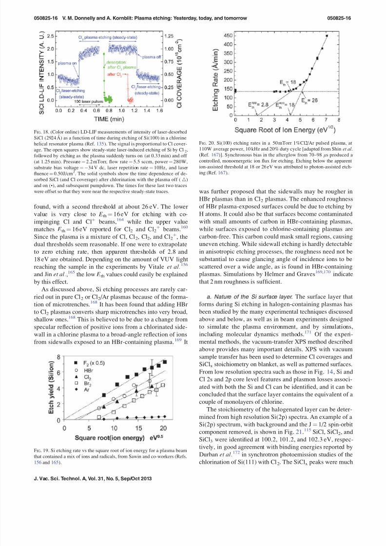
8/16/2019 Plasma etching review
http://slidepdf.com/reader/full/plasma-etching-review 16/48
found, with a second threshold at about 26 eV. The lower value is very close to Eth ¼16 eV for etching with co-impinging Cl and Cl þ beams, 164 while the upper valuematches Eth ¼16 eV reported for Cl 2 and Cl2
þ beams. 160
Since the plasma is a mixture of Cl, Cl 2 , Cl2 , and Cl2þ , the
dual thresholds seem reasonable. If one were to extrapolateto zero etching rate, then apparent thresholds of 2.8 and18 eV are obtained. Depending on the amount of VUV lightreaching the sample in the experiments by Vitale et al. 156
and Jin et al. ,165 the low Eth values could easily be explainedby this effect.
As discussed above, Si etching processes are rarely car-ried out in pure Cl 2 or Cl2 /Ar plasmas because of the forma-tion of microtrenches. 168 It has been found that adding HBr to Cl2 plasmas converts sharp microtrenches into very broad,shallow ones. 168 This is believed to be due to a change fromspecular reection of positive ions from a chlorinated side-wall in a chlorine plasma to a broad-angle reection of ionsfrom sidewalls exposed to an HBr-containing plasma. 169 It
was further proposed that the sidewalls may be rougher inHBr plasmas than in Cl 2 plasmas. The enhanced roughnessof HBr plasma-exposed surfaces could be due to etching byH atoms. It could also be that surfaces become contaminatedwith small amounts of carbon in HBr-containing plasmas,while surfaces exposed to chlorine-containing plasmas arecarbon-free. This carbon could mask small regions, causinguneven etching. While sidewall etching is hardly detectablein anisotropic etching processes, the roughness need not besubstantial to cause glancing angle of incidence ions to bescattered over a wide angle, as is found in HBr-containingplasmas. Simulations by Helmer and Graves 169 ,170 indicatethat 2 nm roughness is sufcient.
a. Nature of the Si surface layer. The surface layer thatforms during Si etching in halogen-containing plasmas hasbeen studied by the many experimental techniques discussedabove and below, as well as in beam experiments designedto simulate the plasma environment, and by simulations,including molecular dynamics methods. 171 Of the experi-mental methods, the vacuum-transfer XPS method describedabove provides many important details. XPS with vacuumsample transfer has been used to determine Cl coverages andSiClx stoichiometry on blanket, as well as patterned surfaces.From low resolution spectra such as those in Fig. 14, Si andCl 2s and 2p core level features and plasmon losses associ-ated with both the Si and Cl can be identied, and it can beconcluded that the surface layer contains the equivalent of acouple of monolayers of chlorine.
The stoichiometry of the halogenated layer can be deter-mined from high resolution Si(2p) spectra. An example of aSi(2p) spectrum, with background and the J ¼1/2 spin-orbitcomponent removed, is shown in Fig. 21.115 SiCl, SiCl 2 , andSiCl3 were identied at 100.2, 101.2, and 102.3 eV, respec-tively, in good agreement with binding energies reported byDurban et al. 172 in synchrotron photoemission studies of thechlorination of Si(111) with Cl 2. The SiCl x peaks were much
FIG. 18. (Color online) LD-LIF measurements of intensity of laser-desorbedSiCl (2924A ) as a function of time during etching of Si(100) in a chlorinehelical resonator plasma (Ref. 135). The signal is proportional to Cl cover-age. The open squares show steady-state laser-induced etching of Si by Cl 2,followed by etching as the plasma suddenly turns on (at 0.33 min) and off (at 1.25 min). Pressure ¼2.2mTorr, ow rate ¼5.5 sccm, power ¼280W,substrate bias voltage ¼ 34 V dc, laser repetition rate ¼10Hz, and laser uence ¼0.50J/cm 2. The solid symbols show the time dependence of de-sorbed SiCl (and Cl coverage) after chlorination with the plasma off ( )and on (•), and subsequent pumpdown. The times for these last two traces
were offset so that they were near the respective steady-state traces.
FIG. 19. Si etching rate vs the square root of ion energy for a plasma beamthat contained a mix of ions and radicals, from Sawin and co-workers (Refs.156 and 165).
FIG. 20. Si(100) etching rates in a 50mTorr 1%Cl2/Ar pulsed plasma, at110W average power, 10 kHz and 20% duty cycle [adapted from Shin et al.(Ref. 167)]. Synchronous bias in the afterglow from 70–98 l s produced acontrolled, monoenergetic ion ux for etching. Etching below the apparention-assisted threshold at 18 or 26eV was attributed to photon-assisted etch-ing (Ref. 167).
050825-16 V. M. Donnelly and A. Kornblit: Plasma etching: Yesterday, today, and tomorrow 050825-16
J. Vac. Sci. Technol. A, Vol. 31, No. 5, Sep/Oct 2013

8/16/2019 Plasma etching review
http://slidepdf.com/reader/full/plasma-etching-review 17/48
broader than the 0.6eV resolution of the XPS instrument(especially for SiCl 2), and hence cannot be attributed to reso-lution but are instead an indication of the high degree of dis-order in the SiCl x layer formed during plasma etching.
An additional, weak peak appearing as a shoulder on thelow binding energy side of the at Si (Si bound to 3 Si andone dangling bond) peak was attributed to Si. Its bindingenergy was found to be the same (98.8eV) as that measuredfor Si after Ar þ sputtering, providing supports for the assign-ment. From an analysis of spectra at various take-off anglesfor different plasma conditions, the relative coverages Si,SiCl, SiCl 2 , and SiCl 3 were deduced, as well as the overallthickness of the chlorinated silicon layer. 115 ,173
Measurements of Cl coverage as a function of ion energy(Cl2
þ and/or Cl þ or Ar þ ) from both plasma and beamexperiments by several groups are summarized in Fig. 22,where the areal density of Cl determined by XPS (Ref. 173)and LD-LIF are plotted as a function of the square root of ion energy. Increasing ion energy increases the Cl coverageduring Si etching, for ion energies less than 300 eV.Coburn 174 also found that ion bombardment increases chlo-rine coverage on Si (two “ þ” points in Fig. 22). The chlorineuptake on Si exposed to simultaneous Ar þ (1 keV) and Cl 2
beams is 3 times larger than with just the Cl 2 beam alone,whether the Si surface was an ordered, annealed surface, or one amorphized by ion bombardment prior to exposure tothe Cl2 beam. The factor of 3 is less than expected from anextrapolation of the XPS and LD-LIF data in Fig. 22, per-haps because of the added Cl supplied by Cl þ and Cl2
þ . Itcould also indicate that the increase in Cl coverage saturateswith increasing Ar þ energy. Such a saturation was observedin the Cl2 /Ar þ beam studies of Barker et al. 175 when the Ar þ
energy was varied between 400 and 900eV (solid circlesincluded in Fig. 22).
Since the beam experiments by Coburn showed that si-multaneous Ar þ and Cl2 exposure creates a more highly
chlorinated layer than sequential Ar þ followed by Cl 2 expo-sures, the enhanced chlorination was attributed to a knock-on process, rather than an increase in binding sights by ionbombardment. In a knock-on process, short range ion impacton adsorbates causes the adsorbates to be implanted into thesubsurface region. This mechanism was also proposed byBarrish et al. 176 for Si etching with Cl 2 and Ar þ beams.While knock-on is a well known effect that no doubt playssome role in subsurface chlorination, ion-induced creation of added adsorption sites is not necessarily ruled out by the Cl 2 / Ar þ beam experiments. Consider the differences in the typesof amorphous layers created by Ar þ versus Cl 2
þ bombard-ment. Ar þ bombardment breaks bonds during the collisioncascade, but most of these broken bonds reform. The resultis a fairly dense lattice with few voids. Cl þ and Cl2
þ bom-bardment also breaks bonds, but in addition prevents someof the Si-Si bonds from reforming through formation of mainly SiCl. This favors formation of a much more opensurface structure than Ar þ amorphized Si.
The strongest evidence for this comes from molecular dy-namics simulations by Graves and co-workers. 104 ,177 Someof these calculations are reproduced in Fig. 23.104 Startingwith a Si(100) surface, they found that bombardment with50eV Ar þ created a disordered but dense damaged layer,while bombardment with Cl þ at the same energy resulted ina highly disordered, roughened layer with small subsurfacevoids. Such a layer contains more binding sites for adsorp-tion by neutral Cl and Cl 2 .
Si etching mechanisms in HBr-containing and HBr/Cl 2-containing plasmas have also been investigated. Horizontalsurfaces take up Br and Cl roughly in proportion to theHBr:Cl 2 feed gas ratio, as shown by the XPS and LD-LIF
FIG. 21. (Color online) High-resolution Si (2 p3/2) XPS spectrum acquired ath ¼30 for Si etched in a 10.0 sccm Cl 2 plasma. The best t from a nonlin-ear least squares model (solid line) includes ve peaks (broken lines)assigned to: Si (98.50eV, 0.70 eV FWHM), Si bulk (99.14eV, 0.70 eVFWHM), SiCl (99.90eV, 0.84 eV FWHM), SiCl 2 (100.94 eV, 1.10 eVFWHM), and SiCl 3 (101.99 eV, 0.84eV FWHM) components present in thechlorinated layer that is formed during etching (Ref. 115).
FIG. 22. Cl coverage on Si(100), during and after etching in high density Cl 2
plasmas ( , , ), and for etching with simultaneous Cl 2 and Ar þ beams(•, þ), expressed as areal density vs the square root of ion energy. Includedare XPS (Ref. 173 ). ( ) and LD-LIF measurements in a helical resonator plasma (Ref. 135) ( ), as well as LD-LIF measurements in a at coil ICPreactor (Ref. 138) ( ). XPS measurements are absolute. LD-LIF measure-ments and the beam measurements by Coburn (Ref. 174) (
þ) are normalized
to the XPS values. The beam measurements by Barker et al. (Ref. 175) (•)are normalized to Coburn’s beam result at 1 keV. The points at zero ionenergy correspond to uptake by laser-annealed Si(100) with the plasma off.The line is a linear least squares t to all of the Cl 2 plasma data.
050825-17 V. M. Donnelly and A. Kornblit: Plasma etching: Yesterday, today, and tomorrow 050825-17
JVSTA - Vacuum, Surfaces, and Films

8/16/2019 Plasma etching review
http://slidepdf.com/reader/full/plasma-etching-review 18/48
measurements in Fig. 24.136 Neither of these methods werecapable of detecting hydrogen, so part of the falloff in totalhalogen coverage as a function of HBr addition could be dueto adsorbed H that blocks sites for adsorption by Cl or Br.The etching rate has been found to fall as HBr is added toCl2 feed gas. This was attributed to a combination of reduced
halogen content in the layer and to a lesser degree, lower ionux in HBr plasmas compared to Cl 2 plasmas. 136
Sawin and co-workers have also studied etching of Si inHBr/Cl 2 plasmas. 156 ,165 Their XPS measurements 165 of halo-gen coverage measured as a function of HBr fraction are vir-tually identical to those of Cheng et al. 136 in Fig. 24. Theyalso found that the etching rate decreases with HBr additionto Cl2, but ascribe it mainly to the lower ion ux and not tothe reduced halogen coverage on the Si surface. This wasbased on the observation that if Si was etched in either a Cl 2
or HBr plasma and then subjected to Ar þ
bombardment, theinitial enhanced sputtering rate was the same. They invokeadsorbed H in HBr plasmas as playing a role similar to Br or Cl in enhancing the rate.
Sawin and co-workers also studied the angle-of-incidencedependence of the etching rate for beams extracted fromHBr and Cl 2 plasmas. 156 ,165 They found that both yieldspeaked at normal incidence ( ¼0 ), but the yield in Cl 2 plas-mas was nearly constant between 0 and 45 while HBr plasma yields fell signicantly between 0 and 45 . Theycarried out simulations of feature prole evolutions and at-tribute the straighter sidewalls in HBr plasmas versus Cl 2
plasmas to this difference in dependence of the ion-assisted
etching yield on angle of incidence.As can be seen from Fig. 15, the chemical (i.e., isotropic)
etching rates by Cl and Br atoms is very slow for all butheavily doped n-type Si. Consequently, no undercutting isexpected and none is found. 178 No sidewall protection isneeded, whether intentional (e.g., oxygen or uorocarbonaddition) or serendipitous (as a benet of mask erosion). Infact, vacuum-transfer XPS analysis of photoresist-masked p-type Si in a HBr plasma showed that there is no carbon or oxygen on the sidewall. 178 When some undercutting doesoccur, either from wide-angle ion bombardment, from possi-ble attack by H atoms, from photo-assisted etching, or in thecase of etching of heavily n-doped Si, the deposition of athin lm on the Si etched feature sidewalls can be benecialin obtaining near-ideal prole shapes. Sidewall lms can beformed by adding oxygen to HBr-containing plasmas. 179 AnSiO2 layer has been shown to form under these conditions,with little carbon, even when photoresist masks wereused. 154 The presence of this thin layer suppresses bowingand notching. 154 Oxygen addition to HBr-containing plas-mas also improves selectivity to underlying oxygen-containing layers such as SiO 2 .
2. SiO 2 etching in fluorocarbon plasmas
F atoms react slowly with SiO2
in the absence of ionbombardment (1/40th the rate of F þSi at room tempera-ture). 99 This rate is too slow to cause much undercutting inmost SiO 2 etching processes. Cl, Br, and H do not react withSiO2 at room temperature. Ion bombardment greatly acceler-ates the etching of SiO 2 by F atoms128 (and also of Cl andBr), but because Si also etches rapidly under these condi-tions, this approach is not commonly used for silicon micro-electronics applications. Instead, uorocarbon plasmas areused for selective etching of SiO 2 over Si. Although the bulkof dielectric etching in IC fabrication is of lower dielectricconstant insulators, etching of SiO 2 is still important. In
FIG. 23. Molecular dynamics simulations by Barone and Graves (Ref. 104)of 50eV Ar þ or Clþ bombardment of Si(100). The light and dark circlesrepresent Si and Cl atoms, respectively.
FIG. 24. (Color online) Cl and Br coverages as a function of HBr addition toa Cl2 plasma during and after Si(100) etching (Ref. 136). Bottom: Cl(2p)( ), Br(3d) (•), and Cl(2p) þBr(3d) ( ) XPS integrated peak intensities[normalized to Si(2p) and corrected for sensitivity differences], recorded af-ter etching in HBr/Cl2 plasmas, as a function of% HBr. The solid lines arelinear least square ts. Top: SiCl ( D ), SiBr ( ), and SiCl þSiBr ( ) LIFintensities [normalized to the corrected Cl(2p) and Br(3d) XPS intensities at100% Cl 2 and HBr, respectively] vs % HBr. The open symbols refer tointensities derived from single peaks 2989 A for SiCl and 3009 A for SiBr,and the open, crossed symbols refer to signals derived from a least squarest to a combination of spectra for pure Cl 2 and HBr plasmas. The curves,which are second- and third-order polynomial ts, are to guide the eye.
050825-18 V. M. Donnelly and A. Kornblit: Plasma etching: Yesterday, today, and tomorrow 050825-18
J. Vac. Sci. Technol. A, Vol. 31, No. 5, Sep/Oct 2013

8/16/2019 Plasma etching review
http://slidepdf.com/reader/full/plasma-etching-review 19/48
addition, the process has been studied more than any other with perhaps the exception of Si etching. Much of what hasbeen learned in these studies also relates to etching of other materials such as SiN. 180
Fluorocarbon plasmas etch SiO 2 in reactions that canform stable products SiF 4 , CO, CO2, and perhaps COF 2, or even SiOF 2 . CF2 and CF3 radicals, generated by electronimpact dissociation and detachment of the feed gas, do not
spontaneously etch SiO 2 in the absence of ion bombard-ment. 181 Neutral CF x radicals and ions bombard surfaces andlead to the formation of a uorocarbon lm. The depositionof this thin lm on horizontal surfaces is the most importantaspect of the etching of SiO 2 in uorocarbon-containingplasmas. Coburn used in-situ Auger electron spectroscopy toinvestigate the formation of uorocarbon lms on Si andSiO2 in CF4 /H2 plasmas. 182 He found that a thicker lmformed on Si than on SiO 2 . The high selectivity of etchingSiO2 over Si was attributed to this difference in lmthickness.
Unlike processes that rely on a sidewall lm to suppressetching, the uorocarbon lm supplies reactants that are acti-
vated by ion bombardment. The lm also improves selectiv-ity toward etching of Si. The composition of the lm and itsdeposition rate on SiO 2 depend on which uorocarbon feedgas is used, the addition of other gases, the reactor materials,and other processing conditions. If the deposition rate is toofast, then the lm continues to thicken and no etching occurs.Under useful condition, a constant steady-state lm thick-ness and composition is maintained while the underlyingSiO2 layer is etched at a constant rate.
Butterbaugh et al. 181 studied the etching of SiO 2 in thepresence of beams of Ar þ , F, and CF 2. They found that ei-ther F or CF 2 enhanced the yield of Ar þ etching and that theenhancement was larger for F. They also found that supply-ing a ux of CF 2 had no additional enhancement of the etch-ing with simultaneous Ar þ and F beams impinging. Aspointed out by Butterbaugh et al. ,181 this is consistent withthe prior observation that the etching rate of SiO 2 in CF4 /O2
plasmas and NF 3 /Ar plasmas are the same at the same uo-rine atom number density. 128 The yields for 500 eV Ar þ canapproach unity for high F/Ar þ ux ratios. 183
Oehrlein and co-workers have extensively studied etchingmechanisms for SiO 2 in uorocarbon plasmas. 184 – 186 Theyfound that the deposition rate of the uorocarbon lmdepends on gas composition and self bias voltage (Fig. 25).Lower ion energies favored faster deposition rates, displayedas negative values in Fig. 25. If a uorocarbon lm was de-posited at low ion energy and then, under the same plasmaconditions, subjected to high ion energies it etched. Thesenet etching rates are given by the positive values in Fig. 25.Under conditions when the etching rate for the uorocarbonlm is much slower than the deposition rate, a thick lmcontinuously grows and no etching of the underlying SiO 2 or Si occurs. If conditions are such that the lm etching rate ismuch greater than the deposition rate, then little if any lmwill form on Si or SiO 2 . When the lm etching and deposi-tion rates are nearly equal, then the nature of the underlyingmaterial determines the steady-state lm thickness. If it
etches fast, as it does for SiO 2 , then the lm is relativelythin, while if it etches slower as for Si, then a thicker lm ispresent.
Some of the processes that occur during etching of SiO 2
in uorocarbon-containing plasmas are summarized in themodel put forth by Sankaran and Kushner; their schematicmechanism is reproduced in Fig. 26.187 The lm affects etch-ing in two ways. First, it attenuates the energy of impactingions that penetrate the lm and reach the underlying layer.Ion-assisted etching rates typically decrease with the squareroot of ion energy above a threshold energy, hence, thethicker the lm, the slower the etching rate. This inverse de-pendence of etching rate as a function of lm thickness isillustrated by the measurements by Schaepkens andOehrlein, reproduced in Fig. 27.186 Somewhat surprisingly,SiO2 , Si, and Si-nitride all fall on the same curve.
More recently, it was shown that the etching rate of Si,SiO2 , and Si-nitride scales inversely with the amount of uo-rine in the lm. 184 The explanation for this is that this uo-rine is liberated by ion bombardment. Some of it diffuses to
FIG. 25. Deposition and etching rates of the lm deposited in uorocarbonplasmas for different feed gases as a function of the dc self-bias voltage (andhence ion bombardment energy) (Ref. 186).
FIG. 26. Surface reaction mechanism during etching of SiO 2 inuorocarbon-containing plasmas (Ref. 187). Iþ and I* refer to positive ionsand energetic neutrals, respectively. The dashed lines indicate that the parti-cle loses energy during traversal through the polymer lm. The curved linesrepresent species that diffuse through the polymer.
050825-19 V. M. Donnelly and A. Kornblit: Plasma etching: Yesterday, today, and tomorrow 050825-19
JVSTA - Vacuum, Surfaces, and Films

8/16/2019 Plasma etching review
http://slidepdf.com/reader/full/plasma-etching-review 20/48
the underlying surface and participates in etching. Fluorine-containing products are liberated from the lm; hence, uo-rine content in the uorocarbon lm is reduced.
Charging in high aspect ratio features is believed to be re-sponsible for “etch stop” that is often observed for dielectricmaterials. 188 – 201 Etch stop can also be caused by depositionof uorocarbon polymer at the bottoms of high aspect holesin insulating lms. 153 The combination of charging and poly-mer deposition can cause other interesting phenomena.When high aspect ratio holes are etched into an insulatinglm, a twisting is sometimes observed, as shown in Fig.28.202 It appears to be random; the origin is believed to bedue to statistical variation in the amount of polymer and the
amount of charge deposited on one side, causing the ions tobe deected off normal incidence, producing asymmetricproles. Wang and Kushner simulated this twisting effectduring etching of SiO 2.202 An example from that study isreproduced in Fig. 29. The different panels represent differ-ent random seeds in the Monte-Carlo simulations. They ndthat once twisting begins in a feature, in propagates. This hasto do with the fact that ions are neutralized on glancing colli-
sions with the sidewalls. These neutrals then perpetuate thetwisted trench or hole. They also found that injecting highenergy electrons into the trench helped to neutralize chargeand reduce the severity of the twisted features.
3. Low-k dielectrics
Low dielectric constant materials usually contain carbonand silica, as in for example methylsilsesquioxane (MSQ),or SiOC(H). Fluorocarbon containing plasmas are used toetch these materials, and the uorocarbon layer that formson surfaces during etching plays a similar role in controllingetching rates of the lm, as well as allowing etching to be
selective to other materials such as SiC(H) etch stoplayers. 203 ,204 The thickness and C/F ratio of the steady-stateuorocarbon layer is greater on MSQ than on SiO 2 [see, for example, Fig. 30 (Ref. 205)], suggesting that carbon in theetching lm is the main source of C in the layer. For bothMSQ and hydrogen silsesquioxane (HSQ), the hydrogen inthe lm leads to a reduction of uorine in the lm throughthe formation of HF. 203 ,205 The uorocarbon layer is alsothicker on SiC(H) lms than on SiOC(H) lms 204 [Fig. 30(Ref. 205)], indicating that the oxygen in the lm helps toremove the uorocarbon layer. 203
To further reduce the dielectric constant of insulatinglayers in interconnects, pores are introduced into the lm.
The etching of porous silica and other porous low- j lms isusually faster than of the same materials without pores. Thefactor by which the etching rate is enhanced might beexpected to scale simply with the reduction of mass of thelm. In fact, the rate can be enhanced either more or lessthan this amount. 206 The introduction of pores can even leadto a suppression of etching rate under certain conditions. 206
The pore size and degree of uorocarbon lm depositionplay key roles in determining the etching rate behavior of
FIG. 27. Etching rate vs thickness of the uorocarbon lm for Si, SiO 2
(“oxide”) and SiN (“nitride”) with different uorocarbon gases. The C 3F6 / H2 mixture contained 27% H 2 (Ref. 186).
FIG. 28. Scanning electron micrograph of high aspect ratio holes etched intoSiO2 in a uorocarbon-containing plasma. Reproduced with permissionfrom Wang and Kushner, J. Appl. Phys. 107, 023309 (2010). Copyright2010, The American Institute of Physics.
FIG. 29. Simulations by Wang and Kushner (Fig. 6, Ref. 202) of etching of high aspect ratio features in SiO 2 in a C4F8 /O2 /Ar plasma with chargingincluded, but no high-energy electrons. Reproduced with permission fromWang and Kushner, J. Appl. Phys. 107, 023309 (2010). Copyright 2010,The American Institute of Physics.
050825-20 V. M. Donnelly and A. Kornblit: Plasma etching: Yesterday, today, and tomorrow 050825-20
J. Vac. Sci. Technol. A, Vol. 31, No. 5, Sep/Oct 2013

8/16/2019 Plasma etching review
http://slidepdf.com/reader/full/plasma-etching-review 21/48
porous material relative to the nonporous material of thesame chemical composition. As proposed by Standaertet al. 206 and simulated by Sankaran and Kushner, 187 llingof the pores with uorocarbon deposits will slow the etchingrate. When the deposition is severe and the pores are large,this can lead to a reduction in etching rate to below that for nonporous material. For small pores, the rate can beenhanced more than the amount expected by the reduction indensity. Detailed simulations have been performed bySankaran and Kushner 207 for etching of porous silica inC4F8-containing plasmas. Blanket etching rates and proleevolutions were generated, and in cases where experimentaldata are available, compared favorably.
V. APPLICATIONSA. General concepts
Many issues must be considered in evaluating an etchingprocess. These issues are often coupled, and sometimestrade-offs must be considered in optimizing a process.
Etch-rate uniformity is critical in most applications. In abatch reactor, both wafer-to-wafer and within-wafer uni-formities must be considered. Two denitions for etchingnonuniformity are commonly used. If E is the average of etch rate Ei of N measurements across a wafer (or a batch of wafers), then three standard-deviations, r , from E will be
3r ¼3 ffiffiffiffiffiffiffiffiffiffiffiffiffiffiffiffiffiXn
i¼1ð Ei EÞ
2
N 1s ; (22)
hence, the etching nonuniformity is 300 r = E, expressed in %.This three-sigma nonuniformity means that 99.7% of theetch-rate measurements will fall within E6 3r . This is rarelythe case, however, since etching nonuniformity is usually notrandom (center to edge, top to bottom, etc.). Another widelyused expression for percent nonuniformity is dened as
% nonuniformity ¼100 Emax Emin
2 E ; (23)
where Emax and Emin are the highest and lowest measuredetch rates.
Typically, 3% nonuniformity within a wafer is consideredgood. However, there are applications that are more forgiv-ing, while others are more critical. If the process has goodselectivity (to be dened below) to an underlying layer, uni-formity is less critical, while in applications when etchingcreates a particular depth feature (e.g., trenches in silicon),
uniformity of etching is extremely critical. Uniformity canbe optimized by reactor design (electrode design, gas deliv-ery system, magnetic connement, and use of multiple coilsfor inductive sources), choice of chemistry and process pa-rameters (e.g., gas ow, pressure, magnetic eld and power,as well as the use of additives). Some etching processes aremore chemical than ion-assisted (e.g., Al etching in Cl 2-containing plasmas, or silicon etching with SF 6 or NF3) andtherefore are more prone to nonuniformity when large openareas are etched and the feed gas is largely consumed(see “loading effect” below). In these cases, additional hard-ware (such as focus and shadow rings) can often improveuniformity.
A high selectivity , dened as the ratio between the rateof the layer being etched, relative to that of an underlyinglayer or masking material, is of critical importance. For example, when polysilicon gate electrodes are formed ineld-effect transistors (FETs), the polysilicon (poly-Si) isetched until the underlying gate dielectric (e.g., SiO 2)begins to be exposed in those regions where the lm wasslightly thinner and/or the etching rate was slightly faster.As the process is carried to completion and the remainingpoly-Si is etched away or “clears” (the so-called “overetch”step), the exposed gate dielectric layer must remain, sinceits removal will result in attack of the Si substrate below.Consequently, a high selectivity of poly-Si etching over thegate dielectric is required. Similarly, the selectivity withrespect to the mask must be high enough that the integrityof the mask is preserved during the main etch and overetchperiod.
The selectivity, however, is not always a well-denedquantity. In many instances, the etching rate changes duringthe process, and as a result, the selectivity varies as well.The etching rates and selectivity can also vary with the as-pect ratio of the features being etched. (Aspect-ratio-depend-ent etching rates are discussed below.) In addition, whileselectivity associated with a process may appear high on amacroscale, local effects such as feature “faceting” and“trenching” (discussed below) may make bulk high-selectivities meaningless.
The determination of selectivity is not always straightfor-ward. For gate etching, post-etch measurements of theremaining gate-dielectric are often erroneously high (some-times higher than the initial thickness) due to deposits thatform during etching. In addition, when SiO 2 is exposed tothe plasma after poly-Si etching in an oxygen-containingplasma such as HBr/O 2 , oxygen can penetrate the exposedSiO2 layer and oxidation of the underlying Si substrate canoccur, also making the remaining dielectric layer thicker andthe selectivity appear articially larger than it is. 96 ,208
FIG. 30. C(1s) XPS spectra of uorocarbon layers on SiO 2, uorinated oxide(SiOF), HSQ, and methyl silsesquioxane (MSQ) after partial etching in aC3F6 plasma at 6 mTorr, 1400 W source power and a substrate self-bias of 2150 V DC (Ref. 205).
050825-21 V. M. Donnelly and A. Kornblit: Plasma etching: Yesterday, today, and tomorrow 050825-21
JVSTA - Vacuum, Surfaces, and Films

8/16/2019 Plasma etching review
http://slidepdf.com/reader/full/plasma-etching-review 22/48
Loading is the decrease of etching rate with an increasein the amount of exposed material being etched. It can beglobal, where the spatially-averaged etch rate varies, or local, where the etching rates of regions of the chip dependon the density of the features. The loading effect is observedwhen the active species in the plasma are depleted rapidlyby reaction with the material being etched. 209 ,210 It isaffected by the lifetime of the active species as well as cham-
ber volume (larger volume, which may be impractical,reduces the loading effect 209 – 212 ) and feed gas ow rate(etching rates decrease with decreasing ow rate 115 ). Theloading effect is strong when the process is dominated byfast chemical etching by neutrals, where the etching rate isoften observed to be rst order in neutral etchant number density, 99 and weaker when etching is driven by ion-stimulated removal of a halogenated surface layer. 212 Theformer is observed, for instance, in SF 6 or NF3-containingplasmas when a large amount of Si is etched, and F-atomsbecome depleted. On the other hand, etching Si in Cl 2 plas-mas varies much less with the area of exposed Si becausethe composition of the halogenated surface layer is largely
independent of loading, 115 and no chemical etching by Clatoms occurs (except for n þ -Si). Etching is limited by ionstimulated desorption, and the ion ux is fairly insensitive toloading. In some applications, such as fabrication of siliconmicrolenses (where a pattern of spherically shaped polymer mask is transferred into the substrate below by polymer-ero-sion213 ,214 ), the loading effect needs to be addressed, sincethe area of exposed substrate changes as the polymer erodes,and maintaining constant etch rates of both polymer and sub-strate material is critical for obtaining the desired lens shape.
Aspect Ratio Dependent Etch Rate (ARDE) or “ RIE Lag ” refers to a phenomenon where etch rate slows down asthe etching proceeds down a hole or a trench. A number of mechanisms have been proposed 215 – 217 and involve transportof neutrals and ions as well as charging and shadowingeffects. Locally, this effect can take place when the aspectratio (i.e., the ratio between the depth and width of the spacebetween features) changes, either as a function of depth or asa function of position across the wafer. During contact etch-ing, the aspect-ratio increases and the etching rate generallydecreases or, in extreme cases, etching stops. This occurssooner in smaller features, meaning that when contacts withdifferent diameters are patterned on the same wafer, thesmaller contacts etch slower. By adjusting the ion/neutralsratio (e.g., by increasing the pressure), however, and movingtoward a regime dominated by polymer deposition, the effectis reduced and even reversed. 217
Faceting of the mask is the result of ion bombardment.Since the sputtering yield is a function of angle, 218 – 220 thesharp (or nearly sharp) corners may erode and attain an anglecommensurate with the angle associated with the maximumsputtering rate. 221 Since the ion ux per unit area decreaseswith the angle of incidence, h, the maximum sputtering ratewill take place at an angle larger than 0 if the sputtering-yield as a function of h rises faster than 1 =cos h.221 If themask erodes signicantly, then the bottom edge will moveinward, away from the etched step and the feature will
develop a tapered prole. 222 In addition, deection of ionsfrom the sloped surface can cause a microtrench to developat the feature base (see below) as well as affect the prole of a neighboring line [see Fig. 31(a)].222
Impinging ions are nearly perpendicular to the wafer sur-face, but there is a small lateral component that can affectthe prole of the feature being dened. In some cases thiscan lead to a near-specular reection off vertical sidewalls,
increasing the ion ux near the base of the feature and caus-ing microtrenching [Fig. 31(b)], an undesired effect. 221 Inother instances, the off-normal-incidence ions cause a slopein the prole and may round the bottoms of trenches(depending on the application, this could be a desired or undesired effect). A good example of these two effects is theetching of trenches in silicon with Cl 2 or HBr-containingplasmas (see also discussion above). The former causes theformation of sharp microtrenches while the latter leads tomuch wider trenches that have rounded corners. 223 – 226
Undercutting [Fig. 31(c)] is the result of isotropic etchingthat will lead to lateral as well as vertical etching. When theisotropic component is strong (such as etching silicon with
low bias SF 6 or NF3 plasmas), a prole similar to the oneobtained by wet etching is observed. This is caused by achemical attack by neutral species [F for all forms of Si andCl for nþ -Si (see Fig. 15), Cl and Cl 2 for Al]. It is possible,however, to increase the vertical component (by increasingthe bias power, for instance), to reduce the relative undercut.To avoid undercutting completely in these situations, a side-wall protection scheme is necessary (See discussion on alu-minum etching, Sec. V C 6 below) Often the application of bias leads to formation of by-products that aid in this side-wall protection, such as resist erosion during Al etching.
Tapered proles [Fig. 31(d)] often result from depositionon the sidewall during etching, effectively increasing themask width as etching progresses. The deposited material
FIG. 31. Various proles obtained during plasma etching: (a) bowing due tofaceting of the mask; (b) microtrenching due to enhanced ion ux along thesidewall; (c) Undercutting due to an isotropic component in the etch pro-cess; (d) tapered prole due to deposition on the sidewall; (e) notching atthe interface due to inadequate sidewall passivation or charging effects; (f)Re-entrant prole (overcutting) due to inadequate sidewall passivation and/ or ion scattering.
050825-22 V. M. Donnelly and A. Kornblit: Plasma etching: Yesterday, today, and tomorrow 050825-22
J. Vac. Sci. Technol. A, Vol. 31, No. 5, Sep/Oct 2013

8/16/2019 Plasma etching review
http://slidepdf.com/reader/full/plasma-etching-review 23/48
can be either polymer formed during the etch process com-bined with etch by-product, or material being sputtered dur-ing etching. An example of the former is the excessiveamount of sidewall passivation lms that deposited duringaluminum etching, 227 while the latter could be sidewalldeposits of nonvolatile by-products from sputtered copper or gold. 228
Notching at bottoms of etched features [Fig. 31(e)], at the
interface with the layer below, can occur for a number of reasons. One can be positive charging of the underlying layer that can deect positive ions toward the sidewall. 229 This isusually observed at low bias power in, for instance, gateoveretch, where the low power is needed to preserve the thingate oxide. Another mechanism occurs in etch processes thatrely on sidewall passivation to achieve anisotropy. The side-wall protective layer near the interface may be too thin toprovide protection, leading to isotropic etching at the inter-face. This can occur, for instance, in Al etching with a hardmask, using a Cl 2 and HBr mixture to generate by-productsthat passivate the sidewalls. 230 The passivation layer at thebottom of the feature is too thin to protect the aluminum
from the highly isotropic etch by Cl 2 .230 Notches at the bot-toms of etched features could sometimes be desirable, suchas in the formation of a notched gate (T-gate), to reduce theoverlap capacitance between the gate and source and drainregions. 231
Reentrant proles, [Fig. 31(f)] could be the result of ei-ther inadequate passivation as the etch progresses deeper, 232
the result of ion-scattering by the etch-stop layer, 233 ,234 or adivergent ion ux. 235
B. Etch chemistries
The etch chemistry chosen for a particular application is
based on the material being etched, the etchers being usedand other considerations such as uniformity, selectivity, etchrate, etc. discussed in the previous sections.
1. Dielectrics
Fluorocarbon and hydrouorocarbon gases, usually withsome additives, are typically used for dielectric etching,such as SiO 2 , Si3N4, SiN, and various low- j dielectrics. CF 4
[FreonVR 14 (Ref. 236)], C2F6 (Freon 116), and C 3F8 (Freon218) were used in the early days to etch SiO 2,28 ,29 usuallywith addition of O 2 when selectivities to resist and/or siliconwere not critical, and polymer control was important.Hydrogen addition to the above uorocarbons was used toincrease selectivity to silicon, 28 ,29 ,237 with the drawbacks of polymer formation, decreased etch rate, 237 ,238 and deep pen-etration of hydrogen into the silicon substrate 239 – 247 that canlead to device degradation if not annealed properly. In appli-cations where this is not an issue (such as patterning of waveguides), hydrogen may be used as an additive to controlselectivity to silicon and/or photoresists.
CHF 3 (Freon 23), 28 ,29 ,37 with some additives that varywith tool and application, has been used for many genera-tions of device for SiO 2 and SiN etching. The additives areneeded to control polymer build-up on the wafer as well as
the chamber wall. O 2 and CO2 were common additives inbatch reactors; however, as the industry migrated to singlewafer etchers, mixtures of CHF 3 with CF4 became morecommon, usually with Ar as a diluent. The selectivity withrespect to silicon could be controlled by the amount CF 4
added to the mixture; increased CF 4 concentration yieldslower selectivity but less polymer formation. 217 Over theyears, etching chemistries for dielectrics evolved too, with
the introduction of gases with lower uorine-to-carbon ratios(F:C) to increase selectivity both to silicon and photoresistmasks.
Gases, such as c-C 4F8 (Refs. 28 and 29) (octauorocyclo-butane—F:C ¼2), c-C5F8 (Ref. 248) (octauorocyclopen-tene—F:C ¼1.6), and C 4F6 (Ref. 249) (hexauoro-1,3-butadiene—F:C ¼1.5), became the chemistries of choice inthe newer generation of etchers. Although the migration tothese gases was driven primarily by performance issues,there were environmental considerations as well. The moti-vation for the introduction of C 5F8 , for instance, was its shortatmospheric lifetime [0.3 years 248 versus 3200 years for C4F8 and 270 years for CHF 3 (Ref. 250)] and reduced global
warming potential. Comparisons have been made of etchingof high aspect-ratio contacts 251 using c-C 4F8 to c-C5F8 andC4F6 in a modied Gaseous Electronic ConferenceReference Cell. 252 However, the performance of these gasesin a commercial reactor may be different and will depend onthe particular etcher used.
Common additives include O 2 , Ar, CO2 , and CO. The lat-ter is used to control selectivity, since it tends to minimizethe amount of uorine-rich species. 253 Special care is neededwith CO since it reacts spontaneously with nickel. Thereforeall gas delivery hardware must be void of any exposed nickelsurfaces (such as nickel gaskets). Type 316 stainless steel isan acceptable choice as gasket material (and tubing) for CO.
Although most chemistries that will etch SiO 2 will etchsilicon nitride lms (stoichiometric or nonstoichiometricLPCVD or plasma-enhanced CVD, collectively referred toas SiN), there are applications when one has to be etchedselectively with respect to the other. Etching SiO 2 selectivelyover SiN can be accomplished by a polymer-producingplasma that will sustain etching as long as oxygen by-products are released to the plasma from the etched lm, butwill stop on the nitride lm, producing polymer deposits. 253
This process is extremely useful in etching self-aligned con-tacts (SAC) (to be discussed later), but difcult to implementin etching a bulk SiO 2 lm on top of SiN (such as silicontrench isolation). The reverse, etching SiN selectively toSiO2 , is needed in cases where a thin SiO 2 lm serves as anetch stop layer, to avoid exposure of the Si substrate to theplasma, such as in a local-oxidation-of-silicon (LOCOS)structure, where subsequent oxidation can create oxidation-induced stacking faults. 254 This can be accomplished in anumber of ways. SiN can be etched with selectivities of 3:1or higher by SF 6 or SF6 /O2 /N2 mixtures under low-bias con-ditions. 255 Best results are obtained in the so-called “plasma”conguration, where the wafer is placed on the groundedelectrode. Higher selectivities, however, can be obtainedwith SF6 /CH4 , NF3 /CH4 or CF4 /CH4 mixtures 256 or
050825-23 V. M. Donnelly and A. Kornblit: Plasma etching: Yesterday, today, and tomorrow 050825-23
JVSTA - Vacuum, Surfaces, and Films

8/16/2019 Plasma etching review
http://slidepdf.com/reader/full/plasma-etching-review 24/48
hydrouorocarbons with F:C ratio less than 3, 257 such asCH3F and CH 2F2. The mechanism proposed 257 is the sup-pression of CF 3
þ that are critical for etching SiO 2 , but theprocess may be much more complex, as discussed above.With the proper additives, and by using the right process pa-rameters (which are tool-dependent), extremely high selec-tivities to SiO 2 or Si can be achieved. Once the layer belowthe SiN is exposed, a high rate of polymer deposition often
ensues.Low- j dielectrics in use consist of organosilicate glass,which was nonporous in older applications, but highly po-rous in current and future technologies (the requirement for the 22 nm node and beyond is j 2.2). Fluorocarbon chem-istry is used to etch the low-k dielectric, stopping on the cap-ping layer below. C 4F8 /CO based chemistry was common atearly stages of implementation of low- j materials; 258 how-ever, with the migration to porous materials, the F:C ratio isadjusted to minimize residues at the end of the etch. The keyto successful integration is the postetch resist strip, whichcan affect the nal j -value of the dielectric. This will be dis-cussed below in Sec. V C 7, where damascene structures are
covered in detail.
2. Silicon
Silicon (crystalline, polycrystalline, and amorphous) isetched in chlorine, bromine, and uorine based plasmas; thechoice depends on the application. Generally, plasmas thatgenerate large amounts of F atoms will etch Si faster thanplasmas that contain large amounts of Cl or Br, but prolecontrol and loading are harder to achieve, due to the fast iso-tropic etching by F atoms (see above and Fig. 15). Cl2 , HBr,or their mixture are better choices when vertical or near ver-tical walls are desired. When large heights or depths must be
created in Si, for applications such as micromachining for MEMS or through-Si-vias (TSV), high etching rates andlarge selectivity to the mask are required. Here, SF 6 plasmas,usually with added O 2 , are the chemistry of choice. Sinceetching is substantially isotropic, the process alternatesbetween an etching plasma containing SF 6 , and a polymer depositing plasma containing most commonly C 4F8 to pro-tect the sidewalls from lateral etch. More detailed discussionwill follow in the sections discussing the various structures.
3. Silicides
Various silicides have been used in semiconductor appli-cations, mostly as the top layer in a gate stack. 259 It can ei-ther be etched together with the silicon layer below to formthe gate-stack, or formed after polysilicon etch and spacer formation (see below) in a silicidation process. 259 The mostcommon silicide in the former is tungsten-silicides, but tan-talum and titanium silicides have been used as well. Asilicon-rich silicide is usually sputtered on top of a poly-Sior amorphous Si layer, and the best etching results areobtained before the lm is sintered. In conventional RIEreactors various chlorouorocarbons, such as CFCl 3 (Refs.260 and 261) and CF2Cl2 ,260 were popular etching gases, butdue to environmental concerns, as well as issues with
polymer residues, they were replaced in later generationetchers by Cl 2 (Ref. 262) or Cl2 and HBr mixtures, some-times with the addition of oxygen, especially when theetched material is tungsten silicide. The ability to etch tung-sten silicide with Cl 2 is not obvious, since tungsten does notform volatile chlorides at room temperature. However, tung-sten silicide is etched at room temperature, at etch rates com-parable to or higher than the etch rate of the polysilicon
layer below. It is possible that residual oxygen in the cham-ber or buried in the lm helps in the creation of somewhatvolatile tungsten oxychloride (WOCl 4).263
4. Aluminum
Aluminum and aluminum alloys (with silicon or copper below 0.5%) are generally etched in Cl 2 based chemistries.Detailed discussion will follow in the discussion of metalli-zation structures below.
5. Titanium and titanium nitride
Both Ti and TiN are used in aluminum metallization
stacks. Cl 2 or BCl3 /Cl2 chemistries are the most commonlyused. Detailed discussion will follow in the discussion of metallization structures below.
6. Chromium
The main use of Cr is in creating patterns on lithographicmasks. Cl 2 and O2 mixtures 264 are used at moderate pres-sures (tens of mTorr). The process relies on formation of chromium oxychloride (CrO 2Cl2) as a volatile by-product.When a hard mask or a silicon-containing resist is used (botherode slowly), there is a slight undercut. 265 The addition of nitrogen to the plasma helps in reducing the undercutting. 265
7. Nickel and nickel alloys
Nickel does not form volatile alloys easily. However, it ispossible to etch nickel with a CO/NH 3 plasma. See detaileddiscussion below on magnetoresistive random-access-mem-ory (MRAM).
8. Other materials
Cu, Au, Pt, Ir, PZT (Pb[Zr xTi1 x]O3 with 0 < x < 1), BST(Ba1 xSr xTiO 3 with 0 < x < 1), and others that do not formvolatile compounds at room temperature can be etched inspecially designed etchers with chucks that can be heated toa few hundred degree Celsius, 63 using a hard mask or by re-active sputtering. 266 The etch chemistry will be materialdependent.
There are number of reports of gold etching in HBr/Ar, 228
Cl2 /Ar,228 Cl2 ,267 CF4 /Cl2 ,267 and CF 4 /CCl4 (Ref. 267) con-taining plasmas, but the samples were not heated, and sput-tering rather than the creation of volatile compounds tookplace. When substrates were heated to 125 C andabove, 268 – 270 Au etching rates in Cl 2 as high as 980 nm/minwith 10:1 selectivity to the SiO 2 hardmask was realized. 270
There was no evidence of deposition on the sidewalls and0.5 l m wide features, 1 l m high, appear to be vertical.
050825-24 V. M. Donnelly and A. Kornblit: Plasma etching: Yesterday, today, and tomorrow 050825-24
J. Vac. Sci. Technol. A, Vol. 31, No. 5, Sep/Oct 2013

8/16/2019 Plasma etching review
http://slidepdf.com/reader/full/plasma-etching-review 25/48
C. Structures
Various structures that are created with the aid of plasmaetching are listed below. It is not possible to cover all appli-cations, so the attempt here is to address structures in use inmodern ICs. Therefore, older application for structures andtechniques such as LOCOS, poly-Si buffered LOCOS,plasma planarization, “champagne glass” contact, etc., havebeen left out.
1. Shallow trench isolation
To achieve wafer planarity and enable higher device den-sity, shallow trench isolation (STI) has replaced LOCOS asthe isolation scheme for modern devices. It consists of etch-ing trenches into silicon, lling them with SiO 2, followed byplanarization, using chemical–mechanical-polishing (CMP)to achieve a nearly planar structure on which the device is tobe built (Fig. 32).
The process involves deposition of a silicon-nitride lmon a thin layer of oxide, followed by patterning with photo-resist and then etching the nitride and oxide layer with uo-
rocarbon etch chemistry (e.g., CHF 3 /CF4 /Ar—Sec. V B,above). The photoresist can be either left in place, or removed prior to the silicon etch. In the latter case, thesilicon-nitride serves as a hard mask during etching, so theetch chemistry must be selective to nitride. The requirementsare to have a slightly tapered trench wall (to facilitate a goodtrench-ll), at bottom and rounded corner at the bottom of the trench. Rounded corners at the top of the trench are nec-essary as well, but this can be accomplished in postetchprocessing. 271
Cl2 plasmas can etch Si with high selectivity to silicon-nitride, but the prole is inadequate and leads tomicrotrenching. 169 ,223 – 225 HBr or HCl (Ref. 226) containing
plasmas lead to highly tapered proles, but a mixture of Cl 2
and HBr gives the desired prole, usually with the additionof oxygen. The latter is added mainly to increase selectivityto the mask, but it leads to the deposition of etch by-productson the trench wall. 272 The process is highly sensitive to oxy-gen concentration and the addition of too much oxygen canlead to heavy deposits on the entire wafer. Therefore, toachieve better control, the oxygen is often diluted in helium(usually 20% O 2 in He).
When silicon-on-insulator (SOI) wafers are used, theburied-oxide (BOX) layer is a natural etch-stop for the pro-cess. With Si wafers, or when the SOI trench does not reachthe BOX layer, uniformity is extremely crucial for consistenttrench depths and device performance across the wafer.
The SiN mask remains on the wafer during the trench llprocess and the subsequent CMP step. The CMP step isselective to SiN and the planarization is stopped once theSiN layer is exposed. The SiN layer is then removed, and af-ter subsequent wet cleans (which include dipping in HF solu-tion) the surface of the wafer is nearly planar.
2. Gate
Polysilicon and amorphous silicon with or without a topconducting layer (silicide or TiN) have been used as the gate
materials for many device generations. The gates are formedby depositing a poly-Si (or amorphous Si) layer on a thinlayer of oxide (either oxidized silicon, or high- j dielectric,usually HfO 2-based). The poly-Si is doped with proper impurities, usually by ion-implantation, and in symmetriccomplementary metal oxide semiconductor (CMOS) devi-ces, both p- and n-type gate materials are present on thesame wafer (in some devices only n-type poly-Si is used andthat can be achieved either in-situ or by postdeposition dop-ing). In some instances, other conductive layers such as a sil-icide (most commonly WSi x, but historically TaSi x andTiSi x) have been used. 259 In other schemes, the silicidationtakes place after the gate formation, where the silicide isformed on the gate source and drain simultaneously.
The mask can be photoresist or a hard mask (e.g., SiO 2 or SiN). Though adding complexity, the hard mask offers
FIG. 32. STI process ow: (a) pattern denition; (b) nitride and oxide etch,and resist strip; (c) trench etch; (d) oxide ll; (e) CMP oxide, stopping onnitride.
050825-25 V. M. Donnelly and A. Kornblit: Plasma etching: Yesterday, today, and tomorrow 050825-25
JVSTA - Vacuum, Surfaces, and Films

8/16/2019 Plasma etching review
http://slidepdf.com/reader/full/plasma-etching-review 26/48
advantages of higher selectivity to oxide, and better CD con-trol, especially when differences between isolated and nestedlines have to be minimized. If photoresist is used as a mask,the eroded resist becomes part of the etch chemistry; it canlead to deposits on the sidewalls and lower selectivity towardSiO2 , hence leading to erosion of the underlying gate oxidelayer. 273 When a hard mask (e.g., SiO 2 or SiN) is to be used,it is deposited on top of the gate stack, followed by an antire-
ective coating (ARC), resist application and lithography.The ARC can be either organic or inorganic. Organic ARCscan be etched either in O 2 or CO2 plasmas while the inor-ganic ARC can be etched with the same chemistry used toetch the hard mask below (using CHF 3 /CF4 /Ar chemistry,for instance). The resist is then stripped followed by theproper wet cleans (Fig. 33).
In some cases, the resist is trimmed prior to hard masketching to obtain dimensions not attainable by the litho-graphic process. This is accomplished in oxygen plasmasunder conditions yielding an isotropic etch process. Etch
uniformity is extremely critical, and this process will inevita-bly increase the relative variability in CD control. For exam-ple, if the desired gate width is 0.1 l m and the gate is printedat 0.15 l m 6 10%, the best that can be achieved after thetrim will be 0.1 l m 6 15%, assuming no additional variabili-ty added by the trimming process.
The gate etch process usually consists of multiple steps.First, there is a breakthrough step to remove the native oxide
and initiate etching. It usually consists of Cl 2 or Cl2 /Ar, atrelatively high bias power. This is followed by an etch pro-cess optimized for good CD control but not necessarilyselective to oxide. The etch chemistry usually consists of aCl2 /HBr mixture, sometimes with the addition of smallamounts of O 2 diluted in He. The Cl 2 /HBr ratio will dependon the application. In pure Cl 2, highly n-doped polysilicontends to etch isotropically (and faster than p or undoped pol-ysilicon), and therefore, higher concentrations of HBr willbe required, since the isotropic etching rate of nþ -Si by Br atoms is much slower than by Cl atoms (see Fig. 15). Onceendpoint is detected, usually by optical emission (see Sec.IIIF), an overetch step follows. This step is intended to clear
residual poly-Si remaining on the wafer due to nonuniform-ity, and in some cases, due to topography. The overetch stepusually involves adding (more) O 2 to a Cl2 /HBr (or justHBr) plasma and reducing the bias voltage. In critical cases,where extremely thin gate oxide is used, the overetch step isinitiated before the polysilicon is cleared. An endpoint pre-diction scheme, relying on interferometry with an externallight source, can be used to terminate the main etch step aslittle as 10 nm before endpoint. 96 – 98 The remaining gate ox-ide after etch cannot be measured reliably. From wet etch-rate measurements, 96 ,274 it appears to be a porous material.
When silicide or TiN is used as a top layer, the etch pro-cess may include another step optimized to etch that particu-lar layer. This step is usually Cl 2 or Cl2 /HBr based, and inthe case of silicide, it may be advantageous to add smallamounts of oxygen to increase the silicide:poly-Si etch-rateratio. When TiN is used as the top layer, large amounts of oxygen added to the plasma will hinder the etch process.Cl2, possibly with the addition of inert gases, is the mostsuitable etch gas.
The above approach has been used for gate formation andis known as the “ gate rst ” approach where the gate isformed before the source and drain are constructed, by dop-ing, epitaxially raised and/or silicided. In some cases, after spacer formation (see below), the hard mask is removed, andsource, drain, and gate are silicided simultaneously.
A further evolution of the gate rst approach is the intro-duction of high- j dielectrics (currently HfO 2 based, but ear-lier investigations included ZrO 2 based dielectrics aswell 275 ) and metal gates for added performance. The detailsare proprietary and will vary between manufacturers, but thegate metal under poly-Si is different for the p- and n-channelgates. 276 If TiN based metal is used for the gate, a Cl 2 /HBr based 277 chemistry is used for etching the gate and BCl 3
based chemistry (possibly with some additives) is used toremove the high- j dielectric after the gate is etched, 277 – 280
sometimes at elevated temperature.
FIG. 33. Polysilicon gate process ow, using a hard mask: (a) pattern deni-tion; (b) hard mask etch and resist strip; (c) polysilicon etching. When theARC is organic, it is stripped with the photoresist; if inorganic, it will stayin place during the gate etching.
050825-26 V. M. Donnelly and A. Kornblit: Plasma etching: Yesterday, today, and tomorrow 050825-26
J. Vac. Sci. Technol. A, Vol. 31, No. 5, Sep/Oct 2013

8/16/2019 Plasma etching review
http://slidepdf.com/reader/full/plasma-etching-review 27/48
Another more recent approach, known as “ gate last ” (Fig.34), relies on forming a poly-Si dummy gate (using a hardmask) that stays in place while the source and drain arebeing formed. There are two avors to this approach: “ high-j rst ”276 ,281 and “high- j last .”281 In the former, the polysi-licon gate is formed over a high- j dielectric, in an identicalfashion described in the gate rst approach. After the forma-tion of source and drain, a SiO 2 layer is deposited over the
entire wafer, which is then planarized using CMP, until thetop of the polysilicon gate is exposed. The poly-Si is thenremoved selectively, and the cavity is lled with the appro-priate metal layers. A metal CMP step then follows toremove the metal everywhere but the gate cavity. The high-j last approach is similar, except that the sacricial poly-Sigate is constructed on a sacricial SiO 2 layer, to be removed
after removal of the poly-Si. A high- j dielectric layer is thendeposited, followed by metal deposition and CMP to formthe gate. 281
In either “gate last” approaches, it is possible to etch backthe metal gate to create a recess to be lled with a dielectric(e.g., SiN). This will be useful in the formation of self-aligned contact, to be discussed below.
3. Gate spacer
This sidewall, intentionally deposited on the sides of thegate (Fig. 35), serves multiple purposes. For simultaneoussilicidation of gate, source, and drain, it prevents the shortingof these areas. It is also used as an implant mask in the crea-tion of lightly doped-drain. Either SiO 2 or SiN x can be usedas the spacer material. The latter is useful in the fabricationof self-aligned contacts, to be discussed below.
After fabricating the gate, a layer of oxide (or nitride) isdeposited over the entire wafer, followed by a blanket etch-back. The process is terminated based on optical emissionendpoint with some overetch. A typical etch chemistry for this step is CHF 3 /CF4 /Ar, which will etch SiO 2 as well asSiN, and depending on the CF 4 concentration, will be selec-tive to silicon. In some integration schemes, when nitride is
FIG. 34. Gate last process ow: Left: high- j rst; Right: high- j last. (a)Polysilicon gate after spacer formation, implant and silicidation; (b) dielec-tric deposition; (c) CMP exposing the disposable gate; (d) polysilicon re-moval, removal of SiO 2 to expose substrate in high- j last scenario; (e)deposit high- j dielectric in high- j last scenario; (f) metal gate ll and CMPto create the gate.
FIG. 35. Spacer process ow: (a) Gate with hard mask (b) after spacer-dielectric deposition (c) after etchback and gate-dielectric removal. Hardmask may or may not be present. The hard mask is typically SiO 2 or SiN;the spacer dielectric may or may not be the same dielectric.
050825-27 V. M. Donnelly and A. Kornblit: Plasma etching: Yesterday, today, and tomorrow 050825-27
JVSTA - Vacuum, Surfaces, and Films

8/16/2019 Plasma etching review
http://slidepdf.com/reader/full/plasma-etching-review 28/48
used and it may be desired not to expose the Si substrate tothe plasma, a thin layer of oxide is formed before the nitridedeposition, and the etchback may consist of one or two steps,depending on the thickness of the nitride. The last step,selective to SiO 2, is carried out in a CH 3F (or CH2F2) con-taining plasma that can be adjusted to obtain high nitride:ox-ide selectivity. The oxide layer can then be removed,exposing the silicon substrate below.
4. Contacts
In this step, contacts are opened both to the gate and sili-con substrate. If the rst dielectric layer is planar, thedepths of these contacts can be signicantly different,depending on whether the contact is to be made to the gateor source and drain. Therefore, the selectivity to the gatematerial has to be high. The chemistries used for this stepare usually C 4F8 , C5F8, or C4F6 based, and typically, a me-dium density plasma such as in a MERIE or multiple-frequency capacitively coupled etcher is used. A slightlytapered prole (88 –89 ) is often desired to facilitate a
good contact metal-ll. ARDE control is extremely impor-tant in this step. Although this step calls for equal sizeopenings, there could be slight variability across the wafer.In addition, since the nal aspect ratio of contacts to thesource and drain regions can be considerably higher thanthe one to the gate, any etch rate reduction due to ARDEwill inevitably lead to a long overetch of contacts to thegate (this is one motivation for using elevated source anddrain regions). Selectivity to the underlying layer (Si, SiN,or silicide) is controlled by the thickness of the uorocar-bon lm. 282 When the contact is terminated on silicide, ex-cessive exposure of the silicided source and drain to ionbombardment can lead to junction degradation. This is gen-erally addressed by a highly selective etch process thatrelies on a thick uorocarbon layer for protection. In someintegration schemes, an etch stop layer such as SiN x coversthe silicided gate, source, and drain, and a “soft” etch isused to clear all contacts simultaneously with minimal over-etch. This approach is also used to form a borderless-con-tact, 283 where the contact to source or drain may overlapthe isolation region and excessive oxide overetch is undesir-able. When SiN x is used for the etch-stop layer, a number of uorocarbon gases can be used for etching; when highselectivity to SiO 2 is desired, either CH 3F or CH2F2 can beused for the nitride etch.
5. Self-aligned contacts
In many instances, such as memory devices, it is desirableto have the contact to source or drain extremely close to thegate. Unfortunately, due to misalignment, the printed contactmay overlap the gate, and eventually, once the contact islled with metal, the gate and source (or drain) will beshorted. This can be overcome by encapsulating the gatewith a dielectric resistant to the SiO 2 etch chemistry used for opening the contact. Using SiN as the hard mask and spacer will achieve this goal. 283 The etch chemistry used for this
step is typically C 4F8 based which can be tuned to achievehigh selectivity with respect to the nitride. 282 ,284 Once theSiO2 is cleared, a short step to remove the SiN and exposethe source or drain is then performed (Fig. 36).
FIG. 36. One of many ways of self-aligned contact formation. (a) Gate isencapsulated with a blocking material that could be, for instance, LPCVDSi3N4, plasma CVD nitride or another blocking material. (b) A thin layer of blocking material is deposited. (c) First dielectric (usually BPSG) is depos-ited and planarized. (d) Lithography step to pattern contacts that could bemisaligned. ARC, if used, is not shown. (e) Etching of BPSG selective tothe blocking layer. (f) Etching of the blocking layer to expose the silicidedsource or drain and stripping of the resist.
050825-28 V. M. Donnelly and A. Kornblit: Plasma etching: Yesterday, today, and tomorrow 050825-28
J. Vac. Sci. Technol. A, Vol. 31, No. 5, Sep/Oct 2013

8/16/2019 Plasma etching review
http://slidepdf.com/reader/full/plasma-etching-review 29/48
6. Aluminum
Aluminum based alloys were the dominant conductors for interconnect in VLSI circuits before the introduction of cop-per, although other metals, such as tungsten, 263 ,285 have beenused occasionally. The aluminum alloys usually containsmall amount of silicon and/or copper—the former toimprove contact resistance when contact is made to the sili-
con substrate and the latter to control electromigration.286
Since copper does not form volatile compounds with thechemistries used for aluminum etching (at the standard oper-ating temperatures), its concentration is limited to less than5%. When the Al layer is “sandwiched” between TiN layers,the same chemistry is used to etch the TiN layers (and the Tithat is used as an adhesion layer below the lower TiN layer)with possible variation of process conditions tailored for each layer.
Al will etch spontaneously in Cl 2 gas, but the presence of surface oxide inhibits etching. BCl 3 /Cl2 mixtures 287 ,288 arecommonly used for etching of Al, usually in a high-densityplasma reactor, such as an ICP or ECR system. CCl 4 ,288
SiCl4 ,288 and BBr 3 (Ref. 289) feed gases have also been usedless frequently. The role of BCl 3 is to remove the native ox-ide on the aluminum, 290 scavenge any moisture in the cham-ber that may inhibit the etch process, and possibly to inhibitsidewall etching. 291 The interaction of the plasma with pho-toresist leads to formation of a layer on the sidewall that willprevent lateral etch of the aluminum, 292 but may lead to sub-sequent corrosion (discussed below). Sometimes an additiveto the feed gas helps in the formation of sidewall passivationand can also be used to taper the metal lines. Typical addi-tives are N 2 and CHF 3 ,227 but other polymer-forming addi-tives have been used as well [e.g., CHCl 3 (Ref. 293)].Although the additive may have a positive effect on theetched prole, it can cause particulate formation on the wa-fer due to the aking off of deposits from the chamber walls.Therefore, the amount and type of the additives are impor-tant in establishing the optimum tradeoff between a desiredprole and minimum wall deposits.
A hard mask can also be used for the pattern transfer. Ithas the advantage of minimized variation between isolatedand nested aluminum lines, but since a major component of the etching process, the eroding photoresist, is absent, theetching process has to be modied. Etching in a low pressure( 2 mTorr) Cl 2 /HCl/N2 plasma has been used successfully topattern an aluminum stack consisting of TiN/Al/TiN/Ti. 230
Etching uniformity is one of the challenges in aluminumetching. 288 Generally, the etch rate at the edge of the wafer is higher than the center and the metal is cleared in “bulls-eye” pattern. However, by process optimization and the useof focus-rings, the effect can be minimized.
Postetch corrosion is a major concern and it can be either purely chemical or galvanic. The chemical corrosion is asso-ciated with residual chlorides present on the wafer, especiallyon the sidewalls. Although during etching the wafer is heatedto 50–70 C to help volatilize the etch by-products, someAlCl 3 is embedded in the sidewall deposits, leading to chemi-cal reactions with moisture in the air 294
AlCl 3 þ3H2O ! AlðOHÞ3 þ3HCl ; (24)
AlðOHÞ3 þ3HCl þ3H2O ! AlCl 3 6H2O; (25)
2AlCl 3 6H2O ! Al2O3 þ9H2O þ6HCl : (26)
Al is also consumed by aqueous HCl
2Al
þ6HCl
!2AlCl
3 þ3H
2: (27)
The process continues to corrode the aluminum, creating“worm”-like residues that are easily observed in an opticalmicroscope (Fig. 37). The standard procedure to avoidchemical corrosion is to minimize sidewall deposits, heat thewafer during etching to the maximum temperature that willnot reticulate the photoresist, and use a passivation step,combined with a partial or complete stripping of the photore-sist. The passivation/strip is carried out by transferring thesubstrates in a load-lock, under vacuum, to a separate cham-ber designed specically for that purpose (in earlier batchmetal etchers, resist strip was carried out in-situ using an ox-
ygen plasma with small amount of uorine containinggas,227 with the intention to convert the chlorides to noncor-rosive uorides). The passivation step is intended to convertthe residual chlorides to volatile HCl and is accomplished byhydrogen-containing plasmas, typically water vapor. 295
Additional steps to reduce chemical corrosion are to heat thewafer after the passivation step on a hot stage in the etchtool, keeping the wafer under vacuum until the entire lot isetched, water rinse immediately after venting to dissolve anyresidues that are left, and chemical sidewall removal, fol-lowed by another resist ashing step to insure complete resistremoval. Wafers should be kept in a dry-box before a cap-ping oxide layer is deposited. The time interval betweencompletion of the etch and the deposition step should beshort, preferably less than 24 h.
Galvanic corrosion takes place when a galvanic cell isformed between two dissimilar metals in the presence of anelectrolyte. The two metals in this case are the aluminummetal and the TiN layer(s) if used, and the electrolyte is the
FIG. 37. Aluminum corrosion. The reaction by-products of the reactionbetween the chlorine-based residues, moisture, and aluminum are evident ontop and the side of the etched metal lines. See text for details.
050825-29 V. M. Donnelly and A. Kornblit: Plasma etching: Yesterday, today, and tomorrow 050825-29
JVSTA - Vacuum, Surfaces, and Films

8/16/2019 Plasma etching review
http://slidepdf.com/reader/full/plasma-etching-review 30/48
residual chlorides dissolved in water. This galvanic corro-sion looks different than the chemical corrosion describedabove and is characterized by voids in the aluminum, whilethe TiN layer(s) is (are) intact. Usually, the TiN is oxidized,preventing the formation of the galvanic cell; however, if there are discontinuities in the lm the cell can form, and of-ten, galvanic corrosion is observed in a small number of sites. The galvanic corrosion is prevented by minimizing
sidewall deposits, and a postetch rinse in an adequateamount of water: quick-dump-rinse or overow-rinse arepreferable to spin-rinse.
The major component in prevention of the two type of corrosion is the minimization of sidewall deposits. However,these deposits are necessary for anisotropic etch. The opti-mized etch process has to take into account these diametri-cally opposite requirements: just enough sidewall deposits toprevent undercut, but not enough to trap large amounts of re-sidual chlorides.
7. Damascene structure
Modern metallization schemes utilize copper wiringinlaid in a dielectric, 296 ,297 producing structures similar todamascene ornaments, where precious metal is inlaid inanother metal. 298
Since metallization schemes involve a large number of metal layers, the entire structure is repeatedly planarized atevery level. The rst dielectric level, encapsulating theactive area, is doped SiO 2 glass with metal (e.g., tungsten)lled contacts to the source, drain, and gates. All subsequentdielectric layers consist of low dielectric-constant material,such as organosilicate glass, which was solid in early imple-mentations, and porous in subsequent technologies. Theetching is accomplished with uorocarbon-based plasmasand the F:C ratio is adjusted to minimize residues. Trenches(for intralevel interconnect) and vias (for interlevel intercon-nect) are formed within these layers, to be lled in subse-quent steps with copper (in early versions with aluminum)and planarized by CMP. The resulting structure is a planar surface on which the next level is to be built in a similar fashion.
In a single-damascene scheme, contacts are made rst tothe level below through vias formed within the dielectric, tobe lled with metal and polished to achieve planarity. Theintralevel connection is achieved by another deposition of dielectric in which trenches are formed and lled with metalin a similar fashion described above. The more common pro-cess, however, is the dual-damascene scheme, where viasand trenches are etched before the metal ll step.
There are a number of approaches to create a dual-damascene structure with and without an intermediate etchlayer that provides an etch-stop for the trench etching. The“via rst” approach shown in Fig. 38(a) has evolved withtime and has been the preferred implementation of dual-damascene structures. The version shown in this gureshows more recent implementation of the structure where notrench etch-stop layer is present within the low- j dielectric.In this approach, the via is etched to completion, resist is
stripped (discussed below), followed by lithographic andetch steps to form the trench. A planarizing layer, cappinglayer (both absent in early implementations) and ARC arealso shown. The role of the planarizing layer is to smooththe topography and, combined with the capping layer, it ena-bles the use of a thin imaging layer. The pattern is rst trans-ferred to the capping layer (which could be either SiO 2 or SiN x, serving as a pattern-transfer layer) followed by a pat-tern transfer to the planarizing layer. The etch chemistry for the latter step is either O 2 or CO2 based; the latter gives amore anisotropic prole than the former. Sometimes theARC layer can serve in dual role as an antireective layer aswell as a pattern-transfer layer.
FIG. 38. (Color online) Dual damascene process ow. Left: Via rst, trenchlast. (a) Via patterning on top of ARC and a cap layer; (b) Via pattern trans-fer and resist strip; (c) Trench patterning utilizing a planarizing layer tosmooth the topography; (d) Trench pattern transfer with partial removal of the planarizing layer in the vias; (e) Complete removal of the planarizinglayer, resist stripping, and barrier etch. Right: Trench rst, via last. (a)Trench patterning on top of cap layer and ARC; (b) Trench pattern transfer,stopping on an etch-stop layer; (c) Via patterning; (d) Via pattern transfer,resist strip and barrier etch.
050825-30 V. M. Donnelly and A. Kornblit: Plasma etching: Yesterday, today, and tomorrow 050825-30
J. Vac. Sci. Technol. A, Vol. 31, No. 5, Sep/Oct 2013

8/16/2019 Plasma etching review
http://slidepdf.com/reader/full/plasma-etching-review 31/48
In the “trench rst” approach [see Fig. 38(b), shown witha trench etch-stop layer], after the deposition of the low- jdielectric, trenches are patterned rst by standard litho-graphic technique and etched to a nite depth into the dielec-tric. After resist removal, another lithographic step denesthe via, and the etch process continues all the way to formthe contact to the metal level below. A capping layer on topof the metal below is then etched in a low-bias process to
reduce sidewall formation.Since oxygen plasmas can degrade the low- j dielec-tric, 299 resist ashing is not performed in an oxygen plasmaasher, but rather in a medium-density plasma (e.g., capaci-tively coupled plasma etcher), using plasmas with low-oxygen concentration or other chemistries, such as N 2 /H2
based chemistry. Regardless of the ashing process used,some degradation of the dielectric is observed, 299 ,300 whichis substantial for ultra low j (j < 2.3) dielectrics. Therefore,newer dual-damascene schemes such as the trench rst metalhard mask (TFMHM) approach attempt to minimize expo-sure of the low- j dielectric to resist-stripping plasmas.
TFMHM is the latest evolution in dual-damascene imple-
mentation, where the low- j dielectric is etched with a metalhard mask. In this approach, metal (usually TiN) is patternedrst (Fig. 39) with a trench pattern and etched. After resiststrip, the vias are patterned and partially etched into thedielectric, followed by resist strip, and simultaneous etchingof trenches and vias. There are a number of advantages tothis method, such as self-aligned vias, 301 ,302 and reduceddegradation of the low- j dielectric associated with resiststripping. 303 However, other issues have to be dealt with,such as hard mask etching, and a clean etch of the dielectricwithout residues associated with sputtered hard maskmaterial. 301 ,302 ,304
8. FinFETs
To achieve higher performance at lower voltages, threedimensional transistors are nding their way into advanceddevices. The fabrication involves creating “ns” in the sub-strate on which eld effect transistors are built. 305 – 307 Thegate wraps around the ns (Fig. 40) and depending on thenumber of the sides of the n used to form the device, bigateor trigate FETs are created. 308 Figure 40 depicts a trigate de-vice, while a bigate FET will have an insulator on top of then. There are two approaches for fabricating these devices,depending on the substrate—SOI or bulk silicon. These twoapproaches are shown in Figs. 40(a) and 40(b) for SOI andbulk silicon, respectively. The approach taken will dependon a number of factors, one of which is the cost of the sub-strate. 309 The gate width for a single-n tri-gate device willbe the sum of twice the height plus the width. Multiple nscan be used to achieve wider gates.
The height of the ns depends on the technology-node.For instance, at the 22 nm node, the n is about 8 nm wide atits midheight and 34 nm high. 310 With SOI substrates, wherethe device-layer thickness equals the targeted n-height,trench isolation is performed rst, and then the ns areetched into the device layer, stopping on the buried-oxide
layer. If bulk silicon is used, the ns are etched at the sametime as the isolation trenches, using a hard mask. Ideally,vertical ns are desired, and the etch is carried out in twostep—the rst to create the vertical prole needed for thens, followed by an etch step that creates a tapered proleneeded for the trench. 311 After oxide deposition and planari-zation, the oxide in the n areas is etched back to the appro-priate depth to expose the ns. Since the sidewalls of the nsare used for the active devices, surface roughness associatedwith the etch can lead to creation of interface-traps. This canbe addressed by the etch process 311 and/or postetch surfacetreatment.
Once the ns are created, gate formation follows with ei-ther “gate rst” or “gate last” approaches. The only differ-ence between formation of planar and FinFET gates is the
FIG. 39. (Color online) Dual damascene process ow—TFMHM. (a) Trenchpatterning on top of ARC, pattern-transfer layer (oxide), planarizing layer,and metal hard-mask; (b) Trench pattern in metal hard mask; (c) Via pattern-ing; (d) Via pattern transfer into low- j dielectric; (e) Trench etching into thelow-k dielectric, using the metal as a mask and barrier removal. Metal hardmask is removed in subsequent steps.
050825-31 V. M. Donnelly and A. Kornblit: Plasma etching: Yesterday, today, and tomorrow 050825-31
JVSTA - Vacuum, Surfaces, and Films

8/16/2019 Plasma etching review
http://slidepdf.com/reader/full/plasma-etching-review 32/48
long overetch-steps associated with the topography. In thegate-rst approach, both metal-gate and hard mask have tobe cleared, 312 while in the gate-last approach, the sacricialpolysilicon has to be etched in its entirety without penetrat-ing the SiO 2 layer below. In both cases, the spacer formedbefore the source and drain construction must be clearedfrom the walls of the ns, while leaving the gate (or sacri-cial gate) protected.
Evolution to more complex 3D devices is expected. The“Pi-Gate,” “Omega-FET,” and “Gate-All Around” as well asthe use of new materials 313 ,314 will, no doubt, pose someintegration and etching challenges in the future.
D. Micromachining
Silicon-based MEMS can be fabricated by techniquessimilar to those used in silicon IC fabrication. Althoughceramics, polymers, and metals are also MEMS materials,the focus of this review is on silicon-based systems only. Aswill be discussed below, etching techniques used for bulk
micromachining have been adopted for etching TSV to facil-itate electrical connections to the backside of the wafer.
Some MEMS involves fabrication of devices only on thesurface of a silicon wafer, and the techniques used to fabri-cate these devices fall into the class of surface micromachin-ing. Bulk micromachining involves utilizing a greater portionof the silicon wafer, typically more than 10 l m of silicon.
1. Surface micromachining
The etch processes used for surface micromachining aresimilar, with some modications to etch processes used in
IC fabrication. Cl 2 or HBr based processes are used to etchsilicon, but in most cases, high selectivity to oxide is notrequired. CD control is important in some cases, and control-ling CD when high aspect-ratio structures are desired couldbe quite challenging, similar to that encountered in the fabri-cation of trench capacitors in DRAMs.
In many cases, especially when high-aspect ratio struc-tures are to be etched, a hard mask (SiO 2 or SiN x) is used.
For these applications, SF 6-based chemistry can be used.Prole control is a challenge, since SF 6 will tend to etch Siisotropically, but with the proper additive for sidewall passi-vation (e.g., C 4F8, Cl2, or HBr), anisotropic proles can beachieved (Fig. 41). If the process is terminated on an etch-stop layer, such as the BOX layer used in SOI wafers, theoveretch step usually differs from the main etch step to avoidundercut during the overetch. This is accomplished either bymodifying the gas ows and/or bias conditions, or switchingto another etch chemistry, such as Cl 2 /HBr.
2. Bulk micromachining
Silicon bulk micromachining requires etching to depthsgreater than 10 l m. It is commonly referred to as “deep reac-tive-ion-etching” (deep RIE or DRIE) and etch tools aremodied high plasma-density etchers, with additional fea-tures to facilitate high etch rates with some degree of prolecontrol.
To achieve high etch rates, SF 6 is the source gas, some-times with the addition of O 2 primarily to reduce the chancesof sulfur build-up in the exhaust line. To obtain anisotropy,the sidewalls of the features being etched must be passi-vated. One approach is to cool the substrate 315 – 317 to typi-cally below 220 K (Ref. 317) and slow the rate of isotropicetching by F-atoms (see Fig. 15). (Ion-assisted etching proc-esses typically have little or no temperature dependence.)The cold temperatures also lead to a buildup of SiO xF y by-products on the sidewalls, also suppressing isotropic etch-ing.315 ,317 It produces smoother sidewalls than the switchedprocess described next, but sufcient time is needed for wa-fer cooling and warming before and after the etch, respec-tively. Once the wafer is warmed, the protection layer isvolatilized, and if additional etch time is needed after
FIG. 40. FinFET with (a) SOI substrate and (b) bulk silicon substrate. Thegate and the gate dielectric wrap the ns formed by etching silicon. Thestructure shown is a trigate, where three surfaces of the n are used to formthe gate.
FIG. 41. Surface micromachining. The height of these features is 12 l m, andthe minimum dimension is 0.25 l m.
050825-32 V. M. Donnelly and A. Kornblit: Plasma etching: Yesterday, today, and tomorrow 050825-32
J. Vac. Sci. Technol. A, Vol. 31, No. 5, Sep/Oct 2013

8/16/2019 Plasma etching review
http://slidepdf.com/reader/full/plasma-etching-review 33/48
postetch inspection, undercutting will occur due to the ab-sence of a protection layer on the sidewall. 317
A second method, known as the Bosch Process, 318 ,319 is aswitched-gas process that utilizes alternate steps of etchingwith SF 6 as the feed gas, and polymer deposition, usuallywith c-C 4F8 as the feed gas. The switched process is the onemore commonly used, and it requires fast acting mass-ow-controllers to switch between etch and deposition steps,
which occur every few seconds. An ICP etching tool is com-monly used for the process and bias power is turned on onlyduring the etch step and is kept low—only a few watts.Source power during the etch step depends on the total gasow (to be discussed below). During the deposition step,polymer is being formed on the horizontal surface as well ason the sidewall. The etch step then removes the polymer from the horizontal surface, and proceeds with etching of sil-icon, while the remaining polymer on the sidewall, eventhough it is being eroded, provides protection against lateraletching. The resulting sidewalls show striations (Fig. 42),and may be an issue when smooth sidewalls are needed (e.g.,mirror surface).
It is desirable to use etch mask and etch stop materials (if needed) that are resistant to the uorine plasma. SiO 2,Al2O3 , and photoresist etch masks etch very slowly withselectivities with respect to silicon of 250:1, > 10,000:1, and50:1, respectively. 320 SiO2 and Al2O3 can also be used as anetch stop material. Care must be used when choosing theetch stop and etch mask material such that the material cho-sen does not sputter during the etch to deposit nonvolatileproducts. This will cause “grass” to form in the etched areasdue to micromasking. 321
In many instances, the etch depths are hundreds of l m,sometimes the full thickness of a silicon wafer (725 6 25 l mfor 200 mm diameter wafer). Therefore, a high etching rateis important. Etching rates can be increased by increasinggas ow, coupled with an increase in source power (Fig. 43).However, selectivity is reduced (the Si etching rate increasesat a slower rate than does erosion of the mask), and it isclaimed that this is due to increased ion ux. 229 Plasma
source power affects ion energy distributions as well as ionux. Ion-ux/energy control, offered on some etchers, is thekey to achieving high etching rates without the adverseeffects such as degraded selectivity mentioned above. Oneapproach is to use pulse shape biasing. 322 ,323
Etching of Si for MEMS devices has many of the sameissues as for Si integrated circuit manufacturing. Etch ratesare governed by the ux of reactants reaching the substratesurface. Therefore, etch rates drop as the total silicon areaexposed to the plasma is increased (i.e., loading effect—Fig.44). Therefore, Si etch rates for via patterning will be higher than for trench patterning. Although absolute etch rate is animportant consideration, uniformity of the etching rate is im-portant as well. Etching nonuniformity is less importantwhen an etch stop layer is used, but selectivity and thicknessof the etch stop layer must be adequate to offset the etchingnonuniformity.
Another important structure in advanced MEMS as wellas integrated circuits is a TSV, also known as through-wa-fer-via. 324 In MEMS fabrication, it enables electrical routingon the back of the wafer, freeing important “real estate” onthe front of the wafer. The structure can also be used for bonding various MEMS modules to create a highly complexsystem, which combines MEMS and low and high-voltagecontrol circuitry in one assembly. 325 In IC fabrication TSVsare used for 3D interconnects. There are number of ways tocreate electrical interconnect using TSV structures. They all
FIG. 42. Scalloping associated with a switched (Bosch) process. The scallopsare the result of alternate etch and deposition steps.
FIG. 43. Si etching rate in an SF 6 plasma as a function of source power andow-rate. Etching rates are given in l m/min. The “bubble” sizes are propor-tional to the etching rate.
FIG. 44. Etch depth and uniformity (5 min in SF 6 based etch) as total area of wafer exposed to plasma is increased. Process is not optimized for uniform-ity [after Bogart et al. (Ref. 321)].
050825-33 V. M. Donnelly and A. Kornblit: Plasma etching: Yesterday, today, and tomorrow 050825-33
JVSTA - Vacuum, Surfaces, and Films

8/16/2019 Plasma etching review
http://slidepdf.com/reader/full/plasma-etching-review 34/48
involve creation of vias, depositing an insulating layer on thesidewalls, lling the via with conducting material, wafer thinning and stacking multiple wafers to create the 3Ddevice.
E. MRAM and FeRAM
Magnetoresistive and ferroelectric random-access-mem-ory devices known as MRAM and FeRAM (or FRAM),respectively, are classes of nonvolatile RAM devices madeof materials that do not form volatile compounds whenetched in plasmas near room temperature.
MRAM memory cells utilize magnetic tunnel junctionsto form a nonvolatile storage cell, integrated into the back-end processing of a CMOS device. Multiple stacked thinlms form the cell. At a minimum, there are two magneticlayers separated by a thin dielectric layer. The magneticmoment orientation of one of the magnetic layers is xedwhile the orientation of the moment of the second magneticlayer is free and it could be set by the control circuitry to beeither parallel or antiparallel to the orientation of the xed
moment. The tunneling magnetoresistance will change basedon the orientation of the moment of the free layer and thatcan be sensed by the CMOS circuitry. In reality, there areadditional layers used to pin the moment of the xed layer and prevent it from changing orientation during a “write”operation. The end result is a stack of thin (order of 1 nm or below) layers with Al 2O3 (Ref. 326) [or MgO (Ref. 327)] asthe tunneling dielectric and magnetic materials such as Ni,Fe, Co, and their alloys, Ru, as well as IrMn or PtMn thatserve as an antiferromagnetic pinning material (Fig. 45).
Unlike the etching of ferroelectric devices (see below), theetching of these stacks cannot be carried out at elevated tem-peratures due the instability of the alloys used. Chlorine, bro-mine, and uorine based chemistries can be used 266 ,328 ,329
to create compounds that are sputtered away, but postetch cor-rosion associated with residues on the wafer must beaddressed. 266 In some instances (NiFeCO), enhanced etch-ratein Cl2 /Ar plasmas with UV illumination has been observed, 330
but the mechanism is not well understood. Alternately, a
CO/NH 3 mixture has been demonstrated as another option,since it can form carbonyls that are volatile, 331 – 334 with someenhancement with the addition of Xe. 335 This process is notentirely chemical, however, and sputtering does take place, asevident from the thick sidewalls of redeposited sputteredmaterial. 336 Another option to avoid patterning tough-to-etchmaterials is to use damascene structures. In this scenario,cavities are etched into the dielectric, and a stack of all of
the above materials is deposited followed by planarizationby CMP. 266 Although this solution seems simple, it basicallytransfers the difculty from etch to the process of chemical–mechanical-polishing. There may be some other integration issues associated with this approach.
FeRAM , known also as FRAM or F-RAM, is a randomaccess memory, where the memory cell consists of one ca-pacitor and one access transistor, similar in structure to aDRAM. The dielectric in the capacitor is a ferroelectric ma-terial such as PZT, while materials such as Ir and IrO 2 areused for the electrodes. Etching of the stack at temperaturesabove 350 C in a capacitively coupled plasma reactor withmagnetic connement yielded vertical proles. 63 Chlorine
and uorine based gases together with oxygen and argonwere part of the etch chemistry.
VI. FUTUREIt has been said that “Studying the past is no sure guide to
predicting the future. 337 ” It has also been said, allegedly byNiels Bohr (and more recently, in a slightly different manner by others, including Yogi Berra), that “Prediction is very dif-cult, especially about the future. 338 ” Nevertheless, for anindustry with annual sale of roughly $300 109 ,339 some ju-dicial assessment of future technologies is needed. The semi-conductor industry, like others, develops and lives by
roadmaps. The corresponding roadmap is the InternationalTechnical Roadmap for Semiconductors (ITRS, published inearlier editions by the Semiconductor Industry Associationas the National Technical Roadmap for Semiconductors), 340
revised annually, with complete reports published biennially.Over time, changes in the ITRS may be signicant; however,it is a blueprint for evolution of devices, technology, andprocesses, and it gives guidance to research and developmentefforts. The discussion below is based loosely on future de-vice and technology requirements, covered in the relevantchapters of the 2011 edition of the ITRS. 341 – 346
A. Patterning
Aside from advances in lithographic techniques, such asusing next-generation-lithography tools, there are numeroustechniques to achieve sub-lithographic features. Someinvolve pure lithographic methods, such as double-expo-sure, 346 some rely on combinations of lithography and etch-ing, and other approaches use solely etching techniques todene features smaller than the capability of the lithographictool. A number of methods have been proposed; some arebeginning to nd their way into manufacturing, while someare at the early stage of development and assessment of their capabilities and limitations. Some techniques are more
FIG. 45. MRAM capacitor structure. The free, xed, and pinned layers areusually alloys of Co, Ni, and Fe. The xed, pinned and ruthenium layersform a synthetic antiferromagnet (SAF) layer. The antiferromagnetic (AF)pinning layer (IrMn or PtMn) is used to prevent the SAF from responding towrite operations [after Engel et al. (Ref. 326)].
050825-34 V. M. Donnelly and A. Kornblit: Plasma etching: Yesterday, today, and tomorrow 050825-34
J. Vac. Sci. Technol. A, Vol. 31, No. 5, Sep/Oct 2013

8/16/2019 Plasma etching review
http://slidepdf.com/reader/full/plasma-etching-review 35/48
appropriate for less dense logic devices, while others areintended for dense structures.
The method of trimming is discussed in the section ongate patterning, and it has been in use in production for anumber of years. It is adequate for isolated lines, but not for creating dense patterns. Aside from CD control issues, thereare also limitations associated with thinning of the resist asthe result of the trimming operation.
The method of double patterning (DP)346 – 348
utilizes twolithography and etch steps to pattern a single layer, which isthen used to transfer the pattern to the target layer (e.g., gate,trench, etc.). It is often referred to as the litho-etch-litho-etch(LELE) method. 346 The technique is illustrated in Fig. 46;after the rst lithographic step [Fig. 46(a)], a hard mask isetched, followed by resist strip [Fig. 46(b)] and another lith-ographic step [Fig. 46(c)], where additional features areprinted and etched to create a dense pattern after the resist isstripped [Fig. 46(d)]. The resulting hard mask is then used toetch the target layer [Fig. 46(e)].
Spacer double patterning approaches come in two vari-eties, positive and negative tones. In the positive tone approach
(known also as self-aligned double patterning 349 – 351 or side-wall image transfer 352 ), the sidewall-spacer is used as the hardmask for pattern-transfer to create features well under the litho-graphic capability of the lithographic tool. The concept is notnew; it was rst used by utilizing sidewall deposits formed dur-ing trilevel etching, 353 where the etched hard-baked resist wasashed away, leaving the sidewalls as the mask for the patterntransfer. 354 Similarly, small platinum features, 50 nm wide,
were fabricated by sputtering away platinum lms depositedon amorphous-silicon sacricial structures that were subse-quently removed by chemical dry etching. 355
In the positive tone approach, the size of the features iscontrolled by the CVD and etch processes, while the spacebetween the features is determined by lithography. Themethod, shown in Fig. 47, can be used when all the featuresare of equal size, such as the ns in FinFETs. The rst stepin using this technique is to create structures (mandrels), ontop of the target layer [Fig. 47(a)] that will be used to con-struct the sublithographic features. After CVD and etch,sidewall-spacers are created [Fig. 47(b)], followed by the re-moval of the mandrels [Fig. 47(c)], pattern transfer and
spacer removal to create the desired structure in the targetlayer [Fig. 47(d)]. The mandrel material will depend on theapplication. To fabricate the ns for FinFETs, for instance,the mandrel could be amorphous carbon, patterned with pho-toresist (possibly after trimming, discussed above, and usingSiO2 or SiN as the pattern-transfer layer), while the spacer material is SiO 2 or SiN. The spacer remaining after the ash-ing can be used as the hardmask for the pattern transfer directly into the silicon to create the ns. Another applica-tion of the technique is metal gates on high- j dielectrics.
FIG. 46. Double patterning (DP): (a) First lithographic step. (b) Hard mask isetched, followed by resist strip. (c) Second lithographic step. (d) Hard masketched and resist stripped. (e) Pattern transfer to the target layer.
FIG. 47. Spacer double patterning—positive tone: (a) Create mandrels ontop of the target layer. (b) Form sidewall spacers by CVD and etch-back. (c)Removal of the mandrels. (d) Pattern transfer and spacer removal to createthe desired structure in the target layer.
050825-35 V. M. Donnelly and A. Kornblit: Plasma etching: Yesterday, today, and tomorrow 050825-35
JVSTA - Vacuum, Surfaces, and Films

8/16/2019 Plasma etching review
http://slidepdf.com/reader/full/plasma-etching-review 36/48
In the negative tone approach, dense features can be cre-ated, and their widths need not be the same. In this case thespacers are disposable. 351 ,356 Following the formation of themask [e.g., SiO 2 , SiN, or polysilicon, Fig. 48(a)] on top of the target layer (which could be either a device layer or ahardmask used for the pattern-transfer to the device layer), aspacer is formed by deposition and etchback [Fig. 48(b)]. Alayer of oxide is then deposited to ll the gap between the
feature [Fig. 48(c)], followed by etchback or CMP to exposethe spacers [Fig. 48(d)]. The spacers are then removed tocreate a dense pattern shown in Fig. 48(e), which is thenused to transfer the pattern to the target layer. The choice of materials will obviously depend on the application. Junget al. used the technique to create a dense pattern in a targetlayer consisting of 50 nm SiON on top of 200 nm amor-phous-carbon. 356 In this case, the mask was 200 nm polysili-con, the sacricial spacer-sidewall was 20 nm uorocarbonand the gap-ll material was spin-on glass.
Self-aligned quadruple patterning (SAQP) 349 ,357 is anextension of the self-aligned double patterning describedabove. In this case, the rst mandrel is used to create a
denser pattern in a 2nd mandrel layer, as shown in Fig. 49.After the formation of the rst mandrel [Fig. 49(a)], spacersare formed [Fig. 49(b)], and the mandrels are removed
[Fig. 49(c)]. The remaining features are then used to transfer the pattern to the hard mask and form a second mandrel[Fig. 49(d)]. After spacer formation [Fig. 49(e)], and man-drel removal [Fig. 49(f)], the pattern is transferred to the tar-get layer [Fig. 49(g)].
In another variation, self-aligned triple patterning isclaimed to offer some advantages over the other multipattern-ing schemes. 349 ,357 ,358 The technique involves the creation of two consecutive spacers, the rst of which is sacricial. Themandrels in this case are not sacricial, and can be used, inaddition to the spacers, as the hard mask for the pattern trans-fer. Details can be found in the references cited.
B. Linewidth roughness and line-edge roughness
Linewidth roughness (LWR) and line-edge roughness(LER) are related quantities that affect CD control. LWR is
FIG. 48. Spacer double patterning—negative tone: (a) Create mandrels ontop of the target layer. (b) Create sidewall spacers by CVD and etch-back.(c) Gap ll. (d) CMP or etch back to expose the spacers and the mandrels.(e) Remove the spacers. (f) Pattern transfer to the target layer.
FIG. 49. SAQP: (a) Create rst mandrels on top of a hard mask layer. (b)Form sidewall spacers by CVD and etch-back. (c) Remove rst mandrels.(d) Use the features created by the previous step for pattern transfer into thesecond mandrel layer. (e) Form sidewall spacers by CVD and etch-back. (f)Remove second mandrels. (g) Transfer pattern to the target layer.
050825-36 V. M. Donnelly and A. Kornblit: Plasma etching: Yesterday, today, and tomorrow 050825-36
J. Vac. Sci. Technol. A, Vol. 31, No. 5, Sep/Oct 2013

8/16/2019 Plasma etching review
http://slidepdf.com/reader/full/plasma-etching-review 37/48
a measure of variation in width of the line expressed in 3 r ,while LER is the variation from a straight line along theedge of the line (also expressed in 3 r ).359 ,360 The guidelinesfor low-frequency LWR are generally less than 8% of theCD,346 and it can occur immediately after the resist is pat-terned, with amplication during the pattern-transfer. 361
Low-frequency line-edge roughness is linked to uctuationin CD,359 ,360 while high frequency LER in polysilicon gatecan lead to enhanced lateral diffusion, ultimately causingreduced channel-length. 362 The roughness is an issue that isbecoming more critical as CD decreases, since LWR doesnot scale with linewidth shrink. In the etch process, it is asso-ciated with plasma interaction with the photoresist, 361 whichroughens the surface, thus causing edge roughness, espe-cially if the resist is chemically amplied. 363 ,364 Ion bom-bardment, plasma radicals, and polymers deposited duringthe etch are claimed to be contributors to the resist rough-ness. 363 Also, photons and heat have been shown to synergis-tically cause LER. 361 ,364 Although the etch process can betuned to reduce the effect, 365 it is clear that more robustresists are necessary in the future to reduce LWR and LERin the patterned resist as well as in the postetch pattern.Nonchemically amplied resists are claimed to be the solu-tion for the problem, but they may present a different set of challenges for the etching process. One option considered isthe use of inorganic resists, 366 which, depending on the ma-terial, may be easy or difcult to remove after the etch. For
instance, one candidate contains both Hf and Zr and exhibits> 7:1 SiO 2:resist selectivity, 367 so removal of the material af-ter the pattern transfer may be a challenge.
C. New materials
Silicon continues to be the substrate material for the fore-seeable future, but SiC is emerging as the material of choicein some applications. 368 In silicon devices, other materialsare expected to be incorporated in the future. Alternate chan-nel materials with high mobility are of great interest,and their integration to large-scale devices may be quite
challenging. The list of materials of interest is long andincludes n-InGaAs and p-Ge in the near future, and other III-V materials, n-Ge, carbon nanotubes, and graphene in futuretechnologies. 344 All of these materials are expected to begrown epitaxially (there may be other options for gra-phene 369 ), but forming a good contact to some of these mate-rials (e.g., graphene) is a major challenge.
The implementation of high- j materials as the gate
dielectrics has addressed the high leakage current densityassociated with thin effective-oxide-thickness (EOT), butfuture devices may require even higher- j materials [e.g.,TiO 2 (Ref. 344)] than the current Hf based dielectric toreduce EOT even further. Removal of these materials fromthe substrate with no appreciable damage will have to beaddressed.
Although there is some discussion on using carbon nano-tubes 345 as a potential interconnect material, in all likelihoodcopper will be the conductor of choice for some time, andthe focus for improved performance will be the reduction of the dielectric-constant of the interlevel dielectric. The pore-volume in the dielectric is expected to increase, leading to j
values below 2.0. Etching the highly porous material,postetch-cleans as well as its integration into current metalli-zation scheme are doable, but may not be simple extensionof current processes. One material is pure-silica-zeolite 370
which, depending on its porosity, could reach j values below2.3, but with an increase in leakage current. Alternately, anonporous low- j dielectric can be used. A polycarbosilane-based dielectric with a j value as low as 2.32 and low leak-age current is one choice. 371 The advantage of this materialis that once it cured, it resists copper diffusion into thedielectric (attributed to the lack of oxygen in the dielectric),thus enabling copper metallization without the need for abarrier material in the vias and trenches. As a result, lower resistivity interconnects can be realized with this materialcompared to a dielectric where a barrier material isneeded. 342 A carbon-rich uorocarbon material with k < 2also has been reported. 372 The material is deposited by aplasma discharge of C 5F8 and Ar. It exhibits good adhesion tothe SiCN barrier layer, and good thermal and mechanical prop-erties. The ultimate goal for reduction of j value is a number close to 1.0. This will be discussed in the following section.
High- j dielectrics have been introduced to DRAMs aswell to maintain the capacitance as the device dimensionsshrink. Current capacitor structures utilize TiN as the elec-trode material with high- j insulator as the dielectric(TiN/insulator/TiN or TIT structure). 373 Hf
xAl
yO
z dielectrics
were used initially, 373 ,374 but they have been replaced byZrO2 /Al2O3 /ZrO2 (ZAZ)373 ,375 at the 40–30 nm half-pitchtechnology nodes, to achieve EOT of 6.3 A˚ .375 Futurereplacement with perovskite structure materials will have ahigher j value.376 Etching of these materials is not required,since they are incorporated in a capacitor structure that cur-rently requires formation of cylindrical cavities in oxide,with no need to etch these dielectrics (see discussion onstructures below).
Other memory devices in the near future, phase-changememories (PCM, known also as phase-change random
FIG. 50. (Color online) Ion energy distributions obtained in a pulsed ICPwith synchronous pulsed DC bias of a boundary electrode (Ref. 434).
050825-37 V. M. Donnelly and A. Kornblit: Plasma etching: Yesterday, today, and tomorrow 050825-37
JVSTA - Vacuum, Surfaces, and Films

8/16/2019 Plasma etching review
http://slidepdf.com/reader/full/plasma-etching-review 38/48
access memory, or PRAM devices), utilize changes in resis-tivity of chalcogenides in their amorphous and crystallinestates to create nonvolatile memories. 340 ,344 These devicesare seen as a future replacement of Flash memory, and insome applications, as replacements for DRAM and staticrandom access memory. PCM devices are already commer-cially available for mobile applications, with endurance of 106 write-cycles in current product offering, 377 and a poten-
tial of increased reliability in future devices (6.5 1015
cycles in one recent publication). 378
It seems that most of the new materials to be introducedin future devices will not require new etching processes andthey will be incorporated into structures formed in traditionalmaterials.
D. New structures
The ITRS lists a large number of emerging devices thatare in different stages of research or development.Obviously, only a small number will be commercialized. Atthis stage, it is not clear what role plasma etching will play
in the fabrication of these devices. In the following discus-sion, we will concentrate on structures where plasma etchingmay be important.
3D structures are expected in most if not all devices in thenear and distant future. FinFETs are now used in manufac-turing of advanced ICs and are expected to become moreubiquitous. The current trigate structure is expected evolveto “Pi-Gate,” “Omega-FET” and “Gate-All Around” struc-tures (see discussion of FinFETs in Sec. V C). In formingthese structures, control of the damage to the underlying sub-strate will be highly important. Various modications of FinFETs have been implemented for DRAM applications.The combined structure of saddle FinFET (S-Fin) 379 andRecessed Channel Array Transistor 380 or R-FinFET seem tobe the preferred structure for current and future generationof DRAMs. 381
The DRAM capacitor has evolved over time too. Sinceminimum capacitance of roughly 25–30 fF per cell isrequired regardless of the technology node (as determinedby the sensing circuit, data retention requirements, and sin-gle disrupting events, such as alpha particles and cosmicradiation 382 ), the capacitor structure has evolved to maintainthis minimum value with reduction in the area occupied onthe device. The initial planar capacitor was replaced by atrench 382 and stacked capacitors. 382 ,383 The latter hasevolved with time to a 3D, cylindrical-cavity structure 383
with the use of high- j dielectrics. The capacitor structure isexpected to change to a pillar type as device dimensions anddielectric thickness shrink further. 344 Bonding of multipleDRAM chips vertically (with the use of through-wafer-vias)to form high-capacity devices is also expected. 383 – 385
In interlevel metallization, the goal is to lower the dielec-tric constant with the ultimate goal of j close to 1.0. Oneway to achieve this is by using nonconformal interdielectricdeposition that will lead to void formation between themetal lines. 386 – 389 In this approach, the dielectric betweenthe metal interconnect is etched away, followed by the
nonconformal deposition of the dielectric. An alternateapproach is to use a sacricial material to build the entiremetallization structure, to be removed (at least partially)later-on, 390 creating a structure that is generally devoid of solid dielectric between the lines. Reactive gas can be usedto remove some sacricial materials. 387 ,391 ,392 Other sacri-cial materials can be removed by thermal decomposition,with the resulting gases diffusing through the capping
layer.393 – 395
Regardless of the method used, numerous etch-ing, integration, packaging, and reliability issues must beaddressed before this scheme becomes viable.
Quantum computing is an area of active research thatpromises to deliver future computing power far exceedingwhat is available today. 396 ,397 Some of the approaches arebased on a nuclear spin of 31 P donor in silicon, 398 – 400 quan-tum dots, 401 – 403 and ion traps, 404 – 410 and many of the fabri-cation steps are similar to the ones used in IC and MEMSfabrication today.
Clearly, regardless the path chosen from the choicesabove, device dimensions will continue to shrink, and therequirements for high-delity pattern transfer as well as
reduction in damage and particle formation will becomeever more stringent. As new 3D structures are introduced,selective and residue-free etch processes will be even morechallenging.
E. Improved processes and equipment
One obvious source of concern for future device technol-ogies is the particles that may be generated in the chamber and end up on the wafer before or during etching. Since thesize of particles must be much smaller than the smallest de-vice dimension, the fraction of particles in a given size distri-bution that qualify as “killer defects” keeps increasing over time. Particles are generated by the process, as deposits akefrom the chamber walls and fall on the wafer. They can alsoarise from erosion of materials in the chamber. Process gen-erated particles can be addressed by frequent cleaning of thechamber wall (e.g., between wafers), or by trapping the par-ticles in a polymer coating. 54 The approach taken will beprocess dependent. Particles generated by the degradation of material in the chamber can be mitigated by choice of better materials and/or replacement of components in the chamber at frequent intervals. Chamber materials, including coatings,will likely become even more important in the future for both particle generation and for consistency in etchingbehavior over time.
Better control of ion and neutral uxes as well as ionenergy will be required to address issues such as CD control,ARDE, line-edge roughness, and lattice damage due to ionbombardment. In addition, improvements in the precise con-trol of amount of material removed and etch uniformity willbe needed.
Since vertical dimensions (with the exception of the pho-toresist mask) do not decrease as much as the width of devi-ces shrinks, aspect ratios of contacts and trenches continueto increase. Therefore, ARDE control is important both tocompensate for variation in the lithography-dened features
050825-38 V. M. Donnelly and A. Kornblit: Plasma etching: Yesterday, today, and tomorrow 050825-38
J. Vac. Sci. Technol. A, Vol. 31, No. 5, Sep/Oct 2013

8/16/2019 Plasma etching review
http://slidepdf.com/reader/full/plasma-etching-review 39/48
as well as changing aspect-ratio with time. In principle, lon-ger etch-time may be used to compensate for the etch-ratereduction; however, the thin photoresist may erode beforethe etch process is complete. It has been shown that controlof the ion/neutral ratio is the key to reduction of aspect-ratiodependent etch rate of dielectrics. 215 ,217 This was accom-plished by changing process parameters, such as pressureand uorocarbon feed gas fraction. 217 However, these condi-
tions tend to lead to high polymer deposition, which can sup-press etching entirely, and do not offer sufcient selectivityto current thinner photoresist. Bias power pulsing seems tooffer an additional means for controlling ARDE, 53 ,54 withoutchanging pressure or gas ows, by operating in an ion-limited regime. 162 ,411 In this case, the neutral ux staysnearly constant, but ion-ux is controlled by the on/off cycleof the bias. Although etching rates may still be decreased bythe increased aspect-ratio, the required longer etch times arenot prohibitive. With bias pulsing, photoresist erosion isreduced more than the dielectric etching rates, increasing se-lectivity to photoresist as compared to continuous-waveplasmas.
As discussed above, line-edge roughness has been alwaysa concern, but it has become more acute as device dimen-sions shrink. Roughness along the edges of photoresist hasbeen shown to be induced by a combination of exposure toUV light, ion bombardment, and heat. 80 ,412 Preliminaryresults have shown 53 that time modulation of neutrals, whereconditions are repeatedly switched from depositing polymer on the sides of the photoresist (and tops) to etching, can pre-vent rough edges on the photoresist. This is done while keep-ing the ion ux constant.
Using pulsed plasmas may be the potential solution toother concerns too, such as surface damage to the layer exposed to the plasma. In the past, the solution has been toremove the damaged layer either by chemical etching (e.g.,downstream etching) or by oxidizing the surface and remov-ing the oxide in HF solution. This loss of material is becom-ing less tolerable now and will be too high a price to pay infuture device technologies.
Two general areas of research have re-emerged to addressmany of these issues: time-modulated plasmas and neutralbeam etching. Pulsed plasmas have been an active area of research for many years. 413 – 430 In most of these early stud-ies, the plasma-generating power was modulated; in a fewinstances, pulsed bias was also investigated. RF or micro-wave power is modulated at frequencies of typically
10 kHz, and 50% duty cycle. Within 10 l s of the power being turned off, T e drops from several eV to 1eV andthen more slowly to < 0.5 eV. During this time, the positiveion density decays only some near the center of the plasma,but can stay constant or even increase near the edge of theplasma. 429 ,431 If the plasma is in a highly electronegative gas(e.g., Cl 2), then the electron density will decay rapidly in theafterglow (power off) period, due to dissociative attachmentand formation of negative ions (e.g., Cl ). Deep into theafterglow period in such plasmas, the negative ion densitycan greatly exceed the electron density, causing the sheathsto collapse and the negative ions can then reach surfaces, as
they are no longer repelled by the negative potential differ-ence between surfaces and the plasma. If, under these ion–-ion plasma conditions, a positive bias is applied to thesubstrate (usually the positive period of RF bias at frequen-cies well below the ion response frequency), then negativeions can be accelerated to the substrate surface. 430 With neg-ative bias, positive ions bombard the surface, so with equalportion positive and negative bias at low RF bias frequen-
cies, the differential charging problems obtained with elec-trons as the negative charge carrier can be greatlyreduced. 432 Apparently, this approach has not been used incommercial etching processes to date, but could become im-portant again in the future.
Pulsed plasmas also allow very narrow ion energy distri-butions to be obtained for most of the afterglow pe-riod.433 ,434 By applying bias synchronously in the afterglow,a nearly monoenergetic IED can be obtained, as shown inFig. 50. The wafer will of course be bombarded by ions dur-ing the power-on portion of the cycle, but with the bias off,and the pressure high enough that T e < 2, the ion energy willnot exceed
10 eV (the low energy portion of the IED in
Fig. 50). This could allow very high selectivities to beobtained by tuning the IED to be above threshold for onematerial (e.g., Si) and below that for another (e.g., SiO 2),making it possible to obtain near-innite selectivities. (Of course etching rates will be low, but for many applicationsthis is not an important constraint.) As discussed above,when Si is etched in a Cl 2 /Ar plasma under these conditions(Fig. 20), the etching rate increases with ion energy above athreshold energy in a manner that is consistent with beamstudies, but with a substantial etching below the ion thresh-old energy. This component has been ascribed to etchingassisted by the light generated by the plasma, mainly in theVUV. 167 It should be noted that pulsed plasmas produce lit-tle VUV light in the off portion, and therefore less averageVUV light while maintaining high positive ion density. Theion ux during the off portion is reduced by T e
1/2 , so thereshould be a net gain in the ion-to-VUV photon ux ratio for pulsed plasmas, perhaps suppressing photo-assisted etching,photoresist degradation, and defect generation in sensitiveregions of circuits. This could also be of added importancein future devices with small dimensions.
Synchronization of source and bias powers 435 as well astailored the waveforms 322 have also been explored speci-cally for ner control of etching processes. The idea behindthe tailored bias waveform is to invert the problem of lettingthe waveform determine the IED. Instead choose a desiredIED and then determine the waveform that will produce thatIED, synthesize it, and apply it to the substrate. 436
Another way to suppress all forms of plasma damageassociated with positive ions, electrons, or photons is tobring the substrate out of the plasma and use directed, ener-getic neutral beams instead of ions to induce etching. Sincepositive ions are neutralized before striking the surface, theenergy dependence of the etching yields for neutrals isexpected to be the same as those of ions. Neutral beamassisted etching was explored in the mid 1990s and thenlargely abandoned. 437 – 439 Recently, however, there has been
050825-39 V. M. Donnelly and A. Kornblit: Plasma etching: Yesterday, today, and tomorrow 050825-39
JVSTA - Vacuum, Surfaces, and Films

8/16/2019 Plasma etching review
http://slidepdf.com/reader/full/plasma-etching-review 40/48
a re-emergence of interest in neutral beam etching. Thesestudies extract neutral beams by allowing ions extractedfrom a plasma to make glancing angle collisions with thewalls of high aspect ratio holes in a grid. 440 ,441 One such sys-tem for etching is shown in Fig. 51.442
Either positive or negative ions from an ICP are allowedto enter a high aspect ratio grid plate. For negative ions in astrongly attaching gas like chlorine, a pulsed plasma must be
used and negative ions are extracted deep in the afterglow.The ions entering the grid are accelerated by an imposedpotential, and are neutralized by specular collision with thegrid wall, forming a highly directed, energetic neutral beam.The beam can retain a large portion of the velocity of theincoming ion. 443 This mostly neutral energetic beam, alongwith background gas, enters the processing chamber below.The etching mechanism is similar to the synergistic ion-assisted process, but with few charged species. These condi-tions have been used to etch various nanostructures includ-ing Si IC FinFETS 440 and Si quantum dots, 440 as well asGaAs/AlGaAs heterojunction nanopillars. 444 A transmissionelectron micrograph (TEM) of the Si quantum dot structure
is reproduced in Fig. 52. The mask for this structure was fer-ritin, a 7 nm diameter spherical protein. The TEM reveals lit-tle if any disruption of the Si crystal lattice below thesidewall surfaces. The authors conclude that neutral beametching creates such little damage because the VUV lightlevels are so much lower than in conventional plasmaetching.
Atomic layer deposition (ALD) has become a mainstreamtechnology for high- j dielectrics. In this process, two alter-nating half steps are carrier out to rst deposit a metal andthen oxidize it. Each half step is self limited. The metal dep-osition follows Langmuir–Hinshelwood kinetics, leaving thesurface covered with a saturated layer of metal that is up toone monolayer. This metal layer is then completely oxidizedin the second half step. Rapid gas pulsing brings the processfrom one step to the next. The process is repeated manytimes to grow precisely the same amount of material all over the wafer.
Atomic layer etching (ALET), the analog to ALD, isattractive for similar reasons. For example, if an etching pro-cess could be made self-limiting in the same manner, it could
eliminate ARDE. ALEt (sometimes referred to as “digitaletching”) was rst reported for GaAs etching with alternat-ing Cl2 adsorption and electron beam etching. 445 Sasaueet al. used ion bombardment to effect ALEt of silicon, butthe etch rate per cycle was less than a monolayer. 446 ALEtof silicon with one monolayer etched per cycle was achievedby Athavale and Economou. 447 Their approach, depicted inFig. 53, consisted of four steps: 448 (1) Exposure of a cleansubstrate to a reactant gas, and adsorption of the gas onto thesurface ( chemisorption step ). The reactant gas ow (chlorinein this case) is turned ON only during this chemisorptionstep. This process is self-limiting; chemisorption stopswhen all available surface sites are occupied. (Spontaneousetching must clearly not take place, otherwise etching with
FIG. 51. (Color online) Neutral beam etching system developed by Panda,Economou, and Lee (Ref. 442).
FIG. 52. Si nanopillar etched with a neutral beam by Samukawa and co-workers (Ref. 440).
FIG. 53. ALEt cyclic process, consisting of four steps: (1) Chemisorption of a gas (chlorine in this case) on the surface (chemisorption step). (2)Chamber evacuation to remove all but the chemisorbed gas. (3) Ion irradia-tion to chemically sputter the top layer of substrate atoms (etching step).(4) Product evacuation to remove the etch products from the chamber (Refs. 447 and 448).
050825-40 V. M. Donnelly and A. Kornblit: Plasma etching: Yesterday, today, and tomorrow 050825-40
J. Vac. Sci. Technol. A, Vol. 31, No. 5, Sep/Oct 2013

8/16/2019 Plasma etching review
http://slidepdf.com/reader/full/plasma-etching-review 41/48
monolayer precision is not possible.) (2) Purging of excessCl2 gas with inert (Ar) gas. (3) Exposure of the surface toion bombardment in an Ar plasma, to induce chemical sput-tering of the surface chlorinated layer ( etching step ). Ideally,this process is also self-limiting; ions react only with sub-strate atoms bonded to the chemisorbed gas. Once this topchlorinated layer is removed, further etching (physical sput-tering now) of the substrate must not occur or be very slow.
(4) Evacuation of the chamber to exhaust the etching prod-ucts. If the periods of chemisorption (step 1) and etching(step 3) are long enough, the etching rate approaches oneatomic layer per cycle, where the atomic layer thickness isthat of the chlorinated layer, and not necessarily one mono-layer of the substrate. If the substrate surface remains(atomically) smooth during repeated ALEt cycling, it is pos-sible to achieve the ideal condition of removal of exactlyone monolayer of the substrate per cycle.
This approach to ALEt process requires a very long150 s per cycle. 449 While pulsed gas valves and fast switch-
ing mass ow controllers have improved in recent years, thecycle time is too low for this process to be widely applicable.
Even with very fast, stable ow switching, the sticky halogencompounds [etching products 121 ,122 and even Cl 2 (Ref. 143)]demand long purging times. Recently, a new method hasbeen proposed in which rapid ALEt is achieved by pulsedbias.53 ,450 ,451 The idea is to form a self-limited halogenatedsurface layer in the plasma with no bias on the substrate sothat no etching occurs ( chemisorption step ). A bias pulse isthen initiated and the halogenated layer is sputtered faster than it can reform ( etching step ). Etching will greatly slow af-ter this layer is removed provided the ion energy is below thesputtering threshold. Bias is then turned off and a halogenatedlayer forms again ( chemisorption step ).
Finally, it is very difcult to predict what is beyond sili-con CMOS devices and what role plasma etching will playin that technology. Such devices will have dimensions muchsmaller than conventional ICs. The smallest components willlikely consist of single monolayers (e.g., graphene 452 ), mole-cules 453 (e.g., carbon nanotubes 454 ), or even single atoms. 455
As these emerging technologies nd their way to commer-cial devices, the need for conventional circuitry and process-ing will likely remain for a long time. For example, an ICwith carbon nanotube FETs still needs metallization,interlayer dielectric layers, vias, contacts, etc. If some futuredevice required placing single molecules such as 1,4-benze-nedithiol between two electrodes in trillions of locations, theneed would still exist to fabrication those electrodes and cre-ate a separation between the electrodes (in this example,0.85 nm) required for the covalent bond linkage. 453 It ishighly unlikely that a fully bottom–up approach will ever beable to produce an advanced integrated circuit, hence someform of top–down fabrication is likely to continue and highlyselective plasmas processes will be called upon to carry outpatterning even on this scale. Low energy ion bombardmentwould be essential, but ultimately more processes maydemand novel sidewall deposition of composite layers fol-lowed by isotropic etching to remove material sandwichedbetween two closely spaced layers.
VII. SUMMARY
In the 1970s, plasma etching became an essential methodfor pattern transfer for silicon integrated circuits. As circuitryhas become ever more complex with no sign of reaching theend of the roadmap for reduction in feature dimensions, theneed for and importance of plasma etching continues toincrease.
The need for plasma etching began roughly forty yearsago when the undercutting of etch masks inherent in wetetching methods was no longer tolerable for transistor andinterconnect formation. Silicon etching for transistor fabrica-tion began in uorine atom-generating plasmas such as CF 4 / O2, but it was quickly realized that the undercutting by Fatoms was not desirable and much better proles were possi-ble in chlorine-containing plasmas. Parallel plate, capaci-tively coupled plasma reactors were used rst for siliconetching but have largely been replaced by higher densityinductively coupled or microwave-generated plasmas.Further improvements were realized with the addition of HBr to Cl 2 . The etching of poly-Si and single crystal Si pro-
ceeds by a mechanism in which positive ions are acceleratedacross the sheath that develops adjacent to the wafer. Thevoltage drop across this sheath (and hence ion energy) iscontrolled by a separate bias power applied to the substratestage. This energetic ion bombardment causes a disruptionof a halogenated chemisorbed layer and induces chemicalreactions that lead to the formation of volatile products.
Anisotropic etching of aluminum for interconnects wasalso developed with chlorine-based CCP plasmas and later also migrated to higher density ICPs. Here the mechanism isquite different. Cl and Cl 2 react readily with Al in the ab-sence of ion bombardment, which will lead to severe under-cutting of masks. To prevent this, species such as BCl 3 feedgas or CCl x fragments of photoresist erosion are introducedand bare Al surfaces become coated with a passivating layer that prevents chemical etching of Al by Cl and Cl 2. Positiveion bombardment keeps horizontal surfaces relatively clean,allowing chemical etching to occur, with some addedenhancement by ion bombardment. On vertical surfaces, thepassivation layer prevents etching and anisotropic prolesare obtained.
Silicon dioxide etching for providing patterned insulatinglayers between interconnecting Al wires and Si transistorsbegan around the same time. Fluorocarbon-containing plas-mas emerged and remain the only way of achieving aniso-tropic etching that is selective toward Si. SiO
2 etching
evolved from CCP to ICP and back to CCP plasmas. The re-emergence of CCP for SiO 2 etching has been accompaniedby the use of radio frequency power at two (or even three)frequencies. The mechanism for etching of SiO 2 has beenwell studied, due to its importance and highly complex na-ture. Etching occurs in the presence of a thin uorocarbonlm that also inhibits unwanted etching of Si. Ion bombard-ment of this uorocarbon layer causes reactions to occur thatlead to the generation of volatile SiF 4 , CO, CO2 , and perhapsother etching products that must then diffuse out of thelayer.
050825-41 V. M. Donnelly and A. Kornblit: Plasma etching: Yesterday, today, and tomorrow 050825-41
JVSTA - Vacuum, Surfaces, and Films

8/16/2019 Plasma etching review
http://slidepdf.com/reader/full/plasma-etching-review 42/48
Recently, insulating materials with dielectric constantslower than SiO 2 have emerged. These lms usually containSi, C, and O and often have voids to further reduce thedielectric constant. Fluorocarbon plasmas etch these materi-als with a mechanism that is similar to SiO 2 . The sameequipment that is used to etch SiO 2 is also used to etch theselow- j materials.
Following the development of processes for Si, Al, and
SiO2 patterning, plasma etching was quickly called upon for etching a host of other conducting and insulating materials.For the rst 25 years or so, plasma etching was used strictlyfor transferring patterns from photoresists to these materials,some of which (e.g., SiO 2 and amorphous Si) were used ashard masks for delineating underlying layers. In the lastroughly 5–10 years, however, many applications have begunto emerge where plasma etching is taking on more of thetask traditionally carried out by photolithography. Theseinvolve using a starting structure with a relatively wide line-width and then creating one, two, or even three narrower lines by trimming processes or by depositing thin layers onthe sides of lines that are then removed. All indications are
that the number of such processes will only increase in thefuture.
The future needs in plasma etching will be for evermoretighter control of process variability, higher selectivity andless damage. This may require one or more of the following:migration to pulsed plasmas, lower ion energies, tighter con-trol of ion energy distributions, and reduced photon uxes.Evolutionary transitions to atomic layer etching or neutralbeam etching could become necessary if sensitive devicescan no longer tolerate monolayer-scale damage produced bycontinuously immersing substrates in the plasma.
Future devices will certainly have smaller critical dimen-sions, will incorporate new materials and structures, and willbe fabricated on larger wafers. Although self-assembly isconsidered as for some structures and materials, dry etchingwill still be used for most of the pattern transfer of the ever-shrinking lithographic features in the foreseeable future. Insome cases, new materials will be incorporated in cavitiesformed in traditional semiconductor materials, and in other cases, these materials will require dry etching, and new etch-ing processes will have to be developed. The choice of struc-tures and materials will be inuenced greatly by thecapabilities of the dry-etching processes and equipment onhand. Control of selectivity (to the substrate as well as themask), prole and CD control, lattice damage, plasma dam-age (which may be enhanced by photon ux), particle forma-tion, process reproducibility, and equipment reliability willdominate future etching technologies and equipment.
Plasma etching technology has evolved from a manuallyloaded quartz tube with a coil wound around it to sophisticatedautomatic multimillion dollar machines, with advanced equip-ment and process control. This evolution continues.
ACKNOWLEDGMENTSThe authors thank Lee Chen, John Coburn, Joel M. Cook,
Richard A. Gottscho, Catherine B. Labelle, Michael Mocella,
Anthony E. Novembre, Richart E. Slusher, and Bruce Slutskyfor providing information and for helpful discussions andsuggestions. Special thanks to Catherine B. Labelle for a criti-cal review of the manuscript. V.M.D. also thanks theDepartment of Energy, Ofce of Fusion Energy Science, con-tract DE-SC0001939, the National Science Foundation grantCBET 0903426, and the Department of Energy grant DE-SC0000881 for nancial support.
1F. Faggin, M. E. Hoff, S. Mazor, and M. Shima, IEEE Micro 16, 10(1996).
2Source: Intel Chip History poster.3O. Auciello and D. L. Flamm, Plasma Diagnostics: Discharge Parameters and Chemistry (Academic, New York, 1989).
4D. M. Manos and D. L. Flamm, Plasma Etching: An Introduction(Academic, New York, 1989).
5M. A. Lieberman and A. J. Lichtenberg, Principles of Plasma Dischargesand Materials Processing , 2nd ed. (John Wiley & Sons, Inc., New York,2005).
6Y. P. Raizer, Gas Discharge Physics (Springer-Verlag, Berlin, 1991).7B. Chapman, Glow Discharge Processes (Wiley-Interscience, USA,Canada, 1980).
8W. R. Grove, Philos. Trans. R. Soc. London 142 , 87 (1852).9F. Simeon, in A Discussion on “The Making of Reecting Surfaces” (TheFleetway, Imperial College of Science and Technology, SouthKensington, S.W.7, 1920), pp. 26.
10 L. Tonks, Am. J. Phys. 35, 85 (1967).11 I. Langmuir, Proc. Natl. Acad. Sci. U.S.A. 14, 627 (1928).12 M. P. Lepselter, H. A. Waggener, R. W. MacDonald, and R. E. Davis,
Proc. IEEE 53, 405 (1965).13 M. P. Lepselter, Bell Syst. Tech. J. 45, 233 (1966).14 C. M. Melliar-Smith, J. Vac. Sci. Technol. 13, 1008 (1976).15 R. Glang and L. V. Gregor, in Handbook of Thin Film Technology , edited
by L. Maissel and R. Glang (McGraw-Hill, New York, 1970).16 K. R. Williams, K. Gupta, and M. Wasilik, J. Elelctromech. Syst. 12, 761
(2003).17 M. P. Lepselter, US patent 3,442,701 (6 May 1969).18 P. D. Davidse, in 13th National Vacuum Symposium of the AVS , edited
by W. J. Lange (San Francisco, 1966), pp. 51–52.19 P. D. Davidse, J. Electrochem. Soc. 116 , 100 (1969).20 H. S. Butler and G. S. Kino, Phys. Fluids 6, 1346 (1963).21 S. M. Irving, in ECS National Meeting (Fall, 1967), Abstract 180.22 S. M. Irving, in Kodak Photoresist Seminar Proceedings (1968), Vol. II,
pp. 26.23 S. M. Irving, Solid State Technol. 14, 47 (1971).24 D. L. Tolliver, Solid State Technol. 23, 99 (1980).25 J. J. Thomson, Philos. Mag. Ser. 5 32, 321 (1891).26 S. M. Irving, K. E. Lemons, and G. E. Bobos, US patent 3,615,956 (26
Oct. 1971).27 T. C. Penn, IEEE Trans. Electron. Dev. ED26 , 640 (1979).28 R. A. H. Heinecke, Solid State Electron. 18, 1146 (1975).29 R. A. H. Heinecke, Solid State Electron. 19, 1039 (1976).30 R. L. Bersin, Solid State Technol. 13, 39 (1970).31 A. R. Reinberg, US patent 3,757,733 (11 Sept. 1973).32 N. Hosokawa, R. Matsuzaki, and T. Asamaki [ Proceedings of the 6th
International Vacuum Congress , 1974], Jpn. J. Appl. Phys. Suppl. 2, 435(1974).
33 J. M. Harvilchuck, J. S. Logan, W. C. Metzger, and P. M. Schaible, USpatent 3,994,793 (30 Nov. 1976).
34 J. A. Bondur, J. Vac. Sci. Technol. 13, 1023 (1976).35 J. W. Coburn and H. F. Winters, J. Vac. Sci. Technol. 16, 391 (1979).36 S. Somekh and H. C. Casey, Appl. Opt. 16, 126 (1977).37 H. W. Lehmann and R. Widmar, J. Vac. Sci. Technol. 15, 319 (1978).38 F. D. Egitto, D. N. K. Wang, D. Maydan, and D. Benzing, Solid State
Technol. 24, 71 (1981).39 H. R. Koenig and L. I. Maissel, IBM J. Res. Dev. 14, 168 (1970).40 C. M. Horwitz, J. Vac. Sci. Technol. A 1, 60 (1983).41 D. Maydan, US patent 4,298,443 (3 Nov. 1981).42 J. Maher, Semicond. Int. 6, 110 (1983).43 O. A. Popov, High Density Plasma Sources, Design, Physics and
Performance (Noyes, Park Ridge, NJ, 1995).
050825-42 V. M. Donnelly and A. Kornblit: Plasma etching: Yesterday, today, and tomorrow 050825-42
J. Vac. Sci. Technol. A, Vol. 31, No. 5, Sep/Oct 2013

8/16/2019 Plasma etching review
http://slidepdf.com/reader/full/plasma-etching-review 43/48
44 Y. Horiike, H. Okano, T. Yamazaki, and H. Horie, Jpn. J. Appl. Phys. 20,L817 (1981).
45 R. N. Castellano, Semiconductor Device Processing: Technology Trendsin the VLSI Era (Gordon and Breach, New York, 1992).
46 V. J. Minkiewicz and B. N. Chapman, Appl. Phys. Lett. 34, 192(1979).
47 J. H. Thomas and B. Singh, J. Vac. Sci. Technol. A 10, 3070 (1992).48 G. J. Gorin, U.S. Patent 4,446,223 (7 August 1984).49 R. Limpaechert and K. R. MacKenzie, J. Sci. Instrum. 44, 726 (1973).50 V. J. Minkiewicz, M. Chen, J. W. Coburn, B. N. Chapman, and K. Lee,
Appl. Phys. Lett. 35, 393 (1979).51 E. H. Lenz, US patent 6,602,381 (5 Aug. 2003).52 V. Milosavljevic, A. R. Ellingboe, C. Gaman, and J. V. Ringwood,
J. Appl. Phys. 103 , 083302 (2008).53 R. A. Gottscho and K. J. Kanarik, in APS 64th Annual Gaseous
Electronics Conference (Salt Lake City, UT, 2011). Abstract available at:http://meetings.aps.org/link/BAPS.2011.GEC.HW1.1 .
54 S. Sriraman, K. Kanarik, and R. A. Gottscho, in AVS 59th NationalSymposium (American Vacuum Society, Tampa, FL, 2012), pp. 73.
55 R. Dhindsa et al ., US patent 7,405,521 (29 July 2008).56 W. T. Lai, C. J. Hwang, A. T. Wang, J. C. Yau, J. H. Liao, L. H. Chen,
K. Adachi, and S. Okamoto, in Proceedings of the 28th InternationalSymposium on Dry Process (Institute of Electrical Engineers, Nagoya,Japan, 2006).
57 E. Kawamura, M. A. Lieberman, A. J. Lichtenberg, and E. A. Hudson,J. Vac. Sci. Technol. A 25, 1456 (2007).
58 E. Kawamura, A. J. Lichtenberg, and M. A. Lieberman, Plasma SourceSci. Technol. 17, 045002 (2008).
59 L. Xu, L. Chen, M. Funk, A. Ranjan, M. Hummel, R. Bravenec, R.Sundararajan, D. J. Economou, and V. M. Donnelly, Appl. Phys. Lett. 93,261502 (2008).
60 L. Chen and M. Funk, in 63rd Annual Gaseous Electronics Conferenceand 7th International Conference on Reactive Plasmas (AmericanPhysical Society, Paris, France, 2010), Abstract CTP.00154.
61 M. Honda, K. Yatsuda and L. Chen, in AVS 55th InternationalSymposium (American Vacuum Society, Boston, MA, 2008), pp. 142.
62 J. C. Forster and J. H. Keller, in High Density Plasma Sources , edited byO. A. Popov (Noyes Publications, Park Ridge, NJ, 1995), pp. 76–99.
63 S. Marks, J. P. Almerico, M. K. Gay, and F. G. Celii, Integr. Ferroelectr.59, 333 (2003).
64 J. E. Stevens, in High Density Plasma Sources , edited by O. A. Popov(Noyes Publications, Park Ridge, NJ, 1995), pp. 312–379.
65 S. Kawamura, N. Itabashi, A. Makino, and M. Sakaguchi, Hitachi Rev.51, 95 (2002).
66 F. F. Chen, in High Density Plasma Sources , edited by O. A. Popov(Noyes Publications, Park Ridge, NJ, 1995), pp. 1–75.
67 F. F. Chen, Plasma Phys. Controlled Fusion 33, 339 (1991).68 R. Boswell, R. Porteous, A. Prytz, A. Bouchoule, and P. Ranson, Phys.
Lett. A 91, 163 (1982).69 R. W. Boswell, Phys. Lett. A 33, 457 (1970).70 R. W. Boswell, A. J. Perry, and M. Emami, J. Vac. Sci. Technol. A 7,
3345 (1989).71 G. Campbell, R. W. Conn, and T. Shoji, US patent 4,990,229 (5 Feb.
1991).72 H. Sugai, I. Ghanashev, and M. Nagatsu, Plasma Sources Sci. Technol. 7,
192 (1998).73 R. Bravenec, J. Zhao, L. Chen, and M. Funk, in 63rd Annual Gaseous
Electronics Conference and 7th International Conference on Reactive Plasmas (American Physical Society, Paris, France, 2010), AbstractCTP.00059.
74 J. Zhao, R. Bravenec, L. Chen, M. Funk, R. Sundararajan, Koji Koyama,T. Nozawa, and S. Samukawa, in APS 63rd Annual Gaseous ElectronicsConference and 7th International Conference on Reactive Plasmas(American Physical Society, Paris, France, 2010), Abstract BT2.0000.
75 C. Cismaru, J. L. Shohet, and J. P. McVittie, Appl. Phys. Lett. 76 , 2191(2000).
76 S. Samukawa, Y. Ishikawa, S. Kumagai, and M. Okigawa, Jpn. J. Appl.Phys. 40, L1346 (2001).
77 S. Fujimura, K. Shinagawa, M. Nakamura, and H. Yano, Jpn. J. Appl.Phys. 29, 2165 (1990).
78 N. Layadi, S. J. Molloy, A. Kornblit, J. T. C. Lee, T. M. Wolf, and D. E.Ibbotson, Plasma Etching in Microelectronics (American VacuumSociety, New York, 2001).
79 B. Thedjoisworo, D. Cheung, and V. Crist, J. Vac. Sci. Technol. B 31 ,021206 (2013).
80 D. Nest, D. B. Graves, S. Engelmann, R. L. Bruce, F. Weilnboeck, G. S.Oehrlein, C. Andes, and E. A. Hudson, Appl. Phys. Lett. 92, 153113(2008).
81 A. R. Reinberg, in Plasma Etching—An Introduction , edited by D. M.Manos and D. L. Flamm (Academic, New York, 1989), pp. 358.
82 P. A. Heimann and R. J. Schutz, J. Electrochem. Soc. 131 , 881 (1984).83 M. Haverlag and G. S. Oehrlein, J. Vac. Sci. Technol. B 10, 2412 (1992).84 N. Blayo, R. A. Cirelli, F. P. Klemens, and J. T. C. Lee, J. Opt. Soc. Am.
A 12, 591 (1995).85 D. W. Mills, R. L. Allen and W. M. Duncan, Proc. SPIE 2637 , 194
(1995).86 E. O. Degenkolb, C. J. Mogab, M. R. Goldrick, and J. E. Grifths, Appl.
Spectrosc. 30, 520 (1976).87 W. R. Harshbarger, R. A. Porter, T. A. Miller, and P. Norton, Appl. Opt.
31, 201 (1977).88 R. G. Poulsen, J. Vac. Sci. Technol. 14, 266 (1977).89 J. E. Greene, J. Vac. Sci. Technol. 15, 1718 (1978).90 K. Hirobe and T. Tsuchimoto, J. Electrochem. Soc. 127 , 234 (1980).91 P. A. Heimann, J. M. Moran, and R. J. Schutz, US patent 4,680,084 (14
July 1987).92 T. J. Dalton, W. T. Conner, and H. H. Sawin, J. Electrochem Soc. 141 ,
1893 (1994).93 H. H. Sawin, W. T. Conner, T. J. Dalton, and E. M. Sachs, US patent
5,450,205 (12 September 1995).94 D. L. Flamm and G. K. Herb, in Plasma Etching—An Introduction , edited
by D. M. Manos and D. L. Flamm (Academic, New York, 1989), pp.1–89.
95 C. W. Jurgensen, R. R. Kola, A. E. Novembre, W. W. Tai, J. Frackoviak,L. E. Trimble, and G. K. Geller, J. Vac. Sci. Technol. B 9, 3280 (1991).
96 A. Kornblit, in Lam Research Corporation Technical Symposium (SanFrancisco, CA, 1998) (unpublished).
97 A. Kornblit, J. T.-C. Lee, H. Lee, and H. L. Maynard, US patent6,228,277 (8 May 2001).
98 N. Layadi, S. J. Molloy, T. C. Esry, T. Lill, J. Trevor, M. N. Grimbergen,and J. Chinn, J. Vac. Sci. Technol. B 17, 2630 (1999).
99 D. L. Flamm, V. M. Donnelly, and J. A. Mucha, J. Appl. Phys. 52 , 3633(1981).
100 E. A. Ogryzlo, D. E. Ibbotson, D. L. Flamm, and J. A. Mucha, J. Appl.Phys. 67, 3115 (1990).
101 This quote is widely (and erroneously) attributed to Aristotle (4th centuryBCE), based on misinterpretation of statement in Metaphysics, Book 8,Sec. 1045a. See: Sheila Guberman and Gianfranco Minati, Dialogueabout Systems (2007), Section C.4, pp. 181–182. It is true, however, thatAristotle says that there are instances that “…you may have the parts andyet not have the whole, so that parts and whole cannot be the same”(Topics, Book VI, Sec. 13, translated by W. A. Pickard-Cambridge).
102 H. F. Winters, J. W. Coburn, and T. J. Chuang, J. Vac. Sci. Technol. B 1,469 (1983).
103 H. F. Winters and J. W. Coburn, Surf. Sci. Rep. 14, 162 (1992).104 M. E. Barone and D. B. Graves, J. Appl. Phys. 78, 6604 (1995).105 P. R. McCurdy, K. H. A. Bogart, N. F. Dalleska, and E. R. Fisher, Rev.
Sci. Instrum. 68, 1684 (1997).106 E. R. Fisher, Plasma Process. Polym. 1, 13 (2004).107 D. Liu, I. T. Martin, J. Zhou, and E. R. Fisher, Pure Appl. Chem. 78,
1187 (2006).108 N. E. Capps, N. M. Mackie, and E. R. Fisher, J. Appl. Phys. 84 , 4736
(1998).109 J. Guha and V. M. Donnelly, J. Vac. Sci. Technol. A 27, 515 (2009).110 V. M. Donnelly, J. Guha, and L. Stafford, J. Vac. Sci. Technol. A 29,
010801 (2011).111 H. Singh, J. W. Coburn, and D. B. Graves, J. Vac. Sci. Technol. A 17 ,
2447 (1999).112 H. Singh, J. W. Coburn, and D. B. Graves, J. Vac. Sci. Technol. A 18 ,
299 (2000).113 J. Benedikt, A. Hecimovic, D. Ellerweg, and A. v. Keudell, J. Phys. D:
Appl. Phys. 45, 403001 (2012).114 I. P. Herman, Optical Diagnostics for Thin Film Processing (Academic,
San Diego, 1996).115 K. H. A. Bogart and V. M. Donnelly, J. Appl. Phys. 86, 1822 (1999).116 V. M. Donnelly, J. Vac. Sci. Technol. A 14, 1076 (1996).117 R. A. Gottscho and V. M. Donnelly, J. Appl. Phys. 56, 245 (1984).
050825-43 V. M. Donnelly and A. Kornblit: Plasma etching: Yesterday, today, and tomorrow 050825-43
JVSTA - Vacuum, Surfaces, and Films

8/16/2019 Plasma etching review
http://slidepdf.com/reader/full/plasma-etching-review 44/48
118 M. V. Malyshev and V. M. Donnelly, J. Appl. Phys. 88, 6207 (2000).119 N. C. M. Fuller, M. V. Malyshev, V. M. Donnelly, and I. P. Herman,
Plasma Sources Sci. Technol. 9, 116 (2000).120 G. Cunge, M. Kogelschatz, and N. Sadeghi, Plasma Sources Sci.
Technol. 13, 522 (2004).121 R. Khare, A. Srivastava, and V. M. Donnelly, J. Vac. Sci. Technol. A 30,
051306 (2012).122 R. Khare, A. Srivastava, and V. M. Donnelly, J. Vac. Sci. Technol. A 30,
051307 (2012).123 M. V. Malyshev, N. C. M. Fuller, K. H. A. Bogart, V. M. Donnelly, and
I. P. Herman, Appl. Phys. Lett. 74, 1666 (1999).124 M. V. Malyshev, N. C. M. Fuller, K. H. A. Bogart, V. M. Donnelly, and
I. P. Herman, J. Appl. Phys. 88, 2246 (2000).125 J. W. Coburn and M. Chen, J. Appl. Phys. 51, 3134 (1980).126 R. d’Agostino, F. Cramarossa, S. D. Benedictis, and G. Ferraro, J. Appl.
Phys. 52, 1259 (1981).127 R. d’Agostino, F. Cramarossa, S. D. Benedictis, F. Fracassi, L. Laska,
and K. Masek, Plasma Chem. Plasma Process. 5, 239 (1985).128 V. M. Donnelly, D. L. Flamm, W. C. Dautremont-Smith, and D. J.
Werder, J. Appl. Phys. 55, 242 (1984).129 M. Schabel, V. M. Donnelly, A. Kornblit, and W. Tai, J. Vac. Sci.
Technol. A 20, 555 (2002).130 E. Karakas, V. M. Donnelly, and D. J. Economou, Appl. Phys. Lett. 102 ,
034107 (2013).131 J. P. Booth, O. Joubert, J. Pelleteir, and N. Sadeghi, J. Appl. Phys. 69,
618 (1991).132 R. E. Walkup, K. L. Saenger, and G. S. Selwyn, J. Chem. Phys. 84 , 2668
(1986).133 A. R. Godfrey, S. J. Ullal, L. B. Braly, E. A. Edelberg, V. Vahedi, and E.
S. Aydi, Rev. Sci. Instrum. 72, 3260 (2001).134 S. J. Ullal, H. Singh, J. Daugherty, and V. Vahedi, J. Vac. Sci. Technol.
A 20, 1195 (2002).135 C. C. Cheng, K. V. Guinn, V. M. Donnelly, and I. P. Herman, J. Vac. Sci.
Technol. A 12, 2630 (1994).136 C. C. Cheng, K. V. Guinn, I. P. Herman, and V. M. Donnelly, J. Vac. Sci.
Technol. A 13, 1970 (1995).137 I. P. Herman, V. M. Donnelly, K. V. Guinn, and C. C. Cheng, Phys. Rev.
Lett. 72, 2801 (1994).138 J. Y. Choe, I. P. Herman, and V. M. Donnelly, J. Vac. Sci. Technol. A
15, 3024 (1997).139 J. Y. Choe, N. C. M. Fuller, V. M. Donnelly, and I. P. Herman, J. Vac.
Sci. Technol. A 18, 2669 (2000).140 P. F. Kurunczi, J. Guha, and V. M. Donnelly, J. Phys. Chem. B 109,
20989 (2005).141 P. F. Kurunczi, J. Guha, and V. M. Donnelly, Phys. Rev. Lett. 96, 018306
(2006).142 J. Guha and V. M. Donnelly, J. Appl. Phys. 105 , 113307 (2009).143 J. Guha, V. M. Donnelly, and Y.-K. Pu, J. Appl. Phys. 103, 013306
(2008).144 J. Guha, R. Khare, L. Stafford, V. M. Donnelly, S. Sirard, and E. A.
Hudson, J. Appl. Phys. 105 , 113309 (2009).145 J. Guha, P. Kurunczi, L. Stafford, and V. M. Donnelly, J. Phys. Chem. C
112 , 8963 (2008).146 J. Guha, Y.-K. Pu, and V. M. Donnelly, J. Vac. Sci. Technol. A 25 , 347
(2007).147 G. S. Oehrlein, K. K. Chan, and M. A. Jaso, J. Appl. Phys. 64, 2399
(1988).148 G. S. Oehrlein, A. A. Bright, and S. W. Robey, J. Vat. Sci. Technol. A 6,
1989 (1988).149 G. S. Oehrlein, J. F. Rembetskii, and E. H. Payne, J. Vac. Sci. Technol. B
8, 1199 (1990).150 G. S. Oehrlein, K. K. Chan, M. A. Jaso, and G. W. Rubloff, J. Vac. Sci.
Technol. A 7, 1030 (1989).151 K. V. Guinn and V. M. Donnelly, J. Appl. Phys. 75, 2227 (1994).152 K. V. Guinn, C. C. Cheng, and V. M. Donnelly, J. Vac. Sci. Technol. B
13, 214 (1995).153 O. Joubert, P. Czuprynski, F. H. Bell, P. Berruyer, and R. Blanc, J. Vac.
Sci. Technol. B 15, 629 (1997).154 F. H. Bell and O. Joubert, J. Vac. Sci. Technol. B 15, 88 (1997).155 J. W. Coburn and H. F. Winters, J. Appl. Phys. 50, 3189 (1979).156 S. A. Vitale, H. Chae, and H. H. Sawin, J. Vac. Sci. Technol. A 19 , 2197
(2001).157 Z. H. Walker and E. A. Ogryzlo, J. Appl. Phys. 69, 548 (1991).
158 Z. H. Walker and E. A. Ogryzlo, J. Appl. Phys. 69, 2635 (1991).159 H. F. Winters and D. Haarer, Phys. Rev. B 36, 6613 (1987).160 J. A. Levinson, E. S. G. Shaqfeh, M. Balooch, and A. V. Hamza, J. Vac.
Sci. Technol. A 15, 1902 (1997).161 C. Steinbruchel, Appl. Phys. Lett. 55, 1960 (1989).162 J. P. Chang, J. C. Arnold, G. C. H. Zau, H.-S. Shin, and H. H. Sawin,
J. Vac. Sci. Technol. A 15, 1853 (1997).163 H. C. Flaum, D. J. D. Sullivan, and A. C. Kummel, J. Phys. Chem. 98 ,
1719 (1994).164 J. P. Chang and H. H. Sawin, J. Vac. Sci. Technol. A 15, 610 (1997).165 W. Jin, S. A. Vitale, and H. H. Sawin, J. Vac. Sci. Technol. A 20 , 2106
(2002).166 M. Balooch, M. Moalem, W.-E. Wang, and A. V. Hamza, J. Vac. Sci.
Technol. A 14, 229 (1996).167 H. Shin, W. Zhu, V. M. Donnelly, and D. J. Economou, J. Vac. Sci.
Technol. A 30, 021306 (2012).168 M. A. Vyvoda, H. Lee, M. V. Malyshev, F. P. Klemens, M. Cerullo, V.
M. Donnelly, D. B. Graves, A. Kornblit, and J. T. C. Lee, J. Vac. Sci.Technol. A 16, 3247 (1998).
169 M. A. Vyvoda, M. Li, D. B. Graves, H. Lee, M. V. Malyshev, F. P.Klemens, J. T. C. Lee, and V. M. Donnelly, J. Vac. Sci. Technol. B 18 ,820 (2000).
170 B. A. Helmer and D. B. Graves, J. Vac. Sci. Technol. A 16, 3502 (1998).171 D. B. Graves and P. Brault, J. Phys. D: Appl. Phys. 42, 194011 (2009).172 T. D. Durbin, W. C. Simpson, V. Chakarian, D. K. Shuh, P. R.
Varekamp, C. W. Lo, and J. A. Yarmoff, Surf. Sci. 316 , 257 (1994).173 N. Layadi, V. M. Donnelly, and J. T. C. Lee, J. Appl. Phys. 81, 6738
(1997).174 J. W. Coburn, J. Vac. Sci. Technol. A 12, 1417 (1994).175 R. A. Barker, T. M. Mayer, and W. C. Pearson, J. Vac. Sci. Technol. B 1,
37 (1983).176 E. L. Barish, D. J. Vitkavage, and T. M. Mayer, J. Appl. Phys. 57 , 1336
(1985).177 M. E. Barone, T. O. Robinson, and D. B. Graves, IEEE Trans. Plasma
Sci. 24, 77 (1996).178 C. C. Cheng, K. V. Guinn, and V. M. Donnelly, J. Vac. Sci. Technol. B
14, 85 (1996).179 L. Desvoivres, L. Vallier, and O. Joubert, J. Vac. Sci. Technol. B 19, 420
(2001).180 Silicon nitride can be either stoichiometric Si3N4 or either silicon or
nitrogen rich, depending on requirements. In case of plasma-enhanceddeposition, hydrogen may be incorporated in the lm as well. Unless oth-erwise specied, SiN refers to any of these materials.
181 J. W. Butterbaugh, D. C. Gray, and H. H. Sawin, J. Vac. Sci. Technol. B9, 1461 (1991).
182 J. W. Coburn, J. Appl. Phys. 50, 5210 (1979).183 D. C. Gray, I. Tepermeister, and H. H. Sawin, J. Vac. Sci. Technol. B 11 ,
1243 (1993).184 T. E. F. M. Standaert, C. Hedlund, E. A. Joseph, G. S. Oehrlein, and T. J.
Dalton, J. Vac. Sci. Technol. A 22, 53 (2004).185 G. S. Oehrlein, Surf. Sci. 386 , 222 (1997).186 M. Schaepkens and G. S. Oehrlein, J. Electrochem. Soc. 148, C211
(2001).187 A. Sankaran and M. J. Kushner, Appl. Phys. Lett. 82, 1824 (2003).188 D. J. Economou and R. C. Alkire, J. Electrochem. Soc. 135 , 941 (1988).189 S. Murakawa and J. P. McVittie, Jpn. J. Appl. Phys., Part 1 33, 2184
(1994).190 S. Murakawa and J. P. McVittie, Jpn. J. Appl. Phys., Part 1 33, 4446
(1994).191 J. I. Ulacia and J. P. McVittie, J. Appl. Phys. 65, 1484 (1989).192 K. Hashimoto, Jpn. J. Appl. Phys., Part 1 32, 6109 (1993).193 H. Ootera, T. Oomori, M. Tuda, and K. Namba, Jpn. J. Appl. Phys., Part
1 33, 4276 (1994).194 S. Sakamori, T. Maruyama, N. Fujiwara, and H. Miyatake, Jpn. J. Appl.
Phys., Part 1 36, 2521 (1997).195 K. K. Chi, H. S. Shin, W. J. Yoo, C. O. Jung, Y. B. Koh, and M. Y. Lee,
Jpn. J. Appl. Phys., Part 1 35, 2440 (1996).196 K. Arita and T. Asano, Jpn. J. Appl. Phys., Part 1 35, 6534 (1996).197 S. Ogino, N. Fujiwara, H. Miyatake, and M. Yoneda, Jpn. J. Appl. Phys.,
Part 1 35, 2445 (1996).198 T. Kamata and H. Arimoto, J. Appl. Phys. 80, 2637 (1996).199 G. S. Hwang and K. P. Giapis, J. Vac. Sci. Technol. B 15, 70 (1997).200 K. P. Giapis and G. S. Hwang, Jpn. J. Appl. Phys., Part 1 37, 2281 (1998).
050825-44 V. M. Donnelly and A. Kornblit: Plasma etching: Yesterday, today, and tomorrow 050825-44
J. Vac. Sci. Technol. A, Vol. 31, No. 5, Sep/Oct 2013

8/16/2019 Plasma etching review
http://slidepdf.com/reader/full/plasma-etching-review 45/48
201 J. Matsui, N. Nakano, Z . L. Petrovic, and T. Makabe, Appl. Phys. Lett.78, 883 (2001).
202 M. Wang and M. J. Kushner, J. Appl. Phys. 107 , 023309 (2010).203 N. Posseme, T. Chevolleau, O. Joubert, L. Vallier, and P. Mangiagalli,
J. Vac. Sci. Technol. B 21, 2432 (2003).204 D. Eon, V. Raballand, G. Cartry, and C. Cardinaud, J. Phys. D: Appl.
Phys. 40, 3951 (2007).205 T. E. F. M. Standaert, P. J. Matsuo, S. D. Allen, G. S. Oehrlein, and T. J.
Dalton, J. Vac. Sci. Technol. A 17, 741 (1999).206 T. E. F. M. Standaert, E. A. Joseph, G. S. Oehrlein, A. Jain, W. N. Gill, J.
P. C. Wayner, and J. L. Plawsky, J. Vac. Sci. Technol. A 18, 2742(2000).
207 A. Sankaran and M. J. Kushner, J. Appl. Phys. 97, 023307 (2005).208 V. M. Donnelly, F. P. Klemens, T. W. Sorsch, G. L. Timp, and F. H.
Baumann, Appl. Phys. Lett. 74, 1260 (1999).209 D. L. Flamm, in Plasma Etching—An Introduction , edited by D. M.
Manos and D. L. Flamm (Academic, New York, 1989), pp. 91–183.210 C. J. Mogab, in VLSI Technology , 1st ed., edited by S. M. Sze (McGraw-
Hill, New York, 1983), pp. 303–345.211 C. J. Mogab, J. Electrochem. Soc. 124 , 1262 (1977).212 D. L. Flamm, D. N. K. Wang, and D. Maydan, J. Electrochem. Soc. 129 ,
2755 (1982).213 O. Wada, J. Electrochem. Soc. 131 , 2373 (1984).214 A. Y. Feldblum, C. R. Nijander, W. P. Townsend, and C. M. Mayer-
Costa, Proc. SPIE 1544 , 200 (1991).215 R. A. Gottscho, C. W. Jurgensen, and D. J. Vitkavage, J. Vac. Sci.
Technol. B 10, 2133 (1992).216 O. Joubert, G. S. Oehrline, and M. Surendra, J. Vac. Sci. Technol. A 12 ,
665 (1994).217 D. J. Vitkavage, A. Kornblit, S. C. McNevin, D. P. Favreau, and R. S.
Nicholas, in Proceedings of the Tegal Plasma Seminar (Redwood City,CA, 1991), late submission, included in the proceedings.
218 H. L. Bay and J. Bohdansky, Appl. Phys. 19, 421 (1979).219 Y. Yamamura, Y. Itikawa, and N. Itoh, Nagoya University Institute of
Plasma Physics Report IPPJ-AM-26 (1983).220 M. R. Nakles, M.S. thesis (Virginia Polytechnic Institute and State
University, 2004).221 J. M. E. Harper, in Plasma Etching—An Introduction , edited by D. M.
Manos and D. L. Flamm (Academic, New York, 1983), pp. 406–423.222 A. Kornblit, M. J. Grieco, D. W. Peters, and T. E. saunders, Proc. SPIE
0775 , 320 (1987).223 M. Vyvoda, H. Lee, M. V. Malyshev, F. P. Klemens, M. Cerullo, V. M.
Donnelly, D. B. Graves, and A. K. J. T. C. Lee, J. Vac. Sci. Technol. A16, 3247 (1998).
224 K. H. A. Bogart, F. P. Klemens, M. V. Malyshev, J. I. Colonell, V. M.Donnelly, J. T. C. Lee, and J. M. Lane, J. Vac. Sci. Technol. A 18 , 197(2000).
225 M. A. Vyvoda, H. Lee, M. V. Malyshev, F. P. Klemens, M. Cerullo, V.M. Donnelly, D. B. Graves, A. Kornblit, and J. T. C. Lee, in AVS 44th International Symposium (American Vacuum Society, San Jose, CA,1997).
226 K. H. A. Bogart, F. P. Klemens, J. Lane, M. V. Malyshev, V. M.Donnelly, A. Kornblit, and J. T. C. Lee, in AVS 45th InternationalSymposium (American Vacuum Society, Baltimore, MD, 1998).
227 N. Selamoglu, C. N. Bredbenner, T. A. Giniecki, and H. J. Stocker,J. Vac. Sci. Technol. B 9, 2530 (1991).
228 P. Werbaneth, Z. Hasan, P. Rajora, and M. Rousey-Seidel, in International Conference on Compound Semiconductor ManufacturingTechnology (CS MANTECH, 1999).
229 M. McNie et al ., Proc. SPIE 4979 , 34 (2003).230 N. A. Ciampa, J. I. Colonell, A. Kornblit and J. T. C. Lee, in AVS 43rd
National Symposium (American Vacuum Society, Philadelphia, PA, 1996).231 C. Chu and T. A. Letson, US patent 7,208,399 (24 Apr. 2007); also led
with the World International Property Organization, 7 Dec. 1999 andpublished as WO 00/34984, 15 June 2000).
232 C. J. D. Craigie, T. Sheehan, V. N. Johnson, S. L. Burkett, A. J. Moll, andW. B. Knowlton, J. Vac. Sci. Technol. B 20, 2229 (2002).
233 R. J. Shul, C. G. Willison, and L. Zhang, Proc. SPIE 3511 , 252 (1998).234 R. J. Shul and J. G. Fleming, in Handbook of Advanced Plasma
Processing Techniques , edited by R. J. Shul and S. J. Pearton (Springer,New York, 2000), pp. 419–458.
235 J. D. Chinn, I. Adesida, and E. D. Wolf, J. Vac. sci. Technol. B 1, 1028(1983).
236 FreonVR is DuPont’s trademark for uorinated or partially uorinatedhydrocarbons, used mainly for refrigeration purposes (the electronic-grade equivalent is marketed under the trademark Zyron VR ). It is com-monly used in the literature even though many of these substances are notmanufactured by DuPont. The Freon (or Zyron) numbering scheme fol-lows what is known as the ‘DuPont 90 Rule’: If the number 90 is addedto the Freon number, a three digit number is obtained; the rst secondand the third digits correspond to the number of carbon, hydrogen and u-orine atoms, respectively. Thus, adding the number 90 to 23 (Freon 23)will yield 113, corresponding to CHF 3. If the number of bonds is not sat-ised by the above procedure, the missing atoms are Cl, thus Freon 11will have one carbon, one uorine, and three chlorine atoms (CFCl 3). If bromine atoms are included in the molecule, the sufx B is added, fol-lowed by the number of the bromine atoms (e.g., Freon 12B1–CBrClF 2).Source: Michael Mocella (DuPont).
237 L. M. Ephrath and E. J. Petrillo, J. Electrochem. Soc. 129, 2282 (1982).238 D. C. Marra and E. S. Aydil, J. Vac. Sci. Technol. A 15, 2508 (1997).239 S. J. Fonash, J. Electrochem. Soc. 137 , 3885 (1990).240 J. M. Heddleson, M. W. Horn, S. J. Fonash, and D. C. Nguyen, J. Vac.
Sci. Technol. B 6, 280 (1988).241 X. C. Mu, S. J. Fonash, A. Rohatgi, and J. Rieger, Appl. Phys. Lett. 48 ,
1147 (1986).242 X. C. Mu, S. J. Fonash, and R. Singh, Appl. Phys. Lett. 49, 67 (1986).243 G. S. Oehrlein, J. Appl. Phys. 59, 3053 (1986).244 G. S. Oehrlein, R. M. Tromp, Y. H. Lee, and E. J. Petrillo, Appl. Phys.
Lett. 45, 420 (1984).245 J. P. Simko, G. S. Oehrlein, and T. M. Mayer, J. Electrochem. Soc. 138 ,
277 (1991).246 H. Norstr €om, H.-O. Blom, M. Ostling, A. N. Larsen, J. Keinonen, and S.
Berg, J. Vac. Sci. Technol. B 9, 34 (1991).247 R. G. Frieser, F. J. Montillo, N. B. Zingerman, W. K. Chu, and S. R.
Mader, J. Electrochem. Soc. 130 , 2237 (1983).248 M. Yamada, Y. Ito, K. Inazawa, A. Toure, K. Hinata, and H. Sakima, US
patent 6,159,862 (12 Dec. 2000).249 T. Yanagida, US patent 5,338,399 (16 Aug. 1994).250 P. Forster et al ., in Climate Change 2007: The Physical Science Basis.
Contribution of Working Group I to the Fourth Assessment Report of the Intergovernmental Panel on Climate Change (Chapter 2: Changes in Atmospheric Constituents and in Radiative Forcing) , edited by S.Solomon, D. Qin, M. Manning, Z. Chen, M. Marquis, K. B. Averyt, M.Tignor, and H. L. Miller (Cambridge University, Cambridge, England,2007), pp. 212–213.
251 B. Ji, S. Motika, P. Badowski, S. Dheandhanoo, J. R. Stets, and E. J.Karwacki, Solid State Technol. 48, 45 (2005).
252 J. K. Olthoff and K. E. Greenberg, J. Res. Natl. Inst. Stand. Technol. 100 ,327 (1995).
253 C. J. Radens and C. A. Fairchock, US patent 5,928,967 (27 July 1999).254 H. J. Stocker, US patent 4,484,979 (27 November 1984).255 C. Reyes-Betanzo, S. A. Moshkalyov, J. W. Swart, and A. C. S. Ramos,
J. Vac. Soc. Technol. A 21, 461 (2003).256 S. Lee, J. Oh, K. Lee, and H. Sohn, J. Vac. Sci. Technol. B 28, 131
(2010).257 S. Kadomura, US patent 4,654,114 (31 Mar. 1987).258 D. Thomas, Y. Song, and K. Powell, Solid State Technol. 44, 107 (2001).259 S. P. Murarka, Silicides for VLSI Applications (Academic, New York,
1983).260 J. S. Deslauriers and H. J. Levinstein, US patent 4,472,237 (18 Sept.
1984).261 G. K. Herb, in MRS Proceedings (Material Research Society, 1986), Vol.
68, p. 3.262 D. S. Fischl, G. W. Rodrigues, and D. W. Hess, J. Electrochem. Soc. 135 ,
2016 (1988).263 E. Kobeda, N. J. Mazzeo, J. P. Gambino, H. Ng, G. L. Patton, J. D.
Warnock, S. Basavaiah, J. F. White, and J. D. Cressler, J. Electrochem.Soc. 140 , 3007 (1993).
264 H. Nakata, H. Nishioka, and H. Abe, J. Vac. Sci. Technol. 17, 1351(1980).
265 A. Kornblit, J. J. DeMarco, J. Garofalo, D. A. Mixon, A. E. Novembre, S.Vaidya, and T. Kook, J. Vac. Sci. Technol. B 13, 2944 (1995).
266 R. Ditizio, P. Werbaneth, and J.-G. Zhu, Semicond. Manufact. Mag. 5, 90(2004).
267 R. M. Ranade, S. S. Ang, and W. D. Brown, J. Electrochem Soc. 140,3676 (1993).
050825-45 V. M. Donnelly and A. Kornblit: Plasma etching: Yesterday, today, and tomorrow 050825-45
JVSTA - Vacuum, Surfaces, and Films

8/16/2019 Plasma etching review
http://slidepdf.com/reader/full/plasma-etching-review 46/48
268 C. Zarowin, in Proceedings of the 4th International Conference on Plasma Chemistry (1979), 56 pp.
269 C. Zarowin, Thin Solid Films 85, 33 (1981).270 F. T. Aldridge, J. Electrochem Soc. 142 , 1563 (1995).271 C. P. Chang et al ., in IEDM Technical Digest (Washington, D.C., 1997),
p. 661.272 C.-K. Yeon and H.-J. You, J. Vac. Sci. Technol. A 16, 1502 (1998).273 S. C. McNevin, J. Vac. Sci. Technol. B 8, 1185 (1990).274 F. P. Klemens et al ., in The 192nd Meeting of the Electrochemical
Society and the 48th Annual Meeting of the International Society of Electrochemistry (The Elecrochemical Society, Paris, France, 1997),Electrochemical Society Proceedings, Vols. 97–30, p. 85.
275 L. Manchanda et al ., in IEDM Technical Digest (San Francisco, CA,2000), p. 23.
276 C. Auth et al ., Intel Technol. J. 12, 77 (2008).277 O. Joubert et al ., in AVS 53rd International Symposium (American
Vacuum Society, San Francisco, CA, 2006), p. 10.278 K. Pelhos, V. M. Donnelly, A. Kornblit, M. L. Green, R. B. V. Dover, L.
Manchanda, Y. Hu, M. Morris, and E. Bower, J. Vac. Sci. Technol. A 19,1361 (2001).
279 L. Sha and J. P. Chang, in AVS 49th International Symposium (AmericanVacuum Society, Denver, CO, 2002), p. 31.
280 J. T. C. Lee et al ., in 25th International Conference on Phenomena in Ionized Gases (International Union of Pure and Applied Physics, Nagoya,Japan, July 18, 2001), Workshop I (1).
281 M. Niwa, in 7th Annual SEMATECH Symposium , (SEMATECH, Tokyo,Japan, 2011).
282 M. Matsui, T. Tatsumi, and M. Sekine, Plasma Sources Sci. Technol. 11 ,A202 (2002).
283 J. Givens, S. Geissler, J. Lee, O. Cain, J. Marks, S. Geisler, and C.Cunningham, J. Vac. Sci. Technol. B 12, 427 (1994).
284 J. Kim, C. W. Chu, C. J. Kang, W. S. Han, and J. T. Moon, J. Vac. Sci.Technol. B 20, 2065 (2002).
285 J. P. Roland, N. E. Hendrickson, D. D. Kessler, J. Donald E. Novy, andD. W. Quint, Hewlett Packard J. 34, 30 (1983).
286 D. B. Fraser, in VLSI Technology , 1st ed., edited by S. M. Sze (McGraw-Hill, New York, 1983), pp. 369–372.
287 H. J. Levinstein and D. N. Wang, US patent 4,256,534 (17 Mar. 1981).288 D. A. Danner, M. Dalvie, and D. W. Hess, J. Electrochem. Soc. 134 , 669
(1987).289 A. L. Keaton and D. W. Hess, J. Vac. Sci. Technol. A 3, 962 (1985).290 S. I. J. Ingrey, H. J. Nentwich, and R. G. Poulsen, US patent 4,030,967
(21 June 1977).291 W. R. Harshbarger, H. J. Levinstein, C. J. Mogab, and R. A. Porter, US
patent 4,208,241 (17 June 1980).292 P. Czuprynski, O. Joubert, L. Vallier, M. Puttock, and M. Heitzmann,
J. Vac. Sci. Technol. B 16, 147 (1998).293 T. Arikado, M. Sekine, H. Okano, and Y. Horiike, in International
Electron Device Meeting (IEEE, Los Angeles, CA, 1986), pp. 54–57.294 G. Cameron and A. Chambers, Semicond. Int. 12, 142 (1989).295 P. Czuprynski, O. Joubert, M. Heitzmann, D. Louis, C. Vizioz, and E.
Lajoinie, J. Vac. Sci. Technol. B 15, 1000 (1997).296 R. H. Havemann and J. A. Hutchby, Proc. IEEE 89, 586 (2001).297 J. Kriz, C. Angelkort, M. Czekalla, S. Huth, D. Meinhold, A. Pohl, S.
Schulte, A. Thamm, and S. Wallace, Microelectron. Eng. 85, 2128 (2008).298 Metalwork, Encyclopædia Britannica Ultimate Reference Suite
(Encyclopædia Britannica, Chicago, 2013).299 D. Moore, R. Carter, H. Cui, P. Burke, P. McGrath, S. Q. Gu, D. Gidley,
and H. Peng, J. Vac. Sci. Technol. B 23, 332 (2005).300 K. Takeda, Y. Miyawaki, S. Takashima, M. Fukasawa, K. Oshima, K.
Nagahata, T. Tatsumi, and M. Hori, J. Appl. Phys. 109 , 033303 (2011).301 C. Labelle et al ., in AVS 59th National Symposium (American Vacuum
Society Tampa, FL, 2012), p. 148.302 C. B. Labelle et al ., in Proc. SPIE 8328: Advanced Etch Technology for
Nanopatterning (SPIE, 2012), paper 83280C.303 International Technical Roadmap for Semiconductors (ITRS). Section:
Interconnect (2011), 27 pp.304 H. Cui, S. J. Kirk, and D. Maloney, in IEEE/SEMI Advanced
Semiconductor Manufacturing Conference (Stresa, Italy, June 2007).305 D. Hisamoto et al ., IEEE Trans. Electron Devices 47, 2320 (2000).306 X. Huang et al ., IEEE Trans. Electron Devices 48, 880 (2001).307 X. Huang et al ., in IEDM Technical Digest (IEEE, Washington DC,
1999), pp. 67–70.
308 C. Auth et al ., in 2012 Symposium on VLSI Technology Digest of Technical Papers (2012), pp. 131–132.
309 H. Mendez, D. M. Fried, S. B. Samavedam, Thomas Hoffmann, and B.-Y. Nguyen, Solid State Technol. 52, 10 (2009).
310 C. Auth, in Custom Integrated Circuits Conference (CICC) (IEEE, SanJose, CA, 2012), pp. 1–6.
311 K. J. Kanarik, G. Kamarthy, and R. A. Gottscho, Solid State Technol. 55,15 (2012).
312 P. L. Jones and C. B. Labelle, in Proc. of SPIE 8328: Advanced EtchTechnology for Nanopatterning (SPIE, 2012), paper 8328-12.
313 K. J. Kuhn, IEEE Trans. Electron Devices 59, 1813 (2012).314 K. J. Kuhn et al ., in IEDM Technical Digest (IEEE, San Francisco, CA,
2012) pp. 8.1.1–8.1.4.315 X. Mellhaoui, R. Dussart, A. Basillais, T. Tillocher, P. Lefaucheux, and
P. Ranson, in AVS 50th International Symposium (Baltimore, MD, 2003),145 pp.
316 T. Tillocher, A. Basillais, X. Mellhaoui, P. Lefaucheux, M. Boufnichel,R. Dussart, and P. Ranson, in AVS 50th National Symposium (Baltimore,MD, 2003), pp. 35.
317 X. Mellhaoui, R. Dussart, T. Tillocher, P. Lefaucheux, P. Ranson, M.Boufnichel, and L. J. Overzet, J. Appl. Phys. 98, 104901 (2005).
318 F. Laermer and A. Schilp, US patent 5,501,893 (26 March 1996).319 C. B. Labelle, V. M. Donnelly, G. R. Bogart, R. L. Opila, and A.
Kornblit, J. Vac. Sci. Technol. A 22, 2500 (2004).320 A. Kornblit et al ., in Proceedings of the International Symposium on
Microfabricated Systems and MEMS VII , edited by J. L. Davidson, P. J.Hesketh, D. Misra, and S. Shoji (Electrochemical Society Honolulu, HI,2004), pp. 11–25.
321 G. R. Bogart et al ., Proc. SPIE 3676 , 171 (1999).322 S.-B. Wang and A. E. Wendt, J. Appl. Phys. 88, 643 (2000).323 M. C. M. v. d. Sanden, M. A. Blauw, F. Roozeboom, and W. M. M.
Kessels, in AVS 54th International Symposium (Seattle, WA, 2007), 19 pp.324 H. T. Soh, C. P. Yue, A. McCarthy, Changsup Ryu, T. H. Lee, S. S.
Wong, and C. F. Quate, Jpn. J. Appl. Phys. 38, 2393 (1999).325 F. Pardo et al ., in Hilton Head Conference (2006).326 B. N. Engel, N. D. Rizzo, J. Janesky, J. M. Slaughter, R. Dave, Mark
DeHerrera, M. Durlam, and S. Tehrani, IEEE Trans. Nanotechnol. 1, 32(2002).
327 W. Shen, D. Mazumdar, X. Zou, X. Liu, B. D. Schrag, and G. Xiao,Appl. Phys. Lett. 88, 182508 (2006).
328 K. B. Jung, E. S. Lambers, J. R. Childress, S. J. Pearton, M. Jenson, andJ. A. T. Hurst, Appl. Phys. Lett. 71, 1255 (1997).
329 K. B. Jung, E. S. Lambers, J. R. Childress, S. J. Pearton, M. Jenson, andJ. A. T. Hurst, J. Vac. Sci. Technol. A 16, 1697 (1998).
330 H. Cho, K. P. Lee, Y. B. Hahn, E. S. Lambers, and S. J. Pearton, J. Vac.Sci. Technol. A 18, 1273 (2000).
331 I. Nakatani, IEEE Trans. Magn. 32, 4448 (1996).332 K. B. Jung, J. Hong, a. H. Cho, S. Onishi, D. Johnson, Y. D. Park, J. R.
Childress, and S. J. Pearton, J. Vac. Sci. Technol. A 17, 535 (1999).333 K. B. Jung, a. J. Hong, H. Cho, S. Onishi, D. Johnson, Y. D. Park, J. R.
Childress, and S. J. Pearton, J. Electrochem. Soc. 146 , 2163 (1999).334 R. Blumenthal and A. S. Orland, in AVS 49th International Symposium
(Denver, CO, 2002), 119 pp.335 T. Abe, Y. G. Hong, and M.Esashi, J. Vac. Sci. Technol. B 21, 2159 (2003).336 N. Matsui, K. Mashimo, A. Egami, A. Konishi, O. Okada, and T.
Tsukada, Vacuum 66, 479 (2002).337 J. L. Gaddis, The Landscape of History: How Historians Map the Past
(Oxford University, New York, 2002).338 Bohr used this quote when asked about the future of quantum physics, but
he may have been quoting someone else. Similar quotes are attributed toSamuel Goldwyn and Yogi Berra. See discussion in http://www.economist.com/blogs/theinbox/2007/07/the_perils_of_prediction_june
339 “Semiconductor Industry Post Near-Record Sales Total in 2012,”Semiconductor Industry Association (4 February 2013).
340 International Technical Roadmap for Semiconductors (ITRS).341 “Front end processes” in International Technical Roadmap for
Semiconductors (ITRS, 2011).342 “Emerging research materials” in International Technical Roadmap for
Semiconductors (ITRS, 2011).343 “Emerging research devices” in International Technical Roadmap for
Semiconductors (ITRS, 2011).344 “Process integration, devices, and structures” in International Technical
Roadmap for Semiconductors (ITRS, 2011).
050825-46 V. M. Donnelly and A. Kornblit: Plasma etching: Yesterday, today, and tomorrow 050825-46
J. Vac. Sci. Technol. A, Vol. 31, No. 5, Sep/Oct 2013

8/16/2019 Plasma etching review
http://slidepdf.com/reader/full/plasma-etching-review 47/48
345 “Interconnect” in International Technical Roadmap for Semiconductors(ITRS, 2011).
346 “Lithography” in International Technical Roadmap for Semiconductors(ITRS, 2011).
347 R. A. Cirelli, O. Nalamasu, S. Pau, and G. P. Watson, US patent6,218,057 (17 Apr. 2001).
348 S. Pau, O. Nalamasu, R. Cirelli, J. Frackoviak, A. Timko, P. Watson, F.Klemens, and G. Timp, J. Vac. Sci. Technol. B 18, 317 (2000).
349 Y. Chen, P. Xu, Y. Chen, L. Miao, X. Xu, C. Bencher, and C. Ngai, in International Symposium on Lithography Extensions (Kobe, Japan, 2010).
350 B. Mebarki, in 2010 International Symposium on Lithography Extensions(Kobe, Japan, 2010).
351 C. Bencher, Y. Chen, H. Dai, W. Montgomery, and L. Huli, Proc. SPIE6924 , 69244E (2008).
352 D. Medeiros, in 6th International Symposium on Immersion Lithography Extensions (Prague, 2009).
353 E. Kinsbron, W. E. Willenbrock, and H. J. Levinstein, in ECS Fall Meeting Extended Abstracts (Detroit, MI, 1982), Vol. 82-2, 243 pp.
354 E. Kinsbron and W. T. Lynch, US patent 4,432,132 (21 February1984).
355 D. S. Y. Hsu, Appl. Phys. Lett. 59, 2193 (1991).356 W.-Y. Jung et al ., Proc. SPIE 6520 , 65201C (2007).357 B. Mebarki et al ., Proc. SPIE 7973 , 79730G (2011).358 C. Bencher et al ., Proc. SPIE 7973 , 79730K (2011).359 Chris A. Mack, Field Guide to Optical Lithography (SPIE Press,
Bellingham, WA, 2006 ).360 Chris Mack, Fundamental Principles of Optical Lithography (Wiley,
Chichester, England, 2007).361 G. S. Oehrlein, R. J. Phaneuf, and D. B. Graves, J. Vac. Sci. Technol. B
29, 010801 (2011).362 S. Xiong, J. Bokor, Q. Xiang, P. Fisher, I. Dudley, and P. Rao, Proc.
SPIE 4689 , 733 (2002).363 W. H. Yan, W. Moreau, R. Wise, and Y. Chui, in AVS 46th International
Symposium (Seattle, WA, 1999).364 S. Halle, W. H. Yan, W. Moreau, J. Wittmann, and A. Gutmann, in AVS
46th International Symposium (Seattle, WA, 1999).365 H. L. Maynard and W. W. Tai, “Striation reduction in oxide etching”
(unpublished).366 M. Nault, T. Weidman, D. Sugiarto, D. Mui, C. Lee, and J. Yang, J. Vac.
Sci. Technol. B 16, 3730 (1998).367 J. Stowers and D. A. Keszler, Microelectron. Eng. 86, 730 (2009).368 B. Ozpineci and L. Tolbert, “Silicon carbide: Smaller, faster, tougher”
IEEE Spectrum (in press).369 F. Schwierz, Nature Nanotechnol. 5, 487 (2010).370 T. Seo, T. Yoshino, Y. Cho, N. Hata, and T. Kikkawa, Jpn. J. Appl. Phys.
46, 5742 (2007).371 P.-I. Wang, Z. Wu, T.-M. Lun and L. V. Interrante, J. Electrochem. Soc.
153 , G267 (2006).372 A. Itoh, A. Inokuchi, S. Yasuda, A. Teramoto, T. Goto, M. Hirayama,
and T. Ohmi, Jpn. J. Appl. Phys. 47, 2515 (2008).373 H. J. Cho et al ., in Proceedings of the 36th European Solid-State Device
Research Conference , edited by M. D. Adrian M. Ionescu, and Yusuf Leblebici (Montreux, Switzerland, 2006), 146 pp.
374 D.-S. Kil et al ., in 2004 Symposium on VLSl Technology Digest of Technical Papers (2004), pp. 126–127.
375 D.-S. Kil et al ., in 2006 Symposium on VLSI Technology Digest of Technical Papers (Honolulu, HI, 2006), pp. 38–39.
376 C. B. Kaynak, Dr.-Ing Thesis, Technical University of Berlin, 2013.377 Micron Technology Phase Change Module Flyer (15 Oct. 2012).378 I. S. Kim et al ., in 2010 Symposium on VLSI Technology (2010), pp.
203–204.379 S.-W. Chung et al ., in 2006 Symposium on VLSI Technology Digest of
Technical Papers (2006), pp. 32–33.380 J. Y. Kim et al ., 2003 Symposium on VLSl Technology Digest of
Technical Papers (2003), pp. 11–12.381 M. A. Siddiqi, Dynamic RAM: Technology Advancements (CRC, Boca
Raton, FL, 2012).382 B. El-Kareh, G. B. Bronner, and S. E. Schuster, Solid State Technol. 40,
89 (1997).383 M. Koyanagi, in IEEE SSCS News (Winter 2008), pp. 37–41.384 K. W. Lee, T. Nakamura, T. Ono, Y. Yamada, T. Mizukusa, H.
Hashimoto, K. T. Park, H. Kurino and M. Koyanagi, in IEDM Technical Digest (San Francisco, CA), pp. 165–168.
385 T. Fukushima, Y. Yamada, H. Kikuchi, and M. Koyanagi, in IEDM Technical Digest (Washington DC, 2005), pp. 359–362.
386 B. Shieh, K. C. Saraswat, J. P. McVittie, S. List, S. Nag, M. Islamraja,and R. H. Havemann, Electron Devices Lett. 19, 16 (1998).
387 L. G. Gosset et al ., Microelectron. Eng. 82, 321 (2005).388 R. J. O. M. Hoofman, G. J. A. M. Verheijden, J. Michelon, F. Iacopi, Y.
Travaly, M. R. Baklanov, Z. T €okei, and G. P. Beyer, Microelectron. Eng.80, 337 (2005).
389 R. Hoofman, R. Daamen, J. Micheton, and V. Nguyenhoang, Solid StateTechnol. 49, 55 (2006).
390 R. H. Havemann and Shin-puu Jeng, US patent 5,461,003 (24 Oct. 1995).391 M. B. Anand, M. Yamada, and H. Shibata, IEEE Trans. Electron Devices
44, 1965 (1997).392 C.-H. Chen, Y.-K. Fang, C.-S. Lin, C.-W. Yang, and J.-C. Hsieh, Solid-
State Electron. 45, 199 (2001).393 P. A. Kohl, D. M. Bhusari, M. Wedlake, C. Case, F. P. Klemens, J.
Miner, B.-C. Lee, R. J. Gutmann, and R. Shick, IEEE Electron DevicesLett. 21, 557 (2000).
394 K. Chan and K. K. Gleason, J. Electrochem Soc. 153 , C223 (2006).395 L. H. Lee and K. K. Gleason, J. Electrochem. Soc. 155 , G78 (2008).396 R. P. Feynman, Int. J. Theor. Phys. 21, 467 (1982).397 A. Ekert, AIP Conf. Proc. 323, 450 (1994).398 S. R. Das, IEEE Spectrum 48, 18 (2011).399 B. E. Kane, Nature 393 , 133 (1998).400 J. J. Pla, K. Y. Tan, J. P. Dehollain, W. H. Lim1, J. J. L. Morton, F. A.
Zwanenburg, D. N. Jamieson, A. S. Dzurak, and A. Morello, Nature 496 ,334 (2013).
401 G. D. Sanders, K. W. Kim, and W. C. Holton, Phys. Rev. A 60, 4146(1999).
402 G. D. Sanders, K. W. Kim, and W. C. Holton, Phys. Rev. B 61, 7526(2000).
403 M. R. Sakr, H. W. Jiang, E. Yablonovitch, and E. T. Croke, Appl. Phys.Lett. 87, 223104 (2005).
404 D. F. V. James, Appl. Phys. B 66, 181 (1998).405 S. Pau, C. S. Pai, Y. L. Low, J. Moxom, P. T. A. Reilly, W. B. Whitten,
and J. M. Ramsey, Phys. Rev. Lett. 96, 120801 (2006).406 H. H€affner, C. F. Roosa, and R. Blatt, Phys. Rep. 469 , 155 (2008).407 L.-M. Duan and C. Monroe, Rev. Mod. Phys. 82, 1209 (2010).408 D. J. Wineland and D. Leibfried, Laser Phys. Lett. 8, 175 (2011).409 S. C. Doret et al ., New J. Phys. 14, 073012 (2012).410 K. Wright et al ., New J. Phys. 15, 033004 (2013).411 F. Roozboom et al ., in Handbook of 3D Integration, Volume 1 -
Technology and Applications of 3D Integrated Circuits , edited by P.Garrou, C. Bower, and P. Ramm (John Wiley, U.S., 2011), Vol. 1 -Technology and Applications of 3D Integrated Circuits, pp. 66–67.
412 E. Pargon, M. Martin, K. Menguelti, L. Azarnouche, J. Foucher, and O.Joubert, Appl. Phys. Lett. 94, 103111 (2009).
413 L. J. Overzet, J. T. Verdeyen, R. M. Roth, and F. F. Carasco, presented atthe Material Research Society Symposium, Pittsburgh, PA, 1987(unpublished).
414 Y. Watanabe, M. Shiratani, Y. Kubo, I. Ogawa, and S. Ogi, Appl. Phys.Lett. 53, 1263 (1988).
415 S. Samukawa and S. Furuoya, Appl. Phys. Lett. 63, 2044 (1993).416 K. Hashimoto, Jpn. J. Appl. Phys. 33, 6013 (1994).417 S. Samukawa and K. Terada, J. Vac. Sci. Technol. B 12, 3300 (1994).418 H. Sugai, K. Nakamura, Y. Hikosaka, and M. Nakamura, J. Vac. Sci.
Technol. A 13, 887 (1995).419 T. Mieno and S. Samukawa, Jpn. J. Appl. Phys. 34, L1079 (1995).420 S. Samukawa and T. Tsukada, Appl. Phys. Lett. 69, 1056 (1996).421 M. A. Lieberman and S. Ashida, Plasma Sources Sci. Technol. 5, 145
(1996).422 T. H. Ahn, K. Nakamura, and H. Sugai, Plasma Sources Sci. Technol. 5,
139 (1996).423 G. A. Hebner and C. B. Fleddermann, J. Appl. Phys. 82, 2814 (1997).424 D. P. Lymberopoulos, V. I. Kolobov, and D. J. Economou, J. Vac. Sci.
Technol. A. 16, 564 (1998).425 M. V. Malyshev, V. M. Donnelly, J. I. Colonell, and S. Samukawa,
J. Appl. Phys. 86, 4813 (1999).426 M. Malyshev and V. M. Donnelly, Plasma Sources Sci. Technol. 9, 353
(2000).427 S. Samukawa, K. Noguchi, J. I. Colonell, K. H. A. Bogart, M. V.
Malyshev, and V. M. Donnelly, J. Vac. Sci. Technol. B. 18, 834 (2000).428 P. Subramonium and M. J. Kushner, Appl. Phys. Lett. 79, 2145 (2001).
050825-47 V. M. Donnelly and A. Kornblit: Plasma etching: Yesterday, today, and tomorrow 050825-47
JVSTA - Vacuum, Surfaces, and Films

8/16/2019 Plasma etching review
http://slidepdf.com/reader/full/plasma-etching-review 48/48
429 P. Subramonium and M. J. Kushner, J. Vac. Sci. Technol. A 20, 313(2002).
430 D. J. Economou, Appl. Surf. Sci. 253 , 6672 (2007).431 H. Shin, W. Zhu, D. J. Economou, and V. M. Donnelly, J. Vac. Sci.
Technol. A 30, 031304 (2012).432 S. K. Kanakasabapathy, L. J. Overzet, V. Midha, and D. J. Economou,
Appl. Phys. Lett. 78, 22 (2001).433 L. Xu, D. J. Economou, V. M. Donnelly, and P. Ruchhoeft, Appl. Phys.
Lett. 87, 041502 (2005).434 H. Shin, W. Zhu, L. Xu, V. M. Donnelly, and D. J. Economou, Plasma
Sources Sci. Technol. 20, 055001 (2011).435 S. Banna et al ., IEEE Trans. Plasma Sci. 37, 1730 (2009).436 P. Diomede, D. J. Economou, and V. M. Donnelly, J. Appl. Phys. 109 ,
083302 (2011).437 L. Chen and Q. Yang, presented at the Electrochemical Society
Symposium, Los Angeles, CA, 1996 (unpublished).438 M. J. Goeckner, T. K. Bennett, and S. A. Cohen, Appl. Phys. Lett. 71,
980 (1997).439 K. P. Giapis, T. A. Moore, and T. K. Minton, J. Vac. Sci. Technol. A 13 ,
959 (1995).440 S. Samukawa, Jpn. J. Appl. Phys. 45, 2395 (2006).441 D. J. Economou, J. Phys. D: Appl. Phys. 41, 024001 (2008).442 S. Panda, D. J. Economou, and L. Chen, J. Vac. Sci. Technol. A 19 , 398
(2001).443 A. Ranjan, V. M. Donnelly, and D. J. Economou, J. Vac Sci. Technol. A
24, 1839 (2006).444 Y. Tamural et al ., Presented at the 12th IEEE International Conference
on Nanotechnology (IEEE-NANO), The International Conference CentreBirmingham, Birmingham, United Kingdom, 2012 (unpublished).
445 T. Meguro, M. Hamagaki, S. Modaressi, T. Hara, Y. Aoyagi, M. Ishii,and Y. Yamamoto, Appl. Phys. Lett. 56, 1552 (1990).
446 H. Sasaue, S. Iseda, K. Asami, J. Yamamoto, M. Hirose, and Y. Horiike,Jpn. J. Appl. Phys. 29, 2648 (1990).
447 S. D. Athavale andD. J. Economou, J. Vac.Sci.Technol. B 14, 3702 (1996).448 S. D. Athavale and D. J. Economou, J. Vac. Sci. Technol.A 13, 966 (1995).449 S. D. Park, C. K. Oh, J. W. Bae, G. Y. Yeom, T. W. Kim, J. I. Song, and
J. H. Jang, Appl. Phys. Lett. 89, 043109 (2006).450 V. M. Donnelly and D. J. Economou, “Atomic Layer Etching with Pulsed
Plasmas,” Provisional Patent Application No. 61/286,572, 15 December 2009.
451 V. M. Donnelly and D. J. Economou, “Atomic Layer Etching with PulsedPlasmas,” Provisional International Patent Application No. PCT/US/ 2010/060251, 14 December 2010.
452 F. Schwierz, Nature Nanotechnol. 5, 487 (2010).453 H. Song, M. A. Reed, and T. Lee, Adv. Mater. 23, 1583 (2011).454 A. D. Franklin, M. Luisier, S.-J. Han, G. Tulevski, C. M. Breslin, L.
Gignac, M. S. Lundstrom, and W. Haensch, Nano Lett. 12, 758 (2012).
455 M. Fuechsle, J. A. Miwa, S. Mahapatra, H. Ryu, S. Lee, O. Warschkow, L.C. L. Hollenberg, G. Klimeck, and M. Y. Simmons, Nature Nanotechnol.7, 242 (2012).
456 M. V. Malyshev, V. M. Donnelly, A. Kornblit, and N. A. Ciampa,J. Appl. Phys. 84, 137 (1998).
Vincent M. Donnelly is a John and RebeccaMoores Professor and Graduate ProgramDirector in the Department of Chemical andBiomolecular Engineering at the University of
Houston. Prior to 2002, he was a DistinguishedMember of Technical Staff at Bell Laboratories,in Murray Hill, New Jersey. He received a B.A.degree in Chemistry from LaSalle University, aPh.D. degree in Physical Chemistry from theUniversity of Pittsburgh, and was a NRC post-doc at the Naval Research Lab. His research
includes experimental studies of plasmas and plasma etching, plasma–sur-face interactions, control of ion and energy distributions in plasmas, newnanopatterning methods, and atmospheric pressure microdischarges. He is aFellow of the American Vacuum Society and a recipient of the AVS PlasmaScience and Technology Division Plasma Prize. In 2011, he received theAVS John Thornton Memorial Award and Lecture.
Avinoam (Avi) Kornblit is a consultant in sili-con processing, based in New Jersey. Until hisretirement in April, 2008, he was a TechnicalManager both at Bell Labs and the New JerseyNanotechnology Consortium, a wholly ownedsubsidiary of Lucent Technologies (later Alcatel-Lucent). He received his B.Sc. degree inMathematics and Physics from the HebrewUniversity in Jerusalem in 1967 and a Ph. D.degree in Mechanics and Material Science fromRutgers University in NJ in 1981. He joined
Bell Telephone Laboratories in 1970, working initially in the CondensedMatter Physics department. Since 1981 he is involved in silicon processing,focusing primarily on plasma processes for the fabrication of silicon ICs. Hewas the Technical Manager of the Plasma Processing Group and later theNano-patterning Group at Bell Labs at Murray Hill, NJ. He was responsiblefor plasma processing development and characterization in multiple BellLabs locations and worked closely with manufacturing engineers in imple-menting etching processes in AT&T’s (later Lucent Technologies) IC manu-facturing facilities worldwide. He has published over 200 articles andholds 20 patents. He is a member of the American Vacuum Society andthe IEEE.
050825-48 V. M. Donnelly and A. Kornblit: Plasma etching: Yesterday, today, and tomorrow 050825-48