plasmo-magnetoelastic waves in a semiconducting ... · plasmo-magnetoelastic waves in a...
TRANSCRIPT

Plasmo-magnetoelastic waves in a semiconductingheterostructureCitation for published version (APA):Ven, van de, A. A. F., & Maruszewski, B. (1993). Plasmo-magnetoelastic waves in a semiconductingheterostructure. (RANA : reports on applied and numerical analysis; Vol. 9313). Eindhoven: EindhovenUniversity of Technology.
Document status and date:Published: 01/01/1993
Document Version:Publisher’s PDF, also known as Version of Record (includes final page, issue and volume numbers)
Please check the document version of this publication:
• A submitted manuscript is the version of the article upon submission and before peer-review. There can beimportant differences between the submitted version and the official published version of record. Peopleinterested in the research are advised to contact the author for the final version of the publication, or visit theDOI to the publisher's website.• The final author version and the galley proof are versions of the publication after peer review.• The final published version features the final layout of the paper including the volume, issue and pagenumbers.Link to publication
General rightsCopyright and moral rights for the publications made accessible in the public portal are retained by the authors and/or other copyright ownersand it is a condition of accessing publications that users recognise and abide by the legal requirements associated with these rights.
• Users may download and print one copy of any publication from the public portal for the purpose of private study or research. • You may not further distribute the material or use it for any profit-making activity or commercial gain • You may freely distribute the URL identifying the publication in the public portal.
If the publication is distributed under the terms of Article 25fa of the Dutch Copyright Act, indicated by the “Taverne” license above, pleasefollow below link for the End User Agreement:
www.tue.nl/taverne
Take down policyIf you believe that this document breaches copyright please contact us at:
providing details and we will investigate your claim.
Download date: 27. Feb. 2019
EINDHOVEN UNIVERSITY OF TECHNOLOGYDepartment of Mathematics and Computing Science
RANA 93-13September 1993
Plasmo-magnetoelastic wa.ves in asemiconducting heterostructure.
1. Plasma-elastic longitudinal modes.II. SH-Magnetoelastic modes.
byA.A.F. van de Ven
andB. Maruszewski

Reports on Applied and Numerical Analysis Department of Mathematics and Computing Science Eindhoven University of Technology P.O. Box 513 5600 MB Eindhoven The Netherlands ISSN: 0926-4507
Plasmo-magnetoelastic waves in a semiconducting heterostructure. I. Plasmo-elastic longitudinal modes
A A F van de YenEindhoven University of Technology. Department of Mathematics and Computing Science,P.O. Boz 513, 5600 MB Eindhoven, The Netherlands
B MaruszewskiTechnical University of Poznan, Institute of Applied Mechanics, ul. Piotrowo 3, 60-965Poznan, Poland
Wave propagation in semiconducting heterostructures is studied. Interactions of the electricalfield with mechanical (elastic) and magnetic fields are considered. This first part deals withlongitudinal (Rayleigh-type) plasmo-elastic waves in a thin layer on a half space (substrate);both layer and substrate are semiconducting. The waves show an exponential decay with depthin the substrate; the longer the waves the more of the wave energy is transmitted through thelayer. Also purely plasmonic waves can exist. These waves are dissipative, and exist only forvalues of the wave number exceeding a certain critical value. In our general model an electricalrelaxation term is included in the generalized Ohm's law; the influence ofthis relaxation aspecthas received special attention.
Consider an elastic semiconducting body, possibly builtup oftwo or more semiconducting sub-bodies (heterostructure). The material is isotropic and, at least for eachsub-body separately homogeneously. The semiconductoris doped (extrinsic semiconductor of n-type) and, therefore, hole field quantities may be neglected in comparisonwith the electronic field ones. The diffusion of impuritiesis neglected, but the relaxation nature of the charge field(plasmonic field) is taken into account. Such a situationmainly occurs in so-called relazation semiconductors.
We are interested in the propagation of waves insuch bodies. These waves show an interaction betweenthe elastic and plasmonic fields, hence, they are calledplasmo-elastic waves. The equations which govern theseprocesses have been derived from an extended thermodynamical model (Maruszewski and Van de Ven (forthcoming), Maruszewski (1987a,b)). As shown there, theseequations can be reduced to a set of two equations for theunknowns: the displacement u = u(x, t) and the electric charge density per unit of mass N =N(x, t). Thesetwo equations read (index notation, including summationconvention is used here)
INTRODUCTION those for T =O. All numerical calculations have been performed for a heterostructure consisting of a ZnSe-layer
Semiconducting media are very rich in many physical on aGe-substrate.phenomena occurring there simultaneously because of theircomparable significance. Not only their electrical prop- BASIC EQUATIONSerties are important, but especially the interactions between electrical and mechanical, magnetic or, possibly,thermal fields give a new look on applications of semiconductors in practice. An example of such an interaction isthe elastodifJuse effect: an interaction between electricaland elastic fields. In the example we have considered, itwas found that the influence of the plasmonic field (Le.the electronic charge) on the elastic one is small (in factnegligible) but, on the other hand, the elastic field generates extra plasmonic fields of technically relevant magnitude. All this is in correspondence with known physicalobservations on semiconductors (Maruszewski and Vande Ven (forthcoming)).
The aspects mentioned above become very evident inheterostructures built up of a thin layer on a half space(substrate). In this first part the propagation of longitudinal plasmo-elastic waves in such a heterostructure isconsidered, whereas the second part is more concernedwith magneto-elastic shear waves in a semiconductingheterostructure.
Relaxation effects in semiconducting media is a relatively new aspect in the study of semiconductors. Here,we have included a relaxation time T in the diffusion equation for the electronic charge. The influence of relaxationis investigated by comparing the results for T ::j; 0 with
(5)
(3)U1 = <P,1 - ..p,3, U3 = <P,3 + 1/>,1 •
respectively, we state that if CTI < v < CTII < CLI <CLlI (the subindex indicates that the constant refers tothe layer (1) or to the substrate (II» there exist purelyela.stic longitudina.l surface waves, and for these waves4'(X3) takes the form ('1/1 is no longer relevant to us here)for -kh < X3 < 0,
Then, (1) yields three equations for the three unknownvariables <p(:l:1I :1:3, t), '1/1(:1:11 :1:3, t) and N(:Cl' :C3, t). Theseequations reveal that the general solution can be assumedof the form
where X3 = k:C3, k is the (real) wave number and v is thewave velocity (which can be complex, with Re v > 0 and1m v :::; 0, but is real for purely elastic waves).
The solution of the purely elastic problem can befound, for instance, in Farnell (1978) Sect. 2.7.1. Introducing the longitudinal and transverse elastic wave velocities by
whereas in the half space :1:3 > O.Let us assume that the propagation of the waves is
along the :l:1-axis. This implies that the resulting problem is two- dimensional, in the OX1x3-plane, meaningthat the variables u and N are functions of :1:1,:1:3 andt only and that U2 = O. In that case, the displacementcomponents U1 and U3 can be expressed in potentials according to
(1)
"U· .. + (>. + lI.)u··· - >.nN· = pu-.,- ,&,11 ,.- ),'&) ,'I " ,
- T' 1TN + (1 + -)N + - N - DN ...,..+.,..+ ,n
er>.n+7 Uj,jii = 0 .
Here, >. and Jl. are the Lame parameters, >.n is the elastodiffusive constant, p the density, .,.. and .,..+ are the relaxation time and the life time of the electrons, respectively,D is the diffusion coefficient and er the electrical conductivity. A superimposed dot 0 means differentiation withrespect to the time t, whereas, i stands for a/fh~i' Inthe first equation, the equation of motion, the influenceof the plasmonic field on the elastic field is representedby the elastodiffusive term: -\n N,i, whereas the oppositeeffect, i.e. the influence of the elastic field on the plasmonic field appears in the second equation, the diffusionequation, as the term preceded by er>.n.
The set (1) must be accompanied by the followingjump conditions
(2)
where s is the coefficient of surface recombination. Thefirst relation expresses the continuity of the stress vector.The outer surface is supposed to be free of stress. Atmaterial interfaces between sub-bodies still some more,physically trivial, jump conditions hold (i.e. continuityof displacements and electron charge).
As shown by Maruszewski and Van de Ven (forthcoming) by means of a dimension analysis, the influenceof the plasmonic field on the elastic field, i.e. the termspreceded by -\n in the first (mechanical) equations of (1)and (2), is negligibly small. On the other hand, the opposite effect, that is the influence of the elastic field on theelectric charge field, represented by the >.n-term in (1), isof physical relevance. All this is in correspondence withphysical observations on semiconductors. Therefore, weshall neglect in (1)1 and (2)1 the elastodiffusive termswith>'n. These equations then represent the purely elastic wave problem, which is assumed to be well-known (cf.Farnell (1978».
LONGITUDINAL WAVES where
The (real) wave velocity v follows from a dispersion relation ofthe form v =V(k), for fixed h. We have calculatedfor a ZnSe- layer of thickness h = 1O-6m , and for a Gesubstrate, v and the associated normalized eigenvector(i.e. A1 + AJ ). Hence, from now on the purely elastic
We wish to apply the equations of the preceding sectionto a heterostructure consisting of a half space (substrate)with grown on it a thin epitaxial film (layer) of thickness h. In this layer longitudinal (Rayleigh-type) wavescan propagate. We take a coordinate system {OX1:1:2X3}with the O:l:1:1:2-plane coinciding with the interface between half space and film, and the :l:3-axis pointing intothe half space. Hence, the upper (free) surface of thelayer is given by :1:3 = -h and the interface by :1:3 = 0,
[
V 2] 1/2(12 - 1- --
( ) - (CLl(II) •(6)
problem {that is I,O(X3» is considered known. for X3 > 0,For N(X3) there then remains the following problem
(from (1F) il == ilII (X3) == B3e-(.i:s _ f 3e-(,is , (15)for -kh < X3 < 0,
dZill A ( dZ ) Zdx~ -aNI=ArkZ
dx~-1 I,OI(X3)==
= (1-(D 2Ar [Al sinh (lx3+Azcosh (lX3], (7)
for X3 > °(analogously)
where
(1-(D ZAIr l (2) = Ǥ _(D A l (2) ,
(1 - (i)zAIIf 3 == (a _(n A3. (16)
where
Hence, r ll r 2 and r3 are known coefficients, representing(8) the particular solution generated by the purely elastic
wave. The coefficients B l , B 2 and B3 follow from theboundary conditions (12) and (13), which here result in
and(17)
(u>.n)Ar(lI) == pZ D r(II)· (10) where (h = kh)
The boundary (at :1:3 == -h) and jump (at :1:3 == 0)conditions for N follow from (2)z. At the upper surfaceof the film they yield (with(4))
where
at X3 == -kh,
s = kSI
(1 - ikTIV) .Dr
(11)
(12)
dl == (3 cosh (3h - S sinh (3h ,dz == (3sinh(3h- S cosh (3h ,
d3 == (1 cosh (1 h- S sinh (lh ,d4 == (1 sinh (lh - S COSh(lh .
In case
(18)
(19)
We assume that there exists no surface recombinationof electrons on the interface :&3 = 0 and, moreover, werequire that the electron charge is continuous across thisplane. This yields
dN1 dNII--D --=0dX3 dX3
ill - ilii == 0, at X3 == 0 .
The general solution of (7)-(8) readsfor == kh < X3 < 0,
(13)
(17) admits the solution
B l == {«ldz+ (4 Dd3 )f l + (4 D (dz - d4 )fz
-D«4 - (z)dZr 3 }/Il ,
Bz == {«ldl - (3d3)rl + «3d4 + (4 Dddr2
-D«4 - (2)dl f 3}/Il, (20)
B3 == {«ldl - (3d3)rl + (3(d4 - d2)r2
+(D(2d l + (3d2)r3}/Il.
With B l +B3 determined, the solution for the longitudinal plasma-elastic waves (of Rayleigh-type) is known.We have calculated for a fixed value of h (i.e. h ==1O-6(m)) and for several values of k E [103,106](m-l ),
k 1.00E+0006
'<jC1J~
* 200
100-
N
Z
300
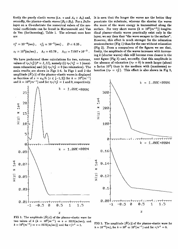
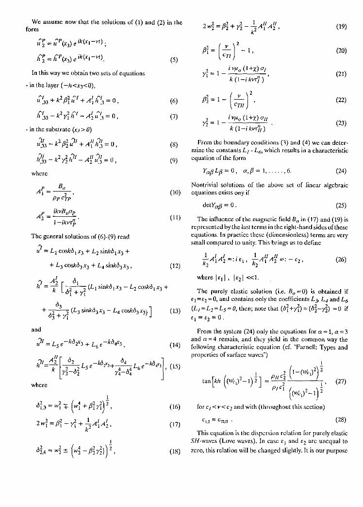
It is seen that the longer the waves are the better theypenetrate the substrate, whereas the shorter the wavesthe more of the wave energy is transmitted along thesurface. For very short waves (k = 106 (m- l )) longitudinal plasmo-elastic waves practically exist only in thelayer; we say then that "the wave escapes to the surface" .However, this effect is much stronger for the relaxationsemiconductor (Fig 1) than for the one without relaxation(Fig 2). From a comparison of the figures we see that,firstly, the amplitude of the waves increases with increasing k (shorter waves)-this will become even clearer in thenext figure (Fig 3)-and, secondly, that this amplitude inthe absence of relaxation (rp =0) is much larger (abouta factor 102 ) than in the medium with (maximum) relaxation (rp = rt). This effect is also shown in Fig 3,
0k = 1.00E+0004
k -- 1.00E+0004 0.16
'>tC1J 0.14~
*N 0.12~
z
0.1
k = 1.00E+0006
SI = 103 (m/sec), AI =60.76, AIl =7.067 * 10-3•
25--
We have preformed these calculations for two, extreme,values ofrp/rt(P =I,JI), namely (i) rp/rt = 1 (maximum relaxation) and (ii) rp/rt = 0 (no relaxation). Themain results are shown in Figs 1-4. In Figs 1 and 2 theamplitude IN(z)1 ofthe plasmo-elastic waves is displayedas function of z = X3/h (z E [-1,2]) for k = 106 (m- l )
and k = 104 (m- l) and for rp/rt = 1 and 0, respectively.
rt = lO- S(sec), rjj =10-5 (sec) , D =6.25 ,
firstly the purely elastic waves (i.e. v and Al + A 3 ) and,secondly, the plasmo-elastic waves (BI +B3 ). For a ZnSelayer on a Ge-substrate the numerical values of the material coefficients can be found in Maruszewski and Vande Ven (forthcoming), Table 1. The relevant ones hereare
'<j- 20C1J~
* 15
N~
z 10
5
0
0.09
'<j-C1J 0.07~
*N 0.05~
z
0.03
o.0 8 l--rr " I I "I"" I r "I --,---,----r-r
-1 -0.5 0 0.5 1 1.51.510.5o.01 +-'-..-T""'i-r-r;,...,.--J--,-,--rr+-r..-T""'i-r-r;,...,.--J--,-,---r-r
-1 -0.5 0
zFIG 1. The amplitude IN(z)\ of the plasmo-elastic wave fortwo values of k (k = 106 (m-1
) => v = 3015(m/sec), andk = 104 (m-1
) => v = 3175(m/sec)) and for r/r+ = 1.
z
FIG 2. The amplitude IN(z)1 of the plasmo-elastic wave forh = 1O-6(m), for k = 106 or 104 (m-1
) and for r/r+ = O.

where the amplitude at the interface is plotted as a function of k (k E [1, I06](m- I
)) for the two cases Tp/T; = 1and Tp/T; = O. One sees that in the first case IN(O)Iattains a maximum at k = 4.1 * I05 (m- l ) (and a second, but smaller one, at k = 4.8* I05(m- I )), whereasthis maximum in the second case lies beyond the region[1,106
]. We note that in the neighbourhood of such amaximum, the interface plays the role of a frequencyfilter for the waves. Finally, we have investigatedthe behaviour of IN(O)I for k = 106 (m- l ) as functionof T := Tp/Tt (P = I, II; we took the same valuefor T in layer and substrate). The result is depictedin Fig 4, showing that IN(O)I attains a maximum forT = l.hl0-4
, and is monotoneously decreasing for largervalues of T (on to a value of IN(O)I = 1.53 * 10-5 forT = 1).
(21)
(22)(1"2 _ I" DS)tanh(3h. _ ~ I" ='>3 '>4 D(3 D + ,>4 O.
the system (17) with the right-hand sides taken equal tozero has a non-trivial solution. This implies the existenceof purely plasmonic waves, (i.e. only (B1 , B2' B3 ) i- 0).With (18) the dispersion relation (21) can be rewrittenas
PURELY PLASOMONIC WAVES
In case (19) is not satisfied so that
Solution of this equation yields the wave velocity v asfunction of k for a fixed value of h. Since the plasmonicwaves are dissipative, we must require 1m(v) < 0, and,moreover, Re 'II > O. It turned out that there existsa solution of (22), satisfying these restrictions, only forvalues of k exceeding a certain critical value kl = kl(h),for h > O. Hence, for 0 < k < k l no solution exists,whereas for k > kl we can obtain from (22) a complexwave velocity'll E C, with Re v > 0 and 1m 'II < O.
The critical value kl not only depends on h, but alsoon the ratio TP/Tt. For Tp = Tt the behaviour of kl asfunction of h (for h E [0, 1O-6](m)) is plotted in FIG 5.It is seen that k l slightly decreases with increasing h.Our calculations revealed that the wave velocity v(v EJR, for k = kI) was almost constant: its value changedfrom v = 314 (m/sec) for h -+ 0 to v = 317 (m/sec) forh = 1O-6(m). Hence, these values of v are much lowerthan those for the purely elastic waves.108642
o+::==~--+-----r-+-----r-+---,--1---,---lo
2
0.5
*lSI 1z
60120~-------------
100vOJ~ 40 80v* OJ
~
lSI* 60z
20 lSI
Z 40
20
2 4 6 8 100
k * 1e-5 0 2 4 6 8 10
FIG 3. The amplitude IlV(O) I at the interface z = °of theplasmo-elastic wave as function of it = k * 10-& E [0,10], forh = 1O-6(m) and for r/r+ =1 and r/r+ = 0, respectively.
T * 1e4
FIG 4. The amplitude I1V(O) I as function of T = r/r+, forh = 1O-6(m) and k = 106(m-1).

9
Maruszewski B (1987a), Coupled evolution equations ofdeformablesemiconductors, Int J Eng Sci 25, 145-153.
REFERENCES
Maruszewski B and Van de Ven A A F (forthcoming), Plasmomagnetoe1astic waves in a magnetic epitaxial film grown ona semiconductor, (submitted to J Acou&t Soc Am).
Maruszewski B (1987b), Heat and charge carrier relaxation in deformable semiconductors in Electromagnetomechanical Interactions in Deformable Solids and Structuru, Y Yamamotoand K Miya (eds), North-Holland, Alnsterdam, 395-400.
CONCLUSIONS
Starting from a set of two equations and jump conditions, describing the displacement and the charge field(plasmonic field) in a relaxation semiconductor, we havederived a system for longitudinal plasmo-elastic waves insuch a medium. We have applied this to a semiconducting heterostructure built up of a thin layer on a half spaceor substrate. Thus, we have calculated the wave velocityand the amplitudes of plane longitudinal plasmo-elasticsurface waves in the structure. The effect of the plasmonic field on the elastic field is extremely small (in factnegligible), but the opposite effect of the elastic field onthe plasmonic field (elastodiffusive effect) remains relevant. In fact, it was just the latter effect that caused theoccurrence of plasma-elastic waves, which were generatedby purely elastic waves. Due to the dissipative characterof the charge diffusion, the wave should be slightly dissipative, but this effect is so extremely small that it isneglected here.
The plasmo-elastic waves decay in the substrate.Characteristic for the presence of the layer was the tendency of the waves to escape to the layer; a tendencywhich was stronger for shorter waves. Also, this effectwas stronger for relaxation semiconductors than for nonrelaxation ones. On the other hand, the amplitudes forthe plasmo-elastic waves were much larger in semiconductors without relaxation than in those with relaxation.
We have also considered purely plasmonic waves. Itwas shown that they only can exist for values of k largerthan a certain critical value ki = kl(h), depending onthe thickness h of the layer and on the relaxation ratioT. The influence of relaxation was twofold: firstly, thevalue of k1 increases for increasing T from T = 0.1 onand, secondly, dissipation was smaller in a medium withrelaxation then in one without relaxation.
1121.8121.6121.4121.25+-~-+-~-+----,--+----,--+---r----l
121
6
FIG 5. The critical wave number k1 as function of h forTp/rj; == 1.
h * 1e6
2
1121
6
For Tp/Tf; = 0 no purely plasmonic waves exist; (22)then only has a solution with Re v = O. To show howk i depends on the ratio Tp /Tt, we have calculated ki
for h = 10-6 (m) for several values of T E [0,1]. Theresults are shown in FIG 6. It turned out that there didnot exist a solution for ki (with Rev> 0) for values ofT between 0 ~ T < Tc = 0.103, and that the value ofki strongly decreases for T ! Tc • Finally, we note thatour calculations of vEe for k > ki revealed that thedissipative character of the waves became stronger forsmaller values of T (less relaxation).
Farnell G W (1978), Types and properties of surface waves, inAcoustic Surface Waves. A A Oliver (ed), Springer, Berlin,13-60.
10.8121.6121.4121.2121 +---r-I---.---+--.--+-.-----+---.---J
121
TFIG 6. The critical wave number k1 as function of T forh == 10-6 (m).

PLASMO-MAGNETOELASTIC WAVESIN A SEMICONDUCTING HETEROSTRUCTURE.II. SH-MAGNETOELASTIC MODES.
B. Maruszewski
Technical Univcrsity oj POZIIGli, Institute ojApplied Mcchanics, Ill. Piotrowo 3, 60-965 PoznaJi, Po/and
A.A.F. van de Ven
Eindhoven University oj TechllolofJ', DepaJ1mc/lt ojMathematics and Computing Science, Den Do/ech 2,5600 MB Eindhoven, The Nether/allds
The paper is dcvoted to the analysis of propagation of thc SH-magnetoelastic (Love-type) waves in anepitaxial heterostructure collectcd of a magnetic semiconducting layer and nonmagnetic semiconductingsubstrate placed into an applied constant magnetic field perpendicular to the interface of the structure.Numerical results have been obtained for ZIISe-Ge heterostructure. The first order approximation of thedispersion of SH-magnetoelastic modes comparing to the dispersion of the purely elastic SH modes hasbeen calculated.
ing with the transverse modes. The formcr case has beenanalyzed in the first part of this paper.
The linal equations govcrning the lattcr ~ne read
l' 1'1' "p'J'It Z,ii + IphZji - ,u(pp(1 +Xp) hz + Boapll2,3 =0, (2)
for P = J,lI (as previously, I indicates the layer and II - thesubstrate). We see that in this case only the llz-componentof the displacement and hz-component of the magnetic fieldare coupled. Therefore we call their evolution in space (XJ,X3) and time t the SH-magnctoelastic waves. In the vacuumspace outside the structure we simply have llZ =hz= O. Theform of the magnetic side of the problem is assumed as .
I' I'B=Bo+b, Ibl < < IBol, Bo=Bo e3, b =xrh " XI=X,
XII =O( X - denotes the magnctic susceptibility).
INTRODUCTION
Contrary to the first part of this paper "van de Yen, Maruszewski: Plasmo-magnetoelastic waves in a semiconductingheterostructure", the second part is devotcd to considerations concerning the transverse (SH) magnetoclastic modesin an epitaxial semiconducting heterostructure. This timethe heterostructure is collected of two sub-bodies: the magnetic epitaxial layer and nonmagnetic substrate, both IHypehomogeneous and isotropic semiconductors. Because of themagnetic properties of the structure just the transversemodes of the plasmo-magnetoelastic waves are the mostintreresting.
Remark, that in this part we try to avoid repetition ofnotation explanation that has been done in thc previous parl.
SH·MAGNETOELASTIC WAVES
The problem concerns propagation of the SH-magnetoe]astic waves in a semiconducting heterostructure collected ofthe epitaxial layer -h <X3 < 0 and the substratex3 > 0 (II is thethickness of the layer). The propagation direction isxJ. Thestructure is placed into the applied magnetic field of induction 8 0 perpendicular to the interface X3 = O. The generalwave equations and boundary conditions for the case whenthe clastic, electronic (plasmonic) and magnetic fields intcract with each other have been derivcd in "Maruszewski, vande Yen: Plasmo-magnetoclastic waves in magnctic epitaxialfilm grown on a semiconductor". Particular analysis of themindicates that the wave propagation problem concerning theabove geometry can bc split into two separate ones: into theproblem dcaling with the longitudinal and the problem deal-
Z l' "1' Bo J'CTJ,II)/',' - It, + p-It'3 =0,
1, _, - }J-'
The boundary conditions are as follows:
- at the free surface X3 = -h:
/ Iliz = 0, llZ,3 = 0,
- while at the interfacex3 = 0
til 1J 1 Ifhz = It z , p/c'i1 lt Z,3 =PlI c':rtt lt Z,3'
/ IIltz = ltz ,
(1)
(3)
(4)
We assume now that the solutions of (1) and (2) in theform (19)
From the boundary conditions (3) and (4) we can determine the constants L1 - L 6, which results in a characteristicequation of the form
,;'~ = ,;'P(X3) e ik(xl-vt) ;
{~ = {P(X3) e ik(xl-vt).
In this way we obtain two scts of equalions
- in the layer (-II <X3<O),
"I Z' "I I "IIl ,33 + k f3ill + A I II ,3 =0 ,
"I Z Z "I I "III ,33 - k YI II - A 2 Il .3 = 0,
- in the substrate (X3> 0)
UII k2 f32 ')1 + All/II - 0,33- 2" 1'.3-,
II Z Z II II II",33 - k yz II - A 2 11,3 = 0,
where
(5)
(6)
(7)
(8)
(9)
f3T = (_V )Z _ 1 ,Cn
, iVf.1o(l+X)olY-I = 1 - -----
k (l-i kvr'j) ,
, ( v )2f3i=l- - ,cTIl
, i vf.1o (1 +X) allY:;= 1------
- k (l-i kvlJ[)
Yaf3Lf3 = 0, a,{3 = 1, ..... ,6.
(20)
(21)
(22)
(23)
(24)
Nontrivial solutions of the above set of linear algebraicequations exists ony if
(25)
(26)
detYa{3 = o.
The inlluence of the magnetic field Bo in (17) and (19) isrepresentcd by the last tcrms in the right-hand sides of theseequations. In practice these (dimensionless) terms are verysmall compared to unity. This brings us to define
The purely elastic solution (i.e. Bo = 0) is obtained if£1 =£2 =0, and contains only the coefficients L 3, L 4 and L 6
(L1 =L2 =L5 =0, then; note that (oI+YI) = (o~-y~) =0 if
£1 = E2 = o.
The general solutions of (6)-(9) read
:l =L 1 cosk<5 1x3 + L 2 sink<51 x3 +
+ L 3 cosk<53 x3 + L4 sink63x3 , (12)
I A~ [<51 .II = k 2 Z (L I sl11k~ I x3 - L 2 cosk<5 1X3 +°1 + YI
and
,;1 =L5 e-k0'2!3 + L6
e-k04't 3 ,
where
I
OI,3 = wi + (wi + f3TYT) '2,
2 Z , 1 I I2wI =f3I-Yj+,A I A 2 ,
k-
1
O~,4 =w~ ± (wi - f3h~} ) 2 ,
(14)
(16)
( 17)
(18)
From the system (24) only the equations for a = 1, a =3and a =4 remain, and they yield in the common way thefollowing characteristic equation (cL "Farnell: Types andproperties of surface waves")
I
I 2 (l-(V/c i )'2tan[kll (VIc/-1)'2] =PIlC; I' (27)
Plci (V'{t)2_ 1) '2
for C1 < v < c2 and with (throughout this section)
c l.~ = CT1,II • (18)
This equation is the dispersion relation for purely elasticSH-waves (Love waves). In case EI and E2 arc unequal to
zero, this relation will be changed slightly. It is our purpose
and
to calculate in first order of e the changes in the dispersionrelation. (35)
(36)
(37)
2Yl I??
e :::; -.,--., el = "7 (Oi+Yi) .(3i+yi I
f-£;\=O,
The elements in the 4°,5° and 6° columns and the 1°,2°and 3° rows of Z are preceded by a factor e in order toindicate that these elements are O(e2) with respect to theremaining ones. The part of2 containing the first three rowsand columns describes the purely elastic SH-waves.
Assuming e small, we can develop the determinant of Zwith respect to e. In doing so we neglect O(e2)-terms and,moreover, we usc the fact that the determinant of the 3x3submatrix2a f3' a,f3 E (1,2,3) ,is also 0(£2) (in accordance
with (27». After some elementary calculations (the detailsof which arc omitted here) we fino that DetZ = 0 isequivakntto the relation
where
PIIf = 03 sin kll0 3 - -/- 04 cos klz03 ,
! J
(it wiJJ turn out that this term is O(e2) and
-1 0131 .!\ = y 1fi11l1(S3+- -Y C I )a 1 . • T 2
n(S\+r Y2 C I)
(30)
(29)
(31)
2? ., Y?
<52=Y2 + ? - ., e2 ,{3i - Yi
2 _ 2 {3~<54 - {32 -? ? e2 .
{3i - Yi
To this end, we substitute (26) into (17) and (19), put thethus obtained relations into (16) and (Hi), respectively, anddevelop these with respect toe. The result reads, up toO(i),
22 2· Yl
<5 1 = -Y I + I? ? eI ,{3i + ri
In the derivation of the laller realtions we have assumed2 .,
that ReY2 > Re{3i .
An immediate consequence of (30) and (31) is that
(<5I+yi) and (<5~-y~) (appearing in the denominator in the
formulas (13) and (15) for the amplitudses II.II) becomeO(e2
). To get rid of this inconvenience we renormalize thecoefficients L b L 2 and L 5, that is we replace them by
(39)
2
. l-i(yISI + !lf32C3) + i ~~ (el-C3)
!lll 1- ikvr'J all!l=fll' T= II' o=OIT,
l-ikvTIl
In (38) we have used the following abbreviations (noticethat in the evaluation of !\ we may neglect all £-terms, whichamong others implies that we may use 0 I = i YI , 0z = I'z,03 = 13 1, 04 = (3z )
(32)
(34)
(33)
M I =L3 , M 2 =03 L 4, M 3 =L6 ,
L I 0IL I L sM4 = -.,--." Ms = -.,--." M6 = -"--?'
0i+Yi 0i+Yi 0i-Yi
where
respectively. Furthermore, we change the numbering of thecoefficients and the sequence of the equations (24) in sucha way that we arrive at the reordered set
ZIl Z\2 0 eZI4 eZ1S 00 Z22 Z23 0 f:Z25 £Z26
Z31 0 Z33 eZJ4 0 eZ36Z=
Z41 Z42 0 Z44 Z45 00 Z52 Z53 0 Z55 Z56
Z61 0 2 63 2 64 0 2 6(,
where e is defined as
The matrix Z is of the form
This is the first order perturbation for small e (i.e.I£ I «1) of the dispersion we are looking for.
(49)
(47)
(48)
On denoting
A-AR(kh) =-VE
The complete relation for the phase velocity then reads
v VO A-A .,-=-+-Ve+O(c).cTJ cT/
NUMERICAL RESULTS
2(132+ 2) £r = .!. (02_ 2) = Y2 1 Yl 2
£ 2 Y2 2( 2 (32) £ 1 .YI Y2- 2
In calculating YI,2 and f31,2 for use in (38)-(39) we must
take for v the velocity v0 of the purely elastic SH wave
(following from (27)). This is consistent with the neglect of0(£2)-terms in the evaluation of A.
We proceed by developing the right-hand side of (37) withrespect to £. This has to be done in two steps: firstly, wesubstitute (30)-(31) for 01 .;. 04' and, secondly, we must
account for the fact that v is a first order perturbation (in £)of vo' In this way we obtain
i)
with
with
of--------"~~- - - --_-----......~.~--••• _(1)
",R,
~.
.12 ~-16 ~.20 I I I I
o 2 4 kh 6 8 10
Fig. 1. Real(l) and imaginary(2) parts ofR(klz) for It = 1m.
«1 E·4
we did calculations for R(kll) (in its first order approximation) of dispersion of the SH-magnetoelastic modes in thecase of ZIISe-Ge heterostructure with respect to variousthickness of the epitaxial (ZIISe) layer II.
(43)
(42)
and
ii)
i f3I I-l f32A = -2? (53+ kh f3I C3) - -2? (rc3+kh(31 53)' (41)
Yi Yi
In (40), A is preceded by a factor £ and, therefore, for theexplicit calculation of A we may use v = V o in (41)
Oncemore, it is noted in the evaluation of V according to(43) one must use Vo for v, that means that in (43) (and in(41) and (38)) one must read for f31,2
PI ~ [(::1' -1]~ P2~ [1- (::n~ (45)The right-hand side of (42) is 0(£2) because the left-hand
side of it is zero for v = Vo in accordance with (27) .
PllP = PI' (44)
(x 1E-5) -- - - - - __~.:~----_- __ (11 __~_ •
-2 -.......... -
~·6
-10
·14
.~-18 -
-220
I I I2 4 kh 6 8 10
Fig. 2. Real(l) and imaginary(2) parts of R(khJ for It = 0./111.
Recapitulating the results derived above we sec that wehave expressed DetZ = 0 in the relation
from which the following expression for the first ordcrperturbation (in e) of the phase velocity v can be derived(CI =cTJ)
VIV- + A - A = a
C 'I(46)
It is easily seen from Figs. 1-4 that the SH-magnetoelasticmodes arc (with respect to their length) much more dampedfor the thick layer (long wave propagation) than for very thinone (short wave propagation) where damping effect practically vanishes. For the thickness of the layer between 0.1 mand 0.01 III (lhe real parl of the phase velocity perturbation

is practically negligible), there is no influence of the plasmomagnetic field on the purely elastic SH waves (27).
(.lE-13)
79
-2 (x 1 E-S)59
·62) 39
-10
Fig. 3. Real(l) and imaginary(2) parts ofR(klz} for II = 10-2
111.
,(1)
.-_.- (2 I
19
van de Ven AAF, Maruszewski B. Plasmo-magnetoelastic waves in asemiconducting heterostructure. I. Plasmo-elastic longitudinal modes.Proceedillgs ofehe IllTAM SymposiulII 011 NOlllillear Wa"cs ill SolidJ;Auguse15-20, 1993, Victoria, Callada
Maruszewski B. van de Ven AAF, Plasmo-magnetoelastic waves in magnetic epitaxial film grown on a semiconductor, J.Acotlse.Soc.Amcr. (10appear;1I 1993).
Farnell GW, Types and properties of surface waves, in Acouse;c SurfaceWaces, AA Oliner (ed). Springer-Verlag, Berlin, 1978.
REFERENCES
-1 0 2 4 kh 6 8 10
Fig. 5. Real(l) and imagillary(2) parts ofR(kh) forh = 10-6
111.10
jI,
,,./
.I
86kh
-------____ (2)-------------_.---
ex 1E-9)
2
6
o
4
-14
-18
-22 0
-2
Fig. 4. Real(l) and imaginary(2) parts of R(klz} for II = 10-4
111.