plasmonic enhancement for colloidal quantum dot photovoltaics · plasmonic enhancement for...
TRANSCRIPT
Plasmonic enhancement forcolloidal quantum dot photovoltaics
by
Daniel Paz-Soldan
A thesis submitted in conformity with the requirementsfor the degree of Master of Applied Science
Graduate Department of Electrical and Computer EngineeringUniversity of Toronto
Toronto, OntarioCanada
Copyright © 2013 by Daniel Paz-Soldan

Plasmonic enhancement for colloidal quantum dot photovoltaics
Abstract
Plasmonic enhancement for colloidal quantum dot photovoltaics
Daniel Paz-Soldan
Master of Applied Science
Graduate Department of Engineering
University of Toronto
2013
Colloidal quantum dots (CQD) are used in the fabrication of efficient, low-cost solar
cells synthesized in and deposited from solution. Breakthroughs in CQD materials have
led to a record efficiency of 7.0 %. Looking forward, any path toward increasing efficiency
must address the trade-off between short charge extraction lengths and long absorption
lengths in the near-infrared spectral region. Here we exploit the localized surface plasmon
resonance of metal nanoparticles to enhance absorption in CQD films. Finite-difference
time-domain analysis directs our choice of plasmonic nanoparticles with minimal parasitic
absorption and broadband response in the infrared. We find that gold nanoshells (NS)
enhance absorption by up to 100 % at λ = 820 nm by coupling of the plasmonic near-field
to the surrounding CQD film. We engineer this enhancement for PbS CQD solar cells
and observe a 13 % improvement in short-circuit current and 11 % enhancement in power
conversion efficiency.
Daniel Paz-Soldan University of Toronto ii

Plasmonic enhancement for colloidal quantum dot photovoltaics
Acknowledgments
This work was made possible by the collective effort of an exemplary group of individuals.
First, I thank my supervisor, Professor Edward H. Sargent, for his constant guidance
and support. He sets the bar high and encourages us to think big. I am grateful for having
had the opportunity to work in a world-class research group in such an exciting field.
I am grateful to Dr. Susanna Thon for her leadership and guidance through thick and
thin. I owe many thanks to Dr. Anna Lee, mentor and friend, who taught me the virtues of
the scientific process and whose contributions were invaluable. I also thank Dr. Michael
Adachi for his objective insight and practical know-how with FDTD simulations. I extend
thanks to Dr. Mingjian Yuan, Dr. Pouya Maraghechi, Andre Labelle, and Haopeng Dong
for their helpful advice and important work on the project.
I particularly thank David Zhitomirsky, Dr. Illan Kramer, and Dr. Rui Li for guiding
my research focus from the very beginning. I am grateful to Dr. Larissa Levina and Elenita
Palmiano for CQD synthesis and tireless preparation of materials for the lab on a daily
basis. I also thank Damir Kopilovic and Remigiusz Wolowiec for designing and building
anything, on-demand, and in a timely fashion. I feel privileged to have collaborated with
a diverse and talented group of individuals outside of the Sargent group while at the Uni-
versity of Toronto and I am thankful for their valuable contributions: Dr. Aftab Ahmed,
Dr. Kun Liu, Dr. Alexander Melnikov, Dr. Peter M. Brodersen, Anjan Reijnders, and
Luke Sandilands. I also thank Dr. Neil Coombs and Dr. Ilya Gourevich for training and
assistance with electron microscopy.
I thank Dr. Sjoerd Hoogland, Dr. Armin Fischer, and Dr. Oleksandr Voznyy for in-
sightful discussions. For scientific and non-scientific discussions alike, I thank: Dr. Yuan
Daniel Paz-Soldan University of Toronto iii
Plasmonic enhancement for colloidal quantum dot photovoltaics
Ren, Dr. Jennifer Flexman, Dr. Shokouh Farvid, Dr. Jin Young Kim, Dr. Ghada Koleilat,
Dr. Zhijun Ning, Dr. Silvia Masala, Dr. Philipp Stadler, Alex Ip, Kyle Kemp, Graham
Carey, Melissa Furukawa, Lisa Rollny, Xinzheng Lan, Brandon Sutherland, Jixian Xu,
Chris Wong, Valerio Adinolfi, and Jeannie Ing.
I thank my parents, Carlos and Patricia, and my brothers, Carlos Jr. and Mario. I am
privileged to have been born into a family that stands behind me in everything I do. Finally
I thank Jessica Nguyen, whose constant encouragement and support through everything
made this work possible.
Daniel Paz-Soldan University of Toronto iv

CONTENTS Plasmonic enhancement for colloidal quantum dot photovoltaics
ContentsAbstract ii
Acknowledgments iii
Acronyms vii
List of Tables viii
List of Figures ix
1 Introduction 11.1 Colloidal quantum dots . . . . . . . . . . . . . . . . . . . . . . . . . . . . 3
1.1.1 Recent advances in colloidal quantum dot solar cells . . . . . . . . 41.1.2 Limitations . . . . . . . . . . . . . . . . . . . . . . . . . . . . . . 5
1.2 Thesis objectives . . . . . . . . . . . . . . . . . . . . . . . . . . . . . . . 7
2 Background 92.1 Solar cell fundamentals . . . . . . . . . . . . . . . . . . . . . . . . . . . . 9
2.1.1 Figures of merit . . . . . . . . . . . . . . . . . . . . . . . . . . . . 102.1.2 Quantum efficiency . . . . . . . . . . . . . . . . . . . . . . . . . . 12
2.2 Surface plasmons . . . . . . . . . . . . . . . . . . . . . . . . . . . . . . . 122.2.1 Localized surface plasmons . . . . . . . . . . . . . . . . . . . . . 142.2.2 Effect of ligand . . . . . . . . . . . . . . . . . . . . . . . . . . . . 14
2.3 State of the art . . . . . . . . . . . . . . . . . . . . . . . . . . . . . . . . . 15
3 Infrared plasmonic nanoparticles 173.1 Optical design considerations . . . . . . . . . . . . . . . . . . . . . . . . . 173.2 Finite-difference time-domain simulations . . . . . . . . . . . . . . . . . . 193.3 Engineering of optical resonances . . . . . . . . . . . . . . . . . . . . . . 20
3.3.1 Hemisphere-capped nanorods . . . . . . . . . . . . . . . . . . . . 203.3.2 Arrowhead nanorods . . . . . . . . . . . . . . . . . . . . . . . . . 213.3.3 Nanoshells . . . . . . . . . . . . . . . . . . . . . . . . . . . . . . 23
3.4 Plasmonic particle spacing in CQD films . . . . . . . . . . . . . . . . . . . 253.5 Conclusions . . . . . . . . . . . . . . . . . . . . . . . . . . . . . . . . . . 27
4 Integrating MNPs into CQD solar cells 284.1 PbS CQD and NS film deposition . . . . . . . . . . . . . . . . . . . . . . 284.2 Physical and electrical considerations . . . . . . . . . . . . . . . . . . . . 29
4.2.1 Surface modification and purification . . . . . . . . . . . . . . . . 304.2.2 Agglomeration . . . . . . . . . . . . . . . . . . . . . . . . . . . . 31
Daniel Paz-Soldan University of Toronto v

CONTENTS Plasmonic enhancement for colloidal quantum dot photovoltaics
4.3 Nanoshell film deposition . . . . . . . . . . . . . . . . . . . . . . . . . . . 314.3.1 Solvent controls . . . . . . . . . . . . . . . . . . . . . . . . . . . 324.3.2 MNP film fabrication by spin casting . . . . . . . . . . . . . . . . 324.3.3 MNP film fabrication by reservoir drop casting . . . . . . . . . . . 33
4.4 Conclusions . . . . . . . . . . . . . . . . . . . . . . . . . . . . . . . . . . 33
5 Characterization of devices 345.1 Design of plasmonic CQD solar cells . . . . . . . . . . . . . . . . . . . . . 345.2 Performance of CQD solar cells with NR and ARNR . . . . . . . . . . . . 355.3 Optical properties of plasmonic CQD films . . . . . . . . . . . . . . . . . 355.4 Device performance . . . . . . . . . . . . . . . . . . . . . . . . . . . . . . 375.5 Quantum efficiency . . . . . . . . . . . . . . . . . . . . . . . . . . . . . . 385.6 Conclusions . . . . . . . . . . . . . . . . . . . . . . . . . . . . . . . . . . 39
6 Conclusion 406.1 Contributions to the field . . . . . . . . . . . . . . . . . . . . . . . . . . . 406.2 Future work . . . . . . . . . . . . . . . . . . . . . . . . . . . . . . . . . . 41
References 43
A Materials and experimental procedures 48A.1 PbS CQD synthesis and solvent exchange . . . . . . . . . . . . . . . . . . 48A.2 Photovoltaic device fabrication . . . . . . . . . . . . . . . . . . . . . . . . 48A.3 Nanorod synthesis . . . . . . . . . . . . . . . . . . . . . . . . . . . . . . . 49A.4 Arrowhead nanorod synthesis . . . . . . . . . . . . . . . . . . . . . . . . . 50A.5 Nanoshell solution preparation . . . . . . . . . . . . . . . . . . . . . . . . 51
B Measurements and simulations 53B.1 AM 1.5 photovoltaic performance characterization . . . . . . . . . . . . . 53B.2 EQE measurements . . . . . . . . . . . . . . . . . . . . . . . . . . . . . . 53B.3 Solution absorption . . . . . . . . . . . . . . . . . . . . . . . . . . . . . . 54B.4 Film absorption . . . . . . . . . . . . . . . . . . . . . . . . . . . . . . . . 54B.5 Double pass film absorption . . . . . . . . . . . . . . . . . . . . . . . . . 54B.6 FDTD simulations . . . . . . . . . . . . . . . . . . . . . . . . . . . . . . 54
Daniel Paz-Soldan University of Toronto vi

CONTENTS Plasmonic enhancement for colloidal quantum dot photovoltaics
Acronyms
AM 1.5 Air Mass 1.5 G solar spectrum
ARNR Arrowhead Nanorod
CQD Colloidal quantum dot
EM Electromagnetic
EQE External Quantum Efficiency
FF Fill Factor
FTO Fluorine doped Tin Oxide
ITO Indium doped Tin Oxide
IQE Internal Quantum Efficiency
J−V Current-Voltage Characteristic
JSC Short-Circuit Current
LSPR Localized Surface Plasmon Reso-nance
MeOH Methanol
MNP Metal Nanoparticle
MPA 1-mercaptopropanoic Acid
MW Molecular weight
MPP Maximum power point
NR Nanorod
NS Nanoshell
OPV Organic Photovoltaics
PbS Lead sulfide
PCE Power Conversion Efficiency
PV Photovoltaics
PVP Polyvinylpyrrolidone
RS Series Resistance
RSH Shunt Resistance
VOC Open-Circuit Voltage
Daniel Paz-Soldan University of Toronto vii

LIST OF TABLES Plasmonic enhancement for colloidal quantum dot photovoltaics
List of Tables1 Solar cell performance results with embedded NS with and without pre-
sonication . . . . . . . . . . . . . . . . . . . . . . . . . . . . . . . . . . . 312 Solar cell performance results with embedded NS for spin casting and drop
casting . . . . . . . . . . . . . . . . . . . . . . . . . . . . . . . . . . . . . 323 Solar cell performance of devices with embedded NRs . . . . . . . . . . . 354 Solar cell performance of devices with embedded ARNRs . . . . . . . . . 365 Device results using nanoshells . . . . . . . . . . . . . . . . . . . . . . . . 37
Daniel Paz-Soldan University of Toronto viii

LIST OF FIGURES Plasmonic enhancement for colloidal quantum dot photovoltaics
List of Figures1.1 Electricity generation by source in the United States, 2009 . . . . . . . . . 11.2 Spectral tuning of quantum dots across the broad solar spectrum . . . . . . 41.3 The depleted heterojunction architecture for CQD PV . . . . . . . . . . . . 51.4 Measured absorption coefficient spectrum of a PbS CQD film . . . . . . . . 62.1 Basic operation of a solar cell . . . . . . . . . . . . . . . . . . . . . . . . . 92.2 Equivalent circuit of a solar cell . . . . . . . . . . . . . . . . . . . . . . . 112.3 Dispersion curves ε(ω) for gold and silver . . . . . . . . . . . . . . . . . . 132.4 Simple illustration of a surface plasmon on a metal nanoparticle . . . . . . 142.5 The effect of a ligand shell on the surface plasmon of a silver nanoparticle . 153.1 Extinction and schematic of hemisphere-capped gold nanorods . . . . . . . 203.2 FDTD simulation of hemisphere-capped gold nanorods . . . . . . . . . . . 223.3 Extinction and schematic of arrowhead-capped gold nanorods . . . . . . . 233.4 FDTD simulation of arrowhead-capped gold nanorods . . . . . . . . . . . 243.5 Summary of peak scattering and absorption cross sections for NR and ARNR 253.6 Experimental and calculated extinction of gold nanoshells . . . . . . . . . 264.1 TEM images of nanoshells before and after purification . . . . . . . . . . . 305.1 Schematic representation and cross sectional TEM image of plasmonic
nanoshell CQD solar cell . . . . . . . . . . . . . . . . . . . . . . . . . . . 345.2 (a) Single pass absorption spectrum of PbS CQD films with and without
embedded NS . . . . . . . . . . . . . . . . . . . . . . . . . . . . . . . . . 365.3 External quantum efficiency spectra and J-V characterization of represen-
tative samples with and without NS embedded . . . . . . . . . . . . . . . . 385.4 Internal quantum efficiency spectra of representative samples with and with-
out NS embedded . . . . . . . . . . . . . . . . . . . . . . . . . . . . . . . 39A-1 TEM image of typical NR . . . . . . . . . . . . . . . . . . . . . . . . . . 50A-2 TEM image of typical ARNR . . . . . . . . . . . . . . . . . . . . . . . . . 51A-1 Double pass absorption spectrum of PbS CQD films with and without em-
bedded NS . . . . . . . . . . . . . . . . . . . . . . . . . . . . . . . . . . . 55
Daniel Paz-Soldan University of Toronto ix

1 Introduction Plasmonic enhancement for colloidal quantum dot photovoltaics
1 Introduction
Electricity, however produced, is now considered a basic right in the developed world. We
demand it and we fight to keep costs low despite the grave implications for the environment.
One of the most significant steps we can take toward reducing climate-changing emissions
to sustainable levels is to generate electricity cleanly. In fact, more than 40% of U.S. carbon
dioxide emissions come from electricity generation alone [1].
Renewables represent only 9% of total generation in the U.S (Figure 1.1). We rely
heavily on conventional sources to fulfill electricity demand even as renewable energy tech-
nologies become better, cheaper, and more efficient.
Figure 1.1: Electricity generation by source in the United States in 2009. Only 9% oftotal generation comes from renewable sources; generation from solar is 0.02% [2].
Solar photovoltaics (PV) has the potential to become a major player in the future energy
mix. Of the 120,000 terrawatts illuminating the earth every day [3], it is estimated that
Daniel Paz-Soldan University of Toronto Page 1 of 55

1 Introduction Plasmonic enhancement for colloidal quantum dot photovoltaics
about 85 terrawatts can realistically be harvested, taking into account land use restrictions
and conversion efficiency limits [4]. By comparison, total energy demand is on the order
of 15 terrawatts today [2]. While solar today meets only a small percentage of the global
electricity demand, this is not due to a lack of available input energy. The fact is that the
cost of solar energy generation remains prohibitively high.
The gross cost of electricity can be summarized in one number: the cost per watt-peak
($/Wp). This is the actual price of generating electricity at peak power output. In a solar
context, the cost per watt peak is the total of the upfront cost of the solar module and
the balance of systems (BoS) cost which takes into account the installation, operation and
maintenance of the PV system. It is widely agreed that once solar energy can be produced
at $1/Wp or about 5-6 cents/kWh it will reach grid parity, making it competitive with
conventional energy sources. A combination of high module efficiency and low module
cost are the key factors in reaching this threshold [5].
One way to reduce the cost of solar energy is to decrease the thickness of the absorb-
ing layer. The reduced module weight would have the dual benefit of much lower input
materials costs as well as decreased installation costs. While crystalline silicon-based PV
(c-Si) has laid the foundation for highly efficient solar energy production, significant film
thicknesses are required to achieve sufficient light absorption and rigid casings are needed
for support. On the other hand, solar cells based on organic materials have the advantage
of very high absorption coefficients in the visible range and very thin films (10-50 nm) can
be completely absorptive. These materials have achieved reasonably high performance at
low cost, but the current best technologies are limited to efficiencies of less than 20% due
to their large bandgaps [6].
Colloidal quantum dot (CQD) photovoltaics have been proposed as a promising alter-
native, offering the potential for both high-efficiency and low-cost. Within this materials
system, complete absorption can be achieved with a few hundred nanometers film thick-
Daniel Paz-Soldan University of Toronto Page 2 of 55

1 Introduction Plasmonic enhancement for colloidal quantum dot photovoltaics
ness and there is the potential to reach the upper limit efficiencies predicted by Shockley
and Queisser in 1962 [7,8]. The potential for flexible, lightweight PV modules offers a sig-
nificant cost advantage for CQD PV. Additionally, the solution processability of this novel
material allows for large-scale, low-temperature, low-cost fabrication techniques with roll-
to-roll processing.
1.1 Colloidal quantum dots
In semiconductor colloidal quantum dots the electron and hole wavefunctions are confined
to less than the Bohr radius. By adjusting the size of the nanocrystals in colloidal synthesis
it is possible to increase the energy of the first excitonic transition relative to the bulk
material [8]. The implication is that the material bandgap is tunable via careful control of
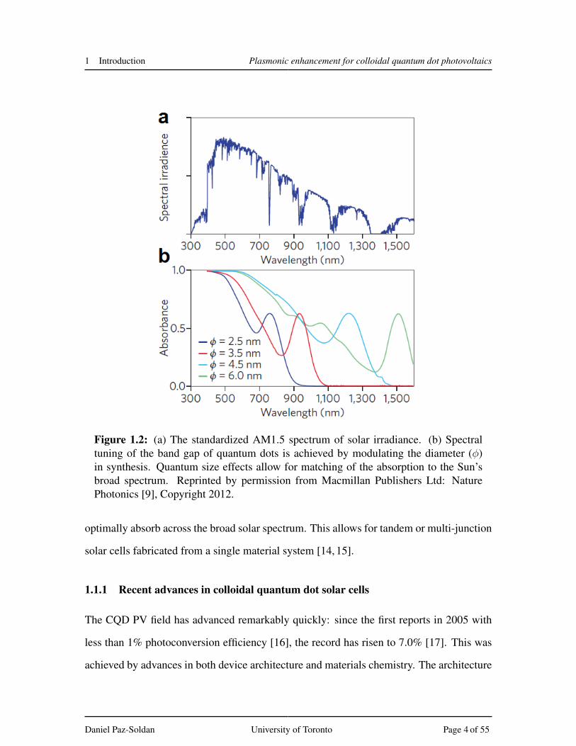
the size and shape of the nanocrystals (Figure 1.2). A variety of quantum dot materials
- In(Sb, As), SnS, FeS2, Cd(Se, Te), Pb(S, Se, Te) - have been demonstrated for myriad
applications. This thesis focuses on quantum dots of lead sulfide (PbS).
PbS CQDs are synthesized in solution from organo-metallic precursors and capped
with long-chain organic ligands to provide colloidal stability. The inter-dot distance in
solid-state films made of CQDs determines the transport properties. By selecting a ligand
with the desired length one can control the conductivity of the material. Thin films are
typically deposited by spin-casting, drop-casting, or dip-coating the solution and applying
solid-state ligand exchange. The result is a relatively well ordered film of nanocrystals
embedded in a matrix of insulating molecular ligands. The electrical transport properties
of such quantum dot films have been studied extensively but the precise mechanisms are in
the process of being understood [10–13].
CQDs offer many exciting opportunities for application to photovoltaics. Spectral tun-
ability by the quantum size effect means that CQD films can be precisely engineered to
Daniel Paz-Soldan University of Toronto Page 3 of 55
1 Introduction Plasmonic enhancement for colloidal quantum dot photovoltaics
Figure 1.2: (a) The standardized AM1.5 spectrum of solar irradiance. (b) Spectraltuning of the band gap of quantum dots is achieved by modulating the diameter (φ)in synthesis. Quantum size effects allow for matching of the absorption to the Sun’sbroad spectrum. Reprinted by permission from Macmillan Publishers Ltd: NaturePhotonics [9], Copyright 2012.
optimally absorb across the broad solar spectrum. This allows for tandem or multi-junction
solar cells fabricated from a single material system [14, 15].
1.1.1 Recent advances in colloidal quantum dot solar cells
The CQD PV field has advanced remarkably quickly: since the first reports in 2005 with
less than 1% photoconversion efficiency [16], the record has risen to 7.0% [17]. This was
achieved by advances in both device architecture and materials chemistry. The architecture
Daniel Paz-Soldan University of Toronto Page 4 of 55

1 Introduction Plasmonic enhancement for colloidal quantum dot photovoltaics
employed is the depleted heterojunction, a p-n heterojunction formed by n-type titanium
dioxide (TiO2) and p-type PbS CQD film. This structure takes advantage of excellent
carrier extraction at the front side of the cell - compared to the back, ohmically-contacted
side - by extending a depletion region through the CQD film [18]. Another important factor
to consider is the formation of trap states at the quantum dot surfaces, which can lead to
increased carrier recombination rates and ultimately limits solar cell performance. A hybrid
organic-inorganic passivation strategy was shown to dramatically reduce trap density in
PbS CQD films, leading to the current record performance [17].
Figure 1.3: (a) Depleted Heterojunction architecture with n-type TiO2 and p-typeCQD. (b) The spatial band diagram shows the extraction of photo-generated electronsby acceptor TiO2 and holes by ohmic gold. Reprinted with permission from [18].Copyright (2010) American Chemical Society.
1.1.2 Limitations
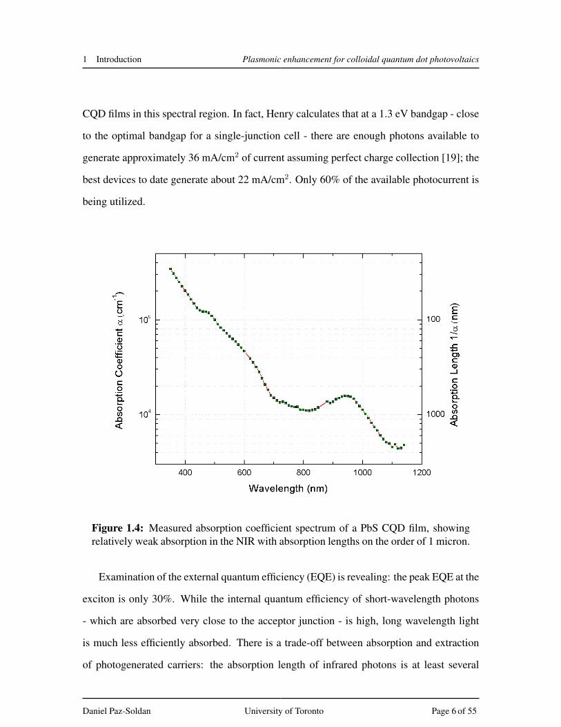
Looking forward, there is significant room for improvement in CQD PV. Figure 1.4 shows
the absorption spectrum for a PbS quantum dot film with an excitonic band-edge at 1.3 eV
or 950 nm. Light in the near infrared (NIR, 700-1,000 nm) range is not fully absorbed at
the optimal film thickness for PbS CQD solar cells of 300 nm. Since nearly half of the
solar irradiance is in the NIR, there is much to be gained by increasing the absorption of
Daniel Paz-Soldan University of Toronto Page 5 of 55
1 Introduction Plasmonic enhancement for colloidal quantum dot photovoltaics
CQD films in this spectral region. In fact, Henry calculates that at a 1.3 eV bandgap - close
to the optimal bandgap for a single-junction cell - there are enough photons available to
generate approximately 36 mA/cm2 of current assuming perfect charge collection [19]; the
best devices to date generate about 22 mA/cm2. Only 60% of the available photocurrent is
being utilized.
Figure 1.4: Measured absorption coefficient spectrum of a PbS CQD film, showingrelatively weak absorption in the NIR with absorption lengths on the order of 1 micron.
Examination of the external quantum efficiency (EQE) is revealing: the peak EQE at the
exciton is only 30%. While the internal quantum efficiency of short-wavelength photons
- which are absorbed very close to the acceptor junction - is high, long wavelength light
is much less efficiently absorbed. There is a trade-off between absorption and extraction
of photogenerated carriers: the absorption length of infrared photons is at least several
Daniel Paz-Soldan University of Toronto Page 6 of 55

1 Introduction Plasmonic enhancement for colloidal quantum dot photovoltaics
times greater than the optimal film thickness for carrier extraction. This is often called the
absorption-extraction compromise and is an important limitation in PbS CQD solar cells.
Unless quantum efficiency in this range can be improved and the infrared bandgap can be
fully utilized, the maximum performance for CQD PV will remain inherently limited.
1.2 Thesis objectives
The proposed project is designed to improve photovoltaic conversion efficiency of state-
of-the-art CQD solar cells using solution-processed colloidal metal nanoparticles (MNPs).
The goal of the project is to use plasmonic resonant scattering to enhance NIR absorption in
the quantum dot layer, break the absorption-extraction compromise, and build a plasmonic
CQD solar cell with enhanced efficiency. The objectives of this project can be summarized
as follows:
Identify the design considerations for plasmonic enhancement. Optical, electrical,
and physical design considerations must be fully explored in order to exploit the plasmonic
effect. An integral aspect of this project is to identify the key factors in such a design
through simulation and experiment.
Achieve absorption enhancement via plasmon-CQD resonance matching. An advan-
tage of CQDs is the relatively strong absorption at the exciton energy near 1.3 eV for single
junctions. This project proposes to overlap the LSPR of the MNPs with the CQD exciton
wavelength to significantly enhance absorption in the IR - a concept that is tailored for
quantum dot photovoltaics.
Realize a fully solution-processed plasmonic CQD solar cell. One of the advantages of
CQD PV is the fact that solution processing allows the possibility of large-scale deposition
Daniel Paz-Soldan University of Toronto Page 7 of 55

1 Introduction Plasmonic enhancement for colloidal quantum dot photovoltaics
on flexible substrates through roll-to-roll techniques. While mechanical techniques such
as nanoimprinting, or thermal methods such as annealing, have already been demonstrated
for the fabrication of plasmonic nanostructures in PV devices, these methods would detract
from the very attractive solution-processed approach. The use of solution-processed MNPs
that are easily integrated into the device fabrication process is an approach amenable to
improving CQD solar cell performance.
All of the listed objectives are addressed through simulation and experimental analysis.
Chapter 2 provides the relevant background and theory. Chapter 3 and 4 describe the design
considerations that were explored and optimized. Chapter 5 showcases the final design
along with complete characterization and analysis. Chapter 6 summarizes the results and
provides future directions for work in this field.
Daniel Paz-Soldan University of Toronto Page 8 of 55

2 Background Plasmonic enhancement for colloidal quantum dot photovoltaics
2 Background
This chapter presents the necessary background and theory of the concepts covered in the
thesis. We begin with a basic discussion of photovoltaic theory and surface plasmons, then
move to a literature review of the state of the art in plasmonics for photovoltaics.
2.1 Solar cell fundamentals
Put simply, the function of a photovoltaic cell is to convert electromagnetic energy in the
form of light to electrical energy (Figure 2.1a). Light is incident on an absorbing material,
with wavelength λ and energy E given by equation 1.
Figure 2.1: (a) Basic operation of a solar cell requires an absorbing layer and efficientextraction of electrons and holes. (b) Solar cell operation is measured by sweepingthe voltage across a load and measuring the current. Reprinted by permission fromMacmillan Publishers Ltd: Nature [20], Copyright 2012.
Daniel Paz-Soldan University of Toronto Page 9 of 55

2 Background Plasmonic enhancement for colloidal quantum dot photovoltaics
E = hν =hc
λ(1)
where h is Planck’s constant and c is the speed of light. Absorption of a photon excites an
electron to a higher energy state, leaving behind a positive hole. The high energy electron
quickly relaxes to the bandedge. It is then collected by a metal contact and travels through
an external circuit where it can do work on a load. A transparent conducting oxide is often
used at the front of the cell and a reflective metal contact at the back to obtain a double pass
of light through the absorbing layer.
2.1.1 Figures of merit
Solar cell performance is typically measured on a current density vs voltage (J-V ) plot
under simulated solar conditions using the American Society for Testing and Measurement
(ASTM) standard G173, Air Mass 1.5 (AM1.5). These conditions correspond to a clear
day with sunlight incident upon a sun-facing 37-tilted surface with the sun at an angle of
41.81 above the horizon. The behaviour of an ideal solar cell diode under illumination is
shown in Figure 2.1b and given by Equation 2.
J = J0
[exp
(qV
kT
)− 1
]− JL (2)
where J is the net current density flowing through the diode, J0 is the dark saturation
current density, V is the applied voltage across the diode terminals, q is the electron charge,
k is Boltzmann’s constant and T is the absolute temperature. JL here is the light generated
current density, which shifts the J − V curve into the fourth quadrant. From the diode
behaviour it is possible to characterize the most important figures of merit of a solar cell
[21].
Daniel Paz-Soldan University of Toronto Page 10 of 55
2 Background Plasmonic enhancement for colloidal quantum dot photovoltaics
The open-circuit voltage (VOC) and the short-circuit current density (JSC) are the in-
tercepts of the current and voltage axes, respectively. The maximum power point (MPP )
is the point on the curve at which the J-V product is maximal and is the operating point
of the solar cell. The Fill Factor (FF ) is a measure of how close the maximum Jm · Vm
product is to the JSC · VOC product and thus hints at the efficiency of charge extraction
under forward-biased conditions. FF benefits from a small series resistance (Rs) and a
large shunt resistance (Rsh). The power conversion efficiency (η) is the ratio of electrical
power out to incident power and is given by Equation 3.
η =PoutPin
=VOCJSCFF
Pin(3)
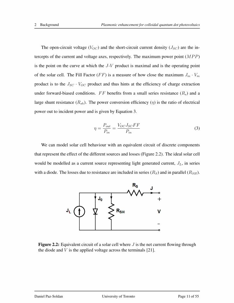
We can model solar cell behaviour with an equivalent circuit of discrete components
that represent the effect of the different sources and losses (Figure 2.2). The ideal solar cell
would be modelled as a current source representing light generated current, JL, in series
with a diode. The losses due to resistance are included in series (RS) and in parallel (RSH).
Figure 2.2: Equivalent circuit of a solar cell where J is the net current flowing throughthe diode and V is the applied voltage across the terminals [21].
Daniel Paz-Soldan University of Toronto Page 11 of 55
2 Background Plasmonic enhancement for colloidal quantum dot photovoltaics
2.1.2 Quantum efficiency
An ideal solar cell absorbs every incident photon and collects every photogenerated carrier.
Quantum Efficiency (QE) is a quantitative measure of the ideality of this process at a given
photon energy.
External Quantum Efficiency (EQE) - or Incident Photon Conversion Efficiency (IPCE)
- is the ratio of current density collected to incident photon flux. It is measured at short-
circuit conditions under 1 sun illumination and given as a percentage as in Equation 4.
EQE(λ) =JSC(λ)
φIN(λ)· 100% =
JSC(λ)
PIN(λ)· hcλ· 100% (4)
It may be important to separate out the effect of optical losses due to reflection or
transmission: the Internal Quantum Efficiency (IQE) - or Absorbed Photon Conversion Ef-
ficiency (APCE) - is the ratio of current density collected to absorbed photon flux. The IQE
gives a measure of the charge extraction efficiency of a solar cell. IQE can be calculated
from EQE and absorption curves as in equation 5.
IQE(λ) =EQE(λ)
Abs(λ)(5)
Using EQE and IQE it is possible to spectrally resolve the contributions of each wavelength
of the solar spectrum to the overall short-circuit current density. Furthermore, by integrat-
ing the EQE curve over the solar spectrum the expected JSC can be accurately calculated.
2.2 Surface plasmons
Surface plasmons are electromagnetic (EM) surface perturbations arising from the reso-
nant oscillation of free electrons in response to an applied field. For most bulk metals the
resonance condition is met with energies in the ultraviolet range. However, for some noble
Daniel Paz-Soldan University of Toronto Page 12 of 55

2 Background Plasmonic enhancement for colloidal quantum dot photovoltaics
metals (Ag, Au) the surface plasmon resonance (SPR) occurs in the visible range [22].
To first order we can describe the optical properties of noble metals by a free electron
gas (plasma) model where an electron sea oscillates against a background of positive ion
cores. Lattice potential and electron-electron interactions are ignored in this model. This is
an accurate description up to visible frequencies for gold and silver; interband transitions
become significant leading to strong absorption at visible frequencies. The response of
a given material to an external field at some frequency, ω, is described by its complex
dielectric function, ε(ω) = ε1 + iε2. The real part ε1 relates to the polarizability of the
material. The imaginary part ε2 relates to the dissipation or absorption of energy in the
material [22]. The measured real and imaginary parts of the complex dielectric function
are shown in Figure 2.3.
Figure 2.3: Dispersion curves for gold (a) real and (b) imaginary parts; and silver (c)real and (d) imaginary parts [23].
Daniel Paz-Soldan University of Toronto Page 13 of 55
2 Background Plasmonic enhancement for colloidal quantum dot photovoltaics
2.2.1 Localized surface plasmons
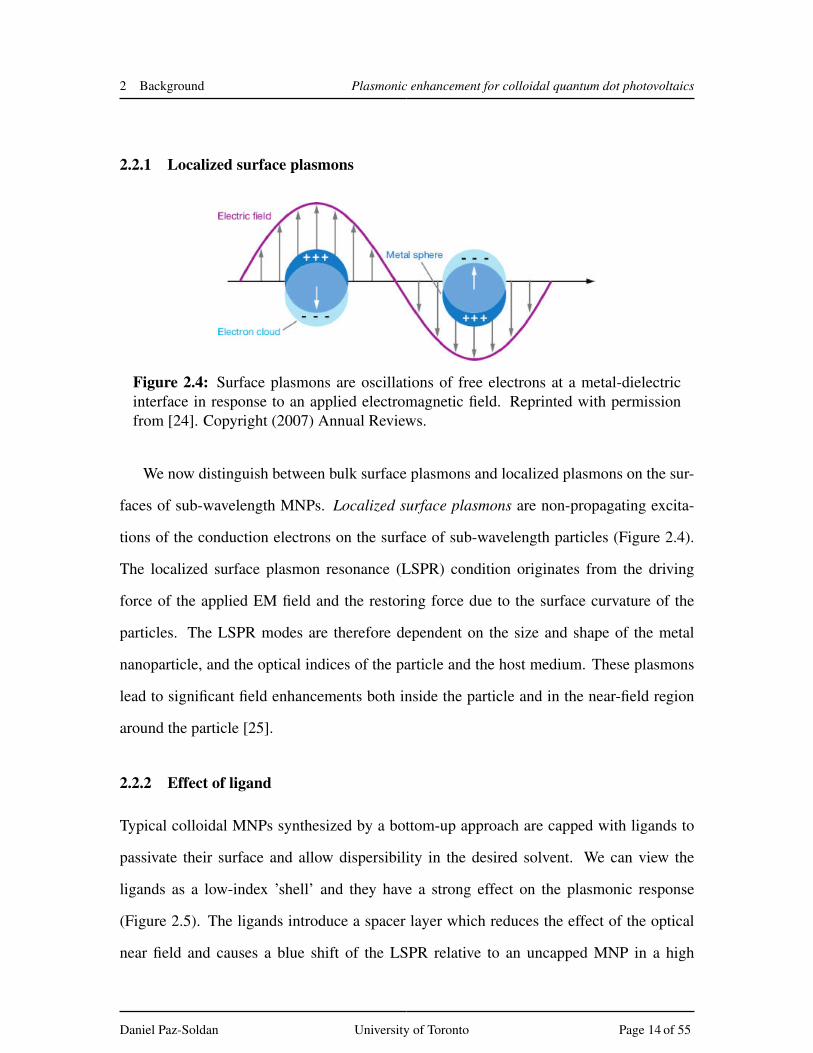
Figure 2.4: Surface plasmons are oscillations of free electrons at a metal-dielectricinterface in response to an applied electromagnetic field. Reprinted with permissionfrom [24]. Copyright (2007) Annual Reviews.
We now distinguish between bulk surface plasmons and localized plasmons on the sur-
faces of sub-wavelength MNPs. Localized surface plasmons are non-propagating excita-
tions of the conduction electrons on the surface of sub-wavelength particles (Figure 2.4).
The localized surface plasmon resonance (LSPR) condition originates from the driving
force of the applied EM field and the restoring force due to the surface curvature of the
particles. The LSPR modes are therefore dependent on the size and shape of the metal
nanoparticle, and the optical indices of the particle and the host medium. These plasmons
lead to significant field enhancements both inside the particle and in the near-field region
around the particle [25].
2.2.2 Effect of ligand
Typical colloidal MNPs synthesized by a bottom-up approach are capped with ligands to
passivate their surface and allow dispersibility in the desired solvent. We can view the
ligands as a low-index ’shell’ and they have a strong effect on the plasmonic response
(Figure 2.5). The ligands introduce a spacer layer which reduces the effect of the optical
near field and causes a blue shift of the LSPR relative to an uncapped MNP in a high
Daniel Paz-Soldan University of Toronto Page 14 of 55

2 Background Plasmonic enhancement for colloidal quantum dot photovoltaics
index medium. Further, the field is effectively confined within the low-index shell which
reduces the optical absorption enhancement (gain) in the surrounding medium [26]. Any
application of plasmonic nanoparticles requires careful consideration of the ligand shell
thickness and the effective medium of the shell.
Figure 2.5: Simulation of absorption enhancement (Gain) spectra in a CQD film with10 nm Ag MNPs capped with ligand shells of different thickneses relative to a bareCQD film. The ligand shell is modelled as n = 1.55 which is typical for organicmolecules. The effect of the ligand shell is to reduce absorption enhancements and blueshift the LSPR relative to the uncapped MNP. Reprinted with permission from [26].Copyright (2011) OSA.
2.3 State of the art
The LSPR of gold and silver MNPs have been used as a means to enhance absorption in
a variety of thin films. In CQD thin films, Konstantatos et al. have achieved absorption
enhancement using metal nanostructures. A 2.4-fold responsivity enhancement near the
absorption edge was observed [27]. The electrical effects of gold, silver, and aluminum
particles on infrared CQD photodetector sensitivity were investigated. It was shown that
the work function of the MNPs is an important factor: gold is ohmic to PbS CQD while
silver and aluminum create a Schottky barrier which impedes current flow. For this reason
gold was determined to be the best material for plasmonic enhancement [28]. However,
Daniel Paz-Soldan University of Toronto Page 15 of 55
2 Background Plasmonic enhancement for colloidal quantum dot photovoltaics
these nanoparticles were formed by an evaporation and annealing method, which is not
amenable to a solution-processing approach.
While these strategies which produce nanostructured substrates have shown promise,
there is a growing trend toward synthesizing and depositing nanoparticles using wet chem-
ical methods. These methods are particularly useful for dye sensitized and organic solar
cells. A recent study by Yang et al. showed near-field plasmonic enhancement by Au par-
ticles embedded in the recombination layer between the small and large bandgap junctions
of a polymer tandem solar cell [29]. Elsewhere, Au nanoparticles were embedded in the ti-
tanium dioxide paste of a dye-sensitized solar cell. It was found that a 3 nm silicon dioxide
shell needed to be grown on the Au particle to chemically and electrically insulate it from
the surrounding medium [30].
Solution processing allows excellent control over particle size and shape and allows the
possibility of using anisotropic and non-spherical particles. For example, silver nanoprisms
have been proposed as candidate plasmonic enhancers for organic photovoltaics because
their SPR frequency is in the NIR range where organic molecules are weak absorbers
[31, 32], but enhanced solar cell performace has yet to be achieved. Large silver nanopar-
ticles with small nucleated silver particles on their surface have shown efficient absorption
enhancement in amorphous silicon solar cells due to their omni-directional scattering and
large scattering-to-absorption ratios [33]. However, typical enhancements with all of these
MNPs are in the visible portion of the solar spectrum, and infrared particles have yet to be
used for solar cell enhancement. CQD PV is an ideal platform for investigating NIR plas-
monic enhancement and for achieving measurable solar cell performance enhancements.
Daniel Paz-Soldan University of Toronto Page 16 of 55

3 Infrared plasmonic nanoparticles Plasmonic enhancement for colloidal quantum dot photovoltaics
3 Infrared plasmonic nanoparticles
The aim of the thesis is to use MNPs tuned to the spectral region of low absorption in CQD
films to enhance field intensities and therefore absorption. In this chapter we explore the
properties of several plasmonic metal nanoparticles and outline the design principles for
application to CQD photovoltaics.
3.1 Optical design considerations
It is desirable to choose metal nanoparticles with a LSPR in the wavelength range where
quantum dots absorb less efficiently. Absorption of electromagnetic radiation through a
film with thickness, L, at a given wavelength, λ, is characterized by the absorption coeffi-
cient, α(λ), through the Beer-Lambert Law (equation 6).
T =I
I0= 10−α(λ)L (6)
where I and I0 are the intensity of transmitted and incident light, respectively. The
absorption coefficient of a PbS CQD film was measured by spectroscopic ellipsometry and
is shown in Figure 1.4. The absorption length, 1/α is the distance at which 1/e or about
63 % of photons have been absorbed. It is clear from this spectrum that several hundred
nanometers to a few microns film thickness are required to fully absorb light in the infrared
range.
The absorption and scattering cross sections, σabs and σscat of small metal nanoparticles
are accurately predicted by a particular solution to Maxwell’s equations in the quasi-static
approximation. In this approximation, the size of the particle is much smaller than the
Daniel Paz-Soldan University of Toronto Page 17 of 55

3 Infrared plasmonic nanoparticles Plasmonic enhancement for colloidal quantum dot photovoltaics
wavelength of light, so that the phase of the harmonically oscillating EM field is approxi-
mately constant over the volume of the particles [25]. These are given by [34]:
σabs =2π
λIm[Γ] (7)
σscat =1
6π
(2π
λ
)4
|Γ|2 (8)
Γ = 3Vε/εm − 1
ε/εm + 2(9)
where λ is the wavelength of incident light, V is the volume of the material, Γ is the
polarizability and ε and εm are the dielectric constants of the material and the medium,
respectively. The SPR occurs at the frequency where the polarizability is maximized.
Re[ε(ω)] = −2ε(ω) (10)
The Frohlich Condition, equation 10, predicts the plasmon resonance based on the
dipole approximation. The LSPR is thus determined by the complex refractive index of the
material, the size and shape of the particle, and the dielectric constant of the surrounding
medium. Further, we note that the optical cross section of plasmonic nanoparticles is typi-
cally larger than the physical cross section [34]. That is, the interaction volume of photons
can be larger than the physical volume of the particle.
One of the most important considerations for plasmonic PV is parasitic absorption in
the metal nanoparticle. From equations 7 and 8 it is clear that the absorption and scatter-
ing cross sections scale with volume V and V 2, respectively. Two competing factors arise
here. First, it is important to couple the near field to the surrounding medium with maxi-
mum efficiency. Second, absorption in the nanoparticle is a loss mechanism because this
Daniel Paz-Soldan University of Toronto Page 18 of 55

3 Infrared plasmonic nanoparticles Plasmonic enhancement for colloidal quantum dot photovoltaics
absorption will not lead to enhanced photocarrier generation. A simple analysis leads to
the hypothesis that scattering must be greater than absorption in order to obtain any benefit
from plasmonic enhancement (equation 11).
σscatσabs
> 1 (11)
That is, for each photon incident on the particle the probability that it will be absorbed
in the metal nanoparticle must be less than the probability that it will be scattered into the
surrounding medium. While there are more complex factors to consider, to first order the
criterion in equation 11 must be satisfied to minimize parasitic absorption.
Ideally we would like to know a priori which particle size and shape will give maximal
scattering and minimal absorption. For large or anisotropic particles, an analytical solution
to Maxwell’s equations may not be easily found and electrodynamic (time varying) effects
must be taken into account [25]. In these cases the scattering and absorption spectra of
the particles in any medium can be accurately predicted by numerical analysis, such as by
finite-difference time-domain simulation.
3.2 Finite-difference time-domain simulations
The finite-difference time-domain (FDTD) method is a numerical analysis technique for
solving coupled differential equations on a discretized spatial grid. It is a versatile method
for modeling electromagnetic wave interactions in various media for arbitrary geometry.
Since solutions are evaluated in the time domain, broadband pulses can be applied. In this
thesis, FDTD simulations are used to evaluate the LSPR spectra and the relative scattering-
to-absorption cross sections for the candidate metal nanoparticles. Further details are found
in Appendix B.6.
Daniel Paz-Soldan University of Toronto Page 19 of 55
3 Infrared plasmonic nanoparticles Plasmonic enhancement for colloidal quantum dot photovoltaics
3.3 Engineering of optical resonances
Metal nanoparticles are engineered to have a localized surface plasmon resonance in a
useful spectral range. For instance the dipole resonance of spherical gold nanoparticles can
be tuned from about 540 nm to 650 nm by increasing the radius from <50nm to about 300
nm. At diameters larger than 150 nm broadband multipole modes arise at lower energies in
the near infrared (NIR) spectral range [34]. Very large sphere sizes relative to the quantum
dot film thickness are needed to obtain good scattering properties. Furthermore it is difficult
to achieve NIR absorption enhancement near the CQD exciton with a spherical geometry
as typically the LSPR are not trivially extended to the NIR. We must look beyond spherical
particles for application to CQD photovoltaics.
3.3.1 Hemisphere-capped nanorods
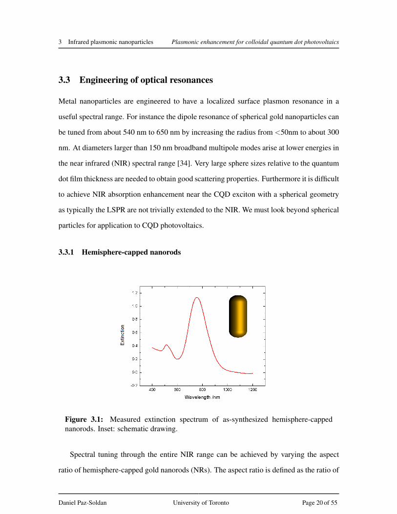
Figure 3.1: Measured extinction spectrum of as-synthesized hemisphere-cappednanorods. Inset: schematic drawing.
Spectral tuning through the entire NIR range can be achieved by varying the aspect
ratio of hemisphere-capped gold nanorods (NRs). The aspect ratio is defined as the ratio of
Daniel Paz-Soldan University of Toronto Page 20 of 55
3 Infrared plasmonic nanoparticles Plasmonic enhancement for colloidal quantum dot photovoltaics
the total length from tip-to-tip to the total diameter at the rod’s center. In the case of NRs,
as with any elongated particle, two spectrally separated LSPRs arise due to the coherent
oscillations of the conduction band electron along each of the particle axes (transverse
and longitudinal). Figure 3.2 shows FDTD simulations demonstrating a linear shift of the
LSPR with increasing NR length and fixed diameter. The incident radiation was a plane
wave polarized along the length of the rod to excite the longitudinal modes. Additionally,
the scattering cross section increases with R more quickly than the absorption cross section.
This agrees well with the theory presented in equations 7 and 8, where σscat increases with
V 2 while σabs increases with V .
The LSPR depends sensitively on the local dielectric environment of the particles. In
general, as the medium n increases, the LSPR redshifts. In relatively high index quantum
dot films (n ∼ 2.5) a redshift of the LSPR of particles embedded in a film relative to the
LSPR in the native solution can be expected. These trends have been reported in previous
studies [35, 36].
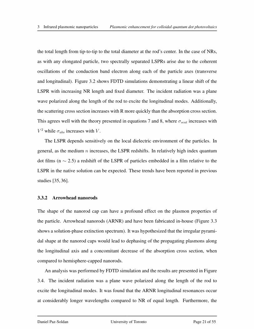
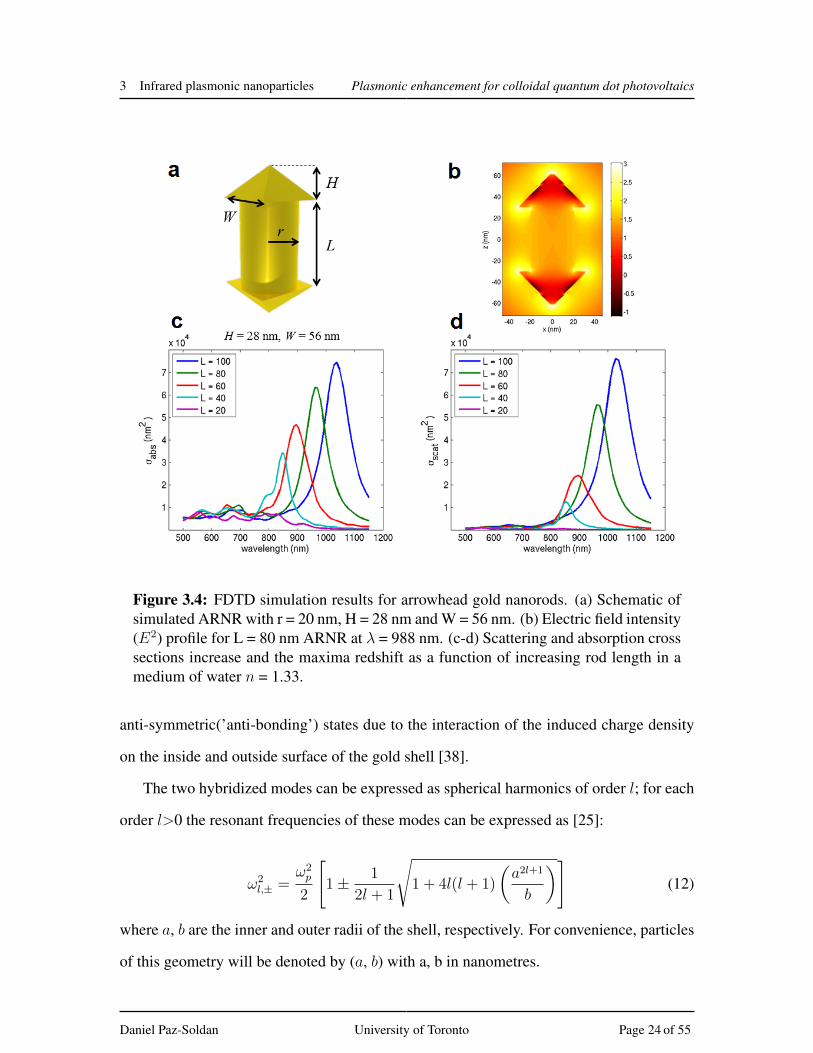
3.3.2 Arrowhead nanorods
The shape of the nanorod cap can have a profound effect on the plasmon properties of
the particle. Arrowhead nanorods (ARNR) and have been fabricated in-house (Figure 3.3
shows a solution-phase extinction spectrum). It was hypothesized that the irregular pyrami-
dal shape at the nanorod caps would lead to dephasing of the propagating plasmons along
the longitudinal axis and a concomitant decrease of the absorption cross section, when
compared to hemisphere-capped nanorods.
An analysis was performed by FDTD simulation and the results are presented in Figure
3.4. The incident radiation was a plane wave polarized along the length of the rod to
excite the longitudinal modes. It was found that the ARNR longitudinal resonances occur
at considerably longer wavelengths compared to NR of equal length. Furthermore, the
Daniel Paz-Soldan University of Toronto Page 21 of 55

3 Infrared plasmonic nanoparticles Plasmonic enhancement for colloidal quantum dot photovoltaics
Figure 3.2: FDTD simulation results for hemisphere-capped gold nanorods. (a)Schematic of simulated NR with r = 20 nm. (b) Electric field intensity (E2) profilefor L = 80 nm NR at λ = 785 nm. (c-d) Scattering and absorption cross sections in-crease and the maxima redshift as a function of increasing rod length in a medium ofwater n = 1.33.
LSPR peak full-width at half-maximum (FWHM) was significantly larger than for NR. This
property is promising for broadband absorption enhancement for solar cell applications.
The peak scattering and absorption cross sections of the particles simulated in this study
are summarized in Figure 3.5. It is noted that the maximum scattering cross section of the
ARNR is less than that of the NR. Furthermore, while the scattering cross section increases
with size as expected, in the case of ARNR the scattering is almost always smaller than
the absorption whereas NRs seem to perform better in terms of scattering for (L>50 nm).
However, in all cases the scattering and absorption cross sections are, at best, comparable
Daniel Paz-Soldan University of Toronto Page 22 of 55
3 Infrared plasmonic nanoparticles Plasmonic enhancement for colloidal quantum dot photovoltaics
Figure 3.3: Measured extinction spectrum of as-synthesized arrowhead nanorods. In-set: schematic drawing.
to each other. In fact it has been observed experimentally and verified numerically that
the scattering-to-absorption ratio of NRs is low due to the presence of a strong electric
field inside the particle, as seen in the electric field intensity profiles. Therefore, while
NR and ARNR have strong field interactions and wide spectral tunability, only a small
enhancement of the absorption of quantum dot films can be expected when these types of
MNPs are employed.
3.3.3 Nanoshells
Broadband visible to NIR localized surface plasmons can be sustained on the surface of
a metal nanoshell (NS), a small dielectric core with a thin metallic shell [37]. The origin
of the specific plasmon spectra of these complex nanostructures can be understood by a
simple hybridization model. The model considers the plasmon response of a gold nanoshell
as the hybridization of a gold sphere plasmon and a dielectric void plasmon in a gold
substrate. The result is two distinct modes that come from the symmetric (’bonding’) and
Daniel Paz-Soldan University of Toronto Page 23 of 55
3 Infrared plasmonic nanoparticles Plasmonic enhancement for colloidal quantum dot photovoltaics
Figure 3.4: FDTD simulation results for arrowhead gold nanorods. (a) Schematic ofsimulated ARNR with r = 20 nm, H = 28 nm and W = 56 nm. (b) Electric field intensity(E2) profile for L = 80 nm ARNR at λ = 988 nm. (c-d) Scattering and absorption crosssections increase and the maxima redshift as a function of increasing rod length in amedium of water n = 1.33.
anti-symmetric(’anti-bonding’) states due to the interaction of the induced charge density
on the inside and outside surface of the gold shell [38].
The two hybridized modes can be expressed as spherical harmonics of order l; for each
order l>0 the resonant frequencies of these modes can be expressed as [25]:
ω2l,± =
ω2p
2
[1± 1
2l + 1
√1 + 4l(l + 1)
(a2l+1
b
)](12)
where a, b are the inner and outer radii of the shell, respectively. For convenience, particles
of this geometry will be denoted by (a, b) with a, b in nanometres.
Daniel Paz-Soldan University of Toronto Page 24 of 55

3 Infrared plasmonic nanoparticles Plasmonic enhancement for colloidal quantum dot photovoltaics
Figure 3.5: Peak scattering and absorption cross sections for various ARNR (a) andNR (b) geometries.
Figure 3.6 shows the experimental extinction spectrum as well as the calculated scatter-
ing and absorption cross section spectra of a solution of gold nanoshells (60, 7.5) dissolved
in methanol (n = 1.33). The dipole and quadrupole modes are distinguishable. For NS of
this size, the scattering-to-absorption ratio is far superior to that of spheres of similar size,
and to that of NRs or ARNR.
3.4 Plasmonic particle spacing in CQD films
Thus far, we have examined the properties of individual nanoparticles. However, ensem-
bles of coupled nanoparticles constitute a different system and the optical response differs
from that of an isolated nanoparticle. For instance, in a recent report it was found end-
to-end assembly of gold nanorods leads to a red shift of the longitudinal LSPR, while
side-by-side assembly leads to blue shift of the longitudinal LSPR and red shift of the
transverse LSPR [12]. It was shown by FDTD simulation and experimentally via surface-
enhanced Raman spectroscopy (SERS) that side-by-side assembly of gold nanorods leads
to destructive interference of the radial component of the surface plasmon modes in the
Daniel Paz-Soldan University of Toronto Page 25 of 55

3 Infrared plasmonic nanoparticles Plasmonic enhancement for colloidal quantum dot photovoltaics
Figure 3.6: Experimental and calculated extinction, and calculated scattering and ab-sorption spectra of (60, 7.5) nanoshells in a medium of index 1.33. Inset: schematicdrawing.
cluster, resulting in field cancellation in the gap between the nanorods [39]. Similarly, we
expect the plasmon modes of nanoshells to become coupled if the MNPs in our films be-
come too closely spaced and the absorption and scattering properties of the ensemble will
change [40].
For application to photovoltaics it might be possible to properly engineer ensembles
of coupled particles for enhanced electric field intensity; however, the controlled design of
such a system was outside the scope of this thesis. Instead we aim to design a system where
the ensemble-average behaviour of the plasmonic nanoparticles is comparable to that of the
isolated nanoparticles. The optimal coverage would ensure that the entire plane of CQD
Daniel Paz-Soldan University of Toronto Page 26 of 55

3 Infrared plasmonic nanoparticles Plasmonic enhancement for colloidal quantum dot photovoltaics
film could interact optically with the nanoparticles while keeping minimal nanoparticle
coverage to reduce recombination effects that could negatively impact the electrical prop-
erties of the device. We can estimate the minimum inter-particle spacing to ensure that all
light interacts with the plasmonic particles from the calculated extinction cross section in
Figure 3.6. The geometric (areal) cross section of (60, 7.5) nanoshells is πr2 = 2× 10⁻¹⁴
m2 and the peak extinction cross section is 1.4 × 10⁻¹³ m2. The ratio of the optical cross
section is therefore 7 times larger than the geometric cross section at the LSPR, and the
ideal areal density of nanoshells is about 14%. This is in reasonably good agreement with
previous estimations that 30% surface coverage is needed to scatter almost all incident ir-
radiation [41]. In this spacing regime, the ensemble-average behaviour is estimated to be
comparable to that of the isolated nanoparticles due to minimal coupling.
3.5 Conclusions
The studies in this chapter help us to understand the important optical properties for appli-
cations of plasmonic metal nanoparticles to solar cells. We are able to engineer the plasmon
response of these particles by selecting appropriate sizes and shapes. We are also able to
use simulation to evaluate the scattering-to-absorption ratio to determine which material
would be the least lossy. We now focus on gold nanoshells in future chapters and look to
exploit their scattering properties for CQD films.
Daniel Paz-Soldan University of Toronto Page 27 of 55

4 Integrating MNPs into CQD solar cells Plasmonic enhancement for colloidal quantum dot photovoltaics
4 Integrating MNPs into CQD solar cells
In this chapter we explore how best to integrate plasmonic nanoparticles into a CQD solar
cell. The overall goal is to increase the absorption cross section of CQD films in order to
boost device performance. The main challenge to overcome is maintaining the integrity of
the thin film after plasmonic nanoparticle deposition.
4.1 PbS CQD and NS film deposition
We begin with a description of the deposition process of a uniform, dense film of quantum
dots. PbS CQD solar cells are fabricated from the solution phase and a film is built up
via a layer-by-layer process by spin casting. A single layer comprises CQD spin cast on
a substrate with thickness determined by the rotational speed of the spin coater and the
concentration of the CQD solution. Next a solution of mercaptopropionic acid (MPA)
is used to flood the CQD layer. This allows complete exchange of the long oleic acid
with MPA on the surfaces of the dots. The ligand exchange step is essential to creating a
conductive, dense film. Finally, a washing step with methanol (MeOH) is used to remove
excess ligand and prepare the surface for the subsequent layer. 12 PbS CQD layers were
used in this study.
A plasmonic PbS CQD solar cell should deviate minimally from this established and
facile layer-by-layer process. In order to embed the NS within the CQD film, we chose to
deposit the NS layer in between PbS CQD layers, keeping all other processing conditions
the same. The main obstacle in this case was ensuring complete coverage of the NS layer
with CQD to ensure that the NS were completely embedded. This was important for several
Daniel Paz-Soldan University of Toronto Page 28 of 55

4 Integrating MNPs into CQD solar cells Plasmonic enhancement for colloidal quantum dot photovoltaics
reasons. The first is that the evaporated top metallic contact is most effective when it
directly contacts the PbS CQD film. Second, we wanted to ensure we had a contiguous
CQD film to facilitate charge carrier transport around the nanoshells. Lastly we aimed
to maximize the coupling of the plasmonic near-field to the CQDs, requiring that the NS
be embedded directly in the film. We found that four layers of the above layer-by-layer
process were needed to achieve complete coverage.
One other factor to consider was the location of the NS along the CQD film thickness.
By empirical observation and theoretical considerations we found that it was best to place
the NS near the back of the device. We hypothesized that the additional surfaces introduced
by embedding NS could lead to enhanced recombination effects which would contribute to
reduced open-circuit voltage. The carriers near the TiO2/PbS interface are particularly
sensitive to these recombination effects. Additionally, we reasoned that introducing NS
near the front of the cell could lead to losses due to Fano interference effects as has been
found in previous reports [27, 42]. These consideration led us to deposit the NS after the
eighth CQD layer, followed by four CQD layer to embed the NS within the film. Details
of the NS deposition method will be described in the present chapter.
4.2 Physical and electrical considerations
A ligand shell of polyvinylpyrrolidone (PVP, MW ' 40,000) was used to maintain col-
loidal stability of NS in polar solvents; methanol was used for our studies. An excess of
PVP was added to allow temporal colloidal stability and avoid aggregation of NS in so-
lution. However, deposition of such a solution was found to lead to considerably reduced
device performance due to several factors. First, excess ligand acts as an insulating layer
preventing extraction of photogenerated carriers. Local variations in ligand density could
lead to non-uniform drying patterns. Furthermore, a dense ligand shell will confine the E
Daniel Paz-Soldan University of Toronto Page 29 of 55

4 Integrating MNPs into CQD solar cells Plasmonic enhancement for colloidal quantum dot photovoltaics
field and limit coupling to the CQDs. On the other hand, removal of ligands leads to unde-
sired agglomerates in solution and in film. Also, a thin passivating dielectric layer is useful
to avoid recombination of carriers on the gold nanoparticle surface. A tradeoff exists for
the optimal surface chemistry of the nanoparticles.
4.2.1 Surface modification and purification
Surface modification of the nanoshells and purification of excess ligand were achieved by
centrifugation of the nanoshell solutions. A fixed volume of nanoshell solution is cen-
trifuged at a set speed and time, causing the capped particles to ’crash’ out of solution.
The supernatant containing excess PVP ligand and other impurities is removed. In order
to minimize particle agglomeration we would like to avoid removing capping ligands from
the particle surfaces. To achieve this, relatively slow centrifugation speeds were used. Sev-
eral centrifugation steps were then needed to ensure complete purification. Transmission
electron microscopy (TEM) was used to visualize the effect of each centrifugation step
(Figure 4.1). A relatively low voltage (70 kV) was used to detect the ligands which appear
as a shadow around the nanoshell particles.
Figure 4.1: Representative low-voltage TEM images of nanoshells deposited on aTEM grid: (a) as-synthesized NS, (b) first centrifugation step and (c) second centrifu-gation step. Scale bar for a-c, 2 microns.
Daniel Paz-Soldan University of Toronto Page 30 of 55

4 Integrating MNPs into CQD solar cells Plasmonic enhancement for colloidal quantum dot photovoltaics
4.2.2 Agglomeration
As mentioned before, bare nanoshells without ligands are prone to agglomeration in so-
lution. We often observed dimers, trimers, and agglomerates of nanoshells, even in the
as-synthesized solution. While it is difficult to eliminate these in a nanoscale colloidal
system, it is desirable to minimize this type of particle coupling. We expected that the
optical and electrical characteristics of multiparticle systems would be altered from that of
individual particles.
Sonication of the nanoshell solutions in an ultrasonic bath was performed immediately
before NS film deposition. It was hypothesized that this applied energy would break the
agglomerated particles apart from each other, leading to more uniform film characteristics.
Table 1 shows the results of a controlled study where device peformance of plasmonic CQD
devices was compared when sonication was applied. The effect is small but the trend shows
improved device properties after the ultrasound treatment to the NS solution. Sonication
has been used for deagglomerating and dispersing nanoparticles evenly in solution for other
applications [43].
Table 1: Solar cell performance results with embedded NS with and without pre-sonication.
Device VOC (V) JSC (mA/cm2) FF (%) PCE (%) Std. Dev. in PCE
Nanoshells 0.57 21.6 48.9 5.4 0.3Nanoshells w. son. 0.58 21.6 51.9 6.0 0.5
4.3 Nanoshell film deposition
Here we describe the methods explored for depositing nanoshells in a uniform, dense,
uncoupled array on a PbS quantum dot film without etching or degrading the underlying
surface.
Daniel Paz-Soldan University of Toronto Page 31 of 55
4 Integrating MNPs into CQD solar cells Plasmonic enhancement for colloidal quantum dot photovoltaics
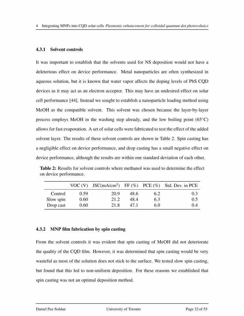
4.3.1 Solvent controls
It was important to establish that the solvents used for NS deposition would not have a
deleterious effect on device performance. Metal nanoparticles are often synthesized in
aqueous solution, but it is known that water vapor affects the doping levels of PbS CQD
devices as it may act as an electron acceptor. This may have an undesired effect on solar
cell performance [44]. Instead we sought to establish a nanoparticle loading method using
MeOH as the compatible solvent. This solvent was chosen because the layer-by-layer
process employs MeOH in the washing step already, and the low boiling point (65C)
allows for fast evaporation. A set of solar cells were fabricated to test the effect of the added
solvent layer. The results of these solvent controls are shown in Table 2. Spin casting has
a negligible effect on device performance, and drop casting has a small negative effect on
device performance, although the results are within one standard deviation of each other.
Table 2: Results for solvent controls where methanol was used to determine the effecton device performance.
VOC (V) JSC(mA/cm2) FF (%) PCE (%) Std. Dev. in PCE
Control 0.59 20.9 48.6 6.2 0.3Slow spin 0.60 21.2 48.4 6.3 0.5Drop cast 0.60 21.8 47.1 6.0 0.4
4.3.2 MNP film fabrication by spin casting
From the solvent controls it was evident that spin casting of MeOH did not deteriorate
the quality of the CQD film. However, it was determined that spin casting would be very
wasteful as most of the solution does not stick to the surface. We tested slow spin casting,
but found that this led to non-uniform deposition. For these reasons we established that
spin casting was not an optimal deposition method.
Daniel Paz-Soldan University of Toronto Page 32 of 55

4 Integrating MNPs into CQD solar cells Plasmonic enhancement for colloidal quantum dot photovoltaics
4.3.3 MNP film fabrication by reservoir drop casting
Drop casting of the plasmonic nanoparticle solution results in minimal waste and uniform
films. Our method of NS deposition leads to consistently repeatable film quality over a large
area (∼3 cm2). We employ a circular reservoir and deposit a controlled-volume solution
with fixed NS concentration. To minimize exposure of the CQD surface to the MeOH
solution, solvent evaporation was performed in low vacuum (∼10−3 Torr). By controlling
the rate of evaporation we were able to obtain consistent and uniform films.
4.4 Conclusions
In summary, the optimal conditions for nanoshell deposition on a colloidal quantum dot
surface were found. Careful control of the NS surface chemistry was achieved to produce
well-dispersed, purified, colloidally stable solutions with minimal aggregation. A reservoir
drop-casting method was found to obtain consistent uniform, dense, largely uncoupled
arrays of nanoshells on a quantum dot surface. With these methods in place, we are now
able to fabricate PbS CQD solar cells with integrated plasmonic nanoparticles.
Daniel Paz-Soldan University of Toronto Page 33 of 55

5 Characterization of devices Plasmonic enhancement for colloidal quantum dot photovoltaics
5 Characterization of devices
In this chapter we perform full optical and electrical characterization of plasmonic CQD
solar cells and compare to a relevant set of controls. From these results we elucidate the
mechanism of improved performance in the enhanced devices.
5.1 Design of plasmonic CQD solar cells
Figure 5.1: Cross sectional TEM image after focused ion beam (FIB) milling andschematic representation of a plasmonic CQD solar cell, showing spectral matching ofthe NS plasmon with the PbS quantum dot absorption spectrum. Scale bar, 100 nm.
We sought to significantly enhance the absorption cross section of our PbS quantum
dot films and thus improve the performance of our best solar cells. To achieve this goal,
we employed the depleted heterojunction stack introduced in chapter 2 as the platform for
our plasmonically enhanced devices. We integrated plasmonic nanoshells directly into the
Daniel Paz-Soldan University of Toronto Page 34 of 55

5 Characterization of devices Plasmonic enhancement for colloidal quantum dot photovoltaics
active CQD layer, allowing for efficient coupling of the broadband plasmonic near and far
field into the PbS film. The design of our solar cell is shown in Figure 5.1. The nanoshells
are embedded into the CQD film. The total PbS film thickness is 400 nm and the NS are
located 200 nm above the TiO2 electrode. Using the design considerations from chapters 3
and 4 we optimized these devices to achieve performance exceeding that of a bare control.
5.2 Performance of CQD solar cells with NR and ARNR
From considerations of the scattering-to-absorption ratios in nanorods, one would expect
no benefit to solar cell performance using embedded gold NR and ARNR. We verified
this experimentally by applying our best processing to make plasmonic nanorod devices as
in Tables 3 and 4. From the figures of merit of 3 devices of each control and plasmonic
samples, we observed no significant enhancement in any figure of merit for these device
sets.
Table 3: Average performance of hemisphere-capped nanorod devices.
Device VOC (V) JSC (mA/cm2) FF (%) PCE (%)
Control sample 1 0.60 20.4 50.3 6.0Control sample 2 0.57 20.2 51.0 5.9Control sample 3 0.58 21.5 44.4 5.6NR sample 1 0.59 21.1 43.8 5.3NR sample 2 0.57 21.5 44.1 5.5NR sample 3 0.59 20.3 48.4 5.8
5.3 Optical properties of plasmonic CQD films
The absorption spectra in a single pass through our thin films were measured using in-
tegrating sphere spectrophotometry. The spectra of two representative samples with and
without nanoshells are shown in Figure 5.2. We observe a broadband absorption enhance-
Daniel Paz-Soldan University of Toronto Page 35 of 55

5 Characterization of devices Plasmonic enhancement for colloidal quantum dot photovoltaics
Table 4: Average performance of arrowhead capped nanorod devices.
Device VOC (V) JSC (mA/cm2) FF (%) PCE (%)
Control sample 1 0.56 20.4 49.3 5.8Control sample 2 0.58 20.9 51.7 6.3Control sample 3 0.58 20.5 52.9 6.4ARNR sample 1 0.59 21.1 50.7 6.5ARNR sample 2 0.55 20.4 47.4 5.3ARNR sample 3 0.58 20.4 49.8 6.0
ment of as much as 100 % centred at the plasmonic LSPR near 820 nm. By subtracting
the absorption curves we can approximately account for the absorption enhancement due
primarily to the plasmonic inclusions (Figure 5.2b). The resonance is red-shifted relative
to that measured in solution due to the higher index of the surrounding medium. If we
consider the high scattering-to-absorption ratio of nanoshells, we may expect the measured
absorption enhancement to mostly originate from absorption in the quantum dot film and
not from parasitic absorption in the plasmonic nanoparticles. Using the integrating sphere
method, however, it is not trivial to decouple the relative contributions from these effects.
Figure 5.2: Single pass absorption spectrum of PbS CQD films with and without NSembedded as measured by integrating sphere UV-Vis-NIR absorption. (b) The absorp-tion enhancement due to the NS is shown by the subtraction of the two absorptioncurves.
It is important to note here that single-pass absorption does not fully represent the sys-
Daniel Paz-Soldan University of Toronto Page 36 of 55

5 Characterization of devices Plasmonic enhancement for colloidal quantum dot photovoltaics
tem employed for the plasmonic CQD solar cells. In a working device, the top contact is
used as a fully reflective mirror and therefore we obtain a double pass through our devices.
However, the absorption enhancement due to the plasmonic effect in this case is convolved
with Fabry-Perot resonances and the specific contribution from plasmonic effects is dif-
ficult to interpret. The double-pass absorption spectra of two representative samples are
shown in Appendix B, Figure A-1.
5.4 Device performance
The performance of nanoshell devices was evaluated by the current-density curves mea-
sured under simulated solar illumination. The results from our best control and nanoshell
devices are shown in Figure 5.3a, demonstrating a consistent and significant trend of en-
hancement relative to the control. For the best control and nanoshell devices there was
an enhancement of 3.6 % in VOC , 13.2 % in JSC , -3.9 % in FF (degradation) and 11.4
% in PCE. These results show that the enhancement in performance is primarily due to
enhanced JSC , while there is no statistically significant enhancement or degradation of the
other figures of merit, VOC and FF . This trend indicates that we were able to maintain
the fidelity of our thin films after NS integration and simultaneously enhance the density of
photogenerated carriers by enhancing the CQD film absorption.
Table 5: Device results using nanoshells.
Device VOC (V) JSC (mA/cm2) FF (%) PCE (%)
Control sample 1 0.56 20.5 53.3 6.1Control sample 2 0.56 21.6 51.6 6.2Control sample 3 0.54 21.2 53.5 6.2
Nanoshell sample 1 0.56 23.8 52.4 6.9Nanoshell sample 2 0.56 24.0 50.9 6.8Nanoshell sample 3 0.58 24.5 49.6 6.9
Daniel Paz-Soldan University of Toronto Page 37 of 55
5 Characterization of devices Plasmonic enhancement for colloidal quantum dot photovoltaics
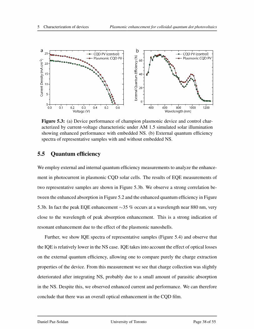
Figure 5.3: (a) Device performance of champion plasmonic device and control char-acterized by current-voltage characteristic under AM 1.5 simulated solar illuminationshowing enhanced performance with embedded NS. (b) External quantum efficiencyspectra of representative samples with and without embedded NS.
5.5 Quantum efficiency
We employ external and internal quantum efficiency measurements to analyze the enhance-
ment in photocurrent in plasmonic CQD solar cells. The results of EQE measurements of
two representative samples are shown in Figure 5.3b. We observe a strong correlation be-
tween the enhanced absorption in Figure 5.2 and the enhanced quantum efficiency in Figure
5.3b. In fact the peak EQE enhancement ∼35 % occurs at a wavelength near 880 nm, very
close to the wavelength of peak absorption enhancement. This is a strong indication of
resonant enhancement due to the effect of the plasmonic nanoshells.
Further, we show IQE spectra of representative samples (Figure 5.4) and observe that
the IQE is relatively lower in the NS case. IQE takes into account the effect of optical losses
on the external quantum efficiency, allowing one to compare purely the charge extraction
properties of the device. From this measurement we see that charge collection was slightly
deteriorated after integrating NS, probably due to a small amount of parasitic absorption
in the NS. Despite this, we observed enhanced current and performance. We can therefore
conclude that there was an overall optical enhancement in the CQD film.
Daniel Paz-Soldan University of Toronto Page 38 of 55

5 Characterization of devices Plasmonic enhancement for colloidal quantum dot photovoltaics
Figure 5.4: Internal quantum efficiency spectra of representative samples with andwithout NS embedded.
5.6 Conclusions
A successful demonstration of the plasmonic effect for CQD photovoltaics was presented.
Complete device characterization shows that the enhancement observed was indeed due
to a plasmonic effect. We have confirmed our hypothesis that solar cell performance can
be improved by increasing the absorption of CQD films using solution-processed metal
nanoparticles.
Daniel Paz-Soldan University of Toronto Page 39 of 55

6 Conclusion Plasmonic enhancement for colloidal quantum dot photovoltaics
6 Conclusion
The field of colloidal quantum dot photovoltaics has advanced rapidly, recently reaching
photoconversion efficiencies of 7 % [17]. The inherent cost advantages presented by the
solution processability of this unique solar material will one day allow CQD photovoltaics
to compete directly with legacy technologies. However, further improvements in device ef-
ficiency are needed to reach this goal. The approach to performance enhancement adopted
in this thesis was to address the absorption-extraction compromise; that is, at the optimal
device thickness for charge collection, absorption of near infrared light is largely incom-
plete. We employ plasmonic enhancements from solution-processed metal nanoparticles
embedded in the CQD film, coupling the near- and far-field scattered light directly to the
absorbing layer. Simulation and theory directed the choice of gold nanoshells with broad-
band, infrared LSPR and maximal scattering-to-absorption ratio. Careful manipulation of
the surface chemistry and proper loading of the nanoshells on the quantum dot surface was
key to maintaining efficient charge collection. Finally, these design principles were applied
to PbS CQD solar cells, leading to enhanced absorption and ultimately improved device
efficiency.
6.1 Contributions to the field
This thesis encompasses several major contributions to the fields of plasmonics and photo-
voltaics:
1. Design criteria for plasmonic enhancement using solution-cast metal nanoparticles
were presented. FDTD simulations and theory were employed to characterize a va-
Daniel Paz-Soldan University of Toronto Page 40 of 55

6 Conclusion Plasmonic enhancement for colloidal quantum dot photovoltaics
riety of particles with tunable plasmonic response in the NIR spectral range. We
found that nanorods, while they are easily tunable, are far too lossy and did not lead
to enhanced photovoltaic performance. Further, our results were used to qualify gold
nanoshells as an optimal material for application to solar cells with appropriately-
tuned LSPR and a superior scattering-to-absorption ratio.
2. A consistent and repeatable method for preparing and depositing metal nanoparticles
which maintained efficient charge collection through the CQD layer was outlined.
This manipulation at the nanoscale was an essential step to exploiting the plasmonic
effect.
3. To the author’s best knowledge, this thesis presents the world’s first plasmonic col-
loidal quantum dot solar cell. While the principles outlined here are applied only
to CQD photovoltaics, we note that this work is relevant to solution-processed plas-
monics for all photovoltaic technologies as well as other opto-electronic device ap-
plications.
6.2 Future work
Suggestions for future research directions follow.
1. This thesis introduced the topic of tuning plasmonic resonances to quantum dot film
absorption curves. It would seem beneficial to employ a wider dispersity of plas-
monic nanoparticle shapes or sizes. In theory this would lead to, in effect, a more
broadband plasmonic enhancement and a further improvement in performance. This
strategy would require careful consideration of the scattering-to-absorption ratios for
the different particles.
2. In the field of plasmonic enhancement for solar cell applications, future research
Daniel Paz-Soldan University of Toronto Page 41 of 55

6 Conclusion Plasmonic enhancement for colloidal quantum dot photovoltaics
should focus on controlled, periodic self-assembly of metal nanoparticles. This
would open the possibility of exploiting the surface plasmon polaritons which arise
from the long range order in such a system. We expect this could lead to more sig-
nificant absorption and performance enhancements.
3. In the field of CQD photovoltaics, transport in PbS films should be improved through
further improvements in quantum dot surface passivation. It is noted that the absorption-
extraction compromise could also be addressed from the other direction - if charge
collection could be efficient at 1 micron film thickness, a planar architecture would
be the most simple and efficient.
Daniel Paz-Soldan University of Toronto Page 42 of 55
REFERENCES Plasmonic enhancement for colloidal quantum dot photovoltaics
References[1] U.S. Energy Information Administration. Emissions of Greenhouse Gases Report.
Technical report, 2009.
[2] U.S. Energy Information Administration. Annual Energy Review. Technical report,2011.
[3] NS Lewis. Powering the planet. MRS Bulletin, 32:808–820, 2007.
[4] M Hoogwijk and W Graus. Global potential of renewable energy sources: a literatureassessment. Technical Report March, 2008.
[5] Illan J. Kramer and Edward H. Sargent. Colloidal Quantum Dot Photovoltaics: APath Forward. ACS Nano, 5(11):8506–8514, 2011.
[6] SR Forrest. The limits to organic photovoltaic cell efficiency. MRS bulletin, 30:28–32,2005.
[7] William Shockley and Hans J. Queisser. Detailed Balance Limit of Efficiency of p-nJunction Solar Cells. Journal of Applied Physics, 32(3):510, 1961.
[8] Jiang Tang and Edward H Sargent. Infrared Colloidal Quantum Dots for Photo-voltaics: Fundamentals and Recent Progress. Advanced Materials, 23(1):12–29, Jan-uary 2011.
[9] Edward H. Sargent. Colloidal quantum dot solar cells. Nature Photonics, 6(3):133–135, February 2012.
[10] Dong Yu, Congjun Wang, Brian Wehrenberg, and Philippe Guyot-Sionnest. VariableRange Hopping Conduction in Semiconductor Nanocrystal Solids. Physical ReviewLetters, 92(21):1–4, May 2004.
[11] Maksym V Kovalenko, Marcus Scheele, and Dmitri V Talapin. Colloidal nanocrystalswith molecular metal chalcogenide surface ligands. Science, 324(5933):1417–20,June 2009.
[12] Jong-Soo Lee, Maksym V Kovalenko, Jing Huang, Dae Sung Chung, and Dmitri VTalapin. Band-like transport, high electron mobility and high photoconductivity in all-inorganic nanocrystal arrays. Nature Nanotechnology, 6(6):348–52, January 2011.
[13] Prashant Nagpal and Victor I. Klimov. Role of mid-gap states in charge transportand photoconductivity in semiconductor nanocrystal films. Nature Communications,2:486, September 2011.
Daniel Paz-Soldan University of Toronto Page 43 of 55
REFERENCES Plasmonic enhancement for colloidal quantum dot photovoltaics
[14] Xihua Wang, Ghada I Koleilat, Jiang Tang, Huan Liu, Illan J Kramer, Ratan Debnath,Lukasz Brzozowski, D Aaron R Barkhouse, Larissa Levina, Sjoerd Hoogland, andEdward H Sargent. Tandem colloidal quantum dot solar cells employing a gradedrecombination layer. Nature Photonics, 5:480–484, 2011.
[15] Joshua J Choi, Whitney N Wenger, Rachel S Hoffman, Yee-Fun Lim, Justin Luria,Jacek Jasieniak, John a Marohn, and Tobias Hanrath. Solution-processed nanocrystalquantum dot tandem solar cells. Advanced Materials, 23(28):3144–3148, July 2011.
[16] Steven a McDonald, Gerasimos Konstantatos, Shiguo Zhang, Paul W Cyr, Ethan J DKlem, Larissa Levina, and Edward H Sargent. Solution-processed PbS quantum dotinfrared photodetectors and photovoltaics. Nature Materials, 4(2):138–42, February2005.
[17] Alexander H Ip, Susanna M Thon, Sjoerd Hoogland, Oleksandr Voznyy, David Zhit-omirsky, Ratan Debnath, Larissa Levina, Lisa R Rollny, Graham H Carey, ArminFischer, Kyle W Kemp, Illan J Kramer, Zhijun Ning, Andre J Labelle, Kang WeiChou, Aram Amassian, and Edward H Sargent. Hybrid passivated colloidal quantumdot solids. Nature Nanotechnology, 7(9):577–82, September 2012.
[18] Andras G Pattantyus-Abraham, Illan J Kramer, Aaron R Barkhouse, Xihua Wang,Gerasimos Konstantatos, Ratan Debnath, Larissa Levina, Ines Raabe, Mohammad KNazeeruddin, and Edward H Sargent. Depleted-Heterojunction Colloidal QuantumDot Solar Cells. ACS Nano, 4(6):3374–3380, 2010.
[19] C. H. Henry. Limiting efficiencies of ideal single and multiple energy gap terrestrialsolar cells. Journal of Applied Physics, 51(8):4494, 1980.
[20] Michael Graetzel, Rene A J Janssen, David B Mitzi, and Edward H Sargent. Materialsinterface engineering for solution-processed photovoltaics. Nature, 488(7411):304–12, August 2012.
[21] Jenny Nelson. The Physics of Solar Cells. Imperial College Press, UK, 2003.
[22] Stefan A. Maier. Electromagnetics of Metals. In Plasmonics: Fundamentals andApplications, chapter 1, pages 5–17. Springer Science+Business Media LLC, Bath,2007.
[23] PB Johnson and RW Christy. Optical constants of the noble metals. Physical ReviewB, 6(12):4370–4379, 1972.
[24] Katherine A Willets and Richard P Van Duyne. Localized surface plasmon resonancespectroscopy and sensing. Annual Review of Physical Chemistry, 58:267–97, January2007.
Daniel Paz-Soldan University of Toronto Page 44 of 55

REFERENCES Plasmonic enhancement for colloidal quantum dot photovoltaics
[25] Stefan A. Maier. Localized Surface Plasmons. In Plasmonics: Fundamentals andApplications2, chapter 5, pages 5–17. Springer Science+Business Media LLC, Bath,2007.
[26] F Pelayo Garcıa De Arquer, Fiona J Beck, and Gerasimos Konstantatos. AbsorptionEnhancement in Solution Processed Metal-Semiconductor Nanocomposites. OpticsExpress, 19(21):21038–21049, 2011.
[27] F Pelayo Garcıa De Arquer, Fiona J Beck, Marıa Bernechea, and Gerasimos Konstan-tatos. Plasmonic light trapping leads to responsivity increase in colloidal quantum dotphotodetectors. Applied Physics Letters, 100(043101), 2012.
[28] F. J. Beck, F. P. Garcia de Arquer, M. Bernechea, and G. Konstantatos. Electricaleffects of metal nanoparticles embedded in ultra-thin colloidal quantum dot films.Applied Physics Letters, 101(4):041103, 2012.
[29] Jun Yang, Jingbi You, Chun-chao Chen, Wan-ching Hsu, Hai-ren Tan, and Xing WangZhang. Plasmonic Polymer Tandem Solar Cell. ACS Nano, 2011.
[30] Michael D Brown, Teeraporn Suteewong, R Sai Santosh Kumar, Valerio D Innocenzo,Annamaria Petrozza, Michael M Lee, Ulrich Wiesner, and Henry J Snaith. PlasmonicDye-Sensitized Solar Cells Using Core-Shell Metal-Insulator Nanoparticles. NanoLetters, 11:438–445, 2011.
[31] Abhishek P Kulkarni, Kevin M Noone, Keiko Munechika, Samuel R Guyer, andDavid S Ginger. Plasmon-Enhanced Charge Carrier Generation in Organic Photo-voltaic Films Using Silver Nanoprisms. Nano Letters, 10:1501–1505, 2010.
[32] Michael Salvador, Bradley A Macleod, Angela Hess, Abhishek P Kulkarni, KeikoMunechika, Jennifer I L Chen, David S Ginger, and Salvador E T Al. Electron Accu-mulation on Metal Organic Solar Cells. ACS Nano, AOP, 2012.
[33] Zhengrong Shi and Min Gu. Broadband Enhancement in Thin-Film Amorphous Sili-con Solar Cells Enabled by Nucleated Silver Nanoparticles. Nano Letters, 2012.
[34] S. Pillai and M.A. Green. Plasmonics for photovoltaic applications. Solar EnergyMaterials and Solar Cells, 94(9):1481–1486, September 2010.
[35] S. Link, M. B. Mohamed, and M. a. El-Sayed. Simulation of the Optical AbsorptionSpectra of Gold Nanorods as a Function of Their Aspect Ratio and the Effect of theMedium Dielectric Constant. The Journal of Physical Chemistry B, 103(16):3073–3077, April 1999.
[36] Xiaohua Huang, Svetlana Neretina, and Mostafa a. El-Sayed. Gold Nanorods: FromSynthesis and Properties to Biological and Biomedical Applications. Advanced Ma-terials, 21(48):4880–4910, December 2009.
Daniel Paz-Soldan University of Toronto Page 45 of 55

REFERENCES Plasmonic enhancement for colloidal quantum dot photovoltaics
[37] S.J Oldenburg, R.D Averitt, S.L Westcott, and N.J Halas. Nanoengineering of opticalresonances. Chemical Physics Letters, 288(2-4):243–247, May 1998.
[38] E Prodan, C Radloff, N J Halas, and P Nordlander. A hybridization model for theplasmon response of complex nanostructures. Science, 302(5644):419–22, October2003.
[39] Anna Lee, Aftab Ahmed, Diego P. dos Santos, Neil Coombs, Jai Il Park, ReuvenGordon, Alexandre G. Brolo, and Eugenia Kumacheva. Side-by-Side Assembly ofGold Nanorods Reduces Ensemble-Averaged SERS Intensity. J. Phys. Chem. C,116(9):5538–5545, 2012.
[40] Boris Khlebtsov, Vitaliy Khanadeyev, Jian Ye, Daniel Mackowski, Gustaaf Borghs,and Nikolai Khlebtsov. Coupled plasmon resonances in monolayers of metal nanopar-ticles and nanoshells. Physical Review B, 77(3):035440, January 2008.
[41] Joseph R. Cole and N. J. Halas. Optimized plasmonic nanoparticle distributions forsolar spectrum harvesting. Applied Physics Letters, 89(15):153120, 2006.
[42] Fiona J Beck, Sudha Mokkapati, Albert Polman, and Kylie R Catchpole. Asymmetryin photocurrent enhancement by plasmonic nanoparticle arrays located on the front oron the rear of solar cells. Applied Physics Letters, 96(3):033113, 2010.
[43] Yongqiang Tan and Daniel E Resasco. Dispersion of single-walled carbon nan-otubes of narrow diameter distribution. The Journal of Physical Chemistry. B,109(30):14454–60, August 2005.
[44] David Zhitomirsky, Melissa Furukawa, Jiang Tang, Philipp Stadler, Sjoerd Hoogland,Oleksandr Voznyy, Huan Liu, and Edward H Sargent. N-Type Colloidal-Quantum-Dot Solids for Photovoltaics. Advanced Materials, September 2012.
[45] M.A. Hines and G.D. Scholes. Colloidal PbS Nanocrystals with Size-Tunable Near-Infrared Emission: Observation of Post-Synthesis Self-Narrowing of the Particle SizeDistribution. Advanced Materials, 15(21):1844–1849, November 2003.
[46] Babak Nikoobakht and MA El-Sayed. Preparation and growth mechanism of goldnanorods (NRs) using seed-mediated growth method. Chemistry of Materials,15(10):1957–1962, 2003.
[47] Yanjuan Xiang, Xiaochun Wu, Dongfang Liu, Lili Feng, Ke Zhang, and Weiguo Chu.Tuning the Morphology of Gold Nanocrystals by Switching the Growth of 110Facets from Restriction to Preference. Journal of Physical Chemistry B, 112:3203–3208, 2008.
[48] nanoComposix, Inc. Gold Nanoshells. http://nanocomposix.com/products/
gold/nanoshells.
Daniel Paz-Soldan University of Toronto Page 46 of 55
REFERENCES Plasmonic enhancement for colloidal quantum dot photovoltaics
[49] Lumerical FDTD Solutions. Mie scattering 3D. http://docs.lumerical.com/en/fdtd/sp_mie_scattering_3d.html.
Daniel Paz-Soldan University of Toronto Page 47 of 55

A Materials and experimental procedures Plasmonic enhancement for colloidal quantum dot photovoltaics
A Materials and experimental procedures
A.1 PbS CQD synthesis and solvent exchange
PbS quantum dots were synthesized according to a previously published method [45]. A
solution-phase metal halide (Cd) treatment was applied. For metal halide treatment, 1.0
ml metal halide precursor was introduced into the reaction flask after sulphur source injec-
tion during the slow cooling process. A 6:1 Pb:Cd molar ratio was maintained during the
synthesis. When the reaction temperature reached 3035C, the PbS CQD were isolated by
the addition of 60 ml of acetone then centrifugation. The nanocrystals were then purified
by dispersion in toluene and reprecipitation with acetone/methanol (1:1 volume ratio), then
re-dissolved in anhydrous toluene.
The PbS CQDs in toluene were transferred to inert atmosphere N2-glovebox and pre-
cipitated by centrifugation with methanol (1:1 volume ratio). The supernatant was removed
and the PbS were dried under low vacuum. Then the dried quantum dots were redispersed
in toluene at about 100 mg/mL. This washing process was repeated twice more with the
final redispersion in octane at 50 mg/mL. The final exchanged solutions were stored in
sealed vials in inert atmosphere before use.
A.2 Photovoltaic device fabrication
PbS CQD PV devices were fabricated on FTO-coated glass substrates (25.0 ± 0.1 mm
× 25.0 ± 0.1 mm, Pilkington, TEC 15). Before spin-coating, the FTO substrates were
sonicated in a mixture of Triton in de-ionized (DI )water (2% by volume) and then in
isopropanol and DI water sequentially. A ZnO solution (Alfa AesarNanoshield ZN-2000,
Daniel Paz-Soldan University of Toronto Page 48 of 55

A Materials and experimental procedures Plasmonic enhancement for colloidal quantum dot photovoltaics
50% in H2O colloidal dispersion) was diluted to 20% in DI H2O with resistivity greated
than 13 MΩ·cm. The solution was sonicated for 2 hours before use and vortexed. FTO
substrates were coated with 300 µL by spin casting (speed = 2,000 r.p.m. , time = 20 sec,
accel = 1.0 sec, deaccel = 1.0 sec), and pre-annealed at 150 C for 30 minutes.
A titanium tetrachloride (TiCl4) treatment was then applied. TiCl4 was diluted to a 60
mM solution in DI water. The TiO2 films were immersed in this solution and placed in a 70
C oven for 30 min in air ambient. The substrates were then removed, rinsed with de-ionized
water, and fired at 520C in a furnace for 1 h in air ambient.
A layer-by-layer spin coating process was used for all PV CQD film deposition in this
thesis. Under an ambient atmosphere, 2 drops of PbS CQD through a 0.22 µm filter were
dropped on the ZnO/TiO2 substrate, and spin cast at 2,500 r.p.m. A solid-state ligand
exchange with MPA was done by flooding the surface for 3 sec, then spin coated dry at
2,500 r.p.m. Finally two washes with MeOH were used to remove unbound ligands. Each
device consisted of 12 such layers.
Top electrodes were deposited using an Angstrom Engineering A mod deposition sys-
tem in an Innovative Technology glovebox. The contacts consisted of 10 nm thermally
evaporated molybdenum trioxide deposited at a rate of 0.2 A/s, followed by electron-beam
deposition of 50 nm of Au deposited at 0.4 A/s, and finally 120 nm of thermally evaporated
silver deposited at 1.0 A/s.
A.3 Nanorod synthesis
The seed-mediated growth method developed by Nikoobakht and El-Sayed was adapted for
gold nanorod (NR) synthesis in-house [46]. For the seed solution, small gold nanoparticles
were obtained by the reduciton of HAuCl4 (0.12 mL, 15mM) dissolved in a cetyltrimethy-
lammonium bromide (CTAB) (2.5mL, 0.20M), with cold sodium borohydride (NaBH4) in
Daniel Paz-Soldan University of Toronto Page 49 of 55

A Materials and experimental procedures Plasmonic enhancement for colloidal quantum dot photovoltaics
1.0 mL DI H2O, in an ice-cold water bath. For the growth solution, CTAB (5.0 mL, 0.20M)
was mixed with an aqueous solution of HAuCl4 (0.50 mL, 15 mM), AgNO3 (280 µL, 4.0
mM) and 4.0 mL of DI water. Ascorbic acid (0.12 mL, 0.788 M) was added dropwise to
the solution. The seed solution was aged for 5 min and was added to the growth solution,
thus initiating the NR growth. The color of the solution mixture changed from clear to
deep purple after incubation for 10 h at 27 C. The mixture was centrifuged at 8,500 r.p.m.
for 30 min (Eppendorf centrifuge 5430), and the supernatant was removed and precipitated
NRs were re-dispersed in DI water. This step was then repeated once.
A 1.0 mL solution of polyvinylpyrrolidone (PVP) (100 mg/mL, MW 5000) was added
to the NR solution. The solution was centrifuged at 10,000 r.p.m. for 20 min and re-
dispersed in methanol. This centrifugation and re-dispersion was repeated 3 times.
Figure A-1: TEM image of typical NR. Scale bar, 150 nm.
A.4 Arrowhead nanorod synthesis
Gold nanorods were synthesized as described above. The arrowhead NRs (ARNRs) were
synthesized following the procedure developed by Xiang et al [47]. A 1.5 mL volume of
Daniel Paz-Soldan University of Toronto Page 50 of 55

A Materials and experimental procedures Plasmonic enhancement for colloidal quantum dot photovoltaics
NRs solution was mixed with CTAB (1.0 mL, 0.20M), HAuCl4 (32 µL, 15 mM), AgNO3
(120 µL, 4.0 mM), and ascorbic acid (60µL, 0.788M). The mixture was diluted to a volume
of 6.0 mL with DI H2O and ste in a water bath at 30C for 12 hours. The solution was
centrifuged (20 min at 6,500 r.p.m.) and the supernatant removed. This was repeated three
to five times. A typical TEM image of the ARNR is shown in Figure A-2.
Exchange to PVP-capped ARNR dispersed in methanol was carried out in the same
way as for NR (above).
Figure A-2: TEM image of typical ARNR. Scale bar, 100 nm.
A.5 Nanoshell solution preparation
Gold nanoshells were purchased from nanoComposix, Inc., and delivered as a dried redis-
persible powder capped with PVP (MW 40,000) [48]. The quoted silica core diamater as
Daniel Paz-Soldan University of Toronto Page 51 of 55

A Materials and experimental procedures Plasmonic enhancement for colloidal quantum dot photovoltaics
measured by TEM was 119.2 +/− 4.7 nm and shell thickness was measured as 14.3 nm.
The hydrodynamic diameter was quoted as 168.1 nm (Malvern Zetasizer Nano ZS).
The dried powder was re-dispersed in MeOH at a concentration of 30 mg/mL. This
solution was centrifuged at 1,000 r.p.m. for 15 min and re-dispersed twice. The NS solution
was used immediately after centrifugation to minimize the time for possible agglomeration
and precipitation. Solutions were used within 2-3 h for PV device fabrication. Sonication
for 40 sec in an ultrasonic bath was done immediately before NS deposition.
Daniel Paz-Soldan University of Toronto Page 52 of 55

B Measurements and simulations Plasmonic enhancement for colloidal quantum dot photovoltaics
B Measurements and simulations
B.1 AM 1.5 photovoltaic performance characterization
All PV and EQE device measurements were done under inert N2-flow. Current-voltage
measurements were done using a Keithley 2400 source meter. A solar simulator (Sci-
encetech, Class A, intensity = 100 mW/cm2). The source intensity was measured with a
Melles-Griot broadband power meter through a circular 0.049 cm2 aperture. The spec-
tral mismatch factor between the measured and actual solar spectrum was calculated to be
approximately 10%, thus a correction factor of 0.90 was applied to all current J measure-
ments. The uncertainty in the AM 1.5 characterization was estimated to be ± 7%.
B.2 EQE measurements
External quantum efficiency measurements were obtained by applying chopped (220 kHz)
monochromatic illumination (400 W xenon lamp through a monochromator with order-
sorting filters) collimated and co-focused with a 1-sun intensity illumination source on the
device of interest. The power was measured with calibratd Newport 818-UV and Newport
818-IR power meters. The response from the chopped signal was mesaured using a Stan-
ford Research Systems lock-in amplifier at short-circuit conditions. The uncertainty in the
EQE measurements was estimated to be ± 8%.
Daniel Paz-Soldan University of Toronto Page 53 of 55

B Measurements and simulations Plasmonic enhancement for colloidal quantum dot photovoltaics
B.3 Solution absorption
A Varian CARY 500 UV-Vis-NIR spectrophotometer was used for all absorption mea-
surements. For solution absorption a diluted solution of interest was loaded into a quartz
cuvette. The baseline 100% transmission curve was the cuvette with pure solvent and 0%
transmission curve was taken with the source blocked by a metal plate.
B.4 Film absorption
For film absorption measurements, an integrating sphere is used. Substrates used were ITO
which had minimal absorption (<5% over all wavelength of interest). The baseline 100%
transmission curve was taken as the substrate of interest, at a small angle (approx. 25) to
the input source to collect the specular reflection. Samples were prepared on clean ITO by
spin-coating a layer-by-layer film.
B.5 Double pass film absorption
Double pass film absorption was measured by depositing a MoO3/Au/Ag reflector on the
CQD film, as in device fabrication. The baseline 100% curve in this case was taken as 2×
the single pass absorption of a bare ITO substrate. The double pass absorption measurement
is shown in Figure A-1.
B.6 FDTD simulations
Finite-difference time-domain (FDTD) simulations were carried out using software pack-
age Lumerical FDTD solutions version 7 (http://www.lumerical.com). Scattering and
absorption cross sections were determined following the Mie scattering method in [49]. A
total-field scattered-field (TFSF) plane wave source surrounds the particle of interest. A
Daniel Paz-Soldan University of Toronto Page 54 of 55

B Measurements and simulations Plasmonic enhancement for colloidal quantum dot photovoltaics
Figure A-1: Double pass absorption spectrum of PbS CQD films with and without NSembedded as measured by integrating sphere UV-Vis-NIR absorption.
broadband (λ = 400 - 1200 nm) source, polarized along the cylinder axis, was injected.
The region is surrounded by Perfectly Matched Layers (PML) which absorb all most in-
cident radiation over a wide range of angles. Two analysis groups, one inside the source
boundary (measuring total field) and one outside the source boundary (measuring scattered
field) calculate the optical cross sections.
Daniel Paz-Soldan University of Toronto Page 55 of 55