plasmonic resonance toward terahertz perfect absorbers€¦ · plasmonic resonance toward terahertz...
TRANSCRIPT
Plasmonic Resonance toward Terahertz Perfect AbsorbersWithawat Withayachumnankul,*,† Charan Manish Shah,‡ Christophe Fumeaux,† Benjamin S.-Y. Ung,†,⊥
Willie J. Padilla,§ Madhu Bhaskaran,‡ Derek Abbott,† and Sharath Sriram*,‡
†School of Electrical and Electronic Engineering, The University of Adelaide, Adelaide, SA 5005, Australia‡Functional Materials and Microsystems Research Group, School of Electrical and Computer Engineering, RMIT University,Melbourne, VIC 3001, Australia§Department of Physics, Boston College, 140 Commonwealth Avenue, Chestnut Hill, Massachusetts 02467, United States
ABSTRACT: Metamaterial perfect absorbers have garneredsignificant interest with applications in sensing, imaging, andenergy harnessing. Of particular interest are terahertzabsorbers to overcome the weak terahertz response of naturalmaterials. Here, we propose lossy plasmonic resonance insilicon-based annular microcavities for perfect terahertzabsorption. This mechanism is in stark contrast to earlierdemonstrations of conventional terahertz perfect absorbersthat invoke Lorentzian electric and magnetic resonances. Afundamental cavity mode coupled to coaxial surface plasmonpolaritons is responsible for the predicted exceptional absorption of −58 dB with a 90% absorption bandwidth of 30%. Theperformance is in agreement with experimental validation and consistent with critical coupling and resonance conditions. Thisspecific cavity design possesses great thermal isolation and minimal electromagnetic coupling between unit cells. These uniquefeatures exclusive to the plasmonic cavity introduce a promising avenue for terahertz imaging with enhanced contrast, resolution,and sensitivity.
KEYWORDS: metamaterial, plasmonics, perfect absorber, cavity mode, THz-TDS, terahertz, multiphysics simulation
Research on perfect absorption has recently become a veryactive topic in the rapidly growing field of metamaterials.
Providing enhanced performance and flexibility, perfectabsorbers have been realized in different applications, includingimaging, sensing, and energy harnessing. Soon after the seminaldevelopment by Padilla and co-workers,1,2 metamaterial-basedperfect absorbers have been demonstrated across the spectrum,from the microwave, to terahertz, infrared, and optical bands.3
In general, these traditional perfect absorbers appeared in theform of metallic resonators on a ground plane, designed toeliminate the reflection and enhance the absorption. Theperfect absorption mechanism was explained with thecoexistence of Lorentzian electric and magnetic responsesthat match the impedance of the structure to free space and atthe same time imposing large energy dissipation on resonance.Another explanation involved wave interference theory wheremultipath reflections originating from different interfaces leadto completely destructive interference in the direction ofreflection.4 Alternatively, perfect absorption was interpreted asnullified reflection by an out-of-phase wave reradiated frominduced electric and magnetic surface currents.5
Of relevance to this article are perfect absorbers at infraredand visible frequencies, where metals with relatively limitedconductivity can support bound surface waves or surfaceplasmon polaritons (SPPs). Earlier implementations ofplasmonic absorbers in the near-infrared6,7 and visible8,9
regimes adopted the conventional design of a metallic dipole
array on a ground plane separated by a dielectric spacer. Thisconcept was extended to random nanoparticles on a groundplane that exhibit electric and magnetic resonances for visiblelight absorption.5,10 Unlike perfect absorbers at lowerfrequencies, where loss occurs mainly inside the dielectricspacer, energy dissipation in these plasmonic absorbers takesplace in the lossy metallic components. Other realizations werebased on a solid metal sheet with periodic textures, includingnanovoids11,12 and nanogrooves.13−15 Depending on thegeometries and dimensions, these textured metallic surfacescan exhibit perfect absorption via either localized surfaceplasmon resonances inside cavities or delocalized in-plane SPPcoupling.At terahertz frequencies, various types of plasmonic
resonators, including dipoles, bowties, and coupled disks,constructed from doped semiconductors have been demon-strated for localized surface plasmon resonances.16−19 None-theless their absorption performance has never been exploredin this frequency range. In this article, a terahertz perfectabsorber based on plasmonic resonance is proposed. Thedesign is inspired by our earlier demonstration of comple-mentary plasmonic resonators in the form of annular cavitiesetched into the surface of a doped silicon wafer.20 Theseresonant cavities exhibit relatively strong nonradiative damping,
Received: April 7, 2014Published: June 3, 2014
Article
pubs.acs.org/journal/apchd5
© 2014 American Chemical Society 625 dx.doi.org/10.1021/ph500110t | ACS Photonics 2014, 1, 625−630
essential for efficient energy trapping. With dimensionssatisfying the critical coupling condition, the cavity array canabsorb nearly 100% of incident terahertz energy at resonance.This article discusses the mechanism of plasmonic resonancesin microcavities, approaches for fabrication and measurementfor experimental validation, and observable electromagnetic andthermal responses. Importantly, the conditions of resonanceand critical coupling are analyzed theoretically in relation to acoaxial plasmonic mode.
■ RESONANCE MECHANISM
Figure 1 depicts a single annular cavity, etched straight downinto the surface of a semiconductor wafer. The unit cell size ison the order of the operating wavelength, the cavity depth isabout a quarter wavelength, and the annular gap is on thesubwavelength scale. The supporting semiconductor ismoderately doped with its plasma frequency in the terahertzregime. Linearly polarized terahertz waves incident normally tothe surface are diffracted by the subwavelength annular gap.This diffraction results in phase matching to SPPs that can besustained along the cavity sidewalls. Since the sidewallseparation is less than the decay length of the normal electricfield component, the confined SPPs form a coupled mode thatis controlled by the gap size. Effectively, the excited SPPsestablish the first-order coaxial SPP mode, as indicated by thered arrow in Figure 1a. This mode is a plasmonic counterpart ofthe TE11 mode in perfect-electric-conductor (PEC) coaxialwaveguides. The excited SPPs propagate back and forth alongthe cavity axis. A resonance resulting from a standing wave canbe observed in the reflection spectrum and can be tuned via thecavity depth and the gap size. Owing to the truly localizedmode, electromagnetic coupling between adjacent cavities isminimal. It is worth noting that the resonance mechanism isrelated to different gap plasmon modes observed in texturedmetal surfaces at the infrared and visible regimes.12,13
■ RESULTS AND DISCUSSION
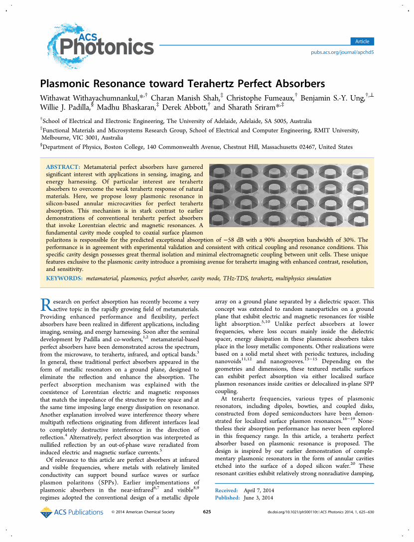
This section discusses numerical and experimental results andelucidates the cavity absorption performance in terms ofelectromagnetic functionality and corresponding thermalbehavior.Electromagnetic Behavior. Figure 2a shows the reflection
amplitude response of the fabricated cavity array at a normalangle of incidence. The measurement and simulation are in
general agreement with small discrepancies associated withfabrication tolerances, optical alignment, and nonplanar wave-front of the incident wave. A strong resonance can be observedat around 1.16 THz with a numerically resolved minimalreflection of −58 dB, compared with a measured reflection of−18 dB at 1.22 THz. The bare silicon wafer shows a baselinereflection profile with monotonically decreasing amplitudetoward high frequencies, where the silicon becomes dielectricwith a constant reflection amplitude of around 0.55. Noterahertz transmission through the cavity sample is detectablewithin the available system bandwidth and dynamic range.Additional simulation suggests that the sample thickness, t, forthe cavity array can be as thin as 80 μm with a transmissionlevel below −25 dB. The simulated and measured absorbanceprofiles are shown in Figure 2b. At resonance, the simulatedand measured absorbance levels are about 100% and 98.5%,respectively. From the simulation, the 90% absorptionbandwidth is around 360 GHz, equivalent to 30%, comparedwith 290 GHz or 24% observed from the measurement. Thestrong absorption is caused by field interaction and ohmic lossin the doped silicon, in contrast to the dominant dielectric lossin conventional perfect absorbers at terahertz frequencies andbelow.3
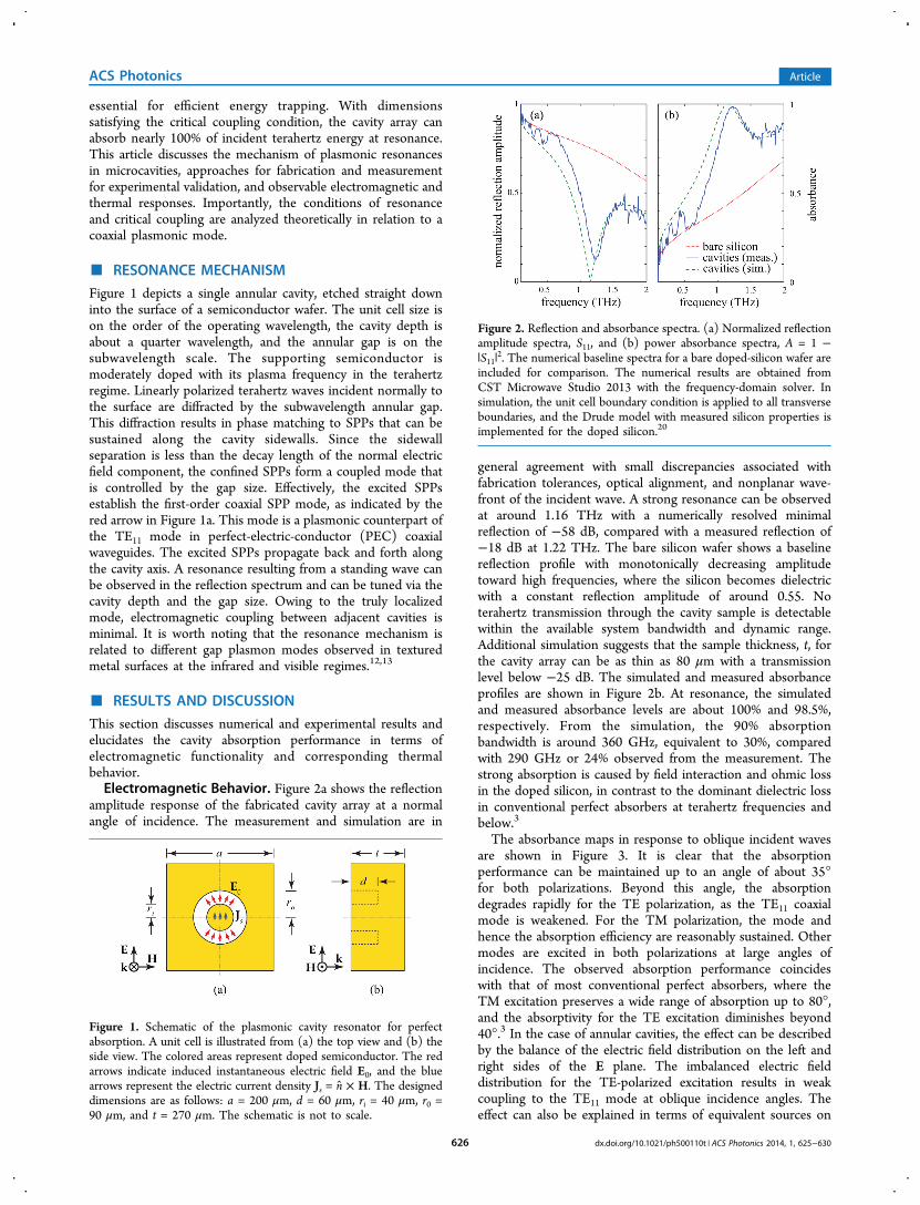
The absorbance maps in response to oblique incident wavesare shown in Figure 3. It is clear that the absorptionperformance can be maintained up to an angle of about 35°for both polarizations. Beyond this angle, the absorptiondegrades rapidly for the TE polarization, as the TE11 coaxialmode is weakened. For the TM polarization, the mode andhence the absorption efficiency are reasonably sustained. Othermodes are excited in both polarizations at large angles ofincidence. The observed absorption performance coincideswith that of most conventional perfect absorbers, where theTM excitation preserves a wide range of absorption up to 80°,and the absorptivity for the TE excitation diminishes beyond40°.3 In the case of annular cavities, the effect can be describedby the balance of the electric field distribution on the left andright sides of the E plane. The imbalanced electric fielddistribution for the TE-polarized excitation results in weakcoupling to the TE11 mode at oblique incidence angles. Theeffect can also be explained in terms of equivalent sources on
Figure 1. Schematic of the plasmonic cavity resonator for perfectabsorption. A unit cell is illustrated from (a) the top view and (b) theside view. The colored areas represent doped semiconductor. The redarrows indicate induced instantaneous electric field E0, and the bluearrows represent the electric current density Js = n × H. The designeddimensions are as follows: a = 200 μm, d = 60 μm, ri = 40 μm, r0 =90 μm, and t = 270 μm. The schematic is not to scale.
Figure 2. Reflection and absorbance spectra. (a) Normalized reflectionamplitude spectra, S11, and (b) power absorbance spectra, A = 1 −|S11|
2. The numerical baseline spectra for a bare doped-silicon wafer areincluded for comparison. The numerical results are obtained fromCST Microwave Studio 2013 with the frequency-domain solver. Insimulation, the unit cell boundary condition is applied to all transverseboundaries, and the Drude model with measured silicon properties isimplemented for the doped silicon.20
ACS Photonics Article
dx.doi.org/10.1021/ph500110t | ACS Photonics 2014, 1, 625−630626
the surface of the central pillar. For the TE polarization, theincident magnetic field component tangential to the surface isnot symmetric with respect to the E plane and, hence, leads toan imbalanced distribution of the surface current density Js.Resonance and Coupling Conditions. In the case of
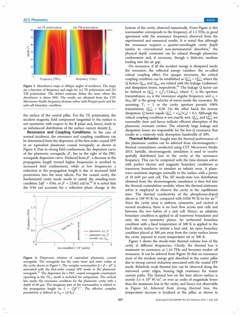
normal incidence, the resonance and coupling conditions canbe determined from the dispersion of the first-order coaxial SPPin an equivalent plasmonic coaxial waveguide, as shown inFigure 4. Due to strong field confinement, the dispersion curveof the plasmonic waveguide, β′, lies to the right of the PECwaveguide dispersion curve. Deduced from β″, a decrease in thepropagation length toward higher frequencies is ascribed toincreased field confinement, while at low frequencies areduction in the propagation length is due to increased fieldpenetration into the lossy silicon. For the coaxial cavity, thefundamental cavity mode needs to satisfy the standing-wavecondition 2dβ′ = 0.9π, or β′ = 23562 rad/m.20 It is noted thatthe 0.9π rad accounts for a reflection phase change at the
bottom of the cavity, observed numerically. From Figure 4, thiswavenumber corresponds to the frequency of 1.2 THz, in goodagreement with the resonance frequency observed from theexperimental and numerical results. It is noted that althoughthe resonance requires a quarter-wavelength cavity depthsimilar to conventional non-metamaterial absorbers,3 thephysical depth constraint can be relaxed through plasmonicconfinement and, if necessary, though a dielectric mediumloading into the air gap.On resonance, if all the incident energy is dissipated inside
the resonator, the reflected energy vanishes: the so-calledcritical coupling effect. For opaque structures, the criticalcoupling condition can be established as Qleak
−1 = Qdiss−1 , where the
Q factors Qleak and Qdiss are related with the leakage (radiation)and dissipation losses, respectively.22 The leakage Q factor canbe defined as Qleak
−1 = vgT1/(2dω0), where T1 is the aperturetransmittance, ω0 is the resonance angular frequency, and vg =∂ω0/∂β′ is the group velocity of waves inside the resonator. Byassuming T1 = 1 or the cavity aperture permits 100%transmission, Qleak
−1 = 0.26. On the other hand, the inversedissipation Q factor equals Qdiss
−1 = εeff″ /|εeff′ | = 0.3. Although thecritical coupling condition is not exactly met, Qleak
−1 and Qdiss−1 are
reasonably close and hence indicate efficient absorption of theplasmonic resonant cavities. The relatively large leakage anddissipation losses are responsible for the low-Q resonance thatresults in a relatively wide absorption bandwidth of 30%.
Thermal Behavior. Insight into the thermal performance ofthe plasmonic cavities can be inferred from electromagnetic−thermal cosimulation conducted using CST Microwave Studio2013. Initially, electromagnetic simulation is used to resolvespatially distributed loss in the cavity at the resonancefrequency. This can be computed with the time-domain solverwith perfect electric and magnetic boundary conditions astransverse boundaries to simulate an infinite array. A plane-wave excitation impinges normally to the surface with a powerof 10 mW per unit cell. The 3D steady-state loss distributionobtained from the electromagnetic simulation is then fed intothe thermal cosimulation module, where the thermal stationarysolver is employed to observe the cavity in the equilibriumstate. The thermal conductivity of the phosphorus-dopedsilicon is 149 W/K/m, compared with 0.026 W/K/m for air.23
Since the cavity array is uniform, symmetric, and excited atnormal incidence, there is no heat flow across unit cells andbetween the two halves of a unit cell. Hence, an adiabaticboundary condition is applied to all transverse boundaries andonto the two symmetry planes. An isothermal boundarycondition with a fixed temperature of 300 K is applied to theback silicon surface to imitate a heat sink. An open boundarycondition placed at 300 μm away from the cavity surface leavesthe cavity exposed to room temperature set to 300 K.Figure 5 shows the steady-state thermal volume loss of the
cavity at different frequencies. Clearly, the thermal loss ismaximum on resonance at 1.16 THz and becomes weaker offresonance. It can be inferred from Figure 5b that on resonancemost of the incident energy gets absorbed in the center pillardue to strong current induction associated with the coaxial SPPmode. Relatively weak thermal loss can be observed along thenarrowed cavity edges, bearing high resistance for returncurrent paths. The thermal loss on the bare silicon surface ismerely 5.5 × 10⁹ W/m3, or over an order of magnitude lowerthan the maximum loss in the cavity, and hence not observablein Figure 5d. Inherent from strong thermal loss, thetemperature increase is localized in the pillar, as shown in
Figure 3. Absorbance maps at oblique angles of incidence. The mapsare a function of frequency and angle for (a) TE polarization and (b)TM polarization. The dotted contours define the areas where theabsorbance is above 90%. The results are obtained from the CSTMicrowave Studio frequency-domain solver with Floquet ports and theunit-cell boundary condition.
Figure 4. Dispersion relation of equivalent plasmonic coaxialwaveguide. The waveguide has the same inner and outer radius asthe cavity shown in Figure 1. The complex wavenumber β = β − jβ″ isassociated with the first-order coaxial SPP mode in the plasmonicwaveguide.21 The dispersion for a PEC coaxial waveguide counterpartoperating in the TE11 mode is included for comparison. The verticalline marks the resonance condition for the plasmonic cavity with adepth of 60 μm. The imaginary part of the wavenumber is related tothe propagation length via L = (2β″)−1. The effective complexpermittivity is defined as εeff = (β/k0)
2.
ACS Photonics Article
dx.doi.org/10.1021/ph500110t | ACS Photonics 2014, 1, 625−630627

Figure 6a. The maximum temperature reaches 300.64 K andprogressively decreases to 300 K toward the back of thesubstrate, where a heat sink is attached. It is worth noting thatthis level of temperature change does not significantly affect thecarrier concentration23 and, hence, the resonance andabsorption conditions. Since the pillar is surrounded by airwith very low thermal conductivity, the heat can barely escapeto the side and to adjacent unit cells, even in the case of anonuniform excitation. Hence, heat accumulated in the pillarmainly flows toward the back in the silicon, as indicated by theheat-flow density in Figure 6b. The particularly high thermalconductivity of silicon benefits the thermal response time,defined as τ = C/Λ, where C is the heat capacity and Λ is thethermal conductance.24 The response time can be reducedfurther by thinning the substrate to reduce the thermal massand hence the heat capacity, yet maintaining the absorptionperformance.
■ CONCLUSIONIn this article, nearly perfect absorption at terahertz frequencieshas been demonstrated with plasmonic microcavities made of
moderately doped silicon. The mechanisms underlyingabsorption are the first-order coaxial SPPs and fundamentalstanding waves developed inside the cavities. With the criticalcoupling satisfied, the incident wave energy is mostly convertedinto heat with theoretical absorption loss of 58 dB. Byleveraging large leakage and dissipation damping, a 90%absorption bandwidth of 30% can be achieved with a singleresonance. On resonance, thermal loss takes place mainly insidethe pillar, giving rise to a local temperature increase therein.The high thermal conductivity of silicon leads to a shortthermal response time of the structure. Since the resonancefrequency can be controlled via carrier concentration, thestructure is ready for dynamic operation via carrier injection.25
The fabrication is relatively inexpensive with silicon as the onlybulk raw material and no multilayer processing. The absorber issuitable for emerging terahertz communications to suppressundesirable multipath effects.As a further application, this plasmonic cavity design can
operate as an integrated detector for active uncooledmicrobolometers. It is worth mentioning existing micro-bolometers employing metamaterial absorbers in the tera-hertz26 and mid-infrared ranges24,27; here, power-dependenttemperature or resistance change in the absorbers can be readout via thermocouples, electrodes, or MEM devices. Likewise,for our plasmonic cavity, either of these devices can beintegrated onto the pillar to sense a change in temperature orresistance. Importantly, this plasmonic absorber designpossesses the unique features of large electromagnetic andthermal isolation between adjacent unit cells. These features,together with nearly 100% absorption, potentially lead to anarray of pixels with high resolution, high contrast, and highsensitivity for terahertz imaging. Since the intercell coupling isminimal, the pixel density can be spatially adapted with nodegradation in the local absorption performance. The frequencyselectivity can be further enhanced due to specific temperatureincrease inside the pillar on resonance. The method canpotentially fill the gap of far-infrared detectors around 10−30 THz.
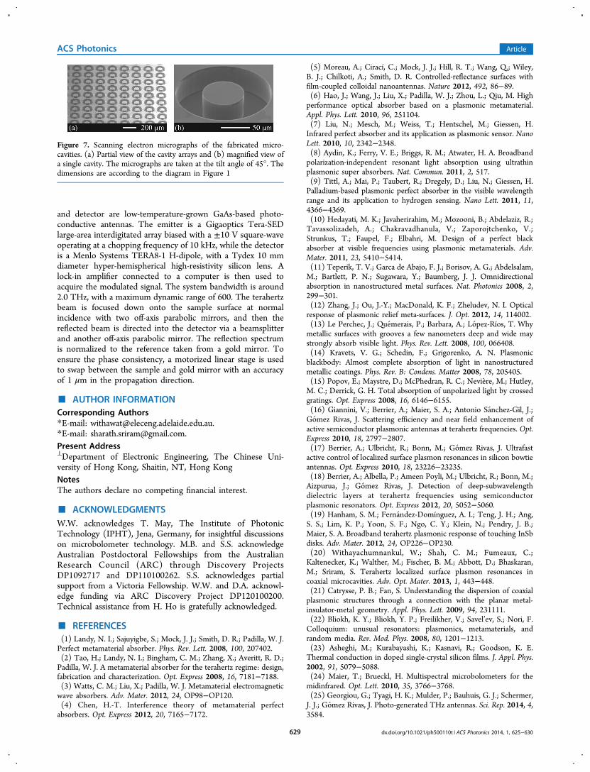
■ METHODSIn order to demonstrate the concept of plasmonic cavityabsorber, microcavities are defined in moderately doped siliconby conventional microfabrication techniques combined withdeep reactive ion etching (DRIE). Silicon substrates are of270 μm thickness, 2 in. diameter, and (100) crystallineorientation. They are doped with phosphorus (n-type) with aresulting dc resistivity of 0.02−0.05 Ω·cm, which correspondsto a carrier concentration of ∼2 × 1017 cm−3 and an electronmobility of 603 cm2/(V·s) at room temperature. The substratesare patterned with photoresist to define the annular structurescovering an area of 36 × 36 mm2 with cavity dimensions givenin Figure 1. The samples are then etched using a Bosch DRIEprocess in a SF6 (etchant) and C4F8 (passivation) fluorine-based chemistry to a depth of 60 at 2.5 μm/min in the regionsnot protected by photoresist. The photoresist is removed byrinsing in acetone and isopropyl alcohol, resulting in theplasmonic absorber samples, as shown in Figure 7.The plasmonic absorber sample is measured with a
reflection-mode terahertz time-domain spectrometer (THz-TDS) at room temperature in a nitrogen atmosphere.28 ATi:sapphire ultrafast laser is used as the pump source for thesystem, with a center wavelength of 800 nm, a repetition rate of80 MHz, and a pulse width of less than 100 fs. Both the emitter
Figure 5. Thermal volume loss for plasmonic cavity and bare siliconsubstrate. (a−c) Plasmonic cavity at 0.5 THz, 1.16 THz (maximumabsorption), and 1.5 THz, respectively. (d) Bare silicon substrate at1.16 THz, with exactly the same settings and carrier concentration asthe cavity. The color plots share the same linear scale.
Figure 6. Steady-state temperature and heat-flow density of plasmoniccavity. Both the temperature (a) and heat-flow density (b) arecalculated at the frequency of maximum absorption at 1.16 THz. Thetemperature color map is in a linear scale.
ACS Photonics Article
dx.doi.org/10.1021/ph500110t | ACS Photonics 2014, 1, 625−630628
and detector are low-temperature-grown GaAs-based photo-conductive antennas. The emitter is a Gigaoptics Tera-SEDlarge-area interdigitated array biased with a ±10 V square-waveoperating at a chopping frequency of 10 kHz, while the detectoris a Menlo Systems TERA8-1 H-dipole, with a Tydex 10 mmdiameter hyper-hemispherical high-resistivity silicon lens. Alock-in amplifier connected to a computer is then used toacquire the modulated signal. The system bandwidth is around2.0 THz, with a maximum dynamic range of 600. The terahertzbeam is focused down onto the sample surface at normalincidence with two off-axis parabolic mirrors, and then thereflected beam is directed into the detector via a beamsplitterand another off-axis parabolic mirror. The reflection spectrumis normalized to the reference taken from a gold mirror. Toensure the phase consistency, a motorized linear stage is usedto swap between the sample and gold mirror with an accuracyof 1 μm in the propagation direction.
■ AUTHOR INFORMATIONCorresponding Authors*E-mail: [email protected].*E-mail: [email protected] Address⊥Department of Electronic Engineering, The Chinese Uni-versity of Hong Kong, Shaitin, NT, Hong KongNotesThe authors declare no competing financial interest.
■ ACKNOWLEDGMENTSW.W. acknowledges T. May, The Institute of PhotonicTechnology (IPHT), Jena, Germany, for insightful discussionson microbolometer technology. M.B. and S.S. acknowledgeAustralian Postdoctoral Fellowships from the AustralianResearch Council (ARC) through Discovery ProjectsDP1092717 and DP110100262. S.S. acknowledges partialsupport from a Victoria Fellowship. W.W. and D.A. acknowl-edge funding via ARC Discovery Project DP120100200.Technical assistance from H. Ho is gratefully acknowledged.
■ REFERENCES(1) Landy, N. I.; Sajuyigbe, S.; Mock, J. J.; Smith, D. R.; Padilla, W. J.Perfect metamaterial absorber. Phys. Rev. Lett. 2008, 100, 207402.(2) Tao, H.; Landy, N. I.; Bingham, C. M.; Zhang, X.; Averitt, R. D.;Padilla, W. J. A metamaterial absorber for the terahertz regime: design,fabrication and characterization. Opt. Express 2008, 16, 7181−7188.(3) Watts, C. M.; Liu, X.; Padilla, W. J. Metamaterial electromagneticwave absorbers. Adv. Mater. 2012, 24, OP98−OP120.(4) Chen, H.-T. Interference theory of metamaterial perfectabsorbers. Opt. Express 2012, 20, 7165−7172.
(5) Moreau, A.; Cirací, C.; Mock, J. J.; Hill, R. T.; Wang, Q.; Wiley,B. J.; Chilkoti, A.; Smith, D. R. Controlled-reflectance surfaces withfilm-coupled colloidal nanoantennas. Nature 2012, 492, 86−89.(6) Hao, J.; Wang, J.; Liu, X.; Padilla, W. J.; Zhou, L.; Qiu, M. Highperformance optical absorber based on a plasmonic metamaterial.Appl. Phys. Lett. 2010, 96, 251104.(7) Liu, N.; Mesch, M.; Weiss, T.; Hentschel, M.; Giessen, H.Infrared perfect absorber and its application as plasmonic sensor. NanoLett. 2010, 10, 2342−2348.(8) Aydin, K.; Ferry, V. E.; Briggs, R. M.; Atwater, H. A. Broadbandpolarization-independent resonant light absorption using ultrathinplasmonic super absorbers. Nat. Commun. 2011, 2, 517.(9) Tittl, A.; Mai, P.; Taubert, R.; Dregely, D.; Liu, N.; Giessen, H.Palladium-based plasmonic perfect absorber in the visible wavelengthrange and its application to hydrogen sensing. Nano Lett. 2011, 11,4366−4369.(10) Hedayati, M. K.; Javaherirahim, M.; Mozooni, B.; Abdelaziz, R.;Tavassolizadeh, A.; Chakravadhanula, V.; Zaporojtchenko, V.;Strunkus, T.; Faupel, F.; Elbahri, M. Design of a perfect blackabsorber at visible frequencies using plasmonic metamaterials. Adv.Mater. 2011, 23, 5410−5414.(11) Teperik, T. V.; Garca de Abajo, F. J.; Borisov, A. G.; Abdelsalam,M.; Bartlett, P. N.; Sugawara, Y.; Baumberg, J. J. Omnidirectionalabsorption in nanostructured metal surfaces. Nat. Photonics 2008, 2,299−301.(12) Zhang, J.; Ou, J.-Y.; MacDonald, K. F.; Zheludev, N. I. Opticalresponse of plasmonic relief meta-surfaces. J. Opt. 2012, 14, 114002.(13) Le Perchec, J.; Quemerais, P.; Barbara, A.; Lopez-Ríos, T. Whymetallic surfaces with grooves a few nanometers deep and wide maystrongly absorb visible light. Phys. Rev. Lett. 2008, 100, 066408.(14) Kravets, V. G.; Schedin, F.; Grigorenko, A. N. Plasmonicblackbody: Almost complete absorption of light in nanostructuredmetallic coatings. Phys. Rev. B: Condens. Matter 2008, 78, 205405.(15) Popov, E.; Maystre, D.; McPhedran, R. C.; Neviere, M.; Hutley,M. C.; Derrick, G. H. Total absorption of unpolarized light by crossedgratings. Opt. Express 2008, 16, 6146−6155.(16) Giannini, V.; Berrier, A.; Maier, S. A.; Antonio Sanchez-Gil, J.;Gomez Rivas, J. Scattering efficiency and near field enhancement ofactive semiconductor plasmonic antennas at terahertz frequencies. Opt.Express 2010, 18, 2797−2807.(17) Berrier, A.; Ulbricht, R.; Bonn, M.; Gomez Rivas, J. Ultrafastactive control of localized surface plasmon resonances in silicon bowtieantennas. Opt. Express 2010, 18, 23226−23235.(18) Berrier, A.; Albella, P.; Ameen Poyli, M.; Ulbricht, R.; Bonn, M.;Aizpurua, J.; Gomez Rivas, J. Detection of deep-subwavelengthdielectric layers at terahertz frequencies using semiconductorplasmonic resonators. Opt. Express 2012, 20, 5052−5060.(19) Hanham, S. M.; Fernandez-Domínguez, A. I.; Teng, J. H.; Ang,S. S.; Lim, K. P.; Yoon, S. F.; Ngo, C. Y.; Klein, N.; Pendry, J. B.;Maier, S. A. Broadband terahertz plasmonic response of touching InSbdisks. Adv. Mater. 2012, 24, OP226−OP230.(20) Withayachumnankul, W.; Shah, C. M.; Fumeaux, C.;Kaltenecker, K.; Walther, M.; Fischer, B. M.; Abbott, D.; Bhaskaran,M.; Sriram, S. Terahertz localized surface plasmon resonances incoaxial microcavities. Adv. Opt. Mater. 2013, 1, 443−448.(21) Catrysse, P. B.; Fan, S. Understanding the dispersion of coaxialplasmonic structures through a connection with the planar metal-insulator-metal geometry. Appl. Phys. Lett. 2009, 94, 231111.(22) Bliokh, K. Y.; Bliokh, Y. P.; Freilikher, V.; Savel’ev, S.; Nori, F.Colloquium: unusual resonators: plasmonics, metamaterials, andrandom media. Rev. Mod. Phys. 2008, 80, 1201−1213.(23) Asheghi, M.; Kurabayashi, K.; Kasnavi, R.; Goodson, K. E.Thermal conduction in doped single-crystal silicon films. J. Appl. Phys.2002, 91, 5079−5088.(24) Maier, T.; Brueckl, H. Multispectral microbolometers for themidinfrared. Opt. Lett. 2010, 35, 3766−3768.(25) Georgiou, G.; Tyagi, H. K.; Mulder, P.; Bauhuis, G. J.; Schermer,J. J.; Gomez Rivas, J. Photo-generated THz antennas. Sci. Rep. 2014, 4,3584.
Figure 7. Scanning electron micrographs of the fabricated micro-cavities. (a) Partial view of the cavity arrays and (b) magnified view ofa single cavity. The micrographs are taken at the tilt angle of 45°. Thedimensions are according to the diagram in Figure 1
ACS Photonics Article
dx.doi.org/10.1021/ph500110t | ACS Photonics 2014, 1, 625−630629

(26) Tao, H.; Kadlec, E. A.; Strikwerda, A. C.; Fan, K.; Padilla, W. J.;Averitt, R. D.; Shaner, E. A.; Zhang, X. Microwave and terahertz wavesensing with metamaterials. Opt. Express 2011, 19, 21620−21626.(27) Maier, T.; Bruckl, H. Wavelength-tunable microbolometers withmetamaterial absorbers. Opt. Lett. 2009, 34, 3012−3014.(28) Ung, B. S.-Y.; Li , J. ; Lin, H.; Fischer, B. M.;Withayachumnankul, W.; Abbott, D. Dual-mode terahertz time-domain spectroscopy system. IEEE Trans. Terahertz Sci. Technol.2013, 3, 216−220.
ACS Photonics Article
dx.doi.org/10.1021/ph500110t | ACS Photonics 2014, 1, 625−630630