plastic spintronics - technische universiteit eindhoven
TRANSCRIPT


Plastic SpintronicsSpin transport and intrinsic magnetoresistance
in organic semiconductors
PROEFSCHRIFT
ter verkrijging van de graad van doctor aan de
Technische Universiteit Eindhoven, op gezag van de
rector magnificus, prof.dr.ir. C.J. van Duijn, voor een
commissie aangewezen door het College voor
Promoties in het openbaar te verdedigen
op maandag 14 juni 2010 om 14.00 uur
door
Wiebe Wagemans
geboren te Arnhem

Dit proefschrift is goedgekeurd door de promotoren:
prof.dr. B. Koopmans
en
prof.dr.ir. H.J.M. Swagten
Copromotor:
dr. P.A. Bobbert
A catalogue record is available from the Eindhoven University of Technology Library.
ISBN 978-90-386-2255-2
This research is supported by the Dutch Technology Foundation STW, which is the
applied science division of NWO, and the Technology Programme of the Ministry of
Economic Affairs (project number 06628).
Printed by Ipskamp Drukkers B.V., Enschede.
Copyright ©2010, W. Wagemans.

Contents
Preface 5
1 Introduction 71.1 Organic electronics . . . . . . . . . . . . . . . . . . . . . . . . . . . . . . 7
1.2 Spintronics . . . . . . . . . . . . . . . . . . . . . . . . . . . . . . . . . . . 12
1.3 Organic spintronics . . . . . . . . . . . . . . . . . . . . . . . . . . . . . . 14
1.3.1 Spin transport in organic materials . . . . . . . . . . . . . . . . 15
1.3.2 Organic magnetoresistance effect . . . . . . . . . . . . . . . . . 17
1.3.3 Models for organic magnetoresistance . . . . . . . . . . . . . . . 20
1.3.4 Comparison of OMAR models with experiments . . . . . . . . 26
1.4 This thesis . . . . . . . . . . . . . . . . . . . . . . . . . . . . . . . . . . . . 31
2 Measuring organic magnetoresistance 332.1 Introduction . . . . . . . . . . . . . . . . . . . . . . . . . . . . . . . . . . 33
2.2 Sample fabrication . . . . . . . . . . . . . . . . . . . . . . . . . . . . . . . 34
2.3 Setup . . . . . . . . . . . . . . . . . . . . . . . . . . . . . . . . . . . . . . . 35
2.4 Field Modulation . . . . . . . . . . . . . . . . . . . . . . . . . . . . . . . 36
2.5 Photocurrent . . . . . . . . . . . . . . . . . . . . . . . . . . . . . . . . . . 38
2.6 Conclusion . . . . . . . . . . . . . . . . . . . . . . . . . . . . . . . . . . . 41
3 A two-site bipolaron model for organic magnetoresistance 433.1 Introduction . . . . . . . . . . . . . . . . . . . . . . . . . . . . . . . . . . 43
3.2 Two-site bipolaron model . . . . . . . . . . . . . . . . . . . . . . . . . . . 44
3.3 Results . . . . . . . . . . . . . . . . . . . . . . . . . . . . . . . . . . . . . . 46
3.4 Conclusion . . . . . . . . . . . . . . . . . . . . . . . . . . . . . . . . . . . 49
4 Frequency dependence of organic magnetoresistance 514.1 Introduction . . . . . . . . . . . . . . . . . . . . . . . . . . . . . . . . . . 51
4.2 Methods . . . . . . . . . . . . . . . . . . . . . . . . . . . . . . . . . . . . . 52
4.3 Results . . . . . . . . . . . . . . . . . . . . . . . . . . . . . . . . . . . . . . 52

4 Contents
4.4 Discussion . . . . . . . . . . . . . . . . . . . . . . . . . . . . . . . . . . . 54
4.5 Conclusion . . . . . . . . . . . . . . . . . . . . . . . . . . . . . . . . . . . 56
5 Angle dependent spin--spin interactions in organic magnetoresistance 575.1 Introduction . . . . . . . . . . . . . . . . . . . . . . . . . . . . . . . . . . 57
5.2 Experimental . . . . . . . . . . . . . . . . . . . . . . . . . . . . . . . . . . 58
5.3 Results . . . . . . . . . . . . . . . . . . . . . . . . . . . . . . . . . . . . . . 58
5.4 Discussion . . . . . . . . . . . . . . . . . . . . . . . . . . . . . . . . . . . 60
5.5 Conclusion . . . . . . . . . . . . . . . . . . . . . . . . . . . . . . . . . . . 66
6 Spin diffusion in organic semiconductors 676.1 Introduction . . . . . . . . . . . . . . . . . . . . . . . . . . . . . . . . . . 67
6.2 Model . . . . . . . . . . . . . . . . . . . . . . . . . . . . . . . . . . . . . . 68
6.3 Spin diffusion . . . . . . . . . . . . . . . . . . . . . . . . . . . . . . . . . . 69
6.4 Modeling a spin valve . . . . . . . . . . . . . . . . . . . . . . . . . . . . . 72
6.4.1 Phenomenological device model . . . . . . . . . . . . . . . . . . 73
6.4.2 Fitting of the experimental data to the model . . . . . . . . . . 75
6.5 Conclusion . . . . . . . . . . . . . . . . . . . . . . . . . . . . . . . . . . . 77
7 Angle dependent spin-diffusion length 797.1 Introduction . . . . . . . . . . . . . . . . . . . . . . . . . . . . . . . . . . 79
7.2 Model . . . . . . . . . . . . . . . . . . . . . . . . . . . . . . . . . . . . . . 80
7.3 Results . . . . . . . . . . . . . . . . . . . . . . . . . . . . . . . . . . . . . . 81
7.4 Waiting Time Analysis . . . . . . . . . . . . . . . . . . . . . . . . . . . . 83
7.5 Hanle Experiment . . . . . . . . . . . . . . . . . . . . . . . . . . . . . . . 86
7.6 Spin Valves . . . . . . . . . . . . . . . . . . . . . . . . . . . . . . . . . . . 87
7.7 Conclusion . . . . . . . . . . . . . . . . . . . . . . . . . . . . . . . . . . . 88
8 Extensions of the experiments and models 898.1 Extending the two-site bipolaron model with physical parameters . . . 89
8.2 An alternative approach to OMAR line shapes . . . . . . . . . . . . . . . 92
8.3 OMAR and spin injection . . . . . . . . . . . . . . . . . . . . . . . . . . 97
9 Outlook 101
Summary / Samenvatting 105
Curriculum vitae 111
List of publications 113
Acknowledgements / Dankwoord 115
Bibliography 126
Index 127

Preface
Plastics are widely known for their easy processing and possibilities to make flexible
or transparent products with vastly different properties. Most people know plastics
for their electrically insulating properties. However, in 1977, it was shown that certain
plastics—or organic materials, as they mostly consist of carbon and hydrogen, like liv-
ing organisms—can conduct electricity. This discovery, which was rewarded with the
Nobel Prize in Chemistry in 2000, was the start of the huge research field of organic
electronics. All the interesting properties of plastics could now be used in electronics
applications. A great boost came in 1987 when the first organic light emitting diode
(OLED) was demonstrated, showing that these organic materials can be used for pro-
ducing light. Since then, this application has rapidly evolved. OLED lighting panels
are now commercially available and OLED displays are incorporated in several mobile
devices. These displays can even be made flexible, allowing a whole new range of possi-
bilities. Organic solar cells are another promising application. Although their efficiency
is still much lower than that of their inorganic counterparts, they aremuch cheaper and
allow roll-to-roll processing in large volumes, which is thought to be essential if solar
power has to be scaled up to a level where it can cover a significant part of our power
consumption.
A completely different field is the field of spintronics, or spin electronics. In most
electronic devices, the charge of electrons is used to transport or store information. Be-
sides a charge, electrons also have a spin, which can be thought of as a small magnet
that can either point up or down. It is this property that is used in spintronics. The
spin of electrons can be influenced by sending them through a magnetic material, or
by applying a magnetic field. One widely used application of spintronics is the read
head used in every modern hard disk. This sensor consists of a stack of magnetic and
non-magnetic layers that respond to the bits on the disk, which are small magnets that
point up (1) or down (0). The current through the stack is different depending on the
orientation of the magnets, allowing the stored data to be read electronically using the
spin-dependent interactions of the electrons. The change in current is called giant mag-
netoresistance (GMR)—the discovery of which (in 1988) was rewarded with the No-
bel Prize in Physics in 2007. GMR allowed for the fast miniaturization and increase of

6 Preface
storage density of hard disks in the last fifteen years. Another example of a spintron-
ics application is the magnetic random access memory (MRAM), which uses the fact
that a magnet preserves its orientation without the need to apply a voltage, like in con-
ventional RAM. This may be used in computers that can be turned on instantly and
consume significantly less power.
As both organic electronics and spintronics offer many advantages and possibili-
ties, the combination of the two fields seems to be a logical step. On the one hand, by
using spins in organic electronics, new functionalities can be added to existing organic
devices. On the other hand, organic materials can be employed in spintronics applica-
tions, benefitting from their low cost, ease of processing and chemical tunability. The
resulting field of organic spintronics is relatively new and the last couple of years first
reports have been made on the successful combination of the fields of organic electron-
ics and spintronics, and even of entirely new phenomena, unique to the field of organic
spintronics. It is thus a new and exciting field that is not only interesting because of the
new physics that is involved, but also because of the possible applications it promises.
In this thesis, two aspects of organic spintronics are investigated. First (Ch. 2–5), a
new magnetic effect in organic materials is investigated. On applying a magnetic field,
the resistance of typical organic devices changes, even without the use of magnetic ma-
terials. This intrinsic organic magnetoresistance (OMAR) is believed to be the result of
the spins of interacting charges. No consensus has been reached yet on the exact ori-
gin of this effect. Therefore, both experimental and theoretical results will be presented
that aim to further the understanding of OMAR. Second (Ch. 6 and 7), the transport of
spin information through organic materials is studied, as this is crucial for successfully
using organic materials in spintronics applications like a GMR sensor. It will be shown
that due to the type of charge transport characteristic for thesematerials, spin transport
is predicted to show specific properties.
Chapters 2–7 can each be read separately, but the first part ofCh. 1 offers an overview
of the basics of organic electronics and spintronics, followed by a review of recent
progress in organic spintronics, also indicating how the following chapters fit into this
picture. InCh. 8, three possible extensions of themodels and experiments are presented,
including suggestions for a combination of the two subjects studied. This is followed
by a general outlook on the future of organic spintronics (Ch. 9). Finally, the reader is
pointed to an index at the end of this thesis for easy reference of the topics covered.
Wiebe Wagemans, Eindhoven, March 2010.
1Introduction
The first part of this chapter provides a basic introduction into organic electronics and
spintronics, while the last part serves to give a broader perspective on the topics covered in
this thesis. This chapter starts with a general introduction of organic electronics. Then, it
introduces the basic concepts of spintronics, using the spin valve as an example. After these
general sections, we zoom in on the use of organic materials in spintronics, which is the
field of organic spintronics. Two topics are discussed inmore detail. First, spin transport in
organic materials is reviewed, highlighting some of the recent results. Second, an extended
overview of organic magnetoresistance is given, starting with describing its main charac-
teristics and explaining the different models. Whereafter these models are compared with
a selection of the many experiments available in literature. Finally, the structure of this
thesis is explained.
1.1 Organic electronicsOrganic electronics, or ‘plastic electronics’, uses conducting organic materials in elec-
tronics applications. The materials we call ‘plastics’ are organic materials, which consist
mostly of carbon and hydrogen. Using organic materials for electronics offers many
advantages. They are easy to process and cheap, and also offer new possibilities as they
are chemically tunable and can allow for flexible or transparent applications. Many dif-
ferent applications have been developed like organic light-emitting diodes (OLEDs),
polymer solar cells, and organic field-effect transistors (OFETs). [31,42,57,130] Many of
these applications are already commercially available, for instance in OLED displays.
Organic electronics is thus a very broad field containing many sub-fields, which can be
considered as mature fields on their own, about which many books, reviews and even
journals are published. In this section we will not try to give a full overview, but will
merely highlight the topics that are relevant for this thesis.

8 Chapter 1: Introduction
H
H
CC
H
H
CC
H
H
H
H
H
H
H
H
H
H
CC
CC
CC
CC
CC
(a)
(b)
Figure 1.1: (a) Part of a polyacetylene polymer, with alternating single and double bonds. (b)
Several pz orbitals from the carbon atoms.
Origin of conductivity
Conduction in many organic molecules is possible because of π-conjugation, resulting
in the presence of alternating single and double bonds in a chain of carbon atoms. Fig-
ure 1.1(a) shows part of the structure of the polymer polyacetylene as an example. The
carbon atoms each have three sp2 orbitals, which overlap to form σ-bonds with the ad-
jacent carbon and hydrogen, and one pz orbital, which overlaps with the neighboring
pz orbitals, see Fig. 1.1(b). This overlap results in the formation of π-bonds, leading to
a delocalization of the π-electrons along the molecule, giving the conducting proper-
ties. The delocalized electrons occupy the bonding π-orbitals, while the anti-bonding
π-orbitals remain empty. The bonding π-orbital with the highest energy is called the
highest occupied molecular orbital (HOMO), while the anti-bonding π-orbital with
the lowest energy is called the lowest unoccupied molecular orbital (LUMO). These
orbitals are comparable to the valence band and conduction band in inorganic semi-
conductors. Due to a geometric relaxation, the delocalization does not extend over the
whole molecule, but single and double bonds are formed. This so-called Peierls distor-
tion leads to the presence of an energy difference, a band gap, of several eV between
the HOMO and LUMO. As a result, these organic materials are semiconducting.
The layers of organic materials studied in this thesis are disordered, or amorphous,
meaning that no (long-range) order exists between the molecules. Due to this disorder
and the weak interaction between molecules, charges are localized on the molecules,
or part of the molecule. Linked to the spatial disorder, an energetic disorder of the
sites exists, as is illustrated in Fig. 1.2. The density of states is often assumed to be a
Gaussian distribution, with a width σ of 75–150meV. [9,136] Charge transport occurs via
hopping between localized sites, which can be described by phonon assisted tunneling.
As a result, mobilities in organic semiconductors are several orders smaller than for
inorganic semiconductors. A typical value is 10−6 cm2V−1 s−1 for the materials used in
this thesis.

1.1 Organic electronics 9
E
x
E
N
Figure 1.2: Disorder in the energy (E) of localized sites, here illustrated in the x direction (left).
The number of sites per energy (N) follows a Gaussian density of states with a width σ (right).
The hopping of a carrier is illustrated.
Alq3 Pentacene(a) (b)
MDMO-PPV P3HT
N
O
N
OAl
N
O
H3CO
OC10H21
n
SS
C6H13
C6H13
n
R2R1
n
cathode
anode
organic layer
PEDOT:PSSITO
V
glass
Figure 1.3: (a) Schematic of a vertical device layout. (b) Examples of typical semiconducting
polymers and small molecules.
Electrical devices
For electrical applications, charges need to be injected into and extracted from the or-
ganic layer. This is usually done with (metal) electrodes. Figure 1.3(a) illustrates a typi-
cal lay-out, where an organic layer is sandwiched between two electrodes. As the anode,
transparent indium tin oxide (ITO) is used, to allow light output, in combinationwith a
layer of poly(3,4-ethylenedioxythiophene): poly(styrenesulfonate) (PEDOT:PSS). For
the active layer, many different organic materials can be used. Here, we typically use
the small molecule tris-(8-hydroxyquinoline) aluminum (Alq3), which is thermally
evaporated in vacuum, or the polymer poly[2-methoxy-5-(3’,7’-dimethyloctyloxy)-1,4-
phenylene vinylene] (MDMO-PPV), which is spin-coated from solution. Both molec-
ular structures are shown in Fig. 1.3(b) with several other examples. As the cathode, we
typically use a very thin layer of LiF, capped with aluminum.
In first order, the alignment of the work functions of the electrodes with theHOMO
and LUMO determines the efficiency of charge injection. A typical case is sketched in
Fig. 1.4(a). With a low work function (Φe), best alignment is achieved with the LUMO

10 Chapter 1: Introduction
Fh
Fe
fh
fe
Vbi
e–
h+HOMO
LUMOFh
Fee–
h+
(a) V = Vbi V = 0(b)
Figure 1.4: Energy diagrams of an organic device with hole (electron) injection barriers ϕh(e),
and electrode work functions Φh(e). For an applied bias (a) V = Vbi (b) V = 0.
and electrons (e) are easiest injected. On the other hand, a high work function (Φh)
facilitates hole (h) injection. In reality, additional effects like the formation of inter-
face dipoles can also play a role. If an energy difference between the electrode and the
HOMOor LUMOexists, an injection barrier ϕ can be present. Depending on the height
of the barrier, the transport of the specific carrier is injection limited. In absence of a
barrier, the contact is Ohmic. By choosing specific combinations of electrodematerials,
it is possible to tune which carriers are present; only electrons or only holes (single-
carrier, or unipolar), or both electrons and holes (double-carrier, or bipolar). At zero
bias, the Fermi energies of the electrodes are aligned [Fig. 1.4(b)], resulting in a reverse
electric field in the organic layer. Charges can only be efficiently injected when the ap-
plied voltage is such that this electric field is at least balanced, so for a voltage that is
equal to or larger than the built-in voltage Vbi [Fig. 1.4(a)].
Charges in organic materials
Once charges are injected, they move to the other electrode under the influence of the
local electric field in the device. These charges induce a displacement of the nearby
atoms, lowering the total energy. The charge and its distortion are called a polaron.∗
When two like charges meet, they will feel a Coulomb repulsion, but they also benefit
from sharing their polaronic distortion. If this balance is positive, a stable bipolaron can
be formed. Opposite charges also interact and can recombine to produce light—a prop-
erty that is exploited in OLEDs. This process starts by the electron and hole becoming
Coulombically bound; they form an e–h pair, which is also called a polaron pair. When
decreasing their separation so that their wave functions overlap, exchange interactions
become important and, only then, the pair is called an exciton.
Pairs of charges (each charge with spin 12) like bipolarons, e–h pairs and excitons
can have either total spin 0, which is a singlet (S), or total spin 1, which are triplets (T).
The triplets split up in T−, T0, and T+ due to the Zeeman energy under the influence
of a magnetic field is applied. The specific spin state is of relevance for interactions and
reactions of the pair. Only a pair of charges in the singlet state can form a bipolaron. For
∗When we speak of electrons and holes we actually mean negatively and positively charged polarons,
respectively.

1.1 Organic electronics 11
excitons only singlet excitons can recombine under emission of light due to spin con-
servation. Because injected charges have a random spin, a S–T ratio of 1:3 is expected,
although deviations have been observed and explained. [145]
Charge transport
When applying an electric field to an organic layer, all charge has to be electrically in-
jected when the layer is undoped. Furthermore, the injected charges drift in this elec-
tric field to the opposite electrode, giving a typical V 2 behavior of the current. The
resulting current is called a space-charge limited current (SCLC), because the current
is impeded by the presence of the (space) charge in the device. By solving the Poisson
equation and the drift equation for a single-carrier device, the exact relationship (called
the Mott–Gurney law) for the current density is: [14]
J = 9
8єµ
V 2
L3 , (1.1)
with є the electric permittivity, µ either the electronmobility µe or the hole mobility µhand, L the thickness.
For a double-carrier device, cancelation of net charge by the injection of oppositely
charged carriers allows for more carriers at the same space charge and thus a much
larger current. Moreover, electrons and holes can also recombine, which reduces the
current as they do not transit the whole length of the device. These type of devices ex-
hibit Langevin recombination, which can be characterized by a recombinationmobility
µr = r(µe + µh), with r ≪ 1 a constant that is small for weak recombination. Parmenter
and Ruppel showed that for ohmic contacts the resulting current density is: [101]
J = 9
8є
¿ÁÁÀ2πµeµh(µe + µh)
µr
V 2
L3 . (1.2)
The mobilities for holes and electrons are usually different. With ‘minority’ and ‘major-
ity’ carriers wewill refer to the carriers with the smaller and largermobility, respectively.
So, in a double-carrier device, also a typical V 2 dependence of the current is found.
However, many other processes can occur in organic devices, the discussion of which
is beyond the scope of this thesis.
One effect worth mentioning is the effect of trapping of carriers. Carriers can be-
come trapped in sites that lie within the band gap of the material. These sites can origi-
nate from defects or impurities, but also from the long tail of the density of states.These
traps limit the mobility of the carriers as they spend a long time in the trap before be-
ing (thermally) released. On increasing the voltage, the current rapidly increases by
trap filling. This increase results in a power law dependence of the current, J ∝ V n ,
with n > 2. [14] At voltages smaller than the built-in voltage, a small current is already
present, which is the result of transport by impurities and defects, and also by diffusion.
This current is linear with voltage, J ∝ V 1. Thus, studying the voltage dependence of
the current on a log–log scale can give information about (changes in) the type of con-
duction.
Besides electrical injection, charges can also be generated by illuminating the or-
ganic material—a property that is exploited in organic solar cells. On absorption of a

12 Chapter 1: Introduction
ferromagnet organic semiconductor
Figure 1.5: Density of states of a ferromagnet and a non-magnetic organic semiconductor, the
selective injection of spin-up electrons from the ferromagnet results in a spin polarization in the
non-magnetic material.
photon, a charge is excited from theHOMO to the LUMO, resulting in a singlet exciton.
This exciton can either recombine (photoluminescence) or dissociate into free carriers,
which drift in the electric field to the electrodes. Depending on the diffusion length of
the excitons, the dissociation can occur in the bulk, at defect sites, or at the electrode. [8]
Conclusion
In conclusion, we have seen that charge transport in organic semiconductors occurs
through hopping. Charges hop between localized sites that are disordered in position
and energy. The charges are called polarons and can interact and form e–h pairs, exci-
tons and bipolarons. The current in a typical organic device is limited by space charge,
resulting in typical J(V) characteristics.
1.2 SpintronicsTraditional electronics uses the charge of electrons to store or transport information,
but by also using their spin, many new and exciting applications are available. Exam-
ples are magnetic-field sensors, non-volatile memory, and even applications such as
quantumcomputing or ‘race-trackmemory’. [25,118,140,146] One famous example of a spin-
tronics application is the sensor in the read head of every modern hard disk; the devel-
opment of which enabled the fast miniaturization and increase in storage density of
hard disks in the last decades. [25] For the demonstration of giant magnetoresistance
(GMR), [6,13] as is also used in the sensor in the hard disk, Fert and Grünberg received
the Nobel Prize in Physics in 2007.
Many different spintronics applications have been developed.Here, wewill describe
the working of a spin valve to illustrate a typical example. Formany of the other applica-
tions and related theory we refer to, for instance, Ref. 140. A spin valve consists of two
ferromagnetic electrodes, separated by a non-magnetic spacer layer. In ferromagnetic
materials, an imbalance exists between the spin-up and spin-down density of states at
the Fermi level (Fig. 1.5). A current injected from the ferromagnetic electrode into the
spacer layerwill have an imbalance between the number of spin-up (N↑) and spin-down(N↓) electrons, resulting in a spin polarization,
P = N↑ − N↓N↑ + N↓
. (1.3)
The spin polarization is transported by a spin-polarized current. During the transport

1.2 Spintronics 13
Figure 1.6: Schematic of MR(B) of spin valve, indicating the magnetization directions of the
electrodes with the horizontal arrows. Both a forward (thick, red) and backward (thin, black)
sweep are shown. The sweep direction is indicated by the vertical arrows. The magnetization
directions switch at the indicated coercive fields.
to the other electrode, the spin polarization is gradually lost by spin flip events. [140]
This loss typically follows an exponential decay that is characterized by a spin-diffusion
length ls. At the other electrode, depending on the relative orientation of the magneti-
zation directions of the two electrodes, the spin polarization can have the same or the
opposite sign. As a result, the device shows a smaller or larger resistance for parallel or
anti-parallel alignment of the magnetization directions.
An illustration of the resistance of a spin valve as a function of the magnetic field B
is shown in Fig. 1.6. At large negative B, the magnetization directions are aligned paral-
lel (as indicated by the horizontal arrows), resulting in a low resistance. On increasing
B beyond zero, the electrode with the smallest coercive field Bc,1 reverses its magneti-
zation first, resulting in an anti-parallel alignment and a large resistance. Increasing B
further also reverses the magnetization of the second electrode, returning the device
in the low resistance state. Sweeping B back to a large negative value, again results in
switching of the magnetization directions, with a corresponding step in resistance, but
now at −Bc,1 and −Bc,2. The magnetoresistance is the relative change in resistance,
MR(B) = R(B) − R0
R0, (1.4)
with R0 (usually) the resistance in the parallel case.
MR(B) curves similar to those for spin valves can also be obtained with magnetic
tunnel junctions. In this case, we speak of tunnel magnetoresistance, TMR. [84] Instead
of transporting carriers through the spacer layer, they tunnel through a thin tunnel
barrier separating the twomagnetic electrodes. As spin is conserved in a tunneling step,
and the resistance of the barrier scales with the product of the density of states at both
sides, a higher resistance is found in the anti-parallel case. This results in an MR(B)
curve identical to the MR(B) curve of a spin valve as shown in Fig. 1.6. One of the
differences between a spin valve and a tunnel junction is the possibility to manipulate
the spins during transport in the spin valve. This is a property we will explore in Ch. 7.
For a properly working spin valve, an obvious requirement is that the spin-diffusion

14 Chapter 1: Introduction
length should be larger than or comparable to the thickness of the spacer layer. There
are, however, many more conditions that affect its working. The efficiency of spin injec-
tion, for example, strongly depends on the details of the interface between the electrode
and the spacer layer, and gradual switching of the magnetization directions can result
in differently shaped curves, in particular when the coercive fields are not properly sepa-
rated. Another possible issue is the reduction ofMRby a ‘conductivitymismatch’. [118,119]
Significant spin injection is prevented by a conductivity mismatch when the resistivity
of thematerial into which spins are injected is much larger than the resistivity of the fer-
romagnetic electrode (evaluated over a thickness of the order of the spin-flip length).
This issue can be overcome by inserting a spin-dependent interface resistance, e.g., a
tunnel barrier, like a thin oxide layer or a Schottky barrier. [118]
1.3 Organic spintronicsOrganic spintronics dealswith the electronic effects of spins in organicmaterials. [36,87,115]
The use of organic materials for organic spintronics has attracted much attention be-
cause of the long spin lifetimes, [76,152] as significant spin–orbit coupling is negligible
due to the low-weight atoms organic materials are composed of (spin–orbit coupling
scales with Z4, where Z is the atomic number). Moreover, the cheap and easy process-
ing, and almost infinite chemical tunability make organic materials very appealing al-
ternatives for the materials currently used in spintronics. One has to remark though
that the long spin lifetime is accompanied by relatively small mobilities, but still is in a
usable range. [36]
From an inorganic spintronics point of view, an obvious step is to replace the inor-
ganic spacer layer in a spin valve with an organic material. There are, however, more ap-
plications of organic spintronics, like single molecule spintronics [109] and organic mag-
nets, [73] but these will not be covered in this thesis. In addition, we note that is should
be possible to enhance OLED efficiency by using spin polarized electrodes. With anti-
parallel alignment of the magnetization directions, 50% singlet excitons can be formed
compared to 25% in a normal OLED. [10] However, no successful realization of this en-
hancement effect has been reported yet. [32,113]
A new spintronics effect, unique to disordered organic semiconductors, deals with
the interaction and correlation of spins in organic semiconductors, leading to an or-
ganic magnetoresistance (OMAR). OMAR has gained much interest as it is an intrin-
sic effect observed in many (very different) organic materials. Because of the relatively
large effects (up to 10–20%) at room temperature and small magnetic fields (10mT),
OMAR is very interesting for applications. For instance, magnetic functionality can
be added to existing applications. [138] Moreover, it also offers new physics and a new
handle to study processes in organic devices.
Spin transport in organic semiconductors and organic magnetoresistance seem to
be two very different topics, but as we will see, they both depend on very similar spin-
dependent processes and are thus interesting to study in parallel. First, in Sect. 1.3.1, a
brief overview of recent experiments on spin transport in organic materials is given.
Second, in Sect. 1.3.2, the key properties of OMAR are introduced and Sect. 1.3.3 de-
scribes the various models that have been suggested to explain the observed OMAR
effects and discusses them in the light of recent experiments.

1.3 Organic spintronics 15
d
dill
(a) (b)
(c)
Figure 1.7: (a) First organic spin valve measurement by Xiong et al., measured on a
LSMO/Alq3/Co device at 11 K. Forward sweep (squares, red) and backward sweep (circles, black)
with parallel and anti-parallel magnetization directions illustrated. Data adapted from Ref. 149.
(b) Ideal spin valve. (c) Spin valve with inclusions from the top electrode, resulting in an ‘ill-
defined’ layer dill.
1.3.1 Spin transport in organic materialsSpin injection into a layer of a small molecule (sexithiophene), with two ferromag-
netic La0.67Sr0.33MnO3 (LSMO) electrodes, was first claimed in 2002. [35] However, no
straightforward proof of correlation of the observed MR with the orientations of the
magnetization directions was given. In 2004, Xiong et al. reported the first organic spin
valve, using Alq3 as the organic spacer layer and LSMO and Co as the electrodes. [149]
Their measurement, shown in Fig. 1.7(a), is not a typical MR(B) curve as introduced
in the previous section. Lower resistance was found in the anti-parallel configuration,
which is believed to be from spin polarization opposite to the magnetization at inter-
face. [36] Also, no sharp, but gradual switching was observed. Note, however, that also
switching before zero was observed, which we believe to be a possible signature of
magnetic-field dependence of the spin-diffusion length as will be covered in Ch. 6. The
authors reported a spin-diffusion length of 45nm, based on measurements on samples
with variable spacer thickness measured at 11K. [149] For this they did have to assume
a significant ‘ill-defined’ layer of 87nm, possibly from pinholes or Co inclusions in
the spacer layer [Fig. 1.7(c)]. For increasing temperature, the MR strongly decreased,
which was attributed to the temperature dependence of the LSMO electrode. [34] After
this first report, several other groups reported on spin valves using organic spacer lay-
ers.The LSMO/Alq3/Co spin valve was reproduced,[34,71,144,150] but also othermaterials
have been tried, like polymers. [71,85] For an excellent overview we refer to Refs. 87 and
36, in which also other devices than spin valves are discussed.
Some controversy still exists about the experimental reports of organic spin valves.
The main question is wether the observed MR is really the result from spin transport
through the layer, or that it is from tunneling through thin regions. [59,139,150] One of the
main arguments for tunneling is that the voltages at which results have been reported
are well below the built-in voltage, but still the resistances are low, which is not a typical
characteristic of organic devices. [59,139,150] In inorganic semiconductors, spin transport
has been unambiguously demonstrated by manipulating the spins during transport, or

16 Chapter 1: Introduction
Bhf
Btot
B
S
Figure 1.8: The spin S of a polaron on a pentacene molecule interacts with the hyperfine fields
from the hydrogen nuclei (grey arrows).The polaron spin precesses around the sum of hyperfine
fields from surrounding hydrogen nuclei and the external magnetic field. Figure adapted from
Ref. 24.
optically measuring them at specific positions along the transport channel. [30,58,60,66]
The optical route is not available in organic materials because of the low spin–orbit cou-
pling. [115] The manipulation of spins during transport with a perpendicularly applied
magnetic field—which is called a Hanle experiment—has not been reported yet for
organic semiconductors. We believe that this is the crucial experiment that has to be
performed on organic spin valves. Therefore, we model these experiments in Ch. 7. Re-
cently, the profile of the spin distribution inside an organic layer was measured via two
new approaches: two-photon photoemission spectroscopy and a muon spin-rotation
technique. [27,40,137] Both these experiments involve rather complicated schemes to in-
terpret the data.
One of the main questions regarding spin transport is about the origin of the spin-
flip processes that determine the spin-diffusion length. Are they caused by the small,
but finite, spin–orbit interactions, or do other processes dominate in organicmaterials?
Inspired by the interpretation of OMAR (Sect. 1.3.3), we suggested that hyperfine fields
could be the main source of spin relaxation, as will be discussed in full in Ch. 6. The
hyperfine field that is sensed by the spin of a carrier originates from the surrounding
hydrogennuclei [Fig. 1.8].The spin of the π-electrons couples indirectly to these nuclear
spins through the interaction with the hydrogen s-electrons. [77] In addition, a dipole–
dipole coupling between the spin of the π-electron and the nucleus is present. As the
electron spin interacts with many neighboring nuclei, the total effect can be described
by a classical hyperfine field on the order of a few millitesla. [121] After a spin is injected
into the the organic layer, it will precess around the local hyperfine field. Because the
hyperfine field is randomat every site, this precessionwill change in a randomdirection
between hops, causing a loss of spin polarization. In Ch. 6, we will show how this affects
the spin-diffusion length and how an external field can reduce this loss.
Very recent experiments byNguyen et al. confirmed the dominant role of hyperfine
fields in determining the spin-diffusion length. [24,92] The authors used a PPV-derivative
and replaced all relevant hydrogen with deuterium. Deuterium has more than a factor
six smaller hyperfine constant, so a larger spin-diffusion length is expected if hyperfine
interactions are the main source of loss of spin polarization. Indeed, when comparing
spin valves using the hydrogenated and deuterated polymer, the latter showed a much

1.3 Organic spintronics 17
larger magnetoresistance and a spin-diffusion length of 49nm (versus 16 nm). More-
over, the authors showed that MR(B) curves can be successfully fitted with the model
we obtained based on hyperfine-field-induced spin relaxation (Ch. 6). In the same pa-
per, the authors also experimentally confirmed the key role of the hyperfine fields for
OMAR, as will be discussed in Sect. 1.3.3.
A remaining question is the role of the conductivity mismatch in organic spin
valves. [59,119] Because the resistance of the organic layer is large compared to the elec-
trode resistance, a significant reduction ofMR could be expected. Experimentally, how-
ever, considerable MR has been observed. This suggests that the observed effects are
either from tunneling through thin regions, or the analysis of conductivity mismatch is
not directly applicable to organic semiconductors. It is indeed suggested [107] that this
issue is not relevant for these materials, as an interfacial tunnel barrier—which is the
standard solution to overcome conductivitymismatch—is naturally present due to hop-
ping injection. [2]
A different approach to organic spin valves is using a very thin organic layer as a
tunnel barrier, aiming for TMR. First results were, however, questionable, see the discus-
sion in Ref. 36. A related approach that can also give information about spin transport
is the use of a hybrid barrier: the combination of an inorganic tunnel barrier with a thin
organic layer. [114,120,126,132,153] We used this approach to investigate the combination of
an Al2O3 tunnel barrier of constant thickness with a thin Alq3 layer of variable thick-
ness. [120] At very small Alq3 thickness, the charges tunnel through the combination
of the two layer, while for thicker layers, they first hop to an intermediate site inside
the Alq3. At this onset of multi-step tunneling, we observed a change in the MR(B)
that agreed well with a model where the spin of the carrier precesses in the random
hyperfine field while at the site in the Alq3.[120]
In conclusion, first steps have been made in using organic materials spin valves.
However, it is still debated wether the observedMR is from transport or tunneling.This
could be resolved by performing experiments in which manipulation of spins during
transport is demonstrated.
1.3.2 Organic magnetoresistance effectMagnetic field effects on the kinetics of chemical reactions and on the photoconduc-
tance and luminescence in organic solids have been studied intensively over the past
decades, see for instance reviews in Refs. 129 and 55. However, only when considerable
changes in the current on applying a magnetic field were reported, [43] much renewed
interest was drawn. In this section, we briefly describe the main characteristic of this
change in current, dubbed organic magnetoresistance (OMAR).
OMAR has now been shown in many different materials, from small molecules
like Alq3 to polymers like PPV [for structures, see Fig. 1.3(b)]. [79] The observed rela-
tive change in current on applying a magnetic field B is generally quantified by the

18 Chapter 1: Introduction
magnetoconductance (MC):†
MC(B) = I(B) − I0I0
= ∆I
I0, (1.5)
with I0 the current at B = 0 and, for small effects, MC(B) ≈ –MR(B) [Eq. 1.4]. Many
groups have reported large MC values up to 10–20% at small magnetic fields of typi-cally 10mT, with in some cases much larger values. [154] Simultaneously, in addition to
effects in the current, [11,16,39,70,79,96,143,154] similar effects were observed in the electrolu-
minescence, [45,56,62,79,90,94,99,143,147] and photocurrent. [37,44,147] OMAR is observed at
room temperature and low temperatures. Only weak temperature effects have been
reported. [44,80] The observation at room temperature makes it very interesting for pos-
sible applications. [138]
For all the different materials, the MC(B) curves usually show a typical shape, seeFig. 1.9, which is found to be fitted well with either a Lorentzian, [79]
MC(B) =MC∞B2
B2 + B20, (1.6)
where MC∞ is the MC at infinite magnetic field and B0 is the half width at half maxi-
mum, or with an empirically found ‘non-Lorentzian’ function,
MC(B) =MC∞B2
(∣B∣ + B0)2, (1.7)
where B0 is the half width at quarter maximum. The non-Lorentzian line shape sat-
urates notably slower (see fits in Fig. 1.9) and is the most commonly observed shape.
Generally, a B0 of 3–6mT is found. [17,18,79,123,125] In Sect. 8.2, we will make suggestions
for an alternative empirical function, which allows us to describe the transition from
one shape to the other and which gives us additional information about the physics
involved. In addition, by introducing a strong spin–orbit coupling, a larger B0 was ob-
served. [93,124]
In many cases the observed MC is positive, however also negative MC values have
been observed. Sign changes have been observed as function of temperature, [16,18,79]
voltage [11,16,38,79,122,148] and by modifying the injection efficiency of one of the carri-
ers. [54] In Fig. 1.10 we show a typical measurement of the MC at a fixed magnetic field
as a function of voltage. The effect starts negative, increases and changes sign, where-
after it has amaximumand then decreases.This shape of theMC(V ) curve is commonly
observed [5,17,95] (although not always starting negative) and will be discussed using dif-
ferentmodels in Sect. 1.3.4. Because it can give important information about OMAR, in
Ch. 2 we introduce a new technique to quicklymeasureMC(V ).We identified the point
where the sign change occurs with the onset of efficient minority carrier injection. [16,17]
This change was shown by a change in the power law fit of the I(V) curve in combina-
tion with the onset of electroluminescence and with a change in capacitance. [17]
OMAR is believed to result from effects in the bulk of the device and not from
†In this thesis we will systematically use the magnetoconductance MC, because we measure the change
in current. We will still call it the organic magnetoresistance effect, even though it is uncommon to use the
resistance in devices with such a strong non-linear I(V).

1.3 Organic spintronics 19
Figure 1.9:Normalized OMAR curves for different materials. The lines are fits with either a non-
Lorentzian, Eq. 1.7 (PFO, Alq3, PtPPE, PPE) or with a Lorentzian, Eq. 1.6 (Pentacene, RRA, RRE).
The curves are vertically shifted. Data adapted from Ref. 79.
Figure 1.10:Magnetoconductance of a PPV based device as a function of voltage, measured at B
= 83mT with the technique described in Ch. 2.
injection. This was confirmed by measuring the same type of devices with different
thicknesses, thereby decreasing the relative influence of the injection step. [79,98] It was
found that the MC increased approximately linearly with thickness, thus ruling out a
magnetic field dependent injection. The increase with thickness is an interesting effect,
because it shows that a thicker device cannot be regarded as the sumof two thin devices,
each with the sameMC, because that would not result in an increase inMC. The origin
of this has not yet been explained. Moreover, it is reported that OMAR is independent
of the orientation of themagnetic fieldwith respect to the sample. [11,43,47,154] However,
in Ch. 4, we will show that a small change can be observed on changing the orientation.
By applying a relatively large current density for some time, called conditioning, themagnitude of the MC can be increased. Niedermeier et al. showed that, for PPV-based
devices, the maximumMC increased from 1% to 15% on applying 1.25 × 10³ Am−2 for1 hour. [96] Smaller current densities also resulted in significant, but smaller, changes.
Optical depletion of traps by illuminating the sample, or waiting several days, partly
reversed the increase. [5] The increase is believed to result from the formation of traps. [5]

20 Chapter 1: Introduction
Figure 1.11: Measurement of the high-field effect (HFE) in the photocurrent of an Alq3 device.
The data are fitted using the sum two non-Lorentzians with different widths and magnitude
(black lines). The HFE and low-field effect (LFE) contributions from the fits are also plotted
separately (grey lines). (a) Large reverse bias results in B0,LFE ≈ 3mT and B0,HFE ≈ 60mT. (b)
Forward bias results in B0,LFE ≈ 3mT and B0,HFE ≈ 117mT.[116]
This result is linked to the general observation that OMAR is larger in devices made
with materials that show a large disorder.
In some cases, deviations from the ‘standard’ OMAR curves were reported at high
magnetic fields. [33,65,70,133,143,151] Instead of a saturation of the MC at large fields, these
high-field effects either show a continuous increase or decrease. Figure 1.11 shows an
example of theMC in the photocurrent as a function of magnetic field for two different
voltages. At large positive bias an increasing slope is present and at large reverse bias
a negative slope. Wang et al. found high-field effects in the current to be absent in the
electroluminescence and attributed the effect to a difference in g-factors of the electron
and hole. [143] We believe the differences in g-factors needed to explain these effects
are unrealistically large. Alternatively, we showed that these high-field effects might be
better explained by interactions of triplet excitons with charges. [116]
Experiments have been performed on single-carrier devices and almost-single-car-
rier devices. [90,143] For these, a (negative) MC is found which is small compared to the
MC in double-carrier devices using the same material. For single-carrier devices, the
MC is also largest for the minority carrier. [90,143] In Sect. 1.3.4, we will compare these
and other results to the models presented in Sect. 1.3.3.
1.3.3 Models for organic magnetoresistanceIn this section, we introduce the main models that have been suggested in order to
explain OMAR. In the next section, these will be compared to available results. Com-
mon models for magnetoresistance, like Lorentz force deflection, hopping magnetore-
sistance or effects like weak localization cannot explain the effect. [79,91] Alternative
models are therefore needed. In all the models that have been proposed for OMAR,
the correlation of the spins of interacting carriers and its dependence on the magnetic
field play an essential role.
Many differentmodels have been suggested forOMAR to explain the observedmag-
netic field effects in the current, electroluminescence, photocurrent, and fluorescence.

1.3 Organic spintronics 21
Anod
e
Cath
ode
bipolaronmodel
exciton–chargeinteraction model
electron–holepair model
exciton
Figure 1.12: Illustration of the particle interactions that are considered in the different OMAR
models. Figure adapted from Ref. 97.
Some of them show similarities. In this section, we will summarize the main groups of
models to illustrate the different mechanisms that are believed to play a role. The mod-
els can be classified based on the pairs of particles that they consider for spin-dependent
interactions. As illustrated in Fig. 1.12, these different particle pairs can be e–e pairs or
h–h pairs as considered in the bipolaron model, e–h pairs as considered in the e–h pair
models, and excitons and free or trapped charges as considered in the triplet–charge
interaction model.
It is important to note that these spin-dependent interactions depend on the rel-
ative orientation of the spins and not on a net spin polarization. It is thus a dynamic
process of spins that are in an out-of-thermal-equilibrium situation. The energy differ-
ence between the spin-up and spin-down states is negligible compared to the thermal
energy.
Bipolaronmodel
First, we consider the bipolaron model. [20,141] Due to energetic and positional disor-
der, charge transport occurs via a limited number of percolation paths. On such paths,
one carrier may be blocking the passage of another carrier. Depending on the spins of
the two (identical) particles, a bipolaron can be formed as an intermediate state, subse-
quently allowing the carrier to pass. This is only possible if the spins of the two carriers
are in a singlet configuration, as illustrated in Fig. 1.13(a). If they are in a triplet config-
uration, we speak of spin blocking, see Fig. 1.13(b). This can be lifted in the following
way.
Evenwithout an externalmagnetic field, the carriers still experiencemagnetic fields
from the nearby hydrogen nuclei, the hyperfine fields. The total hyperfine field one
carrier experiences is the sum of many random hyperfine fields (Fig. 1.8). As a result,
two carriers will each experience a different total hyperfine field. In a magnetic field,
spins will perform a precession.This precession changes the spin configuration of a pair
because each experiences a different hyperfine field. Let us consider two spins, initially
in a triplet configuration, see Fig. 1.13(c). Due to different precession of the spins, a
singlet character will mix in, creating a finite chance to form a bipolaron, thus lifting
the blocking.
On applying a large external magnetic field, the spins will precess around the sum
of this field and the local hyperfine field, see Fig. 1.13(d). Because the hyperfine field is
almost negligible, the spins experience approximately the same field. As a result, two

22 Chapter 1: Introduction
S T0, T–, T+Bhf S T0
T–
T+
gµBB
gµBB
Bhf
(b)(a)
(d)(c)
(f )(e)
Bhf Bhf
Bhf
Btot BtotB B
Bhf
Figure 1.13: (a,b) Illustration of spin-blocking in bipolaron formation. Two particles with par-
allel spins cannot form an intermediate bipolaron. (c,d) Illustration of spin precession of two
neighboring spins in (c) only the local hyperfine fields Bhf or (b) in the total field Btot that is the
sum of the local hyperfine field and the external field B. (e,f) Corresponding energy diagrams.
(e) Without an external field, the hyperfine field mixes the singlet S and all three triples, T+, T0,
and T−. (f) An external field Zeeman splits the triplets. Mixing occurs only between S and T0.
parallel spins will remain parallel and no mixing occurs. This can also be understood
from considering the diagram of the energy levels of the total spin state of the two carri-
ers, see Fig. 1.13(e,f). This consists of one singlet (S) and three triplet (T) states. At zero
external field [Fig. 1.13(e)], S and all three triplets are degenerate in energy and are all
mixed by the random hyperfine fields, allowing a large current to flow. However, on ap-
plying a large magnetic field the triplets split in energy [Fig. 1.13(f)]. As a consequence,
no mixing is possible between S and T+ and T−, due to the Zeeman energy being larger
than the hyperfine energy, resulting in a reduced current, so a negative MC.
According to the above reasoning, a decrease in bipolaron formation by applying
a magnetic field results in a decrease in current and thus a negative MC. A positive
MC is also possible as we will discuss below. Bobbert et al. investigated the bipolaron
model using Monte Carlo simulations. [20] They looked at the current of charges on a
grid of many sites with and without a magnetic field, explicitly including the possibility
of bipolaron formation. With realistic parameters, indeed a finite MC was found. The

1.3 Organic spintronics 23
MC is generally negative, but a positive sign can be obtained when also including long
range Coulomb repulsion. The long range Coulomb repulsion is believed to enhance
bipolaron formation. [20] Whenmore bipolarons are formed, there are less free carriers
to carry a current. By applying a magnetic field, the number of bipolarons is decreased
which gives a positive MC.
When a charge is blocked, it also has the possibility to take an alternative route,
around the blocking site. How strongly it is forced to go through the blocking site is
described by the branching ratio b. In bothMonte Carlo simulations [20] and analytical
calculations (Ch. 3), it was found that a small b gives a narrow MC(B) curve, corre-
sponding to a Lorentzian [Eq. (1.6)]. For large b, the curves broaden and converge to
a non-Lorentzian [Eq. (1.7)]. The experimentally found line shapes can thus be repro-
duced by the bipolaron model. One important requirement is that the spin precession
occurs faster than the hopping of carriers, which we call ‘slow hopping’. It was shown
that this requirement is fulfilled in typical organic materials.
Whether it is energetically favorable to form a bipolaron depends on the energy
gain from sharing the polaronic distortion and the energy loss from the Coulomb re-
pulsion, the difference of which is U . In the Monte Carlo simulations, it was found
that maximum MC is obtained when U is comparable to the disorder strength σ , [20]
which is reasonable according to experiments. [53] We will comment on this result in
Sect. 8.1. If the Coulomb repulsion is large compared to the gain from sharing the pola-
ronic distortion, sites in the tail of the density of states or deeply trapped charges might
play an important role. This could explain the larger MC observed in minority single-
carrier devices, [143] and the increase when inducing traps by conditioning. [96] It could
also explain why OMAR is generally larger in materials with a larger disorder, as in
these materials there are relatively more sites with a site energy favorable for bipolaron
formation.
Finally, we note that similar models were used to explain magnetic field effects
found in double quantum dots in 13C carbon nanotubes, [26] colloidal CdSe quantum
dot films, [51] doped manganites, [1] and amorphous semiconductors. [86]
e--h pair model
For the other models, which are based on e–h pairs and excitons, it is useful to first dis-
cuss the diagram in Fig. 1.14. The diagram shows the different paths via which pairs of
free polarons can recombine to the ground state. Free polarons (top) are first Coulom-
bically bound as singlet and triplet e–h pairs with a ratio 1:3. These can recombine into
excitons (with rates kS and kT) or dissociate back to free polarons (with rates qS and
qT). Singlet and triplet e–h pairs can be mixed by the hyperfine fields, resulting in inter-
system crossing with a ratemISC.The singlet and triplet excitons have a different energy
due to the exchange interaction.
Several variations of the e–hmodel have been suggested. [4,11,44,56,62,75,99,105,106,125,147]
Recombination of free polarons leads to a reduction of the current because this reduces
the number of free carriers. In the e–h model the recombination (k) and/or dissocia-
tion (q) of e–h pairs are assumed different for singlet and triplets. Therefore, a change
in the mixing of these pairs by a magnetic field results in a change in the current. The
way the magnetic field reduces the mixing by the hyperfine fields is equivalent to the

24 Chapter 1: Introduction
free polarons
e–h pairs
excitons
ground state
ST0, T–, T+
2J
S T0, T–, T+mISC
qS
¼qT
kS kT
¾
Figure 1.14: Diagram of possible routes for recombination of free electrons and holes to the
ground state, by first forming an e–h pair which turn into an exciton. The different transitions
are explained in the text. Figure adapted from Ref. 97.
reduction of mixing in the bipolaron model. Instead of mixing the total spin state of
two equally charged polarons (e–e or h–h, see Fig. 1.13), the total spin state of an e–h
pair is mixed.
By balancing the recombination and dissociation rates, Prigodin et al. derived a
magnetic field dependent recombination rate, which was then linked to the recombi-
nation mobility µr, see Eq. (1.2).[11,106] The authors assumed that singlets have a larger
recombination rate than triplets (kS > kT). The triplets then mostly contribute to disso-
ciation. So, with less mixing due to B, there is less recombination. This reduction leads
to more current and thus a positive MC. In addition, an attempt was made by the au-
thors to explain a negative MC by introducing a regime where the current responds
oppositely to a change in recombination.
Recently, Bagnich et al. [4] extended an earlymodel explainingmagnetic field effects
on photocurrents, proposed in 1992 by Frankevich et al. [44] Bagnich et al. [4] explained
the effects on injected charges by analyzing the magnetic-field dependence of the life-
times of e–h pairs and their steady-state concentration. Similar arguments as made by
Prigodin et al. were used; however, the formation of secondary charges from e–h dis-
sociation was studied instead of the recombination rate. Bagnich et al. introduced one
important requirement: the lifetime of the e–h pair should be larger than the time of
spin evolution to allow for mixing. [4] This lifetime is expected to be reduced in a large
electric field.The typical shape ofMC(V ), like in Fig. 1.10, was then explained as follows
(except for the sign change). At lowV , the effect of the electric field on the lifetime is neg-
ligible and only the increase of the number of e–h pairs with increasing V is relevant,
leading to an increase in MC. At a certain voltage, the lifetime of e–h pairs becomes
comparable to the time of spin evolution, resulting in a decrease in MC. The ratio of
the singlet and triplet lifetimes, and the ratio of the singlet and triplet dissociation rates
are both important model parameters. Depending on their values both positive and
negative MCs are predicted. However, a voltage-dependent sign change would require
a voltage dependence of one of the two ratios, which was not yet included.
For the e–h models, there are several requirements to make an effect possible. First,

1.3 Organic spintronics 25
there needs to be a significant dissociation of e–h pairs to see an effect on the free carri-
ers. In e–h pairs, Coulomb attraction rapidly increases for decreasing separation. This
suggests that only distant e–h pairs can play a role, because formore strongly bound e–h
pairs recombination into an exciton seems inevitable. Second, an essential assumption
is that either the recombination rate (k) of an e–h pair into an exciton is different for
singlets and triplets, or the dissociation rate (q) to free carriers is different for singlets
and triplets. Otherwise a change in e–h S:T ratio by reducing the mixing would have
no effect. This requires a spin-state-dependent dissociation or recombination, which is
not trivial as in an e–h pair the interaction between the two spins does not yet play a
role.
Exciton--charge interactionmodel
Instead of considering the e–h pairs, Desai et al. considered the excitons. [37,39] Mostly
triplet excitons are present due to their long lifetime (≈ 25 µs in Alq3). An exciton can
transfer its energy to a charge carrier on recombining to the ground state, called an
exciton–charge interaction. [41] Desai et al. also considered a reduction of the mobility
of the free carriers by scattering on the exciton (an intermediate state of the exciton–
charge interaction). [39] The authors then suggested that a magnetic field acts on the
intersystem crossing of singlet and triplet excitons, reducing the number of triplets in
an applied field. [37,39] This would then give a reduced scattering of free charges on the
triplets, thus a positive MC. A negative MC could result from dissociation of the exci-
tons into free carriers by the charge interaction. However, the suggested magnetic-field
dependence of the intersystem crossing between singlet and triplet excitons is highly
unlikely as the energy splitting is very large (0.7 eV in Alq3[28]) compared to the Zee-
man splitting by a typical hyperfine field (0.5 µeV at 5mT). We therefore consider the
mixing of singlet and triplet excitons not to be applicable.
Exciton–charge interactions can play a role via a different route. The reaction itself
is spin dependent as the total spin has to be conserved in the reaction. [41] Therefore, ap-
plying a magnetic field reduces the average triplet–charge interaction rate by Zeeman-
splitting the energies of the particles. Different arguments lead to both a positive and
a negative MC. The exciton charge interaction can detrap charges, thus increasing the
current, resulting in a negative MC. However, in the reaction the triplet exciton is lost,
so it cannot contribute to the current anymore via dissociation, which would result in
a positive MC. The operating conditions determine which effect is strongest. [46] In ad-
dition to the hyperfine fields, the zero-field splitting parameters of the triplet exciton
also play a role. These are caused by spin–spin interactions between the charges in the
exciton, splitting the three triplet states in energy at zero field. [135] The zero-field split-
ting parameters determine the width of the magnetic field effect as they are larger than
the hyperfine interactions (68 and 12mT in Alq3[29]). We have shown that similar, al-
though broader, line shapes can be simulated. [116] For this we need to average over all
different orientations because the zero-field splitting is anisotropic.
Hu et al. suggested the combination of two mechanisms to play a role: reduced
mixing of e–h pairs giving a positive MC and exciton–charge reactions giving a nega-
tive MC. [55] For the e–h pairs, analogous to the e–h model, the authors suggested that
singlet pairs have a larger dissociation rate because of their relatively stronger ionic

26 Chapter 1: Introduction
nature. [151] Besides the reduced mixing of e–h pairs, the authors also consider mag-
netic field effects on a spin-dependent formation of e–h pairs, [54] a view that is highly
debated. [67] For the exciton–charge reactions, the release of trapped charges is consid-
ered, but also dissociation of the triplets by the reaction, which is believed to increase
the current.
Hu et al. thus considered the total magnetic field effect to be a balance of e–h mix-
ing (positive) and exciton–charge interaction (negative). The ratio can be changed by
changing the charge balance or the electric field. [55] When the electrons and holes are
unbalanced, the exciton–charge interactions dominate, resulting in a negative effect. [54]
At high electric fields, the e–h pairs can dissociate more easily, resulting in a positive
effect. [55]
Next to exciton–charge interactions, exciton–exciton interactions can also play a
role. Two triplets can interact to form a ground state singlet and an excited singlet,
which rapidly decays on emitting a photon, giving delayed fluorescence. This T–T an-
nihilation is spin dependent and can be influenced by a magnetic field. [60,81] Like with
exciton–charge interactions, the zero-field splitting parameters determine the field scale
on which effects can be observed. In this case, the calculated line shapes are different
from the ones discussed before and show a distinct feature around zero field due to
level crossings. [116]
Summary of the OMARmodels
Three groups ofmodels have been introduced. First, in the bipolaronmodel, like charges
can form an intermediate bipolaron if their total spin is in a singlet configuration. How-
ever, on applying a magnetic field, mixing of spin states by the hyperfine fields is sup-
pressed, resulting in ‘spin-blocking’. The basic model gives a negative MC, but it is also
possible to explain a positive MC. Second, in the e–h model, the loss of free carriers by
recombination is considered. The singlet and triplet e–h pairs that are formed in the re-
combination process aremixed by the hyperfine fields. Amagnetic field suppresses this
mixing, causing a positiveMCbecause singlet e–h pairs are believed to either dissociate
or recombine more easily than triplets. Third, in the exciton–charge interaction model,
the effect of the magnetic field on this spin-dependent interaction is held responsible
for the MC. A negative MC results from detrapping of charges. A positive MC could
result from a loss of excitons by the interaction, making them unavailable for contribut-
ing to the current by dissociation. Triplet excitons dominate these effects as they have a
longer lifetime than singlet excitons. From the three models, only the bipolaron model
predicts the effect to be from like charges.
1.3.4 Comparison of OMARmodels with experimentsIn this section, we compare the proposed models with several of the experimental re-
sults. Many experiments on OMAR have been reported, but it can be difficult to com-
pare betweenmeasurements. In several cases, onlymeasurements at a single voltage are
reported when changing parameters like temperature or thickness. As OMAR shows
a significant voltage dependence (Fig. 1.10), this could unintentionally suppress effects,
or suggest effects that are not real. In organic devices, changing only one parameter is
very difficult becausemany processes are linked.Moreover, evenwith (almost) the same

1.3 Organic spintronics 27
Figure 1.15:Relative change in electroluminescence on applying amagnetic field. Measurements
for a PPV derivative with either hydrogen or deuterium at the backbone. Adapted from Ref. 92.
devices andmaterials, differentmagnitudes are reported. [97] This is to be expected as ef-
fects like conditioning and trapping play an important role. So, these differences could
be the result of different material purity, fabrication procedures, and measurement his-
tory. For comparing the proposed models with experimental results, we will only focus
on the main observations.
Hyperfine fields
Mostmodels suggest that the suppression of the hyperfine-field inducedmixing of spin
states by a magnetic field is responsible for the observed changes in current and electro-
luminescence. The magnitude of the hyperfine fields then determines the width of the
experimentally observed MC(B) curves. Very recently, this role of the hyperfine fields
was confirmed by Nguyen et al. via experiments with a deuterated polymer (already in-
troduced for spin valves in Sect. 1.3.1). [92] Not only did they observe an increased spin-
diffusion length on replacing hydrogen with deuterium, also much narrower magneto-
electroluminescence curves were obtained due to the much smaller hyperfine coupling
constant for deuterium (Fig. 1.15). [92] This is the first direct proof that the competition
between the hyperfine fields and the external field is indeed responsible for OMAR.
It should be that a similar experiment was performed with Alq3, which did not show
any clear changes. [111] However, these measurements were performed at relatively large
fields, while we expect the most notable changes at low fields.
Line shapes
OMAR shows a typical line shape, so the functions that were empirically found to fit
the MC(B) curves (Fig. 1.9) might help identifying the correct model. However, for the
bipolaron model and the e–h model similar, line shapes are expected because both can
be evaluated in a similar way. [23] We confirmed this by performing calculations with an
adapted Liouville equation, [116] as will also be discussed in Ch. 7. In these simulations,
we found that a Lorentzian line shape is most dominant, as was also found by Sheng
et al. [125] By tuning the relative rates, a broadening could be obtained. In particular,
increasing the hopping rate relative to the precession rate decreased the magnitude but
also broadened the curves. [116] In Ch. 3 we will show, for the bipolaron model, how

28 Chapter 1: Introduction
averaging over sets of parameters results in curves that can be fitted well with a non-
Lorentzian. The role of the microscopic model on the broadening can be separated
from the role of the hyperfine field. We do this by using the alternative function for
the line shape, which we describe in Sect. 8.2. For the other models, using a similar
Liouville equation resulted in similar curves. [116] By including effects like triplet–triplet
annihilation also some of the high-field effects could be reproduced.
Single-carrier versus double-carrier devices
The most obvious test to discriminate between the bipolaronmodel and the other mod-
els is the measurement of OMAR in single-carrier devices. As the other models rely on
the presence of e–h pairs or excitons, both electrons and holes are needed and no effect
is expected in a single-carrier device. The bipolaronmodel, on the other hand, predicts
an effect even in single-carrier devices. Wang et al. performed measurements on both
hole-only and electron-only devices based on a PPV derivative. [143] In both devices a
small negative MC was observed, which was smallest for the majority carriers. Nguyen
et al. studied hole-only and electron-only Alq3-based devices. No effect was found in
the electron-only (majority) device while anMCwas found in the hole-only (majority)
device that was slightly smaller then in a double-carrier device. [90] These results seem
to favor the bipolaron model. However, it is generally a question if there are really no
opposite charges present. Some carriersmight still be injected in the tails of theHOMO
or LUMO, and theremight be adjustments of the energy levels at the interface, lowering
the expected injection barriers.
An elegant approach was recently proposed, where a doped silicon wafer was used
to ‘filter’ the opposite carriers. [154] In single-carrier devices fabricated in this way, no
clear magnetoconductance was reported. [154] Very small effects might, however, be
missed by the way these samples were measured. Another indication for the require-
ment of e–h pairs could be that OMAR was reported to be correlated with the onset of
light emission of the device, [39] but we found it also to be present before this onset. [17]
Nguyen et al. varied the work function of the electrodes by changing the electrode
material. [90] They found the largest effects forwell balanced double-carrier devices, and
the effect decreased strongly on limiting the electron (majority) injection, suggesting an
important role for e–h pairs. However, based on the observation of nearly equal effects
in almost-hole-only devices and well-balanced devices, they concluded that OMAR is
not an e–h pair effect as the number of e–h pairs is much smaller in these devices. [90]
In the bipolaronmodel, the presence of opposite charges might also play a role. The
large Coulomb repulsion might be reduced by the interaction of the bipolaron with an
oppositely charged polaron, [131] or a counter ion resulting from (un)intentional dop-
ing. [112] A bipolaron and an oppositely charged polaron can form a particle called a
trion, which was recently experimentally observed in a PPV derivative. [61] This stabi-
lization by opposite charges could be a different reasonwhy, also in the bipolaronmodel,
the largest OMAR effects are observed in well balanced double-carrier devices. [90] A
different reason for the observation of large OMAR effects in double-carrier devices
could be that there is only a significant effect on the minority carriers, which is commu-
nicated to the majority carriers via the space charge, as will be described below. [15]

1.3 Organic spintronics 29
LUMO
HOMO
LUMO
HOMO
LUMO
HOMO
Cathode
Anode
E
d
(a) (b)
(c)
Figure 1.16: (a) Illustration of charge transport in a device with an Ohmic electron contact and
an injection limited minority contact. (b,c) Decreasing the mobility of the holes (indicated by
the length of the arrows) results in an increase in their density, allowing more electrons to be
transported.
Sign changes
The sign of OMAR could give an important clue in validating the models. The e–h
and exciton models primarily predict a positive MC, while in the bipolaron model a
negative effect is straightforward and a positive effect needs further assumptions and is
also smaller. In the experiments, the largest effects are positive.
Using a device model, we showed that even with only negative effects on the mo-
bilities of electrons and holes a positive MC can be obtained. [15] Using this model, we
could explain the observed sign changes and theMC(V ) curves (an examplewas shown
in Fig. 1.10). In short, these can be explained in the following way. We assume that the
minority carriers are injection limited. So, a decrease in their mobility by the magnetic
field mostly results in an increase of their density, Fig. 1.16. Via the space charge, this
allows more majority carriers to be injected. Because these carry most of the current,
an increase in current is observed, leading to a positive MC.
With thismodel, we can understand theMC(V ) in Fig. 1.10 as follows. At lowV, only
electrons (majority) are efficiently injected, resulting in a negativeMC.When holes (mi-
nority) start to be efficiently injected, the MC becomes positive via the mechanism de-
scribed above. Here, we also use the experimental observation that the magnetic field
effects in minority carriers are larger than in the majority carriers. [90,143] For larger
V , the minority injection becomes less injection limited, resulting in a decrease of the
positive MC. For large V , the MC is even expected to turn negative again. Two sign
changes have not yet been observed in one device. However, in literature an opposite
sign change at high voltage has been reported. [79] The negative effect can be strongly
enhanced when traps are included in the calculations. [15] The first sign change is a su-
perposition of two effects. If the effect in themajority carriers has a different width than
the minority carriers, an anomalous line shape is expected. We observed such different
widths for the negative and positiveMCat low temperatures inAlq3, in good agreement
with this model. [16]
Hu et al. describe the observed sign changes with a balance of e–h mixing (positive
MC) and exciton–charge interaction (negative MC). [55] In P3HT-based devices, they
measured amagnetic-field dependence of the photocurrent that appeared to be a super-
30 Chapter 1: Introduction
position of a positive and a negative effect. [151] Onmixing in a small amount (0–1%) of
PCBM (an acceptormaterial), the positive effect disappeared and only a broad negative
effect remained. The authors suggested that at these low concentrations only e–h pairs
are effectively dissociated, resulting in only exciton–charge interactions. [151] For PCBM
concentrations above 5%, also the negative effect disappeared, as then also the excitons
were believed to be efficiently dissociated. [151]
The broader, negative signal is consistent with what would be expected based on
the magnetic-field dependence of exciton–charge interactions. [116] Most of the sign
changes reported in literature, however, do not show such a large difference in width be-
tween the positive and negative contribution. Therefore, we believe that in these other
cases exciton–charge interactions cannot be responsible for the observed effects. Also
in other experiments by Hu et al. where they observe a sign change on changing the
charge balance in the devices, thewidth of the positive and negative effects is similar, [54]
suggesting a different origin than exciton–charge reactions.
Singlet and triplet densities
The main concept in the e–hmodel is the interconversion between singlet and triplet e–
h pairs. An applied magnetic field reduces this mixing and the concentration of triplets
is thus expected to increase at the expense of the singlets. By studying both the lumi-
nescence and phosphorescence, Reufer et al. showed that these signals from singlets
and triplets, respectively, did not change after stabilizing the e–h pairs in an electrical
field for an extended time. [108] After this time, no interconversion was observed, which
the authors attributed to a long-range exchange coupling in the e–h pair, resulting in
a significant exchange splitting that prevents mixing. They showed that luminescence
and phosphorescence both increase with applied magnetic field, contrary to what is
predicted by the e–h models.
In the e–h model by Bagnich et al., only a very small negative effect on the triplets
concentration compared to a large positive change in the singlets was predicted. [4] Nie-
dermeier [97] suggested this possible discrepancy could be explained by the polymer
used in the experiments by Reufer et al., [108] which incorporated (heavy) Pd atoms to
allow phosphorescence from the triplets by locally inducing strong spin–orbit coupling.
These atoms, however, have a very low concentration (1 in 1000 polymer repeat units)
and their spin–orbit coupling is highly localized. [108]
Nguyen et al. separately measured the density of polarons, singlet excitons and
triplet excitons. [89,91] They performed current-induced absorption spectroscopy in a
magnetic field to measure changes in the optical transmission spectrum resulting from
absorption by injected carriers and their recombination by-products for several differ-
ent materials. [89,91] With this technique they separately measured the absorption by
triplet excitons and polarons; in addition, they obtained a measure for the singlet exci-
tons from the electroluminescence. Unlike the opposite change in singlet and triplet ex-
citon density as predicted by the e–h models, both increased with magnetic field. [89,91]
This is in agreement with the increase in electroluminescence and phosphorescence
with field found by Reufer et al. [108] On analyzing the e–h models, Nguyen et al. pre-
dicted the effect on the current to be a higher order effect than in densities, so an effect
of 10% in densities would only give a 1% effect in current. [91] They, however, observed

1.4 This thesis 31
comparable changes in both. In the bipolaron model, the changes in mobility result in
changes in the densities of the products, which all should show the same sign. [91] In the
absorption experiments, no signal from bipolaron absorption was observed. However,
no clear absorption of bipolarons is known. [91]
In the exciton–charge interaction models, the density of triplet excitons plays a cru-
cial role. As the triplet exciton lifetime is strongly temperature dependent, [7] significant
temperature-dependent changes in theMC should be observable, which is not the case.
Except for recent experiments on high-field effects in the electroluminescence of an
Alq3 device at various temperatures. Liu et al. observed a wide negative high-field effect,
which they believe results from T–T annihilation. [65] The effect was strongly reduced
at higher temperatures, while the narrow positive contribution was almost unaffected.
This experiment shows that triplet excitons will only play a marginal effect in room-
temperature measurements. Moreover, via current-induced absorption spectroscopy
Nguyen et al. showed a strong signal from triplet excitons at 10K, which is absent at
200K, while the OMAR effects are comparable at both temperatures. [91]
Conclusion
In conclusion, many different experiments have been performed, but no unambigu-
ous evidence for one of the models has been found yet. The widely predicted role of
the hyperfine fields has been established, but this does not exclude any of the models.
The experimental results, in general, seem to favor a unipolar effect, like the bipolaron
model. However, no direct proof of the existence and role of bipolarons has been found
up to now. It is also not unlikely that multiple effects can play a role, for instance a
combination of the e–h model with the bipolaron model. [143] Finally, a complete un-
derstanding of the mechanisms responsible for OMAR will not only be of relevance
for the field of organic spintronics, but could also improve the understanding of the
processes involved in organic electronics in general.
1.4 This thesisThe outline of this thesis is as follows. Chapter 2 discusses the device fabrication and
(new) measurements techniques. It demonstrates these techniques through an investi-
gation of OMAR in the photocurrent.Chapter 3 presents calculations on the bipolaronmodel using an analytical two-site model that is capable of reproducing both the typ-
ical line shapes and the sign changes. Measurements on OMAR are presented in the
next two chapters: Chapter 4 focuses on the frequency dependence and Chapter 5 onthe angle dependence. We show that the magnitude of OMAR is reduced when an os-
cillating magnetic field is used. Changing the angle of the magnetic field results in a
small change in magnitude, which we attribute to anisotropic spin–spin interactions.
Chapter 6 presents a theory for spin diffusion in disordered organic semiconductors.
In this model, the random hyperfine interactions are assumed to be the main cause of
loss of spin information.Chapter 7 extends the work in the previous chapter by theoret-ically investigating the influence of changing the orientation of the magnetic field with
respect to the spin polarization. Experiments are simulated that could unambiguously
demonstrate spin transport through the organic layer. Chapter 8 discusses three exten-sions of the work presented in this thesis. The three topics are: extending the two-site

32 Chapter 1: Introduction
bipolaron model, using an alternative function for fitting the OMAR curves, and the
effect of a spin-polarized current on OMAR. Finally, Chapter 9 gives a more general
outlook of the future of organic spintronics.
2Measuring organic magnetoresistance
This Chapter gives an introduction of the different measurement techniques used for mea-
suring organic magnetoresistance (OMAR) in samples containing organic layers. In addi-
tion, the typical fabrication of such samples is discussed. New measurement techniques
include the use of a modulation of the magnetic field to measure the derivative of the
current to the magnetic field, which gives more accurate measurements and suppresses
time-dependent changes in the current, and the use of fixed magnets to quickly measure
the voltage dependence of OMAR. In addition to measuring the current resulting from
charges injected by the electric field, we also illuminated the sample to photo-generate
charges. To illustrate the measurement techniques, we present measurements of magneto-
conductance (MC) in the photocurrent and the injected current in an Alq3 based device.
We use both a magnetic field modulation and a modulation of the intensity of the illu-
mination to separate the contributions from the photocurrent and the injected current
to the MC and show that these contributions cannot be combined, but should be treated
separately.∗
2.1 IntroductionRecently, a considerable magnetoresistance has been observed in devices using organic
semiconducting materials; this effect is called organic magnetoresistance (OMAR), see
Sect. 1.3.2. The unexpectedly large values, up to 10% at room temperature, make the
effect both interesting for potential applications and a source of scientifically interest-
ing questions. Next to the many experimental reports (see Sect. 1.3.2), several sugges-
tions have been made for theoretical models, all based on the mixing of spins by the
hydrogen hyperfine fields being suppressed by the applied field, see Sect. 1.3.3.Themod-
els are, however, based on different (combinations of) carriers. These models can be
split into excitonic or electron–hole pair models, [11,106,147] an exciton–charge quench-
ing model [39] and a bipolaron model. [20,141] Debate is still going on which model is
∗Published as: Separating photocurrent and injected current contributions to the organicmagnetoresistance
W.Wagemans, W.J. Engelen, F.L. Bloom and B. Koopmans, Synth. Met. 160, 266–270 (2010).

34 Chapter 2: Measuring organic magnetoresistance
applicable; it has recently been suggested that some of the observed effects could even
be explained by a combination of models. [143]
The shape of the OMAR versus magnetic field curves can give much information.
The width of these curves is generally believed to be related to the total hydrogen hy-
perfine fields the carriers experience. By detailed fitting of the curves, combinations
of multiple curves have been identified, sometimes with different signs, which can re-
sult in a sign change of the effect. [16–18,143] In all these cases detailed measurements
are needed to capture these sometimes subtle effects. This is not straightforward as in
many organic devices a time-dependent change in the current, also called drift, is ob-
served when measuring at constant voltage, which could result from degradation or
conditioning. [96,128] In a typical measurement, the magnetic field effects in the current
are superimposed on the drift, requiring a correction before the OMAR effect can be
studied. Severalmethodswere used for this correction: performing a nullmeasurement,
i.e., averaging start and end points, [39,96] and using a Fourier transformation of the cur-
rent while frequently switching on and off the magnetic field. [124] However, as the drift
contribution is not linear in time, the line shape can be erroneously modified.
In the present work, we introduce a field modulation technique to measure OMAR,
which successfully removes drift. In addition, we introduce a technique that allows us
to quickly make detailed measurements of OMAR as a function of voltage. Finally, we
use these techniques and an additional photocurrent modulation technique to separate
the different OMAR contributions in the photocurrent and the injected current. Isolat-
ing the photo-generated charges is interesting as they start as singlets and thus could
potentially be used tomodify the S–T ratio in these devices, which is of relevance in the
excitonic and e–h pair models (see Sect. 1.3.3). [11,106,147] So far most reports of OMAR
in photocurrent focus on effects at zero or low bias, [37,110,151] while we use this tech-
nique to separately measure the influence of the photocurrent also at voltages where
charges are electrically injected from the electrodes. This may answer the question if
photo-generated charges add to the injected charges or if they should be treated sepa-
rately.
2.2 Sample fabricationFor characterizing the different measurement techniques and to get the first results us-
ing a modulated photocurrent, we used typical OMAR samples containing the small
molecule tris-(8-hydroxyquinoline) aluminum (Alq3) as the active layer. As the anode,
we used patterned indium tin oxide (ITO) on a glass substrate covered with poly(3,4-
ethylenedioxythiophene): poly(styrenesulfonate) (PEDOT:PSS) spin coated from a dis-
persion (H.C. Starck), filtered using a 5 µm filter. The PEDOT:PSS serves to improve
hole injection into the Alq3. The Alq3 (Sigma–Aldrich) layer was then thermally de-
posited in high vacuum system (∼ 10−7mbar) inside a nitrogen filled glove box. In an-
other vacuum system within the same glove box, LiF and Al were subsequently evapo-
rated as the cathode.The total junction stack thus consists of ITO/PEDOT:PSS(60nm)/
Alq3(100nm)/LiF(1 nm)/Al(100nm), with a junction area of 3mm× 3mm.

2.3 Setup 35
B dB sampleP + dP
V
RS dV
Figure 2.1: Setup used for the field modulation measurements. A DC magnetic field B and an
ACmagnetic field dB are applied by two separate sets of coils. The sample sits between the poles
of the magnet and can also be illuminated by an LED with an intensity P and modulation dP.
A voltage V is applied to the sample and the voltage over a series resistor RS is measured with a
lock-in amplifier in order to get the change in the current dI.
2.3 SetupThe samples weremeasured at room temperature in a cryostat that is attached to a glove
box with a nitrogen atmosphere.The cryostat is suspended between the poles of an elec-
tromagnet with two sets of coils, one set is used to create a constant magnetic field B,
the other set is used to add a small modulation dB (typically 0.5mT), see Fig. 2.1. The
field modulation has a frequency fB , typically 27Hz. This modulation is used to mea-
sure the derivative of the current with respect to the magnetic field (dI/dB). A voltage
is applied to the sample with a Keithley 2400 source meter, which also records the cur-
rent. Simultaneously, a lock-in amplifier records the voltage dV at the frequency fBover a resistor RS in series with the sample. Additionally, an LED (wavelength 400nm),
mounted close to the sample, can be used to illuminate the sample to create a photocur-
rent. The current which is sent through the LED has both a DC and an AC component,
resulting in an intensity P+dP( fP), with fP typically 45Hz and with a ratio dP/P = 1/3.Here the modulation is used to separate and measure the part of the current affected
by the illumination. This signal occurs at the frequency fB + fP .
A second setup is used to measure voltage dependent magnetoconductance data
[MC(V)]. Usually, a fast way to obtainMC(V) is to perform twomeasurements of the
current I as a function of voltage, with and without a (fixed) magnetic field B, and for
each voltage calculate
MC(B) = I(B) − I0I0
= ∆I(B)I0
, (2.1)
with I0 the current at B = 0. In these samples this is not reliable because of the time-
dependent drift in the current. Alternatively, MC(V) can be obtained by repeatedly
measuring MC(B) at a different constant voltage, which can be very time consuming
and does not easily give a high voltage resolution. This is solved by measuring only at a
few fixed fields while the voltage is varied, with little time between the different fields.
For this, two permanent magnets are used that are mounted on the outside of a disk,
see Fig. 2.2(a). The size of the magnets (20mm× 20mm) is chosen such that the field is
homogenous over the junction area. The sample is placed under the disk, which is then

36 Chapter 2: Measuring organic magnetoresistance
BM1
BM2
LED
sample
(a) (b)
Figure 2.2: (a) Setup used for MC(V) measurements. The disk is rotated in quarter turns. The
two permanent magnets Bm1 and Bm2 apply a magnetic field to the sample, which can also be
illuminated with an LED with intensity P. (b) Resulting I(V) data for four full rotations. I1, I2and I0 (lines) are extracted for Bm1, Bm2 and zero field, respectively.
rotated between four positions using a stepper motor: two positions without a magnet
(B = 0), and two positions with a magnet (Bm1 ≈ 14mT and Bm2 ≈ 83mT at the junc-
tion). The Keithley source meter is used to measure the current as a function of voltage
and is programmed such that it triggers a quarter rotation of the disk after every ap-
plied voltage. In the obtained I(V) data every other point is at B = 0, while the otherpoints are alternately at either Bm1 or Bm2, see Fig. 2.2(b). The current data is separated
into three data sets (I0, I1 and I2) and interpolated to all voltages. The magnetoconduc-
tance as a function of voltage is then calculated for both magnets: MCn = (In − I0)/I0,n = 1, 2. Finally, with this technique it is also possible to illuminate the sample with an
LED (400nm), making it easy to compare the voltage dependence of the total current
including the photocurrent.
2.4 Field ModulationWith the addition of a small modulation dB to the magnetic field it is possible to mea-
sure the derivative of the current with respect to the magnetic field (dI/dB). To illus-
trate the dI/dB technique, we use a measurement of an Alq3 sample at a voltage of 7V.
Figure 2.3(a) shows the current as a function of magnetic field as measured with the
source meter. It is clear that the current is not symmetric around zero field, since a non-
linear decrease in current with increasing time (which corresponds to increasing field)
is superimposed on the typical OMAR curve. To remove this time-dependent change
in current, simultaneously, the lock-in amplifier recorded the voltage over the series re-
sistor RS. This series resistor was chosen small compared to the resistance of the sample
R (RS ≈ 0.01R). From the measured voltage, the change in current dI is calculated and
divided by the modulation amplitude to get dI(B)/dB as plotted in Fig. 2.3(b). This is
then integrated to get ∆I(B), which is vertically shifted so that ∆I(0) = 0, resulting inMC(B) when divided by I0, see Fig. 2.3(c). The fit shows a good agreement with the
‘non-Lorentzian’ line shape, [79]
MC(B) =MC∞B2
(B0 + ∣B∣)2, (2.2)
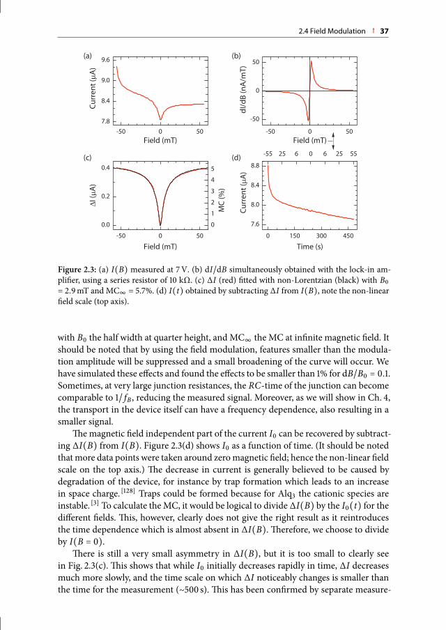
2.4 Field Modulation 37
Figure 2.3: (a) I(B) measured at 7V. (b) dI/dB simultaneously obtained with the lock-in am-
plifier, using a series resistor of 10 kΩ. (c) ∆I (red) fitted with non-Lorentzian (black) with B0= 2.9mT and MC∞ = 5.7%. (d) I(t) obtained by subtracting ∆I from I(B), note the non-linear
field scale (top axis).
with B0 the half width at quarter height, and MC∞ the MC at infinite magnetic field. It
should be noted that by using the field modulation, features smaller than the modula-
tion amplitude will be suppressed and a small broadening of the curve will occur. We
have simulated these effects and found the effects to be smaller than 1% for dB/B0 = 0.1.Sometimes, at very large junction resistances, the RC-time of the junction can become
comparable to 1/ fB , reducing the measured signal. Moreover, as we will show in Ch. 4,
the transport in the device itself can have a frequency dependence, also resulting in a
smaller signal.
The magnetic field independent part of the current I0 can be recovered by subtract-
ing ∆I(B) from I(B). Figure 2.3(d) shows I0 as a function of time. (It should be noted
thatmore data points were taken around zeromagnetic field; hence the non-linear field
scale on the top axis.) The decrease in current is generally believed to be caused by
degradation of the device, for instance by trap formation which leads to an increase
in space charge. [128] Traps could be formed because for Alq3 the cationic species are
instable. [3] To calculate theMC, it would be logical to divide ∆I(B) by the I0(t) for thedifferent fields. This, however, clearly does not give the right result as it reintroduces
the time dependence which is almost absent in ∆I(B). Therefore, we choose to divide
by I(B = 0).There is still a very small asymmetry in ∆I(B), but it is too small to clearly see
in Fig. 2.3(c). This shows that while I0 initially decreases rapidly in time, ∆I decreases
much more slowly, and the time scale on which ∆I noticeably changes is smaller than
the time for the measurement (∼500 s). This has been confirmed by separate measure-

38 Chapter 2: Measuring organic magnetoresistance
ments of dI/dB as a function of time at a constant magnetic field, where the strong
initial decrease is absent while a slow decrease remains, but slower than in I0. This dif-
ference in decrease could be the reason why these type of samples can be ‘conditioned’,
i.e., increasing the MC by applying a large current density for some time. [96] Because
∆I decreases slower in time than I0, the MC will increase. This suggests that the pro-
cesses responsible for OMAR are less affected by the degradation of the device. Thus,
by better understanding the degradation processes occurring in these devices, it might
be possible to exclude effects responsible for OMAR.
2.5 PhotocurrentNext, we discuss a study of the influence of illumination on theMC.Under illumination
the current in these devices can be split in a current from electrically injected charges
and photo-generated charges, respectively:
I = Ii + Ip . (2.3)
The injected current has both a contribution due to leakage, which is dominant at low
voltages, and a contribution from regular transport that starts around the built-in volt-
age.
To get a general idea about the voltage dependence of theMCwith and without illu-
mination, we used the rotating permanent magnets. Figure 2.4(a) showsMC2(V) bothwith andwithout illumination.Without illumination, there are nomagnetic field effects
in the ohmic leakage current regime. The onset of MC occurs at 4.8V and has a maxi-
mumof 8.4% at 6.5V after which it decreases.When the sample is illuminated, themax-
imum shifts to 3.8V, while the MC slightly decreases to 7.6%. At 1.4V a sharp anomaly
is observed where the MC diverges to ±∞. This is caused by the total current going
through zero because the photocurrent and the leakage current are balanced, as can
also be seen from the dip in the zero-field current with illumination I0,P in Fig. 2.4(b).
The leakage current determines the zero crossing of I0,P , while it has (almost) no in-
fluence on ∆I2,P . Therefore, the position of the zero crossing of ∆I2,P at 1.6 V gives
the voltage where the photocurrent is zero due to a flat band condition in the device,
resulting in no electric field to move the photo-induced charges. At low voltages, the
zero-field current without illumination I0,P=0 shows an ohmic leakage current ∝ V 1,
which strongly increases at 4.8V (with a power law ∝ V 11). Fits to a power law are
used to get an indication of the conduction mechanisms in different voltage regimes.
To physically understand why a regime has a certain power law exponent is not trivial,
but it has been shown that for instance space charge [101] and traps [14] can influence it.
The correlation of the onset of MCwith a change in power law is in agreement with pre-
vious observations, [16] although a negative MC is not observed. In contrast, I0,P with
illumination shows a power law∝ V 4 at intermediate voltages which converges to the
current without illumination for large voltages. When comparing the trend of ∆I2,P=0and I0,P=0 without illumination, there is a clear difference which explains the MC(V)behavior. The maximum in MC is observed when ∆I2,P=0 bends down to a power law
of ∝ V 9. For voltages above this point, a decrease in MC ∝ V−2 is thus observed. Asimilar comparison with illumination shows much less clear differences.
An advantage of this measurement technique is that it can also give information

2.5 Photocurrent 39
Figure 2.4: (a) MC2(V) (at 83mT) with and without illumination. (b) Log–log plot of absolute
values of I0 and ∆I2 as a function of voltage without (black lines) and with illumination P (red
lines). Dotted lines indicate fits to different power laws as indicated.
about changes in the line shape if two different magnetic fields are used. If only the
magnitude of the MC changes with voltage, the ratio MC2/MC1 will remain constant.
If the curve also broadens, the ratio will increase. Moreover, if the line shape is non-
Lorentzian, the parameters B0 and MC∞ can be solved. In Fig. 2.5(a), MC2/MC1 with
illumination is plotted. As is indicated by the solid curve, a transition from large ratio
to a smaller ratio is observed. For a non-Lorentzian, this corresponds to a narrowing
of the curve. Below 1.6 V, the ratio is again smaller, but this might be caused by errors
in the calculation due to the small current in this region.
To separate the contribution of the photocurrent from the injected current, we add a
modulated illumination to our field modulation technique. First, we investigate the dif-
ferent ∆I that can be obtained with both these techniques. We compare three cases: (1)
No photocurrent, P = 0: we measure (dI/dB)∣P=0, giving the injected current. (2) Con-stant photocurrent: we measure (dI/dB)∣P , giving the total current: both the injected
and photocurrent. (3)Modulated photocurrent: wemeasure (dI/dB)∣P+dP , giving onlythe photocurrent. At several voltages all three measurements were performed and the
obtained data were processed and fitted to get ∆I at infinite magnetic field (Fig. 2.6),
and B0 [Fig. 2.5(b)]. We observe that the change in photocurrent dominates at low volt-
ages and is equal to the injected current at 6.7V after which the latter dominates. To
validate the technique, also (dI/dB)∣P=0 + (dI/dB)∣P+dP is plotted, which falls on top
of the (dI/dB)∣P data. This confirms that the photocurrent can be properly separated
from the injected current.
A relevant question is whether the transport of the photo-generated charges and

40 Chapter 2: Measuring organic magnetoresistance
Figure 2.5: (a) Ratio MC2/MC1 as a function of voltage, the solid line is a guide to the eye. The
large data points are the ratios calculated for the total current with illumination (dI/dB)∣P from
panel (b). (b) B0 as a function of voltage obtained from fitting measurements for the three dif-
ferent cases: total current without illumination [(dI/dB)∣P=0, black squares], total current withillumination [(dI/dB)∣P , red], and photocurrent with modulated illumination [(dI/dB)∣P+dP ,black triangles]. Lines are a guide to the eye.
the electrically injected charges can be treated in the same way or should be treated
separately. In the first case, they would both show the same shape of MC(B). Therefore,
it is interesting to look at B0 of the MC in the photocurrent and injected current sepa-
rately in the region where they coexist. Figure 2.5(b) shows B0 obtained for the three
cases. With constant illumination, B0 gradually decreases from 4.2 mT to 2.8 mT with
increasing voltage, this widening is also visible from the two normalized ∆I curves ob-
tained at 0V and 8V (inset Fig. 2.6). B0 of the photocurrent, however, remains constant
at 4.3± 0.3 mT, even while an injected current is present with a B0 of 3.0± 0.2 mT. The
trend in B0 with constant illumination agrees well with the trend in the ratio shown in
Fig. 2.5(b), and this agreement is even better shown by MC2/MC1 calculated for these
data and plotted in Fig. 2.5(a) (large data points). The observation that B0 of the pho-
tocurrent remains constant shows that the photocurrent does not just add to the total
current, but that (part) of it is differently affected by the magnetic field.
Two different values for B0 are observed simultaneously, suggesting two separate
processes must be present: one which is dominated by the photocurrent, with a larger
B0, and one dominated by the injected current, with a smaller B0. Our experiments
do not yet give an answer to what these two processes could be. Previously, in Alq3,
effects with different B0 have been reported. [18] In that case the different widths were
assigned to different effects from electrons and holes, possibly by electrons and holes
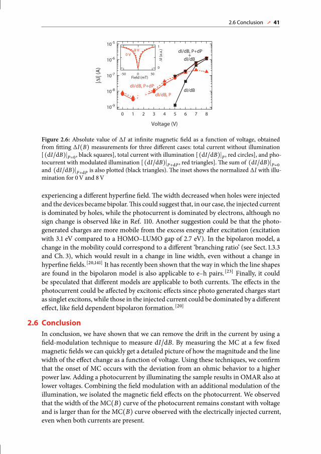
2.6 Conclusion 41
Figure 2.6: Absolute value of ∆I at infinite magnetic field as a function of voltage, obtained
from fitting ∆I(B) measurements for three different cases: total current without illumination
[(dI/dB)∣P=0, black squares], total current with illumination [(dI/dB)∣P , red circles], and pho-
tocurrent with modulated illumination [(dI/dB)∣P+dP , red triangles]. The sum of (dI/dB)∣P=0and (dI/dB)∣P+dP is also plotted (black triangles). The inset shows the normalized ∆I with illu-
mination for 0V and 8V
experiencing a different hyperfine field. The width decreased when holes were injected
and the devices became bipolar.This could suggest that, in our case, the injected current
is dominated by holes, while the photocurrent is dominated by electrons, although no
sign change is observed like in Ref. 110. Another suggestion could be that the photo-
generated charges are more mobile from the excess energy after excitation (excitation
with 3.1 eV compared to a HOMO–LUMO gap of 2.7 eV). In the bipolaron model, a
change in the mobility could correspond to a different ‘branching ratio’ (see Sect. 1.3.3
and Ch. 3), which would result in a change in line width, even without a change in
hyperfine fields. [20,141] It has recently been shown that the way in which the line shapes
are found in the bipolaron model is also applicable to e–h pairs. [23] Finally, it could
be speculated that different models are applicable to both currents. The effects in the
photocurrent could be affected by excitonic effects since photo generated charges start
as singlet excitons, while those in the injected current could be dominated by a different
effect, like field dependent bipolaron formation. [20]
2.6 ConclusionIn conclusion, we have shown that we can remove the drift in the current by using a
field-modulation technique to measure dI/dB. By measuring the MC at a few fixed
magnetic fields we can quickly get a detailed picture of how the magnitude and the line
width of the effect change as a function of voltage. Using these techniques, we confirm
that the onset of MC occurs with the deviation from an ohmic behavior to a higher
power law. Adding a photocurrent by illuminating the sample results in OMAR also at
lower voltages. Combining the field modulation with an additional modulation of the
illumination, we isolated the magnetic field effects on the photocurrent. We observed
that the width of the MC(B) curve of the photocurrent remains constant with voltage
and is larger than for the MC(B) curve observed with the electrically injected current,
even when both currents are present.

42 Chapter 2: Measuring organic magnetoresistance

3A two-site bipolaronmodel for organicmagnetoresistance
The recently proposed bipolaron model for large ‘organic magnetoresistance’ (OMAR) at
room temperature is extended to an analytically solvable two-site scheme. It is shown that
even this extremely simplified approach reproduces some of the key features of OMAR,
viz., the possibility to have both positive and negative magnetoresistance, as well as its
universal line shapes. Specific behavior and limiting cases are discussed. Extensions of the
model, to guide future experiments and numerical Monte Carlo studies, are suggested.∗
3.1 IntroductionAn entirely novel organic magnetoresistance (OMAR) phenomenon has started to puz-
zle the scientific community:magnetoresistance (MR) values up to 10% at room temper-
ature and at fields of only a fewmillitesla have recently been reported in various organic
materials, see Sect. 1.3.2. OMAR can be both positive and negative, and displays univer-
sal line shapes of approximately the same width B0 for many small molecules and poly-
mers. The magnetoconductance, MC(B) = [J(B) − J(0)]/J(0), where J is the currentdensity and B is the applied field, is described by either a Lorentzian B2/(B2
0 + B2) or aspecific non-Lorentzian B2/(∣B∣+B0)2. [79] Anumber ofmodels have been suggested to
account for this intriguing behavior, see Sect. 1.3.3. One class of models assigns OMAR
to spin-related excitonic effects. [39,106] Such amechanismwould only explain finiteMC
in double-carrier devices where both types of carriers are present. However, this inter-
pretation is in conflict with reports that claim the observation of a finite OMAR in
single-carrier devices, see Sect. 1.3.4. [79] Bobbert et al. proposed a bipolaron model [20]
that does not rely on electron-hole recombination. A Monte Carlo scheme was imple-
mented to describe hopping conductance on a large grid of molecular sites displaying
energetic disorder. Thus, both positive and negative MC, as well as the particular line
shapes, were reproduced.
∗Published as: A two-site bipolaron model for organic magnetoresistance W. Wagemans, F.L. Bloom,
P.A. Bobbert, M. Wohlgenannt, and B. Koopmans, J. Appl. Phys. 103, 07F303 (2008), with the addition
of a clarification of the role of Coulomb repulsion and Figs. 3.2 and 3.5.

44 Chapter 3: A two-site bipolaron model for organic magnetoresistance
P
prea
e a b e
P Prabrbe
hahb
rab/b
U
prea
e a b e
P AP rabrbe
hahb
rab/b
U
AP
Figure 3.1: Schematic representation of the transport rates and electron spins in the P and AP
configurations. The symbols are explained in the text.
In this chapter, we calculate the MC analytically by mapping the bipolaron model
onto a model with two ‘characteristic sites’ with energies chosen out of a random distri-
bution ofmolecular energy levels, a simplification which was already briefly outlined in
Ref. 20. It will be shown that such an approach is sufficient to capture all the character-
istics of OMAR in a qualitative way. We will successively discuss the basic ingredients
of the bipolaron model, the definition of the two-site version of it, the derivation of the
associated set of rate equations resulting in analytical expressions for J(B), and, finally,the generic line shapes and the sign changes of OMAR. We conclude by suggesting
possible extensions of the model.
3.2 Two-site bipolaronmodelThe key ingredient of the bipolaron model is the effect of an applied field on the proba-
bility of forming bipolarons (doubly occupiedmolecular sites).The formation of a bipo-
laron by hopping to a singly occupied site is only possible when the two electrons in-
volved have a finite singlet component. Thus, two electrons on different sites, originally
in a parallel (P) state, will have a lower probability to form a bipolaron than electrons in
an antiparallel (AP) state—the notion of parallel and antiparallel refers to the orienta-
tion of the spinwith respect to the local field axis.The restriction can be (partially) lifted
by the presence of different local magnetic fields at the two sites. Then, the bipolaron
formation probabilities for the two states (PAP/P) (PAP/P) scale with the time averaged
singlet component of the two particle wave function, PAP/P = 14(1 ± h1 ⋅ h2), where the
plus (minus) sign applies to the AP (P) orientation and h i is a unit vector along the
local magnetic field at site i. [20] The magnitude B0 ∼ 5mT observed in experiments
supports the conjecture that the random field is the local hyperfine field (Bhf, i) of hy-
drogen atoms surrounding the respective molecular sites i. At applied fields B≫ ∣Bhf∣,the local fields are aligned: h i ∥ B. In theMonte Carlo calculations of Ref. 20, the result-
ing MC was calculated as a function of temperature T and relevant model parameters,
such as the energy difference U between the on-site Coulomb repulsion and the pola-
ronic relaxation within a bipolaron state, the long-range Coulomb interaction V , and
the Gaussian energy disorder strength σ .
In the present work, we select two neighboring critical sites, α and β, situated up-
stream and downstream with respect to the current, respectively, extending the ap-
proach of Ref. 20.The two sites are considered to be bottlenecks in the carrier transport

3.2 Two-site bipolaron model 45
A01 A02
A12
A11P
A11AP
Figure 3.2: Rates to and from the many electron states Anm , with n and m the occupation of
site α and β, respectively. Using dashed, solid, and dash dotted arrows for hops from e, α, and β,
respectively.
with α at most and β at least singly occupied, thereby strongly affecting the MC. To ac-
count for blocking effects to the current, it is crucial to work out the model in terms
of many-electron states. Within the aforementioned restrictions and excluding time-
reversed states (these are implicitly included in the occupation and rate parameters),
we have five of them: ∣01⟩, ∣11P⟩, ∣11AP⟩, ∣02⟩, and ∣12⟩, where ∣nm⟩ denotes an n(m)-foldoccupation at site α (β) and P/AP describes the spin orientation in case both sites are
singly occupied. We consider only a downstream flow of electrons [Fig. 3.1]; from up-
stream in the environment e (not further specified in the model) to α at rate pre→α(where p is a measure of the electron density in the environment), from site α to β at
rate PP/APrα→β , and from site β to downstream e at rate rβ→e . Furthermore, we intro-
duce two routes that can release a blocking situation: (i) from site α bypassing β directly
to the downstream environment, at a rate rα→e = rα→β/b, where b is the branching ratio,and (ii) a spin-orbit induced spin-flip process between states ∣11P⟩ and ∣11AP⟩ at a raterα→β/a, where a is the spin flip coherence ratio. Increasing a and b tends to make block-
ing effects more pronounced and thereby increases the MC. In addition, we can also
include long-range Coulomb interaction by reducing the rate from the environment to
site α with a factor γα (≤ 1) if site β is doubly occupied. Likewise, hopping from site β
can be enhanced with a factor 1/γβ (≥ 1) when site α is occupied.
Next, we define occupationprobabilitiesAnm for the respectivemany-electron states
∣nm⟩, with∑nm Anm = 1, and construct a set of rate equations from the rates illustrated
in Fig. 3.2. In a stable solution, the time derivative of all probabilities should vanish. As
an example, dA11P /dt = 0 yields
0 = 1
2A01pre→α + A11AP rα→β/a +
1
2A12rβ→e/γβ
− A11P(PPrα→β + rα→β/a + rα→β/b),(3.1)
while the other equations can be constructed in a similar way. Solving the set of equa-
tions results in analytical expressions for Anm . The current through the system equals
the total rate from the upstream environment to α,
I/e = ⟨(A01 + γαA02)⟩ pre→α , (3.2)

46 Chapter 3: A two-site bipolaron model for organic magnetoresistance
Figure 3.3: Modeled magnetic response for (a) Γ = 0, (b) Γ = 100, 10
2, 10
3compared to a
Lorentzian and non-Lorentzian fit, and (c) a Gaussian distribution of log Γ values, with average
value log10 Γ = 1.4 and half-width ∆ log10 Γ = 2.1.
where ⟨⋯⟩ denotes the ensemble average over Bhf, i and e is the electron charge. The
explicit expression for I is lengthy but can be rewritten in a generic form,
I = I∞ + IB ⟨1 −1
1 + ΓPPPAP⟩ = I∞ + IB д (Γ, B
Bhf) , (3.3)
where I∞, IB , and Γ are straightforward analytical expressions in terms of the model
parameters, and Bhf is the hyperfine field scale. All field dependencies are described
by the model function д(Γ, B/Bhf); i.e., the line shape is fully described by a single
parameter Γ, with д(Γ,∞) = 0 and д(Γ, 0) → 1 for Γ ≫ 1 and д(Γ, B) ∝ Γ for Γ ≪ 1.
Thus, the shape and magnitude (including sign) of the OMAR are, respectively,
MC(B)MC(∞) = 1 −
д(Γ, B/Bhf)д(Γ, 0) ,
MC(∞) = − IB д(Γ, 0)I∞ + IB д(Γ, 0) .
(3.4)
3.3 ResultsIn order to calculate the line shape, it is required to specify the distribution of hyperfine
fields. Assuming a fixed magnitude ∣Bhf, i ∣ = Bhf but a random orientation, it is possi-
ble to derive a (rather lengthy) analytical expression for д(0, B/Bhf).† As illustrated in
Fig. 3.3(a), at large B the function converges to a Lorentzian with width B0 =√2Bhf
and normalized to 1 at B = 0. However, a plateau up to around B/Bhf = 1 is obtained us-ing this averaging procedure. Numerical results for amore realistic average over a three
dimensional Gaussian distribution of Bhf, i (defining < ∣Bhf, i ∣ >= Bhf) are collected in
†д(0, s) = 16s2[s2 + 1][13s2 − 3]− [s2 − 1]2[log((s − 1)2)− log((s + 1)2)][3 log((s − 1)2)(s2 − 1)
2−
3 log((s + 1)2)(s2 − 1)2+ 8s(3 − 5s2)]/4096s6, with s = B/Bhf .
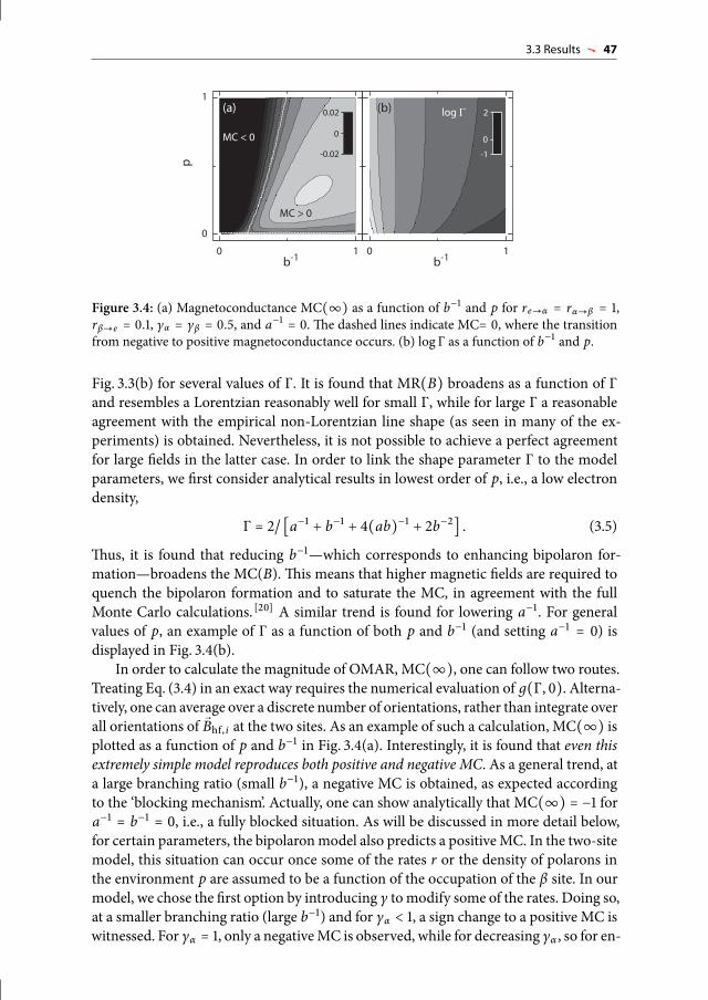
3.3 Results 47
MC < 0
MC > 0
-0.02
0
0.02
-10
2(a) (b)
Figure 3.4: (a) Magnetoconductance MC(∞) as a function of b−1 and p for re→α = rα→β = 1,
rβ→e = 0.1, γα = γβ = 0.5, and a−1 = 0. The dashed lines indicate MC= 0, where the transition
from negative to positive magnetoconductance occurs. (b) log Γ as a function of b−1 and p.
Fig. 3.3(b) for several values of Γ. It is found that MR(B) broadens as a function of Γ
and resembles a Lorentzian reasonably well for small Γ, while for large Γ a reasonable
agreement with the empirical non-Lorentzian line shape (as seen in many of the ex-
periments) is obtained. Nevertheless, it is not possible to achieve a perfect agreement
for large fields in the latter case. In order to link the shape parameter Γ to the model
parameters, we first consider analytical results in lowest order of p, i.e., a low electron
density,
Γ = 2/ [a−1 + b−1 + 4(ab)−1 + 2b−2] . (3.5)
Thus, it is found that reducing b−1—which corresponds to enhancing bipolaron for-
mation—broadens the MC(B). This means that higher magnetic fields are required to
quench the bipolaron formation and to saturate the MC, in agreement with the full
Monte Carlo calculations. [20] A similar trend is found for lowering a−1. For generalvalues of p, an example of Γ as a function of both p and b−1 (and setting a−1 = 0) is
displayed in Fig. 3.4(b).
In order to calculate the magnitude of OMAR, MC(∞), one can follow two routes.
Treating Eq. (3.4) in an exact way requires the numerical evaluation of д(Γ, 0). Alterna-tively, one can average over a discrete number of orientations, rather than integrate over
all orientations of Bhf, i at the two sites. As an example of such a calculation, MC(∞) isplotted as a function of p and b−1 in Fig. 3.4(a). Interestingly, it is found that even this
extremely simple model reproduces both positive and negative MC. As a general trend, at
a large branching ratio (small b−1), a negative MC is obtained, as expected according
to the ‘blocking mechanism’. Actually, one can show analytically that MC(∞) = −1 fora−1 = b−1 = 0, i.e., a fully blocked situation. As will be discussed in more detail below,
for certain parameters, the bipolaronmodel also predicts a positiveMC. In the two-site
model, this situation can occur once some of the rates r or the density of polarons in
the environment p are assumed to be a function of the occupation of the β site. In our
model, we chose the first option by introducing γ to modify some of the rates. Doing so,
at a smaller branching ratio (large b−1) and for γα < 1, a sign change to a positive MC is
witnessed. For γα = 1, only a negativeMC is observed, while for decreasing γα , so for en-

48 Chapter 3: A two-site bipolaron model for organic magnetoresistance
Figure 3.5:Magnetoconductance MC(∞) as a function of b−1 with different γα for γβ = 1 and
p = 0.5, while the other parameters are the same as in Fig. 3.4.
hanced repulsion of a double charge at site β, the positive MC becomes larger [Fig. 3.5].
Within the two-site model, positive MC is a consequence of a reduction of the current
by a doubly occupied β site. In organic devices, such a situation can occur when the
total polaron density increases at the expense of the bipolaron population at increasing
B, as explored further in the full Monte Carlo calculations. [20] Interestingly, the line
separating negative and positive MC is given by a simple expression (for γα = γβ = 0.5,and arbitrary a),
p = (b−2r2α→β − 4r2β→e) / (2re→αrβ→e) . (3.6)
Thus, although the inclusion of spin-flip scattering (finite a) decreases themagnitude of
the MC, the sign of MC is totally independent of a. Moreover, we found that Eq. (3.6)
is unaffected by details of the Bhf, i distribution. We note that the magnitude of the
positive MC is generally smaller than the negative MC, making the negative MC the
more dominant result of the bipolaron mechanism.
Comparing MC(∞) and Γ [Figs. 3.4(a) and 3.4(b), respectively], a one-to-one re-
lation is found to be absent. However, there is some trend that the positive MC has a
larger width (Γ). It would be challenging to unambiguously correlate this outcome with
experiments. Actually, in recent experiments on Alq3 devices wemeasured a trend that
upon a transition from positive to negative MC, B0 is significantly increased.[16] How-
ever, care has to be taken in drawing too strong conclusions from experiments on a
single system.
Finally, we sketch a number of extensions of the present work that could lead to
a closer agreement with the Monte Carlo studies and maybe even provide predictive
power with respect to experiments. First of all, the rate parameters within our model
as well as p, a, and b should be expressed in terms of the more generic system parame-
ters (U , V , σ , EF), electrical bias, and temperature (preliminary results and an outlook
of this approach will be given in Sect. 8.1). Second, rather than specifying two levels
with fixed rate parameters, it might be necessary to model an ensemble of two-level sys-
tems with different relative energy alignments. As one of the outcomes, the final line
shape would not be defined by a single Γ but rather be described by a distribution of
values. Doing so in an ad hoc way, we found this to be a promising route. As an ex-

3.4 Conclusion 49
ample, Fig. 3.3(c) displays the line shape resulting from a distribution of Γ. This way,
contrary to using a single component [Fig. 3.3(b)], perfect agreement is achieved with
the phenomenological non-Lorentzian line shape (as also reproduced by Monte Carlo
calculations) and up to large B.
3.4 ConclusionConcluding, we have introduced a simple two-site bipolaronmodel that reproduces the
main features of OMAR, viz., the occurrence of sign changes and the characteristic line
shapes. By producing simple analytical expressions, the approach could be valuable in
guiding further numerical (Monte Carlo) and experimental efforts aimed at improving
our understanding of this new phenomenon.

50 Chapter 3: A two-site bipolaron model for organic magnetoresistance
4Frequency dependence of organicmagnetoresistance
In this Chapter, the frequency dependence of organic magnetoresistance (OMAR) is inves-
tigated. By this, we aim to identify the processes involved in OMAR by their frequency
characteristics. Doing so, we ultimately hope to be able to distinguish between the differ-
ent models proposed for OMAR, because the processes that are used in the models each
occur on different timescales. We use a superposition of an AC and DC magnetic field
and show that the measured magnetoconductance decreases when the frequency of the
AC component is increased. The decrease is stronger for lower voltages, which is shown
to be linked to the presence of a negative capacitance (as measured with admittance spec-
troscopy). The negative capacitance disappears when the frequency becomes comparable
to the inverse transition time of the minority carriers. We show that these results are in
agreement with recent interpretations of magnetic field effects inminority carrier mobility
being the dominant effect.∗
4.1 IntroductionAs introduced in Sect. 1.3.3, several models have been proposed for the organic magne-
toresistance (OMAR) effect, but the exact origin of the effect is still debated. In organic
devices, many processes can occur which could have an effect on OMAR, each with a
characteristic timescale. For instance, triplet (T) excitons could play a role in T–T an-
nihilation or in reactions with charges, [55] and these excitons have a typical lifetime of
25 µs in Alq3.[7] Traps have been suggested to enhance the MC, for instance via space
charge effects [15] and by conditioning the devices. [5] Traps in the devices have a typical
detrapping time from less than milliseconds up to hours, depending on how deep the
traps are. Another typical timescale is the transit time, which is directly linked to the
mobilities of the carriers, τ = L2/µV , with L the thickness, µ the mobility, and V the
voltage. [49,74] Note that τ is usually different for electrons and holes due to the different
mobilities. If we would be able to perform measurements of OMAR on any of these
∗In preparation: Frequency dependence of organic magnetoresistance W. Wagemans, P. Janssen, E.H.M.
van der Heijden, M. Kemerink, and B. Koopmans.
52 Chapter 4: Frequency dependence of organic magnetoresistance
timescales, we might be able to obtain clues about the processes relevant for OMAR,
and thus discriminate between the proposed models.
In literature, only a few experimental reports on OMAR are available where the
frequency of the applied magnetic field plays a role. Veeraraghaven et al. reported no
significant change in the response to anACmagnetic field for frequencies up to 100 kHz,
for which they used a current density of 10Am−2. [138] On the other hand a slow step
response on the order of seconds was reported by Meruvia et al., which they suggested
to be caused by the magnetic field acting on the trapping times. [82] Finally, Majumdar
et al. recently showed that the OMAR they measure increases when the rate at which
B is swept is decreased, which they conjecture could be caused by traps. [69]
In this chapter we will show that the measured OMAR is sensitive to the frequency
of the AC-component of the applied magnetic field. By comparing the frequency-de-
pendent OMAR measurements with admittance spectroscopy, we relate the disappear-
ance of OMAR to the transit times of the minority carriers. Finally, we discuss the con-
sequences of these observations for the models suggested for OMAR.
4.2 MethodsWe present experimental results on tris-(8-hydroxyquinoline) aluminum (Alq3) based
devices, but we note that we observed similar effects with poly[2-methoxy-5-(3’,7’-di-
methyloctyloxy)-1,4-phenylene vinylene] (MDMO-PPV). The devices have the struc-
ture ITO/PEDOT:PSS(60nm)/Alq3(100nm)/LiF(1 nm)/Al(100nm). See Sect. 2.2 for de-
tails on the used materials and fabrication. Magnetic measurements were performed
with an air coil through which a current with both an AC and DC component was sent.
The AC response was measured with a lock-in amplifier over a resistor in series with
the sample, while a constant voltagewas applied, see also Sect. 2.4. [142] Admittance spec-
troscopy measurements were performed with a Solartron SI 1260 impedance analyzer.
4.3 ResultsWe measured the frequency dependence of the MC at different voltages, starting from
a voltage just above the onset of OMAR. Plotted in Fig. 4.1(a) is the change in current
through the sample due to a change in magnetic field (dI/dB), divided by the DC cur-
rent and normalized at 1 Hz. dI/dB is the derivative of the current with respect to the
magnetic field [inset Fig. 4.1(a)], which, when integrated, gives a typical OMAR curve
(Sect. 2.4). [142] Here, however, we do notmeasure a full field sweep, but divide the signal
at a fixed B by the current to get a measure for the MC, dMC/dB. It was validated that
the shape of the curves does not change with frequency, justifying this approach. To
remove any extra signal from induction, picked up by the wires at higher frequencies,
we measure the difference in signal at 2mT and −2mT, where dI/dB has an opposite
sign.
For allmeasured voltages, theMCdecreaseswith increasing frequency, see Fig. 4.1(a).
At low voltages, the MC decreases faster than at higher voltages. The voltage depen-
dence of the MC at fixed frequencies, extracted from Fig. 4.1(a), is shown in Fig. 4.1(b).
At low frequencies, a typical MC(V ) curve is obtained, which first increases with in-
creasing voltage, has a maximum and then slowly decreases. For increasing frequency,
theMC(V ) curve collapses, with the strongest reduction at low voltages. Also plotted is
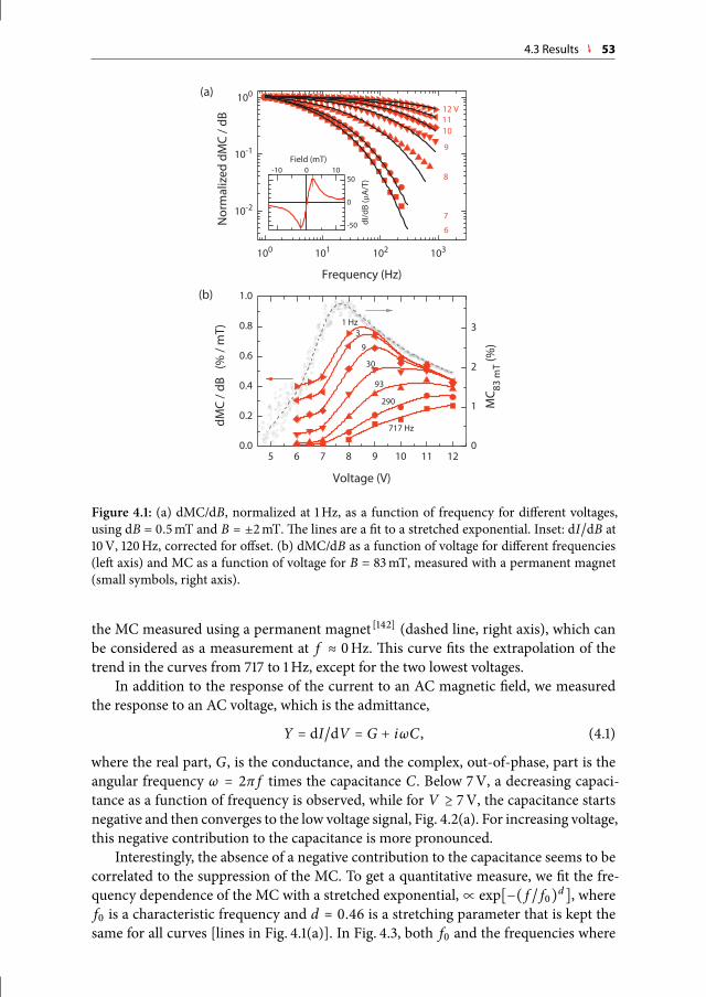
4.3 Results 53
Figure 4.1: (a) dMC/dB, normalized at 1Hz, as a function of frequency for different voltages,
using dB = 0.5mT and B = ±2mT. The lines are a fit to a stretched exponential. Inset: dI/dB at
10V, 120Hz, corrected for offset. (b) dMC/dB as a function of voltage for different frequencies
(left axis) and MC as a function of voltage for B = 83mT, measured with a permanent magnet
(small symbols, right axis).
the MC measured using a permanent magnet [142] (dashed line, right axis), which can
be considered as a measurement at f ≈ 0Hz. This curve fits the extrapolation of the
trend in the curves from 717 to 1Hz, except for the two lowest voltages.
In addition to the response of the current to an AC magnetic field, we measured
the response to an AC voltage, which is the admittance,
Y = dI/dV = G + iωC , (4.1)
where the real part, G, is the conductance, and the complex, out-of-phase, part is the
angular frequency ω = 2π f times the capacitance C. Below 7V, a decreasing capaci-
tance as a function of frequency is observed, while for V ≥ 7V, the capacitance startsnegative and then converges to the low voltage signal, Fig. 4.2(a). For increasing voltage,
this negative contribution to the capacitance is more pronounced.
Interestingly, the absence of a negative contribution to the capacitance seems to be
correlated to the suppression of the MC. To get a quantitative measure, we fit the fre-
quency dependence of the MC with a stretched exponential,∝ exp[−( f / f0)d], wheref0 is a characteristic frequency and d = 0.46 is a stretching parameter that is kept the
same for all curves [lines in Fig. 4.1(a)]. In Fig. 4.3, both f0 and the frequencies where

54 Chapter 4: Frequency dependence of organic magnetoresistance
Figure 4.2: (a) Capacitance as a function of frequency of the AC voltage (50mV) for differentDC
voltages. The frequency where C is 95% of the low voltage value at 9V is indicated. The choice
of 95% is to allow a better defined value than for 100%. (b) Simulation of the capacitance of a
single-carrier device with (dotted line) and without (dashed line) traps, and of a double-carrier
device (solid line). Frequency scaled with transit time τ of majority carriers. (µmin = 0.1µmaj).
the capacitance is 95% of its low voltage value, fC , are plotted as a function of voltage. A
clear correlation between the two frequencies is observed and both curves are approxi-
mately showing an exponential increase with voltage. We have looked at the frequency
characteristics of the equivalent circuit of the sample and the series resistor. They show
no significant changes for the frequencies studied. We thus conclude that the correla-
tion between f0 and fC is a genuine effect.
4.4 DiscussionFirst, we will discuss the observed trends in the capacitance C, which is a measure for
the amount of charge that can be stored in the device. In an ideal single-carrier device,
at f ≫ 1/τ the dielectric properties of the organic material are probed, giving the geo-
metric capacitance Cgeo. At f ≪ 1/τ, the (majority) charges in the device easily follow
the voltage modulation and due to charge relaxation C = 3/4Cgeo.[48] The transition
between these two regimes occurs around f = 1/τmaj, as illustrated by simulations of a
prototype device in Fig. 4.2(b) (dashed line). The strong downturn at high frequencies
due to the frequency dependence of the complex permittivity is not observed in the fre-
quency range of ourmeasurements.When traps are present in the device, they increase
the ability of the device to store charges, resulting in an increased capacitance, which
decreases as the frequency becomes larger than the inverse trapping time, eliminating
the contribution from the traps [Fig. 4.2(b), dotted line]. Depending on the amount of
traps, the step observed in the single-carrier case is obscured, as is the case in the mea-
sured capacitance for V ≤ 6 V [Fig. 4.2(a)]. In a double-carrier device, due to cancela-
tion of the space charge by the presence of both positive and negative carriers, a much
larger amount of charge can be stored in the device, resulting in a large capacitance,
which, due to a lag in signal, is negative. [48] At a certain frequency, the response of the
slowest (minority) carriers can no longer follow the voltage modulation and C follows
the single-carrier case [Fig. 4.2(b), solid line]. This frequency is directly related to their
transit time τmin.[49,74] Thus, interpreting the measured capacitance [Fig. 4.2(a)], start-
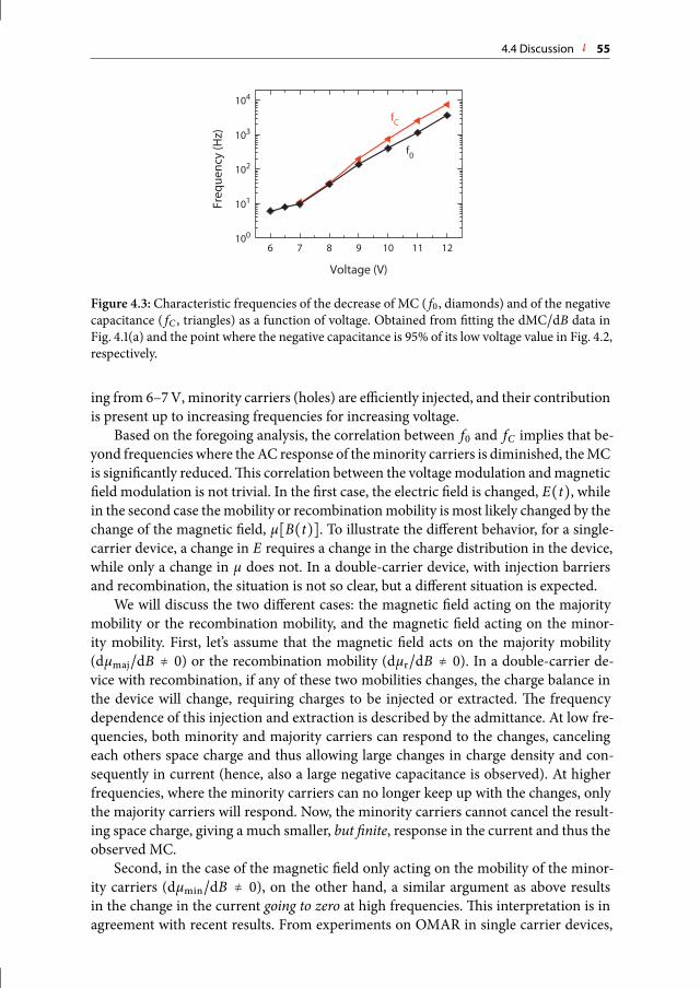
4.4 Discussion 55
Figure 4.3: Characteristic frequencies of the decrease of MC ( f0, diamonds) and of the negative
capacitance ( fC , triangles) as a function of voltage. Obtained from fitting the dMC/dB data in
Fig. 4.1(a) and the point where the negative capacitance is 95% of its low voltage value in Fig. 4.2,
respectively.
ing from 6–7V, minority carriers (holes) are efficiently injected, and their contribution
is present up to increasing frequencies for increasing voltage.
Based on the foregoing analysis, the correlation between f0 and fC implies that be-
yond frequencies where the AC response of theminority carriers is diminished, theMC
is significantly reduced. This correlation between the voltagemodulation andmagnetic
field modulation is not trivial. In the first case, the electric field is changed, E(t), whilein the second case themobility or recombinationmobility is most likely changed by the
change of the magnetic field, µ[B(t)]. To illustrate the different behavior, for a single-
carrier device, a change in E requires a change in the charge distribution in the device,
while only a change in µ does not. In a double-carrier device, with injection barriers
and recombination, the situation is not so clear, but a different situation is expected.
We will discuss the two different cases: the magnetic field acting on the majority
mobility or the recombination mobility, and the magnetic field acting on the minor-
ity mobility. First, let’s assume that the magnetic field acts on the majority mobility
(dµmaj/dB ≠ 0) or the recombination mobility (dµr/dB ≠ 0). In a double-carrier de-
vice with recombination, if any of these two mobilities changes, the charge balance in
the device will change, requiring charges to be injected or extracted. The frequency
dependence of this injection and extraction is described by the admittance. At low fre-
quencies, both minority and majority carriers can respond to the changes, canceling
each others space charge and thus allowing large changes in charge density and con-
sequently in current (hence, also a large negative capacitance is observed). At higher
frequencies, where the minority carriers can no longer keep up with the changes, only
the majority carriers will respond. Now, the minority carriers cannot cancel the result-
ing space charge, giving a much smaller, but finite, response in the current and thus the
observed MC.
Second, in the case of the magnetic field only acting on the mobility of the minor-
ity carriers (dµmin/dB ≠ 0), on the other hand, a similar argument as above results
in the change in the current going to zero at high frequencies. This interpretation is in
agreement with recent results. From experiments on OMAR in single carrier devices,

56 Chapter 4: Frequency dependence of organic magnetoresistance
it is known that the magnetic field acts most strongly on the minority carriers. [143] It
has been shown that even in double-carrier devices, the magnetic field effects in the
minority mobility dominate the total magnetic response of the current, even though
the majority mobility is much larger. [15,16] In addition, via the space charge, a change
in minority mobility gives a change in the current with an opposite sign. [15] In the
bipolaron model, a negative MC is the most dominant effect, [20,141] in agreement with
experiments on single-carrier devices where the MC is always negative. [90,143] The ob-
served positiveMC is then the opposite response of themajority carriers to the negative
effects of the minority carriers. Below the onset of minority carrier injection, only the
effects in the majority carriers are expected, with a negative MC. As we do not observe
any (negative)MC at low voltages, below the onset of hole injection, wemight conclude
that the magnetic field effects in the electrons (majority carriers) are negligible small.
Therefore, modulating the magnetic field at frequencies above the transit time of the
minority carriers, results in a quenching of the total MC.
Although both scenarios give a good qualitative explanation of the observed effects,
other origins ormore complex interactions cannot be excluded.Therefore, a conclusive
prediction on the applicablemodel cannot yet bemade.However, by performing device
simulations a more decisive conclusion might be drawn. Such simulation are currently
being performed to get an idea of how changes in one of the mobilities would exactly
be reflected in the current, also taking into account effects resulting from for instance
traps and injection barriers.
4.5 ConclusionIn conclusion, we have shown frequency dependent OMAR measurements, using a
superposition of a DC and an AC magnetic field. We observed a decrease of MC with
increasing frequency. The decrease is stronger for lower voltages, which is shown to be
linked to the presence of a negative capacitance that disappears when the frequency
becomes comparable to the inverse transition time of the minority carriers. We show
that this interpretation is in agreement with recent results. However, device simulations
need to be performed to allow us to discriminate between different models.

5Angle dependent spin--spin interactionsin organic magnetoresistance
The dependence of organic magnetoresistance (OMAR) on the orientation of the magnetic
field has been investigated. In contrast to previous claims, a clear and systematic, though
small, change in magnitude is observed when the orientation of the field is changed with
respect to the sample. The characteristic field scale of the effect remains approximately
constant. To explain these effects, spin–spin interactions have been included in the models
previously suggested for OMAR, in combination with either an anisotropy of the orien-
tation of the spin pairs or an anisotropy in the hyperfine fields. The essential spin–spin
interaction is dipole coupling, but, depending on the assumptions, exchange interaction
also has to be included.∗
5.1 IntroductionIn organic devices, considerable changes in the current have been observedwhen apply-
ing amagnetic field, an effect called organicmagnetoresistance (OMAR), see Sect. 1.3.2.
OMAR is generally believed to originate from spin correlations of interacting charge
carriers.The spin character of such pairs ismixed by the randomhyperfine fields, which
can be suppressed by an external magnetic field, resulting in a typical field scale of the
effect of a few millitesla. Gaining a better understanding of the physics of OMAR will
improve knowledge of (spin) transport in organic semiconductors and could help real-
izing possible applications, for instance in adding the possibility of sensing magnetic
fields to cheap organic electronic devices.
So far, in literature, it has been claimed that OMAR is independent of the orien-
tation of the applied magnetic field. [11,43] Indeed, the effect is not just observed for a
specific angle between the magnetic field and the current (like the Hall effect). The
models suggested for OMAR (Sect. 1.3.3), like the electron–hole (e–h) pair model [106]
and the bipolaron model, [20] do not predict any angle dependence of OMAR.
In this paperwe report on angle-dependentmeasurements ofOMAR.We show that
∗In Preparation: Angle dependent spin–spin interactions in organic magnetoresistance W. Wagemans,
A.J. Schellekens, M. Kemper, F.L. Bloom, and B. Koopmans.

58 Chapter 5: Angle dependent spin--spin interactions in organic magnetoresistance
changing the orientation of the appliedmagnetic field with respect to the sample results
in a small but systematic change in the magnitude of OMAR.We show that anisotropic
spin–spin interactions are a likely candidate to explain the observed effects.Thereby, we
provide a new handle to electrically study spin–spin interactions in disordered organic
materials. A related effect has previously been found in photoluminescence measure-
ments on organic crystals, where the authors also suggest an angle dependence due to
spin–spin interactions. [50]
5.2 ExperimentalWe performed our experiments on typical OLED-like devices. In discussing our re-
sults we will focus on devices with tris-(8-hydroxyquinoline) aluminum (Alq3) as the
active layer. We note that we also observed an angle dependence in devices with poly[2-
methoxy-5-(3’,7’-dimethyloctyloxy)-1,4-phenylene vinylene] (MDMO-PPV), but due
to the low signal to noise ratio it was not possible to perform a similar in-depth study as
presented here for Alq3.The devices consist of a glass substrate with a patterned indium
tin oxide electrode onwhich poly(3,4-ethylenedioxythiophene):poly(styrenesulfonate)
(PEDOT:PSS) is spin coated (60nm). Then, Alq3 (120nm) is evaporated in a high vac-
uum system inside a nitrogen filled glove box, after which a top electrode is evaporated
consisting of LiF(1 nm)/Al(100nm). The created devices (active area 3mm× 3mm) are
transported to a different glove box in which they are electrically measured, while a
magnetic field can be applied. For detailed measurements and to suppress the drift in
current that can be present, we use an additional AC modulation of the magnetic field
to measure the derivative of the current I to the magnetic field B, dI/dB, which is then
integrated with respect to the magnetic field to get I(B), see Sect. 2.4. From I(B), themagnetoconductance is calculated with MC = [I(B) − I(0)]/I(0).
5.3 ResultsA clear difference in MC is observed between parallel (θ = 0) and perpendicular
(θ = 90) alignment of the magnetic field with respect to the sample normal, see
Fig. 5.1(a). The MC for the perpendicular case is larger than the parallel case; the dif-
ference is 4.3% of the MC at 40mT. This difference is only 0.14% of the total current,
showing that, in order to observe these effects, both very stable samples and a sensitive
measurement technique are required.The inset of Fig. 5.1(a) shows theMCas a function
of voltage, MC(V ), as measured with a permanent magnet of 83mT, see Sect. 2.3. [142]
MC(V ) shows a typical behavior where the MC first increases with voltage, has a max-
imum and then slowly decreases.
The MC for intermediate angles shows an oscillation as a function of θ on top of a
slowly increasing signal, see Fig. 5.1(b). Vertically plotted is MC∞, which was obtainedfrom fitting the MC(B) curves with a typical ‘non-Lorentzian’ that is commonly seen
in OMAR measurements: [79] MC(B) = MC∞B2/(∣B∣ + B0)2, where MC∞ is the MC
at infinite magnetic field and B0 is the half width at quarter maximum. Within the
accuracy of the fits, no change in B0 is observed. The data can be accurately fitted with
a cos2 θ dependence plus a linear contribution. The slow increase in signal is due to
slight conditioning. [5]
Using a different method, the cos2 θ dependence is confirmed. While applying a
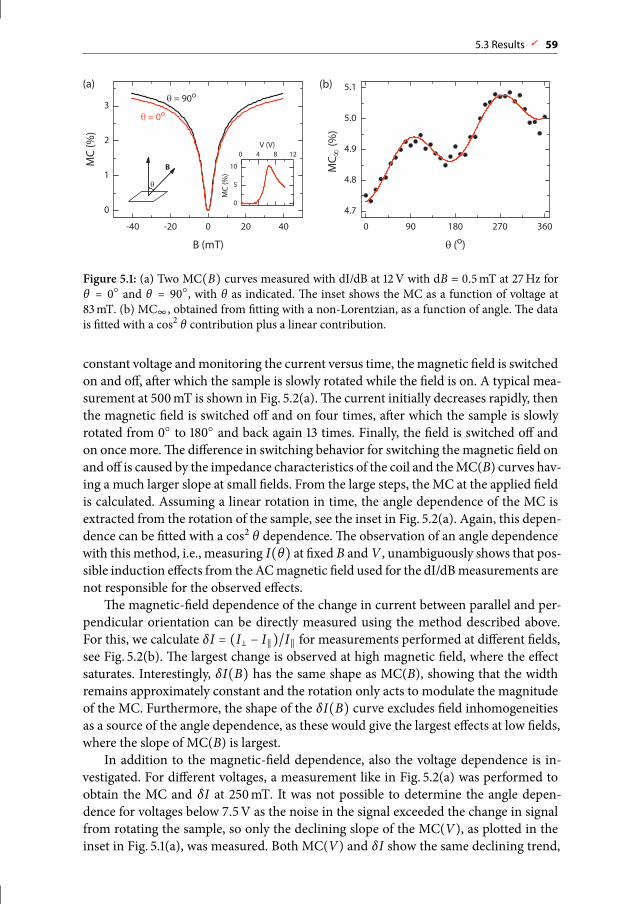
5.3 Results 59
Figure 5.1: (a) Two MC(B) curves measured with dI/dB at 12V with dB = 0.5mT at 27Hz for
θ = 0and θ = 90
, with θ as indicated. The inset shows the MC as a function of voltage at
83mT. (b) MC∞, obtained from fitting with a non-Lorentzian, as a function of angle. The data
is fitted with a cos2 θ contribution plus a linear contribution.
constant voltage andmonitoring the current versus time, themagnetic field is switched
on and off, after which the sample is slowly rotated while the field is on. A typical mea-
surement at 500mT is shown in Fig. 5.2(a). The current initially decreases rapidly, then
the magnetic field is switched off and on four times, after which the sample is slowly
rotated from 0 to 180 and back again 13 times. Finally, the field is switched off and
on once more. The difference in switching behavior for switching the magnetic field on
and off is caused by the impedance characteristics of the coil and theMC(B) curves hav-
ing a much larger slope at small fields. From the large steps, the MC at the applied field
is calculated. Assuming a linear rotation in time, the angle dependence of the MC is
extracted from the rotation of the sample, see the inset in Fig. 5.2(a). Again, this depen-
dence can be fitted with a cos2 θ dependence. The observation of an angle dependence
with this method, i.e., measuring I(θ) at fixed B andV , unambiguously shows that pos-
sible induction effects from the ACmagnetic field used for the dI/dBmeasurements are
not responsible for the observed effects.
The magnetic-field dependence of the change in current between parallel and per-
pendicular orientation can be directly measured using the method described above.
For this, we calculate δI = (I⊥ − I∥)/I∥ for measurements performed at different fields,
see Fig. 5.2(b). The largest change is observed at high magnetic field, where the effect
saturates. Interestingly, δI(B) has the same shape as MC(B), showing that the width
remains approximately constant and the rotation only acts to modulate the magnitude
of the MC. Furthermore, the shape of the δI(B) curve excludes field inhomogeneities
as a source of the angle dependence, as these would give the largest effects at low fields,
where the slope of MC(B) is largest.
In addition to the magnetic-field dependence, also the voltage dependence is in-
vestigated. For different voltages, a measurement like in Fig. 5.2(a) was performed to
obtain the MC and δI at 250mT. It was not possible to determine the angle depen-
dence for voltages below 7.5V as the noise in the signal exceeded the change in signal
from rotating the sample, so only the declining slope of the MC(V ), as plotted in the
inset in Fig. 5.1(a), was measured. Both MC(V ) and δI show the same declining trend,
60 Chapter 5: Angle dependent spin--spin interactions in organic magnetoresistance
which results in a constant ratio δI/MC, see Fig. 5.2(c), left axis. In the same figure the
current as a function of voltage is plotted. While the ratio remains constant in this volt-
age range, the current increases by 2.5 orders of magnitude. From these observations
we conclude that the angle dependence is an intrinsic property of OMAR and is not an
independent effect or a measurement artifact.
5.4 DiscussionAs the angle dependence seems to be a modulation of the OMAR effect, we have to
look at the mechanisms suggested for OMAR to find a possible explanation. In all sug-
gestedmodels, the randomhyperfine fieldsmix spin pairs, which either have like charge
(bipolarons) or opposite charge (e–h pairs or excitons), see Sect. 1.3.3. Such spin pairs
can have either a singlet (S) or triplet (T) character with total spin 0 or 1, respectively.
The orientation of the spin of the triplets is determined by the magnetic field, for T+(−)they are aligned (anti-)parallel to the field and for T0 perpendicular. In the models, at
low fields, the hyperfine field mixes S and all T states, while at high field only S and T0are mixed, resulting in the typical OMAR curves.
The strength of the mixing between S and T0 is determined by their energy differ-
ence compared to the hyperfine field, see Fig. 5.3. For angle dependence at high fields,
two effects can be considered as illustrated in Fig. 5.3 by the red arrows. By changing
the angle, either the magnitude of the hyperfine field Bhf is changed, or the energy dif-
ference between S and T0 is changed. These changes result from either an anisotropy in
the hyperfine fields or an anisotropy in the energy difference between S and T0. Note
that for an effect resulting from a change in the magnitude of Bhf, an energy difference
between S and T0 needs to be present. An energy difference between S and T0 can origi-
nate from spin–spin interactions in the pairs, like exchange coupling or dipole coupling.
A dipole coupling will induce an energy difference which reduces the total mixing, in
turn reducing the total magnitude of OMAR. So far, these spin–spin interactions were
neglected in the models.
To understand the influence of dipole coupling, first, we will discuss it based on a
semi-classical picture. This fails at some details that require a quantum mechanical ap-
proach, whichwill be discussed later. In a semi-classical picture, we can imagine the two
spins of S to be pointing in opposite directions, while they are pointing in the same di-
rection in T0, see Fig. 5.4.The dipole energy of two spins pointing in the same direction
is larger when they are head to tail than when they are next to each other, and vice versa.
This means that for S and T0 the angle between themagnetic field and the displacement
vectorR (as defined in Fig. 5.4) determines the strength of the dipole coupling between
the two spins. Figures 5.4(a) and (b) give a schematic picture of S and T0 with the field
and the displacement vector either parallel or perpendicular, respectively.The spins per-
form a precession in the magnetic field, as indicated by the circles. One third of a full
rotation is indicated by the shaded arrows. ForB andR parallel [Fig. 5.4(a)], the spins of
S have the same (large) dipole coupling throughout the precession. The dipole coupling
of T0 also remains constant, but is smaller. For B and R perpendicular [Fig. 5.4(b)], the
spins of S and T0 both have a varying coupling during their precession. This shows that
rotating the field with respect to the displacement vector results in a different (average)
dipole coupling strength. If we now assume a preferential orientation between the spin

5.4 Discussion 61
Figure 5.2: (a) Current versus time at 15V, while switching the magnetic field off and on
and rotating the sample. The inset shows the angle dependence obtained from the rotation.
(b) Change in current between parallel and perpendicular orientation as a function of field.
The data is mirrored for negative fields. The measurement has been performed at 15V with
Alq3(240nm)/Ba(10 nm)/Al(100 nm). (c) Ratio δI/MC (left axis, circles) and current (right axis,
squares) as a function of voltage at 250mT.

62 Chapter 5: Angle dependent spin--spin interactions in organic magnetoresistance
ST0
Bhf
Figure 5.3: Energies of S and T0. The vertical red arrows indicate a change in the magnitude of
the hyperfine field and in the relative energy difference between S and T0.
B
BR
B
BR
S T0 B BR
S
B BR
T0
(a) (b)
Figure 5.4: Spin pair, in S and T0 configuration, precessing in a magnetic field B, with B and the
displacement vector R either (a) parallel or (b) perpendicular.
pairs in a device, i.e., an anisotropy inR, the introduction of a finite dipole coupling willdirectly give an angle dependence. On the other hand, an anisotropy in the hyperfine
fields, in combination with a non-zero isotropic energy splitting of S and T0 at high
fields, also results in different mixing depending on the orientation of the external field.
The possible link of the mechanisms causing anisotropy with the devices structure will
be discussed after investigating their effects in more detail.
To get an idea about the magnitude of the angle dependence and which orientation
is more favorable for OMAR, a more detailed analysis is needed. To study the effect of
dipole coupling for the bipolaron and e–hmodels, it is necessary to use a densitymatrix
description of the spin system. For the equation of motion of the density matrix ρ, weuse the stochastic Liouville equation: [60]
∂ρ∂t= − i
ħ[H(t), ρ(t)] − 1
2Λ, ρ(t) + Γ = 0. (5.1)
The first term is the Liouville term describing the evolution of the density matrix under
the influence of the Hamiltonian of the systemH; here, the square brackets denote the
commutator. The second term is a ‘sink’ term that spin-selectively removes particles
from the system, using the projection operator Λ; here, the curly brackets denote the
anti-commutator.The last term Γ is a source term that adds particles and is independent
of the current state of the system. As a basis we use the eigenstates of the total spin
operator S2tot.For simplicity, we choose to only discuss the implementation of Eq. (5.1) for the e–h
model, but we stress that completely equivalent results are obtained with the bipolaron
model. Starting from free carriers, e–h pairs are created with a rate r, resulting in 34 r
triplets and 14 r triplets, as illustrated in Fig. 1.14 on p. 24. These can dissociate back into
free carriers with rates qT and qS, and recombine to the ground state with rates kT

5.4 Discussion 63
and kS.[106] S and T can be mixed by a hyperfine contribution to the Hamiltonian. For
Eq. (5.1) this results in Λµ ,ν = (kS+qS)ρµ ,ν(δ0,ν+δµ ,0)+∑3n=1(kT+qT)ρµ ,ν(δn ,ν+δµ ,n)
and Γµ ,ν = 14 rδµ ,ν , where δµ ,ν is the delta function, n = 0 refers to the singlet, and n =1–
3 to the triplets. The singlets and triplets are mixed by a hyperfine contribution to the
Hamiltonian:
Hhf = дµB [Bhf,1 ⋅ S1 + Bhf,2 ⋅ S2] , (5.2)
where µB is the Bohr magneton and д is the g-factor of a polaron. The triplets are split
in energy by a Zeeman term:
HZ = дµBB ⋅ (S1 + S2) . (5.3)
Now, with ρ obtained from solving Eq. (5.1), the recombination probability is:
P = kSρ0,0 +∑3n=1 kTρn ,n
(kS + qS)ρ0,0 +∑3n=1(kT + qT)ρn ,n
. (5.4)
In the e–h model, Prigodin et al. introduced the magnetic-field dependence of the cur-
rent via the recombination mobility µr.[106] The authors show that in the bipolar space-
charge limited regime, the current is proportional to µ−1/2r and that µr is proportional
to P. This results in MC = [P(B)−1/2 − P(0)−1/2]/P(0)−1/2.To investigate the effects of spin–spin interactions, dipole coupling and exchange
coupling are added. The dipole coupling term that is added to the Hamiltonian is: [100]
Hdip = D [S1 ⋅ S2 − 3 (S1 ⋅R/R) (S2 ⋅R/R)] , (5.5)
where S1 and S2 are the spin operators of the two spins, and D is the dipole coupling
strength: D = µ0д2µ2B/(4πħR3), where µ0 is the permeability of free space and ħ is
Planck’s constant. For a typical displacement of 1.5 nm, the dipole interaction strength
is approximately 1mT. [100] We note that this is a point dipole approximation, ignoring
the three dimensional structure of the molecular orbitals. The exchange term that is
added to the Hamiltonian is:
Hex = −J (1
2+ 2S1 ⋅ S2) , (5.6)
with J = J0e−2 R
R0 , where J0 and R0 are determined by the inherent strength of the ex-
change interaction. At large fields, where only S−T0 mixing is relevant due to Zeeman
splitting, the absolute energy difference between S and T0 is 12 ∣D(1 − 3 cos
2 α) − 4J∣,where α is the angle between the applied field and the displacement vector. This yields
an angle-dependent mixing between the S and T0 states and thus a difference in MC at
large fields.
Now, we can calculate MC(B) for a parallel and perpendicular alignment of B and
R, see Fig. 5.5(a). For this, we average over a Gaussian distribution of the x , y and z
components of the hyperfine fields, each with an average value Bhf.[121] The MC curves
show a typical OMAR shape and, most notably, α = 90 shows a larger MC, while the
width remains nearly unchanged. We note that this is the first time that full line shapes
have been calculated instead of only investigating zero and infinite magnetic field. The
most prominent effect of the dipole coupling is to change the magnitude. This is in
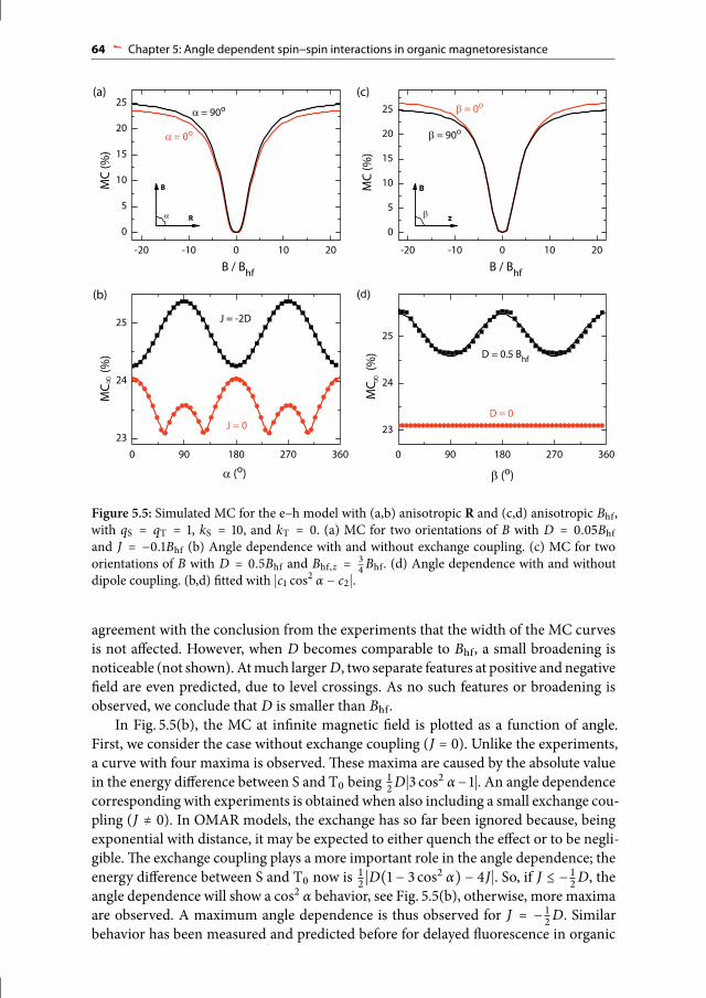
64 Chapter 5: Angle dependent spin--spin interactions in organic magnetoresistance
Figure 5.5: Simulated MC for the e–h model with (a,b) anisotropic R and (c,d) anisotropic Bhf,
with qS = qT = 1, kS = 10, and kT = 0. (a) MC for two orientations of B with D = 0.05Bhfand J = −0.1Bhf (b) Angle dependence with and without exchange coupling. (c) MC for two
orientations of B with D = 0.5Bhf and Bhf,z =34Bhf. (d) Angle dependence with and without
dipole coupling. (b,d) fitted with ∣c1 cos2 α − c2∣.
agreement with the conclusion from the experiments that the width of the MC curves
is not affected. However, when D becomes comparable to Bhf, a small broadening is
noticeable (not shown). Atmuch largerD, two separate features at positive and negative
field are even predicted, due to level crossings. As no such features or broadening is
observed, we conclude that D is smaller than Bhf.
In Fig. 5.5(b), the MC at infinite magnetic field is plotted as a function of angle.
First, we consider the case without exchange coupling (J = 0). Unlike the experiments,
a curve with four maxima is observed. These maxima are caused by the absolute value
in the energy difference between S and T0 being12D∣3 cos
2 α− 1∣. An angle dependencecorresponding with experiments is obtained when also including a small exchange cou-
pling (J ≠ 0). In OMAR models, the exchange has so far been ignored because, being
exponential with distance, it may be expected to either quench the effect or to be negli-
gible. The exchange coupling plays a more important role in the angle dependence; the
energy difference between S and T0 now is 12 ∣D(1 − 3 cos
2 α) − 4J∣. So, if J ≤ − 12D, the
angle dependence will show a cos2 α behavior, see Fig. 5.5(b), otherwise, more maxima
are observed. A maximum angle dependence is thus observed for J = − 12D. Similar
behavior has been measured and predicted before for delayed fluorescence in organic
5.4 Discussion 65
crystals, [50] where the angle dependence was independent from the crystal axes.
Next, we investigate the role of an anisotropy of the hyperfine field. For this, the z
component of the hyperfine fields is reduced with respect to the x and y components,
and we average over 100 000 randomR and hyperfine combinations. Also in this case, a
dependence is predicted on the angle between B and the z axis (β), see Fig. 5.5(c), with
the largest MC for B aligned with the z axis (β = 0), which is the axis with the reduced
hyperfine field. This can also be seen from the MC at infinite field as a function of
angle, see Fig. 5.5(d). We confirm that no angle dependence is observed when D = 0
[Fig. 5.5(d)], as there is no splitting to probe the anisotropic hyperfine fields.
Comparing the simulated angle dependence of the two different anisotropies with
the measurements, in the case of anisotropic R, we find θ = α, which corresponds to
R aligning with the direction of the electric field. This is not unexpected, as the electric
field determines the direction in which the polarons meet. On the other hand, this di-
rection is also the growth direction of the organic layer. So, a preferential R could also
originate from local ordering of molecules due to preferential growth or from current
paths selectingmolecules with favorable alignment, both giving a cylindrical symmetry
perpendicular to the sample. On the other hand, in the case of anisotropic Bhf, we find
θ = β+90, which corresponds to the direction of reduced hyperfine field aligning per-pendicular to the direction of the electric field. The hyperfine fields originate from the
coupling of the spins of the polarons to the hydrogen nuclei. For this there are two con-
tributions, an isotropic contact term and an anisotropic dipole–dipole coupling term.
Because of the large number of hydrogen nuclei, the coupling is described by a classical
hyperfine field, neglecting the anisotropic part. [121] However, for a relatively planar spin
density distribution, like on a ligand of Alq3, a strong anisotropic contribution can be
expected. In such a planar configuration, the anisotropic coupling constant for the axis
perpendicular to the plane is smaller than for those in the plane. [63] In our experiments,
this would correspond to growth of Alq3 with the ligand preferentially perpendicular
to the surface. Moreover, the specific alignment of ligands is crucial for determining
the hopping rate, thereby possibly selecting molecules with a preferential orientation.
However, different orientations could be optimal for electrons and holes, [64] making it
uncertain what kind of orientation is expected in our samples. Note that in this case,
no exchange coupling is needed to get the correct angle dependence, but a finite dipole
coupling between the charges is still essential.
Even our basic model manages to describe the angle dependence well. So far, we
only average over the randomhyperfine fields, using constant dipole coupling, exchange
coupling and transition rates. It is, however, very likely that the values of these parame-
ters are distributed over a certain range, which could lead to changes in the shape of the
MC(B) curve, its magnitude and the angle dependence. Moreover, a ‘selection mecha-
nism’ might be at work where many pairs contribute to theMC, but only a part of these
have the right combination of parameters to show a noticeable angle dependence.
Unfortunately, with these experiments, it is not possible to distinguish between the
bipolaron and e–h model. One possible difference between the models could be that
we expect a much broader spread in separation distances for the e–h pairs than for
bipolarons, as for bipolarons the critical step occurs for nearest neighbors, while for
e–h pairs a range of distances is possible. To distinguish between the models and to

66 Chapter 5: Angle dependent spin--spin interactions in organic magnetoresistance
further elucidate the individual role of exchange and dipole coupling, materials engi-
neering could be used to change the separation distances of the spin pairs or alter the
coupling strengths in a different way. Another interesting condition for studying angle
dependence is around a sign change in MC, as it has been suggested to be related to a
transition from a bipolaron to an e–h model dominated regime, [143] although, a small
signal to noise ratio might be limiting in this range.
5.5 ConclusionIn conclusion, experiments show a clear dependence of themagnitude ofOMARon the
orientation of the magnetic field, while the width of the MC(B) curve hardly changes.
To explain these effects, spin–spin interactions have to be included in the models, in
combination with an anisotropy of either the displacement vector between sites or the
hyperfine fields.

6Spin diffusion in organic semiconductors
In the previous chapters, we have shown that spins in an organic material interact with
the random hyperfine fields of hydrogen nuclei. Not only do these interactions play a key
role in organic magnetoresistance, the interactions will also have a detrimental effect on
the spin polarized transport through an organic layer.
In this chapter, we present a theory for spin diffusion in disordered organic semicon-
ductors, based on incoherent hopping of a charge carrier and coherent precession of its
spin in an effective magnetic field, composed of the random hyperfine field and an ap-
plied magnetic field. From Monte Carlo simulations and an analysis of the waiting-time
distribution of the carrier we predict a surprisingly weak temperature dependence, but a
considerable magnetic-field dependence of the spin-diffusion length. Using a simple device
model, we show that both predictions are in agreement with experiments on organic spin
valves.∗
6.1 IntroductionThe study of electron-spin transport throughnon-magnetic spacermaterials in between
ferromagnetic electrodes is an extremely active field, because of the rich physics in-
volved and the important applications in the area of magnetic sensors. [146] If the spin-
diffusion length is larger than or comparable to the distance between the electrodes,
the current through such structures depends strongly on the mutual orientation of the
magnetization directions of the electrodes, which is called the spin-valve effect, leading
to ‘Giant Magnetoresistance’ (GMR), [6,13] see also Sect. 1.2.
Traditionally, non-magnetic metals are used as the spacer-layer material in these
structures. Spintronic devices utilizing spin injection and transport through a semicon-
ducting spacer layer offer additional functionalities, such as spin transistors and the
possibility to realize quantum computation logic. Consequently, much effort is put into
∗Published as: Theory for Spin Diffusion in Disordered Organic Semiconductors P.A. Bobbert, W. Wage-
mans, F.W.A. van Oost, B. Koopmans, and M. Wohlgenannt, Phys. Rev. Lett. 102 (15), 156604 (2009), and
as part of its supplementary information. W.W. mostly contributed to Sect. 6.4.

68 Chapter 6: Spin diffusion in organic semiconductors
finding suitable materials. Spin relaxation in the inorganic materials traditionally used
in these structures, containing relatively heavy atoms, is mainly caused by spin-orbit
coupling. [104] Organic semiconductors (OS) are a very interesting alternative because
of the enormous versatility of organic chemistry and because the light atoms from
which they are composed cause very little spin-orbit coupling, [109] see also Sect. 1.3.
Recent years have seen the first demonstrations of GMR devices [34,35,40,68,103,144,149] as
well as magnetic tunnel junctions [114] using OS as spacer layer. Here we will investigate
the former type of devices. The experiments reported so far have shown that when the
thickness of the OS spacer layer increases, the GMR effect in these devices disappears
on a typical length scale of the order of 10–100nm. Two very important and still unan-
swered questions, addressed in this Chapter, are: what is the cause of the remaining
spin relaxation and what factors determine the spin-diffusion length?
6.2 ModelRecent research on magnetic-field effects of the resistance and luminescence of OS has
led to the conclusion that the hydrogen hyperfine fields are involved, influencing reac-
tions between spin-carrying radicals (polarons, triplet excitons). [20,39,62,106] The accu-
rate prediction of magnetoresistance line shapes assuming coupling of the spin to these
hyperfine fields [20] strongly suggests that this coupling is the main source of spin relax-
ation in OS. In this Chapter, we take this as our working hypothesis. Since typically
many (∼10 or more) hydrogen nuclear spins couple to the spin of a charge carrier in OS,
we can replace the hyperfine coupling by a classical, quasi-static, and random field, dis-
tributed according to a three-dimensional Gaussian, [121] with standard deviation Bhf .
In addition, we model charge transport in disordered OS by hopping of carriers be-
tween localized sites with random site energies, distributed according to a Gaussian
density of states (GDOS) with standard deviation σ . [9] Hence, we describe spin diffu-
sion in these materials by a combination of incoherent hopping of a carrier in a GDOS
together with coherent precession of its spin S(t) around a local effectivemagnetic field,
see Fig. 6.1a. At each hopping site i this effective field is Bi = Bhf , i + B, where Bhf , i is
the random hyperfine field at this site and B = Bz the externally applied magnetic field,
e.g. the field to which a GMR device should respond. With typically Bhf ≈ 5mT the
hyperfine precession frequency is ωhf = γBhf ≈ 10−8 s−1 (γ is the gyromagnetic ratio).
We consider the situation that a carrier with unit charge e (electron or hole) and
spin fully polarized in the z-direction is injected by an electrode into the organic mate-
rial at x = 0 and moves to the opposite electrode under the influence of an electric field
E = Ex. We assume that nearest-neighbor hopping takes place by thermally assisted
tunneling [83] from site i to j with a rate ω i j = ωhop exp[−(ε j − ε i)/kBT] for ε j ≥ ε iand ω i j = ωhop for ε j < ε i , where T is temperature, kB is Boltzmann’s constant, and
ε i and ε j are the on-site energies of sites i and j, with a contribution due to the elec-
tric field added. The prefactor ωhop contains a phonon attempt frequency as well as a
factor related to a wave-function overlap. For hopping in disordered OS at not too low
temperatures it is a good approximation to include only nearest-neighbor hopping. [102]
Furthermore, it has been shown that positional disorder is much less important than
energetic disorder, [9] so for simplicity we neglect positional disorder and take a fixed
nearest-neighbor distance a.

6.3 Spin diffusion 69
Clearly, the ratio r ≡ ωhop/ωhf is an important parameter. If r is large, the influence
of the hyperfine field is small and large spin-diffusion lengths can be expected, while the
opposite holds if r is small. For derivatives of the familiar π-conjugated polymer poly-
(para-phenylene vinylene) (PPV) we obtain an estimate of 109–1011 s−1 for ωhop.[102]
Hence, for this class of organic semiconductors r is of the order of 10–1000, but the
large variation even within this class shows that very different values can be expected
for different organic semiconductors.
6.3 Spin diffusionIt is instructive to first consider a one-dimensional (1D) chain of sites for the case
E ≫ σ/ea, when all hops are down-field with the same rate ωhop, leading to equal
average waiting times 1/ωhop at each site. By solving the time-dependent Schrödinger
equation for the spinor in the effective magnetic field and performing an average over
the random hyperfine fields (in cylindrical coordinates ρ, ζ), one can easily derive the
following expression for the relative preservation, λ, of spin polarization, p, during the
waiting time of the carrier at a site (see supplementary material of Ref. 22 for details),
λ = 1√2π
∫ ∞0 ρdρ ∫ ∞−∞ dζ exp(− ρ2 + ζ22) r2 + (ζ + b)2r2 + ρ2 + (ζ + b)2 ,
≈ exp− [1/ ln(3) + r2/2 + b2/2]−1 ,(6.1)
with b ≡ B/Bhf .This leads to an exponentially decaying polarization p(x) = exp(−x/ls),with a spin-diffusion length ls = −a/ ln λ ≈ a[1/ ln(3) + r2/2 + b2/2]. The increase of
ls with increasing b and r can be readily understood qualitatively: with increasing b,
the Zeeman coupling becomes increasingly dominant over the hyperfine coupling and
the carrier spin becomes effectively pinned. The quadratic increase with r results from
‘motional narrowing’, well-known in magnetic-resonance spectroscopy. [12]
For the three-dimensional (3D) situation we performed Monte Carlo simulations
for hopping of a single carrier in a homogeneous electric field of arbitrary magnitude
on a cubic lattice of sites (N × 50 × 50, where N is adapted to the specific situation),
while simultaneously solving the time-dependent Schrödinger equation for its spinor
(see supplementary material of Ref. 22 for details). The random site-energies and hy-
perfine fields are drawn from their corresponding Gaussian distributions. Sufficiently
far from the injecting layer, p(x) decreases exponentially, from which we extract ls.
We averaged over several thousands of energetic and hyperfine disorder configurations,
making sure that the error bar in the plots discussed below is smaller than the symbol
sizes shown.
In Fig. 6.1(b) we show ls as a function of E for different reduced disorder strengths
σ ≡ σ/kBT , for r = 1000 and B = 0. The arrow at the right axis shows the value obtained
for the 1D model discussed above, which is quite close to the present results at large E.
For other values of r ≫ 1 (fast hopping) we find a similar dependence on E as shown
in Fig. 6.1(b). For r ≤ 1 (slow hopping) we find ls ∼ a, indicating that for this case no
significant spin-diffusion length is found. The relevant case for the experiments carried
out up to now corresponds to E ≪ σ/ea, [34,35,40,68,103,144,149] so from now on we will
focus on this case. We note that whereas ls decreases steeply for E → 0, it remains

70 Chapter 6: Spin diffusion in organic semiconductors
O O
ON
N
N
Al
OO
O
N
N
N
AlO
O
O
N
N
N
Al
Bhf,1
Bhf,2
Bhf,3B1
B2
B3
B B BS(0)
S(t)
Figure 6.1: (a) Mechanism for spin diffusion, in this case for the molecular semiconductor Alq3.
(b) Spin-diffusion length ls [as multiples of the lattice constant] vs. electric field E at zero mag-
netic field, for r ≡ ωhop/ωhf = 1000 and different σ ≡ σ/kBT .The arrow at the right axis indicates
the result for a one-dimensional chain at large E. Inset: corresponding mobility µ vs. E, in units
of µ0 ≡ ea2ωhop/σ .
non-zero at E = 0.The inset in Fig. 6.1(b) shows the carrier mobility µ as a function of E (for compar-
ison: the unit µ0 is of the order of 10−7-10−5 m2/Vs for the PPV derivatives studied in
Ref. 102). A strikingly different trend with increasing σ is observed for ls compared to
µ at small and intermediate E: while µ keeps on decreasing very rapidly with increas-
ing σ , ls depends rather weakly on σ and even appears to saturate for large σ . In order
to provide an explanation for the weak dependence of ls on σ we show in Fig. 6.2a the
distribution P(τ) of waiting times τ† of the carrier while hopping through the lattice, at
E = 0 and different σ . The curves appear to saturate for large σ . By considering hops up-
wards in energy from a Boltzmann distribution in the GDOS one can in fact prove [21]
that P(τ) converges for large τ to a universal algebraic distribution P(τ) ∼ τ−3/2 in the
limit σ →∞, see the dashed line in Fig. 6.2(a). We note that P(τ) for a GDOS has been
studied before, [52] but for too small disorder strengths (σ ≤ 4) to observe this universalbehavior.
The quite different dependencies of ls and µ on σ can now be understood as follows.
†The concept of a waiting-time distributionwas originally introduced in the field of dispersive transport;
see Ref. 117.

6.3 Spin diffusion 71
Figure 6.2: (a)Waiting-time distributions (equally normalized) at E = 0 for different σ ≡ σ/kBT .
Solid and dash-dotted lines and arrows: see the main text. (b) ls at E = 0.1σ/ea as a function of
ωhop at B = 0 and (c) as a function of magnetic field B for r ≡ ωhop/ωhf = 1000. The dashed lines
in (a–c) indicate the expected power laws.
With increasing σ the tail of the distribution P(τ) contains an increasing amount of
sites with very large τ, leading to a strong decrease of themobility, since these sites cause
a very long delay in themotion of the carrier. Regarding the spin diffusion, however, the
situation is distinctly different. Let us, for example, consider the case r = 1000 and B = 0.At sites i with τ i to the left of the solid line in Fig. 6.2(a), such that r i ≡ 1/ωhfτ i ≫ 1, es-
sentially no polarization loss occurs [cf. Eq. (6.1) with r replaced by r i]. At sites with τ ito the right of this line, such that r i ≪ 1, almost immediate polarization loss occurs, but
this effect is essentially the same for all these sites. For large σ the fraction of the latter
sites, obtained by integrating P(τ) from the solid line to the right, converges to ∼ 1/r1/2.This means that on average the spin polarization disappears in ∼ r1/2 hops. Since atsmall E diffusion of carriers is dominant over drift one expects ls ∼ (r1/2)1/2 ∼ r1/4.The dashed line in Fig. 6.2(b) indicates this expected power law, to which the results
indeed converge (for numerical reasons we took a small but finite E). We studied P(τ)as a function of E and found a similar convergence to a universal distribution with in-
creasing σ , where the power-law behavior gradually changes to an exponential behavior

72 Chapter 6: Spin diffusion in organic semiconductors
Figure 6.3: Full curves: fit of the model discussed in the main text to the experimental mag-
netoresistance (MR) traces taken from Fig. 3(b) of Ref. 149 (symbols). Dashed curves: results
neglecting spin relaxation. Thick/thin lines: up/down field-sweep, also indicated by the arrows.
P(τ) ∼ exp(−ωhopτ) with increasing E.
In Fig. 6.2(c) we plot ls at small E as a function of magnetic field B, for r = 1000.
For B > Bhf we observe an important B-dependence, which again converges to a power
law for increasing σ . The analysis now goes as follows. Let us, for example, take b =B/Bhf = 10. From Eq. (6.1) (again replacing r by r i ≡ 1/ωhfτ i) it follows that if r i ≫ b,
i.e. to the left of the dash-dotted line in Fig. 6.2a, basically no polarization loss takes
place. To the right of this line partial polarization loss takes place with 1 − λ ∼ 1/b2,which is a consequence of the pinning effect of the Zeeman term discussed above. A
similar argument as above now leads to the expectation ls ∼ b3/4 in the diffusive regime,
which is seen to be very well obeyed. Together with the above power-law dependence
on r this allows us to estimate ls for general values of r ≫ 1 and b for the case of large
σ and small E.
6.4 Modeling a spin valveWenowundertake a comparison between our theory and experimental results, as far as
they are available at themoment (see Sect. 1.3.1).We have no information about the hop-
ping frequencies of the OS used in the spin valves of Refs. 35, 149, and 68: sexithienyl,
tris-(8-hydroxyquinoline) aluminum (Alq3), and poly-3-hexylthiophene, respectively.
Since the mobilities in these materials are higher than those of the PPV-derivatives in-
vestigated in Ref. 102, we expect that the hopping frequencies are such that r > 1000. Acalculated value of σ = 0.26 eV for the energetic disorder of electrons in Alq3
[88] leads
to σ ≈ 10 at room temperature, which is clearly in the strong-disorder limit.We can con-
clude that with a typical value a ≈ 1 nm the spin-diffusion lengths of about 10–100nm
found in Refs. 35,68,149 and recently confirmed with muon spin-resonance studies [40]
are compatible with our results.
Very interestingly, inspection of the experimental GMR traces in Refs. 149 and 68,
both using La0.67Sr0.33MnO3 (LSMO) and Co as electrodes, reveals that in the up and
down field-sweeps the resistance as a function of B changes considerably already be-
fore the magnetization of the soft layer (with the weaker coercive field) is reversed (in
Sect. 1.2 a basic introduction of GMR traces is given). This may point at a source of

6.4 Modeling a spin valve 73
D = 0 D = 1
Figure 6.4: Filling of the intermediate reservoir with either separate baths for spin up and spin
down (D = 0) or one shared bath (D = 1).
magnetoresistance other than the switching of the ferromagnetic layers and we pro-
pose that this is the magnetic-field dependence of the spin-diffusion length predicted
by our theory. To illustrate its effect on the GMR traces, we simulated such traces us-
ing a simple phenomenological model, which will be described in more detail in the
next section. We fitted the resulting GMR traces to experimental data of Ref. 149, see
Fig. 6.3. The fitting procedure, which will be described in Sect. 6.4.2, yields a ratio of
the spin-diffusion length and the device thickness at zero field, ls,0 ≈ 1.7d, and Bhf ≈5.7mT, the latter being indeed a typical value for the random hyperfine field. The fact
that the curve for d/ls,0 = 0, which describes the case without spin relaxation, deviates
strongly from the experimental data demonstrates that the MR before zero field can-
not be explained assuming an injected spin polarization proportional to the measured
electrode magnetization.
6.4.1 Phenomenological device modelIn order to relate the spin-diffusion length ls, and in particular its magnetic-field de-
pendence, to the magnetoresistance (MR) traces measured in experiments, we employ
a phenomenological approach. For a very simple system we derive an explicit expres-
sion for the MR versus applied magnetic field in the presence of spin relaxation within
the spacer layer. Rather than using this explicit, model-dependent expression, we sug-
gest a more general equation. We verified that results for different models and under
different conditions can indeed be mapped onto the general equation, when introduc-
ing a model-dependent adjustment parameter.
As to the specific case treated here, we consider a system of two electrodes with
spin polarizations P1 and P2, with an intermediate reservoir (representing the organic
spacer layer), and restrict ourselves to a low temperature case, where charge carriers
only hop from electrode 1, via the reservoir, to electrode 2, while backward hops are
neglected. Then, from the first electrode spin-up and spin-down carriers can hop into
electronic states in the reservoir, of which the occupation by spin-up and spin-down
carriers is given by Nup and Ndo, respectively. In the reservoir, spins are mixed at a
rate α. For the reservoir two assumptions can be made: either spin-up and spin-down
carriers have separate baths (D = 0), or they share the same bath (D = 1), see Fig. 6.4,the latter meaning that Nup +Ndo cannot be larger than one (double occupancy of sites
in the reservoir is excluded). Finally, carriers can hop from the reservoir to electrode 2.
The spin-integrated density of states in both electrodes, as well as the transition rates
from electrode 1 and to electrode 2, are assumed to be equal and for simplicity they are

74 Chapter 6: Spin diffusion in organic semiconductors
taken as unity. For arbitrary value of D, we then find two rate equations,
dNup
dt= 12(1 + P1) (1 − DNdo − Nup)+
α (Ndo − Nup) −1
2(1 +mP2)Nup = 0,
dNdo
dt= 12(1 − P1) (1 − Ndo − DNup)+
α (Nup − Ndo) −1
2(1 −mP2)Ndo = 0,
(6.2)
wherem indicates whether the magnetization of the electrodes are parallel (+1) or anti-parallel (−1). By solving Nup and Ndo from this set of equations the current through the
system is found,
JD=1 =P22 − 4α − 1
P22 + 2mP1P2 − 12α − 3
,
JD=0 =P21 + P2
2 − 4α − 2P21 + 2mP2P1 + P2
2 − 8α − 4,
(6.3)
where the assumption is made that the polarizations of the electrodes are always either
parallel or anti-parallel (m2 = 1).In order to get a simple expression useful for fitting MR data, we expand Eq. (6.3)
in the two lowest orders of P1 and P2,
Jsimple,D=1 =1
3− 2
9(P1P2m − P2
2 )1
4α + 1 ,
Jsimple,D=0 =1
2− 1
4(P1P2m −
1
2P21 −
1
2P22)
1
2α + 1 .(6.4)
This result is compatible with a more general expression for the current,
Jgeneral = const. + (Am − B) exp(−d
ls) , (6.5)
with parameters A and B giving information about the spin polarization at the injection
and collection step. Also, we see that the ratio B/A depends on details of the implemen-
tation, in this specific case the value of D. In order to match our experimental situation
with an MR that decays exponentially as a function of spacer layer thickness d, the
denominator in Eq. (6.4), including the α-dependence, is replaced by the exponential
factor. Note that this is a very pragmatic step, replacing spin relaxation in the time do-
main (described by α), by a decaying spin density in real space, where ls corresponds to
the experimentally or theoretically determined spin-diffusion length. It is not difficult
to derive explicit expressions for modifications of the model, e.g. including backward
hopping at finite temperatures, or considering several intermediate reservoirs in series.
For all cases we investigated, we found the final structure of the solution to be identical
to Eq. (6.5).

6.4 Modeling a spin valve 75
Figure 6.5: MR(B) curves simulated with Eq. (6.6). (a) Using R = 1, forward (thick, red) and
backward (thin, black) are plotted for both s = +1 and s = −1. (b) Similar plots, but using R = 0.
For all curves we use d/ls,0 = 0.7.
6.4.2 Fitting of the experimental data to themodelTo illustrate the effect of a magnetic-field dependent spin-diffusion length on the MR
traces, we simulate such traces for spin valves using the phenomenological model de-
rived in the previous section.The general expression for the current [Eq. (6.5)] is rewrit-
ten to an expression for the MR (assuming MR ≈ −MC, with MC the magnetoconduc-
tance),
MR(B) =MRmax ⋅1
2[R − sm(B)] exp[−d/ls(B)] +MR0 , (6.6)
with MRmax the MR when neglecting spin relaxation, d the thickness of the organic
spacer, and MR0 = MRmax ⋅ 12(s − R) a vertical shift. R = B/A is a model dependent
parameter, including details of the device like the ratio of the polarizations of the elec-
trodes; the case R = 1 represents the common case of no spin accumulation for equal
polarizations, while R = 0 gives direct tunneling between electrodes without carriers ac-cumulating in an intermediate reservoir, i.e. a simple Jullière approximation. For s = +1(−1) these polarizations have equal (opposite) sign in parallel alignment of the mag-
netization of the electrodes. The magnetic switching characteristics of the electrodes
are captured by m(B), with m = +1 (−1) describing parallel (anti-parallel) magnetic
orientation. The magnetic-field dependence of the spin-diffusion length ls is described
by
ls(B) = ls,0 [√1 + (B/B0)2]
3/4, (6.7)
with B0 = 2.3Bhf , as fitted to the predictions of our theory in the diffusive regime (E ≪σ/ea), see Fig. 6.6(a). The value of ls,0 depends on the precise value of ωhop/ωhf , which
is unknown in the experiments. Therefore, ls,0 is treated as a parameter.
In Figure 6.5 we show MR(B) curves simulated with Eq. (6.6) for different values
of R and s. These curves give a better impression of the model than the fit in Fig. 6.3,
where part of the features are obscured by the broad switching behavior. For s = +1 ands = −1 a positive and a negative MR are obtained, respectively. For R = 1, no change

76 Chapter 6: Spin diffusion in organic semiconductors
Figure 6.6: (a) Fit to Eq. (6.7) (line) of themagnetic-field dependence of the spin-diffusion length
to the Monte-Carlo results (symbols) for Eea/σ = 0.1, σ = 6 (strong disorder) and ωhop/ωhf =
1000 (fast hopping). Resulting in B0 = 2.3Bhf and ls,0 = 2.3a. (b–d) MR traces from Ref. 149,
fitted with Eq. (6.6), with R = 1. (b) fit to Fig. 2(a) (130 nm, low bias), yielding ls,0 ≈ 1.9d and
Bhf ≈ 4.7mT, (c) fit to Fig. 3(b) top-right (160 nm, 2.3mV), yielding ls,0 ≈ 1.9d and Bhf ≈ 6.0mT,
and (d) fit to Fig 3(b) bottom-left (160 nm, −400mV), yielding ls,0 ≈ 4d and Bhf ≈ 3mT.
due to the hyperfine fields is present in the case of parallel alignment of the magnetiza-
tion directions [Fig. 6.5(a)], while for R = 0, the change is symmetric [Fig. 6.5(b)]. For
intermediate values of R, a mixture of these two cases can be found.
Using Eq. (6.6) we fitted all the MR traces in Ref. 149 and in its supplementary
information. Several fits are shown in Figs. 6.3 and 6.6(b–d).The backward sweep of the
results in Ref. 149 is mirrored and averaged with the forward sweep. Form(B), we useda product of two error functions centered at the coercive field to match the rounded
switching of the respective electrodes, as observed in the Magneto-Optical Kerr Effect
(MOKE) data of Ref. 149. The coercive fields of the LSMO electrode obtained from the
fits of the MR traces are close to the values from the MOKE data. The values for the Co
electrode are larger, but this is not unexpected as Co on Alq3 can show varying values.
For a system displaying an opposite spin polarization for the parallel alignment of the
magnetization directions s = −1, as is the case here, R mostly determines the slope in
the narrow B-region where the electrodes have opposite magnetization, i.e. where the
soft magnetic electrode has already switched, but the other electrode not yet. Because
of the strongly rounded switching of the Co electrode, the value for R is therefore hard

6.5 Conclusion 77
to determine, but this hardly affects the quality of the fits. For the sake of simplicity, in
Figs. 6.3 and 6.6(b–d) a value of R = 1 is chosen, but treating it as a free parameter
gives almost identical results. We note that the latter is certainly not the case in systems
with ‘ordinary’ spin polarizations (s = 1), in which the detailed shape of theMR trace at
negative fields, before switching of the soft electrode, strongly depends on the value of
R. Fig. 6.3 shows that this predicted ls(B) accurately reproduces the shape of MR(B)in the region before switching of the soft layer, with a minimum number of parameters.
Our theory predicts a ratherweak dependence of ls on the relative disorder strength
σ/kBT and hence on temperature, in agreement with experiments. [34,144,149] In the ex-
periments with LSMO as one of the electrodes the GMR effect decreases significantly
aboveT ≈ 100K, but this can be fully attributed to a reduction of the spin polarization ofthe injected current. [34,144] Finally, it is important to note that in the experiments the
GMR effect rapidly disappears with growing bias voltage [34,144,149] on a voltage scale
(∼1V) that corresponds in our theory to electric fields for which eEa/σ ≪ 1. At such
fields, ls has saturated to its value at E = 0.Therefore, our view is that themeasured bias-
voltage dependence is not caused by a dependence of ls on the electric field.This view is
supported by experiments that find an asymmetric behavior in the bias dependence of
organic spin valves depending on which of the two unequal electrode materials is pos-
itively biased. [144,149] Several possible explanations for the steep decrease of spin-valve
efficiency with increasing bias have been suggested, [144] but it is clear that this issue
requires much further study. If efficient spin injection can be realized with high biases
such that eEa/σ > 1, our theory predicts greatly enhanced spin-diffusion lengths of theorder of several hundreds of nanometers, up to even millimeters [see Fig. 6.1(a)].
6.5 ConclusionConcluding, we have presented a theory for spin diffusion in disordered organic semi-
conductors with hyperfine coupling, based on a combination of incoherent carrier hop-
ping and coherent spin precession in a random effective magnetic field.We obtain spin-
diffusion lengths of the correct magnitude that depend rather weakly on temperature,
but considerably on the applied magnetic field, in agreement with experiments on spin
valves.

78 Chapter 6: Spin diffusion in organic semiconductors

7Angle dependent spin-diffusion length
For a spin valve to show a magnetic response, one of the critical conditions is that the
thickness should be less than or comparable to the spin-diffusion length in the spacer layer.
In Ch. 6, we introduced a model for spin diffusion in organic semiconductors. In addition
to measuring magnetoresistance in an (organic) spin valve, a more rigorous test of spin
transport through the spacer layer can be achieved by manipulation of the spins during
transport. This can be done by applying a magnetic field under an angle with the spin po-
larization, causing a coherent precession of the spins, resulting in a modulation of the spin
valve signal as a function of field strength. This so called Hanle effect has been extensively
studied in many inorganic materials. In this Chapter, we extend the model from Ch. 6
and discuss the Hanle effect in disordered organic materials. We find results that differ sig-
nificantly from high mobility (inorganic) semiconductors, due to the specific waiting-time
distribution resulting from the disorder. Using the obtained angle and field dependence of
the spin-diffusion length, we discuss the conditions for a successful Hanle experiment in
organic semiconductors.∗
7.1 IntroductionOrganic semiconductors are believed to be very interesting candidates for spintronics
applications because of the predicted long spin lifetimes, see Sect. 1.3. In absence of
significant spin–orbit coupling due to the low weight atoms, the main source of spin
scattering is believed to be the random hyperfine fields. [22,92] In recent years, several
reports have appeared on spin valves with an organic spacer layer, see Sect. 1.3.1. In
a spin valve, spin polarized carriers are injected by a ferromagnetic electrode, trans-
ported through the layer and detected by another ferromagnetic electrode. One impor-
tant requirement to see a magnetoresistance (MR) signal, i.e., different resistance for
parallel and anti-parallel alignment of the magnetization of the electrodes, is that the
spin-diffusion length is comparable to or larger than the spacer thickness. Although ex-
∗In Preparation: The effect of magnetic field orientation on the spin-diffusion length in organic semicon-
ductorsW.Wagemans, F.W.A. van Oost, S. Wouters, A.J. Schellekens, P.A. Bobbert, and B. Koopmans.

80 Chapter 7: Angle dependent spin-diffusion length
periments show the expected shape of theMR curves, doubt still exists whether they are
really the result from spin transport through the full layer, or from tunneling through
thin regions. [139] Next to showing spin valve behavior, a more rigorous test for spin
transport through the (organic) layer can be performed by manipulating the spins dur-
ing transport. One commonway to do this is by applying amagnetic field perpendicular
to the polarization direction, causing precession of the spins. Due to this precession, in
combination with dephasing, the signal of the spin valve is modulated, which is called
the Hanle effect. [30,58,60,66] This effect would be absent in the case of direct tunneling.
Previously, we developed a model for spin diffusion in disordered organic semi-
conductors, [22] see Ch. 6. Because of the energetic disorder, the carriers are incoher-
ently hopping through the device while their spins perform a coherent precession in
an effective magnetic field, which is the sum of the externally applied field and ran-
dom hyperfine fields from the hydrogen nuclei. We showed a strong dependence of the
spin-diffusion length on the strength of the applied magnetic field. At low fields, the
spin polarization is quickly reduced by the precession in the random hyperfine fields
[Fig. 7.1(a)], resulting in a relatively short spin-diffusion length. When a large external
field is applied parallel to the polarization direction, the spin precesses around approxi-
mately the same field at all sites and the spin-diffusion length is greatly enhanced. This
magnetic-field dependent spin-diffusion length results in a modification of the typi-
cal (magneto)resistance versus magnetic field curves, where the magnetoresistance is
reduced around zero field. We showed that our model can be successfully used to fit
experimental magnetoresistance curves, see Fig. 6.6.
So far, we only investigated the spin transport with the external field applied paral-
lel to the spin polarization (Ch. 6), as is the case in normal spin valve operation. Here,
we describe an extension of the work, investigating the effect of applying the external
field under an angle, like in a Hanle experiment. We will show that due to the random
hopping caused by disorder, the oscillatory behavior typical for a Hanle experiment is
suppressed by the fast loss of spin coherence. We will use these results to make predic-
tions about Hanle measurements and spin valve operation.
7.2 ModelWe study the average spin polarization of charges hopping through a landscape of lo-
calized sites under influence of an electric field. In disordered organic semiconductors,
the site energies are random and follow a Gaussian density of states with a standard
deviation σ . [9] Transport occurs via hopping between nearest-neighbor sites (from site
i to j) with a rate [83]
ω i j =⎧⎪⎪⎨⎪⎪⎩
ωhop exp[−(ε j − ε i)/kBT] for ε j ≥ ε iωhop for ε j < ε i ,
(7.1)
with T the temperature, kB Boltzmann’s constant, and ε i and ε j the on-site energies of
sites i and j—with a contribution due to the electric field E added—, and ωhop a prefac-
tor containing both a phonon attempt frequency and a factor related to a wave-function
overlap. The electric field is applied along the x-axis and moves the charges from the
injecting electrode at x = 0 to the opposite electrode at x = L. For studying the spin

7.3 Results 81
transport, the injected charges are fully spin polarized along the z-axis (P = 1). At eachhopping site i, the spins interact with an effective magnetic field Bi = Bhf, i + B, whereBhf, i is the random hyperfine field at the site and B = B[sin(θ)x + cos(θ)z] the exter-nally applied magnetic field, which has an angle θ with the z-axis [Fig. 7.1(c)]. For the
hyperfine field we assume a random field, distributed according to a three-dimensional
Gaussian, [121] with standard deviation Bhf. In Fig. 7.1(a) and (b), we illustrate the case
of Bhf ≠ 0 and B = 0—the spins precess around a different hyperfine field at each site—,
and the case of B ≠ 0, θ = 90 and Bhf = 0—the spins perform a coherent precession
around the external field between hops—, respectively. Clearly, both cases give a differ-
ent spin signal at a distance from the electrode, as we will show in the next sections.
To study the angle dependence of the spin transport, we performed Monte Carlo
simulations using a cubic grid of sites (L/a × 50 × 50), with a fixed nearest-neighbor
distance a and periodic boundary conditions in the y and z direction. The sites are pre-
pared by drawing their site energies and hyperfine fields from the corresponding dis-
tributions. After a fully polarized charge is injected, the time-dependent Schrödinger
equation for its spinor is solved in between hopping events. [22] The spin precession
frequency is ωhf = γBhf ≈ 108 s−1, with γ the gyromagnetic ratio. To link the spin trans-
port to the charge transport, we define the ratio r ≡ ωhop/ωhf, which is on the order
of 10–1000 for typical polymers. [22] In order not to loose the spin polarization within
just a few hops, it is required that r ≫ 1, which is likely the case for the semiconductors
typically used for organic spin valves.† At each layer d = x/a, we keep track of the aver-age spin polarization along the z-axis, p, averaging over many energetic and hyperfine
disorder configurations. In our simulations we focus on σ = 0.1 eV and r = 1000, unlessmentioned otherwise, as these values are typical for commonly used organic semicon-
ductors. [22] For different σ , a scaling with E and T , keeping E/σ and σ/kBT constant,
can be applied. Moreover, we focus on room temperature, kBT = 25meV, and for con-
venience define a reduced magnetic field b ≡ B/Bhf, and use a as a unit of length.
7.3 ResultsFirst, the case of a high electric field (Ea/σ → ∞) is discussed. In this limit, effects
of the disorder are negligible (Ea ≫ σ) and only downfield hops occur (Ea ≫ kBT).
Figure 7.2(a) shows p as a function of the position in the device for b = 3, showing
three different angles of the applied magnetic field. At θ = 0, the field is aligned with
the spin polarization and the same results are obtained as in our previous work, [22]
see Ch. 6, where the reduction of p is caused by precession in the random hyperfine
fields [Fig. 7.1(a)]. At θ = 90, the field is perpendicular to the polarization and p shows
a damped oscillation around zero. At intermediate angles, oscillations occur around
a decaying baseline. The oscillations are caused by a coherent precession of the spins
around the external field [Fig. 7.1(b)]. The decay of the amplitude of the oscillations is
a result of both loss of spin polarization due to the random hyperfine fields and loss of
spin coherence due to dephasing of the precession. We find that p can be fitted with:
p = e−d/ls [cos2(θ) + sin2(θ)e−d/lsc cos(2πd/λsc)] , (7.2)
†Note however, that for OMAR—which is observed in the same materials—slow hopping is needed,
r ≤ 1. One explanation for this apparent discrepancy could be the large spread in waiting times, see Fig. 6.2.

82 Chapter 7: Angle dependent spin-diffusion length
z
xy
B
Bhf,i
a
(a) (b)
E
B = 0
x = 0
0
1B
S
(c)
tx
z Pz
Figure 7.1: (a,b) Spin transport, with spin injection at x = 0 and precession in (a) random hy-
perfine fields, and (b) a perpendicular external field. (c) Spin S precessing around a magnetic
field B which has an angle θ with the z-axis. The resulting oscillation in the z-component of the
polarization is shown with the equilibrium and amplitude values.
with ls the spin-diffusion length (as can be obtained at θ = 0), lsc the coherence length ofthe spin precession and λsc the period of the spin precession. The cos2(θ) and sin2(θ)terms follow from simple geometric considerations as sketched in Fig. 7.1(c); the max-
imum polarization along the z-axis is 1 and the minimum is cos(2θ), giving an ampli-
tude of sin2(θ) and an offset of cos2(θ). Fitted curves are shown in Fig. 7.2 and match
Eq. (7.2) very well. The separate roles of the hyperfine fields and the dephasing are illus-
trated by performing the same simulation as in Fig. 7.2(a), but now with the influence
of the hyperfine fields disabled (Bhf = 0), see Fig. 7.2(b). In this case, the baseline of the
oscillation is constant and the decay of the oscillations is slightly slower (as ls → ∞),
while the period of the oscillation is not affected.
In the case of Ea ≲ σ , the effects of disorder are no longer negligible. Figures 7.2(c)and (d) show p as a function of the position in the device for Ea/σ = 1 and Ea/σ = 0.1respectively, both at small field (b = 0.5, circles) and large field (b = 5, squares) for θ =0 (open symbols) and 90 (closed). At 90 and large B, a fast decrease of p is observed,while for a small field the effect of coherent precession is strongly reduced. For Ea →∞ clear oscillations could be observed, but these are much less pronounced when E
becomes comparable or smaller than σ . This dependence on disorder can be seenmore
clearly fromFig. 7.3(a), where ls, lsc and λsc are plotted as a function of E, with σ =0.1 eV.
For small and large E, these lengths are constant, while a transition occurs around E = σ .At low E, p is dominated by lsc and no oscillations are visible [Fig. 7.2(d)], while at large
E, λsc is smallest and oscillations are clearly visible [Fig. 7.2(a)]. Surprisingly, we observe

7.4 Waiting Time Analysis 83
Figure 7.2: Spin polarization as a function of the position in the device for θ = 0 (open symbols),
45(grey), and 90
(black), with (a) Ea →∞, b = 3, σ = 0.1 eV, and r = 10; (b) same parameters
as (a), but with Bhf = 0; (c) Ea = 0.1 eV, b = 0.5 (circles) and 20 (squares), σ = 0.1 eV, and
r = 1000; (d) Ea = 0.01 eV, b = 0.5 (circles) and 7 (squares), σ = 0.1 eV, and r = 1000. The lines
are fits using Eq. 7.2.
that the ratio ls/lsc is constant (not shown), hinting that these lengths have a common
source.
Next, we look at the effect of the magnitude of a perpendicularly applied field, at
constant E. Figure 7.3(b) shows that it acts to reduce lsc and λsc, while it increases ls.
The finite value of ls at B = 0 and increase for larger B was also found in our previous
work, see Ch. 6, where we looked at θ = 0, but according to Eq. (7.2) we should get thesame results. [22] The trend of lsc and λsc is similar at large B, but they show a clearly
different behavior at small B, where Bhf is of comparable value. This influence of the
random hyperfine fields on lsc and λsc is tested by performing identical simulations but
with Bhf = 0 (open symbols). It is clear that both lsc and λsc are larger at low fields when
randomhyperfine fields are dominant.We believe this is due tomotional narrowing. [12]
7.4 Waiting Time AnalysisTo obtain insight into the dependence of lsc and λsc on B and disorder, we will perform
an analysis based on the waiting-time distributions for a few limiting cases. In this dis-
cussion, we assume a perpendicularly applied magnetic field and Bhf = 0. If we look
at all the spins in layer d, they will each have spent a different time τd in the device

84 Chapter 7: Angle dependent spin-diffusion length
Figure 7.3: ls, lsc and λsc as a function of (a) electric field, with b = 5; dashed lines indicate values
obtained from Eq. (7.5), (b) magnetic field, with Ea = 0.1 eV; open symbols are for Bhf = 0, solid
lines are empirical fits, and dotted lines are power laws, fitted at large B. Both in (a) and (b) the
parameters are θ = 90, σ = 0.1 eV, and r = 1000.
after being injected; τd being a sum of hopping times drawn from a specific waiting-
time distribution with a characteristic hopping rate ωhop. To obtain the polarization p
at distance d, we have to average the z-component of each spin, which is proportional
to cos(ωprecτd). For this averaging, we need to know the specific distribution of τd ,
which is a result of the transport through the device and the waiting-time distribution.
In a first order approximation, λsc will depend on themean waiting time per layer τd/dcompared to ω−1prec, and lsc will depend on the width and specific shape of the τd distri-
bution.
In the case of only downfield hops, with hopping times according to an exponential
waiting-time distribution with a single ωhop, simple expressions for lsc and λsc can be
found. In this case, at position d all carriers have performed d hops after being injected.
At sufficiently large d, τd will then follow a Gaussian distribution G(t) with a mean
time of d/ωhop and a width√d/ωhop, according to the central limit theorem. The spin
polarization as a function of d is obtained by calculating the integral over all transition
times:
p(d) = ∫ G(t) cos(ωprect)dt
= e− 12 d ω2
prec/ω2hop cos(d ωprec/ωhop),
(7.3)

7.4 Waiting Time Analysis 85
Figure 7.4:Timedistributions for the sumof d waiting times from (a) an exponential distribution
and (b) an algebraic distribution (α = 12 ).
with ωprec ≡ ωhfb the Larmor precession frequency in the external magnetic field. For
this simple case, by comparison with Eq. (7.2), we find,
λsc = 2πωhop/ωprec ,
lsc = 2 (ωhop/ωprec)2,
(7.4)
where ωhop/ωprec = r/b. The fitted lsc and λsc of the simulated data for Ea → ∞, as
shown in Fig. 7.2(a), correspond well to this relationship. In Fig. 7.3(a), the dashed lines
indicate the values for lsc and λsc obtained from Eq. (7.4), showing a good match for
high E.
For small d, the assumption of a Gaussian distribution is no longer valid as, in this
case, τd is the result of only a few hops. For Ea ≫ σ , the time for each hop is obtained
from a single exponential distribution, which is proportional to exp(−tωhop). The sum
of a number of hopping times obtained from such an exponential distribution is called
a Gamma distribution. For a large number of hops, it converges to a Gaussian distribu-
tion, but deviates for a small number of samples [Fig. 7.4(a)]. Again, expressions for lscand λsc are found, now by performing the integral in Eq. 7.3 with a Gamma distribution
with mean d/ωhop. From a straightforward integration we find
λsc = 2π/ arctan(ωprec/ωhop),lsc = 2/ log[1 + π−1(ωprec/ωhop)2].
(7.5)
For ωhop/ωprec ≳ 10, this is matching the results with the Gaussian distribution, so only
for small b/r. For large b/r and large E, our simulations indeed confirm this different
behavior.
If the electric field is comparable to the energetic disorder, more effects start to play
a role. When selecting a site to hop to, the possible hops to neighbors all have different
energy barriers due to the disorder. Therefore, instead of a single characteristic rate, for
each hop a different characteristic rate has to be considered, which is the sum of the
rates to the neighbors. As a result, the waiting time between hops no longer follows
an exponential distribution, but will have a long, algebraic tail that can be shown to
be proportional to t−(1+α). [117] In our case α = 12 in the limit of large disorder and a

86 Chapter 7: Angle dependent spin-diffusion length
Figure 7.5: Spin polarization as a function of B at different positions d, with θ = 0 (open sym-
bols) and θ = 90 (solid symbols). The used parameters are Ea = 0.1 eV, σ = 0.1 eV and r = 1000.
The lines are guides to the eye.
Gaussian density of states. [22] For this distribution, no trivial expression can be found
for τd . Therefore, we employ a simple one-dimensional model where we explicitly as-
sume hopping times to follow a distribution∝ t−(1+α). We drawmany randomwaiting
times from this distribution in order to calculate p at each position [see Fig. 7.4(b) for
several τd distributions]. For large ωhop/ωprec (small b) and α = 12 , we empirically find
the limiting cases,
λsc ∝ (ωhop/ωprec)12 ,
lsc ∝ (ωhop/ωprec)12 .
(7.6)
Using this simplified model, we can also assume that the carriers on average execute
several hops in the layer before going to the next one, thereby simulating disorder.
This does not change the final slope for large ωhop/ωprec, but the convergence is slower,
which is most pronounced for λsc, giving an apparently smaller slope at smaller values
of ωhop/ωprec. The resulting magnetic-field dependence (∝ B−12 ) is illustrated by the
dotted lines in Fig. 7.3(b), which are indeed a decent match when B≫ Bhf, and an even
better match when Bhf = 0.So far, we have found different oscillatory behavior of p, depending on whether dis-
order is important. For strong disorder, lsc dominates the obtained results. By analyzing
the waiting-time distributions, we found relationships for lsc and λsc in the different
regimes. In the next sections we will use these relationships to make predictions about
possible experiments.
7.5 Hanle ExperimentIn a typical Hanle experiment, the polarization is electrically detected at a fixed d while
changing the magnitude of the perpendicularly applied magnetic field. [30,58,60,66] In
such measurements, the signal is proportional to the polarization at the detecting elec-
trode. Therefore, we plot p as a function of field at four different thicknesses [Fig. 7.5].
With θ = 0 (open symbols), an increase of ls with field is observed, corresponding to
the enhancement of ls by B. For θ = 90 (solid symbols), at small d, p slowly decays

7.6 Spin Valves 87
and no negative values are observed. With increasing d, p decays more quickly and
a negative dip becomes visible. At smaller electric fields, this negative dip disappears
completely, as both ls and lsc become smaller than λsc [Fig. 7.3(a)].
The main difference between Hanle experiments on most inorganic materials and
organic semiconductors is the disorder in the latter. In the former, a Gaussian distribu-
tion is usually assumed for τd ,[30] which is equivalent to our analysis with Ea → ∞.
Thus in that case, we expect lsc and λsc to depend on the magnetic field as (r/B)2 andr/B, respectively [Eq. (7.4)]. Moreover, for r/B > π (which is typically the case in these
high mobility materials), we find that λsc < lsc resulting in clear oscillations in the sig-
nal. In disordered materials, we find a (r/B) 12 dependence for both lsc and λsc, with
α = 12 [Eq. (7.6)]. For 0 < α < 1, usually λsc > lsc, resulting in no or few oscillations to
be observable.
These simulations show that it should be possible to perform successful Hanle mea-
surements on spin transport in organic semiconductors.With high electric fields the sig-
nals should be even observable for large thicknesses. However, for this, proper injection
at high bias should first be achieved as in the current experiments the spin-injection
efficiency seems to be reduced at high bias. Due to the high disorder, we do not expect
pronounced oscillatory behavior.
7.6 Spin ValvesBy changing θ, we can control the total spin polarization at d [Eq. (7.2)], thus giving us
a handle to modulate the signal of an organic spin valve. In Ch. 6, we have shown that
one of the effects of a magnetic-field dependent spin-diffusion length is that themagne-
toresistance curves [MR(B)] will be modified, see Fig. 6.5 on p. 75. [22] At lowmagnetic
field, ls is smaller than at large magnetic field, leading to a reduced signal around zero
field, with a specific shape. Using the simple model we previously developed to predict
the shape of MR(B) curves, we will now show the effect of rotating the sample. When
we go from a spin-valve signal (θ = 0) to a Hanle signal (θ = 90). Here, it is assumed
that due to the high anisotropy of the thin film electrodes, the magnetization will not
tilt out of the plane. Rotating the field will cause the apparent coercive fields of the elec-
trodes to increase with a factor 1/ cos(θ), because only the component of the field in
the plane of the sample causes the switching. In addition, the spins will precess around
the constant external field, reducing the spin correlation as discussed before. As can be
seen fromEq. (7.2), rotating themagnetic field out-of-planewill reduce the polarization
reaching the other electrode.
Previously, we developed a very basicmodel to describe the response of a spin valve,
including amagnetic-field dependent ls, see Ch. 6.[22] Here, we use the samemodel but
instead of only including the influence of B on ls, we include Eq. (7.2) to study the angle
dependence. In the model we use two ferromagnetic electrodes with the organic layer
represented by a single intermediate reservoir. Loss of spin polarization is described by
spin mixing in the reservoir. This model leads to a generic equation for the current, in
which a model parameter R is introduced that contains information about the ratio of
the polarizations and spin accumulation in the layer. For R = 1, spin accumulation is
absent for equal polarizations, and R = 0 is comparable to direct tunneling between the
electrodes.We parameterized the curves for ls, lsc and λsc as a function of B [Fig. 7.3(b)]

88 Chapter 7: Angle dependent spin-diffusion length
Figure 7.6: PredictedMR of a spin valve as a function of B with ls, lsc and λsc dependencies as in
Fig. 7.3(b), for different angles θ = 0–90, with steps of 15
. The thickness of the organic layer is
(a) d = 30 and (b) d = 120. The used parameters are Ea = 0.1 eV, σ = 0.1 eV, r = 1000, and R = 1.
and used these as input for the calculations.
In Fig. 7.6, we show MR(B) curves for increasing magnetic field, for two different
thicknesses (see Sect. 1.2 for a general discussion of spin valves). At θ = 0, we observethe spin valve signal, with the typical shape around B = 0 due to the magnetic-field de-
pendence of ls (see Fig. 6.5 on p. 75). At θ = 90, a Hanle measurement is obtained, sim-
ilar to Fig. 7.5.The dashed line indicates the current if no spin polarization were present.
For θ = 90, the current approaches this line as the coherent precession destroys the
spin polarization. In the case of the thin spin valve [Fig. 7.6(a), θ = 0], considerablespin polarization is still left at B = 0, while this is not the case in the thick spin valve
[Fig. 7.6(b), θ = 0]. Intermediate angles give a combination of the Hanle signal at an
angle and a spin-valve signal that switches at increased B. These simulations show that
a rotation of the spin valve can be used to separate the effects of the spin transport from
spurious effects from switching of the electrodes.
7.7 ConclusionIn conclusion, we have shown how spin transport in disordered organic semiconduc-
tors can be modified by applying a magnetic field under an angle with the spin po-
larization. At low electric fields, because of incoherent hopping due to disorder and
precession in random hyperfine fields, a different Hanle effect is found than at high
electric field. The last case is comparable to experiments on most inorganic materials.
We show that Hanle experiments in organic semiconductors should be possible, but no
pronounced oscillatory behavior is expected.

8Extensions of the experiments andmodels
This chapter gives an overview of three promising extensions of the topics covered in this
thesis. First, an extension of the two-site bipolaron model (Ch. 3) is discussed, in which
physical parameters like the energy of sites and the electric field are used instead of abstract
hopping rates.When aiming at understandingOMARbehavior, for instance as function of
temperature and applied bias, this model offers a convenient alternative to the ‘black box’-
likeMonte Carlo simulations. Second, an alternative analysis of the measuredMC(B) line
shapes is introduced, using an equation that takes both the role of the hyperfine fields and
the broadening induced by the model into account. This equation could be used to make
more quantitative comparisons between measurements using different materials. Third, a
new experiment is suggested in which a spin-polarized current is combined with OMAR,
which could validate the bipolaron model and prove spin injection. Wemodel OMAR in a
device with a single ferromagnetic electrode and show that an angle dependence and line
shape are obtained that are different from OMAR in a regular device.
8.1 Extending the two-site bipolaronmodel with physical parametersIn Ch. 3 we have introduced an analytical approach for investigating the bipolaron
model. We reduced the transport to the critical blocking step in the transport by look-
ing at two sites, where the second site already contained one carrier and thus acted as
a blocking site. The model was successful in obtaining a magnetoconductance and re-
producing the experimentally observed line shapes. However, abstract rate parameters
were used and only forward hopping was considered. On the other hand, Bobbert et
al. used Monte Carlo simulations to investigate the influence of magnetic field depen-
dent bipolaron formation under more realistic conditions by using a large grid of sites
with random energies and hyperfine fields in which they monitored the transport of
carriers. [20] Although such Monte Carlo simulations allow the direct input of physical
parameters like electric field, temperature and disorder strength, they can be time con-
suming to perform and act more like a black box. In this section, we give an outlook
for an adapted two-sitemodel in which physical parameters are introduced and present

90 Chapter 8: Extensions of the experiments and models
eaFd1
d2eaF
U
(b)(a)
(1)
(2)
eaF a
d2
Figure 8.1: (a) Energy alignment of sites α and β with respect to the sites in the environment.
The electric field F determines the relative alignment of the sites, to which deviations δ1 and δ2can be added. The separation between the sites is a. (b) The effect of the bipolaron formation
energy U on the energy alignment of site β, with an energy that is σβ lower if unoccupied.
some first results.
In the adapted two-site model, we still use two sites α and β, each linked to the
environment, but now specify the energy levels explicitly and calculate transitions ac-
cordingly, see Fig. 8.1(a). The relative energy between the sites is determined by the
electric field F and a local deviation in energy δ1 or δ2. The transport rates are now
dependent on the relative energy difference of the sites and the temperature (Eq. 7.1).
In this case, also thermally activated backward hops are considered. The deviations δ1and δ2 can be used to simulate disorder and the change in energy associated with form-
ing a bipolaron. This bipolaron formation can be implemented in the following way.
Consider the unoccupied site β to have an energy σβ below the other sites due to dis-
order, as illustrated in Fig. 8.1(b). When a second charge is added to form a bipolaron,
the bipolaron formation energy U has to be taken into account, shifting the site up in
energy. As we consider site β to always be at least singly occupied, this means that its
energy deviation is:
δ2 = U − σβ . (8.1)
Analogously to the approach in Ch. 3, rate equations can be written down for the
many electron states Anm , which are subsequently solved to get the current. [78] Even
in this rather different model, with only the inclusion of backward hopping and not
including branching, the current can still be expressed in the same generic form as in
the original two-site model (Eq. 3.3):
I = I∞ + IB ⟨1 −1
1 + ΓPPPAP⟩ = I∞ + IB д (Γ, B
Bhf) , (8.2)
where Γ now depends on the new parameters (F, δ1/kT , δ2/kT and p, the density of
carriers in the environment). As the same expression is found, the line shapes that can
be calculated are identical to the original model [Figs. 3.3 and 3.4]. Therefore, we only
have to investigate the dependence of Γ on the new parameters to investigate the shape
of the curves and of the prefactors to investigate the magnitude of the effect [using

8.1 Extending the two-site bipolaron model with physical parameters 91
Figure 8.2: Magnetoconductance at a large magnetic field as a function of the bipolaron for-
mation energy U for different electric fields F. (a) Results obtained with Monte Carlo simu-
lations, where σ is the disorder strength and σ/kT = 10. Data adapted from Ref. 20. (b) Re-
sults calculated with the adapted two-site model, with σβ as defined in Fig. 8.1(b). Resulting in
δ2 = U − σβ = σβ(U/σβ − 1) (top axis), with σβ/kT = 10, δ1 = 0, and p = 0.5.
Eq. (3.4)].
In the original model, a blocked situation with two parallel spins could only be
lifted by the carrier on the first site hopping to the environment. The degree to which
a carrier on the first site is forced to go through the second site was defined as the
branching ratio b. For a large b it is hard to lift a blocked situation, resulting in a large
MC and a large Γ, which gives a broad curve. In the simplest version of the extended
model, no branching is included, but there are two other ways to lift a blocked situation.
(i) The carrier on the first site can hop back into the environment. (ii) A carrier can hop
from the environment back onto the second site to form a bipolaron. After dissociation
by hopping to the environment of one of the two carriers in the bipolaron, a spin with
random orientation is left on the site.
A first analysis of the influence of the different parameters has beenmade. [78] Here,
we will focus on the comparison with several results from theMonte Carlo simulations
by Bobbert et al. [20] In Fig. 8.2(a), theMC, as was found in theMonte Carlo simulations,
is plotted as a function of the bipolaron formation energyU . The magnitude of theMC
is largest around U/σ ≈ 1, with σ the disorder strength, and it increases for a larger
electric field. In the adapted model, we calculate the MC as a function of U/σ , usingEq. (8.1) that followed from Fig. 8.2(b). For all parameters we use the same values as in
the Monte Carlo simulations. Note, however, that only a single energy of β is evaluated
instead of averaging over an ensemble of configurations. Doing so, we obtain results as
plotted in Fig. 8.2(b). Like in the Monte Carlo simulations, the magnitude of the MC is
largest around U/σ ≈ 1 and a similar trend with electric field is found. Moreover, the
MC has a finite value at U/σ = 0, while it goes to zero for U/σ →∞. Considering the
simplifications made, these results can already be considered a good agreement.
In the Monte Carlo simulations, an increase of the magnitude of the MC with de-
creasing temperature (increasing 1/kT) is found, Fig. 8.3(a). [20] For increasing electricfield, a larger saturation value is obtained. Simulations with similar parameters have

92 Chapter 8: Extensions of the experiments and models
Figure 8.3:Magnetoconductance at a large magnetic field as a function of the inverse tempera-
ture for different electric fields. (a) Results obtained with Monte Carlo simulations, with U/σ =
1–1.5. Data adapted from Ref. 20. (b) Results calculated with the adapted two-site model, with
σβ as defined in Fig. 8.1(b), with U/σβ/kT = 1–1.5, δ1 = 0, and p = 0.5.
been performed with the adapted model, see Fig. 8.3(b). The increase in magnitude
with decreasing temperature is confirmed, but the saturation behavior is different. In
the Monte Carlo simulations, hopping to a neighboring site (branching) is always con-
sidered, resulting in a leakage current that determines the maximummagnitude of the
MC. In the adapted model, at small temperatures (large 1/kT), the system can become
completely blocked if the thermal energy is too small to allow back hopping. So far,
branching has not been included in the model, but it could be done by including the
possibility for a magnetic-field-independent hop to a site at the same energy or a differ-
ent energy.
In conclusion, the inclusion of physical parameters in the two-site bipolaronmodel
shows a good agreement with the results obtained on a large grid of sites via Monte
Carlo simulations. By averaging over a distribution of site energies and by including
branching, the agreement could be further improved. This adapted model allows us to
quickly investigate the influence of parameters like the electric field on the line shape
andmagnitude of theMC, which is time consuming with theMonte Carlo simulations.
Moreover, Coulomb repulsion could be included like done in Ch. 3 in order to inves-
tigate sign changes of the MC. Being able to work with physical parameters may con-
tribute to a better understanding of the Monte Carlo simulations, but also allows the
direct comparison with experimental results.
8.2 An alternative approach to OMAR line shapesOne of themain characteristics ofOMAR is the observation ofMC(B) curveswith a typ-
ical shape. It has been shown that these can be fitted well with either a Lorentzian func-
tion [∝ B2/(B20 + B2), Eq. 1.6] or an empirical non-Lorentzian function [∝ B2/(B0 +
∣B∣)2, Eq. 1.7]. Both functions have a similar width, characterized by the parameter B0that is typically 3–6mT. [79] This width is believed to be related to the magnitude of the
local, randomhyperfine fields, [125] as was recently confirmed by experiments on deuter-
ated polymers, [92] which were described in Sect. 1.3.4. However, from the models for
OMAR, like the two-site bipolaron model in Ch. 3, we know that even with the same

8.2 An alternative approach to OMAR line shapes 93
hyperfine fields additional broadening occurs through the interactions in the model.
This additional, hyperfine-field independent broadening also affects the value of B0 ob-
tained with either fitting function.Moreover, themodels show that a smooth transition
is present from a narrow Lorentzian to a broader non-Lorentzian, see for instance Ref.
20. Curves falling in such a transition regime cannot be fitted correctly by either of the
two functions.
Therefore, we suggest to use an alternative empirical function for fitting the experi-
mental curves, which separately includes the magnitude of the hyperfine fields and the
effect of the model. This broadening, caused by the microscopic details of the model,
is not unique to the bipolaron model. It will also occur in the e–h pair model, because
this can be treated in an equivalent way. [23] Moreover, it is also present in the mod-
els we investigated with the Liouville equation (introduced in Ch. 7), like the exciton–
charge quenching model. [116] In the models, the Lorentzian is the more fundamental
line shape, as was, for instance, shown by Sheng et al. [125] A sum of two Lorentzians
with different widths has thus also been used for fitting because two effects were ex-
pected to be present. [123] In Ch. 3 we showed that increasing the branching ratio in the
two-site bipolaronmodel (which results in an increase of the parameter Γ that uniquely
determines the shape of the curve) results in a broadening of the Lorentzian-like curves.
The resulting curves could be fitted reasonably well with a non-Lorentzian, but a much
better fit was obtained if an average over a range of Γ values was taken. The improve-
ment when using a distribution indicates that the experimentally observed curves are
both broadened by themicroscopicmechanism and by the disorder in thematerial.The
disorder results in variations in the transition rates between the sites and the branching
parameter, which all influence Γ.
A clear difference between the Lorentzian and the non-Lorentzian curves is the
way they converge to their high field value MC∞. This can be seen by calculating 1 −MC(B)/MC∞, which converges as 1/B2 for the Lorentzian and as 1/B for the non-
Lorentzian.The exact powerwithwhich B converges is difficult to check experimentally
as MC∞ is usually not well defined due to the limited measuring range and high-field
effects possibly playing a role as well. Nevertheless, the majority of the reported exper-
imental curves can be much better fitted with the non-Lorentzian function.
The function we suggest gives very convincing results when fitting multiple data
sets, as we will show. Although our equation could be partially motivated by specific
models such as the model suggested by Prigodin et al., [106] here we prefer a more
generic, model-independent approach. Specifically, in the different models, a 1/B-likeconvergence is only obtained after averaging over multiple curves. This averaging does
not allow for an analytical treatment of the resulting curves. Therefore, we use an em-
pirical function based on observations from the models and experiments.
In the models, the amount of mixing is determined by the external magnetic field
in comparison to the hyperfine field. Furthermore, the details of the model determine
how strongly this mixing is reflected in the resulting MC curves, possibly giving rise
to additional hyperfine-field independent broadening. We characterize the hyperfine-
field induced suppression of mixing by the parameter β ∈ [1,∞] that is a function of
the magnetic field β(B). We require the line-shape function f (B), defined as f (B) =1−MC[β(B)]/MC∞, to fulfil four conditions. (i) For β = 1: f = 1. (ii) For β →∞: f = 0.

94 Chapter 8: Extensions of the experiments and models
(iii) For B →∞, β(B)∝ Bs , with s = 1 as follows from a non-Lorentzian. (iv) For B = 0,dβ/dB = 0, because there the magnitude of the magnetic field is negligible compared
to the hyperfine field.
ForMC(β), we use the following function, which fulfils requirement (i) and (ii) and
introduces a parameter cm that defines the width of the curve resulting from hyperfine-
field independent broadening:
MC(β) =MC∞ (1 −cm + 1cm + β
) . (8.3)
Now, we need to find a suitable function for β(B) that takes the role of the hyperfinefield into account and fulfils requirement (iii) and (iv). For this, we define an effective
magnetic field Beff, which is the average magnitude of the vector sum of the hyperfine
field and the external field [Fig. 8.4(a)]. The effective field plotted in Fig. 8.4(a) is an
average over a constant, but randomly oriented hyperfine field.We assume β to be equal
to Beff/Bhf. To be able to use β for fitting, we approximate it by using
β = Beff/Bhf = (Bnhf + Bn)1/n/Bhf , (8.4)
which gives the best fit for n ≈ 2.7. This expression is inserted in Eq. (8.3), together with
cm = Bm/Bhf, where Bm is the field scale of the broadening due to the model. We thus
find:
MC(B) =MC∞ [1 −Bm + Bhf
Bm + (Bnhf + Bn)1/n ] . (8.5)
Equation (8.5) can generate curves that are in good agreementwith both Lorentzian
andnon-Lorentzian curves, reproducing both the fast and slow saturation.This is shown
in Fig. 8.4(b) where a Lorentzian and non-Lorentzian curve are fitted with Eq. (8.5)
(lines). For large Bm/Bhf a non-Lorentzian-like curve is found. For these curves, MC∞– MC(B) converges as 1/B for B → ∞, as is characteristic for the non-Lorentzian. For
Bm → 0, a narrow curve that somewhat resembles a Lorentzian is found.We stress, how-
ever, that the convergence for B →∞ remains proportional to 1/B, unlike a Lorentzian,which converges as 1/B2 Next, we will use Eq. (8.5) to fit several theoretical and experi-
mental data sets.
The Monte Carlo simulations of the bipolaron model can produce both Lorentzian
and non-Lorentzian curves, depending on the branching ratio b′. [20] On varying this
ratio, a gradual transition between the two types of curves is observed, as is shown in
Fig. 8.5(a). All the curves have been fitted with Eq. (8.5) to obtain Bhf and Bm as a func-
tion of b′. Resulting parameters of these fits are represented in Fig. 8.5(b). The resulting
values for Bhf are nearly constant over the broad range of branching ratios, while Bm is
found to change considerably. This is indeed what would be expected based on the in-
put of theMonte Carlo simulations, where the hyperfine field is kept constant for all the
simulations and only the branching ratio is changed. The new function, thus, not only
allows us to fit the Lorentzian and non-Lorentzian curves, but also the intermediate
cases.
Next, we compare with some experimental results reported in literature. For dif-
ferent materials, different line shapes have been observed. We fit the different curves

8.2 An alternative approach to OMAR line shapes 95
Figure 8.4: (a) Magnitude of the effective magnetic field which is the magnitude of the vector
sum of the hyperfine field Bhf and the external field B, averaged over all directions of Bhf. The
solid line is a fit to Beff = (Bnhf+B
n)1/n
, with n ≈ 2.7. (b) Fits with Eq. (8.5) (lines) of a Lorentzian
(Bm ≈ 0 and Bhf ≈ 0.55B0) and non-Lorentzian curve (Bm ≈ 2.0B0 and Bhf ≈ 0.26B0).
Figure 8.5: (a) OMAR curves calculated with Monte Carlo simulations of the bipolaron
model[20]
for various branching ratios b′ (curves are vertically shifted for clarity). The curves
are fitted with Eq. (8.5) (lines). Data obtained from F.W.A. van Oost. (b) Characteristic fields Bhf(black) and Bm (red) obtained by fitting as a function of branching ratio b′. Thin curves are for
individual fits, while thick lines are for a global fit with shared Bhf, resulting in Bhf = 1.44 Bhf,in,
with Bhf,in the average value of the hyperfine fields used in the simulations.
reported by Mermer et al. [79] with Eq. (8.5), as shown in Fig. 8.6(a). In the introduc-
tion, we showed the same data, but fitted with a Lorentzian or a non-Lorentzian, see
Fig. 1.9 on p. 19. In comparing the new fits with these, especially the fast saturating
curves give a better fit than with a Lorentzian. In agreement with the fits of the Monte
Carlo simulations, in the fits of these experimental curves the change in shape is com-
pletely determined by Bm, while Bhf has approximately the same value for all materials,
Bhf ≈ 2.8mT [Fig. 8.6(b)].
The variations in Bm can give additional information when comparing betweenma-
terials or samples. For example, the value found for the polymer RRa-P3HT is slightly
larger than the value for the very similar polymer RR-P3HT. The main difference be-
tween the polymers is that RRa-P3HT is more disordered, which would indeed give a

96 Chapter 8: Extensions of the experiments and models
Figure 8.6: (a) OMAR curves measured for different materials, fitted with Eq. (8.5) (curves are
vertically shifted for clarity). Data adapted from Ref. 79. (b) Characteristic fields Bhf (black) and
Bm (red) obtained by fitting. The horizontal line indicates the mean Bhf ≈ 2.8mT.
larger branching ratio in the bipolaron model. The small value of Bm for pentacene is
in good agreement with this observation, because pentacene is also expected to be less
disordered.
Bloom et al. have recently performed experiments with devices using Alq3 with a
small fraction of DCM (a dyemolecule that acts as both an electron and a hole trap). [19]
Here, we will not go into the details of the experiments, but themain observations were
a decrease of MC on increased DCM concentration, in combination with a broadening
of theMC(B) curves [Fig. 8.7(a)]. Moreover, on increasing the voltage, the width of the
curves decreased.We fitted the extensive data set with Eq. (8.5) to obtain Bhf and Bm as
a function of voltage for the different doping concentrations [Fig. 8.6(b)]. The resulting
Bhf is approximately constant for all measurements and all voltages, with a mean of Bhf= 1.3mT. From these fits, it can be concluded that doping does not change the hyperfine
fields, but changes the microscopic processes involved in OMAR. More generally, the
fitting results show that all the changes in the shape and width of OMAR curves can
probably be attributed to details of the microscopic model.
Other experimental results that would be very interesting to fit with the new func-
tion, are the anomalous curves observedwhen theMC changes sign. [16,79] These curves
are the result of a different width of the negative and positive effect, whereby a super-
position of the two effects leads to local extrema at finite values of the magnetic field.
Based on the above observations, wewould expect to be able to fit the curves with a sum
of two of the new curves, each with different Bm and opposite sign, but with the same
Bhf. Unfortunately, the reported curves are often noisy andwith five free parameters the
fits do not converge to a unique solution. A more general challenge when trying to fit
the many curves available in literature is that these are very often plotted or measured
on a large field scale, making it impossible to extract data for 0–5mT, which is essential
to properly fit Bhf.
The values found for Bhf are smaller than the values of B0 obtained with the two
other functions. These values of B0 were considered a bit large compared to the hy-
perfine coupling constants known for these materials (B0 = 5.8mT versus a hyperfine
coupling of 1.8mT for pentacene). [125] The values found for Bhf using the new func-
8.3 OMAR and spin injection 97
Figure 8.7: (a) OMAR curves measured at 10V for Alq3 devices with and without DCM doping,
fitted with Eq. (8.5). Values of B0 obtained with a non-Lorentzian fit are indicated. Data obtained
from Ref. 19. (b) Characteristic fields Bhf (black) and Bm (red) obtained by fitting as a function
of voltage for different amounts of DCM doping.
tion are more in the range of these hyperfine coupling constants (Bhf = 1.3–2.8mT). It
should be noted that the values found for Bhf for Alq3 in Fig. 8.6(b) and 8.6(b) differ
more than a factor of two. The origin of this difference is unclear as we would expect
approximately the same value based on the universal value of Bhf for all the different
materials in Fig. 8.6(b). We suggest to perform additional measurements, taking care
of measuring sufficient data points around zero field, to allow for a better comparison.
Also, the deuterated polymers that where recently used [92] are an interesting candidate
for further investigation.
In conclusion, we have introduced a new empirical function that allows us to sep-
arately extract the role of the hyperfine field and the broadening induced by the mi-
croscopic mechanisms involved in OMAR. We have shown that the new function can
be successfully used to fit several data sets, showing a constant contribution of the hy-
perfine field while the parameter describing the effect of the model accounts for al the
observed changes in the shape of the curves. We suggest to investigate more materials
under different conditions, making sure thatmeasurements are also performed at small
fields. Finally, a more formal analysis of the relationship between the mixing rate and
the (effective) magnetic field could help in theoretically justifying the used function
[Eq. (8.5)].
8.3 OMAR and spin injectionSo far, we have discussed OMAR and spin polarized transport separately.We have seen
that the relative orientation of the spins of two equal carriers plays an essential role
in the bipolaron model for OMAR (Sect. 1.3.3 and Ch. 3), and that this orientation is
modified by the random hyperfine fields, which also play an important role in spin
transport (Ch. 6 and 7). In the bipolaronmodel, if the two spins are parallel, they are in
a triplet configuration and no bipolaron can be formed, as this requires the pair to be
in a singlet configuration. In a normal device, the spins are random and 25% singlets
are formed. However, if the carriers would be injected with a fully spin-polarized elec-
trode, only triplet pairs can be formed, assuming no spins are flipped. In this section,
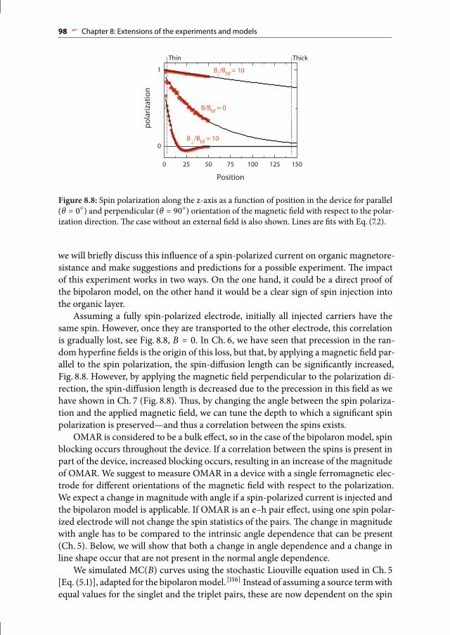
98 Chapter 8: Extensions of the experiments and models
Figure 8.8: Spin polarization along the z-axis as a function of position in the device for parallel
(θ = 0) and perpendicular (θ = 90) orientation of the magnetic field with respect to the polar-
ization direction. The case without an external field is also shown. Lines are fits with Eq. (7.2).
we will briefly discuss this influence of a spin-polarized current on organic magnetore-
sistance and make suggestions and predictions for a possible experiment. The impact
of this experiment works in two ways. On the one hand, it could be a direct proof of
the bipolaron model, on the other hand it would be a clear sign of spin injection into
the organic layer.
Assuming a fully spin-polarized electrode, initially all injected carriers have the
same spin. However, once they are transported to the other electrode, this correlation
is gradually lost, see Fig. 8.8, B = 0. In Ch. 6, we have seen that precession in the ran-
dom hyperfine fields is the origin of this loss, but that, by applying a magnetic field par-
allel to the spin polarization, the spin-diffusion length can be significantly increased,
Fig. 8.8. However, by applying the magnetic field perpendicular to the polarization di-
rection, the spin-diffusion length is decreased due to the precession in this field as we
have shown in Ch. 7 (Fig. 8.8). Thus, by changing the angle between the spin polariza-
tion and the applied magnetic field, we can tune the depth to which a significant spin
polarization is preserved—and thus a correlation between the spins exists.
OMAR is considered to be a bulk effect, so in the case of the bipolaron model, spin
blocking occurs throughout the device. If a correlation between the spins is present in
part of the device, increased blocking occurs, resulting in an increase of the magnitude
of OMAR. We suggest to measure OMAR in a device with a single ferromagnetic elec-
trode for different orientations of the magnetic field with respect to the polarization.
We expect a change in magnitude with angle if a spin-polarized current is injected and
the bipolaron model is applicable. If OMAR is an e–h pair effect, using one spin polar-
ized electrode will not change the spin statistics of the pairs. The change in magnitude
with angle has to be compared to the intrinsic angle dependence that can be present
(Ch. 5). Below, we will show that both a change in angle dependence and a change in
line shape occur that are not present in the normal angle dependence.
We simulated MC(B) curves using the stochastic Liouville equation used in Ch. 5
[Eq. (5.1)], adapted for the bipolaronmodel. [116] Instead of assuming a source termwith
equal values for the singlet and the triplet pairs, these are now dependent on the spin
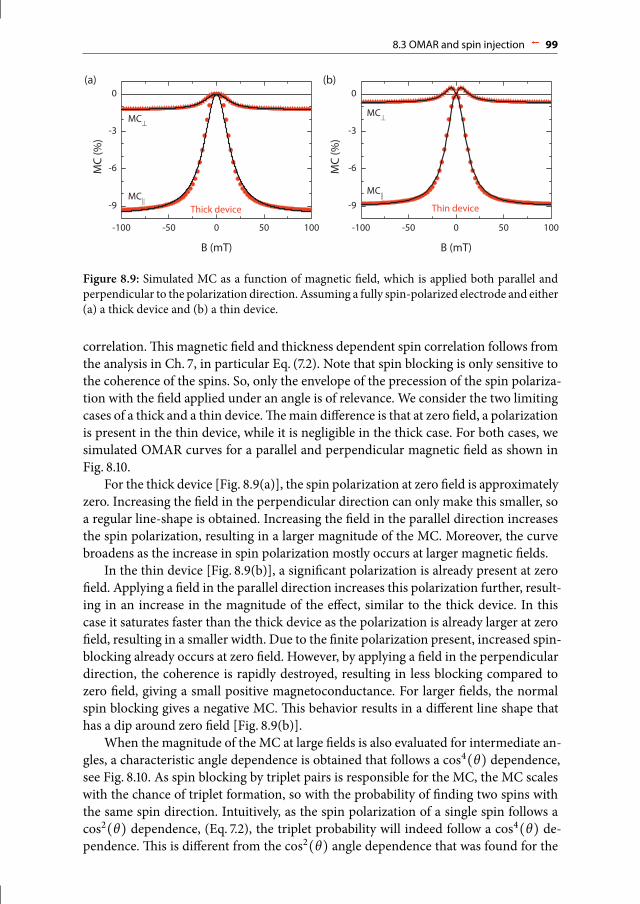
8.3 OMAR and spin injection 99
Figure 8.9: Simulated MC as a function of magnetic field, which is applied both parallel and
perpendicular to the polarization direction. Assuming a fully spin-polarized electrode and either
(a) a thick device and (b) a thin device.
correlation. This magnetic field and thickness dependent spin correlation follows from
the analysis in Ch. 7, in particular Eq. (7.2). Note that spin blocking is only sensitive to
the coherence of the spins. So, only the envelope of the precession of the spin polariza-
tion with the field applied under an angle is of relevance. We consider the two limiting
cases of a thick and a thin device. Themain difference is that at zero field, a polarization
is present in the thin device, while it is negligible in the thick case. For both cases, we
simulated OMAR curves for a parallel and perpendicular magnetic field as shown in
Fig. 8.10.
For the thick device [Fig. 8.9(a)], the spin polarization at zero field is approximately
zero. Increasing the field in the perpendicular direction can only make this smaller, so
a regular line-shape is obtained. Increasing the field in the parallel direction increases
the spin polarization, resulting in a larger magnitude of the MC. Moreover, the curve
broadens as the increase in spin polarization mostly occurs at larger magnetic fields.
In the thin device [Fig. 8.9(b)], a significant polarization is already present at zero
field. Applying a field in the parallel direction increases this polarization further, result-
ing in an increase in the magnitude of the effect, similar to the thick device. In this
case it saturates faster than the thick device as the polarization is already larger at zero
field, resulting in a smaller width. Due to the finite polarization present, increased spin-
blocking already occurs at zero field. However, by applying a field in the perpendicular
direction, the coherence is rapidly destroyed, resulting in less blocking compared to
zero field, giving a small positive magnetoconductance. For larger fields, the normal
spin blocking gives a negative MC. This behavior results in a different line shape that
has a dip around zero field [Fig. 8.9(b)].
When the magnitude of the MC at large fields is also evaluated for intermediate an-
gles, a characteristic angle dependence is obtained that follows a cos4(θ) dependence,see Fig. 8.10. As spin blocking by triplet pairs is responsible for the MC, the MC scales
with the chance of triplet formation, so with the probability of finding two spins with
the same spin direction. Intuitively, as the spin polarization of a single spin follows a
cos2(θ) dependence, (Eq. 7.2), the triplet probability will indeed follow a cos4(θ) de-pendence. This is different from the cos2(θ) angle dependence that was found for the

100 Chapter 8: Extensions of the experiments and models
Figure 8.10:Magnitude of theMC at infinite magnetic field as a function of the angle of the field
with the polarization direction. Curves for three branching ratios b are plotted and fitted with
cos4(θ) (lines).
intrinsic angle dependence (Ch. 5).
In conclusion,whenusing a spin polarized current, the observedOMARwill change
if the bipolaronmodel is applicable, resulting in a typical angle dependence. Compared
to the normal angle dependence, an angle-dependent broadening is predicted in thick
devices and a sign change is predicted for thin devices. Moreover, the magnitude at
large fields is expected to show a cos4(θ) dependence. Experiments on organic devices
of variable thickness with one ferromagnetic electrode could thus be used to simulta-
neously test the bipolaron model and to prove spin injection into the organic layer.

9Outlook
In addition to the specific directions for further research that were presented in the
previous chapter, in this chapter we more generally discuss the future of organic spin-
tronics. We focus mostly on the two aspects of organic spintronics that are treated in
this thesis: organic magnetoresistance and spin transport in disordered organic semi-
conductors.
In the field of OMAR, one of the main questions still is its origin. Several mod-
els have been proposed but still no clear consensus is reached on which model(s) is
(are) applicable. Once the origin is understood, OMAR could prove a valuable tool
for measuring properties of organic electronic devices. One could think of measuring
the strength of hyperfine interaction (which is also very important for other organic
spintronics applications), transport characteristics, or parameters involved in charge re-
combination or generation. Besides using OMAR as a tool, it also has a very promising
technological application. It can be used as a cheapmagnetic field sensor. In addition, it
is (almost) omnidirectional, unlikemany other field sensors, whichmakes it interesting
for certain applications. In addition to using it for field sensing in ink-jet printed ‘plas-
tic’ circuits, [72] one could also look at emerging applications like the use of OLEDs as
chemical or biological sensors, [127] to which a new magnetic degree of freedom could
be added. For all these applications it is an advantage that there is no need for perfect
organic crystals, but that OMAR shows the largest effects in disordered materials. The
effect works even better if the devices are partly degraded by conditioning.
One of the important steps towards a final conclusion on the origin ofOMAR lies in
the design of clever experiments. A good collaboration between physicists and chemists
might prove invaluable as smart engineering of molecules could help to elucidate the
effect. One successful example is the recent experiment with deuteration which proved
the role of the hyperfine fields. [92] For new experiments, one could for instance think
about designing materials with significant differences between the HOMO and LUMO,
resulting in different hyperfine fields sensed by the electrons andholes.These could help
distinguish between single-carrier or double-carrier effects. Doing so, it is important to

102 Chapter 9: Outlook
separate the broadening induced by microscopic effects from the hyperfine fields like
suggested in Sect. 8.2.
In the experiments on organic spin valves, the focus has mostly been on readily
available materials and straightforward processing techniques like evaporation and, in-
cidentally, spin coating.The common choice for Alq3 as the spacer layer is largely based
on its wide availability as a prototype OLED material and it being used in the first suc-
cessful spin valve. [149] There is, however, an interesting future for specially engineered
materials and different type of devices. For instance by engineering materials with re-
duced hyperfine fields, by using lateral FET-like structures, or by using self assembled
mono-layers. An interesting material is graphene, which only consists of carbon, so no
hydrogen is present. Indeed, very long spin-diffusion lengths are found, [134] but it lacks
the flexibility and tunability of conventional organic materials.
A challenge also lies in the fabrication of successful organic spin valves itself. For
instance in a proper definition of the interface with the top electrode, preventing an ‘ill-
defined’ layer and pinholes, and in finding proper materials for the bottom electrode
that are stable against oxidation and are still magnetic at room temperature. This last
requirement is only partially met by the commonly used LSMO, which has a strongly
reduced magnetization at room temperature. The requirement could be fulfilled by us-
ing electrodes of a magnetic metal, like for instance Co, in combination with an oxidic
tunnel barrier.This could open up possibilities formaking lateral structures and for wet
processing techniques.
Our simulations of spin transport in disordered organic semiconductors show that
very large spin-diffusion lengths are expected at high electric fields (Ch. 6). In exper-
iments, however, significant magnetoresistance is only reported at low voltages, see
Sect. 1.3.1. Furthermore, a strong decrease in magnetoresistance is observed with volt-
age. The main question is if this discrepancy is caused by a dominance of tunneling
through thin regions, or that spin transport is present, but the magnetoresistance is
limited via a different mechanism. One such effect could be that there is efficient in-
jection, but detection is reduced by the absence of a barrier at the detecting contact.
This could explain the observation of the strongest MR in the diffusive regime at low
bias. Perhaps different experiments can be devised that detect the polarization in an
alternative way.
So far, to our knowledge no reports have been made on spin valve behavior and
OMAR in the same device at the same time. However, both spin valve behavior and
OMAR have been demonstrated using the samematerials, for instance with Alq3. Con-
sidering the mechanisms involved, this is somewhat unexpected. For spin polarized
transport, we have shown inCh. 6 that fast hopping is required.The time spent between
hops has to be less than the typical precession time. On the other hand, for hyperfine
mixing in the OMARmodels, the time spend on a site should be larger than the typical
precession time.This apparent contradictionmight be explained in one of the following
ways. (i) The effects observed in the spin valves are not originating from spin transport,
but from tunneling through thin regions. (ii) Due to the broad distribution in waiting
times of the carriers (Fig. 6.2), slow carriers might be contributing to the OMAR effect,
while fast carriers are responsible for spin transport. (iii)Minority andmajority carriers
might play a different role. The fast majority carriers transport the spin, while the slow
103
minority carriers are responsible for OMAR. The space charge could play an important
role in communicating this minority effect to the majority carriers, which carry most
of the current. Simultaneous observation of OMAR and spin valve behavior in one de-
vice could be a proof that the majority of the current is not going through pinholes
and spins are transported through the layer. The most convincing experimental proof
would be the manipulation of spins during transport as simulated in Ch. 7.
One interesting application of organic electronics is the organic field effect transis-
tor (OFET). With a gate electrode, the density of charges in the channel is controlled,
resulting in typical mobilities of several cm2V−1 s−1. Using this approach, truly single-carrier devices are obtained,which could be useful for testing themechanisms ofOMAR.
The high mobility might also prove beneficial for spin transport. However, for both ap-
plications, the high mobility and large carrier density could introduce completely new
physics. Using several gate electrodes, it might even be possible to create and manipu-
late quantum dots in organic materials like shown in carbon nanotubes. [26]
In conclusion, organic spintronics is a new, but rapidly growing field. Various in-
teresting effects have been demonstrated, but even more exciting possibilities lie ahead.
Many open issues remain to be solved and new applications to be invented. It is not the
question if we will ever see applications using organic spintronics; the question iswhen
and where we will see them.

104 Outlook

Summary / Samenvatting
Plastic SpintronicsSpin transport and intrinsic magnetoresistance in organic semiconductorsA specific class of plastics and other organic materials is (semi)conducting and can be
used for electronic applications. In this thesis, we investigated their use in certain ap-
plications using magnetic fields. These applications belong to the field of spin electron-
ics, or ‘spintronics’, where next to the charge of the electrons, also their spin is utilized.
This spin can be considered as a small magnetic moment, pointing either up or down.
Organic semiconductors have several advantages that make them interesting for appli-
cations in spintronics. They are relatively cheap, are easy to process, and can be chem-
ically adapted. Two different, but related, topics that combine organic materials with
spintronics have been studied both experimentally and theoretically.
The first topic is the recently discovered change in the current through an organic
layer when a small magnetic field is applied. This effect is called organic magnetoresis-
tance (OMAR). Large changes in the current (10–20%) have been found at relatively
small magnetic fields (∼10mT) and at room temperature. These properties make the ef-
fect interesting for applications like, for instance, cheapmagnetic field sensors, opening
the possibility to addmagnetic functionality to existing organic electronic applications.
Moreover, if its mechanisms are understood, the effect could be used to investigate pro-
cesses in conventional organic electronic devices by studying their magnetic response.
OMAR is observed in a wide range of organic materials, from small molecules to
polymers. It is believed that OMAR originates from the interactions of a pair of charge
carriers (for instance, electron–electron, hole–hole, or electron–hole).More specifically,
it is believed that the possible interactions depend on the relative orientation of the
spins of these two charges.Without an external magnetic field, small intrinsicmagnetic
fields in the organic layer (resulting from hyperfine coupling to nuclear spins) random-
ize the orientations of the two spins.This allows a change from a spin configuration that
is less favorable for the current into a more favorable configuration. However, applying
a magnetic field larger than these hyperfine fields results in a strong reduction of this
spin randomization or spin mixing, causing a pair to remain locked in a less favorable

106 Summary / Samenvatting
spin configuration.
Although there is agreement on the crucial role of hyperfine fields, the exact mech-
anisms behind OMAR are still heavily debated. Several models were proposed in litera-
ture that explainOMAR in terms of different charge pairs. In this thesis, we investigated
a model based on pairs of equal carriers, called the bipolaron model. We used an ele-
mentary model of two neighboring sites, where, depending on the spins, one carrier
might be preventing another one to pass. With this theoretical model we were able
to successfully reproduce several characteristics of OMAR. Both a decrease and an in-
crease in current, as found in experiments, could be obtained and also the universal
shapes of the experimental OMAR curves could be reproduced.
Additionally, we performed new types of experiments to gain better understand-
ing of OMAR.We showed that when an oscillating magnetic field is applied, OMAR is
reduced beyond a certain frequency threshold. This occurs when the slowest charges
can no longer follow the oscillations, as we showed by measuring the frequency depen-
dence of the capacitance. These findings are in agreement with recent interpretations
in which these slowest carriers are expected to induce the largest OMAR effect.
In literature, it was claimed thatOMAR is independent of the orientation of themag-
netic field. However, via sensitive measurements we demonstrated a small but system-
atic dependence on the angle between the magnetic field and the sample. We showed
theoretically that this angle dependence can be explained in the different models by
including an interaction between the spins. This interaction has to be direction depen-
dent in order to explain the angle dependence.We identified dipole–dipole coupling or
an anisotropy in the hyperfine fields as the most likely candidates.
Furthermore, we outlined a first exploration of an alternative approach to describe
OMAR curves. We introduced a function that allows us to extract information both
about the hyperfine fields and about an additional broadening of the curves. Thereby,
this approach could allow for a more quantitative analysis of changes in the OMAR
curves resulting from changes in the operating conditions or the material properties.
In the second topic, the spin of electrons is used in a different way. Inmany spintron-
ics applications a difference between the number of spin-up and spin-down electrons,
called spin polarization, is used to transport information through a device. For the func-
tioning, it is essential that this polarization persists while transporting the charges. The
main mechanism for loss of polarization in most inorganic semiconductors, which is
related to spin–orbit coupling, is negligible in organic materials. The absence of this
loss mechanismmakes organic materials ideal candidates for these types of spintronics
applications. However, there might still be other mechanisms that cause a smaller but
non-zero loss of spin polarization. We conjecture that the hyperfine fields are the main
source of polarization loss in organic materials, which results frommixing between the
spin-up and spin-down electrons by precession of spins about these random fields.
We theoretically investigated this effect of the hyperfine fields on the spin polariza-
tion. We explicitly included the hopping transport characteristic for organic semicon-
ductors. Due to spatial and energetic disorder, the charges hop from one localized site
to another. The longer the time they spend on a site, the larger the loss of spin polariza-
tion. We showed that an external magnetic field larger than the typical hyperfine-field
strength reduces the loss of spin polarization. Hence, such an external field causes the
Summary / Samenvatting 107
polarization to persist over a larger distance, leading to an increase of the spin-diffusion
length. We thus found a magnetic-field dependent spin-diffusion length. In addition,
we found the spin-diffusion length to depend only weakly on temperature.
A spintronics device thatmakes use of spin-polarized transport is the spin valve. Us-
ing the magnetic-field dependent spin-diffusion length obtained from our theory, we
could very accurately fit experimental data on the magnetoresistance of organic spin
valves reported in literature. However, there is still a hot debate on the interpretation of
these and similar experiments. The question has been raised whether spins are indeed
transported through the whole layer, or only through thin regions. A discriminating
experiment would be the manipulation of spins during their transport through the or-
ganic layer.This can be done by applying amagnetic field perpendicular to the direction
of the spin polarization. Using our spin-transport model, we made predictions about
the results that can be expected from such an experiment. We showed that, in the case
of transport through the organic layer, an effect of a perpendicular field should be ob-
servable, but that the strong oscillations in the signal that are typically seen in inorganic
semiconductors will be absent.
Finally, as an extension of the work presented in this thesis, we made predictions
about possible future experiments in which spin polarization is combined with OMAR.
Because for a spin-polarized current the majority of the spins point in the same direc-
tion, most charge pairs will have parallel spins. Therefore, within the bipolaron model,
we expect an increase in the magnitude of OMAR when the injected current is spin po-
larized.Moreover, we showed that the shapes of the OMAR curves will also be changed.
These experiments would provide a means to both prove spin-polarized transport and
to validate the bipolaron model.
In conclusion, both theoretical and experimental results on OMAR and spin polar-
ized transport have been presented in this thesis. Contributions have been made to a
new model for OMAR and new type of experiments have been performed that have
added further insights to the puzzle of OMAR. The limiting role of the hyperfine fields
on spin-polarized transport has been investigated theoretically, providing an explana-
tion for the experimentally observed magnetoresistance curves of organic spin valves
and providing suggestions for future experiments. Although the present work has led
to better understanding of OMAR and spin-polarized transport, the field of organic
spintronics still poses many theoretical and experimental challenges that should be re-
solved before a widespread emergence of organic-spintronics applications will occur.

108 Summary / Samenvatting
Plastic SpintronicaSpintransport en intrinsiekemagnetoweerstand in organische halfgeleidersEen specifieke klasse van plastics en andere organische materialen is (half)geleidend
en kan gebruikt worden voor elektronische toepassingen. In dit proefschrift hebben
we hun gebruik in bepaalde magnetische toepassingen onderzocht. Deze toepassingen
behoren tot het veld van spinelektronica, of ‘spintronica’, waarbij naast de lading van de
elektronen ook gebruik wordt gemaakt van hun spin. Deze spin kan beschouwd wor-
den als een kleinmagnetischmoment dat naar boven of naar benedenwijst. Organische
halfgeleiders hebben een aantal voordelen die hen interessant maken voor toepassing
in spintronica: ze zijn relatief goedkoop, ze zijn gemakkelijk te verwerken en ze kun-
nen chemisch aangepast worden. In dit proefschrift zijn twee verschillende, maar gere-
lateerde, onderwerpen die organische materialen combineren met spintronica, zowel
experimenteel als theoretisch onderzocht.
Het eerste onderwerp is de recent ontdekte verandering in de stroom door een or-
ganische laag ten gevolge van een klein magneetveld. Dit effect wordt organische mag-
netoweerstand (OMAR) genoemd. Grote veranderingen in de stroom (10–20%) zijn ge-
vonden bij relatief kleine magnetische velden (∼10mT) bij kamertemperatuur. Deze ei-
genschappenmakenOMAR interessant voor toepassingen zoals goedkopemagnetisch-
veldsensoren, waardoor bijvoorbeeld magnetische functionaliteiten toegevoegd kun-
nen worden aan bestaande organische elektronische toepassingen. Daarnaast kan een
beter begrip van de OMAR-mechanismes ook gebruikt worden om andere processen
in conventionele organische elektronica te onderzoeken door naar hun magnetische
respons te kijken.
OMAR komt voor in een breed scala van organischematerialen, van kleinemolecu-
len tot (grote) polymeren. Het wordt geloofd dat OMAR ontstaat uit de interactie van
twee ladingsdragers (bijvoorbeeld: elektron–elektron, gat–gat of elektron–gat). Meer
specifiek wordt geloofd dat de mogelijke interacties afhangen van de relatieve oriënta-
tie van de spins van deze twee ladingen. Zonder een extern magneetveld worden de
oriëntaties van de spins gerandomiseerd door kleine intrinsieke magneetvelden (ten
gevolge van de hyperfijnkoppeling aan de kernspins) in de organische laag. Hierdoor
kan een spinconfiguratie veranderen van een configuratie dieminder gunstig is voor de
stroom naar een gunstigere configuratie. Echter, door een magneetveld aan te leggen
dat groter is dan deze hyperfijnvelden wordt de randomisatie sterk verminderd. Dit
zorgt ervoor dat twee ladingsdragers vast kunnen blijven zitten in een minder gunstige
spinconfiguratie.
Hoewel er overeenstemming is over de cruciale rol van hyperfijnvelden, worden de
exacte mechanismes achter OMAR nog sterk bediscussieerd. In de literatuur zijn ver-
scheidene modellen voorgesteld die OMAR uitleggen op basis van verschillende soor-
ten ladingsparen. In dit proefschrift hebben we een model onderzocht dat gebaseerd
is op paren van gelijke ladingen, het zogenaamde bipolaron model. We hebben een ele-
mentair model ontwikkeld van twee naburige posities, waar, afhankelijk van de spin,
de ene ladingsdrager kan voorkomen dat de andere ladingsdrager kan passeren. Met
dit theoretische model hebben we succesvol verschillende karakteristieken van OMAR
kunnen reproduceren, zoals zowel de toename als afname van de stroom die gezien
wordt in experimenten, en de universele vorm van de experimentele OMAR-curves.

Summary / Samenvatting 109
Daarnaast hebben we verschillende nieuwe type experimenten uitgevoerd om een
beter begrip te krijgen van OMAR. We hebben laten zien dat wanneer een oscillerend
magneetveld gebruikt wordt het OMAR effect kleiner wordt voorbij een bepaalde fre-
quentie. Dit gebeurt wanneer de langzaamste ladingen de oscillaties niet meer kunnen
volgen, wat we hebben aangetoond door de frequentieafhankelijkheid van de capaciteit
te meten.
In literatuur wordt geclaimd dat OMAR onafhankelijk is van de oriëntatie van het
magnetische veld. Echter, via gevoeligemetingen hebben wij een kleinemaar systemati-
sche afhankelijkheid van OMAR gedemonstreerd van de hoek tussen het magneetveld
en het sample. We hebben theoretisch laten zien dat deze hoekafhankelijkheid uitge-
legd kan worden door in de verschillende modellen een interactie tussen de spins mee
te nemen. Deze interactie moet richtingsafhankelijk zijn om de hoekafhankelijkheid te
verklaren. Als de meest waarschijnlijke oorzaken voor de interactie hebben we dipool–
dipool koppeling of een anisotropie in de hyperfijnvelden geïdentificeerd.
Tenslotte hebben we een eerste onderzoek geschetst van een alternatieve benade-
ring om OMAR curves te beschrijven. We hebben een functie geïntroduceerd die het
mogelijk maakt om informatie te krijgen over zowel de hyperfijnvelden als over een
extra verbreding van de curves. Zodoende zou deze benadering het mogelijk kunnen
maken om een meer kwantitatieve analyse te maken van veranderingen in de OMAR
curves ten gevolge van veranderingen in de experimentele instellingen of de materiaal-
eigenschappen.
In het tweede onderwerp wordt de spin van elektronen op een andere manier ge-
bruikt. In veel spintronica toepassingen wordt een verschil tussen de spin-op en spin-
neer elektronen, een zogenaamde spinpolarisatie, gebruikt om informatie te transpor-
teren. Voor het functioneren is het essentieel dat deze polarisatie behouden blijft ter-
wijl de ladingen getransporteerd worden. Het voornaamste mechanisme voor verlies
van polarisatie in de meeste inorganische halfgeleiders is verwaarloosbaar in organi-
sche materialen. De afwezigheid van dit verliesmechanisme maakt organische materi-
alen ideale kandidaten voor dit type spintronicatoepassingen. Er kan echter nog een
ander mechanisme zijn dat een kleiner, maar niet verwaarloosbaar, verlies van polari-
satie veroorzaakt. Wij suggereren dat de hyperfijnvelden de voornaamste oorzaak zijn
van verlies van spinpolarisatie in organischematerialen, omdat de spin-op en spin-neer
elektronen kunnen mixen door precessie rond deze random hyperfijnvelden.
Wij hebben het effect van de hyperfijnvelden op de spinpolarisatie theoretisch on-
derzocht. Hierbij hebben we expliciet het hoppingtransport meegenomen dat karakte-
ristiek is voor organische halfgeleiders. Door ruimtelijke en energetische wanorde hop-
pen de ladingen namelijk van de ene naar de andere gelokaliseerde positie. Hoe langer
ze op een positie zitten, hoe groter het verlies van spinpolarisatie. We hebben laten zien
dat een externmagneetveld dat groter is dan de typische hyperfijn veldsterkte het verlies
van spinpolarisatie reduceert. Een dergelijk extern veld zorgt er dus voor dat de spin-
polarisatie behouden blijft over een grotere afstand, resulterend in een toename van
de spindiffusielengte. We hebben dus een magneetveldafhankelijke spindiffusielengte
gevonden. Deze hangt bovendien slechts zwak af van de temperatuur.
Een spintronica device dat gebruikmaakt van spingepolariseerd transport is de or-
ganische spin valve. Met demagneetveldafhankelijke spindiffusielengte uit onze theorie

110 Summary / Samenvatting
konden we zeer nauwkeurig de experimentele data uit de literatuur van magnetoweer-
stand van organische spin valves fitten. Er vindt echter nog een verhit debat plaats over
de interpretatie van deze en vergelijkbare experimenten. De essentiële vraag is of spins
inderdaad getransporteerd worden door de hele laag, of alleen door dunne gebieden.
Een onderscheidend experiment zou de manipulatie van spins zijn tijdens hun trans-
port door de organische laag. Dit kan gedaan worden door een magneetveld loodrecht
op de richting van de spinpolarisatie aan te leggen. Met ons spintransportmodel heb-
ben we voorspellingen gedaan van resultaten die verwacht kunnen worden van een
dergelijk experiment. We hebben laten zien dat, in het geval van transport door de or-
ganische laag, een effect van een loodrecht veld waarneembaar zou moeten zijn, maar
dat de sterke oscillaties in het signaal die typisch zijn voor inorganische halfgeleiders
afwezig zijn.
Tenslotte, als uitbreiding van het werk gepresenteerd in dit proefschrift, hebben we
voorspellingen gedaan over mogelijke toekomstige experimenten waarin spinpolarisa-
tie gecombineerdwordtmetOMAR.Omdat demeerderheid van de spins dezelfde kant
opwijzen in een spingepolariseerde stroom, zullen demeeste paren parallelle spins heb-
ben. In het bipolaron model verwachten we daarom een toename in OMAR als de ge-
ïnjecteerde stroom spingepolariseerd is. Bovendien hebben we laten zien dat de vorm
van de OMAR curves dan ook zal veranderen. Deze experimenten zouden een moge-
lijkheid kunnen bieden om zowel spingepolariseerd transport als het bipolaron model
te valideren.
In dit proefschrift zijn zowel theoretische als experimentele resultaten van OMAR
en spingepolariseerd transport gepresenteerd. Er is bijgedragen aan een nieuw model
voor OMAR en er zijn nieuwe type experimenten uitgevoerd die meer inzichten toe-
gevoegd hebben aan de puzzel van OMAR. De limiterende rol van de hyperfijnvelden
voor spingepolariseerd transport is theoretisch onderzocht en biedt zowel een verkla-
ring voor de experimenteel geobserveerde magnetoweerstandscurves van organische
spin valves, als suggesties voor toekomstige experimenten. Hoewel er nog vele theore-
tische en experimentele uitdagingen opgelost moeten worden, heeft het huidige werk
geleid tot beter begrip van OMAR en spingepolariseerd transport. Daarmee draagt het
bij aan een toekomst waarin organische spintronica wijdverspreid op zal kunnen ko-
men.

Curriculum vitae
WiebeWagemans was born on August 4, 1980, in Arnhem, the Netherlands. There,
he went to high school at the Thomas a Kempis College. After his graduation in 1998,
he moved to Eindhoven to study Applied Physics at the Eindhoven University of Tech-
nology. For his studies he did a local internship in the plasma physics group of prof.dr.ir
M.C.M. van der Sanden and an internship abroad in the group of dr. J.S. Moodera at
the Massachusetts Institute of Technology on the topic of magnetic tunnel junctions.
For his graduation project he investigated organic spin valves in the group of prof.dr. B.
Koopmans. After successful completion of the project in 2006, Wiebe decided to stay
in the same group as a PhD candidate. Part of his PhD work is described in this thesis,
but he also made contributions to several of the related efforts in the group. Moreover,
a new infrastructure was set up, including newmeasurement techniques. As part of his
work, Wiebe supervised six Bachelor and three Master students. He was chosen as the
best practicum supervisor in 2007.
During his studies, Wiebe was a member of the board of the study association for
one year. From 1999 to 2003, he was one of the artists in the Circus of Physics, which
performs at primary and secondary schools. In 2002, inspired by the success of the
circus, Wiebe and Jelle de Jong founded Stichting Techniekpromotie, a foundation that
promotes science and technology to children aged 4 to 15. As one of the new activities,
Wiebe organized the first edition of the FIRSTLEGOLeague in theNetherlands in 2003.
This is a competition for teams of 5–10 children, using a LEGO-based robot, but also
asking for many other skills. His work included finding teams, training volunteers, and
organizing all logistics. The foundation has rapidly grown and now has many partners
in the Netherlands. In 2009, more than 50.000 persons participated in one of the many
activities.Wiebe is still involved in the foundation as a boardmember, but activities are
now organized by a dedicated bureau.
After his graduation,Wiebe also became a boardmember of the alumni association
of Applied Physics (2006–2009). First, he was responsible for the quarterly magazine
and later became chairman. In his free time, Wiebe likes to take photographs and to
practise yoga and meditation.

112 Curriculum vitae

List of publications
Angle dependent spin–spin interactions in organic magnetoresistanceW.Wagemans, A.J. Schellekens, M. Kemper, and B. Koopmans
in preparation.
Frequency dependence of organic magnetoresistanceW.Wagemans, P. Janssen, E.H.M. van der Heijden, M. Kemerink, and B. Koopmans
in preparation.
The effect of magnetic field orientation on the spin-diffusion length in organicsemiconductorsW.Wagemans, F.W.A. van Oost, S. Wouters, A.J. Schellekens, P.A. Bobbert, and
B. Koopmans
in preparation.
Microscopic modeling of organic magnetoresistanceA.J. Schellekens, W. Wagemans, and B. Koopmans
in preparation.
Spin in organics, a new route to spintronicsB. Koopmans, W. Wagemans, F.L. Bloom, P.A. Bobbert, M. Kemerink, and
M. Wohlgenannt
submitted to Philisophical Transactions of the Royal Society A (2010).
Separating photocurrent and injected current contributions to the organicmagnetoresistanceW.Wagemans, W.J. Engelen, F.L. Bloom, and B. Koopmans
Synthetic Metals 160, 266–270 (2010).
Spin relaxation and magnetoresistance in disordered organic semiconductorsP.A. Bobbert, T.D. Nguyen, W. Wagemans, F.W.A. van Oost, B. Koopmans, and
M. Wohlgenannt
Synthetic Metals 160, 223–229 (2010).

114 List of publications
Theory for spin diffusion in disordered organic semiconductorsP.A. Bobbert, W. Wagemans, F.W.A. van Oost, B. Koopmans, and M. Wohlgenannt
Physical Review Letters 102, 156604 (2009).
Magnetoresistance in hybrid organic spin valves at the onset of multiple-steptunnelingJ.J.H.M. Schoonus, P.G.E. Lumens, W. Wagemans, J.T. Kohlhepp, P.A. Bobbert, H.J.M.
Swagten, and B. Koopmans
Physical Review Letters 103, 146601 (2009).
Sign inversion of magnetoresistance in space-charge limited organic devicesF.L. Bloom, M. Kemerink, W. Wagemans, and B. Koopmans
Physical Review Letters 103, 066601 (2009).
Correspondence of the sign change in organic magnetoresistance with the onset ofbipolar charge transportF.L. Bloom, W. Wagemans, M. Kemerink, and B. Koopmans
Applied Physics Letters 93, 263302 (2008).
A two-site bipolaron model for organic magnetoresistanceW.Wagemans, F.L. Bloom, P.A. Bobbert, M. Wohlgenannt, and B. Koopmans
Journal of Applied Physics 103, 07F303 (2008).
Temperature dependent sign change of the organic magnetoresistance effectF.L. Bloom, W. Wagemans, B. Koopmans
Journal of Applied Physics 103, 07F320 (2008).
Extremely large magnetoresistance in boron-doped siliconJ.J.H.M. Schoonus, F.L. Bloom, W. Wagemans, H.J.M. Swagten, and B. Koopmans
Physical Review Letters 100, 127202 (2008).
Separating positive and negative magnetoresistance in organic semiconductordevicesF.L. Bloom, W. Wagemans, M. Kemerink, and B. Koopmans
Physical Review Letters 99, 257201 (2007).
Detailed study of the plasma-activated catalytic generation of ammonia in N2–H2plasmasJ.H. van Helden, W. Wagemans, G. Yagci, R.A.B. Zijlmans, D.C. and Schram,
R. Engeln, G. Lombardi, G.D. Stancu, and J. Röpcke
Journal of Applied Physics 101, 043305 (2007).

Acknowledgements / Dankwoord
De eerste die ik wil bedanken dat ben jij, omdat je interesse toont in mijn proefschrift,
al is het alleen maar in dit dankwoord. Daarnaast zijn er natuurlijk meer mensen die ik
wil bedanken, een promotieonderzoek doe je namelijk niet alleen. Veel mensen hebben
direct of indirect een bijdrage geleverd. Een aantal wil ik graag met name bedanken.
Mijn directe begeleider en promotor Bert Koopmans, ik wil je graag bedanken voor
je vertrouwen, je enthousiasme en je beschikbaarheid. Je maakte altijd tijd voor (we-
tenschappelijke) discussie en kwam regelmatig enthousiast binnen lopen met nieuwe
ideeën. Henk Swagten, wat meer van de zijlijn, maar ik heb onze gesprekken over ver-
schillende onderwerpen zeker erg gewaardeerd. Peter Bobbert, bedankt dat je mijn co-
promotor wilde zijn, en bedankt voor het gedetailleerde inhoudelijke commentaar op
mijn werk en de andere inhoudelijke discussies tijdens mijn onderzoek.
I also want to thank the other committee members, René Janssen, Wilfred van der
Wiel, MarcusWohlgenannt andWilliam Gillin for carefully reading my thesis. Marcus,
I also want to thank you for being a co-author on several papers. I have especially fond
memories of our editing sessions in Brazil.
Aan bijna alle onderwerpen in deze thesis hebben één of meer afstudeerders en
stagairs een bijdrage geleverd. Stagairs Joost Voorbraak, Arno van den Brink, Thomas
Lemmens, RoelHeijnen, RobMensink en Ilse van derHeijden, en afstudeerdersMarijn
Kemper, Wouter Engelen en Sjors Schellekens, allemaal bedankt! Ik heb het erg leuk
gevonden om jullie te begeleiden en om met jullie samen te werken.
FranciscoBloom, youwere the other PhD student on the organic spintronics project.
Thank you for the fruitful collaboration, which resulted in the creation of a new setup
and many papers. I also enjoyed our trips to several international conferences. Paul
Janssen, jij bent nu onze opvolger. Het was leuk om je in te werken en om met je naar
Kopenhagen te gaan.
Zonder de technici Gerrie Baselmans, Jef Noijen en Jeroen Francken was het niet
mogelijk geweest om zoveel nieuwe opstellingen te maken en experimenten uit te voe-
ren. Daarnaast wil ik ook iedereen van de werkplaats hartelijk bedanken voor hun bij-
drage. Met name de ‘klusjesman’, hij/zij heeft de afgelopen vier jaar talloze klusjes voor
mij uitgevoerd.

116 List of publications
Bijna alle samples die ik heb gebruikt, heb ik gemaakt bij scheikunde. Graag wil ik
de groep daar bedanken voor het beschikbaar stellen van de faciliteiten en vooral ook
Martijn Wienk voor de hulp.
Bij natuurkunde wil ik ook nog Martijn Kemerink en Frank van Oost bedanken
voor de samenwerking, de discussies en de nodige inzichten.
Ookwil ik graag de leden bedanken vande groepFysica vanNanostructuren (FNA),
waar ik inclusief mijn afstuderen ruim vijf jaar met heel veel plezier heb rondgelopen.
Bedankt voor de koffiepauzes, publicatie-borrels, sinterklaasvieringen, oudejaarsbras-
partijen, groepsuitjes, tuinfeesten, en nog veel meer. Ik wil zeker ook de spelers en coa-
ches van het zaalvoetbalteam Spin ’m d’r in, waar ik een paar jaar met veel plezier mee
heb gespeeld, bedanken. Wim, Jürgen, Oleg, Beatriz, bedankt. Karin bedankt voor de
goede support. Kamergenoten Coen, Francesco en Reinoud bedankt voor de gezellig-
heid, en ook de (oud-)promovendi en post-docs Harm, Karel, Csaba, Corine, Paresh,
Omer, Jeroen, Andrei, Gregory, Muriel, Sabine, bedankt. De dynamiek in de groep
kwam voor een groot deel ook door alle verschillende studenten, waarvan er te veel
zijn geweest om allemaal te noemen, maar toch zeker ook jullie bedankt.
Jan Millenaar, ik wil je graag bedanken omdat je mij als eerstejaars student bij het
Natuurkundecircus hebt gevraagd. Niet alleen heb ik veel van je geleerd,maar ook heeft
het circus Jelle de Jong en mij geïnspireerd om de Stichting Techniekpromotie op te
richten. Jelle, en ook de andere (oud-)bestuursleden van de stichting, bedankt voor de
gezellige vergaderingen, maar speciaal ook voor het samenwerken aan zo’n mooi doel.
Ook het lidmaatschap van het bestuur van de Alumnivereniging VENI heb ik erg
leuk gevonden. Sonja, Erik, Patrick, Jeroen, Daniel, Thijs, bedankt, vooral ook voor
de gezellige vergaderingen en etentjes. Ook oud-Van-der-Waalsbestuur Equilibrium be-
dankt. Erik ook nog bedankt voor het klimmen en de andere gezellige activiteiten, ook
al is dat de laatste tijd in het slop geraakt.
Mijn ‘schoonfamilie’ wil ik ook graag bedanken. Anja en Rob, bedankt voor het
altijd klaar staan, de hulp, jullie liefde voor Kim en de gezellige vakanties.
Een aantal speciale vrienden wil ik ook bedanken. Jenny, Nico en Jasmijn, bedankt
voor de fijne en gezellige avonden en de inspirerende discussies. Ook Erik, Marjolein
en Michaëla bedankt voor jullie altijd warme en liefdevolle ontvangst. Sri Vasudeva en
zijn organisatie Blue Star wil ik graag bedanken voor de steun bij mijn groei en voor
de fijne omgeving met liefdevolle mensen. Al deze mensen hebben mij veel verdieping
gebracht.
Mijn zus, Olga, dankzij jou ben ik begonnen met yoga en ook met meditatie. Hier
heb ik veel aan gehad en heb ik nog steeds veel aan. Ik vind het fijn dat ik je heb kunnen
helpen bij het opzetten van je eigen yogastudio. Mijn moeder, Dianne, bedankt voor je
steun en liefde. Mijn vader, Gerard, en zijn partner, Gerda, bedankt voor jullie steun en
interesse. Gerard, ik heb goede herinneringen aan onze vakantie in Egypte!
Eén iemandheeftwel heel veel voormij betekend de afgelopen jaren. Kim, jij bent er
altijd geweest om alles mee te kunnen delen. We zijn samen veel gegroeid de afgelopen
jaren. In al die jaren ben je een onderdeel van mij geworden. Bedankt voor je steun en
je liefde!

Bibliography
[1] Alexandrov, A.S. and Bratkovsky, A.M. Carrier density collapse and colossal magnetoresis-
tance in doped manganites. Phys. Rev. Lett. 82, 141 (1999). [p. 23]
[2] Arkhipov, V.I., Emelianova, E.V., Tak, Y.H., and Bässler, H. Charge injection into light-
emitting diodes: Theory and experiment. J. Appl. Phys. 84, 848 (1998). [p. 17]
[3] Aziz, H., Popovic, Z., Hu, N., Hor, A., and Xu, G. Degradation mechanism of small
molecule-based organic light-emitting devices. Science 283, 1900 (1999). [p. 37]
[4] Bagnich, S.A., Niedermeier, U., Melzer, C., Sarfert, W., and von Seggern, H. Electron-
hole pair mechanism for the magnetic field effect in organic light emitting diodes based on
poly(paraphenylene vinylene). J. Appl. Phys. 106, 113702 (2009). [p. 23, 24, and 30]
[5] Bagnich, S.A., Niedermeier, U., Melzer, C., Sarfert, W., and von Seggern, H. Origin of
magnetic field effect enhancement by electrical stress in organic light emitting diodes. J. Appl.
Phys. 105, 123706 (2009). [p. 18, 19, 51, and 58]
[6] Baibich, M.N., Broto, J.M., Fert, A., Van Dau, F.N., Petroff, F., Etienne, P., Creuzet, G.,
Friederich, A., and Chazelas, J. Giant magnetoresistance of (001)Fe/(001)Cr magnetic su-
perlattices. Phys. Rev. Lett. 61, 2472 (1988). [p. 12 and 67]
[7] Baldo, M. and Forrest, S. Transient analysis of organic electrophosphorescence: I. transient
analysis of triplet energy transfer. Phys. Rev. B 62, 10958 (2000). [p. 31 and 51]
[8] Barth, S., Bässler, H., Rost, H., and Hörhold, H.H. Extrinsic and intrinsic dc photoconduc-
tivity in a conjugated polymer. Phys. Rev. B 56, 3844 (1997). [p. 12]
[9] Bässler, H. Charge transport in disordered organic photoconductors a Monte Carlo simula-
tion study. Phys. Status Solidi B 175, 15 (1993). [p. 8, 68, and 80]
[10] Bergenti, I., Dediu, V., Arisi, E., Mertelj, T., Murgia, M., Riminucci, A., Ruani, G., Solzi,
M., and Taliani, C. Spin polarised electrodes for organic light emitting diodes. Org. Electron.
5, 309 (2004). [p. 14]
[11] Bergeson, J.D., Prigodin, V.N., Lincoln, D.M., and Epstein, A.J. Inversion of magnetoresis-
tance in organic semiconductors. Phys. Rev. Lett. 100, 067201 (2008). [p. 18, 19, 23, 24, 33,34, and 57]
[12] Berthelot, A., Favero, I., Cassabois, G., Voisin, C., Delalande, C., Roussignol, P., Ferreira,
R., and Gerard, J.M. Unconventional motional narrowing in the optical spectrum of a semi-
conductor quantum dot. Nat. Phys. 2, 759 (2006). [p. 69 and 83]

118 Bibliography
[13] Binasch, G., Grünberg, P., Saurenbach, F., and Zinn, W. Enhanced magnetoresistance in
layered magnetic structures with antiferromagnetic interlayer exchange. Phys. Rev. B 39,4828 (1989). [p. 12 and 67]
[14] Blom, P., deJong, M., and Vleggaar, J. Electron and hole transport in poly(p-phenylene
vinylene) devices. Appl. Phys. Lett. 68, 3308 (1996). [p. 11 and 38]
[15] Bloom, F.L., Kemerink, M., Wagemans, W., and Koopmans, B. Sign inversion of magne-
toresistance in space-charge limited organic devices. Phys. Rev. Lett. 103, 066601 (2009).[p. 28, 29, 51, and 56]
[16] Bloom, F.L., Wagemans, W., Kemerink, M., and Koopmans, B. Separating positive and
negative magnetoresistance in organic semiconductor devices. Phys. Rev. Lett. 99, 257201(2007). [p. 18, 29, 34, 38, 48, 56, and 96]
[17] Bloom, F.L., Wagemans, W., Kemerink, M., and Koopmans, B. Correspondence of the sign
change in organic magnetoresistance with the onset of bipolar charge transport. Appl. Phys.
Lett. 93, 263302 (2008). [p. 18, 28, and 34]
[18] Bloom, F.L., Wagemans, W., and Koopmans, B. Temperature dependent sign change of the
organic magnetoresistance effect. J. Appl. Phys. 103, 07F320 (2008). [p. 18, 34, and 40]
[19] Bloom, F.L. Exploring organic magnetoresistance—An investigation of microscopic and
device properties. Ph.D. thesis, Eindhoven University of Technology (2010). [p. 96 and 97]
[20] Bobbert, P.A., Nguyen, T.D., van Oost, F.W.A., Koopmans, B., andWohlgenannt, M. Bipo-
laron mechanism for organic magnetoresistance. Phys. Rev. Lett. 99, 216801 (2007). [p. 21,22, 23, 33, 41, 43, 44, 47, 48, 56, 57, 68, 89, 91, 92, 93, 94, and 95]
[21] Bobbert, P.A., van Oost, F.W.A., and Cottaar, J. to be published. [p. 70]
[22] Bobbert, P.A.,Wagemans,W., vanOost, F.W.A., Koopmans, B., andWohlgenannt,M. The-
ory for spin diffusion in disordered organic semiconductors. Phys. Rev. Lett. 102, 156604(2009). [p. 69, 79, 80, 81, 83, 86, and 87]
[23] Bobbert, P., Nguyen, T.,Wagemans,W., vanOost, F., Koopmans, B., andWohlgenannt, M.
Spin relaxation and magnetoresistance in disordered organic semiconductors. Synth. Met.
160, 223 (2010). [p. 27, 41, and 93]
[24] Bobbert, P.A. Organic semiconductors: What makes the spin relax? Nat. Mater. 9, 288(2010). [p. 16]
[25] Chappert, C., Fert, A., and Van Dau, F.N. The emergence of spin electronics in data storage.
Nat. Mater. 6, 813 (2007). [p. 12]
[26] Churchill, H.O.H., Bestwick, A.J., Harlow, J.W., Kuemmeth, F., Marcos, D., Stwertka, C.H.,
Watson, S.K., andMarcus, C.M. Electron-nuclear interaction in 13C nanotube double quan-
tum dots. Nat. Phys. 5, 321 (2009). [p. 23 and 103]
[27] Cinchetti, M., Heimer, K.,Wuestenberg, J.P., Andreyev, O., Bauer, M., Lach, S., Ziegler, C.,
Gao, Y., and Aeschlimann, M. Determination of spin injection and transport in a ferromag-
net/organic semiconductor heterojunction by two-photon photoemission. Nat. Mater. 8, 115(2009). [p. 16]
[28] Cölle,M. andGärditz, C. Phosphorescence of aluminum tris(quinoline-8-olate). Appl. Phys.
Lett. 84, 3160 (2004). [p. 25]
[29] Cölle, M., Gärditz, C., and Braun, M. The triplet state in tris-(8-
hydroxyquinoline)aluminum. J. Appl. Phys. 96, 6133 (2004). [p. 25]
[30] Crooker, S.A., Furis,M., Lou, X., Adelmann, C., Smith, D.L., Palmstrom, C.J., andCrowell,
P.A. Imaging spin transport in lateral ferromagnet/semiconductor structures. Science 309,

Bibliography 119
2191 (2005). [p. 16, 80, 86, and 87]
[31] D’Andrade, B.W. and Forrest, S. White organic light-emitting devices for solid-state lighting.
Adv. Mater. 16, 1585 (2004). [p. 7]
[32] Davis, A.H. and Bussmann, K. Organic luminescent devices and magnetoelectronics. J.
Appl. Phys. 93, 7358 (2003). [p. 14]
[33] Davis, A.H. and Bussmann, K. Large magnetic field effects in organic light emit-
ting diodes based on tris(8-hydroxyquinoline aluminum) (Alq3)/N,N′-Di(naphthalen-1-yl)-
N,N′diphenyl-benzidine (NPB) bilayers. J. Vac. Sci. Technol. A 22, 1885 (2004). [p. 20]
[34] Dediu, V., Hueso, L.E., Bergenti, I., Riminucci, A., Borgatti, F., Graziosi, P., Newby, C.,
Casoli, F., De Jong, M.P., Taliani, C., and Zhan, Y. Room-temperature spintronic effects in
Alq3-based hybrid devices. Phys. Rev. B 78, 115203 (2008). [p. 15, 68, 69, and 77]
[35] Dediu, V., Murgia, M., Matacotta, F., Taliani, C., and Barbanera, S. Room temperature spin
polarized injection in organic semiconductor. Solid State Commun. 122, 181 (2002). [p. 15,68, 69, and 72]
[36] Dediu, V.A., Hueso, L.E., Bergenti, I., and Taliani, C. Spin routes in organic semiconductors.
Nat. Mater. 8, 707 (2009). [p. 14, 15, and 17]
[37] Desai, P., Shakya, P., Kreouzis, T., and Gillin, W.P. Magnetoresistance in organic light-
emitting diode structures under illumination. Phys. Rev. B 76, 235202 (2007). [p. 18, 25,
and 34]
[38] Desai, P., Shakya, P., Kreouzis, T., and Gillin, W.P. The role of magnetic fields on the
transport and efficiency of aluminum tris(8-hydroxyquinoline) based organic light emitting
diodes. J. Appl. Phys. 102, 073710 (2007). [p. 18]
[39] Desai, P., Shakya, P., Kreouzis, T., Gillin, W.P., Morley, N.A., and Gibbs, M.R.J. Magne-
toresistance and efficiency measurements of Alq3-based OLEDs. Phys. Rev. B 75, 094423(2007). [p. 18, 25, 28, 33, 34, 43, and 68]
[40] Drew, A.J., Hoppler, J., Schulz, L., Pratt, F.L., Desai, P., Shakya, P., Kreouzis, T., Gillin,
W.P., Suter, A., Morley, N.A., Malik, V.K., Dubroka, A., Kim, K.W., Bouyanfif, H., Bourqui,
F., Bernhard, C., Scheuermann, R., Nieuwenhuys, G.J., Prokscha, T., and Morenzoni, E.
Direct measurement of the electronic spin diffusion length in a fully functional organic spin
valve by low-energy muon spin rotation. Nat. Mater. 8, 109 (2009). [p. 16, 68, 69, and 72]
[41] Ern, V. and Merrifield, R.E. Magnetic field effect on triplet exciton quenching in organic
crystals. Phys. Rev. Lett. 21, 609 (1968). [p. 25]
[42] Forrest, S.R. The path to ubiquitous and low-cost organic electronic appliances on plastic.
Nature 428, 911 (2004). [p. 7]
[43] Francis, T., Mermer, Ö., Veeraraghavan, G., and Wohlgenannt, M. Large magnetoresis-
tance at room temperature in semiconducting polymer sandwich devices. New J. Phys. 6,185 (2004). [p. 17, 19, and 57]
[44] Frankevich, E.L., Lymarev, A.A., Sokolik, I., Karasz, F.E., Blumstengel, S., Baughman, R.H.,
and Hörhold, H.H. Polaron-pair generation in poly(phenylene vinylenes). Phys. Rev. B 46,9320 (1992). [p. 18, 23, and 24]
[45] Gärditz, C.,Mückl, A.G., andCölle,M. Influence of an externalmagnetic field on the singlet
and triplet emissions of tris-(8-hydroxyquinoline)aluminum(iii) (Alq3). J. Appl. Phys. 98,104507 (2005). [p. 18]
[46] Godlewski, J., Jarosz, G., and Signerski, R. Photoenhanced current in thin organic layers.
Appl. Surf. Sci. 175-176, 344 (2001). [p. 25]

120 Bibliography
[47] Gómez, J., Nüesch, F., Zuppiroli, L., andGraeff, C.Magnetic field effects on the conductivity
of organic bipolar and unipolar devices at room temperature. Synth. Met. 160, 317 (2010).[p. 19]
[48] Gommans, H.H.P., Kemerink, M., Andersson, G.G., and Pijper, R.M.T. Charge transport
and trapping in Cs-doped poly(dialkoxy-p-phenylene vinylene) light-emitting diodes. Phys.
Rev. B 69, 155216 (2004). [p. 54]
[49] Gommans, H., Kemerink,M., and Janssen, R. Negative capacitances in low-mobility solids.
Phys. Rev. B 72, (2005). [p. 51 and 54]
[50] Groff, R.P., Suna, A., Avakian, P., and Merrifield, R.E. Magnetic hyperfine modulation of
dye-sensitized delayed fluorescence in organic crystals. Phys. Rev. B 9, 2655 (1974). [p. 58and 65]
[51] Guyot-Sionnest, P., Yu, D., Jiang, P.h., and Kang, W. Spin blockade in the conduction of
colloidal cdse nanocrystal films. J. Chem. Phys. 127, 014702 (2007). [p. 23]
[52] Hartenstein, B., Bässler, H., Jakobs, A., and Kehr, K.W. Comparison between multiple trap-
ping and multiple hopping transport in a random medium. Phys. Rev. B 54, 8574 (1996).
[p. 70]
[53] Helbig, M. and Hörhold, H.H. Investigation of poly(arylenevinylene)s, 40. electrochemical
studies on poly(p-phenylenevinylene)s. Die Makromolekulare Chemie 194, 1607 (1993).
[p. 23]
[54] Hu, B. andWu, Y. Tuningmagnetoresistance between positive and negative values in organic
semiconductors. Nat. Mater. 6, 985 (2007). [p. 18, 26, and 30]
[55] Hu, B., Yan, L., and Shao, M. Magnetic-field effects in organic semiconducting materials
and devices. Adv. Mater. 21, 1500 (2009). [p. 17, 25, 26, 29, and 51]
[56] Iwasaki, Y., Osasa, T., Asahi, M., Matsumura, M., Sakaguchi, Y., and Suzuki, T. Frac-
tions of singlet and triplet excitons generated in organic light-emitting devices based on a
polyphenylenevinylene derivative. Phys. Rev. B 74, 195209 (2006). [p. 18 and 23]
[57] Janssen, R. and Graetzel, M. Themed issue: solar cells. J. Mater. Chem. 19, 5276 (2009).
[p. 7]
[58] Jedema, F.J., Heersche, H.B., Filip, A.T., Baselmans, J.J.A., and van Wees, B.J. Electrical
detection of spin precession in a metallic mesoscopic spin valve. Nature 416, 713 (2002).
[p. 16, 80, and 86]
[59] Jiang, J.S., Pearson, J.E., and Bader, S.D. Absence of spin transport in the organic semicon-
ductor Alq3. Phys. Rev. B 77, 035303 (2008). [p. 15 and 17]
[60] Johnson, R. andMerrifield, R. Effects ofmagnetic fields on themutual annihilation of triplet
excitons in anthracene crystals. Phys. Rev. B 1, 896 (1970). [p. 16, 26, 62, 80, and 86]
[61] Kadashchuk, A., Arkhipov, V.I., Kim, C.H., Shinar, J., Lee, D.W., Hong, Y.R., Jin, J.I., Here-
mans, P., and Bässler, H. Localized trions in conjugated polymers. Phys. Rev. B 76, 235205(2007). [p. 28]
[62] Kalinowski, J., Cocchi, M., Virgili, D., Di Marco, P., and Fattori, V. Magnetic field effects
on emission and current in Alq3-based electroluminescent diodes. Chem. Phys. Lett. 380,710 (2003). [p. 18, 23, and 68]
[63] Kutzler, F.W., White, C.T., and Cook, M. Local spin-density calculations of anisotropic
hyperfine constants in oriented free radicals. Chem. Phys. Lett. 147, 263 (1988). [p. 65]
[64] Lin, B.C., Cheng, C.P., You, Z.Q., and Hsu, C.P. Charge transport properties of tris(8-
hydroxyquinolinato)aluminum(III): Why it is an electron transporter. J. Am. Chem. Soc.

Bibliography 121
127, 66 (2005). [p. 65]
[65] Liu, R., Zhang, Y., Lei, Y.L., Chen, P., and Xiong, Z.H. Magnetic field dependent triplet-
triplet annihilation in Alq3-based organic light emitting diodes at different temperatures. J.
Appl. Phys. 105, 093719 (2009). [p. 20 and 31]
[66] Lou, X., Adelmann, C., Crooker, S.A., Garlid, E.S., Zhang, J., Reddy, K.S.M., Flexner,
S.D., Palmstrom, C.J., and Crowell, P.A. Electrical detection of spin transport in lateral
ferromagnet-semiconductor devices. Nat. Phys. 3, 197 (2007). [p. 16, 80, and 86]
[67] Lupton, J.M. and Boehme, C. Magnetoresistance in organic semiconductors. Nat. Mater. 7,598 (2008). [p. 26]
[68] Majumdar, S., Laiho, R., Laukkanen, P., Vayrynen, I.J., Majumdar, H.S., and Österbacka,
R. Application of regioregular polythiophene in spintronic devices: Effect of interface. Appl.
Phys. Lett. 89, 122114 (2006). [p. 68, 69, and 72]
[69] Majumdar, S., Majumdar, H.S., Aarnio, H., and Österbacka, R. Hysteretic magnetoresis-
tance in polymeric diodes. Phys. Status Solidi RRL 3, 242 (2009). [p. 52]
[70] Majumdar, S.,Majumdar, H.S., Aarnio, H., Vanderzande, D., Laiho, R., andÖsterbacka, R.
Role of electron-hole pair formation in organic magnetoresistance. Phys. Rev. B 79, 201202(2009). [p. 18 and 20]
[71] Majumdar, S., Majumdar, H.S., Laiho, R., and Österbacka, R. Comparing small molecules
and polymer for future organic spin-valves. J. Alloys Compd. 423, 169 (2006). [p. 15]
[72] Majumdar, S., Majumdar, H.S., Tobjörk, D., and Österbacka, R. Towards printed magnetic
sensors based on organic diodes. Phys. Status Solidi A 206, 2198 (2009). [p. 101]
[73] Manriquez, J.M., Yee, G.T., Mclean, R.S., Epstein, A.J., andMiller, J.S. A room-temperature
molecular/organic-based magnet. Science 252, 1415 (1991). [p. 14]
[74] Martens, H.C.F., Huiberts, J.N., and Blom, P.W.M. Simultaneous measurement of electron
and holemobilities in polymer light-emitting diodes. Appl. Phys. Lett. 77, 1852 (2000). [p. 51and 54]
[75] Martin, J., Bergeson, J., Prigodin,V., andEpstein, A.Magnetoresistance for organic semicon-
ductors: Small molecule, oligomer, conjugated polymer, and non-conjugated polymer. Synth.
Met. 160, 291 (2010). [p. 23]
[76] McCamey, D.R., Seipel, H.A., Paik, S.Y., Walter, M.J., Borys, N.J., Lupton, J.M., and
Boehme, C. Spin rabi flopping in the photocurrent of a polymer light-emitting diode. Nat.
Mater. 7, 723 (2008). [p. 14]
[77] McConnell, H.M. Indirect hyperfine interactions in the paramagnetic resonance spectra of
aromatic free radicals. J. Chem. Phys. 24, 764 (1956). [p. 16]
[78] Mensink, R. Putting physical parameters into the two-site bipolaron model. Bachelor’s
thesis, Eindhoven University of Technology (2009). [p. 90 and 91]
[79] Mermer, Ö., Veeraraghavan, G., Francis, T., Sheng, Y., Nguyen, D., Wohlgenannt, M.,
Kohler, A., Al-Suti, M., and Khan, M. Large magnetoresistance in nonmagnetic π-
conjugated semiconductor thin film devices. Phys. Rev. B 72, 205202 (2005). [p. 17, 18,
19, 20, 29, 36, 43, 58, 92, 95, and 96]
[80] Mermer, Ö., Veeraraghavan, G., Francis, T., and Wohlgenannt, M. Large magnetoresis-
tance at room-temperature in small-molecular-weight organic semiconductor sandwich de-
vices. Solid State Commun. 134, 631 (2005). [p. 18]
[81] Merrifield, R.E. Theory of magnetic field effects on the mutual annihilation of triplet exci-
tons. J. Chem. Phys. 48, 4318 (1968). [p. 26]

122 Bibliography
[82] Meruvia, M.S., Freire, J.A., Hummelgen, I.A., Gruber, J., and Graeff, C.F.O. Magnetic
field release of trapped charges in poly(fluorenylenevinylene)s. Org. Electron. 8, 695 (2007).[p. 52]
[83] Miller, A. and Abrahams, E. Impurity conduction at low concentrations. Phys. Rev. 120,745 (1960). [p. 68 and 80]
[84] Moodera, J.S., Kinder, L.R., Wong, T.M., and Meservey, R. Large magnetoresistance at
room temperature in ferromagnetic thin film tunnel junctions. Phys. Rev. Lett. 74, 3273(1995). [p. 13]
[85] Morley, N.A., Rao, A., Dhandapani, D., Gibbs, M.R.J., Grell, M., and Richardson, T. Room
temperature organic spintronics. J. Appl. Phys. 103, 07F306 (2008). [p. 15]
[86] Movaghar, B. and Schweitzer, L. A model for the anomalous magnetoresistance in amor-
phous semiconductors. Journal of Physics C: Solid State Physics 11, 125 (1977). [p. 23]
[87] Naber, W.J.M., Faez, S., andWiel, W.G.v.d. Organic spintronics. J. Phys. D: Appl. Phys. 40,R205 (2007). [p. 14 and 15]
[88] Nagata, Y. and Lennartz, C. Atomistic simulation on charge mobility of amorphous tris(8-
hydroxyquinoline) aluminum (Alq3): Origin of Poole–Frenkel–type behavior. J. Chem. Phys.
129, 034709 (2008). [p. 72]
[89] Nguyen, T.D., Rybicki, J., Sheng, Y., andWohlgenannt,M. Device spectroscopy of magnetic
field effects in a polyfluorene organic light-emitting diode. Phys. Rev. B 77, 035210 (2008).[p. 30]
[90] Nguyen, T.D., Sheng, Y., Rybicki, J., and Wohlgenannt, M. Magnetic field-effects in bipo-
lar, almost hole-only and almost electron-only tris-(8-hydroxyquinoline) aluminum devices.
Phys. Rev. B 77, 235209 (2008). [p. 18, 20, 28, 29, and 56]
[91] Nguyen, T., Sheng, Y., Rybicki, J., Veeraraghavan, G., and Wohlgenannt, M. Device-
spectroscopy of magnetic field effects in several different polymer organic light-emitting
diodes. Synth. Met. 160, 320 (2010). [p. 20, 30, and 31]
[92] Nguyen, T.D., Hukic-Markosian, G., Wang, F., Wojcik, L., Li, X.G., Ehrenfreund, E., and
Vardeny, Z.V. Isotope effect in spin response of π-conjugated polymer films and devices. Nat.
Mater. 9, 345 (2010). [p. 16, 27, 79, 92, 97, and 101]
[93] Nguyen, T.D., Sheng, Y., Rybicki, J., Veeraraghavan, G., andWohlgenannt, M. Magnetore-
sistance in π-conjugated organic sandwich devices with varying hyperfine and spin-orbit
coupling strengths, and varying dopant concentrations. J. Mater. Chem. 17, 1995 (2007).
[p. 18]
[94] Nguyen, T.D., Sheng, Y., Rybicki, J.E., and Wohlgenannt, M. Magnetoconductivity and
magnetoluminescence studies in bipolar and almost hole-only sandwich devices made from
films of a π-conjugated molecule. Sci. Technol. Adv. Mater. 9, 024206 (2008). [p. 18]
[95] Niedermeier, U., Bagnich, S.,Melzer, C., Sarfert,W., and von Seggern,H. Tuning of organic
magnetoresistance by reversible modification of the active material. Synth. Met. 160, 251(2010). [p. 18]
[96] Niedermeier, U., Vieth, M., Patzold, R., Sarfert, W., and von Seggern, H. Enhancement of
organic magnetoresistance by electrical conditioning. Appl. Phys. Lett. 92, 193309 (2008).
[p. 18, 19, 23, 34, and 38]
[97] Niedermeier, U. Magnetic field effect in organic light emitting diodes. Ph.D. thesis, Tech-
nische Universität Darmstadt (2010). [p. 21, 24, 27, and 30]
[98] Niedermeier, U., Sarfert, W., and von Seggern, H. Influence of a magnetic field on the

Bibliography 123
device performance of OLEDs. In Organic Optoelectronics and Photonics III, vol. 6999, pp.
699913–9. SPIE, Strasbourg, France (2008). [p. 19]
[99] Odaka, H., Okimoto, Y., Yamada, T., Okamoto, H., Kawasaki, M., and Tokura, Y. Control
of magnetic-field effect on electroluminescence in alq[sub 3]-based organic light emitting
diodes. Appl. Phys. Lett. 88, 123501 (2006). [p. 18 and 23]
[100] O’Dea, A.R., Curtis, A.F., Green, N.J.B., Timmel, C.R., and Hore, P.J. Influence of dipolar
interactions on radical pair recombination reactions subject to weak magnetic fields. J. Phys.
Chem. A 109, 869 (2005). [p. 63]
[101] Parmenter, R.H. and Ruppel, W. Two-carrier space-charge-limited current in a trap-free
insulator. J. Appl. Phys. 30, 1548 (1959). [p. 11 and 38]
[102] Pasveer,W.F., Cottaar, J., Tanase, C., Coehoorn, R., Bobbert, P.A., Blom, P.W.M., de Leeuw,
D.M., and Michels, M.A.J. Unified description of charge-carrier mobilities in disordered
semiconducting polymers. Phys. Rev. Lett. 94, 206601 (2005). [p. 68, 69, 70, and 72]
[103] Petta, J.R., Slater, S.K., and Ralph, D.C. Spin-dependent transport in molecular tunnel junc-
tions. Phys. Rev. Lett. 93, 136601 (2004). [p. 68 and 69]
[104] Pikus, G. and Titkov, A. Optical Orientation, chap. 3. Eds. F.Meier and B.P. Zakharchenya,
North-Holland, Amsterdam (1984). [p. 68]
[105] Prigodin, V.N. and Epstein, A.J. Spin dynamics control of recombination current in organic
semiconductors. Synth. Met. 160, 244 (2010). [p. 23]
[106] Prigodin, V., Bergeson, J., Lincoln, D., and Epstein, A. Anomalous room temperature mag-
netoresistance in organic semiconductors. Synth. Met. 156, 757 (2006). [p. 23, 24, 33, 34,43, 57, 63, 68, and 93]
[107] Pulizzi, F. A new face for organics. Nat. Mater. 8, 696 (2009). [p. 17]
[108] Reufer, M., Walter, M.J., Lagoudakis, P.G., Hummel, A.B., Kolb, J.S., Roskos, H.G., Scherf,
U., and Lupton, J.M. Spin-conserving carrier recombination in conjugated polymers. Nat.
Mater. 4, 340 (2005). [p. 30]
[109] Rocha, A.R., Garcia-suarez, V.M., Bailey, S.W., Lambert, C.J., Ferrer, J., and Sanvito, S.
Towards molecular spintronics. Nat. Mater. 4, 335 (2005). [p. 14 and 68]
[110] Rolfe, N., Desai, P., Shakya, P., Kreouzis, T., andGillin,W.P. Separating the roles of electrons
and holes in the organic magnetoresistance of aluminum tris(8-hydroxyquinoline) organic
light emitting diodes. J. Appl. Phys. 104, 083703 (2008). [p. 34 and 41]
[111] Rolfe, N.J., Heeney, M., Wyatt, P.B., Drew, A.J., Kreouzis, T., and Gillin, W.P. Elucidating
the role of hyperfine interactions on organic magnetoresistance using deuterated aluminium
tris(8-hydroxyquinoline). Phys. Rev. B 80, 241201 (2009). [p. 27]
[112] Salaneck,W.R., Friend, R.H., and BrÃľdas, J.L. Electronic structure of conjugated polymers:
consequences of electron-lattice coupling. Physics Reports 319, 231 (1999). [p. 28]
[113] Salis, G., Alvarado, S.F., Tschudy, M., Brunschwiler, T., and Allenspach, R. Hysteretic elec-
troluminescence in organic light-emitting diodes for spin injection. Phys. Rev. B 70, 085203(2004). [p. 14]
[114] Santos, T.S., Lee, J.S., Migdal, P., Lekshmi, I.C., Satpati, B., and Moodera, J.S. Room-
temperature tunnel magnetoresistance and spin-polarized tunneling through an organic
semiconductor barrier. Phys. Rev. Lett. 98, 016601 (2007). [p. 17 and 68]
[115] Sanvito, S. Spintronics goes plastic. Nat. Mater. 6, 803 (2007). [p. 14 and 16]
[116] Schellekens, A.J. Exploring spin interactions in organic semiconductors. Master’s thesis,
124 Bibliography
Eindhoven University of Technology (2010). [p. 20, 25, 26, 27, 28, 30, 93, and 98]
[117] Scher, H. andMontroll, E.W. Anomalous transit-time dispersion in amorphous solids. Phys.
Rev. B 12, 2455 (1975). [p. 70 and 85]
[118] Schmidt, G. Concepts for spin injection into semiconductors—a review. J. Phys. D: Appl.
Phys. 38, R107 (2005). [p. 12 and 14]
[119] Schmidt, G., Ferrand, D., Molenkamp, L.W., Filip, A.T., and van Wees, B.J. Fundamental
obstacle for electrical spin injection from a ferromagnetic metal into a diffusive semiconduc-
tor. Phys. Rev. B 62, R4790 (2000). [p. 14 and 17]
[120] Schoonus, J.J.H.M., Lumens, P.G.E., Wagemans, W., Kohlhepp, J.T., Bobbert, P.A.,
Swagten, H.J.M., and Koopmans, B. Magnetoresistance in hybrid organic spin valves at
the onset of multiple-step tunneling. Phys. Rev. Lett. 103, 146601 (2009). [p. 17]
[121] Schulten, K. andWolynes, P.G. Semiclassical description of electron spin motion in radicals
including the effect of electron hopping. J. Chem. Phys. 68, 3292 (1978). [p. 16, 63, 65, 68,and 81]
[122] Shakya, P., Desai, P., Kreouzis, T., and Gillin, W.P. Magnetoresistance in triphenyl-diamine
derivative blue organic light emitting devices. J. Appl. Phys. 103, 043706 (2008). [p. 18]
[123] Shakya, P., Desai, P., Somerton, M., Gannaway, G., Kreouzis, T., and Gillin, W.P. The
magnetic field effect on the transport and efficiency of group iii tris(8-hydroxyquinoline)
organic light emitting diodes. J. Appl. Phys. 103, 103715 (2008). [p. 18 and 93]
[124] Sheng, Y., Nguyen, T.D., Veeraraghavan, G., Mermer, Ö., and Wohlgenannt, M. Effect
of spin-orbit coupling on magnetoresistance in organic semiconductors. Phys. Rev. B 75,035202 (2007). [p. 18 and 34]
[125] Sheng, Y., Nguyen, T.D., Veeraraghavan, G., Mermer, Ö., Wohlgenannt, M., Qiu, S., and
Scherf, U. Hyperfine interaction and magnetoresistance in organic semiconductors. Phys.
Rev. B 74, 045213 (2006). [p. 18, 23, 27, 92, 93, and 96]
[126] Shim, J.H., Raman, K.V., Park, Y.J., Santos, T.S., Miao, G.X., Satpati, B., and Moodera, J.S.
Large spin diffusion length in an amorphous organic semiconductor. Phys. Rev. Lett. 100,226603 (2008). [p. 17]
[127] Shinar, J. and Shinar, R. Organic light-emitting devices (OLEDs) andOLED-based chemical
and biological sensors: an overview. J. Phys. D: Appl. Phys. 41, 133001 (2008). [p. 101]
[128] Silvestre, G., Johnson, M., Giraldo, A., and Shannon, J. Light degradation and voltage drift
in polymer light-emitting diodes. Appl. Phys. Lett. 78, 1619 (2001). [p. 34 and 37]
[129] Steiner, U.E. and Ulrich, T. Magnetic field effects in chemical kinetics and related phenom-
ena. Chemical Reviews 89, 51 (1989). [p. 17]
[130] Stingelin-Stutzmann, N., Smits, E., Wondergem, H., Tanase, C., Blom, P., Smith, P., and
de Leeuw, D. Organic thin-film electronics from vitreous solution-processed rubrene hyper-
eutectics. Nat. Mater. 4, 601 (2005). [p. 7]
[131] Sun, Z., Li, Y., Gao, K., Liu, D., An, Z., and Xie, S. Dynamical study of polaron-bipolaron
scattering in conjugated polymers. Org. Electron. 11, 279 (2010). [p. 28]
[132] Szulczewski, G., Tokuc, H., Oguz, K., and Coey, J.M.D.Magnetoresistance inmagnetic tun-
nel junctions with an organic barrier and an MgO spin filter. Appl. Phys. Lett. 95, 202506(2009). [p. 17]
[133] Tajima, H., Miyakawa, M., Isozaki, H., Yasui, M., Suzuki, N., and Matsuda, M. Magne-
tophotocurrent effect in organic photovoltaic cells at low temperatures. Synth. Met. 160, 256(2010). [p. 20]

Bibliography 125
[134] Tombros, N., Jozsa, C., Popinciuc, M., Jonkman, H.T., and van Wees, B.J. Electronic spin
transport and spin precession in single graphene layers at room temperature. Nature 448,571 (2007). [p. 102]
[135] van der Waals, J. and ter Maten, G. Zero-field splitting of the lowest triplet state of some
aromatic hydrocarbons: Calculation and comparison with experiment. Mol. Phys. 8, 301(1964). [p. 25]
[136] van Mensfoort, S.L.M. Effects of disorder on the charge transport and recombination in
organic light-emitting diodes. Ph.D. thesis, Eindhoven University of Technology (2009).
[p. 8]
[137] Vardeny, Z.V. Spintronics organics strike back. Nat. Mater. 8, 91 (2009). [p. 16]
[138] Veeraraghavan, G., Nguyen, T.D., Sheng, Y., Mermer, Ö., and Wohlgenannt, M. An 8 x 8
pixel array pen-input OLED screen based on organic magnetoresistance. IEEE T. Electron.
Dev. 54, 1571 (2007). [p. 14, 18, and 52]
[139] Vinzelberg, H., Schumann, J., Elefant, D., Gangineni, R.B., Thomas, J., and Buechner, B.
Low temperature tunneling magnetoresistance on (La,Sr)MnO3/Co junctions with organic
spacer layers. J. Appl. Phys. 103, 093720 (2008). [p. 15 and 80]
[140] Žutić, I., Fabian, J., and Das Sarma, S. Spintronics: Fundamentals and applications. Rev.
Mod. Phys. 76, 323 (2004). [p. 12 and 13]
[141] Wagemans, W., Bloom, F.L., Bobbert, P.A., Wohlgenannt, M., and Koopmans, B. A two-
site bipolaronmodel for organicmagnetoresistance. J. Appl. Phys. 103, 07F303 (2008). [p. 21,33, 41, and 56]
[142] Wagemans, W., Engelen, W., Bloom, F., and Koopmans, B. Separating photocurrent and
injected current contributions to the organicmagnetoresistance. Synth.Met. 160, 266 (2010).[p. 52, 53, and 58]
[143] Wang, F.J., Bässler, H., and Vardeny, Z.V. Magnetic field effects in π-conjugated polymer-
fullerene blends: Evidence for multiple components. Phys. Rev. Lett. 101, 236805 (2008).
[p. 18, 20, 23, 28, 29, 31, 34, 56, and 66]
[144] Wang, F.J., Yang, C.G., Vardeny, Z.V., and Li, X.G. Spin response in organic spin valves based
on La2/3Sr1/3MnO3 electrodes. Phys. Rev. B 75, 245324 (2007). [p. 15, 68, 69, and 77]
[145] Wohlgenannt,M., Tandon, K.,Mazumdar, S., Ramasesha, S., andVardeny, Z.V. Formation
cross-sections of singlet and triplet excitons in π-conjugated polymers. Nature 409, 494(2001). [p. 11]
[146] Wolf, S.A., Awschalom, D.D., Buhrman, R.A., Daughton, J.M., von Molnar, S., Roukes,
M.L., Chtchelkanova, A.Y., and Treger, D.M. Spintronics: A spin-based electronics vision
for the future. Science 294, 1488 (2001). [p. 12 and 67]
[147] Wu, Y., Xu, Z., Hu, B., and Howe, J. Tuning magnetoresistance and magnetic-field-
dependent electroluminescence through mixing a strong-spin-orbital-coupling molecule and
aweak-spin-orbital-coupling polymer. Phys. Rev. B 75, 035214 (2007). [p. 18, 23, 33, and 34]
[148] Xin, L., Li, C., Li, F., Liu, S., andHu, B. Inversion ofmagnetic field effects on electrical current
and electroluminescence in tri-(8-hydroxyquinoline)-aluminum based light-emitting diodes.
Appl. Phys. Lett. 95, 123306 (2009). [p. 18]
[149] Xiong, Z.H., Wu, D., Vardeny, Z.V., and Shi, J. Giant magnetoresistance in organic spin-
valves. Nature 427, 821 (2004). [p. 15, 68, 69, 72, 73, 76, 77, and 102]
[150] Xu,W., Szulczewski, G.J., LeClair, P., Navarrete, I., Schad, R.,Miao, G., Guo,H., andGupta,
A. Tunneling magnetoresistance observed in La0.67Sr0.33MnO3/organic molecule/Co junc-

126 Bibliography
tions. Appl. Phys. Lett. 90, 072506 (2007). [p. 15]
[151] Xu, Z. and Hu, B. Photovoltaic processes of singlet states in organic solar cells. Adv. Funct.
Mater. 18, 2611 (2008). [p. 20, 26, 30, and 34]
[152] Yang, C.G., Ehrenfreund, E., and Vardeny, Z.V. Polaron spin-lattice relaxation time in π-
conjugated polymers from optically detectedmagnetic resonance. Phys. Rev. Lett. 99, 157401(2007). [p. 14]
[153] Yoo, J.W., Jang, H., Prigodin, V., Kao, C., Eom, C., and Epstein, A. Tunneling vs. giant
magnetoresistance in organic spin valve. Synth. Met. 160, 216 (2010). [p. 17]
[154] Yusoff,A.R.B.M., da Silva,W.J., Serbena, J.P.M.,Meruvia,M.S., andHummelgen, I.A. Very
highmagnetocurrent in tris-(8-hydroxyquinoline) aluminum-based bipolar charge injection
devices. Appl. Phys. Lett. 94, 253305 (2009). [p. 18, 19, and 28]

Index
Admittance, 53
Alq3, 9
Bipolar, see Double carrier
Bipolaron, 10, 21, 23, 44
Bipolaron formation energy (U), 23, 90
Bipolaron model, 28, 56
Branching ratio, 23, 41, 45, 91, 94
Built-in voltage, 10
Capacitance, 53, 54
Charge injection, 9
Injection barrier, 10
Ohmic contact, 10
Charge localization, 8
Charge transport, 11, 54
Conductivity mismatch, 14, 17
Coulomb interaction, 10, 23, 28, 45
Current–voltage, 38
Double-carrier device, 11
Power law, 11, 38
Single-carrier device, 11
Trapping, 11
Density matrix, 62
Density of states
Gaussian, 8, 68
Deuteration, 16, 27
dI/dB, 35, 36
Dipole coupling, 60, 63
Disorder, 8, 68, 77, 80, 85, 90
Displacement vector, 60
dMC/dB, 52
Double-carrier device, 10
e–h pair, see Electron–hole pair
Electrical device
Energy diagram, 9
Layout, 9
Electroluminescence, 10
Electron–hole pair, 10, 23
Dissociation, 23
Recombination, 23
Exchange interaction, 10, 60, 63
Exciton, 10, 12, 23, 25
Exciton–charge interaction, 25
Exciton–exciton interaction, 26
Giant magnetoresistance, 12
GMR, see Giant magnetoresistance
Hanle experiment, 16, 80, 86
HOMO, 8, 9
Hopping time distribution
Algebraic, 85
Gamma, 85
Gaussian, 84, 87
Hopping transport, 8, 68, 80, 90
Hyperfine field, 16, 21, 27, 46, 60, 63, 68, 81
Liouville equation, 62, 98
LSMO, 15
LUMO, 8, 9
Magnetic tunnel junction, 13
Magnetoconductance, 18, 35
Magnetoresistance, 13, 18
Magnetoresistance curve, 87
Majority carriers, 11, 55
MC, seeMagnetoconductance

128 Index
MC Spinner, 35
Minority carriers, 11, 55
Modulation
Illumination, 35, 39
Magnetic field, 35, 36, 51
Monte Carlo, 69, 81, 89
Motional narrowing, 69, 83
MR, seeMagnetoresistance
OLED, see Organic light-emitting diode
OMAR, see Organic magnetoresistance
Organic electronics, 7
Organic light-emitting diode, 7, 10, 14
Organic magnetoresistance, 17, 33
Angle dependence, 57
Bulk effect, 18
Conditioning, 19, 23, 38
Drift, 34, 36
Electroluminescence, 18, 30
Frequency dependence, 51
High field effects, 20
Magnetoconductance, 18
Measuring, 35
Phosphorescence, 30
Photocurrent, 18, 29, 38
Sign change, 18, 23–25, 29, 47
Single-carrier devices, 20, 28
Singlet and triplet density, 30
Spin polarization, 97
Spin–spin interactions, 57
Temperature dependence, 18
Trapping, 29, 52
Traps, 23, 25, 37
Voltage dependence, 18, 24, 29, 35, 52,
58, 96
Organic magnetoresistance lineshape, 23,
27, 30, 39, 46, 63, 99
Alternative approach, 92
B0, 18, 40, 58, 93
Broadening, 27, 47, 93
Lorentzian, 18, 94
Non-Lorentzian, 18, 94
Organic magnetoresistance models, 20
Bipolaron model, 21, 43, 62, 89, 97
e–h pair model, 23, 30, 62, 98
Exciton–charge interaction model, 25,
31, 93
Organic materials
Conduction, 8
Mobilities, 8, 11, 70
π-conjugation, 8
Semiconducting, 8
Typical examples, 9
Organic spin valve, 15, 87
Hybrid barrier, 17
Tunneling, 15, 17
Organic spintronics, 14
Photocurrent, 11
Photoluminescence, 12
Polaron, 10
PPV, 9
Recombination, 10, 11
Recombination mobility, 11, 55, 63
Sample fabrication, 9, 34
SCLC, see space-charge limited conduction
Single-carrier device, 10
Singlet, 10, 60
Singlet–triplet ratio, 11, 14, 97
Space-charge limited current, 11
Spin accumulation, 75, 87
Spin blocking, 21, 44, 91
Spin-coherence length, 82
Spin-diffusion length, 13–17, 69, 74, 79, 82,
98
Spin injection, 14, 77, 87
Spin lifetime, 14
Spin manipulation, 13, 16, 79
Spin mixing, 60
Spin–orbit coupling, 14, 30
Spin polarization, 12, 69, 74
Spin precession, 16, 21, 60, 68, 81
Spin transport, 12, 15, 67, 97
Spin valve, 12
Modeling, 72
MR(B), 13, 15, 73, 75, 87
Switching, 13, 15, 73, 75
Spintronics, 12
Transit time, 51, 54
Trapping, 11, 54
Trion, 28
Triplet, 10, 60
Two-site bipolaron model, 43, 89
Unipolar, see Single carrier
Waiting-time distribution, 70, 83
Zero-field splitting, 25
