platform interference: scope, method, mitigation
TRANSCRIPT

Platform Interference in Wireless SystemsIEEE Phoenix September 20101
Platform Interference:Scope, Method, Mitigation
Kevin Slattery
Intel
Near field scan over IO control hub

Platform Interference in Wireless SystemsIEEE Phoenix September 20102
With the advent of mobile computing, wireless communication has become an integral part of the compute platform. Who would now consider buying a laptop without wireless? At the same time, what were once simple communication devices such as cell phones are now adding functions which require subsystems ordinarily associated with compute devices. So what’s the big deal? The problem is these devices were never intended to coexist. Communications devices have not been designed with high speed digital logic in mind. High Speed digital logic has never included communications as a design vector. The end result is that these devices don’t work well together and much shoehorning is currently undertaken to make them cohabit in the same device. That shoehorning generally incurs costs in terms of product delays and additional mitigation solutions. It is a sobering thought that 3dB of noise can reduce the performance of your communications system by 50%. It is even more sobering that 20 or even 30dB of noise is common on some devices. This talk has two main intentions:
1. A discussion of what RF interference is 2. A reference source for identifying noise related issues and mitigating them in your current
or future system design
Wireless System EMI: A New Paradigm?

Platform Interference in Wireless SystemsIEEE Phoenix September 20103
Setting the Scene
Today EMI/EMC is essentially regulation driven (FCC, CISPR, CE Mark…)
Regulations are based on machine to machine interference avoidance
Wireless / RF and EMC have been separate and distinct worlds
No real consequences of EMI emissions in wireless bands.
Until now…
Platform Interference in Wireless SystemsIEEE Phoenix September 20104
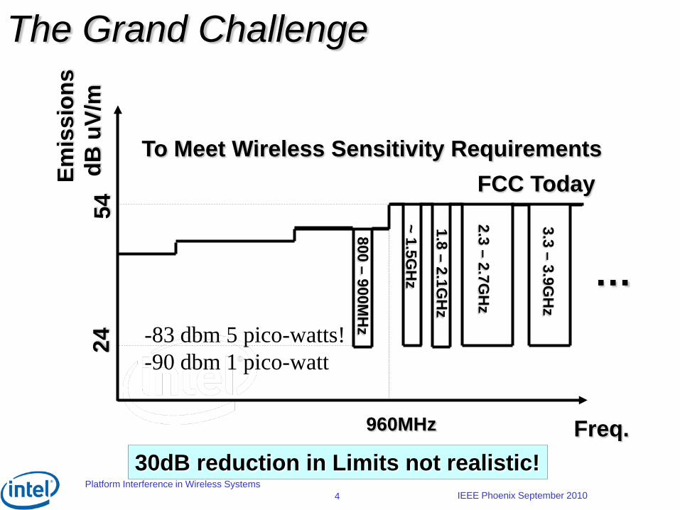
The Grand Challenge
960MHz
Emis
sion
sdB
uV/
m
Freq.
54 2.3 –2.7G
Hz
~ 1.5GH
z
1.8 –2.1G
Hz
800 –900M
Hz
3.3 –3.9G
Hz
…
24
FCC TodayTo Meet Wireless Sensitivity Requirements
30dB reduction in Limits not realistic!
-83 dbm 5 pico-watts!-90 dbm 1 pico-watt

Platform Interference in Wireless SystemsIEEE Phoenix September 20105
Wireless antenna locations
The wireless is embedded in a coupled electromagneticenvironment
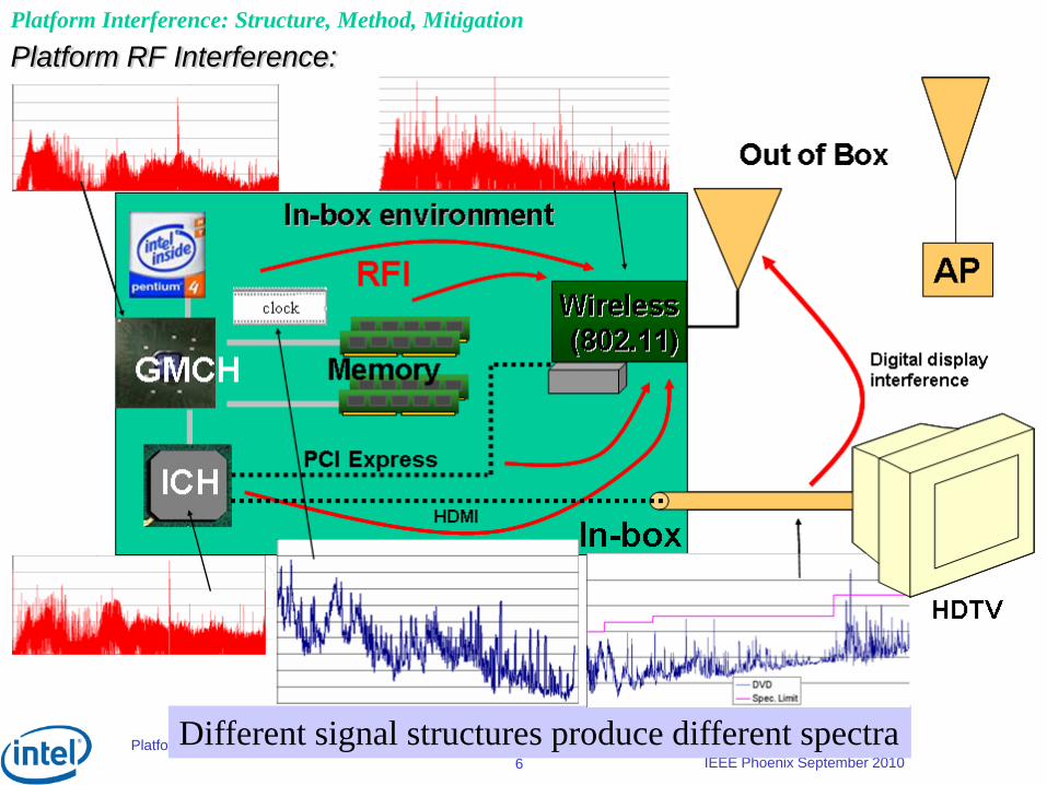
Platform RF Interference:
Platform Interference: Structure, Method, Mitigation
What “solutions”Sometimes look like
Platform Interference in Wireless SystemsIEEE Phoenix September 20106
Platform RF Interference:Platform Interference: Structure, Method, Mitigation
Different signal structures produce different spectra
Platform Interference in Wireless SystemsIEEE Phoenix September 20107
9/23/20107
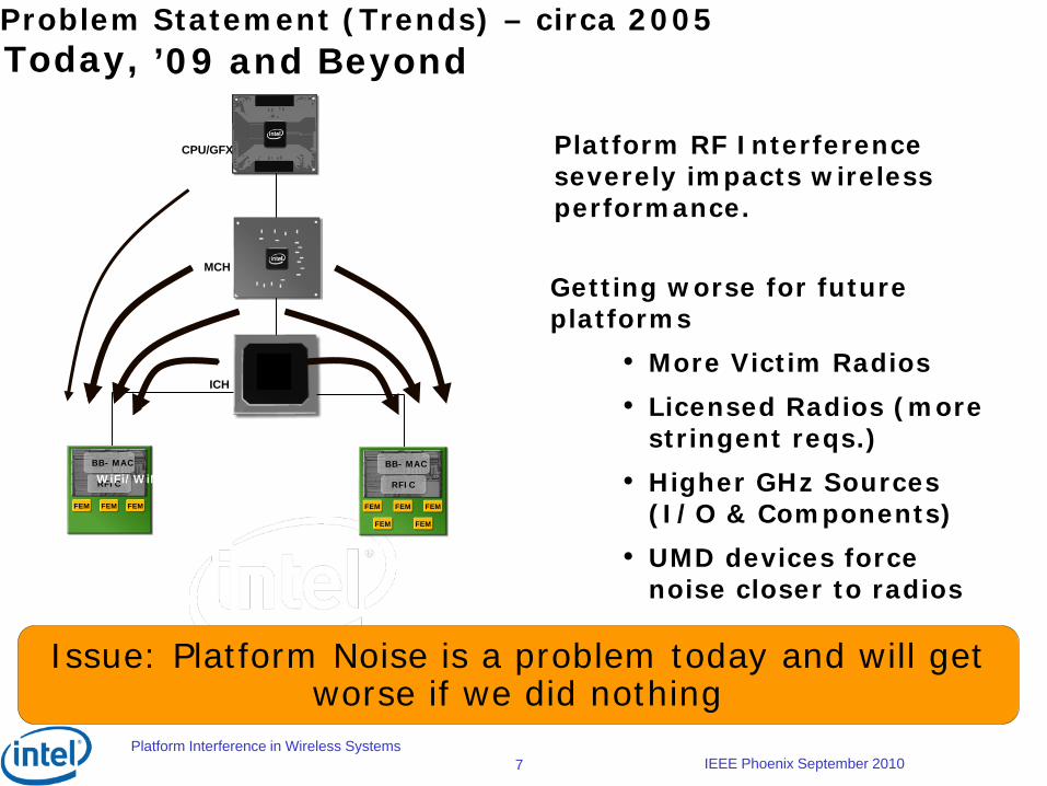
Problem Statement (Trends) – circa 2005
3G/WEDGE
BB- MAC
RFIC
FEM
FEM
FEM FEM
FEM
WiFi
BB- MAC
RFIC
FEM FEM FEM
CPU/GFX
MCH
ICH
WiFi/WiMAX
Platform RF Interference severely impacts wireless performance.
Issue: Platform Noise is a problem today and will get worse if we did nothing
’09 and Beyond
Getting worse for future platforms
• More Victim Radios• Licensed Radios (more
stringent reqs.)• Higher GHz Sources
(I/O & Components)• UMD devices force
noise closer to radios
…
Today,

Platform Interference in Wireless SystemsIEEE Phoenix September 20108
Frequency Spectrum Complexity Growing
RF Interference from Frequency Overlap, Out-of-Band Emissions & Receiver Saturation
Out-of-Band Emissions
Platform Interference in Wireless SystemsIEEE Minneapolis November 20099
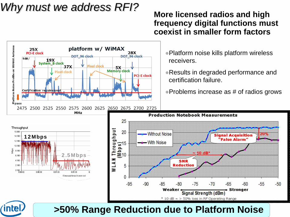
Why must we address RFI?More licensed radios and high frequency digital functions must coexist in smaller form factors
12Mbps
2.5Mbps
12Mbps
Platform noise kills platform wireless receivers.
Results in degraded performance and certification failure.
Problems increase as # of radios grows
9
5x (14dB)
>50% Range Reduction due to Platform Noise

9/23/201010
Problem Statement (Example) - – circa 2005 WWAN/WiMax Carrier Certification - Requirements
-106
-104
-102
-100
-98
-96
-94
-92
Sens
itivi
ty (d
Bm
)
TIS (Novatel)
TIS(Windigo Proto)
2 cell phone TIS Measurements on a platform
Cingular
Vodafone
Low channel
870MHz
Mid channel
880MHz
High channel
890MHzBet
ter Pixel Clock
13th
Harmonic
Carriers Dictate Performance Requirements.
You don’t pass in the intended system – you don’t ship!
Manu 1
Manu 2
Platform Interference in Wireless SystemsIEEE Phoenix January 201011
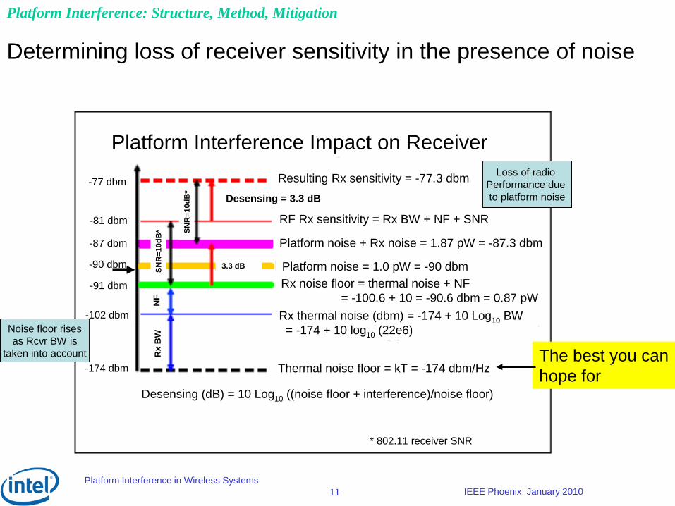
-77 dbm
-81 dbm
-87 dbm
-90 dbm
-91 dbm
-102 dbm
-174 dbm
NF
Rx
BW
SNR
=10d
B*
Desensing = 3.3 dB
3.3 dB
SNR
=10d
B*
Noise floor risesas Rcvr BW is
taken into account
Loss of radio Performance due to platform noise
Desensing (dB) = 10 Log10 ((noise floor + interference)/noise floor)
Platform Interference Impact on Receiver
Thermal noise floor = kT = -174 dbm/Hz
Resulting Rx sensitivity = -77.3 dbm
RF Rx sensitivity = Rx BW + NF + SNR
Platform noise + Rx noise = 1.87 pW = -87.3 dbm
Platform noise = 1.0 pW = -90 dbmRx noise floor = thermal noise + NF
= -100.6 + 10 = -90.6 dbm = 0.87 pWRx thermal noise (dbm) = -174 + 10 Log10 BW= -174 + 10 log10 (22e6) = -90.6 dbm = 0.87 pW
* 802.11 receiver SNR
-77 dbm
-81 dbm
-87 dbm
-90 dbm
-91 dbm
-102 dbm
-174 dbm
NF
Rx
BW
SNR
=10d
B*
Desensing = 3.3 dB
3.3 dB
SNR
=10d
B*
-77 dbm
-81 dbm
-87 dbm
-90 dbm
-91 dbm
-102 dbm
-174 dbm
NF
Rx
BW
SNR
=10d
B*
Desensing = 3.3 dB
3.3 dB
SNR
=10d
B*
Noise floor risesas Rcvr BW is
taken into account
Loss of radio Performance due to platform noise
Desensing (dB) = 10 Log10 ((noise floor + interference)/noise floor)
Platform Interference Impact on Receiver
Thermal noise floor = kT = -174 dbm/Hz
Resulting Rx sensitivity = -77.3 dbm
RF Rx sensitivity = Rx BW + NF + SNR
Platform noise + Rx noise = 1.87 pW = -87.3 dbm
Platform noise = 1.0 pW = -90 dbmRx noise floor = thermal noise + NF
= -100.6 + 10 = -90.6 dbm = 0.87 pWRx thermal noise (dbm) = -174 + 10 Log10 BW= -174 + 10 log10 (22e6) = -90.6 dbm = 0.87 pW
* 802.11 receiver SNR
-77 dbm
-81 dbm
-87 dbm
-90 dbm
-91 dbm
-102 dbm
-174 dbm
NF
Rx
BW
SNR
=10d
B*
Desensing = 3.3 dB
3.3 dB
SNR
=10d
B*
-77 dbm
-81 dbm
-87 dbm
-90 dbm
-91 dbm
-102 dbm
-174 dbm
NF
Rx
BW
SNR
=10d
B*
Desensing = 3.3 dB
3.3 dB
SNR
=10d
B*
Noise floor risesas Rcvr BW is
taken into account
Loss of radio Performance due to platform noise
Desensing (dB) = 10 Log10 ((noise floor + interference)/noise floor)
Platform Interference Impact on Receiver
Thermal noise floor = kT = -174 dbm/Hz
Resulting Rx sensitivity = -77.3 dbm
RF Rx sensitivity = Rx BW + NF + SNR
Platform noise + Rx noise = 1.87 pW = -87.3 dbm
Platform noise = 1.0 pW = -90 dbmRx noise floor = thermal noise + NF
= -100.6 + 10 = -90.6 dbm = 0.87 pWRx thermal noise (dbm) = -174 + 10 Log10 BW= -174 + 10 log10 (22e6) = -90.6 dbm = 0.87 pW
* 802.11 receiver SNR
Determining loss of receiver sensitivity in the presence of noise
The best you canhope for
Platform Interference: Structure, Method, Mitigation

Platform Interference in Wireless SystemsIEEE Phoenix September 201012

Platform Interference in Wireless SystemsIEEE Phoenix September 201013
Radio Type
Center Frequency
Device 1 (dBm)
Device 2 (dBm)
802.11b 2.45GHz -65 -70
802.11g 2.45GHz -65 -70
802.11a(High) 5.8GHz -69 -63
802.11a(Mid) 5.3GHz -77 -76
802.11a(Low) 5.2GHz -67 -78 Bluetooth(2.4GHz) 2.45GHz -65 -70
UWB(3-5GHz) 4GHz -63 -54
GPS(1.575GHz) 1.575GHz -58 -36
GSM(850MHz) 880MHz -43 -41
GSM(900MHz) 942MHz -41 -42
EDGE(1.8GHz) 1842MHz -41 -39
EDGE(1.9GHz) 1960MHz -68 -63
UMTS(1.8GHz) 1842MHz -41 -39
UMTS(1.9GHz) 1960MHz -68 -63
Platform interference levels
Platform Interference in Wireless SystemsIEEE Phoenix September 201014
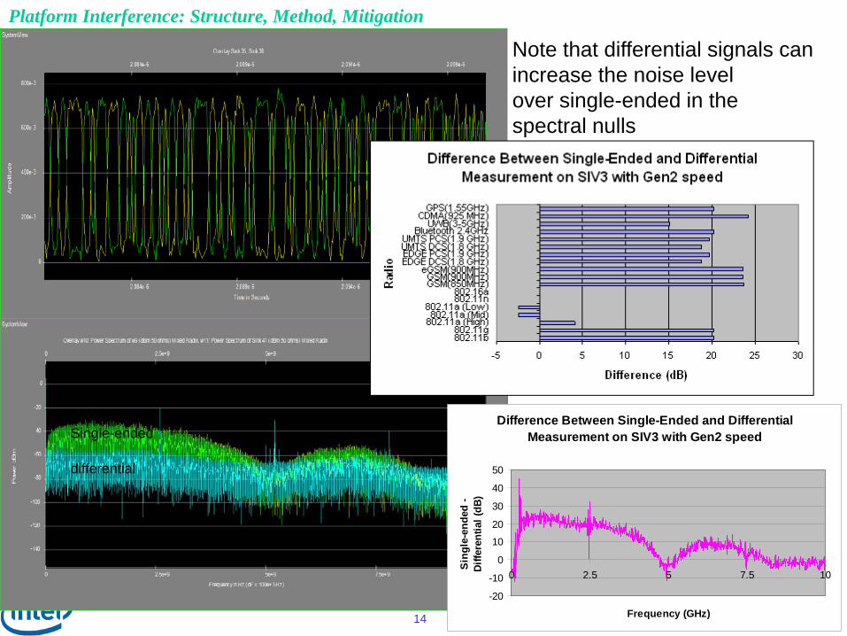
Difference Between Single-Ended and Differential
Measurement on SIV3 with Gen2 speed
-20
-10
0
10
20
30
40
50
0 2.5 5 7.5 10
Frequency (GHz)
Sing
le-e
nded
- Di
ffere
ntia
l (dB
)
PCI Express signalsNote that differential signals canincrease the noise levelover single-ended in thespectral nulls
differential
Single-ended
Platform Interference: Structure, Method, Mitigation

Platform Interference in Wireless SystemsIEEE Phoenix September 201015
Working from theRadio specs we canGenerate a graph ofRequired platformIsolation levels toGuarantee radioperformance

Platform Interference in Wireless SystemsIEEE Phoenix September 201016
Using Best design practices…we still need more!
Interference Level Operating RangeReduction for Constant
Throughput
0dB 0%
3dB 19%
5dB 30%
10dB 50%
20dB 75%

Platform Interference in Wireless SystemsIEEE Phoenix September 201017
Wireless and EMI: Challenges No longer limited to a regulation issue
– Wireless performance will drive EMI requirements Reducing EMI everywhere not realistic
– Lowering limits by 30+dB not an option Wireless proliferation accelerating
– Multiple wireless sub systems on the platform– 7+ wireless antennas on a single platform
Separation / isolation of EMI sources and wireless (antennas and components)
– System form factors trending smaller

Platform Interference in Wireless SystemsIEEE Phoenix September 201018
EMI/EMC strategy for Wireless
Starting point is best possible system EMI design– Focus of today’s workshop– “Platform EMC for wireless”
Selectively reduce emissions where it matters– Only in wireless bands– Only in wireless bands “in use”
Trade off performance between wireless and non-wireless bands– Deliberately “squash” the EMI balloon where needed– Reduce the emissions at frequencies of interest
knowing that emissions at other frequencies may increase
– Must still meet EMI regulations
Platform Interference in Wireless SystemsIEEE Phoenix September 201019
Some preliminaries in spectral analysis
We’ll begin by examining the structure of the signals thatICs generate. Primarily, we will look at clocks, data, and symbolstructures such as those that generate displays. All of thesesignals are present in the ICs, understanding their spectralcontent can give us insight into how they can couple toincidental antennas such as heat sinks, power planes.
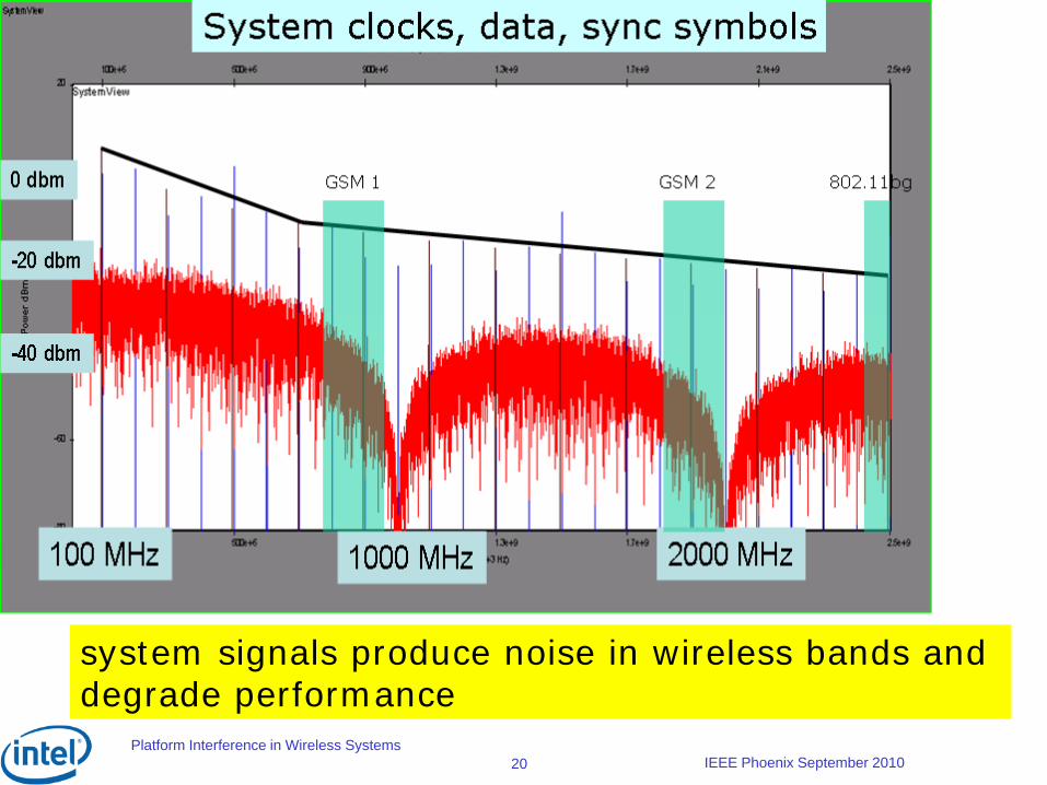
Platform Interference in Wireless SystemsIEEE Phoenix September 201020
system signals produce noise in wireless bands and degrade performance
Platform Interference in Wireless SystemsIEEE Phoenix September 201021
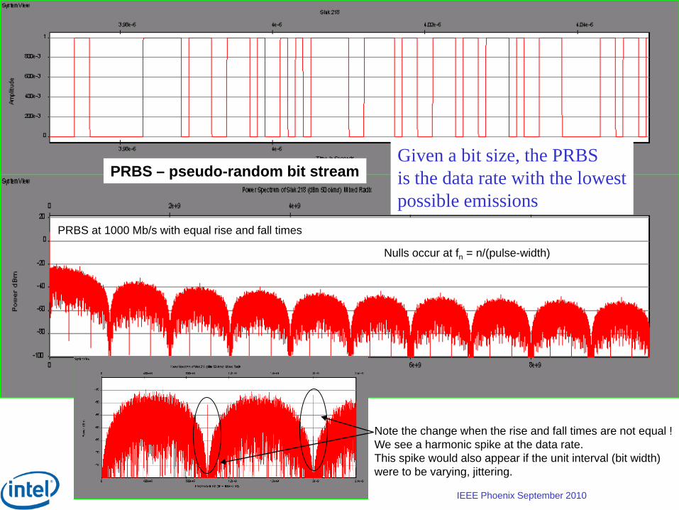
PRBS at 1000 Mb/s with equal rise and fall times
Note the change when the rise and fall times are not equal !We see a harmonic spike at the data rate.This spike would also appear if the unit interval (bit width)were to be varying, jittering.
Nulls occur at fn = n/(pulse-width)
PRBS – pseudo-random bit streamGiven a bit size, the PRBSis the data rate with the lowestpossible emissions
Platform Interference in Wireless SystemsIEEE Phoenix September 201022
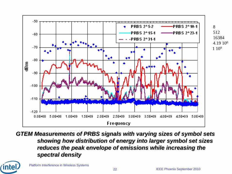
GTEM Measurements of PRBS signals with varying sizes of symbol setsshowing how distribution of energy into larger symbol set sizesreduces the peak envelope of emissions while increasing the spectral density
8512163844.19 106
1 109
Platform Interference in Wireless SystemsIEEE Phoenix September 201023
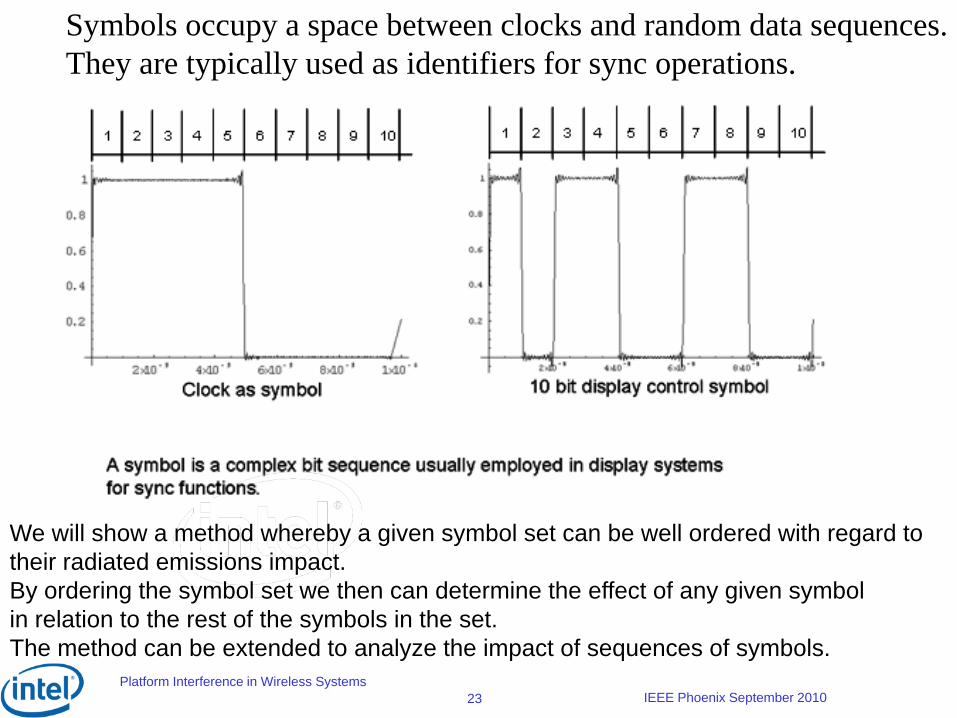
Symbols occupy a space between clocks and random data sequences.They are typically used as identifiers for sync operations.
We will show a method whereby a given symbol set can be well ordered with regard to their radiated emissions impact.By ordering the symbol set we then can determine the effect of any given symbolin relation to the rest of the symbols in the set.The method can be extended to analyze the impact of sequences of symbols.

Platform Interference in Wireless SystemsIEEE Phoenix September 201024
100 MHz 1000 MHz 2000 MHz
0 dbm
-20 dbm
-40 dbm
100 MHz 1000 MHz 2000 MHz
0 dbm
-20 dbm
-40 dbm
clock
PRBS
Display symbol
clock
PRBS
Display symbol
The clock is seen to have no even harmonics and the symbol is seen to have both even and odd harmonics, all at the fundamental clock spacing of 100 MHz. The clock fundamental is seen to have the highest peak of the spectrum set, the PRBS has the lowest peak set and the symbol is seen to have some spectral components that fall above local clock spectral peaks.
Comparing the signal types~30 dB variation!
Platform Interference in Wireless SystemsIEEE Phoenix September 201025
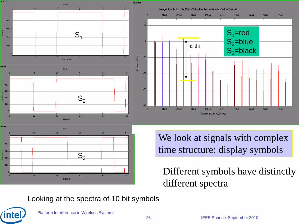
S1
S2
S3
S1=redS2=blueS3=black
Looking at the spectra of 10 bit symbols
We look at signals with complextime structure: display symbols
35 dB
Different symbols have distinctlydifferent spectra
Platform Interference in Wireless SystemsIEEE Phoenix September 201026
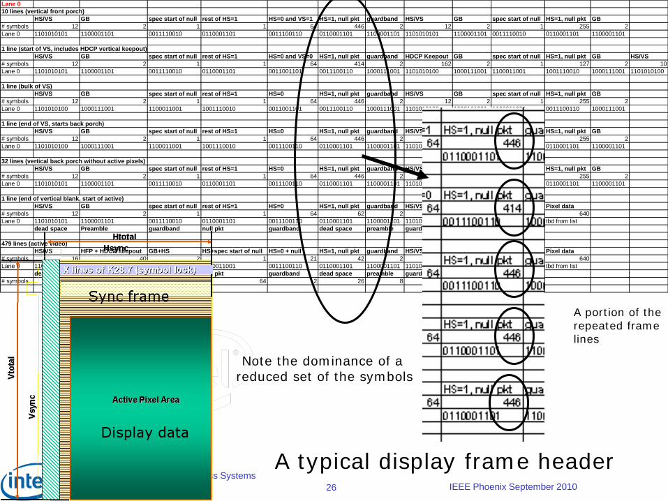
Lane 010 lines (vertical front porch)
HS/VS GB spec start of null rest of HS=1 HS=0 and VS=1 HS=1, null pkt guardband HS/VS GB spec start of null HS=1, null pkt GB# symbols 12 2 1 1 64 446 2 12 2 1 255 2Lane 0 1101010101 1100001101 0011110010 0110001101 0011100110 0110001101 1100001101 1101010101 1100001101 0011110010 0110001101 1100001101
1 line (start of VS, includes HDCP vertical keepout)HS/VS GB spec start of null rest of HS=1 HS=0 and VS=0 HS=1, null pkt guardband HDCP Keepout GB spec start of null HS=1, null pkt GB HS/VS
# symbols 12 2 1 1 64 414 2 162 2 1 127 2 10Lane 0 1101010101 1100001101 0011110010 0110001101 0011001101 0011100110 1000111001 1101010100 1000111001 1100011001 1001110010 1000111001 1101010100
1 line (bulk of VS)HS/VS GB spec start of null rest of HS=1 HS=0 HS=1, null pkt guardband HS/VS GB spec start of null HS=1, null pkt GB
# symbols 12 2 1 1 64 446 2 12 2 1 255 2Lane 0 1101010100 1000111001 1100011001 1001110010 0011001101 0011100110 1000111001 1101010100 1000111001 1100011001 0011100110 1000111001
1 line (end of VS, starts back porch)HS/VS GB spec start of null rest of HS=1 HS=0 HS=1, null pkt guardband HS/VS GB spec start of null HS=1, null pkt GB
# symbols 12 2 1 1 64 446 2 12 2 1 255 2Lane 0 1101010100 1000111001 1100011001 1001110010 0011100110 0110001101 1100001101 1101010101 1100001101 0011110010 0110001101 1100001101
32 lines (vertical back porch without active pixels)HS/VS GB spec start of null rest of HS=1 HS=0 HS=1, null pkt guardband HS/VS GB spec start of null HS=1, null pkt GB
# symbols 12 2 1 1 64 446 2 12 2 1 255 2Lane 0 1101010101 1100001101 0011110010 0110001101 0011100110 0110001101 1100001101 1101010101 1100001101 0011110010 0110001101 1100001101
1 line (end of vertical blank, start of active)HS/VS GB spec start of null rest of HS=1 HS=0 HS=1, null pkt guardband HS/VS preamble GB Pixel data
# symbols 12 2 1 1 64 62 2 6 8 2 640Lane 0 1101010101 1100001101 0011110010 0110001101 0011100110 0110001101 1100001101 1101010101 0010101011 0011001101 tbd from list
dead space Preamble guardband null pkt guardband dead space preamble guardband pixel data
479 lines (active video)HS/VS HFP + HDCP keepout GB+HS HS+spec start of null HS=0 + null HS=1, null pkt guardband HS/VS preamble GB Pixel data
# symbols 16 40 2 1 21 42 2 26 8 2 640Lane 0 1101010101 0010101010 1100011010 1100011001 0011100110 0110001101 1100001101 1101010101 0010101011 0011001101 tbd from list
dead space Preamble guardband null pkt guardband dead space preamble guardband Pixel data# symbols 48 8 2 64 2 26 8 2 640
A typical display frame header
Note the dominance of a reduced set of the symbols
A portion of therepeated framelines

Platform Interference in Wireless SystemsIEEE Phoenix September 201027
A review of display frames:
Single symbol display frames: s4 from the list belowMulti-symbol display frames: s1, s4, s5 used for 3 symbol frame
symbol list of frame (red are dominant):s1: 1101010101s2: 1100001101s3: 0011110010s4: 0110001101s5: 0011100110s6: 0011001101s7: 1000111001s8: 1101010100s9: 1100011001s10: 1001110010
PRBS: pseudo-random bit streams; similar to pixel data)
These 10 symbols comprise the symbol set for a specificdisplay frame format.3 symbols in this frame dominate the symbol distribution.
occurrence
0
5000
10000
15000
20000
25000
30000
35000
sym
bol1
sym
bol2
sym
bol3
sym
bol4
sym
bol5
sym
bol6
sym
bol7
sym
bol8
sym
bol9
sym
bol1
0
the single symbolcontains 84% of the energy3 symbols make up 97% of the energy

Platform Interference in Wireless SystemsIEEE Phoenix September 201028
Analysis of Display Frame Symbols
An example of the Fourier series components for a given symbol:0.0944420.0274379,0.0789340.050093,0.05668260.0642938,0.03213940.0682996,0.009918020.0626199,0.006286320.0497614,0.01449290.0334912, 0.01475110.0178311,0.00891940.00606162,2.9792210162.520881016,0.008760860.000275321,0.01474650.00378625,0.01658050.00980565,0.01432970.0152596,0.009281350.0182157,0.003397960.0178127,0.001358760.0143741,0.003625710.0091575,0.002987930.00385202,7.4480410177.611731017This can be viewed as a vector in Cn space where n is the number of harmoniccomponents.The inner product is then:
etcjvjvwhere
vvvvvvvvvvvv nnn
)050.0789.( ),02743.094442.(
)...,,()...,,()...,,(
21
321321321
−−=−−=
•=
The inner product is chosen because it is conceptually easy to appreciate, andit is an invariant “length” of any given vector. It is also a real number and thereforethe set of inner products for the set of symbols can then be ordered.

Platform Interference in Wireless SystemsIEEE Phoenix September 201029
D3 D2 D1 D0 q_out[9:0]
0 0 0 0 0b10 1001 1100
0 0 0 1 0b10 0110 0011
0 0 1 0 0b10 1110 0100
0 0 1 1 0b10 1110 0010
0 1 0 0 0b01 0111 0001
0 1 0 1 0b01 0001 1110
0 1 1 0 0b01 1000 1110
0 1 1 1 0b01 0011 1100
1 0 0 0 0b10 1100 1100
1 0 0 1 0b01 0011 1001
1 0 1 0 0b011001 1100
1 0 1 1 0b10 1100 0110
1 1 0 0 0b10 1000 1110
1 1 0 1 0b10 0111 0001
1 1 1 0 0b01 0110 0011
1 1 1 1 0b10 1100 0011
Symbol inner-product
comparing the spectral impactOf display symbols
symbolclock 0.496t1011100010 0.49t0110001110 0.418t1001110001 0.418t1011001100 0.383t1001100011 0.376t0110011100 0.376t0100111001 0.347t1011000110 0.347t0101110001 0.307t1010001110 0.30780percent 0.303t1011100100 0.269t0100111100 0.24t1011000011 0.24t100011110 0.237t1010011100 0.225t0101100011 0.225single bit 0.2
The clock shows up asThe worst symbol
Performing the analysis on the symbol setand ordering the set according to the IP
Very pretty…but how does it agree with real measurements of the symbols?A little later on, we will show measurements of symbol impact on wirelessperformance

Platform Interference in Wireless SystemsIEEE Phoenix September 201030
symbolD
0
0.05
0.1
0.15
0.2
0.25
0.3
t1011
1000
10
t1011
0011
00
t0101
1100
01
t1010
0011
10
t0100
1110
01
t1011
0001
10
t0100
1111
00
t1011
0000
11
clock
t0110
0011
10
t1001
1100
01
t1001
1000
11
t0110
0111
00
80pe
rcen
t
t1000
1111
0
single
bit
t1011
1001
00
t1010
0111
00
t0101
1000
11
D3 D2 D1 D0 q_out[9:0]
0 0 0 0 0b10 1001 1100
0 0 0 1 0b10 0110 0011
0 0 1 0 0b10 1110 0100
0 0 1 1 0b10 1110 0010
0 1 0 0 0b01 0111 0001
0 1 0 1 0b01 0001 1110
0 1 1 0 0b01 1000 1110
0 1 1 1 0b01 0011 1100
1 0 0 0 0b10 1100 1100
1 0 0 1 0b01 0011 1001
1 0 1 0 0b011001 1100
1 0 1 1 0b10 1100 0110
1 1 0 0 0b10 1000 1110
1 1 0 1 0b10 0111 0001
1 1 1 0 0b01 0110 0011
1 1 1 1 0b10 1100 0011
Symbol inner-product
comparing the spectral impactof differentiated display symbolssymbols Can we avoid symbols
In this range?
Normalized comparison
symbolDt1011100010 0.273t1011001100 0.195t0101110001 0.194t1010001110 0.194t0100111001 0.189t1011000110 0.189t0100111100 0.159t1011000011 0.159clock 0.158t0110001110 0.155t1001110001 0.155t1001100011 0.118t0110011100 0.11880percent 0.113t100011110 0.109single bit 0.109t1011100100 0.037t1010011100 0.013t0101100011 0.013
symbolD dB margin gaint1011100010 0.273 0t1011001100 0.195 2.922560714t0101110001 0.194 2.967218342t1010001110 0.194 2.967218342t0100111001 0.189 3.194016857t1011000110 0.189 3.194016857t0100111100 0.159 4.695310454t1011000011 0.159 4.695310454clock 0.158 4.750111202t0110001110 0.155 4.916618977t1001110001 0.155 4.916618977t1001100011 0.118 7.285612795t0110011100 0.118 7.28561279580percent 0.113 7.661684071t100011110 0.109 7.974722982single bit 0.109 7.974722982t1011100100 0.037 17.35921846t1010011100 0.013 26.44438589t0101100011 0.013 26.44438589
Patent pending
Platform Interference in Wireless SystemsIEEE Phoenix September 201031
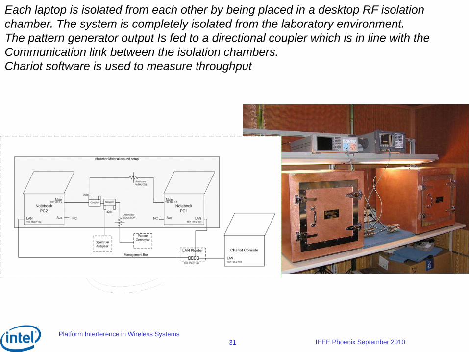
Each laptop is isolated from each other by being placed in a desktop RF isolation chamber. The system is completely isolated from the laboratory environment. The pattern generator output Is fed to a directional coupler which is in line with the Communication link between the isolation chambers. Chariot software is used to measure throughput
Platform Interference in Wireless SystemsIEEE Phoenix September 201032
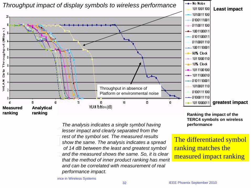
Throughput impact of display symbols to wireless performance Least impact
greatest impact
Least impact
greatest impact
Ranking the impact of the TERC4 symbols on wireless performance
Throughput in absence ofPlatform or environmental noise
Analyticalranking
Measuredranking
Analyticalranking
Measuredranking
The analysis indicates a single symbol havinglesser impact and clearly separated from the rest of the symbol set. The measured results show the same. The analysis indicates a spreadof 14 dB between the least and greatest symbol and the measured shows the same. So, it is clear that the method of inner product ranking has merit and can be correlated with measurement of real performance impact.
The differentiated symbolranking matches themeasured impact ranking

Platform Interference in Wireless SystemsIEEE Phoenix September 201033
20 40 60 80 100
-100
-80
-60
-40
-20
210-9 410-9 610-9 810-9 110-8
-1
-0.5
0.5
1
210-9 410-9 610-9 810-9 110-8
-0.3
-0.2
-0.1
0.1
0.2
0.3
Derivative of the differential clock
20 40 60 80 100
-100
-80
-60
-40
-20
harmonics
dbm Even with as little as 10 pS of skew, there remains a significant signal to contribute to radiation
With 10 pS of skew between Tx+ and Tx-
With 100 pS of skewshowing ~ 18 dB increaseIn the emissions spectrum
Analysis for differential Signals
Platform Interference in Wireless SystemsIEEE Phoenix September 201034
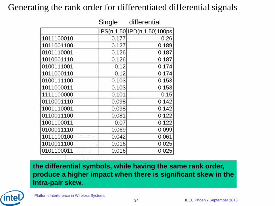
IPS(n,1,50)IPD(n,1,50)100ps1011100010 0.177 0.261011001100 0.127 0.1890101110001 0.126 0.1871010001110 0.126 0.1870100111001 0.12 0.1741011000110 0.12 0.1740100111100 0.103 0.1531011000011 0.103 0.1531111100000 0.101 0.150110001110 0.098 0.1421001110001 0.098 0.1420110011100 0.081 0.1221001100011 0.07 0.1220100011110 0.069 0.0991011100100 0.042 0.0611010011100 0.016 0.0250101100011 0.016 0.025
Single differential
the differential symbols, while having the same rank order, produce a higher impact when there is significant skew in theIntra-pair skew.
Generating the rank order for differentiated differential signals
Platform Interference in Wireless SystemsIEEE Phoenix September 201035
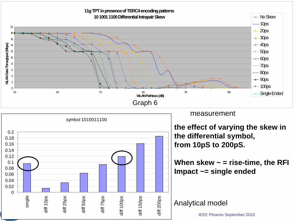
11g TPT in presence of TERC4 encoding patterns10 1001 1100 Differential Intrapair Skew
0
2
4
6
8
10
12
14
16
18
20
50 60 70 80 90 100 110WLAN Pathloss (dB)
WLA
N Da
ta Th
roug
hput
(Mbp
s)
No Skew10ps20ps30ps40ps50ps60ps70ps80ps90ps100psSingle-Ended
Graph 6
the effect of varying the skew in the differential symbol, from 10pS to 200pS.
When skew ~ = rise-time, the RFI Impact ~= single ended
Analytical model
measurementsymbol 1010011100
00.020.040.060.08
0.10.120.140.160.18
0.2
sing
le
diff
10ps
diff
25ps
diff
50ps
diff
75ps
diff
100p
s
diff
150p
s
diff
200p
s

Platform Interference in Wireless SystemsIEEE Phoenix September 201036
Mitigation

Platform Interference in Wireless SystemsIEEE Phoenix September 201037
Reverb chamber 0.8-18 GHzIntel’s near field scanner

Platform Interference in Wireless SystemsIEEE Phoenix September 201038
Managing thespectrum of theplatform
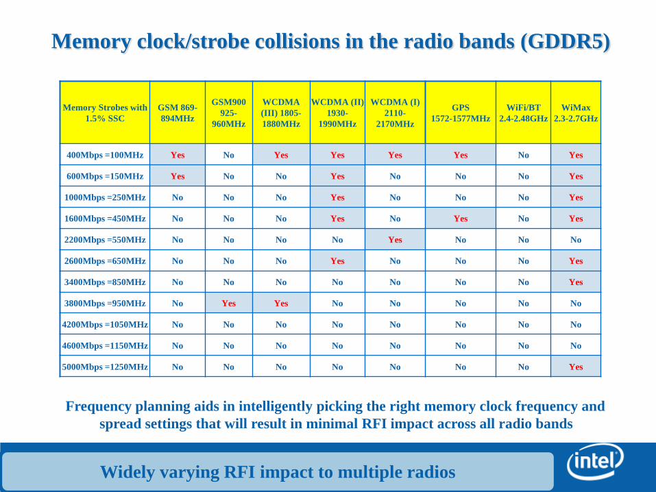
Memory clock/strobe collisions in the radio bands (GDDR5)
Widely varying RFI impact to multiple radios
Memory Strobes with 1.5% SSC
GSM 869-894MHz
GSM900 925-
960MHz
WCDMA (III) 1805-1880MHz
WCDMA (II) 1930-
1990MHz
WCDMA (I) 2110-
2170MHz
GPS 1572-1577MHz
WiFi/BT 2.4-2.48GHz
WiMax 2.3-2.7GHz
400Mbps =100MHz Yes No Yes Yes Yes Yes No Yes
600Mbps =150MHz Yes No No Yes No No No Yes
1000Mbps =250MHz No No No Yes No No No Yes
1600Mbps =450MHz No No No Yes No Yes No Yes
2200Mbps =550MHz No No No No Yes No No No
2600Mbps =650MHz No No No Yes No No No Yes
3400Mbps =850MHz No No No No No No No Yes
3800Mbps =950MHz No Yes Yes No No No No No
4200Mbps =1050MHz No No No No No No No No
4600Mbps =1150MHz No No No No No No No No
5000Mbps =1250MHz No No No No No No No Yes
Frequency planning aids in intelligently picking the right memory clock frequency and spread settings that will result in minimal RFI impact across all radio bands
Platform Interference in Wireless SystemsIEEE Phoenix September 201040
Static Frequency PlanningPros & Cons
Relatively Simple– No additional components and/or materials– Good if you own the complete ‘stack’ (hardware/software/product)
If Harmonics are separated by less than the span of the wireless band, one peak is traded for another– Trading an even for odd harmonic still might be OK– Difficult to remove harmonics entirely
Gets tougher to make it work with more than 1 radio and/or wireless specs with multiple bands– GSM/WCDMA– Simultaneous usage models are emerging
Some system frequencies cannot be changed
One tool but by no means a silver bullet
Platform Interference in Wireless SystemsIEEE Phoenix September 201041
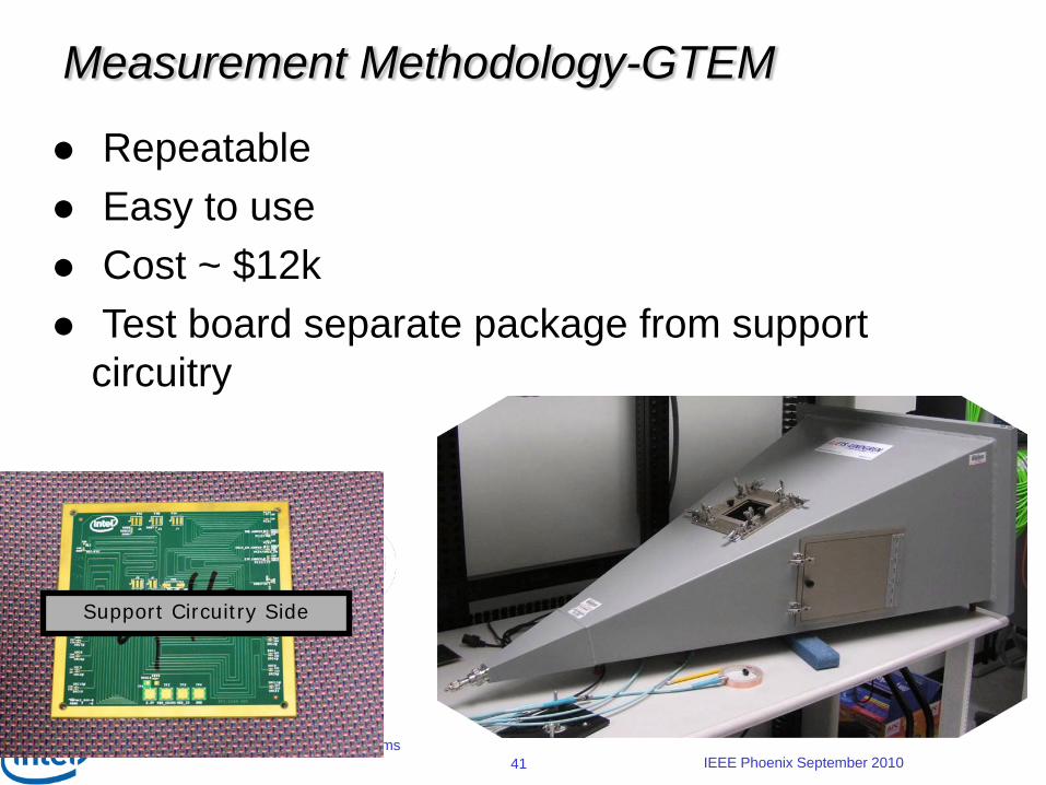
Measurement Methodology-GTEM
Repeatable Easy to use Cost ~ $12k Test board separate package from support
circuitry
Support Circuitry Side
Platform Interference in Wireless SystemsIEEE Phoenix September 201042
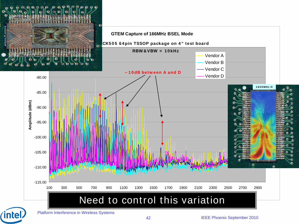
GTEM Capture of 166MHz BSEL Mode
-115.00
-110.00
-105.00
-100.00
-95.00
-90.00
-85.00
-80.00
-75.00
-70.00
100 300 500 700 900 1100 1300 1500 1700 1900 2100 2300 2500 2700 2900
Frequency (MHz)
Ampl
itude
(dBm
)
Vendor AVendor BVendor CVendor D
~10dB between A and D
~5dB
Need to control this variation
CK505 64pin TSSOP package on 4” test board
RBW&VBW = 10kHz
1600MHz H1600MHz H

Platform Interference in Wireless SystemsIEEE Phoenix September 201043
1 GHz
3 GHz
System clock device
Near Field Scans over die
GHzE yxf 1),(
GHzE yxf 3),(
measured
measured),(
...............
...
...
21
22221
11211
yxf
mmm
mmmmmm
nnnn
n
n
→
DiscreteMeasurementMatrix, step size = 50 um
Interpolated surfacesFrom discrete measurements
1.8mm by 1.8 mm

Platform Interference in Wireless SystemsIEEE Phoenix September 201044
Platform Interference in Wireless SystemsIEEE Phoenix September 201045
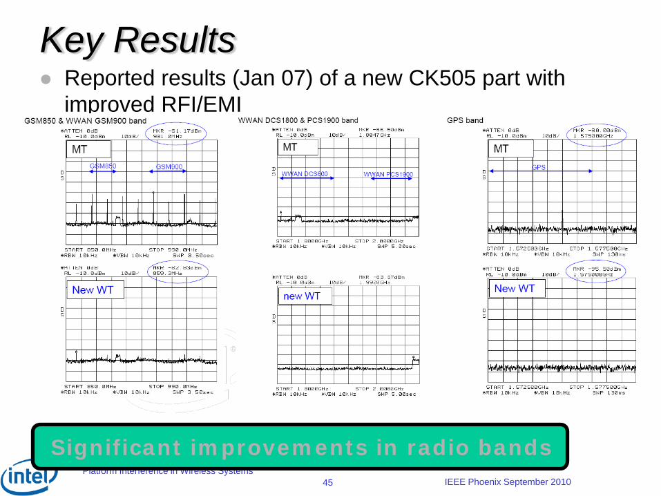
Key Results Reported results (Jan 07) of a new CK505 part with
improved RFI/EMI
Significant improvements in radio bands
Platform Interference in Wireless SystemsIEEE Phoenix September 201046
Clock Supplier– Quick-turn analysis of the clock chip early in
development phase– Better product solutions for OEM/ODM
OEM– Minimizes need for expensive after-the-fact shielding
solutions– Eases implementation of multi-radio mobile platforms – Elimination of RFI at the source removes roadblocks
to future innovative form factors
Impact of Results

Platform Interference in Wireless SystemsIEEE Phoenix September 201047
1cm 2cm 3cm 4cm 5cm 10cm 15cm 20cm20cm 15cm 10cm 5cm 4cm 3cm 2cm 1cm
2.4-2.5GHz WLAN925-960MHz CDMA
Protocol Frequency(MHz)
Receiver Sensitivity
(dBm)
802.11b/g 2400 -105.8
802.11a 5000 -106.6
UWB 3000-5000 -90.8
GPS 1550 -117.8
GPRS 850-900 -124.3
EDGE 1800-1980 -123.8
WCDMA 1800-1980 -108.3
CDMA 925 -115.8
WiMax2300 & 2500 -117.7
Isotropic Radiator1. Scaling GTEM result for distance
2. Avg value of 4 vendor data (not min or max)
We can use the measurementsTo set up keep out zones

Platform Interference in Wireless SystemsIEEE Minneapolis November 200948
0
5
10
15
20
25
30
35
4041
.6
122
202
282
362
442
522
602
682
762
842
922
1002
1082
1162
1242
device 9
device 2
device 3
device 1
device 5
device 6
device 7
device 8
device 4
MHz
dBuV
The measured GTEM emissions of 9 Pentium system clock devices.
These spectra come from older devices and so have no spectral contentabove 1300 MHz. Newer devices have significant energy above 3 GHz.
Devices are all functionallyequivalent. No variation inemissions is due to softwaredifferences, or to lead framegeometry. Therefore, allfield variations are dueentirely to the silicon.
Platform Interference: Structure, Method, Mitigation

Platform Interference in Wireless SystemsIEEE Minneapolis November 200949
Near Field Scans of Clock IC
Platform Interference: Structure, Method, Mitigation
Platform Interference in Wireless SystemsIEEE Minneapolis November 200950
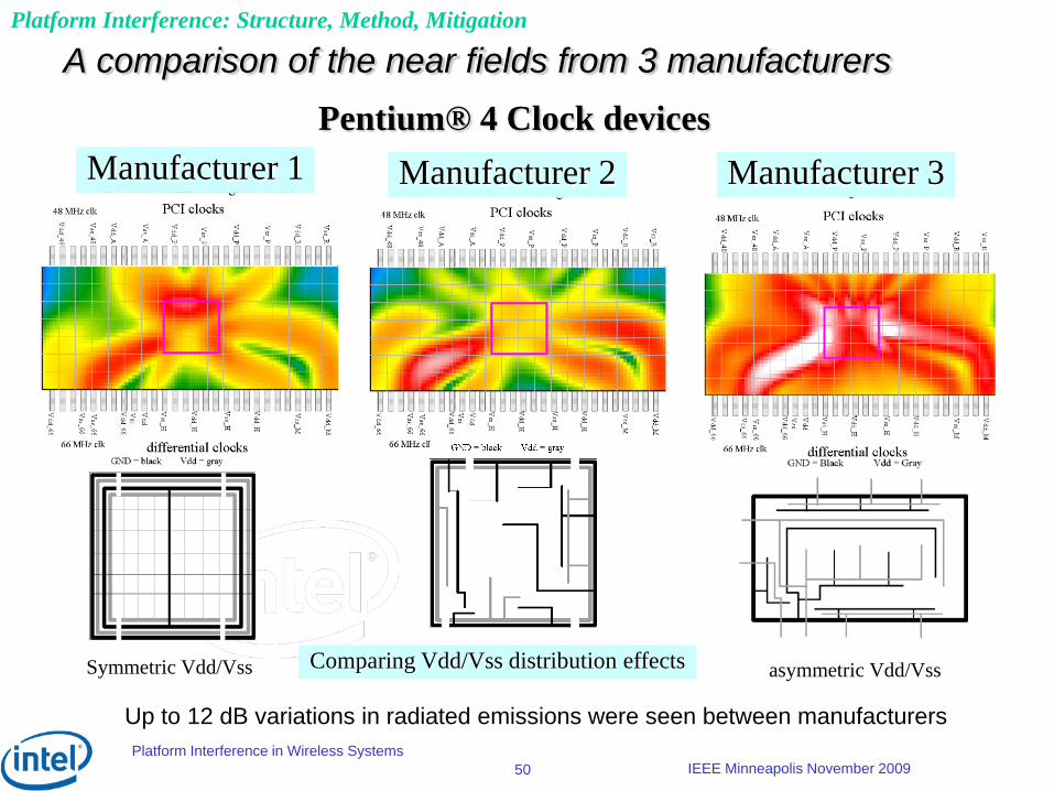
A comparison of the near fields from 3 manufacturers
Manufacturer 1 Manufacturer 2 Manufacturer 3Pentium® 4 Clock devices
Comparing Vdd/Vss distribution effects
Up to 12 dB variations in radiated emissions were seen between manufacturers
Platform Interference: Structure, Method, Mitigation
Symmetric Vdd/Vss asymmetric Vdd/Vss
Platform Interference in Wireless SystemsIEEE Phoenix September 201051
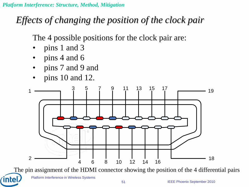
Effects of changing the position of the clock pair
1
24 6 8 10 12 14 16
18
193 5 7 9 11 13 15 17
The pin assignment of the HDMI connector showing the position of the 4 differential pairs
The 4 possible positions for the clock pair are:• pins 1 and 3• pins 4 and 6• pins 7 and 9 and• pins 10 and 12.
Platform Interference: Structure, Method, Mitigation
Platform Interference in Wireless SystemsIEEE Phoenix September 201052
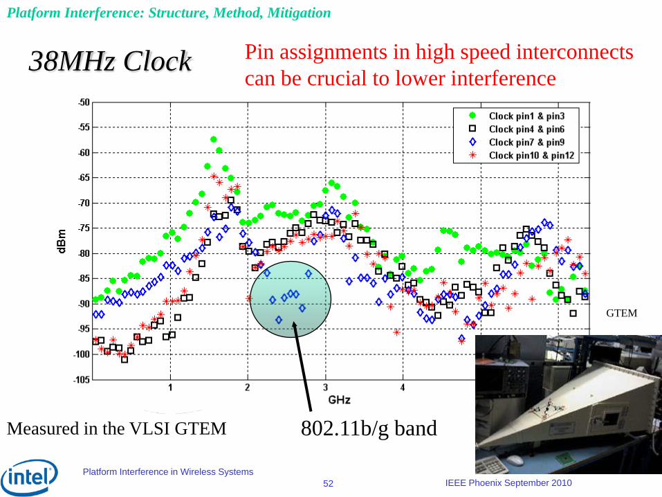
38MHz Clock
Platform Interference: Structure, Method, Mitigation
802.11b/g band
Pin assignments in high speed interconnectscan be crucial to lower interference
Measured in the VLSI GTEM
GTEM
Platform Interference in Wireless SystemsIEEE Phoenix September 201053
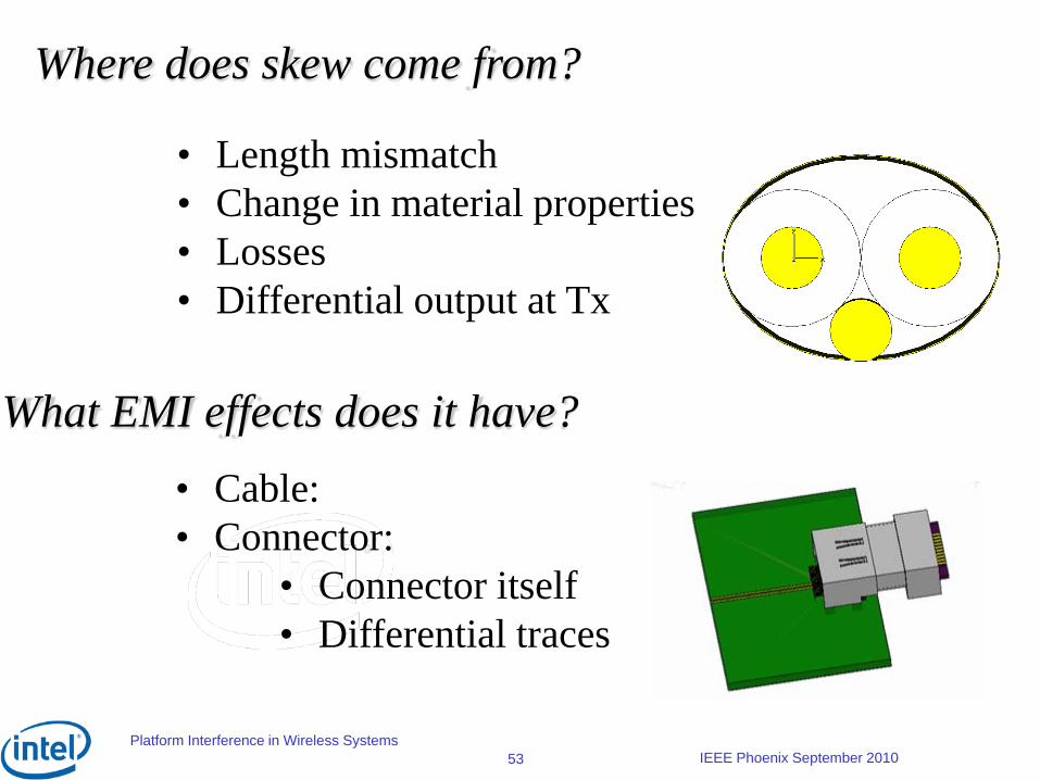
Where does skew come from?
• Length mismatch• Change in material properties• Losses• Differential output at Tx
What EMI effects does it have?• Cable:• Connector:
• Connector itself• Differential traces

Platform Interference in Wireless SystemsIEEE Phoenix September 201054
;
;
dielectricr
r
cc
wherec speed of lightrelative permitivity
ε
ε
=
==
Plot of the EMI as a function of % change in of the insulation material for the last 50cm of a 3m cable
The skew is for % change of εrover the length of 3m
rε
Er % change Skew(ps)2.080 0.00 0.0
2.085 0.25 18.0
2.090 0.50 36.0
2.096 0.75 54.0
2.101 1.00 71.9
2.106 1.25 89.9
2.111 1.50 107.8
2.116 1.75 125.6
2.122 2.00 143.5
Effects of change in εr on cable EMI
Platform Interference in Wireless SystemsIEEE Phoenix September 201055
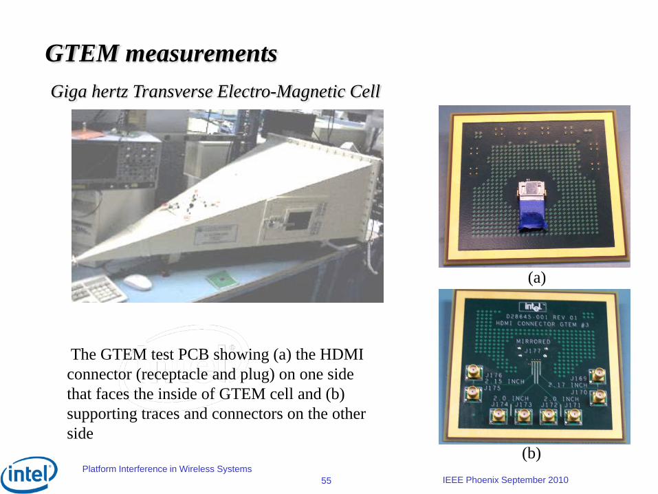
GTEM measurementsGiga hertz Transverse Electro-Magnetic Cell
The GTEM test PCB showing (a) the HDMI connector (receptacle and plug) on one side that faces the inside of GTEM cell and (b) supporting traces and connectors on the other side
(a)
(b)
Platform Interference in Wireless SystemsIEEE Phoenix September 201056
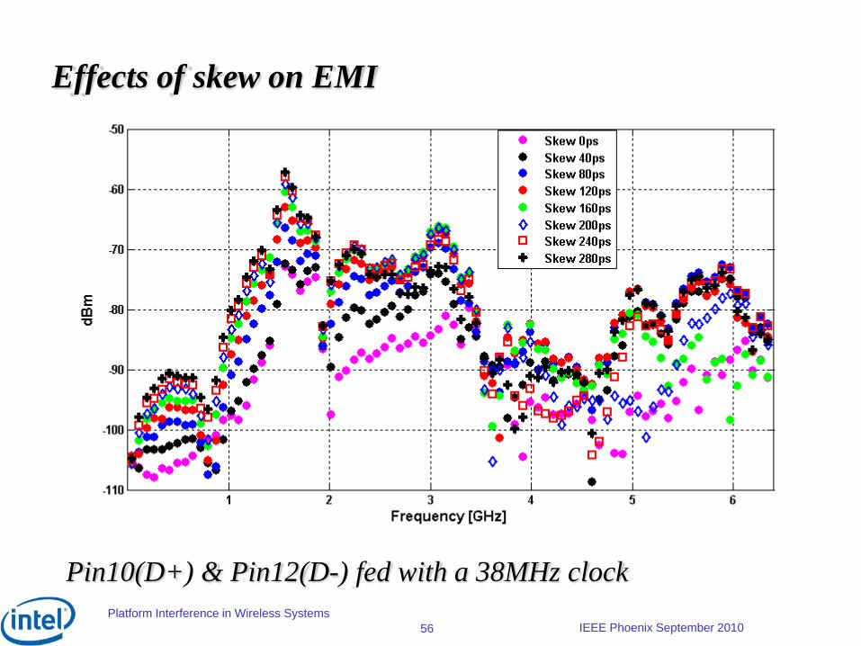
Effects of skew on EMI
Pin10(D+) & Pin12(D-) fed with a 38MHz clock

Platform Interference in Wireless SystemsIEEE Phoenix September 201057
3 meter cablesOff the shelf
Skew is now becoming part of cable specifications

Platform Interference in Wireless SystemsIEEE Phoenix September 201058
Platform Interference: Structure, Method, Mitigation
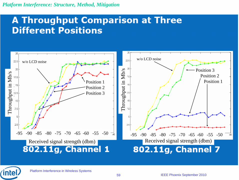
Platform Interference in Wireless SystemsIEEE Phoenix September 201059
Platform Interference: Structure, Method, Mitigation
Received signal strength (dbm)-95 -90 -85 -80 -75 -70 -65 -60 -55 -50
Received signal strength (dbm)-95 -90 -85 -80 -75 -70 -65 -60 -55 -50
Thro
ughp
ut in
Mb/
s
Thro
ughp
ut in
Mb/
s
w/o LCD noise
Position 1Position 2Position 3
Position 3Position 2
Position 1
w/o LCD noise
Platform Interference in Wireless SystemsIEEE Phoenix September 201060
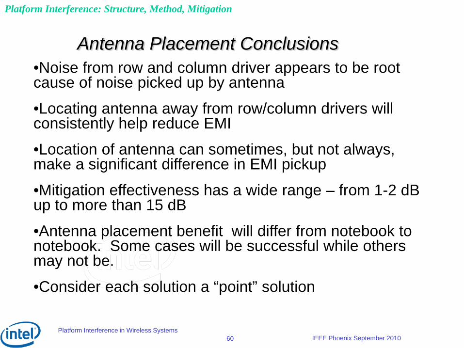
Antenna Placement Conclusions•Noise from row and column driver appears to be root cause of noise picked up by antenna
•Locating antenna away from row/column drivers will consistently help reduce EMI
•Location of antenna can sometimes, but not always, make a significant difference in EMI pickup
•Mitigation effectiveness has a wide range – from 1-2 dB up to more than 15 dB
•Antenna placement benefit will differ from notebook to notebook. Some cases will be successful while others may not be.
•Consider each solution a “point” solution
Platform Interference: Structure, Method, Mitigation
Platform Interference in Wireless SystemsIEEE Phoenix September 201061
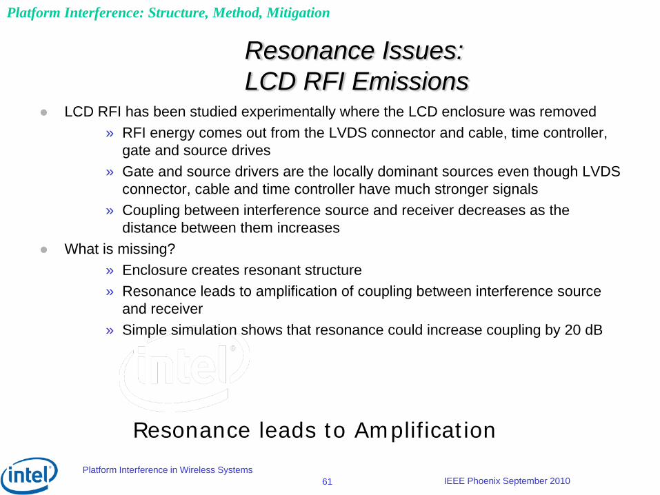
Resonance Issues:LCD RFI Emissions
LCD RFI has been studied experimentally where the LCD enclosure was removed» RFI energy comes out from the LVDS connector and cable, time controller,
gate and source drives» Gate and source drivers are the locally dominant sources even though LVDS
connector, cable and time controller have much stronger signals » Coupling between interference source and receiver decreases as the
distance between them increases What is missing?
» Enclosure creates resonant structure» Resonance leads to amplification of coupling between interference source
and receiver» Simple simulation shows that resonance could increase coupling by 20 dB
Resonance leads to Amplification
Platform Interference: Structure, Method, Mitigation
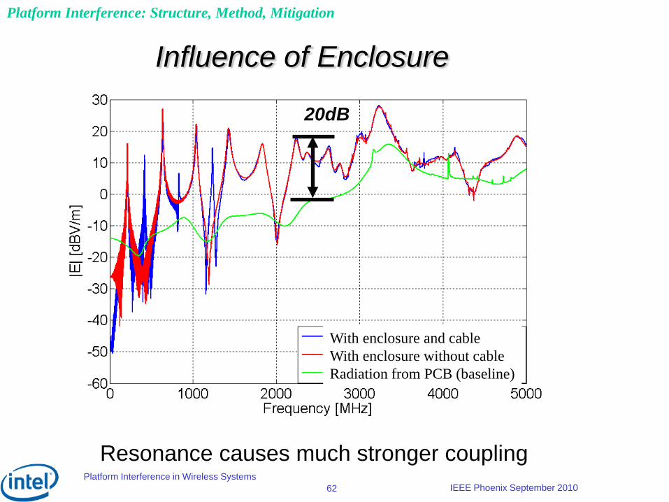
Platform Interference in Wireless SystemsIEEE Phoenix September 201062
Influence of Enclosure
Resonance causes much stronger coupling
20dB
Platform Interference: Structure, Method, Mitigation
With enclosure and cableWith enclosure without cableRadiation from PCB (baseline)
Platform Interference in Wireless SystemsIEEE Phoenix September 201063
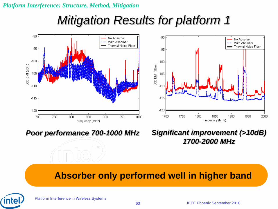
Mitigation Results for platform 1
Poor performance 700-1000 MHz
Absorber only performed well in higher band
Significant improvement (>10dB) 1700-2000 MHz
Platform Interference: Structure, Method, Mitigation
Platform Interference in Wireless SystemsIEEE Phoenix September 201064
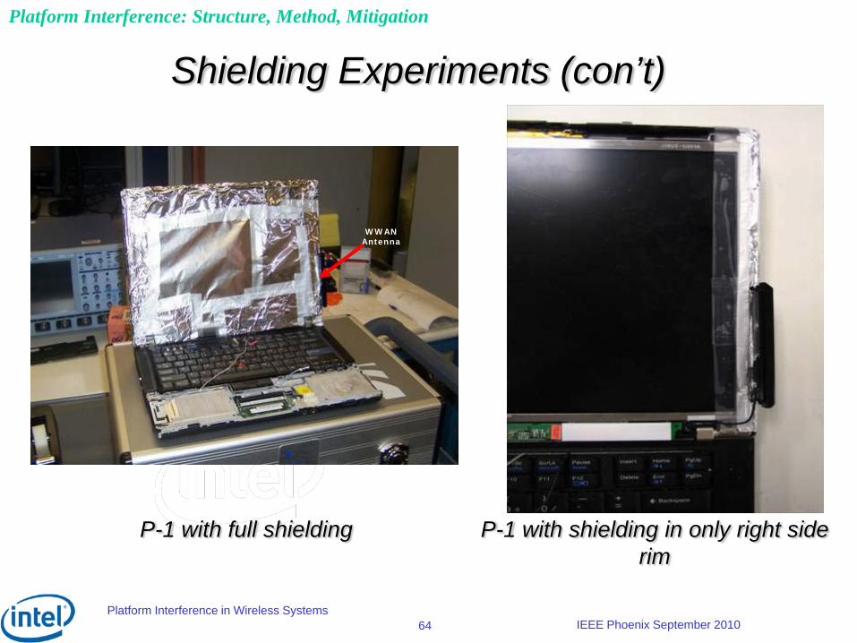
Shielding Experiments (con’t)
P-1 with shielding in only right side rim
P-1 with full shielding
WWAN Antenna
Platform Interference: Structure, Method, Mitigation

Platform Interference in Wireless SystemsIEEE Phoenix September 201065
Shielding Experiment Results
Shielding right side provides ~ 5-10dB mitigation. Concern: compromise of antenna performance (bandwidth and pattern) may
occur unless separation is increased
IBM Z60t Results with Different Shielding Configurations
-120.00
-115.00
-110.00
-105.00
-100.00
-95.00
-90.00
-85.00
-80.00
700.00 750.00 800.00 850.00 900.00 950.00 1000.00
Frequency (MHz)
Pla
tform
Noi
se (d
Bm
/100
kHz)
No shield (dBm) Shield 100% (dBm) Shielding Right Side of the Rim
RX: GSM 850MHz GSM 900MHz
System Noise Floor
~5dB ~10dB
Platform Interference: Structure, Method, Mitigation

Platform Interference in Wireless SystemsIEEE Phoenix September 201066
First resonant mode: m=1, n=0, Freq = 2.46 GHz
Analytical solution for power plane resonancesusing Mathematica (source: IEEE EMC Transactions, August 2003
Higher order mode: m=2, n=1, Freq = 5.15 GHz
mPCIe cardPlatform Interference: Structure, Method, Mitigation
Platform Interference in Wireless SystemsIEEE Phoenix September 201067
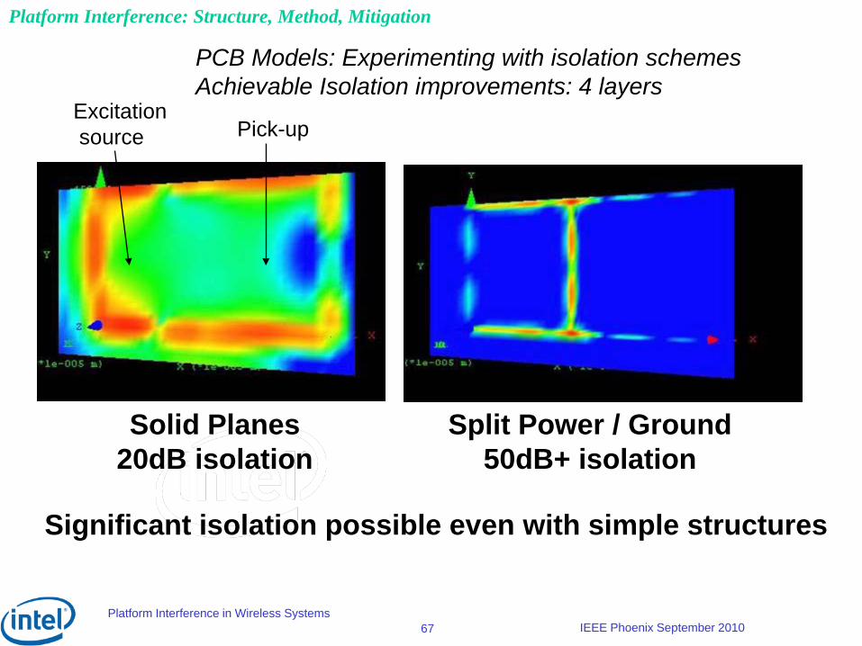
PCB Models: Experimenting with isolation schemesAchievable Isolation improvements: 4 layers
Solid Planes20dB isolation
Split Power / Ground50dB+ isolation
Significant isolation possible even with simple structures
Excitationsource Pick-up
Platform Interference: Structure, Method, Mitigation

Platform Interference in Wireless SystemsIEEE Phoenix September 201068
Simulation Study Progress Report:
Experimental measurements of PCBs: Solid versus split planes-separating the digital from the radio power gains 10 dB of isolationon average and up to +30 dB in some ranges
-100
-90
-80
-70
-60
-50
-40
-30
3.47E
+08
5.45E
+08
7.43E
+08
9.40E
+08
1.14E
+09
1.34E
+09
1.53E
+09
1.73E
+09
1.93E
+09
2.13E
+09
2.33E
+09
2.52E
+09
2.72E
+09
2.92E
+09
3.12E
+09
3.31E
+09
3.51E
+09
3.71E
+09
3.91E
+09
4.11E
+09
4.30E
+09
4.50E
+09
4.70E
+09
4.90E
+09
5.10E
+09
5.29E
+09
5.49E
+09
5.69E
+09
5.89E
+09
PCI 001
PCI 002
Platform Interference: Structure, Method, Mitigation
Solid planes
Split planes
2.4 GHz
Platform Interference in Wireless SystemsIEEE Phoenix September 201069
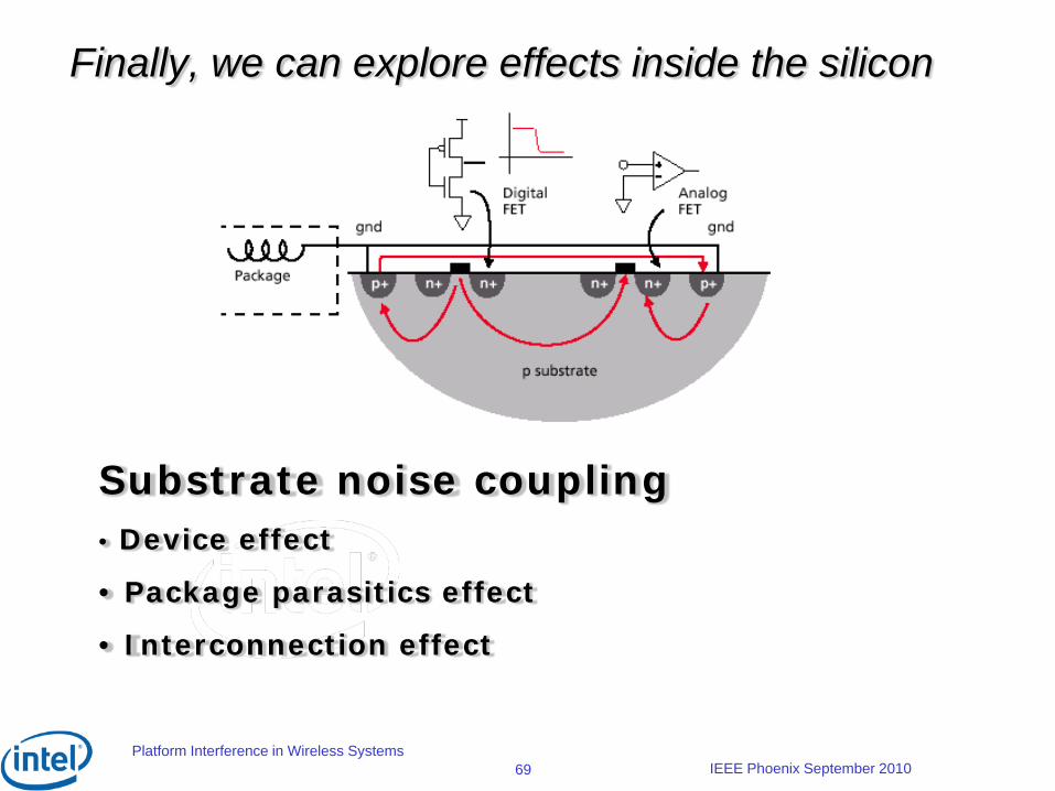
Finally, we can explore effects inside the silicon
Substrate noise coupling• Device effect
• Package parasitics effect
• Interconnection effect
Platform Interference in Wireless SystemsIEEE Phoenix September 201070
-
Noise injection
Noise SourceNoise Victim
Wire bond / flip-chip
Power rails
Epi la
yer
Subs
trate
+
propagation
and
coup
ling
-
Noise injection
Noise SourceNoise Victim
Wire bond / flip-chip
Power rails
Epi la
yer
Subs
trate
+
propagation
and
coup
ling
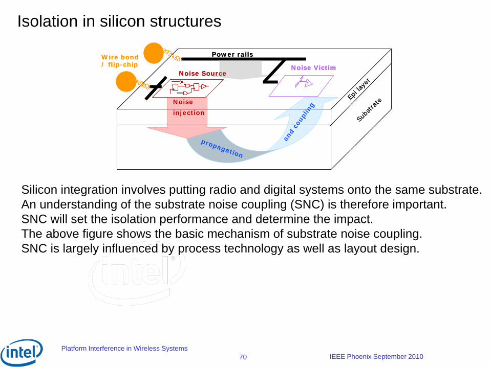
Silicon integration involves putting radio and digital systems onto the same substrate.An understanding of the substrate noise coupling (SNC) is therefore important. SNC will set the isolation performance and determine the impact. The above figure shows the basic mechanism of substrate noise coupling. SNC is largely influenced by process technology as well as layout design.
Isolation in silicon structures
Platform Interference in Wireless SystemsIEEE Phoenix September 201071
P-
p+
P--
p+ p+ p+ STI
Pwell
RL
P/P in p-GR
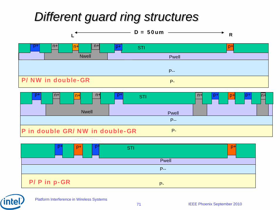
Different guard ring structures
P-
p+
P--
n+
Nwell Pwell
n+ n+ p+p+p+ p+ n+ n+
RL
STI
P in double GR/NW in double-GR
D = 50um R
STI
P-
p+
P--
n+
Nwell Pwell
n+ n+p+ p+
L
P/NW in double-GR
Platform Interference in Wireless SystemsIEEE Phoenix September 201072
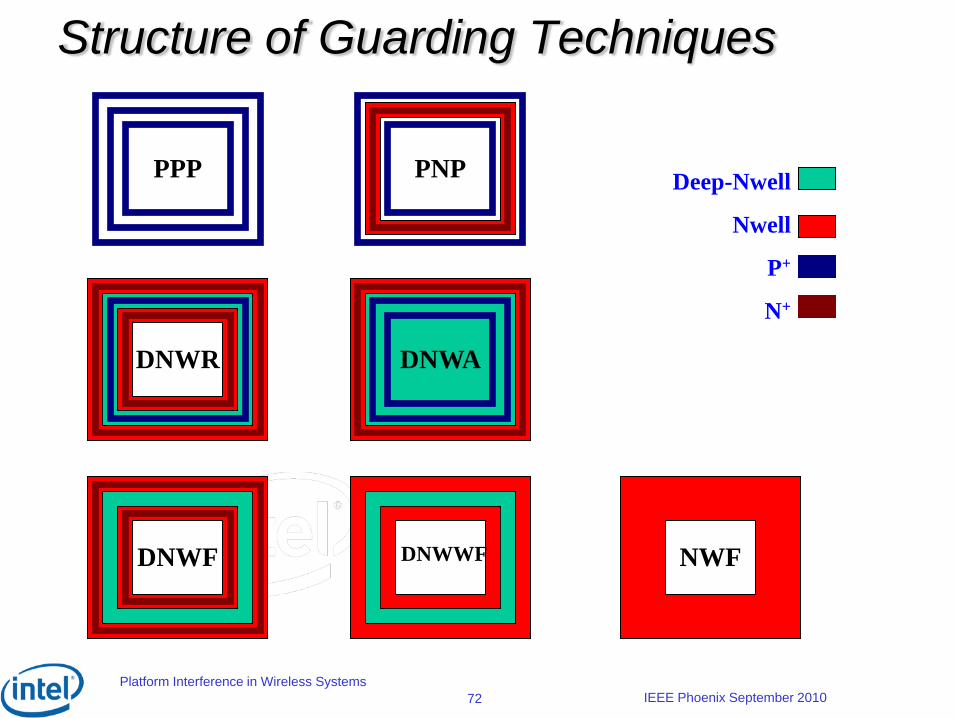
Structure of Guarding Techniques
Deep-Nwell
Nwell
P+
N+
PPP PNP
DNWR DNWA
DNWF DNWWF NWF

Platform Interference in Wireless SystemsIEEE Phoenix September 201073
Energy Transport Mechanisms:
Heat Sinks, Traces, Ground
Planes, etc.
Platform RFI: SUMMING IT UP
Con
nect
or
RFISignals
Resonance
Emissions
HS
HE
HC
Sources:
Clocks, I/O Drivers, etc.
Form Factor Effects:
Resonance and Frequency
Selectivity
RFI Interference:
Non-Gaussian and\or
Impulsive Disturbances
Platform Interference in Wireless SystemsIEEE Phoenix September 201074
RFI Workshop Summary Foil
Platform generated RFI is a tough problem Significant progress has been made to
understand it
We hope you have found today useful
Thank you!