please do not return your form to the above address. …
TRANSCRIPT

REPORT DOCUMENTATION PAGE Form Approved
OMB No. 0704-0188 Public reporting burden for this collection of information is estimated to average 1 hour per response, including the time for reviewing instructions, searching existing data sources, gathering and maintaining the data needed, and completing and reviewing this collection of information. Send comments regarding this burden estimate or any other aspect of this collection of information, including suggestions for reducing this burden to Department of Defense, Washington Headquarters Services, Directorate for Information Operations and Reports (0704-0188), 1215 Jefferson Davis Highway, Suite 1204, Arlington, VA 22202-4302. Respondents should be aware that notwithstanding any other provision of law, no person shall be subject to any penalty for failing to comply with a collection of information if it does not display a currently valid OMB control number. PLEASE DO NOT RETURN YOUR FORM TO THE ABOVE ADDRESS.
1. REPORT DATE (DD-MM-YYYY)
2. REPORT TYPE
3. DATES COVERED (From - To)
4. TITLE AND SUBTITLE
5a. CONTRACT NUMBER
5b. GRANT NUMBER
5c. PROGRAM ELEMENT NUMBER
6. AUTHOR(S)
5d. PROJECT NUMBER
5e. TASK NUMBER
5f. WORK UNIT NUMBER
7. PERFORMING ORGANIZATION NAME(S) AND ADDRESS(ES)
8. PERFORMING ORGANIZATION REPORT NUMBER
9. SPONSORING / MONITORING AGENCY NAME(S) AND ADDRESS(ES) 10. SPONSOR/MONITOR’S ACRONYM(S) 11. SPONSOR/MONITOR’S REPORT NUMBER(S) 12. DISTRIBUTION / AVAILABILITY STATEMENT
13. SUPPLEMENTARY NOTES
14. ABSTRACT
15. SUBJECT TERMS
16. SECURITY CLASSIFICATION OF:
17. LIMITATION OF ABSTRACT
18. NUMBER OF PAGES
19a. NAME OF RESPONSIBLE PERSON
a. REPORT
b. ABSTRACT
c. THIS PAGE
19b. TELEPHONE NUMBER (include area code)
Standard Form 298 (Re . 8-98) vPrescribed by ANSI Std. Z39.18
14-02-2017 Final Technical Report - CLIN 0001 02/18/2016 - 02/14/2017
Dielectric Metamaterial Reflector N00014-16-C-1023, CLIN 0001
Srini Krishnamurthy
SRI International 333 Ravenswood Avenue Menlo Park, CA 94025
Office of Naval Research Attn: Dr. Peter Morrison, Code 352 875 North Randolph Street Arlington, VA 22203
Distribution A: Approved for Public Release; Distribution Unlimited
The overall goal of this project is to develop paint-like and/or applique material with very high reflectivity and low absorptivity in near infrared region of electromagnetic spectrum. In this Year 1 of the project, we have designed metamaterial with an effective real-impedance of zero, which is predicted to have a reflectivity close to 100% at a chosen wavelength. We exploited Mie resonance in monodisperse wavelength-sized particles to achieve effectively zero real impedance. In our design, we choose the size of the non-absorbing dielectric spheres to achieve Mie resonance at the wavelength of interest, a dielectric coating thickness to maintain periodicity under self-assembly conditions, and transparent binder medium amenable to either paint-like material or applique. We have optimized the design by including nonlinear absorption, materials defects and thermal propagation for enhanced reflection and angular performance.
all-dielectric, perfect reflection, metamaterial applique Inspection NDT Galvanic
U U U
SAR 33Srini Krishnamurthy
650-859-4997

14 February 2017
Dielectric Metamaterial Reflector
Final Report for Period: 18 February 2016 – 14 February 2017 Contract # N00014-16-C-1023, CLIN #0001 SRI Project P23720
Prepared by: Srini Krishnamurthy, PI SRI International Advanced Technology and Systems Division 650-859-4997 [email protected]
Prepared for: Office of Naval Research 875 North Randolph Street Arlington, VA 22203
Attn: Dr. Peter Morrison, Code 352
Distribution A: Approved for public release; distribution unlimited.

SRI Final Report, Project P23720 14 February 2017
1
1. Overview of Project
The overall goal of this project is to develop paint-like and/or applique material with very high reflectivity
and low absorptivity in near infrared region of electromagnetic spectrum.
Concept: The reflectivity at a given wavelength is 100% when the material has an effective real-
impedance of zero. Mie resonance in monodisperse wavelength-sized particles can be used to introduce
resonances in the effective permittivity () and permeability () to achieve either a negative real or a
negative real . This ensures that the impedance, given by ()1/2, will have a near-vanishing real part,
resulting in near-perfect reflection. In our design, we choose the size of the non-absorbing dielectric
spheres to achieve Mie resonance at the wavelength of interest, a dielectric coating thickness to maintain
periodicity under self-assembly conditions, and transparent binder medium amenable to either paint-like
material or applique.
The specific objectives in the base year of the program are:
1. Optimize the reflector design for enhanced reflection and improved angular performance.
2. Calculate the nonlinear parameters such as two-photon absorption coefficient and free-carrier
scattering cross section of the particle material.
3. Develop a comprehensive code to solve Maxwell’s equations with nonlinear terms.
4. Evaluate the effect of material defects—voids and particle size—on the reflection property.
5. Solved coupled optical and thermal model for light propagation through absorptive medium.
6. Evaluate of the effect of nonlinear absorption on electric and magnetic resonances.
We achieved these objectives. The details are summarized below and detailed in Appendices A and B.
2. Completed Activities
Below we discuss in detail the activities we completed over the course of this project.
Designed metamaterial reflector: Single-negative metamaterials provide a promising approach for
achieving high reflectivity. However, current designs require carefully designed features that can be
obtained only by lithographic fabrication methods. We have designed a highly reflecting metamaterial
that can be synthesized by self-assembly methods. By exploiting the Mie resonance in dielectric spheres
and optimizing the sphere size and coating thickness, we applied full-wave simulations to obtain near-
perfect reflection in the near-infrared spectral wavelength region. The details and the results of our
systematic study on angular performance and the effect of coating thickness, particle size distribution,
voids, and layer thickness on the reflectivity of the metasurface are described for possible publication and
included here Appendix A.
Developed coupled optical and thermal model: We coupled the nonlinear optical model with a thermal
solver to obtain the change in temperature as function of light absorption in the structured medium. This
coupled model, limited to infinite periodic structures, is based on the microwave heating toolbox in
COMSOL. The user guide for this model are described in Appendix B.
Investigated the impact of nonlinear absorption on Mie resonance: We applied our nonlinear full-
wave model to study the fundamental impact of nonlinear absorption on Mie resonances in InP spheres.
We found that nonlinear absorption dampens both the electric and magnetic resonance with the magnetic
resonance (near 1.2 m) showing greater damping owing to the larger free-carrier absorption cross
SRI Final Report, Project P23720 14 February 2017
2
section associated with longer wavelengths. Since the intensity within the nanoparticle is enhanced at
resonance, the metamaterial achieves the same nonlinear absorption as a homogeneous layer of the same
thickness for an intensity 30 times lower. This effect could be exploited in several nonlinear absorption
applications including optical limiting and frequency conversion. The results of this study have been
summarized for possible publication and included here Appendix C.
Identified methods to synthesize InP & Si particles: Since the modeling study carried out thus far bodes
well for meeting the reflection requirements, we completed a literature study for materials synthesis and
layer deposition so that we are prepared to make progress immediately after optional funding is
authorized. Our models indicate that InP particles with a diameter of 380 nm and a silica shell of
thickness 60 nm will produce the desired coating response. This will be our baseline material. There are
no commercial sources of such particles, so SRI will leverage methods in the literature to develop the
desired materials in Years 2 and 3 of the proposed effort.
InP base particle: Two pathways to the synthesis of the InP base particle have been identified and will be
investigated. One approach will seek to grow the InP crystals utilizing a synthetic strategy based on the
controlled growth in solution under ambient pressure. The other approach will explore a recently reported
solvothermal means to generate the base InP particle. It is likely that both of these approaches will utilize
some form of annealing to achieve performance requirements regarding particle morphology and particle
purity. SRI has unique fluidized bed capabilities that are well suited for this aspect of the project. The
synthesis of InP nanocrystals with dimensions of <10 nm has been well studied and was the subject of a
recent review [Chem. Mater., 2016, 28 (8), pp 2491–2506]. The interest in InP in this size range is due to
their optoelectronic effects associated with quantum confinement. The review, while focused on
nanocrystal development, provides significant input on the kinetics of particle growth and the effect that
monomer concentration has on particle development. It also presents key insights that provide an
understanding of factors involved in maintaining particle growth. Of major importance are control of
precursor concentration, and once particle growth has been achieved it is important to quickly quench
before the onset of Ostwald ripening, which will cause the particle size to defocus and broaden.
The main challenge for this aspect of the synthetic effort is developing a reactor design with a reactant
feed system capable of maintaining precursor concentrations at a desired level. This will require some
kind of input with respect to precursor concentration currently in the reactor. Preferably the precursor
concentration will be determined in real time using an optical flow-through cell monitored by FTIR or
UV-Vis spectroscopy. Alternatively, a rapid sample extraction and analysis protocol will be developed.
The extraction and analysis approach allows for more analytical techniques to be considered, most
notably gas chromatography to interrogate precursor concentrations and dynamic light scattering (DLS) to
monitor particle size. This approach can also be automated to some extent with readily available sampling
devices that will collect samples and subject them to analysis at predetermined intervals.
The solvothermal synthesis of InP particles in the range of 400 to 600 nm with a zinc blende structure has
been reported in the literature [J. of Alloys and Compounds 472, 59 (2009); Materials Research Bulletin
44 (2009), 216–219]. This particle size is slightly larger than the size requirements based on modeling,
and there is no information given regarding particle size distribution. However, there is sufficient
information in the cited reference regarding the influence of reaction variables on the resultant particle
phase and morphology to guide SRI’s synthetic effort to generate the desired particle size and size
distribution. Through an iterative process, SRI will develop a solvothermal protocol for the preparation of
InP with the desired particle size and size distribution characteristics. Once a protocol is identified, work
SRI Final Report, Project P23720 14 February 2017
3
will proceed to scale the process to multi-gram quantities. SRI has employed a similar approach in the
development of rare-earth-doped ceramics particles for use in biodiagnostic applications. In the event the
particle size distribution is large, SRI will employ a combination of sedimentation and/or field flow
fractionation methods to narrow this distribution.
Silica coating: The next step in the particle synthesis is the application of a silica shell to the InP core
particle. SRI has considerable experience using a modified Stöber process [J. of Colloid and Interface
Science, 26, 62 (1968)] to apply a silica coating to a variety of different materials. This work has focused,
for the most part, on the coating of upconverting phosphor particles in the 150-400 nm range [Analytical
Biochem. 288, 176 (2001)]. In the case of the InP particles there are a number of literature precedents for
the application of a silica coating [see for example, Silica-Coated InP/ZnS Nanocrystals as Converter
Material in White LEDs, Advanced Materials, Volume 20, Issue 21, pages 4068–4073, November 3,
2008]. The fundamental difference in the reported silica coating protocol and those previously developed
at SRI is that the InP requires the use of a surfactant to properly solvate, or “wet,” the surface of the
nanoparticles such that uniform nucleation of the silica precursors is obtained, resulting in a uniform silica
coating. The addition of a surfactant is a common technique used to facilitate the silica coating of
nanoparticles with no, or very little, native oxide surface. The oxide surfaces are the nucleating sites
typically exploited in the silica coating of nanoparticles. In this case, InP has very little native oxide and
the surfactants actually bind to the surface and then serve as nucleating sites for the development of a
uniform silica coating.
Ordered film formation: The ordered films will be generated using well-established evaporative
techniques. The key features are the film growth compartment, in which the films are grown at the bottom
by a combination of gravity and evaporation of a slurry containing the nanoparticles. The design
incorporates a fluid thermal control compartment that will be utilized to control the temperature of the
nanoparticle slurry and, along with headspace gas flow/control, will allow effective control of evaporation
rates. The design also includes a glass window to enable monitoring of the film growth process. The cell
design will allow films to be grown on substrates up to 2.5 cm x 2.5 cm. Once film generation parameters
have been established at this length scale, efforts will focus on extending the substrate size. The
parameters of importance are the density of the suspension solution and the evaporation rate of the
suspension fluid. The density of the suspension fluid will control the sedimentation rates of the particles.
Ideally the sedimentation rate will be such that particles will be able to sample many different
configurations before finding the minimum associated with the formation of a quasi-crystalline material.
If sedimentation is too fast, it is likely the defect rates will be high. Defect densities will be investigated
using FESEM and TEM. In SRI’s current understanding of the self-assembly process, the likelihood of
being able to reduce any observed lattice defect structures in a post-assembly manner is low. Therefore,
emphasis will be on fabricating the self-assembled structures in an optimal manner with an anticipated
minimal time spent in attempting to anneal out any defects. Fortunately there is a significant interest in
the utilization of self-assembly techniques in the generation of materials on a commercial scale that has
received considerable attention in the literature. Recently several approaches have been put forth with
respect to the generation of perfect colloidal crystal architectures (ACS Nano, 2016, 10, 5260−5271 and
ACS Nano 2016, 10, 6791−6798). These approaches emphasize that optimal crystal formation is not
achieved in a dynamic system and that a controlled stimulus can be utilized to both improve crystal
quality and reduce growth time. Guidance from the theoretical analysis cited will be useful in developing
the actual crystal growth protocols.

SRI Final Report, Project P23720 14 February 2017
4
Film binder: It is anticipated that the films will be generated in an applique format, which will require
some form of binder to hold the self-assembled structures together. The ability to wick in low viscosity
materials into colloidal structures is known and commonly used to incorporate a binder material. Of key
consideration in the binder selection is the optical absorption (must be 0 in the wavelengths of interest)
and thermal properties (must have as high an operating temperature as possible). Assuming the absorption
on the binder is negligible, the key factor in robustness of the coating will be the thermal stability of the
binder system. Another consideration in a binder system would be the use of solventless formulations in
which 100% of the infiltrated material is utilized. This avoids the issue of solvents and any residue they
may leave behind. SRI recently contacted Dr. Keith Caruso at The John Hopkins Applied Physics
Laboratory. Dr. Caruso has been investigating binder systems for high-temperature applications for ONR.
His input on which binder systems to consider will be extremely valuable, and we will begin technical
discussions with him soon.
Characterization: Characterization of the phase and elemental composition of the InP and silica-coated
InP will be conducted by X-ray diffraction (XRD), energy dispersive X-ray spectroscopy (EDAX), and
X-ray fluorescence (XRF). Particle size and size distribution analysis will be conducted by static (Horiba
CAPA) and dynamic (Horiba LB220) light scattering as well as by field emission scanning electron
microscopy (FESEM) and tunneling electron microscopy (TEM). Cross-sectional analysis by TEM of the
silica-coated InP particles will provide details regarding the silica coating thickness and uniformity.
Physical characterization of the metamaterial films will consist primarily of FESEM and TEM analysis to
determine morphology of the particle arrays. We will use FESEM to examine film quality and will look at
investigating the particle distribution in the film in both a front face and cross-sectional manner. Cross-
sectional analysis will be assisted by embedding the film in an epoxy matrix and then polishing the cross-
sectional areas to reveal the particle distribution in the film.
Silicon nanoparticles: Recent calculations indicate that Si particles could also be used in metamaterial
synthesis. The possibility of utilizing Si particles in the construction of the coating was recently
reconsidered in light of some experimental results from some micro-fabricated structures. The published
information regarding the generation of Si particles is larger than that for InP due to the recent level of
interest in Si nanoparticles in the Li battery industry. The synthetic strategies outlined in the literature
utilize techniques SRI is well suited to investigate. Specifically, high-pressure solvothermal processing
and the use of an RF-induced plasma coupled to a fluidized bed reactor have been utilized at SRI for 20+
years. As such, it would seem that Si particles may be easier to develop. However, when one considers
the Si purity needed to prevent any absorption (estimated at >99.99%) the number of literature precedents
decreases considerably. This is due to the fact that the Li battery application does not require such a high
level of purity as the electronics industry or for the reflective application SRI has proposed. This does not
preclude the use of some of the synthetic strategies utilized in the Li-battery application, but using these
strategies will require special attention to the purity of input materials and any sources of impurities
during processing.
Although we explored Si nanoparticles, we plan to continue our studies only with InP nanoparticles.
Since InP continues to be an acceptable material for reflector application and our previously submitted
options include the cost for only InP-based development, we will develop an InP-based metamaterial
reflector.

SRI Final Report, Project P23720 14 February 2017
5
3. Significance of Results
Our full-wave models indicate that the metamaterial designed in the program offer extremely high
reflectivity with micron-thick metamaterial layer. The design and synthesis method enable applique-type
approach for large area applications and specifically suited for Navy assets. In addition, our detailed
calculations of the effect of nonidealities on optical and thermal properties provide confidence that
nonidealities introduced during materials synthesis will not compromise performance, and bode well for a
follow-on demonstration.
4. Publications
We have written two manuscripts for possible publication, subject to Navy’s approval for public release.
They are included as Appendixes A and C to this final report.

SRI Final Report, Project P23720 14 February 2017
A-1
Appendix A
Manuscript entitled “High Reflector Metasurface of Close-Packed Dielectric Spheres,”
prepared for possible publication in Applied Physics Letters

SRI Final Report, Project P23720 14 February 2017
A-2
Metamaterial Reflector of Close-Packed Dielectric Spheres
L. Zipp, B. Slovick, and S. Krishnamurthy
SRI International, Applied Optics Laboratory, Menlo Park, California 94025
Single-negative metamaterials provide a promising approach for achieving high reflectivity.
However, current designs require carefully designed features that can be obtained only by
lithographic fabrication methods. We present a design for a highly reflecting metamaterial that
can be synthesized by self-assembly methods. By exploiting the Mie resonance in dielectric
spheres and optimizing the sphere size and coating thickness, we apply full-wave simulations to
obtain near-perfect reflection in the near-infrared spectral wavelength region. We report the
results of our systematic study on angular performance and the effect of coating thickness,
particle size distribution, voids, and layer thickness on the reflectivity of the metasurface.

SRI Final Report, Project P23720 14 February 2017
A-3
There is a growing need for robust large-area high reflectivity coatings in applications
including improved coatings in reflective telescopes and free space optical communication
mirrors, optical sensor protection, and laser-powered spacecraft propulsion for missions such as
the Breakthrough Starshot,1 which aims to accelerate a micro-sized spacecraft to 20% of light
speed using laser radiation pressure on a large reflective sail. Traditional metallic coatings cannot
achieve the high reflectivity desired for such applications. Currently, high reflectivity (>99.9%) is
achieved with dielectric multilayer coatings known as distributed Bragg reflectors (DBRs), and
three-dimensional photonic crystals.2 DBRs and photonic crystals achieve high reflection or
photonic band gaps using Bragg scattering, or constructive interference of waves reflected by the
periodic structure. The drawback of DBRs and photonic crystals is that they require expensive and
delicate deposition and fabrication techniques, which preclude their application to large surface
areas. Recently, subwavelength optical elements in the form of metasurfaces have been exploited
for near-perfect reflection3,4,5 and other functions including metasurfaces have been designed for
enhanced reflection and transmission,6 polarization splitting7,8 and control,9 focusing,10 beam
steering,11 and anomalous refraction.12 However, these elements require lithographic fabrication
methods, limiting their use to small, planar surfaces. Self-assembly based nanosphere lithography
has been used to fabricate larger-scale metasurfaces,13 but the etching process limits this process
to cm2 areas.
There have been several studies and demonstrations of the optical properties of dilute as well
as close-packed structures of dielectric spheres. Low-density colloidal suspensions of silicon
spheres have been shown to exhibit highly efficient diffuse reflection.14 However, most
applications require specular reflection. On the other hand, studies of dense, self-assembled, close-
packed spheres have mostly focused on the photonic band structure arising from inter-particle

SRI Final Report, Project P23720 14 February 2017
A-4
Bragg scattering arising from the periodicity.15,16,17,18 Interesting and complex behavior emerges
when the spheres comprising the periodic structure also exhibit large single-particle Mie
resonances, analogous to resonant scattering by a potential well in quantum mechanics. The single-
particle resonances are modified by the presence of neighboring particles, and there is coupling
between single-particle and diffractive resonances arising from the periodicity of the bulk
structure.19 A two-dimensional hexagonal array of silicon spheres was shown to exhibit collective
Mie-resonant behavior,14 but did not achieve near-unity reflectance because of the inability to tune
and optimize the particle spacing.
In this Letter, we exploit Mie resonance in coated indium phosphide (InP) spherical particles
to design a highly reflecting (>99.98%) hexagonally close-packed metamaterial layer. In contrast
to previous designs, this metamaterial layer can be fabricated by self-assembly methods as a
standalone appliqué layer for application on large-area and irregularly shaped surfaces. By
harnessing single-particle Mie resonances and a thin oxide coating to control the particle
separation, we are able to achieve greater than 99.98% reflectivity in the near-infrared (NIR) region
with only three layers of hexagonal close-packed InP spheres. This is in contrast to traditional
photonic crystals and multilayer stacks, which require many more layers to achieve such high
reflectivity.
Since a large refractive index is required to obtain strong Mie resonances, we choose InP
spheres (refractive index n≈3.3 for NIR wavelengths) in a polymer binding matrix (n=1.5). The
spheres are arranged in a hexagonal close-packed structure and the diameter, d, of the sphere is
chosen to position the magnetic-dipole Mie resonance near the wavelength, for high reflection.
For isolated spheres with large refractive index relative to the background medium, the magnetic-
dipole Mie resonance occurs near d=/n, where n is the refractive index of the sphere,20 but for

SRI Final Report, Project P23720 14 February 2017
A-5
the close-packed structure the resonance is modified by the interaction between neighboring
resonators. In addition, we consider a thin SiO2 coating on the InP spheres, as shown in Fig. 1(a),
to allow for tuning of the periodicity of the close-packed structure.
Using full-wave finite-element modeling (HFSS from Ansys), we optimized the diameter,
coating thickness, and number of layers for high reflection at 1 m. The calculated reflectance at
normal incidence is shown in Fig. 1(b). For a single layer, the reflectance reaches close to 100%,
but is narrowband. With additional layers, the high reflectance region broadens and shifts towards
longer wavelengths. For 2 layers, the peak reflectivity is actually lower than for a single layer, due
to the modification of the Mie resonance by the presence of neighboring spheres. For three layers
the reflectance is already > 99.9% over a bandwidth of 50 nm, reaching over 99.98% reflectance
in some regions. We find that the reflectivity continues to increase with additional layers,
approaching near-unity reflection with increased bandwidth. Since the high reflectivity of the
metasurface arises from single-particle Mie resonances, only a few layers of the spheres are
required to achieve near-perfect reflection.
Figure 1. (a) Hexagonal close-packed high-index InP spheres with SiO2 coatings. The structure consists of three
layers of 360 nm indium-phosphide spheres with 60-nm-thick SiO2 coatings on top of a transparent quartz
substrate. (b) Normal incidence reflectance from the metasurface containing different numbers of layers. The
reflectance is greater than 99.9% near 1 m for three layers over a bandwidth of 50 nm. (c) Spatial distribution
of the electric field magnitude in the high reflectance region.

SRI Final Report, Project P23720 14 February 2017
A-6
To further understand the optical properties of the metasurface, we plot in Fig. 1(c) the spatial
distribution of the electric field magnitude in the three layer metasurface. The electric field does
not penetrate beyond the first layer of spheres, confirming that the use of single-particle resonances
negates the need for many layers as in DBRs. In addition, the electric field attains a maximum at
the surface of the top layer of spheres, unlike in conventional reflectors. This behavior is expected
for a magnetic mirror21, since the electric field does not undergo a π phase shift upon reflection, as
in conventional electrical conductors. The maximum electric field at the reflecting surface can be
exploited in applications such as low profile antennas, imaging bio tissues, and surface-enhanced
Raman spectroscopy (SERS).22,23,24
A key feature of the reflector design is the ability to optimize the periodicity of the hexagonal
close-packed structure by tuning the thickness of the silicon dioxide coating on the InP spheres.
When the oxide thickness is reduced, the close packing requirement reduces the periodicity as well
and the reflectance spectrum is considerably changed, as illustrated in Fig. 2(a) for a single layer
design. For a relatively large shell thickness of 200 nm, the electric and magnetic dipole Mie
resonances of the spheres occur near 1.1 m and 1.2 m respectively. This is confirmed by plotting
the electric field vectors at these two resonant wavelengths, as shown in Fig. 2(c-d). At 1.1 m,
the electric field is enhanced within the InP sphere and exhibits the characteristics of a typical
dipole field, while at 1.2 m, the electric field displays a large circulating component, consistent
with the presence of a magnetic dipole. As the shell thickness is reduced and the periodicity
decreases, the electric and magnetic Mie resonances are shifted towards shorter wavelengths, and
the magnetic dipole resonance broadens significantly. This behavior is due to the interaction of the
Mie resonance between neighboring spheres. For a shell thickness of 60 nm, the magnetic dipole
resonance is sufficiently widened for use as a broadband high reflector metasurface. The tunability

SRI Final Report, Project P23720 14 February 2017
A-7
of the reflectance spectrum with the oxide shell thickness is also possible for multiple layers as
shown in Fig. 2(b) in which the reflectivity for three layers of the spheres on a quartz substrate for
different coating thicknesses is plotted. Decreasing the thickness of the coating results in a
blueshift of the high reflectance region, due to the decrease in lattice periodicity. The importance
of the silicon dioxide coating in the design can be seen by comparing the reflectance of the
metasurface with no coating (t=0 nm, dotted blue curve), to designs with finite coating thickness.
In the absence of a coating, the reflectance properties of the metasurface suffer considerably due
to leakage of the normal component of electric field into adjacent spheres, which dampens the Mie
Figure 2. (a) Reflectance for a single layer of hexagonal close-packed spheres for different shell thicknesses t.
The electric dipole and magnetic dipole Mie resonances for a 200-nm coating are denoted “ED” and “MD,”
respectively. (b) Reflectance for different thicknesses with three layers of close-packed spheres at normal
incidence on a quartz substrate. Panels (c) and (d) show the electric field vectors of the electric (c) and magnetic
(d) dipole Mie resonances for a 200-nm-thick coating. The black circle denotes the boundary of the 360-nm-
diameter InP sphere.

SRI Final Report, Project P23720 14 February 2017
A-8
resonance. The presence of even a 30-nm-thick shell eliminates the coupling and near-perfect
reflectance is achieved.
We now study the angle-dependent reflection performance, shown in Fig. 3(a). For dielectric
spheres with a 60 nm coating, high reflectivity at 1 m is maintained up to 10o before dropping
steeply. For TE polarized light (electric field vector perpendicular to the plane of incidence), the
reflectance remains remarkably high (>99.9%) for all angles of incidence, while reflectivity suffers
for TM polarized light (electric field vector in the plane of incidence). The TM mode reflectance
displays a sharp cutoff and drops rapidly to zero, in contrast to normal homogenous materials
which show a gradual variation in the reflectivity as a function of angle. The cause of this sharp
cutoff can be understood by comparing the reflectance spectrum of the TM mode at various angles
of incidence, shown in Fig. 3b. As the angle of incidence increases, the high reflectance band
region shifts towards longer wavelengths, causing the TM polarized reflectance to drop to zero at
lower wavelengths. Consequently, the average reflection decreases to very low values beyond a
Figure 3. (a) Reflectance versus angle of incidence on a 7-layer structure of spheres on a quartz substrate, with two
different silicon dioxide shell thicknesses, as well as a combined “stacked” structure containing two differently
designed metalayers. The stacked structure consists of three layers of spheres with d=360 nm and t=30 nm and four
layers of spheres with d=330 nm and t=45 nm. (b) Reflectance spectrum of the TM polarization mode for d=360 nm
t=60 nm at different angles of incidence showing a redshift at steeper angles of incidence.

SRI Final Report, Project P23720 14 February 2017
A-9
certain angle. Multilayer films also exhibit a redshift with increasing angle of incidence, suggesting
that this behavior derives from the resonant elements or layers. We further note from Fig. 3a that
the angular performance at a chosen wavelength can be increased with appropriate choice of
coating thickness. We can reduce the shell thickness to move the center wavelength of reflection
to lower values and use higher angle to move that to higher wavelength, allowing to high reflection
at the center wavelengths for larger angles. This is seen for a 30-nm shell coating, where we find
that the high reflectivity region can be extended out to 20 degrees. To extend the angular coverage
beyond 20 degrees, we can use a stacked layer approach. For example, we modeled a seven-layer
structure in which the top three layers contain 360-nm-diameter InP spheres coated with 30-nm-
thick SiO2 in a polymer binder, while the bottom four layers are composed of 330-nm-diameter
spheres with a 45-nm-thick SiO2 coat. We find (Fig. 3(a)) that with this structure, high reflectance
can be extended past 30 degrees. With additional layers, the angular performance can be further
improved.
We envision that the layers will be made by a self-assembly process followed by polymer
backfill and peel-off from the substrate for applying to surfaces of interest. Since both the self-
assembly process and the particle synthesis invariably lead to voids and size distribution, we study
the impact of these defects on reflectance. We consider one vacancy in a supercell of 12 atoms per
layer (equivalently 8.3% defect density). The calculated reflectivity in the NIR band from one
layer with defects is reduced considerably (Fig. 4(a), dashed line). However, the reflectivity is
nearly fully recovered at the designed wavelengths when one defect-free layer is added above the
defective layer (Fig. 4(a), solid line). If the void is in the top layer on the other hand, even the
normally incident light is scattered into the perfect layer below at various angles, resulting in lower
reflectivity. High reflection can be regained only by adding several more defect-free layers. This
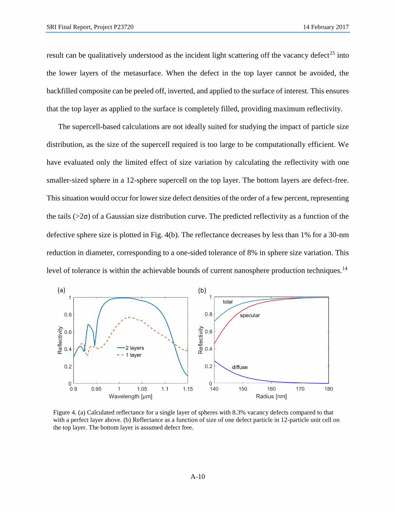
SRI Final Report, Project P23720 14 February 2017
A-10
result can be qualitatively understood as the incident light scattering off the vacancy defect25 into
the lower layers of the metasurface. When the defect in the top layer cannot be avoided, the
backfilled composite can be peeled off, inverted, and applied to the surface of interest. This ensures
that the top layer as applied to the surface is completely filled, providing maximum reflectivity.
The supercell-based calculations are not ideally suited for studying the impact of particle size
distribution, as the size of the supercell required is too large to be computationally efficient. We
have evaluated only the limited effect of size variation by calculating the reflectivity with one
smaller-sized sphere in a 12-sphere supercell on the top layer. The bottom layers are defect-free.
This situation would occur for lower size defect densities of the order of a few percent, representing
the tails (>2σ) of a Gaussian size distribution curve. The predicted reflectivity as a function of the
defective sphere size is plotted in Fig. 4(b). The reflectance decreases by less than 1% for a 30-nm
reduction in diameter, corresponding to a one-sided tolerance of 8% in sphere size variation. This
level of tolerance is within the achievable bounds of current nanosphere production techniques.14
Figure 4. (a) Calculated reflectance for a single layer of spheres with 8.3% vacancy defects compared to that
with a perfect layer above. (b) Reflectance as a function of size of one defect particle in 12-particle unit cell on
the top layer. The bottom layer is assumed defect free.
SRI Final Report, Project P23720 14 February 2017
A-11
In summary, the self-assembled dielectric sphere metasurface studied here represents a robust,
scalable, high-reflectivity coating that can be applied to large and irregularly shaped surfaces. The
design offers distinct advantages over multilayer coatings and other metasurface approaches. We
have shown that the design parameter space is large enough to increase reflectance and angular
performance and mitigate the effect of defects. The simplicity of the construction and its robust
properties suggests that it may provide a cost-effective solution for high-reflectivity, low-
absorption coatings.
The authors gratefully acknowledge funding for this research from the Office of Naval Research
through Contract N00014-16-C-1023.
References:
1 https://breakthroughinitiatives.org/Initiative/3
2 E. Yablonovitch, T.J. Gmitter, and K.M. Leung, Phys. Rev. Lett. 67, 2295 (1991).
3 F. Namin, S. Yun, T.S. Mayer, D.H. Werner, and C. Rivero-Baleine, in 2011 IEEE Int. Symp.
Antennas Propag. APSURSI (2011), pp. 1155–1158.
4 B. Slovick, Z.G. Yu, M. Berding, and S. Krishnamurthy, Phys. Rev. B 88, 165116 (2013).
5 P. Moitra, B.A. Slovick, Z.G. Yu, S. Krishnamurthy, and J. Valentine, Appl. Phys. Lett. 104,
171102 (2014).
6 P. Spinelli, M.A. Verschuuren, and A. Polman, Nat. Commun. 3, 692 (2012).
7 W. Guo, G. Wang, T. Li, H. Li, Y. Zhuang, and H. Hou, J. Phys. Appl. Phys. 49, 425305 (2016).
8 B.A. Slovick, Y. Zhou, Z.G. Yu, I.I. Kravchenckou, D.P. Briggs, P. Moitra, S. Krishnamurthy, and
J. Valentine, ArXiv161004040 Phys. (2016).
9 H.F. Ma, G.Z. Wang, G.S. Kong, and T.J. Cui, Sci. Rep. 5, 9605 (2015).
10 M. Khorasaninejad, W.T. Chen, R.C. Devlin, J. Oh, A.Y. Zhu, and F. Capasso, Science 352, 1190
(2016).
11 S. Sun, K.-Y. Yang, C.-M. Wang, T.-K. Juan, W.T. Chen, C.Y. Liao, Q. He, S. Xiao, W.-T. Kung,
G.-Y. Guo, L. Zhou, and D.P. Tsai, Nano Lett. 12, 6223 (2012).
12 C. Pfeiffer and A. Grbic, Phys. Rev. Lett. 110, 197401 (2013).
13 P. Moitra, B.A. Slovick, W. li, I.I. Kravchencko, D.P. Briggs, S. Krishnamurthy, and J. Valentine,
ACS Photonics 2, 692 (2015).
14 L. Shi, J.T. Harris, R. Fenollosa, I. Rodriguez, X. Lu, B.A. Korgel, and F. Meseguer, Nat. Comm. 4,
1904 (2013).
15 F. Meseguer, Colloids Surf. Physicochem. Eng. Asp. 270–271, 1 (2005).
16 A. Blanco, E. Chomski, S. Grabtchak, M. Ibisate, S. John, S.W. Leonard, C. Lopez, F. Meseguer,
H. Miguez, J.P. Mondia, G.A. Ozin, O. Toader, and H.M. van Driel, Nature 405, 437 (2000).
17 Y. Xia, B. Gates, Y. Yin, and Y. Lu, Adv. Mater. 12, 693 (2000).
18 G.I.N. Waterhouse and M.R. Waterland, Polyhedron 26, 356 (2007).
19 A.B. Evlyukhin, C. Reinhardt, A. Seidel, B.S. Luk’yanchuk, and B.N. Chichkov, Phys. Rev. B 82,
045404 (2010).

SRI Final Report, Project P23720 14 February 2017
A-12
20 M.S. Wheeler, J.S. Aitchison, and M. Mojahedi, Phys. Rev. B 73, 045105 (2006).
21 S. Liu, M.B. Sinclair, T.S. Mahony, Y.C. Jun, S. Campione, J. Ginn, D.A. Bender, J.R. Wendt, J.F.
Ihlefeld, P.G. Clem, J.B. Wright, and I. Brener, Optica 1, 250 (2014).
22 M. Esfandyarpour, E.C. Garnett, Y. Cui, M.D. McGehee, and M.L. Brongersma, Nat. Nanotechnol.
9, 542 (2014).
23 S.B. Choi, D.J. Park, S.J. Byun, J. Kyoung, and S.W. Hwang, Adv. Opt. Mater. 3, 1719 (2015).
24 Z. Ma, S.M. Hanham, P. Albella, B. Ng, H.T. Lu, Y. Gong, S.A. Maier, and M. Hong, ACS
Photonics 3, 1010 (2016).
25 A.F. Koenderink, A. Lagendijk, and W.L. Vos, Phys. Rev. B 72, 153102 (2005).

SRI Final Report, Project P23720 14 February 2017
B-1
Appendix B
COMSOL User Guide to Study High-Intensity Light Propagation Through Structured Media

SRI Final Report, Project P23720 14 February 2017
B-2
COMSOL User Guide to Study High-Intensity Light Propagation Through Structured Media
First, open a new file by selecting Model Wizard, select 3D, and select Electromagnetic Waves,
Frequency Domain (emw). Click Add and then Study, and then under Preset Studies, select Frequency
Domain and click Done. This loads the COMSOL user interface, shown in Fig. 1, which consists of four
setup sections shown on the left-hand side of the window: Global Definitions, Components, Study, and
Results. Global Definitions is where the frequency-dependent material properties are defined, such as the
permittivity of InP, as well as parameters defining the geometry such as radius and shell thickness. The
Components section consists of defining the geometry of the structure, assigning materials to the
geometry, applying boundary conditions and excitations, and meshing the design. The Study section is
where frequency and parameter sweeps are defined, and Results is where plots are generated.
Figure 1. COMSOL user interface.
Starting with the Global Definitions, the first step is to define the frequency-dependent optical properties
of InP and the Al substrate. Start by creating either a text or csv file with one column giving the frequency
in Hz and the second column giving the optical property. Next, right-click Global Definitions and select
Functions and then Interpolation. Near the middle of the window is a folder icon called Load from File.
Select this and load the file with the optical properties. Also specify the function name under Definition.
Repeat this process for all frequency-dependent properties, including permittivity and absorption
coefficient.
Next, the geometry must be defined within the Component section. For the hexagonal close-packed array
of spheres, the unit cell is a hexagon. Start by right-clicking Geometry and selecting Work Plane. Draw

SRI Final Report, Project P23720 14 February 2017
B-3
the hexagon within the work plane and then use the Extrude feature to form a volumetric hexagon, as
shown in Fig. 1. Next, draw the spheres by right-clicking Geometry and selecting Spheres. Choose their
coordinates within the unit cell to form the close-packed geometry. Next, the region of the spheres outside
the hexagonal volume must be removed. This is done using the intersection operation within Boolean and
Partitions by right-clicking Geometry. Within the settings of the intersection, select the sphere and
hexagonal volume and click Build All Objects to remove the portion of the sphere outside the volume.
The next step is to define a few local variables within
the component section, as shown in Fig. 2. Here we
can define, for example, the refractive index n_InP as
the square root of the frequency-dependent
permittivity of InP, which we defined earlier in
Global Definitions. The most important step for the
nonlinear solver is to define the intensity-dependent
absorption coefficient of InP, called alphap. The
effective intensity-dependent permittivity of InP can
be written as
2
0
( ) '( )n
I n j Ik
, (4)
where n is the refractive index and ’(I) is an
effective absorption coefficient given by α’=N0 [1 +
βI/(N0) + I2/(2N0)] and the various
parameters are defined in the report. The intensity is
related to the local electric field by I=1/2ncε0|E|2. As
shown in Fig. 2, we defined the intensity in terms of
the absolute value of the electric field emw.normE.
Then the absorption coefficient alphap was defined
in terms of this intensity variable.
The next step is to assign material properties to the
geometry. This step is straightforward. For example, define a material by right-clicking Materials. Within
the settings of the new material, define the permittivity, which for InP will be of the form of Eq. (x)
above. Note that the permittivity property accepts complex quantities so the absorption can be included
here. Once the properties are defined, select the appropriate domains within the geometric entity selection
window.
Next up are the boundary conditions and excitations within the Components section. T- assign periodic
boundary conditions, right-click Electromagnetic Waves, Frequency Domain and select Periodic
Condition. Within the settings of the periodic condition, select opposite faces of the unit cell, as shown in
Fig. 3. Repeat this for the other four faces of the hexagonal unit cell.
Figure 2. Variables within the component
section, showing how the nonlinear effects
are included by defining the intensity in terms
of the electric field variable emw.normE and
then defining an intensity-dependent
absorption coefficient.

SRI Final Report, Project P23720 14 February 2017
B-4
Figure 3. Assignment of periodic boundary conditions.
To set up the plane wave excitation, right-click
Electromagnetic Waves, Frequency Domain and select
Port. Within the port settings in Boundary Selection,
select the top face of the unit cell where the light will be
entering. To specify the incident power, within the
Boundary Selection window, shown in Fig. 4, uncheck
Specify Deposited Power and type the expression shown
in Fig. 4, which is the product of the incident intensity,
defined as a global variable, and the area of the hexagonal
unit cell. Next, define the incident polarization using the
x, y, and z values within the electric mode field. Lastly,
define the propagation constant as shown in terms of the
solution variable emw.k0. This is the propagation
constant at the source.
Our simulations assume an Al substrate that can be
modeled using an impedance boundary condition. This
can be assigned to the bottom face by right-clicking
Electromagnetic Waves, Frequency Domain. The optical
properties can be assigned by calling the frequency-
dependent permittivity values into the Relative Permittivity field within the Impedance Boundary
Condition properties. Specifically, we defined variables within the Component section called er_Al and
ei_Al, corresponding to the real and imaginary parts of the Al permittivity, which are equal to the
Figure 4. Port excitation properties, including
input power and polarization.

SRI Final Report, Project P23720 14 February 2017
B-5
frequency-dependent functions defined in the Global Definitions. The permittivity is then typed into the
impedance boundary condition as er_Al-1j*ei_Al.
The next step is to define the mesh properties. First, right-click Mesh and select Size. Within the Element
Size window of Size, select normal for the predefined mesh. Next, right-click mesh, go to More
Operations, and select Free Triangular. Within the Boundary Selection of Free Triangular, select all of the
faces on one side of the unit cell, as shown in Fig. 5.
Figure 5. Assigning a mesh to one face of the unit cell.
Next, right-click Mesh, go to More Operations, and select Copy Face. Within Copy Face properties, for
the source Boundaries select the same faces used in the Free triangular field shown in Fig. 5. Then in the
Destination Boundaries, select the faces on the opposite side of the unit cell, as shown in Fig. 6. This
copies the mesh generated on the face shown in Fig. 5 to the opposite face. Repeat this process for the
other two face pairs. Lastly, right-click Mesh and select Free Tetrahedral. Within the Domain Selection of
Free Tetrahedral, select Remaining. Click Build Mesh to render the mesh.
SRI Final Report, Project P23720 14 February 2017
B-6
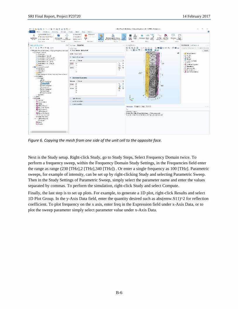
Figure 6. Copying the mesh from one side of the unit cell to the opposite face.
Next is the Study setup. Right-click Study, go to Study Steps, Select Frequency Domain twice. To
perform a frequency sweep, within the Frequency Domain Study Settings, in the Frequencies field enter
the range as range (230 [THz],2 [THz],340 [THz]) . Or enter a single frequency as 100 [THz]. Parametric
sweeps, for example of intensity, can be set up by right-clicking Study and selecting Parametric Sweep.
Then in the Study Settings of Parametric Sweep, simply select the parameter name and enter the values
separated by commas. To perform the simulation, right-click Study and select Compute.
Finally, the last step is to set up plots. For example, to generate a 1D plot, right-click Results and select
1D Plot Group. In the y-Axis Data field, enter the quantity desired such as abs(emw.S11)^2 for reflection
coefficient. To plot frequency on the x axis, enter freq in the Expression field under x-Axis Data, or to
plot the sweep parameter simply select parameter value under x-Axis Data.

SRI Final Report, Project P23720 14 February 2017
C-1
Appendix C
Manuscript entitled “Nonlinear absorption in dielectric metamaterials,”
prepared for possible publication in Applied Physics Letters

SRI Final Report, Project P23720 14 February 2017
C-2
Nonlinear absorption in dielectric metamaterials
B. Slovick, L. Zipp, and S. Krishnamurthy
SRI International, Applied Optics Laboratory, 333 Ravenswood Avenue, Menlo Park, California 94025
Abstract: We solve the nonlinear Maxwell equations in an InP-based dielectric metamaterial, considering both
two-photon absorption and photo-induced free-carrier absorption. We obtain the intensity-dependent reflection,
absorption, and effective permittivity and permeability of the metamaterial. Our results show that nonlinear
absorption dampens both the electric and magnetic resonance, although the magnetic resonance is more affected
because it occurs at longer wavelengths where the free-carrier absorption cross section is larger. Owing to field
concentration in the metamaterial at resonance, the threshold intensity for nonlinear absorption is smaller by a
factor of about 30 compared to a homogeneous layer of the same thickness. Our results have implications on the
use of dielectric metamaterials for nonlinear applications such as frequency conversion and optical limiting.
Materials with strong nonlinear response are desired for applications involving optical limiting [1-3],
ultrafast modulation [4-6], frequency conversion [7,8], and optical isolation [9,10]. Traditional bulk
materials have a weak interaction between electron and sub-bandgap photons, as indicated by
measured nonlinear absorption coefficients [11-14], and thus require high intensities or long interaction
lengths to achieve an efficient nonlinear response.
One way to enhance the nonlinear response is to incorporate metamaterial elements or plasmonic
structures to concentrate the electric fields within a nonlinear material [15,16]. Metamaterials
containing plasmonic nanostructures have been integrated with nonlinear materials to enhance second-
harmonic generation [17-23] and achieve analog electromagnetically induced transparency (EIT) [24,25].
The drawback of plasmonic approaches is that the fields are highly localized at the metal dielectric
interface, leading to small interaction volumes [26,27]. Also, the finite conductivity of metals at optical
frequencies leads to undesirable losses. An alternative approach is to induce nonlinearity in dielectric
metamaterials using Mie or Fano resonances. Dielectric nanostructures have been used to enhance
third-harmonic generation [26-31] and to achieve ultrafast optical modulation [32-34].
To date, the research on nonlinear phenomena in dielectric metamaterials has focused primarily on the
experimental aspects [26-31], with relatively few examples of theoretical studies. A few examples
employ the recently-developed linear generalized source method for nonlinear materials [35-37], which
calculates the diffraction of one- and two-dimensional gratings accounting for nonlinear polarization
sources. Although these models provide important insights, they do not support three-dimensional
structures and do not represent full solutions of the nonlinear Maxwell equations. Also, existing models
do not account for the nontrivial frequency dependence of the nonlinear parameters, such as the two
photon absorption (TPA) coefficient and the free-carrier absorption (FCA) cross section [14].
In this work, we develop a full-wave model to solve the nonlinear Maxwell equations in a structured,
three-dimensional metamaterial accounting for both TPA and photo-induced FCA. The nonlinear
absorption coefficients are obtained from full-band structure calculations [14]. We apply the model to
study the optical properties and effective parameters of a representative InP-based dielectric
SRI Final Report, Project P23720 14 February 2017
C-3
metamaterial operating in the near infrared spectral band. As expected, we find that nonlinear
absorption at high intensities leads to dampening of the electric and magnetic Mie resonances. For
continuous wave illumination, the onset nonlinear absorption occurs at intensities around 1 MW/cm2,
while the Mie resonances are almost completely diminished for intensities approaching 5 MW/cm2. In
addition, we find several unexpected results. First, the nonlinear absorption at the magnetic resonance
is larger than at electric resonance, which can be explained by the wavelength-dependent FCA. Second,
assuming FCA is independent of wavelength, the absorption at the two resonances is found to be nearly
equal, despite the electric field being heavily localized at the electric resonance and more uniformly
distributed at the magnetic resonance. Third, owing to the enhancement of the electric field at
resonance, we find that the intensity threshold of nonlinear absorption in the metamaterial is nearly 30
times lower than for a homogeneous material of similar thickness.
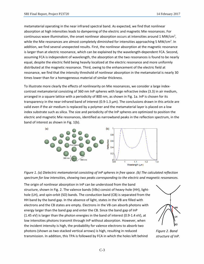
To illustrate more clearly the effects of nonlinearity on Mie resonances, we consider a large index-
contrast metamaterial consisting of 360 nm InP spheres with large refractive index (3.3) in air medium,
arranged in a square lattice with a periodicity of 800 nm, as shown in Fig. 1a. InP is chosen for its
transparency in the near-infrared band of interest (0.9-1.3 μm). The conclusions drawn in this article are
valid even if the air medium is replaced by a polymer and the metamaterial layer is placed on a low
index substrate such as silica. The size and periodicity of the InP spheres are optimized to position the
electric and magnetic Mie resonances, identified as narrowband peaks in the reflection spectrum, in the
band of interest as shown in Fig. 1(b).
Figure 1. (a) Dielectric metamaterial consisting of InP spheres in free space. (b) The calculated reflection
spectrum for low intensities, showing two peaks corresponding to the electric and magnetic resonances.
The origin of nonlinear absorption in InP can be understood from the band
structure, shown in Fig. 2. The valence bands (VBs) consist of heavy-hole (HH), light-
hole (LH), and spin-orbit (SO) bands. The conduction band (CB) is separated from the
HH band by the band gap. In the absence of light, states in the VB are filled with
electrons and the CB states are empty. Electrons in the VB can absorb photons with
energy larger than the band gap and enter the CB. Since the band gap of InP
(1.45 eV) is larger than the photon energies in the band of interest (0.9-1.4 eV), at
low intensities photons transmit through InP without absorption. However, when
the incident intensity is high, the probability for valence electrons to absorb two
photons (shown as two stacked vertical arrows) is high, resulting in reduced
transmission. In addition, this TPA is followed by FCA in which the holes left behind
SO
LH
HH
SO
LH
HH
Figure 2. Band
structure of InP.

SRI Final Report, Project P23720 14 February 2017
C-4
in the HH band can be filled by one-photon absorption by electrons in the LH and SO bands, shown by
the colored arrows in Fig. 2. Because the strength of both TPA and FCA depend on intensity, they are
referred to as nonlinear absorption processes. Figure 3 shows the previously calculated values of TPA
coefficient and the FCA cross section for InP [14]. The value of is relatively constant with
wavelength, which is typical for wide-bandgap materials, while increases by an order of magnitude
over the band. The FCA increases with increasing wavelength because the corresponding photon energy
decreases, and the energy-momentum conservation condition for FCA (colored lines in Figure 2) is
satisfied only near the center of the Brillouin zone, where a larger number of holes are present.
0.9 1 1.1 1.2 1.310
1
102
Wavelength (m)
(
cm
/GW
)
(a)
0.9 1 1.1 1.2 1.310
-18
10-17
10-16
Wavelength (m)
(
cm
2)
(b)
Figure 3. Wavelength dependence of the two-photon absorption coefficient (a) and free-carrier
absorption cross section (b) for InP.
We will now incorporate these nonlinear coefficients into Maxwell’s equations. The nonlinear Maxwell equation for the electric field E(r,t) is [38,39]
22 2
2
2 2 2 2
0
( , )( , ) 1 ( , )( , ) 0NLP tn E t n N E t
E tc t c t c t
rr rr , (1)
where n is the refractive index of the medium, c is the speed of light, N and are the free-carrier
concentration and absorption cross section, and 0 is the free-space permittivity. The nonlinear
polarization PNL is related to the third-order nonlinear susceptibility (3) by
2(3)
0
3( , ) ( , ) ( , )
4NLP t E t E t r r r . (2)
Substituting Eq. (2) into Eq. (1) and assuming monochromatic solutions E(r,t)=E(r)exp(-it), we obtain
0)()(4
3 2)3(
2
2
2
222
rr E
c
NniE
ccn
. (3)
Relating the imaginary part of (3) to the two-photon absorption coefficient as [38,39]
2 2
(3) 02Im( )
3
n c
,
and neglecting the real part of (3), Eq. (3) can be rewritten as
0)()(2
1 2
0
2
2
222
rr E
c
NniEni
cn
. (4)
SRI Final Report, Project P23720 14 February 2017
C-5
The free carrier concentration is given by the continuity equation for free electrons [14,38,39]
2
,2
dN I N
dt
(5)
where is the photon energy and is the photo-carrier relaxation time, which we assume is a constant equal to 1 μs. The first term in Eq. (5) describes free-carrier generation via two-photon absorption, and the second term describes free carrier recombination. For continuous-wave illumination, the free-carrier concentration will reach steady state conditions (dN/dt=0) and thus
2( )2
N I I
. (6)
Substituting Eq. (6) into Eq. (4) and using the relation between the intensity and the electric
field 2/)(2
0 rEncI , we obtain the following form of the nonlinear Maxwell equation:
0)()(8
)(2
1 42
0
32
0
2
2
222
rrr EE
cniEni
cn
. (7)
We use the full-wave finite-element frequency domain solver in COMSOL to solve Eq. 7. Before applying
Eq. (7) to the metamaterial in Fig.1, we apply it to a homogeneous nonlinear medium and compare the
results with the solution to the well-known rate equation [38,39]
32
2II
dx
dI
. (8)
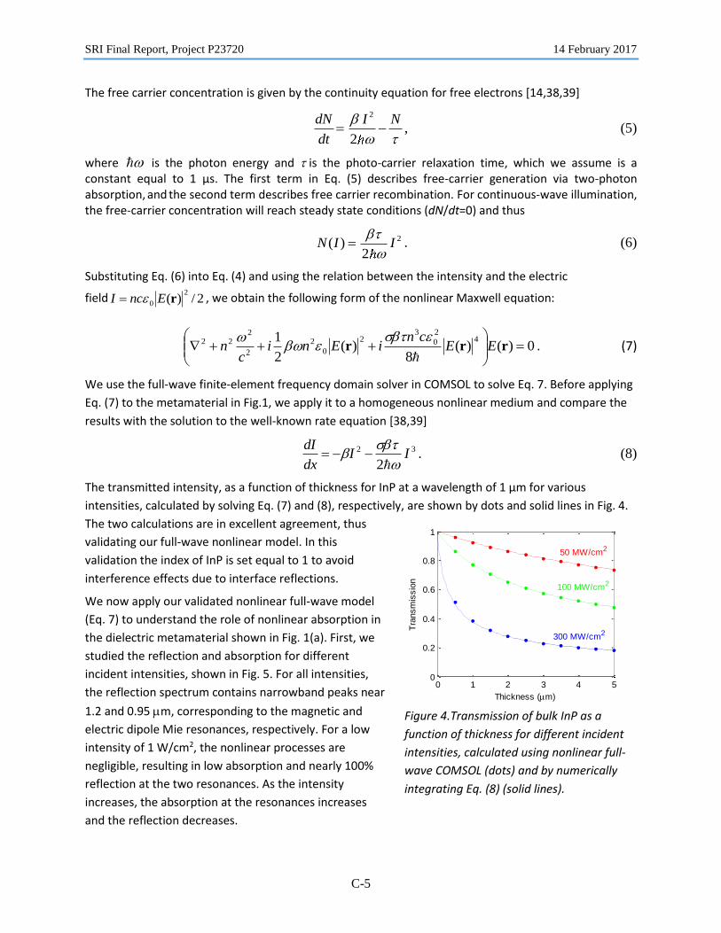
The transmitted intensity, as a function of thickness for InP at a wavelength of 1 μm for various
intensities, calculated by solving Eq. (7) and (8), respectively, are shown by dots and solid lines in Fig. 4.
The two calculations are in excellent agreement, thus
validating our full-wave nonlinear model. In this
validation the index of InP is set equal to 1 to avoid
interference effects due to interface reflections.
We now apply our validated nonlinear full-wave model
(Eq. 7) to understand the role of nonlinear absorption in
the dielectric metamaterial shown in Fig. 1(a). First, we
studied the reflection and absorption for different
incident intensities, shown in Fig. 5. For all intensities,
the reflection spectrum contains narrowband peaks near
1.2 and 0.95 m, corresponding to the magnetic and
electric dipole Mie resonances, respectively. For a low
intensity of 1 W/cm2, the nonlinear processes are
negligible, resulting in low absorption and nearly 100%
reflection at the two resonances. As the intensity
increases, the absorption at the resonances increases
and the reflection decreases.
0 1 2 3 4 50
0.2
0.4
0.6
0.8
1
Thickness (m)
Tra
nsm
issio
n
50 MW/cm2
100 MW/cm2
300 MW/cm2
Figure 4.Transmission of bulk InP as a
function of thickness for different incident
intensities, calculated using nonlinear full-
wave COMSOL (dots) and by numerically
integrating Eq. (8) (solid lines).

SRI Final Report, Project P23720 14 February 2017
C-6
0.9 1 1.1 1.2 1.30
0.2
0.4
0.6
0.8
1(a)
Wavelength (m)
Reflection
0.9 1 1.1 1.2 1.30
0.2
0.4
0.6
0.8
1
Wavelength (m)
Absorp
tion
(b)
1 W/cm2
1 MW/cm2
3 MW/cm2
5 MW/cm2
Figure 5. Wavelength dependence of the reflection (a) and absorption (b) for a 0.8 μm square array of
360-nm diameter InP spheres for different incident intensities.
We note that for a given intensity, the absorption is larger at the magnetic resonance (1.2 m) than at
the electric resonance (0.95 m). This can be understood from the electric field distributions at the
resonances, shown in Fig. 6(a) and (b) normalized to the incident electric field for an intensity of
1 MW/cm2. At the magnetic dipole resonance, the electric field is ring shaped and relatively uniform,
while the electric field at the electric dipole resonance is highly concentrated at the center of the
sphere. Note the field concentration outside the sphere arises from the boundary condition on the
normal component electric field, which is discontinuous by the ratio of the dielectric constants of the
sphere and free space. Thus, based on the field distributions, one might expect the absorption at the
electric resonance to be larger due to the larger field concentration. However, we find more absorption
at the magnetic resonance. We attribute this to the FCA cross section being about 5 times larger at the
magnetic resonance than at the electric resonance (Fig. 3b). To validate this claim, we recalculated the
spectral absorption for 1 MW/cm2 intensity assuming a constant FCA cross section. The results, shown in
Fig. 6(c), show that the absorption is approximately equal at the two resonances, confirming that the
wavelength-dependent FCA cross section is responsible for the larger absorption at the magnetic
resonance. The fact that the absorption is equal at the two resonances for constant FCA is also
counterintuitive, since more absorption is expected at the electric resonance because of the field
concentration.
Figure 6. Electric field distributions, normalized to the incident field, at the magnetic resonance (a) and
electric resonance (b) for an incident intensity of 1 MW/cm2. (c) Absorption of the metamaterial for an
intensity of 1 MW/cm2, assuming a constant free carrier absorption cross section.
SRI Final Report, Project P23720 14 February 2017
C-7
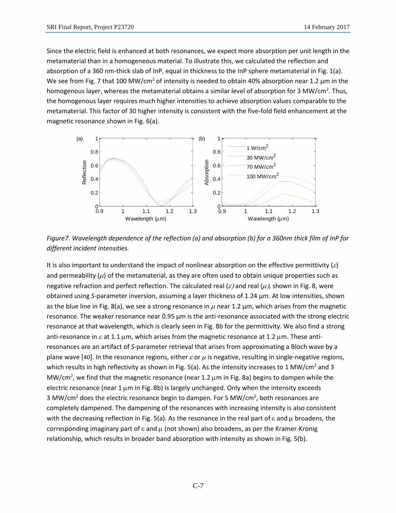
Since the electric field is enhanced at both resonances, we expect more absorption per unit length in the
metamaterial than in a homogeneous material. To illustrate this, we calculated the reflection and
absorption of a 360 nm-thick slab of InP, equal in thickness to the InP sphere metamaterial in Fig. 1(a).
We see from Fig. 7 that 100 MW/cm2 of intensity is needed to obtain 40% absorption near 1.2 μm in the
homogenous layer, whereas the metamaterial obtains a similar level of absorption for 3 MW/cm2. Thus,
the homogenous layer requires much higher intensities to achieve absorption values comparable to the
metamaterial. This factor of 30 higher intensity is consistent with the five-fold field enhancement at the
magnetic resonance shown in Fig. 6(a).
0.9 1 1.1 1.2 1.30
0.2
0.4
0.6
0.8
1(a)
Wavelength (m)
Reflection
0.9 1 1.1 1.2 1.30
0.2
0.4
0.6
0.8
1
Wavelength (m)
Absorp
tion
(b)
1 W/cm2
30 MW/cm2
70 MW/cm2
100 MW/cm2
Figure7. Wavelength dependence of the reflection (a) and absorption (b) for a 360nm thick film of InP for
different incident intensities.
It is also important to understand the impact of nonlinear absorption on the effective permittivity ()
and permeability () of the metamaterial, as they are often used to obtain unique properties such as
negative refraction and perfect reflection. The calculated real ( and real (, shown in Fig. 8, were
obtained using S-parameter inversion, assuming a layer thickness of 1.24 μm. At low intensities, shown
as the blue line in Fig. 8(a), we see a strong resonance in near 1.2 μm, which arises from the magnetic
resonance. The weaker resonance near 0.95 μm is the anti-resonance associated with the strong electric
resonance at that wavelength, which is clearly seen in Fig. 8b for the permittivity. We also find a strong
anti-resonance in at 1.1 m, which arises from the magnetic resonance at 1.2 m. These anti-
resonances are an artifact of S-parameter retrieval that arises from approximating a Bloch wave by a
plane wave [40]. In the resonance regions, either or is negative, resulting in single-negative regions,
which results in high reflectivity as shown in Fig. 5(a). As the intensity increases to 1 MW/cm2 and 3
MW/cm2, we find that the magnetic resonance (near 1.2 m in Fig. 8a) begins to dampen while the
electric resonance (near 1 m in Fig. 8b) is largely unchanged. Only when the intensity exceeds
3 MW/cm2 does the electric resonance begin to dampen. For 5 MW/cm2, both resonances are
completely dampened. The dampening of the resonances with increasing intensity is also consistent
with the decreasing reflection in Fig. 5(a). As the resonance in the real part of and broadens, the
corresponding imaginary part of and (not shown) also broadens, as per the Kramer-Kronig
relationship, which results in broader band absorption with intensity as shown in Fig. 5(b).

SRI Final Report, Project P23720 14 February 2017
C-8
0.9 1 1.1 1.2 1.3-2
0
2
4
6
Wavelength (m)
Eff
ective p
erm
eabili
ty (
)
1 W/cm2
1 MW/cm2
3 MW/cm2
5 MW/cm2
0.9 1 1.1 1.2 1.3-2
0
2
4
6
8
10
Wavelength (m)
Eff
ective p
erm
ittivity (
)
Figure 8. Wavelength dependence of the effective permeability and permittivity of the InP metamaterial
for different incident intensities.
In summary, we developed a full-wave model to study the effects of two-photon absorption and photo-
induced free-carrier absorption on the effective parameters and optical properties of a structured
dielectric metamaterial. As expected, we find that nonlinear absorption leads to dampening of the
electric and magnetic Mie resonances at high intensities, with an onset around 1 MW/cm2, assuming
continuous wave illumination. The resonances are almost completely dampened for intensities around
5 MW/cm2. Surprisingly, we find that the nonlinear absorption at the magnetic resonance is larger than
at the electric resonance, despite the electric field being more concentrated at the electric resonance.
We find this is because the free-carrier absorption cross section is considerably larger at the longer
wavelengths near the magnetic resonance. We also find that the metamaterial provides absorption
comparable to a homogeneous layer of the same thickness at approximately 30 times less intensity. The
lower threshold intensity and smaller footprint for nonlinear absorption can be exploited in applications
involving optical limiting, frequency conversion, the Kerr effect, and four-wave mixing.
References
1. Van Stryland, E.W., Vanherzeele, H., Woodall, M.A., Soileau, M.J., Smirl, A.L., Guha, S. and Boggess, T.F., 1985. Two photon absorption, nonlinear refraction, and optical limiting in semiconductors. Optical Engineering, 24(4), pp.244613-244613.
2. Boggess, T., Smirl, A., Moss, S., Boyd, I. and Van Stryland, E., 1985. Optical limiting in GaAs. IEEE journal of quantum electronics, 21(5), pp.488-494.
3. Van Stryland, E.W., Wu, Y.Y., Hagan, D.J., Soileau, M.J. and Mansour, K., 1988. Optical limiting with semiconductors. JOSA B, 5(9), pp.1980-1988.
4. Scalora, M., Dowling, J.P., Bowden, C.M. and Bloemer, M.J., 1994. Optical limiting and switching of ultrashort pulses in nonlinear photonic band gap materials. Physical review letters, 73(10), p.1368.
5. Tran, P., 1997. Optical limiting and switching of short pulses by use of a nonlinear photonic bandgap structure with a defect. JOSA B, 14(10), pp.2589-2595.
6. Haché, A. and Bourgeois, M., 2000. Ultrafast all-optical switching in a silicon-based photonic crystal. Applied Physics Letters, 77(25), pp.4089-4091.
7. Rashkeev, S.N. and Lambrecht, W.R., 2001. Second-harmonic generation of I-III-VI 2 chalcopyrite semiconductors: Effects of chemical substitutions. Physical Review B, 63(16), p.165212.

SRI Final Report, Project P23720 14 February 2017
C-9
8. Lekse, J.W., Moreau, M.A., McNerny, K.L., Yeon, J., Halasyamani, P.S. and Aitken, J.A., 2009. Second-harmonic generation and crystal structure of the diamond-like semiconductors Li2CdGeS4 and Li2CdSnS4. Inorganic chemistry, 48(16), pp.7516-7518.
9. Gallo, K. and Assanto, G., 1999. All-optical diode based on second-harmonic generation in an asymmetric waveguide. JOSA B, 16(2), pp.267-269.
10. Yu, Z. and Fan, S., 2009. Complete optical isolation created by indirect interband photonic transitions. Nature photonics, 3(2), pp.91-94.
11. Chang, D.E., Vuletić, V. and Lukin, M.D., 2014. Quantum nonlinear optics [mdash] photon by photon. Nature Photonics, 8(9), pp.685-694.
12. Bechtel, J.H. and Smith, W.L., 1976. Two-photon absorption in semiconductors with picosecond laser pulses. Physical Review B, 13(8), p.3515.
13. Boggess, T., Bohnert, K., Mansour, K., Moss, S., Boyd, I. and Smirl, A., 1986. Simultaneous measurement of the two-photon coefficient and free-carrier cross section above the bandgap of crystalline silicon. IEEE journal of quantum electronics, 22(2), pp.360-368.
14. Krishnamurthy, S., Yu, Z.G., Gonzalez, L.P. and Guha, S., 2011. Temperature-and wavelength-dependent two-photon and free-carrier absorption in GaAs, InP, GaInAs, and InAsP. Journal of Applied Physics, 109(3), p.033102.
15. M. Kauranen and A. V. Zayats, Nat. Photon. 6, 737 (2012).
16. Schuller, J.A., Barnard, E.S., Cai, W., Jun, Y.C., White, J.S. and Brongersma, M.L., 2010. Plasmonics for extreme light concentration and manipulation. Nature materials, 9(3), pp.193-204.
17. Czaplicki, R., Husu, H., Siikanen, R., Mäkitalo, J., Kauranen, M., Laukkanen, J., Lehtolahti, J. and Kuittinen, M., 2013. Enhancement of second-harmonic generation from metal nanoparticles by passive elements. Physical review letters, 110(9), p.093902.
18. Aouani, H., Navarro-Cia, M., Rahmani, M., Sidiropoulos, T.P., Hong, M., Oulton, R.F. and Maier, S.A., 2012. Multiresonant broadband optical antennas as efficient tunable nanosources of second harmonic light. Nano letters, 12(9), pp.4997-5002.
19. Thyagarajan, K., Rivier, S., Lovera, A. and Martin, O.J., 2012. Enhanced second-harmonic generation from double resonant plasmonic antennae. Optics express, 20(12), pp.12860-12865.
20. Thyagarajan, K., Butet, J. and Martin, O.J., 2013. Augmenting second harmonic generation using Fano resonances in plasmonic systems. Nano letters, 13(4), pp.1847-1851.
21. Zhang, Y., Grady, N.K., Ayala-Orozco, C. and Halas, N.J., 2011. Three-dimensional nanostructures as highly efficient generators of second harmonic light. Nano letters, 11(12), pp.5519-5523.
22. Harutyunyan, H., Volpe, G., Quidant, R. and Novotny, L., 2012. Enhancing the nonlinear optical response using multifrequency gold-nanowire antennas. Physical review letters, 108(21), p.217403.
23. Navarro-Cia, M. and Maier, S.A., 2012. Broad-band near-infrared plasmonic nanoantennas for higher harmonic generation. ACS nano, 6(4), pp.3537-3544.
24. Gu, J., Singh, R., Liu, X., Zhang, X., Ma, Y., Zhang, S., Maier, S.A., Tian, Z., Azad, A.K., Chen, H.T. and Taylor, A.J., 2012. Active control of electromagnetically induced transparency analogue in terahertz metamaterials. Nature communications, 3, p.1151.
25. Kurter, C., Tassin, P., Zhang, L., Koschny, T., Zhuravel, A.P., Ustinov, A.V., Anlage, S.M. and Soukoulis, C.M., 2011. Classical analogue of electromagnetically induced transparency with a metal-superconductor hybrid metamaterial. Physical review letters, 107(4), p.043901.
26. Shcherbakov, M.R., Neshev, D.N., Hopkins, B., Shorokhov, A.S., Staude, I., Melik-Gaykazyan, E.V., Decker, M., Ezhov, A.A., Miroshnichenko, A.E., Brener, I. and Fedyanin, A.A., 2014. Enhanced third-harmonic generation in silicon nanoparticles driven by magnetic response. Nano letters, 14(11), pp.6488-6492.

SRI Final Report, Project P23720 14 February 2017
C-10
27. Yang, Y., Wang, W., Boulesbaa, A., Kravchenko, I.I., Briggs, D.P., Puretzky, A., Geohegan, D. and Valentine, J., 2015. Nonlinear Fano-resonant dielectric metasurfaces. Nano letters, 15(11), pp.7388-7393.
28. Shcherbakov, M.R., Shorokhov, A.S., Neshev, D.N., Hopkins, B., Staude, I., Melik-Gaykazyan, E.V., Ezhov, A.A., Miroshnichenko, A.E., Brener, I., Fedyanin, A.A. and Kivshar, Y.S., 2015. Nonlinear interference and tailorable third-harmonic generation from dielectric oligomers. ACS Photonics, 2(5), pp.578-582.
29. Smirnova, D.A., Khanikaev, A.B., Smirnov, L.A. and Kivshar, Y.S., 2016. Multipolar third-harmonic generation driven by optically induced magnetic resonances. ACS Photonics, 3(8), pp.1468-1476.
30. Grinblat, G., Li, Y., Nielsen, M.P., Oulton, R.F. and Maier, S.A., 2016. Enhanced third harmonic generation in single germanium nanodisks excited at the anapole mode. Nano letters, 16(7), pp.4635-4640.
31. Shorokhov, A.S., Melik-Gaykazyan, E.V., Smirnova, D.A., Hopkins, B., Chong, K.E., Choi, D.Y., Shcherbakov, M.R., Miroshnichenko, A.E., Neshev, D.N., Fedyanin, A.A. and Kivshar, Y.S., 2016. Multifold enhancement of third-harmonic generation in dielectric nanoparticles driven by magnetic Fano resonances. Nano Letters, 16(8), pp.4857-4861.
32. Shcherbakov, M.R., Vabishchevich, P.P., Shorokhov, A.S., Chong, K.E., Choi, D.Y., Staude, I., Miroshnichenko, A.E., Neshev, D.N., Fedyanin, A.A. and Kivshar, Y.S., 2015. Ultrafast all-optical switching with magnetic resonances in nonlinear dielectric nanostructures. Nano letters, 15(10), pp.6985-6990.
33. Makarov, S., Kudryashov, S., Mukhin, I., Mozharov, A., Milichko, V., Krasnok, A. and Belov, P., 2015. Tuning of magnetic optical response in a dielectric nanoparticle by ultrafast photoexcitation of dense electron–hole plasma. Nano letters, 15(9), pp.6187-6192.
34. Baranov, D.G., Makarov, S.V., Milichko, V.A., Kudryashov, S.I., Krasnok, A.E. and Belov, P.A., 2016. Nonlinear transient dynamics of photoexcited resonant silicon nanostructures. ACS Photonics, 3(9), pp.1546-1551.
35. Weismann, M., Gallagher, D.F. and Panoiu, N.C., 2015. Nonlinear generalized source method for modeling second-harmonic generation in diffraction gratings. JOSA B, 32(4), pp.523-533.
36. Weismann, M. and Panoiu, N.C., 2016. Theoretical and computational analysis of second-and third-harmonic generation in periodically patterned graphene and transition-metal dichalcogenide monolayers. Physical Review B, 94(3), p.035435.
37. Kruk, S., Weismann, M., Bykov, A.Y., Mamonov, E.A., Kolmychek, I.A., Murzina, T., Panoiu, N.C., Neshev, D.N. and Kivshar, Y.S., 2015. Enhanced magnetic second-harmonic generation from resonant metasurfaces. ACS Photonics, 2(8), pp.1007-1012.
38. Shen, Y.R., 1984. The principles of nonlinear optics. New York, Wiley-Interscience, 1984, 575 p., 1.
39. Stegeman, G.I. and Stegeman, R.A., 2012. Nonlinear Optics: Phenomena, Materials and Devices (Vol. 78). John Wiley & Sons.
40. Koschny, T., Markoš, P., Smith, D.R. and Soukoulis, C.M., 2003. Resonant and antiresonant frequency dependence of the effective parameters of metamaterials. Physical Review E, 68(6), p.065602.