pll dynamic reconfiguration - xilinx - all programmable€¦ · · 2018-01-10interface is...
TRANSCRIPT

XAPP879 (v1.1) October 26, 2011 www.xilinx.com 1
© Copyright 2010–2011 Xilinx, Inc. Xilinx, the Xilinx logo, Artix, ISE, Kintex, Spartan, Virtex, Zynq, and other designated brands included herein are trademarks of Xilinx in the United States and other countries. All other trademarks are the property of their respective owners.
Summary This application note provides a method to dynamically change the clock output frequency, phase shift, and duty cycle of the Spartan®-6 FPGA Phase Locked Loop (PLL) through its Dynamic Reconfiguration Port (DRP). An explanation of the behavior of the internal DRP control registers is accompanied by a reference design. The reference design uses a state machine to drive the DRP to ensure that the registers are controlled in the correct sequence.
Caution! If post-configuration cyclic redundancy check (CRC) functionality is needed in the design, the PLL DRP port cannot be used to dynamically reconfigure the PLL. Use of the PLL DRP port breaks the functionality of post-configuration CRC.
Although the reference design performs the operations for the user, familiarity with the functional operation of the PLL is recommended. The PLL used in conjunction with the DRP interface is recommended for advanced users when the basic PLL functionality is not sufficient. The DCM_CLKGEN primitive can be a useful alternative to using the PLL with the DRP interface. For more information on PLL functionality, see UG382, Spartan-6 FPGA Clocking Resources User Guide.
The reference design supports two reconfiguration state addresses and can be extended to support additional states. Each state does a full reconfiguration of the PLL so that most parameters can be changed.
Introduction The clock management tiles (CMT) in the Spartan-6 devices contain two DCMs and one PLL. One of the most powerful features of the PLL is its ability to dynamically reconfigure the phase, duty cycle, and divide values of the clock outputs. This application note describes the information necessary to reconfigure the PLL, and provides a reference design that implements all of the algorithms covered. The PLL used in this reference design is intended to be used with CLKFBOUT as the feedback path. The reference design does not support the use of CLKOUT for the feedback path.
Reconfiguration is performed through the PLL DRP. The DRP provides access to the configuration bits that would normally only be initialized in the bitstream. This allows the user to dynamically change the PLL clock outputs while the design is running. Frequency, phase, and duty cycle can all be changed dynamically. To properly reconfigure the PLL, it must be initially set up with integer divider values.
The PLL Configuration Bit Groups and PLL DRP Registers sections present the configuration bits as four bit groups, provide an overview of their usage, and detail the configuration bit locations as registers. This information is not necessary to use the DRP reference design; it is intended to give an overview of the internal PLL attributes that must be changed along with their register locations. Specific information on how the attributes are calculated is provided through the reference design. The reference design functionality and use are explained in the Reference Design and Using the Reference Design sections.
Application Note: Spartan-6 Family
XAPP879 (v1.1) October 26, 2011
PLL Dynamic ReconfigurationAuthor: Karl Kurbjun and Carl Ribbing
PLL Configuration Bit Groups
XAPP879 (v1.1) October 26, 2011 www.xilinx.com 2
PLL Configuration Bit Groups
The PLL has four user-accessible configuration bit groups that allow reconfiguration of individual clock outputs. The four groups are the divider group, the phase group, the lock group, and the filter group. These configuration bit groups are internal to the PLL primitive and clarify the operation of the PLL_DRP module. The user modifiable parameters for the PLL_DRP module are described in the Reconfiguration Module Ports and Attributes section.
Divider Group
Every clock output has a divider group associated with it. The divider group is composed of the following parameters:
• High Time
• Low Time
• No Count
• Edge
The first two parameters associated with the divider group are the High and Low Time counters. These counters set the number of voltage-controlled oscillator (VCO) clock cycles through which the output clock should stay High or Low. For example, if you set both High and Low Time to 2, the effective divide value is 4 and the duty cycle is 50%.
The No Count parameter disables the High and Low Time counters. This in turn makes the divider output a clock with an effective divide value of 1.
The Edge parameter controls the High to Low transition. It forces the High Time counter to transition on a falling edge at the end of its count. This has the effect of increasing the High Time while decreasing the Low Time. Another way to think of the edge bit is that it adds half a VCO clock cycle to the High Time and subtracts half a clock cycle from the Low Time.
As an example, if a 50/50 duty cycle is desired with a divide value of 3, the Edge bit would be set. The High Time counter would be set to one and the Low Time counter would be set to 2. With the edge bit set, the net count for the High and Low times would be 1.5 clock cycles each.
Phase Group
Each clock output except the DIVCLK has a phase group associated with it. This group is composed of the following set of parameters:
• Phase MUX
• Delay Time
The Phase MUX selects a coarse phase from the VCO for a clock output with a resolution of 45° (360°/8) relative to the VCO clock period.
Delay Time is a counter that counts the number of VCO clock cycles to delay the output. This means that there is a direct correlation between the possible phase shift for the clock output and the divide value for that particular output. As the divide value increases, finer phase shift steps are available. The Delay Time counter allows for a phase offset of up to 64 VCO clock cycles.
Lock Group
This group cannot be calculated with an algorithm and is based on lookup tables created from device characterization. The appropriate lock bit settings are dependent on the feedback divider setting. This divider is set with the CLKFBOUT_MULT attribute when instantiating the PLL_DRP module. The lock group has an effect on the PLL’s ability to detect that it is locked. The lookup table is located in the reference design within pll_drp_func.h.

PLL DRP Registers
XAPP879 (v1.1) October 26, 2011 www.xilinx.com 3
Filter Group
This group cannot be calculated, and is based on lookup tables created from device characterization. There are effectively two tables, one for each bandwidth setting. The feedback divider setting (CLKFBOUT_MULT) acts as the index to the chosen table. There are three bandwidth settings allowable in the tools (High, Low, and Optimized), but in effect, there are only two. High and Optimized use the same table, while the Low bandwidth setting uses a separate table. The filter group has an effect on the phase skew and the jitter filtering capability of the PLL. The lookup table is located in the reference design within pll_drp_func.h.
PLL DRP Registers
Each clock output is associated with a number of configuration bits. The CLKOUT and CLKFBOUT outputs are associated with phase and divider group bits. The locked and filter bits are associated with the CLKFBOUT configuration. The DIVCLK output does not have any associated phase configuration bits. Figure 1 shows the six clock outputs, the feedback clock output, and the DIVCLK (indicated by D in Figure 1).
The PLL DRP address map, which stores the configuration bits, is provided in the Appendix, page 11. Table 1 describes the functionality associated with each register type used in the DRP address map.
X-Ref Target - Figure 1
Figure 1: PLL Block Diagram
Table 1: PLL Register Type Description
Register Type Width Description
PHASE MUX 3 This register type chooses an initial phase offset for the clock output. The resolution of the offset is equal to 1/8 of the VCO period.
HIGH TIME 6 This register type sets the amount of time, in VCO cycles, that the clock output remains High.
LOW TIME 6 This register type sets the amount of time, in VCO cycles, that the clock output remains Low.
DELAY TIME 6 This register type sets the phase offset with a resolution equal to the VCO period.
NO COUNT 1 This register type bypasses the High and Low time counters.
EDGE 1 This register type chooses the edge on which the High time counter transitions.
Clock Pin
D
M
PFD CP LF VCO O0
O1
O2
O3
O4
O5
XAPP879_01_031610

Reference Design
XAPP879 (v1.1) October 26, 2011 www.xilinx.com 4
Reference Design
The reference design files include a Verilog PLL reconfiguration module. This module uses only 25 total slices, comprising the reconfiguration logic and state memory.
The reference design drives the DRP port with a state machine that addresses the PLL, reads the previous value, masks the bits that need to be changed, sets the new value, and finally writes the value to the PLL DRP port. The addresses, masks, and new values are stored in a pre-initialized ROM that is filled during elaboration in synthesis. The ROM initialization is done with constant functions provided with the reference design.
Figure 2 is a block diagram of the reconfiguration module.
The pll_drp.v module contains the state machine and ROM, and calls the constant functions which are provided in pll_drp_func.h.
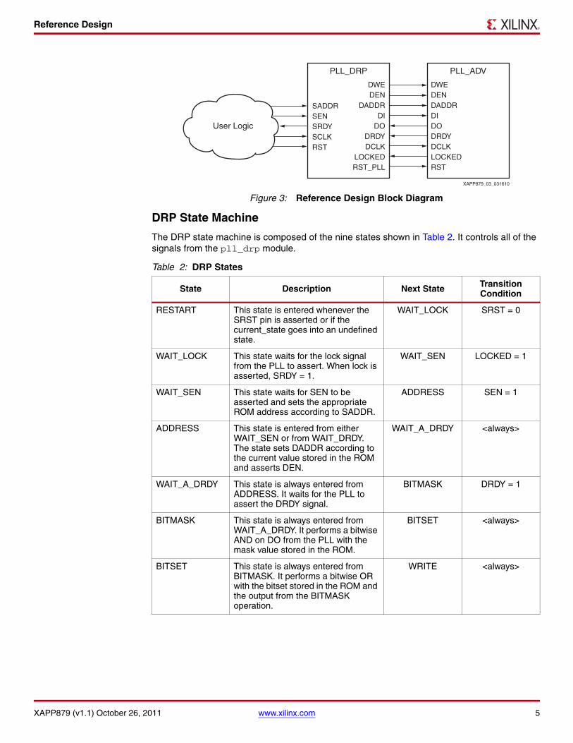
Figure 3 shows the block diagram of the system with the pll_adv and the pll_drp modules attached.
LOCK TABLE 40 These bits are pulled from the lock lookup table provided in the reference design.
FILTER TABLE 10 These bits are pulled from the filter lookup table provided in the reference design.
RESERVED X This register type retains the previous value stored here.
Table 1: PLL Register Type Description (Cont’d)
Register Type Width Description
X-Ref Target - Figure 2
Figure 2: PLL_DRP Internal Block Diagram
State machinegenerates control anddata signals for thePLL DRP portusing pre-computedvalues stored in DISTROM.
User attributes map to PLL attributes with the addition of S1_ and S2_notation, for example S1_CLKOUT0_DIVIDE.
SADDRSEN
SRDYSCLK
RST
XAPP879_02_092311
DWEDENDADDRDIDODRDYDCLKLOCKEDRST_PLL
Memory filled in withconstant functions based
on parameters wheninstantiating the PLL_DRP.
DISTROMDRP State MachinePLL_DRP
rom_addrrom_do
PRIMARY
SECONDARY
SRDY asserts forone clock cycle whenthe PLL_ADV locksand the state machineis ready to start anotherreconfiguration.
Reference Design
XAPP879 (v1.1) October 26, 2011 www.xilinx.com 5
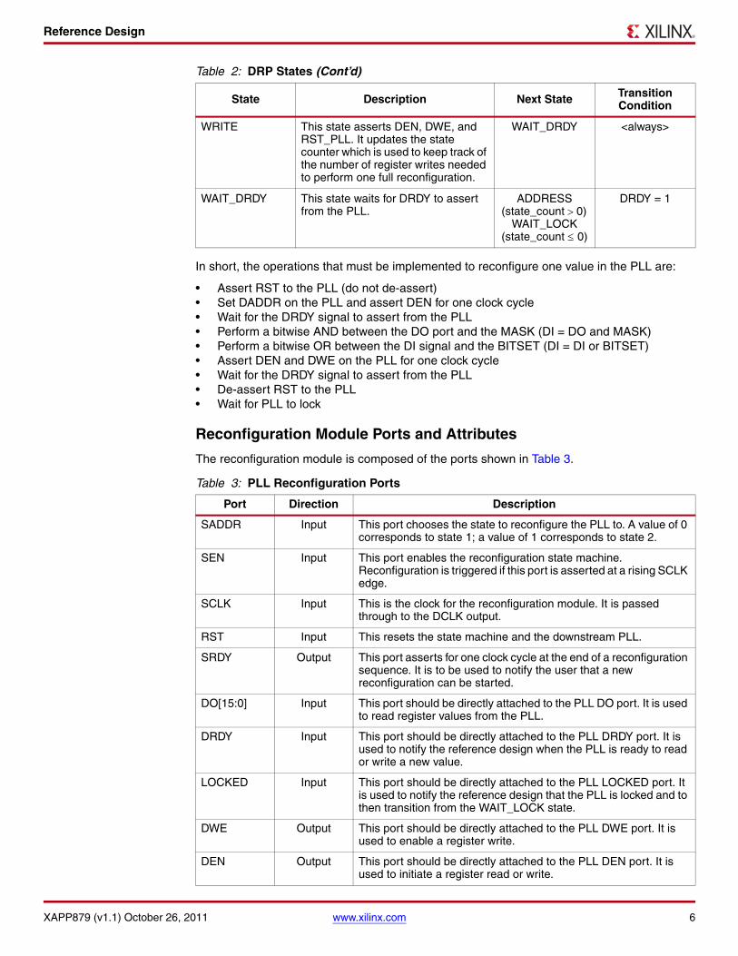
DRP State Machine
The DRP state machine is composed of the nine states shown in Table 2. It controls all of the signals from the pll_drp module.
X-Ref Target - Figure 3
Figure 3: Reference Design Block Diagram
Table 2: DRP States
State Description Next State Transition Condition
RESTART This state is entered whenever the SRST pin is asserted or if the current_state goes into an undefined state.
WAIT_LOCK SRST = 0
WAIT_LOCK This state waits for the lock signal from the PLL to assert. When lock is asserted, SRDY = 1.
WAIT_SEN LOCKED = 1
WAIT_SEN This state waits for SEN to be asserted and sets the appropriate ROM address according to SADDR.
ADDRESS SEN = 1
ADDRESS This state is entered from either WAIT_SEN or from WAIT_DRDY. The state sets DADDR according to the current value stored in the ROM and asserts DEN.
WAIT_A_DRDY <always>
WAIT_A_DRDY This state is always entered from ADDRESS. It waits for the PLL to assert the DRDY signal.
BITMASK DRDY = 1
BITMASK This state is always entered from WAIT_A_DRDY. It performs a bitwise AND on DO from the PLL with the mask value stored in the ROM.
BITSET <always>
BITSET This state is always entered from BITMASK. It performs a bitwise OR with the bitset stored in the ROM and the output from the BITMASK operation.
WRITE <always>
SADDRSENSRDYSCLKRST
XAPP879_03_031610
DWEDENDADDRDIDODRDYDCLKLOCKEDRST
DWEDEN
DADDRDI
DODRDYDCLK
LOCKEDRST_PLL
User Logic
PLL_DRP PLL_ADV
Reference Design
XAPP879 (v1.1) October 26, 2011 www.xilinx.com 6
In short, the operations that must be implemented to reconfigure one value in the PLL are:
• Assert RST to the PLL (do not de-assert)• Set DADDR on the PLL and assert DEN for one clock cycle• Wait for the DRDY signal to assert from the PLL• Perform a bitwise AND between the DO port and the MASK (DI = DO and MASK)• Perform a bitwise OR between the DI signal and the BITSET (DI = DI or BITSET)• Assert DEN and DWE on the PLL for one clock cycle• Wait for the DRDY signal to assert from the PLL• De-assert RST to the PLL• Wait for PLL to lock
Reconfiguration Module Ports and Attributes
The reconfiguration module is composed of the ports shown in Table 3.
WRITE This state asserts DEN, DWE, and RST_PLL. It updates the state counter which is used to keep track of the number of register writes needed to perform one full reconfiguration.
WAIT_DRDY <always>
WAIT_DRDY This state waits for DRDY to assert from the PLL.
ADDRESS (state_count0)
WAIT_LOCK (state_count0)
DRDY = 1
Table 3: PLL Reconfiguration Ports
Port Direction Description
SADDR Input This port chooses the state to reconfigure the PLL to. A value of 0 corresponds to state 1; a value of 1 corresponds to state 2.
SEN Input This port enables the reconfiguration state machine. Reconfiguration is triggered if this port is asserted at a rising SCLK edge.
SCLK Input This is the clock for the reconfiguration module. It is passed through to the DCLK output.
RST Input This resets the state machine and the downstream PLL.
SRDY Output This port asserts for one clock cycle at the end of a reconfiguration sequence. It is to be used to notify the user that a new reconfiguration can be started.
DO[15:0] Input This port should be directly attached to the PLL DO port. It is used to read register values from the PLL.
DRDY Input This port should be directly attached to the PLL DRDY port. It is used to notify the reference design when the PLL is ready to read or write a new value.
LOCKED Input This port should be directly attached to the PLL LOCKED port. It is used to notify the reference design that the PLL is locked and to then transition from the WAIT_LOCK state.
DWE Output This port should be directly attached to the PLL DWE port. It is used to enable a register write.
DEN Output This port should be directly attached to the PLL DEN port. It is used to initiate a register read or write.
Table 2: DRP States (Cont’d)
State Description Next State Transition Condition

Reference Design
XAPP879 (v1.1) October 26, 2011 www.xilinx.com 7
The reconfiguration module also has the attributes shown in Table 4. The PLL_DRP attributes correlate with the standard PLL primitive attributes with some slight naming differences.
DADDR[6:0] Output This port should be directly attached to the PLL DADDR port. It is used to address a register location for reads or writes.
DI[15:0] Output This port should be directly attached to the PLL DI port. It is used to output a new register value for writes.
DCLK Output This port should be directly attached to the PLL DCLK port. It is used to clock the reconfiguration port on the PLL. It is the SCLK forwarded out of the PLL reconfiguration module.
RST_PLL Output This port should be directly attached to the PLL RST port. It is used to reset the PLL during a reconfiguration or when the RST port is asserted.
Table 4: PLL Reconfiguration Attributes
Attribute Description Valid Format Values
CLKFBOUT_MULT This attribute modifies the input clock multiplier to change the VCO output frequency of the PLL.
1–64; Integer values only.
CLKFBOUT_PHASE Modifies the phase of the input clock. This affects all of the PLL outputs.
Integer values multiplied by 1,000. For example, a 45° phase shift would be 45,000
BANDWIDTH Sets the bandwidth setting of the PLL.
OPTIMIZED, HIGH, or LOW.
DIVCLK_DIVIDE Sets the divide value for the DIVCLK output.
1–52; Integer values only.
CLKOUT0_DIVIDE CLKOUT0 output divide value. 1–128; Integer values only.
CLKOUT0_PHASE CLKOUT0 output phase value. Integer values multiplied by 1,000. For example, a 45° phase shift would be 45,000.
CLKOUT0_DUTY Changes the CLKOUT0 Duty Cycle Low Time.
Integer values multiplied by 100,000. For example, a 0.60 duty cycle would be 60,000.
CLKOUT1_DIVIDE CLKOUT1 output divide value. 1–128; Integer values only.
CLKOUT1_PHASE CLKOUT1 output phase value. Integer values multiplied by 1,000. For example, a 45° phase shift would be 45,000.
CLKOUT1_DUTY Changes the CLKOUT1 Duty Cycle Low Time.
Integer values multiplied by 100,000. For example, a 0.60 duty cycle would be 60,000.
CLKOUT2_DIVIDE CLKOUT2 output divide value. 1–128; Integer values only.
CLKOUT2_PHASE CLKOUT2 output phase value. Integer values multiplied by 1,000. For example, a 45° phase shift would be 45,000.
CLKOUT2_DUTY Changes the CLKOUT2 Duty Cycle Low Time.
Integer values multiplied by 1,000. For example, a 60/40 duty cycle would be 60,000.
CLKOUT3_DIVIDE CLKOUT3 output divide value 1-128; Integer values only.
Table 3: PLL Reconfiguration Ports (Cont’d)
Port Direction Description
Using the Reference Design
XAPP879 (v1.1) October 26, 2011 www.xilinx.com 8
Using the Reference Design
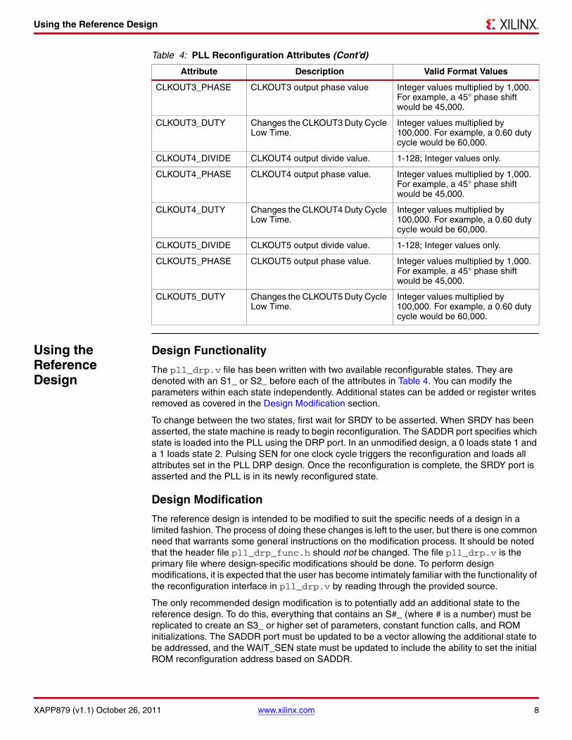
Design Functionality
The pll_drp.v file has been written with two available reconfigurable states. They are denoted with an S1_ or S2_ before each of the attributes in Table 4. You can modify the parameters within each state independently. Additional states can be added or register writes removed as covered in the Design Modification section.
To change between the two states, first wait for SRDY to be asserted. When SRDY has been asserted, the state machine is ready to begin reconfiguration. The SADDR port specifies which state is loaded into the PLL using the DRP port. In an unmodified design, a 0 loads state 1 and a 1 loads state 2. Pulsing SEN for one clock cycle triggers the reconfiguration and loads all attributes set in the PLL DRP design. Once the reconfiguration is complete, the SRDY port is asserted and the PLL is in its newly reconfigured state.
Design Modification
The reference design is intended to be modified to suit the specific needs of a design in a limited fashion. The process of doing these changes is left to the user, but there is one common need that warrants some general instructions on the modification process. It should be noted that the header file pll_drp_func.h should not be changed. The file pll_drp.v is the primary file where design-specific modifications should be done. To perform design modifications, it is expected that the user has become intimately familiar with the functionality of the reconfiguration interface in pll_drp.v by reading through the provided source.
The only recommended design modification is to potentially add an additional state to the reference design. To do this, everything that contains an S#_ (where # is a number) must be replicated to create an S3_ or higher set of parameters, constant function calls, and ROM initializations. The SADDR port must be updated to be a vector allowing the additional state to be addressed, and the WAIT_SEN state must be updated to include the ability to set the initial ROM reconfiguration address based on SADDR.
CLKOUT3_PHASE CLKOUT3 output phase value Integer values multiplied by 1,000. For example, a 45° phase shift would be 45,000.
CLKOUT3_DUTY Changes the CLKOUT3 Duty Cycle Low Time.
Integer values multiplied by 100,000. For example, a 0.60 duty cycle would be 60,000.
CLKOUT4_DIVIDE CLKOUT4 output divide value. 1-128; Integer values only.
CLKOUT4_PHASE CLKOUT4 output phase value. Integer values multiplied by 1,000. For example, a 45° phase shift would be 45,000.
CLKOUT4_DUTY Changes the CLKOUT4 Duty Cycle Low Time.
Integer values multiplied by 100,000. For example, a 0.60 duty cycle would be 60,000.
CLKOUT5_DIVIDE CLKOUT5 output divide value. 1-128; Integer values only.
CLKOUT5_PHASE CLKOUT5 output phase value. Integer values multiplied by 1,000. For example, a 45° phase shift would be 45,000.
CLKOUT5_DUTY Changes the CLKOUT5 Duty Cycle Low Time.
Integer values multiplied by 100,000. For example, a 0.60 duty cycle would be 60,000.
Table 4: PLL Reconfiguration Attributes (Cont’d)
Attribute Description Valid Format Values
Design Verification
XAPP879 (v1.1) October 26, 2011 www.xilinx.com 9
Design Verification
The reference design was verified in hardware and with simulation. This ensures that the simulation models and the hardware functionality are equivalent. The verification process chose a number of corner cases for reconfiguration along with some standard configurations to verify that the calculations worked across each scenario. The functions that calculate the various bit settings have also gone through a complete analysis to ensure they match the calculations performed by the ISE® software backend tools during implementation.
Conclusion This application note and reference design provide a complete implementation of the PLL DRP functionality. Due to its modular nature, the design can be used as a full solution for DRP or can be easily extended to support additional reconfiguration states. The design also uses minimal Spartan-6 FPGA resources, consuming only 25 slices.
Reference Design Additional Information
Files
The reference design files can be downloaded from:
https://secure.xilinx.com/webreg/clickthrough.do?cid=143937
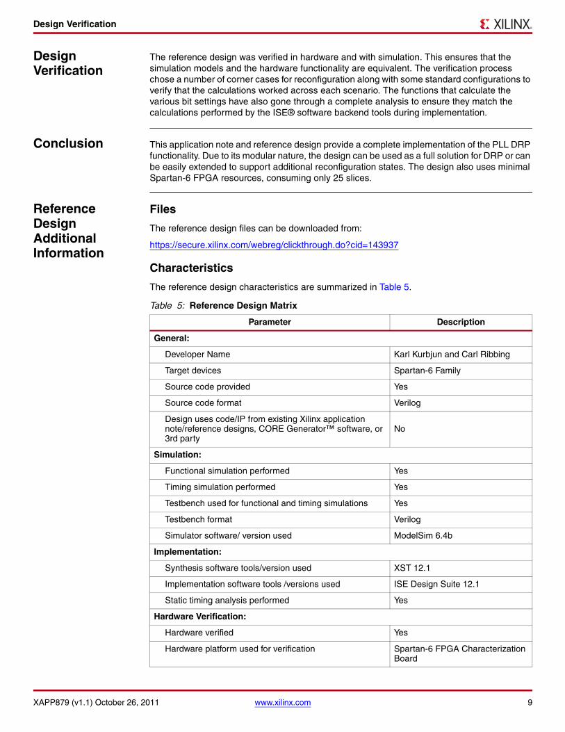
Characteristics
The reference design characteristics are summarized in Table 5.
Table 5: Reference Design Matrix
Parameter Description
General:
Developer Name Karl Kurbjun and Carl Ribbing
Target devices Spartan-6 Family
Source code provided Yes
Source code format Verilog
Design uses code/IP from existing Xilinx application note/reference designs, CORE Generator™ software, or 3rd party
No
Simulation:
Functional simulation performed Yes
Timing simulation performed Yes
Testbench used for functional and timing simulations Yes
Testbench format Verilog
Simulator software/ version used ModelSim 6.4b
Implementation:
Synthesis software tools/version used XST 12.1
Implementation software tools /versions used ISE Design Suite 12.1
Static timing analysis performed Yes
Hardware Verification:
Hardware verified Yes
Hardware platform used for verification Spartan-6 FPGA Characterization Board
Reference Design Additional Information
XAPP879 (v1.1) October 26, 2011 www.xilinx.com 10
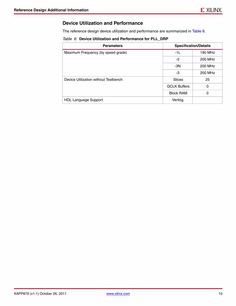
Device Utilization and Performance
The reference design device utilization and performance are summarized in Table 6.
Table 6: Device Utilization and Performance for PLL_DRP
Parameters Specification/Details
Maximum Frequency (by speed grade) -1L 190 MHz
-2 200 MHz
-3N 200 MHz
-3 200 MHz
Device Utilization without Testbench Slices 25
GCLK Buffers 0
Block RAM 0
HDL Language Support Verilog
Appendix
XAPP879 (v1.1) October 26, 2011 www.xilinx.com 11
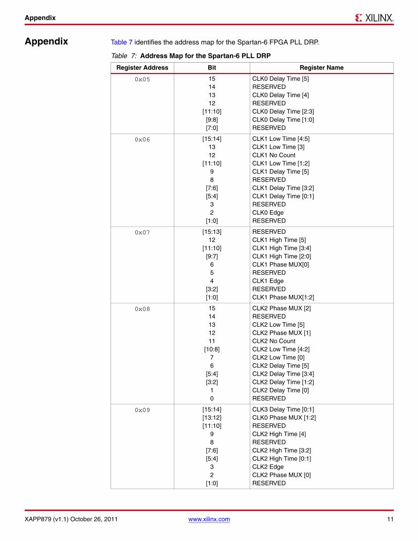
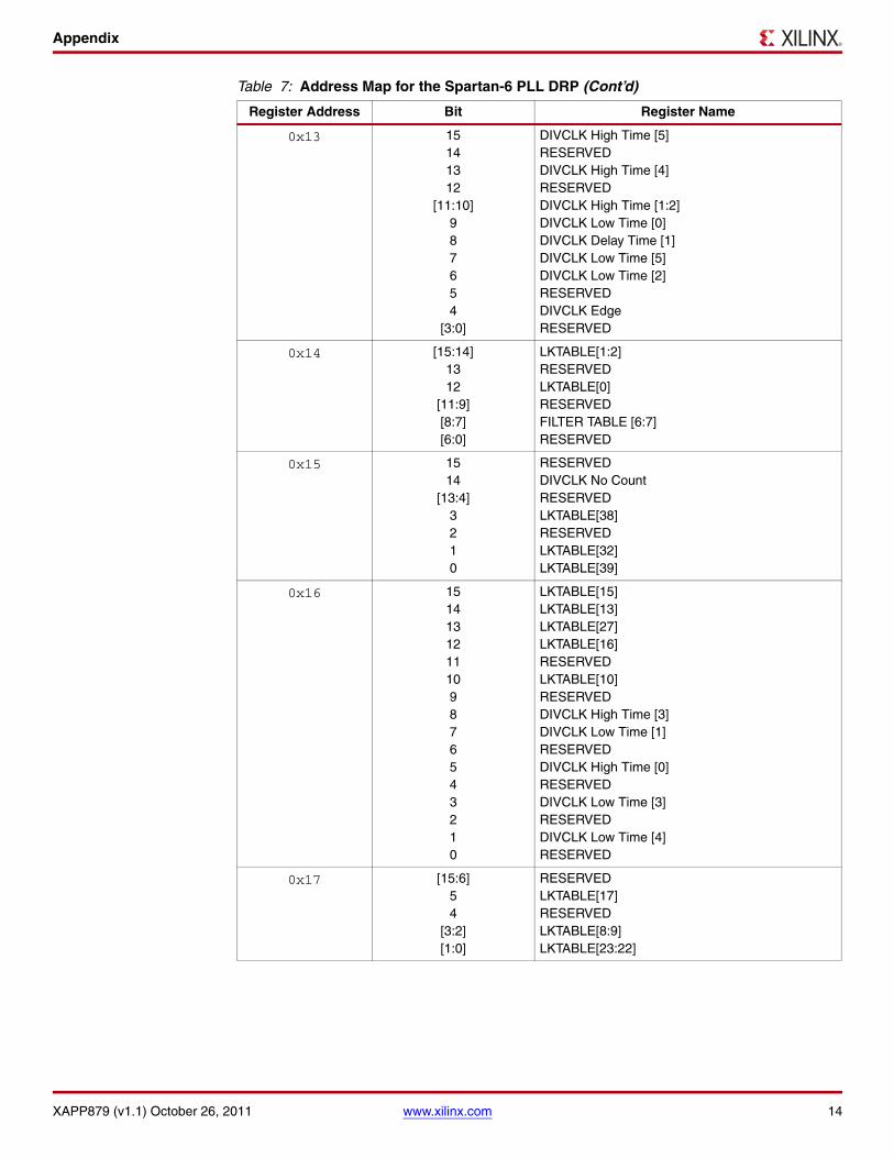
Appendix Table 7 identifies the address map for the Spartan-6 FPGA PLL DRP.
Table 7: Address Map for the Spartan-6 PLL DRP
Register Address Bit Register Name
0x05 15141312
[11:10][9:8][7:0]
CLK0 Delay Time [5]RESERVEDCLK0 Delay Time [4]RESERVEDCLK0 Delay Time [2:3]CLK0 Delay Time [1:0]RESERVED
0x06 [15:14]1312
[11:10]98
[7:6][5:4]
32
[1:0]
CLK1 Low Time [4:5]CLK1 Low Time [3]CLK1 No CountCLK1 Low Time [1:2]CLK1 Delay Time [5]RESERVEDCLK1 Delay Time [3:2]CLK1 Delay Time [0:1]RESERVEDCLK0 EdgeRESERVED
0x07 [15:13]12
[11:10][9:7]
654
[3:2][1:0]
RESERVEDCLK1 High Time [5]CLK1 High Time [3:4]CLK1 High Time [2:0]CLK1 Phase MUX[0]RESERVEDCLK1 EdgeRESERVEDCLK1 Phase MUX[1:2]
0x08 1514131211
[10:8]76
[5:4][3:2]
10
CLK2 Phase MUX [2]RESERVEDCLK2 Low Time [5]CLK2 Phase MUX [1]CLK2 No CountCLK2 Low Time [4:2]CLK2 Low Time [0]CLK2 Delay Time [5]CLK2 Delay Time [3:4]CLK2 Delay Time [1:2]CLK2 Delay Time [0]RESERVED
0x09 [15:14][13:12][11:10]
98
[7:6][5:4]
32
[1:0]
CLK3 Delay Time [0:1]CLK0 Phase MUX [1:2]RESERVEDCLK2 High Time [4]RESERVEDCLK2 High Time [3:2]CLK2 High Time [0:1]CLK2 EdgeCLK2 Phase MUX [0]RESERVED

Appendix
XAPP879 (v1.1) October 26, 2011 www.xilinx.com 12
0x0A 1514
[13:12][11:10]
[9:8]76
[5:4][3:2]
10
RESERVEDCLK3 EdgeRESERVEDCLK3 Phase MUX [1:2]CLK3 Low Time [5:4]CLK3 No CountCLK3 Low Time [2]CLK3 Low Time [0:1]CLK3 Delay Time [4:5]CLK3 Delay Time [3]RESERVED
0x0B 15141312
[11:10]98
[7:5]4
[3:2]10
CLK0 Low Time [5]CLK4 Delay Time [5]CLK4 Delay Time [0]CLK4 Delay Time [3]CLK4 Delay Time [1:2]CLK0 Low Time [4]RESERVEDCLK3 High Time [5:3]RESERVEDCLK3 High Time [1:2]CLK3 Phase MUX [0]CLK3 High Time [0]
0x0C [15:14]13121110
[9:8][7:6][5:4]
32
[1:0]
CLK4 High Time [1:2]CLK4 Phase MUX [0]CLK4 High Time [0]RESERVEDCLK4 EdgeRESERVEDCLK4 Phase MUX [2:1]CLK4 Low Time [4:5]CLK4 Low Time [3]CLK4 No CountCLK4 Low Time [1:2]
0x0D [15:14][13:12][11:10]
[9:7]65432
[1:0]
CLK5 Low Time [2:3]CLK5 Low Time [0:1]CLK5 Delay Time [4:5]CLK5 Delay Time [3:1]CLK0 Low Time [3]CLK0 Low Time [0]CLK0 Low Time [2]RESERVEDCLK4 High Time [5]CLK4 High Time [3:4]
Table 7: Address Map for the Spartan-6 PLL DRP (Cont’d)
Register Address Bit Register Name
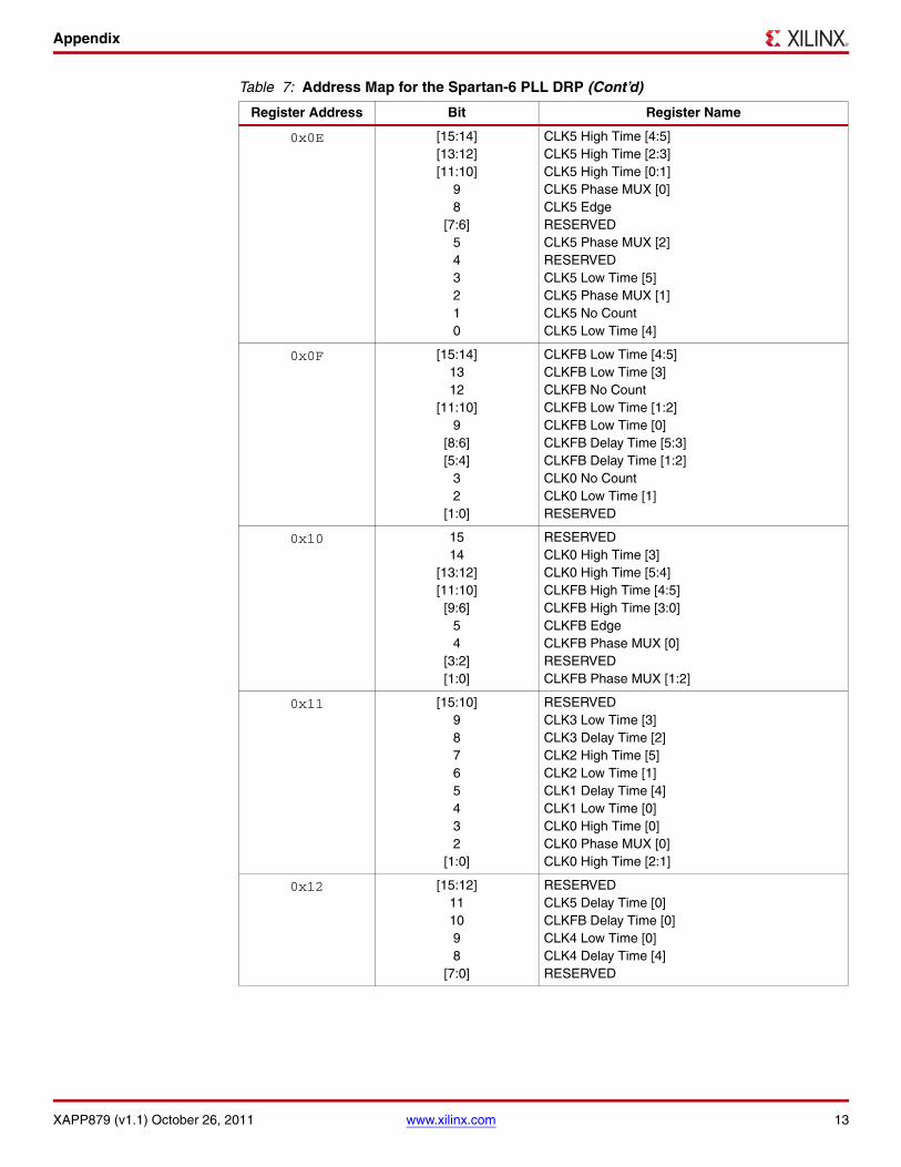
Appendix
XAPP879 (v1.1) October 26, 2011 www.xilinx.com 13
0x0E [15:14][13:12][11:10]
98
[7:6]543210
CLK5 High Time [4:5]CLK5 High Time [2:3]CLK5 High Time [0:1]CLK5 Phase MUX [0]CLK5 EdgeRESERVEDCLK5 Phase MUX [2]RESERVEDCLK5 Low Time [5]CLK5 Phase MUX [1]CLK5 No CountCLK5 Low Time [4]
0x0F [15:14]1312
[11:10]9
[8:6][5:4]
32
[1:0]
CLKFB Low Time [4:5]CLKFB Low Time [3]CLKFB No CountCLKFB Low Time [1:2]CLKFB Low Time [0]CLKFB Delay Time [5:3]CLKFB Delay Time [1:2]CLK0 No CountCLK0 Low Time [1]RESERVED
0x10 1514
[13:12][11:10]
[9:6]54
[3:2][1:0]
RESERVEDCLK0 High Time [3]CLK0 High Time [5:4]CLKFB High Time [4:5]CLKFB High Time [3:0]CLKFB EdgeCLKFB Phase MUX [0]RESERVEDCLKFB Phase MUX [1:2]
0x11 [15:10]98765432
[1:0]
RESERVEDCLK3 Low Time [3]CLK3 Delay Time [2]CLK2 High Time [5]CLK2 Low Time [1]CLK1 Delay Time [4]CLK1 Low Time [0]CLK0 High Time [0]CLK0 Phase MUX [0]CLK0 High Time [2:1]
0x12 [15:12]111098
[7:0]
RESERVEDCLK5 Delay Time [0]CLKFB Delay Time [0]CLK4 Low Time [0]CLK4 Delay Time [4]RESERVED
Table 7: Address Map for the Spartan-6 PLL DRP (Cont’d)
Register Address Bit Register Name
Appendix
XAPP879 (v1.1) October 26, 2011 www.xilinx.com 14
0x13 15141312
[11:10]987654
[3:0]
DIVCLK High Time [5]RESERVEDDIVCLK High Time [4]RESERVEDDIVCLK High Time [1:2]DIVCLK Low Time [0]DIVCLK Delay Time [1]DIVCLK Low Time [5]DIVCLK Low Time [2]RESERVEDDIVCLK EdgeRESERVED
0x14 [15:14]1312
[11:9][8:7][6:0]
LKTABLE[1:2]RESERVEDLKTABLE[0]RESERVEDFILTER TABLE [6:7]RESERVED
0x15 1514
[13:4]3210
RESERVEDDIVCLK No CountRESERVEDLKTABLE[38]RESERVEDLKTABLE[32]LKTABLE[39]
0x16 1514131211109876543210
LKTABLE[15]LKTABLE[13]LKTABLE[27]LKTABLE[16]RESERVEDLKTABLE[10]RESERVEDDIVCLK High Time [3]DIVCLK Low Time [1]RESERVEDDIVCLK High Time [0]RESERVEDDIVCLK Low Time [3]RESERVEDDIVCLK Low Time [4]RESERVED
0x17 [15:6]54
[3:2][1:0]
RESERVEDLKTABLE[17]RESERVEDLKTABLE[8:9]LKTABLE[23:22]
Table 7: Address Map for the Spartan-6 PLL DRP (Cont’d)
Register Address Bit Register Name

Revision History
XAPP879 (v1.1) October 26, 2011 www.xilinx.com 15
Revision History
The following table shows the revision history for this document:
Notice of Disclaimer
The information disclosed to you hereunder (the “Materials”) is provided solely for the selection and use ofXilinx products. To the maximum extent permitted by applicable law: (1) Materials are made available "ASIS" and with all faults, Xilinx hereby DISCLAIMS ALL WARRANTIES AND CONDITIONS, EXPRESS,IMPLIED, OR STATUTORY, INCLUDING BUT NOT LIMITED TO WARRANTIES OFMERCHANTABILITY, NON-INFRINGEMENT, OR FITNESS FOR ANY PARTICULAR PURPOSE; and (2)Xilinx shall not be liable (whether in contract or tort, including negligence, or under any other theory ofliability) for any loss or damage of any kind or nature related to, arising under, or in connection with, theMaterials (including your use of the Materials), including for any direct, indirect, special, incidental, orconsequential loss or damage (including loss of data, profits, goodwill, or any type of loss or damage
0x18 [15:14]1312
[11:10]9
[8:7]6
[5:3][2:1]
0
FILTER TABLE [6:7]FILTER TABLE [0]RESERVEDFILTER TABLE [2:1]FILTER TABLE [3]FILTER TABLE [9:8]LKTABLE [26]RESERVEDLKTABLE [19:18]RESERVED
0x19 [15:14]1312
[11:10]98
[7:5]43210
LKTABLE [24:25]LKTABLE [21]LKTABLE [14]LKTABLE [11:12]LKTABLE [20]LKTABLE [6]LKTABLE [35:37]LKTABLE [3]LKTABLE [33]LKTABLE [31]LKTABLE [34]LKTABLE [30]
0x1A [15:2][1:0]
RESERVEDLKTABLE [28:29]
0x1D 15141312
[11:0]
LKTABLE[7]LKTABLE[4]RESERVEDLKTABLE[5]RESERVED
Table 7: Address Map for the Spartan-6 PLL DRP (Cont’d)
Register Address Bit Register Name
Date Version Description of Revisions
05/13/10 1.0 Initial Xilinx release.
10/26/11 1.1 In Table 2, updated RST output to RST_PLL. In Table 4, updated Valid Format Values for DIVCLK_DIVIDE attribute from 128 to 52. In Table 6, added -1 and -3N speed grades. In Table 7, for bit 4 of register address 0x07, updated register name to “CLK1 Edge.”

Notice of Disclaimer
XAPP879 (v1.1) October 26, 2011 www.xilinx.com 16
suffered as a result of any action brought by a third party) even if such damage or loss was reasonablyforeseeable or Xilinx had been advised of the possibility of the same. Xilinx assumes no obligation tocorrect any errors contained in the Materials or to notify you of updates to the Materials or to productspecifications. You may not reproduce, modify, distribute, or publicly display the Materials without priorwritten consent. Certain products are subject to the terms and conditions of the Limited Warranties whichcan be viewed at http://www.xilinx.com/warranty.htm; IP cores may be subject to warranty and supportterms contained in a license issued to you by Xilinx. Xilinx products are not designed or intended to befail-safe or for use in any application requiring fail-safe performance; you assume sole risk and liability foruse of Xilinx products in Critical Applications: http://www.xilinx.com/warranty.htm#critapps.