plug in accessory for vm800p embedded video engine plus module · vm800p embedded video engine plus...
TRANSCRIPT

Use of FTDI devices in life support and/or safety applications is entirely at the user’s risk, and the user agrees to defend, indemnify and hold FTDI harmless from any and all damages, claims, suits or expense resulting
from such use.
VI800A_RELAY Datasheet Version 1.2
Document Reference No.: FT_000994 Clearance No.: FTDI#410
FTDI Chip
VI800A-RELAY Datasheet
Plug in accessory for
VM800P Embedded Video
Engine
Plus module
1 Introduction
The VI800A-RELAY is a plug in accessory for
the VM800P Plus module, which is used to
develop and demonstrate the functionality of
the FT800 Embedded Video Engine, EVE.
This module behaves as an SPI to relay
bridge for the VM800P Plus module.
1.1 Features
Connects to the VM800P Plus module using
SPI slave interface
SPI slave interface is converted to relay
interface
4 Opto-isolated Inputs and 4 Relay outputs
8 LEDs to indicate the input and output
status
Screw connector to connect the relay inputs
and relay outputs

2
Copyright © 2015 Future Technology Devices International Limited
VI800A_RELAY Datasheet Version 1.2
Document Reference No.: FT_000994 Clearance No.: FTDI#410
2 Ordering Information
Part No. Description
VI800A-RELAY VI800A RELAY module, plug in accessory for the VM800P Plus module
Table 2-1 – Ordering information

3
Copyright © 2015 Future Technology Devices International Limited
VI800A_RELAY Datasheet Version 1.2
Document Reference No.: FT_000994 Clearance No.: FTDI#410
Table of Contents
1 Introduction ................................................................................... 1
1.1 Features ........................................................................................................ 1
2 Ordering Information ..................................................................... 2
3 Hardware Description ..................................................................... 4
3.1 VI800A-RELAY module .................................................................................. 4
3.2 Physical Descriptions .................................................................................... 5
3.2.1 Dimensions ............................................................................................... 5
3.2.2 VI800A-RELAY Connectors .......................................................................... 6
3.2.3 VI800A-RELAY Components ........................................................................ 8
4 Board Schematics ........................................................................... 9
5 Hardware Setup Guide .................................................................. 10
5.1 Power Configuration ................................................................................... 10
5.2 RELAY Interface connection ........................................................................ 10
6 Contact Information ..................................................................... 11
Appendix A – References....................................................................................... 12
Appendix B - List of Figures and Tables ................................................................. 13
Appendix C – Revision History ............................................................................... 14

4
Copyright © 2015 Future Technology Devices International Limited
VI800A_RELAY Datasheet Version 1.2
Document Reference No.: FT_000994 Clearance No.: FTDI#410
3 Hardware Description
Please refer to section 3.3.2 for connector settings. Some VI800A-RELAY jumpers must be set to work properly with your system.
3.1 VI800A-RELAY module
Figure 3-1 – VI800A-RELAY module
The VI800A-RELAY module is intended for the plug in board to the VM800P Plus module.
The main functions of the VM800P are as follows:
Plug in board for the VM800P plus board.
Connect to the VM800P plus board as a SPI slave device.
Connects to the RELAY inputs and outputs.
Supports 4 Opto-isolated inputs (5V maximum input)
Supports 4 relay outputs (switching 12V maximum)
Contains 8 LEDs.
Powered by the VM800P Plus board.
3.2 Safety Considerations
The VI800A-RELAY board is designed for 12V maximum to be switched by the relays and 5V maximum for the logic inputs. Due to the exposed electrical components and traces, and the proximity to the other circuitry of the VM800P board, the VI800A-RELAY must never carry voltages which could present a
danger to users.
If the module is to be used for controlling voltages above 12V, the relays on the VI800A-RELAY may be used to switch an external circuit (e.g. a 5V or 12V coil of an external relay circuit) which has been specifically designed for safe operation at mains voltages.
The user is responsible for the safe design of any circuit connected to the VI800A-RELAY and for ensuring that this module is not not exposed to any voltages outwith the ratings specified above.

5
Copyright © 2015 Future Technology Devices International Limited
VI800A_RELAY Datasheet Version 1.2
Document Reference No.: FT_000994 Clearance No.: FTDI#410
3.3 Physical Descriptions
3.3.1 Dimensions
The VI800A-RELAY module dimension is illustrated in Figure 3-2 and Figure 3-3.
Figure 3-2 - VI800A-RELAY module PCB Top view
Figure 3-3 - VI800A-RELAY module PCB Bottom view
28.30
48.75
68.90
30.10
10.30
29.00

6
Copyright © 2015 Future Technology Devices International Limited
VI800A_RELAY Datasheet Version 1.2
Document Reference No.: FT_000994 Clearance No.: FTDI#410
Figure 3-4 - VI800A-RELAY module PCB Side view
All dimensions are in mm
3.3.2 VI800A-RELAY Connectors
Connectors are described in the following sections.
CN1- SPI Interface
This is the interface where the SPI control and data signals are routed. There are also power and ground pins on this interface. This interface is used to connect the VI800A-RELAY board to the VM800P Plus board.
Note:
This connector should be connected to J5 of the VM800P plus board.
Pin No. Name Type Description
1 SCK I SPI Clock input, 3.3V (5V tolerant)
2 MOSI I Master Out Slave in, 3.3V (5V tolerant)
3 MISO O Master In Slave out, 5V
4 IO7 IO Input/Output Line 7
5 INT0 O Interrupt output active low, 3.3V
6 NC NA Not Connected
7 AD4 IO Address/Data Line 4
8 AD5 IO Address/Data Line 5
9 3V3 P 3.3V power supply
10 5V P 5V power supply
11 GND P Ground
12 RST# I Reset, active low
13 IO5 IO Input/Output Line 5
14 AD0 IO Address/Data Line 0
15 NC NA Not Connected
16 NC NA Not Connected
Table 3-1 – CN1 Pinout

7
Copyright © 2015 Future Technology Devices International Limited
VI800A_RELAY Datasheet Version 1.2
Document Reference No.: FT_000994 Clearance No.: FTDI#410
CN2- Input Screw Connector
This is the interface where the RELAY input connections are connected.
Pin No. Name Type Description
1 IN1+ I Input 1 positive
2 IN1- I Input 1 negative
3 IN2+ I Input 2 positive
4 IN2- I
Input 2 negative
5 IN3+ I Input 3 positive
6 IN3- I Input 3 negative
7 IN4+ I Input 4 positive
8 IN4- I Input 4 negative
Table 3-2 – CN2 Pinout
CN3- Output Screw Connector
This is the interface where the RELAY output connections are connected.
Pin No. Name Type Description
1 O1-NC O Output 1 Normally Closed
2 O1-COM P Connect to 5V
3 O1-NO O Output 1 Normally Open
4 O2-NC O Output 2 Normally Closed
5 O2-COM P Connect to 5V
6 O2-NO O Output 2 Normally Open
7 O3-NC O Output 3 Normally Closed
8 O3-COM P Connect to 5V
9 O3-NO O Output 3 Normally Open
10 O4-NC O Output 4 Normally Closed
11 O4-COM P Connect to 5V
12 O4-NO O Output 4 Normally Open
Table 3-3 – CN3 Pinout
8
Copyright © 2015 Future Technology Devices International Limited
VI800A_RELAY Datasheet Version 1.2
Document Reference No.: FT_000994 Clearance No.: FTDI#410
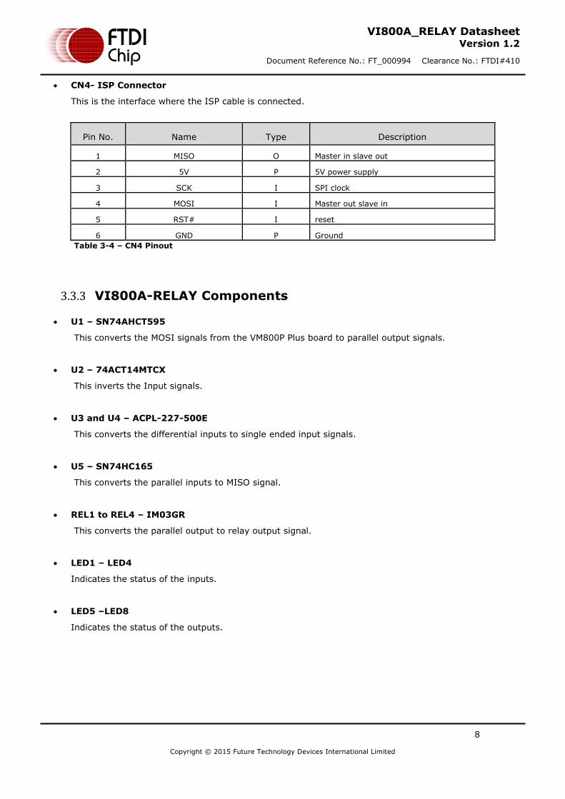
CN4- ISP Connector
This is the interface where the ISP cable is connected.
Pin No. Name Type Description
1 MISO O Master in slave out
2 5V P 5V power supply
3 SCK I SPI clock
4 MOSI I Master out slave in
5 RST# I reset
6 GND P Ground
Table 3-4 – CN4 Pinout
3.3.3 VI800A-RELAY Components
U1 – SN74AHCT595
This converts the MOSI signals from the VM800P Plus board to parallel output signals.
U2 – 74ACT14MTCX
This inverts the Input signals.
U3 and U4 – ACPL-227-500E
This converts the differential inputs to single ended input signals.
U5 – SN74HC165
This converts the parallel inputs to MISO signal.
REL1 to REL4 – IM03GR
This converts the parallel output to relay output signal.
LED1 – LED4
Indicates the status of the inputs.
LED5 –LED8
Indicates the status of the outputs.

9
Copyright © 2015 Future Technology Devices International Limited
VI800A_RELAY Datasheet Version 1.2
Document Reference No.: FT_000994 Clearance No.: FTDI#410
4 Board Schematics
Figure 4-1 - VI800A-RELAY Schematics

10
Copyright © 2015 Future Technology Devices International Limited
VI800A_RELAY Datasheet Version 1.2
Document Reference No.: FT_000994 Clearance No.: FTDI#410
5 Hardware Setup Guide
5.1 Power Configuration
The board is powered from the VM800P Plus board. The CN1 connector on the VI800A-RELAY board
should be connected to the J5 connector of the VM800P plus board as shown in Figure 5-1.
Figure 5-1 - VI800A-RELAY module connected to VM800P Plus module
5.2 RELAY Interface connection
The relay inputs are connected to the connector CN2.
The relay outputs are connected from the connector CN3
The LEDs LED1 to LED8 are used to display the status of the inputs and outputs.
This interface is used to add relay support to the VM800P Plus module.

11
Copyright © 2015 Future Technology Devices International Limited
VI800A_RELAY Datasheet Version 1.2
Document Reference No.: FT_000994 Clearance No.: FTDI#410
6 Contact Information
Head Office – Glasgow, UK Unit 1, 2 Seaward Place, Centurion Business Park Glasgow G41 1HH United Kingdom Tel: +44 (0) 141 429 2777 Fax: +44 (0) 141 429 2758 E-mail (Sales) [email protected] E-mail (Support) [email protected] E-mail (General Enquiries) [email protected]
Branch Office – Taipei, Taiwan 2F, No. 516, Sec. 1, NeiHu Road Taipei 114 Taiwan , R.O.C. Tel: +886 (0) 2 8797 1330 Fax: +886 (0) 2 8751 9737 E-mail (Sales) [email protected] E-mail (Support) [email protected] E-mail (General Enquiries) [email protected]
Branch Office – Tigard, Oregon, USA 7130 SW Fir Loop Tigard, OR 97223 USA Tel: +1 (503) 547 0988 Fax: +1 (503) 547 0987 E-Mail (Sales) [email protected] E-Mail (Support) [email protected] E-Mail (General Enquiries) [email protected]
Branch Office – Shanghai, China Room 1103, No. 666 West Huaihai Road, Changning District, Shanghai, 200052 China Tel: +86 (0)21 6235 1596 Fax: +86 (0)21 6235 1595 E-mail (Sales) [email protected] E-mail (Support) [email protected] E-mail (General Enquiries) [email protected]
Web Site
http://www.ftdichip.com/
Distributor and Sales Representatives
Please visit the Sales Network page of the FTDI Web site for the contact details of our distributor(s) and sales representative(s) in your country.
System and equipment manufacturers and designers are responsible to ensure that their systems, and any Future Technology Devices International Ltd (FTDI) devices incorporated in their systems, meet all applicable safety, regulatory and system-level performance requirements. All application-related information in this document (including application descriptions, suggested FTDI devices and other materials) is provided for reference only. While FTDI has taken care to assure it is accurate, this information is subject to customer confirmation, and FTDI disclaims all liability for system designs and for any applications assistance provided by FTDI. Use of FTDI devices in life support and/or safety applications is entirely at the user’s risk, and the user agrees to defend, indemnify and hold harmless FTDI from any and all damages, claims, suits or expense resulting from such use. This document is subject to change without notice. No freedom to use patents or other intellectual property rights is implied by the publication of this document. Neither the whole nor any part of the information contained in, or the product described in this document, may be adapted or reproduced in any material or electronic form without the prior written consent of the copyright holder. Future Technology Devices International Ltd, Unit 1, 2 Seaward Place, Centurion Business Park, Glasgow G41 1HH, United Kingdom. Scotland Registered Company Number: SC136640

12
Copyright © 2015 Future Technology Devices International Limited
VI800A_RELAY Datasheet Version 1.2
Document Reference No.: FT_000994 Clearance No.: FTDI#410
Appendix A – References
VM800P Plus board
FT800 datasheet: FT800_Embedded_Video_Engine
FT800 software programming guide: FT800_Programmer_Guide
FT800 sample application notes:
AN_246_VM800CB_SampleAPP_Arduino_Introduction
AN_275_FT800_Example_with_Arduino.pdf
AN_318 Arduino Library for FT800 Series
AN_331 VI800A_Relay_SampleApp

13
Copyright © 2015 Future Technology Devices International Limited
VI800A_RELAY Datasheet Version 1.2
Document Reference No.: FT_000994 Clearance No.: FTDI#410
Appendix B - List of Figures and Tables
List of Figures
Figure 3-1 – VI800A-RELAY module .............................................................................................................. 4
Figure 3-2 - VI800A-RELAY module PCB Top view ...................................................................................... 5
Figure 3-3 - VI800A-RELAY module PCB Bottom view ................................................................................ 5
Figure 3-4 - VI800A-RELAY module PCB Side view ..................................................................................... 6
Figure 4-1 - VI800A-RELAY Schematics ........................................................................................................ 9
Figure 5-1 - VI800A-RELAY module connected to VM800P Plus module ................................................ 10
List of Tables
Table 2-1 – Ordering information ................................................................................................................... 2
Table 3-1 – CN1 Pinout .................................................................................................................................... 6
Table 3-2 – CN2 Pinout .................................................................................................................................... 7
Table 3-3 – CN3 Pinout .................................................................................................................................... 7
Table 3-4 – CN4 Pinout .................................................................................................................................... 8

14
Copyright © 2015 Future Technology Devices International Limited
VI800A_RELAY Datasheet Version 1.2
Document Reference No.: FT_000994 Clearance No.: FTDI#410
Appendix C – Revision History
Document Title: DS_VI800A_RELAY
Document Reference No.: FT_000994
Clearance No.: FTDI#410
Product Page: http://www.ftdichip.com/EVE.htm
Document Feedback: Send Feedback
Version 1.0 Initial Datasheet released 14/10/14
Version 1.1 Added height dimensions 20/10/14
Version 1.2 Added max voltage recommendation for relays 15/04/15