polarization sensitive multi-chroic mkids - arxiv.org e · pdf file ·...
TRANSCRIPT

Polarization Sensitive Multi-Chroic MKIDs
Bradley R. Johnsona, Daniel Flanigana, Maximilian H. Abitbola, Peter A. R. Adeb,Sean Bryanc, Hsiao-Mei Chog, Rahul Dattae, Peter Dayf, Simon Doyleb,
Kent Irwind,g, Glenn Jonesa, Sarah Kernasovskiyd, Dale Lig, Phil Mauskopfc,Heather McCarricka, Jeff McMahone, Amber Millera, Giampaolo Pisanob,
Yanru Songd, Harshad Surdic, and Carole Tuckerb
aDepartment of Physics, Columbia University, New York, NY, 10027, USA;bSchool of Physics & Astronomy, Cardiff University, Cardiff, CF243AA, UK;
cSchool of Earth and Space Exploration, Arizona State University, Tempe, AZ, 85287, USA;dDepartment of Physics, Stanford University, Stanford, CA, 94305-4085, USA;eDepartment of Physics, University of Michigan, Ann Arbor, MI, 48103, USA;
fNASA, Jet Propulsion Lab, Pasadena, CA, 91109, USA;gSLAC National Accelerator Laboratory, Menlo Park, CA 94025, USA
ABSTRACT
We report on the development of scalable prototype microwave kinetic inductance detector (MKID) arrays tai-lored for future multi-kilo-pixel experiments that are designed to simultaneously characterize the polarizationproperties of both the cosmic microwave background (CMB) and Galactic dust emission. These modular arraysare composed of horn-coupled, polarization-sensitive MKIDs, and each pixel has four detectors: two polariza-tions in two spectral bands between 125 and 280 GHz. A horn is used to feed each array element, and a planarorthomode transducer, composed of two waveguide probe pairs, separates the incoming light into two linear po-larizations. Diplexers composed of resonant-stub band-pass filters separate the radiation into 125 to 170 GHz and190 to 280 GHz pass bands. The millimeter-wave power is ultimately coupled to a hybrid co-planar waveguidemicrowave kinetic inductance detector using a novel, broadband circuit developed by our collaboration. Elec-tromagnetic simulations show the expected absorption efficiency of the detector is approximately 90%. Arrayfabrication will begin in the summer of 2016.
Keywords: CMB, Polarization, MKID
1. INTRODUCTION
Microwave kinetic inductance detectors (MKIDs) are superconducting thin-film, GHz resonators that are designedto also be optimal photon absorbers.1 Absorbed photons with energies greater than the superconducting gap(ν > 2∆/h ∼= 74 GHz × (Tc/1 K)) break Cooper pairs, changing the density of quasiparticles in the device.The quasiparticle density affects the kinetic inductance and the dissipation of the superconducting film, so achanging optical signal will cause the resonant frequency and internal quality factor of the resonator to shift.These changes in the properties of the resonator can be detected as changes in the amplitude and phase of aprobe tone that drives the resonator at its resonant frequency. This detector technology is particularly well-suitedfor sub-kelvin, kilo-pixel detector arrays because each detector element can be dimensioned to have a uniqueresonant frequency, and the probe tones for hundreds to thousands of detectors can be carried into and out ofthe cryostat on a single pair of coaxial cables.
In this paper, we report on the development of modular arrays of horn-coupled, polarization-sensitive MKIDsthat are each sensitive to two spectral bands between 125 and 280 GHz. The scalable prototype MKID ar-rays we are developing are tailored for future multi-kilo-pixel experiments that are designed to simultaneouslycharacterize the polarization properties of both the cosmic microwave background (CMB) and Galactic dustemission. Our device design builds from successful transition edge sensor (TES) bolometer architectures that
E-mail: [email protected]
1
arX
iv:1
607.
0379
6v1
[as
tro-
ph.I
M]
13
Jul 2
016
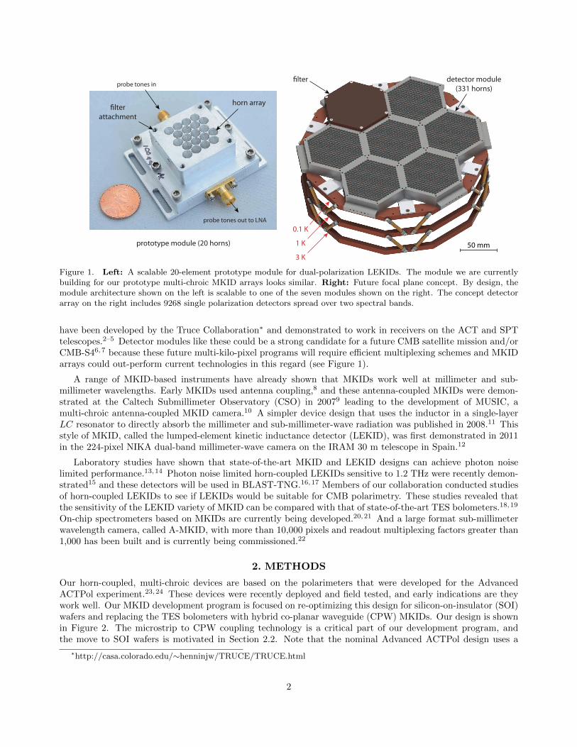
0.1 K
1 K
3 K
lter detector module(331 horns)
prototype module (20 horns) 50 mm
lterattachment
probe tones in
horn array
probe tones out to LNA
Figure 1. Left: A scalable 20-element prototype module for dual-polarization LEKIDs. The module we are currentlybuilding for our prototype multi-chroic MKID arrays looks similar. Right: Future focal plane concept. By design, themodule architecture shown on the left is scalable to one of the seven modules shown on the right. The concept detectorarray on the right includes 9268 single polarization detectors spread over two spectral bands.
have been developed by the Truce Collaboration∗ and demonstrated to work in receivers on the ACT and SPTtelescopes.2–5 Detector modules like these could be a strong candidate for a future CMB satellite mission and/orCMB-S46,7 because these future multi-kilo-pixel programs will require efficient multiplexing schemes and MKIDarrays could out-perform current technologies in this regard (see Figure 1).
A range of MKID-based instruments have already shown that MKIDs work well at millimeter and sub-millimeter wavelengths. Early MKIDs used antenna coupling,8 and these antenna-coupled MKIDs were demon-strated at the Caltech Submillimeter Observatory (CSO) in 20079 leading to the development of MUSIC, amulti-chroic antenna-coupled MKID camera.10 A simpler device design that uses the inductor in a single-layerLC resonator to directly absorb the millimeter and sub-millimeter-wave radiation was published in 2008.11 Thisstyle of MKID, called the lumped-element kinetic inductance detector (LEKID), was first demonstrated in 2011in the 224-pixel NIKA dual-band millimeter-wave camera on the IRAM 30 m telescope in Spain.12
Laboratory studies have shown that state-of-the-art MKID and LEKID designs can achieve photon noiselimited performance.13,14 Photon noise limited horn-coupled LEKIDs sensitive to 1.2 THz were recently demon-strated15 and these detectors will be used in BLAST-TNG.16,17 Members of our collaboration conducted studiesof horn-coupled LEKIDs to see if LEKIDs would be suitable for CMB polarimetry. These studies revealed thatthe sensitivity of the LEKID variety of MKID can be compared with that of state-of-the-art TES bolometers.18,19
On-chip spectrometers based on MKIDs are currently being developed.20,21 And a large format sub-millimeterwavelength camera, called A-MKID, with more than 10,000 pixels and readout multiplexing factors greater than1,000 has been built and is currently being commissioned.22
2. METHODS
Our horn-coupled, multi-chroic devices are based on the polarimeters that were developed for the AdvancedACTPol experiment.23,24 These devices were recently deployed and field tested, and early indications are theywork well. Our MKID development program is focused on re-optimizing this design for silicon-on-insulator (SOI)wafers and replacing the TES bolometers with hybrid co-planar waveguide (CPW) MKIDs. Our design is shownin Figure 2. The microstrip to CPW coupling technology is a critical part of our development program, andthe move to SOI wafers is motivated in Section 2.2. Note that the nominal Advanced ACTPol design uses a
∗http://casa.colorado.edu/∼henninjw/TRUCE/TRUCE.html
2

4.8 mm aperture
niobiumgold
MKID
aluminum
backshort
conicalhorn
cylindricalwaveguide
aluminumdetectorpackage
SOI
SiNx
hybridtee MKID
band-pass lters
OMT
slotline
aluminumsection
niobiumsection
microstrip input
λ/4 CPW resonator
probe tonesniobium
ground plane4.8 mm
Figure 2. Top Left: A cross-sectional view of one focal-plane element. In an effort to minimize two-level system(TLS) noise, the MKID sensing element is deposited directly on the silicon wafer, and it is not covered with siliconnitride. Bottom Left: A scale drawing of the dual-polarization multi-chroic MKID device we propose to develop.Bottom Right: A schematic of the co-planar waveguide MKID we are developing. Photons from the sky are broughtto the detector on a microstrip from the hybrid tee. These photons then couple to our resonator and are absorbed in thealuminum section of the CPW λ/4 resonator. Top Right: End-to-end electromagnetic simulations show the expectedabsorption efficiency is approximately 90% across the 150 GHz and the 235 GHz spectral bands.
ring-loaded corrugated feed. For our laboratory development work we will use a conical horn for simplicity andswitch to profiled horns in the future. Profiled horns are easier to fabricate and they have been shown to performlike corrugated feeds.25
2.1 Horn Coupling and RF Circuit
In our prototype design, a conical horn is used to feed each array element. Each horn is machined into amonolithic horn plate that also serves as both the top of the detector module and the mounting surface forthe MKID arrays. The bottom plate, which closes the module, also contains backshorts, which are used tooptimize photon coupling. Light emerging from the cylindrical waveguide is coupled to a broadband orthomodetransducer (OMT). A choke around the exit aperture of the waveguide minimizes lateral leakage of the fields.The OMT is composed of two probe pairs, and it separates the incoming light into two linear polarizations. Forexample, one linear polarization couples to one pair of probes, and the wave then propagates through identical
3

20 mm
Figure 3. A photograph of our MKID test chip mounted inside an aluminum package designed for dark testing. Thetest chip layout is shown on the right. Each chip contains eight hybrid CPW MKIDs with different lengths and meanderproperties. The red elements are made from aluminum and the gray regions are niobium.
electrical paths in the subsequent millimeter-wave circuit en route to the MKID absorbing element. Along eachpath, a broadband CPW-to-microstrip transition composed of seven alternating sections of CPW and microstripis first used to transition the radiation onto microstrip lines. Next, diplexers composed of two separate five-poleresonant-stub band-pass filters separate the radiation into 125 to 170 GHz and 190 to 280 GHz pass bands. Thesignals from opposite probes within a single sub-band are then combined onto a single microstrip line using thedifference output of a hybrid tee. Signals at the sum output of the hybrid are routed to a termination resistorand discarded, while the output of the difference port is detected.
These polarimeters operate over a 2.25:1 ratio bandwidth over which cylindrical waveguide becomes multi-moded. However, the TE11 mode, which has the desirable polarization properties, couples to opposite fins of theOMT with a 180 phase shift while the higher order modes, which also couple efficiently to the OMT probes havea 0 phase shift. This phase difference allows the hybrid tee to isolate the TE11 signal at the difference port andreject the unwanted modes at the sum port. This ensures single-moded performance over our 2.25:1 bandwidth.The architecture described above offers a frequency independent polarimeter axis defined by the orientation of theplanar OMT. Figure 2 shows a schematic of our microstrip-to-CPW coupler. The the HFSS/Sonnet simulationresults in this figure show the expected absorption efficiency of the detector is approximately 90% taking intoaccount all of the elements in the circuit except the OMT probes.
2.2 MKID Design
The total instrument noise is the quadrature sum of the detector noise and the photon noise, and the fundamentalperformance goal is to achieve a sensitivity that is dominated by the random arrival of background photons. Foran MKID, the detector noise includes contributions from three sources: generation-recombination (g-r) noise,two-level system (TLS) noise, and amplifier noise.1 The g-r noise comes from the random recombination ofquasiparticles. At typical operating temperatures and optical loads, quasiparticle generation noise is dominatedby optical generation – the photon noise – and thermal generation is negligible. TLS noise is produced bydielectric fluctuations due to quantum two level systems in amorphous dielectric surface layers surrounding theMKID. The scaling of TLS noise with operating temperature, resonator geometry, and readout tone power andfrequency has been extensively studied experimentally. We used a semi-empirical model26 to design the resonatorsin order to reduce TLS noise. Finally, the amplifier noise is the electronic noise of the readout system, which isdominated by the cryogenic microwave low-noise amplifier. Our modeling of these noise sources indicates that
4

the detector sensitivity will be limited by photon noise under the 5–20 pW optical loads typically present for150 GHz detectors in ground-based CMB experiments.
Our MKID design is based on a quarter-wavelength CPW resonator (see Figure 2 & 3). The design uses ahybrid CPW transmission line composed of two different metals. The ground plane is made of a superconductorwith Cooper pair binding energy greater than the optical photon energy; our design uses niobium. Most of theCPW center trace is made from the same high-gap superconductor, except for a small active region adjacent tothe grounded end. This active region is made from a lower-gap superconductor in which the optical photons canbreak Cooper pairs; our design uses aluminum. The quasiparticles excited by optical photons alter the dissipationand kinetic inductance of the device, and these changes are probed by a tone produced in the ROACH-basedreadout (see Section 2.4). Devices like these have achieved photon-noise-limited performance over a wide rangeof millimeter and sub-millimeter wavelengths with optical loading levels well under 1 pW.27,28
Because of the gap difference, the quasiparticles are trapped in the active region, the volume of which can bereduced to increase the device responsivity. The active region of our baseline design is 2 mm long with an 8 µmwide aluminum center line and a 5 to 10 µm gap. Greater than 90% of the millimeter-wave power is dissipatedhere due to Cooper pairs breaking. The length of the second section varies from detector to detector becauseit is used to tune the resonant frequency. This section can have a much wider gap to the ground plane, whichreduces TLS noise. In our baseline design, the second section of CPW is ∼8 mm long with a 10 µm niobiumcenter trace and a gap of 30 µm to the niobium ground plane. This ∼10 mm length of transmission line willhave a resonant frequency of approximately 3 GHz.
The millimeter-wave power is coupled from the microstrip output of the hybrid tee to the CPW of the MKIDusing a novel, broadband circuit developed by our collaboration29 (see Figure 2). First, the power is evenlydivided in-phase onto two microstrips each with twice the impedance of the incoming microstrip. Each branchfeeds a standard broadband microstrip-to-slotline transition, where the slotline is formed in the niobium groundplane that is common to the microstrip and the MKID CPW. The two slotlines are then brought together andbecome the gaps of the CPW transmission line, efficiently coupling the radiation into the aluminum CPW centerline, where it dissipates by exciting quasiparticles. The slotline is electrically short at the resonant frequency ofthe MKID, and thus it does not impact the microwave characteristics of the resonators.
2.3 Fabrication
The arrays will be fabricated on SOI wafers 100 mm in diameter. Each SOI wafer consist of a 5 µm thick silicondevice layer and a 350 µm thick handling wafer held together by a 0.5 µm thick oxide layer. The MKID arraysare fabricated on the device layer, which is made of high-purity, float-zone silicon (>10 kΩ cm resistivity). Thefirst metal deposition is a niobium film which is patterned to produce the ground plane and the OMT. Thealuminum film that will form the MKID sensing element is then deposited after the niobium ground plane ispatterned. The aluminum MKID element is co-planar with the niobium ground plane on the 5 µm thick silicondevice layer. Silicon nitride is then deposited as an electrically insulating dielectric material, which will be usedto form the substrate of the microstrip lines. A second niobium film is used to form the top microstrip line. Ourdesign uses crossunders rather than crossovers, so a second silicon nitride and third niobium layer are not need.The layer of silicon nitride is removed to reduce loss and TLS noise. A gold film is deposited and patternedto construct the termination in the hybrid tee. The thick silicon handling wafer and the oxide underneath theOMT and the MKID will be removed using deep reactive ion etching (DRIE) to improve the bandwidth and theoptical coupling and to minimize TLS noise.
2.4 Readout
All tests of the resonator performance are made by injecting sinusoidal tones near the resonant frequency of theMKID and measuring the amplitude and phase of the emerging waveform. To measure the resonant frequencyand quality factor, the frequency of the sine wave is stepped through the resonance, effectively measuring thecomplex forward transmission (S21) as with a vector network analyzer. Once the resonant frequency has beenfound from these sweeps, the probe tone frequency is tuned to this resonant frequency and a complex voltage timeseries is recorded. This time series can then be decomposed into fluctuations of the resonant frequency and of
5

DCblock
DCblock
DCblock
-20 dB attenuator
LNA
-20 dB attenuator
duroid
duroid
detector array
SScoax
SScoax
SScoax
SScoax
NbTicoax
CuNicoax
45 K 3.5 K 100 mK
Cryostat
SMAfeed-
through
Low-PassFilters
Low-PassFilters
DigitalAttenuator
DAC
ADC
ROACH-2Board
Amplier
lterbank
300 K
LocalOscillator
ROACH-2
ADC/DAC
10 Gbit Ethernet
attenuator
mixers
amplierLO
Figure 4. Top: Readout schematic showing the probe tone path. Bottom Left: The ROACH-2 with the DAC/ADC.Bottom Right: The analog signal conditioning hardware. This chassis houses the filters, room-temperature mixers,attenuator, warm amplifier, and the local oscillator shown in the schematic above.
the quality factor of the resonator. Standard spectral analysis is then used to determine the noise characteristicsof the detector.
While all of the measurements just described can be done for a single resonator at a time using a microwavesynthesizer and homodyne mixer, one of the major advantages of MKIDs is that a digital waveform generatorand a digital filter bank and demodulator can be used to measure hundreds of resonators simultaneously bysuperimposing sine waves of different frequencies. Several such systems have been developed and deployed.30
Many of these systems, including one developed at Columbia University for this work, are based around theCASPER ROACH-1 and ROACH-2 FPGA boards†. A schematic and photos of a ROACH-based read outsystem developed at Columbia are shown in Figure 4. Using this system, we can characterize hundreds ofresonators simultaneously, so readout of the 80 resonators per prototype detector module is straightforward.
While the ROACH-1 is a robust and well-proven board, it is now several years old and is being supersededby the ROACH-2 board. We have ported our readout design to the ROACH-2, which allows us to read outover a thousand resonators at full bandwidth for extensive laboratory testing, and is suitable for deployment ofa future large format array. We have designed an analog signal conditioning system based around PolyphaseMicrowave quadrature modulators and demodulators to convert the baseband signals generated and analyzed bythe ROACH to the target 3–4 GHz readout band.
†https://casper.berkeley.edu/
6

50 K
3 K
stainless steel WR6 waveguide
WR6 vacuum windowon KF25 ange
WR6 directional coupler
90 degreeE-plane bend
waveguide section (straight or twist)conical horn
opticsbox
thermal intercept
cryo
stat
1 K
0.1 K
detector module
zero-bias detector (ZBD)
Eccosorb (2-4 K)
ampl
ier
ampl
ier
PIN
switc
h
x12
activ
em
ultip
lier
WR6
atte
nuat
ors
band
-pas
sl
ter
50 O
hmte
rmin
atio
n
tuna
ble
benc
htop
sig
nal g
ener
ator
~12
GH
z
thermal noise source
frequency multiplier
thermal intercept
broadbandor CWsource
selection
millimeter-wave source
stainless steel WR6 waveguide
teon
lter
Figure 5. A schematic of the testing apparatus that is already successfully operating in the laboratory at Columbia.Millimeter-wave radiation is coupled into the cryostat using WR-6 waveguide, and this radiation illuminates the detectorarray via a horn and a collimating reflective optical assembly. The cold Eccosorb acts as both an attenuator and a diffusebackground signal for the detectors. By changing the temperature of the Eccosorb we obtain an absolute brightnesstemperature calibration. We will use this existing setup to characterize the spectral response of the lower frequency band,and a similar ∼235 GHz source will be constructed to test the high-frequency spectral band.
3. TESTING PLAN
To characterize the detector arrays, we will install them in superconducting aluminum detector packages and coolthe assemblies to approximately 120 mK using the STAR Cryoelectronics DRC-100 cryostat system. This systemincludes a two-stage adiabatic demagnetization refrigerator (ADR) backed by a Cryomech PT-407 pulse tubecooler. We have developed and built a cryogenic optical test setup inside this cryostat, which is schematicallydescribed in Figure 5. The testing system consists of two main photon sources.
3.1 Millimeter-Wave Source
A millimeter-wave signal source, which is based on a Millitech active 12-times frequency multiplier, was builtby the group at Columbia. The multiplier can be driven by a sweepable microwave signal generator, which isuseful for measuring the frequency response of the detectors, or it can be driven by a broadband noise source tomimic a diffuse astrophysical background signal such as the CMB or Galactic dust emission. The input to thefrequency multiplier is connected through a PIN diode switch, which allows the signals to be chopped on andoff with sub-microsecond time resolution. This functionality provides a direct way of measuring the responsetime of the detectors. The millimeter-wave source is operated outside the cryostat at room temperature, andphotons are brought to the detectors using WR-6 waveguide. The waveguide is passed into the cryostat through avacuum waveguide window, and sections of stainless steel waveguide are used to decrease the thermal load on thecryogenic system. Inside the cryostat, the WR-6 waveguide feeds a horn (mounted at 4 K) and a small crossed-Dragone optics box (mounted at 1 K), which converts the diverging horn beam into a plane wave that illuminatesthe detectors. This configuration will be ideal for testing the 150 GHz spectral band of the detectors. To test thehigh frequency band, we will build a similar frequency multiplier-based source to cover the 190-280 GHz band.
7

To test the polarization response, we currently have interchangeable waveguide sections with 0, 45, and 90
twists to set the polarization angle of the radiation emitted from the horn in the cryostat. We are also building asmall cryogenic rotateable half-wave plate that can be placed between the horn and the crossed-Dragone optics,allowing the polarization angle to be continuously adjusted without having to open the cryostat.
3.2 Cryogenic Blackbody
A slab of beam-filling Eccosorb absorber, which is coated with etched Teflon for impedance matching, servesas a cold diffuse blackbody load, and it is mounted directly in front of the horn apertures approximately 1 cmfrom the detector module. The temperature of the Eccosorb load is controlled using a heater resistor and a weakthermal link that is connected to either the 3 K stage of the pulse tube cooler or the 1 K stage of the ADR. Bychanging the temperature of this load we can measure the absolute brightness temperature calibration, which isused to compute the NET.
3.3 Measurements
The sources described above will allow us to extensively characterize our detectors. In particular, we will beable to measure: (i) calibrated NEP and NET under loading levels spanning 0.1-100 pW, which correspond tothe loading expected for a wide range of experiments, including space-based, balloon-borne and ground-basedtelescopes, (ii) calibrated spectral response, both across the desired bands, but also including any undesiredout-of-band response, (iii) detector response times to pulses of millimeter wavelength radiation at realistic skyloading levels, and (iv) the response of the detectors versus polarization angle of the incoming radiation, includingboth the co-polarization and cross-polarization response. All of these measurements will be directly compared toour design simulations and performance forecasts, providing the essential feedback needed to identify any issuesto be corrected in subsequent wafer fabrication runs.
4. DISCUSSION
One of the primary goals of this project is to bring the functionality of MKIDs for CMB studies in line withstate-of-the-art TES bolometers.31–36 To date we have (i) designed the critical broadband microstrip-to-CPWcoupler, (ii) modified the existing Advanced ACTPol design for SOI, (iii) fabricated MKID optimization chips,and (iv) developed several of the critical fabrication steps. We are currently dark testing the MKIDs and layingout our final array design. Prototype array fabrication will begin in the summer of 2016.
In the future, we plan on making the sensing element in the MKIDs out of aluminum manganese instead ofaluminum. By adding manganese to the aluminum, the Tc of the sensor decreases in a controllable way,37 whichdoes two critical things. First and foremost, in our current 150 and 235 GHz spectral bands, the photons areenergetic enough to break multiple Cooper pairs in the sensing element, so the detector noise will be suppressedbelow the photon noise – even for the low optical loads that are expected in a space-like environment. Second,a lower Tc makes the detector technology sensitive to lower frequencies, so this technology will open the door tolow-frequency (∼30 GHz) MKIDs in the future.
ACKNOWLEDGMENTS
This project is supported by a grant from the National Science Foundation (Award #1509211, #1509078, and#1506074) and a NASA/NESSF Fellowship for McCarrick.
REFERENCES
[1] Zmuidzinas, J., “Superconducting Microresonators: Physics and Applications,” Ann. Rev. Cond. Matt.Phys. 3, 169–214 (2012).
8

[2] Thornton, R. J., Ade, P. A. R., Aiola, S., Angile, F. E., Amiri, M., Beall, J. A., Becker, D. T., Cho, H., Choi,S. K., Corlies, P., Coughlin, K. P., Datta, R., Devlin, M. J., Dicker, S. R., Dunner, R., Fowler, J. W., Fox,A. E., Gallardo, P. A., Gao, J., Grace, E., Halpern, M., Hasselfield, M., Henderson, S. W., Hilton, G. C.,Hincks, A. D., Ho, S. P., Hubmayr, J., Irwin, K. D., Klein, J., Koopman, B., Li, D., Louis, T., Lungu, M.,Maurin, L., McMahon, J., Munson, C. D., Naess, S., Nati, F., Newburgh, L., Nibarger, J., Niemack, M. D.,Niraula, P., Nolta, M. R., Page, L. A., Pappas, C. G., Schillaci, A., Schmitt, B. L., Sehgal, N., Sievers,J. L., Simon, S. M., Staggs, S. T., Tucker, C., Uehara, M., van Lanen, J., Ward, J. T., and Wollack, E. J.,“The Atacama Cosmology Telescope: The polarization-sensitive ACTPol instrument,” ArXiv e-prints (May2016).
[3] Niemack, M. D., Ade, P. A. R., Aguirre, J., Barrientos, F., Beall, J. A., Bond, J. R., Britton, J., Cho,H. M., Das, S., Devlin, M. J., Dicker, S., Dunkley, J., Dunner, R., Fowler, J. W., Hajian, A., Halpern, M.,Hasselfield, M., Hilton, G. C., Hilton, M., Hubmayr, J., Hughes, J. P., Infante, L., Irwin, K. D., Jarosik,N., Klein, J., Kosowsky, A., Marriage, T. A., McMahon, J., Menanteau, F., Moodley, K., Nibarger, J. P.,Nolta, M. R., Page, L. A., Partridge, B., Reese, E. D., Sievers, J., Spergel, D. N., Staggs, S. T., Thornton,R., Tucker, C., Wollack, E., and Yoon, K. W., “ACTPol: a polarization-sensitive receiver for the AtacamaCosmology Telescope,” in [Society of Photo-Optical Instrumentation Engineers (SPIE) Conference Series ],Society of Photo-Optical Instrumentation Engineers (SPIE) Conference Series 7741 (July 2010).
[4] Austermann, J. E., Aird, K. A., Beall, J. A., Becker, D., Bender, A., Benson, B. A., Bleem, L. E., Britton,J., Carlstrom, J. E., Chang, C. L., Chiang, H. C., Cho, H.-M., Crawford, T. M., Crites, A. T., Datesman,A., de Haan, T., Dobbs, M. A., George, E. M., Halverson, N. W., Harrington, N., Henning, J. W., Hilton,G. C., Holder, G. P., Holzapfel, W. L., Hoover, S., Huang, N., Hubmayr, J., Irwin, K. D., Keisler, R.,Kennedy, J., Knox, L., Lee, A. T., Leitch, E., Li, D., Lueker, M., Marrone, D. P., McMahon, J. J., Mehl, J.,Meyer, S. S., Montroy, T. E., Natoli, T., Nibarger, J. P., Niemack, M. D., Novosad, V., Padin, S., Pryke, C.,Reichardt, C. L., Ruhl, J. E., Saliwanchik, B. R., Sayre, J. T., Schaffer, K. K., Shirokoff, E., Stark, A. A.,Story, K., Vanderlinde, K., Vieira, J. D., Wang, G., Williamson, R., Yefremenko, V., Yoon, K. W., andZahn, O., “SPTpol: an instrument for CMB polarization measurements with the South Pole Telescope,”in [Millimeter, Submillimeter, and Far-Infrared Detectors and Instrumentation for Astronomy VI ], Proc.SPIE 8452, 84521E (Sept. 2012).
[5] Henning, J. W., Ade, P., Aird, K. A., Austermann, J. E., Beall, J. A., Becker, D., Benson, B. A., Bleem,L. E., Britton, J., Carlstrom, J. E., Chang, C. L., Cho, H.-M., Crawford, T. M., Crites, A. T., Datesman,A., de Haan, T., Dobbs, M. A., Everett, W., Ewall-Wice, A., George, E. M., Halverson, N. W., Harrington,N., Hilton, G. C., Holzapfel, W. L., Hubmayr, J., Irwin, K. D., Karfunkle, M., Keisler, R., Kennedy, J., Lee,A. T., Leitch, E., Li, D., Lueker, M., Marrone, D. P., McMahon, J. J., Mehl, J., Meyer, S. S., Montgomery,J., Montroy, T. E., Nagy, J., Natoli, T., Nibarger, J. P., Niemack, M. D., Novosad, V., Padin, S., Pryke,C., Reichardt, C. L., Ruhl, J. E., Saliwanchik, B. R., Sayre, J. T., Schaffer, K. K., Shirokoff, E., Story,K., Tucker, C., Vanderlinde, K., Vieira, J. D., Wang, G., Williamson, R., Yefremenko, V., Yoon, K. W.,and Young, E., “Feedhorn-coupled TES polarimeter camera modules at 150 GHz for CMB polarizationmeasurements with SPTpol,” in [Society of Photo-Optical Instrumentation Engineers (SPIE) ConferenceSeries ], Society of Photo-Optical Instrumentation Engineers (SPIE) Conference Series 8452, 3 (Sept. 2012).
[6] Bock, J., Aljabri, A., Amblard, A., Baumann, D., Betoule, M., Chui, T., Colombo, L., Cooray, A., Crumb,D., Day, P., Dickinson, C., Dowell, D., Dragovan, M., Golwala, S., Gorski, K., Hanany, S., Holmes, W.,Irwin, K., Johnson, B., Keating, B., Kuo, C.-L., Lee, A., Lange, A., Lawrence, C., Meyer, S., Miller,N., Nguyen, H., Pierpaoli, E., Ponthieu, N., Puget, J.-L., Raab, J., Richards, P., Satter, C., Seiffert, M.,Shimon, M., Tran, H., Williams, B., and Zmuidzinas, J., “Study of the Experimental Probe of InflationaryCosmology (EPIC)-Intemediate Mission for NASA’s Einstein Inflation Probe,” ArXiv e-prints (June 2009).
[7] Abazajian, K. N., Arnold, K., Austermann, J., Benson, B. A., Bischoff, C., Bock, J., Bond, J. R., Borrill,J., Buder, I., Burke, D. L., Calabrese, E., Carlstrom, J. E., Carvalho, C. S., Chang, C. L., Chiang, H. C.,Church, S., Cooray, A., Crawford, T. M., Crill, B. P., Dawson, K. S., Das, S., Devlin, M. J., Dobbs,M., Dodelson, S., Dore, O., Dunkley, J., Feng, J. L., Fraisse, A., Gallicchio, J., Giddings, S. B., Green, D.,Halverson, N. W., Hanany, S., Hanson, D., Hildebrandt, S. R., Hincks, A., Hlozek, R., Holder, G., Holzapfel,W. L., Honscheid, K., Horowitz, G., Hu, W., Hubmayr, J., Irwin, K., Jackson, M., Jones, W. C., Kallosh,R., Kamionkowski, M., Keating, B., Keisler, R., Kinney, W., Knox, L., Komatsu, E., Kovac, J., Kuo, C.-L.,
9
Kusaka, A., Lawrence, C., Lee, A. T., Leitch, E., Linde, A., Linder, E., Lubin, P., Maldacena, J., Martinec,E., McMahon, J., Miller, A., Mukhanov, V., Newburgh, L., Niemack, M. D., Nguyen, H., Nguyen, H. T.,Page, L., Pryke, C., Reichardt, C. L., Ruhl, J. E., Sehgal, N., Seljak, U., Senatore, L., Sievers, J., Silverstein,E., Slosar, A., Smith, K. M., Spergel, D., Staggs, S. T., Stark, A., Stompor, R., Vieregg, A. G., Wang, G.,Watson, S., Wollack, E. J., Wu, W. L. K., Yoon, K. W., Zahn, O., and Zaldarriaga, M., “Inflation Physicsfrom the Cosmic Microwave Background and Large Scale Structure,” ArXiv e-prints (Sept. 2013).
[8] Day, P. K., Leduc, H. G., Goldin, A., Vayonakis, T., Mazin, B. A., Kumar, S., Gao, J., and Zmuidzinas, J.,“Antenna-coupled microwave kinetic inductance detectors,” Nuclear Instruments and Methods in PhysicsResearch A 559, 561–563 (Apr. 2006).
[9] Schlaerth, J., Vayonakis, A., Day, P., Glenn, J., Gao, J., Golwala, S., Kumar, S., Leduc, H., Mazin,B., Vaillancourt, J., and Zmuidzinas, J., “A Millimeter and Submillimeter Kinetic Inductance DetectorCamera,” Journal of Low Temperature Physics 151, 684–689 (May 2008).
[10] Golwala, S. R., Bockstiegel, C., Brugger, S., Czakon, N. G., Day, P. K., Downes, T. P., Duan, R., Gao,J., Gill, A. K., Glenn, J., Hollister, M. I., LeDuc, H. G., Maloney, P. R., Mazin, B. A., McHugh, S. G.,Miller, D., Noroozian, O., Nguyen, H. T., Sayers, J., Schlaerth, J. A., Siegel, S., Vayonakis, A. K., Wilson,P. R., and Zmuidzinas, J., “Status of MUSIC, the MUltiwavelength Sub/millimeter Inductance Camera,”in [Society of Photo-Optical Instrumentation Engineers (SPIE) Conference Series ], 8452 (Sept. 2012).
[11] Doyle, S., Mauskopf, P., Naylon, J., Porch, A., and Duncombe, C., “Lumped Element Kinetic InductanceDetectors,” Journal of Low Temperature Physics 151, 530–536 (Apr. 2008).
[12] Monfardini, A., Benoit, A., Bideaud, A., Swenson, L., Cruciani, A., Camus, P., Hoffmann, C., Desert,F. X., Doyle, S., Ade, P., Mauskopf, P., Tucker, C., Roesch, M., Leclercq, S., Schuster, K. F., Endo, A.,Baryshev, A., Baselmans, J. J. A., Ferrari, L., Yates, S. J. C., Bourrion, O., Macias-Perez, J., Vescovi, C.,Calvo, M., and Giordano, C., “A Dual-band Millimeter-wave Kinetic Inductance Camera for the IRAM 30m Telescope,” Astrophys. J. Supp. 194, 24 (June 2011).
[13] Mauskopf, P., Doyle, S., Barry, P., Rowe, S., Bidead, A., Ade, P., Tucker, C., Castillo, E., Monfardini, A.,Goupy, J., and Calvo, M., “Photon-Noise Limited Performance in Aluminum LEKIDs,” Journal of LowTemperature Physics , 1–8 (2014).
[14] McKenney, C., Leduc, H. G., Swenson, L. J., Day, P. K., Eom, B. H., and Zmuidzinas, J., “Designconsiderations for a background limited 350 micron pixel array using lumped element superconductingmicroresonators,” in [Society of Photo-Optical Instrumentation Engineers (SPIE) Conference Series ], 8452,84520S–84520S–10 (July 2012).
[15] Hubmayr, J., Beall, J., Becker, D., Cho, H.-M., Devlin, M., Dober, B., Groppi, C., Hilton, G. C., Irwin,K. D., Li, D., Mauskopf, P., Pappas, D. P., Van Lanen, J., Vissers, M. R., and Gao, J., “Photon-noiselimited sensitivity in titanium nitride kinetic inductance detectors,” ArXiv e-prints (June 2014).
[16] Galitzki, N., Ade, P. A. R., Angile, F. E., Ashton, P., Beall, J. A., Becker, D., Bradford, K. J., Che, G.,Cho, H.-M., Devlin, M. J., Dober, B. J., Fissel, L. M., Fukui, Y., Gao, J., Groppi, C. E., Hillbrand, S.,Hilton, G. C., Hubmayr, J., Irwin, K. D., Klein, J., van Lanen, J., Li, D., Li, Z.-Y., Lourie, N. P., Mani, H.,Martin, P. G., Mauskopf, P., Nakamura, F., Novak, G., Pappas, D. P., Pascale, E., Pisano, G., Santos, F. P.,Savini, G., Scott, D., Stanchfield, S., Tucker, C., Ullom, J. N., Underhill, M., Vissers, M. R., and Ward-Thompson, D., “The Next Generation BLAST Experiment,” Journal of Astronomical Instrumentation 3,1440001 (2014).
[17] Dober, B. J., Ade, P. A. R., Ashton, P., Angile, F. E., Beall, J. A., Becker, D., Bradford, K. J., Che, G.,Cho, H.-M., Devlin, M. J., Fissel, L. M., Fukui, Y., Galitzki, N., Gao, J., Groppi, C. E., Hillbrand, S.,Hilton, G. C., Hubmayr, J., Irwin, K. D., Klein, J., Van Lanen, J., Li, D., Li, Z.-Y., Lourie, N. P., Mani,H., Martin, P. G., Mauskopf, P., Nakamura, F., Novak, G., Pappas, D. P., Pascale, E., Santos, F. P., Savini,G., Scott, D., Stanchfield, S., Ullom, J. N., Underhill, M., Vissers, M. R., and Ward-Thompson, D., “Thenext-generation BLASTPol experiment,” in [Society of Photo-Optical Instrumentation Engineers (SPIE)Conference Series ], Society of Photo-Optical Instrumentation Engineers (SPIE) Conference Series 9153, 0(July 2014).
[18] Flanigan, D., McCarrick, H., Jones, G., Johnson, B. R., Abitbol, M. H., Ade, P., Araujo, D., Bradford,K., Cantor, R., Che, G., Day, P., Doyle, S., Kjellstrand, C. B., Leduc, H., Limon, M., Luu, V., Mauskopf,P., Miller, A., Mroczkowski, T., Tucker, C., and Zmuidzinas, J., “Photon noise from chaotic and coherent
10

millimeter-wave sources measured with horn-coupled, aluminum lumped-element kinetic inductance detec-tors,” Applied Physics Letters 108(8) (2016).
[19] McCarrick, H., Flanigan, D., Jones, G., Johnson, B. R., Ade, P., Araujo, D., Bradford, K., Cantor, R.,Che, G., Day, P., Doyle, S., Leduc, H., Limon, M., Luu, V., Mauskopf, P., Miller, A., Mroczkowski, T.,Tucker, C., and Zmuidzinas, J., “Horn-coupled, commercially-fabricated aluminum lumped-element kineticinductance detectors for millimeter wavelengths,” Review of Scientific Instruments 85, 123117 (Dec. 2014).
[20] Kovacs, A., Barry, P. S., Bradford, C. M., Chattopadhyay, G., Day, P., Doyle, S., Hailey-Dunsheath, S.,Hollister, M., McKenney, C., LeDuc, H. G., Llombart, N., Marrone, D. P., Mauskopf, P., O’Brient, R. C.,Padin, S., Swenson, L. J., and Zmuidzinas, J., “SuperSpec: design concept and circuit simulations,” in[Society of Photo-Optical Instrumentation Engineers (SPIE) Conference Series ], Society of Photo-OpticalInstrumentation Engineers (SPIE) Conference Series 8452 (Sept. 2012).
[21] Patel, A., Brown, A., Hsieh, W., Stevenson, T., Moseley, S., U-yen, K., Ehsan, N., Barrentine, E., Manos,G., and Wollack, E., “Fabrication of mkids for the microspec spectrometer,” Applied Superconductivity,IEEE Transactions on 23, 2400404–2400404 (June 2013).
[22] Baryshev, A., Baselmans, J., Yates, S., Ferrari, L., Bisigello, L., Janssen, R., Endo, A., Klapwijk, T., Klein,B., Heyminck, S., and Gusten, R., “Large Format Antenna Coupled Microwave Kinetic Inductance DetectorArrays for Radio Astronomy,” in [IRMMW-THz 39 ], (Sept. 2014).
[23] Henderson, S. W., Allison, R., Austermann, J., Baildon, T., Battaglia, N., Beall, J. A., Becker, D., DeBernardis, F., Bond, J. R., Calabrese, E., Choi, S. K., Coughlin, K. P., Crowley, K. T., Datta, R., Devlin,M. J., Duff, S. M., Dunkley, J., Dunner, R., van Engelen, A., Gallardo, P. A., Grace, E., Hasselfield, M.,Hills, F., Hilton, G. C., Hincks, A. D., Hlozek, R., Ho, S. P., Hubmayr, J., Huffenberger, K., Hughes, J. P.,Irwin, K. D., Koopman, B. J., Kosowsky, A. B., Li, D., McMahon, J., Munson, C., Nati, F., Newburgh, L.,Niemack, M. D., Niraula, P., Page, L. A., Pappas, C. G., Salatino, M., Schillaci, A., Schmitt, B. L., Sehgal,N., Sherwin, B. D., Sievers, J. L., Simon, S. M., Spergel, D. N., Staggs, S. T., Stevens, J. R., Thornton, R.,Van Lanen, J., Vavagiakis, E. M., Ward, J. T., and Wollack, E. J., “Advanced ACTPol Cryogenic DetectorArrays and Readout,” Journal of Low Temperature Physics (Mar. 2016).
[24] Datta, R., Hubmayr, J., Munson, C., Austermann, J., Beall, J., Becker, D., Cho, H. M., Halverson, N.,Hilton, G., Irwin, K., Li, D., McMahon, J., Newburgh, L., Nibarger, J., Niemack, M., Schmitt, B., Smith,H., Staggs, S., Van Lanen, J., and Wollack, E., “Horn Coupled Multichroic Polarimeters for the AtacamaCosmology Telescope Polarization Experiment,” Journal of Low Temperature Physics 176, 670–676 (Sept.2014).
[25] Zeng, L., Bennett, C. L., Chuss, D. T., and Wollack, E. J., “A Low Cross-Polarization Smooth-Walled HornWith Improved Bandwidth,” IEEE Transactions on Antennas and Propagation 58, 1383–1387 (Apr. 2010).
[26] Gao, J., Daal, M., Martinis, J. M., Vayonakis, A., Zmuidzinas, J., Sadoulet, B., Mazin, B. A., Day, P. K.,and Leduc, H. G., “A semiempirical model for two-level system noise in superconducting microresonators,”Applied Physics Letters 92, 212504 (May 2008).
[27] Janssen, R. M. J., Baselmans, J. J. A., Endo, A., Ferrari, L., Yates, S. J. C., Baryshev, A. M., and Klapwijk,T. M., “Performance of hybrid NbTiN-Al microwave kinetic inductance detectors as direct detectors for sub-millimeter astronomy,” in [Society of Photo-Optical Instrumentation Engineers (SPIE) Conference Series ],Society of Photo-Optical Instrumentation Engineers (SPIE) Conference Series 9153, 0 (July 2014).
[28] Yates, S. J. C., Baselmans, J. J. A., Endo, A., Janssen, R. M. J., Ferrari, L., Diener, P., and Baryshev, A.,“Photon noise limited radiation detection with lens-antenna coupled microwave kinetic inductance detec-tors,” Appl. Phys. Lett. 99(7) (2011).
[29] Surdi, H., Applications of Kinetic Inductance: Parametric Amplifier & Phase Shifter, 2DEG Coupled Co-planar Structures & Microstrip to Slotline Transition at RF Frequencies, PhD thesis, ARIZONA STATEUNIVERSITY (2016).
[30] Duan, R., McHugh, S., Serfass, B., Mazin, B. A., Merrill, A., Golwala, S. R., Downes, T. P., Czakon, N. G.,Day, P. K., Gao, J., Glenn, J., Hollister, M. I., Leduc, H. G., Maloney, P. R., Noroozian, O., Nguyen, H. T.,Sayers, J., Schlaerth, J. A., Siegel, S., Vaillancourt, J. E., Vayonakis, A., Wilson, P. R., and Zmuidzinas,J., “An open-source readout for MKIDs,” in [Society of Photo-Optical Instrumentation Engineers (SPIE)Conference Series ], 7741 (July 2010).
11
[31] Ade, P. A. R., Aikin, R. W., Amiri, M., Barkats, D., Benton, S. J., Bischoff, C. A., Bock, J. J., Brevik,J. A., Buder, I., Bullock, E., Davis, G., Day, P. K., Dowell, C. D., Duband, L., Filippini, J. P., Fliescher, S.,Golwala, S. R., Halpern, M., Hasselfield, M., Hildebrandt, S. R., Hilton, G. C., Irwin, K. D., Karkare, K. S.,Kaufman, J. P., Keating, B. G., Kernasovskiy, S. A., Kovac, J. M., Kuo, C. L., Leitch, E. M., Llombart,N., Lueker, M., Netterfield, C. B., Nguyen, H. T., O’Brient, R., Ogburn, IV, R. W., Orlando, A., Pryke,C., Reintsema, C. D., Richter, S., Schwarz, R., Sheehy, C. D., Staniszewski, Z. K., Story, K. T., Sudiwala,R. V., Teply, G. P., Tolan, J. E., Turner, A. D., Vieregg, A. G., Wilson, P., Wong, C. L., Yoon, K. W.,and Bicep2 Collaboration, “BICEP2. II. Experiment and three-year Data Set,” Astrophys. J. 792, 62 (Sept.2014).
[32] Suzuki, A., Arnold, K., Edwards, J., Engargiola, G., Ghribi, A., Holzapfel, W., Lee, A., Meng, X., Myers,M., O’Brient, R., Quealy, E., Rebeiz, G., and Richards, P., “Multi-chroic Dual-Polarization BolometricFocal Plane for Studies of the Cosmic Microwave Background,” Journal of Low Temperature Physics 167,852–858 (June 2012).
[33] Arnold, K., Ade, P. A. R., Anthony, A. E., Barron, D., Boettger, D., Borrill, J., Chapman, S., Chinone,Y., Dobbs, M. A., Errard, J., Fabbian, G., Flanigan, D., Fuller, G., Ghribi, A., Grainger, W., Halverson,N., Hasegawa, M., Hattori, K., Hazumi, M., Holzapfel, W. L., Howard, J., Hyland, P., Jaffe, A., Keating,B., Kermish, Z., Kisner, T., Le Jeune, M., Lee, A. T., Linder, E., Lungu, M., Matsuda, F., Matsumura, T.,Miller, N. J., Meng, X., Morii, H., Moyerman, S., Myers, M. J., Nishino, H., Paar, H., Quealy, E., Reichardt,C., Richards, P. L., Ross, C., Shimizu, A., Shimmin, C., Shimon, M., Sholl, M., Siritanasak, P., Spieler, H.,Stebor, N., Steinbach, B., Stompor, R., Suzuki, A., Tomaru, T., Tucker, C., and Zahn, O., “The bolometricfocal plane array of the POLARBEAR CMB experiment,” in [Millimeter, Submillimeter, and Far-InfraredDetectors and Instrumentation for Astronomy VI ], Proc. SPIE 8452, 84521D (Sept. 2012).
[34] Kermish, Z. D., Ade, P., Anthony, A., Arnold, K., Barron, D., Boettger, D., Borrill, J., Chapman, S.,Chinone, Y., Dobbs, M. A., Errard, J., Fabbian, G., Flanigan, D., Fuller, G., Ghribi, A., Grainger, W.,Halverson, N., Hasegawa, M., Hattori, K., Hazumi, M., Holzapfel, W. L., Howard, J., Hyland, P., Jaffe, A.,Keating, B., Kisner, T., Lee, A. T., Le Jeune, M., Linder, E., Lungu, M., Matsuda, F., Matsumura, T.,Meng, X., Miller, N. J., Morii, H., Moyerman, S., Myers, M. J., Nishino, H., Paar, H., Quealy, E., Reichardt,C. L., Richards, P. L., Ross, C., Shimizu, A., Shimon, M., Shimmin, C., Sholl, M., Siritanasak, P., Spieler,H., Stebor, N., Steinbach, B., Stompor, R., Suzuki, A., Tomaru, T., Tucker, C., and Zahn, O., “ThePOLARBEAR experiment,” in [Society of Photo-Optical Instrumentation Engineers (SPIE) ConferenceSeries ], Society of Photo-Optical Instrumentation Engineers (SPIE) Conference Series 8452 (Sept. 2012).
[35] Rostem, K., Ali, A., Appel, J. W., Bennett, C. L., Chuss, D. T., Colazo, F. A., Crowe, E., Denis, K. L.,Essinger-Hileman, T., Marriage, T. A., Moseley, S. H., Stevenson, T. R., Towner, D. W., U-Yen, K., andWollack, E. J., “Scalable background-limited polarization-sensitive detectors for mm-wave applications,” in[Society of Photo-Optical Instrumentation Engineers (SPIE) Conference Series ], Society of Photo-OpticalInstrumentation Engineers (SPIE) Conference Series 9153, 0 (July 2014).
[36] Benson, B. A., Ade, P. A. R., Ahmed, Z., Allen, S. W., Arnold, K., Austermann, J. E., Bender, A. N., Bleem,L. E., Carlstrom, J. E., Chang, C. L., Cho, H. M., Cliche, J. F., Crawford, T. M., Cukierman, A., de Haan,T., Dobbs, M. A., Dutcher, D., Everett, W., Gilbert, A., Halverson, N. W., Hanson, D., Harrington, N. L.,Hattori, K., Henning, J. W., Hilton, G. C., Holder, G. P., Holzapfel, W. L., Irwin, K. D., Keisler, R., Knox,L., Kubik, D., Kuo, C. L., Lee, A. T., Leitch, E. M., Li, D., McDonald, M., Meyer, S. S., Montgomery, J.,Myers, M., Natoli, T., Nguyen, H., Novosad, V., Padin, S., Pan, Z., Pearson, J., Reichardt, C., Ruhl, J. E.,Saliwanchik, B. R., Simard, G., Smecher, G., Sayre, J. T., Shirokoff, E., Stark, A. A., Story, K., Suzuki,A., Thompson, K. L., Tucker, C., Vanderlinde, K., Vieira, J. D., Vikhlinin, A., Wang, G., Yefremenko, V.,and Yoon, K. W., “SPT-3G: a next-generation cosmic microwave background polarization experiment onthe South Pole telescope,” in [Millimeter, Submillimeter, and Far-Infrared Detectors and Instrumentationfor Astronomy VII ], Proc. SPIE 9153, 91531P (July 2014).
[37] Deiker, S. W., Doriese, W., Hilton, G. C., Irwin, K. D., Rippard, W. H., Ullom, J. N., Vale, L. R., Ruggiero,S. T., Williams, A., and Young, B. A., “Superconducting transition edge sensor using dilute AlMn alloys,”Applied Physics Letters 85, 2137 (Sept. 2004).
12