pontifical catholic university of paranÁ state …
TRANSCRIPT

PONTIFICAL CATHOLIC UNIVERSITY OF PARANÁ STATE
POLYTECHNIC SCHOOL
ELECTRONIC ENGINEERING COURSE
JOÃO PAULO DE MELO CARDOSO
MATHEUS EDUARDO GARBELINI
LOW COST TRANSFORMER MONITORING SYSTEM
WITH LORA/LTE CONNECTIVITY
CURITIBA
2018

JOÃO PAULO DE MELO CARDOSO
MATHEUS EDUARDO GARBELINI
LOW COST TRANSFORMER MONITORING SYSTEM
WITH LORA/LTE CONNECTIVITY
Bachelor's Degree Final Project presented to the Electronic Engineering course at the Pontifical Catholic University of Paraná State, as a partial requirement to obtain the title of Engineer in Electronics. Advisor: Prof. Dr. Ivan Jorge Chueiri
CURITIBA
2018

JOÃO PAULO DE MELO CARDOSO
MATHEUS EDUARDO GARBELINI
LOW COST TRANSFORMER MONITORING SYSTEM
WITH LORA/LTE CONNECTIVITY
Bachelor's Degree Final Project presented to the Electronic Engineering course at the Pontifical Catholic University of Paraná State, as a partial requirement to obtain the title of Engineer in Electronics.
EXAMINING COMMISSION
_____________________________________
Ivan Jorge Chueiri, M.Sc.
Pontifical Catholic University of Paraná
_____________________________________
Luiz Augusto de Paula Lima Jr., Ph.D.
Pontifical Catholic University of Paraná
Curitiba, Octuber 21, 2018.
ABSTRACT
The main purpose of this project consists of using new available wireless communication technologies applied to energy monitoring in low voltage local area transformers. The hardware measures the voltage and current of each phase of a 3-phase transformer, allowing to obtain energy quality parameters like active, reactive, and apparent energy on each phase and on the overall system. Concepts of signal processing and electrical power systems are applied in the embedded hardware in order to provide the necessary behavior, informing when something in the measured transformer is wrong. Lora/LTE communication is presented to be the main features to access the hardware remotely.
Key-words: Transformer Monitoring, Lora, LTE.

RESUMO
O principal objetivo deste projeto consiste no uso de novas tecnologias de comunicação sem fio disponíveis aplicadas ao monitoramento de energia em transformadores locais de baixa tensão. O hardware mede a tensão e a corrente de cada fase de um transformador trifásico, permitindo obter parâmetros de qualidade de energia como energia ativa, reativa e aparente em cada fase e no sistema geral. Conceitos de processamento de sinal e sistemas de energia elétrica são aplicados no hardware embarcado para fornecer o comportamento necessário, informando quando algo no transformador medido está errado. A comunicação LoRa/LTE é apresentada como os principais recursos para acessar o hardware remotamente.
Palavras-chaves: Monitor de transformado, LoRa, LTE.

LIST OF ILLUSTRATIONS
Figure 1 - General project diagram ............................................................................ 14
Figure 2 - Energy measuring system and processing system. .................................. 18
Figure 3 – Current Transformer ................................................................................. 19
Figure 4 - ATT7022EU .............................................................................................. 20
Figure 5 - Block diagram of the AC Sensors and the Energy Meter Hardware.......... 21
Figure 6 - ESP32-WROOM Module .......................................................................... 22
Figure 7 - Bootloader Flowchart ................................................................................ 23
Figure 8 - Development of applications for ESP32 .................................................... 24
Figure 9 - MCU Simplified Firmware Flowchart ......................................................... 25
Figure 10 – Classes and Threads diagram ............................................................... 27
Figure 11 - GPS Schematic ....................................................................................... 27
Figure 12 - Battery Charging Profile .......................................................................... 29
Figure 13 - LoRa SX1278 Module ............................................................................. 29
Figure 14 - ZTE MF823L 4G Modem ........................................................................ 30
Figure 15 - Orange Pi Zero........................................................................................ 31
Figure 16 - Orange Pi Zero connector ....................................................................... 31
Figure 17 - High Charts Javascript Graph Library example. ...................................... 33
Figure 18 - LoopBack Rest Framework ..................................................................... 34
Figure 19 - Configuration JSON File ......................................................................... 35
Figure 20 - Web Server architecture ......................................................................... 36
Figure 21 - Testing and validation flowchart .............................................................. 43
Figure 22 - Simplified Step-Down Regulator ............................................................. 45
Figure 23 - Simplified step-down regulator model response ..................................... 46
Figure 24 - Power supply circuit model ..................................................................... 47
Figure 25 - Input and output voltage simulation results ............................................. 48
Figure 26 - Connection diagram of the voltage sampling to the ATT7022EU ............ 49
Figure 27 - Connection diagram of the current sampling to the ATT7022EU ............ 50
Figure 28 - Connection diagram of the DC voltage of the analog board .................... 50
Figure 29 - Connection diagram of the DC voltage of the analog board .................... 51
Figure 30 - Analog. board PCB layout ....................................................................... 52
Figure 31 - Digital Board Layout ................................................................................ 53

Figure 32 - Digital Board 3D Mounting ...................................................................... 55
Figure 33 - LoRa Dongle 3D Project ......................................................................... 55
Figure 34 - General project diagram .......................................................................... 56
Figure 35 - GPS NMEA information on serial terminal screen .................................. 58
Figure 36 – Decoded GPS module information on serial terminal screen ................. 59
Figure 37 - Google maps location pointed by the GPS ............................................. 59
Figure 38 - LoRa dongle ............................................................................................ 60
Figure 39 - Orange PI terminal screen ...................................................................... 61
Figure 40 – OrangePi user Web interface ................................................................. 62
Figure 41 - IHM interface ........................................................................................... 63
Figure 42 - EMONCMS dashboard ........................................................................... 64
Figure 43 – RoHS component summary ................................................................... 66
Figure 44 - Complete mounted hardware .................................................................. 67
Figure 45 - Analog voltage signal .............................................................................. 68
Figure 46 - Analog simulated current signal .............................................................. 68
Figure 47 - Frequency measurements ...................................................................... 69
Figure 48 - Realtime dashboard 1 ............................................................................. 69
Figure 49 - Realtime dashboard 2 ............................................................................. 70
Figure 50 - LoRa remote measurements responses ................................................. 70
Figure 51 - Functional IHM ........................................................................................ 71
Figure 52 – 2-cell lithium battery ............................................................................... 72

LIST OF TABLES
Table 1 - Microcontroller Options .............................................................................. 21
Table 2 - Project Risks .............................................................................................. 37
Table 3 - Power supply circuit behavior ..................................................................... 47

ACRONYMS
AC - Alternate Current
MCU - Microcontroller Unity
LTE - Long Term Evolution
HMI - Human Machine Interface
IC – Integrated Circuit
PCB - Printed Circuit Board
TTL - Transistor-Transistor Logic
USB - Universal Serial Bus
ISA - Socio-environmental Impact (Impacto)
Copel - Paraná Energy Company
LACTEC - Institute of Technology for Development
AC - Analog current
IC – Integrated Circuit
USB – Universal Serial Bus
FIFO – First In First Out
MCU - Microcontroller
Scada - Supervisory Control and Data Acquisition
HMI – Human Machine Interface
RMS – Root Mean Square
SRAM – Static Random-Access Memory
MIPS - Million instruction per second
PPS – Pulse per second
GPS – Global Positioning System
NMEA - National Marine Electronics Association
UTC - Universal Time Coordinated
EMI – Eelectromagnetic Interference

SUMMARY
ACRONYMS ............................................................................................................... 8
1 INTRODUCTION .......................................................................................... 11
2 PROJECT PLANNING ................................................................................. 12
2.1 PROJECT APPLICATION ............................................................................ 12
2.2 PROJECT OVERVIEW ................................................................................. 14
2.2.1 AC Sensors .................................................................................................. 14
2.2.2 Energy Meter Hardware ................................................................................ 15
2.2.3 Analog Front-End.......................................................................................... 15
2.2.4 Processing Unity ........................................................................................... 15
2.2.5 Power Supply ............................................................................................... 16
2.2.6 Local Connectivity......................................................................................... 16
2.2.7 Remote Connectivity ..................................................................................... 16
2.2.8 Web Application ............................................................................................ 16
2.3 PROJECT DETAILED DESCRIPTION ......................................................... 17
2.3.1 AC Sensors and Energy Meter Hardware ..................................................... 18
2.3.2 Main micro-controller .................................................................................... 21
2.3.2.1 Bootloader support ....................................................................................... 23
2.3.2.2 Development Framework .............................................................................. 24
2.3.2.3 Main Application Logic .................................................................................. 25
2.3.2.4 GPS Time Synchronization ........................................................................... 27
2.3.3 System Power Supply ................................................................................... 28
2.3.4 External Communication Interfaces .............................................................. 29
2.3.4.1 LoRa Communication ................................................................................... 29
2.3.4.2 LTE Connectivity........................................................................................... 30
2.3.4.3 RS-485 ......................................................................................................... 31
2.3.4.4 USB .............................................................................................................. 32
2.3.4.5 HMI ............................................................................................................... 32
2.3.5 Web User Interface ....................................................................................... 32
2.3.5.1 Measurement Graphs ................................................................................... 33
2.3.6 Web Server ................................................................................................... 33
2.4 RISK ANALISYS ........................................................................................... 37
2.4.1 General Risks ............................................................................................... 37

2.4.2 Hardware Risks ............................................................................................ 38
2.4.3 Software Risks .............................................................................................. 40
2.5 PROJECT SCHEDULE ................................................................................ 42
2.6 TESTING METHODOLOGY ......................................................................... 43
2.7 HARDWARE PROJECT ............................................................................... 44
2.7.1 Simulation ..................................................................................................... 44
2.7.2 Analog board design ..................................................................................... 48
2.7.3 Digital Board design ...................................................................................... 52
3 PROJECT PROTOTYPE AND TESTING .................................................... 56
4 SUSTAINABILITY AND ENVIRONMENTAL IMPACT ................................ 65
5 RESULTS ..................................................................................................... 67
6 FINAL CONSIDERATIONS AND FUTURE WORK ..................................... 73
REFERENCES .......................................................................................................... 75

11
1 INTRODUCTION
The main goal of this project is the producing of a robust hardware to be
able to measure voltage and current, anomaly detection and remote data sending
to a management center using Lora or LTE technologies. Our challenge and goal
are in the research for new and alternatives technologies that make our hardware
technological, efficient, robust and more cost-effective compared to other
technologies.
Connectivity, undoubtedly, is the word of our century until then (2018). To
share something, perform the remote control of some device or to do the
control/supervise something remotely is becoming easier, cheaper and widely
used today. Even when we do not realize that we are doing it, indirectly, we are
sending or receiving something to/from someone. The use of the Internet and
other resources allowed us to carry out the supervision of a process remotely to
allow activities that were previously not possible.
Connecting things is the future. Even if that future is not far from now, there
are many technologies to be developed. The use of smart meters that can
communicate with a management center is another important tool in these
innumerable connectivity platforms that we see in our daily lives and that can
positively impact all the people involved. The device of this project, thus, can be
a tool capable of increasing efficiency and cost reduction by the companies that
use it and impact the services used by the final consumer. It can be considered
as one of most important tools in the revolution called Internet of things (IoT).
The following chapters are presented as the following: A description of the
problem involved in the project; Technologies that are in our final physical project;
The test procedures used to test and validate the component parts of the project;
The risk analysis of the main problems that we may face during development;
The project schedule and finally a conclusion pointing the principal project
aspects.

12
2 PROJECT PLANNING
2.1 PROJECT APPLICATION
Electrical power applications are changing rapidly. LED lighting is
replacing incandescent lamps, variable speed motor drives replace directly
coupled electric motors, electric vehicle is gradually replacing internal combustion
engine vehicle and photovoltaic installations and wind turbines are gradually been
added to the grid to generate additional electrical power. It shows the load on the
electric network is changing and the consumption of electricity is increasing. As
a result of it, we have the increase of the number of harmonics and the also a
highter risk of voltage and current unbalance, voltage sags and swells,
harmonics, transients. In a balanced three-phase system, the phase voltages
should be equal or very close to equal. Unbalance is a measurement of the
inequality of the phase voltages. Voltage unbalance is the measure of voltage
differences between the phases of a three-phase system. It degrades the
performance and shortens the life of three-phase devices – as motors, three-
phase loads and power transformers, for example. It can cause to these three-
phase a poor performance or a premature failure. Voltage and current unbalances
could also indicate maintenance issues such as loose connections and worn
contacts (Fluke, 2018).
Unbalance can occur at any point throughout the distribution system.
Loads should be equally divided across each phase of a panelboard. Should one
phase become too heavily loaded in comparison to others, voltage will be lower
on that phase. Transformers and three-phase motors exposed the above-
mentioned anomalies, may run hotter, be unusually noisy, vibrate excessively,
and even suffer premature failure, which generates high costs for fixing or
replacing the damaged equipment (Fluke, 2018).
These are some of our motivations in having developed our bachelor’s
degree Final Project in this subject, as well it is a technology that has a direct and
a good impact on people's lives and the today’s economy, beside it is a
technology that meets the future of smart and connected things (Fluke, 2018).
With the use of our system in real transmission/distribution systems, these
anomalies, that currently are detected mainly when a failure or damage occurs –

13
or even when the costumer detects a fault or a lack of electricity and warns the
power utility company, can be detected before a defect happens, which also
changes the way of the practice of maintenance, from corrective maintenance
into predictive maintenance, which reduce costs and also contributes to better
understand the system and it needs/requirements.
Ravaglio et. All (2004), realized and study intituled “Life Valuation of Copel
Distribution Transformers”, where Copel means Paraná Energy Company and it
is the company responsible for generating and distributing electricity in the state
Brazilian stat of Paraná This is a large study carried out jointly with the electric
company with the Institute of Technology for Development - LACTEC that has
quantitative and qualitative data related to power transformers, their useful life
and the main faults and problems related to it. In an extremely objective and
applied to the subject of this project, they show that in 2004, based on operational
data, Copel had around 370 thousand transformers and, according to records,
they present malfunctions in an average time of 9.0 years "of life", that means, 9
years after its construction and the real life of 93% of the fixed transformers is a
maximum of 20 years - only 1% of them has a life of more than 27 years. The
authors point out as some of the reasons of the damages in the transformers are:
lightning, inadequate adjustment of protection devices, short circuits in the
network and overloads due to unbalance of loads and voltages. Among other
motivations, it is explicit the need for a technology that helps in detecting
problems in transformers in order to prevent damage and repairs in an efficient
way, given the price of a transformer and accessible, considering the amount of
transformers that exist only in the state of Paraná - Brazil (2004 data) and the
already existing technology that still not beeing using by some factors (Some pre-
existing solutions still have an expensive price).

14
2.2 PROJECT OVERVIEW
The project’s general diagram is shown in the Figure 1. On it is shown the
connections between the functional blocks of the system.
Figure 1 - General project diagram
Source: The authors, 2018.
As discussed in the previous sections, the project goals are, besides
performing fundamental measurements of a three-phase power transformer, to
provide a simple and easy solution to read those measurements through local
or/and remote connectivity. This is accomplished by the following functional
blocks, which are described in the 2.2.1 to 2.2.8 subsections.
2.2.1 AC Sensors
To measure the voltage and current flowing through the three-phase power
transformer, external current and voltage transducer are used to ensure that next
functional block will receive the sampled measurements properly.

15
2.2.2 Energy Meter Hardware
The energy meter hardware is divided into two main blocks. The first one
is related to AC sensors connection and from which the analogical integrated
circuit is responsible for the signal processing, informing it’s results to the second
block - the processing unity.
2.2.3 Analog Front-End
This block is responsible to adequate the sampled measurements from AC
voltage and current transducers and make it compatible to the levels supported
by the analog integrate circuit that is responsible to process these signals into
other energy measurements. As this block is directly connected to the AC
electrical network, it must be isolated from all the other blocks to avoid possible
electrical surges from damaging them. Also, the hardware must be correctly
designed in order to avoid that high currents can interfere with its measurements.
2.2.4 Processing Unity
The processing unity uses a microcontroller to read a three-phase energy
metering IC information through an isolated interface and stores them in its main
flash memory. The stored values can be polled by optional interfaces like RS-
485, USB or sent remotely throught LoRa Radio or a 4G connection (indirectly
through another serial interface). The memory works like a FIFO memory in a
measurement can be stored for a certain amount of time before being overwritten
by a new value.
The MCU also includes a real-time clock for generating a timestamp of the
measurement so it can be further analyzed. A low power mode is also necessary
to maintain maximum battery life in situations where main power supply Is not
available. This allows the MCU to alert the situation of the power transformer for
a certain time before the energy meter shuts down entirely.

16
2.2.5 Power Supply
The power supply block is responsible to provide appropriate voltage and
current to the circuit. It supplies other blocks such as the Analog Front-End,
Processing Unity and remote connectivity. It also must isolate the Analog front
and supply from other blocks and contain necessary circuit protection to possible
high voltage surge. Optionally, a 2-Cell Lithium-Ion battery backup system can be
used when there is no AC Supply available.
2.2.6 Local Connectivity
The local connectivity with the proposed hardware is an extremely
important component of the system as it enables user interaction, whether it is for
configuration, manual data receiving, visualization of stored information or simply
to easy development. The RS-485 Communication enables the use of MODBUS
RTU communication protocol, so the data can be polled by a master that is
connected to a Scada system. The USB enables to only communication to a
nearby computer but also helps developing the system. Finally, the optional HMI
enables fast interaction with the system, informing its current configuration and
main measurements received from the electrical network (LI; ZHANG; QIU,
2007).
2.2.7 Remote Connectivity
Through an external connection, the processing unity sends energy
information to the communication processor that is responsible to forward them
using a LoRa radio or 4G LTE connectivity. Optionally, Ethernet cable can be
used to enable internet connection or MODBUS TCP communication (SWALES;
OTHERS, 1999).
2.2.8 Web Application
The Web application is composed of two parts, the application framework
and the Web server: The application framework is an intuitive graphic interface
that enables the user to interact with the hardware such as graphical visualization,

17
parameters and connectivity configuration. Finally, the web server allows remote
access to this framework and to receive remote information from the energy meter
system via 4G or Ethernet cable. To be able to receive LoRa radio information,
a dedicated LoRa gateway or a host computer with a LoRa USB stick attached to
it must be used.
Regarding the user interface, the following measurements information
related to the power transformer shall be presented in its graphical visualization
tool:
• RMS voltage of each phase;
• RMS current of each phase;
• Active power of each phase;
• Reactive power of each phase;
• Phase lag of each phase;
• Frequency;
• Total Harmonic distorcion (THD) of each phase voltage and current.
The EMONCMS Open source web-app project is used as a bridge to
receive, store the data and to easily create a visual interfaces that contain all the
necessary tools to depict all the energy measurement variables in real time. It can
also allow to download the energy (BALAMURUGAN; SARAVANAKAMALAM,
2017).
2.3 PROJECT DETAILED DESCRIPTION
The main hardware and its connections not including the communication
processor, is shown with more details in the Figure 2.

18
Figure 2 - Energy measuring system and processing system.
Source: The authors, 2018.
Most of the technologies chosen in the development of this project took
into the consideration of the principle of using electronic components, boards,
modules etc., that meets the technical needs, robustness, technology and price.
Since there are already some solutions available on the task of monitoring
transformers, we will seek alternatives, add new technologies and always look for
an optimized way to implement them - either by manufacturing new circuits or
purchasing existing modules.
2.3.1 AC Sensors and Energy Meter Hardware
To measure the voltage and current flowing through the three-phase power
transformer, external current and voltage transducer are used to ensure that next
functional block will receive the sampled measurements properly. The current
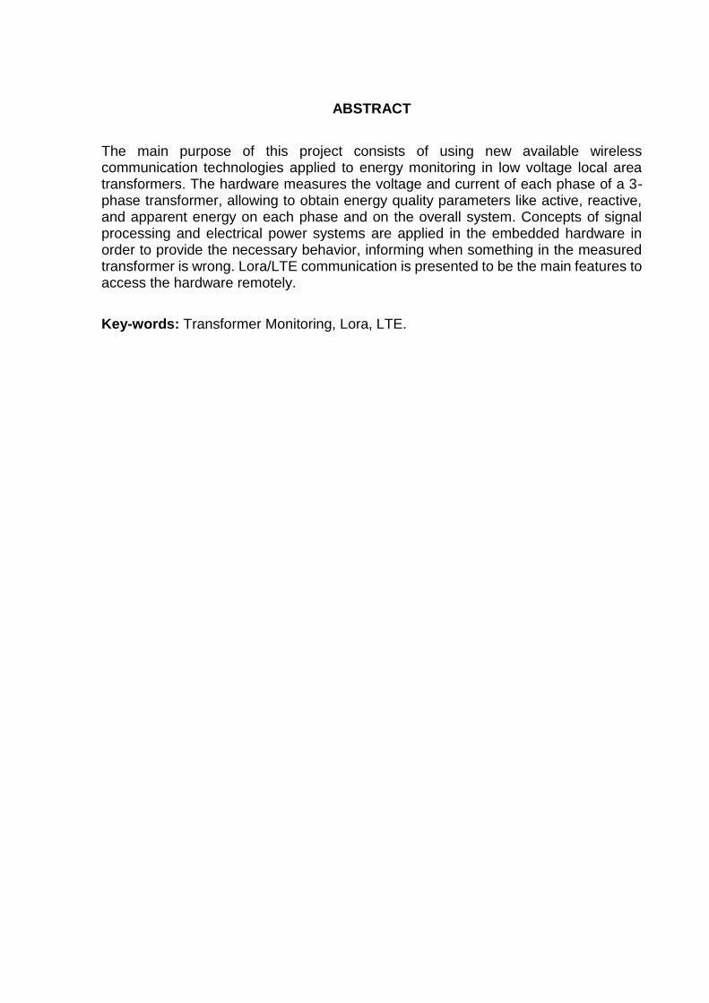
transducer chosen to be used in our project is the LEM LA 100-P shown in the
Figure 3 - once this transducer meets the technical requirements for our
application and we already had some units available to use.
19
Figure 3 – Current Transformer
Source: The authors
We found the price of this kind of transducers do not change significantly
when comparing different manufacturers. Others current transducer for other
brands could be used since it meets voltage or current requirements of our
system and is compatible with the currents that are measured.
For sampling the voltage, we choose to use a direct method for it, that
means, the use of two insulation piercing connectors to make a fused conductive
connection to the power line. Resistors and small transformers were used in order
to make the samples compatible with the with the other system components.
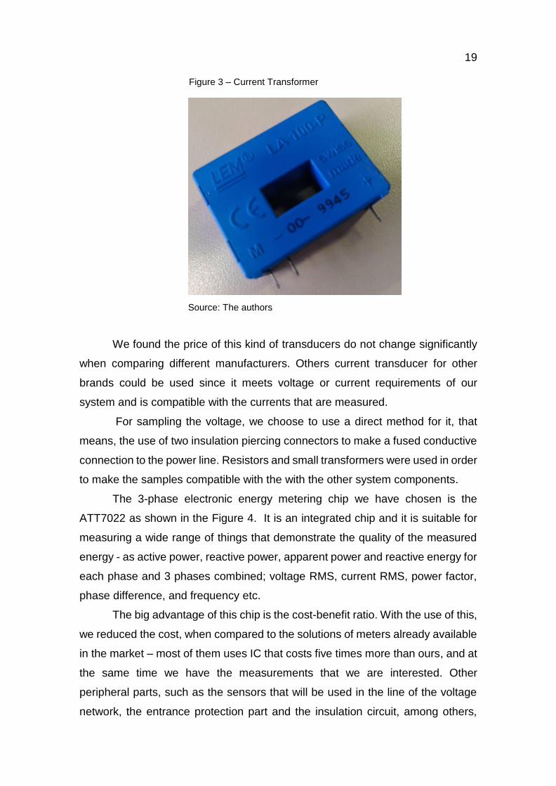
The 3-phase electronic energy metering chip we have chosen is the
ATT7022 as shown in the Figure 4. It is an integrated chip and it is suitable for
measuring a wide range of things that demonstrate the quality of the measured
energy - as active power, reactive power, apparent power and reactive energy for
each phase and 3 phases combined; voltage RMS, current RMS, power factor,
phase difference, and frequency etc.
The big advantage of this chip is the cost-benefit ratio. With the use of this,
we reduced the cost, when compared to the solutions of meters already available
in the market – most of them uses IC that costs five times more than ours, and at
the same time we have the measurements that we are interested. Other
peripheral parts, such as the sensors that will be used in the line of the voltage
network, the entrance protection part and the insulation circuit, among others,
20
were all designed and implemented in the analog board. Similar projects used
this IC to provide solutions in intelligent energy metering solutions as can be seen
in (QI; GAO; ZHANG, 2015; XUPENG; XIU, 2010).
Figure 4 - ATT7022EU
Source: http://lcsc.com, 2018
ADE7868 form the ADE78XX series is one alternatives to use instead the
ATT, however, it is about 5 times expensive than the Chinese IC (MHETRE;
KULKARNI; BHARADWAJ, 2015). The Figure 5 shows a block diagram of the
principal components between the power line and the ATT7022EU energy meter
IC. The AC Sensors block constitutes of sensors to measure the voltage and the
current from the power line. As mentioned in the previous sections, the filter and
protection block are the blocks responsible for protecting the subsequent circuits
in cases of outbreaks that may damage the other components of the circuit and
filtering noise or signals that are undesirable during the acquisition and
processing of the sampled signals respectively.
The Signal Adquancy block is responsible for adjusting the voltage
samples to signals in hundreds of millivolts in order to enable the ATT7022 to
correctly measure these signals.

21
Figure 5 - Block diagram of the AC Sensors and the Energy Meter Hardware
Source: The authors, 2018.
2.3.2 Main micro-controller
The main controller needs to be fast in order to receive signals and process
them in real time. A range of possible microcontrollers feasible for this project
based on their Speed, Flash and SRAM are depicted in Table 1.
Table 1 - Microcontroller Options
MCU Manufacturer Architecture Flash SRAM Speed Unity Price @
500
STM32F103C8T6 ST
Microelectronics ARM Cortex-M3
128 KB
20KB 72Mhz $ 3.90
STM32F722RET6 ST
Microelectronics ARM Cortex-M7
512 KB
256 KB
216Mhz $ 6.74
ESP32-WROOM Espressif Dual Xtensa
LX6 4 MB 512KB 260Mhz $ 4.20
ESP32-WROVER Espressif Dual Xtensa
LX6 4 MB 4.5KB 260Mhz $ 4.57
Source: The Authors, 2018.

22
The Microcontroller Architecture, It’s Speed, Flash and SRAM were
considered for the selection. Even tough MCU frequency is not the only
determinist to indicate how fast it performs, it allows an indication of the MCU
million instruction per second (MIPS) ranking (PESOVIC et al., 2012).
Due to the project requirements of being innovative, low cost and robust,
Espressif’s ESP32 shown in Figure 6 was used as the most viable option. It’s is
the cheapest when compared to other micro-controllers of the same category
(Cortex-M7 from STMicroelectronics) at around 5 dollars each unity at the current
year of this paper. Furthermore, it includes WiFi that can benefit in developments
due to the support for over the air update and flexible boot-loader schemes. It’s
also very successful in current IoT application as discussed in (MAIER; SHARP;
VAGAPOV, 2017).
Figure 6 - ESP32-WROOM Module
Source: Kolban, 2017
ESP32-WROVER module specifications are listed below:
• 240M HZ System frequency;
• 4MB of SRAM + 512KB of System RAM;
• Dual core Xtensa 32-bit LX6 microprocessor;
• Integrated RTC;
To allow correct behavior of the MCU during supply startup and guarantee
correct operation under rough circumstances and some indication during
development a bootstrap circui was used alongside an external watchdog that
prevents the internal MCU to fail due to some not planned internal software loops.

23
2.3.2.1 Bootloader support
To ease development, there is a need to use a bootloader. ESP32 MCU
supports this by default in its main serial, but some external circuit must be used
in order to reset and make the device enter in bootloader state automatically
without needing to reset the board. This functionality is shown in Figure 7.
When the MCU is initialized with it’s Boot pin in a lower voltage level, it will
initiate in the bootloader state, which will allow code to be uploaded to it’s main
flash memory through UART peripheral. When the code is uploaded without
erros, the MCU is then rebooted to RUN mode with the user new code. The reset
pin is the key fator to enable programing the board without turning the system off
and on.
The protocol of the bootloader communication is specific to Espressif chips
(ESP8266 and ESP32 family), but flashing software tools can be found freely in
the company’s repository1.
Figure 7 - Bootloader Flowchart
Source: The Authors, 2018
_______________ 1 Available in <https://github.com/espressif/arduino-esp32>

24
2.3.2.2 Development Framework
The Developement Framework used in this project is the Espressif IoT
Development Framework (ESP-IDF) is exclusivelly for the ESP32 MCU.
Furthermore, to start developing in C/C++ for this system, a toolchain must be
obtained so it can compile the Framework that allows out of box examples to be
tried in the system.
The official IDE support for the ESP-IDF is Eclipse, although, alternative
IDEs such as Visual Studio 2017 are preferable to be used due to it’s rich
features. Third Party extensions such as Visual Micro2 allows this alternative to
be used.
Normally to compile the toolchain in the Windows operatinal system, the
CygWin container software must be used in order to support the necessary linux
build system envernment (RACINE, 2000). This windows container is officialy
supported and can be downloaded in Espressif’s main site. The development
workflow is presented in Figure 8.
Figure 8 - Development of applications for ESP32
Source: https://esp-idf.readthedocs.io/
_______________ 2 Available in <https://www.visualmicro.com/>

25
2.3.2.3 Main Application Logic
The main MCU firmware needed to get the energy measurements and
send them remotely, to better explain this logic, the alghorithm is shown in Figure
9.
As the ESP32 MCU has two processing cores - one core (Core 1) is
responsible to initialize the system and then start the second core (Core 0), this
includes initializing the module system clocks and peripherals such as SPI and
UART before doing so. Following this, the first core starts a thread to read
ATT7022 energy measurements in a loop. In parallel of this, the second core also
starts a thread, but it waits to execute until the thread from core 0 finishes it’s job.
When the second core receives a signal, it can send remote messages
related to the measurements or alerts that are generated by some problem in the
ATT7022 reading. This alert indicates power failures or SPI communication
issues.
After all this procedure finishes, the second cores return to wait for a signal
and core 0 reads the measurements again.
Figure 9 - MCU Simplified Firmware Flowchart
Source: The Authors, 2018.
With the simplified flowchart in mind, the firmware can be extended to be
more organized and expanded in 6 different classes which are handled by a
dedicated thread each. As the ESP32 has 2 cores and its SDK supports the

26
FreeRTOS operational system out of the box, it’s easy to implement these
features in the way presented in the Figure 10. Each Class/Thread is highlighted
in green and is responsible for specific tasks that handle peripherics configuration
and reading.
The advantage in using FreeRTOS operational system with
microcontrollers such as the ESP32 is not only related to its code being efficienty
executed and automatically distributed across available CPU cores, but to
achieve a huge flexibility to develop IHM handling code. It’s common for HMI
handling or communication protocols implementation to use timeouts for waiting
responses. In order to implement correct behavior for different states it’s common
to implement an extensive non-blocking machine state, thus, by using threads it’s
possible to simply implement blocking procedures which can be preempted by
tasks with higher priority. Implementing non-blocking code over asynchronous
one is generally easier, making the firmware development and testing faster
(POLIĆ, 2018).
Each thread is given a certain priority and execution time according to the
project design requirement. For instance, the “Measurement Manager” thread
which is responsible to read the energy metering IC (ATT7022EU) is assigned
the highest possible priority and a periodic execution of 50ms (this corresponds
to a little more than 3 cycles in a 60Hz power grid). All the other threads have a
lower priority and longer execution period which can be always preempted by the
Measurements Manager thread.

27
Figure 10 – Classes and Threads diagram
Source: The Authors, 2018.
2.3.2.4 GPS Time Synchronization
To capture energy measurements with a precise time stamp, a GPS can
be used as can be seen in the schematic shown in the Figure 11. The PPS signals
allows the MCU to receive each second a precise interrupt while the GPS Serial
line sends NMEA messages so the MCU can know not only it’s position but also
it’s UTC Time (GIAMMARINI et al., 2015).
Figure 11 - GPS Schematic
Source: The Authors, 2018.
28
The following steps are applied on the main microntroller firmware to
synchronize the timestamp for the energy masurements:
1. When NMEA messages are received, the MCU decodes it and
check if there is the UTC time is valid;
2. If the decoded UTC time is valid, update its internal time to the
received UTC time and enable interrupt synchronization for the next
second is enabled;
3. When the MCU receives a rising PPS signal from the GPS second,
it updated its internal time to the last decoded UTC time and adds
1 second to it.
When the system is powered on, the step 2 only occurs if step 1 succeds.
Also, these steps are repeated each 60 seconds to guarantee time
synchronization each minute. If the GPS signal is lost due to some environmental
issue, the MCU continues to use its internal reference. The time drift is around 20
parts per million (ppm) which is the external crystal specification.
2.3.3 System Power Supply
The supply circuit uses a switched regulator to power the system as it can
consume large current depending on what he communication processor is doing
or what remote communication is used, so efficiency must be considered here.
A basic protection circuit is used on it for the input voltage coming from the
supply connector, this envolves a resettable fuse and a voltage transient
suppressor that is capable to cut spikes above 13 V that can harm the system.
Additionally, there’s a circuit that allows a change in the supply logic when
the board is not powered by main supply connector, but instead, powered by a
battery in emergency situations.
If only a battery is used to power the system and it has maximum charged
voltage less than 6 V, a conditional supply circuit allows the battery to bypass the
switched regulator to avoid voltage dropout.

29
The hardware can also optionally be powered by an alternative 2 cell
Lithium-ion, or a super capacitor bank. Both technologies are included as factors
such as battery longevity and high temperature operation are important.
The charging curve that the IC follows are depicted in Figure 12. Note that
even tough the graph indicates charging end at 4.2V, this can be adjusted for any
voltage based on the feedback resistors.
Figure 12 - Battery Charging Profile
Source: The Authors, 2018.
2.3.4 External Communication Interfaces
2.3.4.1 LoRa Communication
The popular module SX1278 is used in this project (Figure 13).
Figure 13 - LoRa SX1278 Module
Source: http://lcsc.com, 2018.

30
Besides the SX1278 low cost, a variety of selectable base frequency
modules from the supplier can be bought. Furthermore, It’s a well tested device
in IoT applications (DAUD et al., 2018).
2.3.4.2 LTE Connectivity
The connectivity with a 4G/3G network can then be made with a USB
modem such as the ZTE MF823L 4G Modem Figure 14. They are very cheap
and can be found in national market. It also supports external antennas to achieve
better reception and transition.
Figure 14 - ZTE MF823L 4G Modem
Source: http://www.ztebrasil.com.br.
The application of a communication processor for this project is
essential as it is independently isolate the communication tasks from the main
processor responsible for the energy readings. Due to this reason and 4G/LTE
support pricing options, the best solution we encountered so far is the use of
cheap embedded linux module called Orage Pi Zero depicted in Figure 15.
The Orange Pi Zero is a board that costs about 10 dollars with 512MB
of RAM, has a quad core ARM processor and wifi capabilities by default. Its
board size is very short and a single USB and Ethernet connector is present -
Just as this project needs according to the general diagram showed in the
beginning of this section.

31
Figure 15 - Orange Pi Zero
Source: http://www.orangepi.org
It’s integration in the schematic is showed in the schematic of Figure
16. The connector J5 is a 10-pin female header in which the OrangePi Zero is
connected.
Figure 16 - Orange Pi Zero connector
Source: The Authors, 2018.
2.3.4.3 RS-485
The use of an isolated cost efective RS-485 IC is a must for a project
involving power transformers as a transient in the communication cable cannot
damage the board. The commercial used for this is the ADM2484 IC. Other
solutions such as the MAX14938GW were not considered due to their price.

32
2.3.4.4 USB
To allows easy hardware setup and programming, a USB is be included
on the board. As the onboard MCU doesn’t have an internal USB controller so
an external serial-USB controller IC is be used such as the CH340C instead of
the commonly used FT232 IC. A commom choice such as FTDI counterpart
costs almost 4 times more than the chosen solution and does the same for our
application.
USB protection is also included by using a bidirectional TVS and a
perfect diode circuit which allows almost all the USB voltage to power the
system and protect the USB against reverse current.
2.3.4.5 HMI
A TTL serial interface is used to communicate with hardware or to program
the display. The HMI interface is programmed using a specialized editor (Nextion
Editor) provided by Nextion free of charge. It allows to simulate the user interface
before deploying to the display itself via a SD card integrated in the display.
Nextion also provides a lot of libraries to allow integration with the project
hadware as easy and fast as possible.
2.3.5 Web User Interface
The web user interface needs to be a clean and easy to depict data coming
from the hardware. Thinking of that, Quasar Framework is an open source web
framework that help developers to create responsive websites that look native. It
means that the same web page can be showed in desktop or mobile devices
without the need to rewrite the code.
Quasar is built on top of technologies such as VueJS to allow HTML and
Javascript interaction to be as clean and complete as possible. For that reason,
this framework was chosen instead of similar alternatives like React, Ionic or
AngularJs.
33
2.3.5.1 Measurement Graphs
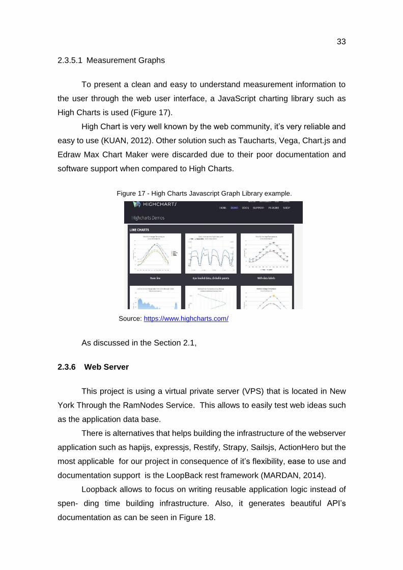
To present a clean and easy to understand measurement information to
the user through the web user interface, a JavaScript charting library such as
High Charts is used (Figure 17).
High Chart is very well known by the web community, it’s very reliable and
easy to use (KUAN, 2012). Other solution such as Taucharts, Vega, Chart.js and
Edraw Max Chart Maker were discarded due to their poor documentation and
software support when compared to High Charts.
Figure 17 - High Charts Javascript Graph Library example.
Source: https://www.highcharts.com/
As discussed in the Section 2.1,
2.3.6 Web Server
This project is using a virtual private server (VPS) that is located in New
York Through the RamNodes Service. This allows to easily test web ideas such
as the application data base.
There is alternatives that helps building the infrastructure of the webserver
application such as hapijs, expressjs, Restify, Strapy, Sailsjs, ActionHero but the
most applicable for our project in consequence of it’s flexibility, ease to use and
documentation support is the LoopBack rest framework (MARDAN, 2014).
Loopback allows to focus on writing reusable application logic instead of
spen- ding time building infrastructure. Also, it generates beautiful API’s
documentation as can be seen in Figure 18.

34
Figure 18 - LoopBack Rest Framework
Source: https://loopback.io/
The Web Server architecture is shown in Figure 20. The communication
processor (Orange Pi Zero) sends its local information through a private port that
can only be accessed through a VPN connection.
The LoopBack framework handles the logic between inserting new data
using generic access to a database such as MySQL. This API access can be
made through normal API calls in NodeJS (RAUCH, 2012).
The communication processor will also use LoopBack Framework for it’s
interaction with the database, allowing a more robust access to configure the
digital board and so on. A configuration JSON file is used to store OrangePi
configuration so it’s connectivity and general option can be configured. These
options are depicted in Figure 19 and are described as following:
▪ CommunicationMode: Allows to use one or more
communication modes to ssend measurement data.
Ethernet and Cellular networks can send information
directly to the server but for LoRa, a LoRa gateway needs
to be used.
▪ DeiveID: Used to identify the device as a ModbusSlave or
a LoRa node in a local network.
▪ DeviceUUI: Unique device ID. It’s used to register get the
device serial number for production control.
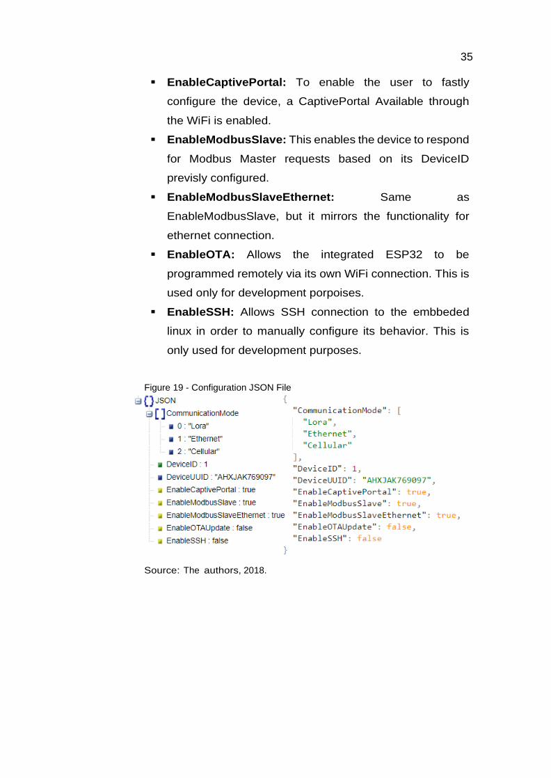
35
▪ EnableCaptivePortal: To enable the user to fastly
configure the device, a CaptivePortal Available through
the WiFi is enabled.
▪ EnableModbusSlave: This enables the device to respond
for Modbus Master requests based on its DeviceID
previsly configured.
▪ EnableModbusSlaveEthernet: Same as
EnableModbusSlave, but it mirrors the functionality for
ethernet connection.
▪ EnableOTA: Allows the integrated ESP32 to be
programmed remotely via its own WiFi connection. This is
used only for development porpoises.
▪ EnableSSH: Allows SSH connection to the embbeded
linux in order to manually configure its behavior. This is
only used for development purposes.
Figure 19 - Configuration JSON File
Source: The authors, 2018.

36
Figure 20 - Web Server architecture
Source: The authors, 2018.

37
2.4 RISK ANALISYS
To ensure that the project development occurs with the least number of surpri-
ses, a risk analysis must be done to all it’s possible scenarios and factors that could
make the development slower or not feasible. There are two main topics to cover in
this analysis: The first is related to general project factors regarding this final year
undergrate project; The second is related to specific details about the type and
complexity of an energy meter hardware proposed in this work.
A table containing a summary of all the listed risks and avoidance difficult is
depicted in Table 2.
Table 2 - Project Risks
Source: The authors, 2018.
2.4.1 General Risks
In the end of the analysis, some solutions must be proposed to avoid or create
an action plan to achieve the project goal. Below are presented some general risks
regarding the project subject:
• Components Supply: as this project involves the use of components that are
not available in the country of this project (Brazil), international components
supplier alternatives must be used. There are well knows companies such as
DigiKey, Mouser, Farnell, LCSC and RC Components. In order to avoid initial
hardware development time, a supplier must be chosen according to its arrival
time and price.

38
• Printed circuit board: Most of the problems can occur in an initial prototyping
stage of the hardware. The use of inadequate or low-quality printed circuit
boards can affect significantly the development time due to issues such as
electrical issues on the board, poor signal integrity, limited board options, etc.
To avoid those problems, professional printed circuit company must be used
such as JLPCB, AllPCB, PCBWAY. Combined with DHL courier as the shipping
option, the board can arrive in maximum of one week.
• Project Complexity: There are 3 main system blocks in the project: Low
voltage Energy measurement, Hardware processing unity and local/remote LTE
communication. In each one there are specific critical details that if not followed
would imply incorrect or faulty behavior of the hardware. The project complexity
is also product of how much tasks are necessary to conclude each project part
and how familiarized and skilled are the students with the concepts and
procedures involved contained in the project development.
• Project cost: There is a maximum amount of resources available that can be
spent in development. Each development phase must agree with a maximum
cost. This problem consists of expenses in electronic components, shipping,
software, PCB manufacturing, manufacturing materials, sensors, modules, etc.
Exceeding the maximum quota would imply in not being able to conclude the
project with integral hardware and functionalities. The cost must always be
aligned with each development step, choosing the only necessary resources
that will be used in order to achieve the goals.
2.4.2 Hardware Risks3
Besides the general risks listed above, there’s also hardware and software
specific risks that must be taken in account. Starting with the hardware risks, a list is
presented below:
• Low Voltage: The front end of the hardware must deal with voltages in the
range of 110-240 Vrms. Thus, must be developed solutions not only to support
_______________ 3 This section was made in March-April 2018, that explain some things that were to be validated.

39
the specified voltage limit, but also provide protection and suppression from
electrical network surges. Not being able to develop this solution would imply in
damaging the hardware in a possible transient scenario. In order to avoid this
problems, guides and components specifications must be followed.
• Electromagnetic Interference: As the hardware will be near a power
transformer, high currents may interfere with the energy monitoring circuit and
communica- tion. EMI suppression techniques must be used such as RF shield
to suppress interferences. Also, modularizing the hardware to separate vital
parts can help eliminate the problem if such techniques are not enough.
• LTE Connectivity: Depending on the region in which the hardware is
installed, internet connectivity or bandwidth is not always guaranteed, even if
dedicated receiver antennas are used. In order to solve this issue, a third
communication option must be used to poll the energy metering data from the
hardware. For instance, RS-485 and LoRa radio communication could be
added.
• Energy fault: There’s a risk that an electrical network measured by the
hardware is turned off intentionally or by some accident. If the hardware doesn’t
detect this, faulty behavior would occur in the measuring system. To avoid this
issue, the main measuring integrated circuit must provide some mechanism.
This must be used as one of the main project criteria for the component’s
selection.
• Integrated Circuit malfunctioning: There is a possibility that a faulty
component is used. It’s difficult to identify this kind of problem as other similar
issues could present similar behavior. To also avoid this problem and also non-
intentional components shortage or maximum parameters exceeding,
redundant components must be bought.
• Schematic and Layout validation: Besides the need of a correct and clean
schematic and layout project according to the project criteria’s, if a further
validation step is not done in early hardware step, the possibility in hardware
faulty behavior that is difficult to find such as incorrect pin placement, incorrect
expected signals, incorrect supply voltage. To avoid those problems or to at

40
least help to identifying them, montecarlo simulation must be done whether is
possible and the schematic and layout must additionally be organized in isolated
blocks and include testing probes, jumpers and extra components. This helps
to better test the hardware when mounted and to promptly identify the origin of
an issue. Furthermore, with extra redundant components included in the
schematic, it gets easy to rework some circuit block for instance.
2.4.3 Software Risks4
With all those possible hardware risks mentioned, there is the software side of
the project that itself contains equally important development steps that could be prune
to some risks:
• Micro-controller peripherals support: There’s a common risk that even
tough using a micro-controller with initially all it’s available peripherals that the
project needs, in practice, an incomplete or faulty peripheral behavior is
supported on software. To avoid this issue in the micro-controller selection, the
errata of it must be read and official forums could be searched to detect if
anyone is having some problem or hardware conflict in a specific peripheral and
also if there’s a software workaround to use it normally use. This presents
initially as low risk as can be done early in the project, but if for some reason
this step is overlooked, the consequences are catastrophic in later hardware
validation. Official sample codes for the targeted micro-controller also must be
seen.
• Software feasibility and complexity: The software running on the
microcontroller must support a complete mathematic library and the
manufacturer must support a compiler with C++11 enabled. If using an ARM
Cortex-M architecture as target micro-controller, the ARM tool-chain must allow
Newlib nano (nano. Specs enabled). As nowadays micro-controllers supporting
these features are getting cheaper, the preferable micro-controller must depict
those capabilities in order to avoid future problems with libraries support such
_______________ 4 This section was made in March-April 2018, that explain some things that were to be validated.

41
as JSON parsing and remote communication. This allows major timing
reduction in project development and avoid libraries incapability and
implementation complexity. One could argue that C++ is too heavy for a micro-
controller, but with the correct compiler optimization and light-weight standard
library usage this is not true anymore.
• Integrated circuit support: By using a dedicated integrated circuit to
measure the energy, a communication to the micro-controller is needed. To
avoid development slow downs in IC communication testing and configuration,
sample codes from manufacturer must be used as reference implementation.
This also reduces the chance in generating bugs that causes undefined
behavior when reading or configuring the IC.

42
2.5 PROJECT SCHEDULE
Source: The authors, 2018.

43
2.6 TESTING METHODOLOGY
The basic flowchart of the testing and validation procedure is presented in Figure
21. The first steps involve the schematic and layout validation trough simulations
whether they are possible. Following this, the PCB Layout must be verified with the
desired PCB manufacturer service do guarantee correct fabrication.
When the board and the components arrive, the PCB is soldered, and each part
of the circuit is independently verified in order to validate all it’s components behavior.
If during initial tests (including fast software IC tests) something goes wrong, a
hardware analysis must be used in order to apply a workaround, getting back to the
component validation step.
An important step that must done in the initial test is the use of a three-phase
signal generator. It allowsto testthe energy measurement IC by generating the
necessary signals of voltage and current with a lag of 120 degrees of each other.
Figure 21 - Testing and validation flowchart
Source: The authors, 2018.

44
2.7 HARDWARE PROJECT
The following subsections will present the project development procedure,
including simulations and design considerations.
2.7.1 Simulation
Some parts of the project were realized in the PSPICE software. The software
presented as a fast model based electronic circuit simulator, in which allowed to
validate some electrical behavior specially in the power supply circuit. The following
paragraph will present the fundamentals steps during the circuit planning.
The first fundamental circuit to simulate is the power supply, for that we
considered a switched DC regulator as this would allow better efficiency and size
reduction for the project. In the PSPICE software unfortunately the switched regulator
doesn’t exist and is required to be manually designed. Fortuntelly, as the simulator is
model based we can use control blocks to simulate the fundamental voltage feedback
circuit present in buck step-down regulators (ZURITA-BUSTAMANTE et al., 2011).
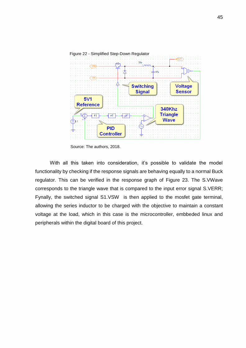
These elements can be seen in Figure 22.
The simplified model of the the switched regulator contains an internal
reference, an error-based controller such as a PID controller, a triangular wave
oscillator tuned to 340Khz (specified for this project) and a voltage comparator followed
by a mosfet which is responsible to turn on and off the the load. The voltage is fed back
to the PID controller trough a diferential voltage sensor. As the Supply circuit uses 5.1V
for higher voltage drop tolerance, the internal regulator reference is also fixed to 5.1V.
45
Figure 22 - Simplified Step-Down Regulator
Source: The authors, 2018.
With all this taken into consideration, it’s possible to validate the model
functionality by checking if the response signals are behaving equally to a normal Buck
regulator. This can be verified in the response graph of Figure 23. The S.VWave
corresponds to the triangle wave that is compared to the input error signal S.VERR;
Fynally, the switched signal S1.VSW is then applied to the mosfet gate terminal,
allowing the series inductor to be charged with the objective to maintain a constant
voltage at the load, which in this case is the microcontroller, embbeded linux and
peripherals within the digital board of this project.

46
Figure 23 - Simplified step-down regulator model response
Source: The authors, 2018.
After this basic model is tested independently, thus ensuring that it supports an
extensive range of loads ranging from few miliampers to 2 ampers, a submodel of it is
created and placed in the main power supply circuit as depicted in Figure 24.
The switched regulator is an important component to support input voltages at
the maximum of 24V for this project. Allownig the digital board to be as independent
as possible to the actual analog board that is responsible to read power quality
masurements. To ensure this specification support for a beckup battery, not only the
regulator has to work properly, but an auxiliary circuit must be designed to permit low
voltages such as 5V to supply the entire board without voltage drop. The components
responsible for the auxiliary circuit are some voltage comparator ICs and mosfet
transistors that act such as logic gates.
Depending on the voltage applied to the main power supply input, the switched
regulator is used or not. And when the buck regulator is not used, a transistor circuit
turns it off and shorts the input with the output in a way that lower voltages such as 5V
can supply directly the circuit without a considerable voltage drop to occur (in the order
of few millivolts).

47
Figure 24 - Power supply circuit model
Source: The authors, 2018.
To better explain the auxiliary circuit behavior, the conditional behavior the
supply circuit is presented in Table 3.
Input Voltage /Battery Voltage
Buck regulator status
Bypass Transistor
>= 7.4V ON OFF
>= 5.9 & < 7.4V OFF OFF
< 5.9V OFF ON
Table 3 - Power supply circuit behavior
When the input supply voltage is over or equal 7.4V, the buck regulator is turned
on. However, when the input voltage drops to a level ranging from 5.9V to lower than
7.4V, the regulator is turned off. This is the desired behavior for a 2 Cells lithium-ion
battery as turning off the regulator and the bypass transistor prevents the battery to
discharge even more, thus avoiding damage to the battery. On the other hand, when
the complimentary circuit receives a voltage lower than 5.9V it assumes that the board
is being supplied intentionally with low voltage such as the association with 2 series

48
super-capacitors and enables the bypass transistor. This voltage level is not critical to
the digital board as its internal regulators are rated to support it.
The simulation yields the expected results which can be seen in Figure 25. Input
and output voltage are plotted in red and blue respectively. When Vin=5V there’s no
voltage drop at the output due to the bypass transistor being enabled.
Figure 25 - Input and output voltage simulation results
Source: The authors, 2018.
2.7.2 Analog board design
For the development of the schematic and PCB of the analog part of the project,
in addition of the knowledge and experiences got during the undergraduate classes
and projects, technical data, design suggestions and some wiring diagrams found in
the datasheets of the components - ATT7022EU, voltage regulators, protection
devices, etc. - were used. Briefly, this part consists of, once the sampling the voltage
and current is performance, the signals got from the transducers are reduced aiming
to make them compatibles with the levels that are compatible with the ATT7022EU
voltage input and sending the data sent from IC to the processing unit. In addition, the

49
developed analog part includes the generation of the DC voltages used and some
measurement points for the validation of the correct operation of the circuit. The
connection diagram of the voltage sampling is shown in Figure 26.
Figure 26 - Connection diagram of the voltage sampling to the ATT7022EU
Source: The authors, 2018.
Firstly, we have the interface between the analog board with the transmission
line – the “interface with the transducer” block. Once this part is about the voltage
sampling, a direct sampling in the low side of the transformer must be performance.
The next step consists in some protection components to avoid damages with
overvoltage and overcurrent and filters. The “signal adequacy and isolation circuit”
block consists on resistors and transformers to set the signal from the transducers
down to levels that are compatibles with de ATT IC.
For the current, the connection diagram of the current sampling is shown in
Figure 27.

50
Figure 27 - Connection diagram of the current sampling to the ATT7022EU
Source: The authors, 2018.
Once the current sampling is done indirectly – using a current transducer
“connection with the transducer” box, the connection between the transducer and the
analog board is done indirectlly. Once the cureent is sampled, it goes to the “signal
adquacy circuit” that has two main tasks. The first one is to reduce the current from the
transducer to values that are compatible with the ATT IC and isolation between the
external measurement and all the the rest of the systems’ circuit. The next step – the
“current to voltage transformation and filter” is responsible to transform a current signal
into a voltage and filter it, avoiding high frequency noises for then to conect to the ATT
IC.
Another system that is part of the analog boars is the part that is responsible of
the adquation of the DC voltage to levels that are used in this board - Figure 28.
Figure 28 - Connection diagram of the DC voltage of the analog board
Source: The authors, 2018.

51
In the Figure 29, the connection diagram of the DC voltage of the analog board
is shown. The first stage is about the supply voltage. For instance, this voltage will be
supplied by an external power supply. The second block – the “filter and circuit
protection” is about filtering the voltage that come from the power supply to avoid high
frequency noise that may come through from the main power supply, that can be a
linear or switched power supply type, and the protection from voltage transients
induced by lightning and other transient voltage events. In the next step dropped down
from 12 V to 5 V using a regular voltage regulator with the capacitors suggested in the
datasheet. Lastly, the voltage is reduced again from 5 V to 3.3 V and then used to
supply the respective components.
Figure 29 - Connection diagram of the DC voltage of the analog board
Source: The authors, 2018.
The layout of the analog board is shown in Figure 30. It’s a simple design
but some considerations needed to be made during the project such as circuit
protection and correct components placement according to the ATT7022 manufacturer
datasheet. There are analog tracks that need to be folloed by gounding to avoid
interference. Also, the right side of the board that contains the current transformers
must not contain ground as high voltages are involved during the energy reading.

52
Furthermore, circuit protection was added right after the terminal block connectors to
avoid circuit damage during a powervoltage period.
Figure 30 - Analog. board PCB layout
Source: The authors, 2018.
2.7.3 Digital Board design
The Layout of the digital board is depicted in the Figure 31. The layout involves
deferent ground plans to best avoid noise and to shield the board. This will be
explained in following paragraphs.
The division between each functional part of the digital board is done in a way
to best isolate the power supply circuit from the MCU and antennas. This can be seen
in Figure 31 as each functional part has its ground isolated but at the same time, they
are united at just one point, at the lower right side of the board, where the power supply
components are present. This technique is widely applied to mixed analog/digital

53
hardware such as studied electromagnetic interference mitigation theory (CHEN,
2005).
Figure 31 - Digital Board Layout
Source: The authors, 2018.
For each part of the board, a certain layout criterion were applied:
• Power supply & battery: The layout design of the power supply is done in a way
to centralize every ground from the other peripherals. This is important due to;
• Comms: The communication consists of two peripherals, the RS-485
transceiver and the CAN transceiver, although CAN is not used in this project,
it’s future support is beneficial for future applications using the same digital
board. The RS-485 transceiver is totally isolated; thus it has its own ground and
voltage regulation circuitry which need to be connected to an external power
supply tied from the bus master side. In a different way, the CAN transceiver is
not isolated but has a separated ground which then unifies at the power supply
segment of the board;
• MCU & Linux: This segment consists of a large grounding which is divided with
USB peripherals, watchdog supervisor, analog board and IHM connectors and

54
Orange Pi Zero female header. As all the peripherals are mostly communicating
with binary communication protocols such as USART and SPI, there’s no
worries about interference between tracks influencing each other in a negative
way, that is, digital crosstalk is not taken into account here as we are dealing
with low clock speeds for communication. It’s understood as high speed
communication when it comes to signals operating with 100Mhz or more
(JOHNSON; JOHNSON; GRAHAM, 2003). However, even at this point it’s
optional to use more complex techniques evolving track width calculation if the
total length of a net from a peripheral to other is short. This is exactly the case
where our project fits. In short, the project’s board doesn’t have high speed
signals nor long signal tracks between components.
• GPS and LoRa: The GPS and LoRa segment are generally equal in the sence
that both have an antenna connector near their respectives modules. For this
layout, the importance relays on the shielding near the antenna tracks. Several
vias was placed on the ground to equalize impedance and fast transient
response near the module, this is called via stitching. Another interference
refuction technique applied was the track shield in which consists in placing a
high amount of vias near the antenna track, thus allowing the antenna path to
be horizontally protected from EMI sources.
A 3D Overview of the board is also generated and is shown in Figure 32. The
main connectors are disposed in the edge of the board, so it allows easy board wiring.
Communication connectors for Cellular modem, ethernet and antennas are in the back
side of the board.
In order to receive LoRa messages, a USB dongle is designed so it can be
placed not only in the a commom gateway, but also in a simple computer, allowing
faster development and cost reduction. This dongle is shown in Figure 33.

55
Figure 32 - Digital Board 3D Mounting
Source: The authors, 2018.
Figure 33 - LoRa Dongle 3D Project
Source: The authors, 2018.

56
3 PROJECT PROTOTYPE AND TESTING
The general project diagram is shown in Figure 34. The numbers from 1 to 9
are the subststem that will be better described in the following subsections.
Figure 34 - General project diagram
Source: The authors, 2018.
1 – ENERGY METER HARDWARE
This part is responsible of getting the values of voltage and current sampled
from the low side of the transformer and process it in the ATT7022EU IC. For it, the
sampled signals must be in the range that the ATT7022EU operate. For it, some
circuits were designed aiming to make this interface.
• POWER SUPPLY: A 12V power supply is used to supply the circuit. Once 12 V
is a voltage that is too high for some IC – the ATT, for example, works with 3.3
V, it must be dropped down. By powering the analog board with +12 V DC, we
can validate the right functionality of the power supply system of the used ICs.

57
• VOLTAGE MEASUREMENT: By plugging the voltage connector a 127 V AC
and measuring the voltage on the measure pin after the current transformer, it
is possible to validate that the system that changes the voltage to values that
are compatibles with the ATT IC are working properly.
2 – POWER SUPPLY
In this part of the project, we are going to validate the right functionality of the
system that the manage the battery and the right functionality of the digital board when
supplied by the battery or by and external supply.
1. Testing the functionality of the digital board only powered with the battery - In
this test, we are going to validate the operation of the digital board even when
the external power supply is “out of working”, that mean, there is no external
power supply supplying the circuit. In this case, LED disposed in the digital
board will turn on indicating the operation of the board without any problems or
restrictions.
2. Testing the functionality of the circuit that manage the power supply system - In
this test, we are going to validate the operation of the circuit that manage the
power supply system, that means, we can see it operating when we plug in a
battery that is not completely charged and will be charged – during the charging
process, a LED that indicate the “charging battery” status will turn on. For it, the
board must be supplied for and external power supply and a battery not
completely charged needs to be plugged in. When the battery is completely
charged, the LED that indicate the “battery charged” status will turn on and the
LED that indicate the “charging battery” status will turn off.

58
3 – ESP32
In this test, we are going to validate the MCU by re-uploading the program in it.
Once it is very important for the right functionality of other blocks, it is hard to make a
test that shows only the ESP32 working by itself without user interaction.
4 – Realtime Clock (GPS)
The GPS module is used for the identification of the right location of the energy
meter. Using the NMEA information showed in Figure 35, we can get the coordinates
of the device and some information’s about the right functionality of some parts of the
GPS hardware. For example, using “$GPTXT” parameter we can get information’s
about the right functionality of the antenna and the “$GPFLL” the coordinates of the
current location of the device. The Figure 36 shows the decoded GPS module
information and the Figure 37 the position got from the GPS module.
Figure 35 - GPS NMEA information on serial terminal screen
Source: The authors, 2018.

59
Figure 36 – Decoded GPS module information on serial terminal screen
Source: The authors, 2018.
Figure 37 - Google maps location pointed by the GPS
Source: The authors, 2018.
5 – RS-485 and USB
The RS-485 validation will be performance through some date send from a USB
connection from a PC using a serial monitor – Arduino serial monitor, for example and
it will arrive in the digital board as a RS-485 message. To validate that it is working
properly, the LoRa connection may be used to show that any request sent through the

60
USB-RS-485 has arrived in the digital board, the answer got can be send through the
LoRa communication and show in a serial monitor.
6 – REMOTE CONECTIVITY
For the validation of the LoRa communication, we are going to test to scenarios.
The first one is called “transparent” and the second “protocol”. A LoRa dongle (Figure
38) was developed in parallel of this project in order to better debug such
communication modes.
Figure 38 - LoRa dongle
Source: The authors, 2018.
The following testing procedures were used to validade the remote LoRa
communication:
1. For the “transparent” validation, 2 PC are needed to have the communication
between the PC and the digital board working properly. One of them must have
the LoRa Dongo plugged in a USB input and a serial monitor configured with a

61
baud rate of 115200 bps. The second one has the digital board plugged in a
USB port and has a serial monitor configured with a baud rate of 115200 bps.
Messages can be sent and received for both and the messages will be show in
the monitor serial of the receiver. In this test we can validate the right
functionality of the hardware, software and firmware developed.
2. For the “protocol” communication, we have the communication between the
digital board and the PC. In this scenario, unlike the previous, the digital board
is not connected with the PC and its decisions and answers are done by itself -
through programming. The digital board is configured to answer the received
questions in a determined interval of time.
For the 3G connectivity, a USB modem must be attached to the Orange PI board
to provide to it an internet connection. Once this is done, the system can send data
and communicate with other devices through internet connection. The Figure 39 shows
the Shell screen from the Orange PI subsystem and the Figure 40 shows the User
Web Interface.
Figure 39 - Orange PI terminal screen
Source: The authors, 2018.

62
Figure 40 – OrangePi user Web interface
Source: The authors, 2018.
7 – IHM (Human Machine Interface):
The IHM will start since the startup of the system. It will show a “loading screen”
while the microcontroller is getting ready and makes the transition to another screen
where its possible to see the voltage, current and power from each of the 3-phase
measured and shows the status of the availability of the GPS system and the data
connectivity. It has, also, a button where it is possible to activate and de-activate the
LoRa communication and a place that shows if is the embedded Linux is available or
not. With it, we can validate the code done for the IHM and the communication with the
other subsystems.

63
Figure 41 - IHM interface
Source: The authors, 2018.
8 – CLIENT
This part is the validation of the client side of the system. As shown in the other
validations step, a PC can almost every time interact with the systems and its data. A
simple terminal application can be used to check or configure the system usin JSON
syntax.
9 – WEB APPLICATION
In this stage, it is possible to test the integration with the MQTT connectivity. An
application called MQTT.fx is used to connect to the server and send some relevant
data (this can be done by using the broker link http://mote.ddns.net). Further it’s
possible to check that correct data was receiving by opening the EMONCMS web
dashboard. The Figure 42 shows measurements sent from the MQTT.fx. Later the
same procediment is done, but with the embedded linux connection to the MQTT
broker and sending real energy measurement data.

64
Figure 42 - EMONCMS dashboard
Source: The authors, 2018.

65
4 SUSTAINABILITY AND ENVIRONMENTAL IMPACT
According to according to the Manual of the technological R & D programs of
the Brazilian electric sector of 2001, the production, transportation and consumption of
electricity - and electronic devices affect various aspects of the environment such as
air quality, water quality and availability, populations and habitat of aquatic and
terrestrial fauna and flora, the use of hazardous material and waste the impact of
electromagnetic effects on health as general and the environment, etc. Doing a briefly
analisys on sustainability and environmental impact aspects of the developed project,
we selected some aspects to analyze and to discuss about. Whenever possible, we
tried to choose technologies that have the minimum environmental impacts.
Thinking about alternative ways of powering our systems, we can quote solar
systems as one alternative. However, it was not implemented in our system due the
need of our project - since our hardware will be coupled in the output of a transformer
and it has a low consumption, it was chosen powering it with the voltage of the network
itself, adjusting in the voltage to make it compatible with levels of the circuit, which is
more appropriate - it is already used by other available and functional solutions and
has a better cost-benefit ratio – implementing a solar system has an additional cost
besides the system.
During the process of choosing the components of our hardware, we took care
to choose components that have a seal that demonstrates that the product in question
complies with the RoHS directive in the manufacturing process and the product itself -
as can be seen in Figure 32, which shows that RoHS is a parameter of the product in
our supplier.

66
Figure 43 – RoHS component summary
Source: The authors, 2018.
Aiming the quality and reliability of our solution, besides the hardware was
developed for this specific solution, the electronic components used were new. We cite
as ways of reducing the cost, in the hardware part, the purchase of components in big
quantities and the search for other national suppliers.

67
5 RESULTS
The complete mounted board is present in Figure 44. The analog board is
assembled on top of the analog board which is connected to a digital power supply
regulated to 12 volts. The 3G dongle is attached on the available port on the embedded
Linux. The connectivity link is checked trough the local user interface.
Figure 44 - Complete mounted hardware
Source: The authors, 2018.
The hardware is connected to the available laboratory ac power and tied to a
voltage generator for current signal simulation. The analog board response for
acquired voltage and current signals are shown in Figure 45 and Figure 46
respectively.
The microcontroller is programmed to collect data for a period of 30 minutes.
After this period the data is collected on the web interface which can be seen in
Figure 45. The average values are always in the range of 59.9 – 60.1 HZ.
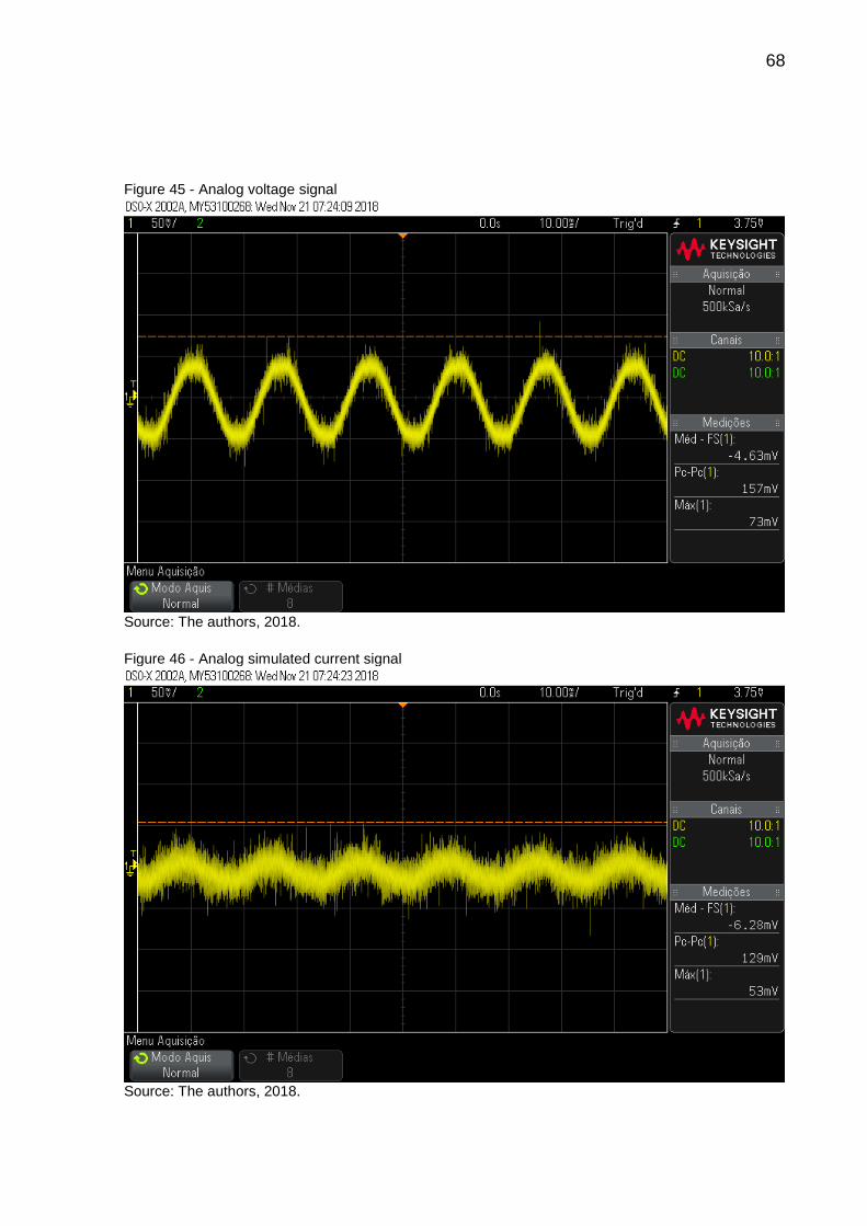
68
Figure 45 - Analog voltage signal
Source: The authors, 2018.
Figure 46 - Analog simulated current signal
Source: The authors, 2018.

69
Figure 47 - Frequency measurements
Source: The authors, 2018.
Moreover, the realtime data of most important energy information is observed
in the EMONCMS realtime dashboard containing measurements the ac frequency,
phase voltage, current, active power and power factor of each phase.
Figure 48 - Realtime dashboard 1
Source: The authors, 2018.

70
Figure 49 - Realtime dashboard 2
Source: The authors, 2018.
The LoRa dongle is attached to a notebook close to the board and LoRa
communication is validated by receiving the aggregated energy measurements
information with its average, minimum and maximum values each 1,5 and 15 minutes
respectivelly. This can be seen in the serial terminal application of Figure 50.
Figure 50 - LoRa remote measurements responses
Source: The authors, 2018.

71
Further the IHM is attached to the board in order to easily show the main
energy measurements. This is presented on Figure 51.
Figure 51 - Functional IHM
Source: The authors, 2018.
Finally, the 2-cell lithium battery was attached on the battery connector of the
digital board (Figure 52) and verified to work when the main 12V power was disabled,
allowing a continuous operation without causing the system restart.

72
Figure 52 – 2-cell lithium battery
Source: The authors, 2018.

73
6 FINAL CONSIDERATIONS AND FUTURE WORK
The development of this project was a very challenging task. We started with an
abstract idea and when we reach the end of the discipline of TFG 2 with a hardware
that can perform the assignments that we planned in the initial documents delivered in
the TFG 1 discipline. It was a very good experience that, in our opinion, brought us
closer to the day-to-day/activities of an engineer.
All aspects the technologies foreseen in the planning stage were maintained
and implemented in the final soluton. We are very satisfied with the results obtained in
the final implementation that will be presented in the final presentation of the discipline,
since we seek to develop the hardware used by ourselves and today we can see our
technical and practial evolution when we compare our knowledge at the beginning of
the discipline of TFG 1. For our solution to gain even more robustness and that can be
implemented in a real physical system, we are aware that there are still aspects that
need to be developed - encapsulation with isolation of electromagnetic interference,
for example, and field tests need to be performed. However, considering the time and
complexity of our solution, we are very satisfied with the results achieved.
Making a superficial comparison with the technologies that already exist and
that apply in the same area as our solution, we can say that the hardware we use are
according to the needs of the application and have, for the most part, a lower price.
For example, Babelbee (avalible in http://www.babelbee.org/#About) uses the ARM
core as the main CPU running at 700 MHz, with a price of approximately $ 20.00
(2018). In our solution, we used the ESP32-WROVER, with a price of approximately $
4.57 (2018), showing a difference of prices of $ 15.43 (2018), which represents
approximately 337.64% of difference between the values. It is worth mentioning that
one of the requirements for the choice of technologies embedded in our final solution
considered what was already in the market and its purchase price. In total, the
components used present a technical characteristic compatible with those used in pre-
existing solutions but with a lower value. Another rugged and portable solution we
found is Fluke's advanced Power Quality and energy analyzer. It is a complete and
versatile equipment but, according to values found on Fluke's website for sales in the
United States, it costs $ 7,599.00, which is equivalent to R$ 35,000.00 (Brazilian

74
currency). in general, we can state that our solution has the technical potential and an
interesting financial aspect to be applied in environments where the Babelbee or Fluke
energy meter could be applied with a more cost-effective ratio and flexible
communication systems.
It can also be said that the project has extrapolated the barriers of technical
knowledge in electronics and covered aspects related to electrical engineering,
computer engineering, administration, marketing, etc. We didn't just go beyond
developing the hardware, we had to think about alternative ways of its implementation
aiming minimizing costs, which impacted in searching for suppliers with the lowest
price of the components and we found LCSC - a worldwide supplier of electronic
components located in China, and with that, we had to understand the process of
importing a product and also that it takes time (shipping) - for physical distance and
legal issues. We had to manage our time and the activities we needed to develop. As
the work developed in a group, we used Trello tool for the management part of the
activities and the deadline that we needed to fulfill. We also sought a tool for the
development of the schematics in a cooperative way and we found easyeda, which, in
addition to working in a cooperative way, we had a direct connection with LCSC
components and it allowed us to buy the necessary components directly from them
and at the same time generate the layout of the printed circuit board and order it - with
a great price.
75
REFERENCES
CHEN, J. EMI suppression technique for RJ connectors with integrated magnetics, Google Patents, 2005.
DAUD, S. et al. Performance Evaluation of Low Cost LoRa Modules in IoT Applications. In: IOP CONFERENCE SERIES: MATERIALS SCIENCE AND ENGINEERING 2018, Anais... [s.l: s.n.]
GIAMMARINI, M. et al. Real-time synchronization of wireless sensor network by 1-PPS signal. In: SMART SENSORS, ACTUATORS, AND MEMS VII; AND CYBER PHYSICAL SYSTEMS 2015, Anais... [s.l: s.n.]
JOHNSON, H.; JOHNSON, H. W.; GRAHAM, M. High-speed signal propagation: advanced black magic. [s.l.] : Prentice Hall Professional, 2003.
KUAN, J. Learning Highcharts. [s.l.] : Packt Publishing Ltd, 2012.
LI, J.; ZHANG, B.; QIU, D. Y. Multi-computer communication based on Modbus RTU in power quality monitoring system. Electric Power Automation Equipment, [s. l.], v. 27, n. 1, p. 93–96, 2007.
MAIER, A.; SHARP, A.; VAGAPOV, Y. Comparative analysis and practical implementation of the ESP32 microcontroller module for the internet of things. In: INTERNET TECHNOLOGIES AND APPLICATIONS (ITA), 2017 2017, Anais... [s.l: s.n.]
MARDAN, A. Sails. js, derbyjs, loopback, and other frameworks. In: Pro Express. js. [s.l.] : Springer, 2014. p. 205–214.
MHETRE, S. B.; KULKARNI, H. H.; BHARADWAJ, D. G. A Simple and Low Cost Solution for Measurement of Harmonics in Distribution Sector. In: COMPUTING COMMUNICATION CONTROL AND AUTOMATION (ICCUBEA), 2015 INTERNATIONAL CONFERENCE ON 2015, Anais... [s.l: s.n.]
PESOVIC, U. et al. Benchmarking performance and energy efficiency of microprocessors for wireless sensor network applications. In: MIPRO, 2012 PROCEEDINGS OF THE 35TH INTERNATIONAL CONVENTION 2012, Anais... [s.l: s.n.]
POLIĆ, F. Using FreeRTOS operating system in laboratory exercises. 2018. Fakultet elektrotehnike i računarstva, Sveučilište u Zagrebu, [s. l.], 2018.
QI, H.; GAO, N.; ZHANG, Y. Design of Intelligent Power Supply Unit Based on Zigbee Technology. 2015 International Conference on Education, Management, Information and Medicine, [s. l.], 2015.
RACINE, J. The Cygwin tools: a GNU toolkit for Windows, JSTOR, 2000.
RAUCH, G. Smashing Node. js: JavaScript Everywhere. [s.l.] : John Wiley & Sons, 2012.

76
SWALES, A.; OTHERS. Open modbus/tcp specification. Schneider Electric, [s. l.], v. 29, 1999.
XUPENG, C.; XIU, J. Application of the wireless sensor network topology based on the power acquisition system. In: ELECTRICAL AND CONTROL ENGINEERING (ICECE), 2010 INTERNATIONAL CONFERENCE ON 2010, Anais... [s.l: s.n.]
ZURITA-BUSTAMANTE, E. W. et al. A comparison between the GPI and PID controllers for the stabilization of a DC--DC “buck” converter: A field programmable gate array implementation. IEEE Transactions on Industrial Electronics, [s. l.], v. 58, n. 11, p. 5251–5262, 2011.
FLUKE knowledge base available in < https://www.fluke.com/en-us/learn/> Acessed in november, 2018.
RAVAGLIO, M. A. SCHAEFER, J. C., GAMBOA, L. R. A., ADONIS N. G. and VALENÇA M. M., "Avaliação da Vida Útil dos Transformadores da COPEL Distribuição", SENDI 2004 - XVI SEMINÁRIO NACIONAL DE DISTRIBUIÇÃO DE ENERGIA ELÉTRICA, 2004.