power design guide - freetrendol.free.fr/smdk6410/356185s3c6410x_powerdesignguide...6410x_power...
TRANSCRIPT

Confidential Proprietary of Samsung Electronics Co., Ltd Copyright © 2007 Samsung Electronics, Inc. All Rights Reserved
Power Design Guide S3C6410X
RISC Microprocessor
October 7, 2009
Preliminary REV 0.91
Preliminary product information describe products that are in development, for which full characterization data and associated errata are not yet available. Specifications and information herein are subject to change without notice.

6410X_POWER DESIGN GUIDE PRELIMINARY REV 0.91
2 Samsung Confidential
Important Notice
The information in this publication has been carefully checked and is believed to be entirely accurate at the time of publication. Samsung assumes no responsibility, however, for possible errors or omissions, or for any consequences resulting from the use of the information contained herein.
Samsung reserves the right to make changes in its products or product specifications with the intent to improve function or design at any time and without notice and is not required to update this documentation to reflect such changes.
This publication does not convey to a purchaser of semiconductor devices described herein any license under the patent rights of Samsung or others.
Samsung makes no warranty, representation, or guarantee regarding the suitability of its products for any particular purpose, nor does Samsung assume any liability arising out of the application or use of any product or circuit and specifically disclaims any and all liability, including without limitation any consequential or incidental damages.
"Typical" parameters can and do vary in different applications. All operating parameters, including "Typicals" must be validated for each customer application by the customer's technical experts.
Samsung products are not designed, intended, or authorized for use as components in systems intended for surgical implant into the body, for other applications intended to support or sustain life, or for any other application in which the failure of the Samsung product could create a situation where personal injury or death may occur.
Should the Buyer purchase or use a Samsung product for any such unintended or unauthorized application, the Buyer shall indemnify and hold Samsung and its officers, employees, subsidiaries, affiliates, and distributors harmless against all claims, costs, damages, expenses, and reasonable attorney fees arising out of, either directly or indirectly, any claim of personal injury or death that may be associated with such unintended or unauthorized use, even if such claim alleges that Samsung was negligent regarding the design or manufacture of said product
.
S3C6410X RISC Microprocessor Power Design Guide, Preliminary Revision 0.9a
Copyright © 2007-2009 Samsung Electronics Co.,Ltd.
All rights reserved. No part of this publication may be reproduced, stored in a retrieval system, or transmitted in any form or by any means, electric or mechanical, by photocopying, recording, or otherwise, without the prior written consent of Samsung Electronics Co.,Ltd.
Samsung Electronics Co., Ltd. San #24 Nongseo-Dong, Giheung-Gu Yongin-City Gyeonggi-Do, Korea 446-711
Home Page: http://www.samsungsemi.com/ E-Mail: [email protected]
Printed in the Republic of Korea

6410X_POWER DESIGN GUIDE PRELIMINARY REV 0.91
3 Samsung Confidential
Revision History
Revision No Description of Change Refer to Author(s) Date 0.00 - Initial Release for review - S.K. Kim 2008-05-13
0.03 - DC Spec. is changed - Notification is added - S.K.Kim 2008-07-25
0.04 - Power Sequence is updated - S.K.Kim 2008-08-20
0.05 - DVFS Guideline at sync. Mode is added - S.K.Kim 2008-09-23
0.06 - Power Consumption is added - S.K.Kim 2008-09-27 0.7 - Redundant information is removed - S.K.Kim 2009-05-14
0.7a - DVFS Minimum Voltage is added - S.K.Kim 2009-07-22 0.8 - Power on Sequence is modified - S.K.Kim 2009-08-06
0.91 - Power on Sequence is modified - Operating Voltage is modified - S.K.Kim 2009-10-07
NOTE: Revised parts are written in blue.

6410X_POWER DESIGN GUIDE PRELIMINARY REV 0.91
4 Samsung Confidential
Table of Contents
1. PRODUCT OVERVIEW ............................................................................................................................ 5
2. RECOMMENDED OPERATING CONDITIONS ....................................................................................... 6
3. RECOMMEND SYSTEM POWER DESIGN ............................................................................................. 7
4. CIRCUIT GUIDE FOR DVS SCHEME...................................................................................................... 8
5. TIMING CHARTS WITH DVFS ................................................................................................................. 9
5.1. Typical DVFS Level Definition ........................................................................................................ 9
5.1.1. Typical DVFS Transition Table @ 533Mhz Synchronous and Asynchronous Mode......... 9
5.1.2. Typical DVFS Transition Table @ 800Mhz Synchronous and Asynchronous Mode......... 9
5.2. Typical DVFS Transition Diagram .................................................................................................. 10
5.2.1. Typical DVFS Transition Diagram @ 533, 800Mhz ................................................................ 10
6. POWER ON AND OFF SEQUENCE ........................................................................................................ 15
7. PLL DESIGN GUIDE ................................................................................................................................ 19
7.1. APLL/MPLL Specification ............................................................................................................... 19
7.2. EPLL Specification .......................................................................................................................... 20
7.3. USB OTG 2.0 PLL Specification ..................................................................................................... 21
7.4. TV OUT Clock Specification............................................................................................................ 21
APPENDIX .................................................................................................................................................... 22
A. Example of Changing Divider Code ................................................................................................. 22
B. Power Requirement............................................................................................................................ 23

6410X_POWER DESIGN GUIDE PRELIMINARY REV 0.91
5 Samsung Confidential
1. PRODUCT OVERVIEW
This document describes S3C6410 power design guide for circuit designer. It shows as follows,
- recommend DC operating conditions
- recommend system power design
- power on/off sequence
- pll design guide
- power consumption data
It will help you design your system properly.
6410X_POWER DESIGN GUIDE PRELIMINARY REV 0.91
6 Samsung Confidential
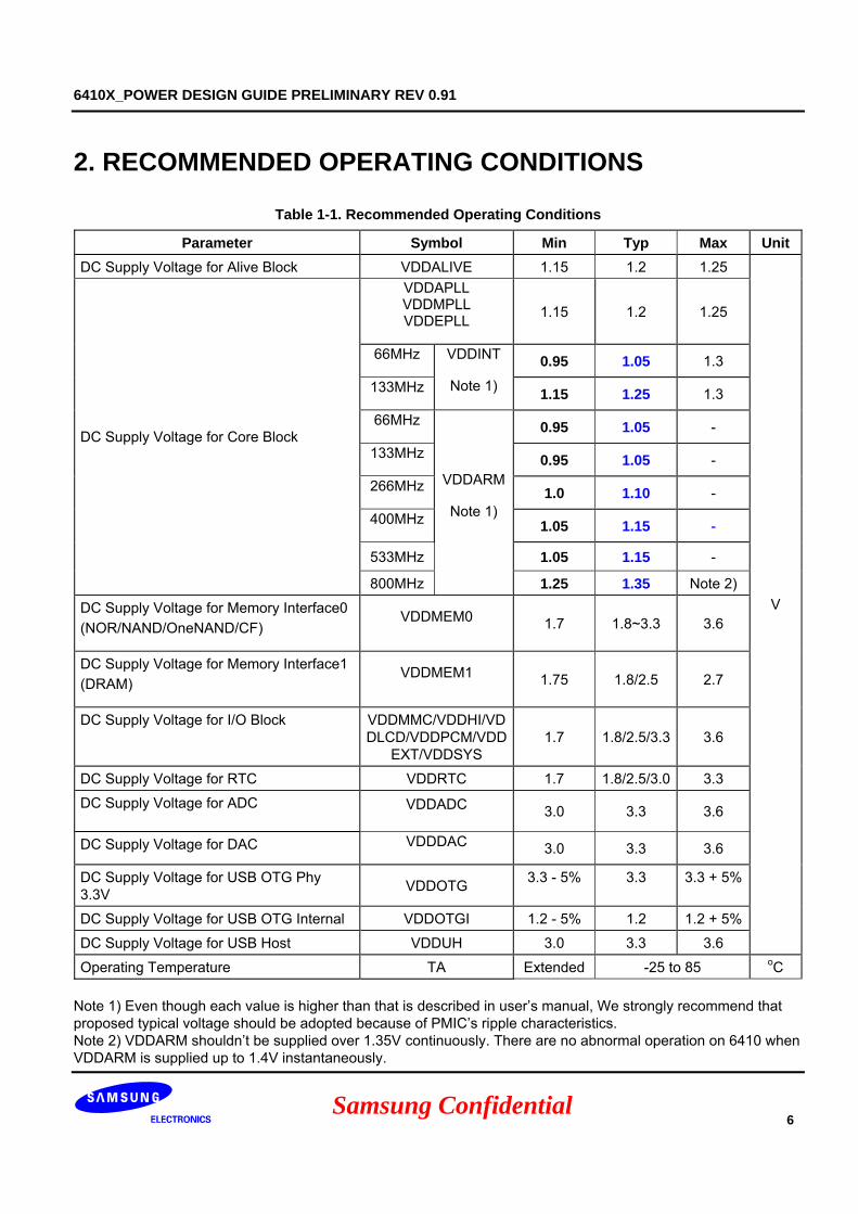
2. RECOMMENDED OPERATING CONDITIONS
Table 1-1. Recommended Operating Conditions
Parameter Symbol Min Typ Max UnitDC Supply Voltage for Alive Block VDDALIVE 1.15 1.2 1.25
VDDAPLL VDDMPLL VDDEPLL 1.15 1.2 1.25
66MHz 0.95 1.05 1.3
133MHz
VDDINT
Note 1) 1.15 1.25 1.3
66MHz 0.95 1.05 -
133MHz 0.95 1.05 -
266MHz 1.0 1.10 -
400MHz 1.05 1.15 -
533MHz 1.05 1.15 -
DC Supply Voltage for Core Block
800MHz
VDDARM
Note 1)
1.25 1.35 Note 2)
DC Supply Voltage for Memory Interface0 (NOR/NAND/OneNAND/CF)
VDDMEM0 1.7 1.8~3.3 3.6
DC Supply Voltage for Memory Interface1 (DRAM)
VDDMEM1 1.75 1.8/2.5 2.7
DC Supply Voltage for I/O Block VDDMMC/VDDHI/VDDLCD/VDDPCM/VDD
EXT/VDDSYS 1.7 1.8/2.5/3.3 3.6
DC Supply Voltage for RTC VDDRTC 1.7 1.8/2.5/3.0 3.3
DC Supply Voltage for ADC VDDADC 3.0 3.3 3.6
DC Supply Voltage for DAC VDDDAC 3.0 3.3 3.6
DC Supply Voltage for USB OTG Phy 3.3V VDDOTG 3.3 - 5% 3.3 3.3 + 5%
DC Supply Voltage for USB OTG Internal VDDOTGI 1.2 - 5% 1.2 1.2 + 5%
DC Supply Voltage for USB Host VDDUH 3.0 3.3 3.6
V
Operating Temperature TA Extended -25 to 85 oC
Note 1) Even though each value is higher than that is described in user’s manual, We strongly recommend that proposed typical voltage should be adopted because of PMIC’s ripple characteristics. Note 2) VDDARM shouldn’t be supplied over 1.35V continuously. There are no abnormal operation on 6410 when VDDARM is supplied up to 1.4V instantaneously.

6410X_POWER DESIGN GUIDE PRELIMINARY REV 0.91
7 Samsung Confidential
3. RECOMMEND SYSTEM POWER DESIGN
S3C6410XVDDARM
VDDINT
VDDAPLL/VDDMPLL/VDDEPLLVDDALIVE
VDDMEM0VDDMEM1
VDDRTC
VDDADC/VDDDAC/VDDUH
VDDMMC/VDDHI/VDDLCD/VDDPCM/VDDEXT/VDDSYS
VDDOTG
VDDOTGI
DC/DC
V.V-DC-DC
Battery3.8V/
xx mAh
V.V-DC-DC
FET
LDO
LDO
LDO
LDO
EN
GPIO Control
LDO
VDDARM
VDDINT
VDDxPLL
VDDALIVE
VDDRTC
VDDMEMx
VDDADC/DAC/UH
IO Voltage
VDDOTG
VDDOTGI
LDO
EN
GPIO Control
Figure 1. Power Scheme Diagram
VDDALIVE is fed into FET(MosFET Switch) to generate VDDxPLL. FET switch should be turned on when VDDINT is supplied. FET switch should be turned off when CPU is in sleep mode.

6410X_POWER DESIGN GUIDE PRELIMINARY REV 0.91
8 Samsung Confidential
4. CIRCUIT GUIDE FOR DVS SCHEME
The diagram described in figure 2 is a example to implement h/w configuration for DVFS. VDDARM and VDDINT can be supplied directly from PMIC if the voltage of them can be variable with software setting.
DC/ DCConverter
VDD33VVDDARM
FB
R1
R2 R3
R2 : DVS OFF Resistor ValueR3 : DVS ON Resistor Value
nGPIO1
On : / w DVSOff : / wo DVS
VDDARM
DC/ DCConverter
VDD33VVDDINT
FB
R1
R2 R3
R2 : Resistor Value(133MHz)R3 : Resistor Value(66MHz)
nGPIO2
On : / w DVSOff : / wo DVS
VDDINT
VDDARM is depended by ARM Frequency
Figure 2. An example of generating variable voltage

6410X_POWER DESIGN GUIDE PRELIMINARY REV 0.91
9 Samsung Confidential
5. TIMING CHARTS WITH DVFS 5.1. Typical DVFS Level Definition
5.1.1. Typical DVFS Transition Table @ 533Mhz Synchronous and Asynchronous Mode
LEVEL FoutAPLL FoutMPLL ARMCLK(MHz) HCLK(MHz) PCLK(MHz) Remark L0(Fast) 532 133 66
L1 266 133 66
L2 266 133 66
L3 133 133 66
AL1 133 66 66
AL2
532 266
66 66 66 Note)
Note) If AL1 or AL2 is used, refresh cycle should be set based on 66MHz at initial setting
5.1.2. Typical DVFS Transition Table @ 800Mhz Synchronous and Asynchronous Mode
LEVEL FoutAPLL FoutMPLL ARMCLK(MHz) HCLK(MHz) PCLK(MHz) Remark L0(Fast) 800 133 66
L1 400 133 66
L2 266 133 66
L3 133 133 66
AL1 133 66 66
AL2
800 266
66 66 66 Note)
Note) If AL1 or AL2 is used, refresh cycle should be set based on 66MHz at initial setting

6410X_POWER DESIGN GUIDE PRELIMINARY REV 0.91
10 Samsung Confidential
5.2. Typical DVFS Transition Diagram
5.2.1. Typical DVFS Transition Diagram @ 533, 800Mhz
L0
L1
L2
L3
Figure 3. A transition diagram when cpu is in 533, 800Mhz
DVFS level can be switched by changing clock divider. External access by ARM is not permitted when clock divider is changed at synchronous mode. It is implemented easily using IMB(Instruction Memory Barrier) and DMB(Data Memory Barrier). Refer to attached assembly code, ChangeDivider()

6410X_POWER DESIGN GUIDE PRELIMINARY REV 0.91
11 Samsung Confidential
5.3. Timing diagram with DVFS
Slow
0V
xtal:xtal:xtal 0:133:33
NormalIdleNormal
533:133:33 533:133:33
(1) Power is turned on and program is started under slow clock(2) After locktime(caused by PMS setting), the system runs at high speed(533MHz)(3) Enter Idle mode(4) Wake-up from Idle mode
Figure 5. Transition between Normal and Idle mode when 533:133MHz Case

6410X_POWER DESIGN GUIDE PRELIMINARY REV 0.91
12 Samsung Confidential
Figure 6. DVFS example by changing clock divider when 533:133MHz Case

6410X_POWER DESIGN GUIDE PRELIMINARY REV 0.91
13 Samsung Confidential
Figure 7. DVFS with Idle state example by changing clock divider when 533:133MHz Case

6410X_POWER DESIGN GUIDE PRELIMINARY REV 0.91
14 Samsung Confidential
Figure 9. DVFS example by changing PMS value during

6410X_POWER DESIGN GUIDE PRELIMINARY REV 0.91
15 Samsung Confidential
6. POWER ON AND OFF SEQUENCE
VDD_IO
VDDALIVE
XPWRRGTON
XnRESET
OSC(XTIpll)
tOA
tAI
tOSC
tOR
tAEIO State
Unknown State Reset State
S/W defines GPIO
User-Defined State
Unknown State
VDDARM/ VDDINT
Figure 10-a. Power on sequence in case of normal discrete power solution (Non-PMIC)
Symbol Description Min Typical Max Units
tOA VDD_IO to VDDALIVE 0 Ms
tAI XPWRRGTON to VDDARM/VDDINT It depend on Regulator Ms
tAE VDDALIVE to XPWRRGTON 0 10 Ns
tOSC VDDINT/VDDARM/VDDPLL to Oscillator stabilization Note) Ms
tOR Oscillator stabilization to XnRESET high 10 Cycle Note) VDD_IO=VDDMMC & VDDHI & VDDLCD & VDDPCM & VDDEXT & VDDSYS & VDDATA & VDDUH &
VDDM0 & VDDM1 VDDPLL=VDDMPLL & VDDEPLL & VDDAPLL tOSC is depend on characteristics of crystal, pcb and capacitance.

6410X_POWER DESIGN GUIDE PRELIMINARY REV 0.91
16 Samsung Confidential
VDD_IO
VDDALIVE
XnRESET
OSC(XTIpll)
tAC
tCI
tOSC
tOR
IO StateReset State
S/W defines GPIO
User-Defined State
VDDARM/ VDDINT
Figure 10-b. Power on sequence in case of PMIC solution
Symbol Description Min Typical Max Units
tAC VDDALIVE to VDD_ARM/INT 0 Ms
tCI VDD_ARM/INT to VDD_IO 0 Us
tOSC VDDINT/VDDARM/VDDPLL to Oscillator stabilization Note) Ms
tOR Oscillator stabilization to XnRESET high 10 Cycle Note) VDD_IO=VDDMMC & VDDHI & VDDLCD & VDDPCM & VDDEXT & VDDSYS & VDDATA & VDDUH &
VDDM0 & VDDM1 VDDPLL=VDDMPLL & VDDEPLL & VDDAPLL tOSC is depend on characteristics of crystal, pcb and capacitance.

6410X_POWER DESIGN GUIDE PRELIMINARY REV 0.91
17 Samsung Confidential
Figure 11. Power off sequence
Symbol Description Min TYP Max Units tloa VDD_IO to VDDALIVE 0 ms tloi VDD_IO to VDDINT/VDDARM/VDDPLL 0 ms
Note) VDD_IO=VDDMMC & VDDHI & VDDLCD & VDDPCM & VDDEXT & VDDSYS & VDDATA & VDDUH & VDDM0 & VDDM1
VDDPLL=VDDMPLL & VDDEPLL & VDDAPLL
I/O signal has unknown state which is described in the Figure 10-a. I/O signal may occur glitch at power on stage. For example, when using this I/O as LED on/off control signal, it causes unwanted flickering. To protect this glitch, System designer can use external AND gate device with nRESET signal.

6410X_POWER DESIGN GUIDE PRELIMINARY REV 0.91
18 Samsung Confidential
VDDarm /int/pll
nRESET
EXTCLKor XTIpll
VCO Output
SYSCLK
Sleep mode is initiated
Pll lock time
RSTOUT
PWR_EN
Wakeup Event
PWRSETCNT
Normal Mode Normal ModeResetSleep Mode
VDD_Opx, cam, lcd, sd, sdram, sram, adc, rtc
VDDA33T, A33C, UDEV
Turn on USB power when use USB
Figure 12 Sleep mode & wakeup sequence
Note) VDD_IO : VDDMMC, VDDHI, VDDLCD, VDDPCM, VDDEXT, VDDSYS, VDDMEMx, VDDSS PWR_EN : Signal at XPWRRGTON pin

6410X_POWER DESIGN GUIDE PRELIMINARY REV 0.91
19 Samsung Confidential
7. PLL DESIGN GUIDE
Figure 13 Crystal Design Guide
7.1. APLL/MPLL Specification The output frequencies of APLL/MPLL can be calculated using the following equations:
FOUT = MDIV X FIN / (PDIV X 2SDIV)
MDIV: 64 ≤ MDIV ≤ 1023
PDIV: 1 ≤ PDIV ≤ 63
SDIV: 0 ≤ SDIV ≤ 5
FVCO =(MDIV X FIN / PDIV): 800MHz ≤ FVCO ≤ 1600MHz
FIN : 10MHz ≤ FIN ≤ 20MHz
NOTE ) Although there is the equation for choosing PLL value, we strongly recommend only the values in the PLL value recommendation table. If you have to use other values, please contact us.
XXTI
XXTO 1M-ohm
X27MXTI
X27MXTO 1M-ohm
5M-ohm
1M-ohm
XrtxXTI
XrtcXTO
XotgTI
XotgTO

6410X_POWER DESIGN GUIDE PRELIMINARY REV 0.91
20 Samsung Confidential
FIN (MHz)
Target FOUT (MHz)
MDIV PDIV SDIV
12 266 266 3 2 12 400 400 3 2 12 533 266 3 1 12 800 400 3 1
Usual Conditions for MPLL & Clock Generator PLL & Clock Generator generally uses the following conditions.
Loop filter capacitance CLF Need not Loop Filter Capacitance
External X-tal frequency - 10 – 20 MHz
External capacitance used for X-tal CEXT 15 – 22 pF
7.2. EPLL Specification
The output frequencies of EPLL can be calculated using the following equations:
FOUT = (MDIV + KDIV / 216) X FIN / (PDIV X 2SDIV)
where, MDIV, PDIV, SDIV for APLL and MPLL must meet the following conditions :
MDIV: 16 ≤ MDIV ≤ 255
PDIV: 1 ≤ PDIV ≤ 63
KDIV: 0 ≤ KDIV ≤ 65535
SDIV: 0 ≤ SDIV ≤ 4
FVCO (= (MDIV + KDIV / 216) X FIN / PDIV) : 300MHz ≤ FVCO ≤ 600MHz
FOUT : 20MHz ≤ FOUT ≤ 600MHz
FIN : 10MHz ≤ FIN ≤ 20MHz
NOTE ) Although there is the equation for choosing PLL value, we strongly recommend only the values in the PLL value recommendation table. If you have to use other values, please contact us.
FIN (MHz) FOUT (MHz) MDIV PDIV SDIV KDIV 12 36 48 1 4 0 12 48 32 1 3 0 12 60 40 1 3 0 12 72 48 1 3 0 12 84 28 1 2 0 12 96 32 1 2 0

6410X_POWER DESIGN GUIDE PRELIMINARY REV 0.91
21 Samsung Confidential
Usual Conditions for EPLL & Clock Generator PLL & Clock Generator generally uses the following conditions.
Loop filter capacitance CLF XpllEFILTER: 1.8nF
External X-tal frequency - 10 – 20 MHz
External capacitance used for X-tal CEXT 15 – 22 pF
7.3. USB OTG 2.0 PLL Specification
PLL & Clock Generator generally uses the following conditions.
REXT R 44.2Ω ± 1%
VDDOTG V 3.3 ± 5%
VDDOTGI V 1.2 ± 5%
External X-tal frequency - 12M/24M/48 MHz recommend a quartz crystal
External capacitance used for X-tal CEXT 12M/24M - 20 pF 48M - 16 pF
Note )
(1) For usb2.0 device, user should be obey a layout rule of pcb.
7.4. TV OUT Clock Specification
PLL & Clock Generator generally uses the following conditions.
XdacIREF R 6.49 KΩ ± 1%
VDDDAC V 3.3 ± 0.3V
External X-tal frequency - 27MHz
External capacitance used for X-tal CEXT 15pF

6410X_POWER DESIGN GUIDE PRELIMINARY REV 0.91
22 Samsung Confidential
APPENDIX A. Example of Changing Divider Code ;--------------------------------- ------------------------------------------------------------------ ; Enable Branch Prediction ;--------------------------------- ------------------------------------------------------------------ LEAF_ENTRY System_EnableBP mrc p15,0,r0,c1,c0,0 orr r0,r0,#R1_BP mcr p15,0,r0,c1,c0,0 mov pc, lr ENTRY_END ;--------------------------------- ------------------------------------------------------------------ ; ChangeDivider ;--------------------------------- ------------------------------------------------------------------ EXPORT ChangeDivider ; r0=the value of clock divider ChangeDivider PROC stmfd sp!, r0-r5 ldr r1,=0x7e00f020 mov r2, #0 mov r3, #0 loopcd mov r4, #0 mcr p15, 0, r2, c7, c10, 4 ; data synchronization barrier instruction mcr p15, 0, r2, c7, c10, 5 ; data memory barrier operation cmp r3, #1 streq r0, [r1] mcr p15, 0, r2, c7, c5, 4 ; flush prefetch buffer loop1000 add r4, r4, #1 cmp r4, #0x1000 bne loop1000 cmp r3, #1 add r3, r3, #1 bne loopcd ldmfd sp!, r0-r5 mov pc,lr ENDP ;--------------------------------- ------------------------------------------------------------------ ; Disable Branch Prediction ;--------------------------------- ------------------------------------------------------------------ LEAF_ENTRY System_DisableBP mrc p15,0,r0,c1,c0,0 bic r0,r0,#R1_BP mcr p15,0,r0,c1,c0,0 mov pc, lr ENTRY_END Usage) System_EnableBP();
ChangeDivider(); System_DisableBP();

6410X_POWER DESIGN GUIDE PRELIMINARY REV 0.91
23 Samsung Confidential
B. Power Requirement
Power Name Voltage [V] Max. Current [mA]
VDDALIVE 1.2 2
VDDAPLL/VDDMPLL/VDDEPLL 1.2 10
VDDARM 1.2 900
VDDINT 1.3 500
VDDMEM0 3.3 50
VDDMEM1 1.8 100
VDDMMC/VDDHI/VDDLCD/VDDPCM/VDDEXT/VDDSYS 3.3 150
VDDRTC 1.8 1
VDDADC 3.3 10
VDDDAC 3.3 20
VDDOTG 3.3 20
VDDOTGI 1.2 20
VDDUH 3.3 30